JP4678933B2 - Method for manufacturing semiconductor device - Google Patents
Method for manufacturing semiconductor device Download PDFInfo
- Publication number
- JP4678933B2 JP4678933B2 JP2000338572A JP2000338572A JP4678933B2 JP 4678933 B2 JP4678933 B2 JP 4678933B2 JP 2000338572 A JP2000338572 A JP 2000338572A JP 2000338572 A JP2000338572 A JP 2000338572A JP 4678933 B2 JP4678933 B2 JP 4678933B2
- Authority
- JP
- Japan
- Prior art keywords
- insulating film
- film
- impurity
- region
- impurity region
- Prior art date
- Legal status (The legal status is an assumption and is not a legal conclusion. Google has not performed a legal analysis and makes no representation as to the accuracy of the status listed.)
- Expired - Fee Related
Links
- 239000004065 semiconductor Substances 0.000 title claims description 88
- 238000000034 method Methods 0.000 title claims description 57
- 238000004519 manufacturing process Methods 0.000 title claims description 22
- 239000012535 impurity Substances 0.000 claims description 153
- 239000000758 substrate Substances 0.000 claims description 48
- 230000015572 biosynthetic process Effects 0.000 claims description 46
- 238000005530 etching Methods 0.000 claims description 21
- 238000009826 distribution Methods 0.000 claims description 18
- 239000010408 film Substances 0.000 description 192
- 239000010410 layer Substances 0.000 description 122
- 238000005401 electroluminescence Methods 0.000 description 31
- 239000000463 material Substances 0.000 description 21
- 239000004973 liquid crystal related substance Substances 0.000 description 19
- 239000011229 interlayer Substances 0.000 description 16
- 239000011159 matrix material Substances 0.000 description 14
- 229910052581 Si3N4 Inorganic materials 0.000 description 13
- 230000003287 optical effect Effects 0.000 description 13
- HQVNEWCFYHHQES-UHFFFAOYSA-N silicon nitride Chemical compound N12[Si]34N5[Si]62N3[Si]51N64 HQVNEWCFYHHQES-UHFFFAOYSA-N 0.000 description 13
- 230000008569 process Effects 0.000 description 12
- VYPSYNLAJGMNEJ-UHFFFAOYSA-N Silicium dioxide Chemical compound O=[Si]=O VYPSYNLAJGMNEJ-UHFFFAOYSA-N 0.000 description 11
- 230000005684 electric field Effects 0.000 description 10
- 229910052814 silicon oxide Inorganic materials 0.000 description 10
- XUIMIQQOPSSXEZ-UHFFFAOYSA-N Silicon Chemical compound [Si] XUIMIQQOPSSXEZ-UHFFFAOYSA-N 0.000 description 9
- 238000010586 diagram Methods 0.000 description 9
- 230000006870 function Effects 0.000 description 9
- 229910052751 metal Inorganic materials 0.000 description 9
- 239000002184 metal Substances 0.000 description 9
- 229910052710 silicon Inorganic materials 0.000 description 9
- 239000010703 silicon Substances 0.000 description 9
- 230000001681 protective effect Effects 0.000 description 8
- 239000011347 resin Substances 0.000 description 8
- 229920005989 resin Polymers 0.000 description 8
- 239000010409 thin film Substances 0.000 description 7
- 238000000137 annealing Methods 0.000 description 6
- 230000000694 effects Effects 0.000 description 6
- 230000002093 peripheral effect Effects 0.000 description 6
- 239000000565 sealant Substances 0.000 description 6
- 238000002230 thermal chemical vapour deposition Methods 0.000 description 6
- 238000001994 activation Methods 0.000 description 5
- 150000001875 compounds Chemical class 0.000 description 5
- 239000011521 glass Substances 0.000 description 5
- 239000007769 metal material Substances 0.000 description 5
- 238000005268 plasma chemical vapour deposition Methods 0.000 description 5
- 238000004544 sputter deposition Methods 0.000 description 5
- 229910052782 aluminium Inorganic materials 0.000 description 4
- 239000003990 capacitor Substances 0.000 description 4
- 238000002347 injection Methods 0.000 description 4
- 239000007924 injection Substances 0.000 description 4
- 229910052698 phosphorus Inorganic materials 0.000 description 4
- 229910021420 polycrystalline silicon Inorganic materials 0.000 description 4
- 229920005591 polysilicon Polymers 0.000 description 4
- 239000003566 sealing material Substances 0.000 description 4
- 239000010936 titanium Substances 0.000 description 4
- OAICVXFJPJFONN-UHFFFAOYSA-N Phosphorus Chemical compound [P] OAICVXFJPJFONN-UHFFFAOYSA-N 0.000 description 3
- 230000004913 activation Effects 0.000 description 3
- 229910052785 arsenic Inorganic materials 0.000 description 3
- UMIVXZPTRXBADB-UHFFFAOYSA-N benzocyclobutene Chemical compound C1=CC=C2CCC2=C1 UMIVXZPTRXBADB-UHFFFAOYSA-N 0.000 description 3
- 239000010949 copper Substances 0.000 description 3
- 238000002425 crystallisation Methods 0.000 description 3
- 230000005284 excitation Effects 0.000 description 3
- 238000007687 exposure technique Methods 0.000 description 3
- 238000002161 passivation Methods 0.000 description 3
- 239000011574 phosphorus Substances 0.000 description 3
- 238000000206 photolithography Methods 0.000 description 3
- 230000010287 polarization Effects 0.000 description 3
- 229910052719 titanium Inorganic materials 0.000 description 3
- 238000007740 vapor deposition Methods 0.000 description 3
- 238000001039 wet etching Methods 0.000 description 3
- OKTJSMMVPCPJKN-UHFFFAOYSA-N Carbon Chemical compound [C] OKTJSMMVPCPJKN-UHFFFAOYSA-N 0.000 description 2
- PXHVJJICTQNCMI-UHFFFAOYSA-N Nickel Chemical compound [Ni] PXHVJJICTQNCMI-UHFFFAOYSA-N 0.000 description 2
- XLOMVQKBTHCTTD-UHFFFAOYSA-N Zinc monoxide Chemical compound [Zn]=O XLOMVQKBTHCTTD-UHFFFAOYSA-N 0.000 description 2
- XAGFODPZIPBFFR-UHFFFAOYSA-N aluminium Chemical compound [Al] XAGFODPZIPBFFR-UHFFFAOYSA-N 0.000 description 2
- 229910021417 amorphous silicon Inorganic materials 0.000 description 2
- RQNWIZPPADIBDY-UHFFFAOYSA-N arsenic atom Chemical compound [As] RQNWIZPPADIBDY-UHFFFAOYSA-N 0.000 description 2
- QVGXLLKOCUKJST-UHFFFAOYSA-N atomic oxygen Chemical compound [O] QVGXLLKOCUKJST-UHFFFAOYSA-N 0.000 description 2
- 230000000903 blocking effect Effects 0.000 description 2
- 229910052799 carbon Inorganic materials 0.000 description 2
- 239000011651 chromium Substances 0.000 description 2
- 239000013078 crystal Substances 0.000 description 2
- 238000001312 dry etching Methods 0.000 description 2
- 238000005247 gettering Methods 0.000 description 2
- 238000005984 hydrogenation reaction Methods 0.000 description 2
- 229910010272 inorganic material Inorganic materials 0.000 description 2
- 239000011147 inorganic material Substances 0.000 description 2
- 239000012212 insulator Substances 0.000 description 2
- 238000005468 ion implantation Methods 0.000 description 2
- 150000002500 ions Chemical class 0.000 description 2
- 238000005224 laser annealing Methods 0.000 description 2
- 229910052760 oxygen Inorganic materials 0.000 description 2
- 239000001301 oxygen Substances 0.000 description 2
- 238000000059 patterning Methods 0.000 description 2
- 239000004033 plastic Substances 0.000 description 2
- 238000004151 rapid thermal annealing Methods 0.000 description 2
- 238000004088 simulation Methods 0.000 description 2
- 239000002356 single layer Substances 0.000 description 2
- DDFHBQSCUXNBSA-UHFFFAOYSA-N 5-(5-carboxythiophen-2-yl)thiophene-2-carboxylic acid Chemical compound S1C(C(=O)O)=CC=C1C1=CC=C(C(O)=O)S1 DDFHBQSCUXNBSA-UHFFFAOYSA-N 0.000 description 1
- VYZAMTAEIAYCRO-UHFFFAOYSA-N Chromium Chemical compound [Cr] VYZAMTAEIAYCRO-UHFFFAOYSA-N 0.000 description 1
- RYGMFSIKBFXOCR-UHFFFAOYSA-N Copper Chemical compound [Cu] RYGMFSIKBFXOCR-UHFFFAOYSA-N 0.000 description 1
- GYHNNYVSQQEPJS-UHFFFAOYSA-N Gallium Chemical compound [Ga] GYHNNYVSQQEPJS-UHFFFAOYSA-N 0.000 description 1
- WHXSMMKQMYFTQS-UHFFFAOYSA-N Lithium Chemical compound [Li] WHXSMMKQMYFTQS-UHFFFAOYSA-N 0.000 description 1
- ZOKXTWBITQBERF-UHFFFAOYSA-N Molybdenum Chemical compound [Mo] ZOKXTWBITQBERF-UHFFFAOYSA-N 0.000 description 1
- 239000004642 Polyimide Substances 0.000 description 1
- 229910006404 SnO 2 Inorganic materials 0.000 description 1
- 239000004809 Teflon Substances 0.000 description 1
- 229920006362 Teflon® Polymers 0.000 description 1
- RTAQQCXQSZGOHL-UHFFFAOYSA-N Titanium Chemical compound [Ti] RTAQQCXQSZGOHL-UHFFFAOYSA-N 0.000 description 1
- LEVVHYCKPQWKOP-UHFFFAOYSA-N [Si].[Ge] Chemical compound [Si].[Ge] LEVVHYCKPQWKOP-UHFFFAOYSA-N 0.000 description 1
- NIXOWILDQLNWCW-UHFFFAOYSA-N acrylic acid group Chemical group C(C=C)(=O)O NIXOWILDQLNWCW-UHFFFAOYSA-N 0.000 description 1
- 239000000853 adhesive Substances 0.000 description 1
- 230000001070 adhesive effect Effects 0.000 description 1
- 239000005407 aluminoborosilicate glass Substances 0.000 description 1
- 239000010407 anodic oxide Substances 0.000 description 1
- 229910052787 antimony Inorganic materials 0.000 description 1
- 238000003491 array Methods 0.000 description 1
- LDDQLRUQCUTJBB-UHFFFAOYSA-O azanium;hydrofluoride Chemical compound [NH4+].F LDDQLRUQCUTJBB-UHFFFAOYSA-O 0.000 description 1
- 229910052788 barium Inorganic materials 0.000 description 1
- DSAJWYNOEDNPEQ-UHFFFAOYSA-N barium atom Chemical compound [Ba] DSAJWYNOEDNPEQ-UHFFFAOYSA-N 0.000 description 1
- 230000005540 biological transmission Effects 0.000 description 1
- 229910052797 bismuth Inorganic materials 0.000 description 1
- 239000005388 borosilicate glass Substances 0.000 description 1
- 239000000969 carrier Substances 0.000 description 1
- 230000015556 catabolic process Effects 0.000 description 1
- 239000003054 catalyst Substances 0.000 description 1
- 230000001413 cellular effect Effects 0.000 description 1
- 230000008859 change Effects 0.000 description 1
- 238000006243 chemical reaction Methods 0.000 description 1
- 229910052804 chromium Inorganic materials 0.000 description 1
- 238000000576 coating method Methods 0.000 description 1
- 239000003086 colorant Substances 0.000 description 1
- 239000004020 conductor Substances 0.000 description 1
- 238000011109 contamination Methods 0.000 description 1
- 229910052802 copper Inorganic materials 0.000 description 1
- 229910021419 crystalline silicon Inorganic materials 0.000 description 1
- 230000008025 crystallization Effects 0.000 description 1
- 230000006866 deterioration Effects 0.000 description 1
- 238000009792 diffusion process Methods 0.000 description 1
- 238000005516 engineering process Methods 0.000 description 1
- 230000002349 favourable effect Effects 0.000 description 1
- 230000005669 field effect Effects 0.000 description 1
- 229910052733 gallium Inorganic materials 0.000 description 1
- 229910052732 germanium Inorganic materials 0.000 description 1
- GNPVGFCGXDBREM-UHFFFAOYSA-N germanium atom Chemical compound [Ge] GNPVGFCGXDBREM-UHFFFAOYSA-N 0.000 description 1
- 230000005525 hole transport Effects 0.000 description 1
- 229910003437 indium oxide Inorganic materials 0.000 description 1
- PJXISJQVUVHSOJ-UHFFFAOYSA-N indium(iii) oxide Chemical compound [O-2].[O-2].[O-2].[In+3].[In+3] PJXISJQVUVHSOJ-UHFFFAOYSA-N 0.000 description 1
- 238000009413 insulation Methods 0.000 description 1
- 238000005499 laser crystallization Methods 0.000 description 1
- 229910052744 lithium Inorganic materials 0.000 description 1
- 230000000873 masking effect Effects 0.000 description 1
- 230000008018 melting Effects 0.000 description 1
- 238000002844 melting Methods 0.000 description 1
- 239000002923 metal particle Substances 0.000 description 1
- 239000011259 mixed solution Substances 0.000 description 1
- 229910052750 molybdenum Inorganic materials 0.000 description 1
- 239000011733 molybdenum Substances 0.000 description 1
- 229910052759 nickel Inorganic materials 0.000 description 1
- 229910052757 nitrogen Inorganic materials 0.000 description 1
- 230000003647 oxidation Effects 0.000 description 1
- 238000007254 oxidation reaction Methods 0.000 description 1
- 239000002245 particle Substances 0.000 description 1
- 230000000737 periodic effect Effects 0.000 description 1
- 229920001721 polyimide Polymers 0.000 description 1
- 239000010453 quartz Substances 0.000 description 1
- 239000003870 refractory metal Substances 0.000 description 1
- 230000003014 reinforcing effect Effects 0.000 description 1
- 230000002040 relaxant effect Effects 0.000 description 1
- 230000002441 reversible effect Effects 0.000 description 1
- 238000005070 sampling Methods 0.000 description 1
- 238000007789 sealing Methods 0.000 description 1
- 229910021332 silicide Inorganic materials 0.000 description 1
- FVBUAEGBCNSCDD-UHFFFAOYSA-N silicide(4-) Chemical compound [Si-4] FVBUAEGBCNSCDD-UHFFFAOYSA-N 0.000 description 1
- HBMJWWWQQXIZIP-UHFFFAOYSA-N silicon carbide Chemical compound [Si+]#[C-] HBMJWWWQQXIZIP-UHFFFAOYSA-N 0.000 description 1
- 229910010271 silicon carbide Inorganic materials 0.000 description 1
- 238000009751 slip forming Methods 0.000 description 1
- 238000003892 spreading Methods 0.000 description 1
- 230000007480 spreading Effects 0.000 description 1
- 238000003860 storage Methods 0.000 description 1
- 239000000126 substance Substances 0.000 description 1
- 229910052715 tantalum Inorganic materials 0.000 description 1
- GUVRBAGPIYLISA-UHFFFAOYSA-N tantalum atom Chemical compound [Ta] GUVRBAGPIYLISA-UHFFFAOYSA-N 0.000 description 1
- XOLBLPGZBRYERU-UHFFFAOYSA-N tin dioxide Chemical compound O=[Sn]=O XOLBLPGZBRYERU-UHFFFAOYSA-N 0.000 description 1
- 229910001887 tin oxide Inorganic materials 0.000 description 1
- WFKWXMTUELFFGS-UHFFFAOYSA-N tungsten Chemical compound [W] WFKWXMTUELFFGS-UHFFFAOYSA-N 0.000 description 1
- 229910052721 tungsten Inorganic materials 0.000 description 1
- 239000010937 tungsten Substances 0.000 description 1
- 230000005641 tunneling Effects 0.000 description 1
- 239000011787 zinc oxide Substances 0.000 description 1
Images


Classifications
-
- H—ELECTRICITY
- H01—ELECTRIC ELEMENTS
- H01L—SEMICONDUCTOR DEVICES NOT COVERED BY CLASS H10
- H01L27/00—Devices consisting of a plurality of semiconductor or other solid-state components formed in or on a common substrate
- H01L27/02—Devices consisting of a plurality of semiconductor or other solid-state components formed in or on a common substrate including semiconductor components specially adapted for rectifying, oscillating, amplifying or switching and having at least one potential-jump barrier or surface barrier; including integrated passive circuit elements with at least one potential-jump barrier or surface barrier
- H01L27/12—Devices consisting of a plurality of semiconductor or other solid-state components formed in or on a common substrate including semiconductor components specially adapted for rectifying, oscillating, amplifying or switching and having at least one potential-jump barrier or surface barrier; including integrated passive circuit elements with at least one potential-jump barrier or surface barrier the substrate being other than a semiconductor body, e.g. an insulating body
- H01L27/1214—Devices consisting of a plurality of semiconductor or other solid-state components formed in or on a common substrate including semiconductor components specially adapted for rectifying, oscillating, amplifying or switching and having at least one potential-jump barrier or surface barrier; including integrated passive circuit elements with at least one potential-jump barrier or surface barrier the substrate being other than a semiconductor body, e.g. an insulating body comprising a plurality of TFTs formed on a non-semiconducting substrate, e.g. driving circuits for AMLCDs
- H01L27/1259—Multistep manufacturing methods
- H01L27/1288—Multistep manufacturing methods employing particular masking sequences or specially adapted masks, e.g. half-tone mask
-
- H—ELECTRICITY
- H01—ELECTRIC ELEMENTS
- H01L—SEMICONDUCTOR DEVICES NOT COVERED BY CLASS H10
- H01L27/00—Devices consisting of a plurality of semiconductor or other solid-state components formed in or on a common substrate
- H01L27/02—Devices consisting of a plurality of semiconductor or other solid-state components formed in or on a common substrate including semiconductor components specially adapted for rectifying, oscillating, amplifying or switching and having at least one potential-jump barrier or surface barrier; including integrated passive circuit elements with at least one potential-jump barrier or surface barrier
- H01L27/12—Devices consisting of a plurality of semiconductor or other solid-state components formed in or on a common substrate including semiconductor components specially adapted for rectifying, oscillating, amplifying or switching and having at least one potential-jump barrier or surface barrier; including integrated passive circuit elements with at least one potential-jump barrier or surface barrier the substrate being other than a semiconductor body, e.g. an insulating body
- H01L27/1214—Devices consisting of a plurality of semiconductor or other solid-state components formed in or on a common substrate including semiconductor components specially adapted for rectifying, oscillating, amplifying or switching and having at least one potential-jump barrier or surface barrier; including integrated passive circuit elements with at least one potential-jump barrier or surface barrier the substrate being other than a semiconductor body, e.g. an insulating body comprising a plurality of TFTs formed on a non-semiconducting substrate, e.g. driving circuits for AMLCDs
-
- H—ELECTRICITY
- H01—ELECTRIC ELEMENTS
- H01L—SEMICONDUCTOR DEVICES NOT COVERED BY CLASS H10
- H01L29/00—Semiconductor devices adapted for rectifying, amplifying, oscillating or switching, or capacitors or resistors with at least one potential-jump barrier or surface barrier, e.g. PN junction depletion layer or carrier concentration layer; Details of semiconductor bodies or of electrodes thereof ; Multistep manufacturing processes therefor
- H01L29/66—Types of semiconductor device ; Multistep manufacturing processes therefor
- H01L29/66007—Multistep manufacturing processes
- H01L29/66075—Multistep manufacturing processes of devices having semiconductor bodies comprising group 14 or group 13/15 materials
- H01L29/66227—Multistep manufacturing processes of devices having semiconductor bodies comprising group 14 or group 13/15 materials the devices being controllable only by the electric current supplied or the electric potential applied, to an electrode which does not carry the current to be rectified, amplified or switched, e.g. three-terminal devices
- H01L29/66409—Unipolar field-effect transistors
- H01L29/66477—Unipolar field-effect transistors with an insulated gate, i.e. MISFET
- H01L29/66742—Thin film unipolar transistors
- H01L29/6675—Amorphous silicon or polysilicon transistors
- H01L29/66765—Lateral single gate single channel transistors with inverted structure, i.e. the channel layer is formed after the gate
-
- H—ELECTRICITY
- H01—ELECTRIC ELEMENTS
- H01L—SEMICONDUCTOR DEVICES NOT COVERED BY CLASS H10
- H01L29/00—Semiconductor devices adapted for rectifying, amplifying, oscillating or switching, or capacitors or resistors with at least one potential-jump barrier or surface barrier, e.g. PN junction depletion layer or carrier concentration layer; Details of semiconductor bodies or of electrodes thereof ; Multistep manufacturing processes therefor
- H01L29/66—Types of semiconductor device ; Multistep manufacturing processes therefor
- H01L29/68—Types of semiconductor device ; Multistep manufacturing processes therefor controllable by only the electric current supplied, or only the electric potential applied, to an electrode which does not carry the current to be rectified, amplified or switched
- H01L29/76—Unipolar devices, e.g. field effect transistors
- H01L29/772—Field effect transistors
- H01L29/78—Field effect transistors with field effect produced by an insulated gate
- H01L29/786—Thin film transistors, i.e. transistors with a channel being at least partly a thin film
- H01L29/78606—Thin film transistors, i.e. transistors with a channel being at least partly a thin film with supplementary region or layer in the thin film or in the insulated bulk substrate supporting it for controlling or increasing the safety of the device
- H01L29/78618—Thin film transistors, i.e. transistors with a channel being at least partly a thin film with supplementary region or layer in the thin film or in the insulated bulk substrate supporting it for controlling or increasing the safety of the device characterised by the drain or the source properties, e.g. the doping structure, the composition, the sectional shape or the contact structure
- H01L29/78621—Thin film transistors, i.e. transistors with a channel being at least partly a thin film with supplementary region or layer in the thin film or in the insulated bulk substrate supporting it for controlling or increasing the safety of the device characterised by the drain or the source properties, e.g. the doping structure, the composition, the sectional shape or the contact structure with LDD structure or an extension or an offset region or characterised by the doping profile
- H01L29/78627—Thin film transistors, i.e. transistors with a channel being at least partly a thin film with supplementary region or layer in the thin film or in the insulated bulk substrate supporting it for controlling or increasing the safety of the device characterised by the drain or the source properties, e.g. the doping structure, the composition, the sectional shape or the contact structure with LDD structure or an extension or an offset region or characterised by the doping profile with a significant overlap between the lightly doped drain and the gate electrode, e.g. GOLDD
-
- G—PHYSICS
- G02—OPTICS
- G02F—OPTICAL DEVICES OR ARRANGEMENTS FOR THE CONTROL OF LIGHT BY MODIFICATION OF THE OPTICAL PROPERTIES OF THE MEDIA OF THE ELEMENTS INVOLVED THEREIN; NON-LINEAR OPTICS; FREQUENCY-CHANGING OF LIGHT; OPTICAL LOGIC ELEMENTS; OPTICAL ANALOGUE/DIGITAL CONVERTERS
- G02F1/00—Devices or arrangements for the control of the intensity, colour, phase, polarisation or direction of light arriving from an independent light source, e.g. switching, gating or modulating; Non-linear optics
- G02F1/01—Devices or arrangements for the control of the intensity, colour, phase, polarisation or direction of light arriving from an independent light source, e.g. switching, gating or modulating; Non-linear optics for the control of the intensity, phase, polarisation or colour
- G02F1/13—Devices or arrangements for the control of the intensity, colour, phase, polarisation or direction of light arriving from an independent light source, e.g. switching, gating or modulating; Non-linear optics for the control of the intensity, phase, polarisation or colour based on liquid crystals, e.g. single liquid crystal display cells
- G02F1/133—Constructional arrangements; Operation of liquid crystal cells; Circuit arrangements
- G02F1/1333—Constructional arrangements; Manufacturing methods
- G02F1/1345—Conductors connecting electrodes to cell terminals
- G02F1/13454—Drivers integrated on the active matrix substrate
-
- H—ELECTRICITY
- H01—ELECTRIC ELEMENTS
- H01L—SEMICONDUCTOR DEVICES NOT COVERED BY CLASS H10
- H01L29/00—Semiconductor devices adapted for rectifying, amplifying, oscillating or switching, or capacitors or resistors with at least one potential-jump barrier or surface barrier, e.g. PN junction depletion layer or carrier concentration layer; Details of semiconductor bodies or of electrodes thereof ; Multistep manufacturing processes therefor
- H01L29/66—Types of semiconductor device ; Multistep manufacturing processes therefor
- H01L29/68—Types of semiconductor device ; Multistep manufacturing processes therefor controllable by only the electric current supplied, or only the electric potential applied, to an electrode which does not carry the current to be rectified, amplified or switched
- H01L29/76—Unipolar devices, e.g. field effect transistors
- H01L29/772—Field effect transistors
- H01L29/78—Field effect transistors with field effect produced by an insulated gate
- H01L29/786—Thin film transistors, i.e. transistors with a channel being at least partly a thin film
- H01L29/78606—Thin film transistors, i.e. transistors with a channel being at least partly a thin film with supplementary region or layer in the thin film or in the insulated bulk substrate supporting it for controlling or increasing the safety of the device
- H01L29/78618—Thin film transistors, i.e. transistors with a channel being at least partly a thin film with supplementary region or layer in the thin film or in the insulated bulk substrate supporting it for controlling or increasing the safety of the device characterised by the drain or the source properties, e.g. the doping structure, the composition, the sectional shape or the contact structure
- H01L29/78621—Thin film transistors, i.e. transistors with a channel being at least partly a thin film with supplementary region or layer in the thin film or in the insulated bulk substrate supporting it for controlling or increasing the safety of the device characterised by the drain or the source properties, e.g. the doping structure, the composition, the sectional shape or the contact structure with LDD structure or an extension or an offset region or characterised by the doping profile
- H01L2029/7863—Thin film transistors, i.e. transistors with a channel being at least partly a thin film with supplementary region or layer in the thin film or in the insulated bulk substrate supporting it for controlling or increasing the safety of the device characterised by the drain or the source properties, e.g. the doping structure, the composition, the sectional shape or the contact structure with LDD structure or an extension or an offset region or characterised by the doping profile with an LDD consisting of more than one lightly doped zone or having a non-homogeneous dopant distribution, e.g. graded LDD
-
- H—ELECTRICITY
- H10—SEMICONDUCTOR DEVICES; ELECTRIC SOLID-STATE DEVICES NOT OTHERWISE PROVIDED FOR
- H10B—ELECTRONIC MEMORY DEVICES
- H10B10/00—Static random access memory [SRAM] devices
- H10B10/12—Static random access memory [SRAM] devices comprising a MOSFET load element
- H10B10/125—Static random access memory [SRAM] devices comprising a MOSFET load element the MOSFET being a thin film transistor [TFT]
Description
【0001】
【発明の属する技術分野】
本願発明は薄膜トランジスタ(以下、TFTという)で構成された回路を有する半導体装置およびその作製方法に関する。例えば、液晶表示パネルに代表される電気光学装置およびその様な電気光学装置を部品として搭載した電子機器に関する。
【0002】
なお、本明細書中において半導体装置とは、半導体特性を利用することで機能しうる装置全般を指し、電気光学装置、半導体回路および電子機器は全て半導体装置である。
【0003】
【従来の技術】
近年、絶縁表面を有する基板上に形成された半導体薄膜(厚さ数〜数百nm程度)を用いて薄膜トランジスタ(TFT)を構成する技術が注目されている。薄膜トランジスタはICや電気光学装置のような電子デバイスに広く応用され、特に画像表示装置のスイッチング素子として開発が急がれている。薄膜トランジスタは、トップゲート型TFTとボトムゲート型TFTとがある。
【0004】
ボトムゲート型TFTはトップゲート型TFTと比べ基板から半導体層への不純物拡散の影響が少ないので信頼性が高い。また、ゲート電極とオーバーラップするのが一般的な構造である。
【0005】
これらのTFTで形成した大面積集積回路を有する半導体装置の開発が進んでいる。
【0006】
アクティブマトリクス型液晶表示装置、EL表示装置、および密着型イメージセンサはその代表例として知られている。特に、結晶質シリコン膜(典型的にはポリシリコン膜)を活性層にしたTFT(以下、ポリシリコンTFTと記す)は電界効果移動度が高いことから、いろいろな機能を備えた回路を形成することも可能である。
【0007】
例えば、アクティブマトリクス型液晶表示装置には、機能ブロックごとに画像表示を行う画素回路や、CMOS回路を基本としたシフトレジスタ回路、レベルシフタ回路、バッファ回路、サンプリング回路などの画素回路を制御するための駆動回路が一枚の基板上に形成される。
【0008】
アクティブマトリクス型液晶表示装置の画素回路には、数十から数百万個の各画素にTFT(画素TFT)が配置され、その画素TFTのそれぞれには画素電極が設けられている。液晶を挟んだ対向基板側には対向電極が設けられており、液晶を誘電体とした一種のコンデンサを形成している。そして、各画素に印加する電圧をTFTのスイッチング機能により制御して、このコンデンサへの電荷を制御することで液晶を駆動し、透過光量を制御して画像を表示する仕組みになっている。
【0009】
画素TFTはnチャネル型TFTから成り、スイッチング素子として液晶に電圧を印加して駆動させるものである。液晶は交流で駆動させるので、フレーム反転駆動と呼ばれる方式が多く採用されている。この方式では消費電力を低く抑えるために、画素TFTに要求される特性はオフ電流値(TFTがオフ動作時に流れるドレイン電流)を十分低くすることが重要である。
【0010】
【発明が解決しようとする課題】
本発明はこのような問題点を解決するための技術であり、TFTを用いて作製するアクティブマトリクス型の液晶表示装置に代表される電気光学装置ならびに半導体装置において、半導体装置の動作特性を向上させ、かつ、低消費電力化を図ることを目的としている。
【0011】
特に、本発明は、オフ電流値が十分低く、且つオフ電流値に対するオン電流値の比が大きい画素TFT(nチャネル型TFT)の構造を得ることを目的としている。
【0012】
【課題を解決するための手段】
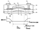
図1(A)に示すように本発明は、不純物領域102において、チャネル形成領域からの距離(チャネル長方向における距離)が増大するとともに、一導電型を付与する不純物元素の濃度が増大するような濃度勾配を有する領域102aを持たせることを特徴とする。
【0013】
即ち、チャネル長方向においてゲート電極105の端部から半導体層の周縁部(チャネル長方向で切断した断面における周縁部)に向かって離れるにつれて不純物元素(リン)の濃度が徐々に増大する不純物領域を備えたことを特徴としている。従って、この不純物領域は、チャネル形成領域側で電気抵抗が大きく、半導体層の周縁部側で電気抵抗が小さくなっている。
【0014】
また、本発明においては、連続的に増大する不純物領域であるため、明確な境界はなく、本明細書中では、不純物領域102のうち、不純物濃度が1×10²⁰/cm3以上の領域をドレイン領域102bと呼ぶ。
【0015】
また、上述では、ドレイン側について説明したが、ソース側においても同様とすることが好ましい。ソース側の不純物領域において、チャネル形成領域からの距離が増大するとともに、一導電型を付与する不純物元素の濃度が増大するような濃度勾配を有する領域103aを形成する。また、本明細書中では、ソース側の不純物領域のうち、不純物濃度が1×10²⁰/cm3以上の領域をソース領域103bと呼ぶ。
【0016】
本発明は、このような濃度勾配を有する領域102a、103aを意図的に形成することによって、オフ電流値が非常に低く、オフ電流値に対するオン電流値の比が高いTFTを実現することを特徴としている。ただし、ゲート電極105はゲート絶縁膜104を介してチャネル形成領域101及び不純物領域102aと重なる。なお、図1(A)において、100は絶縁表面を有する基板、108は層間絶縁膜、109はソース電極、110はドレイン電極である。また、図7に示したようにゲート電極が不純物領域と重ならない構造としてもよい。
【0017】
また、従来のTFT構造は、図13に示すように、明確な濃度差による境界が存在しており、チャネル形成領域1と、低濃度不純物領域2と、高濃度不純物領域3とで階段状に濃度が異なっていた。即ち、不連続な濃度分布を示していた。加えて、各領域における濃度は、ほぼ一定であった。従って、従来では、高濃度不純物領域3と低濃度不純物領域2との境界における濃度差や、低濃度不純物領域2とチャネル形成領域1との境界における濃度差が比較的大きいため、強い電界集中がそれぞれの境界付近に生じていた。
【0018】
オフ電流はバンド間のトンネリングなど量子力学的な効果で流れるため、主として電界に影響されると考えられる。従って、境界で生じていた電界集中がTFTのオフ電流値を増大させる原因となっていた。特に、従来のTFT構造においてチャネル形成領域と低濃度不純物領域との境界における大きな濃度差により強い電界が集中して問題となっていた。
【0019】
一方、本発明は、連続的に濃度が増大する不純物領域を設けることにより明確な境界をなくして、境界部近傍に発生する電界集中を緩和させることによってオフ電流値の低いTFT構造を得ることができる。
【0020】
本発明においては、図1(A)に示すように、半導体層における不純物元素の濃度差による境界が完全になくなるような濃度勾配を不純物領域102(1×10¹⁵/cm3〜1×1021/cm3の範囲)で形成することが最も望ましいが、チャネル形成領域101と該チャネル形成領域近傍の不純物領域102aの濃度差を小さくすることでも本発明の効果は得られる。また、不純物領域102bと該不純物領域近傍の不純物領域102aとの境界における濃度差を小さくすることでも本発明の効果は得られる。
【0021】
また、図1(B)は、TFT構造を図1(A)とし、チャネル長L=6μm、チャネル幅W=4μm、ゲート絶縁膜104の膜厚=115nm、ポリシリコン層の膜厚=45nm、不純物濃度(P濃度)1×10¹⁷〜1×10¹⁸/cm3の範囲で濃度勾配を有する領域102a(幅1.5μm)、不純物濃度(P濃度)1×1019/cm3の不純物領域102b、チャネル形成領域101のキャリア濃度(B濃度)=2×1016/cm3とした場合のシミュレーション結果である。このシミュレーション結果は、縦軸を半導体層表面の電界強度E(V/cm)、横軸をチャネル形成領域からの距離(μm)としており、図1(B)中の実線で示したものが本発明の不純物領域への電界集中の様子を示している。
【0022】
また、従来例として、TFTの半導体層における濃度分布を図13に示した分布とした低濃度不純物領域2への電界集中の様子を図1(B)中の点線で示した。
【0023】
図1(B)に示したように、本発明は少なくとも不純物濃度(P濃度)1×10¹⁷〜1×10¹⁸/cm3の範囲で濃度勾配を有する不純物領域を備えたことによって、従来よりも半導体層表面の電界強度を緩やかにすることができた。従って、本発明により、半導体層全域にわたって強い電界集中が発生せず、オフ電流値の低いTFTを得ることができる。
【0024】
本明細書で開示する発明の構成は、
絶縁表面上に形成されたゲート電極と、ゲート電極上に形成された絶縁膜と、該絶縁膜上に形成された半導体層とを含むTFTを備えた半導体装置であって、
前記半導体層は、前記ゲート電極と重なるチャネル形成領域と、該チャネル形成領域に接して形成された不純物領域とを有し、
前記不純物領域は、前記チャネル形成領域からの距離が増大するとともに不純物濃度が増加する濃度分布を備えたことを特徴とする半導体装置である。
【0025】
また、上記構成において、半導体に一導電型を付与する不純物元素は、リン(P)または砒素(As)であり、nチャネル型TFTが得られる。このnチャネル型TFTは、オフ電流が小さいので画素部のTFTに適している。
【0026】
また、上記構成において、前記不純物領域は、前記チャネル形成領域からの距離が増大するとともに不純物濃度が連続的に増加する濃度分布を備えたことを特徴としている。また、前記不純物領域は、チャネル長方向に濃度分布の濃度勾配を有する領域を少なくとも含むことを特徴としている。
【0027】
また、上記構成において、前記チャネル形成領域上に接して第1絶縁膜と、該第1絶縁膜上に第2絶縁膜とを有し、前記第1絶縁膜はテーパ−部を備えたことを特徴としている。
【0028】
また、上記構成において、前記第1絶縁膜のテーパ−部は、前記不純物領域のうち、濃度勾配を有する領域と重なっていることを特徴としている。
【0029】
また、上記構成において、前記第2絶縁膜は、前記チャネル形成領域と重なっていることを特徴としている。
【0030】
また、上記構成において、前記不純物領域は、前記ゲート電極と重なった構成としてもよいし、前記ゲート電極と重ならない構成としてもよい。
【0031】
また、上記構成において、第1絶縁膜と第2絶縁膜はエッチングレートの異なる材料を適宜選択すればよく、例えば、第1絶縁膜を窒化珪素膜とし、第2絶縁膜を酸化珪素膜とすればよい。
【0032】
また、上記構成において、前記不純物濃度は、半導体に一導電型を付与する不純物元素の濃度であることを特徴としている。
【0033】
また、図1において、不純物領域は、前記チャネル形成領域からの距離が増大するとともに不純物濃度が増加しており、その濃度分布を正規分布で示したが、特に限定されず、その濃度分布は指数分布であってもよいし、傾きを有する直線であってもよいし、それらを組み合わせたものであってもよい。
【0034】
従来では、パターニングしたレジストマスクを用いて不純物元素のドーピングを行ったり、配線をマスクとして自己整合的に不純物元素のドーピングを行っていたため、図13に示したような階段状の濃度分布が形成されており、上記本発明の構成、即ち濃度勾配を有する不純物領域を得ることはできなかった。また、本発明は上記構造を得るための作製方法も特徴としている。
【0035】
上記構造を実現する作製方法に関する発明の構成は、
絶縁表面上にゲート電極を形成する工程と、
前記ゲート電極上にゲート絶縁膜を形成する工程と、
前記ゲート絶縁膜上に半導体層を形成する工程と、
前記半導体層上に絶縁膜を形成する工程と、
該絶縁膜をエッチングして前記半導体層上にテーパ−部を有する絶縁層を形成する工程と、
前記テーパ−部を通過させて前記半導体層に一導電型を付与する不純物元素を添加し、前記テーパ−部の端部に向かって不純物濃度が増加する不純物領域を形成する工程と、
を有する半導体装置の作製方法である。
【0036】
従来ではフォトマスクを用いて形成したレジストマスクを用いて不純物元素のドーピングを行い、LDD領域、ソース領域、及びドレイン領域を形成していた。上記作製方法の構成においては、導電層からなるテーパ−部を通過させてドーピングを行い、濃度勾配を有する不純物領域を形成することを特徴としている。
【0037】
また、上記構成において、前記テーパ−部を通過させて前記半導体層に一導電型を付与する不純物元素を添加し、前記テーパ−部の端部に向かって不純物濃度が増加する不純物領域は、少なくとも不純物濃度(P濃度)1×10¹⁷〜1×10¹⁸/cm3の範囲で濃度勾配を有することを特徴とする。なお、本発明においては、図1(A)に示すように、半導体層における不純物元素の濃度差による境界が完全になくなるような濃度勾配を不純物領域102(1×1015/cm3〜1×1021/cm3の範囲)で形成することが最も望ましいが、チャネル形成領域101と該チャネル形成領域近傍の不純物領域102aの濃度差を小さくすることでも本発明の効果は得られる。また、不純物領域102bと該不純物領域近傍の不純物領域102aとの境界における濃度差を小さくすることでも本発明の効果は得られる。
【0038】
また、駆動回路と画素部とを同一基板上に形成することも可能である。
【0039】
また、上記構造を実現する作製方法に関する他の発明の構成は、
絶縁表面上にゲート電極を形成する工程と、
前記ゲート電極上にゲート絶縁膜を形成する工程と、
前記ゲート絶縁膜上に半導体層を形成する工程と、
前記半導体層上に第1絶縁膜を形成する工程と、
前記第1絶縁膜上に第2絶縁膜を形成する工程と、
前記第2絶縁膜上にレジストマスクを形成する工程と、
前記第2絶縁膜を選択的にエッチングしてチャネル形成領域となる部分を覆う第2絶縁層を形成し、前記第1絶縁膜を選択的にエッチングして前記半導体層上にテーパ−部を有する第2絶縁層を形成する工程と、
前記レジストマスクをマスクとして前記半導体層に一導電型を付与する不純物元素を添加する工程と、
前記レジストマスクを除去した後、前記テーパ−部を通過させて前記半導体層に一導電型を付与する不純物元素を添加し、前記テーパ−部の端部に向かって不純物濃度が増加する不純物領域を形成する工程と、
を有する半導体装置の作製方法である。
【0040】
また、上記作製方法の構成において、前記レジストマスクを形成する工程は、前記基板の裏面側からの露光により前記ゲート電極をマスクとして形成することを特徴としている。
【0041】
また、上記作製方法の構成において、前記テーパ−部を有する第2絶縁層を形成する工程におけるエッチングは、スピン方式やディップ方式等のウエットエッチングであることを特徴としている。
【0042】
また、前記テーパ−部を有する第2絶縁層を形成する工程におけるエッチングは、工程数が削減できるため一度のエッチングで形成することが好ましいが、複数回のエッチングにより形成してもよい。また、第2絶縁層をドライエッチングにより形成してもよい。また、第2絶縁層をウエットエッチングとドライエッチングを組み合わせて形成してもよい。
【0043】
【発明の実施の形態】
本願発明の実施形態について、以下に図1を用いて説明する。
【0044】
ここでは、第1の絶縁層108のテーパー部を利用して、前記チャネル形成領域側から前記不純物領域側に向かって不純物濃度(P濃度)が連続的に増加する不純物領域102を形成する例を示す。
【0045】
まず、透光性を有する基板上に、第1のマスクを用いてゲート配線(ゲート電極105を含む)と、ゲート配線を覆う絶縁膜と、結晶質半導体膜からなる半導体膜と、窒化珪素膜からなる第1絶縁膜と、酸化珪素膜からなる第2絶縁膜とを形成する。
【0046】
次いで、基板の裏面側からの露光によりゲート配線をマスクとしてレジストマスクを形成する。ここでは工程数低減のため裏面露光技術を用いたが、通常のフォトリソグラフィ技術を用いてもよい。通常のフォトリソグラフィ技術を用いる場合は、基板を透光性を有する基板に限らず、金属基板やシリコン、ゲルマニウム、ガリウム・砒素などの半導体基板の表面に絶縁膜を形成し、これを基板を用いてもよい。
【0047】
次いで、レジストマスクを用いてエッチングを行い、テーパ−部を有する絶縁層を形成する。ここでは、ディップ方式のウエットエッチングを行い、商品名:LAL500(フッ化水素アンモニウム(NH4HF2)を7.13%と、フッ化アンモニウム(NH4F)を15.4%含む混合溶液)を用いる。このエッチングにより、レジストマスクより狭いパターンの第2絶縁層107を形成し、さらに裾状に広がるテーパ−部を有する第1絶縁層106も同時に形成する。
【0048】
次いで、レジストマスクをそのままの状態で半導体膜にn型を付与する不純物元素を添加するドーピング工程を行ない、不純物領域(n+ 領域)を形成する。半導体材料に対してn型を付与する不純物元素としては、15族に属する不純物元素、例えばP、As、Sb、N、Bi等を用いることができる。
【0049】
次いで、レジストマスクを除去し、第2絶縁層をマスクとしてn型を付与する不純物元素を添加する2回目のドーピング工程を行なう。この2回目のドーピング工程において、第1絶縁層106のテーパー部を通過させて半導体層に不純物元素が添加され、第1絶縁層の直下には実質的に真性な結晶質半導体領域(以下、チャネル形成領域101)が残る。なお、本明細書中で実質的に真性とは、シリコンのフェルミレベルを変化させうる量の不純物元素を含まない領域、即ち、しきい値制御が可能な濃度範囲でN型またはP型を付与する不純物を含む領域、または意図的に逆導電型不純物を添加することにより導電型を相殺させた領域を示す。
【0050】
また、この2回目のドーピング工程の際、第1絶縁層のテーパー部を通過させることによって、チャネル形成領域からの距離(チャネル長方向)が増大するとともに不純物濃度が増加する濃度分布を備えた不純物領域102a、103aを形成する。なお、実際にはチャネル形成領域101と不純物領域102a、103aとの明確な境界はない。
【0051】
この後、半導体膜に添加された不純物元素の活性化を行う。この活性化によって、不純物領域に含まれた不純物元素が拡散するため、より滑らかなカーブを描く濃度勾配が形成されて各領域間の境界がなくなる。次いで、第2のマスクを用いて半導体膜を所望の形状にパターニングして半導体層を形成する。次いで、半導体層を覆う層間絶縁膜108を形成した後、第3のマスクを用いてコンタクトホールを形成し、第4のマスクを用いて電極109、110を形成する。
【0052】
こうして、フォトマスク4枚で、図1(A)に示す構造のボトムゲート型TFTを形成することができる。
【0053】
また、本発明は不純物領域に図1に示すような濃度勾配を有していればよく、図1に示したチャネルストップ型のボトムゲートTFT構造に限定されないことは言うまでもない。例えば、本発明はチャネルエッチ型のボトムゲートTFT構造にも適用できる。
【0054】
図1では、ゲート電極105と不純物領域102、103とが重なる構造を示したが、図7に示したようにゲート電極と不純物領域とが重ならない構造としてもよい。
【0055】
また、ここではテーパー部を有する絶縁層を利用して濃度勾配を有する不純物領域を形成した例を示したが、金属層を用いてもよい。その場合には半導体膜上に絶縁膜を形成し、その上に金属層、例えば第1金属層としてTaN、第2金属層としてWを用いた積層構造を用いてICPエッチング法によりテーパー部を形成すればよい。また、テーパー部を有する金属層を利用したドーピング処理後には、その金属層を除去することが好ましい。
【0056】
以上の構成でなる本願発明について、以下に示す実施例でもってさらに詳細な説明を行うこととする。
【0057】
【実施例】
[実施例1]
ここでは、基板上にTFT(nチャネル型TFT)を作製する方法について図2を用いて説明する。
【0058】
まず、本実施例ではコーニング社の#7059ガラスや#1737ガラスなどに代表されるバリウムホウケイ酸ガラス、またはアルミノホウケイ酸ガラスなどのガラスからなる基板200を用いる。基板200としては、透光性を有する基板であれば限定されず、石英基板や処理温度に耐えうる耐熱性を有するプラスチック基板を用いてもよい。
【0059】
次いで、基板200上に下地絶縁膜(図示しない)を形成する。下地絶縁膜としては、酸化シリコン膜、窒化シリコン膜または酸化窒化シリコン膜などの絶縁膜から成る下地膜を形成する。なお、基板から半導体層への汚染の問題がなければ下地絶縁膜を形成しなくてもよい。
【0060】
次いで、下地絶縁膜上に単層構造または積層構造を有するゲート配線(ゲート電極201含む)を形成する。ゲート配線の形成手段としては熱CVD法、プラズマCVD法、減圧熱CVD法、蒸着法、スパッタ法等を用いて10〜1000nm、好ましくは30〜300nmの膜厚範囲の導電膜を形成した後、公知のパターニング技術(第1のマスク)で形成する。また、ゲート配線の材料としては、導電性材料または半導体材料を主成分とする材料、例えばTa(タンタル)、Mo(モリブデン)、Ti(チタン)、W(タングステン)、クロム(Cr)等の高融点金属材料、これら金属材料とシリコンとの化合物であるシリサイド、N型又はP型の導電性を有するポリシリコン等の材料、低抵抗金属材料Cu(銅)、Al(アルミニウム)等を主成分とする材料層を少なくとも一層有する構造であれば特に限定されることなく用いることができる。なお、ゲート配線の下層を低抵抗金属材料とし上層を高融点金属材料とした積層構造が好ましく、例えばAl(下層)とTa(上層)の積層構造、Al(下層)とW(上層)の積層構造、Al(下層)とCu(上層)の積層構造が望ましい。また、ゲート配線を保護するための陽極酸化膜または酸化膜を形成する構成としてもよい。
【0061】
次いで、ゲート配線を覆うゲート絶縁膜202を形成する。ゲート絶縁膜としては、酸化シリコン膜、窒化シリコン膜、窒化酸化シリコン膜(SiOx Ny )、有機樹脂膜(BCB(ベンゾシクロブテン)膜)、またはこれらの積層膜等を100〜400nmの膜厚範囲で用いることができる。下地膜の形成手段としては熱CVD法、プラズマCVD法、減圧熱CVD法、蒸着法、スパッタ法、塗布法等の形成方法を用いることができる。
【0062】
次いで、非晶質半導体膜203を成膜する。(図2(A))非晶質半導体膜203としては、シリコンを主成分とする非晶質シリコン膜または非晶質シリコンゲルマニウム膜またはを20〜100nm、より好ましくは20〜60nmの膜厚範囲で用いることができる。非晶質半導体膜の形成手段としては熱CVD法、プラズマCVD法、減圧熱CVD法、蒸着法、スパッタ法等の形成方法を用いることができる。
【0063】
なお、上記ゲート絶縁膜202と非晶質半導体膜203とを大気にさらすことなく連続成膜すれば、不純物がゲート絶縁膜と非晶質半導体膜との界面に混入しないため良好な界面特性を得ることができる。
【0064】
次いで、非晶質半導体膜203を公知の結晶化処理(レーザー結晶化法、熱結晶化法、またはニッケルなどの触媒を用いた熱結晶化法等)を行って結晶質半導体膜を得る。
【0065】
次いで、結晶質半導体膜上に第1絶縁膜204a、第2絶縁膜205aを形成する。第1絶縁膜及び第2絶縁膜としては、酸化シリコン膜、窒化シリコン膜、窒化酸化シリコン膜(SiOx Ny )、有機樹脂膜(BCB膜)、またはこれらの積層膜等を用いればよい。ただし、第1絶縁膜は、後のエッチング処理におけるエッチングレートが第2絶縁膜と異なる材料を用いる。また、後の工程で第1絶縁膜を通過させて半導体膜にドーピング(第2のドーピング)を行うため、10〜100nmの範囲で用いる。また、第2絶縁膜は、後のドーピング(第2のドーピング)の際、チャネル形成領域へのドーピングを防ぐ膜厚を有する第2絶縁層を形成するため、100〜400nmの膜厚範囲で用いる。本実施例では、PCVD法を用いて膜厚25nmの窒化珪素膜からなる第1絶縁膜204aと、膜厚100nmの酸化珪素膜からなる第2絶縁膜205aを形成した。
【0066】
次いで、裏面露光技術を用い、ゲート電極201をマスクとしてレジストからなるレジストマスク206を形成する。(図2(B))
【0067】
次いで、エッチング処理を行いテーパー部を有する絶縁層を形成する。本実施例ではエッチャントとしてLAL500(20℃)を用いて35秒のエッチング処理を行い、第1絶縁膜と第2絶縁膜を同時に選択的に除去した。なお、窒化珪素膜は、酸化珪素膜のエッチングレートより小さい。このエッチング処理により図2(C)に示すような第1絶縁層204bと第2絶縁層205bを形成する。また、ここでのエッチング処理によって形成された裾状に広がるテーパー部を有する第1絶縁層204bが、後のドーピング(第2のドーピング)で形成される不純物領域の濃度分布に勾配を形成する役目を果たす。
【0068】
次いで、レジストマスク206をそのままマスクとして用い、第1のドーピングを行う。ドーピング処理はイオンドープ法、若しくはイオン注入法で行えば良い。この第1のドーピングにより結晶質半導体膜に不純物領域207が形成される。(図2(D))不純物領域207には1×10²⁰〜1×10²¹/cm3の濃度範囲でn型を付与する不純物元素を添加する。
【0069】
次いで、レジストマスク206を除去した後、第2のドーピングを行う。この第2のドーピングにより、濃度分布に勾配を有する不純物領域208が形成される。(図2(E))また、ドーピングされなかった領域はチャネル形成領域209となる。不純物領域208は、チャネル形成領域からチャネル長方向に距離が離れるにつれて不純物濃度が増大する領域を含んでいる。不純物領域208における不純物濃度は、第2のドーピングにおける第1絶縁層204bのテーパー部の膜厚を反映している。即ち、テーパー部は、チャネル形成領域から離れるにつれて膜厚が連続的に薄くなっており、このテーパー部を通過させて添加する不純物元素の濃度分布(1×10¹⁵〜1×10²¹/cm3)は、チャネル形成領域から離れるにつれて連続的に増大している。
【0070】
この後、半導体膜に添加された不純物元素の活性化を行う。この活性化工程はファーネスアニール炉を用いる熱アニール法で行う。なお、熱アニール法の他に、レーザーアニール法、またはラピッドサーマルアニール法(RTA法)を適用することができる。この活性化によって、不純物領域に含まれた不純物元素が拡散するため、より滑らかなカーブを描く濃度勾配が形成されて各領域間の境界がなくなる。また、半導体膜の結晶化方法として結晶成長を助長する金属元素を用いた場合、公知の方法によって、ゲッタリングを行うことが望ましい。
【0071】
次いで、水素化を行った後、第2のマスクを用いて半導体膜を所望の形状にパターニングして半導体層を形成する。次いで、半導体層を覆う層間絶縁膜212を形成した後、第3のマスクを用いて不純物領域210、211に達するコンタクトホールを形成し、第4のマスクを用いて電極213、214を形成する。この層間絶縁膜212としては、プラズマCVD法またはスパッタ法を用い、厚さを10〜200nmとしてシリコンを含む絶縁膜で形成する。また、これらの電極213、214の材料は、AlまたはTiを主成分とする膜、またはそれらの積層膜等を用いる。
【0072】
こうして、フォトマスク4枚で、図2(F)に示す構造のボトムゲート型TFTを形成することができた。また、本実施例により得られるTFT特性は良好であり、特にオフ電流値が低減され、オフ電流値に対するオン電流の比が高いものとすることができる。
【0073】
また、本実施例では第1絶縁層204bと第2絶縁層205bを残した構造としたが、除去してもよい。
【0074】
また、本実施例ではnチャネル型TFTを例に説明したが、これに代えてnチャネル型TFTとpチャネル型TFTとを組み合わせたCMOS構造を単位とした回路を同一基板上に形成することも可能である。この場合にはn型を付与する不純物とp型を付与する不純物を各TFT毎に選択的にドーピングするため、最低一枚のフォトマスクが必要となる。
【0075】
[実施例2]
本実施例では実施例1により得られるTFTを用いてアクティブマトリクス基板を作製し、さらに液晶モジュールを作製する例を以下に示す。
【0076】
実施例1に従って、画素部には画素TFTとしてnチャネル型TFTを用い、駆動回路部にはnチャネル型TFTとpチャネル型TFTとを用い、同一基板上に形成した。
【0077】
図3(A)に一画素を拡大した上面図を示す。また、図3(B)は図3(A)中の点線A−A’で切断した場合の断面図を示す。
【0078】
画素部において、基板301上にゲート電極302が形成され、その上に窒化珪素膜からなる第1絶縁膜303a、酸化珪素膜からなる第2絶縁膜303bが設けられている。また、第2絶縁膜上には、活性層として第1絶縁層300に覆われていない不純物領域304〜306と、チャネル形成領域307、308と、前記不純物領域とチャネル形成領域の間に第1絶縁層300に覆われた不純物領域309、310が形成される。この第1絶縁層300に覆われた不純物領域309、310は、濃度分布に勾配を有しており、チャネル形成領域からの距離が増大するとともに不純物濃度が増加する。また、チャネル形成領域307、308は第2絶縁層311、312で保護される。第2絶縁層311、312及び活性層を覆う第1の層間絶縁膜313にコンタクトホールを形成した後、n+ 領域304に接続する配線314が形成され、不純物領域306に配線315が接続され、さらにその上にパッシベーション膜316が形成される。そして、その上に第2の層間絶縁膜317が形成される。さらに、その上に第3の層間絶縁膜318が形成され、ITO、SnO2等の透明導電膜からなる画素電極319が配線315と接続される。また、320は画素電極319と隣接する画素電極である。また、本明細書では、画素電極を形成した段階の基板をアクティブマトリクス基板と呼ぶ。
【0079】
本実施例では一例として透過型の例を示したが特に限定されない。例えば、画素電極の材料として反射性を有する金属材料を用い、画素電極のパターニングの変更、または幾つかの工程の追加/削除を適宜行えば反射型の液晶モジュールを作製することが可能である。
【0080】
なお、本実施例では、画素部の画素TFTのゲート配線をダブルゲート構造としているが、オフ電流のバラツキを低減するために、トリプルゲート構造等のマルチゲート構造としても構わない。また、開口率を向上させるためにシングルゲート構造としてもよい。
【0081】
また、画素部の容量部は、第1絶縁膜及び第2絶縁膜を誘電体として、容量配線321と、不純物領域306とで形成されている。
【0082】
なお、図3で示した画素部はあくまで一例に過ぎず、特に上記構成に限定されないことはいうまでもない。
【0083】
また、図4に示す上面図は、画素部、駆動回路、FPC(フレキシブルプリント配線板:Flexible Printed Circuit)を貼り付ける外部入力端子、外部入力端子と各回路の入力部までを接続する配線410などが形成されたアクティブマトリクス基板と、カラーフィルタなどが設けられた対向基板400とがシール材を介して貼り合わされている。
【0084】
ゲート配線側駆動回路401aと重なるように対向基板側に遮光層403aが設けられ、ソース配線側駆動回路401bと重なるように対向基板側に遮光層403bが形成されている。また、画素部412上の対向基板側に設けられたカラーフィルタ402は遮光層と、赤色(R)、緑色(G)、青色(B)の各色の着色層とが各画素に対応して設けられている。実際に表示する際には、赤色(R)の着色層、緑色(G)の着色層、青色(B)の着色層の3色でカラー表示を形成するが、これら各色の着色層の配列は任意なものとする。
【0085】
ここでは、カラー化を図るためにカラーフィルタ402を対向基板に設けているが特に限定されず、アクティブマトリクス基板を作製する際、アクティブマトリクス基板にカラーフィルタを形成してもよい。
【0086】
また、カラーフィルタにおいて隣り合う画素の間には遮光層が設けられており、表示領域以外の箇所を遮光している。また、ここでは、駆動回路を覆う領域にも遮光層403a、403bを設けているが、駆動回路を覆う領域は、後に液晶表示装置を電子機器の表示部として組み込む際、カバーで覆うため、特に遮光層を設けない構成としてもよい。また、アクティブマトリクス基板を作製する際、アクティブマトリクス基板に遮光層を形成してもよい。
【0087】
また、上記遮光層を設けずに、対向基板と対向電極の間に、カラーフィルタを構成する着色層を複数層重ねた積層で遮光するように適宜配置し、表示領域以外の箇所(各画素電極の間隙)や、駆動回路を遮光してもよい。
【0088】
また、外部入力端子にはベースフィルムと配線から成るFPC411が異方性導電性樹脂で貼り合わされている。さらに補強板で機械的強度を高めている。
【0089】
以上のようにして作製される液晶モジュールは各種電子機器の表示部として用いることができる。
【0090】
[実施例3]
本実施例では、EL(Electro Luminescence)素子を備えた自発光表示装置を作製する例を図5に示す。
【0091】
図5(A)は、ELモジュールをを示す上面図、図5(B)は図5(A)をA−A’で切断した断面図である。絶縁表面を有する基板500(例えば、ガラス基板、結晶化ガラス基板、もしくはプラスチック基板等)に、画素部502、ソース側駆動回路501、及びゲート側駆動回路503を形成する。また、518はシール材、点線で囲まれた519はDLC膜であり、画素部および駆動回路部はシール材518で覆われ、そのシール材は保護膜519で覆われている。さらに、接着材を用いてカバー材で封止されている。
【0092】
なお、508はソース側駆動回路501及びゲート側駆動回路503に入力される信号を伝送するための配線であり、外部入力端子となるFPC(フレキシブルプリントサーキット)509からビデオ信号やクロック信号を受け取る。なお、ここではFPCしか図示されていないが、このFPCにはプリント配線基盤(PWB)が取り付けられていても良い。本明細書における自発光装置には、自発光装置本体だけでなく、それにFPCもしくはPWBが取り付けられた状態をも含むものとする。
【0093】
次に、断面構造について図5(B)を用いて説明する。基板500上に絶縁膜510が設けられ、絶縁膜510の上方には画素部502、ゲート側駆動回路503が形成されており、画素部502は電流制御用TFT711とそのドレインに電気的に接続された画素電極512を含む複数の画素により形成される。また、ゲート側駆動回路503はnチャネル型TFT713とpチャネル型TFT514とを組み合わせたCMOS回路を用いて形成される。
【0094】
これらのTFT(511、513、514を含む)は、実施例1に従って作製すればよい。
【0095】
画素電極512はEL素子の陽極として機能する。また、画素電極512の両端にはバンク515が形成され、画素電極512上にはEL層516およびEL素子の陰極517が形成される。
【0096】
EL層516としては、発光層、電荷輸送層または電荷注入層を自由に組み合わせてEL層(発光及びそのためのキャリアの移動を行わせるための層)を形成すれば良い。例えば、低分子系有機EL材料や高分子系有機EL材料を用いればよい。また、EL層として一重項励起により発光(蛍光)する発光材料(シングレット化合物)からなる薄膜、または三重項励起により発光(リン光)する発光材料(トリプレット化合物)からなる薄膜を用いることができる。特に三重項励起により発光するトリプレット化合物は、約5Vの電圧を印加するだけで十分な輝度を得ることができるため好ましい。また、電荷輸送層や電荷注入層として炭化珪素等の無機材料を用いることも可能である。これらの有機EL材料や無機材料は公知の材料を用いることができる。
【0097】
陰極517は全画素に共通の配線としても機能し、接続配線508を経由してFPC509に電気的に接続されている。さらに、画素部502及びゲート側駆動回路503に含まれる素子は全て陰極517、シール材518、及び保護膜519で覆われている。
【0098】
なお、シール材518としては、できるだけ可視光に対して透明もしくは半透明な材料を用いるのが好ましい。また、シール材518はできるだけ水分や酸素を透過しない材料であることが望ましい。
【0099】
また、シール材518を用いて発光素子を完全に覆った後、すくなくとも図5に示すようにDLC膜等からなる保護膜519をシール材518の表面(露呈面)に設けることが好ましい。また、基板の裏面を含む全面に保護膜を設けてもよい。ここで、外部入力端子(FPC)が設けられる部分に保護膜が成膜されないように注意することが必要である。マスクを用いて保護膜が成膜されないようにしてもよいし、CVD装置でマスキングテープとして用いるテフロン等のテープで外部入力端子部分を覆うことで保護膜が成膜されないようにしてもよい。
【0100】
以上のような構造でEL素子をシール材518及び保護膜で封入することにより、EL素子を外部から完全に遮断することができ、外部から水分や酸素等のEL層の酸化による劣化を促す物質が侵入することを防ぐことができる。従って、信頼性の高い自発光装置を得ることができる。
【0101】
[実施例4]
実施例1では不純物領域がゲート電極と重なる例を示したが、本実施例では、不純物領域がゲート電極と重ならない例を図6、図7を用いて形成する。
【0102】
まず、実施例1と同様にして基板600上にゲート配線(ゲート電極601を含む)を形成し、ゲート電極を覆うゲート絶縁膜602、さらに半導体膜603を形成する。(図6(A))
【0103】
次いで、第1絶縁膜604a、第2絶縁膜605aを積層形成する。
【0104】
次いで、フォトリソグラフィ技術を用いてレジストマスク606を形成する。(図6(B))このレジストマスクはゲート電極の幅よりも広い幅を有している。なお、ここではフォトマスクを用いてレジストマスクを形成したが、裏面露光技術によってレジストマスク606を形成してもよい。
【0105】
次いで、エッチング処理を行いテーパー部を有する絶縁層を形成する。本実施例ではエッチャントとしてLAL500(20℃)を用いて35秒のエッチング処理を行い、第1絶縁膜と第2絶縁膜を同時に選択的に除去した。このエッチングにより第1絶縁層604bと第2絶縁層605bを形成する。(図6(C))
【0106】
次いで、レジストマスク606をそのままマスクとして用い、第1のドーピングを行う。ドーピング処理はイオンドープ法、若しくはイオン注入法で行えば良い。この第1のドーピングにより結晶質半導体膜に不純物領域607が形成される。(図6(D))不純物領域607には1×10²⁰〜1×10²¹/cm3の濃度範囲でn型を付与する不純物元素を添加する。
【0107】
次いで、レジストマスク606を除去した後、第2のドーピングを行う。この第2のドーピングにより、不純物領域608が形成される。(図6(E))また、ドーピングされなかった領域はチャネル形成領域609となる。不純物領域608は、チャネル形成領域からチャネル長方向に距離が離れるにつれて不純物濃度が増大する領域を含んでいる。不純物領域608における不純物濃度は、第2のドーピングにおける第1絶縁層604bのテーパー部の膜厚を反映している。即ち、テーパー部は、チャネル形成領域から離れるにつれて膜厚が連続的に薄くなっており、このテーパー部を通過させて添加する不純物元素の濃度分布(1×10¹⁵〜1×10²¹/cm3)は、チャネル形成領域から離れるにつれて連続的に増大している。
【0108】
この後、半導体膜に添加された不純物元素の活性化を行う。この活性化工程はファーネスアニール炉を用いる熱アニール法で行う。なお、熱アニール法の他に、レーザーアニール法、またはラピッドサーマルアニール法(RTA法)を適用することができる。この活性化によって、不純物領域に含まれた不純物元素が拡散するため、より滑らかなカーブを描く濃度勾配が形成されて各領域間の境界がなくなる。また、半導体膜の結晶化方法として結晶成長を助長する金属元素を用いた場合、公知の方法によって、ゲッタリングを行うことが望ましい。
【0109】
次いで、水素化を行った後、第3のマスクを用いて半導体膜を所望の形状にパターニングして半導体層を形成する。次いで、半導体層を覆う層間絶縁膜612を形成した後、第4のマスクを用いて不純物領域610、611に達するコンタクトホールを形成し、第5のマスクを用いて電極613、614を形成する。この層間絶縁膜612としては、プラズマCVD法またはスパッタ法を用い、厚さを10〜200nmとしてシリコンを含む絶縁膜で形成する。また、これらの電極613、614の材料は、AlまたはTiを主成分とする膜、またはそれらの積層膜等を用いる。
【0110】
こうして、フォトマスク5枚で、図6(F)に示す構造のボトムゲート型TFTを形成することができた。また、本実施例により得られるTFT特性は良好であり、特にオフ電流値が低減され、オフ電流値に対するオン電流の比が高いものとすることができる。
【0111】
また、図7に本実施例により得られたTFTの不純物領域における濃度分布を示した。
【0112】
不純物領域702において、チャネル形成領域からの距離(チャネル長方向における距離)が増大するとともに、一導電型を付与する不純物元素の濃度が増大するような濃度勾配を有する領域702aを持たせることを特徴とする。
【0113】
即ち、チャネル長方向においてゲート電極705の端部から半導体層の周縁部(チャネル長方向で切断した断面における周縁部)に向かって離れるにつれて不純物元素(リン)の濃度が徐々に増大する不純物領域を備えたことを特徴としている。従って、この不純物領域は、チャネル形成領域側で電気抵抗が大きく、半導体層の周縁部側で電気抵抗が小さくなっている。
【0114】
ただし、ゲート電極705はゲート絶縁膜704を介してチャネル形成領域101と重なるが、不純物領域702とは重ならない構造とする。なお、図7において、700は絶縁表面を有する基板、706は層間絶縁膜、707はソース電極、708はドレイン電極である。
【0115】
また、本実施例では第1絶縁層708と第2絶縁層709を残した構造としたが、除去してもよい。
【0116】
また、本実施例は、実施例1乃至3のいずれか一と自由に組み合わせることができる。
【0117】
[実施例5]
本実施例では、実施例3に記載のELモジュールの各画素にメモリー素子(SRAM)を組み込んだ例を示す。図8に画素1104の拡大図を示す。
【0118】
図8において、1105はスイッチング用TFTである。スイッチング用TFT1105のゲート電極は、ゲート信号を入力するゲート信号線(G1〜Gn)のうちの1つであるゲート信号線1106に接続されている。スイッチングTFT1105のソース領域とドレイン領域は、一方が信号を入力するソース信号線(S1〜Sn)のうちの1つであるソース信号線1107に、もう一方がSRAM1108の入力側に接続されている。SRAM1108の出力側は電流制御用TFT1109のゲート電極に接続されている。
【0119】
また、電流制御用TFT1109のソース領域とドレイン領域は、一方が電流供給線(V1〜Vn)の1つである電流供給線1110に接続され、もう一方はEL素子1111に接続される。
【0120】
EL素子1111は陽極と陰極と、陽極と陰極との間に設けられたEL層とからなる。陽極が電流制御用TFT1109のソース領域またはドレイン領域と接続している場合、言い換えると陽極が画素電極の場合、陰極は対向電極となる。逆に陰極が電流制御用TFT1109のソース領域またはドレイン領域と接続している場合、言い換えると陰極が画素電極の場合、陽極は対向電極となる。
【0121】
SRAM1108はpチャネル型TFTとnチャネル型TFTを2つずつ有しており、pチャネル型TFTのソース領域は高電圧側のVddhに、nチャネル型TFTのソース領域は低電圧側のVssに、それぞれ接続されている。1つのpチャネル型TFTと1つのnチャネル型TFTとが対になっており、1つのSRAMの中にpチャネル型TFTとnチャネル型TFTとの対が2組存在することになる。
【0122】
なお、本実施例のnチャネル型TFTの構造は実施例1で形成されるnチャネル型TFTとほぼ同じであるので、ここでは詳細な説明を省略する。また、pチャネル型TFTの構造も同様に省略する。
【0123】
また、対になったpチャネル型TFTとnチャネル型TFTは、そのドレイン領域が互いに接続されている。また対になったpチャネル型TFTとnチャネル型TFTは、そのゲート電極が互いに接続されている。そして互いに、一方の対になっているpチャネル型TFT及びnチャネル型TFTのドレイン領域が、他の一方の対になっているpチャネル型TFT及びnチャネル型TFTのゲート電極と同じ電位に保たれている。
【0124】
そして一方の対になっているpチャネル型及びnチャネル型TFTのドレイン領域は入力の信号(Vin)が入る入力側であり、もう一方の対になっているpチャネル型及びnチャネル型TFTのドレイン領域は出力の信号(Vout)が出力される出力側である。
【0125】
SRAMはVinを保持し、Vinを反転させた信号であるVoutを出力するように設計されている。つまり、VinがHiだとVoutはVss相当のLoの信号となり、VinがLoだとVoutはVddh相当のHiの信号となる。
【0126】
なお、本実施例で示すように、SRAMが画素1104に一つ設けられている場合には、画素中のメモリーデータが保持されているため外部回路の大半を止めた状態で静止画を表示することが可能である。これにより、低消費電力化を実現することができる。
【0127】
また、画素に複数のSRAMを設けることも可能であり、SRAMを複数設けた場合には、複数のデータを保持することができるので、時間階調による階調表示を可能にする。
【0128】
なお、本実施例の構成は、実施例1、実施例3、実施例4のいずれの構成とも自由に組み合わせて実施することが可能である。
【0129】
[実施例6]
ここでは、上記実施例1で得られるTFTを用いてEL(エレクトロルミネセンス)表示装置を作製した例について図9を用い、以下に説明する。
【0130】
同一の絶縁体上に画素部とそれを駆動する駆動回路を有した発光装置の例(但し封止前の状態)を図9に示す。なお、駆動回路には基本単位となるCMOS回路を示し、画素部には一つの画素を示す。このCMOS回路は実施例1に従えば得ることができる。
【0131】
図9において、800は絶縁体であり、その上にはNチャネル型TFT801、Pチャネル型TFT802、Pチャネル型TFTからなるスイッチングTFT803およびNチャネル型TFTからなる電流制御TFT804が形成されている。また、本実施例では、TFTはすべて逆スタガ型TFTで形成されている。
【0132】
Nチャネル型TFT801およびPチャネル型TFT802の説明は実施例1を参照すれば良いので省略する。また、スイッチングTFT803はソース領域およびドレイン領域の間に二つのチャネル形成領域を有した構造(ダブルゲート構造)となっている。なお、本実施例はダブルゲート構造に限定されることなく、チャネル形成領域が一つ形成されるシングルゲート構造もしくは三つ形成されるトリプルゲート構造であっても良い。
【0133】
また、電流制御TFT804のドレイン領域805の上には第2層間絶縁膜807が設けられる前に、第1層間絶縁膜806にコンタクトホールが設けられている。これは第2層間絶縁膜807にコンタクトホールを形成する際に、エッチング工程を簡単にするためである。第1層間絶縁膜806及び第2層間絶縁膜807は、珪素を含む絶縁膜もしくは樹脂膜、またはそれらの積層膜で形成すれば良い。例えば、樹脂膜としてアクリル、ポリイミドを用い、その上に窒化珪素膜を形成すればよい。第2層間絶縁膜807にはドレイン領域805に到達するようにコンタクトホールが形成され、ドレイン領域805に接続された画素電極808が設けられている。画素電極808はEL素子の陰極として機能する電極であり、周期表の1族もしくは2族に属する元素を含む導電膜を用いて形成されている。本実施例では、リチウムとアルミニウムとの化合物からなる導電膜を用いる。
【0134】
次に、813は画素電極808の端部を覆うように設けられた絶縁膜であり、本明細書中ではバンクと呼ぶ。バンク813は珪素を含む絶縁膜もしくは樹脂膜で形成すれば良い。樹脂膜を用いる場合、樹脂膜の比抵抗が1×10⁶〜1×10¹²Ωm(好ましくは1×10⁸〜1×10¹⁰Ωm)となるようにカーボン粒子もしくは金属粒子を添加すると、成膜時の絶縁破壊を抑えることができる。
【0135】
また、EL素子809は画素電極(陰極)808、EL層811および陽極812からなる。陽極812は、仕事関数の大きい導電膜、代表的には酸化物導電膜が用いられる。酸化物導電膜としては、酸化インジウム、酸化スズ、酸化亜鉛もしくはそれらの化合物を用いれば良い。
【0136】
なお、本明細書中では発光層に対して正孔注入層、正孔輸送層、正孔阻止層、電子輸送層、電子注入層もしくは電子阻止層を組み合わせた積層体をEL層と定義する。
【0137】
なお、ここでは図示しないが陽極812を形成した後、EL素子809を完全に覆うようにしてパッシベーション膜を設けることは有効である。パッシベーション膜としては、炭素膜、窒化シリコン膜もしくは窒化酸化シリコン膜を含む絶縁膜からなり、該絶縁膜を単層もしくは組み合わせた積層で用いる。
【0138】
また、本実施例は、実施例1、実施例3、実施例4、実施例5のいずれか一と自由に組み合わせることができる。
【0139】
[実施例7]
本願発明を実施して形成された駆動回路や画素部は様々なモジュール(アクティブマトリクス型液晶モジュール、アクティブマトリクス型ELモジュール、アクティブマトリクス型ECモジュール)に用いることができる。即ち、それらを表示部に組み込んだ電子機器全てに本願発明を実施できる。
【0140】
その様な電子機器としては、ビデオカメラ、デジタルカメラ、ヘッドマウントディスプレイ(ゴーグル型ディスプレイ)、カーナビゲーション、プロジェクタ、カーステレオ、パーソナルコンピュータ、携帯情報端末(モバイルコンピュータ、携帯電話または電子書籍等)などが挙げられる。それらの一例を図10〜図12に示す。
【0141】
図10(A)はパーソナルコンピュータであり、本体2001、画像入力部2002、表示部2003、キーボード2004等を含む。本発明を表示部2003に適用することができる。
【0142】
図10(B)はビデオカメラであり、本体2101、表示部2102、音声入力部2103、操作スイッチ2104、バッテリー2105、受像部2106等を含む。本発明を表示部2102に適用することができる。
【0143】
図10(C)はモバイルコンピュータ(モービルコンピュータ)であり、本体2201、カメラ部2202、受像部2203、操作スイッチ2204、表示部2205等を含む。本発明は表示部2205に適用できる。
【0144】
図10(D)はゴーグル型ディスプレイであり、本体2301、表示部2302、アーム部2303等を含む。本発明は表示部2302に適用することができる。
【0145】
図10(E)はプログラムを記録した記録媒体(以下、記録媒体と呼ぶ)を用いるプレーヤーであり、本体2401、表示部2402、スピーカ部2403、記録媒体2404、操作スイッチ2405等を含む。なお、このプレーヤーは記録媒体としてDVD(Digtial Versatile Disc)、CD等を用い、音楽鑑賞や映画鑑賞やゲームやインターネットを行うことができる。本発明は表示部2402に適用することができる。
【0146】
図10(F)はデジタルカメラであり、本体2501、表示部2502、接眼部2503、操作スイッチ2504、受像部(図示しない)等を含む。本願発明を表示部2502に適用することができる。
【0147】
図11(A)はフロント型プロジェクターであり、投射装置2601、スクリーン2602等を含む。本発明は投射装置2601の一部を構成する液晶モジュール2808に適用することができる。
【0148】
図11(B)はリア型プロジェクターであり、本体2701、投射装置2702、ミラー2703、スクリーン2704等を含む。本発明は投射装置2702の一部を構成する液晶モジュール2808に適用することができる。
【0149】
なお、図11(C)は、図11(A)及び図11(B)中における投射装置2601、2702の構造の一例を示した図である。投射装置2601、2702は、光源光学系2801、ミラー2802、2804〜2806、ダイクロイックミラー2803、プリズム2807、液晶モジュール2808、位相差板2809、投射光学系2810で構成される。投射光学系2810は、投射レンズを含む光学系で構成される。本実施例は三板式の例を示したが、特に限定されず、例えば単板式であってもよい。また、図11(C)中において矢印で示した光路に実施者が適宜、光学レンズや、偏光機能を有するフィルムや、位相差を調節するためのフィルム、IRフィルム等の光学系を設けてもよい。
【0150】
また、図11(D)は、図11(C)中における光源光学系2801の構造の一例を示した図である。本実施例では、光源光学系2801は、リフレクター2811、光源2812、レンズアレイ2813、2814、偏光変換素子2815、集光レンズ2816で構成される。なお、図11(D)に示した光源光学系は一例であって特に限定されない。例えば、光源光学系に実施者が適宜、光学レンズや、偏光機能を有するフィルムや、位相差を調節するフィルム、IRフィルム等の光学系を設けてもよい。
【0151】
ただし、図11に示したプロジェクターにおいては、透過型の電気光学装置を用いた場合を示しており、反射型の電気光学装置及びELモジュールでの適用例は図示していない。
【0152】
図12(A)は携帯電話であり、本体2901、音声出力部2902、音声入力部2903、表示部2904、操作スイッチ2905、アンテナ2906、画像入力部(CCD、イメージセンサ等)2907等を含む。本願発明を表示部2904に適用することができる。
【0153】
図12(B)は携帯書籍(電子書籍)であり、本体3001、表示部3002、3003、記憶媒体3004、操作スイッチ3005、アンテナ3006等を含む。本発明は表示部3002、3003に適用することができる。
【0154】
図12(C)はディスプレイであり、本体3101、支持台3102、表示部3103等を含む。本発明は表示部3103に適用することができる。
【0155】
以上の様に、本願発明の適用範囲は極めて広く、あらゆる分野の電子機器の作製方法に適用することが可能である。また、本実施例の電子機器は実施例1〜6のどのような組み合わせからなる構成を用いても実現することができる。
【0156】
【発明の効果】
本発明によりオフ電流値が極めて低く、オフ電流値に対するオン電流値の比が高い画素TFTを実現することができる。従って、優れた表示特性を有する半導体装置を実現することができる。また、エッチングにより形成されるテーパ−部を利用して不純物領域を形成するため、工程数を削減して製造コストの低減および歩留まりの向上を実現することができる。
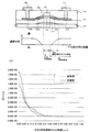
【図面の簡単な説明】
【図1】 本発明の構成を示す図である。(実施例1)
【図2】 本発明の作製工程を示す図である。(実施例1)
【図3】 画素上面図および断面図を示す図である。
【図4】 液晶モジュールの外観を示す図である。
【図5】 ELモジュールを示す上面図及び断面図である。
【図6】 本発明の作製工程を示す図である。(実施例4)
【図7】 本発明の構成を示す図である。(実施例4)
【図8】 回路ブロック図を示す図である。
【図9】 ELモジュールの断面図である。
【図10】 電子機器の一例を示す図である。
【図11】 電子機器の一例を示す図である。
【図12】 電子機器の一例を示す図である。
【図13】 従来例を示す図である。[0001]
BACKGROUND OF THE INVENTION
The present invention relates to a semiconductor device having a circuit formed of a thin film transistor (hereinafter referred to as TFT) and a method for manufacturing the semiconductor device. For example, the present invention relates to an electro-optical device typified by a liquid crystal display panel and an electronic apparatus in which such an electro-optical device is mounted as a component.
[0002]
Note that in this specification, a semiconductor device refers to all devices that can function by utilizing semiconductor characteristics, and an electro-optical device, a semiconductor circuit, and an electronic device are all semiconductor devices.
[0003]
[Prior art]
In recent years, a technique for forming a thin film transistor (TFT) using a semiconductor thin film (having a thickness of about several to several hundred nm) formed on a substrate having an insulating surface has attracted attention. Thin film transistors are widely applied to electronic devices such as ICs and electro-optical devices, and development of switching devices for image display devices is urgently required. Thin film transistors include top gate TFTs and bottom gate TFTs.
[0004]
The bottom gate type TFT is more reliable than the top gate type TFT because it is less affected by impurity diffusion from the substrate to the semiconductor layer. Moreover, it is a common structure to overlap with the gate electrode.
[0005]
Development of a semiconductor device having a large area integrated circuit formed of these TFTs is in progress.
[0006]
Active matrix liquid crystal display devices, EL display devices, and contact image sensors are known as representative examples. In particular, a TFT having a crystalline silicon film (typically a polysilicon film) as an active layer (hereinafter referred to as a polysilicon TFT) has high field-effect mobility, so that a circuit having various functions is formed. It is also possible.
[0007]
For example, in an active matrix liquid crystal display device, a pixel circuit for displaying an image for each functional block, a pixel circuit such as a shift register circuit based on a CMOS circuit, a level shifter circuit, a buffer circuit, and a sampling circuit are controlled. A drive circuit is formed on a single substrate.
[0008]
In a pixel circuit of an active matrix liquid crystal display device, a TFT (pixel TFT) is disposed in each of tens to millions of pixels, and a pixel electrode is provided in each of the pixel TFTs. A counter electrode is provided on the counter substrate side with the liquid crystal interposed therebetween, and a kind of capacitor using the liquid crystal as a dielectric is formed. Then, the voltage applied to each pixel is controlled by the switching function of the TFT, and the liquid crystal is driven by controlling the charge to this capacitor, and the transmitted light quantity is controlled to display an image.
[0009]
The pixel TFT is composed of an n-channel TFT, and is driven by applying a voltage to the liquid crystal as a switching element. Since the liquid crystal is driven by alternating current, a method called frame inversion driving is often employed. In this method, in order to keep power consumption low, it is important that the characteristics required for the pixel TFT have a sufficiently low off-current value (drain current that flows when the TFT is off).
[0010]
[Problems to be solved by the invention]
The present invention is a technique for solving such problems, and improves the operating characteristics of a semiconductor device in an electro-optical device and a semiconductor device typified by an active matrix liquid crystal display device manufactured using TFTs. And it aims at achieving low power consumption.
[0011]
In particular, an object of the present invention is to obtain a structure of a pixel TFT (n-channel TFT) having a sufficiently low off-current value and a large ratio of the on-current value to the off-current value.
[0012]
[Means for Solving the Problems]
As shown in FIG. 1A, according to the present invention, in the
[0013]
That is, an impurity region in which the concentration of the impurity element (phosphorus) gradually increases as the distance from the edge of the
[0014]
In the present invention, since the impurity region is continuously increased, there is no clear boundary. In this specification, the impurity concentration of the
[0015]
In the above description, the drain side is described, but the same is preferable on the source side. In the impurity region on the source side, a
[0016]
The present invention is characterized in that a TFT having a very low off-current value and a high ratio of the on-current value to the off-current value is realized by intentionally forming the
[0017]
Further, as shown in FIG. 13, the conventional TFT structure has a boundary due to a clear concentration difference, and the
[0018]
Since the off-current flows due to quantum mechanical effects such as tunneling between bands, it is considered that it is mainly influenced by the electric field. Therefore, the electric field concentration occurring at the boundary is a cause of increasing the off-current value of the TFT. In particular, in the conventional TFT structure, a strong electric field is concentrated due to a large concentration difference at the boundary between the channel formation region and the low concentration impurity region.
[0019]
On the other hand, according to the present invention, it is possible to obtain a TFT structure having a low off-current value by eliminating the clear boundary by providing the impurity region having a continuously increasing concentration and relaxing the electric field concentration generated near the boundary. it can.
[0020]
In the present invention, as shown in FIG. 1A, a concentration gradient such that the boundary due to the impurity element concentration difference in the semiconductor layer is completely eliminated is formed in the impurity region 102 (1 × 10 6. 15 / Cm Three ~ 1x10 twenty one / Cm Three However, the effect of the present invention can also be obtained by reducing the concentration difference between the
[0021]
FIG. 1B shows the TFT structure as shown in FIG. 1A, with a channel length L = 6 μm, a channel width W = 4 μm, a thickness of the
[0022]
Further, as a conventional example, the state of electric field concentration on the low-concentration impurity region 2 having the concentration distribution in the semiconductor layer of the TFT shown in FIG. 13 is indicated by a dotted line in FIG.
[0023]
As shown in FIG. 1B, the present invention has at least an impurity concentration (P concentration) of 1 × 10. 17 ~ 1x10 18 / Cm Three By providing the impurity region having a concentration gradient in the range of 1, the electric field strength on the surface of the semiconductor layer can be made gentler than before. Therefore, according to the present invention, a strong electric field concentration does not occur over the entire semiconductor layer, and a TFT with a low off-current value can be obtained.
[0024]
The configuration of the invention disclosed in this specification is as follows.
A semiconductor device comprising a TFT including a gate electrode formed on an insulating surface, an insulating film formed on the gate electrode, and a semiconductor layer formed on the insulating film,
The semiconductor layer has a channel formation region overlapping with the gate electrode, and an impurity region formed in contact with the channel formation region,
In the semiconductor device, the impurity region has a concentration distribution in which the impurity concentration increases as the distance from the channel formation region increases.
[0025]
In the above structure, the impurity element imparting one conductivity type to the semiconductor is phosphorus (P) or arsenic (As), and an n-channel TFT is obtained. This n-channel TFT is suitable for a TFT in a pixel portion because it has a small off-state current.
[0026]
In the above structure, the impurity region has a concentration distribution in which the impurity concentration continuously increases as the distance from the channel formation region increases. Further, the impurity region includes at least a region having a concentration gradient of concentration distribution in the channel length direction.
[0027]
In the above structure, the first insulating film is in contact with the channel formation region, and the second insulating film is provided on the first insulating film, and the first insulating film has a tapered portion. It is a feature.
[0028]
In the above structure, the tapered portion of the first insulating film overlaps with a region having a concentration gradient in the impurity region.
[0029]
In the above structure, the second insulating film overlaps with the channel formation region.
[0030]
In the above structure, the impurity region overlaps the gate electrode. Constitution Alternatively, the gate electrode may not overlap with the gate electrode.
[0031]
In the above structure, the first insulating film and the second insulating film may be appropriately selected from materials having different etching rates. For example, the first insulating film may be a silicon nitride film and the second insulating film may be a silicon oxide film. That's fine.
[0032]
In the above structure, the impurity concentration is a concentration of an impurity element imparting one conductivity type to a semiconductor.
[0033]
In FIG. 1, the impurity region has an impurity concentration that increases as the distance from the channel formation region increases, and the concentration distribution is shown as a normal distribution. However, the concentration distribution is not particularly limited. It may be a distribution, a straight line having an inclination, or a combination thereof.
[0034]
Conventionally, impurity elements are doped using a patterned resist mask, or impurity elements are doped in a self-aligning manner using a wiring as a mask. Therefore, a stepwise concentration distribution as shown in FIG. 13 is formed. Thus, the structure of the present invention, that is, an impurity region having a concentration gradient could not be obtained. The present invention also features a manufacturing method for obtaining the above structure.
[0035]
The configuration of the invention relating to the manufacturing method for realizing the above structure is as follows.
Forming a gate electrode on the insulating surface;
Forming a gate insulating film on the gate electrode;
Forming a semiconductor layer on the gate insulating film;
Forming an insulating film on the semiconductor layer;
Etching the insulating film to form an insulating layer having a tapered portion on the semiconductor layer;
Adding an impurity element that imparts one conductivity type to the semiconductor layer through the tapered portion, and forming an impurity region in which an impurity concentration increases toward an end of the tapered portion;
A method for manufacturing a semiconductor device having
[0036]
Conventionally, an LDD region, a source region, and a drain region are formed by doping an impurity element using a resist mask formed using a photomask. The structure of the manufacturing method is characterized in that doping is performed through a tapered portion made of a conductive layer to form an impurity region having a concentration gradient.
[0037]
Further, in the above structure, an impurity region which imparts one conductivity type to the semiconductor layer through the tapered portion is added, and an impurity region whose impurity concentration increases toward the end portion of the tapered portion is at least Impurity concentration (P concentration) 1 × 10 17 ~ 1x10 18 / Cm Three It has a concentration gradient in the range of. Note that, in the present invention, as shown in FIG. 1A, the impurity region 102 (1 × 10 6) has a concentration gradient that completely eliminates the boundary due to the impurity element concentration difference in the semiconductor layer. 15 / Cm Three ~ 1x10 twenty one / Cm Three However, the effect of the present invention can also be obtained by reducing the concentration difference between the
[0038]
In addition, the driver circuit and the pixel portion can be formed over the same substrate.
[0039]
In addition, the configuration of another invention related to a manufacturing method for realizing the above structure is as follows.
Forming a gate electrode on the insulating surface;
Forming a gate insulating film on the gate electrode;
Forming a semiconductor layer on the gate insulating film;
Forming a first insulating film on the semiconductor layer;
Forming a second insulating film on the first insulating film;
Forming a resist mask on the second insulating film;
The second insulating film is selectively etched to form a second insulating layer that covers a portion to be a channel formation region, and the first insulating film is selectively etched to have a tapered portion on the semiconductor layer. Forming a second insulating layer;
Adding an impurity element imparting one conductivity type to the semiconductor layer using the resist mask as a mask;
After removing the resist mask, an impurity element imparting one conductivity type is added to the semiconductor layer through the tapered portion, and an impurity region whose impurity concentration increases toward an end of the tapered portion is formed. Forming, and
A method for manufacturing a semiconductor device having
[0040]
In the structure of the manufacturing method, the step of forming the resist mask is characterized in that the gate electrode is formed as a mask by exposure from the back side of the substrate.
[0041]
In the structure of the manufacturing method, the etching in the step of forming the second insulating layer having the tapered portion is wet etching such as a spin method or a dip method.
[0042]
The etching in the step of forming the second insulating layer having the tapered portion is preferably formed by one etching because the number of steps can be reduced, but may be formed by a plurality of etchings. Further, the second insulating layer may be formed by dry etching. Further, the second insulating layer may be formed by combining wet etching and dry etching.
[0043]
DETAILED DESCRIPTION OF THE INVENTION
An embodiment of the present invention will be described below with reference to FIG.
[0044]
Here, an example in which the
[0045]
First, a gate wiring (including the gate electrode 105) using a first mask, an insulating film covering the gate wiring, a semiconductor film formed of a crystalline semiconductor film, and a silicon nitride film over a light-transmitting substrate A first insulating film made of and a second insulating film made of a silicon oxide film are formed.
[0046]
Next, a resist mask is formed using the gate wiring as a mask by exposure from the back side of the substrate. Here, the back exposure technique is used to reduce the number of processes, but a normal photolithography technique may be used. When using normal photolithography technology, the substrate is not limited to a light-transmitting substrate, but an insulating film is formed on the surface of a metal substrate or a semiconductor substrate such as silicon, germanium, gallium or arsenic, and this substrate is used. May be.
[0047]
Next, etching is performed using a resist mask to form an insulating layer having a tapered portion. Here, dip-type wet etching is performed, and the product name: LAL500 (ammonium hydrogen fluoride (NH Four HF 2 ) 7.13% and ammonium fluoride (NH Four A mixed solution containing 15.4% of F) is used. By this etching, the second insulating
[0048]
Next, a doping process for adding an impurity element imparting n-type to the semiconductor film is performed with the resist mask as it is, thereby forming an impurity region (n + region). As the impurity element imparting n-type conductivity to the semiconductor material, an impurity element belonging to Group 15, for example, P, As, Sb, N, Bi, or the like can be used.
[0049]
Next, the resist mask is removed, and a second doping step is performed in which an impurity element imparting n-type conductivity is added using the second insulating layer as a mask. In this second doping step, an impurity element is added to the semiconductor layer through the tapered portion of the first insulating
[0050]
Further, in the second doping step, an impurity having a concentration distribution in which the distance from the channel formation region (channel length direction) is increased and the impurity concentration is increased by passing through the tapered portion of the first insulating layer.
[0051]
Thereafter, the impurity element added to the semiconductor film is activated. By this activation, the impurity element contained in the impurity region is diffused, so that a concentration gradient that draws a smoother curve is formed and the boundary between the regions is eliminated. Next, the semiconductor film is patterned into a desired shape using the second mask to form a semiconductor layer. Next, after an
[0052]
Thus, a bottom-gate TFT having the structure shown in FIG. 1A can be formed with four photomasks.
[0053]
Further, the present invention only needs to have a concentration gradient as shown in FIG. 1 in the impurity region, and it is needless to say that the present invention is not limited to the channel stop type bottom gate TFT structure shown in FIG. For example, the present invention can be applied to a channel-etch type bottom gate TFT structure.
[0054]
Although FIG. 1 shows a structure in which the
[0055]
Although an example in which an impurity region having a concentration gradient is formed using an insulating layer having a tapered portion is shown here, a metal layer may be used. In that case, an insulating film is formed on the semiconductor film, and a taper portion is formed by ICP etching using a laminated structure using a metal layer, for example, TaN as the first metal layer and W as the second metal layer. do it. Moreover, it is preferable to remove the metal layer after the doping treatment using the metal layer having a tapered portion.
[0056]
The present invention having the above-described configuration will be described in more detail with the following examples.
[0057]
【Example】
[Example 1]
Here, a method for manufacturing a TFT (n-channel TFT) over a substrate is described with reference to FIGS.
[0058]
First, in this embodiment, a
[0059]
Next, a base insulating film (not shown) is formed over the
[0060]
Next, a gate wiring (including the gate electrode 201) having a single layer structure or a stacked structure is formed over the base insulating film. After forming a conductive film having a film thickness range of 10 to 1000 nm, preferably 30 to 300 nm using a thermal CVD method, a plasma CVD method, a low pressure thermal CVD method, a vapor deposition method, a sputtering method or the like as a gate wiring forming means, It is formed by a known patterning technique (first mask). In addition, as a material of the gate wiring, a material mainly composed of a conductive material or a semiconductor material such as Ta (tantalum), Mo (molybdenum), Ti (titanium), W (tungsten), chromium (Cr), or the like The main component is a melting point metal material, a silicide which is a compound of these metal materials and silicon, a material such as N-type or P-type conductivity polysilicon, a low resistance metal material Cu (copper), Al (aluminum), etc. Any structure having at least one material layer can be used without any particular limitation. A laminated structure in which the lower layer of the gate wiring is a low resistance metal material and the upper layer is a refractory metal material is preferable. For example, a laminated structure of Al (lower layer) and Ta (upper layer), a laminated layer of Al (lower layer) and W (upper layer). The structure, a laminated structure of Al (lower layer) and Cu (upper layer) is desirable. Further, an anodic oxide film or an oxide film for protecting the gate wiring may be formed.
[0061]
Next, a
[0062]
Next, an
[0063]
Note that if the
[0064]
Next, the
[0065]
Next, a first
[0066]
Next, a resist
[0067]
Next, an etching process is performed to form an insulating layer having a tapered portion. In this embodiment, LAL500 (20 ° C.) is used as an etchant for 35 seconds to selectively remove the first insulating film and the second insulating film at the same time. Note that the silicon nitride film is smaller than the etching rate of the silicon oxide film. By this etching process, a first insulating
[0068]
Next, the first doping is performed using the resist
[0069]
Next, after removing the resist
[0070]
Thereafter, the impurity element added to the semiconductor film is activated. This activation process is performed by a thermal annealing method using a furnace annealing furnace. In addition to the thermal annealing method, a laser annealing method or a rapid thermal annealing method (RTA method) can be applied. By this activation, the impurity element contained in the impurity region is diffused, so that a concentration gradient that draws a smoother curve is formed and the boundary between the regions is eliminated. In addition, when a metal element that promotes crystal growth is used as a method for crystallizing a semiconductor film, it is desirable to perform gettering by a known method.
[0071]
Next, after performing hydrogenation, the semiconductor film is patterned into a desired shape using a second mask to form a semiconductor layer. Next, after forming an
[0072]
Thus, a bottom gate type TFT having a structure shown in FIG. 2F could be formed with four photomasks. Further, the TFT characteristics obtained by this example are good, and the off-current value is particularly reduced, and the ratio of the on-current to the off-current value can be high.
[0073]
In this embodiment, the first insulating
[0074]
In this embodiment, an n-channel TFT has been described as an example. Alternatively, a circuit having a CMOS structure in which an n-channel TFT and a p-channel TFT are combined may be formed on the same substrate. Is possible. In this case, an n-type impurity and a p-type impurity are selectively doped for each TFT, so that at least one photomask is required.
[0075]
[Example 2]
In this embodiment, an example in which an active matrix substrate is manufactured using the TFT obtained in
[0076]
In accordance with
[0077]
FIG. 3A shows an enlarged top view of one pixel. FIG. 3B is a cross-sectional view taken along the dotted line AA ′ in FIG.
[0078]
In the pixel portion, a
[0079]
In this embodiment, an example of a transmission type is shown as an example, but it is not particularly limited. For example, a reflective liquid crystal module can be manufactured by using a reflective metal material as the material of the pixel electrode and appropriately changing the patterning of the pixel electrode or adding / deleting some processes as appropriate.
[0080]
In this embodiment, the gate wiring of the pixel TFT in the pixel portion has a double gate structure. However, a multi-gate structure such as a triple gate structure may be used in order to reduce variation in off current. Further, a single gate structure may be used in order to improve the aperture ratio.
[0081]
Further, the capacitor portion of the pixel portion is formed of a
[0082]
Note that the pixel portion illustrated in FIG. 3 is merely an example, and needless to say, the configuration is not particularly limited to the above configuration.
[0083]
4 is a pixel portion, a driving circuit, an external input terminal to which an FPC (Flexible Printed Circuit Board: Flexible Printed Circuit) is pasted, a
[0084]
A
[0085]
Here, the
[0086]
In addition, a light-shielding layer is provided between adjacent pixels in the color filter to shield light other than the display area. Here, the
[0087]
Further, without providing the light-shielding layer, the light-shielding layer is appropriately disposed between the counter substrate and the counter electrode so as to be shielded from light by stacking a plurality of colored layers constituting the color filter. Or the drive circuit may be shielded from light.
[0088]
Further, an
[0089]
The liquid crystal module manufactured as described above can be used as a display portion of various electronic devices.
[0090]
[Example 3]
In this embodiment, an example of manufacturing a self-luminous display device including an EL (Electro Luminescence) element is shown in FIG.
[0091]
FIG. 5A is a top view showing the EL module, and FIG. 5B is a cross-sectional view of FIG. 5A cut along AA ′. A pixel portion 502, a source side driver circuit 501, and a gate side driver circuit 503 are formed over a substrate 500 (eg, a glass substrate, a crystallized glass substrate, or a plastic substrate) having an insulating surface. Reference numeral 518 denotes a sealing material, and reference numeral 519 surrounded by a dotted line denotes a DLC film. The pixel portion and the drive circuit portion are covered with a sealing material 518, and the sealing material is covered with a protective film 519. Furthermore, it is sealed with a cover material using an adhesive.
[0092]
Reference numeral 508 denotes wiring for transmitting signals input to the source side driver circuit 501 and the gate side driver circuit 503, and receives a video signal and a clock signal from an FPC (flexible printed circuit) 509 serving as an external input terminal. Although only the FPC is shown here, a printed wiring board (PWB) may be attached to the FPC. The self-light-emitting device in this specification includes not only the self-light-emitting device main body but also a state in which an FPC or PWB is attached thereto.
[0093]
Next, a cross-sectional structure is described with reference to FIG. An insulating film 510 is provided over the substrate 500, and a pixel portion 502 and a gate side driver circuit 503 are formed above the insulating film 510. The pixel portion 502 is electrically connected to the current control TFT 711 and its drain. The
[0094]
These TFTs (including 511, 513, and 514) may be manufactured according to
[0095]
The
[0096]
As the
[0097]
The cathode 517 also functions as a wiring common to all pixels, and is electrically connected to the
[0098]
Note that as the sealant 518, a material that is as transparent or translucent as possible to visible light is preferably used. The sealant 518 is preferably a material that does not transmit moisture and oxygen as much as possible.
[0099]
In addition, after completely covering the light emitting element with the sealant 518, it is preferable to provide a protective film 519 made of a DLC film or the like on the surface (exposed surface) of the sealant 518 at least as shown in FIG. Further, a protective film may be provided on the entire surface including the back surface of the substrate. Here, it is necessary to pay attention so that a protective film is not formed on the portion where the external input terminal (FPC) is provided. The protective film may be prevented from being formed using a mask, or the protective film may be prevented from being formed by covering the external input terminal portion with a tape such as Teflon used as a masking tape in a CVD apparatus.
[0100]
By encapsulating the EL element with the sealing material 518 and the protective film with the above structure, the EL element can be completely shut off from the outside, and a substance that promotes deterioration due to oxidation of the EL layer such as moisture and oxygen from the outside. Can be prevented from entering. Therefore, a highly reliable self-luminous device can be obtained.
[0101]
[Example 4]
In the first embodiment, an example in which the impurity region overlaps with the gate electrode is shown. In this embodiment, an example in which the impurity region does not overlap with the gate electrode is formed with reference to FIGS.
[0102]
First, gate wiring (including the gate electrode 601) is formed over the
[0103]
Next, a first
[0104]
Next, a resist
[0105]
Next, an etching process is performed to form an insulating layer having a tapered portion. In this embodiment, LAL500 (20 ° C.) is used as an etchant for 35 seconds to selectively remove the first insulating film and the second insulating film at the same time. By this etching, a first insulating
[0106]
Next, the first doping is performed using the resist
[0107]
Next, after removing the resist
[0108]
Thereafter, the impurity element added to the semiconductor film is activated. This activation process is performed by a thermal annealing method using a furnace annealing furnace. In addition to the thermal annealing method, a laser annealing method or a rapid thermal annealing method (RTA method) can be applied. By this activation, the impurity element contained in the impurity region is diffused, so that a concentration gradient that draws a smoother curve is formed and the boundary between the regions is eliminated. In addition, when a metal element that promotes crystal growth is used as a method for crystallizing a semiconductor film, it is desirable to perform gettering by a known method.
[0109]
Next, after hydrogenation, the semiconductor film is patterned into a desired shape using a third mask to form a semiconductor layer. Next, after an
[0110]
In this manner, a bottom gate TFT having a structure shown in FIG. 6F could be formed with five photomasks. Further, the TFT characteristics obtained by this example are good, and the off-current value is particularly reduced, and the ratio of the on-current to the off-current value can be high.
[0111]
FIG. 7 shows the concentration distribution in the impurity region of the TFT obtained in this example.
[0112]
The
[0113]
That is, an impurity region in which the concentration of the impurity element (phosphorus) gradually increases as it moves away from the end of the
[0114]
Note that the
[0115]
Further, although the first insulating
[0116]
In addition, this embodiment can be freely combined with any one of
[0117]
[Example 5]
In this embodiment, an example in which a memory element (SRAM) is incorporated in each pixel of the EL module described in Embodiment 3 is shown. FIG. 8 shows an enlarged view of the pixel 1104.
[0118]
In FIG. 8, reference numeral 1105 denotes a switching TFT. A gate electrode of the switching TFT 1105 is connected to a gate signal line 1106 which is one of gate signal lines (G1 to Gn) for inputting a gate signal. One of a source region and a drain region of the switching TFT 1105 is connected to a
[0119]
One of a source region and a drain region of the
[0120]
The
[0121]
The
[0122]
Note that the structure of the n-channel TFT of this embodiment is almost the same as that of the n-channel TFT formed in
[0123]
The drain regions of the paired p-channel TFT and n-channel TFT are connected to each other. The gate electrodes of the paired p-channel TFT and n-channel TFT are connected to each other. The drain regions of one pair of p-channel TFT and n-channel TFT are kept at the same potential as the gate electrode of the other pair of p-channel TFT and n-channel TFT. I'm leaning.
[0124]
The drain region of one pair of p-channel and n-channel TFTs is the input side for receiving an input signal (Vin), and the other pair of p-channel and n-channel TFTs. The drain region is an output side from which an output signal (Vout) is output.
[0125]
The SRAM is designed to hold Vin and output Vout that is a signal obtained by inverting Vin. That is, when Vin is Hi, Vout is a Lo signal corresponding to Vss, and when Vin is Lo, Vout is a Hi signal corresponding to Vddh.
[0126]
As shown in this embodiment, when one SRAM is provided in the pixel 1104, since the memory data in the pixel is held, a still image is displayed with most of the external circuits stopped. It is possible. Thereby, low power consumption can be realized.
[0127]
In addition, a plurality of SRAMs can be provided in a pixel, and when a plurality of SRAMs are provided, a plurality of data can be held, so that gradation display by time gradation is possible.
[0128]
The configuration of the present embodiment can be implemented by freely combining with any of the configurations of
[0129]
[Example 6]
Here, an example in which an EL (electroluminescence) display device is manufactured using the TFT obtained in Example 1 will be described with reference to FIGS.
[0130]
FIG. 9 shows an example of a light-emitting device having a pixel portion and a driving circuit for driving the pixel portion on the same insulator (but a state before sealing). Note that a CMOS circuit serving as a basic unit is shown in the driver circuit, and one pixel is shown in the pixel portion. This CMOS circuit can be obtained according to the first embodiment.
[0131]
In FIG. 9,
[0132]
Description of the N-channel TFT 801 and the P-channel TFT 802 will be omitted because the first embodiment may be referred to. The switching TFT 803 has a structure (double gate structure) having two channel formation regions between a source region and a drain region. Note that this embodiment is not limited to the double gate structure, and may be a single gate structure in which one channel formation region is formed or a triple gate structure in which three channel formation regions are formed.
[0133]
In addition, a contact hole is provided in the first
[0134]
Next,
[0135]
The EL element 809 includes a pixel electrode (cathode) 808, an
[0136]
Note that in this specification, a stacked body in which a hole injection layer, a hole transport layer, a hole blocking layer, an electron transport layer, an electron injection layer, or an electron blocking layer is combined with the light-emitting layer is defined as an EL layer.
[0137]
Although not shown here, it is effective to provide a passivation film so as to completely cover the EL element 809 after the
[0138]
In addition, this embodiment can be freely combined with any one of
[0139]
[Example 7]
The driving circuit and the pixel portion formed by implementing the present invention can be used for various modules (active matrix liquid crystal module, active matrix EL module, active matrix EC module). That is, the present invention can be implemented in all electronic devices in which they are incorporated in the display unit.
[0140]
Such electronic devices include video cameras, digital cameras, head mounted displays (goggles type displays), car navigation systems, projectors, car stereos, personal computers, personal digital assistants (mobile computers, mobile phones, electronic books, etc.), etc. Can be mentioned. Examples of these are shown in FIGS.
[0141]
FIG. 10A illustrates a personal computer, which includes a main body 2001, an image input portion 2002, a display portion 2003, a
[0142]
FIG. 10B illustrates a video camera, which includes a main body 2101, a display portion 2102, an
[0143]
FIG. 10C illustrates a mobile computer, which includes a main body 2201, a camera unit 2202, an
[0144]
FIG. 10D illustrates a goggle type display including a
[0145]
FIG. 10E shows a player using a recording medium (hereinafter referred to as a recording medium) on which a program is recorded, and includes a main body 2401, a
[0146]
FIG. 10F illustrates a digital camera, which includes a main body 2501, a
[0147]
FIG. 11A illustrates a front projector, which includes a
[0148]
FIG. 11B shows a rear projector, which includes a main body 2701, a
[0149]
Note that FIG. 11C illustrates an example of the structure of the
[0150]
FIG. 11D illustrates an example of the structure of the light source
[0151]
However, the projector shown in FIG. 11 shows a case where a transmissive electro-optical device is used, and an application example in a reflective electro-optical device and an EL module is not shown.
[0152]
FIG. 12A shows a cellular phone, which includes a
[0153]
FIG. 12B illustrates a portable book (electronic book), which includes a
[0154]
FIG. 12C illustrates a display, which includes a
[0155]
As described above, the application range of the present invention is extremely wide and can be applied to manufacturing methods of electronic devices in various fields. Moreover, the electronic device of a present Example is realizable even if it uses the structure which consists of what combination of Examples 1-6.
[0156]
【The invention's effect】
According to the present invention, a pixel TFT having an extremely low off-current value and a high ratio of the on-current value to the off-current value can be realized. Therefore, a semiconductor device having excellent display characteristics can be realized. In addition, since the impurity region is formed by using the tapered portion formed by etching, the number of steps can be reduced, and the manufacturing cost and the yield can be reduced.
[Brief description of the drawings]
FIG. 1 is a diagram showing a configuration of the present invention. Example 1
FIG. 2 is a diagram showing a manufacturing process of the present invention. Example 1
FIG. 3 is a diagram illustrating a top view and a cross-sectional view of a pixel.
FIG. 4 is a diagram illustrating an appearance of a liquid crystal module.
FIGS. 5A and 5B are a top view and a cross-sectional view showing an EL module. FIGS.
FIG. 6 is a diagram showing a manufacturing process of the present invention. Example 4
FIG. 7 is a diagram showing a configuration of the present invention. Example 4
FIG. 8 is a diagram showing a circuit block diagram.
FIG. 9 is a cross-sectional view of an EL module.
FIG. 10 illustrates an example of an electronic device.
FIG. 11 illustrates an example of an electronic device.
FIG. 12 illustrates an example of an electronic device.
FIG. 13 is a diagram showing a conventional example.
Claims (6)
前記ゲート電極上にゲート絶縁膜を形成し、
前記ゲート絶縁膜上に半導体層を形成し、
前記半導体層上に第1の絶縁膜を形成し、
前記第1の絶縁膜上に第2の絶縁膜を形成し、
前記第2の絶縁膜上にレジストマスクを形成し、
前記第2の絶縁膜をエッチングして前記レジストマスクより幅が狭く、かつ、前記半導体層のチャネル形成領域となる部分を覆う第2の絶縁層を形成するとともに、前記第1の絶縁膜をエッチングして前記半導体層上にテーパー部分を有する第1の絶縁層を形成し、
前記レジストマスクをマスクとして、前記半導体層の第1の不純物領域に一導電型を付与する不純物元素を添加し、
前記レジストマスクを除去した後、前記第1の絶縁層の前記テーパー部分を通過させて、前記半導体層の前記第1の不純物領域と第2の不純物領域とに前記一導電型を付与する不純物元素を添加し、
前記第1の不純物領域に接するソース配線又はドレイン配線を形成することを特徴とする半導体装置の作製方法。Forming a gate electrode on the insulating surface;
Forming a gate insulating film on the gate electrode;
Forming a semiconductor layer on the gate insulating film;
Forming a first insulating film on the semiconductor layer;
Forming a second insulating film on the first insulating film;
Forming a resist mask on the second insulating film;
The resist narrower than the mask by etching the second insulating film, and to form a second insulating layer covering a portion to be a channel formation region of the semiconductor layer, etching said first insulating film Forming a first insulating layer having a tapered portion on the semiconductor layer;
Wherein the resist mask as a mask, by adding an impurity element imparting one conductivity type to the first impurity region of the semiconductor layer,
Wherein after the resist mask is removed, the first is passed through the tapered portion of the insulating layer, an impurity element imparting the one conductivity type on said first impurity region and a second impurity region of the semiconductor layer It was added,
A manufacturing method of a semiconductor device, wherein a source wiring or a drain wiring in contact with the first impurity region is formed .
前記レジストマスクは、前記ゲート電極をマスクとして、前記絶縁表面を有する基板の裏面側から露光することにより形成することを特徴とする半導体装置の作製方法。In claim 1 ,
The resist mask, the gate electrode as a mask, a method for manufacturing a semiconductor device, which comprises Rikatachi formed by to the rear surface side or et dew light substrate having the insulating surface.
前記第2の不純物領域は、前記ゲート電極と重なることを特徴とする半導体装置の作製方法。The method for manufacturing a semiconductor device, wherein the second impurity region overlaps with the gate electrode.
前記第2の不純物領域は、前記ゲート電極と重ならないことを特徴とする半導体装置の作製方法。The method for manufacturing a semiconductor device, wherein the second impurity region does not overlap with the gate electrode.
前記第2の不純物領域は、チャネル長方向における前記チャネル形成領域からの距離が増えるにつれて、前記一導電型を付与する不純物元素の濃度が連続的に増加する濃度分布を有することを特徴とする半導体装置の作製方法。The second impurity region has a concentration distribution in which the concentration of the impurity element imparting the one conductivity type continuously increases as the distance from the channel formation region in the channel length direction increases. Device fabrication method.
前記第1の不純物領域と前記第2の不純物領域とに前記一導電型を付与する不純物元素を添加した後に、前記一導電型を付与する不純物元素の活性化を行うことを特徴とする半導体装置の作製方法。The semiconductor device, wherein the impurity element imparting the one conductivity type is activated after the impurity element imparting the one conductivity type is added to the first impurity region and the second impurity region. Manufacturing method.
Priority Applications (3)
| Application Number | Priority Date | Filing Date | Title |
|---|---|---|---|
| JP2000338572A JP4678933B2 (en) | 2000-11-07 | 2000-11-07 | Method for manufacturing semiconductor device |
| US10/007,361 US6562669B2 (en) | 2000-11-07 | 2001-11-05 | Semiconductor device and method of manufacturing the same |
| US10/413,985 US6825071B2 (en) | 2000-11-07 | 2003-04-15 | Semiconductor device and method of manufacturing the same |
Applications Claiming Priority (1)
| Application Number | Priority Date | Filing Date | Title |
|---|---|---|---|
| JP2000338572A JP4678933B2 (en) | 2000-11-07 | 2000-11-07 | Method for manufacturing semiconductor device |
Publications (3)
| Publication Number | Publication Date |
|---|---|
| JP2002141513A JP2002141513A (en) | 2002-05-17 |
| JP2002141513A5 JP2002141513A5 (en) | 2008-01-10 |
| JP4678933B2 true JP4678933B2 (en) | 2011-04-27 |
Family
ID=18813766
Family Applications (1)
| Application Number | Title | Priority Date | Filing Date |
|---|---|---|---|
| JP2000338572A Expired - Fee Related JP4678933B2 (en) | 2000-11-07 | 2000-11-07 | Method for manufacturing semiconductor device |
Country Status (2)
| Country | Link |
|---|---|
| US (2) | US6562669B2 (en) |
| JP (1) | JP4678933B2 (en) |
Families Citing this family (34)
| Publication number | Priority date | Publication date | Assignee | Title |
|---|---|---|---|---|
| JP2001102169A (en) * | 1999-10-01 | 2001-04-13 | Sanyo Electric Co Ltd | El display |
| JP5046452B2 (en) * | 2000-10-26 | 2012-10-10 | 株式会社半導体エネルギー研究所 | Method for manufacturing semiconductor device |
| JP4678933B2 (en) * | 2000-11-07 | 2011-04-27 | 株式会社半導体エネルギー研究所 | Method for manufacturing semiconductor device |
| JP4017886B2 (en) * | 2002-02-28 | 2007-12-05 | シャープ株式会社 | Thin film transistor device and manufacturing method thereof |
| JP4027691B2 (en) * | 2002-03-18 | 2007-12-26 | 株式会社日立製作所 | Liquid crystal display |
| US6853052B2 (en) * | 2002-03-26 | 2005-02-08 | Semiconductor Energy Laboratory Co., Ltd. | Semiconductor device having a buffer layer against stress |
| JP2003332045A (en) * | 2002-05-09 | 2003-11-21 | Sanyo Electric Co Ltd | Electroluminescence display device and its manufacturing method |
| US20060049428A1 (en) * | 2002-07-05 | 2006-03-09 | Van Der Zaag Pieter J | Tft electronic devices and their manufacture |
| US6642092B1 (en) * | 2002-07-11 | 2003-11-04 | Sharp Laboratories Of America, Inc. | Thin-film transistors formed on a metal foil substrate |
| JP2004296453A (en) * | 2003-02-06 | 2004-10-21 | Sharp Corp | Solid-state imaging device, semiconductor wafer, optical device module, method of manufacturing the solid-state imaging device, and method of manufacturing the optical device module |
| KR100527195B1 (en) * | 2003-07-25 | 2005-11-08 | 삼성에스디아이 주식회사 | Flat Panel Display |
| JP4741177B2 (en) * | 2003-08-29 | 2011-08-03 | 株式会社半導体エネルギー研究所 | Method for manufacturing display device |
| US7115488B2 (en) * | 2003-08-29 | 2006-10-03 | Semiconductor Energy Laboratory Co., Ltd. | Method of manufacturing semiconductor device |
| US7220611B2 (en) * | 2003-10-14 | 2007-05-22 | Lg.Philips Lcd Co., Ltd. | Liquid crystal display panel and fabricating method thereof |
| KR100623844B1 (en) * | 2004-04-30 | 2006-09-19 | 엘지.필립스 엘시디 주식회사 | Organic Electro luminescence Device and fabrication method thereof |
| EP1624333B1 (en) * | 2004-08-03 | 2017-05-03 | Semiconductor Energy Laboratory Co., Ltd. | Display device, manufacturing method thereof, and television set |
| TWI284245B (en) * | 2004-08-12 | 2007-07-21 | Au Optronics Corp | Pixel structure of a thin film transistor liquid crystal display and fabricating method thereof |
| US8148895B2 (en) | 2004-10-01 | 2012-04-03 | Semiconductor Energy Laboratory Co., Ltd. | Display device and manufacturing method of the same |
| US8003449B2 (en) * | 2004-11-26 | 2011-08-23 | Semiconductor Energy Laboratory Co., Ltd. | Method of manufacturing a semiconductor device having a reverse staggered thin film transistor |
| TWI302060B (en) * | 2004-12-30 | 2008-10-11 | Au Optronics Corp | Light emitting diode display panel and digital-analogy converter of the same |
| US7858451B2 (en) | 2005-02-03 | 2010-12-28 | Semiconductor Energy Laboratory Co., Ltd. | Electronic device, semiconductor device and manufacturing method thereof |
| JP5238132B2 (en) * | 2005-02-03 | 2013-07-17 | 株式会社半導体エネルギー研究所 | Semiconductor device, module, and electronic device |
| KR20070013132A (en) * | 2005-07-25 | 2007-01-30 | 삼성전자주식회사 | Thin film transistor substrate and manufacturing method thereof |
| JP2008129314A (en) * | 2006-11-21 | 2008-06-05 | Hitachi Displays Ltd | Image display device and manufacturing method thereof |
| US7777224B2 (en) * | 2007-01-30 | 2010-08-17 | Semiconductor Energy Laboratory Co., Ltd. | Semiconductor device and method of manufacturing the same |
| JP5442228B2 (en) * | 2008-08-07 | 2014-03-12 | 株式会社ジャパンディスプレイ | Display device and manufacturing method of display device |
| KR101127574B1 (en) * | 2009-04-06 | 2012-03-23 | 삼성모바일디스플레이주식회사 | Manufacturing methods of active matrix substrate and organic light emitting display device |
| KR101746198B1 (en) | 2009-09-04 | 2017-06-12 | 가부시키가이샤 한도오따이 에네루기 켄큐쇼 | Display device and electronic device |
| KR20180031077A (en) * | 2009-09-24 | 2018-03-27 | 가부시키가이샤 한도오따이 에네루기 켄큐쇼 | Semiconductor device and method for manufacturing the same |
| WO2011043163A1 (en) | 2009-10-05 | 2011-04-14 | Semiconductor Energy Laboratory Co., Ltd. | Semiconductor device and manufacturing method thereof |
| KR102142450B1 (en) | 2009-10-30 | 2020-08-10 | 가부시키가이샤 한도오따이 에네루기 켄큐쇼 | Semiconductor device and method for manufacturing the same |
| KR101094280B1 (en) * | 2009-11-10 | 2011-12-19 | 삼성모바일디스플레이주식회사 | Organic Light Emitting Diode display device and Fabrication method for the same |
| WO2012035984A1 (en) * | 2010-09-15 | 2012-03-22 | Semiconductor Energy Laboratory Co., Ltd. | Semiconductor device and display device |
| US8716708B2 (en) | 2011-09-29 | 2014-05-06 | Semiconductor Energy Laboratory Co., Ltd. | Semiconductor device and method for manufacturing the same |
Citations (2)
| Publication number | Priority date | Publication date | Assignee | Title |
|---|---|---|---|---|
| JPH08125190A (en) * | 1994-10-27 | 1996-05-17 | Nec Corp | Thin film transistor and fabrication thereof |
| JP2000150904A (en) * | 1998-08-21 | 2000-05-30 | Semiconductor Energy Lab Co Ltd | Semiconductor device provided with semiconductor circuit consisting of semiconductor element and manufacture thereof |
Family Cites Families (13)
| Publication number | Priority date | Publication date | Assignee | Title |
|---|---|---|---|---|
| JP2503656B2 (en) * | 1989-05-31 | 1996-06-05 | 日本電気株式会社 | Thin film field effect transistor and method of manufacturing the same |
| EP0497427B1 (en) | 1991-02-01 | 1996-04-10 | Koninklijke Philips Electronics N.V. | Semiconductor device for high voltage application and method of making the same |
| TW403972B (en) | 1993-01-18 | 2000-09-01 | Semiconductor Energy Lab | Method of fabricating mis semiconductor device |
| JPH07288327A (en) * | 1994-04-18 | 1995-10-31 | Sony Corp | Method for forming sram load tft |
| JPH0818056A (en) * | 1994-06-27 | 1996-01-19 | Sony Corp | Manufacture of field effect transistor |
| US6121660A (en) | 1997-09-23 | 2000-09-19 | Semiconductor Energy Laboratory Co., Ltd. | Channel etch type bottom gate semiconductor device |
| JP3702096B2 (en) * | 1998-06-08 | 2005-10-05 | 三洋電機株式会社 | Thin film transistor and display device |
| US6261881B1 (en) | 1998-08-21 | 2001-07-17 | Semiconductor Energy Laboratory Co., Ltd. | Semiconductor device provided with semiconductor circuit consisting of semiconductor element and method of manufacturing the same |
| US6259138B1 (en) * | 1998-12-18 | 2001-07-10 | Semiconductor Energy Laboratory Co., Ltd. | Semiconductor device having multilayered gate electrode and impurity regions overlapping therewith |
| US6380007B1 (en) * | 1998-12-28 | 2002-04-30 | Semiconductor Energy Laboratory Co., Ltd. | Semiconductor device and manufacturing method of the same |
| US7503975B2 (en) * | 2000-06-27 | 2009-03-17 | Semiconductor Energy Laboratory Co., Ltd. | Semiconductor device and fabrication method therefor |
| JP4678933B2 (en) * | 2000-11-07 | 2011-04-27 | 株式会社半導体エネルギー研究所 | Method for manufacturing semiconductor device |
| US6693297B2 (en) * | 2001-06-18 | 2004-02-17 | International Business Machines Corporation | Thin film transistor formed by an etching process with high anisotropy |
-
2000
- 2000-11-07 JP JP2000338572A patent/JP4678933B2/en not_active Expired - Fee Related
-
2001
- 2001-11-05 US US10/007,361 patent/US6562669B2/en not_active Expired - Lifetime
-
2003
- 2003-04-15 US US10/413,985 patent/US6825071B2/en not_active Expired - Lifetime
Patent Citations (2)
| Publication number | Priority date | Publication date | Assignee | Title |
|---|---|---|---|---|
| JPH08125190A (en) * | 1994-10-27 | 1996-05-17 | Nec Corp | Thin film transistor and fabrication thereof |
| JP2000150904A (en) * | 1998-08-21 | 2000-05-30 | Semiconductor Energy Lab Co Ltd | Semiconductor device provided with semiconductor circuit consisting of semiconductor element and manufacture thereof |
Also Published As
| Publication number | Publication date |
|---|---|
| US6825071B2 (en) | 2004-11-30 |
| US6562669B2 (en) | 2003-05-13 |
| US20020053669A1 (en) | 2002-05-09 |
| JP2002141513A (en) | 2002-05-17 |
| US20030234424A1 (en) | 2003-12-25 |
Similar Documents
| Publication | Publication Date | Title |
|---|---|---|
| JP4678933B2 (en) | Method for manufacturing semiconductor device | |
| US9250490B2 (en) | Liquid crystal display device including light shielding film | |
| US9035314B2 (en) | Method for manufacturing an electrooptical device | |
| US8310612B2 (en) | Thin film transistor liquid crystal display panel having gate line and data line formed on same layer and method of fabricating the same | |
| US6596571B2 (en) | Method of manufacturing semiconductor device | |
| JP4845273B2 (en) | Semiconductor device and manufacturing method thereof | |
| KR100654927B1 (en) | semiconductor device and manufacturing method thereof | |
| US8183064B2 (en) | Thin film transistor devices for OLED displays and method for fabricating the same | |
| JPH11112002A (en) | Semiconductor device and manufacture therefor | |
| JP4583540B2 (en) | Semiconductor device and manufacturing method thereof | |
| JP4993826B2 (en) | Method for manufacturing semiconductor device | |
| JP4558121B2 (en) | Semiconductor device and manufacturing method thereof | |
| JP4275720B2 (en) | Semiconductor device and manufacturing method thereof | |
| JP5046439B2 (en) | Method for manufacturing semiconductor device | |
| JP4850328B2 (en) | Method for manufacturing semiconductor device | |
| JP4850763B2 (en) | Method for manufacturing semiconductor device | |
| JP5577384B2 (en) | Method for manufacturing semiconductor device | |
| JP5019677B2 (en) | Semiconductor device and manufacturing method thereof | |
| JP2012109579A (en) | Semiconductor device and manufacturing method for the same | |
| JP4818288B2 (en) | Method for manufacturing semiconductor device |
Legal Events
| Date | Code | Title | Description |
|---|---|---|---|
| A521 | Request for written amendment filed |
Free format text: JAPANESE INTERMEDIATE CODE: A523 Effective date: 20071106 |
|
| A621 | Written request for application examination |
Free format text: JAPANESE INTERMEDIATE CODE: A621 Effective date: 20071106 |
|
| A131 | Notification of reasons for refusal |
Free format text: JAPANESE INTERMEDIATE CODE: A131 Effective date: 20101214 |
|
| A977 | Report on retrieval |
Free format text: JAPANESE INTERMEDIATE CODE: A971007 Effective date: 20101216 |
|
| A521 | Request for written amendment filed |
Free format text: JAPANESE INTERMEDIATE CODE: A523 Effective date: 20110106 |
|
| TRDD | Decision of grant or rejection written | ||
| A01 | Written decision to grant a patent or to grant a registration (utility model) |
Free format text: JAPANESE INTERMEDIATE CODE: A01 Effective date: 20110125 |
|
| A01 | Written decision to grant a patent or to grant a registration (utility model) |
Free format text: JAPANESE INTERMEDIATE CODE: A01 |
|
| A61 | First payment of annual fees (during grant procedure) |
Free format text: JAPANESE INTERMEDIATE CODE: A61 Effective date: 20110201 |
|
| R150 | Certificate of patent or registration of utility model |
Free format text: JAPANESE INTERMEDIATE CODE: R150 |
|
| FPAY | Renewal fee payment (event date is renewal date of database) |
Free format text: PAYMENT UNTIL: 20140210 Year of fee payment: 3 |
|
| FPAY | Renewal fee payment (event date is renewal date of database) |
Free format text: PAYMENT UNTIL: 20140210 Year of fee payment: 3 |
|
| R250 | Receipt of annual fees |
Free format text: JAPANESE INTERMEDIATE CODE: R250 |
|
| R250 | Receipt of annual fees |
Free format text: JAPANESE INTERMEDIATE CODE: R250 |
|
| R250 | Receipt of annual fees |
Free format text: JAPANESE INTERMEDIATE CODE: R250 |
|
| R250 | Receipt of annual fees |
Free format text: JAPANESE INTERMEDIATE CODE: R250 |
|
| LAPS | Cancellation because of no payment of annual fees |