JP5046452B2 - Method for manufacturing semiconductor device - Google Patents
Method for manufacturing semiconductor device Download PDFInfo
- Publication number
- JP5046452B2 JP5046452B2 JP2001291795A JP2001291795A JP5046452B2 JP 5046452 B2 JP5046452 B2 JP 5046452B2 JP 2001291795 A JP2001291795 A JP 2001291795A JP 2001291795 A JP2001291795 A JP 2001291795A JP 5046452 B2 JP5046452 B2 JP 5046452B2
- Authority
- JP
- Japan
- Prior art keywords
- gate electrode
- shape
- region
- insulating film
- impurity
- Prior art date
- Legal status (The legal status is an assumption and is not a legal conclusion. Google has not performed a legal analysis and makes no representation as to the accuracy of the status listed.)
- Expired - Fee Related
Links
- 239000004065 semiconductor Substances 0.000 title claims description 139
- 238000000034 method Methods 0.000 title claims description 103
- 238000004519 manufacturing process Methods 0.000 title claims description 42
- 239000012535 impurity Substances 0.000 claims description 238
- 238000005530 etching Methods 0.000 claims description 104
- 230000015572 biosynthetic process Effects 0.000 claims description 72
- 230000007423 decrease Effects 0.000 claims description 3
- 239000010408 film Substances 0.000 description 231
- 239000010410 layer Substances 0.000 description 169
- 239000000758 substrate Substances 0.000 description 75
- 238000009826 distribution Methods 0.000 description 39
- 239000004973 liquid crystal related substance Substances 0.000 description 27
- 239000011159 matrix material Substances 0.000 description 26
- 238000010586 diagram Methods 0.000 description 24
- 239000007789 gas Substances 0.000 description 22
- XUIMIQQOPSSXEZ-UHFFFAOYSA-N Silicon Chemical compound [Si] XUIMIQQOPSSXEZ-UHFFFAOYSA-N 0.000 description 21
- 239000011229 interlayer Substances 0.000 description 21
- 229910052710 silicon Inorganic materials 0.000 description 21
- 239000010703 silicon Substances 0.000 description 21
- 238000005401 electroluminescence Methods 0.000 description 20
- MZLGASXMSKOWSE-UHFFFAOYSA-N tantalum nitride Chemical compound [Ta]#N MZLGASXMSKOWSE-UHFFFAOYSA-N 0.000 description 20
- 239000000463 material Substances 0.000 description 19
- OAICVXFJPJFONN-UHFFFAOYSA-N Phosphorus Chemical compound [P] OAICVXFJPJFONN-UHFFFAOYSA-N 0.000 description 18
- 229910052698 phosphorus Inorganic materials 0.000 description 18
- 239000011574 phosphorus Substances 0.000 description 18
- 230000003287 optical effect Effects 0.000 description 17
- 230000005684 electric field Effects 0.000 description 13
- 230000000694 effects Effects 0.000 description 11
- PXHVJJICTQNCMI-UHFFFAOYSA-N Nickel Chemical compound [Ni] PXHVJJICTQNCMI-UHFFFAOYSA-N 0.000 description 10
- 238000002425 crystallisation Methods 0.000 description 10
- 238000005268 plasma chemical vapour deposition Methods 0.000 description 10
- 238000004088 simulation Methods 0.000 description 10
- 239000000460 chlorine Substances 0.000 description 9
- 230000000052 comparative effect Effects 0.000 description 9
- 238000009616 inductively coupled plasma Methods 0.000 description 9
- 238000004544 sputter deposition Methods 0.000 description 9
- 239000003990 capacitor Substances 0.000 description 8
- 230000001681 protective effect Effects 0.000 description 8
- 239000000565 sealant Substances 0.000 description 8
- 238000001994 activation Methods 0.000 description 7
- 239000000956 alloy Substances 0.000 description 7
- 230000008025 crystallization Effects 0.000 description 7
- 239000011521 glass Substances 0.000 description 7
- 229910052760 oxygen Inorganic materials 0.000 description 7
- VYPSYNLAJGMNEJ-UHFFFAOYSA-N silicon dioxide Inorganic materials O=[Si]=O VYPSYNLAJGMNEJ-UHFFFAOYSA-N 0.000 description 7
- 238000003860 storage Methods 0.000 description 7
- 229910052739 hydrogen Inorganic materials 0.000 description 6
- 229910021420 polycrystalline silicon Inorganic materials 0.000 description 6
- 230000001052 transient effect Effects 0.000 description 6
- 230000004913 activation Effects 0.000 description 5
- 229910045601 alloy Inorganic materials 0.000 description 5
- 230000006866 deterioration Effects 0.000 description 5
- 238000010438 heat treatment Methods 0.000 description 5
- 229910052759 nickel Inorganic materials 0.000 description 5
- 238000000059 patterning Methods 0.000 description 5
- 239000003566 sealing material Substances 0.000 description 5
- 229910052814 silicon oxide Inorganic materials 0.000 description 5
- 239000002356 single layer Substances 0.000 description 5
- 239000010409 thin film Substances 0.000 description 5
- ZOXJGFHDIHLPTG-UHFFFAOYSA-N Boron Chemical compound [B] ZOXJGFHDIHLPTG-UHFFFAOYSA-N 0.000 description 4
- 229910052581 Si3N4 Inorganic materials 0.000 description 4
- 230000001133 acceleration Effects 0.000 description 4
- 238000000137 annealing Methods 0.000 description 4
- QVGXLLKOCUKJST-UHFFFAOYSA-N atomic oxygen Chemical compound [O] QVGXLLKOCUKJST-UHFFFAOYSA-N 0.000 description 4
- 229910052796 boron Inorganic materials 0.000 description 4
- 229910021419 crystalline silicon Inorganic materials 0.000 description 4
- 238000013461 design Methods 0.000 description 4
- 230000005669 field effect Effects 0.000 description 4
- 238000002347 injection Methods 0.000 description 4
- 239000007924 injection Substances 0.000 description 4
- 150000002500 ions Chemical class 0.000 description 4
- 230000010355 oscillation Effects 0.000 description 4
- 239000001301 oxygen Substances 0.000 description 4
- 229920005591 polysilicon Polymers 0.000 description 4
- 238000005070 sampling Methods 0.000 description 4
- HQVNEWCFYHHQES-UHFFFAOYSA-N silicon nitride Chemical compound N12[Si]34N5[Si]62N3[Si]51N64 HQVNEWCFYHHQES-UHFFFAOYSA-N 0.000 description 4
- 125000006850 spacer group Chemical group 0.000 description 4
- 229910000577 Silicon-germanium Inorganic materials 0.000 description 3
- 229910052782 aluminium Inorganic materials 0.000 description 3
- 229910021417 amorphous silicon Inorganic materials 0.000 description 3
- 239000003054 catalyst Substances 0.000 description 3
- 150000001875 compounds Chemical class 0.000 description 3
- 238000001312 dry etching Methods 0.000 description 3
- PCHJSUWPFVWCPO-UHFFFAOYSA-N gold Chemical compound [Au] PCHJSUWPFVWCPO-UHFFFAOYSA-N 0.000 description 3
- 239000001257 hydrogen Substances 0.000 description 3
- 238000005984 hydrogenation reaction Methods 0.000 description 3
- 238000005224 laser annealing Methods 0.000 description 3
- 238000005499 laser crystallization Methods 0.000 description 3
- 239000000203 mixture Substances 0.000 description 3
- 229910052757 nitrogen Inorganic materials 0.000 description 3
- 230000002093 peripheral effect Effects 0.000 description 3
- 239000004033 plastic Substances 0.000 description 3
- 230000010287 polarization Effects 0.000 description 3
- 239000010453 quartz Substances 0.000 description 3
- 229910052715 tantalum Inorganic materials 0.000 description 3
- 239000010936 titanium Substances 0.000 description 3
- 239000004925 Acrylic resin Substances 0.000 description 2
- 229920000178 Acrylic resin Polymers 0.000 description 2
- UFHFLCQGNIYNRP-UHFFFAOYSA-N Hydrogen Chemical compound [H][H] UFHFLCQGNIYNRP-UHFFFAOYSA-N 0.000 description 2
- XYFCBTPGUUZFHI-UHFFFAOYSA-N Phosphine Chemical compound P XYFCBTPGUUZFHI-UHFFFAOYSA-N 0.000 description 2
- LEVVHYCKPQWKOP-UHFFFAOYSA-N [Si].[Ge] Chemical compound [Si].[Ge] LEVVHYCKPQWKOP-UHFFFAOYSA-N 0.000 description 2
- 238000004458 analytical method Methods 0.000 description 2
- 229910052785 arsenic Inorganic materials 0.000 description 2
- RQNWIZPPADIBDY-UHFFFAOYSA-N arsenic atom Chemical compound [As] RQNWIZPPADIBDY-UHFFFAOYSA-N 0.000 description 2
- 239000000969 carrier Substances 0.000 description 2
- 238000006243 chemical reaction Methods 0.000 description 2
- 229910052802 copper Inorganic materials 0.000 description 2
- 239000013078 crystal Substances 0.000 description 2
- 230000005284 excitation Effects 0.000 description 2
- 239000000945 filler Substances 0.000 description 2
- 229910010272 inorganic material Inorganic materials 0.000 description 2
- 239000011147 inorganic material Substances 0.000 description 2
- 238000004518 low pressure chemical vapour deposition Methods 0.000 description 2
- 229910052750 molybdenum Inorganic materials 0.000 description 2
- 239000012299 nitrogen atmosphere Substances 0.000 description 2
- 238000000206 photolithography Methods 0.000 description 2
- 238000001020 plasma etching Methods 0.000 description 2
- 238000012545 processing Methods 0.000 description 2
- 239000011347 resin Substances 0.000 description 2
- 229920005989 resin Polymers 0.000 description 2
- 229910052719 titanium Inorganic materials 0.000 description 2
- 229910052721 tungsten Inorganic materials 0.000 description 2
- XLOMVQKBTHCTTD-UHFFFAOYSA-N zinc oxide Inorganic materials [Zn]=O XLOMVQKBTHCTTD-UHFFFAOYSA-N 0.000 description 2
- KZBUYRJDOAKODT-UHFFFAOYSA-N Chlorine Chemical compound ClCl KZBUYRJDOAKODT-UHFFFAOYSA-N 0.000 description 1
- YCKRFDGAMUMZLT-UHFFFAOYSA-N Fluorine atom Chemical compound [F] YCKRFDGAMUMZLT-UHFFFAOYSA-N 0.000 description 1
- 229910052779 Neodymium Inorganic materials 0.000 description 1
- NRTOMJZYCJJWKI-UHFFFAOYSA-N Titanium nitride Chemical compound [Ti]#N NRTOMJZYCJJWKI-UHFFFAOYSA-N 0.000 description 1
- 230000003213 activating effect Effects 0.000 description 1
- 239000000853 adhesive Substances 0.000 description 1
- 230000001070 adhesive effect Effects 0.000 description 1
- 239000005407 aluminoborosilicate glass Substances 0.000 description 1
- 238000003491 array Methods 0.000 description 1
- 239000012298 atmosphere Substances 0.000 description 1
- 229910052788 barium Inorganic materials 0.000 description 1
- DSAJWYNOEDNPEQ-UHFFFAOYSA-N barium atom Chemical compound [Ba] DSAJWYNOEDNPEQ-UHFFFAOYSA-N 0.000 description 1
- 239000005388 borosilicate glass Substances 0.000 description 1
- 229910052804 chromium Inorganic materials 0.000 description 1
- 239000003086 colorant Substances 0.000 description 1
- 238000007796 conventional method Methods 0.000 description 1
- 230000003247 decreasing effect Effects 0.000 description 1
- ZOCHARZZJNPSEU-UHFFFAOYSA-N diboron Chemical compound B#B ZOCHARZZJNPSEU-UHFFFAOYSA-N 0.000 description 1
- 239000012895 dilution Substances 0.000 description 1
- 238000010790 dilution Methods 0.000 description 1
- 238000011156 evaluation Methods 0.000 description 1
- 229910052731 fluorine Inorganic materials 0.000 description 1
- 239000011737 fluorine Substances 0.000 description 1
- 150000002431 hydrogen Chemical class 0.000 description 1
- AMGQUBHHOARCQH-UHFFFAOYSA-N indium;oxotin Chemical compound [In].[Sn]=O AMGQUBHHOARCQH-UHFFFAOYSA-N 0.000 description 1
- 239000011810 insulating material Substances 0.000 description 1
- 238000005468 ion implantation Methods 0.000 description 1
- 238000003475 lamination Methods 0.000 description 1
- 230000000873 masking effect Effects 0.000 description 1
- 229910052751 metal Inorganic materials 0.000 description 1
- 239000002184 metal Substances 0.000 description 1
- QJGQUHMNIGDVPM-UHFFFAOYSA-N nitrogen group Chemical group [N] QJGQUHMNIGDVPM-UHFFFAOYSA-N 0.000 description 1
- 230000003647 oxidation Effects 0.000 description 1
- 238000007254 oxidation reaction Methods 0.000 description 1
- 229910000073 phosphorus hydride Inorganic materials 0.000 description 1
- 230000002250 progressing effect Effects 0.000 description 1
- 238000004151 rapid thermal annealing Methods 0.000 description 1
- 239000012495 reaction gas Substances 0.000 description 1
- 238000002310 reflectometry Methods 0.000 description 1
- 230000003014 reinforcing effect Effects 0.000 description 1
- 230000002040 relaxant effect Effects 0.000 description 1
- 239000010979 ruby Substances 0.000 description 1
- 229910001750 ruby Inorganic materials 0.000 description 1
- HBMJWWWQQXIZIP-UHFFFAOYSA-N silicon carbide Chemical compound [Si+]#[C-] HBMJWWWQQXIZIP-UHFFFAOYSA-N 0.000 description 1
- 229910010271 silicon carbide Inorganic materials 0.000 description 1
- 229910052709 silver Inorganic materials 0.000 description 1
- 239000000243 solution Substances 0.000 description 1
- 239000000126 substance Substances 0.000 description 1
- GUVRBAGPIYLISA-UHFFFAOYSA-N tantalum atom Chemical compound [Ta] GUVRBAGPIYLISA-UHFFFAOYSA-N 0.000 description 1
- 238000012360 testing method Methods 0.000 description 1
- 238000002230 thermal chemical vapour deposition Methods 0.000 description 1
- NXHILIPIEUBEPD-UHFFFAOYSA-H tungsten hexafluoride Chemical compound F[W](F)(F)(F)(F)F NXHILIPIEUBEPD-UHFFFAOYSA-H 0.000 description 1
- 230000005641 tunneling Effects 0.000 description 1
- OYQCBJZGELKKPM-UHFFFAOYSA-N zinc indium(3+) oxygen(2-) Chemical compound [O-2].[Zn+2].[O-2].[In+3] OYQCBJZGELKKPM-UHFFFAOYSA-N 0.000 description 1
- 239000011787 zinc oxide Substances 0.000 description 1
Images


Classifications
-
- H—ELECTRICITY
- H01—ELECTRIC ELEMENTS
- H01L—SEMICONDUCTOR DEVICES NOT COVERED BY CLASS H10
- H01L27/00—Devices consisting of a plurality of semiconductor or other solid-state components formed in or on a common substrate
- H01L27/02—Devices consisting of a plurality of semiconductor or other solid-state components formed in or on a common substrate including semiconductor components specially adapted for rectifying, oscillating, amplifying or switching and having at least one potential-jump barrier or surface barrier; including integrated passive circuit elements with at least one potential-jump barrier or surface barrier
- H01L27/12—Devices consisting of a plurality of semiconductor or other solid-state components formed in or on a common substrate including semiconductor components specially adapted for rectifying, oscillating, amplifying or switching and having at least one potential-jump barrier or surface barrier; including integrated passive circuit elements with at least one potential-jump barrier or surface barrier the substrate being other than a semiconductor body, e.g. an insulating body
- H01L27/1214—Devices consisting of a plurality of semiconductor or other solid-state components formed in or on a common substrate including semiconductor components specially adapted for rectifying, oscillating, amplifying or switching and having at least one potential-jump barrier or surface barrier; including integrated passive circuit elements with at least one potential-jump barrier or surface barrier the substrate being other than a semiconductor body, e.g. an insulating body comprising a plurality of TFTs formed on a non-semiconducting substrate, e.g. driving circuits for AMLCDs
- H01L27/124—Devices consisting of a plurality of semiconductor or other solid-state components formed in or on a common substrate including semiconductor components specially adapted for rectifying, oscillating, amplifying or switching and having at least one potential-jump barrier or surface barrier; including integrated passive circuit elements with at least one potential-jump barrier or surface barrier the substrate being other than a semiconductor body, e.g. an insulating body comprising a plurality of TFTs formed on a non-semiconducting substrate, e.g. driving circuits for AMLCDs with a particular composition, shape or layout of the wiring layers specially adapted to the circuit arrangement, e.g. scanning lines in LCD pixel circuits
-
- H—ELECTRICITY
- H01—ELECTRIC ELEMENTS
- H01L—SEMICONDUCTOR DEVICES NOT COVERED BY CLASS H10
- H01L27/00—Devices consisting of a plurality of semiconductor or other solid-state components formed in or on a common substrate
- H01L27/02—Devices consisting of a plurality of semiconductor or other solid-state components formed in or on a common substrate including semiconductor components specially adapted for rectifying, oscillating, amplifying or switching and having at least one potential-jump barrier or surface barrier; including integrated passive circuit elements with at least one potential-jump barrier or surface barrier
- H01L27/12—Devices consisting of a plurality of semiconductor or other solid-state components formed in or on a common substrate including semiconductor components specially adapted for rectifying, oscillating, amplifying or switching and having at least one potential-jump barrier or surface barrier; including integrated passive circuit elements with at least one potential-jump barrier or surface barrier the substrate being other than a semiconductor body, e.g. an insulating body
- H01L27/1214—Devices consisting of a plurality of semiconductor or other solid-state components formed in or on a common substrate including semiconductor components specially adapted for rectifying, oscillating, amplifying or switching and having at least one potential-jump barrier or surface barrier; including integrated passive circuit elements with at least one potential-jump barrier or surface barrier the substrate being other than a semiconductor body, e.g. an insulating body comprising a plurality of TFTs formed on a non-semiconducting substrate, e.g. driving circuits for AMLCDs
- H01L27/1259—Multistep manufacturing methods
- H01L27/127—Multistep manufacturing methods with a particular formation, treatment or patterning of the active layer specially adapted to the circuit arrangement
-
- H—ELECTRICITY
- H01—ELECTRIC ELEMENTS
- H01L—SEMICONDUCTOR DEVICES NOT COVERED BY CLASS H10
- H01L29/00—Semiconductor devices adapted for rectifying, amplifying, oscillating or switching, or capacitors or resistors with at least one potential-jump barrier or surface barrier, e.g. PN junction depletion layer or carrier concentration layer; Details of semiconductor bodies or of electrodes thereof ; Multistep manufacturing processes therefor
- H01L29/40—Electrodes ; Multistep manufacturing processes therefor
- H01L29/41—Electrodes ; Multistep manufacturing processes therefor characterised by their shape, relative sizes or dispositions
- H01L29/423—Electrodes ; Multistep manufacturing processes therefor characterised by their shape, relative sizes or dispositions not carrying the current to be rectified, amplified or switched
- H01L29/42312—Gate electrodes for field effect devices
- H01L29/42316—Gate electrodes for field effect devices for field-effect transistors
- H01L29/4232—Gate electrodes for field effect devices for field-effect transistors with insulated gate
- H01L29/42384—Gate electrodes for field effect devices for field-effect transistors with insulated gate for thin film field effect transistors, e.g. characterised by the thickness or the shape of the insulator or the dimensions, the shape or the lay-out of the conductor
-
- H—ELECTRICITY
- H01—ELECTRIC ELEMENTS
- H01L—SEMICONDUCTOR DEVICES NOT COVERED BY CLASS H10
- H01L29/00—Semiconductor devices adapted for rectifying, amplifying, oscillating or switching, or capacitors or resistors with at least one potential-jump barrier or surface barrier, e.g. PN junction depletion layer or carrier concentration layer; Details of semiconductor bodies or of electrodes thereof ; Multistep manufacturing processes therefor
- H01L29/40—Electrodes ; Multistep manufacturing processes therefor
- H01L29/43—Electrodes ; Multistep manufacturing processes therefor characterised by the materials of which they are formed
- H01L29/49—Metal-insulator-semiconductor electrodes, e.g. gates of MOSFET
- H01L29/4908—Metal-insulator-semiconductor electrodes, e.g. gates of MOSFET for thin film semiconductor, e.g. gate of TFT
-
- H—ELECTRICITY
- H01—ELECTRIC ELEMENTS
- H01L—SEMICONDUCTOR DEVICES NOT COVERED BY CLASS H10
- H01L29/00—Semiconductor devices adapted for rectifying, amplifying, oscillating or switching, or capacitors or resistors with at least one potential-jump barrier or surface barrier, e.g. PN junction depletion layer or carrier concentration layer; Details of semiconductor bodies or of electrodes thereof ; Multistep manufacturing processes therefor
- H01L29/66—Types of semiconductor device ; Multistep manufacturing processes therefor
- H01L29/66007—Multistep manufacturing processes
- H01L29/66075—Multistep manufacturing processes of devices having semiconductor bodies comprising group 14 or group 13/15 materials
- H01L29/66227—Multistep manufacturing processes of devices having semiconductor bodies comprising group 14 or group 13/15 materials the devices being controllable only by the electric current supplied or the electric potential applied, to an electrode which does not carry the current to be rectified, amplified or switched, e.g. three-terminal devices
- H01L29/66409—Unipolar field-effect transistors
- H01L29/66477—Unipolar field-effect transistors with an insulated gate, i.e. MISFET
- H01L29/66742—Thin film unipolar transistors
- H01L29/6675—Amorphous silicon or polysilicon transistors
- H01L29/66757—Lateral single gate single channel transistors with non-inverted structure, i.e. the channel layer is formed before the gate
-
- H—ELECTRICITY
- H01—ELECTRIC ELEMENTS
- H01L—SEMICONDUCTOR DEVICES NOT COVERED BY CLASS H10
- H01L29/00—Semiconductor devices adapted for rectifying, amplifying, oscillating or switching, or capacitors or resistors with at least one potential-jump barrier or surface barrier, e.g. PN junction depletion layer or carrier concentration layer; Details of semiconductor bodies or of electrodes thereof ; Multistep manufacturing processes therefor
- H01L29/66—Types of semiconductor device ; Multistep manufacturing processes therefor
- H01L29/68—Types of semiconductor device ; Multistep manufacturing processes therefor controllable by only the electric current supplied, or only the electric potential applied, to an electrode which does not carry the current to be rectified, amplified or switched
- H01L29/76—Unipolar devices, e.g. field effect transistors
- H01L29/772—Field effect transistors
- H01L29/78—Field effect transistors with field effect produced by an insulated gate
- H01L29/786—Thin film transistors, i.e. transistors with a channel being at least partly a thin film
- H01L29/78606—Thin film transistors, i.e. transistors with a channel being at least partly a thin film with supplementary region or layer in the thin film or in the insulated bulk substrate supporting it for controlling or increasing the safety of the device
- H01L29/78618—Thin film transistors, i.e. transistors with a channel being at least partly a thin film with supplementary region or layer in the thin film or in the insulated bulk substrate supporting it for controlling or increasing the safety of the device characterised by the drain or the source properties, e.g. the doping structure, the composition, the sectional shape or the contact structure
- H01L29/78621—Thin film transistors, i.e. transistors with a channel being at least partly a thin film with supplementary region or layer in the thin film or in the insulated bulk substrate supporting it for controlling or increasing the safety of the device characterised by the drain or the source properties, e.g. the doping structure, the composition, the sectional shape or the contact structure with LDD structure or an extension or an offset region or characterised by the doping profile
- H01L29/78627—Thin film transistors, i.e. transistors with a channel being at least partly a thin film with supplementary region or layer in the thin film or in the insulated bulk substrate supporting it for controlling or increasing the safety of the device characterised by the drain or the source properties, e.g. the doping structure, the composition, the sectional shape or the contact structure with LDD structure or an extension or an offset region or characterised by the doping profile with a significant overlap between the lightly doped drain and the gate electrode, e.g. GOLDD
-
- H—ELECTRICITY
- H01—ELECTRIC ELEMENTS
- H01L—SEMICONDUCTOR DEVICES NOT COVERED BY CLASS H10
- H01L29/00—Semiconductor devices adapted for rectifying, amplifying, oscillating or switching, or capacitors or resistors with at least one potential-jump barrier or surface barrier, e.g. PN junction depletion layer or carrier concentration layer; Details of semiconductor bodies or of electrodes thereof ; Multistep manufacturing processes therefor
- H01L29/66—Types of semiconductor device ; Multistep manufacturing processes therefor
- H01L29/68—Types of semiconductor device ; Multistep manufacturing processes therefor controllable by only the electric current supplied, or only the electric potential applied, to an electrode which does not carry the current to be rectified, amplified or switched
- H01L29/76—Unipolar devices, e.g. field effect transistors
- H01L29/772—Field effect transistors
- H01L29/78—Field effect transistors with field effect produced by an insulated gate
- H01L29/786—Thin film transistors, i.e. transistors with a channel being at least partly a thin film
- H01L29/78645—Thin film transistors, i.e. transistors with a channel being at least partly a thin film with multiple gate
Landscapes
- Engineering & Computer Science (AREA)
- Power Engineering (AREA)
- Microelectronics & Electronic Packaging (AREA)
- Physics & Mathematics (AREA)
- Condensed Matter Physics & Semiconductors (AREA)
- General Physics & Mathematics (AREA)
- Computer Hardware Design (AREA)
- Ceramic Engineering (AREA)
- Manufacturing & Machinery (AREA)
- Thin Film Transistor (AREA)
- Liquid Crystal (AREA)
- Internal Circuitry In Semiconductor Integrated Circuit Devices (AREA)
- Electroluminescent Light Sources (AREA)
- Devices For Indicating Variable Information By Combining Individual Elements (AREA)
- Electrodes Of Semiconductors (AREA)
- Recrystallisation Techniques (AREA)
Description
【0001】
【発明の属する技術分野】
本発明は薄膜トランジスタ(以下、TFTという)で構成された回路を有する半導体装置およびその作製方法に関する。例えば、液晶モジュールやELモジュールを部品として搭載した電子機器に関する。
【0002】
なお、本明細書中において半導体装置とは、半導体特性を利用することで機能しうる装置全般を指し、電気光学装置、発光装置、半導体回路および電子機器は全て半導体装置である。
【0003】
【従来の技術】
近年、絶縁表面を有する基板上に形成された半導体薄膜(厚さ数〜数百nm程度)を用いて薄膜トランジスタ(TFT)を構成し、このTFTで形成した大面積集積回路を有する半導体装置の開発が進んでいる。アクティブマトリクス型の液晶モジュール、ELモジュール、および密着型イメージセンサはその代表例として知られている。特に、結晶質シリコン膜(典型的にはポリシリコン膜)を活性層にしたTFT(以下、ポリシリコンTFTと記す)は電界効果移動度が高いことから、いろいろな機能を備えた回路を形成することも可能である。
【0004】
例えば、液晶表示装置に搭載される液晶モジュールには、機能ブロックごとに画像表示を行う画素回路や、CMOS回路を基本としたシフトレジスタ回路、レベルシフタ回路、バッファ回路、サンプリング回路などの画素回路を制御するための駆動回路が一枚の基板上に形成される。
【0005】
また、アクティブマトリクス型の液晶モジュールの画素回路には、数十から数百万個の各画素にTFT(画素TFT)が配置され、その画素TFTのそれぞれには画素電極が設けられている。液晶を挟んだ対向基板側には対向電極が設けられており、液晶を誘電体とした一種のコンデンサを形成している。そして、各画素に印加する電圧をTFTのスイッチング機能により制御して、このコンデンサへの電荷を制御することで液晶を駆動し、透過光量を制御して画像を表示する仕組みになっている。
【0006】
画素TFTはnチャネル型TFTから成り、スイッチング素子として液晶に電圧を印加して駆動させるものである。液晶は交流で駆動させるので、フレーム反転駆動と呼ばれる方式が多く採用されている。この方式では消費電力を低く抑えるために、画素TFTに要求される特性はオフ電流値(TFTがオフ動作時に流れるドレイン電流)を十分低くすることが重要である。
【0007】
オフ電流値を低減するためのTFTの構造として、低濃度ドレイン(LDD:Lightly Doped Drain)構造が知られている。この構造はチャネル形成領域と、高濃度に不純物元素を添加して形成するソース領域またはドレイン領域との間に低濃度に不純物元素を添加した領域を設けたものであり、この領域をLDD領域と呼んでいる。
【0008】
しかし、従来の画素TFTにおいて、通常のLDD領域を形成した場合、オフ電流値を低減することはできたが、同時にオン電流値も低下していた。通常のLDD構造はオフ電流値を抑える効果は高いが、ドレイン近傍の電界を緩和してホットキャリア注入による劣化を防ぐ効果は低かった。
【0009】
また、ホットキャリアによるオン電流値の劣化を防ぐための手段として、ゲート絶縁膜を介してLDD領域をゲート電極と重ねて配置させた、いわゆるGOLD(Gate-drain Overlapped LDD)構造が知られている。このような構造とすることで、ドレイン近傍の電界強度が緩和されてホットキャリア注入を防ぎ、劣化現象の防止に有効であることが知られている。
【0010】
また、GOLD構造はオン電流値の劣化を防ぐ効果は高いが、その反面、通常のLDD構造と比べてオフ電流値が大きくなってしまう問題があった。従って、画素TFTに適用するには好ましい構造ではなかった。
【0011】
このように、アクティブマトリクス型液晶表示装置のような複数の集積回路を有する半導体装置において、このような問題点は、特に結晶質シリコンTFTにおいて、その特性が高まり、またアクティブマトリクス型液晶表示装置に要求される性能が高まるほど顕在化してきた。
【0012】
【発明が解決しようとする課題】
本発明はこのような問題点を解決するための技術であり、TFTを用いて作製するアクティブマトリクス型の液晶表示装置に代表される電気光学装置ならびに半導体装置において、半導体装置の動作特性を向上させ、かつ、低消費電力化を図ることを目的としている。
【0013】
特に、本発明は、オフ電流値が低い画素TFT(nチャネル型TFT)の構造を得ることを目的としている。加えて、オフ電流値に対するオン電流値の比が高い画素TFTの構造を得ることも本発明の目的としている。
【0014】
【課題を解決するための手段】
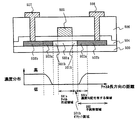
図1(A)に示すように本発明は、不純物領域102において、チャネル形成領域からの距離(チャネル長方向における距離)が増大するとともに、一導電型を付与する不純物元素の濃度が増大するような濃度勾配を有する領域102aを持たせることを特徴とする。
【0015】
即ち、チャネル長方向においてゲート電極105の端部(チャネル長方向に切断した断面におけるゲート電極の端部)から半導体層の周縁部に向かって離れるにつれて不純物元素(リン)の濃度が徐々に増大する不純物領域を備えたことを特徴としている。従って、この不純物領域は、チャネル形成領域側で電気抵抗が大きく、半導体層の周縁部側で電気抵抗が小さくなっている。
【0016】
また、本発明においては、連続的に増大する不純物領域であるため、明確な境界はなく、本明細書中では、不純物領域102のうち、不純物濃度が1×10²⁰/cm3以上の領域をドレイン領域102bと呼ぶ。
【0017】
また、上述では、ドレイン側について説明したが、画素TFTに用いる場合、ソース側においても同様とすることが好ましい。ソース側の不純物領域において、チャネル形成領域からの距離が増大するとともに、一導電型を付与する不純物元素の濃度が増大するような濃度勾配を有する領域103aを形成する。また、本明細書中では、ソース側の不純物領域のうち、不純物濃度が1×10²⁰/cm3以上の領域をソース領域103bと呼ぶ。
【0018】
本発明は、このような濃度勾配を有する領域102a、103aを意図的に形成することによって、オフ電流値が非常に低く、オフ電流値に対するオン電流値の比が高いTFTを実現することを特徴としている。ただし、ゲート電極105はゲート絶縁膜104を介してチャネル形成領域101と重なるが、不純物領域102とは重ならない構造とする。なお、図1(A)において、100は絶縁表面を有する基板、106は層間絶縁膜、107はソース電極、108はドレイン電極である。
【0019】
また、従来のTFT構造は、図29に示すように、明確な濃度差による境界が存在しており、チャネル形成領域1と、低濃度不純物領域2と、高濃度不純物領域3とで階段状に濃度が異なっていた。即ち、不連続な濃度分布を示していた。加えて、各領域における濃度は、ほぼ一定であった。従って、従来では、高濃度不純物領域3と低濃度不純物領域2との境界における濃度差や、低濃度不純物領域2とチャネル形成領域1との境界における濃度差が比較的大きいため、強い電界集中がそれぞれの境界付近に生じていた。
【0020】
オフ電流はバンド間のトンネリングなど量子力学的な効果で流れるため、主として電界に影響されると考えられる。従って、境界で生じていた電界集中がTFTのオフ電流値を増大させる原因となっていた。特に、従来のTFT構造においてチャネル形成領域と低濃度不純物領域との境界における大きな濃度差により強い電界が集中して問題となっていた。
【0021】
一方、本発明は、連続的に濃度が増大する不純物領域をチャネル形成領域とドレイン領域との間に設けることにより明確な境界をなくして、境界部近傍に発生する電界集中を緩和させることによってオフ電流値の低いTFT構造を得ることができる。
【0022】
本発明においては、図1(A)に示すように、半導体層における不純物元素の濃度差による境界が完全になくなるような濃度勾配を不純物領域102(1×10¹⁵/cm3〜1×1021/cm3の範囲)で形成することが最も望ましいが、チャネル形成領域101と該チャネル形成領域近傍の不純物領域102aの濃度差を小さくすることでも本発明の効果は得られる。また、高濃度不純物領域102bと該高濃度不純物領域近傍の低濃度不純物領域102aとの境界における濃度差を小さくすることでも本発明の効果は得られる。
【0023】
また、図1(B)は、TFT構造を図1(A)とし、チャネル長L=6μm、チャネル幅W=4μm、ゲート絶縁膜104の膜厚=115nm、ポリシリコン層の膜厚=45nm、不純物濃度(P濃度)1×10¹⁷〜1×10¹⁸/cm3の範囲で濃度勾配を有する領域102a(幅1.5μm)、不純物濃度(P濃度)1×1019/cm3の不純物領域102b、チャネル形成領域101のキャリア濃度(B濃度)=2×1016/cm3とした場合のシミュレーション結果である。このシミュレーション結果は、縦軸を半導体層表面の電界強度E(V/cm)、横軸をチャネル形成領域からの距離(μm)としており、図1(B)中の実線で示したものが本発明の不純物領域への電界集中の様子を示している。
【0024】
また、従来例として、TFTの半導体層における濃度分布を図29に示した分布とした低濃度不純物領域2への電界集中の様子を図1(B)中の点線で示した。
【0025】
図1(B)に示したように、本発明は少なくとも不純物濃度(P濃度)1×10¹⁷〜1×10¹⁸/cm3の範囲で濃度勾配を有する不純物領域を備えたことによって、従来よりも半導体層表面の電界強度を緩やかにすることができた。従って、本発明により、半導体層全域にわたって強い電界集中が発生せず、オフ電流値の低いTFTを得ることができる。
【0026】
本明細書で開示する発明の構成は、
絶縁表面上に形成された半導体層と、該半導体層上に形成された絶縁膜(ゲート絶縁膜)と、該絶縁膜上に形成されたゲート電極とを含むTFTを備えた半導体装置であって、
前記半導体層は、前記ゲート電極と重なるチャネル形成領域と、該チャネル形成領域に接して形成された不純物領域(LDD領域、ソース領域またはドレイン領域を含む)とを有し、
前記不純物領域は、前記チャネル形成領域からの距離が増大するとともに一導電型を付与する不純物元素の濃度が増加する濃度分布を備えたことを特徴とする半導体装置である。
【0027】
また、上記構成において、半導体に一導電型を付与する不純物元素は、リン(P)または砒素(As)であり、nチャネル型TFTが得られる。このnチャネル型TFTは、オフ電流が小さいので画素部のTFTに適している。
【0028】
また、画素部のTFTにおいて、チャネル形成領域と低濃度不純物領域との間にオフセット領域を形成しても同程度の信頼性を得ることができた。図18にその一例を示す。
【0029】
また、他の発明の構成は、
絶縁表面上に形成された半導体層と、該半導体層上に形成された絶縁膜と、該絶縁膜上に形成されたゲート電極とを含むTFTを備えた半導体装置であって、前記半導体層は、前記ゲート電極と重なるチャネル形成領域と、該チャネル形成領域に接して形成されたオフセット領域と、該オフセット領域に接して形成された不純物領域とを有し、
前記不純物領域は、前記チャネル形成領域からの距離が増大するとともに不純物濃度が増加する濃度分布を備えたことを特徴とする半導体装置である。
【0030】
また、上記構成において、前記ゲート電極の端部は、前記チャネル形成領域と前記オフセット領域との界面と概略一致することを特徴としている。
【0031】
また、同一の絶縁表面上に画素部及び駆動回路を含む半導体装置において、画素部は、絶縁膜(ゲート絶縁膜)を間に挟んでゲート電極と重ならない不純物領域とすることが好ましい。この場合、画素TFTのゲート電極の端部は、チャネル形成領域と不純物領域との界面(境界)と概略一致させる。
【0032】
また、上記構成において、前記駆動回路のnチャネル型TFTのゲート電極はテーパ−部を有し、該テーパー部は不純物領域の一部と絶縁膜(ゲート絶縁膜)を間に挟んで重なっていることを特徴としている。なお、前記テーパー部を通過させてドーピングを行うため、駆動回路において、テーパー部の幅と、前記チャネル形成領域からの距離が増大するとともに不純物濃度が増加する濃度分布を有する領域の幅は概略一致する。また、図32に示したように、設計しようとする配線幅を長くすれば、形成されるテーパー部も長くなるため、駆動回路のゲート電極の幅は、画素部のゲート電極の幅よりも長くなるよう設計することが好ましい。
【0033】
また、上記構成において、前記画素TFTのチャネル形成領域と前記不純物領域との間にオフセット領域を備えてもよい。
【0034】
また、上記各構成において、ゲート電極は、第1の導電層を下層とし、第2の導電層を上層とする積層構造を有している。本発明では、この積層構造のゲート電極を利用して濃度勾配を有する不純物領域を形成している。従って、前記チャネル形成領域からの距離が増大するとともに不純物濃度が増加する不純物領域は、前記チャネル形成領域を挟んで両側に形成される。
【0035】
また、上記各構成において、前記不純物領域はソース領域またはドレイン領域を含むことを特徴としている。
【0036】
また、図1において、不純物領域は、前記チャネル形成領域からの距離が増大するとともに不純物濃度が増加しており、その濃度分布を正規分布で示したが、特に限定されず、その濃度分布は指数分布であってもよいし、傾きを有する直線であってもよいし、それらを組み合わせたものであってもよい。ただし、上記濃度勾配を有する領域102a、103aのチャネル長における幅は、少なくとも0.5μm〜1.7μm、好ましくは1μm以上とし、その領域内で緩やかな濃度勾配を有していることが重要である。
【0037】
即ち、上記各構成において、前記不純物領域は、不純物濃度が増加する濃度分布を有する領域と不純物濃度がほぼ一定である領域とを有し、前記不純物濃度が増加する濃度分布を有する領域は、チャネル長方向における長さが1μm以上であることを特徴としている。
【0038】
また、従来の方法において、ドーピングの条件によっては不純物元素がゲート電極の下方への廻り込んで、ゲート電極と重なり、且つ濃度勾配を有する不純物領域が0.1μm程度生じる場合もあったが、本発明と同等の効果を得ることは困難である。
【0039】
従来では、パターニングしたレジストマスクを用いて不純物元素のドーピングを行ったり、配線をマスクとして自己整合的に不純物元素のドーピングを行っていたため、図29に示したような階段状の濃度分布が形成されており、上記本発明の構成、即ち濃度勾配を有する不純物領域を0.5μm以上得ることはできなかった。
【0040】
本発明では、積層構造のゲート電極だけでなく、半導体層を覆う絶縁膜(ゲート絶縁膜)の一部をテーパー形状とし、前記絶縁膜を利用して濃度勾配を有する不純物領域を形成することも可能である。その場合、前記不純物領域は、前記チャネル形成領域からの距離が最大の領域と最小の領域とで前記絶縁膜の膜厚が異なることを特徴としている。また、テーパー部を有するゲート電極と、テーパー部を有する絶縁膜とを両方用いて濃度勾配を有する不純物領域を形成することも可能である。
【0041】
また、本発明は上記構造を得るための作製方法も特徴としている。
【0042】
上記構造を実現する作製方法に関する発明の構成は、
絶縁表面上に半導体層を形成する工程と、
前記半導体層上に絶縁膜を形成する工程と、
前記絶縁膜(ゲート絶縁膜)上にテーパ−部を有する導電層を形成する工程と、
前記テーパ−部及び前記絶縁膜を通過させて前記半導体層に一導電型を付与する不純物元素を添加し、前記テーパ−部の端部に向かって不純物濃度が増加する不純物領域を形成する工程と、
前記導電層のうち、テーパ−部のみを選択的に除去してゲート電極を形成する工程と、
を有する半導体装置の作製方法である。
【0043】
上記作製方法の構成においては、導電層からなるテーパ−部を通過させてドーピングを行い、濃度勾配を有する不純物領域を形成することを特徴としている。
【0044】
一方、従来の作製方法ではフォトマスクを用いて形成したレジストマスクを用いて不純物元素のドーピングを行い、LDD領域、ソース領域、及びドレイン領域を形成していた。
【0045】
また、上記構成において、前記テーパ−部を通過させて前記半導体層に一導電型を付与する不純物元素を添加し、前記テーパ−部の端部に向かって不純物濃度が増加する不純物領域は、少なくとも不純物濃度(P濃度)1×10¹⁷〜1×10¹⁸/cm3の範囲で濃度勾配を有することを特徴とする。
【0046】
また、駆動回路と画素部とを同一基板上に形成することも可能である。その場合、少なくとも画素部のTFTのゲート電極は、テーパ−部のみを選択的に除去し、駆動回路のTFT(オン電流を重視するTFT)のゲート電極はテーパ−部をそのままに残すことが好ましい。また、駆動回路のTFTにおいては、テーパ−部のチャネル長方向の幅が長ければ長いほど信頼性が高いため、テーパ−部を形成する際、テーパー部の幅が長くなるように、選択比の高いSF6を含むエッチングガスでドライエッチングを行うことが有効である。
【0047】
また、積層構造のゲート電極だけでなく、半導体層を覆う絶縁膜(ゲート絶縁膜)の一部をテーパー形状とし、前記絶縁膜を利用して濃度勾配を有する不純物領域を形成することも可能であり、上記構造を実現する作製方法に関する他の発明の構成は、
絶縁表面上に半導体層を形成する工程と、
前記半導体層上に絶縁膜を形成する工程と、
前記絶縁膜上にゲート電極を形成する工程と、
前記絶縁膜をエッチングして前記半導体層上にテーパ−部を有する絶縁層を形成する工程と、
前記テーパ−部を通過させて前記半導体層に一導電型を付与する不純物元素を添加し、前記テーパ−部の端部に向かって不純物濃度が増加する不純物領域を形成する工程と、
を有する半導体装置の作製方法である。
【0048】
また、上記作製方法の構成においては、絶縁層からなるテーパ−部を通過させてドーピングを行い、濃度勾配を有する不純物領域を形成することを特徴としている。
【0049】
【発明の実施の形態】
本発明の実施形態について、以下に図2、図3に説明する。
【0050】
ここでは、ゲート電極のテーパー部を利用して、前記チャネル形成領域側から前記不純物領域側に向かって不純物濃度(P濃度)が連続的に増加する不純物領域を形成する例を示す。
【0051】
まず、基板10上に下地絶縁膜11を形成する。基板10としては、ガラス基板や石英基板やシリコン基板、金属基板またはステンレス基板の表面に絶縁膜を形成したものを用いても良い。また、処理温度に耐えうる耐熱性を有するプラスチック基板を用いてもよい。
【0052】
また、下地絶縁膜11としては、酸化シリコン膜、窒化シリコン膜または酸化窒化シリコン膜などの絶縁膜から成る下地膜11を形成する。ここでは下地膜11として2層構造(11a、11b)を用いた例を示したが、前記絶縁膜の単層膜または2層以上積層させた構造を用いても良い。なお、下地絶縁膜を形成しなくてもよい。
【0053】
次いで、下地絶縁膜上に半導体層12を形成する。半導体層12は、非晶質構造を有する半導体膜を公知の手段(スパッタ法、LPCVD法、またはプラズマCVD法等)により成膜した後、公知の結晶化処理(レーザー結晶化法、熱結晶化法、またはニッケルなどの触媒を用いた熱結晶化法等)を行って得られた結晶質半導体膜を第1のフォトマスクを用いて所望の形状にパターニングして形成する。この半導体層12の厚さは25〜80nm(好ましくは30〜60nm)の厚さで形成する。結晶質半導体膜の材料に限定はないが、好ましくはシリコンまたはシリコンゲルマニウム(SiGe)合金などで形成すると良い。
【0054】
次いで、半導体層12を覆う絶縁膜13を形成する。
【0055】
絶縁膜13はプラズマCVD法またはスパッタ法を用い、厚さを40〜150nmとしてシリコンを含む絶縁膜の単層または積層構造で形成する。なお、この絶縁膜13はゲート絶縁膜となる。
【0056】
次いで、絶縁膜13上に膜厚20〜100nmの第1の導電膜14と、膜厚100〜400nmの第2の導電膜15とを積層形成する。(図2(A))ここでは、スパッタ法を用い、TaN膜からなる第1の導電膜14と、W膜からなる第2の導電膜15を積層形成した。なお、ここでは、第1の導電膜14をTaN、第2の導電膜15をWとしたが、特に限定されず、いずれもTa、W、Ti、Mo、Al、Cuから選ばれた元素、または前記元素を主成分とする合金材料若しくは化合物材料で形成してもよい。また、リン等の不純物元素をドーピングした多結晶シリコン膜に代表される半導体膜を用いてもよい。
【0057】
次いで、第2のフォトマスクを用いてレジストマスク16aを形成し、ICPエッチング装置を用いて第1のエッチング工程を行う。この第1のエッチング工程によって、第2の導電膜15をエッチングして、図2(B)に示すように、端部においてテーパー形状を有する部分(テーパー部)を有する第2の導電層17aを得る。
【0058】
ここで、テーパー部の角度(テーパー角)は基板表面(水平面)とテーパー部の傾斜部とのなす角度として定義する。第2の導電層17aのテーパー角は、エッチング条件を適宜、選択することによって、5〜45°の範囲とすることができる。
【0059】
次いで、レジストマスク16aをそのまま用い、ICPエッチング装置を用いて第2のエッチング工程を行う。この第2のエッチング工程によって、第1の導電膜14をエッチングして図2(C)に示すような第1の導電層18aを形成する。第1の導電層18aは、第1の幅(W1)を有している。なお、この第2のエッチング工程の際、レジストマスク、第2の導電層、及び絶縁膜もわずかにエッチングされて、それぞれレジストマスク16b、第2の導電層17b、絶縁膜19が形成される。
【0060】
なお、ここでは、絶縁膜13の膜減りを抑えるために、2回のエッチング(第1のエッチング工程と第2のエッチング工程)を行ったが、図3(B)に示すような電極構造(第2の導電層17bと第1の導電層18aの積層)が形成できるのであれば、特に限定されず、1回のエッチング工程で行ってもよい。
【0061】
次いで、レジストマスク16bをそのままの状態にしたまま、第1のドーピング工程を行う。この第1のドーピング工程によって絶縁膜19を介してスルードープを行い、高濃度不純物領域20、21を形成する。(図2(D))
【0062】
次いで、レジストマスク16bを用いて、ICPエッチング装置を用いて第3のエッチング工程を行う。この第3のエッチング工程によって、第2の導電層17bをエッチングして図3(A)に示すような第2の導電層17cを形成する。第2の導電層17cは、第2の幅(W2)を有する。なお、この第3のエッチングの際、第1の導電層もわずかにエッチングされて、第1の幅より狭まった第1の導電層18bが形成される。なお、図32に示すように配線幅(ここでは第1の導電層の幅W1)によって第1の導電層のテーパー部の長さが変化する。従って、同一基板上に配線幅の異なる配線を複数設ける場合、形成される第1の導電層18bの幅もそれぞれ異なって形成される。
【0063】
次いで、レジストマスク16bを除去した後、第2のドーピング工程を行う。この第2のドーピング工程によって第1の導電層18bのテーパー部及び絶縁膜19を介してスルードープを行い、低濃度不純物領域24、25を形成する。(図3(B))このドーピング工程において、テーパ−部を通過させることによって、チャネル形成領域側から前記高濃度不純物領域側に向かって不純物濃度(P濃度)が連続的に増加する低濃度不純物領域24、25を形成する。なお、この第2のドーピングの際、高濃度不純物領域にもドーピングされ、高濃度不純物領域22、23が形成される。なお、ここでは、高濃度不純物領域と低濃度不純物領域とを別々なものとして図示しているが、実際は、明確な境界はなく、図1(A)に示したように濃度勾配を有する領域が形成されている。また、同様にチャネル形成領域と低濃度不純物領域との明確な境界はない。なお、図32に示すように設計する配線幅によって第1の導電層のテーパー部の長さが変化する。従って、同一基板上に配線幅の異なる配線を複数設ける場合、ドーピングされる領域(濃度勾配を有する領域)の幅もそれぞれ異なる。
【0064】
なお、ここでは、第1のエッチング工程と第2のエッチング工程を行って第1のドーピング工程を行い、その後で第3のエッチング工程を行って第2のドーピング工程を行う例を示したが、図3(B)に示すような電極構造(第2の導電層と第1の導電層の積層)と濃度勾配を有する領域が形成できるのであれば、特に工程順序等は限定されず、例えば、第1のエッチング工程と第2のエッチング工程と第3のエッチング工程を行って図3(B)に示すような電極構造を得た後、第1のドーピング工程と第2のドーピング工程とを順次行ってもよい。
【0065】
次いで、ICPエッチング装置を用いて第4のエッチング工程を行う。この第4のエッチング工程によって、第1の導電層18bのテーパー部のみを除去する。ここで、第1の幅(W1)を有していた第1の導電層18bが、第2の幅(W2)を有する第1の導電層18cとなった。本発明では、この第1の導電層18cとその上に積層された第2の導電層17cがゲート電極となる。
【0066】
この後、半導体層に添加された不純物元素の活性化を行う。この活性化によって、不純物領域に含まれた不純物元素が拡散するため、より滑らかなカーブを描く濃度勾配が形成されて各領域間の境界がなくなる。次いで、層間絶縁膜27を形成した後、第3のマスクを用いてコンタクトホールを形成し、第4のマスクを用いて電極28、29を形成する。
【0067】
こうして、フォトマスク4枚で、図3(D)に示す構造のTFTを形成することができる。
【0068】
また、本発明により形成されたTFTの特徴は、チャネル形成領域26とドレイン領域23との間に設けられる低濃度不純物領域25において、チャネル形成領域からの距離が増大するとともに不純物濃度が連続的に増加するような濃度勾配を有し、ゲート電極と重ならない点である。
【0069】
また、濃度勾配を有する不純物領域の効果を調べるためにシミュレーションを行った。ここでは、図4に示すようにソース領域/ドレイン領域である高濃度不純物領域と、低濃度不純物領域と、チャネル形成領域とを想定し、低濃度不純物領域のみに濃度勾配を持たせた場合についてシミュレーションを行った。シミュレーションに用いた各数値は、L=6μm、W=4μm、低濃度不純物領域(Loff)の幅=1.5μm、ゲート絶縁膜の膜厚=115nm、ポリシリコン層の膜厚=45nm、チャネル形成領域のキャリア密度(B濃度)=2×1016/cm3、ソース領域/ドレイン領域のキャリア密度(P濃度)=1×1019/cm3とした。また、低濃度不純物領域が一定である場合(比較例)と、低濃度不純物領域が濃度勾配を有している場合とで比較を行った。ここでは低濃度不純物領域の濃度分布モデルとして、図4に示すような正規分布(ガウシアン分布)の勾配を用いてシミュレーションを行い、TFTの電圧/電流特性(図5)を導出した。また、比較例として、キャリア濃度(P濃度)を低濃度不純物領域において一定の濃度(3×1017/cm3、5×1017/cm3)とし、同様にTFTの電圧/電流特性を導出した。
【0070】
図5は、Vds(ソース領域とドレイン領域の電圧差)=14Vとした時の電圧/電流特性である。図5に示されているように、濃度勾配を有している低濃度不純物領域を備えたTFTのオフ電流値は、比較例と比べて顕著に低減されている。これは、本発明により各領域の境界に生じる電界集中が緩和されたことが主な原因であると考えられる。一方、オン電流値は、移動度やシート抵抗によって決まる。また、濃度勾配を有している低濃度不純物領域を備えたTFTのオン電流値は、比較例と同程度であることが示されている。即ち、低濃度不純物領域においてシート抵抗を測定した場合、比較例と本発明が同一(オン電流値も同一)であっても、本発明はオフ電流値のみを低減することができる。従って、オフ電流値に対するオン電流値の比が高くなる。従来ではオフ電流を低減する構造とした場合、オン電流も低減していたため、オフ電流値に対するオン電流値の比にほとんど変化がないか、下がっていた。
【0071】
なお、ここでは正規分布(ガウシアン分布)の勾配を用いたが、濃度勾配を有していれば特に限定されず、その濃度分布は指数分布であってもよいし、傾きを有する直線を描いてもよい。シミュレーションによる結果はいずれもほぼ同一であり、不純物領域において連続的な濃度勾配を有していればオフ電流が低減した。
【0072】
また、本発明は不純物領域に図1に示すような濃度勾配を有していればよく、図1に示したトップゲート型TFT構造に限定されないことは言うまでもない。
【0073】
以上の構成でなる本発明について、以下に示す実施例でもってさらに詳細な説明を行うこととする。
【0074】
【実施例】
[実施例1]
ここでは、同一基板上に画素部と、画素部の周辺に設ける駆動回路のTFT(nチャネル型TFT及びpチャネル型TFT)を同時に作製する方法について図6〜図8を用いて説明する。
【0075】
まず、本実施例ではコーニング社の#7059ガラスや#1737ガラスなどに代表されるバリウムホウケイ酸ガラス、またはアルミノホウケイ酸ガラスなどのガラスからなる基板200を用いる。なお、基板200としては、透光性を有する基板であれば限定されず、石英基板を用いても良い。また、本実施例の処理温度に耐えうる耐熱性を有するプラスチック基板を用いてもよい。
【0076】
次いで、基板200上に酸化シリコン膜、窒化シリコン膜または酸化窒化シリコン膜などの絶縁膜から成る下地膜201を形成する。本実施例では下地膜201として2層構造を用いるが、前記絶縁膜の単層膜または2層以上積層させた構造を用いても良い。下地膜201の一層目としては、プラズマCVD法を用い、SiH4、NH3、及びN2Oを反応ガスとして成膜される酸化窒化シリコン膜201aを10〜200nm(好ましくは50〜100nm)形成する。本実施例では、膜厚50nmの酸化窒化シリコン膜201a(組成比Si=32%、O=27%、N=24%、H=17%)を形成した。次いで、下地膜101のニ層目としては、プラズマCVD法を用い、SiH4及びN2Oを反応ガスとして成膜される酸化窒化シリコン膜201bを50〜200nm(好ましくは100〜150nm)の厚さに積層形成する。本実施例では、膜厚100nmの酸化窒化シリコン膜201b(組成比Si=32%、O=59%、N=7%、H=2%)を形成した。
【0077】
次いで、下地膜上に半導体層202〜206を形成する。半導体層202〜206は、非晶質構造を有する半導体膜を公知の手段(スパッタ法、LPCVD法、またはプラズマCVD法等)により成膜した後、公知の結晶化処理(レーザー結晶化法、熱結晶化法、またはニッケルなどの触媒を用いた熱結晶化法等)を行って得られた結晶質半導体膜を所望の形状にパターニングして形成する。この半導体層202〜206の厚さは25〜80nm(好ましくは30〜60nm)の厚さで形成する。結晶質半導体膜の材料に限定はないが、好ましくはシリコンまたはシリコンゲルマニウム(SiXGe1-X(X=0.0001〜0.02))合金などで形成すると良い。本実施例では、プラズマCVD法を用い、55nmの非晶質シリコン膜を成膜した後、ニッケルを含む溶液を非晶質シリコン膜上に保持させた。この非晶質シリコン膜に脱水素化(500℃、1時間)を行った後、熱結晶化(550℃、4時間)を行い、さらに結晶化を改善するためのレーザーアニ―ル処理を行って結晶質シリコン膜を形成した。そして、この結晶質シリコン膜をフォトリソグラフィ法を用いたパターニング処理によって、半導体層202〜206を形成した。
【0078】
また、半導体層202〜206を形成した後、TFTのしきい値を制御するために微量な不純物元素(ボロンまたはリン)のドーピングを適宜行ってもよい。
【0079】
また、レーザー結晶化法で結晶質半導体膜を作製する場合には、パルス発振型または連続発光型であるエキシマレーザーやYAGレーザーやYVO4レーザー、YLFレーザ、YAlO3レーザ、ガラスレーザ、ルビーレーザ、アレキサンドライドレーザ、Ti:サファイアレーザなどを用いることができる。これらのレーザーを用いる場合には、レーザー発振器から放射されたレーザー光を光学系で線状に集光し半導体膜に照射する方法を用いると良い。結晶化の条件は実施者が適宣選択するものであるが、パルス発振型のエキシマレーザーを用いる場合はパルス発振周波数30Hzとし、レーザーエネルギー密度を100〜400mJ/cm2(代表的には200〜300mJ/cm2)とする。また、パルス発振型のYAGレーザーやYVO4レーザーを用いる場合にはその第2高調波または第3高調波を用いパルス発振周波数1〜10kHzとし、レーザーエネルギー密度を300〜600mJ/cm2(代表的には350〜500mJ/cm2)とすると良い。そして幅100〜1000μm、例えば400μmで線状に集光したレーザー光を基板全面に渡って照射し、この時の線状レーザー光の重ね合わせ率(オーバーラップ率)を80〜98%として行えばよい。
【0080】
また、YVO4レーザで代表される連続発振型のレーザーを用いる場合、出力10Wの連続発振のYVO4レーザから射出されたレーザ光を非線形光学素子により高調波(第2高調波〜第4高調波)に変換する。また、共振器の中にYVO4結晶と非線形光学素子を入れて、高調波を射出する方法もある。そして、好ましくは光学系により照射面にて矩形状または楕円形状のレーザ光に成形して、被処理体に照射する。このときのエネルギー密度は0.01〜100MW/cm2程度(好ましくは0.1〜10MW/cm2)が必要である。そして、0.5〜2000cm/s程度の速度でレーザ光に対して相対的に半導体膜を移動させて照射すればよい。
【0081】
次いで、半導体層202〜206を覆うゲート絶縁膜207を形成する。ゲート絶縁膜207はプラズマCVD法またはスパッタ法を用い、厚さを40〜150nmとしてシリコンを含む絶縁膜で形成する。本実施例では、プラズマCVD法により115nmの厚さで酸化窒化シリコン膜(組成比Si=32%、O=59%、N=7%、H=2%)で形成した。勿論、ゲート絶縁膜は酸化窒化シリコン膜に限定されるものでなく、他のシリコンを含む絶縁膜を単層または積層構造として用いても良い。
【0082】
次いで、図6(A)に示すように、ゲート絶縁膜207上に膜厚20〜100nmの第1の導電膜208と、膜厚100〜400nmの第2の導電膜209とを積層形成する。本実施例では、膜厚30nmのTaN膜からなる第1の導電膜208と、膜厚370nmのW膜からなる第2の導電膜209を積層形成した。TaN膜はスパッタ法で形成し、Taのターゲットを用い、窒素を含む雰囲気内でスパッタした。また、W膜は、Wのターゲットを用いたスパッタ法で形成した。その他に6フッ化タングステン(WF6)を用いる熱CVD法で形成することもできる。いずれにしてもゲート電極として使用するためには低抵抗化を図る必要があり、W膜の抵抗率は20μΩcm以下にすることが望ましい。W膜は結晶粒を大きくすることで低抵抗率化を図ることができるが、W膜中に酸素などの不純物元素が多い場合には結晶化が阻害され高抵抗化する。従って、本実施例では、高純度のW(純度99.9999%)のターゲットを用いたスパッタ法で、さらに成膜時に気相中からの不純物の混入がないように十分配慮してW膜を形成することにより、抵抗率9〜20μΩcmを実現することができた。
【0083】
なお、本実施例では、第1の導電膜208をTaN、第2の導電膜209をWとしたが、特に限定されず、いずれもTa、W、Ti、Mo、Al、Cu、Cr、Ndから選ばれた元素、または前記元素を主成分とする合金材料若しくは化合物材料で形成してもよい。また、リン等の不純物元素をドーピングした多結晶シリコン膜に代表される半導体膜を用いてもよい。また、AgPdCu合金を用いてもよい。また、第1の導電膜をタンタル(Ta)膜で形成し、第2の導電膜をW膜とする組み合わせ、第1の導電膜を窒化チタン(TiN)膜で形成し、第2の導電膜をW膜とする組み合わせ、第1の導電膜を窒化タンタル(TaN)膜で形成し、第2の導電膜をAl膜とする組み合わせ、第1の導電膜を窒化タンタル(TaN)膜で形成し、第2の導電膜をCu膜とする組み合わせとしてもよい。
【0084】
次に、フォトリソグラフィ法を用いてレジストからなるマスク210〜215を形成し、電極及び配線を形成するための第1のエッチング処理を行う。第1のエッチング処理では第1及び第2のエッチング条件で行う。本実施例では第1のエッチング条件として、ICP(Inductively Coupled Plasma:誘導結合型プラズマ)エッチング法を用い、エッチング用ガスにCF4とCl2とO2とを用い、それぞれのガス流量比を25/25/10(sccm)とし、1Paの圧力でコイル型の電極に500WのRF(13.56MHz)電力を投入してプラズマを生成してエッチングを行った。なお、エッチング用ガスとしては、Cl2、BCl3、SiCl4、CCl4などを代表とする塩素系ガスまたはCF4、SF6、NF3などを代表とするフッ素系ガス、またはO2を適宜用いることができる。ここでは、松下電器産業(株)製のICPを用いたドライエッチング装置(Model E645−□ICP)を用いた。基板側(試料ステージ)にも150WのRF(13.56MHz)電力を投入し、実質的に負の自己バイアス電圧を印加する。なお、基板側の電極面積サイズは、12.5cm×12.5cmであり、コイル型の電極面積サイズ(ここではコイルの設けられた石英円板)は、直径25cmの円板である。この第1のエッチング条件によりW膜をエッチングして第1の導電層の端部をテーパー形状とする。第1のエッチング条件でのWに対するエッチング速度は200.39nm/min、TaNに対するエッチング速度は80.32nm/minであり、TaNに対するWの選択比は約2.5である。また、この第1のエッチング条件によって、Wのテーパー角は、約26°となる。なお、ここでの第1のエッチング条件でのエッチングは、実施の形態に記載した第1のエッチング工程(図2(B))に相当する。
【0085】
この後、レジストからなるマスク210〜215を除去せずに第2のエッチング条件に変え、エッチング用ガスにCF4とCl2とを用い、それぞれのガス流量比を30/30(sccm)とし、1Paの圧力でコイル型の電極に500WのRF(13.56MHz)電力を投入してプラズマを生成して約30秒程度のエッチングを行った。基板側(試料ステージ)にも20WのRF(13.56MHz)電力を投入し、実質的に負の自己バイアス電圧を印加する。CF4とCl2を混合した第2のエッチング条件ではW膜及びTaN膜とも同程度にエッチングされる。第2のエッチング条件でのWに対するエッチング速度は58.97nm/min、TaNに対するエッチング速度は66.43nm/minである。なお、ゲート絶縁膜上に残渣を残すことなくエッチングするためには、10〜20%程度の割合でエッチング時間を増加させると良い。なお、ここでの第2エッチング条件でのエッチングは、実施の形態に記載した第2のエッチング工程(図2(C))に相当する。
【0086】
上記第1のエッチング処理では、レジストからなるマスクの形状を適したものとすることにより、基板側に印加するバイアス電圧の効果により第1の導電層及び第2の導電層の端部がテーパー形状となる。このテーパー部の角度は15〜45°とすればよい。
【0087】
また、テーパ−部の角度(テーパ−角度)は、表1を参考にして実施者が適宜、決定すればよい。
【0088】
【表1】

こうして、第1のエッチング処理により第1の導電層と第2の導電層から成る第1の形状の導電層216〜221(第1の導電層216a〜221aと第2の導電層216b〜221b)を形成する。ここでのチャネル長方向の第1の導電層の幅は、上記実施の形態に示したW1に相当する。図示しないが、ゲート絶縁膜となる絶縁膜207のうち、第1の形状の導電層216〜221で覆われない領域は10〜20nm程度エッチングされ薄くなった領域が形成される。
【0090】
そして、レジストからなるマスクを除去せずに第1のドーピング処理を行い、半導体層にn型を付与する不純物元素を添加する。(図6(B))ドーピング処理はイオンドープ法、若しくはイオン注入法で行えば良い。イオンドープ法の条件はドーズ量を1×10¹³〜5×10¹⁵/cm2とし、加速電圧を60〜100keVとして行う。本実施例ではドーズ量を1.5×1015/cm2とし、加速電圧を80keVとして行った。n型を付与する不純物元素として15族に属する元素、典型的にはリン(P)または砒素(As)を用いるが、ここではリン(P)を用いた。この場合、導電層216〜221がn型を付与する不純物元素に対するマスクとなり、自己整合的に高濃度不純物領域222〜233が形成される。高濃度不純物領域222〜233には1×1020〜1×1021/cm3の濃度範囲でn型を付与する不純物元素を添加する。なお、ここでの第1のドーピング処理は、実施の形態に記載した第1のドーピング工程(図2(D))に相当する。
【0091】
次いで、レジストからなるマスクを除去せずに第2のエッチング処理を行う。ここでは、エッチング用ガスにSF6とCl2とO2とを用い、それぞれのガス流量比を24/12/24(sccm)とし、1.3Paの圧力でコイル型の電極に700WのRF(13.56MHz)電力を投入してプラズマを生成してエッチングを25秒行った。基板側(試料ステージ)にも10WのRF(13.56MHz)電力を投入し、実質的に負の自己バイアス電圧を印加する。第2のエッチング処理でのWに対するエッチング速度は227.3nm/min、TaNに対するエッチング速度は32.1nm/minであり、TaNに対するWの選択比は7.1であり、絶縁膜207であるSiONに対するエッチング速度は33.7nm/minであり、TaNに対するWの選択比は6.83である。このようにエッチングガス用ガスにSF6を用いた場合、絶縁膜207との選択比が高いので膜減りを抑えることができる。また、駆動回路のTFTにおいては、テーパ−部のチャネル長方向の幅が長ければ長いほど信頼性が高いため、テーパ−部を形成する際、SF6を含むエッチングガスでドライエッチングを行うことが有効である。
【0092】
この第2のエッチング処理によりWのテーパー角は70°となった。この第2のエッチング処理により第2の導電層234b〜239bを形成する。一方、第1の導電層は、ほとんどエッチングされず、第1の導電層234a〜239aを形成する。図示しないが、実際には、第1の導電層の幅は、第2のエッチング処理前に比べて約0.15μm程度、即ち線幅全体で0.3μm程度後退する。なお、ここでの第2のエッチング処理は、実施の形態に記載した第3のエッチング工程(図3(A))に相当する。また、ここでのチャネル長方向の第2の導電層の幅が実施の形態に示したW2に相当する。
【0093】
また、上記第2のエッチング処理において、CF4とCl2とO2とをエッチングガスに用いることも可能である。その場合は、それぞれのガス流量比を25/25/10(sccm)とし、1Paの圧力でコイル型の電極に500WのRF(13.56MHz)電力を投入してプラズマを生成してエッチングを行えばよい。基板側(試料ステージ)にも20WのRF(13.56MHz)電力を投入し、実質的に負の自己バイアス電圧を印加する。CF4とCl2とO2とを用いる場合のWに対するエッチング速度は124.62nm/min、TaNに対するエッチング速度は20.67nm/minであり、TaNに対するWの選択比は6.05である。従って、W膜が選択的にエッチングされる。また、この場合、絶縁膜207のうち、第1の形状の導電層234〜239で覆われない領域は50nm程度エッチングされ薄くなった領域が形成される。
【0094】
次いで、レジストからなるマスクを除去した後、第2のドーピング処理を行って図6(C)の状態を得る。また、図6(C)では、第1の導電層のテーパー部の長さは同一として図示しているが、図32に示すように配線幅によって第1の導電層のテーパー部の長さが変化している。従って、同一基板上に配線幅の異なる配線が複数設けられている場合、ドーピングされる領域の幅もそれぞれ異なる。ドーピングは第2の導電層234b〜239bを不純物元素に対するマスクとして用い、第1の導電層のテーパー部下方の半導体層に不純物元素が添加されるようにドーピングする。本実施例では、不純物元素としてP(リン)を用い、ドーピング条件をドーズ量1.5×10¹⁴/cm2、加速電圧90keV、イオン電流密度0.5μA/cm2、フォスフィン(PH3)5%水素希釈ガス、ガス流量30sccmにてプラズマドーピングを行った。こうして、第1の導電層と重なる低濃度不純物領域241〜254を自己整合的に形成する。この低濃度不純物領域241〜254へ添加されたリン(P)の濃度は、1×1017〜1×1019/cm3であり、且つ、第1の導電層のテーパー部の膜厚に従って濃度勾配を有している。なお、第1の導電層のテーパー部と重なる半導体層において、第1の導電層のテーパー部の端部から内側に向かって不純物濃度(P濃度)が次第に低くなっている。即ち、この第2のドーピング処理により実施の形態に記載した図1(A)の濃度分布が形成される。また、高濃度不純物領域222〜233にも不純物元素が添加され、高濃度不純物領域255〜266を形成する。なお、ここでの第2のドーピング処理は、実施の形態に記載した第2のドーピング工程(図3(B))に相当する。
【0095】
また、図23に、第2のドーピング処理(加速電圧90kV、ドーズ量1.5×10¹⁴/cm2)を行った際のリンの深さ方向における濃度分布(SIMS分析)を示す。図23により、深さ方向においては、第2のドーピング処理で半導体層(Si)に添加される不純物濃度は、表面から基板側に向かって低減している。図23中、×印は、シリコン基板上に110nmの膜厚で酸化窒化シリコン膜を形成して第2のドーピングを行った試料Aの濃度分布(深さ方向)を示している。この試料Aの濃度分布は、図6(C)において第1の導電層で覆われていない箇所の濃度分布に相当する。
【0096】
また、図23中、□印は、さらにゲート絶縁膜(酸化窒化シリコン膜)上に15nmのTaNを形成して第2のドーピングを行った試料Bの濃度分布(深さ方向)を示している。この試料Bの濃度分布は、図6(C)において第1の導電層のテーパ−部の厚さが15nmである箇所の濃度分布に相当する。ただし、横軸の深さの値にTaNの膜厚は含んでいない。
【0097】
また、図23中、○印は、酸化窒化シリコン膜上に30nmのTaNを形成して第2のドーピングを行った試料Cの濃度分布(深さ方向)を示している。この試料Cの濃度分布は、図6(C)において第1の導電層のテーパ−部の厚さが30nmである箇所の濃度分布に相当する。ただし、横軸の深さの値にTaNの膜厚は含んでいない。
【0098】
また、図23によりテーパ−部の下方に位置する半導体層の表面付近(ゲート絶縁膜との界面近傍)には、テーパー部の膜厚が30nmから0nmとなるにつれ、即ちチャネル形成領域からチャネル長方向に離れるにつれてリン濃度が1×10¹⁸〜7×10¹⁸/cm3の範囲で連続的に増加していると読み取れる。
【0099】
また、図23によりテーパ−部の下方に位置する半導体層のうち、半導体層表面から40nmの位置では、テーパー部の膜厚が30nmから0nmとなるにつれ、即ちチャネル形成領域からチャネル長方向に離れるにつれてリン濃度が1.5×10¹⁷〜3.5×10¹⁸/cm3の範囲で連続的に増加していると読み取れる。ただし、これらのSIMS分析によるリン濃度は、ドーピング直後のものであり、後の熱処理等でリンが拡散するため、TFT作製完了時のリン濃度とは若干異なる。
【0100】
なお、本実施例ではテーパ−部の幅(チャネル長方向の幅)は少なくとも0.5μm以上であることが好ましく、1.5μm〜2μmが限界である。従って、膜厚にも左右されるが濃度勾配を有する低濃度不純物領域のチャネル長方向の幅も1.5μm〜2μmが限界となる。また、ここでは、高濃度不純物領域と低濃度不純物領域とを別々なものとして図示しているが、実際は、明確な境界はなく、図1(A)に示したように濃度勾配を有する領域が形成されている。また、同様にチャネル形成領域と低濃度不純物領域との明確な境界はない。
【0101】
次いで、後にnチャネル型TFTの活性層となる半導体層をレジストからなるマスク267〜269で覆い、第3のドーピング処理を行う。この第3のドーピング処理により、pチャネル型TFTの活性層となる半導体層に前記一導電型(n型)とは逆の導電型(p型)を付与する不純物元素が添加されたp型不純物領域270〜273(高濃度不純物領域270a〜273a及び低濃度不純物領域270b〜273b)を形成する。なお、テーパ−部を通過させてドープするため、p型の低濃度不純物領域270b〜273bは、n型の低濃度不純物領域241〜254と同様の濃度勾配を有している。(図7(A))第1の導電層234a、236bを不純物元素に対するマスクとして用い、p型を付与する不純物元素を添加してp型不純物領域を形成する。本実施例では、p型不純物領域270〜273はジボラン(B2H6)を用いたイオンドープ法で形成する。なお、第1のドーピング処理及び第2のドーピング処理によって、不純物領域270a〜273aにはそれぞれ異なる濃度でリンが添加されているが、そのいずれの領域においてもボロンの濃度が2×10²⁰〜2×10²¹/cm3となるようにドーピング処理することにより、pチャネル型TFTのソース領域およびドレイン領域として機能するために何ら問題は生じない。
【0102】
また、第2のエッチング処理で膜減りしない条件、例えばSF6をエッチングガスに用いた場合、ボロンのドーピングを容易とするため、第3のドーピング処理の前に絶縁膜207を薄膜化するエッチング(CHF3ガスを用いた反応性イオンエッチング法(RIE法))を行ってもよい。
【0103】
次いで、レジストからなるマスク274を形成して第3のエッチング処理を行う。この第3のエッチング処理では第1の導電層のテーパー部を選択的にエッチングして、半導体層と重なる領域をなくす。第3のエッチング処理は、エッチングガスにWとの選択比が高いCl2を用い、ICPエッチング装置を用いて行う。本実施例では、Cl2のガス流量比を80(sccm)とし、1.2Paの圧力でコイル型の電極に350WのRF(13.56MHz)電力を投入してプラズマを生成してエッチングを30秒行った。基板側(試料ステージ)にも50WのRF(13.56MHz)電力を投入し、実質的に負の自己バイアス電圧を印加する。第3のエッチングにより、第1の導電層237c〜239cが形成される。(図7(B))なお、ここでの第3のエッチング処理は、実施の形態に記載した第4のエッチング工程(図3(C))に相当する。また、ここでのチャネル長方向の第1の導電層の幅が実施の形態に示したW2に相当する。
【0104】
上記第3のエッチング処理によって、第1の導電層237c〜239cと重ならず、濃度勾配を有する低濃度不純物領域(LDD領域)247〜254が形成される。なお、低濃度不純物領域(GOLD領域)241〜246は、第1の導電層234a〜236aと重なったままである。このように、各回路に応じてTFTの構造を作り分けている。
【0105】
また、第1の導電層237cと第2の導電層237bとで形成された電極は、後の工程で形成されるサンプリング回路のnチャネル型TFTのゲート電極となる。同様に、第1の導電層238cと第2の導電層238bとで形成された電極は、後の工程で形成される画素部のnチャネル型TFTのゲート電極となり、第1の導電層239cと第2の導電層239bとで形成された電極は、後の工程で形成される画素部の保持容量の一方の電極となる。
【0106】
また、本実施例では第3のドーピング処理の後に、第3のエッチング処理を行った例を示したが、第3のエッチング処理を行った後に第3のドーピング処理を行ってもよい。
【0107】
次いで、レジストからなるマスク274を除去して第1の層間絶縁膜275を形成する。この第1の層間絶縁膜275としては、プラズマCVD法またはスパッタ法を用い、厚さを10〜200nmとしてシリコンを含む絶縁膜で形成する。この第1の層間絶縁膜は、膜減りした絶縁膜に後でコンタクトホールを形成する際、半導体層をオーバーエッチングしないようにエッチングストッパーとしての機能を果たすものである。本実施例では、プラズマCVD法により膜厚50nmの酸化シリコン膜を形成した。勿論、第1の層間絶縁膜275は酸化シリコン膜に限定されるものでなく、他のシリコンを含む絶縁膜を単層または積層構造として用いても良い。
【0108】
次いで、図7(C)に示すように、それぞれの半導体層に添加された不純物元素を活性化処理する工程を行う。この活性化工程はファーネスアニール炉を用いる熱アニール法で行う。熱アニール法としては、酸素濃度が1ppm以下、好ましくは0.1ppm以下の窒素雰囲気中で400〜700℃、代表的には500〜550℃で行えばよく、本実施例では550℃、4時間の熱処理で活性化処理を行った。なお、熱アニール法の他に、レーザーアニール法、またはラピッドサーマルアニール法(RTA法)を適用することができる。
【0109】
また、図示しないが、この活性化処理により不純物元素が拡散して低濃度不純物領域と高濃度不純物領域との境界がなくなり、図1(A)に示した濃度分布となる。従って、ここで低濃度不純物領域は、濃度勾配を有しており、さらに高濃度不純物領域のうち、低濃度不純物領域側の領域の一部も濃度勾配を有している。
【0110】
なお、本実施例では、上記活性化処理と同時に、結晶化の際に触媒として使用したニッケルが高濃度のリンを含む不純物領域にゲッタリングされ、主にチャネル形成領域となる半導体層中のニッケル濃度が低減される。このようにして作製したチャネル形成領域を有するTFTはオフ電流値が下がり、結晶性が良いことから高い電界効果移動度が得られ、良好な特性を達成することができる。
【0111】
また、第1の層間絶縁膜を形成する前に活性化処理を行っても良い。ただし、用いた配線材料が熱に弱い場合には、本実施例のように配線等を保護するため層間絶縁膜(シリコンを主成分とする絶縁膜、例えば窒化珪素膜)を形成した後で活性化処理を行うことが好ましい。
【0112】
次いで、窒化シリコン膜からなる第2の層間絶縁膜276を形成して熱処理(300〜550℃で1〜12時間の熱処理)を行い、半導体層を水素化する工程を行う。本実施例では、窒素雰囲気中で410℃、1時間の熱処理を行った。この工程は第2の層間絶縁膜276に含まれる水素により半導体層のダングリングボンドを終端する工程である。第1の層間絶縁膜の存在に関係なく半導体層を水素化することができる。水素化の他の手段として、プラズマ水素化(プラズマにより励起された水素を用いる)を行っても良い。
【0113】
また、活性化処理としてレーザーアニール法を用いる場合には、上記水素化を行った後、エキシマレーザーやYAGレーザー等のレーザー光を照射することが望ましい。
【0114】
次いで、第2の層間絶縁膜276上に有機絶縁物材料から成る第3の層間絶縁膜277を形成する。本実施例では膜厚1.6μmのアクリル樹脂膜を形成した。次いで、各不純物領域(257、258、261〜263、265、270a、271a、272a、273a)に達するコンタクトホールを形成するためのパターニングを行う。本実施例では複数のエッチング処理を行った。本実施例では第2の層間絶縁膜をエッチングストッパーとして第3の層間絶縁膜をエッチングした後、第1の層間絶縁膜をエッチングストッパーとして第2の層間絶縁膜をエッチングしてから第1の層間絶縁膜をエッチングした。
【0115】
次いで、不純物領域(257、258、261〜263、270a、271a、272a、273a)とそれぞれ電気的に接続する電極278〜286と、不純物領域265と電気的に接続する画素電極287を形成する。これらの電極及び画素電極の材料は、AlまたはAgを主成分とする膜、またはそれらの積層膜等の反射性の優れた材料を用いる。
【0116】
以上の様にして、nチャネル型TFT306及びpチャネル型TFT305からなるロジック回路部303と、nチャネル型TFT308及びpチャネル型TFT307からなるサンプリング回路部304とを有する駆動回路301と、nチャネルTFT309からなる画素TFT及び保持容量310とを有する画素部302とを同一基板上に形成することができる。本明細書中ではこのような基板を便宜上アクティブマトリクス基板と呼ぶ。
【0117】
本実施例では、各回路に応じてTFTの構造が異なっている。
【0118】
画素部のnチャネル型TFT309には、消費電力を低く抑えることが要求され、オフ電流値が十分低いTFT構造とすることが望ましい。また、本実施例では、低濃度不純物領域249〜252に濃度勾配を持たせ、さらにゲート電極(238b、238c)と重ならない構造とした。また、nチャネル型TFT309におけるゲート電極の端部は、ゲート絶縁膜を挟んで、チャネル形成領域と低濃度不純物領域との界面と概略一致する。また、各低濃度不純物領域249〜252の濃度分布は、チャネル形成領域292、293からの距離が増大するとともに不純物濃度が増加している。
【0119】
また、本実施例の工程により形成されたTFT(L/W=6μm/4μm、LDD領域の幅1.5μm)の電圧/電流特性を図13に示す。なお、比較例としてTFTの電圧/電流特性を図30に示す。この比較例は、本実施例(濃度勾配を有する低濃度不純物領域)とは異なり、図29に示したように低濃度不純物領域2に濃度勾配を有していないTFTである。
【0120】
図13において、TFTのしきい値(Vth)は、0.415V、S値は、0.214V/dec、電界効果移動度(μFE)は、122.1cm2/Vs、オン電流値は、Vds(ソース領域とドレイン領域の電圧差)=14Vの時に1.08×10-4A、オフ電流値は、Vds=14Vの時に1.5×10-12Aとなった。これらの値は全て良好なTFT特性値を示しているが、特にオフ電流値が非常に小さく、比較例と比べて約10分の1に抑えられている。また、これらのTFT特性は、上記実施の形態に示したシミュレーションの結果と一致する。
【0121】
また、画素部のTFTのゲート電極近傍の断面TEM写真を図11に示した。
【0122】
なお、本実施例ではnチャネル型TFT309は、ソース領域およびドレイン領域の間に二つのチャネル形成領域を有した構造(ダブルゲート構造)となっているが、本実施例はダブルゲート構造に限定されることなく、チャネル形成領域が一つ形成されるシングルゲート構造もしくは三つ形成されるトリプルゲート構造であっても良い。
【0123】
また、保持容量310の一方の電極として機能する不純物領域253、254、265、266には、それぞれn型を付与する不純物元素が添加されている。保持容量204は、絶縁膜207を誘電体として、電極239b、239cと、半導体層とで形成している。なお、本実施例では不純物領域と電極239b、239cとが重ならない構造としたが、重なる構造とすれば、さらに容量を増大することができる。
【0124】
また、サンプリング回路部304、代表的にはアナログスイッチ回路のnチャネル型TFT308には、同様にオフ電流値が低いことが好ましい。本実施例では、低濃度不純物領域247、248に濃度勾配を持たせ、さらにゲート電極(237b、237c)と重ならない構造とした。また、各低濃度不純物領域247、248の濃度分布は、チャネル形成領域291からの距離が増大するとともに不純物濃度が増加している。ただし、オン電流値または信頼性を重視するのであれば、低濃度不純物領域がゲート電極と重なる構造としてもよい。
【0125】
また、pチャネル型TFT307は、オン電流値または信頼性を重視するため、低濃度不純物領域272b、273bがゲート電極236a、236bと重なる構造とした。また、各低濃度不純物領域272b、273bの濃度分布は、チャネル形成領域290からの距離が増大するとともに不純物濃度が増加している。また、pチャネル型TFT307におけるゲート電極の端部は、ゲート絶縁膜を挟んで、低濃度不純物領域272b、273bと高濃度不純物領域272a、273aとの界面と概略一致する。
【0126】
また、ロジック回路部のpチャネル型TFT305は、オン電流値または信頼性を重視するため、低濃度不純物領域270b、271bがゲート電極234a、234bと重なる構造とした。また、各低濃度不純物領域270b、271bの濃度分布は、チャネル形成領域288からの距離が増大するとともに不純物濃度が増加している。
【0127】
また、同様にnチャネル型TFT306は、低濃度不純物領域272b、273bがゲート電極235a、235bと重なる構造とした。また、各低濃度不純物領域272b、273bの濃度分布は、チャネル形成領域289からの距離が増大するとともに不純物濃度が増加している。
【0128】
また、nチャネル型TFT306のゲート電極近傍の断面TEM写真を図12に示した。
【0129】
また、図14に駆動回路のnチャネル型TFT306の信頼性を示す。信頼性の評価は、10年保証電圧を導出することで評価する。なお、10年保証電圧とは、TFTの移動度の最大値(μFE(max))が10%変動するまでの時間をそのTFTの寿命と仮定し、ドレイン電圧の逆数を片対数グラフにプロットして、得られる直線的な関係から寿命が10年となるドレイン電圧の値を導出している。
【0130】
図14に示すようにnチャネル型TFT306の10年保証電圧は20V以上と導出され、高い信頼性を示している。
【0131】
また、pチャネル型TFT305も10年保証電圧において同様に高い信頼性を示している。
【0132】
また、他の信頼性の評価も行った。ここではオンストレスによる1000時間寿命温度を導出するためVg=+20V、Vd=0Vにおいて、TFT特性(I―Vカーブの立ち上がりの電圧値(Shift−1))が0.1V変動するまでの時間を1000/T(T:絶対温度(K))に対してプロットし、1000時間で0.1V変動する温度(寿命温度)の導出を行った結果を図15に示した。図15で示すようにnチャネル型TFT306の1000時間での寿命温度は80℃以上が得られた。
【0133】
また、pチャネル型TFT305もオンストレスによる1000時間寿命温度において同様に高い信頼性を有している。ただし、pチャネル型TFTの場合、Vg=−20V、Vd=0vとする。
【0134】
また、オフストレスによる1000時間寿命温度を調べるためVg=0V、Vd=+20Vにおいて、TFT特性(I―Vカーブの立ち上がりの電圧値(Shift−1))が0.1V変動するまでの時間を1000/T(T:絶対温度(K))に対してプロットし、1000時間で0.1V変動する温度(寿命温度)の導出を行った結果を図16に示した。図16で示すようにnチャネル型TFT306の1000時間での寿命温度は80℃以上が得られた。
【0135】
また、pチャネル型TFT305もオフストレスによる1000時間寿命温度同様に高い信頼性を有している。ただし、pチャネル型TFTの場合、Vg=0V、Vd=−20vとする。
【0136】
次いで、トランジェントストレスによるnチャネル型TFTの特性変動を導出するため、Vd=+20V、Vg=2〜6Vとし、室温で20時間放置した後のオン特性変動を図17で示している。図17で示すようにnチャネル型TFT306の20時間後での移動度最大値(μFE(max))の変動は10%以下にすることができた。トランジェントストレスとは、ドレイン電圧をある値に設定し、ゲート電圧を固定した時のストレスを指している。
【0137】
駆動回路のnチャネル型TFT306において、ゲート電極と重なる低濃度不純物領域の幅は、1.5μmである。従来のドーピングの条件等によっては、ゲート電極の下方に廻り込んで添加されることがあるが、その場合、ゲート電極と重なる低濃度不純物領域の幅は、0.1μm程度であるため、本実施例に示したような顕著な効果を得ることは困難である。
【0138】
また、pチャネル型TFT305もトランジェントストレスにおいて同様に高い信頼性を有している。ただし、pチャネル型TFTの場合、Vd=−20V、Vg=−2〜−6Vとする。
【0139】
こうして、本実施例では、同一基板上に信頼性の高いTFT306を備えた駆動回路と、オフ電流値が低減された画素TFT309とを備えた画素部とを同時に形成することができた。また、画素TFT309のオン電流値は、TFT306のオン電流値と同程度のものが得られたため、オフ電流値に対するオン電流値の比が高くなった。図24にオフ電流値に対するオン電流値の比を示す。○印で示したものが本実施例の画素TFTであり、オフ電流値に対するオン電流値の比は、7.9〜8.5となっており、▲印で示した従来例よりも高い。この従来例は、本実施例(濃度勾配を有する低濃度不純物領域)とは異なり、図29に示したように低濃度不純物領域2に濃度勾配を有していないTFTである。
【0140】
[実施例2]
本実施例では、実施例1で作製したアクティブマトリクス基板から、アクティブマトリクス型液晶表示装置を作製する工程を以下に説明する。説明には図9を用いる。
【0141】
まず、実施例1に従い、図8の状態のアクティブマトリクス基板を得た後、図8のアクティブマトリクス基板上に配向膜401を形成しラビング処理を行う。なお、本実施例では配向膜401を形成する前に、アクリル樹脂膜等の有機樹脂膜をパターニングすることによって基板間隔を保持するための柱状のスペーサを所望の位置に形成した。また、柱状のスペーサに代えて、球状のスペーサを基板全面に散布してもよい。
【0142】
次いで、対向基板400を用意する。この対向基板には、着色層402、遮光層403が各画素に対応して配置されたカラーフィルタが設けられている。また、駆動回路の部分にも遮光層403を設けた。このカラーフィルタと遮光層とを覆う平坦化膜404を設けた。次いで、平坦化膜404上に透明導電膜からなる対向電極405を画素部に形成し、対向基板の全面に配向膜406を形成し、ラビング処理を施した。
【0143】
そして、画素部と駆動回路が形成されたアクティブマトリクス基板と対向基板とをシール材407で貼り合わせる。シール材407にはフィラーが混入されていて、このフィラーと柱状スペーサによって均一な間隔を持って2枚の基板が貼り合わせられる。その後、両基板の間に液晶材料408を注入し、封止剤(図示せず)によって完全に封止する。液晶材料408には公知の液晶材料を用いれば良い。このようにして図9に示すアクティブマトリクス型液晶表示装置が完成する。そして、必要があれば、アクティブマトリクス基板または対向基板を所望の形状に分断する。さらに、公知の技術を用いて偏光板等を適宜設けた。そして、公知の技術を用いてFPCを貼りつけた。
【0144】
こうして得られた液晶モジュールの構成を図10の上面図を用いて説明する。なお、図9と対応する部分には同じ符号を用いた。
【0145】
図10(A)で示す上面図は、画素部、駆動回路、FPC(フレキシブルプリント配線板:Flexible Printed Circuit)411を貼り付ける外部入力端子409、外部入力端子と各回路の入力部までを接続する配線410などが形成されたアクティブマトリクス基板と、カラーフィルタなどが設けられた対向基板400とがシール材407を介して貼り合わされている。
【0146】
ゲート配線側駆動回路301aと重なるように対向基板側に遮光層403aが設けられ、ソース配線側駆動回路301bと重なるように対向基板側に遮光層403bが形成されている。また、画素部302上の対向基板側に設けられたカラーフィルタ402は遮光層と、赤色(R)、緑色(G)、青色(B)の各色の着色層とが各画素に対応して設けられている。実際に表示する際には、赤色(R)の着色層、緑色(G)の着色層、青色(B)の着色層の3色でカラー表示を形成するが、これら各色の着色層の配列は任意なものとする。
【0147】
ここでは、カラー化を図るためにカラーフィルタ402を対向基板に設けているが特に限定されず、アクティブマトリクス基板を作製する際、アクティブマトリクス基板にカラーフィルタを形成してもよい。
【0148】
また、カラーフィルタにおいて隣り合う画素の間には遮光層が設けられており、表示領域以外の箇所を遮光している。また、ここでは、駆動回路を覆う領域にも遮光層403a、403bを設けているが、駆動回路を覆う領域は、後に液晶表示装置を電子機器の表示部として組み込む際、カバーで覆うため、特に遮光層を設けない構成としてもよい。また、アクティブマトリクス基板を作製する際、アクティブマトリクス基板に遮光層を形成してもよい。
【0149】
また、上記遮光層を設けずに、対向基板と対向電極の間に、カラーフィルタを構成する着色層を複数層重ねた積層で遮光するように適宜配置し、表示領域以外の箇所(各画素電極の間隙)や、駆動回路を遮光してもよい。
【0150】
また、外部入力端子にはベースフィルムと配線から成るFPC411が異方性導電性樹脂で貼り合わされている。さらに補強板で機械的強度を高めている。
【0151】
以上のようにして作製される液晶モジュールは各種電子機器の表示部として用いることができる。
【0152】
[実施例3]
本実施例ではオフセット領域をチャネル形成領域と低濃度不純物領域との間に設ける例を図18に示す。なお、図18は模式図である。
【0153】
図18において、チャネル形成領域501aを挟むように設けられたオフセット領域501bと不純物領域(LDD領域、ソース領域またはドレイン領域)502a、502b、503a、503bにおいて、チャネル形成領域からの距離が増大するとともに一導電型を付与する不純物元素の濃度が増大するような濃度分布とする。即ち、チャネル長方向においてゲート電極505の端部から半導体層の周縁部に向かって離れるにつれて不純物元素(リン)の濃度が徐々に増大する不純物領域502を備えている。
【0154】
本実施例は、このような濃度勾配を有する不純物領域502を意図的に形成し、さらにチャネル形成領域と低濃度不純物領域との間にオフセット領域を形成して極めて低いオフ電流値とすることができた。なお、ゲート電極505はゲート絶縁膜504を介してチャネル形成領域501aと重なるが、オフセット領域501b及び不純物領域502とは重ならない構造とする。なお、図18において、500は絶縁表面を有する基板、506は層間絶縁膜、507、508はソース電極またはドレイン電極である。
【0155】
本明細書中では、オフセット領域501bとは、活性層のうち、チャネル形成領域501に含まれる不純物濃度とほぼ同一の不純物濃度を有し、且つ、ゲート電極505と重ならない領域を指している。
【0156】
なお、オフセット領域501bを作製するには、実施例1に示した第3のエッチング工程において、Wとの選択比が低いエッチングガスを用いたエッチング処理を行えばよい。また、他の方法としては、不純物領域を形成した後、テーパ−形状とした電極に等方性エッチングを行ってオフセット領域501bを形成してもよい。
【0157】
図19に本実施例のTFT(L/W=6×2μm/4μm、オフセット領域の幅0.5μm、LDD領域の幅1.5μm)の電圧/電流特性を示す。なお、ダブルゲート構造であるので、2つのチャネル形成領域L/W=6μm/4μmをL/W=6×2μm/4μmと示した。TFTのしきい値(Vth)は、0.715V、S値は、0.243V/dec、電界効果移動度(μFE)は、90.7cm2/Vs、オン電流値は、Vds=14Vの時に7.85×10-5A、オフ電流値は、Vds=14Vの時に9.5×10-13Aとなった。図19において、これらは全て良好なTFT特性値を示しているが、特にオフ電流値が非常に小さく、オフ電流値に対するオン電流値の比が高いため、画素TFTとして好適である。図24中、□印で示したものが本実施例の画素TFTであり、オフ電流値に対するオン電流値の比は、7.9〜8.4となっており、▲印で示した従来例よりも高い。
【0158】
また、トランジェントストレスによるnチャネル型TFTの特性変動を導出した。図20に示す。なお、比較例として実施例1の画素TFT(●印)と、従来例(濃度勾配のない低濃度不純物領域)の画素TFT(▲印)とをそれぞれ示した。図20で示したように、□印で示した本実施例の画素TFT(10年保証電圧:12V)は、従来例(10年保証電圧:10V)や実施例1(10年保証電圧:10.3V)より高い信頼性を得ることができた。
【0159】
[実施例4]
本実施例では、実施例1とは異なるアクティブマトリクス基板及びその作製方法について図21、図22を用いて説明する。本実施例では、画素電極に透光性を有する導電膜を用いて透過型の表示装置を形成する。透光性を有する導電膜としては、ITO(酸化インジウム酸化スズ合金)、酸化インジウム酸化亜鉛合金(In2O3―ZnO)、酸化亜鉛(ZnO)等を用いればよい。
【0160】
本実施例においては、層間絶縁膜609を形成した後、透明導電膜を形成し、透明導電膜からなる画素電極600をフォトマスクを用いてパターニングする。その後、層間絶縁膜609にコンタクトホールを形成する。次いで、画素電極600と重なる接続電極611を形成する。この接続電極611は、コンタクトホールを通じてドレイン領域625と接続されている。また、この接続電極611と同時に他のTFTのソース電極またはドレイン電極も形成する。
【0161】
また、図21に示すように画素部のソース配線610がゲート電極629と同じ絶縁膜上に形成されており、画素部のnチャネル型TFT607のソース領域623とは接続電極613で接続されている。
【0162】
また、ゲート配線612は、ゲート電極629と異なる絶縁膜609上に形成されており、コンタクトホールを通じてゲート電極629と接続されている。なお、このゲート配線612はチャネル形成領域617、618への光を遮る遮光膜も兼ねている。
【0163】
また、画素部606においては、nチャネル型TFT607と保持容量608が形成される。nチャネル型TFT607はダブルゲート構造であり、その構造は図8のnチャネル型TFT309と同一である。チャネル形成領域617、618と、低濃度不純物領域619〜622と、高濃度不純物領域623〜625とでTFTの活性層が形成されている。623はソース領域であり、625はドレイン領域である。
【0164】
また、保持容量608を形成する一方の電極630は、ゲート電極629と同一のパターンで形成されている。もう一方の電極は、ボロンが高濃度に添加された高濃度不純物領域624、628、低濃度不純物領域625、627、不純物元素がほとんど添加されていない領域626からなる半導体層である。高濃度不純物領域624は、画素電極600とコンタクトホールを通じて接続電極614で接続されている。
【0165】
本実施例の画素構造は、ブラックマトリクスを用いることなく、画素電極間の隙間が遮光されるように、画素電極600の端部をソース配線610と重なるように配置形成させている。
【0166】
また、駆動回路601においては、実施例1と同一の構造であるため、ここでは詳細な説明は省略する。なお、nチャネル型TFT603は、図9中のnチャネル型TFT306に相当し、pチャネル型TFT604は、図9中のpチャネル型TFT305に相当し、nチャネル型TFT605はnチャネル型TFT308に相当している。
【0167】
本実施例で作製するアクティブマトリクス基板の画素部の上面図を図22に示す。なお、図21に対応する部分には同じ符号を用いている。図21中の鎖線A−A’は図22中の鎖線A―A’で切断した断面図に対応している。また、図21中の鎖線B−B’は図22中の鎖線B―B’で切断した断面図に対応している。
【0168】
また、本実施例で示す工程に従えば、アクティブマトリクス基板の作製に必要なフォトマスクの数を6枚とすることができる。その結果、製造工程を短縮し、製造コストの低減及び歩留まりの向上に寄与することができる。
【0169】
[実施例5]
本実施例では、EL(Electro Luminescence)素子を備えた発光表示装置を作製する例を図25に示す。
【0170】
図25(A)は、ELモジュールを示す上面図、図25(B)は図25(A)をA−A’で切断した断面図である。絶縁表面を有する基板700(例えば、ガラス基板、結晶化ガラス基板、もしくはプラスチック基板等)に、画素部702、ソース側駆動回路701、及びゲート側駆動回路703を形成する。また、718はシール材、719はDLC膜であり、画素部および駆動回路部はシール材718で覆われ、そのシール材は保護膜719で覆われている。さらに、接着材を用いてカバー材で封止されている。
【0171】
なお、708はソース側駆動回路701及びゲート側駆動回路703に入力される信号を伝送するための配線であり、外部入力端子となるFPC(フレキシブルプリントサーキット)709からビデオ信号やクロック信号を受け取る。なお、ここではFPCしか図示されていないが、このFPCにはプリント配線基盤(PWB)が取り付けられていても良い。本明細書における発光装置には、発光装置本体だけでなく、それにFPCもしくはPWBが取り付けられた状態をも含むものとする。
【0172】
次に、断面構造について図25(B)を用いて説明する。基板500上に絶縁膜710が設けられ、絶縁膜710の上方には画素部702、ゲート側駆動回路503が形成されており、画素部702は電流制御用TFT711とそのドレインに電気的に接続された画素電極712を含む複数の画素により形成される。また、ゲート側駆動回路703はnチャネル型TFT713とpチャネル型TFT714とを組み合わせたCMOS回路を用いて形成される。
【0173】
これらのTFT(711、713、714を含む)は、実施例1または実施例3に従って作製すればよい。
【0174】
画素電極712はEL素子の陽極として機能する。また、画素電極712の両端にはバンク715が形成され、画素電極712上にはEL層716およびEL素子の陰極717が形成される。
【0175】
EL層716としては、発光層、電荷輸送層または電荷注入層を自由に組み合わせてEL層(発光及びそのためのキャリアの移動を行わせるための層)を形成すれば良い。例えば、低分子系有機EL材料や高分子系有機EL材料を用いればよい。また、EL層として一重項励起により発光(蛍光)する発光材料(シングレット化合物)からなる薄膜、または三重項励起により発光(リン光)する発光材料(トリプレット化合物)からなる薄膜を用いることができる。また、電荷輸送層や電荷注入層として炭化珪素等の無機材料を用いることも可能である。これらの有機EL材料や無機材料は公知の材料を用いることができる。
【0176】
陰極717は全画素に共通の配線としても機能し、接続配線708を経由してFPC709に電気的に接続されている。さらに、画素部702及びゲート側駆動回路703に含まれる素子は全て陰極717、シール材718、及び保護膜719で覆われている。
【0177】
なお、シール材718としては、できるだけ可視光に対して透明もしくは半透明な材料を用いるのが好ましい。また、シール材718はできるだけ水分や酸素を透過しない材料であることが望ましい。
【0178】
また、シール材718を用いて発光素子を完全に覆った後、すくなくとも図25に示すようにDLC膜等からなる保護膜719をシール材718の表面(露呈面)に設けることが好ましい。また、基板の裏面を含む全面に保護膜を設けてもよい。ここで、外部入力端子(FPC)が設けられる部分に保護膜が成膜されないように注意することが必要である。マスクを用いて保護膜が成膜されないようにしてもよいし、CVD装置でマスキングテープ等のテープで外部入力端子部分を覆うことで保護膜が成膜されないようにしてもよい。
【0179】
以上のような構造でEL素子をシール材718及び保護膜で封入することにより、EL素子を外部から完全に遮断することができ、外部から水分や酸素等のEL層の酸化による劣化を促す物質が侵入することを防ぐことができる。従って、信頼性の高い発光装置を得ることができる。
【0180】
[実施例6]
本発明を実施して形成された駆動回路や画素部は様々なモジュール(アクティブマトリクス型液晶モジュール、アクティブマトリクス型ELモジュール、アクティブマトリクス型ECモジュール)に用いることができる。即ち、本発明を実施することによって、それらを組み込んだ全ての電子機器が完成される。
【0181】
その様な電子機器としては、ビデオカメラ、デジタルカメラ、ヘッドマウントディスプレイ(ゴーグル型ディスプレイ)、カーナビゲーション、プロジェクタ、カーステレオ、パーソナルコンピュータ、携帯情報端末(モバイルコンピュータ、携帯電話または電子書籍等)などが挙げられる。それらの一例を図26〜図28に示す。
【0182】
図26(A)はパーソナルコンピュータであり、本体2001、画像入力部2002、表示部2003、キーボード2004等を含む。
【0183】
図26(B)はビデオカメラであり、本体2101、表示部2102、音声入力部2103、操作スイッチ2104、バッテリー2105、受像部2106等を含む。
【0184】
図26(C)はモバイルコンピュータ(モービルコンピュータ)であり、本体2201、カメラ部2202、受像部2203、操作スイッチ2204、表示部2205等を含む。
【0185】
図26(D)はゴーグル型ディスプレイであり、本体2301、表示部2302、アーム部2303等を含む。
【0186】
図26(E)はプログラムを記録した記録媒体(以下、記録媒体と呼ぶ)を用いるプレーヤーであり、本体2401、表示部2402、スピーカ部2403、記録媒体2404、操作スイッチ2405等を含む。なお、このプレーヤーは記録媒体としてDVD(Digtial Versatile Disc)、CD等を用い、音楽鑑賞や映画鑑賞やゲームやインターネットを行うことができる。
【0187】
図26(F)はデジタルカメラであり、本体2501、表示部2502、接眼部2503、操作スイッチ2504、受像部(図示しない)等を含む。
【0188】
図27(A)はフロント型プロジェクターであり、投射装置2601、スクリーン2602等を含む。本発明は投射装置2601の一部を構成する液晶モジュール2808に適用することができる。
【0189】
図27(B)はリア型プロジェクターであり、本体2701、投射装置2702、ミラー2703、スクリーン2704等を含む。本発明は投射装置2702の一部を構成する液晶モジュール2808に適用することができる。
【0190】
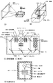
なお、図27(C)は、図27(A)及び図27(B)中における投射装置2601、2702の構造の一例を示した図である。投射装置2601、2702は、光源光学系2801、ミラー2802、2804〜2806、ダイクロイックミラー2803、プリズム2807、液晶モジュール2808、位相差板2809、投射光学系2810で構成される。投射光学系2810は、投射レンズを含む光学系で構成される。本実施例は三板式の例を示したが、特に限定されず、例えば単板式であってもよい。また、図27(C)中において矢印で示した光路に実施者が適宜、光学レンズや、偏光機能を有するフィルムや、位相差を調節するためのフィルム、IRフィルム等の光学系を設けてもよい。
【0191】
また、図27(D)は、図27(C)中における光源光学系2801の構造の一例を示した図である。本実施例では、光源光学系2801は、リフレクター2811、光源2812、レンズアレイ2813、2814、偏光変換素子2815、集光レンズ2816で構成される。なお、図27(D)に示した光源光学系は一例であって特に限定されない。例えば、光源光学系に実施者が適宜、光学レンズや、偏光機能を有するフィルムや、位相差を調節するフィルム、IRフィルム等の光学系を設けてもよい。
【0192】
ただし、図27に示したプロジェクターにおいては、透過型の電気光学装置を用いた場合を示しており、反射型の電気光学装置及びELモジュールでの適用例は図示していない。
【0193】
図28(A)は携帯電話であり、本体2901、音声出力部2902、音声入力部2903、表示部2904、操作スイッチ2905、アンテナ2906、画像入力部(CCD、イメージセンサ等)2907等を含む。
【0194】
図20(B)は携帯書籍(電子書籍)であり、本体3001、表示部3002、3003、記憶媒体3004、操作スイッチ3005、アンテナ3006等を含む。
【0195】
図20(C)はディスプレイであり、本体3101、支持台3102、表示部3103等を含む。
【0196】
ちなみに図20(C)に示すディスプレイは中小型または大型のもの、例えば5〜20インチの画面サイズのものである。また、このようなサイズの表示部を形成するためには、基板の一辺が1m以上のものを用い、多面取りを行って量産することが好ましい。
【0197】
以上の様に、本発明の適用範囲は極めて広く、あらゆる分野の電子機器の作製方法に適用することが可能である。また、本実施例の電子機器は実施例1〜5のどのような組み合わせからなる構成を用いても実現することができる。
【0198】
[実施例7]
本実施例では、駆動回路のTFT(チャネル長:L/チャネル幅:W=10μm/8μm)において、ゲート電極と重なる不純物領域(Lov領域とも呼ぶ)のチャネル長方向における長さと信頼性との関係を示す。
【0199】
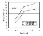
図14では、Lov領域の長さが1.5μmである場合におけるTFTの移動度の最大値(μFE(max))が10%変動するまでの時間をそのTFTの寿命と仮定し、ドレイン電圧の逆数を片対数グラフにプロットして、得られる直線的な関係から寿命が10年となるドレイン電圧の値を10年保証電圧として導出したが、本実施例では、Lov領域のチャネル長方向における長さ(Lov長とも呼ぶ)を0.5μm、0.78μ、1μm、1.5μm、1.7μmとした場合のそれぞれについて、TFTのオン電流値が10%変動するまでの時間をそのTFTの寿命と仮定し、ドレイン電圧の逆数を片対数グラフにプロットして、得られる直線的な関係から寿命が10年となるドレイン電圧の値を10年保証電圧として導出して得られた結果を図31に示す。
【0200】
なお、トランジェントストレス試験でTFTのオン電流値が10%変動するまでの時間が20時間となるドレイン電圧の値を20時間保証電圧として得られた結果も図31中に示した。
【0201】
図31に示すように、16V系の装置に用いられることを想定し、20%のマージンを考えた時、19.2V(16×1.2)以上となるnチャネル型TFTのLov領域の長さは、20時間保証電圧においては1μm以上であり、10年保証電圧となると1.5μm以上であることが望ましい。
【0202】
[実施例8]
本実施例では、ゲート電極を3μm〜10μmの線幅設計サイズとした場合、線幅設計サイズと、ゲート電極と重なる不純物領域(Lov領域とも呼ぶ)のチャネル長方向における長さの関係を図32に示す。
【0203】
実施例1に従って、エッチングを行って、テーパー形状を有するゲート電極を形成した場合、線幅によって、形成されるLovの長さが変化する。
【0204】
得ようとする線幅を3μm、4μm、6μm、8μm、10μmと設定し、実施例1と同じエッチングを行って形成されるLovのチャネル長方向における長さ(Lov長)に関してそれぞれの平均値を測定した。なお、ここでいうLovの長さは、ゲート電極の片側の端部に形成されるテーパー部の長さに対応している。
【0205】
得ようとする線幅が3μmである場合、Lov長の平均値は1.09μmであり、そのときのチャネル長の平均値が0.86であり、0.86+2×(1.09)=3.04のゲート電極幅が得られた。
【0206】
また、それぞれ図32に示したように、線幅が4μmである場合、Lov長の平均値は1.13μmであり、線幅が6μmである場合、Lov長の平均値は1.24μmであり、線幅が8μmである場合、Lov長の平均値は1.32μmであり、線幅が10μmである場合、Lov長の平均値は1.39μmである。
【0207】
従って、これらのデータに基づき、画素部や駆動回路部に使用する配線の線幅を決定し、それぞれ必要とするLov長に設置することが望ましい。
【0208】
【発明の効果】
本発明によりオフ電流値が極めて低く、オフ電流値に対するオン電流値の比が高い画素TFTを実現することができる。また、駆動回路においては、オン電流値が高く、信頼性の高いTFTを備えたため、優れた表示特性を有する半導体装置を実現することができる。また、テーパ−部を利用して不純物領域を形成するため、工程数を削減して製造コストの低減および歩留まりの向上を実現することができる。
【図面の簡単な説明】
【図1】 本発明の構成を示す図。
【図2】 本発明の作製工程を示す図である。
【図3】 本発明の作製工程を示す図である。
【図4】 シミュレーションのキャリア密度分布を示す図である。
【図5】 シミュレーションによるTFT特性を示す図である。
【図6】 AM−LCDの作製工程を示す図である。
【図7】 AM−LCDの作製工程を示す図である。
【図8】 AM−LCDの作製工程を示す図である。
【図9】 液晶モジュールの断面図を示す図である。
【図10】 液晶モジュールの外観を示す図である。
【図11】 駆動回路のTFTにおけるゲート電極のTEM写真図である。
【図12】 画素部のTFTにおけるゲート電極のTEM写真図である。
【図13】 画素部のTFTにおける電圧/電流特性を示す図である。
【図14】 駆動回路のTFTにおける信頼性データ(10年保証電圧)を示す図である。
【図15】 駆動回路のTFTにおける信頼性データ(オンストレス)を示す図である。
【図16】 駆動回路のTFTにおける信頼性データ(オフストレス)を示す図である。
【図17】 駆動回路のTFTにおける信頼性データ(トランジェントストレス)を示す図である。
【図18】 本発明の構成を示す図である。(実施例3)
【図19】 画素部のTFTにおける電圧/電流特性を示す図である。(実施例3)
【図20】 画素部のTFTにおける信頼性データ(10年保証電圧)を示す図である。
【図21】 アクティブマトリクス基板の断面図を示す図である。
【図22】 画素を示す上面図である。
【図23】 第2のドーピング処理による深さ方向の不純物濃度分布を示す図である。
【図24】 オフ電流に対するオン電流の比を示すグラフである。
【図25】 ELモジュールを示す上面図及び断面図である。(実施例5)
【図26】 電子機器の一例を示す図である。
【図27】 電子機器の一例を示す図である。
【図28】 電子機器の一例を示す図である。
【図29】 従来例を示す図である。
【図30】 従来例のTFTにおける電圧/電流特性を示す図である。
【図31】 駆動回路のTFTにおける信頼性(20時間保証電圧、10年保証電圧)とLov長との関係を示す図である。
【図32】 線幅設計サイズとLov長との関係を示す図である。[0001]
BACKGROUND OF THE INVENTION
The present invention relates to a semiconductor device having a circuit formed of a thin film transistor (hereinafter referred to as TFT) and a manufacturing method thereof. For example, the present invention relates to an electronic device in which a liquid crystal module or an EL module is mounted as a component.
[0002]
Note that in this specification, a semiconductor device refers to all devices that can function by utilizing semiconductor characteristics, and an electro-optical device, a light-emitting device, a semiconductor circuit, and an electronic device are all semiconductor devices.
[0003]
[Prior art]
In recent years, a thin film transistor (TFT) is formed using a semiconductor thin film (thickness of about several to several hundred nm) formed on a substrate having an insulating surface, and a semiconductor device having a large-area integrated circuit formed using this TFT is developed. Is progressing. Active matrix liquid crystal modules, EL modules, and contact image sensors are known as representative examples. In particular, a TFT having a crystalline silicon film (typically a polysilicon film) as an active layer (hereinafter referred to as a polysilicon TFT) has high field-effect mobility, so that a circuit having various functions is formed. It is also possible.
[0004]
For example, a liquid crystal module mounted on a liquid crystal display device controls a pixel circuit that displays an image for each functional block, a pixel circuit such as a shift register circuit based on a CMOS circuit, a level shifter circuit, a buffer circuit, and a sampling circuit. A driving circuit is formed on a single substrate.
[0005]
In the pixel circuit of the active matrix type liquid crystal module, a TFT (pixel TFT) is disposed in each of several tens to several millions of pixels, and a pixel electrode is provided in each of the pixel TFTs. A counter electrode is provided on the counter substrate side with the liquid crystal interposed therebetween, and a kind of capacitor using the liquid crystal as a dielectric is formed. Then, the voltage applied to each pixel is controlled by the switching function of the TFT, and the liquid crystal is driven by controlling the charge to this capacitor, and the transmitted light quantity is controlled to display an image.
[0006]
The pixel TFT is composed of an n-channel TFT, and is driven by applying a voltage to the liquid crystal as a switching element. Since the liquid crystal is driven by alternating current, a method called frame inversion driving is often employed. In this method, in order to keep power consumption low, it is important that the characteristics required for the pixel TFT have a sufficiently low off-current value (drain current that flows when the TFT is off).
[0007]
As a TFT structure for reducing the off-current value, a lightly doped drain (LDD) structure is known. In this structure, a region to which an impurity element is added at a low concentration is provided between a channel formation region and a source region or a drain region formed by adding an impurity element at a high concentration, and this region is referred to as an LDD region. I'm calling.
[0008]
However, when a normal LDD region is formed in a conventional pixel TFT, the off-current value can be reduced, but at the same time, the on-current value is also lowered. The normal LDD structure has a high effect of suppressing the off-current value, but has a low effect of relaxing the electric field in the vicinity of the drain and preventing deterioration due to hot carrier injection.
[0009]
A so-called GOLD (Gate-drain Overlapped LDD) structure in which an LDD region is disposed so as to overlap with a gate electrode through a gate insulating film is known as means for preventing deterioration of an on-current value due to hot carriers. . With such a structure, it is known that the electric field strength in the vicinity of the drain is relaxed, hot carrier injection is prevented, and the deterioration phenomenon is effective.
[0010]
In addition, the GOLD structure has a high effect of preventing deterioration of the on-current value, but on the other hand, there is a problem that the off-current value becomes larger than that of a normal LDD structure. Therefore, it is not a preferable structure for application to the pixel TFT.
[0011]
As described above, in a semiconductor device having a plurality of integrated circuits such as an active matrix liquid crystal display device, such a problem is enhanced particularly in a crystalline silicon TFT, and in the active matrix liquid crystal display device. It has become apparent as the required performance increases.
[0012]
[Problems to be solved by the invention]
The present invention is a technique for solving such problems, and improves the operating characteristics of a semiconductor device in an electro-optical device and a semiconductor device typified by an active matrix liquid crystal display device manufactured using TFTs. And it aims at achieving low power consumption.
[0013]
In particular, an object of the present invention is to obtain a structure of a pixel TFT (n-channel TFT) having a low off-current value. In addition, an object of the present invention is to obtain a structure of a pixel TFT having a high ratio of on-current value to off-current value.
[0014]
[Means for Solving the Problems]
As shown in FIG. 1A, according to the present invention, in the
[0015]
That is, the concentration of the impurity element (phosphorus) gradually increases as the distance from the edge of the gate electrode 105 (the edge of the gate electrode in the cross section cut in the channel length direction) toward the peripheral edge of the semiconductor layer increases in the channel length direction. An impurity region is provided. Therefore, this impurity region has a large electric resistance on the channel forming region side and a small electric resistance on the peripheral portion side of the semiconductor layer.
[0016]
In the present invention, since the impurity region is continuously increased, there is no clear boundary. In this specification, the impurity concentration of the
[0017]
In the above description, the drain side has been described. However, when the pixel TFT is used, the same is preferable on the source side. In the impurity region on the source side, a
[0018]
The present invention is characterized in that a TFT having a very low off-current value and a high ratio of the on-current value to the off-current value is realized by intentionally forming the
[0019]
Further, as shown in FIG. 29, the conventional TFT structure has a boundary due to a clear concentration difference, and the
[0020]
Since the off-current flows due to quantum mechanical effects such as tunneling between bands, it is considered that it is mainly influenced by the electric field. Therefore, the electric field concentration occurring at the boundary is a cause of increasing the off-current value of the TFT. In particular, in the conventional TFT structure, a strong electric field is concentrated due to a large concentration difference at the boundary between the channel formation region and the low concentration impurity region.
[0021]
On the other hand, the present invention eliminates a clear boundary by providing an impurity region having a continuously increasing concentration between the channel formation region and the drain region, thereby reducing the concentration of the electric field generated in the vicinity of the boundary portion. A TFT structure with a low current value can be obtained.
[0022]
In the present invention, as shown in FIG. 1A, a concentration gradient such that the boundary due to the impurity element concentration difference in the semiconductor layer is completely eliminated is formed in the impurity region 102 (1 × 10 6. 15 / Cm Three ~ 1x10 twenty one / Cm Three However, the effect of the present invention can also be obtained by reducing the concentration difference between the
[0023]
FIG. 1B shows the TFT structure as shown in FIG. 1A, with a channel length L = 6 μm, a channel width W = 4 μm, a thickness of the
[0024]
Further, as a conventional example, the state of electric field concentration on the low-
[0025]
As shown in FIG. 1B, the present invention has at least an impurity concentration (P concentration) of 1 × 10. 17 ~ 1x10 18 / Cm Three By providing the impurity region having a concentration gradient in the range of 1, the electric field strength on the surface of the semiconductor layer can be made gentler than before. Therefore, according to the present invention, a strong electric field concentration does not occur over the entire semiconductor layer, and a TFT with a low off-current value can be obtained.
[0026]
The configuration of the invention disclosed in this specification is as follows.
A semiconductor device including a TFT including a semiconductor layer formed on an insulating surface, an insulating film (gate insulating film) formed on the semiconductor layer, and a gate electrode formed on the insulating film. ,
The semiconductor layer includes a channel formation region overlapping with the gate electrode, and an impurity region (including an LDD region, a source region, or a drain region) formed in contact with the channel formation region,
The impurity region has a concentration distribution in which a concentration of an impurity element imparting one conductivity type increases as a distance from the channel formation region increases.
[0027]
In the above structure, the impurity element imparting one conductivity type to the semiconductor is phosphorus (P) or arsenic (As), and an n-channel TFT is obtained. This n-channel TFT is suitable for a TFT in a pixel portion because it has a small off current.
[0028]
In the TFT of the pixel portion, the same level of reliability can be obtained even if an offset region is formed between the channel formation region and the low concentration impurity region. An example is shown in FIG.
[0029]
Further, the configuration of the other invention is as follows:
A semiconductor device comprising a TFT including a semiconductor layer formed on an insulating surface, an insulating film formed on the semiconductor layer, and a gate electrode formed on the insulating film, wherein the semiconductor layer comprises: A channel formation region overlapping the gate electrode, an offset region formed in contact with the channel formation region, and an impurity region formed in contact with the offset region,
In the semiconductor device, the impurity region has a concentration distribution in which the impurity concentration increases as the distance from the channel formation region increases.
[0030]
In the above structure, the end portion of the gate electrode substantially coincides with the interface between the channel formation region and the offset region.
[0031]
In a semiconductor device including a pixel portion and a driver circuit over the same insulating surface, the pixel portion is preferably an impurity region that does not overlap with the gate electrode with an insulating film (gate insulating film) interposed therebetween. In this case, the end portion of the gate electrode of the pixel TFT is approximately coincident with the interface (boundary) between the channel formation region and the impurity region.
[0032]
In the above structure, the gate electrode of the n-channel TFT of the driver circuit has a tapered portion, and the tapered portion overlaps part of the impurity region with an insulating film (gate insulating film) interposed therebetween. It is characterized by that. Since doping is performed by passing through the tapered portion, in the driving circuit, the width of the tapered portion and the width of the region having a concentration distribution in which the impurity concentration increases as the distance from the channel formation region increases are approximately the same To do. Further, as shown in FIG. 32, if the wiring width to be designed is increased, the formed tapered portion also becomes longer. Therefore, the width of the gate electrode of the driving circuit is longer than the width of the gate electrode of the pixel portion. It is preferable to design so that it becomes.
[0033]
In the above structure, an offset region may be provided between the channel formation region of the pixel TFT and the impurity region.
[0034]
In each of the above structures, the gate electrode has a stacked structure in which the first conductive layer is a lower layer and the second conductive layer is an upper layer. In the present invention, an impurity region having a concentration gradient is formed using the gate electrode of this laminated structure. Accordingly, impurity regions whose impurity concentration increases as the distance from the channel formation region increases are formed on both sides of the channel formation region.
[0035]
In each of the above structures, the impurity region includes a source region or a drain region.
[0036]
In FIG. 1, the impurity region has an impurity concentration that increases as the distance from the channel formation region increases, and the concentration distribution is shown as a normal distribution. However, the concentration distribution is not particularly limited. It may be a distribution, a straight line having an inclination, or a combination thereof. However, it is important that the width in the channel length of the
[0037]
That is, in each of the above structures, the impurity region has a region having a concentration distribution in which the impurity concentration increases and a region in which the impurity concentration is substantially constant, and the region having the concentration distribution in which the impurity concentration increases is a channel. The length in the long direction is 1 μm or more.
[0038]
Further, in the conventional method, depending on the doping conditions, the impurity element may wrap around below the gate electrode, resulting in an impurity region overlapping the gate electrode and having a concentration gradient of about 0.1 μm. It is difficult to obtain the same effect as the invention.
[0039]
Conventionally, impurity elements are doped using a patterned resist mask, or impurity elements are doped in a self-aligning manner using a wiring as a mask, so that a stepwise concentration distribution as shown in FIG. 29 is formed. Thus, the structure of the present invention, that is, the impurity region having a concentration gradient could not be obtained by 0.5 μm or more.
[0040]
In the present invention, not only the stacked gate electrode but also a part of the insulating film (gate insulating film) covering the semiconductor layer is tapered and an impurity region having a concentration gradient is formed using the insulating film. Is possible. In this case, the impurity region is characterized in that the thickness of the insulating film is different between a region having the maximum distance from the channel formation region and a region having the minimum distance. In addition, an impurity region having a concentration gradient can be formed using both the gate electrode having a tapered portion and the insulating film having the tapered portion.
[0041]
The present invention also features a manufacturing method for obtaining the above structure.
[0042]
The configuration of the invention relating to the manufacturing method for realizing the above structure is as follows.
Forming a semiconductor layer on the insulating surface;
Forming an insulating film on the semiconductor layer;
Forming a conductive layer having a tapered portion on the insulating film (gate insulating film);
Adding an impurity element imparting one conductivity type to the semiconductor layer through the tapered portion and the insulating film, and forming an impurity region in which an impurity concentration increases toward an end portion of the tapered portion; ,
Forming a gate electrode by selectively removing only the tapered portion of the conductive layer;
A method for manufacturing a semiconductor device having
[0043]
The structure of the manufacturing method is characterized in that doping is performed through a tapered portion made of a conductive layer to form an impurity region having a concentration gradient.
[0044]
On the other hand, in a conventional manufacturing method, an LDD region, a source region, and a drain region are formed by doping an impurity element using a resist mask formed using a photomask.
[0045]
Further, in the above structure, an impurity region which imparts one conductivity type to the semiconductor layer through the tapered portion is added, and an impurity region whose impurity concentration increases toward the end portion of the tapered portion is at least Impurity concentration (P concentration) 1 × 10 17 ~ 1x10 18 / Cm Three It has a concentration gradient in the range of.
[0046]
In addition, the driver circuit and the pixel portion can be formed over the same substrate. In that case, it is preferable that at least the gate electrode of the TFT of the pixel portion selectively removes only the taper portion, and the gate electrode of the TFT of the drive circuit (TFT on which on-current is important) is left as it is. . In addition, in the TFT of the drive circuit, the longer the width of the taper portion in the channel length direction, the higher the reliability. Therefore, when forming the taper portion, the selection ratio is set so that the width of the taper portion becomes longer. High SF 6 It is effective to perform dry etching with an etching gas containing.
[0047]
In addition to the gate electrode having a stacked structure, a part of an insulating film (gate insulating film) covering the semiconductor layer can be tapered, and an impurity region having a concentration gradient can be formed using the insulating film. There are other configurations of a manufacturing method for realizing the above structure,
Forming a semiconductor layer on the insulating surface;
Forming an insulating film on the semiconductor layer;
Forming a gate electrode on the insulating film;
Etching the insulating film to form an insulating layer having a tapered portion on the semiconductor layer;
Adding an impurity element that imparts one conductivity type to the semiconductor layer through the tapered portion, and forming an impurity region in which an impurity concentration increases toward an end of the tapered portion;
A method for manufacturing a semiconductor device having
[0048]
In addition, the structure of the manufacturing method is characterized in that doping is performed through a tapered portion made of an insulating layer to form an impurity region having a concentration gradient.
[0049]
DETAILED DESCRIPTION OF THE INVENTION
Embodiments of the present invention will be described below with reference to FIGS.
[0050]
Here, an example in which an impurity region whose impurity concentration (P concentration) continuously increases from the channel formation region side to the impurity region side is shown using the tapered portion of the gate electrode.
[0051]
First, the
[0052]
As the
[0053]
Next, the
[0054]
Next, an insulating
[0055]
The insulating
[0056]
Next, a first
[0057]
Next, a resist
[0058]
Here, the angle of the tapered portion (taper angle) is defined as the angle formed by the substrate surface (horizontal plane) and the inclined portion of the tapered portion. The taper angle of the second
[0059]
Next, using the resist
[0060]
Here, in order to suppress the film loss of the insulating
[0061]
Next, a first doping process is performed while the resist
[0062]
Next, a third etching process is performed using the resist
[0063]
Next, after removing the resist
[0064]
Here, an example is shown in which the first etching step and the second etching step are performed to perform the first doping step, and then the third etching step is performed to perform the second doping step. As long as an electrode structure (lamination of the second conductive layer and the first conductive layer) and a region having a concentration gradient can be formed as shown in FIG. After the first etching process, the second etching process, and the third etching process are performed to obtain an electrode structure as shown in FIG. 3B, the first doping process and the second doping process are sequentially performed. You may go.
[0065]
Next, a fourth etching process is performed using an ICP etching apparatus. By this fourth etching step, only the tapered portion of the first
[0066]
Thereafter, the impurity element added to the semiconductor layer is activated. By this activation, the impurity element contained in the impurity region is diffused, so that a concentration gradient that draws a smoother curve is formed and the boundary between the regions is eliminated. Next, after an
[0067]
In this manner, a TFT having a structure shown in FIG. 3D can be formed using four photomasks.
[0068]
The TFT formed according to the present invention is characterized in that, in the low
[0069]
In addition, a simulation was performed to examine the effect of the impurity region having a concentration gradient. Here, as shown in FIG. 4, a high concentration impurity region which is a source region / drain region, a low concentration impurity region, and a channel formation region are assumed, and a concentration gradient is given only to the low concentration impurity region. A simulation was performed. The numerical values used in the simulation are as follows: L = 6 μm, W = 4 μm, low-concentration impurity region (Loff) width = 1.5 μm, gate insulating film thickness = 115 nm, polysilicon layer thickness = 45 nm, channel formation Region carrier density (B concentration) = 2 × 10 16 / Cm Three , Carrier density (P concentration) of source / drain regions = 1 × 10 19 / Cm Three It was. Further, a comparison was made between a case where the low concentration impurity region is constant (comparative example) and a case where the low concentration impurity region has a concentration gradient. Here, simulation was performed using a gradient of a normal distribution (Gaussian distribution) as shown in FIG. 4 as a concentration distribution model of the low concentration impurity region, and the voltage / current characteristics (FIG. 5) of the TFT were derived. As a comparative example, the carrier concentration (P concentration) is set to a constant concentration (3 × 10 5 in the low concentration impurity region. 17 /
[0070]
FIG. 5 shows voltage / current characteristics when Vds (voltage difference between the source region and the drain region) = 14V. As shown in FIG. 5, the off-current value of the TFT having the low-concentration impurity region having the concentration gradient is significantly reduced as compared with the comparative example. This is considered to be mainly due to the fact that the electric field concentration generated at the boundary of each region is relaxed by the present invention. On the other hand, the on-current value is determined by mobility and sheet resistance. Further, it is shown that the on-current value of the TFT including the low concentration impurity region having the concentration gradient is approximately the same as that of the comparative example. That is, when the sheet resistance is measured in the low-concentration impurity region, even if the comparative example and the present invention are the same (the on-current value is the same), the present invention can reduce only the off-current value. Accordingly, the ratio of the on-current value to the off-current value is increased. Conventionally, when the structure for reducing the off-current is used, the on-current is also reduced, so that the ratio of the on-current value to the off-current value is almost unchanged or decreased.
[0071]
Although the gradient of the normal distribution (Gaussian distribution) is used here, it is not particularly limited as long as it has a concentration gradient. The concentration distribution may be an exponential distribution or draw a straight line having a gradient. Also good. The results of the simulation were almost the same, and the off-current was reduced if the impurity region had a continuous concentration gradient.
[0072]
Further, the present invention is not limited to the top gate TFT structure shown in FIG. 1 as long as the impurity region has a concentration gradient as shown in FIG.
[0073]
The present invention having the above-described configuration will be described in more detail with the following examples.
[0074]
【Example】
[Example 1]
Here, a method for simultaneously manufacturing a pixel portion and driver circuit TFTs (n-channel TFT and p-channel TFT) provided around the pixel portion over the same substrate will be described with reference to FIGS.
[0075]
First, in this embodiment, a
[0076]
Next, a
[0077]
Next, semiconductor layers 202 to 206 are formed over the base film. The semiconductor layers 202 to 206 are formed by forming a semiconductor film having an amorphous structure by a known means (sputtering method, LPCVD method, plasma CVD method, or the like), and then known crystallization treatment (laser crystallization method, heat A crystalline semiconductor film obtained by performing a crystallization method or a thermal crystallization method using a catalyst such as nickel) is formed by patterning into a desired shape. The semiconductor layers 202 to 206 are formed to a thickness of 25 to 80 nm (preferably 30 to 60 nm). The material of the crystalline semiconductor film is not limited, but is preferably silicon or silicon germanium (Si X Ge 1-X (X = 0.0001 to 0.02)) It may be formed of an alloy or the like. In this example, a 55 nm amorphous silicon film was formed by plasma CVD, and then a solution containing nickel was held on the amorphous silicon film. This amorphous silicon film is dehydrogenated (500 ° C., 1 hour), then thermally crystallized (550 ° C., 4 hours), and then laser annealing treatment is performed to improve crystallization. Thus, a crystalline silicon film was formed. Then, semiconductor layers 202 to 206 were formed by patterning the crystalline silicon film using a photolithography method.
[0078]
Further, after forming the semiconductor layers 202 to 206, a small amount of impurity element (boron or phosphorus) may be appropriately doped in order to control the threshold value of the TFT.
[0079]
In the case of producing a crystalline semiconductor film by a laser crystallization method, an excimer laser, a YAG laser, a YVO, which is a pulse oscillation type or a continuous emission type, is used. Four Laser, YLF laser, YAlO Three A laser, a glass laser, a ruby laser, an alexandride laser, a Ti: sapphire laser, or the like can be used. When these lasers are used, it is preferable to use a method in which laser light emitted from a laser oscillator is linearly collected by an optical system and irradiated onto a semiconductor film. The conditions for crystallization are appropriately selected by the practitioner. When a pulsed excimer laser is used, the pulse oscillation frequency is 30 Hz, and the laser energy density is 100 to 400 mJ / cm. 2 (Typically 200-300mJ / cm 2 ). Also, pulse oscillation type YAG laser and YVO Four When using a laser, the second harmonic or the third harmonic is used and the pulse oscillation frequency is 1 to 10 kHz, and the laser energy density is 300 to 600 mJ / cm. 2 (Typically 350-500mJ / cm 2 ) Then, when the laser beam condensed linearly with a width of 100 to 1000 μm, for example 400 μm, is irradiated over the entire surface of the substrate, the superposition ratio (overlap ratio) of the linear laser light at this time is 80 to 98%. Good.
[0080]
YVO Four When a continuous wave laser represented by a laser is used, a continuous wave YVO with an output of 10 W is used. Four Laser light emitted from the laser is converted into a harmonic (second harmonic to fourth harmonic) by a nonlinear optical element. Also, YVO in the resonator Four There is also a method of emitting harmonics by inserting a crystal and a nonlinear optical element. Then, it is preferably formed into a rectangular or elliptical laser beam on the irradiation surface by an optical system, and irradiated to the object to be processed. The energy density at this time is 0.01 to 100 MW / cm. 2 Degree (preferably 0.1-10 MW / cm 2 )is necessary. Then, irradiation may be performed by moving the semiconductor film relative to the laser light at a speed of about 0.5 to 2000 cm / s.
[0081]
Next, a
[0082]
Next, as illustrated in FIG. 6A, a first
[0083]
In this embodiment, the first
[0084]
Next, resist
[0085]
Thereafter, the resist
[0086]
In the first etching process, the shape of the mask made of resist is made suitable, and the end portions of the first conductive layer and the second conductive layer are tapered due to the effect of the bias voltage applied to the substrate side. It becomes. The angle of the tapered portion may be 15 to 45 °.
[0087]
The angle of the taper portion (taper angle) may be appropriately determined by the practitioner with reference to Table 1.
[0088]
[Table 1]
Thus, the first shape
[0090]
Then, a first doping process is performed without removing the resist mask, and an impurity element imparting n-type conductivity is added to the semiconductor layer. (FIG. 6B) The doping process may be performed by an ion doping method or an ion implantation method. The condition of the ion doping method is a dose of 1 × 10 13 ~ 5x10 15 /cm 2 The acceleration voltage is set to 60 to 100 keV. In this embodiment, the dose is 1.5 × 10 15 /cm 2 The acceleration voltage was 80 keV. As an impurity element imparting n-type, an element belonging to
[0091]
Next, a second etching process is performed without removing the resist mask. Here, SF is used as the etching gas. 6 And Cl 2 And O 2 The gas flow ratio is 24/12/24 (sccm), and 700 W of RF (13.56 MHz) power is applied to the coil-type electrode at a pressure of 1.3 Pa to generate plasma and perform etching. 25 seconds. 10 W RF (13.56 MHz) power is also applied to the substrate side (sample stage), and a substantially negative self-bias voltage is applied. In the second etching process, the etching rate with respect to W is 227.3 nm / min, the etching rate with respect to TaN is 32.1 nm / min, the selection ratio of W with respect to TaN is 7.1, and the insulating
[0092]
By this second etching process, the taper angle of W became 70 °. Second conductive layers 234b to 239b are formed by the second etching process. On the other hand, the first conductive layer is hardly etched, and the first conductive layers 234a to 239a are formed. Although not shown, in actuality, the width of the first conductive layer recedes by about 0.15 μm, that is, the entire line width recedes by about 0.3 μm as compared with that before the second etching process. Note that the second etching process here corresponds to the third etching step (FIG. 3A) described in the embodiment mode. The width of the second conductive layer in the channel length direction here corresponds to W2 described in the embodiment.
[0093]
In the second etching process, CF Four And Cl 2 And O 2 Can also be used as an etching gas. In that case, if each gas flow rate ratio is 25/25/10 (sccm), 500 W of RF (13.56 MHz) power is applied to the coil-type electrode at a pressure of 1 Pa to generate plasma and perform etching. Good. 20 W of RF (13.56 MHz) power is also applied to the substrate side (sample stage), and a substantially negative self-bias voltage is applied. CF Four And Cl 2 And O 2 When W is used, the etching rate with respect to W is 124.62 nm / min, the etching rate with respect to TaN is 20.67 nm / min, and the selection ratio of W with respect to TaN is 6.05. Therefore, the W film is selectively etched. In this case, a region of the insulating
[0094]
Next, after removing the resist mask, a second doping process is performed to obtain the state of FIG. In FIG. 6C, the length of the tapered portion of the first conductive layer is shown as being the same, but the length of the tapered portion of the first conductive layer is different depending on the wiring width as shown in FIG. It has changed. Therefore, when a plurality of wirings having different wiring widths are provided on the same substrate, the widths of the doped regions are also different. Doping is performed using the second conductive layers 234b to 239b as masks against the impurity element so that the impurity element is added to the semiconductor layer below the tapered portion of the first conductive layer. In this embodiment, P (phosphorus) is used as the impurity element, and the doping condition is a dose of 1.5 × 10. 14 /cm 2 , Acceleration voltage 90 keV, ion current density 0.5 μA / cm 2 , Phosphine (PH Three ) Plasma doping was performed with a 5% hydrogen dilution gas and a gas flow rate of 30 sccm. Thus, the low
[0095]
FIG. 23 shows the second doping process (acceleration voltage 90 kV, dose amount 1.5 × 10 14 /cm 2 ) Shows the concentration distribution (SIMS analysis) of phosphorus in the depth direction. According to FIG. 23, in the depth direction, the impurity concentration added to the semiconductor layer (Si) in the second doping process decreases from the surface toward the substrate side. In FIG. 23, x indicates the concentration distribution (in the depth direction) of Sample A in which a silicon oxynitride film having a thickness of 110 nm is formed on a silicon substrate and second doping is performed. The concentration distribution of the sample A corresponds to the concentration distribution in a portion not covered with the first conductive layer in FIG.
[0096]
Further, in FIG. 23, the □ marks indicate the concentration distribution (depth direction) of Sample B in which 15 nm of TaN is further formed on the gate insulating film (silicon oxynitride film) and the second doping is performed. . The concentration distribution of the sample B corresponds to the concentration distribution of the portion where the thickness of the tapered portion of the first conductive layer is 15 nm in FIG. However, the thickness value of the horizontal axis does not include the film thickness of TaN.
[0097]
In FIG. 23, the ◯ marks indicate the concentration distribution (depth direction) of Sample C in which TaN of 30 nm is formed on the silicon oxynitride film and second doping is performed. The concentration distribution of the sample C corresponds to the concentration distribution of the portion where the thickness of the tapered portion of the first conductive layer is 30 nm in FIG. However, the thickness value of the horizontal axis does not include the film thickness of TaN.
[0098]
Further, as shown in FIG. 23, in the vicinity of the surface of the semiconductor layer located below the tapered portion (near the interface with the gate insulating film), as the thickness of the tapered portion is changed from 30 nm to 0 nm, that is, from the channel formation region to the channel length. The phosphorus concentration becomes 1 × 10 with increasing distance 18 ~ 7 × 10 18 /cm Three It can be read as increasing continuously in the range of.
[0099]
Further, in the semiconductor layer located below the tapered portion in FIG. 23, at a position 40 nm from the surface of the semiconductor layer, as the thickness of the tapered portion is changed from 30 nm to 0 nm, that is, away from the channel formation region in the channel length direction. As the phosphorus concentration is 1.5 × 10 17 ~ 3.5 × 10 18 /cm Three It can be read as increasing continuously in the range of. However, the phosphorus concentration by these SIMS analysis is just after doping, and phosphorus is diffused by a subsequent heat treatment or the like, and therefore slightly different from the phosphorus concentration at the completion of TFT fabrication.
[0100]
In the present embodiment, the width of the taper portion (width in the channel length direction) is preferably at least 0.5 μm, and the limit is 1.5 μm to 2 μm. Therefore, the width in the channel length direction of the low-concentration impurity region having a concentration gradient is also limited to 1.5 μm to 2 μm, although it depends on the film thickness. Although the high-concentration impurity region and the low-concentration impurity region are illustrated separately here, there is actually no clear boundary, and a region having a concentration gradient as shown in FIG. Is formed. Similarly, there is no clear boundary between the channel formation region and the low concentration impurity region.
[0101]
Next, a semiconductor layer that later becomes an active layer of the n-channel TFT is covered with a
[0102]
In addition, the film is not reduced by the second etching process, for example, SF 6 Is used as an etching gas, in order to facilitate boron doping, etching (CHF) for thinning the insulating
[0103]
Next, a resist
[0104]
By the third etching process, low concentration impurity regions (LDD regions) 247 to 254 having a concentration gradient are formed without overlapping the first
[0105]
In addition, the electrode formed using the first
[0106]
In this embodiment, the third etching process is performed after the third doping process. However, the third doping process may be performed after the third etching process.
[0107]
Next, the resist
[0108]
Next, as shown in FIG. 7C, a step of activating the impurity element added to each semiconductor layer is performed. This activation process is performed by a thermal annealing method using a furnace annealing furnace. As the thermal annealing method, it may be performed at 400 to 700 ° C., typically 500 to 550 ° C. in a nitrogen atmosphere having an oxygen concentration of 1 ppm or less, preferably 0.1 ppm or less. The activation treatment was performed by heat treatment. In addition to the thermal annealing method, a laser annealing method or a rapid thermal annealing method (RTA method) can be applied.
[0109]
Although not shown, the impurity element is diffused by this activation treatment, the boundary between the low concentration impurity region and the high concentration impurity region is eliminated, and the concentration distribution shown in FIG. 1A is obtained. Accordingly, here, the low concentration impurity region has a concentration gradient, and among the high concentration impurity region, a part of the region on the low concentration impurity region side also has the concentration gradient.
[0110]
In this embodiment, at the same time as the activation treatment, nickel used as a catalyst during crystallization is gettered to an impurity region containing high-concentration phosphorus, and nickel in a semiconductor layer mainly serving as a channel formation region The concentration is reduced. A TFT having a channel formation region manufactured in this manner has a low off-current value and good crystallinity, so that high field-effect mobility can be obtained and good characteristics can be achieved.
[0111]
In addition, an activation process may be performed before forming the first interlayer insulating film. However, when the wiring material used is weak against heat, it is activated after an interlayer insulating film (insulating film containing silicon as a main component, for example, a silicon nitride film) is formed to protect the wiring and the like as in this embodiment. It is preferable to perform the conversion treatment.
[0112]
Next, a second
[0113]
In the case where a laser annealing method is used as the activation treatment, it is desirable to irradiate a laser beam such as an excimer laser or a YAG laser after the hydrogenation.
[0114]
Next, a third
[0115]
Next,
[0116]
As described above, the driving
[0117]
In this embodiment, the structure of the TFT differs depending on each circuit.
[0118]
The n-
[0119]
FIG. 13 shows the voltage / current characteristics of the TFT (L / W = 6 μm / 4 μm, LDD region width 1.5 μm) formed by the process of this example. As a comparative example, the voltage / current characteristics of the TFT are shown in FIG. Unlike the present embodiment (low concentration impurity region having a concentration gradient), this comparative example is a TFT having no concentration gradient in the low
[0120]
In FIG. 13, the threshold value (Vth) of the TFT is 0.415 V, the S value is 0.214 V / dec, and the field effect mobility (μFE) is 122.1 cm. 2 / Vs, the on-current value is 1.08 × 10 when Vds (voltage difference between the source region and the drain region) = 14V -Four A, the off-current value is 1.5 × 10 when Vds = 14V -12 A. All of these values show good TFT characteristic values, but the off current value is particularly small and is suppressed to about 1/10 compared with the comparative example. Further, these TFT characteristics coincide with the simulation results shown in the above embodiment.
[0121]
A cross-sectional TEM photograph in the vicinity of the gate electrode of the TFT of the pixel portion is shown in FIG.
[0122]
In this embodiment, the n-
[0123]
An impurity element imparting n-type conductivity is added to each of the
[0124]
Similarly, the sampling circuit 304, typically an n-
[0125]
The p-
[0126]
The p-
[0127]
Similarly, the n-channel TFT 306 has a structure in which the low-
[0128]
A cross-sectional TEM photograph in the vicinity of the gate electrode of the n-channel TFT 306 is shown in FIG.
[0129]
FIG. 14 shows the reliability of the n-channel TFT 306 of the driver circuit. Reliability is evaluated by deriving a 10-year guaranteed voltage. The 10-year guaranteed voltage means that the time until the maximum mobility (μFE (max)) of the TFT fluctuates by 10% is assumed to be the lifetime of the TFT, and the inverse of the drain voltage is plotted on a semi-logarithmic graph. Thus, a drain voltage value with a lifetime of 10 years is derived from the obtained linear relationship.
[0130]
As shown in FIG. 14, the 10-year guaranteed voltage of the n-channel TFT 306 is derived as 20 V or more, and shows high reliability.
[0131]
The p-
[0132]
Other reliability evaluations were also conducted. Here, in order to derive the 1000-hour lifetime temperature due to on-stress, the time until the TFT characteristic (voltage value at the rise of the IV curve (Shift-1)) fluctuates by 0.1 V at Vg = + 20 V and Vd = 0 V is shown. FIG. 15 shows the result of plotting with respect to 1000 / T (T: absolute temperature (K)) and deriving the temperature (life temperature) that fluctuates by 0.1 V in 1000 hours. As shown in FIG. 15, the lifetime temperature in 1000 hours of the n-channel TFT 306 was 80 ° C. or more.
[0133]
In addition, the p-
[0134]
Further, in order to investigate the 1000-hour lifetime temperature due to off-stress, when Vg = 0 V and Vd = + 20 V, the time until the TFT characteristic (voltage value at the rise of the IV curve (Shift-1)) fluctuates by 0.1 V is 1000 FIG. 16 shows the results of plotting against / T (T: absolute temperature (K)) and deriving a temperature (life temperature) that fluctuates by 0.1 V in 1000 hours. As shown in FIG. 16, the lifetime temperature in 1000 hours of the n-channel TFT 306 was 80 ° C. or more.
[0135]
In addition, the p-
[0136]
Next, in order to derive the characteristic variation of the n-channel TFT due to the transient stress, FIG. 17 shows the on-characteristic variation after leaving Vd = + 20 V and Vg = 2 to 6 V for 20 hours at room temperature. As shown in FIG. 17, the fluctuation of the mobility maximum value (μFE (max)) after 20 hours of the n-channel TFT 306 could be 10% or less. Transient stress refers to stress when the drain voltage is set to a certain value and the gate voltage is fixed.
[0137]
In the n-channel TFT 306 of the driving circuit, the width of the low concentration impurity region overlapping with the gate electrode is 1.5 μm. Depending on the conventional doping conditions, it may be added under the gate electrode. In this case, the width of the low-concentration impurity region overlapping the gate electrode is about 0.1 μm. It is difficult to obtain a remarkable effect as shown in the example.
[0138]
In addition, the p-
[0139]
In this way, in this embodiment, a driver circuit including a highly reliable TFT 306 and a pixel portion including a
[0140]
[Example 2]
In this embodiment, a process for manufacturing an active matrix liquid crystal display device from the active matrix substrate manufactured in
[0141]
First, after obtaining the active matrix substrate in the state of FIG. 8 according to the first embodiment, an
[0142]
Next, the
[0143]
Then, the active matrix substrate on which the pixel portion and the driver circuit are formed and the counter substrate are attached to each other with a
[0144]
The structure of the liquid crystal module thus obtained will be described with reference to the top view of FIG. In addition, the same code | symbol was used for the part corresponding to FIG.
[0145]
The top view shown in FIG. 10A connects a pixel portion, a driving circuit, an
[0146]
A
[0147]
Here, the
[0148]
In addition, a light-shielding layer is provided between adjacent pixels in the color filter to shield light other than the display area. Here, the
[0149]
Further, without providing the light-shielding layer, the light-shielding layer is appropriately disposed between the counter substrate and the counter electrode so as to be shielded from light by stacking a plurality of colored layers constituting the color filter. Or the drive circuit may be shielded from light.
[0150]
Further, an
[0151]
The liquid crystal module manufactured as described above can be used as a display portion of various electronic devices.
[0152]
[Example 3]
In this embodiment, an example in which an offset region is provided between a channel formation region and a low concentration impurity region is shown in FIG. FIG. 18 is a schematic diagram.
[0153]
In FIG. 18, in the offset
[0154]
In this embodiment, the
[0155]
In this specification, the offset
[0156]
Note that in order to manufacture the offset
[0157]
FIG. 19 shows voltage / current characteristics of the TFT of this example (L / W = 6 × 2 μm / 4 μm, offset region width 0.5 μm, LDD region width 1.5 μm). Since the structure is a double gate structure, two channel formation regions L / W = 6 μm / 4 μm are indicated as L / W = 6 × 2 μm / 4 μm. The threshold value (Vth) of the TFT is 0.715 V, the S value is 0.243 V / dec, and the field effect mobility (μFE) is 90.7 cm. 2 / Vs, ON current value is 7.85 × 10 when Vds = 14V -Five A, OFF current value is 9.5 × 10 when Vds = 14V -13 A. In FIG. 19, these all show good TFT characteristic values, but the off-current value is particularly small and the ratio of the on-current value to the off-current value is high, so that it is suitable as a pixel TFT. In FIG. 24, the □ marks indicate the pixel TFTs of this example, and the ratio of the on-current value to the off-current value is 7.9 to 8.4. The conventional example indicated by the ▲ mark Higher than.
[0158]
In addition, the characteristic variation of the n-channel TFT due to transient stress was derived. It shows in FIG. As a comparative example, the pixel TFT of Example 1 (● mark) and the pixel TFT of the conventional example (low concentration impurity region without concentration gradient) (勾 配 mark) are shown. As shown in FIG. 20, the pixel TFTs (10-year guaranteed voltage: 12V) of this example indicated by □ are the conventional example (10-year guaranteed voltage: 10V) and Example 1 (10-year guaranteed voltage: 10V). .3V) higher reliability could be obtained.
[0159]
[Example 4]
In this embodiment, an active matrix substrate different from that in
[0160]
In this embodiment, after forming the
[0161]
Further, as shown in FIG. 21, the
[0162]
The
[0163]
In the pixel portion 606, an n-
[0164]
One
[0165]
In the pixel structure of this embodiment, the end portion of the
[0166]
Further, since the drive circuit 601 has the same structure as that of the first embodiment, detailed description thereof is omitted here. Note that the n-channel TFT 603 corresponds to the n-channel TFT 306 in FIG. 9, the p-
[0167]
A top view of a pixel portion of an active matrix substrate manufactured in this embodiment is shown in FIG. In addition, the same code | symbol is used for the part corresponding to FIG. A chain line AA ′ in FIG. 21 corresponds to a cross-sectional view taken along the chain line AA ′ in FIG. Further, a chain line BB ′ in FIG. 21 corresponds to a cross-sectional view taken along the chain line BB ′ in FIG.
[0168]
Further, according to the steps shown in this embodiment, the number of photomasks necessary for manufacturing the active matrix substrate can be six. As a result, the manufacturing process can be shortened, and the manufacturing cost can be reduced and the yield can be improved.
[0169]
[Example 5]
In this embodiment, an example of manufacturing a light-emitting display device including an EL (Electro Luminescence) element is shown in FIG.
[0170]
FIG. 25A is a top view showing the EL module, and FIG. 25B is a cross-sectional view of FIG. 25A taken along line AA ′. A pixel portion 702, a source side driver circuit 701, and a gate side driver circuit 703 are formed over a substrate 700 (eg, a glass substrate, a crystallized glass substrate, or a plastic substrate) having an insulating surface. Reference numeral 718 denotes a sealing material, and 719 denotes a DLC film. The pixel portion and the driving circuit portion are covered with a sealing material 718, and the sealing material is covered with a protective film 719. Furthermore, it is sealed with a cover material using an adhesive.
[0171]
Reference numeral 708 denotes a wiring for transmitting signals input to the source side driver circuit 701 and the gate side driver circuit 703, and receives a video signal and a clock signal from an FPC (flexible printed circuit) 709 serving as an external input terminal. Although only the FPC is shown here, a printed wiring board (PWB) may be attached to the FPC. The light-emitting device in this specification includes not only a light-emitting device body but also a state in which an FPC or a PWB is attached thereto.
[0172]
Next, a cross-sectional structure is described with reference to FIG. An insulating film 710 is provided over the
[0173]
These TFTs (including 711, 713, and 714) may be manufactured according to Example 1 or Example 3.
[0174]
The
[0175]
As the EL layer 716, an EL layer (a layer for emitting light and moving carriers therefor) may be formed by freely combining a light-emitting layer, a charge transport layer, or a charge injection layer. For example, a low molecular organic EL material or a high molecular organic EL material may be used. As the EL layer, a thin film made of a light emitting material (singlet compound) that emits light (fluorescence) by singlet excitation, or a thin film made of a light emitting material (phosphorescence) that emits light (phosphorescence) by triplet excitation can be used. It is also possible to use an inorganic material such as silicon carbide for the charge transport layer or the charge injection layer. As these organic EL materials and inorganic materials, known materials can be used.
[0176]
The cathode 717 also functions as a wiring common to all pixels, and is electrically connected to the
[0177]
Note that as the sealant 718, a material that is as transparent or translucent as possible to visible light is preferably used. The sealant 718 is preferably a material that does not transmit moisture and oxygen as much as possible.
[0178]
In addition, after the light emitting element is completely covered with the sealant 718, it is preferable to provide a protective film 719 made of a DLC film or the like on the surface (exposed surface) of the sealant 718 at least as shown in FIG. Further, a protective film may be provided on the entire surface including the back surface of the substrate. Here, it is necessary to pay attention so that a protective film is not formed on the portion where the external input terminal (FPC) is provided. The protective film may be prevented from being formed using a mask, or the protective film may be prevented from being formed by covering the external input terminal portion with a tape such as a masking tape by a CVD apparatus.
[0179]
By encapsulating the EL element with the sealing material 718 and the protective film with the structure as described above, the EL element can be completely blocked from the outside, and a substance that promotes deterioration due to oxidation of the EL layer such as moisture and oxygen from the outside. Can be prevented from entering. Therefore, a highly reliable light-emitting device can be obtained.
[0180]
[Example 6]
The driver circuit and the pixel portion formed by implementing the present invention can be used for various modules (active matrix liquid crystal module, active matrix EL module, active matrix EC module). That is, by implementing the present invention, all electronic devices incorporating them are completed.
[0181]
Such electronic devices include video cameras, digital cameras, head mounted displays (goggles type displays), car navigation systems, projectors, car stereos, personal computers, personal digital assistants (mobile computers, mobile phones, electronic books, etc.), etc. Can be mentioned. Examples of these are shown in FIGS.
[0182]
FIG. 26A illustrates a personal computer, which includes a main body 2001, an image input portion 2002, a display portion 2003, a
[0183]
FIG. 26B illustrates a video camera, which includes a main body 2101, a display portion 2102, an
[0184]
FIG. 26C illustrates a mobile computer, which includes a main body 2201, a camera portion 2202, an
[0185]
FIG. 26D illustrates a goggle type display including a
[0186]
FIG. 26E shows a player using a recording medium (hereinafter referred to as a recording medium) on which a program is recorded, and includes a main body 2401, a
[0187]
FIG. 26F illustrates a digital camera, which includes a main body 2501, a
[0188]
FIG. 27A illustrates a front projector, which includes a
[0189]
FIG. 27B shows a rear projector, which includes a main body 2701, a
[0190]
FIG. 27C is a diagram showing an example of the structure of the
[0191]
FIG. 27D illustrates an example of the structure of the light source
[0192]
However, the projector shown in FIG. 27 shows a case where a transmissive electro-optical device is used, and an application example in a reflective electro-optical device and an EL module is not shown.
[0193]
FIG. 28A shows a mobile phone, which includes a
[0194]
FIG. 20B illustrates a portable book (electronic book), which includes a
[0195]
FIG. 20C illustrates a display, which includes a
[0196]
Incidentally, the display shown in FIG. 20C is a medium or small size display, for example, a screen size of 5 to 20 inches. In order to form a display portion having such a size, it is preferable to use a substrate having a side of 1 m or more and perform mass production by performing multiple chamfering.
[0197]
As described above, the applicable range of the present invention is so wide that the present invention can be applied to methods for manufacturing electronic devices in various fields. Moreover, the electronic apparatus of a present Example is realizable even if it uses the structure which consists of what combination of Examples 1-5.
[0198]
[Example 7]
In this embodiment, in the TFT (channel length: L / channel width: W = 10 μm / 8 μm) of the driving circuit, the relationship between the length in the channel length direction and the reliability of the impurity region (also referred to as Lov region) overlapping with the gate electrode Indicates.
[0199]
In FIG. 14, the time until the maximum mobility (μFE (max)) of the TFT when the length of the Lov region is 1.5 μm varies by 10% is assumed to be the lifetime of the TFT, and the drain voltage The inverse number is plotted on a semilogarithmic graph, and the value of the drain voltage with a lifetime of 10 years is derived as a 10-year guaranteed voltage from the obtained linear relationship. In this embodiment, the length of the Lov region in the channel length direction is derived. When the thickness (also referred to as Lov length) is 0.5 μm, 0.78 μ, 1 μm, 1.5 μm, and 1.7 μm, the time until the on-current value of the TFT fluctuates by 10% is the lifetime of the TFT. Assuming that the reciprocal of the drain voltage is plotted on a semilogarithmic graph, the result obtained by deriving the value of the drain voltage with a lifetime of 10 years as the 10-year guaranteed voltage from the obtained linear relationship is shown in FIG. In It is.
[0200]
FIG. 31 also shows the result of obtaining the drain voltage value that takes 20 hours until the TFT on-current value fluctuates by 10% in the transient stress test as the 20-hour guaranteed voltage.
[0201]
As shown in FIG. 31, the length of the Lov region of an n-channel TFT that is 19.2 V (16 × 1.2) or more when a 20% margin is considered assuming that it is used in a 16 V system device. The 20-hour guaranteed voltage is preferably 1 μm or more, and the 10-year guaranteed voltage is preferably 1.5 μm or more.
[0202]
[Example 8]
In this embodiment, when the gate electrode has a line width design size of 3 μm to 10 μm, the relationship between the line width design size and the length in the channel length direction of the impurity region overlapping with the gate electrode (also referred to as Lov region) is shown in FIG. Shown in
[0203]
When the gate electrode having a tapered shape is formed by performing etching according to Example 1, the length of Lov to be formed varies depending on the line width.
[0204]
The line width to be obtained is set to 3 μm, 4 μm, 6 μm, 8 μm, and 10 μm, and the average value of the length in the channel length direction (Lov length) of Lov formed by performing the same etching as in Example 1 is It was measured. Here, the length of Lov corresponds to the length of the tapered portion formed at one end of the gate electrode.
[0205]
When the line width to be obtained is 3 μm, the average value of Lov length is 1.09 μm, the average value of channel length at that time is 0.86, and 0.86 + 2 × (1.09) = 3 A gate electrode width of .04 was obtained.
[0206]
Further, as shown in FIG. 32, when the line width is 4 μm, the average value of Lov length is 1.13 μm, and when the line width is 6 μm, the average value of Lov length is 1.24 μm. When the line width is 8 μm, the average value of Lov length is 1.32 μm, and when the line width is 10 μm, the average value of Lov length is 1.39 μm.
[0207]
Therefore, it is desirable to determine the line widths of the wirings used for the pixel portion and the drive circuit portion based on these data, and to set the required Lov lengths.
[0208]
【Effect of the invention】
According to the present invention, a pixel TFT having an extremely low off-current value and a high ratio of the on-current value to the off-current value can be realized. In addition, since the driver circuit includes a TFT with a high on-current value and high reliability, a semiconductor device having excellent display characteristics can be realized. In addition, since the impurity region is formed using the tapered portion, the number of steps can be reduced, and the manufacturing cost can be reduced and the yield can be improved.
[Brief description of the drawings]
FIG. 1 is a diagram showing a configuration of the present invention.
FIG. 2 is a diagram showing a manufacturing process of the present invention.
FIG. 3 is a diagram showing a manufacturing process of the present invention.
FIG. 4 is a diagram showing a carrier density distribution of simulation.
FIG. 5 is a diagram showing TFT characteristics by simulation.
FIG. 6 is a diagram illustrating a manufacturing process of an AM-LCD.
FIG. 7 is a diagram illustrating a manufacturing process of an AM-LCD.
FIG. 8 is a diagram illustrating a manufacturing process of an AM-LCD.
FIG. 9 is a cross-sectional view of a liquid crystal module.
FIG. 10 is a diagram illustrating an appearance of a liquid crystal module.
FIG. 11 is a TEM photograph of a gate electrode in a TFT of a drive circuit.
FIG. 12 is a TEM photograph of a gate electrode in a TFT of a pixel portion.
FIG. 13 is a diagram showing voltage / current characteristics in a TFT of a pixel portion.
FIG. 14 is a diagram showing reliability data (10-year guaranteed voltage) in a TFT of a drive circuit.
FIG. 15 is a diagram showing reliability data (on stress) in a TFT of a drive circuit.
FIG. 16 is a diagram showing reliability data (off-stress) in a TFT of a drive circuit.
FIG. 17 is a diagram showing reliability data (transient stress) in a TFT of a drive circuit.
FIG. 18 is a diagram showing a configuration of the present invention. (Example 3)
FIG. 19 is a diagram illustrating voltage / current characteristics in a TFT of a pixel portion. (Example 3)
FIG. 20 is a diagram showing reliability data (10-year guaranteed voltage) in the TFT of the pixel portion.
FIG. 21 is a sectional view of an active matrix substrate.
FIG. 22 is a top view showing a pixel.
FIG. 23 is a diagram showing an impurity concentration distribution in a depth direction by the second doping process.
FIG. 24 is a graph showing a ratio of on-current to off-current.
FIG. 25 is a top view and a cross-sectional view showing an EL module. (Example 5)
FIG. 26 illustrates an example of an electronic device.
FIG 27 illustrates an example of an electronic device.
FIG. 28 illustrates an example of an electronic device.
FIG. 29 is a diagram illustrating a conventional example.
FIG. 30 is a diagram showing voltage / current characteristics in a TFT of a conventional example.
FIG. 31 is a diagram showing the relationship between the reliability (20-hour guaranteed voltage, 10-year guaranteed voltage) and Lov length in the TFT of the drive circuit.
FIG. 32 is a diagram showing the relationship between the line width design size and the Lov length.
Claims (9)
前記画素部の絶縁表面上に第1の半導体層と、前記駆動回路部の絶縁表面上に第2の半導体層とを形成し、
前記第1及び前記第2の半導体層上に絶縁膜を形成し、
前記絶縁膜上に、テーパー部を有する第1形状の第1のゲート電極を前記第1の半導体層と重なるように、且つ、テーパー部を有する第1形状の第2のゲート電極を前記第2の半導体層と重なるように形成し、
前記第1及び第2のゲート電極の前記テーパー部及び前記絶縁膜を通過させて前記第1及び前記第2の半導体層にn型を付与する不純物元素を添加することによって、チャネル形成領域と、前記チャネル形成領域の端部から前記テーパー部の端部に向かって不純物濃度が増加する不純物領域を形成し、
前記第1形状の第1のゲート電極のうち、前記テーパー部のみを選択的に除去して前記チャネル形成領域と重なる第2形状のゲート電極を形成することを特徴とする半導体装置の作製方法。A method for manufacturing a semiconductor device including a pixel portion provided with an n-channel pixel TFT and a drive circuit portion provided with an n-channel TFT on the same insulating surface,
Forming a first semiconductor layer on the insulating surface of the pixel portion and a second semiconductor layer on the insulating surface of the drive circuit portion;
Forming an insulating film on the first and second semiconductor layers;
A first gate electrode having a first shape having a tapered portion is overlapped with the first semiconductor layer on the insulating film, and a second gate electrode having a first shape having a tapered portion is formed on the second film. To overlap with the semiconductor layer of
A channel formation region by adding an impurity element imparting n-type to the first and second semiconductor layers through the tapered portions of the first and second gate electrodes and the insulating film; and Forming an impurity region in which an impurity concentration increases from an end of the channel formation region toward an end of the tapered portion;
A method for manufacturing a semiconductor device, comprising: selectively removing only the tapered portion of the first shape first gate electrode to form a second shape gate electrode overlapping with the channel formation region.
前記画素部の絶縁表面上に第1の半導体層と、前記駆動回路部の絶縁表面上に第2及び第3の半導体層とを形成し、
前記第1乃至前記第3の半導体層上に絶縁膜を形成し、
前記絶縁膜上に、テーパー部を有する第1形状の第1のゲート電極を前記第1の半導体層と重なるように、且つ、テーパー部を有する第1形状の第2のゲート電極を前記第2の半導体層と重なるように、且つ、テーパー部を有する第1形状の第3のゲート電極を前記第3の半導体層と重なるように形成し、
前記第1乃至第3のゲート電極の前記テーパー部及び前記絶縁膜を通過させて前記第1乃至前記第3の半導体層にn型を付与する不純物元素を添加することによって、第1乃至第3のチャネル形成領域と、前記第1乃至第3のチャネル形成領域の端部から前記第1乃至第3のゲート電極の前記テーパー部の端部に向かってn型を付与する不純物濃度が増加する不純物領域を形成し、
前記第3のゲート電極の前記テーパー部及び前記絶縁膜を通過させて前記第3の半導体層にp型を付与する不純物元素を添加することによって、前記第3のチャネル形成領域と、前記第3のチャネル形成領域の端部から前記第3のゲート電極の前記テーパー部の端部に向かってp型を付与する不純物濃度が増加する不純物領域を形成し、
前記第1形状の第1のゲート電極のうち、前記テーパー部のみを選択的に除去して前記チャネル形成領域と重なる第2形状のゲート電極を形成することを特徴とする半導体装置の作製方法。A method for manufacturing a semiconductor device including a pixel portion provided with an n-channel pixel TFT and a driver circuit portion provided with an n-channel TFT and a p-channel TFT on the same insulating surface,
Forming a first semiconductor layer on the insulating surface of the pixel portion and second and third semiconductor layers on the insulating surface of the drive circuit portion;
Forming an insulating film on the first to third semiconductor layers;
A first gate electrode having a first shape having a tapered portion is overlapped with the first semiconductor layer on the insulating film, and a second gate electrode having a first shape having a tapered portion is formed on the second film. Forming a third gate electrode of a first shape having a tapered portion so as to overlap with the semiconductor layer, and to overlap with the third semiconductor layer,
By adding an impurity element imparting n-type to the first to third semiconductor layers through the tapered portions of the first to third gate electrodes and the insulating film, the first to third gate electrodes are added. Impurity in which the impurity concentration for imparting n-type increases from the end portions of the first to third channel formation regions to the end portions of the tapered portions of the first to third gate electrodes. Forming a region,
By adding an impurity element imparting p-type to the third semiconductor layer through the tapered portion of the third gate electrode and the insulating film, the third channel formation region, and the third Forming an impurity region in which an impurity concentration for imparting p-type increases from an end portion of the channel forming region toward an end portion of the tapered portion of the third gate electrode;
A method for manufacturing a semiconductor device, comprising: selectively removing only the tapered portion of the first shape first gate electrode to form a second shape gate electrode overlapping with the channel formation region.
前記第1形状の第1及び第2のゲート電極は、第1の導電層を下層とし、第2の導電層を上層とする積層構造を有し、
前記テーパー部は、前記第1の導電層に設けられていることを特徴とする半導体装置の作製方法。In claim 1 or claim 2 ,
The first shape first and second gate electrodes have a laminated structure in which a first conductive layer is a lower layer and a second conductive layer is an upper layer,
The method for manufacturing a semiconductor device, wherein the tapered portion is provided in the first conductive layer.
前記画素部の絶縁表面上に半導体層を形成し、
前記半導体層上に絶縁膜を形成し、
前記絶縁膜上に、第1形状のゲート電極を前記半導体層と重なるように形成し、
前記第1形状のゲート電極をマスクとして、前記半導体層にn型を付与する不純物元素を添加し、
前記第1形状のゲート電極をエッチングして、テーパー部を有する第2形状のゲート電極に形成し、
前記テーパー部及び前記絶縁膜を通過させて前記半導体層にn型を付与する不純物元素を添加することによって、チャネル形成領域と、前記チャネル形成領域の端部から前記テーパー部の端部に向かって不純物濃度が増加する不純物領域を形成し、
前記第2形状のゲート電極のうち、前記テーパー部のみを選択的に除去して前記チャネル形成領域と重なる第3形状のゲート電極を形成することを特徴とする半導体装置の作製方法。A method for manufacturing a semiconductor device including a pixel portion,
Forming a semiconductor layer on the insulating surface of the pixel portion;
Forming an insulating film on the semiconductor layer;
On the insulating film, a first shape gate electrode is formed so as to overlap the semiconductor layer,
Using the first-shaped gate electrode as a mask, an impurity element imparting n-type is added to the semiconductor layer,
Etching the first shape gate electrode to form a second shape gate electrode having a tapered portion;
By adding an impurity element which imparts n-type conductivity to the semiconductor layer through the tapered portion and the insulating film, a channel forming region and an end portion of the channel forming region toward an end portion of the tapered portion Forming an impurity region where the impurity concentration increases;
A method for manufacturing a semiconductor device, comprising: selectively removing only the tapered portion of the second shape gate electrode to form a third shape gate electrode overlapping with the channel formation region.
前記第1形状のゲート電極は、第1の導電層を下層とし、第2の導電層を上層とする積層構造を有し、
前記テーパー部は、前記第1の導電層に設けられていることを特徴とする半導体装置の作製方法。In claim 4 ,
The first-shaped gate electrode has a laminated structure in which a first conductive layer is a lower layer and a second conductive layer is an upper layer,
The method for manufacturing a semiconductor device, wherein the tapered portion is provided in the first conductive layer.
前記画素部の絶縁表面上に第1の半導体層と、前記駆動回路部の絶縁表面上に第2の半導体層とを形成し、
前記第1及び前記第2の半導体層上に絶縁膜を形成し、
前記絶縁膜上に、第1形状の第1のゲート電極を前記第1の半導体層と重なるように、且つ、第1形状の第2のゲート電極を前記第2の半導体層と重なるように形成し、
前記第1形状の第1及び第2のゲート電極をマスクとして、前記第1及び第2の半導体層にn型を付与する不純物元素を添加し、
前記第1形状の第1及び第2のゲート電極をエッチングして、テーパー部を有する第2形状の第1及び第2のゲート電極に形成し、
前記第1及び第2のゲート電極の前記テーパー部及び前記絶縁膜を通過させて前記第1及び前記第2の半導体層にn型を付与する不純物元素を添加することによって、チャネル形成領域と、前記チャネル形成領域の端部から前記テーパー部の端部に向かって不純物濃度が増加する不純物領域を形成し、
前記第2形状の第1のゲート電極のうち、前記テーパー部のみを選択的に除去して前記チャネル形成領域と重なる第3形状のゲート電極を形成することを特徴とする半導体装置の作製方法。A method for manufacturing a semiconductor device including a pixel portion provided with an n-channel pixel TFT and a drive circuit portion provided with an n-channel TFT on the same insulating surface,
Forming a first semiconductor layer on the insulating surface of the pixel portion and a second semiconductor layer on the insulating surface of the drive circuit portion;
Forming an insulating film on the first and second semiconductor layers;
On the insulating film, a first gate electrode having a first shape is formed so as to overlap with the first semiconductor layer, and a second gate electrode having a first shape is formed to overlap with the second semiconductor layer. And
Using the first and second gate electrodes of the first shape as a mask, an impurity element imparting n-type is added to the first and second semiconductor layers,
Etching the first and second gate electrodes of the first shape to form second and first gate electrodes having a tapered portion,
A channel formation region by adding an impurity element imparting n-type to the first and second semiconductor layers through the tapered portions of the first and second gate electrodes and the insulating film; and Forming an impurity region in which an impurity concentration increases from an end of the channel formation region toward an end of the tapered portion;
A method for manufacturing a semiconductor device, comprising: selectively removing only the tapered portion of the second shape first gate electrode to form a third shape gate electrode overlapping with the channel formation region.
前記画素部の絶縁表面上に第1の半導体層と、前記駆動回路部の絶縁表面上に第2及び第3の半導体層とを形成し、
前記第1乃至前記第3の半導体層上に絶縁膜を形成し、
前記絶縁膜上に、第1形状の第1のゲート電極を前記第1の半導体層と重なるように、且つ、第1形状の第2のゲート電極を前記第2の半導体層と重なるように、且つ、第1形状の第3のゲート電極を前記第3の半導体層と重なるように形成し、
前記第1形状の第1乃至第3のゲート電極をマスクとして、前記第1乃至第3の半導体層にn型を付与する不純物元素を添加し、
前記第1形状の第1乃至第3のゲート電極をエッチングして、テーパー部を有する第2形状の第1乃至第3のゲート電極に形成し、
前記第1乃至第3のゲート電極の前記テーパー部及び前記絶縁膜を通過させて前記第1乃至前記第3の半導体層にn型を付与する不純物元素を添加することによって、第1乃至第3のチャネル形成領域と、前記第1乃至第3のチャネル形成領域の端部から前記第1乃至第3のゲート電極の前記テーパー部の端部に向かってn型を付与する不純物濃度が増加する不純物領域を形成し、
前記第3のゲート電極の前記テーパー部及び前記絶縁膜を通過させて前記第3の半導体層にp型を付与する不純物元素を添加することによって、前記第3のチャネル形成領域と、前記第3のチャネル形成領域の端部から前記第3のゲート電極の前記テーパー部の端部に向かってp型を付与する不純物濃度が増加する不純物領域を形成し、
前記第2形状の第1のゲート電極のうち、前記テーパー部のみを選択的に除去して前記チャネル形成領域と重なる第3形状のゲート電極を形成することを特徴とする半導体装置の作製方法。A method for manufacturing a semiconductor device including a pixel portion provided with an n-channel pixel TFT and a driver circuit portion provided with an n-channel TFT and a p-channel TFT on the same insulating surface,
Forming a first semiconductor layer on the insulating surface of the pixel portion and second and third semiconductor layers on the insulating surface of the drive circuit portion;
Forming an insulating film on the first to third semiconductor layers;
On the insulating film, a first shape first gate electrode overlaps the first semiconductor layer, and a first shape second gate electrode overlaps the second semiconductor layer. And forming a third gate electrode having a first shape so as to overlap the third semiconductor layer;
Using the first to third gate electrodes of the first shape as a mask, an impurity element imparting n-type is added to the first to third semiconductor layers,
Etching the first shape first to third gate electrodes to form second shape first to third gate electrodes having a tapered portion;
By adding an impurity element imparting n-type to the first to third semiconductor layers through the tapered portions of the first to third gate electrodes and the insulating film, the first to third gate electrodes are added. Impurity in which the impurity concentration for imparting n-type increases from the end portions of the first to third channel formation regions to the end portions of the tapered portions of the first to third gate electrodes. Forming a region,
By adding an impurity element imparting p-type to the third semiconductor layer through the tapered portion of the third gate electrode and the insulating film, the third channel formation region, and the third Forming an impurity region in which an impurity concentration for imparting p-type increases from an end portion of the channel forming region toward an end portion of the tapered portion of the third gate electrode;
A method for manufacturing a semiconductor device, comprising: selectively removing only the tapered portion of the second shape first gate electrode to form a third shape gate electrode overlapping with the channel formation region.
前記第1形状の第1及び第2のゲート電極は、第1の導電層を下層とし、第2の導電層を上層とする積層構造を有し、
前記テーパー部は、前記第1の導電層に設けられていることを特徴とする半導体装置の作製方法。In claim 6 or claim 7 ,
The first shape first and second gate electrodes have a laminated structure in which a first conductive layer is a lower layer and a second conductive layer is an upper layer,
The method for manufacturing a semiconductor device, wherein the tapered portion is provided in the first conductive layer.
前記画素部の絶縁表面上に第1の半導体層と、前記駆動回路部の絶縁表面上に第2の半導体層とを形成し、
前記第1及び前記第2の半導体層上に絶縁膜を形成し、
前記絶縁膜上に、第1の導電層を下層とし、第2の導電層を上層とする積層構造を有し、前記第1の導電層にテーパー部を有する第1形状の第1のゲート電極を前記第1の半導体層と重なるように、且つ、第3の導電層を下層とし、第4の導電層を上層とする積層構造を有し、前記第3の導電層にテーパー部を有する第1形状の第2のゲート電極を前記第2の半導体層と重なるように形成し、
前記第1及び第2のゲート電極の前記テーパー部及び前記絶縁膜を通過させて前記第1及び前記第2の半導体層にn型を付与する不純物元素を添加することによって、前記テーパー部の端部からチャネル形成領域に向かって不純物濃度が減少する不純物領域を形成し、
前記第1形状の第1のゲート電極のうち、前記テーパー部を除去し、且つ前記第1の導電層及び前記第2の導電層をスリミングし、前記チャネル形成領域と重なる第2形状の第1のゲート電極を形成することで、前記チャネル形成領域と前記不純物領域との間にオフセット領域を形成することを特徴とする半導体装置の作製方法。A method for manufacturing a semiconductor device including a pixel portion provided with an n-channel pixel TFT and a drive circuit portion provided with an n-channel TFT on the same insulating surface,
Forming a first semiconductor layer on the insulating surface of the pixel portion and a second semiconductor layer on the insulating surface of the drive circuit portion;
Forming an insulating film on the first and second semiconductor layers;
A first gate electrode having a first shape having a laminated structure in which a first conductive layer is a lower layer and a second conductive layer is an upper layer on the insulating film, and the first conductive layer has a tapered portion. With a third conductive layer as a lower layer and a fourth conductive layer as an upper layer, and the third conductive layer has a tapered portion. Forming a second gate electrode having one shape so as to overlap the second semiconductor layer;
An end of the tapered portion is formed by adding an impurity element imparting n-type to the first and second semiconductor layers through the tapered portion and the insulating film of the first and second gate electrodes. Forming an impurity region in which the impurity concentration decreases from the portion toward the channel formation region,
Of the first gate electrode of the first shape, the tapered portion is removed, the first conductive layer and the second conductive layer are slimmed, and the second shape of the first gate electrode overlaps with the channel formation region. A method for manufacturing a semiconductor device is characterized in that an offset region is formed between the channel formation region and the impurity region by forming a gate electrode.
Priority Applications (3)
| Application Number | Priority Date | Filing Date | Title |
|---|---|---|---|
| JP2001291795A JP5046452B2 (en) | 2000-10-26 | 2001-09-25 | Method for manufacturing semiconductor device |
| US10/017,114 US6884664B2 (en) | 2000-10-26 | 2001-10-24 | Semiconductor device and method of manufacturing the same |
| US11/083,678 US7183144B2 (en) | 2000-10-26 | 2005-03-18 | Semiconductor device and method of manufacturing the same |
Applications Claiming Priority (4)
| Application Number | Priority Date | Filing Date | Title |
|---|---|---|---|
| JP2000-327879 | 2000-10-26 | ||
| JP2000327879 | 2000-10-26 | ||
| JP2000327879 | 2000-10-26 | ||
| JP2001291795A JP5046452B2 (en) | 2000-10-26 | 2001-09-25 | Method for manufacturing semiconductor device |
Publications (3)
| Publication Number | Publication Date |
|---|---|
| JP2002203862A JP2002203862A (en) | 2002-07-19 |
| JP2002203862A5 JP2002203862A5 (en) | 2008-10-16 |
| JP5046452B2 true JP5046452B2 (en) | 2012-10-10 |
Family
ID=26602876
Family Applications (1)
| Application Number | Title | Priority Date | Filing Date |
|---|---|---|---|
| JP2001291795A Expired - Fee Related JP5046452B2 (en) | 2000-10-26 | 2001-09-25 | Method for manufacturing semiconductor device |
Country Status (2)
| Country | Link |
|---|---|
| US (2) | US6884664B2 (en) |
| JP (1) | JP5046452B2 (en) |
Families Citing this family (32)
| Publication number | Priority date | Publication date | Assignee | Title |
|---|---|---|---|---|
| JPH09191111A (en) * | 1995-11-07 | 1997-07-22 | Semiconductor Energy Lab Co Ltd | Semiconductor device and its manufacture |
| US6524895B2 (en) * | 1998-12-25 | 2003-02-25 | Semiconductor Energy Laboratory Co., Ltd. | Semiconductor device and method of fabricating the same |
| US6613620B2 (en) | 2000-07-31 | 2003-09-02 | Semiconductor Energy Laboratory Co., Ltd. | Semiconductor device and method of manufacturing the same |
| JP5046452B2 (en) * | 2000-10-26 | 2012-10-10 | 株式会社半導体エネルギー研究所 | Method for manufacturing semiconductor device |
| JP2002151698A (en) * | 2000-11-14 | 2002-05-24 | Semiconductor Energy Lab Co Ltd | Semiconductor device and manufacturing method thereof |
| JP4954366B2 (en) | 2000-11-28 | 2012-06-13 | 株式会社半導体エネルギー研究所 | Method for manufacturing semiconductor device |
| JP2002365614A (en) * | 2001-06-04 | 2002-12-18 | Nec Kagoshima Ltd | Manufacturing method for liquid crystal display device |
| JP3961310B2 (en) * | 2002-02-21 | 2007-08-22 | 株式会社半導体エネルギー研究所 | Method for manufacturing semiconductor device |
| JP4683817B2 (en) * | 2002-09-27 | 2011-05-18 | 株式会社半導体エネルギー研究所 | Method for manufacturing semiconductor device |
| JP4454921B2 (en) * | 2002-09-27 | 2010-04-21 | 株式会社半導体エネルギー研究所 | Method for manufacturing semiconductor device |
| JP4402396B2 (en) * | 2003-08-07 | 2010-01-20 | 株式会社半導体エネルギー研究所 | Method for manufacturing semiconductor device |
| JP3646723B2 (en) * | 2003-08-12 | 2005-05-11 | セイコーエプソン株式会社 | Manufacturing method of semiconductor device |
| JP4754792B2 (en) * | 2003-08-29 | 2011-08-24 | 株式会社半導体エネルギー研究所 | Method for manufacturing semiconductor device |
| TWI405242B (en) * | 2004-04-28 | 2013-08-11 | Semiconductor Energy Lab | Wiring over substrate, semiconductor device, and methods for manufacturing thereof |
| US20060049464A1 (en) | 2004-09-03 | 2006-03-09 | Rao G R Mohan | Semiconductor devices with graded dopant regions |
| KR100793357B1 (en) * | 2005-03-18 | 2008-01-11 | 삼성에스디아이 주식회사 | Thin Film Transitor and Flat Panel Display Device, and Method of fabricating thereof |
| US7579220B2 (en) | 2005-05-20 | 2009-08-25 | Semiconductor Energy Laboratory Co., Ltd. | Semiconductor device manufacturing method |
| JP2006332209A (en) * | 2005-05-24 | 2006-12-07 | Sharp Corp | Thin film transistor substrate and its manufacturing method |
| US7608490B2 (en) | 2005-06-02 | 2009-10-27 | Semiconductor Energy Laboratory Co., Ltd. | Semiconductor device and manufacturing method thereof |
| US7867791B2 (en) | 2005-07-29 | 2011-01-11 | Semiconductor Energy Laboratory Co., Ltd. | Manufacturing method of semiconductor device using multiple mask layers formed through use of an exposure mask that transmits light at a plurality of intensities |
| US7524593B2 (en) * | 2005-08-12 | 2009-04-28 | Semiconductor Energy Laboratory Co., Ltd. | Exposure mask |
| TWI460851B (en) * | 2005-10-17 | 2014-11-11 | Semiconductor Energy Lab | Semiconductor device and manufacturing method thereof |
| JP2008153427A (en) * | 2006-12-18 | 2008-07-03 | Hitachi Displays Ltd | High sensitive optical sensor element and optical sensor device using it |
| TWI354377B (en) * | 2007-05-30 | 2011-12-11 | Au Optronics Corp | Pixel structure of lcd and fabrication method ther |
| JP5244832B2 (en) * | 2010-02-03 | 2013-07-24 | 株式会社半導体エネルギー研究所 | Method for manufacturing semiconductor device |
| CN103367167B (en) * | 2010-04-23 | 2020-04-10 | 株式会社半导体能源研究所 | Method for manufacturing semiconductor device |
| US8766361B2 (en) | 2010-12-16 | 2014-07-01 | Semiconductor Energy Laboratory Co., Ltd. | Semiconductor device and electronic device |
| KR102008956B1 (en) * | 2012-07-18 | 2019-08-09 | 삼성디스플레이 주식회사 | Display device and manufacturing method thereof |
| CN102856173B (en) * | 2012-09-29 | 2015-03-18 | 京东方科技集团股份有限公司 | Polycrystalline silicon film, preparation method thereof, array substrate and display device |
| JP5700032B2 (en) * | 2012-12-26 | 2015-04-15 | 東京エレクトロン株式会社 | Plasma doping apparatus and plasma doping method |
| WO2017137869A1 (en) * | 2016-02-12 | 2017-08-17 | Semiconductor Energy Laboratory Co., Ltd. | Semiconductor device and display device including the semiconductor device |
| US10497724B2 (en) * | 2017-12-28 | 2019-12-03 | Shenzhen China Star Optoelectronics Semiconductor Display Technology Co., Ltd. | Manufacturing method of a thin film transistor and manufacturing method of an array substrate |
Family Cites Families (40)
| Publication number | Priority date | Publication date | Assignee | Title |
|---|---|---|---|---|
| US4394182A (en) | 1981-10-14 | 1983-07-19 | Rockwell International Corporation | Microelectronic shadow masking process for reducing punchthrough |
| JPS60127761A (en) | 1983-12-15 | 1985-07-08 | Matsushita Electric Ind Co Ltd | Manufacture of mos transistor |
| US4851363A (en) | 1986-07-11 | 1989-07-25 | General Motors Corporation | Fabrication of polysilicon fets on alkaline earth alumino-silicate glasses |
| JPH0425076A (en) * | 1990-05-16 | 1992-01-28 | Sony Corp | Thin film transistor |
| JPH04258160A (en) | 1991-02-13 | 1992-09-14 | Nec Corp | Semiconductor device |
| JPH0575033A (en) | 1991-09-12 | 1993-03-26 | Hitachi Ltd | Semiconductor integrated circuit device and manufacture thereof |
| JPH06148685A (en) | 1992-11-13 | 1994-05-27 | Toshiba Corp | Liquid crystal display device |
| JP3587537B2 (en) | 1992-12-09 | 2004-11-10 | 株式会社半導体エネルギー研究所 | Semiconductor device |
| JP3210455B2 (en) | 1992-12-22 | 2001-09-17 | 川崎製鉄株式会社 | Method for manufacturing semiconductor device |
| JP2949404B2 (en) | 1993-05-20 | 1999-09-13 | エルジイ・セミコン・カンパニイ・リミテッド | Thin film transistor and method of manufacturing the same |
| JP3030368B2 (en) | 1993-10-01 | 2000-04-10 | 株式会社半導体エネルギー研究所 | Semiconductor device and manufacturing method thereof |
| JP3141656B2 (en) * | 1993-11-01 | 2001-03-05 | 富士ゼロックス株式会社 | Method for manufacturing thin film semiconductor device |
| JP3398453B2 (en) * | 1994-02-24 | 2003-04-21 | 株式会社東芝 | Method for manufacturing thin film transistor |
| JPH08264784A (en) | 1995-03-28 | 1996-10-11 | Sony Corp | Manufacture of field-effect semiconductor device |
| JPH08274336A (en) | 1995-03-30 | 1996-10-18 | Toshiba Corp | Polycrystal semiconductor thin-film transistor and its manufacture |
| JPH1074950A (en) * | 1996-08-29 | 1998-03-17 | Semiconductor Energy Lab Co Ltd | Semiconductor device and its production |
| US6118148A (en) * | 1996-11-04 | 2000-09-12 | Semiconductor Energy Laboratory Co., Ltd. | Semiconductor device and manufacturing method thereof |
| JP3392672B2 (en) | 1996-11-29 | 2003-03-31 | 三洋電機株式会社 | Display device |
| JP3942769B2 (en) | 1998-07-21 | 2007-07-11 | 株式会社ダイエンジニアリング | Degassing device for mold casting |
| JP3883706B2 (en) * | 1998-07-31 | 2007-02-21 | シャープ株式会社 | Etching method and method of manufacturing thin film transistor matrix substrate |
| JP4583529B2 (en) | 1998-11-09 | 2010-11-17 | 株式会社半導体エネルギー研究所 | Semiconductor device and manufacturing method thereof |
| JP4641581B2 (en) | 1998-11-10 | 2011-03-02 | 株式会社半導体エネルギー研究所 | Semiconductor device and manufacturing method thereof |
| JP3859915B2 (en) | 1998-11-16 | 2006-12-20 | 株式会社半導体エネルギー研究所 | Method for manufacturing semiconductor device |
| JP4159712B2 (en) | 1998-11-17 | 2008-10-01 | 株式会社半導体エネルギー研究所 | Semiconductor device, active matrix display device, liquid crystal display device, electroluminescence display device, video camera, digital camera, projector, goggle type display, car navigation system, personal computer or portable information terminal |
| JP4536187B2 (en) * | 1998-11-17 | 2010-09-01 | 株式会社半導体エネルギー研究所 | Semiconductor device and manufacturing method thereof |
| US6365917B1 (en) * | 1998-11-25 | 2002-04-02 | Semiconductor Energy Laboratory Co., Ltd. | Semiconductor device |
| JP3901893B2 (en) | 1998-11-25 | 2007-04-04 | 株式会社半導体エネルギー研究所 | Semiconductor device and manufacturing method thereof |
| JP4159713B2 (en) * | 1998-11-25 | 2008-10-01 | 株式会社半導体エネルギー研究所 | Semiconductor device |
| JP4531175B2 (en) | 1998-12-03 | 2010-08-25 | 株式会社半導体エネルギー研究所 | Method for manufacturing semiconductor device |
| JP4641582B2 (en) | 1998-12-18 | 2011-03-02 | 株式会社半導体エネルギー研究所 | Method for manufacturing semiconductor device |
| JP4869464B2 (en) | 1998-12-25 | 2012-02-08 | 株式会社半導体エネルギー研究所 | Semiconductor device and manufacturing method thereof |
| JP4869472B2 (en) | 1999-07-22 | 2012-02-08 | 株式会社半導体エネルギー研究所 | Semiconductor device |
| JP4801241B2 (en) | 1999-07-22 | 2011-10-26 | 株式会社半導体エネルギー研究所 | Semiconductor device and manufacturing method thereof |
| US6646287B1 (en) * | 1999-11-19 | 2003-11-11 | Semiconductor Energy Laboratory Co., Ltd. | Semiconductor device with tapered gate and insulating film |
| JP4801249B2 (en) | 1999-11-19 | 2011-10-26 | 株式会社半導体エネルギー研究所 | Method for manufacturing semiconductor device |
| JP2001177101A (en) * | 1999-12-20 | 2001-06-29 | Semiconductor Energy Lab Co Ltd | Semiconductor device and method of manufacturing the same |
| TW495854B (en) * | 2000-03-06 | 2002-07-21 | Semiconductor Energy Lab | Semiconductor device and manufacturing method thereof |
| JP3918412B2 (en) * | 2000-08-10 | 2007-05-23 | ソニー株式会社 | Thin film semiconductor device, liquid crystal display device and manufacturing method thereof |
| JP5046452B2 (en) * | 2000-10-26 | 2012-10-10 | 株式会社半導体エネルギー研究所 | Method for manufacturing semiconductor device |
| JP4678933B2 (en) * | 2000-11-07 | 2011-04-27 | 株式会社半導体エネルギー研究所 | Method for manufacturing semiconductor device |
-
2001
- 2001-09-25 JP JP2001291795A patent/JP5046452B2/en not_active Expired - Fee Related
- 2001-10-24 US US10/017,114 patent/US6884664B2/en not_active Expired - Lifetime
-
2005
- 2005-03-18 US US11/083,678 patent/US7183144B2/en not_active Expired - Fee Related
Also Published As
| Publication number | Publication date |
|---|---|
| US20020102783A1 (en) | 2002-08-01 |
| US6884664B2 (en) | 2005-04-26 |
| US7183144B2 (en) | 2007-02-27 |
| JP2002203862A (en) | 2002-07-19 |
| US20050161674A1 (en) | 2005-07-28 |
Similar Documents
| Publication | Publication Date | Title |
|---|---|---|
| JP5046452B2 (en) | Method for manufacturing semiconductor device | |
| US9362410B2 (en) | Semiconductor device, manufacturing method thereof, and display device | |
| JP5025057B2 (en) | Method for manufacturing semiconductor device | |
| JP5674883B2 (en) | Display device | |
| US6828586B2 (en) | Semiconductor device and method of manufacturing the same | |
| JP4939690B2 (en) | Method for manufacturing semiconductor device | |
| US7141822B2 (en) | Semiconductor device and method for manufacturing the same | |
| JP4993810B2 (en) | Method for manufacturing semiconductor device | |
| US6808968B2 (en) | Method of manufacturing a semiconductor device | |
| JP2003031587A (en) | Semiconductor device and manufacturing method therefor | |
| JP2003229578A (en) | Semiconductor device, display device and manufacturing method therefor | |
| JP5046439B2 (en) | Method for manufacturing semiconductor device | |
| JP4064075B2 (en) | Method for manufacturing semiconductor device | |
| JP5292453B2 (en) | Method for manufacturing semiconductor device | |
| JP2005322935A (en) | Semiconductor device and its manufacturing method | |
| JP4346852B2 (en) | Method for manufacturing semiconductor device | |
| JP4954387B2 (en) | Method for manufacturing semiconductor device | |
| JP4818288B2 (en) | Method for manufacturing semiconductor device | |
| JP2003303833A (en) | Manufacturing method of semiconductor device | |
| JP4712197B2 (en) | Method for manufacturing semiconductor device | |
| JP2002305209A (en) | Method of manufacturing semiconductor device | |
| JP4677546B2 (en) | Method for manufacturing semiconductor device | |
| JP2002314092A (en) | Semiconductor device and manufacturing method therefor |
Legal Events
| Date | Code | Title | Description |
|---|---|---|---|
| A521 | Request for written amendment filed |
Free format text: JAPANESE INTERMEDIATE CODE: A523 Effective date: 20080901 |
|
| A621 | Written request for application examination |
Free format text: JAPANESE INTERMEDIATE CODE: A621 Effective date: 20080901 |
|
| A977 | Report on retrieval |
Free format text: JAPANESE INTERMEDIATE CODE: A971007 Effective date: 20111027 |
|
| A131 | Notification of reasons for refusal |
Free format text: JAPANESE INTERMEDIATE CODE: A131 Effective date: 20111115 |
|
| A521 | Request for written amendment filed |
Free format text: JAPANESE INTERMEDIATE CODE: A523 Effective date: 20111222 |
|
| A131 | Notification of reasons for refusal |
Free format text: JAPANESE INTERMEDIATE CODE: A131 Effective date: 20120313 |
|
| A521 | Request for written amendment filed |
Free format text: JAPANESE INTERMEDIATE CODE: A523 Effective date: 20120329 |
|
| TRDD | Decision of grant or rejection written | ||
| A01 | Written decision to grant a patent or to grant a registration (utility model) |
Free format text: JAPANESE INTERMEDIATE CODE: A01 Effective date: 20120710 |
|
| A01 | Written decision to grant a patent or to grant a registration (utility model) |
Free format text: JAPANESE INTERMEDIATE CODE: A01 |
|
| A61 | First payment of annual fees (during grant procedure) |
Free format text: JAPANESE INTERMEDIATE CODE: A61 Effective date: 20120717 |
|
| FPAY | Renewal fee payment (event date is renewal date of database) |
Free format text: PAYMENT UNTIL: 20150727 Year of fee payment: 3 |
|
| R150 | Certificate of patent or registration of utility model |
Free format text: JAPANESE INTERMEDIATE CODE: R150 |
|
| FPAY | Renewal fee payment (event date is renewal date of database) |
Free format text: PAYMENT UNTIL: 20150727 Year of fee payment: 3 |
|
| R250 | Receipt of annual fees |
Free format text: JAPANESE INTERMEDIATE CODE: R250 |
|
| R250 | Receipt of annual fees |
Free format text: JAPANESE INTERMEDIATE CODE: R250 |
|
| R250 | Receipt of annual fees |
Free format text: JAPANESE INTERMEDIATE CODE: R250 |
|
| LAPS | Cancellation because of no payment of annual fees |