JP4801241B2 - Semiconductor device and manufacturing method thereof - Google Patents
Semiconductor device and manufacturing method thereof Download PDFInfo
- Publication number
- JP4801241B2 JP4801241B2 JP2000221386A JP2000221386A JP4801241B2 JP 4801241 B2 JP4801241 B2 JP 4801241B2 JP 2000221386 A JP2000221386 A JP 2000221386A JP 2000221386 A JP2000221386 A JP 2000221386A JP 4801241 B2 JP4801241 B2 JP 4801241B2
- Authority
- JP
- Japan
- Prior art keywords
- region
- insulating film
- gate electrode
- tapered portion
- film
- Prior art date
- Legal status (The legal status is an assumption and is not a legal conclusion. Google has not performed a legal analysis and makes no representation as to the accuracy of the status listed.)
- Expired - Fee Related
Links
Images


Classifications
-
- H—ELECTRICITY
- H01—ELECTRIC ELEMENTS
- H01L—SEMICONDUCTOR DEVICES NOT COVERED BY CLASS H10
- H01L27/00—Devices consisting of a plurality of semiconductor or other solid-state components formed in or on a common substrate
- H01L27/02—Devices consisting of a plurality of semiconductor or other solid-state components formed in or on a common substrate including semiconductor components specially adapted for rectifying, oscillating, amplifying or switching and having at least one potential-jump barrier or surface barrier; including integrated passive circuit elements with at least one potential-jump barrier or surface barrier
- H01L27/12—Devices consisting of a plurality of semiconductor or other solid-state components formed in or on a common substrate including semiconductor components specially adapted for rectifying, oscillating, amplifying or switching and having at least one potential-jump barrier or surface barrier; including integrated passive circuit elements with at least one potential-jump barrier or surface barrier the substrate being other than a semiconductor body, e.g. an insulating body
- H01L27/1214—Devices consisting of a plurality of semiconductor or other solid-state components formed in or on a common substrate including semiconductor components specially adapted for rectifying, oscillating, amplifying or switching and having at least one potential-jump barrier or surface barrier; including integrated passive circuit elements with at least one potential-jump barrier or surface barrier the substrate being other than a semiconductor body, e.g. an insulating body comprising a plurality of TFTs formed on a non-semiconducting substrate, e.g. driving circuits for AMLCDs
- H01L27/124—Devices consisting of a plurality of semiconductor or other solid-state components formed in or on a common substrate including semiconductor components specially adapted for rectifying, oscillating, amplifying or switching and having at least one potential-jump barrier or surface barrier; including integrated passive circuit elements with at least one potential-jump barrier or surface barrier the substrate being other than a semiconductor body, e.g. an insulating body comprising a plurality of TFTs formed on a non-semiconducting substrate, e.g. driving circuits for AMLCDs with a particular composition, shape or layout of the wiring layers specially adapted to the circuit arrangement, e.g. scanning lines in LCD pixel circuits
-
- H—ELECTRICITY
- H01—ELECTRIC ELEMENTS
- H01L—SEMICONDUCTOR DEVICES NOT COVERED BY CLASS H10
- H01L27/00—Devices consisting of a plurality of semiconductor or other solid-state components formed in or on a common substrate
- H01L27/02—Devices consisting of a plurality of semiconductor or other solid-state components formed in or on a common substrate including semiconductor components specially adapted for rectifying, oscillating, amplifying or switching and having at least one potential-jump barrier or surface barrier; including integrated passive circuit elements with at least one potential-jump barrier or surface barrier
- H01L27/12—Devices consisting of a plurality of semiconductor or other solid-state components formed in or on a common substrate including semiconductor components specially adapted for rectifying, oscillating, amplifying or switching and having at least one potential-jump barrier or surface barrier; including integrated passive circuit elements with at least one potential-jump barrier or surface barrier the substrate being other than a semiconductor body, e.g. an insulating body
- H01L27/1214—Devices consisting of a plurality of semiconductor or other solid-state components formed in or on a common substrate including semiconductor components specially adapted for rectifying, oscillating, amplifying or switching and having at least one potential-jump barrier or surface barrier; including integrated passive circuit elements with at least one potential-jump barrier or surface barrier the substrate being other than a semiconductor body, e.g. an insulating body comprising a plurality of TFTs formed on a non-semiconducting substrate, e.g. driving circuits for AMLCDs
- H01L27/1259—Multistep manufacturing methods
- H01L27/127—Multistep manufacturing methods with a particular formation, treatment or patterning of the active layer specially adapted to the circuit arrangement
Description
【0001】
【発明の属する技術分野】
本発明は絶縁表面を有する基板上に薄膜トランジスタ(以下、TFTと記す)で構成された回路を有する半導体装置およびその作製方法に関する。特に本発明は、画素部とその周辺に設けられる駆動回路を同一の基板上に設けた液晶表示装置に代表される電気光学装置、および電気光学装置を搭載した電子機器に好適に利用できる技術を提供する。尚、本明細書において半導体装置とは、半導体特性を利用することで機能する装置全般を指し、上記電気光学装置およびその電気光学装置を搭載した電子機器をその範疇に含んでいる。
【0002】
【従来の技術】
アクティブマトリクス型の液晶表示装置に代表される電気光学装置において、スイッチング素子や能動回路をTFTを用いて構成する技術が開発されている。TFTはガラスなどの基板上に気相成長法などにより半導体膜を形成し、その半導体膜を活性層として形成する。半導体膜にはシリコンまたはシリコン・ゲルマニウムなどシリコンを主成分とする材料が好適に用いられている。このような半導体膜はその作製法により、非晶質シリコン膜や多結晶シリコンに代表される結晶質シリコン膜などに分類することができた。
【0003】
非晶質半導体(代表的には非晶質シリコン)膜を活性層としたTFTは、非晶質構造などに起因する電子物性的要因から、数cm2/Vsec以上の電界効果移動度を得ることは不可能であった。そのために、アクティブマトリクス型の液晶表示装置においては、画素部において液晶を駆動するためのスイッチング素子(以下、画素TFTという)として使用することはできても、画像表示を行うための駆動回路を形成することは不可能であった。従って、駆動回路はTAB(Tape Automated Bonding)方式やCOG(Chip on Glass)方式を使ってドライバICなどを実装する技術が用いられていた。
【0004】
一方、結晶構造を含む半導体(以下、結晶質半導体と記す)膜(代表的には、結晶質シリコン或いは多結晶シリコン)を活性層としたTFTでは、高い電界効果移動度が得られることから各種の機能回路を同一のガラス基板上に形成することが可能となり、画素TFTの他に駆動回路においてシフトレジスタ回路、レベルシフタ回路、バッファ回路、サンプリング回路などを実現することができた。このような回路は、nチャネル型TFTとpチャネル型TFTとから成るCMOS回路を基本として形成されていた。このような駆動回路の実装技術が根拠となり、液晶表示装置において軽量化および薄型化を推進するためには、画素部の他に駆動回路を同一基板上に一体形成できる結晶質半導体層を活性層とするTFTが適していることが明らかとなってきた。
【0005】
【発明が解決しようとする課題】
TFTの特性から比較すると結晶質半導体層を活性層に適用した方が優れているが、画素TFTの他に各種回路に対応したTFTを作製するためには、その製造工程が複雑なものとなり工程数が増加してしまう問題があった。工程数の増加は製造コストの増加要因になるばかりか、製造歩留まりを低下させる原因となることは明らかである。
【0006】
画素TFTと駆動回路のTFTとでは、それらの回路の動作条件は必ずしも同一ではなく、そのことからTFTに要求される特性も少なからず異なっている。画素TFTはnチャネル型TFTから成り、スイッチング素子として液晶に電圧を印加して駆動させるものである。液晶は交流で駆動させるので、フレーム反転駆動と呼ばれる方式が多く採用されている。この方式では消費電力を低く抑えるために、画素TFTに要求される特性はオフ電流値(TFTがオフ動作時に流れるドレイン電流)を十分低くすることである。一方、駆動回路のバッファ回路などは高い駆動電圧が印加されるため、高電圧が印加されても壊れないように耐圧を高めておく必要がある。また電流駆動能力を高めるために、オン電流値(TFTがオン動作時に流れるドレイン電流)を十分確保する必要がある。
【0007】
オフ電流値を低減するためのTFTの構造として、低濃度ドレイン(LDD:Lightly Doped Drain)構造が知られている。この構造はチャネル形成領域と、高濃度に不純物元素を添加して形成するソース領域またはドレイン領域との間に低濃度に不純物元素を添加した領域を設けたものであり、この領域をLDD領域と呼んでいる。また、ホットキャリアによるオン電流値の劣化を防ぐための手段として、LDD領域をゲート絶縁膜を介してゲート電極と重ねて配置させた、いわゆるGOLD(Gate-drain Overlapped LDD)構造が知られている。このような構造とすることで、ドレイン近傍の高電界が緩和されてホットキャリア注入を防ぎ、劣化現象の防止に有効であることが知られている。
【0008】
しかし、上記オフ電流値やオン電流値の他にも注目すべき点はある。例えば、画素TFTと、シフトレジスタ回路やバッファ回路などの駆動回路のTFTとでは、そのバイアス状態も必ずしも同じではない。例えば、画素TFTにおいてはゲートに大きな逆バイアス(nチャネル型TFTでは負の電圧)が印加されるが、駆動回路のTFTは基本的に逆バイアス状態で動作することはない。また、動作速度に関しても、画素TFTは制御回路のTFTの1/100以下で良い。また、GOLD構造はオン電流値の劣化を防ぐ効果は高いが、その反面、通常のLDD構造と比べてオフ電流値が大きくなってしまう問題があった。従って、画素TFTに適用するには好ましい構造ではなかった。逆に通常のLDD構造はオフ電流値を抑える効果は高いが、ドレイン近傍の電界を緩和してホットキャリア注入による劣化を防ぐ効果は低かった。このように、アクティブマトリクス型液晶表示装置のような動作条件の異なる複数の集積回路を有する半導体装置において、全てのTFTを同じ構造で形成することは必ずしも好ましくなかった。このような問題点は、特に結晶質シリコンTFTにおいて、その特性が高まり、またアクティブマトリクス型液晶表示装置に要求される性能が高まるほど顕在化してきた。
【0009】
さらに、nチャネル型TFTおよびpチャネル型TFTを用いて作製されるこれらの回路の動作を安定化させるためには、TFTのしきい値電圧やサブスレショルド係数(S値)などの値を所定の範囲内とする必要がある。そのためには、TFTを構造面からと構成する材料面からとの両面から検討する必要がある。
【0010】
本発明はこのような問題点を解決するための技術であり、TFTを用いて作製するアクティブマトリクス型の液晶表示装置に代表される電気光学装置ならびに半導体装置において、各種回路に配置されるTFTの構造を、回路の機能に応じて適切なものとすることにより、半導体装置の動作特性および信頼性を向上させ、かつ、低消費電力化を図ると共に、工程数を削減して製造コストの低減および歩留まりの向上を実現することを目的としている。
【0011】
【課題を解決するための手段】
製造コストの低減および歩留まりを実現するためには、工程数を削減することが一つの手段として適用できる。具体的には、TFTの製造に要するフォトマスクの枚数を削減することが必要である。フォトマスクはフォトリソグラフィーの技術において、エッチング工程のマスクとするレジストパターンを基板上に形成するために用いる。従って、フォトマスクを1枚使用することは、その前後の工程において、被膜の成膜およびエッチングなどの工程の他に、レジスト剥離、洗浄や乾燥工程などが付加され、フォトリソグラフィーの工程においても、レジスト塗布、プレベーク、露光、現像、ポストベークなどの煩雑な工程が行われることを意味する。
【0012】
そして、フォトマスク数を削減しながらも、各種回路に配置されるTFTの構造をその回路の機能に応じて適切なものとする。具体的には、スイッチング素子用のTFTは、動作速度よりもオフ電流値を低減させることに重点を置いた構造が望ましい。そのような構造として、マルチゲート構造を採用する。一方、高速動作が要求される駆動回路に設けられるTFTは、動作速度を高めることと、それと同時に顕著な問題となるホットキャリア注入による劣化を抑制することに重点を置いた構造が望ましい。そのような構造として、TFTのLDD領域に工夫を加える。即ち、チャネル形成領域とドレイン領域との間に設けられるLDD領域において、ドレイン領域に近づくにつれて徐々に導電型制御用の不純物元素の濃度が高くなるような濃度勾配を持たせる点に特徴がある。この構成は、ドレイン領域近傍の空乏層において、電界が集中するのを緩和する効果がより顕著となる。
【0013】
このような不純物元素の濃度勾配を有するLDD領域を形成するために、本発明では、イオン化した導電型制御用の不純物元素を、電界で加速してゲート電極とゲート絶縁膜(本発明では、ゲート電極と半導体層とに密接してその両者の間に設けられるゲート絶縁膜と、該ゲート絶縁膜からその周辺の領域に延在する絶縁膜を含めてゲート絶縁膜と称する)を通過させて、半導体層に添加する方法を用いる。本明細書中において、この不純物元素の添加方法を便宜上「スルードープ法」と呼ぶ。そして、本発明のスルードープ法においてゲート電極の形状は、ゲート電極の端部において端部から内側に向かって徐々に厚さが増加するいわゆるテーパー形状とする。ゲート電極をテーパー形状としてスルードープ法を行うことで、ゲート電極の厚さにより半導体層に添加される不純物元素の濃度を制御することが可能となり、TFTのチャネル長方向に渡って不純物元素の濃度が徐々に変化するLDD領域を形成することができる。
【0014】
ゲート電極を形成する材料は耐熱性導電性材料を用い、タングステン(W)、タンタル(Ta)、チタン(Ti)から選ばれた元素、または前記元素を成分とする化合物或いは合金から形成する。このような耐熱性導電性材料を高速でかつ精度良エッチングして、さらに端部をテーパー形状とするためには、高密度プラズマを用いたドライエッチング法を適用する。高密度プラズマを得る手法にはマイクロ波や誘導結合プラズマ(Inductively Coupled Plasma:ICP)を用いたエッチング装置が適している。特に、ICPエッチング装置はプラズマの制御が容易であり、処理基板の大面積化にも対応できる。
【0015】
ICPを用いたプラズマ処理方法やプラズマ処理装置に関しては特開平9−293600号公報で開示されている。同公報では、プラズマ処理を高精度に行うための手段として、高周波電力をインピーダンス整合器を介して4本の渦巻き状コイル部分が並列に接続されてなるマルチスパイラルコイルに印加してプラズマを形成する方法を用いている。ここで、各コイル部分の1本当たりの長さは、高周波の波長の1/4倍としている。さらに、被処理物を保持する下部電極にも、別途高周波電力を印加してバイアス電圧を付加する構成としている。
【0016】
このようなICPを用いたプラズマ処理装置(例えば、エッチング装置)の構造概略図を図20(A)に示す。反応空間の上部に設けられた石英板905上にアンテナコイル903を配置して、マッチングボックス907を介して第1の高周波電源901に接続されている。第1の高周波電源901は6〜60MHz、代表的には13.56MHzを適用する。被処理物となる基板906を保持する下部電極904には第2の高周波電源902がマッチングボックス912を介して接続されている。第2の高周波電源902は100kHz〜60MHz(例えば、6〜29MHz)とする。アンテナコイル903に高周波電力が印加されると、アンテナコイル903に高周波電流Jがθ方向に流れ、Z方向に磁界Bが発生する(式1)。そして、ファラデーの電磁誘導の法則に従い、θ方向に誘導電界Eが生じる(式2)。
【0017】
【数1】

【数2】
この誘導電界Eで電子がθ方向に加速されてガス分子と衝突し、プラズマが生成される。誘導電界の方向がθ方向なので、荷電粒子が反応室の壁や基板に衝突してエネルギーを消失させる確立が低くなる。また、アンテナコイル903の下方へは、磁界Bが殆ど及ばないので、平板状に広がった高密度プラズマ領域が形成される。そして、下部電極904に印加する高周波電力を調整することによって、プラズマ密度と基板906にかかるバイアス電圧を独立に制御することができる。また、被処理物の材料に応じて印加する高周波電力の周波数を異ならせることも可能となる。
【0020】
ICPで高密度プラズマを得る為にはアンテナコイルに流れる高周波電流Jを低損失で流す必要があり、そのインダクタンスを低下させなければならない。その為に、アンテナコイルを分割した方式とすることが有効となる。図20(B)はそのような構成を示す図であり、石英板911上に4本の渦巻き状コイル(マルチスパイラルコイル)910を配置して、マッチングボックス909を介して第1の高周波電源908に接続されている。このとき、各コイルの1本当たりの長さを高周波の波長の1/4の正数倍としておくと、コイルに定在波が立ち発生する電圧のピーク値を高めることができる。
【0021】
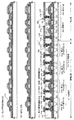
このようなマルチスパイラルコイルを適用したICPを用いたエッチング装置を用いると、前記耐熱性導電性材料のエッチングを良好に行うことができる。ここでは、松下電器産業(株)製のICPを用いたドライエッチング装置(Model E645−□ICP)を用いた。図21は、ガラス基板上に所定のパターンに形成されたW膜について、そのパターン端部のテーパー形状について調べた結果を示す。ここで、テーパー部の角度は基板表面(水平面)とテーパー部の傾斜部とが角度として定義する(図4においてθ1で示す角度)。ここでは、共通条件として放電電力(コイルに印加する高周波電力、13.56MHz)を3.2W/cm2、圧力1.0PaとしてエッチングガスにCF4とCl2を用いた。図21(A)はテーパー部の角度について、基板側にかけるバイアス電力(13.56MHz)依存性を示す。エッチングガスの流量はCF4、Cl2共に30SCCMとした。テーパー部の角度はバイアス電力が128〜384mW/cm2の範囲で70〜20°まで変化させることが可能であることが明らかとなった。
【0022】
図25はエッチングされたW膜の形状を示す電子顕微鏡写真である。図25(A)は基板側に印加したバイアス電力が128mW/cm2の場合であり、同図(B)は192mW/cm2、同図(C)は256mW/cm2の場合をそれぞれ示している。図26から明らかなように基板側に印加するバイアス電力が大きくなるに従ってテーパー角が小さくなっている。
【0023】
また、図21(B)はテーパー部の角度のエッチングガス流量比依存性について調べた結果を示す。CF4とCl2の合計の流量を60SCCMとして、CF4のみを20〜40SCCMの範囲で変化させた。このときバイアス電力は128mW/cm2とした。その結果、テーパー部の角度は60〜80°まで変化させることが可能であった。
【0024】
このようにテーパー部の角度は基板側にかけるバイアス電力によって大きく変化を示し、バイアス電力をさらに高め、また、圧力を変化させることによりテーパー部の角度を5〜45°まで変化させることができる。
【0025】
表1はゲート電極を形成する前記耐熱性導電性材料のICPエッチング装置における加工特性を示す。ここでは、W膜とTa膜の他に、ゲート電極用の材料としてしばしば用いられるモリブデンータングステン(Mo−W)合金(組成比はMo:W=48:50wt%)の例を示す。表1にはエッチング速度、適用するエッチングガス、およびゲート電極の下地となるゲート絶縁膜との選択比の代表的な値を示す。ゲート絶縁膜はプラズマCVD法で作製する酸化シリコン膜または酸化窒化シリコン膜であり、ここで選択比はゲート絶縁膜のエッチング速度に対するそれぞれの材料のエッチング速度の割合として定義する。
【0026】
【表1】
Ta膜のエッチング速度は140〜160nm/minで選択比も6〜8が選られ、W膜のエッチング速度70〜90nm/min、また選択比2〜4に対して優れた値となっている。従って、被加工性という観点からはTa膜も適しているが、表中に示さない値として、抵抗率が20〜30μΩcmであり、W膜の10〜16μΩcmに比べて若干高い点が難点となる。一方、Mo−W合金はエッチング速度が40〜60nm/minと遅く、また選択比は0.1〜2となりこの材料は被加工性という観点から必ずしも適していないことが覗われる。このように、表1からはTa膜が最も良い結果を示していることがわかるが、前述のように抵抗率を考慮するとW膜が総合的には適していると判断される。
【0028】
ここでは、W膜を一例として示したが、前記耐熱性導電性材料についてICPエッチング装置を用いると、容易にパターンの端部をテーパー形状として加工することができる。そして、このような方法を適用してゲート電極を設け、スルードープ法を行うことで、ゲート電極の厚さにより半導体層に添加される不純物元素の濃度を制御することが可能となり、TFTのチャネル長方向に渡って不純物元素の濃度が徐々に変化するLDD領域を形成することが可能となる。
【0029】
このような手段を用い、本発明の構成は、画素部に設けた画素TFTと、該画素部の周辺にpチャネル型TFTとnチャネル型TFTとを有する駆動回路を同一の基板上に設けた半導体装置において、前記駆動回路のnチャネル型TFTは、テーパー部を有するゲート電極が設けられ、チャネル形成領域と、該チャネル形成領域に接し、かつ、該ゲート電極と重なるように設けられLDD領域を形成する第1の不純物領域と、該第1の不純物領域の外側に設けられソース領域またはドレイン領域を形成する第2の不純物領域とを有し、前記駆動回路のpチャネル型TFTは、テーパー部を有するゲート電極が設けられ、チャネル形成領域と、該チャネル形成領域に接し、かつ、該ゲート電極と重なるように設けられLDD領域を形成する第3の不純物領域と、該第3の不純物領域の外側に設けられソース領域またはドレイン領域を形成する第4の不純物領域とを有し、前記画素TFTは、テーパー部を有するゲート電極が設けられ、チャネル形成領域と、該チャネル形成領域に接し、かつ、該ゲート電極と重なるように設けられLDD領域を形成する第1の不純物領域と、該第1の不純物領域の外側に設けられソース領域またはドレイン領域を形成する第2の不純物領域とを有し、前記第1の不純物領域の一導伝型の不純物元素の濃度と、第3の不純物領域の一導伝型とは反対の導伝型の不純物元素の濃度とは、該不純物領域が接するチャネル形成領域から遠ざかるにつれて高くなるように設けられ、前記画素部に設けた画素電極は光反射性表面を有し、有機絶縁物材料からなる第2の層間絶縁膜上に形成され、少なくとも、前記画素TFTのゲート電極の上方に設けた無機絶縁物材料から成る第1の層間絶縁膜と、該絶縁膜上に密接して形成された前記第2の層間絶縁膜とに設けられた開孔を介して、前記画素TFTに接続していることを特徴としている。或いは、前記画素部に設けた画素電極は光透過性を有し、有機絶縁物材料からなる第2の層間絶縁膜上に形成され、少なくとも、前記画素TFTのゲート電極の上方に設けた無機絶縁物材料から成る第1の層間絶縁膜と、該絶縁膜上に密接して形成された前記第2の層間絶縁膜とに設けられた開孔を介して形成された、前記画素TFTに接続する導電性金属配線と接続していることを特徴としている。
【0030】
また、他の発明の構成は、一対の基板間に液晶を挟持した半導体装置であって、一方の基板には画素部と該画素部の周辺に駆動回路が形成され、前記駆動回路のnチャネル型TFTは、テーパー部を有するゲート電極が設けられ、チャネル形成領域と、該チャネル形成領域に接し、かつ、該ゲート電極と重なるように設けられLDD領域を形成する第1の不純物領域と、該第1の不純物領域の外側に設けられソース領域またはドレイン領域を形成する第2の不純物領域とを有し、前記駆動回路のpチャネル型TFTは、テーパー部を有するゲート電極が設けられ、チャネル形成領域と、該チャネル形成領域に接し、かつ、該ゲート電極と重なるように設けられLDD領域を形成する第3の不純物領域と、該第3の不純物領域の外側に設けられソース領域またはドレイン領域を形成する第4の不純物領域とを有し、前記画素TFTは、テーパー部を有するゲート電極が設けられ、チャネル形成領域と、該チャネル形成領域に接し、かつ、該ゲート電極と重なるように設けられLDD領域を形成する第1の不純物領域と、該第1の不純物領域の外側に設けられソース領域またはドレイン領域を形成する第2の不純物領域とを有し、前記第1の不純物領域の一導伝型の不純物元素の濃度と、第3の不純物領域の一導伝型とは反対の導伝型の不純物元素の濃度とは、該不純物領域が接するチャネル形成領域から遠ざかるにつれて高くなるように設けられ、前記画素部に設けた画素電極は光反射性表面を有し、有機絶縁物材料からなる第2の層間絶縁膜上に形成され、少なくとも、前記画素TFTのゲート電極の上方に設けた無機絶縁物材料から成る第1の層間絶縁膜と、該絶縁膜上に密接して形成された前記第2の層間絶縁膜とに設けられた開孔を介して、前記画素TFTに接続していて、透明導電膜が形成された他方の基板と、前記前記第2の層間絶縁膜とに設けられた開孔に重ねて形成された少なくとも一つの柱状スペーサを介して貼合わされていることを特徴としている。或いは、前記画素部に設けた画素電極は光透過性を有し、有機絶縁物材料からなる第2の層間絶縁膜上に形成され、少なくとも、前記画素TFTのゲート電極の上方に設けた無機絶縁物材料から成る第1の層間絶縁膜と、該絶縁膜上に密接して形成された前記第2の層間絶縁膜とに設けられた開孔を介して形成された、前記画素TFTに接続する導電性金属配線と接続していて、透明導電膜が形成された他方の基板と、前記前記第2の層間絶縁膜とに設けられた開孔に重ねて形成された少なくとも一つの柱状スペーサを介して貼合わされていることを特徴としている。前記ゲート電極のテーパー部の角度は5〜35°で設ける。
【0031】
本発明の半導体装置の作製方法に関する構成は、画素部に設けた画素TFTと、該画素部の周辺にpチャネル型TFTとnチャネル型TFTとを有する駆動回路を同一の基板上に設けた半導体装置において、前記基板上に結晶構造を含む半導体層を形成する第1の工程と、前記結晶構造を含む半導体層を選択的にエッチングして複数の島状半導体層を形成する第2の工程と、前記島状半導体層に接してゲート絶縁膜を形成する第3の工程と、前記ゲート絶縁膜上に耐熱性導電性材料から成る導電層を形成する第4の工程と、前記導電層を選択的にエッチングして、テーパー部を有するゲート電極を形成する第5の工程と、少なくとも、前記駆動回路のnチャネル型TFTおよび前記画素TFTを形成する前記島状半導体層に、前記ゲート電極のテーパー部と前記ゲート絶縁膜を通してn型を付与する不純物元素を添加して、前記基板と平行な方向において該n型を付与する不純物元素の濃度勾配を有する第1の不純物領域を形成する第6の工程と、前記駆動回路のnチャネル型TFTおよび前記画素TFTを形成する前記島状半導体層に、前記ゲート電極をマスクとしてn型を付与する不純物元素を添加して第2の不純物領域を形成する第7の工程と、前記駆動回路のpチャネル型TFTを形成する前記島状半導体層に、前記ゲート電極のテーパー部と前記ゲート絶縁膜を通してp型を付与する不純物元素を添加して、前記基板と平行な方向において該p型を付与する不純物元素の濃度勾配を有する第3の不純物領域と、前記ゲート電極のテーパー部を介しないでp型を付与する不純物元素を添加して、第4の不純物領域とを同時に形成する第8の工程と、前記駆動回路のnチャネル型TFTと前記画素TFTとpチャネル型TFTとの上方に、無機絶縁物材料から成る第1の層間絶縁膜を形成する第9の工程と、該第1の層間絶縁膜に密接して有機絶縁物材料からなる第2の層間絶縁膜を形成する第10の工程と、前記画素TFTに接続する光反射性表面を有する画素電極を、前記第2の層間絶縁膜上に形成する第11の工程とを有することを特徴としている。或いは、画素電極を透明導電膜で形成し、前記画素TFTに接続する導電性金属配線と接続する工程を適用しても良い。
【0032】
また、他の発明の構成は、一対の基板間に液晶を挟持した半導体装置の作製方法において、画素部に設けた画素TFTと、該画素部の周辺にpチャネル型TFTとnチャネル型TFTとを設けた駆動回路とを一方の基板は、前記一方の基板上に結晶構造を含む半導体層を形成する第1の工程と、前記結晶構造を含む半導体層を選択的にエッチングして複数の島状半導体層を形成する第2の工程と、前記島状半導体層に接してゲート絶縁膜を形成する第3の工程と、前記ゲート絶縁膜上に耐熱性導電性材料から成る導電層を形成する第4の工程と、前記導電層を選択的にエッチングして、テーパー部を有するゲート電極を形成する第5の工程と、少なくとも、前記駆動回路のnチャネル型TFTおよび前記画素TFTを形成する前記島状半導体層に、前記ゲート電極のテーパー部と前記ゲート絶縁膜を通してn型を付与する不純物元素を添加して、前記基板と平行な方向において該n型を付与する不純物元素の濃度勾配を有する第1の不純物領域を形成する第6の工程と、前記駆動回路のnチャネル型TFTおよび前記画素TFTを形成する前記島状半導体層に、前記ゲート電極をマスクとしてn型を付与する不純物元素を添加して第2の不純物領域を形成する第7の工程と、前記駆動回路のpチャネル型TFTを形成する前記島状半導体層に、前記ゲート電極のテーパー部と前記ゲート絶縁膜を通してp型を付与する不純物元素を添加して、前記基板と平行な方向において該p型を付与する不純物元素の濃度勾配を有する第3の不純物領域と、前記ゲート電極のテーパー部を介しないでp型を付与する不純物元素を添加して、第4の不純物領域とを同時に形成する第8の工程と、前記駆動回路のnチャネル型TFTと前記画素TFTとpチャネル型TFTとの上方に、無機絶縁物材料から成る第1の層間絶縁膜を形成する第9の工程と、該第1の層間絶縁膜に密接して有機絶縁物材料からなる第2の層間絶縁膜を形成する第10の工程と、前記第2の層間絶縁膜と第1の層間絶縁膜とに設けられた開孔を介して前記画素TFTに接続する光反射性表面を有する画素電極を前記第2の層間絶縁膜上に形成する第11の工程と、他方の基板は少なくとも透明導電膜を形成する第12の工程と、前記開孔に重ねて形成された少なくとも一つの柱状スペーサを介して、前記一方の基板と前記他方の基板を貼合わせる第13の工程とを有することを特徴としている。或いは、前記第2の層間絶縁膜と第1の層間絶縁膜とに設けられた開孔を介して前記画素TFTに接続する導電性金属配線を形成する工程と、前記第2の層間絶縁膜上に該金属配線に接続する透明導電膜から成る画素電極を形成する工程とを適用することもできる。
【0033】
【発明の実施の形態】
本発明の実施の形態について、以下に示す実施例により詳細な説明を行う。
【0034】
[実施例1]
本発明の実施例を図1〜図3を用いて説明する。ここでは、画素部の画素TFTおよび保持容量と、画素部の周辺に設けられる駆動回路のTFTを同時に作製する方法について工程に従って詳細に説明する。
【0035】
図1(A)において、基板101にはコーニング社の#7059ガラスや#1737ガラスなどに代表されるバリウムホウケイ酸ガラスやアルミノホウケイ酸ガラスなどのガラス基板の他に、ポリエチレンテレフタレート(PET)、ポリエチレンナフタレート(PEN)、ポリエーテルサルフォン(PES)など光学的異方性を有しないプラスチック基板を用いることができる。ガラス基板を用いる場合には、ガラス歪み点よりも10〜20℃程度低い温度であらかじめ熱処理しておいても良い。そして、基板101のTFTを形成する表面に、基板101からの不純物拡散を防ぐために、酸化シリコン膜、窒化シリコン膜または酸化窒化シリコン膜などの絶縁膜から成る下地膜102を形成する。例えば、プラズマCVD法でSiH4、NH3、N2Oから作製される酸化窒化シリコン膜102aを10〜200nm(好ましくは50〜100nm)、同様にSiH4、N2Oから作製される酸化窒化水素化シリコン膜102bを50〜200nm(好ましくは100〜150nm)の厚さに積層形成する。ここでは下地膜102を2層構造として示したが、前記絶縁膜の単層膜または2層以上積層させて形成しても良い。
【0036】
酸化窒化シリコン膜は従来の平行平板型のプラズマCVD法を用いて形成する。酸化窒化シリコン膜102aは、SiH4を10SCCM、NH3を100SCCM、N2Oを20SCCMとして反応室に導入し、基板温度325℃、反応圧力40Pa、放電電力密度0.41W/cm2、放電周波数60MHzとする。一方、酸化窒化水素化シリコン膜102bは、SiH4を5SCCM、N2Oを120SCCM、H2を125SCCMとして反応室に導入し、基板温度400℃、反応圧力20Pa、放電電力密度0.41W/cm2、放電周波数60MHzとした。これらの膜は、基板温度を変化させ、反応ガスの切り替えのみで連続して形成することもできる。
【0037】
このようにして作製した酸化窒化シリコン膜102aは、密度が9.28×10²²/cm3であり、フッ化水素アンモニウム(NH4HF2)を7.13%とフッ化アンモニウム(NH4F)を15.4%含む混合溶液(ステラケミファ社製、商品名LAL500)の20℃におけるエッチング速度が約63nm/minと遅く、緻密で硬い膜である。このような膜を下地膜に用いると、この上に形成する半導体層にガラス基板からのアルカリ金属元素が拡散するのを防ぐのに有効である。
【0038】
次に、25〜80nm(好ましくは30〜60nm)の厚さで非晶質構造を有する半導体層103aを、プラズマCVD法やスパッタ法などの公知の方法で形成する。例えば、プラズマCVD法で非晶質シリコン膜を55nmの厚さに形成する。非晶質構造を有する半導体膜には、非晶質半導体層や微結晶半導体膜があり、非晶質シリコン・ゲルマニウム膜などの非晶質構造を有する化合物半導体膜を適用しても良い。また、下地膜102と非晶質半導体層103aとは両者を連続形成することも可能である。例えば、前述のように酸化窒化シリコン膜102aと酸化窒化水素化シリコン膜102bをプラズマCVD法で連続して成膜後、反応ガスをSiH4、N2O、H2からSiH4とH2或いはSiH4のみに切り替えれば、一旦大気雰囲気に晒すことなく連続形成できる。その結果、酸化窒化水素化シリコン膜102bの表面の汚染を防ぐことが可能となり、作製するTFTの特性バラツキやしきい値電圧の変動を低減させることができる。
【0039】
そして、結晶化の工程を行い非晶質半導体層103aから結晶質半導体層103bを作製する。その方法としてレーザーアニール法や熱アニール法(固相成長法)、またはラピットサーマルアニール法(RTA法)を適用することができる。前述のようなガラス基板や耐熱性の劣るプラスチック基板を用いる場合には、特にレーザーアニール法を適用することが好ましい。RTA法では、赤外線ランプ、ハロゲンランプ、メタルハライドランプ、キセノンランプなどを光源に用いる。或いは特開平7−130652号公報で開示された技術に従って、触媒元素を用いる結晶化法で結晶質半導体層103bを形成することもできる。結晶化の工程ではまず、非晶質半導体層が含有する水素を放出させておくことが好ましく、400〜500℃で1時間程度の熱処理を行い含有する水素量を5atomic%以下にしてから結晶化させると膜表面の荒れを防ぐことができるので良い。
【0040】
また、プラズマCVD法で非晶質シリコン膜の形成工程において、反応ガスにSiH4とアルゴン(Ar)を用い、成膜時の基板温度を400〜450℃として形成すると、非晶質シリコン膜の含有水素濃度を5atomic%以下にすることもできる。このような場合において水素を放出させるための熱処理は不要となる。
【0041】
結晶化をレーザーアニール法にて行う場合には、パルス発振型または連続発光型のエキシマレーザーやアルゴンレーザーをその光源とする。パルス発振型のエキシマレーザーを用いる場合には、レーザー光を線状に加工してレーザーアニールを行う。レーザーアニール条件は実施者が適宣選択するものであるが、例えば、レーザーパルス発振周波数30Hzとし、レーザーエネルギー密度を100〜500mJ/cm2(代表的には300〜400mJ/cm2)とする。そして線状ビームを基板全面に渡って照射し、この時の線状ビームの重ね合わせ率(オーバーラップ率)を80〜98%として行う。このようにして図1(B)に示すように結晶質半導体層103bを得ることができる。
【0042】
そして、結晶質半導体層103b上に第1のフォトマスク(PM1)を用い、フォトリソグラフィーの技術を用いてレジストパターンを形成し、ドライエッチングによって結晶質半導体層を島状に分割し、図1(C)に示すように島状半導体層104〜108を形成する。結晶質シリコン膜のドライエッチングにはCF4とO2の混合ガスを用いる。
【0043】
このような島状半導体層に対し、TFTのしきい値電圧(Vth)を制御する目的でp型を付与する不純物元素を1×10¹⁶〜5×10¹⁷atoms/cm3程度の濃度で島状半導体層の全面に添加しても良い。半導体に対してp型を付与する不純物元素には、ホウ素(B)、アルミニウム(Al)、ガリウム(Ga)など周期律表第13族の元素が知られている。その方法として、イオン注入法やイオンドープ法(或いはイオンシャワードーピング法)を用いることができるが、大面積基板を処理するにはイオンドープ法が適している。イオンドープ法ではジボラン(B2H6)をソースガスとして用いホウ素(B)を添加する。このような不純物元素の注入は必ずしも必要でなく省略しても差し支えないが、特にnチャネル型TFTのしきい値電圧を所定の範囲内に収めるために好適に用いる手法である。
【0044】
ゲート絶縁膜109はプラズマCVD法またはスパッタ法を用い、膜厚を40〜150nmとしてシリコンを含む絶縁膜で形成する。本実施例では、120nmの厚さで酸化窒化シリコン膜から形成する。また、SiH4とN2OにO2を添加させて作製される酸化窒化シリコン膜は、膜中の固定電荷密度が低減されているのでこの用途に対して好ましい材料となる。勿論、ゲート絶縁膜はこのような酸化窒化シリコン膜に限定されるものでなく、他のシリコンを含む絶縁膜を単層または積層構造として用いても良い。例えば、酸化シリコン膜を用いる場合には、プラズマCVD法で、オルトケイ酸テトラエチル(Tetraethyl Ortho Silicate:TEOS)とO2とを混合し、反応圧力40Pa、基板温度300〜400℃とし、高周波(13.56MHz)電力密度0.5〜0.8W/cm2で放電させて形成することができる。このようにして作製された酸化シリコン膜は、その後400〜500℃の熱アニールによりゲート絶縁膜として良好な特性を得ることができる。
【0045】
そして、図1(D)に示すように、ゲート絶縁膜109上にゲート電極を形成するための耐熱性導電層を形成する。耐熱性導電層は単層で形成しても良いが、必要に応じて二層あるいは三層といった複数の層から成る積層構造としても良い。例えば、ゲート電極にはこのような耐熱性導電性材料を用い、導電性の窒化物金属膜から成る導電層(A)110と金属膜から成る導電層(B)111とを積層した構造とすると良い。導電層(B)111はTa、Ti、Wから選ばれた元素、または前記元素を成分とする合金か、前記元素を組み合わせた合金膜で形成すれば良く、導電層(A)110は窒化タンタル(TaN)、窒化タングステン(WN)、窒化チタン(TiN)膜などで形成する。また、導電層(A)110はタングステンシリサイド、チタンシリサイドを適用しても良い。導電層(B)111は低抵抗化を図るために含有する不純物濃度を低減させることが好ましく、特に酸素濃度に関しては30ppm以下とすると良かった。例えば、Wは酸素濃度を30ppm以下とすることで20μΩcm以下の比抵抗値を実現することができる。
【0046】
導電層(A)110は10〜50nm(好ましくは20〜30nm)とし、導電層(B)111は200〜400nm(好ましくは250〜350nm)とすれば良い。Wをゲート電極として形成する場合には、Wをターゲットとしたスパッタ法で、Arガスと窒素(N2)ガスを導入して導電層(A)110をWN膜で50nmの厚さに形成し、導電層(B)111をW膜で250nmの厚さに形成する。その他の方法として、W膜は6フッ化タングステン(WF6)を用いて熱CVD法で形成することもできる。いずれにしてもゲート電極として使用するためには低抵抗化を図る必要があり、W膜の抵抗率は20μΩcm以下にすることが望ましい。W膜は結晶粒を大きくすることで低抵抗率化を図ることができるが、W中に酸素などの不純物元素が多い場合には結晶化が阻害され高抵抗化する。このことより、スパッタ法による場合、純度99.9999%のWターゲットを用い、さらに成膜時に気相中からの不純物の混入がないように十分配慮してW膜を形成することにより、抵抗率9〜20μΩcmを実現することができる。
【0047】
一方、導電層(A)110にTaN膜を、導電層(B)111にTa膜を用いる場合には、同様にスパッタ法で形成することが可能である。TaN膜はTaをターゲットとしてスパッタガスにArと窒素との混合ガスを用いて形成し、Ta膜はスパッタガスにArを用いる。また、これらのスパッタガス中に適量のXeやKrを加えておくと、形成する膜の内部応力を緩和して膜の剥離を防止することができる。α相のTa膜の抵抗率は20μΩcm程度でありゲート電極に使用することができるが、β相のTa膜の抵抗率は180μΩcm程度でありゲート電極とするには不向きであった。TaN膜はα相に近い結晶構造を持つので、この上にTa膜を形成すればα相のTa膜が容易に得られる。尚、図示しないが、導電層(A)110の下に2〜20nm程度の厚さでリン(P)をドープしたシリコン膜を形成しておくことは有効である。これにより、その上に形成される導電膜の密着性向上と酸化防止を図ると同時に、導電層(A)110または導電層(B)111が微量に含有するアルカリ金属元素がゲート絶縁膜109に拡散するのを防ぐことができる。いずれにしても、導電層(B)111は抵抗率を10〜50μΩcmの範囲ですることが好ましい。
【0048】
本実施例では、ゲート電極を形成するために導電層(A)110をWN膜で、導電層(B)111をW膜で形成した。次に、第2のフォトマスク(PM2)を用い、フォトリソグラフィーの技術を使用してレジストマスク112〜117を形成し、導電層(A)110と導電層(B)111とを一括でエッチングしてゲート電極118〜122と容量配線123を形成する。ゲート電極118〜122と容量配線123は、導電層(A)から成る118a〜123aと、導電層(B)から成る118b〜123bとが一体として形成されている(図2(A))。
【0049】
このとき少なくともゲート電極118〜122の端部にテーパー部が形成されるようにエッチングする。このエッチング加工はICPエッチング装置により行う。その技術の詳細は前述の如くである。具体的なエッチング条件として、エッチングガスにCF4とCl2の混合ガスを用いその流量をそれぞれ30SCCMとして、放電電力3.2W/cm2(13.56MHz)、バイアス電力224mW/cm2(13.56MHz)、圧力1.0Paでエッチングを行った。このようなエッチング条件によって、ゲート電極118〜122の端部において、該端部から内側にむかって徐々に厚さが増加するテーパー部が形成され、その角度は5〜35°、好ましくは10〜25°とする。テーパー部の角度は、図4でθ1として示す部分の角度である。この角度は、後にLDD領域を形成する第1の不純物領域の濃度勾配に大きく影響する。尚、テーパー部の角度θ1は、テーパー部の長さ(WG)とテーパー部の厚さ(HG)を用いてTan(θ1)=HG/WGで表される。
【0050】
また、残渣を残すことなくエッチングするためには、10〜20%程度の割合でエッチング時間を増しするオーバーエッチングを施すものとする。しかし、この時に下地とのエッチングの選択比に注意する必要がある。例えば、W膜に対する酸化窒化シリコン膜(ゲート絶縁膜109)の選択比は表1で示したように2〜4(代表的には3)であるので、このようなオーバーエッチング処理により、酸化窒化シリコン膜が露出した面は20〜50nm程度エッチングされて実質的に薄くなり、新たな形状のゲート絶縁膜130が形成される。
【0051】
そして、画素TFTおよび駆動回路のnチャネル型TFTのLDD領域を形成するために、n型を付与する不純物元素添加の工程(n-ドープ工程)を行う。ゲート電極の形成に用いたレジストマスク112〜117をそのまま残し、端部にテーパー部を有するゲート電極118〜122をマスクとして自己整合的にn型を付与する不純物元素をイオンドープ法で添加する。ここでは、n型を付与する不純物元素をゲート電極の端部におけるテーパー部とゲート絶縁膜とを通して、その下に位置する半導体層に達するように添加するためにドーズ量を1×10¹³〜5×10¹⁴atoms/cm2とし、加速電圧を80〜160keVとして行う。n型を付与する不純物元素として15族に属する元素、典型的にはリン(P)または砒素(As)を用いるが、ここではリン(P)を用いた。このようなイオンドープ法により半導体層のリン(P)濃度は1×1016〜1×1019atoms/cm3の濃度範囲で添加する。このようにして、図2(B)に示すように島状半導体層に第1の不純物領域124〜129を形成する。
【0052】
この工程において、第1の不純物領域124〜128の少なくともゲート電極118〜122に重なった部分に含まれるリン(P)の濃度勾配は、ゲート電極118〜122のテーパー部の膜厚変化を反映する。即ち、第1の不純物領域124〜128へ添加されるリン(P)の濃度は、ゲート電極に重なる領域において、ゲート電極の端部に向かって徐々に濃度が高くなる。これはテーパー部の膜厚の差によって、半導体層に達するリン(P)の濃度が変化するためである。尚、図2(B)では第1の不純物領域124〜129の端部を斜めに図示しているが、これはリン(P)が添加された領域を直接的に示しているのではなく、上述のようにリンの濃度変化がゲート電極118〜122のテーパー部の形状に沿って変化していることを表している。
【0053】
次に、nチャネル型TFTにおいて、ソース領域またはドレイン領域として機能する第2の不純物領域の形成を行う(n+ドープ工程)。レジストのマスク112〜117を残し、今度はゲート電極118〜122がリン(P)を遮蔽するマスクとなるように、イオンドープ法において10〜30keVの低加速電圧の条件で添加する。このようにして第2の不純物領域131〜136を形成する。この領域におけるゲート絶縁膜130は、前述のようにゲート電極の加工においてオーバーエッチングが施されるため、当初の膜厚である120nmから薄くなり、70〜100nmとなっている。そのためこのような低加速電圧の条件でも良好にリン(P)を添加することができる。そして、この領域のリン(P)の濃度は1×10²⁰〜1×10²¹atoms/cm3の濃度範囲となるようにする(図2(C))。
【0054】
そして、pチャネル型TFTを形成する島状半導体層104、106にソース領域およびドレイン領域とする第4の不純物領域140、141を形成する。ここでは、ゲート電極118、120をマスクとしてp型を付与する不純物元素を添加し、自己整合的に第4の不純物領域を形成する。このとき、nチャネル型TFTを形成する島状半導体層105、107、108は、第3のフォトマスク(PM3)を用いてレジストマスク137〜139を形成し全面を被覆しておく。ここで形成される不純物領域140、141はジボラン(B2H6)を用いたイオンドープ法で形成する。そして、ゲート電極と重ならない第4の不純物領域140a、141aのボロン(B)濃度は、3×10²⁰〜3×10²¹atoms/cm3となるようにする。また、ゲート電極と重なる不純物領域140b、141bは、ゲート絶縁膜とゲート電極のテーパー部を介して不純物元素が添加されるので、実質的に第3の不純物領域として形成され、少なくとも1.5×1019atoms/cm3以上の濃度とする。この第4の不純物領域140a、141aおよび第3の不純物領域140b、141bには、前工程においてリン(P)が添加されていて、第4の不純物領域140a、141aには1×1020〜1×1021atoms/cm3の濃度で、第3の不純物領域140b、141bには1×1016〜1×1019atoms/cm3の濃度で含有しているが、この工程で添加するボロン(B)の濃度をリン(P)濃度の1.5から3倍となるようにすることにより、pチャネル型TFTのソース領域およびドレイン領域として機能するために何ら問題は生じない。
【0055】
その後、図3(A)に示すように、ゲート電極およびゲート絶縁膜上から第1の層間絶縁膜142を形成する。第1の層間絶縁膜は酸化シリコン膜、酸化窒化シリコン膜、窒化シリコン膜、またはこれらを組み合わせた積層膜で形成すれば良い。いずれにしても第1の層間絶縁膜142は無機絶縁物材料から形成する。第1の層間絶縁膜142の膜厚は100〜200nmとする。ここで、酸化シリコン膜を用いる場合には、プラズマCVD法でTEOSとO2とを混合し、反応圧力40Pa、基板温度300〜400℃とし、高周波(13.56MHz)電力密度0.5〜0.8W/cm2で放電させて形成することができる。また、酸化窒化シリコン膜を用いる場合には、プラズマCVD法でSiH4、N2O、NH3から作製される酸化窒化シリコン膜、またはSiH4、N2Oから作製される酸化窒化シリコン膜で形成すれば良い。この場合の作製条件は反応圧力20〜200Pa、基板温度300〜400℃とし、高周波(60MHz)電力密度0.1〜1.0W/cm2で形成することができる。また、SiH4、N2O、H2から作製される酸化窒化水素化シリコン膜を適用しても良い。窒化シリコン膜も同様にプラズマCVD法でSiH4、NH3から作製することが可能である。
【0056】
その後、それぞれの濃度で添加されたn型またはp型を付与する不純物元素を活性化する工程を行う。この工程はファーネスアニール炉を用いる熱アニール法で行う。その他に、レーザーアニール法、またはラピッドサーマルアニール法(RTA法)を適用することができる。熱アニール法では酸素濃度が1ppm以下、好ましくは0.1ppm以下の窒素雰囲気中で400〜700℃、代表的には500〜600℃で行うものであり、本実施例では550℃で4時間の熱処理を行う。また、基板101に耐熱温度が低いプラスチック基板を用いる場合にはレーザーアニール法を適用することが好ましい(図3(B))。
【0057】
活性化の工程に続いて、雰囲気ガスを変化させ、3〜100%の水素を含む雰囲気中で、300〜450℃で1〜12時間の熱処理を行い、島状半導体層を水素化する工程を行う。この工程は熱的に励起された水素により島状半導体層にある1016〜1018/cm3のダングリングボンドを終端する工程である。水素化の他の手段として、プラズマ水素化(プラズマにより励起された水素を用いる)を行っても良い。いずれにしても、島状半導体層104〜108中の欠陥密度を1016/cm3以下とすることが望ましく、そのために水素を0.01〜0.1atomic%程度付与すれば良い。
【0058】
活性化および水素化の工程が終了したら、有機絶縁物材料からなる第2の層間絶縁膜143を1.0〜2.0μmの平均厚を有して形成する。有機樹脂材料としては、ポリイミド、アクリル、ポリアミド、ポリイミドアミド、BCB(ベンゾシクロブテン)等を使用することができる。例えば、基板に塗布後、熱重合するタイプのポリイミドを用いる場合には、クリーンオーブンを用い300℃で焼成して形成する。また、アクリルを用いる場合には、2液性のものを用い、主材と硬化剤を混合した後、スピナーを用いて基板全面に塗布した後、ホットプレートを用い80℃で60秒の予備加熱を行い、さらにクリーンオーブンを用い250℃で60分焼成して形成することができる。
【0059】
このように、第2の層間絶縁膜を有機絶縁物材料で形成することにより、表面を良好に平坦化させることができる。また、有機樹脂材料は一般に誘電率が低いので、寄生容量を低減することができる。しかし、吸湿性があり保護膜としては適さないので、本実施例のように、第1の層間絶縁膜142として形成した酸化シリコン膜、酸化窒化シリコン膜、窒化シリコン膜などと組み合わせて用いると良い。
【0060】
その後、第4のフォトマスク(PM4)を用い、所定のパターンのレジストマスクを形成し、それぞれの島状半導体層に形成されたソース領域またはドレイン領域に達するコンタクトホールを形成する。コンタクトホールの形成はドライエッチング法により行う。この場合、エッチングガスにCF4、O2、Heの混合ガスを用い有機樹脂材料から成る第2の層間絶縁膜143をまずエッチングし、その後、続いてエッチングガスをCF4、O2として第1の層間絶縁膜142をエッチングする。さらに、島状半導体層との選択比を高めるために、エッチングガスをCHF3に切り替えてゲート絶縁膜130をエッチングすることにより、良好にコンタクトホールを形成することができる。
【0061】
そして、導電性の金属膜をスパッタ法や真空蒸着法で形成し、第5のフォトマスク(PM5)によりレジストマスクパターンを形成し、エッチングによってソース配線144〜148とドレイン配線149〜153を形成する。ここで、ドレイン配線153は画素電極として機能するものである。ドレイン配線154は隣の画素に帰属する画素電極を表している。図示していないが、本実施例ではこの配線を、Ti膜を50〜150nmの厚さで形成し、島状半導体層のソースまたはドレイン領域を形成する半導体膜とコンタクトを形成し、そのTi膜上に重ねてアルミニウム(Al)を300〜400nmの厚さで形成(図3(C)において144a〜154aで示す)し、さらにその上に透明導電膜を80〜120nmの厚さで形成(図3(C)において144b〜154bで示す)する。透明導電膜には酸化インジウム酸化亜鉛合金(In2O3―ZnO)、酸化亜鉛(ZnO)も適した材料であり、さらに可視光の透過率や導電率を高めるためにガリウム(Ga)を添加した酸化亜鉛(ZnO:Ga)などを好適に用いることができる。
【0062】
こうして5枚のフォトマスクにより、同一の基板上に、駆動回路のTFTと画素部の画素TFTとを有した基板を完成させることができる。駆動回路には第1のpチャネル型TFT(A)200a、第1のnチャネル型TFT(A)201a、第2のpチャネル型TFT(A)202a、第2のnチャネル型TFT(A)203a、画素部には画素TFT204、保持容量205が形成されている。本明細書では便宜上このような基板をアクティブマトリクス基板と呼ぶ。
【0063】
駆動回路の第1のpチャネル型TFT(A)200aには、島状半導体層104にチャネル形成領域206、ゲート電極と重なるLDD領域207、第4の不純物領域から成るソース領域208、ドレイン領域209を有した構造となっている。第1のnチャネル型TFT(A)201aには、島状半導体層105にチャネル形成領域210、第1の不純物領域で形成されゲート電極119と重なるLDD領域211、第2の不純物領域で形成するソース領域212、ドレイン領域213を有している。チャネル長3〜7μmに対して、ゲート電極119と重なるLDD領域をLovとしてそのチャネル長方向の長さは0.1〜1.5μm、好ましくは0.3〜0.8μmとする。このLovの長さはゲート電極119の厚さとテーパー部の角度θ1から制御する。
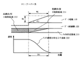
【0064】
このLDD領域について図4を用いて説明する。図4に示すのは、図3(C)の第1のnチャネル型TFT(A)201aの部分拡大図である。LDD領域211はテーパー部261の下に形成される。このとき、LDD領域におけるリン(P)の濃度分布は232の曲線で示されるようにチャネル形成領域211から遠ざかるにつれて増加する。この増加の割合は、イオンドープにおける加速電圧やドーズ量などの条件、テーパー部261の角度θ1やゲート電極119の厚さによって異なってくる。このように、ゲート電極の端部をテーパー形状として、そのテーパー部を通して不純物元素を添加することにより、テーパー部の下に存在する半導体層中に、徐々に前記不純物元素の濃度が変化するような不純物領域を形成することができる。本発明はこのような不純物領域を積極的に活用する。nチャネル型TFTにおいてこのようなLDD領域を形成することにより、ドレイン領域近傍に発生する高電界を緩和して、ホットキャリアの発生を防ぎ、TFTの劣化を防止することができる。
【0065】
駆動回路の第2のpチャネル型TFT(A)202aは同様に、島状半導体層106にチャネル形成領域214、ゲート電極120と重なるLDD領域215、第4の不純物領域で形成されるソース領域216、ドレイン領域217を有した構造となっている。第2のnチャネル型TFT(A)203aには、島状半導体層107にチャネル形成領域218、ゲート電極121と重なるLDD領域219、第2の不純物領域で形成するソース領域220、ドレイン領域221を有している。LDD領域219は、LDD領域211と同じ構成とする。画素TFT204には、島状半導体層108にチャネル形成領域222a、222b、第1の不純物領域で形成するLDD領域223a、223b、第2の不純物領域で形成するソースまたはドレイン領域225〜227を有している。LDD領域223a、223bは、LDD領域211と同じ構成とする。さらに、容量配線123と、ゲート絶縁膜と、画素TFT204のドレイン領域227に接続する半導体層228、229とから保持容量205が形成されている。図3(C)では、駆動回路のnチャネル型TFTおよびpチャネル型TFTを一対のソース・ドレイン間に一つのゲート電極を設けたシングルゲートの構造とし、画素TFTをダブルゲート構造としたが、これらのTFTはいずれもシングルゲート構造としても良いし、複数のゲート電極を一対のソース・ドレイン間に設けたマルチゲート構造としても差し支えない。
【0066】
図10は画素部のほぼ一画素分を示す上面図である。図中に示すA−A'断面が図3(C)に示す画素部の断面図に対応している。画素TFT204は、ゲート電極122は図示されていないゲート絶縁膜を介してその下の島状半導体層108と交差し、さらに複数の島状半導体層に跨って延在してゲート配線を兼ねている。図示はしていないが、島状半導体層には、図3(C)で説明したソース領域、ドレイン領域、LDD領域が形成されている。また、230はソース配線148とソース領域225とのコンタクト部、231はドレイン配線153とドレイン領域227とのコンタクト部である。保持容量205は、画素TFT204のドレイン領域227から延在する半導体層228、229とゲート絶縁膜を介して容量配線123が重なる領域で形成されている。この構成において半導体層228には、価電子制御を目的とした不純物元素は添加されていない。
【0067】
以上の様な構成は、画素TFTおよび駆動回路が要求する仕様に応じて各回路を構成するTFTの構造を最適化し、半導体装置の動作性能と信頼性を向上させることを可能としている。さらにゲート電極を耐熱性を有する導電性材料で形成することによりLDD領域やソース領域およびドレイン領域の活性化を容易としている。
【0068】
さらに、ゲート電極にゲート絶縁膜を介して重なるLDD領域を形成する際に、導電型を制御する目的で添加した不純物元素に濃度勾配を持たせてLDD領域を形成することで、特にドレイン領域近傍における電界緩和効果が高まることが期待できる。
【0069】
アクティブマトリクス型の液晶表示装置の場合、第1のpチャネル型TFT(A)200aと第1のnチャネル型TFT(A)201aは高速動作を重視するシフトレジスタ回路、バッファ回路、レベルシフタ回路などを形成するのに用いる。図3(C)ではこれらの回路をロジック回路部として表している。第1のnチャネル型TFT(A)201aのLDD領域211はホットキャリア対策を重視した構造となっている。さらに、耐圧を高め動作を安定化させるために、図8(A)で示すようにこのロジック回路部のTFTを第1のpチャネル型TFT(B)200bと第1のnチャネル型TFT(B)201bで形成しても良い。このTFTは、一対のソース・ドレイン間に2つのゲート電極を設けたダブルゲート構造であり、このようなTFTは本実施例の工程を用いて同様に作製できる。第1のpチャネル型TFT(B)200bには、島状半導体層にチャネル形成領域236a、236b、第3の不純物領域から成りゲート電極118と重なるLDD領域237a、237b、第4の不純物領域から成るソース領域238とドレイン領域239、240を有した構造となっている。第1のnチャネル型TFT(B)201bには、島状半導体層にチャネル形成領域241a、241b、第1の不純物領域で形成されゲート電極119と重なるLDD領域242a、242b、第2の不純物領域で形成するソース領域243とドレイン領域244、245を有している。チャネル長はいずれも3〜7μmとして、ゲート電極と重なるLDD領域をLovとしてそのチャネル長方向の長さは0.1〜1.5μm、好ましくは0.3〜0.8μmとする。
【0070】
また、アナログスイッチで構成するサンプリング回路には、同様な構成とした第2のpチャネル型TFT(A)202aと第2のnチャネル型TFT(A)203aを適用することができる。サンプリング回路はホットキャリア対策と低オフ電流動作が重視されるので、図8(B)で示すようにこの回路のTFTを第2のpチャネル型TFT(B)202bと第2のnチャネル型TFT(B)203bで形成しても良い。この第2のpチャネル型TFT(B)202bは、一対のソース・ドレイン間に3つのゲート電極を設けたトリプルゲート構造であり、このようなTFTは本実施例の工程を用いて同様に作製できる。第2のpチャネル型TFT(B)202bには、島状半導体層にチャネル形成領域246a、246b、246c、第3の不純物領域から成りゲート電極120と重なるLDD領域247a、247b、247c、第4の不純物領域から成るソース領域249とドレイン領域250〜252を有した構造となっている。第2のnチャネル型TFT(B)203bには、島状半導体層にチャネル形成領域253a、253b、第1の不純物領域で形成されゲート電極121と重なるLDD領域254a、254b、第2の不純物領域で形成するソース領域255とドレイン領域256、257を有している。
【0071】
このように、TFTのゲート電極の構成をシングルゲート構造とするか、複数のゲート電極を一対のソース・ドレイン間に設けたマルチゲート構造とするかは、回路の特性に応じて実施者が適宣選択すれば良い。そして、本実施例で完成したアクティブマトリクス基板を用いることで反射型の液晶表示装置を作製することができる。
【0072】
[実施例2]
実施例1ではゲート電極の材料にWやTaなどの耐熱性導電性材料を用いる例を示した。このような材料を用いる理由は、ゲート電極形成後に導電型の制御を目的として半導体層に添加した不純物元素を400〜700℃の熱アニールによって活性化させる必要があり、その工程を実施する上でゲート電極に耐熱性を持たせる必要があるためである。しかしながら、このような耐熱性導電性材料は面積抵抗で10Ω程度あり、画面サイズが4インチクラスかそれ以上の液晶表示装置には必ずしも適していなかった。ゲート電極に接続するゲート配線を同じ材料で形成すると、基板上における引回し長さが必然的に大きくなり、配線抵抗の影響による配線遅延の問題を無視することができなくなるためである。
【0073】
例えば、画素密度がVGAの場合、480本のゲート配線と640本のソース配線が形成され、XGAの場合には768本のゲート配線と1024本のソース配線が形成される。表示領域の画面サイズは、13インチクラスの場合対角線の長さは340mmとなり、18インチクラスの場合には460mmとなる。本実施例ではこのような液晶表示装置を実現する手段として、ゲート配線をAlや銅(Cu)などの低抵抗導電性材料で形成する方法について図5を用いて説明する。
【0074】
まず、実施例1と同様にして図1(A)〜図2(D)に示す工程を行う。そして導電型の制御を目的として、それぞれの島状半導体層に添加された不純物元素を活性化する工程を行う。この工程はファーネスアニール炉を用いる熱アニール法で行う。その他に、レーザーアニール法、またはラピッドサーマルアニール法(RTA法)を適用することができる。熱アニール法では酸素濃度が1ppm以下、好ましくは0.1ppm以下の窒素雰囲気中で400〜700℃、代表的には500〜600℃で行う。例えば500℃で4時間の熱処理を行う。
【0075】
この熱処理において、ゲート電極118〜122と容量配線123を形成する導電層(B)118b〜123bは、表面から5〜80nmの厚さで導電層(C)118c〜123cが形成される。例えば、導電層(B)118b〜123bがタングステン(W)の場合には窒化タングステン(WN)が形成され、タンタル(Ta)の場合には窒化タンタル(TaN)が形成される。また、導電層(C)118c〜123cは、窒素またはアンモニアなどを用いた窒素を含むプラズマ雰囲気にゲート電極118〜123を晒しても同様に形成することができる。さらに、3〜100%の水素を含む雰囲気中で、300〜450℃で1〜12時間の熱処理を行い、島状半導体層を水素化する工程を行う。この工程は熱的に励起された水素により半導体層のダングリングボンドを終端する工程である。水素化の他の手段として、プラズマ水素化(プラズマにより励起された水素を用いる)を行っても良い(図5(A))。
【0076】
活性化および水素化の工程が終了したら、ゲート配線を低抵抗導電性材料で形成する。低抵抗導電性層はAlやCuを主成分とする導電層(D)で形成する。例えば、Tiを0.1〜2重量%含むAl膜を導電層(D)として全面に形成する(図示せず)。導電層(D)は200〜400nm(好ましくは250〜350nm)とすれば良い。そして、フォトマスクを用いて所定のレジストパターンを形成し、エッチング処理して、ゲート配線233、234と容量配線235を形成する。エッチング処理はリン酸系のエッチング溶液によるウエットエッチングで導電層(D)を除去することにより、下地との選択加工性を保ってゲート配線を形成することができる。そして第1の層間絶縁膜260を実施例1と同様にして形成する(図5(B))。
【0077】
その後、実施例1と同様にして有機絶縁物材料から成る第2の層間絶縁膜147、ソース配線148〜151、167、ドレイン配線153〜156、168を形成してアクティブマトリクス基板を完成させることができる。図6(A)、(B)はこの状態の上面図を示し、図6(A)のB−B'断面および図6(B)のC−C'断面は図5(C)のA−A'およびC−C'に対応している。図6(A)、(B)ではゲート絶縁膜、第1の層間絶縁膜、第2の層間絶縁膜を省略して示しているが、島状半導体層104、105、108の図示されていないソースおよびドレイン領域にソース配線144、145、148とドレイン配線149、150、153がコンタクトホールを介して接続している。また、図6(A)のD−D'断面および図6(B)のE−E'断面を図7(A)と(B)にそれぞれ示す。ゲート配線233はゲート電極118、119と、またゲート配線234はゲート電極122と島状半導体層104、105、108の外側で重なるように形成され、導電層(C)と導電層(D)が接触して電気的に導通している。このようにゲート配線低抵抗導電性材料で形成することにより、配線抵抗を十分低減できる。従って、画素部(画面サイズ)が4インチクラス以上の表示装置に適用することができる。
【0078】
[実施例3]
実施例1で作製したアクティブマトリクス基板はそのまま反射型の液晶表示装置に適用することができる。一方、透過型の液晶表示装置とする場合には画素部の各画素に設ける画素電極を透明電極で形成すれば良い。本実施例では透過型の液晶表示装置に対応するアクティブマトリクス基板の作製方法について図9を用いて説明する。
【0079】
アクティブマトリクス基板は実施例1と同様に作製する。図9(A)では、ソース配線とドレイン配線は導電性の金属膜をスパッタ法や真空蒸着法で形成する。ドレイン配線256を例としてこの構成を図9(B)で詳細に説明すると、Ti膜256aを50〜150nmの厚さで形成し、島状半導体層のソースまたはドレイン領域を形成する半導体膜とコンタクトを形成する。そのTi膜256a上に重ねてアルミニウム(Al)膜256bを300〜400nmの厚さで形成し、さらにTi膜256cまたは窒化チタン(TiN)膜を100〜200nmの厚さで形成して3層構造とする。その後、透明導電膜を全面に形成し、フォトマスクを用いたパターニング処理およびエッチング処理により画素電極257を形成する。画素電極257は、有機樹脂材料から成る第2の層間絶縁膜上に形成され、画素TFT204のドレイン配線256と重なる部分を設け電気的な接続を形成している。
【0080】
図9(C)では最初に第2の層間絶縁膜143上に透明導電膜を形成し、パターニング処理およびエッチング処理をして画素電極258を形成した後、ドレイン配線259を画素電極258と重なる部分を設けて形成した例である。ドレイン配線259は、図9(D)で示すようにTi膜259aを50〜150nmの厚さで形成し、島状半導体層のソースまたはドレイン領域を形成する半導体膜とコンタクトを形成し、そのTi膜259a上に重ねてAl膜259bを300〜400nmの厚さで形成して設ける。この構成にすると、画素電極258はドレイン配線259を形成するTi膜259aのみと接触することになる。その結果、透明導電膜材料とAlとが直接接し反応するのを確実に防止できる。
【0081】
透明導電膜の材料は、酸化インジウム(In2O3)や酸化インジウム酸化スズ合金(In2O3―SnO2;ITO)などをスパッタ法や真空蒸着法などを用いて形成して用いることができる。このような材料のエッチング処理は塩酸系の溶液により行う。しかし、特にITOのエッチングは残渣が発生しやすいので、エッチング加工性を改善するために酸化インジウム酸化亜鉛合金(In2O3―ZnO)を用いても良い。酸化インジウム酸化亜鉛合金は表面平滑性に優れ、ITOに対して熱安定性にも優れているので、図9(A)、(B)の構成においてドレイン配線256の端面で、Al膜256bが画素電極257と接触して腐蝕反応をすることを防止できる。同様に、酸化亜鉛(ZnO)も適した材料であり、さらに可視光の透過率や導電率を高めるためにガリウム(Ga)を添加した酸化亜鉛(ZnO:Ga)などを用いることができる。
【0082】
実施例1では反射型の液晶表示装置を作製できるアクティブマトリクス基板を5枚のフォトマスクにより作製したが、さらに1枚のフォトマスクの追加(合計6枚)で、透過型の液晶表示装置に対応したアクティブマトリクス基板を完成させることができる。本実施例では、実施例1と同様な工程として説明したが、このような構成は実施例2で示すアクティブマトリクス基板に適用することができる。
【0083】
[実施例4]
本実施例では、実施例1〜実施例3で示したアクティブマトリクス基板のTFTの活性層を形成する結晶質半導体層の他の作製方法について示す。結晶質半導体層は非晶質半導体層を熱アニール法やレーザーアニール法、またはRTA法などで結晶化させて形成するが、その他に特開平7−130652号公報で開示されている触媒元素を用いる結晶化法を適用することもできる。その場合の例を図11を用いて説明する。
【0084】
図11(A)で示すように、実施例1と同様にして、ガラス基板1101上に下地膜1102a、1102b、非晶質構造を有する半導体層1103を25〜80nmの厚さで形成する。非晶質半導体層は非晶質シリコン(a−Si)膜、非晶質シリコン・ゲルマニウム(a−SiGe)膜、非晶質炭化シリコン(a−SiC)膜,非晶質シリコン・スズ(a−SiSn)膜などが適用できる。これらの非晶質半導体層は水素を0.1〜40atomic%程度含有するようにして形成すると良い。例えば、非晶質シリコン膜を55nmの厚さで形成する。そして、重量換算で10ppmの触媒元素を含む水溶液をスピナーで基板を回転させて塗布するスピンコート法で触媒元素を含有する層1104を形成する。触媒元素にはニッケル(Ni)、鉄(Fe)、パラジウム(Pd)、鉛(Pb)、コバルト(Co)、白金(Pt)、銅(Cu)、金(Au)などである。この触媒元素を含有する層1104は、スピンコート法の他に印刷法やスプレー法、バーコーター法、或いはスパッタ法や真空蒸着法によって上記触媒元素の層を1〜5nmの厚さに形成しても良い。
【0085】
そして、図11(B)に示す結晶化の工程では、まず400〜500℃で1時間程度の熱処理を行い、非晶質シリコン膜の含有水素量を5atomic%以下にする。非晶質シリコン膜の含有水素量が成膜後において最初からこの値である場合にはこの熱処理は必ずしも必要でない。そして、ファーネスアニール炉を用い、窒素雰囲気中で550〜600℃で1〜8時間の熱アニールを行う。以上の工程により結晶質シリコン膜から成る結晶質半導体層1105を得ることができる(図11(C))。しかし、この熱アニールによって作製された結晶質半導体層1105は、光学顕微鏡観察により巨視的に観察すると局所的に非晶質領域が残存していることが観察されることがあり、このような場合、同様にラマン分光法では480cm-1にブロードなピークを持つ非晶質成分が観測される。そのため、熱アニールの後に実施例1で説明したレーザーアニール法で結晶質半導体層1105を処理してその結晶性を高めることは有効な手段として適用できる。
【0086】
図12は同様に触媒元素を用いる結晶化法の実施例であり、触媒元素を含有する層をスパッタ法により形成するものである。まず、実施例1と同様にして、ガラス基板1201上に下地膜1202a、1202b、非晶質構造を有する半導体層1203を25〜80nmの厚さで形成する。そして、非晶質構造を有する半導体層1203の表面に0.5〜5nm程度の酸化膜(図示せず)を形成する。このような厚さの酸化膜は、プラズマCVD法やスパッタ法などで積極的に該当する被膜を形成しても良いが、100〜300℃に基板を加熱してプラズマ化した酸素雰囲気中に非晶質構造を有する半導体層1203の表面を晒しても良いし、過酸化水素水(H2O2)を含む溶液に非晶質構造を有する半導体層1203の表面を晒して形成しても良い。或いは、酸素を含む雰囲気中で紫外線光を照射してオゾンを発生させ、そのオゾン雰囲気中に非晶質構造を有する半導体層1203を晒すことによっても形成できる。
【0087】
このようにして表面に薄い酸化膜を有する非晶質構造を有する半導体層1203上に前記触媒元素を含有する層1204をスパッタ法で形成する。この層の厚さに限定はないが、10〜100nm程度の厚さに形成すれば良い。例えば、Niをターゲットとして、Ni膜を形成することは有効な方法である。スパッタ法では、電界で加速された前記触媒元素から成る高エネルギー粒子の一部が基板側にも飛来し、非晶質構造を有する半導体層1203の表面近傍、または該半導体層表面に形成した酸化膜中に打ち込まれる。その割合はプラズマ生成条件や基板のバイアス状態によって異なるものであるが、好適には非晶質構造を有する半導体層1203の表面近傍や該酸化膜中に打ち込まれる触媒元素の量を1×10¹¹〜1×10¹⁴atoms/cm2程度となるようにすると良い。
【0088】
その後、触媒元素を含有する層1204を選択的に除去する。例えば、この層がNi膜で形成されている場合には、硝酸などの溶液で除去することが可能であり、または、フッ酸を含む水溶液で処理すればNi膜と非晶質構造を有する半導体層1203上に形成した酸化膜を同時に除去できる。いずれにしても、非晶質構造を有する半導体層1203の表面近傍の触媒元素の量を1×10¹¹〜1×10¹⁴atoms/cm2程度となるようにしておく。そして、図12(B)で示すように、図11(B)と同様にして熱アニールによる結晶化の工程を行い、結晶質半導体層1205を得ることができる(図11(C))。
【0089】
図11または図12で作製された結晶質半導体層1105、1205から島状半導体層104〜108を作製すれば、実施例1と同様にしてアクティブマトリクス基板を完成させることができる。しかし、結晶化の工程においてシリコンの結晶化を助長する触媒元素を使用した場合、島状半導体層中には微量(1×10¹⁷〜1×10¹⁹atoms/cm3程度)の触媒元素が残留する。勿論、そのような状態でもTFTを完成させることが可能であるが、残留する触媒元素を少なくともチャネル形成領域から除去する方がより好ましかった。この触媒元素を除去する手段の一つにリン(P)によるゲッタリング作用を利用する手段がある。
【0090】
この目的におけるリン(P)によるゲッタリング処理は、図3(B)で説明した活性化工程で同時に行うことができる。この様子を図13で説明する。ゲッタリングに必要なリン(P)の濃度は第2の不純物領域の不純物濃度と同程度でよく、活性化工程の熱アニールにより、nチャネル型TFTおよびpチャネル型TFTのチャネル形成領域から触媒元素をその濃度でリン(P)を含有する不純物領域へ偏析させることができる(図13で示す矢印の方向)。その結果その不純物領域には1×10¹⁷〜1×10¹⁹atoms/cm3程度の触媒元素が偏析する。このようにして作製したTFTはオフ電流値が下がり、結晶性が良いことから高い電界効果移動度が得られ、良好な特性を達成することができる。
【0091】
[実施例5]
本実施例では実施例1で作製したアクティブマトリクス基板から、アクティブマトリクス型液晶表示装置を作製する工程を説明する。まず、図14(A)に示すように、図3(C)の状態のアクティブマトリクス基板に柱状スペーサから成るスペーサを形成する。スペーサは数μmの粒子を散布して設ける方法でも良いが、ここでは基板全面に樹脂膜を形成した後これをパターニングして形成する方法を採用した。このようなスペーサの材料に限定はないが、例えば、JSR社製のNN700を用い、スピナーで塗布した後、露光と現像処理によって所定のパターンに形成する。さらにクリーンオーブンなどで150〜200℃で加熱して硬化させる。このようにして作製されるスペーサは露光と現像処理の条件によって形状を異ならせることができるが、好ましくは、図15で示すように、スペーサの形状は柱状で頂部が平坦な形状となるようにすると、対向側の基板を合わせたときに液晶表示パネルとしての機械的な強度を確保することができる。形状は円錐状、角錐状など特別の限定はないが、例えば円錐状としたときに具体的には、高さHを1.2〜5μmとし、平均半径L1を5〜7μm、平均半径L1と底部の半径L2との比を1対1.5とする。このとき側面のテーパー角は±15°以下とする。
【0092】
スペーサの配置は任意に決定すれば良いが、好ましくは、図14(A)で示すように、画素部においてはドレイン配線153(画素電極)のコンタクト部231と重ねてその部分を覆うように柱状スペーサ406を形成すると良い。コンタクト部231は平坦性が損なわれこの部分では液晶がうまく配向しなくなるので、このようにしてコンタクト部231にスペーサ用の樹脂を充填する形で柱状スペーサ406を形成することでディスクリネーションなどを防止することができる。また、駆動回路のTFT上にもスペーサ405a〜405eを形成しておく。このスペーサは駆動回路部の全面に渡って形成しても良いし、図14で示すようにソース配線およびドレイン配線を覆うようにして設けても良い。
【0093】
その後、配向膜407を形成する。通常液晶表示素子の配向膜にはポリイミド樹脂を用いる。配向膜を形成した後、ラビング処理を施して液晶分子がある一定のプレチルト角を持って配向するようにした。画素部に設けた柱状スペーサ406の端部からラビング方向に対してラビングされない領域が2μm以下となるようにした。また、ラビング処理では静電気の発生がしばしば問題となるが、駆動回路のTFT上に形成したスペーサ405a〜405eにより静電気からTFTを保護する効果を得ることができる。また図では説明しないが、配向膜407を先に形成してから、スペーサ406、405a〜405eを形成した構成としても良い。
【0094】
対向側の対向基板401には、遮光膜402、透明導電膜403および配向膜404を形成する。遮光膜402はTi膜、Cr膜、Al膜などを150〜300nmの厚さで形成する。そして、画素部と駆動回路が形成されたアクティブマトリクス基板と対向基板とをシール剤408で貼り合わせる。シール剤408にはフィラー(図示せず)が混入されていて、このフィラーとスペーサ406、405a〜405eによって均一な間隔を持って2枚の基板が貼り合わせられる。その後、両基板の間に液晶材料409を注入する。液晶材料には公知の液晶材料を用いれば良い。例えば、TN液晶の他に、電場に対して透過率が連続的に変化する電気光学応答性を示す、無しきい値反強誘電性混合液晶を用いることもできる。この無しきい値反強誘電性混合液晶には、V字型の電気光学応答特性を示すものもある。このようにして図14(B)に示すアクティブマトリクス型液晶表示装置が完成する。
【0095】
図16はこのようなアクティブマトリクス基板の上面図を示し、画素部および駆動回路部とスペーサおよびシール剤の位置関係を示す上面図である。実施例1で述べたガラス基板101上に画素部604の周辺に駆動回路として走査信号駆動回路605と画像信号駆動回路606が設けられている。さらに、その他CPUやメモリーなどの信号処理回路607も付加されていても良い。そして、これらの駆動回路は接続配線603によって外部入出力端子602と接続されている。画素部604では走査信号駆動回路605から延在するゲート配線群608と画像信号駆動回路606から延在するソース配線群609がマトリクス状に交差して画素を形成し、各画素にはそれぞれ画素TFT204と保持容量205が設けられている。
【0096】
図14において画素部において設けた柱状スペーサ406は、すべての画素に対して設けても良いが、図16で示すようにマトリクス状に配列した画素の数個から数十個おきに設けても良い。即ち、画素部を構成する画素の全数に対するスペーサの数の割合は20〜100%とすることが可能である。また、駆動回路部に設けるスペーサ405a〜405eはその全面を覆うように設けても良いし各TFTのソースおよびドレイン配線の位置にあわせて設けても良い。図16では駆動回路部に設けるスペーサの配置を610〜612で示す。そして、図16で示すシール剤619は、基板101上の画素部604および走査信号駆動回路605、画像信号駆動回路606、その他の信号処理回路607の外側であって、外部入出力端子602よりも内側に形成する。
【0097】
このようなアクティブマトリクス型液晶表示装置の構成を図17の斜視図を用いて説明する。図17においてアクティブマトリクス基板は、ガラス基板101上に形成された、画素部604と、走査信号駆動回路605と、画像信号駆動回路606とその他の信号処理回路607とで構成される。画素部604には画素TFT204と保持容量205が設けられ、画素部の周辺に設けられる駆動回路はCMOS回路を基本として構成されている。走査信号駆動回路605と画像信号駆動回路606からは、それぞれゲート配線122とソース配線148が画素部604に延在し、画素TFT204に接続している。また、フレキシブルプリント配線板(Flexible Printed Circuit:FPC)613が外部入力端子602に接続していて画像信号などを入力するのに用いる。FPC613は補強樹脂614によって強固に接着されている。そして接続配線603でそれぞれの駆動回路に接続している。また、対向基板401には図示していない、遮光膜や透明電極が設けられている。
【0098】
このような構成の液晶表示装置は、実施例1〜3で示したアクティブマトリクス基板を用いて形成することができる。実施例1で示すアクティブマトリクス基板を用いれば反射型の液晶表示装置が得られ、実施例3で示すアクティブマトリクス基板を用いると透過型の液晶表示装置を得ることができる。
【0099】
[実施例6]
図18は実施例1〜3で示したアクティブマトリクス基板の回路構成の一例であり、直視型の表示装置の回路構成を示す図である。このアクティブマトリクス基板は、画像信号駆動回路606、走査信号駆動回路(A)(B)605、画素部604を有している。尚、本明細書中において記した駆動回路とは、画像信号駆動回路606、走査信号駆動回路605を含めた総称である。
【0100】
画像信号駆動回路606は、シフトレジスタ回路501a、レベルシフタ回路502a、バッファ回路503a、サンプリング回路504を備えている。また、走査信号駆動回路(A)(B)185は、シフトレジスタ回路501b、レベルシフタ回路502b、バッファ回路503bを備えている。
【0101】
シフトレジスタ回路501a、501bは駆動電圧が5〜16V(代表的には10V)であり、この回路を形成するCMOS回路のTFTは、図3(C)の第1のpチャネル型TFT(A)200aと第1のnチャネル型TFT(A)201aで形成する。或いは、図8(A)で示す第1のpチャネル型TFT(B)200bと第1のnチャネル型TFT(B)201bで形成しても良い。また、レベルシフタ回路502a、502bやバッファ回路503a、503bは駆動電圧が14〜16Vと高くなるので図8(A)で示すようなマルチゲートのTFT構造とすることが望ましい。マルチゲート構造でTFTを形成すると耐圧が高まり、回路の信頼性を向上させる上で有効である。
【0102】
サンプリング回路504はアナログスイッチから成り、駆動電圧が14〜16Vであるが、極性が交互に反転して駆動される上、オフ電流値を低減させる必要があるため、図3(C)で示す第2のpチャネル型TFT(A)202aと第2のnチャネル型TFT(A)203aで形成することが望ましい。或いは、オフ電流値を効果的に低減させるために図8(B)で示す第2のpチャネル型TFT(B)200bと第2のnチャネル型TFT(B)201bで形成しても良い。
【0103】
また、画素部は駆動電圧が14〜16Vであり、低消費電力化の観点からサンプリング回路よりもさらにオフ電流値を低減することが要求され、図3(C)で示す画素TFT204のようにマルチゲート構造を基本とする。
【0104】
尚、本実例の構成は、実施例1〜3に示した工程に従ってTFTを作製することによって容易に実現することができる。本実施例では、画素部と駆動回路の構成のみを示しているが、実施例1〜3の工程に従えば、その他にも信号分割回路、分周波回路、D/Aコンバータ、γ補正回路、オペアンプ回路、さらにメモリー回路や演算処理回路などの信号処理回路、あるいは論理回路を同一基板上に形成することが可能である。このように、本発明は同一基板上に画素部とその駆動回路とを含む半導体装置、例えば信号制御回路および画素部を具備した液晶表示装置を実現することができる。
【0105】
[実施例7]
ICPを用いたゲート電極のエッチング加工を精密に制御することによって、ゲート電極と、ゲート絶縁膜の表面から20〜50nmの厚さ分をエッチングすることができる。この時エッチング条件を適宣選択することにより、ゲート電極の端部と、それに接するゲート絶縁膜の領域にテーパー部を形成することができる。
【0106】
このようなエッチングは、例えば、図2(A)で示したゲート電極を形成する工程において、レジストマスク112〜117を設け、最初に基板側にバイアス電力を加えないでW膜およびWN膜をエッチングする。この場合レジストマスクは殆ど侵蝕されないで残る。そして、ゲート絶縁膜がほぼ露呈した段階で、バイアス電力を印加することにより、レジストマスクがエッチングされその端部から後退してW膜のテーパーエッチングが成される。W膜に対するレジストの選択比(レジストのエッチング速度/W膜のエッチング速度)はバイアス電力の増加と共に小さくなり、即ちレジストマスクが速くエッチングされる。
【0107】
こうしたエッチング方法を用い、実施例1の工程に従って作製したTFTを図19を用いて説明する。図19(A)は完成したTFTの断面図であり、実施例1と同様にして、基板601、下地膜602(酸化窒化シリコン膜602aと酸化窒化水素化シリコン膜602b)、島状半導体層603、604が設けられている。そして、ゲート絶縁膜605はテーパー部を有するゲート電極606、607の端部の近傍において徐々に膜厚が変化するテーパー部を有して形成される。第1の層間絶縁膜608、第2の層間絶縁膜609、ソース配線610、613、ドレイン配線611、612は実施例1と同様にして形成する。このようなエッチング条件によって、ゲート電極606、607の端部において、該端部から内側にむかって徐々に厚さが増加するテーパー部が形成され、その角度は25〜35°、好ましくは30°となる。この角度はLDD領域を形成する第1の不純物領域の濃度勾配に大きく影響する。尚、図19(B)で示すように、テーパー部の角度θ1は、ゲート電極のテーパー部の長さ(WG1)とテーパー部の厚さ(HG1)を用いてTan(θ1)=HG1/WG1で表され、θ2は、ゲート絶縁膜のテーパー部の長さ(WG2)とテーパー部の厚さ(HG2)を用いてTan(θ2)=HG2/WG2で表される。
【0108】
nチャネル型TFTにおいてLDD領域を形成する第1の不純物領域はイオンドープ法により行う。導電型を制御する不純物元素は、テーパー部を有するゲート電極606、607とテーパー部を有するゲート絶縁膜を通過させてその下の半導体層に添加する。ドーズ量を1×10¹³〜5×10¹⁴atoms/cm2とし、加速電圧を80〜160keVとして行う。また、ドーズ量を1×1015〜5×1015atoms/cm2とし、加速電圧を10〜30keVとして、ソース領域またはドレイン領域を形成する第2の不純物領域の形成を行う。そして、第3のnチャネル型TFT615にはチャネル形成領域621、第1の不純物領域で形成され、ゲート電極に重なるLDD領域622と重ならないLDD領域623、第2の不純物領域から成るソース領域624、ドレイン領域624が形成される。
【0109】
このLDD領域について図19(B)を用いて説明する。図19(B)で示すのは、図19(A)の第3のnチャネル型TFT615の部分拡大図である。LDD領域622はゲート電極のテーパー部628の下に形成される。また、LDD領域623はゲート絶縁膜のテーパー部627の下に形成される。このとき、両者のLDD領域におけるリン(P)の濃度分布は625の曲線で示され、チャネル形成領域621から遠ざかるにつれて増加する。この増加の割合は、イオンドープにおける加速電圧やドーズ量などの条件、テーパー部627、628の角度θ2、θ1やゲート電極607の厚さなどによって異なってくる。このように、ゲート電極の端部とその近傍におけるゲート絶縁膜をテーパー形状として、そのテーパー部を通して不純物元素を添加することにより、テーパー部の下に存在する半導体層中に、徐々に前記不純物元素の濃度が変化するような不純物領域を形成することができる。そして、LDD領域622の不純物濃度において、その最低濃度範囲を1×10¹⁶〜1×10¹⁷atoms/cm3とし、最高濃度範囲を1×1017〜1×1018atoms/cm3とする。また、LDD領域623の不純物濃度において、その最低濃度範囲を1×1017〜1×1018atoms/cm3とし、最高濃度範囲を1×1019〜1×1020atoms/cm3とする。このような不純物領域を設けることにより、nチャネル型TFTにおいてドレイン領域近傍に発生する高電界を緩和して、ホットキャリアの発生を防ぎ、TFTの劣化を防止することができると同時にオフ電流値を低減させることを可能としている。
【0110】
一方、pチャネル型TFTにおける不純物領域は、ドーズ量を2×10¹⁵〜1×10¹⁶atoms/cm2とし、加速電圧を80〜160keVとして行う。そして、第3のpチャネル型TFT614にはチャネル形成領域616、第3の不純物領域から形成される、ゲート電極に重なるLDD領域617と重ならないLDD領域618、第4の不純物領域から成るソース領域619、ドレイン領域620が形成される。そして、LDD領域617の不純物濃度において、その最低濃度範囲を2×1016〜3×1017atoms/cm3とし、最高濃度範囲を2×1017〜3×1018atoms/cm3とする。また、LDD領域618の不純物濃度において、その最低濃度範囲を2×1017〜3×1018atoms/cm3とし、最高濃度範囲を2×1019〜5×1020atoms/cm3とする。このような不純物領域を設けることにより、pチャネル型TFTにおいてオフ電流値を低減させることを可能としている。
【0111】
[実施例8]
本発明を実施して作製されたアクティブマトリクス基板および液晶表示装置は様々な電気光学装置に用いることができる。そして、そのような電気光学装置を表示媒体として組み込んだ電子機器全てに本発明を適用することがでできる。電子機器としては、パーソナルコンピュータ、デジタルカメラ、ビデオカメラ、携帯情報端末(モバイルコンピュータ、携帯電話、電子書籍など)、ナビゲーションシステムなどが上げられる。
【0112】
図22(A)は携帯情報端末であり、本体2201、画像入力部2202、受像部2203、操作スイッチ2204、表示装置2205で構成される。本発明は表示装置2205やその他の信号制御回路に適用することができる。
【0113】
このような携帯型情報端末は、屋内はもとより屋外で使用されることも多い。長時間の使用を可能とするためにはバックライト使用せず、外光を利用する反射型の液晶表示装置が低消費電力型として適しているが、周囲が暗い場合にはバックライトを設けた透過型の液晶表示装置が適している。このような背景から反射型と透過型の両方の特徴を兼ね備えたハイブリット型の液晶表示装置が開発されているが、本発明はこのようなハイブリット型の液晶表示装置にも適用できる。表示装置2205はタッチパネル3002、液晶表示装置3003、LEDバックライト3004により構成されている。タッチパネル3002は携帯型情報端末の操作を簡便にするために設けている。タッチパネル3002の構成は、一端にLEDなどの発光素子3100を、他の一端にフォトダイオードなどの受光素子3200が設けられ、その両者の間に光路が形成されている。このタッチパネル3002を押して光路を遮ると受光素子3200の出力が変化するので、この原理を用いて発光素子と受光素子を液晶表示装置上でマトリクス状に配置させることにより、入力媒体として機能させることができる。
【0114】
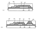
図22(B)はハイブリット型の液晶表示装置の画素部の構成であり、画素TFT204および保持容量205上の第2の層間絶縁膜上にドレイン配線263と画素電極262が設けられている。このような構成は、実施例3を適用すれば形成することができる。ドレイン配線はTi膜とAl膜の積層構造として画素電極を兼ねる構成としている。画素電極262は実施例3で説明した透明導電膜材料を用いて形成する。液晶表示装置3003をこのようなアクティブマトリクス基板から作製することで携帯型情報端末に好適に用いることができる。
【0115】
図23(A)はパーソナルコンピュータであり、マイクロプロセッサやメモリーなどを備えた本体2001、画像入力部2002、表示装置2003、キーボード2004で構成される。本発明は表示装置2003やその他の信号処理回路を形成することができる。
【0116】
図23(B)はビデオカメラであり、本体2101、表示装置2102、音声入力部2103、操作スイッチ2104、バッテリー2105、受像部2106で構成される。本発明は表示装置2102やその他の信号制御回路に適用することができる。
【0117】
図23(C)はテレビゲームまたはビデオゲームなどの電子遊技機器であり、CPU等の電子回路2308、記録媒体2304などが搭載された本体2301、コントローラ2305、表示装置2303、本体2301に組み込まれた表示装置2302で構成される。表示装置2303と本体2301に組み込まれた表示装置2302とは、同じ情報を表示しても良いし、前者を主表示装置とし、後者を副表示装置として記録媒体2304の情報を表示したり、機器の動作状態を表示したり、或いはタッチセンサーの機能を付加して操作盤とすることもできる。また、本体2301とコントローラ2305と表示装置2303とは、相互に信号を伝達するために有線通信としても良いし、センサ部2306、2307を設けて無線通信または光通信としても良い。本発明は、表示装置2302、2303に適用することができる。表示装置2303は従来のCRTを用いることもできる。
【0118】
図23(D)はプログラムを記録した記録媒体(以下、記録媒体と呼ぶ)を用いるプレーヤーであり、本体2401、表示装置2402、スピーカー部2403、記録媒体2404、操作スイッチ2405で構成される。尚、記録媒体にはDVD(Digital Versatile Disc)やコンパクトディスク(CD)などを用い、音楽プログラムの再生や映像表示、ビデオゲーム(またはテレビゲーム)やインターネットを介した情報表示などを行うことができる。本発明は表示装置2402やその他の信号制御回路に好適に利用することができる。
【0119】
図23(E)はデジタルカメラであり、本体2501、表示装置2502、接眼部2503、操作スイッチ2504、受像部(図示しない)で構成される。本発明は表示装置2502やその他の信号制御回路に適用することができる。
【0120】
図24(A)はフロント型プロジェクターであり、光源光学系および表示装置2601、スクリーン2602で構成される。本発明は表示装置やその他の信号制御回路に適用することができる。図24(B)はリア型プロジェクターであり、本体2701、光源光学系および表示装置2702、ミラー2703、スクリーン2704で構成される。本発明は表示装置やその他の信号制御回路に適用することができる。
【0121】
なお、図24(C)に、図24(A)および図24(B)における光源光学系および表示装置2601、2702の構造の一例を示す。光源光学系および表示装置2601、2702は光源光学系2801、ミラー2802、2804〜2806、ダイクロイックミラー2803、ビームスプリッター2807、液晶表示装置2808、位相差板2809、投射光学系2810で構成される。投射光学系2810は複数の光学レンズで構成される。図24(C)では液晶表示装置2808を三つ使用する三板式の例を示したが、このような方式に限定されず、単板式の光学系で構成しても良い。また、図24(C)中で矢印で示した光路には適宣光学レンズや偏光機能を有するフィルムや位相を調節するためのフィルムや、IRフィルムなどを設けても良い。また、図24(D)は図24(C)における光源光学系2801の構造の一例を示した図である。本実施例では、光源光学系2801はリフレクター2811、光源2812、レンズアレイ2813、2814、偏光変換素子2815、集光レンズ2816で構成される。尚、図24(D)に示した光源光学系は一例であって図示した構成に限定されるものではない。
【0122】
また、ここでは図示しなかったが、本発明はその他にも、ナビゲーションシステムやイメージセンサの読み取り回路などに適用することも可能である。このように本願発明の適用範囲はきわめて広く、あらゆる分野の電子機器に適用することが可能である。また、本実施例の電子機器は実施例1〜5の技術を用いて実現することができる。
【0123】
【発明の効果】
本発明を用いることで、同一の基板上に複数の機能回路が形成された半導体装置(ここでは具体的には電気光学装置)において、その機能回路が要求する仕様に応じて適切な性能のTFTを配置することが可能となり、その動作特性を大幅に向上させることができる。
【0124】
本発明の半導体装置の作製方法に従えば、駆動回路部のpチャネル型TFT、nチャネル型TFTおよび画素TFTをゲート電極と重なるLDD構造としたアクティブマトリクス基板を5枚のフォトマスクで製造することができる。このようなアクティブマトリクス基板から反射型の液晶表示装置を作製することができる。また、同工程に従えば透過型の液晶表示装置を6枚のフォトマスクで製造することができる。
【0125】
本発明の半導体装置の作製方法に従えば、ゲート電極を耐熱性導電性材料で形成し、ゲート配線を低抵抗導電性材料で形成したTFTにおいて、駆動回路部のpチャネル型TFT、nチャネル型TFTおよび画素TFTをゲート電極と重なるLDD構造としたアクティブマトリクス基板を6枚のフォトマスクで製造することができ、このようなアクティブマトリクス基板から反射型の液晶表示装置を作製することができる。また、同工程に従えば、透過型の液晶表示装置を7枚のフォトマスクで製造することができる。
【図面の簡単な説明】
【図1】 画素TFT、駆動回路のTFTの作製工程を示す断面図。
【図2】 画素TFT、駆動回路のTFTの作製工程を示す断面図。
【図3】 画素TFT、駆動回路のTFTの作製工程を示す断面図。
【図4】 nチャネル型TFTのLDD領域の構造を説明する図。
【図5】 画素TFT、駆動回路のTFTの作製工程を示す断面図。
【図6】 駆動回路のTFTと画素TFTの構造を示す上面図。
【図7】 駆動回路のTFTの作製工程を示す断面図。
【図8】 駆動回路のTFTの構成を示す断面図。
【図9】 画素TFTの構成を示す断面図。
【図10】 画素部の画素を示す上面図。
【図11】 結晶質半導体層の作製工程を示す断面図。
【図12】 結晶質半導体層の作製工程を示す断面図。
【図13】 画素TFT、駆動回路のTFTの作製工程を示す断面図。
【図14】 アクティブマトリクス型液晶表示装置の作製工程を示す断面図。
【図15】 柱状スペーサの形状を説明する図。
【図16】 液晶表示装置の入出力端子、配線、回路配置、スペーサ、シール剤の配置を説明する上面図。
【図17】 液晶表示装置の構造を示す斜視図。
【図18】 液晶表示装置の回路構成を説明するブロック図。
【図19】 TFTの断面図とLDD領域の構成を説明する図。
【図20】 ICPの原理を説明する図。
【図21】 パターン形成したW膜の端部におけるテーパー部の角度とエッチング条件の関係を示すグラフ。
【図22】 携帯型情報端末の一例を示す図。
【図23】 半導体装置の一例を示す図。
【図24】 投影型液晶表示装置の構成を示す図。
【図25】 パターン形成したW膜の端部における形状を示す電子顕微鏡写真。[0001]
BACKGROUND OF THE INVENTION
The present invention relates to a semiconductor device having a circuit including a thin film transistor (hereinafter referred to as TFT) on a substrate having an insulating surface, and a method for manufacturing the semiconductor device. In particular, the present invention relates to an electro-optical device typified by a liquid crystal display device in which a pixel portion and a drive circuit provided in the periphery thereof are provided on the same substrate, and a technique that can be suitably used for an electronic apparatus equipped with the electro-optical device. provide. Note that in this specification, a semiconductor device refers to all devices that function by utilizing semiconductor characteristics, and includes the above-described electro-optical device and electronic devices including the electro-optical device in its category.
[0002]
[Prior art]
In an electro-optical device typified by an active matrix type liquid crystal display device, a technique has been developed in which switching elements and active circuits are configured using TFTs. In the TFT, a semiconductor film is formed on a substrate such as glass by a vapor deposition method or the like, and the semiconductor film is formed as an active layer. For the semiconductor film, a silicon-based material such as silicon or silicon / germanium is preferably used. Such a semiconductor film can be classified into an amorphous silicon film, a crystalline silicon film typified by polycrystalline silicon, and the like depending on the manufacturing method.
[0003]
TFTs with an amorphous semiconductor (typically amorphous silicon) film as the active layer are several centimeters away from electronic physical properties due to the amorphous structure. 2 It was impossible to obtain field effect mobility of more than / Vsec. Therefore, in an active matrix liquid crystal display device, a driving circuit for displaying an image can be formed even though it can be used as a switching element (hereinafter referred to as a pixel TFT) for driving a liquid crystal in a pixel portion. It was impossible to do. Therefore, a technology for mounting a driver IC or the like using a TAB (Tape Automated Bonding) method or a COG (Chip on Glass) method has been used for the drive circuit.
[0004]
On the other hand, a TFT having an active layer made of a semiconductor (hereinafter, referred to as crystalline semiconductor) film including a crystal structure (typically crystalline silicon or polycrystalline silicon) has high field effect mobility, so that These functional circuits can be formed on the same glass substrate, and in addition to the pixel TFT, a shift register circuit, a level shifter circuit, a buffer circuit, a sampling circuit, and the like can be realized in the driver circuit. Such a circuit is formed based on a CMOS circuit composed of an n-channel TFT and a p-channel TFT. In order to promote weight reduction and thinning in a liquid crystal display device based on the mounting technology of such a drive circuit, in addition to the pixel portion, a crystalline semiconductor layer capable of integrally forming a drive circuit on the same substrate is used as an active layer. It has become clear that the TFT is suitable.
[0005]
[Problems to be solved by the invention]
Compared with the characteristics of TFT, it is better to apply the crystalline semiconductor layer to the active layer. However, in order to manufacture TFT corresponding to various circuits in addition to the pixel TFT, the manufacturing process becomes complicated. There was a problem that the number would increase. It is clear that an increase in the number of processes not only increases the manufacturing cost but also decreases the manufacturing yield.
[0006]
The operation conditions of the pixel TFT and the TFT of the drive circuit are not necessarily the same, and thus the characteristics required for the TFT are not a little different. The pixel TFT is composed of an n-channel TFT, and is driven by applying a voltage to the liquid crystal as a switching element. Since the liquid crystal is driven by alternating current, a method called frame inversion driving is often employed. In this method, in order to keep power consumption low, a characteristic required for the pixel TFT is to sufficiently reduce an off-current value (a drain current that flows when the TFT is turned off). On the other hand, since a high drive voltage is applied to the buffer circuit of the drive circuit, it is necessary to increase the breakdown voltage so that it does not break even when a high voltage is applied. In order to increase the current driving capability, it is necessary to secure a sufficient on-current value (drain current that flows when the TFT is on).
[0007]
As a TFT structure for reducing the off-current value, a lightly doped drain (LDD) structure is known. In this structure, a region to which an impurity element is added at a low concentration is provided between a channel formation region and a source region or a drain region formed by adding an impurity element at a high concentration, and this region is referred to as an LDD region. I'm calling. A so-called GOLD (Gate-drain Overlapped LDD) structure in which an LDD region is disposed so as to overlap a gate electrode through a gate insulating film is known as a means for preventing deterioration of an on-current value due to hot carriers. . With such a structure, it is known that a high electric field in the vicinity of the drain is relaxed, hot carrier injection is prevented, and the deterioration phenomenon is effective.
[0008]
However, there are other points to be noted in addition to the off current value and the on current value. For example, the bias state is not necessarily the same between a pixel TFT and a TFT of a drive circuit such as a shift register circuit or a buffer circuit. For example, in a pixel TFT, a large reverse bias (a negative voltage in an n-channel TFT) is applied to the gate, but a TFT in a drive circuit basically does not operate in a reverse bias state. Further, regarding the operation speed, the pixel TFT may be 1/100 or less of the TFT of the control circuit. In addition, the GOLD structure has a high effect of preventing deterioration of the on-current value, but on the other hand, there is a problem that the off-current value becomes larger than that of a normal LDD structure. Therefore, it is not a preferable structure for application to the pixel TFT. Conversely, the normal LDD structure has a high effect of suppressing the off-current value, but has a low effect of relaxing the electric field in the vicinity of the drain and preventing deterioration due to hot carrier injection. Thus, in a semiconductor device having a plurality of integrated circuits with different operating conditions, such as an active matrix liquid crystal display device, it is not always preferable to form all TFTs with the same structure. Such problems have become apparent as the characteristics of crystalline silicon TFTs increase and the performance required for active matrix liquid crystal display devices increases.
[0009]
Furthermore, in order to stabilize the operation of these circuits manufactured using n-channel TFTs and p-channel TFTs, values such as the threshold voltage and subthreshold coefficient (S value) of the TFT are set to predetermined values. Must be within range. For that purpose, it is necessary to examine both from the structural side and from the material side that constitutes the TFT.
[0010]
The present invention is a technique for solving such problems. In an electro-optical device typified by an active matrix type liquid crystal display device manufactured using TFTs and a semiconductor device, TFTs arranged in various circuits are disclosed. By making the structure appropriate for the function of the circuit, the operating characteristics and reliability of the semiconductor device are improved, and the power consumption is reduced, and the number of steps is reduced, and the manufacturing cost is reduced. The goal is to improve yield.
[0011]
[Means for Solving the Problems]
In order to realize a reduction in manufacturing cost and a yield, reducing the number of steps can be applied as one means. Specifically, it is necessary to reduce the number of photomasks required for manufacturing TFTs. A photomask is used in photolithography to form a resist pattern on a substrate as a mask for an etching process. Therefore, the use of a single photomask means that, in addition to steps such as film formation and etching in the steps before and after that, resist stripping, washing and drying steps are added, and even in the photolithography step, It means that complicated steps such as resist coating, pre-baking, exposure, development, and post-baking are performed.
[0012]
Then, while reducing the number of photomasks, the structure of TFTs arranged in various circuits is made appropriate according to the functions of the circuits. Specifically, the TFT for the switching element preferably has a structure that focuses on reducing the off-current value rather than the operation speed. A multi-gate structure is adopted as such a structure. On the other hand, a TFT provided in a drive circuit that requires high-speed operation preferably has a structure that focuses on increasing the operation speed and at the same time suppressing deterioration due to hot carrier injection, which is a significant problem. As such a structure, a device is added to the LDD region of the TFT. In other words, the LDD region provided between the channel formation region and the drain region is characterized by having a concentration gradient such that the concentration of the impurity element for controlling the conductivity type gradually increases as the drain region is approached. In this configuration, the effect of reducing the concentration of the electric field in the depletion layer near the drain region becomes more remarkable.
[0013]
In order to form an LDD region having such an impurity element concentration gradient, in the present invention, an ionized impurity element for controlling the conductivity type is accelerated by an electric field to form a gate electrode and a gate insulating film (in the present invention, a gate insulating film). A gate insulating film provided between and in close contact with the electrode and the semiconductor layer, and an insulating film extending from the gate insulating film to a peripheral region thereof is referred to as a gate insulating film) A method of adding to the semiconductor layer is used. In this specification, this impurity element addition method is referred to as a “through doping method” for convenience. In the through doping method of the present invention, the shape of the gate electrode is a so-called tapered shape in which the thickness gradually increases from the end toward the inside at the end of the gate electrode. By performing the through doping method with the gate electrode having a tapered shape, the concentration of the impurity element added to the semiconductor layer can be controlled by the thickness of the gate electrode, and the concentration of the impurity element in the channel length direction of the TFT can be controlled. A gradually changing LDD region can be formed.
[0014]
A material for forming the gate electrode is a heat-resistant conductive material, and is formed from an element selected from tungsten (W), tantalum (Ta), and titanium (Ti), or a compound or alloy containing the element as a component. In order to etch such a heat-resistant conductive material at high speed and with high accuracy and further to make the end tapered, a dry etching method using high-density plasma is applied. An etching apparatus using microwaves or inductively coupled plasma (ICP) is suitable for obtaining high-density plasma. In particular, the ICP etching apparatus can easily control the plasma and can cope with an increase in the area of the processing substrate.
[0015]
A plasma processing method and a plasma processing apparatus using ICP are disclosed in JP-A-9-293600. In this publication, as a means for performing plasma processing with high accuracy, high-frequency power is applied to a multi-spiral coil in which four spiral coil portions are connected in parallel via an impedance matching device to form plasma. The method is used. Here, the length of each coil portion is set to 1/4 times the wavelength of the high frequency. Further, a bias voltage is additionally applied to the lower electrode holding the object to be processed by separately applying high frequency power.
[0016]
A schematic diagram of the structure of a plasma processing apparatus (for example, an etching apparatus) using such an ICP is shown in FIG. An antenna coil 903 is disposed on a quartz plate 905 provided in the upper part of the reaction space, and is connected to a first high-frequency power source 901 through a matching box 907. The first high-frequency power source 901 applies 6 to 60 MHz, typically 13.56 MHz. A second high-frequency power source 902 is connected through a matching box 912 to the lower electrode 904 that holds the substrate 906 to be processed. The second high frequency power source 902 is 100 kHz to 60 MHz (for example, 6 to 29 MHz). When high frequency power is applied to the antenna coil 903, a high frequency current J flows through the antenna coil 903 in the θ direction, and a magnetic field B is generated in the Z direction (Formula 1). In accordance with Faraday's law of electromagnetic induction, an induced electric field E is generated in the θ direction (Formula 2).
[0017]
[Expression 1]
[Expression 2]
Electrons are accelerated in the θ direction by this induced electric field E, collide with gas molecules, and plasma is generated. Since the direction of the induction electric field is the θ direction, the probability that the charged particles collide with the walls of the reaction chamber or the substrate and lose energy is reduced. Further, since the magnetic field B hardly reaches below the antenna coil 903, a high-density plasma region spreading in a flat plate shape is formed. The plasma density and the bias voltage applied to the substrate 906 can be controlled independently by adjusting the high frequency power applied to the lower electrode 904. In addition, it is possible to vary the frequency of the high frequency power applied according to the material of the object to be processed.
[0020]
In order to obtain high-density plasma by ICP, it is necessary to flow a high-frequency current J flowing through the antenna coil with low loss, and the inductance must be reduced. For this purpose, it is effective to adopt a system in which the antenna coil is divided. FIG. 20B is a diagram showing such a configuration, in which four spiral coils (multi-spiral coils) 910 are arranged on a quartz plate 911 and a first high-frequency power source 908 is passed through a
[0021]
When an etching apparatus using ICP to which such a multi-spiral coil is applied is used, the heat-resistant conductive material can be satisfactorily etched. Here, a dry etching apparatus (Model E645- □ ICP) using ICP manufactured by Matsushita Electric Industrial Co., Ltd. was used. FIG. 21 shows the result of examining the taper shape of the pattern end of the W film formed in a predetermined pattern on the glass substrate. Here, the angle of the tapered portion is defined as an angle between the substrate surface (horizontal plane) and the inclined portion of the tapered portion (an angle indicated by θ1 in FIG. 4). Here, discharge power (high frequency power applied to the coil, 13.56 MHz) is 3.2 W / cm as a common condition. 2 , CF as an etching gas at a pressure of 1.0 Pa Four And Cl 2 Was used. FIG. 21A shows the dependency of the angle of the tapered portion on the bias power (13.56 MHz) applied to the substrate side. Etching gas flow rate is CF Four , Cl 2 Both were set to 30 SCCM. The angle of the taper part is a bias power of 128 to 384 mW / cm. 2 It was revealed that it is possible to change the angle in the range of 70 to 20 °.
[0022]
FIG. 25 is an electron micrograph showing the shape of the etched W film. FIG. 25A shows a bias power applied to the substrate side of 128 mW / cm. 2 (B) is 192mW / cm. 2 The figure (C) is 256mW / cm. 2 Each case is shown. As is apparent from FIG. 26, the taper angle decreases as the bias power applied to the substrate side increases.
[0023]
FIG. 21B shows the result of examining the dependency of the angle of the tapered portion on the etching gas flow rate ratio. CF Four And Cl 2 The total flow rate of 60 SCCM, CF Four Only was varied in the range of 20-40 SCCM. At this time, the bias power is 128 mW / cm. 2 It was. As a result, the angle of the tapered portion could be changed from 60 to 80 °.
[0024]
As described above, the angle of the tapered portion greatly changes depending on the bias power applied to the substrate side, and the angle of the tapered portion can be changed from 5 to 45 ° by further increasing the bias power and changing the pressure.
[0025]
Table 1 shows the processing characteristics of the heat-resistant conductive material for forming the gate electrode in an ICP etching apparatus. Here, in addition to the W film and the Ta film, an example of a molybdenum-tungsten (Mo—W) alloy (composition ratio: Mo: W = 48: 50 wt%) often used as a material for a gate electrode is shown. Table 1 shows typical values of the etching rate, the etching gas to be applied, and the selection ratio with the gate insulating film serving as the base of the gate electrode. The gate insulating film is a silicon oxide film or a silicon oxynitride film manufactured by a plasma CVD method. Here, the selection ratio is defined as the ratio of the etching rate of each material to the etching rate of the gate insulating film.
[0026]
[Table 1]
The etching rate of the Ta film is 140 to 160 nm / min and the selection ratio is 6 to 8, which is an excellent value for the etching rate of the W film 70 to 90 nm / min and the selection ratio 2 to 4. Therefore, a Ta film is also suitable from the viewpoint of workability, but as a value not shown in the table, the resistivity is 20 to 30 μΩcm, which is a point that is slightly higher than the W film of 10 to 16 μΩcm. . On the other hand, the Mo-W alloy has a slow etching rate of 40 to 60 nm / min, and the selectivity is 0.1 to 2, so that it can be seen that this material is not necessarily suitable from the viewpoint of workability. As described above, it can be seen from Table 1 that the Ta film shows the best result, but it is determined that the W film is generally suitable in consideration of the resistivity as described above.
[0028]
Here, the W film is shown as an example. However, when an ICP etching apparatus is used for the heat-resistant conductive material, the end portion of the pattern can be easily processed into a tapered shape. By applying such a method and providing a gate electrode and performing a through-doping method, it becomes possible to control the concentration of the impurity element added to the semiconductor layer by the thickness of the gate electrode, and the channel length of the TFT. It becomes possible to form an LDD region in which the concentration of the impurity element gradually changes in the direction.
[0029]
Using such means, the structure of the present invention is such that a pixel TFT provided in a pixel portion and a drive circuit having a p-channel TFT and an n-channel TFT around the pixel portion are provided on the same substrate. In the semiconductor device, the n-channel TFT of the driver circuit is provided with a gate electrode having a tapered portion, and is provided with a channel formation region, an LDD region provided in contact with the channel formation region and overlapping the gate electrode. A first impurity region to be formed and a second impurity region which is provided outside the first impurity region and forms a source region or a drain region. The p-channel TFT of the driver circuit includes a tapered portion A third electrode that forms a channel formation region and an LDD region that is in contact with the channel formation region and overlaps with the gate electrode. The pixel TFT has an impurity region and a fourth impurity region which is provided outside the third impurity region and forms a source region or a drain region. The pixel TFT is provided with a gate electrode having a tapered portion, and a channel is formed. A first impurity region which is in contact with the channel formation region and overlaps with the gate electrode and forms an LDD region; and a source region or a drain region provided outside the first impurity region. A second impurity region to be formed, and a conductivity type impurity element opposite to the one conductivity type of the third impurity region and the concentration of the one conductivity type impurity element of the first impurity region. The pixel electrode provided in the pixel portion has a light-reflecting surface and is made of an organic insulating material. A first interlayer insulating film made of an inorganic insulating material provided at least above the gate electrode of the pixel TFT, and the second interlayer formed in close contact with the insulating film. The pixel TFT is connected through an opening provided in the interlayer insulating film. Alternatively, the pixel electrode provided in the pixel portion is light transmissive, formed on the second interlayer insulating film made of an organic insulating material, and at least an inorganic insulation provided above the gate electrode of the pixel TFT. Connected to the pixel TFT formed through an opening provided in the first interlayer insulating film made of a material and the second interlayer insulating film formed in close contact with the insulating film It is characterized by being connected to conductive metal wiring.
[0030]
According to another aspect of the invention, there is provided a semiconductor device in which a liquid crystal is sandwiched between a pair of substrates. A driver circuit is formed on one substrate around the pixel portion, and the n-channel of the driver circuit is formed. The type TFT includes a gate electrode having a tapered portion, a channel formation region, a first impurity region that is in contact with the channel formation region and overlaps the gate electrode, and forms an LDD region, and And a second impurity region which is provided outside the first impurity region and forms a source region or a drain region. The p-channel TFT of the driver circuit is provided with a gate electrode having a tapered portion, and a channel is formed. A third impurity region which is in contact with the channel formation region and overlaps with the gate electrode and forms an LDD region; and is provided outside the third impurity region. The pixel TFT includes a gate electrode having a tapered portion, is in contact with the channel formation region, and is in contact with the channel formation region. A first impurity region which is provided so as to overlap with the electrode and forms an LDD region; and a second impurity region which is provided outside the first impurity region and forms a source region or a drain region. The concentration of the one conductivity type impurity element of one impurity region and the concentration of the conductivity type impurity element opposite to the one conductivity type of the third impurity region are determined from the channel formation region in contact with the impurity region. The pixel electrode provided in the pixel portion has a light reflective surface and is formed on a second interlayer insulating film made of an organic insulating material, and at least the pixel T Through a hole provided in the first interlayer insulating film made of an inorganic insulating material provided above the T gate electrode and the second interlayer insulating film formed in close contact with the insulating film. And at least one columnar spacer connected to the pixel TFT and overlaid on an opening provided in the other substrate on which the transparent conductive film is formed and the second interlayer insulating film. It is characterized by being pasted together. Alternatively, the pixel electrode provided in the pixel portion is light transmissive, formed on the second interlayer insulating film made of an organic insulating material, and at least an inorganic insulation provided above the gate electrode of the pixel TFT. Connected to the pixel TFT formed through an opening provided in the first interlayer insulating film made of a material and the second interlayer insulating film formed in close contact with the insulating film Via at least one columnar spacer connected to the conductive metal wiring and overlapping the opening provided in the other substrate on which the transparent conductive film is formed and the second interlayer insulating film. It is characterized by being pasted together. The angle of the tapered portion of the gate electrode is 5 to 35 °.
[0031]
A structure relating to a method for manufacturing a semiconductor device of the present invention is a semiconductor in which a pixel TFT provided in a pixel portion and a driver circuit having a p-channel TFT and an n-channel TFT around the pixel portion are provided over the same substrate. In the apparatus, a first step of forming a semiconductor layer including a crystal structure on the substrate, and a second step of selectively etching the semiconductor layer including the crystal structure to form a plurality of island-shaped semiconductor layers; A third step of forming a gate insulating film in contact with the island-shaped semiconductor layer; a fourth step of forming a conductive layer made of a heat-resistant conductive material on the gate insulating film; and selecting the conductive layer Etching to form a gate electrode having a taper portion, and at least the island-like semiconductor layer for forming the n-channel TFT and the pixel TFT of the drive circuit on the gate electrode. An impurity element imparting n-type is added through the taper portion and the gate insulating film to form a first impurity region having a concentration gradient of the impurity element imparting n-type in a direction parallel to the substrate. And a second impurity region is formed by adding an impurity element imparting n-type to the island-like semiconductor layer forming the n-channel TFT and the pixel TFT of the driving circuit using the gate electrode as a mask. And adding an impurity element imparting p-type through the tapered portion of the gate electrode and the gate insulating film to the island-like semiconductor layer forming the p-channel TFT of the drive circuit, A third impurity region having a concentration gradient of the impurity element imparting the p-type in a direction parallel to the substrate, and a non-conducting property imparting the p-type without passing through the tapered portion of the gate electrode. An eighth step of simultaneously forming a fourth impurity region by adding a physical element, and an inorganic insulating material above the n-channel TFT, the pixel TFT, and the p-channel TFT of the drive circuit A ninth step of forming the first interlayer insulating film, a tenth step of forming a second interlayer insulating film made of an organic insulating material in close contact with the first interlayer insulating film, and the pixel And an eleventh step of forming a pixel electrode having a light-reflective surface connected to the TFT on the second interlayer insulating film. Alternatively, a process of forming a pixel electrode with a transparent conductive film and connecting to a conductive metal wiring connected to the pixel TFT may be applied.
[0032]
According to another aspect of the invention, there is provided a method for manufacturing a semiconductor device in which a liquid crystal is sandwiched between a pair of substrates, a pixel TFT provided in a pixel portion, and a p-channel TFT and an n-channel TFT around the pixel portion. And a driver circuit provided with a first step of forming a semiconductor layer including a crystal structure on the one substrate, and a plurality of islands by selectively etching the semiconductor layer including the crystal structure. A second step of forming a semiconductor layer, a third step of forming a gate insulating film in contact with the island-like semiconductor layer, and forming a conductive layer made of a heat-resistant conductive material on the gate insulating film A fourth step, a fifth step of selectively etching the conductive layer to form a gate electrode having a tapered portion, and forming at least the n-channel TFT and the pixel TFT of the drive circuit Island semiconductor An impurity element imparting n-type is added through the tapered portion of the gate electrode and the gate insulating film, and a first impurity having a concentration gradient of the impurity element imparting n-type in a direction parallel to the substrate A sixth step of forming a region, and an impurity element imparting n-type conductivity is added to the island-like semiconductor layer forming the n-channel TFT and the pixel TFT of the driver circuit by using the gate electrode as a mask. An impurity element that imparts p-type to the island-like semiconductor layer forming the p-channel TFT of the drive circuit through the tapered portion of the gate electrode and the gate insulating film; And a third impurity region having a concentration gradient of the impurity element imparting the p-type in a direction parallel to the substrate, and a tapered portion of the gate electrode. And adding an impurity element imparting p-type to form a fourth impurity region at the same time, and above the n-channel TFT, the pixel TFT, and the p-channel TFT of the drive circuit. A ninth step of forming a first interlayer insulating film made of an inorganic insulating material, and a tenth step of forming a second interlayer insulating film made of an organic insulating material in close contact with the first interlayer insulating film. And a pixel electrode having a light-reflective surface connected to the pixel TFT through an opening provided in the second interlayer insulating film and the first interlayer insulating film. An eleventh step formed above, a twelfth step forming at least a transparent conductive film on the other substrate, and at least one columnar spacer formed over the opening, A thirteenth step of bonding the other substrate; It is characterized by having. Alternatively, a step of forming a conductive metal wiring connected to the pixel TFT through an opening provided in the second interlayer insulating film and the first interlayer insulating film, and on the second interlayer insulating film And a step of forming a pixel electrode made of a transparent conductive film connected to the metal wiring.
[0033]
DETAILED DESCRIPTION OF THE INVENTION
The embodiment of the present invention will be described in detail with reference to the following examples.
[0034]
[Example 1]
An embodiment of the present invention will be described with reference to FIGS. Here, a method for simultaneously manufacturing the pixel TFT and the storage capacitor of the pixel portion and the TFT of the driver circuit provided around the pixel portion will be described in detail according to the process.
[0035]
In FIG. 1A, a
[0036]
The silicon oxynitride film is formed by using a conventional parallel plate type plasma CVD method. The silicon oxynitride film 102a is made of SiH. Four 10SCCM, NH Three To 100 SCCM, N 2 O was introduced into the reaction chamber as 20 SCCM, the substrate temperature was 325 ° C., the reaction pressure was 40 Pa, and the discharge power density was 0.41 W / cm. 2 The discharge frequency is 60 MHz. On the other hand, the silicon
[0037]
The silicon oxynitride film 102a thus manufactured has a density of 9.28 × 10 twenty two /cm Three And ammonium hydrogen fluoride (NH Four HF 2 ) 7.13% and ammonium fluoride (NH Four F) is a dense and hard film having a slow etching rate of about 63 nm / min at 20 ° C. in a mixed solution containing 15.4% (product name: LAL500, manufactured by Stella Chemifa). When such a film is used for the base film, it is effective to prevent the alkali metal element from the glass substrate from diffusing into the semiconductor layer formed thereon.
[0038]
Next, a
[0039]
Then, a crystallization step is performed to form a
[0040]
In the process of forming an amorphous silicon film by plasma CVD, SiH is used as a reactive gas. Four And argon (Ar) and the substrate temperature during film formation is set to 400 to 450 ° C., the hydrogen concentration of the amorphous silicon film can be reduced to 5 atomic% or less. In such a case, heat treatment for releasing hydrogen is not necessary.
[0041]
When crystallization is performed by laser annealing, a pulse oscillation type or continuous light emission type excimer laser or argon laser is used as the light source. In the case of using a pulse oscillation type excimer laser, laser annealing is performed by processing laser light into a linear shape. The laser annealing conditions are appropriately selected by the practitioner. For example, the laser pulse oscillation frequency is 30 Hz and the laser energy density is 100 to 500 mJ / cm. 2 (Typically 300-400mJ / cm 2 ). Then, a linear beam is irradiated over the entire surface of the substrate, and the linear beam superposition ratio (overlap ratio) at this time is set to 80 to 98%. In this way, a
[0042]
Then, a first photomask (PM1) is used over the
[0043]
For such an island-shaped semiconductor layer, an impurity element imparting p-type conductivity is used in order to control the threshold voltage (Vth) of the TFT. 16 ~ 5x10 17 atoms / cm Three You may add to the whole surface of an island-like semiconductor layer with a density | concentration of a grade. As an impurity element imparting p-type to a semiconductor, elements of Group 13 of the periodic table such as boron (B), aluminum (Al), and gallium (Ga) are known. As the method, an ion implantation method or an ion doping method (or an ion shower doping method) can be used, but the ion doping method is suitable for processing a large area substrate. In the ion doping method, diborane (B 2 H 6 ) As a source gas and boron (B) is added. Such implantation of the impurity element is not always necessary and may be omitted. However, this is a technique that is particularly suitable for keeping the threshold voltage of the n-channel TFT within a predetermined range.
[0044]
The
[0045]
Then, as shown in FIG. 1D, a heat resistant conductive layer for forming a gate electrode is formed over the
[0046]
The conductive layer (A) 110 may be 10 to 50 nm (preferably 20 to 30 nm), and the conductive layer (B) 111 may be 200 to 400 nm (preferably 250 to 350 nm). When W is formed as a gate electrode, Ar gas and nitrogen (N 2 ) Gas is introduced to form the conductive layer (A) 110 with a WN film to a thickness of 50 nm, and the conductive layer (B) 111 with a W film to a thickness of 250 nm. As another method, W film is tungsten hexafluoride (WF 6 Can also be formed by a thermal CVD method. In any case, it is necessary to reduce the resistance in order to use it as a gate electrode, and it is desirable that the resistivity of the W film be 20 μΩcm or less. The resistivity of the W film can be reduced by increasing the crystal grains. However, when there are many impurity elements such as oxygen in W, crystallization is hindered and the resistance is increased. Therefore, in the case of sputtering, the resistivity is obtained by using a W target with a purity of 99.9999% and forming a W film with sufficient consideration so that impurities are not mixed in the gas phase during film formation. 9-20 μΩcm can be realized.
[0047]
On the other hand, when a TaN film is used for the conductive layer (A) 110 and a Ta film is used for the conductive layer (B) 111, it can be similarly formed by sputtering. The TaN film is formed using Ta as a target and a mixed gas of Ar and nitrogen as a sputtering gas, and the Ta film uses Ar as a sputtering gas. In addition, when an appropriate amount of Xe or Kr is added to these sputtering gases, the internal stress of the film to be formed can be relaxed and the film can be prevented from peeling. The resistivity of the α-phase Ta film is about 20 μΩcm and can be used as a gate electrode, but the resistivity of the β-phase Ta film is about 180 μΩcm and is not suitable for a gate electrode. Since the TaN film has a crystal structure close to an α phase, an α phase Ta film can be easily obtained by forming a Ta film thereon. Although not shown, it is effective to form a silicon film doped with phosphorus (P) with a thickness of about 2 to 20 nm under the conductive layer (A) 110. This improves adhesion and prevents oxidation of the conductive film formed thereon, and at the same time, an alkali metal element contained in a trace amount in the conductive layer (A) 110 or the conductive layer (B) 111 is added to the
[0048]
In this embodiment, the conductive layer (A) 110 is formed of a WN film and the conductive layer (B) 111 is formed of a W film in order to form a gate electrode. Next, using the second photomask (PM2), resist
[0049]
At this time, etching is performed so that a tapered portion is formed at least at the end portion of the
[0050]
Further, in order to perform etching without leaving a residue, overetching that increases the etching time at a rate of about 10 to 20% is performed. However, it is necessary to pay attention to the etching selectivity with the base at this time. For example, since the selection ratio of the silicon oxynitride film (gate insulating film 109) to the W film is 2 to 4 (typically 3) as shown in Table 1, the oxynitridation is performed by such over-etching treatment. The surface where the silicon film is exposed is etched by about 20 to 50 nm to be substantially thin, and a
[0051]
Then, in order to form the LDD regions of the pixel TFT and the n-channel TFT of the driving circuit, an impurity element adding step for imparting n-type (n - Doping step) is performed. The resist
[0052]
In this step, the concentration gradient of phosphorus (P) contained in at least a portion of the
[0053]
Next, in the n-channel TFT, a second impurity region functioning as a source region or a drain region is formed (n + Doping process). The resist
[0054]
Then, fourth impurity regions 140 and 141 serving as a source region and a drain region are formed in the island-shaped semiconductor layers 104 and 106 forming the p-channel TFT. Here, an impurity element imparting p-type conductivity is added using the
[0055]
Thereafter, as shown in FIG. 3A, a first
[0056]
Thereafter, a step of activating the impurity element imparting n-type or p-type added at each concentration is performed. This step is performed by a thermal annealing method using a furnace annealing furnace. In addition, a laser annealing method or a rapid thermal annealing method (RTA method) can be applied. In the thermal annealing method, the oxygen concentration is 1 ppm or less, preferably 0.1 ppm or less in a nitrogen atmosphere at 400 to 700 ° C., typically 500 to 600 ° C. In this embodiment, the temperature is 550 ° C. for 4 hours. Heat treatment is performed. Further, in the case where a plastic substrate having a low heat resistant temperature is used for the
[0057]
Subsequent to the activation step, the step of hydrogenating the island-like semiconductor layer by changing the atmospheric gas and performing heat treatment at 300 to 450 ° C. for 1 to 12 hours in an atmosphere containing 3 to 100% hydrogen. Do. This step is performed on the island-like semiconductor layer 10 by thermally excited hydrogen. 16 -10 18 /cm Three This is a step of terminating the dangling bond. As another means of hydrogenation, plasma hydrogenation (using hydrogen excited by plasma) may be performed. In any case, the defect density in the island-like semiconductor layers 104 to 108 is 10 16 /cm Three It is desirable to set it as follows, and for that purpose, hydrogen may be added at about 0.01 to 0.1 atomic%.
[0058]
After the activation and hydrogenation steps are completed, a second
[0059]
Thus, the surface can be satisfactorily flattened by forming the second interlayer insulating film with an organic insulating material. In addition, since organic resin materials generally have a low dielectric constant, parasitic capacitance can be reduced. However, since it is hygroscopic and not suitable as a protective film, it is preferably used in combination with a silicon oxide film, a silicon oxynitride film, a silicon nitride film, or the like formed as the first
[0060]
After that, a resist mask having a predetermined pattern is formed using a fourth photomask (PM4), and contact holes reaching the source region or the drain region formed in each island-shaped semiconductor layer are formed. Contact holes are formed by dry etching. In this case, CF is used as an etching gas. Four , O 2 The second
[0061]
Then, a conductive metal film is formed by sputtering or vacuum deposition, a resist mask pattern is formed by a fifth photomask (PM5), and source wirings 144 to 148 and drain wirings 149 to 153 are formed by etching. . Here, the
[0062]
In this manner, a substrate having the TFT of the driving circuit and the pixel TFT of the pixel portion can be completed on the same substrate by using five photomasks. The driver circuit includes a first p-channel TFT (A) 200a, a first n-channel TFT (A) 201a, a second p-channel TFT (A) 202a, and a second n-channel TFT (A). A
[0063]
The first p-channel TFT (A) 200a of the driver circuit includes a
[0064]
The LDD region will be described with reference to FIG. FIG. 4 is a partially enlarged view of the first n-channel TFT (A) 201a shown in FIG. The
[0065]
Similarly, the second p-channel TFT (A) 202a of the driver circuit has a
[0066]
FIG. 10 is a top view showing almost one pixel in the pixel portion. A cross section AA ′ shown in the drawing corresponds to the cross sectional view of the pixel portion shown in FIG. In the
[0067]
The configuration as described above makes it possible to optimize the structure of the TFT constituting each circuit according to the specifications required by the pixel TFT and the drive circuit, and to improve the operation performance and reliability of the semiconductor device. Furthermore, activation of the LDD region, the source region, and the drain region is facilitated by forming the gate electrode from a heat-resistant conductive material.
[0068]
Further, when forming the LDD region overlapping the gate electrode through the gate insulating film, the impurity element added for the purpose of controlling the conductivity type is provided with a concentration gradient to form the LDD region, particularly in the vicinity of the drain region. It can be expected that the electric field relaxation effect will increase.
[0069]
In the case of an active matrix liquid crystal display device, the first p-channel TFT (A) 200a and the first n-channel TFT (A) 201a include a shift register circuit, a buffer circuit, a level shifter circuit, etc. that place importance on high-speed operation. Used to form. In FIG. 3C, these circuits are shown as logic circuit portions. The
[0070]
In addition, a second p-channel TFT (A) 202a and a second n-channel TFT (A) 203a having the same structure can be applied to a sampling circuit including analog switches. Since the sampling circuit emphasizes countermeasures against hot carriers and low off-current operation, as shown in FIG. 8B, the TFT of this circuit is replaced with a second p-channel TFT (B) 202b and a second n-channel TFT. (B) You may form by 203b. The second p-channel TFT (B) 202b has a triple gate structure in which three gate electrodes are provided between a pair of source and drain. Such a TFT is similarly manufactured by using the process of this embodiment. it can. The second p-channel TFT (B) 202b includes
[0071]
As described above, the practitioner determines whether the gate electrode configuration of the TFT has a single gate structure or a multi-gate structure in which a plurality of gate electrodes are provided between a pair of source and drain according to the characteristics of the circuit. You just have to choose. A reflective liquid crystal display device can be manufactured by using the active matrix substrate completed in this embodiment.
[0072]
[Example 2]
In Example 1, an example in which a heat-resistant conductive material such as W or Ta is used as the material of the gate electrode is shown. The reason for using such a material is that it is necessary to activate the impurity element added to the semiconductor layer for the purpose of controlling the conductivity type after forming the gate electrode by thermal annealing at 400 to 700 ° C. This is because the gate electrode needs to have heat resistance. However, such a heat-resistant conductive material has a sheet resistance of about 10Ω and is not necessarily suitable for a liquid crystal display device having a screen size of 4 inches class or more. This is because if the gate wiring connected to the gate electrode is formed of the same material, the routing length on the substrate inevitably increases, and the problem of wiring delay due to the influence of wiring resistance cannot be ignored.
[0073]
For example, when the pixel density is VGA, 480 gate wirings and 640 source wirings are formed, and in the case of XGA, 768 gate wirings and 1024 source wirings are formed. The screen size of the display area is 340 mm for the 13-inch class and 460 mm for the 18-inch class. In this embodiment, as a means for realizing such a liquid crystal display device, a method of forming a gate wiring with a low-resistance conductive material such as Al or copper (Cu) will be described with reference to FIG.
[0074]
First, the steps shown in FIGS. 1A to 2D are performed in the same manner as in the first embodiment. Then, for the purpose of controlling the conductivity type, a step of activating the impurity element added to each island-like semiconductor layer is performed. This step is performed by a thermal annealing method using a furnace annealing furnace. In addition, a laser annealing method or a rapid thermal annealing method (RTA method) can be applied. The thermal annealing method is performed at 400 to 700 ° C., typically 500 to 600 ° C. in a nitrogen atmosphere having an oxygen concentration of 1 ppm or less, preferably 0.1 ppm or less. For example, heat treatment is performed at 500 ° C. for 4 hours.
[0075]
In this heat treatment, the conductive layers (B) 118b to 123b forming the
[0076]
When the activation and hydrogenation steps are completed, the gate wiring is formed of a low resistance conductive material. The low resistance conductive layer is formed of a conductive layer (D) mainly composed of Al or Cu. For example, an Al film containing 0.1 to 2% by weight of Ti is formed on the entire surface as a conductive layer (D) (not shown). The conductive layer (D) may be 200 to 400 nm (preferably 250 to 350 nm). Then, a predetermined resist pattern is formed using a photomask, and etching is performed to form
[0077]
Thereafter, the second interlayer insulating film 147 made of an organic insulating material, the source wirings 148 to 151 and 167, and the drain wirings 153 to 156 and 168 are formed in the same manner as in Example 1 to complete the active matrix substrate. it can. 6A and 6B are top views of this state, and the BB ′ cross section of FIG. 6A and the CC ′ cross section of FIG. 6B are taken along line A- of FIG. It corresponds to A ′ and CC ′. 6A and 6B, the gate insulating film, the first interlayer insulating film, and the second interlayer insulating film are omitted, but the island-shaped semiconductor layers 104, 105, and 108 are not illustrated.
[0078]
[Example 3]
The active matrix substrate manufactured in
[0079]
The active matrix substrate is manufactured in the same manner as in Example 1. In FIG. 9A, for the source wiring and the drain wiring, a conductive metal film is formed by a sputtering method or a vacuum evaporation method. This configuration will be described in detail with reference to FIG. 9B by taking the
[0080]
In FIG. 9C, a transparent conductive film is first formed over the second
[0081]
The material of the transparent conductive film is indium oxide (In 2 O Three ) Or indium tin oxide alloy (In 2 O Three -SnO 2 ; ITO) or the like can be formed using a sputtering method, a vacuum deposition method, or the like. Etching treatment of such a material is performed with a hydrochloric acid based solution. However, in particular, etching of ITO is likely to generate a residue, so in order to improve etching processability, an indium oxide-zinc oxide alloy (In 2 O Three —ZnO) may also be used. Since the indium zinc oxide alloy has excellent surface smoothness and thermal stability with respect to ITO, the
[0082]
In Example 1, an active matrix substrate on which a reflective liquid crystal display device can be manufactured is manufactured using five photomasks. However, by adding one photomask (total of six), it corresponds to a transmissive liquid crystal display device. The active matrix substrate thus completed can be completed. Although this embodiment has been described as a process similar to that in the first embodiment, such a configuration can be applied to the active matrix substrate shown in the second embodiment.
[0083]
[Example 4]
In this embodiment, another method for manufacturing a crystalline semiconductor layer for forming an active layer of a TFT of the active matrix substrate shown in
[0084]
As shown in FIG. 11A, a base film 1102a and 1102b and a
[0085]
In the crystallization step shown in FIG. 11B, first, heat treatment is performed at 400 to 500 ° C. for about 1 hour, so that the amount of hydrogen contained in the amorphous silicon film is 5 atomic% or less. When the amount of hydrogen contained in the amorphous silicon film is this value from the beginning after the film formation, this heat treatment is not necessarily required. Then, using a furnace annealing furnace, thermal annealing is performed at 550 to 600 ° C. for 1 to 8 hours in a nitrogen atmosphere. Through the above steps, a
[0086]
FIG. 12 shows an example of a crystallization method using a catalytic element in the same manner, in which a layer containing a catalytic element is formed by sputtering. First, in the same manner as in Example 1,
[0087]
In this manner, the
[0088]
Thereafter, the
[0089]
If the island-shaped semiconductor layers 104 to 108 are formed from the
[0090]
The gettering process using phosphorus (P) for this purpose can be performed simultaneously in the activation step described with reference to FIG. This will be described with reference to FIG. The concentration of phosphorus (P) necessary for gettering may be approximately the same as the impurity concentration of the second impurity region, and the catalytic element from the channel formation region of the n-channel TFT and the p-channel TFT is thermally annealed in the activation process. Can be segregated to the impurity region containing phosphorus (P) at that concentration (in the direction of the arrow shown in FIG. 13). As a result, the impurity region is 1 × 10 17 ~ 1x10 19 atoms / cm Three A degree of catalyst element segregates. The TFT manufactured in this manner has a low off-current value and good crystallinity, so that high field-effect mobility can be obtained and good characteristics can be achieved.
[0091]
[Example 5]
In this embodiment, a process of manufacturing an active matrix liquid crystal display device from the active matrix substrate manufactured in
[0092]
The arrangement of the spacers may be arbitrarily determined, but preferably, as shown in FIG. 14A, in the pixel portion, a columnar shape is formed so as to overlap with and cover the
[0093]
Thereafter, an
[0094]
A
[0095]
FIG. 16 is a top view of such an active matrix substrate, and is a top view showing the positional relationship between the pixel portion and the drive circuit portion, the spacer and the sealant. A scanning
[0096]
The
[0097]
The structure of such an active matrix liquid crystal display device will be described with reference to the perspective view of FIG. In FIG. 17, the active matrix substrate includes a
[0098]
The liquid crystal display device having such a structure can be formed using the active matrix substrate shown in
[0099]
[Example 6]
FIG. 18 is an example of a circuit configuration of the active matrix substrate shown in
[0100]
The image
[0101]
The
[0102]
The sampling circuit 504 is composed of an analog switch and has a driving voltage of 14 to 16 V. However, the sampling circuit 504 is driven by alternately inverting the polarity, and it is necessary to reduce the off-current value. Therefore, the sampling circuit 504 shown in FIG. It is desirable to form with two p-channel TFTs (A) 202a and a second n-channel TFT (A) 203a. Alternatively, a second p-channel TFT (B) 200b and a second n-channel TFT (B) 201b shown in FIG. 8B may be formed in order to effectively reduce the off-current value.
[0103]
In addition, the pixel portion has a driving voltage of 14 to 16 V, and from the viewpoint of reducing power consumption, it is required to further reduce the off-current value as compared with the sampling circuit. As illustrated in FIG. Based on the gate structure.
[0104]
The configuration of this example can be easily realized by manufacturing a TFT according to the steps shown in the first to third embodiments. In this embodiment, only the configuration of the pixel unit and the drive circuit is shown, but if the steps of
[0105]
[Example 7]
By precisely controlling the etching process of the gate electrode using ICP, a thickness of 20 to 50 nm can be etched from the surface of the gate electrode and the gate insulating film. At this time, by appropriately selecting the etching conditions, a tapered portion can be formed in the end portion of the gate electrode and the region of the gate insulating film in contact therewith.
[0106]
In such etching, for example, in the step of forming the gate electrode shown in FIG. 2A, resist
[0107]
A TFT manufactured according to the process of Example 1 using such an etching method will be described with reference to FIG. FIG. 9 FIG. 6A is a cross-sectional view of a completed TFT. In the same manner as in Example 1, the
[0108]
The first impurity region for forming the LDD region in the n-channel TFT is performed by an ion doping method. The impurity element that controls the conductivity type is added to the semiconductor layer under the
[0109]
This LDD region will be described with reference to FIG. FIG. 19B is a partially enlarged view of the third n-channel TFT 615 of FIG. The
[0110]
On the other hand, the impurity region in the p-channel TFT has a dose amount of 2 × 10 15 ~ 1x10 16 atoms / cm 2 The acceleration voltage is set to 80 to 160 keV. The third p-
[0111]
[Example 8]
The active matrix substrate and the liquid crystal display device manufactured by implementing the present invention can be used for various electro-optical devices. The present invention can be applied to all electronic devices in which such an electro-optical device is incorporated as a display medium. Examples of electronic devices include personal computers, digital cameras, video cameras, portable information terminals (mobile computers, mobile phones, electronic books, etc.), navigation systems, and the like.
[0112]
FIG. 22A illustrates a portable information terminal which includes a main body 2201, an image input portion 2202, an
[0113]
Such portable information terminals are often used outdoors as well as indoors. In order to enable long-term use, a backlight is not used, and a reflective liquid crystal display device that uses outside light is suitable as a low-power consumption type, but a backlight is provided when the surroundings are dark. A transmissive liquid crystal display device is suitable. From such a background, a hybrid type liquid crystal display device having both characteristics of a reflection type and a transmission type has been developed. However, the present invention can also be applied to such a hybrid type liquid crystal display device. A
[0114]
FIG. 22B shows a structure of a pixel portion of a hybrid liquid crystal display device. A
[0115]
FIG. 23A illustrates a personal computer, which includes a main body 2001 including a microprocessor and a memory, an image input portion 2002, a display device 2003, and a
[0116]
FIG. 23B illustrates a video camera, which includes a main body 2101, a display device 2102, an
[0117]
FIG. 23C illustrates an electronic game device such as a video game or a video game, which is incorporated in a
[0118]
FIG. 23D shows a player that uses a recording medium (hereinafter referred to as a recording medium) in which a program is recorded, and includes a main body 2401, a
[0119]
FIG. 23E illustrates a digital camera which includes a main body 2501, a
[0120]
FIG. 24A shows a front projector, which includes a light source optical system, a
[0121]
Note that FIG. 24C illustrates an example of the structure of the light source optical system and the
[0122]
Although not shown here, the present invention can also be applied to a navigation system, a reading circuit of an image sensor, and the like. As described above, the application range of the present invention is extremely wide and can be applied to electronic devices in various fields. Moreover, the electronic device of a present Example is realizable using the technique of Examples 1-5.
[0123]
【The invention's effect】
By using the present invention, in a semiconductor device (specifically, an electro-optical device here) in which a plurality of functional circuits are formed on the same substrate, a TFT having appropriate performance according to the specifications required by the functional circuits Can be arranged, and its operating characteristics can be greatly improved.
[0124]
According to the method for manufacturing a semiconductor device of the present invention, an active matrix substrate having an LDD structure in which a p-channel TFT, an n-channel TFT, and a pixel TFT in a driver circuit portion overlap with a gate electrode is manufactured using five photomasks. Can do. A reflective liquid crystal display device can be manufactured from such an active matrix substrate. Further, according to the same process, a transmissive liquid crystal display device can be manufactured with six photomasks.
[0125]
According to the method for manufacturing a semiconductor device of the present invention, in a TFT in which a gate electrode is formed of a heat-resistant conductive material and a gate wiring is formed of a low-resistance conductive material, a p-channel TFT, an n-channel type in a driving circuit portion An active matrix substrate having an LDD structure in which a TFT and a pixel TFT overlap with a gate electrode can be manufactured using six photomasks, and a reflective liquid crystal display device can be manufactured from such an active matrix substrate. Further, according to this process, a transmissive liquid crystal display device can be manufactured with seven photomasks.
[Brief description of the drawings]
FIG. 1 is a cross-sectional view illustrating a manufacturing process of a pixel TFT and a TFT of a driver circuit.
FIG. 2 is a cross-sectional view illustrating a manufacturing process of a pixel TFT and a TFT of a driver circuit.
FIG. 3 is a cross-sectional view illustrating a manufacturing process of a pixel TFT and a driver circuit TFT;
FIG. 4 illustrates a structure of an LDD region of an n-channel TFT.
FIG. 5 is a cross-sectional view illustrating a manufacturing process of a pixel TFT and a TFT of a driver circuit.
FIG. 6 is a top view illustrating a structure of a TFT and a pixel TFT of a driver circuit.
7 is a cross-sectional view illustrating a manufacturing process of a TFT of a driver circuit. FIG.
FIG. 8 is a cross-sectional view illustrating a structure of a TFT of a driver circuit.
FIG. 9 is a cross-sectional view illustrating a configuration of a pixel TFT.
FIG. 10 is a top view illustrating a pixel in a pixel portion.
FIG. 11 is a cross-sectional view illustrating a manufacturing process of a crystalline semiconductor layer.
12 is a cross-sectional view illustrating a manufacturing process of a crystalline semiconductor layer. FIG.
13 is a cross-sectional view illustrating a manufacturing process of a pixel TFT and a TFT of a driver circuit. FIG.
FIG. 14 is a cross-sectional view illustrating a manufacturing process of an active matrix liquid crystal display device.
FIG. 15 is a diagram illustrating the shape of a columnar spacer.
FIG. 16 is a top view illustrating the arrangement of input / output terminals, wiring, circuit arrangement, spacers, and a sealant of a liquid crystal display device.
FIG. 17 is a perspective view illustrating a structure of a liquid crystal display device.
FIG. 18 is a block diagram illustrating a circuit configuration of a liquid crystal display device.
FIG. 19 is a cross-sectional view of a TFT and a diagram illustrating a structure of an LDD region.
FIG. 20 is a diagram for explaining the principle of ICP.
FIG. 21 is a graph showing the relationship between the angle of the tapered portion at the edge of the patterned W film and the etching conditions.
FIG 22 illustrates an example of a portable information terminal.
FIG 23 illustrates an example of a semiconductor device.
FIG. 24 is a diagram showing a configuration of a projection type liquid crystal display device.
FIG. 25 is an electron micrograph showing the shape of an end portion of a patterned W film.
Claims (10)
前記島状半導体層上のテーパー部を有するゲート絶縁膜と、
前記ゲート絶縁膜上のテーパー部を有するゲート電極とを有し、
前記島状半導体層は、チャネル形成領域、ソース領域、ドレイン領域、第1のLDD領域、及び第2のLDD領域を有し、
前記ゲート絶縁膜のテーパー部は、前記ゲート電極の端部に接し、
前記チャネル形成領域と前記ソース領域または前記ドレイン領域との間に、前記第1のLDD領域と前記第2のLDD領域が挟まれており、前記第1のLDD領域は前記チャネル形成領域側に、前記第2のLDD領域は前記ソース領域または前記ドレイン領域側に配置され、
前記第1のLDD領域は前記ゲート電極のテーパー部の下に形成され、前記第2のLDD領域は前記ゲート絶縁膜のテーパー部の下に形成されることを特徴とする半導体装置。An island-like semiconductor layer on the substrate;
A gate insulating film having a tapered portion on the island-shaped semiconductor layer;
A gate electrode having a tapered portion on the gate insulating film,
The island-shaped semiconductor layer has a channel formation region, a source region, a drain region, a first LDD region, and a second LDD region,
The tapered portion of the gate insulating film is in contact with the end of the gate electrode,
The first LDD region and the second LDD region are sandwiched between the channel formation region and the source region or the drain region, and the first LDD region is on the channel formation region side. The second LDD region is disposed on the source region or the drain region side,
The semiconductor device according to claim 1, wherein the first LDD region is formed under a tapered portion of the gate electrode, and the second LDD region is formed under a tapered portion of the gate insulating film.
前記島状半導体層上のテーパー部を有するゲート絶縁膜と、
前記ゲート絶縁膜上にあり、端部にテーパー部を有するゲート電極とを有し、
前記島状半導体層は、チャネル形成領域、ソース領域、ドレイン領域、第1のLDD領域、及び第2のLDD領域を有し、
前記ゲート絶縁膜のテーパー部は、前記ゲート電極の前記端部に接し、
前記チャネル形成領域と前記ソース領域または前記ドレイン領域との間に、前記第1のLDD領域と前記第2のLDD領域が挟まれており、前記第1のLDD領域は前記チャネル形成領域側に、前記第2のLDD領域は前記ソース領域または前記ドレイン領域側に配置され、
前記ゲート絶縁膜のテーパー部では、前記ゲート電極の前記端部から離れるに従い前記ゲート絶縁膜の膜厚が徐々に薄くなっており、
前記第1のLDD領域は前記ゲート電極のテーパー部の下に形成され、前記第2のLDD領域は前記ゲート絶縁膜のテーパー部の下に形成されることを特徴とする半導体装置。An island-like semiconductor layer on the substrate;
A gate insulating film having a tapered portion on the island-shaped semiconductor layer;
A gate electrode on the gate insulating film and having a tapered portion at an end;
The island-shaped semiconductor layer has a channel formation region, a source region, a drain region, a first LDD region, and a second LDD region,
The tapered portion of the gate insulating film is in contact with the end portion of the gate electrode,
The first LDD region and the second LDD region are sandwiched between the channel formation region and the source region or the drain region, and the first LDD region is on the channel formation region side. The second LDD region is disposed on the source region or the drain region side,
In the tapered portion of the gate insulating film, the thickness of the gate insulating film gradually decreases as the distance from the end of the gate electrode increases.
The semiconductor device according to claim 1, wherein the first LDD region is formed under a tapered portion of the gate electrode, and the second LDD region is formed under a tapered portion of the gate insulating film.
前記島状半導体層上にゲート絶縁膜を形成し、
前記ゲート絶縁膜上に導電層を形成し、
前記導電層上にレジストマスクを形成し、
前記レジストマスクを用いて前記導電層をエッチングし、テーパー部を有するゲート電極を形成するとともに、前記ゲート絶縁膜の前記ゲート電極の端部に接する領域にテーパー部を形成し、
前記ゲート電極のテーパー部と前記ゲート絶縁膜を通過させて、第1の不純物元素を前記島状半導体層に添加し、前記島状半導体層に第1の不純物領域を形成し、
第2の不純物元素を前記第1の不純物領域の一部に添加し、前記島状半導体層にソース領域及びドレイン領域となる第2の不純物領域を形成し、
前記第1の不純物領域は、前記ゲート電極のテーパー部の下に位置する第1のLDD領域と、前記ゲート絶縁膜のテーパー部の下に位置する第2のLDD領域を有することを特徴とする半導体装置の作製方法。Forming an island-like semiconductor layer on the substrate;
Forming a gate insulating film on the island-like semiconductor layer;
Forming a conductive layer on the gate insulating film;
Forming a resist mask on the conductive layer;
Etching the conductive layer using the resist mask to form a gate electrode having a tapered portion, and forming a tapered portion in a region of the gate insulating film in contact with the end of the gate electrode;
Passing through the tapered portion of the gate electrode and the gate insulating film, adding a first impurity element to the island-shaped semiconductor layer, forming a first impurity region in the island-shaped semiconductor layer;
A second impurity element is added to a part of the first impurity region, and a second impurity region to be a source region and a drain region is formed in the island-shaped semiconductor layer;
The first impurity region has a first LDD region located under the tapered portion of the gate electrode and a second LDD region located under the tapered portion of the gate insulating film. A method for manufacturing a semiconductor device.
前記島状半導体層上にゲート絶縁膜を形成し、
前記ゲート絶縁膜上に導電層を形成し、
前記導電層上にレジストマスクを形成し、
前記レジストマスクを用いて前記導電層をエッチングし、端部にテーパー部を有するゲート電極を形成するとともに、前記ゲート絶縁膜の一部に、前記ゲート電極の前記端部に接し且つ前記ゲート電極の前記端部から離れるに従い膜厚が薄くなるテーパー部を形成し、
前記ゲート電極のテーパー部と前記ゲート絶縁膜を通過させて、第1の不純物元素を前記島状半導体層に添加し、前記島状半導体層に第1の不純物領域を形成し、
第2の不純物元素を前記第1の不純物領域の一部に添加し、前記島状半導体層にソース領域及びドレイン領域となる第2の不純物領域を形成し、
前記第1の不純物領域は、前記ゲート電極のテーパー部の下に位置する第1のLDD領域と、前記ゲート絶縁膜のテーパー部の下に位置する第2のLDD領域を有することを特徴とする半導体装置の作製方法。Forming an island-like semiconductor layer on the substrate;
Forming a gate insulating film on the island-like semiconductor layer;
Forming a conductive layer on the gate insulating film;
Forming a resist mask on the conductive layer;
The conductive layer is etched using the resist mask to form a gate electrode having a tapered portion at an end portion, and a part of the gate insulating film is in contact with the end portion of the gate electrode and the gate electrode Forming a tapered portion where the film thickness decreases as the distance from the end increases,
Passing through the tapered portion of the gate electrode and the gate insulating film, adding a first impurity element to the island-shaped semiconductor layer, forming a first impurity region in the island-shaped semiconductor layer;
A second impurity element is added to a part of the first impurity region, and a second impurity region to be a source region and a drain region is formed in the island-shaped semiconductor layer;
The first impurity region has a first LDD region located under the tapered portion of the gate electrode and a second LDD region located under the tapered portion of the gate insulating film. A method for manufacturing a semiconductor device.
Priority Applications (1)
| Application Number | Priority Date | Filing Date | Title |
|---|---|---|---|
| JP2000221386A JP4801241B2 (en) | 1999-07-22 | 2000-07-21 | Semiconductor device and manufacturing method thereof |
Applications Claiming Priority (4)
| Application Number | Priority Date | Filing Date | Title |
|---|---|---|---|
| JP20693899 | 1999-07-22 | ||
| JP1999206938 | 1999-07-22 | ||
| JP11-206938 | 1999-07-22 | ||
| JP2000221386A JP4801241B2 (en) | 1999-07-22 | 2000-07-21 | Semiconductor device and manufacturing method thereof |
Related Child Applications (2)
| Application Number | Title | Priority Date | Filing Date |
|---|---|---|---|
| JP2010237285A Division JP4801790B2 (en) | 1999-07-22 | 2010-10-22 | Semiconductor device |
| JP2011077995A Division JP5292434B2 (en) | 1999-07-22 | 2011-03-31 | Semiconductor device |
Publications (3)
| Publication Number | Publication Date |
|---|---|
| JP2001111060A JP2001111060A (en) | 2001-04-20 |
| JP2001111060A5 JP2001111060A5 (en) | 2007-09-20 |
| JP4801241B2 true JP4801241B2 (en) | 2011-10-26 |
Family
ID=26515970
Family Applications (1)
| Application Number | Title | Priority Date | Filing Date |
|---|---|---|---|
| JP2000221386A Expired - Fee Related JP4801241B2 (en) | 1999-07-22 | 2000-07-21 | Semiconductor device and manufacturing method thereof |
Country Status (1)
| Country | Link |
|---|---|
| JP (1) | JP4801241B2 (en) |
Families Citing this family (17)
| Publication number | Priority date | Publication date | Assignee | Title |
|---|---|---|---|---|
| JP5046452B2 (en) | 2000-10-26 | 2012-10-10 | 株式会社半導体エネルギー研究所 | Method for manufacturing semiconductor device |
| JP4954366B2 (en) | 2000-11-28 | 2012-06-13 | 株式会社半導体エネルギー研究所 | Method for manufacturing semiconductor device |
| JP2003045874A (en) * | 2001-07-27 | 2003-02-14 | Semiconductor Energy Lab Co Ltd | Metallized wiring and its forming method, metallized wiring board and its producing method |
| US6876350B2 (en) * | 2001-08-10 | 2005-04-05 | Semiconductor Energy Laboratory Co., Ltd. | Display device and electronic equipment using the same |
| US6773944B2 (en) | 2001-11-07 | 2004-08-10 | Semiconductor Energy Laboratory Co., Ltd. | Method of manufacturing a semiconductor device |
| KR100504537B1 (en) * | 2002-04-17 | 2005-08-01 | 엘지.필립스 엘시디 주식회사 | Method for Manufacturing Thin Film Transistors |
| JP4689155B2 (en) * | 2002-08-29 | 2011-05-25 | 株式会社半導体エネルギー研究所 | Method for manufacturing semiconductor device |
| US8125601B2 (en) * | 2003-01-08 | 2012-02-28 | Samsung Electronics Co., Ltd. | Upper substrate and liquid crystal display device having the same |
| KR100675636B1 (en) | 2004-05-31 | 2007-02-02 | 엘지.필립스 엘시디 주식회사 | Driving circuit integrated liquid crystal display device comprising goldd type tft and ldd type tft |
| US8878177B2 (en) * | 2011-11-11 | 2014-11-04 | Semiconductor Energy Laboratory Co., Ltd. | Semiconductor device and method for manufacturing semiconductor device |
| JP5906132B2 (en) | 2012-05-09 | 2016-04-20 | 株式会社ジャパンディスプレイ | Display device |
| CN106469750A (en) * | 2015-08-19 | 2017-03-01 | 昆山工研院新型平板显示技术中心有限公司 | Thin film transistor (TFT) and its manufacture method |
| JP2016054306A (en) * | 2015-11-13 | 2016-04-14 | 株式会社半導体エネルギー研究所 | Display device, display module and electronic equipment |
| JP6139730B2 (en) * | 2016-03-18 | 2017-05-31 | 株式会社ジャパンディスプレイ | Display device and manufacturing method thereof |
| JP6553114B2 (en) * | 2017-04-10 | 2019-07-31 | 株式会社半導体エネルギー研究所 | Semiconductor device, display module, and electronic device |
| CN107104108B (en) * | 2017-05-19 | 2020-08-21 | 京东方科技集团股份有限公司 | Array substrate and manufacturing method thereof, flat panel detector and imaging equipment |
| JP2020074442A (en) * | 2020-01-21 | 2020-05-14 | 株式会社半導体エネルギー研究所 | Semiconductor device |
Family Cites Families (1)
| Publication number | Priority date | Publication date | Assignee | Title |
|---|---|---|---|---|
| JP3883706B2 (en) * | 1998-07-31 | 2007-02-21 | シャープ株式会社 | Etching method and method of manufacturing thin film transistor matrix substrate |
-
2000
- 2000-07-21 JP JP2000221386A patent/JP4801241B2/en not_active Expired - Fee Related
Also Published As
| Publication number | Publication date |
|---|---|
| JP2001111060A (en) | 2001-04-20 |
Similar Documents
| Publication | Publication Date | Title |
|---|---|---|
| JP4801790B2 (en) | Semiconductor device | |
| JP3538084B2 (en) | Method for manufacturing semiconductor device | |
| US9576981B2 (en) | Semiconductor device having a gate insulting film with thick portions aligned with a tapered gate electrode | |
| JP4666723B2 (en) | Method for manufacturing semiconductor device | |
| JP4294622B2 (en) | Method for manufacturing semiconductor device | |
| JP4801241B2 (en) | Semiconductor device and manufacturing method thereof | |
| JP4522529B2 (en) | Semiconductor device and manufacturing method thereof | |
| JP4869472B2 (en) | Semiconductor device | |
| JP3983460B2 (en) | Method for manufacturing semiconductor device | |
| JP4202777B2 (en) | Method for manufacturing semiconductor device | |
| JP4712155B2 (en) | Method for manufacturing semiconductor device | |
| JP5244837B2 (en) | Semiconductor device |
Legal Events
| Date | Code | Title | Description |
|---|---|---|---|
| A521 | Written amendment |
Free format text: JAPANESE INTERMEDIATE CODE: A523 Effective date: 20070719 |
|
| A621 | Written request for application examination |
Free format text: JAPANESE INTERMEDIATE CODE: A621 Effective date: 20070719 |
|
| A977 | Report on retrieval |
Free format text: JAPANESE INTERMEDIATE CODE: A971007 Effective date: 20100721 |
|
| A131 | Notification of reasons for refusal |
Free format text: JAPANESE INTERMEDIATE CODE: A131 Effective date: 20100831 |
|
| A521 | Written amendment |
Free format text: JAPANESE INTERMEDIATE CODE: A523 Effective date: 20101025 |
|
| A131 | Notification of reasons for refusal |
Free format text: JAPANESE INTERMEDIATE CODE: A131 Effective date: 20110301 |
|
| A521 | Written amendment |
Free format text: JAPANESE INTERMEDIATE CODE: A523 Effective date: 20110331 |
|
| TRDD | Decision of grant or rejection written | ||
| A01 | Written decision to grant a patent or to grant a registration (utility model) |
Free format text: JAPANESE INTERMEDIATE CODE: A01 Effective date: 20110802 |
|
| A01 | Written decision to grant a patent or to grant a registration (utility model) |
Free format text: JAPANESE INTERMEDIATE CODE: A01 |
|
| A61 | First payment of annual fees (during grant procedure) |
Free format text: JAPANESE INTERMEDIATE CODE: A61 Effective date: 20110805 |
|
| FPAY | Renewal fee payment (event date is renewal date of database) |
Free format text: PAYMENT UNTIL: 20140812 Year of fee payment: 3 |
|
| R150 | Certificate of patent or registration of utility model |
Ref document number: 4801241 Country of ref document: JP Free format text: JAPANESE INTERMEDIATE CODE: R150 Free format text: JAPANESE INTERMEDIATE CODE: R150 |
|
| FPAY | Renewal fee payment (event date is renewal date of database) |
Free format text: PAYMENT UNTIL: 20140812 Year of fee payment: 3 |
|
| R250 | Receipt of annual fees |
Free format text: JAPANESE INTERMEDIATE CODE: R250 |
|
| R250 | Receipt of annual fees |
Free format text: JAPANESE INTERMEDIATE CODE: R250 |
|
| R250 | Receipt of annual fees |
Free format text: JAPANESE INTERMEDIATE CODE: R250 |
|
| R250 | Receipt of annual fees |
Free format text: JAPANESE INTERMEDIATE CODE: R250 |
|
| R250 | Receipt of annual fees |
Free format text: JAPANESE INTERMEDIATE CODE: R250 |
|
| LAPS | Cancellation because of no payment of annual fees |