JP4583529B2 - Semiconductor device and manufacturing method thereof - Google Patents
Semiconductor device and manufacturing method thereof Download PDFInfo
- Publication number
- JP4583529B2 JP4583529B2 JP31771499A JP31771499A JP4583529B2 JP 4583529 B2 JP4583529 B2 JP 4583529B2 JP 31771499 A JP31771499 A JP 31771499A JP 31771499 A JP31771499 A JP 31771499A JP 4583529 B2 JP4583529 B2 JP 4583529B2
- Authority
- JP
- Japan
- Prior art keywords
- conductive layer
- layer
- region
- film
- pair
- Prior art date
- Legal status (The legal status is an assumption and is not a legal conclusion. Google has not performed a legal analysis and makes no representation as to the accuracy of the status listed.)
- Expired - Fee Related
Links
- 239000004065 semiconductor Substances 0.000 title claims description 163
- 238000004519 manufacturing process Methods 0.000 title claims description 39
- 239000012535 impurity Substances 0.000 claims description 158
- 238000000034 method Methods 0.000 claims description 122
- 239000000758 substrate Substances 0.000 claims description 94
- 239000004973 liquid crystal related substance Substances 0.000 claims description 60
- 239000010936 titanium Substances 0.000 claims description 51
- 230000015572 biosynthetic process Effects 0.000 claims description 37
- 239000003990 capacitor Substances 0.000 claims description 32
- 229910052719 titanium Inorganic materials 0.000 claims description 19
- 239000010949 copper Substances 0.000 claims description 17
- 229920002120 photoresistant polymer Polymers 0.000 claims description 17
- 238000003860 storage Methods 0.000 claims description 17
- 239000000956 alloy Substances 0.000 claims description 16
- 229910052750 molybdenum Inorganic materials 0.000 claims description 16
- 229910052715 tantalum Inorganic materials 0.000 claims description 16
- 229910052782 aluminium Inorganic materials 0.000 claims description 15
- 239000011521 glass Substances 0.000 claims description 15
- 229910052721 tungsten Inorganic materials 0.000 claims description 15
- 229910045601 alloy Inorganic materials 0.000 claims description 12
- XAGFODPZIPBFFR-UHFFFAOYSA-N aluminium Chemical compound [Al] XAGFODPZIPBFFR-UHFFFAOYSA-N 0.000 claims description 12
- ZOKXTWBITQBERF-UHFFFAOYSA-N Molybdenum Chemical compound [Mo] ZOKXTWBITQBERF-UHFFFAOYSA-N 0.000 claims description 9
- RTAQQCXQSZGOHL-UHFFFAOYSA-N Titanium Chemical compound [Ti] RTAQQCXQSZGOHL-UHFFFAOYSA-N 0.000 claims description 9
- 229910052802 copper Inorganic materials 0.000 claims description 9
- 239000011733 molybdenum Substances 0.000 claims description 9
- GUVRBAGPIYLISA-UHFFFAOYSA-N tantalum atom Chemical compound [Ta] GUVRBAGPIYLISA-UHFFFAOYSA-N 0.000 claims description 9
- WFKWXMTUELFFGS-UHFFFAOYSA-N tungsten Chemical compound [W] WFKWXMTUELFFGS-UHFFFAOYSA-N 0.000 claims description 9
- 239000010937 tungsten Substances 0.000 claims description 9
- RYGMFSIKBFXOCR-UHFFFAOYSA-N Copper Chemical compound [Cu] RYGMFSIKBFXOCR-UHFFFAOYSA-N 0.000 claims description 7
- 239000010935 stainless steel Substances 0.000 claims description 5
- 229910001220 stainless steel Inorganic materials 0.000 claims description 5
- 238000005401 electroluminescence Methods 0.000 claims description 3
- 150000004767 nitrides Chemical class 0.000 claims description 3
- 229920003023 plastic Polymers 0.000 claims description 3
- 239000004033 plastic Substances 0.000 claims description 3
- 230000000737 periodic effect Effects 0.000 claims 9
- 239000010408 film Substances 0.000 description 395
- 239000010410 layer Substances 0.000 description 369
- 239000011159 matrix material Substances 0.000 description 64
- 239000000463 material Substances 0.000 description 61
- OAICVXFJPJFONN-UHFFFAOYSA-N Phosphorus Chemical compound [P] OAICVXFJPJFONN-UHFFFAOYSA-N 0.000 description 35
- 229910052698 phosphorus Inorganic materials 0.000 description 35
- 239000011574 phosphorus Substances 0.000 description 35
- 239000011229 interlayer Substances 0.000 description 31
- 229910021419 crystalline silicon Inorganic materials 0.000 description 26
- 229920005989 resin Polymers 0.000 description 26
- 239000011347 resin Substances 0.000 description 26
- 229910052710 silicon Inorganic materials 0.000 description 26
- XUIMIQQOPSSXEZ-UHFFFAOYSA-N Silicon Chemical compound [Si] XUIMIQQOPSSXEZ-UHFFFAOYSA-N 0.000 description 24
- 230000008569 process Effects 0.000 description 24
- 239000010703 silicon Substances 0.000 description 24
- VYPSYNLAJGMNEJ-UHFFFAOYSA-N Silicium dioxide Chemical compound O=[Si]=O VYPSYNLAJGMNEJ-UHFFFAOYSA-N 0.000 description 21
- 239000003566 sealing material Substances 0.000 description 19
- 229910052814 silicon oxide Inorganic materials 0.000 description 18
- 229910052581 Si3N4 Inorganic materials 0.000 description 17
- 229910052796 boron Inorganic materials 0.000 description 17
- 238000010586 diagram Methods 0.000 description 17
- 238000002161 passivation Methods 0.000 description 17
- HQVNEWCFYHHQES-UHFFFAOYSA-N silicon nitride Chemical compound N12[Si]34N5[Si]62N3[Si]51N64 HQVNEWCFYHHQES-UHFFFAOYSA-N 0.000 description 17
- XYFCBTPGUUZFHI-UHFFFAOYSA-N Phosphine Chemical compound P XYFCBTPGUUZFHI-UHFFFAOYSA-N 0.000 description 16
- 238000005224 laser annealing Methods 0.000 description 16
- 230000003287 optical effect Effects 0.000 description 16
- ZOXJGFHDIHLPTG-UHFFFAOYSA-N Boron Chemical compound [B] ZOXJGFHDIHLPTG-UHFFFAOYSA-N 0.000 description 15
- PXHVJJICTQNCMI-UHFFFAOYSA-N Nickel Chemical compound [Ni] PXHVJJICTQNCMI-UHFFFAOYSA-N 0.000 description 15
- 229910021417 amorphous silicon Inorganic materials 0.000 description 15
- PCHJSUWPFVWCPO-UHFFFAOYSA-N gold Chemical compound [Au] PCHJSUWPFVWCPO-UHFFFAOYSA-N 0.000 description 15
- 238000000059 patterning Methods 0.000 description 15
- 238000000137 annealing Methods 0.000 description 14
- 238000005530 etching Methods 0.000 description 14
- 239000000945 filler Substances 0.000 description 14
- 238000002347 injection Methods 0.000 description 14
- 239000007924 injection Substances 0.000 description 14
- 125000006850 spacer group Chemical group 0.000 description 14
- 238000004544 sputter deposition Methods 0.000 description 14
- 239000007789 gas Substances 0.000 description 13
- XLOMVQKBTHCTTD-UHFFFAOYSA-N zinc oxide Inorganic materials [Zn]=O XLOMVQKBTHCTTD-UHFFFAOYSA-N 0.000 description 12
- 238000002425 crystallisation Methods 0.000 description 11
- 230000008025 crystallization Effects 0.000 description 11
- 238000010438 heat treatment Methods 0.000 description 11
- 239000012071 phase Substances 0.000 description 11
- 238000009826 distribution Methods 0.000 description 10
- 230000005684 electric field Effects 0.000 description 10
- 239000002585 base Substances 0.000 description 9
- 230000003197 catalytic effect Effects 0.000 description 9
- 150000001875 compounds Chemical class 0.000 description 9
- 230000006866 deterioration Effects 0.000 description 9
- 230000000694 effects Effects 0.000 description 9
- 238000005268 plasma chemical vapour deposition Methods 0.000 description 9
- 230000001133 acceleration Effects 0.000 description 8
- 238000001994 activation Methods 0.000 description 8
- 239000013078 crystal Substances 0.000 description 8
- 150000002500 ions Chemical class 0.000 description 8
- PQXKHYXIUOZZFA-UHFFFAOYSA-M lithium fluoride Chemical class [Li+].[F-] PQXKHYXIUOZZFA-UHFFFAOYSA-M 0.000 description 8
- 229910000073 phosphorus hydride Inorganic materials 0.000 description 8
- 229920001721 polyimide Polymers 0.000 description 8
- NRTOMJZYCJJWKI-UHFFFAOYSA-N Titanium nitride Chemical compound [Ti]#N NRTOMJZYCJJWKI-UHFFFAOYSA-N 0.000 description 7
- 229910052759 nickel Inorganic materials 0.000 description 7
- 238000004088 simulation Methods 0.000 description 7
- XKRFYHLGVUSROY-UHFFFAOYSA-N Argon Chemical compound [Ar] XKRFYHLGVUSROY-UHFFFAOYSA-N 0.000 description 6
- IJGRMHOSHXDMSA-UHFFFAOYSA-N Atomic nitrogen Chemical compound N#N IJGRMHOSHXDMSA-UHFFFAOYSA-N 0.000 description 6
- 239000004642 Polyimide Substances 0.000 description 6
- DQXBYHZEEUGOBF-UHFFFAOYSA-N but-3-enoic acid;ethene Chemical compound C=C.OC(=O)CC=C DQXBYHZEEUGOBF-UHFFFAOYSA-N 0.000 description 6
- 238000006243 chemical reaction Methods 0.000 description 6
- 239000005038 ethylene vinyl acetate Substances 0.000 description 6
- 239000005262 ferroelectric liquid crystals (FLCs) Substances 0.000 description 6
- 229910003437 indium oxide Inorganic materials 0.000 description 6
- PJXISJQVUVHSOJ-UHFFFAOYSA-N indium(iii) oxide Chemical compound [O-2].[O-2].[O-2].[In+3].[In+3] PJXISJQVUVHSOJ-UHFFFAOYSA-N 0.000 description 6
- 230000010355 oscillation Effects 0.000 description 6
- 229920001200 poly(ethylene-vinyl acetate) Polymers 0.000 description 6
- 229920002037 poly(vinyl butyral) polymer Polymers 0.000 description 6
- 229920002620 polyvinyl fluoride Polymers 0.000 description 6
- 239000011787 zinc oxide Substances 0.000 description 6
- 229910000838 Al alloy Inorganic materials 0.000 description 5
- 230000004913 activation Effects 0.000 description 5
- QVGXLLKOCUKJST-UHFFFAOYSA-N atomic oxygen Chemical compound [O] QVGXLLKOCUKJST-UHFFFAOYSA-N 0.000 description 5
- 238000004364 calculation method Methods 0.000 description 5
- 229910052736 halogen Inorganic materials 0.000 description 5
- 150000002367 halogens Chemical class 0.000 description 5
- 229910052751 metal Inorganic materials 0.000 description 5
- 239000002184 metal Substances 0.000 description 5
- 239000001301 oxygen Substances 0.000 description 5
- 229910052760 oxygen Inorganic materials 0.000 description 5
- 230000003071 parasitic effect Effects 0.000 description 5
- 230000010287 polarization Effects 0.000 description 5
- 229920002799 BoPET Polymers 0.000 description 4
- UFHFLCQGNIYNRP-UHFFFAOYSA-N Hydrogen Chemical compound [H][H] UFHFLCQGNIYNRP-UHFFFAOYSA-N 0.000 description 4
- 239000005041 Mylar™ Substances 0.000 description 4
- NIXOWILDQLNWCW-UHFFFAOYSA-N acrylic acid group Chemical group C(C=C)(=O)O NIXOWILDQLNWCW-UHFFFAOYSA-N 0.000 description 4
- 239000012298 atmosphere Substances 0.000 description 4
- 230000008901 benefit Effects 0.000 description 4
- 239000003054 catalyst Substances 0.000 description 4
- 230000007423 decrease Effects 0.000 description 4
- 238000005516 engineering process Methods 0.000 description 4
- 230000001747 exhibiting effect Effects 0.000 description 4
- 239000011152 fibreglass Substances 0.000 description 4
- 239000001257 hydrogen Substances 0.000 description 4
- 229910052739 hydrogen Inorganic materials 0.000 description 4
- 239000012299 nitrogen atmosphere Substances 0.000 description 4
- 229920000915 polyvinyl chloride Polymers 0.000 description 4
- 239000004800 polyvinyl chloride Substances 0.000 description 4
- 230000004044 response Effects 0.000 description 4
- 238000002834 transmittance Methods 0.000 description 4
- GYHNNYVSQQEPJS-UHFFFAOYSA-N Gallium Chemical compound [Ga] GYHNNYVSQQEPJS-UHFFFAOYSA-N 0.000 description 3
- KDLHZDBZIXYQEI-UHFFFAOYSA-N Palladium Chemical compound [Pd] KDLHZDBZIXYQEI-UHFFFAOYSA-N 0.000 description 3
- 239000000853 adhesive Substances 0.000 description 3
- 230000001070 adhesive effect Effects 0.000 description 3
- 229910052786 argon Inorganic materials 0.000 description 3
- 230000000903 blocking effect Effects 0.000 description 3
- 239000000969 carrier Substances 0.000 description 3
- 238000007796 conventional method Methods 0.000 description 3
- 238000006356 dehydrogenation reaction Methods 0.000 description 3
- 239000002274 desiccant Substances 0.000 description 3
- 238000001312 dry etching Methods 0.000 description 3
- 229910052733 gallium Inorganic materials 0.000 description 3
- 238000005247 gettering Methods 0.000 description 3
- 230000010354 integration Effects 0.000 description 3
- 230000001678 irradiating effect Effects 0.000 description 3
- 230000003647 oxidation Effects 0.000 description 3
- 238000007254 oxidation reaction Methods 0.000 description 3
- BASFCYQUMIYNBI-UHFFFAOYSA-N platinum Chemical compound [Pt] BASFCYQUMIYNBI-UHFFFAOYSA-N 0.000 description 3
- 229920003227 poly(N-vinyl carbazole) Polymers 0.000 description 3
- 239000002861 polymer material Substances 0.000 description 3
- -1 polyparaphenylene vinylene Polymers 0.000 description 3
- 239000010453 quartz Substances 0.000 description 3
- 229910052706 scandium Inorganic materials 0.000 description 3
- 229910010271 silicon carbide Inorganic materials 0.000 description 3
- HBMJWWWQQXIZIP-UHFFFAOYSA-N silicon carbide Chemical compound [Si+]#[C-] HBMJWWWQQXIZIP-UHFFFAOYSA-N 0.000 description 3
- XOLBLPGZBRYERU-UHFFFAOYSA-N tin dioxide Chemical compound O=[Sn]=O XOLBLPGZBRYERU-UHFFFAOYSA-N 0.000 description 3
- 229910001887 tin oxide Inorganic materials 0.000 description 3
- JBRZTFJDHDCESZ-UHFFFAOYSA-N AsGa Chemical compound [As]#[Ga] JBRZTFJDHDCESZ-UHFFFAOYSA-N 0.000 description 2
- 229910001218 Gallium arsenide Inorganic materials 0.000 description 2
- VEXZGXHMUGYJMC-UHFFFAOYSA-N Hydrochloric acid Chemical compound Cl VEXZGXHMUGYJMC-UHFFFAOYSA-N 0.000 description 2
- 239000004990 Smectic liquid crystal Substances 0.000 description 2
- LEVVHYCKPQWKOP-UHFFFAOYSA-N [Si].[Ge] Chemical compound [Si].[Ge] LEVVHYCKPQWKOP-UHFFFAOYSA-N 0.000 description 2
- 238000010521 absorption reaction Methods 0.000 description 2
- 239000003513 alkali Substances 0.000 description 2
- 150000001408 amides Chemical class 0.000 description 2
- 229910052787 antimony Inorganic materials 0.000 description 2
- WATWJIUSRGPENY-UHFFFAOYSA-N antimony atom Chemical compound [Sb] WATWJIUSRGPENY-UHFFFAOYSA-N 0.000 description 2
- 229910052785 arsenic Inorganic materials 0.000 description 2
- RQNWIZPPADIBDY-UHFFFAOYSA-N arsenic atom Chemical compound [As] RQNWIZPPADIBDY-UHFFFAOYSA-N 0.000 description 2
- 150000001638 boron Chemical class 0.000 description 2
- 239000000919 ceramic Substances 0.000 description 2
- 230000000295 complement effect Effects 0.000 description 2
- 238000005094 computer simulation Methods 0.000 description 2
- 238000005485 electric heating Methods 0.000 description 2
- 239000003822 epoxy resin Substances 0.000 description 2
- 239000011888 foil Substances 0.000 description 2
- 229910052732 germanium Inorganic materials 0.000 description 2
- GNPVGFCGXDBREM-UHFFFAOYSA-N germanium atom Chemical compound [Ge] GNPVGFCGXDBREM-UHFFFAOYSA-N 0.000 description 2
- 239000010931 gold Substances 0.000 description 2
- 239000008187 granular material Substances 0.000 description 2
- AMGQUBHHOARCQH-UHFFFAOYSA-N indium;oxotin Chemical compound [In].[Sn]=O AMGQUBHHOARCQH-UHFFFAOYSA-N 0.000 description 2
- 229910010272 inorganic material Inorganic materials 0.000 description 2
- 239000011147 inorganic material Substances 0.000 description 2
- 238000004518 low pressure chemical vapour deposition Methods 0.000 description 2
- 229910021424 microcrystalline silicon Inorganic materials 0.000 description 2
- AIYYMMQIMJOTBM-UHFFFAOYSA-L nickel(ii) acetate Chemical compound [Ni+2].CC([O-])=O.CC([O-])=O AIYYMMQIMJOTBM-UHFFFAOYSA-L 0.000 description 2
- 229910052757 nitrogen Inorganic materials 0.000 description 2
- 230000002093 peripheral effect Effects 0.000 description 2
- 229920000553 poly(phenylenevinylene) Polymers 0.000 description 2
- 229920000767 polyaniline Polymers 0.000 description 2
- 229920000647 polyepoxide Polymers 0.000 description 2
- 229920006267 polyester film Polymers 0.000 description 2
- 239000009719 polyimide resin Substances 0.000 description 2
- 229920000642 polymer Polymers 0.000 description 2
- 238000004151 rapid thermal annealing Methods 0.000 description 2
- 230000002040 relaxant effect Effects 0.000 description 2
- 239000012266 salt solution Substances 0.000 description 2
- 239000000565 sealant Substances 0.000 description 2
- 229920002050 silicone resin Polymers 0.000 description 2
- 238000009751 slip forming Methods 0.000 description 2
- 239000000243 solution Substances 0.000 description 2
- 230000002269 spontaneous effect Effects 0.000 description 2
- 239000010409 thin film Substances 0.000 description 2
- 230000007704 transition Effects 0.000 description 2
- 238000007740 vapor deposition Methods 0.000 description 2
- POILWHVDKZOXJZ-ARJAWSKDSA-M (z)-4-oxopent-2-en-2-olate Chemical compound C\C([O-])=C\C(C)=O POILWHVDKZOXJZ-ARJAWSKDSA-M 0.000 description 1
- 229910001316 Ag alloy Inorganic materials 0.000 description 1
- ZAMOUSCENKQFHK-UHFFFAOYSA-N Chlorine atom Chemical compound [Cl] ZAMOUSCENKQFHK-UHFFFAOYSA-N 0.000 description 1
- 229910000881 Cu alloy Inorganic materials 0.000 description 1
- PXGOKWXKJXAPGV-UHFFFAOYSA-N Fluorine Chemical compound FF PXGOKWXKJXAPGV-UHFFFAOYSA-N 0.000 description 1
- 229910000927 Ge alloy Inorganic materials 0.000 description 1
- XEEYBQQBJWHFJM-UHFFFAOYSA-N Iron Chemical compound [Fe] XEEYBQQBJWHFJM-UHFFFAOYSA-N 0.000 description 1
- 239000004988 Nematic liquid crystal Substances 0.000 description 1
- 229920001609 Poly(3,4-ethylenedioxythiophene) Polymers 0.000 description 1
- ZLMJMSJWJFRBEC-UHFFFAOYSA-N Potassium Chemical compound [K] ZLMJMSJWJFRBEC-UHFFFAOYSA-N 0.000 description 1
- 229910000676 Si alloy Inorganic materials 0.000 description 1
- 229910000577 Silicon-germanium Inorganic materials 0.000 description 1
- ATJFFYVFTNAWJD-UHFFFAOYSA-N Tin Chemical compound [Sn] ATJFFYVFTNAWJD-UHFFFAOYSA-N 0.000 description 1
- 229910001080 W alloy Inorganic materials 0.000 description 1
- 230000005856 abnormality Effects 0.000 description 1
- 230000009471 action Effects 0.000 description 1
- 229910052783 alkali metal Inorganic materials 0.000 description 1
- 150000001340 alkali metals Chemical class 0.000 description 1
- 230000005620 antiferroelectricity Effects 0.000 description 1
- 238000003491 array Methods 0.000 description 1
- 230000004888 barrier function Effects 0.000 description 1
- 230000015556 catabolic process Effects 0.000 description 1
- 239000010406 cathode material Substances 0.000 description 1
- 239000003795 chemical substances by application Substances 0.000 description 1
- 239000000460 chlorine Substances 0.000 description 1
- 229910052801 chlorine Inorganic materials 0.000 description 1
- 230000003098 cholesteric effect Effects 0.000 description 1
- 239000011248 coating agent Substances 0.000 description 1
- 238000000576 coating method Methods 0.000 description 1
- 229910017052 cobalt Inorganic materials 0.000 description 1
- 239000010941 cobalt Substances 0.000 description 1
- GUTLYIVDDKVIGB-UHFFFAOYSA-N cobalt atom Chemical compound [Co] GUTLYIVDDKVIGB-UHFFFAOYSA-N 0.000 description 1
- 239000004020 conductor Substances 0.000 description 1
- 229920000547 conjugated polymer Polymers 0.000 description 1
- 239000000470 constituent Substances 0.000 description 1
- 230000007547 defect Effects 0.000 description 1
- 238000007872 degassing Methods 0.000 description 1
- 238000006731 degradation reaction Methods 0.000 description 1
- 238000013461 design Methods 0.000 description 1
- 230000002542 deteriorative effect Effects 0.000 description 1
- 238000011161 development Methods 0.000 description 1
- ZOCHARZZJNPSEU-UHFFFAOYSA-N diboron Chemical compound B#B ZOCHARZZJNPSEU-UHFFFAOYSA-N 0.000 description 1
- 229910001873 dinitrogen Inorganic materials 0.000 description 1
- 125000005678 ethenylene group Chemical group [H]C([*:1])=C([H])[*:2] 0.000 description 1
- 230000008020 evaporation Effects 0.000 description 1
- 238000001704 evaporation Methods 0.000 description 1
- 230000005669 field effect Effects 0.000 description 1
- 229910052731 fluorine Inorganic materials 0.000 description 1
- 239000011737 fluorine Substances 0.000 description 1
- 229910052737 gold Inorganic materials 0.000 description 1
- 230000005525 hole transport Effects 0.000 description 1
- BHEPBYXIRTUNPN-UHFFFAOYSA-N hydridophosphorus(.) (triplet) Chemical compound [PH] BHEPBYXIRTUNPN-UHFFFAOYSA-N 0.000 description 1
- 239000012212 insulator Substances 0.000 description 1
- 238000005499 laser crystallization Methods 0.000 description 1
- 230000007774 longterm Effects 0.000 description 1
- 230000000873 masking effect Effects 0.000 description 1
- 230000008018 melting Effects 0.000 description 1
- 238000002844 melting Methods 0.000 description 1
- 230000000116 mitigating effect Effects 0.000 description 1
- 229910021421 monocrystalline silicon Inorganic materials 0.000 description 1
- 238000005121 nitriding Methods 0.000 description 1
- 229910052763 palladium Inorganic materials 0.000 description 1
- 230000000149 penetrating effect Effects 0.000 description 1
- 239000000049 pigment Substances 0.000 description 1
- 229910052697 platinum Inorganic materials 0.000 description 1
- 229910021420 polycrystalline silicon Inorganic materials 0.000 description 1
- 229920002098 polyfluorene Polymers 0.000 description 1
- 229920000123 polythiophene Polymers 0.000 description 1
- 229910021426 porous silicon Inorganic materials 0.000 description 1
- 229910052700 potassium Inorganic materials 0.000 description 1
- 239000011591 potassium Substances 0.000 description 1
- 238000007639 printing Methods 0.000 description 1
- 239000012495 reaction gas Substances 0.000 description 1
- 239000003870 refractory metal Substances 0.000 description 1
- 238000010956 selective crystallization Methods 0.000 description 1
- 238000000926 separation method Methods 0.000 description 1
- 229910021332 silicide Inorganic materials 0.000 description 1
- FVBUAEGBCNSCDD-UHFFFAOYSA-N silicide(4-) Chemical compound [Si-4] FVBUAEGBCNSCDD-UHFFFAOYSA-N 0.000 description 1
- 239000002356 single layer Substances 0.000 description 1
- 239000007790 solid phase Substances 0.000 description 1
- 238000004528 spin coating Methods 0.000 description 1
- 238000002230 thermal chemical vapour deposition Methods 0.000 description 1
- 238000012719 thermal polymerization Methods 0.000 description 1
- 229920001187 thermosetting polymer Polymers 0.000 description 1
- 238000012546 transfer Methods 0.000 description 1
- NXHILIPIEUBEPD-UHFFFAOYSA-H tungsten hexafluoride Chemical compound F[W](F)(F)(F)(F)F NXHILIPIEUBEPD-UHFFFAOYSA-H 0.000 description 1
- OYQCBJZGELKKPM-UHFFFAOYSA-N zinc indium(3+) oxygen(2-) Chemical compound [O-2].[Zn+2].[O-2].[In+3] OYQCBJZGELKKPM-UHFFFAOYSA-N 0.000 description 1
- YVTHLONGBIQYBO-UHFFFAOYSA-N zinc indium(3+) oxygen(2-) Chemical compound [O--].[Zn++].[In+3] YVTHLONGBIQYBO-UHFFFAOYSA-N 0.000 description 1
Images


Classifications
-
- H—ELECTRICITY
- H01—ELECTRIC ELEMENTS
- H01L—SEMICONDUCTOR DEVICES NOT COVERED BY CLASS H10
- H01L27/00—Devices consisting of a plurality of semiconductor or other solid-state components formed in or on a common substrate
- H01L27/02—Devices consisting of a plurality of semiconductor or other solid-state components formed in or on a common substrate including semiconductor components specially adapted for rectifying, oscillating, amplifying or switching and having potential barriers; including integrated passive circuit elements having potential barriers
- H01L27/12—Devices consisting of a plurality of semiconductor or other solid-state components formed in or on a common substrate including semiconductor components specially adapted for rectifying, oscillating, amplifying or switching and having potential barriers; including integrated passive circuit elements having potential barriers the substrate being other than a semiconductor body, e.g. an insulating body
- H01L27/1214—Devices consisting of a plurality of semiconductor or other solid-state components formed in or on a common substrate including semiconductor components specially adapted for rectifying, oscillating, amplifying or switching and having potential barriers; including integrated passive circuit elements having potential barriers the substrate being other than a semiconductor body, e.g. an insulating body comprising a plurality of TFTs formed on a non-semiconducting substrate, e.g. driving circuits for AMLCDs
- H01L27/124—Devices consisting of a plurality of semiconductor or other solid-state components formed in or on a common substrate including semiconductor components specially adapted for rectifying, oscillating, amplifying or switching and having potential barriers; including integrated passive circuit elements having potential barriers the substrate being other than a semiconductor body, e.g. an insulating body comprising a plurality of TFTs formed on a non-semiconducting substrate, e.g. driving circuits for AMLCDs with a particular composition, shape or layout of the wiring layers specially adapted to the circuit arrangement, e.g. scanning lines in LCD pixel circuits
Landscapes
- Engineering & Computer Science (AREA)
- Power Engineering (AREA)
- Physics & Mathematics (AREA)
- Condensed Matter Physics & Semiconductors (AREA)
- General Physics & Mathematics (AREA)
- Computer Hardware Design (AREA)
- Microelectronics & Electronic Packaging (AREA)
- Liquid Crystal (AREA)
- Devices For Indicating Variable Information By Combining Individual Elements (AREA)
- Thin Film Transistor (AREA)
Description
【0001】
【発明の属する技術分野】
本願発明は絶縁表面を有する基板上に薄膜トランジスタで構成された回路を有する半導体装置およびその作製方法に関する。例えば、液晶表示装置に代表される電気光学装置および電気光学装置を搭載した電子機器の構成に関する。なお、本願明細書において半導体装置とは、半導体特性を利用することで機能する装置全般を指し、上記電気光学装置およびその電気光学装置を搭載した電子機器を範疇に含んでいる。
【0002】
【従来の技術】
薄膜トランジスタ(以下、TFTと記す)は透明ガラス基板上に作製することができるので、アクティブマトリクス型液晶表示装置への応用開発が積極的に進められてきた。結晶構造を有する半導体膜を活性層にしたTFT(以下、結晶質TFTと記す)は高移動度が得られるので、同一基板上に機能回路を集積させて高精細な画像表示を実現することが可能になった。
【0003】
本願明細書において、前記結晶構造を有する半導体膜とは、単結晶半導体、多結晶半導体、微結晶半導体を含み、さらに、特開平7−130652号公報、特開平8−78329号公報、特開平10−135468号公報、または特開平10−135469号公報で開示された半導体を含んでいる。
【0004】
アクティブマトリクス型液晶表示装置を構成するためには、画素マトリクス回路だけでも100〜200万個の結晶質TFTが必要であり、さらに周辺に設けられる機能回路を付加するとそれ以上の数の結晶質TFTが必要であった。そして、液晶表示装置を安定に動作させるためには、個々の結晶質TFの信頼性を確保しておく必要があった。
【0005】
TFTなどの電界効果トランジスタの特性は、ドレイン電流とドレイン電圧が比例して増加する線形領域と、ドレイン電圧が増加してもドレイン電流が飽和する飽和領域と、ドレイン電圧を印加しても理想的には電流が流れない遮断領域とに分けて考えることができる。本明細書では、線形領域と飽和領域をTFTのオン領域と呼び、遮断領域をオフ領域と呼ぶ。また、便宜上、オン領域のドレイン電流をオン電流と呼びオフ領域の電流をオフ電流と呼ぶ。
【0006】
アクティブマトリクス型液晶表示装置の画素マトリクス回路はnチャネル型TFT(以下、これを画素TFTと記す)で構成されていて、振幅15〜20V程度のゲート電圧が印加されるので、オン領域とオフ領域の両方の特性を満足する必要があった。一方、画素マトリクス回路を駆動するために設けられる周辺回路はCMOS回路を基本として構成され、主にオン領域の特性が重要であった。しかし、結晶質TFTはオフ電流が上がりやすいという問題点があった。また、結晶質TFTを長期間駆動させると移動度やオン電流の低下、オフ電流の増加といった劣化現象がしばしば観測された。この原因の一つは、ドレイン近傍の高電界が原因で発生するホットキャリア注入現象にあると考えられた。
【0007】
LSIの技術分野ではMOSトランジスタのオフ電流を下げ、さらにドレイン近傍の高電界を緩和する方法として、低濃度ドレイン(LDD:Lightly Doped Drain)構造が知られている。この構造は、ドレイン領域とチャネル形成領域の間に低濃度の不純物領域を設けたものであり、この低濃度不純物領域をLDD領域と呼んでいる。
【0008】
同様に結晶質TFTでもLDD構造を形成することは知られていた。従来の技術では、ゲート電極をマスクとして、第1の不純物元素の添加工程によりLDD領域となる低濃度不純物領域を形成しておき、その後異方性エッチングの技術を利用してゲート電極の両側にサイドウオールを形成し、ゲート電極とサイドウオールをマスクとして第2の不純物元素の添加工程によりソース領域とドレイン領域となる高濃度不純物領域を形成する方法である。
【0009】
しかし、LDD構造は通常の構造のTFTと比べて、オフ電流を下げることができても、構造的に直列抵抗成分が増えてしまうため、結果としてTFTのオン電流も低下させてしまう欠点があった。また、オン電流の劣化を完全に防ぐことはできなかった。この欠点を補う方法として、LDD領域をゲート絶縁膜を介してゲート電極とオーバーラップさせる構造が知られている。この構造を形成する方法は幾つかあるが、例えば、GOLD(Gate-drain Overlapped LDD)や、LATID(Large-tilt-angle implanted drain)として知られている。このような構造とすることで、ドレイン近傍の高電界を緩和してホットキャリア耐性を高め、同時にオン電流の低下を防ぐことができた。
【0010】
また、結晶質TFTにおいても、ソース領域とドレイン領域とチャネル領域のみから形成された単純な構成の結晶質TFTに比べ、LDD構造を設けることによりホットキャリア耐性が向上し、さらにGOLD構造を採用するときわめて優れた効果が得られることが確認されていた("A Novel Self-aligned Gate-overlapped LDD Poly-Si TFT with High Reliability and Performance", Mutsuko Hatano,Hajime Akimoto and Takeshi Sakai, IEDM97-523)。
【0011】
【発明が解決しようとする課題】
結晶質TFTにおいて、ホットキャリア注入現象を抑止するためにLDD構造を形成することは有効な手段であり、さらにGOLD構造にすると、LDD構造で見られたオン電流の低下を防ぐことができる。そして、信頼性の面からも良好な結果が得られている。
【0012】
このように、結晶質TFTで高い信頼性を達成するためには素子の構造面からの検討が必要であり、そのために、GOLD構造を形成することが望ましかった。しかし、従来の方法では、自己整合的にLDD領域を形成することができるが、サイドウオール膜を異方性エッチングで形成する工程は、液晶表示装置のように大面積のガラス基板を処理するには不向きであった。また、サイドウオールの幅でLDD領域の長さが決まるので、素子の設計上の自由度もきわめて限定されるものであった。
【0013】
本願発明の第1の目的は、このような問題点を克服するための技術を提供するものであり、従来技術よりも簡便な方法で、ゲート電極とLDD領域とをオーバーラップさせた構造の結晶質TFTを作製する技術を提供することを目的としている。
【0014】
GOLD構造はオン電流の劣化を防ぐことができるが、特に画素マトリクス回路を構成するnチャネル型TFTのように、オフ領域で高いゲート電圧が印加されるとき、オフ電流が増加してしまう場合がある。画素マトリクス回路の画素TFTでオフ電流が増加すると、消費電力が増えたり、画像表示に異常が現れたりする不都合が生じる。これはオフ領域で、ゲート電極とオーバーラップさせて形成されたLDD領域に反転層が形成され、ホールの通路を作ってしまうためであると考えられる。このような場合、TFTの動作範囲は狭く限られたものとなってしまう。
【0015】
本願発明の第2の目的は、ゲート電極とLDD領域とをオーバーラップさせた構造の結晶質TFTにおいて、その動作範囲を広げることができるように、オフ電流の増加を防止する構造およびその作製方法を提供することを第2の目的としている。
【0016】
【課題を解決するための手段】
図17は、これまでの知見を基にして、TFTの構造とそのとき得られるVg−Id(ゲート電圧―ドレイン電流)特性を模式的に示したものである。図17(A−1)は、半導体層がチャネル形成領域と、ソース領域と、ドレイン領域とから成る最も単純なTFTの構造である。同図(B−1)はこのTFTの特性であり、+Vg側がTFTのオン領域、−Vg側はオフ領域である。そして、実線は初期特性を示し、破線はホットキャリア注入現象による劣化の特性を示している。この構造ではオン電流とオフ電流が共に高く、また、劣化も大きいので、例えば、画素マトリクス回路の画素TFTなどにはこのままでは使用できなかった。
【0017】
図17(A−2)は、(A−1)にLDD領域となる低濃度不純物領域が設けられた構造であり、ゲート電極とオーバーラップしないLDD構造である。同図(B−2)はこのTFTの特性であり、オフ電流をある程度抑えることができるが、オン電流の劣化を防ぐことはできなかった。また、図17(A−3)は、LDD領域がゲート電極と完全にオーバーラップした構造で、GOLD構造とも呼ばれるものである。同図(B−3)はこれに対応する特性で、劣化を問題ない程度にまで抑えることはできるが、−Vg側で(A−2)の構造よりもオフ電流が増加している。
【0018】
一方、図17(A−4)の構造は、同図(B−4)に示すように劣化を防ぎ、オフ電流の増加も抑えることができる構造である。これは、LDD領域をゲート電極とオーバーラップする領域と、オーバーラップしない領域の2つの領域に分けたものであり、ゲート電極とオーバーラップしたLDD領域でホットキャリア注入現象を抑止して、かつ、ゲート電極とオーバーラップしないLDD領域でオフ電流の増加を防ぐ効果を兼ね備えたものである。
【0019】
本願発明は、図17(A−3)若しくは(A−4)のような構造のTFTを実現するために、nチャネル型TFTにおいてLDD領域がゲート電極と重なる構造とする。そのために、ゲート電極を第1の導電層と第2の導電層とから形成し、第1の導電層を形成した後で1回目のn型を付与する不純物元素を添加してLDD領域とする第1の不純物領域を形成し、第2の導電層を形成した後で2回目のn型を付与する不純物元素を添加する工程を行い、ソース領域とドレイン領域とする第2の不純物領域を形成するものである。このようにして、LDD領域がゲート電極と重なる構造を実現する。さらに、ゲート電極と重ならないLDD領域を設けるためには第2の導電層の一部を除去すれば良い。
【0020】
一方、pチャネル型TFTも同様にゲート電極を第1の導電層と第2の導電層とから形成するが、ソース領域およびドレイン領域とする第3の不純物領域の一部がゲート電極と重なる構造とする。
【0021】
第1の導電層は、チタン(Ti)、タンタル(Ta)、タングステン(W)、モリブデン(Mo)、から選ばれた一種または複数種の元素、あるいは該元素を成分とする材料で形成する。その構成において、少なくとも、前記材料から成りゲート絶縁膜に接して形成される導電層(A)と、導電層(A)上にアルミニウム(Al)、銅(Cu)から選ばれた一種または複数種の元素、あるいは該元素を成分とする材料から成る導電層(B)で形成することは好ましい形態である。
【0022】
第2の導電層は、チタン(Ti)、タンタル(Ta)、タングステン(W)、モリブデン(Mo)から選ばれた一種または複数種の元素、あるいは該元素を成分とする合金材料で形成する。
【0023】
また、画素マトリクス回路の構成において、画素TFTの第2の不純物領域に接して設けられ、第1の不純物領域と同じ濃度で不純物元素を含む半導体層と、ゲート絶縁膜と同じ層で形成された絶縁層と、該絶縁層上に形成された容量配線とから保持容量を形成する。或いは、画素TFTの第2の不純物領域に接して設けられ、第3の不純物領域と同じ濃度で不純物元素を含む半導体層と、前記ゲート絶縁膜と同じ層で形成された絶縁層と、該絶縁層上に形成された容量配線とから保持容量を形成する。
【0024】
【発明の実施の形態】
[実施形態1]
本願発明の実施の形態について図28を用いて説明する。基板301は絶縁表面を有する基板である。例えば、酸化珪素膜を設けた、ガラス基板、ステンレス基板、プラスチック基板、セラミックス基板、シリコン基板を用いることができる。またその他に石英基板を用いても良い。
【0025】
基板301上に形成する半導体層は、プラズマCVD法、減圧CVD法、スパッタ法などの成膜法で形成する非晶質半導体膜を、レーザーアニール法や熱アニール法で結晶化した、結晶質半導体膜で形成することが望ましい。または、前記成膜法で形成される微結晶半導体を用いることも可能である。ここで適用できる半導体材料は、シリコン、ゲルマニウム、またシリコンとゲルマニウム合金、炭化シリコンであり、その他にガリウム砒素などの化合物半導体材料を用いることもできる。
【0026】
或いは、基板301上に形成する半導体層は、単結晶シリコン層を形成したSOI(Silicon On Insulators)基板としても良い。SOI基板にはその構造や作製方法によっていくつかの種類が知られているが、代表的には、SIMOX(Separation by Implanted Oxygen)、ELTRAN(Epitaxial Layer Transfer:キャノン社の登録商標)基板、Smart-Cut(SOITEC社の登録商標)などを使用することができる。勿論、その他のSOI基板を使用することも可能である。
【0027】
図28は基板301上に形成した、nチャネル型及びpチャネル型TFTの断面構造を示している。nチャネル型TFT及びpチャネル型TFTのゲート電極は、第1の導電層と第2の導電層とから成っている。第1の導電層はゲート絶縁膜312に接して設けられた導電層(A)313、316と、前記導電層(A)313、316に接して設けられた導電層(B)314、317とから成っている。そして、第2の導電層315、318は、第1の導電層の導電層(A)313、316と第導電層(B)314、317と、ゲート絶縁膜312に接して設けられている。
【0028】
第1の導電層を構成する導電層(A)313、316は、チタン(Ti)、タンタル(Ta)、モリブデン(Mo)、タングステン(W)など元素か、これらの元素を成分とする材料で形成する。また、導電層(B)314、317は抵抗率の低いアルミニウム(Al)や銅(Cu)を用いれば良い。ここで導電層(B)は、液晶表示装置のような大面積の基板に本願発明のTFTを形成することを考慮したものであり、ゲート電極およびゲート配線の抵抗を低くする目的で設けている。従って、用途によっては、第1の導電層を導電層(A)のみで形成しても良し、導電層(B)の上にさらに他の導電層を積層しても良い。
【0029】
第2の導電層315、318は、第1の導電層と接し、第1の導電層上からゲート絶縁膜312上に延在するように形成する。図31に示すように第1の導電層と第2の導電層のチャネル長方向の長さをそれぞれL1、L2とすると、L1<L2の関係が保たれていれば良く、本願発明を実施するに当たってその長さは適宣設定すれば良い。しかし、次に述べるように、第1の導電層と第2の導電層はTFTの製造工程において、半導体層に不純物を添加してソース領域やドレイン領域およびLDD領域を形成するためのマスクとして機能するので、その点を考慮してL1、L2の値を決める必要がある。
【0030】
nチャネル型TFTの半導体層は、チャネル形成領域302と、チャネル形成領域の両側に接して設けられる第1の不純物領域303、304と、第1の不純物領域303に接して設けるソース領域305と、第1の不純物領域304に接して設けるドレイン領域306とから成っている。第1の不純物領域303、304は、ゲート絶縁膜312を介して、第2の導電層315がゲート絶縁膜と接している領域に重なって設ける。
【0031】
第1の不純物領域303、304のチャネル長方向の長さは、0.5〜3μm、代表的には1.5μmの長さを有し、n型を付与する不純物元素の濃度が1×10¹⁶〜5×10¹⁹atoms/cm3、代表的には1×1017〜5×1018atoms/cm3である。また、ソース領域305とドレイン領域306の不純物濃度は、1×1020〜1×1021atoms/cm3、代表的には1×1020〜5×1020atoms/cm3とする。
【0032】
チャネル形成領域302には、あらかじめ1×10¹⁶〜5×10¹⁸atoms/cm3の濃度でボロンを添加しても良い。このボロンはしきい値電圧を制御するために添加するものであり、同様の効果が得られるものであれば他の元素で代用することもできる。
【0033】
一方、pチャネル型TFTの第1の不純物領域308、309、ソース領域310とドレイン領域311とには、同じ濃度でp型を付与する不純物元素を添加する。そして、nチャネル型TFTのソース領域305とドレイン領域306に添加する不純物濃度の1.5〜3倍の濃度でp型を付与する不純物元素を添加する。
【0034】
以上示したように本願発明はTFTの構造において、ゲート電極を第1の導電層と、その上に第2の導電層を設けるものであり、図28で示すようにゲート絶縁膜と第2の導電層との間に位置する第1の導電層は、その端部が第2の導電層の端部よりも内側に形成されている。そして、半導体層に設けられた第1の不純物領域と、第2の導電層が重なって設けられている構造に特長があり、その作製方法に特長がある。
【0035】
図28に示すTFTは、特にnチャネル型TFTにおいて、いわゆるLDD領域として機能する第1の低濃度不純物領域303、304が、ゲート絶縁膜を介してゲート電極と重なって設けられた構造となっているので、MOSトランジスタのGOLD構造やLATID構造の如き利点を得ることが可能である。
【0036】
一方、pチャネル型TFTはこうしたLDD構造となる低濃度不純物領域は設けないものとする。勿論、低濃度不純物領域を設ける構造としても良いが、pチャネル型TFTはもともと信頼性が高いため、オン電流を稼いでnチャネル型TFTとの特性バランスをとった方が好ましい。本願発明を図28に示すようにCMOS回路に適用する場合には、特にこの特性のバランスをとることが重要である。但し、本願発明の構造をpチャネル型TFTに適用しても何ら問題はない。
【0037】
こうしてnチャネル型TFTおよびpチャネル型TFTが完成したら、第1の層間絶縁膜319で覆い、ソース領域305、311、ドレイン領域306、310と接触するソース電極320、322とドレイン電極321とを設ける。図28の構造では、これらを設けた後でパッシベーション膜323として窒化シリコン膜を設けている。さらに樹脂材料でなる第2の層間絶縁膜324を設ける。
第2の層間絶縁膜は、樹脂材料に限定される必要はないが、例えば、液晶表示装置に応用する場合には、表面の平坦性を確保するために樹脂材料を用いることが好ましい。
【0038】
図28では、nチャネル型TFTとpチャネル型TFTとを相補的組み合わせて成るCMOS回路を例にして示したが、nチャネル型TFTを用いたNMOS回路や、液晶表示装置の画素マトリクス回路に本願発明を適用することもできる。
【0039】
[実施形態2]
本願発明の実施の形態について図1を用いて説明する。基板101は絶縁表面を有するものである。例えば、ガラス基板やプラスチック基板の他に、表面に絶縁膜を設けたステンレス基板、セラミックス基板、シリコン基板を用いることができる。またその他に石英基板を用いても良い。
【0040】
そして、基板101のTFTが形成される表面には、下地膜102が形成されている。下地膜102は酸化シリコン膜や窒化シリコン膜または酸化窒化シリコン膜などで形成され、基板101から不純物が半導体層へ拡散することを防ぐために設けている。
【0041】
前記下地膜102上に形成する半導体層は、プラズマCVD法、減圧CVD法、スパッタ法などの成膜法で形成される非晶質半導体膜を、レーザー結晶化法や熱処理による固相成長法で結晶化した、結晶質半導体で形成することが望ましい。また、前記成膜法で形成される微結晶半導体を用いることも可能である。ここで適用できる半導体材料は、シリコン、ゲルマニウム、またシリコンゲルマニウム合金、炭化シリコン合金であり、その他にガリウム砒素などの化合物半導体材料を用いることもできる。その他に実施形態1と同様にSOI基板を用いても良い。
【0042】
図1では、nチャネル型TFTとpチャネル型TFTの断面構造を示している。nチャネル型TFTおよびpチャネル型TFTのゲート電極は、第1の導電層と第2の導電層とから成っている。第1の導電層は3層構造となっており、ゲート絶縁膜103に接して設けられた導電層(A)111、115と、その上に積層された、導電層(B)112、116と、導電層(C)113、117から成っている。そして、第2の導電層114、118は、前記第1の導電層と、前記ゲート絶縁膜103に接して設けられている。
【0043】
第1の導電層を構成する導電層(A)111、115はTi、Ta、Mo、Wなど元素か、これらの元素を主成分とする合金材料で形成する。或いは、これらの元素の窒化物、酸化物、シリサイドで形成しても良い。また、導電層(B)112、116は抵抗率の低いAlやCuを用いることが望ましい。また導電層(C)113、117は導電層(A)と同様にTi、Ta、Mo、W、など元素か、これらの元素を主成分とする合金材料で形成する。ここで導電層(B)は、液晶表示装置のような大面積の基板に本願発明のTFTを形成することを考慮して、ゲート電極およびゲート電極に接続するゲート配線の抵抗を低くする目的で設けるものである。用途によっては、第1の導電層を導電層(A)のみで形成しても良く、また3層以上積層させても構わない。
【0044】
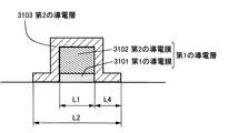
第2の導電層114、118は、前記第1の導電層と電気的に導通していて、かつ、ゲート絶縁膜103に接して設けられている。ここで、図16で示すように、第2の導電層はチャネル長方向に対し、最初L3の長さで形成され、その後エッチング処理によりL5の長さだけ除去して最後にL2の長さにされる。従って、第1の導電層をL1とすると、第2の導電層がゲート絶縁膜に延在する長さはL4で表すことができる。
【0045】
ここで、本願発明において、第1の導電層の長さL1は0.2〜10μm、好ましくは0.4〜5μm、第2の導電層の長さL2は1.2〜16μm、好ましくは2.2〜11μmの長さで形成することが望ましい。ここで、第2の導電層を除去する長さL5は0.5〜3μm、好ましくは1.0〜2.0μmとしている。
【0046】
第1の導電層と第2の導電層は、1回目の一導電型の不純物元素を添加する工程と2回目の一導電型の不純物元素を添加する工程でマスクとして機能するものであり、その点を考慮してL1とL3、および、L2とL5の長さを決める必要がある。nチャネル型TFTのLDD領域の長さは、このL3とL1の差分の長さで形成される。そして、第2の導電層をあらかじめL3の長さで形成しておき、その後エッチング処理によりL5の長さだけ除去して、L2の長さとするのは、本願発明の構成を得るために、LDD領域となる第1の不純物領域1605が、ゲート絶縁膜を介して第2の導電層と重なる領域をL4の長さで、重ならない領域をL5の長さで設けるためである。
【0047】
図1において、nチャネル型TFTの半導体層は、チャネル形成領域104と、前記チャネル形成領域の両側に接して設けられた第1の不純物領域105と、前記第1の不純物領域105に接して設けられた第2の不純物領域106、107とから形成されている。この第2の不純物領域106はソース領域として機能し、第2の不純物領域107はドレイン領域として機能するものである。第1の不純物領域105は、ゲート絶縁膜103を介して、第2の導電層114がゲート絶縁膜と接している領域に重なって設けられている。
【0048】
図16のL6に相当する第1の不純物領域105の長さは、1.0〜6μm、好ましくは2.0〜4μm、(例えば3μm)の長さを有し、n型を付与する不純物元素の濃度が1×10¹⁶〜5×10¹⁹atoms/cm3、代表的には5×1017〜5×1018atoms/cm3で添加されている。そして、第1の不純物領域が第2の導電層と重ならない長さL5は前述の如く0.5〜3μm、好ましくは1.0〜2μmとする。また、ソース領域105とドレイン領域106の不純物濃度は、1×1020〜1×1021atoms/cm3、代表的には2×1020〜5×1020atoms/cm3とすれば良い。
【0049】
この時、チャネル形成領域104には、あらかじめ1×10¹⁶〜5×10¹⁸atoms/cm3の濃度でボロンが添加されても良い。このボロンはしきい値電圧を制御するために添加されるものであり、同様の効果が得られるものであれば他の元素で代用することもできる。
【0050】
一方、pチャネル型TFTの第3の不純物領域109、110、130、131は、ソース領域とドレイン領域とを形成するものである。そして、第3の不純物領域130、131にはn型を付与する不純物元素がnチャネル型TFTのソース領域106とドレイン領域107と同じ濃度で含まれているが、その1.5〜3倍の濃度でp型を付与する不純物元素が添加されている。
【0051】
以上示したように本願発明のTFTは、ゲート電極を第1の導電層と、第2の導電層とを設けた構造を有し、図1で示すように第2の導電層は、第1の導電層とゲート絶縁膜とに接して設けられている。そして、少なくともnチャネル型TFTにおいて、第1の不純物領域の一部は、第2の導電層のゲート絶縁膜に接している領域と重なって設けられている構造に特徴がある。
【0052】
図1で示された構造は、第1の導電層をマスクとして、LDD領域となる第1の不純物領域を形成し、第2の導電層をマスクとしてソース領域とドレイン領域となる第2の不純物領域を形成した後で、エッチング処理により第2の導電層を後退させることにより実現できる。従って、図16で示されたようにLDD領域の長さは、第1の導電層の長さL1と第2の導電層の長さL3で決まり、LDD領域が第2の導電層と重ならない長さは、第2の導電層をエッチングする長さL5で決めることができる。このような方法は、TFTの設計上または製作上において自由度を広げることが可能となり、非常に有効である。
【0053】
一方、pチャネル型TFTには第3の不純物領域109、110、130、131が形成され、LDD構造となる領域は設けないものとする。第3の不純物領域は、ソース領域109、130とドレイン領域110、131を形成する。そして、ソース領域109とドレイン領域110の一部が第2の導電層とオーバーラップしている。勿論、本願発明のLDD構造を設けても良いが、pチャネル型TFTはもともと信頼性が高いため、オン電流を稼いでnチャネル型TFTとの特性バランスをとった方が好ましい。本願発明を図1に示すようにCMOS回路に適用する場合には、特にこの特性のバランスをとることが重要である。但し、本願発明の構造をpチャネル型TFTに適用しても何ら問題はない。
【0054】
こうしてnチャネル型TFTおよびpチャネル型TFTが完成したら、第1の層間絶縁膜119で覆い、ソース電極120、121ドレイン電極122を設ける。図1の構造では、これらを設けた後でパッシベーション膜123として窒化シリコン膜を設けている。さらに樹脂材料でなる第2の層間絶縁膜124が設けられている。第2の層間絶縁膜は、樹脂材料に限定される必要はないが、例えば、液晶表示装置に応用する場合には、表面の平坦性を確保するために樹脂材料を用いることが好ましい。
【0055】
図1では、nチャネル型TFTとpチャネル型TFTとを相補的組み合わせて成るCMOS回路を例にして示したが、nチャネル型TFTを用いたNMOS回路や、液晶表示装置の画素マトリクス回路に本願発明を適用することもできる。
【0056】
以上に示した本願発明の構成について、以下に示す実施例でさらに詳細に説明する。
【0057】
[実施例1]
本実施例では、本願発明の構成を液晶表示装置に適用した例を示し、画素マトリクス回路とその周辺に設けられる駆動回路の基本形態であるCMOS回路を同時に作製する方法について、図29と図30を用いて説明する。
【0058】
図29(A)において、基板401には、例えばコーニング社の1737ガラス基板に代表される無アルカリガラス基板を用る。そして、基板401のTFTが形成される表面に、酸化シリコン膜、窒化シリコン膜、酸化窒化シリコン膜などで形成する下地膜402を200nmの厚さに形成する。
【0059】
次に、この下地膜402の上に50nmの厚さで、非晶質シリコン膜をプラズマCVD法で形成する。非晶質シリコン膜の含有水素量にもよるが、好ましくは400〜500℃に加熱して脱水素処理を行い、非晶質シリコン膜の含有水素量を5atomic%以下として、結晶化の工程を行い結晶質シリコン膜を得る。
【0060】
この結晶化の工程は、レーザーアニール法または熱アニール法の技術を用いれば良い。本実施例では、パルス発振型のKrFエキシマレーザー光を線状に集光して非晶質シリコン膜に照射して結晶質シリコン膜を形成する。
【0061】
ここで用いたレーザーアニール装置の構成を図32に示す。レーザー発振装置3201から照射され、反射ミラー3202で方向を変えられ、光学系3203により光路が変更されたパルス状レーザービームを、ミラー3207で反射させ、シリンドリカルレンズを用いた光学系3208にて集光させて、非晶質シリコン膜が形成されている基板3209に照射する機能を有している。レーザー発振装置3201はXeClエキシマレーザーやKrFエキシマレーザーを用いれば良い。基板3209はステージ3205上に設置されている。
【0062】
尚、本実施例では非晶質シリコン膜から結晶質シリコン膜を形成したが、微結晶シリコン膜をレーザーアニール法で結晶化させても構わないし、直接結晶質シリコン膜を成膜しても良い。
【0063】
こうして形成した結晶質シリコン膜をパターニングして、島状の半導体層403、404、405を形成する。
【0064】
次に、半導体層403、404、405を覆って、酸化シリコンまたは窒化シリコンを主成分とするゲート絶縁膜406を形成する。ここではプラズマCVD法で酸化窒化シリコン膜を100nmの厚さに形成する。そして、図では説明しないが、ゲート絶縁膜406の表面に第1の導電層を構成する。第1の導電層は、導電層(A)としてTaを10〜200nm、例えば50nmさらに導電層(B)としてAlを100〜1000nm、例えば200nmの厚さでスパッタ法で形成する。そして、公知のパターニング技術により、第1の導電層を構成する導電層(A)407、408、409、410と、導電層(B)の412、413、414、415を形成する。このとき、図31で示した第1の導電層の長さL1は3μmとなるようにパターニングする。
【0065】
第1の導電層を構成する導電層(B)として、Alを用いる場合には、純Alを用いても良いし、Ti、Si、Scから選ばれた元素が0.1〜5atomic%添加されたAl合金を用いても良い。またCuを用いる場合には、図示しないが、ゲート絶縁膜406の表面に窒化シリコン膜を設けておくと好ましい。
【0066】
また、図29では画素マトリクス回路の画素TFTのドレイン側に保持容量を設ける構造となっている。このとき、第1の導電層と同じ材料で容量配線411、416を形成する。
【0067】
こうして図29(A)に示す構造を形成したら、1回目のn型を付与する不純物元素を添加する工程を行う。結晶質導体材料に対してn型を付与する不純物元素としては、リン(P)、砒素(As)、アンチモン(Sb)などが知られているが、ここでは、フォスフィン(PH3)を用いたイオンドープ法でリンを添加する。この工程では、ゲート絶縁膜406を通してその下の半導体層にリンを添加するために、加速電圧は80keVと高めに設定する。また、こうして形成された不純物領域は、後に示すnチャネル型TFTの第1の不純物領域434、442を形成するもので、LDD領域として機能するものである。従ってこの領域のリンの濃度は、1×10¹⁶〜5×10¹⁹atoms/cm3の範囲にするのが好ましく、本実施例では1×1018atoms/cm3とする。
【0068】
半導体層中に添加された前記不純物元素は、レーザーアニール法や、熱アニール法により活性化させる必要がある。この工程は、ソース領域およびドレイン領域を形成する不純物元素の添加工程のあと実施しても良いが、この段階でレーザーアニール法により活性化させることは効果的である。
【0069】
この工程で、第1の導電層を構成する導電層(A)407、408、409、410と導電層(B)412、413、414、415は、リンの添加に対してマスクとして機能する。その結果ゲート絶縁膜を介して存在する半導体層の第1の導電層の真下の領域には、まったく、あるいは殆どリンが添加されない。そして、図29(B)に示すように、リンが添加された不純物領域417、418、419、420、421、422、423が形成される。本明細書ではこの不純物領域を第1の不純物領域と呼ぶ。
【0070】
次にフォトレジストをマスクとして、nチャネル型TFTを形成する領域をレジストマスク424、425で覆って、pチャネル型TFTが形成される領域のみに、p型を付与する不純物元素の添加工程を行う。p型を付与する不純物元素としては、ボロン(B)、アルミニウム(Al)、ガリウム(Ga)が知られているが、本実施例ではイオンドープ法でジボラン(B2H6)を用いてボロン(B)を添加する。ここでも加速電圧を80keVとして、2×10²⁰atmos/cm3の濃度にボロンを添加する。そして、図29(C)に示すようにボロン(B)が高濃度に添加された領域426、427を形成する。本明細書ではこの領域を第3の不純物領域と呼び、後にpチャネル型TFTのソース領域およびドレイン領域とする。
【0071】
そして、レジストマスク424、425を除去した後、第2の導電層を形成する工程を行う。ここでは、第2の導電層の材料にTaを用い、100〜1000nm、例えば200nmの厚さに形成する。そして、公知の技術によりパターニングを行い、第2の導電層428、429、430、431を形成する。この時、図31で示した第2の導電層の長さL2は6μmとなるようにパターニングする。結果として、第2の導電層は、第1の導電層の両側にそれぞれ1.5μmの長さでゲート絶縁膜と接する領域が形成される。
【0072】
また、画素マトリクス回路の画素TFTのドレイン側に保持容量を設けるが、この保持容量の配線432は第2の導電層と同時に形成する。
【0073】
そして、第2の導電層428、429、430、431をマスクとして、2回目のn型を付与する不純物元素を添加する工程を行う。フォスフィン(PH3)を用いたイオンドープ法で行い、ゲート絶縁膜406を通してその下の半導体層にリン(P)を添加するために、加速電圧は80keVと高めに設定する。そして、ここでリン(P)が添加される領域は、nチャネル型TFTでソース領域435、443およびドレイン領域434、444、447として機能させるため、この領域のリンの濃度は1×10²⁰〜1×10²¹atmos/cm3とするのが好ましく、ここでは1×1020atmos/cm3とする(図29(D))。
【0074】
また、ここで図示はしないが、ソース領域435、443およびドレイン領域436、444、447を覆うゲート絶縁膜を除去して、その領域の半導体層を露出させて直接リンを添加しても良い。この処理によりイオンドープ法の加速電圧を10keVまで下げることができ、また、効率良くリンを添加することができる。
【0075】
また、pチャネル型TFTのソース領域439とドレイン領域440にも同じ濃度でリンが添加されるが、前の工程でその2倍の濃度でボロンが添加されているため導電型は反転せず、pチャネル型TFTの動作上何ら問題はない。
【0076】
それぞれの濃度で添加されたn型またはp型を付与する不純物元素は、このままでは活性化せず有効に作用しないので、活性化の工程を行う必要がある。この工程は電気加熱炉を用いた熱アニール法や、前述のエキシマレーザーを用いたレーザーアニール法や、ハロゲンランプを用いたラピットサーマルアニール法(RTA法)で行うことができる。
【0077】
熱アニール法では、窒素雰囲気中において550℃、2時間の加熱処理をして活性化を行う。本実施例では、第1の導電層を構成する導電層(B)にAlを用いたが、Taで形成した導電層(A)と第2の導電層がAlを覆って形成されているため、Taがブロッキング層として機能して、Al原子が他の領域に拡散することを防ぐことができる。また、レーザーアニール法では、図32と同じ構成の装置で、パルス発振型のKrFエキシマレーザー光を線状に集光して照射することにより活性化を行う。また、レーザーアニール法を実施した後に熱アニール法を実施すると、さらに良い結果が得られる。またこの工程は、イオンドーピングによって結晶性が破壊された領域をアニールする効果も兼ね備えていて、その領域の結晶性を改善することもできる。
【0078】
以上までの工程で、ゲート電極を第1の導電層と、その第1の導電層を覆って第2の導電層が設けられ、nチャネル型TFTでは、第2の導電層の両側にソース領域とドレイン領域が形成される。また、ゲート絶縁膜を介して半導体層に設けられた第1の不純物領域が、第2の導電層のゲート絶縁膜に接している領域と重なって設けられた構造が自己整合的に形成される。一方、pチャネル型TFTでは、ソース領域とドレイン領域の一部が第2の導電層とオーバーラップして形成されているが、実使用上何ら問題はない。
【0079】
図29(D)の状態が得られたら、第1の層間絶縁膜449を1000nmの厚さに形成する。第1の層間絶縁膜449としては、酸化シリコン膜、窒化シリコン膜、酸化窒化シリコン膜、有機樹脂膜、およびそれらの積層膜を用いることができる。本実施例では、図示しないが、最初に窒化シリコン膜を50nm形成し、さらに酸化シリコン膜を950nm形成した2層構造とする。
【0080】
第1の層間絶縁膜449は、パターニング処理でそれぞれのTFTのソース領域とドレイン領域に達するコンタクトホールを形成する。そして、ソース配線450、452、453とドレイン配線451、454を形成する。図示していないが、本実施例ではこの電極をTi膜を100nm、Tiを含むAl膜300nm、Ti膜150nmをスパッタ法で連続して積層させた3層構造の膜をパターニングして形成する。
【0081】
こうして図29(E)に示すように、基板401上にCMOS回路と、画素マトリクス回路が形成される。画素マトリクス回路のnチャネル型TFTのドレイン側には、保持容量が同時に形成される。以上のようにして、アクティブマトリクス基板を作製することができる。
【0082】
次に、図30を用いて、以上の工程によって同一の基板に作製されたCMOS回路と、画素マトリクス回路をもとに、アクティブマトリクス型液晶表示装置を作製する工程を説明する。最初に、図29(E)の状態の基板に対して、ソース配線450、452、453とドレイン配線451、454と、第1の層間絶縁膜445を覆ってパッシベーション膜455を形成する。パッシベーション膜455は、窒化珪素膜で50nmの厚さで形成する。さらに、有機樹脂からなる第2の層間絶縁膜456を約1000nmの厚さに形成する。有機樹脂膜としては、ポリイミド、アクリル、ポリイミドアミド等を使用することができる。有機性樹脂膜を用いることの利点は、成膜方法が簡単である点や、比誘電率が低いので、寄生容量を低減できる点、平坦性に優れる点などが上げられる。なお上述した以外の有機性樹脂膜を用いることもできる。ここでは、基板に塗布後、熱重合するタイプのポリイミドを用い、300℃で焼成して形成する(図30(A))。
【0083】
次に、第2の層間絶縁膜456の画素領域の一部に、遮光層457を形成する。遮光層457は金属膜や顔料を含ませた有機樹脂膜で形成すれば良いものである。ここでは、Ti膜をスパッタ法で形成して遮光膜とする。
【0084】
遮光膜457を形成したら、第3の層間絶縁膜458を形成する。この第3の層間絶縁膜458は、第2の層間絶縁膜456と同様に、有機樹脂膜を用いて形成すると良い。そして、第2の層間絶縁膜456と第3の層間絶縁膜458とにドレイン配線454に達するコンタクトホールを形成し、画素電極459を形成する。画素電極459は、透過型液晶表示装置とする場合には透明導電膜を用い、反射型の液晶表示装置とする場合には金属膜を用いれば良い。ここでは透過型の液晶表示装置とするために、酸化インジウム・スズ(ITO)膜を100nmの厚さにスパッタ法で形成し、画素電極459を形成する。
【0085】
透明導電膜の材料のエッチング処理は塩酸系の溶液により行う。しかし、ITOのエッチングは残渣が発生しやすいので、エッチング加工性を改善するために酸化インジウム酸化亜鉛合金(In2O3―ZnO)を用いても良い。酸化インジウム酸化亜鉛合金は表面平滑性に優れ、ITOと比較して熱安定性にも優れているという特徴をもつ。同様に、酸化亜鉛(ZnO)も適した材料であり、さらに可視光の透過率や導電率を高めるためにガリウム(Ga)を添加した酸化亜鉛(ZnO:Ga)などを用いることができる。
【0086】
図30(A)の状態が形成されたら、配向膜460を形成する。通常液晶表示素子の配向膜にはポリイミド樹脂が多く用いられている。対向側の基板471には、透明導電膜472と、配向膜473とを形成する。配向膜はその後、ラビング処理を施して液晶分子がある一定のプレチルト角を持って平行配向するようにする。
【0087】
上記の工程を経て、画素マトリクス回路とCMOS回路が形成された基板と対向基板とを、公知のセル組み工程によってシール材やスペーサ(共に図示せず)などを介して貼り合わせる。その後、両基板の間に液晶材料474を注入し、封止剤(図示せず)によって完全に封止する。よって図30(B)に示すアクティブマトリクス型液晶表示装置が完成する。
【0088】
[実施例2]
本実施例では、本願発明の構成を、画素マトリクス回路とその周辺に設ける駆動回路の基本形態であるCMOS回路を同時に作製する方法として説明する。
【0089】
図2において、基板201には、例えばコーニング社の1737ガラス基板に代表される無アルカリガラス基板を用いる。そして、基板201のTFTを形成する表面に、下地膜202を形成する。下地膜202は、酸化シリコン膜、窒化シリコン膜、酸化窒化シリコン膜などを用いる。
【0090】
下地膜202は上記材料の1層で形成しても良いし、2層以上の積層構造としても良い。いずれにしてもその厚さが100〜300nm程度になるように形成する。例えば、プラズマCVD法でSiH4、NH3、N2Oから作製される第1の酸化窒化シリコン膜を10〜100nmの厚さに形成し、SiH4、N2Oから作製される第2の酸化窒化シリコン膜を100〜200nmの厚さに積層形成した2層構造として下地膜102を形成する。
【0091】
第1の酸化窒化シリコン膜は従来の平行平板型のプラズマCVD法を用いて形成する。酸化窒化シリコン膜は、SiH4を10SCCM、NH3を100SCCM、N2Oを20SCCMとして反応室に導入し、基板温度325℃、反応圧力40Pa、放電電力密度0.41W/cm2、放電周波数60MHzとした。一方、第2の酸化窒化シリコン膜は、SiH4を4SCCM、N2Oを400SCCM、として反応室に導入し、基板温度400℃、反応圧力40Pa、放電電力密度0.41W/cm2、放電周波数60MHzとした。これらの膜は、基板温度を変化させ、反応ガスの切り替えのみで連続して形成することもできる。また、第1の酸化窒化シリコン膜は基板を中心に考えて、その内部応力が引張り応力となるように形成する。第2の酸化窒化シリコン膜も同様な方向に内部応力を持たせるが、第1の酸化窒化シリコン膜よりも絶対値で比較して小さい応力となるようにする。
【0092】
次に、この下地膜202の上に30〜80nm、例えば50nmの厚さで、非晶質シリコン膜をプラズマCVD法で形成する。その後、非晶質シリコン膜は含有水素量にもよるが、好ましくは400〜500℃に加熱して脱水素処理を行い、含有水素量を5atomic%以下として、結晶化の工程を行うことが望ましい。
【0093】
非晶質シリコン膜を結晶化する工程は、レーザーアニール法や熱アニール法により行う。本実施例では、パルス発振型のKrFエキシマレーザー光を線状に集光して非晶質シリコン膜に照射して結晶質シリコン膜とする。
【0094】
尚、本実施例では非晶質シリコン膜を用いたが、微結晶シリコン膜を用いても構わないし、直接結晶質シリコン膜を成膜しても良い。
【0095】
こうして形成された結晶質シリコン膜をパターニングして、島状の半導体層204、205、206を形成する。
【0096】
次に、半導体層204、205、206を覆って、酸化シリコンまたは窒化シリコンを主成分とするゲート絶縁膜203を形成する。例えば、プラズマCVD法で酸化窒化シリコン膜を100nmの厚さに形成する。そして、図では説明しないが、ゲート絶縁膜203の表面にゲート電極の第1の導電層を構成する、導電層(A)としてTa膜を10〜200nm、例えば50nmの厚さに、さらに導電層(B)としてAl膜を100〜1000nm、例えば200nmの厚さでスパッタ法により形成した。そして、公知のパターニング技術により、第1の導電層を構成する導電層(A)207、208、209、210と、導電層(B)212、213、214、215を形成する。このとき、図16で示した第1の導電層の長さL1は適宣決めれば良く0.2〜10μm、ここでは3μmの長さでパターニングする(図2(A))。
【0097】
第1の導電層を構成する導電層(B)として、Alを用いる場合には、純Alを用いても良いし、Ti、Si、Scから選ばれた元素が0.1〜5atomic%添加されたAl合金を用いても良い。銅を用いる場合には、図示しないが、ゲート絶縁膜203の表面に窒化シリコン膜を30〜100nmの厚さで設けておくと好ましい。
【0098】
導電層(A)207、208、209、210にTa膜を用いる場合には、同様にスパッタ法で形成することが可能である。Ta膜はスパッタガスにArを用いる。また、これらのスパッタガス中に適量のXeやKrを加えておくと、形成する膜の内部応力を緩和して膜の剥離を防止することができる。α相のTa膜の抵抗率は20μΩcm程度でありゲート電極に使用することができるが、β相のTa膜の抵抗率は180μΩcm程度でありゲート電極とするには不向きである。しかし、TaN膜はα相に近い結晶構造を持つので、この上にTa膜を形成すればα相のTa膜が容易に得られる。従って、図示しないが導電層(A)207、208、209、210の下に10〜50nmの厚さでTaN膜を形成しておいても良い。同様に図示しないが、導電層(A)の下に2〜20nm程度の厚さでリン(P)をドープしたシリコン膜を形成しておくことは有効である。これにより、その上に形成される導電膜の密着性向上と酸化防止を図ると同時に、導電層(A)または導電層(B)が微量に含有するアルカリ金属元素がゲート絶縁膜203に拡散するのを防ぐことができる。いずれにしても、導電層(A)は抵抗率を10〜50μΩcmの範囲ですることが好ましい。
【0099】
その他に、導電層(A)207、208、209、210にW膜を用いることも可能であり、その場合はWをターゲットとしたスパッタ法で、アルゴン(Ar)ガスと窒素(N2)ガスを導入して導電層(A)をW膜で200nmの厚さに形成する。また、W膜を6フッ化タングステン(WF6)を用いて熱CVD法で形成することもできる。いずれにしてもゲート電極として使用するためには低抵抗化を図る必要があり、W膜の抵抗率は20μΩcm以下にすることが望ましい。
W膜は結晶粒を大きくすることで低抵抗率化を図ることができるが、W膜中に酸素などの不純物元素が多い場合には結晶化が阻害され高抵抗化する。このことより、スパッタ法による場合、純度99.9999%のWターゲットを用い、さらに成膜時に気相中からの不純物の混入がないように十分配慮してW膜を形成することにより、抵抗率9〜20μΩcmを実現することができる。
【0100】
また、図2では画素マトリクス回路の画素TFTのドレイン側に保持容量を設ける構造となっている。このとき、第1の導電層と同じ材料で保持容量の配線211、216を形成する。
【0101】
こうして図2(A)に示す構造を形成した後、1回目のn型を付与する不純物元素を添加する工程を行い、第1の不純物領域を形成する。結晶質半導体材料に対してn型を付与する不純物元素としては、リン(P)、砒素(As)、アンチモン(Sb)などが知られているが、例えば、リンを用い、フォスフィン(PH3)を用いたイオンドープ法で行う。この工程では、ゲート絶縁膜203を通してその下の半導体層にリンを添加するために、加速電圧を80keVと高めに設定した。こうして形成する第1の不純物領域は、後に示すnチャネル型TFTの第1の不純物領域229、236、240を形成するもので、LDD領域として機能するものである。従ってこの領域のリンの濃度は、1×10¹⁶〜5×10¹⁹atoms/cm3の範囲にするのが好ましく、ここでは1×1018atoms/cm3とした(図2(B))。
【0102】
半導体層中に添加された前記不純物元素は、レーザーアニール法や、熱アニール法により活性化させる必要がある。この工程は、ソース領域およびドレイン領域を形成する不純物元素を添加する工程のあと実施しても良いが、この段階でレーザーアニール法により活性化させることは有効である。
【0103】
この工程で、第1の導電層を構成する導電層(A)207、208、209、210と導電層(B)212、213、214、215は、リンの添加に対してマスクとして機能する。その結果、半導体層の第1の導電層と重なる領域には、まったく、あるいは殆どリンは添加されていない。ここでは、図2(B)に示すように、リンが添加された第1の不純物領域218、219、220、221、222を形成する。
【0104】
次にフォトレジスト膜をマスクとして、nチャネル型TFTを形成する領域をレジストマスク225、226で覆って、pチャネル型TFTが形成される領域のみに、p型を付与する不純物添加の工程を行う。p型を付与する不純物元素としては、ボロン(B)、アルミニウム(Al)、ガリウム(Ga)、が知られている。ここではボロンをその不純物元素とし、ジボラン(B2H6)を用いてイオンドープ法で半導体層に添加する。加速電圧は80keVとして、2×10²⁰atoms/cm3の濃度にボロンを添加する。そして、図2(C)に示すようにボロンが高濃度に添加された第3の不純物領域227、228を形成する。この第3の不純物領域は後にpチャネル型TFTのソース領域、ドレイン領域領域となる(図2(C))。
【0105】
そして、レジストマスク225、226を除去した後、第2の導電層を形成する工程を行う。その材料にTaを用い、100〜1000nm(例えば、200nm)の厚さに形成する。そして、公知の技術によりパターニングを行い、第2の導電層243、244、245、246を形成する。この時、図16で示すように第2の導電層のチャネル長方向の長さL3は1.3〜20μm、例えば9μmとなるようにパターニングする。結果として、第2の導電層は、第1の導電層の両側にそれぞれ3μmの長さでゲート絶縁膜と接する領域(L6)が形成される。
【0106】
また、画素マトリクス回路を構成するnチャネル型TFT(画素TFT)のドレイン側に保持容量が設けられるが、この保持容量の電極247は第2の導電層と同時に形成する。
【0107】
そして、第2の導電層243、244、245、246をマスクとして、2回目のn型を付与する不純物元素を添加する工程を行い、第2の不純物領域を形成する。このとき図3(A)に示す様に、第2の導電層をパターニングするときに設けたレジストマスク283、284、285、286、287をそのまま残しておいても良い。不純物元素の添加は、フォスフィン(PH3)を用いたイオンドープ法で行った。この工程でも、ゲート絶縁膜203を通してその下の半導体層にリンを添加するために、加速電圧は80keVと高めに設定した。そして、ここで形成される第2の不純物領域は、nチャネル型TFTのソース領域230、237、およびドレイン領域231、238、241として機能させるため、この領域のリンの濃度は、1×10²⁰〜1×10²¹atoms/cm3とするのが好ましく、本実施例では1×1020atoms/cm3とした(図3(A))。
【0108】
また、ここで図示はしないが、ソース領域230、237、289およびドレイン領域231、238、241、288を覆うゲート絶縁膜を除去して、その領域の半導体層を露出させ、直接リンを添加しても良い。この工程を加えると、イオンドープ法の加速電圧を10keVまで下げることができ、また、効率良くリンを添加することができる。
【0109】
また、pチャネル型TFTの第3の不純物領域の一部288、289にも同じ濃度でリンが添加されるが、その2倍の濃度でボロンが添加されているため、導電型は反転せず、pチャネル型TFTの動作上何ら問題はない。そして、pチャネル型TFTでは、第3の不純物領域234、289、233、288によって、ソース領域が234、289で形成され、ドレイン領域が233、288で形成される。このとき、ソース領域234と、ドレイン領域233とは、第2の導電層244とオーバーラップして形成される。
【0110】
図3(A)の状態が得られたら、レジストマスク283、284、285,286,287は除去して、再度フォトレジスト膜を形成し、裏面からの露光によってレジストマスクを形成する。このとき図3(B)に示すように、第1および第2の導電層をマスクとして自己整合的にレジストマスク248、249、250、256、257を形成する。裏面からの露光は、直接光と散乱光を利用して行うもので、オーバー露光とすることで、図3(B)のようにレジストマスクを第2の導電層の内側に設けることができる。
【0111】
そして、第2の導電層のマスクされていない領域をエッチングして除去する。
エッチングは通常のドライエッチング技術を用いればよく、CF4とO2ガスを用いて行う。そして、図3(C)に示すように、L5の長さだけ除去する。L5の長さは0.5〜3μmの範囲で適宣調整すれば良く、ここでは1.5μmとした。その結果、nチャネル型TFTにおいて、LDD領域となる第1の不純物領域の長さ3μmの内、1.5μm(L4)の長さで第2の導電層と重なる領域が形成され、1.5μm(L5)の長さで第2の導電層と重ならない領域を形成することができた。
【0112】
それぞれの濃度で添加されたn型またはp型を付与する不純物元素は、このままでは活性化せず有効に作用しないので、活性化の工程を行う必要がある。この工程は、電気加熱炉を用いた熱アニール法や、前述のエキシマレーザーを用いたレーザーアニール法や、ハロゲンランプを用いたラピットサーマルアニール法(RTA法)で行うことができる。
【0113】
熱アニール法では、窒素雰囲気中において300〜700℃、好ましくは350〜550℃、例えば450℃、2時間の加熱処理をして活性化を行う。本実施例では、第1の導電層を構成する導電膜(B)にAlを用いる構造とし、Taで形成される導電膜(A)と第2の導電層がAlを覆って形成されているため、Taがブロッキング層として機能して、Al原子が他の領域に拡散することを防ぐことができる。また、レーザーアニール法では、パルス発振型のKrFエキシマレーザー光を線状に集光して照射することにより活性化が行われる。また、レーザーアニール法を実施した後に熱アニール法を実施すると、さらに良い結果が得られる。この工程は、イオンドーピング法によって結晶性が破壊された領域をアニールする効果も兼ね備えていて、その領域の結晶性を改善することもできる。
【0114】
以上の工程で、ゲート電極を第1の導電層と、その第1の導電層に接して第2の導電層が設けられ、半導体層204、206にはLDD領域となる第1の不純物領域と、ソース領域とドレイン領域となる第2の不純物領域が形成される。そして、第1の不純物領域は、ゲート絶縁膜を介して第2の導電層と重なる領域と重ならない領域が形成される。一方、pチャネル型TFTでは、チャネル形成領域と、ソース領域とドレイン領域とが形成される。
【0115】
図3(B)までの工程が終了したら、レジストマスク248、249、250、256、257を除去して、第1の層間絶縁膜263を500〜1500nmの厚さに形成する。第1の層間絶縁膜263としては、酸化シリコン膜、窒化シリコン膜、酸化窒化シリコン膜、有機樹脂膜、およびそれらの積層膜を用いることができる。本実施例では、図示しないが、最初に窒化シリコン膜を50nm形成し、さらに酸化シリコン膜を950nm形成した2層構造とする。或いは、SiH4とN2Oとから作製する酸化窒化シリコン膜で1000nmの厚さに形成しても良い。
【0116】
第1の層間絶縁膜263にはその後、それぞれの半導体層のソース領域と、ドレイン領域に達するコンタクトホールを形成する。そして、ソース配線264、265、266、とドレイン配線267、268を形成する。図示していないが、本実施例ではこの配線を3層構造とし、Ti膜100nm、Tiを含むAl膜300nm、Ti膜150nmの厚さでスパッタ法で連続して形成する。
【0117】
そして、ソース電極264、265、266とドレイン電極267、268と、第1の層間絶縁膜263を覆ってパッシベーション膜269を形成する。パッシベーション膜269は、窒化シリコン膜で50nmの厚さで形成する。さらに、有機樹脂からなる第2の層間絶縁膜270を約1000nmの厚さに形成する。有機樹脂膜としては、ポリイミド、アクリル、ポリイミドアミド等を使用することができる。有機樹脂膜を用いることの利点は、成膜方法が簡単である点や、比誘電率が低いので、寄生容量を低減できる点、平坦性に優れる点などが上げられる。なお上述した以外の有機樹脂膜を用いることもできる。ここでは、基板に塗布後、熱重合するタイプのポリイミドを用い、300℃で焼成して形成する。
【0118】
こうして図3(C)に示すように、基板201上にCMOS回路と、画素マトリクス回路の画素TFTが形成されたアクティブマトリクス基板が作製される。
また、画素マトリクス回路の画素TFTのドレイン側には、保持容量が同時に形成される。
【0119】
[実施例3]
本実施例では、実施例1と同じ工程で図3(A)に示す状態得た後、他の方法で第2の導電層の一部を除去して、第1の不純物領域が第2の導電層と重なる領域と重ならない領域とを形成する例を示す。
【0120】
まず、図3(A)に示すように、第2の導電層のパターニング工程で使用したレジストマスク283、284、285、286、287をそのまま使用して、エッチングにより、第2の導電層の一部を図4(A)に示すようにL5の長さだけ除去する。
【0121】
この工程は、ドライエッチングで行うことができる。第2の導電層の材料にもよるが、基本的にはフッ素(F)系ガスを用いることにより等方性エッチングが進み、レジストマスクの下にある第2の導電層材料を除去することができる。例えば、Taの場合にはCF4ガスで可能であり、Tiの場合にはCF4やCCl4ガスで可能であり、Moの場合にはSF6やNF3で可能である。
【0122】
そして、図4(A)に示すように、L5の長さだけ、ここでは1.5μm除去する。その結果、nチャネル型TFTにおいて、LDD領域となる第1の不純物領域は3μmの長さ(L6)で形成されており、1.5μmの長さ(L4)で第2の導電層と重なる領域が形成され、1.5μmの長さ(L5)で第2のゲート電極と重ならない領域を形成することができる。
【0123】
そしてレジストマスク283、284、285,286、287を除去して、実施例1と同様に活性化の工程を行い、第1の層間絶縁膜263、ソース配線264、265、266、ドレイン配線267、268、パッシベーション膜269、第2の層間絶縁膜270を形成して、図4(B)に示すアクティブマトリクス基板を形成することができる。
【0124】
[実施例4]
本実施例では、実施例1〜3および実施例5で形成されるアクティブマトリクス基板から、アクティブマトリクス型液晶表示装置を作製する工程を説明する。
【0125】
図3(C)または図4(B)の状態のアクティブマトリクス基板に対して、第2の層間絶縁膜270にドレイン電極268に達するコンタクトホールを形成し、画素電極271を形成する。画素電極271は、透過型液晶表示装置とする場合には透明導電膜を用い、反射型の液晶表示装置とする場合には金属膜を用いれば良い。ここでは透過型の液晶表示装置とするために、酸化インジウム・スズ(ITO)膜を100nmの厚さにスパッタ法で形成し、画素電極271を形成する。
【0126】
図5(A)の状態を形成したら、配向膜272を第2の層間絶縁膜270と画素電極271上に形成する。通常液晶表示素子の配向膜にはポリイミド樹脂が多く用いられている。対向側の基板273には、透明導電膜274と、配向膜275とを形成する。配向膜は形成された後、ラビング処理を施して液晶分子がある一定のプレチルト角を持って平行配向するようにする。
【0127】
上記の工程を経て、画素マトリクス回路と、CMOS回路が形成されたアクティブマトリクス基板と対向基板とを公知のセル組み工程により、シール材やスペーサ(共に図示せず)などを介して貼りあわせる。その後、両基板の間に液晶材料276を注入し、封止剤(図示せず)によって完全に封止する。よって図5(B)に示すアクティブマトリクス型液晶表示装置が完成する。
【0128】
次に本実施例のアクティブマトリクス型液晶表示装置の構成を、図7と図8を用いて説明する。図7は本実施例のアクティブマトリクス基板の斜視図である。
アクティブマトリクス基板は、ガラス基板201上に形成された画素マトリクス回路701と、走査(ゲート)線側駆動回路702と、データ(ソース)線側駆動回路703で構成される。画素マトリクス回路の画素TFT700はnチャネル型TFTであり、周辺に設けられる駆動回路はCMOS回路を基本として構成されている。走査(ゲート)線側駆動回路702と、データ(ソース)線側駆動回路703はそれぞれゲート配線802とソース配線803で画素マトリクス回路701に接続されている。
【0129】
図8(A)は画素マトリクス回路701の上面図であり、ほぼ1画素の上面図である。画素マトリクス回路には画素TFTが設けられている。ゲート配線802に連続して形成されるゲート電極820は、図示されていないゲート絶縁膜を介してその下の半導体層801と交差している。図示はしていないが、半導体層には、ソース領域、ドレイン領域、第1の不純物領域が形成されている。また、画素TFTのドレイン側には、半導体層と、ゲート絶縁膜と、第1及び第2の導電層と同じ材料で形成された容量配線821とから、保持容量807が形成されている。また、図8(A)で示すA―A'に沿った断面構造は、図3(C)または図4(C)に示す画素マトリクス回路の画素TFTの断面図に対応している。
【0130】
一方、図8(B)に示すCMOS回路では、ゲート配線815から延在するゲート電極813、814が、図示されていないゲート絶縁膜を介してその下の半導体層810、812とそれぞれ交差している。図示はしていないが、同様にnチャネル型TFTの半導体層810には、ソース領域、ドレイン領域、第1の不純物領域が形成されている。また、pチャネル型TFTの半導体層812にはソース領域とドレイン領域が形成されている。そして、B―B'に沿った断面構造は、図3(C)または図4(C)に示す画素マトリクス回路の断面図に対応している。
【0131】
本実施例では、画素TFT700をダブルゲートの構造としているが、シングルゲートの構造でも良いし、トリプルゲートとしたマルチゲート構造にしても構わない。本実施例のアクティブマトリクス基板の構造は、本実施例の構造に限定されるものではない。本願発明の構造は、ゲート電極の構造と、ゲート絶縁膜を介して設けられた半導体層のソース領域と、ドレイン領域と、その他の不純物領域の構成に特徴があるので、それ以外の構成については実施者が適宣決定すれば良い。
【0132】
[実施例5]
本実施例は、実施例2と同じ工程であるが、画素マトリクス回路の画素TFTとCMOS回路のnチャネル型TFTおよびpチャネル型TFTの、第2の導電層の構造が異なる一例を示す。このとき、図6(A)に示すように、第2の導電層290、291は、第1の導電層に接していて、各TFTのドレイン側にのみ延在した形態となっている。CMOS回路において、nチャネル型TFTの第2の導電層をこのような形状としてもTFTのドレイン側に形成される高電界領域を緩和することができる。一方、画素TFTの第2の導電層292、293および容量配線294は実施例1と同様に形成する。
【0133】
本実施例の工程は、基本的に実施例2で示す工程に従えば良く、第2の導電層の形状はパターニングの工程で使用するフォトマスクを変更するだけで、他の工程は何ら変更する必要はない。しかし、nチャネル型TFTの第1の不純物領域は、ドレイン領域側のみに形成される。
【0134】
そして、図6(B)に示すように、レジストマスク223、224、225,226,227は除去して、再度フォトレジスト膜を形成し、裏面からの露光によってパターニングする。このとき図6(B)に示すように、第1および第2の導電層をマスクとして自己整合的にレジストマスク248、249、250、256、257が形成される。裏面からの露光は、直接光と散乱光を利用して行うもので、オーバー露光とすることで、図6(B)のようにレジストマスクを第2の導電層の内側に設けることができる。
【0135】
そして、第2の導電層のマスクされていない領域をエッチングして除去する。
エッチングは通常のドライエッチング技術を用いればよく、CF4とO2ガスを用いて行う。そして、図6(C)に示すように、L5の長さだけ除去する。L5の長さは0.5〜3μmの範囲で適宣調整すれば良く、ここでは1.5μmとする。その結果、nチャネル型TFTにおいて、LDD領域となる第1の不純物領域の長さ3μmの内、1.5μm(L4)の長さで第2の導電層と重なる領域が形成され、1.5μm(L5)の長さで第2のゲート電極と重ならない領域を形成することができる。以降の工程は、実施例1と同様に行うことで、図6(C)に示すアクティブマトリクス基板が形成される。
【0136】
[実施例6]
本実施例では、実施形態1、2および実施例1、2、3、5において半導体層として用いる結晶質半導体膜を、触媒元素を用いた熱アニール法により形成する例を示す。触媒元素を用いる場合、特開平7−130652号公報、特開平8−78329号公報で開示された技術を用いることが望ましい。
【0137】
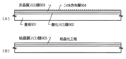
ここで、特開平7−130652号公報に開示されている技術を本願発明に適用する場合の例を図9に示す。まず基板901に酸化シリコン膜902を設け、その上に非晶質シリコン膜903を形成した。さらに、重量換算で10ppmのニッケルを含む酢酸ニッケル塩溶液を塗布してニッケル含有層904を形成する(図9(A))。
【0138】
次に、500℃、1時間の脱水素工程の後、500〜650℃で4〜12時間、例えば550℃、8時間の熱処理を行い、結晶質シリコン膜905を形成する。こうして得られた結晶質シリコン膜905は非常に優れた結晶性を有している(図9(B))。
【0139】
また、特開平8−78329号公報で開示された技術は、触媒元素を選択的に添加することによって、非晶質半導体膜の選択的な結晶化を可能としたものである。同技術を本願発明に適用した場合について図10で説明する。
【0140】
まず、ガラス基板1001に酸化シリコン膜1002を設け、その上に非晶質シリコン膜1003、酸化シリコン膜1004を連続的に形成する。この時、酸化シリコン膜1004の厚さは150nmとする。
【0141】
次に酸化シリコン膜1004をパターニングして、選択的に開孔部1005を形成し、その後、重量換算で10ppmのニッケルを含む酢酸ニッケル塩溶液を塗布する。これにより、ニッケル含有層1006が形成され、ニッケル含有層1006は開孔部1005の底部のみで非晶質シリコン膜1002と接触している(図10(A))。
【0142】
次に、500〜650℃で4〜24時間、例えば570℃、14時間の熱処理を行い、結晶質シリコン膜1007を形成する。この結晶化の過程では、ニッケルが接した非晶質シリコン膜の部分が最初に結晶化し、そこから横方向へと結晶化が進行する。こうして形成された結晶質シリコン膜1007は棒状または針状の結晶が集合して成り、その各々の結晶は巨視的に見ればある特定の方向性をもって成長しているため、結晶性が揃っているという利点がある(図10(B))。
【0143】
尚、上記2つの技術において使用可能な触媒元素は、ニッケル(Ni)の以外にも鉄(Fe)、パラジウム(Pd)、スズ(Sn)、鉛(Pb)、コバルト(Co)、白金(Pt)、銅(Cu)、金(Au)、といった元素を用いても良い。
【0144】
以上のような技術を用いて結晶質半導体膜(結晶質シリコン膜や結晶質シリコンゲルマニウム膜などを含む)を形成し、パターニングを行えば、結晶質TFTの半導体層を形成することができる。本実施例の技術を用いて、結晶質半導体膜から作製されたTFTは、優れた特性が得られるが、そのため高い信頼性を要求されている。しかしながら、本願発明のTFT構造を採用することで、本実施例の技術を最大限に生かしたTFTを作製することが可能となる。
【0145】
[実施例7]
本実施例は、実施形態1、2および実施例1、2、3、5で用いられる半導体層を形成する方法として、非晶質半導体膜を初期膜として前記触媒元素を用いて結晶質半導体膜を形成した後で、その触媒元素を結晶質半導体膜から除去する工程を行った例を示す。本実施例ではその方法として、特開平10−247735、特開平10−135468号公報または特開平10−135469号公報に記載された技術を用いる。
【0146】
同公報に記載された技術は、非晶質半導体膜の結晶化に用いた触媒元素を結晶化後にリンのゲッタリング作用を用いて除去する技術である。同技術を用いることで、結晶質半導体膜中の触媒元素の濃度を1×10¹⁷atoms/cm3以下、好ましくは1×1016atoms/cm3にまで低減することができる。
【0147】
本実施例の構成について図11を用いて説明する。ガラス基板1101はコーニング社の1737基板に代表される無アルカリガラス基板を用いている。図11(A)では、実施例5で示した結晶化の技術を用いて、下地1102、結晶質シリコン膜1103が形成された状態を示している。そして、結晶質シリコン膜1103の表面にマスク用の酸化シリコン膜1104が150nmの厚さに形成され、パターニングにより開孔部が設けられ、結晶質シリコン膜を露出させた領域を設けてある。そして、リンを添加する工程を実施して、結晶質シリコン膜にリンが添加された領域1105が設ける。
【0148】
この状態で、窒素雰囲気中で550〜800℃、5〜24時間、例えば600℃、12時間の熱処理を行うと、結晶質シリコン膜にリンが添加された領域1105がゲッタリングサイトとして働き、結晶質シリコン膜1103に残存していた触媒元素はリンが添加された領域1105に偏析させることができる。
【0149】
そして、マスク用の酸化シリコン膜1104と、リンが添加された領域1105とをエッチングして除去することにより、結晶化の工程で使用した触媒元素の濃度が1×10¹⁷atoms/cm3以下にまで低減された結晶質シリコン膜を得ることができる。この結晶質シリコン膜はそのまま実施例1、2、4で示した本願発明のTFTの半導体層として使用することができる。
【0150】
[実施例8]
本実施例では、実施形態1、2および実施例1、2、3、5で示した本願発明のTFTを作製する工程において、半導体層とゲート絶縁膜を形成する他の実施例を示す。そして、本実施例の構成を図12で説明する。
【0151】
ここでは、少なくとも700〜1100℃程度の耐熱性を有する基板が必要であり、石英基板1201を用いる。そして実施例5で示した技術を用い、結晶質半導体を形成する。これをTFTの半導体層とするために、島状にパターニングして半導体層1202、1203を形成する。そして、半導体層1202、1203を覆って、ゲート絶縁膜1204を酸化シリコンを主成分とする膜で形成した。本実施例では、プラズマCVD法で酸化窒化シリコン膜を70nmの厚さで形成する(図12(A))。
【0152】
そして、ハロゲン(代表的には塩素)と酸素を含む雰囲気中で熱処理を行う。
本実施例では、950℃、30分とする。尚、処理温度は700〜1100℃の範囲で選択すれば良く、処理時間も10分から8時間の間で選択すれば良い(図12(B))。
【0153】
その結果、本実施例の条件では、半導体層1202、1203とゲート絶縁膜1204との界面で熱酸化膜が形成され、ゲート絶縁膜1207が形成される。
また、ハロゲン雰囲気での酸化の過程で、ゲート絶縁膜1204と半導体層1202、1203に含まれる不純物で、特に金属不純物元素はハロゲンと化合物を形成し、気相中に除去することができる。
【0154】
以上の工程で作製されるゲート絶縁膜1207は、絶縁耐圧が高く半導体層1205、1206とゲート絶縁膜1207の界面は非常に良好なものであった。
本願発明のTFTの構成を得るためには、以降の工程は実施例1、2、4に従えば良い。
【0155】
[実施例9]
本実施例では、実施例2と異なる工程順序で結晶質TFTを作製する例を図13に示す。まず、実施例2において、図2(A)で示される半導体層204、205、206は、実施例6で示す方法で作製する結晶質シリコン膜を用いる。このとき、結晶化の工程で用いられる触媒元素が半導体層中にわずかに残存している。その後の工程は、実施例1に従い図3(B)に示すp型を付与する不純物添加の工程までを実施する。そして、レジストマスク258、259を除去する。
【0156】
このとき、図13に示すように、nチャネル型TFTのソース領域230、237と、ドレイン領域231、238、241と、pチャネル型TFTのソース領域234、289と、ドレイン領域233、288とにはいずれも図3(A)の工程で添加されたリンが存在している。実施例1に従えばこのときリン濃度は1×10²⁰〜1×10²¹atoms/cm3であった。
【0157】
この状態で、窒素雰囲気中で400〜800℃、1〜24時間、例えば550℃、4時間の加熱処理の工程を行う。この工程により、添加されたn型及びp型を付与する不純物元素を活性化することができる。さらに、前記リンが添加された領域がゲッタリングサイトとなり、結晶化の工程の後残存していた触媒元素を偏析させることができる。その結果、チャネル形成領域から触媒元素を除去することができる。
【0158】
図13の工程が終了したら、以降の工程は実施例1の工程に従い、図3(C)の状態を形成することにより、アクティブマトリクス基板を作製することができる。
【0159】
[実施例10]
本実施例では、本願発明のTFTにおけるゲート電極の構成の例を図14で示す。ゲート電極は、第1の導電層と、第1の導電層に接して形成される第2の導電層とから成っている。そして、第1の導電層は、一つまたは複数の導電層から形成されるものである。
【0160】
図14(A)は、ゲート電極の第1の導電層のゲート絶縁膜に接して形成される導電層(A)1701をMo−Ti膜で形成し、その導電層(A)上に積層して、導電層(B)1702をTi膜で形成し、導電層(C)1703をAlを主成分とする膜で形成し、導電層(D)1704をTi膜で形成した構造を有している。ここで、導電層(A)の厚さは30〜200nmの厚さに、また、導電層(B)〜導電層(D)の厚さは50〜100nmの厚さで形成することが望ましい。
【0161】
ゲート絶縁膜に接する導電層(A)は、その上に形成する導電層の構成元素がゲート絶縁膜中にしみ込むのを防ぐバリア層としての役割を果たすものであり、Ti、Ta、W、Mo、などの高融点金属か、その合金材料を用いることが望ましい。また、図14(A)で形成された導電層(C)1703はAlを主成分とする膜であり、これはゲート電極の抵抗率を下げるために設けられる。そして、形成するAl膜の平坦性を高めるために、Sc、Ti、Siなどの元素を0.1〜5atomic%の割合で含有させたAl合金膜を用いると望ましい。いずれにしても、本願発明を10インチクラスかそれ以上の液晶表示装置に適用する場合には、ゲート電極の抵抗を下げるために、AlまたはCuを主成分とする抵抗率の低い材料を用いることが望ましい。さらに、第1の導電層とゲート絶縁膜に接して形成される第2の導電層1705は、耐熱性を高めるために、Ti、Ta、W、Mo、などの高融点金属か、その合金材料を用いることが望ましい。
【0162】
図14(B)は他の構成例であり、導電層(A)1706をMo−W合金膜またはW膜から成る一つの層で、第2の導電層1707をTi膜で形成するものである。第2の導電層1707はその他にTa、Mo、Wで形成しても良い。導電層(A)1706は厚さを50〜100nmとすれば良い。
【0163】
図14(C)は、ゲート電極の第1の導電層を構成する導電層(A)1708をTi膜で形成し、導電層(B)1709を銅(Cu)を主成分とする膜で形成し、導電層(C)1710をTi膜で形成するものである。Al膜と同様にCu膜を用いてもゲート電極およびゲート配線の抵抗率を下げることが可能である。
また、第2の導電層1711はTi、Mo、W、Taなどの膜で形成する。
【0164】
図14(D)は、第1の導電層を構成する導電層(A)1712をTi膜で形成し、導電層(B)1713をAlを主成分とする膜で形成し、導電層(C)1714をTi膜で形成したものである。第2の導電層1715はTi、Mo、W、Taなどの膜で形成する。
【0165】
図14(E)は、ゲート電極の第1の導電層を構成する導電層(A)1716をTi膜で形成し、その表面を窒化して窒化チタン(TiN)膜1720を設ける。TiN膜の厚さは、Ti膜の厚さ30〜200nmに対して10〜100nmとすれば良く、ここでは20nmとした。TiN膜はスパッタ法で導電層(A)1716のTi膜を形成するとき、アルゴンガス中に流量比で10〜30%程度の窒素ガスを加えれば良く、このとき膜中の含有量を20〜50atomic%、好ましくは40atomic%とすれば良い。そして導電層(B)1717をAlを主成分とする膜で形成し、導電層(C)1718をTi膜で形成する。この時、Ti膜の成膜前にTiN膜1721を形成しておいても良い。そして、第2の導電層1719をTi膜で形成する。この時も、Ti膜の成膜前にTiN膜1722を形成しておいても良い。
【0166】
図14(E)のように、TiN膜を導電層(B)1717との界面に設けることにより、TiとAlが直接反応することを防ぐことができる。このようなゲート電極の構成は、実施例1の熱活性化の工程や、実施例8で行われる加熱処理の工程に対して有効であり、300〜700℃の範囲、好ましくは350〜550℃の範囲でその工程を実施することができる。
【0167】
図14(F)は、ゲート電極の第1の導電層を構成する導電層(A)1723をTi膜で形成し、導電層(B)1724をAlを主成分とする膜で形成し、第2の導電層1725をTa膜で形成するものである。ここでも同様に、導電層(B)1724と接する面にTiN膜1726およびTaN膜1727を形成する。TaN膜は同様にスパッタ法でアルゴンガスに窒素を流量比で1〜10%添加すれば良く、このときTaN膜中に含まれる窒素の量を35〜60atomic%、好ましくは45〜50atomic%含ませると良い。このような構成とすることで、図14(E)の構成例と同様に耐熱性を高めることができる。
【0168】
このようなゲート電極の構成は実施形態1、2および実施例1、2、3、5のTFTと好適に組み合わせて用いることができる。
【0169】
[実施例11]
本実施例では、図16で示すL4を半導体層上とその周辺で異ならせる例について図18を用いて説明する。
【0170】
図18において、半導体層1840上にはゲート電極の第1の導電層1841及び第2の導電層1842が形成されている。この時、第2の導電層1842は第1の導電層1841を覆い隠すように形成されるが、本明細書中では第1の導電層1841と重ならない部分の長さをL4と定義している。
【0171】
本実施例の場合、半導体層の上ではL4の長さ(ここではWLDDと表す)を0.5〜3μmとする。そして、配線部(半導体層の上以外の周辺部)ではL4'の長さ(ここではWLと表す)を0.1〜1.5μmとする。
【0172】
即ち、本実施例は半導体層の上よりも配線部の方において第2の導電層の線幅を狭くすることに特徴がある。なぜならば配線部ではL4に相当する領域は必要なく、配線の高密度集積化を妨げる要因となってしまうため、可能な限り線幅を狭くした方が好ましい。
【0173】
従って、本実施例の構成を用いることで配線の高密度集積化が容易となり、ひいては半導体装置の高密度集積化が可能となる。なお、本実施例の構成は実施例1〜10のいずれの構成とも自由に組み合わせることが可能である。
【0174】
[実施例12]
本実施例では、実施例1、2のアクティブマトリクス基板に設けられた保持容量を形成する工程の他の一例を示す。図2(B)の状態の基板に、フォトレジスト膜をマスクとして、nチャネル型TFTを形成する領域をレジストマスク225、295で覆って、pチャネル型TFTが形成される領域と、保持容量が形成される領域とに、p型を付与する不純物添加の工程を行う。ここでは実施例1と同様に2×10²⁰atoms/cm3の濃度にボロンを添加する。そして、図19に示すようにボロンが高濃度に添加された第3の不純物領域227、228、296が形成される。
【0175】
保持容量が形成される領域の半導体層に高濃度のボロン(B)が添加されることで、抵抗率を下げることができて、好ましい状態となる。尚、以降の工程は実施例1に従えば良い。
【0176】
[実施例13]
本実施例では、計算機シュミレーションを用い、本願発明の構成について、その妥当性を検証した。ここでは、ISE(Integrated system engineering AG)半導体デバイスシュミレータ総合パッケージを用いた。
【0177】
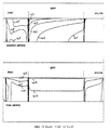
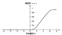
ここで計算に用いたTFTの構造を図20に示す。TFTの構造は、チャネル長10μm、チャネル幅10μm、で低濃度不純物領域(LDD)の長さを2.5μm固定とした。また、その他の条件としては、低濃度不純物領域(n-)のリン濃度を4.2×10¹⁷個/cm3、ソース領域とドレイン領域(n+)のリン濃度を2×1020個/cm3、半導体層の厚さ50nm、ゲート絶縁膜の厚さを150nm、ゲート電極の厚さを400nmとした。そして計算では、低濃度不純物領域(n-)が、ゲート電極と完全にオーバーラップさせたGOLD構造の場合と、0.5μmピッチで外側にずらして、一部がオーバーラップさせた構造(GOLD+LDD)との場合について調べた。
【0178】
図21は、チャネル形成領域の中心を基準として、そのドレイン側の電界強度分布を計算した結果を示す。ここではゲート電圧Vg=ー8V、ドレイン電圧Vds=16Vとして計算した。その結果、低濃度不純物領域(n-)がゲート電極と完全にオーバーラップしたGOLD構造の場合、ゲートードレイン端での電界強度が最も強くなり、低濃度不純物領域(n-)領域をドレイン側にずらして、オーバーラップ量を減らすと電界強度が緩和される結果が得られた。
【0179】
また図22は、ドレイン電圧Vds=16V一定とした、Vg−Id(ゲート電圧―ドレイン電流)特性を計算した結果を示している。GOLD構造の場合オフ電流の増大があるが、低濃度不純物領域(n-)領域をドレイン側にずらして、オーバーラップ量を減らすとオフ電流の増加を防ぐことができる様子を示している。
【0180】
また図23と図24は、低濃度不純物領域(n-)が、ゲート電極と完全にオーバーラップしたGOLD構造と、0.5μm外側にずらして、一部がオーバーラップさせた構造(GOLD+LDD)との場合について、チャネル形成領域、ソース領域、ドレイン領域の電子濃度分布とホール濃度分布について計算した結果を示している。図では濃度分布を等高線で示している。図23では、低濃度不純物領域(n-)の表面がゲート電極とオーバーラップしている領域でホール濃度が高くなっている様子をみることができる。このとき、このホール濃度が高いことが起因するオフ電流の増加がよそうされる。この様子は、図25のホール電流としてみることができる。一方、図24では、GOLD+LDD構造によりゲート電極とドレイン端での電界強度が緩和されるため、ホール濃度は高くない。
また、電子濃度の分布も緩やかとなり、LDD領域の存在のためトンネル電流も阻止されるため、オフ電流の増加もなくなる。同様に図26では電子電流およびホール電流とも低減されている。
【0181】
以上の計算機シュミレーションの結果は、本願発明が課題としているGOLD構造の現象を良く説明している。そして、本願発明の構成をとることによって、オフ電流の増大を防ぐことができることを示している。
【0182】
[実施例14]
本実施例では、本願発明のTFT回路によるアクティブマトリクス型液晶表示装置を組み込んだ半導体装置について図15、図40、図41で説明する。
【0183】
このような半導体装置には、携帯情報端末(電子手帳、モバイルコンピュータ、携帯電話等)、ビデオカメラ、スチルカメラ、パーソナルコンピュータ、テレビ等が挙げられる。それらの一例を図15、図40、図41に示す。
【0184】
図15(A)は携帯電話であり、本体9001、音声出力部9002、音声入力部9003、表示装置9004、操作スイッチ9005、アンテナ9006から構成されている。本願発明は音声出力部9002、音声入力部9003、及びアクティブマトリクス基板を備えた表示装置9004に適用することができる。
【0185】
図15(B)はビデオカメラであり、本体9101、表示装置9102、音声入力部9103、操作スイッチ9104、バッテリー9105、受像部9106から成っている。本願発明は音声入力部9103、及びアクティブマトリクス基板を備えた表示装置9102、受像部9106に適用することができる。
【0186】
図15(C)はモバイルコンピュータであり、本体9201、カメラ部9202、受像部9203、操作スイッチ9204、表示装置9205で構成されている。本願発明は受像部9203、及びアクティブマトリクス基板を備えた表示装置9205に適用することができる。
【0187】
図15(D)はヘッドマウントディスプレイであり、本体9301、表示装置9302、アーム部9303で構成される。本願発明は表示装置9302に適用することができる。また、表示されていないが、その他の信号制御用回路に使用することもできる。
【0188】
図15(E)は携帯書籍であり、本体9501、表示装置9502、9503、記憶媒体9504、操作スイッチ9505、アンテナ9506から構成されており、ミニディスク(MD)やDVDに記憶されたデータや、アンテナで受信したデータを表示するものである。表示装置9502、9503は直視型の表示装置であり、本願発明はこの適用することができる。
【0189】
図40(A)はパーソナルコンピュータであり、本体9601、画像入力部9602、表示装置9603、キーボード9604で構成される。
【0190】
図40(B)はプログラムを記録した記録媒体(以下、記録媒体と呼ぶ)を用いるプレーヤーであり、本体9701、表示装置9702、スピーカ部9703、記録媒体9704、操作スイッチ9705で構成される。なお、この装置は記録媒体としてDVD(Digtial Versatile Disc)、CD等を用い、音楽鑑賞や映画鑑賞やゲームやインターネットを行うことができる。
【0191】
図40(C)はデジタルカメラであり、本体9801、表示装置9802、接眼部9803、操作スイッチ9804、受像部(図示しない)で構成される。
【0192】
図27(A)はフロント型プロジェクターであり、表示装置2601、スクリーン2602で構成される。本願発明は表示装置やその他の信号制御回路に適用することができる。
【0193】
図27(B)はリア型プロジェクターであり、本体2701、表示装置2702、ミラー2703、スクリーン2704で構成される。本願発明は表示装置やその他の信号制御回路に適用することができる。
【0194】
なお、図27(C)は、図27(A)及び図27(B)中における表示装置2601、2702の構造の一例を示した図である。表示装置2601、2702は、光源光学系2801、ミラー2802、2804〜2806、ダイクロイックミラー2803、プリズム2807、液晶表示装置2808、位相差板2809、投射光学系2810で構成される。投射光学系2810、投射レンズを含む光学系で構成される。本実施例は三板式の例を示したが、特に限定されず、例えば単板式であってもよい。また、図27(C)中において矢印で示した光路に実施者が適宜、光学レンズや、偏光機能を有するフィルムや、位相差を調節するためのフィルム、IRフィルム等の光学系を設けてもよい。
【0195】
また、図27(D)は、図27(C)中における光源光学系2810の構造の一例を示した図である。本実施例では、光源光学系2810は、リフレクター2811、光源2812、レンズアレイ2813、2814、偏光変換素子2815、集光レンズ2816で構成される。なお、図27(D)に示した光源光学系は一例であって特に限定されない。例えば、光源光学系に実施者が適宜、光学レンズや、偏光機能を有するフィルムや、位相差を調節するフィルム、IRフィルム等の光学系を設けてもよい。また、本願発明はその他にも、イメージセンサやEL型表示素子に適用することも可能である。このように、本願発明の適用範囲はきわめて広く、あらゆる分野の電子機器に適用することが可能である。
【0196】
[実施例15]
本実施例では、本願発明を用いてEL(エレクトロルミネッセンス)表示装置を作製した例について説明する。
【0197】
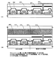
図33(A)は本願発明を用いたEL表示装置の上面図である。図33(A)において、4010は基板、4011は画素部、4012はソース側駆動回路、4013はゲート側駆動回路であり、それぞれの駆動回路は配線4014〜4016を経てFPC4017に至り、外部機器へと接続される。
【0198】
このとき、少なくとも画素部、好ましくは駆動回路及び画素部を囲むようにしてカバー材6000、シーリング材(ハウジング材ともいう)7000、密封材(第2のシーリング材)7001が設けられている。
【0199】
また、図33(B)は本実施例のEL表示装置の断面構造であり、基板4010、下地膜4021の上に駆動回路用TFT(但し、ここではnチャネル型TFTとpチャネル型TFTを組み合わせたCMOS回路を図示している。)4022及び画素部用TFT4023(但し、ここではEL素子への電流を制御するTFTだけ図示している。)が形成されている。これらのTFTは公知の構造(トップゲート構造またはボトムゲート構造)を用いれば良い。
【0200】
本願発明は、駆動回路用TFT4022、画素部用TF4023に際して用いることができる。
【0201】
本願発明を用いて駆動回路用TFT4022、画素部用TFT4023が完成したら、樹脂材料でなる層間絶縁膜(平坦化膜)4026の上に画素部用TFT4023のドレインと電気的に接続する透明導電膜でなる画素電極4027を形成する。透明導電膜としては、酸化インジウムと酸化スズとの化合物(ITOと呼ばれる)または酸化インジウムと酸化亜鉛との化合物を用いることができる。
そして、画素電極4027を形成したら、絶縁膜4028を形成し、画素電極4027上に開口部を形成する。
【0202】
次に、EL層4029を形成する。EL層4029は公知のEL材料(正孔注入層、正孔輸送層、発光層、電子輸送層または電子注入層)を自由に組み合わせて積層構造または単層構造とすれば良い。どのような構造とするかは公知の技術を用いれば良い。また、EL材料には低分子系材料と高分子系(ポリマー系)材料がある。低分子系材料を用いる場合は蒸着法を用いるが、高分子系材料を用いる場合には、スピンコート法、印刷法またはインクジェット法等の簡易な方法を用いることが可能である。
【0203】
本実施例では、シャドーマスクを用いて蒸着法によりEL層を形成する。シャドーマスクを用いて画素毎に波長の異なる発光が可能な発光層(赤色発光層、緑色発光層及び青色発光層)を形成することで、カラー表示が可能となる。その他にも、色変換層(CCM)とカラーフィルターを組み合わせた方式、白色発光層とカラーフィルターを組み合わせた方式があるがいずれの方法を用いても良い。
勿論、単色発光のEL表示装置とすることもできる。
【0204】
EL層4029を形成したら、その上に陰極4030を形成する。陰極4030とEL層4029の界面に存在する水分や酸素は極力排除しておくことが望ましい。従って、真空中でEL層4029と陰極4030を連続成膜するか、EL層4029を不活性雰囲気で形成し、大気解放しないで陰極4030を形成するといった工夫が必要である。本実施例ではマルチチャンバー方式(クラスターツール方式)の成膜装置を用いることで上述のような成膜を可能とする。
【0205】
なお、本実施例では陰極4030として、LiF(フッ化リチウム)膜とAl(アルミニウム)膜の積層構造を用いる。具体的にはEL層4029上に蒸着法で1nm厚のLiF(フッ化リチウム)膜を形成し、その上に300nm厚のアルミニウム膜を形成する。勿論、公知の陰極材料であるMgAg電極を用いても良い。そして陰極4030は4031で示される領域において配線4016に接続される。配線4016は陰極4030に所定の電圧を与えるための電源供給線であり、導電性ペースト材料4032を介してFPC4017に接続される。
【0206】
4031に示された領域において陰極4030と配線4016とを電気的に接続するために、層間絶縁膜4026及び絶縁膜4028にコンタクトホールを形成する必要がある。これらは層間絶縁膜4026のエッチング時(画素電極用コンタクトホールの形成時)や絶縁膜4028のエッチング時(EL層形成前の開口部の形成時)に形成しておけば良い。また、絶縁膜4028をエッチングする際に、層間絶縁膜4026まで一括でエッチングしても良い。この場合、層間絶縁膜4026と絶縁膜4028が同じ樹脂材料であれば、コンタクトホールの形状を良好なものとすることができる。
【0207】
このようにして形成されたEL素子の表面を覆って、パッシベーション膜6003、充填材6004、カバー材6000が形成される。
【0208】
さらに、EL素子部を囲むようにして、カバー材7000と基板4010の内側にシーリング材が設けられ、さらにシーリング材7000の外側には密封材(第2のシーリング材)7001が形成される。
【0209】
このとき、この充填材6004は、カバー材6000を接着するための接着剤としても機能する。充填材6004としては、PVC(ポリビニルクロライド)、エポキシ樹脂、シリコーン樹脂、PVB(ポリビニルブチラル)またはEVA(エチレンビニルアセテート)を用いることができる。この充填材6004の内部に乾燥剤を設けておくと、吸湿効果を保持できるので好ましい。
【0210】
また、充填材6004の中にスペーサーを含有させてもよい。このとき、スペーサーをBaOなどからなる粒状物質とし、スペーサー自体に吸湿性をもたせてもよい。
【0211】
スペーサーを設けた場合、パッシベーション膜6003はスペーサー圧を緩和することができる。また、パッシベーション膜とは別に、スペーサー圧を緩和する樹脂膜などを設けてもよい。
【0212】
また、カバー材6000としては、ガラス板、アルミニウム板、ステンレス板、FRP(Fiberglass−Reinforced Plastics)板、PVF(ポリビニルフルオライド)フィルム、マイラーフィルム、ポリエステルフィルムまたはアクリルフィルムを用いることができる。なお、充填材6004としてPVBやEVAを用いる場合、数十μmのアルミニウムホイルをPVFフィルムやマイラーフィルムで挟んだ構造のシートを用いることが好ましい。
【0213】
但し、EL素子からの発光方向(光の放射方向)によっては、カバー材6000が透光性を有する必要がある。
【0214】
また、配線4016はシーリング材7000および密封材7001と基板4010との隙間を通ってFPC4017に電気的に接続される。なお、ここでは配線4016について説明したが、他の配線4014、4015も同様にしてシーリング材7000および密封材7001の下を通ってFPC4017に電気的に接続される。
【0215】
[実施例16]
本実施例では、本願発明を用いて実施例15とは異なる形態のEL表示装置を作製した例について、図34(A)、(B)を用いて説明する。図33(A)、(B)と同じ番号のものは同じ部分を指しているので説明は省略する。
【0216】
図34(A)は本実施例のEL表示装置の上面図であり、図34(A)をA-A'で切断した断面図を図34(B)に示す。
【0217】
実施例15に従って、EL素子の表面を覆ってパッシベーション膜6003までを形成する。
【0218】
さらに、EL素子を覆うようにして充填材6004を設ける。この充填材6004は、カバー材6000を接着するための接着剤としても機能する。充填材6004としては、PVC(ポリビニルクロライド)、エポキシ樹脂、シリコーン樹脂、PVB(ポリビニルブチラル)またはEVA(エチレンビニルアセテート)を用いることができる。この充填材6004の内部に乾燥剤を設けておくと、吸湿効果を保持できるので好ましい。
【0219】
また、充填材6004の中にスペーサーを含有させてもよい。このとき、スペーサーをBaOなどからなる粒状物質とし、スペーサー自体に吸湿性をもたせてもよい。
【0220】
スペーサーを設けた場合、パッシベーション膜6003はスペーサー圧を緩和することができる。また、パッシベーション膜とは別に、スペーサー圧を緩和する樹脂膜などを設けてもよい。
【0221】
また、カバー材6000としては、ガラス板、アルミニウム板、ステンレス板、FRP(Fiberglass−Reinforced Plastics)板、PVF(ポリビニルフルオライド)フィルム、マイラーフィルム、ポリエステルフィルムまたはアクリルフィルムを用いることができる。なお、充填材6004としてPVBやEVAを用いる場合、数十μmのアルミニウムホイルをPVFフィルムやマイラーフィルムで挟んだ構造のシートを用いることが好ましい。
【0222】
但し、EL素子からの発光方向(光の放射方向)によっては、カバー材6000が透光性を有する必要がある。
【0223】
次に、充填材6004を用いてカバー材6000を接着した後、充填材6004の側面(露呈面)を覆うようにフレーム材6001を取り付ける。フレーム材6001はシーリング材(接着剤として機能する)6002によって接着される。このとき、シーリング材6002としては、光硬化性樹脂を用いるのが好ましいが、EL層の耐熱性が許せば熱硬化性樹脂を用いても良い。なお、シーリング材6002はできるだけ水分や酸素を透過しない材料であることが望ましい。また、シーリング材6002の内部に乾燥剤を添加してあっても良い。
【0224】
また、配線4016はシーリング材6002と基板4010との隙間を通ってFPC4017に電気的に接続される。なお、ここでは配線4016について説明したが、他の配線4014、4015も同様にしてシーリング材6002の下を通ってFPC4017に電気的に接続される。
【0225】
[実施例17]
実施例15および16のような構成からなるEL表示パネルにおいて、本願発明を用いることができる。画素部の詳細な断面構造を図35に、上面構造を図36(A)に、回路図を図36(B)に示す。図35、図36(A)及び図36(B)では共通の符号を用いるので互いに参照すれば良い。
【0226】
図35において、基板3501上に設けられたスイッチング用TFT3502は本願発明のnチャネル型TFTを用いて形成される(実施例1〜12参照)。
本実施例ではダブルゲート構造としているが、構造及び作製プロセスに大きな違いはないので説明は省略する。但し、ダブルゲート構造とすることで実質的に二つのTFTが直列された構造となり、オフ電流値を低減することができるという利点がある。なお、本実施例ではダブルゲート構造としているが、シングルゲート構造でも構わないし、トリプルゲート構造やそれ以上のゲート本数を持つマルチゲート構造でも構わない。また、本願発明のpチャネル型TFTを用いて形成しても構わない。
【0227】
また、電流制御用TFT3503は本願発明のnチャネル型TFTを用いて形成される。このとき、スイッチング用TFT3502のドレイン配線35は配線36によって電流制御用TFTのゲート電極37に電気的に接続されている。また、38で示される配線は、スイッチング用TFT3502のゲート電極39a、39bを電気的に接続するゲート配線である。
【0228】
このとき、電流制御用TFT3503が本願発明の構造であることは非常に重要な意味を持つ。電流制御用TFTはEL素子を流れる電流量を制御するための素子であるため、多くの電流が流れ、熱による劣化やホットキャリアによる劣化の危険性が高い素子でもある。そのため、電流制御用TFTのドレイン側に、ゲート絶縁膜を介してゲート電極に重なるようにLDD領域を設ける本願発明の構造は極めて有効である。
【0229】
また、本実施例では電流制御用TFT3503をシングルゲート構造で図示しているが、複数のTFTを直列につなげたマルチゲート構造としても良い。さらに、複数のTFTを並列につなげて実質的にチャネル形成領域を複数に分割し、熱の放射を高い効率で行えるようにした構造としても良い。このような構造は熱による劣化対策として有効である。
【0230】
また、図36(A)に示すように、電流制御用TFT3503のゲート電極37となる配線は3504で示される領域で、電流制御用TFT3503のドレイン配線40と絶縁膜を介して重なる。このとき、3504で示される領域ではコンデンサが形成される。このコンデンサ3504は電流制御用TFT3503のゲートにかかる電圧を保持するためのコンデンサとして機能する。なお、ドレイン配線40は電流供給線(電源線)3506に接続され、常に一定の電圧が加えられている。
【0231】
スイッチング用TFT3502及び電流制御用TFT3503の上には第1パッシベーション膜41が設けられ、その上に樹脂絶縁膜でなる平坦化膜42が形成される。平坦化膜42を用いてTFTによる段差を平坦化することは非常に重要である。後に形成されるEL層は非常に薄いため、段差が存在することによって発光不良を起こす場合がある。従って、EL層をできるだけ平坦面に形成しうるように画素電極を形成する前に平坦化しておくことが望ましい。
【0232】
また、43は反射性の高い導電膜でなる画素電極(EL素子の陰極)であり、電流制御用TFT3503のドレインに電気的に接続される。画素電極43としてはアルミニウム合金膜、銅合金膜または銀合金膜など低抵抗な導電膜またはそれらの積層膜を用いることが好ましい。勿論、他の導電膜との積層構造としても良い。
【0233】
また、絶縁膜(好ましくは樹脂)で形成されたバンク44a、44bにより形成された溝(画素に相当する)の中に発光層45が形成される。なお、ここでは一画素しか図示していないが、R(赤)、G(緑)、B(青)の各色に対応した発光層を作り分けても良い。発光層とする有機EL材料としてはπ共役ポリマー系材料を用いる。代表的なポリマー系材料としては、ポリパラフェニレンビニレン(PPV)系、ポリビニルカルバゾール(PVK)系、ポリフルオレン系などが挙げられる。
【0234】
なお、PPV系有機EL材料としては様々な型のものがあるが、例えば「H. Shenk,H.Becker,O.Gelsen,E.Kluge,W.Kreuder,and H.Spreitzer,“Polymers for Light Emitting Diodes”,Euro Display,Proceedings,1999,p.33-37」や特開平10−92576号公報に記載されたような材料を用いれば良い。
【0235】
具体的な発光層としては、赤色に発光する発光層にはシアノポリフェニレンビニレン、緑色に発光する発光層にはポリフェニレンビニレン、青色に発光する発光層にはポリフェニレンビニレン若しくはポリアルキルフェニレンを用いれば良い。膜厚は30〜150nm(好ましくは40〜100nm)とすれば良い。
【0236】
但し、以上の例は発光層として用いることのできる有機EL材料の一例であって、これに限定する必要はまったくない。発光層、電荷輸送層または電荷注入層を自由に組み合わせてEL層(発光及びそのためのキャリアの移動を行わせるための層)を形成すれば良い。
【0237】
例えば、本実施例ではポリマー系材料を発光層として用いる例を示したが、低分子系有機EL材料を用いても良い。また、電荷輸送層や電荷注入層として炭化珪素等の無機材料を用いることも可能である。これらの有機EL材料や無機材料は公知の材料を用いることができる。
【0238】
本実施例では発光層45の上にPEDOT(ポリチオフェン)またはPAni(ポリアニリン)でなる正孔注入層46を設けた積層構造のEL層としている。
そして、正孔注入層46の上には透明導電膜でなる陽極47が設けられる。本実施例の場合、発光層45で生成された光は上面側に向かって(TFTの上方に向かって)放射されるため、陽極は透光性でなければならない。透明導電膜としては酸化インジウムと酸化スズとの化合物や酸化インジウムと酸化亜鉛との化合物を用いることができるが、耐熱性の低い発光層や正孔注入層を形成した後で形成するため、可能な限り低温で成膜できるものが好ましい。
【0239】
陽極47まで形成された時点でEL素子3505が完成する。なお、ここでいうEL素子3505は、画素電極(陰極)43、発光層45、正孔注入層46及び陽極47で形成されたコンデンサを指す。図36Aに示すように画素電極43は画素の面積にほぼ一致するため、画素全体がEL素子として機能する。従って、発光の利用効率が非常に高く、明るい画像表示が可能となる。
【0240】
ところで、本実施例では、陽極47の上にさらに第2パッシベーション膜48を設けている。第2パッシベーション膜48としては窒化珪素膜または窒化酸化珪素膜が好ましい。この目的は、外部とEL素子とを遮断することであり、有機EL材料の酸化による劣化を防ぐ意味と、有機EL材料からの脱ガスを抑える意味との両方を併せ持つ。これによりEL表示装置の信頼性が高められる。
【0241】
以上のように本願発明のEL表示パネルは図35のような構造の画素からなる画素部を有し、オフ電流値の十分に低いスイッチング用TFTと、ホットキャリア注入に強い電流制御用TFTとを有する。従って、高い信頼性を有し、且つ、良好な画像表示が可能なEL表示パネルが得られる。
【0242】
なお、本実施例の構成は、実施例1〜12構成と自由に組み合わせて実施することが可能である。また、実施例14の電子機器の表示部として本実施例のEL表示パネルを用いることは有効である。
【0243】
[実施例18]
本実施例では、実施例17に示した画素部において、EL素子3505の構造を反転させた構造について説明する。説明には図37を用いる。なお、図35の構造と異なる点はEL素子の部分と電流制御用TFTだけであるので、その他の説明は省略することとする。
【0244】
図37において、電流制御用TFT3503は本願発明のpチャネル型TFTを用いて形成される。作製プロセスは実施例1〜12を参照すれば良い。
【0245】
本実施例では、画素電極(陽極)50として透明導電膜を用いる。具体的には酸化インジウムと酸化亜鉛との化合物でなる導電膜を用いる。勿論、酸化インジウムと酸化スズとの化合物でなる導電膜を用いても良い。
【0246】
そして、絶縁膜でなるバンク51a、51bが形成された後、溶液塗布によりポリビニルカルバゾールでなる発光層52が形成される。その上にはカリウムアセチルアセトネート(acacKと表記される)でなる電子注入層53、アルミニウム合金でなる陰極54が形成される。この場合、陰極54がパッシベーション膜としても機能する。こうしてEL素子3701が形成される。
【0247】
本実施例の場合、発光層52で発生した光は、矢印で示されるようにTFTが形成された基板の方に向かって放射される。
【0248】
なお、本実施例の構成は、実施例1〜12の構成と自由に組み合わせて実施することが可能である。また、実施例14の電子機器の表示部として本実施例のEL表示パネルを用いることは有効である。
【0249】
[実施例19]
本実施例では、図36(B)に示した回路図とは異なる構造の画素とした場合の例について図38(A)〜(C)に示す。なお、本実施例において、3801はスイッチング用TFT3802のソース配線、3803はスイッチング用TFT3802のゲート配線、3804は電流制御用TFT、3805はコンデンサ、3806、3808は電流供給線、3807はEL素子とする。
【0250】
図38(A)は、二つの画素間で電流供給線3806を共通とした場合の例である。即ち、二つの画素が電流供給線3806を中心に線対称となるように形成されている点に特徴がある。この場合、電源供給線の本数を減らすことができるため、画素部をさらに高精細化することができる。
【0251】
また、図38(B)は、電流供給線3808をゲート配線3803と平行に設けた場合の例である。なお、図38(B)では電流供給線3808とゲート配線3803とが重ならないように設けた構造となっているが、両者が異なる層に形成される配線であれば、絶縁膜を介して重なるように設けることもできる。この場合、電源供給線3808とゲート配線3803とで専有面積を共有させることができるため、画素部をさらに高精細化することができる。
【0252】
また、図38(C)は、図38(B)の構造と同様に電流供給線3808をゲート配線3803と平行に設け、さらに、二つの画素を電流供給線3808を中心に線対称となるように形成する点に特徴がある。また、電流供給線3808をゲート配線3803のいずれか一方と重なるように設けることも有効である。この場合、電源供給線の本数を減らすことができるため、画素部をさらに高精細化することができる。
【0253】
なお、本実施例の構成は、実施例1〜12、15または16の構成と自由に組み合わせて実施することが可能である。また、実施例14の電子機器の表示部として本実施例の画素構造を有するEL表示パネルを用いることは有効である。
【0254】
[実施例20]
実施例17に示した図36(A)、36(B)では電流制御用TFT3503のゲートにかかる電圧を保持するためにコンデンサ3504を設ける構造としているが、コンデンサ3504を省略することも可能である。実施例17の場合、電流制御用TFT3503として実施例1〜12に示すような本願発明のnチャネル型TFTを用いているため、ゲート絶縁膜を介してゲート電極に重なるように設けられたLDD領域を有している。この重なり合った領域には一般的にゲート容量と呼ばれる寄生容量が形成されるが、本実施例ではこの寄生容量をコンデンサ3504の代わりとして積極的に用いる点に特徴がある。
【0255】
この寄生容量のキャパシタンスは、上記ゲート電極とLDD領域とが重なり合った面積によって変化するため、その重なり合った領域に含まれるLDD領域の長さによって決まる。
【0256】
また、実施例19に示した図38(A)、(B)、(C)の構造においても同様に、コンデンサ3805を省略することは可能である。
【0257】
なお、本実施例の構成は、実施例1〜12、15〜19の構成と自由に組み合わせて実施することが可能である。また、実施例14の電子機器の表示部として本実施例の画素構造を有するEL表示パネルを用いることは有効である。
【0258】
[実施例21]
実施例1または実施例4で示したの液晶表示装置にはネマチック液晶以外にも様々な液晶を用いることが可能である。例えば、1998, SID, "Characteristics and Driving Scheme of Polymer-Stabilized Monostable FLCD Exhibiting Fast Response Time and High Contrast Ratio with Gray-Scale Capability" by H. Furue et al.や、1997, SID DIGEST, 841, "A Full-Color Thresholdless Antiferroelectric LCD Exhibiting Wide Viewing Angle with Fast Response Time" by T. Yoshida et al.や、1996, J. Mater. Chem. 6(4), 671-673, "Thresholdless antiferroelectricity in liquid crystals and its application to displays" by S. Inui et al.や、米国特許第5594569 号に開示された液晶を用いることが可能である。
【0259】
等方相−コレステリック相−カイラルスメクティックC相転移系列を示す強誘電性液晶(FLC)を用い、DC電圧を印加しながらコレステリック相−カイラルスメクティックC相転移をさせ、かつコーンエッジをほぼラビング方向に一致させた単安定FLCの電気光学特性を図39に示す。図39に示すような強誘電性液晶による表示モードは「Half−V字スイッチングモード」と呼ばれている。図39に示すグラフの縦軸は透過率(任意単位)、横軸は印加電圧である。
「Half−V字スイッチングモード」については、寺田らの”Half−V字スイッチングモードFLCD”、第46回応用物理学関係連合講演会講演予稿集、1999年3月、第1316頁、および吉原らの”強誘電性液晶による時分割フルカラーLCD”、液晶第3巻第3号第190頁に詳しい。
【0260】
図39に示されるように、このような強誘電性混合液晶を用いると、低電圧駆動かつ階調表示が可能となることがわかる。本願発明の液晶表示装置には、このような電気光学特性を示す強誘電性液晶も用いることができる。
【0261】
また、ある温度域において反強誘電相を示す液晶を反強誘電性液晶(AFLC)という。反強誘電性液晶を有する混合液晶には、電場に対して透過率が連続的に変化する電気光学応答特性を示す、無しきい値反強誘電性混合液晶と呼ばれるものがある。この無しきい値反強誘電性混合液晶は、いわゆるV字型の電気光学応答特性を示すものがあり、その駆動電圧が約±2.5V程度(セル厚約1μm〜2μm)のものも見出されている。
【0262】
また、一般に、無しきい値反強誘電性混合液晶は自発分極が大きく、液晶自体の誘電率が高い。このため、無しきい値反強誘電性混合液晶を液晶表示装置に用いる場合には、画素に比較的大きな保持容量が必要となってくる。よって、自発分極が小さな無しきい値反強誘電性混合液晶を用いるのが好ましい。
【0263】
なお、このような無しきい値反強誘電性混合液晶を本願発明の液晶表示装置に用いることによって低電圧駆動が実現されるので、低消費電力化が実現される。
【0264】
【発明の効果】
本願発明を実施することで、画素マトリクス回路の画素TFTに15〜20Vのゲート電圧を印加して駆動させても、安定した動作を得ることができる。その結果、結晶質TFTで作製されたCMOS回路を含む半導体装置、また、具体的には液晶表示装置やEL表示装置などの画素マトリクス回路や、その周辺に設けられる駆動回路の信頼性を高め、長時間の使用に耐える液晶表示装置やEL表示装置を得ることができる。
【図面の簡単な説明】
【図1】本実施形態のTFTの断面図。
【図2】TFTの作製工程を示す断面図。
【図3】TFTの作製工程を示す断面図。
【図4】TFTの作製工程を示す断面図。
【図5】TFTの作製工程を示す断面図。
【図6】TFTの作製工程を示す断面図。
【図7】アクティブマトリクス基板の斜視図。
【図8】画素マトリクス回路とCMOS回路の上面図
【図9】結晶質シリコン膜の作製工程を示す図。
【図10】結晶質シリコン膜の作製工程を示す図。
【図11】結晶質シリコン膜の作製工程を示す図。
【図12】結晶質シリコン膜の作製工程を示す図。
【図13】TFTの作製工程を示す断面図。
【図14】ゲート電極の構成を示す図。
【図15】電子機器の一例を示す図。
【図16】ゲート電極の構成を示す図。
【図17】TFTの構造と電気的特性を説明する図。
【図18】ゲート電極の構成を示す図。
【図19】TFTの作製工程を示す断面図。
【図20】シュミレーションの基本構造を示す図。
【図21】チャネル長方向の電界強度分布のシュミレーション結果の図。
【図22】ゲート電圧―ドレイン電流特性のシュミレーション結果の図。
【図23】電子・ホール濃度分布のシュミレーション結果の図。
【図24】電子・ホール濃度分布のシュミレーション結果の図。
【図25】電子・ホール電流密度分布のシュミレーション結果の図。
【図26】電子・ホール電流密度分布のシュミレーション結果の図。
【図27】プロジェクターの構成を説明する図。
【図28】本実施形態のTFTの断面図。
【図29】TFTの作製工程を示す断面図。
【図30】TFTの作製工程を示す断面図。
【図31】ゲート電極の構成を示す図。
【図32】レーザーアニール装置の構成を説明する図。
【図33】アクティブマトリクス型のEL表示装置の構成を示す図。
【図34】アクティブマトリクス型のEL表示装置の構成を示す図。
【図35】アクティブマトリクス型のEL表示装置の画素部の構成を示す断面図。
【図36】アクティブマトリクス型のEL表示装置の画素部の構成を示す上面図と回路図。
【図37】アクティブマトリクス型のEL表示装置の画素部の構成を示す断面図。
【図38】アクティブマトリクス型のEL表示装置の画素部の構成を示す回路図。
【図39】反強誘電性混合液晶の光透過率特性の一例を示す図。
【図40】電子機器の一例を示す図。[0001]
BACKGROUND OF THE INVENTION
The present invention relates to a semiconductor device having a circuit formed of a thin film transistor over a substrate having an insulating surface and a manufacturing method thereof. For example, the present invention relates to an electro-optical device typified by a liquid crystal display device and a configuration of an electronic apparatus equipped with the electro-optical device. Note that in this specification, a semiconductor device refers to all devices that function by utilizing semiconductor characteristics, and includes the above-described electro-optical device and electronic devices in which the electro-optical device is mounted.
[0002]
[Prior art]
Since thin film transistors (hereinafter referred to as TFTs) can be manufactured on a transparent glass substrate, application development to active matrix liquid crystal display devices has been actively promoted. A TFT having a semiconductor film having a crystal structure as an active layer (hereinafter referred to as a crystalline TFT) can obtain high mobility, so that a high-definition image display can be realized by integrating functional circuits on the same substrate. It became possible.
[0003]
In the specification of the present application, the semiconductor film having the crystal structure includes a single crystal semiconductor, a polycrystalline semiconductor, and a microcrystalline semiconductor, and further includes Japanese Patent Application Laid-Open Nos. H7-130652, H8-78329, and H10. -135468 or the semiconductor disclosed in Japanese Patent Application Laid-Open No. 10-135469.
[0004]
In order to construct an active matrix type liquid crystal display device, it is necessary to provide one to two million crystalline TFTs with only a pixel matrix circuit, and if a functional circuit provided in the periphery is further added, a larger number of crystalline TFTs are required. Was necessary. In order to stably operate the liquid crystal display device, it is necessary to ensure the reliability of each crystalline TF.
[0005]
The characteristics of a field effect transistor such as a TFT are ideal for a linear region where the drain current and drain voltage increase proportionally, a saturation region where the drain current saturates even when the drain voltage increases, and a drain voltage applied Can be divided into a cut-off region where no current flows. In this specification, the linear region and the saturation region are referred to as the TFT on region, and the blocking region is referred to as the off region. For convenience, the drain current in the on region is referred to as on-current, and the current in the off region is referred to as off-current.
[0006]
The pixel matrix circuit of the active matrix liquid crystal display device is composed of n-channel TFTs (hereinafter referred to as pixel TFTs), and a gate voltage having an amplitude of about 15 to 20 V is applied thereto. It was necessary to satisfy both characteristics. On the other hand, the peripheral circuit provided for driving the pixel matrix circuit is configured based on a CMOS circuit, and the on-region characteristics are mainly important. However, the crystalline TFT has a problem that the off-current tends to increase. When the crystalline TFT is driven for a long period of time, deterioration phenomena such as a decrease in mobility, an on-current, and an increase in off-current are often observed. One of the causes is considered to be a hot carrier injection phenomenon that occurs due to a high electric field near the drain.
[0007]
In the LSI technical field, a lightly doped drain (LDD) structure is known as a method for reducing the off-current of a MOS transistor and further mitigating a high electric field in the vicinity of the drain. In this structure, a low concentration impurity region is provided between a drain region and a channel formation region, and this low concentration impurity region is called an LDD region.
[0008]
Similarly, it has been known that a crystalline TFT forms an LDD structure. In the conventional technique, a low-concentration impurity region that becomes an LDD region is formed by adding a first impurity element using a gate electrode as a mask, and then an anisotropic etching technique is used on both sides of the gate electrode. In this method, sidewalls are formed, and a high concentration impurity region to be a source region and a drain region is formed by adding a second impurity element using the gate electrode and the sidewall as a mask.
[0009]
However, the LDD structure has a drawback in that, even if the off-current can be reduced, the series resistance component increases structurally, and as a result, the on-current of the TFT also decreases. It was. Moreover, the deterioration of the on-current could not be prevented completely. As a method for compensating for this drawback, a structure is known in which the LDD region is overlapped with a gate electrode through a gate insulating film. There are several methods for forming this structure. For example, it is known as GOLD (Gate-drain Overlapped LDD) or LATID (Large-tilt-angle implanted drain). With such a structure, the high electric field in the vicinity of the drain was relaxed to increase the hot carrier resistance, and at the same time, a decrease in on-current could be prevented.
[0010]
Also, in the case of a crystalline TFT, compared to a crystalline TFT having a simple structure formed only from a source region, a drain region, and a channel region, by providing an LDD structure, resistance to hot carriers is improved, and furthermore, a GOLD structure is adopted. It was confirmed that an extremely excellent effect was obtained ("A Novel Self-aligned Gate-overlapped LDD Poly-Si TFT with High Reliability and Performance", Mutsuko Hatano, Hajime Akimoto and Takeshi Sakai, IEDM97-523).
[0011]
[Problems to be solved by the invention]
In a crystalline TFT, it is an effective means to form an LDD structure in order to suppress the hot carrier injection phenomenon. Further, when the GOLD structure is used, it is possible to prevent a decrease in on-current observed in the LDD structure. Also, good results are obtained from the viewpoint of reliability.
[0012]
As described above, in order to achieve high reliability with the crystalline TFT, it is necessary to study from the structure side of the element. For this reason, it is desirable to form a GOLD structure. However, in the conventional method, the LDD region can be formed in a self-aligning manner. However, the step of forming the sidewall film by anisotropic etching is to process a large-area glass substrate like a liquid crystal display device. Was unsuitable. In addition, since the length of the LDD region is determined by the width of the side wall, the degree of freedom in device design is extremely limited.
[0013]
A first object of the present invention is to provide a technique for overcoming such problems, and a crystal having a structure in which a gate electrode and an LDD region are overlapped by a simpler method than the conventional technique. The object is to provide a technique for producing a quality TFT.
[0014]
Although the GOLD structure can prevent the on-current from deteriorating, the off-current may increase when a high gate voltage is applied in the off region, particularly in the case of an n-channel TFT constituting a pixel matrix circuit. is there. When the off-current increases in the pixel TFT of the pixel matrix circuit, there arises a problem that power consumption increases and abnormality appears in image display. This is considered to be because an inversion layer is formed in the LDD region which is formed in the off region so as to overlap the gate electrode, thereby creating a hole passage. In such a case, the operating range of the TFT becomes narrow and limited.
[0015]
A second object of the present invention is to provide a structure for preventing an increase in off-current so that the operating range can be expanded in a crystalline TFT having a structure in which a gate electrode and an LDD region overlap each other, and a method for manufacturing the same. The second purpose is to provide the above.
[0016]
[Means for Solving the Problems]
FIG. 17 schematically shows the structure of the TFT and the Vg-Id (gate voltage-drain current) characteristics obtained at that time, based on the knowledge thus far. FIG. 17A-1 illustrates the simplest TFT structure in which a semiconductor layer includes a channel formation region, a source region, and a drain region. (B-1) shows the characteristics of this TFT. The + Vg side is the on region of the TFT and the -Vg side is the off region. The solid line indicates the initial characteristics, and the broken line indicates the deterioration characteristics due to the hot carrier injection phenomenon. In this structure, both the on-current and the off-current are high and the deterioration is large, so that it cannot be used as it is, for example, in the pixel TFT of the pixel matrix circuit.
[0017]
FIG. 17A-2 illustrates a structure in which a low-concentration impurity region serving as an LDD region is provided in (A-1) and does not overlap with the gate electrode. FIG. 2B-2 shows the characteristics of this TFT, which can suppress the off current to some extent, but cannot prevent the deterioration of the on current. FIG. 17A-3 shows a structure in which the LDD region completely overlaps with the gate electrode, which is also called a GOLD structure. FIG. 5B-3 shows characteristics corresponding to this, and the degradation can be suppressed to a level that does not cause a problem, but the off-current is increased on the −Vg side as compared with the structure of (A-2).
[0018]
On the other hand, the structure shown in FIG. 17A-4 can prevent deterioration and suppress an increase in off-state current as shown in FIG. 17B-4. This is an LDD region divided into two regions, a region overlapping with the gate electrode and a region not overlapping, suppressing the hot carrier injection phenomenon in the LDD region overlapping with the gate electrode, and The LDD region that does not overlap with the gate electrode also has an effect of preventing an increase in off current.
[0019]
In the present invention, in order to realize a TFT having a structure as shown in FIG. 17A-3 or A-4, an LDD region overlaps with a gate electrode in an n-channel TFT. Therefore, a gate electrode is formed from a first conductive layer and a second conductive layer, and after forming the first conductive layer, an impurity element imparting the n-type for the first time is added to form an LDD region. After the first impurity region is formed and the second conductive layer is formed, a second step of adding an impurity element imparting n-type is performed to form a second impurity region as a source region and a drain region To do. In this way, a structure in which the LDD region overlaps with the gate electrode is realized. Further, in order to provide an LDD region that does not overlap with the gate electrode, part of the second conductive layer may be removed.
[0020]
On the other hand, a p-channel TFT similarly has a gate electrode formed of a first conductive layer and a second conductive layer, but has a structure in which part of a third impurity region serving as a source region and a drain region overlaps with the gate electrode. And
[0021]
The first conductive layer is formed using one or more elements selected from titanium (Ti), tantalum (Ta), tungsten (W), and molybdenum (Mo), or a material containing the element as a component. In the structure, at least one conductive layer (A) made of the above material and formed in contact with the gate insulating film, and one or more selected from aluminum (Al) and copper (Cu) on the conductive layer (A) It is preferable to form the conductive layer (B) made of the above element or a material containing the element as a component.
[0022]
The second conductive layer is formed of one or more elements selected from titanium (Ti), tantalum (Ta), tungsten (W), and molybdenum (Mo), or an alloy material containing the element as a component.
[0023]
Further, in the structure of the pixel matrix circuit, a semiconductor layer that is provided in contact with the second impurity region of the pixel TFT and includes the impurity element at the same concentration as the first impurity region, and the same layer as the gate insulating film are formed. A storage capacitor is formed from the insulating layer and the capacitor wiring formed on the insulating layer. Alternatively, a semiconductor layer provided in contact with the second impurity region of the pixel TFT and containing the impurity element at the same concentration as the third impurity region, an insulating layer formed of the same layer as the gate insulating film, and the insulating layer A storage capacitor is formed from the capacitor wiring formed on the layer.
[0024]
DETAILED DESCRIPTION OF THE INVENTION
[Embodiment 1]
An embodiment of the present invention will be described with reference to FIG. The
[0025]
The semiconductor layer formed on the
[0026]
Alternatively, the semiconductor layer formed over the
[0027]
FIG. 28 shows a cross-sectional structure of n-channel and p-channel TFTs formed on the
[0028]
The conductive layers (A) 313 and 316 constituting the first conductive layer are elements such as titanium (Ti), tantalum (Ta), molybdenum (Mo), tungsten (W), or a material containing these elements as components. Form. The conductive layers (B) 314 and 317 may be made of aluminum (Al) or copper (Cu) with low resistivity. Here, the conductive layer (B) is provided in consideration of forming the TFT of the present invention on a large-area substrate such as a liquid crystal display device, and is provided for the purpose of reducing the resistance of the gate electrode and the gate wiring. . Therefore, depending on the application, the first conductive layer may be formed of only the conductive layer (A), or another conductive layer may be stacked on the conductive layer (B).
[0029]
The second
[0030]
The semiconductor layer of the n-channel TFT includes a
[0031]
The length of the
[0032]
In the
[0033]
On the other hand, an impurity element imparting p-type conductivity is added to the
[0034]
As described above, in the present invention, in the TFT structure, the gate electrode is provided with the first conductive layer, and the second conductive layer is provided thereon. As shown in FIG. 28, the gate insulating film and the second conductive layer are provided. The first conductive layer located between the conductive layers has an end formed inside the end of the second conductive layer. In addition, the structure in which the first impurity region provided in the semiconductor layer and the second conductive layer are provided to overlap each other has a feature, and the manufacturing method has a feature.
[0035]
The TFT shown in FIG. 28 has a structure in which first low-
[0036]
On the other hand, the p-channel TFT is not provided with such a low concentration impurity region having an LDD structure. Of course, a structure in which a low-concentration impurity region is provided may be used. However, since the p-channel TFT is originally highly reliable, it is preferable to gain on-current and balance the characteristics with the n-channel TFT. When the present invention is applied to a CMOS circuit as shown in FIG. 28, it is particularly important to balance this characteristic. However, there is no problem even if the structure of the present invention is applied to a p-channel TFT.
[0037]
When the n-channel TFT and the p-channel TFT are thus completed, the
The second interlayer insulating film need not be limited to a resin material. For example, when applied to a liquid crystal display device, it is preferable to use a resin material in order to ensure surface flatness.
[0038]
In FIG. 28, a CMOS circuit formed by complementary combination of an n-channel TFT and a p-channel TFT is shown as an example. However, the present invention is applied to an NMOS circuit using an n-channel TFT or a pixel matrix circuit of a liquid crystal display device. The invention can also be applied.
[0039]
[Embodiment 2]
An embodiment of the present invention will be described with reference to FIG. The
[0040]
A
[0041]
The semiconductor layer formed on the
[0042]
FIG. 1 shows cross-sectional structures of an n-channel TFT and a p-channel TFT. The gate electrodes of the n-channel TFT and the p-channel TFT are composed of a first conductive layer and a second conductive layer. The first conductive layer has a three-layer structure. Conductive layers (A) 111 and 115 provided in contact with the
[0043]
The conductive layers (A) 111 and 115 constituting the first conductive layer are formed of an element such as Ti, Ta, Mo, W, or an alloy material containing these elements as a main component. Alternatively, a nitride, oxide, or silicide of these elements may be used. The conductive layers (B) 112 and 116 are preferably made of Al or Cu having a low resistivity. Similarly to the conductive layer (A), the conductive layers (C) 113 and 117 are formed of an element such as Ti, Ta, Mo, W, or an alloy material containing these elements as a main component. Here, the conductive layer (B) is used for the purpose of reducing the resistance of the gate electrode and the gate wiring connected to the gate electrode in consideration of forming the TFT of the present invention on a large-area substrate such as a liquid crystal display device. It is provided. Depending on the application, the first conductive layer may be formed of only the conductive layer (A), or three or more layers may be laminated.
[0044]
The second
[0045]
Here, in the present invention, the length L1 of the first conductive layer is 0.2 to 10 μm, preferably 0.4 to 5 μm, and the length L2 of the second conductive layer is 1.2 to 16 μm, preferably 2 It is desirable to form with a length of 2 to 11 μm. Here, the length L5 for removing the second conductive layer is 0.5 to 3 μm, preferably 1.0 to 2.0 μm.
[0046]
The first conductive layer and the second conductive layer function as a mask in the first step of adding the first conductive type impurity element and the second step of adding the first conductive type impurity element. It is necessary to determine the lengths of L1 and L3 and L2 and L5 in consideration of the points. The length of the LDD region of the n-channel TFT is formed by the length of the difference between L3 and L1. In order to obtain the configuration of the present invention, the second conductive layer is formed in advance with a length of L3, and then the length of L2 is removed by etching to remove the length of L2. This is because the region where the first impurity region 1605 to be a region overlaps with the second conductive layer through the gate insulating film has a length of L4, and a region which does not overlap has a length of L5.
[0047]
In FIG. 1, a semiconductor layer of an n-channel TFT is provided in contact with a
[0048]
The length of the
[0049]
At this time, the
[0050]
On the other hand, the
[0051]
As described above, the TFT of the present invention has a structure in which the gate electrode is provided with the first conductive layer and the second conductive layer. As shown in FIG. The conductive layer is in contact with the gate insulating film. At least in the n-channel TFT, there is a feature in a structure in which a part of the first impurity region is provided so as to overlap with a region in contact with the gate insulating film of the second conductive layer.
[0052]
In the structure shown in FIG. 1, a first impurity region that becomes an LDD region is formed using the first conductive layer as a mask, and a second impurity that becomes a source region and a drain region using the second conductive layer as a mask. After forming the region, it can be realized by retracting the second conductive layer by an etching process. Therefore, as shown in FIG. 16, the length of the LDD region is determined by the length L1 of the first conductive layer and the length L3 of the second conductive layer, and the LDD region does not overlap with the second conductive layer. The length can be determined by the length L5 for etching the second conductive layer. Such a method can increase the degree of freedom in designing or manufacturing a TFT, and is very effective.
[0053]
On the other hand, the
[0054]
When the n-channel TFT and the p-channel TFT are thus completed, the
[0055]
In FIG. 1, a CMOS circuit formed by complementary combination of an n-channel TFT and a p-channel TFT is shown as an example. However, the present invention is applied to an NMOS circuit using an n-channel TFT or a pixel matrix circuit of a liquid crystal display device. The invention can also be applied.
[0056]
The configuration of the present invention described above will be described in more detail in the following examples.
[0057]
[Example 1]
In this embodiment, an example in which the structure of the present invention is applied to a liquid crystal display device is shown, and a method of simultaneously manufacturing a pixel matrix circuit and a CMOS circuit which is a basic form of a driver circuit provided in the periphery thereof is shown in FIGS. Will be described.
[0058]
In FIG. 29A, an alkali-free glass substrate typified by a Corning 1737 glass substrate is used as the
[0059]
Next, an amorphous silicon film having a thickness of 50 nm is formed on the
[0060]
For this crystallization step, a laser annealing technique or a thermal annealing technique may be used. In this embodiment, a pulsed oscillation type KrF excimer laser beam is condensed into a linear shape and irradiated to an amorphous silicon film to form a crystalline silicon film.
[0061]
The configuration of the laser annealing apparatus used here is shown in FIG. The pulsed laser beam irradiated from the
[0062]
In this embodiment, the crystalline silicon film is formed from the amorphous silicon film. However, the microcrystalline silicon film may be crystallized by a laser annealing method, or the crystalline silicon film may be directly formed. .
[0063]
The crystalline silicon film thus formed is patterned to form island-like semiconductor layers 403, 404, and 405.
[0064]
Next, a
[0065]
When Al is used as the conductive layer (B) constituting the first conductive layer, pure Al may be used, and an element selected from Ti, Si, and Sc is added in an amount of 0.1 to 5 atomic%. Al alloy may also be used. In the case of using Cu, although not shown, it is preferable to provide a silicon nitride film on the surface of the
[0066]
In FIG. 29, a storage capacitor is provided on the drain side of the pixel TFT of the pixel matrix circuit. At this time, the
[0067]
When the structure shown in FIG. 29A is thus formed, a first step of adding an impurity element imparting n-type conductivity is performed. Phosphorus (P), arsenic (As), antimony (Sb), and the like are known as impurity elements that impart n-type to crystalline conductor materials. Here, phosphine (PH) Three Phosphorus is added by an ion doping method using In this step, in order to add phosphorus to the semiconductor layer thereunder through the
[0068]
The impurity element added to the semiconductor layer needs to be activated by a laser annealing method or a thermal annealing method. This step may be performed after the step of adding the impurity element for forming the source region and the drain region, but it is effective to activate at this stage by a laser annealing method.
[0069]
In this step, the conductive layers (A) 407, 408, 409, and 410 and the conductive layers (B) 412, 413, 414, and 415 constituting the first conductive layer function as a mask against the addition of phosphorus. As a result, no or almost no phosphorus is added to the region immediately below the first conductive layer of the semiconductor layer existing through the gate insulating film. Then, as shown in FIG. 29B,
[0070]
Next, using the photoresist as a mask, the region for forming the n-channel TFT is covered with resist
[0071]
Then, after removing the resist
[0072]
In addition, a storage capacitor is provided on the drain side of the pixel TFT of the pixel matrix circuit, and the
[0073]
Then, a second step of adding an impurity element imparting n-type conductivity is performed using the second
[0074]
Although not shown here, the gate insulating film covering the
[0075]
Further, phosphorus is added to the
[0076]
Since the impurity element imparting n-type or p-type added at each concentration is not activated as it is and does not act effectively, it is necessary to perform an activation process. This step can be performed by a thermal annealing method using an electric heating furnace, a laser annealing method using the above-described excimer laser, or a rapid thermal annealing method (RTA method) using a halogen lamp.
[0077]
In the thermal annealing method, activation is performed by heating at 550 ° C. for 2 hours in a nitrogen atmosphere. In this embodiment, Al is used for the conductive layer (B) constituting the first conductive layer, but the conductive layer (A) formed of Ta and the second conductive layer are formed so as to cover the Al. , Ta functions as a blocking layer, and Al atoms can be prevented from diffusing into other regions. In the laser annealing method, activation is performed by condensing and irradiating a pulse oscillation type KrF excimer laser beam in a line with an apparatus having the same configuration as that shown in FIG. Further, better results can be obtained when the thermal annealing method is performed after the laser annealing method. This process also has the effect of annealing a region where the crystallinity is destroyed by ion doping, and can improve the crystallinity of the region.
[0078]
Through the above steps, the gate electrode is provided with the first conductive layer and the second conductive layer is provided so as to cover the first conductive layer. In the n-channel TFT, the source region is formed on both sides of the second conductive layer. And a drain region are formed. In addition, a structure in which the first impurity region provided in the semiconductor layer through the gate insulating film overlaps with the region in contact with the gate insulating film of the second conductive layer is formed in a self-aligned manner. . On the other hand, in the p-channel type TFT, a part of the source region and the drain region overlaps with the second conductive layer, but there is no problem in practical use.
[0079]
When the state of FIG. 29D is obtained, a first
[0080]
The first
[0081]
Thus, as shown in FIG. 29E, a CMOS circuit and a pixel matrix circuit are formed over the
[0082]
Next, a process of manufacturing an active matrix liquid crystal display device based on a CMOS circuit and a pixel matrix circuit manufactured on the same substrate by the above process will be described with reference to FIGS. First, a
[0083]
Next, a
[0084]
After the
[0085]
Etching treatment of the material of the transparent conductive film is performed with a hydrochloric acid based solution. However, since etching of ITO tends to generate residues, an indium oxide-zinc oxide alloy (In 2 O Three —ZnO) may also be used. Indium zinc oxide alloy is characterized by excellent surface smoothness and thermal stability compared to ITO. Similarly, zinc oxide (ZnO) is also a suitable material, and zinc oxide (ZnO: Ga) to which gallium (Ga) is added to further increase the transmittance and conductivity of visible light can be used.
[0086]
When the state of FIG. 30A is formed, an alignment film 460 is formed. Usually, a polyimide resin is often used for the alignment film of the liquid crystal display element. A transparent
[0087]
Through the above steps, the substrate on which the pixel matrix circuit and the CMOS circuit are formed and the counter substrate are bonded to each other through a sealing material, a spacer (both not shown) and the like by a known cell assembling process. Thereafter, a
[0088]
[Example 2]
In this embodiment, the structure of the present invention will be described as a method for simultaneously manufacturing a CMOS circuit which is a basic form of a pixel matrix circuit and a driver circuit provided in the periphery thereof.
[0089]
In FIG. 2, as the
[0090]
The base film 202 may be formed of one layer of the above material or a stacked structure of two or more layers. In any case, it is formed to have a thickness of about 100 to 300 nm. For example, SiH by plasma CVD method Four , NH Three , N 2 A first silicon oxynitride film made of O is formed to a thickness of 10 to 100 nm, and SiH Four , N 2 The
[0091]
The first silicon oxynitride film is formed by using a conventional parallel plate type plasma CVD method. The silicon oxynitride film is SiH Four 10SCCM, NH Three To 100 SCCM, N 2 O was introduced into the reaction chamber as 20 SCCM, the substrate temperature was 325 ° C., the reaction pressure was 40 Pa, and the discharge power density was 0.41 W / cm. 2 The discharge frequency was 60 MHz. On the other hand, the second silicon oxynitride film is made of SiH. Four 4SCCM, N 2 O was introduced into the reaction chamber as 400 SCCM, the substrate temperature was 400 ° C., the reaction pressure was 40 Pa, and the discharge power density was 0.41 W / cm. 2 The discharge frequency was 60 MHz. These films can be formed continuously only by changing the substrate temperature and switching the reaction gas. The first silicon oxynitride film is formed so that the internal stress becomes a tensile stress with the substrate as the center. The second silicon oxynitride film is also given an internal stress in the same direction, but the stress is smaller than the first silicon oxynitride film in terms of absolute value.
[0092]
Next, an amorphous silicon film having a thickness of 30 to 80 nm, for example 50 nm, is formed on the base film 202 by plasma CVD. Thereafter, although depending on the amount of hydrogen contained in the amorphous silicon film, it is desirable to perform a dehydrogenation treatment by heating to 400 to 500 ° C., and to perform a crystallization step with the amount of hydrogen contained being 5 atomic% or less. .
[0093]
The step of crystallizing the amorphous silicon film is performed by a laser annealing method or a thermal annealing method. In this embodiment, a pulse oscillation type KrF excimer laser beam is condensed into a linear shape and irradiated to an amorphous silicon film to form a crystalline silicon film.
[0094]
In this embodiment, an amorphous silicon film is used. However, a microcrystalline silicon film may be used, or a crystalline silicon film may be directly formed.
[0095]
The crystalline silicon film thus formed is patterned to form island-shaped semiconductor layers 204, 205, and 206.
[0096]
Next, a gate insulating film 203 containing silicon oxide or silicon nitride as a main component is formed so as to cover the semiconductor layers 204, 205, and 206. For example, a silicon oxynitride film is formed to a thickness of 100 nm by plasma CVD. Although not illustrated in the figure, a Ta film is formed as a conductive layer (A) constituting a first conductive layer of the gate electrode on the surface of the gate insulating film 203 to a thickness of 10 to 200 nm, for example, 50 nm, and a conductive layer. As (B), an Al film was formed by sputtering at a thickness of 100 to 1000 nm, for example, 200 nm. Then, conductive layers (A) 207, 208, 209 and 210 and conductive layers (B) 212, 213, 214 and 215 constituting the first conductive layer are formed by a known patterning technique. At this time, the length L1 of the first conductive layer shown in FIG. 16 may be determined as appropriate, and patterning is performed with a length of 0.2 to 10 μm, here 3 μm (FIG. 2A).
[0097]
When Al is used as the conductive layer (B) constituting the first conductive layer, pure Al may be used, and an element selected from Ti, Si, and Sc is added in an amount of 0.1 to 5 atomic%. Al alloy may also be used. In the case of using copper, although not shown, it is preferable to provide a silicon nitride film with a thickness of 30 to 100 nm on the surface of the gate insulating film 203.
[0098]
When a Ta film is used for the conductive layers (A) 207, 208, 209, and 210, they can be similarly formed by sputtering. The Ta film uses Ar as a sputtering gas. In addition, when an appropriate amount of Xe or Kr is added to these sputtering gases, the internal stress of the film to be formed can be relaxed and the film can be prevented from peeling. The resistivity of the α-phase Ta film is about 20 μΩcm and can be used as a gate electrode, but the resistivity of the β-phase Ta film is about 180 μΩcm and is not suitable for a gate electrode. However, since the TaN film has a crystal structure close to an α phase, an α phase Ta film can be easily obtained by forming a Ta film thereon. Therefore, although not shown, a TaN film having a thickness of 10 to 50 nm may be formed under the conductive layers (A) 207, 208, 209, and 210. Similarly, although not shown, it is effective to form a silicon film doped with phosphorus (P) with a thickness of about 2 to 20 nm under the conductive layer (A). This improves adhesion and prevents oxidation of the conductive film formed thereon, and at the same time, the alkali metal element contained in a trace amount in the conductive layer (A) or the conductive layer (B) diffuses into the gate insulating film 203. Can be prevented. In any case, the conductive layer (A) preferably has a resistivity in the range of 10 to 50 μΩcm.
[0099]
In addition, it is also possible to use a W film for the conductive layers (A) 207, 208, 209, and 210, in which case argon (Ar) gas and nitrogen (N 2 ) Gas is introduced to form the conductive layer (A) with a W film to a thickness of 200 nm. In addition, W film is made of tungsten hexafluoride (WF 6 Can also be formed by a thermal CVD method. In any case, in order to use as a gate electrode, it is necessary to reduce the resistance, and the resistivity of the W film is desirably 20 μΩcm or less.
The resistivity of the W film can be reduced by increasing the crystal grains. However, when there are many impurity elements such as oxygen in the W film, the crystallization is hindered and the resistance is increased. Therefore, in the case of sputtering, the resistivity is obtained by using a W target with a purity of 99.9999% and forming a W film with sufficient consideration so that impurities are not mixed in the gas phase during film formation. 9-20 μΩcm can be realized.
[0100]
In FIG. 2, a storage capacitor is provided on the drain side of the pixel TFT of the pixel matrix circuit. At this time, wirings 211 and 216 having storage capacitors are formed using the same material as the first conductive layer.
[0101]
After the structure shown in FIG. 2A is formed in this manner, a first impurity region imparting n-type conductivity is added to form a first impurity region. Phosphorus (P), arsenic (As), antimony (Sb), and the like are known as impurity elements that impart n-type to crystalline semiconductor materials. For example, phosphorous is used to form phosphine (PH Three ) Using an ion doping method. In this step, the acceleration voltage was set as high as 80 keV in order to add phosphorus to the underlying semiconductor layer through the gate insulating film 203. The first impurity region formed in this way forms the
[0102]
The impurity element added to the semiconductor layer needs to be activated by a laser annealing method or a thermal annealing method. This step may be performed after the step of adding an impurity element for forming a source region and a drain region, but it is effective to activate at this stage by a laser annealing method.
[0103]
In this step, the conductive layers (A) 207, 208, 209, and 210 and the conductive layers (B) 212, 213, 214, and 215 included in the first conductive layer function as a mask with respect to the addition of phosphorus. As a result, no or almost no phosphorus is added to the region of the semiconductor layer overlapping the first conductive layer. Here, as shown in FIG. 2B,
[0104]
Next, using the photoresist film as a mask, the region for forming the n-channel TFT is covered with the resist
[0105]
Then, after removing the resist
[0106]
In addition, a storage capacitor is provided on the drain side of the n-channel TFT (pixel TFT) constituting the pixel matrix circuit, and the
[0107]
Then, using the second
[0108]
Although not shown here, the gate insulating film covering the
[0109]
Further, phosphorus is added to the
[0110]
When the state of FIG. 3A is obtained, the resist
[0111]
Then, the unmasked region of the second conductive layer is removed by etching.
Etching may be performed using ordinary dry etching technology, and CF Four And O 2 Use gas. Then, as shown in FIG. 3C, the length L5 is removed. The length of L5 may be appropriately adjusted in the range of 0.5 to 3 μm, and here it is 1.5 μm. As a result, in the n-channel TFT, a region overlapping with the second conductive layer is formed with a length of 1.5 μm (L4) out of the length of 3 μm of the first impurity region serving as the LDD region, and 1.5 μm. A region which does not overlap with the second conductive layer with a length of (L5) could be formed.
[0112]
Since the impurity element imparting n-type or p-type added at each concentration is not activated as it is and does not act effectively, it is necessary to perform an activation process. This step can be performed by a thermal annealing method using an electric heating furnace, a laser annealing method using the above-described excimer laser, or a rapid thermal annealing method (RTA method) using a halogen lamp.
[0113]
In the thermal annealing method, activation is performed by heat treatment in a nitrogen atmosphere at 300 to 700 ° C., preferably 350 to 550 ° C., for example, 450 ° C. for 2 hours. In this embodiment, Al is used for the conductive film (B) constituting the first conductive layer, and the conductive film (A) made of Ta and the second conductive layer are formed to cover Al. Therefore, Ta functions as a blocking layer, and Al atoms can be prevented from diffusing into other regions. In the laser annealing method, activation is performed by converging and irradiating pulse oscillation type KrF excimer laser light in a linear shape. Further, better results can be obtained when the thermal annealing method is performed after the laser annealing method. This step also has the effect of annealing the region where the crystallinity is destroyed by the ion doping method, and the crystallinity of the region can be improved.
[0114]
Through the above steps, the gate electrode is provided with the first conductive layer, the second conductive layer is provided in contact with the first conductive layer, and the semiconductor layers 204 and 206 include the first impurity region serving as the LDD region, A second impurity region to be a source region and a drain region is formed. In the first impurity region, a region that does not overlap with the region overlapping with the second conductive layer is formed through the gate insulating film. On the other hand, in a p-channel TFT, a channel formation region, a source region, and a drain region are formed.
[0115]
When the steps up to FIG. 3B are completed, the resist
[0116]
Thereafter, contact holes reaching the source region and the drain region of the respective semiconductor layers are formed in the first
[0117]
Then, a
[0118]
Thus, as shown in FIG. 3C, an active matrix substrate in which a CMOS circuit and a pixel TFT of a pixel matrix circuit are formed over a
Further, a storage capacitor is simultaneously formed on the drain side of the pixel TFT of the pixel matrix circuit.
[0119]
[Example 3]
In this embodiment, after the state shown in FIG. 3A is obtained in the same process as that of
[0120]
First, as shown in FIG. 3A, the resist
[0121]
This step can be performed by dry etching. Although it depends on the material of the second conductive layer, isotropic etching proceeds basically by using a fluorine (F) gas, and the second conductive layer material under the resist mask can be removed. it can. For example, in the case of Ta, CF Four Gas is possible, and in the case of Ti, CF Four And CCl Four It is possible with gas, and in the case of Mo, SF 6 And NF Three Is possible.
[0122]
Then, as shown in FIG. 4A, the length of L5 is removed here by 1.5 μm. As a result, in the n-channel TFT, the first impurity region serving as the LDD region is formed with a length (L6) of 3 μm and overlaps with the second conductive layer with a length (L4) of 1.5 μm. A region that does not overlap with the second gate electrode can be formed with a length (L5) of 1.5 μm.
[0123]
Then, the resist
[0124]
[Example 4]
In this embodiment, a process of manufacturing an active matrix liquid crystal display device from the active matrix substrate formed in
[0125]
A contact hole reaching the
[0126]
After the state shown in FIG. 5A is formed, an alignment film 272 is formed over the second
[0127]
Through the above steps, the pixel matrix circuit, the active matrix substrate on which the CMOS circuit is formed, and the counter substrate are bonded to each other via a sealing material, a spacer (both not shown), or the like by a known cell assembly process. Thereafter, a liquid crystal material 276 is injected between both substrates and completely sealed with a sealant (not shown). Thus, the active matrix liquid crystal display device shown in FIG. 5B is completed.
[0128]
Next, the structure of the active matrix liquid crystal display device of this embodiment will be described with reference to FIGS. FIG. 7 is a perspective view of the active matrix substrate of this embodiment.
The active matrix substrate includes a
[0129]
FIG. 8A is a top view of the
[0130]
On the other hand, in the CMOS circuit shown in FIG. 8B, the gate electrodes 813 and 814 extending from the gate wiring 815 intersect with the semiconductor layers 810 and 812 thereunder through a gate insulating film (not shown). Yes. Although not shown, similarly, a source region, a drain region, and a first impurity region are formed in the semiconductor layer 810 of the n-channel TFT. A source region and a drain region are formed in the semiconductor layer 812 of the p-channel TFT. A cross-sectional structure along the line BB ′ corresponds to the cross-sectional view of the pixel matrix circuit shown in FIG. 3C or 4C.
[0131]
In this embodiment, the
[0132]
[Example 5]
The present embodiment is the same process as the second embodiment, but shows an example in which the structure of the second conductive layer is different between the pixel TFT of the pixel matrix circuit and the n-channel TFT and the p-channel TFT of the CMOS circuit. At this time, as shown in FIG. 6A, the second
[0133]
The steps of this embodiment may basically follow the steps shown in
[0134]
Then, as shown in FIG. 6B, the resist
[0135]
Then, the unmasked region of the second conductive layer is removed by etching.
Etching may be performed using ordinary dry etching technology, and CF Four And O 2 Use gas. Then, as shown in FIG. 6C, the length L5 is removed. The length of L5 may be appropriately adjusted in the range of 0.5 to 3 μm, and here it is 1.5 μm. As a result, in the n-channel TFT, a region overlapping with the second conductive layer is formed with a length of 1.5 μm (L4) out of the length of 3 μm of the first impurity region serving as the LDD region, and 1.5 μm. A region which does not overlap with the second gate electrode with a length of (L5) can be formed. The subsequent steps are performed in the same manner as in Example 1, so that the active matrix substrate shown in FIG. 6C is formed.
[0136]
[Example 6]
In this example, an example in which a crystalline semiconductor film used as a semiconductor layer in
[0137]
Here, FIG. 9 shows an example in which the technique disclosed in Japanese Patent Laid-Open No. 7-130652 is applied to the present invention. First, a silicon oxide film 902 was provided over a substrate 901, and an amorphous silicon film 903 was formed thereon. Further, a nickel acetate salt solution containing 10 ppm of nickel by weight is applied to form a nickel-containing layer 904 (FIG. 9A).
[0138]
Next, after a dehydrogenation step at 500 ° C. for 1 hour, a heat treatment is performed at 500 to 650 ° C. for 4 to 12 hours, for example, 550 ° C. for 8 hours to form a crystalline silicon film 905. The crystalline silicon film 905 thus obtained has extremely excellent crystallinity (FIG. 9B).
[0139]
Further, the technique disclosed in Japanese Patent Laid-Open No. 8-78329 enables selective crystallization of an amorphous semiconductor film by selectively adding a catalytic element. The case where this technology is applied to the present invention will be described with reference to FIG.
[0140]
First, a silicon oxide film 1002 is provided over a glass substrate 1001, and an amorphous silicon film 1003 and a silicon oxide film 1004 are successively formed thereon. At this time, the thickness of the silicon oxide film 1004 is 150 nm.
[0141]
Next, the silicon oxide film 1004 is patterned to selectively form the
[0142]
Next, heat treatment is performed at 500 to 650 ° C. for 4 to 24 hours, for example, 570 ° C. for 14 hours to form a crystalline silicon film 1007. In this crystallization process, the portion of the amorphous silicon film in contact with nickel is crystallized first, and then proceeds laterally from there. The crystalline silicon film 1007 formed in this way is formed by a collection of rod-like or needle-like crystals, and each crystal grows in a specific direction as viewed macroscopically, and therefore has a uniform crystallinity. (FIG. 10B).
[0143]
In addition to nickel (Ni), the catalyst elements that can be used in the above two technologies are iron (Fe), palladium (Pd), tin (Sn), lead (Pb), cobalt (Co), platinum (Pt). ), Copper (Cu), gold (Au), or the like may be used.
[0144]
A crystalline TFT semiconductor layer can be formed by forming a crystalline semiconductor film (including a crystalline silicon film and a crystalline silicon germanium film) using the above-described technique and performing patterning. A TFT manufactured from a crystalline semiconductor film by using the technique of this embodiment can provide excellent characteristics, but is required to have high reliability. However, by adopting the TFT structure of the present invention, it is possible to manufacture a TFT that makes the best use of the technique of this embodiment.
[0145]
[Example 7]
In this example, as a method for forming a semiconductor layer used in
[0146]
The technique described in the publication is a technique for removing a catalytic element used for crystallization of an amorphous semiconductor film by using a gettering action of phosphorus after crystallization. By using this technique, the concentration of the catalytic element in the crystalline semiconductor film can be reduced to 1 × 10. 17 atoms / cm Three Or less, preferably 1 × 10 16 atoms / cm Three It can be reduced to.
[0147]
The configuration of this embodiment will be described with reference to FIG. As the glass substrate 1101, a non-alkali glass substrate typified by Corning 1737 substrate is used. FIG. 11A shows a state in which a base 1102 and a crystalline silicon film 1103 are formed by using the crystallization technique shown in
[0148]
In this state, when heat treatment is performed in a nitrogen atmosphere at 550 to 800 ° C. for 5 to 24 hours, for example, 600 ° C. for 12 hours, the region 1105 in which phosphorus is added to the crystalline silicon film functions as a gettering site, The catalytic element remaining in the porous silicon film 1103 can be segregated in the region 1105 to which phosphorus is added.
[0149]
Then, the silicon oxide film 1104 for mask and the region 1105 to which phosphorus is added are removed by etching, so that the concentration of the catalytic element used in the crystallization step is 1 × 10 6. 17 atoms / cm Three A crystalline silicon film reduced to the following can be obtained. This crystalline silicon film can be used as it is as the semiconductor layer of the TFT of the present invention shown in Examples 1, 2, and 4.
[0150]
[Example 8]
In this example, another example of forming a semiconductor layer and a gate insulating film in the process of manufacturing the TFT of the present invention shown in
[0151]
Here, a substrate having heat resistance of at least about 700 to 1100 ° C. is necessary, and a quartz substrate 1201 is used. Then, a crystalline semiconductor is formed using the technique shown in the fifth embodiment. In order to make this a semiconductor layer of a TFT, semiconductor layers 1202 and 1203 are formed by patterning into island shapes. Then, the gate insulating film 1204 was formed using a film containing silicon oxide as a main component so as to cover the semiconductor layers 1202 and 1203. In this embodiment, a silicon oxynitride film is formed with a thickness of 70 nm by a plasma CVD method (FIG. 12A).
[0152]
Then, heat treatment is performed in an atmosphere containing halogen (typically chlorine) and oxygen.
In this embodiment, the temperature is 950 ° C. and 30 minutes. The treatment temperature may be selected in the range of 700 to 1100 ° C., and the treatment time may be selected from 10 minutes to 8 hours (FIG. 12B).
[0153]
As a result, under the conditions of this embodiment, a thermal oxide film is formed at the interface between the semiconductor layers 1202 and 1203 and the gate insulating film 1204, and the gate insulating film 1207 is formed.
In addition, in the process of oxidation in a halogen atmosphere, a metal impurity element, in particular, impurities contained in the gate insulating film 1204 and the semiconductor layers 1202 and 1203 can form a compound with halogen and can be removed in the gas phase.
[0154]
The gate insulating film 1207 manufactured through the above steps has high withstand voltage, and the interface between the semiconductor layers 1205 and 1206 and the gate insulating film 1207 is very good.
In order to obtain the structure of the TFT of the present invention, the subsequent steps may follow the first, second, and fourth embodiments.
[0155]
[Example 9]
In this embodiment, an example in which a crystalline TFT is manufactured in a process order different from that in
[0156]
At this time, as shown in FIG. 13, the
[0157]
In this state, a heat treatment step is performed in a nitrogen atmosphere at 400 to 800 ° C. for 1 to 24 hours, for example, 550 ° C. for 4 hours. By this step, the added impurity element imparting n-type and p-type can be activated. Further, the region to which phosphorus is added becomes a gettering site, and the catalytic element remaining after the crystallization step can be segregated. As a result, the catalytic element can be removed from the channel formation region.
[0158]
After the process of FIG. 13 is completed, the subsequent process is the same as that of the first embodiment, and an active matrix substrate can be manufactured by forming the state of FIG. 3C.
[0159]
[Example 10]
In this embodiment, an example of the configuration of the gate electrode in the TFT of the present invention is shown in FIG. The gate electrode includes a first conductive layer and a second conductive layer formed in contact with the first conductive layer. The first conductive layer is formed from one or a plurality of conductive layers.
[0160]
In FIG. 14A, a conductive layer (A) 1701 formed in contact with the gate insulating film of the first conductive layer of the gate electrode is formed using a Mo—Ti film and stacked on the conductive layer (A). The conductive layer (B) 1702 is formed of a Ti film, the conductive layer (C) 1703 is formed of a film containing Al as a main component, and the conductive layer (D) 1704 is formed of a Ti film. Yes. Here, the thickness of the conductive layer (A) is preferably 30 to 200 nm, and the thickness of the conductive layer (B) to conductive layer (D) is preferably 50 to 100 nm.
[0161]
The conductive layer (A) in contact with the gate insulating film serves as a barrier layer that prevents the constituent elements of the conductive layer formed thereon from penetrating into the gate insulating film. Ti, Ta, W, Mo It is desirable to use a high melting point metal such as In addition, the conductive layer (C) 1703 formed in FIG. 14A is a film containing Al as a main component, and is provided to reduce the resistivity of the gate electrode. In order to improve the flatness of the Al film to be formed, it is desirable to use an Al alloy film containing elements such as Sc, Ti, and Si at a ratio of 0.1 to 5 atomic%. In any case, when the present invention is applied to a 10-inch class or higher liquid crystal display device, in order to reduce the resistance of the gate electrode, a material having a low resistivity mainly composed of Al or Cu should be used. Is desirable. Further, the second
[0162]
FIG. 14B shows another configuration example, in which the conductive layer (A) 1706 is formed of one layer made of a Mo—W alloy film or a W film, and the second
[0163]
In FIG. 14C, the conductive layer (A) 1708 included in the first conductive layer of the gate electrode is formed using a Ti film, and the conductive layer (B) 1709 is formed using a film containing copper (Cu) as a main component. Then, the conductive layer (C) 1710 is formed of a Ti film. Even when a Cu film is used as in the case of the Al film, the resistivity of the gate electrode and the gate wiring can be lowered.
The second
[0164]
In FIG. 14D, the conductive layer (A) 1712 included in the first conductive layer is formed using a Ti film, the conductive layer (B) 1713 is formed using a film containing Al as a main component, and the conductive layer (C ) 1714 is formed of a Ti film. The second conductive layer 1715 is formed using a film of Ti, Mo, W, Ta, or the like.
[0165]
In FIG. 14E, a conductive layer (A) 1716 that constitutes the first conductive layer of the gate electrode is formed using a Ti film, and a titanium nitride (TiN)
[0166]
By providing the TiN film at the interface with the conductive layer (B) 1717 as shown in FIG. 14E, Ti and Al can be prevented from reacting directly. Such a structure of the gate electrode is effective for the heat activation step of Example 1 and the heat treatment step of Example 8, and is in the range of 300 to 700 ° C., preferably 350 to 550 ° C. The process can be carried out in the range of.
[0167]
In FIG. 14F, a conductive layer (A) 1723 included in the first conductive layer of the gate electrode is formed using a Ti film, a conductive layer (B) 1724 is formed using a film containing Al as a main component, The second
[0168]
Such a structure of the gate electrode can be suitably combined with the TFTs of
[0169]
[Example 11]
In this embodiment, an example in which L4 shown in FIG. 16 is different on the semiconductor layer and its periphery will be described with reference to FIG.
[0170]
In FIG. 18, a first conductive layer 1841 and a second conductive layer 1842 of a gate electrode are formed over a semiconductor layer 1840. At this time, the second conductive layer 1842 is formed so as to cover the first conductive layer 1841. In this specification, the length of the portion that does not overlap with the first conductive layer 1841 is defined as L4. Yes.
[0171]
In the case of the present embodiment, the length of L4 (represented here as WDDD) on the semiconductor layer is set to 0.5 to 3 μm. In the wiring portion (peripheral portion other than the top of the semiconductor layer), the length of L4 ′ (here, expressed as WL) is set to 0.1 to 1.5 μm.
[0172]
That is, this embodiment is characterized in that the line width of the second conductive layer is narrower in the wiring portion than on the semiconductor layer. This is because an area corresponding to L4 is not necessary in the wiring portion, and it becomes a factor that hinders the high-density integration of the wiring. Therefore, it is preferable to make the line width as narrow as possible.
[0173]
Therefore, by using the configuration of this embodiment, high-density integration of wiring is facilitated, and as a result, high-density integration of semiconductor devices becomes possible. In addition, the structure of a present Example can be freely combined with any structure of Examples 1-10.
[0174]
[Example 12]
In this embodiment, another example of a process for forming a storage capacitor provided on the active matrix substrate of
[0175]
By adding high-concentration boron (B) to the semiconductor layer in the region where the storage capacitor is formed, the resistivity can be lowered, which is a preferable state. The subsequent steps may be performed according to the first embodiment.
[0176]
[Example 13]
In this example, the validity of the configuration of the present invention was verified using computer simulation. Here, an integrated system engineering AG (ISE) semiconductor device simulator integrated package was used.
[0177]
The structure of the TFT used for the calculation is shown in FIG. The TFT has a channel length of 10 μm and a channel width of 10 μm, and the low-concentration impurity region (LDD) length is fixed at 2.5 μm. Other conditions include a low concentration impurity region (n - ) Concentration of 4.2 × 10 17 Piece / cm Three , Source region and drain region (n + ) Phosphorus concentration of 2 × 10 20 Piece / cm Three The thickness of the semiconductor layer was 50 nm, the thickness of the gate insulating film was 150 nm, and the thickness of the gate electrode was 400 nm. In the calculation, the low concentration impurity region (n - ), The case of the GOLD structure completely overlapping with the gate electrode and the case of the structure partially overlapped by shifting to the outside at a pitch of 0.5 μm (GOLD + LDD) were investigated.
[0178]
FIG. 21 shows the calculation result of the electric field intensity distribution on the drain side with the center of the channel formation region as a reference. Here, the calculation was performed assuming that the gate voltage Vg = −8V and the drain voltage Vds = 16V. As a result, the low concentration impurity region (n - ) Is completely overlapped with the gate electrode, the electric field strength at the gate-drain end is the strongest, and the low concentration impurity region (n - ) By shifting the region to the drain side and reducing the amount of overlap, the electric field strength was reduced.
[0179]
FIG. 22 shows the result of calculating the Vg-Id (gate voltage-drain current) characteristics with the drain voltage Vds = 16V constant. In the case of the GOLD structure, there is an increase in off-current, but a low concentration impurity region (n - ) When the region is shifted to the drain side and the overlap amount is reduced, an increase in off current can be prevented.
[0180]
23 and 24 show a low concentration impurity region (n - ) In the case of a GOLD structure that completely overlaps with the gate electrode and a structure (GOLD + LDD) that is shifted outward by 0.5 μm and partially overlaps, the electrons in the channel formation region, the source region, and the drain region The calculation results for the concentration distribution and hole concentration distribution are shown. In the figure, the concentration distribution is indicated by contour lines. In FIG. 23, the low concentration impurity region (n - It can be seen that the hole concentration is high in the region where the surface of () overlaps the gate electrode. At this time, an increase in off-current due to the high hole concentration is expected. This can be seen as the hole current in FIG. On the other hand, in FIG. 24, since the electric field strength at the gate electrode and the drain end is relaxed by the GOLD + LDD structure, the hole concentration is not high.
In addition, the distribution of the electron concentration becomes gentle and the tunnel current is blocked due to the presence of the LDD region, so that the increase in off current is also eliminated. Similarly, in FIG. 26, both the electron current and the hole current are reduced.
[0181]
The results of the above computer simulation fully explain the phenomenon of the GOLD structure, which is the problem of the present invention. And it has shown that the increase of an off-current can be prevented by taking the structure of this invention.
[0182]
[Example 14]
In this embodiment, a semiconductor device incorporating an active matrix liquid crystal display device using a TFT circuit of the present invention will be described with reference to FIGS.
[0183]
Examples of such a semiconductor device include a portable information terminal (electronic notebook, mobile computer, mobile phone, etc.), a video camera, a still camera, a personal computer, a television, and the like. Examples of these are shown in FIGS. 15, 40, and 41.
[0184]
FIG. 15A illustrates a mobile phone, which includes a main body 9001, an
[0185]
FIG. 15B illustrates a video camera which includes a main body 9101, a display device 9102, an
[0186]
FIG. 15C illustrates a mobile computer, which includes a main body 9201, a camera portion 9202, an image receiving portion 9203, operation switches 9204, and a display device 9205. The present invention can be applied to an image receiving portion 9203 and a display device 9205 including an active matrix substrate.
[0187]
FIG. 15D illustrates a head mounted display which includes a main body 9301, a
[0188]
FIG. 15E illustrates a portable book, which includes a main body 9501,
[0189]
FIG. 40A illustrates a personal computer which includes a main body 9601, an
[0190]
FIG. 40B shows a player using a recording medium (hereinafter referred to as a recording medium) on which a program is recorded. The player includes a main body 9701, a
[0191]
FIG. 40C illustrates a digital camera, which includes a main body 9801, a
[0192]
FIG. 27A illustrates a front type projector which includes a
[0193]
FIG. 27B illustrates a rear projector, which includes a main body 2701, a
[0194]
Note that FIG. 27C illustrates an example of the structure of the
[0195]
FIG. 27D illustrates an example of the structure of the light source optical system 2810 in FIG. In this embodiment, the light source optical system 2810 includes a reflector 2811, a light source 2812, lens arrays 2813 and 2814, a polarization conversion element 2815, and a condenser lens 2816. Note that the light source optical system illustrated in FIG. 27D is an example and is not particularly limited. For example, the practitioner may appropriately provide an optical system such as an optical lens, a film having a polarization function, a film for adjusting a phase difference, or an IR film in the light source optical system. In addition, the present invention can also be applied to image sensors and EL display elements. Thus, the applicable range of the present invention is extremely wide and can be applied to electronic devices in all fields.
[0196]
[Example 15]
In this example, an example in which an EL (electroluminescence) display device is manufactured using the present invention will be described.
[0197]
FIG. 33A is a top view of an EL display device using the present invention. In FIG. 33A,
[0198]
At this time, a
[0199]
FIG. 33B shows a cross-sectional structure of the EL display device of this embodiment. A driving circuit TFT (here, an n-channel TFT and a p-channel TFT are combined on a
[0200]
The present invention can be used for the
[0201]
When the
Then, after the
[0202]
Next, an
[0203]
In this embodiment, the EL layer is formed by vapor deposition using a shadow mask. Color display is possible by forming a light emitting layer (a red light emitting layer, a green light emitting layer, and a blue light emitting layer) capable of emitting light having different wavelengths for each pixel using a shadow mask. In addition, there are a method in which a color conversion layer (CCM) and a color filter are combined, and a method in which a white light emitting layer and a color filter are combined, but either method may be used.
Needless to say, an EL display device emitting monochromatic light can also be used.
[0204]
After the
[0205]
In this embodiment, a stacked structure of a LiF (lithium fluoride) film and an Al (aluminum) film is used as the
[0206]
In order to electrically connect the
[0207]
A
[0208]
Further, a sealing material is provided inside the
[0209]
At this time, the
[0210]
In addition, a spacer may be included in the
[0211]
In the case where a spacer is provided, the
[0212]
As the
[0213]
However, the
[0214]
The
[0215]
[Example 16]
In this embodiment, an example of manufacturing an EL display device having a different form from that of
[0216]
FIG. 34A is a top view of the EL display device of this example, and FIG. 34B is a cross-sectional view taken along line AA ′ of FIG.
[0217]
According to the fifteenth embodiment, a
[0218]
Further, a
[0219]
In addition, a spacer may be included in the
[0220]
In the case where a spacer is provided, the
[0221]
As the
[0222]
However, the
[0223]
Next, after the
[0224]
The
[0225]
[Example 17]
The present invention can be used in an EL display panel configured as in
[0226]
In FIG. 35, a switching
In this embodiment, a double gate structure is used. However, there is no significant difference in structure and manufacturing process, and thus description thereof is omitted. However, the double gate structure substantially has a structure in which two TFTs are connected in series, and there is an advantage that the off-current value can be reduced. Although the double gate structure is used in this embodiment, a single gate structure may be used, and a triple gate structure or a multi-gate structure having more gates may be used. Alternatively, the p-channel TFT of the present invention may be used.
[0227]
The
[0228]
At this time, it is very important that the
[0229]
In this embodiment, the
[0230]
Further, as shown in FIG. 36A, the wiring that becomes the
[0231]
A first passivation film 41 is provided on the switching
[0232]
[0233]
A
[0234]
There are various types of PPV organic EL materials such as “H. Shenk, H. Becker, O. Gelsen, E. Kluge, W. Kreuder, and H. Spreitzer,“ Polymers for Light Emitting ”. Materials such as those described in “Diodes”, Euro Display, Proceedings, 1999, p. 33-37 ”and Japanese Patent Laid-Open No. 10-92576 may be used.
[0235]
As a specific light emitting layer, cyanopolyphenylene vinylene may be used for a light emitting layer that emits red light, polyphenylene vinylene may be used for a light emitting layer that emits green light, and polyphenylene vinylene or polyalkylphenylene may be used for a light emitting layer that emits blue light. The film thickness may be 30 to 150 nm (preferably 40 to 100 nm).
[0236]
However, the above example is an example of an organic EL material that can be used as a light emitting layer, and is not necessarily limited to this. An EL layer (a layer for emitting light and moving carriers therefor) may be formed by freely combining a light-emitting layer, a charge transport layer, or a charge injection layer.
[0237]
For example, in this embodiment, an example in which a polymer material is used as the light emitting layer is shown, but a low molecular weight organic EL material may be used. It is also possible to use an inorganic material such as silicon carbide for the charge transport layer or the charge injection layer. As these organic EL materials and inorganic materials, known materials can be used.
[0238]
In this embodiment, the EL layer has a laminated structure in which a
An
[0239]
When the
[0240]
By the way, in the present embodiment, a
[0241]
As described above, the EL display panel of the present invention has a pixel portion composed of pixels having a structure as shown in FIG. 35, and includes a switching TFT having a sufficiently low off-current value and a current control TFT resistant to hot carrier injection. Have. Therefore, an EL display panel having high reliability and capable of displaying a good image can be obtained.
[0242]
In addition, the structure of a present Example can be implemented in combination freely with Examples 1-12 structure. Further, it is effective to use the EL display panel of this embodiment as the display unit of the electronic apparatus of Embodiment 14.
[0243]
[Example 18]
In this embodiment, a structure in which the structure of the
[0244]
In FIG. 37, a
[0245]
In this embodiment, a transparent conductive film is used as the pixel electrode (anode) 50. Specifically, a conductive film made of a compound of indium oxide and zinc oxide is used. Of course, a conductive film made of a compound of indium oxide and tin oxide may be used.
[0246]
Then, after
[0247]
In the case of the present embodiment, the light generated in the
[0248]
In addition, the structure of a present Example can be implemented in combination freely with the structure of Examples 1-12. Further, it is effective to use the EL display panel of this embodiment as the display unit of the electronic apparatus of Embodiment 14.
[0249]
[Example 19]
In this embodiment, FIGS. 38A to 38C show an example of a pixel having a structure different from that of the circuit diagram shown in FIG. In this embodiment, 3801 is a source wiring of the switching TFT 3802, 3803 is a gate wiring of the switching TFT 3802, 3804 is a current control TFT, 3805 is a capacitor, 3806 and 3808 are current supply lines, and 3807 is an EL element. .
[0250]
FIG. 38A shows an example in which the current supply line 3806 is shared between two pixels. In other words, the two pixels are formed so as to be symmetrical about the current supply line 3806. In this case, since the number of power supply lines can be reduced, the pixel portion can be further refined.
[0251]
FIG. 38B illustrates an example in which the current supply line 3808 is provided in parallel with the gate wiring 3803. Note that in FIG. 38B, the current supply line 3808 and the gate wiring 3803 are provided so as not to overlap with each other. However, if the wirings are formed in different layers, they overlap with each other through an insulating film. It can also be provided. In this case, since the exclusive area can be shared by the power supply line 3808 and the gate wiring 3803, the pixel portion can be further refined.
[0252]
In FIG. 38C, a current supply line 3808 is provided in parallel with the gate wiring 3803 similarly to the structure of FIG. 38B, and two pixels are symmetrical with respect to the current supply line 3808. It is characterized in that it is formed. It is also effective to provide the current supply line 3808 so as to overlap with any one of the gate wirings 3803. In this case, since the number of power supply lines can be reduced, the pixel portion can be further refined.
[0253]
In addition, the structure of a present Example can be implemented in combination freely with the structure of Example 1-12, 15 or 16. In addition, it is effective to use the EL display panel having the pixel structure of this embodiment as the display unit of the electronic device of Embodiment 14.
[0254]
[Example 20]
In FIGS. 36A and 36B shown in
[0255]
Since the capacitance of the parasitic capacitance varies depending on the area where the gate electrode and the LDD region overlap, it is determined by the length of the LDD region included in the overlapping region.
[0256]
Similarly, in the structure of FIGS. 38A, 38B, and 38C shown in Embodiment 19, the capacitor 3805 can be omitted.
[0257]
In addition, the structure of a present Example can be implemented in combination freely with the structure of Examples 1-12, 15-19. In addition, it is effective to use the EL display panel having the pixel structure of this embodiment as the display unit of the electronic device of Embodiment 14.
[0258]
[Example 21]
In addition to the nematic liquid crystal, various liquid crystals can be used for the liquid crystal display device described in
[0259]
Ferroelectric liquid crystal (FLC) showing an isotropic phase-cholesteric phase-chiral smectic C phase transition series is used to cause a cholesteric phase-chiral smectic C phase transition while applying a DC voltage, and the cone edge is almost in the rubbing direction. The electro-optic characteristics of the matched monostable FLC are shown in FIG. The display mode using the ferroelectric liquid crystal as shown in FIG. 39 is called “Half-V-shaped switching mode”. The vertical axis of the graph shown in FIG. 39 is the transmittance (arbitrary unit), and the horizontal axis is the applied voltage.
Regarding “Half-V-shaped switching mode”, Terada et al., “Half-V-shaped switching mode FLCD”, Proceedings of the 46th Joint Physics Related Conference, March 1999, p. 1316, and Yoshihara et al. "Time-division full-color LCD using ferroelectric liquid crystal", Liquid Crystal, Vol. 3, No. 3, page 190.
[0260]
As shown in FIG. 39, it can be seen that when such a ferroelectric mixed liquid crystal is used, low voltage driving and gradation display are possible. For the liquid crystal display device of the present invention, ferroelectric liquid crystal exhibiting such electro-optical characteristics can also be used.
[0261]
A liquid crystal exhibiting an antiferroelectric phase in a certain temperature range is called an antiferroelectric liquid crystal (AFLC). Among mixed liquid crystals having antiferroelectric liquid crystals, there is a so-called thresholdless antiferroelectric mixed liquid crystal that exhibits electro-optic response characteristics in which transmittance continuously changes with respect to an electric field. This thresholdless antiferroelectric mixed liquid crystal has a so-called V-shaped electro-optic response characteristic, and a drive voltage of about ± 2.5 V (cell thickness of about 1 μm to 2 μm) is also found. Has been.
[0262]
In general, the thresholdless antiferroelectric mixed liquid crystal has a large spontaneous polarization, and the dielectric constant of the liquid crystal itself is high. For this reason, when a thresholdless antiferroelectric mixed liquid crystal is used in a liquid crystal display device, a relatively large storage capacitor is required for the pixel. Therefore, it is preferable to use a thresholdless antiferroelectric mixed liquid crystal having a small spontaneous polarization.
[0263]
In addition, since such a thresholdless antiferroelectric mixed liquid crystal is used for the liquid crystal display device of the present invention, low voltage driving is realized, so that low power consumption is realized.
[0264]
【The invention's effect】
By implementing the present invention, a stable operation can be obtained even if a gate voltage of 15 to 20 V is applied to the pixel TFT of the pixel matrix circuit and driven. As a result, the reliability of a semiconductor device including a CMOS circuit made of crystalline TFT, specifically, a pixel matrix circuit such as a liquid crystal display device or an EL display device, and a drive circuit provided in the periphery thereof is improved. A liquid crystal display device and an EL display device that can withstand long-term use can be obtained.
[Brief description of the drawings]
FIG. 1 is a cross-sectional view of a TFT according to an embodiment.
FIG. 2 is a cross-sectional view illustrating a manufacturing process of a TFT.
FIG. 3 is a cross-sectional view illustrating a manufacturing process of a TFT.
FIG. 4 is a cross-sectional view illustrating a manufacturing process of a TFT.
FIG. 5 is a cross-sectional view illustrating a manufacturing process of a TFT.
FIG. 6 is a cross-sectional view illustrating a manufacturing process of a TFT.
FIG. 7 is a perspective view of an active matrix substrate.
FIG. 8 is a top view of a pixel matrix circuit and a CMOS circuit.
FIGS. 9A and 9B are diagrams illustrating a manufacturing process of a crystalline silicon film. FIGS.
FIGS. 10A and 10B are diagrams illustrating a manufacturing process of a crystalline silicon film. FIGS.
FIGS. 11A and 11B are diagrams illustrating a manufacturing process of a crystalline silicon film. FIGS.
FIGS. 12A and 12B are diagrams illustrating a manufacturing process of a crystalline silicon film. FIGS.
13 is a cross-sectional view illustrating a manufacturing process of a TFT. FIG.
FIG 14 illustrates a structure of a gate electrode.
FIG 15 illustrates an example of an electronic device.
FIG 16 illustrates a structure of a gate electrode.
FIGS. 17A and 17B illustrate a structure and electrical characteristics of a TFT. FIGS.
FIG 18 illustrates a structure of a gate electrode.
FIG. 19 is a cross-sectional view illustrating a manufacturing process of a TFT.
FIG. 20 is a diagram showing a basic structure of simulation.
FIG. 21 is a diagram of a simulation result of electric field intensity distribution in the channel length direction.
FIG. 22 shows a simulation result of gate voltage-drain current characteristics.
FIG. 23 is a diagram of a simulation result of electron / hole concentration distribution.
FIG. 24 is a diagram of a simulation result of electron / hole concentration distribution.
FIG. 25 is a diagram of a simulation result of electron / hole current density distribution.
FIG. 26 is a diagram of a simulation result of electron / hole current density distribution.
FIG. 27 is a diagram illustrating a configuration of a projector.
FIG. 28 is a cross-sectional view of the TFT of this embodiment.
29 is a cross-sectional view showing a manufacturing process of a TFT. FIG.
30 is a cross-sectional view illustrating a manufacturing process of a TFT. FIG.
FIG 31 shows a structure of a gate electrode.
FIG. 32 is a diagram illustrating a configuration of a laser annealing apparatus.
FIG. 33 illustrates a structure of an active matrix EL display device.
FIG. 34 illustrates a structure of an active matrix EL display device.
35 is a cross-sectional view illustrating a structure of a pixel portion of an active matrix EL display device.
36A and 36B are a top view and a circuit diagram illustrating a structure of a pixel portion of an active matrix EL display device.
FIG. 37 is a cross-sectional view illustrating a structure of a pixel portion of an active matrix EL display device.
FIG. 38 is a circuit diagram illustrating a structure of a pixel portion of an active matrix EL display device.
FIG. 39 is a diagram showing an example of light transmittance characteristics of an antiferroelectric mixed liquid crystal.
FIG 40 illustrates an example of an electronic device.
Claims (27)
前記nチャネル型TFTと前記pチャネル型TFTのゲート電極は、ゲート絶縁膜に接して形成された第1の導電層と、該第1の導電層の上面及び側面に接して形成され、かつ、前記ゲート絶縁膜上に延在して設けられた第2の導電層とを有し、
前記nチャネル型TFTの半導体層は、チャネル形成領域と、該チャネル形成領域に接して形成されたLDD領域となる一対の第1の不純物領域と、一対の該第1の不純物領域に接して形成されたソース領域及びドレイン領域となる一対の第2の不純物領域とを有し、
前記pチャネル型TFTの半導体層は、チャネル形成領域と、該チャネル形成領域に接して形成されたソース領域及びドレイン領域となる一対の第3の不純物領域を有し、
前記nチャネル型TFTの前記チャネル形成領域は、前記第1の導電層と重なるように設けられ、
前記pチャネル型TFTの前記チャネル形成領域は、前記第1の導電層と重なるように設けられ、
前記nチャネル型TFTの一対の前記第1の不純物領域は、前記第2の導電層と一部が重なるように設けられ、
前記pチャネル型TFTの一対の前記第3の不純物領域は、前記第2の導電層と一部が重なるように設けられていることを特徴とする半導体装置。A semiconductor device including a CMOS circuit formed of an n-channel TFT and a p-channel TFT,
The gate electrodes of the n-channel TFT and the p-channel TFT are formed in contact with the first conductive layer formed in contact with the gate insulating film, the top surface and the side surface of the first conductive layer, and A second conductive layer extending on the gate insulating film,
The semiconductor layer of the n-channel TFT is formed in contact with a channel formation region, a pair of first impurity regions to be an LDD region formed in contact with the channel formation region, and a pair of the first impurity regions. A pair of second impurity regions to be a source region and a drain region,
The semiconductor layer of the p-channel TFT has a channel formation region and a pair of third impurity regions that are a source region and a drain region formed in contact with the channel formation region,
The channel formation region of the n-channel TFT is provided to overlap the first conductive layer ,
The channel formation region of the p-channel TFT is provided to overlap the first conductive layer ,
The pair of first impurity regions of the n-channel TFT are provided so as to partially overlap the second conductive layer,
A pair of the third impurity regions of the p-channel TFT is provided so as to partially overlap the second conductive layer.
前記画素TFT、前記nチャネル型TFT及び前記pチャネル型TFTのゲート電極は、ゲート絶縁膜に接して形成された第1の導電層と、該第1の導電層の上面及び側面に接して形成され、かつ前記ゲート絶縁膜上に延在して設けられた第2の導電層とを有し、
前記画素TFTと前記nチャネル型TFTの半導体層は、チャネル形成領域と、該チャネル形成領域に接して形成されたLDD領域となる一対の第1の不純物領域と、一対の該第1の不純物領域に接して形成されたソース領域及びドレイン領域となる一対の第2の不純物領域とを有し、
前記pチャネル型TFTの半導体層は、チャネル形成領域と、該チャネル形成領域に接して形成されたソース領域及びドレイン領域となる一対の第3の不純物領域を有し、
前記画素TFTと前記nチャネル型TFTの前記チャネル形成領域は、前記第1の導電層と重なるように設けられ、
前記pチャネル型TFTの前記チャネル形成領域は、前記第1の導電層と重なるように設けられ、
前記画素TFTと前記nチャネル型TFTの一対の前記第1の不純物領域は、前記第2の導電層と一部が重なるように設けられ、
前記pチャネル型TFTの一対の前記第3の不純物領域は、前記第2の導電層と一部が重なるように設けられていることを特徴とする半導体装置。A semiconductor device including a CMOS circuit formed by a pixel TFT, an n-channel TFT, and a p-channel TFT,
The gate electrodes of the pixel TFT, the n-channel TFT, and the p-channel TFT are formed in contact with a first conductive layer formed in contact with a gate insulating film, and an upper surface and a side surface of the first conductive layer. And a second conductive layer provided extending on the gate insulating film,
The semiconductor layer of the pixel TFT and the n-channel TFT includes a channel formation region, a pair of first impurity regions that are LDD regions formed in contact with the channel formation region, and a pair of the first impurity regions. A pair of second impurity regions to be a source region and a drain region formed in contact with each other,
The semiconductor layer of the p-channel TFT has a channel formation region and a pair of third impurity regions that are a source region and a drain region formed in contact with the channel formation region,
The channel formation regions of the pixel TFT and the n-channel TFT are provided so as to overlap the first conductive layer ,
The channel formation region of the p-channel TFT is provided to overlap the first conductive layer ,
The pair of first impurity regions of the pixel TFT and the n-channel TFT are provided so as to partially overlap the second conductive layer,
A pair of the third impurity regions of the p-channel TFT is provided so as to partially overlap the second conductive layer.
前記nチャネル型TFTと前記pチャネル型TFTとのゲート電極は、ゲート絶縁膜に接して形成された第1の導電層と、該第1の導電層の上面及び側面に接して形成され、かつ前記ゲート絶縁膜上に延在して設けられた第2の導電層とを有し、
前記nチャネル型TFTの半導体層は、チャネル形成領域と、該チャネル形成領域に接して形成されたLDD領域となる一対の第1の不純物領域と、一対の該第1の不純物領域に接して形成されたソース領域及びドレイン領域となる一対の第2の不純物領域とを有し、一対の前記第1の不純物領域は、前記第2の導電層と一部が重なるように設けられ、
前記pチャネル型TFTの半導体層は、チャネル形成領域と、該チャネル形成領域に接して形成されたソース領域及びドレイン領域となる一対の第3の不純物領域を有し、一対の前記第3の不純物領域は、前記第2の導電層と一部が重なるように設けられ、
前記nチャネル型TFTの前記チャネル形成領域は、前記第1の導電層と重なるように設けられ、
前記pチャネル型TFTの前記チャネル形成領域は、前記第1の導電層と重なるように設けられていることを特徴とする半導体装置。A semiconductor device having an n-channel TFT and a p-channel TFT in one pixel,
Gate electrodes of the n-channel TFT and the p-channel TFT are formed in contact with the first conductive layer formed in contact with the gate insulating film, the upper surface and the side surface of the first conductive layer, and A second conductive layer provided extending on the gate insulating film,
The semiconductor layer of the n-channel TFT is formed in contact with a channel formation region, a pair of first impurity regions to be an LDD region formed in contact with the channel formation region, and a pair of the first impurity regions. A pair of second impurity regions to be a source region and a drain region, and the pair of first impurity regions are provided to partially overlap the second conductive layer,
The semiconductor layer of the p-channel TFT has a channel formation region and a pair of third impurity regions that are a source region and a drain region formed in contact with the channel formation region, and a pair of the third impurity regions The region is provided so as to partially overlap the second conductive layer,
The channel formation region of the n-channel TFT is provided to overlap the first conductive layer ,
The semiconductor device, wherein the channel formation region of the p-channel TFT is provided so as to overlap the first conductive layer .
一対の前記第1の不純物領域の長さは、1.0μm以上6μm以下であり、
一対の前記第1の不純物領域が前記第2の導電層と重ならない長さは、0.5μm以上3μm以下であることを特徴とする半導体装置。In any one of Claims 1 thru | or 3,
The length of the pair of first impurity regions is 1.0 μm or more and 6 μm or less,
The semiconductor device, wherein a length of the pair of the first impurity regions so as not to overlap with the second conductive layer is 0.5 μm or more and 3 μm or less.
一対の前記第1の不純物領域におけるn型を付与する不純物元素の濃度が、1×10¹⁶〜5×10¹⁹atoms/cm3であることを特徴とする半導体装置。In any one of Claims 1 thru | or 6,
The semiconductor device is characterized in that the concentration of the impurity element imparting n-type in the pair of first impurity regions is 1 × 10 16 to 5 × 10 19 atoms / cm 3 .
一対の前記第2の不純物領域に接して設けられ、一対の前記第1の不純物領域と同一の不純物元素又は一対の前記第3の不純物領域と同一の不純物元素を含む半導体層と、前記ゲート絶縁膜と同じ層で形成された絶縁層と、該絶縁層上に形成された容量配線でなる保持容量が形成されていることを特徴とする半導体装置。In any one of Claims 1 thru | or 7,
A semiconductor layer provided in contact with the pair of second impurity regions and including the same impurity element as the pair of first impurity regions or the same impurity element as the pair of third impurity regions; A semiconductor device comprising: an insulating layer formed of the same layer as the film; and a storage capacitor including a capacitor wiring formed over the insulating layer.
前記第1の導電層は、チタン(Ti)、タンタル(Ta)、タングステン(W)、モリブデン(Mo)から選ばれた一種若しくは複数種の元素、又は該元素を主成分とする合金を有することを特徴とする半導体装置。In any one of Claims 1 thru | or 8,
The first conductive layer includes one or more elements selected from titanium (Ti), tantalum (Ta), tungsten (W), and molybdenum (Mo), or an alloy containing the element as a main component. A semiconductor device characterized by the above.
前記第1の導電層は、積層された導電層でなることを特徴とする半導体装置。In any one of Claims 1 thru | or 9,
The semiconductor device, wherein the first conductive layer is a stacked conductive layer.
前記第1の導電層は、前記ゲート絶縁膜に接して形成され、チタン(Ti)、タンタル(Ta)、タングステン(W)、モリブデン(Mo)から選ばれた一種若しくは複数種の元素、又は該元素を主成分とする合金を有する導電層(A)と、
前記導電層(A)の上に形成され、アルミニウム(Al)、銅(Cu)から選ばれた一種若しくは複数種の元素、又は該元素を主成分とする合金を有する導電層(B)とを少なくとも有することを特徴とする半導体装置。In any one of Claims 1 to 10,
The first conductive layer is formed in contact with the gate insulating film, and includes one or more elements selected from titanium (Ti), tantalum (Ta), tungsten (W), and molybdenum (Mo), or A conductive layer (A) having an alloy containing an element as a main component;
A conductive layer (B) formed on the conductive layer (A) and having one or a plurality of elements selected from aluminum (Al) and copper (Cu), or an alloy containing the element as a main component; A semiconductor device including at least the semiconductor device.
前記導電層(B)と前記第2の導電層との界面には、前記第2の導電層の窒化膜が設けられていることを特徴とする半導体装置。In Claim 11, the nitride film of said conductive layer (A) is provided in the interface of said conductive layer (A) and said conductive layer (B),
A semiconductor device, wherein a nitride film of the second conductive layer is provided at an interface between the conductive layer (B) and the second conductive layer.
前記第2の導電層は、チタン(Ti)、タンタル(Ta)、タングステン(W)、モリブデン(Mo)から選ばれた一種若しくは複数種の元素、又は該元素を主成分とする合金を有することを特徴とする半導体装置。In any one of Claims 1 to 12,
The second conductive layer has one or more elements selected from titanium (Ti), tantalum (Ta), tungsten (W), and molybdenum (Mo), or an alloy containing the element as a main component. A semiconductor device characterized by the above.
前記nチャネル型TFT及び前記pチャネル型TFTは、ガラス基板、ステンレス基板又はプラスチック基板上に設けられていることを特徴とする半導体装置。In any one of Claims 1 thru / or Claim 13,
The n-channel TFT and the p-channel TFT are provided on a glass substrate, a stainless steel substrate, or a plastic substrate.
前記半導体装置は、有機エレクトロルミネッセンス表示装置、透過型の液晶表示装置又は反射型の液晶表示装置であることを特徴とする半導体装置。In any one of Claims 1 thru | or 14,
The semiconductor device is an organic electroluminescence display device, a transmissive liquid crystal display device, or a reflective liquid crystal display device.
前記半導体装置は、携帯電話、パーソナルコンピュータ、ビデオカメラ、携帯型情報端末、デジタルカメラ、プログラムを記録した記録媒体を用いるプレーヤー、ゴーグル型ディスプレイ、電子書籍、プロジェクターから選ばれたいずれか一つであることを特徴とする半導体装置。In any one of Claims 1 thru | or 14,
The semiconductor device is any one selected from a mobile phone, a personal computer, a video camera, a portable information terminal, a digital camera, a player using a recording medium storing a program, a goggle type display, an electronic book, and a projector. A semiconductor device.
前記第1の半導体層と前記第2の半導体層とに接してゲート絶縁膜を形成し、
前記ゲート絶縁膜に接して前記第1の半導体層と前記第2の半導体層上に第1の導電層を形成し、
前記第1の導電層をマスクとして前記第1の半導体層及び前記第2の半導体層に周期律表15族に属する元素を添加して前記第1の半導体層にLDD領域となる一対の第1の不純物領域を形成し、
前記第1の半導体層上にフォトレジストを形成し、
前記フォトレジスト及び前記第1の導電層をマスクとして前記第2の半導体層に周期律表13族に属する元素を添加してソース領域及びドレイン領域となる一対の第3の不純物領域を形成し、
前記フォトレジストを除去し、
前記第1の導電層と前記ゲート絶縁膜とに接する第2の導電層を前記第1の半導体層と前記第2の半導体層上に形成し、
前記第2の導電層をマスクとして前記第1の半導体層及び前記第2の半導体層に周期律表15族に属する元素を添加して前記第1の半導体層にソース領域及びドレイン領域となる一対の第2の不純物領域を形成し、
前記第2の導電層の一部を除去することを特徴とする半導体装置の作製方法。Forming a first semiconductor layer and a second semiconductor layer;
Forming a gate insulating film in contact with said second semiconductor layer and the first semiconductor layer,
Wherein the first conductive layer is formed on the second semiconductor layer and the first semiconductor layer in contact with the gate insulating film,
Using the first conductive layer as a mask, an element belonging to Group 15 of the periodic table is added to the first semiconductor layer and the second semiconductor layer to form a pair of first layers that form LDD regions in the first semiconductor layer. An impurity region of
Forming a photoresist on the first semiconductor layer;
Using the photoresist and the first conductive layer as a mask, an element belonging to Group 13 of the periodic table is added to the second semiconductor layer to form a pair of third impurity regions to be a source region and a drain region,
Removing the photoresist,
Forming a second conductive layer in contact with the first conductive layer and the gate insulating film on the first semiconductor layer and the second semiconductor layer;
Using the second conductive layer as a mask, an element belonging to Group 15 of the periodic table is added to the first semiconductor layer and the second semiconductor layer to form a source region and a drain region in the first semiconductor layer. Forming a second impurity region of
A method for manufacturing a semiconductor device, wherein part of the second conductive layer is removed.
前記第2の導電層上に前記第2の導電層よりも幅の狭い第3のフォトレジストを、前記第1の導電層及び前記第2の導電層をマスクとして裏面から露光することによって形成し、
前記第3のフォトレジストをマスクとして前記第2の導電層の一部を除去することを特徴とする半導体装置の作製方法。In claim 17,
A third photoresist having a narrower width than the second conductive layer is formed on the second conductive layer by exposing from the back surface using the first conductive layer and the second conductive layer as a mask. ,
A method for manufacturing a semiconductor device, wherein part of the second conductive layer is removed using the third photoresist as a mask.
前記第1の半導体層と前記第2の半導体層とに接してゲート絶縁膜を形成し、
前記ゲート絶縁膜に接して前記第1の半導体層と前記第2の半導体層上に第1の導電層を形成し、
前記第1の導電層をマスクとして前記第1の半導体層及び前記第2の半導体層に周期律表15族に属する元素を添加して前記第1の半導体層にLDD領域となる一対の第1の不純物領域を形成し、
前記第1の半導体層上に第1のフォトレジストを形成し、
前記第1のフォトレジスト及び前記第1の導電層をマスクとして前記第2の半導体層に周期律表13族に属する元素を添加してソース領域及びドレイン領域となる一対の第3の不純物領域を形成し、
前記第1のフォトレジストを除去し、
第2のフォトレジストをマスクとして前記第1の導電層と前記ゲート絶縁膜とに接する第2の導電層を前記第1の半導体層と前記第2の半導体層上に形成し、
前記第2のフォトレジスト及び前記第2の導電層をマスクとして前記第1の半導体層及び前記第2の半導体層に周期律表15族に属する元素を添加して前記第1の半導体層にソース領域及びドレイン領域となる一対の第2の不純物領域を形成し、
前記第2のフォトレジストの下にある前記第2の導電層の一部を除去し、
前記第2のフォトレジストを除去することを特徴とする半導体装置の作製方法。Forming a first semiconductor layer and a second semiconductor layer;
Forming a gate insulating film in contact with said second semiconductor layer and the first semiconductor layer,
Wherein the first conductive layer is formed on the second semiconductor layer and the first semiconductor layer in contact with the gate insulating film,
Using the first conductive layer as a mask, an element belonging to Group 15 of the periodic table is added to the first semiconductor layer and the second semiconductor layer to form a pair of first layers that form LDD regions in the first semiconductor layer. An impurity region of
Forming a first photoresist on the first semiconductor layer;
Using the first photoresist and the first conductive layer as a mask, an element belonging to Group 13 of the periodic table is added to the second semiconductor layer to form a pair of third impurity regions to be a source region and a drain region. Forming,
Removing the first photoresist;
Forming a second conductive layer in contact with the first conductive layer and the gate insulating film on the first semiconductor layer and the second semiconductor layer using a second photoresist as a mask;
Using the second photoresist and the second conductive layer as a mask, an element belonging to Group 15 of the periodic table is added to the first semiconductor layer and the second semiconductor layer, and a source is added to the first semiconductor layer. Forming a pair of second impurity regions to be a region and a drain region;
Removing a portion of the second conductive layer under the second photoresist;
A method for manufacturing a semiconductor device, wherein the second photoresist is removed.
一対の前記第2の不純物領域から延在した半導体層上に、前記第1の導電層と該第1の導電層に接する前記第2の導電層と同一の層でなる容量配線を形成することを特徴とする半導体装置の作製方法。In any one of claims 17 to 19,
Forming a capacitor wiring formed of the same layer as the second conductive layer in contact with the first conductive layer and the first conductive layer on the semiconductor layer extending from the pair of second impurity regions; A method for manufacturing a semiconductor device.
前記第1の導電層は、チタン(Ti)、タンタル(Ta)、タングステン(W)、モリブデン(Mo)、から選ばれた一種若しくは複数種の元素、又は該元素を主成分とする合金を有することを特徴とする半導体装置の作製方法。In any one of Claims 17 to 21,
The first conductive layer has one or more elements selected from titanium (Ti), tantalum (Ta), tungsten (W), and molybdenum (Mo), or an alloy containing the element as a main component. A method for manufacturing a semiconductor device.
前記第1の導電層は、前記ゲート絶縁膜に接して形成され、チタン(Ti)、タンタル(Ta)、タングステン(W)、モリブデン(Mo)から選ばれた一種若しくは複数種の元素、又は該元素を主成分とする合金を有する導電層(A)と、前記導電層(A)上にアルミニウム(Al)、銅(Cu)から選ばれた一種若しくは複数種の元素、又は該元素を主成分とする合金を有する導電層(B)とから形成されることを特徴とする半導体装置の作製方法。In any one of Claim 17 thru | or Claim 22,
The first conductive layer is formed in contact with the gate insulating film, and one or more elements selected from titanium (Ti), tantalum (Ta), tungsten (W), and molybdenum (Mo), or the A conductive layer (A) having an alloy containing an element as a main component, one or a plurality of elements selected from aluminum (Al) and copper (Cu) on the conductive layer (A), or the main component of the element And a conductive layer (B) having an alloy as described above.
前記第2の導電層は、チタン(Ti)、タンタル(Ta)、タングステン(W)、モリブデン(Mo)、から選ばれた一種若しくは複数種の元素、又は該元素を主成分とする合金を有することを特徴とする半導体装置の作製方法。24. In any one of claims 17 to 23,
The second conductive layer has one or more elements selected from titanium (Ti), tantalum (Ta), tungsten (W), and molybdenum (Mo), or an alloy containing the element as a main component. A method for manufacturing a semiconductor device.
一対の前記第1の不純物領域に1×10¹⁶〜5×10¹⁹atoms/cm3で周期律表15族に属する元素を添加することを特徴とする半導体装置の作製方法。25. In any one of claims 17 to 24,
A method for manufacturing a semiconductor device, wherein an element belonging to Group 15 of the periodic table is added to the pair of first impurity regions at 1 × 10 16 to 5 × 10 19 atoms / cm 3 .
前記半導体装置は、有機エレクトロルミネッセンス表示装置、透過型の液晶表示装置又は反射型の液晶表示装置であることを特徴とする半導体装置の作製方法。In any one of Claims 17 to 25,
The method for manufacturing a semiconductor device, wherein the semiconductor device is an organic electroluminescence display device, a transmissive liquid crystal display device, or a reflective liquid crystal display device.
前記半導体装置は、携帯電話、パーソナルコンピュータ、ビデオカメラ、携帯型情報端末、デジタルカメラ、プログラムを記録した記録媒体を用いるプレーヤー、ゴーグル型ディスプレイ、電子書籍、プロジェクターから選ばれたいずれか一つであることを特徴とする半導体装置の作製方法。In any one of Claims 17 to 25,
The semiconductor device is any one selected from a mobile phone, a personal computer, a video camera, a portable information terminal, a digital camera, a player using a recording medium storing a program, a goggle type display, an electronic book, and a projector. A method for manufacturing a semiconductor device.
Priority Applications (1)
| Application Number | Priority Date | Filing Date | Title |
|---|---|---|---|
| JP31771499A JP4583529B2 (en) | 1998-11-09 | 1999-11-09 | Semiconductor device and manufacturing method thereof |
Applications Claiming Priority (5)
| Application Number | Priority Date | Filing Date | Title |
|---|---|---|---|
| JP10-318197 | 1998-11-09 | ||
| JP31819798 | 1998-11-09 | ||
| JP10-344893 | 1998-11-17 | ||
| JP34489398 | 1998-11-17 | ||
| JP31771499A JP4583529B2 (en) | 1998-11-09 | 1999-11-09 | Semiconductor device and manufacturing method thereof |
Publications (3)
| Publication Number | Publication Date |
|---|---|
| JP2000216396A JP2000216396A (en) | 2000-08-04 |
| JP2000216396A5 JP2000216396A5 (en) | 2006-12-07 |
| JP4583529B2 true JP4583529B2 (en) | 2010-11-17 |
Family
ID=27339609
Family Applications (1)
| Application Number | Title | Priority Date | Filing Date |
|---|---|---|---|
| JP31771499A Expired - Fee Related JP4583529B2 (en) | 1998-11-09 | 1999-11-09 | Semiconductor device and manufacturing method thereof |
Country Status (1)
| Country | Link |
|---|---|
| JP (1) | JP4583529B2 (en) |
Cited By (4)
| Publication number | Priority date | Publication date | Assignee | Title |
|---|---|---|---|---|
| WO2021030038A1 (en) * | 2019-08-09 | 2021-02-18 | Micron Technology, Inc. | Transistor and methods of forming integrated circuitry |
| US10964811B2 (en) | 2019-08-09 | 2021-03-30 | Micron Technology, Inc. | Transistor and methods of forming transistors |
| US11417730B2 (en) | 2019-08-09 | 2022-08-16 | Micron Technology, Inc. | Vertical transistors with channel region having vertically elongated crystal grains that individually are directly against both of the top and bottom source/drain regions |
| US11637175B2 (en) | 2020-12-09 | 2023-04-25 | Micron Technology, Inc. | Vertical transistors |
Families Citing this family (17)
| Publication number | Priority date | Publication date | Assignee | Title |
|---|---|---|---|---|
| JP2001257350A (en) | 2000-03-08 | 2001-09-21 | Semiconductor Energy Lab Co Ltd | Semiconductor device and its preparation method |
| US6739931B2 (en) * | 2000-09-18 | 2004-05-25 | Semiconductor Energy Laboratory Co., Ltd. | Display device and method of fabricating the display device |
| CN100481159C (en) * | 2000-09-29 | 2009-04-22 | 三洋电机株式会社 | Semiconductor device and display device |
| JP5046452B2 (en) | 2000-10-26 | 2012-10-10 | 株式会社半導体エネルギー研究所 | Method for manufacturing semiconductor device |
| JP4780830B2 (en) * | 2000-11-28 | 2011-09-28 | 株式会社半導体エネルギー研究所 | Electro-optical device and manufacturing method thereof |
| JP4954366B2 (en) | 2000-11-28 | 2012-06-13 | 株式会社半導体エネルギー研究所 | Method for manufacturing semiconductor device |
| SG118117A1 (en) | 2001-02-28 | 2006-01-27 | Semiconductor Energy Lab | Semiconductor device and manufacturing method thereof |
| JP4593256B2 (en) * | 2001-02-28 | 2010-12-08 | 株式会社半導体エネルギー研究所 | Method for manufacturing semiconductor device |
| JP4079655B2 (en) * | 2001-02-28 | 2008-04-23 | 株式会社半導体エネルギー研究所 | Semiconductor device and manufacturing method thereof |
| JP4831885B2 (en) | 2001-04-27 | 2011-12-07 | 株式会社半導体エネルギー研究所 | Method for manufacturing semiconductor device |
| JP4402396B2 (en) * | 2003-08-07 | 2010-01-20 | 株式会社半導体エネルギー研究所 | Method for manufacturing semiconductor device |
| KR101086487B1 (en) * | 2004-12-24 | 2011-11-25 | 엘지디스플레이 주식회사 | Poly Thin Film Transistor Substrate and Method of Fabricating The Same |
| JP2007134730A (en) * | 2006-12-01 | 2007-05-31 | Semiconductor Energy Lab Co Ltd | Display device |
| KR102580063B1 (en) * | 2016-07-21 | 2023-09-19 | 삼성디스플레이 주식회사 | Display device and method for fabricating the same |
| JP6412181B2 (en) * | 2017-02-22 | 2018-10-24 | 株式会社半導体エネルギー研究所 | Semiconductor device |
| CN113474830B (en) * | 2019-02-27 | 2023-04-18 | 夏普株式会社 | Display device and method for manufacturing the same |
| CN112701045B (en) * | 2020-12-29 | 2023-07-18 | 北京大学深圳研究生院 | Structure and manufacturing method of double-gate thin film transistor |
Citations (3)
| Publication number | Priority date | Publication date | Assignee | Title |
|---|---|---|---|---|
| JPH0818055A (en) * | 1994-04-29 | 1996-01-19 | Semiconductor Energy Lab Co Ltd | Semiconductor integrated circuit and its manufacture |
| JPH10163498A (en) * | 1996-11-29 | 1998-06-19 | Toshiba Corp | Thin film transistor, fabrication thereof and liquid crystal display |
| JPH1139241A (en) * | 1997-07-18 | 1999-02-12 | Nec Corp | Communication control configuration information transfer system |
-
1999
- 1999-11-09 JP JP31771499A patent/JP4583529B2/en not_active Expired - Fee Related
Patent Citations (3)
| Publication number | Priority date | Publication date | Assignee | Title |
|---|---|---|---|---|
| JPH0818055A (en) * | 1994-04-29 | 1996-01-19 | Semiconductor Energy Lab Co Ltd | Semiconductor integrated circuit and its manufacture |
| JPH10163498A (en) * | 1996-11-29 | 1998-06-19 | Toshiba Corp | Thin film transistor, fabrication thereof and liquid crystal display |
| JPH1139241A (en) * | 1997-07-18 | 1999-02-12 | Nec Corp | Communication control configuration information transfer system |
Cited By (6)
| Publication number | Priority date | Publication date | Assignee | Title |
|---|---|---|---|---|
| WO2021030038A1 (en) * | 2019-08-09 | 2021-02-18 | Micron Technology, Inc. | Transistor and methods of forming integrated circuitry |
| US10964811B2 (en) | 2019-08-09 | 2021-03-30 | Micron Technology, Inc. | Transistor and methods of forming transistors |
| US11024736B2 (en) | 2019-08-09 | 2021-06-01 | Micron Technology, Inc. | Transistor and methods of forming integrated circuitry |
| US11417730B2 (en) | 2019-08-09 | 2022-08-16 | Micron Technology, Inc. | Vertical transistors with channel region having vertically elongated crystal grains that individually are directly against both of the top and bottom source/drain regions |
| US11688808B2 (en) | 2019-08-09 | 2023-06-27 | Micron Technology, Inc. | Transistor and methods of forming integrated circuitry |
| US11637175B2 (en) | 2020-12-09 | 2023-04-25 | Micron Technology, Inc. | Vertical transistors |
Also Published As
| Publication number | Publication date |
|---|---|
| JP2000216396A (en) | 2000-08-04 |
Similar Documents
| Publication | Publication Date | Title |
|---|---|---|
| US9214532B2 (en) | Ferroelectric liquid crystal display device comprising gate-overlapped lightly doped drain structure | |
| US7244962B2 (en) | Method of manufacturing semiconductor devices | |
| US8373171B2 (en) | Light-emitting device having a triple-layer wiring structure | |
| JP4531175B2 (en) | Method for manufacturing semiconductor device | |
| US8816347B2 (en) | Semiconductor device and method of fabricating the same | |
| JP4583529B2 (en) | Semiconductor device and manufacturing method thereof | |
| US6524895B2 (en) | Semiconductor device and method of fabricating the same | |
| JP3901893B2 (en) | Semiconductor device and manufacturing method thereof | |
| JP4641582B2 (en) | Method for manufacturing semiconductor device | |
| JP4869464B2 (en) | Semiconductor device and manufacturing method thereof | |
| JP3859915B2 (en) | Method for manufacturing semiconductor device | |
| JP4536186B2 (en) | Method for manufacturing semiconductor device | |
| JP4583716B2 (en) | Semiconductor device | |
| JP3913689B2 (en) | Semiconductor device and manufacturing method thereof |
Legal Events
| Date | Code | Title | Description |
|---|---|---|---|
| A521 | Request for written amendment filed |
Free format text: JAPANESE INTERMEDIATE CODE: A523 Effective date: 20061025 |
|
| A621 | Written request for application examination |
Free format text: JAPANESE INTERMEDIATE CODE: A621 Effective date: 20061025 |
|
| A977 | Report on retrieval |
Free format text: JAPANESE INTERMEDIATE CODE: A971007 Effective date: 20100217 |
|
| A131 | Notification of reasons for refusal |
Free format text: JAPANESE INTERMEDIATE CODE: A131 Effective date: 20100323 |
|
| A521 | Request for written amendment filed |
Free format text: JAPANESE INTERMEDIATE CODE: A523 Effective date: 20100428 |
|
| A131 | Notification of reasons for refusal |
Free format text: JAPANESE INTERMEDIATE CODE: A131 Effective date: 20100615 |
|
| A521 | Request for written amendment filed |
Free format text: JAPANESE INTERMEDIATE CODE: A523 Effective date: 20100708 |
|
| TRDD | Decision of grant or rejection written | ||
| A01 | Written decision to grant a patent or to grant a registration (utility model) |
Free format text: JAPANESE INTERMEDIATE CODE: A01 Effective date: 20100831 |
|
| A01 | Written decision to grant a patent or to grant a registration (utility model) |
Free format text: JAPANESE INTERMEDIATE CODE: A01 |
|
| A61 | First payment of annual fees (during grant procedure) |
Free format text: JAPANESE INTERMEDIATE CODE: A61 Effective date: 20100901 |
|
| R150 | Certificate of patent or registration of utility model |
Ref document number: 4583529 Country of ref document: JP Free format text: JAPANESE INTERMEDIATE CODE: R150 Free format text: JAPANESE INTERMEDIATE CODE: R150 |
|
| FPAY | Renewal fee payment (event date is renewal date of database) |
Free format text: PAYMENT UNTIL: 20130910 Year of fee payment: 3 |
|
| FPAY | Renewal fee payment (event date is renewal date of database) |
Free format text: PAYMENT UNTIL: 20130910 Year of fee payment: 3 |
|
| R250 | Receipt of annual fees |
Free format text: JAPANESE INTERMEDIATE CODE: R250 |
|
| R250 | Receipt of annual fees |
Free format text: JAPANESE INTERMEDIATE CODE: R250 |
|
| R250 | Receipt of annual fees |
Free format text: JAPANESE INTERMEDIATE CODE: R250 |
|
| R250 | Receipt of annual fees |
Free format text: JAPANESE INTERMEDIATE CODE: R250 |
|
| R250 | Receipt of annual fees |
Free format text: JAPANESE INTERMEDIATE CODE: R250 |
|
| R250 | Receipt of annual fees |
Free format text: JAPANESE INTERMEDIATE CODE: R250 |
|
| LAPS | Cancellation because of no payment of annual fees |