JP3913689B2 - Semiconductor device and manufacturing method thereof - Google Patents
Semiconductor device and manufacturing method thereof Download PDFInfo
- Publication number
- JP3913689B2 JP3913689B2 JP2003050784A JP2003050784A JP3913689B2 JP 3913689 B2 JP3913689 B2 JP 3913689B2 JP 2003050784 A JP2003050784 A JP 2003050784A JP 2003050784 A JP2003050784 A JP 2003050784A JP 3913689 B2 JP3913689 B2 JP 3913689B2
- Authority
- JP
- Japan
- Prior art keywords
- conductive layer
- island
- shaped
- region
- gate electrode
- Prior art date
- Legal status (The legal status is an assumption and is not a legal conclusion. Google has not performed a legal analysis and makes no representation as to the accuracy of the status listed.)
- Expired - Fee Related
Links
- 239000004065 semiconductor Substances 0.000 title claims description 117
- 238000004519 manufacturing process Methods 0.000 title claims description 38
- 239000012535 impurity Substances 0.000 claims description 170
- 238000000034 method Methods 0.000 claims description 88
- 239000000758 substrate Substances 0.000 claims description 78
- 230000015572 biosynthetic process Effects 0.000 claims description 48
- 239000004973 liquid crystal related substance Substances 0.000 claims description 46
- 238000005530 etching Methods 0.000 claims description 40
- 239000010936 titanium Substances 0.000 claims description 31
- 229910052710 silicon Inorganic materials 0.000 claims description 22
- 150000001875 compounds Chemical class 0.000 claims description 20
- XUIMIQQOPSSXEZ-UHFFFAOYSA-N Silicon Chemical compound [Si] XUIMIQQOPSSXEZ-UHFFFAOYSA-N 0.000 claims description 19
- 239000010703 silicon Substances 0.000 claims description 19
- 229910052719 titanium Inorganic materials 0.000 claims description 16
- 229910052782 aluminium Inorganic materials 0.000 claims description 14
- 239000010949 copper Substances 0.000 claims description 13
- 229910052750 molybdenum Inorganic materials 0.000 claims description 13
- 229910052715 tantalum Inorganic materials 0.000 claims description 13
- 229910052721 tungsten Inorganic materials 0.000 claims description 13
- XAGFODPZIPBFFR-UHFFFAOYSA-N aluminium Chemical compound [Al] XAGFODPZIPBFFR-UHFFFAOYSA-N 0.000 claims description 11
- 229910052802 copper Inorganic materials 0.000 claims description 10
- RYGMFSIKBFXOCR-UHFFFAOYSA-N Copper Chemical compound [Cu] RYGMFSIKBFXOCR-UHFFFAOYSA-N 0.000 claims description 7
- ZOKXTWBITQBERF-UHFFFAOYSA-N Molybdenum Chemical compound [Mo] ZOKXTWBITQBERF-UHFFFAOYSA-N 0.000 claims description 7
- RTAQQCXQSZGOHL-UHFFFAOYSA-N Titanium Chemical compound [Ti] RTAQQCXQSZGOHL-UHFFFAOYSA-N 0.000 claims description 7
- 239000011733 molybdenum Substances 0.000 claims description 7
- GUVRBAGPIYLISA-UHFFFAOYSA-N tantalum atom Chemical compound [Ta] GUVRBAGPIYLISA-UHFFFAOYSA-N 0.000 claims description 7
- WFKWXMTUELFFGS-UHFFFAOYSA-N tungsten Chemical compound [W] WFKWXMTUELFFGS-UHFFFAOYSA-N 0.000 claims description 7
- 239000010937 tungsten Substances 0.000 claims description 7
- 238000005401 electroluminescence Methods 0.000 claims description 2
- 239000010410 layer Substances 0.000 description 350
- 239000010408 film Substances 0.000 description 325
- 239000011159 matrix material Substances 0.000 description 76
- 239000000463 material Substances 0.000 description 68
- 239000003990 capacitor Substances 0.000 description 31
- 239000011229 interlayer Substances 0.000 description 31
- OAICVXFJPJFONN-UHFFFAOYSA-N Phosphorus Chemical compound [P] OAICVXFJPJFONN-UHFFFAOYSA-N 0.000 description 28
- 229910052698 phosphorus Inorganic materials 0.000 description 28
- 239000011574 phosphorus Substances 0.000 description 28
- 229910021419 crystalline silicon Inorganic materials 0.000 description 26
- 229910052581 Si3N4 Inorganic materials 0.000 description 25
- HQVNEWCFYHHQES-UHFFFAOYSA-N silicon nitride Chemical compound N12[Si]34N5[Si]62N3[Si]51N64 HQVNEWCFYHHQES-UHFFFAOYSA-N 0.000 description 25
- 229920005989 resin Polymers 0.000 description 23
- 239000011347 resin Substances 0.000 description 23
- 238000003860 storage Methods 0.000 description 21
- 229910021417 amorphous silicon Inorganic materials 0.000 description 20
- VYPSYNLAJGMNEJ-UHFFFAOYSA-N silicon dioxide Inorganic materials O=[Si]=O VYPSYNLAJGMNEJ-UHFFFAOYSA-N 0.000 description 19
- 238000002161 passivation Methods 0.000 description 18
- 239000003566 sealing material Substances 0.000 description 18
- 239000002585 base Substances 0.000 description 17
- 229910052814 silicon oxide Inorganic materials 0.000 description 17
- 238000004544 sputter deposition Methods 0.000 description 17
- 230000006870 function Effects 0.000 description 16
- PXHVJJICTQNCMI-UHFFFAOYSA-N Nickel Chemical compound [Ni] PXHVJJICTQNCMI-UHFFFAOYSA-N 0.000 description 15
- PCHJSUWPFVWCPO-UHFFFAOYSA-N gold Chemical compound [Au] PCHJSUWPFVWCPO-UHFFFAOYSA-N 0.000 description 15
- 239000000945 filler Substances 0.000 description 14
- 230000003287 optical effect Effects 0.000 description 14
- 238000005268 plasma chemical vapour deposition Methods 0.000 description 14
- 238000010438 heat treatment Methods 0.000 description 13
- 238000002347 injection Methods 0.000 description 13
- 239000007924 injection Substances 0.000 description 13
- 230000008569 process Effects 0.000 description 13
- 125000006850 spacer group Chemical group 0.000 description 13
- XLOMVQKBTHCTTD-UHFFFAOYSA-N zinc oxide Inorganic materials [Zn]=O XLOMVQKBTHCTTD-UHFFFAOYSA-N 0.000 description 12
- 230000003197 catalytic effect Effects 0.000 description 11
- 238000002425 crystallisation Methods 0.000 description 11
- 238000010586 diagram Methods 0.000 description 11
- 229910052796 boron Inorganic materials 0.000 description 10
- 230000008025 crystallization Effects 0.000 description 10
- 238000001312 dry etching Methods 0.000 description 10
- 239000011521 glass Substances 0.000 description 10
- ZOXJGFHDIHLPTG-UHFFFAOYSA-N Boron Chemical compound [B] ZOXJGFHDIHLPTG-UHFFFAOYSA-N 0.000 description 9
- 230000006866 deterioration Effects 0.000 description 9
- 150000002500 ions Chemical class 0.000 description 9
- 238000005224 laser annealing Methods 0.000 description 9
- 239000000243 solution Substances 0.000 description 9
- XYFCBTPGUUZFHI-UHFFFAOYSA-N Phosphine Chemical compound P XYFCBTPGUUZFHI-UHFFFAOYSA-N 0.000 description 8
- 230000001133 acceleration Effects 0.000 description 8
- 238000005247 gettering Methods 0.000 description 8
- PQXKHYXIUOZZFA-UHFFFAOYSA-M lithium fluoride Chemical class [Li+].[F-] PQXKHYXIUOZZFA-UHFFFAOYSA-M 0.000 description 8
- 238000000059 patterning Methods 0.000 description 8
- 229920001721 polyimide Polymers 0.000 description 8
- 239000004642 Polyimide Substances 0.000 description 7
- 230000000694 effects Effects 0.000 description 7
- 229910052759 nickel Inorganic materials 0.000 description 7
- 238000000137 annealing Methods 0.000 description 6
- DQXBYHZEEUGOBF-UHFFFAOYSA-N but-3-enoic acid;ethene Chemical compound C=C.OC(=O)CC=C DQXBYHZEEUGOBF-UHFFFAOYSA-N 0.000 description 6
- 239000013078 crystal Substances 0.000 description 6
- 239000005038 ethylene vinyl acetate Substances 0.000 description 6
- 239000005262 ferroelectric liquid crystals (FLCs) Substances 0.000 description 6
- 229910003437 indium oxide Inorganic materials 0.000 description 6
- PJXISJQVUVHSOJ-UHFFFAOYSA-N indium(iii) oxide Chemical compound [O-2].[O-2].[O-2].[In+3].[In+3] PJXISJQVUVHSOJ-UHFFFAOYSA-N 0.000 description 6
- 230000003071 parasitic effect Effects 0.000 description 6
- 229920001200 poly(ethylene-vinyl acetate) Polymers 0.000 description 6
- 229920002037 poly(vinyl butyral) polymer Polymers 0.000 description 6
- 229920002620 polyvinyl fluoride Polymers 0.000 description 6
- 239000011787 zinc oxide Substances 0.000 description 6
- IJGRMHOSHXDMSA-UHFFFAOYSA-N Atomic nitrogen Chemical compound N#N IJGRMHOSHXDMSA-UHFFFAOYSA-N 0.000 description 5
- QVGXLLKOCUKJST-UHFFFAOYSA-N atomic oxygen Chemical compound [O] QVGXLLKOCUKJST-UHFFFAOYSA-N 0.000 description 5
- 239000000969 carrier Substances 0.000 description 5
- 239000000460 chlorine Substances 0.000 description 5
- 230000005684 electric field Effects 0.000 description 5
- 239000001301 oxygen Substances 0.000 description 5
- 229910052760 oxygen Inorganic materials 0.000 description 5
- 239000012071 phase Substances 0.000 description 5
- 229910000838 Al alloy Inorganic materials 0.000 description 4
- 229920002799 BoPET Polymers 0.000 description 4
- UFHFLCQGNIYNRP-UHFFFAOYSA-N Hydrogen Chemical compound [H][H] UFHFLCQGNIYNRP-UHFFFAOYSA-N 0.000 description 4
- 239000005041 Mylar™ Substances 0.000 description 4
- NBIIXXVUZAFLBC-UHFFFAOYSA-N Phosphoric acid Chemical compound OP(O)(O)=O NBIIXXVUZAFLBC-UHFFFAOYSA-N 0.000 description 4
- NIXOWILDQLNWCW-UHFFFAOYSA-N acrylic acid group Chemical group C(C=C)(=O)O NIXOWILDQLNWCW-UHFFFAOYSA-N 0.000 description 4
- 239000012298 atmosphere Substances 0.000 description 4
- 239000003054 catalyst Substances 0.000 description 4
- 238000004140 cleaning Methods 0.000 description 4
- 230000001747 exhibiting effect Effects 0.000 description 4
- 239000011152 fibreglass Substances 0.000 description 4
- 239000007789 gas Substances 0.000 description 4
- 239000001257 hydrogen Substances 0.000 description 4
- 229910052739 hydrogen Inorganic materials 0.000 description 4
- 239000012299 nitrogen atmosphere Substances 0.000 description 4
- 230000010355 oscillation Effects 0.000 description 4
- 229910000073 phosphorus hydride Inorganic materials 0.000 description 4
- 230000010287 polarization Effects 0.000 description 4
- 229920000915 polyvinyl chloride Polymers 0.000 description 4
- 239000004800 polyvinyl chloride Substances 0.000 description 4
- 230000004044 response Effects 0.000 description 4
- 238000009751 slip forming Methods 0.000 description 4
- 238000002834 transmittance Methods 0.000 description 4
- KDLHZDBZIXYQEI-UHFFFAOYSA-N Palladium Chemical compound [Pd] KDLHZDBZIXYQEI-UHFFFAOYSA-N 0.000 description 3
- 239000000853 adhesive Substances 0.000 description 3
- 230000001070 adhesive effect Effects 0.000 description 3
- 229910045601 alloy Inorganic materials 0.000 description 3
- 239000000956 alloy Substances 0.000 description 3
- 230000008901 benefit Effects 0.000 description 3
- 238000005253 cladding Methods 0.000 description 3
- 238000006356 dehydrogenation reaction Methods 0.000 description 3
- 239000002274 desiccant Substances 0.000 description 3
- 238000001704 evaporation Methods 0.000 description 3
- 230000000873 masking effect Effects 0.000 description 3
- 230000003647 oxidation Effects 0.000 description 3
- 238000007254 oxidation reaction Methods 0.000 description 3
- 229920002120 photoresistant polymer Polymers 0.000 description 3
- BASFCYQUMIYNBI-UHFFFAOYSA-N platinum Chemical compound [Pt] BASFCYQUMIYNBI-UHFFFAOYSA-N 0.000 description 3
- 229920003227 poly(N-vinyl carbazole) Polymers 0.000 description 3
- 239000002861 polymer material Substances 0.000 description 3
- -1 polyparaphenylene vinylene Polymers 0.000 description 3
- 230000002040 relaxant effect Effects 0.000 description 3
- 239000010935 stainless steel Substances 0.000 description 3
- 229910001220 stainless steel Inorganic materials 0.000 description 3
- XOLBLPGZBRYERU-UHFFFAOYSA-N tin dioxide Chemical compound O=[Sn]=O XOLBLPGZBRYERU-UHFFFAOYSA-N 0.000 description 3
- 229910001887 tin oxide Inorganic materials 0.000 description 3
- 238000001039 wet etching Methods 0.000 description 3
- XKRFYHLGVUSROY-UHFFFAOYSA-N Argon Chemical compound [Ar] XKRFYHLGVUSROY-UHFFFAOYSA-N 0.000 description 2
- GYHNNYVSQQEPJS-UHFFFAOYSA-N Gallium Chemical compound [Ga] GYHNNYVSQQEPJS-UHFFFAOYSA-N 0.000 description 2
- VEXZGXHMUGYJMC-UHFFFAOYSA-N Hydrochloric acid Chemical compound Cl VEXZGXHMUGYJMC-UHFFFAOYSA-N 0.000 description 2
- 239000004990 Smectic liquid crystal Substances 0.000 description 2
- BOTDANWDWHJENH-UHFFFAOYSA-N Tetraethyl orthosilicate Chemical compound CCO[Si](OCC)(OCC)OCC BOTDANWDWHJENH-UHFFFAOYSA-N 0.000 description 2
- 238000010521 absorption reaction Methods 0.000 description 2
- 238000001994 activation Methods 0.000 description 2
- 229910000147 aluminium phosphate Inorganic materials 0.000 description 2
- 150000001408 amides Chemical class 0.000 description 2
- 238000006243 chemical reaction Methods 0.000 description 2
- 239000011248 coating agent Substances 0.000 description 2
- 238000000576 coating method Methods 0.000 description 2
- 238000011109 contamination Methods 0.000 description 2
- 230000007423 decrease Effects 0.000 description 2
- 238000013461 design Methods 0.000 description 2
- ZOCHARZZJNPSEU-UHFFFAOYSA-N diboron Chemical compound B#B ZOCHARZZJNPSEU-UHFFFAOYSA-N 0.000 description 2
- 238000005485 electric heating Methods 0.000 description 2
- 239000003822 epoxy resin Substances 0.000 description 2
- 230000005669 field effect Effects 0.000 description 2
- 239000011888 foil Substances 0.000 description 2
- 229910052733 gallium Inorganic materials 0.000 description 2
- 239000010931 gold Substances 0.000 description 2
- 239000008187 granular material Substances 0.000 description 2
- 229910052736 halogen Inorganic materials 0.000 description 2
- 150000002367 halogens Chemical class 0.000 description 2
- 229910010272 inorganic material Inorganic materials 0.000 description 2
- 239000011147 inorganic material Substances 0.000 description 2
- 238000009413 insulation Methods 0.000 description 2
- 238000005468 ion implantation Methods 0.000 description 2
- 229910052751 metal Inorganic materials 0.000 description 2
- 239000002184 metal Substances 0.000 description 2
- 229910052757 nitrogen Inorganic materials 0.000 description 2
- 229920000553 poly(phenylenevinylene) Polymers 0.000 description 2
- 229920000767 polyaniline Polymers 0.000 description 2
- 229920000647 polyepoxide Polymers 0.000 description 2
- 229920006267 polyester film Polymers 0.000 description 2
- 229920000642 polymer Polymers 0.000 description 2
- 238000012545 processing Methods 0.000 description 2
- 239000010453 quartz Substances 0.000 description 2
- 238000004151 rapid thermal annealing Methods 0.000 description 2
- 239000002994 raw material Substances 0.000 description 2
- 229910052706 scandium Inorganic materials 0.000 description 2
- 229910010271 silicon carbide Inorganic materials 0.000 description 2
- HBMJWWWQQXIZIP-UHFFFAOYSA-N silicon carbide Chemical compound [Si+]#[C-] HBMJWWWQQXIZIP-UHFFFAOYSA-N 0.000 description 2
- 229920002050 silicone resin Polymers 0.000 description 2
- 230000002269 spontaneous effect Effects 0.000 description 2
- 238000012719 thermal polymerization Methods 0.000 description 2
- 230000007704 transition Effects 0.000 description 2
- 238000007740 vapor deposition Methods 0.000 description 2
- POILWHVDKZOXJZ-ARJAWSKDSA-M (z)-4-oxopent-2-en-2-olate Chemical compound C\C([O-])=C\C(C)=O POILWHVDKZOXJZ-ARJAWSKDSA-M 0.000 description 1
- 229910001316 Ag alloy Inorganic materials 0.000 description 1
- JBRZTFJDHDCESZ-UHFFFAOYSA-N AsGa Chemical compound [As]#[Ga] JBRZTFJDHDCESZ-UHFFFAOYSA-N 0.000 description 1
- ZAMOUSCENKQFHK-UHFFFAOYSA-N Chlorine atom Chemical compound [Cl] ZAMOUSCENKQFHK-UHFFFAOYSA-N 0.000 description 1
- 229910000881 Cu alloy Inorganic materials 0.000 description 1
- YCKRFDGAMUMZLT-UHFFFAOYSA-N Fluorine atom Chemical compound [F] YCKRFDGAMUMZLT-UHFFFAOYSA-N 0.000 description 1
- 229910001218 Gallium arsenide Inorganic materials 0.000 description 1
- XEEYBQQBJWHFJM-UHFFFAOYSA-N Iron Chemical compound [Fe] XEEYBQQBJWHFJM-UHFFFAOYSA-N 0.000 description 1
- 239000004988 Nematic liquid crystal Substances 0.000 description 1
- 229920001609 Poly(3,4-ethylenedioxythiophene) Polymers 0.000 description 1
- ZLMJMSJWJFRBEC-UHFFFAOYSA-N Potassium Chemical compound [K] ZLMJMSJWJFRBEC-UHFFFAOYSA-N 0.000 description 1
- 229910000577 Silicon-germanium Inorganic materials 0.000 description 1
- ATJFFYVFTNAWJD-UHFFFAOYSA-N Tin Chemical compound [Sn] ATJFFYVFTNAWJD-UHFFFAOYSA-N 0.000 description 1
- LEVVHYCKPQWKOP-UHFFFAOYSA-N [Si].[Ge] Chemical compound [Si].[Ge] LEVVHYCKPQWKOP-UHFFFAOYSA-N 0.000 description 1
- 230000005856 abnormality Effects 0.000 description 1
- MQRWBMAEBQOWAF-UHFFFAOYSA-N acetic acid;nickel Chemical compound [Ni].CC(O)=O.CC(O)=O MQRWBMAEBQOWAF-UHFFFAOYSA-N 0.000 description 1
- 230000009471 action Effects 0.000 description 1
- 239000003513 alkali Substances 0.000 description 1
- 230000005620 antiferroelectricity Effects 0.000 description 1
- 229910052787 antimony Inorganic materials 0.000 description 1
- WATWJIUSRGPENY-UHFFFAOYSA-N antimony atom Chemical compound [Sb] WATWJIUSRGPENY-UHFFFAOYSA-N 0.000 description 1
- 229910052786 argon Inorganic materials 0.000 description 1
- 238000003491 array Methods 0.000 description 1
- 229910052785 arsenic Inorganic materials 0.000 description 1
- RQNWIZPPADIBDY-UHFFFAOYSA-N arsenic atom Chemical compound [As] RQNWIZPPADIBDY-UHFFFAOYSA-N 0.000 description 1
- IVHJCRXBQPGLOV-UHFFFAOYSA-N azanylidynetungsten Chemical compound [W]#N IVHJCRXBQPGLOV-UHFFFAOYSA-N 0.000 description 1
- 230000000903 blocking effect Effects 0.000 description 1
- 150000001638 boron Chemical class 0.000 description 1
- 230000015556 catabolic process Effects 0.000 description 1
- 239000010406 cathode material Substances 0.000 description 1
- 239000000919 ceramic Substances 0.000 description 1
- 229910052801 chlorine Inorganic materials 0.000 description 1
- 230000003098 cholesteric effect Effects 0.000 description 1
- 229910052804 chromium Inorganic materials 0.000 description 1
- 229910017052 cobalt Inorganic materials 0.000 description 1
- 239000010941 cobalt Substances 0.000 description 1
- GUTLYIVDDKVIGB-UHFFFAOYSA-N cobalt atom Chemical compound [Co] GUTLYIVDDKVIGB-UHFFFAOYSA-N 0.000 description 1
- 230000000295 complement effect Effects 0.000 description 1
- 229920000547 conjugated polymer Polymers 0.000 description 1
- 230000007547 defect Effects 0.000 description 1
- 238000007872 degassing Methods 0.000 description 1
- 238000006731 degradation reaction Methods 0.000 description 1
- 238000011161 development Methods 0.000 description 1
- 229910001873 dinitrogen Inorganic materials 0.000 description 1
- 238000005516 engineering process Methods 0.000 description 1
- 125000005678 ethenylene group Chemical group [H]C([*:1])=C([H])[*:2] 0.000 description 1
- 230000008020 evaporation Effects 0.000 description 1
- 229910052731 fluorine Inorganic materials 0.000 description 1
- 239000011737 fluorine Substances 0.000 description 1
- 229910052732 germanium Inorganic materials 0.000 description 1
- GNPVGFCGXDBREM-UHFFFAOYSA-N germanium atom Chemical compound [Ge] GNPVGFCGXDBREM-UHFFFAOYSA-N 0.000 description 1
- 229910052737 gold Inorganic materials 0.000 description 1
- 230000005525 hole transport Effects 0.000 description 1
- BHEPBYXIRTUNPN-UHFFFAOYSA-N hydridophosphorus(.) (triplet) Chemical compound [PH] BHEPBYXIRTUNPN-UHFFFAOYSA-N 0.000 description 1
- AMGQUBHHOARCQH-UHFFFAOYSA-N indium;oxotin Chemical compound [In].[Sn]=O AMGQUBHHOARCQH-UHFFFAOYSA-N 0.000 description 1
- 239000012212 insulator Substances 0.000 description 1
- 238000004518 low pressure chemical vapour deposition Methods 0.000 description 1
- 229910021424 microcrystalline silicon Inorganic materials 0.000 description 1
- 229910021421 monocrystalline silicon Inorganic materials 0.000 description 1
- 229940078494 nickel acetate Drugs 0.000 description 1
- AIYYMMQIMJOTBM-UHFFFAOYSA-L nickel(ii) acetate Chemical compound [Ni+2].CC([O-])=O.CC([O-])=O AIYYMMQIMJOTBM-UHFFFAOYSA-L 0.000 description 1
- 229910052763 palladium Inorganic materials 0.000 description 1
- 230000035515 penetration Effects 0.000 description 1
- 230000002093 peripheral effect Effects 0.000 description 1
- 239000000049 pigment Substances 0.000 description 1
- 229920003023 plastic Polymers 0.000 description 1
- 239000004033 plastic Substances 0.000 description 1
- 229910052697 platinum Inorganic materials 0.000 description 1
- 229920002098 polyfluorene Polymers 0.000 description 1
- 239000009719 polyimide resin Substances 0.000 description 1
- 229920000123 polythiophene Polymers 0.000 description 1
- 229910052700 potassium Inorganic materials 0.000 description 1
- 239000011591 potassium Substances 0.000 description 1
- 238000007639 printing Methods 0.000 description 1
- 238000010926 purge Methods 0.000 description 1
- 239000012266 salt solution Substances 0.000 description 1
- 239000000565 sealant Substances 0.000 description 1
- 238000010956 selective crystallization Methods 0.000 description 1
- 238000000926 separation method Methods 0.000 description 1
- 239000002356 single layer Substances 0.000 description 1
- 239000007790 solid phase Substances 0.000 description 1
- 238000004528 spin coating Methods 0.000 description 1
- MZLGASXMSKOWSE-UHFFFAOYSA-N tantalum nitride Chemical compound [Ta]#N MZLGASXMSKOWSE-UHFFFAOYSA-N 0.000 description 1
- 229920001187 thermosetting polymer Polymers 0.000 description 1
- 239000010409 thin film Substances 0.000 description 1
- 238000012546 transfer Methods 0.000 description 1
- OYQCBJZGELKKPM-UHFFFAOYSA-N zinc indium(3+) oxygen(2-) Chemical compound [O-2].[Zn+2].[O-2].[In+3] OYQCBJZGELKKPM-UHFFFAOYSA-N 0.000 description 1
- YVTHLONGBIQYBO-UHFFFAOYSA-N zinc indium(3+) oxygen(2-) Chemical compound [O--].[Zn++].[In+3] YVTHLONGBIQYBO-UHFFFAOYSA-N 0.000 description 1
Images


Landscapes
- Liquid Crystal (AREA)
- Recrystallisation Techniques (AREA)
- Electroluminescent Light Sources (AREA)
- Thin Film Transistor (AREA)
Description
【0001】
【発明の属する技術分野】
本発明は絶縁表面を有する基板上に薄膜トランジスタ(以下、TFTと記す)で構成された回路を有する半導体装置およびその作製方法に関する。例えば、液晶表示装置に代表される電気光学装置および電気光学装置を搭載した電子機器の構成に関する。なお、本願明細書において半導体装置とは、半導体特性を利用することで機能する装置全般を指し、上記電気光学装置およびその電気光学装置を搭載した電子機器を範疇に含んでいる。
【0002】
【従来の技術】
TFTをガラス基板または石英基板上に設け、アクティブマトリクス型液晶表示装置を作製する技術開発が積極的に推進されている。中でも結晶構造を有する半導体膜を活性層にしたTFT(以下、結晶質TFTと記す)は高移動度が得られるので、同一基板上に機能回路を集積させて高精細な画像表示を実現することが可能であるとされている。
【0003】
ここで、本明細書において、前記結晶構造を有する半導体膜とは、単結晶半導体、多結晶半導体、微結晶半導体を含み、さらに、特開平7−130652号公報、特開平8−78329号公報、特開平10−135468号公報、特開平10−135469号公報、または特開平10−247735号公報で開示された半導体を含んでいる。
【0004】
アクティブマトリクス型液晶表示装置を構成するためには、画素マトリクス回路のnチャネル型TFT(以下、画素TFTと記す)だけでも100〜200万個が必要となり、さらに周辺に設ける機能回路を付加するとそれ以上の結晶質TFTが必要である。液晶表示装置に要求される仕様は厳しく、画像表示を安定して行うためには、結局、個々の結晶質TFTの信頼性を確保することが第1に必要とされている。
【0005】
TFTなどの電界効果トランジスタの特性は、ドレイン電流とドレイン電圧が比例して増加する線形領域と、ドレイン電圧が増加してもドレイン電流が飽和する飽和領域と、ドレイン電圧を印加しても理想的には電流が流れない遮断領域とに分けて考えることができる。本明細書では、線形領域と飽和領域をTFTのオン領域と呼び、遮断領域をオフ領域と呼ぶ。また、便宜上、オン領域のドレイン電流をオン電流と呼びオフ領域の電流をオフ電流と呼ぶ。
【0006】
画素TFTは駆動条件として振幅15〜20V程度のゲート電圧が印加される。従って、オン領域とオフ領域の両方の特性を満足する必要がある。一方、画素マトリクス回路を駆動するための周辺回路はCMOS回路を基本として構成され、主にオン領域の特性が重視される。
【0007】
ところが、結晶質TFTは信頼性の面で依然LSIなどに用いられるMOSトランジスタ(単結晶半導体基板上に作製されるトランジスタ)に及ばないとされている。例えば、結晶質TFTを連続駆動させると、電界効果移動度やオン電流の低下やオフ電流の増加といった劣化現象が観測されることがある。この原因はホットキャリア注入現象であり、ドレイン近傍の高電界によって発生したホットキャリアが劣化現象を引き起こすものである。
【0008】
LSIの技術分野ではMOSトランジスタのオフ電流を下げ、かつ、ドレイン近傍の高電界を緩和する方法として、低濃度ドレイン(LDD:Lightly Doped Drain)構造が知られている。この構造はチャネル形成領域の外側に低濃度の不純物領域を設けたものであり、この低濃度不純物領域をLDD領域と呼んでいる。
【0009】
結晶質TFTでもLDD構造を形成することは当然知られている。例えば、特開平7−202210号公報には、ゲート電極を互いに幅の異なる2層構造とし、上層の幅を下層の幅よりも小さく形成し、そのゲート電極をマスクとしてイオン注入を行うことにより、ゲート電極の厚さが異なることによるイオンの侵入深さの違いを利用して、一回のイオン注入でLDD領域を形成している。そして、LDD領域の直上にゲート電極が重なる構造としている。
【0010】
このような構造は、GOLD(Gate-drain Overlapped LDD)構造、LATID(Large-tilt-angle implanted drain)構造、または、ITLDD(Inverse T LDD)構造等として知られている。そして、ドレイン近傍の高電界を緩和してホットキャリア注入現象を防ぎ、信頼性を向上させることができる。例えば、「Mutsuko Hatano,Hajime Akimoto and Takeshi Sakai,IEDM97 TECHNICAL DIGEST,p523-526,1997」では、シリコンで形成したサイドウォールによるGOLD構造であるが、他の構造のTFTと比べ、きわめて優れた信頼性が得られることが確認されている。
【0011】
しかしながら、同論文に公開された構造では通常のLDD構造に比べてオフ電流が大きくなってしまうという問題があり、そのための対策が必要である。特に、画素マトリクス回路を構成する画素TFTでは、オフ電流が増加すると、消費電力が増えたり画像表示に異常が現れたりするので、GOLD構造を結晶質TFTをそのまま適用することはできない。
【0012】
【発明が解決しようとする課題】
本発明はこのような問題点を解決するための技術であり、MOSトランジスタと同等かそれ以上の信頼性を達成すると同時に、オン領域とオフ領域の両方で良好な特性が得られる結晶質TFTを実現することを目的とする。そして、そのような結晶質TFTで回路を形成した半導体回路を有する信頼性の高い半導体装置を実現することを目的とする。
【0013】
【課題を解決するための手段】
図18は、これまでの知見を基にして、TFTの構造とそのとき得られるVg−Id(ゲート電圧―ドレイン電流)特性を模式的に示したものである。図18(A−1)は、半導体層がチャネル形成領域と、ソース領域と、ドレイン領域とから成る最も単純なTFTの構造である。同図(B−1)はこのTFTの特性であり、+Vg側がTFTのオン領域、−Vg側はオフ領域である。そして、実線は初期特性を示し、破線はホットキャリア注入現象による劣化の特性を示している。この構造ではオン電流とオフ電流が共に高く、また、劣化も大きいので、例えば、画素マトリクス回路の画素TFTなどにはこのままでは使用できなかった。
【0014】
図18(A−2)は、(A−1)にLDD領域となる低濃度不純物領域が設けられた構造であり、ゲート電極とオーバーラップしないLDD構造である。同図(B−2)はこのTFTの特性であり、オフ電流をある程度抑えることができるが、オン電流の劣化を防ぐことはできなかった。また、図18(A−3)は、LDD領域がゲート電極と完全にオーバーラップした構造で、GOLD構造とも呼ばれるものである。同図(B−3)はこれに対応する特性で、劣化を問題ない程度にまで抑えることはできるが、−Vg側で(A−2)の構造よりもオフ電流が増加している。
【0015】
従って、図18(A−1)、(A−2)、(A−3)に示す構造では、画素マトリクス回路に必要なオン領域の特性とオフ領域の特性を、信頼性の問題を含めて同時に満足させることはできなかった。しかし、図18(A−4)に示すようにLDD領域をゲート電極とオーバーラップさせた部分と、オーバーラップさせない部分とを形成するような構造とすると、オン電流の劣化を十分に抑制し、かつ、オフ電流を低減することが可能となる。
【0016】
図18(A-4)の構造は以下の考察により導かれるものである。図18(A−3)に示したような構造で、nチャネル型TFTのゲート電極に負の電圧が印加されたとき、即ちオフ領域において、ゲート電極とオーバーラップして形成されたLDD領域では、負電圧の増加と共にゲート絶縁膜との界面にホールが誘起されて、ドレイン領域、LDD領域、チャネル領域をつなぐ少数キャリアによる電流経路が形成される。このとき、ドレイン領域に正の電圧が印加されているとホールはソース領域側に流れるため、これがオフ電流の増加原因と考えられた。
【0017】
このような電流経路を途中で遮断するために、ゲート電圧が印加されても少数キャリアが蓄積されないLDD領域を設ければ良いと考えることができる。本発明はこのような構成を有するTFTと、このTFTを用いた回路に関するものである。
【0018】
従って、本発明の構成は、基板上に、半導体層と、該半導体層上に形成されたゲート絶縁膜と、該ゲート絶縁膜上に形成されたゲート電極とを有するTFTが形成されている半導体装置において、前記ゲート電極は、前記ゲート絶縁膜に接して形成されるゲート電極の第1層目と、前記ゲート電極の第1層目上であって該ゲート電極の第1層目の内側に形成されるゲート電極の第2層目と、前記ゲート電極の第1層目と前記ゲート電極の第2層目とに接して形成されるゲート電極の第3層目とを有し、前記半導体層は、チャネル形成領域と、一導電型の第1の不純物領域と、前記チャネル形成領域と前記第1の不純物領域との間に形成された一導電型の第2の不純物領域とを有し、前記一導電型の第2の不純物領域の一部は、前記ゲート電極の第1層目と重なっていることを特徴としている。
【0019】
また、他の発明の構成は、絶縁表面を有する基板上に、半導体層を形成する第1の工程と、前記半導体層に接して、ゲート絶縁膜を形成する第2の工程と、前記ゲート絶縁膜上に、導電層(A)と導電層(B)を順次形成する第3の工程と、前記導電層(B)を所定のパターンにエッチングして、ゲート電極の第2層目を形成する第4の工程と、一導電型の不純物元素を前記半導体層の選択された領域に添加する第5の工程と、前記導電層(A)と前記ゲート電極の第2層目とに接して、導電層(C)を形成する第6の工程と、前記導電層(C)と導電層(A)とを所定のパターンにエッチングして、ゲート電極の第3層目とゲート電極の第1層目とを形成する第7の工程と、一導電型の不純物元素を前記半導体層の選択された領域に添加する第8の工程とを有することを特徴としている。
【0020】
また、他の発明の構成は、絶縁表面を有する基板上に、半導体層を形成する第1の工程と、前記半導体層に接して、ゲート絶縁膜を形成する第2の工程と、前記ゲート絶縁膜上に、導電層(A)と導電層(B)を順次形成する第3の工程と、前記導電層(B)を所定のパターンにエッチングして、ゲート電極の第2層目を形成する第4の工程と、一導電型の不純物元素を前記半導体層の選択された領域に添加する第5の工程と、前記導電層(A)と前記ゲート電極の第2層目とに接して、導電層(C)を形成する第6の工程と、前記導電層(C)と導電層(A)とを所定のパターンにエッチングして、ゲート電極の第3層目とゲート電極の第1層目とを形成する第7の工程と、一導電型の不純物元素を前記半導体層の選択された領域に添加する第8の工程と、前記ゲート電極の第1層目と前記ゲート電極の第3層目との一部を除去する第9の工程とを有することを特徴としている。
【0021】
また、他の発明の構成は、絶縁表面を有する基板上に、第1の半導体層と第2の半導体層を形成する第1の工程と、前記第1の半導体層と第2の半導体層上に、ゲート絶縁膜を形成する第2の工程と、前記ゲート絶縁膜上に、導電層(A)と導電層(B)を順次形成する第3の工程と、前記導電層(B)を所定のパターンにエッチングして、ゲート電極の第2層目を形成する第4の工程と、一導電型の不純物元素を前記第1の半導体層の選択された領域に添加する第5の工程と、前記導電層(A)と前記ゲート電極の第2層目とに接して、導電層(C)を形成する第6の工程と、前記導電層(C)と導電層(A)とを所定のパターンにエッチングして、ゲート電極の第3層目とゲート電極の第1層目とを形成する第7の工程と、一導電型の不純物元素を前記第1の半導体層と第2の半導体層の選択された領域に添加する第8の工程と、一導電型とは逆の導電型の不純物を前記第2の半導体層の選択された領域に添加する第9の工程とを有することを特徴としている。
【0022】
このようなTFTは、CMOS回路のnチャネル型TFTや画素TFTに好適に用いることができる。本発明のTFTの構成において、半導体層に形成する第1の不純物領域はソース領域またはドレイン領域として機能するものであり、第2の不純物領域はLDD領域として機能する。従って、一導電型の不純物元素の濃度は第2の不純物領域の方が第1の不純物領域よりも低い。
【0023】
また、前記半導体層の一端に設けられた一導電型の不純物領域と、前記ゲート絶縁膜と、前記ゲート電極の第1層目乃至ゲート電極の第3層目から形成された配線とから保持容量を形成し、前記保持容量は前記TFTのソースまたはドレインに接続している構成をとることもできる。
【0024】
さらに、前記ゲート電極の第1層目と、前記ゲート電極の第3層目とは、シリコン(Si)、チタン(Ti)、タンタル(Ta)、タングステン(W)、モリブデン(Mo)、から選ばれた一種または複数種の元素、あるいは前記元素を成分とする化合物であり、前記ゲート電極の第2層目は、アルミニウム(Al)、銅(Cu)、から選ばれた一種または複数種の元素、あるいは前記元素を主成分とする化合物であることを特徴としている。
【0025】
【発明の実施の形態】
本発明の実施の形態を図1により説明する。絶縁表面を有する基板101は、ガラス基板、プラスチック基板、セラミックス基板などを用いることができる。また、酸化シリコン膜などの絶縁膜を表面に形成したシリコン基板やステンレス基板を用いても良い。また、石英基板を使用することも可能である。
【0026】
そして、基板101のTFTが形成される側の面には、下地膜102が形成される。下地膜102はプラズマCVD法やスパッタ法で形成すれば良く、酸化シリコン膜や窒化シリコン膜、または酸化窒化シリコン膜で形成すると良い。下地膜102は基板101から不純物が半導体層へ拡散することを防ぐために設けるものである。例えば、窒化シリコン膜を25〜100nm形成し、さらに酸化シリコン膜を50〜200nm形成した2層構造としても良い。
【0027】
下地膜102に接して形成する半導体層は、プラズマCVD法、減圧CVD法、スパッタ法などの成膜法で形成される非晶質半導体膜を、レーザーアニール法や熱アニール法による固相成長法で結晶化した、結晶質半導体を用いることが望ましい。また、前記成膜法で形成される微結晶半導体膜を適用することも可能である。ここで適用できる半導体材料は、シリコン、ゲルマニウム、またシリコンゲルマニウム合金、炭化シリコンがあり、その他にガリウム砒素などの化合物半導体材料を用いることもできる。
【0028】
或いは、基板301上に形成する半導体層は、単結晶シリコン層を形成したSOI(Silicon On Insulators)基板としても良い。SOI基板にはその構造や作製方法によっていくつかの種類が知られているが、代表的には、SIMOX(Separation by Implanted Oxygen)、ELTRAN(Epitaxial Layer Transfer:キャノン社の登録商標)基板、Smart-Cut(SOITEC社の登録商標)などを使用することができる。勿論、その他のSOI基板を使用することも可能である。
【0029】
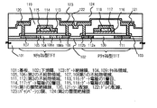
図1では、nチャネル型TFTとpチャネル型TFTの断面構造を示している。nチャネル型TFTとpチャネル型TFTのゲート電極は、ゲート電極の第1層目と、ゲート電極の第2層目と、ゲート電極の第3層目とから構成されている。ゲート電極の第1層目113、116はゲート絶縁膜103に接して形成されている。そして、ゲート電極の第1層目よりもチャネル長方向の長さが短く形成されたゲート電極の第2層目114、117が、ゲート電極の第1層目113、116に重ねて設けられる。さらにゲート電極の第3層目は115、118は、ゲート電極の第1層目113、116と、ゲート電極の第2層目114、117上に形成される。
【0030】
ゲート電極の第1層目113、116は、シリコン(Si)、チタン(Ti)、タンタル(Ta)、タングステン(W)、モリブデン(Mo)から選ばれた材料か、これらの材料を成分とする材料で形成する。例えば、W―Mo化合物や、窒化タンタル(TaN)、窒化タングステン(WN)としても良い。ゲート電極の第1層目の厚さは10〜100nm、好ましくは20〜50nmとすれば良い。
【0031】
ゲート電極の第2層目114、117は抵抗率の低い、アルミニウム(Al)や銅(Cu)を成分とする材料を用いることが望ましい。ゲート電極の第2層目の厚さは50〜400nm、好ましくは100〜200nmとすれば良い。ゲート電極の第2層目は、ゲート電極の電気抵抗を下げる目的で形成するものであり、ゲート電極に接続するゲート配線やバスラインの長さと抵抗値を考慮して、その両者の兼ね合いで決定すれば良い。
【0032】
ゲート電極の第3層目115、118は、ゲート電極の第1層目と同様にシリコン(Si)、チタン(Ti)、タンタル(Ta)、タングステン(W)、モリブデン(Mo)から選ばれた材料か、これらの材料を成分とする材料で形成する。ゲート電極の第3層目の厚さは50〜400nm、好ましくは100〜200nmとすれば良い。
【0033】
いずれにしても、ゲート電極の第1層目と、ゲート電極の第2層目と、ゲート電極の第3層目とは、スパッタ法で上記材料の被膜を形成すれば良く、ウエットエッチングとドライエッチングにより所定の形状に形成する。ここで、ゲート電極の第3層目を、ゲート電極の第2層目を覆って形成させるためには、上記で示したようにゲート電極の第2層目の厚さを管理することはもとより、スパッタ条件を適切に設定する必要がある。例えば、形成する被膜の成膜速度を比較的遅くすることは有効な手段である。
【0034】
図1のようなゲート電極の構造として、ゲート電極の第2層目を、ゲート電極の第1層目とゲート電極の第3層目で囲んだクラッド構造とすることで耐熱性を高めることができる。ゲート電極の材料としては、AlやCuなどの抵抗率の低い材料を用いることが望ましいが、450℃以上で加熱するとヒロックが発生したり、周辺の絶縁膜や半導体層に拡散してしまうといった問題点がある。しかし、このような現象はSi、Ti、Ta、W、Moなどの材料か、これらの材料を成分とする材料で囲んだクラッド構造とすることで防ぐことができる。
【0035】
nチャネル型TFTの半導体層は、チャネル形成領域104と、第1の不純物領域107、108と、チャネル形成領域に接して形成される第2の不純物領域105、106a、106bとから成っている。第1の不純物領域と第2の不純物領域にはいずれもn型を付与する不純物元素が添加されている。このとき、前記不純物元素の濃度は、第1の不純物領域の濃度が1×10²⁰〜1×10²¹atoms/cm3、好ましくは2×1020〜5×1020atoms/cm3として、第2の不純物領域の濃度が1×1016〜5×1019atoms/cm3、代表的には5×1017〜5×1018atoms/cm3で添加されている。第1の不純物領域107、108はソース領域およびドレイン領域として機能する。
【0036】
一方、pチャネル型TFTの第3の不純物領域111、112a、112bは、ソース領域またはドレイン領域として機能するものである。そして、第3の不純物領域112bにはn型を付与する不純物元素が第1の不純物領域と同じ濃度で含まれているが、その1.5〜3倍の濃度でp型を付与する不純物元素が添加されている。
【0037】
第2の不純物領域への不純物元素は、添加するn型を付与する不純物元素をゲート電極の第1層目113とゲート絶縁膜103を通過させて半導体層に添加する方法により行われるものである。
【0038】
第2の不純物領域106a、106bは、図2(A)、(B)に示すようにゲート絶縁膜103を介してゲート電極と重なる第2の不純物領域106aとゲート電極と重ならない第2の不純物領域106bとに分けることができる。すなわち、ゲート電極とオーバーラップするLDD領域と、オーバーラップしないLDD領域が形成される。この領域の作り分けは、一導電型の不純物元素を添加する第1の工程(第2の不純物領域の形成)と、一導電型の不純物元素を添加する第2の工程(第1の不純物領域の形成)により行うものであり、このときフォトレジストをマスクとして利用すれば良い。
【0039】
これは、同一基板上に駆動電圧の異なる回路を作製するときにきわめて便利な方法である。図2(B)には、液晶表示装置のロジック回路部、バッファ回路部、アナログスイッチ部、および画素マトリクス回路に使用するTFTの設計値の一例を示す。このとき、それぞれのTFTの駆動電圧を考慮して、チャネル長はもとより、ゲート電極と重なる第2の不純物領域106aとゲート電極と重ならない第2の不純物領域106bの長さを設定することが可能となる。
【0040】
駆動回路のシフトレジスタ回路のTFTや、バッファ回路のTFTは基本的にオン領域の特性が重視されるので、いわゆるGOLD構造でも良く、ゲート電極と重ならない第2の不純物領域106bは必ずしも設ける必要はない。しかしあえて設ける場合は駆動電圧を考慮して0.5〜3μmの範囲で設定すれば良い。いずれにしても、耐圧を考慮してゲート電極と重ならない第2の不純物領域106bの値は、駆動電圧が高くなるにしたがって大きくすることが望ましい。
【0041】
また、アナログスイッチや、画素マトリクス回路に設けるTFTはオフ電流が増加しては困るので、例えば、駆動電圧16Vの場合、チャネル長3μmとしてゲート電極と重なる第2の不純物領域106aを1.5μmとし、ゲート電極と重ならない第2の不純物領域106bを1.5μmとする。勿論、本発明はここで示す設計値に限定されるものでなく、実施者が適宣決定すれば良い。
【0042】
また、図17に示すように、本発明において、ゲート電極の第1層目1701と、ゲート電極の第2層目1702と、ゲート電極の第3層目1703とのチャネル長方向の長さは、作製するTFTの寸法と深い関わりがある。ゲート電極の第2層目1702のチャネル長方向の長さは、チャネル長L1にほぼ相当するものである。このときL1は0.1〜10μm、代表的には0.2〜5μmの値とすれば良い。
【0043】
また、第2の不純物領域1705の長さL6は前述のようにフォトレジストによるマスキングで任意に設定することが可能であるが、0.2〜6μm、代表的には0.6〜3μmで形成することが望ましい。
【0044】
そして、第2の不純物領域1705がゲート電極と重なる長さL4は、ゲート電極の第1層目1701の長さL2と密接な関係にある。L4の長さは、0.1〜4μm、代表的には0.5〜3μmで形成することが望ましい。また、第2の不純物領域1705がゲート電極と重ならないる長さL5は、前述のように必ずしも設ける必要がない場合もあるが、通常は0.1〜3μm、代表的には0.3〜2μmとするのが良い。ここでL4とL5の長さは、例えば、前述のようにTFTの駆動電圧を根拠にして決めると良い。
【0045】
また、図1においてチャネル形成領域104には、あらかじめ1×10¹⁶〜5×10¹⁸atoms/cm3の濃度でボロンが添加されても良い。このボロンはしきい値電圧を制御するために添加されるものであり、同様の効果が得られるものであれば他の元素で代用することもできる。
【0046】
以上示したように本発明は、ゲート電極をゲート電極の第1層目113、116と、ゲート電極の第2層目114、117と、ゲート電極の第3層目115、118とで形成し、図1で示すようにゲート電極の第2層目114、117が、ゲート電極の第1層目113,116とゲート電極の第3層目115、118で囲まれたクラッド型の構造としてある。そして、少なくともnチャネル型TFTでは、ゲート絶縁膜103を介して半導体層に設けられた第2の不純物領域106の一部が、このようなゲート電極と重なっている構造に特徴がある。
【0047】
nチャネル型TFTにおいて、第2の不純物領域はチャネル形成領域104を中心としてドレイン領域側(図1の第1の不純物領域108側)だけに設けても良い。また画素マトリクス回路の画素TFTのように、オン領域とオフ領域の両方の特性が要求される場合には、チャネル形成領域104を中心としてソース側(図1の第1の不純物領域107側)とドレイン領域側(図1の第1の不純物領域108側)の両方に設けることが望ましい。
【0048】
一方、pチャネル型TFTにはチャネル形成領域109と第3の不純物領域111、112a、112bが形成された構造とする。勿論、本発明のnチャネル型TFTと同様の構造としても良いが、pチャネル型TFTはもともと信頼性が高いため、オン電流を稼いでnチャネル型TFTとの特性バランスをとった方が好ましい。本願発明を図1に示すようにCMOS回路に適用する場合には、特にこの特性のバランスをとることが重要である。但し、本発明の構造をpチャネル型TFTに適用しても何ら問題はない。
【0049】
こうしてnチャネル型TFTおよびpチャネル型TFTが完成したら、第1の層間絶縁膜119で覆い、ソース配線120、121、ドレイン配線122を設ける。図1の構造では、これらを設けた後でパッシベーション膜123として窒化シリコン膜を設けている。さらに樹脂材料でなる第2の層間絶縁膜124が設けられている。第2の層間絶縁膜は、樹脂材料に限定される必要はないが、例えば、液晶表示装置に応用する場合には、表面の平坦性を確保するために樹脂材料を用いることが好ましい。
【0050】
図1では、nチャネル型TFTとpチャネル型TFTとを相補的組み合わせて成るCMOS回路を例にして示したが、nチャネル型TFTを用いたNMOS回路や、液晶表示装置の画素マトリクス回路に本願発明を適用することもできる。
【0051】
以上に示した本願発明の構成について、以下に示す実施例でさらに詳細に説明する。
【0052】
[実施例1]
本実施例では、本願発明の構成を、画素マトリクス回路とその周辺に設けられる駆動回路の基本形態であるCMOS回路を同時に作製する方法について説明する。
【0053】
図3(A)において、基板301には、コーニング社の1737ガラス基板に代表される無アルカリガラス基板を用いる。そして、基板301のTFTが形成される表面には、下地膜302をプラズマCVD法やスパッタ法で形成する。下地膜302は図示していないが、窒化シリコン膜を25〜100nm、代表的には50nmの厚さに、酸化シリコン膜を50〜300nm、代表的には150nmの厚さに形成する。
【0054】
その他に、プラズマCVD法でSiH4、NH3、N2Oから作製される酸化窒化シリコン膜を10〜200nm(好ましくは50〜100nm)、同様にSiH4、N2Oから作製される酸化窒化シリコン膜を50〜200nm(好ましくは100〜150nm)の厚さに積層形成する。
【0055】
次に、この下地膜302の上に50nmの厚さの、非晶質シリコン膜をプラズマCVD法で形成する。非晶質シリコン膜は含有水素量にもよるが、好ましくは400〜550℃で数時間加熱して脱水素処理を行い、含有水素量を5atomic%以下として、結晶化の工程を行うことが望ましい。また、非晶質シリコン膜をスパッタ法や蒸着法などの他の作製方法で形成しても良いが、膜中に含まれる酸素、窒素などの不純物元素を十分低減させておくことが望ましい。
【0056】
ここで、下地膜と非晶質シリコン膜とはいずれもプラズマCVD法で作製することが可能であるので、下地膜と非晶質シリコン膜を真空中で連続して形成しても良い。下地膜を形成後、一旦大気雰囲気にさらさない工程にすることにより、表面の汚染を防ぐことが可能となり、作製するTFTの特性バラツキを低減させることができる。
【0057】
非晶質シリコン膜を結晶化する工程は、公知のレーザーアニール法または熱アニール法の技術を用いれば良い。本実施例では、パルス発振型のKrFエキシマレーザー光を線状に集光して非晶質シリコン膜に照射して結晶質シリコン膜を形成する。
【0058】
結晶化をレーザーアニール法にて行う場合には、パルス発振型または連続発光型のエキシマレーザーやアルゴンレーザーをその光源とする。また、YAGレーザーを光源とし、その基本周波数、第2高調波、第3高調波、第4高調波を光源としても良い。パルス発振型のエキシマレーザーを用いる場合には、レーザー光を線状に加工してレーザーアニールを行う。レーザーアニール条件は実施者が適宣選択するものであるが、例えば、レーザーパルス発振周波数30Hzとし、レーザーエネルギー密度を100〜500mJ/cm2(代表的には300〜400mJ/cm2)とする。そして線状ビームを基板全面に渡って照射し、この時の線状ビームの重ね合わせ率(オーバーラップ率)を80〜98%として行う。
【0059】
尚、本実施例では半導体層を非晶質シリコン膜から結晶質シリコン膜を形成したが、微結晶シリコン膜を用いても構わないし、直接結晶質シリコン膜を成膜しても良い。
【0060】
こうして形成した結晶質シリコン膜をパターニングして、島状の半導体層303、304、305を形成する。
【0061】
次に、島状の半導体層303、304、305を覆って、酸化シリコンまたは窒化シリコンを主成分とするゲート絶縁膜306を形成する。ゲート絶縁膜306は、プラズマCVD法でN2OとSiH4を原料とした酸化窒化シリコン膜を10〜200nm、好ましくは50〜150nmの厚さで形成すれば良い。ここでは100nmの厚さに形成する。
【0062】
そして、ゲート絶縁膜306上にゲート電極の第1層目とゲート電極の第2層目とゲート電極の第3層目から成るゲート電極を形成する。まず、導電層(A)307と、導電層(B)308を形成する。導電層(A)307はTi、Ta、W、Moから選ばれた材料で形成すれば良いが、電気抵抗や耐熱性を考慮して前記材料を成分とする化合物を用いても良い。また、導電層(A)307の厚さは10〜100nm、好ましくは20〜50nmとする必要がある。ここでは、50nmの厚さでTi膜をスパッタ法で形成する。
【0063】
ゲート絶縁膜306と導電層(A)307の厚さの管理は重要である。これは、後に実施される第1の不純物添加の工程において、n型を付与する不純物をゲート絶縁膜306と導電層(A)307を通過させて半導体層303、305に添加するためである。実際には、ゲート絶縁膜306と導電層(A)307の膜厚と、添加する不純物元素の濃度を考慮して、第1の不純物添加の工程条件を決定した。前記膜厚範囲であれば不純物元素を半導体層に添加できることは予め確認されたが、膜厚が設定された本来の値よりも10%以上変動すると、添加される不純物濃度が減少してしまう。
【0064】
導電層(B)は、Al、Cuから選ばれた材料を用いることが好ましい。これはゲート電極の電気抵抗を下げるために設けられるものであり、50〜400nm、好ましくは100〜200nmの厚さに形成する。Alを用いる場合には、純Alを用いても良いし、Ti、Si、Scから選ばれた元素が0.1〜5atomic%添加されたAl合金を用いても良い。また銅を用いる場合には、図示しないが、ゲート絶縁膜306の表面に窒化シリコン膜を30〜100nmの厚さで設けておくと好ましい。
【0065】
ここでは、Scが0.5atomic%添加されたAl膜をスパッタ法で200nmの厚さに形成する(図3(A))。
【0066】
次に公知のパターニング技術を使ってレジストマスクを形成し、導電層(B)308の一部を除去する工程を行う。ここでは、導電層(B)308はScが0.5atomic%添加されたAl膜で形成されているので、リン酸溶液を用いたウエットエッチング法で行う。そして、図3(B)に示すように導電層(B)からゲート電極の第2層目309、310、311、312を形成する。それぞれのゲート電極の第2層目のチャネル長方向の長さは、CMOS回路を形成するゲート電極の第2層目309、310で3μmとし、また、画素マトリクス回路はマルチゲート構造となっていて、ゲート電極の第2層目311、312のそれぞれの長さを2μmとした。
【0067】
この工程をドライエッチング法で行うことも可能であるが、導電層(A)307にダメージを与えず、選択性良く導電層(B)308の不要な領域を除去するためにはウエットエッチング法が好ましい。
【0068】
また、画素マトリクス回路を構成する画素TFTのドレイン側に保持容量を設ける構造となっている。このとき、導電層(B)と同じ材料で保持容量の容量配線313を形成する。
【0069】
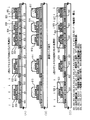
そして、pチャネル型TFTを形成する領域にレジストマスク314を形成して、1回目のn型を付与する不純物元素を添加する工程を行う。結晶質半導体材料に対してn型を付与する不純物元素としては、リン(P)、砒素(As)、アンチモン(Sb)などが知られているが、ここでは、リンを用い、フォスフィン(PH3)を用いたイオンドープ法で行う。この工程では、ゲート絶縁膜306と導電層(A)307を通してその下の半導体層にリンを添加するために、加速電圧は80keVと高めに設定する。半導体層に添加するリンの濃度は1×10¹⁶〜5×10¹⁹atoms/cm3の範囲にするのが好ましく、ここでは1×1018atoms/cm3とする。そして、半導体層にリンが添加された領域315、316、317、318、319、320が形成される(図3(B))。
【0070】
そして、レジストマスク314を除去した後、導電層(A)307とゲート電極の第2層目309、310、311、312と保持容量の配線313に密接させてゲート電極の第3層目となる導電層(C)321を形成する。導電層(C)321はTi、Ta、W、Moから選ばれた材料で形成すれば良いが、電気抵抗や耐熱性を考慮して前記材料を成分とする化合物を用いても良い。例えば、また、導電層(C)321の厚さは10〜100nm、好ましくは20〜50nmとする必要がある。ここでは、50nmの厚さでTa膜をスパッタ法で形成する(図3(C))。
【0071】
次に公知のパターニング技術を使ってレジストマスクを形成し、導電層(C)321と導電層(A)307の一部を除去する工程を行う。ここでは、ドライエッチング法により行う。導電層(C)321はTaであり、ドライエッチングの条件として、CF4を80SCCM、O2を20SCCM導入して100mTorr、で500Wの高周波電力を投入して行う。このときTaのエッチングレートは60nm/分である。また、導電層(A)307をエッチングする条件は、SiCl4を40SCCM、Cl2を5SCCM、BCl3を180SCCM導入して、80mTorr、1200Wの高周波電力を印加して行う。このとき、Tiのエッチングレートは34nm/分である。
【0072】
エッチング後わずかに残さが確認されることがあるが、SPX洗浄液やEKCなどの溶液で洗浄することにより除去することができる。また、上記エッチング条件で、下地にあるゲート絶縁膜306のエッチングレートは18〜38nm/分であり、エッチング時間が長いとゲート絶縁膜のエッチングが進んでしまうため注意が必要である。
【0073】
そして、ゲート電極の第1層目322、323、324、325とゲート電極の第3層目327、328、329、330とが形成される。ゲート電極の第1層目とゲート電極の第3層目とのチャネル長方向の長さは同じに形成され、ゲート電極の第1層目322、323とゲート電極の第3層目327、328は6μmの長さに形成する。また、ゲート電極の第1層目324、325とゲート電極の第3層目329、330は4μmの長さに形成する(図4(A))。
【0074】
このようにして、ゲート電極の第1層目とゲート電極の第2層目とゲート電極の第3層目とから成るゲート電極が形成される。また、画素マトリクス回路を構成する画素TFTのドレイン側に保持容量を設ける構造となっている。このとき、導電層(A)と、導電層(C)とから保持容量の配線326、331が形成される。
【0075】
そして、図4(B)に示すように、レジストマスク332、333、334、335、336を形成して、2回目のn型を付与する不純物元素を添加する工程を行う。これも、フォスフィン(PH3)を用いたイオンドープ法で行う。この工程でもゲート絶縁膜306を通してその下の半導体層にリンを添加するために、加速電圧は80keVと高めに設定する。そして、リンが添加された領域337、338、339、340、341、342、343が形成される。この領域のリンの濃度は、1回目のn型を付与する不純物元素を添加する工程と比較して高濃度であり、1×10¹⁹〜1×10²¹atoms/cm3とするのが好ましく、ここでは1×1020atoms/cm3とする。
【0076】
この工程において、レジストマスク332、333、334、335のチャネル長方向の長さは、それぞれのTFTの構造を決める上で重要である。特に、nチャネル型TFTにおいては、前述のゲート電極の第1層目と第3層目の長さと、このレジストマスクの長さにより、第2の不純物領域がゲート電極と重なる領域と、重ならない領域をある範囲で自由に決めることができる。本実施例では、ゲート電極の第1層目322と第3層目327の長さを6μmで、ゲート電極の第1層目324、325と第3層目329、330の長さを4μmで形成したので、レジストマスク332は9μmの長さで、レジストマスク334、335は7μmの長さで形成した。勿論、ここで記載したそれぞれの長さは一例であるので、前述のようにTFTの駆動電圧を考慮して決めると良い。
【0077】
次にnチャネル型TFTを形成する領域をレジストマスク344、345で覆って、pチャネル型TFTが形成される領域のみに、p型を付与する第3の不純物元素を添加するの工程を行う。p型を付与する不純物元素としては、ボロン(B)、アルミニウム(Al)、ガリウム(Ga)、が知られているが、ここではボロンをその不純物元素として、ジボラン(B2H6)を用いてイオンドープ法で添加する。この場合も加速電圧を80keVとして、2×10²⁰atoms/cm3の濃度にボロンを添加する。そして、図4(C)に示すようにボロンが高濃度に添加された第3の不純物領域346a、346b、347a、347bが形成される。第3の不純物域346b、347bには前の工程で添加されたリンが含まれているが、その 2倍の濃度でボロンが添加されているので問題はない(図4(C))。
【0078】
図4(C)までの工程が終了したら、図5で示すように、レジストマスク344、345を除去して、第1の層間絶縁膜374を形成する工程を行う。第1の層間絶縁膜374は2層構造で形成する。最初に窒化シリコン膜374aを50nmの成膜する。窒化シリコン膜はプラズマCVD法で形成し、SiH4を5SCCM、NH3を40SCCM、N2を100SCCM導入して0.7Torr、300Wの高周波電力を投入する。そして、続いて酸化シリコン膜374bをTEOSを500SCCM、O2を50SCCM導入し1Torr、200Wの高周波電力を投入して950nmの厚さに成膜する。このように窒化シリコン膜374aと酸化シリコン膜374bにより、合計1μmの第1の層間絶縁膜374を形成する。
【0079】
ここで形成された窒化シリコン膜は次の熱処理工程を行うために必要なものである。本実施例では、前述のようなクラッド構造のゲート電極を形成する。この構造はAlで形成されるゲート電極の第2層目を、Tiで形成されるゲート電極の第1層目とTaで形成されるゲート電極の第3層目で囲むように形成している。TaはAlのヒロックや周辺へのしみ出しを防ぐ効果があるが、常圧において400℃以上で加熱するとすぐに酸化してしまう欠点を有している。その結果、電気抵抗が増加してしまうが、その表面を第1の層間絶縁膜の窒化シリコン膜374aで被覆しておくと、酸化を防止することができる。
【0080】
熱処理の工程は、それぞれの濃度で添加されたn型またはp型を付与する不純物元素を活性化するために行う必要がある。この工程は、電気加熱炉を用いる熱アニール法や、前述のエキシマレーザーを用いるレーザーアニール法や、ハロゲンランプを用いるラピットサーマルアニール法(RTA法)で行えば良い。しかし、レーザーアニール法は低い基板加熱温度で活性をすることができるが、ゲート電極の下にかくれる領域まで活性化させることは困難である。従って、ここでは熱アニール法で活性化の工程を行う。この時の条件は、窒素雰囲気中において300〜700℃、好ましくは350〜550℃、ここでは450℃、2時間の処理を行う。
【0081】
第1の層間絶縁膜374はその後、パターニングでそれぞれのTFTのソース領域と、ドレイン領域に達するコンタクトホールが形成する。そして、ソース配線375、376、377、とドレイン配線378、379を形成する。図示していないが、本実施例ではこの配線を、Ti膜を100nm、Tiを含むAl膜300nm、Ti膜150nmをスパッタ法で連続して形成する3層構造の配線として用いる。
【0082】
そして、ソース配線375、376、377とドレイン配線378、379と、第1の層間絶縁膜374を覆ってパッシベーション膜380を形成する。パッシベーション膜380は、窒化シリコン膜で50nmの厚さで形成する。さらに、有機樹脂からなる第2の層間絶縁膜381を約1000nmの厚さに形成する。有機樹脂膜としては、ポリイミド、アクリル、ポリイミドアミド等を使用することができる。有機樹脂膜を用いることの利点は、成膜方法が簡単である点や、比誘電率が低いので、寄生容量を低減できる点、平坦性に優れる点などが上げられる。なお上述した以外の有機樹脂膜を用いることもできる。ここでは、基板に塗布後、熱重合するタイプのポリイミドを用い、300℃で焼成して形成する。
【0083】
以上までの工程で、クラッド構造のゲート電極が形成され、CMOS回路のnチャネル型TFTにはチャネル形成領域348、第1の不純物領域360、361、第2の不純物領域349a、349b、350a、350bが形成される。ここで、第2の不純物領域は、ゲート電極と重なる領域349a、350aが1.5μmの長さに、ゲート電極と重ならない領域(LDD領域)349b、350bが1.5μmの長さにそれぞれ形成される。そして、第1の不純物領域360はソース領域として、第1の不純物領域361はドレイン領域として機能する。
【0084】
pチャネル型TFTは、同様にクラッド構造のゲート電極が形成され、チャネル形成領域362、第3の不純物領域363a、363b、364a、364bが形成される。第3の不純物領域363a、363bはソース領域として、第3の不純物領域364a、364bはドレイン領域となる。
【0085】
また、画素マトリクス回路の画素TFTは、チャネル形成領域365、369と第1の不純物領域368、372と第2の不純物領域366、367、370、371が形成される。この第2の不純物領域は、ゲート電極と重なる領域366a、367a、370a、371aと重ならない領域366b、367b、370b、371bとに分けることができる。
【0086】
こうして図5に示すように、基板301上にCMOS回路と、画素マトリクス回路が形成されたアクティブマトリクス基板が作製される。また、画素マトリクス回路の画素TFTのドレイン側には、保持容量が同時に形成される。
【0087】
[実施例2]
本実施例では、実施例1と同様に、画素マトリクス回路とその周辺に設けられる駆動回路の基本形態であるCMOS回路を同時に作製する他の実施形態について説明する。
【0088】
まず、実施例1と同様に図3(A)から(C)までの工程と、図4(A)までの工程を行う。
【0089】
そして、図6(A)はゲート電極の第1層目とゲート電極の第2層目とゲート電極の第3層目とからゲート電極が形成されている状態を示す。この状態の基板に対して、レジストマスク601、602、603、604、605を形成し、n型を付与する不純物元素を添加する工程を行う。そして、第1の不純物領域606、607、608、609、610、611、612が形成される(図6(B))。
【0090】
ここで形成されるレジストマスク601、602は、いずれもLDD領域をTFTのドレイン領域側のみに形成する形状のものである。これは、第2の不純物領域をゲート絶縁膜上からマスクする領域がチャネル形成領域を中心として、片側のみに形成されるものである。
【0091】
このようなレジストマスクの形成は、CMOS回路のnチャネル型TFTに対して特に有効である。LDD領域が片側のみに形成されるため、TFTの直列抵抗成分を実質的に下げることが可能となり、オン電流を増加させることができる。
【0092】
これまで述べてきたGOLD構造にしても、LDD構造にしても、ドレイン領域近傍の高電界を緩和するために設けるためのものであり、TFTのドレイン側に形成されていればその効果は十分得られる。
【0093】
さらに、レジストマスク613、614を形成し、実施例1と同様にp型を付与する不純物元素を添加する工程を行い、第3の不純物領域615a、615b、616を形成する。第3の不純物領域615aは前の工程で添加したn型を付与する不純物元素が含まれている(図6(C))。
【0094】
以降の工程は実施例1と同様に行えば良く、ソース配線375、376、377とドレイン配線378、379、パッシベーション膜380、有機樹脂からなる第2の層間絶縁膜381を形成して図7に示すアクティブマトリクス基板が完成する。そして、CMOS回路のnチャネル型TFTにはチャネル形成領域617、第1の不純物領域620、621、第2の不純物領域618、619が形成される。ここで、第2の不純物領域は、ゲート電極と重なる領域(GOLD領域)619aと、ゲート電極と重ならない領域(LDD領域)619bがそれぞれ形成される。そして、第1の不純物領域620はソース領域として、第1の不純物領域621はドレイン領域となる。
【0095】
pチャネル型TFTは、チャネル形成領域622、第3の不純物領域624a、624b、623が形成される。第3の不純物領域623はソース領域として、第3の不純物領域624a、624bはドレイン領域となる。画素マトリクス回路の画素TFTは、チャネル形成領域625、629と第1の不純物領域628、632と第2の不純物領域626、627、630、631が形成される。この第2の不純物領域は、ゲート電極と重なる領域626a、627a、630a、631aと重ならない領域626b、627b、630b、631bとに分けることができる。
【0096】
[実施例3]
本実施例では、実施例1と同様に、画素マトリクス回路とその周辺に設けられる駆動回路の基本形態であるCMOS回路を同時に作製する他の実施形態について説明する。
【0097】
まず、実施例1と同様に図3(A)から(C)までの工程を行う。
【0098】
そして、図8(A)では、公知のパターニング技術を使ってレジストマスク801、802、803、804、805を形成し、導電層(C)321と導電層(A)307の一部を除去する工程を行う。ここでは、実施例1と同様にドライエッチング法により行う。そして、ゲート電極の第1層目851、852、853、854、855とゲート電極の第3層目856、857、858、859、860とを形成する。ゲート電極の第1層目とゲート電極の第3層目とのチャネル長方向の長さは同じに形成され、CMOS回路のゲート電極の第1層目851、852とゲート電極の第3層目856、857は最終的な形状よりも長く9μmの長さに形成する。また、画素マトリクス回路のゲート電極の第1層目853、854とゲート電極の第3層目858、859は同様に7μmの長さに形成する。
【0099】
また、画素マトリクス回路の画素TFTのドレイン側に保持容量を設ける構造となっている。このとき、導電層(A)と、導電層(C)とから保持容量の配線855、860を形成する。
【0100】
そして、実施例1と同様に2回目のn型を付与する不純物元素を添加する工程を行う。この工程では、ゲート電極が接していないゲート絶縁膜の領域を通って半導体層にリンが添加して、高濃度にリンが添加される領域806、807、808、811、812を形成する。この工程の終了後、レジストマスク801、802、803、804、805は除去する(図8(A))。
【0101】
次に、再度フォトレジスト膜を形成し、裏面からの露光によるパターニングの工程を行う。このとき、図8(B)に示すようにゲート電極がマスクとなって、自己整合的にレジストマスク813、814、815、816、817が形成される。裏面からの露光は直接光と散乱光を利用して行うもので、光強度や露光時間などの露光条件の調節により、図8(B)に示すようにレジストマスクをゲート電極上の内側に形成することができる。
【0102】
レジストマスク813、814、815、816、817を使用して、ゲート電極の第3層目とゲート電極の第1層目のマスクされていない領域をドライエッチング法により除去する。ドライエッチングの条件は実施例1と同様に行う。エッチングが終了した後レジストマスク813、814、815、816、817は除去する。
【0103】
そして、図8(C)に示すように、ゲート電極の第1層目818、819、820、821と、ゲート電極の第3層目823、824、825、826及び保持容量の配線822、827が形成される。エッチングにより、CMOS回路のゲート電極の第1層目851、852とゲート電極の第3層目856、857は6μmの長さになる。また、画素マトリクス回路のゲート電極の第1層目853、854とゲート電極の第3層目858、859は同様に4μmの長さに形成される。
【0104】
さらに、nチャネル型TFTが形成される領域にレジストマスク828、829を形成してp型を付与する第3の不純物元素を添加する工程を行う(図8(C))。
【0105】
以降の工程は実施例1と同様に行えば良く、図5に示すアクティブマトリクス基板が作製することができる。
【0106】
[実施例4]
本実施例では、実施例1と同様に、画素マトリクス回路とその周辺に設る駆動回路の基本形態であるCMOS回路を同時に作製する他の実施形態について説明する。
【0107】
まず、実施例1と同様に図3(A)から(C)までの工程を行う。そして、図9(A)で示すようにゲート電極の形成を行う。
【0108】
次に、公知のパターニング技術を使ってレジストマスクを形成し、導電層(C)321と導電層(A)307との一部を除去する工程を行う。ここでは、ドライエッチング法により行う。導電層(C)321はTaであり、ドライエッチングの条件として、CF4を80SCCM、O2を20SCCM導入して100mTorr、で500Wの高周波電力を投入して行う。このときTa膜のエッチングレートは60nm/分である。また、導電層(A)307をエッチングする条件は、SiCl4を40SCCM、Cl2を5SCCM、BCl3を180SCCM導入して、80mTorr、1200Wの高周波電力を印加して行う。このとき、Ti膜のエッチングレートは34nm/分である。
【0109】
そして、ゲート電極の第1層目322、323、324、325とゲート電極の第3層目327、328、329、330とを形成する。ゲート電極の第1層目とゲート電極の第3層目とのチャネル長方向の長さは同じに形成され、ゲート電極の第1層目322、323とゲート電極の第3層目327、328は、ここでは6μmの長さに形成する。また、ゲート電極の第1層目324、325とゲート電極の第3層目329、330は、4μmの長さに形成する。
【0110】
上記エッチング条件では、酸化窒化シリコン膜で形成されたゲート絶縁膜306もエッチングされる。そのエッチングレートはTa膜のエッチング条件で18nm/分である。通常はゲート絶縁膜がエッチングされないように注意深く行われるものであるが、この現象を積極的に利用して、ゲート電極に接していないゲート絶縁膜の領域を薄くすることができる。これは、ゲート電極をエッチングする工程で、エッチング時間をそのまま増加させればすぐに実施することができる。
【0111】
しかし、ゲート絶縁膜をエッチングするためには、やはり使用するガスを選ぶ必要があり、塩素系のガスよりはCF4やNF3などのフッ素系のガスの方が良い結果が得られる。
【0112】
ここでは、Ta膜をエッチングするときに使用したCF4とO2の混合ガスにより行う。CF4を80SCCM、O2を20SCCM導入して100mTorr、で500Wの高周波電力を投入して行う。そして、100nmの厚さで形成されていたゲート絶縁膜306に対して、約2分半のエッチングにより図9(A)に示すようにゲート電極と接していないゲート絶縁膜の領域を50nmの厚さにまで薄くすることができる。
【0113】
そして実施例1と同様に、レジストマスク332、333、334、335、336を形成して2回目のn型を付与する不純物元素を添加する工程を行う。このとき、n型を付与する不純物元素を添加する領域337、338、339、340、341、342、343はゲート絶縁膜の厚さが50nmとなっているので、半導体層に効率よく不純物元素を添加することができる。
【0114】
ゲート絶縁膜が薄くなったことで、イオンドープ法における加速電圧を80keVから40keVまで下げることが可能となり、ゲート絶縁膜や半導体層へのダメージを減らすことができる(図9(B))。
【0115】
次に図9(C)に示すようにレジストマスク344、345を形成し、p型を付与する不純物元素を添加する工程も同様に実施するものであり、p型を付与する不純物が添加される領域346a、346b、347a、347bに接するゲート絶縁膜は厚さが50nmとなっているので、イオンドープ法における加速電圧を80keVから40keVまで下げることが可能となり、半導体層に効率よく不純物元素を添加することができる。
【0116】
その他の工程は実施例1に従えば良く、ソース配線375、376、377とドレイン配線378、379、パッシベーション膜380、有機樹脂からなる第2の層間絶縁膜381を形成して図10に示すアクティブマトリクス基板が完成する。CMOS回路のnチャネル型TFTにはチャネル形成領域348、第1の不純物領域360、361、第2の不純物領域349、350が形成される。ここで、第2の不純物領域は、ゲート電極と重なる領域349a、350a、ゲート電極と重ならない領域(LDD領域)349b、350bが形成される。そして、第1の不純物領域360はソース領域として、第1の不純物領域361はドレイン領域として機能する。pチャネル型TFTは、同様にクラッド構造のゲート電極が形成され、チャネル形成領域362、第3の不純物領域363a、363b、364a、364bが形成される。第3の不純物領域363a、363bはソース領域として、第3の不純物領域364a、364bはドレイン領域となる。また、画素マトリクス回路の画素TFTは、チャネル形成領域365、369と第1の不純物領域368、372と第2の不純物領域366a、366b、367a、367b、370a、370b、371a、371bが形成される。この第2の不純物領域は、ゲート電極と重なる領域366a、367a、370a、371aと重ならない領域366b、367b、370b、371bとに分けることができる。
【0117】
[実施例5]
本実施例では、本願発明の構成を、画素マトリクス回路とその周辺に設けられる駆動回路の基本形態であるCMOS回路を同時に作製する方法について説明する。
【0118】
図11(A)において、基板1101には、例えばコーニング社の1737ガラス基板に代表される無アルカリガラス基板を用いる。そして、基板1101のTFTが形成される表面に、下地膜1102をプラズマCVD法やスパッタ法で形成する。下地膜1102は図示していないが、窒化シリコン膜を25〜100nm、代表的には50nmの厚さに、酸化シリコン膜を50〜300nm、代表的には150nmの厚さに形成する。また、下地膜1102は、窒化シリコン膜や酸化窒化シリコン膜のみを用いても良い。
【0119】
次に、この下地膜1102の上に50nmの厚さの、非晶質シリコン膜をプラズマCVD法で形成する。非晶質シリコン膜は含有水素量にもよるが、好ましくは400〜550℃で数時間加熱して脱水素処理を行い、含有水素量を5atomic%以下として、結晶化の工程を行うことが望ましい。また、非晶質シリコン膜をスパッタ法や蒸着法などの他の作製方法で形成しても良いが、膜中に含まれる酸素、窒素などの不純物元素を十分低減させておくことが望ましい。
【0120】
ここで、下地膜と非晶質シリコン膜とはいずれもプラズマCVD法で作製されるものであり、このとき下地膜と非晶質シリコン膜を真空中で連続して形成しても良い。下地膜を形成後、一旦大気雰囲気にさらされない工程にすることにより、表面の汚染を防ぐことが可能となり、作製されるTFTの特性バラツキを低減させることができる。
【0121】
ここで、半導体層として用いる結晶質シリコン膜を、触媒元素を用いた熱結晶化法により形成する。触媒元素を用いる場合、特開平7−130652号公報、特開平8−78329号公報で開示された技術を用いることが望ましい。
【0122】
ここで、特開平7−130652号公報に開示されている技術を本願発明に適用する場合の例を図19(A)、(B)で説明する。基板1901上に酸化シリコン膜1902が形成され、その上に非晶質シリコン膜1903を形成する。非晶質シリコン膜1903の表面に重量換算で10ppmのニッケルを含む酢酸ニッケル塩溶液を塗布してニッケル含有層1904を形成する(図19(A))。
【0123】
次に、500℃、1時間の脱水素工程の後、500〜650℃で4〜12時間、例えば550℃で8時間の熱処理を行い、結晶質シリコン膜1905を形成する(図19(B))。
【0124】
また、特開平8−78329号公報で開示された技術は、触媒元素を選択的に添加することによって、非晶質シリコン膜の選択的な結晶化を可能とするものである。同技術を本願発明に適用する場合について、図20(A)、(B)で説明する。
【0125】
まず、ガラス基板2001上に酸化シリコン膜2002、非晶質シリコン膜2003を形成し、さらに酸化シリコン膜2004を連続的に形成する。この時、酸化シリコン膜2004の厚さは150nmとする。
【0126】
次に酸化シリコン膜2004をパターニングして、選択的に開孔部2005を形成し、その後、重量換算で10ppmのニッケルを含む酢酸ニッケル塩溶液を塗布する。これにより、ニッケル含有層2006が形成され、ニッケル含有層2006は開孔部2005の底部のみで非晶質シリコン膜2003と接触する(図20(A))。
【0127】
次に、500〜650℃で4〜24時間、例えば570℃、14時間の熱処理を行い、結晶質シリコン膜2007を形成する。この結晶化の過程では、ニッケルが接した非晶質シリコン膜の部分が最初に結晶化し、そこから横方向へと結晶化が進行する。こうして形成された結晶質シリコン膜2007は棒状または針状の結晶が集合して成り、その各々の結晶は巨視的に見ればある特定の方向性をもって成長しているため、結晶性が揃っているという利点がある(図20(B))。
【0128】
尚、上記2つの技術において使用可能な触媒元素は、ニッケル(Ni)の以外にも鉄(Fe)、パラジウム(Pd)、スズ(Sn)、鉛(Pb)、コバルト(Co)、白金(Pt)、銅(Cu)、金(Au)といった元素を用いても良い。
【0129】
以上のような技術を用いて結晶質シリコン膜を形成し、パターニングを行えば、図11に示す半導体層1103、1104、1105を形成することができる。
【0130】
また、触媒元素を用いて結晶質シリコン膜を形成し、その触媒元素を結晶質シリコン膜から除去するゲッタリング工程を行った例を示す。
【0131】
これは、非晶質シリコン膜の結晶化に用いた触媒元素を結晶化後にリンのゲッタリング作用を用いて除去する技術である。同技術を用いることで、結晶質シリコン膜中の触媒元素の濃度を1×10¹⁷atoms/cm3以下、好ましくは1×1016atoms/cm3にまで低減することができる。
【0132】
図21(A)では、下地膜2102、結晶質シリコン膜2103が形成された状態を示している。そして、結晶質シリコン膜2103の表面にマスク用の酸化シリコン膜2104が150nmの厚さに形成され、パターニングにより開孔部が設けられ、結晶質シリコン膜を露出させた領域を設けてある。そして、リンを添加する工程を実施して、結晶質シリコン膜にリンが添加された領域2105を設ける。
【0133】
この状態で、窒素雰囲気中で550〜800℃、5〜24時間、例えば600℃、12時間の熱処理を行うと、結晶質シリコン膜にリンが添加されている領域2105がゲッタリングサイトとして働き、結晶質シリコン膜2103に残存していた触媒元素はリンが添加されている領域2105に偏析させることができる。
【0134】
そして、マスク用の酸化シリコン膜2104と、リンが添加されている領域2105とをエッチングして除去することにより、結晶化の工程で使用した触媒元素の濃度を1×10¹⁷atoms/cm3以下にまで低減した結晶質シリコン膜を得ることができる。この結晶質シリコン膜は図11(A)の半導体層1103、1104、1105として使用することができる。
【0135】
次に、島状の半導体層1103、1104、1105を覆って、酸化シリコンまたは窒化シリコンを主成分とするゲート絶縁膜1106を形成する。ゲート絶縁膜1106は、プラズマCVD法でN2OとSiH4を原料とした窒化酸化シリコン膜を10〜200nm、好ましくは50〜150nmの厚さで形成すれば良い。ここでは100nmの厚さに形成する。
【0136】
そして、ゲート絶縁膜1106の表面にゲート電極の第1層目とする導電層(A)1107と、ゲート電極の第2層目とする導電層(B)1108とを形成する。導電層(A)1107はTi、Ta、W、Moから選ばれた材料で形成すれば良いが、電気抵抗や耐熱性を考慮して前記材料を成分とする化合物を用いても良い。また、導電層(A)1107の厚さは10〜100nm、好ましくは20〜50nmとする必要がある。ここでは、50nmの厚さでTi膜をスパッタ法で形成する。
【0137】
ゲート電極の第2層目となる導電層(B)1108は、Al、Cuから選ばれた材料を用いることが好ましい。これはゲート電極の電気抵抗を下げるために設けられるものであり、50〜400nm、好ましくは100〜200nmの厚さに形成する。Alを用いる場合には、純Alを用いても良いし、Ti、Si、Scから選ばれた元素が0.1〜5atomic%添加されたAl合金を用いても良い。また銅を用いる場合には、図示しないが、ゲート絶縁膜1106の表面に窒化シリコン膜を30〜100nmの厚さで設けておくと好ましい。
【0138】
ここでは、Scが0.5atomic%添加されたAl膜をスパッタ法で200nmの厚さに形成する(図11(A))。
【0139】
次に公知のパターニング技術を使ってレジストマスクを形成し、導電層(B)1108の一部を除去する工程を行う。ここでは、導電層(B)1108はScが0.5atomic%添加されたAl膜で形成されているが、リン酸溶液を用いたウエットエッチング法で行うことができる。そして、図11(B)に示すようにゲート電極の第2層目1109、1110、1111、1112を形成する。それぞれのゲート電極の第2層目のチャネル長方向の長さは、CMOS回路を形成するゲート電極の第2層目1109、1110で3μmとし、また、画素マトリクス回路はマルチゲートの構造となっていて、ゲート電極の第2層目1111、1112のそれぞれの長さを2μmとする。
【0140】
また、画素マトリクス回路を構成する画素TFTのドレイン側に保持容量を設ける構造となっている。このとき、導電層(B)と同じ材料で保持容量の配線1113が形成される。
【0141】
そして、n型を付与する第1の不純物元素を添加する工程を行う。ここでは、リンを用い、フォスフィン(PH3)を用いたイオンドープ法で行う。この工程では、ゲート絶縁膜1106と導電層(A)1107を通してその下の半導体層1103、1104、1105にリンを添加するために、加速電圧は80keVと高めに設定する。半導体層に添加されるリンの濃度は、1×10¹⁶〜5×10¹⁹atoms/cm3の範囲にするのが好ましく、ここでは1×1018atoms/cm3とする。そして、半導体層にリンが添加された領域1114、1115、1116、1117、1118、1119、1120、1121が形成される(図11(B))。
【0142】
次にnチャネル型TFTを形成する領域をレジストマスク1122、1123で覆って、pチャネル型TFTが形成される領域のみに、p型を付与する第3の不純物元素を添加するの工程を行う。ここではボロンをその不純物元素として、ジボラン(B2H6)を用いてイオンドープ法で添加する。ここでも加速電圧を80keVとして、2×10²⁰atoms/cm3の濃度にボロンを添加する。そして、図11(C)に示すようにボロンが高濃度に添加された第3の不純物領域1124、1125が形成される。
【0143】
そして、レジストマスク1122、1123を除去した後、導電層(A)1107とゲート電極の第2層目1109、1110、1111、1112と保持容量の配線1113に密接させてゲート電極の第3層目となる導電層(C)1126を形成する。導電層(C)1126はTi、Ta、W、Moから選ばれた材料で形成すれば良いが、電気抵抗や耐熱性を考慮して前記材料を成分とする化合物を用いても良い。例えば、また、導電層(C)1126の厚さは10〜100nm、好ましくは20〜50nmとする必要がある。ここでは、50nmの厚さでMo−W膜をスパッタ法で形成する。(図12(A))
【0144】
次に公知のパターニング技術を使ってレジストマスクを形成し、導電層(C)1126と導電層(A)1107との一部を除去する工程を行う。ここでは、ドライエッチング法により行う。導電層(C)1126はMo−W膜であり、ドライエッチングの条件として、Cl2を80SCCM導入して10mTorr、で350Wの高周波電力を投入して行う。このときMo−W膜のエッチングレートは50nm/分である。また、導電層(A)1107をエッチングする条件は、SiCl4を40SCCM、Cl2を5SCCM、BCl3を180SCCM導入して、80mTorr、1200Wの高周波電力を印加して行う。このとき、Ti膜のエッチングレートは34nm/分である。
【0145】
エッチング後わずかに残さが確認されることがあるが、SPX洗浄液やEKCなどの溶液で洗浄することにより除去することができる。また、上記エッチング条件で、下地にあるゲート絶縁膜1106のエッチングレートは18〜38nm/分であり、エッチング時間が長いとゲート絶縁膜のエッチングが進んでしまうため注意が必要である。
【0146】
そして、ゲート電極の第1層目1127、1128、1129、1130とゲート電極の第3層目1132、1133、1134、1135とを形成する。ゲート電極の第1層目とゲート電極の第3層目とのチャネル長方向の長さは同じに形成され、ゲート電極の第1層目1127、1128とゲート電極の第3層目1132、1133は、ここでは6μmの長さに形成する。また、ゲート電極の第1層目1129、1130とゲート電極の第3層目1134、1135は、4μmの長さに形成する(図12(B))。
【0147】
また、画素マトリクス回路を構成する画素TFTのドレイン側に保持容量を設ける構造となっている。このとき、導電層(A)と、導電層(C)とから保持容量の電極1131、1136を形成する。
【0148】
そして、図12(C)に示すように、レジストマスク1137、1138、1139、1140、1141を形成して、n型を付与する第2の不純物元素を添加する工程を行う。ここでは、フォスフィン(PH3)を用いたイオンドープ法で行う。この工程でも、ゲート絶縁膜1106を通してその下の半導体層にリンを添加するために、加速電圧は80keVと高めに設定する。そして、リンが添加された領域1142、1143、1144、1145、1146、1147、1148を形成する。この領域のリンの濃度はn型を付与する第1の不純物元素を添加する工程と比較して高濃度であり、1×10²⁰〜1×10²¹atoms/cm3とするのが好ましく、ここでは1×1020atoms/cm3とする。
【0149】
この工程において、レジストマスク1137、1138、1139、1140のチャネル長方向の長さは、それぞれのTFTの構造を決める上で重要である。特に、nチャネル型TFTにおいては、前述のゲート電極の第1層目と第3層目の長さと、このレジストマスクの長さにより、第2の不純物領域がゲート電極と重なる領域と、重ならない領域をある範囲で自由に決めることができる。本実施例では、ゲート電極の第1層目1127、1128とゲート電極の第3層目1132、1133の長さが6μmであり、ゲート電極の第1層目1129、1130とゲート電極の第3層目1134、1135の長さが4μmであるので、第1とゲート電極の第3層目の長さが6μmで形成されたので、レジストマスク1137は9μmの長さで、レジストマスク1139、1140は7μmの長さで形成する。
【0150】
図12(C)までの工程が終了したら、レジストマスク1137、1138、1139、1140、1141を除去して、第1の層間絶縁膜1168を形成する工程を行う。第1の層間絶縁膜1168は2層構造で形成する。最初に窒化シリコン膜を50nmの成膜する。窒化シリコン膜はプラズマCVD法で形成され、SiH4を5SCCM、NH3を40SCCM、N2を100SCCM導入して0.7Torr、300Wの高周波電力を投入する。そして、続いて酸化シリコン膜をTEOSを500SCCM、O2を50SCCM導入し1Torr、200Wの高周波電力を投入して950nmの厚さに成膜する。従って、合計1μmの第1の層間絶縁膜1168を形成する。
【0151】
熱処理の工程は、それぞれの濃度で添加されたn型またはp型を付与する不純物元素を活性化するために行う必要がある。この工程は、電気加熱炉を用いた熱アニール法や、前述のエキシマレーザーを用いたレーザーアニール法や、ハロゲンランプを用いたラピットサーマルアニール法(RTA法)で行えば良い。しかし、レーザーアニール法は低い基板加熱温度で活性をすることができるが、ゲート電極の下の半導体層まで活性化させることは困難である。従って、ここでは熱アニール法で活性化の工程を行う。加熱処理は、窒素雰囲気中において300〜700℃、好ましくは350〜550℃、ここでは450℃、2時間の処理を行う。
【0152】
第1の層間絶縁膜1168はその後、パターニングでそれぞれのTFTのソース領域と、ドレイン領域に達するコンタクトホールが形成された。そして、ソース配線1169、1170、1171、とドレイン配線1172、1173を形成する。図示していないが、本実施例ではこの配線を、Ti膜を100nm、Tiを含むAl膜300nm、Ti膜150nmをスパッタ法で連続して形成する3層構造の配線として用いる。
【0153】
そして、ソース配線1169、1170、1171とドレイン配線1172、1173と、第1の層間絶縁膜1168を覆ってパッシベーション膜1174を形成する。パッシベーション膜1174は、窒化シリコン膜で50nmの厚さで形成する。さらに、有機樹脂からなる第2の層間絶縁膜1175を約1000nmの厚さに形成する。有機樹脂膜としては、ポリイミド、アクリル、ポリイミドアミド等を使用することができる。有機樹脂膜を用いることの利点は、成膜方法が簡単である点や、比誘電率が低いので、寄生容量を低減できる点、平坦性に優れる点などが上げられる。なお上述した以外の有機樹脂膜を用いることもできる。ここでは、基板に塗布後、熱重合するタイプのポリイミドを用い、300℃で焼成して形成する。
【0154】
以上までの工程で、クラッド構造のゲート電極が形成され、CMOS回路のnチャネル型TFTにはチャネル形成領域1149、第1の不純物領域1152、1153、第2の不純物領域1150a、1150b、1151a、1151bが形成される。ここで、第2の不純物領域は、ゲート電極と重なる領域(GOLD領域)1150a、1151aが1.5μmの長さに、ゲート電極と重ならない領域(LDD領域)1150b、1151bが1.5μmの長さにそれぞれ形成される。そして、第1の不純物領域1152はソース領域として、第1の不純物領域1153はドレイン領域となる。
【0155】
pチャネル型TFTは、同様にクラッド構造のゲート電極が形成され、チャネル形成領域1154、第3の不純物領域1155a1155b、1156a、1156bが形成される。そして、第3の不純物領域1155a、1155bはソース領域として、第3の不純物領域1156a、1156bはドレイン領域となる。
【0156】
また、画素マトリクス回路の画素TFTは、チャネル形成領域1157、1161と第1の不純物領域1160、1164と第2の不純物領域1158、1159、1162、1163が形成される。ここで第2の不純物領域は、ゲート電極と重なる領域1158a、1159a、1162a、1163aと重ならない領域1158b、1159b、1162b、1163bとが形成される。
【0157】
こうして図13に示すように、基板1101上にCMOS回路と、画素マトリクス回路が形成されたアクティブマトリクス基板が作製される。また、画素マトリクス回路のnチャネル型TFTのドレイン側には、保持容量部が同時に形成される。
【0158】
[実施例6]
本実施例では、実施例1で作製されたアクティブマトリクス基板から、アクティブマトリクス型液晶表示装置を作製する工程を説明する。
【0159】
図5の状態のアクティブマトリクス基板に対して、図16(A)に示すように第2の層間絶縁膜381上に遮光膜1601、第3の層間絶縁膜1602を形成する。遮光膜1601は顔料を含む有機樹脂膜や、Ti、Crなどの金属膜を用いると良い。また、第3の層間絶縁膜1602は、ポリイミドなどの有機樹脂膜で形成する。そして、第3の層間絶縁膜1602と第2の層間絶縁膜381にドレイン配線379に達するコンタクトホールを形成し、画素電極1603を形成する。画素電極1603は、透過型液晶表示装置とする場合には透明導電膜を用い、反射型の液晶表示装置とする場合には金属膜を用いれば良い。ここでは透過型の液晶表示装置とするために、酸化インジウム・スズ(ITO)膜を100nmの厚さにスパッタ法で形成し、画素電極1603を形成する。
【0160】
透明導電膜の材料のエッチング処理は塩酸系の溶液により行う。しかし、ITOのエッチングは残渣が発生しやすいので、エッチング加工性を改善するために酸化インジウム酸化亜鉛合金(In2O3―ZnO)を用いても良い。酸化インジウム酸化亜鉛合金は表面平滑性に優れ、ITOと比較して熱安定性にも優れているという特徴をもつ。同様に、酸化亜鉛(ZnO)も適した材料であり、さらに可視光の透過率や導電率を高めるためにガリウム(Ga)を添加した酸化亜鉛(ZnO:Ga)などを用いることができる。
【0161】
次に、図16(B)に示すように、配向膜1604を第3の層間絶縁膜1602と画素電極1603形成する。通常液晶表示素子の配向膜にはポリイミド樹脂が多く用いられている。対向側の基板1605には、透明導電膜1606と、配向膜1607とを形成する。配向膜は形成された後、ラビング処理を施して液晶分子がある一定のプレチルト角を持って平行配向するようにする。
【0162】
上記の工程を経て、画素マトリクス回路と、CMOS回路が形成されたアクティブマトリクス基板と対向基板とを、公知のセル組み工程によってシール材やスペーサ(共に図示せず)などを介して貼り合わせる。その後、両基板の間に液晶材料1608を注入し、封止剤(図示せず)によって完全に封止する。よって図16(B)に示すアクティブマトリクス型液晶表示装置が完成する。
【0163】
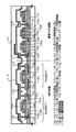
次に本実施例のアクティブマトリクス型液晶表示装置の構成を、図14と図15(A)、(B)を用いて説明する。図14は本実施例のアクティブマトリクス基板の斜視図である。アクティブマトリクス基板は、ガラス基板301上に形成される画素マトリクス回路1401と、走査(ゲート)線駆動回路1402と、データ(ソース)線駆動回路1403で構成される。画素マトリクス回路の画素TFT1400はnチャネル型TFTであり、周辺に設けられる駆動回路はCMOS回路を基本として構成されている。走査(ゲート)線駆動回路1402と、データ(ソース)線駆動回路1403はそれぞれゲート配線1502とソース配線1503で画素マトリクス回路1401に接続されている。
【0164】
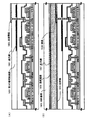
図15(A)は画素マトリクス回路1401の上面図であり、ほぼ1画素の上面図である。画素マトリクス回路には画素TFTであるnチャネル型TFTが設けられている。ゲート配線1502に連続して形成されるゲート電極1520は、図示されていないゲート絶縁膜を介してその下の半導体層1501と交差している。図示はしていないが、半導体層には、ソース領域、ドレイン領域、第1の不純物領域が形成されている。また、画素TFTのドレイン側には、半導体層と、ゲート絶縁膜と、ゲート電極と同じ材料で形成された電極とから、保持容量1507が形成されている。そして、保持容量1507に接続した容量配線1521が、ゲート配線1502と平行に設けられている。また、図15(A)で示すA―A'に沿った断面構造は、図5に示すCMOS回路の断面図に対応している。
【0165】
一方、図15(B)に示すCMOS回路では、ゲート配線1515から延在するゲート電極1513、1514が、図示されていないゲート絶縁膜を介してその下の半導体層1510、1512とそれぞれ交差している。図示はしていないが、同様にnチャネル型TFTの半導体層には、ソース領域、ドレイン領域、第1の不純物領域が形成されている。また、pチャネル型TFTの半導体層にはソース領域とドレイン領域が形成されている。そして、その位置関係は、B―B'に沿った断面構造は、図5に示す画素マトリクス回路の断面図に対応している。
【0166】
本実施例では、画素TFT1400をダブルゲートの構造としているが、シングルゲートの構造でも良いし、トリプルゲートとしたマルチゲート構造にしても構わない。本実施例のアクティブマトリクス基板の構造は、本実施例の構造に限定されるものではない。本願発明の構造は、ゲート電極の構造と、ゲート絶縁膜を介して設けられた半導体層のソース領域と、ドレイン領域と、その他の不純物領域の構成に特徴があるので、それ以外の構成については実施者が適宣決定すれば良い。
【0167】
本実施例で示すアクティブマトリクス型液晶表示装置を作製するためのアクティブマトリクス基板は、実施例1で示すものに限定れさず、実施例2〜5および実施例7に示す工程に基づいて作製されるアクティブマトリクス基板であれば、いずれも適用することができる。
【0168】
[実施例7]
本実施例では、実施例5で示したアクティブマトリクス基板の作製方法においてゲッタリング工程を簡略化する方法を示す。まず、実施例5において、図11(A)で示される半導体層1103、1104、1105は、触媒元素を用いて作製された結晶質シリコン膜である。このとき、結晶化の工程で用いられた触媒元素が半導体層中に残存するので、ゲッタリングの工程を実施することが望ましい。実施例5では結晶質シリコン膜が得られた後で、その結晶質シリコン膜の一部にリンを添加してゲッタリングする方法であったが、ここでは、そのゲッタリング工程を実施せずに、以下に述べる方法で触媒元素をTFTのチャネル形成領域から除去する。
【0169】
ここでは、図11(A)から図12(C)に示す工程までそのまま実施する。そして、レジストマスク1137、1138、1139、1140、1141を除去する。
【0170】
このとき、nチャネル型TFTの第1の不純物領域1152、1153、1160、1164にはリンが添加されている。またpチャネル型TFTの第3の不純物領域の1155b、1156bにも同様にリンが添加されている。実施例5に従えばこのときリン濃度は1×10²⁰〜1×10²¹atoms/cm3である。
【0171】
この状態で、図22に示すようにゲート絶縁膜およびゲート電極を窒化シリコン膜1180で被覆する。窒化シリコン膜はプラズマCVD法で、10〜100nm、ここでは50nmの厚さに形成する。窒化シリコン膜の代りに酸化窒化シリコン膜を用いても良い。
【0172】
実施例5では、ゲート電極の第3層目をMo−Wで形成する。またその他にTi、Ta、Mo、Wなどで形成しても良い。そしてこれらの材料は大気圧中または窒素ガスをパージしながらの加熱処理で比較的酸化されやすいものである。このような状況において、その表面を窒化シリコンで被覆すると酸化を防止することができる。
【0173】
この状態で、窒素雰囲気中で400〜800℃、1〜24時間、例えば600℃、12時間の加熱処理の工程を行う。この工程により、添加されたn型及びp型を付与する不純物元素を活性化することができる。さらに、リンが添加されている領域がゲッタリングサイトとなり、結晶化の工程の後残存していた触媒元素を偏析させることができる。その結果、チャネル形成領域から触媒元素を除去することができる。その結果、完成したTFTにおいてオフ電流を低減させる効果が得られる。
【0174】
図22の工程が終了したら、以降の工程は実施例5の工程に従い、第1の層間絶縁膜、ソース配線およびドレイン配線、パッシベーション膜、第2の層間絶縁膜を形成し、図13状態を形成することによりアクティブマトリクス基板を作製することができる。
【0175】
[実施例8]
本実施例では、図1で示したCMOS回路の回路構成の他の例について図23を用いて説明する。尚、図23(A)のインバータ回路図、図23(B)のインバータ回路の上面図における各端子部a、b、c、dは対応している。
【0176】
図23(A)に示すインバータ回路について、その上面図を図23(B)に示す。図23(B)のA−A'断面構造を図23(C)に示し、ゲート電極2409、2409'、nチャネル型TFTのソース配線2411、pチャネル型TFTのソース配線2414、共通ドレイン配線2413から構成されている。ここで、ゲート電極2409、2409'は、ゲート電極の第1層目2408、2408'、ゲート電極の第2層目2409、2409'、ゲート電極の第3層目2410、2410'が一体となった状態を表している。
【0177】
このインバータ回路のnチャネル型TFTには第2の不純物領域2402が設けられている。詳細には、ゲート電極2409とオーバーラップしている第2の不純物領域2402aと、オーバーラップしない第2の不純物領域(LDD領域)2402bとが形成されている。このような構造はドレイン側のみに設ければ良い。また、pチャネル型TFTにはこのような不純物領域は設けられていない。
【0178】
[実施例9]
上述の本発明の液晶表示装置にはネマチック液晶以外にも様々な液晶を用いることが可能である。例えば、1998, SID, "Characteristics and Driving Scheme of Polymer-Stabilized Monostable FLCD Exhibiting Fast Response Time and High Contrast Ratio with Gray-Scale Capability" by H. Furue et al.や、1997, SID DIGEST, 841, "A Full-Color Thresholdless Antiferroelectric LCD Exhibiting Wide Viewing Angle with Fast Response Time" by T. Yoshida et al.や、1996, J. Mater. Chem. 6(4), 671-673, "Thresholdless antiferroelectricity in liquid crystals and its application to displays" by S. Inui et al.や、米国特許第5594569 号に開示された液晶を用いることが可能である。
【0179】
等方相−コレステリック相−カイラルスメクティックC相転移系列を示す強誘電性液晶(FLC)を用い、DC電圧を印加しながらコレステリック相−カイラルスメクティックC相転移をさせ、かつコーンエッジをほぼラビング方向に一致させた単安定FLCの電気光学特性を図24に示す。図24に示すような強誘電性液晶による表示モードは「Half−V字スイッチングモード」と呼ばれている。図24に示すグラフの縦軸は透過率(任意単位)、横軸は印加電圧である。「Half−V字スイッチングモード」については、寺田らの”Half−V字スイッチングモードFLCD”、第46回応用物理学関係連合講演会講演予稿集、1999年3月、第1316頁、および吉原らの”強誘電性液晶による時分割フルカラーLCD”、液晶第3巻第3号第190頁に詳しい。
【0180】
図24に示されるように、このような強誘電性混合液晶を用いると、低電圧駆動かつ階調表示が可能となることがわかる。本願発明の液晶表示装置には、このような電気光学特性を示す強誘電性液晶も用いることができる。
【0181】
また、ある温度域において反強誘電相を示す液晶を反強誘電性液晶(AFLC)という。反強誘電性液晶を有する混合液晶には、電場に対して透過率が連続的に変化する電気光学応答特性を示す、無しきい値反強誘電性混合液晶と呼ばれるものがある。この無しきい値反強誘電性混合液晶は、いわゆるV字型の電気光学応答特性を示すものがあり、その駆動電圧が約±2.5V程度(セル厚約1μm〜2μm)のものも見出されている。
【0182】
また、一般に、無しきい値反強誘電性混合液晶は自発分極が大きく、液晶自体の誘電率が高い。このため、無しきい値反強誘電性混合液晶を液晶表示装置に用いる場合には、画素に比較的大きな保持容量が必要となってくる。よって、自発分極が小さな無しきい値反強誘電性混合液晶を用いるのが好ましい。
【0183】
なお、このような無しきい値反強誘電性混合液晶を本願発明の液晶表示装置に用いることによって低電圧駆動が実現されるので、低消費電力化が実現される。
【0184】
[実施例10]
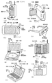
本発明を実施して作製されたアクティブマトリクス基板および液晶表示装置や有機EL表示装置は様々な電気光学装置に用いることができる。そして、そのような電気光学装置を表示部として組み込んだ電子機器全てに本発明を適用することがでできる。電子機器としては、携帯電話、ビデオカメラ、携帯情報端末、ゴーグル型ディスプレイ、記録媒体のプレーヤー、携帯書籍、パーソナルコンピュータ、デジタルカメラ、プロジェクターなどが上げられる。それらの一例を図25と図26に示す。
【0185】
図25(A)は携帯電話であり、本体9001、音声出力部9002、音声入力部9003、表示装置9004、操作スイッチ9005、アンテナ9006から構成されている。本願発明は音声出力部9002、音声入力部9003、及びアクティブマトリクス基板を備えた表示装置9004に適用することができる。
【0186】
図25(B)はビデオカメラであり、本体9101、表示装置9102、音声入力部9103、操作スイッチ9104、バッテリー9105、受像部9106で構成される。本発明は表示装置9102やその他の信号制御回路に適用することができる。
【0187】
図25(C)は携帯情報端末であり、本体9201、画像入力部9202、受像部9203、操作スイッチ9204、表示装置9205で構成される。本発明は表示装置9205やその他の信号制御回路に適用することができる。
【0188】
図25(D)はゴーグル型ディスプレイであり、本体9301、表示装置9302、アーム部9303で構成される。本願発明は表示装置9302に適用することができる。また、表示されていないが、その他の信号制御用回路に使用することもできる。
【0189】
図25(E)はプログラムを記録した記録媒体(以下、記録媒体と呼ぶ)を用いるプレーヤーであり、本体9401、表示装置9402、スピーカー部9403、記録媒体9404、操作スイッチ9405で構成される。尚、記録媒体にはDVD(Digital Versatile Disc)やコンパクトディスク(CD)などを用い、音楽プログラムの再生や映像表示、ビデオゲーム(またはテレビゲーム)やインターネットを介した情報表示などを行うことができる。本発明は表示装置9402やその他の信号制御回路に好適に利用することができる。
【0190】
図25(F)は携帯書籍であり、本体9501、表示装置9502、9503、記憶媒体9504、操作スイッチ9505、アンテナ9506から構成されており、ミニディスク(MD)やDVDに記憶されたデータや、アンテナで受信したデータを表示するものである。表示装置9502、9503は直視型の表示装置であり、本願発明はこの適用することができる。
【0191】
図25(G)はパーソナルコンピュータであり、マイクロプロセッサやメモリーなどを備えた本体9601、画像入力部9602、表示装置9603、キーボード9604で構成される。本発明は表示装置9603やその他の信号処理回路を形成することができる。
【0192】
図26(H)はデジタルカメラであり、本体9701、表示装置9702、接眼部9703、操作スイッチ9704、受像部(図示しない)で構成される。本発明は表示装置9702やその他の信号制御回路に適用することができる。
【0193】
図26(A)はフロント型プロジェクターであり、光源光学系および表示装置2601、スクリーン2602で構成される。本発明は表示装置やその他の信号制御回路に適用することができる。図26(B)はリア型プロジェクターであり、本体2701、光源光学系および表示装置2702、ミラー2703、スクリーン2704で構成される。本発明は表示装置やその他の信号制御回路に適用することができる。
【0194】
なお、図26(C)に、図26(A)および図26(B)における光源光学系および表示装置2601、2702の構造の一例を示す。光源光学系および表示装置2601、2702は光源光学系2801、ミラー2802、2804〜2806、ダイクロイックミラー2803、ビームスプリッター2807、液晶表示装置2808、位相差板2809、投射光学系2810で構成される。投射光学系2810は複数の光学レンズで構成される。図26(C)では液晶表示装置2808を三つ使用する三板式の例を示したが、このような方式に限定されず、単板式の光学系で構成しても良い。また、図26(C)中で矢印で示した光路には適宣光学レンズや偏光機能を有するフィルムや位相を調節するためのフィルムや、IRフィルムなどを設けても良い。また、図26(D)は図26(C)における光源光学系2801の構造の一例を示した図である。本実施例では、光源光学系2801はリフレクター2811、光源2812、レンズアレイ2813、2814、偏光変換素子2815、集光レンズ2816で構成される。尚、図26(D)に示した光源光学系は一例であって図示した構成に限定されるものではない。
【0195】
また、ここでは図示しなかったが、本発明はその他にも、ナビゲーションシステムやイメージセンサの読み取り回路などにも適用することも可能である。このように本願発明の適用範囲はきわめて広く、あらゆる分野の電子機器に適用することが可能である。また、本実施例の電子機器は実施形態および、実施例1〜9及び実施例11のどのような組み合わせから成る構成を用いても実現することができる。
【0196】
[実施例11]
本実施例では、本願発明を用いてEL(エレクトロルミネッセンス)表示装置を作製した例について説明する。
【0197】
図27(A)は本願発明を用いたEL表示装置の上面図である。図27(A)において、4010は基板、4011は画素部、4012はソース側駆動回路、4013はゲート側駆動回路であり、それぞれの駆動回路は配線4014〜4016を経てFPC4017に至り、外部機器へと接続される。
【0198】
このとき、少なくとも画素部、好ましくは駆動回路及び画素部を囲むようにしてカバー材6000、シーリング材(ハウジング材ともいう)7000、密封材(第2のシーリング材)7001が設けられている。
【0199】
また、図27(B)は本実施例のEL表示装置の断面構造であり、基板4010、下地膜4021の上に駆動回路用TFT(但し、ここではnチャネル型TFTとpチャネル型TFTを組み合わせたCMOS回路を図示している。)4022及び画素部用TFT4023(但し、ここではEL素子への電流を制御するTFTだけ図示している。)が形成されている。
【0200】
本願発明は、駆動回路用TFT4022、画素部用TF4023に際して用いることができる。
【0201】
本願発明を用いて駆動回路用TFT4022、画素部用TFT4023が完成したら、樹脂材料でなる層間絶縁膜(平坦化膜)4026の上に画素部用TFT4023のドレインと電気的に接続する透明導電膜でなる画素電極4027を形成する。画素電極4027が透明導電膜である場合、画素部用TFTとしては、pチャネル型TFTを用いることが好ましい。透明導電膜としては、酸化インジウムと酸化スズとの化合物(ITOと呼ばれる)または酸化インジウムと酸化亜鉛との化合物を用いることができる。そして、画素電極4027を形成したら、絶縁膜4028を形成し、画素電極4027上に開口部を形成する。
【0202】
次に、EL層4029を形成する。EL層4029は公知のEL材料(正孔注入層、正孔輸送層、発光層、電子輸送層または電子注入層)を自由に組み合わせて積層構造または単層構造とすれば良い。どのような構造とするかは公知の技術を用いれば良い。また、EL材料には低分子系材料と高分子系(ポリマー系)材料がある。低分子系材料を用いる場合は蒸着法を用いるが、高分子系材料を用いる場合には、スピンコート法、印刷法またはインクジェット法等の簡易な方法を用いることが可能である。
【0203】
本実施例では、シャドーマスクを用いて蒸着法によりEL層を形成する。シャドーマスクを用いて画素毎に波長の異なる発光が可能な発光層(赤色発光層、緑色発光層及び青色発光層)を形成することで、カラー表示が可能となる。その他にも、色変換層(CCM)とカラーフィルターを組み合わせた方式、白色発光層とカラーフィルターを組み合わせた方式があるがいずれの方法を用いても良い。勿論、単色発光のEL表示装置とすることもできる。
【0204】
EL層4029を形成したら、その上に陰極4030を形成する。陰極4030とEL層4029の界面に存在する水分や酸素は極力排除しておくことが望ましい。従って、真空中でEL層4029と陰極4030を連続成膜するか、EL層4029を不活性雰囲気で形成し、大気解放しないで陰極4030を形成するといった工夫が必要である。本実施例ではマルチチャンバー方式(クラスターツール方式)の成膜装置を用いることで上述のような成膜を可能とする。
【0205】
なお、本実施例では陰極4030として、LiF(フッ化リチウム)膜とAl(アルミニウム)膜の積層構造を用いる。具体的にはEL層4029上に蒸着法で1nm厚のLiF(フッ化リチウム)膜を形成し、その上に300nm厚のアルミニウム膜を形成する。勿論、公知の陰極材料であるMgAg電極を用いても良い。そして陰極4030は4031で示される領域において配線4016に接続される。配線4016は陰極4030に所定の電圧を与えるための電源供給線であり、導電性ペースト材料4032を介してFPC4017に接続される。
【0206】
4031に示された領域において陰極4030と配線4016とを電気的に接続するために、層間絶縁膜4026及び絶縁膜4028にコンタクトホールを形成する必要がある。これらは層間絶縁膜4026のエッチング時(画素電極用コンタクトホールの形成時)や絶縁膜4028のエッチング時(EL層形成前の開口部の形成時)に形成しておけば良い。また、絶縁膜4028をエッチングする際に、層間絶縁膜4026まで一括でエッチングしても良い。この場合、層間絶縁膜4026と絶縁膜4028が同じ樹脂材料であれば、コンタクトホールの形状を良好なものとすることができる。
【0207】
このようにして形成されたEL素子の表面を覆って、パッシベーション膜6003、充填材6004、カバー材6000が形成される。
【0208】
さらに、EL素子部を囲むようにして、カバー材7000と基板4010の内側にシーリング材が設けられ、さらにシーリング材7000の外側には密封材(第2のシーリング材)7001が形成される。
【0209】
このとき、この充填材6004は、カバー材6000を接着するための接着剤としても機能する。充填材6004としては、PVC(ポリビニルクロライド)、エポキシ樹脂、シリコーン樹脂、PVB(ポリビニルブチラル)またはEVA(エチレンビニルアセテート)を用いることができる。この充填材6004の内部に乾燥剤を設けておくと、吸湿効果を保持できるので好ましい。
【0210】
また、充填材6004の中にスペーサーを含有させてもよい。このとき、スペーサーをBaOなどからなる粒状物質とし、スペーサー自体に吸湿性をもたせてもよい。
【0211】
スペーサーを設けた場合、パッシベーション膜6003はスペーサー圧を緩和することができる。また、パッシベーション膜とは別に、スペーサー圧を緩和する樹脂膜などを設けてもよい。
【0212】
また、カバー材6000としては、ガラス板、アルミニウム板、ステンレス板、FRP(Fiberglass−Reinforced Plastics)板、PVF(ポリビニルフルオライド)フィルム、マイラーフィルム、ポリエステルフィルムまたはアクリルフィルムを用いることができる。なお、充填材6004としてPVBやEVAを用いる場合、数十μmのアルミニウムホイルをPVFフィルムやマイラーフィルムで挟んだ構造のシートを用いることが好ましい。
【0213】
但し、EL素子からの発光方向(光の放射方向)によっては、カバー材6000が透光性を有する必要がある。
【0214】
また、配線4016はシーリング材7000および密封材7001と基板4010との隙間を通ってFPC4017に電気的に接続される。なお、ここでは配線4016について説明したが、他の配線4014、4015も同様にしてシーリング材7000および密封材7001の下を通ってFPC4017に電気的に接続される。
【0215】
[実施例12]
本実施例では、本願発明を用いて実施例11とは異なる形態のEL表示装置を作製した例について、図28(A)、(B)を用いて説明する。図27(A)、(B)と同じ番号のものは同じ部分を指しているので説明は省略する。
【0216】
図28(A)は本実施例のEL表示装置の上面図であり、図28(A)をA-A'で切断した断面図を図28(B)に示す。
【0217】
実施例11に従って、EL素子の表面を覆ってパッシベーション膜6003までを形成する。
【0218】
さらに、EL素子を覆うようにして充填材6004を設ける。この充填材6004は、カバー材6000を接着するための接着剤としても機能する。充填材6004としては、PVC(ポリビニルクロライド)、エポキシ樹脂、シリコーン樹脂、PVB(ポリビニルブチラル)またはEVA(エチレンビニルアセテート)を用いることができる。この充填材6004の内部に乾燥剤を設けておくと、吸湿効果を保持できるので好ましい。
【0219】
また、充填材6004の中にスペーサーを含有させてもよい。このとき、スペーサーをBaOなどからなる粒状物質とし、スペーサー自体に吸湿性をもたせてもよい。
【0220】
スペーサーを設けた場合、パッシベーション膜6003はスペーサー圧を緩和することができる。また、パッシベーション膜とは別に、スペーサー圧を緩和する樹脂膜などを設けてもよい。
【0221】
また、カバー材6000としては、ガラス板、アルミニウム板、ステンレス板、FRP(Fiberglass−Reinforced Plastics)板、PVF(ポリビニルフルオライド)フィルム、マイラーフィルム、ポリエステルフィルムまたはアクリルフィルムを用いることができる。なお、充填材6004としてPVBやEVAを用いる場合、数十μmのアルミニウムホイルをPVFフィルムやマイラーフィルムで挟んだ構造のシートを用いることが好ましい。
【0222】
但し、EL素子からの発光方向(光の放射方向)によっては、カバー材6000が透光性を有する必要がある。
【0223】
次に、充填材6004を用いてカバー材6000を接着した後、充填材6004の側面(露呈面)を覆うようにフレーム材6001を取り付ける。フレーム材6001はシーリング材(接着剤として機能する)6002によって接着される。このとき、シーリング材6002としては、光硬化性樹脂を用いるのが好ましいが、EL層の耐熱性が許せば熱硬化性樹脂を用いても良い。なお、シーリング材6002はできるだけ水分や酸素を透過しない材料であることが望ましい。また、シーリング材6002の内部に乾燥剤を添加してあっても良い。
【0224】
また、配線4016はシーリング材6002と基板4010との隙間を通ってFPC4017に電気的に接続される。なお、ここでは配線4016について説明したが、他の配線4014、4015も同様にしてシーリング材6002の下を通ってFPC4017に電気的に接続される。
【0225】
[実施例13]
本実施例ではEL表示装置の画素部の詳細な断面構造を図29に、上面構造を図30(A)に、回路図を図30(B)に示す。図29、図30(A)及び図30(B)では共通の符号を用いるので互いに参照すれば良い。
【0226】
図29において、基板3001上に設けられたスイッチング用TFT3002は本願発明のnチャネル型TFTを用いて形成される(実施例1〜8参照)。本実施例ではダブルゲート構造としているが、構造及び作製プロセスに大きな違いはないので説明は省略する。但し、ダブルゲート構造とすることで実質的に二つのTFTが直列された構造となり、オフ電流値を低減することができるという利点がある。なお、本実施例ではダブルゲート構造としているが、シングルゲート構造でも構わないし、トリプルゲート構造やそれ以上のゲート本数を持つマルチゲート構造でも構わない。また、本願発明のpチャネル型TFTを用いて形成しても構わない。
【0227】
また、電流制御用TFT3003は本願発明のnチャネル型TFTを用いて形成される。このとき、スイッチング用TFT3002のドレイン配線3035は配線3036によって電流制御用TFTのゲート電極3037に電気的に接続されている。また、3038で示される配線は、スイッチング用TFT3002のゲート電極3039a、3039bを電気的に接続するゲート配線である。
【0228】
このとき、電流制御用TFT3003が本願発明の構造であることは非常に重要な意味を持つ。電流制御用TFTはEL素子を流れる電流量を制御するための素子であるため、多くの電流が流れ、熱による劣化やホットキャリアによる劣化の危険性が高い素子でもある。そのため、電流制御用TFTのドレイン側に、ゲート絶縁膜を介してゲート電極に重なるようにGOLD領域(第2の不純物領域)を設ける本願発明の構造は極めて有効である。
【0229】
また、本実施例では電流制御用TFT3003をシングルゲート構造で図示しているが、複数のTFTを直列につなげたマルチゲート構造としても良い。さらに、複数のTFTを並列につなげて実質的にチャネル形成領域を複数に分割し、熱の放射を高い効率で行えるようにした構造としても良い。このような構造は熱による劣化対策として有効である。
【0230】
また、図30(A)に示すように、電流制御用TFT3003のゲート電極3037となる配線は3004で示される領域で、電流制御用TFT3003のドレイン配線3040と絶縁膜を介して重なる。このとき、3004で示される領域ではコンデンサが形成される。このコンデンサ3004は電流制御用TFT3003のゲートにかかる電圧を保持するためのコンデンサとして機能する。なお、ドレイン配線3040は電流供給線(電源線)3006に接続され、常に一定の電圧が加えられている。
【0231】
スイッチング用TFT3002及び電流制御用TFT3003の上には第1パッシベーション膜3041が設けられ、その上に樹脂絶縁膜でなる平坦化膜3042が形成される。平坦化膜3042を用いてTFTによる段差を平坦化することは非常に重要である。後に形成されるEL層は非常に薄いため、段差が存在することによって発光不良を起こす場合がある。従って、EL層をできるだけ平坦面に形成しうるように画素電極を形成する前に平坦化しておくことが望ましい。
【0232】
また、3043は反射性の高い導電膜でなる画素電極(EL素子の陰極)であり、電流制御用TFT3003のドレインに電気的に接続される。この場合においては、電流制御用TFTとしてnチャネル型TFTを用いることが好ましい。画素電極3043としてはアルミニウム合金膜、銅合金膜または銀合金膜など低抵抗な導電膜またはそれらの積層膜を用いることが好ましい。勿論、他の導電膜との積層構造としても良い。
【0233】
また、絶縁膜(好ましくは樹脂)で形成されたバンク44a、44bにより形成された溝(画素に相当する)の中に発光層45が形成される。なお、ここでは一画素しか図示していないが、R(赤)、G(緑)、B(青)の各色に対応した発光層を作り分けても良い。発光層とする有機EL材料としてはπ共役ポリマー系材料を用いる。代表的なポリマー系材料としては、ポリパラフェニレンビニレン(PPV)系、ポリビニルカルバゾール(PVK)系、ポリフルオレン系などが挙げられる。
【0234】
なお、PPV系有機EL材料としては様々な型のものがあるが、例えば「H. Shenk,H.Becker,O.Gelsen,E.Kluge,W.Kreuder,and H.Spreitzer,“Polymers for Light Emitting Diodes”,Euro Display,Proceedings,1999,p.33-37」や特開平10−92576号公報に記載されたような材料を用いれば良い。
【0235】
具体的な発光層としては、赤色に発光する発光層にはシアノポリフェニレンビニレン、緑色に発光する発光層にはポリフェニレンビニレン、青色に発光する発光層にはポリフェニレンビニレン若しくはポリアルキルフェニレンを用いれば良い。膜厚は30〜150nm(好ましくは40〜100nm)とすれば良い。
【0236】
但し、以上の例は発光層として用いることのできる有機EL材料の一例であって、これに限定する必要はまったくない。発光層、電荷輸送層または電荷注入層を自由に組み合わせてEL層(発光及びそのためのキャリアの移動を行わせるための層)を形成すれば良い。
【0237】
例えば、本実施例ではポリマー系材料を発光層として用いる例を示したが、低分子系有機EL材料を用いても良い。また、電荷輸送層や電荷注入層として炭化珪素等の無機材料を用いることも可能である。これらの有機EL材料や無機材料は公知の材料を用いることができる。
【0238】
本実施例では発光層3045の上にPEDOT(ポリチオフェン)またはPAni(ポリアニリン)でなる正孔注入層3046を設けた積層構造のEL層としている。そして、正孔注入層3046の上には透明導電膜でなる陽極47が設けられる。本実施例の場合、発光層3045で生成された光は上面側に向かって(TFTの上方に向かって)放射されるため、陽極は透光性でなければならない。透明導電膜としては酸化インジウムと酸化スズとの化合物や酸化インジウムと酸化亜鉛との化合物を用いることができるが、耐熱性の低い発光層や正孔注入層を形成した後で形成するため、可能な限り低温で成膜できるものが好ましい。
【0239】
陽極3047まで形成された時点でEL素子3005が完成する。なお、ここでいうEL素子3005は、画素電極(陰極)3043、発光層3045、正孔注入層3046及び陽極3047で形成されたコンデンサを指す。図30(A)に示すように画素電極3043は画素の面積にほぼ一致するため、画素全体がEL素子として機能する。従って、発光の利用効率が非常に高く、明るい画像表示が可能となる。
【0240】
ところで、本実施例では、陽極3047の上にさらに第2パッシベーション膜3048を設けている。第2パッシベーション膜3048としては窒化珪素膜または窒化酸化珪素膜が好ましい。この目的は、外部とEL素子とを遮断することであり、有機EL材料の酸化による劣化を防ぐ意味と、有機EL材料からの脱ガスを抑える意味との両方を併せ持つ。これによりEL表示装置の信頼性が高められる。
【0241】
以上のように本願発明のEL表示パネルは図29のような構造の画素からなる画素部を有し、オフ電流値の十分に低いスイッチング用TFTと、ホットキャリア注入に強い電流制御用TFTとを有する。従って、高い信頼性を有し、且つ、良好な画像表示が可能なEL表示パネルが得られる。
【0242】
なお、本実施例の構成は、実施例1〜8構成と自由に組み合わせて実施することが可能である。また、実施例10の電子機器の表示部として本実施例のEL表示装置を用いることは有効である。
【0243】
[実施例14]
本実施例では、実施例13に示した画素部において、EL素子3005の構造を反転させた構造について説明する。説明には図31を用いる。なお、図29の構造と異なる点はEL素子の部分と電流制御用TFTだけであるので、その他の説明は省略することとする。
【0244】
図31において、電流制御用TFT3103は本願発明のpチャネル型TFTを用いて形成される。作製プロセスは実施例1〜8を参照すれば良い。
【0245】
本実施例では、画素電極(陽極)3050として透明導電膜を用いる。具体的には酸化インジウムと酸化亜鉛との化合物でなる導電膜を用いる。勿論、酸化インジウムと酸化スズとの化合物でなる導電膜を用いても良い。
【0246】
そして、絶縁膜でなるバンク3051a、3051bが形成された後、溶液塗布によりポリビニルカルバゾールでなる発光層52が形成される。その上にはカリウムアセチルアセトネート(acacKと表記される)でなる電子注入層3053、アルミニウム合金でなる陰極3054が形成される。この場合、陰極3054がパッシベーション膜としても機能する。こうしてEL素子3101が形成される。
【0247】
本実施例の場合、発光層3052で発生した光は、矢印で示されるようにTFTが形成された基板の方に向かって放射される。
【0248】
なお、本実施例の構成は、実施例1〜8の構成と自由に組み合わせて実施することが可能である。また、実施例10の電子機器の表示部として本実施例のEL表示パネルを用いることは有効である。
【0249】
[実施例15]
本実施例では、図30(B)に示した回路図とは異なる構造の画素とした場合の例について図32(A)〜(C)に示す。なお、本実施例において、3201はスイッチング用TFT3202のソース配線、3203はスイッチング用TFT3202のゲート配線、3204は電流制御用TFT、3205はコンデンサ、3206、3208は電流供給線、3207はEL素子とする。
【0250】
図32(A)は、二つの画素間で電流供給線3206を共通とした場合の例である。即ち、二つの画素が電流供給線3206を中心に線対称となるように形成されている点に特徴がある。この場合、電源供給線の本数を減らすことができるため、画素部をさらに高精細化することができる。
【0251】
また、図32(B)は、電流供給線3208をゲート配線3203と平行に設けた場合の例である。なお、図32(B)では電流供給線3208とゲート配線3203とが重ならないように設けた構造となっているが、両者が異なる層に形成される配線であれば、絶縁膜を介して重なるように設けることもできる。この場合、電源供給線3208とゲート配線3203とで専有面積を共有させることができるため、画素部をさらに高精細化することができる。
【0252】
また、図32(C)は、図32(B)の構造と同様に電流供給線3208をゲート配線3203a、3230bと平行に設け、さらに、二つの画素を電流供給線3208を中心に線対称となるように形成する点に特徴がある。また、電流供給線3208をゲート配線3203a、3230bのいずれか一方と重なるように設けることも有効である。この場合、電源供給線の本数を減らすことができるため、画素部をさらに高精細化することができる。
【0253】
なお、本実施例の構成は、実施例1〜8の構成と自由に組み合わせて実施することが可能である。また、実施例10の電子機器の表示部として本実施例の画素構造を有するEL表示表示装置を用いることは有効である。
【0254】
[実施例16]
実施例13に示した図30(A)、(B)では電流制御用TFT3003のゲートにかかる電圧を保持するためにコンデンサ3004を設ける構造としているが、コンデンサ3004を省略することも可能である。実施例13の場合、電流制御用TFT3003として実施例1〜8に示すような本願発明のnチャネル型TFTを用いているため、ゲート絶縁膜を介してゲート電極に重なるように設けられたGOLD領域(第2の不純物領域)を有している。この重なり合った領域には一般的にゲート容量と呼ばれる寄生容量が形成されるが、本実施例ではこの寄生容量をコンデンサ3004の代わりとして積極的に用いる点に特徴がある。
【0255】
この寄生容量のキャパシタンスは、上記ゲート電極とGOLD領域とが重なり合った面積によって変化するため、その重なり合った領域に含まれるGOLD領域の長さによって決まる。
【0256】
また、実施例15に示した図32(A)、(B)、(C)の構造においても同様に、コンデンサ3205を省略することは可能である。
【0257】
なお、本実施例の構成は、実施例1〜8の構成と自由に組み合わせて実施することが可能である。また、実施例10の電子機器の表示部として本実施例の画素構造を有するEL表示装置を用いることは有効である。
【0258】
【発明の効果】
本願発明を実施することで、画素マトリクス回路のnチャネル型TFTに15〜20Vのゲート電圧を印加して駆動させても、安定した動作を得ることができた。その結果、結晶質TFTで作製されたCMOS回路を含む半導体装置、また、具体的には液晶表示装置の画素マトリクス回路や、その周辺に設けられる駆動回路の信頼性を高め、長時間の使用に耐える液晶表示装置を得ることができた。
【0259】
また、本発明によれば、nチャネル型TFTのチャネル形成領域とドレイン領域との間に形成される第2の不純物領域において、その第2の不純物領域がゲート電極と重なる領域(GOLD領域)と重ならない領域(LDD領域)の長さを容易に作り分けることが可能である。具体的には、TFTの駆動電圧に応じて第2の不純物領域がゲート電極と重なる領域(GOLD領域)と重ならない領域(LDD領域)の長さを決めることも可能であり、このことは、同一基板内において異なる駆動電圧でTFT動作させる場合に、それぞれの駆動電圧に応じたTFTを同一工程で作製することを可能とする。
【0260】
また、本発明のこのような特徴は、駆動電圧や要求されるTFT特性が画素マトリクス回路とドライバ回路で異なるアクティブマトリクス型の液晶表示装置においてきわめて適したものである。
【図面の簡単な説明】
【図1】 本実施形態のTFTの断面図。
【図2】 ゲート電極と第2の不純物領域との位置関係を説明する図。
【図3】 TFTの作製工程を示す断面図。
【図4】 TFTの作製工程を示す断面図。
【図5】 TFTの作製工程を示す断面図。
【図6】 TFTの作製工程を示す断面図。
【図7】 TFTの作製工程を示す断面図。
【図8】 TFTの作製工程を示す断面図。
【図9】 TFTの作製工程を示す断面図。
【図10】 TFTの作製工程を示す断面図。
【図11】 TFTの作製工程を示す断面図。
【図12】 TFTの作製工程を示す断面図。
【図13】 TFTの作製工程を示す断面図。
【図14】 アクティブマトリクス基板の斜視図。
【図15】 アクティブマトリクス回路とCMOS回路の上面図。
【図16】 液晶表示装置の作製工程を示す断面図。
【図17】 ゲート電極の構成を示す図。
【図18】 TFTの構造と電気的特性を説明する図。
【図19】 結晶質シリコン膜の作製工程を示す図。
【図20】 結晶質シリコン膜の作製工程を示す図。
【図21】 結晶質シリコン膜の作製工程を示す図。
【図22】 TFTの作製工程を示す断面図。
【図23】 インバータ回路図、上面図、および断面構造図。
【図24】 強誘電性混合液晶の光透過率特性を示す図。
【図25】 半導体装置の一例を示す図。
【図26】 プロジェクターの構成を説明する図。
【図27】 アクティブマトリクス型EL表示装置の上面図及び断面図。
【図28】 アクティブマトリクス型EL表示装置の上面図及び断面図。
【図29】 アクティブマトリクス型EL表示装置の画素部の断面図。
【図30】 アクティブマトリクス型EL表示装置の画素部の上面図及び回路図。
【図31】 アクティブマトリクス型EL表示装置の画素部の断面図。
【図32】 アクティブマトリクス型EL表示装置の画素部の回路図。[0001]
BACKGROUND OF THE INVENTION
The present invention relates to a semiconductor device having a circuit including a thin film transistor (hereinafter referred to as TFT) on a substrate having an insulating surface, and a method for manufacturing the semiconductor device. For example, the present invention relates to an electro-optical device typified by a liquid crystal display device and a configuration of an electronic apparatus equipped with the electro-optical device. Note that in this specification, a semiconductor device refers to all devices that function by utilizing semiconductor characteristics, and includes the above-described electro-optical device and electronic devices in which the electro-optical device is mounted.
[0002]
[Prior art]
Technological development for manufacturing an active matrix liquid crystal display device by providing TFTs on a glass substrate or a quartz substrate is being actively promoted. In particular, a TFT having a semiconductor film having a crystal structure as an active layer (hereinafter referred to as a crystalline TFT) can obtain high mobility. Therefore, a high-definition image display can be realized by integrating functional circuits on the same substrate. Is supposed to be possible.
[0003]
Here, in the present specification, the semiconductor film having the crystal structure includes a single crystal semiconductor, a polycrystalline semiconductor, and a microcrystalline semiconductor, and further includes Japanese Patent Application Laid-Open Nos. H7-130652, H8-78329, The semiconductors disclosed in JP-A-10-135468, JP-A-10-135469, or JP-A-10-247735 are included.
[0004]
In order to construct an active matrix liquid crystal display device, it is necessary to provide one to two million n-channel TFTs (hereinafter referred to as pixel TFTs) of a pixel matrix circuit, and if a functional circuit provided in the periphery is added, The above crystalline TFT is necessary. The specifications required for the liquid crystal display device are strict, and in order to stably display an image, it is first necessary to ensure the reliability of each crystalline TFT.
[0005]
The characteristics of a field effect transistor such as a TFT are ideal for a linear region where the drain current and drain voltage increase proportionally, a saturation region where the drain current saturates even when the drain voltage increases, and a drain voltage applied Can be divided into a cut-off region where no current flows. In this specification, the linear region and the saturation region are referred to as the TFT on region, and the blocking region is referred to as the off region. For convenience, the drain current in the on region is referred to as on-current, and the current in the off region is referred to as off-current.
[0006]
A gate voltage having an amplitude of about 15 to 20 V is applied to the pixel TFT as a driving condition. Therefore, it is necessary to satisfy the characteristics of both the on region and the off region. On the other hand, a peripheral circuit for driving the pixel matrix circuit is configured based on a CMOS circuit, and the on-region characteristics are mainly emphasized.
[0007]
However, crystalline TFTs are still considered to be less reliable than MOS transistors (transistors fabricated on a single crystal semiconductor substrate) used in LSI and the like in terms of reliability. For example, when a crystalline TFT is continuously driven, deterioration phenomena such as field effect mobility, a decrease in on-current, and an increase in off-current may be observed. This is due to a hot carrier injection phenomenon, and hot carriers generated by a high electric field near the drain cause a deterioration phenomenon.
[0008]
In the technical field of LSI, a lightly doped drain (LDD) structure is known as a method for reducing the off-state current of a MOS transistor and relaxing a high electric field near the drain. In this structure, a low concentration impurity region is provided outside the channel formation region, and this low concentration impurity region is called an LDD region.
[0009]
It is naturally known that an LDD structure is formed even in a crystalline TFT. For example, in JP-A-7-202210, a gate electrode has a two-layer structure with different widths, an upper layer width is formed smaller than a lower layer width, and ion implantation is performed using the gate electrode as a mask. The LDD region is formed by a single ion implantation by utilizing the difference in ion penetration depth due to the difference in the thickness of the gate electrode. The gate electrode overlaps directly above the LDD region.
[0010]
Such a structure is known as a GOLD (Gate-drain Overlapped LDD) structure, a LATID (Large-tilt-angle implanted drain) structure, an ITLDD (Inverse T LDD) structure, or the like. Then, the high electric field in the vicinity of the drain can be relaxed to prevent the hot carrier injection phenomenon, and the reliability can be improved. For example, “Mutsuko Hatano, Hajime Akimoto and Takeshi Sakai, IEDM97 TECHNICAL DIGEST, p523-526, 1997” has a GOLD structure with sidewalls made of silicon, but extremely superior reliability compared to TFTs with other structures. Has been confirmed to be obtained.
[0011]
However, the structure disclosed in this paper has a problem that the off-current becomes larger than that of a normal LDD structure, and a countermeasure for that is required. In particular, in the pixel TFT constituting the pixel matrix circuit, when the off-current increases, power consumption increases and an abnormality appears in image display. Therefore, the GOLD structure cannot be applied to the crystalline TFT as it is.
[0012]
[Problems to be solved by the invention]
The present invention is a technique for solving such problems, and a crystalline TFT that achieves reliability equivalent to or higher than that of a MOS transistor and at the same time obtains good characteristics in both the on region and the off region. It aims to be realized. Then, an object is to realize a highly reliable semiconductor device having a semiconductor circuit in which a circuit is formed using such a crystalline TFT.
[0013]
[Means for Solving the Problems]
FIG. 18 schematically shows the structure of the TFT and the Vg-Id (gate voltage-drain current) characteristics obtained at that time, based on the knowledge thus far. FIG. 18A-1 illustrates the simplest TFT structure in which a semiconductor layer includes a channel formation region, a source region, and a drain region. (B-1) shows the characteristics of this TFT. The + Vg side is the on region of the TFT and the -Vg side is the off region. The solid line indicates the initial characteristics, and the broken line indicates the deterioration characteristics due to the hot carrier injection phenomenon. In this structure, both the on-current and the off-current are high and the deterioration is large, so that it cannot be used as it is, for example, in the pixel TFT of the pixel matrix circuit.
[0014]
FIG. 18A-2 illustrates a structure in which a low-concentration impurity region serving as an LDD region is provided in (A-1), which is an LDD structure that does not overlap with the gate electrode. FIG. 2B-2 shows the characteristics of this TFT, which can suppress the off current to some extent, but cannot prevent the deterioration of the on current. FIG. 18A-3 shows a structure in which the LDD region completely overlaps with the gate electrode, which is also called a GOLD structure. FIG. 5B-3 shows characteristics corresponding to this, and the degradation can be suppressed to a level that does not cause a problem, but the off-current is increased on the −Vg side as compared with the structure of (A-2).
[0015]
Accordingly, in the structure shown in FIGS. 18A-1, (A-2), and (A-3), the on-region characteristics and the off-region characteristics necessary for the pixel matrix circuit are included in the reliability problem. At the same time, I could not be satisfied. However, as shown in FIG. 18A-4, when a structure in which the LDD region is overlapped with the gate electrode and a portion where the LDD region is not overlapped is formed, deterioration of on-current is sufficiently suppressed, In addition, the off current can be reduced.
[0016]
The structure of FIG. 18A-4 is derived from the following consideration. In the structure as shown in FIG. 18A-3, when a negative voltage is applied to the gate electrode of the n-channel TFT, that is, in the LDD region formed overlapping the gate electrode in the off region. As the negative voltage increases, holes are induced at the interface with the gate insulating film, and a current path by minority carriers connecting the drain region, the LDD region, and the channel region is formed. At this time, if a positive voltage is applied to the drain region, holes flow to the source region side, which is considered to be a cause of an increase in off-current.
[0017]
In order to cut off such a current path in the middle, it can be considered that an LDD region in which minority carriers are not accumulated even when a gate voltage is applied may be provided. The present invention relates to a TFT having such a configuration and a circuit using this TFT.
[0018]
Therefore, the structure of the present invention is a semiconductor in which a TFT having a semiconductor layer, a gate insulating film formed on the semiconductor layer, and a gate electrode formed on the gate insulating film is formed on a substrate. In the device, the gate electrode is formed on the first layer of the gate electrode formed in contact with the gate insulating film, and on the first layer of the gate electrode and inside the first layer of the gate electrode. A second layer of the gate electrode to be formed; a third layer of the gate electrode formed in contact with the first layer of the gate electrode and the second layer of the gate electrode; The layer includes a channel formation region, a first conductivity type first impurity region, and a one conductivity type second impurity region formed between the channel formation region and the first impurity region. , Part of the second impurity region of the one conductivity type is the gate electrode It is characterized in that overlaps the first layer.
[0019]
According to another aspect of the invention, there is provided a first step of forming a semiconductor layer on a substrate having an insulating surface, a second step of forming a gate insulating film in contact with the semiconductor layer, and the gate insulation. A third step of sequentially forming a conductive layer (A) and a conductive layer (B) on the film, and etching the conductive layer (B) into a predetermined pattern to form a second layer of the gate electrode A fourth step, a fifth step of adding an impurity element of one conductivity type to a selected region of the semiconductor layer, the conductive layer (A) and the second layer of the gate electrode, A sixth step of forming a conductive layer (C), and etching the conductive layer (C) and the conductive layer (A) into a predetermined pattern to form a third layer of the gate electrode and a first layer of the gate electrode; A seventh step of forming an eye, and an impurity element of one conductivity type is added to a selected region of the semiconductor layer It is characterized by having a eighth step.
[0020]
According to another aspect of the invention, there is provided a first step of forming a semiconductor layer on a substrate having an insulating surface, a second step of forming a gate insulating film in contact with the semiconductor layer, and the gate insulation. A third step of sequentially forming a conductive layer (A) and a conductive layer (B) on the film, and etching the conductive layer (B) into a predetermined pattern to form a second layer of the gate electrode A fourth step, a fifth step of adding an impurity element of one conductivity type to a selected region of the semiconductor layer, the conductive layer (A) and the second layer of the gate electrode, A sixth step of forming a conductive layer (C), and etching the conductive layer (C) and the conductive layer (A) into a predetermined pattern to form a third layer of the gate electrode and a first layer of the gate electrode; A seventh step of forming an eye, and an impurity element of one conductivity type is added to a selected region of the semiconductor layer A step of eighth, is characterized by having a ninth step of removing a portion of the third layer of the first layer and the gate electrode of the gate electrode.
[0021]
According to another aspect of the invention, there is provided a first step of forming a first semiconductor layer and a second semiconductor layer on a substrate having an insulating surface, and the first semiconductor layer and the second semiconductor layer. A second step of forming a gate insulating film, a third step of sequentially forming a conductive layer (A) and a conductive layer (B) on the gate insulating film, and a predetermined step of forming the conductive layer (B). A fourth step of forming the second layer of the gate electrode by etching into the pattern of step 5, and a fifth step of adding an impurity element of one conductivity type to the selected region of the first semiconductor layer; A sixth step of forming a conductive layer (C) in contact with the conductive layer (A) and the second layer of the gate electrode, and the conductive layer (C) and the conductive layer (A) Etching to a pattern to form a third layer of the gate electrode and a first layer of the gate electrode; An eighth step of adding a physical element to a selected region of the first semiconductor layer and the second semiconductor layer; and an impurity having a conductivity type opposite to the one conductivity type is selected in the second semiconductor layer. And a ninth step of adding to the region.
[0022]
Such a TFT can be suitably used for an n-channel TFT or a pixel TFT of a CMOS circuit. In the structure of the TFT of the present invention, the first impurity region formed in the semiconductor layer functions as a source region or a drain region, and the second impurity region functions as an LDD region. Therefore, the concentration of the impurity element of one conductivity type is lower in the second impurity region than in the first impurity region.
[0023]
In addition, a storage capacitor is formed from an impurity region of one conductivity type provided at one end of the semiconductor layer, the gate insulating film, and a wiring formed from the first layer to the third layer of the gate electrode. And the storage capacitor can be connected to the source or drain of the TFT.
[0024]
Further, the first layer of the gate electrode and the third layer of the gate electrode are selected from silicon (Si), titanium (Ti), tantalum (Ta), tungsten (W), and molybdenum (Mo). One or more kinds of elements, or a compound containing the above elements as a component, and the second layer of the gate electrode is one or more kinds of elements selected from aluminum (Al) and copper (Cu) Or a compound containing the above element as a main component.
[0025]
DETAILED DESCRIPTION OF THE INVENTION
An embodiment of the present invention will be described with reference to FIG. As the substrate 101 having an insulating surface, a glass substrate, a plastic substrate, a ceramic substrate, or the like can be used. Alternatively, a silicon substrate or a stainless steel substrate on which an insulating film such as a silicon oxide film is formed may be used. It is also possible to use a quartz substrate.
[0026]
A
[0027]
A semiconductor layer formed in contact with the
[0028]
Alternatively, the semiconductor layer formed over the
[0029]
FIG. 1 shows cross-sectional structures of an n-channel TFT and a p-channel TFT. The gate electrodes of the n-channel TFT and the p-channel TFT are composed of a first layer of the gate electrode, a second layer of the gate electrode, and a third layer of the gate electrode. The
[0030]
The
[0031]
The
[0032]
The
[0033]
In any case, the first layer of the gate electrode, the second layer of the gate electrode, and the third layer of the gate electrode may be formed by sputtering to form a film of the above material. It is formed into a predetermined shape by etching. Here, in order to form the third layer of the gate electrode so as to cover the second layer of the gate electrode, the thickness of the second layer of the gate electrode is controlled as described above. It is necessary to set the sputtering conditions appropriately. For example, it is an effective means to relatively slow the film formation rate of the film to be formed.
[0034]
As the structure of the gate electrode as shown in FIG. 1, the heat resistance can be improved by making the second layer of the gate electrode surrounded by the first layer of the gate electrode and the third layer of the gate electrode. it can. As a material for the gate electrode, it is desirable to use a material having a low resistivity such as Al or Cu. However, when heated at a temperature of 450 ° C. or higher, hillocks are generated or diffused into the surrounding insulating film or semiconductor layer. There is a point. However, such a phenomenon can be prevented by using a clad structure surrounded by materials such as Si, Ti, Ta, W, and Mo, or materials containing these materials as components.
[0035]
The semiconductor layer of the n-channel TFT includes a
[0036]
On the other hand, the
[0037]
The impurity element to the second impurity region is formed by a method in which an impurity element imparting n-type conductivity is added to the semiconductor layer through the
[0038]
As shown in FIGS. 2A and 2B, the
[0039]
This is a very convenient method when manufacturing circuits with different drive voltages on the same substrate. FIG. 2B shows an example of design values of TFTs used for a logic circuit portion, a buffer circuit portion, an analog switch portion, and a pixel matrix circuit of a liquid crystal display device. At this time, it is possible to set the length of the
[0040]
Since the TFT of the shift register circuit of the driver circuit and the TFT of the buffer circuit are basically focused on the characteristics of the ON region, the so-called GOLD structure may be used, and the
[0041]
Further, since it is not necessary for the TFT provided in the analog switch or the pixel matrix circuit to increase the off-current, for example, when the driving voltage is 16 V, the channel length is 3 μm and the
[0042]
As shown in FIG. 17, in the present invention, the length of the first layer 1701 of the gate electrode, the second layer 1702 of the gate electrode, and the third layer 1703 of the gate electrode in the channel length direction is This is closely related to the size of the TFT to be manufactured. The length in the channel length direction of the second layer 1702 of the gate electrode substantially corresponds to the channel length L1. At this time, L1 may be 0.1 to 10 μm, typically 0.2 to 5 μm.
[0043]
Further, the length L6 of the second impurity region 1705 can be arbitrarily set by masking with a photoresist as described above, but it is 0.2 to 6 μm, typically 0.6 to 3 μm. It is desirable to do.
[0044]
The length L4 where the second impurity region 1705 overlaps with the gate electrode is closely related to the length L2 of the first layer 1701 of the gate electrode. The length of L4 is preferably 0.1 to 4 μm, typically 0.5 to 3 μm. The length L5 at which the second impurity region 1705 does not overlap with the gate electrode is not necessarily provided as described above, but is usually 0.1 to 3 μm, typically 0.3 to It is good to set it as 2 micrometers. Here, the lengths of L4 and L5 may be determined based on the driving voltage of the TFT as described above, for example.
[0045]
In FIG. 1, the
[0046]
As described above, in the present invention, the gate electrode is formed of the
[0047]
In the n-channel TFT, the second impurity region may be provided only on the drain region side (the
[0048]
On the other hand, the p-channel TFT has a structure in which a
[0049]
When the n-channel TFT and the p-channel TFT are thus completed, the source wirings 120 and 121 and the
[0050]
In FIG. 1, a CMOS circuit formed by complementary combination of an n-channel TFT and a p-channel TFT is shown as an example. However, the present invention is applied to an NMOS circuit using an n-channel TFT or a pixel matrix circuit of a liquid crystal display device. The invention can also be applied.
[0051]
The configuration of the present invention described above will be described in more detail in the following examples.
[0052]
[Example 1]
In this embodiment, a method for simultaneously manufacturing a CMOS circuit which is a basic form of a pixel matrix circuit and a driver circuit provided in the periphery of the pixel matrix circuit will be described.
[0053]
In FIG. 3A, a non-alkali glass substrate typified by a Corning 1737 glass substrate is used as the
[0054]
Besides, SiH by plasma CVD method Four , NH Three , N 2 A silicon oxynitride film made of O is 10 to 200 nm (preferably 50 to 100 nm), similarly SiH Four , N 2 A silicon oxynitride film formed from O is stacked to a thickness of 50 to 200 nm (preferably 100 to 150 nm).
[0055]
Next, an amorphous silicon film having a thickness of 50 nm is formed on the
[0056]
Here, since both the base film and the amorphous silicon film can be formed by a plasma CVD method, the base film and the amorphous silicon film may be continuously formed in a vacuum. After the formation of the base film, once the process is not exposed to the air atmosphere, surface contamination can be prevented, and variations in characteristics of TFTs to be manufactured can be reduced.
[0057]
A known laser annealing method or thermal annealing method may be used for the step of crystallizing the amorphous silicon film. In this embodiment, a pulsed oscillation type KrF excimer laser beam is condensed into a linear shape and irradiated to an amorphous silicon film to form a crystalline silicon film.
[0058]
When crystallization is performed by laser annealing, a pulse oscillation type or continuous light emission type excimer laser or argon laser is used as the light source. Alternatively, a YAG laser may be used as the light source, and its fundamental frequency, second harmonic, third harmonic, and fourth harmonic may be used as the light source. In the case of using a pulse oscillation type excimer laser, laser annealing is performed by processing laser light into a linear shape. The laser annealing conditions are appropriately selected by the practitioner. For example, the laser pulse oscillation frequency is 30 Hz, and the laser energy density is 100 to 500 mJ / cm. 2 (Typically 300-400mJ / cm 2 ). Then, a linear beam is irradiated over the entire surface of the substrate, and the linear beam superposition ratio (overlap ratio) at this time is set to 80 to 98%.
[0059]
In this embodiment, a crystalline silicon film is formed from an amorphous silicon film as a semiconductor layer. However, a microcrystalline silicon film may be used, or a crystalline silicon film may be formed directly.
[0060]
The crystalline silicon film thus formed is patterned to form island-shaped semiconductor layers 303, 304, and 305.
[0061]
Next, a
[0062]
Then, a gate electrode including a first layer of the gate electrode, a second layer of the gate electrode, and a third layer of the gate electrode is formed over the
[0063]
Management of the thickness of the
[0064]
The conductive layer (B) is preferably made of a material selected from Al and Cu. This is provided to lower the electric resistance of the gate electrode, and is formed to a thickness of 50 to 400 nm, preferably 100 to 200 nm. When Al is used, pure Al may be used, or an Al alloy to which an element selected from Ti, Si, and Sc is added in an amount of 0.1 to 5 atomic% may be used. In the case of using copper, although not shown, it is preferable to provide a silicon nitride film with a thickness of 30 to 100 nm on the surface of the
[0065]
Here, an Al film added with 0.5 atomic% of Sc is formed to a thickness of 200 nm by sputtering (FIG. 3A).
[0066]
Next, a resist mask is formed using a known patterning technique, and a step of removing part of the conductive layer (B) 308 is performed. Here, since the conductive layer (B) 308 is formed of an Al film to which 0.5 atomic% of Sc is added, the wet etching method using a phosphoric acid solution is performed. Then, as shown in FIG. 3B,
[0067]
Although this step can be performed by a dry etching method, a wet etching method is used to remove an unnecessary region of the conductive layer (B) 308 with high selectivity without damaging the conductive layer (A) 307. preferable.
[0068]
In addition, a storage capacitor is provided on the drain side of the pixel TFT constituting the pixel matrix circuit. At this time, the
[0069]
Then, a resist mask 314 is formed in a region where a p-channel TFT is to be formed, and a first step of adding an impurity element imparting n-type conductivity is performed. Phosphorus (P), arsenic (As), antimony (Sb), and the like are known as impurity elements imparting n-type to crystalline semiconductor materials. Here, phosphorous is used, and phosphine (PH Three ) Using an ion doping method. In this step, in order to add phosphorus to the semiconductor layer thereunder through the
[0070]
Then, after removing the resist mask 314, the conductive layer (A) 307, the
[0071]
Next, a resist mask is formed using a known patterning technique, and a step of removing part of the conductive layer (C) 321 and the conductive layer (A) 307 is performed. Here, dry etching is performed. The conductive layer (C) 321 is Ta, and the dry etching condition is CF. Four 80 SCCM, O 2 20 SCCM is introduced and 500 m high frequency power is applied at 100 mTorr. At this time, the etching rate of Ta is 60 nm / min. The condition for etching the conductive layer (A) 307 is SiCl. Four 40 SCCM, Cl 2 5SCCM, BCl Three 180 SCCM is introduced and high frequency power of 80 mTorr and 1200 W is applied. At this time, the etching rate of Ti is 34 nm / min.
[0072]
A slight residue may be confirmed after etching, but it can be removed by cleaning with a solution such as SPX cleaning solution or EKC. Further, under the above etching conditions, the etching rate of the underlying
[0073]
Then, the
[0074]
In this manner, a gate electrode composed of the first layer of the gate electrode, the second layer of the gate electrode, and the third layer of the gate electrode is formed. In addition, a storage capacitor is provided on the drain side of the pixel TFT constituting the pixel matrix circuit. At this time, wirings 326 and 331 having a storage capacitor are formed from the conductive layer (A) and the conductive layer (C).
[0075]
Then, as shown in FIG. 4B, resist
[0076]
In this step, the length of the resist
[0077]
Next, a step of covering the region where the n-channel TFT is formed with resist
[0078]
When the steps up to FIG. 4C are completed, the resist
[0079]
The silicon nitride film formed here is necessary for performing the next heat treatment step. In this embodiment, the gate electrode having the cladding structure as described above is formed. In this structure, the second layer of the gate electrode formed of Al is surrounded by the first layer of the gate electrode formed of Ti and the third layer of the gate electrode formed of Ta. . Ta has the effect of preventing Al hillocks and seepage to the surroundings, but has a drawback that it is oxidized immediately when heated at 400 ° C. or higher at normal pressure. As a result, the electrical resistance increases. However, if the surface is covered with the
[0080]
The heat treatment step needs to be performed in order to activate the impurity element imparting n-type or p-type added at each concentration. This step may be performed by a thermal annealing method using an electric heating furnace, a laser annealing method using the above-described excimer laser, or a rapid thermal annealing method (RTA method) using a halogen lamp. However, the laser annealing method can be activated at a low substrate heating temperature, but it is difficult to activate the region that covers the gate electrode. Therefore, here, the activation process is performed by thermal annealing. The conditions at this time are 300 to 700 ° C., preferably 350 to 550 ° C., here 450 ° C. for 2 hours in a nitrogen atmosphere.
[0081]
The first
[0082]
Then, a
[0083]
Through the above steps, a gate electrode having a clad structure is formed, and a
[0084]
In the p-channel TFT, similarly, a gate electrode having a cladding structure is formed, and a
[0085]
In the pixel TFT of the pixel matrix circuit,
[0086]
Thus, as shown in FIG. 5, an active matrix substrate in which a CMOS circuit and a pixel matrix circuit are formed on a
[0087]
[Example 2]
In this embodiment, as in
[0088]
First, similarly to Example 1, the steps from FIG. 3A to FIG. 3C and the step from FIG. 4A are performed.
[0089]
FIG. 6A shows a state in which the gate electrode is formed from the first layer of the gate electrode, the second layer of the gate electrode, and the third layer of the gate electrode. Resist
[0090]
The resist
[0091]
Formation of such a resist mask is particularly effective for an n-channel TFT of a CMOS circuit. Since the LDD region is formed only on one side, the series resistance component of the TFT can be substantially reduced, and the on-current can be increased.
[0092]
Both the GOLD structure and the LDD structure described so far are provided to alleviate the high electric field in the vicinity of the drain region. If the structure is formed on the drain side of the TFT, the effect is sufficiently obtained. It is done.
[0093]
Further, resist
[0094]
The subsequent steps may be performed in the same manner as in the first embodiment.
[0095]
In the p-channel TFT, a
[0096]
[Example 3]
In this embodiment, as in
[0097]
First, the steps from FIGS. 3A to 3C are performed as in the first embodiment.
[0098]
8A, resist
[0099]
In addition, a storage capacitor is provided on the drain side of the pixel TFT of the pixel matrix circuit. At this time, wirings 855 and 860 having storage capacitors are formed from the conductive layer (A) and the conductive layer (C).
[0100]
Then, in the same manner as in Example 1, a second step of adding an impurity element imparting n-type is performed. In this step,
[0101]
Next, a photoresist film is formed again, and a patterning process is performed by exposure from the back surface. At this time, as shown in FIG. 8B, resist
[0102]
Using the resist
[0103]
8C, the
[0104]
Further, a resist mask 828, 829 is formed in a region where the n-channel TFT is formed, and a third impurity element imparting p-type conductivity is added (FIG. 8C).
[0105]
The subsequent steps may be performed in the same manner as in Example 1, and the active matrix substrate shown in FIG. 5 can be manufactured.
[0106]
[Example 4]
In this embodiment, as in
[0107]
First, the steps from FIGS. 3A to 3C are performed as in the first embodiment. Then, a gate electrode is formed as shown in FIG.
[0108]
Next, a resist mask is formed using a known patterning technique, and a step of removing part of the conductive layer (C) 321 and the conductive layer (A) 307 is performed. Here, dry etching is performed. The conductive layer (C) 321 is Ta, and the dry etching condition is CF. Four 80 SCCM, O 2 20 SCCM is introduced and 500 m high frequency power is applied at 100 mTorr. At this time, the etching rate of the Ta film is 60 nm / min. The condition for etching the conductive layer (A) 307 is SiCl. Four 40 SCCM, Cl 2 5SCCM, BCl Three 180 SCCM is introduced and high frequency power of 80 mTorr and 1200 W is applied. At this time, the etching rate of the Ti film is 34 nm / min.
[0109]
Then, the
[0110]
Under the above etching conditions, the
[0111]
However, in order to etch the gate insulating film, it is necessary to select a gas to be used, and CF is more preferable than chlorine-based gas. Four And NF Three Better results are obtained with fluorine-based gases such as
[0112]
Here, CF used when etching the Ta film Four And O 2 The mixed gas is used. CF Four 80 SCCM, O 2 20 SCCM is introduced and 500 m high frequency power is applied at 100 mTorr. Then, with respect to the
[0113]
Then, similarly to Example 1, resist
[0114]
Since the gate insulating film is thin, the acceleration voltage in the ion doping method can be reduced from 80 keV to 40 keV, and damage to the gate insulating film and the semiconductor layer can be reduced (FIG. 9B).
[0115]
Next, as shown in FIG. 9C, the steps of forming resist
[0116]
Other steps may be performed in accordance with the first embodiment, and source wirings 375, 376, and 377, drain wirings 378 and 379, a
[0117]
[Example 5]
In this embodiment, a method for simultaneously manufacturing a CMOS circuit which is a basic form of a pixel matrix circuit and a driver circuit provided in the periphery of the pixel matrix circuit will be described.
[0118]
In FIG. 11A, an alkali-free glass substrate typified by a Corning 1737 glass substrate is used as the
[0119]
Next, an amorphous silicon film having a thickness of 50 nm is formed on the
[0120]
Here, both the base film and the amorphous silicon film are produced by the plasma CVD method. At this time, the base film and the amorphous silicon film may be continuously formed in a vacuum. After the formation of the base film, once the process is not exposed to the air atmosphere, surface contamination can be prevented, and variation in characteristics of the manufactured TFT can be reduced.
[0121]
Here, a crystalline silicon film used as a semiconductor layer is formed by a thermal crystallization method using a catalytic element. In the case of using a catalyst element, it is desirable to use the techniques disclosed in Japanese Patent Application Laid-Open Nos. 7-130652 and 8-78329.
[0122]
Here, an example in the case of applying the technique disclosed in Japanese Patent Application Laid-Open No. 7-130652 to the present invention will be described with reference to FIGS. A silicon oxide film 1902 is formed over the substrate 1901, and an amorphous silicon film 1903 is formed thereover. A nickel acetate layer solution containing 10 ppm of nickel in terms of weight is applied to the surface of the amorphous silicon film 1903 to form a nickel-containing layer 1904 (FIG. 19A).
[0123]
Next, after a dehydrogenation step at 500 ° C. for 1 hour, a heat treatment is performed at 500 to 650 ° C. for 4 to 12 hours, for example, 550 ° C. for 8 hours to form a crystalline silicon film 1905 (FIG. 19B). ).
[0124]
Further, the technique disclosed in Japanese Patent Laid-Open No. 8-78329 enables selective crystallization of an amorphous silicon film by selectively adding a catalytic element. The case where this technique is applied to the present invention will be described with reference to FIGS.
[0125]
First, a silicon oxide film 2002 and an amorphous silicon film 2003 are formed over a glass substrate 2001, and a silicon oxide film 2004 is continuously formed. At this time, the thickness of the silicon oxide film 2004 is 150 nm.
[0126]
Next, the silicon oxide film 2004 is patterned to selectively form an
[0127]
Next, heat treatment is performed at 500 to 650 ° C. for 4 to 24 hours, for example, 570 ° C. for 14 hours, so that a crystalline silicon film 2007 is formed. In this crystallization process, the portion of the amorphous silicon film in contact with nickel is first crystallized, and the crystallization proceeds laterally therefrom. The crystalline silicon film 2007 formed in this way is formed by a collection of rod-like or needle-like crystals, and each crystal grows in a specific direction as viewed macroscopically, so that the crystallinity is uniform. (FIG. 20B).
[0128]
In addition to nickel (Ni), catalyst elements that can be used in the above two technologies include iron (Fe), palladium (Pd), tin (Sn), lead (Pb), cobalt (Co), platinum (Pt). ), Copper (Cu), gold (Au), or other elements may be used.
[0129]
When a crystalline silicon film is formed and patterned using the above technique, the
[0130]
In addition, an example is shown in which a crystalline silicon film is formed using a catalytic element and a gettering step is performed in which the catalytic element is removed from the crystalline silicon film.
[0131]
This is a technique for removing a catalyst element used for crystallization of an amorphous silicon film by using a gettering action of phosphorus after crystallization. By using this technique, the concentration of the catalytic element in the crystalline silicon film is 1 × 10 17 atoms / cm Three Or less, preferably 1 × 10 16 atoms / cm Three It can be reduced to.
[0132]
FIG. 21A shows a state in which a base film 2102 and a crystalline silicon film 2103 are formed. A silicon oxide film 2104 for masking is formed to a thickness of 150 nm on the surface of the crystalline silicon film 2103, an opening is provided by patterning, and a region where the crystalline silicon film is exposed is provided. Then, a step of adding phosphorus is performed to provide a
[0133]
In this state, when heat treatment is performed in a nitrogen atmosphere at 550 to 800 ° C. for 5 to 24 hours, for example, 600 ° C. for 12 hours, the
[0134]
Then, the silicon oxide film 2104 for the mask and the
[0135]
Next, a
[0136]
Then, a conductive layer (A) 1107 as a first layer of the gate electrode and a conductive layer (B) 1108 as a second layer of the gate electrode are formed on the surface of the
[0137]
For the conductive layer (B) 1108 which is the second layer of the gate electrode, a material selected from Al and Cu is preferably used. This is provided to lower the electric resistance of the gate electrode, and is formed to a thickness of 50 to 400 nm, preferably 100 to 200 nm. When Al is used, pure Al may be used, or an Al alloy to which an element selected from Ti, Si, and Sc is added in an amount of 0.1 to 5 atomic% may be used. In the case of using copper, although not illustrated, it is preferable to provide a silicon nitride film with a thickness of 30 to 100 nm on the surface of the
[0138]
Here, an Al film added with 0.5 atomic% of Sc is formed to a thickness of 200 nm by sputtering (FIG. 11A).
[0139]
Next, a resist mask is formed using a known patterning technique, and a step of removing part of the conductive layer (B) 1108 is performed. Here, the conductive layer (B) 1108 is formed of an Al film to which 0.5 atomic% of Sc is added, but can be performed by a wet etching method using a phosphoric acid solution. Then, as shown in FIG. 11B,
[0140]
In addition, a storage capacitor is provided on the drain side of the pixel TFT constituting the pixel matrix circuit. At this time, a
[0141]
Then, a step of adding a first impurity element imparting n-type is performed. Here, phosphorus is used and phosphine (PH Three ) Using an ion doping method. In this step, in order to add phosphorus to the
[0142]
Next, a region in which the n-channel TFT is formed is covered with resist
[0143]
Then, after removing the resist
[0144]
Next, a resist mask is formed using a known patterning technique, and a step of removing part of the conductive layer (C) 1126 and the conductive layer (A) 1107 is performed. Here, dry etching is performed. The conductive layer (C) 1126 is a Mo—W film, and the dry etching conditions are Cl 2 80 SCCM is introduced, and 350 W high frequency power is applied at 10 mTorr. At this time, the etching rate of the Mo—W film is 50 nm / min. The condition for etching the conductive layer (A) 1107 is SiCl. Four 40 SCCM, Cl 2 5SCCM, BCl Three 180 SCCM is introduced and high frequency power of 80 mTorr and 1200 W is applied. At this time, the etching rate of the Ti film is 34 nm / min.
[0145]
A slight residue may be confirmed after etching, but it can be removed by cleaning with a solution such as SPX cleaning solution or EKC. Further, under the above etching conditions, the etching rate of the underlying
[0146]
Then, the
[0147]
In addition, a storage capacitor is provided on the drain side of the pixel TFT constituting the pixel matrix circuit. At this time,
[0148]
Then, as illustrated in FIG. 12C, resist
[0149]
In this step, the length of the resist
[0150]
When the steps up to FIG. 12C are completed, the resist
[0151]
The heat treatment step needs to be performed in order to activate the impurity element imparting n-type or p-type added at each concentration. This step may be performed by a thermal annealing method using an electric heating furnace, a laser annealing method using the above-described excimer laser, or a rapid thermal annealing method (RTA method) using a halogen lamp. However, although the laser annealing method can be activated at a low substrate heating temperature, it is difficult to activate the semiconductor layer under the gate electrode. Therefore, here, the activation process is performed by thermal annealing. The heat treatment is performed in a nitrogen atmosphere at 300 to 700 ° C., preferably 350 to 550 ° C., here 450 ° C. for 2 hours.
[0152]
The first
[0153]
Then, a
[0154]
Through the above steps, a gate electrode having a clad structure is formed, and a channel formation region 1149,
[0155]
In the p-channel TFT, similarly, a gate electrode having a clad structure is formed, and a
[0156]
In the pixel TFT of the pixel matrix circuit,
[0157]
Thus, as shown in FIG. 13, an active matrix substrate in which a CMOS circuit and a pixel matrix circuit are formed on a
[0158]
[Example 6]
In this embodiment, a process of manufacturing an active matrix liquid crystal display device from the active matrix substrate manufactured in
[0159]
On the active matrix substrate in the state shown in FIG. 5, a light shielding film 1601 and a third interlayer insulating film 1602 are formed on the second
[0160]
Etching treatment of the material of the transparent conductive film is performed with a hydrochloric acid-based solution. However, since etching of ITO tends to generate residues, an indium oxide-zinc oxide alloy (In 2 O Three —ZnO) may also be used. Indium zinc oxide alloy is characterized by excellent surface smoothness and thermal stability compared to ITO. Similarly, zinc oxide (ZnO) is also a suitable material, and zinc oxide (ZnO: Ga) to which gallium (Ga) is added to further increase the transmittance and conductivity of visible light can be used.
[0161]
Next, as shown in FIG. 16B, an alignment film 1604 is formed with a third interlayer insulating film 1602 and a pixel electrode 1603. Usually, a polyimide resin is often used for the alignment film of the liquid crystal display element. A transparent conductive film 1606 and an alignment film 1607 are formed on the opposite substrate 1605. After the alignment film is formed, a rubbing process is performed so that the liquid crystal molecules are aligned in parallel with a certain pretilt angle.
[0162]
Through the above steps, the pixel matrix circuit, the active matrix substrate on which the CMOS circuit is formed, and the counter substrate are bonded to each other through a sealing material, a spacer (both not shown), and the like by a known cell assembly process. Thereafter, a liquid crystal material 1608 is injected between both the substrates and completely sealed with a sealant (not shown). Thus, the active matrix liquid crystal display device shown in FIG. 16B is completed.
[0163]
Next, the structure of the active matrix liquid crystal display device of this embodiment will be described with reference to FIGS. 14 and 15A and 15B. FIG. 14 is a perspective view of the active matrix substrate of this embodiment. The active matrix substrate includes a
[0164]
FIG. 15A is a top view of the
[0165]
On the other hand, in the CMOS circuit shown in FIG. 15B, the gate electrodes 1513 and 1514 extending from the gate wiring 1515 intersect with the semiconductor layers 1510 and 1512 thereunder through a gate insulating film not shown. Yes. Although not shown, similarly, a source region, a drain region, and a first impurity region are formed in the semiconductor layer of the n-channel TFT. A source region and a drain region are formed in the semiconductor layer of the p-channel TFT. As for the positional relationship, the cross-sectional structure along BB ′ corresponds to the cross-sectional view of the pixel matrix circuit shown in FIG.
[0166]
In this embodiment, the
[0167]
The active matrix substrate for manufacturing the active matrix liquid crystal display device shown in this embodiment is not limited to that shown in
[0168]
[Example 7]
In this embodiment, a method for simplifying the gettering step in the method for manufacturing the active matrix substrate shown in Embodiment 5 will be described. First, in Example 5, the
[0169]
Here, the steps shown in FIGS. 11A to 12C are performed as they are. Then, the resist
[0170]
At this time, phosphorus is added to the
[0171]
In this state, the gate insulating film and the gate electrode are covered with a
[0172]
In Example 5, the third layer of the gate electrode is formed of Mo-W. In addition, Ti, Ta, Mo, W, or the like may be used. These materials are relatively easily oxidized by heat treatment at atmospheric pressure or while purging with nitrogen gas. In such a situation, oxidation can be prevented by coating the surface with silicon nitride.
[0173]
In this state, a heat treatment process is performed in a nitrogen atmosphere at 400 to 800 ° C. for 1 to 24 hours, for example, 600 ° C. for 12 hours. By this step, the added impurity element imparting n-type and p-type can be activated. Further, the region to which phosphorus is added becomes a gettering site, and the catalytic element remaining after the crystallization step can be segregated. As a result, the catalytic element can be removed from the channel formation region. As a result, an effect of reducing off-current in the completed TFT can be obtained.
[0174]
When the step of FIG. 22 is completed, the subsequent steps are performed in accordance with the steps of Example 5 to form the first interlayer insulating film, the source wiring and the drain wiring, the passivation film, and the second interlayer insulating film, thereby forming the state of FIG. Thus, an active matrix substrate can be manufactured.
[0175]
[Example 8]
In this embodiment, another example of the circuit configuration of the CMOS circuit shown in FIG. 1 will be described with reference to FIG. Note that the terminal portions a, b, c, and d in the inverter circuit diagram of FIG. 23A and the top view of the inverter circuit of FIG. 23B correspond to each other.
[0176]
A top view of the inverter circuit shown in FIG. 23A is shown in FIG. FIG. 23C shows a cross-sectional structure taken along line AA ′ of FIG. 23B.
[0177]
A second impurity region 2402 is provided in the n-channel TFT of this inverter circuit. Specifically, a
[0178]
[Example 9]
In addition to the nematic liquid crystal, various liquid crystals can be used for the above-described liquid crystal display device of the present invention. For example, 1998, SID, "Characteristics and Driving Scheme of Polymer-Stabilized Monostable FLCD Exhibiting Fast Response Time and High Contrast Ratio with Gray-Scale Capability" by H. Furue et al., 1997, SID DIGEST, 841, "A Full -Color Thresholdless Antiferroelectric LCD Exhibiting Wide Viewing Angle with Fast Response Time "by T. Yoshida et al., 1996, J. Mater. Chem. 6 (4), 671-673," Thresholdless antiferroelectricity in liquid crystals and its application to The liquid crystal disclosed in "displays" by S. Inui et al. or US Pat. No. 5,945,569 can be used.
[0179]
Ferroelectric liquid crystal (FLC) showing an isotropic phase-cholesteric phase-chiral smectic C phase transition series is used to cause a cholesteric phase-chiral smectic C phase transition while applying a DC voltage, and the cone edge is almost in the rubbing direction. The electro-optic characteristics of the matched monostable FLC are shown in FIG. The display mode using the ferroelectric liquid crystal as shown in FIG. 24 is called “Half-V-shaped switching mode”. The vertical axis of the graph shown in FIG. 24 is the transmittance (arbitrary unit), and the horizontal axis is the applied voltage. Regarding “Half-V-shaped switching mode”, Terada et al., “Half-V-shaped switching mode FLCD”, Proceedings of the 46th Joint Physics Related Conference, March 1999, p. 1316, and Yoshihara et al. "Time-division full-color LCD using ferroelectric liquid crystal", Liquid Crystal, Vol. 3, No. 3, page 190.
[0180]
As shown in FIG. 24, it can be seen that when such a ferroelectric mixed liquid crystal is used, low voltage driving and gradation display are possible. For the liquid crystal display device of the present invention, ferroelectric liquid crystal exhibiting such electro-optical characteristics can also be used.
[0181]
A liquid crystal exhibiting an antiferroelectric phase in a certain temperature range is called an antiferroelectric liquid crystal (AFLC). Among mixed liquid crystals having antiferroelectric liquid crystals, there is a so-called thresholdless antiferroelectric mixed liquid crystal that exhibits electro-optic response characteristics in which transmittance continuously changes with respect to an electric field. This thresholdless antiferroelectric mixed liquid crystal has a so-called V-shaped electro-optic response characteristic, and a drive voltage of about ± 2.5 V (cell thickness of about 1 μm to 2 μm) is also found. Has been.
[0182]
In general, the thresholdless antiferroelectric mixed liquid crystal has a large spontaneous polarization, and the dielectric constant of the liquid crystal itself is high. For this reason, when a thresholdless antiferroelectric mixed liquid crystal is used in a liquid crystal display device, a relatively large storage capacitor is required for the pixel. Therefore, it is preferable to use a thresholdless antiferroelectric mixed liquid crystal having a small spontaneous polarization.
[0183]
In addition, since such a thresholdless antiferroelectric mixed liquid crystal is used for the liquid crystal display device of the present invention, low voltage driving is realized, so that low power consumption is realized.
[0184]
[Example 10]
The active matrix substrate, the liquid crystal display device, and the organic EL display device manufactured by implementing the present invention can be used for various electro-optical devices. The present invention can be applied to all electronic devices in which such an electro-optical device is incorporated as a display unit. Examples of the electronic device include a mobile phone, a video camera, a portable information terminal, a goggle type display, a recording medium player, a portable book, a personal computer, a digital camera, and a projector. Examples of these are shown in FIGS.
[0185]
FIG. 25A illustrates a mobile phone, which includes a main body 9001, an
[0186]
FIG. 25B illustrates a video camera which includes a main body 9101, a display device 9102, an
[0187]
FIG. 25C illustrates a portable information terminal which includes a main body 9201, an
[0188]
FIG. 25D illustrates a goggle type display which includes a main body 9301, a
[0189]
FIG. 25E shows a player that uses a recording medium (hereinafter referred to as a recording medium) in which a program is recorded. The player includes a main body 9401, a
[0190]
FIG. 25F illustrates a portable book, which includes a main body 9501,
[0191]
FIG. 25G illustrates a personal computer, which includes a main body 9601 including a microprocessor, a memory, and the like, an image input portion 9602, a display device 9603, and a
[0192]
FIG. 26H illustrates a digital camera, which includes a main body 9701, a
[0193]
FIG. 26A shows a front projector, which includes a light source optical system, a
[0194]
Note that FIG. 26C illustrates an example of the structure of the light source optical system and the
[0195]
Although not shown here, the present invention can also be applied to a navigation system, a reading circuit of an image sensor, and the like. As described above, the application range of the present invention is extremely wide and can be applied to electronic devices in various fields. Further, the electronic apparatus of the present embodiment can be realized by using any configuration of the embodiment and any combination of the first to ninth embodiments and the eleventh embodiment.
[0196]
[Example 11]
In this example, an example in which an EL (electroluminescence) display device is manufactured using the present invention will be described.
[0197]
FIG. 27A is a top view of an EL display device using the present invention. In FIG. 27A,
[0198]
At this time, a
[0199]
FIG. 27B shows a cross-sectional structure of the EL display device of this embodiment. A driving circuit TFT (here, an n-channel TFT and a p-channel TFT are combined on a
[0200]
The present invention can be used for the
[0201]
When the
[0202]
Next, an
[0203]
In this embodiment, the EL layer is formed by vapor deposition using a shadow mask. Color display is possible by forming a light emitting layer (a red light emitting layer, a green light emitting layer, and a blue light emitting layer) capable of emitting light having different wavelengths for each pixel using a shadow mask. In addition, there are a method in which a color conversion layer (CCM) and a color filter are combined, and a method in which a white light emitting layer and a color filter are combined, but either method may be used. Needless to say, an EL display device emitting monochromatic light can also be used.
[0204]
After the
[0205]
In this embodiment, a stacked structure of a LiF (lithium fluoride) film and an Al (aluminum) film is used as the
[0206]
In order to electrically connect the
[0207]
A
[0208]
Further, a sealing material is provided inside the
[0209]
At this time, the
[0210]
In addition, a spacer may be included in the
[0211]
In the case where a spacer is provided, the
[0212]
As the
[0213]
However, the
[0214]
The
[0215]
[Example 12]
In this embodiment, an example of manufacturing an EL display device having a different form from that of Embodiment 11 using the present invention will be described with reference to FIGS. The same numbers as those in FIGS. 27A and 27B indicate the same parts, and the description thereof is omitted.
[0216]
FIG. 28A is a top view of the EL display device of this example, and FIG. 28B is a cross-sectional view taken along line AA ′ of FIG.
[0217]
In accordance with Example 11, a
[0218]
Further, a
[0219]
In addition, a spacer may be included in the
[0220]
In the case where a spacer is provided, the
[0221]
As the
[0222]
However, the
[0223]
Next, after the
[0224]
The
[0225]
[Example 13]
In this embodiment, FIG. 29 shows a detailed cross-sectional structure of a pixel portion of an EL display device, FIG. 30A shows a top structure, and FIG. 30B shows a circuit diagram. In FIG. 29, FIG. 30A and FIG. 30B, common reference numerals are used and may be referred to each other.
[0226]
In FIG. 29, a switching
[0227]
The
[0228]
At this time, it is very important that the
[0229]
In this embodiment, the
[0230]
Further, as shown in FIG. 30A, a wiring to be the
[0231]
A
[0232]
[0233]
A light emitting layer 45 is formed in a groove (corresponding to a pixel) formed by banks 44a and 44b formed of an insulating film (preferably resin). Although only one pixel is shown here, a light emitting layer corresponding to each color of R (red), G (green), and B (blue) may be formed separately. A π-conjugated polymer material is used as the organic EL material for the light emitting layer. Typical polymer materials include polyparaphenylene vinylene (PPV), polyvinyl carbazole (PVK), and polyfluorene.
[0234]
There are various types of PPV organic EL materials such as “H. Shenk, H. Becker, O. Gelsen, E. Kluge, W. Kreuder, and H. Spreitzer,“ Polymers for Light Emitting ”. Materials such as those described in “Diodes”, Euro Display, Proceedings, 1999, p. 33-37 ”and Japanese Patent Laid-Open No. 10-92576 may be used.
[0235]
As a specific light emitting layer, cyanopolyphenylene vinylene may be used for a red light emitting layer, polyphenylene vinylene may be used for a green light emitting layer, and polyphenylene vinylene or polyalkylphenylene may be used for a blue light emitting layer. The film thickness may be 30 to 150 nm (preferably 40 to 100 nm).
[0236]
However, the above example is an example of an organic EL material that can be used as a light emitting layer, and is not necessarily limited to this. An EL layer (a layer for emitting light and moving carriers therefor) may be formed by freely combining a light-emitting layer, a charge transport layer, or a charge injection layer.
[0237]
For example, in this embodiment, an example in which a polymer material is used as the light emitting layer is shown, but a low molecular weight organic EL material may be used. It is also possible to use an inorganic material such as silicon carbide for the charge transport layer or the charge injection layer. As these organic EL materials and inorganic materials, known materials can be used.
[0238]
In this embodiment, an EL layer having a stacked structure in which a
[0239]
When the
[0240]
Incidentally, in this embodiment, a
[0241]
As described above, the EL display panel of the present invention has a pixel portion composed of pixels having a structure as shown in FIG. 29, and includes a switching TFT having a sufficiently low off-current value and a current control TFT resistant to hot carrier injection. Have. Therefore, an EL display panel having high reliability and capable of displaying a good image can be obtained.
[0242]
In addition, the structure of a present Example can be implemented in combination freely with Examples 1-8 structure. Moreover, it is effective to use the EL display device of this embodiment as the display unit of the electronic apparatus of Embodiment 10.
[0243]
[Example 14]
In this embodiment, a structure in which the structure of the
[0244]
In FIG. 31, a current control TFT 3103 is formed using the p-channel TFT of the present invention. Examples 1 to 8 may be referred to for the manufacturing process.
[0245]
In this embodiment, a transparent conductive film is used as the pixel electrode (anode) 3050. Specifically, a conductive film made of a compound of indium oxide and zinc oxide is used. Of course, a conductive film made of a compound of indium oxide and tin oxide may be used.
[0246]
Then, after the
[0247]
In this embodiment, light generated in the
[0248]
In addition, the structure of a present Example can be implemented in combination freely with the structure of Examples 1-8. Further, it is effective to use the EL display panel of this embodiment as the display unit of the electronic apparatus of Embodiment 10.
[0249]
[Example 15]
In this embodiment, FIGS. 32A to 32C show an example of a pixel having a structure different from that of the circuit diagram shown in FIG. In this embodiment, 3201 is a source wiring of the switching
[0250]
FIG. 32A shows an example in which the
[0251]
FIG. 32B illustrates an example in which the
[0252]
In FIG. 32C, the
[0253]
In addition, the structure of a present Example can be implemented in combination freely with the structure of Examples 1-8. In addition, it is effective to use the EL display device having the pixel structure of this embodiment as the display unit of the electronic apparatus of Embodiment 10.
[0254]
[Example 16]
In FIGS. 30A and 30B shown in Embodiment 13, the
[0255]
Since the capacitance of the parasitic capacitance varies depending on the area where the gate electrode and the GOLD region overlap, the capacitance of the parasitic capacitance is determined by the length of the GOLD region included in the overlapping region.
[0256]
Similarly, in the structure of FIGS. 32A, 32B, and 32C shown in the fifteenth embodiment, the
[0257]
In addition, the structure of a present Example can be implemented in combination freely with the structure of Examples 1-8. In addition, it is effective to use the EL display device having the pixel structure of this embodiment as the display unit of the electronic apparatus of Embodiment 10.
[0258]
【The invention's effect】
By implementing the present invention, a stable operation could be obtained even when a gate voltage of 15 to 20 V was applied to the n-channel TFT of the pixel matrix circuit to drive it. As a result, the reliability of a semiconductor device including a CMOS circuit made of crystalline TFTs, and more specifically, a pixel matrix circuit of a liquid crystal display device and a drive circuit provided in the periphery thereof is improved for long-time use. A durable liquid crystal display device could be obtained.
[0259]
Further, according to the present invention, in the second impurity region formed between the channel formation region and the drain region of the n-channel TFT, the region where the second impurity region overlaps the gate electrode (GOLD region) It is possible to easily create different lengths of non-overlapping regions (LDD regions). Specifically, the length of the region (LDD region) where the second impurity region does not overlap with the gate electrode (GOLD region) can be determined according to the driving voltage of the TFT. When TFTs are operated with different driving voltages in the same substrate, TFTs corresponding to the respective driving voltages can be manufactured in the same process.
[0260]
Further, such a feature of the present invention is very suitable for an active matrix type liquid crystal display device in which driving voltage and required TFT characteristics are different between a pixel matrix circuit and a driver circuit.
[Brief description of the drawings]
FIG. 1 is a cross-sectional view of a TFT according to an embodiment.
FIG. 2 is a diagram illustrating a positional relationship between a gate electrode and a second impurity region.
FIG. 3 is a cross-sectional view showing a manufacturing process of a TFT.
FIG. 4 is a cross-sectional view illustrating a manufacturing process of a TFT.
FIG. 5 is a cross-sectional view illustrating a manufacturing process of a TFT.
FIG. 6 is a cross-sectional view illustrating a manufacturing process of a TFT.
7 is a cross-sectional view illustrating a manufacturing process of a TFT. FIG.
FIG. 8 is a cross-sectional view showing a manufacturing process of a TFT.
FIG. 9 is a cross-sectional view showing a manufacturing process of a TFT.
FIG. 10 is a cross-sectional view showing a manufacturing process of a TFT.
FIG. 11 is a cross-sectional view illustrating a manufacturing process of a TFT.
12 is a cross-sectional view showing a manufacturing process of a TFT. FIG.
FIG. 13 is a cross-sectional view illustrating a manufacturing process of a TFT.
FIG. 14 is a perspective view of an active matrix substrate.
FIG. 15 is a top view of an active matrix circuit and a CMOS circuit.
FIG. 16 is a cross-sectional view illustrating a manufacturing process of a liquid crystal display device.
FIG. 17 shows a structure of a gate electrode.
18A and 18B illustrate a structure and electrical characteristics of a TFT.
FIG. 19 is a diagram showing a manufacturing process of a crystalline silicon film.
FIG. 20 is a view showing a manufacturing process of a crystalline silicon film.
FIG. 21 is a view showing a manufacturing process of a crystalline silicon film.
FIG. 22 is a cross-sectional view showing a manufacturing process of a TFT.
FIG. 23 is an inverter circuit diagram, a top view, and a cross-sectional structure diagram.
FIG. 24 is a view showing light transmittance characteristics of a ferroelectric mixed liquid crystal.
FIG 25 illustrates an example of a semiconductor device.
FIG. 26 is a diagram illustrating a configuration of a projector.
FIGS. 27A and 27B are a top view and a cross-sectional view of an active matrix EL display device. FIGS.
28A and 28B are a top view and a cross-sectional view of an active matrix EL display device.
FIG. 29 is a cross-sectional view of a pixel portion of an active matrix EL display device.
30A and 30B are a top view and a circuit diagram of a pixel portion of an active matrix EL display device.
FIG. 31 is a cross-sectional view of a pixel portion of an active matrix EL display device.
FIG. 32 is a circuit diagram of a pixel portion of an active matrix EL display device.
Claims (13)
前記ゲート電極は、前記ゲート絶縁膜に接して形成された島状の第1導電層と、前記島状の第1導電層上に形成された島状の第2導電層と、前記島状の第1導電層と前記島状の第2導電層とに接して形成された島状の第3導電層とからなり、
前記島状の第2導電層は、前記島状の第1導電層のチャネル長方向の長さよりも短く、前記島状の第1導電層及び前記島状の第3導電層によって囲まれており、
前記半導体層は、チャネル形成領域と、一導電型の不純物元素が添加されたソース領域及びドレイン領域と、前記チャネル形成領域と前記ソース領域及び前記ドレイン領域との間にそれぞれ形成された、一導電型の不純物元素が添加されたLDD領域とを有し、
前記島状の第1導電層と前記島状の第3導電層とは、端部が一致しており、
前記島状の第2導電層と前記チャネル形成領域とは、前記ゲート絶縁膜を介して端部が一致しており、
前記チャネル形成領域と前記ソース領域との間に形成されたLDD領域は、前記ゲート電極と重なっており、
前記チャネル形成領域と前記ドレイン領域との間に形成されたLDD領域の一部は、前記ゲート電極と重なっていることを特徴とする半導体装置。A semiconductor device in which a TFT having a semiconductor layer, a gate insulating film formed on the semiconductor layer, and a gate electrode formed on the gate insulating film is formed on a substrate having an insulating surface ,
The gate electrode includes an island-shaped first conductive layer formed in contact with the gate insulating film, an island-shaped second conductive layer formed on the island-shaped first conductive layer, and the island-shaped conductive layer. An island-shaped third conductive layer formed in contact with the first conductive layer and the island-shaped second conductive layer;
The island-shaped second conductive layer is shorter than the length of the island-shaped first conductive layer in the channel length direction, and is surrounded by the island-shaped first conductive layer and the island-shaped third conductive layer. ,
The semiconductor layer is formed between a channel formation region, a source region and a drain region to which an impurity element of one conductivity type is added, and between the channel formation region, the source region, and the drain region, respectively. An LDD region to which an impurity element of a type is added,
The island-shaped first conductive layer and the island-shaped third conductive layer have matching ends.
The island-shaped second conductive layer and the channel formation region have ends coincident with each other through the gate insulating film,
An LDD region formed between the channel formation region and the source region overlaps the gate electrode,
A part of an LDD region formed between the channel formation region and the drain region overlaps with the gate electrode.
前記ゲート電極は、前記ゲート絶縁膜に接して形成された島状の第1導電層と、前記島状の第1導電層上に形成された島状の第2導電層と、前記島状の第1導電層と前記島状の第2導電層とに接して形成された島状の第3導電層とからなり、
前記島状の第2導電層は、前記島状の第1導電層のチャネル長方向の長さよりも短く、前記島状の第1導電層及び前記島状の第3導電層によって囲まれており、
前記半導体層は、チャネル形成領域と、一導電型の不純物元素が添加されたソース領域及びドレイン領域と、前記チャネル形成領域と前記ソース領域及び前記ドレイン領域との間にそれぞれ形成された、一導電型の不純物元素が添加されたLDD領域とを有し、
前記島状の第1導電層と前記島状の第3導電層とは、端部が一致しており、
前記島状の第2導電層と前記チャネル形成領域とは、前記ゲート絶縁膜を介して端部が一致しており、
前記LDD領域の一部は、前記ゲート電極と重なっており、
前記ゲート絶縁膜の厚さは、前記ゲート電極と接する領域に比較して前記ゲート電極と接していない領域の方が薄いことを特徴とする半導体装置。A semiconductor device in which a TFT having a semiconductor layer, a gate insulating film formed on the semiconductor layer, and a gate electrode formed on the gate insulating film is formed on a substrate having an insulating surface ,
The gate electrode includes an island-shaped first conductive layer formed in contact with the gate insulating film, an island-shaped second conductive layer formed on the island-shaped first conductive layer, and the island-shaped conductive layer. An island-shaped third conductive layer formed in contact with the first conductive layer and the island-shaped second conductive layer;
The island-shaped second conductive layer is shorter than the length of the island-shaped first conductive layer in the channel length direction, and is surrounded by the island-shaped first conductive layer and the island-shaped third conductive layer. ,
The semiconductor layer is formed between a channel formation region, a source region and a drain region to which an impurity element of one conductivity type is added, and between the channel formation region, the source region, and the drain region, respectively. An LDD region to which an impurity element of a type is added,
The island-shaped first conductive layer and the island-shaped third conductive layer have matching ends.
The island-shaped second conductive layer and the channel formation region have ends coincident with each other through the gate insulating film,
A part of the LDD region overlaps the gate electrode,
The thickness of the gate insulating film is smaller in a region not in contact with the gate electrode than in a region in contact with the gate electrode.
前記絶縁表面を有する基板上に半導体層を形成し、
前記半導体層に接してゲート絶縁膜を形成し、
前記ゲート絶縁膜上に第1導電層と第2導電層とを順次形成し、
前記第2導電層の一部をエッチングして、前記島状の第2導電層を形成した後、
一導電型の不純物元素を、前記島状の第2導電層をマスクとして前記半導体層に添加し、
その後、前記第1導電層と前記島状の第2導電層に接して、第3導電層を形成し、
前記第1導電層及び前記第3導電層の一部をエッチングして、前記島状の第2導電層を囲う前記島状の第1導電層及び前記島状の第3導電層をそれぞれ形成し、
前記島状の第1乃至第3導電層の上面及び一方の側面を覆うようにレジストマスクを形成した後、
前記一導電型の不純物元素を、前記レジストマスクをマスクとして前記半導体層の選択された領域に添加して、ソース領域及びドレイン領域と、チャネル形成領域と前記ソース領域及び前記ドレイン領域との間にそれぞれ形成されたLDD領域とを形成し、
前記チャネル形成領域と前記ソース領域との間に形成されたLDD領域は、前記ゲート電極と重なっており、
前記チャネル形成領域と前記ドレイン領域との間に形成されたLDD領域の一部は、前記ゲート電極と重なっていることを特徴とする半導体装置の作製方法。A method for manufacturing a semiconductor device in which a TFT having a semiconductor layer, a gate insulating film, and an island-shaped gate electrode including first to third conductive layers is formed over a substrate having an insulating surface .
The semiconductor layer is formed on the substrate having the insulating surface,
Forming a gate insulating film in contact with the semiconductor layer;
A first conductive layer and a second conductive layer are sequentially formed on the gate insulating film;
After etching part of the second conductive layer to form the island-shaped second conductive layer,
An impurity element of one conductivity type is added to the semiconductor layer using the island-shaped second conductive layer as a mask,
Thereafter, a third conductive layer is formed in contact with the first conductive layer and the island-shaped second conductive layer,
Etching a part of the first conductive layer and the third conductive layer to form the island-shaped first conductive layer and the island-shaped third conductive layer surrounding the island-shaped second conductive layer, respectively. ,
After forming a resist mask so as to cover the upper surface and one side surface of the island-shaped first to third conductive layers,
The impurity element of one conductivity type is added to a selected region of the semiconductor layer using the resist mask as a mask, and between the source region and the drain region, the channel formation region, the source region, and the drain region. Forming each formed LDD region;
An LDD region formed between the channel formation region and the source region overlaps the gate electrode,
A method for manufacturing a semiconductor device, wherein a part of an LDD region formed between the channel formation region and the drain region overlaps with the gate electrode.
前記絶縁表面を有する基板上に半導体層を形成し、
前記半導体層に接してゲート絶縁膜を形成し、
前記ゲート絶縁膜上に第1導電層と第2導電層とを順次形成し、
前記第2導電層の一部をエッチングして、前記島状の第2導電層を形成した後、
一導電型の不純物元素を、前記島状の第2導電層をマスクとして前記半導体層に添加し、
その後、前記第1導電層と前記島状の第2導電層に接して、第3導電層を形成し、
前記第1導電層及び前記第3導電層の一部をエッチングして、前記島状の第2導電層を囲う前記島状の第1導電層及び前記島状の第3導電層をそれぞれ形成するとともに、前記島状の第1導電層と接する領域以外の前記ゲート絶縁膜の膜厚を薄くし、
前記島状の第1乃至第3導電層の上面及び側面を覆うようにレジストマスクを形成した後、
前記一導電型の不純物元素を、前記レジストマスクをマスクとして前記半導体層の選択された領域に添加して、ソース領域及びドレイン領域と、チャネル形成領域と前記ソース領域及び前記ドレイン領域との間にそれぞれ形成されたLDD領域とを形成し、
前記LDD領域の一部は、前記ゲート電極と重なっていることを特徴とする半導体装置の作製方法。A method for manufacturing a semiconductor device in which a TFT having a semiconductor layer, a gate insulating film, and an island-shaped gate electrode including first to third conductive layers is formed over a substrate having an insulating surface .
The semiconductor layer is formed on the substrate having the insulating surface,
Forming a gate insulating film in contact with the semiconductor layer;
A first conductive layer and a second conductive layer are sequentially formed on the gate insulating film;
After etching part of the second conductive layer to form the island-shaped second conductive layer,
An impurity element of one conductivity type is added to the semiconductor layer using the island-shaped second conductive layer as a mask,
Thereafter, a third conductive layer is formed in contact with the first conductive layer and the island-shaped second conductive layer,
The first conductive layer and the third conductive layer are partially etched to form the island-shaped first conductive layer and the island-shaped third conductive layer that surround the island-shaped second conductive layer, respectively. And reducing the thickness of the gate insulating film other than the region in contact with the island-shaped first conductive layer,
After forming a resist mask so as to cover the top and side surfaces of the island-shaped first to third conductive layers,
The impurity element of one conductivity type is added to a selected region of the semiconductor layer using the resist mask as a mask, and between the source region and the drain region, the channel formation region, the source region, and the drain region. Forming each formed LDD region;
A method for manufacturing a semiconductor device, wherein a part of the LDD region overlaps with the gate electrode.
Priority Applications (1)
| Application Number | Priority Date | Filing Date | Title |
|---|---|---|---|
| JP2003050784A JP3913689B2 (en) | 1998-11-25 | 2003-02-27 | Semiconductor device and manufacturing method thereof |
Applications Claiming Priority (3)
| Application Number | Priority Date | Filing Date | Title |
|---|---|---|---|
| JP33362398 | 1998-11-25 | ||
| JP10-333623 | 1998-11-25 | ||
| JP2003050784A JP3913689B2 (en) | 1998-11-25 | 2003-02-27 | Semiconductor device and manufacturing method thereof |
Related Parent Applications (1)
| Application Number | Title | Priority Date | Filing Date |
|---|---|---|---|
| JP33445399A Division JP3901893B2 (en) | 1998-11-25 | 1999-11-25 | Semiconductor device and manufacturing method thereof |
Publications (3)
| Publication Number | Publication Date |
|---|---|
| JP2003303833A JP2003303833A (en) | 2003-10-24 |
| JP2003303833A5 JP2003303833A5 (en) | 2007-01-11 |
| JP3913689B2 true JP3913689B2 (en) | 2007-05-09 |
Family
ID=29404616
Family Applications (1)
| Application Number | Title | Priority Date | Filing Date |
|---|---|---|---|
| JP2003050784A Expired - Fee Related JP3913689B2 (en) | 1998-11-25 | 2003-02-27 | Semiconductor device and manufacturing method thereof |
Country Status (1)
| Country | Link |
|---|---|
| JP (1) | JP3913689B2 (en) |
Cited By (1)
| Publication number | Priority date | Publication date | Assignee | Title |
|---|---|---|---|---|
| KR20150048508A (en) * | 2013-10-28 | 2015-05-07 | 삼성디스플레이 주식회사 | Display apparatus, method for manufacturing the same, and organic light emitting display |
Families Citing this family (3)
| Publication number | Priority date | Publication date | Assignee | Title |
|---|---|---|---|---|
| US7193594B1 (en) * | 1999-03-18 | 2007-03-20 | Semiconductor Energy Laboratory Co., Ltd. | Display device |
| US7615495B2 (en) * | 2005-11-17 | 2009-11-10 | Semiconductor Energy Laboratory Co., Ltd. | Display device and manufacturing method of the same |
| JP6118020B2 (en) * | 2010-12-16 | 2017-04-19 | 株式会社半導体エネルギー研究所 | Light emitting device |
-
2003
- 2003-02-27 JP JP2003050784A patent/JP3913689B2/en not_active Expired - Fee Related
Cited By (2)
| Publication number | Priority date | Publication date | Assignee | Title |
|---|---|---|---|---|
| KR20150048508A (en) * | 2013-10-28 | 2015-05-07 | 삼성디스플레이 주식회사 | Display apparatus, method for manufacturing the same, and organic light emitting display |
| KR102211967B1 (en) | 2013-10-28 | 2021-02-05 | 삼성디스플레이 주식회사 | Display apparatus, method for manufacturing the same, and organic light emitting display |
Also Published As
| Publication number | Publication date |
|---|---|
| JP2003303833A (en) | 2003-10-24 |
Similar Documents
| Publication | Publication Date | Title |
|---|---|---|
| JP3901893B2 (en) | Semiconductor device and manufacturing method thereof | |
| US6501098B2 (en) | Semiconductor device | |
| US7244962B2 (en) | Method of manufacturing semiconductor devices | |
| US7279711B1 (en) | Ferroelectric liquid crystal and goggle type display devices | |
| JP4531175B2 (en) | Method for manufacturing semiconductor device | |
| US6936844B1 (en) | Semiconductor device having a gate wiring comprising laminated wirings | |
| JP4583529B2 (en) | Semiconductor device and manufacturing method thereof | |
| JP2000312007A (en) | Semiconductor device and manufacture thereof | |
| JP4641582B2 (en) | Method for manufacturing semiconductor device | |
| JP4159713B2 (en) | Semiconductor device | |
| JP4536187B2 (en) | Semiconductor device and manufacturing method thereof | |
| JP4536186B2 (en) | Method for manufacturing semiconductor device | |
| JP4869464B2 (en) | Semiconductor device and manufacturing method thereof | |
| JP3859915B2 (en) | Method for manufacturing semiconductor device | |
| JP4540776B2 (en) | Semiconductor device and electronic equipment | |
| JP4583716B2 (en) | Semiconductor device | |
| JP4850763B2 (en) | Method for manufacturing semiconductor device | |
| JP2001210832A (en) | Semiconductor device and method of manufacturing it | |
| JP3913689B2 (en) | Semiconductor device and manufacturing method thereof | |
| JP4160072B2 (en) | Method for manufacturing semiconductor device | |
| JP4700159B2 (en) | Method for manufacturing semiconductor device |
Legal Events
| Date | Code | Title | Description |
|---|---|---|---|
| A521 | Request for written amendment filed |
Free format text: JAPANESE INTERMEDIATE CODE: A523 Effective date: 20061120 |
|
| A621 | Written request for application examination |
Free format text: JAPANESE INTERMEDIATE CODE: A621 Effective date: 20061120 |
|
| A131 | Notification of reasons for refusal |
Free format text: JAPANESE INTERMEDIATE CODE: A131 Effective date: 20061226 |
|
| A521 | Request for written amendment filed |
Free format text: JAPANESE INTERMEDIATE CODE: A523 Effective date: 20061227 |
|
| TRDD | Decision of grant or rejection written | ||
| A01 | Written decision to grant a patent or to grant a registration (utility model) |
Free format text: JAPANESE INTERMEDIATE CODE: A01 Effective date: 20070130 |
|
| A61 | First payment of annual fees (during grant procedure) |
Free format text: JAPANESE INTERMEDIATE CODE: A61 Effective date: 20070131 |
|
| R150 | Certificate of patent or registration of utility model |
Free format text: JAPANESE INTERMEDIATE CODE: R150 |
|
| FPAY | Renewal fee payment (event date is renewal date of database) |
Free format text: PAYMENT UNTIL: 20100209 Year of fee payment: 3 |
|
| FPAY | Renewal fee payment (event date is renewal date of database) |
Free format text: PAYMENT UNTIL: 20100209 Year of fee payment: 3 |
|
| FPAY | Renewal fee payment (event date is renewal date of database) |
Free format text: PAYMENT UNTIL: 20110209 Year of fee payment: 4 |
|
| FPAY | Renewal fee payment (event date is renewal date of database) |
Free format text: PAYMENT UNTIL: 20110209 Year of fee payment: 4 |
|
| FPAY | Renewal fee payment (event date is renewal date of database) |
Free format text: PAYMENT UNTIL: 20120209 Year of fee payment: 5 |
|
| FPAY | Renewal fee payment (event date is renewal date of database) |
Free format text: PAYMENT UNTIL: 20120209 Year of fee payment: 5 |
|
| FPAY | Renewal fee payment (event date is renewal date of database) |
Free format text: PAYMENT UNTIL: 20130209 Year of fee payment: 6 |
|
| FPAY | Renewal fee payment (event date is renewal date of database) |
Free format text: PAYMENT UNTIL: 20130209 Year of fee payment: 6 |
|
| R250 | Receipt of annual fees |
Free format text: JAPANESE INTERMEDIATE CODE: R250 |
|
| R250 | Receipt of annual fees |
Free format text: JAPANESE INTERMEDIATE CODE: R250 |
|
| R250 | Receipt of annual fees |
Free format text: JAPANESE INTERMEDIATE CODE: R250 |
|
| R250 | Receipt of annual fees |
Free format text: JAPANESE INTERMEDIATE CODE: R250 |
|
| LAPS | Cancellation because of no payment of annual fees |