JP4536186B2 - Method for manufacturing semiconductor device - Google Patents
Method for manufacturing semiconductor device Download PDFInfo
- Publication number
- JP4536186B2 JP4536186B2 JP32179399A JP32179399A JP4536186B2 JP 4536186 B2 JP4536186 B2 JP 4536186B2 JP 32179399 A JP32179399 A JP 32179399A JP 32179399 A JP32179399 A JP 32179399A JP 4536186 B2 JP4536186 B2 JP 4536186B2
- Authority
- JP
- Japan
- Prior art keywords
- film
- gate electrode
- semiconductor
- gate
- semiconductor layer
- Prior art date
- Legal status (The legal status is an assumption and is not a legal conclusion. Google has not performed a legal analysis and makes no representation as to the accuracy of the status listed.)
- Expired - Fee Related
Links
Images


Classifications
-
- H—ELECTRICITY
- H01—ELECTRIC ELEMENTS
- H01L—SEMICONDUCTOR DEVICES NOT COVERED BY CLASS H10
- H01L27/00—Devices consisting of a plurality of semiconductor or other solid-state components formed in or on a common substrate
- H01L27/02—Devices consisting of a plurality of semiconductor or other solid-state components formed in or on a common substrate including semiconductor components specially adapted for rectifying, oscillating, amplifying or switching and having at least one potential-jump barrier or surface barrier; including integrated passive circuit elements with at least one potential-jump barrier or surface barrier
- H01L27/12—Devices consisting of a plurality of semiconductor or other solid-state components formed in or on a common substrate including semiconductor components specially adapted for rectifying, oscillating, amplifying or switching and having at least one potential-jump barrier or surface barrier; including integrated passive circuit elements with at least one potential-jump barrier or surface barrier the substrate being other than a semiconductor body, e.g. an insulating body
- H01L27/1214—Devices consisting of a plurality of semiconductor or other solid-state components formed in or on a common substrate including semiconductor components specially adapted for rectifying, oscillating, amplifying or switching and having at least one potential-jump barrier or surface barrier; including integrated passive circuit elements with at least one potential-jump barrier or surface barrier the substrate being other than a semiconductor body, e.g. an insulating body comprising a plurality of TFTs formed on a non-semiconducting substrate, e.g. driving circuits for AMLCDs
- H01L27/124—Devices consisting of a plurality of semiconductor or other solid-state components formed in or on a common substrate including semiconductor components specially adapted for rectifying, oscillating, amplifying or switching and having at least one potential-jump barrier or surface barrier; including integrated passive circuit elements with at least one potential-jump barrier or surface barrier the substrate being other than a semiconductor body, e.g. an insulating body comprising a plurality of TFTs formed on a non-semiconducting substrate, e.g. driving circuits for AMLCDs with a particular composition, shape or layout of the wiring layers specially adapted to the circuit arrangement, e.g. scanning lines in LCD pixel circuits
-
- H—ELECTRICITY
- H01—ELECTRIC ELEMENTS
- H01L—SEMICONDUCTOR DEVICES NOT COVERED BY CLASS H10
- H01L27/00—Devices consisting of a plurality of semiconductor or other solid-state components formed in or on a common substrate
- H01L27/02—Devices consisting of a plurality of semiconductor or other solid-state components formed in or on a common substrate including semiconductor components specially adapted for rectifying, oscillating, amplifying or switching and having at least one potential-jump barrier or surface barrier; including integrated passive circuit elements with at least one potential-jump barrier or surface barrier
- H01L27/12—Devices consisting of a plurality of semiconductor or other solid-state components formed in or on a common substrate including semiconductor components specially adapted for rectifying, oscillating, amplifying or switching and having at least one potential-jump barrier or surface barrier; including integrated passive circuit elements with at least one potential-jump barrier or surface barrier the substrate being other than a semiconductor body, e.g. an insulating body
- H01L27/1214—Devices consisting of a plurality of semiconductor or other solid-state components formed in or on a common substrate including semiconductor components specially adapted for rectifying, oscillating, amplifying or switching and having at least one potential-jump barrier or surface barrier; including integrated passive circuit elements with at least one potential-jump barrier or surface barrier the substrate being other than a semiconductor body, e.g. an insulating body comprising a plurality of TFTs formed on a non-semiconducting substrate, e.g. driving circuits for AMLCDs
- H01L27/1259—Multistep manufacturing methods
- H01L27/127—Multistep manufacturing methods with a particular formation, treatment or patterning of the active layer specially adapted to the circuit arrangement
Description
【0001】
【発明の属する技術分野】
本願発明は薄膜トランジスタ(以下、TFTという)で構成された回路を有する半導体装置に関する。例えば、液晶表示装置やEL表示装置に代表される電気光学装置及び本願発明の電気光学装置を用いた電気器具(電子機器)の構成に関する。なお、本明細書中において半導体装置とは、半導体特性を利用することで機能しうる装置全般を指し、電気光学装置、半導体回路および電気器具も半導体装置である。
【0002】
【従来の技術】
薄膜トランジスタ(以下、TFTと呼ぶ)は透明なガラス基板に形成することができるので、アクティブマトリクス型液晶表示装置への応用開発が積極的に進められてきた。結晶質半導体膜を利用したTFT(結晶性TFT)は高移動度が得られるので、同一基板上に機能回路を集積させて高精細な画像表示を実現することが可能とされている。
【0003】
アクティブマトリクス型液晶表示装置は、画面の解像度が高精細になるに従い、画素だけでも100万個のTFTが必要になってくる。さらに機能回路を付加すると、それ以上の数のTFTが必要になり、液晶表示装置を安定に動作させるためには、個々のTFTの信頼性を確保して安定に動作させる必要があった。
【0004】
ところが、TFTは必ずしも信頼性の面で単結晶半導体基板に作製されるMOSトランジスタと同等ではないとされている。TFTはオフ電流(リーク電流)が大きくなり易く、長期にわたって動作させると、移動度やオン電流が低下するといった現象がしばしば観測された。このような現象がおこる原因の一つとして、チャネル電界の増大に伴って発生するホットキャリアによる特性の劣化が考えられた。
【0005】
一方、MOSトランジスタでは、信頼性を向上させる技術として、LDD(Lightly Doped Drain)構造が良く知られている。この構造は、ソース・ドレイン領域の内側に、さらに低濃度の不純物領域を設けたものであり、この低濃度不純物領域をLDD領域と呼んでいる。この構造はTFTでも採用されている。従来技術では、ゲート電極をマスクとして、第1の不純物添加の工程によりLDD領域となる低濃度不純物領域を形成しておき、その後異方性エッチングの技術を利用してゲート電極の両側にサイドウオールを形成し、ゲート電極とサイドウオールをマスクとして第2の不純物添加の工程によりソース・ドレイン領域となる高濃度不純物領域を形成するものである。
【0006】
さらにMOSトランジスタでは、ゲート絶縁膜を介して、LDD領域をゲート電極とある程度オーバーラップさせる構造が知られている。この構造を形成する方法は幾つかあるが、例えば、GOLD(Gate-drain Overlapped LDD)や、LATID(Large-tilt-angle implanted drain)として知られている。このような構造とすることで、LDD領域の不純物濃度を低減することが可能となり、電界の緩和効果が大きくなってホットキャリア耐性を高めることができた。
【0007】
また、こういったMOSFETの構造をTFTに応用しようという試みもなされている。例えば、「M.Hatano,H.Akimoto,and T.Sakai,IEDM97 TECHNICAL DIGEST,p523-526,1997」という発表論文ではシリコンで形成したサイドウォールを用いてGOLD構造を実現している。
【0008】
しかしながら、同論文に公開された構造では通常のLDD構造に比べてオフ電流(TFTがオフ状態にある時に流れる電流)が大きくなってしまうという問題があり、そのための対策が必要であった。
【0009】
【発明が解決しようとする課題】
MOSトランジスタの技術分野であるように、TFTで高い信頼性を達成するためには素子の構造面からの検討が必要であった。しかし、前述にある従来の方法では、自己整合的にLDD領域を形成することができるが、サイドウオール用の膜を異方性エッチングする工程は、ゲート絶縁膜を選択性良く残すことが困難であり、特性バラツキの原因となった。また、オフ電流が高いという問題が残ったままであった。
【0010】
本発明はこのような問題点を克服するための技術を提供するものであり、ゲート電極とLDD領域とをオーバーラップさせた新たな構造のTFTを提供することを目的とする。その目的を達成するために、従来技術よりも簡便な方法で、ゲート電極とLDD領域とをオーバーラップさせた構造のTFTを作製する技術を提供することを目的としている。そして、高い信頼性を有するTFTで回路を形成した信頼性の高い半導体装置を提供することを目的とする。
【0011】
【課題を解決するための手段】
本願発明では、nチャネル型TFTのゲート電極を、第1のゲート電極と該第1のゲート電極を覆うように形成された第2のゲート電極で形成する。このとき、第1のゲート電極としてあらゆる導電膜を用いることができるが、本願発明では第2のゲート電極として半導体膜を用いる点に特徴がある。
【0012】
第2のゲート電極は、ゲート電極としての機能だけでなく、第1のゲート電極を保護する役割も果たす。
【0013】
また、本願発明ではnチャネル型TFTの半導体層(活性層)が、チャネル形成領域、該チャネル形成領域に接して形成された第1の不純物領域及び該第1の不純物領域に接して形成された第2の不純物領域からなっている。前記第2のゲート電極は第1のゲート電極を覆うように形成されるが、さらに第1の不純物領域にも一部が重なるように形成される。
【0014】
第1の不純物領域はソース領域またはドレイン領域となる第2の不純物領域よりも含まれる不純物元素(nチャネル型TFTなので周期律表の15族に属する元素)の濃度が低い領域であり、低濃度不純物領域またはLDD領域と呼ばれる。本願発明では第2のゲート電極をゲート絶縁膜を介して第1の不純物領域に重ねることで、ホットキャリア注入を抑制し、劣化を防ぐ効果を得ている。
【0015】
さらに、第1の不純物領域には、第2のゲート電極が重ならない領域もあり、その部分が抵抗体として働くため、オフ電流も抑制することができる。
【0016】
【発明の実施の形態】
本発明の実施の形態について図1(A)を用いて説明する。101は絶縁表面を有する基板である。例えば、酸化珪素膜を設けたガラス基板、ステンレス基板、プラスチック基板、セラミックス基板またはシリコン基板を用いることができる。またその他に石英基板を用いても良い。
【0017】
前記基板上に形成される半導体層は、プラズマCVD法、減圧CVD法、スパッタ法などの成膜法で形成される非晶質半導体を、レーザー結晶化法や熱処理による固相成長法で結晶化した結晶質半導体で形成することが望ましい。前記成膜法で形成される微結晶半導体を用いることも可能である。ここで適用できる半導体材料は、珪素、ゲルマニウム、また珪素とゲルマニウム合金、炭化珪素であり、その他にガリウム砒素などの化合物半導体材料を用いることもできる。
【0018】
図1(A)では前記基板上に形成された、nチャネル型及びpチャネル型TFTの断面構造を示している。nチャネル型TFT及びpチャネル型TFTのゲート電極は、第1のゲート電極と第2のゲート電極とから成っている。nチャネル型TFTの第1のゲート電極はゲート絶縁膜112に接して設けられた第1の導電層113と第1の導電層113に接して設けられた第2の導電層114とからなり、pチャネル型TFTの第1のゲート電極はゲート絶縁膜112に接して設けられた第1の導電層116と第1の導電層116に接して設けられた第2の導電層117とからなる。
【0019】
そして、第2のゲート電極115は、nチャネル型TFTの第1のゲート電極を覆って、さらにゲート絶縁膜112に接して設けられている。また、第2のゲート電極118は、pチャネル型TFTの第1のゲート電極を覆って、さらにゲート絶縁膜112に接して設けられている。
【0020】
第1のゲート電極は珪素(Si)、チタン(Ti)、タンタル(Ta)、タングステン(W)、モリブデン(Mo)、アルミニウム(Al)または銅(Cu)から選ばれた元素からなる薄膜、それら薄膜を積層した膜、或いはそれら元素のいずれかを含む合金膜で形成されている。
【0021】
また、第1のゲート電極を構成する第1の導電層113、116は、珪素、チタン、タンタルなどの元素か、これらの元素を主成分とする合金材料で形成されている。また、第2の導電層114、117は抵抗率の低い、アルミニウム(Al)や銅(Cu)を用いれば良い。ただし、銅を用いる場合は銅を窒化珪素膜で囲んで銅元素の拡散を防ぐ構造とする必要がある。
【0022】
なお、珪素を用いる場合には珪素膜に対して不純物元素を添加することによって導電性を持たせ、導電性を有する珪素膜(以下、導電性珪素膜という)として用いることになる。
【0023】
ここで第2の導電層は、液晶表示装置のような大面積の基板に本願発明のTFTを形成することを考慮して、ゲート電極の抵抗を低くする目的で設けられるものである。従って、用途によっては、第1のゲート電極を前記第1の導電層のみで形成しても良い。また、第2の導電層の上にさらに他の導電層を積層しても良い。
【0024】
第2のゲート電極115、118は、前記第1のゲート電極と電気的に導通している。本願発明では第2のゲート電極として半導体膜(具体的には導電性珪素膜)を用いる。導電性珪素膜を用いた場合、様々な利点がある。
【0025】
まず、第2のゲート電極として珪素膜を用いた場合の優位点として、第1のゲート電極に対する被覆性が高い点、ファインパターンが得やすいという点、絶縁膜(特にゲート絶縁膜)中へ拡散する恐れがない点などが挙げられる。また、周期律表の13族または15族に属する元素、炭素、窒素、酸素といった元素を添加することで容易に導電性を調節できる点も優位点の一つである。
【0026】
なお、珪素膜としては、非晶質珪素膜、結晶質珪素膜(多結晶珪素膜と単結晶珪素膜を含む)または微結晶珪素膜を用いることができる。また、珪素膜だけでなく、シリコンゲルマニウム膜などの珪素を主成分とする半導体膜を用いることも可能である。
【0027】
そして、第2のゲート電極は第1のゲート電極を完全に覆っていて、さらにゲート絶縁膜112に延在している。図11に示すように第1のゲート電極の長さ(線幅)をL1、第2のゲート電極の長さ(線幅)をL2とすると、L1<L2の関係が保たれていれば良い。具体的には、L1を0.1〜10μm(代表的には0.2〜5μm)とし、L2を0.3〜14μm(代表的には0.8〜8μm)とするのが好ましい。
【0028】
しかし、次に述べるように、第1のゲート電極と第2のゲート電極は、半導体層に不純物を添加してソース領域、ドレイン領域またはLDD領域を形成するためのマスクとして機能するので、その点を考慮してL1、L2の値を決める必要がある。
【0029】
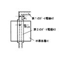
nチャネル型TFTの半導体層は、チャネル形成領域102と、前記チャネル形成領域の両側に接して設けられた第1の不純物領域103、104と、前記第1の不純物領域103、104に接して設けられた第2の不純物領域105、106とから成っている。第1の不純物領域103、104は、ゲート絶縁膜112を介して、第2のゲート電極115がゲート絶縁膜と接している領域に重なって設けられている。
【0030】
ただし、本願発明の最大の特徴は、第1の不純物領域103、104は全域が第2のゲート電極に重なっているのではなく、その一部のみが重なっているという点にある。即ち、第1の不純物領域は、ゲート絶縁膜112を介して第2のゲート電極と重なっている部分(ゲート電圧が印加される部分)と、重なっていない部分(ゲート電圧が印加されない部分)とを含む。
【0031】
この様子を図1(B)に示す。なお、図1(B)の符号は図1(A)の符号に対応している。図1(B)に示すように、第1の不純物領域(本明細書中では低濃度不純物領域またはLDD領域ともいう)104は、第2のゲート電極115とゲート絶縁膜112を介して重なっている部分(Gate-overlapped LDD領域104a)と重なっていない部分(non-Gate-overlapped LDD領域104b)とに区別される。
【0032】
この様子を上面から見ると図1(C)に示すようになる。図1(C)において、半導体層125と第2のゲート配線126とが交差する部分を特に第2のゲート電極115と呼び、この交差によって形成された第2のゲート電極115の端部127は、第1の不純物領域104上に位置する。
【0033】
本願発明では、Gate-overlapped LDD領域104aの長さ(図11のL4に相当する)を0.1〜2μm(代表的には0.3〜1.5μm)とし、non-Gate-overlapped LDD領域104b(図11のL5に相当する)を0.1〜2μm(代表的には0.3〜1μm)とするのが好ましいと考えている。
【0034】
なお、第1の不純物領域103、104は、0.2〜4μm、代表的には0.6〜2.5μmの長さ(図11のL6に相当する)を有し、n型を付与する不純物元素(周期律表の15族に属する元素、代表的にはリン又は砒素)の濃度が1×10¹⁶〜1×10¹⁹atoms/cm3、代表的には1×1017〜5×1018atoms/cm3である。また、ソース領域105とドレイン領域106の不純物濃度は、1×1019〜1×1021atoms/cm3、代表的には1×1020〜5×1020atoms/cm3とすれば良い。
【0035】
この時、チャネル形成領域102は真性な半導体層、またはあらかじめ1×10¹⁶〜5×10¹⁸atoms/cm3の濃度でボロンが添加された半導体層で構成される。このボロンはしきい値電圧を制御するために添加されるものであり、同様の効果が得られるものであれば他の元素で代用することもできる。
【0036】
一方、pチャネル型TFTの不純物領域108〜111(これらをまとめて第3の不純物領域という)には、同じ濃度でp型を付与する不純物元素(周期律表の13族に属する元素、代表的にはボロン)が添加されている。そして、前記nチャネル型TFTのソース領域105とドレイン領域106に添加される不純物濃度の1.5〜3倍の濃度でp型を付与する不純物元素が添加されている。
【0037】
また、本願発明の作製方法で形成すると、不純物領域110、111には、前記nチャネル型TFTの第2の不純物領域105、106と同一濃度の不純物元素(n型を付与する不純物元素)が含まれている。即ち、第3の不純物領域の一部に第2の不純物領域と同一濃度で周期律表の15族に属する元素含まれていることになる。
【0038】
以上示したように本願発明はTFTの構造において、ゲート電極を第1のゲート電極と、第1のゲート電極を覆って第2のゲート電極を設けたものであり、図1で示すように第2のゲート電極は、第1のゲート電極とゲート絶縁膜とに接して設けられている。
【0039】
そして、ゲート絶縁膜を介して半導体層に設けられた第1の不純物領域と、第2のゲート電極がゲート絶縁膜に接している領域とが、部分的に重なって設けられている構造に特徴があり、また、その作製方法に特徴がある。
【0040】
図1に示すTFTは、特にnチャネル型TFTにおいて、いわゆるLDD領域として機能する第1の低濃度不純物領域103、104が、ゲート絶縁膜を介して第2のゲート電極と重なって設けられた構造となっているので、MOSトランジスタのGOLD構造やLATID構造の如き利点を得ることが可能である。さらに、第1の不純物領域103、104は前記第2のゲート電極と重ならない部分もあるので、その部分は実質的に抵抗体として機能する。
【0041】
一方、pチャネル型TFTはこうしたLDD構造となる低濃度不純物領域は設けないものとする。勿論、低濃度不純物領域を設ける構造としても良いが、pチャネル型TFTはもともと信頼性が高いため、オン電流を稼いでnチャネル型TFTとの特性バランスをとった方が好ましい。本願発明を図1に示すようにCMOS回路に適用する場合には、特にこの特性のバランスをとることが重要である。但し、本願発明の構造をpチャネル型TFTに適用しても何ら問題はない。
【0042】
こうしてnチャネル型TFT及びpチャネル型TFTが完成したら、第1の層間絶縁膜119で覆い、ソース領域105、111、ドレイン領域106、110とコンタクトをとったソース電極120、122、とドレイン電極121とを設ける。図1の構造では、これらを設けた後でパッシベーション膜123として窒化珪素膜を設けている。さらに樹脂材料でなる第2の層間絶縁膜124が設けられている。第2の層間絶縁膜は、樹脂材料に限定される必要はないが、例えば、液晶表示装置に応用する場合には、表面の平坦性を確保するために樹脂材料を用いることが好ましい。
【0043】
図1では、nチャネル型TFTとpチャネル型TFTとを相補的組み合わせて成るCMOS回路を例にして示したが、nチャネル型TFTを用いたNMOS回路や、液晶表示装置の画素部に本願発明を適用することもできる。
【0044】
(本願発明のnチャネル型TFT構造の利点)
本願発明のnチャネル型TFTは第1の不純物領域(LDD領域)の一部に対してゲート電極をオーバーラップさせ、LDD領域の中にゲート電圧が印加される部分と印加されない部分とを形成するという点に特徴がある。
【0045】
ここで本願発明の優位性を従来の構造と比較して説明する。図13(I)の(A)、(B)はLDD構造のないnチャネル型TFT(以下、NTFTという)とその電気特性(ゲート電圧Vg対ドレイン電流Id特性)である。同様に、図13(II)の(A)、(B)は通常のLDD構造の場合を、図13(III)の(A)、(B)はゲート電極をオーバーラップさせたLDD構造の場合を、そして図13(IV)の(A)、(B)には本願発明のnチャネル型TFTの場合を示す。
【0046】
なお、図面中においてn+はソース領域またはドレイン領域を、channelはチャネル形成領域を、n-はLDD領域を指す。また、Idはドレイン電流、Vgはゲート電圧である。
【0047】
図13(I)の(A)、(B)に示すようにLDD構造がない場合、オフ電流は高く、オン電流(TFTがオン状態にある時のドレイン電流)もオフ電流も非常に劣化しやすい。
【0048】
次に、図13(II)の(A)、(B)に示すLDD構造の場合、オフ電流はかなり抑えられ、オン電流もオフ電流もある程度は劣化が抑制できる。しかしながら、オン電流の劣化を完全に抑えられているわけではない。
【0049】
次に、図13(III)の(A)、(B)に示すLDD領域とゲート電極とがオーバーラップした構造であるが、この構造はオン電流の劣化を抑制することに重点を置いた構造となっている。
【0050】
この場合、オン電流の劣化を十分に抑えることができる反面、通常のLDD構造よりもややオフ電流が高いという問題を持つ。従来例で述べた論文はこの構造を採用しており、本願発明はこのオフ電流が高いという問題を認識した上で、解決するための構造を模索したものである。
【0051】
そして、本願発明の構造は図13(IV)の(A)、(B)に示すように、LDD領域の中に、ゲート電極とオーバーラップさせた部分と、オーバーラップさせない部分とを形成するような構造とした。この構造を採用することで、オン電流の劣化を十分に抑制し、且つ、オフ電流を低減することが可能となった。
【0052】
以上に示した本願発明の構成について、以下に示す実施例でさらに詳細に説明する。
【0053】
[実施例1]
本実施例では、本願発明の構成を液晶表示装置に適用した例を示し、画素部とその周辺に設けられる駆動回路の基本形態であるCMOS回路を同時に作製する方法について、図2と図3を用いて説明する。
【0054】
なお、画素部を形成する画素TFTとして本実施例ではnチャネル型TFTを用いる。また、オフ電流(TFTがオフ状態にある時に流れてしまう電流)を低減するためにはダブルゲート構造またはトリプルゲート構造等のマルチゲート構造とするのが好ましい。本実施例の場合、図面上では簡略化してシングルゲート構造で図示しているが、実際にはダブルゲート構造を採用する。
【0055】
まず基板201には、例えばコーニング社の1737ガラス基板に代表される無アルカリガラス基板を用いる。そして、基板201のTFTが形成される表面に、酸化珪素で成る下地膜202を200nmの厚さに形成する。下地膜202は、さらに窒化珪素膜を積層させても良いし、窒化珪素膜のみであっても良い。
【0056】
次に、この下地膜202の上に50nmの厚さで、非晶質珪素膜をプラズマCVD法で形成する。非晶質珪素膜の含有水素量にもよるが、好ましくは400〜500℃に加熱して脱水素処理を行い、非晶質珪素膜の含有水素量を5atm%以下として、結晶化の工程を行って結晶質珪素膜とする。
【0057】
この結晶化の工程は、公知のレーザー結晶化技術または熱結晶化の技術を用いれば良い。本実施例では、パルス発振型のKrFエキシマレーザー光を線状に集光して非晶質珪素膜に照射して、結晶質珪素膜とする。
【0058】
尚、本実施例では初期膜を非晶質珪素膜として用いたが、初期膜として微結晶珪素膜を用いても構わないし、直接結晶質珪素膜を成膜しても良い。
【0059】
こうして形成された結晶質珪素膜をパターニングして、島状の半導体層(以下、半導体層という)203〜205を形成する。
【0060】
次に、半導体層203〜205を覆って、酸化珪素膜、窒化酸化珪素膜、窒化珪素膜またはそれらの積層膜でなるゲート絶縁膜206を形成する。ここではプラズマCVD法で窒化酸化珪素膜を100nmの厚さに形成する。そして、図では説明しないが、ゲート絶縁膜206の表面に第1のゲート電極を構成する、第1の導電層として導電性珪素膜を10〜200nm(本実施例では50nm)に形成し、さらに第2の導電層としてチタン/アルミニウム/チタンの三層構造からなる積層膜を100〜1000nm(本実施例では200nm)の厚さで形成する。
【0061】
そして、公知のパターニング技術により、第1のゲート電極を構成する第1の導電層207〜210と、第2の導電層の211〜214が形成される。なお、図2(A)では第2の導電層を簡略化して単層で図示しているが、実際にはアルミニウム膜の上面及び下面をチタンで挟んだ構造となっている。
【0062】
また、この時、図11で示した第1のゲート電極の長さL1は2μmとなるようにパターニングする。
【0063】
第1のゲート電極を構成する第2の導電層として、アルミニウムを用いる場合には、純アルミニウムを用いても良いし、チタン、珪素、スカンジウム、ネオジウムから選ばれた元素が0.1〜5atm%添加されたアルミニウム合金を用いても良い。また銅を用いる場合には、図示しないが、ゲート絶縁膜206の表面に窒化珪素膜を設けておくと好ましい。
【0064】
また、図2では画素部を構成するnチャネル型TFTのドレイン側に付加容量部を設ける構造となっている。このとき、付加容量部の配線電極は第1の導電層210及び第2の導電層214とで形成される。
【0065】
こうして図2(A)に示す構造が形成されたら、1回目のn型不純物を添加する工程を行う。結晶質半導体材料に対してn型を付与する不純物元素としては、リン(P)、砒素(As)、アンチモン(Sb)などが知られているが、ここでは、リンを用い、フォスフィン(PH3)を用いたイオンドープ法で行う。この工程では、ゲート絶縁膜206を通してその下の半導体層にリンを添加するために、加速電圧は80keVと高めに設定する。
【0066】
また、こうして形成された不純物領域は、後に示すnチャネル型TFTの第1の不純物領域241、242を形成することになり、LDD領域として機能する部分である。従ってこの領域のリンの濃度は、1×10¹⁶〜1×10¹⁹atoms/cm3の範囲にするのが好ましく、ここでは1×1018atoms/cm3とする。本明細書中では、こうして形成された不純物領域をn-領域と呼ぶ。
【0067】
また、半導体層中に添加された前記不純物元素は、レーザーアニール法や、熱処理により活性化させる必要がある。この工程は、ソース・ドレイン領域を形成する不純物添加の工程のあと実施しても良いが、この段階でレーザーアニール法により活性化させることは効果的である。
【0068】
この工程で、第1のゲート電極を構成する第1の導電層207〜210と第2の導電層211〜214は、リンの添加に対してマスクとして機能する。即ち、ゲート絶縁膜を介して存在する半導体層において、第1のゲート電極の真下にあたる領域にはリンは添加されない。そして、図2(B)に示すように、リンが添加された低濃度不純物領域215〜220が形成される。
【0069】
なお、ここで形成された低濃度不純物領域220は後に付加容量部の下部電極として機能することになる。本願発明の作製方法では付加容量部の下部電極としてn-領域を用いることができる。また、本明細書中では付加容量の電極を全て容量電極と呼ぶが、説明の必要に応じて「上部電極」または「下部電極」と使い分けることにする。
【0070】
通常、半導体層を付加容量部の電極として用いる場合には、電圧を加えて半導体層を反転させて電極として機能させなければならない。従来は半導体層が真性であったため比較的大きな電圧をかけなければならなかったが、本願発明ではn型半導体層を用いることになるため必要な電圧が小さくて済む(消費電力が小さい)という利点が得られる。
【0071】
次にフォトレジスト膜221、222でnチャネル型TFTを形成する領域を覆って、pチャネル型TFTが形成される領域に、p型を付与する不純物添加の工程を行う。p型を付与する不純物元素としては、ボロン(B)、アルミニウム(Al)、ガリウム(Ga)、が知られているが、ここではボロンをその不純物元素として、イオンドープ法でジボラン(B2H6)を用いて添加する。
【0072】
ここでも加速電圧を80keVとして、2×10²¹atoms/cm3の濃度にボロンを添加する。そして、図2(C)に示すようにボロンが高濃度に添加された領域223、224が形成される。この領域は後にpチャネル型TFTのソース領域またはドレイン領域となる。
【0073】
そして、レジストマスク221、222を除去した後、第2のゲート電極を形成する工程を行う。ここでは、第2のゲート電極の材料に第1の導電層と同一材料である導電性珪素膜を用い、100〜1000nm(本実施例では200nm)の厚さに形成する。また、第2のゲート電極の線幅(図11のL3に相当する)を5μmとする。即ち、第1のゲート電極に重ならない部分(図11のL6に相当する)が1.5μmとなるように調節する。
【0074】
なお、本願発明ではL3を0.5〜18μm(代表的には1.4〜10μm)、L6を0.2〜4μm(代表的には0.6〜2.5μm)の範囲から選択すると良い。
【0075】
また、本実施例では第1のゲート電極に対する被覆性を高めるために、減圧熱CVD法により導電性珪素膜(本実施例ではリンを添加した非晶質珪素膜)を形成する。減圧熱CVD法で作製された導電性珪素膜はパターン側面に対する被覆性が高いため、本願発明のような構造を実現するには適している。勿論、プラズマCVD法、スパッタ法を用いても構わないが、第1のゲート電極の側面で断線しないように注意が必要である。
【0076】
そして、公知の技術によりパターニングを行ってフォトレジスト膜225〜228を形成し、導電性珪素膜をエッチングして第2のゲート電極229〜232が形成される。この時、前述のように第2のゲート電極は、第1のゲート電極の両側にそれぞれ1.5μmの長さ(図11のL6に相当する)でゲート絶縁膜と接する領域が形成されるようにパターニングする。
【0077】
また、画素部を構成するnチャネル型TFTのドレイン側に付加容量部が設けられるが、この付加容量部の電極(上部電極)232は第2のゲート電極と同時に形成される。
【0078】
そして、フォトレジスト膜225〜228をマスクとして、2回目のn型を付与する不純物元素の添加工程を行い、不純物領域233〜238を形成する。ここでは前述のリン添加工程と同様に、フォスフィン(PH3)を用いたイオンドープ法で行う。この工程でも、ゲート絶縁膜206を通してその下の半導体層にリンを添加するために、加速電圧は80keVと高めに設定する。
【0079】
そして、ここでリンが添加される領域は、nチャネル型TFTでソース領域またはドレイン領域として機能させるため、この領域のリンの濃度は、1×10¹⁹〜1×10²¹atoms/cm3とするのが好ましく、ここでは5×1020atoms/cm3とする。本明細書中ではこの不純物領域をn+領域と呼ぶ。
【0080】
こうしてnチャネル型TFTのソース領域233、237(または238)及びドレイン領域234、238(または237)が形成される。また、nチャネル型TFTのチャネル形成領域239、240、低濃度不純物領域(LDD領域ともいう。図1の第1の不純物領域に相当する)241、242が画定し、付加容量部の下部電極243が画定する。
【0081】
さらに、pチャネル型TFTのチャネル形成領域244も画定する。また、pチャネル型TFTのドレイン領域223とソース領域224にもnチャネル型TFTのソース領域及びドレイン領域と同一濃度でリンが添加される(不純物領域235、236)が、前の工程でその4倍の濃度でボロンが添加されているため、導電型は反転せず、pチャネル型TFTの動作上何ら問題はない。また、不純物領域(図1の第2の不純物領域に相当する)245は図2(B)の工程で添加された濃度のリンと、図2(C)の工程で添加された濃度のボロンのみを含む領域となる。
【0082】
こうして図2(D)の状態が得られたら、フォトレジスト膜225〜228をマスクとして第2のゲート電極229〜231及び上部電極232の等方性エッチング)を行う。エッチングはヒドラジン、エチレンジアミン、ピロカテコール水溶液(EPW)、水酸化カリウムまたはTMAH(水酸化テトラメチルアンモニウム)等のエッチャントを用いたウェットエッチング法によっても良いし、CF4+O2等の混合ガスを用いたドライエッチング法によっても良い。本明細書中ではこの工程をサイドエッチング工程という。(図2(E))
【0083】
このサイドエッチング工程によって形成された第2のゲート電極246〜248及び上部電極249は、端部が後退してΧμmだけ短くなる。第2のゲート電極はもともと図11のL3に相当する線幅(0.5〜18μm、代表的には1.4〜10μm)で形成されていたが、この工程によって図11のL2に相当する線幅(0.3〜14μm、代表的には0.8〜8μm)となる。
【0084】
本願発明ではこの距離(図11のL5に相当する)を0.1〜2μm(好ましくは0.3〜1μm)で制御する。本実施例ではサイドエッチングをΧ=0.5μmで行ったため、図11に示したL4は1μmとなる。
【0085】
即ち、nチャネル型TFTのLDD領域241、242のうち、チャネル形成領域239、240に近い部分では1μmにわたって第2のゲート電極246、248と重なり、残りの0.5μmは第2のゲート電極246、248とは重ならない状態となる。こうして図1で説明したようなnチャネル型TFTを実現することができる。
【0086】
次に、それぞれの濃度で添加されたn型またはp型を付与する不純物元素は、このままでは活性化せず有効に作用しないので、活性化の工程を行う必要がある。この工程は、電気加熱炉を用いた熱アニール法や、前述のエキシマレーザーを用いたレーザーアニール法や、ハロゲンランプを用いたラピットサーマルアニール法(RTA法)で行うことができる。
【0087】
熱アニール法では、窒素雰囲気中において500℃、2時間の加熱処理をして活性化を行う。本実施例では、第1のゲート電極を構成する第2の導電層にアルミニウムを用いたが、導電性珪素膜で形成された第1の導電層と同じく導電性珪素膜で形成された第2のゲート電極がアルミニウム膜(実際にはチタンで挟まれたアルミニウム膜)を覆って形成されているため、導電性珪素膜がブロッキング層として機能して、ヒロックの発生やアルミニウム原子の他の領域への拡散等を防ぐことができる。
【0088】
また、レーザーアニール法では、パルス発振型のKrFエキシマレーザー光を線状に集光して照射することにより活性化を行う。また、レーザーアニール法を実施した後に熱アニール法を実施すると、さらに良い結果が得られる。またこの工程は、イオンドーピングによって結晶性が破壊された領域をアニールする効果も兼ね備えていて、その領域の結晶性を改善することもできる。
【0089】
次に、第1の層間絶縁膜250を1μmの厚さに形成する。第1の層間絶縁膜250としては、酸化珪素膜、窒化珪素膜、窒化酸化珪素膜、有機樹脂膜、またはそれらの積層膜をもちいることができる。本実施例では、図示しないが、最初に窒化珪素膜を50nm形成し、さらに酸化珪素膜を950nm形成した2層構造とする。
【0090】
第1の層間絶縁膜250を形成したら、次にパターニングでそれぞれのTFTのソース領域と、ドレイン領域にコンタクトホールを形成する。そして、ソース配線(またはソース電極)251〜253とドレイン配線(またはドレイン電極)254、255を形成する。図示していないが、本実施例ではこの電極を、チタン膜を100nm、チタンを含むアルミニウム膜300nm、チタン膜150nmをスパッタ法で連続して形成した3層構造の膜を、パターニングして形成する。
【0091】
次に、ソース配線251〜253とドレイン配線254、255と、第1の層間絶縁膜250を覆ってパッシベーション膜(窒化珪素膜)256を形成する。パッシベーション膜256は、窒化珪素膜で300nmの厚さで形成する。さらに、有機樹脂からなる第2の層間絶縁膜257を約2μmの厚さに形成する。有機樹脂膜としては、ポリイミド、アクリル、ポリイミドアミド、BCB(ベンゾシクロブテン)等を使用することができる。
【0092】
有機性樹脂膜を用いることの利点は、成膜方法が簡単である点や、比誘電率が低いので、寄生容量を低減できる点、平坦性に優れる点などが上げられる。なお上述した以外の有機性樹脂膜を用いることもできる。ここでは、基板に塗布後、熱重合するタイプのポリイミドを用い、300℃で焼成して形成する。
【0093】
次に、第2の層間絶縁膜257の上に、遮光層258を形成する。遮光層258は金属膜や顔料を含ませた有機樹脂膜で形成すれば良いものである。ここでは、チタン膜をスパッタ法で形成する。
【0094】
遮光膜258を形成したら、第3の層間絶縁膜259を形成する。この第3の層間絶縁膜259は、第2の層間絶縁膜257と同様に、有機樹脂膜を用いて形成すると良い。そして、第2の層間絶縁膜257と第3の層間絶縁膜259とにドレイン配線255に達するコンタクトホールを形成し、画素電極260を形成する。
【0095】
画素電極260は、透過型液晶表示装置とする場合には透明導電膜を用い、反射型の液晶表示装置とする場合には金属膜を用いれば良い。ここでは透過型の液晶表示装置とするために、酸化インジウムと酸化スズとの化合物膜(ITO膜)を100nmの厚さにスパッタ法で形成し、画素電極260を形成する。
【0096】
図3(A)の状態が形成されたら、配向膜261を形成する。本実施例では配向膜261としてポリイミド膜を用いる。対向側の基板262には、透明導電膜263と、配向膜264とを形成する。配向膜261、264は形成された後、ラビング処理を施して液晶分子がある一定のプレチルト角を持って平行配向するようにする。
【0097】
上記の工程を経て、画素部と、CMOS回路が形成された基板と対向基板とを、公知のセル組み工程によってシール材やスペーサ(ともに図示せず)などを介して貼りあわせる。その後、両基板の間に液晶材料265を注入し、図示しない封止剤(シール剤)によって完全に封入する。よって図3(B)に示すアクティブマトリクス型液晶表示装置が完成する。
【0098】
図10は完成したアクティブマトリクス型液晶表示装置の外観を表している。基板1001には画素部1002、信号線駆動回路(ソースドライバー回路)1003、走査線駆動回路(ゲートドライバー回路)1004、信号処理回路(信号分割回路、DAコンバータ回路、γ補正回路等)1005が形成され、FPC(フレキシブルプリントサーキット)1006が取り付けられている。なお、1007は対向基板である。
【0099】
次に本実施例のアクティブマトリクス型液晶表示装置の構成を、図4と図5を用いて説明する。図4は本実施例のアクティブマトリクス基板の斜視図である。アクティブマトリクス基板は、ガラス基板400上に形成された、画素部401と、走査線駆動回路(ゲートドライバー回路)402と、信号線駆動回路(ソースドライバー回路)403で構成される。
【0100】
これら駆動回路はCMOS回路を基本として構成されている。走査線駆動回路402と、信号線駆動回路403はそれぞれゲート配線(走査線)502とソース配線(信号線)503で画素部401に接続されている。また、ゲート配線502とソース配線503との各交点に画素TFT500が配置され、その画素TFT500には直列に付加容量506が接続される。さらに、画素TFT500及び付加容量506と直列に画素電極504が接続される。
【0101】
図5(A)は画素部401の上面図であり、ほぼ一つの画素の上面図である。画素部にはダブルゲート構造の画素TFT(nチャネル型TFT)500が設けられている。なお、ゲート配線502が図示されていないゲート絶縁膜を介してその下の半導体層501と交差している部分を本明細書中ではゲート電極508と呼ぶ。
【0102】
また、図5(A)に示した画素TFT500をA−A'で切断した断面図は図3(B)に示した画素部の断面図に相当する。図3(B)の場合、シングルゲート構造で図示されているので実際の断面とは異なるが、本願発明を理解するのに妨げとはならない。
【0103】
また、図4に示した付加容量506は半導体層501と容量線505とでゲート絶縁膜(図示せず)を挟んで形成される。なお、容量配線505において実質的に付加容量の上部電極(容量電極)として機能する部分が図2(E)の容量電極249である。この容量配線505は第2のゲート電極と同時に形成され、第2のゲート電極と平行に設けられる。
【0104】
なお、507で示されるのはドレイン電極であり、画素TFT500と画素電極504とを接続する際に、オーミック接触をとりやすくするために形成された電極である。
【0105】
一方、図5(B)に示すCMOS回路をB−B'に沿った断面は、図1に示すCMOS回路の断面図となる。なお、図1に対応する部分には同一の符号を付した。図5(B)において、ゲート電極510は、図1における第1の導電層113と第2の導電層114からなる第1のゲート電極及び第2のゲート電極115で構成される。また、ゲート電極511は、図1における第1の導電層116と第2の導電層117からなる第1のゲート電極及び第2のゲート電極118で構成される。
【0106】
なお、本実施例のアクティブマトリクス基板の構造は、本実施例の構造に限定されるものではない。本願発明の構造は、ゲート電極の構造と、ゲート絶縁膜を介して設けられた半導体層のソース領域と、ドレイン領域と、その他の不純物領域の構成に特徴があるので、それ以外の構成については実施者が適宣決定すれば良い。
【0107】
[実施例2]
本実施例では、実施例1において半導体層として用いる結晶質半導体膜を、触媒元素を用いた熱結晶化法により形成する例を示す。触媒元素を用いる場合、特開平7−130652号公報、特開平8−78329号公報で開示された技術を用いることが望ましい。
【0108】
ここで、特開平7−130652号公報に開示されている技術を本願発明に適用する場合の例を図6に示す。まず基板601に酸化珪素膜602を設け、その上に非晶質珪素膜603を形成する。さらに、重量換算で10ppmのニッケルを含む酢酸ニッケル塩溶液を塗布してニッケル含有層604を形成する。(図6(A))
【0109】
次に、500℃、1時間の脱水素工程の後、500〜650℃で4〜24時間(本実施例では550℃、14時間)の熱処理を行い、結晶質珪素膜605を形成する。こうして得られた結晶質珪素膜605は非常に優れた結晶性を有する。(図5(B))
【0110】
また、特開平8−78329号公報で開示された技術は、触媒元素を選択的に添加することによって、非晶質半導体膜の選択的な結晶化を可能としたものである。同技術を本願発明に適用した場合について、図7で説明する。
【0111】
まず、ガラス基板701に酸化珪素膜702を設け、その上に非晶質珪素膜703、酸化珪素膜704を連続的に形成する。この時、酸化珪素膜704の厚さは150nmとする。
【0112】
次に酸化珪素膜704をパターニングして、選択的に開孔部705を形成し、その後、重量換算で10ppmのニッケルを含む酢酸ニッケル塩溶液を塗布する。これにより、ニッケル含有層706が形成され、ニッケル含有層706は開孔部705の底部のみで非晶質珪素膜702と接触する。(図7(A))
【0113】
次に、500〜650℃で4〜24時間(本実施例では580℃、14時間)の熱処理を行い、結晶質珪素膜707を形成する。この結晶化の過程では、ニッケルが接した非晶質珪素膜の部分が最初に結晶化し、そこから横方向へと結晶化が進行する。こうして形成された結晶質珪素膜707は棒状または針状の結晶が集合して成り、その各々の結晶は巨視的にはある特定の方向性をもって成長しているため、結晶性が揃っているという利点がある。
【0114】
尚、上記2つの技術において使用可能な触媒元素は、ニッケル(Ni)の以外にも、ゲルマニウム(Ge)、鉄(Fe)、パラジウム(Pd)、スズ(Sn)、鉛(Pb)、コバルト(Co)、白金(Pt)、銅(Cu)、金(Au)、といった元素を用いても良い。
【0115】
以上のような技術を用いて結晶質半導体膜(結晶質珪素膜や結晶質シリコンゲルマニウム膜などを含む)を形成し、パターニングを行えば、TFTの半導体層を形成することができる。本実施例の技術を用いて、結晶質半導体膜から作製されたTFTは、優れた特性が得られるが、そのため高い信頼性を要求されていた。しかしながら、本願発明のTFT構造を採用することで、本実施例の技術を最大限に生かしたTFTを作製することが可能となる。
【0116】
[実施例3]
本実施例は、実施例1で用いられる半導体層を形成する方法として、実施例2のように非晶質半導体膜を初期膜として前記触媒元素を用いて結晶質半導体膜を形成した後で、その触媒元素を結晶質半導体膜から除去する工程を行った例を示す。本実施例ではその方法として、特開平10−135468号公報または特開平10−135469号公報に記載された技術を用いる。
【0117】
同公報に記載された技術は、非晶質半導体膜の結晶化に用いた触媒元素を結晶化後にリンのゲッタリング作用を用いて除去する技術である。同技術を用いることで、結晶質半導体膜中の触媒元素の濃度を1×10¹⁷atoms/cm3以下、好ましくは1×1016atoms/cm3にまで低減することができる。
【0118】
本実施例の構成について図8を用いて説明する。ここではコーニング社の1737基板に代表される無アルカリガラス基板を用いた。図8(A)では、実施例2で示した結晶化の技術を用いて、下地膜802、結晶質珪素膜803が形成された状態を示している。そして、結晶質珪素膜803の表面にマスク用の酸化珪素膜804が150nmの厚さに形成され、パターニングにより開孔部が設けられ、結晶質珪素膜を露出させた領域を設けてある。そして、リンを添加する工程を実施して、結晶質珪素膜にリンが添加された領域805が設けられる。
【0119】
この状態で、窒素雰囲気中で550〜800℃、5〜24時間(本実施例では600℃、12時間)の熱処理を行うと、結晶質珪素膜にリンが添加された領域805がゲッタリングサイトとして働き、結晶質珪素膜803に残存していた触媒元素はリンが添加された領域805に移動させることができる。
【0120】
そして、マスク用の酸化珪素膜804と、リンが添加された領域805とをエッチングして除去することにより、結晶化の工程で使用した触媒元素の濃度を1×10¹⁷atoms/cm3以下にまで低減された結晶質珪素膜を得ることができる。この結晶質珪素膜はそのまま実施例1で示した本願発明のTFTの半導体層として使用することができる。
【0121】
[実施例4]
本実施例では、実施例1で示した本願発明のTFTを作製する工程において、半導体層とゲート絶縁膜を形成する他の実施形態を示す。そして、本実施例の構成を図9で説明する。
【0122】
ここでは、少なくとも700〜1100℃程度の耐熱性を有する基板が必要であり、石英基板901が用いられる。そして実施例2及び実施例3で示した技術を用い、結晶質半導体膜が形成され、これをTFTの半導体層にするために、島状にパターニングして半導体層902、903を形成する。そして、半導体層902、903を覆って、ゲート絶縁膜904を、珪素を主成分とする膜で形成する。本実施例では、プラズマCVD法で窒化酸化珪素膜を70nmの厚さで形成する。(図9(A))
【0123】
そして、ハロゲン(代表的には塩素)と酸素を含む雰囲気中で熱処理を行う。本実施例では、950℃、30分とした。尚、処理温度は700〜1100℃の範囲で選択すれば良く、処理時間も10分から8時間の間で選択すれば良い。(図9(B))
【0124】
その結果、本実施例の条件では、半導体層902、903とゲート絶縁膜904との界面で熱酸化膜が形成され、ゲート絶縁膜907が形成される。
【0125】
以上の工程で作製されたゲート絶縁膜907は、絶縁耐圧が高く半導体層905、906とゲート絶縁膜907の界面は非常に良好なものである。本願発明のTFTの構成を得るためには、以降の工程は実施例1に従えば良い。
【0126】
勿論、本実施例に実施例2や実施例3を組み合わせることは実施者が適宜決定すれば良い。
【0127】
[実施例5]
本実施例では、実施例1と異なる工程順序で結晶質TFTを作製する例を図14に示す。具体的には実施例3で示したリンによるゲッタリング工程の別形態について説明する。なお、基本的な工程は図1に従うものであるので、相違点のみに着目して説明する。
【0128】
まず、実施例1の工程に従って図2(E)の状態を得る。図14(A)は図2(E)の状態からフォトレジスト膜225〜228を除去した状態を表している。ただし、TFTの活性層となる半導体層の形成には実施例2に示した熱結晶化技術を用いている。
【0129】
この時、nチャネル型TFTのソース領域233、237及びドレイン領域234、238、並びにpチャネル型TFTのソース領域236及びドレイン領域235には1×10¹⁹〜1×10²¹atoms/cm3(好ましくは5×1020atoms/cm3)の濃度でリンが含まれている。
【0130】
本実施例ではこの状態で、窒素雰囲気中で500〜800℃、1〜24時間、例えば600℃、12時間の加熱処理の工程を行う。この工程により、添加されたn型及びp型を付与する不純物元素を活性化することができた。さらに、結晶化工程の後残存していた触媒元素(本実施例ではニッケル)が矢印の方向に移動し、前述のソース領域及びドレイン領域に含まれたリンの作用によって同領域にゲッタリング(捕獲)することができる。その結果、チャネル形成領域からニッケルを1×10¹⁷atoms/cm3以下にまで低減することができる。
【0131】
図14(B)の工程が終了したら、以降の工程は実施例1の工程に従い、図3(B)に示すようなアクティブマトリクス基板を作製することができる。
【0132】
なお、本実施例の構成は実施例1〜実施例4のいずれの構成とも自由に組み合わせることが可能である。
【0133】
[実施例6]
本実施例では実施例1において図2(E)に示したサイドエッチング工程を異なる方法で行った場合について説明する。説明には図15を用いる。
【0134】
まず実施例1の工程によって図2(D)の工程までを終了させる。次に、フォトレジスト膜1500を形成し、基板側から光を照射してフォトレジスト膜1500の一部を感光させる。この工程は公知の裏面露光法を用いれば良い。
【0135】
この時、第2のゲート電極229〜231及び容量電極232がマスクとなって未感光領域1501が形成される。未感光領域1501は光の回り込みによって第2のゲート電極よりも内側に形成される。光の回り込み量は露光条件で制御ができるが、この回り込み量が図2(E)に示した距離(Χμm)を決めることになる。
【0136】
なお、本実施例の場合、第2のゲート電極229〜231及び容量電極232を裏面露光用のマスクとして機能させなければならない。そのため、材料の選択と裏面露光用光源を慎重に組み合わせることが必要である。ただし、通常の露光装置に使われるi線、g線やエキシマレーザー光を用いるとすると、その波長の光が吸収される材料を用いることになる。
【0137】
露光光源としてどのような波長の光を用いるかによって適切な材料は異なるが、少なくともTFTの半導体層とは異なる材料を選択する必要がある。本実施例ではTFTの半導体層が結晶質珪素膜であるため、第2のゲート電極の材料として非晶質珪素膜を用いる。
【0138】
非晶質珪素膜中に不純物元素を添加して、露光光を吸収しうるエネルギーバンドギャップをもたせることも有効である。そのような不純物元素としては、リン、ボロン、炭素、酸素または窒素等の元素が挙げられる。
【0139】
こうして図15(A)の状態が得られたら、フォトレジスト膜1500を現像してパターン化されたフォトレジスト膜1502〜1505を形成する。そして、これらのフォトレジスト膜をマスクとして第2のゲート電極229〜231及び容量電極232をエッチングする。
【0140】
このエッチング工程によって新たに第2のゲート電極1506〜1508及び容量電極1509が形成される。(図15(B))
【0141】
この後、実施例1の工程に従えば図3(B)に示したような構造のアクティブマトリクス基板が完成する。本実施例の構成は実施例1〜5のいずれの構成とも自由に組み合わせることが可能である。
【0142】
[実施例7]
本実施例では実施例1と異なる工程でアクティブマトリクス基板を作製する場合について説明する。なお、基本的には実施例1と同様であるので、相違点のみに注目して説明する。
【0143】
まず、実施例1の工程に従って図2(A)の状態を得た後、pチャネル型TFTを隠すようにフォトレジスト膜60を形成する。次に、図2(B)と同様の条件でリンを添加し、第1の不純物領域となる不純物領域61〜64を形成する。(図16(A))
【0144】
次に、図2(D)の工程に示したようにフォトレジスト膜65〜68を形成し、さらに第2のゲート電極69〜71及び容量電極72を形成する。その後、図2(D)の工程と同様の条件でリンを添加し、高濃度にリンが添加された不純物領域73〜78を形成する。(図16(B))
【0145】
次に、図2(E)に示した工程に従って電極の端部をエッチングし、第2のゲート電極79〜81及び容量電極82を形成する。(図16(C))
【0146】
次に、nチャネル型TFTとなる領域をフォトレジスト膜83、84で隠し、図2(C)の工程と同様の条件でボロンを添加した。この工程によりpチャネル型TFTの第3の不純物領域(ソース領域85及びドレイン領域86)とチャネル形成領域87が画定する。(図16(D))
【0147】
この後、実施例1の工程に従えば図3(B)に示したような構造のアクティブマトリクス基板が完成する。本実施例の構成は実施例2〜6のいずれの構成とも自由に組み合わせることが可能である。
【0148】
[実施例8]
本実施例では、実施例1において第1のゲート電極と第2のゲート電極との組み合わせについて例を示す。説明には図17を用いる。
【0149】
図17(A)は第1の導電層として導電性珪素膜1701を用い、第2の導電層としてチタン(Ti)膜1702、アルミニウムを主成分とする膜(代表的にはアルミニウムに0.1〜5wt%のチタン、スカンジウムまたはネオジウムを添加した膜)1703、チタン膜1704とを積層した積層膜を用いて第1のゲート電極とする。そして、第1のゲート電極を覆う第2のゲート電極として導電性珪素膜1705を用いる。
【0150】
図17(B)は第1の導電層として導電性珪素膜1701を用い、第2の導電層としてモリブデンとタングステンが1:1に混合された合金膜(以下、Mo−W膜という)1706を用いて第1のゲート電極とする。そして、第1のゲート電極を覆う第2のゲート電極として導電性珪素膜1705を用いる。なお、Mo−W膜の代わりにタングステンをタンタルに置き換えたMo−Ta膜を用いても良い。
【0151】
図17(C)は第1の導電層として導電性珪素膜1701を用い、第2の導電層として銅または銅(Cu)を主成分とする膜(代表的には銅に0.1〜5wt%の他元素を添加した膜)1707とチタン膜1708とを積層した積層膜を用いて第1のゲート電極とする。そして、第1のゲート電極を覆う第2のゲート電極として導電性珪素膜1705を用いる。
【0152】
この場合、銅の拡散を防ぐために上記どちらの導電性珪素膜にも窒素を含有させておくことが好ましい。または、第1のゲート電極と第2のゲート電極との間または第1の導電層と第2の導電層に、電極間または導電層間の導通を妨げない程度の膜厚で窒化珪素膜を設けておくことも有効である。その場合の膜厚は1〜10nm(代表的には2〜5nm)としておく。
【0153】
図17(D)は第1の導電層としてチタン膜1702を用い、第2の導電層としてアルミニウムを主成分とする膜1703、チタン膜1704とを積層した積層膜を用いて第1のゲート電極とする。そして、第1のゲート電極を覆う第2のゲート電極として導電性珪素膜1705を用いる。
【0154】
以上の組み合わせは代表例であって本願発明に適用できる組み合わせは本実施例に限定されるものではない。例えば、図17(D)において、第1のゲート電極として下層にタンタル膜を設け、上層にアルミニウムを主成分とする膜を設けた構成なども可能である。
【0155】
また、本実施例に示した導電性珪素膜は周期律表の13族または15族に属する元素によって導電性が付与されているが、炭素、酸素または窒素といった元素を添加してあっても構わない。
【0156】
また、第1の導電層は、好ましくは導電性珪素膜であるが、他の金属膜(代表的にはチタン膜またはタンタル膜)で代用することは可能である。第1の導電層は第2の導電層の元素がゲート絶縁膜中へと拡散することを防ぐ保護膜も兼ねているので、そのような効果を失わない組み合わせであれば良い。
【0157】
なお、本実施例の構成は実施例1〜7のいずれの構成とも自由に組み合わせることが可能である。
【0158】
[実施例9]
本実施例では第1のゲート電極の構造に関する一実施例を図18に示す。図18(A)は第1のゲート電極として、導電性珪素膜(第1の導電層)1801とアルミニウムを主成分とする膜(第2の導電層)1802との積層膜を用い、第2のゲート電極として導電性珪素膜1803を用いた例である。
【0159】
この時、図18(A)に示すように第2の導電層1802の幅を第1の導電層1801の幅よりも狭くすることによって、第1のゲート電極を階段状に形成することができる。こうすることによって第2のゲート電極の被覆性が高まり、断線等の不良を防ぐことができる。
【0160】
なお、本実施例では段差は一つしか形成されていないが、多数の段差を形成した多段階形状であるとさらに良い。
【0161】
図18(A)に示したような形状は、第2の導電層1802をフォトレジスト膜(図示せず)を用いてエッチングした後で、オーバーエッチングを行うことにより膜の側面を横方向にエッチング(サイドエッチング)してフォトレジスト膜よりも細いパターンを形成すれば良い。この時、前述のフォトレジスト膜は傘のように第2の導電層上に残る。これをそのまま用いて導電性珪素膜をエッチングすれば図18(A)の形状が得られる。
【0162】
次に、図18(B)に示す構造は、図18(A)に示した構造において第1の導電層である導電性珪素膜をテーパー状にエッチングした場合の例である。この形状は、図18(A)の際に説明したように第2の導電層1802をサイドエッチングした後、傘のように残ったフォトレジスト膜を使ってエッチングを行えば、導電性珪素膜1801にテーパーを形成することができる。
【0163】
この時、テーパー角は8〜40°(好ましくは10〜30°)とすれば良い。さらに、図18(A)、(B)の構造において第2の導電層をテーパー形状に形成しても有効である。
【0164】
なお、本実施例の構成は実施例1〜8のいずれの構成とも自由に組み合わせることが可能である。
【0165】
[実施例10]
本実施例では図1(B)に示したLDD領域の構造をドレイン側(ドレイン電極が接続される側)のみに設けた場合の例を図19に示す。本実施例の実施する場合、実施例1の図2(D)の工程で、第2のゲート電極を形成する際のパターニングマスクを変更するだけで良い。
【0166】
図19に示すように第2のゲート電極1901、1902はドレイン側のLDD領域のみに第2のゲート電極1901、1902が重なるように形成されている。そのため、ソース側(ソース電極が接続される側)はLDD領域が形成されない。
【0167】
また、画素部に用いられる画素TFTはソース領域とドレイン領域の機能が逆になる場合もあるので、本実施例の構造は採用しない方が好ましい。
【0168】
なお、本実施例の構成は実施例1〜9のいずれの構成とも自由に組み合わせることが可能である。
【0169】
[実施例11]
本実施例では画素部の付加容量の下部電極として機能する不純物領域を、p型を付与する不純物元素を添加して形成する場合について説明する。説明には図20を用いる。
【0170】
図20(A)は実施例1の図2(C)の工程に相当する工程であり、フォトレジスト膜222の形状を異ならせた状態である。即ち、本実施例ではフォトレジスト膜222を付加容量部に重ならないように形成する。
【0171】
この状態でボロンを添加することによって、第3の不純物領域223、224と同一濃度でボロンが添加された不純物領域21が形成される。本実施例ではこの不純物領域21を容量電極(下部電極)ともいう。
【0172】
次に実施例1に従って図2(D)に示した工程を行い、第2のゲート電極と同時に容量電極(上部電極)232を形成する。
【0173】
こうして容量電極(下部電極)21と絶縁膜(ゲート絶縁膜から延在する)と容量電極(上部電極)232とで付加容量が形成される。この付加容量は画素TFTと直列に接続される。
【0174】
この後の工程を実施例1に従えば、図3(B)に示すような構造のアクティブマトリクス型基板が完成する。図3(B)との違いは付加容量の下部電極がp型不純物領域で形成されている点である。
【0175】
なお、本実施例の構成は実施例1〜10に示した構成のいずれとも自由に組み合わせることが可能である。
【0176】
[実施例12]
本実施例では、実施例1においてn+領域(第2不純物領域)を異なる工程で形成する場合について図21を用いて説明する。
【0177】
まず、実施例1の工程に従って図2(D)に示したリンの添加工程の直前まで行う。そして、リンを添加する前に第2のゲート電極のサイドエッチング工程を行い、図21(A)の状態を得る。この時、図21(A)で用いている符号は図2(D)、(E)で用いた符号に対応する。
【0178】
次に、フォトレジスト膜225〜228をマスクとしてゲート絶縁膜のエッチングを行い、パターン化されたゲート絶縁膜31〜33を形成する。ゲート絶縁膜のエッチングには公知のドライエッチング法を用いれば良い。この時、絶縁膜34はゲート絶縁膜31〜33と同時に形成された膜であるが、付加容量用の絶縁体として機能するため、厳密にはゲート絶縁膜ではない。
【0179】
こうして図21(B)の状態を得たら、フォトレジスト膜225〜228を除去し、第2のゲート電極246〜248及び容量電極(上部電極)249をマスクとしてn型を付与する不純物の添加工程を行う。本実施例ではn型を付与する不純物としてリンを用いる。(図21(C))
【0180】
こうしてnチャネル型TFTのソース領域またはドレイン領域として機能する第2の不純物領域35〜38及びpチャネル型TFTのソース領域またはドレイン領域として機能する第3の不純物領域39、40が形成される。
【0181】
このあとの工程は実施例1に従えば良い。完成した液晶表示装置の完成図は図3(B)とほぼ同様(ゲート絶縁膜がパターニングされているかいないかの違いがあるのみ)なので説明は省略する。
【0182】
なお、不純物領域35〜40を形成した後で、公知のシリサイド形成工程を行い、不純物領域35〜40の表面近傍または全体をシリサイド化することも有効である。図示していないが、本実施例では図21(C)の工程の後、コバルト膜を形成してコバルトシリサイド層を形成する。
【0183】
こうすることでTFTと配線間の接触抵抗を低減することが可能である。また、その際、第2のゲート電極の表面近傍(または全体)もシリサイド化するので、低抵抗化されてゲート電極としての機能が向上するとともに、ゲート電極と他の配線とのオーミック接触をとる際に接触抵抗を低減することができるという利点がある。
【0184】
なお、本実施例の構成は実施例1〜実施例11のいずれの構成とも自由に組み合わせることが可能である。
[実施例13]
本実施例では、図11のL4に相当する長さをTFT形成部と配線部とで異ならせる場合について図22を用いて説明する。
【0185】
図22において、半導体層41上には第1のゲート配線(第1のゲート電極含む)42及び第2のゲート配線(第2のゲート電極含む)43が形成されている。この時、第2のゲート配線43は第1のゲート配線42を覆い隠すように形成されるが、本明細書中では第1のゲート配線42と重ならない部分の長さをL4と定義している(図11参照)。
【0186】
本実施例の場合、TFT形成部(半導体層の上)ではL4の長さ(ここではWLDDと表す)を0.1〜2μm(代表的には0.3〜1.5μm)とする。そして、配線部(半導体層の上以外)ではL4'の長さ(ここではWLと表す)を0.05〜0.5μm(代表的には0.1〜0.3μm)とする。
【0187】
即ち、本実施例はTFT形成部よりも配線形成部の方において第2のゲート配線の線幅を狭くすることに特徴がある。なぜならば配線形成部ではL4に相当する領域は必要なく、却って配線の高密度集積化を妨げる要因となってしまうため、可能な限り線幅を狭くした方が好ましいからである。
【0188】
従って、本実施例の構成を用いることで配線の高密度集積化が容易となり、延いては半導体装置の高密度集積化が可能となる。なお、本実施例の構成は実施例1〜12のいずれの構成とも自由に組み合わせることが可能である。
【0189】
[実施例14]
本願発明のTFT構造は液晶表示装置のような電気光学装置だけでなく、あらゆる半導体回路に用いることが可能である。即ち、RISCプロセッサ、ASICプロセッサ等のマイクロプロセッサに適用しても良いし、D/Aコンバータ等の信号処理回路から携帯機器(携帯電話、PHS、モバイルコンピュータ)用の高周波回路に用いても良い。
【0190】
さらに、従来のMOSFET上に層間絶縁膜を形成し、その上に本願発明を用いて半導体回路を作製したような三次元構造の半導体装置を実現することも可能である。このように本願発明は現在LSIが用いられている全ての半導体装置に適用することが可能である。即ち、SIMOX、Smart−Cut(SOITEC社の登録商標)、ELTRAN(キャノン株式会社の登録商標)などのSOI構造(単結晶半導体薄膜を用いたTFT構造)に本願発明を用いても良い。
【0191】
また、本実施例の半導体回路は実施例1〜11のどのような組み合わせからなる構成を用いても実現することができる。
【0192】
[実施例15]
本実施例では、本願発明を用いてEL(エレクトロルミネッセンス)表示装置を作製した例について説明する。
【0193】
図23(A)は本願発明を用いたEL表示装置の上面図である。図23(A)において、4010は基板、4011は画素部、4012はソース側駆動回路、4013はゲート側駆動回路であり、それぞれの駆動回路は配線4014〜4016を経てFPC4017に至り、外部機器へと接続される。
【0194】
このとき、少なくとも画素部、好ましくは駆動回路及び画素部を囲むようにしてカバー材6000、シーリング材7000、密封材(第2のシーリング材)7001が設けられている。
【0195】
また、図23(B)は本実施例のEL表示装置の断面構造であり、基板4010、下地膜4021の上に駆動回路用TFT(但し、ここではnチャネル型TFTとpチャネル型TFTを組み合わせたCMOS回路を図示している。)4022及び画素部用TFT4023(但し、ここではEL素子への電流を制御するTFTだけ図示している。)が形成されている。
【0196】
本願発明は、駆動回路用TFT4022、画素部用TFT4023に用いることができる。本願発明を用いて駆動回路用TFT4022、画素部用TFT4023が完成したら、樹脂材料でなる層間絶縁膜(平坦化膜)4026の上に画素部用TFT4023のドレインと電気的に接続する透明導電膜でなる画素電極4027を形成する。透明導電膜としては、酸化インジウムと酸化スズとの化合物(ITOと呼ばれる)または酸化インジウムと酸化亜鉛との化合物を用いることができる。そして、画素電極4027を形成したら、絶縁膜4028を形成し、画素電極4027上に開口部を形成する。
【0197】
次に、EL層4029を形成する。EL層4029は公知のEL材料(正孔注入層、正孔輸送層、発光層、電子輸送層または電子注入層)を自由に組み合わせて積層構造または単層構造とすれば良い。どのような構造とするかは公知の技術を用いれば良い。また、EL材料には低分子系材料と高分子系(ポリマー系)材料がある。低分子系材料を用いる場合は蒸着法を用いるが、高分子系材料を用いる場合には、スピンコート法、印刷法またはインクジェット法等の簡易な方法を用いることが可能である。
【0198】
本実施例では、シャドーマスクを用いて蒸着法によりEL層を形成する。シャドーマスクを用いて画素毎に波長の異なる発光が可能な発光層(赤色発光層、緑色発光層及び青色発光層)を形成することで、カラー表示が可能となる。その他にも、色変換層(CCM)とカラーフィルターを組み合わせた方式、白色発光層とカラーフィルターを組み合わせた方式があるがいずれの方法を用いても良い。勿論、単色発光のEL表示装置とすることもできる。
【0199】
EL層4029を形成したら、その上に陰極4030を形成する。陰極4030とEL層4029の界面に存在する水分や酸素は極力排除しておくことが望ましい。従って、真空中でEL層4029と陰極4030を連続成膜するか、EL層4029を不活性雰囲気で形成し、大気解放しないで陰極4030を形成するといった工夫が必要である。本実施例ではマルチチャンバー方式(クラスターツール方式)の成膜装置を用いることで上述のような成膜を可能とする。
【0200】
なお、本実施例では陰極4030として、LiF(フッ化リチウム)膜とAl(アルミニウム)膜の積層構造を用いる。具体的にはEL層4029上に蒸着法で1nm厚のLiF(フッ化リチウム)膜を形成し、その上に300nm厚のアルミニウム膜を形成する。勿論、公知の陰極材料であるMgAg電極を用いても良い。そして陰極4030は4031で示される領域において配線4016に接続される。配線4016は陰極4030に所定の電圧を与えるための電源供給線であり、導電性ペースト材料4032を介してFPC4017に接続される。
【0201】
4031に示された領域において陰極4030と配線4016とを電気的に接続するために、層間絶縁膜4026及び絶縁膜4028にコンタクトホールを形成する必要がある。これらは層間絶縁膜4026のエッチング時(画素電極用コンタクトホールの形成時)や絶縁膜4028のエッチング時(EL層形成前の開口部の形成時)に形成しておけば良い。また、絶縁膜4028をエッチングする際に、層間絶縁膜4026まで一括でエッチングしても良い。この場合、層間絶縁膜4026と絶縁膜4028が同じ樹脂材料であれば、コンタクトホールの形状を良好なものとすることができる。
【0202】
このようにして形成されたEL素子の表面を覆って、パッシベーション膜6003、充填材6004、カバー材6000が形成される。
【0203】
さらに、EL素子部を囲むようにして、カバー材6000と基板4010の内側にシーリング材が設けられ、さらにシーリング材7000の外側には密封材(第2のシーリング材)7001が形成される。
【0204】
このとき、この充填材6004は、カバー材6000を接着するための接着剤としても機能する。充填材6004としては、PVC(ポリビニルクロライド)、エポキシ樹脂、シリコーン樹脂、PVB(ポリビニルブチラル)またはEVA(エチレンビニルアセテート)を用いることができる。この充填材6004の内部に乾燥剤を設けておくと、吸湿効果を保持できるので好ましい。
【0205】
また、充填材6004の中にスペーサーを含有させてもよい。このとき、スペーサーをBaOなどからなる粒状物質とし、スペーサー自体に吸湿性をもたせてもよい。
【0206】
スペーサーを設けた場合、パッシベーション膜6003はスペーサー圧を緩和することができる。また、パッシベーション膜とは別に、スペーサー圧を緩和する樹脂膜などを設けてもよい。
【0207】
また、カバー材6000としては、ガラス板、アルミニウム板、ステンレス板、FRP(Fiberglass−Reinforced Plastics)板、PVF(ポリビニルフルオライド)フィルム、マイラーフィルム、ポリエステルフィルムまたはアクリルフィルムを用いることができる。なお、充填材6004としてPVBやEVAを用いる場合、数十μmのアルミニウムホイルをPVFフィルムやマイラーフィルムで挟んだ構造のシートを用いることが好ましい。
【0208】
但し、EL素子からの発光方向(光の放射方向)がカバー材側へ向かう場合は、カバー材6000は透光性を有する必要がある。
【0209】
また、配線4016はシーリング材7000および密封材7001と基板4010との隙間を通ってFPC4017に電気的に接続される。なお、ここでは配線4016について説明したが、他の配線4014、4015も同様にしてシーリング材7000および密封材7001の下を通ってFPC4017に電気的に接続される。
【0210】
以上のような構成でなるEL表示装置において、本願発明を用いることができる。本願発明を用いることで、信頼性の高いEL表示装置が得られる。なお、本実施例の構成に実施例1〜実施例14のいずれの構成を組み合わせて実施しても構わない。
【0211】
[実施例16]
本実施例では、本願発明を用いて実施例15とは異なる形態のEL表示装置を作製した例について、図24(A)、24(B)を用いて説明する。図23(A)、23(B)と同じ番号のものは同じ部分を指しているので説明は省略する。
【0212】
図24(A)は本実施例のEL表示装置の上面図であり、図24(A)をA-A'で切断した断面図を図24(B)に示す。
【0213】
実施例15に従って、EL素子の表面を覆ってパッシベーション膜6003までを形成する。
【0214】
さらに、EL素子を覆うようにして充填材6004を設ける。この充填材6004は、カバー材6000を接着するための接着剤としても機能する。充填材6004としては、PVC(ポリビニルクロライド)、エポキシ樹脂、シリコーン樹脂、PVB(ポリビニルブチラル)またはEVA(エチレンビニルアセテート)を用いることができる。この充填材6004の内部に乾燥剤を設けておくと、吸湿効果を保持できるので好ましい。
【0215】
また、充填材6004の中にスペーサーを含有させてもよい。このとき、スペーサーをBaOなどからなる粒状物質とし、スペーサー自体に吸湿性をもたせてもよい。
【0216】
スペーサーを設けた場合、パッシベーション膜6003はスペーサー圧を緩和することができる。また、パッシベーション膜とは別に、スペーサー圧を緩和する樹脂膜などを設けてもよい。
【0217】
また、カバー材6000としては、ガラス板、アルミニウム板、ステンレス板、FRP(Fiberglass−Reinforced Plastics)板、PVF(ポリビニルフルオライド)フィルム、マイラーフィルム、ポリエステルフィルムまたはアクリルフィルムを用いることができる。なお、充填材6004としてPVBやEVAを用いる場合、数十μmのアルミニウムホイルをPVFフィルムやマイラーフィルムで挟んだ構造のシートを用いることが好ましい。
【0218】
但し、EL素子からの発光方向(光の放射方向)によっては、カバー材6000が透光性を有する必要がある。
【0219】
次に、充填材6004を用いてカバー材6000を接着した後、充填材6004の側面(露呈面)を覆うようにフレーム材6001を取り付ける。フレーム材6001はシーリング材(接着剤として機能する)6002によって接着される。このとき、シーリング材6002としては、光硬化性樹脂を用いるのが好ましいが、EL層の耐熱性が許せば熱硬化性樹脂を用いても良い。なお、シーリング材6002はできるだけ水分や酸素を透過しない材料であることが望ましい。また、シーリング材6002の内部に乾燥剤を添加してあっても良い。
【0220】
また、配線4016はシーリング材6002と基板4010との隙間を通ってFPC4017に電気的に接続される。なお、ここでは配線4016について説明したが、他の配線4014、4015も同様にしてシーリング材6002の下を通ってFPC4017に電気的に接続される。
【0221】
以上のような構成でなるEL表示装置において、本願発明を用いることができる。本願発明を用いることで、信頼性の高いEL表示装置が得られる。なお、本実施例の構成に実施例1〜実施例14のいずれの構成を組み合わせて実施しても構わない。
【0222】
[実施例17]
実施例15および16のような構成からなるEL表示パネルにおいて、本願発明を用いることができる。ここで画素部のさらに詳細な断面構造を図25に、上面構造を図26(A)に、回路図を図26(B)に示す。図25、図26(A)及び図26(B)では共通の符号を用いるので互いに参照すれば良い。
【0223】
図25において、基板3501上に設けられたスイッチング用TFT3502は図1(A)に示した本願発明のnチャネル型TFTを用いて形成される。本実施例ではダブルゲート構造としているが、構造及び作製プロセスに大きな違いはないので説明は省略する。但し、ダブルゲート構造とすることで実質的に二つのTFTが直列された構造となり、オフ電流値を低減することができるという利点がある。なお、本実施例ではダブルゲート構造としているが、シングルゲート構造でも構わないし、トリプルゲート構造やそれ以上のゲート本数を持つマルチゲート構造でも構わない。また、スイッチング用TFT3502を図1(A)のpチャネル型TFTを用いて形成しても構わない。
【0224】
また、電流制御用TFT3503は図1(A)に示した本願発明のnチャネル型TFTを用いて形成される。このとき、スイッチング用TFT3502のドレイン配線3601は配線3602によって電流制御用TFTのゲート電極3603に電気的に接続されている。また、3604で示される配線は、スイッチング用TFT3502のゲート電極3605を電気的に接続するゲート配線である。
【0225】
このとき、電流制御用TFT3503が本願発明の構造であることは非常に重要な意味を持つ。電流制御用TFTはEL素子を流れる電流量を制御するための素子であるため、多くの電流が流れ、熱による劣化やホットキャリアによる劣化の危険性が高い素子でもある。そのため、電流制御用TFTのドレイン側に、ゲート絶縁膜を介してゲート電極に重なるようにLDD領域を設ける本願発明の構造は極めて有効である。
【0226】
また、本実施例では電流制御用TFT3503をシングルゲート構造で図示しているが、複数のTFTを直列につなげたマルチゲート構造としても良い。さらに、複数のTFTを並列につなげて実質的にチャネル形成領域を複数に分割し、熱の放射を高い効率で行えるようにした構造としても良い。このような構造は熱による劣化対策として有効である。
【0227】
また、図26(A)に示すように、電流制御用TFT3503のゲート電極3603となる配線は3504で示される領域で、電流制御用TFT3503のドレイン配線3606と絶縁膜を介して重なる。このとき、3504で示される領域ではコンデンサが形成される。このコンデンサ3504は電流制御用TFT3503のゲートにかかる電圧を保持するためのコンデンサとして機能する。なお、ドレイン配線3606は電流供給線(電源線)3506に接続される。
【0228】
スイッチング用TFT3502及び電流制御用TFT3503の上には第1パッシベーション膜3607が設けられ、その上に樹脂絶縁膜でなる平坦化膜3608が形成される。平坦化膜3608を用いてTFTによる段差を平坦化することは非常に重要である。後に形成されるEL層は非常に薄いため、段差が存在することによって発光不良を起こす場合がある。従って、EL層をできるだけ平坦面に形成しうるように画素電極を形成する前に平坦化しておくことが望ましい。
【0229】
また、3609は反射性の高い導電膜でなる画素電極(EL素子の陰極)であり、電流制御用TFT3503のドレインに電気的に接続される。画素電極3609としてはアルミニウム合金膜、銅合金膜または銀合金膜など低抵抗な導電膜またはそれらの積層膜を用いることが好ましい。勿論、他の導電膜との積層構造としても良い。
【0230】
また、絶縁膜(好ましくは樹脂)で形成されたバンク3610により形成された溝(画素に相当する)の中に発光層3611が形成される。なお、ここでは一画素しか図示していないが、R(赤)、G(緑)、B(青)の各色に対応した発光層を作り分けても良い。発光層とする有機EL材料としてはπ共役ポリマー系材料を用いる。代表的なポリマー系材料としては、ポリパラフェニレンビニレン(PPV)系、ポリビニルカルバゾール(PVK)系、ポリフルオレン系などが挙げられる。
【0231】
なお、PPV系有機EL材料としては様々な型のものがあるが、例えば「H. Shenk,H.Becker,O.Gelsen,E.Kluge,W.Kreuder,and H.Spreitzer,“Polymers for Light Emitting Diodes”,Euro Display,Proceedings,1999,p.33-37」や特開平10−92576号公報に記載されたような材料を用いれば良い。
【0232】
具体的な発光層としては、赤色に発光する発光層にはシアノポリフェニレンビニレン、緑色に発光する発光層にはポリフェニレンビニレン、青色に発光する発光層にはポリフェニレンビニレン若しくはポリアルキルフェニレンを用いれば良い。膜厚は30〜150nm(好ましくは40〜100nm)とすれば良い。
【0233】
但し、以上の例は発光層として用いることのできる有機EL材料の一例であって、これに限定する必要はまったくない。発光層、電荷輸送層または電荷注入層を自由に組み合わせてEL層(発光及びそのためのキャリアの移動を行わせるための層)を形成すれば良い。
【0234】
例えば、本実施例ではポリマー系材料を発光層として用いる例を示したが、低分子系有機EL材料を用いても良い。また、電荷輸送層や電荷注入層として炭化珪素等の無機材料を用いることも可能である。これらの有機EL材料や無機材料は公知の材料を用いることができる。
【0235】
本実施例では発光層3611の上にPEDOT(ポリチオフェン)またはPAni(ポリアニリン)でなる正孔注入層3612を設けた積層構造のEL層としている。そして、正孔注入層3612の上には透明導電膜でなる陽極3613が設けられる。本実施例の場合、発光層3611で生成された光は上面側に向かって(TFTの上方に向かって)放射されるため、陽極は透光性でなければならない。透明導電膜としては酸化インジウムと酸化スズとの化合物や酸化インジウムと酸化亜鉛との化合物を用いることができるが、耐熱性の低い発光層や正孔注入層を形成した後で形成するため、可能な限り低温で成膜できるものが好ましい。
【0236】
陽極3613まで形成された時点でEL素子3505が完成する。なお、ここでいうEL素子3505は、画素電極(陰極)3607、発光層3611、正孔注入層3612及び陽極3613で形成されたコンデンサを指す。図26(A)に示すように画素電極3609は画素の面積にほぼ一致するため、画素全体がEL素子として機能する。従って、発光の利用効率が非常に高く、明るい画像表示が可能となる。
【0237】
ところで、本実施例では、陽極3613の上にさらに第2パッシベーション膜3614を設けている。第2パッシベーション膜3614としては窒化珪素膜または窒化酸化珪素膜が好ましい。この目的は、外部とEL素子とを遮断することであり、有機EL材料の酸化による劣化を防ぐ意味と、有機EL材料からの脱ガスを抑える意味との両方を併せ持つ。これによりEL表示装置の信頼性が高められる。
【0238】
以上のように本願発明のEL表示装置は図25のような構造の画素からなる画素部を有し、オフ電流値の十分に低いスイッチング用TFTと、ホットキャリア注入に強い電流制御用TFTとを有する。従って、高い信頼性を有し、且つ、良好な画像表示が可能なEL表示パネルが得られる。
【0239】
以上のような構成でなるEL表示装置において、本願発明を用いることができる。本願発明を用いることで、信頼性の高いEL表示装置が得られる。なお、本実施例の構成に実施例1〜実施例16のいずれの構成を組み合わせて実施しても構わない。
【0240】
〔実施例18〕
本実施例では、実施例17に示した画素部において、EL素子3505の構造を反転させた構造について説明する。説明には図27を用いる。なお、図25の構造と異なる点はEL素子の部分と電流制御用TFTだけであるので、その他の説明は省略することとする。
【0241】
図27において、電流制御用TFT3503は図1(A)のpチャネル型TFTを用いて形成される。作製プロセスは実施例1を参照すれば良い。
【0242】
本実施例では、画素電極(陽極)3616として透明導電膜を用いる。具体的には酸化インジウムと酸化亜鉛との化合物でなる導電膜を用いる。勿論、酸化インジウムと酸化スズとの化合物でなる導電膜を用いても良い。
【0243】
そして、絶縁膜でなるバンク3617が形成された後、溶液塗布によりポリビニルカルバゾールでなる発光層3618が形成される。その上にはアルカリ金属錯体(好ましくはカリウムアセチルアセトネート)でなる電子注入層3619、アルミニウム合金でなる陰極3620が形成される。この場合、陰極3620がパッシベーション膜として機能する。こうしてEL素子3701が形成される。
【0244】
本実施例の場合、発光層3618で発生した光は、矢印で示されるようにTFTが形成された基板の方に向かって放射される。
【0245】
以上のような構成でなるEL表示装置において、本願発明を用いることができる。本願発明を用いることで、信頼性の高いEL表示装置が得られる。なお、本実施例の構成に実施例1〜実施例16のいずれの構成を組み合わせて実施しても構わない。
【0246】
〔実施例19〕
本実施例では、図26(B)に示した回路図とは異なる構造の画素とした場合の例について図28(A)〜(C)に示す。なお、本実施例において、3801はスイッチング用TFT3802のソース配線、3803はスイッチング用TFT3802のゲート配線、3804は電流制御用TFT、3805はコンデンサ、3806、3808は電流供給線、3807はEL素子とする。
【0247】
図28(A)は、二つの画素間で電流供給線3806を共通とした場合の例である。即ち、二つの画素が電流供給線3806を中心に線対称となるように形成されている点に特徴がある。この場合、電源供給線の本数を減らすことができるため、画素部をさらに高精細化することができる。
【0248】
また、図28(B)は、電流供給線3808をゲート配線3803と平行に設けた場合の例である。なお、図28(B)では電流供給線3808とゲート配線3803とが重ならないように設けた構造となっているが、両者が異なる層に形成される配線であれば、絶縁膜を介して重なるように設けることもできる。この場合、電源供給線3808とゲート配線3803とで専有面積を共有させることができるため、画素部をさらに高精細化することができる。
【0249】
また、図28(C)は、図28(B)の構造と同様に電流供給線3808をゲート配線3803と平行に設け、さらに、二つの画素を電流供給線3808を中心に線対称となるように形成する点に特徴がある。また、電流供給線3808をゲート配線3803のいずれか一方と重なるように設けることも有効である。この場合、電源供給線の本数を減らすことができるため、画素部をさらに高精細化することができる。
【0250】
なお、本実施例の構成は、実施例1〜18の構成と自由に組み合わせて実施することが可能である。
【0251】
[実施例20]
実施例17に示した図26(A)、26(B)では電流制御用TFT3503のゲートにかかる電圧を保持するためにコンデンサ3504を設ける構造としているが、コンデンサ3504を省略することも可能である。実施例17の場合、電流制御用TFT3503として実施例1〜12に示すような本願発明のnチャネル型TFTを用いているため、ゲート絶縁膜を介してゲート電極に重なるように設けられたLDD領域を有している。この重なり合った領域には一般的にゲート容量と呼ばれる寄生容量が形成されるが、本実施例ではこの寄生容量をコンデンサ3504の代わりとして積極的に用いる点に特徴がある。
【0252】
この寄生容量のキャパシタンスは、上記ゲート電極とLDD領域とが重なり合った面積によって変化するため、その重なり合った領域に含まれるLDD領域の長さによって決まる。
【0253】
また、実施例19に示した図28(A)〜(C)の構造においても同様に、コンデンサ3805を省略することは可能である。
【0254】
なお、本実施例の構成は、実施例1〜19の構成と自由に組み合わせて実施することが可能である。
[実施例21]
本願発明の電気光学装置、具体的には本願発明の液晶表示装置にはネマチック液晶以外にも様々な液晶を用いることが可能である。例えば、1998, SID, "Characteristics and Driving Scheme of Polymer-Stabilized Monostable FLCD Exhibiting Fast Response Time and High Contrast Ratio with Gray-Scale Capability" by H. Furue et al.や、1997, SID DIGEST, 841, "A Full-Color Thresholdless Antiferroelectric LCD Exhibiting Wide Viewing Angle with Fast Response Time" by T. Yoshida et al.や、1996, J. Mater. Chem. 6(4), 671-673, "Thresholdless antiferroelectricity in liquid crystals and its application to displays" by S. Inui et al.や、米国特許第5594569 号に開示された液晶を用いることが可能である。
【0255】
また、等方相−コレステリック相−カイラルスメクティック相転移系列を示す強誘電性液晶(FLC)を用い、DC電圧を印加しながらコレステリック相−カイラルスメクティック相転移をさせ、かつコーンエッジをほぼラビング方向に一致させた単安定FLCの電気光学特性を図29に示す。
【0256】
図29に示すような強誘電性液晶による表示モードは「Half−V字スイッチングモード」と呼ばれている。図29に示すグラフの縦軸は透過率(任意単位)、横軸は印加電圧である。「Half−V字スイッチングモード」については、寺田らの”Half−V字スイッチングモードFLCD”、第46回応用物理学関係連合講演会講演予稿集、1999年3月、第1316頁、および吉原らの”強誘電性液晶による時分割フルカラーLCD”、液晶第3巻第3号第190頁に詳しい。
【0257】
図29に示されるように、このような強誘電性混合液晶を用いると、低電圧駆動かつ階調表示が可能となることがわかる。本願発明の液晶表示装置には、このような電気光学特性を示す強誘電性液晶も用いることができる。
【0258】
また、ある温度域において反強誘電相を示す液晶を反強誘電性液晶(AFLC)という。反強誘電性液晶を有する混合液晶には、電場に対して透過率が連続的に変化する電気光学応答特性を示す、無しきい値反強誘電性混合液晶と呼ばれるものがある。この無しきい値反強誘電性混合液晶は、いわゆるV字型の電気光学応答特性を示すものがあり、その駆動電圧が約±2.5V程度(セル厚約1μm〜2μm)のものも見出されている。
【0259】
また、一般に、無しきい値反強誘電性混合液晶は自発分極が大きく、液晶自体の誘電率が高い。このため、無しきい値反強誘電性混合液晶を液晶表示装置に用いる場合には、画素に比較的大きな保持容量が必要となってくる。よって、自発分極が小さな無しきい値反強誘電性混合液晶を用いるのが好ましい。
【0260】
なお、このような無しきい値反強誘電性混合液晶を本願発明の液晶表示装置に用いることによって低電圧駆動が実現されるので、低消費電力化が実現される。
【0261】
なお、本実施例に示す液晶は、実施例1〜14のいずれの構成を有する液晶表示装置においても用いることが可能である。
【0262】
[実施例22]
本願発明を実施して形成されたTFTは様々な電気光学装置や半導体回路に用いることができる。即ち、電気光学装置や半導体回路を部品として組み込んだ電気器具全てに本願発明は用いることができる。
【0263】
上記電気器具としては、ビデオカメラ、デジタルカメラ、プロジェクター、プロジェクションTV、ゴーグル型ディスプレイ(ヘッドマウントディスプレイ)、カーナビゲーションシステム、音響再生装置、ノート型パーソナルコンピュータ、ゲーム機器、携帯情報端末(モバイルコンピュータ、携帯電話、携帯型ゲーム機または電子書籍等)、記録媒体を備えた画像再生装置(具体的にはコンパクトディスク(CD)、レーザーディスク(LD)又はデジタルビデオディスク(DVD)等の記録媒体を再生し、その画像を表示しうるディスプレイを備えた装置)などが挙げられる。それら電気器具の具体例を図12、図30、31に示す。
【0264】
図12(A)は携帯電話であり、本体2001、音声出力部2002、音声入力部2003、表示部2004、操作スイッチ2005、アンテナ2006で構成される。本願発明の電気光学装置は表示部2004に、本願発明の半導体回路は音声出力部2002、音声入力部2003またはCPUやメモリ等に用いることができる。
【0265】
図12(B)はビデオカメラであり、本体2101、表示部2102、音声入力部2103、操作スイッチ2104、バッテリー2105、受像部2106で構成される。本願発明の電気光学装置は表示部2102に、本願発明の半導体回路は音声入力部2103またはCPUやメモリ等に用いることができる。
【0266】
図12(C)はモバイルコンピュータ(モービルコンピュータ)であり、本体2201、カメラ部2202、受像部2203、操作スイッチ2204、表示部2205で構成される。本願発明の電気光学装置は表示部2205に、本願発明の半導体回路はCPUやメモリ等に用いることができる。
【0267】
図12(D)はゴーグル型ディスプレイであり、本体2301、表示部2302、アーム部2303で構成される。本願発明の電気光学装置は表示部2302に、本願発明の半導体回路はCPUやメモリ等に用いることができる。
【0268】
図12(E)はリアプロジェクター(プロジェクションTV)であり、本体2401、光源2402、液晶表示装置2403、偏光ビームスプリッタ2404、リフレクター2405、2406、スクリーン2407で構成される。本発明は液晶表示装置2403に用いることができ、本願発明の半導体回路はCPUやメモリ等に用いることができる。
【0269】
図12(F)はフロントプロジェクターであり、本体2501、光源2502、液晶表示装置2503、光学系2504、スクリーン2505で構成される。本発明は液晶表示装置2502に用いることができ、本願発明の半導体回路はCPUやメモリ等に用いることができる。
【0270】
図30(A)はパーソナルコンピュータであり、本体2601、映像入力部2602、表示部2603、キーボード2604等を含む。本願発明の電気光学装置は表示部2603に、本願発明の半導体回路はCPUやメモリ等に用いることができる。
【0271】
図30(B)は電子遊戯機器(ゲーム機器)であり、本体2701、記録媒体2702、表示部2703及びコントローラー2704を含む。この電子遊技機器から出力された音声や映像は筐体2705及び表示部2706を含む表示ディスプレイにて再生される。コントローラー2704と本体2701との間の通信手段または電子遊技機器と表示ディスプレイとの間の通信手段は、有線通信、無線通信もしくは光通信が使える。本実施例では赤外線をセンサ部2707、2708で検知する構成となっている。本願発明の電気光学装置は表示部2703、2706に、本願発明の半導体回路はCPUやメモリ等に用いることができる。
【0272】
図30(C)はプログラムを記録した記録媒体(以下、記録媒体と呼ぶ)を用いるプレーヤー(画像再生装置)であり、本体2801、表示部2802、スピーカ部2803、記録媒体2804及び操作スイッチ2805を含む。なお、この画像再生装置は記録媒体としてDVD(Digital VersatileDisc)、CD等を用い、音楽鑑賞や映画鑑賞やゲームやインターネットを行うことができる。本願発明の電気光学装置は表示部2802やCPUやメモリ等に用いることができる。
【0273】
図30(D)はデジタルカメラであり、本体2901、表示部2902、接眼部2903、操作スイッチ2904、受像部(図示せず)を含む。本願発明の電気光学装置は表示部2902やCPUやメモリ等に用いることができる。
【0274】
なお、図12(E)のリアプロジェクターや図12(F)のフロントプロジェクターに用いることのできる光学エンジンについての詳細な説明を図31に示す。なお、図31(A)は光学エンジンであり、図31(B)は光学エンジンに内蔵される光源光学系である。
【0275】
図31(A)に示す光学エンジンは、光源光学系3001、ミラー3002、3005〜3007、ダイクロイックミラー3003、3004、光学レンズ3008、3009、3011、液晶表示装置3010、投射光学系3012を含む。投射光学系3012は、投射レンズを備えた光学系である。本実施例は液晶表示装置3010を三つ使用する三板式の例を示したが、単板式であってもよい。また、図31(A)中において矢印で示した光路には、光学レンズ、偏光機能を有するフィルム、位相差を調節するためのフィルムもしくはIRフィルム等を設けてもよい。
【0276】
また、図31(B)に示すように、光源光学系3001は、光源3013、3014、合成プリズム3015、コリメータレンズ3016、3020、レンズアレイ3017、3018、偏光変換素子3019を含む。なお、図31(B)に示した光源光学系は光源を2つ用いたが、一つでも良いし、三つ以上としてもよい。また、光源光学系の光路のどこかに、光学レンズ、偏光機能を有するフィルム、位相差を調節するフィルムもしくはIRフィルム等を設けてもよい。
【0277】
以上の様に、本願発明の適用範囲は極めて広く、あらゆる分野の電気器具に適用することが可能である。また、本実施例の電気器具は実施例1〜21のどのような組み合わせからなる構成を用いても実現することができる。
【0278】
【発明の効果】
本願発明を実施することであらゆる半導体装置に用いられるnチャネル型TFTの信頼性を高めることが可能となる。その結果、TFTで作製されたCMOS回路を含む半導体装置、また、具体的には液晶表示装置の画素部や、その周辺に設けられる駆動回路の信頼性を高めることができる。延いては、nチャネル型TFTを回路に含む半導体回路や上記液晶表示装置を部品として組み込んだ電気器具の信頼性も向上する。
【図面の簡単な説明】
【図1】 本実施形態のTFTの断面図。
【図2】 TFTの作製工程を示す断面図。
【図3】 TFTの作製工程を示す断面図。
【図4】 アクティブマトリクス基板の斜視図。
【図5】 画素部とCMOS回路の上面図。
【図6】 結晶性珪素膜の作製工程を示す図。
【図7】 結晶性珪素膜の作製工程を示す図。
【図8】 結晶性珪素膜の作製工程を示す図。
【図9】 結晶性珪素膜の作製工程を示す図。
【図10】 液晶表示装置の外観を示す図。
【図11】 本発明のゲート電極の構成を示す図。
【図12】 電気器具の一例を示す図。
【図13】 各種TFT構造における電気特性の特徴を示す図。
【図14】 TFTの作製工程を示す断面図。
【図15】 TFTの作製工程を示す断面図。
【図16】 TFTの作製工程を示す断面図。
【図17】 ゲート電極の構造を示す図。
【図18】 ゲート電極の構造を示す図。
【図19】 画素部とCMOS回路の断面図。
【図20】 付加容量の作製工程を示す断面図。
【図21】 TFTの作製工程を示す断面図。
【図22】 ゲート配線(ゲート電極含む)の構成を示す上面図。
【図23】 EL表示装置の外観を示す図。
【図24】 EL表示装置の外観を示す図。
【図25】 EL表示装置の画素部の断面構造を示す図。
【図26】 EL表示装置の画素部の上面構造及び回路図を示す図。
【図27】 EL表示装置の画素部の断面構造を示す図。
【図28】 EL表示装置の画素部の回路図を示す図。
【図29】 液晶の光学応答特性を示す図。
【図30】 電気器具の一例を示す図。
【図31】 光学エンジンの構成を示す図。[0001]
BACKGROUND OF THE INVENTION
The present invention relates to a semiconductor device having a circuit composed of thin film transistors (hereinafter referred to as TFTs). For example, the present invention relates to a configuration of an electro-optical device typified by a liquid crystal display device or an EL display device and an electric appliance (electronic device) using the electro-optical device of the present invention. Note that in this specification, a semiconductor device refers to all devices that can function by utilizing semiconductor characteristics, and an electro-optical device, a semiconductor circuit, and an electric appliance are also semiconductor devices.
[0002]
[Prior art]
Since thin film transistors (hereinafter referred to as TFTs) can be formed on a transparent glass substrate, application development to active matrix liquid crystal display devices has been actively promoted. Since a TFT (crystalline TFT) using a crystalline semiconductor film has high mobility, high-definition image display can be realized by integrating functional circuits on the same substrate.
[0003]
An active matrix type liquid crystal display device requires 1 million TFTs with only pixels as the screen resolution becomes higher. If a functional circuit is further added, a larger number of TFTs are required, and in order to stably operate the liquid crystal display device, it is necessary to ensure the reliability of individual TFTs and to operate them stably.
[0004]
However, TFTs are not necessarily equivalent to MOS transistors manufactured on a single crystal semiconductor substrate in terms of reliability. TFTs tend to have large off-state current (leakage current), and when operating for a long period of time, a phenomenon such as a decrease in mobility and on-current has often been observed. One of the causes of such a phenomenon is thought to be the deterioration of characteristics due to hot carriers generated with an increase in channel electric field.
[0005]
On the other hand, in a MOS transistor, an LDD (Lightly Doped Drain) structure is well known as a technique for improving reliability. In this structure, a low concentration impurity region is provided inside the source / drain region, and this low concentration impurity region is called an LDD region. This structure is also adopted in the TFT. In the conventional technique, a low-concentration impurity region that becomes an LDD region is formed by the first impurity addition process using the gate electrode as a mask, and then sidewalls are formed on both sides of the gate electrode by using an anisotropic etching technique. And a high concentration impurity region to be a source / drain region is formed by a second impurity addition step using the gate electrode and the sidewall as a mask.
[0006]
Further, in the MOS transistor, a structure in which the LDD region overlaps with the gate electrode to some extent through the gate insulating film is known. There are several methods for forming this structure. For example, it is known as GOLD (Gate-drain Overlapped LDD) or LATID (Large-tilt-angle implanted drain). With such a structure, the impurity concentration in the LDD region can be reduced, the electric field relaxation effect is increased, and hot carrier resistance can be increased.
[0007]
Attempts have also been made to apply such MOSFET structures to TFTs. For example, in the published paper “M. Hatano, H. Akimoto, and T. Sakai, IEDM97 TECHNICAL DIGEST, p523-526, 1997”, a GOLD structure is realized using a sidewall formed of silicon.
[0008]
However, the structure disclosed in this paper has a problem that off current (current that flows when the TFT is in an off state) becomes larger than that of a normal LDD structure, and a countermeasure for that is required.
[0009]
[Problems to be solved by the invention]
As in the technical field of MOS transistors, in order to achieve high reliability with TFTs, it was necessary to examine the structure of the device. However, with the conventional method described above, the LDD region can be formed in a self-aligned manner, but the step of anisotropically etching the sidewall film is difficult to leave the gate insulating film with good selectivity. There was a characteristic variation. Moreover, the problem that the off-current is high remains.
[0010]
The present invention provides a technique for overcoming such a problem, and an object thereof is to provide a TFT having a new structure in which a gate electrode and an LDD region are overlapped. In order to achieve the object, an object of the present invention is to provide a technique for manufacturing a TFT having a structure in which a gate electrode and an LDD region are overlapped by a simpler method than the conventional technique. It is another object of the present invention to provide a highly reliable semiconductor device in which a circuit is formed using a highly reliable TFT.
[0011]
[Means for Solving the Problems]
In the present invention, the gate electrode of the n-channel TFT is formed by the first gate electrode and the second gate electrode formed so as to cover the first gate electrode. At this time, any conductive film can be used as the first gate electrode, but the present invention is characterized in that a semiconductor film is used as the second gate electrode.
[0012]
The second gate electrode not only functions as a gate electrode but also serves to protect the first gate electrode.
[0013]
In the present invention, the semiconductor layer (active layer) of the n-channel TFT is formed in contact with the channel formation region, the first impurity region formed in contact with the channel formation region, and the first impurity region. It consists of a second impurity region. The second gate electrode is formed so as to cover the first gate electrode, and is further formed so as to partially overlap the first impurity region.
[0014]
The first impurity region is a region having a lower concentration of an impurity element (an element belonging to Group 15 of the periodic table because it is an n-channel TFT) than the second impurity region serving as a source region or a drain region. It is called an impurity region or an LDD region. In the present invention, the second gate electrode is superimposed on the first impurity region through the gate insulating film, thereby suppressing the hot carrier injection and preventing the deterioration.
[0015]
Further, the first impurity region includes a region where the second gate electrode does not overlap, and the portion serves as a resistor, so that off-state current can also be suppressed.
[0016]
DETAILED DESCRIPTION OF THE INVENTION
An embodiment mode of the present invention will be described with reference to FIG.
[0017]
The semiconductor layer formed on the substrate is formed by crystallizing an amorphous semiconductor formed by a film formation method such as a plasma CVD method, a low pressure CVD method, or a sputtering method by a laser crystallization method or a solid phase growth method by heat treatment. It is desirable to form the crystalline semiconductor. A microcrystalline semiconductor formed by the above film formation method can also be used. The semiconductor material applicable here is silicon, germanium, silicon and germanium alloy, or silicon carbide. In addition, a compound semiconductor material such as gallium arsenide can also be used.
[0018]
FIG. 1A shows cross-sectional structures of n-channel and p-channel TFTs formed on the substrate. The gate electrodes of the n-channel TFT and the p-channel TFT are composed of a first gate electrode and a second gate electrode. The first gate electrode of the n-channel TFT includes a first
[0019]
The
[0020]
The first gate electrode is a thin film made of an element selected from silicon (Si), titanium (Ti), tantalum (Ta), tungsten (W), molybdenum (Mo), aluminum (Al) or copper (Cu), and It is formed of a film in which thin films are laminated or an alloy film containing any of these elements.
[0021]
The first
[0022]
Note that in the case of using silicon, an impurity element is added to the silicon film to provide conductivity, and the silicon film is used as a conductive silicon film (hereinafter referred to as a conductive silicon film).
[0023]
Here, the second conductive layer is provided for the purpose of reducing the resistance of the gate electrode in consideration of forming the TFT of the present invention on a large-area substrate such as a liquid crystal display device. Therefore, depending on the application, the first gate electrode may be formed only of the first conductive layer. Further, another conductive layer may be stacked on the second conductive layer.
[0024]
The
[0025]
First, advantages of using a silicon film as the second gate electrode include high coverage with respect to the first gate electrode, ease of obtaining a fine pattern, and diffusion into the insulating film (particularly the gate insulating film). The point that there is no fear of doing. Another advantage is that the conductivity can be easily adjusted by adding an element belonging to Group 13 or 15 of the periodic table, such as carbon, nitrogen or oxygen.
[0026]
Note that as the silicon film, an amorphous silicon film, a crystalline silicon film (including a polycrystalline silicon film and a single crystal silicon film), or a microcrystalline silicon film can be used. In addition to a silicon film, a semiconductor film containing silicon as a main component, such as a silicon germanium film, can be used.
[0027]
The second gate electrode completely covers the first gate electrode and further extends to the gate insulating film 112. As shown in FIG. 11, when the length (line width) of the first gate electrode is L1 and the length (line width) of the second gate electrode is L2, it is sufficient that the relationship of L1 <L2 is maintained. . Specifically, it is preferable that L1 is 0.1 to 10 μm (typically 0.2 to 5 μm) and L2 is 0.3 to 14 μm (typically 0.8 to 8 μm).
[0028]
However, as described below, the first gate electrode and the second gate electrode function as a mask for forming a source region, a drain region, or an LDD region by adding impurities to the semiconductor layer. Therefore, it is necessary to determine the values of L1 and L2.
[0029]
The semiconductor layer of the n-channel TFT is provided in contact with the
[0030]
However, the greatest feature of the present invention is that the entire
[0031]
This state is shown in FIG. Note that the reference numerals in FIG. 1B correspond to the reference numerals in FIG. As shown in FIG. 1B, the first impurity region (also referred to as a low concentration impurity region or an LDD region in this specification) 104 overlaps with the
[0032]
When this state is viewed from above, it is as shown in FIG. In FIG. 1C, a portion where the semiconductor layer 125 and the second gate wiring 126 intersect with each other is particularly called a
[0033]
In the present invention, the length of the gate-overlapped
[0034]
Note that the
[0035]
At this time, the
[0036]
On the other hand, the
[0037]
Further, when formed by the manufacturing method of the present invention, the
[0038]
As described above, the present invention has a TFT structure in which a gate electrode is provided with a first gate electrode, and a second gate electrode is provided so as to cover the first gate electrode. As shown in FIG. The second gate electrode is provided in contact with the first gate electrode and the gate insulating film.
[0039]
A feature is that the first impurity region provided in the semiconductor layer with the gate insulating film interposed therebetween and the region in which the second gate electrode is in contact with the gate insulating film are partially overlapped. There is also a feature in its manufacturing method.
[0040]
The TFT shown in FIG. 1 has a structure in which first low-
[0041]
On the other hand, the p-channel TFT is not provided with such a low concentration impurity region having an LDD structure. Of course, a structure in which a low-concentration impurity region is provided may be used. However, since the p-channel TFT is originally highly reliable, it is preferable to gain on-current and balance the characteristics with the n-channel TFT. When the present invention is applied to a CMOS circuit as shown in FIG. 1, it is particularly important to balance this characteristic. However, there is no problem even if the structure of the present invention is applied to a p-channel TFT.
[0042]
When the n-channel TFT and the p-channel TFT are thus completed, the
[0043]
Although FIG. 1 shows an example of a CMOS circuit in which an n-channel TFT and a p-channel TFT are complementarily combined, the present invention is applied to an NMOS circuit using an n-channel TFT or a pixel portion of a liquid crystal display device. Can also be applied.
[0044]
(Advantages of the n-channel TFT structure of the present invention)
In the n-channel TFT of the present invention, the gate electrode is overlapped with a part of the first impurity region (LDD region), and a portion where the gate voltage is applied and a portion where the gate voltage is not applied are formed in the LDD region. This is a feature.
[0045]
Here, the superiority of the present invention will be described in comparison with the conventional structure. FIGS. 13A and 13B show n-channel TFTs (hereinafter referred to as NTFTs) having no LDD structure and their electrical characteristics (gate voltage Vg vs. drain current Id characteristics). Similarly, (A) and (B) in FIG. 13 (II) show the case of a normal LDD structure, and (A) and (B) in FIG. 13 (III) show the case of an LDD structure with overlapping gate electrodes. FIGS. 13A and 13B show the case of the n-channel TFT of the present invention.
[0046]
In the drawings, n + Is the source or drain region, channel is the channel formation region, n - Indicates an LDD region. Id is a drain current, and Vg is a gate voltage.
[0047]
When there is no LDD structure as shown in FIGS. 13 (I) and (B), the off current is high, and the on current (drain current when the TFT is in the on state) and the off current are greatly deteriorated. Cheap.
[0048]
Next, in the case of the LDD structure shown in FIGS. 13 (II) (A) and (B), the off-state current is considerably suppressed, and the on-state current and the off-state current can be suppressed to some extent. However, the deterioration of the on-current is not completely suppressed.
[0049]
Next, a structure in which the LDD region and the gate electrode shown in FIGS. 13A and 13B overlap with each other has a structure in which the emphasis is on suppressing deterioration of on-current. It has become.
[0050]
In this case, deterioration of the on-current can be sufficiently suppressed, but there is a problem that the off-current is slightly higher than that of a normal LDD structure. The paper described in the prior art employs this structure, and the present invention seeks a structure for solving the problem that the off-state current is high.
[0051]
In the structure of the present invention, as shown in (A) and (B) of FIG. 13 (IV), in the LDD region, a portion overlapping with the gate electrode and a portion not overlapping are formed. The structure was By adopting this structure, it is possible to sufficiently suppress deterioration of on-current and reduce off-current.
[0052]
The configuration of the present invention described above will be described in more detail in the following examples.
[0053]
[Example 1]
In this embodiment, an example in which the structure of the present invention is applied to a liquid crystal display device is shown, and a method for simultaneously manufacturing a CMOS circuit, which is a basic form of a driver circuit provided in the periphery of a pixel portion, is shown in FIGS. It explains using.
[0054]
In this embodiment, an n-channel TFT is used as the pixel TFT forming the pixel portion. In order to reduce off current (current that flows when the TFT is in an off state), a multi-gate structure such as a double gate structure or a triple gate structure is preferable. In the case of the present embodiment, a simplified single gate structure is shown in the drawing, but a double gate structure is actually employed.
[0055]
First, as the
[0056]
Next, an amorphous silicon film having a thickness of 50 nm is formed on the
[0057]
For this crystallization step, a known laser crystallization technique or thermal crystallization technique may be used. In this embodiment, a pulsed oscillation type KrF excimer laser beam is condensed into a linear shape and irradiated to an amorphous silicon film to form a crystalline silicon film.
[0058]
Although the initial film is used as an amorphous silicon film in this embodiment, a microcrystalline silicon film may be used as the initial film, or a crystalline silicon film may be formed directly.
[0059]
The crystalline silicon film thus formed is patterned to form island-like semiconductor layers (hereinafter referred to as semiconductor layers) 203-205.
[0060]
Next, a
[0061]
Then, the first
[0062]
At this time, the patterning is performed so that the length L1 of the first gate electrode shown in FIG. 11 is 2 μm.
[0063]
When aluminum is used as the second conductive layer constituting the first gate electrode, pure aluminum may be used, or an element selected from titanium, silicon, scandium, and neodymium is 0.1 to 5 atm%. An added aluminum alloy may be used. In the case of using copper, although not shown, it is preferable to provide a silicon nitride film on the surface of the
[0064]
In FIG. 2, an additional capacitor portion is provided on the drain side of the n-channel TFT constituting the pixel portion. At this time, the wiring electrode of the additional capacitor portion is formed by the first
[0065]
When the structure shown in FIG. 2A is thus formed, a first n-type impurity addition step is performed. Phosphorus (P), arsenic (As), antimony (Sb), and the like are known as impurity elements that impart n-type to crystalline semiconductor materials. Here, phosphorous is used, and phosphine (PH Three ) Using an ion doping method. In this step, the acceleration voltage is set as high as 80 keV in order to add phosphorus to the semiconductor layer thereunder through the
[0066]
In addition, the impurity region thus formed forms
[0067]
Further, the impurity element added to the semiconductor layer needs to be activated by laser annealing or heat treatment. This step may be performed after the step of adding impurities for forming the source / drain regions, but it is effective to activate by this step at this stage.
[0068]
In this step, the first
[0069]
Note that the low-
[0070]
Usually, when a semiconductor layer is used as an electrode of an additional capacitor portion, a voltage must be applied to invert the semiconductor layer to function as an electrode. Conventionally, since a semiconductor layer was intrinsic, a relatively large voltage had to be applied. However, in the present invention, an n-type semiconductor layer is used, so that the necessary voltage is small (power consumption is small). Is obtained.
[0071]
Next, a region for forming an n-channel TFT is covered with the
[0072]
Again, the acceleration voltage is 80 keV and 2 × 10 twenty one atoms / cm Three Boron is added to the concentration of. Then, as shown in FIG. 2C,
[0073]
Then, after removing the resist
[0074]
In the present invention, L3 may be selected from the range of 0.5 to 18 μm (typically 1.4 to 10 μm), and L6 may be selected from the range of 0.2 to 4 μm (typically 0.6 to 2.5 μm). .
[0075]
In this embodiment, in order to improve the coverage with respect to the first gate electrode, a conductive silicon film (in this embodiment, an amorphous silicon film to which phosphorus is added) is formed by a low pressure thermal CVD method. Since the conductive silicon film produced by the low pressure thermal CVD method has high coverage with respect to the side surface of the pattern, it is suitable for realizing the structure as in the present invention. Of course, a plasma CVD method or a sputtering method may be used, but care must be taken not to break the side surface of the first gate electrode.
[0076]
Then, patterning is performed by a known technique to form
[0077]
Further, an additional capacitor portion is provided on the drain side of the n-channel TFT constituting the pixel portion, and the electrode (upper electrode) 232 of this additional capacitor portion is formed simultaneously with the second gate electrode.
[0078]
Then, using the
[0079]
The region to which phosphorus is added here functions as a source region or a drain region in the n-channel TFT, and the concentration of phosphorus in this region is 1 × 10 19 ~ 1x10 twenty one Atoms / cm3 are preferred, here 5 × 10 20 atoms / cm Three And In this specification, this impurity region is referred to as n. + This is called a region.
[0080]
Thus,
[0081]
Further, a
[0082]
When the state of FIG. 2D is thus obtained, isotropic etching of the
[0083]
The end portions of the
[0084]
In the present invention, this distance (corresponding to L5 in FIG. 11) is controlled by 0.1 to 2 μm (preferably 0.3 to 1 μm). In this embodiment, since the side etching is performed at Χ = 0.5 μm, L4 shown in FIG. 11 is 1 μm.
[0085]
That is, in the
[0086]
Next, since the impurity element imparting n-type or p-type added at each concentration is not activated as it is and does not act effectively, it is necessary to perform an activation process. This step can be performed by a thermal annealing method using an electric heating furnace, a laser annealing method using the above-described excimer laser, or a rapid thermal annealing method (RTA method) using a halogen lamp.
[0087]
In the thermal annealing method, activation is performed by heating at 500 ° C. for 2 hours in a nitrogen atmosphere. In this embodiment, aluminum is used for the second conductive layer constituting the first gate electrode. However, the second conductive layer formed of the conductive silicon film is the same as the first conductive layer formed of the conductive silicon film. Since the gate electrode is formed so as to cover the aluminum film (in reality, the aluminum film sandwiched between titanium), the conductive silicon film functions as a blocking layer to generate hillocks and other regions of aluminum atoms. Can be prevented.
[0088]
In the laser annealing method, activation is performed by condensing and irradiating pulse oscillation type KrF excimer laser light in a linear shape. Further, better results can be obtained when the thermal annealing method is performed after the laser annealing method. This process also has the effect of annealing a region where the crystallinity is destroyed by ion doping, and can improve the crystallinity of the region.
[0089]
Next, a first
[0090]
After the first
[0091]
Next, a passivation film (silicon nitride film) 256 is formed so as to cover the source wirings 251 to 253, the
[0092]
Advantages of using the organic resin film are that the film forming method is simple, the dielectric constant is low, the parasitic capacitance can be reduced, and the flatness is excellent. An organic resin film other than those described above can also be used. Here, after applying to the substrate, a thermal polymerization type polyimide is used and baked at 300 ° C.
[0093]
Next, a
[0094]
After the
[0095]
The
[0096]
When the state of FIG. 3A is formed, an
[0097]
Through the above steps, the pixel portion, the substrate on which the CMOS circuit is formed, and the counter substrate are bonded to each other via a sealing material, a spacer (both not shown) and the like by a known cell assembling step. Thereafter, a
[0098]
FIG. 10 shows the appearance of the completed active matrix liquid crystal display device. A pixel portion 1002, a signal line driver circuit (source driver circuit) 1003, a scanning line driver circuit (gate driver circuit) 1004, and a signal processing circuit (signal division circuit, DA converter circuit, γ correction circuit, etc.) 1005 are formed on the substrate 1001. FPC (flexible printed circuit) 1006 is attached.
[0099]
Next, the structure of the active matrix liquid crystal display device of this embodiment will be described with reference to FIGS. FIG. 4 is a perspective view of the active matrix substrate of this embodiment. The active matrix substrate includes a pixel portion 401, a scanning line driver circuit (gate driver circuit) 402, and a signal line driver circuit (source driver circuit) 403 formed on the glass substrate 400.
[0100]
These drive circuits are configured based on CMOS circuits. The scanning line driver circuit 402 and the signal line driver circuit 403 are connected to the pixel portion 401 through a gate wiring (scanning line) 502 and a source wiring (signal line) 503, respectively. A
[0101]
FIG. 5A is a top view of the pixel portion 401 and is a top view of almost one pixel. A pixel gate (n-channel TFT) 500 having a double gate structure is provided in the pixel portion. Note that a portion where the gate wiring 502 intersects with the semiconductor layer 501 under the gate insulating film (not shown) is referred to as a
[0102]
5A is a cross-sectional view taken along line AA ′ of the
[0103]
Further, the additional capacitor 506 shown in FIG. 4 is formed by sandwiching a gate insulating film (not shown) between the semiconductor layer 501 and the capacitor line 505. Note that a portion of the capacitor wiring 505 that substantially functions as an upper electrode (capacitance electrode) of the additional capacitor is the
[0104]
Reference numeral 507 denotes a drain electrode, which is an electrode formed to facilitate an ohmic contact when the
[0105]
On the other hand, the cross section along the line BB ′ of the CMOS circuit shown in FIG. 5B is a cross-sectional view of the CMOS circuit shown in FIG. In addition, the same code | symbol was attached | subjected to the part corresponding to FIG. 5B, the gate electrode 510 includes a
[0106]
Note that the structure of the active matrix substrate of this embodiment is not limited to the structure of this embodiment. The structure of the present invention is characterized by the structure of the gate electrode, and the structure of the source region, drain region, and other impurity regions of the semiconductor layer provided via the gate insulating film. The practitioner should make a proper decision.
[0107]
[Example 2]
In this embodiment, an example in which a crystalline semiconductor film used as a semiconductor layer in
[0108]
Here, FIG. 6 shows an example in which the technique disclosed in Japanese Patent Laid-Open No. 7-130652 is applied to the present invention. First, a silicon oxide film 602 is provided over a substrate 601, and an amorphous silicon film 603 is formed thereon. Further, a nickel-containing layer 604 is formed by applying a nickel acetate salt solution containing 10 ppm of nickel in terms of weight. (Fig. 6 (A))
[0109]
Next, after a dehydrogenation process at 500 ° C. for 1 hour, a heat treatment is performed at 500 to 650 ° C. for 4 to 24 hours (550 ° C. for 14 hours in this embodiment) to form a crystalline silicon film 605. The crystalline silicon film 605 thus obtained has very good crystallinity. (Fig. 5 (B))
[0110]
Further, the technique disclosed in Japanese Patent Laid-Open No. 8-78329 enables selective crystallization of an amorphous semiconductor film by selectively adding a catalytic element. The case where this technology is applied to the present invention will be described with reference to FIG.
[0111]
First, a silicon oxide film 702 is provided over a glass substrate 701, and an amorphous silicon film 703 and a silicon oxide film 704 are continuously formed thereon. At this time, the thickness of the silicon oxide film 704 is 150 nm.
[0112]
Next, the silicon oxide film 704 is patterned to selectively form the
[0113]
Next, heat treatment is performed at 500 to 650 ° C. for 4 to 24 hours (580 ° C. for 14 hours in this embodiment) to form a crystalline silicon film 707. In this crystallization process, the portion of the amorphous silicon film in contact with nickel is crystallized first, and then proceeds laterally from there. The crystalline silicon film 707 formed in this manner is formed by a collection of rod-like or needle-like crystals, and each crystal grows macroscopically in a specific direction, so that the crystallinity is uniform. There are advantages.
[0114]
The catalyst elements that can be used in the above two techniques are not only nickel (Ni) but also germanium (Ge), iron (Fe), palladium (Pd), tin (Sn), lead (Pb), cobalt ( Elements such as Co), platinum (Pt), copper (Cu), and gold (Au) may be used.
[0115]
When a crystalline semiconductor film (including a crystalline silicon film or a crystalline silicon germanium film) is formed using the above technique and patterned, a semiconductor layer of a TFT can be formed. A TFT manufactured from a crystalline semiconductor film by using the technique of this embodiment can obtain excellent characteristics, and therefore high reliability is required. However, by adopting the TFT structure of the present invention, it is possible to manufacture a TFT that makes the best use of the technique of this embodiment.
[0116]
[Example 3]
In this example, as a method of forming the semiconductor layer used in Example 1, after forming a crystalline semiconductor film using the catalytic element using an amorphous semiconductor film as an initial film as in Example 2, An example in which the step of removing the catalyst element from the crystalline semiconductor film is performed will be described. In this embodiment, the technique described in Japanese Patent Laid-Open No. 10-135468 or Japanese Patent Laid-Open No. 10-135469 is used as the method.
[0117]
The technique described in the publication is a technique for removing a catalytic element used for crystallization of an amorphous semiconductor film by using a gettering action of phosphorus after crystallization. By using this technique, the concentration of the catalytic element in the crystalline semiconductor film can be reduced to 1 × 10. 17 atoms / cm Three Or less, preferably 1 × 10 16 atoms / cm Three It can be reduced to.
[0118]
The configuration of this embodiment will be described with reference to FIG. Here, an alkali-free glass substrate typified by Corning's 1737 substrate was used. FIG. 8A shows a state in which a base film 802 and a crystalline silicon film 803 are formed by using the crystallization technique shown in
[0119]
In this state, when heat treatment is performed in a nitrogen atmosphere at 550 to 800 ° C. for 5 to 24 hours (in this embodiment, 600 ° C. and 12 hours), a region 805 in which phosphorus is added to the crystalline silicon film is obtained as a gettering site. The catalytic element remaining in the crystalline silicon film 803 can be moved to the region 805 to which phosphorus is added.
[0120]
Then, the silicon oxide film 804 for mask and the region 805 to which phosphorus is added are removed by etching, so that the concentration of the catalytic element used in the crystallization step is 1 × 10. 17 atoms / cm Three A crystalline silicon film reduced to the following can be obtained. This crystalline silicon film can be used as it is as the semiconductor layer of the TFT of the present invention shown in Example 1.
[0121]
[Example 4]
In this embodiment, another embodiment in which a semiconductor layer and a gate insulating film are formed in the process of manufacturing the TFT of the present invention shown in
[0122]
Here, a substrate having heat resistance of at least about 700 to 1100 ° C. is necessary, and a quartz substrate 901 is used. Then, a crystalline semiconductor film is formed by using the techniques shown in
[0123]
Then, heat treatment is performed in an atmosphere containing halogen (typically chlorine) and oxygen. In this example, the temperature was 950 ° C. for 30 minutes. The treatment temperature may be selected in the range of 700 to 1100 ° C., and the treatment time may be selected between 10 minutes and 8 hours. (Figure 9 (B))
[0124]
As a result, under the conditions of this embodiment, a thermal oxide film is formed at the interface between the semiconductor layers 902 and 903 and the gate insulating film 904, and the gate insulating film 907 is formed.
[0125]
The gate insulating film 907 manufactured through the above steps has high withstand voltage, and the interface between the semiconductor layers 905 and 906 and the gate insulating film 907 is very good. In order to obtain the structure of the TFT of the present invention, the subsequent steps may be performed according to the first embodiment.
[0126]
Of course, the combination of the second embodiment and the third embodiment with this embodiment may be appropriately determined by the practitioner.
[0127]
[Example 5]
In this embodiment, an example in which a crystalline TFT is manufactured in a process order different from that in
[0128]
First, the state shown in FIG. FIG. 14A shows a state in which the
[0129]
At this time, the
[0130]
In this embodiment, in this state, a heat treatment process is performed in a nitrogen atmosphere at 500 to 800 ° C. for 1 to 24 hours, for example, 600 ° C. for 12 hours. By this step, the added impurity element imparting n-type and p-type could be activated. Further, the catalyst element (nickel in this embodiment) remaining after the crystallization process moves in the direction of the arrow, and gettering (capturing) is performed in the region by the action of phosphorus contained in the source region and the drain region. )can do. As a result, 1 × 10 5 of nickel is formed from the channel formation region. 17 atoms / cm Three It can be reduced to the following.
[0131]
When the step of FIG. 14B is completed, the subsequent steps can be performed according to the steps of
[0132]
The configuration of this embodiment can be freely combined with any of the configurations of
[0133]
[Example 6]
In this embodiment, a case where the side etching step shown in FIG. 2E in
[0134]
First, the process up to the process of FIG. Next, a photoresist film 1500 is formed, and a part of the photoresist film 1500 is exposed by irradiating light from the substrate side. For this step, a known backside exposure method may be used.
[0135]
At this time, the
[0136]
In the case of this embodiment, the
[0137]
Although an appropriate material differs depending on what wavelength of light is used as the exposure light source, it is necessary to select a material different from at least the semiconductor layer of the TFT. In this embodiment, since the semiconductor layer of the TFT is a crystalline silicon film, an amorphous silicon film is used as a material for the second gate electrode.
[0138]
It is also effective to add an impurity element to the amorphous silicon film to provide an energy band gap that can absorb exposure light. Examples of such an impurity element include elements such as phosphorus, boron, carbon, oxygen, and nitrogen.
[0139]
15A is obtained, the photoresist film 1500 is developed to form patterned photoresist films 1502-1505. Then, the
[0140]
By this etching process, second gate electrodes 1506 to 1508 and a capacitor electrode 1509 are newly formed. (Fig. 15 (B))
[0141]
Thereafter, according to the steps of Example 1, an active matrix substrate having a structure as shown in FIG. 3B is completed. The configuration of this embodiment can be freely combined with any of the configurations of
[0142]
[Example 7]
In this embodiment, a case where an active matrix substrate is manufactured by a process different from that of
[0143]
First, after obtaining the state of FIG. 2A according to the steps of Example 1, a
[0144]
Next, as shown in the step of FIG. 2D,
[0145]
Next, in accordance with the process shown in FIG. 2E, the ends of the electrodes are etched to form
[0146]
Next, a region to be an n-channel TFT was hidden with
[0147]
Thereafter, according to the steps of Example 1, an active matrix substrate having a structure as shown in FIG. 3B is completed. The configuration of this embodiment can be freely combined with any of the configurations of
[0148]
[Example 8]
In this embodiment, an example of a combination of the first gate electrode and the second gate electrode in
[0149]
In FIG. 17A, a
[0150]
In FIG. 17B, a
[0151]
In FIG. 17C, a
[0152]
In this case, in order to prevent copper diffusion, it is preferable that nitrogen is contained in either of the conductive silicon films. Alternatively, a silicon nitride film is provided between the first gate electrode and the second gate electrode or in the first conductive layer and the second conductive layer so as not to prevent conduction between the electrodes or between the conductive layers. It is also effective to keep it. In this case, the film thickness is set to 1 to 10 nm (typically 2 to 5 nm).
[0153]
FIG. 17D illustrates a first gate electrode using a
[0154]
The above combinations are representative examples, and combinations applicable to the present invention are not limited to the present embodiment. For example, in FIG. 17D, a structure in which a tantalum film is provided as a lower layer as the first gate electrode and a film containing aluminum as a main component is provided as an upper layer is also possible.
[0155]
Further, although the conductive silicon film shown in this embodiment is given conductivity by an element belonging to Group 13 or 15 of the periodic table, an element such as carbon, oxygen, or nitrogen may be added. Absent.
[0156]
The first conductive layer is preferably a conductive silicon film, but other metal films (typically titanium films or tantalum films) can be substituted. Since the first conductive layer also serves as a protective film that prevents the elements of the second conductive layer from diffusing into the gate insulating film, any combination that does not lose such an effect is sufficient.
[0157]
In addition, the structure of a present Example can be freely combined with any structure of Examples 1-7.
[0158]
[Example 9]
In this embodiment, one embodiment relating to the structure of the first gate electrode is shown in FIG. In FIG. 18A, a stacked film of a conductive silicon film (first conductive layer) 1801 and a film containing aluminum as a main component (second conductive layer) 1802 is used as the first gate electrode. In this example, a conductive silicon film 1803 is used as the gate electrode.
[0159]
At this time, the first gate electrode can be formed stepwise by making the width of the second conductive layer 1802 narrower than the width of the first conductive layer 1801 as shown in FIG. . By doing so, the coverage of the second gate electrode is increased, and defects such as disconnection can be prevented.
[0160]
In the present embodiment, only one step is formed, but a multi-step shape in which a large number of steps are formed is better.
[0161]
In the shape as shown in FIG. 18A, after etching the second conductive layer 1802 using a photoresist film (not shown), the side surface of the film is etched in the lateral direction by over-etching. A pattern thinner than the photoresist film may be formed by (side etching). At this time, the aforementioned photoresist film remains on the second conductive layer like an umbrella. If the conductive silicon film is etched using this as it is, the shape of FIG. 18A is obtained.
[0162]
Next, the structure illustrated in FIG. 18B is an example in which the conductive silicon film which is the first conductive layer in the structure illustrated in FIG. As described with reference to FIG. 18A, this shape is obtained when the second conductive layer 1802 is side-etched and then etched using the remaining photoresist film like an umbrella. A taper can be formed.
[0163]
At this time, the taper angle may be 8 to 40 ° (preferably 10 to 30 °). Further, it is effective to form the second conductive layer in a tapered shape in the structure of FIGS.
[0164]
In addition, the structure of a present Example can be freely combined with any structure of Examples 1-8.
[0165]
[Example 10]
In this embodiment, an example in which the structure of the LDD region shown in FIG. 1B is provided only on the drain side (side to which the drain electrode is connected) is shown in FIG. In the case of carrying out this embodiment, it is only necessary to change the patterning mask for forming the second gate electrode in the step of FIG.
[0166]
As shown in FIG. 19, the second gate electrodes 1901 and 1902 are formed so that the second gate electrodes 1901 and 1902 overlap only in the LDD region on the drain side. Therefore, the LDD region is not formed on the source side (side to which the source electrode is connected).
[0167]
Further, since the function of the source region and the drain region may be reversed in the pixel TFT used in the pixel portion, it is preferable not to adopt the structure of this embodiment.
[0168]
In addition, the structure of a present Example can be freely combined with any structure of Examples 1-9.
[0169]
[Example 11]
In this embodiment, the case where an impurity region functioning as a lower electrode of an additional capacitor in a pixel portion is formed by adding an impurity element imparting p-type is described. FIG. 20 is used for the description.
[0170]
FIG. 20A is a process corresponding to the process of FIG. 2C of Example 1, and shows a state in which the shape of the
[0171]
By adding boron in this state, the
[0172]
Next, the process shown in FIG. 2D is performed in accordance with
[0173]
In this way, an additional capacitor is formed by the capacitor electrode (lower electrode) 21, the insulating film (extending from the gate insulating film), and the capacitor electrode (upper electrode) 232. This additional capacitor is connected in series with the pixel TFT.
[0174]
If the subsequent steps are performed in accordance with the first embodiment, an active matrix substrate having a structure as shown in FIG. 3B is completed. The difference from FIG. 3B is that the lower electrode of the additional capacitor is formed of a p-type impurity region.
[0175]
In addition, the structure of a present Example can be freely combined with any of the structure shown in Examples 1-10.
[0176]
[Example 12]
In this example, n in Example 1 is used. + A case where the region (second impurity region) is formed in different steps will be described with reference to FIGS.
[0177]
First, according to the process of Example 1, it is performed until just before the phosphorus addition process shown in FIG. Then, before adding phosphorus, a side etching step of the second gate electrode is performed to obtain the state of FIG. At this time, the reference numerals used in FIG. 21A correspond to the reference numerals used in FIGS.
[0178]
Next, the gate insulating film is etched using the
[0179]
When the state of FIG. 21B is obtained in this way, the
[0180]
Thus,
[0181]
The subsequent steps may be performed according to the first embodiment. A completed drawing of the completed liquid crystal display device is almost the same as FIG. 3B (only there is a difference in whether or not the gate insulating film is patterned), and thus description thereof is omitted.
[0182]
It is also effective to perform a known silicide formation step after forming the
[0183]
By doing so, the contact resistance between the TFT and the wiring can be reduced. At that time, the vicinity (or the whole) of the surface of the second gate electrode is also silicided, so that the resistance is lowered and the function as the gate electrode is improved, and an ohmic contact between the gate electrode and another wiring is obtained. There is an advantage that the contact resistance can be reduced.
[0184]
The configuration of this embodiment can be freely combined with any of the configurations of
[Example 13]
In this embodiment, the case where the length corresponding to L4 in FIG. 11 is made different between the TFT formation portion and the wiring portion will be described with reference to FIG.
[0185]
In FIG. 22, a first gate wiring (including a first gate electrode) 42 and a second gate wiring (including a second gate electrode) 43 are formed on the semiconductor layer 41. At this time, the second gate wiring 43 is formed so as to cover the first gate wiring 42. In this specification, the length of the portion that does not overlap the first gate wiring 42 is defined as L4. (See FIG. 11).
[0186]
In the case of the present embodiment, the length of L4 (here, W4) in the TFT forming portion (on the semiconductor layer). LDD Is 0.1 to 2 μm (typically 0.3 to 1.5 μm). In the wiring portion (other than the semiconductor layer), the length of L4 ′ (here, W L Represents 0.05 to 0.5 μm (typically 0.1 to 0.3 μm).
[0187]
That is, this embodiment is characterized in that the line width of the second gate wiring is narrower in the wiring forming portion than in the TFT forming portion. This is because the area corresponding to L4 is not necessary in the wiring forming portion, and on the contrary, it becomes a factor that hinders high-density integration of wiring, and therefore it is preferable to make the line width as narrow as possible.
[0188]
Therefore, by using the configuration of this embodiment, high-density integration of wiring is facilitated, and thus high-density integration of semiconductor devices is possible. In addition, the structure of a present Example can be freely combined with any structure of Examples 1-12.
[0189]
[Example 14]
The TFT structure of the present invention can be used not only in an electro-optical device such as a liquid crystal display device but also in any semiconductor circuit. That is, the present invention may be applied to a microprocessor such as a RISC processor or an ASIC processor, or may be used from a signal processing circuit such as a D / A converter to a high-frequency circuit for a portable device (mobile phone, PHS, mobile computer).
[0190]
Furthermore, it is possible to realize a semiconductor device having a three-dimensional structure in which an interlayer insulating film is formed on a conventional MOSFET and a semiconductor circuit is fabricated thereon using the present invention. Thus, the present invention can be applied to all semiconductor devices in which LSI is currently used. That is, the present invention may be used for SOI structures (TFT structures using a single crystal semiconductor thin film) such as SIMOX, Smart-Cut (registered trademark of SOITEC), ELTRAN (registered trademark of Canon Inc.), and the like.
[0191]
Further, the semiconductor circuit of this embodiment can be realized by using a configuration including any combination of
[0192]
[Example 15]
In this example, an example in which an EL (electroluminescence) display device is manufactured using the present invention will be described.
[0193]
FIG. 23A is a top view of an EL display device using the present invention. In FIG. 23A,
[0194]
At this time, a
[0195]
FIG. 23B shows a cross-sectional structure of the EL display device of this embodiment. A driving circuit TFT (here, an n-channel TFT and a p-channel TFT are combined on a
[0196]
The present invention can be used for the
[0197]
Next, an
[0198]
In this embodiment, the EL layer is formed by vapor deposition using a shadow mask. Color display is possible by forming a light emitting layer (a red light emitting layer, a green light emitting layer, and a blue light emitting layer) capable of emitting light having different wavelengths for each pixel using a shadow mask. In addition, there are a method in which a color conversion layer (CCM) and a color filter are combined, and a method in which a white light emitting layer and a color filter are combined, but either method may be used. Needless to say, an EL display device emitting monochromatic light can also be used.
[0199]
After the
[0200]
In this embodiment, a stacked structure of a LiF (lithium fluoride) film and an Al (aluminum) film is used as the
[0201]
In order to electrically connect the
[0202]
A
[0203]
Further, a sealing material is provided inside the
[0204]
At this time, the
[0205]
In addition, a spacer may be included in the
[0206]
In the case where a spacer is provided, the
[0207]
As the
[0208]
However, when the light emission direction from the EL element (light emission direction) is directed to the cover material side, the
[0209]
The
[0210]
The present invention can be used in the EL display device configured as described above. By using the present invention, a highly reliable EL display device can be obtained. In addition, you may implement combining the structure of a present Example in any structure of Example 1-14.
[0211]
[Example 16]
In this embodiment, an example of manufacturing an EL display device having a different form from that of Embodiment 15 using the present invention will be described with reference to FIGS. The same reference numerals as those in FIGS. 23A and 23B denote the same parts, and the description thereof is omitted.
[0212]
FIG. 24A is a top view of the EL display device of this embodiment, and FIG. 24B is a cross-sectional view taken along line AA ′ of FIG.
[0213]
According to the fifteenth embodiment, a
[0214]
Further, a
[0215]
In addition, a spacer may be included in the
[0216]
In the case where a spacer is provided, the
[0217]
As the
[0218]
However, the
[0219]
Next, after the
[0220]
The
[0221]
The present invention can be used in the EL display device configured as described above. By using the present invention, a highly reliable EL display device can be obtained. In addition, you may implement combining the structure of a present Example in any structure of Example 1-14.
[0222]
[Example 17]
The present invention can be used in an EL display panel configured as in Embodiments 15 and 16. Here, a more detailed cross-sectional structure of the pixel portion is shown in FIG. 25, a top structure is shown in FIG. 26A, and a circuit diagram is shown in FIG. In FIG. 25, FIG. 26 (A), and FIG.
[0223]
In FIG. 25, a switching
[0224]
The
[0225]
At this time, it is very important that the
[0226]
In this embodiment, the
[0227]
As shown in FIG. 26A, a wiring to be the
[0228]
A
[0229]
[0230]
A
[0231]
There are various types of PPV organic EL materials such as “H. Shenk, H. Becker, O. Gelsen, E. Kluge, W. Kreuder, and H. Spreitzer,“ Polymers for Light Emitting ”. Materials such as those described in “Diodes”, Euro Display, Proceedings, 1999, p. 33-37 ”and Japanese Patent Laid-Open No. 10-92576 may be used.
[0232]
As a specific light emitting layer, cyanopolyphenylene vinylene may be used for a light emitting layer that emits red light, polyphenylene vinylene may be used for a light emitting layer that emits green light, and polyphenylene vinylene or polyalkylphenylene may be used for a light emitting layer that emits blue light. The film thickness may be 30 to 150 nm (preferably 40 to 100 nm).
[0233]
However, the above example is an example of an organic EL material that can be used as a light emitting layer, and is not necessarily limited to this. An EL layer (a layer for emitting light and moving carriers therefor) may be formed by freely combining a light-emitting layer, a charge transport layer, or a charge injection layer.
[0234]
For example, in this embodiment, an example in which a polymer material is used as the light emitting layer is shown, but a low molecular weight organic EL material may be used. It is also possible to use an inorganic material such as silicon carbide for the charge transport layer or the charge injection layer. As these organic EL materials and inorganic materials, known materials can be used.
[0235]
In this embodiment, an EL layer having a stacked structure in which a
[0236]
When the
[0237]
In this embodiment, a
[0238]
As described above, the EL display device of the present invention has a pixel portion composed of pixels having a structure as shown in FIG. 25, and includes a switching TFT having a sufficiently low off-current value and a current control TFT resistant to hot carrier injection. Have. Therefore, an EL display panel having high reliability and capable of displaying a good image can be obtained.
[0239]
The present invention can be used in the EL display device configured as described above. By using the present invention, a highly reliable EL display device can be obtained. In addition, you may implement combining the structure of a present Example in any structure of Examples 1-16.
[0240]
Example 18
In this embodiment, a structure in which the structure of the
[0241]
In FIG. 27, a
[0242]
In this embodiment, a transparent conductive film is used as the pixel electrode (anode) 3616. Specifically, a conductive film made of a compound of indium oxide and zinc oxide is used. Of course, a conductive film made of a compound of indium oxide and tin oxide may be used.
[0243]
After a
[0244]
In this embodiment, light generated in the
[0245]
The present invention can be used in the EL display device configured as described above. By using the present invention, a highly reliable EL display device can be obtained. In addition, you may implement combining the structure of a present Example in any structure of Examples 1-16.
[0246]
Example 19
In this embodiment, FIGS. 28A to 28C show an example of a pixel having a structure different from the circuit diagram shown in FIG. In this embodiment, 3801 is a source wiring of the switching
[0247]
FIG. 28A shows an example in which the
[0248]
FIG. 28B illustrates an example in which the
[0249]
In FIG. 28C, a
[0250]
In addition, the structure of a present Example can be implemented in combination freely with the structure of Examples 1-18.
[0251]
[Example 20]
26A and 26B shown in Embodiment 17, the
[0252]
Since the capacitance of the parasitic capacitance varies depending on the area where the gate electrode and the LDD region overlap, it is determined by the length of the LDD region included in the overlapping region.
[0253]
Similarly, in the structure of FIGS. 28A to 28C shown in the nineteenth embodiment, the
[0254]
In addition, the structure of a present Example can be implemented in combination freely with the structure of Examples 1-19.
[Example 21]
In addition to the nematic liquid crystal, various liquid crystals can be used for the electro-optical device of the present invention, specifically, the liquid crystal display device of the present invention. For example, 1998, SID, "Characteristics and Driving Scheme of Polymer-Stabilized Monostable FLCD Exhibiting Fast Response Time and High Contrast Ratio with Gray-Scale Capability" by H. Furue et al., 1997, SID DIGEST, 841, "A Full -Color Thresholdless Antiferroelectric LCD Exhibiting Wide Viewing Angle with Fast Response Time "by T. Yoshida et al., 1996, J. Mater. Chem. 6 (4), 671-673," Thresholdless antiferroelectricity in liquid crystals and its application to The liquid crystal disclosed in "displays" by S. Inui et al. or US Pat. No. 5,945,569 can be used.
[0255]
In addition, a ferroelectric liquid crystal (FLC) showing an isotropic phase-cholesteric phase-chiral smectic phase transition series is used, and a cholesteric phase-chiral smectic phase transition is applied while applying a DC voltage, and the cone edge is substantially in the rubbing direction. FIG. 29 shows the electro-optical characteristics of the matched monostable FLC.
[0256]
The display mode using the ferroelectric liquid crystal as shown in FIG. 29 is called “Half-V-shaped switching mode”. The vertical axis of the graph shown in FIG. 29 is the transmittance (arbitrary unit), and the horizontal axis is the applied voltage. Regarding “Half-V-shaped switching mode”, Terada et al., “Half-V-shaped switching mode FLCD”, Proceedings of the 46th Joint Physics Related Conference, March 1999, p. 1316, and Yoshihara et al. "Time-division full-color LCD using ferroelectric liquid crystal", Liquid Crystal, Vol. 3, No. 3, page 190.
[0257]
As shown in FIG. 29, it can be seen that when such a ferroelectric mixed liquid crystal is used, low voltage driving and gradation display are possible. For the liquid crystal display device of the present invention, ferroelectric liquid crystal exhibiting such electro-optical characteristics can also be used.
[0258]
A liquid crystal exhibiting an antiferroelectric phase in a certain temperature range is called an antiferroelectric liquid crystal (AFLC). Among mixed liquid crystals having antiferroelectric liquid crystals, there is a so-called thresholdless antiferroelectric mixed liquid crystal that exhibits electro-optic response characteristics in which transmittance continuously changes with respect to an electric field. This thresholdless antiferroelectric mixed liquid crystal has a so-called V-shaped electro-optic response characteristic, and a drive voltage of about ± 2.5 V (cell thickness of about 1 μm to 2 μm) is also found. Has been.
[0259]
In general, the thresholdless antiferroelectric mixed liquid crystal has a large spontaneous polarization, and the dielectric constant of the liquid crystal itself is high. For this reason, when a thresholdless antiferroelectric mixed liquid crystal is used in a liquid crystal display device, a relatively large storage capacitor is required for the pixel. Therefore, it is preferable to use a thresholdless antiferroelectric mixed liquid crystal having a small spontaneous polarization.
[0260]
In addition, since such a thresholdless antiferroelectric mixed liquid crystal is used for the liquid crystal display device of the present invention, low voltage driving is realized, so that low power consumption is realized.
[0261]
Note that the liquid crystal shown in this embodiment can be used in the liquid crystal display device having any of the configurations of
[0262]
[Example 22]
TFTs formed by implementing the present invention can be used in various electro-optical devices and semiconductor circuits. That is, the present invention can be used for all electric appliances incorporating an electro-optical device or a semiconductor circuit as a component.
[0263]
Examples of the electric appliance include a video camera, a digital camera, a projector, a projection TV, a goggle type display (head mounted display), a car navigation system, a sound reproduction device, a notebook personal computer, a game machine, and a portable information terminal (mobile computer, mobile phone). Plays back a recording medium such as a telephone, a portable game machine or an electronic book, and an image playback device (specifically, a compact disc (CD), a laser disc (LD) or a digital video disc (DVD)). And a device provided with a display capable of displaying the image). Specific examples of these electric appliances are shown in FIGS.
[0264]
FIG. 12A illustrates a mobile phone, which includes a main body 2001, an audio output unit 2002, an audio input unit 2003, a display unit 2004, an
[0265]
FIG. 12B illustrates a video camera, which includes a main body 2101, a display portion 2102, an
[0266]
FIG. 12C illustrates a mobile computer, which includes a main body 2201, a camera unit 2202, an
[0267]
FIG. 12D illustrates a goggle type display which includes a
[0268]
FIG. 12E illustrates a rear projector (projection TV), which includes a main body 2401, a light source 2402, a liquid
[0269]
FIG. 12F illustrates a front projector which includes a
[0270]
FIG. 30A illustrates a personal computer, which includes a main body 2601, a video input portion 2602, a display portion 2603, a
[0271]
FIG. 30B illustrates an electronic game machine (game machine), which includes a
[0272]
FIG. 30C shows a player (image reproduction apparatus) that uses a recording medium (hereinafter referred to as a recording medium) in which a program is recorded. A main body 2801, a
[0273]
FIG. 30D illustrates a digital camera, which includes a main body 2901, a
[0274]
FIG. 31 shows a detailed description of an optical engine that can be used for the rear projector of FIG. 12E and the front projector of FIG. FIG. 31A shows an optical engine, and FIG. 31B shows a light source optical system built in the optical engine.
[0275]
The optical engine shown in FIG. 31A includes a light source
[0276]
As shown in FIG. 31B, the light source
[0277]
As described above, the application range of the present invention is extremely wide and can be applied to electric appliances in various fields. Moreover, the electric appliance of a present Example is realizable even if it uses the structure which consists of what combination of Examples 1-21.
[0278]
【The invention's effect】
By implementing the present invention, the reliability of an n-channel TFT used in any semiconductor device can be improved. As a result, the reliability of a semiconductor device including a CMOS circuit manufactured using TFTs, specifically, a pixel portion of a liquid crystal display device and a driver circuit provided in the periphery thereof can be improved. As a result, the reliability of an electric appliance incorporating a semiconductor circuit including an n-channel TFT in the circuit or the liquid crystal display device as a component is also improved.
[Brief description of the drawings]
FIG. 1 is a cross-sectional view of a TFT according to an embodiment.
FIG. 2 is a cross-sectional view illustrating a manufacturing process of a TFT.
FIG. 3 is a cross-sectional view showing a manufacturing process of a TFT.
FIG. 4 is a perspective view of an active matrix substrate.
FIG. 5 is a top view of a pixel portion and a CMOS circuit.
6A and 6B are diagrams illustrating a manufacturing process of a crystalline silicon film.
FIGS. 7A and 7B are diagrams illustrating a manufacturing process of a crystalline silicon film. FIGS.
FIGS. 8A to 8C are diagrams illustrating a manufacturing process of a crystalline silicon film. FIGS.
FIGS. 9A and 9B are diagrams illustrating a manufacturing process of a crystalline silicon film. FIGS.
FIG. 10 illustrates an appearance of a liquid crystal display device.
FIG. 11 shows a structure of a gate electrode of the present invention.
FIG. 12 is a diagram showing an example of an electric appliance.
FIG. 13 is a diagram showing characteristics of electrical characteristics in various TFT structures.
FIG. 14 is a cross-sectional view showing a manufacturing process of a TFT.
FIG. 15 is a cross-sectional view illustrating a manufacturing process of a TFT.
FIG. 16 is a cross-sectional view showing a manufacturing process of a TFT.
FIG. 17 shows a structure of a gate electrode.
FIG. 18 shows a structure of a gate electrode.
FIG. 19 is a cross-sectional view of a pixel portion and a CMOS circuit.
20 is a cross-sectional view showing a manufacturing process of an additional capacitor. FIG.
FIG. 21 is a cross-sectional view showing a manufacturing process of a TFT.
FIG. 22 is a top view illustrating a structure of a gate wiring (including a gate electrode).
FIG. 23 illustrates an appearance of an EL display device.
FIG. 24 is a diagram showing the appearance of an EL display device.
FIG 25 illustrates a cross-sectional structure of a pixel portion of an EL display device.
FIG 26 illustrates a top structure and a circuit diagram of a pixel portion in an EL display device.
FIG 27 illustrates a cross-sectional structure of a pixel portion of an EL display device.
FIG 28 illustrates a circuit diagram of a pixel portion in an EL display device.
FIG. 29 is a graph showing optical response characteristics of liquid crystal.
FIG. 30 is a diagram showing an example of an electric appliance.
FIG. 31 is a diagram showing a configuration of an optical engine.
Claims (7)
前記半導体層を覆うゲート絶縁膜を形成し、
前記ゲート絶縁膜上に第1のゲート電極を形成し、
前記第1のゲート電極をマスクとして、前記半導体層に周期律表の15族に属する元素を添加し、
前記第1のゲート電極を覆う半導体膜を形成し、
前記半導体膜上にフォトレジスト膜を形成し、前記半導体膜をエッチングして第2のゲート電極を形成し、
前記フォトレジスト膜をマスクとして、前記半導体層に周期律表の15族に属する元素を添加し、
前記フォトレジスト膜をマスクとして、前記第2のゲート電極をサイドエッチングすることを特徴とする半導体装置の作製方法。Forming a semiconductor layer over a substrate having an insulating surface;
Forming a gate insulating film covering the semiconductor layer;
Forming a first gate electrode on the gate insulating film;
Using the first gate electrode as a mask, adding an element belonging to Group 15 of the periodic table to the semiconductor layer,
Forming a semiconductor film covering the first gate electrode;
Forming a photoresist film on the semiconductor film, etching the semiconductor film to form a second gate electrode;
Using the photoresist film as a mask, adding an element belonging to Group 15 of the periodic table to the semiconductor layer,
A method for manufacturing a semiconductor device, wherein the second gate electrode is side-etched using the photoresist film as a mask.
前記半導体層を覆うゲート絶縁膜を形成し、
前記ゲート絶縁膜上に第1のゲート電極を形成し、
前記第1のゲート電極をマスクとして、前記半導体層に周期律表の15族に属する元素を添加し、
前記第1のゲート電極を覆う半導体膜を形成し、
前記半導体膜上に第1のフォトレジスト膜を形成し、前記半導体膜をエッチングして第2のゲート電極を形成し、
前記第2のゲート電極をマスクとして、前記半導体層に周期律表の15族に属する元素を添加し、
裏面露光法により前記第2のゲート電極をマスクとして前記第2のゲート電極上に第2のフォトレジスト膜を形成し、
前記第2のフォトレジスト膜をマスクとして、前記第2のゲート電極をエッチングすることを特徴とする半導体装置の作製方法。Forming a semiconductor layer over a substrate having an insulating surface;
Forming a gate insulating film covering the semiconductor layer;
Forming a first gate electrode on the gate insulating film;
Using the first gate electrode as a mask, adding an element belonging to Group 15 of the periodic table to the semiconductor layer,
Forming a semiconductor film covering the first gate electrode;
Forming a first photoresist film on the semiconductor film, etching the semiconductor film to form a second gate electrode;
Using the second gate electrode as a mask, adding an element belonging to Group 15 of the periodic table to the semiconductor layer,
Forming a second photoresist film on the second gate electrode using the second gate electrode as a mask by a backside exposure method;
A method for manufacturing a semiconductor device, wherein the second gate electrode is etched using the second photoresist film as a mask.
前記第1のゲート電極をマスクとして周期律表の15族に属する元素が添加された前記半導体層と同時に形成された半導体層でなる下部電極と、
前記ゲート絶縁膜と同時に形成された絶縁膜と、
前記半導体膜と同時に形成された半導体膜でなる上部電極とで付加容量部を形成することを特徴とする半導体装置の作製方法。In claim 1 or claim 2 ,
A lower electrode formed of a semiconductor layer formed simultaneously with the semiconductor layer to which an element belonging to Group 15 of the periodic table is added using the first gate electrode as a mask;
An insulating film formed simultaneously with the gate insulating film;
A method for manufacturing a semiconductor device, comprising: forming an additional capacitor portion with an upper electrode made of a semiconductor film formed simultaneously with the semiconductor film.
前記第1の半導体層及び前記第2の半導体層を覆うゲート絶縁膜を形成し、
前記ゲート絶縁膜上に第1のゲート電極を形成し、
前記第1のゲート電極をマスクとして、前記第1の半導体層及び前記第2の半導体層に周期律表の15族に属する元素を添加し、
前記ゲート絶縁膜を介して、前記第1の半導体層上に第1のフォトレジスト膜を形成し、
前記第1のフォトレジスト膜及び前記第1のゲート電極をマスクとして、前記第2の半導体層に周期律表の13族に属する元素を添加し、
前記第1のフォトレジスト膜を除去し、
前記第1のゲート電極を覆う半導体膜を形成し、
前記半導体膜上に第2のフォトレジスト膜を形成し、前記半導体膜をエッチングして第2のゲート電極を形成し、
前記第2のフォトレジスト膜をマスクとして、前記第1の半導体層及び前記第2の半導体層に周期律表の15族に属する元素を添加し、
前記第2のフォトレジスト膜をマスクとして、前記第2のゲート電極をサイドエッチングすることを特徴とする半導体装置の作製方法。Forming a first semiconductor layer and a second semiconductor layer over a substrate having an insulating surface;
Forming a gate insulating film covering the first semiconductor layer and the second semiconductor layer;
Forming a first gate electrode on the gate insulating film;
Using the first gate electrode as a mask, adding an element belonging to Group 15 of the periodic table to the first semiconductor layer and the second semiconductor layer,
Forming a first photoresist film on the first semiconductor layer via the gate insulating film;
Using the first photoresist film and the first gate electrode as a mask, adding an element belonging to Group 13 of the periodic table to the second semiconductor layer,
Removing the first photoresist film;
Forming a semiconductor film covering the first gate electrode;
Forming a second photoresist film on the semiconductor film, etching the semiconductor film to form a second gate electrode;
Using the second photoresist film as a mask, adding an element belonging to Group 15 of the periodic table to the first semiconductor layer and the second semiconductor layer,
A method for manufacturing a semiconductor device, wherein the second gate electrode is side-etched using the second photoresist film as a mask.
前記第1の半導体層及び前記第2の半導体層を覆うゲート絶縁膜を形成し、
前記ゲート絶縁膜上に第1のゲート電極を形成し、
前記第1のゲート電極をマスクとして、前記第1の半導体層及び前記第2の半導体層に周期律表の15族に属する元素を添加し、
前記ゲート絶縁膜を介して、前記第1の半導体層上に第1のフォトレジスト膜を形成し、
前記第1のフォトレジスト膜及び前記第1のゲート電極をマスクとして、前記第2の半導体層に周期律表の13族に属する元素を添加し、
前記第1のフォトレジスト膜を除去し、
前記第1のゲート電極を覆う半導体膜を形成し、
前記半導体膜上に第2のフォトレジスト膜を形成し、前記半導体膜をエッチングして第2のゲート電極を形成し、
前記第2のゲート電極をマスクとして、前記第1の半導体層及び前記第2の半導体層に周期律表の15族に属する元素を添加し、
裏面露光法により前記第2のゲート電極をマスクとして前記第2のゲート電極上に第3のフォトレジスト膜を形成し、
前記第3のフォトレジスト膜をマスクとして、前記第2のゲート電極をエッチングすることを特徴とする半導体装置の作製方法。Forming a first semiconductor layer and a second semiconductor layer over a substrate having an insulating surface;
Forming a gate insulating film covering the first semiconductor layer and the second semiconductor layer;
Forming a first gate electrode on the gate insulating film;
Using the first gate electrode as a mask, adding an element belonging to Group 15 of the periodic table to the first semiconductor layer and the second semiconductor layer,
Forming a first photoresist film on the first semiconductor layer via the gate insulating film;
Using the first photoresist film and the first gate electrode as a mask, adding an element belonging to Group 13 of the periodic table to the second semiconductor layer,
Removing the first photoresist film;
Forming a semiconductor film covering the first gate electrode;
Forming a second photoresist film on the semiconductor film, etching the semiconductor film to form a second gate electrode;
Using the second gate electrode as a mask, adding an element belonging to Group 15 of the periodic table to the first semiconductor layer and the second semiconductor layer,
Forming a third photoresist film on the second gate electrode by a backside exposure method using the second gate electrode as a mask;
A method for manufacturing a semiconductor device, wherein the second gate electrode is etched using the third photoresist film as a mask.
前記第1のゲート電極は、第1の導電層及び該第1の導電層を覆う第2の導電層とで形成され、
前記第1の導電層として、珪素膜を用い、
前記第2の導電層として、アルミニウム又は銅を含む合金膜を用いることを特徴とする半導体装置の作製方法。In any one of Claims 1 thru | or 5 ,
The first gate electrode is formed of a first conductive layer and a second conductive layer covering the first conductive layer,
A silicon film is used as the first conductive layer,
A method for manufacturing a semiconductor device, wherein an alloy film containing aluminum or copper is used for the second conductive layer.
前記半導体膜として、導電性珪素膜を用いることを特徴とする半導体装置の作製方法。In any one of Claims 1 thru | or 6 ,
A method for manufacturing a semiconductor device, wherein a conductive silicon film is used as the semiconductor film.
Priority Applications (1)
| Application Number | Priority Date | Filing Date | Title |
|---|---|---|---|
| JP32179399A JP4536186B2 (en) | 1998-11-16 | 1999-11-11 | Method for manufacturing semiconductor device |
Applications Claiming Priority (3)
| Application Number | Priority Date | Filing Date | Title |
|---|---|---|---|
| JP32571998 | 1998-11-16 | ||
| JP10-325719 | 1998-11-16 | ||
| JP32179399A JP4536186B2 (en) | 1998-11-16 | 1999-11-11 | Method for manufacturing semiconductor device |
Publications (3)
| Publication Number | Publication Date |
|---|---|
| JP2000216397A JP2000216397A (en) | 2000-08-04 |
| JP2000216397A5 JP2000216397A5 (en) | 2006-12-14 |
| JP4536186B2 true JP4536186B2 (en) | 2010-09-01 |
Family
ID=26570596
Family Applications (1)
| Application Number | Title | Priority Date | Filing Date |
|---|---|---|---|
| JP32179399A Expired - Fee Related JP4536186B2 (en) | 1998-11-16 | 1999-11-11 | Method for manufacturing semiconductor device |
Country Status (1)
| Country | Link |
|---|---|
| JP (1) | JP4536186B2 (en) |
Cited By (1)
| Publication number | Priority date | Publication date | Assignee | Title |
|---|---|---|---|---|
| US9576953B2 (en) | 2014-02-03 | 2017-02-21 | Samsung Electronics Co., Ltd. | Layout design system, semiconductor device fabricated by using the system and method for fabricating the semiconductor device |
Families Citing this family (9)
| Publication number | Priority date | Publication date | Assignee | Title |
|---|---|---|---|---|
| KR100796745B1 (en) * | 2000-10-26 | 2008-01-22 | 삼성전자주식회사 | Wires and manufacturing method thereof and thin film transistor array panel including the wires and manufacturing method thereof |
| JP4926321B2 (en) * | 2001-01-24 | 2012-05-09 | 株式会社半導体エネルギー研究所 | Method for manufacturing semiconductor device |
| JP5028723B2 (en) * | 2001-08-16 | 2012-09-19 | 奇美電子股▲ふん▼有限公司 | THIN FILM TRANSISTOR, METHOD FOR PRODUCING THIN FILM TRANSISTOR, ARRAY SUBSTRATE CONTAINING THIN FILM TRANSISTOR, DISPLAY DEVICE, AND DRIVE METHOD FOR DISPLAY DEVICE |
| JP2004304167A (en) | 2003-03-20 | 2004-10-28 | Advanced Lcd Technologies Development Center Co Ltd | Wiring, display device and method for forming the same |
| JP2005294815A (en) * | 2004-03-12 | 2005-10-20 | Semiconductor Energy Lab Co Ltd | Thin film transistor and semiconductor device |
| SG115733A1 (en) | 2004-03-12 | 2005-10-28 | Semiconductor Energy Lab | Thin film transistor, semiconductor device, and method for manufacturing the same |
| JP5076550B2 (en) | 2006-04-03 | 2012-11-21 | セイコーエプソン株式会社 | Semiconductor device |
| JP5520911B2 (en) * | 2011-10-12 | 2014-06-11 | 株式会社半導体エネルギー研究所 | Method for manufacturing semiconductor device |
| KR102187047B1 (en) | 2013-07-10 | 2020-12-04 | 가부시키가이샤 한도오따이 에네루기 켄큐쇼 | Semiconductor device, driver circuit, and display device |
Citations (1)
| Publication number | Priority date | Publication date | Assignee | Title |
|---|---|---|---|---|
| WO1994000882A1 (en) * | 1992-06-24 | 1994-01-06 | Seiko Epson Corporation | Thin film transistor, solid-state device, display device, and method for manufacturing thin film transistor |
-
1999
- 1999-11-11 JP JP32179399A patent/JP4536186B2/en not_active Expired - Fee Related
Patent Citations (1)
| Publication number | Priority date | Publication date | Assignee | Title |
|---|---|---|---|---|
| WO1994000882A1 (en) * | 1992-06-24 | 1994-01-06 | Seiko Epson Corporation | Thin film transistor, solid-state device, display device, and method for manufacturing thin film transistor |
Cited By (1)
| Publication number | Priority date | Publication date | Assignee | Title |
|---|---|---|---|---|
| US9576953B2 (en) | 2014-02-03 | 2017-02-21 | Samsung Electronics Co., Ltd. | Layout design system, semiconductor device fabricated by using the system and method for fabricating the semiconductor device |
Also Published As
| Publication number | Publication date |
|---|---|
| JP2000216397A (en) | 2000-08-04 |
Similar Documents
| Publication | Publication Date | Title |
|---|---|---|
| US6518594B1 (en) | Semiconductor devices | |
| US6501098B2 (en) | Semiconductor device | |
| US9214532B2 (en) | Ferroelectric liquid crystal display device comprising gate-overlapped lightly doped drain structure | |
| US7173280B2 (en) | Electro-optical device and manufacturing method thereof | |
| US7202499B2 (en) | Semiconductor device including two transistors and capacitive part | |
| JP3901893B2 (en) | Semiconductor device and manufacturing method thereof | |
| JP4549475B2 (en) | Semiconductor device, electronic device, and method for manufacturing semiconductor device | |
| JP4583529B2 (en) | Semiconductor device and manufacturing method thereof | |
| JP4536187B2 (en) | Semiconductor device and manufacturing method thereof | |
| JP4159713B2 (en) | Semiconductor device | |
| JP4641582B2 (en) | Method for manufacturing semiconductor device | |
| JP4536186B2 (en) | Method for manufacturing semiconductor device | |
| JP4641581B2 (en) | Semiconductor device and manufacturing method thereof | |
| JP3859915B2 (en) | Method for manufacturing semiconductor device | |
| JP4540776B2 (en) | Semiconductor device and electronic equipment | |
| JP4583716B2 (en) | Semiconductor device | |
| JP4683710B2 (en) | Liquid crystal display device, EL display device and electronic apparatus | |
| JP3913689B2 (en) | Semiconductor device and manufacturing method thereof | |
| JP4641586B2 (en) | Method for manufacturing semiconductor device | |
| JP4160072B2 (en) | Method for manufacturing semiconductor device | |
| JP4700159B2 (en) | Method for manufacturing semiconductor device |
Legal Events
| Date | Code | Title | Description |
|---|---|---|---|
| A521 | Written amendment |
Free format text: JAPANESE INTERMEDIATE CODE: A523 Effective date: 20061025 |
|
| A621 | Written request for application examination |
Free format text: JAPANESE INTERMEDIATE CODE: A621 Effective date: 20061025 |
|
| A977 | Report on retrieval |
Free format text: JAPANESE INTERMEDIATE CODE: A971007 Effective date: 20100317 |
|
| A131 | Notification of reasons for refusal |
Free format text: JAPANESE INTERMEDIATE CODE: A131 Effective date: 20100323 |
|
| A521 | Written amendment |
Free format text: JAPANESE INTERMEDIATE CODE: A523 Effective date: 20100427 |
|
| TRDD | Decision of grant or rejection written | ||
| A01 | Written decision to grant a patent or to grant a registration (utility model) |
Free format text: JAPANESE INTERMEDIATE CODE: A01 Effective date: 20100615 |
|
| A01 | Written decision to grant a patent or to grant a registration (utility model) |
Free format text: JAPANESE INTERMEDIATE CODE: A01 |
|
| A61 | First payment of annual fees (during grant procedure) |
Free format text: JAPANESE INTERMEDIATE CODE: A61 Effective date: 20100616 |
|
| FPAY | Renewal fee payment (event date is renewal date of database) |
Free format text: PAYMENT UNTIL: 20130625 Year of fee payment: 3 |
|
| R150 | Certificate of patent or registration of utility model |
Free format text: JAPANESE INTERMEDIATE CODE: R150 Ref document number: 4536186 Country of ref document: JP Free format text: JAPANESE INTERMEDIATE CODE: R150 |
|
| FPAY | Renewal fee payment (event date is renewal date of database) |
Free format text: PAYMENT UNTIL: 20130625 Year of fee payment: 3 |
|
| FPAY | Renewal fee payment (event date is renewal date of database) |
Free format text: PAYMENT UNTIL: 20130625 Year of fee payment: 3 |
|
| R250 | Receipt of annual fees |
Free format text: JAPANESE INTERMEDIATE CODE: R250 |
|
| R250 | Receipt of annual fees |
Free format text: JAPANESE INTERMEDIATE CODE: R250 |
|
| R250 | Receipt of annual fees |
Free format text: JAPANESE INTERMEDIATE CODE: R250 |
|
| R250 | Receipt of annual fees |
Free format text: JAPANESE INTERMEDIATE CODE: R250 |
|
| R250 | Receipt of annual fees |
Free format text: JAPANESE INTERMEDIATE CODE: R250 |
|
| R250 | Receipt of annual fees |
Free format text: JAPANESE INTERMEDIATE CODE: R250 |
|
| LAPS | Cancellation because of no payment of annual fees |