JP4683710B2 - Liquid crystal display device, EL display device and electronic apparatus - Google Patents
Liquid crystal display device, EL display device and electronic apparatus Download PDFInfo
- Publication number
- JP4683710B2 JP4683710B2 JP2000350612A JP2000350612A JP4683710B2 JP 4683710 B2 JP4683710 B2 JP 4683710B2 JP 2000350612 A JP2000350612 A JP 2000350612A JP 2000350612 A JP2000350612 A JP 2000350612A JP 4683710 B2 JP4683710 B2 JP 4683710B2
- Authority
- JP
- Japan
- Prior art keywords
- impurity region
- film
- gate wiring
- tft
- gate
- Prior art date
- Legal status (The legal status is an assumption and is not a legal conclusion. Google has not performed a legal analysis and makes no representation as to the accuracy of the status listed.)
- Expired - Fee Related
Links
Images


Description
【0001】
【発明の属する技術分野】
本発明は絶縁表面を有する基板上に薄膜トランジスタ(Thin Film Transistor:以下、TFTとする)で構成された回路を有する半導体装置およびその作製方法に関する。例えば、液晶表示装置に代表される電気光学装置および電気光学装置を搭載した電気器具(電子機器ともいう)およびその作製方法に関する。なお、本明細書において半導体装置とは、半導体特性を利用することで機能する装置全般を指し、上記電気光学装置およびその電気光学装置を搭載した電気器具を範疇に含んでいる。
【0002】
【従来の技術】
近年、ポリシリコン膜を利用したTFT(以下、結晶質TFTと記す)で回路を構成したアクティブマトリクス型液晶表示装置が注目されている。これは、マトリクス状に配置された複数の画素によって液晶にかかる電界をマトリクス状に制御し、高精細な画像表示装置を実現するものである。
【0003】
アクティブマトリクス型液晶表示装置の画素部はnチャネル型TFTが形成されている場合が多い(以下、画素部に形成されているTFTを画素TFTと記す)。画素TFTは、振幅15〜20V程度のゲート電圧が印加されるので、オン領域とオフ領域の両方の特性を満足する必要があった。一方、画素部を駆動するために設けられる周辺回路はCMOS回路を基本として構成され、主にオン領域の特性が重要であった。しかし、結晶質TFTはオフ電流が上がりやすいという問題点があった。また、結晶質TFTを長期間駆動させると移動度やオン電流の低下、オフ電流の増加といった劣化現象がしばしば観測された。この原因の一つは、ドレイン近傍の高電界が原因で発生するホットキャリア注入現象にあると考えられた。
【0004】
LSIの技術分野ではMOSトランジスタのオフ電流を下げ、さらにドレイン近傍の高電界を緩和する方法として、低濃度ドレイン(LDD:Lightly Doped Drain)構造が知られている。この構造は、ドレイン領域とチャネル形成領域の間に低濃度の不純物領域を設けたものであり、この低濃度不純物領域をLDD領域と呼んでいる。
【0005】
同様に結晶質TFTでもLDD構造を形成することは知られていた。従来の技術では、ゲート電極をマスクとして、第1の不純物元素の添加工程によりLDD領域となる低濃度不純物領域を形成しておき、その後異方性エッチングの技術を利用してゲート電極の両側にサイドウオールを形成し、ゲート電極とサイドウオールをマスクとして第2の不純物元素の添加工程によりソース領域とドレイン領域となる高濃度不純物領域を形成する方法である。
【0006】
【発明が解決しようとする課題】
しかし、LDD構造は通常の構造のTFTと比べて、オフ電流を下げることができても、構造的に直列抵抗成分が増えてしまうため、結果としてTFTのオン電流も低下させてしまう欠点があった。また、オン電流の劣化を完全に防ぐことはできなかった。
【0007】
本発明はこの様な問題点を克服するための技術を提供するものであり、ゲート電極とLDD領域とをオーバーラップさせた構造のTFTを提供することを目的とする。その目的を達成するために、簡便な方法で、ゲート電極がLDD領域にオーバーラップする構造のTFTを作製する技術を提供することを目的としている。そして、信頼性の高いTFTで回路を形成した半導体装置を提供することを目的とする。
【0008】
【課題を解決するための手段】
本明細書で開示する発明の構成は、ゲート絶縁膜上にゲート配線を有し、前記ゲート配線の側面および上面に膜厚の等しい金属膜を有しているTFTを有することを特徴とする半導体装置である。
【0009】
また、他の発明の構成は、ゲート絶縁膜上にゲート配線を有し、前記ゲート配線の側面および上面には電解めっき法によって析出させた金属膜を有しているTFTを有することを特徴とする半導体装置である。
【0010】
また、他の発明の構成は、nチャネル型TFTおよびpチャネル型TFTで形成されるCMOS回路を有する半導体装置において、前記nチャネル型TFTおよび前記pチャネル型TFTは、ゲート絶縁膜上にゲート配線を有し、前記ゲート配線は、側面および上面に金属膜を有することを特徴とする半導体装置である。
【0011】
また、他の発明の構成は、nチャネル型TFTおよびpチャネル型TFTで形成されるCMOS回路を含む半導体装置において、前記nチャネル型TFTおよび前記pチャネル型TFTのそれぞれの活性層上にゲート絶縁膜と、前記ゲート絶縁膜上にゲート配線と、前記ゲート配線の側面および上面を覆う金属膜と、を有し、前記nチャネル型TFTの活性層は、チャネル形成領域、前記チャネル形成領域に接して第1不純物領域、前記第1不純物領域に接して第2不純物領域、前記第2不純物領域に接して第3不純物領域を有し、前記ゲート配線は前記チャネル形成領域と重なって形成されており、前記第1不純物領域の幅は前記ゲート配線の側面に形成された金属膜の厚さによって決定されることを特徴とする半導体装置である。
【0012】
また、他の発明の構成は、nチャネル型TFTと、pチャネル型TFTとで形成されるCMOS回路を含む半導体装置において、活性層上にゲート絶縁膜と、前記ゲート絶縁膜上にゲート配線と、前記ゲート配線の側面および上面を覆う金属膜と、を有し、
前記nチャネル型TFTの活性層は、チャネル形成領域、前記チャネル形成領域に接して第1不純物領域、前記第1不純物領域に接して第2不純物領域、前記第2不純物領域に接して第3不純物領域を有し、前記チャネル形成領域の長さと前記ゲート配線の幅および前記第1不純物領域の長さと前記金属膜の膜厚は前記ゲート絶縁膜を介して一致しており、
前記第3不純物領域には、前記活性層の結晶化に用いた触媒元素が1×10¹⁷〜1×10²⁰atoms/cm3の濃度で存在することを特徴とする半導体装置である。
【0013】
また、他の発明の構成は、絶縁表面を有する基板上に形成された半導体層を結晶化し、活性層を形成する工程と、前記活性層上にゲート絶縁膜を形成する工程と、前記ゲート絶縁膜上にゲート配線を形成する工程と、前記ゲート配線をマスクにして不純物を添加し第1不純物領域を形成する工程と、電解めっき法により前記ゲート配線の側面および上部に金属膜を形成する工程と、前記金属膜をマスクにして不純物を添加しpチャネル型薄膜トランジスタに第4不純物領域を形成する工程と、前記金属膜をマスクにして不純物を添加し第2の不純物領域を形成する工程と、前記活性層の選択部分に不純物を添加して第3の不純物領域を形成する工程と、を有することを特徴とする半導体装置の作製方法である。
【0014】
また、他の発明の構成は、絶縁表面を有する基板上に形成された半導体層に触媒元素を添加する工程と、前記半導体層を熱処理して結晶化し、活性層を形成する工程と、前記活性層上にゲート絶縁膜を形成する工程と、前記ゲート絶縁膜上にゲート配線を形成する工程と、前記ゲート配線をマスクにして不純物を添加し第1不純物領域を形成する工程と、
電解めっき法により前記ゲート配線の側面および上部に金属膜を形成する工程と、前記金属膜をマスクにして不純物を添加しpチャネル型薄膜トランジスタに第4不純物領域を形成する工程と、前記金属膜をマスクにして不純物を添加し第2の不純物領域を形成する工程と、前記活性層の選択部分に不純物を添加して第3の不純物領域を形成する工程と、を有することを特徴とする半導体装置作製方法である。
【0015】
【発明の実施の形態】
[実施例1]
本実施例では、本願発明の半導体装置を作製する方法について、図2、3を用いて説明する。
【0016】
まず基板301には、例えばコーニング社の1737ガラス基板に代表されるガラス基板を用いた。そして、基板301のTFTが形成される側の表面に、酸化シリコン膜でなる下地膜302を200nm厚に形成した。下地膜302は窒化シリコン膜を堆積してもよいし、酸化窒化シリコン膜のみであってもよい。下地膜の成膜方法は、プラズマCVD法、熱CVD法またはスパッタ法を用いればよい。
【0017】
次に、この下地膜302の上に非晶質シリコン膜をプラズマCVD法により30nm厚に形成した。非晶質シリコン膜の成膜方法は、熱CVD法またはスパッタ法でもよい。非晶質シリコン膜を脱水素処理した後、結晶化工程を行なうことにより多結晶シリコン膜を形成した。
【0018】
この結晶化の工程は、公知のレーザー結晶化技術または熱結晶化の技術を用いればよい。本実施例では、パルス発信型のKrFエキシマレーザー光を線状に集光して非晶質シリコン膜に照射し、結晶質シリコン膜とした。
【0019】
本実施例では、初期膜を非晶質シリコン膜として用いたが、初期膜として微結晶シリコン膜を用いても構わないし、直接結晶性シリコン膜を成膜してもよい。
【0020】
こうして形成された結晶質シリコン膜をパターニングして、島状のシリコン層からなる活性層303、304を形成した。
【0021】
なお、結晶質シリコン膜を形成した後、エキシマレーザー光を照射して結晶性を高めてもよい。また、活性層303、304を形成した後に行なっても構わない。
【0022】
次に、酸化シリコン膜でなるゲート絶縁膜305を膜厚100nmで、活性層303、304を覆って形成した。続いて、ゲート絶縁膜305の上にタンタルと窒化タンタルの積層構造でなるゲート配線306、307を形成した。ゲート配線306は他の金属を用いることもできるが、後の工程を考慮するとシリコンとのエッチング選択比の高い材料が望ましい。(図2(A))
【0023】
後のpチャネル型薄膜トランジスタ(以下、PTFTという)となる領域全体を覆うようにして、ゲート絶縁膜305上にレジストマスク308を形成した。
【0024】
この状態で1回目のリンを添加する工程を行なった。ここではゲート絶縁膜を通して不純物を添加するため、加速電圧は80KeVと設定した。こうして形成された第1不純物領域309はリン濃度が、1×10¹⁶〜5×10¹⁸atoms/cm3(好ましくは3×1017〜3×1018atoms/cm3)となるようにドーズ量を調節した。この時のリン濃度を(n-)で表すことにする。また、第1不純物領域はゲート配線306をマスクとして自己整合的に形成した。第1不純物領域309は、LDD領域として機能することになる。(図2(B))
【0025】
次に、本実施例では、CuSO4・5H2O電解液を用いた公知の電解めっき法により、導電層の側面および上面に銅(Cu)を0.1〜1μm(好ましくは0.2〜0.5μm)析出させた。(図2(C))
【0026】
電解めっき法は図1に示すように、電解質溶液103に2個の電極を浸し、外部から電流を通ずると両電極面で電気化学的変化が生じることによって行われる。したがって、液中の+イオンが放電するカソード電極101(金属が析出する側の極)を前記ゲート配線とし、−イオンが放電するか、または金属が溶解して金属イオンとなるアノード電極102をCu電極で形成し、コンタクトパッドを介して電流が流れるようにすれば、前記ゲート配線の側壁および上部にCuからなる金属膜を析出させることができる。
【0027】
電解めっき法は、カソード電極で金属イオンが還元されて析出する現象であり、電極反応の量は通電量に比例するので、析出する金属膜の膜厚を容易に調整することができ、ゲート電極の側面および上面に析出する金属膜の膜厚を等しくすることも容易である。
【0028】
金属膜311、312を形成した後、NTFTの全体を覆うようにしてレジストマスク313を形成した。
【0029】
この状態で、ボロンを添加する工程を行なった。ここでは加速電圧を10KeVとし、第4不純物領域314を形成した。ボロンが3×10²⁰〜3×10²¹atoms/cm3(好ましくは5×1020〜1×1021atoms/cm3)の濃度で含まれるようにドーズ量を調節した。この時のボロン濃度を(p++)と表すことにする。また、PTFTのチャネル形成領域315が画定した。(図2(D))
【0030】
次に、PTFTの全体を覆うようにしてレジストマスク316を形成した。
【0031】
この状態で、2回目のリンを添加する工程を行なった。この場合も加圧電圧を80KeVとした。2回目の不純物添加(リンドープ)工程では、金属層311をドープマスクとして、自己整合的に第2不純物領域317を形成し、リンが2×10¹⁶〜5×10¹⁹atoms/cm3(好ましくは5×1017〜5×1018atoms/cm3)の濃度で含まれるようにドーズ量を調整した。この時のリン濃度を(n)で表すことにする。第2不純物領域317はLDD領域として機能することになる。(図2(E))
【0032】
次に後のnチャネル型TFT(以下、NTFTと記す。)となる領域の一部を覆うレジストマスク318と、PTFTの全体を覆うレジストマスク319を形成した。
【0033】
この状態で、3回目のリンを添加する工程を行ない、第3不純物領域320を形成した。ここでは加速電圧を10KeVとし、第3不純物領域にはリンが1×10²⁰〜1×10²¹atoms/cm3(好ましくは2×1020〜5×1021atoms/cm3)の濃度で含まれるようにドーズ量を調整した。この時のリンの濃度を(n+)で表すことにする。第3不純物領域320はソース領域またはドレイン領域として機能する。(図3(A))
【0034】
レジストマスク318、319を除去し、後のNTFTとなる領域および後のPTFTとなる領域全部を覆う保護膜321を形成した。この時保護膜として設けられた窒化シリコン膜は、ゲート配線(タンタル膜)306、307および金属膜(銅膜)311、312が酸化されるのを防ぐ。保護膜としては、酸化シリコン膜、窒化シリコン膜、窒化酸化シリコン膜を用いることができ、その膜厚範囲は、1〜30nm、好ましくは5〜20nmとした。(図3(B))
【0035】
PTFTは、もともと信頼性が高いので問題なくかえってLDD領域等を設けないほうがオン電流を稼ぐことができるので都合がよい場合もあるため、本実施例ではPTFTに対してLDD領域もオフセット領域も形成していない。
【0036】
こうして最終的には、NTFTの活性層にはチャネル形成領域、第1の不純物領域、第2の不純物領域および第3の不純物領域が形成され、Lov=0.5〜3.0μm(1.0〜1.5μm)、Loff=0.5〜3.0μm(1.0〜2.0μm)の幅になった。PTFTの活性層にはチャネル形成領域および第4の不純物領域のみが形成された。
【0037】
電解めっき法によって、ゲート配線の側面および上面に金属膜を形成し、この金属膜をマスクにして不純物を添加することで、自己整合的にLDD領域を形成することができた。また、この金属膜の膜厚を変えれば、LDD領域の長さ(幅)を変えることができる。
【0038】
[実施例2]
実施例1で作製したTFT(図3(B))をドライバー回路として、また、アクティブマトリクス基板の画素TFTに実施例1で示された方法で作製されたNTFT(ただし、マルチゲート構造である)を採用したアクティブマトリクス型液晶表示装置の画素部におけるTFTに接続される保持容量の構成について図4を用いて説明する。
【0039】
第1層間絶縁膜322を1μmの厚さに形成した。本実施例ではアクリル樹脂膜を採用した。第1層間絶縁膜322を形成した後、金属材料でなるソース配線323、324、325およびドレイン配線326、327を形成した。本実施例ではチタンを含むアルミニウム膜をチタンで挟み込んだ構造の三層配線を用いた。
【0040】
こうしてソース配線およびドレイン配線を形成したら、第1層間絶縁膜として50nm厚の窒化シリコン膜328を形成した。その上に第2層間絶縁膜329を形成した。この第2層間絶縁膜329としては50nm厚の酸化シリコン膜上に有機樹脂膜を積層した構造を採用した。有機樹脂膜としては、ポリイミド、アクリル、ポリイミドアミド等を使用することができる。有機性樹脂膜を用いることの利点は、成膜方法が簡単である点や、比誘電率が低いので、寄生容量を低減できる点、平坦性に優れる点などが上げられる。なお、上述した以外の有機性樹脂膜を用いることもできる。ここでは、基板に塗布後、熱重合するタイプのポリイミドを用い、300℃で焼成して形成した。
【0041】
次に、第2層間絶縁膜329上の画素領域の一部に、遮光層330を形成した。遮光層330はアルミニウム、チタン、タンタル等の金属材料、これらの金属を主成分とする膜または有機樹脂膜で形成すればよい。ここでは、チタンをスパッタ法で形成した。
【0042】
遮光膜を形成したら、第3の層間絶縁膜331を形成する。この第3層間絶縁膜331は、第2層間絶縁膜329と同様に、有機樹脂膜を用いて形成するとよい。そして、第2層間絶縁膜329と第3層間絶縁膜331とにドレイン電極327に達するコンタクトホールを形成し、画素電極332を形成した。画素電極332は、透過型液晶表示装置とする場合には透明導電膜を用い、反射型の液晶表示装置とする場合には金属膜を用いればよい。ここでは、透過型の液晶表示装置とするために、酸化インジウム・スズ(ITO)膜を100nmの厚さにスパッタ法で形成し、画素電極332を形成した。
【0043】
図4(A)の状態が形成されたら、配向膜333を形成する。通常、液晶表示素子の配向膜にはポリイミド樹脂が多く用いられている。対向側の基板336には、透明導電膜(画素電極)335と、配向膜334とを形成した。配向膜は形成された後、ラビング処理を施して液晶分子がある一定のプレチルト角を持って平行配向するようにした。
【0044】
上記の工程を経て、画素マトリクス回路と、CMOS回路が形成された基板と対向基板とを公知のセル組み工程によってシール材やスペーサ(ともに図示せず)などを介して貼りあわせる。その後、両基板の間に液晶材料337を注入し、封止材(図示せず)によって完全に封止した。よって、図4(B)に示すアクティブマトリクス型液晶表示装置が完成した。
【0045】
本実施例によって、ゲート配線の側面および上面に金属膜を形成し、完成したCMOS回路は、NTFTが優れた信頼性を有するため、回路全体として信頼性が大幅に向上した。また、本実施例のような構造とすると、NTFTとPTFTとの特性バランスがよくなるため、動作不良を起こしにくくなることがわかった。
【0046】
[実施例3]
実施例1の作製方法において、図2(A)に示す工程を終了した後、PTFTの全体および画素部の全体を覆うレジストマスク403、404を形成し、1回目のリンを添加する工程を行った。
その結果、駆動回路部のNTFTにおいて、ゲート配線306をマスクとして、自己整合的に第1不純物領域309、チャネル形成領域310が形成された。(図5(A))
【0047】
次に,電解めっき法により、ゲート配線311、312、401、402の側面および上部に金属膜311、312、406、407を形成した。(図5(B))
【0048】
このあとの工程は、実施例2に従って行ない、図7(B)に示すようなアクティブマトリクス型液晶表示装置が完成した。
【0049】
[実施例4]
実施例1ではゲート配線306、307としてタンタルと窒化タンタルの積層、金属膜311、312として銅を用いたが、本実施例では、ゲート配線の材料として低抵抗金属、例えば、Al、W、Mo、Cu、Au、Nbといった金属を主成分とする材料、また、金属膜として高融点金属の材料として、例えば、Ta、Mo、Wといった金属を主成分とする材料を用いて形成した。
本実施例のように、高融点金属をゲート配線の側面および上部に形成すれば、高融点金属が、ゲート配線を保護するため、高い温度で熱活性化が行なえるという長所がある。本実施例は、実施例1〜3と組み合わせて用いることができる。
【0050】
[実施例5]
実施例1ではゲート配線306、307としてタンタルと窒化タンタルの積層、金属膜311、312として銅を用いたが、本実施例では、ゲート配線、金属膜の材料として高融点金属、例えば、Ta、W、Mo、Cr、Ni、Znなどを主成分とする材料を用いて形成した。
ゲート配線および金属膜が、どちらも高融点金属であるため高い温度で熱活性化でき、さらに2つの金属を同じ物にすることで金属どうしが剥がれにくくすることができる。本実施例は、実施例1〜3と組み合わせて用いることができる。
【0051】
[実施例6]
本実施例では、実施例1において半導体層として用いる結晶質半導体膜を、触媒元素を用いた熱結晶化法により形成する例を示す。触媒元素を用いる場合、特開平7−130652号公報、特開平8−78329号公報で開示された技術を用いることが望ましい。
【0052】
ここで、特開平7−130652号公報に開示されている技術を本発明に適用する場合の例を図8に示す。まず基板601に酸化シリコン膜602を設け、その上に非晶質シリコン膜603を形成した。さらに、重量換算で10ppmのニッケルを含む酢酸ニッケル塩溶液を塗布してニッケル含有層604を形成した。(図8(A))
【0053】
次に、500℃、1時間の脱水素工程の後、500〜650℃で4〜12時間(本実施例では550℃、14時間)の熱処理を行い、結晶質シリコン膜605を形成した。こうして得られた結晶質シリコン膜605は非常に優れた結晶性を有した。(図8(B))
【0054】
また、特開平8−78329号公報で開示された技術は、触媒元素を選択的に添加することによって、非晶質半導体膜の選択的な結晶化を可能としたものである。同技術を本発明に適用した場合について、図9で説明する。
【0055】
まず、ガラス基板701に酸化珪素膜702を設け、その上に非晶質シリコン膜703、酸化シリコン膜704を連続的に形成した。
【0056】
次に酸化シリコン膜704をパターニングして、選択的に開孔部705を形成し、その後、重量換算で10ppmのニッケルを含む酢酸ニッケル塩溶液を塗布した。これにより、ニッケル含有層706が形成され、ニッケル含有層706は開孔部705から露出している非晶質シリコン膜702のみと接触した。(図9(A))
【0057】
次に、500〜650℃で4〜24時間(本実施例では580℃、14時間)の熱処理を行い、結晶質シリコン膜707を形成した。この結晶化の過程では、ニッケルが接した非晶質シリコン膜の部分が最初に結晶化し、そこから横方向へと結晶化が進行する。こうして形成された結晶質シリコン膜707は棒状または針状の結晶が集合して成り、その各々の結晶は巨視的にはある特定の方向性をもって成長しているため、結晶性が揃っているという利点がある。
【0058】
尚、上記2つの技術において使用可能な触媒元素は、ニッケル(Ni)の以外にも、ゲルマニウム(Ge)、鉄(Fe)、パラジウム(Pd)、スズ(Sn)、鉛(Pb)、コバルト(Co)、白金(Pt)、銅(Cu)、金(Au)、といった元素を用いても良い。
【0059】
以上のような技術を用いて結晶質半導体膜(結晶質シリコン膜や結晶質シリコンゲルマニウム膜などを含む)を形成し、パターニングを行えば、TFTの半導体層を形成することができる。結晶質半導体膜から作製されたTFTは優れた特性が得られるがそのため高い信頼性を要求されていた。しかしながら、本発明のTFT構造を採用することで、本実施例の技術を最大限に生かしたTFTを作製することが可能となった。本実施例は、実施例1〜5のいずれかと組み合わせてもちいることができる。
【0060】
[実施例7]
本実施例は、実施例1で用いられる半導体層を形成する方法として、実施例6のように非晶質半導体膜を初期膜として前記触媒元素を用いて結晶質半導体膜を形成した後で、その触媒元素を結晶質半導体膜から除去する工程を行った例を示す。本実施例ではその方法として、特開平10−135468号公報または特開平10−135469号公報に記載された技術を用いた。
【0061】
同公報に記載された技術は、非晶質半導体膜の結晶化に用いた触媒元素を結晶化後にリンのゲッタリング作用を用いて除去する技術である。同技術を用いることで、結晶質半導体膜中の触媒元素の濃度を1×10¹⁷atoms/cm3以下、好ましくは1×1016atoms/cm3にまで低減することができる。
【0062】
本実施例の構成について図20を用いて説明する。ここではコーニング社の1737基板に代表される無アルカリガラス基板を用いた。図20(A)では、実施例6で示した結晶化の技術を用いて、下地膜802、結晶質シリコン膜803が形成された状態を示している。そして、結晶質シリコン膜803の表面にマスク用の酸化珪素膜804が150nmの厚さに形成され、パターニングにより開孔部が設けられ、結晶質シリコン膜を露出させた領域を設けてある。そして、リンを添加する工程を実施して、結晶質シリコン膜にリンが添加された領域805が設けられた。
【0063】
この状態で、窒素雰囲気中で550〜800℃、5〜24時間(本実施例では600℃、12時間)の熱処理を行うと、結晶質シリコン膜にリンが添加された領域805がゲッタリングサイトとして働き、結晶質シリコン膜803に残存していた触媒元素はリンが添加された領域805に移動させることができた。
【0064】
そして、マスク用の酸化シリコン膜804と、リンが添加された領域805とをエッチングして除去することにより、結晶化の工程で使用した触媒元素の濃度を1×10¹⁷atoms/cm3以下にまで低減された結晶質シリコン膜を得ることができた。この結晶質シリコン膜はそのまま実施例1で示した本発明のTFTの活性層として使用することができた。本実施例は、実施例1〜5のいずれかと組み合わせて用いることができる。
【0065】
[実施例8]
本実施例では、実施例1で示した本願発明のTFTを作製する工程において、半導体層とゲート絶縁膜を形成する他の実施形態を示す。
【0066】
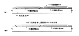
ここでは、少なくとも700〜1100℃程度の耐熱性を有する基板が必要であり、石英基板901が用いられた。そして実施例6及び実施例7で示した技術を用い、結晶質半導体膜が形成され、島状にパターニングして活性層902、903を形成した。そして、活性層902、903を覆って、ゲート絶縁膜904を、酸化珪素を主成分とする膜で形成した。本実施例では、プラズマCVD法で窒化酸化シリコン膜を70nmの厚さで形成した。(図21(A))
【0067】
そして、ハロゲン(代表的には塩素)と酸素を含む雰囲気中で熱処理を行った。本実施例では、950℃、30分とした。尚、処理温度は700〜1100℃の範囲で選択すれば良く、処理時間も10分から8時間の間で選択すれば良かった。(図21(B))
【0068】
その結果、本実施例の条件では、活性層902、903とゲート絶縁膜904との界面で熱酸化膜が形成され、ゲート絶縁膜907が形成された。
【0069】
以上の工程で作製されたゲート絶縁膜907は、絶縁耐圧が高く活性層905、906とゲート絶縁膜907の界面は非常に良好なものであった。本願発明のTFTの構成を得るためには、以降の工程は実施例1に従えば良い。
【0070】
勿論、本実施例に実施例6や実施例7を組み合わせることは実施者が適宜決定すれば良い。
【0071】
[実施例9]
上述の本発明の液晶表示装置にはネマチック液晶以外にも様々な液晶を用いることが可能である。例えば、1998, SID, "Characteristics and Driving Scheme of Polymer-Stabilized Monostable FLCD Exhibiting Fast Response Time and High Contrast Ratio with Gray-Scale Capability" by H. Furue et al.や、1997, SID DIGEST, 841, "A Full-Color Thresholdless Antiferroelectric LCD Exhibiting Wide Viewing Angle with Fast Response Time" by T. Yoshida et al.や、1996, J. Mater. Chem. 6(4), 671-673, "Thresholdless antiferroelectricity in liquid crystals and its application to displays" by S. Inui et al.や、米国特許第5594569 号に開示された液晶を用いることが可能である。
【0072】
等方相−コレステリック相−カイラルスメクティックC相転移系列を示す強誘電性液晶(FLC)を用い、DC電圧を印加しながらコレステリック相−カイラルスメクティックC相転移をさせ、かつコーンエッジをほぼラビング方向に一致させた単安定FLCの電気光学特性を図10に示す。図10に示すような強誘電性液晶による表示モードは「Half−V字スイッチングモード」と呼ばれている。図10に示すグラフの縦軸は透過率(任意単位)、横軸は印加電圧である。「Half−V字スイッチングモード」については、寺田らの"Half−V字スイッチングモードFLCD"、第46回応用物理学関係連合講演会講演予稿集、1999年3月、第1316頁、および吉原らの"強誘電性液晶による時分割フルカラーLCD"、液晶第3巻第3号第190頁に詳しい。
【0073】
図10に示されるように、このような強誘電性混合液晶を用いると、低電圧駆動かつ階調表示が可能となることがわかる。本発明の液晶表示装置には、このような電気光学特性を示す強誘電性液晶も用いることができる。
【0074】
また、ある温度域において反強誘電相を示す液晶を反強誘電性液晶(AFLC)という。反強誘電性液晶を有する混合液晶には、電場に対して透過率が連続的に変化する電気光学応答特性を示す、無しきい値反強誘電性混合液晶と呼ばれるものがある。この無しきい値反強誘電性混合液晶は、いわゆるV字型の電気光学応答特性を示すものがあり、その駆動電圧が約±2.5V程度(セル厚約1μm〜2μm)のものも見出されている。
【0075】
また、一般に、無しきい値反強誘電性混合液晶は自発分極が大きく、液晶自体の誘電率が高い。このため、無しきい値反強誘電性混合液晶を液晶表示装置に用いる場合には、画素に比較的大きな保持容量が必要となってくる。よって、自発分極が小さな無しきい値反強誘電性混合液晶を用いるのが好ましい。
【0076】
なお、このような無しきい値反強誘電性混合液晶を本発明の液晶表示装置に用いることによって低電圧駆動が実現されるので、低消費電力化が実現される。
【0077】
〔実施例10〕
本願発明を実施して形成されたCMOS回路や画素部は様々な電気光学装置(アクティブマトリクス型液晶ディスプレイ、アクティブマトリクス型ELディスプレイ)に用いることができる。即ち、それら電気光学装置を表示部に組み込んだ電気器具全てに本発明を実施できる。
【0078】
その様な電気器具としては、ビデオカメラ、デジタルカメラ、プロジェクター(リア型またはフロント型)、ヘッドマウントディスプレイ(ゴーグル型ディスプレイ)、パーソナルコンピュータ、携帯情報端末(モバイルコンピュータ、携帯電話または電子書籍等)などが挙げられる。それらの一例を図11、図12及び図13に示す。
【0079】
図11(A)はパーソナルコンピュータであり、本体2001、画像入力部2002、表示部2003、キーボード2004等を含む。本発明を画像入力部2002、表示部2003やその他の信号制御回路に適用することができる。
【0080】
図11(B)はビデオカメラであり、本体2101、表示部2102、音声入力部2103、操作スイッチ2104、バッテリー2105、受像部2106等を含む。本発明を表示部2102やその他の信号制御回路に適用することができる。
【0081】
図11(C)はモバイルコンピュータ(モービルコンピュータ)であり、本体2201、カメラ部2202、受像部2203、操作スイッチ2204、表示部2205等を含む。本発明は表示部2205やその他の信号制御回路に適用できる。
【0082】
図11(D)はゴーグル型ディスプレイであり、本体2301、表示部2302、アーム部2303等を含む。本発明は表示部2302やその他の信号制御回路に適用することができる。
【0083】
図11(E)はプログラムを記録した記録媒体(以下、記録媒体と呼ぶ)を用いるプレーヤーであり、本体2401、表示部2402、スピーカ部2403、記録媒体2404、操作スイッチ2405等を含む。なお、このプレーヤーは記録媒体としてDVD(Digtial Versatile Disc)、CD等を用い、音楽鑑賞や映画鑑賞やゲームやインターネットを行うことができる。本発明は表示部2402やその他の信号制御回路に適用することができる。
【0084】
図11(F)はデジタルカメラであり、本体2501、表示部2502、接眼部2503、操作スイッチ2504、受像部(図示しない)等を含む。本願発明を表示部2502やその他の信号制御回路に適用することができる。
【0085】
図12(A)はフロント型プロジェクターであり、投射装置2601、スクリーン2602等を含む。本発明は投射装置2601の一部を構成する液晶表示装置2808やその他の信号制御回路に適用することができる。
【0086】
図12(B)はリア型プロジェクターであり、本体2701、投射装置2702、ミラー2703、スクリーン2704等を含む。本発明は投射装置2702の一部を構成する液晶表示装置2808やその他の信号制御回路に適用することができる。
【0087】
なお、図12(C)は、図12(A)及び図12(B)中における投射装置2601、2702の構造の一例を示した図である。投射装置2601、2702は、光源光学系2801、ミラー2802、2804〜2806、ダイクロイックミラー2803、プリズム2807、液晶表示装置2808、位相差板2809、投射光学系2810で構成される。投射光学系2810は、投射レンズを含む光学系で構成される。本実施例は三板式の例を示したが、特に限定されず、例えば単板式であってもよい。また、図12(C)中において矢印で示した光路に実施者が適宜、光学レンズや、偏光機能を有するフィルムや、位相差を調節するためのフィルム、IRフィルム等の光学系を設けてもよい。
【0088】
また、図12(D)は、図12(C)中における光源光学系2801の構造の一例を示した図である。本実施例では、光源光学系2801は、リフレクター2811、光源2812、レンズアレイ2813、2814、偏光変換素子2815、集光レンズ2816で構成される。なお、図12(D)に示した光源光学系は一例であって特に限定されない。例えば、光源光学系に実施者が適宜、光学レンズや、偏光機能を有するフィルムや、位相差を調節するフィルム、IRフィルム等の光学系を設けてもよい。
【0089】
ただし、図12に示したプロジェクターにおいては、透過型の電気光学装置を用いた場合を示しており、反射型の電気光学装置及びEL表示装置での適用例は図示していない。
【0090】
図13(A)は携帯電話であり、本体2901、音声出力部2902、音声入力部2903、表示部2904、操作スイッチ2905、アンテナ2906等を含む。本願発明を音声出力部2902、音声入力部2903、表示部2904やその他の信号制御回路に適用することができる。
【0091】
図13(B)は携帯書籍(電子書籍)であり、本体3001、表示部3002、3003、記憶媒体3004、操作スイッチ3005、アンテナ3006等を含む。本発明は表示部3002、3003やその他の信号回路に適用することができる。
【0092】
図13(C)はディスプレイであり、本体3101、支持台3102、表示部3103等を含む。本発明は表示部3103に適用することができる。本発明のディスプレイは特に大画面化した場合において有利であり、対角10インチ以上(特に30インチ以上)のディスプレイには有利である。
【0093】
以上の様に、本願発明の適用範囲は極めて広く、あらゆる分野の電子機器に適用することが可能である。また、本実施例の電子機器は実施例1〜8のどのような組み合わせからなる構成を用いても実現することができる。
【0094】
〔実施例11〕
本実施例では、本発明を用いてEL(エレクトロルミネッセンス)表示装置を作製した例について説明する。
【0095】
図14(A)は本発明を用いたEL表示装置の上面図である。図14(A)において、4010は基板、4011は画素部、4012はソース側駆動回路、4013はゲート側駆動回路であり、それぞれの駆動回路は配線4014〜4016を経てFPC4017に至り、外部機器へと接続される。
【0096】
このとき、少なくとも画素部、好ましくは駆動回路及び画素部を囲むようにしてカバー材6000、シーリング材(ハウジング材ともいう)7000、密封材(第2のシーリング材)7001が設けられている。
【0097】
また、図14(B)は本実施例のEL表示装置の断面構造であり、基板4010、下地膜4021の上に駆動回路用TFT(但し、ここではnチャネル型TFTとpチャネル型TFTを組み合わせたCMOS回路を図示している。)4022及び画素部用TFT4023(但し、ここではEL素子への電流を制御するTFTだけ図示している。)が形成されている。これらのTFTは本発明により作製されたTFTを用いれば良い。
【0098】
本発明は、駆動回路用TFT4022、画素部用TFT4023に際して用いることができる。
【0099】
本発明を用いて駆動回路用TFT4022、画素部用TFT4023が完成したら、樹脂材料でなる層間絶縁膜(平坦化膜)4026の上に画素部用TFT4023のドレインと電気的に接続する透明導電膜でなる画素電極4027を形成する。透明導電膜としては、酸化インジウムと酸化スズとの化合物(ITOと呼ばれる)または酸化インジウムと酸化亜鉛との化合物を用いることができる。そして、画素電極4027を形成したら、絶縁膜4028を形成し、画素電極4027上に開口部を形成する。
【0100】
次に、EL層4029を形成する。EL層4029は公知のEL材料(正孔注入層、正孔輸送層、発光層、電子輸送層または電子注入層)を自由に組み合わせて積層構造または単層構造とすれば良い。どのような構造とするかは公知の技術を用いれば良い。また、EL材料には低分子系材料と高分子系(ポリマー系)材料がある。低分子系材料を用いる場合は蒸着法を用いるが、高分子系材料を用いる場合には、スピンコート法、印刷法またはインクジェット法等の簡易な方法を用いることが可能である。
【0101】
本実施例では、シャドーマスクを用いて蒸着法によりEL層を形成する。シャドーマスクを用いて画素毎に波長の異なる発光が可能な発光層(赤色発光層、緑色発光層及び青色発光層)を形成することで、カラー表示が可能となる。その他にも、色変換層(CCM)とカラーフィルターを組み合わせた方式、白色発光層とカラーフィルターを組み合わせた方式があるがいずれの方法を用いても良い。勿論、単色発光のEL表示装置とすることもできる。
【0102】
EL層4029を形成したら、その上に陰極4030を形成する。陰極4030とEL層4029の界面に存在する水分や酸素は極力排除しておくことが望ましい。従って、真空中でEL層4029と陰極4030を連続成膜するか、EL層4029を不活性雰囲気で形成し、大気解放しないで陰極4030を形成するといった工夫が必要である。本実施例ではマルチチャンバー方式(クラスターツール方式)の成膜装置を用いることで上述のような成膜を可能とする。
【0103】
なお、本実施例では陰極4030として、LiF(フッ化リチウム)膜とAl(アルミニウム)膜の積層構造を用いる。具体的にはEL層4029上に蒸着法で1nm厚のLiF(フッ化リチウム)膜を形成し、その上に300nm厚のアルミニウム膜を形成する。勿論、公知の陰極材料であるMgAg電極を用いても良い。そして陰極4030は4031で示される領域において配線4016に接続される。配線4016は陰極4030に所定の電圧を与えるための電源供給線であり、導電性ペースト材料4032を介してFPC4017に接続される。
【0104】
4031に示された領域において陰極4030と配線4016とを電気的に接続するために、層間絶縁膜4026及び絶縁膜4028にコンタクトホールを形成する必要がある。これらは層間絶縁膜4026のエッチング時(画素電極用コンタクトホールの形成時)や絶縁膜4028のエッチング時(EL層形成前の開口部の形成時)に形成しておけば良い。また、絶縁膜4028をエッチングする際に、層間絶縁膜4026まで一括でエッチングしても良い。この場合、層間絶縁膜4026と絶縁膜4028が同じ樹脂材料であれば、コンタクトホールの形状を良好なものとすることができる。
【0105】
このようにして形成されたEL素子の表面を覆って、パッシベーション膜6003、充填材6004、カバー材6000が形成される。
【0106】
さらに、EL素子部を囲むようにして、カバー材6000と基板4010の内側にシーリング材が設けられ、さらにシーリング材7000の外側には密封材(第2のシーリング材)7001が形成される。
【0107】
このとき、この充填材6004は、カバー材6000を接着するための接着剤としても機能する。充填材6004としては、PVC(ポリビニルクロライド)、エポキシ樹脂、シリコーン樹脂、PVB(ポリビニルブチラル)またはEVA(エチレンビニルアセテート)を用いることができる。この充填材6004の内部に乾燥剤を設けておくと、吸湿効果を保持できるので好ましい。
【0108】
また、充填材6004の中にスペーサーを含有させてもよい。このとき、スペーサーをBaOなどからなる粒状物質とし、スペーサー自体に吸湿性をもたせてもよい。
【0109】
スペーサーを設けた場合、パッシベーション膜6003はスペーサー圧を緩和することができる。また、パッシベーション膜とは別に、スペーサー圧を緩和する樹脂膜などを設けてもよい。
【0110】
また、カバー材6000としては、ガラス板、アルミニウム板、ステンレス板、FRP(Fiberglass−Reinforced Plastics)板、PVF(ポリビニルフルオライド)フィルム、マイラーフィルム、ポリエステルフィルムまたはアクリルフィルムを用いることができる。なお、充填材6004としてPVBやEVAを用いる場合、数十μmのアルミニウムホイルをPVFフィルムやマイラーフィルムで挟んだ構造のシートを用いることが好ましい。
【0111】
但し、EL素子からの発光方向(光の放射方向)によっては、カバー材6000が透光性を有する必要がある。
【0112】
また、配線4016はシーリング材7000および密封材7001と基板4010との隙間を通ってFPC4017に電気的に接続される。なお、ここでは配線4016について説明したが、他の配線4014、4015も同様にしてシーリング材7000および密封材7001の下を通ってFPC4017に電気的に接続される。
【0113】
[実施例12]
本実施例では、本発明を用いて実施例11とは異なる形態のEL表示装置を作製した例について、図15(A)、図15(B)を用いて説明する。図14(A)、14(B)と同じ番号のものは同じ部分を指しているので説明は省略する。
【0114】
図15(A)は本実施例のEL表示装置の上面図であり、図15(A)をA-A'で切断した断面図を図15(B)に示す。
【0115】
実施例10に従って、EL素子の表面を覆ってパッシベーション膜6003までを形成する。
【0116】
さらに、EL素子を覆うようにして充填材6004を設ける。この充填材6004は、カバー材6000を接着するための接着剤としても機能する。充填材6004としては、PVC(ポリビニルクロライド)、エポキシ樹脂、シリコーン樹脂、PVB(ポリビニルブチラル)またはEVA(エチレンビニルアセテート)を用いることができる。この充填材6004の内部に乾燥剤を設けておくと、吸湿効果を保持できるので好ましい。
【0117】
また、充填材6004の中にスペーサーを含有させてもよい。このとき、スペーサーをBaOなどからなる粒状物質とし、スペーサー自体に吸湿性をもたせてもよい。
【0118】
スペーサーを設けた場合、パッシベーション膜6003はスペーサー圧を緩和することができる。また、パッシベーション膜とは別に、スペーサー圧を緩和する樹脂膜などを設けてもよい。
【0119】
また、カバー材6000としては、ガラス板、アルミニウム板、ステンレス板、FRP(Fiberglass−Reinforced Plastics)板、PVF(ポリビニルフルオライド)フィルム、マイラーフィルム、ポリエステルフィルムまたはアクリルフィルムを用いることができる。なお、充填材6004としてPVBやEVAを用いる場合、数十μmのアルミニウムホイルをPVFフィルムやマイラーフィルムで挟んだ構造のシートを用いることが好ましい。
【0120】
但し、EL素子からの発光方向(光の放射方向)によっては、カバー材6000が透光性を有する必要がある。
【0121】
次に、充填材6004を用いてカバー材6000を接着した後、充填材6004の側面(露呈面)を覆うようにフレーム材6001を取り付ける。フレーム材6001はシーリング材(接着剤として機能する)6002によって接着される。このとき、シーリング材6002としては、光硬化性樹脂を用いるのが好ましいが、EL層の耐熱性が許せば熱硬化性樹脂を用いても良い。なお、シーリング材6002はできるだけ水分や酸素を透過しない材料であることが望ましい。また、シーリング材6002の内部に乾燥剤を添加してあっても良い。
【0122】
また、配線4016はシーリング材6002と基板4010との隙間を通ってFPC4017に電気的に接続される。なお、ここでは配線4016について説明したが、他の配線4014、4015も同様にしてシーリング材6002の下を通ってFPC4017に電気的に接続される。
【0123】
[実施例13]
ここでEL表示パネルにおける画素部のさらに詳細な断面構造を図16に、上面構造を図17(A)に、回路図を図17(B)に示す。図16、図17(A)及び図17(B)では共通の符号を用いるので互いに参照すれば良い。
【0124】
図16において、基板3501上に設けられたスイッチング用TFT3502は本願発明のNTFTを用いて形成される(実施例1〜7参照)。本実施例ではダブルゲート構造としているが、構造及び作製プロセスに大きな違いはないので説明は省略する。但し、ダブルゲート構造とすることで実質的に二つのTFTが直列された構造となり、オフ電流値を低減することができるという利点がある。なお、本実施例ではダブルゲート構造としているが、シングルゲート構造でも構わないし、トリプルゲート構造やそれ以上のゲート本数を持つマルチゲート構造でも構わない。
【0125】
また、電流制御用TFT3503は本発明のNTFTを用いて形成される。このとき、スイッチング用TFT3502のドレイン配線35は配線36によって電流制御用TFTのゲート電極37に電気的に接続されている。また、38で示される配線は、スイッチング用TFT3502のゲート電極39a、39bを電気的に接続するゲート配線である。
【0126】
このとき、電流制御用TFT3503が本発明の構造であることは非常に重要な意味を持つ。電流制御用TFTはEL素子を流れる電流量を制御するための素子であるため、多くの電流が流れ、熱による劣化やホットキャリアによる劣化の危険性が高い素子でもある。そのため、電流制御用TFTに、ゲート絶縁膜を介してゲート電極に重なるようにLDD領域を設ける本発明の構造は極めて有効である。
【0127】
また、本実施例では電流制御用TFT3503をシングルゲート構造で図示しているが、複数のTFTを直列につなげたマルチゲート構造としても良い。さらに、複数のTFTを並列につなげて実質的にチャネル形成領域を複数に分割し、熱の放射を高い効率で行えるようにした構造としても良い。このような構造は熱による劣化対策として有効である。
【0128】
また、図17(A)に示すように、電流制御用TFT3503のゲート電極37となる配線は3504で示される領域で、電流制御用TFT3503のドレイン配線40と絶縁膜を介して重なる。このとき、3504で示される領域ではコンデンサが形成される。このコンデンサ3504は電流制御用TFT3503のゲートにかかる電圧を保持するためのコンデンサとして機能する。なお、ドレイン配線40は電流供給線(電源線)3506に接続され、常に一定の電圧が加えられている。
【0129】
スイッチング用TFT3502及び電流制御用TFT3503の上には第1パッシベーション膜41が設けられ、その上に樹脂絶縁膜でなる平坦化膜42が形成される。平坦化膜42を用いてTFTによる段差を平坦化することは非常に重要である。後に形成されるEL層は非常に薄いため、段差が存在することによって発光不良を起こす場合がある。従って、EL層をできるだけ平坦面に形成しうるように画素電極を形成する前に平坦化しておくことが望ましい。
【0130】
また、43は反射性の高い導電膜でなる画素電極(EL素子の陰極)であり、電流制御用TFT3503のドレインに電気的に接続される。画素電極43としてはアルミニウム合金膜、銅合金膜または銀合金膜など低抵抗な導電膜またはそれらの積層膜を用いることが好ましい。勿論、他の導電膜との積層構造としても良い。
【0131】
また、絶縁膜(好ましくは樹脂)で形成されたバンク44a、44bにより形成された溝(画素に相当する)の中に発光層45が形成される。なお、ここでは一画素しか図示していないが、R(赤)、G(緑)、B(青)の各色に対応した発光層を作り分けても良い。発光層とする有機EL材料としてはπ共役ポリマー系材料を用いる。代表的なポリマー系材料としては、ポリパラフェニレンビニレン(PPV)系、ポリビニルカルバゾール(PVK)系、ポリフルオレン系などが挙げられる。
【0132】
なお、PPV系有機EL材料としては様々な型のものがあるが、例えば「H. Shenk,H.Becker,O.Gelsen,E.Kluge,W.Kreuder,and H.Spreitzer,"Polymers for Light Emitting Diodes",Euro Display,Proceedings,1999,p.33-37」や特開平10−92576号公報に記載されたような材料を用いれば良い。
【0133】
具体的な発光層としては、赤色に発光する発光層にはシアノポリフェニレンビニレン、緑色に発光する発光層にはポリフェニレンビニレン、青色に発光する発光層にはポリフェニレンビニレン若しくはポリアルキルフェニレンを用いれば良い。膜厚は30〜150nm(好ましくは40〜100nm)とすれば良い。
【0134】
但し、以上の例は発光層として用いることのできる有機EL材料の一例であって、これに限定する必要はまったくない。発光層、電荷輸送層または電荷注入層を自由に組み合わせてEL層(発光及びそのためのキャリアの移動を行わせるための層)を形成すれば良い。
【0135】
例えば、本実施例ではポリマー系材料を発光層として用いる例を示したが、低分子系有機EL材料を用いても良い。また、電荷輸送層や電荷注入層として炭化珪素等の無機材料を用いることも可能である。これらの有機EL材料や無機材料は公知の材料を用いることができる。
【0136】
本実施例では発光層45の上にPEDOT(ポリチオフェン)またはPAni(ポリアニリン)でなる正孔注入層46を設けた積層構造のEL層としている。そして、正孔注入層46の上には透明導電膜でなる陽極47が設けられる。本実施例の場合、発光層45で生成された光は上面側に向かって(TFTの上方に向かって)放射されるため、陽極は透光性でなければならない。透明導電膜としては酸化インジウムと酸化スズとの化合物や酸化インジウムと酸化亜鉛との化合物を用いることができるが、耐熱性の低い発光層や正孔注入層を形成した後で形成するため、可能な限り低温で成膜できるものが好ましい。
【0137】
陽極47まで形成された時点でEL素子3505が完成する。なお、ここでいうEL素子3505は、画素電極(陰極)43、発光層45、正孔注入層46及び陽極47で形成されたコンデンサを指す。図17(A)に示すように画素電極43は画素の面積にほぼ一致するため、画素全体がEL素子として機能する。従って、発光の利用効率が非常に高く、明るい画像表示が可能となる。
【0138】
ところで、本実施例では、陽極47の上にさらに第2パッシベーション膜48を設けている。第2パッシベーション膜48としては窒化珪素膜または窒化酸化珪素膜が好ましい。この目的は、外部とEL素子とを遮断することであり、有機EL材料の酸化による劣化を防ぐ意味と、有機EL材料からの脱ガスを抑える意味との両方を併せ持つ。これによりEL表示装置の信頼性が高められる。
【0139】
以上のように本発明のEL表示パネルは図16のような構造の画素からなる画素部を有し、オフ電流値の十分に低いスイッチング用TFTと、ホットキャリア注入に強い電流制御用TFTとを有する。従って、高い信頼性を有し、且つ、良好な画像表示が可能なEL表示パネルが得られる。
【0140】
なお、本実施例の構成は、実施例1〜9の構成と自由に組み合わせて実施することが可能である。また、実施例10の電子機器の表示部として本実施例のEL表示パネルを用いることは有効である。
【0141】
〔実施例14〕
本実施例では、実施例13に示した画素部において、EL素子3505の構造を反転させた構造について説明する。説明には図18を用いる。なお、図16の構造と異なる点はEL素子の部分と電流制御用TFTだけであるので、その他の説明は省略することとする。
【0142】
図18において、電流制御用TFT3503はPTFTを用いて形成される。
【0143】
本実施例では、画素電極(陽極)50として透明導電膜を用いる。具体的には酸化インジウムと酸化亜鉛との化合物でなる導電膜を用いる。勿論、酸化インジウムと酸化スズとの化合物でなる導電膜を用いても良い。
【0144】
そして、絶縁膜でなるバンク51a、51bが形成された後、溶液塗布によりポリビニルカルバゾールでなる発光層52が形成される。その上にはカリウムアセチルアセトネート(acacKと表記される)でなる電子注入層53、アルミニウム合金でなる陰極54が形成される。この場合、陰極54がパッシベーション膜としても機能する。こうしてEL素子3701が形成される。
【0145】
本実施例の場合、発光層52で発生した光は、矢印で示されるようにTFTが形成された基板の方に向かって放射される。
【0146】
なお、本実施例の構成は、実施例1〜9の構成と自由に組み合わせて実施することが可能である。また、実施例10の電子機器の表示部として本実施例のEL表示パネルを用いることは有効である。
【0147】
〔実施例14〕
本実施例では、図17(B)に示した回路図とは異なる構造の画素とした場合の例について図19(A)〜(C)に示す。なお、本実施例において、3801はスイッチング用TFT3802のソース配線、3803はスイッチング用TFT3802のゲート配線、3804は電流制御用TFT、3805はコンデンサ、3806、3808は電流供給線、3807はEL素子とする。
【0148】
図19(A)は、二つの画素間で電流供給線3806を共通とした場合の例である。即ち、二つの画素が電流供給線3806を中心に線対称となるように形成されている点に特徴がある。この場合、電源供給線の本数を減らすことができるため、画素部をさらに高精細化することができる。
【0149】
また、図19(B)は、電流供給線3808をゲート配線3803と平行に設けた場合の例である。なお、図19(B)では電流供給線3808とゲート配線3803とが重ならないように設けた構造となっているが、両者が異なる層に形成される配線であれば、絶縁膜を介して重なるように設けることもできる。この場合、電源供給線3808とゲート配線3803とで専有面積を共有させることができるため、画素部をさらに高精細化することができる。
【0150】
また、図19(C)は、図19(B)の構造と同様に電流供給線3808をゲート配線3803と平行に設け、さらに、二つの画素を電流供給線3808を中心に線対称となるように形成する点に特徴がある。また、電流供給線3808をゲート配線3803のいずれか一方と重なるように設けることも有効である。この場合、電源供給線の本数を減らすことができるため、画素部をさらに高精細化することができる。
【0151】
なお、本実施例の構成は、実施例1〜9、11または12の構成と自由に組み合わせて実施することが可能である。また、実施例10の電子機器の表示部として本実施例の画素構造を有するEL表示パネルを用いることは有効である。
【0152】
[実施例16]
実施例13に示した図17(A)、図17(B)では電流制御用TFT3503のゲートにかかる電圧を保持するためにコンデンサ3504を設ける構造としているが、コンデンサ3504を省略することも可能である。実施例12の場合、電流制御用TFT3503として実施例1〜8に示すような本発明のNTFTを用いているため、ゲート絶縁膜を介してゲート電極に重なるように設けられたLDD領域を有している。この重なり合った領域には一般的にゲート容量と呼ばれる寄生容量が形成されるが、本実施例ではこの寄生容量をコンデンサ3504の代わりとして積極的に用いる点に特徴がある。
【0153】
この寄生容量のキャパシタンスは、上記ゲート電極とLDD領域とが重なり合った面積によって変化するため、その重なり合った領域に含まれるLDD領域の長さによって決まる。
【0154】
また、実施例14に示した図19(A)〜(C)の構造においても同様に、コンデンサ3805を省略することは可能である。
【0155】
なお、本実施例の構成は、実施例1〜9、11〜15の構成と自由に組み合わせて実施することが可能である。また、実施例10の電子機器の表示部として本実施例の画素構造を有するEL表示パネルを用いることは有効である。
【0156】
【発明の効果】
本発明により、電解めっき法で析出条件を設定することにより、容易にゲート配線の側面および上部に金属膜を析出させることができる。また、この金属膜をマスクとして島状半導体層に不純物元素を添加させ、LDD領域をゲート配線の両側に均一の幅で形成することができる。
この結果、GOLD構造である半導体装置が得られるため、高耐圧、高信頼性のTFTを作製することができる。また、画素部の画素TFTに15〜20Vのゲート電圧を印加して駆動させても、安定した動作を得ることができる。その結果、結晶性TFTで作製されたCMOS回路を含む半導体装置、また、具体的には液晶表示装置やEL表示装置の周辺に設けられる駆動回路の信頼性を高め、長時間の使用に耐えうる液晶表示装置やEL表示装置を得ることができる。
【図面の簡単な説明】
【図1】 電解めっき法の簡略図。
【図2】 本発明によるTFTの作製工程を示す断面図。
【図3】 本発明によるTFTの作製工程を示す断面図。
【図4】 本発明によるアクティブマトリクス基板の作製工程を示す断面図。
【図5】 本発明によるアクティブマトリクス基板の作製工程を示す断面図。
【図6】 本発明によるアクティブマトリクス基板の作製工程を示す断面図。
【図7】 本発明によるアクティブマトリクス基板の作製工程を示す断面図。
【図8】 TFTの作製工程を示す断面図。
【図9】 TFTの作製工程を示す断面図。
【図10】 反強誘電性混合液晶の光透過率特性の一例を示す図。
【図11】 電気器具の一例を示す図。
【図12】 電気器具の一例を示す図。
【図13】 電気器具の一例を示す図。
【図14】 EL表示装置の構成を示す図。
【図15】 EL表示装置の構成を示す図。
【図16】 EL表示装置の構成を示す図。
【図17】 EL表示装置の構成を示す図。
【図18】 EL表示装置の構成を示す図。
【図19】 EL表示装置の構成を示す図。
【図20】 TFTの作製工程を示す断面図。
【図21】 TFTの作製工程を示す断面図。[0001]
BACKGROUND OF THE INVENTION
The present invention relates to a semiconductor device having a circuit formed of a thin film transistor (hereinafter referred to as TFT) on a substrate having an insulating surface, and a manufacturing method thereof. For example, the present invention relates to an electro-optical device typified by a liquid crystal display device, an electric appliance (also referred to as an electronic device) on which the electro-optical device is mounted, and a manufacturing method thereof. Note that in this specification, a semiconductor device refers to all devices that function by utilizing semiconductor characteristics, and includes the above-described electro-optical device and an electric appliance in which the electro-optical device is mounted.
[0002]
[Prior art]
In recent years, attention has been paid to an active matrix liquid crystal display device in which a circuit is constituted by TFTs using a polysilicon film (hereinafter referred to as crystalline TFTs). This realizes a high-definition image display device by controlling the electric field applied to the liquid crystal in a matrix by a plurality of pixels arranged in a matrix.
[0003]
In many cases, an n-channel TFT is formed in a pixel portion of an active matrix liquid crystal display device (hereinafter, a TFT formed in the pixel portion is referred to as a pixel TFT). Since a gate voltage having an amplitude of about 15 to 20 V is applied to the pixel TFT, it is necessary to satisfy the characteristics of both the on region and the off region. On the other hand, the peripheral circuit provided for driving the pixel portion is configured based on a CMOS circuit, and the characteristics of the on region are mainly important. However, the crystalline TFT has a problem that the off-current tends to increase. When the crystalline TFT is driven for a long period of time, deterioration phenomena such as a decrease in mobility, an on-current, and an increase in off-current are often observed. One of the causes is considered to be a hot carrier injection phenomenon that occurs due to a high electric field near the drain.
[0004]
In the LSI technical field, a lightly doped drain (LDD) structure is known as a method for reducing the off-current of a MOS transistor and further mitigating a high electric field in the vicinity of the drain. In this structure, a low concentration impurity region is provided between a drain region and a channel formation region, and this low concentration impurity region is called an LDD region.
[0005]
Similarly, it has been known that a crystalline TFT forms an LDD structure. In the conventional technique, a low-concentration impurity region that becomes an LDD region is formed by adding a first impurity element using a gate electrode as a mask, and then an anisotropic etching technique is used on both sides of the gate electrode. In this method, sidewalls are formed, and a high concentration impurity region to be a source region and a drain region is formed by adding a second impurity element using the gate electrode and the sidewall as a mask.
[0006]
[Problems to be solved by the invention]
However, the LDD structure has a drawback in that, even if the off-current can be reduced, the series resistance component increases structurally, and as a result, the on-current of the TFT also decreases. It was. Moreover, the deterioration of the on-current could not be prevented completely.
[0007]
The present invention provides a technique for overcoming such a problem, and an object thereof is to provide a TFT having a structure in which a gate electrode and an LDD region are overlapped. In order to achieve the object, an object is to provide a technique for manufacturing a TFT having a structure in which a gate electrode overlaps an LDD region by a simple method. Another object of the present invention is to provide a semiconductor device in which a circuit is formed using highly reliable TFTs.
[0008]
[Means for Solving the Problems]
The structure of the invention disclosed in this specification includes a TFT having a gate wiring on a gate insulating film, and having a metal film having the same film thickness on a side surface and an upper surface of the gate wiring. Device.
[0009]
According to another aspect of the invention, there is provided a TFT having a gate wiring on a gate insulating film, and having a metal film deposited by an electrolytic plating method on a side surface and an upper surface of the gate wiring. It is a semiconductor device.
[0010]
According to another aspect of the invention, there is provided a semiconductor device having a CMOS circuit formed of an n-channel TFT and a p-channel TFT, wherein the n-channel TFT and the p-channel TFT are arranged on a gate insulating film on a gate wiring. And the gate wiring has a metal film on a side surface and an upper surface.
[0011]
According to another aspect of the invention, in a semiconductor device including a CMOS circuit formed of an n-channel TFT and a p-channel TFT, gate insulation is provided on each active layer of the n-channel TFT and the p-channel TFT. A gate wiring on the gate insulating film, and a metal film covering a side surface and an upper surface of the gate wiring, and an active layer of the n-channel TFT is in contact with the channel forming region and the channel forming region. A first impurity region; a second impurity region in contact with the first impurity region; a third impurity region in contact with the second impurity region; and the gate wiring overlapping the channel formation region. The width of the first impurity region is determined by the thickness of the metal film formed on the side surface of the gate wiring.
[0012]
According to another aspect of the invention, there is provided a semiconductor device including a CMOS circuit formed of an n-channel TFT and a p-channel TFT, wherein a gate insulating film is formed on an active layer, and a gate wiring is formed on the gate insulating film. A metal film covering the side surface and the upper surface of the gate wiring,
An active layer of the n-channel TFT includes a channel formation region, a first impurity region in contact with the channel formation region, a second impurity region in contact with the first impurity region, and a third impurity in contact with the second impurity region. And the length of the channel formation region, the width of the gate wiring, the length of the first impurity region, and the film thickness of the metal film coincide with each other through the gate insulating film,
In the third impurity region, the catalyst element used for crystallization of the active layer is 1 × 10 6. 17 ~ 1x10 20 atoms / cm Three It is a semiconductor device characterized by existing at a concentration of
[0013]
According to another aspect of the invention, there is provided a step of crystallizing a semiconductor layer formed on a substrate having an insulating surface to form an active layer, a step of forming a gate insulating film on the active layer, and the gate insulation. A step of forming a gate wiring on the film; a step of forming a first impurity region by adding an impurity using the gate wiring as a mask; and a step of forming a metal film on a side surface and an upper portion of the gate wiring by an electrolytic plating method Adding a impurity by using the metal film as a mask to form a fourth impurity region in the p-channel type thin film transistor; adding a impurity by using the metal film as a mask to form a second impurity region; And a step of forming a third impurity region by adding an impurity to a selected portion of the active layer.
[0014]
According to another aspect of the invention, there is provided a step of adding a catalytic element to a semiconductor layer formed on a substrate having an insulating surface, a step of crystallizing the semiconductor layer by heat treatment, and a step of forming the active layer. Forming a gate insulating film on the layer; forming a gate wiring on the gate insulating film; adding a impurity using the gate wiring as a mask to form a first impurity region;
Forming a metal film on a side surface and an upper portion of the gate wiring by an electrolytic plating method, adding an impurity using the metal film as a mask to form a fourth impurity region in a p-channel thin film transistor, and A semiconductor device comprising: a step of forming a second impurity region by adding an impurity using a mask; and a step of forming a third impurity region by adding an impurity to a selected portion of the active layer. This is a manufacturing method.
[0015]
DETAILED DESCRIPTION OF THE INVENTION
[Example 1]
In this embodiment, a method for manufacturing a semiconductor device of the present invention will be described with reference to FIGS.
[0016]
First, as the substrate 301, for example, a glass substrate represented by a 1737 glass substrate manufactured by Corning was used. Then, a base film 302 made of a silicon oxide film was formed to a thickness of 200 nm on the surface of the substrate 301 on the side where the TFT is formed. The base film 302 may be a silicon nitride film deposited or only a silicon oxynitride film. As a method for forming the base film, a plasma CVD method, a thermal CVD method, or a sputtering method may be used.
[0017]
Next, an amorphous silicon film was formed to a thickness of 30 nm on the base film 302 by plasma CVD. The method for forming the amorphous silicon film may be a thermal CVD method or a sputtering method. After the amorphous silicon film was dehydrogenated, a crystallization process was performed to form a polycrystalline silicon film.
[0018]
In this crystallization step, a known laser crystallization technique or thermal crystallization technique may be used. In this embodiment, a pulsed transmission type KrF excimer laser beam is condensed into a linear shape and irradiated to the amorphous silicon film to form a crystalline silicon film.
[0019]
In this embodiment, the initial film is used as an amorphous silicon film, but a microcrystalline silicon film may be used as the initial film, or a crystalline silicon film may be formed directly.
[0020]
The crystalline silicon film thus formed was patterned to form active layers 303 and 304 made of island-like silicon layers.
[0021]
Note that after the crystalline silicon film is formed, excimer laser light may be irradiated to increase crystallinity. Further, it may be performed after the active layers 303 and 304 are formed.
[0022]
Next, a gate insulating film 305 made of a silicon oxide film was formed to a thickness of 100 nm so as to cover the active layers 303 and 304. Subsequently, gate wirings 306 and 307 having a laminated structure of tantalum and tantalum nitride were formed on the gate insulating film 305. Although another metal can be used for the
[0023]
A resist
[0024]
In this state, the first step of adding phosphorus was performed. Here, since the impurity is added through the gate insulating film, the acceleration voltage is set to 80 KeV. The
[0025]
Next, in this example, CuSO Four ・ 5H 2 Copper (Cu) was deposited to 0.1 to 1 μm (preferably 0.2 to 0.5 μm) on the side and top surfaces of the conductive layer by a known electrolytic plating method using an O electrolyte. (Fig. 2 (C))
[0026]
As shown in FIG. 1, the electrolytic plating method is performed by immersing two electrodes in an electrolyte solution 103 and causing an electrochemical change on both electrode surfaces when electric current is passed from the outside. Therefore, the cathode electrode 101 (the electrode on the metal deposition side) from which + ions in the liquid are discharged is used as the gate wiring, and the anode electrode 102 in which − ions are discharged or the metal is dissolved to form metal ions is formed as Cu. If the electrode is formed and an electric current flows through the contact pad, a metal film made of Cu can be deposited on the side wall and upper part of the gate wiring.
[0027]
The electrolytic plating method is a phenomenon in which metal ions are reduced and deposited at the cathode electrode, and the amount of electrode reaction is proportional to the amount of current applied, so the thickness of the deposited metal film can be easily adjusted, and the gate electrode It is easy to equalize the film thickness of the metal film deposited on the side surface and the upper surface of the metal film.
[0028]
After forming the
[0029]
In this state, a step of adding boron was performed. Here, the acceleration voltage is 10 KeV, and the
[0030]
Next, a resist
[0031]
In this state, a second step of adding phosphorus was performed. Also in this case, the applied voltage was set to 80 KeV. In the second impurity addition (phosphorus doping) step, the
[0032]
Next, a resist
[0033]
In this state, the third step of adding phosphorus was performed to form the
[0034]
The resist
[0035]
Since the PTFT is originally highly reliable, it may be advantageous to provide an on-current without providing an LDD region or the like without any problem. In this embodiment, both the LDD region and the offset region are formed with respect to the PTFT. Not done.
[0036]
Thus, finally, a channel formation region, a first impurity region, a second impurity region, and a third impurity region are formed in the active layer of the NTFT. ov = 0.5-3.0 μm (1.0-1.5 μm), L off = 0.5 to 3.0 μm (1.0 to 2.0 μm). Only the channel formation region and the fourth impurity region were formed in the active layer of the PTFT.
[0037]
An LDD region could be formed in a self-aligned manner by forming a metal film on the side and top surfaces of the gate wiring by electrolytic plating and adding impurities using the metal film as a mask. Further, if the thickness of the metal film is changed, the length (width) of the LDD region can be changed.
[0038]
[Example 2]
The TFT manufactured in Example 1 (FIG. 3B) is used as a driver circuit, and the NTFT manufactured in the pixel TFT of the active matrix substrate by the method shown in Example 1 (however, has a multi-gate structure). The structure of the storage capacitor connected to the TFT in the pixel portion of the active matrix liquid crystal display device employing the above will be described with reference to FIG.
[0039]
A first
[0040]
After the source wiring and the drain wiring were formed in this way, a 50 nm thick
[0041]
Next, a light shielding layer 330 was formed in a part of the pixel region on the second interlayer insulating film 329. The light shielding layer 330 may be formed using a metal material such as aluminum, titanium, or tantalum, a film containing these metals as a main component, or an organic resin film. Here, titanium was formed by a sputtering method.
[0042]
When the light shielding film is formed, a third interlayer insulating film 331 is formed. The third interlayer insulating film 331 is preferably formed using an organic resin film, like the second interlayer insulating film 329. Then, a contact hole reaching the
[0043]
When the state of FIG. 4A is formed, an alignment film 333 is formed. Usually, a polyimide resin is often used for the alignment film of the liquid crystal display element. A transparent conductive film (pixel electrode) 335 and an alignment film 334 were formed on the opposite substrate 336. After the alignment film was formed, it was rubbed so that the liquid crystal molecules were aligned in parallel with a certain pretilt angle.
[0044]
Through the above steps, the pixel matrix circuit, the substrate on which the CMOS circuit is formed, and the counter substrate are bonded together by a known cell assembling process via a sealant or a spacer (both not shown). Thereafter, a liquid crystal material 337 was injected between both substrates and completely sealed with a sealing material (not shown). Thus, the active matrix liquid crystal display device shown in FIG. 4B is completed.
[0045]
According to this embodiment, a metal film is formed on the side surface and the upper surface of the gate wiring, and the completed CMOS circuit has excellent reliability, so that the reliability of the entire circuit is greatly improved. Further, it was found that when the structure as in this example is used, the characteristic balance between NTFT and PTFT is improved, so that it is difficult for malfunctions to occur.
[0046]
[Example 3]
In the manufacturing method of Example 1, after the step illustrated in FIG. 2A is completed, resist masks 403 and 404 that cover the entire PTFT and the entire pixel portion are formed, and the first phosphorus is added. It was.
As a result, in the NTFT of the driver circuit portion, the
[0047]
Next,
[0048]
Subsequent steps were performed according to Example 2, and an active matrix liquid crystal display device as shown in FIG. 7B was completed.
[0049]
[Example 4]
In the first embodiment, a stack of tantalum and tantalum nitride is used as the
If the refractory metal is formed on the side surface and the upper portion of the gate wiring as in this embodiment, the refractory metal protects the gate wiring, and therefore has an advantage that thermal activation can be performed at a high temperature. This embodiment can be used in combination with the first to third embodiments.
[0050]
[Example 5]
In the first embodiment, tantalum and tantalum nitride are laminated as the
Since both the gate wiring and the metal film are refractory metals, they can be thermally activated at a high temperature, and by making the two metals the same, it is possible to make the metals difficult to peel off. This embodiment can be used in combination with the first to third embodiments.
[0051]
[Example 6]
In this embodiment, an example in which a crystalline semiconductor film used as a semiconductor layer in
[0052]
Here, FIG. 8 shows an example in which the technique disclosed in Japanese Patent Laid-Open No. 7-130652 is applied to the present invention. First, a silicon oxide film 602 was provided on a substrate 601, and an amorphous silicon film 603 was formed thereon. Furthermore, a nickel acetate layer solution containing 10 ppm of nickel in terms of weight was applied to form a nickel-containing layer 604. (Fig. 8 (A))
[0053]
Next, after a dehydrogenation step at 500 ° C. for 1 hour, a heat treatment was performed at 500 to 650 ° C. for 4 to 12 hours (550 ° C. for 14 hours in this embodiment) to form a crystalline silicon film 605. The crystalline silicon film 605 thus obtained had very excellent crystallinity. (Fig. 8 (B))
[0054]
Further, the technique disclosed in Japanese Patent Laid-Open No. 8-78329 enables selective crystallization of an amorphous semiconductor film by selectively adding a catalytic element. The case where this technique is applied to the present invention will be described with reference to FIG.
[0055]
First, a silicon oxide film 702 was provided over a glass substrate 701, and an amorphous silicon film 703 and a silicon oxide film 704 were continuously formed thereon.
[0056]
Next, the silicon oxide film 704 was patterned to selectively form opening
[0057]
Next, a heat treatment was performed at 500 to 650 ° C. for 4 to 24 hours (580 ° C. for 14 hours in this embodiment) to form a crystalline silicon film 707. In this crystallization process, the portion of the amorphous silicon film in contact with nickel is first crystallized, and the crystallization proceeds laterally therefrom. The crystalline silicon film 707 formed in this way is formed by a collection of rod-like or needle-like crystals, and each crystal grows macroscopically in a specific direction, so that the crystallinity is uniform. There are advantages.
[0058]
The catalyst elements that can be used in the above two techniques are not only nickel (Ni) but also germanium (Ge), iron (Fe), palladium (Pd), tin (Sn), lead (Pb), cobalt ( Elements such as Co), platinum (Pt), copper (Cu), and gold (Au) may be used.
[0059]
If a crystalline semiconductor film (including a crystalline silicon film or a crystalline silicon germanium film) is formed using the above technique and patterned, a semiconductor layer of a TFT can be formed. Although a TFT manufactured from a crystalline semiconductor film can provide excellent characteristics, high reliability is required. However, by adopting the TFT structure of the present invention, it has become possible to produce a TFT that makes the most of the technique of this embodiment. This embodiment can be used in combination with any one of
[0060]
[Example 7]
In this example, as a method of forming the semiconductor layer used in Example 1, after forming a crystalline semiconductor film using the above catalytic element using an amorphous semiconductor film as an initial film as in Example 6, An example in which the step of removing the catalyst element from the crystalline semiconductor film is performed will be described. In the present embodiment, the technique described in Japanese Patent Application Laid-Open No. 10-135468 or Japanese Patent Application Laid-Open No. 10-135469 is used as the method.
[0061]
The technique described in the publication is a technique for removing a catalytic element used for crystallization of an amorphous semiconductor film by using a gettering action of phosphorus after crystallization. By using this technique, the concentration of the catalytic element in the crystalline semiconductor film can be reduced to 1 × 10. 17 atoms / cm Three Or less, preferably 1 × 10 16 atoms / cm Three It can be reduced to.
[0062]
The configuration of this example will be described with reference to FIG. Here, an alkali-free glass substrate typified by Corning's 1737 substrate was used. FIG. 20A shows a state in which the base film 802 and the crystalline silicon film 803 are formed by using the crystallization technique shown in
[0063]
In this state, when heat treatment is performed in a nitrogen atmosphere at 550 to 800 ° C. for 5 to 24 hours (in this embodiment, 600 ° C. and 12 hours), a region 805 in which phosphorus is added to the crystalline silicon film becomes a gettering site. The catalytic element remaining in the crystalline silicon film 803 could be moved to the region 805 to which phosphorus was added.
[0064]
Then, the silicon oxide film 804 for mask and the region 805 to which phosphorus is added are removed by etching, so that the concentration of the catalytic element used in the crystallization step is 1 × 10. 17 atoms / cm Three A crystalline silicon film reduced to the following could be obtained. This crystalline silicon film could be used as the active layer of the TFT of the present invention shown in Example 1 as it was. This example can be used in combination with any of Examples 1-5.
[0065]
[Example 8]
In this embodiment, another embodiment in which a semiconductor layer and a gate insulating film are formed in the process of manufacturing the TFT of the present invention shown in
[0066]
Here, a substrate having a heat resistance of at least about 700 to 1100 ° C. is necessary, and a quartz substrate 901 is used. A crystalline semiconductor film was formed by using the techniques shown in Examples 6 and 7, and active layers 902 and 903 were formed by patterning into island shapes. Then, the gate insulating film 904 was formed using a film containing silicon oxide as a main component so as to cover the active layers 902 and 903. In this embodiment, a silicon nitride oxide film with a thickness of 70 nm is formed by plasma CVD. (FIG. 21 (A))
[0067]
Then, heat treatment was performed in an atmosphere containing halogen (typically chlorine) and oxygen. In this example, the temperature was 950 ° C. for 30 minutes. The treatment temperature may be selected in the range of 700 to 1100 ° C., and the treatment time may be selected between 10 minutes and 8 hours. (Fig. 21 (B))
[0068]
As a result, under the conditions of this example, a thermal oxide film was formed at the interface between the active layers 902 and 903 and the gate insulating film 904, and a gate insulating film 907 was formed.
[0069]
The gate insulating film 907 manufactured through the above steps had a high withstand voltage, and the interface between the active layers 905 and 906 and the gate insulating film 907 was very good. In order to obtain the structure of the TFT of the present invention, the subsequent steps may be performed according to the first embodiment.
[0070]
Of course, the combination of the sixth embodiment and the seventh embodiment with this embodiment may be appropriately determined by the practitioner.
[0071]
[Example 9]
In addition to the nematic liquid crystal, various liquid crystals can be used for the above-described liquid crystal display device of the present invention. For example, 1998, SID, "Characteristics and Driving Scheme of Polymer-Stabilized Monostable FLCD Exhibiting Fast Response Time and High Contrast Ratio with Gray-Scale Capability" by H. Furue et al., 1997, SID DIGEST, 841, "A Full -Color Thresholdless Antiferroelectric LCD Exhibiting Wide Viewing Angle with Fast Response Time "by T. Yoshida et al., 1996, J. Mater. Chem. 6 (4), 671-673," Thresholdless antiferroelectricity in liquid crystals and its application to The liquid crystal disclosed in "displays" by S. Inui et al. or US Pat. No. 5,945,569 can be used.
[0072]
Using a ferroelectric liquid crystal (FLC) exhibiting an isotropic phase-cholesteric phase-chiral smectic C phase transition series, a cholesteric phase-chiral smectic C phase transition is applied while applying a DC voltage, and the cone edge is substantially in the rubbing direction. The electro-optical characteristics of the matched monostable FLC are shown in FIG. The display mode using the ferroelectric liquid crystal as shown in FIG. 10 is called “Half-V-shaped switching mode”. The vertical axis of the graph shown in FIG. 10 is the transmittance (arbitrary unit), and the horizontal axis is the applied voltage. Regarding "Half-V-shaped switching mode", Terada et al., "Half-V-shaped switching mode FLCD", Proceedings of the 46th Joint Physics Related Conference, March 1999, p. 1316, and Yoshihara et al. "Time-division full-color LCD with ferroelectric liquid crystal", Liquid Crystal Vol. 3, No. 3, page 190.
[0073]
As shown in FIG. 10, it can be seen that when such a ferroelectric mixed liquid crystal is used, low voltage driving and gradation display are possible. In the liquid crystal display device of the present invention, a ferroelectric liquid crystal exhibiting such electro-optical characteristics can also be used.
[0074]
A liquid crystal exhibiting an antiferroelectric phase in a certain temperature range is called an antiferroelectric liquid crystal (AFLC). Among mixed liquid crystals having antiferroelectric liquid crystals, there is a so-called thresholdless antiferroelectric mixed liquid crystal that exhibits electro-optic response characteristics in which transmittance continuously changes with respect to an electric field. This thresholdless antiferroelectric mixed liquid crystal has a so-called V-shaped electro-optic response characteristic, and a drive voltage of about ± 2.5 V (cell thickness of about 1 μm to 2 μm) is also found. Has been.
[0075]
In general, the thresholdless antiferroelectric mixed liquid crystal has a large spontaneous polarization, and the dielectric constant of the liquid crystal itself is high. For this reason, when a thresholdless antiferroelectric mixed liquid crystal is used in a liquid crystal display device, a relatively large storage capacitor is required for the pixel. Therefore, it is preferable to use a thresholdless antiferroelectric mixed liquid crystal having a small spontaneous polarization.
[0076]
In addition, since such a thresholdless antiferroelectric mixed liquid crystal is used for the liquid crystal display device of the present invention, low voltage driving is realized, so that low power consumption is realized.
[0077]
Example 10
The CMOS circuit and the pixel portion formed by implementing the present invention can be used for various electro-optical devices (active matrix liquid crystal display, active matrix EL display). That is, the present invention can be implemented in all electric appliances in which these electro-optical devices are incorporated in the display unit.
[0078]
Such electric appliances include video cameras, digital cameras, projectors (rear type or front type), head mounted displays (goggles type displays), personal computers, personal digital assistants (mobile computers, mobile phones, electronic books, etc.), etc. Is mentioned. Examples of these are shown in FIGS. 11, 12 and 13.
[0079]
FIG. 11A illustrates a personal computer, which includes a main body 2001, an image input portion 2002, a display portion 2003, a
[0080]
FIG. 11B shows a video camera, which includes a main body 2101, a display portion 2102, an
[0081]
FIG. 11C illustrates a mobile computer, which includes a main body 2201, a camera unit 2202, an
[0082]
FIG. 11D shows a goggle type display, which includes a
[0083]
FIG. 11E shows a player using a recording medium (hereinafter referred to as a recording medium) on which a program is recorded, and includes a main body 2401, a
[0084]
FIG. 11F illustrates a digital camera, which includes a main body 2501, a
[0085]
FIG. 12A illustrates a front projector, which includes a
[0086]
FIG. 12B illustrates a rear projector, which includes a main body 2701, a
[0087]
FIG. 12C is a diagram showing an example of the structure of the
[0088]
FIG. 12D illustrates an example of the structure of the light source
[0089]
However, the projector shown in FIG. 12 shows a case where a transmissive electro-optical device is used, and an application example in a reflective electro-optical device and an EL display device is not shown.
[0090]
FIG. 13A shows a mobile phone, which includes a
[0091]
FIG. 13B illustrates a portable book (electronic book), which includes a
[0092]
FIG. 13C shows a display, which includes a
[0093]
As described above, the application range of the present invention is extremely wide and can be applied to electronic devices in various fields. Moreover, the electronic apparatus of a present Example is realizable even if it uses the structure which consists of what combination of Examples 1-8.
[0094]
Example 11
In this example, an example in which an EL (electroluminescence) display device is manufactured using the present invention will be described.
[0095]
FIG. 14A is a top view of an EL display device using the present invention. In FIG. 14A,
[0096]
At this time, a
[0097]
FIG. 14B shows a cross-sectional structure of the EL display device of this embodiment. A driver circuit TFT (here, an n-channel TFT and a p-channel TFT are combined on a
[0098]
The present invention can be used for the
[0099]
When the driving
[0100]
Next, an
[0101]
In this embodiment, the EL layer is formed by vapor deposition using a shadow mask. Color display is possible by forming a light emitting layer (a red light emitting layer, a green light emitting layer, and a blue light emitting layer) capable of emitting light having different wavelengths for each pixel using a shadow mask. In addition, there are a method in which a color conversion layer (CCM) and a color filter are combined, and a method in which a white light emitting layer and a color filter are combined, but either method may be used. Needless to say, an EL display device emitting monochromatic light can also be used.
[0102]
After the
[0103]
In this embodiment, a stacked structure of a LiF (lithium fluoride) film and an Al (aluminum) film is used as the
[0104]
In order to electrically connect the
[0105]
A
[0106]
Further, a sealing material is provided inside the
[0107]
At this time, the
[0108]
In addition, a spacer may be included in the
[0109]
In the case where a spacer is provided, the
[0110]
As the
[0111]
However, the
[0112]
The
[0113]
[Example 12]
In this embodiment, an example of manufacturing an EL display device having a different form from that of Embodiment 11 by using the present invention will be described with reference to FIGS. 15A and 15B. Components having the same numbers as those in FIGS. 14 (A) and 14 (B) indicate the same parts, and thus description thereof is omitted.
[0114]
FIG. 15A is a top view of the EL display device of this embodiment, and FIG. 15B is a cross-sectional view taken along line AA ′ of FIG.
[0115]
According to the tenth embodiment, the
[0116]
Further, a
[0117]
In addition, a spacer may be included in the
[0118]
In the case where a spacer is provided, the
[0119]
As the
[0120]
However, the
[0121]
Next, after the
[0122]
The
[0123]
[Example 13]
Here, FIG. 16 shows a more detailed cross-sectional structure of the pixel portion in the EL display panel, FIG. 17A shows a top structure, and FIG. 17B shows a circuit diagram. In FIG. 16, FIG. 17 (A), and FIG.
[0124]
In FIG. 16, a switching
[0125]
The
[0126]
At this time, it is very important that the
[0127]
In this embodiment, the
[0128]
Further, as shown in FIG. 17A, the wiring that becomes the
[0129]
A
[0130]
[0131]
A
[0132]
There are various types of PPV organic EL materials. For example, “H. Shenk, H. Becker, O. Gelsen, E. Kluge, W. Kreuder, and H. Spreitzer,” Polymers for Light Emitting. Materials such as those described in “Diodes”, Euro Display, Proceedings, 1999, p. 33-37 ”and Japanese Patent Application Laid-Open No. 10-92576 may be used.
[0133]
As a specific light emitting layer, cyanopolyphenylene vinylene may be used for a light emitting layer that emits red light, polyphenylene vinylene may be used for a light emitting layer that emits green light, and polyphenylene vinylene or polyalkylphenylene may be used for a light emitting layer that emits blue light. The film thickness may be 30 to 150 nm (preferably 40 to 100 nm).
[0134]
However, the above example is an example of an organic EL material that can be used as a light emitting layer, and is not necessarily limited to this. An EL layer (a layer for emitting light and moving carriers therefor) may be formed by freely combining a light-emitting layer, a charge transport layer, or a charge injection layer.
[0135]
For example, in this embodiment, an example in which a polymer material is used as the light emitting layer is shown, but a low molecular weight organic EL material may be used. It is also possible to use an inorganic material such as silicon carbide for the charge transport layer or the charge injection layer. As these organic EL materials and inorganic materials, known materials can be used.
[0136]
In this embodiment, the EL layer has a laminated structure in which a
[0137]
When the
[0138]
By the way, in the present embodiment, a
[0139]
As described above, the EL display panel of the present invention has a pixel portion composed of pixels having a structure as shown in FIG. 16, and includes a switching TFT having a sufficiently low off-current value and a current control TFT resistant to hot carrier injection. Have. Therefore, an EL display panel having high reliability and capable of displaying a good image can be obtained.
[0140]
In addition, the structure of a present Example can be implemented in combination freely with the structure of Examples 1-9. Further, it is effective to use the EL display panel of this embodiment as the display unit of the electronic apparatus of Embodiment 10.
[0141]
Example 14
In this embodiment, a structure in which the structure of the
[0142]
In FIG. 18, a
[0143]
In this embodiment, a transparent conductive film is used as the pixel electrode (anode) 50. Specifically, a conductive film made of a compound of indium oxide and zinc oxide is used. Of course, a conductive film made of a compound of indium oxide and tin oxide may be used.
[0144]
Then, after
[0145]
In the case of the present embodiment, the light generated in the
[0146]
In addition, the structure of a present Example can be implemented in combination freely with the structure of Examples 1-9. Further, it is effective to use the EL display panel of this embodiment as the display unit of the electronic apparatus of Embodiment 10.
[0147]
Example 14
In this embodiment, FIGS. 19A to 19C show an example of a pixel having a structure different from the circuit diagram shown in FIG. In this embodiment, 3801 is a source wiring of the switching
[0148]
FIG. 19A shows an example in which the
[0149]
FIG. 19B illustrates an example in which the
[0150]
In FIG. 19C, a
[0151]
In addition, the structure of a present Example can be implemented in combination freely with the structure of Example 1-9, 11 or 12. In addition, it is effective to use the EL display panel having the pixel structure of this embodiment as the display portion of the electronic apparatus of Embodiment 10.
[0152]
[Example 16]
In FIGS. 17A and 17B shown in Embodiment 13, the
[0153]
Since the capacitance of the parasitic capacitance varies depending on the area where the gate electrode and the LDD region overlap, the capacitance of the parasitic capacitance is determined by the length of the LDD region included in the overlapping region.
[0154]
Similarly, in the structure of FIGS. 19A to 19C shown in the fourteenth embodiment, the
[0155]
In addition, the structure of a present Example can be implemented in combination freely with the structure of Examples 1-9, 11-15. In addition, it is effective to use the EL display panel having the pixel structure of this embodiment as the display portion of the electronic apparatus of Embodiment 10.
[0156]
【The invention's effect】
According to the present invention, the metal film can be easily deposited on the side surface and the upper portion of the gate wiring by setting the deposition conditions by electrolytic plating. Further, an impurity element can be added to the island-like semiconductor layer using this metal film as a mask, so that the LDD regions can be formed with a uniform width on both sides of the gate wiring.
As a result, a semiconductor device having a GOLD structure can be obtained, so that a high breakdown voltage and high reliability TFT can be manufactured. Further, even if a gate voltage of 15 to 20 V is applied to the pixel TFT in the pixel portion and driven, stable operation can be obtained. As a result, the reliability of a semiconductor device including a CMOS circuit manufactured using a crystalline TFT, and more specifically, a driving circuit provided around a liquid crystal display device or an EL display device can be improved and can be used for a long time. A liquid crystal display device or an EL display device can be obtained.
[Brief description of the drawings]
FIG. 1 is a simplified diagram of an electrolytic plating method.
FIG. 2 is a cross-sectional view showing a manufacturing process of a TFT according to the present invention.
FIG. 3 is a cross-sectional view showing a manufacturing process of a TFT according to the present invention.
FIG. 4 is a cross-sectional view showing a manufacturing process of an active matrix substrate according to the present invention.
FIG. 5 is a cross-sectional view showing a manufacturing process of an active matrix substrate according to the present invention.
FIG. 6 is a cross-sectional view showing a manufacturing process of an active matrix substrate according to the present invention.
FIG. 7 is a cross-sectional view showing a manufacturing process of an active matrix substrate according to the present invention.
FIG. 8 is a cross-sectional view showing a manufacturing process of a TFT.
FIG. 9 is a cross-sectional view showing a manufacturing process of a TFT.
FIG. 10 is a diagram showing an example of light transmittance characteristics of an antiferroelectric mixed liquid crystal.
FIG. 11 illustrates an example of an electric appliance.
FIG. 12 is a diagram showing an example of an electric appliance.
FIG. 13 shows an example of an electric appliance.
FIG 14 illustrates a structure of an EL display device.
FIG. 15 illustrates a structure of an EL display device.
FIG 16 illustrates a structure of an EL display device.
FIG 17 illustrates a structure of an EL display device.
FIG 18 illustrates a structure of an EL display device.
FIG 19 illustrates a structure of an EL display device.
20 is a cross-sectional view showing a manufacturing process of a TFT. FIG.
FIG. 21 is a cross-sectional view showing a manufacturing process of a TFT.
Claims (6)
nチャネル型の駆動回路用TFT及びpチャネル型の駆動回路用TFTを有する駆動回路と、を有する液晶表示装置であって、a liquid crystal display device having a driving circuit having an n-channel driving circuit TFT and a p-channel driving circuit TFT,
前記nチャネル型の画素TFT及び前記nチャネル型の駆動回路用TFTは、The n-channel pixel TFT and the n-channel driver TFT are as follows:
絶縁表面上の第1の活性層と、A first active layer on an insulating surface;
前記第1の活性層上の第1のゲート絶縁膜と、A first gate insulating film on the first active layer;
前記第1のゲート絶縁膜上の第1のゲート配線と、A first gate wiring on the first gate insulating film;
前記第1のゲート配線の側面及び上面に形成された第1の金属膜と、を有し、A first metal film formed on a side surface and an upper surface of the first gate wiring,
前記第1の活性層は、第1のチャネル形成領域と、前記第1のチャネル形成領域を挟むn型の第1の不純物領域と、前記第1のチャネル形成領域及び前記第1の不純物領域を挟むn型の第2の不純物領域と、前記第1のチャネル形成領域、前記第1の不純物領域及び前記第2の不純物領域を挟むn型の第3の不純物領域と、を有し、The first active layer includes a first channel formation region, an n-type first impurity region sandwiching the first channel formation region, the first channel formation region, and the first impurity region. An n-type second impurity region sandwiched, and an n-type third impurity region sandwiching the first channel formation region, the first impurity region, and the second impurity region,
前記第1の不純物領域に添加された不純物は前記第2の不純物領域に添加された不純物よりも低濃度であり、前記第2の不純物領域に添加された不純物は前記第3の不純物領域に添加された不純物よりも低濃度であり、The impurity added to the first impurity region has a lower concentration than the impurity added to the second impurity region, and the impurity added to the second impurity region is added to the third impurity region. Lower concentration than the impurities produced,
前記第1のチャネル形成領域は、前記第1のゲート絶縁膜を介して前記第1のゲート配線と重なり、The first channel formation region overlaps with the first gate wiring through the first gate insulating film,
前記第1の不純物領域は、前記第1のゲート絶縁膜を介して前記第1のゲート配線の側面に形成された第1の金属膜と重なり、The first impurity region overlaps with a first metal film formed on a side surface of the first gate wiring via the first gate insulating film,
前記第2の不純物領域は前記第1のゲート絶縁膜を介して前記第1のゲート配線の側面に形成された第1の金属膜と重ならず、The second impurity region does not overlap with the first metal film formed on the side surface of the first gate wiring via the first gate insulating film,
前記pチャネル型の駆動回路用TFTは、The p-channel type driving circuit TFT is:
前記絶縁表面上の第2の活性層と、A second active layer on the insulating surface;
前記第2の活性層上の第2のゲート絶縁膜と、A second gate insulating film on the second active layer;
前記第2のゲート絶縁膜上の第2のゲート配線と、A second gate wiring on the second gate insulating film;
前記第2のゲート配線の側面及び上面に形成された第2の金属膜と、を有し、A second metal film formed on a side surface and an upper surface of the second gate wiring,
前記第2の活性層は、第2のチャネル形成領域と、前記第2のチャネル形成領域を挟むp型の第4の不純物領域と、を有し、The second active layer has a second channel formation region and a p-type fourth impurity region sandwiching the second channel formation region,
前記第2のチャネル形成領域は、前記第2のゲート絶縁膜を介して前記第2のゲート配線及び前記第2のゲート配線の側面に形成された第2の金属膜と重なり、The second channel formation region overlaps with the second gate wiring and the second metal film formed on the side surface of the second gate wiring through the second gate insulating film,
前記第1のゲート配線及び前記第2のゲート配線は、Cuを主成分とする材料からなり、The first gate wiring and the second gate wiring are made of a material mainly composed of Cu,
前記第1の金属膜及び前記第2の金属膜は、高融点金属材料からなることを特徴とする液晶表示装置。The liquid crystal display device, wherein the first metal film and the second metal film are made of a refractory metal material.
nチャネル型の駆動回路用TFT及びpチャネル型の駆動回路用TFTを有する駆動回路と、を有するEL表示装置であって、An EL display device having an n-channel type driving circuit TFT and a p-channel type driving circuit TFT,
前記nチャネル型のスイッチング用TFT、前記nチャネル型の電流制御用TFT及び前記nチャネル型の駆動回路用TFTは、The n-channel switching TFT, the n-channel current control TFT, and the n-channel driver circuit TFT are:
絶縁表面上の第1の活性層と、A first active layer on an insulating surface;
前記第1の活性層上の第1のゲート絶縁膜と、A first gate insulating film on the first active layer;
前記第1のゲート絶縁膜上の第1のゲート配線と、A first gate wiring on the first gate insulating film;
前記第1のゲート配線の側面及び上面に形成された第1の金属膜と、を有し、A first metal film formed on a side surface and an upper surface of the first gate wiring,
前記第1の活性層は、第1のチャネル形成領域と、前記第1のチャネル形成領域を挟むn型の第1の不純物領域と、前記第1のチャネル形成領域及び前記第1の不純物領域を挟むn型の第2の不純物領域と、前記第1のチャネル形成領域、前記第1の不純物領域及び前記第2の不純物領域を挟むn型の第3の不純物領域と、を有し、The first active layer includes a first channel formation region, an n-type first impurity region sandwiching the first channel formation region, the first channel formation region, and the first impurity region. An n-type second impurity region sandwiched, and an n-type third impurity region sandwiching the first channel formation region, the first impurity region, and the second impurity region,
前記第1の不純物領域に添加された不純物は前記第2の不純物領域に添加された不純物よりも低濃度であり、前記第2の不純物領域に添加された不純物は前記第3の不純物領域に添加された不純物よりも低濃度であり、The impurity added to the first impurity region has a lower concentration than the impurity added to the second impurity region, and the impurity added to the second impurity region is added to the third impurity region. Lower concentration than the impurities produced,
前記第1のチャネル形成領域は、前記第1のゲート絶縁膜を介して前記第1のゲート配線と重なり、The first channel formation region overlaps with the first gate wiring through the first gate insulating film,
前記第1の不純物領域は、前記第1のゲート絶縁膜を介して前記第1のゲート配線の側面に形成された第1の金属膜と重なり、The first impurity region overlaps with a first metal film formed on a side surface of the first gate wiring via the first gate insulating film,
前記第2の不純物領域は前記第1のゲート絶縁膜を介して前記第1のゲート配線の側面に形成された第1の金属膜と重ならず、The second impurity region does not overlap with the first metal film formed on the side surface of the first gate wiring via the first gate insulating film,
前記pチャネル型の駆動回路用TFTは、The p-channel type driving circuit TFT is:
前記絶縁表面上の第2の活性層と、A second active layer on the insulating surface;
前記第2の活性層上の第2のゲート絶縁膜と、A second gate insulating film on the second active layer;
前記第2のゲート絶縁膜上の第2のゲート配線と、A second gate wiring on the second gate insulating film;
前記第2のゲート配線の側面及び上面に形成された第2の金属膜と、を有し、A second metal film formed on a side surface and an upper surface of the second gate wiring,
前記第2の活性層は、第2のチャネル形成領域と、前記第2のチャネル形成領域を挟むp型の第4の不純物領域と、を有し、The second active layer has a second channel formation region and a p-type fourth impurity region sandwiching the second channel formation region,
前記第2のチャネル形成領域は、前記第2のゲート絶縁膜を介して前記第2のゲート配線及び前記第2のゲート配線の側面に形成された第2の金属膜と重なり、The second channel formation region overlaps with the second gate wiring and the second metal film formed on the side surface of the second gate wiring through the second gate insulating film,
前記第1のゲート配線及び前記第2のゲート配線は、Cuを主成分とする材料からなり、The first gate wiring and the second gate wiring are made of a material mainly composed of Cu,
前記第1の金属膜及び前記第2の金属膜は、高融点金属材料からなることを特徴とするEL表示装置。The EL display device, wherein the first metal film and the second metal film are made of a refractory metal material.
Priority Applications (1)
| Application Number | Priority Date | Filing Date | Title |
|---|---|---|---|
| JP2000350612A JP4683710B2 (en) | 1999-11-18 | 2000-11-17 | Liquid crystal display device, EL display device and electronic apparatus |
Applications Claiming Priority (3)
| Application Number | Priority Date | Filing Date | Title |
|---|---|---|---|
| JP32878599 | 1999-11-18 | ||
| JP11-328785 | 1999-11-18 | ||
| JP2000350612A JP4683710B2 (en) | 1999-11-18 | 2000-11-17 | Liquid crystal display device, EL display device and electronic apparatus |
Publications (3)
| Publication Number | Publication Date |
|---|---|
| JP2001210833A JP2001210833A (en) | 2001-08-03 |
| JP2001210833A5 JP2001210833A5 (en) | 2007-12-27 |
| JP4683710B2 true JP4683710B2 (en) | 2011-05-18 |
Family
ID=26572981
Family Applications (1)
| Application Number | Title | Priority Date | Filing Date |
|---|---|---|---|
| JP2000350612A Expired - Fee Related JP4683710B2 (en) | 1999-11-18 | 2000-11-17 | Liquid crystal display device, EL display device and electronic apparatus |
Country Status (1)
| Country | Link |
|---|---|
| JP (1) | JP4683710B2 (en) |
Families Citing this family (6)
| Publication number | Priority date | Publication date | Assignee | Title |
|---|---|---|---|---|
| WO2004073068A1 (en) | 2003-02-14 | 2004-08-26 | Canon Kabushiki Kaisha | Radiation image pickup device |
| JP2004265933A (en) * | 2003-02-14 | 2004-09-24 | Canon Inc | Radiation detector |
| JP5288234B2 (en) * | 2007-09-07 | 2013-09-11 | セイコーエプソン株式会社 | Semiconductor device, electro-optical device, electronic apparatus, semiconductor device manufacturing method, and electro-optical device manufacturing method |
| JP6435860B2 (en) | 2012-11-05 | 2018-12-19 | 大日本印刷株式会社 | Wiring structure |
| JP2014236177A (en) * | 2013-06-05 | 2014-12-15 | 日本電信電話株式会社 | Wiring structure and formation method thereof |
| WO2020188643A1 (en) * | 2019-03-15 | 2020-09-24 | シャープ株式会社 | Display device |
Citations (6)
| Publication number | Priority date | Publication date | Assignee | Title |
|---|---|---|---|---|
| JPH01205569A (en) * | 1988-02-12 | 1989-08-17 | Seiko Epson Corp | Manufacture of mos-type semiconductor device |
| JPH0955508A (en) * | 1995-08-10 | 1997-02-25 | Sanyo Electric Co Ltd | Thin film transistor and its manufacture |
| JPH10321869A (en) * | 1998-03-30 | 1998-12-04 | Semiconductor Energy Lab Co Ltd | Semiconductor device and manufacture thereof |
| JPH1187716A (en) * | 1997-09-02 | 1999-03-30 | Toshiba Corp | Thin film transistor device, fabrication thereof and array substrate for liquid crystal display |
| WO1999039241A1 (en) * | 1998-01-30 | 1999-08-05 | Hitachi, Ltd. | Liquid crystal display device |
| JP2000349297A (en) * | 1999-03-10 | 2000-12-15 | Matsushita Electric Ind Co Ltd | Thin film transistor, panel and manufacture thereof |
-
2000
- 2000-11-17 JP JP2000350612A patent/JP4683710B2/en not_active Expired - Fee Related
Patent Citations (6)
| Publication number | Priority date | Publication date | Assignee | Title |
|---|---|---|---|---|
| JPH01205569A (en) * | 1988-02-12 | 1989-08-17 | Seiko Epson Corp | Manufacture of mos-type semiconductor device |
| JPH0955508A (en) * | 1995-08-10 | 1997-02-25 | Sanyo Electric Co Ltd | Thin film transistor and its manufacture |
| JPH1187716A (en) * | 1997-09-02 | 1999-03-30 | Toshiba Corp | Thin film transistor device, fabrication thereof and array substrate for liquid crystal display |
| WO1999039241A1 (en) * | 1998-01-30 | 1999-08-05 | Hitachi, Ltd. | Liquid crystal display device |
| JPH10321869A (en) * | 1998-03-30 | 1998-12-04 | Semiconductor Energy Lab Co Ltd | Semiconductor device and manufacture thereof |
| JP2000349297A (en) * | 1999-03-10 | 2000-12-15 | Matsushita Electric Ind Co Ltd | Thin film transistor, panel and manufacture thereof |
Also Published As
| Publication number | Publication date |
|---|---|
| JP2001210833A (en) | 2001-08-03 |
Similar Documents
| Publication | Publication Date | Title |
|---|---|---|
| US8994887B2 (en) | Semiconductor device comprising a second organic film over a third insulating film wherein the second organic film overlaps with a channel formation region and a second conductive film | |
| US6815273B2 (en) | Method of manufacturing semiconductor devices | |
| US6936844B1 (en) | Semiconductor device having a gate wiring comprising laminated wirings | |
| US6380007B1 (en) | Semiconductor device and manufacturing method of the same | |
| JP4531175B2 (en) | Method for manufacturing semiconductor device | |
| JP4549475B2 (en) | Semiconductor device, electronic device, and method for manufacturing semiconductor device | |
| JP4583529B2 (en) | Semiconductor device and manufacturing method thereof | |
| JP4159713B2 (en) | Semiconductor device | |
| JP4641582B2 (en) | Method for manufacturing semiconductor device | |
| JP4536187B2 (en) | Semiconductor device and manufacturing method thereof | |
| JP2000349298A (en) | Electrooptic device and manufacture thereof | |
| JP3977974B2 (en) | Semiconductor device | |
| JP4801238B2 (en) | Method for manufacturing semiconductor device | |
| JP4536186B2 (en) | Method for manufacturing semiconductor device | |
| JP3859915B2 (en) | Method for manufacturing semiconductor device | |
| JP4683710B2 (en) | Liquid crystal display device, EL display device and electronic apparatus | |
| JP4583716B2 (en) | Semiconductor device | |
| JP4531177B2 (en) | Method for manufacturing semiconductor device | |
| JP4666704B2 (en) | Active matrix semiconductor display device | |
| JP3978145B2 (en) | Method for manufacturing semiconductor device | |
| JP4850326B2 (en) | Method for manufacturing semiconductor device | |
| JP4776773B2 (en) | Method for manufacturing semiconductor device | |
| JP4160072B2 (en) | Method for manufacturing semiconductor device | |
| JP3913689B2 (en) | Semiconductor device and manufacturing method thereof | |
| JP4700159B2 (en) | Method for manufacturing semiconductor device |
Legal Events
| Date | Code | Title | Description |
|---|---|---|---|
| A521 | Request for written amendment filed |
Free format text: JAPANESE INTERMEDIATE CODE: A523 Effective date: 20071025 |
|
| A621 | Written request for application examination |
Free format text: JAPANESE INTERMEDIATE CODE: A621 Effective date: 20071025 |
|
| A131 | Notification of reasons for refusal |
Free format text: JAPANESE INTERMEDIATE CODE: A131 Effective date: 20101214 |
|
| A977 | Report on retrieval |
Free format text: JAPANESE INTERMEDIATE CODE: A971007 Effective date: 20101216 |
|
| A521 | Request for written amendment filed |
Free format text: JAPANESE INTERMEDIATE CODE: A523 Effective date: 20110110 |
|
| TRDD | Decision of grant or rejection written | ||
| A01 | Written decision to grant a patent or to grant a registration (utility model) |
Free format text: JAPANESE INTERMEDIATE CODE: A01 Effective date: 20110201 |
|
| A01 | Written decision to grant a patent or to grant a registration (utility model) |
Free format text: JAPANESE INTERMEDIATE CODE: A01 |
|
| A61 | First payment of annual fees (during grant procedure) |
Free format text: JAPANESE INTERMEDIATE CODE: A61 Effective date: 20110208 |
|
| FPAY | Renewal fee payment (event date is renewal date of database) |
Free format text: PAYMENT UNTIL: 20140218 Year of fee payment: 3 |
|
| R150 | Certificate of patent or registration of utility model |
Free format text: JAPANESE INTERMEDIATE CODE: R150 |
|
| FPAY | Renewal fee payment (event date is renewal date of database) |
Free format text: PAYMENT UNTIL: 20140218 Year of fee payment: 3 |
|
| R250 | Receipt of annual fees |
Free format text: JAPANESE INTERMEDIATE CODE: R250 |
|
| R250 | Receipt of annual fees |
Free format text: JAPANESE INTERMEDIATE CODE: R250 |
|
| R250 | Receipt of annual fees |
Free format text: JAPANESE INTERMEDIATE CODE: R250 |
|
| R250 | Receipt of annual fees |
Free format text: JAPANESE INTERMEDIATE CODE: R250 |
|
| LAPS | Cancellation because of no payment of annual fees |