JP4531177B2 - Method for manufacturing semiconductor device - Google Patents
Method for manufacturing semiconductor device Download PDFInfo
- Publication number
- JP4531177B2 JP4531177B2 JP37193399A JP37193399A JP4531177B2 JP 4531177 B2 JP4531177 B2 JP 4531177B2 JP 37193399 A JP37193399 A JP 37193399A JP 37193399 A JP37193399 A JP 37193399A JP 4531177 B2 JP4531177 B2 JP 4531177B2
- Authority
- JP
- Japan
- Prior art keywords
- region
- film
- island
- semiconductor layer
- insulating film
- Prior art date
- Legal status (The legal status is an assumption and is not a legal conclusion. Google has not performed a legal analysis and makes no representation as to the accuracy of the status listed.)
- Expired - Fee Related
Links
Images


Landscapes
- Liquid Crystal (AREA)
- Thin Film Transistor (AREA)
- Recrystallisation Techniques (AREA)
Description
【0001】
【発明の属する技術分野】
本発明は、結晶質半導体膜を用いて半導体装置を作製する方法に関する。なお、本発明の半導体装置は、薄膜トランジスタやMOSトランジスタなどの素子だけでなく、これら絶縁ゲート型半導体素子で構成された半導体回路を有する電子機器や、アクティブマトリクス基板でなる電気光学表示装置(代表的には、液晶表示装置)を備えたパーソナルコンピュータやデジタルカメラ等の電子機器をもその範疇とする。
【0002】
【従来の技術】
現在、半導体膜を用いた半導体素子として、薄膜トランジスタ(TFT)が知られている。TFTは各種集積回路に利用されているが、特にアクティブマトリクス型液晶表示装置のマトリクス回路のスイッチング素子として利用されている。更に、近年TFTの高移動度化が進められており、マトリクス回路を駆動するドライバ回路の素子としてもTFTが利用されている。ドライバ回路に利用するには、半導体層としては、非晶質シリコン膜よりも移動度の高い、結晶質シリコン膜を用いることが必要となる。この結晶質シリコン膜(結晶性シリコン膜ともいう)は多結晶シリコン、ポリシリコン、微結晶シリコン等と呼ばれている。
【0003】
従来、結晶質シリコン膜を形成するには、結晶質シリコン膜を直接成膜する方法と、非晶質シリコンをCVD法で成膜し、600〜1100℃の温度で20〜48時間加熱処理して、非晶質シリコンを結晶化する方法が知られている。後者の方法で形成した結晶質シリコン膜のほうが結晶粒が大きく、作製した半導体素子の特性も良好である。
【0004】
後者の方法でガラス基板上に結晶質シリコン膜を形成する場合には、結晶化のプロセス温度の上限が600℃程度になり、結晶化工程に長時間要することになる。また600℃という温度はシリコンを結晶化する最低の温度に近く、500℃以下になると、工業的な時間で結晶化させることは不可能である。
【0005】
結晶化時間を短縮するには、高い歪点を有する石英基板を用いて、結晶化温度を1000℃程度に上昇すればよいが、石英基板はガラス基板に比較して非常に高価であり、大面積化は困難である。例えば、アクティブ型の液晶表示装置に広く用いられるコーニング7059ガラスはガラス歪点が593℃であり、600℃以上の温度で数時間の加熱では基板の縮みや撓みが発生してしまう。このため、コーニング7059ガラスのようなガラス基板が利用できるように、結晶化プロセスの低温化及び時短化が要求されている。
【0006】
エキシマレーザーによる結晶化技術はプロセスの低温化、時短化を可能にした技術の1つである。エキシマレーザー光は基板に熱的な影響を殆ど与えずに、1000℃前後の熱アニールに匹敵するエネルギーを短時間で半導体膜に与えることができ、また高い結晶性の半導体膜を形成することができる。しかしながら、エキシマレーザーは照射面のエネルギー分布がばらついているので、得られた結晶質半導体膜の結晶性もばらついてしまい、TFTごとの素子特性もばらつきが見られた。
【0007】
そこで、本出願人は、加熱処理を用いつつ、結晶化温度を低温化した技術を特開平6−232059号公報、特開平7−321339号公報等に開示している。上記公報の技術は、非晶質シリコン膜に微量の結晶化を促進する元素(便宜上、結晶化促進元素と呼ぶ)を触媒として導入し、しかる後に加熱処理を行うことにより結晶質シリコン膜を得るものである。結晶化を助長、促進する元素としては、Ni、Fe、Co、Ru、Rh、Pd、Os、Ir、Pt、Cu、Au、Geから選ばれた元素を用いる。
【0008】
上記公報の結晶化では、加熱処理により、非晶質シリコン膜内に結晶化促進元素が移動し(拡散ともいう)、非晶質シリコンの結晶化が進行する。上記公報の結晶化技術を用いることにより、450〜600℃、4〜24時間の加熱処理で結晶質シリコンを形成することが可能であり、ガラス基板を使用することを可能にした。
【0009】
しかしながら、上記公報の結晶化では、結晶化促進元素が結晶質シリコン膜に残存しているという問題点を有する。このような結晶化促進元素はシリコン膜の半導体特性を損なうものであり、作製する素子の安定性、信頼性が損われてしまう。
【0010】
そこで、この問題点を解消するため、本出願人は結晶質シリコン膜から結晶化促進元素を除去する(ゲッタリングする)方法を検討した。1つの方法は、塩素などハロゲン元素を含有する雰囲気で加熱処理する方法である。この方法では、膜内の結晶化促進元素がハロゲン化物として気化される。
【0011】
第2の方法は、リンを結晶質シリコン膜に選択的に添加して加熱処理を行う方法である。加熱処理を行うことにより、結晶化促進元素をリン添加領域へと移動させ、この領域に捕獲する。
【0012】
しかしながら、第1の方法では、ゲッタリングの効果を得るには熱処理温度を800℃以上にする必要があり、ガラス基板が使用できない。他方、第2の方法は加熱温度を600℃以下とすることができるが、処理時間が十数時間要するという欠点を有する。
【0013】
【発明が解決しようとする課題】
本発明は、上記第2の方法の結晶化促進元素の除去技術を用いるにあたって、結晶化促進元素の除去工程を効率良く行う方法を提供することを目的とする。
【0014】
更に、本発明はプロセス温度を600℃以下とし、ガラス基板上に高性能の半導体素子の形成を可能にすることを目的とする。
【0015】
【課題を解決するための手段】
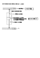
結晶化促進元素の除去に時間を要するのは、図2に示すように、結晶化促進元素を低減させる領域70(便宜上、被ゲッタリング領域と呼ぶ)と、その元素を吸い取り捕獲するリン添加領域71(ゲッタリング領域)とが離れていることが原因である。
【0016】
従って、被ゲッタリング領域に接してゲッタリング領域を形成すれば、結晶化促進元素の捕獲される領域までの移動距離が短くなり、結晶化促進元素の除去工程の時短化、低温化が図れる。
【0017】
ここで、結晶化促進元素を低減させる領域70(被ゲッタリング領域)とは、その特性の良、不良が半導体特性に最も影響を及ぼすチャネル形成領域となる領域を含む領域である。チャネル形成領域の特性によって、スイッチング特性や移動度の値が大きく左右される。チャネル形成領域中に不規則に結晶化促進元素が残存したままであると、スイッチング特性や移動度等の半導体特性を損ない、素子の安定性や信頼性を損なう原因となる。そのため、チャネル形成領域に残存する結晶化促進元素を低減させることは、安定性、信頼性のある素子作製に必要不可欠なことである。
【0018】
更に、被ゲッタリング領域70として、チャネル形成領域となる領域に加えて、その領域と隣接する低濃度不純物領域となる領域を含ませることは好ましい。低濃度不純物領域はOFF時のリーク電流を低減させる領域である。そのため、低濃度不純物領域に残存する結晶化促進元素を減少させることにより、リーク電流の低減に関して、安定性、信頼性のある素子を得ることが可能である。
【0019】
なお、低濃度不純物領域とは、不純物濃度がソース領域やドレイン領域よりも低い高抵抗な領域である。その不純物濃度は1016〜1019atoms/cm3 である。ただし、低濃度不純物領域は必ずしもソース領域やドレイン領域より不純物濃度が低くなければならないわけではない。低濃度不純物領域はソース領域やドレイン領域よりも高抵抗であればよい。従って、低濃度不純物領域の不純物濃度を低くする代わりに、低濃度不純物領域にイオン打ち込みやレーザー照射してソース領域やドレイン領域よりも高抵抗領域とすれば、ソース領域やドレイン領域と同じ不純物濃度であっても構わない。
【0020】
結晶化促進元素を捕獲するゲッタリング領域は、被ゲッタリング領域に接すること、被ゲッタリング領域に含まれる結晶化促進元素を捕獲可能な大きさであること、工程数を削減すること、を考え合わせると、少なくともソース領域となる領域及びドレイン領域となる領域を含んだ領域であることが必要である。ソース領域となる領域及びドレイン領域となる領域を含んだ領域にリン等の15族元素を添加することで、同時にソース領域となる領域及びドレイン領域となる領域を低抵抗化するための不純物元素の導入を行うことができ、不純物元素の導入工程を省くことができる。
【0021】
そこで、本発明では、図1に示すように、チャネル形成領域となる領域又はチャネル形成領域及び低濃度不純物領域となる領域を含む被ゲッタリング領域80に接した、少なくともソース領域となる領域81及びドレイン領域となる領域82を含んだ斜線で示す領域83に15族元素を添加し、被ゲッタリング領域80中の結晶化促進元素を矢印85で示すようにゲッタリング領域83に移動させて捕獲し、被ゲッタリング領域80から結晶化促進元素を除去することを主要な構成とする。
【0022】
図1(A)では、ソース領域となる領域81及びドレイン領域となる領域82をゲッタリング領域83として、15族元素を添加して、被ゲッタリング領域80の結晶化促進元素の除去を行う。図1(A)は、結晶化促進元素を捕獲するゲッタリング領域83の面積が必要最低限の大きさであるため、ゲッタリング領域83に捕獲される結晶化促進元素の濃度を高くでき、ソース領域81及びドレイン領域82の低抵抗化を図ることができる。
【0023】
図1(B)は、帯状にリンを添加するものであって、リン添加領域83と島状半導体層86の横方向(帯の長さ方向)の位置合わせが不要となる。更に、図1(B)は、ゲッタリング領域83の面積が図1(A)よりも大きいため、結晶化促進元素除去の時短化、低温化を図ることができる。それと同時に、図1(B)は、リン添加領域83の帯の幅をソース領域81及びドレイン領域82の幅としているため、リン添加領域83を帯状でかつその面積を必要最低限としているため、横方向の位置合わせを不要としたものの中で最もソース領域81及びドレイン領域82に捕獲される結晶化促進元素の濃度を高くでき、ソース領域81及びドレイン領域82の低抵抗化を図ることができる。
【0024】
図1(C)は図1(B)と同様、帯状にリンを添加するものであり、図1(B)と同様の効果が得られる。図1(C)はリン添加領域83の幅が図1(B)のようにソース領域となる領域81及びドレイン領域となる領域82の幅ではなく、それよりリン添加領域83の幅を広くしているため、図1(B)よりも更に結晶化促進元素除去の時短化、低温化を図ることができる。また、帯状の幅がソース領域となる領域及びドレイン領域となる領域の幅よりも広いため、リン添加領域83と島状半導体層86の横方向(帯の長さ方向)の位置合わせが不要なことに加えて、リン添加領域83と島状半導体層86の縦方向(帯の幅方向)の位置合わせを厳密に行う必要もない。従って図1(C)は最も信頼性を高めることができる。
【0025】
図1(D)は、チャネル形成領域となる領域84(又はチャネル形成領域と低濃度不純物領域となる領域)を囲んでリンを添加するものであり、最も結晶化促進元素除去の時短化、低温化を図ることができる。
【0026】
上述の課題を解決するための本発明は、
半導体膜を形成する工程Aと、
前記半導体膜に結晶化を促進する元素を導入する工程Bと、
前記結晶化を促進する元素を導入した後、前記半導体膜を結晶化する工程Cと、
結晶化された半導体膜に選択的に15族元素を添加する工程Dと、
前記15族元素を添加した後、前記半導体膜を加熱処理する工程Eと、
前記半導体膜をパターニングして島状半導体層を形成する工程Fと、を有し、
前記パターニングは、前記15族元素が添加された領域がソース領域およびドレイン領域となるように、かつ前記15族元素が添加されなかった領域がチャネル形成領域となるように行われる
ことを主要な構成とする。
【0027】
上記半導体膜の形成工程Aにおいて、半導体膜は結晶性のない半導体膜、又は結晶性を有するが100nm以上のオーダーの結晶粒が殆どない半導体膜であって、具体的には非晶質半導体膜、微結晶半導体膜を指す。微結晶半導体膜は、数nm〜数十nmの大きさの結晶粒を含む微結晶と非晶質とが混相状態の半導体膜である。
【0028】
より具体的には、半導体膜は非晶質シリコン膜、微結晶シリコン膜、非晶質ゲルマニウム膜、微結晶ゲルマニウム膜、非晶質Si1 Ge1-x (0<x<1)であり、これらの半導体膜はプラズマCVD法、減圧CVD法等の化学的気相法で成膜される。
【0029】
また、半導体膜を形成する際に、半導体膜と無機絶縁膜を連続成膜してもよい。そうすることにより、半導体膜の表面への不純物の付着を防ぐことができる。更に、この連続成膜した無機絶縁膜をゲート絶縁膜又はゲート絶縁膜の一部としててもよい。半導体膜とゲート絶縁膜の界面における不純物は、半導体特性を損なう原因となるが、半導体膜とゲート絶縁膜を連続成膜すると、半導体膜とゲート絶縁膜の界面への不純物の付着を防止することができる。
【0030】
上記導入工程Bにおいて、結晶化を促進する元素(結晶化促進元素)とは半導体、特にシリコンの結晶化を助長、促進する機能を有する元素であり、Ni、Fe、Co、Ru、Rh、Pd、Os、Ir、Pt、Cu、Au、Geから選ばれた1種又は複数種の元素を用いることができる。
【0031】
上記結晶化促進元素を導入する方法は、結晶化促進元素を半導体膜に添加する方法、結晶化促進元素を含有する膜を半導体膜の上面又は下面に接して形成する方法を用いることができる。
【0032】
前者の方法では、半導体膜を成膜後、イオン注入法、プラズマドーピング法等によって、結晶化促進元素を半導体膜に添加する方法を用いることができる。
【0033】
後者の方法において、結晶化促進元素を含有する膜を形成するには、CVD法やスパッタリング法などの堆積法や、スピナーを用いて結晶化促進元素を含む溶液を塗布する塗布法が挙げられる。また、結晶化促進元素を含有する膜の形成と、半導体膜の形成はどちらが先でも良く、半導体膜を先に成膜すれば、結晶化促進元素を含有する膜は半導体膜上面に密接して形成され、形成順序を逆にすれば、結晶化促進元素を含有する膜は半導体膜下面に密接して形成されることになる。なお本発明では、密接するとは半導体膜と結晶化促進元素が文字通り密接するだけでなく、半導体膜内に結晶化促進元素が移動できれば、膜の間に10nm程度の厚さの酸化膜、自然酸化膜等が存在している構成も含む。
【0034】
例えば、導入工程で、結晶化促進元素としてニッケル(Ni)を用いた場合には、堆積法でNi膜やNiシリサイド膜を成膜すればよい。
【0035】
また、塗布法を用いる場合には、臭化ニッケルや、酢酸ニッケル、蓚酸ニッケル、炭酸ニッケル、塩化ニッケル、沃化ニッケル、硝酸ニッケル、硫酸ニッケル等のニッケル塩を溶質とし、水、アルコール、酸、アンモニアを溶媒とする溶液、又はニッケル元素を溶質とし、ベンゼン、トルエン、キシレン、四塩化炭素、クロロホルム、エーテルを溶媒とする溶液を用いることができる。あるいは、ニッケルが完全に溶解していなくとも、ニッケルが媒質中に分散したエマルジョンの如き材料を用いてもよい。
【0036】
または酸化膜形成用の溶液にニッケル単体あるいはニッケルの化合物を分散させ、ニッケルを含有した酸化膜を形成する方法でもよい。このような溶液としては、東京応化工業株式会社のOCD(Ohka Diffusion Source)を用いることができる。このOCD溶液を用いれば、被形成面上に塗布し、200℃程度で焼成することで、簡単に酸化シリコン膜を形成できる。他の結晶化促進元素についても同様である。
【0037】
結晶化促進元素の導入方法としては、ドーピング法やNi膜をスパッタ法で成膜する方法よりも、塗布法が最も容易に半導体膜中の結晶化促進元素濃度を調節することができ、また工程も簡単化される。
【0038】
また、上記結晶化工程Cは、半導体膜内に結晶化促進元素を移動(拡散ともいう)させながら行う。結晶化促進元素を導入した半導体膜を加熱処理すると、結晶化促進元素が直ちに半導体膜内に移動する。そして結晶化促進元素は移動しつつ、非晶質状態にある分子鎖に触媒的な作用を及ぼし、半導体膜を結晶化させる。
【0039】
この結晶化を促進させる作用に関しては、本出願人により、特開平06−244103号公報、特開平06−244104号公報等で開示している。結晶化促進元素と接しているシリコンは結晶化促進元素と結合し、シリサイドが形成される。そして、シリサイドと非晶質状態のシリコン結合が反応して、結晶化が進行することが分かった。これは、結晶化促進元素とシリコンの原子間距離が単結晶シリコンの原子間距離に非常に近いためであり、Ni−Si間距離が単結晶Si−Si間距離と最も近く、0.6%ほど短い。
【0040】
Niを結晶化促進元素として用いて非晶質シリコン膜を結晶化させる反応をモデル化すると、
Si[a]−Ni(シリサイド)+Si[b]−Si[c](非晶質)
→Si[a]−Si[b](結晶性)+Ni−Si[c](シリサイド)
という反応式で表すことができる。
【0041】
なお、上記の反応式において、[a]、[b]、[c]という指標はSi原子位置を表している。
【0042】
上記の反応式は、シリサイド中のNi原子が非晶質部分のシリコンのSi[b]原子と置換するために、Si[a]−Si[b]間距離が単結晶とほぼ同じになることを示している。また、Niが半導体膜内を拡散しつつ、結晶成長させていることを示している。また、結晶化反応が終了した時点で、NiはSiと結合した状態で、移動した終端(又は、結晶成長の先端)に局在していることを示している。つまりNiSix で表されるシリサイド状態で結晶化後の膜内に不規則に分布していることとなる。このシリサイドの存在は、結晶化後の膜をFPM処理することで、穴として確認できる。
【0043】
FPM処理とは、ニッケルシリサイドを短時間で除去できるFPM(50%HFと50%H2 O2 を1:1で混合したエッチャント)を用いた処理であって、FPMで30秒程度エッチングして、エッチングによる穴の有無によってニッケルシリサイドの存在が確認できるものである。
【0044】
FPM処理によって結晶化されたシリコン膜には不規則にFPMによる穴が発生していた。このことは、結晶化された領域にはニッケルが局在し、この局在している部分でシリコンと結合してシリサイドが形成されていることを示している。
【0045】
なお、この結晶化反応を進行させるためのエネルギーを与えるには、加熱炉において450℃以上で加熱すればよいことが分かっている。また、加熱温度の上限は650℃とする。これは、結晶化促進元素と反応しない部分で、非晶質半導体膜の結晶化が進行しないようにするためである。結晶化促進元素と反応しない部分で結晶化してしまうと、結晶化促進元素がその部分に拡散できないので結晶粒を大きくすることができず、また粒径もばらついてしまう。
【0046】
また、結晶化工程において、加熱処理により結晶化した半導体膜には結晶粒内に欠陥が含まれる場合があり、また非晶質部分が残存している場合がある。そこで、その非晶質部分を結晶化し、また粒内の欠陥を消滅させるために、再び加熱処理を行うことは好ましい。この加熱温度は結晶化の際の加熱処理よりも高く、具体的には500〜1100℃とする、より好ましくは600〜1100℃とする。なお、実際の温度の上限は基板の耐熱温度で決定されることはいうまでもない。
【0047】
なお、この工程で、加熱処理の代わりにエキシマレーザー光を照射することもできる。しかしながら、上述したようにエキシマレーザーには不可避的な照射エネルギーばらつきがあるため、非晶質部分の結晶化にばらつきが生じてしまうおそれがある。特に、膜ごとに非晶質部分の分布にばらつきがある場合は、1つの半導体装置で、素子間の特性がばらついてしまうだけでなく、半導体装置間の特性のばらつきが生ずるおそれがある。
【0048】
そのため、結晶化工程後、エキシマレーザー光を照射する場合は、必ず加熱処理を施して、非晶質部分を結晶化させ、また欠陥を減少させることが望まれる。従って、次の光アニール工程でエキシマレーザーを使用する場合には、結晶性改善するための処理を加熱処理で行うことが重要になる。
【0049】
また、加熱炉内での加熱処理と同等な加熱方法として、波長0.6〜4μm、より好ましくは0.8〜1.4μmにピークをもつ赤外光を数十〜数百秒照射するRTA法が知られている。赤外光に対する吸収係数が高いため、赤外光の照射によって半導体膜は800〜1100℃に短時間で加熱される。しかし、RTA法はエキシマレーザー光よりも照射時間が長いため、基板に熱が吸収され易く、ガラス基板を用いる場合には反りの発生に注意が必要である。
【0050】
また、他の方法としてパルス発振型のYAGレーザーやYVO4レーザーを使用する方法がある。特にレーザーダイオード励起方式のレーザー装置を使用すると高出力と高いパルス発振周波数が得られる。その第2高調波(532nm)、第3高調波(354.7nm)、第4高調波(266nm)のいずれかを使用し、例えばレーザーパルス発振周波数1〜20000Hz(好ましくは10〜10000Hz)、レーザーエネルギー密度を200〜600mJ/cm2(代表的には300〜500mJ/cm2)とする。そして、線状ビームを基板全面に渡って照射し、この時の線状ビームの重ね合わせ率(オーバーラップ率)を80〜90%として行う。第2高調波を使うと、半導体層の内部にも均一に熱が伝わり、照射エネルギー範囲が多少ばらついても結晶化が可能となる。それにより、加工マージンがとれるため結晶化のばらつきが少なくなる。また、パルス周波数が高いのでスループットが向上する。
【0051】
本発明では、結晶化された半導体膜内に局在する結晶化促進元素を除去(ゲッタリング)することを目的とする。本発明では、結晶化促進元素をゲッタリングするために15族元素を用いる。ここで、15族元素はP、As、N、Sb、Biである。ゲッタリング能力の最も高いのはPであり、次いでSbである。
【0052】
本発明において結晶化促進元素の除去は、結晶化した結晶質半導体膜に15族元素を選択的に添加して15族元素を含有する領域を形成し、加熱処理して、15族元素を含有する領域に結晶化促進元素を移動させ、捕獲することにより行う。結晶質半導体膜に15族元素を添加する工程Dには、半導体膜に結晶化促進元素を導入する方法と同様に、プラズマドーピング法やイオン注入法等の気相法が挙げられる。
【0053】
15族元素を添加する領域(ゲッタリング領域)は、結晶化された半導体膜のチャネル形成領域となる領域又はチャネル形成領域と低濃度不純物領域となる領域を含まず、かつチャネル形成領域となる領域又はチャネル形成領域と低濃度不純物領域となる領域に接した領域、具体的には、ソース領域となる領域及びドレイン領域となる領域を含んだ領域である。ソース領域となる領域及びドレイン領域となる領域に15族元素を添加することにより、同時に低抵抗化のための不純物元素の導入工程を行うことができ、工程を簡略化できる。
【0054】
15族元素を添加する際のマスクは、酸化シリコン膜や、窒化シリコン膜、窒化酸化シリコン膜等の無機絶縁膜を用いることが好ましい。
【0055】
15族元素を添加する領域(ゲッタリング領域)の大きさは、少なくともソース領域となる領域及びドレイン領域となる領域の大きさがあれば、結晶化促進元素の除去のためには十分である。しかし、15族元素を添加する領域が大きければ除去工程の時短化、低温化となるので好ましい。従って、結晶化を促進する元素の除去工程の後に、半導体膜をパターニングして島状半導体層を形成する工程を行うことは、15族元素の添加領域をソース領域及びドレイン領域より大きくすることができるため好ましい。
【0056】
15族元素を添加した領域の15族元素濃度は、半導体膜内に残存する結晶化促進元素の濃度の10倍とする。本発明の結晶化方法では、1018〜1020atoms/cm3 オーダーで結晶化促進元素が残存するため、15族元素濃度は1×10¹⁹〜1×10²¹atoms/cm3 とする。
【0057】
結晶化促進元素の除去(ゲッタリング)は、加熱処理する工程Eによって行う。加熱処理によって、結晶化促進元素は15族元素を添加した領域(ゲッタリング領域)へ移動して捕獲(ゲッタリング)される。この結晶化促進元素の除去工程は、15族元素を添加した領域に結晶化促進元素を吸い取らせる(ゲッタリングさせる)工程と見ることができる。
【0058】
この加熱処理は、ゲート電極、ゲート配線形成前に行う(ゲート配線とゲート電極は一体的に形成されていることが多い)。半導体膜の結晶化時と、結晶化促進元素の除去時の温度が、半導体装置作製の中で最も高温に上げなければならない。従って、これらの工程終了後にゲート電極の形成を行うことで、耐熱性の高くない導電材料をゲート電極として用いることができる。半導体装置の使用時に求められているゲート電極材料の特性は低抵抗なことであるが、半導体装置の作製時に求められているゲート電極材料の特性は耐熱性があることである。耐熱性は、半導体装置の信頼性を損なわないために求められる重要な特性である。耐熱性の低い導電材料は、いくら抵抗が低くてもゲート電極材料として用いることができなかったが、本発明を用いることにより、耐熱性の高くない導電材料を用いてゲート電極を形成することができる。
【0059】
また本発明において、結晶化促進元素の除去工程を低温化、時短化するために、この工程の前に、結晶化した結晶質半導体膜にレーザー光又は強光を照射することは好ましい。この光照射(光アニール)によって、結晶質半導体膜に局在している結晶化促進元素を移動しやすい状態とすることができる。
【0060】
結晶化促進元素はNiSix の如く、半導体分子と結合した状態で、半導体膜内に分布しているが、光アニールのエネルギーにより、Ni−Si結合が断たれて、結晶化促進元素は原子状態にされる、あるいはNi−Si結合エネルギーが低下されるため、残存している結晶化促進元素は結晶質半導体膜内を移動しやすい状態となるためである。
【0061】
上記光アニールによって、結晶化促進元素を移動させるために必要なエネルギーを下げることができるため、500℃以上で加熱することで、結晶化促進元素を移動させることができ、また、処理時間を短くすることもできる。更に、ゲッタリング領域を素子形成領域に形成するため、ゲッタリング領域を新たに設ける必要がなく、素子形成可能な部分を拡大できる。なお、結晶化促進元素の除去工程の加熱温度の上限は、ゲッタリング領域に含まれる15族元素が移動しない温度であり、800℃〜850℃である。
【0062】
また光アニール工程において光を照射する部分は、半導体膜のうち半導体素子を構成する半導体層となる部分に照射すればよく、少なくともこの半導体層の空乏層が形成される領域(チャネル形成領域)を含むようにする。
【0063】
光アニールに使用する光源は、エキシマレーザーを用いることができる。例えばKrFエキシマレーザー(波長248nm)、XeClエキシマレーザー(波長308nm)、XeFエキシマレーザー(波長351、353nm)、ArFエキシマレーザー(波長193nm)、XeFエキシマレーザー(波長483nm)等を用いることができる。また、紫外線ランプを用いることができる。またはキセノンランプやアークランプなどの赤外線ランプなどを用いることができる。パルス発振方式のエキシマレーザー光を用いることができる。
【0064】
また、他の方法としてパルス発振型のYAGレーザーやYVO4レーザーを使用する方法がある。特にレーザーダイオード励起方式のレーザー装置を使用すると高出力と高いパルス発振周波数が得られる。その基本波(1064nm)、第2高調波(532nm)、第3高調波(354.7nm)、第4高調波(266nm)のいずれかを使用し、例えばレーザーパルス発振周波数1〜20000Hz(好ましくは10〜10000Hz)、レーザーエネルギー密度を200〜600mJ/cm2(代表的には300〜500mJ/cm2)とする。そして、線状ビームを基板全面に渡って照射し、この時の線状ビームの重ね合わせ率(オーバーラップ率)を80〜90%として行う。また、パルス周波数が高いのでスループットが向上する。
【0065】
島状半導体層の形成工程Fにおいて、パターニングは、前記15族元素が添加された領域がソース領域およびドレイン領域となるように、かつ前記15族元素が添加されなかった領域がチャネル形成領域又はチャネル形成領域と低濃度不純物領域となるように行われる。
【0066】
その後、半導体層に接して設けられたゲート絶縁膜を介してゲート電極を形成し、ゲート電極に対向する半導体層をチャネル形成領域とする。ゲート電極は、島状半導体層の前記15族元素が添加されてない領域(被ゲッタリング領域)上に前記ゲート絶縁膜を介して形成する。
【0067】
本発明は、ゲート電極に整合して自己整合的にソース領域及びドレイン領域を形成するものではない。従って、ゲート電極の大きさを変更するだけで、上面から見て15族元素が添加された領域(ソース領域とドレイン領域)とゲート電極とが重なった構造とすることも、上面から見て15族元素が添加された領域(ソース領域とドレイン領域)とゲート電極とがほぼ接するように形成することも、上面から見て15族元素が添加された領域(ソース領域とドレイン領域)とゲート電極との間隔が一定距離ある構造とすることも可能である。
【0068】
更に、15族元素が添加された領域(ソース領域とドレイン領域)とゲート電極との間隔が一定距離あるように形成した後、即ち島状半導体層の前記15族元素が添加されていない領域の一部分(チャネル形成領域と低濃度不純物領域となる領域のうちチャネル形成領域となる領域)上に前記ゲート絶縁膜を介してゲート電極を形成し、その後、ゲート電極をマスクとして不純物元素を添加して、上面から見て、ソース領域及びドレイン領域とゲート電極との間に低濃度不純物領域を形成することもできる。
【0069】
そして更に、低濃度不純物領域形成後、ゲート電極として既に形成されている第1の導電膜上に第2の導電膜をゲート電極の一部として形成し、低濃度不純物領域とその第2の導電膜が重なりを有するように第2の導電膜をパターニングすることによって、ゲート電極と低濃度不純物領域が重なる領域を有するゲート・オーバーラップド・LDD(GOLD)構造を得ることができる。GOLD構造は、ホットエレクトロン注入による半導体装置の劣化を防止することができる。また、ゲート電極が2層の場合を例に説明したが、3層以上の多層構造としてもよい。
【0070】
このように本発明は、ゲート電極の大きさを変えるだけで異なる構造の素子を作製することができる。従って、同じパネル上の、例えばマトリクス回路とドライバ回路の素子構造を容易に異なる構造とすることができる。同様に、マトリクス回路のNチャネル型TFTとPチャネル型TFTを容易に異なる構造とすることができる。
【0071】
結晶化促進元素を捕獲する領域には15族元素だけでなく、13族元素をも添加することにより、15族元素のみよりも高い除去効果が得られることが判明している。この場合には、13族元素濃度は15族元素濃度の1.3〜2倍とする。13族元素とはB、Al、Ga、In、Tiである。
【0072】
本発明の結晶化促進元素の除去工程によって、結晶化促進元素濃度が5×10¹⁷atoms/cm3 以下(好ましくは2×10¹⁷atoms/cm3 以下)にまで低減された結晶質半導体領域が得られる。
【0073】
なお、現状ではSIMS(質量二次イオン分析)による検出下限が2×10¹⁷atoms/cm3 程度であるため、それ以下の濃度を調べることはできない。しかしながら、本明細書に示す除去工程を行うことで、少なくとも1×10¹⁴〜1×10¹⁵atoms/cm3 程度にまで、結晶化促進元素は低減されるものと推定される。
【0074】
【発明の実施の形態】
図3〜図6を用いて本発明の実施の形態を説明する。なお、15族元素は半導体にN型の導電型を付与する元素であり、本発明の実施の形態は、N型のソース領域となる領域及びドレイン領域となる領域をゲッタリング領域に用いる。
【0075】
[実施形態1] 図3を用いて、本実施形態を説明す。図3(A)に示すように、基板10を用意し、基板10表面に下地膜11を形成する。基板10にはガラス基板、石英基板、セラミック基板等の絶縁性基板、単結晶シリコン基板、更にステンレス基板、Cu基板、Ta 、W、Mo、Ti、Cr等の高融点金属材料又はこれら合金系(例えば、窒素系合金)からなる基板等の導電性基板を用いることができる。
【0076】
下地膜11は、半導体装置内に基板から不純物が拡散するのを防ぐ機能、基板10上に形成される半導体膜や金属膜の密着性を高め、剥離を防止する機能を有する。下地膜11には、CVD法などで成膜した酸化シリコン膜や、窒化シリコン膜、窒化酸化シリコン膜等の無機絶縁膜が使用できる。例えば、シリコン基板を使用した場合には、熱酸化によってその表面を酸化して下地膜を形成することができる。また、石英基板やステンレス基板などの耐熱性基板を用いた場合には、非晶質シリコン膜を成膜し、このシリコン膜を熱酸化してもよい。
【0077】
更に、下地膜11として、タングステン、クロム、タンタル等の高融点金属の被膜や、窒化アルミニウム膜等の高い伝導度を有する被膜を下層に、上記の無機絶縁膜を上層に積層した積層膜を用いてもよい。この場合には、半導体装置で発生した熱が下地膜11の下層の被膜から放射されるため、半導体装置の動作が安定できる。
【0078】
下地膜11上に、プラズマCVD、減圧CVD法、熱CVD等の気相法で半導体膜12を成膜する。ここでは、減圧CVD法で非晶質シリコン膜を10〜150nmの厚さに成膜する。プラズマCVD法は減圧CVD法よりも生産性に優れるが、減圧CVD法は成膜に時間が掛かるが、プラズマCVD法よりも緻密な膜ができるという利点がある。(図3(A))
【0079】
次に、半導体膜12に結晶化促進元素を導入する。ここでは、半導体膜12表面に結晶化促進元素を含有する膜13を形成する方法を用いる。例えば、スピナーにおいて、Ni酢酸塩溶液を塗布し、この状態を数分間保持する。スピナーを用いて乾燥することによって、膜13としてNi膜が形成される。溶液のニッケルの濃度は、1ppm以上好ましくは10ppm以上であれば実用になる。なお、Ni 膜は必ずしも膜状とは限らないが、膜状でなくても用いることができる。(図3(B))
【0080】
そして、加熱炉において、結晶化促進元素が導入された半導体膜12を熱処理し、結晶質半導体膜15を形成する。熱処理条件は、雰囲気は窒素等の不活性雰囲気とし、温度450℃〜650℃、好ましくは500℃〜650℃、時間4〜24時間とする。本実施形態においては、半導体膜表面全体にニッケル元素が接するため、ニッケルの移動方向は半導体膜表面から下地膜方向、即ち基板表面にほぼ垂直な方向に移動し、その方向に結晶化が進行する。(図3(C))
【0081】
次に、結晶質半導体膜15のソース領域及びドレイン領域となる領域を含む領域に15族元素を選択的に添加する。まず半導体膜15のチャネル形成領域となる領域又はチャネル形成領域と低濃度不純物領域となる領域を含む領域上にマスク絶縁膜16を形成する。マスク絶縁膜16としては、レジスト、酸化シリコンなどが使用できるが無機絶縁膜が好ましい。ここでは100nmの厚さの酸化シリコン膜を成膜し、パターニングしてマスク絶縁膜16を形成する。そして、プラズマドーピング法、塗布法などによって、選択的に15族元素を添加して、半導体膜15に15族添加領域15aを形成する。15族元素が添加されなかった領域15bを便宜上、被ゲッタリング領域と呼ぶ。(図3(D))
【0082】
領域15aの15族元素濃度は被ゲッタリング領域15bの結晶化促進元素濃度の10倍とする。本実施例形態の方法では領域15bには1019〜1020atoms/cm3 オーダーで結晶化促進元素が残存するため、領域15aの15族元素の濃度は1×10²⁰〜1×10²¹atoms/cm3 とする。
【0083】
次に、500〜850℃、より好ましくは550℃〜650℃、4〜8時間加熱処理して、被ゲッタリング領域15bに残存した結晶化促進元素をソース領域及びドレイン領域となる領域を含む領域である15族元素添加領域15aへ移動させ、そこに吸い取らせる。ソース領域及びドレイン領域となる領域に達した結晶化促進元素は15族元素と結合する。例えば結晶化促進元素がNi、15族元素がPの場合には、ソース領域及びドレイン領域となる領域でNiP1 、NiP2 Ni2 ・・・といった結合状態で存在する。この結合状態は非常に安定であり、TFTの動作にほとんど影響しない。(図3(E))
この加熱処理により、領域15bの結晶化促進元素(Ni)濃度は2×10¹⁷atoms/cm3 以下に低下される。また、ソース領域となる領域及びドレイン領域となる領域に添加された15族元素を活性化させて、ソース領域となる領域及びドレイン領域となる領域を低抵抗化することもできる。
【0084】
そして、結晶化促進元素の除去工程後に、領域15を領域15aの全部もしくは一部がソース領域及びドレイン領域となるように島状にパターニングして、島状半導体層17を形成する。半導体層17を用いてTFT等の半導体素子を作製すればよい。
【0085】
本発明では、結晶化促進元素の除去工程前において、結晶化促進元素を除去する被ゲッタリング領域に接したソース領域及びドレイン領域となる領域に15族元素を添加するため、除去工程に要する時間を短縮することができる。
本実施形態ではソース領域及びドレイン領域となる領域をゲッタリング領域である15族添加領域に用いたため、即ち素子形成部分にゲッタリング領域である15族添加領域を形成したため、素子の集積化が図れる。
【0086】
[実施形態2] 図4を用いて、本実施形態を説明する。本実施形態は、実施形態1の触媒導入方法を変形したものである。また、半導体層形成以降のゲート絶縁膜の形成方法を示す。後は、実施形態1と同様である。
【0087】
実施形態1に記した基板を用意し、基板20表面上に下地膜21を形成する。次に、半導体膜22として、減圧熱CVD法により非晶質シリコン膜を形成する。非晶質シリコン膜の膜厚は20〜100nm(好ましくは40〜75nm)とする。ここでは成膜膜厚を65nmとする。なお、減圧熱CVD法で形成した非晶質シリコン膜と同等の膜質が得られるのであればプラズマCVD法を用いても良い。
【0088】
次に、非晶質シリコン膜でなる半導体膜22上にマスク絶縁膜23を形成する。マスク絶縁膜23にはパターニングによって開口部23aを設けておく。この開口部23aが結晶化促進元素の添加領域を規定する。マスク絶縁膜23としてはレジストや、酸化シリコン膜を用いることができる。ここでは120nm厚の酸化シリコン膜で形成する。
【0089】
次に重量換算で5〜10ppm のニッケルを含むニッケル酢酸塩をエタノールに溶かした溶液をスピンコート法により塗布し、乾燥させて、結晶化促進元素を含有する膜24としてNi膜をマスク絶縁膜23上に形成する。この状態で、ニッケルはマスク絶縁膜23に設けられた開口部23aにおいて半導体膜22と接した状態となる。(図4(A))
【0090】
次に、熱炉内で450℃、1時間程度の水素出しの後、ニッケルを添加した領域22aから半導体膜22にニッケルを移動させるため、加熱炉内で、不活性雰囲気、水素雰囲気または酸素雰囲気において、温度450〜650℃、加熱時間4〜24時間の加熱処理を行う。加熱によって、矢印で模式的に示すようにニッケルが半導体膜22内を移動しつつ、結晶化させる。ここでは570℃、8時間の加熱処理を行い、ニッケルを含有する結晶質半導体膜25を形成する。(図4(B))
【0091】
この工程では、ニッケルを添加した領域22aで反応したニッケルシリサイドから優先的に進行し、基板20の基板面に対してほぼ平行に成長した結晶領域(横成長領域とよぶ)25bが形成される。横成長領域25bは比較的揃った状態で個々の結晶粒が集合しているため、全体的な結晶性に優れるという利点がある。なお、領域25aは結晶化促進元素が導入された領域であって、結晶化されるが結晶化促進元素が高濃度に残存するため、素子には不適である。また非結晶化領域25cは結晶化促進元素が移動しなかった領域であり、結晶化が進行しなかった領域である。よって、横成長領域25bだけが高性能の素子を形成するのに適している。
【0092】
TEM(透過型電子顕微鏡法)観察によると、結晶質半導体膜において横成長領域25bの結晶粒は棒状または偏平棒状であり、これらの結晶粒の方位が殆ど揃っている。これら結晶粒の殆ど全てが概略{110}配向であり、<100>軸、<111>軸の方向は各結晶粒同士で同じであり、<110>軸が結晶粒間で2°ほど僅かに揺らいでいる。このように、横成長領域26bでは結晶軸の方位が揃っているために、結晶粒界での原子の結合がスムーズになり、未結合手がわずかになる。
【0093】
他方、従来の多結晶シリコンは結晶粒ごとに、結晶軸の方向は不規則であるため、粒界において結合できない原子が多数存在する。この点で、本実施形態の横成長領域25bと従来の多結晶シリコン膜の結晶構造は全く異なっている。横成長領域25bは結晶粒界において、殆どの原子の接合がとぎれることがなく、二つの結晶粒が極めて整合性よく接合しているため、結晶粒界において結晶格子が連続的に連なり、結晶欠陥等に起因するトラップ準位を非常に作りにくい構成となっている。
【0094】
次に、実施形態1と同様に、酸化シリコン膜でなるマスク絶縁膜27を形成する。横成長領域25bがチャネル形成領域又はチャネル形成領域及び低濃度不純物領域となる領域である被ゲッタリング領域26aに含まれるようにする。そして、15族元素としてP(リン)を添加し、15族元素添加領域26cを形成する。横成長領域25aに残存するニッケル濃度は、実施形態1の場合の1/10程度、即ち1018〜1019atoms/cm3 となるため、領域26cのリンの濃度は1×10¹⁹〜1×10²⁰atoms/cm3 とする。(図4(C))
【0095】
なお、15族元素は領域26c膜を通過して下地膜21、基板20にも添加されるため、下地膜21または基板22中の特定の領域のみに高濃度の15族元素が含まれる。しかし、このような15族元素がTFT特性に悪影響を与えることはない。
【0096】
そして、添加領域26cを形成した後、500〜850℃で2〜24時間の加熱処理を行い、被ゲッタリング領域26a中の結晶化促進元素を15族元素添加領域26c へと移動させて、領域26cに吸い取らせる(移動方向は矢印で示す)。こうして結晶化促進元素が5×10¹⁷atoms/cm3 以下、1×10¹⁴〜1×10¹⁵atoms/cm3 に低減された横成長領域が得られる。(図4(D))
【0097】
結晶化促進元素除去工程が終了したら、マスク絶縁膜27を除去した後、領域26を領域26cの全部もしくは一部がソース領域及びドレイン領域となるように、領域26aがチャネル形成領域又はチャネル形成領域と低濃度不純物領域となるように島状にパターニングして、島状の半導体層28を形成する。
【0098】
次に、プラズマCVD法または減圧熱CVD法により、半導体層28を覆って窒化酸化シリコンでなる絶縁膜30を形成する。この絶縁膜30はゲート絶縁膜を構成するものであり、その膜厚は50〜150nmとする。
【0099】
次に、絶縁膜30上に、ゲート電極31を形成する。例えば、Pが添加されたシリコン、Al、Ta、W、Mo、Ti、Cr等の高融点金属やこれらの合金(例えば、高融点金属同士の合金、高融点金属と窒素との合金など)を用いることができる。
【0100】
以上の工程で得られた半導体層28、絶縁膜30、及びゲート電極31を用いて、TFTを作製することができる。
【0101】
[実施形態3] 図5を用いて、本実施形態を説明する。
本実施形態は、島状半導体層の形成後(パターニング後)に、結晶化促進元素を除去したものである。その他は、実施形態1又は実施形態2と同様である。
まず、実施形態1又は実施形態2で説明した工程に従って、半導体膜の結晶化まで行い、得られた結晶質半導体膜をパターニングして島状半導体層35を形成する。(図5(A))
【0102】
次に、実施形態1、2と同様に、酸化シリコン膜でなるマスク絶縁膜37を形成する。そして、15族元素としてP(リン)をソース領域及びドレイン領域に添加し、15族元素添加領域36cを形成する。(図5(B)
【0103】
そして、添加領域36cを形成した後、500〜850℃で2〜24時間の加熱処理を行い、被ゲッタリング領域36d中の結晶化促進元素を15族元素添加領域36cへと移動させて吸い取らせる(移動方向は矢印で示す)。こうして触媒が5×10¹⁷atoms/cm3 以下、1×10¹⁴〜1×10¹⁵atoms/cm3 に低減された領域が得られる。(図5(C))
【0104】
以上の工程で得られた半導体層のソース領域、ドレイン領域は、ニッケル元素濃度が高いので、実施形態1、2に比べてソース領域及びドレイン領域を低抵抗化できる。
【0105】
[実施形態4] 図6を用いて、本実施形態を説明する。
本実施形態は、被ゲッタリング領域をチャネル形成領域及び低濃度不純物領域として、低濃度不純物領域を形成したものである。本実施形態を実施形態1乃至3に適用することも可能である。
まず、実施形態1乃至3で説明した工程に従って、被ゲッタリング領域46d中の結晶化促進元素が除去された島状半導体層48の形成まで行い、その上にゲート絶縁膜50を形成する。(図6(A))
【0106】
次に、ゲート電極51を形成する。例えば、Pが添加されたシリコン、Al、Ta、W、Mo、Ti、Cr等の高融点金属やこれらの合金(例えば、高融点金属同士の合金、高融点金属と窒素との合金など)を用いて形成する。ゲート電極51は、被ゲッタリング領域46dの一部(チャネル形成領域と低濃度不純物領域となる領域のうちチャネル形成領域となる領域)上に形成する。(図6(B))
【0107】
次に、ゲート電極をマスクとして不純物を添加して低濃度不純物領域52を形成する。不純物の添加は、高加速度、低ドーズ量でドーピングを行い、ゲート絶縁膜を通過してリンが半導体層に添加されるようにした。条件は加速電圧80kV、設定ドーズ量6×10¹³atoms/cm3とし、添加量は1×1016〜1×1019atoms/cm3 とする。
【0108】
以上の工程によって、新たなマスクを用いることなく低濃度不純物領域を形成できる。
【0109】
本実施形態を用いて更に、低濃度不純物領域形成後、ゲート電極として既に形成されている第1の導電膜上に第2の導電膜をゲート電極の一部として形成し、低濃度不純物領域とその第2の導電膜が重なりを有するように第2の導電膜をパターニングすることによって、ゲート電極と低濃度不純物領域が重なる領域を有するゲート・オーバーラップド・LDD(GOLD)構造を得ることも可能である。GOLD構造は、ホットエレクトロン注入による半導体装置の劣化を防止することができる。また、ゲート電極が2層でなく、3層以上の多層構造としてもよい。
【0110】
【実施例】
図7〜図16を用いて、本発明の実施例を説明する。なお、実施例に実施形態1〜4を適用してもよい。
【0111】
[ 実施例1] 本実施例は本発明をTFTに適用した例であり、Nチャネル型TFTとPチャネル型TFTを同一基板上に形成し、CMOS回路を作製した例を示す。説明には図7〜図9を用いる。
【0112】
図7はCMOS回路の概略の上面図を示す。図7において、111はゲート配線、108はNチャネル型TFTの半導体層、109はPチャネル型TFTの半導体層である。161、162は半導体層108、109とソース配線のコンタクト部であり、163、164は半導体層108、109とドレイン配線とのコンタクト部である。165はゲート配線111と取出し配線とのコンタクト部(ゲートコンタクト部)である。
【0113】
図8、図9を用いて、TFTの作製工程を説明する。なお図8、図9において左側にNチャネル型TFTの断面図を示し、右側にPチャネル型TFTの断面図を示す。各TFTの断面図は図7の鎖線A−A' 、鎖線B−B' で切断した断面図に対応する。
【0114】
まず、コーニング社製1737ガラス基板を基板100として用いる。ガラス基板100上に下地膜として300nm厚の酸化シリコン膜101を形成する。
【0115】
こうして絶縁表面を有する基板が準備できたら、減圧熱CVD法により、ジシランを原料ガスに半導体膜として非晶質シリコン膜102を成膜する。非晶質シリコン膜102の膜厚は55nmとする。次に、非晶質シリコン膜102上に120nm厚の酸化シリコン膜でなるマスク絶縁膜103を形成する。マスク絶縁膜103にはパターニングによって開口部103a、103bが設けられている。
【0116】
次に、重量換算で10ppm のニッケルを含むニッケル酢酸塩をエタノールに溶かした溶液をスピンコターにより塗布し、乾燥してNi膜104を形成する。Ni膜104はマスク絶縁膜103に設けられた開口部103a、103bにおいて非晶質シリコン膜102と接している。なお、非晶質シリコン膜102は浸潤性が乏しいので、マスク絶縁膜103を形成する前にUV照射などにより数nm程度の酸化膜を形成しておくと、Ni膜104が開口部103a、103bで接した状態で形成することが容易になる。(図8(A))
【0117】
こうして図8(A)の状態が得られたら、加熱炉内で450℃、1時間程度、加熱処理して、非晶質シリコン膜102から水素出しした後、加熱炉内で、窒素雰囲気、570℃、14時間の加熱処理を行う。Ni膜104から非晶質シリコン膜102内へNiが移動して、結晶化が進行して、横成長領域106a、106bを有する結晶質シリコン膜106が形成される。(図8(B))
【0118】
結晶化工程が終了したら、600℃、1〜4時間、結晶質シリコン膜106を熱処理して、非晶質部分を結晶化させ、結晶性を向上させることは好ましい。更に、KrFエキシマレーザー光を結晶質シリコン膜106に照射して、膜内に局在しているNiを移動しやすい状態にすることは好ましい。エキシマレーザーは光学系によって、0.5 mm幅、12cm長の線状レーザー光に加工して、線状レーザー光に対して基板を相対的に1方向に走査させることにより、基板全面にレーザー光を照射する。あるいは、レーザー光を1辺が5〜10cm程度の矩形上に加工して照射することもできる。
【0119】
次に、半導体膜のチャネル形成領域又はチャネル形成領域と低濃度不純物領域となる領域を含む被ゲッタリング領域上にマスク絶縁膜118を形成し、半導体膜に15族元素を添加して、Nチャネル型TFTのソース領域及びドレイン領域となる領域を形成する。ドーピングガスには水素で5%に希釈したホスフィンを用いて、P(リン)を添加する。低加速度、高ドーズ量でドーピングを行い、ドーピング条件はP濃度が半導体膜106に残存するNi濃度の10倍とし、加速電圧80kV、設定ドーズ量6×10¹³atoms/ cm3で添加し、添加量は1×10¹⁹〜1×10²²atoms/cm3 とする。(図8(C))
【0120】
半導体膜106にN+ 型領域107が形成される。ここで半導体膜106のN+ 型領域107の一部はソース及びドレイン領域となり、領域123がチャネル形成領域及び低濃度不純物領域となる。
【0121】
この状態で加熱処理することで、N+ 型領域107にリンが添加されなかった領域123、133のニッケルを吸い取らせることができる。非晶質シリコン膜の結晶化のために意図的に添加したNiが、図8において矢印で模式的に示すように、チャネル形成領域又はチャネル形成領域と低濃度不純物領域を含む領域123、133からそれぞれのソース領域及びドレイン領域となる領域へ移動する。その結果、チャネル形成領域及び低濃度不純物領域となる領域内のNiが減少し、他方、ゲッタリングシンクに用いたソース領域及びドレイン領域となる領域中のNi濃度はチャネル形成領域123、133よりも高くなる。
【0122】
次に、結晶質シリコン膜106を島状にパターニングして、半導体層108、109を形成する。なお、上記のエキシマレーザの照射は半導体層108、109の形成後でもよい。(図8(D))
【0123】
次に、プラズマCVD法により、SiH4 とN2 Oを原料ガスにして、窒化酸化シリコン膜110を120nmの厚さに成膜する。次に、窒化酸化シリコン膜110上に厚さ40nmのタンタル膜(Ta膜)をスパッタ装置において成膜しパターニングしてゲート電極111を形成する。ゲート電極はリンが添加されてない領域の一部分(Nチャネル型TFTのチャネル形成領域と低濃度不純物領域となる領域のうちチャネル形成領域となる領域)上に配置する。なお、上記のエキシマレーザー光の照射はTa膜の成膜前に実施してもよい。本実施例では、少なくともチャネル形成領域となる領域にレーザ光が照射されればよい。(図8(E))
【0124】
そしてゲート電極111をマスクとして不純物を添加して低濃度不純物領域124,125を形成する。不純物の添加は、高加速度、低ドーズ量でドーピングを行い、ゲート絶縁膜を通過してリンが半導体層に添加されるようにした。条件は加速電圧80kV、設定ドーズ量6×10¹³atoms/ cm3とし、添加量は1×10¹⁶〜1×10¹⁹atoms/cm3 とする。(図9(A))
【0125】
次に、Pチャネル型TFTの半導体層109に13族元素であるB(ボロン)を添加する。Nチャネル型TFTをレジストマスク140で覆った後、半導体層109にBを添加する。ドーピングガスには水素で5%に希釈されたジボランを用い、P+ 型のソース領域及びドレイン領域となる領域141、142を形成する。(図9(B))
【0126】
ソース領域及びドレイン領域となる領域を形成した後、レジストマスク140を除去し、電気炉内で350℃〜550℃、ここでは450℃、2時間の加熱処理をする。この加熱処理で、ソース領域及びドレイン領域121,122,141,142、及び低濃度不純物領域124,125に添加されたリン、ボロンが活性化される。
【0127】
次に、酸化シリコン膜でなる層間絶縁膜150を形成する。層間絶縁膜150にコンタクトホールを形成した後、電極材料としてチタン/アルミ/チタンからなる積層膜を形成し、パターニングして、配線151〜153を形成する。ここでは、配線153によってNチャネル型TFTとPチャネル型TFTとを接続してCMOS回路を形成する。更に、図示しないゲート電極111に接続されたゲート配線の取出し配線も形成する。最後に水素雰囲気中において350℃、2時間程度の水素化処理を行い、TFT全体の水素終端処理を行う。(図9(C))
【0128】
[実施例2] 本実施例を図10を用いて説明する。本実施例は実施例1を変形してGOLD構造を形成した例である。本実施例のGOLD構造を実施例1に適用してもよい。
【0129】
結晶化促進元素が低減された島状半導体領域を形成するまでは、実施例1と同様に行う。次にゲート絶縁膜として、20nm厚の窒化シリコン膜/100nm厚の窒化酸化シリコン膜210を形成する。
【0130】
次に、ゲート電極の形成及び低濃度不純物領域の形成を行う。窒化酸化シリコン膜210表面上に第1の導電膜215と第2の導電層216を形成する。第1の導電膜215はTi,Ta,W,Moから選ばれた材料もしくはそれらの合金からなる材料で形成すればよい。また、電気抵抗や耐熱性を考慮して前記材料を主成分とする導電材料を用いてもよい。第1の導電膜の厚さは10〜100nm、好ましくは20〜50nmとする必要がある。ここでは、50nmの厚さでTi膜をスパッタ法で形成した。
【0131】
第2の導電層216は、Al、Cuから選ばれた材料を用いることが好ましい。これはゲート電極の電気抵抗を下げるために設けられるものであり、50〜400nm、好ましくは100〜200nmの厚さに形成する。Alを用いる場合には、純Alを用いても良いし、Ti、Si、Scから選ばれた元素が0.1〜5atom%添加されたAl合金を用いても良い。また銅を用いる場合には、図示しないが、ゲート絶縁膜210の表面に窒化シリコン膜を30〜100nmの厚さで設けておくと好ましい。
【0132】
ここでは、Scが0.5atom%添加されたAl膜をスパッタ法で200nmの厚さに形成した。(図10(A))
そして、Pチャネル型TFTが形成される領域にレジストマスク314を形成して、N型を付与する第1の不純物元素を添加する工程を行った。結晶質半導体材料に対してN型を付与する不純物元素としては、リン(P)、砒素(As)、アンチモン(Sb)などが知られているが、ここでは、リンを用い、フォスフィン(PH3 )を用いたイオンドープ法で行った。この工程では、ゲート絶縁膜210と第1の導電膜215を通してその下の半導体層にリンを添加するために、加速電圧は80keVと高めに設定した。半導体層に添加されるリンの濃度は、1×10¹⁶〜1×10¹⁹atoms/cm3 の範囲にするのが好ましく、ここでは1×10¹⁸atoms/cm3 とした。そして、半導体層に低濃度にリンが添加された領域315、316が形成された。( 図10(B))
【0133】
そして、レジストマスク314を除去した後、第1の導電膜215と第2の導電層216に密接させて図示しない第3の導電膜を形成した。第3の導電膜はTi、Ta、W、Moから選ばれた材料で形成すれば良いが、電気抵抗や耐熱性を考慮して前記材料を主成分とする化合物を用いても良い。例えば、また、第3の導電膜の厚さは10〜100nm、好ましくは20〜50nmとする必要がある。ここでは、50nmの厚さでTa膜をスパッタ法で形成した。その後、第1の導電膜と第3の導電膜を同時にパターニングして、チャネル長方向の長さが同じ第1の導電層217と第3の導電層218を形成した。(図10(C))
次に、Pチャネル型TFTの半導体層209に13族元素であるB(ボロン)を添加する。Nチャネル型TFTをレジストマスク240で覆った後、半導体層209にBを添加する。ドーピングガスには水素で5%に希釈されたジボランを用い、P+ 型のソース領域及びドレイン領域241、242を形成する。(図10(D))
【0134】
ソース領域及びドレイン領域を形成した後、レジストマスク240を除去して、電気炉内で450℃、2時間の加熱処理をする。この加熱処理でゲッタリングと同時に、ソース領域及びドレイン領域211、212、241,242、及び低濃度不純物領域315,316に添加されるたリン、ボロンが活性化される。
【0135】
次に、酸化シリコン膜でなる層間絶縁膜256を形成する。層間絶縁膜256にコンタクトホールを形成した後、電極材料としてチタン/アルミ/チタンからなる積層膜を形成し、パターニングして、配線251〜253を形成する。ここでは、配線253によってNチャネル型TFTとPチャネル型TFTとを接続してCMOS回路を形成する。更に、図示しないゲート配線111の取出し配線も形成する。最後に水素雰囲気中において350℃、2時間程度の水素化処理を行い、TFT全体の水素終端処理を行う。(図10(E))
【0136】
[ 実施例3] 本実施例を図11を用いて説明する。本実施例は、活性化工程後にゲート電極を形成したものであって、ゲート電極の耐熱性が劣ることによる信頼性の低下を実施例1や実施例2より更に防止することができる。本実施例を実施例1又は実施例2に適用してもよい。
【0137】
15属元素の添加までは実施例1と同様に行う。この状態で加熱処理することで、N+ 型領域311、312、313にリンが添加されなかった領域323、333のニッケルを吸い取らせることができるが、本実施例では、Pチャネル型TFTとなる領域に13族元素であるB(ボロン)を添加した後、結晶化促進元素の除去工程を行う。
【0138】
そこで、Nチャネル型TFTをレジストマスク340で覆った後、Pチャネル型TFTとなる半導体膜にBを添加する。ドーピングガスには水素で5%に希釈されたジボランを用い、P+ 型のソース領域及びドレイン領域341、342、チャネル形成領域となる領域343を形成する。(図11(B))
【0139】
Pチャネル型のソース領域及びドレイン領域341,342に結晶化促進元素を吸い取らせるには、ボロンイオンの濃度が、当該領域に添加されるリンイオン濃度の1.3〜2倍程度にする。
【0140】
ソース領域及びドレイン領域に不純物添加後、電気炉内で500℃、2時間の加熱処理をする。この加熱処理により、非晶質シリコン膜の結晶化のために意図的に添加したNiが、図11(C)において矢印で模式的に示すように、被ゲッタリング領域323、343からそれぞれのソース領域及びドレイン領域321、322、341、342へ移動する。その結果、被ゲッタリング領域323、343内のNiが減少し、他方、ゲッタリングシンクに用いたソース領域及びドレイン領域321、322、341、342中のNi濃度は被ゲッタリング領域323、343よりも高くなる。(図11(C))
【0141】
更に、この加熱処理でゲッタリングと同時に、ソース領域及びドレイン領域321、322、341、342、に添加されたリン、ボロンが活性化される。
次に、プラズマCVD法により、SiH4 とN2 Oを原料ガスにして、窒化酸化シリコン膜310を120nmの厚さに成膜する。次に、窒化酸化シリコン膜310上のPチャネル型TFTをレジストマスク又はマスク絶縁膜350で覆い、Nチャネル型TFTのチャネル形成領域上レジストマスク又はマスク絶縁膜351を形成した後、15族元素としてリンを添加する。半導体層に添加されるリンの濃度は、1×10¹⁶〜1×10¹⁹atoms/cm3 の範囲にするのが好ましく、ここでは1×10¹⁸atoms/cm3 とした。こうして、Nチャネル型TFTの低濃度不純物領域355,356を形成する。(図11(D))
【0142】
その後、電気炉内で450℃、2時間の加熱処理をすることは好ましい。この加熱処理で、ソース領域及びドレイン領域321,322,341,342、及び低濃度不純物領域355,356に添加されたリン、ボロンが活性化される。
【0143】
次に、ゲート配線360を形成する導電膜を成膜する。ここでは、窒化タンタル(TaNx )/タンタル(Ta)/窒化タンタル(TaNx )の3層をスパッタ法で成膜した。TaNx 膜の厚さは50nmとし、Ta膜の厚さは250nmとする。そしてこの3層膜をパターニングしてゲート配線360を形成する。本実施例では、Nチャネル型TFTはGOLD構造とし、Pチャネル型TFTは低濃度不純物領域のない構造とした。(図11(E))
【0144】
次に、酸化シリコン膜でなる層間絶縁膜370を形成する。層間絶縁膜370にコンタクトホールを形成した後、電極材料としてチタン/アルミ/チタンからなる積層膜を形成し、パターニングして、配線371〜373を形成する。ここでは、配線373によってNチャネル型TFTとPチャネル型TFTとを接続してCMOS回路を形成する。更に、図示しないゲート配線360の取出し配線も形成する。最後に水素雰囲気中において350℃、2時間程度の水素化処理を行い、TFT全体の水素終端処理を行う。(図11(F))
【0145】
[実施例4] 本実施例では、実施例1で説明したTFTをアクティブマトリクス基板に適用したものである。本実施例のアクティブマトリクス基板は液晶表示装置や、EL表示装置などの平板型の電気光学装置に用いられる。なお、本実施例を実施例2又は実施例3に適用してもよい。
【0146】
図12〜図14を用いて、本実施例を説明する。図12〜図14で同じ符号は同じ構成要素を示す。図12は本実施例のアクティブマトリクス基板の概略斜視図である。アクティブマトリクス基板は、ガラス基板400上に形成された、画素部401、走査線駆動回路402、信号線駆動回路403で構成される。走査線駆動回路402、信号線駆動回路403はそれぞれ走査線502、信号線503によって画素部401に接続され、これら駆動回路402、403は、CMOS回路で主に構成されている。
【0147】
走査線502は画素部401の行ごとに形成され、信号線503は列ごとに形成されている。走査線502、信号線503の交差部近傍には、各配線502、503に接続された画素TFT406が形成されている。画素TFT406には、画素電極407、保持容量408が接続されている。
【0148】
まず、実施例1のTFTの作製工程に従って、駆動回路402、403のNチャネル型TFT、Pチャネル型TFT、画素部401の画素TFT406を完成する。
【0149】
図13(A)は画素部401の上面図であり、ほぼ1画素の上面図である。図13(B)は駆動回路402、403を構成するCMOS回路の上面図である。図14はアクティブマトリクス基板の断面図であり、画素部401、CMOS回路の断面図である。画素部401の断面図は図13(A)の鎖線A−A' に沿った断面図であり、CMOS回路の断面図は図13(B)の鎖線B−B' に沿った断面図である。
【0150】
画素部401の画素TFT406はNチャネル型TFTである。「U」字型(馬蹄型)に屈曲した半導体層501を有する。第1層目の配線である走査線502がゲート絶縁膜510を挟んで半導体層501と交差している。
【0151】
半導体層501には、N+ 型領域511〜513、2つのチャネル形成領域514、515、低濃度不純物領域(N- 型領域)516〜519が形成される。N+ 型領域511、512はソース領域及びドレイン領域である。
【0152】
他方、CMOS回路では、1本のゲート配線601が2つの半導体層602、603とゲート絶縁膜610を挟んで交差している。半導体層602には、ソース領域及びドレイン領域(N+ 型領域)611、612、チャネル形成領域613、低濃度不純物領域(N- 型領域)614、615が形成されている。半導体層603には、ソース領域及びドレイン領域(P+ 型領域)621、622、チャネル形成領域623が形成されている。
【0153】
半導体層501、602、603にソース領域及びドレイン領域を形成した後、基板全面に層間絶縁膜430が形成される。層間絶縁膜430上には第2層目の配線・電極として、信号線503、ドレイン電極504、ソース電極631、632、ドレイン電極633が形成される。
【0154】
走査線502と信号線503は層間絶縁膜430を挟んで、図13(A)に示すように直交している。ドレイン電極504はドレイン領域512を画素電極505に接続させるための取出し電極である共に、保持容量408の下部電極である。保持容量408の容量を大きくするため、ドレイン電極504は開口部を低下させない限りにおいて、できるだけ広くなるようにしている。
【0155】
第2層目の配線・電極上に、第1の平坦化膜440が形成されている。本実施例では窒化シリコン(50nm)/酸化シリコン(25nm)/アクリル(1μm)の積層膜を第1の平坦化膜440として利用する。アクリルやポリイミド、ベンゾシクロブテン(BCB)といった有機性樹脂膜は、スピンコート法で形成可能な溶液塗布型絶縁膜なので、1μm程度の膜厚を高いスループットで形成することが可能であり、良好な平坦面が得られる。更に、有機性樹脂膜は窒化シリコンや酸化シリコンと較べて誘電率が低いため、寄生容量を小さくすることができる。
【0156】
次に、第1の平坦化膜440上に、第3層目の配線として、チタンやクロム等の遮光性導電膜でなるソース配線641、642、ドレイン配線643、ブラックマスク520が形成されている。図13(A)に示すように画素部401でブラックマスク520は一体であり、画素電極505の周辺とオーバーラップして、表示に寄与しない部分を全て覆うように形成されている。なお、ブラックマスク520は図13(A)に点線で示すように配置されている。またブラックマスク520の電位は所定の値に固定される。
【0157】
これら第3層目の配線641、642、643、520の形成に先立って、第1の平坦化膜440をエッチングして、最下層の窒化シリコン膜のみを残した凹部530をドレイン電極504上に形成する。
【0158】
凹部530では、ドレイン電極504とブラックマスク520とが窒化シリコン膜のみを挟んで対向しているので、凹部530においてドレイン電極504、ブラックマスク520を電極に、窒化シリコン膜を誘電体とする保持容量408が形成される。窒化シリコンは比誘電率が高く、しかも膜厚を薄くすることでより大きな容量を確保できる。
【0159】
第3層目の配線641、642、520上に第2の平坦化膜450が形成されている。第2の平坦化膜450は1.5μm厚のアクリルで形成する。保持容量408が形成された部分は大きな段差を生じるが、その様な段差も十分に平坦化できる。
【0160】
第1の平坦化膜440及び第2の平坦化膜450にコンタクトホールを形成し、ITOや酸化スズ等の透明導電膜からなる画素電極505が形成される。こうしてアクティブマトリクス基板が完成する。
【0161】
本実施例のアクティブマトリクス基板を液晶表示装置に利用する場合には、基板全面を覆って図示しない配向膜を形成する。必要に応じて配向膜にラビング処理が施される
【0162】
なお、画素電極505として反射率の高い導電膜、代表的にはアルミニウムまたはアルミニウムを主成分とする材料を用いれば、反射型AMLCD用のアクティブマトリクス基板を作製することもできる。
【0163】
また、本実施例では画素TFT406をダブルゲート構造としているが、シングルゲート構造でも良いし、トリプルゲート構造等のマルチゲート構造としても構わない。また、実施例1で示した逆スタガ型TFTで形成することもできる。本実施例のアクティブマトリクス基板の構造は本実施例の構造に限定されるものではない。本発明の特徴はゲート配線の構成にあるので、それ以外の構成については実施者が適宜決定すれば良い。
【0164】
[実施例5] 本実施例では実施例4で示したアクティブ基板を用いた電気光学装置の一例として、アクティブマトリクス方式の液晶表示装置(AMLCDと記す)を構成した例について説明する。
【0165】
本実施例のAMLCDの外観を図15に示す。図15(A)において図12と同じ符号は同じ構成要素を示す。アクティブマトリクス基板は、ガラス基板400上に形成された画素部401、走査線駆動回路402、信号線駆動回路403を有する。
【0166】
アクティブマトリクス基板と対向基板700とが貼り合わされている。これら基板の隙間に液晶が封止されている。ただし、アクティブマトリクス基板には、TFTの作製工程で外部端子が形成されており、この外部端子が形成された部分は対向基板700と対向していない。外部端子にはFPC(フレキシブル・プリント・サーキット)710が接続され、FPC710を介して外部信号、電源が回路401〜403へ伝達される。
【0167】
対向基板700は、ガラス基板上全面にITO膜等の透明導電膜が形成されている。透明導電膜は画素部401の画素電極に対する対向電極であり、画素電極、対向電極間に形成された電界によって液晶材料が駆動される。更に、対向基板700には必要であれば配向膜や、カラーフィルタが形成されている。
【0168】
本実施例のアクティブマトリクス基板には、FPC710を取り付ける面を利用してICチップ711、712が取り付けられている。これらのICチップはビデオ信号の処理回路、タイミングパルス発生回路、γ補正回路、メモリ回路、演算回路などの回路をシリコン基板上に形成して構成される。図15(A)ではICチップを2個取り付けたが、1個でも良いし、3個以上であっても良い。
【0169】
あるいは図15(B)の構成も可能である。図15(B)において図15(A)と同一の構成要素は同じ符号を付した。ここでは図15(A)でICチップが行っていた信号処理を、同一基板上にTFTでもって形成されたロジック回路720によって行う例を示している。この場合、ロジック回路720も駆動回路402、403と同様にCMOS回路を基本として構成されている。
【0170】
本実施例では、ブラックマスクをアクティブマトリクス基板に設ける構成(BM on TFT )を採用するが、それに加えて対向側にブラックマスクを設ける構成とすることも可能である。
【0171】
また、カラーフィルターを用いてカラー表示を行っても良いし、ECB(電界制御複屈折)モード、GH(ゲストホスト)モードなどで液晶を駆動し、カラーフィルターを用いない構成としても良い。また、特開平8−15686号公報に記載されたように、マイクロレンズアレイを用いる構成にしても良い。
【0172】
[実施例6] 実施例1、2、3で示したTFTは、AMLCD以外にも他の様々な電気光学装置や半導体回路に適用することができる。
【0173】
AMLCD以外の電気光学装置としてはEL(エレクトロルミネッセンス)表示装置やイメージセンサ等を挙げることができる。
【0174】
また、半導体回路としては、ICチップで構成されるマイクロプロセッサの様な演算処理回路、携帯機器の入出力信号を扱う高周波モジュール(MMICなど)が挙げられる。
【0175】
この様に本発明は絶縁ゲイト型TFTで構成される回路によって機能する全ての半導体装置に対して適用することが可能である。
【0176】
〔実施例7〕
上述の本発明の液晶表示装置にはネマチック液晶以外にも様々な液晶を用いることが可能である。例えば、1998, SID, “Characteristics and Driving Scheme of Polymer-Stabilized Monostable FLCD Exhibiting Fast Response Time and High Contrast Ratio with Gray-Scale Capability” by H. Furue et al.や、1997, SID DIGEST, 841, “A Full-Color Thresholdless Antiferroelectric LCD Exhibiting Wide Viewing Angle with Fast Response Time” by T. Yoshida et al.や、1996, J. Mater. Chem. 6(4), 671-673, "Thresholdless antiferroelectricity in liquid crystals and its application to displays" by S. Inui et al.や、米国特許第5594569 号に開示された液晶を用いることが可能である。
【0177】
等方相−コレステリック相−カイラルスメクティックC相転移系列を示す強誘電性液晶(FLC)を用い、DC電圧を印加しながらコレステリック相−カイラルスメクティックC相転移をさせ、かつコーンエッジをほぼラビング方向に一致させた単安定FLCの電気光学特性を図16に示す。図16に示すような強誘電性液晶による表示モードは「Half−V字スイッチングモード」と呼ばれている。図16に示すグラフの縦軸は透過率(任意単位)、横軸は印加電圧である。「Half−V字スイッチングモード」については、寺田らの”Half−V字スイッチングモードFLCD”、第46回応用物理学関係連合講演会講演予稿集、1999年3月、第1316頁、および吉原らの”強誘電性液晶による時分割フルカラーLCD”、液晶第3巻第3号第190頁に詳しい。
【0178】
図16に示されるように、このような強誘電性混合液晶を用いると、低電圧駆動かつ階調表示が可能となることがわかる。本発明の液晶表示装置には、このような電気光学特性を示す強誘電性液晶も用いることができる。
【0179】
また、ある温度域において反強誘電相を示す液晶を反強誘電性液晶(AFLC)という。反強誘電性液晶を有する混合液晶には、電場に対して透過率が連続的に変化する電気光学応答特性を示す、無しきい値反強誘電性混合液晶と呼ばれるものがある。この無しきい値反強誘電性混合液晶は、いわゆるV字型の電気光学応答特性を示すものがあり、その駆動電圧が約±2.5V程度(セル厚約1μm〜2μm)のものも見出されている。
【0180】
また、一般に、無しきい値反強誘電性混合液晶は自発分極が大きく、液晶自体の誘電率が高い。このため、無しきい値反強誘電性混合液晶を液晶表示装置に用いる場合には、画素に比較的大きな保持容量が必要となってくる。よって、自発分極が小さな無しきい値反強誘電性混合液晶を用いるのが好ましい。
【0181】
なお、このような無しきい値反強誘電性混合液晶を本発明の液晶表示装置に用いることによって低電圧駆動が実現されるので、低消費電力化が実現される。
【0182】
〔実施例8〕
本実施例では、本願発明を用いてEL(エレクトロルミネッセンス)表示装置を作製した例について説明する。
【0183】
図17Aは本願発明を用いたEL表示装置の上面図である。図17Aにおいて、4010は基板、4011は画素部、4012はソース側駆動回路、4013はゲート側駆動回路であり、それぞれの駆動回路は配線4014〜4016を経てFPC4017に至り、外部機器へと接続される。
【0184】
このとき、少なくとも画素部、好ましくは駆動回路及び画素部を囲むようにしてカバー材6000、シーリング材(ハウジング材ともいう)7000、密封材(第2のシーリング材)7001が設けられている。
【0185】
また、図17Bは本実施例のEL表示装置の断面構造であり、基板4010、下地膜4021の上に駆動回路用TFT(但し、ここではnチャネル型TFTとpチャネル型TFTを組み合わせたCMOS回路を図示している。)4022及び画素部用TFT4023(但し、ここではEL素子への電流を制御するTFTだけ図示している。)が形成されている。これらのTFTは公知の構造(トップゲート構造またはボトムゲート構造)を用いれば良い。
【0186】
本願発明は、駆動回路用TFT4022、画素部用TF4023に際して用いることができる。
【0187】
本願発明を用いて駆動回路用TFT4022、画素部用TFT4023が完成したら、樹脂材料でなる層間絶縁膜(平坦化膜)4026の上に画素部用TFT4023のドレインと電気的に接続する透明導電膜でなる画素電極4027を形成する。透明導電膜としては、酸化インジウムと酸化スズとの化合物(ITOと呼ばれる)または酸化インジウムと酸化亜鉛との化合物を用いることができる。そして、画素電極4027を形成したら、絶縁膜4028を形成し、画素電極4027上に開口部を形成する。
【0188】
次に、EL層4029を形成する。EL層4029は公知のEL材料(正孔注入層、正孔輸送層、発光層、電子輸送層または電子注入層)を自由に組み合わせて積層構造または単層構造とすれば良い。どのような構造とするかは公知の技術を用いれば良い。また、EL材料には低分子系材料と高分子系(ポリマー系)材料がある。低分子系材料を用いる場合は蒸着法を用いるが、高分子系材料を用いる場合には、スピンコート法、印刷法またはインクジェット法等の簡易な方法を用いることが可能である。
【0189】
本実施例では、シャドーマスクを用いて蒸着法によりEL層を形成する。シャドーマスクを用いて画素毎に波長の異なる発光が可能な発光層(赤色発光層、緑色発光層及び青色発光層)を形成することで、カラー表示が可能となる。その他にも、色変換層(CCM)とカラーフィルターを組み合わせた方式、白色発光層とカラーフィルターを組み合わせた方式があるがいずれの方法を用いても良い。勿論、単色発光のEL表示装置とすることもできる。
【0190】
EL層4029を形成したら、その上に陰極4030を形成する。陰極4030とEL層4029の界面に存在する水分や酸素は極力排除しておくことが望ましい。従って、真空中でEL層4029と陰極4030を連続成膜するか、EL層4029を不活性雰囲気で形成し、大気解放しないで陰極4030を形成するといった工夫が必要である。本実施例ではマルチチャンバー方式(クラスターツール方式)の成膜装置を用いることで上述のような成膜を可能とする。
【0191】
なお、本実施例では陰極4030として、LiF(フッ化リチウム)膜とAl(アルミニウム)膜の積層構造を用いる。具体的にはEL層4029上に蒸着法で1nm厚のLiF(フッ化リチウム)膜を形成し、その上に300nm厚のアルミニウム膜を形成する。勿論、公知の陰極材料であるMgAg電極を用いても良い。そして陰極4030は4031で示される領域において配線4016に接続される。配線4016は陰極4030に所定の電圧を与えるための電源供給線であり、導電性ペースト材料4032を介してFPC4017に接続される。
【0192】
4031に示された領域において陰極4030と配線4016とを電気的に接続するために、層間絶縁膜4026及び絶縁膜4028にコンタクトホールを形成する必要がある。これらは層間絶縁膜4026のエッチング時(画素電極用コンタクトホールの形成時)や絶縁膜4028のエッチング時(EL層形成前の開口部の形成時)に形成しておけば良い。また、絶縁膜4028をエッチングする際に、層間絶縁膜4026まで一括でエッチングしても良い。この場合、層間絶縁膜4026と絶縁膜4028が同じ樹脂材料であれば、コンタクトホールの形状を良好なものとすることができる。
【0193】
このようにして形成されたEL素子の表面を覆って、パッシベーション膜6003、充填材6004、カバー材6000が形成される。
【0194】
さらに、EL素子部を囲むようにして、カバー材7000と基板4010の内側にシーリング材が設けられ、さらにシーリング材7000の外側には密封材(第2のシーリング材)7001が形成される。
【0195】
このとき、この充填材6004は、カバー材6000を接着するための接着剤としても機能する。充填材6004としては、PVC(ポリビニルクロライド)、エポキシ樹脂、シリコーン樹脂、PVB(ポリビニルブチラル)またはEVA(エチレンビニルアセテート)を用いることができる。この充填材6004の内部に乾燥剤を設けておくと、吸湿効果を保持できるので好ましい。
【0196】
また、充填材6004の中にスペーサーを含有させてもよい。このとき、スペーサーをBaOなどからなる粒状物質とし、スペーサー自体に吸湿性をもたせてもよい。
【0197】
スペーサーを設けた場合、パッシベーション膜6003はスペーサー圧を緩和することができる。また、パッシベーション膜とは別に、スペーサー圧を緩和する樹脂膜などを設けてもよい。
【0198】
また、カバー材6000としては、ガラス板、アルミニウム板、ステンレス板、FRP(Fiberglass−Reinforced Plastics)板、PVF(ポリビニルフルオライド)フィルム、マイラーフィルム、ポリエステルフィルムまたはアクリルフィルムを用いることができる。なお、充填材6004としてPVBやEVAを用いる場合、数十μmのアルミニウムホイルをPVFフィルムやマイラーフィルムで挟んだ構造のシートを用いることが好ましい。
【0199】
但し、EL素子からの発光方向(光の放射方向)によっては、カバー材6000が透光性を有する必要がある。
【0200】
また、配線4016はシーリング材7000および密封材7001と基板4010との隙間を通ってFPC4017に電気的に接続される。なお、ここでは配線4016について説明したが、他の配線4014、4015も同様にしてシーリング材7000および密封材7001の下を通ってFPC4017に電気的に接続される。
【0201】
[実施例9]
本実施例では、本願発明を用いて実施例8とは異なる形態のEL表示装置を作製した例について、図18A、18Bを用いて説明する。図17A、17Bと同じ番号のものは同じ部分を指しているので説明は省略する。
【0202】
図18Aは本実施例のEL表示装置の上面図であり、図18AをA-A'で切断した断面図を図18Bに示す。
【0203】
実施例8に従って、EL素子の表面を覆ってパッシベーション膜6003までを形成する。
【0204】
さらに、EL素子を覆うようにして充填材6004を設ける。この充填材6004は、カバー材6000を接着するための接着剤としても機能する。充填材6004としては、PVC(ポリビニルクロライド)、エポキシ樹脂、シリコーン樹脂、PVB(ポリビニルブチラル)またはEVA(エチレンビニルアセテート)を用いることができる。この充填材6004の内部に乾燥剤を設けておくと、吸湿効果を保持できるので好ましい。
【0205】
また、充填材6004の中にスペーサーを含有させてもよい。このとき、スペーサーをBaOなどからなる粒状物質とし、スペーサー自体に吸湿性をもたせてもよい。
【0206】
スペーサーを設けた場合、パッシベーション膜6003はスペーサー圧を緩和することができる。また、パッシベーション膜とは別に、スペーサー圧を緩和する樹脂膜などを設けてもよい。
【0207】
また、カバー材6000としては、ガラス板、アルミニウム板、ステンレス板、FRP(Fiberglass−Reinforced Plastics)板、PVF(ポリビニルフルオライド)フィルム、マイラーフィルム、ポリエステルフィルムまたはアクリルフィルムを用いることができる。なお、充填材6004としてPVBやEVAを用いる場合、数十μmのアルミニウムホイルをPVFフィルムやマイラーフィルムで挟んだ構造のシートを用いることが好ましい。
【0208】
但し、EL素子からの発光方向(光の放射方向)によっては、カバー材6000が透光性を有する必要がある。
【0209】
次に、充填材6004を用いてカバー材6000を接着した後、充填材6004の側面(露呈面)を覆うようにフレーム材6001を取り付ける。フレーム材6001はシーリング材(接着剤として機能する)6002によって接着される。このとき、シーリング材6002としては、光硬化性樹脂を用いるのが好ましいが、EL層の耐熱性が許せば熱硬化性樹脂を用いても良い。なお、シーリング材6002はできるだけ水分や酸素を透過しない材料であることが望ましい。また、シーリング材6002の内部に乾燥剤を添加してあっても良い。
【0210】
また、配線4016はシーリング材6002と基板4010との隙間を通ってFPC4017に電気的に接続される。なお、ここでは配線4016について説明したが、他の配線4014、4015も同様にしてシーリング材6002の下を通ってFPC4017に電気的に接続される。
【0211】
[実施例10]
実施例8および9のような構成からなるEL表示パネルにおいて、本願発明を用いることができる。ここで画素部のさらに詳細な断面構造を図19に、上面構造を図20Aに、回路図を図20Bに示す。図19、図20A及び図20Bでは共通の符号を用いるので互いに参照すれば良い。
【0212】
図19において、基板3501上に設けられたスイッチング用TFT3502は本願発明を用いたNTFTを用いて形成される。なお、図19では実施例2のNTFTと同様の構成としているが、実施例1や実施例3の構成としてもよい。本実施例ではダブルゲート構造としているが、構造及び作製プロセスに大きな違いはないので説明は省略する。但し、ダブルゲート構造とすることで実質的に二つのTFTが直列された構造となり、オフ電流値を低減することができるという利点がある。なお、本実施例ではダブルゲート構造としているが、シングルゲート構造でも構わないし、トリプルゲート構造やそれ以上のゲート本数を持つマルチゲート構造でも構わない。また、本願発明のPTFTを用いて形成しても構わない。
【0213】
また、電流制御用TFT3503は本願発明を用いたNTFTを用いて形成される。このとき、スイッチング用TFT3502のドレイン配線35は配線36によって電流制御用TFTのゲート電極37に電気的に接続されている。また、38で示される配線は、スイッチング用TFT3502のゲート電極39a、39bを電気的に接続するゲート配線である。
【0214】
このとき、電流制御用TFT3503が本実施例の構造であることは非常に重要な意味を持つ。電流制御用TFTはEL素子を流れる電流量を制御するための素子であるため、多くの電流が流れ、熱による劣化やホットキャリアによる劣化の危険性が高い素子でもある。そのため、電流制御用TFTのドレイン側に、ゲート絶縁膜を介してゲート電極に重なるようにLDD領域を設ける本願発明の構造は極めて有効である。
【0215】
また、本実施例では電流制御用TFT3503をシングルゲート構造で図示しているが、複数のTFTを直列につなげたマルチゲート構造としても良い。さらに、複数のTFTを並列につなげて実質的にチャネル形成領域を複数に分割し、熱の放射を高い効率で行えるようにした構造としても良い。このような構造は熱による劣化対策として有効である。
【0216】
また、図20Aに示すように、電流制御用TFT3503のゲート電極37となる配線は3504で示される領域で、電流制御用TFT3503のドレイン配線40と絶縁膜を介して重なる。このとき、3504で示される領域ではコンデンサが形成される。このコンデンサ3504は電流制御用TFT3503のゲートにかかる電圧を保持するためのコンデンサとして機能する。なお、ドレイン配線40は電流供給線(電源線)3506に接続され、常に一定の電圧が加えられている。
【0217】
スイッチング用TFT3502及び電流制御用TFT3503の上には第1パッシベーション膜41が設けられ、その上に樹脂絶縁膜でなる平坦化膜42が形成される。平坦化膜42を用いてTFTによる段差を平坦化することは非常に重要である。後に形成されるEL層は非常に薄いため、段差が存在することによって発光不良を起こす場合がある。従って、EL層をできるだけ平坦面に形成しうるように画素電極を形成する前に平坦化しておくことが望ましい。
【0218】
また、43は反射性の高い導電膜でなる画素電極(EL素子の陰極)であり、電流制御用TFT3503のドレインに電気的に接続される。画素電極43としてはアルミニウム合金膜、銅合金膜または銀合金膜など低抵抗な導電膜またはそれらの積層膜を用いることが好ましい。勿論、他の導電膜との積層構造としても良い。
【0219】
また、絶縁膜(好ましくは樹脂)で形成されたバンク44a、44bにより形成された溝(画素に相当する)の中に発光層45が形成される。なお、ここでは一画素しか図示していないが、R(赤)、G(緑)、B(青)の各色に対応した発光層を作り分けても良い。発光層とする有機EL材料としてはπ共役ポリマー系材料を用いる。代表的なポリマー系材料としては、ポリパラフェニレンビニレン(PPV)系、ポリビニルカルバゾール(PVK)系、ポリフルオレン系などが挙げられる。
【0220】
なお、PPV系有機EL材料としては様々な型のものがあるが、例えば「H. Shenk,H.Becker,O.Gelsen,E.Kluge,W.Kreuder,and H.Spreitzer,“Polymers for Light Emitting Diodes”,Euro Display,Proceedings,1999,p.33-37」や特開平10−92576号公報に記載されたような材料を用いれば良い。
【0221】
具体的な発光層としては、赤色に発光する発光層にはシアノポリフェニレンビニレン、緑色に発光する発光層にはポリフェニレンビニレン、青色に発光する発光層にはポリフェニレンビニレン若しくはポリアルキルフェニレンを用いれば良い。膜厚は30〜150nm(好ましくは40〜100nm)とすれば良い。
【0222】
但し、以上の例は発光層として用いることのできる有機EL材料の一例であって、これに限定する必要はまったくない。発光層、電荷輸送層または電荷注入層を自由に組み合わせてEL層(発光及びそのためのキャリアの移動を行わせるための層)を形成すれば良い。
【0223】
例えば、本実施例ではポリマー系材料を発光層として用いる例を示したが、低分子系有機EL材料を用いても良い。また、電荷輸送層や電荷注入層として炭化珪素等の無機材料を用いることも可能である。これらの有機EL材料や無機材料は公知の材料を用いることができる。
【0224】
本実施例では発光層45の上にPEDOT(ポリチオフェン)またはPAni(ポリアニリン)でなる正孔注入層46を設けた積層構造のEL層としている。そして、正孔注入層46の上には透明導電膜でなる陽極47が設けられる。本実施例の場合、発光層45で生成された光は上面側に向かって(TFTの上方に向かって)放射されるため、陽極は透光性でなければならない。透明導電膜としては酸化インジウムと酸化スズとの化合物や酸化インジウムと酸化亜鉛との化合物を用いることができるが、耐熱性の低い発光層や正孔注入層を形成した後で形成するため、可能な限り低温で成膜できるものが好ましい。
【0225】
陽極47まで形成された時点でEL素子3505が完成する。なお、ここでいうEL素子3505は、画素電極(陰極)43、発光層45、正孔注入層46及び陽極47で形成されたコンデンサを指す。図20Aに示すように画素電極43は画素の面積にほぼ一致するため、画素全体がEL素子として機能する。従って、発光の利用効率が非常に高く、明るい画像表示が可能となる。
【0226】
ところで、本実施例では、陽極47の上にさらに第2パッシベーション膜48を設けている。第2パッシベーション膜48としては窒化珪素膜または窒化酸化珪素膜が好ましい。この目的は、外部とEL素子とを遮断することであり、有機EL材料の酸化による劣化を防ぐ意味と、有機EL材料からの脱ガスを抑える意味との両方を併せ持つ。これによりEL表示装置の信頼性が高められる。
【0227】
以上のように本実施例のEL表示パネルは図19のような構造の画素からなる画素部を有し、オフ電流値の十分に低いスイッチング用TFTと、ホットキャリア注入に強い電流制御用TFTとを有する。従って、高い信頼性を有し、且つ、良好な画像表示が可能なEL表示パネルが得られる。
【0228】
なお、本実施例の構成は、実施例1〜3構成と自由に組み合わせて実施することが可能である。また、実施例7の電子機器の表示部として本実施例のEL表示パネルを用いることは有効である。
【0229】
〔実施例11〕
本実施例では、実施例10に示した画素部において、EL素子3505の構造を反転させた構造について説明する。説明には図21を用いる。なお、図19の構造と異なる点はEL素子の部分と電流制御用TFTだけであるので、その他の説明は省略することとする。
【0230】
図21において、電流制御用TFT3503は本願発明のPTFTを用いて形成される。なお、図21では実施例2のPTFTと同様の構成としているが、実施例1や実施例3の構成としてもよい。
【0231】
本実施例では、画素電極(陽極)50として透明導電膜を用いる。具体的には酸化インジウムと酸化亜鉛との化合物でなる導電膜を用いる。勿論、酸化インジウムと酸化スズとの化合物でなる導電膜を用いても良い。
【0232】
そして、絶縁膜でなるバンク51a、51bが形成された後、溶液塗布によりポリビニルカルバゾールでなる発光層52が形成される。その上にはカリウムアセチルアセトネート(acacKと表記される)でなる電子注入層53、アルミニウム合金でなる陰極54が形成される。この場合、陰極54がパッシベーション膜としても機能する。こうしてEL素子3701が形成される。
【0233】
本実施例の場合、発光層52で発生した光は、矢印で示されるようにTFTが形成された基板の方に向かって放射される。
【0234】
なお、本実施例の構成は、実施例1〜3の構成と自由に組み合わせて実施することが可能である。また、実施例7の電子機器の表示部として本実施例のEL表示パネルを用いることは有効である。
【0235】
〔実施例12〕
本実施例では、図20Bに示した回路図とは異なる構造の画素とした場合の例について図22A〜Cに示す。なお、本実施例において、3801はスイッチング用TFT3802のソース配線、3803はスイッチング用TFT3802のゲート配線、3804は電流制御用TFT、3805はコンデンサ、3806、3808は電流供給線、3807はEL素子とする。
【0236】
図22Aは、二つの画素間で電流供給線3806を共通とした場合の例である。即ち、二つの画素が電流供給線3806を中心に線対称となるように形成されている点に特徴がある。この場合、電源供給線の本数を減らすことができるため、画素部をさらに高精細化することができる。
【0237】
また、図22Bは、電流供給線3808をゲート配線3803と平行に設けた場合の例である。なお、図22Bでは電流供給線3808とゲート配線3803とが重ならないように設けた構造となっているが、両者が異なる層に形成される配線であれば、絶縁膜を介して重なるように設けることもできる。この場合、電源供給線3808とゲート配線3803とで専有面積を共有させることができるため、画素部をさらに高精細化することができる。
【0238】
また、図22Cは、図22Bの構造と同様に電流供給線3808をゲート配線3803と平行に設け、さらに、二つの画素を電流供給線3808を中心に線対称となるように形成する点に特徴がある。また、電流供給線3808をゲート配線3803のいずれか一方と重なるように設けることも有効である。この場合、電源供給線の本数を減らすことができるため、画素部をさらに高精細化することができる。
【0239】
なお、本実施例の構成は、実施例1〜3、8または9の構成と自由に組み合わせて実施することが可能である。また、実施例7の電子機器の表示部として本実施例の画素構造を有するEL表示パネルを用いることは有効である。
【0240】
[実施例13]
実施例10に示した図20A、20Bでは電流制御用TFT3503のゲートにかかる電圧を保持するためにコンデンサ3504を設ける構造としているが、コンデンサ3504を省略することも可能である。実施例10の場合、電流制御用TFT3503として実施例2と同様の構成のNTFTを用いているため、ゲート絶縁膜を介してゲート電極に重なるように設けられたLDD領域を有している。この重なり合った領域には一般的にゲート容量と呼ばれる寄生容量が形成されるが、本実施例ではこの寄生容量をコンデンサ3504の代わりとして積極的に用いる点に特徴がある。
【0241】
この寄生容量のキャパシタンスは、上記ゲート電極とLDD領域とが重なり合った面積によって変化するため、その重なり合った領域に含まれるLDD領域の長さによって決まる。
【0242】
また、実施例12に示した図22A,B,Cの構造においても同様に、コンデンサ3805を省略することは可能である。
【0243】
なお、本実施例の構成は、実施例1〜3、8〜12の構成と自由に組み合わせて実施することが可能である。また、実施例7の電子機器の表示部として本実施例の画素構造を有するEL表示パネルを用いることは有効である。
【0244】
〔実施例14〕
本願発明を実施して形成されたCMOS回路や画素部は様々な表示装置(アクティブマトリクス型の液晶表示装置、アクティブマトリクス型のEL表示装置、アクティブマトリクス型のEC表示装置)に用いることができる。即ち、それら表示装置を表示部に組み込んだ電子機器全てに本願発明を実施できる。
【0245】
その様な電子機器としては、ビデオカメラ、デジタルカメラ、プロジェクター(リア型またはフロント型)、ヘッドマウントディスプレイ(ゴーグル型ディスプレイ)、カーナビゲーション、カーステレオ、パーソナルコンピュータ、携帯情報端末(モバイルコンピュータ、携帯電話または電子書籍等)などが挙げられる。それらの一例を図23、図24及び図25に示す。
【0246】
図23(A)はパーソナルコンピュータであり、本体2001、画像入力部2002、表示部2003、キーボード2004等を含む。本発明を画像入力部2002、表示部2003やその他の信号制御回路に適用することができる。
【0247】
図23(B)はビデオカメラであり、本体2101、表示部2102、音声入力部2103、操作スイッチ2104、バッテリー2105、受像部2106等を含む。本発明を表示部2102やその他の信号制御回路に適用することができる。
【0248】
図23(C)はモバイルコンピュータ(モービルコンピュータ)であり、本体2201、カメラ部2202、受像部2203、操作スイッチ2204、表示部2205等を含む。本発明は表示部2205やその他の信号制御回路に適用できる。
【0249】
図23(D)はゴーグル型ディスプレイであり、本体2301、表示部2302、アーム部2303等を含む。本発明は表示部2302やその他の信号制御回路に適用することができる。
【0250】
図23(E)はプログラムを記録した記録媒体(以下、記録媒体と呼ぶ)を用いるプレーヤーであり、本体2401、表示部2402、スピーカ部2403、記録媒体2404、操作スイッチ2405等を含む。なお、このプレーヤーは記録媒体としてDVD(Digtial Versatile Disc)、CD等を用い、音楽鑑賞や映画鑑賞やゲームやインターネットを行うことができる。本発明は表示部2402やその他の信号制御回路に適用することができる。
【0251】
図23(F)はデジタルカメラであり、本体2501、表示部2502、接眼部2503、操作スイッチ2504、受像部(図示しない)等を含む。本願発明を表示部2502やその他の信号制御回路に適用することができる。
【0252】
図24(A)はフロント型プロジェクターであり、投射装置2601、スクリーン2602等を含む。本発明は投射装置2601の一部を構成する液晶表示装置2808やその他の信号制御回路に適用することができる。
【0253】
図24(B)はリア型プロジェクターであり、本体2701、投射装置2702、ミラー2703、スクリーン2704等を含む。本発明は投射装置2702の一部を構成する液晶表示装置2808やその他の信号制御回路に適用することができる。
【0254】
なお、図24(C)は、図24(A)及び図24(B)中における投射装置2601、2702の構造の一例を示した図である。投射装置2601、2702は、光源光学系2801、ミラー2802、2804〜2806、ダイクロイックミラー2803、プリズム2807、液晶表示装置2808、位相差板2809、投射光学系2810で構成される。投射光学系2810は、投射レンズを含む光学系で構成される。本実施例は三板式の例を示したが、特に限定されず、例えば単板式であってもよい。また、図24(C)中において矢印で示した光路に実施者が適宜、光学レンズや、偏光機能を有するフィルムや、位相差を調節するためのフィルム、IRフィルム等の光学系を設けてもよい。
【0255】
また、図24(D)は、図24(C)中における光源光学系2801の構造の一例を示した図である。本実施例では、光源光学系2801は、リフレクター2811、光源2812、レンズアレイ2813、2814、偏光変換素子2815、集光レンズ2816で構成される。なお、図24(D)に示した光源光学系は一例であって特に限定されない。例えば、光源光学系に実施者が適宜、光学レンズや、偏光機能を有するフィルムや、位相差を調節するフィルム、IRフィルム等の光学系を設けてもよい。
【0256】
ただし、図24に示したプロジェクターにおいては、透過型の表示装置を用いた場合を示しており、反射型の表示装置及びEL表示装置での適用例は図示していない。
【0257】
図25(A)は携帯電話であり、本体2901、音声出力部2902、音声入力部2903、表示部2904、操作スイッチ2905、アンテナ2906等を含む。本願発明を音声出力部2902、音声入力部2903、表示部2904やその他の信号制御回路に適用することができる。
【0258】
図25(B)は携帯書籍(電子書籍)であり、本体3001、表示部3002、3003、記憶媒体3004、操作スイッチ3005、アンテナ3006等を含む。本発明は表示部3002、3003やその他の信号回路に適用することができる。
【0259】
図25(C)はディスプレイであり、本体3101、支持台3102、表示部3103等を含む。本発明は表示部3103に適用することができる。本発明のディスプレイは特に大画面化した場合において有利であり、対角10インチ以上(特に30インチ以上)のディスプレイには有利である。
【0260】
以上の様に、本願発明の適用範囲は極めて広く、あらゆる分野の電子機器に適用することが可能である。また、本実施例の電子機器は実施例1〜6、8〜13のどのような組み合わせからなる構成を用いても実現することができる。
【0261】
【発明の効果】
本発明は、結晶化促進元素を用いて半導体膜を結晶化する、または結晶性を高める技術を用いるにあたって、被ゲッタリング領域に接してゲッタリング領域を設けたため、結晶化促進元素除去工程を時短化でき、結晶化促進元素除去工程を効率良く行うことが可能になる。また、結晶化促進元素除去工程のプロセス温度を600℃より低い温度で行うことが可能なため、ガラス基板を使用することが十分可能である。
【図面の簡単な説明】
【図1】 結晶化促進元素除去の模式図
【図2】 従来の結晶化促進元素除去の模式図
【図3】 実施形態1の作製工程を示す断面図
【図4】 実施形態2の作製工程を示す断面図
【図5】 実施形態3の作製工程を示す断面図
【図6】 実施形態4の作製工程を示す断面図
【図7】 実施例1のCMOS回路の平面図。
【図8】 実施例1のTFTの作製工程を示す断面図
【図9】 実施例1のTFTの作製工程を示す断面図
【図10】 実施例2のTFTの作製工程を示す断面図
【図11】 実施例3のTFTの作製工程を示す断面図
【図12】 実施例4のアクティブマトリクス基板の斜視図
【図13】 画素部、CMOS回路の上面図
【図14】 アクティブマトリクス基板の断面図
【図15】 実施例5の液晶表示装置の外観斜視図
【図16】 反強誘電性混合液晶の光透過率特性の一例を示す図
【図17】 実施例8のEL表示装置の上面図および断面図
【図18】 実施例9のEL表示装置の上面図および断面図
【図19】 実施例10のEL表示装置の断面図
【図20】 実施例10のEL表示装置の上面図および回路図
【図21】 実施例11のEL表示装置の断面図
【図22】 実施例12のEL表示装置の回路図
【図23】 実施例14の電子機器の構成図
【図24】 実施例14の電子機器の構成図
【図25】 実施例14の電子機器の構成図
【符号の説明】
100 基板
102 非晶質シリコン膜
104 Ni膜
106 結晶質シリコン膜
108、109 半導体層[0001]
BACKGROUND OF THE INVENTION
The present invention relates to a method for manufacturing a semiconductor device using a crystalline semiconductor film. Note that the semiconductor device of the present invention is not limited to an element such as a thin film transistor or a MOS transistor, but also an electronic apparatus having a semiconductor circuit formed of these insulated gate semiconductor elements, or an electro-optic display device including an active matrix substrate (typically In addition, an electronic device such as a personal computer or a digital camera provided with a liquid crystal display device is also included in the category.
[0002]
[Prior art]
Currently, a thin film transistor (TFT) is known as a semiconductor element using a semiconductor film. TFTs are used in various integrated circuits, and in particular, are used as switching elements for matrix circuits in active matrix liquid crystal display devices. Further, in recent years, TFTs have been increased in mobility, and TFTs are also used as elements of driver circuits for driving matrix circuits. For use in a driver circuit, it is necessary to use a crystalline silicon film having a higher mobility than the amorphous silicon film as the semiconductor layer. This crystalline silicon film (also referred to as a crystalline silicon film) is called polycrystalline silicon, polysilicon, microcrystalline silicon, or the like.
[0003]
Conventionally, in order to form a crystalline silicon film, a method of directly forming a crystalline silicon film and an amorphous silicon film are formed by a CVD method, followed by heat treatment at a temperature of 600 to 1100 ° C. for 20 to 48 hours. A method for crystallizing amorphous silicon is known. The crystalline silicon film formed by the latter method has larger crystal grains, and the fabricated semiconductor device has better characteristics.
[0004]
When the crystalline silicon film is formed on the glass substrate by the latter method, the upper limit of the crystallization process temperature is about 600 ° C., and the crystallization process takes a long time. Further, the temperature of 600 ° C. is close to the lowest temperature for crystallizing silicon, and if it becomes 500 ° C. or less, it cannot be crystallized in industrial time.
[0005]
In order to shorten the crystallization time, it is only necessary to use a quartz substrate having a high strain point and raise the crystallization temperature to about 1000 ° C. However, the quartz substrate is very expensive as compared with the glass substrate, and is large. It is difficult to increase the area. For example, Corning 7059 glass widely used for active liquid crystal display devices has a glass strain point of 593 ° C., and heating and heating for several hours at a temperature of 600 ° C. or higher causes the substrate to shrink or bend. For this reason, it is required to lower the temperature and shorten the time of the crystallization process so that a glass substrate such as Corning 7059 glass can be used.
[0006]
Crystallization technology using an excimer laser is one of the technologies that enables process temperature reduction and time reduction. Excimer laser light can give a semiconductor film energy in a short period of time comparable to thermal annealing at around 1000 ° C. with little thermal effect on the substrate, and can form a highly crystalline semiconductor film. it can. However, since the excimer laser varies in energy distribution on the irradiated surface, the crystallinity of the obtained crystalline semiconductor film also varies, and the device characteristics for each TFT also vary.
[0007]
In view of this, the present applicant has disclosed a technique in which the crystallization temperature is lowered while using heat treatment in JP-A-6-232059, JP-A-7-321339, and the like. In the technique of the above publication, an element that promotes a small amount of crystallization (referred to as a crystallization promoting element for convenience) is introduced into an amorphous silicon film as a catalyst, and then heat treatment is performed to obtain a crystalline silicon film. Is. As an element that promotes or promotes crystallization, an element selected from Ni, Fe, Co, Ru, Rh, Pd, Os, Ir, Pt, Cu, Au, and Ge is used.
[0008]
In the crystallization of the above publication, the heat treatment causes the crystallization promoting element to move (also referred to as diffusion) in the amorphous silicon film, and the crystallization of the amorphous silicon proceeds. By using the crystallization technique of the above publication, crystalline silicon can be formed by heat treatment at 450 to 600 ° C. for 4 to 24 hours, and a glass substrate can be used.
[0009]
However, the crystallization of the above publication has a problem that the crystallization promoting element remains in the crystalline silicon film. Such a crystallization promoting element impairs the semiconductor characteristics of the silicon film, and the stability and reliability of the device to be fabricated is impaired.
[0010]
Therefore, in order to solve this problem, the present applicant examined a method for removing (gettering) the crystallization promoting element from the crystalline silicon film. One method is a heat treatment in an atmosphere containing a halogen element such as chlorine. In this method, the crystallization promoting element in the film is vaporized as a halide.
[0011]
The second method is a method in which phosphorus is selectively added to the crystalline silicon film and heat treatment is performed. By performing the heat treatment, the crystallization promoting element is moved to the phosphorus addition region and captured in this region.
[0012]
However, in the first method, in order to obtain the gettering effect, the heat treatment temperature needs to be 800 ° C. or higher, and a glass substrate cannot be used. On the other hand, the second method can reduce the heating temperature to 600 ° C. or less, but has the disadvantage that the processing time is more than 10 hours.
[0013]
[Problems to be solved by the invention]
An object of the present invention is to provide a method for efficiently performing the step of removing the crystallization promoting element when using the technique for removing the crystallization promoting element of the second method.
[0014]
Another object of the present invention is to make it possible to form a high-performance semiconductor element on a glass substrate at a process temperature of 600 ° C. or lower.
[0015]
[Means for Solving the Problems]
As shown in FIG. 2, it takes time to remove the crystallization promoting element, as shown in FIG. 2, a region 70 for reducing the crystallization promoting element (referred to as a gettering region for convenience) and a phosphorus-added region for sucking and capturing the element. This is because 71 (gettering region) is separated.
[0016]
Therefore, if the gettering region is formed in contact with the gettering region, the moving distance to the region where the crystallization promoting element is captured is shortened, and the time for removing the crystallization promoting element can be shortened and the temperature can be lowered.
[0017]
Here, the region 70 (gettering region) in which the crystallization promoting element is reduced is a region including a region that becomes a channel formation region in which good and bad characteristics are most affected by semiconductor characteristics. Switching characteristics and mobility values are greatly affected by the characteristics of the channel formation region. If the crystallization promoting element remains irregularly in the channel formation region, the semiconductor characteristics such as switching characteristics and mobility are impaired, and the stability and reliability of the element are impaired. Therefore, reducing the crystallization promoting element remaining in the channel formation region is indispensable for the production of a stable and reliable device.
[0018]
Further, it is preferable that the gettering region 70 includes a region to be a low concentration impurity region adjacent to the region in addition to a region to be a channel formation region. The low-concentration impurity region is a region that reduces the leakage current at the OFF time. Therefore, by reducing the crystallization promoting elements remaining in the low-concentration impurity region, it is possible to obtain an element that is stable and reliable with respect to reduction of leakage current.
[0019]
Note that the low-concentration impurity region is a high-resistance region whose impurity concentration is lower than that of the source region or the drain region. Its impurity concentration is 10 16 -10 19 atoms / cm Three It is. However, the impurity concentration of the low concentration impurity region does not necessarily have to be lower than that of the source region or the drain region. The low concentration impurity region may have a higher resistance than the source region and the drain region. Therefore, instead of lowering the impurity concentration of the low concentration impurity region, if the low concentration impurity region is ion-implanted or laser-irradiated so as to have a higher resistance region than the source region or drain region, the same impurity concentration as the source region or drain region is obtained. It does not matter.
[0020]
The gettering region that captures the crystallization promoting element is considered to be in contact with the gettering region, to have a size capable of capturing the crystallization promoting element contained in the gettering region, and to reduce the number of steps. In total, the region needs to include at least a region to be a source region and a region to be a drain region. By adding a
[0021]
Therefore, in the present invention, as shown in FIG. 1, at least a
[0022]
In FIG. 1A, a
[0023]
In FIG. 1B, phosphorus is added in a band shape, and alignment of the phosphorus-added
[0024]
FIG. 1C is similar to FIG. 1B in which phosphorus is added in a band shape, and the same effect as in FIG. 1B can be obtained. In FIG. 1C, the width of the phosphorus-added
[0025]
In FIG. 1D, phosphorus is added so as to surround a region 84 (or a region that becomes a channel formation region and a low-concentration impurity region) to be a channel formation region. Can be achieved.
[0026]
The present invention for solving the above-described problems is as follows.
A step A of forming a semiconductor film;
A step B of introducing an element for promoting crystallization into the semiconductor film;
Step C for crystallizing the semiconductor film after introducing the element for promoting crystallization;
A step D of selectively adding a
After adding the
A step F of patterning the semiconductor film to form an island-shaped semiconductor layer,
The patterning is performed so that the region to which the
This is the main structure.
[0027]
In the semiconductor film formation step A, the semiconductor film is a semiconductor film having no crystallinity, or a semiconductor film having crystallinity but having few crystal grains on the order of 100 nm or more, specifically an amorphous semiconductor film Refers to a microcrystalline semiconductor film. The microcrystalline semiconductor film is a semiconductor film in which a microcrystal including crystal grains with a size of several nanometers to several tens of nanometers and an amorphous phase are mixed.
[0028]
More specifically, the semiconductor film is an amorphous silicon film, a microcrystalline silicon film, an amorphous germanium film, a microcrystalline germanium film, or an amorphous Si film. 1 Ge 1-x (0 <x <1), and these semiconductor films are formed by a chemical vapor phase method such as a plasma CVD method or a low pressure CVD method.
[0029]
In addition, when the semiconductor film is formed, the semiconductor film and the inorganic insulating film may be continuously formed. By doing so, adhesion of impurities to the surface of the semiconductor film can be prevented. Further, the continuously formed inorganic insulating film may be used as a gate insulating film or a part of the gate insulating film. Impurities at the interface between the semiconductor film and the gate insulating film cause damage to the semiconductor characteristics. However, if the semiconductor film and the gate insulating film are continuously formed, the adhesion of impurities to the interface between the semiconductor film and the gate insulating film should be prevented. Can do.
[0030]
In the introduction step B, an element that promotes crystallization (crystallization promoting element) is an element that has a function of promoting and promoting crystallization of a semiconductor, particularly silicon, and is Ni, Fe, Co, Ru, Rh, Pd. One or more elements selected from Os, Ir, Pt, Cu, Au, and Ge can be used.
[0031]
As a method for introducing the crystallization promoting element, a method of adding a crystallization promoting element to the semiconductor film or a method of forming a film containing the crystallization promoting element in contact with the upper surface or the lower surface of the semiconductor film can be used.
[0032]
In the former method, after the semiconductor film is formed, a method of adding a crystallization promoting element to the semiconductor film by an ion implantation method, a plasma doping method, or the like can be used.
[0033]
In the latter method, in order to form a film containing a crystallization promoting element, there are a deposition method such as a CVD method and a sputtering method, and a coating method in which a solution containing the crystallization promoting element is applied using a spinner. In addition, either the formation of the film containing the crystallization promoting element or the formation of the semiconductor film may be performed first. If the semiconductor film is formed first, the film containing the crystallization promoting element is in close contact with the upper surface of the semiconductor film. If formed and the order of formation is reversed, the film containing the crystallization promoting element is formed in close contact with the lower surface of the semiconductor film. In the present invention, close contact means not only literally close contact between the semiconductor film and the crystallization promoting element, but if the crystallization promoting element can move into the semiconductor film, an oxide film having a thickness of about 10 nm or a natural oxidation film is formed between the films. A configuration in which a film or the like is present is also included.
[0034]
For example, when nickel (Ni) is used as the crystallization promoting element in the introducing step, a Ni film or a Ni silicide film may be formed by a deposition method.
[0035]
In addition, when using the coating method, nickel bromide, nickel acetate, nickel oxalate, nickel carbonate, nickel chloride, nickel iodide, nickel nitrate, nickel sulfate, and other nickel salts as solutes, water, alcohol, acid, A solution using ammonia as a solvent or a solution containing nickel as a solute and benzene, toluene, xylene, carbon tetrachloride, chloroform, or ether as a solvent can be used. Alternatively, a material such as an emulsion in which nickel is dispersed in a medium may be used even if nickel is not completely dissolved.
[0036]
Alternatively, a method of forming an oxide film containing nickel by dispersing nickel alone or a nickel compound in a solution for forming an oxide film may be used. As such a solution, Oka (Ohka Diffusion Source) manufactured by Tokyo Ohka Kogyo Co., Ltd. can be used. If this OCD solution is used, a silicon oxide film can be easily formed by coating on the surface to be formed and baking at about 200 ° C. The same applies to other crystallization promoting elements.
[0037]
As a method for introducing the crystallization promoting element, the concentration of the crystallization promoting element in the semiconductor film can be adjusted most easily by the coating method, compared with the doping method or the method of forming the Ni film by the sputtering method. Is also simplified.
[0038]
Further, the crystallization step C is performed while moving (also referred to as diffusion) the crystallization promoting element in the semiconductor film. When the semiconductor film into which the crystallization promoting element is introduced is subjected to heat treatment, the crystallization promoting element immediately moves into the semiconductor film. While the crystallization promoting element moves, it exerts a catalytic action on the molecular chain in the amorphous state to crystallize the semiconductor film.
[0039]
The effect of promoting this crystallization is disclosed by the present applicant in Japanese Patent Application Laid-Open Nos. 06-244103 and 06-244104. Silicon in contact with the crystallization promoting element is bonded to the crystallization promoting element, and silicide is formed. It was found that the crystallization proceeds due to the reaction between the silicide and the amorphous silicon bond. This is because the interatomic distance between the crystallization promoting element and silicon is very close to the interatomic distance of single crystal silicon, and the Ni—Si distance is closest to the single crystal Si—Si distance, which is 0.6%. Short enough.
[0040]
When modeling the reaction of crystallizing an amorphous silicon film using Ni as a crystallization promoting element,
Si [a] -Ni (silicide) + Si [b] -Si [c] (amorphous)
→ Si [a] -Si [b] (crystalline) + Ni-Si [c] (silicide)
It can be expressed by the reaction formula
[0041]
In the above reaction formula, the indices [a], [b], and [c] represent Si atom positions.
[0042]
In the above reaction formula, since the Ni atom in the silicide is replaced with the Si [b] atom of the silicon in the amorphous part, the distance between Si [a] -Si [b] is almost the same as that of the single crystal. Is shown. Further, it is shown that Ni is crystal-grown while diffusing in the semiconductor film. In addition, when the crystallization reaction is completed, Ni is bound to Si and is localized at the terminal end (or the tip of crystal growth). That is, NiSi x It is irregularly distributed in the film after crystallization in the silicide state represented by The presence of this silicide can be confirmed as a hole by subjecting the crystallized film to FPM treatment.
[0043]
FPM treatment is an FPM that can remove nickel silicide in a short time (50% HF and 50% H 2 O 2 The etching is performed by FPM for about 30 seconds, and the presence of nickel silicide can be confirmed by the presence or absence of holes by etching.
[0044]
In the silicon film crystallized by the FPM treatment, holes due to FPM were generated irregularly. This indicates that nickel is localized in the crystallized region, and silicide is formed by bonding with silicon in the localized portion.
[0045]
It has been found that in order to give energy for advancing this crystallization reaction, it is sufficient to heat at 450 ° C. or higher in a heating furnace. Moreover, the upper limit of heating temperature shall be 650 degreeC. This is to prevent the crystallization of the amorphous semiconductor film from proceeding at a portion that does not react with the crystallization promoting element. If crystallization occurs in a portion that does not react with the crystallization promoting element, the crystallization promoting element cannot diffuse into the portion, so that the crystal grains cannot be enlarged and the particle size also varies.
[0046]
In the crystallization step, a semiconductor film crystallized by heat treatment may include defects in crystal grains, and an amorphous portion may remain. Therefore, it is preferable to perform the heat treatment again in order to crystallize the amorphous part and eliminate defects in the grains. This heating temperature is higher than the heat treatment during crystallization, specifically 500 to 1100 ° C., more preferably 600 to 1100 ° C. Needless to say, the upper limit of the actual temperature is determined by the heat-resistant temperature of the substrate.
[0047]
Note that in this step, excimer laser light can be irradiated instead of heat treatment. However, as described above, the excimer laser has an unavoidable variation in irradiation energy, which may cause variations in crystallization of the amorphous portion. In particular, when there is a variation in the distribution of the amorphous portion for each film, not only the characteristics between elements vary in one semiconductor device, but also there may be a variation in characteristics between the semiconductor devices.
[0048]
Therefore, when the excimer laser light is irradiated after the crystallization step, it is desired to heat-treat the amorphous portion to crystallize and reduce defects. Therefore, when an excimer laser is used in the next light annealing step, it is important to perform a treatment for improving crystallinity by a heat treatment.
[0049]
Further, as a heating method equivalent to the heat treatment in the heating furnace, an RTA that irradiates infrared light having a peak at a wavelength of 0.6 to 4 μm, more preferably 0.8 to 1.4 μm for several tens to several hundreds of seconds. The law is known. Since the absorption coefficient for infrared light is high, the semiconductor film is heated to 800 to 1100 ° C. in a short time by irradiation with infrared light. However, since the RTA method has a longer irradiation time than the excimer laser beam, heat is easily absorbed by the substrate, and attention must be paid to the occurrence of warpage when a glass substrate is used.
[0050]
Other methods include pulse oscillation type YAG laser and YVO. Four There is a method using a laser. In particular, when a laser diode excitation type laser device is used, a high output and a high pulse oscillation frequency can be obtained. Any one of the second harmonic (532 nm), the third harmonic (354.7 nm), and the fourth harmonic (266 nm) is used. For example, a laser pulse oscillation frequency of 1 to 20000 Hz (preferably 10 to 10,000 Hz), a laser Energy density 200-600mJ / cm 2 (Typically 300-500mJ / cm 2 ). Then, the linear beam is irradiated over the entire surface of the substrate, and the linear beam superposition ratio (overlap ratio) at this time is set to 80 to 90%. When the second harmonic is used, heat is uniformly transferred to the inside of the semiconductor layer, and crystallization is possible even if the irradiation energy range varies somewhat. As a result, a processing margin can be obtained, and variations in crystallization are reduced. Further, since the pulse frequency is high, the throughput is improved.
[0051]
An object of the present invention is to remove (getter) crystallization promoting elements localized in a crystallized semiconductor film. In the present invention, a
[0052]
In the present invention, the crystallization promoting element is removed by selectively adding a
[0053]
The region to which a
[0054]
As a mask for adding the
[0055]
As long as the region to which the
[0056]
The concentration of the
[0057]
The removal (gettering) of the crystallization promoting element is performed by the heat treatment step E. By the heat treatment, the crystallization promoting element moves to the region to which the
[0058]
This heat treatment is performed before forming the gate electrode and the gate wiring (the gate wiring and the gate electrode are often formed integrally). The temperature at the time of crystallization of the semiconductor film and at the time of removal of the crystallization promoting element must be raised to the highest temperature in the production of the semiconductor device. Therefore, by performing formation of the gate electrode after completion of these steps, a conductive material with low heat resistance can be used as the gate electrode. The characteristic of the gate electrode material required when using the semiconductor device is low resistance, but the characteristic of the gate electrode material required when manufacturing the semiconductor device is heat resistance. Heat resistance is an important characteristic required in order not to impair the reliability of a semiconductor device. A conductive material with low heat resistance could not be used as a gate electrode material no matter how low the resistance was. However, by using the present invention, a gate electrode can be formed using a conductive material with low heat resistance. it can.
[0059]
In the present invention, it is preferable to irradiate the crystallized crystalline semiconductor film with laser light or strong light before this step in order to lower the temperature and shorten the time for removing the crystallization promoting element. By this light irradiation (light annealing), the crystallization promoting element localized in the crystalline semiconductor film can be easily moved.
[0060]
The crystallization promoting element is NiSi x As shown in the figure, it is distributed in the semiconductor film in a state of being bonded to the semiconductor molecule, but the Ni—Si bond is broken by the energy of light annealing, and the crystallization promoting element is changed to the atomic state, or Ni— This is because since the Si bond energy is lowered, the remaining crystallization promoting element is easily moved in the crystalline semiconductor film.
[0061]
Since the energy required to move the crystallization promoting element can be lowered by the light annealing, the crystallization promoting element can be moved by heating at 500 ° C. or higher, and the processing time can be shortened. You can also Furthermore, since the gettering region is formed in the element formation region, it is not necessary to newly provide a gettering region, and the portion where the element can be formed can be enlarged. The upper limit of the heating temperature in the step of removing the crystallization promoting element is a temperature at which the
[0062]
In the light annealing step, the portion to be irradiated with light may be irradiated to the portion of the semiconductor film that becomes the semiconductor layer constituting the semiconductor element, and at least a region where the depletion layer of the semiconductor layer is formed (channel formation region) To include.
[0063]
An excimer laser can be used as a light source used for light annealing. For example, KrF excimer laser (wavelength 248 nm), XeCl excimer laser (wavelength 308 nm), XeF excimer laser (
[0064]
Other methods include pulse oscillation type YAG laser and YVO. Four There is a method using a laser. In particular, when a laser diode excitation type laser device is used, a high output and a high pulse oscillation frequency can be obtained. One of the fundamental wave (1064 nm), the second harmonic (532 nm), the third harmonic (354.7 nm), and the fourth harmonic (266 nm) is used. For example, the laser pulse oscillation frequency is 1 to 20000 Hz (preferably 10-10000Hz), laser energy density 200-600mJ / cm 2 (Typically 300-500mJ / cm 2 ). Then, the linear beam is irradiated over the entire surface of the substrate, and the linear beam superposition ratio (overlap ratio) at this time is set to 80 to 90%. Further, since the pulse frequency is high, the throughput is improved.
[0065]
In the island-shaped semiconductor layer forming step F, patterning is performed so that the region to which the
[0066]
After that, a gate electrode is formed through a gate insulating film provided in contact with the semiconductor layer, and the semiconductor layer facing the gate electrode is used as a channel formation region. The gate electrode is formed on the island-like semiconductor layer on the region to which the
[0067]
The present invention does not form the source region and the drain region in a self-aligned manner in alignment with the gate electrode. Therefore, by changing the size of the gate electrode, a region in which a
[0068]
Further, after forming the region to which the
[0069]
Further, after the low concentration impurity region is formed, a second conductive film is formed as a part of the gate electrode on the first conductive film already formed as the gate electrode, and the low concentration impurity region and the second conductive region are formed. By patterning the second conductive film so that the films overlap, a gate-overlapped LDD (GOLD) structure having a region where the gate electrode and the low-concentration impurity region overlap can be obtained. The GOLD structure can prevent deterioration of the semiconductor device due to hot electron injection. Moreover, although the case where the gate electrode has two layers has been described as an example, a multilayer structure of three or more layers may be used.
[0070]
As described above, according to the present invention, elements having different structures can be manufactured only by changing the size of the gate electrode. Therefore, for example, the element structures of the matrix circuit and the driver circuit on the same panel can be easily changed. Similarly, the N-channel TFT and the P-channel TFT of the matrix circuit can be easily configured differently.
[0071]
It has been found that the removal effect higher than that of the
[0072]
By the crystallization promoting element removing step of the present invention, the crystallization promoting element concentration is 5 × 10 5. 17 atoms / cm Three The following (preferably 2 × 10 17 atoms / cm Three A crystalline semiconductor region reduced to the following is obtained.
[0073]
Currently, the lower limit of detection by SIMS (mass secondary ion analysis) is 2 × 10. 17 atoms / cm Three Therefore, it is not possible to examine the concentration below that. However, by performing the removal step shown herein, at least 1 × 10 14 ~ 1x10 15 atoms / cm Three To some extent, it is estimated that crystallization promoting elements are reduced.
[0074]
DETAILED DESCRIPTION OF THE INVENTION
The embodiment of the present invention will be described with reference to FIGS. Note that the
[0075]
[0076]
The
[0077]
Further, as the
[0078]
A
[0079]
Next, a crystallization promoting element is introduced into the
[0080]
Then, in the heating furnace, the
[0081]
Next, a
[0082]
The
[0083]
Next, a region including a region that serves as a source region and a drain region for the crystallization promoting element remaining in the
By this heat treatment, the concentration of the crystallization promoting element (Ni) in the
[0084]
Then, after the step of removing the crystallization promoting element, the
[0085]
In the present invention, since the
In this embodiment, since the regions to be the source region and the drain region are used for the
[0086]
[0087]
The substrate described in
[0088]
Next, a
[0089]
Next, a solution in which nickel acetate containing nickel of 5 to 10 ppm by weight is dissolved in ethanol is applied by a spin coating method and dried to form a Ni film as a
[0090]
Next, after dehydrogenating at 450 ° C. for about 1 hour in a heating furnace, nickel is moved from the
[0091]
In this step, a crystal region (referred to as a lateral growth region) 25b is formed which proceeds preferentially from the nickel silicide reacted in the
[0092]
According to TEM (transmission electron microscopy) observation, the crystal grains in the
[0093]
On the other hand, since conventional polycrystalline silicon has irregular crystal axis directions for each crystal grain, there are many atoms that cannot be bonded at grain boundaries. In this respect, the crystal structure of the
[0094]
Next, as in the first embodiment, a
[0095]
Note that the
[0096]
Then, after forming the
[0097]
After the crystallization accelerating element removal step is completed, after removing the
[0098]
Next, an insulating
[0099]
Next, a
[0100]
A TFT can be manufactured by using the
[0101]
Embodiment 3 This embodiment will be described with reference to FIG.
In the present embodiment, the crystallization promoting element is removed after the formation of the island-like semiconductor layer (after patterning). Others are the same as those in the first or second embodiment.
First, the semiconductor film is crystallized according to the steps described in
[0102]
Next, as in the first and second embodiments, a
[0103]
Then, after forming the
[0104]
Since the source region and the drain region of the semiconductor layer obtained by the above steps have a high nickel element concentration, the resistance of the source region and the drain region can be reduced as compared with the first and second embodiments.
[0105]
In the present embodiment, a low concentration impurity region is formed using a gettering region as a channel formation region and a low concentration impurity region. The present embodiment can also be applied to the first to third embodiments.
First, according to the steps described in the first to third embodiments, the formation of the island-
[0106]
Next, the gate electrode 51 is formed. For example, refractory metals such as silicon, Al, Ta, W, Mo, Ti, Cr added with P or alloys thereof (for example, alloys of refractory metals, alloys of refractory metals and nitrogen, etc.) Use to form. The gate electrode 51 is formed on a part of the
[0107]
Next, an impurity is added using the gate electrode as a mask to form a low
[0108]
Through the above steps, a low concentration impurity region can be formed without using a new mask.
[0109]
Further, after the low concentration impurity region is formed using this embodiment, a second conductive film is formed as a part of the gate electrode on the first conductive film already formed as the gate electrode, and the low concentration impurity region is formed. A gate overlapped LDD (GOLD) structure having a region where the gate electrode and the low concentration impurity region overlap may be obtained by patterning the second conductive film so that the second conductive film overlaps. Is possible. The GOLD structure can prevent deterioration of the semiconductor device due to hot electron injection. Further, the gate electrode may have a multilayer structure of three or more layers instead of two layers.
[0110]
【Example】
Embodiments of the present invention will be described with reference to FIGS.
[0111]
[Embodiment 1] This embodiment is an example in which the present invention is applied to a TFT, and shows an example in which an N-channel TFT and a P-channel TFT are formed on the same substrate to produce a CMOS circuit. 7 to 9 are used for the description.
[0112]
FIG. 7 shows a schematic top view of a CMOS circuit. In FIG. 7, 111 is a gate wiring, 108 is an N-channel TFT semiconductor layer, and 109 is a P-channel TFT semiconductor layer.
[0113]
The TFT manufacturing process will be described with reference to FIGS. 8 and 9, a cross-sectional view of the N-channel TFT is shown on the left side, and a cross-sectional view of the P-channel TFT is shown on the right side. The sectional view of each TFT corresponds to the sectional view taken along the chain line AA ′ and the chain line BB ′ in FIG.
[0114]
First, a 1737 glass substrate manufactured by Corning is used as the
[0115]
When a substrate having an insulating surface is thus prepared, an
[0116]
Next, a solution obtained by dissolving nickel acetate containing 10 ppm of nickel in weight in ethanol is applied by a spin cotter and dried to form the
[0117]
When the state of FIG. 8A is obtained in this manner, heat treatment is performed in a heating furnace at 450 ° C. for about 1 hour to release hydrogen from the
[0118]
When the crystallization step is completed, it is preferable to heat the
[0119]
Next, a
[0120]
N in the semiconductor film 106 + A
[0121]
By performing heat treatment in this state, N + The nickel in the
[0122]
Next, the
[0123]
Next, SiH is performed by plasma CVD. Four And N 2 A silicon
[0124]
Then, low
[0125]
Next, B (boron) which is a
[0126]
After the regions to be the source region and the drain region are formed, the resist
[0127]
Next, an
[0128]
Example 2 This example will be described with reference to FIG. The present embodiment is an example in which a GOLD structure is formed by modifying the first embodiment. The GOLD structure of the present embodiment may be applied to the first embodiment.
[0129]
The process is performed in the same manner as in Example 1 until the island-shaped semiconductor region in which the crystallization promoting element is reduced is formed. Next, a 20 nm thick silicon nitride film / 100 nm thick silicon
[0130]
Next, a gate electrode and a low concentration impurity region are formed. A first
[0131]
The second
[0132]
Here, an Al film added with 0.5 atom% of Sc was formed to a thickness of 200 nm by sputtering. (Fig. 10 (A))
Then, a step of forming a resist
[0133]
Then, after removing the resist
Next, B (boron) which is a
[0134]
After forming the source region and the drain region, the resist
[0135]
Next, an
[0136]
Example 3 This example will be described with reference to FIG. In this embodiment, the gate electrode is formed after the activation process, and the lowering of the reliability due to the poor heat resistance of the gate electrode can be further prevented than in the first and second embodiments. The present embodiment may be applied to the first embodiment or the second embodiment.
[0137]
The same process as in Example 1 is performed until the addition of
[0138]
Therefore, after covering the N-channel TFT with the resist mask 340, B is added to the semiconductor film to be the P-channel TFT. Diborane diluted to 5% with hydrogen is used as the doping gas, and P + The source and drain
[0139]
In order to cause the P-channel source and drain
[0140]
After impurities are added to the source region and the drain region, heat treatment is performed at 500 ° C. for 2 hours in an electric furnace. By this heat treatment, Ni intentionally added for crystallization of the amorphous silicon film is supplied from the
[0141]
Further, phosphorus and boron added to the source and drain
Next, SiH is performed by plasma CVD. Four And N 2 A silicon
[0142]
Then, it is preferable to heat-process at 450 degreeC for 2 hours in an electric furnace. By this heat treatment, phosphorus and boron added to the source and drain
[0143]
Next, a conductive film for forming the
[0144]
Next, an
[0145]
[Embodiment 4] In this embodiment, the TFT described in
[0146]
The present embodiment will be described with reference to FIGS. 12 to 14, the same reference numerals denote the same components. FIG. 12 is a schematic perspective view of the active matrix substrate of this embodiment. The active matrix substrate includes a
[0147]
The
[0148]
First, according to the TFT manufacturing process of
[0149]
FIG. 13A is a top view of the
[0150]
A
[0151]
The semiconductor layer 501 includes N + Mold regions 511 to 513, two
[0152]
On the other hand, in the CMOS circuit, one
[0153]
After the source region and the drain region are formed in the semiconductor layers 501, 602, and 603, an
[0154]
The
[0155]
A
[0156]
Next, source wirings 641 and 642, a drain wiring 643, and a
[0157]
Prior to the formation of the third-
[0158]
In the
[0159]
A
[0160]
Contact holes are formed in the
[0161]
When the active matrix substrate of this embodiment is used for a liquid crystal display device, an alignment film (not shown) is formed so as to cover the entire surface of the substrate. If necessary, the alignment film is rubbed
[0162]
Note that an active matrix substrate for a reflective AMLCD can be manufactured by using a conductive film having a high reflectance, typically aluminum or a material containing aluminum as a main component, as the
[0163]
In this embodiment, the
[0164]
[Embodiment 5] In this embodiment, as an example of an electro-optical device using the active substrate shown in
[0165]
The appearance of the AMLCD of this example is shown in FIG. 15A, the same reference numerals as those in FIG. 12 denote the same components. The active matrix substrate includes a
[0166]
The active matrix substrate and the
[0167]
In the
[0168]
IC chips 711 and 712 are attached to the active matrix substrate of this embodiment using the surface to which the
[0169]
Or the structure of FIG. 15 (B) is also possible. In FIG. 15B, the same components as those in FIG. Here, an example is shown in which the signal processing performed by the IC chip in FIG. 15A is performed by a
[0170]
In this embodiment, a configuration in which a black mask is provided on an active matrix substrate (BM on TFT) is employed. However, in addition to this, a configuration in which a black mask is provided on the opposite side may be employed.
[0171]
Further, color display may be performed using a color filter, or the liquid crystal may be driven in an ECB (electric field control birefringence) mode, a GH (guest host) mode, or the like, and the color filter may not be used. Further, as described in JP-A-8-15686, a configuration using a microlens array may be used.
[0172]
[Embodiment 6] The TFT shown in
[0173]
Examples of electro-optical devices other than AMLCDs include EL (electroluminescence) display devices and image sensors.
[0174]
Further, examples of the semiconductor circuit include an arithmetic processing circuit such as a microprocessor constituted by an IC chip, and a high-frequency module (such as MMIC) that handles input / output signals of portable devices.
[0175]
As described above, the present invention can be applied to all semiconductor devices that function by a circuit formed of an insulated gate TFT.
[0176]
Example 7
In addition to the nematic liquid crystal, various liquid crystals can be used for the above-described liquid crystal display device of the present invention. For example, 1998, SID, “Characteristics and Driving Scheme of Polymer-Stabilized Monostable FLCD Exhibiting Fast Response Time and High Contrast Ratio with Gray-Scale Capability” by H. Furue et al., 1997, SID DIGEST, 841, “A Full -Color Thresholdless Antiferroelectric LCD Exhibiting Wide Viewing Angle with Fast Response Time ”by T. Yoshida et al., 1996, J. Mater. Chem. 6 (4), 671-673," Thresholdless antiferroelectricity in liquid crystals and its application to The liquid crystal disclosed in "displays" by S. Inui et al. or US Pat. No. 5,945,569 can be used.
[0177]
Using a ferroelectric liquid crystal (FLC) exhibiting an isotropic phase-cholesteric phase-chiral smectic C phase transition series, a cholesteric phase-chiral smectic C phase transition is applied while applying a DC voltage, and the cone edge is substantially in the rubbing direction. FIG. 16 shows the electro-optical characteristics of the matched monostable FLC. The display mode using the ferroelectric liquid crystal as shown in FIG. 16 is called “Half-V-shaped switching mode”. The vertical axis of the graph shown in FIG. 16 is the transmittance (arbitrary unit), and the horizontal axis is the applied voltage. Regarding “Half-V-shaped switching mode”, Terada et al., “Half-V-shaped switching mode FLCD”, Proceedings of the 46th Joint Physics Related Conference, March 1999, p. 1316, and Yoshihara et al. "Time-division full-color LCD using ferroelectric liquid crystal", Liquid Crystal, Vol. 3, No. 3, page 190.
[0178]
As shown in FIG. 16, it can be seen that when such a ferroelectric mixed liquid crystal is used, low voltage driving and gradation display are possible. In the liquid crystal display device of the present invention, a ferroelectric liquid crystal exhibiting such electro-optical characteristics can also be used.
[0179]
A liquid crystal exhibiting an antiferroelectric phase in a certain temperature range is called an antiferroelectric liquid crystal (AFLC). Among mixed liquid crystals having antiferroelectric liquid crystals, there is a so-called thresholdless antiferroelectric mixed liquid crystal that exhibits electro-optic response characteristics in which transmittance continuously changes with respect to an electric field. This thresholdless antiferroelectric mixed liquid crystal has a so-called V-shaped electro-optic response characteristic, and a drive voltage of about ± 2.5 V (cell thickness of about 1 μm to 2 μm) is also found. Has been.
[0180]
In general, the thresholdless antiferroelectric mixed liquid crystal has a large spontaneous polarization, and the dielectric constant of the liquid crystal itself is high. For this reason, when a thresholdless antiferroelectric mixed liquid crystal is used in a liquid crystal display device, a relatively large storage capacitor is required for the pixel. Therefore, it is preferable to use a thresholdless antiferroelectric mixed liquid crystal having a small spontaneous polarization.
[0181]
In addition, since such a thresholdless antiferroelectric mixed liquid crystal is used for the liquid crystal display device of the present invention, low voltage driving is realized, so that low power consumption is realized.
[0182]
Example 8
In this example, an example in which an EL (electroluminescence) display device is manufactured using the present invention will be described.
[0183]
FIG. 17A is a top view of an EL display device using the present invention. In FIG. 17A,
[0184]
At this time, a
[0185]
FIG. 17B shows a cross-sectional structure of the EL display device of this embodiment. A driving circuit TFT (here, a CMOS circuit in which an n-channel TFT and a p-channel TFT are combined) is formed on a
[0186]
The present invention can be used for the
[0187]
When the
[0188]
Next, an
[0189]
In this embodiment, the EL layer is formed by vapor deposition using a shadow mask. Color display is possible by forming a light emitting layer (a red light emitting layer, a green light emitting layer, and a blue light emitting layer) capable of emitting light having different wavelengths for each pixel using a shadow mask. In addition, there are a method in which a color conversion layer (CCM) and a color filter are combined, and a method in which a white light emitting layer and a color filter are combined, but either method may be used. Needless to say, an EL display device emitting monochromatic light can also be used.
[0190]
After the
[0191]
In this embodiment, a stacked structure of a LiF (lithium fluoride) film and an Al (aluminum) film is used as the
[0192]
In order to electrically connect the
[0193]
A
[0194]
Further, a sealing material is provided inside the
[0195]
At this time, the
[0196]
In addition, a spacer may be included in the
[0197]
In the case where a spacer is provided, the
[0198]
As the
[0199]
However, the
[0200]
The
[0201]
[Example 9]
In this embodiment, an example of manufacturing an EL display device having a different form from that of
[0202]
FIG. 18A is a top view of the EL display device of this example, and FIG. 18B shows a cross-sectional view taken along line AA ′ of FIG. 18A.
[0203]
According to Example 8, a
[0204]
Further, a
[0205]
In addition, a spacer may be included in the
[0206]
In the case where a spacer is provided, the
[0207]
As the
[0208]
However, the
[0209]
Next, after the
[0210]
The
[0211]
[Example 10]
The present invention can be used in an EL display panel configured as in
[0212]
In FIG. 19, a switching
[0213]
The
[0214]
At this time, it is very important that the
[0215]
In this embodiment, the
[0216]
Further, as shown in FIG. 20A, the wiring that becomes the
[0217]
A
[0218]
[0219]
A
[0220]
There are various types of PPV organic EL materials such as “H. Shenk, H. Becker, O. Gelsen, E. Kluge, W. Kreuder, and H. Spreitzer,“ Polymers for Light Emitting ”. Materials such as those described in “Diodes”, Euro Display, Proceedings, 1999, p. 33-37 ”and Japanese Patent Laid-Open No. 10-92576 may be used.
[0221]
As a specific light emitting layer, cyanopolyphenylene vinylene may be used for a light emitting layer that emits red light, polyphenylene vinylene may be used for a light emitting layer that emits green light, and polyphenylene vinylene or polyalkylphenylene may be used for a light emitting layer that emits blue light. The film thickness may be 30 to 150 nm (preferably 40 to 100 nm).
[0222]
However, the above example is an example of an organic EL material that can be used as a light emitting layer, and is not necessarily limited to this. An EL layer (a layer for emitting light and moving carriers therefor) may be formed by freely combining a light-emitting layer, a charge transport layer, or a charge injection layer.
[0223]
For example, in this embodiment, an example in which a polymer material is used as the light emitting layer is shown, but a low molecular weight organic EL material may be used. It is also possible to use an inorganic material such as silicon carbide for the charge transport layer or the charge injection layer. As these organic EL materials and inorganic materials, known materials can be used.
[0224]
In this embodiment, the EL layer has a laminated structure in which a
[0225]
When the
[0226]
By the way, in the present embodiment, a
[0227]
As described above, the EL display panel of this embodiment has a pixel portion composed of pixels having a structure as shown in FIG. 19, and includes a switching TFT having a sufficiently low off-current value, a current control TFT resistant to hot carrier injection, Have Therefore, an EL display panel having high reliability and capable of displaying a good image can be obtained.
[0228]
In addition, the structure of a present Example can be implemented in combination freely with Examples 1-3 structure. Further, it is effective to use the EL display panel of this embodiment as the display unit of the electronic apparatus of
[0229]
Example 11
In this embodiment, a structure in which the structure of the
[0230]
In FIG. 21, a
[0231]
In this embodiment, a transparent conductive film is used as the pixel electrode (anode) 50. Specifically, a conductive film made of a compound of indium oxide and zinc oxide is used. Of course, a conductive film made of a compound of indium oxide and tin oxide may be used.
[0232]
Then, after
[0233]
In the case of the present embodiment, the light generated in the
[0234]
In addition, the structure of a present Example can be implemented in combination freely with the structure of Examples 1-3. Further, it is effective to use the EL display panel of this embodiment as the display unit of the electronic apparatus of
[0235]
Example 12
In this embodiment, an example in the case of a pixel having a structure different from the circuit diagram shown in FIG. 20B is shown in FIGS. In this embodiment, 3801 is a source wiring of the switching
[0236]
FIG. 22A shows an example in which the
[0237]
FIG. 22B shows an example in which the
[0238]
Further, FIG. 22C is characterized in that the
[0239]
In addition, the structure of a present Example can be implemented in combination freely with the structure of Example 1-3, 8 or 9. In addition, it is effective to use the EL display panel having the pixel structure of this embodiment as the display portion of the electronic device of
[0240]
[Example 13]
20A and 20B shown in
[0241]
Since the capacitance of the parasitic capacitance varies depending on the area where the gate electrode and the LDD region overlap, it is determined by the length of the LDD region included in the overlapping region.
[0242]
Similarly, in the structure of FIGS. 22A, 22B, and 22C shown in the twelfth embodiment, the
[0243]
In addition, the structure of a present Example can be implemented in combination freely with the structure of Examples 1-3, 8-12. In addition, it is effective to use the EL display panel having the pixel structure of this embodiment as the display portion of the electronic device of
[0244]
Example 14
The CMOS circuit and the pixel portion formed by implementing the present invention can be used for various display devices (active matrix liquid crystal display devices, active matrix EL display devices, active matrix EC display devices). That is, the present invention can be implemented in all electronic devices in which these display devices are incorporated in the display unit.
[0245]
Such electronic devices include video cameras, digital cameras, projectors (rear or front type), head mounted displays (goggles type displays), car navigation systems, car stereos, personal computers, personal digital assistants (mobile computers, mobile phones) Or an electronic book). Examples of these are shown in FIGS. 23, 24 and 25. FIG.
[0246]
FIG. 23A illustrates a personal computer, which includes a main body 2001, an image input portion 2002, a display portion 2003, a
[0247]
FIG. 23B illustrates a video camera, which includes a main body 2101, a display portion 2102, an
[0248]
FIG. 23C illustrates a mobile computer, which includes a main body 2201, a
[0249]
FIG. 23D illustrates a goggle type display, which includes a
[0250]
FIG. 23E shows a player using a recording medium (hereinafter referred to as a recording medium) on which a program is recorded, and includes a main body 2401, a
[0251]
FIG. 23F illustrates a digital camera, which includes a main body 2501, a
[0252]
FIG. 24A illustrates a front type projector that includes a
[0253]
FIG. 24B illustrates a rear projector, which includes a
[0254]
Note that FIG. 24C illustrates an example of the structure of the
[0255]
FIG. 24D shows an example of the structure of the light source
[0256]
However, the projector shown in FIG. 24 shows a case where a transmissive display device is used, and an application example in a reflective display device and an EL display device is not shown.
[0257]
FIG. 25A shows a mobile phone, which includes a
[0258]
FIG. 25B illustrates a portable book (electronic book), which includes a
[0259]
FIG. 25C illustrates a display, which includes a
[0260]
As described above, the application range of the present invention is extremely wide and can be applied to electronic devices in various fields. Moreover, the electronic device of a present Example is realizable even if it uses the structure which consists of what combination of Examples 1-6 and 8-13.
[0261]
【The invention's effect】
The present invention provides a gettering region in contact with a gettering region when using a technique for crystallizing a semiconductor film using a crystallization promoting element or improving the crystallinity. And the crystallization promoting element removing step can be efficiently performed. In addition, since the process temperature of the crystallization promoting element removing step can be performed at a temperature lower than 600 ° C., it is sufficiently possible to use a glass substrate.
[Brief description of the drawings]
FIG. 1 is a schematic diagram of removing crystallization promoting elements.
FIG. 2 is a schematic diagram of conventional crystallization promoting element removal.
3 is a cross-sectional view showing a manufacturing process of
4 is a cross-sectional view showing a manufacturing process of
5 is a cross-sectional view showing a manufacturing process of Embodiment 3. FIG.
6 is a cross-sectional view showing a manufacturing process of
7 is a plan view of a CMOS circuit according to
8 is a cross-sectional view showing a manufacturing process of the TFT of Example 1. FIG.
9 is a cross-sectional view showing a manufacturing process of the TFT of Example 1. FIG.
10 is a cross-sectional view showing a manufacturing process of the TFT of Example 2. FIG.
11 is a cross-sectional view showing a manufacturing process of the TFT of Example 3. FIG.
12 is a perspective view of an active matrix substrate of Example 4. FIG.
FIG. 13 is a top view of a pixel portion and a CMOS circuit.
FIG. 14 is a cross-sectional view of an active matrix substrate
15 is an external perspective view of a liquid crystal display device of Example 5. FIG.
FIG. 16 is a diagram showing an example of light transmittance characteristics of an antiferroelectric mixed liquid crystal.
17 is a top view and cross-sectional view of an EL display device according to Example 8. FIG.
18 is a top view and cross-sectional view of an EL display device according to Example 9. FIG.
19 is a sectional view of an EL display device according to Example 10. FIG.
20 is a top view and a circuit diagram of an EL display device according to Example 10; FIG.
FIG. 21 is a cross-sectional view of an EL display device according to an eleventh embodiment.
22 is a circuit diagram of an EL display device according to Example 12. FIG.
FIG. 23 is a block diagram of an electronic apparatus according to a fourteenth embodiment.
FIG. 24 is a configuration diagram of an electronic device according to a fourteenth embodiment.
FIG. 25 is a block diagram of an electronic apparatus according to a fourteenth embodiment.
[Explanation of symbols]
100 substrates
102 Amorphous silicon film
104 Ni film
106 crystalline silicon film
108, 109 Semiconductor layer
Claims (5)
前記下地膜上に半導体膜を形成し、
前記半導体膜に結晶化を促進する元素を導入した後、第1の加熱処理を行って結晶質半導体膜を形成し、
前記結晶質半導体膜をパターニングして島状半導体層を形成し、
前記島状半導体層上にマスク絶縁膜を形成し、
前記マスク絶縁膜を用いて前記島状半導体層に選択的に15族元素を添加した後、前記島状半導体層に第2の加熱処理を行い、前記島状半導体層において前記15族元素が添加されていない領域から前記15族元素が添加された領域に前記結晶化を促進する元素を移動させ、
前記マスク絶縁膜を除去し、
前記島状半導体層を覆うようにゲート絶縁膜を形成し、
前記島状半導体層において前記15族元素が添加されていない領域上に前記ゲート絶縁膜を介してゲート電極を形成することを特徴とする半導体装置の作製方法。Form a base film on the substrate,
Forming a semiconductor film on the base film;
After introducing an element that promotes crystallization into the semiconductor film, a first heat treatment is performed to form a crystalline semiconductor film,
Patterning the crystalline semiconductor film to form an island-shaped semiconductor layer;
Forming a mask insulating film on the island-like semiconductor layer;
After the group 15 element is selectively added to the island-shaped semiconductor layer using the mask insulating film, a second heat treatment is performed on the island-shaped semiconductor layer, and the group 15 element is added to the island-shaped semiconductor layer. Moving the element that promotes crystallization from a region not added to the region to which the group 15 element is added,
Removing the mask insulating film;
Forming a gate insulating film so as to cover the island-shaped semiconductor layer;
A method for manufacturing a semiconductor device, comprising forming a gate electrode through the gate insulating film over a region where the group 15 element is not added in the island-shaped semiconductor layer.
基板上に下地膜を形成し、
前記下地膜上に半導体膜を形成し、
前記半導体膜に結晶化を促進する元素を導入した後、第1の加熱処理を行って結晶質半導体膜を形成し、
前記結晶質半導体膜をパターニングして第1の島状半導体層及び第2の島状半導体層を形成し、
前記第1の島状半導体層上に第1のマスク絶縁膜を形成するとともに、前記第2の島状半導体層上に第2のマスク絶縁膜を形成し、
前記第1のマスク絶縁膜を用いて前記第1の島状半導体層に選択的に15族元素を添加して前記Nチャネル型薄膜トランジスタのソース領域及びドレイン領域を形成するとともに、前記第2のマスク絶縁膜を用いて前記第2の島状半導体層に選択的に前記15族元素を添加し、
前記第1のマスク絶縁膜及び前記第1の島状半導体層を覆うように第1のレジストマスクを形成した後、前記第1のレジストマスク及び前記第2のマスク絶縁膜を用いて前記第2の島状半導体層に選択的に13族元素を添加して前記Pチャネル型薄膜トランジスタのソース領域及びドレイン領域を形成し、
前記第1のレジストマスクを除去した後、前記第1の島状半導体層及び前記第2の島状半導体層に第2の加熱処理を行い、前記第1の島状半導体層において前記15族元素が添加されていない領域から前記15族元素が添加された領域に前記結晶化を促進する元素を移動させるとともに、前記第2の島状半導体層において前記15族元素が添加されていない領域から前記15族元素が添加された領域に前記結晶化を促進する元素を移動させ、
前記第1のマスク絶縁膜及び前記第2のマスク絶縁膜を除去し、
前記第1の島状半導体層及び前記第2の島状半導体層を覆うようにゲート絶縁膜を形成し、
前記第2の島状半導体層を覆うように第2のレジストマスクまたは第3のマスク絶縁膜を形成するとともに、前記第1の島状半導体層において前記15族元素が添加されていない領域の一部の上に第3のレジストマスクまたは第4のマスク絶縁膜を形成した後、前記第1の島状半導体層に選択的に前記15族元素を添加して前記Nチャネル型薄膜トランジスタの低濃度不純物領域を形成し、
前記第2のレジストマスクまたは前記第3のマスク絶縁膜、及び前記第3のレジストマスクまたは前記第4のマスク絶縁膜を除去し、
前記ゲート絶縁膜上に導電膜を形成した後、前記第1の島状半導体層において前記15族元素が添加されていない領域と重なり、かつ前記低濃度不純物領域と重なる領域を有するように前記導電膜をパターニングして前記第1の島状半導体層上に前記ゲート絶縁膜を介して第1のゲート電極を形成するとともに、前記第2の島状半導体層において前記15族元素及び前記13族元素が添加されていない領域と重なるように前記導電膜をパターニングして前記第2の島状半導体層上に前記ゲート絶縁膜を介して第2のゲート電極を形成することを特徴とする半導体装置の作製方法。A method for manufacturing a semiconductor device having an N-channel thin film transistor and a P-channel thin film transistor,
Form a base film on the substrate,
Forming a semiconductor film on the base film;
After introducing an element that promotes crystallization into the semiconductor film, a first heat treatment is performed to form a crystalline semiconductor film,
Patterning the crystalline semiconductor film to form a first island-like semiconductor layer and a second island-like semiconductor layer;
Forming a first mask insulating film on the first island-shaped semiconductor layer and forming a second mask insulating film on the second island-shaped semiconductor layer;
A source region and a drain region of the N-channel thin film transistor are formed by selectively adding a group 15 element to the first island-like semiconductor layer using the first mask insulating film, and the second mask. The group 15 element is selectively added to the second island-shaped semiconductor layer using an insulating film,
After forming a first resist mask so as to cover the first mask insulating film and the first island-like semiconductor layer, the second resist mask and the second mask insulating film are used to form the second resist mask. A group 13 element is selectively added to the island-shaped semiconductor layer to form a source region and a drain region of the P-channel thin film transistor,
After removing the first resist mask, a second heat treatment is performed on the first island-shaped semiconductor layer and the second island-shaped semiconductor layer, and the group 15 element is formed in the first island-shaped semiconductor layer. The element that promotes crystallization is moved from the region to which the Group 15 element is added to the region to which the Group 15 element is not added, and the region from which the Group 15 element is not added to the second island-shaped semiconductor layer. Moving the element for promoting crystallization to a region to which a group 15 element is added;
Removing the first mask insulating film and the second mask insulating film;
Forming a gate insulating film so as to cover the first island-like semiconductor layer and the second island-like semiconductor layer;
A second resist mask or a third mask insulating film is formed so as to cover the second island-shaped semiconductor layer, and one of the regions where the group 15 element is not added in the first island-shaped semiconductor layer. After forming a third resist mask or a fourth mask insulating film on the portion, the group 15 element is selectively added to the first island-like semiconductor layer to reduce the low concentration impurity of the N-channel thin film transistor Forming a region,
Removing the second resist mask or the third mask insulating film and the third resist mask or the fourth mask insulating film;
After the conductive film is formed on the gate insulating film, the conductive layer is formed so that the first island-shaped semiconductor layer has a region overlapping with a region to which the group 15 element is not added and overlapping with the low-concentration impurity region. A film is patterned to form a first gate electrode on the first island-shaped semiconductor layer via the gate insulating film, and the group 15 element and the group 13 element in the second island-shaped semiconductor layer A second gate electrode is formed on the second island-shaped semiconductor layer through the gate insulating film by patterning the conductive film so as to overlap with a region to which no dopant is added. Manufacturing method.
Priority Applications (1)
| Application Number | Priority Date | Filing Date | Title |
|---|---|---|---|
| JP37193399A JP4531177B2 (en) | 1998-12-28 | 1999-12-27 | Method for manufacturing semiconductor device |
Applications Claiming Priority (3)
| Application Number | Priority Date | Filing Date | Title |
|---|---|---|---|
| JP37488498 | 1998-12-28 | ||
| JP10-374884 | 1998-12-28 | ||
| JP37193399A JP4531177B2 (en) | 1998-12-28 | 1999-12-27 | Method for manufacturing semiconductor device |
Publications (3)
| Publication Number | Publication Date |
|---|---|
| JP2000252474A JP2000252474A (en) | 2000-09-14 |
| JP2000252474A5 JP2000252474A5 (en) | 2007-02-22 |
| JP4531177B2 true JP4531177B2 (en) | 2010-08-25 |
Family
ID=26582366
Family Applications (1)
| Application Number | Title | Priority Date | Filing Date |
|---|---|---|---|
| JP37193399A Expired - Fee Related JP4531177B2 (en) | 1998-12-28 | 1999-12-27 | Method for manufacturing semiconductor device |
Country Status (1)
| Country | Link |
|---|---|
| JP (1) | JP4531177B2 (en) |
Families Citing this family (10)
| Publication number | Priority date | Publication date | Assignee | Title |
|---|---|---|---|---|
| US6599818B2 (en) | 2000-10-10 | 2003-07-29 | Semiconductor Energy Laboratory Co., Ltd. | Semiconductor device manufacturing method, heat treatment apparatus, and heat treatment method |
| KR100466964B1 (en) | 2001-12-27 | 2005-01-24 | 엘지.필립스 엘시디 주식회사 | Method of manufacturing for poly-Silicone thin layer |
| JP4722391B2 (en) * | 2003-12-04 | 2011-07-13 | 株式会社半導体エネルギー研究所 | Thin film transistor manufacturing method |
| KR101039024B1 (en) * | 2004-06-14 | 2011-06-03 | 삼성전자주식회사 | Thin film transistor array panel using organic semiconductor and manufacturing method thereof |
| KR100875432B1 (en) * | 2007-05-31 | 2008-12-22 | 삼성모바일디스플레이주식회사 | Method for manufacturing polycrystalline silicon layer, thin film transistor formed using same, method for manufacturing thereof and organic light emitting display device comprising same |
| KR100889626B1 (en) | 2007-08-22 | 2009-03-20 | 삼성모바일디스플레이주식회사 | Thin film transistor, fabricating method for the same, organic light emitting diode display device comprising the same, and fabricating method the same |
| KR100889627B1 (en) | 2007-08-23 | 2009-03-20 | 삼성모바일디스플레이주식회사 | Thin film transistor, fabricating method for the same, and organic light emitting diode display device comprising the same |
| KR100982310B1 (en) | 2008-03-27 | 2010-09-15 | 삼성모바일디스플레이주식회사 | TFT, fabricating methode of the TFT, and organic lighting emitting diode display device comprising the same |
| KR100989136B1 (en) | 2008-04-11 | 2010-10-20 | 삼성모바일디스플레이주식회사 | TFT, fabricating methode of the TFT, and organic lighting emitting diode display device comprising the same |
| KR101002666B1 (en) | 2008-07-14 | 2010-12-21 | 삼성모바일디스플레이주식회사 | Thin film transistor, fabricating methode of the same, and organic lighting emitting diode display device comprising the same |
-
1999
- 1999-12-27 JP JP37193399A patent/JP4531177B2/en not_active Expired - Fee Related
Also Published As
| Publication number | Publication date |
|---|---|
| JP2000252474A (en) | 2000-09-14 |
Similar Documents
| Publication | Publication Date | Title |
|---|---|---|
| US6380007B1 (en) | Semiconductor device and manufacturing method of the same | |
| US7122409B2 (en) | Semiconductor device and a method of manufacturing the same | |
| US6555875B2 (en) | EL display device with a TFT | |
| US7202499B2 (en) | Semiconductor device including two transistors and capacitive part | |
| US6878968B1 (en) | Semiconductor device | |
| JP3901893B2 (en) | Semiconductor device and manufacturing method thereof | |
| JP4583529B2 (en) | Semiconductor device and manufacturing method thereof | |
| JP4536187B2 (en) | Semiconductor device and manufacturing method thereof | |
| JP2003031587A (en) | Semiconductor device and manufacturing method therefor | |
| JP2000349298A (en) | Electrooptic device and manufacture thereof | |
| JP4531177B2 (en) | Method for manufacturing semiconductor device | |
| JP4641581B2 (en) | Semiconductor device and manufacturing method thereof | |
| JP4536186B2 (en) | Method for manufacturing semiconductor device | |
| JP4519278B2 (en) | Method for manufacturing semiconductor device | |
| JP4540776B2 (en) | Semiconductor device and electronic equipment | |
| JP4357672B2 (en) | Exposure apparatus, exposure method, and manufacturing method of semiconductor device | |
| JP4841740B2 (en) | Method for manufacturing semiconductor device | |
| JP3859915B2 (en) | Method for manufacturing semiconductor device | |
| JP2001290171A (en) | Semiconductor device and manufacturing method thereof | |
| JP4896286B2 (en) | Method for manufacturing semiconductor device | |
| JP4583716B2 (en) | Semiconductor device | |
| JP4776773B2 (en) | Method for manufacturing semiconductor device | |
| JP4463374B2 (en) | Method for manufacturing semiconductor device | |
| JP4712156B2 (en) | Method for manufacturing semiconductor device | |
| JP4683710B2 (en) | Liquid crystal display device, EL display device and electronic apparatus |
Legal Events
| Date | Code | Title | Description |
|---|---|---|---|
| A521 | Written amendment |
Free format text: JAPANESE INTERMEDIATE CODE: A523 Effective date: 20061226 |
|
| A621 | Written request for application examination |
Free format text: JAPANESE INTERMEDIATE CODE: A621 Effective date: 20061226 |
|
| A977 | Report on retrieval |
Free format text: JAPANESE INTERMEDIATE CODE: A971007 Effective date: 20100301 |
|
| A131 | Notification of reasons for refusal |
Free format text: JAPANESE INTERMEDIATE CODE: A131 Effective date: 20100309 |
|
| A521 | Written amendment |
Free format text: JAPANESE INTERMEDIATE CODE: A523 Effective date: 20100421 |
|
| A131 | Notification of reasons for refusal |
Free format text: JAPANESE INTERMEDIATE CODE: A131 Effective date: 20100518 |
|
| A521 | Written amendment |
Free format text: JAPANESE INTERMEDIATE CODE: A523 Effective date: 20100520 |
|
| TRDD | Decision of grant or rejection written | ||
| A01 | Written decision to grant a patent or to grant a registration (utility model) |
Free format text: JAPANESE INTERMEDIATE CODE: A01 Effective date: 20100608 |
|
| A01 | Written decision to grant a patent or to grant a registration (utility model) |
Free format text: JAPANESE INTERMEDIATE CODE: A01 |
|
| A61 | First payment of annual fees (during grant procedure) |
Free format text: JAPANESE INTERMEDIATE CODE: A61 Effective date: 20100609 |
|
| R150 | Certificate of patent or registration of utility model |
Free format text: JAPANESE INTERMEDIATE CODE: R150 Ref document number: 4531177 Country of ref document: JP Free format text: JAPANESE INTERMEDIATE CODE: R150 |
|
| FPAY | Renewal fee payment (event date is renewal date of database) |
Free format text: PAYMENT UNTIL: 20130618 Year of fee payment: 3 |
|
| FPAY | Renewal fee payment (event date is renewal date of database) |
Free format text: PAYMENT UNTIL: 20130618 Year of fee payment: 3 |
|
| FPAY | Renewal fee payment (event date is renewal date of database) |
Free format text: PAYMENT UNTIL: 20130618 Year of fee payment: 3 |
|
| R250 | Receipt of annual fees |
Free format text: JAPANESE INTERMEDIATE CODE: R250 |
|
| R250 | Receipt of annual fees |
Free format text: JAPANESE INTERMEDIATE CODE: R250 |
|
| R250 | Receipt of annual fees |
Free format text: JAPANESE INTERMEDIATE CODE: R250 |
|
| R250 | Receipt of annual fees |
Free format text: JAPANESE INTERMEDIATE CODE: R250 |
|
| R250 | Receipt of annual fees |
Free format text: JAPANESE INTERMEDIATE CODE: R250 |
|
| R250 | Receipt of annual fees |
Free format text: JAPANESE INTERMEDIATE CODE: R250 |
|
| LAPS | Cancellation because of no payment of annual fees |