JP4841740B2 - Method for manufacturing semiconductor device - Google Patents
Method for manufacturing semiconductor device Download PDFInfo
- Publication number
- JP4841740B2 JP4841740B2 JP2001128346A JP2001128346A JP4841740B2 JP 4841740 B2 JP4841740 B2 JP 4841740B2 JP 2001128346 A JP2001128346 A JP 2001128346A JP 2001128346 A JP2001128346 A JP 2001128346A JP 4841740 B2 JP4841740 B2 JP 4841740B2
- Authority
- JP
- Japan
- Prior art keywords
- film
- region
- semiconductor
- tft
- manufacturing
- Prior art date
- Legal status (The legal status is an assumption and is not a legal conclusion. Google has not performed a legal analysis and makes no representation as to the accuracy of the status listed.)
- Expired - Fee Related
Links
Images


Landscapes
- Liquid Crystal (AREA)
- Devices For Indicating Variable Information By Combining Individual Elements (AREA)
- Metal-Oxide And Bipolar Metal-Oxide Semiconductor Integrated Circuits (AREA)
- Lasers (AREA)
- Thin Film Transistor (AREA)
- Recrystallisation Techniques (AREA)
Description
【0001】
【発明の属する技術分野】
本発明は、レーザ光を照射して半導体膜を結晶化して用いた薄膜トランジスタ(以下、TFTと示す)の作製方法に関する。特に、本発明は作製工程に、レーザ光による非晶質半導体膜の結晶化の工程を含んで作製された半導体特性を利用することで機能する半導体装置、画素部とその周辺に設けられる駆動回路を同一基板上に設けた液晶表示装置、EL(エレクトロルミネッセンス)表示装置に代表される電気光学装置(電子装置ともいう)もしくは前記電気光学装置を搭載した電気器具作製方法に関する。
【従来技術】
【0002】
レーザ光を半導体膜に照射して大粒径の結晶質半導体膜を得る方法がさかんに研究されている。エキシマレーザを用いて半導体膜の結晶化を行った結果を観察した結果、粒径が数百nm程度の単結晶が無数に集まって構成されていることが知られているがこれらの結晶粒の界面(以下、結晶粒界と示す。)には、多数の格子欠陥が存在しており、これらが半導体装置の特性を著しく損ねる原因となっていた。
【0003】
そこで、結晶粒径を大きくして結晶粒界を減少させ、結晶粒界に多数存在する格子欠陥の密度を減少させる方法が考えられている。例えば、レーザ光の照射中(および照射後)に、ある領域のみ固相を残して、その他の領域は完全に溶融させる方法があげられる。
【0004】
エキシマレーザを代表とするパルスレーザ照射後の半導体膜の固化は、完全溶融したシリコン中に結晶成長の核となりうる固相核が生成し、その固相核から一気に結晶成長する。しかし、固相核が生成するまでにはある程度時間がかかる。そこで、ある位置にのみ固相核となる固相シリコンを残存させてその周囲を完全溶融させると、レーザ光照射後ただちに、この固相シリコンから結晶成長が始まり、それぞれ成長してきた結晶粒が衝突して結晶成長は止まる。
【0005】
また、レーザ光を照射することにより半導体膜が完全に溶融した領域において、均一核(あるいは不均一核)が生成するまでの間、膜面に対する水平方向(以下、ラテラル方向と示す。)に固液界面が移動することで膜厚の数十倍もの長さにわたって結晶粒が成長する。以下、この現象をスーパーラテラル成長と示す。このスーパーラテラル成長は、Si/下地SiO2/基板構造の場合には、通常1μm以上にわたってラテラル方向に成長することがわかっている。このスーパーラテラル成長は、完全溶融領域における無数の均一(不均一)核が生成することで終了すると考えられている。
【0006】
上記した構造でなくても、スーパーラテラル成長を実現するレーザ光照射エネルギー領域は存在する。しかし、実際にはスーパーラテラル成長を実現できるレーザ光のエネルギー領域は非常に狭く、また、位置を制御して粒径の大きな結晶を得ることはできなかった。
【0007】
上記のような問題を解決するために、「R.Ishihara and A.Burtsev:AM-LCD ′98. ,p153-p156 ,1998」では、Si/SiO2/メタル/基板という構造を形成し基板の上下からエキシマレーザを用いてレーザ光を照射している。下側からのレーザ光は、金属膜に吸収されて熱に変わり、金属膜を高温に熱している。つまり、金属膜は熱の蓄積層として働いているため、シリコン膜の冷却速度は小さくなっている。この方法で任意の場所に、直径数μmの結晶粒径を有する結晶質半導体膜を得ることができる。
【0008】
また、コロンビア大のJames S.Im氏らは、任意の場所にスーパーラテラル成長を実現させることのできるSequential Lateral Solidification法(以下、SLS法と示す)を示した。SLS法は、1ショットごとにスリット状のマスクを1パルスでスーパーラテラル成長する距離分(〜0.75μm)ずつずらして結晶を成長させていくという方法である。
【0009】
【発明が解決しようとする課題】
R.Ishihara氏らの方法では、基板と絶縁膜(SiO2)との間のメタルに高融点金属を用いてゲート電極とすれば、ボトムゲート型薄膜トランジスタで有効にこの構造を適応することができる。しかし、この構造をトップゲート型薄膜トランジスタに用いる場合、寄生容量が発生してしまい、消費電力が増加し、薄膜トランジスタの高速動作を実現することは困難である。また、材料によっては、レーザ光の照射時にピーリングが発生することもある。
【0010】
また、SLS法は、マスクと基板との相対的な位置決め技術にミクロンオーダーでの精密さが必要であり、通常のレーザ装置と比較して複雑な装置になってしまう。また、大面積領域を有する液晶ディスプレイに適用されるTFTの作製に用いるには、スループットに問題がある。
【0011】
本発明は、従来と比較して簡便な方法で結晶粒径の大きな結晶質半導体膜を位置を制御して得る方法を提供することを課題とする。
【0012】
【課題を解決する手段】
本発明は上記問題を解決するため、絶縁体上に非晶質半導体膜を形成する工程と、前記非晶質半導体膜上に絶縁膜からなるマスクを形成し、前記マスクの開口部から露出した非晶質半導体膜の領域に結晶化を助長する元素を添加する工程と、前記添加工程の後、加熱処理を行い選択的に多結晶半導体領域を形成する工程と、波長が390〜600nmの範囲のレーザ光を照射して結晶質半導体膜を形成する工程を含むことを特徴とする半導体装置作製方法である。
【0013】
また、上記発明において、前記レーザ光は、Nd:YAGレーザの第2高調波(波長532nm)の光であることを特徴としている。
【0014】
また、上記発明において、前記結晶化を助長する元素はニッケル(Ni)、ゲルマニウム(Ge)、鉄(Fe)、パラジウム(Pd)、スズ(Sn)、鉛(Pb)、コバルト(Co)、白金(Pt)、銅(Cu)もしくは金(Au)であることを特徴としている。
【0015】
また、上記発明において、前記マスクの開口部は1μm以上10μm以下であることを特徴としている。
【0016】
また、他の発明は、絶縁体上に非晶質半導体膜を形成する工程と、前記非晶質半導体膜の選択された領域に第1のレーザ光を照射して選択的に多結晶半導体領域を形成する工程と、第2のレーザ光を照射して結晶質半導体膜を形成する工程を含むことを特徴とする半導体装置作製方法である。
【0017】
また、上記発明において、前記第1のレーザ光は、エキシマレーザの光であり、前記第2のレーザ光はNd:YAGレーザの第2高調波(波長532nm)の光であることを特徴としている。
【0018】
また、上記発明において、前記第1のレーザ光および前記第2のレーザ光は、Nd:YAGレーザの第2高調波(波長532nm)の光であることを特徴としている。
【0019】
また、上記発明において、前記第1のレーザ光および前記第2のレーザ光は基板の表面、裏面または両面から照射することを特徴としている。
【0020】
また、他の発明は、絶縁体上に多結晶半導体膜を形成する工程と、前記多結晶半導体膜上に絶縁膜からなるマスクを形成し、前記マスクの開口部から露出した領域にシリコン(Si)、ゲルマニウム(Ge)、アルゴン(Ar)、酸素(O)もしくは水素(H)から選ばれたいずれかの元素を添加して選択的に非晶質半導体領域を形成する工程と、レーザ光を照射して結晶質半導体膜を形成する工程を含むことを特徴とする半導体装置作製方法である。
【0021】
また、上記発明において、前記レーザ光はNd:YAGレーザの第2高調波(波長532nm)の光であることを特徴としている。
【0022】
【発明の実施の形態】
〔実施形態1〕
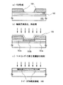
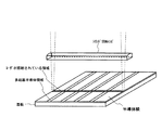
図1を用いて、本発明の実施の形態を説明する。基板101上に基板101からの不純物元素の拡散を防ぐために酸化シリコン膜、窒化シリコン膜または酸化窒化シリコン膜などの下地膜102を形成する。本実施例ではプラズマCVD法でSiH4、NH3、N2Oから作製される酸化窒化シリコン膜102aを10〜200nm(好ましくは50〜100nm)、同様にSiH4、N2Oから作製される酸化窒化水素化シリコン膜102bを50〜200nm(好ましくは100〜150nm)の厚さに積層形成する。
【0023】
次に、下地絶縁膜102上に25〜80nm(好ましくは30〜60nm)の厚さで非晶質半導体膜103をプラズマCVD法やスパッタ法などの公知の方法で形成する。
【0024】
非晶質半導体膜103を形成したらその上に、SiO2膜104を成膜する。さらに、選択的に非晶質半導体膜103の表面が露呈する開口部を有するマスクSiO2104をパターニングして形成する。本明細書中では、非晶質半導体膜が下地絶縁膜と接する面を非晶質半導体膜の裏面、非晶質半導体膜がゲート絶縁膜と接する面を非晶質半導体膜の表面とする。マスクSiO2104は、膜厚は50nm以上で、非晶質半導体膜103の表面が露呈する開口部分の幅は1μm以上10μm以下とする。
【0025】
次に、非晶質半導体膜103のマスクSiO2104の開口部から露呈する領域の結晶化を行う。
【0026】
非晶質半導体膜の結晶化を助長する触媒元素としてニッケル(Ni)を含有した溶液をスピンコート法により塗布し、Ni含有層105を形成した。なお、触媒元素としてはニッケル以外にも、コバルト(Co)、鉄(Fe)、パラジウム(Pd)、白金(Pt)、銅(Cu)、金(Au)、ゲルマニウム(Ge)等を用いることができる(図1(B))。
【0027】
また、本実施形態では、マスクSiO2104の開口部の幅と、多結晶半導体領域の幅とであまり差ができないように制御するために、100ppmの濃度で触媒元素を含む水溶液をスピンコート法により塗布し、550℃で2時間の加熱処理を行う。なお、触媒元素の添加はスピンコート法以外に、スパッタ法を用いてもよい。
【0028】
この加熱処理により、非晶質半導体膜103に非晶質半導体領域103aと多結晶半導体領域103bとを選択的に隣接させて形成することができる。マスクSiO2104bの開口部には多結晶半導体領域103bが形成される。なお、多結晶半導体領域の幅は、結晶成長の制御方法にもよるが、マスク開口部の幅より若干広くなることがある。その後、マスクSiO2104を除去して、Nd:YAGレーザの第2高調波(波長532nm)を非晶質半導体膜の表面側から照射する。レーザ光の照射は、非晶質半導体膜の裏面側からまたは両面から行ってもよい(図1(C))。
【0029】
なお、本実施例ではマスクSiO2104を除去したが、そのまま除去せずにレーザ光の照射を行ってもよい。
【0030】
ここで、非晶質シリコン領域と多結晶シリコン領域が隣接して形成された領域に、波長390〜600nmのレーザ光を照射して結晶化することの有効性を説明する。
【0031】
図4で示すように波長390〜600nm領域の光(Nd:YAGレーザの第2高調波の光を含む領域)では、非晶質シリコンの吸収係数は、多結晶シリコンの吸収係数と比べて、2倍以上大きいことがわかる。
【0032】
Nd:YAGレーザの第2高調波の波長532nmでは、非晶質シリコンの吸収係数は、9.53×10⁴/cmであり、多結晶シリコンの吸収係数は2.75×104/cmである。非晶質シリコンの吸収係数は、多結晶シリコンの吸収係数の3.5倍である。この場合のシリコン膜深さ方向の発熱量分布は、図22のようになる。多結晶シリコンと比較して、非晶質シリコンで、発熱量が大きいことがわかる。
【0033】
次に、温度履歴シミュレーション結果例を示す。シミュレーションは、石英ガラス基板上のシリコン膜厚55nmに、Nd:YAGレーザの第2高調波(波長532nm)を照射するモデルである。図23にシミュレーションから得られた、シリコン層と石英ガラス基板との界面の温度履歴を示す。シリコン層が非晶質シリコンの場合、最高到達温度は、2583Kである。一方、シリコン層を多結晶シリコンとした場合の最高到達温度は、1292Kである。つまり、非晶質シリコンは完全溶融しているが、多結晶シリコンは、固相状態である。
【0034】
以上のように、Nd:YAGレーザの第2高調波(波長532nm)の光を図1(B)で形成した多結晶半導体領域が形成された(非晶質半導体領域と多結晶半導体領域とが隣接した)半導体膜に照射すると、非晶質半導体領域103aは完全溶融状態となり、多結晶半導体領域103bは一部に固相が存在する不完全な溶融状態(少なくとも、下地との界面に固相が存在する状態)になる。
【0035】
そして、多結晶半導体領域103bに残った固相が核となり、完全溶融状態の領域103aにむかって固液界面が移動し、結晶成長が進むと考えられる。
【0036】
1回のレーザ光の照射を行うことにより、0.5〜3μm程度のスーパーラテラル成長した結晶粒106が非晶質半導体領域103aと多結晶半導体領域103bとの間に形成される。このスーパーラテラル成長粒をTFTのチャネル領域に作製することで、電流輸送特性の良好なTFTを得ることができる。特に、結晶成長の方向がチャネルの長さ方向になるようにTFTを設計、作製することが望ましい。
【0037】
〔実施形態2〕
実施形態1で示した方法とは異なる方法で、非晶質半導体膜103に選択的に非晶質半導体領域103aと多結晶半導体領域103bとを隣接させて形成する方法について図2を用いて説明する。
【0038】
非晶質半導体膜103を成膜したら、マスク201を介して非晶質半導体膜103にレーザ光の照射を行って、選択的に非晶質半導体領域103aと多結晶半導体領域103bを形成する。ここで使用するレーザは、エキシマレーザでもNd:YAGレーザでもよい。また、レーザ光の照射は非晶質半導体膜の表面、裏面もしくは表面と裏面との両面から行ってもよい。
【0039】
スリット201aは1μm以上10μ以下とする。また、マスク201は、W(タングステン)、Mo(モリブデン)、Ta(タンタル)、TaN(窒化タンタル)、Cr(クロム)、Nb(ニオブ)、TiN(窒化チタン)、Si(シリコン)からなる単層膜または積層膜をガラスや石英基板上に所定のパターンで形成したものを使用すればよい。スリットが上記の範囲内であればどのようなマスクを用いても構わない。
【0040】
レーザ光を照射することにより、選択的に非晶質半導体領域103aと多結晶半導体領域103bが形成される。この非晶質半導体領域と多結晶半導体領域が隣接した状態の半導体(シリコン)膜103にNd:YAGレーザの第2高調波を照射すると、非晶質半導体領域103aは完全溶融状態になり、多結晶半導体領域103bは一部に固相が残存する不完全溶融状態になる。その後、多結晶半導体領域の固相が結晶成長の核となって、そこから非晶質半導体領域103aに向かって結晶成長が進み、スーパーラテラル成長領域202が実現できる。
【0041】
〔実施形態3〕
実施形態1または実施形態2とは異なる方法で非晶質半導体(シリコン)膜に、位置を制御して非晶質半導体領域と多結晶半導体領域とが隣接した状態を形成する方法について図3を用いて説明する。
【0042】
非晶質半導体膜103の全面にレーザ光を照射して多結晶半導体膜301を形成する。その後、SiO2膜302を形成し、SiO2マスク302の開口部分にあたる多結晶半導体膜301にドーピング種をドープして、マスク開口部分の多結晶半導体膜は結晶組織が破壊されて再び非晶質半導体膜303が形成される。このドーピング種はアルゴン(Ar)、ゲルマニウム(Ge)、酸素(O)、水素(H)、シリコン(Si)から選ばれたいずれかの元素であればよいが、なかでもシリコン(Si)をドーピング種とすることが好ましい。
【0043】
なお、多結晶半導体膜を形成する方法は、レーザによる結晶化方法、触媒元素を用いる結晶化方法もしくは、熱による結晶化方法でもよい。ただし、触媒元素を用いる結晶化方法により多結晶半導体膜を形成した場合には、結晶組織を破壊するためのドーピング種にシリコン(Si)を用いることが好ましい。
【0044】
選択的に多結晶半導体領域と非晶質半導体領域とが隣接して形成された半導体膜に、Nd:YAGレーザの第2高調波を照射する。Nd:YAGレーザの第2高調波の光を照射することによって、非晶質半導体領域は完全溶融状態になり、多結晶半導体領域は一部に固相が残存する不完全溶融状態になる。多結晶半導体領域に残留した固相が結晶成長の核となり、そこから非晶質半導体領域に向かって結晶成長が進み、スーパーラテラル成長領域304が得られる。
【0045】
本実施形態の方法を用いれば、不純物元素をドーピングする工程で用いるマスクの形状によって結晶粒を成長させる位置の制御が可能になる。
【0046】
以上のように実施形態1〜3で示したいずれかの結晶成長方法を用いて、結晶化させた半導体膜を用いてTFTを作製すればよい。
【0047】
【実施例】
〔実施例1〕
本実施例について図5〜図7を用いて説明する。ここでは画素部のnチャネル型TFT(以下、画素TFTと示す)および保持容量と、画素部の周辺に設けられる駆動回路のnチャネル型TFTとpチャネル型TFTとを同時に作製する工程について説明する。
【0048】
図5(A)において、基板501にはコーニング社の#7059ガラスや#1737ガラスなどに代表されるバリウムホウケイ酸ガラスやアルミノホウケイ酸ガラスなどのガラス基板を用いることができる。さらに、処理温度によっては、ポリエチレンテレフタレート(PET)、ポリエチレンテレフタレート(PEN)、ポリエーテルサルフォン(PES)など光学的異方性を有しないプラスチック基板を用いることもできる。
【0049】
基板501のTFTを形成する表面に、基板501からの不純物元素の拡散を防ぐために酸化シリコン膜、窒化シリコン膜または酸化窒化シリコン膜などの下地膜502を形成する。本実施例ではプラズマCVD法でSiH4、NH3、N2Oから作製される酸化窒化シリコン膜502aを10〜200nm(好ましくは50〜100nm)、同様にSiH4、N2Oから作製される酸化窒化水素化シリコン膜502bを50〜200nm(好ましくは100〜150nm)の厚さに積層形成する。
【0050】
酸化窒化シリコン膜は従来の平行平板型のプラズマCVD法を用いて形成すればよい。酸化窒化シリコン502aは、SiH4を10(SCCM)、NH3を100(SCCM)、N2Oを20(SCCM)として反応室に導入し、基板温度325℃、反応圧力40Pa、放電電力密度0.41W/cm2、放電周波数60MHzとする。一方、酸化窒化水素化シリコン502bは、SiH4を5(SCCM)、N2Oを120(SCCM)、H2を125(SCCM)として反応室に導入し、基板温度400℃、反応圧力20Pa、放電電力密度0.41W/cm2、放電周波数60MHzとする。これらの膜は、基板温度を変化させ、反応ガスの切り替えのみで連続して形成することもできる。
【0051】
また、酸化窒化シリコン膜502aは基板を中心に考えて、その内部応力が引っ張り応力となるように形成する。酸化窒化水素化シリコン膜502bも同様の方向に内部応力を持たせるが、酸化窒化シリコン膜502aよりも絶対値で比較して小さい応力となるようにする。
【0052】
次に、25〜80nm(好ましくは30〜60nm)の厚さで非晶質半導体膜(本実施例では半導体膜として、シリコンゲルマニウム膜を用いる。)503をプラズマCVD法やスパッタ法などの公知の方法で形成する。例えば、プラズマCVD法で非晶質半導体膜を55nmの厚さに形成する。このとき、下地膜502と非晶質半導体膜503とは両者を連続形成することも可能である。例えば、前述のように酸化窒化シリコン膜502aと酸化窒化水素化シリコン膜502bをプラズマCVD法で連続して成膜した後、反応ガスをSiH4、N2O、H2からSiH4とH2あるいはSiH4のみに切り替えれば、いったん大気雰囲気に晒すことなく連続形成できる。その結果、酸化窒化水素化シリコン膜502bの表面の汚染を防ぐことが可能となり、TFT特性のバラツキやしきい値電圧の変動を低減させることができる。
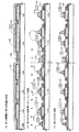
【0053】
次に、本実施例では、図24(a)に示すように、実施形態1にしたがって、半導体膜を形成したら、マスクを形成する。その後、触媒元素を添加して加熱処理を行い、半導体膜の一部に多結晶半導体領域を形成する。次に、図25に示すように、半導体膜全体に形成された複数の多結晶半導体領域に直交するようにNd:YAGレーザの第2高調波(532nm)の光を照射して、多結晶半導体領域を結晶成長の核とした結晶成長させる。
本実施例では、実施形態1を用いて半導体膜の結晶化を行っているが、半導体膜の結晶化の方法は、実施形態2または3で示した方法を用いればよい。
【0054】
結晶化工程の後、島状半導体層504〜506を形成する。本実施例では、図24(c)で示すように、結晶成長が矢印の方向に進むように半導体膜を島状に形成する。島状半導体層は長方形とし一辺が50μm以下となるように形成するが、島状半導体層の形状は任意なものとすることが可能であり、好ましくはその中心部から端部までの最小距離が50μm以下となるような形態であればどのような多角形、あるいは円形でもかまわないが、結晶成長の方向がチャネル長の方向に沿うように島状半導体層を形成することが好ましい。
【0055】
次いで、島状半導体層504〜506を覆うゲート絶縁膜507を形成する。ゲート絶縁膜507はプラズマCVD法またはスパッタ法を用い、厚さを40〜150nmとしてシリコンを含む絶縁膜で形成する。本実施例では、120nmの厚さの酸化窒化シリコン膜で形成する。勿論、ゲート絶縁膜はこのような酸化窒化シリコン膜に限定されるものでなく、他のシリコンを含む絶縁膜を単層または積層構造として用いても良い。例えば、酸化シリコン膜を用いる場合には、プラズマCVD法でTEOS(Tetraethylorthosilicate)とO2とを混合し、反応圧力40Pa、基板温度300〜400℃とし、高周波(13.56MHz)電力密度0.5〜0.8W/cm2で放電させて形成することができる。このようにして作製される酸化シリコン膜は、その後400〜500℃の加熱処理によりゲート絶縁膜として良好な特性を得ることができる。
【0056】
そして、ゲート絶縁膜507上にゲート電極を形成するための第1の導電膜508と第2の導電膜509とを形成する。本実施例では、第1の導電膜508をTa(タンタル)で50〜100nmの厚さに形成し、第2の導電膜509をW(タングステン)で100〜300nmの厚さに形成する。
【0057】
Ta膜はスパッタ法で形成し、TaのターゲットをArでスパッタする。この場合、Arに適量のXeやKrを加えると、Ta膜の内部応力を緩和して膜の剥離を防止することができる。また、α相のTa膜の抵抗率は20μΩcm程度でありゲート電極に使用することができるが、β相のTa膜の抵抗率は180μΩcm程度でありゲート電極とするには不向きである。α相のTa膜を形成するために、Taのα相に近い結晶構造をもつ窒化タンタルを10〜50nm程度の厚さでTaの下地に形成しておくとα相のTa膜を容易に得ることができる。
【0058】
W膜を形成する場合には、Wをターゲットとしたスパッタ法で形成する。その他に6フッ化タングステン(WF6)を用いる熱CVD法で形成することもできる。いずれにしてもゲート電極として使用するためには低抵抗化を図る必要があり、W膜の抵抗率は20μΩcm以下にすることが望ましい。W膜は結晶粒を大きくすることで低抵抗率化を図ることができるが、W中に酸素などの不純物元素が多い場合には結晶化が阻害され高抵抗化する。このことより、スパッタ法による場合、純度99.9〜99.9999%のWターゲットを用い、さらに成膜時に気相中からの不純物元素の混入がないように十分配慮してW膜を形成することにより、抵抗率9〜20μΩcmを実現することができる。
【0059】
なお、本実施例では、第1の導電膜508をTa、第2の導電膜509をWとしたが、特に限定されず、いずれもTa、W、Ti、Mo、Al、Cuから選ばれた元素、または前記元素を主成分とする合金材料若しくは化合物材料で形成してもよい。また、リン等の不純物元素をドーピングした多結晶シリコン膜に代表される半導体膜を用いてもよい。本実施例以外の他の組み合わせの一例は、第1の導電膜508を窒化タンタル(TaN)で形成し、第2の導電膜509をWとする組み合わせ、第1の導電膜508を窒化タンタル(TaN)で形成し、第2の導電膜をAlとする組み合わせ、第1の導電膜を窒化タンタル(TaN)で形成し、第2の導電膜509をCuとする組み合わせで形成することが好ましい。
【0060】
次に、レジストによるマスク510〜513を形成し、電極及び配線を形成するための第1のエッチング処理を行う。本実施例ではICP(Inductively Coupled Plasma:誘導結合型プラズマ)エッチング法を用い、エッチング用ガスにCF4とCl2を混合し、1Paの圧力でコイル型の電極に500WのRF(13.56MHz)電力を投入してプラズマを生成して行う。基板側(試料ステージ)にも100WのRF(13.56MHz)電力を投入し、実質的に負の自己バイアス電圧を印加する。CF4とCl2を混合した場合にはW膜及びTa膜とも同程度にエッチングされる。
【0061】
上記エッチング条件では、レジストによるマスクの形状を適したものとすることにより、基板側に印加するバイアス電圧の効果により第1の導電層及び第2の導電層の端部がテーパー形状となる。テーパー部の角度は15〜45°となる。ゲート絶縁膜上に残渣を残すことなくエッチングするためには、10〜20%程度の割合でエッチング時間を増加させると良い。W膜に対する酸化窒化シリコン膜の選択比は2〜4(代表的には3)であるので、オーバーエッチング処理により、酸化窒化シリコン膜が露出した面は20〜50nm程度エッチングされることになる。こうして、第1のエッチング処理により第1の導電層と第2の導電層から成る第1の形状の導電層514〜517(第1の導電層514a〜517aと第2の導電層514b〜517b)を形成する。ゲート絶縁膜507の第1の形状の導電層514〜517で覆われない領域は20〜50nm程度エッチングされ薄くなった領域が形成される。
【0062】
次に、図5(D)に示すように第2のエッチング処理を行う。同様にICPエッチング法を用い、エッチングガスにCF4とCl2とO2を混合して、1Paの圧力でコイル型の電極に500WのRF電力(13.56MHz)を供給し、プラズマを生成して行う。基板側(試料ステージ)には50WのRF(13.56MHz)電力を投入し、第1のエッチング処理に比べ低い自己バイアス電圧を印加する。このような条件によりW膜を異方性エッチングし、かつ、それより遅いエッチング速度で第1の導電層であるTaを異方性エッチングして第2の形状の導電層518〜521(第1の導電層518a〜521aと第2の導電層518b〜521b)を形成する。ゲート絶縁膜507の第2の形状の導電層518〜521で覆われない領域はさらに20〜50nm程度エッチングされ薄くなった領域が形成される。
【0063】
W膜やTa膜のCF4とCl2の混合ガスによるエッチング反応は、生成されるラジカルまたはイオン種と反応生成物の蒸気圧から推測することができる。WとTaのフッ化物と塩化物の蒸気圧を比較すると、Wのフッ化物であるWF6が極端に高く、その他のWCl5、TaF5、TaCl5は同程度である。従って、CF4とCl2の混合ガスではW膜及びTa膜共にエッチングされる。しかし、この混合ガスに適量のO2を添加するとCF4とO2が反応してCOとFになり、FラジカルまたはFイオンが多量に発生する。その結果、フッ化物の蒸気圧が高いW膜のエッチング速度が増大する。一方、TaはFが増大しても相対的にエッチング速度の増加は少ない。また、TaはWに比較して酸化されやすいので、O2を添加することでTaの表面が酸化される。Taの酸化物はフッ素や塩素と反応しないためさらにTa膜のエッチング速度は低下する。従って、W膜とTa膜とのエッチング速度に差を作ることが可能となりW膜のエッチング速度をTa膜よりも大きくすることが可能となる。
【0064】
第1のエッチング処理および第2のエッチング処理が終了したら、第1のドーピング処理を行いn型を付与する不純物元素を添加する(図5(D))。ドーピングの方法はイオンドープ法若しくはイオン注入法で行えば良い。第2の形状の導電層518〜520をマスクとして島状半導体層に、n型を付与する不純物元素が添加される。1×10¹⁷〜5×10¹⁸/cm3(好ましくは、3×1017〜3×1018/cm3)の濃度範囲のn型不純物領域(b)522〜526が形成されるように加速電圧を70〜120keVとしてドーピング処理が行われる。n型を付与する不純物元素として15族に属する元素、典型的にはリン(P)または砒素(As)を用いるが、ここではリン(P)を用いる。
【0065】
また第2の導電層518b〜520bの一部がエッチングされた領域の島状半導体層は、第1の導電層518a〜520aおよびゲート絶縁膜507をすり抜けてn型を付与する不純物元素が添加され、2×10¹⁶〜1×10¹⁷/cm3(好ましくは、6×1016〜6×1017/cm3)の濃度範囲のn型不純物領域(c)527〜530が形成される。
【0066】
第1のドーピング処理工程が終了したら、レジストマスク510b〜513bを除去する(図6(A))。
【0067】
次に、図6(B)に示すように第2のドーピング処理を行う。まず、島状半導体506のチャネル形成領域を覆うようにして、レジストマスク531を形成する。次に、加速電圧を80〜200keVとし、5×10¹⁷〜5×10¹⁹/cm3(好ましくは、1×1018〜1×1019/cm3)の濃度範囲のn型不純物領域(b’)538を形成するためにn型を付与する不純物元素をドーピングする。この時不純物元素は、島状半導体層505上の第1の導電層514aおよびゲート絶縁膜507をすり抜けて、添加される。
【0068】
次に、不純物の濃度範囲が1×10²⁰〜1×10²¹/cm3(好ましくは、2×1020〜5×1020/cm3)であるn型不純物領域(a)533〜536を形成するためにn型を付与する不純物元素の添加を行う(図6(B))。
【0069】
そして、図6(C)に示すように、pチャネル型TFTを形成する島状半導体層504にp型不純物領域を形成する。まず、p型の不純物元素を添加する領域以外を隠すレジストマスク543を形成する。そして、第1の導電層514aを不純物元素に対するマスクとして用い、p型不純物領域(a)544およびp型不純物領域(b)545を形成する。p型不純物領域544、545にはそれぞれ異なる濃度でリンが添加されているが、B2H6を用いたイオンドープ法で形成し、そのいずれの領域においても不純物濃度を2×10²⁰〜2×10²¹/cm3となるようにする。
【0070】
以上までの工程でそれぞれの島状半導体層に不純物領域が形成される。島状半導体層と重なる第2の導電層518〜520がゲート電極として機能する。また、521は容量配線として機能する。
【0071】
こうして導電型の制御を目的として、それぞれの島状半導体層に添加された不純物元素を活性化する工程を行う。この工程は炉を用いる加熱処理(ファーネスアニール法)を行う。その他にレーザアニール法を適用することができる。加熱処理は酸素濃度が1ppm以下、好ましくは0.1ppm以下の窒素雰囲気中で400〜700℃、代表的には500〜600℃で行うものであり、本実施例では500℃で4時間の加熱処理を行う。ただし、518〜521に用いた配線材料が熱に弱い場合には、配線等を保護するため層間絶縁膜(シリコンを主成分とする)を形成した後で活性化を行うことが好ましい。
【0072】
このとき、n型不純物元素が添加された領域、すなわちn型不純物領域もしくはp型不純物領域でn型不純物元素を含む領域に、非晶質シリコン膜の結晶化に用いたニッケルが、n型不純物元素が添加された領域の方向に移動し、ゲッタリングされる。すなわち、TFTのチャネル形成領域560〜562のニッケル濃度が大幅に低減され、少なくとも1×10¹⁶/cm3以下となる。
【0073】
さらに、3〜100%の水素を含む雰囲気中で、300〜450℃で1〜12時間の加熱処理を行い、島状半導体層を水素化する工程を行う。この工程は熱的に励起された水素により半導体層のダングリングボンドを終端する工程である。水素化の他の手段として、プラズマ水素化(プラズマにより励起された水素を用いる)を行っても良い。
【0074】
次いで、第1の層間絶縁膜546は酸化窒化シリコン膜から100〜200nmの厚さで形成する。その上に有機絶縁物材料から成る第2の層間絶縁膜547を形成する。次いで、コンタクトホールを形成するためのエッチング工程を行う。
【0075】
そして、駆動回路405において島状半導体層のソース領域とコンタクトを形成するソース配線548、549、550、ドレイン領域とコンタクトを形成するドレイン配線551、552を形成する(図7(A))。ドレイン配線552は、画素電極としても用いられている。本実施例では配線548〜552は、Ti膜を100nm、Tiを含むアルミニウム膜300nm、Ti膜150nmをスパッタ法で連続して形成した3層構造の積層膜とした。
【0076】
以上のようにして、pチャネル型TFT401およびnチャネル型TFT402を有する駆動回路405と、画素TFT403、保持容量404とを有する画素部406を同一基板上に形成することができる。本明細書中ではこのような基板を便宜上アクティブマトリクス基板と呼ぶ。
【0077】
なお、図21に示すように、ドレイン電極(画素電極)552を配線548〜551と同じ材料で形成されるドレイン電極601と酸化物導電膜で形成される画素電極602とにおきかえて形成することで、透過型の液晶表示装置を作製することもできる。
【0078】
駆動回路405のpチャネル型TFT401にはチャネル形成領域560、ゲート電極を形成する第1の導電層518aと重なるp型不純物領域(b)545、ソース領域またはドレイン領域として機能するp型不純物領域(a)544を有している。nチャネル型TFT402にはチャネル形成領域561、ゲート電極を形成する第1の導電層519aと重なるn型不純物領域(b)538(Lov領域:なお、ovはoverlappedの意味で付す。)、ソース領域またはドレイン領域として機能するn型不純物領域(a)534を有している。
【0079】
画素部406の画素TFT403にはチャネル形成領域562、ゲート電極を形成する第1の導電層520aと重なるn型不純物領域(c)539(Lov領域)、ゲート電極の外側に形成されるn型不純物領域(b)540(Loff領域:なお、offはoffsetの意味で付す。)とソース領域またはドレイン領域として機能するn型不純物領域(a)535を有している。また、保持容量404の一方の電極として機能する半導体層にはn型不純物領域(a)と同じ濃度の領域536が形成され、第1の容量配線521aが残った領域の半導体層には、n型不純物領域(c)と同じ濃度の領域541が形成される。容量配線521とその間の絶縁層(ゲート絶縁膜と同じ層)とで保持容量を形成している。
【0080】
続いてアクティブマトリクス基板から、反射型のアクティブマトリクス型液晶表示装置を作製する工程を説明する。図7(A)の状態のアクティブマトリクス基板に対し、配向膜701を形成する。通常液晶表示素子の配向膜にはポリイミド樹脂が多く用いられている。対向側の対向基板702には、遮光膜703、透明導電膜704および配向膜705を形成した。配向膜を形成した後、ラビング処理を施して液晶分子がある一定のプレチルト角を持って配向するようにした。そして、画素部と、CMOS回路が形成されたアクティブマトリクス基板と対向基板とを、公知のセル組み工程によってシール材やスペーサ(共に図示せず)などを介して貼りあわせる。その後、両基板の間に液晶材料706を注入し、封止剤(図示せず)によって完全に封止した。液晶材料には公知の液晶材料を用いれば良い。このようにして図7(B)に示すアクティブマトリクス型液晶表示装置が完成した。
【0081】
本実施例で示す工程に従えば、良好な特性を有する半導体膜を作製することができ、さらに、製造コストの低減及び歩留まりの向上に寄与することができる。
【0082】
〔実施例2〕
実施例1に従って、基板上に下地絶縁膜を設け、その上に半導体膜を形成して結晶化を行う。本実施例では半導体膜として、シリコン膜を用いる。また、本実施例における半導体膜の結晶化工程は、実施形態1〜3に示したいずれかの方法で行う。
【0083】
次に、本実施例では、図24(a)に示すように、実施形態1にしたがって、半導体膜を形成したら、マスクを形成する。その後、触媒元素を添加して加熱処理を行い、半導体膜の一部に多結晶領域を形成する。次に、図25に示すように、半導体膜全体に形成された複数の多結晶半導体領域に直交するようにNd:YAGレーザの第2高調波(532nm)を照射して、多結晶半導体領域を結晶成長の核とした結晶成長させる。本実施例では、実施形態1を用いて半導体膜の結晶化を行っているが、半導体膜の結晶化の方法は、実施形態2または3で示した方法を用いてもよい。
【0084】
結晶化工程の後、島状半導体層1102〜1106を形成する。本実施例では、図24(c)で示すように、結晶成長が矢印の方向に進むように半導体膜を島状に形成する。島状半導体層は長方形とし一辺が50μm以下となるように形成するが、島状半導体層の形状は任意なものとすることが可能であり、好ましくはその中心部から端部までの最小距離が50μm以下となるような形態であればどのような多角形、あるいは円形でもかまわないが、結晶成長の方向がチャネル長の方向に沿うように島状半導体層を形成することが好ましい。
【0085】
次に、島状半導体層を覆うようにしてゲート絶縁膜1107を形成する。さらに、ゲート絶縁膜1107上にゲート電極を形成するための第1の導電膜1108および第2の導電膜1109として本実施例では、実施例1と同様にTaN膜およびW膜を形成する(図6(A))。第1の導電膜1108および第2の導電膜の材料は、特に限定されず、いずれもTa、W、Ti、Mo、Al、Cuから選ばれた元素、または前記元素を主成分とする合金材料もしくは化合物材料で形成してよい。
【0086】
次に、レジストによるマスク1110〜1116を形成し、電極および配線を形成するための第1のエッチング処理を行う。本実施例では、ICP(Inductively Coupled Plasma:誘導結合型プラズマ)エッチング法を用い、エッチング用ガスにCF4とCl2を混合し、1Paの圧力でコイル型の電極に500WのRF(13.56MHz)電力を投入してプラズマを精製して行う。基板側(試料ステージ)にも100WのRF(13.56MHz)電力を投入し、実質的に負の自己バイアス電圧を印加する。CF4とCl2を混合した場合にはW膜およびTaN膜とも同程度にエッチングされる。
【0087】
上記エッチング条件では、レジストによるマスクの形状を適したものとすることにより、基板側に印加するバイアス電圧の効果により第1の導電層および第2の導電層の端部がテーパー形状となる。テーパー部の角度は15〜45°となる。ゲート絶縁膜上に残渣を残すことなくエッチングするためには10〜20%程度の割合でエッチング時間を増加させるとよい。W膜に対する酸化窒化シリコン膜の選択比は2〜4(代表的には3)であるので、オーバーエッチング処理により、酸化窒化シリコン膜が露出した面は20〜50nm程度エッチングされることになる。こうして、第1のエッチング処理により第1の導電層と第2の導電層からなる第1の形状の導電層1118〜1124(第1の導電層1118a〜1124aと第2の導電層1118b〜1124b)を形成する。1117はゲート絶縁膜であり、第1の形状の導電層1118〜1124で覆われない領域は20〜50nm程度エッチングされ薄くなった領域が形成される。
【0088】
そして、第1のドーピング処理を行いn型を付与する不純物元素を添加する(図8(B))。ドーピングの方法はイオンドープ法もしくはイオン注入法で行えばよい。不純物濃度が、5×10²⁰〜5×10²¹/cm3(好ましくは1×1020〜1×1021/cm3)となるように不純物元素の添加を行った。
【0089】
また、n型を付与する不純物元素としては15族に属する元素、典型的にはリン(P)または、砒素(As)を用いるが、ここでは、リン(P)を用いる。この場合、導電層1118〜1122がn型を付与する不純物元素に対するマスクとなり、自己整合的にn型不純物領域(a)1125〜1129が形成される。
【0090】
次に、図8(C)に示すように第2のエッチング処理を行う。同様にICPエッチングを行い、エッチングガスにCF4とCl2とO2とを混合して、1Paの圧力でコイル型の電極に500WのRF電力(13.56MHz)を供給し、プラズマを生成して行う。基板側(試料ステージ)には50WのRF(13.56MHz)電力を投入して、第1のエッチング処理に比べ低い自己バイアス電圧を印加する。このような条件によりW膜を異方性エッチングし、かつ、それより遅いエッチング速度で第1の導電層であるTaNを異方性エッチングして第2の形状の導電層1131〜1137(第1の導電層1131a〜1137aと第2の導電層1131b〜1137b)を形成する。1130はゲート絶縁膜であり、第2の形状の導電層1131〜1137で覆われない領域はさらに20〜50nm程度エッチングされ薄くなった領域が形成される。
【0091】
W膜やTaN膜のCF4とCl2の混合ガスによるエッチング反応は、生成されるラジカルまたはイオン種と反応生成物の蒸気圧から推測することができる。WとTaNのフッ化物と塩化物の蒸気圧を比較すると、Wのフッ化物であるWF6が極端に高く、その他のWCl5、TaF5、TaCl5は同程度である。従って、CF4とCl2の混合ガスではW膜およびTaN膜ともにエッチングされる。しかし、この混合ガスに適量のO2を添加するとCF4とO2が反応してCOとFになり、FラジカルまたはFイオンが多量に発生する。その結果、フッ化物の蒸気圧が高いW膜のエッチング速度が増大する。一方、TaNはFが増大しても相対的にエッチング速度の増加は少ない。また、TaNはWに比較して酸化されやすいので、O2を添加することでTaNの表面が多少酸化される。TaNの酸化物はフッ素や塩素と反応しないためさらにTaN膜のエッチング速度に差を作ることが可能となりW膜のエッチング速度をTaN膜よりも大きくすることが可能となる。
【0092】
そして、図9(A)に示すように第2のドーピング処理を行う。n型不純物領域(b)1138〜1142を形成する。n型不純物領域(b)におけるn型不純物の濃度が5×10¹⁷〜5×10¹⁹/cm3(好ましくは1×1018〜1×1019/cm3)となるように不純物元素の添加を行う。また、第2の形状の第1の導電膜1131〜1137とゲート絶縁膜1130とを不純物元素が通り抜け、不純物濃度が1×1017〜5×1018/cm3(好ましくは3×1017〜3×1018/cm3)の領域n型不純物領域(c)1143〜1147も同時に形成される。
【0093】
次に、図9(B)に示すように、pチャネル型TFTを形成する島状半導体層1103に一導電型とは逆の導電型の不純物元素を添加してp型不純物領域1151〜1156を形成する。第2の導電層1132bを不純物元素に対するマスクとして用い、自己整合的に不純物領域を形成する。このとき、nチャネル型TFTを形成する島状半導体層1102、1104、1105はレジストマスク1148〜1150で全面を被覆しておく。不純物領域1151〜1156にはそれぞれ異なる濃度でリンが添加されているが、ジボラン(B2H6)を用いたイオンドープ法で形成し、そのいずれの領域においても不純物濃度を2×10²⁰〜2×10²¹/cm3となるようにする。
【0094】
以上までの工程でそれぞれの島状半導体層に不純物領域が形成される。島状半導体層と重なる第2の導電層1131〜1134がゲート電極として機能する。また、1136は島状のソース配線、1137はゲート配線、1135は容量配線として機能する。
【0095】
こうして導電型の制御を目的として図9(c)に示すように、それぞれの島状半導体層に添加された不純物元素を活性化する工程を行う。この工程は炉を用いる加熱処理(ファーネスアニール法)を行う。その他に、レーザアニール法、またはラピッドサーマルアニール法(RTA法)を適用することができる。加熱処理は、酸素濃度が1ppm以下、好ましくは0.1ppm以下の窒素雰囲気中で400〜700℃、代表的には500〜600℃で行うこともある。本実施例では500℃で4時間の加熱処理を行う。ただし、1131〜1137に用いた配線材料が熱に弱い場合には、配線等を保護するため層間絶縁膜(シリコンを主成分とする)を形成した後で活性化を行うことが好ましい。
【0096】
このとき、n型不純物元素が添加された領域、すなわちn型不純物領域もしくはp型不純物領域でn型不純物元素を含む領域に、非晶質半導体膜の結晶化に用いたニッケルが、n型不純物元素が添加された領域に移動しゲッタリングされる。すなわち、TFTのチャネル形成領域1168〜1171のニッケル濃度が大幅に低減され、少なくとも1×10¹⁶/cm3以下となる。
【0097】
さらに、3〜100%の水素を含む雰囲気中で、300〜450℃で1〜12時間の加熱処理を行い、島状半導体層を水素化する工程を行う。この工程は熱的に励起された水素により半導体層のダングリングボンドを終端する工程である。水素化の他の手段として、プラズマ水素化(プラズマにより励起された水素を用いる)を行ってもよい。
【0098】
次いで、第1の層間絶縁膜1157は酸化窒化シリコン膜から100〜200nmの厚さで形成する。その上に有機絶縁物材料からなる第2の層間絶縁膜1158を形成する。そして、コンタクトホールを形成するためのエッチング工程を行う。
【0099】
駆動回路1405において島状半導体層のソース領域とコンタクトを形成するソース配線1159〜1161、ドレイン領域とコンタクトを形成するドレイン配線1162〜1164を形成する。また、画素部1406においては、画素電極1167、ゲート配線1166、接続電極1165を形成する(図10)。この接続電極1165により、ソース配線1137は、画素TFT1404と電気的な接続が形成される。また、ゲート配線1166は、第1の電極と電気的な接続が形成される。
【0100】
本実施例では、画素電極1167を酸化物導電膜(代表的には、ITO膜)で形成することで透過型の液晶表示装置を作製することもできる。
【0101】
以上のようにして、nチャネル型TFT1401、pチャネル型TFT1402、nチャネル型TFT1403を有する駆動回路1405と、画素TFT1404と保持容量1405とを有する画素部1406とを同一基板上に形成することができる。
【0102】
〔実施例3〕
本実施例では、本発明を用いてEL(エレクトロルミネセンス)表示装置を作製した例について説明する。なお、図11(A)は本発明のEL表示装置の上面図であり、図11(B)はその断面図である。
【0103】
図11(A)において、4001は基板、4002は画素部、4003はソース側駆動回路、4004はゲート側駆動回路であり、それぞれの駆動回路は配線4005を経てFPC(フレキシブルプリントサーキット)4006に至り、外部機器へと接続される。
【0104】
このとき、画素部4002、ソース側駆動回路4003及びゲート側駆動回路4004を囲むようにして第1シール材4101、カバー材4102、充填材4103及び第2シール材4104が設けられている。
【0105】
また、図11(B)は図11(A)をA−A’で切断した断面図に相当し、基板4001の上にソース側駆動回路4003に含まれる駆動TFT(nチャネル型TFTとpチャネル型TFT)4201及び画素部4002に含まれる電流制御用TFT(EL素子への電流を制御するTFT)4202が形成されている。
【0106】
本実施例では、駆動TFT4201には図10のpチャネル型TFTまたはnチャネル型TFTと同じ構造のTFTが用いられ、電流制御用TFT4202には図7または図10のpチャネル型TFTと同じ構造のTFTが用いられる。また、画素部4002には電流制御用TFT4202のゲートに接続された保持容量(図示せず)が設けられる。
【0107】
駆動TFT4201及び画素TFT4202の上には樹脂材料でなる層間絶縁膜(平坦化膜)4301が形成され、その上に画素TFT4202のドレインと電気的に接続する画素電極(陽極)4302が形成される。画素電極4302としては仕事関数の大きい透明導電膜が用いられる。透明導電膜としては、酸化インジウムと酸化スズとの化合物、酸化インジウムと酸化亜鉛との化合物、酸化亜鉛、酸化スズまたは酸化インジウムを用いることができる。また、前記透明導電膜にガリウムを添加したものを用いても良い。
【0108】
そして、画素電極4302の上には絶縁膜4303が形成され、絶縁膜4303は画素電極4302の上に開口部が形成されている。この開口部において、画素電極4302の上にはEL(エレクトロルミネッセンス)層4304が形成される。EL層4304は公知の有機EL材料または無機EL材料を用いることができる。また、有機EL材料には低分子系(モノマー系)材料と高分子系(ポリマー系)材料があるがどちらを用いても良い。
【0109】
EL層4304の形成方法は公知の蒸着技術もしくは塗布法技術を用いれば良い。また、EL層の構造は正孔注入層、正孔輸送層、発光層、電子輸送層または電子注入層を自由に組み合わせて積層構造または単層構造とすれば良い。
【0110】
EL層4304の上には遮光性を有する導電膜(代表的にはアルミニウム、銅もしくは銀を主成分とする導電膜またはそれらと他の導電膜との積層膜)からなる陰極4305が形成される。また、陰極4305とEL層4304の界面に存在する水分や酸素は極力排除しておくことが望ましい。従って、真空中で両者を連続成膜するか、EL層4304を窒素または希ガス雰囲気で形成し、酸素や水分に触れさせないまま陰極4305を形成するといった工夫が必要である。本実施例ではマルチチャンバー方式(クラスターツール方式)の成膜装置を用いることで上述のような成膜を可能とする。
【0111】
そして陰極4305は4306で示される領域において配線4005に電気的に接続される。配線4005は陰極4305に所定の電圧を与えるための配線であり、異方導電性フィルム4307を介してFPC4006に電気的に接続される。
【0112】
以上のようにして、画素電極(陽極)4302、EL層4304及び陰極4305からなるEL素子が形成される。このEL素子は、第1シール材4101及び第1シール材4101によって基板4001に貼り合わされたカバー材4102で囲まれ、充填材4103により封入されている。
【0113】
カバー材4102としては、ガラス材、金属材(代表的にはステンレス材)、セラミックス材、プラスチック材(プラスチックフィルムも含む)を用いることができる。プラスチック材としては、FRP(Fiberglass−Reinforced Plastics)板、PVF(ポリビニルフルオライド)フィルム、マイラーフィルム、ポリエステルフィルムまたはアクリル樹脂フィルムを用いることができる。また、アルミニウムホイルをPVFフィルムやマイラーフィルムで挟んだ構造のシートを用いることもできる。
【0114】
但し、EL素子からの光の放射方向がカバー材側に向かう場合にはカバー材は透明でなければならない。その場合には、ガラス板、プラスチック板、ポリエステルフィルムまたはアクリルフィルムのような透明物質を用いる。
【0115】
また、充填材4103としては紫外線硬化樹脂または熱硬化樹脂を用いることができ、PVC(ポリビニルクロライド)、アクリル、ポリイミド、エポキシ樹脂、シリコン樹脂、PVB(ポリビニルブチラル)またはEVA(エチレンビニルアセテート)を用いることができる。この充填材4103の内部に吸湿性物質(好ましくは酸化バリウム)もしくは酸素を吸着しうる物質を設けておくとEL素子の劣化を抑制できる。
【0116】
また、充填材4103の中にスペーサを含有させてもよい。このとき、スペーサを酸化バリウムで形成すればスペーサ自体に吸湿性をもたせることが可能である。また、スペーサを設けた場合、スペーサからの圧力を緩和するバッファ層として陰極4305上に樹脂膜を設けることも有効である。
【0117】
また、配線4005は異方導電性フィルム4307を介してFPC4006に電気的に接続される。配線4005は画素部4002、ソース側駆動回路4003及びゲート側駆動回路4004に送られる信号をFPC4006に伝え、FPC4006により外部機器と電気的に接続される。
【0118】
また、本実施例では第1シール材4101の露呈部及びFPC4006の一部を覆うように第2シール材4104を設け、EL素子を徹底的に外気から遮断する構造となっている。こうして図11(B)の断面構造を有するEL表示装置となる。
【0119】
ここで画素部のさらに詳細な断面構造を図12に、上面構造を図13(A)に、回路図を図13(B)に示す。図12、図13(A)及び図13(B)では共通の符号を用いるので互いに参照すれば良い。
【0120】
図12において、基板4401上に設けられたスイッチング用TFT4402は図10のnチャネル型TFT403を用いて形成される。従って、構造の説明はnチャネル型TFT403の説明を参照すれば良い。また、4403で示される配線は、スイッチング用TFT4402のゲート電極4404a、4404bを電気的に接続するゲート配線である。
【0121】
なお、本実施例ではチャネル形成領域が二つ形成されるダブルゲート構造としているが、チャネル形成領域が一つ形成されるシングルゲート構造もしくは三つ形成されるトリプルゲート構造であっても良い。
【0122】
また、スイッチング用TFT4402のドレイン配線4405は電流制御用TFT4406のゲート電極4407に電気的に接続されている。なお、電流制御用TFT4406は図10のpチャネル型TFT401を用いて形成される。従って、構造の説明はpチャネル型TFT401の説明を参照すれば良い。なお、本実施例ではシングルゲート構造としているが、ダブルゲート構造もしくはトリプルゲート構造であっても良い。
【0123】
スイッチング用TFT4402及び電流制御用TFT4406の上には第1パッシベーション膜4408が設けられ、その上に樹脂からなる平坦化膜4409が形成される。平坦化膜4409を用いてTFTによる段差を平坦化することは非常に重要である。後に形成されるEL層は非常に薄いため、段差が存在することによって発光不良を起こす場合がある。従って、EL層をできるだけ平坦面に形成しうるように画素電極を形成する前に平坦化しておくことが望ましい。
【0124】
また、4418は透明導電膜からなる画素電極(EL素子の陽極)であり、電流制御用TFT4406のドレイン配線4414に電気的に接続される。透明導電膜としては、酸化インジウムと酸化スズとの化合物、酸化インジウムと酸化亜鉛との化合物、酸化亜鉛、酸化スズまたは酸化インジウムを用いることができる。また、前記透明導電膜にガリウムを添加したものを用いても良い。
【0125】
画素電極4418の上にはEL層4411が形成される。なお、図12では一画素しか図示していないが、本実施例ではR(赤)、G(緑)、B(青)の各色に対応したEL層を作り分けている。また、本実施例では蒸着法により低分子系有機EL材料を形成している。具体的には、正孔注入層として20nm厚の銅フタロシアニン(CuPc)膜を設け、その上に発光層として70nm厚のトリス−8−キノリノラトアルミニウム錯体(Alq3)膜を設けた積層構造としている。Alq3にキナクリドン、ペリレンもしくはDCM1といった蛍光色素を添加することで発光色を制御することができる。
【0126】
但し、以上の例はEL層として用いることのできる有機EL材料の一例であって、これに限定する必要はまったくない。発光層、電荷輸送層または電荷注入層を自由に組み合わせてEL層(発光及びそのためのキャリアの移動を行わせるための層)を形成すれば良い。例えば、本実施例では低分子系有機EL材料をEL層として用いる例を示したが、高分子系有機EL材料を用いても良い。また、電荷輸送層や電荷注入層として炭化珪素等の無機材料を用いることも可能である。これらの有機EL材料や無機材料は公知の材料を用いることができる。
【0127】
次に、EL層4411の上には導電膜からなる陰極4412が設けられる。本実施例の場合、導電膜としてアルミニウムとリチウムとの合金膜を用いる。勿論、公知のMgAg膜(マグネシウムと銀との合金膜)を用いても良い。陰極材料としては、周期表の1族もしくは2族に属する元素からなる導電膜もしくはそれらの元素を添加した導電膜を用いれば良い。
【0128】
この陰極4412まで形成された時点でEL素子4413が完成する。なお、ここでいうEL素子4413は、画素電極(陽極)4418、EL層4411及び陰極4412で形成された積層を指す。
【0129】
次に、本実施例における画素の上面構造を図13(A)を用いて説明する。スイッチング用TFT4402のソースはソース配線4415に接続され、ドレインはドレイン配線4405に接続される。また、ドレイン配線4405は電流制御用TFT4406のゲート電極4407に電気的に接続される。また、電流制御用TFT4406のソースは電流供給線4416に電気的に接続され、ドレインはドレイン配線4417に電気的に接続される。また、ドレイン配線4417は点線で示される画素電極(陽極)4418に電気的に接続される。
【0130】
このとき、4419で示される領域には保持容量が形成される。保持容量4419は、電流供給線4416と電気的に接続された半導体膜4420、ゲート絶縁膜と同一層の絶縁膜(図示せず)及びゲート電極4407との間で形成される。また、ゲート電極4407、第1層間絶縁膜と同一の層(図示せず)及び電流供給線4416で形成される容量も保持容量として用いることが可能である。
【0131】
〔実施例4〕
本実施例では、実施例3とは異なる画素構造を有したEL表示装置について説明する。説明には図14を用いる。なお、図13と同一の符号が付してある部分については実施例3の説明を参照すれば良い。
【0132】
図14では電流制御用TFT4501として図10のnチャネル型TFT403と同一構造のTFTを用いる。勿論、電流制御用TFT4501のゲート配線4502はスイッチング用TFT4402のドレイン配線4405に電気的に接続されている。また、電流制御用TFT4501のドレイン配線4503は画素電極4504に電気的に接続されている。
【0133】
本実施例では、導電膜からなる画素電極4504がEL素子の陰極として機能する。具体的には、アルミニウムとリチウムとの合金膜を用いるが、周期表の1族もしくは2族に属する元素からなる導電膜もしくはそれらの元素を添加した導電膜を用いれば良い。
【0134】
画素電極4504の上にはEL層4505が形成される。なお、図14では一画素しか図示していないが、本実施例ではG(緑)に対応したEL層を蒸着法及び塗布法(好ましくはスピンコーティング法)により形成している。具体的には、電子注入層として20nm厚のフッ化リチウム(LiF)膜を設け、その上に発光層として70nm厚のPPV(ポリパラフェニレンビニレン)膜を設けた積層構造としている。
【0135】
次に、EL層4505の上には透明導電膜からなる陽極4506が設けられる。本実施例の場合、透明導電膜として酸化インジウムと酸化スズとの化合物もしくは酸化インジウムと酸化亜鉛との化合物からなる導電膜を用いる。
【0136】
この陽極4506まで形成された時点でEL素子4507が完成する。なお、ここでいうEL素子4507は、画素電極(陰極)4504、EL層4505及び陽極4506で形成された積層を指す。
【0137】
EL素子に加える電圧が10V以上といった高電圧の場合には、電流制御用TFT4501においてホットキャリア効果による劣化が顕在化してくる。このような場合に、電流制御用TFT4501として本発明の構造のnチャネル型TFTを用いることは有効である。
【0138】
また、本実施例の電流制御用TFT4501はゲート電極4502とLDD領域4509との間にゲート容量と呼ばれる寄生容量を形成する。このゲート容量を調節することで図13(A)、(B)に示した保持容量4419と同等の機能を持たせることも可能である。特に、EL表示装置をデジタル駆動方式で動作させる場合においては、保持容量のキャパシタンスがアナログ駆動方式で動作させる場合よりも小さくて済むため、ゲート容量で保持容量を代用しうる。
【0139】
なお、EL素子に加える電圧が10V以下、好ましくは5V以下となった場合、上記ホットキャリア効果による劣化はさほど問題とならなくなるため、図14においてLDD領域4509を省略した構造のnチャネル型TFTを用いても良い。
【0140】
〔実施例5〕
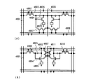
本実施例では、実施例3もしくは実施例4に示したEL表示装置の画素部に用いることができる画素構造の例を図15(A)〜(C)に示す。なお、本実施例において、4601はスイッチング用TFT4602のソース配線、4603はスイッチング用TFT4602のゲート配線、4604は電流制御用TFT、4605はコンデンサ、4606、4608は電流供給線、4607はEL素子とする。
【0141】
図15(A)は、二つの画素間で電流供給線4606を共通とした場合の例である。即ち、二つの画素が電流供給線4606を中心に線対称となるように形成されている点に特徴がある。この場合、電源供給線の本数を減らすことができるため、画素部をさらに高精細化することができる。
【0142】
また、図15(B)は、電流供給線4608をゲート配線4603と平行に設けた場合の例である。なお、図15(B)では電流供給線4608とゲート配線4603とが重ならないように設けた構造となっているが、両者が異なる層に形成される配線であれば、絶縁膜を介して重なるように設けることもできる。この場合、電源供給線4608とゲート配線4603とで専有面積を共有させることができるため、画素部をさらに高精細化することができる。
【0143】
また、図15(C)は、図15(B)の構造と同様に電流供給線4608をゲート配線4603と平行に設け、さらに、二つの画素を電流供給線4608を中心に線対称となるように形成する点に特徴がある。また、電流供給線4608をゲート配線4603のいずれか一方と重なるように設けることも有効である。この場合、電源供給線の本数を減らすことができるため、画素部をさらに高精細化することができる。
【0144】
〔実施例6〕
本実施例では、本発明を実施したEL表示装置の画素構造の例を図16(A)、(B)に示す。なお、本実施例において、4701はスイッチング用TFT4702のソース配線、4703はスイッチング用TFT4702のゲート配線、4704は電流制御用TFT、4705はコンデンサ(省略することも可能)、4706は電流供給線、4707は電源制御用TFT、4708は電源制御用ゲート配線、4709はEL素子とする。電源制御用TFT4707の動作については特願平11−341272号を参照すると良い。
【0145】
また、本実施例では電源制御用TFT4707を電流制御用TFT4704とEL素子4708との間に設けているが、電源制御用TFT4707とEL素子4708との間に電流制御用TFT4704が設けられた構造としても良い。また、電源制御用TFT4707は電流制御用TFT4704と同一構造とするか、同一の活性層で直列させて形成するのが好ましい。
【0146】
また、図16(A)は、二つの画素間で電流供給線4706を共通とした場合の例である。即ち、二つの画素が電流供給線4706を中心に線対称となるように形成されている点に特徴がある。この場合、電流供給線の本数を減らすことができるため、画素部をさらに高精細化することができる。
【0147】
また、図16(B)は、ゲート配線4703と平行に電流供給線4710を設け、ソース配線4701と平行に電源制御用ゲート配線4711を設けた場合の例である。なお、図16(B)では電流供給線4710とゲート配線4703とが重ならないように設けた構造となっているが、両者が異なる層に形成される配線であれば、絶縁膜を介して重なるように設けることもできる。この場合、電流供給線4710とゲート配線4703とで専有面積を共有させることができるため、画素部をさらに高精細化することができる。
【0148】
〔実施例7〕
本実施例では、本発明を実施したEL表示装置の画素構造の例を図17(A)、(B)に示す。なお、本実施例において、4801はスイッチング用TFT4802のソース配線、4803はスイッチング用TFT4802のゲート配線、4804は電流制御用TFT、4805はコンデンサ(省略することも可能)、4806は電流供給線、4807は消去用TFT、4808は消去用ゲート配線、4809はEL素子とする。消去用TFT4807の動作については特願平11−338786号を参照すると良い。
【0149】
消去用TFT4807のドレインは電流制御用TFT4804のゲートに接続され、電流制御用TFT4804のゲート電圧を強制的に変化させることができるようになっている。なお、消去用TFT4807はnチャネル型TFTとしてもpチャネル型TFTとしても良いが、オフ電流を小さくできるようにスイッチング用TFT4802と同一構造とすることが好ましい。
【0150】
また、図17(A)は、二つの画素間で電流供給線4806を共通とした場合の例である。即ち、二つの画素が電流供給線4806を中心に線対称となるように形成されている点に特徴がある。この場合、電流供給線の本数を減らすことができるため、画素部をさらに高精細化することができる。
【0151】
また、図17(B)は、ゲート配線4803と平行に電流供給線4810を設け、ソース配線4801と平行に消去用ゲート配線4811を設けた場合の例である。なお、図17(B)では電流供給線4810とゲート配線4803とが重ならないように設けた構造となっているが、両者が異なる層に形成される配線であれば、絶縁膜を介して重なるように設けることもできる。この場合、電流供給線4810とゲート配線4803とで専有面積を共有させることができるため、画素部をさらに高精細化することができる。
【0152】
〔実施例8〕
本発明のEL表示装置は画素内にいくつのTFTを設けた構造としても良い。例えば、四つ乃至六つまたはそれ以上のTFTを設けても構わない。本発明はEL表示装置の画素構造に限定されずに実施することが可能である。
【0153】
〔実施例9〕
本発明を実施して形成されたCMOS回路や画素部は様々な電気光学装置(アクティブマトリクス型液晶ディスプレイ、アクティブマトリクス型ELディスプレイ)に用いることができる。即ち、それら電気光学装置を表示部に組み込んだ電気器具全てに本発明を実施できる。
【0154】
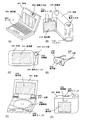
その様な電気器具としては、ビデオカメラ、デジタルカメラ、プロジェクター(リア型またはフロント型)、ヘッドマウントディスプレイ(ゴーグル型ディスプレイ)、カーナビゲーション、カーステレオ、パーソナルコンピュータ、携帯情報端末(モバイルコンピュータ、携帯電話または電子書籍等)などが挙げられる。それらの一例を図18、図19及び図20に示す。
【0155】
図18(A)はパーソナルコンピュータであり、本体2001、画像入力部2002、表示部2003、キーボード2004等を含む。
【0156】
図18(B)はビデオカメラであり、本体2101、表示部2102、音声入力部2103、操作スイッチ2104、バッテリー2105、受像部2106等を含む。
【0157】
図18(C)はモバイルコンピュータ(モービルコンピュータ)であり、本体2201、カメラ部2202、受像部2203、操作スイッチ2204、表示部2205等を含む。
【0158】
図18(D)はゴーグル型ディスプレイであり、本体2301、表示部2302、アーム部2303等を含む。
【0159】
図18(E)はプログラムを記録した記録媒体(以下、記録媒体と呼ぶ)を用いるプレーヤーであり、本体2401、表示部2402、スピーカ部2403、記録媒体2404、操作スイッチ2405等を含む。なお、このプレーヤーは記録媒体としてDVD(Digtial Versatile Disc)、CD等を用い、音楽鑑賞や映画鑑賞やゲームやインターネットを行うことができる。
【0160】
図18(F)はデジタルカメラであり、本体2501、表示部2502、接眼部2503、操作スイッチ2504、受像部(図示しない)等を含む。
【0161】
図19(A)はフロント型プロジェクターであり、投射装置2601、スクリーン2602等を含む。
【0162】
図19(B)はリア型プロジェクターであり、本体2701、投射装置2702、ミラー2703、スクリーン2704等を含む。
【0163】
なお、図19(C)は、図19(A)及び図19(B)中における投射装置2601、2702の構造の一例を示した図である。投射装置2601、2702は、光源光学系2801、ミラー2802、2804〜2806、ダイクロイックミラー2803、プリズム2807、液晶表示装置2808、位相差板2809、投射光学系2810で構成される。投射光学系2810は、投射レンズを含む光学系で構成される。本実施例は三板式の例を示したが、特に限定されず、例えば単板式であってもよい。また、図19(C)中において矢印で示した光路に実施者が適宜、光学レンズや、偏光機能を有するフィルムや、位相差を調節するためのフィルム、IRフィルム等の光学系を設けてもよい。
【0164】
また、図19(D)は、図19(C)中における光源光学系2801の構造の一例を示した図である。本実施例では、光源光学系2801は、リフレクター2811、光源2812、レンズアレイ2813、2814、偏光変換素子2815、集光レンズ2816で構成される。なお、図19(D)に示した光源光学系は一例であって特に限定されない。例えば、光源光学系に実施者が適宜、光学レンズや、偏光機能を有するフィルムや、位相差を調節するフィルム、IRフィルム等の光学系を設けてもよい。
【0165】
ただし、図19に示したプロジェクターにおいては、透過型の電気光学装置を用いた場合を示しており、反射型の電気光学装置及びEL表示装置での適用例は図示していない。
【0166】
図20(A)は携帯電話であり、本体2901、音声出力部2902、音声入力部2903、表示部2904、操作スイッチ2905、アンテナ2906等を含む。
【0167】
図20(B)は携帯書籍(電子書籍)であり、本体3001、表示部3002、3003、記憶媒体3004、操作スイッチ3005、アンテナ3006等を含む。
【0168】
図20(C)はディスプレイであり、本体3101、支持台3102、表示部3103等を含む。本発明は表示部3103に適用することができる。本発明のディスプレイは特に大画面化した場合において有利であり、対角10インチ以上(特に30インチ以上)のディスプレイには有利である。
【0169】
以上の様に、本発明の適用範囲は極めて広く、あらゆる分野の電気器具に適用することが可能である。また、本実施例の電気器具は実施形態1〜3、実施例1、2を組み合わせて構成される液晶表示装置で実現することができる。
【0170】
【発明の効果】
本発明にしたがって390〜600nmの範囲の波長における光に対する非晶質シリコン膜と多結晶シリコン膜との吸収系数の差を利用すると、従来と比較して結晶粒径の大きな結晶質半導体膜を簡便な方法で得ることができる。さらに、この結晶粒径の大きな結晶質半導体膜を用いて半導体装置を作製することで、半導体装置の性能を大幅に向上させることができる。
【0171】
例えば、非晶質シリコン領域と多結晶シリコン領域とが隣接して存在するシリコン膜に390〜600nmの範囲の波長における光(代表的にはNd:YAGレーザの第2高調波の光)を照射することによって、非晶質シリコン領域が完全溶融し、かつ多結晶シリコン領域は不完全溶融となり、この不完全溶融状態領域が核となって結晶成長が始まり、位置制御した大粒径の半導体膜を形成することができる。
【0172】
SLS法など精密な位置制御が必要な方法と比較して、本方法は簡便な方法で位置制御して大粒径の結晶質半導体膜を得ることができる。さらに、本発明により得られた半導体膜をTFTに適用することで、良好なTFTを得ることができる。
【図面の簡単な説明】
【図1】 本発明の実施形態を示す図。
【図2】 本発明の実施形態を示す図。
【図3】 本発明の実施形態を示す図。
【図4】 レーザのエネルギー領域および非晶質シリコンと多結晶シリコンのレーザ吸収係数を示す図。
【図5】 本発明を利用してTFTを作製する工程を示す図。
【図6】 本発明を利用してTFTを作製する工程を示す図。
【図7】 本発明を利用してTFTを作製する工程を示す図。
【図8】 本発明を利用してTFTを作製する工程を示す図。
【図9】 本発明を利用してTFTを作製する工程を示す図。
【図10】 本発明を利用してTFTを作製する工程を示す図。
【図11】 EL表示装置の構造を示す図。
【図12】 EL表示装置の構造を示す図。
【図13】 EL表示装置の構造を示す図。
【図14】 EL表示装置の構造を示す図。
【図15】 EL表示装置の回路を示す図。
【図16】 EL表示装置の回路を示す図。
【図17】 EL表示装置の回路を示す図。
【図18】 電気器具の具体例を示す図。
【図19】 電気器具の具体例を示す図。
【図20】 電気器具の具体例を示す図。
【図21】 本発明を利用して作製されたTFTの断面を示す図。
【図22】 非晶質シリコンと多結晶シリコンの膜厚方向に対する発熱量を示す図。
【図23】 シリコン層と石英ガラス基板との界面の温度履歴を示す図。
【図24】 本発明の実施形態を示す図。
【図25】 本発明の実施形態を示す図。[0001]
BACKGROUND OF THE INVENTION
The present invention relates to a method for manufacturing a thin film transistor (hereinafter referred to as a TFT) which is used by crystallizing a semiconductor film by irradiating a laser beam. In particular, the present invention provides a semiconductor device that functions by utilizing semiconductor characteristics manufactured by including a process of crystallizing an amorphous semiconductor film by laser light in a manufacturing process, a pixel portion, and a driver circuit provided in the periphery thereof The present invention relates to a liquid crystal display device provided on the same substrate, an electro-optical device (also referred to as an electronic device) typified by an EL (electroluminescence) display device, or a method of manufacturing an electric appliance equipped with the electro-optical device.
[Prior art]
[0002]
A method for obtaining a crystalline semiconductor film having a large grain size by irradiating a semiconductor film with laser light has been studied extensively. As a result of observing the result of crystallization of a semiconductor film using an excimer laser, it is known that an infinite number of single crystals having a grain size of about several hundreds of nanometers are collected. A large number of lattice defects exist at the interface (hereinafter referred to as a crystal grain boundary), and these cause significant damage to the characteristics of the semiconductor device.
[0003]
Thus, a method has been considered in which the crystal grain size is increased to reduce the crystal grain boundary, thereby reducing the density of many lattice defects existing at the crystal grain boundary. For example, a method of leaving the solid phase only in a certain region and completely melting the other region during irradiation (and after irradiation) of the laser beam can be mentioned.
[0004]
Solidification of a semiconductor film after irradiation with a pulse laser typified by an excimer laser generates solid-phase nuclei that can serve as nuclei for crystal growth in completely melted silicon, and crystals grow from the solid-phase nuclei all at once. However, it takes some time before solid phase nuclei are generated. Therefore, if solid phase silicon that becomes solid phase nuclei remains only at a certain position and its surroundings are completely melted, crystal growth starts from this solid phase silicon immediately after laser irradiation, and the grown crystal grains collide with each other. Then crystal growth stops.
[0005]
Further, in a region where the semiconductor film is completely melted by irradiation with laser light, until the formation of uniform nuclei (or non-uniform nuclei), the film is fixed in a horizontal direction (hereinafter referred to as a lateral direction). As the liquid interface moves, crystal grains grow over a length of several tens of times the film thickness. Hereinafter, this phenomenon is referred to as super lateral growth. This super lateral growth is achieved by Si / underlying SiO. 2 / In the case of the substrate structure, it is known that the crystal generally grows in the lateral direction over 1 μm or more. This super lateral growth is considered to be terminated by the generation of innumerable uniform (non-uniform) nuclei in the complete melting region.
[0006]
Even if it is not the above-described structure, there is a laser beam irradiation energy region that realizes super lateral growth. However, in reality, the energy range of the laser beam that can realize super lateral growth is very narrow, and it has been impossible to obtain a crystal having a large grain size by controlling the position.
[0007]
In order to solve the above problems, “R. Ishihara and A. Burtsev: AM-LCD '98., P153-p156, 1998” describes Si / SiO 2 / Metal / substrate is formed, and laser light is irradiated from above and below the substrate using an excimer laser. Laser light from the lower side is absorbed by the metal film and converted into heat, which heats the metal film to a high temperature. That is, since the metal film works as a heat accumulation layer, the cooling rate of the silicon film is reduced. By this method, a crystalline semiconductor film having a crystal grain diameter of several μm in diameter can be obtained at an arbitrary place.
[0008]
In addition, Columbia University's James S. Im and others showed the Sequential Lateral Solidification method (hereinafter referred to as SLS method) that can realize super lateral growth in any place. The SLS method is a method in which a crystal is grown by shifting a slit-shaped mask by a distance (up to 0.75 μm) for super lateral growth with one pulse for each shot.
[0009]
[Problems to be solved by the invention]
In the method of R. Ishihara et al., The substrate and the insulating film (SiO 2 If a high-melting point metal is used as the metal between the gate electrode and the gate electrode, the structure can be effectively applied to the bottom gate type thin film transistor. However, when this structure is used for a top-gate thin film transistor, parasitic capacitance is generated, power consumption increases, and it is difficult to realize high-speed operation of the thin film transistor. Depending on the material, peeling may occur when the laser beam is irradiated.
[0010]
In addition, the SLS method requires precision on the order of microns in the relative positioning technique between the mask and the substrate, and is a complicated device as compared with a normal laser device. In addition, there is a problem in throughput when used for manufacturing a TFT applied to a liquid crystal display having a large area.
[0011]
An object of the present invention is to provide a method for controlling the position of a crystalline semiconductor film having a large crystal grain size by a simpler method than the conventional method.
[0012]
[Means for solving the problems]
In order to solve the above-described problems, the present invention forms an amorphous semiconductor film on an insulator, and forms a mask made of an insulating film on the amorphous semiconductor film, which is exposed from the opening of the mask. A step of adding an element for promoting crystallization to the region of the amorphous semiconductor film, a step of selectively forming a polycrystalline semiconductor region by heat treatment after the addition step, and a wavelength range of 390 to 600 nm. A method for manufacturing a semiconductor device, comprising the step of forming a crystalline semiconductor film by irradiating a laser beam.
[0013]
In the above invention, the laser light is light of the second harmonic (wavelength 532 nm) of an Nd: YAG laser.
[0014]
In the above invention, the elements that promote crystallization are nickel (Ni), germanium (Ge), iron (Fe), palladium (Pd), tin (Sn), lead (Pb), cobalt (Co), platinum. It is characterized by being (Pt), copper (Cu) or gold (Au).
[0015]
In the above invention, the opening of the mask is not less than 1 μm and not more than 10 μm.
[0016]
According to another aspect of the invention, a step of forming an amorphous semiconductor film on an insulator, and selectively irradiating a selected region of the amorphous semiconductor film with a first laser beam to selectively form a polycrystalline semiconductor region And a step of forming a crystalline semiconductor film by irradiation with a second laser beam.
[0017]
In the invention described above, the first laser light is excimer laser light, and the second laser light is light of a second harmonic (wavelength 532 nm) of an Nd: YAG laser. .
[0018]
In the above invention, the first laser light and the second laser light are light of a second harmonic (wavelength 532 nm) of an Nd: YAG laser.
[0019]
In the above invention, the first laser light and the second laser light are irradiated from the front surface, back surface, or both surfaces of the substrate.
[0020]
According to another aspect of the invention, a step of forming a polycrystalline semiconductor film on an insulator, a mask made of an insulating film on the polycrystalline semiconductor film, and silicon (Si) in a region exposed from the opening of the mask. ), Adding an element selected from germanium (Ge), argon (Ar), oxygen (O), or hydrogen (H) to selectively form an amorphous semiconductor region, and laser light. A method for manufacturing a semiconductor device including a step of forming a crystalline semiconductor film by irradiation.
[0021]
In the invention described above, the laser light is light of the second harmonic (wavelength 532 nm) of an Nd: YAG laser.
[0022]
DETAILED DESCRIPTION OF THE INVENTION
[Embodiment 1]
An embodiment of the present invention will be described with reference to FIG. A
[0023]
Next, an
[0024]
After the
[0025]
Next, the mask SiO of the
[0026]
A solution containing nickel (Ni) as a catalyst element for promoting crystallization of the amorphous semiconductor film was applied by a spin coating method to form the Ni-containing
[0027]
In this embodiment, the mask SiO 2 In order to control so that there is not much difference between the width of the
[0028]
By this heat treatment, the
[0029]
In this embodiment, the mask SiO 2 Although 104 is removed, laser light irradiation may be performed without removal.
[0030]
Here, the effectiveness of crystallization by irradiating a region where the amorphous silicon region and the polycrystalline silicon region are formed adjacent to each other with laser light having a wavelength of 390 to 600 nm will be described.
[0031]
As shown in FIG. 4, in the light in the wavelength range of 390 to 600 nm (region including the second harmonic light of the Nd: YAG laser), the absorption coefficient of amorphous silicon is compared with the absorption coefficient of polycrystalline silicon. It can be seen that it is twice as large.
[0032]
At the wavelength of 532 nm of the second harmonic of the Nd: YAG laser, the absorption coefficient of amorphous silicon is 9.53 × 10 Four / cm, and the absorption coefficient of polycrystalline silicon is 2.75 × 10 Four / cm. The absorption coefficient of amorphous silicon is 3.5 times that of polycrystalline silicon. The calorific value distribution in the depth direction of the silicon film in this case is as shown in FIG. It can be seen that the amount of heat generated is larger in amorphous silicon than in polycrystalline silicon.
[0033]
Next, a temperature history simulation result example is shown. The simulation is a model in which a silicon film thickness of 55 nm on a quartz glass substrate is irradiated with the second harmonic (wavelength: 532 nm) of an Nd: YAG laser. FIG. 23 shows the temperature history of the interface between the silicon layer and the quartz glass substrate obtained from the simulation. When the silicon layer is amorphous silicon, the maximum temperature reached is 2583K. On the other hand, the highest temperature reached when the silicon layer is polycrystalline silicon is 1292K. That is, amorphous silicon is completely melted, but polycrystalline silicon is in a solid state.
[0034]
As described above, the polycrystalline semiconductor region in which the light of the second harmonic (wavelength 532 nm) of the Nd: YAG laser is formed in FIG. 1B is formed (the amorphous semiconductor region and the polycrystalline semiconductor region are When the adjacent semiconductor film is irradiated, the
[0035]
Then, it is considered that the solid phase remaining in the
[0036]
By performing laser light irradiation once,
[0037]
[Embodiment 2]
A method for selectively forming the
[0038]
After the
[0039]
The
[0040]
By irradiation with laser light, an
[0041]
[Embodiment 3]
FIG. 3 shows a method for forming a state in which an amorphous semiconductor region and a polycrystalline semiconductor region are adjacent to each other by controlling the position in an amorphous semiconductor (silicon) film by a method different from that in
[0042]
A
[0043]
Note that a method for forming a polycrystalline semiconductor film may be a crystallization method using a laser, a crystallization method using a catalytic element, or a crystallization method using heat. However, when a polycrystalline semiconductor film is formed by a crystallization method using a catalytic element, it is preferable to use silicon (Si) as a doping species for destroying the crystal structure.
[0044]
A semiconductor film in which a polycrystalline semiconductor region and an amorphous semiconductor region are selectively formed is irradiated with a second harmonic of an Nd: YAG laser. By irradiating the second harmonic light of the Nd: YAG laser, the amorphous semiconductor region is in a completely molten state, and the polycrystalline semiconductor region is in an incompletely molten state in which a solid phase remains in part. The solid phase remaining in the polycrystalline semiconductor region becomes the nucleus of crystal growth, from which crystal growth proceeds toward the amorphous semiconductor region, and a super lateral growth region 304 is obtained.
[0045]
If the method of this embodiment is used, the position where crystal grains are grown can be controlled by the shape of the mask used in the step of doping the impurity element.
[0046]
As described above, any of the crystal growth methods described in
[0047]
【Example】
[Example 1]
The present embodiment will be described with reference to FIGS. Here, a process of simultaneously manufacturing an n-channel TFT (hereinafter referred to as a pixel TFT) and a storage capacitor in a pixel portion, and an n-channel TFT and a p-channel TFT in a driver circuit provided around the pixel portion will be described. .
[0048]
In FIG. 5A, a glass substrate such as barium borosilicate glass or alumino borosilicate glass typified by Corning # 7059 glass or # 1737 glass can be used for the
[0049]
A
[0050]
The silicon oxynitride film may be formed using a conventional parallel plate type plasma CVD method. Silicon oxynitride 502a is made of SiH. Four 10 (SCCM), NH Three 100 (SCCM), N 2 O was introduced into the reaction chamber as 20 (SCCM), the substrate temperature was 325 ° C., the reaction pressure was 40 Pa, and the discharge power density was 0.41 W / cm. 2 The discharge frequency is 60 MHz. On the other hand, silicon oxynitride 502b is made of SiH. Four 5 (SCCM), N 2 O for 120 (SCCM), H 2 Is introduced into the reaction chamber as 125 (SCCM), the substrate temperature is 400 ° C., the reaction pressure is 20 Pa, and the discharge power density is 0.41 W / cm. 2 The discharge frequency is 60 MHz. These films can be formed continuously only by changing the substrate temperature and switching the reaction gas.
[0051]
Further, the silicon oxynitride film 502a is formed so that the internal stress becomes tensile stress with the substrate as the center. The silicon oxynitride film 502b is also given internal stress in the same direction, but the stress is smaller than the silicon oxynitride film 502a in absolute value.
[0052]
Next, an amorphous semiconductor film (a silicon germanium film is used as a semiconductor film in this embodiment) 503 with a thickness of 25 to 80 nm (preferably 30 to 60 nm) 503 such as a plasma CVD method or a sputtering method is known. Form by the method. For example, an amorphous semiconductor film is formed to a thickness of 55 nm by plasma CVD. At this time, the
[0053]
Next, in this example, as shown in FIG. 24A, after the semiconductor film is formed according to the first embodiment, a mask is formed. Thereafter, a catalytic element is added and heat treatment is performed to form a polycrystalline semiconductor region in part of the semiconductor film. Next, as shown in FIG. 25, the second harmonic (532 nm) light of the Nd: YAG laser is irradiated so as to be orthogonal to a plurality of polycrystalline semiconductor regions formed over the entire semiconductor film, thereby producing a polycrystalline semiconductor. Crystal growth is performed using the region as the nucleus of crystal growth.
In this example, the semiconductor film is crystallized using the first embodiment, but the method described in the second or third embodiment may be used as the method for crystallizing the semiconductor film.
[0054]
After the crystallization step, island-shaped semiconductor layers 504 to 506 are formed. In this embodiment, as shown in FIG. 24C, the semiconductor film is formed in an island shape so that crystal growth proceeds in the direction of the arrow. The island-like semiconductor layer is rectangular and is formed so that one side is 50 μm or less, but the shape of the island-like semiconductor layer can be arbitrary, and preferably the minimum distance from the center to the end is Any polygonal or circular shape may be used as long as it is 50 μm or less, but it is preferable to form the island-shaped semiconductor layer so that the crystal growth direction is along the channel length direction.
[0055]
Next, a
[0056]
Then, a first
[0057]
The Ta film is formed by sputtering, and a Ta target is sputtered with Ar. In this case, when an appropriate amount of Xe or Kr is added to Ar, the internal stress of the Ta film can be relieved and peeling of the film can be prevented. The resistivity of the α-phase Ta film is about 20 μΩcm and can be used for the gate electrode, but the resistivity of the β-phase Ta film is about 180 μΩcm and is not suitable for the gate electrode. In order to form an α-phase Ta film, tantalum nitride having a crystal structure close to Ta's α-phase is formed on a Ta base with a thickness of about 10 to 50 nm, so that an α-phase Ta film can be easily obtained. be able to.
[0058]
When forming a W film, it is formed by sputtering using W as a target. In addition, tungsten hexafluoride (WF 6 It can also be formed by a thermal CVD method using In any case, in order to use as a gate electrode, it is necessary to reduce the resistance, and the resistivity of the W film is desirably 20 μΩcm or less. The resistivity of the W film can be reduced by increasing the crystal grains. However, when there are many impurity elements such as oxygen in W, crystallization is hindered and the resistance is increased. Therefore, when sputtering is used, a W target having a purity of 99.9 to 99.9999% is used, and a W film is formed with sufficient consideration so that no impurity elements are mixed from the gas phase during film formation. Thus, a resistivity of 9 to 20 μΩcm can be realized.
[0059]
In this embodiment, the first
[0060]
Next, resist
[0061]
Under the above etching conditions, by making the shape of the resist mask suitable, the end portions of the first conductive layer and the second conductive layer are tapered due to the effect of the bias voltage applied to the substrate side. The angle of the tapered portion is 15 to 45 °. In order to perform etching without leaving a residue on the gate insulating film, it is preferable to increase the etching time at a rate of about 10 to 20%. Since the selection ratio of the silicon oxynitride film to the W film is 2 to 4 (typically 3), the surface where the silicon oxynitride film is exposed is etched by about 20 to 50 nm by the over-etching process. Thus, the first shape conductive layers 514 to 517 (first
[0062]
Next, a second etching process is performed as shown in FIG. Similarly, using the ICP etching method, the etching gas is CF. Four And Cl 2 And O 2 And 500 W of RF power (13.56 MHz) is supplied to the coil-type electrode at a pressure of 1 Pa to generate plasma. 50 W RF (13.56 MHz) power is applied to the substrate side (sample stage), and a lower self-bias voltage is applied than in the first etching process. Under such conditions, the W film is anisotropically etched, and Ta, which is the first conductive layer, is anisotropically etched at a slower etching rate to form the second shape
[0063]
CF of W film and Ta film Four And Cl 2 The etching reaction by the mixed gas can be estimated from the generated radicals or ion species and the vapor pressure of the reaction product. Comparing the vapor pressure of fluoride and chloride of W and Ta, WF, which is fluoride of W 6 Is extremely high, other WCl Five , TaF Five , TaCl Five Are comparable. Therefore, CF Four And Cl 2 With this mixed gas, both the W film and the Ta film are etched. However, an appropriate amount of O is added to this mixed gas. 2 When CF is added Four And O 2 Reacts to CO and F, and a large amount of F radicals or F ions are generated. As a result, the etching rate of the W film having a high fluoride vapor pressure is increased. On the other hand, the increase in etching rate of Ta is relatively small even when F increases. Further, since Ta is more easily oxidized than W, O 2 When Ta is added, the surface of Ta is oxidized. Since the Ta oxide does not react with fluorine or chlorine, the etching rate of the Ta film further decreases. Therefore, it is possible to make a difference in the etching rate between the W film and the Ta film, and the etching rate of the W film can be made larger than that of the Ta film.
[0064]
When the first etching process and the second etching process are completed, an impurity element imparting n-type conductivity is added by performing a first doping process (FIG. 5D). The doping method may be an ion doping method or an ion implantation method. An impurity element imparting n-type conductivity is added to the island-shaped semiconductor layer using the second shape
[0065]
In addition, the island-shaped semiconductor layer in the region where a part of the second
[0066]
When the first doping process is completed, the resist masks 510b to 513b are removed (FIG. 6A).
[0067]
Next, a second doping process is performed as shown in FIG. First, a resist mask 531 is formed so as to cover a channel formation region of the island-shaped
[0068]
Next, the impurity concentration range is 1 × 10. 20 ~ 1x10 twenty one /cm Three (Preferably 2 × 10 20 ~ 5x10 20 /cm Three In order to form n-type impurity regions (a) 533 to 536, an impurity element imparting n-type conductivity is added (FIG. 6B).
[0069]
Then, as shown in FIG. 6C, a p-type impurity region is formed in the island-shaped
[0070]
Through the above steps, impurity regions are formed in each island-like semiconductor layer. The second
[0071]
Thus, for the purpose of controlling the conductivity type, a step of activating the impurity element added to each island-like semiconductor layer is performed. In this step, heat treatment using a furnace (furnace annealing method) is performed. In addition, a laser annealing method can be applied. The heat treatment is performed in a nitrogen atmosphere having an oxygen concentration of 1 ppm or less, preferably 0.1 ppm or less, at 400 to 700 ° C., typically 500 to 600 ° C. In this embodiment, heating is performed at 500 ° C. for 4 hours. Process. However, when the wiring material used for 518 to 521 is weak against heat, activation is preferably performed after an interlayer insulating film (having silicon as a main component) is formed in order to protect the wiring and the like.
[0072]
At this time, nickel used for crystallization of the amorphous silicon film is added to the region to which the n-type impurity element is added, that is, the region containing the n-type impurity element in the n-type impurity region or the p-type impurity region. It moves in the direction of the region to which the element is added and is gettered. That is, the nickel concentration in the
[0073]
Further, a heat treatment is performed at 300 to 450 ° C. for 1 to 12 hours in an atmosphere containing 3 to 100% hydrogen to perform a step of hydrogenating the island-shaped semiconductor layer. This step is a step of terminating dangling bonds in the semiconductor layer with thermally excited hydrogen. As another means of hydrogenation, plasma hydrogenation (using hydrogen excited by plasma) may be performed.
[0074]
Next, the first
[0075]
Then, source wirings 548, 549, and 550 that form contacts with the source region of the island-shaped semiconductor layer and
[0076]
As described above, the driver circuit 405 including the p-
[0077]
Note that as shown in FIG. 21, the drain electrode (pixel electrode) 552 is formed by replacing the
[0078]
The p-
[0079]
The pixel TFT 403 of the pixel portion 406 includes a
[0080]
Next, a process for manufacturing a reflective active matrix liquid crystal display device from an active matrix substrate will be described. An
[0081]
By following the steps shown in this embodiment, a semiconductor film having favorable characteristics can be manufactured, and further, the manufacturing cost can be reduced and the yield can be improved.
[0082]
[Example 2]
In accordance with
[0083]
Next, in this example, as shown in FIG. 24A, after the semiconductor film is formed according to the first embodiment, a mask is formed. Thereafter, a catalytic element is added and heat treatment is performed to form a polycrystalline region in part of the semiconductor film. Next, as shown in FIG. 25, the second harmonic (532 nm) of the Nd: YAG laser is irradiated so as to be orthogonal to the plurality of polycrystalline semiconductor regions formed in the entire semiconductor film, thereby The crystal is grown as a nucleus of crystal growth. In this example, the semiconductor film is crystallized using the first embodiment, but the method described in the second or third embodiment may be used as the method for crystallizing the semiconductor film.
[0084]
After the crystallization step, island-shaped
[0085]
Next, a
[0086]
Next, resist
[0087]
Under the above etching conditions, by making the shape of the resist mask suitable, the end portions of the first conductive layer and the second conductive layer are tapered due to the effect of the bias voltage applied to the substrate side. The angle of the tapered portion is 15 to 45 °. In order to perform etching without leaving a residue on the gate insulating film, the etching time is preferably increased by about 10 to 20%. Since the selection ratio of the silicon oxynitride film to the W film is 2 to 4 (typically 3), the surface where the silicon oxynitride film is exposed is etched by about 20 to 50 nm by the overetching process. Thus, first-shaped conductive layers 1118 to 1124 (first
[0088]
Then, an impurity element imparting n-type conductivity is added by performing a first doping process (FIG. 8B). Doping may be performed by ion doping or ion implantation. Impurity concentration is 5 × 10 20 ~ 5x10 twenty one /cm Three (Preferably 1 × 10 20 ~ 1x10 twenty one /cm Three The impurity element was added so that
[0089]
As an impurity element imparting n-type conductivity, an element belonging to Group 15, typically phosphorus (P) or arsenic (As) is used. Here, phosphorus (P) is used. In this case, the conductive layers 1118 to 1122 serve as a mask for the impurity element imparting n-type, and n-type impurity regions (a) 1125 to 1129 are formed in a self-aligning manner.
[0090]
Next, a second etching process is performed as shown in FIG. Similarly, ICP etching is performed and CF is used as an etching gas. Four And Cl 2 And O 2 And 500 W of RF power (13.56 MHz) is supplied to the coil-type electrode at a pressure of 1 Pa to generate plasma. 50 W RF (13.56 MHz) power is applied to the substrate side (sample stage), and a lower self-bias voltage is applied than in the first etching process. Under such conditions, the W film is anisotropically etched, and TaN, which is the first conductive layer, is anisotropically etched at a slower etching rate to form the second shape
[0091]
CF of W film and TaN film Four And Cl 2 The etching reaction by the mixed gas can be estimated from the generated radicals or ion species and the vapor pressure of the reaction product. When the vapor pressures of W and TaN fluoride and chloride are compared, WF, the fluoride of W 6 Is extremely high, other WCl Five , TaF Five , TaCl Five Are comparable. Therefore, CF Four And Cl 2 In this mixed gas, both the W film and the TaN film are etched. However, an appropriate amount of O is added to this mixed gas. 2 When CF is added Four And O 2 Reacts to CO and F, and a large amount of F radicals or F ions are generated. As a result, the etching rate of the W film having a high fluoride vapor pressure is increased. On the other hand, TaN has a relatively small increase in etching rate even when F increases. Also, since TaN is more easily oxidized than W, ON 2 When Ta is added, the surface of TaN is somewhat oxidized. Since the TaN oxide does not react with fluorine or chlorine, it is possible to make a difference in the etching rate of the TaN film, and the etching rate of the W film can be made larger than that of the TaN film.
[0092]
Then, a second doping process is performed as shown in FIG. N-type impurity regions (b) 1138 to 1142 are formed. The concentration of the n-type impurity in the n-type impurity region (b) is 5 × 10 17 ~ 5x10 19 /cm Three (Preferably 1 × 10 18 ~ 1x10 19 /cm Three The impurity element is added so that Further, the impurity element passes through the second shape first
[0093]
Next, as shown in FIG. 9B, an impurity element having a conductivity type opposite to that of one conductivity type is added to the island-shaped
[0094]
Through the above steps, impurity regions are formed in each island-like semiconductor layer. The second
[0095]
Thus, for the purpose of controlling the conductivity type, as shown in FIG. 9C, a step of activating the impurity element added to each island-like semiconductor layer is performed. In this step, heat treatment using a furnace (furnace annealing method) is performed. In addition, a laser annealing method or a rapid thermal annealing method (RTA method) can be applied. The heat treatment may be performed at 400 to 700 ° C., typically 500 to 600 ° C. in a nitrogen atmosphere having an oxygen concentration of 1 ppm or less, preferably 0.1 ppm or less. In this embodiment, heat treatment is performed at 500 ° C. for 4 hours. However, when the wiring material used for 1131 to 1137 is weak against heat, activation is preferably performed after an interlayer insulating film (having silicon as a main component) is formed in order to protect the wiring and the like.
[0096]
At this time, nickel used for crystallization of the amorphous semiconductor film is added to the region added with the n-type impurity element, that is, the region containing the n-type impurity element in the n-type impurity region or the p-type impurity region. It moves to the region where the element is added and is gettered. That is, the nickel concentration in the
[0097]
Further, a heat treatment is performed at 300 to 450 ° C. for 1 to 12 hours in an atmosphere containing 3 to 100% hydrogen to perform a step of hydrogenating the island-shaped semiconductor layer. This step is a step of terminating dangling bonds in the semiconductor layer with thermally excited hydrogen. As another means of hydrogenation, plasma hydrogenation (using hydrogen excited by plasma) may be performed.
[0098]
Next, the first
[0099]
In the driver circuit 1405, source wirings 1159 to 1161 that form contacts with the source region of the island-shaped semiconductor layer and
[0100]
In this embodiment, a transmissive liquid crystal display device can be manufactured by forming the
[0101]
As described above, the driver circuit 1405 including the n-
[0102]
Example 3
In this example, an example in which an EL (electroluminescence) display device is manufactured using the present invention will be described. 11A is a top view of the EL display device of the present invention, and FIG. 11B is a cross-sectional view thereof.
[0103]
In FIG. 11A,
[0104]
At this time, a
[0105]
FIG. 11B corresponds to a cross-sectional view taken along line AA ′ of FIG. 11A, and includes driving TFTs (n-channel TFTs and p-channels) included in the source-
[0106]
In this embodiment, the driving
[0107]
An interlayer insulating film (planarization film) 4301 made of a resin material is formed on the driving
[0108]
An insulating
[0109]
As a method for forming the
[0110]
Over the
[0111]
The
[0112]
As described above, an EL element including the pixel electrode (anode) 4302, the
[0113]
As the
[0114]
However, when the emission direction of light from the EL element is directed toward the cover material, the cover material must be transparent. In that case, a transparent material such as a glass plate, a plastic plate, a polyester film or an acrylic film is used.
[0115]
As the
[0116]
Further, the
[0117]
The
[0118]
In this embodiment, the
[0119]
Here, FIG. 12 shows a more detailed cross-sectional structure of the pixel portion, FIG. 13A shows a top structure, and FIG. 13B shows a circuit diagram. In FIG. 12, FIG. 13 (A), and FIG.
[0120]
In FIG. 12, a switching
[0121]
Note that although a double gate structure in which two channel formation regions are formed is used in this embodiment, a single gate structure in which one channel formation region is formed or a triple gate structure in which three channel formation regions are formed may be used.
[0122]
Further, the
[0123]
A
[0124]
[0125]
An
[0126]
However, the above example is an example of an organic EL material that can be used as an EL layer, and is not necessarily limited to this. An EL layer (a layer for emitting light and moving carriers therefor) may be formed by freely combining a light-emitting layer, a charge transport layer, or a charge injection layer. For example, in this embodiment, an example in which a low molecular weight organic EL material is used as an EL layer is shown, but a high molecular weight organic EL material may be used. It is also possible to use an inorganic material such as silicon carbide for the charge transport layer or the charge injection layer. As these organic EL materials and inorganic materials, known materials can be used.
[0127]
Next, a
[0128]
When the
[0129]
Next, the top structure of the pixel in this embodiment is described with reference to FIG. The source of the switching
[0130]
At this time, a storage capacitor is formed in the region indicated by 4419. The
[0131]
Example 4
In this embodiment, an EL display device having a pixel structure different from that in Embodiment 3 will be described. FIG. 14 is used for the description. In addition, what is necessary is just to refer description of Example 3 about the part to which the code | symbol same as FIG. 13 is attached | subjected.
[0132]
In FIG. 14, a TFT having the same structure as that of the n-channel TFT 403 in FIG. Needless to say, the
[0133]
In this embodiment, the
[0134]
An
[0135]
Next, an
[0136]
When the
[0137]
When the voltage applied to the EL element is a high voltage of 10 V or more, the current control TFT 4501 becomes prominent due to the hot carrier effect. In such a case, it is effective to use an n-channel TFT having the structure of the present invention as the current control TFT 4501.
[0138]
In addition, the current control TFT 4501 of this embodiment forms a parasitic capacitance called a gate capacitance between the
[0139]
Note that when the voltage applied to the EL element is 10 V or less, preferably 5 V or less, the deterioration due to the hot carrier effect is not a serious problem. It may be used.
[0140]
Example 5
In this embodiment, an example of a pixel structure that can be used for the pixel portion of the EL display device shown in Embodiment 3 or Embodiment 4 is shown in FIGS. In this embodiment, 4601 is a source wiring of the switching
[0141]
FIG. 15A shows an example in which the
[0142]
FIG. 15B illustrates an example in which the
[0143]
15C, the
[0144]
Example 6
In this embodiment, an example of a pixel structure of an EL display device according to the present invention is shown in FIGS. In this embodiment, 4701 is a source wiring of the switching
[0145]
In this embodiment, the power
[0146]
FIG. 16A illustrates an example in which the
[0147]
FIG. 16B shows an example in which a
[0148]
Example 7
In this embodiment, examples of a pixel structure of an EL display device in which the present invention is implemented are shown in FIGS. In this embodiment, 4801 is the source wiring of the switching
[0149]
The drain of the erasing
[0150]
FIG. 17A illustrates an example in which the
[0151]
FIG. 17B shows an example in which a
[0152]
Example 8
The EL display device of the present invention may have a structure in which any number of TFTs are provided in a pixel. For example, four to six or more TFTs may be provided. The present invention can be practiced without being limited to the pixel structure of an EL display device.
[0153]
Example 9
The CMOS circuit and the pixel portion formed by implementing the present invention can be used for various electro-optical devices (active matrix liquid crystal display, active matrix EL display). That is, the present invention can be implemented in all electric appliances in which these electro-optical devices are incorporated in the display unit.
[0154]
Such electrical appliances include video cameras, digital cameras, projectors (rear or front type), head mounted displays (goggles type displays), car navigation systems, car stereos, personal computers, personal digital assistants (mobile computers, mobile phones) Or an electronic book). Examples of these are shown in FIGS.
[0155]
FIG. 18A illustrates a personal computer, which includes a main body 2001, an image input portion 2002, a display portion 2003, a
[0156]
FIG. 18B shows a video camera, which includes a main body 2101, a display portion 2102, an
[0157]
FIG. 18C illustrates a mobile computer, which includes a main body 2201, a camera unit 2202, an
[0158]
FIG. 18D shows a goggle type display, which includes a
[0159]
FIG. 18E shows a player using a recording medium (hereinafter referred to as a recording medium) on which a program is recorded, and includes a main body 2401, a
[0160]
FIG. 18F illustrates a digital camera, which includes a main body 2501, a
[0161]
FIG. 19A illustrates a front projector, which includes a
[0162]
FIG. 19B shows a rear projector, which includes a main body 2701, a
[0163]
Note that FIG. 19C is a diagram illustrating an example of the structure of the
[0164]
FIG. 19D illustrates an example of the structure of the light source
[0165]
However, the projector shown in FIG. 19 shows a case where a transmissive electro-optical device is used, and an application example in a reflective electro-optical device and an EL display device is not shown.
[0166]
FIG. 20A illustrates a mobile phone, which includes a
[0167]
FIG. 20B illustrates a portable book (electronic book), which includes a
[0168]
FIG. 20C illustrates a display, which includes a
[0169]
As described above, the scope of application of the present invention is extremely wide and can be applied to electric appliances in various fields. Moreover, the electric appliance of a present Example is realizable with the liquid crystal display device comprised combining Embodiment 1-3, and Examples 1 and 2. FIG.
[0170]
【The invention's effect】
In accordance with the present invention, a crystalline semiconductor film having a larger crystal grain size than a conventional one can be easily obtained by utilizing the difference in the absorption system number between an amorphous silicon film and a polycrystalline silicon film with respect to light in a wavelength range of 390 to 600 nm. Can be obtained in a simple manner. Further, by manufacturing a semiconductor device using the crystalline semiconductor film having a large crystal grain size, the performance of the semiconductor device can be significantly improved.
[0171]
For example, a silicon film in which an amorphous silicon region and a polycrystalline silicon region are adjacent to each other is irradiated with light having a wavelength in the range of 390 to 600 nm (typically, the second harmonic light of an Nd: YAG laser). As a result, the amorphous silicon region is completely melted, and the polycrystalline silicon region is incompletely melted. Can be formed.
[0172]
Compared with a method that requires precise position control, such as the SLS method, this method can control the position by a simple method to obtain a crystalline semiconductor film having a large grain size. Furthermore, a favorable TFT can be obtained by applying the semiconductor film obtained by the present invention to the TFT.
[Brief description of the drawings]
FIG. 1 shows an embodiment of the present invention.
FIG. 2 is a diagram showing an embodiment of the present invention.
FIG. 3 is a diagram showing an embodiment of the present invention.
FIG. 4 is a diagram showing a laser energy region and laser absorption coefficients of amorphous silicon and polycrystalline silicon.
FIGS. 5A and 5B are diagrams illustrating a process of manufacturing a TFT using the present invention. FIGS.
6A and 6B are diagrams showing a process for manufacturing a TFT using the present invention.
FIGS. 7A and 7B are diagrams illustrating a process of manufacturing a TFT using the present invention. FIGS.
FIG. 8 is a view showing a process for manufacturing a TFT using the present invention.
FIG. 9 is a view showing a process of manufacturing a TFT using the present invention.
FIGS. 10A and 10B are diagrams illustrating a process of manufacturing a TFT using the present invention. FIGS.
FIG. 11 illustrates a structure of an EL display device.
FIG. 12 illustrates a structure of an EL display device.
FIG. 13 illustrates a structure of an EL display device.
FIG 14 illustrates a structure of an EL display device.
FIG 15 illustrates a circuit of an EL display device.
FIG 16 illustrates a circuit of an EL display device.
FIG 17 illustrates a circuit of an EL display device.
FIG. 18 is a diagram showing a specific example of an electric appliance.
FIG. 19 is a diagram showing a specific example of an electric appliance.
FIG. 20 is a diagram showing a specific example of an electric appliance.
FIG. 21 is a cross-sectional view of a TFT manufactured using the present invention.
FIG. 22 is a graph showing heat generation amounts in the film thickness direction of amorphous silicon and polycrystalline silicon.
FIG. 23 is a diagram showing a temperature history of an interface between a silicon layer and a quartz glass substrate.
FIG. 24 is a diagram showing an embodiment of the present invention.
FIG. 25 is a diagram showing an embodiment of the present invention.
Claims (10)
前記膜上に開口部を有するマスクを形成し、
前記膜の結晶化を助長する触媒元素を添加し、
加熱処理により、前記膜の前記開口部に対応する領域に多結晶半導体領域を形成し、
前記マスクを除去した後、前記膜にレーザ光を照射して前記多結晶半導体領域からラテラル方向に半導体の結晶を成長させることを特徴とする半導体装置の作製方法。Forming a film made of an amorphous semiconductor;
Forming a mask having an opening on the film;
Adding a catalytic element to promote crystallization of the film,
By heat treatment, a polycrystalline semiconductor region is formed in a region corresponding to the opening of the film,
After removing the mask, a method for manufacturing a semiconductor device characterized by growing the semi-conductor crystals the by irradiating a laser beam on the film of a polycrystalline semiconductor region laterally.
前記膜上に開口部を有するマスクを形成し、
前記膜の結晶化を助長する触媒元素を添加し、
加熱処理により、前記膜の前記開口部に対応する領域に多結晶半導体領域を形成し、
前記マスクを除去せずに、前記膜にレーザ光を照射して前記多結晶半導体領域からラテラル方向に半導体の結晶を成長させることを特徴とする半導体装置の作製方法。Forming a film made of an amorphous semiconductor;
Forming a mask having an opening on the film;
Adding a catalytic element to promote crystallization of the film,
By heat treatment, a polycrystalline semiconductor region is formed in a region corresponding to the opening of the film,
The method for manufacturing a semiconductor device according to claim without removing the mask, the film to grow the semi-conductor crystal with laser light from the irradiation the polycrystalline semiconductor region lateral to.
前記触媒元素は、Ni、Co、Fe、Pd、Pt、Cu、Au、又はGeであることを特徴とする半導体装置の作製方法。In claim 1 or claim 2,
The method for manufacturing a semiconductor device, wherein the catalyst element is Ni, Co, Fe, Pd, Pt, Cu, Au, or Ge.
前記マスクは、SiO2膜であることを特徴とする半導体装置の作製方法。In any one of Claims 1 thru | or 3,
The method for manufacturing a semiconductor device, wherein the mask is an SiO 2 film.
前記レーザ光を、前記多結晶半導体領域に直交するように照射することを特徴とする半導体装置の作製方法。In any one of Claims 1 thru | or 4,
A method for manufacturing a semiconductor device, wherein the laser light is irradiated so as to be orthogonal to the polycrystalline semiconductor region.
前記レーザ光は、前記多結晶半導体の吸収係数よりも前記非晶質半導体の吸収係数が高くなる波長のレーザ光であることを特徴とする半導体装置の作製方法。In any one of Claims 1 thru | or 5,
The method for manufacturing a semiconductor device, wherein the laser light is laser light having a wavelength at which an absorption coefficient of the amorphous semiconductor is higher than an absorption coefficient of the polycrystalline semiconductor.
前記レーザ光はNd:YAGレーザの第2高調波の光であることを特徴とする半導体装置の作製方法。In any one of Claims 1 thru | or 6,
The method for manufacturing a semiconductor device, wherein the laser light is second harmonic light of an Nd: YAG laser.
前記結晶を成長させた後、前記結晶の成長方向がチャネル長の方向に沿うように前記膜を島状に形成することを特徴とする半導体装置の作製方法。In any one of Claims 1 thru | or 7,
A method for manufacturing a semiconductor device, wherein after the crystal is grown, the film is formed in an island shape so that a growth direction of the crystal is along a channel length direction.
前記膜を島状に形成した後、前記島状に形成した前記膜にn型不純物元素を添加してn型不純物領域を形成し、
前記n型不純物元素を活性化するとともに、前記触媒元素を前記n型不純物領域にゲッタリングすることを特徴とする半導体装置の作製方法。In claim 8,
After forming the film in an island shape, an n-type impurity region is formed by adding an n-type impurity element to the film formed in the island shape,
A method for manufacturing a semiconductor device, wherein the n-type impurity element is activated and the catalyst element is gettered to the n-type impurity region.
前記ゲッタリングにより、チャネル形成領域における前記触媒元素の濃度を1×10¹⁶/cm3以下とすることを特徴とする半導体装置の作製方法。In claim 9,
A method for manufacturing a semiconductor device, wherein the concentration of the catalytic element in the channel formation region is 1 × 10 16 / cm 3 or less by the gettering.
Priority Applications (1)
| Application Number | Priority Date | Filing Date | Title |
|---|---|---|---|
| JP2001128346A JP4841740B2 (en) | 2000-04-26 | 2001-04-25 | Method for manufacturing semiconductor device |
Applications Claiming Priority (4)
| Application Number | Priority Date | Filing Date | Title |
|---|---|---|---|
| JP2000125199 | 2000-04-26 | ||
| JP2000-125199 | 2000-04-26 | ||
| JP2000125199 | 2000-04-26 | ||
| JP2001128346A JP4841740B2 (en) | 2000-04-26 | 2001-04-25 | Method for manufacturing semiconductor device |
Publications (3)
| Publication Number | Publication Date |
|---|---|
| JP2002025907A JP2002025907A (en) | 2002-01-25 |
| JP2002025907A5 JP2002025907A5 (en) | 2008-03-21 |
| JP4841740B2 true JP4841740B2 (en) | 2011-12-21 |
Family
ID=26590803
Family Applications (1)
| Application Number | Title | Priority Date | Filing Date |
|---|---|---|---|
| JP2001128346A Expired - Fee Related JP4841740B2 (en) | 2000-04-26 | 2001-04-25 | Method for manufacturing semiconductor device |
Country Status (1)
| Country | Link |
|---|---|
| JP (1) | JP4841740B2 (en) |
Families Citing this family (9)
| Publication number | Priority date | Publication date | Assignee | Title |
|---|---|---|---|---|
| TWI263336B (en) | 2000-06-12 | 2006-10-01 | Semiconductor Energy Lab | Thin film transistors and semiconductor device |
| JP4290349B2 (en) * | 2000-06-12 | 2009-07-01 | セイコーエプソン株式会社 | Manufacturing method of semiconductor device |
| JP4698010B2 (en) * | 2000-10-20 | 2011-06-08 | 三洋電機株式会社 | Electroluminescence display device and manufacturing method thereof |
| JP4610867B2 (en) * | 2002-06-14 | 2011-01-12 | 株式会社半導体エネルギー研究所 | Method for manufacturing semiconductor device |
| JP4481562B2 (en) * | 2002-11-29 | 2010-06-16 | キヤノン株式会社 | Method for producing crystalline thin film |
| KR100611744B1 (en) * | 2003-11-22 | 2006-08-10 | 삼성에스디아이 주식회사 | Thin film transistor using metal induced lateral crystallization and its manufacturing method |
| DE102005027089B4 (en) * | 2005-06-11 | 2013-03-21 | Daimler Ag | Profile for receiving a sensor tape on a vehicle bumper and bumper |
| JP5311754B2 (en) * | 2006-03-20 | 2013-10-09 | 株式会社半導体エネルギー研究所 | Crystalline semiconductor film, semiconductor device and manufacturing method thereof |
| JP2015521368A (en) * | 2012-04-18 | 2015-07-27 | アプライド マテリアルズ インコーポレイテッドApplied Materials,Incorporated | Apparatus and method for reducing particles in an advanced annealing process |
Family Cites Families (4)
| Publication number | Priority date | Publication date | Assignee | Title |
|---|---|---|---|---|
| JP2000003875A (en) * | 1998-06-12 | 2000-01-07 | Semiconductor Energy Lab Co Ltd | Semiconductor device and manufacturing method thereof |
| JP4376331B2 (en) * | 1998-08-07 | 2009-12-02 | 株式会社半導体エネルギー研究所 | Method for manufacturing semiconductor device |
| JP2000286211A (en) * | 1999-03-31 | 2000-10-13 | Seiko Epson Corp | Method for manufacturing thin film semiconductor device |
| JP3442694B2 (en) * | 1999-08-19 | 2003-09-02 | 株式会社半導体エネルギー研究所 | Method for manufacturing semiconductor device |
-
2001
- 2001-04-25 JP JP2001128346A patent/JP4841740B2/en not_active Expired - Fee Related
Also Published As
| Publication number | Publication date |
|---|---|
| JP2002025907A (en) | 2002-01-25 |
Similar Documents
| Publication | Publication Date | Title |
|---|---|---|
| JP5656335B2 (en) | Semiconductor device | |
| JP5483763B2 (en) | Liquid crystal display | |
| US6936844B1 (en) | Semiconductor device having a gate wiring comprising laminated wirings | |
| KR100794154B1 (en) | Manufacturing method of semiconductor device | |
| JP5331778B2 (en) | Method for manufacturing semiconductor device | |
| JP5244885B2 (en) | Method for manufacturing semiconductor device | |
| JP5078205B2 (en) | Laser irradiation device | |
| US6770518B2 (en) | Method for manufacturing a semiconductor device | |
| JP4869509B2 (en) | Method for manufacturing semiconductor device | |
| JP2003051446A (en) | Method for manufacturing semiconductor device | |
| JP2003152086A (en) | Semiconductor device | |
| JP4841740B2 (en) | Method for manufacturing semiconductor device | |
| JP4076720B2 (en) | Method for manufacturing semiconductor device | |
| JP5046439B2 (en) | Method for manufacturing semiconductor device | |
| JP4531177B2 (en) | Method for manufacturing semiconductor device | |
| JP4986332B2 (en) | Method for manufacturing semiconductor device | |
| JP5292453B2 (en) | Method for manufacturing semiconductor device | |
| JP4712156B2 (en) | Method for manufacturing semiconductor device | |
| JP5520911B2 (en) | Method for manufacturing semiconductor device | |
| JP4954387B2 (en) | Method for manufacturing semiconductor device | |
| JP4472082B2 (en) | Method for manufacturing semiconductor device | |
| JP4968996B2 (en) | Method for manufacturing semiconductor device | |
| JP4397582B2 (en) | Method for manufacturing semiconductor device | |
| JP4641598B2 (en) | Method for manufacturing semiconductor device | |
| JP4302357B2 (en) | Method for manufacturing semiconductor device |
Legal Events
| Date | Code | Title | Description |
|---|---|---|---|
| A521 | Written amendment |
Free format text: JAPANESE INTERMEDIATE CODE: A523 Effective date: 20080205 |
|
| A621 | Written request for application examination |
Free format text: JAPANESE INTERMEDIATE CODE: A621 Effective date: 20080205 |
|
| A977 | Report on retrieval |
Free format text: JAPANESE INTERMEDIATE CODE: A971007 Effective date: 20110127 |
|
| A131 | Notification of reasons for refusal |
Free format text: JAPANESE INTERMEDIATE CODE: A131 Effective date: 20110201 |
|
| A521 | Written amendment |
Free format text: JAPANESE INTERMEDIATE CODE: A523 Effective date: 20110218 |
|
| A131 | Notification of reasons for refusal |
Free format text: JAPANESE INTERMEDIATE CODE: A131 Effective date: 20110816 |
|
| A521 | Written amendment |
Free format text: JAPANESE INTERMEDIATE CODE: A523 Effective date: 20110906 |
|
| TRDD | Decision of grant or rejection written | ||
| A01 | Written decision to grant a patent or to grant a registration (utility model) |
Free format text: JAPANESE INTERMEDIATE CODE: A01 Effective date: 20110927 |
|
| A01 | Written decision to grant a patent or to grant a registration (utility model) |
Free format text: JAPANESE INTERMEDIATE CODE: A01 |
|
| A61 | First payment of annual fees (during grant procedure) |
Free format text: JAPANESE INTERMEDIATE CODE: A61 Effective date: 20111005 |
|
| R150 | Certificate of patent or registration of utility model |
Free format text: JAPANESE INTERMEDIATE CODE: R150 |
|
| FPAY | Renewal fee payment (event date is renewal date of database) |
Free format text: PAYMENT UNTIL: 20141014 Year of fee payment: 3 |
|
| FPAY | Renewal fee payment (event date is renewal date of database) |
Free format text: PAYMENT UNTIL: 20141014 Year of fee payment: 3 |
|
| R250 | Receipt of annual fees |
Free format text: JAPANESE INTERMEDIATE CODE: R250 |
|
| R250 | Receipt of annual fees |
Free format text: JAPANESE INTERMEDIATE CODE: R250 |
|
| R250 | Receipt of annual fees |
Free format text: JAPANESE INTERMEDIATE CODE: R250 |
|
| LAPS | Cancellation because of no payment of annual fees |