JP4376331B2 - Method for manufacturing semiconductor device - Google Patents
Method for manufacturing semiconductor device Download PDFInfo
- Publication number
- JP4376331B2 JP4376331B2 JP25549798A JP25549798A JP4376331B2 JP 4376331 B2 JP4376331 B2 JP 4376331B2 JP 25549798 A JP25549798 A JP 25549798A JP 25549798 A JP25549798 A JP 25549798A JP 4376331 B2 JP4376331 B2 JP 4376331B2
- Authority
- JP
- Japan
- Prior art keywords
- film
- polysilicon film
- region
- atmosphere
- forming
- Prior art date
- Legal status (The legal status is an assumption and is not a legal conclusion. Google has not performed a legal analysis and makes no representation as to the accuracy of the status listed.)
- Expired - Fee Related
Links
- 238000000034 method Methods 0.000 title claims description 107
- 239000004065 semiconductor Substances 0.000 title claims description 95
- 238000004519 manufacturing process Methods 0.000 title claims description 19
- 229910021420 polycrystalline silicon Inorganic materials 0.000 claims description 75
- 229920005591 polysilicon Polymers 0.000 claims description 75
- 239000012298 atmosphere Substances 0.000 claims description 48
- PXHVJJICTQNCMI-UHFFFAOYSA-N Nickel Chemical compound [Ni] PXHVJJICTQNCMI-UHFFFAOYSA-N 0.000 claims description 46
- 239000010410 layer Substances 0.000 claims description 32
- 239000012535 impurity Substances 0.000 claims description 26
- 238000000137 annealing Methods 0.000 claims description 25
- 229910052759 nickel Inorganic materials 0.000 claims description 23
- 230000001603 reducing effect Effects 0.000 claims description 20
- 238000010438 heat treatment Methods 0.000 claims description 18
- 239000001257 hydrogen Substances 0.000 claims description 18
- 229910052739 hydrogen Inorganic materials 0.000 claims description 18
- 238000005224 laser annealing Methods 0.000 claims description 18
- 238000007254 oxidation reaction Methods 0.000 claims description 17
- UFHFLCQGNIYNRP-UHFFFAOYSA-N Hydrogen Chemical compound [H][H] UFHFLCQGNIYNRP-UHFFFAOYSA-N 0.000 claims description 16
- 230000003647 oxidation Effects 0.000 claims description 15
- IJGRMHOSHXDMSA-UHFFFAOYSA-N Atomic nitrogen Chemical compound N#N IJGRMHOSHXDMSA-UHFFFAOYSA-N 0.000 claims description 12
- 229910017052 cobalt Inorganic materials 0.000 claims description 8
- 239000010941 cobalt Substances 0.000 claims description 8
- GUTLYIVDDKVIGB-UHFFFAOYSA-N cobalt atom Chemical compound [Co] GUTLYIVDDKVIGB-UHFFFAOYSA-N 0.000 claims description 8
- KDLHZDBZIXYQEI-UHFFFAOYSA-N Palladium Chemical compound [Pd] KDLHZDBZIXYQEI-UHFFFAOYSA-N 0.000 claims description 7
- QVGXLLKOCUKJST-UHFFFAOYSA-N atomic oxygen Chemical compound [O] QVGXLLKOCUKJST-UHFFFAOYSA-N 0.000 claims description 7
- 229910052757 nitrogen Inorganic materials 0.000 claims description 7
- 239000001301 oxygen Substances 0.000 claims description 7
- 229910052760 oxygen Inorganic materials 0.000 claims description 7
- BASFCYQUMIYNBI-UHFFFAOYSA-N platinum Chemical compound [Pt] BASFCYQUMIYNBI-UHFFFAOYSA-N 0.000 claims description 7
- QGZKDVFQNNGYKY-UHFFFAOYSA-N Ammonia Chemical compound N QGZKDVFQNNGYKY-UHFFFAOYSA-N 0.000 claims description 6
- KRHYYFGTRYWZRS-UHFFFAOYSA-N Fluorane Chemical compound F KRHYYFGTRYWZRS-UHFFFAOYSA-N 0.000 claims description 6
- 239000011229 interlayer Substances 0.000 claims description 6
- XEEYBQQBJWHFJM-UHFFFAOYSA-N Iron Chemical compound [Fe] XEEYBQQBJWHFJM-UHFFFAOYSA-N 0.000 claims description 5
- 239000010949 copper Substances 0.000 claims description 5
- 229910021332 silicide Inorganic materials 0.000 claims description 5
- FVBUAEGBCNSCDD-UHFFFAOYSA-N silicide(4-) Chemical compound [Si-4] FVBUAEGBCNSCDD-UHFFFAOYSA-N 0.000 claims description 5
- XKRFYHLGVUSROY-UHFFFAOYSA-N Argon Chemical compound [Ar] XKRFYHLGVUSROY-UHFFFAOYSA-N 0.000 claims description 4
- RYGMFSIKBFXOCR-UHFFFAOYSA-N Copper Chemical compound [Cu] RYGMFSIKBFXOCR-UHFFFAOYSA-N 0.000 claims description 4
- 229910052802 copper Inorganic materials 0.000 claims description 4
- 239000010931 gold Substances 0.000 claims description 4
- 238000002834 transmittance Methods 0.000 claims description 4
- 229910021529 ammonia Inorganic materials 0.000 claims description 3
- PCHJSUWPFVWCPO-UHFFFAOYSA-N gold Chemical compound [Au] PCHJSUWPFVWCPO-UHFFFAOYSA-N 0.000 claims description 3
- 229910052737 gold Inorganic materials 0.000 claims description 3
- 229910052763 palladium Inorganic materials 0.000 claims description 3
- 238000000059 patterning Methods 0.000 claims description 3
- 229910052697 platinum Inorganic materials 0.000 claims description 3
- 229910052786 argon Inorganic materials 0.000 claims description 2
- 229910052742 iron Inorganic materials 0.000 claims description 2
- 230000003287 optical effect Effects 0.000 claims description 2
- 150000002927 oxygen compounds Chemical class 0.000 claims description 2
- 239000010408 film Substances 0.000 description 289
- 230000008569 process Effects 0.000 description 57
- 239000013078 crystal Substances 0.000 description 45
- 229910021417 amorphous silicon Inorganic materials 0.000 description 41
- 229910052732 germanium Inorganic materials 0.000 description 36
- GNPVGFCGXDBREM-UHFFFAOYSA-N germanium atom Chemical compound [Ge] GNPVGFCGXDBREM-UHFFFAOYSA-N 0.000 description 35
- 238000002425 crystallisation Methods 0.000 description 28
- 230000008025 crystallization Effects 0.000 description 28
- 125000004429 atom Chemical group 0.000 description 26
- 239000000758 substrate Substances 0.000 description 25
- VYPSYNLAJGMNEJ-UHFFFAOYSA-N silicon dioxide Inorganic materials O=[Si]=O VYPSYNLAJGMNEJ-UHFFFAOYSA-N 0.000 description 24
- 229910052814 silicon oxide Inorganic materials 0.000 description 18
- 230000000694 effects Effects 0.000 description 15
- XUIMIQQOPSSXEZ-UHFFFAOYSA-N Silicon Chemical compound [Si] XUIMIQQOPSSXEZ-UHFFFAOYSA-N 0.000 description 14
- 239000003054 catalyst Substances 0.000 description 13
- 238000012545 processing Methods 0.000 description 12
- 238000001069 Raman spectroscopy Methods 0.000 description 11
- 239000011159 matrix material Substances 0.000 description 11
- 229910052710 silicon Inorganic materials 0.000 description 11
- 239000010703 silicon Substances 0.000 description 11
- 239000004973 liquid crystal related substance Substances 0.000 description 10
- 230000006870 function Effects 0.000 description 9
- 238000005247 gettering Methods 0.000 description 9
- 239000000463 material Substances 0.000 description 9
- RTAQQCXQSZGOHL-UHFFFAOYSA-N Titanium Chemical compound [Ti] RTAQQCXQSZGOHL-UHFFFAOYSA-N 0.000 description 7
- 230000015572 biosynthetic process Effects 0.000 description 7
- 230000001737 promoting effect Effects 0.000 description 7
- 230000001681 protective effect Effects 0.000 description 7
- 239000010409 thin film Substances 0.000 description 7
- 239000010936 titanium Substances 0.000 description 7
- 229910052719 titanium Inorganic materials 0.000 description 7
- 229910052581 Si3N4 Inorganic materials 0.000 description 6
- 230000008859 change Effects 0.000 description 6
- 238000009792 diffusion process Methods 0.000 description 6
- 238000005468 ion implantation Methods 0.000 description 6
- 239000010453 quartz Substances 0.000 description 6
- HQVNEWCFYHHQES-UHFFFAOYSA-N silicon nitride Chemical compound N12[Si]34N5[Si]62N3[Si]51N64 HQVNEWCFYHHQES-UHFFFAOYSA-N 0.000 description 6
- OAICVXFJPJFONN-UHFFFAOYSA-N Phosphorus Chemical compound [P] OAICVXFJPJFONN-UHFFFAOYSA-N 0.000 description 5
- 238000004455 differential thermal analysis Methods 0.000 description 5
- 239000007789 gas Substances 0.000 description 5
- YBMRDBCBODYGJE-UHFFFAOYSA-N germanium oxide Inorganic materials O=[Ge]=O YBMRDBCBODYGJE-UHFFFAOYSA-N 0.000 description 5
- 229910052751 metal Inorganic materials 0.000 description 5
- PVADDRMAFCOOPC-UHFFFAOYSA-N oxogermanium Chemical compound [Ge]=O PVADDRMAFCOOPC-UHFFFAOYSA-N 0.000 description 5
- 239000012071 phase Substances 0.000 description 5
- 229910052698 phosphorus Inorganic materials 0.000 description 5
- 239000011574 phosphorus Substances 0.000 description 5
- 239000000243 solution Substances 0.000 description 5
- 238000004528 spin coating Methods 0.000 description 5
- 229910052799 carbon Inorganic materials 0.000 description 4
- 230000003197 catalytic effect Effects 0.000 description 4
- 230000007547 defect Effects 0.000 description 4
- 230000005284 excitation Effects 0.000 description 4
- 239000002184 metal Substances 0.000 description 4
- 238000002230 thermal chemical vapour deposition Methods 0.000 description 4
- OKTJSMMVPCPJKN-UHFFFAOYSA-N Carbon Chemical compound [C] OKTJSMMVPCPJKN-UHFFFAOYSA-N 0.000 description 3
- LFQSCWFLJHTTHZ-UHFFFAOYSA-N Ethanol Chemical compound CCO LFQSCWFLJHTTHZ-UHFFFAOYSA-N 0.000 description 3
- KFZMGEQAYNKOFK-UHFFFAOYSA-N Isopropanol Chemical compound CC(C)O KFZMGEQAYNKOFK-UHFFFAOYSA-N 0.000 description 3
- 229910000577 Silicon-germanium Inorganic materials 0.000 description 3
- LEVVHYCKPQWKOP-UHFFFAOYSA-N [Si].[Ge] Chemical compound [Si].[Ge] LEVVHYCKPQWKOP-UHFFFAOYSA-N 0.000 description 3
- 230000002238 attenuated effect Effects 0.000 description 3
- 239000000919 ceramic Substances 0.000 description 3
- 238000012937 correction Methods 0.000 description 3
- 238000010586 diagram Methods 0.000 description 3
- 239000011133 lead Substances 0.000 description 3
- 239000012299 nitrogen atmosphere Substances 0.000 description 3
- 230000001590 oxidative effect Effects 0.000 description 3
- 239000011347 resin Substances 0.000 description 3
- 229920005989 resin Polymers 0.000 description 3
- 229910052715 tantalum Inorganic materials 0.000 description 3
- GUVRBAGPIYLISA-UHFFFAOYSA-N tantalum atom Chemical compound [Ta] GUVRBAGPIYLISA-UHFFFAOYSA-N 0.000 description 3
- 239000011135 tin Substances 0.000 description 3
- 239000004642 Polyimide Substances 0.000 description 2
- 238000003841 Raman measurement Methods 0.000 description 2
- 238000001237 Raman spectrum Methods 0.000 description 2
- QAOWNCQODCNURD-UHFFFAOYSA-N Sulfuric acid Chemical compound OS(O)(=O)=O QAOWNCQODCNURD-UHFFFAOYSA-N 0.000 description 2
- ATJFFYVFTNAWJD-UHFFFAOYSA-N Tin Chemical compound [Sn] ATJFFYVFTNAWJD-UHFFFAOYSA-N 0.000 description 2
- 230000004931 aggregating effect Effects 0.000 description 2
- 239000007864 aqueous solution Substances 0.000 description 2
- 229910052785 arsenic Inorganic materials 0.000 description 2
- RQNWIZPPADIBDY-UHFFFAOYSA-N arsenic atom Chemical compound [As] RQNWIZPPADIBDY-UHFFFAOYSA-N 0.000 description 2
- UMIVXZPTRXBADB-UHFFFAOYSA-N benzocyclobutene Chemical compound C1=CC=C2CCC2=C1 UMIVXZPTRXBADB-UHFFFAOYSA-N 0.000 description 2
- PMHQVHHXPFUNSP-UHFFFAOYSA-M copper(1+);methylsulfanylmethane;bromide Chemical compound Br[Cu].CSC PMHQVHHXPFUNSP-UHFFFAOYSA-M 0.000 description 2
- 238000009826 distribution Methods 0.000 description 2
- 238000005401 electroluminescence Methods 0.000 description 2
- 238000005530 etching Methods 0.000 description 2
- 150000002290 germanium Chemical class 0.000 description 2
- 229910052736 halogen Inorganic materials 0.000 description 2
- 150000002367 halogens Chemical class 0.000 description 2
- 230000017525 heat dissipation Effects 0.000 description 2
- 150000002431 hydrogen Chemical class 0.000 description 2
- 238000002844 melting Methods 0.000 description 2
- 230000008018 melting Effects 0.000 description 2
- 229910021424 microcrystalline silicon Inorganic materials 0.000 description 2
- 229910021421 monocrystalline silicon Inorganic materials 0.000 description 2
- 230000010355 oscillation Effects 0.000 description 2
- 238000005268 plasma chemical vapour deposition Methods 0.000 description 2
- 229920001721 polyimide Polymers 0.000 description 2
- 239000012266 salt solution Substances 0.000 description 2
- 238000000926 separation method Methods 0.000 description 2
- 239000002904 solvent Substances 0.000 description 2
- VJHDVMPJLLGYBL-UHFFFAOYSA-N tetrabromogermane Chemical compound Br[Ge](Br)(Br)Br VJHDVMPJLLGYBL-UHFFFAOYSA-N 0.000 description 2
- IHLDFUILQQSDCQ-UHFFFAOYSA-L C(C)(=O)[O-].[Ge+2].C(C)(=O)[O-] Chemical compound C(C)(=O)[O-].[Ge+2].C(C)(=O)[O-] IHLDFUILQQSDCQ-UHFFFAOYSA-L 0.000 description 1
- 229910000881 Cu alloy Inorganic materials 0.000 description 1
- 229910005793 GeO 2 Inorganic materials 0.000 description 1
- 229910002616 GeOx Inorganic materials 0.000 description 1
- 239000004952 Polyamide Substances 0.000 description 1
- 229910001362 Ta alloys Inorganic materials 0.000 description 1
- 230000001133 acceleration Effects 0.000 description 1
- NIXOWILDQLNWCW-UHFFFAOYSA-N acrylic acid group Chemical group C(C=C)(=O)O NIXOWILDQLNWCW-UHFFFAOYSA-N 0.000 description 1
- 229910052782 aluminium Inorganic materials 0.000 description 1
- XAGFODPZIPBFFR-UHFFFAOYSA-N aluminium Chemical compound [Al] XAGFODPZIPBFFR-UHFFFAOYSA-N 0.000 description 1
- 150000001408 amides Chemical class 0.000 description 1
- 239000012300 argon atmosphere Substances 0.000 description 1
- 230000005540 biological transmission Effects 0.000 description 1
- 238000006243 chemical reaction Methods 0.000 description 1
- 239000011248 coating agent Substances 0.000 description 1
- 238000000576 coating method Methods 0.000 description 1
- 238000011109 contamination Methods 0.000 description 1
- 238000007796 conventional method Methods 0.000 description 1
- 230000003247 decreasing effect Effects 0.000 description 1
- 238000011161 development Methods 0.000 description 1
- PZPGRFITIJYNEJ-UHFFFAOYSA-N disilane Chemical compound [SiH3][SiH3] PZPGRFITIJYNEJ-UHFFFAOYSA-N 0.000 description 1
- 230000005684 electric field Effects 0.000 description 1
- 238000005516 engineering process Methods 0.000 description 1
- 238000002474 experimental method Methods 0.000 description 1
- 230000005669 field effect Effects 0.000 description 1
- 229910000078 germane Inorganic materials 0.000 description 1
- QUZPNFFHZPRKJD-UHFFFAOYSA-N germane Chemical compound [GeH4] QUZPNFFHZPRKJD-UHFFFAOYSA-N 0.000 description 1
- -1 germanium halide Chemical class 0.000 description 1
- 229910052986 germanium hydride Inorganic materials 0.000 description 1
- 239000011521 glass Substances 0.000 description 1
- 239000001307 helium Substances 0.000 description 1
- 229910052734 helium Inorganic materials 0.000 description 1
- SWQJXJOGLNCZEY-UHFFFAOYSA-N helium atom Chemical compound [He] SWQJXJOGLNCZEY-UHFFFAOYSA-N 0.000 description 1
- 238000005984 hydrogenation reaction Methods 0.000 description 1
- 125000002887 hydroxy group Chemical group [H]O* 0.000 description 1
- 238000005499 laser crystallization Methods 0.000 description 1
- 238000005259 measurement Methods 0.000 description 1
- AIYYMMQIMJOTBM-UHFFFAOYSA-L nickel(ii) acetate Chemical compound [Ni+2].CC([O-])=O.CC([O-])=O AIYYMMQIMJOTBM-UHFFFAOYSA-L 0.000 description 1
- 230000000704 physical effect Effects 0.000 description 1
- 229920002647 polyamide Polymers 0.000 description 1
- 230000006798 recombination Effects 0.000 description 1
- 238000005215 recombination Methods 0.000 description 1
- 230000009467 reduction Effects 0.000 description 1
- 239000013558 reference substance Substances 0.000 description 1
- 230000002040 relaxant effect Effects 0.000 description 1
- 238000007790 scraping Methods 0.000 description 1
- 238000002791 soaking Methods 0.000 description 1
- 238000004544 sputter deposition Methods 0.000 description 1
- 238000003860 storage Methods 0.000 description 1
- 239000000126 substance Substances 0.000 description 1
- 238000006467 substitution reaction Methods 0.000 description 1
- UQMCSSLUTFUDSN-UHFFFAOYSA-N sulfanylidenegermane Chemical compound [GeH2]=S UQMCSSLUTFUDSN-UHFFFAOYSA-N 0.000 description 1
- 239000002344 surface layer Substances 0.000 description 1
- MZLGASXMSKOWSE-UHFFFAOYSA-N tantalum nitride Chemical compound [Ta]#N MZLGASXMSKOWSE-UHFFFAOYSA-N 0.000 description 1
- IEXRMSFAVATTJX-UHFFFAOYSA-N tetrachlorogermane Chemical compound Cl[Ge](Cl)(Cl)Cl IEXRMSFAVATTJX-UHFFFAOYSA-N 0.000 description 1
- WFKWXMTUELFFGS-UHFFFAOYSA-N tungsten Chemical compound [W] WFKWXMTUELFFGS-UHFFFAOYSA-N 0.000 description 1
- 229910052721 tungsten Inorganic materials 0.000 description 1
- 239000010937 tungsten Substances 0.000 description 1
- 239000012808 vapor phase Substances 0.000 description 1
- XLYOFNOQVPJJNP-UHFFFAOYSA-N water Chemical compound O XLYOFNOQVPJJNP-UHFFFAOYSA-N 0.000 description 1
- 238000009279 wet oxidation reaction Methods 0.000 description 1
Images


Landscapes
- Thin Film Transistor (AREA)
- Recrystallisation Techniques (AREA)
Description
【0001】
【発明が属する技術分野】
本発明は半導体薄膜を利用した薄膜トランジスタ(以下、TFTと呼ぶ)を回路として含む半導体装置及びその作製方法に関する技術である。なお、本明細書において、半導体装置とは半導体を用いて機能させる装置全般を指すものである。
【0002】
従って、請求項に用いた半導体装置という文言には、TFTの如き単体の半導体素子のみならず、TFTを有する電気光学装置、半導体回路及びそれらを搭載した電子機器をも含むものとする。
【0003】
【従来の技術】
近年、アクティブマトリクス型液晶表示装置の様な電気光学装置に用いられるTFTの開発が活発に進められている。アクティブマトリクス型液晶表示装置は、同一基板上に画素マトリクス回路とドライバー回路とを設けたモノリシック型表示装置である。
【0004】
また、最近では基板上に設けたTFTで従来のICと同等の機能を持つ半導体回路を形成する試みもなされている。例えばγ補正回路、メモリ回路、クロック発生回路等のロジック回路を内蔵したシステムオンパネルの開発が検討されている。
【0005】
この様なドライバー回路やロジック回路は高速動作を行う必要があるので、活性層として非晶質半導体膜(代表的にはアモルファスシリコン膜)を用いることは不適当である。そのため、現状では結晶質半導体膜(代表的にはポリシリコン膜)が検討されている。
【0006】
【発明が解決しようとする課題】
しかしながら、TFTで組む回路に対して従来のICに匹敵する回路性能を要求される様になってくると、これまでの技術で形成された結晶質半導体膜では、回路の仕様を満たすに十分な性能を有するTFTを作製することが困難な状況になってきた。
【0007】
そこで本願発明では、従来のポリシリコン膜を用いたTFTよりも電気特性の優れたTFTを作製し、そのTFTで回路を組むことによって高性能な半導体装置を実現することを課題とする。
【0008】
【課題を解決するための手段】
本明細書で開示する発明の要旨は、
結晶を含む半導体膜を形成する第1工程と、
前記結晶を含む半導体膜を酸化して膜厚を減じる第2工程と、
前記第2工程後の結晶を含む半導体膜に対して250〜5000mJ/cm2のエネルギー密度のレーザーアニール処理を行う第3工程と、
前記第3工程後の結晶を含む半導体膜に対してファーネスアニール処理を行う第4工程と、
を含むことを特徴としている。
【0009】
また、他の発明の要旨は、
結晶を含む半導体膜を形成する第1工程と、
前記結晶を含む半導体膜を酸化して膜厚を減じる第2工程と、
前記第2工程後の結晶を含む半導体膜に対して250〜5000mJ/cm2のエネルギー密度のレーザーアニール処理を行う第3工程と、
前記第3工程後の結晶を含む半導体膜に対して還元雰囲気中において900〜1200℃のファーネスアニール処理を行う第4工程と、
を含むことを特徴としている。
【0010】
第1工程において、結晶を含む半導体膜とは結晶成分を含む半導体膜全てを含み、具体的には単結晶半導体膜、多結晶半導体膜、微結晶半導体膜、非晶質半導体膜の一部のみが結晶化している半導体膜、実質的に単結晶と見なせる半導体膜を指す。
【0011】
なお、実質的に単結晶と見なせる半導体膜とは、複数の結晶粒が集合して形成された半導体膜でありながら、個々の結晶粒の面方位が揃っている様な結晶性を有する、即ち膜面全体において特定の配向性を示す様な半導体膜を指す。
【0012】
また、非晶質を含む半導体膜とは非晶質成分を含む半導体膜全てを含み、微結晶半導体膜、非晶質半導体膜、非晶質半導体膜の一部のみが結晶化している半導体膜を指す。
【0013】
また、本明細書では半導体膜としてシリコン膜を代表的な例として挙げているが、ゲルマニウム膜やシリコンゲルマニウム膜(Si1-xGex(0<X<1)で表される)などの半導体膜も本願発明に用いることができることは言うまでもない。
【0014】
また、第3工程においてレーザーアニール処理を行う工程ではKrF(波長248nm)、XeCl(波長308nm)、ArF(波長193nm)などを励起ガスとしたエキシマレーザー光を用いると良い。レーザー光のビーム形状は線状であっても面状であっても良い。
【0015】
また、本願発明に用いることのできる光エネルギーはエキシマレーザー光に限ったものではなく、紫外光又は赤外光を用いても構わない。その場合、レーザー光と同等の光強度を持つ強光を紫外光ランプや赤外光ランプから照射すれば良い。
【0016】
また、第4工程においてファーネスアニール処理は処理雰囲気に特に限定はないが、還元雰囲気とするのが好ましい。還元雰囲気とは水素雰囲気、アンモニア雰囲気、水素又はアンモニアを含む不活性雰囲気(水素と窒素の混合雰囲気や水素とアルゴンの混合雰囲気など)を指している。また、処理温度は900〜1200℃(好ましくは1000〜1100℃)とすることが好ましい。
【0017】
この工程にはまず結晶を含む半導体膜の表面を平坦化する効果がある。これは表面エネルギーを最小化しようとする半導体原子の増速表面拡散の結果である。また、同時にこの工程は結晶粒界や結晶粒内に存在する欠陥を著しく低減するといった効果をも有する。これは水素による未結合手の終端効果と、水素による不純物の除去効果及びそれに伴う半導体原子同士の再結合とによる。これらの効果を得るには還元雰囲気中で900〜1200℃の熱処理が必要である。
【0018】
なお、不活性雰囲気(窒素雰囲気、ヘリウム雰囲気又はアルゴン雰囲気)でも結晶を含む半導体膜の表面の平坦化は可能である。しかし還元作用を利用して自然酸化膜の還元を行うとエネルギーの高いシリコン原子が多く発生し、結果的に平坦化効果が高まるので好ましい。
【0019】
【発明の実施の形態】
以上の構成からなる本願発明の実施形態について、以下に記載する実施例でもって詳細な説明を行うこととする。
【0020】
【実施例】
〔実施例1〕
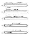
本実施例では、本願発明を実施して基板上にTFTを作製する工程について説明する。説明には図1を用いる。
【0021】
まず、石英基板101を用意した。基板としては耐熱性の高い材料を選択しなければならない。石英基板の代わりにシリコン基板、セラミックス基板、結晶化ガラス基板、金属基板等の耐熱性の高い材料を用いることもできる。
【0022】
ただし、石英基板を用いる場合は下地膜を設けても設けなくても良いが、他の材料を用いる時は下地膜として絶縁膜を設けることが好ましい。絶縁膜としては、酸化珪素膜(SiOx )、窒化珪素膜(Six Ny )、酸化窒化珪素膜(SiOx Ny )、窒化アルミニウム膜(AlxNy)のいずれか若しくはそれらの積層膜を用いると良い。
【0023】
また、耐熱性金属層と酸化珪素膜とを積層した下地膜を用いると放熱効果が大幅に高まるので有効である。放熱効果は上述の窒化アルミニウム膜と酸化珪素膜との積層構造でも十分な効果を示す。
【0024】
こうして石英基板101が準備できたら、90nm厚の半導体膜(本実施例ではアモルファスシリコン膜)102を形成し、その表面にニッケル含有層103を形成した。ニッケル含有層103の形成方法に関しては特開平7−130652号公報に記載された技術を参考にすると良い。(図1(A))
【0025】
なお、本実施例では特開平7−130652号公報に記載された技術を用いてニッケルを添加する例を示すが、ニッケル膜を成膜して熱拡散させる方法やイオン打ち込み法(イオンインプランテーション法(質量分離あり)、プラズマドーピング法(質量分離なし)又はレーザードーピング法など)を用いても良い。
【0026】
本実施例ではアモルファスシリコン膜102の成膜ガスとしてジシラン(Si2H6)を用い、450℃の減圧熱CVD法により成膜した。この時、膜中に混入するC(炭素)、N(窒素)及びO(酸素)といった不純物の濃度を徹底的に管理することが重要である。これらの不純物が多く存在すると結晶化の進行が妨げられるからである。
【0027】
本出願人は炭素及び窒素の濃度が5×10¹⁸atoms/cm3以下(好ましくは5×1017atoms/cm3以下)、酸素の濃度が1×1019atoms/cm3以下(好ましくは5×1018atoms/cm3以下)となる様に不純物濃度を管理した。また、金属元素は1×1017atoms/cm3以下となる様に管理した。成膜段階でこの様な濃度管理をしておけば、外部汚染さえ防げばTFT作製工程中に不純物濃度が増加する様なことはない。
【0028】
ニッケル含有層103はアモルファスシリコン膜102の全面(全部の領域)に対して重量換算で10ppmのニッケルを含む酢酸ニッケル塩溶液をスピンコート法により塗布し、450℃1時間程度の水素出しを行った。
【0029】
そしてその後、不活性雰囲気、水素雰囲気または酸素雰囲気において500〜700℃(代表的には550〜650℃)の温度で4〜24時間の加熱処理を加えてポリシリコン膜104を得た。このポリシリコン膜104にはニッケルが1×10¹⁸〜1×10¹⁹atoms/cm3の濃度で残存する。(図1(B))
【0030】
なお、厳密に言うとスピンコートした時点ではアモルファスシリコン膜中にニッケルは添加されていない。しかし、その後の水素だし工程でニッケルがアモルファスシリコン膜中へと容易に拡散するので実質的には添加工程と考えて良い。
【0031】
また、減圧熱CVD法で形成したアモルファスシリコン膜と同等の膜質が得られるのであればプラズマCVD法を用いても良い。また、完全にアモルファス状態の半導体である必要はなく、微結晶シリコン膜等を形成しても良い。
【0032】
また、シリコン膜の代わりにシリコン膜中にゲルマニウムを含有させたシリコンゲルマニウム(Six Ge1−x (0<X<1)で表される)等の半導体膜を用いても良い。その場合、シリコンゲルマニウム中に含まれるゲルマニウムは5atomic%以下にしておくことが望ましい。
【0033】
また、ニッケル以外にもコバルト(Co)、鉄(Fe)、パラジウム(Pd)、白金(Pt)、銅(Cu)、金(Au)といった格子侵入型の触媒元素またはゲルマニウム(Ge)、鉛(Pb)、錫(Sn)といった格子置換型(または溶融型)の触媒元素から選ばれた一種または複数種を用いることもできる。
【0034】
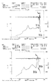
ここでアモルファスシリコン膜がポリシリコン膜へ変化する温度を示差熱分析法(正確には示差熱解析法)によって調べた結果を図9に示す。示差熱分析法(DTA法とも呼ばれる)とは、基準物質と試料とを同時に一定の速度で加熱しながら両者の間に生じる温度差を測定し、試料物質の熱的特性を解析する方法である。
【0035】
本出願人が示差熱分析法を用いてアモルファスシリコン膜(膜厚500nm)からポリシリコン膜への相変化を解析した結果、図9(A)の矢印で示す様に、686.7℃で相変化を起こすことが確かめられた。ただし、図9(A)の結果は触媒等を用いずに結晶化させた場合のデータである。
【0036】
一方、本実施例の様にアモルファスシリコン膜の結晶化を助長する触媒元素としてニッケルを用いた場合の相変化の様子を図9(B)に示す。この時、ニッケルの添加量は1〜2×10¹⁹atoms/cm3である。その場合、相変化(結晶化)する温度が下がり、605.0℃となっていたことが確かめられた。
【0037】
同様の実験を他の触媒元素を用いた場合についても確認したところ、全て600℃前後(550〜650℃)で相変化を起こし、結晶化することが確かめられた。本出願人が前述の様な温度範囲で結晶化工程を行う理由はこういうデータの裏付けがある。
【0038】
こうして図1(B)の状態が得られたら、酸化性雰囲気中で1000℃30分のファーネスアニール処理(電熱炉を用いた熱処理)を行った。この時、熱酸化処理によってポリシリコン膜104の膜厚を減じ(thinning処理)、ポリシリコン膜104よりも膜厚の薄いポリシリコン膜105を形成した。(図1(C))
【0039】
なお、図1(C)には図示していないが、ポリシリコン膜105上には熱酸化膜が形成される。この熱酸化膜は除去してしまっても良いし、次のレーザーアニール工程で保護膜として活用しても良い。
【0040】
この熱酸化工程では酸化反応が進行する際に生じる余剰シリコン原子によってポリシリコン膜中の欠陥等が修復され、非常に欠陥の少ないポリシリコン膜を得ることができた。また、ポリシリコン膜の膜厚を薄くすることで、当初90nm厚であった膜厚が60nm厚となった。
【0041】
さらに、ポリシリコン膜の表面層を削りながら酸化反応が進行するので、形成されたポリシリコン膜105は非常に平坦な表面を有する半導体膜となった。この事は、今後、TFTの活性層/ゲート絶縁膜界面の準位を低減する上で有効に働く。
【0042】
なお、このthinning工程は複数回行うとポリシリコン膜の平坦性がさらに向上する。その場合、熱酸化工程と熱酸化膜の除去工程とを交互に繰り返す。
【0043】
また、本実施例は初期膜として90nm厚のアモルファスシリコン膜を用いているため、thinning工程を採用しているが、初期膜を50nm厚以下としてそれ以上薄くする必要をなくせば、thinning工程を省略することも可能である。
【0044】
こうして図1(C)の状態が得られたら、次にエキシマレーザー光をポリシリコン膜105に対して照射した。本実施例ではXeCl(波長308nm)を励起ガスとしたパルス発振型のエキシマレーザー光によってレーザーアニール処理を行った。エキシマレーザーのビーム形状は線状ビームであっても良いが、処理の均一性を高めるに面状ビームを用いても良い。(図1(D))
【0045】
なお、KrF、KrCl、ArF等を励起ガスとしたエキシマレーザー光やその他の紫外光レーザーを用いても構わない。また、赤外光を用いる場合には赤外線ランプから発する強光をポリシリコン膜105に対して照射すれば良い。
【0046】
本実施例では発振周波数30Hz、ビーム形状が145×0.41mmの線状レーザー光を用いた。また、レーザー光は基板の一端から他端までを1.2mm/secで走査し、隣接する線状レーザー光のオーバーラップを92%とした。
【0047】
また、本実施例の場合、レーザーエネルギー密度は250〜5000mJ/cm2(好ましくは450〜1000mJ/cm2)の条件で行うことが好ましい。本実施例ではレーザーエネルギー密度を550mJ/cm2とした。ここで本明細書中におけるレーザーエネルギー密度の測定方法について説明する。
【0048】
まず、レーザー発振器から発振されたレーザー光の光強度(E0)をパワーメーターによって実測する。しかし、パワーメーターを通過した後のレーザー光はアッテネーターの透過率(a)に応じて減光し、さらに光学系の透過率(b)に応じて減光する。この様にして減光されたレーザー光の光強度をレーザー照射面積(A)で割ったものがレーザーエネルギー密度(E)である。これを式で表すと、E=(E0×a×b)/Aで表される。
【0049】
次に、このレーザーアニール工程を行って得たポリシリコン膜106に対して、1000℃2時間のファーネスアニール処理を行った。本実施例では処理雰囲気を水素雰囲気としたが、還元雰囲気であれば問題はない。また、窒素雰囲気の様な不活性雰囲気であっても結晶性を改善するという目的は果たされる。(図1(E))
【0050】
なお、このファーネスアニール工程を行う前に、ポリシリコン膜106の表面をフッ酸系エッチャントによって洗浄しておくことが望ましい。即ち、自然酸化膜を除去すると共に表面のシリコン原子を水素終端しておき、実際の処理の前に自然酸化膜が形成されるのを防ぐといった工夫が効果的である。
【0051】
ただし、特に注意が必要なのは雰囲気中に含まれる酸素又は酸素化合物(例えばOH基)の濃度を10ppm以下(好ましくは1ppm以下)にしておくことである。さもないと還元雰囲気で熱処理することによる平坦化効果が弱まってしまう。
【0052】
こうしてポリシリコン膜107を得た。ポリシリコン膜107は1000℃という高い温度における水素アニールによって非常に平坦な表面を有していた。また、高い温度でアニールされるので、結晶粒内には殆ど積層欠陥等が存在しなかった。
【0053】
また、本出願人が本実施例の工程で得たポリシリコン膜をラマン測定法で観察した結果、ラマンピーク値は517〜520cm-1(代表的には518〜519cm-1)であった。また、半値半幅は2.2〜3.0cm-1(代表的には2.4〜2.6cm-1)であった。
【0054】
518〜519cm-1というラマンピーク値は非常に高波数側にあり、本実施例で得られたポリシリコン膜が非常に単結晶に近い結晶を有していることが判る。また、2.4〜2.6cm-1という値も非常に小さく(リファレンスとして測定した単結晶シリコン膜は2.1cm-1であった。)、即ち結晶性が高いことを示している。
【0055】
なお、本明細書中においてラマンピーク値とは、波長514.5cm-1のArレーザーを1.0×10⁵〜1.3×10⁵W/cm2の光強度で結晶を含む半導体膜(本実施例ではポリシリコン膜)に照射した際に得られるラマンスペクトルに対して、ローレンツ分布によるフィッティングを行った際に得られるピーク値である。なお、実際の測定にはレニショー社の「ラマスコープ顕微ラマン装置システム2000」というラマン測定装置を使用した。
【0056】
また半値半幅とは、波長514.5cm-1のArレーザーを1.0×10⁵〜1.3×10⁵W/cm2の光強度で結晶を含む半導体膜に照射した際に得られるラマンスペクトルに対して、ローレンツ分布によるフィッティングを行った際に得られる半値幅の半分の値である。こちらも前述のラマン測定装置で測定を行った。
【0057】
以上の定義でなるラマンピーク値と半値半幅であるが、本実施例のポリシリコン膜107はラマンピーク値と半値半幅との比(ラマンピーク値/半値半幅)が170〜240(代表的には190〜220)であることが判明した。
【0058】
こうして著しく結晶性の高いポリシリコン膜107が得られたら、このポリシリコン膜107をパターニングして活性層108を形成した。なお、本実施例では活性層を形成する前に水素雰囲気中での熱処理を行っているが、活性層を形成した後に行うこともできる。その場合、パターン化されていることによってポリシリコン膜に発生する応力が緩和されるため好ましい。
【0059】
そして熱酸化工程を行って活性層108の表面に10nm厚の酸化シリコン膜109を形成した。この酸化シリコン膜109はゲート絶縁膜として機能する。また、活性層108はこの酸化により5nmの厚さだけ膜減りするため膜厚は45nmとなった。最終的に10〜50nm厚の活性層(特にチャネル形成領域)が残る様に、熱酸化による膜減りを考慮して初期半導体膜(最も初めに成膜された半導体膜)の膜厚を決定しておくことが必要である。
【0060】
ゲート絶縁膜109を形成したら、その上に導電性を有するポリシリコン膜を形成し、パターニングによりゲート配線110を形成した。(図2(A))
【0061】
なお、本実施例ではゲート配線としてN型導電性を持たせたポリシリコンを利用するが、材料はこれに限定されるものではない。特に、ゲート配線の抵抗を下げるにはタンタル、タンタル合金又はタンタルと窒化タンタルとの積層膜を用いることも有効である。さらに低抵抗なゲート配線を狙うならば銅や銅合金を用いても有効である。
【0062】
図2(A)の状態が得られたら、N型導電性又はP型導電性を付与する不純物を添加して不純物領域111を形成した。この時の不純物濃度は後のLDD領域の不純物濃度を鑑みて決定した。本実施例では1×10¹⁸atoms/cm3の濃度で砒素を添加したが、不純物も濃度も本実施例に限定される必要はない。
【0063】
次に、ゲート配線110の表面に5〜10nm程度の薄い酸化シリコン膜112を形成した。これは熱酸化法やプラズマ酸化法を用いて形成すれば良い。この酸化シリコン膜112は、次のサイドウォール形成工程でエッチングストッパーとして機能する。
【0064】
エッチングストッパーとなる酸化シリコン膜112を形成したら、窒化シリコン膜を形成してエッチバックを行い、サイドウォール113を形成した。こうして図2(B)の状態を得た。
【0065】
なお、本実施例ではサイドウォールとして窒化シリコン膜を用いたが、ポリシリコン膜やアモルファスシリコン膜を用いることもできる。勿論、ゲート配線の材料が変われば、それに応じてサイドウォールとして用いることのできる材料も変わることは言うまでもない。
【0066】
次に、再び先程と同一導電型の不純物を添加した。この時に添加する不純物濃度は先程の工程よりも高い濃度とした。本実施例では不純物として砒素を用い、濃度は1×10²¹atoms/cm3とするがこれに限定する必要はない。この不純物の添加工程によりソース領域114、ドレイン領域115、LDD領域116及びチャネル形成領域117が画定した。(図2(C))
【0067】
こうして各不純物領域が形成されたらファーネスアニール、レーザーアニール又はランプアニール等の熱処理により不純物の活性化を行った。
【0068】
次に、ゲート配線110、ソース領域114及びドレイン領域115の表面に形成された酸化シリコン膜を除去し、それらの表面を露呈させた。そして、5nm程度のコバルト膜(図示せず)を形成して熱処理工程を行った。この熱処理によりコバルトとシリコンとの反応が起こり、シリサイド層(コバルトシリサイド層)118が形成された。(図2(D))
【0069】
この技術は公知のサリサイド技術である。従って、コバルトの代わりにチタンやタングステンを用いても構わないし、アニール条件等は公知技術を参考にすれば良い。本実施例では赤外光を照射してランプアニール処理工程を行った。
【0070】
こうしてシリサイド層118を形成したら、コバルト膜を除去した。その後、1μm厚の層間絶縁膜119を形成した。層間絶縁膜119としては、酸化シリコン膜、窒化シリコン膜、酸化窒化シリコン膜又は樹脂膜(ポリイミド、アクリル、ポリアミド、ポリイミドアミド、ベンゾシクロブテン(BCB)等)を用いれば良い。また、これらの絶縁膜を自由な組み合わせで積層しても良い。
【0071】
次に、層間絶縁膜119にコンタクトホールを形成してアルミニウムを主成分とする材料でなるソース配線120及びドレイン配線121を形成した。最後に素子全体に対して水素雰囲気中で300℃2時間のファーネスアニールを行い、水素化を完了した。
【0072】
こうして、図2(D)に示す様なTFTが得られた。なお、本実施例で説明した構造は一例であって本願発明を適用しうるTFT構造はこれに限定されない。従って、公知のあらゆる構造のTFTに対して適用可能である。また、ポリシリコン膜107を形成した以降の工程における数値条件も本実施例に限定される必要はない。さらには、公知のチャネルドープ工程(しきい値電圧を制御するための不純物添加工程)を本実施例のどこかに導入してもなんら問題はない。
【0073】
また、本実施例では初期膜であるアモルファスシリコン膜を成膜する段階で徹底的にC、N、Oといった不純物の濃度を管理しているため、完成したTFTの活性層中に含まれる各不純物濃度は、炭素及び窒素の濃度が5×10¹⁸atoms/cm3以下(好ましくは5×1018atoms/cm3以下)、酸素の濃度が5×1018atoms/cm3以下(好ましくは5×1018atoms/cm3以下)のままであった。また、ニッケルを除く金属元素は1×1017atoms/cm3以下であった。
【0074】
また、本願発明はトップゲート構造に限らず、逆スタガ型TFTに代表されるボトムゲート構造に対しても容易に適用することが可能であることは言うまでもない。
【0075】
また、本実施例ではNチャネル型TFTを例にとって説明したが、公知技術と組み合わせればPチャネル型TFTを作製することも容易である。さらに公知技術を組み合わせれば同一基板上にNチャネル型TFTとPチャネル型TFTとを形成して相補的に組み合わせ、CMOS回路を形成することも可能である。
【0076】
さらに、図2(D)の構造においてドレイン配線121と電気的に接続する画素電極(図示せず)を公知の手段で形成すればアクティブマトリクス型表示装置の画素スイッチング素子を形成することも容易である。即ち、本願発明は液晶表示装置やEL(エレクトロルミネッセンス)表示装置などのアクティブマトリクス型の電気光学装置を作製する際にも実施することが可能である。
【0077】
(実施例2)
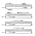
本実施例では基板上に最初に成膜する初期膜をポリシリコン膜とする場合の例について図3を用いて説明する。
【0078】
まず、金属基板(本実施例ではタンタル基板)301上に酸化シリコン膜でなる下地膜302、75nm厚のポリシリコン膜303、保護膜304を大気開放しないで連続的に積層形成する。なお、本実施例では真空ロードロックと共通室を持ったマルチチャンバー方式の減圧熱CVD装置で成膜を行う。(図3(A))
【0079】
次に、1050℃30分の熱酸化工程を行う。本実施例では応力を緩和しつつ熱処理を行うために、水蒸気を含んだウェット酸化法を用いた。この工程を経たポリシリコン膜305の膜厚は酸化されることによって膜厚が減って50nm厚となる。また、保護膜306は形成された熱酸化膜の分だけ膜厚が増す。(図3(B))
【0080】
勿論、この熱酸化工程はポリシリコン膜をさらに薄膜化するためのthinning工程として行われている。また、このthinning工程は複数回行うとポリシリコン膜の平坦性がさらに向上する。その場合、熱酸化工程と熱酸化膜の除去工程とを交互に繰り返せば良い。
【0081】
次に、保護膜306を残したままKrFエキシマレーザー光によりレーザーアニール工程を行う。本実施例のレーザー照射条件は発振周波数30Hz、ビーム形状が145×0.41mmの線状レーザー光を用いた。また、レーザー光は基板の一端から他端までを1.2mm/secで走査し、隣接する線状レーザー光のオーバーラップを92%とした。
【0082】
また、本実施例の場合、レーザーエネルギー密度は450〜5000mJ/cm2(好ましくは500〜1000mJ/cm2)の条件で行う。本実施例では600mJ/cm2とする。なお、レーザーエネルギー密度の測定方法は実施例1と同様である。こうしてポリシリコン膜307が形成される。(図3(C))
【0083】
こうしてレーザーアニール工程が済んだら、窒素雰囲気中で1100℃2時間のファーネスアニール処理を行い、ポリシリコン膜307の結晶性を改善する。この工程によりポリシリコン膜308が得られる。こうして得られたポリシリコン膜308は膜面全体において特定の配向性を示し、実質的に単結晶と見なせる半導体膜となる。
【0084】
以上の様にして形成されたポリシリコン膜308は図3(A)〜図3(D)に至るまでの全ての工程で外気に触れずに処理されるため、極めて清浄な界面を有している。これは本実施例において、▲1▼図3(A)の工程を大気開放しない連続成膜で行う、▲2▼保護膜を介して一切の処理を行う、という二つの構成の効果である。
【0085】
また、ラマンピーク値や半値半幅も実施例1で説明した範囲に収まるものとなる。
【0086】
なお、本実施例では初期膜(最も初めに成膜する半導体膜)としてポリシリコン膜を用いているが、微結晶シリコン膜やアモルファスシリコン膜とし、保護膜を介してレーザー結晶化させることも可能である。勿論、シリコン以外の半導体材料を用いても良い。
【0087】
こうしてポリシリコン膜308が得られたら、あとは実施例1と同様の手順でTFTを作製すれば良い。勿論、実施例1だけでなく、公知の手段でTFTを作
【0088】
(実施例3)
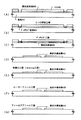
本実施例では、初期膜であるアモルファスシリコン膜の結晶化を特開平8−78329号公報に記載された技術で行った場合の例について図4を用いて説明する。
【0089】
まず、表面に絶縁膜を設けた石英基板401を用意し、その上にアモルファスシリコン膜(図示せず)及び酸化シリコン膜(図示せず)を大気開放しないで連続的に積層形成する。次に、酸化シリコン膜をパターニングして開口部を有するマスク402を形成する。
【0090】
次に、重量換算で100ppmのニッケルを含んだ溶液をスピンコート法により塗布し、前述の開口部の底部でアモルファスシリコン膜とニッケルとが接した状態を得る。その後、570℃14時間のファーネスアニール工程を行い、横成長領域403を得る。
【0091】
なお、横成長領域403は棒状結晶が基板とほぼ平行な方向に結晶成長しているため、ランダムに核発生したポリシリコン膜に較べて欠陥やトラップ準位の少
【0092】
また、図4(A)の状態ではアモルファス成分のまま残る領域と、横成長領域(結晶成分を有する領域)とが混在した半導体膜が得られる。本明細書中ではこの様な膜も半導体膜(又は結晶を含む半導体膜)と呼ぶ。
【0093】
こうして図4(A)の状態が得られたら、マスク402をそのままマスクとしてプラズマドーピング法又はイオン注入法によりリンを添加する。リンの添加量は、シリコン膜中の濃度がSIMSで1×10¹⁹〜1×10²¹atoms/cm3となる様に調節する。
【0094】
こうして高濃度にリンが添加された領域を本明細書中ではゲッタリング領域404と呼ぶ。(図4(B))
【0095】
ゲッタリング領域404を形成したら、600℃12時間のファーネスアニール工程を行い、横成長領域403中に存在するニッケルをゲッタリング領域404へとゲッタリングさせる。こうして、膜中のニッケル濃度が1×10¹⁷atoms/cm3以下にmで低減された横成長領域405を得る。(図4(C))
【0096】
次に、パターニングを行い、横成長領域405のみで形成された島状半導体膜406を得る。この時、ゲッタリング領域はリンやニッケルを高濃度に含んでいるので、完全に除去することが望ましい。
【0097】
こうして図4(D)の状態を得る。次に、酸素雰囲気中で1000℃30分のファーネスアニール処理を行い、熱酸化工程(thinning工程)を行う。この時形成される熱酸化膜(図示せず)はここで除去しても良いし、次のレーザーアニール処理を行う時まで残しておいても良い。(図4(E))
【0098】
こうしてthinning工程によって膜厚を減らされた島状半導体膜407を得たら、次に、XeClエキシマレーザー光を用いてレーザーアニール処理を行う。本実施例のレーザー照射条件は実施例1と同様とする。(図4(F))
【0099】
こうしてレーザーアニール工程を経た島状半導体膜408を得たら、さらに、水素と窒素を混合した雰囲気中で1100℃2時間のファーネスアニール処理を行う。こうして島状半導体膜409を得る。(図4(G))
【0100】
以上の様にして形成された島状半導体膜409は実施例1及び実施例2で説明したポリシリコン膜と同等の結晶性を有している。即ち、膜面全体が特定の配向性を示し、実質的に単結晶と見なせる半導体膜となっている。
【0101】
また、ラマン測定によって得られるラマンピーク値や半値半幅も実施例1で説明したものと同様のものとなる。
【0102】
(実施例4)
実施例1又は実施例3では初期膜の結晶化に際して結晶化を助長する触媒元素(具体的にはニッケル)を用いているが、自然核発生により結晶化させたポリシリコン膜(これも結晶を含む半導体膜である)に対して本願発明の工程を施しても十分な効果が得られる。
【0103】
その場合、下地膜、アモルファスシリコン膜、保護膜を大気開放しないで連続的に積層形成し、600℃24時間のファーネスアニール処理によってアモルファスシリコン膜をポリシリコン膜に結晶化させることで、界面の清浄なポリシリコン膜を得ることもできる。
【0104】
ただし、本実施例の様に自然核発生で半導体膜の結晶化を行う場合には80〜120nm(典型的には90〜100nm)の膜厚を有することが望ましい。即ち、初期膜が最初から薄いと結晶化の効率が低下することが経験的に知られている。
【0105】
その様な場合、結晶化終了後に酸化工程を入れて結晶を含む半導体膜のthinning(膜厚を減じること)を行うことは重要である。そうすることで結晶化は効率良く行われ、その後で所望の膜厚のポリシリコン膜を得ることができる。
【0106】
なお、本実施例の構成は実施例1又は実施例3のどちらの構成とも組み合わせることができる。
【0107】
(実施例5)
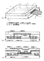
本実施例では、本願発明によって作製された反射型液晶表示装置の例を図5に示す。画素TFT(画素スイッチング素子)の作製方法やセル組工程は公知の手段を用いれば良いので詳細な説明は省略する。
【0108】
図5(A)において11は絶縁表面を有する基板(酸化珪素膜を設けたセラミックス基板)、12は画素マトリクス回路、13はソースドライバー回路、14はゲイトドライバー回路、15は対向基板、16はFPC(フレキシブルプリントサーキット)、17は信号処理回路である。信号処理回路17としては、D/Aコンバータ、γ補正回路、信号分割回路などの従来ICで代用していた様な処理を行う回路を形成することができる。勿論、基板上にICチップを設けて、ICチップ上で信号処理を行うことも可能である。
【0109】
さらに、本実施例では液晶表示装置を例に挙げて説明しているが、アクティブマトリクス型の表示装置であればEL(エレクトロルミネッセンス)表示装置やEC(エレクトロクロミックス)表示装置に本願発明を適用することも可能であることは言うまでもない。
【0110】
ここで図5(A)のドライバー回路13、14を構成する回路の一例を図5(B)に示す。なお、TFT部分については既に実施例1で説明しているので、ここでは必要箇所のみの説明を行う。
【0111】
図5(B)において、501、502はNチャネル型TFT、503はPチャネル型TFTであり、501と503のTFTでCMOS回路を構成している。504は窒化珪素膜/酸化珪素膜/樹脂膜の積層膜でなる絶縁層、その上にはチタン配線505が設けられ、前述のCMOS回路とTFT502とが電気的に接続されている。チタン配線はさらに樹脂膜でなる絶縁層506で覆われている。二つの絶縁層504、506は平坦化膜としての機能も有している。
【0112】
また、図5(A)の画素マトリクス回路12を構成する回路の一部を図5(C)に示す。図5(C)において、507はダブルゲート構造のNチャネル型TFTでなる画素TFTであり、画素領域内に大きく広がる様にしてドレイン配線508が形成されている。なお、ダブルゲート構造以外にシングルゲート構造やトリプルゲート構造などを採用しても構わない。
【0113】
その上には絶縁層504が設けられ、その上にチタン配線405が設けられている。この時、絶縁層504の一部には凹部が落とし込み部が形成され、最下層の窒化シリコン及び酸化シリコンのみが残される。これによりドレイン配線508とチタン配線505との間で補助容量が形成される。
【0114】
また、画素マトリクス回路内に設けられたチタン配線505はソース・ドレイン配線と後の画素電極との間において電界遮蔽効果をもたらす。さらに、複数設けられた画素電極間の隙間ではブラックマスクとしても機能する。
【0115】
そして、チタン配線505を覆って絶縁層506が設けられ、その上に反射性導電膜でなる画素電極509が形成される。勿論、画素電極509の表面に反射率を上げるための工夫をなしても構わない。
【0116】
また、実際には画素電極509の上に配向膜や液晶層が設けられるが、ここでの説明は省略する。
【0117】
本願発明を用いて以上の様な構成でなる反射型液晶表示装置を作製することができる。勿論、公知の技術と組み合わせれば容易に透過型液晶表示装置を作製することもできる。
【0118】
また、図面では区別していないが画素マトリクス回路を構成する画素TFTと、ドライバー回路や信号処理回路を構成するCMOS回路とでゲート絶縁膜の膜厚を異ならせることも可能である。
【0119】
画素マトリクス回路ではTFTに印加される駆動電圧が高い(10V以上)ので50〜200nm(好ましくは100〜150nm)の膜厚のゲート絶縁膜が必要である。一方、ドライバー回路や信号処理回路ではTFTに印加される駆動電圧は低く(1〜5V)、逆に高速動作が求められるのでゲート絶縁膜の膜厚を3〜30nm(好ましくは5〜10nm)と画素TFTよりも薄くすることが有効である。
【0120】
(実施例6)
本願発明は従来のIC技術全般に適用することが可能である。即ち、現在市場に流通している全ての半導体回路に適用できる。例えば、ワンチップ上に集積化されたRISCプロセッサ、ASICプロセッサ等のマイクロプロセッサに適用しても良いし、液晶用ドライバー回路(D/Aコンバータ、γ補正回路、信号分割回路等)に代表される信号処理回路や携帯機器(携帯電話、PHS、モバイルコンピュータ)用の高周波回路に適用しても良い。
【0121】
図6に示すのは、マイクロプロセッサの一例である。マイクロプロセッサは典型的にはCPUコア21、RAM22、クロックコントローラ23、キャッシュメモリ24、キャッシュコントローラ25、シリアルインターフェース26、I/Oポート27等から構成される。
【0122】
勿論、図6に示すマイクロプロセッサは簡略化した一例であり、実際のマイクロプロセッサはその用途によって多種多様な回路設計が行われる。
【0123】
しかし、どの様な機能を有するマイクロプロセッサであっても中枢として機能するのはIC(Integrated Circuit)28である。IC28は半導体チップ29上に形成された集積化回路をセラミック等で保護した機能回路である。
【0124】
そして、その半導体チップ29上に形成された集積化回路を構成するのが本願発明の構造を有するNチャネル型TFT30、Pチャネル型TFT31である。なお、基本的な回路はCMOS回路を最小単位として構成することで消費電力を抑えることができる。
【0125】
また、本実施例に示したマイクロプロセッサは様々な電子機器に搭載されて中枢回路として機能する。代表的な電子機器としてはパーソナルコンピュータ、携帯型情報端末機器、その他あらゆる家電製品が挙げられる。また、車両(自動車や電車等)の制御用コンピュータなども挙げられる。
【0126】
(実施例7)
本願発明の電気光学装置は、様々な電子機器のディスプレイとして利用される。その様な電子機器としては、ビデオカメラ、デジタルカメラ、フロント型プロジェクター、リア型プロジェクター(プロジェクションTV)、ゴーグルディスプレイ、カーナビゲーション、パーソナルコンピュータ、携帯情報端末(モバイルコンピュータ、携帯電話、電子書籍等)などが挙げられる。それらの一例を図7に示す。
【0127】
図7(A)は携帯電話であり、本体2001、音声出力部2002、音声入力部2003、表示装置2004、操作スイッチ2005、アンテナ2006で構成される。本願発明を音声出力部2002、音声入力部2003、表示装置2004やその他の信号制御回路に適用することができる。
【0128】
図7(B)はビデオカメラであり、本体2101、表示装置2102、音声入力部2103、操作スイッチ2104、バッテリー2105、受像部2106で構成される。本願発明を表示装置2102、音声入力部2103やその他の信号制御回路に適用することができる。
【0129】
図7(C)はモバイルコンピュータ(モービルコンピュータ)であり、本体2201、カメラ部2202、受像部2203、操作スイッチ2204、表示装置2205で構成される。本願発明は表示装置2205やその他の信号制御回路に適用できる。
【0130】
図7(D)はゴーグル型ディスプレイであり、本体2301、表示装置2302、アーム部2303で構成される。本発明は表示装置2302やその他の信号制御回路に適用することができる。
【0131】
図7(E)はリア型プロジェクターであり、本体2401、光源2402、表示装置2403、偏光ビームスプリッタ2404、リフレクター2405、2406、スクリーン2407で構成される。本発明は表示装置2403やその他の信号制御回路に適用することができる。
【0132】
図7(F)は携帯書籍(電子書籍)であり、本体2501、表示装置2502、2503、記憶媒体2504、操作スイッチ2505、アンテナ2506で構成される。本発明は表示装置2502、2503やその他の信号制御回路に適用することができる。
【0133】
以上の様に、本願発明の適用範囲は極めて広く、あらゆる分野の電子機器に適用することが可能である。
【0134】
(実施例8)
実施例1乃至実施例4に示した工程で得られる結晶を含む半導体膜は膜面全体において特定の配向性を示す。即ち、個々の結晶粒が集合して形成された多結晶半導体膜の如き形態であったとしても、全体の80%以上(典型的には90%以上)の結晶粒が同一の結晶面(配向面)を示すという特徴を有する。このように全体の80%以上を占める結晶面を主たる配向面と呼ぶ。
【0135】
本願発明のプロセスで形成される半導体膜(結晶を含む半導体膜)のとりうる主たる結晶面は、{110}面、{100}面、{111}面、{311}面、{511}面、又は{110}面と{100}面とが混在した結晶面のいずれかである。実際にいずれの結晶面が主たる配向面であるかは、現在のところ判明していない。
【0136】
即ち、本願発明のプロセスで形成される半導体膜(結晶を含む半導体膜)は、上記6種類のいずれかの結晶面が、膜面に存在しうる結晶面全体の80%以上(典型的には90%以上)を占める。
【0137】
単結晶シリコンを例として良く知られている様に、結晶面によって界面物性は異なる。界面準位密度(Qss)が最も小さくなる面方位は{100}面であり、次いで{511}面、{311}面、{111}面、{110}面と{100}面との混在した結晶面、{110}面の順に大きくなる。なお、{511}面は{100}面に匹敵する界面準位密度を持つことが知られている。
【0138】
従って、本願発明のプロセスで形成される半導体膜の主たる配向面が{100}面であれば、活性層とゲート絶縁膜との界面は非常に界面準位密度が小さくなる。その場合、従来のICに匹敵する性能を有する半導体装置が実現しうる。後述するが、実際に本願発明を用いて試作したTFTは従来のICに匹敵する電気特性を示す回路を形成可能としている。
【0139】
また、本願発明のプロセスにおいてレーザーアニール処理の後に行う還元雰囲気又は不活性雰囲気でのファーネスアニール処理は、活性層とゲート絶縁膜との界面を平坦なものとするに非常に有効である。特に、還元雰囲気で行う場合には半導体膜表面における半導体原子の増速表面拡散によって極めて平坦な面が得られる。
【0140】
本出願人がAFM(分子間力顕微鏡)を用いて表面凹凸を測定した結果、1μm2の範囲内で凹凸のP−V値(凸部の頂上部と凹部の底部との高さの差)が10nm以下(典型的には5nm以下)であり、10μm2の範囲内で凹凸のP−V値が20nm以下(典型的には10nm以下)であった。
【0141】
(実施例9)
本願発明を実施して作製されたTFTの代表的な電気特性は以下の様なものであった。
(1)スイッチング性能(オン/オフ動作切り換えの俊敏性)の指標となるサブスレッショルド係数が、ドレイン電圧が1Vの時にNチャネル型TFTおよびPチャネル型TFTともに60〜150mV/decade(代表的には80〜100mV/decade)と小さい。
(2)TFTの動作速度の指標となる電界効果移動度(μFE)が、ドレイン電圧が1Vの時にNチャネル型TFTで 200〜500cm2/Vs (代表的には 300〜400cm2/Vs )、Pチャネル型TFTで100〜300cm2/Vs (代表的には 150〜200cm2/Vs )と大きい。
(3)TFTの駆動電圧の指標となるしきい値電圧(Vth)が、ドレイン電圧が14Vの時にNチャネル型TFTで-1.0〜2.5V(代表的には-0.5〜1.5V)、Pチャネル型TFTで-2.5〜1.0V(代表的には-1.5〜0.5V)と小さい。
【0142】
また、本願発明のTFTを500個測定したデータを元に正規確率グラフを作成し、そのグラフを使って特性ばらつきを推定した。その結果、100個中の90個(典型的には95個)が上記電気特性の範囲内に収まることが判った。
【0143】
以上の様に、極めて優れたスイッチング特性および高速動作特性が実現可能であることが確認されている。
【0144】
(実施例10)
本実施例では液晶ドライバー回路であるシフトレジスタを作製して動作周波数を確認した。その結果、電源電圧5V、段数50段のシフトレジスタ回路において動作周波数80〜200MHz(典型的には100〜150MHz)の出力パルスが得られた。
【0145】
(実施例11)
実施例1ではアモルファスシリコン膜の結晶化に際して、結晶化を助長する触媒元素としてニッケルを用いる例を示したが、本実施例では触媒元素としてゲルマニウムを用いる例を図8に示す。
【0146】
まず、実施例1の工程に従って石英基板801上に80nm厚のアモルファスシリコン膜802を形成する。そして、アモルファスシリコン膜802に対してゲルマニウムを添加する。(図8(A))
【0147】
ゲルマニウムの添加にはイオンインプランテーション法、プラズマドーピング法又はレーザードーピング法を用いることが好ましい。
【0148】
また、ゲルマニウム膜を成膜した後で熱拡散させる方法を採用しても良いし、実施例1の様にゲルマニウム塩溶液をスピンコートしてゲルマニウムをアモルファスシリコン上に吸着させた後で熱拡散させる方法を採用しても良い。また、アモルファスシリコン膜の成膜時に予め添加してしまう方法でも良い。
【0149】
本実施例では励起ガスとしてゲルマン(GeH4)を用い、加速電圧30keV、RF電力5W、ドーズ量1×10¹⁴atoms/cm2でイオンインプランテーション法を用いてゲルマニウムを添加する。勿論、この条件に限定する必要はなく、アモルファスシリコン膜802中へは1×1014〜5×1019atoms/cm3(代表的には1×1016〜5×1018atoms/cm3)の濃度でゲルマニウムが添加される様に調節すれば良い。
【0150】
なお、アモルファスシリコン膜中に添加するゲルマニウムは1×10¹⁴atoms/cm3以上(代表的には1×1016atoms/cm3以上)でないと触媒として結晶化の助長効果を活用することができない。また、添加が5×1019atoms/cm3を超えるとアモルファスシリコン膜の融点が下がりすぎ、900℃程度の温度でも溶融してしまう恐れがあり好ましくない。従って、添加量の上限は安全を見て1×1018atoms/cm3程度としておくことが望ましい。
【0151】
次に、550℃1時間の熱処理(ファーネスアニール)を行って、アモルファスシリコン膜802をポリシリコン膜803に変化させる。勿論、この条件に限定する必要はなく、実施例1に示した様な温度範囲の熱処理を行えば良い。(図8(B))
【0152】
また、本実施例の場合、処理雰囲気は不活性雰囲気または還元雰囲気とすることが望ましい。この理由は後述する。
【0153】
こうしてアモルファスシリコン膜の結晶化工程を終えたら、実施例1に従ってポリシリコン膜803のthinning工程(熱酸化工程)を行う。実際には熱酸化膜が形成されるが、ここでは図示していない。こうしてthinning工程を経たポリシリコン膜804が得られる。(図8(C))
【0154】
この時、触媒元素としてゲルマニウムを用いた場合に注目すべき特徴がある。ゲルマニウムは700℃以上の熱処理により酸化ゲルマニウムとなって昇華する。即ち、ポリシリコン膜803のthinning工程を行う際に必然的にゲルマニウムは昇華してしまい、ポリシリコン膜803中から離脱する。
【0155】
即ち、前述の様に結晶化工程を不活性雰囲気または還元雰囲気とすることが望ましいとした理由は、極力酸化ゲルマニウムを形成しない方がゲルマニウムの触媒作用を最も効率良く用いることができるからに他ならない。
【0156】
なお、実施例1でも述べた様に触媒元素を用いた場合、アモルファスシリコン膜が結晶化する温度は600℃前後であることが確かめられている。実際には処理温度によって多少変動するので、550〜650℃が結晶化に要する温度と考えて良い。即ち、結晶化時の温度を650℃までしか上げなければ結晶化時にゲルマニウムが昇華してしまうということは殆ど起こり得ない。
【0157】
この様に、実施例3では結晶化を助長する触媒元素としてニッケルを用いているため、リンを用いてゲッタリングする例を示しているが、本実施例の場合には熱処理のみで触媒元素のゲッタリング工程に相当する効果が得られる。
【0158】
この熱処理はファーネスアニール、レーザーアニール又はランプアニールのいずれかの手段を用いれば良い。また、結晶化工程の後で熱処理温度を変えるだけで、大気開放しないままに連続的にゲルマニウムを昇華させることも可能である。
【0159】
また、熱処理雰囲気にハロゲン元素を加えても良い。ハロゲン元素はゲルマニウムと結合して揮発性のハロゲン化ゲルマニウムを形成するため、ゲッタリング効果を助長することができる。
【0160】
以上の様にして、thinning工程を行うと同時に、アモルファスシリコン膜の結晶化時に用いた触媒元素(ゲルマニウム)を工程数を増やすことなくポリシリコン膜中から除去することができる。
【0161】
この後は、実施例1と同様の工程に従って図2(D)に示される様なTFTを形成すれば良い。勿論、実施例2、実施例3の構成と組み合わせることも可能であるし、実施例5〜実施例7に示した半導体装置を作製するにあたって、本実施例を用いても良い。
【0162】
また、本実施例ではアモルファスシリコン膜の結晶化を助長する触媒元素としてゲルマニウムのみを用いる例を示したが、その他の触媒元素(ニッケル、コバルト、鉄、パラジウム、白金、銅、金、鉛、錫など)とゲルマニウムとを同時に用いても構わない。その場合には本実施例に実施例3に示した様なゲッタリング手段を組み合わせる必要がありうる。
【0163】
(実施例12)
実施例11ではアモルファスシリコン膜中へゲルマニウムを添加する手段としてイオンインプランテーション法等を用いる場合について説明したが、本実施例ではゲルマニウム膜を成膜した後に熱拡散によって添加する例を示す。
【0164】
本実施例の場合、アモルファスシリコン膜を成膜したら、その上に1〜50nm(代表的には10〜20nm)のゲルマニウム膜を形成する。成膜方法はプラズマCVD法、減圧熱CVD法、スパッタ法などの気相法を用いることができる。
【0165】
なお、ゲルマニウム膜は直接アモルファスシリコン膜に触れる様に形成しても良いし、絶縁膜を介して設けられていても良い。絶縁膜を形成する場合、絶縁膜が厚すぎるとゲルマニウムのシリコン膜中への熱拡散を阻害することになるので、10〜30nmとしておくことが好ましい。
【0166】
ゲルマニウム膜を設けた状態で結晶化工程を行うと、加熱されることによってゲルマニウムがアモルファスシリコン膜中へ熱拡散し、結晶化を助長する触媒元素として働く。
【0167】
結晶化工程後のゲルマニウム膜は酸化させて除去しても良いし、硫酸過水溶液(H2SO4:H2O2=1:1)で除去しても良い。その後で、700℃以上の熱処理を行えば、形成されたポリシリコン膜中のゲルマニウムを除去又は低減される。
【0168】
本実施例の構成は、実施例1〜11までのどの実施例との組み合わせも可能であり、どの実施例にも適用できる。
【0169】
(実施例13)
本実施例ではアモルファスシリコン膜中へゲルマニウムを添加する手段として溶液塗布によるスピンコート法と熱拡散法を用いる場合について説明する。
【0170】
本実施例の場合、アモルファスシリコン膜を成膜したら、その上にゲルマニウムを含む溶液を塗布する。その様な溶液としては酸化ゲルマニウム(GeOx、代表的にはGeO2)、塩化ゲルマニウム(GeCl4)、臭化ゲルマニウム(GeBr4)、硫化ゲルマニウム(GeS2)、酢酸ゲルマニウム(Ge(CH3CO2))などのゲルマニウム塩水溶液がある。
【0171】
また、溶媒としてエタノール、イソプロピルアルコール等のアルコール系溶媒を用いても良い。
【0172】
本実施例では10〜100ppmの酸化ゲルマニウム水溶液を作製してアモルファスシリコン膜上(絶縁膜を介しても良い)に塗布し、スピンコートすることでゲルマニウム含有層を形成する。
【0173】
なお、アモルファスシリコン膜は疎水性を示すため、スピンコートの前にシリコン膜表面に絶縁膜を形成しておいて、濡れ性を高めておくことは有効である。この場合、絶縁膜が厚すぎるとゲルマニウムのシリコン膜中への熱拡散を阻害することになるので、10〜30nmとしておくことが好ましい。
【0174】
こうしてゲルマニウム含有層を設けた状態で結晶化工程を行うと、加熱されることによってゲルマニウムがアモルファスシリコン膜中へ熱拡散し、結晶化を助長する触媒元素として働く。
【0175】
本実施例の構成は、実施例1〜11までのどの実施例との組み合わせも可能であり、どの実施例にも適用できる。
【0176】
【発明の効果】
本願発明を実施することで、実質的に単結晶と見なせる結晶性を有する半導体膜を得ることができる。そして、その様な半導体膜を活性層とするTFTで回路を組み、高性能な半導体装置を実現することが可能となる。
【図面の簡単な説明】
【図1】 薄膜トランジスタの作製工程を示す図。
【図2】 薄膜トランジスタの作製工程を示す図。
【図3】 薄膜トランジスタの作製工程を示す図。
【図4】 薄膜トランジスタの作製工程を示す図。
【図5】 電気光学装置の構成を示す図。
【図6】 半導体回路の構成を示す図。
【図7】 電子機器の構成を示す図。
【図8】 薄膜トランジスタの作製工程を示す図。
【図9】 示差熱分析の結果を示す図。[0001]
[Technical field to which the invention belongs]
The present invention relates to a semiconductor device including a thin film transistor (hereinafter referred to as TFT) using a semiconductor thin film as a circuit and a technique for manufacturing the semiconductor device. Note that in this specification, a semiconductor device refers to all devices that function using a semiconductor.
[0002]
Therefore, the term “semiconductor device” used in the claims includes not only a single semiconductor element such as a TFT, but also an electro-optical device having a TFT, a semiconductor circuit, and an electronic device on which these are mounted.
[0003]
[Prior art]
In recent years, TFTs used in electro-optical devices such as active matrix liquid crystal display devices have been actively developed. An active matrix liquid crystal display device is a monolithic display device in which a pixel matrix circuit and a driver circuit are provided on the same substrate.
[0004]
Recently, an attempt has been made to form a semiconductor circuit having a function equivalent to that of a conventional IC using TFTs provided on a substrate. For example, development of a system-on-panel that incorporates logic circuits such as a γ correction circuit, a memory circuit, and a clock generation circuit has been studied.
[0005]
Since such a driver circuit or logic circuit needs to operate at high speed, it is inappropriate to use an amorphous semiconductor film (typically an amorphous silicon film) as an active layer. Therefore, at present, crystalline semiconductor films (typically polysilicon films) are being studied.
[0006]
[Problems to be solved by the invention]
However, when circuit performance equal to that of conventional ICs is required for circuits assembled with TFTs, crystalline semiconductor films formed by conventional techniques are sufficient to satisfy circuit specifications. It has become difficult to produce a TFT having performance.
[0007]
Accordingly, an object of the present invention is to realize a high-performance semiconductor device by fabricating a TFT having better electrical characteristics than a TFT using a conventional polysilicon film and assembling a circuit with the TFT.
[0008]
[Means for Solving the Problems]
The gist of the invention disclosed in this specification is as follows:
A first step of forming a semiconductor film containing crystals;
A second step of oxidizing the semiconductor film containing the crystal to reduce the film thickness;
250 to 5000 mJ / cm for the semiconductor film containing crystals after the second step 2 A third step of performing a laser annealing treatment with an energy density of
A fourth step of performing a furnace annealing process on the semiconductor film including the crystal after the third step;
It is characterized by including.
[0009]
The gist of other inventions is as follows:
A first step of forming a semiconductor film containing crystals;
A second step of oxidizing the semiconductor film containing the crystal to reduce the film thickness;
250 to 5000 mJ / cm for the semiconductor film containing crystals after the second step 2 A third step of performing a laser annealing treatment with an energy density of
A fourth step of performing a furnace annealing treatment at 900 to 1200 ° C. in a reducing atmosphere on the semiconductor film including the crystal after the third step;
It is characterized by including.
[0010]
In the first step, the semiconductor film including a crystal includes all semiconductor films including a crystal component, specifically, only a part of a single crystal semiconductor film, a polycrystalline semiconductor film, a microcrystalline semiconductor film, and an amorphous semiconductor film. Refers to a semiconductor film that is crystallized or a semiconductor film that can be regarded as a substantially single crystal.
[0011]
Note that a semiconductor film that can be substantially regarded as a single crystal is a semiconductor film formed by aggregating a plurality of crystal grains, but has crystallinity such that the plane orientations of the individual crystal grains are aligned, that is, A semiconductor film that exhibits a specific orientation over the entire film surface.
[0012]
A semiconductor film containing an amorphous material includes all semiconductor films containing an amorphous component, and a microcrystalline semiconductor film, an amorphous semiconductor film, or a semiconductor film in which only a part of the amorphous semiconductor film is crystallized. Point to.
[0013]
In this specification, a silicon film is given as a typical example of a semiconductor film, but a germanium film or a silicon germanium film (Si 1-x Ge x (0 <X It goes without saying that a semiconductor film such as <1) can also be used in the present invention.
[0014]
In the step of performing the laser annealing process in the third step, excimer laser light using KrF (wavelength 248 nm), XeCl (wavelength 308 nm), ArF (wavelength 193 nm) or the like as an excitation gas may be used. The beam shape of the laser light may be linear or planar.
[0015]
The light energy that can be used in the present invention is not limited to excimer laser light, and ultraviolet light or infrared light may be used. In that case, strong light having the same light intensity as the laser light may be emitted from an ultraviolet lamp or an infrared lamp.
[0016]
In addition, the furnace annealing treatment in the fourth step is not particularly limited in the treatment atmosphere, but a reducing atmosphere is preferable. The reducing atmosphere refers to a hydrogen atmosphere, an ammonia atmosphere, an inert atmosphere containing hydrogen or ammonia (a mixed atmosphere of hydrogen and nitrogen, a mixed atmosphere of hydrogen and argon, or the like). Moreover, it is preferable that processing temperature shall be 900-1200 degreeC (preferably 1000-1100 degreeC).
[0017]
This step has an effect of flattening the surface of the semiconductor film containing crystals. This is a result of accelerated surface diffusion of semiconductor atoms that seeks to minimize surface energy. At the same time, this step also has the effect of significantly reducing the defects present in the crystal grain boundaries and crystal grains. This is due to the termination effect of dangling bonds by hydrogen, the effect of removing impurities by hydrogen, and the accompanying recombination of semiconductor atoms. In order to obtain these effects, heat treatment at 900 to 1200 ° C. is required in a reducing atmosphere.
[0018]
Note that the surface of the semiconductor film containing crystals can be planarized even in an inert atmosphere (a nitrogen atmosphere, a helium atmosphere, or an argon atmosphere). However, it is preferable to reduce the natural oxide film by using the reducing action because many silicon atoms with high energy are generated and as a result, the planarization effect is enhanced.
[0019]
DETAILED DESCRIPTION OF THE INVENTION
The embodiment of the present invention having the above-described configuration will be described in detail with the examples described below.
[0020]
【Example】
[Example 1]
In this example, a process for manufacturing a TFT on a substrate by implementing the present invention will be described. FIG. 1 is used for the description.
[0021]
First, a quartz substrate 101 was prepared. As the substrate, a material having high heat resistance must be selected. A material having high heat resistance such as a silicon substrate, a ceramic substrate, a crystallized glass substrate, or a metal substrate can be used instead of the quartz substrate.
[0022]
However, although a base film may or may not be provided when a quartz substrate is used, an insulating film is preferably provided as a base film when other materials are used. As the insulating film, any one of a silicon oxide film (SiOx), a silicon nitride film (Six Ny), a silicon oxynitride film (SiOx Ny), an aluminum nitride film (AlxNy), or a laminated film thereof may be used.
[0023]
In addition, it is effective to use a base film in which a heat-resistant metal layer and a silicon oxide film are laminated, since the heat dissipation effect is greatly enhanced. The heat dissipation effect is sufficient even in the laminated structure of the above-described aluminum nitride film and silicon oxide film.
[0024]
When the quartz substrate 101 was thus prepared, a 90 nm-thick semiconductor film (in this example, an amorphous silicon film) 102 was formed, and a nickel-containing layer 103 was formed on the surface. Regarding the method of forming the nickel-containing layer 103, it is preferable to refer to the technique described in Japanese Patent Laid-Open No. 7-130652. (Fig. 1 (A))
[0025]
In this embodiment, an example in which nickel is added using the technique described in Japanese Patent Laid-Open No. 7-130652 is shown. However, a nickel film is formed and thermally diffused, or an ion implantation method (ion implantation method). (With mass separation), plasma doping method (without mass separation) or laser doping method) may be used.
[0026]
In this embodiment, disilane (Si) is used as a film forming gas for the amorphous silicon film 102. 2 H 6 The film was formed by a low pressure thermal CVD method at 450 ° C. At this time, it is important to thoroughly control the concentration of impurities such as C (carbon), N (nitrogen), and O (oxygen) mixed in the film. This is because the presence of a large amount of these impurities hinders the progress of crystallization.
[0027]
The applicant has a carbon and nitrogen concentration of 5 × 10 18 atoms / cm Three The following (preferably 5 × 10 17 atoms / cm Three Below), oxygen concentration is 1 × 10 19 atoms / cm Three The following (preferably 5 × 10 18 atoms / cm Three The impurity concentration was controlled so that: The metal element is 1 × 10 17 atoms / cm Three It managed so that it might become the following. If such concentration control is performed in the film formation stage, the impurity concentration does not increase during the TFT manufacturing process as long as external contamination is prevented.
[0028]
The nickel-containing layer 103 was coated with a nickel acetate salt solution containing 10 ppm of nickel in terms of weight on the entire surface (all regions) of the amorphous silicon film 102 by spin coating, and hydrogen was extracted at 450 ° C. for about 1 hour. .
[0029]
Thereafter, a heat treatment is applied for 4 to 24 hours at a temperature of 500 to 700 ° C. (typically 550 to 650 ° C.) in an inert atmosphere, a hydrogen atmosphere, or an oxygen atmosphere to obtain a polysilicon film 104. The polysilicon film 104 has 1 × 10 nickel. 18 ~ 1x10 19 atoms / cm Three Remain at a concentration of (Fig. 1 (B))
[0030]
Strictly speaking, no nickel is added to the amorphous silicon film at the time of spin coating. However, since nickel easily diffuses into the amorphous silicon film in the subsequent hydrogen soaking process, it can be considered substantially an addition process.
[0031]
Further, the plasma CVD method may be used as long as a film quality equivalent to the amorphous silicon film formed by the low pressure thermal CVD method can be obtained. Further, it is not necessary to be a completely amorphous semiconductor, and a microcrystalline silicon film or the like may be formed.
[0032]
Further, instead of the silicon film, silicon germanium (Six Ge1-x (0 <X A semiconductor film such as represented by <1) may be used. In that case, it is desirable that germanium contained in silicon germanium be 5 atomic% or less.
[0033]
In addition to nickel, lattice intrusive catalytic elements such as cobalt (Co), iron (Fe), palladium (Pd), platinum (Pt), copper (Cu), gold (Au), germanium (Ge), lead ( One or more kinds selected from lattice substitution (or melting) catalyst elements such as Pb) and tin (Sn) can also be used.
[0034]
FIG. 9 shows the result of examining the temperature at which the amorphous silicon film changes to the polysilicon film by the differential thermal analysis method (more precisely, the differential thermal analysis method). The differential thermal analysis method (also called DTA method) is a method for analyzing the thermal characteristics of a sample substance by measuring the temperature difference between the reference substance and the sample while heating them simultaneously at a constant rate. .
[0035]
As a result of analyzing the phase change from the amorphous silicon film (film thickness 500 nm) to the polysilicon film by using the differential thermal analysis method, the applicant of the present invention has a phase at 686.7 ° C. as indicated by the arrow in FIG. It was confirmed that it would change. However, the results of FIG. 9A are data when crystallized without using a catalyst or the like.
[0036]
On the other hand, FIG. 9B shows a state of phase change when nickel is used as a catalyst element for promoting crystallization of an amorphous silicon film as in this embodiment. At this time, the amount of nickel added is 1-2 × 10. 19 atoms / cm Three It is. In that case, it was confirmed that the temperature at which the phase change (crystallization) occurred decreased to 605.0 ° C.
[0037]
The same experiment was confirmed with other catalyst elements. As a result, it was confirmed that the phase change occurred at around 600 ° C. (550 to 650 ° C.) and crystallization occurred. The reason why the applicant conducts the crystallization process in the temperature range as described above is supported by such data.
[0038]
When the state of FIG. 1B is thus obtained, a furnace annealing treatment (heat treatment using an electric furnace) at 1000 ° C. for 30 minutes is performed in an oxidizing atmosphere. At this time, the thickness of the polysilicon film 104 was reduced by a thermal oxidation process (thinning process), and a polysilicon film 105 having a thickness smaller than that of the polysilicon film 104 was formed. (Figure 1 (C))
[0039]
Although not shown in FIG. 1C, a thermal oxide film is formed on the polysilicon film 105. This thermal oxide film may be removed or used as a protective film in the next laser annealing step.
[0040]
In this thermal oxidation process, defects in the polysilicon film were repaired by surplus silicon atoms generated when the oxidation reaction progressed, and a polysilicon film having very few defects could be obtained. In addition, by reducing the thickness of the polysilicon film, the initial thickness of 90 nm was changed to 60 nm.
[0041]
Furthermore, since the oxidation reaction proceeds while scraping the surface layer of the polysilicon film, the formed polysilicon film 105 is a semiconductor film having a very flat surface. This will work effectively in reducing the level of the TFT active layer / gate insulating film interface in the future.
[0042]
If this thinning process is performed a plurality of times, the flatness of the polysilicon film is further improved. In that case, the thermal oxidation process and the thermal oxide film removal process are repeated alternately.
[0043]
In addition, since the present embodiment uses an amorphous silicon film having a thickness of 90 nm as an initial film, a thinning process is employed. However, if the initial film has a thickness of 50 nm or less and does not need to be further thinned, the thinning process is omitted. It is also possible to do.
[0044]
When the state of FIG. 1C is obtained in this way, the excimer laser beam is then irradiated to the polysilicon film 105. In this embodiment, laser annealing treatment was performed with a pulsed excimer laser beam using XeCl (wavelength 308 nm) as an excitation gas. The beam shape of the excimer laser may be a linear beam, but a planar beam may be used to improve processing uniformity. (Figure 1 (D))
[0045]
In addition, you may use the excimer laser beam which used KrF, KrCl, ArF etc. as excitation gas, and another ultraviolet light laser. When infrared light is used, the polysilicon film 105 may be irradiated with strong light emitted from an infrared lamp.
[0046]
In this example, a linear laser beam having an oscillation frequency of 30 Hz and a beam shape of 145 × 0.41 mm was used. The laser beam was scanned from one end to the other end of the substrate at 1.2 mm / sec, and the overlap of adjacent linear laser beams was set to 92%.
[0047]
In this embodiment, the laser energy density is 250 to 5000 mJ / cm. 2 (Preferably 450 to 1000 mJ / cm 2 ) Is preferably performed. In this embodiment, the laser energy density is 550 mJ / cm. 2 It was. Here, the measuring method of the laser energy density in this specification is demonstrated.
[0048]
First, the light intensity of the laser light oscillated from the laser oscillator (E 0 ) Is measured with a power meter. However, the laser beam after passing through the power meter is attenuated according to the transmittance (a) of the attenuator and further attenuated according to the transmittance (b) of the optical system. The laser energy density (E) is obtained by dividing the light intensity of the laser light thus attenuated by the laser irradiation area (A). This can be expressed as an equation: E = (E 0 × a × b) / A.
[0049]
Next, a furnace annealing process at 1000 ° C. for 2 hours was performed on the polysilicon film 106 obtained by performing this laser annealing process. In this embodiment, the treatment atmosphere is a hydrogen atmosphere, but there is no problem if it is a reducing atmosphere. Moreover, the objective of improving crystallinity is achieved even in an inert atmosphere such as a nitrogen atmosphere. (Figure 1 (E))
[0050]
Note that it is desirable to clean the surface of the polysilicon film 106 with a hydrofluoric acid-based etchant before performing this furnace annealing step. That is, it is effective to remove the natural oxide film and to terminate the silicon atoms on the surface with hydrogen to prevent the natural oxide film from being formed before the actual processing.
[0051]
However, it is particularly necessary to keep the concentration of oxygen or oxygen compounds (for example, OH groups) in the atmosphere at 10 ppm or less (preferably 1 ppm or less). Otherwise, the flattening effect due to heat treatment in a reducing atmosphere is weakened.
[0052]
A polysilicon film 107 was thus obtained. The polysilicon film 107 had a very flat surface by hydrogen annealing at a high temperature of 1000 ° C. Further, since annealing was performed at a high temperature, there were almost no stacking faults in the crystal grains.
[0053]
Moreover, as a result of observing the polysilicon film obtained by the applicant in the process of this example by the Raman measurement method, the Raman peak value is 517 to 520 cm. -1 (Typically 518-519cm -1 )Met. The half width at half maximum is 2.2 to 3.0 cm. -1 (Typically 2.4-2.6cm -1 )Met.
[0054]
518-519cm -1 The Raman peak value is on the very high wavenumber side, and it can be seen that the polysilicon film obtained in this example has a crystal very close to a single crystal. Also, 2.4-2.6cm -1 (The single-crystal silicon film measured as a reference is 2.1 cm.) -1 Met. ), That is, the crystallinity is high.
[0055]
In this specification, the Raman peak value is a wavelength of 514.5 cm. -1 1.0 × 10 Ar laser Five ~ 1.3 × 10 Five W / cm 2 This is a peak value obtained when fitting by a Lorentz distribution to a Raman spectrum obtained when a semiconductor film containing crystals with a light intensity of (a polysilicon film in this embodiment) is irradiated. In the actual measurement, a Raman measuring device called “Ramascope
[0056]
The half width at half maximum is a wavelength of 514.5 cm. -1 1.0 × 10 Ar laser Five ~ 1.3 × 10 Five W / cm 2 This is a half value of the half-value width obtained when fitting by the Lorentz distribution to the Raman spectrum obtained when the semiconductor film containing crystals is irradiated with the light intensity of. This was also measured with the aforementioned Raman measuring device.
[0057]
Although the Raman peak value and the half width at half maximum defined as described above, the polysilicon film 107 of this embodiment has a ratio between the Raman peak value and the half width at half maximum (Raman peak value / half width at half maximum) of 170 to 240 (typically 190-220).
[0058]
When the polysilicon film 107 having extremely high crystallinity was thus obtained, the polysilicon film 107 was patterned to form the active layer 108. In this embodiment, the heat treatment is performed in a hydrogen atmosphere before forming the active layer, but it can also be performed after forming the active layer. In that case, it is preferable because the stress generated in the polysilicon film is relieved by being patterned.
[0059]
A thermal oxidation process was then performed to form a 10 nm thick silicon oxide film 109 on the surface of the active layer 108. This silicon oxide film 109 functions as a gate insulating film. Further, the active layer 108 is reduced in thickness by 5 nm by this oxidation, so that the film thickness becomes 45 nm. The film thickness of the initial semiconductor film (the first semiconductor film formed) is determined in consideration of film reduction due to thermal oxidation so that an active layer (especially a channel formation region) having a thickness of 10 to 50 nm remains finally. It is necessary to keep it.
[0060]
After the gate insulating film 109 was formed, a conductive polysilicon film was formed thereon, and the gate wiring 110 was formed by patterning. (Fig. 2 (A))
[0061]
In this embodiment, polysilicon having N-type conductivity is used as the gate wiring, but the material is not limited to this. In particular, it is effective to use a tantalum, a tantalum alloy, or a laminated film of tantalum and tantalum nitride to lower the resistance of the gate wiring. Furthermore, if a low resistance gate wiring is aimed, it is effective to use copper or a copper alloy.
[0062]
When the state of FIG. 2A is obtained, an impurity region 111 is formed by adding an impurity imparting N-type conductivity or P-type conductivity. The impurity concentration at this time was determined in view of the impurity concentration of the LDD region later. In this embodiment, 1 × 10 18 atoms / cm Three Although arsenic was added at a concentration of 5%, the impurity and concentration need not be limited to this embodiment.
[0063]
Next, a thin silicon oxide film 112 having a thickness of about 5 to 10 nm was formed on the surface of the gate wiring 110. This may be formed using a thermal oxidation method or a plasma oxidation method. This silicon oxide film 112 functions as an etching stopper in the next side wall forming step.
[0064]
After the silicon oxide film 112 serving as an etching stopper was formed, a silicon nitride film was formed and etched back to form sidewalls 113. In this way, the state of FIG.
[0065]
In this embodiment, a silicon nitride film is used as the sidewall, but a polysilicon film or an amorphous silicon film can also be used. Of course, if the material of the gate wiring changes, it goes without saying that the material that can be used as the sidewall also changes accordingly.
[0066]
Next, an impurity having the same conductivity type as before was added again. The impurity concentration added at this time was higher than that in the previous step. In this embodiment, arsenic is used as an impurity, and the concentration is 1 × 10. twenty one atoms / cm Three However, it is not necessary to limit to this. A source region 114, a drain region 115, an LDD region 116, and a channel formation region 117 are defined by this impurity addition step. (Fig. 2 (C))
[0067]
After each impurity region was formed in this way, the impurity was activated by heat treatment such as furnace annealing, laser annealing or lamp annealing.
[0068]
Next, the silicon oxide film formed on the surfaces of the gate wiring 110, the source region 114, and the drain region 115 was removed to expose the surfaces. Then, a cobalt film (not shown) of about 5 nm was formed and a heat treatment process was performed. By this heat treatment, a reaction between cobalt and silicon occurred, and a silicide layer (cobalt silicide layer) 118 was formed. (Fig. 2 (D))
[0069]
This technique is a known salicide technique. Therefore, titanium or tungsten may be used in place of cobalt, and known conditions may be referred to for annealing conditions. In this embodiment, infrared annealing was performed to perform a lamp annealing process.
[0070]
When the silicide layer 118 was thus formed, the cobalt film was removed. Thereafter, an interlayer insulating film 119 having a thickness of 1 μm was formed. As the interlayer insulating film 119, a silicon oxide film, a silicon nitride film, a silicon oxynitride film, or a resin film (polyimide, acrylic, polyamide, polyimide amide, benzocyclobutene (BCB), or the like) may be used. Further, these insulating films may be stacked in any combination.
[0071]
Next, contact holes were formed in the interlayer insulating film 119 to form source wirings 120 and drain wirings 121 made of a material mainly composed of aluminum. Finally, the furnace was annealed at 300 ° C. for 2 hours in a hydrogen atmosphere to complete the hydrogenation.
[0072]
In this way, a TFT as shown in FIG. 2D was obtained. Note that the structure described in this embodiment is merely an example, and the TFT structure to which the present invention can be applied is not limited thereto. Therefore, the present invention can be applied to any known TFT structure. Also, the numerical conditions in the steps after the formation of the polysilicon film 107 need not be limited to this embodiment. Furthermore, there is no problem even if a known channel doping process (impurity addition process for controlling the threshold voltage) is introduced somewhere in this embodiment.
[0073]
In this embodiment, since the concentration of impurities such as C, N, and O is thoroughly managed at the stage of forming an amorphous silicon film as an initial film, each impurity contained in the active layer of the completed TFT Concentration of carbon and nitrogen is 5 × 10 18 atoms / cm Three The following (preferably 5 × 10 18 atoms / cm Three Below), oxygen concentration is 5 × 10 18 atoms / cm Three The following (preferably 5 × 10 18 atoms / cm Three The following): In addition, metal elements excluding nickel are 1 × 10 17 atoms / cm Three It was the following.
[0074]
It goes without saying that the present invention can be easily applied not only to the top gate structure but also to a bottom gate structure typified by an inverted staggered TFT.
[0075]
In this embodiment, an N-channel TFT has been described as an example. However, a P-channel TFT can be easily manufactured by combining with a known technique. Further, if a known technique is combined, it is possible to form an N-channel TFT and a P-channel TFT on the same substrate and complementarily combine them to form a CMOS circuit.
[0076]
Further, if a pixel electrode (not shown) electrically connected to the drain wiring 121 in the structure of FIG. 2D is formed by a known means, it is easy to form a pixel switching element of an active matrix display device. is there. That is, the present invention can also be implemented when manufacturing an active matrix type electro-optical device such as a liquid crystal display device or an EL (electroluminescence) display device.
[0077]
(Example 2)
In this embodiment, an example in which the initial film formed first on the substrate is a polysilicon film will be described with reference to FIG.
[0078]
First, a base film 302 made of a silicon oxide film, a 75 nm thick polysilicon film 303, and a protective film 304 are successively laminated on a metal substrate (in this embodiment, a tantalum substrate) 301 without being exposed to the atmosphere. In this embodiment, film formation is performed by a multi-chamber reduced pressure thermal CVD apparatus having a vacuum load lock and a common chamber. (Fig. 3 (A))
[0079]
Next, a thermal oxidation process at 1050 ° C. for 30 minutes is performed. In this embodiment, a wet oxidation method containing water vapor was used to perform heat treatment while relaxing the stress. The thickness of the polysilicon film 305 that has undergone this step is reduced to 50 nm by being oxidized. Further, the thickness of the protective film 306 increases by the amount of the formed thermal oxide film. (Fig. 3 (B))
[0080]
Of course, this thermal oxidation process is performed as a thinning process for further thinning the polysilicon film. Further, if this thinning process is performed a plurality of times, the flatness of the polysilicon film is further improved. In that case, the thermal oxidation process and the thermal oxide film removal process may be repeated alternately.
[0081]
Next, a laser annealing process is performed with KrF excimer laser light while the protective film 306 is left. As the laser irradiation conditions in this example, linear laser light having an oscillation frequency of 30 Hz and a beam shape of 145 × 0.41 mm was used. The laser beam was scanned from one end to the other end of the substrate at 1.2 mm / sec, and the overlap of adjacent linear laser beams was set to 92%.
[0082]
In this embodiment, the laser energy density is 450 to 5000 mJ / cm. 2 (Preferably 500 to 1000 mJ / cm 2 ) In this embodiment, 600 mJ / cm 2 And The method for measuring the laser energy density is the same as in Example 1. A polysilicon film 307 is thus formed. (Figure 3 (C))
[0083]
After the laser annealing step is completed in this way, a furnace annealing process is performed at 1100 ° C. for 2 hours in a nitrogen atmosphere to improve the crystallinity of the polysilicon film 307. By this step, a polysilicon film 308 is obtained. The polysilicon film 308 thus obtained has a specific orientation over the entire film surface, and becomes a semiconductor film that can be regarded substantially as a single crystal.
[0084]
Since the polysilicon film 308 formed as described above is processed without touching the outside air in all steps from FIG. 3A to FIG. 3D, it has an extremely clean interface. Yes. This is the effect of two configurations in this embodiment: (1) the process of FIG. 3 (A) is performed by continuous film formation without opening to the atmosphere, and (2) all processing is performed through the protective film.
[0085]
In addition, the Raman peak value and the half width at half maximum are within the range described in the first embodiment.
[0086]
In this embodiment, a polysilicon film is used as the initial film (the first semiconductor film to be formed). However, a microcrystalline silicon film or an amorphous silicon film can be used for laser crystallization through a protective film. It is. Of course, a semiconductor material other than silicon may be used.
[0087]
After the polysilicon film 308 is obtained in this way, the TFT may be manufactured by the same procedure as in the first embodiment. Of course, not only the first embodiment, but also TFTs are made by known means.
[0088]
(Example 3)
In this embodiment, an example in which crystallization of an amorphous silicon film as an initial film is performed by the technique described in Japanese Patent Laid-Open No. 8-78329 will be described with reference to FIG.
[0089]
First, a quartz substrate 401 provided with an insulating film on the surface is prepared, and an amorphous silicon film (not shown) and a silicon oxide film (not shown) are continuously stacked thereon without being exposed to the atmosphere. Next, the silicon oxide film is patterned to form a mask 402 having an opening.
[0090]
Next, a solution containing nickel of 100 ppm in terms of weight is applied by a spin coating method to obtain a state where the amorphous silicon film and nickel are in contact with each other at the bottom of the opening. Thereafter, a furnace annealing step at 570 ° C. for 14 hours is performed to obtain a lateral growth region 403.
[0091]
In the lateral growth region 403, since rod-like crystals are grown in a direction substantially parallel to the substrate, the number of defects and trap levels is smaller than that of a randomly nucleated polysilicon film.
[0092]
Further, in the state of FIG. 4A, a semiconductor film in which a region remaining as an amorphous component and a lateral growth region (region having a crystal component) are mixed is obtained. In this specification, such a film is also referred to as a semiconductor film (or a semiconductor film including a crystal).
[0093]
When the state of FIG. 4A is obtained in this way, phosphorus is added by the plasma doping method or the ion implantation method using the mask 402 as it is. The amount of phosphorus added is 1 × 10 in terms of SIMS in the silicon film. 19 ~ 1x10 twenty one atoms / cm Three Adjust so that
[0094]
In this specification, a region to which phosphorus is added at a high concentration is called a gettering region 404 in this specification. (Fig. 4 (B))
[0095]
After the gettering region 404 is formed, a furnace annealing process is performed at 600 ° C. for 12 hours to getter the nickel present in the lateral growth region 403 into the gettering region 404. Thus, the nickel concentration in the film is 1 × 10 17 atoms / cm Three In the following, a lateral growth region 405 reduced by m is obtained. (Fig. 4 (C))
[0096]
Next, patterning is performed to obtain an island-shaped semiconductor film 406 formed only by the lateral growth region 405. At this time, since the gettering region contains phosphorus and nickel in high concentration, it is desirable to completely remove the gettering region.
[0097]
In this way, the state of FIG. Next, a furnace annealing process is performed in an oxygen atmosphere at 1000 ° C. for 30 minutes, and a thermal oxidation process (thinning process) is performed. The thermal oxide film (not shown) formed at this time may be removed here or left until the next laser annealing process is performed. (Fig. 4 (E))
[0098]
After the island-like semiconductor film 407 having a reduced thickness is obtained by the thinning process, laser annealing is performed using XeCl excimer laser light. The laser irradiation conditions in this example are the same as those in Example 1. (Fig. 4 (F))
[0099]
After obtaining the island-like semiconductor film 408 that has undergone the laser annealing process in this way, a furnace annealing process is further performed at 1100 ° C. for 2 hours in an atmosphere in which hydrogen and nitrogen are mixed. In this way, an island-shaped semiconductor film 409 is obtained. (Fig. 4 (G))
[0100]
The island-shaped semiconductor film 409 formed as described above has the same crystallinity as the polysilicon film described in the first and second embodiments. That is, the entire film surface shows a specific orientation and is a semiconductor film that can be regarded as a substantially single crystal.
[0101]
In addition, the Raman peak value and half width at half maximum obtained by Raman measurement are the same as those described in the first embodiment.
[0102]
(Example 4)
In Example 1 or Example 3, a catalyst element (specifically, nickel) that promotes crystallization is used in crystallization of the initial film, but a polysilicon film crystallized by generation of natural nuclei (also crystal A sufficient effect can be obtained even if the process of the present invention is applied to the semiconductor film including the semiconductor film.
[0103]
In that case, the base film, the amorphous silicon film, and the protective film are continuously laminated without being exposed to the atmosphere, and the amorphous silicon film is crystallized into a polysilicon film by furnace annealing at 600 ° C. for 24 hours to clean the interface. A simple polysilicon film can also be obtained.
[0104]
However, when the semiconductor film is crystallized by generation of natural nuclei as in this embodiment, it is desirable to have a film thickness of 80 to 120 nm (typically 90 to 100 nm). That is, it is empirically known that the crystallization efficiency is reduced when the initial film is thin from the beginning.
[0105]
In such a case, after the crystallization is completed, it is important to perform an thinning (reducing the film thickness) of the semiconductor film including the crystal by including an oxidation step. By doing so, crystallization is efficiently performed, and thereafter a polysilicon film having a desired film thickness can be obtained.
[0106]
The configuration of this embodiment can be combined with either the configuration of
[0107]
(Example 5)
In this embodiment, an example of a reflective liquid crystal display device manufactured according to the present invention is shown in FIG. Since a known method may be used for a manufacturing method of a pixel TFT (pixel switching element) and a cell assembly process, detailed description thereof is omitted.
[0108]
In FIG. 5A, 11 is a substrate having an insulating surface (ceramic substrate provided with a silicon oxide film), 12 is a pixel matrix circuit, 13 is a source driver circuit, 14 is a gate driver circuit, 15 is a counter substrate, and 16 is an FPC. (Flexible printed circuit), 17 is a signal processing circuit. As the
[0109]
Further, in this embodiment, the liquid crystal display device is described as an example, but the present invention is applied to an EL (electroluminescence) display device and an EC (electrochromic) display device as long as it is an active matrix display device. It goes without saying that it is also possible to do.
[0110]
Here, FIG. 5B shows an example of a circuit constituting the
[0111]
In FIG. 5B, reference numerals 501 and 502 denote N-channel TFTs, and 503 denotes a P-channel TFT. The TFTs 501 and 503 constitute a CMOS circuit. Reference numeral 504 denotes an insulating layer formed of a laminated film of silicon nitride film / silicon oxide film / resin film, and a titanium wiring 505 is provided on the insulating layer, and the above-described CMOS circuit and the TFT 502 are electrically connected. The titanium wiring is further covered with an insulating layer 506 made of a resin film. The two insulating layers 504 and 506 also have a function as a planarizing film.
[0112]
FIG. 5C illustrates part of a circuit included in the
[0113]
An insulating layer 504 is provided thereon, and a titanium wiring 405 is provided thereon. At this time, a recess is dropped into a part of the insulating layer 504, and only the lowermost silicon nitride and silicon oxide are left. As a result, an auxiliary capacitance is formed between the drain wiring 508 and the titanium wiring 505.
[0114]
The titanium wiring 505 provided in the pixel matrix circuit provides an electric field shielding effect between the source / drain wiring and the subsequent pixel electrode. Further, it functions as a black mask in the gaps between a plurality of pixel electrodes.
[0115]
An insulating layer 506 is provided to cover the titanium wiring 505, and a pixel electrode 509 made of a reflective conductive film is formed thereon. Of course, the surface of the pixel electrode 509 may be devised to increase the reflectance.
[0116]
In addition, an alignment film and a liquid crystal layer are actually provided on the pixel electrode 509, but description thereof is omitted here.
[0117]
A reflection type liquid crystal display device having the above-described configuration can be manufactured using the present invention. Needless to say, a transmission type liquid crystal display device can be easily manufactured by combining with a known technique.
[0118]
Although not distinguished in the drawings, the film thickness of the gate insulating film can be different between the pixel TFT constituting the pixel matrix circuit and the CMOS circuit constituting the driver circuit and the signal processing circuit.
[0119]
In the pixel matrix circuit, since the driving voltage applied to the TFT is high (10 V or more), a gate insulating film having a thickness of 50 to 200 nm (preferably 100 to 150 nm) is required. On the other hand, in the driver circuit and the signal processing circuit, the driving voltage applied to the TFT is low (1 to 5 V), and conversely, high speed operation is required. Therefore, the thickness of the gate insulating film is 3 to 30 nm (preferably 5 to 10 nm). It is effective to make it thinner than the pixel TFT.
[0120]
(Example 6)
The present invention can be applied to all conventional IC technologies. That is, it can be applied to all semiconductor circuits currently on the market. For example, the present invention may be applied to a microprocessor such as a RISC processor or an ASIC processor integrated on one chip, and is represented by a liquid crystal driver circuit (D / A converter, γ correction circuit, signal dividing circuit, etc.). The present invention may be applied to a signal processing circuit and a high-frequency circuit for a portable device (mobile phone, PHS, mobile computer).
[0121]
FIG. 6 shows an example of a microprocessor. The microprocessor typically includes a CPU core 21, a RAM 22, a clock controller 23, a cache memory 24, a cache controller 25, a serial interface 26, an I / O port 27, and the like.
[0122]
Needless to say, the microprocessor illustrated in FIG. 6 is a simplified example, and various circuit designs are performed on an actual microprocessor depending on its application.
[0123]
However, it is an IC (Integrated Circuit) 28 that functions as the center of a microprocessor having any function. The IC 28 is a functional circuit in which an integrated circuit formed on the semiconductor chip 29 is protected with ceramic or the like.
[0124]
The N-channel TFT 30 and the P-channel TFT 31 having the structure of the present invention constitute an integrated circuit formed on the semiconductor chip 29. Note that power consumption can be suppressed by configuring a basic circuit with a CMOS circuit as a minimum unit.
[0125]
The microprocessor shown in this embodiment is mounted on various electronic devices and functions as a central circuit. Typical electronic devices include personal computers, portable information terminal devices, and all other home appliances. Further, a computer for controlling a vehicle (such as an automobile or a train) may be used.
[0126]
(Example 7)
The electro-optical device of the present invention is used as a display of various electronic devices. Such electronic devices include video cameras, digital cameras, front projectors, rear projectors (projection TVs), goggle displays, car navigation systems, personal computers, personal digital assistants (mobile computers, mobile phones, electronic books, etc.), etc. Is mentioned. An example of them is shown in FIG.
[0127]
FIG. 7A illustrates a mobile phone, which includes a main body 2001, an audio output unit 2002, an audio input unit 2003, a display device 2004, operation switches 2005, and an antenna 2006. The present invention can be applied to the audio output unit 2002, the audio input unit 2003, the display device 2004, and other signal control circuits.
[0128]
FIG. 7B illustrates a video camera, which includes a main body 2101, a display device 2102, an
[0129]
FIG. 7C illustrates a mobile computer, which includes a main body 2201, a camera unit 2202, an
[0130]
FIG. 7D illustrates a goggle type display which includes a
[0131]
FIG. 7E illustrates a rear projector, which includes a main body 2401, a light source 2402, a display device 2403, a
[0132]
FIG. 7F illustrates a portable book (electronic book) which includes a
[0133]
As described above, the application range of the present invention is extremely wide and can be applied to electronic devices in various fields.
[0134]
(Example 8)
The semiconductor film containing crystals obtained by the steps shown in Examples 1 to 4 exhibits specific orientation over the entire film surface. That is, even if it is in the form of a polycrystalline semiconductor film formed by aggregating individual crystal grains, 80% or more (typically 90% or more) of the entire crystal grains have the same crystal plane (orientation). Surface). A crystal plane that occupies 80% or more of the whole is called a main orientation plane.
[0135]
The main crystal planes that can be taken by the semiconductor film (semiconductor film containing crystals) formed by the process of the present invention are {110} plane, {100} plane, {111} plane, {311} plane, {511} plane, Or, it is one of crystal faces in which {110} face and {100} face are mixed. At present, it is not clear which crystal plane is the main orientation plane.
[0136]
That is, in the semiconductor film (semiconductor film containing crystals) formed by the process of the present invention, any of the above six types of crystal planes is 80% or more (typically 90% or more).
[0137]
As is well known as an example of single crystal silicon, the interface physical properties differ depending on the crystal plane. The plane orientation with the lowest interface state density (Qss) is the {100} plane, followed by the {511} plane, {311} plane, {111} plane, {110} plane, and {100} plane. The size increases in the order of crystal plane and {110} plane. It is known that the {511} plane has an interface state density comparable to the {100} plane.
[0138]
Therefore, if the main orientation plane of the semiconductor film formed by the process of the present invention is the {100} plane, the interface state density at the interface between the active layer and the gate insulating film becomes very small. In that case, a semiconductor device having performance comparable to that of a conventional IC can be realized. As will be described later, a TFT actually fabricated using the present invention can form a circuit having electrical characteristics comparable to a conventional IC.
[0139]
In addition, the furnace annealing treatment in a reducing atmosphere or an inert atmosphere performed after the laser annealing treatment in the process of the present invention is very effective for making the interface between the active layer and the gate insulating film flat. In particular, when performed in a reducing atmosphere, an extremely flat surface can be obtained by accelerated surface diffusion of semiconductor atoms on the surface of the semiconductor film.
[0140]
As a result of measuring the surface irregularities by using the AFM (Intermolecular Force Microscope) by the applicant, 1 μm 2 The PV value of the concavo-convex (the difference in height between the top of the convex part and the bottom of the concave part) is 10 nm or less (typically 5 nm or less), and 10 μm 2 Within the range, the PV value of the unevenness was 20 nm or less (typically 10 nm or less).
[0141]
Example 9
Typical electrical characteristics of TFTs produced by carrying out the present invention were as follows.
(1) When the drain voltage is 1V, the sub-threshold coefficient, which is an index of switching performance (ON / OFF operation switching agility), is 60 to 150 mV / decade for both N-channel and P-channel TFTs (typically 80-100 mV / decade) and small.
(2) Field-effect mobility (μFE), which is an index of TFT operating speed, is 200 to 500 cm for an N-channel TFT when the drain voltage is 1V. 2 / Vs (typically 300-400cm 2 / Vs), 100-300cm with P-channel TFT 2 / Vs (typically 150-200cm 2 / Vs).
(3) When the drain voltage is 14V, the threshold voltage (Vth), which is an indicator of TFT drive voltage, is -1.0 to 2.5V (typically -0.5 to 1.5V), P-channel for N-channel TFT The type TFT is as small as -2.5 to 1.0 V (typically -1.5 to 0.5 V).
[0142]
In addition, a normal probability graph was created based on data obtained by measuring 500 TFTs of the present invention, and characteristic variations were estimated using the graph. As a result, it was found that 90 out of 100 (typically 95) were within the range of the electrical characteristics.
[0143]
As described above, it has been confirmed that extremely excellent switching characteristics and high-speed operation characteristics can be realized.
[0144]
(Example 10)
In this embodiment, a shift register, which is a liquid crystal driver circuit, was manufactured and the operating frequency was confirmed. As a result, an output pulse with an operating frequency of 80 to 200 MHz (typically 100 to 150 MHz) was obtained in a shift register circuit having a power supply voltage of 5 V and 50 stages.
[0145]
Example 11
Although Example 1 shows an example in which nickel is used as a catalyst element for promoting crystallization in crystallization of an amorphous silicon film, FIG. 8 shows an example in which germanium is used as a catalyst element in this example.
[0146]
First, an amorphous silicon film 802 having a thickness of 80 nm is formed on a quartz substrate 801 according to the steps of the first embodiment. Then, germanium is added to the amorphous silicon film 802. (Fig. 8 (A))
[0147]
For the addition of germanium, an ion implantation method, a plasma doping method, or a laser doping method is preferably used.
[0148]
Alternatively, a method of thermally diffusing after forming a germanium film may be adopted, or as in Example 1, a germanium salt solution is spin-coated and germanium is adsorbed on amorphous silicon and then thermally diffused. A method may be adopted. Alternatively, it may be added in advance when the amorphous silicon film is formed.
[0149]
In this embodiment, germane (GeH4) is used as the excitation gas, the acceleration voltage is 30 keV, the RF power is 5 W, and the dose is 1 × 10. 14 atoms / cm 2 Add germanium using the ion implantation method. Of course, it is not necessary to limit to this condition, and the amorphous silicon film 802 is 1 × 10 14 ~ 5x10 19 atoms / cm Three (Typically 1 x 10 16 ~ 5x10 18 atoms / cm Three ) To adjust so that germanium is added.
[0150]
The germanium added to the amorphous silicon film is 1 × 10. 14 atoms / cm Three Above (typically 1 × 10 16 atoms / cm Three Otherwise, the crystallization promoting effect cannot be utilized as a catalyst. Addition is 5 × 10 19 atoms / cm Three If it exceeds 1, the melting point of the amorphous silicon film is too low, and it may be melted even at a temperature of about 900 ° C., which is not preferable. Therefore, the upper limit of the amount added is 1 × 10 for safety reasons. 18 atoms / cm Three It is desirable to keep the degree.
[0151]
Next, heat treatment (furnace annealing) is performed at 550 ° C. for 1 hour to change the amorphous silicon film 802 to the polysilicon film 803. Of course, it is not necessary to limit to this condition, and heat treatment in the temperature range as shown in
[0152]
In the case of this embodiment, it is desirable that the processing atmosphere is an inert atmosphere or a reducing atmosphere. The reason for this will be described later.
[0153]
When the crystallization process of the amorphous silicon film is thus completed, a thinning process (thermal oxidation process) of the polysilicon film 803 is performed according to the first embodiment. Although a thermal oxide film is actually formed, it is not shown here. In this way, a polysilicon film 804 having undergone a thinning process is obtained. (Fig. 8 (C))
[0154]
At this time, there is a remarkable feature when germanium is used as a catalyst element. Germanium is sublimated as germanium oxide by heat treatment at 700 ° C. or higher. That is, when the thinning process of the polysilicon film 803 is performed, germanium is inevitably sublimated and detached from the polysilicon film 803.
[0155]
That is, the reason why the crystallization process is desirably an inert atmosphere or a reducing atmosphere as described above is none other than the fact that germanium oxide can be used as efficiently as possible without forming germanium oxide as much as possible. .
[0156]
As described in Example 1, when the catalytic element is used, it has been confirmed that the temperature at which the amorphous silicon film crystallizes is around 600 ° C. Actually, it varies somewhat depending on the treatment temperature, so 550 to 650 ° C. may be considered as the temperature required for crystallization. That is, if the temperature at the time of crystallization is increased only to 650 ° C., it is almost impossible that germanium will be sublimated at the time of crystallization.
[0157]
Thus, in Example 3, since nickel is used as a catalyst element for promoting crystallization, an example in which gettering is performed using phosphorus is shown. An effect equivalent to the gettering step can be obtained.
[0158]
For this heat treatment, any one of furnace annealing, laser annealing, and lamp annealing may be used. Further, it is possible to continuously sublimate germanium without changing to the atmosphere only by changing the heat treatment temperature after the crystallization step.
[0159]
Further, a halogen element may be added to the heat treatment atmosphere. Since the halogen element combines with germanium to form volatile germanium halide, the gettering effect can be promoted.
[0160]
As described above, simultaneously with the thinning process, the catalyst element (germanium) used for crystallization of the amorphous silicon film can be removed from the polysilicon film without increasing the number of processes.
[0161]
Thereafter, a TFT as shown in FIG. 2D may be formed according to the same process as in the first embodiment. Of course, it is possible to combine with the configurations of the second embodiment and the third embodiment, and this embodiment may be used when manufacturing the semiconductor devices shown in the fifth to seventh embodiments.
[0162]
In this embodiment, germanium alone is used as a catalyst element for promoting crystallization of an amorphous silicon film, but other catalyst elements (nickel, cobalt, iron, palladium, platinum, copper, gold, lead, tin) are used. Etc.) and germanium may be used simultaneously. In that case, it may be necessary to combine the gettering means as shown in the third embodiment with this embodiment.
[0163]
Example 12
In the eleventh embodiment, the case where an ion implantation method or the like is used as a means for adding germanium to the amorphous silicon film has been described. However, this embodiment shows an example in which a germanium film is formed and then added by thermal diffusion.
[0164]
In this embodiment, when an amorphous silicon film is formed, a germanium film having a thickness of 1 to 50 nm (typically 10 to 20 nm) is formed thereon. As a film formation method, a vapor phase method such as a plasma CVD method, a low pressure thermal CVD method, or a sputtering method can be used.
[0165]
Note that the germanium film may be formed so as to be in direct contact with the amorphous silicon film, or may be provided via an insulating film. When the insulating film is formed, if the insulating film is too thick, thermal diffusion into the silicon film of germanium is hindered.
[0166]
When the crystallization process is performed in a state where the germanium film is provided, germanium is thermally diffused into the amorphous silicon film by being heated, and serves as a catalytic element for promoting crystallization.
[0167]
The germanium film after the crystallization process may be oxidized and removed, or an aqueous sulfuric acid solution (H 2 SO Four : H 2 O 2 = 1: 1). Thereafter, if heat treatment is performed at 700 ° C. or higher, germanium in the formed polysilicon film is removed or reduced.
[0168]
The configuration of this embodiment can be combined with any of the
[0169]
(Example 13)
In this embodiment, a case where a spin coating method by solution coating and a thermal diffusion method are used as means for adding germanium into an amorphous silicon film will be described.
[0170]
In the case of this embodiment, when an amorphous silicon film is formed, a solution containing germanium is applied thereon. Such solutions include germanium oxide (GeOx, typically GeO 2 ), Germanium chloride (GeCl Four ), Germanium bromide (GeBr) Four ), Germanium sulfide (GeS) 2 ), Germanium acetate (Ge (CH Three CO 2 )) And other germanium salt aqueous solutions.
[0171]
Moreover, you may use alcohol type solvents, such as ethanol and isopropyl alcohol, as a solvent.
[0172]
In this embodiment, a germanium oxide aqueous solution having a concentration of 10 to 100 ppm is prepared and applied on an amorphous silicon film (may be provided with an insulating film) and spin-coated to form a germanium-containing layer.
[0173]
Note that since the amorphous silicon film exhibits hydrophobicity, it is effective to increase the wettability by forming an insulating film on the surface of the silicon film before spin coating. In this case, if the insulating film is too thick, thermal diffusion of germanium into the silicon film will be hindered.
[0174]
When the crystallization process is performed with the germanium-containing layer thus provided, the germanium is thermally diffused into the amorphous silicon film by being heated and acts as a catalytic element for promoting crystallization.
[0175]
The configuration of this embodiment can be combined with any of the
[0176]
【The invention's effect】
By practicing the present invention, a semiconductor film having crystallinity that can be regarded as substantially a single crystal can be obtained. Then, it is possible to realize a high-performance semiconductor device by assembling a circuit with TFTs having such a semiconductor film as an active layer.
[Brief description of the drawings]
FIGS. 1A to 1C illustrate a manufacturing process of a thin film transistor. FIGS.
FIGS. 2A and 2B illustrate a manufacturing process of a thin film transistor. FIGS.
FIG. 3 illustrates a manufacturing process of a thin film transistor.
4A and 4B illustrate a manufacturing process of a thin film transistor.
FIG. 5 is a diagram illustrating a configuration of an electro-optical device.
FIG. 6 is a diagram showing a configuration of a semiconductor circuit.
FIG 7 illustrates a structure of an electronic device.
FIG. 8 illustrates a manufacturing process of a thin film transistor.
FIG. 9 is a diagram showing the results of differential thermal analysis.
Claims (7)
前記ポリシリコン膜を熱酸化してその膜厚を減じるとともに前記ポリシリコン膜上に熱酸化膜を形成し、
前記熱酸化膜を除去し、
膜厚を減じた前記ポリシリコン膜に対して250〜5000mJ/cm2のエネルギー密度でレーザーアニール処理を行い、
前記レーザーアニール処理後のポリシリコン膜の表面をフッ酸系エッチャントによって洗浄し、
表面を洗浄した前記ポリシリコン膜に対して、還元雰囲気中で900〜1200℃のファーネスアニール処理を行うことを特徴とする半導体装置の作製方法。Forming a polysilicon film,
The polysilicon film a thermal oxide film is formed on the thermally oxidized to Rutotomoni the polysilicon film reduces the film thickness,
Removing the thermal oxide film;
Laser annealing treatment is performed on the polysilicon film having a reduced thickness at an energy density of 250 to 5000 mJ / cm 2 ,
The surface of the polysilicon film after the laser annealing treatment is washed with a hydrofluoric acid etchant,
A method of manufacturing a semiconductor device, comprising performing a furnace annealing treatment at 900 to 1200 ° C. in a reducing atmosphere on the polysilicon film whose surface has been cleaned .
前記ポリシリコン膜を熱酸化してその膜厚を減じるとともに前記ポリシリコン膜上に熱酸化膜を形成し、
前記熱酸化膜を除去し、
膜厚を減じた前記ポリシリコン膜に対して250〜5000mJ/cm2のエネルギー密度でレーザーアニール処理を行い、
前記レーザーアニール処理後のポリシリコン膜の表面をフッ酸系エッチャントによって洗浄し、
表面を洗浄した前記ポリシリコン膜に対して、還元雰囲気中で900〜1200℃のファーネスアニール処理を行い、
前記ポリシリコン膜をパターニングし所定のパターンに形成し、
前記所定のパターンに形成されたポリシリコン膜の表面にゲート絶縁膜を形成し、
前記ゲート絶縁膜上にゲート配線を形成し、
N型導電性又はP型導電性を付与する不純物を前記所定のパターンに形成されたポリシリコン膜の前記ゲート配線に覆われていない領域に添加して不純物領域を形成し、
前記ゲート配線の側部及び前記不純物領域の一部上にサイドウォールを形成し、
前記不純物と同一導電型の不純物を前記不純物領域の前記サイドウォールに覆われていない領域に添加してソース領域及びドレイン領域を形成すると共に、前記サイドウォールの下部の前記不純物領域にLDD領域が形成され、
少なくとも前記ソース領域及び前記ドレイン領域の表面を露出させ、
露出した前記ソース領域及び前記ドレイン領域それぞれにシリサイド層を形成し、
少なくとも前記ソース領域、前記ドレイン領域、前記サイドウォール、前記ゲート配線を覆うように1層又は積層でなる層間絶縁膜を形成し、
前記層間絶縁膜に前記シリサイド層を露出するコンタクトホールを形成し、前記層間絶縁膜上及び前記コンタクトホールにソース配線及びドレイン配線を形成することを特徴とする半導体装置の作製方法。Forming a polysilicon film,
The polysilicon film a thermal oxide film is formed on the thermally oxidized to Rutotomoni the polysilicon film reduces the film thickness,
Removing the thermal oxide film;
Laser annealing treatment is performed on the polysilicon film having a reduced thickness at an energy density of 250 to 5000 mJ / cm 2 ,
The surface of the polysilicon film after the laser annealing treatment is washed with a hydrofluoric acid etchant,
A furnace annealing treatment at 900 to 1200 ° C. in a reducing atmosphere is performed on the polysilicon film whose surface has been cleaned ,
Patterning the polysilicon film to form a predetermined pattern;
Forming a gate insulating film on the surface of the polysilicon film formed in the predetermined pattern;
Forming a gate wiring on the gate insulating film;
Impurity imparting N-type conductivity or P-type conductivity is added to a region of the polysilicon film formed in the predetermined pattern that is not covered with the gate wiring to form an impurity region,
Forming a sidewall on a side of the gate wiring and part of the impurity region;
An impurity having the same conductivity type as the impurity is added to a region of the impurity region not covered by the sidewall to form a source region and a drain region, and an LDD region is formed in the impurity region below the sidewall. And
Exposing at least the surfaces of the source region and the drain region;
Forming a silicide layer in each of the exposed source region and drain region;
Forming an interlayer insulating film composed of one layer or a stack so as to cover at least the source region, the drain region, the sidewall, and the gate wiring;
A method for manufacturing a semiconductor device, comprising: forming a contact hole exposing the silicide layer in the interlayer insulating film; and forming a source wiring and a drain wiring on the interlayer insulating film and in the contact hole.
Priority Applications (4)
| Application Number | Priority Date | Filing Date | Title |
|---|---|---|---|
| JP25549798A JP4376331B2 (en) | 1998-08-07 | 1998-09-09 | Method for manufacturing semiconductor device |
| US09/369,158 US6559036B1 (en) | 1998-08-07 | 1999-08-06 | Semiconductor device and method of manufacturing the same |
| US09/908,727 US7186600B2 (en) | 1998-08-07 | 2001-07-20 | Semiconductor device and method of manufacturing the same |
| US11/653,951 US7847294B2 (en) | 1998-08-07 | 2007-01-17 | Semiconductor device and method of manufacturing the same |
Applications Claiming Priority (3)
| Application Number | Priority Date | Filing Date | Title |
|---|---|---|---|
| JP22506798 | 1998-08-07 | ||
| JP10-225067 | 1998-08-07 | ||
| JP25549798A JP4376331B2 (en) | 1998-08-07 | 1998-09-09 | Method for manufacturing semiconductor device |
Publications (3)
| Publication Number | Publication Date |
|---|---|
| JP2000114527A JP2000114527A (en) | 2000-04-21 |
| JP2000114527A5 JP2000114527A5 (en) | 2005-10-27 |
| JP4376331B2 true JP4376331B2 (en) | 2009-12-02 |
Family
ID=26526417
Family Applications (1)
| Application Number | Title | Priority Date | Filing Date |
|---|---|---|---|
| JP25549798A Expired - Fee Related JP4376331B2 (en) | 1998-08-07 | 1998-09-09 | Method for manufacturing semiconductor device |
Country Status (1)
| Country | Link |
|---|---|
| JP (1) | JP4376331B2 (en) |
Families Citing this family (20)
| Publication number | Priority date | Publication date | Assignee | Title |
|---|---|---|---|---|
| JP4841740B2 (en) * | 2000-04-26 | 2011-12-21 | 株式会社半導体エネルギー研究所 | Method for manufacturing semiconductor device |
| JP4827324B2 (en) * | 2000-06-12 | 2011-11-30 | 株式会社半導体エネルギー研究所 | Method for manufacturing semiconductor device |
| JP4993822B2 (en) * | 2000-06-19 | 2012-08-08 | 株式会社半導体エネルギー研究所 | Method for manufacturing semiconductor device |
| JP2002083974A (en) * | 2000-06-19 | 2002-03-22 | Semiconductor Energy Lab Co Ltd | Semiconductor device |
| US6770518B2 (en) | 2001-01-29 | 2004-08-03 | Semiconductor Energy Laboratory Co., Ltd. | Method for manufacturing a semiconductor device |
| SG143975A1 (en) | 2001-02-28 | 2008-07-29 | Semiconductor Energy Lab | Method of manufacturing a semiconductor device |
| TW550648B (en) | 2001-07-02 | 2003-09-01 | Semiconductor Energy Lab | Semiconductor device and method of manufacturing the same |
| JP4646531B2 (en) * | 2004-03-05 | 2011-03-09 | 株式会社半導体エネルギー研究所 | THIN FILM TRANSISTOR, ITS MANUFACTURING METHOD, AND ELECTRONIC DEVICE USING THE THIN FILM TRANSISTOR |
| JP2006216891A (en) * | 2005-02-07 | 2006-08-17 | Tokyo Univ Of Agriculture & Technology | Thin film element structure fabrication method and functional substrate for thin film element structure fabrication |
| JP5250186B2 (en) * | 2005-05-31 | 2013-07-31 | 株式会社半導体エネルギー研究所 | Semiconductor device |
| JP5107541B2 (en) * | 2006-08-22 | 2012-12-26 | ルネサスエレクトロニクス株式会社 | Insulating film forming method and semiconductor device manufacturing method |
| JP2008243975A (en) * | 2007-03-26 | 2008-10-09 | Japan Steel Works Ltd:The | Method and apparatus for crystallizing amorphous thin film |
| KR100875432B1 (en) * | 2007-05-31 | 2008-12-22 | 삼성모바일디스플레이주식회사 | Method for manufacturing polycrystalline silicon layer, thin film transistor formed using same, method for manufacturing thereof and organic light emitting display device comprising same |
| KR100889626B1 (en) | 2007-08-22 | 2009-03-20 | 삼성모바일디스플레이주식회사 | Thin film transistor, manufacturing method thereof, organic light emitting display device having same, and manufacturing method thereof |
| KR100889627B1 (en) | 2007-08-23 | 2009-03-20 | 삼성모바일디스플레이주식회사 | Thin film transistor, manufacturing method thereof, and organic light emitting display device having same |
| KR100982310B1 (en) | 2008-03-27 | 2010-09-15 | 삼성모바일디스플레이주식회사 | TFT, fabricating methode of the TFT, and organic lighting emitting diode display device comprising the same |
| KR100989136B1 (en) | 2008-04-11 | 2010-10-20 | 삼성모바일디스플레이주식회사 | Thin film transistor, manufacturing method thereof, and organic light emitting display device comprising the same |
| KR101009429B1 (en) * | 2008-04-23 | 2011-01-19 | 주식회사 엔씰텍 | Polycrystalline silicon film, thin film transistor comprising same, and method for manufacturing same |
| KR101002666B1 (en) | 2008-07-14 | 2010-12-21 | 삼성모바일디스플레이주식회사 | Thin film transistor, manufacturing method thereof, and organic light emitting display device comprising the same |
| WO2012120775A1 (en) * | 2011-03-04 | 2012-09-13 | パナソニック株式会社 | Crystalline evaluation method, crystalline evaluation device, and computer software |
-
1998
- 1998-09-09 JP JP25549798A patent/JP4376331B2/en not_active Expired - Fee Related
Also Published As
| Publication number | Publication date |
|---|---|
| JP2000114527A (en) | 2000-04-21 |
Similar Documents
| Publication | Publication Date | Title |
|---|---|---|
| US6559036B1 (en) | Semiconductor device and method of manufacturing the same | |
| JP4376331B2 (en) | Method for manufacturing semiconductor device | |
| JP4307635B2 (en) | Method for manufacturing semiconductor device | |
| JP4376979B2 (en) | Method for manufacturing semiconductor device | |
| KR100515279B1 (en) | Semiconductor device and method for fabricating the same | |
| JP5298094B2 (en) | Semiconductor device and manufacturing method thereof | |
| JP4667523B2 (en) | Semiconductor device and manufacturing method thereof | |
| JP4115252B2 (en) | Semiconductor film and manufacturing method thereof, and semiconductor device and manufacturing method thereof | |
| US7361577B2 (en) | Method of manufacturing semiconductor device | |
| JP4450900B2 (en) | Method for manufacturing semiconductor device | |
| JP4558140B2 (en) | Method for manufacturing semiconductor device | |
| JP4656685B2 (en) | Semiconductor device | |
| JP4024341B2 (en) | Method for manufacturing semiconductor device | |
| JP2000114173A (en) | Manufacture of semiconductor device | |
| JP4216003B2 (en) | Method for manufacturing semiconductor device | |
| JP2000114526A (en) | Semiconductor device and its manufacture | |
| JP2000114172A (en) | Manufacture of semiconductor device | |
| JP4360798B2 (en) | Semiconductor film and manufacturing method thereof, and semiconductor device, manufacturing method and semiconductor manufacturing apparatus | |
| JP4212844B2 (en) | Method for manufacturing semiconductor device | |
| JP4493749B2 (en) | Method for manufacturing semiconductor device | |
| JP4493751B2 (en) | Method for manufacturing semiconductor device | |
| JP2001156295A (en) | Manufacturing method for semiconductor device | |
| JP2000164598A (en) | Manufacture of semiconductor device | |
| JPH11121756A (en) | Method for manufacturing semiconductor device | |
| JPH11307781A (en) | Thin film transistor and its manufacture |
Legal Events
| Date | Code | Title | Description |
|---|---|---|---|
| A521 | Written amendment |
Free format text: JAPANESE INTERMEDIATE CODE: A523 Effective date: 20050829 |
|
| A621 | Written request for application examination |
Free format text: JAPANESE INTERMEDIATE CODE: A621 Effective date: 20050829 |
|
| A977 | Report on retrieval |
Free format text: JAPANESE INTERMEDIATE CODE: A971007 Effective date: 20060310 |
|
| A131 | Notification of reasons for refusal |
Free format text: JAPANESE INTERMEDIATE CODE: A131 Effective date: 20090616 |
|
| A521 | Written amendment |
Free format text: JAPANESE INTERMEDIATE CODE: A523 Effective date: 20090729 |
|
| TRDD | Decision of grant or rejection written | ||
| A01 | Written decision to grant a patent or to grant a registration (utility model) |
Free format text: JAPANESE INTERMEDIATE CODE: A01 Effective date: 20090908 |
|
| A01 | Written decision to grant a patent or to grant a registration (utility model) |
Free format text: JAPANESE INTERMEDIATE CODE: A01 |
|
| A61 | First payment of annual fees (during grant procedure) |
Free format text: JAPANESE INTERMEDIATE CODE: A61 Effective date: 20090909 |
|
| R150 | Certificate of patent or registration of utility model |
Free format text: JAPANESE INTERMEDIATE CODE: R150 |
|
| FPAY | Renewal fee payment (event date is renewal date of database) |
Free format text: PAYMENT UNTIL: 20120918 Year of fee payment: 3 |
|
| FPAY | Renewal fee payment (event date is renewal date of database) |
Free format text: PAYMENT UNTIL: 20120918 Year of fee payment: 3 |
|
| FPAY | Renewal fee payment (event date is renewal date of database) |
Free format text: PAYMENT UNTIL: 20120918 Year of fee payment: 3 |
|
| FPAY | Renewal fee payment (event date is renewal date of database) |
Free format text: PAYMENT UNTIL: 20130918 Year of fee payment: 4 |
|
| R250 | Receipt of annual fees |
Free format text: JAPANESE INTERMEDIATE CODE: R250 |
|
| R250 | Receipt of annual fees |
Free format text: JAPANESE INTERMEDIATE CODE: R250 |
|
| R250 | Receipt of annual fees |
Free format text: JAPANESE INTERMEDIATE CODE: R250 |
|
| R250 | Receipt of annual fees |
Free format text: JAPANESE INTERMEDIATE CODE: R250 |
|
| LAPS | Cancellation because of no payment of annual fees |