JP4216003B2 - Method for manufacturing semiconductor device - Google Patents
Method for manufacturing semiconductor device Download PDFInfo
- Publication number
- JP4216003B2 JP4216003B2 JP2002158582A JP2002158582A JP4216003B2 JP 4216003 B2 JP4216003 B2 JP 4216003B2 JP 2002158582 A JP2002158582 A JP 2002158582A JP 2002158582 A JP2002158582 A JP 2002158582A JP 4216003 B2 JP4216003 B2 JP 4216003B2
- Authority
- JP
- Japan
- Prior art keywords
- film
- semiconductor film
- semiconductor
- concentration
- substrate
- Prior art date
- Legal status (The legal status is an assumption and is not a legal conclusion. Google has not performed a legal analysis and makes no representation as to the accuracy of the status listed.)
- Expired - Fee Related
Links
Images


Description
【0001】
【発明の属する技術分野】
本発明は、プラズマCVD法による非晶質構造を有する半導体膜の作製方法、及び、この半導体膜を用いた薄膜トランジスタ(以下、TFTという)で構成された回路を有する半導体装置およびその作製方法に関する。例えば、液晶表示パネルに代表される電気光学装置およびその様な電気光学装置を部品として搭載した電子機器に関する。
【0002】
なお、本明細書中において半導体装置とは、半導体特性を利用することで機能しうる装置全般を指し、電気光学装置、半導体回路および電子機器は全て半導体装置である。
【0003】
【従来の技術】
結晶構造を有する半導体膜を用いた代表的な半導体素子として薄膜トランジスタ(以下、TFTと記す)が知られている。TFTはガラスなどの絶縁基板上に集積回路を形成する技術として注目され、駆動回路一体型液晶表示装置などが実用化されつつある。従来の技術において、結晶構造を有する半導体膜は、プラズマCVD法や減圧CVD法で堆積した非晶質半導体膜を、加熱処理やレーザーアニール法(レーザー光の照射により半導体膜を結晶化させる技術)により作製されている。
【0004】
こうして作製される結晶構造を有する半導体膜は多数の結晶粒の集合体であり、その結晶方位は任意な方向に配向して制御不能であるため、TFTの特性を制限する要因となっている。このような問題点に対し、特開平7−183540号公報で開示される技術は、ニッケルなど半導体膜の結晶化を助長する金属元素を添加し、結晶構造を有する半導体膜を作製するものであり、結晶化に必要とする加熱温度を低下させる効果ばかりでなく、結晶方位の配向性を単一方向に高めることが可能である。このような結晶構造を有する半導体膜でTFTを形成すると、電界効果移動度の向上のみでなく、サブスレッショルド係数(S値)が小さくなり、飛躍的に電気的特性を向上させることが可能となっている。
【0005】
結晶化を助長する金属元素を用いることによって、結晶化における核発生が制御可能となるため、核発生がランダムである他の結晶化方法に比べて得られる膜質は均一であり、理想的には、完全に金属元素を除去または許容範囲までに低減することが望ましい。しかし、結晶化を助長する金属元素を添加する故に、結晶構造を有する半導体膜の膜中或いは膜表面には、当該金属元素が残存し、得られる素子の特性をばらつかせるなどの問題がある。その一例は、TFTにおいてオフ電流が増加し、個々の素子間でばらつくなどの問題がある。即ち、結晶化を助長する金属元素は、一旦、結晶構造を有する半導体膜が形成されてしまえば、かえって不要な存在となってしまう。
【0006】
リンを用いたゲッタリングは、結晶構造を有する半導体膜のうち特定の領域から結晶化を助長する金属元素を除去するための手法として有効に活用されている。例えば、TFTのソース・ドレイン領域にリンを添加して450〜700℃の熱処理を行うことで、チャネル形成領域から当該金属元素を容易に除去することが可能である。
【0007】
【発明が解決しようとする課題】
リンはイオンドープ法(PH3などをプラズマで解離して、イオンを電界で加速して半導体中に注入する方法であり、基本的にイオンの質量分離を行わない方法を指す)で結晶構造を有する半導体膜に注入するが、ゲッタリングのために必要なリン濃度は1×10²⁰/cm3以上である。イオンドープ法によるリンの添加は、結晶構造を有する半導体膜の非晶質化をもたらすが、リン濃度の増加はその後のアニールによる再結晶化の妨げとなり問題となっている。また、高濃度のリンの添加は、ドーピングに必要な処理時間の増大をもたらし、ドーピング工程におけるスループットを低下させるので問題となっている。
【0008】
さらに、pチャネル型TFTのソース・ドレイン領域に添加したリンに対し、その導電型を反転させるために必要な硼素の濃度は1.5〜3倍が必要であり、再結晶化の困難さに伴って、ソース・ドレイン領域の高抵抗化をもたらし問題となっている。
【0009】
また、基板内でゲッタリングが十分にされず、ゲッタリングにバラツキが生じると、各々のTFT特性に若干の差、即ちバラツキが生じていた。透過型の液晶表示装置の場合、画素部に配置されるTFTに電気特性のバラツキがあれば、各画素電極に印加する電圧のバラツキが生じ、そのため透過光量のバラツキも生じ、これが表示むらとなって観察者の目に映ることになる。
【0010】
また、OLEDを用いた発光装置にとって、TFTはアクティブマトリクス駆動方式を実現する上で、必須の素子となっている。従って、OLEDを用いた発光装置は、少なくとも、スイッチング素子として機能するTFTと、OLEDに電流を供給するTFTとが、各画素に設けられることになる。画素の回路構成、及び駆動方法によらず、OLEDと電気的に接続され、且つ、OLEDに電流を供給するTFTのオン電流(Ion)で画素の輝度が決定されるため、例えば、全面白表示とした場合、オン電流が一定でなければ輝度にバラツキが生じてしまうという問題がある。
【0011】
本発明はこのような問題を解決するための手段であり、半導体膜の結晶化を助長する金属元素を用いて結晶構造を有する半導体膜を得た後、該膜中に残存する当該金属元素を効果的に除去する技術を提供することを目的とする。
【0012】
【課題を解決するための手段】
ゲッタリング技術は単結晶シリコンウエハーを用いる集積回路の製造技術において主要な技術として位置付けられている。ゲッタリングは半導体中に取り込まれた金属不純物が、何らかのエネルギーでゲッタリングサイトに偏析して、素子の能動領域の不純物濃度を低減させる技術として知られている。それは、エクストリンシックゲッタリング(Extrinsic Gettering)とイントリンシックゲッタリング(Intrinsic Gettering)の二つに大別されている。エクストリンシックゲッタリングは外部から歪場や化学作用を与えてゲッタリング効果をもたらすものである。高濃度のリンを単結晶シリコンウエハーの裏面から拡散させるゲッタリングはこれに当たり、前述のリンを用いたゲッタリングもエクストリンシックゲッタリングの一種と見なすことができる。
【0013】
一方、イントリンシックゲッタリングは単結晶シリコンウエハーの内部に生成された酸素が関与する格子欠陥の歪場を利用したものとして知られている。本発明は、このような格子欠陥、或いは格子歪みを利用したイントリンシックゲッタリングに着目したものであり、厚さ10〜100nm程度の結晶構造を有する半導体膜に適用するために以下の手段を採用するものである。
【0014】
本発明は、半導体の結晶化を助長する金属元素を用いて絶縁表面上に結晶構造を有する第1の半導体膜を形成する工程と、該第1の半導体膜上にエッチングストッパーとなる膜(バリア層)を形成する工程と、該バリア層上に希ガス元を含む第2の半導体膜(ゲッタリングサイト)を形成する工程と、ゲッタリングサイトに金属元素をゲッタリングさせる工程と、前記第2の半導体膜を除去する工程とを有している。
【0015】
本発明は、上記ゲッタリングサイトを形成する工程として、プラズマCVD法を用い、原料ガスとしてモノシランと希ガス元素と水素を用いて成膜し、高濃度に希ガス元素を含み非晶質構造を有する半導体膜、代表的にはアモルファスシリコン膜とするものである。また、モノシランに代えて、ジシランやトリシランを用いてもよい。なお、プラズマCVD法はガスによる成膜室(チャンバーとも呼ぶ)内のクリーニングが行えるため、スパッタ法に比べてメンテナンスが少なくて済み、量産には適した成膜方法である。
【0016】
また、原料ガスの一つとして水素を使用しなかった場合に比べ、原料ガスの一つとして水素を用いて成膜しているため、膜中に含まれる水素濃度は低減される。また、原料ガスの一つとして水素を使用しなかった場合に比べ、原料ガスの一つとして水素を用いて成膜することによって膜中に含まれるフッ素濃度も低減される。
【0017】
本明細書で開示する半導体膜の作製方法に関する発明の構成は、
成膜室にモノシランと希ガスと水素とを原料ガスとして導入し、プラズマを発生させて、希ガス元素を1×10¹⁸/cm3〜1×1022/cm3で含み、且つ非晶質構造を有する半導体膜を被表面上に成膜することを特徴とする非晶質構造を有する半導体膜の作製方法である。
【0018】
また、上記構成において、前記プラズマを発生させる際、成膜室内における圧力は、2.666Pa〜133.3Pa、好ましくは、53.32Pa(0.4Torr)未満とすることが望ましい。
【0019】
また、上記構成において、希ガスに対する水素の流量比(H2/希ガス)を0.2〜5に制御することを特徴としている。
【0020】
また、上記構成において、前記プラズマを発生させるRFパワー密度は、0.0017W/cm2〜1W/cm2であることを特徴としている。なお、1W/cm2よりも高いRFパワーとすると膜にならず粉になってしまったり、膜に半球状の浮きが発生したりする成膜不良が発生しやすい。
【0021】
また、上記構成において、原料ガスとしてモノシランと希ガス元素と水素を用い、比率(モノシラン:希ガス)を0.1:99.9〜1:9、好ましくは、1:99〜5:95に制御して成膜し、高濃度に希ガス元素を含み非晶質構造を有する半導体膜、代表的にはアモルファスシリコン膜を形成することを特徴としている。また、モノシランに代えて、ジシランやトリシランを用いてもよい。また、成膜温度は300℃〜500℃が好ましい。
【0022】
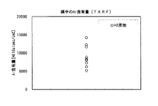
原料ガスとしてモノシラン(流量2sccm)とアルゴン(流量198sccm)と水素(10sccm)を用い、比率(モノシラン:希ガス)を1:99に制御して、成膜温度350℃、成膜圧力を6.665Pa(0.05Torr)、RFパワー50Wという成膜条件で成膜されたアモルファスシリコン膜表面付近のアルゴン/シリコン強度比をTXRFで測定してアルゴン濃度を求めた実験結果を図17に示す。
【0023】
また、上記構成において、前記半導体膜中のフッ素濃度は、2×10¹⁶/cm3〜8×1016/cm3、好ましくは1×1015/cm3〜1×1017/cm3であることを特徴としている。
【0024】
また、本明細書で開示する半導体装置の作製方法に関する発明の構成は、
絶縁表面上に非晶質構造を有する第1の半導体膜を形成する第1工程と、
前記非晶質構造を有する第1の半導体膜に金属元素を添加する第2工程と、
前記第1の半導体膜を結晶化させて結晶構造を有する第1の半導体膜を形成する第3工程と、
前記結晶構造を有する第1の半導体膜の表面にバリア層を形成する第4の工程と、
前記バリア層上にプラズマCVD法で希ガス元素を含む第2の半導体膜を形成する第5工程と、
前記第2の半導体膜に前記金属元素をゲッタリングして結晶構造を有する第1の半導体膜中の前記金属元素を除去または低減する第6工程と、
前記第2の半導体膜を除去する第7工程とを有することを特徴とする半導体装置の作製方法である。
【0025】
上記構成において、前記第2の半導体膜は、成膜室にモノシランと希ガスと水素とを原料ガスとして導入し、プラズマを発生させるプラズマCVD法により形成することを特徴としている。
【0026】
また、上記構成において、前記金属元素とはシリコンの結晶化を助長する金属元素であり、Fe、Ni、Co、Ru、Rh、Pd、Os、Ir、Pt、Cu、Auから選ばれた一種または複数種である。
【0027】
また、上記各構成において、前記希ガス元素は、He、Ne、Ar、Kr、Xeから選ばれた一種または複数種である。
【0028】
(実験1)
ここで、プラズマCVD法を用い、原料ガスとしてモノシランとアルゴン元素と水素を用いて半導体基板上に形成されたアモルファスシリコン膜の膜中におけるアルゴン濃度のRFパワー密度依存性を調べることとした。
【0029】
まず、半導体基板をチャンバー内に搬送し、加熱して300℃に維持し、チャンバー内の圧力を66.65Pa(0.5Torr)となるように排気系で調節する。次いで、チャンバー内にガス導入系からSiH4ガスを流量100sccm導入するとともに高周波電源より放電周波数27.12MHz、投入RF電力20W(RFパワー密度0.033W/cm2(電極面積600cm2))の放電を行いながらプラズマCVD法で第1アモルファスシリコン膜を形成した。なお、この第1アモルファスシリコン膜はリファレンスである。
【0030】
次いで、第1アモルファスシリコン膜上に膜厚200nmの第2アモルファスシリコン膜を積層形成した。第2アモルファスシリコン膜は、300℃に維持した後、チャンバー内の圧力を26.66Pa(0.2Torr)となるように排気系で調節し、チャンバー内にガス導入系からSiH4ガスを流量100sccm、アルゴンガスを流量500sccm、水素ガスを200sccmでそれぞれ導入するとともに高周波電源より放電周波数27.12MHz、投入RF電力20W(RFパワー密度0.033W/cm2)の放電を行いながらプラズマCVD法で形成した。
【0031】
次いで、投入RF電力のみの条件を変え、第2アモルファスシリコン膜上に第3アモルファスシリコン膜(RFパワー密度0.166W/cm2)、第4アモルファスシリコン膜(RFパワー密度0.333W/cm2)、第5アモルファスシリコン膜(RFパワー密度0.5W/cm2)を順次積層した。
【0032】
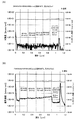
こうして半導体基板上に得られた積層膜に対してSIMS分析を行い、膜中のアルゴン濃度を測定した結果を図2(A)に、フッ素濃度を測定した結果を図2(B)に、窒素濃度を測定した結果を図3(A)に、酸素濃度を測定した結果を図3(B)にそれぞれ示す。図3(A)から膜中の窒素濃度は、1×10¹⁶/cm3〜1×1017/cm3程度と読み取れる。また、図3(B)から膜中の酸素濃度は、4×1017/cm3〜3×1018/cm3程度と読み取れる。また、図示しないが、膜中の炭素濃度は、1×1016/cm3〜5×1017/cm3であった。
【0033】
図2、図3から明かなように原料ガスに水素とアルゴンとモノシランガスを用いることで、アモルファスシリコン膜中のアルゴン濃度が、1×10²⁰/cm3〜1×1021/cm3まで増加した。従って、水素とアルゴンとモノシランガスを原料ガスとするプラズマCVD法によって、高濃度、具体的には1×1020/cm3〜1×1021/cm3の濃度でアルゴンを含むアモルファスシリコン膜を形成できる。一方、原料ガスとしてモノシランとアルゴンガスのみを用いた場合では、膜中のアルゴン濃度は、1×1018/cm3前後、即ち5×1017/cm3〜2×1018/cm3程度しか含ませることができなかった。
【0034】
また、原料ガスに水素とアルゴンとモノシランガスを用いることで、アモルファスシリコン膜中のフッ素濃度が、2×10¹⁶/cm3〜8×1016/cm3まで低減した。
【0035】
また、RFパワー密度を増加させるにつれ、アモルファスシリコン膜中のアルゴン濃度が増加した。なお、RFパワー密度を増加させても膜中のフッ素濃度、窒素濃度、酸素濃度、及び炭素濃度はほとんど変化が見られなかった。
【0036】
(実験2)
次に、プラズマCVD法を用い、チャンバー内の圧力の条件を振り、アモルファスシリコン膜の膜中におけるアルゴン濃度において、チャンバー内の圧力の依存性を調べた。
【0037】
まず、実験1と同じ条件でプラズマCVD法でリファレンスとなる第1アモルファスシリコン膜を半導体基板上に形成した。
【0038】
次いで、第1アモルファスシリコン膜上に膜厚200nmの第2アモルファスシリコン膜を積層形成した。第2アモルファスシリコン膜は、300℃に維持した後、チャンバー内の圧力を5.332Pa(0.04Torr)となるように排気系で調節し、チャンバー内にガス導入系からSiH4ガスを流量100sccm、アルゴンガスを流量100sccm、水素ガスを50sccmでそれぞれ導入するとともに高周波電源より放電周波数27.12MHz、投入RF電力20W(RFパワー密度0.033W/cm2)の放電を行いながらプラズマCVD法で形成した。
【0039】
次いで、チャンバー内の圧力とガス流量の条件を変え、第2アモルファスシリコン膜上に第3アモルファスシリコン膜(圧力=4Pa(0.03Torr)、SiH4ガスを流量100sccm、アルゴンガスを流量50sccm、水素ガスを40sccm)、第4アモルファスシリコン膜(圧力2.666Pa(0.02Torr)、SiH4ガスを流量100sccm、アルゴンガスを流量15sccm、水素ガスを12sccm)を順次積層した。
【0040】
こうして半導体基板上に得られた積層膜に対してSIMS分析を行い、膜中のアルゴン濃度を測定した結果を図4(A)に、フッ素濃度を測定した結果を図4(B)に、窒素濃度を測定した結果を図5(A)に、酸素濃度を測定した結果を図5(B)にそれぞれ示す。また、炭素濃度は、1×10¹⁶/cm3〜5×101 7/cm3であった。
【0041】
図4、図5から明かなように圧力を減圧、即ち高真空にさせるにつれ、アモルファスシリコン膜中のアルゴン濃度が減少した。なお、圧力を減圧させても膜中のフッ素濃度、窒素濃度、酸素濃度、及び炭素濃度はほとんど変化が見られなかった。
【0042】
(実験3)
ここでは、プラズマCVD法を用い、原料ガスとしてモノシランとアルゴン元素と水素を用いて形成されたアモルファスシリコン膜の膜質について以下に述べる。
【0043】
原料ガスとしてモノシランとアルゴン元素と水素を用いて形成されたアモルファスシリコン膜をフーリエ変換赤外分光法(FT−IR法)で得られる分光スペクトルデータを図16に示した。図16では波数640/cmの所でSi−Si結合のピークと、波数2020/cmの所でピークが見られる。波数2000/cmがSi−H結合のピーク、波数2100/cmがSi−H2結合のピークとされており、図16の波数2020/cmのピークは主にSi−H結合であり僅かにSi−H2結合を有しているため現れたピークであると言える。
【0044】
【発明の実施の形態】
本発明の実施形態について、以下に説明する。
【0045】
(実施の形態1)
以下に本発明を用いた代表的なTFTの作製手順を簡略に図1を用いて示す。ここではゲッタリングサイトとして本発明の希ガス元素を含み、且つ非晶質構造を有する半導体膜を用いた例を示す。
【0046】
図1(A)中、10は、絶縁表面を有する基板、11はブロッキング層となる絶縁膜、12は非晶質構造を有する半導体膜である。
【0047】
図1(A)において、基板10はガラス基板、石英基板、セラミック基板などを用いることができる。また、シリコン基板、金属基板またはステンレス基板の表面に絶縁膜を形成したものを用いても良い。また、本工程の処理温度に耐えうる耐熱性を有するプラスチック基板を用いてもよい。
【0048】
まず、図1(A)に示すように基板10上に酸化シリコン膜、窒化シリコン膜または酸化窒化シリコン膜(SiOxNy)等の絶縁膜から成る下地絶縁膜11を形成する。代表的な一例は下地絶縁膜11として2層構造から成り、SiH4、NH3、及びN2Oを反応ガスとして成膜される第1酸化窒化シリコン膜を50〜100nm、SiH4、及びN2Oを反応ガスとして成膜される第2酸化窒化シリコン膜を100〜150nmの厚さに積層形成する構造が採用される。また、下地絶縁膜11の一層として膜厚10nm以下の窒化シリコン膜(SiN膜)、或いは第2酸化窒化シリコン膜(SiNxOy膜(X≫Y))を用いることが好ましい。ゲッタリングの際、ニッケルは酸素濃度の高い領域に移動しやすい傾向があるため、半導体膜と接する下地絶縁膜を窒化シリコン膜とすることは極めて有効である。また、第1酸化窒化シリコン膜、第2酸化窒化シリコン膜、窒化シリコン膜とを順次積層した3層構造を用いてもよい。
【0049】
次いで、下地絶縁膜上に非晶質構造を有する第1の半導体膜12を形成する。第1の半導体膜12は、シリコンを主成分とする半導体材料を用いる。代表的には、非晶質シリコン膜又は非晶質シリコンゲルマニウム膜などが適用され、プラズマCVD法や減圧CVD法、或いはスパッタ法で10〜100nmの厚さに形成する。後の結晶化で良質な結晶構造を有する半導体膜を得るためには、非晶質構造を有する第1の半導体膜12の膜中に含まれる酸素、窒素などの不純物濃度を5×10¹⁸/cm3(二次イオン質量分析法(SIMS)にて測定した原子濃度)以下に低減させておくと良い。これらの不純物は後の結晶化を妨害する要因となり、また、結晶化後においても捕獲中心や再結合中心の密度を増加させる要因となる。そのために、高純度の材料ガスを用いることはもとより、反応室内の鏡面処理(電界研磨処理)やオイルフリーの真空排気系を備えた超高真空対応のCVD装置を用いることが望ましい。
【0050】
次いで、非晶質構造を有する第1の半導体膜12を結晶化させる技術としてここでは特開平8-78329号公報記載の技術を用いて結晶化させる。同公報記載の技術は、非晶質シリコン膜(アモルファスシリコン膜とも呼ばれる)に対して結晶化を助長する金属元素を選択的に添加し、加熱処理を行うことで添加領域を起点として広がる結晶構造を有する半導体膜を形成するものである。まず、非晶質構造を有する第1の半導体膜12の表面に、結晶化を促進する触媒作用のある金属元素(ここでは、ニッケル)を重量換算で1〜100ppm含む酢酸ニッケル塩溶液をスピナーで塗布してニッケル含有層13を形成する。(図1(B))塗布によるニッケル含有層13の形成方法以外の他の手段として、スパッタ法、蒸着法、またはプラズマ処理により極薄い膜を形成する手段を用いてもよい。また、ここでは、全面に塗布する例を示したが、マスクを形成して選択的にニッケル含有層を形成してもよい。
【0051】
次いで、加熱処理を行い、結晶化を行う。この場合、結晶化は半導体の結晶化を助長する金属元素が接した半導体膜の部分でシリサイドが形成され、それを核として結晶化が進行する。こうして、図1(C)に示す結晶構造を有する第1の半導体膜14が形成される。なお、結晶化後での第1の半導体膜14に含まれる酸素濃度は、5×10¹⁸/cm3以下とすることが望ましい。ここでは、脱水素化のための熱処理(450℃、1時間)の後、結晶化のための熱処理(550℃〜650℃で4〜24時間)を行う。また、強光の照射により結晶化を行う場合は、赤外光、可視光、または紫外光のいずれか一またはそれらの組み合わせを用いることが可能であるが、代表的には、ハロゲンランプ、メタルハライドランプ、キセノンアークランプ、カーボンアークランプ、高圧ナトリウムランプ、または高圧水銀ランプから射出された光を用いる。ランプ光源は、1〜60秒、好ましくは30〜60秒点灯させ、それを1回〜10回繰り返し、半導体膜が瞬間的に600〜1000℃程度にまで加熱すればよい。なお、必要であれば、強光を照射する前に非晶質構造を有する第1の半導体膜14に含有する水素を放出させる熱処理を行ってもよい。また、熱処理と強光の照射とを同時に行って結晶化を行ってもよい。生産性を考慮すると、結晶化は強光の照射により結晶化を行うことが望ましい。
【0052】
このようにして得られる第1の半導体膜14には、金属元素(ここではニッケル)が残存している。それは膜中において一様に分布していないにしろ、平均的な濃度とすれば、1×10¹⁹/cm3を越える濃度で残存している。勿論、このような状態でもTFTをはじめ各種半導体素子を形成することが可能であるが、以降に示す方法で当該元素を除去する。
【0053】
次いで、結晶化率(膜の全体積における結晶成分の割合)を高め、結晶粒内に残される欠陥を補修するために、結晶構造を有する第1の半導体膜14に対してレーザー光を照射することが好ましい。レーザー光を照射した場合、表面に薄い酸化膜(図示しない)が形成される。このレーザー光には波長400nm以下のエキシマレーザー光や、YAGレーザーの第2高調波、第3高調波を用いる。また、連続発振のレーザ(YAGレーザ、YVO4レーザ、YLFレーザ、YAlO3レーザ、ガラスレーザ、ルビーレーザ、アレキサンドライドレーザ、Ti:サファイアレーザ)を用い、基本波の第2高調波〜第4高調波を適用してもよい。代表的には、Nd:YVO4レーザー(基本波1064nm)の第2高調波(532nm)や第3高調波(355nm)を適用すればよい。連続発振のレーザーを用いる場合には、出力10Wの連続発振のYVO4レーザから射出されたレーザ光を非線形光学素子により高調波に変換する。また、共振器の中にYVO4結晶と非線形光学素子を入れて、高調波を射出する方法もある。そして、好ましくは光学系により照射面にて矩形状または楕円形状のレーザ光に成形して、被処理体に照射する。なお、照射面におけるレーザ光の形状(レーザースポット)は光学系からなるビーム形成手段により短径の長さが3〜100μmとし、長径の長さが100μm以上である楕円形状であるとする。楕円形状に代えて、短辺の長さが3〜100μmとし、長辺の長さが100μm以上である矩形形状としてもよい。前記形状を矩形状または楕円状としたのは、基板全面を効率よくレーザアニールするためである。ここで、長径(または長辺)の長さを100μm以上としたのは、レーザアニールに適したエネルギー密度を有するレーザ光であれば、実施者が長径(または長辺)の長さを適宜決定すればよいからである。このときのエネルギー密度は0.01〜100MW/cm2程度(好ましくは0.1〜10MW/cm2)が必要である。そして、10〜2000cm/s程度の速度でレーザ光に対して相対的に半導体膜を移動させて照射すればよい。
【0054】
上記結晶化後のレーザー光の照射により形成された酸化膜では、不十分であるため、さらに、オゾン含有水溶液(代表的にはオゾン水)で酸化膜(ケミカルオキサイドと呼ばれる)を形成して合計1〜10nmの酸化膜からなるバリア層15を形成し、このバリア層15上に希ガス元素を含む第2の半導体膜16を形成する。(図1(D))なお、ここでは、結晶構造を有する第1の半導体膜14に対してレーザー光を照射した場合に形成される酸化膜もバリア層の一部と見なしている。このバリア層15は、後の工程で第2の半導体膜16のみを選択的に除去する際にエッチングストッパーとして機能する。また、オゾン含有水溶液に代えて、硫酸、塩酸、硝酸などと過酸化水素水を混合させた水溶液で処理しても同様にケミカルオキサイドを形成することができる。また、他のバリア層15の形成方法としては、酸素雰囲気下の紫外線の照射でオゾンを発生させて前記結晶構造を有する半導体膜の表面を酸化して形成してもよい。また、他のバリア層15の形成方法としては、プラズマCVD法やスパッタ法や蒸着法などで1〜10nm程度の酸化膜を堆積してバリア層としても良い。バリア層の形成にプラズマCVD法やスパッタ法や蒸着法などを用いる場合には、前記結晶構造を有する半導体膜の表面を洗浄し、自然酸化膜やレーザー光の照射により形成された酸化膜などを除去した後で形成することが望ましい。
【0055】
また、バリア層の形成にプラズマCVD法を用いる場合、原料ガスとしてシラン系ガス(モノシラン、ジシラン、トリシラン等)と窒素酸化物系ガス(NOxで表記されるガス)を用い、パルス発振させて成膜する。例えば、原料ガスとしてモノシラン(SiH4)と亜酸化窒素(N2O)、或いは、TEOSガスとN2O、或いはTEOSガスとN2OとO2を用い、10nm以下、好ましくは5nm以下の酸化窒化シリコン膜を形成する。この酸化窒化シリコン膜は、オゾン含有水溶液(代表的にはオゾン水)で得られる酸化膜(ケミカルオキサイドと呼ばれる)や、酸素雰囲気下の紫外線の照射でオゾンを発生させて結晶構造を有する半導体膜の表面を酸化して得られる酸化膜と比較して、結晶構造を有する第1の半導体膜との密着性が高く、後の工程(第2の半導体膜の形成)でピーリングが発生しない。さらに密着性を高くするために、バリア層の形成前にアルゴンプラズマ処理を行ってもよい。また、ゲッタリングさせる工程においても、上記膜厚範囲の酸化窒化シリコン膜であれば、金属元素がバリア層を通過してゲッタリングサイトに移動させることができる。
【0056】
また、バリア層の形成にプラズマCVD法を用いた場合、希ガス元素を含む第2の半導体膜と、バリア層を大気に触れさせることなく成膜することが可能であり、さらに同一チャンバーで連続的に成膜することも可能であるため、スループットに優れている。
【0057】
また、他のバリア層15の形成方法としては、クリーンオーブンを用い、200〜350℃程度に加熱して薄い酸化膜を形成しても良い。なお、上記方法のいずれか一の方法、またはそれらの方法を組み合わせて形成されたバリア層15は、後のゲッタリングで第1の半導体膜中のニッケルが第2の半導体膜に移動可能な膜質または膜厚とすることが必要である。本明細書中、バリア層とは、ゲッタリング工程において金属元素が通過可能な膜質または膜厚を有し、且つ、ゲッタリングサイトとなる層の除去工程においてエッチングストッパーとなる層を指している。
【0058】
ここでは、希ガス元素を含む第2の半導体膜16をプラズマCVD法にて形成し、ゲッタリングサイトを形成する。希ガス元素としてはヘリウム(He)、ネオン(Ne)、アルゴン(Ar)、クリプトン(Kr)、キセノン(Xe)から選ばれた一種または複数種を用いる。中でも安価なガスであるアルゴン(Ar)が好ましい。ここでは原料ガスとして、モノシラン、アルゴン、水素を用いることによって、アルゴンを1×10¹⁸/cm3〜1×1022/cm3、好ましくは、1×1020/cm3〜1×1021/cm3の濃度で含み、ゲッタリング効果が得られる第2の半導体膜をプラズマCVD法で成膜することができる。なお、第2の半導体膜は、膜中のフッ素濃度が2×1016/cm3〜8×1016/cm3の濃度にまで低減され、水素濃度も比較的低い値となる。
【0059】
膜中に不活性気体である希ガス元素イオンを含有させる意味は二つある。一つはダングリングボンドを形成し半導体膜に歪みを与えることであり、他の一つは半導体膜の格子間に歪みを与えることである。半導体膜の格子間に歪みを与えるにはアルゴン(Ar)、クリプトン(Kr)、キセノン(Xe)などシリコンより原子半径の大きな元素を用いた時に顕著に得られる。また、膜中に希ガス元素を含有させることにより、格子歪だけでなく、不対結合手も形成させてゲッタリング作用に寄与する。
【0060】
次いで、加熱処理を行い、第1の半導体膜中における金属元素(ニッケル)の濃度を低減、あるいは除去するゲッタリングを行う。(図1(E))ゲッタリングを行う加熱処理としては、強光を照射する処理または熱処理を行えばよい。このゲッタリングにより、図1(E)中の矢印の方向(即ち、基板側から第2の半導体膜表面に向かう方向)に金属元素が移動し、バリア層15で覆われた第1の半導体膜14に含まれる金属元素の除去、または金属元素の濃度の低減が行われる。金属元素がゲッタリングの際に移動する距離は、少なくとも第1の半導体膜の厚さ程度の距離であればよく、比較的短時間でゲッタリングを完遂することができる。ここでは、ニッケルが第1の半導体膜16に偏析しないよう全て第2の半導体膜16に移動させ、第1の半導体膜14に含まれるニッケルがほとんど存在しない、即ち膜中のニッケル濃度が1×10¹⁸/cm3以下、望ましくは1×1017/cm3以下になるように十分ゲッタリングする。
【0061】
なお、このゲッタリングの加熱処理の条件、或いは第2の半導体膜の膜厚によっては、第2の半導体膜が一部結晶化される場合もある。第2の半導体膜が結晶化してしまうとダングリングボンドや格子歪みや不対結合手が減少してゲッタリング効果の低減を招くことから、好ましくは、第2の半導体膜が結晶化しない加熱処理の条件、或いは第2の半導体膜の膜厚とする。いずれにせよ、第2の半導体膜、即ち希ガス元素を含有する非晶質シリコン膜は、希ガス元素を含まない非晶質シリコン膜と比べて結晶化が生じにくいため、ゲッタリングサイトとして最適である。
【0062】
また、このゲッタリングの加熱処理の条件によっては、ゲッタリングと同時に第1の半導体膜の結晶化率を高め、結晶粒内に残される欠陥を補修する、即ち結晶性の改善を行うことができる。
【0063】
本明細書において、ゲッタリングとは、被ゲッタリング領域(ここでは第1の半導体膜)にある金属元素が熱エネルギーにより放出され、拡散によりゲッタリングサイトに移動することを指している。従って、ゲッタリングは処理温度に依存し、より高温であるほど短時間でゲッタリングが進むことになる。
【0064】
強光を照射する処理を用いる場合は、加熱用のランプ光源を1〜60秒、好ましくは30〜60秒点灯させ、それを1〜10回、好ましくは2〜6回繰り返す。ランプ光源の発光強度は任意なものとするが、瞬間的には600〜1000℃、好ましくは700〜750℃程度に半導体膜が加熱されるようにする。
【0065】
また、熱処理で行う場合は、窒素雰囲気中で450〜800℃、1〜24時間、例えば550℃にて14時間の熱処理を行えばよい。また、熱処理に加えて強光を照射してもよい。
【0066】
次いで、バリア層15をエッチングストッパーとして、16で示した第2の半導体膜のみを選択的に除去した後、バリア層15を除去し、第1の半導体膜16を公知のパターニング技術を用いて所望の形状の半導体層17を形成する。(図1(F))第2の半導体膜のみを選択的にエッチングする方法としては、ClF3によるプラズマを用いないドライエッチング、或いはヒドラジンや、テトラエチルアンモニウムハイドロオキサイド(化学式 (CH3)4NOH)を含む水溶液などアルカリ溶液によるウエットエッチングで行うことができる。また、第2の半導体膜を除去した後、バリア層の表面をTXRFでニッケル濃度を測定したところ、ニッケルが高濃度で検出されるため、バリア層は除去することが望ましく、フッ酸を含むエッチャントにより除去すれば良い。また、バリア層を除去した後、レジストからなるマスクを形成する前に、オゾン水で表面に薄い酸化膜を形成することが望ましい。
【0067】
次いで、半導体層の表面をフッ酸を含むエッチャントで洗浄した後、ゲート絶縁膜18となる珪素を主成分とする絶縁膜を形成する。この表面洗浄とゲート絶縁膜の形成は、大気にふれさせずに連続的に行うことが望ましい。
【0068】
次いで、ゲート絶縁膜18の表面を洗浄した後、ゲート電極19を形成する。次いで、半導体にn型を付与する不純物元素(P、As等)、ここではリンを適宜添加して、ソース領域20及びドレイン領域21を形成する。添加した後、不純物元素を活性化するために加熱処理、強光の照射、またはレーザー光の照射を行う。また、活性化と同時にゲート絶縁膜へのプラズマダメージやゲート絶縁膜と半導体層との界面へのプラズマダメージを回復することができる。特に、室温〜300℃の雰囲気中において、表面または裏面からYAGレーザーの第2高調波を照射して不純物元素を活性化させることは非常に有効である。YAGレーザーはメンテナンスが少ないため好ましい活性化手段である。
【0069】
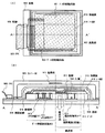
以降の工程は、層間絶縁膜23を形成し、水素化を行って、ソース領域、ドレイン領域に達するコンタクトホールを形成し、ソース電極24、ドレイン電極25を形成してTFT(nチャネル型TFT)を完成させる。(図1(G))
【0070】
こうして得られたTFTのチャネル形成領域22に含まれる金属元素の濃度は1×10¹⁷/cm3未満とすることができる。
【0071】
また、本発明は図1(G)のTFT構造に限定されず、必要があればチャネル形成領域とドレイン領域(またはソース領域)との間にLDD領域を有する低濃度ドレイン(LDD:Lightly Doped Drain)構造としてもよい。この構造はチャネル形成領域と、高濃度に不純物元素を添加して形成するソース領域またはドレイン領域との間に低濃度に不純物元素を添加した領域を設けたものであり、この領域をLDD領域と呼んでいる。さらにゲート絶縁膜を介してLDD領域をゲート電極と重ねて配置させた、いわゆるGOLD(Gate-drain Overlapped LDD)構造としてもよい。
【0072】
また、ここではnチャネル型TFTを用いて説明したが、n型不純物元素に代えてp型不純物元素を用いることによってpチャネル型TFTを形成することができることは言うまでもない。
【0073】
また、ここではトップゲート型TFTを例として説明したが、TFT構造に関係なく本発明を適用することが可能であり、例えばボトムゲート型(逆スタガ型)TFTや順スタガ型TFTに適用することが可能である。
【0074】
(実施の形態2)
ここではTFTの活性層として本発明の希ガス元素を含み、且つ非晶質構造を有する半導体膜を用いた例を示す。
【0075】
まず、絶縁表面を有する基板上にゲート電極を形成し、該ゲート電極を覆うゲート絶縁膜を形成し、該ゲート絶縁膜上に、本発明の希ガス元素を含み、且つ非晶質構造を有する第1の半導体膜を形成する。ここでは原料ガスとして、モノシラン、アルゴン、水素を用いることによって、アルゴンを1×10¹⁸/cm3〜1×1022/cm3、好ましくは、1×1020/cm3〜1×1021/cm3の濃度で含み、且つ、フッ素を2×1016/cm3〜8×1016/cm3の濃度で含み、且つ、水素濃度が比較的低く、非晶質構造を有する第1の半導体膜をプラズマCVD法で成膜することができる。次いで、一導電型(n型またはp型)の不純物元素を含有する第2の半導体膜を積層する。次いで、非晶質構造を有する第1の半導体膜のうち、活性層となる部分以外の不要な部分をエッチングで除去する。次いで、全面に導電膜からなる導電膜を成膜した後に、前記導電膜と一導電型(n型またはp型)の不純物元素を含有する第2の半導体膜の一部を除去して、半導体膜からなるソース領域とドレイン領域を形成し、同時に導電膜からなるドレイン配線とソース配線も形成する。さらに第1の半導体膜の一部を除去して、チャネル・エッチ型のボトムゲート構造のTFTを作製する。このTFTに画素電極を設ければ、液晶表示装置における画素部のTFTに使用することができる。
【0076】
また、本発明は、アモルファスシリコンTFTと呼ばれている上記TFTに限定されず、ポリシリコンTFTと呼ばれるTFTの活性層にも適用できる。
【0077】
その場合、実施の形態1に示した下地絶縁膜上に設ける非晶質構造を有する第1の半導体膜12として、本発明の希ガス元素を含み、且つ非晶質構造を有する第1の半導体膜を用いる。そして、結晶化技術(固相成長法、レーザー結晶化方法、金属元素を触媒として用いた熱処理による固相成長法など)により結晶化を行って結晶構造を有する半導体を形成し、パターニングしてTFTの活性層とすればよい。本発明の非晶質構造を有する半導体膜は、膜中の水素濃度およびフッ素濃度が低減されているため、結晶化の際に有利である。ここでは原料ガスとして、モノシラン、アルゴン、水素を用いることによって、アルゴンを1×10¹⁸/cm3〜1×1022/cm3、好ましくは、1×1020/cm3〜1×1021/cm3の濃度で含み、非晶質構造を有する第1の半導体膜をプラズマCVD法で成膜することができる。
【0078】
例えば、レーザー結晶化を行う場合、絶縁表面を有する基板上に、本発明の希ガス元素及び窒素を含み、且つ非晶質構造を有する第1の半導体膜を成膜した後、レーザー結晶化を行う。
【0079】
用いるレーザー光としては、パルス発振型または連続発光型であるエキシマレーザーやYAGレーザーやYVO4レーザー、YLFレーザ、YAlO3レーザ、ガラスレーザ、ルビーレーザ、アレキサンドライトレーザ、Ti:サファイアレーザなどを用いることができる。これらのレーザーを用いる場合には、レーザー発振器から放射されたレーザー光を光学系で線状に集光し半導体膜に照射する方法を用いると良い。結晶化の条件は実施者が適宣選択するものであるが、パルス発振型のエキシマレーザーを用いる場合はパルス発振周波数30Hzとし、レーザーエネルギー密度を100〜400mJ/cm2(代表的には200〜300mJ/cm2)とする。また、パルス発振型のYAGレーザーやYVO4レーザーを用いる場合にはその第2高調波または第3高調波を用いパルス発振周波数1〜10kHzとし、レーザーエネルギー密度を300〜600mJ/cm2(代表的には350〜500mJ/cm2)とすると良い。そして幅100〜1000μm、例えば400μmで線状に集光したレーザー光を基板全面に渡って照射し、この時の線状レーザー光の重ね合わせ率(オーバーラップ率)を80〜98%として行えばよい。
【0080】
また、YVO4レーザで代表される連続発振型のレーザーを用いる場合、出力10Wの連続発振のYVO4レーザから射出されたレーザ光を非線形光学素子により高調波(第2高調波〜第4高調波)に変換する。また、共振器の中にYVO4結晶と非線形光学素子を入れて、高調波を射出する方法もある。そして、好ましくは光学系により照射面にて矩形状または楕円形状のレーザ光に成形して、被処理体に照射する。このときのエネルギー密度は0.01〜100MW/cm2程度(好ましくは0.1〜10MW/cm2)が必要である。そして、0.5〜2000cm/s程度の速度でレーザ光に対して相対的に半導体膜を移動させて照射すればよい。
【0081】
(実施の形態3)
また、本発明の希ガス元素を含み、且つ非晶質構造を有する半導体膜は、基板上に各素子を形成した後、基板とTFT等の素子とを分離する際、エッチング処理、或いはレーザー光の照射によって層内または界面において剥離現象が生じる層(剥離層)として用いることもできる。この剥離層は、基板上に接して設け、剥離層上に絶縁膜およびTFTを形成する。
【0082】
また、本発明の希ガス元素を含み、且つ非晶質構造を有する半導体膜は、従来の非晶質構造を有する半導体膜と比較して、エッチングレートが異なるため、各種エッチング工程のエッチングストッパーに用いることができる。
【0083】
さらに、本発明の希ガス元素を含み、且つ、非晶質構造を有する半導体膜は、実施の形態1で説明した方法とは別の方法で結晶化した半導体膜や、その他の一般的な半導体膜のゲッタリングサイトとしても用いることができる。
【0084】
以上の構成でなる本発明について、以下に示す実施例でもってさらに詳細な説明を行うこととする。
【0085】
(実施例)
[実施例1]
本発明の実施例を図6〜図8を用いて説明する。ここでは、同一基板上に画素部と、画素部の周辺に設ける駆動回路のTFT(nチャネル型TFT及びpチャネル型TFT)を同時に作製する方法について詳細に説明する。
【0086】
まず、基板100上に下地絶縁膜101を形成し、結晶構造を有する第1の半導体膜を得た後、所望の形状にエッチング処理して島状に分離された半導体層102〜106を形成する。
【0087】
基板100としては、ガラス基板(#1737)を用い、下地絶縁膜101としては、プラズマCVD法で成膜温度400℃、原料ガスSiH4、NH3、N2Oから作製される酸化窒化シリコン膜101a(組成比Si=32%、O=27%、N=24%、H=17%)を50nm(好ましくは10〜200nm)形成する。次いで、表面をオゾン水で洗浄した後、表面の酸化膜を希フッ酸(1/100希釈)で除去する。次いでプラズマCVD法で成膜温度400℃、原料ガスSiH4、N2Oから作製される酸化窒化シリコン膜101b(組成比Si=32%、O=59%、N=7%、H=2%)を100nm(好ましくは50〜200nm)の厚さに積層形成し、さらに大気解放せずにプラズマCVD法で成膜温度300℃、成膜ガスSiH4で非晶質構造を有する半導体膜(ここではアモルファスシリコン膜)を54nmの厚さ(好ましくは25〜80nm)で形成する。
【0088】
本実施例では下地膜101を2層構造として示したが、前記絶縁膜の単層膜または2層以上積層させた構造として形成しても良い。また、半導体膜の材料に限定はないが、好ましくはシリコンまたはシリコンゲルマニウム(Si1-XGeX(X=0.0001〜0.02))合金などを用い、公知の手段(スパッタ法、LPCVD法、またはプラズマCVD法等)により形成すればよい。また、プラズマCVD装置は、枚葉式の装置でもよいし、バッチ式の装置でもよい。また、同一の成膜室で大気に触れることなく下地絶縁膜と半導体膜とを連続成膜してもよい。
【0089】
次いで、非晶質構造を有する半導体膜の表面を洗浄した後、オゾン水で表面に約2nmの極薄い酸化膜を形成する。次いで、TFTのしきい値を制御するために微量な不純物元素(ボロンまたはリン)のドーピングを行う。ここでは、ジボラン(B2H6)を質量分離しないでプラズマ励起したイオンドープ法を用い、ドーピング条件を加速電圧15kV、ジボランを水素で1%に希釈したガス流量30sccm、ドーズ量2×10¹²/cm2で非晶質シリコン膜にボロンを添加した。
【0090】
次いで、重量換算で10ppmのニッケルを含む酢酸ニッケル塩溶液をスピナーで塗布する。塗布に代えてスパッタ法でニッケル元素を全面に散布する方法を用いてもよい。
【0091】
次いで、加熱処理を行い結晶化させて結晶構造を有する半導体膜を形成する。この加熱処理は、電気炉の熱処理または強光の照射を用いればよい。電気炉の熱処理で行う場合は、500℃〜650℃で4〜24時間で行えばよい。ここでは脱水素化のための熱処理(500℃、1時間)の後、結晶化のための熱処理(550℃、4時間)を行って結晶構造を有するシリコン膜を得る。なお、ここでは炉を用いた熱処理を用いて結晶化を行ったが、ランプアニール装置で結晶化を行ってもよい。なお、ここではシリコンの結晶化を助長する金属元素としてニッケルを用いた結晶化技術を用いたが、他の公知の結晶化技術、例えば固相成長法やレーザー結晶化法を用いてもよい。
【0092】
次いで、結晶構造を有するシリコン膜表面の酸化膜を希フッ酸等で除去した後、結晶化率を高め、結晶粒内に残される欠陥を補修するための第1のレーザー光(XeCl:波長308nm)の照射を大気中、または酸素雰囲気中で行う。レーザー光には波長400nm以下のエキシマレーザ光や、YAGレーザの第2高調波、第3高調波を用いる。いずれにしても、繰り返し周波数10〜1000Hz程度のパルスレーザー光を用い、当該レーザー光を光学系にて100〜500mJ/cm2に集光し、90〜95%のオーバーラップ率をもって照射し、シリコン膜表面を走査させればよい。ここでは、繰り返し周波数30Hz、エネルギー密度393mJ/cm2で第1のレーザー光の照射を大気中で行なう。なお、大気中、または酸素雰囲気中で行うため、第1のレーザー光の照射により表面に酸化膜が形成される。
【0093】
次いで、第1のレーザー光の照射により形成された酸化膜を希フッ酸で除去した後、第2のレーザー光の照射を窒素雰囲気、或いは真空中で行い、半導体膜表面を平坦化する。このレーザー光(第2のレーザー光)には波長400nm以下のエキシマレーザー光や、YAGレーザーの第2高調波、第3高調波を用いる。第2のレーザー光のエネルギー密度は、第1のレーザー光のエネルギー密度より大きくし、好ましくは30〜60mJ/cm2大きくする。ここでは、繰り返し周波数30Hz、エネルギー密度453mJ/cm2で第2のレーザー光の照射を行ない、半導体膜表面における凹凸のP―V値(Peak to Valley、高さの最大値と最小値の差分)が50nm以下となる。このP−V値は、AFM(原子間力顕微鏡)により得られる。
【0094】
また、本実施例では第2のレーザー光の照射を全面に行ったが、オフ電流の低減は、画素部のTFTに特に効果があるため、少なくとも画素部のみに選択的に照射する工程としてもよい。
【0095】
また、本実施例では第2のレーザー光の照射を行って平坦化する例を示したが、特に行わなくともよい。
【0096】
次いで、オゾン水で表面を120秒処理して合計1〜5nmの酸化膜からなるバリア層を形成する。
【0097】
次いで、バリア層上に上記実施の形態1に示したプラズマCVD法にてゲッタリングサイトとなるアルゴン元素を含む非晶質シリコン膜を膜厚150nmで形成する。
【0098】
本実施例のプラズマCVD法による成膜条件は、基板温度を300℃とし、チャンバー内の圧力を26.66Pa(0.2Torr)とし、チャンバー内にガス導入系からSiH4ガスを流量100sccm、アルゴンガスを流量500sccm、水素ガスを200sccmでそれぞれ導入するとともに高周波電源より放電周波数27.12MHz、投入RF電力300W(RFパワー密度0.5W/cm2)の放電を行う。なお、上記条件での非晶質シリコン膜に含まれるアルゴン元素の原子濃度は、1×1020/cm3〜1×1021/cm3である。その後、ランプアニール装置を用いて650℃、3分の熱処理を行いゲッタリングする。
【0099】
次いで、バリア層をエッチングストッパーとして、ゲッタリングサイトであるアルゴン元素を含む非晶質シリコン膜を選択的に除去した後、バリア層を希フッ酸で選択的に除去する。なお、ゲッタリングの際、ニッケルは酸素濃度の高い領域に移動しやすい傾向があるため、酸化膜からなるバリア層をゲッタリング後に除去することが望ましい。
【0100】
次いで、得られた結晶構造を有するシリコン膜(ポリシリコン膜とも呼ばれる)の表面にオゾン水で薄い酸化膜を形成した後、レジストからなるマスクを形成し、所望の形状にエッチング処理して島状に分離された半導体層102〜106を形成する。半導体層を形成した後、レジストからなるマスクを除去する。
【0101】
次いで、フッ酸を含むエッチャントで酸化膜を除去すると同時にシリコン膜の表面を洗浄した後、ゲート絶縁膜107となる珪素を主成分とする絶縁膜を形成する。本実施例では、プラズマCVD法により115nmの厚さで酸化窒化シリコン膜(組成比Si=32%、O=59%、N=7%、H=2%)で形成する。
【0102】
次いで、図6(A)に示すように、ゲート絶縁膜107上に膜厚20〜100nmの第1の導電膜108aと、膜厚100〜400nmの第2の導電膜108bとを積層形成する。本実施例では、ゲート絶縁膜107上に膜厚50nmの窒化タンタル膜、膜厚370nmのタングステン膜を順次積層する。
【0103】
第1の導電膜及び第2の導電膜を形成する導電性材料としてはTa、W、Ti、Mo、Al、Cuから選ばれた元素、または前記元素を主成分とする合金材料もしくは化合物材料で形成する。また、第1の導電膜及び第2の導電膜としてリン等の不純物元素をドーピングした多結晶シリコン膜に代表される半導体膜や、、AgPdCu合金を用いてもよい。また、2層構造に限定されず、例えば、膜厚50nmのタングステン膜、膜厚500nmのアルミニウムとシリコンの合金(Al−Si)膜、膜厚30nmの窒化チタン膜を順次積層した3層構造としてもよい。また、3層構造とする場合、第1の導電膜のタングステンに代えて窒化タングステンを用いてもよいし、第2の導電膜のアルミニウムとシリコンの合金(Al−Si)膜に代えてアルミニウムとチタンの合金膜(Al−Ti)を用いてもよいし、第3の導電膜の窒化チタン膜に代えてチタン膜を用いてもよい。また、単層構造であってもよい。
【0104】
次に、図6(B)に示すように光露光工程によりレジストからなるマスク110〜115を形成し、ゲート電極及び配線を形成するための第1のエッチング処理を行う。第1のエッチング処理では第1及び第2のエッチング条件で行う。エッチングにはICP(Inductively Coupled Plasma:誘導結合型プラズマ)エッチング法を用いると良い。ICPエッチング法を用い、エッチング条件(コイル型の電極に印加される電力量、基板側の電極に印加される電力量、基板側の電極温度等)を適宜調節することによって所望のテーパー形状に膜をエッチングすることができる。なお、エッチング用ガスとしては、Cl2、BCl3、SiCl4、CCl4などを代表とする塩素系ガスまたはCF4、SF6、NF3などを代表とするフッ素系ガス、またはO2を適宜用いることができる。
【0105】
本実施例では、基板側(試料ステージ)にも150WのRF(13.56MHz)電力を投入し、実質的に負の自己バイアス電圧を印加する。なお、基板側の電極面積サイズは、12.5cm×12.5cmであり、コイル型の電極面積サイズ(ここではコイルの設けられた石英円板)は、直径25cmの円板である。この第1のエッチング条件によりW膜をエッチングして第1の導電層の端部をテーパー形状とする。第1のエッチング条件でのWに対するエッチング速度は200.39nm/min、TaNに対するエッチング速度は80.32nm/minであり、TaNに対するWの選択比は約2.5である。また、この第1のエッチング条件によって、Wのテーパー角は、約26°となる。この後、レジストからなるマスク110〜115を除去せずに第2のエッチング条件に変え、エッチング用ガスにCF4とCl2とを用い、それぞれのガス流量比を30/30(sccm)とし、1Paの圧力でコイル型の電極に500WのRF(13.56MHz)電力を投入してプラズマを生成して約30秒程度のエッチングを行った。基板側(試料ステージ)にも20WのRF(13.56MHz)電力を投入し、実質的に負の自己バイアス電圧を印加する。CF4とCl2を混合した第2のエッチング条件ではW膜及びTaN膜とも同程度にエッチングされる。第2のエッチング条件でのWに対するエッチング速度は58.97nm/min、TaNに対するエッチング速度は66.43nm/minである。なお、ゲート絶縁膜上に残渣を残すことなくエッチングするためには、10〜20%程度の割合でエッチング時間を増加させると良い。
【0106】
上記第1のエッチング処理では、レジストからなるマスクの形状を適したものとすることにより、基板側に印加するバイアス電圧の効果により第1の導電層及び第2の導電層の端部がテーパー形状となる。このテーパー部の角度は15〜45°とすればよい。
【0107】
こうして、第1のエッチング処理により第1の導電層と第2の導電層から成る第1の形状の導電層117〜121(第1の導電層117a〜121aと第2の導電層117b〜121b)を形成する。ゲート絶縁膜となる絶縁膜107は、10〜20nm程度エッチングされ、第1の形状の導電層117〜121で覆われない領域が薄くなったゲート絶縁膜116となる。
【0108】
次いで、レジストからなるマスクを除去せずに第2のエッチング処理を行う。(図6(C))ここでは、エッチング用ガスにSF6とCl2とO2とを用い、それぞれのガス流量比を24/12/24(sccm)とし、1.3Paの圧力でコイル型の電極に700WのRF(13.56MHz)電力を投入してプラズマを生成してエッチングを25秒行った。基板側(試料ステージ)にも10WのRF(13.56MHz)電力を投入し、実質的に負の自己バイアス電圧を印加する。第2のエッチング処理でのWに対するエッチング速度は227.3nm/min、TaNに対するエッチング速度は32.1nm/minであり、TaNに対するWの選択比は7.1であり、絶縁膜116であるSiONに対するエッチング速度は33.7nm/minであり、SiONに対するWの選択比は6.83である。このようにエッチングガス用ガスにSF6を用いた場合、絶縁膜116との選択比が高いので膜減りを抑えることができる。本実施例では絶縁膜116において約8nmしか膜減りが起きない。
【0109】
この第2のエッチング処理によりWのテーパー角は70°となった。この第2のエッチング処理により第2の導電層124b〜129bを形成する。一方、第1の導電層は、ほとんどエッチングされず、第1の導電層124a〜129aとなる。なお、第1の導電層124a〜129aは、第1の導電層117a〜122aとほぼ同一サイズである。実際には、第1の導電層の幅は、第2のエッチング処理前に比べて約0.3μm程度、即ち線幅全体で0.6μm程度後退する場合もあるがほとんどサイズに変化がない。また、図6(B)および図6(C)では、第1の導電層のテーパー部の長さは同一として図示しているが、実際は、配線幅の依存性があるため、配線幅によって第1の導電層のテーパー部の長さが変化する。
【0110】
また、2層構造に代えて、膜厚50nmのタングステン膜、膜厚500nmのアルミニウムとシリコンの合金(Al−Si)膜、膜厚30nmの窒化チタン膜を順次積層した3層構造とした場合、第1のエッチング処理の第1のエッチング条件としては、BCl3とCl2とO2とを原料ガスに用い、それぞれのガス流量比を65/10/5(sccm)とし、基板側(試料ステージ)に300WのRF(13.56MHz)電力を投入し、1.2Paの圧力でコイル型の電極に450WのRF(13.56MHz)電力を投入してプラズマを生成して117秒のエッチングを行えばよく、第1のエッチング処理の第2のエッチング条件としては、CF4とCl2とO2とを用い、それぞれのガス流量比を25/25/10(sccm)とし、基板側(試料ステージ)にも20WのRF(13.56MHz)電力を投入し、1Paの圧力でコイル型の電極に500WのRF(13.56MHz)電力を投入してプラズマを生成して約30秒程度のエッチングを行えばよく、第2のエッチング処理としてはBCl3とCl2を用い、それぞれのガス流量比を20/60(sccm)とし、基板側(試料ステージ)には100WのRF(13.56MHz)電力を投入し、1.2Paの圧力でコイル型の電極に600WのRF(13.56MHz)電力を投入してプラズマを生成してエッチングを行えばよい。
【0111】
次いで、レジストからなるマスクを除去した後、第1のドーピング処理を行って図6(D)の状態を得る。ドーピング処理はイオンドープ法、もしくはイオン注入法で行えば良い。イオンドープ法の条件はドーズ量を1.5×10¹⁴atoms/cm2とし、加速電圧を60〜100keVとして行う。n型を付与する不純物元素として、典型的にはリン(P)または砒素(As)を用いる。この場合、第1の導電層及び第2の導電層124〜128がn型を付与する不純物元素に対するマスクとなり、自己整合的に第1の不純物領域130〜134が形成される。第1の不純物領域130〜134には1×1016〜1×1017/cm3の濃度範囲でn型を付与する不純物元素を添加する。ここでは、第1の不純物領域と同じ濃度範囲の領域をn--領域とも呼ぶ。
【0112】
なお、本実施例ではレジストからなるマスクを除去した後、第1のドーピング処理を行ったが、レジストからなるマスクを除去せずに第1のドーピング処理を行ってもよい。また、図6(D)では、便宜上、第1の導電層のテーパー部の長さは同一として図示しているが、実際は、配線幅によって第1の導電層のテーパー部の長さが変化している。従って、同一基板上に配線幅の異なる配線が複数設けられている場合、ドーピングされる領域の幅もそれぞれ異なる。
【0113】
次いで、図7(A)に示すようにレジストからなるマスク135〜137を形成し第2のドーピング処理を行う。マスク135は駆動回路のpチャネル型TFTを形成する半導体層のチャネル形成領域及びその周辺の領域を保護するマスクであり、マスク136は駆動回路のnチャネル型TFTの一つを形成する半導体層のチャネル形成領域及びその周辺の領域を保護するマスクであり、マスク137は画素部のTFTを形成する半導体層のチャネル形成領域及びその周辺の領域と保持容量となる領域とを保護するマスクである。
【0114】
第2のドーピング処理におけるイオンドープ法の条件はドーズ量を1.5×10¹⁵atoms/cm2とし、加速電圧を60〜100keVとしてリン(P)をドーピングする。ここでは、第2の導電層124b〜126bをマスクとして各半導体層に不純物領域が自己整合的に形成される。勿論、マスク135〜137で覆われた領域には添加されない。こうして、第2の不純物領域138〜140と、第3の不純物領域142が形成される。第2の不純物領域138〜140には1×1020〜1×1021/cm3の濃度範囲でn型を付与する不純物元素を添加されている。ここでは、第2の不純物領域と同じ濃度範囲の領域をn+領域とも呼ぶ。
【0115】
また、第3の不純物領域は第1の導電層により第2の不純物領域よりも低濃度に形成され、1×10¹⁸〜1×10¹⁹/cm3の濃度範囲でn型を付与する不純物元素を添加されることになる。なお、第3の不純物領域は、テーパー形状である第1の導電層の部分を通過させてドーピングを行うため、テーパ−部の端部に向かって不純物濃度が増加する濃度勾配を有している。ここでは、第3の不純物領域と同じ濃度範囲の領域をn-領域とも呼ぶ。また、マスク136、137で覆われた領域は、第2のドーピング処理で不純物元素が添加されず、第1の不純物領域144、145となる。
【0116】
次いで、レジストからなるマスク135〜137を除去した後、新たにレジストからなるマスク146〜148を形成して図7(B)に示すように第3のドーピング処理を行う。
【0117】
駆動回路において、上記第3のドーピング処理により、pチャネル型TFTを形成する半導体層および保持容量を形成する半導体層にp型の導電型を付与する不純物元素が添加された第4の不純物領域149、150及び第5の不純物領域151、152を形成する。
【0118】
また、第4の不純物領域149、150には1×10²⁰〜1×10²¹/cm3の濃度範囲でp型を付与する不純物元素が添加されるようにする。尚、第4の不純物領域149、150には先の工程でリン(P)が添加された領域(n--領域)であるが、p型を付与する不純物元素の濃度がその1.5〜3倍添加されていて導電型はp型となっている。ここでは、第4の不純物領域と同じ濃度範囲の領域をp+領域とも呼ぶ。
【0119】
また、第5の不純物領域151、152は第2の導電層125aのテーパー部と重なる領域に形成されるものであり、1×10¹⁸〜1×10²⁰/cm3の濃度範囲でp型を付与する不純物元素が添加されるようにする。ここでは、第5の不純物領域と同じ濃度範囲の領域をp-領域とも呼ぶ。
【0120】
以上までの工程でそれぞれの半導体層にn型またはp型の導電型を有する不純物領域が形成される。導電層124〜127はTFTのゲート電極となる。また、導電層128は画素部において保持容量を形成する一方の電極となる。さらに、導電層129は画素部においてソース配線を形成する。
【0121】
また、導電層124〜127及び不純物領域(第1の不純物領域〜第5の不純物領域)が形成できるのであれば特に上記工程順序に限定されず、各エッチング順序、各ドーピング順序を適宜変更してもよい。
【0122】
次いで、ほぼ全面を覆う絶縁膜(図示しない)を形成する。本実施例では、プラズマCVD法により膜厚50nmの酸化シリコン膜を形成した。勿論、この絶縁膜は酸化シリコン膜に限定されるものでなく、他のシリコンを含む絶縁膜を単層または積層構造として用いても良い。
【0123】
次いで、それぞれの半導体層に添加された不純物元素を活性化処理する工程を行う。この活性化工程は、ランプ光源を用いたラピッドサーマルアニール法(RTA法)、或いはYAGレーザーまたはエキシマレーザーを裏面から照射する方法、或いは炉を用いた熱処理、或いはこれらの方法のうち、いずれかと組み合わせた方法によって行う。
【0124】
また、本実施例では、上記活性化の前に絶縁膜を形成した例を示したが、上記活性化を行った後、絶縁膜を形成する工程としてもよい。
【0125】
次いで、窒化シリコン膜からなる第1の層間絶縁膜153を形成して熱処理(300〜550℃で1〜12時間の熱処理)を行い、半導体層を水素化する工程を行う。(図7(C))この工程は第1の層間絶縁膜153に含まれる水素により半導体層のダングリングボンドを終端する工程である。酸化シリコン膜からなる絶縁膜(図示しない)の存在に関係なく半導体層を水素化することができる。ただし、本実施例では、第2の導電層としてアルミニウムを主成分とする材料を用いているので、水素化する工程において第2の導電層が耐え得る熱処理条件とすることが重要である。水素化の他の手段として、プラズマ水素化(プラズマにより励起された水素を用いる)を行っても良い。
【0126】
次いで、第1の層間絶縁膜153上に有機絶縁物材料から成る第2の層間絶縁膜154を形成する。本実施例では膜厚1.6μmのアクリル樹脂膜を形成する。次いで、ソース配線129に達するコンタクトホールと、導電層127、128に達するコンタクトホールと、各不純物領域に達するコンタクトホールを形成する。本実施例では複数のエッチング処理を順次行う。本実施例では第1の層間絶縁膜をエッチングストッパーとして第2の層間絶縁膜をエッチングした後、絶縁膜(図示しない)をエッチングストッパーとして第1の層間絶縁膜をエッチングしてから絶縁膜(図示しない)をエッチングした。
【0127】
その後、Al、Ti、Mo、Wなどを用いて配線及び画素電極を形成する。これらの電極及び画素電極の材料は、AlまたはAgを主成分とする膜、またはそれらの積層膜等の反射性の優れた材料を用いることが望ましい。こうして、ソース電極またはドレイン電極155〜160、ゲート配線162、接続配線161、画素電極163が形成される。
【0128】
以上の様にして、nチャネル型TFT201、pチャネル型TFT202、nチャネル型TFT203を有する駆動回路206と、nチャネル型TFTからなる画素TFT204、保持容量205とを有する画素部207を同一基板上に形成することができる。(図8)本明細書中ではこのような基板を便宜上アクティブマトリクス基板と呼ぶ。本明細書中ではこのような基板を便宜上アクティブマトリクス基板と呼ぶ。
【0129】
画素部207において、画素TFT204(nチャネル型TFT)にはチャネル形成領域167、ゲート電極を形成する導電層127の外側に形成される第1の不純物領域(n--領域)145とソース領域として機能する第2の不純物領域(n+領域)140を有している。また、保持容量205の一方の電極として機能する半導体層には第4の不純物領域150、第5の不純物領域152が形成されている。保持容量205は、絶縁膜(ゲート絶縁膜と同一膜)116を誘電体として、第2の電極128と、半導体層150、152、168とで形成されている。
【0130】
また、駆動回路206において、nチャネル型TFT201(第1のnチャネル型TFT)はチャネル形成領域164、ゲート電極を形成する導電層124の一部と絶縁膜を介して重なる第3の不純物領域(n-領域)142とソース領域またはドレイン領域として機能する第2の不純物領域(n+領域)138を有している。
【0131】
また、駆動回路206において、pチャネル型TFT202にはチャネル形成領域165、ゲート電極を形成する導電層125の一部と絶縁膜を介して重なる第5不純物領域(p-領域)151とソース領域またはドレイン領域として機能する第4の不純物領域(p+領域)149を有している。
【0132】
また、駆動回路206において、nチャネル型TFT203(第2のnチャネル型TFT)にはチャネル形成領域166、ゲート電極を形成する導電層126の外側に第1の不純物領域(n--領域)144とソース領域またはドレイン領域として機能する第2の不純物領域(n+領域)139を有している。
【0133】
これらのTFT201〜203を適宜組み合わせてシフトレジスタ回路、バッファ回路、レベルシフタ回路、ラッチ回路などを形成し、駆動回路206を形成すればよい。例えば、CMOS回路を形成する場合には、nチャネル型TFT201とpチャネル型TFT202を相補的に接続して形成すればよい。
【0134】
特に、駆動電圧が高いバッファ回路には、ホットキャリア効果による劣化を防ぐ目的から、nチャネル型TFT203の構造が適している。
【0135】
また、信頼性が最優先とされる回路には、GOLD構造であるnチャネル型TFT201の構造が適している。
【0136】
また、半導体膜表面の平坦化を向上させることによって信頼性を向上させることができるので、GOLD構造のTFTにおいて、ゲート電極とゲート絶縁膜を介して重なる不純物領域の面積を縮小しても十分な信頼性を得ることができる。具体的にはGOLD構造のTFTにおいてゲート電極のテーパー部となる部分サイズを小さくしても十分な信頼性を得ることができる。
【0137】
また、GOLD構造のTFTにおいてはゲート絶縁膜が薄くなると寄生容量が増加するが、ゲート電極(第1導電層)のテーパー部となる部分サイズを小さくして寄生容量を低減すれば、f特性も向上してさらなる高速動作が可能となり、且つ、十分な信頼性を有するTFTとなる。
【0138】
なお、画素部207の画素TFTにおいても、第2のレーザー光の照射によりオフ電流の低減、およびバラツキの低減が実現される。
【0139】
また、本実施例では反射型の表示装置を形成するためのアクティブマトリクス基板を作製する例を示したが、画素電極を透明導電膜で形成すると、フォトマスクは1枚増えるものの、透過型の表示装置を形成することができる。
【0140】
[実施例2]
本実施例では、実施例1で作製したアクティブマトリクス基板から、アクティブマトリクス型液晶表示装置を作製する工程を以下に説明する。説明には図9を用いる。
【0141】
まず、実施例1に従い、図8の状態のアクティブマトリクス基板を得た後、図8のアクティブマトリクス基板上に配向膜を形成しラビング処理を行う。なお、本実施例では配向膜を形成する前に、アクリル樹脂膜等の有機樹脂膜をパターニングすることによって基板間隔を保持するための柱状のスペーサを所望の位置に形成した。また、柱状のスペーサに代えて、球状のスペーサを基板全面に散布してもよい。
【0142】
次いで、対向基板を用意する。この対向基板には、着色層、遮光層が各画素に対応して配置されたカラーフィルタが設けられている。また、駆動回路の部分にも遮光層を設けた。このカラーフィルタと遮光層とを覆う平坦化膜を設けた。次いで、平坦化膜上に透明導電膜からなる対向電極を画素部に形成し、対向基板の全面に配向膜を形成し、ラビング処理を施した。
【0143】
そして、画素部と駆動回路が形成されたアクティブマトリクス基板と対向基板とをシール材で貼り合わせる。シール材にはフィラーが混入されていて、このフィラーと柱状スペーサによって均一な間隔を持って2枚の基板が貼り合わせられる。その後、両基板の間に液晶材料を注入し、封止剤(図示せず)によって完全に封止する。液晶材料には公知の液晶材料を用いれば良い。このようにしてアクティブマトリクス型液晶表示装置が完成する。そして、必要があれば、アクティブマトリクス基板または対向基板を所望の形状に分断する。さらに、公知の技術を用いて偏光板等を適宜設けた。そして、公知の技術を用いてFPCを貼りつけた。
【0144】
こうして得られた液晶モジュールの構成を図9の上面図を用いて説明する。
【0145】
アクティブマトリクス基板301の中央には、画素部304が配置されている。画素部304の上側には、ソース信号線を駆動するためのソース信号線駆動回路302が配置されている。画素部304の左右には、ゲート信号線を駆動するためのゲート信号線駆動回路303が配置されている。本実施例に示した例では、ゲート信号線駆動回路303は画素部に対して左右対称配置としているが、これは片側のみの配置でも良く、液晶モジュールの基板サイズ等を考慮して、設計者が適宜選択すれば良い。ただし、回路の動作信頼性や駆動効率等を考えると、図9に示した左右対称配置が望ましい。
【0146】
各駆動回路への信号の入力は、フレキシブルプリント基板(Flexible Print Circuit:FPC)305から行われる。FPC305は、基板301の所定の場所まで配置された配線に達するように、層間絶縁膜および樹脂膜にコンタクトホールを開口し、接続電極309を形成した後、異方性導電膜等を介して圧着される。本実施例においては、接続電極はITOを用いて形成した。
【0147】
駆動回路、画素部の周辺には、基板外周に沿ってシール剤307が塗布され、あらかじめアクティブマトリクス基板上に形成されたスペーサ310によって一定のギャップ(基板301と対向基板306との間隔)を保った状態で、対向基板306が貼り付けられる。その後、シール剤307が塗布されていない部分より液晶素子が注入され、封止剤308によって密閉される。以上の工程により、液晶モジュールが完成する。
【0148】
また、ここでは全ての駆動回路を基板上に形成した例を示したが、駆動回路の一部に数個のICを用いてもよい。
【0149】
また、本実施例は、実施例1と自由に組みあわせることが可能である。
【0150】
[実施例3]
実施例1では画素電極が反射性を有する金属材料で形成された反射型の表示装置の例を示したが、本実施例では画素電極を透光性を有する導電膜で形成した透過型の表示装置の例を示す。
【0151】
層間絶縁膜を形成する工程までは実施例1と同じであるので、ここでは省略する。実施例1に従って層間絶縁膜を形成した後、透光性を有する導電膜からなる画素電極601を形成する。透光性を有する導電膜としては、ITO(酸化インジウム酸化スズ合金)、酸化インジウム酸化亜鉛合金(In2O3―ZnO)、酸化亜鉛(ZnO)等を用いればよい。
【0152】
その後、層間絶縁膜600にコンタクトホールを形成する。次いで、画素電極と重なる接続電極602を形成する。この接続電極602は、コンタクトホールを通じてドレイン領域と接続されている。また、この接続電極と同時に他のTFTのソース電極またはドレイン電極も形成する。
【0153】
また、ここでは全ての駆動回路を基板上に形成した例を示したが、駆動回路の一部に数個のICを用いてもよい。
【0154】
以上のようにしてアクティブマトリクス基板が形成される。このアクティブマトリクス基板を用い、実施例2に従って液晶モジュールを作製し、バックライト604、導光板605を設け、カバー606で覆えば、図10にその断面図の一部を示したようなアクティブマトリクス型液晶表示装置が完成する。なお、カバーと液晶モジュールは接着剤や有機樹脂を用いて貼り合わせる。また、基板と対向基板を貼り合わせる際、枠で囲んで有機樹脂を枠と基板との間に充填して接着してもよい。また、透過型であるので偏光板603は、アクティブマトリクス基板と対向基板の両方に貼り付ける。
【0155】
また、本実施例は、実施例1、または実施例2と自由に組みあわせることが可能である。
【0156】
[実施例4]
本実施例では、EL(Electro Luminescence)素子を備えた発光表示装置を作製する例を図11に示す。
【0157】
図11(A)は、ELモジュールを示す上面図、図11(B)は図11(A)をA−A’で切断した断面図である。絶縁表面を有する基板900(例えば、ガラス基板、結晶化ガラス基板、もしくはプラスチック基板等)に、画素部902、ソース側駆動回路901、及びゲート側駆動回路903を形成する。これらの画素部や駆動回路は、上記実施例に従えば得ることができる。
【0158】
また、918はシール材、919はDLC膜であり、画素部および駆動回路部はシール材918で覆われ、そのシール材は保護膜919で覆われている。さらに、接着材を用いてカバー材920で封止されている。熱や外力などによる変形に耐えるためカバー材920は基板900と同じ材質のもの、例えばガラス基板を用いることが望ましく、サンドブラスト法などにより図11に示す凹部形状(深さ3〜10μm)に加工する。さらに加工して乾燥剤921が設置できる凹部(深さ50〜200μm)を形成することが望ましい。また、多面取りでELモジュールを製造する場合、基板とカバー材とを貼り合わせた後、CO2レーザー等を用いて端面が一致するように分断してもよい。
【0159】
なお、908はソース側駆動回路901及びゲート側駆動回路903に入力される信号を伝送するための配線であり、外部入力端子となるFPC(フレキシブルプリントサーキット)909からビデオ信号やクロック信号を受け取る。なお、ここではFPCしか図示されていないが、このFPCにはプリント配線基盤(PWB)が取り付けられていても良い。本明細書における発光装置には、発光装置本体だけでなく、それにFPCもしくはPWBが取り付けられた状態をも含むものとする。
【0160】
次に、断面構造について図11(B)を用いて説明する。基板900上に絶縁膜910が設けられ、絶縁膜910の上方には画素部902、ゲート側駆動回路903が形成されており、画素部902は電流制御用TFT911とそのドレインに電気的に接続された画素電極912を含む複数の画素により形成される。また、ゲート側駆動回路903はnチャネル型TFT913とpチャネル型TFT714とを組み合わせたCMOS回路を用いて形成される。
【0161】
これらのTFT(911、913、914を含む)は、上記実施例1のnチャネル型TFT201、上記実施例1のpチャネル型TFT202に従って作製すればよい。
【0162】
なお、TFTとEL素子の間に設ける絶縁膜としては、アルカリ金属イオンやアルカリ土金属イオン等の不純物イオンの拡散をブロックするだけでなく、積極的にアルカリ金属イオンやアルカリ土金属イオン等の不純物イオンを吸着する材料が好ましく、更には後のプロセス温度に耐えうる材料が適している。これらの条件に合う材料は、一例としてフッ素を多く含んだ窒化シリコン膜が挙げられる。窒化シリコン膜の膜中に含まれるフッ素濃度は、1×10¹⁹/cm3以上、好ましくは窒化シリコン膜中でのフッ素の組成比を1〜5%とすればよい。窒化シリコン膜中のフッ素がアルカリ金属イオンやアルカリ土金属イオン等と結合し、膜中に吸着される。また、他の例としてアルカリ金属イオンやアルカリ土金属イオン等を吸着するアンチモン(Sb)化合物、スズ(Sn)化合物、またはインジウム(In)化合物からなる微粒子を含む有機樹脂膜、例えば、五酸化アンチモン微粒子(Sb2O5・nH2O)を含む有機樹脂膜も挙げられる。なお、この有機樹脂膜は、平均粒径10〜20nmの微粒子が含まれており、光透過性も非常に高い。この五酸化アンチモン微粒子で代表されるアンチモン化合物は、アルカリ金属イオン等の不純物イオンやアルカリ土金属イオンを吸着しやすい。
【0163】
画素電極912は発光素子(EL素子)の陽極として機能する。また、画素電極912の両端にはバンク915が形成され、画素電極912上にはEL層916および発光素子の陰極917が形成される。
【0164】
EL層916としては、発光層、電荷輸送層または電荷注入層を自由に組み合わせてEL層(発光及びそのためのキャリアの移動を行わせるための層)を形成すれば良い。例えば、低分子系有機EL材料や高分子系有機EL材料を用いればよい。また、EL層として一重項励起により発光(蛍光)する発光材料(シングレット化合物)からなる薄膜、または三重項励起により発光(リン光)する発光材料(トリプレット化合物)からなる薄膜を用いることができる。また、電荷輸送層や電荷注入層として炭化珪素等の無機材料を用いることも可能である。これらの有機EL材料や無機材料は公知の材料を用いることができる。
【0165】
陰極917は全画素に共通の配線としても機能し、接続配線908を経由してFPC909に電気的に接続されている。さらに、画素部902及びゲート側駆動回路903に含まれる素子は全て陰極917、シール材918、及び保護膜919で覆われている。
【0166】
なお、シール材918としては、できるだけ可視光に対して透明もしくは半透明な材料を用いるのが好ましい。また、シール材918はできるだけ水分や酸素を透過しない材料であることが望ましい。
【0167】
また、シール材918を用いて発光素子を完全に覆った後、すくなくとも図11に示すようにDLC膜等からなる保護膜919をシール材918の表面(露呈面)に設けることが好ましい。また、基板の裏面を含む全面に保護膜を設けてもよい。ここで、外部入力端子(FPC)が設けられる部分に保護膜が成膜されないように注意することが必要である。マスクを用いて保護膜が成膜されないようにしてもよいし、CVD装置で使用するマスキングテープ等のテープで外部入力端子部分を覆うことで保護膜が成膜されないようにしてもよい。
【0168】
以上のような構造で発光素子をシール材918及び保護膜で封入することにより、発光素子を外部から完全に遮断することができ、外部から水分や酸素等のEL層の酸化による劣化を促す物質が侵入することを防ぐことができる。従って、信頼性の高い発光装置を得ることができる。
【0169】
また、画素電極を陰極とし、EL層と陽極を積層して図11とは逆方向に発光する構成としてもよい。図12にその一例を示す。なお、上面図は同一であるので省略する。
【0170】
図12に示した断面構造について以下に説明する。基板1000としては、ガラス基板や石英基板の他にも、半導体基板または金属基板も使用することができる。基板1000上に絶縁膜1010が設けられ、絶縁膜1010の上方には画素部1002、ゲート側駆動回路1003が形成されており、画素部1002は電流制御用TFT1011とそのドレインに電気的に接続された画素電極1012を含む複数の画素により形成される。また、ゲート側駆動回路1003はnチャネル型TFT1013とpチャネル型TFT1014とを組み合わせたCMOS回路を用いて形成される。
【0171】
画素電極1012は発光素子の陰極として機能する。また、画素電極1012の両端にはバンク1015が形成され、画素電極1012上にはEL層1016および発光素子の陽極1017が形成される。
【0172】
陽極1017は全画素に共通の配線としても機能し、接続配線1008を経由してFPC1009に電気的に接続されている。さらに、画素部1002及びゲート側駆動回路1003に含まれる素子は全て陽極1017、シール材1018、及びDLC等からなる保護膜1019で覆われている。また、カバー材1021と基板1000とを接着剤で貼り合わせた。また、カバー材には凹部を設け、乾燥剤1021を設置する。
【0173】
なお、シール材1018としては、できるだけ可視光に対して透明もしくは半透明な材料を用いるのが好ましい。また、シール材1018はできるだけ水分や酸素を透過しない材料であることが望ましい。
【0174】
また、図12では、画素電極を陰極とし、EL層と陽極を積層したため、発光方向は図12に示す矢印の方向となっている。
【0175】
本実施例では、実施例1で得られる電気特性、信頼性ともに高いTFTを用いるため、従来の素子に比べて信頼性の高い発光素子を形成することができる。また、そのような発光素子を有する発光装置を表示部として用いることにより高性能な電気器具を得ることができる。
【0176】
なお、本実施例は実施例1と自由に組み合わせることが可能である。
【0177】
[実施例5]
本発明を実施して形成された駆動回路や画素部は様々なモジュール(アクティブマトリクス型液晶モジュール、アクティブマトリクス型ELモジュール、アクティブマトリクス型ECモジュール)に用いることができる。即ち、本発明を実施することによって、それらを組み込んだ全ての電子機器が完成される。
【0178】
その様な電子機器としては、ビデオカメラ、デジタルカメラ、ヘッドマウントディスプレイ(ゴーグル型ディスプレイ)、カーナビゲーション、プロジェクタ、カーステレオ、パーソナルコンピュータ、携帯情報端末(モバイルコンピュータ、携帯電話または電子書籍等)などが挙げられる。それらの一例を図13〜図15に示す。
【0179】
図13(A)はパーソナルコンピュータであり、本体2001、画像入力部2002、表示部2003、キーボード2004等を含む。
【0180】
図13(B)はビデオカメラであり、本体2101、表示部2102、音声入力部2103、操作スイッチ2104、バッテリー2105、受像部2106等を含む。
【0181】
図13(C)はモバイルコンピュータ(モービルコンピュータ)であり、本体2201、カメラ部2202、受像部2203、操作スイッチ2204、表示部2205等を含む。
【0182】
図13(D)はゴーグル型ディスプレイであり、本体2301、表示部2302、アーム部2303等を含む。
【0183】
図13(E)はプログラムを記録した記録媒体(以下、記録媒体と呼ぶ)を用いるプレーヤーであり、本体2401、表示部2402、スピーカ部2403、記録媒体2404、操作スイッチ2405等を含む。なお、このプレーヤーは記録媒体としてDVD(Digtial Versatile Disc)、CD等を用い、音楽鑑賞や映画鑑賞やゲームやインターネットを行うことができる。
【0184】
図13(F)はデジタルカメラであり、本体2501、表示部2502、接眼部2503、操作スイッチ2504、受像部(図示しない)等を含む。
【0185】
図14(A)はフロント型プロジェクターであり、投射装置2601、スクリーン2602等を含む。実施例3を投射装置2601の一部を構成する液晶モジュール2808に適用し、装置全体を完成させることができる。
【0186】
図14(B)はリア型プロジェクターであり、本体2701、投射装置2702、ミラー2703、スクリーン2704等を含む。実施例3を投射装置2702の一部を構成する液晶モジュール2808に適用し、装置全体を完成させることができる。
【0187】
なお、図14(C)は、図14(A)及び図14(B)中における投射装置2601、2702の構造の一例を示した図である。投射装置2601、2702は、光源光学系2801、ミラー2802、2804〜2806、ダイクロイックミラー2803、プリズム2807、液晶モジュール2808、位相差板2809、投射光学系2810で構成される。投射光学系2810は、投射レンズを含む光学系で構成される。本実施例は三板式の例を示したが、特に限定されず、例えば単板式であってもよい。また、図14(C)中において矢印で示した光路に実施者が適宜、光学レンズや、偏光機能を有するフィルムや、位相差を調節するためのフィルム、IRフィルム等の光学系を設けてもよい。
【0188】
また、図14(D)は、図14(C)中における光源光学系2801の構造の一例を示した図である。本実施例では、光源光学系2801は、リフレクター2811、光源2812、レンズアレイ2813、2814、偏光変換素子2815、集光レンズ2816で構成される。なお、図14(D)に示した光源光学系は一例であって特に限定されない。例えば、光源光学系に実施者が適宜、光学レンズや、偏光機能を有するフィルムや、位相差を調節するフィルム、IRフィルム等の光学系を設けてもよい。
【0189】
ただし、図14に示したプロジェクターにおいては、透過型の電気光学装置を用いた場合を示しており、反射型の電気光学装置及びELモジュールでの適用例は図示していない。
【0190】
図15(A)は携帯電話であり、本体2901、音声出力部2902、音声入力部2903、表示部2904、操作スイッチ2905、アンテナ2906、画像入力部(CCD、イメージセンサ等)2907等を含む。
【0191】
図15(B)は携帯書籍(電子書籍)であり、本体3001、表示部3002、3003、記憶媒体3004、操作スイッチ3005、アンテナ3006等を含む。
【0192】
図15(C)はディスプレイであり、本体3101、支持台3102、表示部3103等を含む。
【0193】
ちなみに図15(C)に示すディスプレイは中小型または大型のもの、例えば5〜20インチの画面サイズのものである。また、このようなサイズの表示部を形成するためには、基板の一辺が1mのものを用い、多面取りを行って量産することが好ましい。
【0194】
以上の様に、本発明の適用範囲は極めて広く、あらゆる分野の電子機器の作製方法に適用することが可能である。また、本実施例の電子機器は実施例1〜4のどのような組み合わせからなる構成を用いても実現することができる。
【0195】
【発明の効果】
本発明により、膜中に高濃度、具体的には1×10²⁰/cm3〜1×1021/cm3の濃度でアルゴンを含み、且つ、膜中のフッ素濃度が、1×1017/cm3以下であるアモルファスシリコン膜をプラズマCVD法によって形成できる。
【0196】
また、本発明により十分に結晶化を助長する金属元素が低減または除去された結晶構造を有する半導体膜を得ることができ、該半導体膜を活性層とするTFTにおいて電気特性の向上、及び、個々の素子間でのバラツキを低減することができる。特に、液晶表示装置においては、TFT特性のバラツキに起因する表示むらを低減できる。
【0197】
加えて、OLEDを有する半導体装置においては、画素電極に一定の電流が流れるように配置されたTFT(駆動回路または画素に配置されるOLEDに電流を供給するTFT)のオン電流(Ion)のバラツキを低減することができ、輝度のバラツキを低減できる。
【0198】
また、本発明により結晶化を助長する金属元素だけでなく、不純物となる他の金属元素(Fe、Cuなど)も除去または低減することができる。
【図面の簡単な説明】
【図1】 TFTの作製工程を示す図。
【図2】 (A)はアルゴン濃度を示すSIMSデータ(RFパワー依存性)、(B)はフッ素濃度を示すSIMSデータ。(実験1)
【図3】 (A)は酸素濃度を示すSIMSデータ、(B)は窒素濃度を示すSIMSデータ。(実験1)
【図4】 (A)はアルゴン濃度を示すSIMSデータ(圧力依存性)、(B)はフッ素濃度を示すSIMSデータ。(実験2)
【図5】 (A)は酸素濃度を示すSIMSデータ、(B)は窒素濃度を示すSIMSデータ。(実験2)
【図6】 アクティブマトリクス基板の作製工程を示す図。
【図7】 アクティブマトリクス基板を示す図。
【図8】 アクティブマトリクス基板を示す図。
【図9】 AM−LCDの外観を示す図。
【図10】 透過型の液晶表示装置を示す図。
【図11】 ELモジュールの上面および断面を示す図である。
【図12】 ELモジュールの断面を示す図である。
【図13】 電子機器の一例を示す図。
【図14】 電子機器の一例を示す図。
【図15】 電子機器の一例を示す図。
【図16】 FT−IR法による分光スペクトルデータを示す図。
【図17】 本発明のアモルファスシリコン膜表面のアルゴン濃度を示すグラフ。[0001]
BACKGROUND OF THE INVENTION
The present invention relates to a method for manufacturing a semiconductor film having an amorphous structure by a plasma CVD method, a semiconductor device having a circuit including a thin film transistor (hereinafter referred to as TFT) using the semiconductor film, and a method for manufacturing the semiconductor device. For example, the present invention relates to an electro-optical device typified by a liquid crystal display panel and an electronic apparatus in which such an electro-optical device is mounted as a component.
[0002]
Note that in this specification, a semiconductor device refers to all devices that can function by utilizing semiconductor characteristics, and an electro-optical device, a semiconductor circuit, and an electronic device are all semiconductor devices.
[0003]
[Prior art]
A thin film transistor (hereinafter referred to as TFT) is known as a typical semiconductor element using a semiconductor film having a crystal structure. TFT is attracting attention as a technique for forming an integrated circuit on an insulating substrate such as glass, and a drive circuit integrated liquid crystal display device or the like is being put into practical use. In a conventional technique, a semiconductor film having a crystal structure is obtained by heating an amorphous semiconductor film deposited by a plasma CVD method or a low pressure CVD method, or a laser annealing method (a technique for crystallizing a semiconductor film by laser light irradiation). It is produced by.
[0004]
The semiconductor film having a crystal structure manufactured in this way is an aggregate of a large number of crystal grains, and the crystal orientation is oriented in an arbitrary direction and cannot be controlled, which is a factor that limits the characteristics of the TFT. In order to solve such problems, the technique disclosed in Japanese Patent Laid-Open No. 7-183540 is to add a metal element that promotes crystallization of a semiconductor film such as nickel to produce a semiconductor film having a crystal structure. In addition to the effect of lowering the heating temperature required for crystallization, it is possible to increase the orientation of crystal orientation in a single direction. When a TFT is formed using a semiconductor film having such a crystal structure, not only the field-effect mobility is improved, but also the subthreshold coefficient (S value) is reduced, and the electrical characteristics can be dramatically improved. ing.
[0005]
By using a metal element that promotes crystallization, nucleation in crystallization can be controlled, so the film quality obtained is uniform compared to other crystallization methods in which nucleation is random, ideally. It is desirable to completely remove metal elements or reduce them to an acceptable range. However, since a metal element that promotes crystallization is added, the metal element remains in the film of the semiconductor film having a crystal structure or on the film surface, and there is a problem in that the characteristics of the obtained element are varied. . As an example, there is a problem that an off current increases in a TFT and varies between individual elements. That is, the metal element that promotes crystallization becomes unnecessary once a semiconductor film having a crystal structure is formed.
[0006]
Gettering using phosphorus is effectively used as a technique for removing a metal element that promotes crystallization from a specific region in a semiconductor film having a crystal structure. For example, the metal element can be easily removed from the channel formation region by adding phosphorus to the source / drain region of the TFT and performing heat treatment at 450 to 700 ° C.
[0007]
[Problems to be solved by the invention]
Phosphorus is an ion doping method (PHThreeEtc. is dissociated with plasma, and ions are accelerated by an electric field and injected into a semiconductor, and basically refers to a method in which ion mass separation is not performed). The phosphorus concentration required for gettering is 1 × 10²⁰/cmThreeThat's it. Addition of phosphorus by the ion doping method causes the semiconductor film having a crystal structure to become amorphous. However, an increase in the phosphorus concentration hinders recrystallization by subsequent annealing, which is a problem. Further, the addition of high-concentration phosphorus is problematic because it increases the processing time required for doping and decreases the throughput in the doping process.
[0008]
Furthermore, the concentration of boron necessary to invert the conductivity type of phosphorus added to the source / drain regions of the p-channel TFT must be 1.5 to 3 times, which makes recrystallization difficult. As a result, the resistance of the source / drain regions is increased, which is a problem.
[0009]
Further, if the gettering is not sufficient in the substrate and the gettering varies, there is a slight difference, that is, a variation in each TFT characteristic. In the case of a transmissive liquid crystal display device, if the TFTs arranged in the pixel portion have variations in electrical characteristics, there will be variations in the voltage applied to each pixel electrode, resulting in variations in the amount of transmitted light, resulting in display unevenness. It will be reflected in the eyes of the observer.
[0010]
In addition, for a light emitting device using an OLED, a TFT is an essential element for realizing an active matrix driving method. Therefore, in a light emitting device using an OLED, at least a TFT that functions as a switching element and a TFT that supplies current to the OLED are provided in each pixel. An on-current (I) of a TFT that is electrically connected to the OLED and supplies current to the OLED regardless of the circuit configuration of the pixel and the driving method.on), The luminance of the pixel is determined. For example, in the case of white display on the entire surface, there is a problem in that the luminance varies if the on-current is not constant.
[0011]
The present invention is a means for solving such a problem, and after obtaining a semiconductor film having a crystal structure using a metal element that promotes crystallization of a semiconductor film, the metal element remaining in the film is removed. It aims at providing the technique which removes effectively.
[0012]
[Means for Solving the Problems]
The gettering technique is positioned as a main technique in the manufacturing technique of an integrated circuit using a single crystal silicon wafer. Gettering is known as a technique for reducing the impurity concentration of an active region of an element by segregating metal impurities taken into a semiconductor to gettering sites with some energy. It is roughly divided into extrinsic gettering and intrinsic gettering. The extrinsic gettering provides a gettering effect by applying a strain field and chemical action from the outside. In this case, gettering in which a high concentration of phosphorus is diffused from the back surface of the single crystal silicon wafer corresponds to this, and gettering using the above-described phosphorus can be regarded as a kind of extrinsic gettering.
[0013]
On the other hand, intrinsic gettering is known as utilizing a strain field of lattice defects involving oxygen generated inside a single crystal silicon wafer. The present invention pays attention to intrinsic gettering using such lattice defects or lattice distortions, and adopts the following means to apply to a semiconductor film having a crystal structure of about 10 to 100 nm in thickness. To do.
[0014]
The present invention includes a step of forming a first semiconductor film having a crystal structure on an insulating surface using a metal element that promotes crystallization of a semiconductor, and a film serving as an etching stopper (barrier) on the first semiconductor film. A layer), a step of forming a second semiconductor film containing a noble gas source (gettering site) on the barrier layer, a step of gettering a metal element at the gettering site, And a step of removing the semiconductor film.
[0015]
The present invention uses the plasma CVD method as a step of forming the gettering site, forms a film using monosilane, a rare gas element, and hydrogen as a source gas, and has an amorphous structure containing a rare gas element at a high concentration. The semiconductor film is typically an amorphous silicon film. Further, disilane or trisilane may be used instead of monosilane. Note that the plasma CVD method can clean a film formation chamber (also referred to as a chamber) with a gas, and therefore requires less maintenance than the sputtering method, and is a film formation method suitable for mass production.
[0016]
In addition, since hydrogen is used as one of the source gases as compared with a case where hydrogen is not used as one of the source gases, the concentration of hydrogen contained in the film is reduced. Further, as compared with a case where hydrogen is not used as one of the source gases, the concentration of fluorine contained in the film is reduced by forming a film using hydrogen as one of the source gases.
[0017]
The structure of the invention relating to the method for manufacturing a semiconductor film disclosed in this specification is as follows.
Monosilane, a rare gas, and hydrogen are introduced as source gases into the film formation chamber, and plasma is generated, so that the rare gas element is 1 × 10 6.18/ CmThree~ 1x10twenty two/ CmThreeAnd a semiconductor film having an amorphous structure is formed over the surface of the semiconductor film.
[0018]
In the above structure, when the plasma is generated, the pressure in the deposition chamber is preferably 2.666 Pa to 133.3 Pa, and preferably less than 53.32 Pa (0.4 Torr).
[0019]
In the above structure, the flow rate ratio of hydrogen to rare gas (H2/ Noble gas) is controlled to 0.2-5.
[0020]
In the above configuration, the RF power density for generating the plasma is 0.0017 W / cm.2~ 1W / cm2It is characterized by being. 1W / cm2If the RF power is higher than that, a film formation failure such that the film does not become a film but becomes a powder or a hemispherical float occurs in the film is likely to occur.
[0021]
In the above structure, monosilane, a rare gas element, and hydrogen are used as a raw material gas, and the ratio (monosilane: rare gas) is set to 0.1: 99.9 to 1: 9, preferably 1:99 to 5:95. It is characterized by being controlled to form a semiconductor film containing a rare gas element at a high concentration and having an amorphous structure, typically an amorphous silicon film. Further, disilane or trisilane may be used instead of monosilane. The film forming temperature is preferably 300 ° C to 500 ° C.
[0022]
Monosilane (flow
[0023]
In the above structure, the fluorine concentration in the semiconductor film is 2 × 10¹⁶/ CmThree~ 8x10¹⁶/ CmThree, Preferably 1 × 10¹⁵/ CmThree~ 1x10¹⁷/ CmThreeIt is characterized by being.
[0024]
Further, the structure of the invention related to the method for manufacturing a semiconductor device disclosed in this specification is as follows.
A first step of forming a first semiconductor film having an amorphous structure on an insulating surface;
A second step of adding a metal element to the first semiconductor film having the amorphous structure;
A third step of crystallizing the first semiconductor film to form a first semiconductor film having a crystal structure;
A fourth step of forming a barrier layer on the surface of the first semiconductor film having the crystal structure;
A fifth step of forming a second semiconductor film containing a rare gas element on the barrier layer by a plasma CVD method;
A sixth step of removing or reducing the metal element in the first semiconductor film having a crystal structure by gettering the metal element to the second semiconductor film;
And a seventh step of removing the second semiconductor film.
[0025]
In the above structure, the second semiconductor film is formed by a plasma CVD method in which monosilane, a rare gas, and hydrogen are introduced as source gases into a deposition chamber to generate plasma.
[0026]
In the above structure, the metal element is a metal element that promotes crystallization of silicon, and is a kind selected from Fe, Ni, Co, Ru, Rh, Pd, Os, Ir, Pt, Cu, Au, or There are multiple species.
[0027]
In each of the above structures, the rare gas element is one or more selected from He, Ne, Ar, Kr, and Xe.
[0028]
(Experiment 1)
Here, the plasma CVD method was used, and the RF power density dependence of the argon concentration in the amorphous silicon film formed on the semiconductor substrate using monosilane, argon element, and hydrogen as source gases was examined.
[0029]
First, the semiconductor substrate is transferred into the chamber, heated and maintained at 300 ° C., and the pressure in the chamber is adjusted by an exhaust system so as to be 66.65 Pa (0.5 Torr). Next, SiH is introduced into the chamber from the gas introduction system.FourThe gas was introduced at a flow rate of 100 sccm and the discharge frequency was 27.12 MHz from the high-frequency power source, the input RF power was 20 W (RF power density 0.033 W / cm2(Electrode area 600cm2The first amorphous silicon film was formed by the plasma CVD method while performing the discharge of)). The first amorphous silicon film is a reference.
[0030]
Next, a second amorphous silicon film having a thickness of 200 nm was stacked on the first amorphous silicon film. After the second amorphous silicon film is maintained at 300 ° C., the pressure in the chamber is adjusted by an exhaust system so as to be 26.66 Pa (0.2 Torr), and SiH 4 gas is flowed into the chamber from the gas introduction system at a flow rate of 100 sccm, Argon gas flow rate 500sccm,hydrogenEach gas was introduced at 200 sccm, and was formed by plasma CVD while discharging from a high frequency power source at a discharge frequency of 27.12 MHz and an input RF power of 20 W (RF power density 0.033 W / cm 2).
[0031]
Next, the condition of only the input RF power was changed, and a third amorphous silicon film (RF power density 0.166 W / cm) was formed on the second amorphous silicon film.2), Fourth amorphous silicon film (RF power density 0.333 W / cm2), Fifth amorphous silicon film (RF power density 0.5 W / cm2) Were sequentially laminated.
[0032]
The SIMS analysis was performed on the laminated film thus obtained on the semiconductor substrate, the result of measuring the argon concentration in the film is shown in FIG. 2A, the result of measuring the fluorine concentration is shown in FIG. FIG. 3A shows the result of measuring the concentration, and FIG. 3B shows the result of measuring the oxygen concentration. From FIG. 3A, the nitrogen concentration in the film is 1 × 10.16/ CmThree~ 1x10¹⁷/ CmThreeIt can be read as a degree. From FIG. 3B, the oxygen concentration in the film is 4 × 10.17/ CmThree~ 3x10¹⁸/ CmThreeIt can be read as a degree. Although not shown, the carbon concentration in the film is 1 × 10¹⁶/ CmThree~ 5x10¹⁷/ CmThreeMet.
[0033]
As apparent from FIGS. 2 and 3, by using hydrogen, argon, and monosilane gas as the source gas, the argon concentration in the amorphous silicon film is 1 × 10.20/ CmThree~ 1x10twenty one/ CmThreeIncreased to. Therefore, a high concentration, specifically, 1 × 10 6 is obtained by a plasma CVD method using hydrogen, argon, and monosilane gas as source gases.20/ CmThree~ 1x10twenty one/ CmThreeAmorphous silicon film containing argon can be formed at a concentration of 2%. On the other hand, when only monosilane and argon gas are used as the source gas, the argon concentration in the film is 1 × 10¹⁸/ CmThreeBefore and after, ie 5 × 10¹⁷/ CmThree~ 2x10¹⁸/ CmThreeIt could only be included.
[0034]
Further, by using hydrogen, argon, and monosilane gas as the source gas, the fluorine concentration in the amorphous silicon film is 2 × 10.16/ CmThree~ 8x10¹⁶/ CmThreeReduced to.
[0035]
Further, as the RF power density was increased, the argon concentration in the amorphous silicon film increased. Even when the RF power density was increased, the fluorine concentration, nitrogen concentration, oxygen concentration, and carbon concentration in the film were hardly changed.
[0036]
(Experiment 2)
Next, plasma CVD was used to vary the pressure conditions in the chamber, and the dependence of the pressure in the chamber on the argon concentration in the amorphous silicon film was examined.
[0037]
First, a first amorphous silicon film serving as a reference was formed on a semiconductor substrate by plasma CVD under the same conditions as in
[0038]
Next, a second amorphous silicon film having a thickness of 200 nm was stacked on the first amorphous silicon film. After the second amorphous silicon film is maintained at 300 ° C., the pressure in the chamber is adjusted by an exhaust system so as to be 5.332 Pa (0.04 Torr), and SiH is introduced into the chamber from the gas introduction system.FourThe gas was introduced at a flow rate of 100 sccm, the argon gas was introduced at a flow rate of 100 sccm, and the hydrogen gas was introduced at 50 sccm, and the discharge frequency was 27.12 MHz and the input RF power was 20 W (RF power density 0.033 W / cm).2It was formed by plasma CVD while discharging.
[0039]
Next, the conditions of the pressure in the chamber and the gas flow rate are changed, and a third amorphous silicon film (pressure = 4 Pa (0.03 Torr), SiH is formed on the second amorphous silicon film.Four100 sccm for gas, 50 sccm for argon gas, 40 sccm for hydrogen gas, a fourth amorphous silicon film (pressure 2.666 Pa (0.02 Torr), SiHFourA gas flow rate of 100 sccm, an argon gas flow rate of 15 sccm, and a hydrogen gas of 12 sccm) were sequentially stacked.
[0040]
The SIMS analysis was performed on the laminated film thus obtained on the semiconductor substrate, the result of measuring the argon concentration in the film is shown in FIG. 4A, the result of measuring the fluorine concentration is shown in FIG. FIG. 5A shows the result of measuring the concentration, and FIG. 5B shows the result of measuring the oxygen concentration. The carbon concentration is 1 × 10¹⁶/ CmThree~ 5x101 7/ CmThreeMet.
[0041]
As apparent from FIGS. 4 and 5, the argon concentration in the amorphous silicon film decreased as the pressure was reduced, that is, the vacuum was increased. Even when the pressure was reduced, the fluorine concentration, nitrogen concentration, oxygen concentration, and carbon concentration in the film were hardly changed.
[0042]
(Experiment 3)
Here, the film quality of an amorphous silicon film formed by using plasma CVD and using monosilane, argon element and hydrogen as source gases will be described below.
[0043]
FIG. 16 shows spectral data obtained by Fourier transform infrared spectroscopy (FT-IR method) of an amorphous silicon film formed using monosilane, argon element and hydrogen as source gases. In FIG. 16, a peak of Si—Si bond is observed at a wave number of 640 / cm and a peak is observed at a wave number of 2020 / cm.
[0044]
DETAILED DESCRIPTION OF THE INVENTION
Embodiments of the present invention will be described below.
[0045]
(Embodiment 1)
A procedure for manufacturing a typical TFT using the present invention will be briefly described below with reference to FIGS. Here, an example in which a semiconductor film containing a rare gas element of the present invention and having an amorphous structure is used as a gettering site is shown.
[0046]
In FIG. 1A, 10 is a substrate having an insulating surface, 11 is an insulating film to be a blocking layer, and 12 is a semiconductor film having an amorphous structure.
[0047]
In FIG. 1A, a glass substrate, a quartz substrate, a ceramic substrate, or the like can be used as the substrate 10. Alternatively, a silicon substrate, a metal substrate, or a stainless steel substrate with an insulating film formed thereon may be used. Alternatively, a plastic substrate having heat resistance that can withstand the processing temperature in this step may be used.
[0048]
First, as shown in FIG. 1A, a silicon oxide film, a silicon nitride film, or a silicon oxynitride film (SiOxNyA base insulating film 11 made of an insulating film is formed. A typical example has a two-layer structure as the base insulating film 11, and SiHFour, NHThreeAnd N2A first silicon oxynitride film formed using O as a reaction gas is formed in a thickness of 50 to 100 nm, SiH.FourAnd N2A structure in which a second silicon oxynitride film formed using O as a reaction gas is formed to a thickness of 100 to 150 nm is employed. Further, as a layer of the base insulating film 11, a silicon nitride film (SiN film) having a film thickness of 10 nm or less or a second silicon oxynitride film (SiN)xOyIt is preferable to use a film (X >> Y). Since nickel tends to move to a region having a high oxygen concentration during gettering, it is extremely effective to use a silicon nitride film as the base insulating film in contact with the semiconductor film. Alternatively, a three-layer structure in which a first silicon oxynitride film, a second silicon oxynitride film, and a silicon nitride film are sequentially stacked may be used.
[0049]
Next, a
[0050]
Next, as a technique for crystallizing the
[0051]
Next, heat treatment is performed to perform crystallization. In this case, in crystallization, silicide is formed in a portion of the semiconductor film in contact with a metal element that promotes crystallization of the semiconductor, and crystallization proceeds using the silicide as a nucleus. Thus, the
[0052]
The metal element (here, nickel) remains in the
[0053]
Next, the
[0054]
Since the oxide film formed by the laser light irradiation after crystallization is insufficient, an oxide film (called chemical oxide) is further formed with an aqueous solution containing ozone (typically ozone water). A
[0055]
Further, when the plasma CVD method is used for forming the barrier layer, a silane-based gas (monosilane, disilane, trisilane, etc.) and a nitrogen oxide-based gas (a gas expressed by NOx) are used as a source gas, and a pulse oscillation is performed. Film. For example, as a source gas, monosilane (SiHFour) And nitrous oxide (N2O) or TEOS gas and N2O or TEOS gas and N2O and O2A silicon oxynitride film having a thickness of 10 nm or less, preferably 5 nm or less is formed. This silicon oxynitride film is an oxide film (called chemical oxide) obtained from an ozone-containing aqueous solution (typically ozone water), or a semiconductor film having a crystal structure by generating ozone by irradiation with ultraviolet rays in an oxygen atmosphere. Compared with the oxide film obtained by oxidizing the surface of the film, the adhesion with the first semiconductor film having a crystal structure is high, and peeling does not occur in the subsequent process (formation of the second semiconductor film). In order to further increase the adhesion, an argon plasma treatment may be performed before the barrier layer is formed. In the gettering step, the metal element can pass through the barrier layer and move to the gettering site as long as it is a silicon oxynitride film in the above thickness range.
[0056]
In addition, when the plasma CVD method is used for forming the barrier layer, the second semiconductor film containing a rare gas element and the barrier layer can be formed without being exposed to the atmosphere, and are continuously formed in the same chamber. Therefore, it is possible to form a film, and the throughput is excellent.
[0057]
As another method for forming the
[0058]
Here, the
[0059]
There are two meanings of including a rare gas element ion which is an inert gas in the film. One is to form a dangling bond to give distortion to the semiconductor film, and the other is to give distortion to the lattice of the semiconductor film. Distortion between the lattices of the semiconductor film can be obtained remarkably when an element having an atomic radius larger than that of silicon such as argon (Ar), krypton (Kr), or xenon (Xe) is used. Further, by containing a rare gas element in the film, not only lattice distortion but also dangling bonds are formed, contributing to the gettering action.
[0060]
Next, heat treatment is performed, and gettering for reducing or removing the concentration of the metal element (nickel) in the first semiconductor film is performed. (FIG. 1E) Heat treatment for performing gettering may be performed by irradiation with intense light or heat treatment. By this gettering, the metal element moves in the direction of the arrow in FIG. 1E (that is, the direction from the substrate side to the surface of the second semiconductor film), and the first semiconductor film covered with the
[0061]
Note that the second semiconductor film may be partially crystallized depending on the conditions of the heat treatment for the gettering or the thickness of the second semiconductor film. If the second semiconductor film is crystallized, dangling bonds, lattice distortion, and dangling bonds are reduced, and the gettering effect is reduced. Therefore, it is preferable that the second semiconductor film is not crystallized. Or the thickness of the second semiconductor film. In any case, the second semiconductor film, that is, an amorphous silicon film containing a rare gas element, is less likely to be crystallized than an amorphous silicon film containing no rare gas element, so that it is optimal as a gettering site. It is.
[0062]
Depending on the conditions of the heat treatment for the gettering, the crystallization rate of the first semiconductor film can be increased at the same time as the gettering, and defects remaining in the crystal grains can be repaired, that is, the crystallinity can be improved. .
[0063]
In this specification, gettering means that a metal element in a gettering region (here, the first semiconductor film) is released by thermal energy and moves to a gettering site by diffusion. Accordingly, the gettering depends on the processing temperature, and the gettering proceeds in a shorter time as the temperature is higher.
[0064]
When using the process of irradiating intense light, the lamp light source for heating is turned on for 1 to 60 seconds, preferably 30 to 60 seconds, and this is repeated 1 to 10 times, preferably 2 to 6 times. The emission intensity of the lamp light source is arbitrary, but the semiconductor film is instantaneously heated to 600 to 1000 ° C., preferably about 700 to 750 ° C.
[0065]
In the case where the heat treatment is performed, the heat treatment may be performed in a nitrogen atmosphere at 450 to 800 ° C. for 1 to 24 hours, for example, at 550 ° C. for 14 hours. Moreover, you may irradiate strong light in addition to heat processing.
[0066]
Next, using the
[0067]
Next, after cleaning the surface of the semiconductor layer with an etchant containing hydrofluoric acid, an insulating film containing silicon as a main component and serving as the
[0068]
Next, after cleaning the surface of the
[0069]
In the subsequent steps, an
[0070]
The concentration of the metal element contained in the
[0071]
Further, the present invention is not limited to the TFT structure of FIG. 1G, and if necessary, a lightly doped drain (LDD) having an LDD region between a channel formation region and a drain region (or source region). ) Structure may be used. In this structure, a region to which an impurity element is added at a low concentration is provided between a channel formation region and a source region or a drain region formed by adding an impurity element at a high concentration, and this region is referred to as an LDD region. I'm calling. Further, a so-called GOLD (Gate-drain Overlapped LDD) structure in which an LDD region is disposed so as to overlap with a gate electrode through a gate insulating film may be employed.
[0072]
Although an n-channel TFT has been described here, it goes without saying that a p-channel TFT can be formed by using a p-type impurity element instead of an n-type impurity element.
[0073]
Although the top gate type TFT has been described as an example here, the present invention can be applied regardless of the TFT structure. For example, it can be applied to a bottom gate type (reverse stagger type) TFT or a forward stagger type TFT. Is possible.
[0074]
(Embodiment 2)
Here, an example in which a semiconductor film containing a rare gas element of the present invention and having an amorphous structure is used as an active layer of a TFT is shown.
[0075]
First, a gate electrode is formed over a substrate having an insulating surface, a gate insulating film covering the gate electrode is formed, and the gate insulating film contains the rare gas element of the present invention and has an amorphous structure. A first semiconductor film is formed. Here, by using monosilane, argon, or hydrogen as a source gas, argon is 1 × 10 6.18/ CmThree~ 1x10twenty two/ CmThree, Preferably 1 × 10²⁰/cmThree~ 1x10twenty one/cmThreeAnd 2 × 10 fluorine.16/ CmThree~ 8x10¹⁶/ CmThreeAnd a first semiconductor film having an amorphous structure with a relatively low hydrogen concentration can be formed by a plasma CVD method. Next, a second semiconductor film containing an impurity element of one conductivity type (n-type or p-type) is stacked. Next, unnecessary portions of the first semiconductor film having an amorphous structure other than the portion serving as the active layer are removed by etching. Next, after a conductive film made of a conductive film is formed over the entire surface, a part of the conductive film and the second semiconductor film containing an impurity element of one conductivity type (n-type or p-type) is removed, and the semiconductor A source region and a drain region made of a film are formed, and simultaneously, a drain wiring and a source wiring made of a conductive film are also formed. Further, a part of the first semiconductor film is removed, and a channel-etch type bottom gate TFT is manufactured. If a pixel electrode is provided in this TFT, it can be used for a TFT in a pixel portion in a liquid crystal display device.
[0076]
Further, the present invention is not limited to the above-described TFT called an amorphous silicon TFT, but can also be applied to an active layer of a TFT called a polysilicon TFT.
[0077]
In that case, as the
[0078]
For example, in the case of performing laser crystallization, after forming a first semiconductor film containing a rare gas element and nitrogen of the present invention and having an amorphous structure over a substrate having an insulating surface, laser crystallization is performed. Do.
[0079]
As the laser light to be used, excimer laser, YAG laser, YVO, which are pulse oscillation type or continuous emission type, are used.FourLaser, YLF laser, YAlOThreeLaser, glass laser, ruby laser, alexander dryGA laser, a Ti: sapphire laser, or the like can be used. When these lasers are used, it is preferable to use a method in which laser light emitted from a laser oscillator is linearly collected by an optical system and irradiated onto a semiconductor film. The conditions for crystallization are appropriately selected by the practitioner. When a pulsed excimer laser is used, the pulse oscillation frequency is 30 Hz, and the laser energy density is 100 to 400 mJ / cm.2(Typically 200-300mJ / cm2). Also, pulse oscillation type YAG laser and YVOFourWhen using a laser, the second harmonic or the third harmonic is used and the pulse oscillation frequency is 1 to 10 kHz, and the laser energy density is 300 to 600 mJ / cm.2(Typically 350-500mJ / cm2) Then, when the laser beam condensed linearly with a width of 100 to 1000 μm, for example 400 μm, is irradiated over the entire surface of the substrate, the superposition ratio (overlap ratio) of the linear laser light at this time is 80 to 98%. Good.
[0080]
YVOFourWhen a continuous wave laser represented by a laser is used, a continuous wave YVO with an output of 10 W is used.FourLaser light emitted from the laser is converted into a harmonic (second harmonic to fourth harmonic) by a nonlinear optical element. Also, YVO in the resonatorFourThere is also a method of emitting harmonics by inserting a crystal and a nonlinear optical element. Then, it is preferably formed into a rectangular or elliptical laser beam on the irradiation surface by an optical system, and irradiated to the object to be processed. The energy density at this time is 0.01 to 100 MW / cm.2Degree (preferably 0.1-10 MW / cm2)is required. Then, irradiation may be performed by moving the semiconductor film relative to the laser light at a speed of about 0.5 to 2000 cm / s.
[0081]
(Embodiment 3)
In addition, the semiconductor film containing a rare gas element and having an amorphous structure according to the present invention is formed by etching treatment or laser beam when separating the substrate and the element such as TFT after forming each element on the substrate. It can also be used as a layer (peeling layer) in which a peeling phenomenon occurs in the layer or at the interface by irradiation. This release layer is provided in contact with the substrate, and an insulating film and a TFT are formed on the release layer.
[0082]
In addition, a semiconductor film containing a rare gas element and having an amorphous structure according to the present invention has an etching rate different from that of a conventional semiconductor film having an amorphous structure, so that it is used as an etching stopper in various etching processes. Can be used.
[0083]
Further, the semiconductor film containing the rare gas element of the present invention and having an amorphous structure includes a semiconductor film crystallized by a method different from the method described in
[0084]
The present invention having the above-described configuration will be described in more detail with the following examples.
[0085]
(Example)
[Example 1]
An embodiment of the present invention will be described with reference to FIGS. Here, a method for simultaneously manufacturing a pixel portion and TFTs (n-channel TFT and p-channel TFT) of a driver circuit provided around the pixel portion on the same substrate will be described in detail.
[0086]
First, a
[0087]
As the
[0088]
Although the
[0089]
Next, after cleaning the surface of the semiconductor film having an amorphous structure, an extremely thin oxide film of about 2 nm is formed on the surface with ozone water. Next, a small amount of impurity element (boron or phosphorus) is doped in order to control the threshold value of the TFT. Here, diborane (B2H6) Using a plasma-excited ion doping method without mass separation, a doping condition of an acceleration voltage of 15 kV, diborane diluted to 1% with hydrogen, a gas flow rate of 30 sccm, a dose of 2 × 10¹²/ Cm2Then, boron was added to the amorphous silicon film.
[0090]
Next, a nickel acetate salt solution containing 10 ppm of nickel by weight is applied by a spinner. Instead of coating, a method of spreading nickel element over the entire surface by sputtering may be used.
[0091]
Next, heat treatment is performed for crystallization, so that a semiconductor film having a crystal structure is formed. For this heat treatment, heat treatment in an electric furnace or irradiation with strong light may be used. When the heat treatment is performed in an electric furnace, the heat treatment may be performed at 500 ° C. to 650 ° C. for 4 to 24 hours. Here, after heat treatment for dehydrogenation (500 ° C., 1 hour), heat treatment for crystallization (550 ° C., 4 hours) is performed to obtain a silicon film having a crystal structure. Note that although crystallization is performed here using heat treatment using a furnace, crystallization may be performed using a lamp annealing apparatus. Although a crystallization technique using nickel as a metal element for promoting crystallization of silicon is used here, other known crystallization techniques such as a solid phase growth method and a laser crystallization method may be used.
[0092]
Next, after removing the oxide film on the surface of the silicon film having a crystal structure with dilute hydrofluoric acid or the like, a first laser beam (XeCl: wavelength 308 nm) for increasing the crystallization rate and repairing defects left in the crystal grains ) Is performed in the air or in an oxygen atmosphere. As the laser light, excimer laser light having a wavelength of 400 nm or less, and second harmonic and third harmonic of a YAG laser are used. In any case, a pulse laser beam having a repetition frequency of about 10 to 1000 Hz is used, and the laser beam is 100 to 500 mJ / cm in an optical system.2And the surface of the silicon film may be scanned by irradiating with an overlap rate of 90 to 95%. Here, repetition frequency 30Hz, energy density 393mJ / cm2Then, the first laser beam is irradiated in the atmosphere. Note that an oxide film is formed on the surface by irradiation with the first laser light because it is performed in the air or in an oxygen atmosphere.
[0093]
Next, after removing the oxide film formed by irradiation with the first laser beam with dilute hydrofluoric acid, irradiation with the second laser beam is performed in a nitrogen atmosphere or in a vacuum to flatten the surface of the semiconductor film. As this laser light (second laser light), excimer laser light having a wavelength of 400 nm or less, and second and third harmonics of a YAG laser are used. The energy density of the second laser beam is larger than the energy density of the first laser beam, preferably 30 to 60 mJ / cm.2Enlarge. Here, repetition frequency 30Hz, energy density 453mJ / cm2Then, the second laser beam is irradiated, and the PV value (Peak to Valley, difference between the maximum value and the minimum value) of the unevenness on the surface of the semiconductor film becomes 50 nm or less. This PV value is obtained by an AFM (atomic force microscope).
[0094]
In this embodiment, the second laser beam is irradiated on the entire surface. However, since the reduction of the off-current is particularly effective for the TFT in the pixel portion, it is possible to selectively irradiate at least the pixel portion. Good.
[0095]
Further, in this embodiment, the example in which the second laser light is irradiated and planarized is shown, but this need not be particularly performed.
[0096]
Next, the surface is treated with ozone water for 120 seconds to form a barrier layer made of an oxide film having a total thickness of 1 to 5 nm.
[0097]
Next, an amorphous silicon film containing an argon element serving as a gettering site is formed with a thickness of 150 nm over the barrier layer by the plasma CVD method described in
[0098]
The film forming conditions by the plasma CVD method of this embodiment are that the substrate temperature is 300 ° C., the pressure in the chamber is 26.66 Pa (0.2 Torr), and SiH is introduced into the chamber from the gas introduction system.FourGas was introduced at a flow rate of 100 sccm, argon gas was introduced at a flow rate of 500 sccm, and hydrogen gas was introduced at a rate of 200 sccm.2). Note that the atomic concentration of the argon element contained in the amorphous silicon film under the above conditions is 1 × 10²⁰/ CmThree~ 1x10twenty one/ CmThreeIt is. Thereafter, heat treatment is performed at 650 ° C. for 3 minutes using a lamp annealing apparatus to perform gettering.
[0099]
Next, the amorphous silicon film containing an argon element as a gettering site is selectively removed using the barrier layer as an etching stopper, and then the barrier layer is selectively removed with dilute hydrofluoric acid. Note that during gettering, nickel tends to move to a region with a high oxygen concentration, and thus it is desirable to remove the barrier layer made of an oxide film after gettering.
[0100]
Next, after forming a thin oxide film with ozone water on the surface of the obtained silicon film having a crystal structure (also called a polysilicon film), a mask made of resist is formed and etched into a desired shape to form islands. The separated
[0101]
Next, the oxide film is removed with an etchant containing hydrofluoric acid, and at the same time, the surface of the silicon film is washed, and then an insulating film containing silicon as a main component to be the
[0102]
Next, as illustrated in FIG. 6A, a first
[0103]
The conductive material for forming the first conductive film and the second conductive film is an element selected from Ta, W, Ti, Mo, Al, and Cu, or an alloy material or a compound material containing the element as a main component. Form. Alternatively, a semiconductor film typified by a polycrystalline silicon film doped with an impurity element such as phosphorus, or an AgPdCu alloy may be used as the first conductive film and the second conductive film. Further, the present invention is not limited to the two-layer structure. For example, a three-layer structure in which a 50 nm-thickness tungsten film, a 500 nm-thickness aluminum and silicon alloy (Al-Si) film, and a 30 nm-thickness titanium nitride film are sequentially stacked. Also good. In the case of a three-layer structure, tungsten nitride may be used instead of tungsten of the first conductive film, or aluminum instead of the aluminum and silicon alloy (Al-Si) film of the second conductive film. A titanium alloy film (Al—Ti) may be used, or a titanium film may be used instead of the titanium nitride film of the third conductive film. Moreover, a single layer structure may be sufficient.
[0104]
Next, as shown in FIG. 6B, masks 110 to 115 made of resist are formed by a light exposure process, and a first etching process for forming gate electrodes and wirings is performed. The first etching process is performed under the first and second etching conditions. For etching, an ICP (Inductively Coupled Plasma) etching method may be used. Using the ICP etching method, the film is formed into a desired taper shape by appropriately adjusting the etching conditions (the amount of power applied to the coil-type electrode, the amount of power applied to the substrate-side electrode, the electrode temperature on the substrate side, etc.) Can be etched. As an etching gas, Cl2, BClThree, SiClFour, CClFourChlorine gas or CF represented byFour, SF6, NFThreeFluorine gas such as O2Can be used as appropriate.
[0105]
In this embodiment, 150 W RF (13.56 MHz) power is also applied to the substrate side (sample stage), and a substantially negative self-bias voltage is applied. The electrode area size on the substrate side is 12.5 cm × 12.5 cm, and the coil-type electrode area size (here, the quartz disk provided with the coil) is a disk having a diameter of 25 cm. The W film is etched under this first etching condition so that the end portion of the first conductive layer is tapered. Under the first etching conditions, the etching rate with respect to W is 200.39 nm / min, the etching rate with respect to TaN is 80.32 nm / min, and the selection ratio of W with respect to TaN is about 2.5. Further, the taper angle of W is about 26 ° under this first etching condition. Thereafter, the resist
[0106]
In the first etching process, the shape of the mask made of resist is made suitable, and the end portions of the first conductive layer and the second conductive layer are tapered due to the effect of the bias voltage applied to the substrate side. It becomes. The angle of the tapered portion may be 15 to 45 °.
[0107]
Thus, first-shaped
[0108]
Next, a second etching process is performed without removing the resist mask. (FIG. 6C) Here, SF is used as the etching gas.6And Cl2And O2The gas flow ratio is 24/12/24 (sccm), and 700 W of RF (13.56 MHz) power is applied to the coil-type electrode at a pressure of 1.3 Pa to generate plasma and perform etching. 25 seconds. 10 W RF (13.56 MHz) power is also applied to the substrate side (sample stage), and a substantially negative self-bias voltage is applied. In the second etching process, the etching rate with respect to W is 227.3 nm / min, the etching rate with respect to TaN is 32.1 nm / min, the selection ratio of W with respect to TaN is 7.1, and the SiON that is the insulating
[0109]
By this second etching process, the taper angle of W became 70 °. The second
[0110]
In place of the two-layer structure, a three-layer structure in which a 50-nm-thick tungsten film, a 500-nm-thick aluminum and silicon alloy (Al-Si) film, and a 30-nm-thick titanium nitride film are sequentially stacked, As the first etching condition of the first etching process, BClThreeAnd Cl2And O2Are used as source gases, each gas flow rate ratio is 65/10/5 (sccm), 300 W RF (13.56 MHz) power is applied to the substrate side (sample stage), and the coil is operated at a pressure of 1.2 Pa. 450 W RF (13.56 MHz) power is applied to the electrode of the mold to generate plasma and perform etching for 117 seconds. The second etching condition of the first etching process is CFFourAnd Cl2And O2Each gas flow rate ratio is 25/25/10 (sccm), 20 W RF (13.56 MHz) power is supplied to the substrate side (sample stage), and a coil type electrode is applied at a pressure of 1 Pa. An RF (13.56 MHz) power of 500 W is applied to generate plasma, and etching may be performed for about 30 seconds. As the second etching process, BCl is used.ThreeAnd Cl2Each gas flow rate ratio is 20/60 (sccm), 100 W RF (13.56 MHz) power is supplied to the substrate side (sample stage), and 600 W is applied to the coil-type electrode at a pressure of 1.2 Pa. RF (13.56 MHz) power may be input to generate plasma and perform etching.
[0111]
Next, after removing the resist mask, a first doping process is performed to obtain the state of FIG. The doping process may be performed by ion doping or ion implantation. The condition of the ion doping method is that the dose is 1.5 × 10¹⁴atoms / cm2The acceleration voltage is set to 60 to 100 keV. Typically, phosphorus (P) or arsenic (As) is used as the impurity element imparting n-type conductivity. In this case, the first conductive layer and the second
[0112]
In this embodiment, the first doping process is performed after removing the resist mask, but the first doping process may be performed without removing the resist mask. In FIG. 6D, for the sake of convenience, the length of the tapered portion of the first conductive layer is illustrated as being the same, but actually, the length of the tapered portion of the first conductive layer varies depending on the wiring width. ing. Therefore, when a plurality of wirings having different wiring widths are provided on the same substrate, the widths of the doped regions are also different.
[0113]
Next, as shown in FIG. 7A, masks 135 to 137 made of resist are formed, and a second doping process is performed. The
[0114]
The condition of the ion doping method in the second doping process is that the dose is 1.5 × 10 5.15atoms / cm2Then, phosphorus (P) is doped with an acceleration voltage of 60 to 100 keV. Here, impurity regions are formed in each semiconductor layer in a self-aligned manner using the second
[0115]
The third impurity region is formed at a lower concentration than the second impurity region by the first conductive layer, and is 1 × 10 6.18~ 1x10¹⁹/cmThreeAn impurity element imparting n-type is added in a concentration range of. Note that the third impurity region has a concentration gradient in which the impurity concentration increases toward the end portion of the tapered portion because doping is performed by passing the portion of the first conductive layer having a tapered shape. . Here, a region having the same concentration range as the third impurity region is n-Also called a region. The regions covered with the
[0116]
Next, after removing the resist
[0117]
In the driver circuit, a
[0118]
The
[0119]
The
[0120]
Through the above steps, impurity regions having n-type or p-type conductivity are formed in each semiconductor layer. The
[0121]
In addition, as long as the
[0122]
Next, an insulating film (not shown) that covers substantially the entire surface is formed. In this example, a 50 nm-thickness silicon oxide film was formed by plasma CVD. Of course, this insulating film is not limited to the silicon oxide film, and another insulating film containing silicon may be used as a single layer or a laminated structure.
[0123]
Next, a step of activating the impurity element added to each semiconductor layer is performed. This activation process is performed by a rapid thermal annealing method (RTA method) using a lamp light source, a method of irradiating a YAG laser or an excimer laser from the back surface, a heat treatment using a furnace, or a combination thereof. By different methods.
[0124]
Further, in this embodiment, an example in which an insulating film is formed before the activation is shown, but an insulating film may be formed after the activation.
[0125]
Next, a first
[0126]
Next, a second
[0127]
Thereafter, wirings and pixel electrodes are formed using Al, Ti, Mo, W, or the like. As the material of these electrodes and pixel electrodes, it is desirable to use a material having excellent reflectivity such as a film mainly composed of Al or Ag, or a laminated film thereof. Thus, the source or drain
[0128]
As described above, the pixel portion 207 including the driving circuit 206 including the n-channel TFT 201, the p-channel TFT 202, and the n-channel TFT 203, the pixel TFT 204 including the n-channel TFT, and the storage capacitor 205 is formed over the same substrate. Can be formed. (FIG. 8) In this specification, such a substrate is referred to as an active matrix substrate for convenience. In this specification, such a substrate is referred to as an active matrix substrate for convenience.
[0129]
In the pixel portion 207, the pixel TFT 204 (n-channel TFT) includes a
[0130]
In the driver circuit 206, the n-channel TFT 201 (first n-channel TFT) includes a third impurity region (a first n-channel TFT) that overlaps with the
[0131]
In the driver circuit 206, the p-channel TFT 202 includes a
[0132]
In the driver circuit 206, the n-channel TFT 203 (second n-channel TFT) has a
[0133]
A driving circuit 206 may be formed by appropriately combining these TFTs 201 to 203 to form a shift register circuit, a buffer circuit, a level shifter circuit, a latch circuit, and the like. For example, in the case of forming a CMOS circuit, an n-channel TFT 201 and a p-channel TFT 202 may be complementarily connected.
[0134]
In particular, the structure of the n-channel TFT 203 is suitable for a buffer circuit having a high driving voltage in order to prevent deterioration due to the hot carrier effect.
[0135]
In addition, the structure of the n-channel TFT 201 having a GOLD structure is suitable for a circuit in which reliability is given the highest priority.
[0136]
In addition, since the reliability can be improved by improving the planarization of the surface of the semiconductor film, it is sufficient to reduce the area of the impurity region overlapping with the gate electrode and the gate insulating film in the GOLD structure TFT. Reliability can be obtained. Specifically, sufficient reliability can be obtained even if the size of the portion that becomes the tapered portion of the gate electrode is reduced in the GOLD structure TFT.
[0137]
Further, in the GOLD structure TFT, the parasitic capacitance increases as the gate insulating film becomes thin. However, if the parasitic capacitance is reduced by reducing the size of the tapered portion of the gate electrode (first conductive layer), the f characteristic is also improved. As a result, the TFT can be operated at a higher speed and has sufficient reliability.
[0138]
Note that also in the pixel TFT of the pixel portion 207, reduction of off-state current and variation are realized by irradiation with the second laser light.
[0139]
In this embodiment, an example of manufacturing an active matrix substrate for forming a reflective display device is shown. However, when a pixel electrode is formed of a transparent conductive film, a photomask is increased by one, but a transmissive display is provided. A device can be formed.
[0140]
[Example 2]
In this embodiment, a process for manufacturing an active matrix liquid crystal display device from the active matrix substrate manufactured in
[0141]
First, after obtaining the active matrix substrate in the state of FIG. 8 according to Example 1, an alignment film is formed on the active matrix substrate of FIG. 8 and a rubbing process is performed. In this embodiment, before the alignment film is formed, columnar spacers for maintaining the distance between the substrates are formed at desired positions by patterning an organic resin film such as an acrylic resin film. Further, instead of the columnar spacers, spherical spacers may be scattered over the entire surface of the substrate.
[0142]
Next, a counter substrate is prepared. The counter substrate is provided with a color filter in which a colored layer and a light shielding layer are arranged corresponding to each pixel. Further, a light shielding layer was also provided in the drive circuit portion. A flattening film covering the color filter and the light shielding layer was provided. Next, a counter electrode made of a transparent conductive film was formed on the planarizing film in the pixel portion, an alignment film was formed on the entire surface of the counter substrate, and a rubbing process was performed.
[0143]
Then, the active matrix substrate on which the pixel portion and the driving circuit are formed and the counter substrate are bonded together with a sealant. A filler is mixed in the sealing material, and two substrates are bonded to each other with a uniform interval by the filler and the columnar spacer. Thereafter, a liquid crystal material is injected between both substrates and completely sealed with a sealant (not shown). A known liquid crystal material may be used as the liquid crystal material. In this way, an active matrix liquid crystal display device is completed. If necessary, the active matrix substrate or the counter substrate is divided into a desired shape. Furthermore, a polarizing plate or the like was appropriately provided using a known technique. And FPC was affixed using the well-known technique.
[0144]
The structure of the liquid crystal module thus obtained will be described with reference to the top view of FIG.
[0145]
A pixel portion 304 is disposed in the center of the
[0146]
A signal is input to each drive circuit from a flexible printed circuit (FPC) 305. The
[0147]
A sealant 307 is applied to the periphery of the driving circuit and the pixel portion along the outer periphery of the substrate, and a predetermined gap (a space between the
[0148]
Although an example in which all the drive circuits are formed on the substrate is shown here, several ICs may be used as part of the drive circuit.
[0149]
Further, this embodiment can be freely combined with the first embodiment.
[0150]
[Example 3]
In Example 1, an example of a reflective display device in which a pixel electrode is formed of a reflective metal material is shown. However, in this embodiment, a transmissive display in which a pixel electrode is formed of a light-transmitting conductive film. An example of an apparatus is shown.
[0151]
Since the steps up to the formation of the interlayer insulating film are the same as those in the first embodiment, they are omitted here. After an interlayer insulating film is formed according to
[0152]
Thereafter, contact holes are formed in the
[0153]
Although an example in which all the drive circuits are formed on the substrate is shown here, several ICs may be used as part of the drive circuit.
[0154]
An active matrix substrate is formed as described above. Using this active matrix substrate, a liquid crystal module is manufactured in accordance with
[0155]
Further, this embodiment can be freely combined with
[0156]
[Example 4]
In this embodiment, an example of manufacturing a light-emitting display device including an EL (Electro Luminescence) element is shown in FIG.
[0157]
11A is a top view illustrating the EL module, and FIG. 11B is a cross-sectional view taken along line A-A ′ of FIG. 11A. A pixel portion 902, a source side driver circuit 901, and a gate side driver circuit 903 are formed over a substrate 900 (eg, a glass substrate, a crystallized glass substrate, or a plastic substrate) having an insulating surface. These pixel portions and driving circuits can be obtained according to the above embodiment.
[0158]
[0159]
Reference numeral 908 denotes wiring for transmitting signals input to the source side driver circuit 901 and the gate side driver circuit 903, and receives a video signal and a clock signal from an FPC (flexible printed circuit) 909 serving as an external input terminal. Although only the FPC is shown here, a printed wiring board (PWB) may be attached to the FPC. The light-emitting device in this specification includes not only a light-emitting device body but also a state in which an FPC or a PWB is attached thereto.
[0160]
Next, a cross-sectional structure is described with reference to FIG. An insulating film 910 is provided over the substrate 900, and a pixel portion 902 and a gate side driver circuit 903 are formed above the insulating film 910. The pixel portion 902 is electrically connected to the
[0161]
These TFTs (including 911, 913, and 914) may be manufactured according to the n-channel TFT 201 of the first embodiment and the p-channel TFT 202 of the first embodiment.
[0162]
The insulating film provided between the TFT and the EL element not only blocks the diffusion of impurity ions such as alkali metal ions and alkaline earth metal ions, but also actively impurities such as alkali metal ions and alkaline earth metal ions. Materials that adsorb ions are preferred, and materials that can withstand subsequent process temperatures are suitable. An example of a material that meets these conditions is a silicon nitride film containing a large amount of fluorine. The concentration of fluorine contained in the silicon nitride film is 1 × 10¹⁹/ CmThreeAs described above, the fluorine composition ratio in the silicon nitride film is preferably 1 to 5%. Fluorine in the silicon nitride film is combined with alkali metal ions, alkaline earth metal ions, etc., and is adsorbed in the film. As another example, an organic resin film containing fine particles made of an antimony (Sb) compound, a tin (Sn) compound, or an indium (In) compound that adsorbs alkali metal ions, alkaline earth metal ions, etc., for example, antimony pentoxide Fine particles (Sb2OFive・ NH2An organic resin film containing O) is also included. This organic resin film contains fine particles having an average particle diameter of 10 to 20 nm and has a very high light transmittance. The antimony compound represented by the antimony pentoxide fine particles easily adsorbs impurity ions such as alkali metal ions and alkaline earth metal ions.
[0163]
The
[0164]
As the EL layer 916, an EL layer (a layer for emitting light and moving carriers therefor) may be formed by freely combining a light-emitting layer, a charge transport layer, or a charge injection layer. For example, a low molecular organic EL material or a high molecular organic EL material may be used. In addition, a thin film made of a light emitting material (singlet compound) that emits light (fluorescence) by singlet excitation or a thin film made of a light emitting material (phosphorescence) that emits light (phosphorescence) by triplet excitation can be used as the EL layer. It is also possible to use an inorganic material such as silicon carbide for the charge transport layer or the charge injection layer. As these organic EL materials and inorganic materials, known materials can be used.
[0165]
The cathode 917 also functions as a wiring common to all pixels, and is electrically connected to the
[0166]
Note that as the
[0167]
In addition, after completely covering the light emitting element with the
[0168]
By encapsulating the light emitting element with the sealing
[0169]
Alternatively, the pixel electrode may be a cathode, and an EL layer and an anode may be stacked to emit light in the direction opposite to that in FIG. An example is shown in FIG. Since the top view is the same, it is omitted.
[0170]
The cross-sectional structure shown in FIG. 12 will be described below. As the
[0171]
The pixel electrode 1012 functions as a cathode of the light emitting element. A bank 1015 is formed at both ends of the pixel electrode 1012, and an EL layer 1016 and an anode 1017 of a light emitting element are formed on the pixel electrode 1012.
[0172]
The anode 1017 also functions as a wiring common to all pixels, and is electrically connected to the
[0173]
Note that as the sealant 1018, it is preferable to use a material that is as transparent or translucent as possible to visible light. The sealing material 1018 is desirably a material that does not transmit moisture and oxygen as much as possible.
[0174]
In FIG. 12, since the pixel electrode is the cathode and the EL layer and the anode are stacked, the light emission direction is the direction of the arrow shown in FIG.
[0175]
In this embodiment, a TFT with high electrical characteristics and high reliability obtained in
[0176]
Note that this embodiment can be freely combined with
[0177]
[Example 5]
The driver circuit and the pixel portion formed by implementing the present invention can be used for various modules (active matrix liquid crystal module, active matrix EL module, active matrix EC module). That is, by implementing the present invention, all electronic devices incorporating them are completed.
[0178]
Such electronic devices include video cameras, digital cameras, head mounted displays (goggles type displays), car navigation systems, projectors, car stereos, personal computers, personal digital assistants (mobile computers, mobile phones, electronic books, etc.), etc. Can be mentioned. Examples of these are shown in FIGS.
[0179]
FIG. 13A illustrates a personal computer, which includes a main body 2001, an image input portion 2002, a display portion 2003, a
[0180]
FIG. 13B illustrates a video camera, which includes a main body 2101, a display portion 2102, an
[0181]
FIG. 13C illustrates a mobile computer, which includes a main body 2201, a camera unit 2202, an
[0182]
FIG. 13D shows a goggle type display, which includes a
[0183]
FIG. 13E shows a player using a recording medium (hereinafter referred to as a recording medium) on which a program is recorded, and includes a main body 2401, a
[0184]
FIG. 13F illustrates a digital camera, which includes a main body 2501, a
[0185]
FIG. 14A illustrates a front type projector, which includes a
[0186]
FIG. 14B shows a rear projector, which includes a main body 2701, a
[0187]
FIG. 14C is a diagram showing an example of the structure of the
[0188]
FIG. 14D shows an example of the structure of the light source
[0189]
However, the projector shown in FIG. 14 shows a case where a transmissive electro-optical device is used, and an application example in a reflective electro-optical device and an EL module is not shown.
[0190]
FIG. 15A shows a cellular phone, which includes a
[0191]
FIG. 15B illustrates a portable book (electronic book), which includes a
[0192]
FIG. 15C illustrates a display, which includes a
[0193]
Incidentally, the display shown in FIG. 15C is a medium or small size display, for example, a screen size of 5 to 20 inches. Further, in order to form a display portion having such a size, it is preferable to use a substrate having a side of 1 m and perform mass production by performing multiple chamfering.
[0194]
As described above, the applicable range of the present invention is so wide that the present invention can be applied to methods for manufacturing electronic devices in various fields. Moreover, the electronic device of a present Example is realizable even if it uses the structure which consists of what combination of Examples 1-4.
[0195]
【The invention's effect】
According to the present invention, a high concentration in the film, specifically 1 × 10²⁰/ CmThree~ 1x10twenty one/ CmThreeThe concentration of fluorine in the film is 1 × 10¹⁷/ CmThreeThe following amorphous silicon film can be formed by plasma CVD.
[0196]
In addition, according to the present invention, it is possible to obtain a semiconductor film having a crystal structure in which a metal element that sufficiently promotes crystallization is reduced or removed. In the TFT using the semiconductor film as an active layer, improvement in electrical characteristics and The variation between the elements can be reduced. In particular, in a liquid crystal display device, display unevenness due to variations in TFT characteristics can be reduced.
[0197]
In addition, in a semiconductor device having an OLED, an on-current (I) of a TFT (TFT that supplies current to an OLED arranged in a driving circuit or a pixel) arranged so that a constant current flows through the pixel electrode.on) Variation and luminance variation can be reduced.
[0198]
In addition to the metal element that promotes crystallization according to the present invention, other metal elements (such as Fe and Cu) that become impurities can be removed or reduced.
[Brief description of the drawings]
FIGS. 1A and 1B illustrate a manufacturing process of a TFT. FIGS.
FIGS. 2A and 2B are SIMS data (RF power dependence) indicating an argon concentration, and FIG. 2B is SIMS data indicating a fluorine concentration. (Experiment 1)
3A is SIMS data indicating oxygen concentration, and FIG. 3B is SIMS data indicating nitrogen concentration. (Experiment 1)
4A is SIMS data (pressure dependency) showing an argon concentration, and FIG. 4B is SIMS data showing a fluorine concentration. (Experiment 2)
5A is SIMS data indicating oxygen concentration, and FIG. 5B is SIMS data indicating nitrogen concentration. (Experiment 2)
FIGS. 6A and 6B are diagrams illustrating a manufacturing process of an active matrix substrate. FIGS.
FIG. 7 shows an active matrix substrate.
FIG. 8 shows an active matrix substrate.
FIG. 9 is a diagram illustrating an appearance of an AM-LCD.
FIG. 10 illustrates a transmissive liquid crystal display device.
FIG. 11 is a diagram showing a top surface and a cross section of an EL module.
FIG. 12 is a view showing a cross section of an EL module.
FIG 13 illustrates an example of an electronic device.
FIG 14 illustrates an example of an electronic device.
FIG 15 illustrates an example of an electronic device.
FIG. 16 is a diagram showing spectroscopic spectrum data by an FT-IR method.
FIG. 17 is a graph showing the argon concentration on the surface of the amorphous silicon film of the present invention.
Claims (6)
前記非晶質構造を有する第1の半導体膜に金属元素を添加する第2工程と、
前記第1の半導体膜を結晶化させて結晶構造を有する第1の半導体膜を形成する第3工程と、
前記結晶構造を有する第1の半導体膜の表面にバリア層を形成する第4の工程と、
前記バリア層上にプラズマCVD法で希ガス元素が1×10 20 /cm 3 〜1×10 21 /cm 3 の濃度で含まれる第2の半導体膜を、モノシランと希ガスと水素とを原料ガスとして導入し、プラズマを発生させることにより形成する第5工程と、
前記第2の半導体膜に前記金属元素をゲッタリングして結晶構造を有する第1の半導体膜中の前記金属元素を除去または低減する第6工程と、
前記第2の半導体膜を除去する第7工程とを有することを特徴とする半導体装置の作製方法。A first step of forming a first semiconductor film having an amorphous structure on an insulating surface;
A second step of adding a metal element to the first semiconductor film having the amorphous structure;
A third step of crystallizing the first semiconductor film to form a first semiconductor film having a crystal structure;
A fourth step of forming a barrier layer on the surface of the first semiconductor film having the crystal structure;
A second semiconductor film containing a rare gas element at a concentration of 1 × 10 20 / cm 3 to 1 × 10 21 / cm 3 on the barrier layer by plasma CVD is used as a source gas of monosilane, a rare gas, and hydrogen. And a fifth step of forming by generating plasma,
A sixth step of removing or reducing the metal element in the first semiconductor film having a crystal structure by gettering the metal element to the second semiconductor film;
A method for manufacturing a semiconductor device, comprising: a seventh step of removing the second semiconductor film.
前記非晶質構造を有する第1の半導体膜に金属元素を添加する第2工程と、
前記第1の半導体膜を結晶化させて結晶構造を有する第1の半導体膜を形成する第3工程と、
前記結晶構造を有する第1の半導体膜の表面にバリア層を形成する第4の工程と、
前記バリア層上にプラズマCVD法で希ガス元素が1×10 20 /cm 3 〜1×10 21 /cm 3 の濃度で含まれる第2の半導体膜を、モノシランと希ガスと水素とを原料ガスとして導入し、プラズマを発生させることにより形成する第5工程と、
前記第2の半導体膜に前記金属元素をゲッタリングして結晶構造を有する第1の半導体膜中の前記金属元素を除去または低減する第6工程と、
前記第2の半導体膜を除去する第7工程と、
前記バリア層を除去する第8の工程とを有することを特徴とする半導体装置の作製方法。A first step of forming a first semiconductor film having an amorphous structure on an insulating surface;
A second step of adding a metal element to the first semiconductor film having the amorphous structure;
A third step of crystallizing the first semiconductor film to form a first semiconductor film having a crystal structure;
A fourth step of forming a barrier layer on the surface of the first semiconductor film having the crystal structure;
A second semiconductor film containing a rare gas element at a concentration of 1 × 10 20 / cm 3 to 1 × 10 21 / cm 3 on the barrier layer by plasma CVD is used as a source gas of monosilane, a rare gas, and hydrogen. And a fifth step of forming by generating plasma,
A sixth step of removing or reducing the metal element in the first semiconductor film having a crystal structure by gettering the metal element to the second semiconductor film;
A seventh step of removing the second semiconductor film;
And an eighth step of removing the barrier layer.
前記希ガス元素は、He、Ne、Ar、Kr、Xeから選ばれた一種または複数種であることを特徴とする半導体装置の作製方法。In any one of Claim 1 or Claim 2,
The method for manufacturing a semiconductor device, wherein the rare gas element is one or more selected from He, Ne, Ar, Kr, and Xe.
前記金属元素はFe、Ni、Co、Ru、Rh、Pd、Os、Ir、Pt、Cu、Auから選ばれた一種または複数種であることを特徴とする半導体装置の作製方法。In any one of Claims 1 thru | or 3,
The method of manufacturing a semiconductor device, wherein the metal element is one or more selected from Fe, Ni, Co, Ru, Rh, Pd, Os, Ir, Pt, Cu, and Au.
前記第2の半導体膜を形成するプラズマの発生条件は、投入RFパワー密度が0.333W/cmThe plasma generating conditions for forming the second semiconductor film are as follows: the input RF power density is 0.333 W / cm. 22 以上であることを特徴とする半導体装置の作製方法。A manufacturing method of a semiconductor device, which is described above.
前記第2の半導体膜のフッ素濃度が、2×10The fluorine concentration of the second semiconductor film is 2 × 10 1616 /cm/ Cm 33 〜8×10~ 8x10 1616 /cm/ Cm 33 であり、窒素濃度が1×10And the nitrogen concentration is 1 × 10 1616 /cm/ Cm 33 〜1×10~ 1x10 1717 /cm/ Cm 33 であり、酸素濃度が1×10And the oxygen concentration is 1 × 10 1818 /cm/ Cm 33 〜3×10~ 3x10 1818 /cm/ Cm 33 であり、炭素濃度が1×10And the carbon concentration is 1 × 10 1616 /cm/ Cm 33 〜5×10~ 5x10 1717 cmcm 33 であることを特徴とする半導体装置の作製方法。A method for manufacturing a semiconductor device.
Priority Applications (1)
| Application Number | Priority Date | Filing Date | Title |
|---|---|---|---|
| JP2002158582A JP4216003B2 (en) | 2001-06-01 | 2002-05-31 | Method for manufacturing semiconductor device |
Applications Claiming Priority (7)
| Application Number | Priority Date | Filing Date | Title |
|---|---|---|---|
| JP2001-167330 | 2001-06-01 | ||
| JP2001167330 | 2001-06-01 | ||
| JP2001-209354 | 2001-07-10 | ||
| JP2001209354 | 2001-07-10 | ||
| JP2001-295484 | 2001-09-27 | ||
| JP2001295484 | 2001-09-27 | ||
| JP2002158582A JP4216003B2 (en) | 2001-06-01 | 2002-05-31 | Method for manufacturing semiconductor device |
Related Child Applications (1)
| Application Number | Title | Priority Date | Filing Date |
|---|---|---|---|
| JP2008004408A Division JP5106136B2 (en) | 2001-06-01 | 2008-01-11 | Method for manufacturing semiconductor device |
Publications (3)
| Publication Number | Publication Date |
|---|---|
| JP2003173969A JP2003173969A (en) | 2003-06-20 |
| JP2003173969A5 JP2003173969A5 (en) | 2005-09-22 |
| JP4216003B2 true JP4216003B2 (en) | 2009-01-28 |
Family
ID=27482312
Family Applications (1)
| Application Number | Title | Priority Date | Filing Date |
|---|---|---|---|
| JP2002158582A Expired - Fee Related JP4216003B2 (en) | 2001-06-01 | 2002-05-31 | Method for manufacturing semiconductor device |
Country Status (1)
| Country | Link |
|---|---|
| JP (1) | JP4216003B2 (en) |
Cited By (1)
| Publication number | Priority date | Publication date | Assignee | Title |
|---|---|---|---|---|
| JP2011211214A (en) * | 2001-06-01 | 2011-10-20 | Semiconductor Energy Lab Co Ltd | Method of forming semiconductor film |
Families Citing this family (5)
| Publication number | Priority date | Publication date | Assignee | Title |
|---|---|---|---|---|
| JP4761734B2 (en) * | 2003-08-15 | 2011-08-31 | 株式会社半導体エネルギー研究所 | Method for manufacturing semiconductor device |
| JP5063867B2 (en) * | 2005-04-21 | 2012-10-31 | 株式会社Sumco | Manufacturing method of SOI substrate |
| TWI384295B (en) * | 2008-11-10 | 2013-02-01 | Htc Corp | Portable electronic apparatus and method for controlling light source thereof |
| KR101901361B1 (en) | 2011-12-02 | 2018-09-27 | 삼성디스플레이 주식회사 | Method for formation of crystalline silicon layer and method for formation of thin film transistor using the same |
| KR20190088079A (en) * | 2016-12-16 | 2019-07-25 | 어플라이드 머티어리얼스, 인코포레이티드 | How to Enable High Temperature Processing Without Chamberped Lifting |
-
2002
- 2002-05-31 JP JP2002158582A patent/JP4216003B2/en not_active Expired - Fee Related
Cited By (1)
| Publication number | Priority date | Publication date | Assignee | Title |
|---|---|---|---|---|
| JP2011211214A (en) * | 2001-06-01 | 2011-10-20 | Semiconductor Energy Lab Co Ltd | Method of forming semiconductor film |
Also Published As
| Publication number | Publication date |
|---|---|
| JP2003173969A (en) | 2003-06-20 |
Similar Documents
| Publication | Publication Date | Title |
|---|---|---|
| JP5106136B2 (en) | Method for manufacturing semiconductor device | |
| JP5072157B2 (en) | Method for manufacturing semiconductor device | |
| JP4850858B2 (en) | Method for manufacturing semiconductor device | |
| US7202119B2 (en) | Method of manufacturing semiconductor device | |
| US7998845B2 (en) | Semiconductor device and method of manufacturing the same | |
| US7199027B2 (en) | Method of manufacturing a semiconductor film by plasma CVD using a noble gas and nitrogen | |
| US7091110B2 (en) | Method of manufacturing a semiconductor device by gettering using a anti-diffusion layer | |
| JP4230160B2 (en) | Method for manufacturing semiconductor device | |
| JP4216003B2 (en) | Method for manufacturing semiconductor device | |
| JP4860055B2 (en) | Method for manufacturing semiconductor device | |
| JP4176362B2 (en) | Method for manufacturing semiconductor device | |
| JP4212844B2 (en) | Method for manufacturing semiconductor device | |
| JP2004022900A (en) | Method for manufacturing semiconductor device | |
| JP4837871B2 (en) | Method for manufacturing semiconductor device | |
| JP5005881B2 (en) | Method for manufacturing semiconductor device | |
| JP4342843B2 (en) | Method for manufacturing semiconductor device | |
| JP4267253B2 (en) | Method for manufacturing semiconductor device | |
| JP4176366B2 (en) | Method for manufacturing semiconductor device |
Legal Events
| Date | Code | Title | Description |
|---|---|---|---|
| A521 | Written amendment |
Free format text: JAPANESE INTERMEDIATE CODE: A523 Effective date: 20050411 |
|
| A621 | Written request for application examination |
Free format text: JAPANESE INTERMEDIATE CODE: A621 Effective date: 20050411 |
|
| A977 | Report on retrieval |
Free format text: JAPANESE INTERMEDIATE CODE: A971007 Effective date: 20070615 |
|
| A131 | Notification of reasons for refusal |
Free format text: JAPANESE INTERMEDIATE CODE: A131 Effective date: 20071204 |
|
| A521 | Written amendment |
Free format text: JAPANESE INTERMEDIATE CODE: A523 Effective date: 20080111 |
|
| TRDD | Decision of grant or rejection written | ||
| A01 | Written decision to grant a patent or to grant a registration (utility model) |
Free format text: JAPANESE INTERMEDIATE CODE: A01 Effective date: 20081104 |
|
| A01 | Written decision to grant a patent or to grant a registration (utility model) |
Free format text: JAPANESE INTERMEDIATE CODE: A01 |
|
| A61 | First payment of annual fees (during grant procedure) |
Free format text: JAPANESE INTERMEDIATE CODE: A61 Effective date: 20081105 |
|
| R150 | Certificate of patent or registration of utility model |
Free format text: JAPANESE INTERMEDIATE CODE: R150 |
|
| FPAY | Renewal fee payment (event date is renewal date of database) |
Free format text: PAYMENT UNTIL: 20111114 Year of fee payment: 3 |
|
| FPAY | Renewal fee payment (event date is renewal date of database) |
Free format text: PAYMENT UNTIL: 20111114 Year of fee payment: 3 |
|
| FPAY | Renewal fee payment (event date is renewal date of database) |
Free format text: PAYMENT UNTIL: 20111114 Year of fee payment: 3 |
|
| FPAY | Renewal fee payment (event date is renewal date of database) |
Free format text: PAYMENT UNTIL: 20111114 Year of fee payment: 3 |
|
| FPAY | Renewal fee payment (event date is renewal date of database) |
Free format text: PAYMENT UNTIL: 20121114 Year of fee payment: 4 |
|
| FPAY | Renewal fee payment (event date is renewal date of database) |
Free format text: PAYMENT UNTIL: 20121114 Year of fee payment: 4 |
|
| FPAY | Renewal fee payment (event date is renewal date of database) |
Free format text: PAYMENT UNTIL: 20131114 Year of fee payment: 5 |
|
| R250 | Receipt of annual fees |
Free format text: JAPANESE INTERMEDIATE CODE: R250 |
|
| R250 | Receipt of annual fees |
Free format text: JAPANESE INTERMEDIATE CODE: R250 |
|
| R250 | Receipt of annual fees |
Free format text: JAPANESE INTERMEDIATE CODE: R250 |
|
| LAPS | Cancellation because of no payment of annual fees |