JP4472082B2 - Method for manufacturing semiconductor device - Google Patents
Method for manufacturing semiconductor device Download PDFInfo
- Publication number
- JP4472082B2 JP4472082B2 JP2000002028A JP2000002028A JP4472082B2 JP 4472082 B2 JP4472082 B2 JP 4472082B2 JP 2000002028 A JP2000002028 A JP 2000002028A JP 2000002028 A JP2000002028 A JP 2000002028A JP 4472082 B2 JP4472082 B2 JP 4472082B2
- Authority
- JP
- Japan
- Prior art keywords
- film
- semiconductor film
- insulating film
- silicon
- tft
- Prior art date
- Legal status (The legal status is an assumption and is not a legal conclusion. Google has not performed a legal analysis and makes no representation as to the accuracy of the status listed.)
- Expired - Fee Related
Links
Images


Landscapes
- Thin Film Transistor (AREA)
- Recrystallisation Techniques (AREA)
- Devices For Indicating Variable Information By Combining Individual Elements (AREA)
Description
【0001】
【発明の属する技術分野】
本発明は結晶構造を有する半導体膜及びその半導体膜を用いて作製される半導体装置の作製方法に関する。尚、本明細書において半導体装置とは、液晶表示装置やエレクトロルミネッセンス(EL)材料を用いたEL表示装置等の電気光学装置及び該電気光学装置を部品として含む電子装置を含むものとする。
【0002】
【従来の技術】
薄膜トランジスタ(以下、TFTと記す)は、基板上に形成した半導体膜を用いて作製することができる。TFTは能動素子として各種集積回路を形成することが可能であるが、特にアクティブマトリックス型の液晶表示装置の画素部に設けるスイッチング素子として、或いは画素部の周辺に設けられる駆動回路を形成する素子として利用することができる。
【0003】
半導体膜として非晶質シリコン膜を用いたTFTはプロセス温度が低く生産が容易であるが、電気的特性が低いという欠点がある。そのために各画素に設けるスイッチング素子としての利用形態はあるが、画素部の駆動回路を形成することは出来なかった。一方、結晶構造を有する半導体膜(以下、結晶質半導体膜と記す)でTFTを形成すると電気的特性を高めることができることが知られている。半導体膜としては代表的にはシリコン膜が利用されているが、結晶構造を有するシリコン膜は多結晶シリコン膜、ポリシリコン膜、微結晶シリコン膜などとしても知られている。TFTの技術分野では非晶質シリコン膜を光や熱エネルギーによって結晶化させた結晶質シリコン膜が用いられている。
【0004】
しかし、熱エネルギーを用いる熱結晶法は600℃以上の温度での熱処理が必要であり、処理時間も10時間程度を要するものである。従って、アクティブマトリックス型液晶表示装置などTFTを用いた製品を量産する場合には、その生産性を低下させてしまう問題がある。一方、光エネルギーを用いる結晶化技術はエキシマレーザー光やYAGレーザー光を用いたレーザー結晶化法が知られているが、熱結晶化法で作製したTFTと比較して電気的特性が劣るという問題がある。
【0005】
その他に、結晶質半導体膜を触媒元素を用いた熱結晶化法により形成する技術が知られている。例えば、特開平7−130652号公報、特開平8−78329号公報などで開示された技術を用いることができる。触媒元素を用いた熱結晶化法によれば非晶質シリコン膜にニッケルなどの触媒元素を導入し、550℃、4時間の熱処理により結晶質シリコン膜を形成することができる。
【0006】
【発明が解決しようとする課題】
ガラスなどの基板上に酸化シリコン、窒化シリコン、酸化窒化シリコンなどから成る下地膜を形成し、その上に堆積した非晶質半導体膜を熱結晶化法やレーザー結晶化法で結晶化して得られる結晶質半導体膜は、下地膜と半導体膜との界面エネルギーの大小関係の兼ね合いで<111>に優先的に配向し、その他の方向にもランダムな方位を持った結晶粒が多数存在してしまうことが電子線回折の解析から知られている。一方、ニッケルなどの触媒元素を用いた熱結晶化法で作製される結晶質半導体膜は、その結晶粒の大部分は<110>に配向している。しかしながら前述のように下地膜と半導体膜との界面エネルギーとの兼ね合いで<111>などのその他の配向が若干混在してしまう。
【0007】
複数の結晶粒から成る結晶質半導体膜において配向性が低いと結晶粒界で不対結合手が多く形成され、結晶質半導体膜中のキャリア(電子・ホール)の輸送特性を低下させる。即ち、キャリアが散乱されたりトラップされたりするため、このような結晶質半導体膜でTFTを作製しても高い電界効果移動度を有するTFTを作製することができない。また、結晶粒界はランダムに存在するため、個々のTFTの電気的特性のバラツキの要因ともなる。
【0008】
本発明はこのような問題点を解決する手段を提供することを目的とし、非晶質半導体膜を熱結晶化法やレーザー結晶化法を用いて作製される結晶質半導体膜の配向性を高めることを目的とする。さらに、そのような結晶質半導体膜を用いることでTFTの特性を向上させ、特性バラツキを低減させることを目的とする。
【0009】
【課題を解決するための手段】
上記問題点を解決するために本発明の構成は、基板上に第1の絶縁膜を形成する第1の工程と、第1の絶縁膜上に非晶質半導体膜を形成する第2の工程と、非晶質半導体膜の表面からフッ素を注入する第3の工程と、非晶質半導体膜中または非晶質半導体膜に接して該非晶質半導体膜の結晶化を助長する触媒元素を付加する第4の工程と、非晶質半導体膜を第1の加熱処理を行い結晶質半導体膜を形成する第5の工程とを有し、さらに結晶質半導体膜にレーザー光を照射して前記結晶質半導体膜の結晶性を高める第6の工程を付加しても良い。
【0010】
また、他の発明の構成は、基板上に第1の絶縁膜を形成する第1の工程と、第1の絶縁膜の表面をフッ素化する第2の工程と、第1の絶縁膜上に非晶質半導体膜を形成する第3の工程と、非晶質半導体膜中または前記非晶質半導体膜に接して該非晶質半導体膜の結晶化を助長する触媒元素を付加する第4の工程と、非晶質半導体膜に第1の加熱処理を行い結晶質半導体膜を形成する第5の工程とを有し、さらに結晶質半導体膜にレーザー光を照射して前記結晶質半導体膜の結晶性を高める第6の工程を行うことも効果的である。
【0011】
また、他の発明の構成は、基板上に第1の絶縁膜を形成する第1の工程と、第1の絶縁膜の表面をフッ素化する第2の工程と、第1の絶縁膜上に少なくともフッ素と水素とを含む反応ガスから非晶質半導体膜を形成する第3の工程と、非晶質半導体膜中または前記非晶質半導体膜に接して該非晶質半導体膜の結晶化を助長する触媒元素を付加する第4の工程と、非晶質半導体膜を加熱処理して結晶質半導体膜を形成する第5の工程とを有し、さらに結晶質半導体膜にレーザー光を照射して前記結晶質半導体膜の結晶性を高める第6の工程を行うことも可能である。
【0012】
また、他の発明の構成は、基板上に第1の絶縁膜を形成する第1の工程と、第1の絶縁膜の表面をフッ素化する第2の工程と、第1の絶縁膜上に非晶質半導体膜を形成する第3の工程と、非晶質半導体膜中または非晶質半導体膜に接して該非晶質半導体膜の結晶化を助長する触媒元素を付加する第4の工程と、非晶質半導体膜に第1の加熱処理をして結晶質半導体膜を形成する第5の工程と、結晶質半導体膜の選択された領域にリンが添加された領域を形成する第6の工程と、
前記第6の工程の後に第2の加熱処理を行う第7の工程とを有することを特徴としている。
【0013】
また、他の発明の構成は、基板上に第1の絶縁膜を形成する第1の工程と、第1の絶縁膜の表面をフッ素化する第2の工程と、第1の絶縁膜上に少なくともフッ素と水素とを含む反応ガスから非晶質半導体膜を形成する第3の工程と、非晶質半導体膜中または前記非晶質半導体膜に接して該非晶質半導体膜の結晶化を助長する触媒元素を付加する第4の工程と、非晶質半導体膜を加熱処理して結晶質半導体膜を形成する第5の工程と、結晶質半導体膜の選択された領域にリンが添加された領域を形成する第6の工程と、第6の工程の後に第2の加熱処理を行う第7の工程とを有することを特徴としている。
【0014】
上記本発明の構成において、第1の絶縁膜の表面をフッ素化する工程は、フッ素原子またはフッ素ラジカルを含むプラズマに晒すことで行っても良いし、四フッ化珪素または三フッ化窒素をプラズマ化した雰囲気中に晒すことで行っても良い。
【0015】
【発明の実施の形態】
[実施形態1]
図1(A)において基板1001にはバリウムホウケイ酸ガラスやアルミノホウケイ酸ガラスなどの無アルカリガラス基板を用いる。例えば、コーニング社の#7059ガラスや#1737ガラス基などを好適に用いることができる。その他に、石英基板をはじめ、表面に酸化シリコン膜や窒化シリコン膜などの絶縁膜を形成したセラミック基板やステンレス基板を適用することができる。
【0016】
基板1101の半導体膜を形成する側の表面には、基板1101からのアルカリ金属元素などの不純物拡散を防ぐために、酸化シリコン膜、窒化シリコン膜または酸化窒化シリコン(SiOxNy)膜などのシリコンを含む絶縁膜を形成する。このような絶縁膜を本明細書では下地膜と呼ぶ。
【0017】
下地膜1102は上記材料の1層で形成しても良いし、2層以上の積層構造としても良い。いずれにしてもその厚さが100〜300nm程度になるように形成する。例えば、プラズマCVD法でSiH4、NH3、N2Oから作製される第1の酸化窒化シリコン膜1102aを10〜100nmの厚さに形成し、SiH4、N2Oから作製される第2の酸化窒化シリコン膜1102bを100〜200nmの厚さに積層形成した2層構造として下地膜1102を形成する。
【0018】
第1の酸化窒化シリコン膜1102aは従来の平行平板型のプラズマCVD法を用いて形成する。その作製条件の一例は、SiH4を10SCCM、NH3を100SCCM、N2Oを20SCCMとして反応室に導入し、基板温度325℃、反応圧力40Pa、放電電力密度0.41W/cm2、放電周波数60MHzとする。一方、第2の酸化窒化シリコン膜1102bの作製条件の一例は、SiH4を4SCCM、N2Oを400SCCM、として反応室に導入し、基板温度400℃、反応圧力40Pa、放電電力密度0.41W/cm2、放電周波数60MHzとする。これらの膜は、基板温度を変化させ、反応ガスの切り替えのみで連続して形成することもできる。また、第1の酸化窒化シリコン膜は基板を中心に考えて、その内部応力が引張り応力となるように形成する。第2の酸化窒化シリコン膜も同様な方向に内部応力を持たせるが、第1の酸化窒化シリコン膜よりも絶対値で比較して小さい応力となるようにする。
【0019】
下地膜1102を形成した後その表面処理を行う。これはハロゲン元素を用いた表面処理であり、特にフッ素またはフッ素ラジカルの雰囲気中に下地膜1102の表面を晒し、表面をフッ素でコーティングすることを目的としている。ハロゲン元素としてはその他に塩素や臭素などを用いることも可能である。
【0020】
具体的には、四フッ化珪素(SiF4)または三フッ化窒素(NF3)を導入しプラズマ化してフッ素原子またはフッ素ラジカルを生成させる。その手段として、例えばプラズマCVD装置を適用することができる。プラズマCVD装置には、容量結合型または誘導結合型のものをはじめ、ECR(電子サイクロトン共鳴)プラズマCVD装置やマイクロ波CVD装置などいずれの形式の装置を適用しても良い。特に、ECRプラズマやマイクロ波プラズマはガスの分解効率が高いので、フッ素ラジカルを効率良く生成することができる。
【0021】
図1(A)の例では下地膜1102として第1の酸化窒化シリコン膜1102aと第2の酸化窒化シリコン膜1102bとを形成してあるので、その場合には第2の酸化窒化シリコン膜の表面をフッ素で表面処理することになる。第2の酸化窒化シリコン膜の最表面ではフッ素の電気陰性度が酸素よりも大きいので、酸素と置換してフッ素で表面の不対結合手(ダングリングボンド)を終端させることができる。このような効果は酸化窒化シリコン膜に限らず、酸化シリコン膜や窒化シリコン膜などでも同様に実現することができる。
【0022】
そして、図1(B)で示すように非晶質構造を有する半導体膜1103を25〜100nmの厚さで形成する。非晶質構造を有する半導体膜の代表例としては非晶質シリコン(a−Si)膜、非晶質シリコン・ゲルマニウム(a−SiGe)膜、非晶質炭化シリコン(a−SiC)膜,非晶質シリコン・スズ(a−SiSn)膜などが適用できる。これらの非晶質半導体膜は水素を0.1〜40atomic%程度含有するようにして形成すると良い。これらの非晶質構造を有する半導体膜はプラズマCVD法やスパッタ法、或いは減圧CVD法などにより作製する。例えば、プラズマCVD法でSiH4またはSiH4とH2から作製される非晶質シリコン膜を55nmの厚さで形成する。尚、SiH4の代わりにSi2H6を使用しても良い。
【0023】
そして、重量換算で10ppmの触媒元素を含む水溶液をスピナーで基板を回転させて塗布するスピンコート法で触媒元素を含有する層1104を形成する。触媒元素にはニッケル(Ni)、ゲルマニウム(Ge)、鉄(Fe)、パラジウム(Pd)、スズ(Sn)、鉛(Pb)、コバルト(Co)、白金(Pt)、銅(Cu)、金(Au)などである。この触媒元素を含有する層1104は、スピンコート法の他に印刷法やスプレー法、バーコーター法、或いはスパッタ法や真空蒸着法によって上記触媒元素の層を1〜5nmの厚さに形成しても良い。
【0024】
図1(C)で示す結晶化の工程では、まず400〜500℃で1時間程度の熱処理を行い、非晶質シリコン膜の含有水素量を5atom%以下にする。非晶質シリコン膜の含有水素量が成膜後において最初からこの値である場合にはこの熱処理は必ずしも必要でない。そして、ファーネスアニール炉を用い、窒素雰囲気中で550〜600℃で1〜8時間の熱結晶化を行う。好適には、550℃で4時間の熱処理を行う。こうして結晶質シリコン膜から成る結晶質半導体膜1105を得ることができる。
【0025】
しかし、この熱結晶化によって作製された結晶質半導体膜1105は、光学顕微鏡観察により観察すると局所的に非晶質領域が残存していることが観察されることがある。このような場合、同様にラマン分光法では480cm-1にブロードなピークを持つ非晶質成分が観測される。レーザー結晶化法はこのように残存する非晶質領域を結晶化させる目的において適した方法である。
【0026】
レーザー結晶化法において用いるレーザー光源にはエキシマレーザー、YAGレーザー、YVO4レーザー、YAlO3レーザー、YLFレーザーなどを用いることができる。エキシマレーザーでは400nm以下の波長の光を高出力で放射させることができるので半導体膜の結晶化に好適に用いることができる。一方、YAGレーザー、YVO4レーザー、YAlO3レーザー、YLFレーザーなどの固体レーザーではその第2高調波(532nm)、第3高調波(355nm)、第4高調波(266nm)を用いる。光の侵入長により、第2高調波(532nm)を用いる場合には半導体膜の表面及び内部から、第3高調波(355nm)や第4高調波(266nm)の場合にはエキシマレーザーと同様に半導体膜の表面から加熱して結晶化を行うことができる。
【0027】
図1(D)はその様子を示すものであり、例えば、Nd:YAGレーザーを用い、そのパルス発振周波数を1〜10kHzとし、レーザーエネルギー密度を100〜500mJ/cm2(代表的には100〜400mJ/cm2)として、シリンドリカルレンズなどを含む光学系にて形成した線状レーザー光1107をその長手方向に対し垂直な方向に走査して(或いは、相対的に基板を移動させて)する。線状レーザー光1107の線幅は100〜1000μm、例えば400μmとする。このようにして熱結晶化法とレーザー結晶化法を併用することにより、結晶性の高い結晶質半導体膜1108を形成することができる。
【0028】
熱結晶化法やレーザー結晶化法で作製される結晶質半導体膜は、下地膜として形成した酸化シリコンや酸化窒化シリコンとシリコンとの界面エネルギーが低いため、このような下地膜上に形成した非晶質シリコン膜を熱結晶化法やレーザー結晶化法で結晶化させると<111>に優先的に配向し、その他にランダムな方位を持った結晶粒が多数存在することが電子線回折の解析から知られている。一方、ニッケルなどの触媒元素を用いた熱結晶化法で作製される結晶質シリコン膜は、微視的に見れば複数の針状または棒状の結晶が集合した構造を有している。しかし、隣接する結晶粒の連続性が高く不対結合手(ダングリングボンド)が殆ど形成されないことが見込まれている。また、その結晶粒の大部分は<110>に配向している。その理由の一つとして、ニッケルなどの触媒元素を用いた場合の結晶成長過程は、触媒元素のシリサイド化物が関与しているものと考えられ、半導体膜の膜厚が25〜100nmと薄いのでその初期核のうち(111)面が基板表面とほぼ垂直なものが優先的に成長するため実質的に<110>の配向性が高くなると考えられる。しかしながら前述のように酸化シリコンとシリコンとの界面エネルギーが低いので<111>晶帯に含まれる他の面方位をとることも可能となる。従って、その他の配向が若干混在してしまう。
【0029】
しかし、触媒元素を用いた熱結晶化法において、下地膜として形成した酸化シリコン膜、窒化シリコン膜、酸化窒化シリコン膜などの表面をフッ素で終端させておくことにより、下地との界面の影響を低減させることができ、実質的にその影響を無視することができる。その結果、結晶の配向性は表面エネルギーのみに影響されることになるが、触媒元素を用いた結晶成長では<110>の配向性が高まる。このような効果は通常の熱結晶化法やレーザー結晶化法などでも実現することができるが、触媒元素を用いた熱結晶化法においてより顕著に得ることができる。
【0030】
以上のようにして作製された結晶質半導体膜1108を用いてTFTを作製することができる。結晶質半導体膜1108はチャネル形成領域をはじめ、ソース領域、ドレイン領域、LDD領域などを形成するのに好適に用いることができる。必要であれば図1(E)に示すように結晶質半導体膜1108を所定の形状にエッチングして島状半導体層1109を形成しても良い。いずれにしても、本発明を用いることにより配向性が揃った結晶質半導体膜を使用することにより電気的特性及びそのバラツキの少ないTFTを作製することを可能とする。
【0031】
[実施形態2]
実施形態1で作製した結晶質半導体膜中には熱結晶化で用いた触媒元素が1×10¹⁷〜1×10²⁰atoms/cm3程度の濃度で膜中に残存してしまう。勿論、その状態でもTFTなどの素子を作製して動作させることはできるが、さらに好ましくは触媒元素を膜中から除去することが望ましい。本実施形態は、実施形態1で示した触媒元素を用いた熱結晶化法において、結晶質半導体膜を形成した後でその触媒元素を結晶質半導体膜から除去する工程を行う一例を示す。その方法として特開平10−247735、特開平10−135468号公報または特開平10−135469号公報などに記載された技術を用いることができる。
【0032】
特開平10−247735号公報に記載された技術は、非晶質半導体膜の結晶化に用いた触媒元素を結晶化後にリンのゲッタリング作用を用いて除去する技術である。この技術を用いることで、結晶質半導体膜中の触媒元素の濃度を1×10¹⁷atoms/cm3以下、好ましくは1×1016atoms/cm3にまで低減することができる。
【0033】
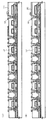
まず、実施形態1と同様にして図1(A)〜(D)までに示す工程を行い結晶質半導体膜1108を形成する。以降の工程は図2を用いて説明する。そして、結晶質半導体膜1108の表面にマスク用の絶縁膜(例えば酸化シリコン膜)1110を50〜200nm、例えば150nmの厚さに形成する。そしてエッチング処理により開孔1111を絶縁膜1110に形成してその部分の結晶質半導体膜1108の表面を露呈させる。
【0034】
そして、イオンドープ法などによりリンドープの工程を行い結晶質半導体膜1108にリンが添加された領域1112を形成する。この領域のリン濃度は特に限定されるものではないが、1×10¹⁸〜1×10²⁰atoms/cm3程度にすると良い。
【0035】
この状態で、窒素雰囲気中で550〜800℃、5〜24時間、例えば600℃、12時間の熱処理を行うと、結晶質半導体膜1108にリンが添加された領域1112がゲッタリングサイトとして働き、結晶質半導体膜1108に残存していた触媒元素をリンが添加された領域1112に偏析させることができる。
【0036】
そして、マスク用の絶縁膜1110はエッチングして除去しする。さらにリンが添加された領域1112をエッチングして除去することにより、熱結晶化法で使用した触媒元素の濃度を1×10¹⁷atoms/cm3以下にまで低減させるれたれた結晶質半導体膜1113を形成することができる。
【0037】
[実施形態3]
実施形態1では非晶質構造を有する半導体膜1103をプラズマCVD法でSiH4またはSiH4とH2から作製する例について示した。本実施形態では他のガスを用いて作製する場合について示す。
【0038】
本実施形態の作製方法の特徴は、非晶質構造を有する半導体膜1103はハロゲン元素と水素を含む反応ガスで形成することにある。具体的には、非晶質構造を有する半導体膜として例えば非晶質シリコン膜を作製する時にハロゲン元素と水素とを混合させる。ハロゲン元素としては特にフッ素を用いると良く、フッ素はシリコンに対しエッチングする作用があり、膜の堆積過程において結合の弱い部分を優先的にエッチングすることができる。また、水素を供給することにより膜中に残存してしまうフッ素濃度を低減させることができる。そして、フッ素と水素の作用を利用してボイドや空孔の少ない緻密な非晶質シリコン膜を作製することができる。このような効果は非晶質シリコン膜の他に非晶質シリコン・ゲルマニウム(a−SiGe)膜、非晶質炭化シリコン(a−SiC)膜,非晶質シリコン・スズ(a−SiSn)膜などにも適用することができる。
【0039】
フッ素と水素の供給方法は、非晶質半導体膜として非晶質シリコン膜を作製する場合には、反応ガスとして四フッ化珪素(SiF4)と水素(H2)、またはSiF4とSiH4、またはSiF4とSiH4とH2の組み合わせを選択することができる。SiF4の代わりにトリフロロシラン(SiHF3)、ジフロロシラン(SiH2F2)、モノフロロシラン(SiH3F)を適用することもできる。また、SiH4とF2を直接反応させても良い。さらに、非晶質シリコン・ゲルマニウム膜を作製する場合にはゲルマン(GeH4)や四フッ化ゲルマニウム(GeF4)を、非晶質炭化シリコンを作製する場合にはメタン(CH4)や四フッ化メタン(CF4)などを、非晶質シリコン・スズ膜を形成する場合には水素化スズ(SnH4)を適宣添加すれば良い。
【0040】
非晶質構造を有する半導体膜1103の厚さは25〜100nmの厚さで形成する。膜の堆積初期の段階ではフッ素の効果により下地膜1102の表面をフッ素化することができる。
【0041】
このようにフッ素と水素とを含む反応ガスで作製された非晶質構造を有する半導体膜1103には、成膜時の基板温度にも依存するが、膜中に水素が0.1〜20atomic%、フッ素が0.1〜10atomic%含有するように形成する。膜中に残存するフッ素や水素はその後の熱結晶化の工程で膜中から放出されて膜中に残存する濃度はさらに低下するが、緻密化した非晶質半導体膜と、最表面をフッ素で終端した下地膜との相互作用により<110>の配向性をより高めることができる。
【0042】
[実施形態4]
下地膜の表面または下地膜と非晶質半導体膜との界面をフッ素化する方法として、図1で示すように基板1101上に下地膜1102を形成し、そのまま非晶質半導体膜1103を形成した後で非晶質半導体膜1103の表面からフッ素を注入しても良い。その手法としてイオンドープ法やイオン注入法を用いる。
【0043】
イオンドープ法ではイオン原としてSiF4やヘリウム(He)希釈のF2を用いイオン化して非晶質半導体膜の表面から注入する。加速電圧は高めに設定して、非晶質半導体膜1103と下地膜1102との界面またはその近傍に注入されたフッ素の濃度分布のピークが存在するようにする。その場合、ピーク濃度は1×10¹⁹〜1×10²¹atoms/cm3となるようにする。イオンドープ法では質量分離されないのでフッ素以外の元素も同時に注入されてしまうが、液晶表示装置などの大面積基板を処理するのに適している。また、イオン注入法でも同様な濃度でフッ素を非晶質半導体膜1103と下地膜1102との界面またはその近傍に注入することができる。
【0044】
このようにフッ素を注入した状態で実施形態1と同様にして非晶質半導体膜1103に接して触媒元素を含有する層を設けて結晶化させると同様の効果を得ることができる。
【0045】
【実施例】
[実施例1]
本実施例では、本発明で作製される結晶化半導体膜を用いてTFTを作製する方法の一例について示す。図3〜図5に示すのは表示装置の一例であり、画素部の画素TFTおよび保持容量と、表示領域の周辺に設けられる駆動回路のTFTを同時に作製する方法について図3〜図5を用い工程に従って詳細に説明する。
【0046】
図3(A)において、基板101にはコーニング社の#7059ガラスや#1737ガラスなどに代表されるバリウムホウケイ酸ガラスやアルミノホウケイ酸ガラスなどのガラス基板などを用いる。ガラス基板は、ガラス歪み点よりも10〜20℃程度低い温度であらかじめ熱処理しておいても良い。そして、基板101のTFTを形成する表面に基板101からの不純物拡散を防ぐために、酸化シリコン膜、窒化シリコン膜または酸化窒化シリコン膜などの絶縁膜から成る下地膜102を形成する。例えば、プラズマCVD法でSiH4、NH3、N2Oから作製される酸化窒化シリコン膜102aを10〜200nm(好ましくは50〜100nm)、同様にSiH4、N2Oから作製される酸化窒化水素化シリコン膜102bを50〜200nm(好ましくは100〜150nm)の厚さに積層形成する。
【0047】
その後、下地膜として形成した酸化窒化水素化シリコン膜102bの表面処理を行いその表面をフッ素化する。例えば、下地膜102を形成したプラズマCVD装置を用い、SiF4ガスまたはNF3ガスを導入し、高周波電力を印加して前記ガスをプラズマ化してフッ素原子またはフッ素ラジカルを生成させる。こうして形成したプラズマに酸化窒化水素化シリコン膜102bの表面を晒すことにより、表面にフッ素またはフッ素ラジカルが供給され、フッ素の電気陰性度が酸素よりも大きいので酸素を置換してフッ素で表面の結合手を終端させることができる。
【0048】
そして、実施形態1または3に従って、下地膜102上に非晶質半導体膜を形成し、それを結晶化させて結晶質半導体膜を形成する。その結晶質半導体膜から図1(A)に示すように島状半導体膜104〜108を形成する。本実施例では、プラズマCVD法で非晶質シリコン膜を55nmの厚さに形成したものから、結晶質シリコン膜を形成する。非晶質シリコン膜はSiH4またはSiH4とH2を反応ガスとして用いプラズマCVD法を用いて形成する。或いは、反応ガスとしてSiF4と水H2、またはSiF4とSiH4、またはSiF4とSiH4とH2の組み合わせを選択することもできる。また、下地膜102と表面処理と非晶質半導体膜との形成はプラズマCVD装置を用いて連続的に処理することもできる。さらにこの連続的な処理を同一の反応室で行うこともできる。このようにして一旦大気雰囲気に晒すことなく連続的に処理することにより、酸化窒化水素化シリコン膜102bの表面の汚染を防ぐことが可能となり、作製するTFTの特性バラツキやしきい値電圧の変動を低減させることが可能となる。
【0049】
島状半導体膜を形成した後、プラズマCVD法またはスパッタ法により50〜100nmの厚さの酸化シリコン膜によるマスク層194を形成する。
【0050】
この状態で島状半導体膜に対し、TFTのしきい値電圧(Vth)を制御する目的でp型を付与する不純物元素を1×10¹⁶〜5×10¹⁷atoms/cm3程度の濃度で島状半導体膜の全面に添加しても良い。半導体に対してp型を付与する不純物元素には、ホウ素(B)、アルミニウム(Al)、ガリウム(Ga)など周期律表第13族の元素が知られている。その方法として、イオン注入法やイオンドープ法を用いることができるが、大面積基板を処理するにはイオンドープ法が適している。イオンドープ法ではジボラン(B2H6)をソースガスとして用いホウ素(B)を添加する。このような不純物元素の注入は必ずしも必要でなく省略しても差し支えないが、特にnチャネル型TFTのしきい値電圧を所定の範囲内に収めるために好適に用いる手法である。
【0051】
次に、駆動回路のnチャネル型TFTのLDD領域を形成するために、n型を付与する不純物元素を島状半導体膜105、107に選択的に添加する。あらかじめレジストマスク195a〜195eを形成する。n型を付与する不純物元素としては、リン(P)や砒素(As)を用いれば良く、ここではリン(P)を添加すべく、フォスフィン(PH3)を用いたイオンドープ法を適用する。形成された不純物領域は低濃度n型不純物領域196、197として、このリン(P)濃度は2×10¹⁶〜5×10¹⁹atoms/cm3の範囲とすれば良い。本明細書中では、ここで形成された不純物領域196、197に含まれるn型を付与する不純物元素の濃度を(n-)と表す。また、不純物領域198は、画素部の保持容量を形成するための半導体膜であり、この領域にも同じ濃度でリン(P)を添加する(図3(B))。
【0052】
その後、添加した不純物元素を活性化させる処理を行う。活性化の処理は実施形態7で説明したレーザーアニール法により行う。その条件の一例は、レーザーパルス発振周波数1kHzとし、レーザーエネルギー密度を100〜300mJ/cm2(代表的には150〜250mJ/cm2)とする。そして線状ビームを基板全面に渡って照射し、この時の線状ビームの重ね合わせ率(オーバーラップ率)を80〜99%(好ましくは、95〜99%)として行う。レーザーアニール法に用いるレーザー発振器には、ガスレーザーであるエキシマレーザーや固体レーザーであるYAGレーザー、YVO4レーザー、YAlO3レーザー、YLFレーザーなどを用いることができる。前記YAGレーザーなどの固体レーザーの場合には、その基本波(1064nm)の他にその第2高調波(532nm)、第3高調波(355nm)を用いることができる。
【0053】
ゲート絶縁膜109はプラズマCVD法またはスパッタ法を用い、膜厚を40〜150nmとしてシリコンを含む絶縁膜で形成する。例えば、120nmの厚さで酸化窒化シリコン膜から形成すると良い。また、SiH4とN2OにO2を添加させて作製された酸化窒化シリコン膜は、膜中の固定電荷密度が低減されているのでこの用途に対して好ましい材料となる。勿論、ゲート絶縁膜はこのような酸化窒化シリコン膜に限定されるものでなく、他のシリコンを含む絶縁膜を単層または積層構造として用いても良い。
【0054】
そして、図3(E)に示すように、ゲート絶縁膜109上にゲート電極を形成するための耐熱性導電層を形成する。耐熱性導電層は単層で形成しても良いが、必要に応じて二層あるいは三層といった複数の層から成る積層構造としても良い。このような耐熱性導電性材料を用い、導電層111を形成する。導電層111はタンタル(Ta)、チタン(Ti)、モリブデン(Mo)、タングステン(W)から選ばれた元素、または前記元素を主成分とする合金か、前記元素を組み合わせた合金膜(代表的にはMo−W合金膜、Mo−Ta合金膜)で形成すれば良い。このような材料から成る導電層111の下には窒化タンタル(TaN)、窒化タングステン(WN)、窒化チタン(TiN)膜、窒化モリブデン(MoN)などの窒化物、タングステンシリサイド、チタンシリサイド、モリブデンシリサイドなどのシリサイドを形成しておいても良い。導電層111は低抵抗化を図るために含有する不純物濃度を低減させることが好ましく、特に酸素濃度に関しては30ppm以下とすると良かった。例えば、タングステン(W)は酸素濃度を30ppm以下とすることで20μΩcm以下の比抵抗値を実現することができる。
【0055】
導電層111は200〜400nm(好ましくは250〜350nm)の厚さに形成する。例えば、導電層111をWで形成するには、Wをターゲットとしたスパッタ法で、アルゴン(Ar)ガスを導入して250nmの厚さに形成する。その他の方法として、W膜は6フッ化タングステン(WF6)を用いて熱CVD法で形成することもできる。いずれにしてもゲート電極として使用するためには低抵抗化を図る必要があり、W膜の抵抗率は20μΩcm以下にすることが望ましい。W膜は結晶粒を大きくすることで低抵抗率化を図ることができるが、W中に酸素などの不純物元素が多い場合には結晶化が阻害され高抵抗化する。このことより、スパッタ法による場合、純度99.9999%のWターゲットを用い、さらに成膜時に気相中からの不純物の混入がないように十分配慮してW膜を形成することにより、抵抗率9〜20μΩcmを実現することができる(図3(A))。
【0056】
次に、フォトリソグラフィーの技術を使用してレジストマスク112〜117を形成し、導電層111をエッチングしてゲート電極118〜122と容量配線123を形成する(図4(A))。
【0057】
導電層111をエッチングする方法は実施者が適宣選択すれば良いが、前述のようにWを主成分とする材料で形成されている場合には、高速でかつ精度良くエッチングを実施するために高密度プラズマを用いたドライエッチング法を適用することが望ましい。高密度プラズマを得る手法の一つとして、誘導結合プラズマ(Inductively Coupled Plasma:ICP)エッチング装置を用いると良い。ICPエッチング装置を用いたWのエッチング法は、エッチングガスにCF4とCl2の2種のガスを反応室に導入し、圧力0.5〜1.5Pa(好ましくは1Pa)とし、誘導結合部に200〜1000Wの高周波(13.56MHz)電力を印加する。この時、基板が置かれたステージには20Wの高周波電力が印加され、自己バイアスで負電位に帯電することにより、正イオンが加速されて異方性のエッチングを行うことができる。ICPエッチング装置を使用することにより、Wなどの硬い金属膜も2〜5nm/秒のエッチング速度を得ることができる。また、残渣を残すことなくエッチングするためには、10〜20%程度の割合でエッチング時間を増しオーバーエッチングをすると良い。しかし、この時に下地とのエッチングの選択比に注意する必要がある。例えば、W膜に対する酸化窒化シリコン膜(ゲート絶縁膜109)の選択比は2.5〜3であるので、このようなオーバーエッチング処理により、酸化窒化シリコン膜が露出した面は20〜50nm程度エッチングされて実質的に薄くなる。
【0058】
そして、画素TFTのnチャネル型TFTにLDD領域を形成するために、n型を付与する不純物元素添加の工程(n--ドープ工程)を行う。ゲート電極118〜122をマスクとして自己整合的にn型を付与する不純物元素をイオンドープ法で添加した。n型を付与する不純物元素として添加するリン(P)の濃度は1×10¹⁶〜5×10¹⁹atoms/cm3の濃度範囲で添加する。このようにして、図4(B)に示すように島状半導体膜に低濃度n型不純物領域124〜129を形成する。
【0059】
次に、nチャネル型TFTに対して、ソース領域またはドレイン領域として機能する高濃度n型不純物領域の形成を行う(n+ドープ工程)。まず、レジストのマスク130〜134を形成し、n型を付与する不純物元素を添加して高濃度n型不純物領域135〜140を形成する。n型を付与する不純物元素にはリン(P)を用い、その濃度が1×10²⁰〜1×10²¹atoms/cm3の濃度範囲となるようにフォスフィン(PH3)を用いたイオンドープ法で行う(図4(C))。
【0060】
そして、pチャネル型TFTを形成する島状半導体膜104、106にソース領域およびドレイン領域とする高濃度p型不純物領域144、145を形成する。ここでは、ゲート電極118、120をマスクとしてp型を付与する不純物元素を添加し、自己整合的に高濃度p型不純物領域を形成する。このときnチャネル型TFTを形成する島状半導体膜105、107、108はレジストマスク141〜143を形成し全面を被覆しておく。高濃度p型不純物領域144、145はジボラン(B2H6)を用いたイオンドープ法で形成する。この領域のボロン(B)濃度は3×10²⁰〜3×10²¹atoms/cm3となるようにする(図4(D))。
【0061】
この高濃度p型不純物領域144、145には、前工程においてリン(P)が添加されていて、高濃度p型不純物領域144a、145aには1×10²⁰〜1×10²¹atoms/cm3の濃度で、高濃度p型不純物領域144b、145bには1×1016〜5×1019atoms/cm3の濃度で含有しているが、この工程で添加するボロン(B)の濃度を1.5から3倍とすることにより、pチャネル型TFTのソース領域およびドレイン領域として機能する上で何ら問題は生じない。
【0062】
その後、図5(A)に示すように、ゲート電極およびゲート絶縁膜上から保護絶縁膜146を形成する。保護絶縁膜は酸化シリコン膜、酸化窒化シリコン膜、窒化シリコン膜、またはこれらを組み合わせた積層膜で形成すれば良い。いずれにしても保護絶縁膜146は無機絶縁物材料から形成する。保護絶縁膜146の膜厚は100〜200nmとする。ここで、酸化シリコン膜を用いる場合には、プラズマCVD法で、TEOS(Tetraethyl Orthosilicate)とO2とを混合し、反応圧力40Pa、基板温度300〜400℃とし、高周波(13.56MHz)電力密度0.5〜0.8W/cm2で放電させて形成する。酸化窒化シリコン膜を用いる場合には、プラズマCVD法でSiH4、N2O、NH3から作製される酸化窒化シリコン膜、またはSiH4、N2Oから作製される酸化窒化シリコン膜で形成すれば良い。この場合の作製条件は反応圧力20〜200Pa、基板温度300〜400℃とし、高周波(60MHz)電力密度0.1〜1.0W/cm2で形成することができる。また、SiH4、N2O、H2から作製される酸化窒化水素化シリコン膜を適用しても良い。窒化シリコン膜も同様にプラズマCVD法でSiH4、NH3から作製することが可能である。
【0063】
その後、それぞれの濃度で添加されたn型またはp型を付与する不純物元素を活性化する工程を行う。この工程はファーネスアニール炉を用いる熱アニール法で行うこともできるが、実施形態7で説明したレーザー光を用いた熱処理方法で活性化させても良い。この場合の熱処理条件は前述のものと同様なものとする。一方、熱アニール法で行う場合には酸素濃度が1ppm以下、好ましくは0.1ppm以下の窒素雰囲気中で400〜700℃、代表的には500〜600℃で行うものであり、本実施例では550℃で4時間の熱処理を行った。また、基板101に耐熱温度が低いプラスチック基板を用いる場合には、本発明のレーザー光を用いた熱処理方法を適用することが好ましい(図5(B))。
【0064】
熱処理を行った後、さらに、3〜100%の水素を含む雰囲気中で、300〜450℃で1〜12時間の熱処理を行い、島状半導体膜を水素化する工程を行った。この工程は熱的に励起された水素により島状半導体膜にある1016〜1018/cm3のダングリングボンドを終端する工程である。水素化の他の手段として、プラズマ水素化(プラズマにより励起された水素を用いる)を行っても良い。
【0065】
そして、有機絶縁物材料からなる層間絶縁膜147を1.0〜2.0μmの平均膜厚で形成する。有機樹脂材料としては、ポリイミド、アクリル、ポリアミド、ポリイミドアミド、BCB(ベンゾシクロブテン)等を使用することができる。例えば、基板に塗布後、熱重合するタイプのポリイミドを用いる場合には、クリーンオーブンで300℃で焼成して形成する。また、アクリルを用いる場合には、2液性のものを用い、主材と硬化剤を混合した後、スピナーを用いて基板全面に塗布した後、ホットプレートで80℃で60秒の予備加熱を行い、さらにクリーンオーブンで250℃で60分焼成して形成することができる。
【0066】
このように、層間絶縁膜を有機絶縁物材料で形成することにより、表面を良好に平坦化させることができる。また、有機樹脂材料は一般に誘電率が低いので、寄生容量を低減するできる。しかし、吸湿性があり保護膜としては適さないので、本実施例のように、保護絶縁膜146として形成した酸化シリコン膜、酸化窒化シリコン膜、窒化シリコン膜などと組み合わせて用いる必要がある。
【0067】
その後、所定のパターンのレジストマスクを形成し、それぞれの島状半導体膜に形成されたソース領域またはドレイン領域に達するコンタクトホールを形成する。コンタクトホールの形成はドライエッチング法により行う。この場合、エッチングガスにCF4、O2、Heの混合ガスを用い有機樹脂材料から成る層間絶縁膜をまずエッチングし、その後、続いてエッチングガスをCF4、O2として保護絶縁膜146をエッチングする。さらに、島状半導体膜との選択比を高めるために、エッチングガスをCHF3に切り替えてゲート絶縁膜をエッチングすることにより、良好にコンタクトホールを形成することができる。
【0068】
そして、導電性の金属膜をスパッタ法や真空蒸着法で形成し、レジストマスクパターンを形成し、エッチングによってソース配線148〜152とドレイン配線153〜157を形成する。ここで、ドレイン配線157は画素電極として機能するものである。図示していないが、本実施例ではこの電極を、Ti膜を50〜150nmの厚さで形成し、島状半導体膜のソースまたはドレイン領域を形成する半導体膜とコンタクトを形成し、そのTi膜上に重ねてアルミニウム(Al)を300〜400nmの厚さで形成して配線とする。
【0069】
この状態で水素化処理を行うとTFTの特性向上に対して好ましい結果が得られる。例えば、3〜100%の水素を含む雰囲気中で、300〜450℃で1〜12時間の熱処理を行うと良く、あるいはプラズマ水素化法を用いても同様の効果が得られる。また、このような熱処理により保護絶縁膜146や、下地膜102にに存在する水素を島状半導体膜104〜108に拡散させ水素化をすることもできる。いずれにしても、島状半導体膜104〜108中の欠陥密度を1016/cm3以下とすることが望ましく、そのために水素を0.01〜0.1atomic%程度付与すれば良い(図5(C))。
【0070】
こうして同一の基板上に、駆動回路のTFTと画素部の画素TFTとを有した基板を完成させることができる。駆動回路には第1のpチャネル型TFT200、第1のnチャネル型TFT201、第2のpチャネル型TFT202、第2のnチャネル型TFT203、画素部には画素TFT204、保持容量205が形成されている。本明細書では便宜上このような基板をアクティブマトリクス基板と呼ぶ。
【0071】
駆動回路の第1のpチャネル型TFT200には、島状半導体膜104にチャネル形成領域206、高濃度p型不純物領域から成るソース領域207a、207b、ドレイン領域208a,208bを有したシングルドレインの構造を有している。第1のnチャネル型TFT201には、島状半導体膜105にチャネル形成領域209、ゲート電極119と重なるLDD領域210、ソース領域212、ドレイン領域211を有している。このLDD領域において、ゲート電極119と重なるLDD領域をLovとするとそのチャネル長方向の長さは0.5〜3.0μm、好ましくは1.0〜2.0μmとした。nチャネル型TFTにおけるLDD領域の長さをこのようにすることにより、ドレイン領域近傍に発生する高電界を緩和して、ホットキャリアの発生を防ぎ、TFTの劣化を防止することができる。駆動回路の第2のpチャネル型TFT202は同様に、島状半導体膜106にチャネル形成領域213、高濃度p型不純物領域から成るソース領域214a、214b、ドレイン領域215a,215bを有したシングルドレインの構造を有している。第2のnチャネル型TFT203には、島状半導体膜107にチャネル形成領域216、ゲート電極121と一部が重なるLDD領域217、218、ソース領域220、ドレイン領域219が形成されている。このTFTのゲート電極と重なるLovの長さも0.5〜3.0μm、好ましくは1.0〜2.0μmとした。また、ゲート電極と重ならないLDD領域をLoffとして、このチャネル長方向の長さは0.5〜4.0μm、好ましくは1.0〜2.0μmとした。画素TFT204には、島状半導体膜108にチャネル形成領域221、222、LDD領域223〜225、ソースまたはドレイン領域226〜228を有している。LDD領域(Loff)のチャネル長方向の長さは0.5〜4.0μm、好ましくは1.5〜2.5μmである。さらに、容量配線123と、ゲート絶縁膜と同じ材料から成る絶縁膜と、画素TFT204のドレイン領域228に接続する半導体膜229とから保持容量205が形成されている。図5(C)では画素TFT204をダブルゲート構造としたが、シングルゲート構造でも良いし、複数のゲート電極を設けたマルチゲート構造としても差し支えない。
【0072】
図15は画素部のほぼ一画素分を示す上面図である。図中に示すA−A'断面が図5(C)に示す画素部の断面図に対応している。画素TFT204のゲート電極122は、図示されていないゲート絶縁膜を介してその下の島状半導体膜108と交差している。また、ゲート電極122はAlやCuなどの材料を用いて形成される低抵抗導電性材料から成るゲート配線900と島状半導体膜108の外側でコンタクトホールを介さず接触している。図示はしていないが、島状半導体膜108には、ソース領域、ドレイン領域、LDD領域が形成されている。また、256はソース配線152とソース領域226とのコンタクト部、257はドレイン配線157とドレイン領域228とのコンタクト部である。保持容量205は、画素TFT204のドレイン領域228から延在する半導体膜229とゲート絶縁膜を介して容量配線123が重なる領域で形成されている。この構成におて半導体膜229には価電子制御を目的とした不純物元素は添加されていない。
【0073】
以上の様な構成は、画素TFTおよび駆動回路が要求する仕様に応じて各回路を構成するTFTの構造を最適化し、半導体装置の動作性能と信頼性を向上させることを可能としている。さらにゲート電極を耐熱性を有する導電性材料で形成することによりLDD領域やソース領域およびドレイン領域の活性化を容易としている。このようなTFTを設けたアクティブマトリクス基板を作製するために、本発明の結晶化法を用いて<110>の配向性が高い結晶質シリコン膜を用いてTFTを作製することにより、電界効果移動度などの電気的特性を向上させることができる。また、個々のTFTの特性のバラツキを小さくすることができる。このようなアクティブマトリクス基板を用いて液晶表示装置やEL表示装置を作製することができる。
【0074】
[実施例2]
実施例1ではTFTのゲート電極の材料にWやTaなどの耐熱性導電性材料を用いる例を示した。このような材料を用いる理由は、ゲート電極形成後に価電子制御を目的として半導体膜に添加した不純物元素を400〜700℃の熱アニールによって活性化させること、エレクトロマイグレーションの防止、耐腐蝕性の向上など複数の要因に起因している。しかしながら、このような耐熱性導電性材料は面積抵抗で10Ω程度あり、画面サイズが4インチクラスかそれ以上の液晶表示装置やEL表示装置には適していない。ゲート電極に接続するゲート配線を同じ材料で形成すると、基板面上における引回し長さが必然的に大きくなり、配線抵抗の影響による遅延時間を無視することができなくなるためである。
【0075】
例えば、画素密度がVGAの場合、480本のゲート配線と640本のソース配線が形成され、XGAの場合には768本のゲート配線と1024本のソース配線が形成される。表示領域の画面サイズは、13インチクラスの場合対角線の長さは340mmとなり、18インチクラスの場合には460mmとなる。本実施例ではこのような液晶表示装置を実現する手段として、ゲート配線をAlや銅(Cu)などの低抵抗導電性材料で形成する方法について図6を用いて説明する。
【0076】
まず、実施例1と同様にして図3(A)〜図4(D)に示す工程を行う。そして、価電子制御を目的としてそれぞれの島状半導体膜に添加された不純物元素を活性化する処理を行う。この活性化の処理は実施形態7で示すレーザー光を用いた熱処理方法を用いることが最も好ましい。さらに、3〜100%の水素を含む雰囲気中で、300〜450℃で1〜12時間の熱処理を行い、島状半導体膜を水素化する処理を行う。この工程は熱的に励起された水素により半導体膜のダングリングボンドを終端する工程である。水素化の他の手段として、プラズマ水素化(プラズマにより励起された水素を用いる)を行っても良い(図6(A))。
【0077】
活性化および水素化の処理が終了したら、ゲート配線を低抵抗導電性材料で形成する。この低抵抗導電性層はAlやCuを主成分とする導電膜で形成する。例えば、Tiを0.1〜2重量%含むAl膜を導電膜として全面に形成する(図示せず)。導電膜は200〜400nm(好ましくは250〜350nm)とすれば良い。そして、フォトマスクを用いて所定のレジストパターンを形成し、エッチング処理して、ゲート配線163、164と容量配線165を形成する。エッチング処理はリン酸系のエッチング溶液によるウエットエッチングで導電膜を除去することにより、下地との選択加工性を保ってゲート配線を形成することができる。そして保護絶縁膜146を形成する(図6(B))。
【0078】
その後、実施例1と同様にして有機絶縁物材料から成る層間絶縁膜147、ソース配線148〜151、167、ドレイン配線153〜156、168を形成してアクティブマトリクス基板を完成させることができる。図7(A)、(B)はこの状態の上面図を示し、図7(A)のB−B'断面および図7(B)のC−C'断面は図6(C)のA−A'およびC−C'に対応している。図7(A)、(B)ではゲート絶縁膜、保護絶縁膜、層間絶縁膜を省略して示しているが、島状半導体膜104、105、108の図示されていないソースおよびドレイン領域にソース配線148、149、167とドレイン配線153、154、168がコンタクトホールを介して接続している。また、図7(A)のD−D'断面および図7(B)のE−E'断面を図8(A)と(B)にそれぞれ示す。ゲート配線163はゲート電極118、119と、またゲート配線164はゲート電極122と島状半導体膜104、105、108の外側で重なるように形成され、ゲート電極とゲート配線が接触して電気的に導通している。このようにゲート配線低抵抗導電性材料で形成することにより、配線抵抗を十分低減できる。従って、画素部(画面サイズ)が4インチクラス以上の液晶表示装置やEL表示装置に適用することができる。
【0079】
[実施例3]
実施例1で作製したアクティブマトリクス基板はそのまま反射型の液晶表示装置に適用することができる。一方、透過型の液晶表示装置とする場合には画素部の各画素に設ける画素電極を透明電極で形成すれば良い。本実施例では透過型の液晶表示装置に対応するアクティブマトリクス基板の作製方法について図10を用いて説明する。
【0080】
アクティブマトリクス基板は実施例1と同様に作製する。図10(A)では、ソース配線とドレイン配線は導電性の金属膜をスパッタ法や真空蒸着法で形成する。これは、Ti膜を50〜150nmの厚さで形成し、島状半導体膜のソースまたはドレイン領域を形成する半導体膜とコンタクトを形成し、そのTi膜上に重ねてアルミニウム(Al)を300〜400nmの厚さで形成し、さらにTi膜または窒化チタン(TiN)膜を100〜200nmの厚さで形成して3層構造とした。その後、透明導電膜を全面に形成し、フォトマスクを用いたパターニング処理およびエッチング処理により画素電極171を形成する。画素電極171は、層間絶縁膜147上に形成され、画素TFTのドレイン配線169と重なる部分を設け、接続構造を形成している。
【0081】
図10(B)では最初に層間絶縁膜147上に透明導電膜を形成し、パターニング処理およびエッチング処理をして画素電極193を形成した後、ドレイン配線169を画素電極193と重なる部分を設けて形成した例である。ドレイン配線169はTi膜を50〜150nmの厚さで形成し、島状半導体膜のソースまたはドレイン領域を形成する半導体膜とコンタクトを形成し、そのTi膜上に重ねてアルミニウム(Al)を300〜400nmの厚さで形成して設ける。この構成にすると、画素電極171はドレイン配線169を形成するTi膜のみと接触することになる。その結果、透明導電膜材料とAlとが反応するのを防止できる。
【0082】
透明導電膜の材料は、酸化インジウム(In2O3)や酸化インジウム酸化スズ合金(In2O3―SnO2;ITO)などをスパッタ法や真空蒸着法などを用いて形成して用いることができる。このような材料のエッチング処理は塩酸系の溶液により行う。しかし、特にITOのエッチングは残渣が発生しやすいので、エッチング加工性を改善するために酸化インジウム酸化亜鉛合金(In2O3―ZnO)を用いても良い。酸化インジウム酸化亜鉛合金は表面平滑性に優れ、ITOに対して熱安定性にも優れているので、ドレイン配線169の端面で接触するAlとの腐蝕反応を防止できる。同様に、酸化亜鉛(ZnO)も適した材料であり、さらに可視光の透過率や導電率を高めるためにガリウム(Ga)を添加した酸化亜鉛(ZnO:Ga)などを用いることができる。
【0083】
このようにして、透過型の液晶表示装置に対応したアクティブマトリクス基板を完成させることができる。本実施例では、実施例1と同様な工程として説明したが、このような構成は実施例2や実施例3で示すアクティブマトリクス基板に適用することができる。
【0084】
[実施例4]
実施形態1または実施形態3で示したように非晶質半導体膜の結晶化を助長する触媒元素を用いて結晶質半導体膜を得る方法は、電界効果移動度が高いTFTを作製する目的に対し有効である。しかしこの場合、結晶質半導体膜中には微量(1×10¹⁷〜1×10¹⁹atoms/cm3程度)の触媒元素が残留してしまう。勿論、そのような状態でもTFTを完成させることが可能であるが、オフ電流を下げる為に残留する触媒元素を少なくともチャネル形成領域から除去する方がより好ましい。この触媒元素を除去する手段の一つに実施形態2で示したようにリン(P)によるゲッタリング作用を利用する手段がある。
【0085】
リン(P)によるゲッタリング処理は、図5(B)で説明した活性化工程で同時に行うことができる。この様子を図9で説明する。ゲッタリングに必要なリン(P)の濃度は高濃度n型不純物領域の不純物濃度と同程度でよく、活性化工程の熱アニールにより、nチャネル型TFTおよびpチャネル型TFTのチャネル形成領域から触媒元素をその濃度でリン(P)を含有する不純物領域へ偏析させることができる(図9で示す矢印の方向)。その結果その不純物領域には1×10¹⁷〜1×10¹⁹atoms/cm3程度の触媒元素が偏析した。このようにして作製したTFTはオフ電流値が下がり、結晶性が良いことから高い電界効果移動度が得られ、良好な特性を達成することができる。
【0086】
[実施例5]
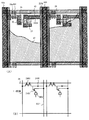
本実施例では実施例1で作製したアクティブマトリクス基板から、アクティブマトリクス型液晶表示装置を作製する工程を説明する。まず、図11(A)に示すように、図5(C)の状態のアクティブマトリクス基板に柱状スペーサから成るスペーサを形成する。スペーサは数μmの粒子を散布して設ける方法でも良いが、ここでは基板全面に樹脂膜を形成した後これをパターニングして形成する方法を採用する。このようなスペーサの材料に限定はないが、例えば、JSR社製のNN700を用い、スピナーで塗布した後、露光と現像処理によって所定のパターンに形成する。さらにクリーンオーブンなどで150〜200℃で加熱して硬化させる。このようにして作製されるスペーサは露光と現像処理の条件によって形状を異ならせることができるが、好ましくは、柱状スペーサ173の形状は柱状で頂部が平坦な形状となるようにすると、対向側の基板を合わせたときに液晶表示パネルとしての機械的な強度を確保することができる。形状は円錐状、角錐状など特別の限定はないが、例えば円錐状としたときに具体的には、その高さを1.2〜5μmとし、平均半径を5〜7μm、平均半径と底部の半径との比を1対1.5程度とする。このとき断面から見たテーパー角は±15°以下とすると良い。
【0087】
柱状スペーサの配置は任意に決定すれば良いが、好ましくは、図11(A)で示すように、画素部においてはドレイン配線161(画素電極)のコンタクト部235と重ねてその部分を覆うように柱状スペーサ168を形成すると良い。コンタクト部235は平坦性が損なわれこの部分では液晶がうまく配向しなくなるので、このようにしてコンタクト部235にスペーサ用の樹脂を充填する形で柱状スペーサ168を形成することでディスクリネーションなどを防止することができる。
【0088】
その後、配向膜174を形成する。通常液晶表示素子の配向膜にはポリイミド樹脂を用る。配向膜を形成した後、ラビング処理を施して液晶分子がある一定のプレチルト角を持って配向するようにした。画素部に設けた柱状スペーサ173の端部からラビング方向に対してラビングされない領域が2μm以下となるようにした。また、ラビング処理では静電気の発生がしばしば問題となるが、駆動回路のTFT上にもスペーサ172を形成しておくと、スペーサとしての本来の役割と、静電気からTFTを保護する効果を得ることができる。
【0089】
対向側の対向基板175には、遮光膜176、透明導電膜177および配向膜178を形成する。遮光膜176はTi、Cr、Alなどを150〜300nmの厚さで形成する。そして、画素部と駆動回路が形成されたアクティブマトリクス基板と対向基板とをシール剤179で貼り合わせる。シール剤179にはフィラー180が混入されていて、このフィラー180とスペーサ172、173によって均一な間隔を持って2枚の基板が貼り合わせられる。その後、両基板の間に液晶材料606を注入し、封止剤(図示せず)によって完全に封止する。液晶材料には公知の液晶材料を用いれば良い。このようにして図11(B)に示すアクティブマトリクス型の液晶表示装置が完成する。
【0090】
図11ではスペーサ172を駆動回路のTFT上の全面に形成する例を示したが、図12に示すようにこのスペーサを複数個に分割してスペーサ172a〜172eとして形成しても良い。駆動回路が形成されている部分に設けるスペーサは、このように少なくとも駆動回路のソース配線およびドレイン配線を覆うように形成すれば良い。このような構成とすることによって、駆動回路の各TFTは、保護絶縁膜146と層間絶縁膜147とスペーサ172またはスペーサ172a〜172eによって完全に覆われ保護されることになる。
【0091】
図13はスペーサとシール剤を形成したアクティブマトリクス基板の上面図を示し、画素部および駆動回路部とスペーサおよびシール剤の位置関係を示す上面図である。画素部188の周辺に駆動回路として走査信号駆動回路185と画像信号駆動回路186が設けられている。さらに、その他CPUやメモリなどの信号処理回路187も付加されていても良い。そして、これらの駆動回路は接続配線183によって外部入出力端子182と接続されている。画素部188では走査信号駆動回路185から延在するゲート配線群189と画像信号駆動回路186から延在するソース配線群190がマトリクス状に交差して画素を形成し、各画素にはそれぞれ画素TFT204と保持容量205が設けられている。
【0092】
画素部において設けられる柱状スペーサ173は、すべての画素に対して設けても良いが、マトリクス状に配列した画素の数個から数十個おきに設けても良い。即ち、画素部を構成する画素の全数に対するスペーサの数の割合は20〜100%とすると良い。また、駆動回路部に設けるスペーサ172、172'、172''はその全面を覆うように設けても良いし、図22で示したように各TFTのソースおよびドレイン配線の位置にあわせて複数個に分割して設けても良い。シール剤179は、基板101上の画素部188および走査信号制御回路185、画像信号制御回路186、その他の信号処理回路187の外側であって、外部入出力端子182よりも内側に形成する。
【0093】
このようなアクティブマトリクス型液晶表示装置の構成を図14の斜視図を用いて説明する。図14においてアクティブマトリクス基板は、ガラス基板101上に形成された、画素部188と、走査信号駆動回路185と、画像信号駆動回路186とその他の信号処理回路187とで構成される。画素部188には画素TFT204と保持容量205が設けられ、画素部の周辺に設けられる駆動回路はCMOS回路を基本として構成されている。走査信号駆動回路185と、画像信号駆動回路186はそれぞれゲート配線122とソース配線152で画素TFT204に接続している。また、フレキシブルプリント配線板(Flexible Printed Circuit:FPC)191が外部入力端子182に接続していて画像信号などを入力するのに用いる。そして接続配線183でそれぞれの駆動回路に接続している。また、対向基板175には図示していないが、遮光膜や透明電極が設けられている。
【0094】
このような構成の液晶表示装置は、実施例1〜4で示すアクティブマトリクス基板を用いて形成することができる。実施例1〜3で示すアクティブマトリクス基板を用いれば反射型の液晶表示装置が得られ、実施例4で示すアクティブマトリクス基板を用いると透過型の液晶表示装置を得ることができる。
【0095】
[実施例6]
本実施例では、実施例1で示したアクティブマトリクス基板を用いてエレクトロルミネッセンス(EL:Electro Luminescence)材料を用いた自発光型の表示パネル(以下、EL表示装置と記す)を作製する例について説明する。図16(A)は本発明を用いたEL表示パネルの上面図である。図16(A)において、10は基板、11は画素部、12はソース側駆動回路、13はゲート側駆動回路であり、それぞれの駆動回路は配線14〜16を経てFPC17に至り、外部機器へと接続される。
【0096】
図16(B)は図16(A)のA−A'断面を表す図であり、このとき少なくとも画素部上、好ましくは駆動回路及び画素部上に対向板80を設ける。対向板80はシール材19でTFTとEL材料を用いた自発光層が形成されているアクティブマトリクス基板と貼り合わされている。シール剤19にはフィラー(図示せず)が混入されていて、このフィラーによりほぼ均一な間隔を持って2枚の基板が貼り合わせられている。さらに、シール材19の外側とFPC17の上面及び周辺は封止剤81で密封する構造とする。封止剤81はシリコーン樹脂、エポキシ樹脂、フェノール樹脂、ブチルゴムなどの材料を用いる。
【0097】
このように、シール剤19によりアクティブマトリクス基板10と対向基板80とが貼り合わされると、その間には空間が形成される。その空間には充填剤83が充填される。この充填剤83は対向板80を接着する効果も合わせ持つ。充填剤83はPVC(ポリビニルクロライド)、エポキシ樹脂、シリコーン樹脂、PVB(ポリビニルブチラル)またはEVA(エチレンビニルアセテート)などを用いることができる。また、自発光層は水分をはじめ湿気に弱く劣化しやすいので、この充填剤83の内部に酸化バリウムなどの乾燥剤を混入させておくと吸湿効果を保持できるので望ましい。また、自発光層上に窒化シリコン膜や酸化窒化シリコン膜などで形成するパッシベーション膜82を形成し、充填剤83に含まれるアルカリ元素などによる腐蝕を防ぐ構造としていある。
【0098】
対向板80にはガラス板、アルミニウム板、ステンレス板、FRP(Fiberglass-Reinforced Plastics)板、PVF(ポリビニルフルオライド)フィルム、マイラーフィルム(デュポン社の商品名)、ポリエステルフィルム、アクリルフィルムまたはアクリル板などを用いることができる。また、数十μmのアルミニウム箔をPVFフィルムやマイラーフィルムで挟んだ構造のシートを用い、耐湿性を高めることもできる。このようにして、EL素子は密閉された状態となり外気から遮断されている。
【0099】
また、図16(B)において基板10、下地膜21の上に駆動回路用TFT(但し、ここではnチャネル型TFTとpチャネル型TFTを組み合わせたCMOS回路を図示している。)22及び画素部用TFT23(但し、ここではEL素子への電流を制御するTFTだけ図示している。)が形成されている。これらのTFTの内特にnチャネル型TFTにははホットキャリア効果によるオン電流の低下や、Vthシフトやバイアスストレスによる特性低下を防ぐため、本実施形態で示す構成のLDD領域が設けられている。
【0100】
例えば、駆動回路用TFT22とし、図5(C)に示すpチャネル型TFT200、202とnチャネル型TFT201、203を用いれば良い。また、画素部用TFT23には図5(B)に示す画素TFT204またはそれと同様な構造を有するpチャネル型TFTを用いれば良い。
【0101】
図5(C)または図6(C)の状態のアクティブマトリクス基板からEL表示装置を作製するには、ソース配線、ドレイン配線上に樹脂材料でなる層間絶縁膜(平坦化膜)26を形成し、その上に画素部用TFT23のドレインと電気的に接続する透明導電膜でなる画素電極27を形成する。透明導電膜には酸化インジウムと酸化スズとの化合物(ITOと呼ばれる)または酸化インジウムと酸化亜鉛との化合物を用いることができる。そして、画素電極27を形成したら、絶縁膜28を形成し、画素電極27上に開口部を形成する。
【0102】
次に、自発光層29を形成する。自発光層29は公知のEL材料(正孔注入層、正孔輸送層、発光層、電子輸送層または電子注入層)を自由に組み合わせて積層構造または単層構造とすれば良い。どのような構造とするかは公知の技術を用いれば良い。また、EL材料には低分子系材料と高分子系(ポリマー系)材料がある。低分子系材料を用いる場合は蒸着法を用いるが、高分子系材料を用いる場合には、スピンコート法、印刷法またはインクジェット法等の簡易な方法を用いることが可能である。
【0103】
自発光層はシャドーマスクを用いて蒸着法、またはインクジェット法、ディスペンサー法などで形成する。いずれにしても、画素毎に波長の異なる発光が可能な発光層(赤色発光層、緑色発光層及び青色発光層)を形成することで、カラー表示が可能となる。その他にも、色変換層(CCM)とカラーフィルターを組み合わせた方式、白色発光層とカラーフィルターを組み合わせた方式があるがいずれの方法を用いても良い。勿論、単色発光のEL表示装置とすることもできる。
【0104】
自発光層29を形成したら、その上に陰極30を形成する。陰極30と自発光層29の界面に存在する水分や酸素は極力排除しておくことが望ましい。従って、真空中で自発光層29と陰極30を連続して形成するか、自発光層29を不活性雰囲気で形成し、大気解放しないで真空中で陰極30を形成するといった工夫が必要である。本実施例ではマルチチャンバー方式(クラスターツール方式)の成膜装置を用いることで上述のような成膜を可能とする。
【0105】
なお、本実施例では陰極30として、LiF(フッ化リチウム)膜とAl(アルミニウム)膜の積層構造を用いる。具体的には自発光層29上に蒸着法で1nm厚のLiF(フッ化リチウム)膜を形成し、その上に300nm厚のアルミニウム膜を形成する。勿論、公知の陰極材料であるMgAg電極を用いても良い。そして陰極30は31で示される領域において配線16に接続される。配線16は陰極30に所定の電圧を与えるための電源供給線であり、異方性導電性ペースト材料32を介してFPC17に接続される。FPC17上にはさらに樹脂層80が形成され、この部分の接着強度を高めている。
【0106】
31に示された領域において陰極30と配線16とを電気的に接続するために、層間絶縁膜26及び絶縁膜28にコンタクトホールを形成する必要がある。これらは層間絶縁膜26のエッチング時(画素電極用コンタクトホールの形成時)や絶縁膜28のエッチング時(自発光層形成前の開口部の形成時)に形成しておけば良い。また、絶縁膜28をエッチングする際に、層間絶縁膜26まで一括でエッチングしても良い。この場合、層間絶縁膜26と絶縁膜28が同じ樹脂材料であれば、コンタクトホールの形状を良好なものとすることができる。また、配線16はシーリル19と基板10との間を隙間(但し封止剤81で塞がれている。)を通ってFPC17に電気的に接続される。なお、ここでは配線16について説明したが、他の配線14、15も同様にしてシーリング材18の下を通ってFPC17に電気的に接続される。
【0107】
ここで画素部のさらに詳細な断面構造を図17に、上面構造を図18(A)に、回路図を図18(B)に示す。図17(A)において、基板2401上に設けられたスイッチング用TFT2402は実施例1の図5(C)の画素TFT204と同じ構造で形成される。ダブルゲート構造とすることで実質的に二つのTFTが直列された構造となり、オフ電流値を低減することができるという利点がある。なお、本実施例ではダブルゲート構造としているがトリプルゲート構造やそれ以上のゲート本数を持つマルチゲート構造でも良い。
【0108】
また、電流制御用TFT2403は図5(C)で示すnチャネル型TFT201を用いて形成する。このとき、スイッチング用TFT2402のドレイン線35は配線36によって電流制御用TFTのゲート電極37に電気的に接続されている。また、38で示される配線は、スイッチング用TFT2402のゲート電極39a、39bを電気的に接続するゲート線である。
【0109】
このとき、電流制御用TFT2403が本発明の構造であることは非常に重要な意味を持つ。電流制御用TFTはEL素子を流れる電流量を制御するための素子であるため、多くの電流が流れ、熱による劣化やホットキャリアによる劣化の危険性が高い素子でもある。そのため、電流制御用TFTにゲート電極と一部が重なるLDD領域を設けることでTFTの劣化を防ぎ、動作の安定性を高めることができる。また、本発明により作製される配向性の高い結晶質半導体膜を用いることにより、TFTの特性である電界効果移動度やオン電流などを高めることができる。
【0110】
また、本実施例では電流制御用TFT2403をシングルゲート構造で図示しているが、複数のTFTを直列につなげたマルチゲート構造としても良い。さらに、複数のTFTを並列につなげて実質的にチャネル形成領域を複数に分割し、熱の放射を高い効率で行えるようにした構造としても良い。このような構造は熱による劣化対策として有効である。
【0111】
また、図18(A)に示すように、電流制御用TFT2403のゲート電極37となる配線は2404で示される領域で、電流制御用TFT2403のドレイン線40と絶縁膜を介して重なる。このとき、2404で示される領域ではコンデンサが形成される。このコンデンサ2404は電流制御用TFT2403のゲートにかかる電圧を保持するためのコンデンサとして機能する。なお、ドレイン線40は電流供給線(電源線)2501に接続され、常に一定の電圧が加えられている。
【0112】
スイッチング用TFT2402及び電流制御用TFT2403の上には第1パッシベーション膜41が設けられ、その上に樹脂絶縁膜でなる平坦化膜42が形成される。平坦化膜42を用いてTFTによる段差を平坦化することは非常に重要である。後に形成される自発光層は非常に薄いため、段差が存在することによって発光不良を起こす場合がある。従って、自発光層をできるだけ平坦面に形成しうるように画素電極を形成する前に平坦化しておくことが望ましい。
【0113】
また、43は反射性の高い導電膜でなる画素電極(EL素子の陰極)であり、電流制御用TFT2403のドレインに電気的に接続される。画素電極43としてはアルミニウム合金膜、銅合金膜または銀合金膜など低抵抗な導電膜またはそれらの積層膜を用いることが好ましい。勿論、他の導電膜との積層構造としても良い。また、絶縁膜(好ましくは樹脂)で形成されたバンク44a、44bにより形成された溝(画素に相当する)の中に発光層44が形成される。なお、ここでは一画素しか図示していないが、R(赤)、G(緑)、B(青)の各色に対応した発光層を作り分けても良い。発光層とする有機EL材料としてはπ共役ポリマー系材料を用いる。代表的なポリマー系材料としては、ポリパラフェニレンビニレン(PPV)系、ポリビニルカルバゾール(PVK)系、ポリフルオレン系などが挙げられる。尚、PPV系有機EL材料としては様々な型のものがあるが、例えば「H. Shenk,H.Becker,O.Gelsen,E.Kluge,W.Kreuder,and H.Spreitzer,“Polymers for Light Emitting Diodes”,Euro Display,Proceedings,1999,p.33-37」や特開平10−92576号公報に記載されたような材料を用いれば良い。
【0114】
具体的な発光層としては、赤色に発光する発光層にはシアノポリフェニレンビニレン、緑色に発光する発光層にはポリフェニレンビニレン、青色に発光する発光層にはポリフェニレンビニレン若しくはポリアルキルフェニレンを用いれば良い。膜厚は30〜150nm(好ましくは40〜100nm)とすれば良い。但し、以上の例は発光層として用いることのできる有機EL材料の一例であって、これに限定する必要はまったくない。発光層、電荷輸送層または電荷注入層を自由に組み合わせて自発光層(発光及びそのためのキャリアの移動を行わせるための層)を形成すれば良い。例えば、本実施例ではポリマー系材料を発光層として用いる例を示したが、低分子系有機EL材料を用いても良い。また、電荷輸送層や電荷注入層として炭化珪素等の無機材料を用いることも可能である。これらの有機EL材料や無機材料は公知の材料を用いることができる。
【0115】
本実施例では発光層45の上にPEDOT(ポリチオフェン)またはPAni(ポリアニリン)でなる正孔注入層46を設けた積層構造の自発光層としている。そして、正孔注入層46の上には透明導電膜でなる陽極47が設けられる。本実施例の場合、発光層45で生成された光は上面側に向かって(TFTの上方に向かって)放射されるため、陽極は透光性でなければならない。透明導電膜としては酸化インジウムと酸化スズとの化合物や酸化インジウムと酸化亜鉛との化合物を用いることができるが、耐熱性の低い発光層や正孔注入層を形成した後で形成するため、可能な限り低温で成膜できるものが好ましい。
【0116】
陽極47まで形成された時点で自発光素子2405が完成する。なお、ここでいうEL素子2405は、画素電極(陰極)43、発光層45、正孔注入層46及び陽極47で形成されたコンデンサを指す。図18(A)に示すように画素電極43は画素の面積にほぼ一致するため、画素全体がEL素子として機能する。従って、発光の利用効率が非常に高く、明るい画像表示が可能となる。
【0117】
ところで、本実施例では、陽極47の上にさらに第2パッシベーション膜48を設けている。第2パッシベーション膜48としては窒化珪素膜または窒化酸化珪素膜が好ましい。この目的は、外部とEL素子とを遮断することであり、有機EL材料の酸化による劣化を防ぐ意味と、有機EL材料からの脱ガスを抑える意味との両方を併せ持つ。これによりEL表示装置の信頼性が高められる。
【0118】
以上のように本願発明のEL表示パネルは図18のような構造の画素からなる画素部を有し、オフ電流値の十分に低いスイッチング用TFTと、ホットキャリア注入に強い電流制御用TFTとを有する。従って、高い信頼性を有し、且つ、良好な画像表示が可能なEL表示パネルが得られる。
【0119】
図17(B)は自発光層の構造を反転させた例を示す。電流制御用TFT2601は図5(B)のpチャネル型TFT200を用いて形成される。作製プロセスは実施例1を参照すれば良い。本実施例では、画素電極(陽極)50として透明導電膜を用いる。具体的には酸化インジウムと酸化亜鉛との化合物でなる導電膜を用いる。勿論、酸化インジウムと酸化スズとの化合物でなる導電膜を用いても良い。
【0120】
そして、絶縁膜でなるバンク51a、51bが形成された後、溶液塗布によりポリビニルカルバゾールでなる発光層52が形成される。その上にはカリウムアセチルアセトネート(acacKと表記される)でなる電子注入層53、アルミニウム合金でなる陰極54が形成される。この場合、陰極54がパッシベーション膜としても機能する。こうしてEL素子2602が形成される。本実施例の場合、発光層53で発生した光は、矢印で示されるようにTFTが形成された基板の方に向かって放射される。本実施例のような構造とする場合、電流制御用TFT2601はpチャネル型TFTで形成することが好ましい。
【0121】
以上のような本実施例の構成は、実施形態1〜3に示す本発明の方法で配向性の高い結晶質半導体膜を作製し、実施例1〜2のTFTの構成を自由に組み合わせて実施することが可能である。また、実施例8の電子機器の表示部として本実施例のEL表示パネルを用いることは有効である。
【0122】
[実施例7]
本実施例では、図18(B)に示した回路図とは異なる構造の画素とした場合の例について図19に示す。なお、本実施例において、2701はスイッチング用TFT2702のソース配線、2703はスイッチング用TFT2702のゲート配線、2704は電流制御用TFT、2705はコンデンサ、2706、2708は電流供給線、2707はEL素子とする。
【0123】
図19(A)は、二つの画素間で電流供給線2706を共通とした場合の例である。即ち、二つの画素が電流供給線2706を中心に線対称となるように形成されている点に特徴がある。この場合、電源供給線の本数を減らすことができるため、画素部をさらに高精細化することができる。
【0124】
また、図19(B)は、電流供給線2708をゲート配線2703と平行に設けた場合の例である。尚、図19(B)では電流供給線2708とゲート配線2703とが重ならないように設けた構造となっているが、両者が異なる層に形成される配線であれば、絶縁膜を介して重なるように設けることもできる。この場合、電源供給線2708とゲート配線2703とで専有面積を共有させることができるため、画素部をさらに高精細化することができる。
【0125】
また、図19(C)は、図19(B)の構造と同様に電流供給線2708をゲート配線2703と平行に設け、さらに、二つの画素を電流供給線2708を中心に線対称となるように形成する点に特徴がある。また、電流供給線2708をゲート配線2703のいずれか一方と重なるように設けることも有効である。この場合、電源供給線の本数を減らすことができるため、画素部をさらに高精細化することができる。図19(A)、図19(B)では電流制御用TFT2403のゲートにかかる電圧を保持するためにコンデンサ2404を設ける構造としているが、コンデンサ2404を省略することも可能である。
【0126】
電流制御用TFT2403として図17(A)に示すような本願発明のnチャネル型TFTを用いているため、ゲート絶縁膜を介してゲート電極(と重なるように設けられたLDD領域を有している。この重なり合った領域には一般的にゲート容量と呼ばれる寄生容量が形成されるが、本実施例ではこの寄生容量をコンデンサ2404の代わりとして積極的に用いる点に特徴がある。この寄生容量のキャパシタンスは上記ゲート電極とLDD領域とが重なり合った面積で変化するため、その重なり合った領域に含まれるLDD領域の長さによって決まる。また、図19(A)、(B)、(C)の構造においても同様にコンデンサ2705を省略することは可能である。
【0127】
以上のような本実施例の構成は、実施形態1〜3に示す本発明の方法で配向性の高い結晶質半導体膜を作製し、実施例1〜2のTFTの構成を自由に組み合わせて実施することが可能である。また、実施例8の電子機器の表示部として本実施例のEL表示パネルを用いることは有効である。
【0128】
[実施例8]
本実施例では、本発明のTFT回路によるアクティブマトリクス型液晶表示装置を組み込んだ半導体装置について図20、図21、図22で説明する。
【0129】
このような半導体装置には、携帯情報端末(電子手帳、モバイルコンピュータ、携帯電話等)、ビデオカメラ、スチルカメラ、パーソナルコンピュータ、テレビ等が挙げられる。それらの一例を図20と図21に示す。
【0130】
図20(A)は携帯電話であり、本体9001、音声出力部9002、音声入力部9003、表示装置9004、操作スイッチ9005、アンテナ9006から構成されている。本発明はアクティブマトリクス基板を備えた表示装置9004に適用することができる。
【0131】
図20(B)はビデオカメラであり、本体9101、表示装置9102、音声入力部9103、操作スイッチ9104、バッテリー9105、受像部9106から成っている。本発明はアクティブマトリクス基板を備えた表示装置9102、受像部9106として設けられるイメージセンサーの読み取り回路を構成するTFTなどに適用することができる。
【0132】
図20(C)はモバイルコンピュータ或いは携帯型情報端末であり、本体9201、カメラ部9202、受像部9203、操作スイッチ9204、表示装置9205で構成されている。本発明は受像部9203として設けられるイメージセンサーの読み取り回路を構成するTFTやアクティブマトリクス基板を備えた表示装置9205に適用することができる。
【0133】
図20(D)はヘッドマウントディスプレイであり、本体9301、表示装置9302、アーム部9303で構成される。本発明は表示装置9302に適用することができる。また、表示されていないが、その他の信号制御用回路を形成するTFTなどに使用することもできる。
【0134】
図20(E)はテレビであり、本体9401、スピーカー9402、表示装置9403、受信装置9404、増幅装置9405等で構成される。実施例5で示す液晶表示装置や、実施例6または7で示すEL表示装置は表示装置9403に適用することができる。
【0135】
図20(F)は携帯書籍であり、本体9501、表示装置9502、9503、記憶媒体9504、操作スイッチ9505、アンテナ9506から構成されており、ミニディスク(MD)やDVDに記憶されたデータや、アンテナで受信したデータを表示するものである。表示装置9502、9503は直視型の表示装置であり本発明はこれらに適用することができる。
【0136】
図21(A)はパーソナルコンピュータであり、本体9601、画像入力部9602、表示装置9603、キーボード9604で構成される。実施例5で示す液晶表示装置や、実施例6または7で示すEL表示装置は表示装置9603に適用することができる。
【0137】
図21(B)はプログラムを記録した記録媒体(以下、記録媒体と呼ぶ)を用いるプレーヤーであり、本体9701、表示装置9702、スピーカ部9703、記録媒体9704、操作スイッチ9705で構成される。なお、この装置は記録媒体としてDVD(Digtial Versatile Disc)、CD等を用い、音楽鑑賞や映画鑑賞やゲームやインターネットを行うことができる。実施例5で示す液晶表示装置や、実施例6または7で示すEL表示装置は表示装置9702に適用することができる。
【0138】
図21(C)はデジタルカメラであり、本体9801、表示装置9802、接眼部9803、操作スイッチ9804、受像部(図示しない)で構成される。実施例5で示す液晶表示装置や、実施例6または7で示すEL表示装置は表示装置9802に適用することができる。
【0139】
図22(A)はフロント型プロジェクターであり、投射装置3601、スクリーン3602で構成される。本発明は投射装置3601やその他の信号制御回路に適用することができる。
【0140】
図22(B)はリア型プロジェクターであり、本体3701、投射装置3702、ミラー3703、スクリーン3704で構成される。本発明は投射装置3702やその他の信号制御回路に適用することができる。
【0141】
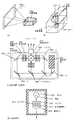
尚、図22(C)は、図22(A)及び図22(B)中における投射装置3601、3702の構造の一例を示した図である。投射装置3601、3702は、光源光学系3801、ミラー3802、3804〜3806、ダイクロイックミラー3803、プリズム3807、液晶表示装置3808、位相差板3809、投射光学系3810で構成される。投射光学系3810は、投射レンズを含む光学系で構成される。本実施例は三板式の例を示したが、特に限定されず、例えば単板式であってもよい。また、図22(C)中において矢印で示した光路に実施者が適宜、光学レンズや、偏光機能を有するフィルムや、位相差を調節するためのフィルム、IRフィルム等の光学系を設けてもよい。
【0142】
また、図22(D)は、図22(C)中における光源光学系3801の構造の一例を示した図である。本実施例では、光源光学系3801は、リフレクター3811、光源3812、レンズアレイ3813、3814、偏光変換素子3815、集光レンズ3816で構成される。なお、図22(D)に示した光源光学系は一例であって特に限定されない。例えば、光源光学系に実施者が適宜、光学レンズや、偏光機能を有するフィルムや、位相差を調節するフィルム、IRフィルム等の光学系を設けてもよい。
【0143】
【発明の効果】
本発明を用いることにより非晶質半導体膜を熱結晶化法やレーザー結晶化法を用いて作製される結晶質半導体膜の配向性を高めることができる。さらに、そのような結晶質半導体膜を用いることでTFTの特性を向上させ、特性バラツキを低減させることができる。
【図面の簡単な説明】
【図1】 本発明の結晶化方法の工程を示す図。
【図2】 本発明の結晶化方法の工程を示す図。
【図3】 画素TFT、駆動回路のTFTの作製工程を示す断面図。
【図4】 画素TFT、駆動回路のTFTの作製工程を示す断面図。
【図5】 画素TFT、駆動回路のTFTの作製工程を示す断面図。
【図6】 画素TFT、駆動回路のTFTの作製工程を示す断面図。
【図7】 駆動回路のTFTと画素TFTの構造を示す上面図。
【図8】 駆動回路のTFTと画素TFTの構造を示す断面図。
【図9】 画素TFT、駆動回路のTFTの作製工程を示す断面図。
【図10】 画素TFT、駆動回路のTFTの作製工程を示す断面図。
【図11】 アクティブマトリクス型液晶表示装置の作製工程を示す断面図。
【図12】 アクティブマトリクス型液晶表示装置の構成を示す断面図。
【図13】 液晶表示装置の入力端子、配線、回路配置、スペーサ、シール剤の配置を説明する上面図。
【図14】 液晶表示装置の構成を説明する斜視図。
【図15】 画素部の画素を示す上面図。
【図16】 EL表示装置の構造を示す上面図及び断面図。
【図17】 EL表示装置の画素部の断面図。
【図18】 EL表示装置の画素部の上面図と回路図。
【図19】 EL表示装置の画素部の回路図の例。
【図20】 半導体装置の一例を示す図。
【図21】 半導体装置の一例を示す図。
【図22】 投影型液晶表示装置の構成を示す図。[0001]
BACKGROUND OF THE INVENTION
The present invention relates to a semiconductor film having a crystal structure and a method for manufacturing a semiconductor device manufactured using the semiconductor film. Note that in this specification, a semiconductor device includes an electro-optical device such as a liquid crystal display device or an EL display device using an electroluminescence (EL) material, and an electronic device including the electro-optical device as a component.
[0002]
[Prior art]
A thin film transistor (hereinafter referred to as TFT) can be manufactured using a semiconductor film formed over a substrate. A TFT can form various integrated circuits as an active element. In particular, as a switching element provided in a pixel portion of an active matrix type liquid crystal display device or as an element forming a drive circuit provided in the periphery of the pixel portion. Can be used.
[0003]
A TFT using an amorphous silicon film as a semiconductor film has a low process temperature and is easy to produce, but has a drawback of low electrical characteristics. Therefore, although there is a usage form as a switching element provided in each pixel, a driving circuit for the pixel portion cannot be formed. On the other hand, it is known that when a TFT is formed using a semiconductor film having a crystal structure (hereinafter referred to as a crystalline semiconductor film), electrical characteristics can be improved. A silicon film is typically used as the semiconductor film, but a silicon film having a crystal structure is also known as a polycrystalline silicon film, a polysilicon film, a microcrystalline silicon film, or the like. In the technical field of TFT, a crystalline silicon film obtained by crystallizing an amorphous silicon film with light or heat energy is used.
[0004]
However, the thermal crystallization method using thermal energy requires heat treatment at a temperature of 600 ° C. or higher, and the processing time is about 10 hours. Therefore, when mass-producing a product using TFT such as an active matrix type liquid crystal display device, there is a problem that the productivity is lowered. On the other hand, a laser crystallization method using excimer laser light or YAG laser light is known as a crystallization technique using light energy, but the electrical characteristics are inferior to TFTs manufactured by thermal crystallization. There is.
[0005]
In addition, a technique for forming a crystalline semiconductor film by a thermal crystallization method using a catalytic element is known. For example, the techniques disclosed in Japanese Patent Laid-Open Nos. 7-130652 and 8-78329 can be used. According to the thermal crystallization method using a catalytic element, a crystalline silicon film can be formed by introducing a catalytic element such as nickel into an amorphous silicon film and performing a heat treatment at 550 ° C. for 4 hours.
[0006]
[Problems to be solved by the invention]
It is obtained by forming a base film made of silicon oxide, silicon nitride, silicon oxynitride, etc. on a substrate such as glass and crystallizing the amorphous semiconductor film deposited thereon by thermal crystallization or laser crystallization. The crystalline semiconductor film is preferentially oriented to <111> in consideration of the magnitude relationship of the interfacial energy between the base film and the semiconductor film, and there are many crystal grains having random orientations in other directions. This is known from the analysis of electron diffraction. On the other hand, in the crystalline semiconductor film manufactured by the thermal crystallization method using a catalytic element such as nickel, most of the crystal grains are oriented in <110>. However, as described above, other orientations such as <111> are slightly mixed in consideration of the interfacial energy between the base film and the semiconductor film.
[0007]
In a crystalline semiconductor film composed of a plurality of crystal grains, if the orientation is low, a large number of dangling bonds are formed at the crystal grain boundaries, and the transport properties of carriers (electrons and holes) in the crystalline semiconductor film are degraded. That is, since carriers are scattered or trapped, a TFT having a high field effect mobility cannot be manufactured even when a TFT is manufactured using such a crystalline semiconductor film. Further, since crystal grain boundaries exist randomly, it becomes a factor of variation in electrical characteristics of individual TFTs.
[0008]
An object of the present invention is to provide means for solving such problems, and to enhance the orientation of a crystalline semiconductor film produced by using a thermal crystallization method or a laser crystallization method for an amorphous semiconductor film. For the purpose. It is another object of the present invention to improve TFT characteristics and reduce characteristic variations by using such a crystalline semiconductor film.
[0009]
[Means for Solving the Problems]
In order to solve the above problems, the configuration of the present invention includes a first step of forming a first insulating film on a substrate and a second step of forming an amorphous semiconductor film on the first insulating film. And a third step of injecting fluorine from the surface of the amorphous semiconductor film, and adding a catalytic element in the amorphous semiconductor film or in contact with the amorphous semiconductor film to promote crystallization of the amorphous semiconductor film A fourth step of performing a first heat treatment on the amorphous semiconductor film to form a crystalline semiconductor film, and further irradiating the crystalline semiconductor film with laser light to provide the crystal A sixth step for increasing the crystallinity of the crystalline semiconductor film may be added.
[0010]
According to another aspect of the invention, there is provided a first step of forming a first insulating film on a substrate, a second step of fluorinating the surface of the first insulating film, and a first step on the first insulating film. A third step of forming an amorphous semiconductor film, and a fourth step of adding a catalyst element in the amorphous semiconductor film or in contact with the amorphous semiconductor film to promote crystallization of the amorphous semiconductor film And a fifth step of performing a first heat treatment on the amorphous semiconductor film to form a crystalline semiconductor film, and further irradiating the crystalline semiconductor film with laser light to crystallize the crystalline semiconductor film. It is also effective to perform the sixth step for improving the property.
[0011]
According to another aspect of the invention, there is provided a first step of forming a first insulating film on a substrate, a second step of fluorinating the surface of the first insulating film, and a first step on the first insulating film. A third step of forming an amorphous semiconductor film from a reaction gas containing at least fluorine and hydrogen; and crystallization of the amorphous semiconductor film in or in contact with the amorphous semiconductor film A fourth step of adding a catalytic element to be formed, and a fifth step of heat-treating the amorphous semiconductor film to form a crystalline semiconductor film, and further irradiating the crystalline semiconductor film with laser light It is also possible to perform a sixth step for increasing the crystallinity of the crystalline semiconductor film.
[0012]
According to another aspect of the invention, there is provided a first step of forming a first insulating film on a substrate, a second step of fluorinating the surface of the first insulating film, and a first step on the first insulating film. A third step of forming an amorphous semiconductor film, and a fourth step of adding a catalytic element in the amorphous semiconductor film or in contact with the amorphous semiconductor film to promote crystallization of the amorphous semiconductor film; A fifth step of forming a crystalline semiconductor film by first heat-treating the amorphous semiconductor film, and a sixth step of forming a region to which phosphorus is added in a selected region of the crystalline semiconductor film Process,
And a seventh step of performing a second heat treatment after the sixth step.
[0013]
According to another aspect of the invention, there is provided a first step of forming a first insulating film on a substrate, a second step of fluorinating the surface of the first insulating film, and a first step on the first insulating film. A third step of forming an amorphous semiconductor film from a reaction gas containing at least fluorine and hydrogen; and crystallization of the amorphous semiconductor film in or in contact with the amorphous semiconductor film Phosphorus is added to a selected region of the crystalline semiconductor film, a fourth step of adding a catalytic element to be added, a fifth step of heat-treating the amorphous semiconductor film to form a crystalline semiconductor film, and It has a sixth step of forming a region and a seventh step of performing a second heat treatment after the sixth step.
[0014]
In the structure of the present invention, the step of fluorinating the surface of the first insulating film may be performed by exposing to a plasma containing fluorine atoms or fluorine radicals, or using silicon tetrafluoride or nitrogen trifluoride as the plasma. It may be done by exposing it to a tempered atmosphere.
[0015]
DETAILED DESCRIPTION OF THE INVENTION
[Embodiment 1]
In FIG. 1A, an alkali-free glass substrate such as barium borosilicate glass or alumino borosilicate glass is used for the substrate 1001. For example, Corning # 7059 glass or # 1737 glass base can be preferably used. In addition to the quartz substrate, a ceramic substrate or a stainless steel substrate on which an insulating film such as a silicon oxide film or a silicon nitride film is formed can be used.
[0016]
An insulating surface containing silicon such as a silicon oxide film, a silicon nitride film, or a silicon oxynitride (SiOxNy) film is formed on the surface of the
[0017]
The base film 1102 may be formed of one layer of the above material or a stacked structure of two or more layers. In any case, it is formed to have a thickness of about 100 to 300 nm. For example, SiH by plasma CVD method Four , NH Three , N 2 A first silicon oxynitride film 1102a made of O is formed to a thickness of 10 to 100 nm, and SiH Four , N 2 A base film 1102 is formed as a two-layer structure in which a second
[0018]
The first silicon oxynitride film 1102a is formed by using a conventional parallel plate type plasma CVD method. An example of the production conditions is SiH Four 10SCCM, NH Three To 100 SCCM, N 2 O was introduced into the reaction chamber as 20 SCCM, the substrate temperature was 325 ° C., the reaction pressure was 40 Pa, and the discharge power density was 0.41 W / cm. 2 The discharge frequency is 60 MHz. On the other hand, an example of conditions for forming the second
[0019]
After the base film 1102 is formed, the surface treatment is performed. This is a surface treatment using a halogen element, and is intended to expose the surface of the base film 1102 in an atmosphere of fluorine or fluorine radicals and coat the surface with fluorine. In addition, chlorine, bromine, etc. can be used as the halogen element.
[0020]
Specifically, silicon tetrafluoride (SiF Four ) Or nitrogen trifluoride (NF) Three ) To form plasma and generate fluorine atoms or fluorine radicals. For example, a plasma CVD apparatus can be applied. As the plasma CVD apparatus, any type of apparatus such as a capacitively coupled type or an inductively coupled type, an ECR (electron cycloton resonance) plasma CVD apparatus, or a microwave CVD apparatus may be applied. In particular, since ECR plasma and microwave plasma have high gas decomposition efficiency, fluorine radicals can be generated efficiently.
[0021]
In the example of FIG. 1A, since the first silicon oxynitride film 1102a and the second
[0022]
Then, as shown in FIG. 1B, a
[0023]
Then, a
[0024]
In the crystallization step shown in FIG. 1C, first, heat treatment is performed at 400 to 500 ° C. for about 1 hour, so that the amount of hydrogen contained in the amorphous silicon film is 5 atom% or less. When the amount of hydrogen contained in the amorphous silicon film is this value from the beginning after the film formation, this heat treatment is not necessarily required. Then, thermal crystallization is performed in a nitrogen atmosphere at 550 to 600 ° C. for 1 to 8 hours using a furnace annealing furnace. Preferably, heat treatment is performed at 550 ° C. for 4 hours. Thus, a
[0025]
However, when the
[0026]
Laser light sources used in the laser crystallization method include excimer laser, YAG laser, YVO Four Laser, YAlO Three A laser, a YLF laser, or the like can be used. An excimer laser can radiate light having a wavelength of 400 nm or less with high output, and thus can be suitably used for crystallization of a semiconductor film. On the other hand, YAG laser, YVO Four Laser, YAlO Three A solid laser such as a laser or a YLF laser uses the second harmonic (532 nm), the third harmonic (355 nm), and the fourth harmonic (266 nm). Due to the penetration depth of light, the second harmonic (532 nm) is used from the surface and inside of the semiconductor film, and the third harmonic (355 nm) and the fourth harmonic (266 nm) are used in the same manner as the excimer laser. Crystallization can be performed by heating from the surface of the semiconductor film.
[0027]
FIG. 1D shows such a state. For example, an Nd: YAG laser is used, its pulse oscillation frequency is 1 to 10 kHz, and the laser energy density is 100 to 500 mJ / cm. 2 (Typically 100-400mJ / cm 2 ), The
[0028]
A crystalline semiconductor film manufactured by a thermal crystallization method or a laser crystallization method has low interface energy between silicon oxide or silicon oxynitride and silicon formed as a base film. Electron diffraction analysis shows that when crystallizing a crystalline silicon film by thermal crystallization or laser crystallization, <111> is preferentially oriented and there are many other grains with random orientations. Known from. On the other hand, a crystalline silicon film manufactured by a thermal crystallization method using a catalytic element such as nickel has a structure in which a plurality of needle-like or rod-like crystals are aggregated when viewed microscopically. However, it is expected that the continuity of adjacent crystal grains is high and almost no dangling bonds are formed. Most of the crystal grains are oriented to <110>. One reason is that the crystal growth process using a catalyst element such as nickel is considered to involve the silicide of the catalyst element, and the semiconductor film is as thin as 25 to 100 nm. Among the initial nuclei, those whose (111) plane is substantially perpendicular to the substrate surface preferentially grow, so it is considered that the <110> orientation is substantially increased. However, as described above, since the interface energy between silicon oxide and silicon is low, other plane orientations included in the <111> crystal zone can be taken. Accordingly, other orientations are mixed slightly.
[0029]
However, in the thermal crystallization method using a catalytic element, the surface of the silicon oxide film, silicon nitride film, silicon oxynitride film, etc. formed as the base film is terminated with fluorine, so that the influence of the interface with the base is affected. Can be reduced and the effect can be substantially ignored. As a result, the crystal orientation is influenced only by the surface energy, but the <110> orientation is enhanced in crystal growth using a catalytic element. Such an effect can be realized by a normal thermal crystallization method, a laser crystallization method, or the like, but can be obtained more significantly by a thermal crystallization method using a catalytic element.
[0030]
A TFT can be manufactured using the
[0031]
[Embodiment 2]
In the crystalline semiconductor film manufactured in Embodiment 1, the catalyst element used in the thermal crystallization is 1 × 10. 17 ~ 1x10 20 atoms / cm Three It remains in the film at a certain concentration. Of course, an element such as a TFT can be manufactured and operated even in this state, but it is more preferable to remove the catalytic element from the film. In this embodiment, in the thermal crystallization method using the catalyst element shown in Embodiment 1, the catalyst element is crystallized after the crystalline semiconductor film is formed. quality An example of performing a step of removing from a semiconductor film is shown. As the method, techniques described in JP-A-10-247735, JP-A-10-135468, JP-A-10-135469, etc. can be used.
[0032]
The technique described in Japanese Patent Laid-Open No. 10-247735 is a technique for removing a catalyst element used for crystallization of an amorphous semiconductor film by using a gettering action of phosphorus after crystallization. By using this technique, the concentration of the catalytic element in the crystalline semiconductor film is reduced to 1 × 10. 17 atoms / cm Three Or less, preferably 1 × 10 16 atoms / cm Three It can be reduced to.
[0033]
First, the steps shown in FIGS. 1A to 1D are performed in the same manner as in Embodiment 1 to form the
[0034]
Then, a phosphorus doping step is performed by an ion doping method or the like, so that a
[0035]
In this state, when heat treatment is performed in a nitrogen atmosphere at 550 to 800 ° C. for 5 to 24 hours, for example, 600 ° C. for 12 hours, the
[0036]
Then, the
[0037]
[Embodiment 3]
In Embodiment 1, a
[0038]
A feature of the manufacturing method of this embodiment is that the
[0039]
As a method for supplying fluorine and hydrogen, when an amorphous silicon film is formed as an amorphous semiconductor film, silicon tetrafluoride (SiF) is used as a reactive gas. Four ) And hydrogen (H 2 ) Or SiF Four And SiH Four Or SiF Four And SiH Four And H 2 Can be selected. SiF Four Instead of trifluorosilane (SiHF Three ), Difluorosilane (SiH) 2 F 2 ), Monofluorosilane (SiH) Three F) can also be applied. SiH Four And F 2 May be reacted directly. Further, when an amorphous silicon / germanium film is formed, germane (GeH Four ) And germanium tetrafluoride (GeF) Four ) In the case of producing amorphous silicon carbide, methane (CH Four ) And tetrafluoromethane (CF Four ), Etc., when forming an amorphous silicon / tin film, tin hydride (SnH) Four ) May be added as appropriate.
[0040]
The
[0041]
As described above, the
[0042]
[Embodiment 4]
As a method for fluorinating the surface of the base film or the interface between the base film and the amorphous semiconductor film, the base film 1102 is formed on the
[0043]
In the ion doping method, SiF is used as the ion source. Four Or helium (He) diluted F 2 Is ionized and implanted from the surface of the amorphous semiconductor film. The acceleration voltage is set high so that a peak of the concentration distribution of fluorine implanted exists at or near the interface between the
[0044]
In this way, the same effect can be obtained by crystallizing a layer containing a catalytic element in contact with the
[0045]
【Example】
[Example 1]
In this embodiment, an example of a method for manufacturing a TFT using a crystallized semiconductor film manufactured according to the present invention will be described. 3 to 5 show an example of a display device. A method for simultaneously manufacturing a pixel TFT and a storage capacitor of a pixel portion and a TFT of a driver circuit provided in the periphery of the display region will be described with reference to FIGS. It demonstrates in detail according to a process.
[0046]
In FIG. 3A, a glass substrate such as barium borosilicate glass or alumino borosilicate glass typified by Corning # 7059 glass or # 1737 glass is used for the
[0047]
After that, the surface treatment of the silicon
[0048]
Then, according to Embodiment 1 or 3, an amorphous semiconductor film is formed on the
[0049]
After the island-like semiconductor film is formed, a
[0050]
In this state, an impurity element imparting p-type is added to the island-like semiconductor film for the purpose of controlling the threshold voltage (Vth) of the TFT. 16 ~ 5x10 17 atoms / cm Three You may add to the whole surface of an island-like semiconductor film with a density | concentration of a grade. As an impurity element imparting p-type to a semiconductor, elements of
[0051]
Next, an impurity element imparting n-type conductivity is selectively added to the island-shaped
[0052]
Thereafter, a treatment for activating the added impurity element is performed. The activation process is performed by the laser annealing method described in the seventh embodiment. An example of the conditions is a laser pulse oscillation frequency of 1 kHz and a laser energy density of 100 to 300 mJ / cm. 2 (Typically 150-250mJ / cm 2 ). Then, a linear beam is irradiated over the entire surface of the substrate, and the superposition ratio (overlap ratio) of the linear beam at this time is 80 to 99% (preferably 95 to 99%). Laser oscillators used for laser annealing include gas laser excimer laser, solid laser YAG laser, YVO Four Laser, YAlO Three A laser, a YLF laser, or the like can be used. In the case of a solid-state laser such as the YAG laser, the second harmonic (532 nm) and the third harmonic (355 nm) can be used in addition to the fundamental wave (1064 nm).
[0053]
The
[0054]
Then, as shown in FIG. 3E, a heat resistant conductive layer for forming a gate electrode is formed over the
[0055]
The
[0056]
Next, resist masks 112 to 117 are formed using a photolithography technique, and the
[0057]
A method for etching the
[0058]
Then, in order to form an LDD region in the n-channel TFT of the pixel TFT, an impurity element addition step (n - Doping step) is performed. An impurity element imparting n-type in a self-aligning manner is added by ion doping using the
[0059]
Next, a high-concentration n-type impurity region that functions as a source region or a drain region is formed for the n-channel TFT (n + Doping process). First, resist masks 130 to 134 are formed, and an n-type impurity element is added to form high-concentration n-
[0060]
Then, high-concentration p-type impurity regions 144 and 145 serving as a source region and a drain region are formed in the island-
[0061]
The high-concentration p-type impurity regions 144 and 145 are doped with phosphorus (P) in the previous step, and the high-concentration p-
[0062]
After that, as shown in FIG. 5A, a protective
[0063]
Thereafter, a step of activating the impurity element imparting n-type or p-type added at each concentration is performed. This step can be performed by a thermal annealing method using a furnace annealing furnace, but may be activated by the heat treatment method using laser light described in the seventh embodiment. The heat treatment conditions in this case are the same as those described above. On the other hand, when the thermal annealing method is used, the oxygen concentration is 1 ppm or less, preferably 0.1 ppm or less in a nitrogen atmosphere at 400 to 700 ° C., typically 500 to 600 ° C. Heat treatment was performed at 550 ° C. for 4 hours. In the case where a plastic substrate having a low heat resistant temperature is used for the
[0064]
After the heat treatment, a heat treatment was performed at 300 to 450 ° C. for 1 to 12 hours in an atmosphere containing 3 to 100% hydrogen to perform a step of hydrogenating the island-shaped semiconductor film. This process is performed on the island-
[0065]
Then, an
[0066]
Thus, the surface can be satisfactorily flattened by forming the interlayer insulating film with an organic insulating material. In addition, since the organic resin material generally has a low dielectric constant, parasitic capacitance can be reduced. However, it is hygroscopic and is not suitable as a protective film, and thus needs to be used in combination with a silicon oxide film, a silicon oxynitride film, a silicon nitride film, or the like formed as the protective
[0067]
Thereafter, a resist mask having a predetermined pattern is formed, and contact holes reaching the source region or the drain region formed in each island-shaped semiconductor film are formed. Contact holes are formed by dry etching. In this case, CF is used as an etching gas. Four , O 2 First, the interlayer insulating film made of an organic resin material is etched using a mixed gas of He, and then the etching gas is changed to CF. Four , O 2 The protective
[0068]
Then, a conductive metal film is formed by sputtering or vacuum vapor deposition, a resist mask pattern is formed, and source wirings 148 to 152 and
[0069]
When the hydrogenation treatment is performed in this state, a favorable result can be obtained for improving the characteristics of the TFT. For example, heat treatment may be performed at 300 to 450 ° C. for 1 to 12 hours in an atmosphere containing 3 to 100% hydrogen, or the same effect can be obtained by using a plasma hydrogenation method. Further, by such heat treatment, hydrogen present in the protective
[0070]
In this way, a substrate having the TFT of the driving circuit and the pixel TFT of the pixel portion can be completed on the same substrate. A first p-channel TFT 200, a first n-channel TFT 201, a second p-channel TFT 202, and a second n-channel TFT 203 are formed in the driver circuit, and a
[0071]
The first p-channel TFT 200 of the driving circuit has a single drain structure having a
[0072]
FIG. 15 is a top view showing almost one pixel in the pixel portion. A cross section AA ′ shown in the drawing corresponds to the cross sectional view of the pixel portion shown in FIG. The
[0073]
The configuration as described above makes it possible to optimize the structure of the TFT constituting each circuit according to the specifications required by the pixel TFT and the drive circuit, and to improve the operation performance and reliability of the semiconductor device. Furthermore, activation of the LDD region, the source region, and the drain region is facilitated by forming the gate electrode from a heat-resistant conductive material. In order to fabricate an active matrix substrate provided with such TFTs, field effect transfer is achieved by fabricating TFTs using a crystalline silicon film having a high <110> orientation using the crystallization method of the present invention. The electrical characteristics such as the degree can be improved. Further, variation in characteristics of individual TFTs can be reduced. A liquid crystal display device or an EL display device can be manufactured using such an active matrix substrate.
[0074]
[Example 2]
In Example 1, an example in which a heat-resistant conductive material such as W or Ta is used as the material of the gate electrode of the TFT is shown. The reason for using such a material is that the impurity element added to the semiconductor film for the purpose of valence electron control after gate electrode formation is activated by thermal annealing at 400 to 700 ° C., prevention of electromigration, and improvement of corrosion resistance. This is due to multiple factors. However, such a heat-resistant conductive material has a sheet resistance of about 10Ω, and is not suitable for a liquid crystal display device or an EL display device having a screen size of 4 inches class or more. This is because if the gate wiring connected to the gate electrode is formed of the same material, the routing length on the substrate surface inevitably increases, and the delay time due to the influence of the wiring resistance cannot be ignored.
[0075]
For example, when the pixel density is VGA, 480 gate wirings and 640 source wirings are formed, and in the case of XGA, 768 gate wirings and 1024 source wirings are formed. The screen size of the display area is 340 mm for the 13-inch class and 460 mm for the 18-inch class. In this embodiment, as a means for realizing such a liquid crystal display device, a method of forming a gate wiring with a low-resistance conductive material such as Al or copper (Cu) will be described with reference to FIG.
[0076]
First, the steps shown in FIGS. 3A to 4D are performed in the same manner as in the first embodiment. Then, processing for activating the impurity element added to each island-shaped semiconductor film is performed for the purpose of valence electron control. This activation treatment is most preferably performed by the heat treatment method using laser light shown in the seventh embodiment. Further, heat treatment is performed at 300 to 450 ° C. for 1 to 12 hours in an atmosphere containing 3 to 100% hydrogen to perform a process of hydrogenating the island-shaped semiconductor film. This step is a step of terminating dangling bonds in the semiconductor film with thermally excited hydrogen. As another means for hydrogenation, plasma hydrogenation (using hydrogen excited by plasma) may be performed (FIG. 6A).
[0077]
After the activation and hydrogenation processes are completed, a gate wiring is formed using a low resistance conductive material. This low resistance conductive layer is formed of a conductive film mainly composed of Al or Cu. For example, an Al film containing 0.1 to 2% by weight of Ti is formed as a conductive film on the entire surface (not shown). The conductive film may be 200 to 400 nm (preferably 250 to 350 nm). Then, a predetermined resist pattern is formed using a photomask, and etching is performed to form
[0078]
Thereafter, an
[0079]
[Example 3]
The active matrix substrate manufactured in Embodiment 1 can be applied to a reflective liquid crystal display device as it is. On the other hand, in the case of a transmissive liquid crystal display device, a pixel electrode provided in each pixel of the pixel portion may be formed using a transparent electrode. In this embodiment, a method for manufacturing an active matrix substrate corresponding to a transmissive liquid crystal display device will be described with reference to FIGS.
[0080]
The active matrix substrate is manufactured in the same manner as in Example 1. In FIG. 10A, a conductive metal film is formed for the source wiring and the drain wiring by a sputtering method or a vacuum evaporation method. In this method, a Ti film is formed to a thickness of 50 to 150 nm, a contact is formed with a semiconductor film that forms a source or drain region of the island-shaped semiconductor film, and aluminum (Al) 300 to 300 is stacked on the Ti film. The film was formed to a thickness of 400 nm, and a Ti film or a titanium nitride (TiN) film was formed to a thickness of 100 to 200 nm to form a three-layer structure. Thereafter, a transparent conductive film is formed over the entire surface, and a
[0081]
In FIG. 10B, first, a transparent conductive film is formed over the
[0082]
The material of the transparent conductive film is indium oxide (In 2 O Three ) Or indium tin oxide alloy (In 2 O Three -SnO 2 ; ITO) or the like can be formed using a sputtering method, a vacuum deposition method, or the like. Etching treatment of such a material is performed with a hydrochloric acid based solution. However, in particular, etching of ITO is likely to generate a residue, so in order to improve etching processability, an indium oxide-zinc oxide alloy (In 2 O Three —ZnO) may also be used. Since the indium oxide-zinc oxide alloy has excellent surface smoothness and thermal stability with respect to ITO, it can prevent a corrosion reaction with Al coming into contact with the end face of the
[0083]
In this manner, an active matrix substrate corresponding to a transmissive liquid crystal display device can be completed. Although this embodiment has been described as a process similar to that of Embodiment 1, such a configuration can be applied to the active matrix substrate shown in Embodiment 2 or Embodiment 3.
[0084]
[Example 4]
As described in Embodiment Mode 1 or Embodiment Mode 3, a method for obtaining a crystalline semiconductor film using a catalytic element that promotes crystallization of an amorphous semiconductor film is used for the purpose of manufacturing a TFT having high field effect mobility. It is valid. However, in this case, a very small amount (1 × 10 10) is present in the crystalline semiconductor film. 17 ~ 1x10 19 atoms / cm Three Degree) catalyst element remains. Of course, the TFT can be completed even in such a state, but it is more preferable to remove at least the remaining catalyst element from the channel formation region in order to reduce the off-current. As one of means for removing the catalyst element, there is means for utilizing the gettering action by phosphorus (P) as shown in the second embodiment.
[0085]
The gettering process using phosphorus (P) can be performed simultaneously in the activation step described with reference to FIG. This will be described with reference to FIG. The concentration of phosphorus (P) necessary for gettering may be approximately the same as the impurity concentration of the high-concentration n-type impurity region, and the catalyst from the channel formation region of the n-channel TFT and the p-channel TFT is formed by thermal annealing in the activation process. The element can be segregated to the impurity region containing phosphorus (P) at that concentration (in the direction of the arrow shown in FIG. 9). As a result, the impurity region is 1 × 10 17 ~ 1x10 19 atoms / cm Three About a catalytic element segregated. The TFT manufactured in this manner has a low off-current value and good crystallinity, so that high field-effect mobility can be obtained and good characteristics can be achieved.
[0086]
[Example 5]
In this embodiment, a process of manufacturing an active matrix liquid crystal display device from the active matrix substrate manufactured in Embodiment 1 will be described. First, as shown in FIG. 11A, a spacer made of a columnar spacer is formed on the active matrix substrate in the state of FIG. The spacer may be provided by dispersing particles of several μm, but here, a method of forming a resin film on the entire surface of the substrate and then patterning it is adopted. Although there is no limitation on the material of such a spacer, for example, NN700 manufactured by JSR Co. is used, and after applying with a spinner, a predetermined pattern is formed by exposure and development processing. Further, it is cured by heating at 150 to 200 ° C. in a clean oven or the like. The spacers produced in this manner can have different shapes depending on the conditions of exposure and development processing. Preferably, the
[0087]
The arrangement of the columnar spacers may be arbitrarily determined. Preferably, as shown in FIG. 11A, the pixel portion is overlapped with the contact portion 235 of the drain wiring 161 (pixel electrode) so as to cover the portion. A
[0088]
Thereafter, an
[0089]
A
[0090]
Although FIG. 11 shows an example in which the
[0091]
FIG. 13 is a top view of an active matrix substrate on which spacers and a sealing agent are formed, and is a top view showing the positional relationship between the pixel portion and the drive circuit portion and the spacers and the sealing agent. Around the
[0092]
The
[0093]
The structure of such an active matrix liquid crystal display device will be described with reference to the perspective view of FIG. In FIG. 14, the active matrix substrate includes a
[0094]
The liquid crystal display device having such a structure can be formed using the active matrix substrate shown in Embodiments 1 to 4. A reflective liquid crystal display device can be obtained by using the active matrix substrate shown in Embodiments 1 to 3, and a transmissive liquid crystal display device can be obtained by using the active matrix substrate shown in Embodiment 4.
[0095]
[Example 6]
In this embodiment, an example in which a self-luminous display panel (hereinafter referred to as an EL display device) using an electroluminescence (EL) material is manufactured using the active matrix substrate described in Embodiment 1 will be described. To do. FIG. 16A is a top view of an EL display panel using the present invention. In FIG. 16A,
[0096]
FIG. 16B is a diagram illustrating a cross section taken along line AA ′ of FIG. 16A. At this time, a
[0097]
Thus, when the
[0098]
The
[0099]
In FIG. 16B, a driver circuit TFT (however, here, a CMOS circuit in which an n-channel TFT and a p-channel TFT are combined is illustrated) 22 and a pixel on the
[0100]
For example, as the
[0101]
In order to manufacture an EL display device from the active matrix substrate in the state of FIG. 5C or FIG. 6C, an interlayer insulating film (planarization film) 26 made of a resin material is formed over the source wiring and the drain wiring. A
[0102]
Next, the self-
[0103]
The self-luminous layer is formed by a vapor deposition method, an inkjet method, a dispenser method, or the like using a shadow mask. In any case, color display is possible by forming light emitting layers (red light emitting layer, green light emitting layer, and blue light emitting layer) capable of emitting light having different wavelengths for each pixel. In addition, there are a method in which a color conversion layer (CCM) and a color filter are combined, and a method in which a white light emitting layer and a color filter are combined, but either method may be used. Needless to say, an EL display device emitting monochromatic light can also be used.
[0104]
When the self-
[0105]
In this embodiment, a laminated structure of a LiF (lithium fluoride) film and an Al (aluminum) film is used as the
[0106]
In order to electrically connect the
[0107]
Here, FIG. 17 shows a more detailed cross-sectional structure of the pixel portion, FIG. 18A shows a top structure, and FIG. 18B shows a circuit diagram. In FIG. 17A, a switching
[0108]
The
[0109]
At this time, it is very important that the
[0110]
In this embodiment, the
[0111]
As shown in FIG. 18A, the wiring to be the
[0112]
A
[0113]
[0114]
As a specific light emitting layer, cyanopolyphenylene vinylene may be used for a light emitting layer that emits red light, polyphenylene vinylene may be used for a light emitting layer that emits green light, and polyphenylene vinylene or polyalkylphenylene may be used for a light emitting layer that emits blue light. The film thickness may be 30 to 150 nm (preferably 40 to 100 nm). However, the above example is an example of an organic EL material that can be used as a light emitting layer, and is not necessarily limited to this. A self-luminous layer (a layer for emitting light and moving carriers therefor) may be formed by freely combining a light-emitting layer, a charge transport layer, or a charge injection layer. For example, in this embodiment, an example in which a polymer material is used as the light emitting layer is shown, but a low molecular weight organic EL material may be used. It is also possible to use an inorganic material such as silicon carbide for the charge transport layer or the charge injection layer. As these organic EL materials and inorganic materials, known materials can be used.
[0115]
In this embodiment, a self-luminous layer having a laminated structure in which a
[0116]
When the
[0117]
By the way, in the present embodiment, a
[0118]
As described above, the EL display panel of the present invention has a pixel portion composed of pixels having a structure as shown in FIG. 18, and includes a switching TFT having a sufficiently low off-current value and a current control TFT resistant to hot carrier injection. Have. Therefore, an EL display panel having high reliability and capable of displaying a good image can be obtained.
[0119]
FIG. 17B shows an example in which the structure of the self-luminous layer is inverted. The current control TFT 2601 is formed using the p-channel TFT 200 of FIG. For the manufacturing process, Example 1 may be referred to. In this embodiment, a transparent conductive film is used as the pixel electrode (anode) 50. Specifically, a conductive film made of a compound of indium oxide and zinc oxide is used. Of course, a conductive film made of a compound of indium oxide and tin oxide may be used.
[0120]
Then, after
[0121]
The configuration of this example as described above is carried out by producing a highly oriented crystalline semiconductor film by the method of the present invention shown in Embodiments 1 to 3, and freely combining the configurations of the TFTs of Examples 1 and 2. Is possible. Further, it is effective to use the EL display panel of this embodiment as the display unit of the electronic apparatus of Embodiment 8.
[0122]
[Example 7]
In this embodiment, an example of a pixel having a structure different from the circuit diagram shown in FIG. 18B is shown in FIG. In this embodiment, 2701 is a source wiring of the switching
[0123]
FIG. 19A shows an example in which the
[0124]
FIG. 19B illustrates an example in which the
[0125]
In FIG. 19C, a
[0126]
Since the n-channel TFT of the present invention as shown in FIG. 17A is used as the
[0127]
The configuration of this example as described above is carried out by producing a highly oriented crystalline semiconductor film by the method of the present invention shown in Embodiments 1 to 3, and freely combining the configurations of the TFTs of Examples 1 and 2. Is possible. Further, it is effective to use the EL display panel of this embodiment as the display unit of the electronic apparatus of Embodiment 8.
[0128]
[Example 8]
In this embodiment, a semiconductor device incorporating an active matrix liquid crystal display device using a TFT circuit of the present invention will be described with reference to FIGS.
[0129]
Examples of such a semiconductor device include a portable information terminal (electronic notebook, mobile computer, mobile phone, etc.), a video camera, a still camera, a personal computer, a television, and the like. Examples of these are shown in FIGS.
[0130]
FIG. 20A illustrates a mobile phone, which includes a main body 9001, an
[0131]
FIG. 20B illustrates a video camera which includes a main body 9101, a
[0132]
FIG. 20C illustrates a mobile computer or a portable information terminal, which includes a main body 9201, a
[0133]
FIG. 20D illustrates a head mounted display which includes a main body 9301, a
[0134]
FIG. 20E illustrates a television set including a main body 9401,
[0135]
FIG. 20F illustrates a portable book which includes a main body 9501,
[0136]
FIG. 21A illustrates a personal computer which includes a main body 9601, an
[0137]
FIG. 21B shows a player that uses a recording medium (hereinafter referred to as a recording medium) on which a program is recorded, and includes a main body 9701, a
[0138]
FIG. 21C illustrates a digital camera, which includes a main body 9801, a
[0139]
FIG. 22A illustrates a front type projector, which includes a
[0140]
FIG. 22B illustrates a rear projector, which includes a
[0141]
Note that FIG. 22C is a diagram showing an example of the structure of the
[0142]
FIG. 22D illustrates an example of the structure of the light source
[0143]
【The invention's effect】
By using the present invention, the orientation of a crystalline semiconductor film manufactured using a thermal crystallization method or a laser crystallization method for an amorphous semiconductor film can be improved. Further, by using such a crystalline semiconductor film, characteristics of the TFT can be improved and variation in characteristics can be reduced.
[Brief description of the drawings]
FIG. 1 shows steps of a crystallization method of the present invention.
FIG. 2 is a diagram showing a process of a crystallization method of the present invention.
FIG. 3 is a cross-sectional view illustrating a manufacturing process of a pixel TFT and a driver circuit TFT;
FIG. 4 is a cross-sectional view illustrating a manufacturing process of a pixel TFT and a TFT of a driver circuit.
FIG. 5 is a cross-sectional view illustrating a manufacturing process of a pixel TFT and a TFT of a driver circuit.
FIG. 6 is a cross-sectional view illustrating a manufacturing process of a pixel TFT and a TFT of a driver circuit.
FIG. 7 is a top view illustrating a structure of a TFT and a pixel TFT of a driver circuit.
FIG. 8 is a cross-sectional view illustrating structures of a TFT and a pixel TFT of a driver circuit.
FIG. 9 is a cross-sectional view illustrating a manufacturing process of a pixel TFT and a driver circuit TFT;
FIG. 10 is a cross-sectional view illustrating a manufacturing process of a pixel TFT and a TFT of a driver circuit.
FIG. 11 is a cross-sectional view illustrating a manufacturing process of an active matrix liquid crystal display device.
FIG. 12 is a cross-sectional view illustrating a structure of an active matrix liquid crystal display device.
FIG. 13 is a top view illustrating the arrangement of input terminals, wiring, circuit arrangement, spacers, and sealant of a liquid crystal display device.
FIG. 14 is a perspective view illustrating a structure of a liquid crystal display device.
FIG. 15 is a top view illustrating a pixel in a pixel portion.
FIGS. 16A and 16B are a top view and a cross-sectional view illustrating a structure of an EL display device. FIGS.
FIG. 17 is a cross-sectional view of a pixel portion of an EL display device.
18A and 18B are a top view and a circuit diagram of a pixel portion of an EL display device.
FIG. 19 is an example of a circuit diagram of a pixel portion of an EL display device.
FIG 20 illustrates an example of a semiconductor device.
FIG. 21 illustrates an example of a semiconductor device.
FIG. 22 is a diagram showing a configuration of a projection type liquid crystal display device.
Claims (8)
前記シリコンを含む絶縁膜の表面をフッ素又はフッ素ラジカルの雰囲気に晒してフッ素によって前記シリコンを含む絶縁膜の表面の不対結合手を終端させ、
表面の不対結合手を終端させた前記シリコンを含む絶縁膜上に非晶質半導体膜を形成し、
前記非晶質半導体膜に該非晶質半導体膜の結晶化を助長する触媒元素を添加し、
前記非晶質半導体膜に加熱処理を行い結晶質半導体膜を形成することを特徴とする半導体装置の作製方法。Forming an insulating film containing silicon on the substrate;
To terminate dangling bonds on the surface of the insulating film including silicon by fluorine is exposed to an atmosphere of fluorine or fluorine radicals the surface of the insulating film including silicon,
Forming an amorphous semiconductor film on the insulating film containing silicon terminated with dangling bonds on the surface ;
Adding a catalyst element for promoting crystallization of the amorphous semiconductor film to the amorphous semiconductor film;
A method for manufacturing a semiconductor device, wherein a heat treatment is performed on the amorphous semiconductor film to form a crystalline semiconductor film.
前記シリコンを含む絶縁膜の表面をフッ素又はフッ素ラジカルの雰囲気に晒してフッ素によって前記シリコンを含む絶縁膜の表面の不対結合手を終端させ、
表面の不対結合手を終端させた前記シリコンを含む絶縁膜上に非晶質半導体膜を形成し、
前記非晶質半導体膜に該非晶質半導体膜の結晶化を助長する触媒元素を添加し、
前記非晶質半導体膜に加熱処理を行い結晶質半導体膜を形成し、
前記結晶質半導体膜にレーザー光を照射して結晶化することを特徴とする半導体装置の作製方法。Forming an insulating film containing silicon on the substrate;
To terminate dangling bonds on the surface of the insulating film including silicon by fluorine is exposed to an atmosphere of fluorine or fluorine radicals the surface of the insulating film including silicon,
Forming an amorphous semiconductor film on the insulating film containing silicon terminated with dangling bonds on the surface ;
Adding a catalyst element for promoting crystallization of the amorphous semiconductor film to the amorphous semiconductor film;
A heat treatment is performed on the amorphous semiconductor film to form a crystalline semiconductor film,
A method for manufacturing a semiconductor device, wherein the crystalline semiconductor film is crystallized by irradiating a laser beam.
前記レーザー光は波長400nm以下のエキシマレーザー光であることを特徴とする半導体装置の作製方法。In claim 2 ,
The method for manufacturing a semiconductor device, wherein the laser light is excimer laser light having a wavelength of 400 nm or less.
前記レーザー光はYAGレーザー、YVO4レーザー、YAlO3レーザー、YLFレーザーから選ばれた一つのレーザー光であって、第2高調波(532nm)、第3高調波(355nm)、第4高調波(266nm)から選ばれた一つであることを特徴とする半導体装置の作製方法。In claim 2 ,
The laser beam is one laser beam selected from a YAG laser, a YVO 4 laser, a YAlO 3 laser, and a YLF laser. The second harmonic (532 nm), the third harmonic (355 nm), and the fourth harmonic ( 266 nm). A method for manufacturing a semiconductor device, wherein
前記触媒元素はニッケル(Ni)、ゲルマニウム(Ge)、鉄(Fe)、パラジウム(Pd)、スズ(Sn)、鉛(Pb)、コバルト(Co)、白金(Pt)、銅(Cu)、金(Au)であることを特徴とする半導体装置の作製方法。In any one of Claims 1 thru | or 4 ,
The catalyst elements are nickel (Ni), germanium (Ge), iron (Fe), palladium (Pd), tin (Sn), lead (Pb), cobalt (Co), platinum (Pt), copper (Cu), gold A method for manufacturing a semiconductor device, wherein the method is (Au).
前記シリコンを含む絶縁膜の表面を四フッ化珪素又は三フッ化窒素をプラズマ化した雰囲気中に晒して前記シリコンを含む絶縁膜の表面の不対結合手を終端させることを特徴とする半導体装置の作製方法。In any one of Claims 1 thru | or 5 ,
Semiconductor, characterized in that to terminate the dangling bonds of the surface of the insulating film including silicon and exposed in plasma atmosphere to the surface of the silicon tetrafluoride or nitrogen trifluoride insulating film including silicon Device fabrication method.
前記シリコンを含む絶縁膜は、酸化シリコン、窒化シリコン、酸化窒化シリコンから選ばれた材料でなる単層又は積層であることを特徴とする半導体装置の作製方法。In any one of Claims 1 thru | or 6 ,
The method for manufacturing a semiconductor device is characterized in that the insulating film containing silicon is a single layer or a stacked layer made of a material selected from silicon oxide, silicon nitride, and silicon oxynitride.
前記シリコンを含む絶縁膜の表面の不対結合手の終端化及び前記非晶質半導体膜の形成はプラズマCVD装置を用いて大気雰囲気に晒すことなく連続的に行われることを特徴とする半導体装置の作製方法。 Termination of dangling bonds on the surface of the insulating film containing silicon and formation of the amorphous semiconductor film are continuously performed using a plasma CVD apparatus without being exposed to an air atmosphere. Manufacturing method.
Priority Applications (1)
| Application Number | Priority Date | Filing Date | Title |
|---|---|---|---|
| JP2000002028A JP4472082B2 (en) | 2000-01-07 | 2000-01-07 | Method for manufacturing semiconductor device |
Applications Claiming Priority (1)
| Application Number | Priority Date | Filing Date | Title |
|---|---|---|---|
| JP2000002028A JP4472082B2 (en) | 2000-01-07 | 2000-01-07 | Method for manufacturing semiconductor device |
Publications (3)
| Publication Number | Publication Date |
|---|---|
| JP2001196306A JP2001196306A (en) | 2001-07-19 |
| JP2001196306A5 JP2001196306A5 (en) | 2007-02-15 |
| JP4472082B2 true JP4472082B2 (en) | 2010-06-02 |
Family
ID=18531184
Family Applications (1)
| Application Number | Title | Priority Date | Filing Date |
|---|---|---|---|
| JP2000002028A Expired - Fee Related JP4472082B2 (en) | 2000-01-07 | 2000-01-07 | Method for manufacturing semiconductor device |
Country Status (1)
| Country | Link |
|---|---|
| JP (1) | JP4472082B2 (en) |
Families Citing this family (4)
| Publication number | Priority date | Publication date | Assignee | Title |
|---|---|---|---|---|
| TW554398B (en) * | 2001-08-10 | 2003-09-21 | Semiconductor Energy Lab | Method of peeling off and method of manufacturing semiconductor device |
| TWI282126B (en) * | 2001-08-30 | 2007-06-01 | Semiconductor Energy Lab | Method for manufacturing semiconductor device |
| TWI325157B (en) * | 2002-08-19 | 2010-05-21 | Univ Columbia | Process and system for laser crystallization processing of film regions on a substrate to provide substantial uniformity, and a structure of such film regions |
| KR101224377B1 (en) * | 2006-02-17 | 2013-01-21 | 삼성디스플레이 주식회사 | Method for forming silicon layer and method for fabricating display substrate using the method |
-
2000
- 2000-01-07 JP JP2000002028A patent/JP4472082B2/en not_active Expired - Fee Related
Also Published As
| Publication number | Publication date |
|---|---|
| JP2001196306A (en) | 2001-07-19 |
Similar Documents
| Publication | Publication Date | Title |
|---|---|---|
| JP5593424B2 (en) | Liquid crystal display | |
| KR100794154B1 (en) | Production method for semiconductor device | |
| US7560734B2 (en) | Semiconductor device and manufacturing method thereof | |
| US7429751B2 (en) | Method of manufacturing a semiconductor device | |
| US7709894B2 (en) | Semiconductor device including a transistor with a gate electrode having a taper portion | |
| US6380007B1 (en) | Semiconductor device and manufacturing method of the same | |
| JP2012089854A (en) | Semiconductor device and manufacturing method of semiconductor device | |
| JP2001175198A (en) | Semiconductor device and manufacturing method therefor | |
| JP4494369B2 (en) | Liquid crystal display | |
| JP2006293385A (en) | Display device | |
| JP2006313363A (en) | Display device | |
| JP4939689B2 (en) | Semiconductor device and manufacturing method thereof | |
| JP4076720B2 (en) | Method for manufacturing semiconductor device | |
| JP4801249B2 (en) | Method for manufacturing semiconductor device | |
| JP4986332B2 (en) | Method for manufacturing semiconductor device | |
| JP4896286B2 (en) | Method for manufacturing semiconductor device | |
| JP5244274B2 (en) | Method for manufacturing semiconductor device | |
| JP4472082B2 (en) | Method for manufacturing semiconductor device | |
| JP4776773B2 (en) | Method for manufacturing semiconductor device | |
| JP4663063B2 (en) | Method for manufacturing semiconductor device | |
| JP2001015764A (en) | Semiconductor device and manufacture thereof | |
| JP3913689B2 (en) | Semiconductor device and manufacturing method thereof | |
| JP5159005B2 (en) | Method for manufacturing semiconductor device | |
| JP2012142571A (en) | Semiconductor device |
Legal Events
| Date | Code | Title | Description |
|---|---|---|---|
| A521 | Written amendment |
Free format text: JAPANESE INTERMEDIATE CODE: A523 Effective date: 20061222 |
|
| A621 | Written request for application examination |
Free format text: JAPANESE INTERMEDIATE CODE: A621 Effective date: 20061222 |
|
| A977 | Report on retrieval |
Free format text: JAPANESE INTERMEDIATE CODE: A971007 Effective date: 20091201 |
|
| A131 | Notification of reasons for refusal |
Free format text: JAPANESE INTERMEDIATE CODE: A131 Effective date: 20091208 |
|
| A521 | Written amendment |
Free format text: JAPANESE INTERMEDIATE CODE: A523 Effective date: 20091218 |
|
| TRDD | Decision of grant or rejection written | ||
| A01 | Written decision to grant a patent or to grant a registration (utility model) |
Free format text: JAPANESE INTERMEDIATE CODE: A01 Effective date: 20100302 |
|
| A01 | Written decision to grant a patent or to grant a registration (utility model) |
Free format text: JAPANESE INTERMEDIATE CODE: A01 |
|
| A61 | First payment of annual fees (during grant procedure) |
Free format text: JAPANESE INTERMEDIATE CODE: A61 Effective date: 20100303 |
|
| FPAY | Renewal fee payment (event date is renewal date of database) |
Free format text: PAYMENT UNTIL: 20130312 Year of fee payment: 3 |
|
| R150 | Certificate of patent or registration of utility model |
Free format text: JAPANESE INTERMEDIATE CODE: R150 |
|
| FPAY | Renewal fee payment (event date is renewal date of database) |
Free format text: PAYMENT UNTIL: 20130312 Year of fee payment: 3 |
|
| FPAY | Renewal fee payment (event date is renewal date of database) |
Free format text: PAYMENT UNTIL: 20130312 Year of fee payment: 3 |
|
| FPAY | Renewal fee payment (event date is renewal date of database) |
Free format text: PAYMENT UNTIL: 20140312 Year of fee payment: 4 |
|
| R250 | Receipt of annual fees |
Free format text: JAPANESE INTERMEDIATE CODE: R250 |
|
| R250 | Receipt of annual fees |
Free format text: JAPANESE INTERMEDIATE CODE: R250 |
|
| R250 | Receipt of annual fees |
Free format text: JAPANESE INTERMEDIATE CODE: R250 |
|
| R250 | Receipt of annual fees |
Free format text: JAPANESE INTERMEDIATE CODE: R250 |
|
| LAPS | Cancellation because of no payment of annual fees |