JP4754792B2 - Method for manufacturing semiconductor device - Google Patents
Method for manufacturing semiconductor device Download PDFInfo
- Publication number
- JP4754792B2 JP4754792B2 JP2004243673A JP2004243673A JP4754792B2 JP 4754792 B2 JP4754792 B2 JP 4754792B2 JP 2004243673 A JP2004243673 A JP 2004243673A JP 2004243673 A JP2004243673 A JP 2004243673A JP 4754792 B2 JP4754792 B2 JP 4754792B2
- Authority
- JP
- Japan
- Prior art keywords
- film
- mask
- semiconductor film
- forming
- crystalline semiconductor
- Prior art date
- Legal status (The legal status is an assumption and is not a legal conclusion. Google has not performed a legal analysis and makes no representation as to the accuracy of the status listed.)
- Expired - Fee Related
Links
- 239000004065 semiconductor Substances 0.000 title claims description 136
- 238000000034 method Methods 0.000 title claims description 42
- 238000004519 manufacturing process Methods 0.000 title claims description 28
- 239000000758 substrate Substances 0.000 claims description 74
- 238000005530 etching Methods 0.000 claims description 36
- 239000011521 glass Substances 0.000 claims description 30
- 238000010438 heat treatment Methods 0.000 claims description 18
- 229910052751 metal Inorganic materials 0.000 claims description 11
- 239000002184 metal Substances 0.000 claims description 11
- IJGRMHOSHXDMSA-UHFFFAOYSA-N Atomic nitrogen Chemical compound N#N IJGRMHOSHXDMSA-UHFFFAOYSA-N 0.000 claims description 7
- 238000001312 dry etching Methods 0.000 claims description 7
- 229910052760 oxygen Inorganic materials 0.000 claims description 7
- QGZKDVFQNNGYKY-UHFFFAOYSA-N Ammonia Chemical compound N QGZKDVFQNNGYKY-UHFFFAOYSA-N 0.000 claims description 6
- 239000012298 atmosphere Substances 0.000 claims description 6
- 238000004140 cleaning Methods 0.000 claims description 5
- 238000002425 crystallisation Methods 0.000 claims description 5
- 230000008025 crystallization Effects 0.000 claims description 5
- 230000001678 irradiating effect Effects 0.000 claims description 4
- 229910021529 ammonia Inorganic materials 0.000 claims description 3
- 229910052757 nitrogen Inorganic materials 0.000 claims description 3
- 238000009832 plasma treatment Methods 0.000 claims description 2
- 238000001039 wet etching Methods 0.000 claims 1
- 239000010408 film Substances 0.000 description 218
- 239000010409 thin film Substances 0.000 description 33
- 239000012535 impurity Substances 0.000 description 23
- XUIMIQQOPSSXEZ-UHFFFAOYSA-N Silicon Chemical compound [Si] XUIMIQQOPSSXEZ-UHFFFAOYSA-N 0.000 description 22
- 229910052710 silicon Inorganic materials 0.000 description 22
- 239000010703 silicon Substances 0.000 description 22
- 239000007789 gas Substances 0.000 description 17
- 239000002585 base Substances 0.000 description 16
- KRHYYFGTRYWZRS-UHFFFAOYSA-N Fluorane Chemical compound F KRHYYFGTRYWZRS-UHFFFAOYSA-N 0.000 description 14
- VYPSYNLAJGMNEJ-UHFFFAOYSA-N Silicium dioxide Chemical compound O=[Si]=O VYPSYNLAJGMNEJ-UHFFFAOYSA-N 0.000 description 12
- 230000015572 biosynthetic process Effects 0.000 description 12
- 239000011368 organic material Substances 0.000 description 10
- 229920002120 photoresistant polymer Polymers 0.000 description 10
- 238000005268 plasma chemical vapour deposition Methods 0.000 description 10
- 229910052581 Si3N4 Inorganic materials 0.000 description 9
- HQVNEWCFYHHQES-UHFFFAOYSA-N silicon nitride Chemical compound N12[Si]34N5[Si]62N3[Si]51N64 HQVNEWCFYHHQES-UHFFFAOYSA-N 0.000 description 9
- 229910052814 silicon oxide Inorganic materials 0.000 description 9
- 239000010936 titanium Substances 0.000 description 9
- 239000004033 plastic Substances 0.000 description 8
- 229920003023 plastic Polymers 0.000 description 8
- 229910010272 inorganic material Inorganic materials 0.000 description 7
- 239000011147 inorganic material Substances 0.000 description 7
- 239000000243 solution Substances 0.000 description 7
- 230000006870 function Effects 0.000 description 6
- 239000010410 layer Substances 0.000 description 6
- 239000000463 material Substances 0.000 description 6
- 229910052802 copper Inorganic materials 0.000 description 5
- 239000010949 copper Substances 0.000 description 5
- 238000005247 gettering Methods 0.000 description 5
- 238000004518 low pressure chemical vapour deposition Methods 0.000 description 5
- 229920005989 resin Polymers 0.000 description 5
- 239000011347 resin Substances 0.000 description 5
- RYGMFSIKBFXOCR-UHFFFAOYSA-N Copper Chemical compound [Cu] RYGMFSIKBFXOCR-UHFFFAOYSA-N 0.000 description 4
- MHAJPDPJQMAIIY-UHFFFAOYSA-N Hydrogen peroxide Chemical compound OO MHAJPDPJQMAIIY-UHFFFAOYSA-N 0.000 description 4
- XYFCBTPGUUZFHI-UHFFFAOYSA-N Phosphine Chemical compound P XYFCBTPGUUZFHI-UHFFFAOYSA-N 0.000 description 4
- 239000000956 alloy Substances 0.000 description 4
- 238000004380 ashing Methods 0.000 description 4
- QVGXLLKOCUKJST-UHFFFAOYSA-N atomic oxygen Chemical compound [O] QVGXLLKOCUKJST-UHFFFAOYSA-N 0.000 description 4
- 238000010586 diagram Methods 0.000 description 4
- PCHJSUWPFVWCPO-UHFFFAOYSA-N gold Chemical group [Au] PCHJSUWPFVWCPO-UHFFFAOYSA-N 0.000 description 4
- 229910052739 hydrogen Inorganic materials 0.000 description 4
- 239000012299 nitrogen atmosphere Substances 0.000 description 4
- 239000001301 oxygen Substances 0.000 description 4
- -1 polyethylene terephthalate Polymers 0.000 description 4
- 238000012545 processing Methods 0.000 description 4
- 229910052719 titanium Inorganic materials 0.000 description 4
- XLYOFNOQVPJJNP-UHFFFAOYSA-N water Chemical compound O XLYOFNOQVPJJNP-UHFFFAOYSA-N 0.000 description 4
- QTBSBXVTEAMEQO-UHFFFAOYSA-N Acetic acid Chemical compound CC(O)=O QTBSBXVTEAMEQO-UHFFFAOYSA-N 0.000 description 3
- RTAQQCXQSZGOHL-UHFFFAOYSA-N Titanium Chemical compound [Ti] RTAQQCXQSZGOHL-UHFFFAOYSA-N 0.000 description 3
- NIXOWILDQLNWCW-UHFFFAOYSA-N acrylic acid group Chemical group C(C=C)(=O)O NIXOWILDQLNWCW-UHFFFAOYSA-N 0.000 description 3
- 229910052783 alkali metal Inorganic materials 0.000 description 3
- 150000001340 alkali metals Chemical class 0.000 description 3
- 229910052784 alkaline earth metal Inorganic materials 0.000 description 3
- 150000001342 alkaline earth metals Chemical class 0.000 description 3
- 229910045601 alloy Inorganic materials 0.000 description 3
- 238000009792 diffusion process Methods 0.000 description 3
- 239000001257 hydrogen Substances 0.000 description 3
- 239000004973 liquid crystal related substance Substances 0.000 description 3
- 238000000059 patterning Methods 0.000 description 3
- 239000010453 quartz Substances 0.000 description 3
- 239000002356 single layer Substances 0.000 description 3
- 238000004528 spin coating Methods 0.000 description 3
- 229910052721 tungsten Inorganic materials 0.000 description 3
- ZOXJGFHDIHLPTG-UHFFFAOYSA-N Boron Chemical compound [B] ZOXJGFHDIHLPTG-UHFFFAOYSA-N 0.000 description 2
- 102100040844 Dual specificity protein kinase CLK2 Human genes 0.000 description 2
- PXGOKWXKJXAPGV-UHFFFAOYSA-N Fluorine Chemical compound FF PXGOKWXKJXAPGV-UHFFFAOYSA-N 0.000 description 2
- 101000749291 Homo sapiens Dual specificity protein kinase CLK2 Proteins 0.000 description 2
- CBENFWSGALASAD-UHFFFAOYSA-N Ozone Chemical compound [O-][O+]=O CBENFWSGALASAD-UHFFFAOYSA-N 0.000 description 2
- 239000004642 Polyimide Substances 0.000 description 2
- 229910000577 Silicon-germanium Inorganic materials 0.000 description 2
- LEVVHYCKPQWKOP-UHFFFAOYSA-N [Si].[Ge] Chemical compound [Si].[Ge] LEVVHYCKPQWKOP-UHFFFAOYSA-N 0.000 description 2
- 239000006096 absorbing agent Substances 0.000 description 2
- 229910052782 aluminium Inorganic materials 0.000 description 2
- 229910021417 amorphous silicon Inorganic materials 0.000 description 2
- 238000004458 analytical method Methods 0.000 description 2
- 239000007864 aqueous solution Substances 0.000 description 2
- 229910052796 boron Inorganic materials 0.000 description 2
- 239000000969 carrier Substances 0.000 description 2
- 230000015556 catabolic process Effects 0.000 description 2
- 239000013078 crystal Substances 0.000 description 2
- 238000000151 deposition Methods 0.000 description 2
- 230000008021 deposition Effects 0.000 description 2
- 238000011161 development Methods 0.000 description 2
- 239000003822 epoxy resin Substances 0.000 description 2
- 229910052731 fluorine Inorganic materials 0.000 description 2
- 239000011737 fluorine Substances 0.000 description 2
- 239000010931 gold Substances 0.000 description 2
- 229910052737 gold Inorganic materials 0.000 description 2
- 150000002431 hydrogen Chemical class 0.000 description 2
- 150000002500 ions Chemical class 0.000 description 2
- 239000003550 marker Substances 0.000 description 2
- 229910052750 molybdenum Inorganic materials 0.000 description 2
- 150000004767 nitrides Chemical group 0.000 description 2
- 230000003647 oxidation Effects 0.000 description 2
- 238000007254 oxidation reaction Methods 0.000 description 2
- 230000002093 peripheral effect Effects 0.000 description 2
- 238000000206 photolithography Methods 0.000 description 2
- 229920003207 poly(ethylene-2,6-naphthalate) Polymers 0.000 description 2
- 229920000647 polyepoxide Polymers 0.000 description 2
- 239000011112 polyethylene naphthalate Substances 0.000 description 2
- 229920000139 polyethylene terephthalate Polymers 0.000 description 2
- 239000005020 polyethylene terephthalate Substances 0.000 description 2
- 229920001721 polyimide Polymers 0.000 description 2
- 239000010979 ruby Substances 0.000 description 2
- 229910001750 ruby Inorganic materials 0.000 description 2
- 239000011734 sodium Substances 0.000 description 2
- 125000001424 substituent group Chemical group 0.000 description 2
- WFKWXMTUELFFGS-UHFFFAOYSA-N tungsten Chemical compound [W] WFKWXMTUELFFGS-UHFFFAOYSA-N 0.000 description 2
- 239000010937 tungsten Substances 0.000 description 2
- QTBSBXVTEAMEQO-UHFFFAOYSA-M Acetate Chemical compound CC([O-])=O QTBSBXVTEAMEQO-UHFFFAOYSA-M 0.000 description 1
- 229910000838 Al alloy Inorganic materials 0.000 description 1
- 229910018125 Al-Si Inorganic materials 0.000 description 1
- 229910018520 Al—Si Inorganic materials 0.000 description 1
- 102100040862 Dual specificity protein kinase CLK1 Human genes 0.000 description 1
- 101000749294 Homo sapiens Dual specificity protein kinase CLK1 Proteins 0.000 description 1
- UFHFLCQGNIYNRP-UHFFFAOYSA-N Hydrogen Chemical compound [H][H] UFHFLCQGNIYNRP-UHFFFAOYSA-N 0.000 description 1
- DGAQECJNVWCQMB-PUAWFVPOSA-M Ilexoside XXIX Chemical compound C[C@@H]1CC[C@@]2(CC[C@@]3(C(=CC[C@H]4[C@]3(CC[C@@H]5[C@@]4(CC[C@@H](C5(C)C)OS(=O)(=O)[O-])C)C)[C@@H]2[C@]1(C)O)C)C(=O)O[C@H]6[C@@H]([C@H]([C@@H]([C@H](O6)CO)O)O)O.[Na+] DGAQECJNVWCQMB-PUAWFVPOSA-M 0.000 description 1
- ZOKXTWBITQBERF-UHFFFAOYSA-N Molybdenum Chemical compound [Mo] ZOKXTWBITQBERF-UHFFFAOYSA-N 0.000 description 1
- OAICVXFJPJFONN-UHFFFAOYSA-N Phosphorus Chemical compound [P] OAICVXFJPJFONN-UHFFFAOYSA-N 0.000 description 1
- 239000004952 Polyamide Substances 0.000 description 1
- ATJFFYVFTNAWJD-UHFFFAOYSA-N Tin Chemical compound [Sn] ATJFFYVFTNAWJD-UHFFFAOYSA-N 0.000 description 1
- NRTOMJZYCJJWKI-UHFFFAOYSA-N Titanium nitride Chemical compound [Ti]#N NRTOMJZYCJJWKI-UHFFFAOYSA-N 0.000 description 1
- 238000010306 acid treatment Methods 0.000 description 1
- 230000002411 adverse Effects 0.000 description 1
- 125000000217 alkyl group Chemical group 0.000 description 1
- UQZIWOQVLUASCR-UHFFFAOYSA-N alumane;titanium Chemical compound [AlH3].[Ti] UQZIWOQVLUASCR-UHFFFAOYSA-N 0.000 description 1
- XAGFODPZIPBFFR-UHFFFAOYSA-N aluminium Chemical compound [Al] XAGFODPZIPBFFR-UHFFFAOYSA-N 0.000 description 1
- 239000005407 aluminoborosilicate glass Substances 0.000 description 1
- 150000001408 amides Chemical class 0.000 description 1
- 150000004945 aromatic hydrocarbons Chemical class 0.000 description 1
- 229910052788 barium Inorganic materials 0.000 description 1
- DSAJWYNOEDNPEQ-UHFFFAOYSA-N barium atom Chemical compound [Ba] DSAJWYNOEDNPEQ-UHFFFAOYSA-N 0.000 description 1
- UMIVXZPTRXBADB-UHFFFAOYSA-N benzocyclobutene Chemical compound C1=CC=C2CCC2=C1 UMIVXZPTRXBADB-UHFFFAOYSA-N 0.000 description 1
- 239000005388 borosilicate glass Substances 0.000 description 1
- 238000006243 chemical reaction Methods 0.000 description 1
- 239000007795 chemical reaction product Substances 0.000 description 1
- 238000000576 coating method Methods 0.000 description 1
- 150000001875 compounds Chemical class 0.000 description 1
- 230000006866 deterioration Effects 0.000 description 1
- 238000007598 dipping method Methods 0.000 description 1
- KPUWHANPEXNPJT-UHFFFAOYSA-N disiloxane Chemical class [SiH3]O[SiH3] KPUWHANPEXNPJT-UHFFFAOYSA-N 0.000 description 1
- 230000000694 effects Effects 0.000 description 1
- 238000005516 engineering process Methods 0.000 description 1
- 230000001747 exhibiting effect Effects 0.000 description 1
- 229910052732 germanium Inorganic materials 0.000 description 1
- GNPVGFCGXDBREM-UHFFFAOYSA-N germanium atom Chemical compound [Ge] GNPVGFCGXDBREM-UHFFFAOYSA-N 0.000 description 1
- 230000010365 information processing Effects 0.000 description 1
- 238000005468 ion implantation Methods 0.000 description 1
- 239000011159 matrix material Substances 0.000 description 1
- 239000011733 molybdenum Substances 0.000 description 1
- 238000005121 nitriding Methods 0.000 description 1
- 229920003986 novolac Polymers 0.000 description 1
- 230000001590 oxidative effect Effects 0.000 description 1
- 238000004806 packaging method and process Methods 0.000 description 1
- 229910052698 phosphorus Inorganic materials 0.000 description 1
- 239000011574 phosphorus Substances 0.000 description 1
- 229910000073 phosphorus hydride Inorganic materials 0.000 description 1
- 229920002647 polyamide Polymers 0.000 description 1
- 239000012495 reaction gas Substances 0.000 description 1
- 230000003252 repetitive effect Effects 0.000 description 1
- 238000011160 research Methods 0.000 description 1
- 229910052708 sodium Inorganic materials 0.000 description 1
- 239000007921 spray Substances 0.000 description 1
- 238000005507 spraying Methods 0.000 description 1
- 238000004544 sputter deposition Methods 0.000 description 1
- 239000010935 stainless steel Substances 0.000 description 1
- 229910001220 stainless steel Inorganic materials 0.000 description 1
- 229920003002 synthetic resin Polymers 0.000 description 1
- 239000000057 synthetic resin Substances 0.000 description 1
- 229910052715 tantalum Inorganic materials 0.000 description 1
- MZLGASXMSKOWSE-UHFFFAOYSA-N tantalum nitride Chemical compound [Ta]#N MZLGASXMSKOWSE-UHFFFAOYSA-N 0.000 description 1
- WGTYBPLFGIVFAS-UHFFFAOYSA-M tetramethylammonium hydroxide Chemical compound [OH-].C[N+](C)(C)C WGTYBPLFGIVFAS-UHFFFAOYSA-M 0.000 description 1
- 238000012546 transfer Methods 0.000 description 1
Images


Landscapes
- Electrodes Of Semiconductors (AREA)
- Thin Film Transistor (AREA)
- Exposure Of Semiconductors, Excluding Electron Or Ion Beam Exposure (AREA)
- Recrystallisation Techniques (AREA)
Description
本発明は、ガラス基板上に薄膜トランジスタ(以下、TFTとも表記する)を形成した半導体装置、特に中央処理装置(CPU)、及びその作製方法に関する。 The present invention relates to a semiconductor device in which a thin film transistor (hereinafter also referred to as TFT) is formed over a glass substrate, in particular, a central processing unit (CPU), and a manufacturing method thereof.
従来のCPUは単結晶の半導体基板を用いた半導体素子、いわゆるシリコンウェハ上に形成されたIC(integrated circuit:集積回路)チップを積層して形成されている。このようなCPUは、動作速度が1GHzを越えるものが製造されており、高周波数化が進んでいる。そして将来的には、より高い動作周波数を確保することができる集積回路の実現が期待されている。 A conventional CPU is formed by stacking semiconductor elements using a single crystal semiconductor substrate, so-called IC (integrated circuit) chips formed on a so-called silicon wafer. Such CPUs are manufactured with operating speeds exceeding 1 GHz, and the frequency is increasing. In the future, it is expected to realize an integrated circuit capable of securing a higher operating frequency.
また安価なガラス基板上に形成されたTFTを有するアクティブマトリクス型の半導体装置への開発が進められている。特に集積回路を画素部とガラス基板上に一体形成する技術、いわゆるシステムオンパネル化が重要視されており、その流れから、薄膜の半導体膜を用いた大規模集積回路の形成に関する研究も進められている。特に、多結晶半導体膜を用いたTFTは、移動度(モビリティ)が高いため、システムオンパネル化する場合の半導体素子として期待されている。 Further, development of an active matrix semiconductor device having TFTs formed on an inexpensive glass substrate is underway. In particular, the technology that forms integrated circuits on a pixel part and a glass substrate, so-called system-on-panel, is regarded as important. From this trend, research on the formation of large-scale integrated circuits using thin semiconductor films is also underway. ing. In particular, a TFT using a polycrystalline semiconductor film has high mobility, and is expected as a semiconductor element in the case of system-on-panel.
このようなガラス基板上にTFTを形成する技術として以下のようなものがある。 There are the following techniques for forming TFTs on such a glass substrate.
耐熱性の劣る基板上に良好な特性を示す絶縁ゲイト型シリコン半導体装置の作製方法に関して、ガラス基板上に下地膜を介して形成されたシリコン半導体膜表面を酸素等の酸化雰囲気中にさらし、更に強光を照射することによって、表面に極薄い酸化膜を形成し、しかる後にプラズマCVD法等によりゲイト絶縁膜を形成する方法がある(特許文献1参照)。 With respect to a method for manufacturing an insulated gate type silicon semiconductor device exhibiting good characteristics on a substrate with poor heat resistance, the surface of the silicon semiconductor film formed on the glass substrate through the base film is exposed to an oxidizing atmosphere such as oxygen, and There is a method in which an extremely thin oxide film is formed on the surface by irradiating intense light, and then a gate insulating film is formed by a plasma CVD method or the like (see Patent Document 1).
また良好なオーミック接触が実現されたコンタクト構造を備えた高性能な半導体装置を実現するため、三層以上の積層構造を有する配線を形成し、この配線に達するコンタクトホールを形成する場合、第2の導電層をエッチングストッパーとして機能させることにより、良好なオーミック接触が実現されたコンタクト構造を形成する方法がある(特許文献2参照)。 Further, in order to realize a high-performance semiconductor device having a contact structure in which good ohmic contact is realized, when a wiring having a laminated structure of three or more layers is formed and a contact hole reaching this wiring is formed, the second There is a method of forming a contact structure in which good ohmic contact is realized by using the conductive layer as an etching stopper (see Patent Document 2).
また第1層、及び第2層を有するゲート電極をエッチングし、いわゆるGOLD構造TFTを作製する方補に関し、フォトリソグラフィ工程によりゲート電極のエッチングマスクとなるレジストパターンを形成し、第2層のゲート電極膜のみをテーパーエッチングする方法がある。レジストパターンは高精度に制御されたテーパー角を有している(特許文献3参照)。
しかし、従来のCPUはシリコンウェハ上に形成しているため、高価な機材が必要である。さらにフレキシブル性が乏しかった。またガラス基板上に形成されたTFTを用いてCPU等を形成する場合、ガラスに含まれるナトリウムや、ガラス自体の耐熱性の問題があり、実現できなかった。 However, since a conventional CPU is formed on a silicon wafer, expensive equipment is required. Furthermore, the flexibility was poor. Moreover, when forming CPU etc. using TFT formed on the glass substrate, there existed the problem of the heat resistance of sodium contained in glass or glass itself, and it was not realizable.
また高速度でCPUを動作させる場合、TFTのゲートの長さ(ゲート長)をより小さくすることが必要となる。しかし、ガラス基板はたわみが大きいため、CPUとして動作させる程度のゲート長に、ゲート電極をエッチングすることが難しかった。 Further, when the CPU is operated at a high speed, it is necessary to make the gate length (gate length) of the TFT smaller. However, since the glass substrate has a large deflection, it has been difficult to etch the gate electrode to a gate length sufficient to operate as a CPU.
そこで本発明は、ガラス基板上に形成されたTFTによりCPUを形成することを課題とする。特にTFTのゲート長が1μm以下となる微細なTFTを有するCPUを形成することを課題とする。 Therefore, an object of the present invention is to form a CPU by TFTs formed on a glass substrate. In particular, it is an object to form a CPU having a fine TFT in which the gate length of the TFT is 1 μm or less.
上記問題を鑑み本発明は、ガラス基板上に形成された結晶性半導体膜上に導電膜を形成し、導電膜上にテーパーを有するマスクを形成し、該マスクを用いて導電膜をエッチングすることによりゲート長が1.0μm以下の薄膜トランジスタを形成することを特徴とする。特に結晶性半導体膜は、ガラス基板上に形成された非晶質半導体膜の結晶化に際し、レーザー照射を用いることを特徴とする。 In view of the above problems, the present invention includes forming a conductive film over a crystalline semiconductor film formed over a glass substrate, forming a tapered mask over the conductive film, and etching the conductive film using the mask. Thus, a thin film transistor having a gate length of 1.0 μm or less is formed. In particular, a crystalline semiconductor film is characterized in that laser irradiation is used in crystallization of an amorphous semiconductor film formed over a glass substrate.
レーザー光として、Arレーザー、Krレーザー、エキシマレーザー、YAGレーザー、Y2O3レーザー、YVO4レーザー、YLFレーザー、YAlO3レーザー、ガラスレーザー、ルビーレーザー、アレキサンドライドレーザー、Ti:サファイヤレーザー、銅蒸気レーザーまたは金蒸気レーザーのうち一種または複数種を用いることができる。 Laser light: Ar laser, Kr laser, excimer laser, YAG laser, Y 2 O 3 laser, YVO 4 laser, YLF laser, YAlO 3 laser, glass laser, ruby laser, alexandride laser, Ti: sapphire laser, copper vapor One or a plurality of lasers or gold vapor lasers can be used.
また連続発振型のレーザー(CWレーザーとも表記する)やパルス発振型のレーザー(パルスレーザーとも表記する)を用いることができる。またレーザーのビーム形状は、線状とすると好ましく、長軸の長さは200〜350μmとすればよい。またさらにレーザーは、半導体膜に対して入射角θ1(0°<θ1<90°)を持たせてもよい。 In addition, a continuous wave laser (also referred to as CW laser) or a pulsed laser (also referred to as pulse laser) can be used. The beam shape of the laser is preferably linear, and the length of the long axis may be 200 to 350 μm. Further, the laser may have an incident angle θ1 (0 ° <θ1 <90 °) with respect to the semiconductor film.
また本発明は、テーパーを有するマスクを用いて導電膜をエッチングすることを特徴とする。またテーパーを有するマスクとは、マスクの底辺と、マスクの斜辺(端面)とがある角度θ2を有する状態をいう。なお該角度θ2は、20°<θ2<85°、好ましくは45°<θ2<60°とするとよい。このようなテーパーを有するマスクは、有機材料または無機材料から形成することができる。具体的には有機材料としてレジスト、無機材料として酸化珪素膜を用いることができる。またテーパーを有するマスクは、マスクの端面がテーパーを有していればよく、マスクの上面の形状は平坦であっても、凸状であってもよく、つまり上面はどのような形状でもよい。 In addition, the present invention is characterized in that the conductive film is etched using a mask having a taper. A mask having a taper means a state in which the bottom side of the mask and the oblique side (end face) of the mask have an angle θ2. The angle θ2 is 20 ° <θ2 <85 °, preferably 45 ° <θ2 <60 °. The mask having such a taper can be formed from an organic material or an inorganic material. Specifically, a resist can be used as the organic material, and a silicon oxide film can be used as the inorganic material. In addition, the mask having a taper only needs to have a tapered end face of the mask, and the shape of the upper surface of the mask may be flat or convex, that is, the upper surface may have any shape.
さらに本発明は、導電膜を少なくとも第1の導電膜及び第2の導電膜の順に積層される積層構造とする。第2の導電膜を、上記マスクを用いてエッチングする場合、第1の導電膜をいわゆるエッチングストッパーとして用いることができる。第1の導電膜をエッチングストッパーとして用いることにより、第2の導電膜のチャネル長方向の長さ、つまりゲート長に相当する長さを1.0μm以下と小さくすることができる。 Furthermore, in the present invention, the conductive film has a stacked structure in which at least a first conductive film and a second conductive film are stacked in this order. In the case where the second conductive film is etched using the mask, the first conductive film can be used as a so-called etching stopper. By using the first conductive film as an etching stopper, the length of the second conductive film in the channel length direction, that is, the length corresponding to the gate length can be reduced to 1.0 μm or less.
なおゲート長が1.0μm以下のTFTを、特にサブミクロンTFTと呼ぶことがある。このようなサブミクロンTFTでは、半導体膜に形成される不純物領域と、配線(ソース電極、又はドレイン電極に相当する)とを接続するための、絶縁膜に形成される開口部(コンタクトホールとも表記する)の直径も小さくなる。またコンタクトホールの形状が垂直となると、がゲート電極と、コンタクトホール(つまり配線)間のキャリアの移動を小さくすることができる。そのため、意図的に、コンタクトホールを形成するためのレジストの端部はテーパー形状とならないように形成するとよい。またレジストと、コンタクトホールを開口する絶縁膜との選択比が高ければ、絶縁膜のエッチング速度が速く、コンタクトホールを垂直に形成することができるため、レジスト端部がテーパー形状となっても構わない。 A TFT having a gate length of 1.0 μm or less may be particularly called a submicron TFT. In such a submicron TFT, an opening (also referred to as a contact hole) formed in an insulating film for connecting an impurity region formed in a semiconductor film and a wiring (corresponding to a source electrode or a drain electrode). )) Also becomes smaller. Further, when the shape of the contact hole is vertical, the movement of carriers between the gate electrode and the contact hole (that is, wiring) can be reduced. Therefore, it is preferable to intentionally form the end portion of the resist for forming the contact hole so as not to have a tapered shape. Further, if the selection ratio between the resist and the insulating film that opens the contact hole is high, the etching speed of the insulating film is high and the contact hole can be formed vertically. Therefore, the resist end may be tapered. Absent.
コンタクトホールを形成する絶縁膜の材料により、コンタクトホール形成用のマスクの材料を有機材料、又は無機材料から選択することができる。具体的には、無機材料からなる絶縁膜の場合、有機材料、例えばレジストからなるマスクを用い、有機材料からなる絶縁膜の場合、無機材料、例えば酸化珪素からなるマスクを用いるとよい。 Depending on the material of the insulating film for forming the contact hole, the mask material for forming the contact hole can be selected from an organic material or an inorganic material. Specifically, in the case of an insulating film made of an inorganic material, a mask made of an organic material such as a resist is used. In the case of an insulating film made of an organic material, a mask made of an inorganic material such as silicon oxide may be used.
またサブミクロンTFTとなると、半導体膜と、ゲート電極との間に設けられたゲート絶縁膜の膜厚が薄膜化する。そのため、ゲート絶縁膜を形成する前に半導体膜表面をフッ酸等により洗浄すると、下地膜、特に半導体膜と接して設けられた下地膜に、溝や凹部等が形成されてしまうことがあるため、薄膜化されたゲート絶縁膜の段差被覆性が低下してしまう。そのため、半導体膜表面をフッ素等により洗浄する前に、下地膜を窒化することで、該洗浄による溝や凹部の形成を防止すると、好ましい。 In the case of a submicron TFT, the thickness of the gate insulating film provided between the semiconductor film and the gate electrode is reduced. Therefore, if the surface of the semiconductor film is washed with hydrofluoric acid or the like before forming the gate insulating film, a groove or a recess may be formed in the base film, particularly the base film provided in contact with the semiconductor film. As a result, the step coverage of the thinned gate insulating film is lowered. Therefore, it is preferable to prevent the formation of grooves and recesses due to the cleaning by nitriding the base film before cleaning the surface of the semiconductor film with fluorine or the like.
以上のように形成された薄膜トランジスタを用いて、半導体装置、特にCPU(中央演算処理装置)を形成することができる。このように形成された半導体装置やCPUは、ゲート長が1.0μm以下の薄膜トランジスタを有するため、高速動作を行うことができる。 A semiconductor device, particularly a CPU (Central Processing Unit) can be formed using the thin film transistor formed as described above. Since the semiconductor device and the CPU formed in this manner have a thin film transistor having a gate length of 1.0 μm or less, high speed operation can be performed.
従来のようにシリコンウェハを用いたCPUの製造には高価な機材が必要であるが、ガラス基板に形成されたTFTを用いたCPUの場合は廉価な機材だけで実現でき、低コストなCPUを作製することができる。さらにシリコンウェハを用いたCPUと比べ、ガラス基板上の薄膜トランジスタを用いたCPUは軽量であり、携帯や実装する場合に好ましい。 Manufacturing a CPU using a silicon wafer as in the past requires expensive equipment, but in the case of a CPU using TFTs formed on a glass substrate, a low-cost CPU can be realized using only inexpensive equipment. Can be produced. Further, a CPU using a thin film transistor on a glass substrate is lighter than a CPU using a silicon wafer, and is preferable for carrying or mounting.
本発明より、表示部と駆動回路部をはじめとする周辺回路だけでなく、CPU、メモリなどの情報処理回路を同一基板上に一体形成することができる。 According to the present invention, not only peripheral circuits including a display portion and a drive circuit portion, but also information processing circuits such as a CPU and a memory can be integrally formed on the same substrate.
以下に、本発明の実施の形態を図面に基づいて説明する。但し、本発明は多くの異なる態様で実施することが可能であり、本発明の趣旨及びその範囲から逸脱することなくその形態及び詳細を様々に変更し得ることは当業者であれば容易に理解される。従って、本実施の形態の記載内容に限定して解釈されるものではない。なお、実施の形態を説明するための全図において、同一部分又は同様な機能を有する部分には同一の符号を付し、その繰り返しの説明は省略する。 Embodiments of the present invention will be described below with reference to the drawings. However, the present invention can be implemented in many different modes, and those skilled in the art can easily understand that the modes and details can be variously changed without departing from the spirit and scope of the present invention. Is done. Therefore, the present invention is not construed as being limited to the description of this embodiment mode. Note that in all the drawings for describing the embodiments, the same portions or portions having similar functions are denoted by the same reference numerals, and repetitive description thereof is omitted.
(実施の形態1)
本実施の形態では、具体的な作製工程について説明する。
(Embodiment 1)
In this embodiment mode, specific manufacturing steps will be described.
図1(A)に示すように、絶縁表面を有する基板100上に下地膜101を形成する。基板100には、例えばバリウムホウケイ酸ガラスや、アルミノホウケイ酸ガラスなどのガラス基板、石英基板、SUS基板等を用いることができる。また、PET(ポリエチレンテレフタレート)、PES(ポリエチレンサルファイル)、PEN(ポリエチレンナフタレート)に代表されるプラスチックや、アクリル等の可撓性を有する合成樹脂からなる基板は、一般的に他の基板と比較して耐熱温度が低い傾向にあるが、作製工程における処理温度に耐え得るのであれば用いることが可能である。
As shown in FIG. 1A, a
下地膜101は基板100中に含まれるNaなどのアルカリ金属やアルカリ土類金属が、半導体膜中に拡散し、半導体素子の特性に悪影響を及ぼすのを防ぐために設ける。そのためアルカリ金属やアルカリ土類金属の半導体膜への拡散を抑えることができる酸化珪素や、窒化珪素、窒化酸化珪素などの絶縁膜を用いて形成する。本実施の形態では、プラズマCVD法を用いてSiH4、NH3、N2O及びH2を反応ガスとして形成される酸化窒化珪素膜(SiNO)を10〜200nm(本実施の形態では50nm)、SiH4及びN2Oを反応ガスとして形成される酸化窒化珪素膜(SiON)を50〜200nm(本実施の形態では100nm)の順に積層する。なお下地膜101は単層構造を有してもよく、例えば窒化酸化珪素膜を10〜400nm(好ましくは50〜300nm)の膜厚になるように形成することができる。
The
ガラス基板、ステンレス基板(SUS基板)またはプラスチック基板のように、アルカリ金属やアルカリ土類金属が多少なりとも含まれている基板を用いる場合、不純物の拡散を防ぐという観点から下地膜を設けることは有効であるが、石英基板など不純物の拡散がさして問題とならない場合は、必ずしも設ける必要はない。 When using a substrate that contains alkali metal or alkaline earth metal, such as a glass substrate, stainless steel substrate (SUS substrate), or plastic substrate, it is necessary to provide a base film from the viewpoint of preventing impurity diffusion. Although it is effective, it is not always necessary to provide it when there is no problem of diffusion of impurities such as a quartz substrate.
下地膜101上に非晶質半導体膜102を形成する。非晶質半導体膜102の膜厚は25〜100nm(好ましくは30〜60nm)とする。また非晶質半導体は珪素だけではなくシリコンゲルマニウムも用いることができ、シリコンゲルマニウムを用いる場合、ゲルマニウムの濃度は0.01〜4.5atomic%程度であることが好ましい。本実施の形態では66nmの珪素を主成分とする半導体膜(非晶質珪素膜、アモルファスシリコンとも表記する)を用いる。
An
次に、非晶質半導体膜102に金属元素を添加する。ここで添加とは、少なくとも非晶質半導体膜の結晶化が促進されるように非晶質半導体膜102の表面上に金属元素を形成することをいう。金属元素を形成することにより、低温で結晶化できるため好ましい。
Next, a metal element is added to the
例えば、非晶質半導体膜102上にスピンコーティング法やディップ法といった塗布方法によりNi溶液(水溶液や酢酸溶液を含む)を塗布し、Niを含む膜103(但し、極めて薄いため膜として観測できない場合もある)を形成する。このとき非晶質半導体膜102の表面の濡れ性を改善し、非晶質半導体膜の表面全体に溶液を行き渡らせるため、酸素雰囲気中でのUV光の照射、熱酸化法、ヒドロキシラジカルを含むオゾン水又は過酸化水素による処理等により、酸化膜(図示しない)を10〜50Å(1〜5nm)に成膜することが望ましい。また、イオン注入法によりNiイオンを非晶質半導体膜中に注入したり、Niを含有する水蒸気雰囲気中で加熱したり、ターゲットをNi材料としてArプラズマでスパッタリングしてもよい。本実施の形態では、Ni酢酸塩10ppmを含有した水溶液をスピンコーティング法により塗布する。
For example, a Ni solution (including an aqueous solution and an acetic acid solution) is applied onto the
その後、非晶質半導体膜102を500〜550℃で2〜20時間かけて熱処理を行い、非晶質半導体膜を結晶化し結晶性半導体膜を形成する。このとき加熱温度を徐々に高温となるように変化させると好ましい。最初の低温加熱工程により、非晶質半導体膜の水素等が出てくるため、結晶化の際の膜荒れを低減する、いわゆる水素だしを行うことができる。また磁場をかけて、その磁気エネルギーと合わせて結晶化させてもよいし、高出力マイクロ波を使用しても構わない。本実施の形態では、縦型炉を用いて500℃で1時間熱処理後、550℃4時間で熱処理を行う。
Thereafter, the
このように金属元素を用いて熱処理を行うため、低温にて結晶化を行うことができる。そのため、ガラス基板上に結晶性半導体膜を形成することができる。さらには、上記熱処理温度に耐えうるプラスチック基板状に半導体膜を形成することもできる。その結果、フレキシブル性を有する半導体装置を形成することができ、いわゆるシート型コンピュータの実現に貢献することができる。 Since heat treatment is performed using a metal element in this manner, crystallization can be performed at a low temperature. Therefore, a crystalline semiconductor film can be formed over the glass substrate. Furthermore, the semiconductor film can be formed over a plastic substrate that can withstand the heat treatment temperature. As a result, a flexible semiconductor device can be formed, which can contribute to the realization of a so-called sheet type computer.
図1(B)に示すように、結晶性半導体膜の表面に形成された酸化膜をフッ酸等でエッチング除去した後、結晶化が行われた非晶質半導体膜102にレーザー光(レーザービーム)105を照射する。レーザーとして、Arレーザー、Krレーザー、エキシマレーザー、YAGレーザー、Y2O3レーザー、YVO4レーザー、YLFレーザー、YAlO3レーザー、ガラスレーザー、ルビーレーザー、アレキサンドライドレーザー、Ti:サファイヤレーザー、銅蒸気レーザーまたは金蒸気レーザーのうち一種または複数種を用いることができる。また連続発振型のレーザー(CWレーザー)やパルス発振型のレーザー(パルスレーザー)を用いることができる。またレーザーのビーム形状は、線状とすると好ましく、長軸の長さは200〜350μmとすればよい。またさらにレーザーは、半導体膜に対して入射角θ1(0°<θ1<90°)を持たせてもよい。 As shown in FIG. 1B, after the oxide film formed on the surface of the crystalline semiconductor film is removed by etching with hydrofluoric acid or the like, laser light (laser beam) is applied to the crystallized amorphous semiconductor film 102. ) 105 is irradiated. As lasers, Ar laser, Kr laser, excimer laser, YAG laser, Y 2 O 3 laser, YVO 4 laser, YLF laser, YAlO 3 laser, glass laser, ruby laser, alexandride laser, Ti: sapphire laser, copper vapor laser Alternatively, one or a plurality of gold vapor lasers can be used. Further, a continuous wave laser (CW laser) or a pulsed laser (pulse laser) can be used. The beam shape of the laser is preferably linear, and the length of the long axis may be 200 to 350 μm. Further, the laser may have an incident angle θ1 (0 ° <θ1 <90 °) with respect to the semiconductor film.
本実施の形態では、大気中において、6.4WのCWレーザー105を、半導体膜に対してθ1=25度で入射し、レーザービームの長軸を300μmとし、走査速度40cm/secで照射する。すると、幅(レーザーの照射方向に垂直な方向の長さ)が210μmの領域が、結晶成長が良好な領域のとなり、レーザービームの長軸を90μmずつ重ね合わせて照射するとよい。
In the present embodiment, in the atmosphere, a 6.4
このようなレーザー照射において、精度よく重ね合わせたり、照射開始位置や照射終了位置を制御するため、マーカーを形成することもできる。マーカーは非晶質半導体膜と同時に、同一材料によって、基板へ形成すればよい。 In such laser irradiation, a marker can be formed in order to accurately superimpose and control the irradiation start position and irradiation end position. The marker may be formed on the substrate with the same material as the amorphous semiconductor film.
その後、金属元素を低減、又は除去するためにゲッタリング工程を施す。本実施の形態では、非晶質半導体膜をゲッタリングシンクとして金属元素をゲッタリングする(捕獲する)方法を説明する。まず、結晶性半導体膜上に酸素雰囲気中でのUV光の照射、熱酸化法、ヒドロキシラジカルを含むオゾン水又は過酸化水素による処理等により、酸化膜を形成する。次いでプラズマCVD法を用いて、原料ガスにSH4、Ar、圧力が0.3パスカル、RFパワーが3KW、基板温度が150℃として非晶質半導体膜を150nmの膜厚で形成する。 Thereafter, a gettering step is performed to reduce or remove the metal element. In this embodiment mode, a method for gettering (capturing) a metal element using an amorphous semiconductor film as a gettering sink will be described. First, an oxide film is formed over the crystalline semiconductor film by irradiation with UV light in an oxygen atmosphere, a thermal oxidation method, treatment with ozone water containing hydroxyl radicals or hydrogen peroxide, and the like. Next, an amorphous semiconductor film having a thickness of 150 nm is formed by using plasma CVD with a source gas of SH 4 , Ar, a pressure of 0.3 Pascal, an RF power of 3 kW, and a substrate temperature of 150 ° C.
その後、窒素雰囲気で550℃、4時間の加熱処理を行い、金属元素を低減、又は除去する。そして、ゲッタリングシンクとなる非晶質半導体膜、及び酸化膜をフッ酸等により除去し、金属元素が低減、又は除去された結晶性半導体膜を得ることができる。 Thereafter, heat treatment is performed at 550 ° C. for 4 hours in a nitrogen atmosphere to reduce or remove the metal element. Then, the amorphous semiconductor film serving as a gettering sink and the oxide film are removed with hydrofluoric acid or the like, so that a crystalline semiconductor film from which a metal element is reduced or removed can be obtained.
以上のように、結晶性半導体膜を形成することができるが、レーザー照射のみによって、結晶性半導体膜を形成しても構わない。レーザー光は、その波長によって、ガラス基板等の透明基板を透過することができるため、基板の選択幅を広げることができる。またレーザー照射のみによって結晶化すると、金属元素を添加する工程や、ゲッタリング工程を削除することができ、好ましい。 Although a crystalline semiconductor film can be formed as described above, a crystalline semiconductor film may be formed only by laser irradiation. Since the laser light can be transmitted through a transparent substrate such as a glass substrate depending on its wavelength, the selection range of the substrate can be widened. Further, it is preferable to crystallize only by laser irradiation because a step of adding a metal element and a gettering step can be eliminated.
図1(C)に示すように、結晶性半導体膜を所定の形状にパターニングし、島状の半導体膜106a〜106eを得る。パターニングに際し、結晶性半導体膜にフォトレジストを塗布し、所定のマスク形状を露光し、焼成して、結晶性半導体膜上にマスクを形成する。このマスクを用いて、ドライエッチング法により結晶性半導体膜をパターニングする。ドライエッチング法のガスは、CF4と、O2とを用いることができる。
As shown in FIG. 1C, the crystalline semiconductor film is patterned into a predetermined shape to obtain island-shaped
その後、必要に応じて結晶性半導体膜に不純物を添加する。例えば、ドーピング法によりボロン(B)を添加する。すると、薄膜トランジスタの電気特性であるしきい値をよりゼロに近づかせることができる。すなわち結晶性半導体膜をより真性状態とすることができる。 Thereafter, impurities are added to the crystalline semiconductor film as necessary. For example, boron (B) is added by a doping method. Then, the threshold value, which is an electrical characteristic of the thin film transistor, can be made closer to zero. That is, the crystalline semiconductor film can be made more intrinsic.
その後、結晶性半導体膜106a〜106eを覆うように絶縁膜、いわゆるゲート絶縁膜108を形成する。なお、ゲート絶縁膜108の形成前に、島状の半導体膜の表面をフッ酸等により洗浄するとよい。その結果、半導体膜表面と、ゲート絶縁膜との界面状態を良好に保つことができる。ゲート絶縁膜108はプラズマCVD法またはスパッタ法を用い、厚さを10〜150nm、好ましくは20〜40nmとしてシリコンを含む絶縁膜で形成する。本実施の形態では、プラズマCVD法により、原料ガスにSiH4、N2Oを用い、成膜室の温度を400℃として、20nmの厚さで酸化窒化シリコン膜を形成する。このとき、ゲート絶縁膜の膜厚を薄くするため、成膜レートを落とすとよい。その結果、成膜初期であって膜質が良くない膜の形成を減らすことができる。勿論、ゲート絶縁膜は酸化窒化シリコン膜に限定されるものでなく、他のシリコンを含む絶縁膜を単層または積層構造として用いてもよい。
After that, an insulating film, so-called
その後、結晶性半導体膜上にゲート絶縁膜108を介してゲート電極109となる導電膜109a、109bを形成する。勿論ゲート電極109は、単層であっても積層であってもよい。導電膜109a、109bは、Ta、W、Ti、Mo、Al、Cuから選ばれた元素、または前記元素を主成分とする合金材料もしくは化合物材料で形成すればよい。本実施の形態では、ゲート絶縁膜108を覆うように、第1の導電膜108aとして膜厚10〜50nm、例えば30nmの窒化タンタル膜を形成し、第2の導電膜108bとして膜厚200〜400nm、例えば370nmのタングステン膜を順次積層する。
After that,
その後図2(A)に示すように、第1の導電膜109a、第2の導電膜109bを、マスクを用いてエッチングする。まず、第2の導電膜上にフォトレジストをスピンコーティング法等により塗布する。フォトレジストは、ポジ型及びネガ型のいずれかを使用することができる。このとき、吸光剤が添加されたフォトレジストを用いてもよい。本実施の形態では、吸光剤が添加されたポジ型のノボラック型のものを使用する。
After that, as illustrated in FIG. 2A, the first
そして、塗布されたフォトレジストに対し加熱処理、いわゆるプリベークを施す。プリベークの加熱温度は50〜120℃とし、後に行われるポストベークより低い温度で行う。本実施の形態では、加熱温度90℃、加熱時間90secとしてプリベークを行う。 Then, the applied photoresist is subjected to heat treatment, so-called pre-bake. The prebaking heating temperature is 50 to 120 ° C., which is lower than the postbaking performed later. In this embodiment mode, prebaking is performed at a heating temperature of 90 ° C. and a heating time of 90 seconds.
次いで露光機を用いて、フォトレジストへマスクを転写するため露光を施す。本実施の形態では、露光機にステッパを用いる。露光時間は150〜250msecであればよく、本実施の形態ではゲート長0.8μmが要求されるため205msecとする。その他、ゲート長が0.6μmの場合露光時間は320μm、ゲート長が1.0μmの場合露光時間は175μmとする。すなわち所望のゲート長により露光時間を決定することができる。 Next, exposure is performed to transfer the mask to the photoresist using an exposure machine. In this embodiment, a stepper is used for the exposure machine. The exposure time may be 150 to 250 msec. In this embodiment, since a gate length of 0.8 μm is required, it is set to 205 msec. In addition, when the gate length is 0.6 μm, the exposure time is 320 μm, and when the gate length is 1.0 μm, the exposure time is 175 μm. That is, the exposure time can be determined by a desired gate length.
その後、フォトレジストへ現像液を滴下したり、スプレーノズルからスプレーすることにより、露光されたフォトレジストを現像し、加熱処理を行う。本実施の形態では、現像液にNMD−3を用い、現像時間60secとする。 Then, the exposed photoresist is developed by dropping a developer onto the photoresist or spraying from a spray nozzle, and heat treatment is performed. In this embodiment, NMD-3 is used as the developer, and the development time is 60 sec.
その後本実施の形態では、現像されたフォトレジストを125℃、180secで加熱処理を行う、いわゆるポストベークを行う。その結果、フォトレジスト中に残っている水分等を除去し、同時に熱に対する安定性を高めることができる。すると、端面に角度θ2となるテーパー形状を有するレジストマスク110が第2の導電膜上に形成される。なお、レジストマスクの形状は扇形、又は台形となってもよい、つまりレジストマスクの上面の形状は限定されない。
After that, in this embodiment mode, the developed photoresist is subjected to heat treatment at 125 ° C. for 180 seconds, so-called post-baking. As a result, moisture remaining in the photoresist can be removed, and at the same time, stability against heat can be improved. Then, a resist
またマスク自体に露光解像度の限界以下のパターンを付けて、レジスト形状を制御することにより、端面にテーパー形状を有するレジストマスクを形成することもできる。これは、露光解像度の限界以下のパターンを付けると、レジストマスク端面の露光精度が低下するため、レジストマスク端面は垂直に露光されることなく、テーパー形状に露光されてしまうからである。 Further, a resist mask having a tapered shape on the end face can be formed by attaching a pattern below the limit of exposure resolution to the mask itself and controlling the resist shape. This is because, if a pattern having a limit of the exposure resolution or less is applied, the exposure accuracy of the resist mask end face is lowered, and the resist mask end face is exposed in a tapered shape without being exposed vertically.
このようにレジストマスクの端面にテーパー形状を有することにより、エッチング工程により、レジストマスクの側面に付着してしまう反応生成物の形成を防止することができる。 As described above, since the end surface of the resist mask has a tapered shape, formation of a reaction product that adheres to the side surface of the resist mask can be prevented by the etching process.
図2(B)に示すように、レジストマスク110を用いて、第2の導電膜109bをエッチングする。本実施の形態では、ガスとしてCF4、Cl、O2を用いたドライエッチング法により、第2の導電膜109bをエッチングする。このときレジストマスク110のテーパーと同様に、第2の導電膜109bの端部にはテーパー形状が形成される。また第1の導電膜109aは、ゲート絶縁膜や半導体膜がエッチングされないよう、いわゆるエッチングストッパーとして機能する。
As shown in FIG. 2B, the second
エッチングされた第2の導電膜109bは、0.2μm以上1.0μm以下のゲート長113を有する。またこのとき、レジストマスク110も数μm後退する場合がある。本実施の形態では、レジストマスク110を0.4μm後退させ、ゲート長0.8μmの第2の導電膜を形成する。
The etched second
図2(C)に示すように、レジストマスク110を設けた状態で、第1の導電膜109aをエッチングする。このとき、ゲート絶縁膜108と、第1の導電膜109aとの選択比の高い条件で第1の導電膜109aをエッチングする。本実施の形態では、ガスとしてCl2を用い、第1の導電膜109aをエッチングする。すると、薄膜状態にゲート絶縁膜108を維持しながら、第1の導電膜109aをエッチングすることができる。この工程により、レジストマスク110、第2の導電膜109bも多少エッチングされ、さらに細くなることがある。以上のようにゲート長が1.0μm以下と非常に小さくいゲート電極109が形成される。
As shown in FIG. 2C, the first
その後、レジストマスク110をO2アッシングやレジスト剥離液により除去し、不純物添加用のレジストマスク115を形成する。具体的には図3(A)に示すように、pチャネル型TFTとなる領域に、レジストマスク115を形成する。このレジストマスク115の作製方法は、上記記載を参考にすればよいため、詳細な説明を省略する。
Thereafter, the resist
次いで、nチャネル型TFTとなる領域に、ゲート電極109をマスクとして自己整合的に不純物元素であるリン(P)を添加する。本実施の形態では、ホスフィン(PH3)を60〜80kVでドーピングする。すると、nチャネル型のTFTとなる領域に、不純物領域116a〜116cが形成される。このとき、半導体膜に対して深さ方向に均一になるようにホスフィンを添加する。しかし、添加時の不純物元素の回り込みにより、ゲート電極109と重なるように不純物領域が形成されることもある。但し、このようなゲート電極109と重なる不純物領域のチャネル長方向の長さは、0.1〜0.3μmとなるようにする。
Next, phosphorus (P), which is an impurity element, is added in a self-aligning manner to the region to be an n-channel TFT using the gate electrode 109 as a mask. In this embodiment mode, phosphine (PH 3 ) is doped at 60 to 80 kV. Then,
図3(B)に示すように、nチャネル型TFTとなる領域にレジストマスク117を形成する。その後、pチャネル型TFTとなる領域にゲート電極109をマスクとして、自己整合的に不純物元素であるボロン(B)を添加する。本実施の形態では、B2H6を30〜45kVでドーピングする。すると、pチャネル型のTFTとなる領域に、不純物領域118a〜118bが形成される。その後、レジストマスク117をO2アッシングやレジスト剥離液により除去する。
As shown in FIG. 3B, a resist
その後図3(C)に示すように、ゲート電極の側面を覆うように、絶縁膜、いわゆるサイドウォール119a〜119cを形成する。サイドウォールは、プラズマCVD法や減圧CVD(LPCVD)法を用いて、珪素を有する絶縁膜により形成することができる。本実施の形態では、減圧CVD(LPCVD)法により原料ガスにSiH4、N2Oを用い、圧力2Torr(266パスカル)、温度400℃で、窒化した酸化珪素膜、いわゆる酸化窒化珪素(SiON)を形成する。またプラズマCVD法を用いてサイドウォールを形成する場合、原料ガスにSiH4、N2Oを用い圧力1Torr(133パスカル)で窒化した酸化珪素膜(SiON)を形成することができる。その後、酸化窒化珪素膜(SiON)をエッチングすることにより、テーパー形状を有するサイドウォールを形成する。 Thereafter, as shown in FIG. 3C, insulating films, so-called sidewalls 119a to 119c, are formed so as to cover the side surfaces of the gate electrode. The sidewall can be formed using an insulating film containing silicon by a plasma CVD method or a low pressure CVD (LPCVD) method. In this embodiment mode, a silicon oxide film nitrided at a pressure of 2 Torr (266 Pascal) and a temperature of 400 ° C. using SiH 4 and N 2 O by a low pressure CVD (LPCVD) method, so-called silicon oxynitride (SiON) Form. In the case where the sidewall is formed by plasma CVD, a silicon oxide film (SiON) nitrided at a pressure of 1 Torr (133 Pascal) using SiH 4 and N 2 O as a source gas can be formed. Thereafter, the silicon oxynitride film (SiON) is etched to form a sidewall having a tapered shape.
減圧CVD法を用いてサイドウォールを形成する場合のエッチング条件は以下の通りである。第1のエッチング条件として、原料ガスにCHF3、Heを用いて、数sec、例えば3secかけてプラズマをたてる。このとき、成膜装置に配置された基板と対向する側の電極を475Wとし、基板が配置される電極を300Wとする。基板が配置される電極に印加する電圧により、エッチングガスのイオンを加速することができる。第2のエッチング条件として、原料ガスにCHF3、Heを用いて、数十sec、例えば60sec間電圧を印加する。エッチング対象となる膜の高さが所定値(本実施の形態では100nm)となるとき終了するように、エッチング時間を決定することができる。このとき、成膜装置に配置された基板と対向する側の電極を475Wとし、基板が配置される電極を300Wとする。第3のエッチング条件として、原料ガスにCHF3、Heを用いて、エッチング対象となる表面の膜が無くなったと思われる時間から数十sec、例えば31sec間電圧を印加する。このとき、成膜装置に配置された基板と対向する側の電極を50Wとし、基板が配置される電極を450Wとする。 The etching conditions for forming the sidewall using the low pressure CVD method are as follows. As a first etching condition, plasma is generated over several seconds, for example, 3 seconds, using CHF 3 and He as source gases. At this time, the electrode on the side facing the substrate disposed in the film formation apparatus is 475 W, and the electrode on which the substrate is disposed is 300 W. Etching gas ions can be accelerated by a voltage applied to the electrode on which the substrate is disposed. As a second etching condition, a voltage is applied for several tens of seconds, for example, 60 seconds, using CHF 3 and He as a source gas. The etching time can be determined so as to end when the height of the film to be etched reaches a predetermined value (100 nm in this embodiment). At this time, the electrode on the side facing the substrate disposed in the film formation apparatus is 475 W, and the electrode on which the substrate is disposed is 300 W. As a third etching condition, CHF 3 or He is used as a source gas, and a voltage is applied for several tens of seconds, for example, 31 seconds from the time when the surface film to be etched disappears. At this time, the electrode on the side facing the substrate disposed in the film formation apparatus is 50 W, and the electrode on which the substrate is disposed is 450 W.
またプラズマCVD法を用いてサイドウォールを形成する場合のエッチング条件は以下の通りである。第1のエッチング条件として、原料ガスにCHF3、Heを用いて、数sec、例えば3secかけてプラズマをたてる。このとき、成膜装置に配置された基板と対向する側の電極を475Wとし、基板が配置される電極を300Wとする。第2のエッチング条件として、原料ガスにCHF3、Heを用いて、数十sec、例えば50sec間電圧を印加する。エッチング対象となる膜の高さが残り100nmとなるとき終了するように、エッチング時間を決定することができる。このとき、成膜装置に配置された基板と対向する側の電極を900Wとし、基板が配置される電極を150Wとする。第3のエッチング条件として、原料ガスにCHF3、Heを用いて、エッチング対象となる表面の膜が無くなったと思われる時間から数十sec、例えば30sec間電圧を印加する。このとき、成膜装置に配置された基板と対向する側の電極を50Wとし、基板が配置される電極を300Wとする。
Etching conditions for forming a sidewall using the plasma CVD method are as follows. As a first etching condition, plasma is generated over several seconds, for example, 3 seconds, using CHF 3 and He as source gases. At this time, the electrode on the side facing the substrate disposed in the film formation apparatus is 475 W, and the electrode on which the substrate is disposed is 300 W. As a second etching condition, a voltage of several tens of seconds, for example, 50 seconds is applied using CHF 3 and He as a source gas. The etching time can be determined so as to end when the height of the film to be etched
以上のように形成されるサイドウォールの端部は、テーパー形状を有さなくともよく、垂直、つまり矩形状を有すると好ましい。サイドウォールを矩形状に形成すると、次に添加される不純物濃度がサイドウォール下方で濃度勾配を有することを防ぐことができるからである。 The end portion of the sidewall formed as described above does not need to have a taper shape, and preferably has a vertical shape, that is, a rectangular shape. This is because, if the sidewall is formed in a rectangular shape, it is possible to prevent the concentration of impurities added next from having a concentration gradient below the sidewall.
このサイドウォール119a〜119cを用いて、nチャネル型TFTの不純物領域に、高濃度不純物領域を形成120a〜120cする。すなわち、ゲート電極109、及びサイドウォール119a〜119cをマスクとして自己整合的に高濃度不純物領域120a〜120cを形成する。このときpチャネル型のTFT上にはレジストマスク121を形成する。本実施の形態では、ホスフィン(PH3)を15〜25kVでドーピングし、高濃度不純物領域、いわゆるソース領域及びドレイン領域を形成する。その後、レジストマスク121をO2アッシングやレジスト剥離液により除去する。
Using these
その後不純物領域を活性化するため加熱処理を行う。本実施の形態では、窒素雰囲気中で550℃に加熱する。 Thereafter, heat treatment is performed to activate the impurity region. In this embodiment mode, heating is performed at 550 ° C. in a nitrogen atmosphere.
図4(A)に示すように、ゲート絶縁膜108、ゲート電極109を覆うように第1の絶縁膜122を形成する。第1の絶縁膜は窒素を有する絶縁膜であればよく、本実施の形態では、プラズマCVD法により100nmの窒化珪素を形成する。その後、加熱処理を行い、活性化を施す。本実施の形態では、窒素雰囲気中410℃で1時間の加熱処理を行う。その結果、不純物添加により生じた膜荒れ等を低減することができる。
As shown in FIG. 4A, a first
そして、第1の絶縁膜122を覆うように第2の絶縁膜123を形成する。第2の絶縁膜123は、無機材料(酸化シリコン、窒化シリコン、酸化窒化シリコンなど)、感光性または非感光性の有機材料(ポリイミド、アクリル、ポリアミド、ポリイミドアミド、レジストまたはベンゾシクロブテン)、珪素(Si)と酸素(O)との結合で骨格構造が構成され、置換基に少なくとも水素を含み、また置換基にはフッ素、アルキル基、あるいは芳香族炭化水素のうち少なくとも1種を有する材料、いわゆるシロキサン、及びそれらの積層構造を用いることができる。有機材料として、ポジ型感光性有機樹脂又はネガ型感光性有機樹脂を用いることができる。例えば、有機材料としてポジ型の感光性アクリルを用いた場合、フォトリソフラフィ工程による露光処理により感光性有機樹脂をエッチングすると上端部に曲率を有する開口部を形成することができる。本実施の形態では、原料ガスにSiH4、N2Oを用いるプラズマCVD法により形成される窒化された酸化珪素膜を600nmの膜厚に形成する。このとき、基板の温度を300〜450℃に加熱し、本実施の形態では400℃に加熱する。
Then, a second
図4(B)に示すように、ゲート絶縁膜108、第1の絶縁膜122、第2の絶縁膜123に開口部、いわゆるコンタクトホールを形成し、不純物領域と接続する配線125a〜125eを形成する。同時にゲート電極と接続する配線を形成する。このとき、開口部の直径を1.0μm程度とするため、開口部は垂直に開口するとよい。そのため、意図的にレジストマスク端部がテーパー形状とならない、つまり垂直となるように形成する。またレジストと、コンタクトホールを開口する絶縁膜との選択比が高ければ、絶縁膜のエッチングが早いため、レジスト端部がテーパー形状となっても構わない。本実施の形態では、第2の絶縁膜123に窒化された酸化珪素膜を用いるため、端部が垂直となるように、つまり意図的にテーパー形状とならないように形成されたレジストマスクを用いて、ドライエッチング法により開口部を形成する。エッチングガスにはCHF3、Heを用い、第1のエッチング時間として数sec、例えば3sec、第2のエッチング時間として100〜130sec、例えば117sec、第3のエッチング時間として200〜270sec、例えば256secとしてエッチングを行う。このとき、開口部のエッチング状況に応じて、エッチングガスの流量を決定することができる。
As shown in FIG. 4B, openings, so-called contact holes are formed in the
なお第2の絶縁膜123に、有機材料やシロキサンを用いる場合、開口部の側面を垂直とするため、有機材料からなるレジストマスクよりも高硬度を有するレジストマスク、例えば酸化珪素膜等の無機材料から形成するレジストマスクを用いるとよい。
In the case where an organic material or siloxane is used for the second
その後、レジストマスクをO2アッシングやレジスト剥離液により除去する。 Thereafter, the resist mask is removed by O 2 ashing or resist stripping solution.
そして開口部に配線125a〜125eを形成する。配線は、アルミニウム(Al)、チタン(Ti)、モリブデン(Mo)、タングステン(W)もしくはシリコン(Si)の元素からなる膜又はこれらの元素を用いた合金膜を用いればよい。本実施の形態では、チタン膜/窒化チタン膜/チタン−アルミニウム合金膜/チタン膜(Ti/TiN/Al−Si/Ti)をそれぞれ60/40/300/100nmに積層したのち、所望の形状にパターニング及びエッチングして配線、つまりソース電極、ドレイン電極を形成する。
Then,
以上のようにして、低濃度不純物領域を有するように形成するLDD構造からなり、ゲート長が1.0μm以下となるnチャネル型の薄膜トランジスタを形成することができる。また、低濃度不純物領域を有さないように形成するいわゆるシングル・ドレイン構造からなり、ゲート長が1.0μm以下となるpチャネル型の薄膜トランジスタが完成する。pチャネル型の薄膜トランジスタは、ホットキャリアによる劣化や短チャネル効果が生じにくいことから、シングル・ドレイン構造とすることができる。勿論本発明において、pチャネル型の薄膜トランジスタをLDD構造としてもよい。さらにnチャネル型の薄膜トランジスタ、及びpチャネル型の薄膜トランジスタにおいて、LDD構造に代えて、低濃度不純物領域がゲート電極と重なる、いわゆるGOLD構造を有してもよい。なおゲート長が1.0μm以下となるTFTをサブミクロンTFTとも表記できる。 As described above, an n-channel thin film transistor having an LDD structure formed so as to have a low-concentration impurity region and a gate length of 1.0 μm or less can be formed. Further, a p-channel thin film transistor having a so-called single drain structure formed so as not to have a low concentration impurity region and having a gate length of 1.0 μm or less is completed. A p-channel thin film transistor can hardly have deterioration due to hot carriers and a short channel effect, and thus can have a single-drain structure. Of course, in the present invention, a p-channel thin film transistor may have an LDD structure. Further, an n-channel thin film transistor and a p-channel thin film transistor may have a so-called GOLD structure in which a low-concentration impurity region overlaps with a gate electrode instead of the LDD structure. A TFT having a gate length of 1.0 μm or less can be expressed as a submicron TFT.
そして、以上のように形成された薄膜トランジスタを有する半導体装置、本実施の形態においてはCPUを作製することができ、駆動電圧5Vで、動作周波数30MHzと高速動作が可能となった。 A semiconductor device having the thin film transistor formed as described above, a CPU in this embodiment mode, can be manufactured, and a driving voltage of 5 V and an operating frequency of 30 MHz are possible.
その他の半導体装置としては、集積回路や半導体表示装置であって、特に液晶表示装置、DMD(Digital Micromirror Device)、PDP(Plasma Display Panel)、FED(Field Emission Display)等の半導体表示装置の画素部及び駆動回路部に本実施の形態のように形成された薄膜トランジスタを用いることもできる。 Other semiconductor devices include integrated circuits and semiconductor display devices, and in particular, pixel portions of semiconductor display devices such as liquid crystal display devices, DMD (Digital Micromirror Device), PDP (Plasma Display Panel), FED (Field Emission Display), etc. In addition, a thin film transistor formed as in this embodiment can be used for the driver circuit portion.
(実施の形態2)
半導体膜と、ゲート絶縁膜との界面特性は、TFTの電気特性に大きく影響を与える。そのため、ゲート絶縁膜形成前にフッ酸等により半導体膜の表面を洗浄している。このとき、半導体膜は所定の形状となるようにパターニングされているため、フッ酸処理により下地膜、特に半導体膜の側面に設けられた下地膜までが一部除去され、溝や凹部が形成されてしまう。このような形状でゲート絶縁膜、さらにはゲート電極が形成されると、段差被覆性が十分でないためゲート絶縁膜の耐圧不良の原因となってしまう。特に、ゲート絶縁膜の膜厚が薄くなるにつれ、耐圧不良は顕著な問題となってくる。そこで、本実施の形態では薄膜化する場合のゲート絶縁膜の作製方法について説明する。
(Embodiment 2)
The interface characteristics between the semiconductor film and the gate insulating film greatly affect the electrical characteristics of the TFT. Therefore, the surface of the semiconductor film is cleaned with hydrofluoric acid or the like before forming the gate insulating film. At this time, since the semiconductor film is patterned so as to have a predetermined shape, a portion of the base film, particularly the base film provided on the side surface of the semiconductor film, is removed by hydrofluoric acid treatment, and grooves and recesses are formed. End up. If the gate insulating film and further the gate electrode are formed in such a shape, the step coverage is not sufficient, which causes a breakdown voltage failure of the gate insulating film. In particular, as the gate insulating film becomes thinner, the breakdown voltage becomes a significant problem. Thus, in this embodiment, a method for manufacturing a gate insulating film in the case of reducing the thickness will be described.
図5(A)に示すように、実施の形態1と同様に基板100、下地膜101、非晶質半導体膜102を形成する。非晶質半導体膜102を結晶化し、レジストマスク130を用いて島状の半導体膜106a〜106eを形成する。
As shown in FIG. 5A, a
その後図5(B)に示すように、島状の半導体膜をパターニングするときに用いるレジストマスク130を除去する前に、窒素雰囲気に曝して下地膜101の一部の表面、及び島状の半導体膜106a〜106eの側面を窒化する。本実施の形態では、窒素(N2)、又はアンモニア(NH3)を用いたプラズマ処理により、下地膜101の表面の一部、及び島状の半導体膜106a〜106eの側面に窒化領域131を形成する。窒化領域とは、下地膜や半導体膜の材料により、窒化珪素(SiN)又は酸化窒化珪素(SiON)となる。本実施の形態では、下地膜101の表面の一部は酸化窒化珪素(SiON)が形成され、半導体膜の側面には窒化珪素(SiN)が形成されている。なお、図5(B)において示す窒化領域131は模式図であり、実際の窒化される領域とは異なる場合がある。その結果、次に行うゲート絶縁膜形成前のフッ酸等による島状の半導体膜表面の洗浄を行っても、溝や凹部が形成されることを防止できる。
After that, as shown in FIG. 5B, before removing the resist
そして図5(C)に示すように、実施の形態1と同様に、ゲート絶縁膜108を形成する。以降の工程は、実施の形態1を参照すればよいため、詳細な説明を省略する。
Then, as shown in FIG. 5C, a
そして、以上のように形成された薄膜トランジスタを有する半導体装置、本実施の形態においてはCPUを作製することができる。その他の半導体装置としては、集積回路や半導体表示装置であって、特に液晶表示装置、DMD、PDP、FED等の半導体表示装置の画素部及び駆動回路部に本実施の形態のように形成された薄膜トランジスタを用いることもできる。 Then, a semiconductor device having the thin film transistor formed as described above, in this embodiment mode, a CPU can be manufactured. Other semiconductor devices include integrated circuits and semiconductor display devices, which are particularly formed in a pixel portion and a drive circuit portion of a liquid crystal display device, a semiconductor display device such as a DMD, PDP, or FED as in this embodiment. Thin film transistors can also be used.
(実施の形態3)
本実施の形態では、CPUの構成についてブロック図を用いて説明する。
(Embodiment 3)
In this embodiment, a structure of a CPU will be described with reference to a block diagram.
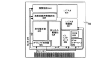
図6に示すCPUは、基板600上に、演算回路(ALU:Arithmetic logic unit)601、演算回路用の制御部(ALU Controller)602、命令解析部(Instruction Decoder)603、割り込み制御部(Interrupt Controller)604、タイミング制御部(Timing Controller)605、レジスタ(Register)606、レジスタ制御部(Register Controller)607、バスインターフェース(Bus I/F)608、書き換え可能なROM609、ROMインターフェース(ROM I/F)620とを主に有している。またROM609及びROM I/F620は、別チップに設けても良い。
The CPU shown in FIG. 6 includes an arithmetic circuit (ALU) 601, an arithmetic circuit controller (ALU Controller) 602, an instruction analyzer (Instruction Decoder) 603, and an interrupt controller (Interrupt Controller). 604,
以上のような各種回路を実施の形態1、2に示した方法により形成されるガラス基板上の薄膜トランジスタを用いて構成することができる。 Various circuits as described above can be formed using a thin film transistor over a glass substrate formed by the method described in Embodiment Modes 1 and 2.
勿論、図6に示すCPUは、その構成を簡略化して示した一例にすぎず、実際のCPUはその用途によって多種多様な構成を有している。 Needless to say, the CPU illustrated in FIG. 6 is just an example in which the configuration is simplified, and an actual CPU may have various configurations depending on the application.
バスインターフェース608を介してCPUに入力された命令は、命令解析部603に入力され、デコードされた後、演算回路用の制御部602、割り込み制御部604、レジスタ制御部607、タイミング制御部605に入力される。
An instruction input to the CPU via the
演算回路用の制御部602、割り込み制御部604、レジスタ制御部607、タイミング制御部605は、デコードされた命令に基づき、各種制御を行う。具体的に演算回路用の制御部602は、演算回路601の動作を制御するための信号を生成する。また、割り込み制御部604は、CPUのプログラム実行中に、外部の入出力装置や、周辺回路からの割り込み要求を、その優先度やマスク状態から判断し、処理する。レジスタ制御部607は、レジスタ606のアドレスを生成し、CPUの状態に応じてレジスタ606の読み出しや書き込みを行う。
An arithmetic
またタイミング制御部605は、演算回路601、演算回路用の制御部602、命令解析部603、割り込み制御部604、レジスタ制御部607の動作のタイミングを制御する信号を生成する。例えばタイミング制御部605は、基準クロック信号CLK1(621)を元に、内部クロック信号CLK2(622)を生成する内部クロック生成部を備えており、クロック信号CLK2を上記各種回路に供給する。
The
また本実施の形態では、半導体装置としてCPUを例に挙げて説明したが、本発明のガラス基板上に形成された薄膜トランジスタは、有機発光素子に代表される発光素子を各画素に備えた表示装置を作製することができる。その他の半導体装置としては、集積回路や半導体表示装置であって、特に液晶表示装置、DMD、PDP、FED等の半導体表示装置の画素部及び駆動回路部に用いることができる。本発明を適用して作製される半導体装置の具体例として、デジタルカメラ、カーオーディオなどの音響再生装置、ノート型パーソナルコンピュータ、ゲーム機器、携帯情報端末(携帯電話機、携帯型ゲーム機等)、家庭用ゲーム機などの記録媒体を備えた画像再生装置などが挙げられる。 In this embodiment, the CPU is described as an example of the semiconductor device. However, the thin film transistor formed over the glass substrate of the present invention includes a light-emitting element typified by an organic light-emitting element in each pixel. Can be produced. Other semiconductor devices include integrated circuits and semiconductor display devices, and can be used particularly for pixel portions and drive circuit portions of liquid crystal display devices, semiconductor display devices such as DMD, PDP, and FED. Specific examples of a semiconductor device manufactured by applying the present invention include a digital camera, a sound reproducing device such as a car audio, a notebook personal computer, a game machine, a portable information terminal (a mobile phone, a portable game machine, etc.), a home And an image reproducing device including a recording medium such as a game machine.
特に本発明により形成される薄膜トランジスタはゲート長が小さいため、駆動回路部に用いることによる駆動電圧の低下が期待できる。また本発明のゲート長が小さい薄膜トランジスタにより、高精細化が進む、すなわち各画素の間隔が小さくなる画素部に対応することができる。 In particular, since the thin film transistor formed according to the present invention has a small gate length, it can be expected that the driving voltage is lowered due to use in the driving circuit portion. In addition, the thin film transistor having a small gate length according to the present invention can cope with a pixel portion in which high definition progresses, that is, the interval between pixels is small.
その結果、ガラス基板の場合は廉価な機材で実現でき、低コストなCPU、その他の半導体装置を作製することができる。 As a result, in the case of a glass substrate, it can be realized with inexpensive equipment, and a low-cost CPU and other semiconductor devices can be manufactured.
(実施の形態4)
本実施の形態では、CPUの形態について説明する。
(Embodiment 4)
In this embodiment, a form of a CPU will be described.
図7には、画素部と、CPU、その他の回路が同一基板に形成された表示装置、いわゆるシステムオンパネルを示す。基板700上に画素部701、画素部701が有する画素を選択する走査線駆動回路702と、選択された画素にビデオ信号を供給する信号線駆動回路703とが設けられている。走査線駆動回路702、及び信号線駆動回路703から引き回される配線によりCPU704、その他の回路、例えばコントロール回路705とが接続されている。なおコントロール回路にはインターフェースが含まれている。そして、基板の端部にFPC端子との接続部を設け、外部信号とのやりとりを行う。
FIG. 7 illustrates a display device in which a pixel portion, a CPU, and other circuits are formed over the same substrate, a so-called system-on-panel. Over the
その他の回路として、映像信号処理回路、電源回路、階調電源回路、ビデオRAM、メモリ(DRAM、SRAM、PROM)等を基板上に設けることができる。またこれら回路は、ICチップにより形成し、基板上に実装してもよい。さらに必ずしも走査線駆動回路702、及び信号線駆動回路703を同一基板に形成する必要はなく、例えば走査線駆動回路702のみを同一基板に形成し、信号線駆動回路703をICチップにより形成し、実装してもよい。
As other circuits, a video signal processing circuit, a power supply circuit, a gradation power supply circuit, a video RAM, a memory (DRAM, SRAM, PROM), and the like can be provided over the substrate. These circuits may be formed by an IC chip and mounted on a substrate. Further, the scan
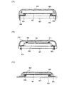
図8(A)には、パッケージングされたCPUの形態を示す。基板800上に形成されたCPUの機能を有する薄膜トランジスタアレイ801を、CPU表面に設けられた電極(ソース電極やドレイン電極、又はそれらの上に絶縁膜を介して形成された電極等)802が下側となるフェイスダウン状態とする。基板800は、ガラス、プラスチックを用いることができる。また銅やその合金で形成される配線803が設けられた配線基板、例えばプリント基板807を用意する。プリント基板807には、接続端子(ピン)804が設けられている。そして電極802と、配線803とを異方性導電膜808等を介して接続する。その後、エポキシ樹脂等の樹脂805で基板800上方から覆い、パッケージングされたCPUとして完成する。または中空に保った状態で外周をプラスチックなどで囲んでもよい。
FIG. 8A shows the form of a packaged CPU. A thin
図8(B)には、図8(A)と異なり、CPU表面に設けられた電極802が上側となるフェイスアップ状態とする。そしてプリント基板807上に基板800を固定し、電極802と、配線803とをワイヤ818により接続する。このようにワイヤにより接続することをワイヤボンディングという。そして電極802と、配線803に接続されるバンプ814とが接続する。その後、中空に保った状態で外周をプラスチック815等で囲み、パッケージングされたCPUとして完成する。
In FIG. 8B, unlike FIG. 8A, a face-up state is shown in which the
図8(C)には、フレキシブル性を有する基板、例えばFPC(Flexible printed circuit)上に、CPUの機能を有する薄膜トランジスタアレイ801を固定する例を示す。基板810に形成されたCPUの機能を有する薄膜トランジスタアレイ801を、CPU表面に設けられた電極802が下側となるフェイスダウン状態とする。基板810には、ガラス、石英、金属、バルク半導体、プラスチックを用いることができるが、図8(C)ではフレキシブル性の高いプラスチックを用いると好ましい。また、銅やその合金で形成される配線803が設けられたフレキシブル性を有するFPC817を用意する。そして、電極802と、配線803とを異方性導電膜808を介して接続する。その後、エポキシ樹脂等の樹脂805で基板800上方から覆い、パッケージングされたCPUとして完成する。
FIG. 8C illustrates an example in which a thin
このようにパッケージングされたCPUは、外部から保護され、さらに携帯しやすくなる。そして所望箇所に、CPUを実装することができ、特に図8(C)のようにフレキシブル性を有すると、実装する位置の自由度が高まる。またパッケージングすることによりCPUの機能を補助することもできる。 The CPU packaged in this way is protected from the outside and becomes easier to carry. Then, a CPU can be mounted at a desired location. In particular, when flexibility is provided as shown in FIG. Further, the function of the CPU can be assisted by packaging.
以上のように、ガラス基板上の薄膜トランジスタにより形成されるCPUは、多様な形態をとることができる。そして、ガラス基板上の薄膜トランジスタにより形成されるCPUは軽量であるため、携帯や実装するときの負担を軽減することができる。 As described above, a CPU formed using thin film transistors over a glass substrate can take a variety of forms. Since the CPU formed by the thin film transistors on the glass substrate is lightweight, the burden on carrying or mounting can be reduced.
(実施の形態5)
本実施の形態では、上記実施の形態と異なる作製工程について説明する。
(Embodiment 5)
In this embodiment, a manufacturing process which is different from that in the above embodiment will be described.
図9(A)に示すように、上記実施の形態と同様にレジストマスク110まで形成し、これを用いて、導電膜109bをエッチングする。
As shown in FIG. 9A, a resist
その後、図9(B)に示すように、レジストマスク110を除去する。そして図9(C)に示すように、エッチングされた導電膜109bを用いて、導電膜109aをエッチングする。このようにレジストマスクを用いずに、導電膜109aをエッチングしてもよい。
Thereafter, as shown in FIG. 9B, the resist
その後の工程は、上記実施の形態を参照することができる。 For the subsequent steps, the above embodiment can be referred to.
本実施の形態のように、レジストマスクを除去した後、エッチングされた導電膜109bを用いて、導電膜109aをエッチングすると、レジストマスクの形状の影響を受けることなく、導電膜をエッチングすることができる。
When the
以上のように形成された薄膜トランジスタを有する半導体装置、例えばCPUを作製することができ、高速動作が可能となる。 A semiconductor device having a thin film transistor formed as described above, for example, a CPU can be manufactured, and high-speed operation is possible.
Claims (8)
前記下地膜上に非晶質半導体膜を形成し、
前記非晶質半導体膜にレーザー光を照射することにより結晶性半導体膜を形成し、
前記結晶性半導体膜上に第1のマスクを形成し、
前記第1のマスクを用いて前記結晶性半導体膜をエッチングし、
前記下地膜の表面、及び前記結晶性半導体膜の側面を窒化し、
前記第1のマスクを除去し、
前記結晶性半導体膜の表面を洗浄し、
前記結晶性半導体膜上にゲート絶縁膜を形成し、
前記ゲート絶縁膜上に導電膜を形成し、
前記導電膜上にテーパを有する第2のマスクを形成し、
前記第2のマスクを後退させつつ前記導電膜をエッチングしてゲート電極を形成する半導体装置の作製方法であって、
前記ゲート電極のゲート長が1.0μm以下となるように前記導電膜をエッチングすることを特徴とする半導体装置の作製方法。 Form a base film on the glass substrate,
Forming an amorphous semiconductor film on the base film;
A crystalline semiconductor film is formed by irradiating the amorphous semiconductor film with a laser beam,
Forming a first mask on the crystalline semiconductor film;
Etching the crystalline semiconductor film using the first mask ;
The surface of the underlying film, the sides of及beauty the crystalline semiconductor film is nitrided,
Removing the first mask;
Cleaning the surface of the crystalline semiconductor film;
Forming a gate insulating film on the crystalline semiconductor film;
Forming a conductive film on the gate insulating film;
Forming a second mask having a taper on the conductive film;
A method of manufacturing a semiconductor device, wherein a gate electrode is formed by etching the conductive film while retracting the second mask,
A method for manufacturing a semiconductor device, wherein the conductive film is etched so that a gate length of the gate electrode is 1.0 μm or less.
前記下地膜上に非晶質半導体膜を形成し、Forming an amorphous semiconductor film on the base film;
前記非晶質半導体膜にレーザー光を照射することにより結晶性半導体膜を形成し、A crystalline semiconductor film is formed by irradiating the amorphous semiconductor film with a laser beam,
前記結晶性半導体膜上に第1のマスクを形成し、Forming a first mask on the crystalline semiconductor film;
前記第1のマスクを用いて前記結晶性半導体膜をエッチングし、Etching the crystalline semiconductor film using the first mask;
前記下地膜の表面、及び前記第1のマスクが形成された前記結晶性半導体膜に対して、窒素又はアンモニアを用いたプラズマ処理を施し、Plasma treatment using nitrogen or ammonia is performed on the surface of the base film and the crystalline semiconductor film on which the first mask is formed,
前記第1のマスクを除去し、Removing the first mask;
前記結晶性半導体膜の表面を洗浄し、Cleaning the surface of the crystalline semiconductor film;
前記結晶性半導体膜上にゲート絶縁膜を形成し、Forming a gate insulating film on the crystalline semiconductor film;
前記ゲート絶縁膜上に導電膜を形成し、Forming a conductive film on the gate insulating film;
前記導電膜上にテーパを有する第2のマスクを形成し、Forming a second mask having a taper on the conductive film;
前記第2のマスクを後退させつつ前記導電膜をエッチングしてゲート電極を形成する半導体装置の作製方法であって、A method of manufacturing a semiconductor device, wherein a gate electrode is formed by etching the conductive film while retracting the second mask,
前記ゲート電極のゲート長が1.0μm以下となるように前記導電膜をエッチングすることを特徴とする半導体装置の作製方法。A method for manufacturing a semiconductor device, wherein the conductive film is etched so that a gate length of the gate electrode is 1.0 μm or less.
前記下地膜上に非晶質半導体膜を形成し、Forming an amorphous semiconductor film on the base film;
前記非晶質半導体膜にレーザー光を照射することにより結晶性半導体膜を形成し、A crystalline semiconductor film is formed by irradiating the amorphous semiconductor film with a laser beam,
前記結晶性半導体膜上に第1のマスクを形成し、Forming a first mask on the crystalline semiconductor film;
前記第1のマスクを用いて前記結晶性半導体膜をエッチングし、Etching the crystalline semiconductor film using the first mask;
前記下地膜の表面、及び前記第1のマスクが形成された前記結晶性半導体膜を、窒素又はアンモニアを用いたプラズマ雰囲気にさらし、Exposing the surface of the base film and the crystalline semiconductor film on which the first mask is formed to a plasma atmosphere using nitrogen or ammonia,
前記第1のマスクを除去し、Removing the first mask;
前記結晶性半導体膜の表面を洗浄し、Cleaning the surface of the crystalline semiconductor film;
前記結晶性半導体膜上にゲート絶縁膜を形成し、Forming a gate insulating film on the crystalline semiconductor film;
前記ゲート絶縁膜上に導電膜を形成し、Forming a conductive film on the gate insulating film;
前記導電膜上にテーパを有する第2のマスクを形成し、Forming a second mask having a taper on the conductive film;
前記第2のマスクを後退させつつ前記導電膜をエッチングしてゲート電極を形成する半導体装置の作製方法であって、A method of manufacturing a semiconductor device, wherein a gate electrode is formed by etching the conductive film while retracting the second mask,
前記ゲート電極のゲート長が1.0μm以下となるように前記導電膜をエッチングすることを特徴とする半導体装置の作製方法。A method for manufacturing a semiconductor device, wherein the conductive film is etched so that a gate length of the gate electrode is 1.0 μm or less.
ドライエッチング法又はウェットエッチング法により前記導電膜をエッチングすることを特徴とする半導体装置の作製方法。 In any one of Claims 1 thru | or 3 ,
A method for manufacturing a semiconductor device, wherein the conductive film is etched by a dry etching method or a wet etching method.
前記ドライエッチング法は、CF4、Cl及びO2を用いて行われることを特徴とする半導体装置の作製方法。 In claim 4 ,
The method for manufacturing a semiconductor device, wherein the dry etching method is performed using CF 4 , Cl, and O 2 .
前記ドライエッチング法は、Cl2を用いて行われることを特徴とする半導体装置の作製方法。 In claim 4 ,
The method for manufacturing a semiconductor device, wherein the dry etching method is performed using Cl 2 .
前記レーザー光を照射する前に、前記非晶質半導体膜上に結晶化を促進させる金属元素を添加し、加熱処理を行うことを特徴とする半導体装置の作製方法。 In any one of Claims 1 thru | or 6 ,
A method for manufacturing a semiconductor device, wherein a metal element that promotes crystallization is added to the amorphous semiconductor film and heat treatment is performed before the laser light irradiation.
Priority Applications (1)
| Application Number | Priority Date | Filing Date | Title |
|---|---|---|---|
| JP2004243673A JP4754792B2 (en) | 2003-08-29 | 2004-08-24 | Method for manufacturing semiconductor device |
Applications Claiming Priority (3)
| Application Number | Priority Date | Filing Date | Title |
|---|---|---|---|
| JP2003307489 | 2003-08-29 | ||
| JP2003307489 | 2003-08-29 | ||
| JP2004243673A JP4754792B2 (en) | 2003-08-29 | 2004-08-24 | Method for manufacturing semiconductor device |
Publications (3)
| Publication Number | Publication Date |
|---|---|
| JP2005101571A JP2005101571A (en) | 2005-04-14 |
| JP2005101571A5 JP2005101571A5 (en) | 2007-07-26 |
| JP4754792B2 true JP4754792B2 (en) | 2011-08-24 |
Family
ID=34467410
Family Applications (1)
| Application Number | Title | Priority Date | Filing Date |
|---|---|---|---|
| JP2004243673A Expired - Fee Related JP4754792B2 (en) | 2003-08-29 | 2004-08-24 | Method for manufacturing semiconductor device |
Country Status (1)
| Country | Link |
|---|---|
| JP (1) | JP4754792B2 (en) |
Family Cites Families (4)
| Publication number | Priority date | Publication date | Assignee | Title |
|---|---|---|---|---|
| JP4651851B2 (en) * | 2000-05-12 | 2011-03-16 | 株式会社半導体エネルギー研究所 | Method for manufacturing semiconductor device |
| JP5046452B2 (en) * | 2000-10-26 | 2012-10-10 | 株式会社半導体エネルギー研究所 | Method for manufacturing semiconductor device |
| JP4673513B2 (en) * | 2001-08-01 | 2011-04-20 | 株式会社半導体エネルギー研究所 | Method for manufacturing semiconductor device |
| JP3638926B2 (en) * | 2001-09-10 | 2005-04-13 | 株式会社半導体エネルギー研究所 | Light emitting device and method for manufacturing semiconductor device |
-
2004
- 2004-08-24 JP JP2004243673A patent/JP4754792B2/en not_active Expired - Fee Related
Also Published As
| Publication number | Publication date |
|---|---|
| JP2005101571A (en) | 2005-04-14 |
Similar Documents
| Publication | Publication Date | Title |
|---|---|---|
| US7115488B2 (en) | Method of manufacturing semiconductor device | |
| US7303981B2 (en) | Polysilicon structure, thin film transistor panel using the same, and manufacturing method of the same | |
| US7390704B2 (en) | Laser process apparatus, laser irradiation method, and method for manufacturing semiconductor device | |
| US8569170B2 (en) | Manufacturing method of semiconductor device comprising silicide layer with varied thickness | |
| US7344825B2 (en) | Method of fabricating semiconductor device, and developing apparatus using the method | |
| US6927418B2 (en) | Thin film transistor substrate and manufacturing method thereof | |
| JP4754792B2 (en) | Method for manufacturing semiconductor device | |
| JP4141292B2 (en) | Semiconductor device | |
| JP2002033489A (en) | Poly thin film transistor and method of manufacturing the same | |
| JP3889066B2 (en) | Method for manufacturing semiconductor device | |
| JP4230159B2 (en) | Method for manufacturing semiconductor device | |
| JP2002100780A (en) | Semiconductor device and its manufacturing method | |
| JP4304374B2 (en) | Top gate type thin film transistor | |
| US20050167634A1 (en) | Etchant for nickel silicide | |
| JP2000353807A (en) | Method for manufacturing thin film transistor, method for manufacturing active matrix substrate, and electro-optical device | |
| JP4141307B2 (en) | Method for manufacturing semiconductor device | |
| JP4421242B2 (en) | Method for manufacturing crystalline semiconductor film, method for manufacturing thin film transistor having crystalline semiconductor film, and method for manufacturing semiconductor device having crystalline semiconductor film | |
| JP4526773B2 (en) | Method for manufacturing semiconductor device | |
| JP4137473B2 (en) | Method for manufacturing semiconductor device | |
| JP4342876B2 (en) | Method for manufacturing crystalline semiconductor film, method for manufacturing thin film transistor having crystalline semiconductor film, and method for manufacturing semiconductor device having crystalline semiconductor film | |
| JP3921384B2 (en) | Manufacturing method of semiconductor device | |
| JP4387144B2 (en) | Method for manufacturing crystalline semiconductor film, method for manufacturing thin film transistor having crystalline semiconductor film, and method for manufacturing semiconductor device having crystalline semiconductor film | |
| JP2002033329A (en) | Method for manufacturing semiconductor device | |
| JP2005175444A (en) | Laser irradiator and process for fabricating semiconductor device |
Legal Events
| Date | Code | Title | Description |
|---|---|---|---|
| A521 | Written amendment |
Free format text: JAPANESE INTERMEDIATE CODE: A523 Effective date: 20070613 |
|
| A621 | Written request for application examination |
Free format text: JAPANESE INTERMEDIATE CODE: A621 Effective date: 20070613 |
|
| A977 | Report on retrieval |
Free format text: JAPANESE INTERMEDIATE CODE: A971007 Effective date: 20100916 |
|
| A131 | Notification of reasons for refusal |
Free format text: JAPANESE INTERMEDIATE CODE: A131 Effective date: 20100921 |
|
| A521 | Written amendment |
Free format text: JAPANESE INTERMEDIATE CODE: A523 Effective date: 20101101 |
|
| TRDD | Decision of grant or rejection written | ||
| A01 | Written decision to grant a patent or to grant a registration (utility model) |
Free format text: JAPANESE INTERMEDIATE CODE: A01 Effective date: 20110517 |
|
| A01 | Written decision to grant a patent or to grant a registration (utility model) |
Free format text: JAPANESE INTERMEDIATE CODE: A01 |
|
| A61 | First payment of annual fees (during grant procedure) |
Free format text: JAPANESE INTERMEDIATE CODE: A61 Effective date: 20110526 |
|
| FPAY | Renewal fee payment (event date is renewal date of database) |
Free format text: PAYMENT UNTIL: 20140603 Year of fee payment: 3 |
|
| R150 | Certificate of patent or registration of utility model |
Free format text: JAPANESE INTERMEDIATE CODE: R150 |
|
| FPAY | Renewal fee payment (event date is renewal date of database) |
Free format text: PAYMENT UNTIL: 20140603 Year of fee payment: 3 |
|
| R250 | Receipt of annual fees |
Free format text: JAPANESE INTERMEDIATE CODE: R250 |
|
| R250 | Receipt of annual fees |
Free format text: JAPANESE INTERMEDIATE CODE: R250 |
|
| R250 | Receipt of annual fees |
Free format text: JAPANESE INTERMEDIATE CODE: R250 |
|
| R250 | Receipt of annual fees |
Free format text: JAPANESE INTERMEDIATE CODE: R250 |
|
| LAPS | Cancellation because of no payment of annual fees |