JP4754792B2 - 半導体装置の作製方法 - Google Patents
半導体装置の作製方法 Download PDFInfo
- Publication number
- JP4754792B2 JP4754792B2 JP2004243673A JP2004243673A JP4754792B2 JP 4754792 B2 JP4754792 B2 JP 4754792B2 JP 2004243673 A JP2004243673 A JP 2004243673A JP 2004243673 A JP2004243673 A JP 2004243673A JP 4754792 B2 JP4754792 B2 JP 4754792B2
- Authority
- JP
- Japan
- Prior art keywords
- film
- mask
- semiconductor film
- forming
- crystalline semiconductor
- Prior art date
- Legal status (The legal status is an assumption and is not a legal conclusion. Google has not performed a legal analysis and makes no representation as to the accuracy of the status listed.)
- Expired - Fee Related
Links
- 239000004065 semiconductor Substances 0.000 title claims description 136
- 238000000034 method Methods 0.000 title claims description 42
- 238000004519 manufacturing process Methods 0.000 title claims description 28
- 239000000758 substrate Substances 0.000 claims description 74
- 238000005530 etching Methods 0.000 claims description 36
- 239000011521 glass Substances 0.000 claims description 30
- 238000010438 heat treatment Methods 0.000 claims description 18
- 229910052751 metal Inorganic materials 0.000 claims description 11
- 239000002184 metal Substances 0.000 claims description 11
- IJGRMHOSHXDMSA-UHFFFAOYSA-N Atomic nitrogen Chemical compound N#N IJGRMHOSHXDMSA-UHFFFAOYSA-N 0.000 claims description 7
- 238000001312 dry etching Methods 0.000 claims description 7
- 229910052760 oxygen Inorganic materials 0.000 claims description 7
- QGZKDVFQNNGYKY-UHFFFAOYSA-N Ammonia Chemical compound N QGZKDVFQNNGYKY-UHFFFAOYSA-N 0.000 claims description 6
- 239000012298 atmosphere Substances 0.000 claims description 6
- 238000004140 cleaning Methods 0.000 claims description 5
- 238000002425 crystallisation Methods 0.000 claims description 5
- 230000008025 crystallization Effects 0.000 claims description 5
- 230000001678 irradiating effect Effects 0.000 claims description 4
- 229910021529 ammonia Inorganic materials 0.000 claims description 3
- 229910052757 nitrogen Inorganic materials 0.000 claims description 3
- 238000009832 plasma treatment Methods 0.000 claims description 2
- 238000001039 wet etching Methods 0.000 claims 1
- 239000010408 film Substances 0.000 description 218
- 239000010409 thin film Substances 0.000 description 33
- 239000012535 impurity Substances 0.000 description 23
- XUIMIQQOPSSXEZ-UHFFFAOYSA-N Silicon Chemical compound [Si] XUIMIQQOPSSXEZ-UHFFFAOYSA-N 0.000 description 22
- 229910052710 silicon Inorganic materials 0.000 description 22
- 239000010703 silicon Substances 0.000 description 22
- 239000007789 gas Substances 0.000 description 17
- 239000002585 base Substances 0.000 description 16
- KRHYYFGTRYWZRS-UHFFFAOYSA-N Fluorane Chemical compound F KRHYYFGTRYWZRS-UHFFFAOYSA-N 0.000 description 14
- VYPSYNLAJGMNEJ-UHFFFAOYSA-N Silicium dioxide Chemical compound O=[Si]=O VYPSYNLAJGMNEJ-UHFFFAOYSA-N 0.000 description 12
- 230000015572 biosynthetic process Effects 0.000 description 12
- 239000011368 organic material Substances 0.000 description 10
- 229920002120 photoresistant polymer Polymers 0.000 description 10
- 238000005268 plasma chemical vapour deposition Methods 0.000 description 10
- 229910052581 Si3N4 Inorganic materials 0.000 description 9
- HQVNEWCFYHHQES-UHFFFAOYSA-N silicon nitride Chemical compound N12[Si]34N5[Si]62N3[Si]51N64 HQVNEWCFYHHQES-UHFFFAOYSA-N 0.000 description 9
- 229910052814 silicon oxide Inorganic materials 0.000 description 9
- 239000010936 titanium Substances 0.000 description 9
- 239000004033 plastic Substances 0.000 description 8
- 229920003023 plastic Polymers 0.000 description 8
- 229910010272 inorganic material Inorganic materials 0.000 description 7
- 239000011147 inorganic material Substances 0.000 description 7
- 239000000243 solution Substances 0.000 description 7
- 230000006870 function Effects 0.000 description 6
- 239000010410 layer Substances 0.000 description 6
- 239000000463 material Substances 0.000 description 6
- 229910052802 copper Inorganic materials 0.000 description 5
- 239000010949 copper Substances 0.000 description 5
- 238000005247 gettering Methods 0.000 description 5
- 238000004518 low pressure chemical vapour deposition Methods 0.000 description 5
- 229920005989 resin Polymers 0.000 description 5
- 239000011347 resin Substances 0.000 description 5
- RYGMFSIKBFXOCR-UHFFFAOYSA-N Copper Chemical compound [Cu] RYGMFSIKBFXOCR-UHFFFAOYSA-N 0.000 description 4
- MHAJPDPJQMAIIY-UHFFFAOYSA-N Hydrogen peroxide Chemical compound OO MHAJPDPJQMAIIY-UHFFFAOYSA-N 0.000 description 4
- XYFCBTPGUUZFHI-UHFFFAOYSA-N Phosphine Chemical compound P XYFCBTPGUUZFHI-UHFFFAOYSA-N 0.000 description 4
- 239000000956 alloy Substances 0.000 description 4
- 238000004380 ashing Methods 0.000 description 4
- QVGXLLKOCUKJST-UHFFFAOYSA-N atomic oxygen Chemical compound [O] QVGXLLKOCUKJST-UHFFFAOYSA-N 0.000 description 4
- 238000010586 diagram Methods 0.000 description 4
- PCHJSUWPFVWCPO-UHFFFAOYSA-N gold Chemical group [Au] PCHJSUWPFVWCPO-UHFFFAOYSA-N 0.000 description 4
- 229910052739 hydrogen Inorganic materials 0.000 description 4
- 239000012299 nitrogen atmosphere Substances 0.000 description 4
- 239000001301 oxygen Substances 0.000 description 4
- -1 polyethylene terephthalate Polymers 0.000 description 4
- 238000012545 processing Methods 0.000 description 4
- 229910052719 titanium Inorganic materials 0.000 description 4
- XLYOFNOQVPJJNP-UHFFFAOYSA-N water Chemical compound O XLYOFNOQVPJJNP-UHFFFAOYSA-N 0.000 description 4
- QTBSBXVTEAMEQO-UHFFFAOYSA-N Acetic acid Chemical compound CC(O)=O QTBSBXVTEAMEQO-UHFFFAOYSA-N 0.000 description 3
- RTAQQCXQSZGOHL-UHFFFAOYSA-N Titanium Chemical compound [Ti] RTAQQCXQSZGOHL-UHFFFAOYSA-N 0.000 description 3
- NIXOWILDQLNWCW-UHFFFAOYSA-N acrylic acid group Chemical group C(C=C)(=O)O NIXOWILDQLNWCW-UHFFFAOYSA-N 0.000 description 3
- 229910052783 alkali metal Inorganic materials 0.000 description 3
- 150000001340 alkali metals Chemical class 0.000 description 3
- 229910052784 alkaline earth metal Inorganic materials 0.000 description 3
- 150000001342 alkaline earth metals Chemical class 0.000 description 3
- 229910045601 alloy Inorganic materials 0.000 description 3
- 238000009792 diffusion process Methods 0.000 description 3
- 239000001257 hydrogen Substances 0.000 description 3
- 239000004973 liquid crystal related substance Substances 0.000 description 3
- 238000000059 patterning Methods 0.000 description 3
- 239000010453 quartz Substances 0.000 description 3
- 239000002356 single layer Substances 0.000 description 3
- 238000004528 spin coating Methods 0.000 description 3
- 229910052721 tungsten Inorganic materials 0.000 description 3
- ZOXJGFHDIHLPTG-UHFFFAOYSA-N Boron Chemical compound [B] ZOXJGFHDIHLPTG-UHFFFAOYSA-N 0.000 description 2
- 102100040844 Dual specificity protein kinase CLK2 Human genes 0.000 description 2
- PXGOKWXKJXAPGV-UHFFFAOYSA-N Fluorine Chemical compound FF PXGOKWXKJXAPGV-UHFFFAOYSA-N 0.000 description 2
- 101000749291 Homo sapiens Dual specificity protein kinase CLK2 Proteins 0.000 description 2
- CBENFWSGALASAD-UHFFFAOYSA-N Ozone Chemical compound [O-][O+]=O CBENFWSGALASAD-UHFFFAOYSA-N 0.000 description 2
- 239000004642 Polyimide Substances 0.000 description 2
- 229910000577 Silicon-germanium Inorganic materials 0.000 description 2
- LEVVHYCKPQWKOP-UHFFFAOYSA-N [Si].[Ge] Chemical compound [Si].[Ge] LEVVHYCKPQWKOP-UHFFFAOYSA-N 0.000 description 2
- 239000006096 absorbing agent Substances 0.000 description 2
- 229910052782 aluminium Inorganic materials 0.000 description 2
- 229910021417 amorphous silicon Inorganic materials 0.000 description 2
- 238000004458 analytical method Methods 0.000 description 2
- 239000007864 aqueous solution Substances 0.000 description 2
- 229910052796 boron Inorganic materials 0.000 description 2
- 239000000969 carrier Substances 0.000 description 2
- 230000015556 catabolic process Effects 0.000 description 2
- 239000013078 crystal Substances 0.000 description 2
- 238000000151 deposition Methods 0.000 description 2
- 230000008021 deposition Effects 0.000 description 2
- 238000011161 development Methods 0.000 description 2
- 239000003822 epoxy resin Substances 0.000 description 2
- 229910052731 fluorine Inorganic materials 0.000 description 2
- 239000011737 fluorine Substances 0.000 description 2
- 239000010931 gold Substances 0.000 description 2
- 229910052737 gold Inorganic materials 0.000 description 2
- 150000002431 hydrogen Chemical class 0.000 description 2
- 150000002500 ions Chemical class 0.000 description 2
- 239000003550 marker Substances 0.000 description 2
- 229910052750 molybdenum Inorganic materials 0.000 description 2
- 150000004767 nitrides Chemical group 0.000 description 2
- 230000003647 oxidation Effects 0.000 description 2
- 238000007254 oxidation reaction Methods 0.000 description 2
- 230000002093 peripheral effect Effects 0.000 description 2
- 238000000206 photolithography Methods 0.000 description 2
- 229920003207 poly(ethylene-2,6-naphthalate) Polymers 0.000 description 2
- 229920000647 polyepoxide Polymers 0.000 description 2
- 239000011112 polyethylene naphthalate Substances 0.000 description 2
- 229920000139 polyethylene terephthalate Polymers 0.000 description 2
- 239000005020 polyethylene terephthalate Substances 0.000 description 2
- 229920001721 polyimide Polymers 0.000 description 2
- 239000010979 ruby Substances 0.000 description 2
- 229910001750 ruby Inorganic materials 0.000 description 2
- 239000011734 sodium Substances 0.000 description 2
- 125000001424 substituent group Chemical group 0.000 description 2
- WFKWXMTUELFFGS-UHFFFAOYSA-N tungsten Chemical compound [W] WFKWXMTUELFFGS-UHFFFAOYSA-N 0.000 description 2
- 239000010937 tungsten Substances 0.000 description 2
- QTBSBXVTEAMEQO-UHFFFAOYSA-M Acetate Chemical compound CC([O-])=O QTBSBXVTEAMEQO-UHFFFAOYSA-M 0.000 description 1
- 229910000838 Al alloy Inorganic materials 0.000 description 1
- 229910018125 Al-Si Inorganic materials 0.000 description 1
- 229910018520 Al—Si Inorganic materials 0.000 description 1
- 102100040862 Dual specificity protein kinase CLK1 Human genes 0.000 description 1
- 101000749294 Homo sapiens Dual specificity protein kinase CLK1 Proteins 0.000 description 1
- UFHFLCQGNIYNRP-UHFFFAOYSA-N Hydrogen Chemical compound [H][H] UFHFLCQGNIYNRP-UHFFFAOYSA-N 0.000 description 1
- DGAQECJNVWCQMB-PUAWFVPOSA-M Ilexoside XXIX Chemical compound C[C@@H]1CC[C@@]2(CC[C@@]3(C(=CC[C@H]4[C@]3(CC[C@@H]5[C@@]4(CC[C@@H](C5(C)C)OS(=O)(=O)[O-])C)C)[C@@H]2[C@]1(C)O)C)C(=O)O[C@H]6[C@@H]([C@H]([C@@H]([C@H](O6)CO)O)O)O.[Na+] DGAQECJNVWCQMB-PUAWFVPOSA-M 0.000 description 1
- ZOKXTWBITQBERF-UHFFFAOYSA-N Molybdenum Chemical compound [Mo] ZOKXTWBITQBERF-UHFFFAOYSA-N 0.000 description 1
- OAICVXFJPJFONN-UHFFFAOYSA-N Phosphorus Chemical compound [P] OAICVXFJPJFONN-UHFFFAOYSA-N 0.000 description 1
- 239000004952 Polyamide Substances 0.000 description 1
- ATJFFYVFTNAWJD-UHFFFAOYSA-N Tin Chemical compound [Sn] ATJFFYVFTNAWJD-UHFFFAOYSA-N 0.000 description 1
- NRTOMJZYCJJWKI-UHFFFAOYSA-N Titanium nitride Chemical compound [Ti]#N NRTOMJZYCJJWKI-UHFFFAOYSA-N 0.000 description 1
- 238000010306 acid treatment Methods 0.000 description 1
- 230000002411 adverse Effects 0.000 description 1
- 125000000217 alkyl group Chemical group 0.000 description 1
- UQZIWOQVLUASCR-UHFFFAOYSA-N alumane;titanium Chemical compound [AlH3].[Ti] UQZIWOQVLUASCR-UHFFFAOYSA-N 0.000 description 1
- XAGFODPZIPBFFR-UHFFFAOYSA-N aluminium Chemical compound [Al] XAGFODPZIPBFFR-UHFFFAOYSA-N 0.000 description 1
- 239000005407 aluminoborosilicate glass Substances 0.000 description 1
- 150000001408 amides Chemical class 0.000 description 1
- 150000004945 aromatic hydrocarbons Chemical class 0.000 description 1
- 229910052788 barium Inorganic materials 0.000 description 1
- DSAJWYNOEDNPEQ-UHFFFAOYSA-N barium atom Chemical compound [Ba] DSAJWYNOEDNPEQ-UHFFFAOYSA-N 0.000 description 1
- UMIVXZPTRXBADB-UHFFFAOYSA-N benzocyclobutene Chemical compound C1=CC=C2CCC2=C1 UMIVXZPTRXBADB-UHFFFAOYSA-N 0.000 description 1
- 239000005388 borosilicate glass Substances 0.000 description 1
- 238000006243 chemical reaction Methods 0.000 description 1
- 239000007795 chemical reaction product Substances 0.000 description 1
- 238000000576 coating method Methods 0.000 description 1
- 150000001875 compounds Chemical class 0.000 description 1
- 230000006866 deterioration Effects 0.000 description 1
- 238000007598 dipping method Methods 0.000 description 1
- KPUWHANPEXNPJT-UHFFFAOYSA-N disiloxane Chemical class [SiH3]O[SiH3] KPUWHANPEXNPJT-UHFFFAOYSA-N 0.000 description 1
- 230000000694 effects Effects 0.000 description 1
- 238000005516 engineering process Methods 0.000 description 1
- 230000001747 exhibiting effect Effects 0.000 description 1
- 229910052732 germanium Inorganic materials 0.000 description 1
- GNPVGFCGXDBREM-UHFFFAOYSA-N germanium atom Chemical compound [Ge] GNPVGFCGXDBREM-UHFFFAOYSA-N 0.000 description 1
- 230000010365 information processing Effects 0.000 description 1
- 238000005468 ion implantation Methods 0.000 description 1
- 239000011159 matrix material Substances 0.000 description 1
- 239000011733 molybdenum Substances 0.000 description 1
- 238000005121 nitriding Methods 0.000 description 1
- 229920003986 novolac Polymers 0.000 description 1
- 230000001590 oxidative effect Effects 0.000 description 1
- 238000004806 packaging method and process Methods 0.000 description 1
- 229910052698 phosphorus Inorganic materials 0.000 description 1
- 239000011574 phosphorus Substances 0.000 description 1
- 229910000073 phosphorus hydride Inorganic materials 0.000 description 1
- 229920002647 polyamide Polymers 0.000 description 1
- 239000012495 reaction gas Substances 0.000 description 1
- 230000003252 repetitive effect Effects 0.000 description 1
- 238000011160 research Methods 0.000 description 1
- 229910052708 sodium Inorganic materials 0.000 description 1
- 239000007921 spray Substances 0.000 description 1
- 238000005507 spraying Methods 0.000 description 1
- 238000004544 sputter deposition Methods 0.000 description 1
- 239000010935 stainless steel Substances 0.000 description 1
- 229910001220 stainless steel Inorganic materials 0.000 description 1
- 229920003002 synthetic resin Polymers 0.000 description 1
- 239000000057 synthetic resin Substances 0.000 description 1
- 229910052715 tantalum Inorganic materials 0.000 description 1
- MZLGASXMSKOWSE-UHFFFAOYSA-N tantalum nitride Chemical compound [Ta]#N MZLGASXMSKOWSE-UHFFFAOYSA-N 0.000 description 1
- WGTYBPLFGIVFAS-UHFFFAOYSA-M tetramethylammonium hydroxide Chemical compound [OH-].C[N+](C)(C)C WGTYBPLFGIVFAS-UHFFFAOYSA-M 0.000 description 1
- 238000012546 transfer Methods 0.000 description 1
Images


Landscapes
- Electrodes Of Semiconductors (AREA)
- Thin Film Transistor (AREA)
- Exposure Of Semiconductors, Excluding Electron Or Ion Beam Exposure (AREA)
- Recrystallisation Techniques (AREA)
Description
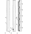
本実施の形態では、具体的な作製工程について説明する。
半導体膜と、ゲート絶縁膜との界面特性は、TFTの電気特性に大きく影響を与える。そのため、ゲート絶縁膜形成前にフッ酸等により半導体膜の表面を洗浄している。このとき、半導体膜は所定の形状となるようにパターニングされているため、フッ酸処理により下地膜、特に半導体膜の側面に設けられた下地膜までが一部除去され、溝や凹部が形成されてしまう。このような形状でゲート絶縁膜、さらにはゲート電極が形成されると、段差被覆性が十分でないためゲート絶縁膜の耐圧不良の原因となってしまう。特に、ゲート絶縁膜の膜厚が薄くなるにつれ、耐圧不良は顕著な問題となってくる。そこで、本実施の形態では薄膜化する場合のゲート絶縁膜の作製方法について説明する。
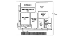
本実施の形態では、CPUの構成についてブロック図を用いて説明する。
本実施の形態では、CPUの形態について説明する。
本実施の形態では、上記実施の形態と異なる作製工程について説明する。
Claims (8)
- ガラス基板上に下地膜を形成し、
前記下地膜上に非晶質半導体膜を形成し、
前記非晶質半導体膜にレーザー光を照射することにより結晶性半導体膜を形成し、
前記結晶性半導体膜上に第1のマスクを形成し、
前記第1のマスクを用いて前記結晶性半導体膜をエッチングし、
前記下地膜の表面、及び前記結晶性半導体膜の側面を窒化し、
前記第1のマスクを除去し、
前記結晶性半導体膜の表面を洗浄し、
前記結晶性半導体膜上にゲート絶縁膜を形成し、
前記ゲート絶縁膜上に導電膜を形成し、
前記導電膜上にテーパを有する第2のマスクを形成し、
前記第2のマスクを後退させつつ前記導電膜をエッチングしてゲート電極を形成する半導体装置の作製方法であって、
前記ゲート電極のゲート長が1.0μm以下となるように前記導電膜をエッチングすることを特徴とする半導体装置の作製方法。 - ガラス基板上に下地膜を形成し、
前記下地膜上に非晶質半導体膜を形成し、
前記非晶質半導体膜にレーザー光を照射することにより結晶性半導体膜を形成し、
前記結晶性半導体膜上に第1のマスクを形成し、
前記第1のマスクを用いて前記結晶性半導体膜をエッチングし、
前記下地膜の表面、及び前記第1のマスクが形成された前記結晶性半導体膜に対して、窒素又はアンモニアを用いたプラズマ処理を施し、
前記第1のマスクを除去し、
前記結晶性半導体膜の表面を洗浄し、
前記結晶性半導体膜上にゲート絶縁膜を形成し、
前記ゲート絶縁膜上に導電膜を形成し、
前記導電膜上にテーパを有する第2のマスクを形成し、
前記第2のマスクを後退させつつ前記導電膜をエッチングしてゲート電極を形成する半導体装置の作製方法であって、
前記ゲート電極のゲート長が1.0μm以下となるように前記導電膜をエッチングすることを特徴とする半導体装置の作製方法。 - ガラス基板上に下地膜を形成し、
前記下地膜上に非晶質半導体膜を形成し、
前記非晶質半導体膜にレーザー光を照射することにより結晶性半導体膜を形成し、
前記結晶性半導体膜上に第1のマスクを形成し、
前記第1のマスクを用いて前記結晶性半導体膜をエッチングし、
前記下地膜の表面、及び前記第1のマスクが形成された前記結晶性半導体膜を、窒素又はアンモニアを用いたプラズマ雰囲気にさらし、
前記第1のマスクを除去し、
前記結晶性半導体膜の表面を洗浄し、
前記結晶性半導体膜上にゲート絶縁膜を形成し、
前記ゲート絶縁膜上に導電膜を形成し、
前記導電膜上にテーパを有する第2のマスクを形成し、
前記第2のマスクを後退させつつ前記導電膜をエッチングしてゲート電極を形成する半導体装置の作製方法であって、
前記ゲート電極のゲート長が1.0μm以下となるように前記導電膜をエッチングすることを特徴とする半導体装置の作製方法。 - 請求項1乃至3のいずれか一において、
ドライエッチング法又はウェットエッチング法により前記導電膜をエッチングすることを特徴とする半導体装置の作製方法。 - 請求項4において、
前記ドライエッチング法は、CF4、Cl及びO2を用いて行われることを特徴とする半導体装置の作製方法。 - 請求項4において、
前記ドライエッチング法は、Cl2を用いて行われることを特徴とする半導体装置の作製方法。 - 請求項1乃至6のいずれか一において、
前記レーザー光を照射する前に、前記非晶質半導体膜上に結晶化を促進させる金属元素を添加し、加熱処理を行うことを特徴とする半導体装置の作製方法。 - 請求項1乃至7のいずれか一に記載の半導体装置の作製方法を用いたCPUの作製方法。
Priority Applications (1)
| Application Number | Priority Date | Filing Date | Title |
|---|---|---|---|
| JP2004243673A JP4754792B2 (ja) | 2003-08-29 | 2004-08-24 | 半導体装置の作製方法 |
Applications Claiming Priority (3)
| Application Number | Priority Date | Filing Date | Title |
|---|---|---|---|
| JP2003307489 | 2003-08-29 | ||
| JP2003307489 | 2003-08-29 | ||
| JP2004243673A JP4754792B2 (ja) | 2003-08-29 | 2004-08-24 | 半導体装置の作製方法 |
Publications (3)
| Publication Number | Publication Date |
|---|---|
| JP2005101571A JP2005101571A (ja) | 2005-04-14 |
| JP2005101571A5 JP2005101571A5 (ja) | 2007-07-26 |
| JP4754792B2 true JP4754792B2 (ja) | 2011-08-24 |
Family
ID=34467410
Family Applications (1)
| Application Number | Title | Priority Date | Filing Date |
|---|---|---|---|
| JP2004243673A Expired - Fee Related JP4754792B2 (ja) | 2003-08-29 | 2004-08-24 | 半導体装置の作製方法 |
Country Status (1)
| Country | Link |
|---|---|
| JP (1) | JP4754792B2 (ja) |
Family Cites Families (4)
| Publication number | Priority date | Publication date | Assignee | Title |
|---|---|---|---|---|
| JP4651851B2 (ja) * | 2000-05-12 | 2011-03-16 | 株式会社半導体エネルギー研究所 | 半導体装置の作製方法 |
| JP5046452B2 (ja) * | 2000-10-26 | 2012-10-10 | 株式会社半導体エネルギー研究所 | 半導体装置の作製方法 |
| JP4673513B2 (ja) * | 2001-08-01 | 2011-04-20 | 株式会社半導体エネルギー研究所 | 半導体装置の作製方法 |
| JP3638926B2 (ja) * | 2001-09-10 | 2005-04-13 | 株式会社半導体エネルギー研究所 | 発光装置及び半導体装置の作製方法 |
-
2004
- 2004-08-24 JP JP2004243673A patent/JP4754792B2/ja not_active Expired - Fee Related
Also Published As
| Publication number | Publication date |
|---|---|
| JP2005101571A (ja) | 2005-04-14 |
Similar Documents
| Publication | Publication Date | Title |
|---|---|---|
| US7115488B2 (en) | Method of manufacturing semiconductor device | |
| US7303981B2 (en) | Polysilicon structure, thin film transistor panel using the same, and manufacturing method of the same | |
| US7390704B2 (en) | Laser process apparatus, laser irradiation method, and method for manufacturing semiconductor device | |
| US8569170B2 (en) | Manufacturing method of semiconductor device comprising silicide layer with varied thickness | |
| US7344825B2 (en) | Method of fabricating semiconductor device, and developing apparatus using the method | |
| US6927418B2 (en) | Thin film transistor substrate and manufacturing method thereof | |
| JP4754792B2 (ja) | 半導体装置の作製方法 | |
| JP4141292B2 (ja) | 半導体装置 | |
| JP2002033489A (ja) | ポリ薄膜トランジスタ及びその製造方法 | |
| JP3889066B2 (ja) | 半導体装置の作製方法 | |
| JP4230159B2 (ja) | 半導体装置の作製方法 | |
| JP2002100780A (ja) | 半導体装置及びその製造方法 | |
| JP4304374B2 (ja) | トップゲート型薄膜トランジスタ | |
| US20050167634A1 (en) | Etchant for nickel silicide | |
| JP2000353807A (ja) | 薄膜トランジスタの製造方法、アクティブマトリクス基板の製造方法、および電気光学装置 | |
| JP4141307B2 (ja) | 半導体装置の作製方法 | |
| JP4421242B2 (ja) | 結晶性半導体膜の作製方法、該結晶性半導体膜を有する薄膜トランジスタの作製方法、該結晶性半導体膜を有する半導体装置の作製方法 | |
| JP4526773B2 (ja) | 半導体装置の作製方法 | |
| JP4137473B2 (ja) | 半導体装置の作製方法 | |
| JP4342876B2 (ja) | 結晶性半導体膜の作製方法、該結晶性半導体膜を有する薄膜トランジスタの作製方法、該結晶性半導体膜を有する半導体装置の作製方法 | |
| JP3921384B2 (ja) | 半導体装置の製造方法 | |
| JP4387144B2 (ja) | 結晶性半導体膜の作製方法、該結晶性半導体膜を有する薄膜トランジスタの作製方法、該結晶性半導体膜を有する半導体装置の作製方法 | |
| JP2002033329A (ja) | 半導体装置の作製方法 | |
| JP2005175444A (ja) | レーザ照射装置並びに半導体装置の作製方法。 |
Legal Events
| Date | Code | Title | Description |
|---|---|---|---|
| A521 | Written amendment |
Free format text: JAPANESE INTERMEDIATE CODE: A523 Effective date: 20070613 |
|
| A621 | Written request for application examination |
Free format text: JAPANESE INTERMEDIATE CODE: A621 Effective date: 20070613 |
|
| A977 | Report on retrieval |
Free format text: JAPANESE INTERMEDIATE CODE: A971007 Effective date: 20100916 |
|
| A131 | Notification of reasons for refusal |
Free format text: JAPANESE INTERMEDIATE CODE: A131 Effective date: 20100921 |
|
| A521 | Written amendment |
Free format text: JAPANESE INTERMEDIATE CODE: A523 Effective date: 20101101 |
|
| TRDD | Decision of grant or rejection written | ||
| A01 | Written decision to grant a patent or to grant a registration (utility model) |
Free format text: JAPANESE INTERMEDIATE CODE: A01 Effective date: 20110517 |
|
| A01 | Written decision to grant a patent or to grant a registration (utility model) |
Free format text: JAPANESE INTERMEDIATE CODE: A01 |
|
| A61 | First payment of annual fees (during grant procedure) |
Free format text: JAPANESE INTERMEDIATE CODE: A61 Effective date: 20110526 |
|
| FPAY | Renewal fee payment (event date is renewal date of database) |
Free format text: PAYMENT UNTIL: 20140603 Year of fee payment: 3 |
|
| R150 | Certificate of patent or registration of utility model |
Free format text: JAPANESE INTERMEDIATE CODE: R150 |
|
| FPAY | Renewal fee payment (event date is renewal date of database) |
Free format text: PAYMENT UNTIL: 20140603 Year of fee payment: 3 |
|
| R250 | Receipt of annual fees |
Free format text: JAPANESE INTERMEDIATE CODE: R250 |
|
| R250 | Receipt of annual fees |
Free format text: JAPANESE INTERMEDIATE CODE: R250 |
|
| R250 | Receipt of annual fees |
Free format text: JAPANESE INTERMEDIATE CODE: R250 |
|
| R250 | Receipt of annual fees |
Free format text: JAPANESE INTERMEDIATE CODE: R250 |
|
| LAPS | Cancellation because of no payment of annual fees |