JP4230159B2 - Method for manufacturing semiconductor device - Google Patents
Method for manufacturing semiconductor device Download PDFInfo
- Publication number
- JP4230159B2 JP4230159B2 JP2002085856A JP2002085856A JP4230159B2 JP 4230159 B2 JP4230159 B2 JP 4230159B2 JP 2002085856 A JP2002085856 A JP 2002085856A JP 2002085856 A JP2002085856 A JP 2002085856A JP 4230159 B2 JP4230159 B2 JP 4230159B2
- Authority
- JP
- Japan
- Prior art keywords
- film
- insulating film
- semiconductor
- region
- forming
- Prior art date
- Legal status (The legal status is an assumption and is not a legal conclusion. Google has not performed a legal analysis and makes no representation as to the accuracy of the status listed.)
- Expired - Fee Related
Links
Images


Description
【0001】
【発明の属する技術分野】
本発明は、結晶構造を有する半導体膜(結晶性半導体膜ともいう。)を用いて形成される半導体素子及びその作製方法並びにその半導体素子を集積化した回路を備えた半導体装置及びその作製方法に関する。特に半導体素子として、絶縁表面上に形成された結晶性半導体膜でチャネル形成領域を形成する薄膜トランジスタに関する。
【0002】
【従来の技術】
ガラスなどの絶縁基板上に形成した結晶性半導体膜を用いた薄膜トランジスタなどの半導体素子を形成する技術が開発されている。特に、レーザー光を照射して非晶質半導体膜を結晶化させる技術は薄膜トランジスタ(TFT)の製造技術に応用されている。結晶性半導体膜を用いて作製される薄膜トランジスタは、液晶表示装置、EL(エレクトロルミネッセンス)表示装置に代表される平面型表示装置(フラットパネルディスプレイ)に応用されている。
【0003】
半導体製造プロセスにおいて、レーザー光の光源としては、エキシマレーザーに代表される気体レーザーや、YAGレーザーに代表される固体レーザーが通常用いられている。レーザー光の照射による非晶質半導体膜の結晶化の一例は、特開昭62−104117号公報で開示されているように、レーザー光の走査速度をビームスポット径×5000/秒以上として高速走査により非晶質半導体膜を完全な溶融状態に至らしめることなく多結晶化するもの、米国特許4,330,363号には島状に形成された半導体膜に、引き延ばされたレーザー光を照射して実質的に単結晶領域を形成する技術が開示されている。或いは特開平8−195357号公報に開示のレーザー処理装置のように光学系にて線状にビームを加工して照射する方法が知られている。
【0004】
さらに、特開2001−144027号公報に開示されているようにNd:YVO4レーザーなど固体レーザー発振装置を用いて、その第2高調波であるレーザー光を非晶質半導体膜に照射して、従来に比べ結晶粒径の大きい結晶性半導体膜を形成し、トランジスタを作製する技術が開示されている。
【0005】
【発明が解決しようとする課題】
しかしながら、平坦な表面上に形成された非晶質半導体膜にレーザー光を照射して結晶化させると結晶は多結晶となり、結晶粒界などの欠陥が任意に形成されて配向の揃った結晶を得ることは困難であった。特に、ガラス基板上にレーザー結晶化技術を用いて配向性の揃った結晶を得ることは困難であった。
【0006】
結晶粒界には結晶欠陥が含まれ、それがキャリアトラップとなって電子又は正孔の移動度が低下する要因となっている。また、結晶化に伴って起こる半導体膜の体積収縮や下地との熱応力や格子不整合などにより、歪みや結晶欠陥の存在しない半導体膜を形成することは出来なかった。従って、張り合わせSOI(Silicon on Insulator)など特殊な方法を省いては、絶縁表面上に形成され、結晶化又は再結晶化された結晶性半導体膜をもって、単結晶基板に形成されるMOSトランジスタと同等の品質を得ることはできなかった。
【0007】
前述の平面型表示装置などは、安価なガラス基板上に半導体膜を形成してトランジスタを作り込むものであるが、任意に形成される結晶粒界を避けるようにトランジスタを配置することは殆ど不可能であった。つまり、トランジスタのチャネル形成領域の結晶性を厳密に制御し、意図せずに含まれてしまう結晶粒界や結晶欠陥を排除することはできなかった。結局、トランジスタの電気特性が劣るばかりでなく、個々の素子特性がばらつく要因となっていた。
【0008】
特に、工業的に多用されている無アルカリガラス基板上にレーザー光を用いて結晶性半導体膜を形成する場合、無アルカリガラス基板自体のうねりの影響を受けてレーザー光の焦点がばらつき、結果的に結晶性のばらつきを招くという問題がある。さらに、無アルカリガラス基板はアルカリ金属による汚染を避けるために、絶縁膜等の保護膜を下地膜として設ける必要があり、その上に結晶粒界や結晶欠陥の排除された結晶性半導体膜を大粒径で形成することは殆ど不可能であった。
【0009】
本発明は上記問題点に鑑みなされたものであり、絶縁表面上、特に安価なガラス基板を支持基板とする絶縁表面上に、少なくともチャネル形成領域において結晶粒界が存在しない結晶性半導体膜を形成し、高速動作が可能で電流駆動能力の高く、且つ複数の素子間においてばらつきの小さい半導体素子又は半導体素子群により構成される安価な半導体装置を提供することを目的とする。
【0010】
さらに、上記少なくともチャネル形成領域において結晶粒界が存在しない結晶性半導体膜においては、EBSP(Electron Backscatter diffraction Pattern)法にて解析した際に主表面に最も多く現れる結晶面(以下、優勢結晶面という。)を{110}面にすることを課題とする。なお、EBSP法については、後述する。
【0011】
なお、結晶面については、ミラー指数を(110)で示されるように小括弧で括って表し、(101)や(011)といった等価な結晶面は{110}で示されるように大括弧で括って表す。また、結晶方位(結晶軸)については、ミラー指数を[110]で示されるようにカギ括弧で括って表し、[101]や[011]といった等価な結晶方位は<110>で示されるように山括弧で括って表す。
【0012】
【課題を解決するための手段】
上記問題点を解決するために本発明は、絶縁表面を有する基板上に直線状のストライプパターンで延在する凹部及び凸部が設けられた絶縁膜を形成し、該絶縁膜上に半導体の結晶化を促進する元素を付着させ、さらに該絶縁膜上に非晶質半導体膜を形成し、前記絶縁膜の凹部にあたる部分(以下、単に凹部という。)に半導体膜を溶融して流し込み結晶化させた結晶性半導体膜を形成し、不要な領域をエッチング除去して前記結晶性半導体膜から島状に分割された結晶性半導体膜(後に半導体素子の一部となる。)を形成し、少なくともチャネル形成領域を形成する部位が前述の凹部に形成された結晶性半導体膜となるように、前記結晶性半導体膜上にゲート絶縁膜及びゲート電極を設けたことを特徴とするものである。
【0013】
本発明の特徴は、凹部及び凸部が設けられた絶縁膜上に上記結晶化を促進する元素を付着させ、該元素の結晶化促進効果を利用して結晶性半導体膜の結晶性を向上させる点にある。なお、非晶質半導体膜の結晶化を促進する元素とは、代表的には、ニッケル(Ni)、コバルト(Co)、鉄(Fe)、白金(Pt)、金(Au)もしくはパラジウム(Pd)等が挙げられる。特に、半導体としてシリコン(Si)、シリコンゲルマニウム(SiXGe1-X:典型的にGe含有量は0.01〜4.5原子%)もしくはシリコンカーバイド(SiXC1-X)を用いる場合、該半導体の結晶化を促進する元素としては、ニッケルが有効である。ニッケルとシリコンの化合物であるニッケルシリサイドは、その格子定数がシリコンの格子定数に近いため、ニッケルシリサイドを媒介とした非常に整合性の良い結晶化が進むからである。
【0014】
また、本発明において、上記結晶化を促進する元素を凹部及び凸部が設けられた絶縁膜上に付着させる手段としては、
▲1▼前記凹部及び凸部が設けられた絶縁膜を、前記元素を含むプラズマに曝す手段
▲2▼前記絶縁膜上に前記元素を含む化合物を溶媒に溶かした溶液を塗布した後、該元素を残して溶媒を除去する手段
の2つの手段が代表的に挙げられる。
【0015】
このとき、前記凹部は底面に向かって幅が狭くなるテーパー形状を有し、該凹部の側面と底面とのなす角(θ)が145±5°の範囲に収まるように形成されることが好ましい。この構成とすると、半導体としてシリコン、シリコンゲルマニウムもしくはシリコンカーバイドを用いた際に、凹部の側面に垂直な方向に{111}面が現れやすくなり、その結果として、凹部に形成された結晶性半導体膜の結晶面は{110}面となりやすくなるからである。これは、ニッケルシリサイドを媒介とした際、ニッケルシリサイドの{111}面を先頭にして結晶化が進行するためである。
【0016】
なお、前記直線状のストライプパターンで延在する絶縁膜を異方性エッチング等で側面が垂直になるようにエッチングすれば、当然のことながら凹部の側面も概略垂直になるが、本発明の効果を失うものではなく、本発明の適用は可能である。
【0017】
また、前記凹部または凸部にあたる部分が設けられた絶縁膜のうち、凸部にあたる部分(以下、単に凸部という。)の上に形成された結晶性半導体膜の結晶性は凹部に形成された結晶性半導体膜に比べて劣るが、当該凸部の上に形成された結晶性半導体膜を積極的に電極(薄膜トランジスタであればソース領域もしくはドレイン領域に相当する。)もしくは配線として用いても良い。配線として用いる場合、占有面積についての設計の自由度が高いため、配線長を調節して抵抗として用いたり、形状を屈曲した形状として保護回路としての機能を持たせることも可能である。
【0018】
前述の凹部は酸化珪素、窒化珪素、又は酸窒化珪素膜などを厚く設け、それをエッチング処理して凹部を形成しても良い。凹部は半導体素子、特にトランジスタのチャネル形成領域を含む島状の半導体膜の配置に合わせて形成し、少なくともチャネル形成領域に合致するように形成されていることが望ましい。また、凹部はチャネル長方向に延在して設けら、その幅(チャネル形成領域とする場合におけるチャネル幅方向)は0.01μm以上2μm以下(好ましくは0.1〜1μm)で形成するのが好ましく、その深さは、0.01μm以上3μm以下(好ましくは0.1μm以上2μm以下)で形成するのが好ましい。
【0019】
勿論、絶縁表面上に島状の絶縁膜を形成し、積極的に凸部を形成することも可能である。その場合、複数の直線状のストライプパターンで延在する凸部は、隣接間で相対的に凹部にあたる部分を形成することになるので、その凹部を半導体素子のチャネル形成領域を含む島状の半導体膜の配置に合わせて形成すれば良いし、幅についても前述の範囲に収めれば良い。
【0020】
また、最初の段階において絶縁膜上及び凹部にかけて形成する半導体膜は、公知の方法で形成される非晶質半導体膜の他に、多結晶半導体膜(成膜されたものも固相成長させたものも含む。)または微結晶半導体膜であっても良い。
【0021】
結晶性半導体膜を溶融して結晶化させる手段としては、気体レーザー発振装置、固体レーザー発振装置を光源とするパルス発振又は連続発振レーザー光を適用する。照射するレーザー光は光学系にて線状に集光されたものであり、その強度分布が長手方向において均一な領域を有し、短手方向に分布を持っていても良く、光源として用いるレーザー発振装置は、矩形ビーム固体レーザー発振装置が適用され、特に好ましくは、スラブレーザー発振装置が適用される。或いは、Nd、Tm、Hoをドープしたロッドを用いた固体レーザー発振装置であり、特にYAG、YVO4、YLF、YAlO3などの結晶にNd、Tm、Hoをドープした結晶を使った固体レーザー発振装置にスラブ構造増幅器を組み合わせたものでも良い。スラブ材料としては、Nd:YAG、Nd:GGG(ガドリニウム・ガリウム・ガーネット)、Nd:GsGG(ガドリニウム・スカンジウム・ガリウム・ガーネット)などの結晶が使用される。スラブレーザーでは、この板状のレーザー媒質の中を、全反射を繰り返しながらジグザグ光路で進む。
【0022】
また、それに準ずる強光を照射しても良い。例えば、ハロゲンランプ、キセノンランプ、高圧水銀灯、メタルハライドランプ、エキシマランプから放射される光を反射鏡やレンズなどにより集光したエネルギー密度の高い光であっても良い。
【0023】
線状に集光され長手方向に拡張されたレーザー光又は強光は結晶性半導体膜に照射し、且つレーザー光の照射位置と結晶性半導体膜が形成された基板とを相対的に動かして、レーザー光が一部又は全面を走査することにより結晶性半導体膜を溶融させ、その状態を経て結晶化又は再結晶化を行う。レーザー光の走査方向は、絶縁膜に形成され直線状のストライプパターンで延在する凹部の長手方向又はトランジスタのチャネル長方向に沿って行う。これによりレーザー光の走査方向に沿って結晶が成長し、結晶粒界がチャネル長方向と交差することを防ぐことができる。
【0024】
凹部の深さを半導体膜の厚さと同程度かそれ以上とすることにより、レーザー光又は強光の照射により溶融した半導体膜が表面張力により凹部に凝集して固化する。その結果、絶縁膜の凸部にある半導体膜の厚さは薄くなり、そこに応力歪みを集中させることができる。また凹部の側面は結晶方位をある程度規定する効力を持つ。
【0025】
半導体膜を溶融状態として、表面張力により絶縁表面上に形成した凹部に凝集させ、凹部の側面部から結晶成長させることにより結晶化に伴い発生する歪みを凹部以外の領域に集中させることができる。即ち、凹部に充填されるように形成した結晶性半導体領域(第1の結晶性半導体領域)を歪みから開放することができる。また、絶縁膜上には結晶粒界や結晶欠陥を含む結晶性半導体領域(第2の結晶性半導体領域)が形成されることになる。また、結晶化の促進のために導入した元素は、結晶化に伴って凸部へと移動し、最終的に凸部に凝集することが期待できる。特に、結晶化を促進する元素としてニッケルを用いた場合、ニッケルシリサイドを固液界面の先頭に立てて移動するため、最終的には殆どのニッケルが凸部へと移動していくものと考えられる。以上のように形成される第1の結晶性半導体領域は、その結晶面が概ね{110}面、即ち優勢結晶面が{110}面となる。
【0026】
そして、凹部に結晶粒界が存在しない結晶性半導体膜を形成した後、半導体素子の活性層(キャリア移動経路として機能する半導体層)をパターニングにより形成し、当該活性層に接するゲート絶縁膜を形成し、さらにゲート電極を形成する。このパターニングの際、活性層の端部にはテーパーを設けることが望ましい。この後は、公知の手法によって電界効果型トランジスタを形成することができる。
【0027】
上記本発明によって、トランジスタなどの半導体素子、特にそのチャネル形成領域の形成される領域を指定して、結晶粒界が存在しない結晶性半導体領域を当該領域に形成することが可能となる。これにより不用意に介在する結晶粒界や結晶欠陥により特性がばらつく要因を無くすことができる。即ち、高速動作が可能で電流駆動能力の高く、且つ複数の素子間においてばらつきの小さい半導体素子又はその半導体素子群により構成される半導体装置を形成することができる。
【0028】
【発明の実施の形態】
[実施の形態1]
本実施の形態では、本発明を実施して薄膜トランジスタを作製する形態について説明する。なお、作製する薄膜トランジスタの個数は実施者が適宜決定すれば良いものでああり、使用する図面はいずれも本発明に制限を与えるものではない。
【0029】
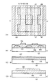
まず、図1について説明する。図1(A)は上面図であり、図1(B)はA−A’に対応する断面図、図1(C)はB−B’に対応する断面図である。基板101上に第1絶縁膜102と直線状のストライプパターン形成された第2絶縁膜103が形成された状態を示している。なお、本明細書において、凹部とは103aで示される部分を指し、凸部とは103bで示される部分を指す。
【0030】
基板101は市販の無アルカリガラス基板、石英基板、サファイア基板、単結晶又は多結晶半導体基板の表面を絶縁膜で被覆した基板、金属基板の表面を絶縁膜で被覆した基板を適用することができる。なお、安価な半導体装置を得るという課題の解決にあたっては、安価な無アルカリガラス基板を用いれば良い。
【0031】
サブミクロンのデザインルールで直線状のストライプパターンを形成するには、基板表面の凹凸、基板のうねり又はねじれを露光装置(特にステッパ)の焦点深度以下にしておくことが望ましい。具体的には、基板のうねり又はねじれが、1回の露光光照射領域内において1μm以下、好ましくは0.5μm以下とすることが望ましい。この点については、特に支持基板として無アルカリガラスを用いる場合には注意が必要である。
【0032】
直線状のストライプパターンに形成される第2絶縁膜103の幅(W1)は0.1〜10μm(好ましくは0.5〜1μm)で、隣接する第2絶縁膜との間隔(W2)は0.01〜2μm(好ましくは0.1〜1μm)であり、第2絶縁膜の厚さ(d)は0.01〜3μm(好ましくは0.1〜2μm)が好ましい。また、段差形状は規則的な周期パターンである必要はなく、島状の半導体膜の幅に合わせて異なる間隔で配置させても良い。その長さも特に数値的な限定はなく、基板の一端から他端に渡るように長く形成することも可能であるし、例えばトランジスタのチャネル形成領域を形成することができる程度の長さとすることも可能である。
【0033】
第1絶縁膜102は、後に形成する第2絶縁膜との選択比の確保できる材料であれば良いが、代表的には、窒化珪素、酸化珪素、酸窒化珪素(SiOxNyと示す。)、窒酸化珪素(SiNxOyと示す。)、窒化アルミニウム(AlxNyと示す。)、酸窒化アルミニウム(AlOxNyと示す。)、窒酸化アルミニウム(AlNxOyと示す。)または酸化アルミニウムから選ばれた材料で、30〜300nmの厚さで形成する。特に、酸化アルミニウム膜はナトリウム(Na)に対するブロッキング効果が期待できるため、ガラス基板からの汚染対策として有効である。
【0034】
なお、酸窒化珪素(SiOxNy)膜としては、Siが25〜35原子%、酸素が55〜65原子%、窒素が1〜20原子%、水素が0.1〜10原子%で含まれるものを用いれば良い。また、窒酸化珪素(SiNxOy)膜としては、Siが25〜35原子%、酸素が15〜30原子%、窒素が20〜35原子%、水素が15〜25原子%で含まれるものを用いれば良い。また、酸窒化アルミニウム(AlOxNy)膜としては、Alが30〜40原子%、酸素が50〜70原子%、窒素が1〜20原子%で含まれるものを用いれば良い。また、また、窒酸化アルミニウム(AlNxOy)膜としては、Alが30〜50原子%、酸素が0.01〜20原子%、窒素が30〜50原子%で含まれるものを用いれば良い。
【0035】
また、第2絶縁膜103は、10〜3000nm、好ましくは100〜2000nmの厚さの酸化珪素又は酸窒化珪素で形成すれば良い。酸化珪素はオルトケイ酸テトラエチル(Tetraethyl Ortho Silicate:TEOS)とO2とを混合しプラズマCVD法で形成することができる。窒酸化珪素膜はSiH4、NH3、N2O又は、SiH4、N2Oを原料として用いプラズマCVD法で形成することができる。
【0036】
図1で示すように、直線状のストライプパターンを二層の絶縁膜で形成する場合には、エッチング加工において第1絶縁膜102と第2絶縁膜103との間に高い選択比をもたせる必要がある。実際には、第1絶縁膜102よりも第2絶縁膜103のエッチング速度が相対的に早くなるように材料及び成膜条件を適宜調整することが望ましい。エッチングの方法としては、緩衝フッ酸を用いたエッチング、又はCHF3を用いたドライエッチングにより行う。
【0037】
なお、第2絶縁膜103としては、CVD法(代表的には、プラズマCVD法もしくは熱CVD法)やPVD法(代表的には、スパッタ法もしくは蒸着法)によって形成された絶縁膜を用いることが好ましい。これは、非晶質半導体膜を結晶化する際、結晶化に伴う応力を緩和しうる程度の柔らかさを持つことが、良好な結晶性を得るにあたって重要な役割を果たしていると考えられるからである。その理由については、後述する。
【0038】
第2絶縁膜103を形成したら、第1絶縁膜102及び第2絶縁膜103をニッケルを含むプラズマ中に曝し、それぞれの表面にニッケルを付着させ、Ni付着面100を形成する。ニッケルを含むプラズマは、放電電極の少なくとも一部にニッケルを用いて窒素、希ガス、水素もしくはこれらの混合ガスをプラズマ化することで形成できる。また、ニッケルを含むガスを直接プラズマ化して形成しても良い。なお、本実施の形態ではニッケルを例に挙げているが、コバルト、鉄、白金、金もしくはパラジウムでも良いことは前述の通りである。
【0039】
本実施の形態で適用するプラズマ処理は、1〜20分(典型的には、3〜5分)の処理時間で終了するためスループットが高い。また、スループットを多少犠牲にしてしまうが、150〜300℃で加熱しながらプラズマ処理を行っても良い。この際、第1絶縁膜102及び第2絶縁膜103になるべくプラズマダメージを残さないように、放電電力や電極間距離を調節することが好ましい。
【0040】
次に、図2について説明する。図2(A)は上面図であり、図2(B)はA−A’に対応する断面図、図2(C)はB−B’に対応する断面図である。上記プラズマ処理の終了後、第2絶縁膜103を覆って非晶質半導体膜105を形成し、連続発振の線状レーザー光によって結晶化する様子を示している。
【0041】
まず、第1絶縁膜102と第2絶縁膜103から成る表面上および凹部103aを覆うようにバッファ膜104を形成し、その後、大気解放することなく連続的に非晶質半導体膜105を0.01〜3μm(好ましくは0.1〜1μm)の厚さに形成する。バッファ膜104は、第1絶縁膜102及び第2絶縁膜103の表面に付着した硼素などの化学汚染の影響の排除と密着性の向上を狙うものであり、薄いものでも十分に効果がある。典型的には、5〜50nm(化学汚染のブロッキング効果を高めるには20nm以上が好ましい。)とすれば良い。
【0042】
この時、非晶質半導体膜106の膜厚は、第2絶縁膜103で形成される凹部の深さ(図1(B)の段差dに相当する。)と同程度かそれ以上の厚さとすることが望ましい。即ち、第2絶縁膜103の段差dと非晶質半導体膜105の凹部103aにおける膜厚t02との関係は、d≧t02であれば良いが、dがt02に比べて厚すぎると凸部103bの上に結晶性半導体膜が残存しなくなるので注意が必要である。なお、非晶質半導体膜は珪素、珪素とゲルマニウムの化合物又は合金、珪素と炭素の化合物又は合金を適用することができる。
【0043】
そして、この非晶質半導体膜105を瞬間的に溶融させ結晶化させる。この結晶化はレーザー光又はランプ光源からの放射光を光学系にて半導体膜が溶融する程度のエネルギー密度に集光して照射する。この工程においては、特に連続発振レーザー発振装置を光源とするレーザー光を適用することが好ましい。適用されるレーザー光は光学系にて線状に集光され、長さの長い方向に拡張されたものであり、その強度分布が長さの長い方向において均一な領域を有し、長さの短い方向にある程度の分布を持たせておくことが望ましい。
【0044】
例えば、結晶化の条件の一例としては、連続発振モードのYVO4レーザー発振器を用い、その第2高調波(波長532nm)の出力5〜10Wを、光学系にて短手方向に対する長手方向の比が10以上である線状レーザー光に集光し、且つ長手方向に均一なエネルギー密度分布を有するように集光し、5〜200cm/secの速度で走査して結晶化させる等が挙げられる。なお、均一なエネルギー密度分布とは、完全に一定であるもの以外を排除するものではなく、エネルギー密度分布において許容される範囲は±10%の範囲内である。
【0045】
また、線状に集光されたレーザー光による結晶化は、1回の走査(即ち、一方向)のみで完了させても良いし、より結晶性を高めるためには往復走査しても良い。さらに、レーザー光により結晶化した後、フッ酸などによる酸化物除去、或いは、アンモニア過酸化水素水処理などアルカリ溶液により珪素膜の表面を処理し、エッチング速度の速い品質の悪い部分を選択的に除去して、再度同様の結晶化処理を行っても良い。このようにして、結晶性を高めることができる。
【0046】
また、結晶化の際、基板の端など後にパターニングのマスク合わせに使用するマーカーを形成する位置は結晶化しないことが好ましい。結晶性半導体膜(特に結晶性珪素膜)は結晶化すると可視光の透過率が上がるため、マーカーとして識別が困難になるからである。ただし、光学的にマーカーの段差によるコントラストの違い等を識別するタイプの位置合わせ制御を行う場合には問題とならない。
【0047】
レーザー発振装置は、矩形ビーム固体レーザー発振装置が適用され、特に好ましくは、スラブレーザー発振装置が適用される。スラブ材料としては、Nd:YAG、Nd:GGG(ガドリニウム・ガリウム・ガーネット)、Nd:GsGG(ガドリニウム・スカンジウム・ガリウム・ガーネット)などの結晶が使用される。スラブレーザーでは、この板状のレーザー媒質の中を、全反射を繰り返しながらジグザグ光路で進む。或いは、Nd、Tm、Hoをドープしたロッドを用いた固体レーザー発振装置であり、特にYAG、YVO4、YLF、YAlO3などの結晶にNd、Tm、Hoをドープした結晶を使った固体レーザー発振装置にスラブ構造増幅器を組み合わせたものでも良い。
【0048】
そして、図2中に矢印で示すように、線状レーザー光の照射領域106の長さの長い方向(図中、X軸方向)が直線状のストライプパターンでなる第2絶縁膜103の各々に交差するように線状のレーザー光又は強光を走査する。尚、ここでいう線状とは、長さの短い方向(図中、Y軸方向)の長さに対し、長さの長い方向(X軸方向)の長さの比が1対10以上のものをもって言う。また、図2では一部しか図示されていないが、線状レーザー光の照射領域106の端部は、矩形状となっていても曲率を持った形状となっていても良い。
【0049】
また、連続発振レーザー光の波長は、非晶質半導体膜の光吸収係数を考慮して400〜700nmであることが望ましい。このような波長帯の光は、波長変換素子を用いて基本波の第2高調波、第3高調波を取り出すことで得られる。波長変換素子としてはADP(リン酸二水素化アンモニウム)、Ba2NaNb5O15(ニオブ酸バリウムナトリウム)、CdSe(セレンカドミウム)、KDP(リン酸二水素カリウム)、LiNbO3(ニオブ酸リチウム)、Se、Te、LBO、BBO、KB5などが適用される。特にLBOを用いることが望ましい。代表的な一例は、Nd:YVO4レーザー発振装置(基本波1064nm)の第2高調波(532nm)を用いる。また、レーザーの発振モードはTEM00モードであるシングルモードを適用する。
【0050】
最も適した材料として選ばれる珪素の場合、吸収係数が103〜104cm-1である領域はほぼ可視光域にある。ガラスなど可視光透過率の高い基板と、珪素により30〜200nmの厚さをもって形成される非晶質半導体膜を結晶化する場合、波長400〜700nmの可視光域の光を照射することで、当該半導体膜を選択的に加熱して、下地絶縁膜にダメージを与えずに結晶化を行うことができる。具体的には、非晶質珪素膜に対し、波長532nmの光の侵入長は概略100nm〜1000nmであり、膜厚30nm〜200nmで形成される非晶質半導体膜105の内部まで十分達することができる。即ち、半導体膜の内側から加熱することが可能であり、レーザー光の照射領域における半導体膜のほぼ全体を均一に加熱することができる。
【0051】
レーザー光は直線状のストライプパターンが延在する方向と平行な方向に走査され、溶融した半導体は表面張力が働いて凹部に流れ込み凝固する。凝固した状態では図2(B)で示すように表面がほぼ平坦になる。これは半導体が一旦溶融することにより、凸部上であろうと凹部上であろうと、溶融した半導体と気相との界面が平衡状態に達し、平坦な界面が形成されるためである。さらに結晶の成長端や結晶粒界は、第2絶縁膜上(凸部上)に形成される(図中ハッチングで示す領域110)。こうして結晶性半導体膜107が形成される。なお、107aは凹部に形成された結晶性の高い半導体領域(以下、第1の結晶性半導体領域という。)であり、107bは凸部に形成された結晶性の劣る結晶性半導体領域(以下、第2の結晶性半導体領域という。)である。
【0052】
なお、上記結晶化工程の際、第2絶縁膜が柔らかい絶縁膜(密度の低い絶縁膜)であると、結晶化時における半導体膜の収縮等による応力を緩和するという効果が期待できる。逆に、固い絶縁膜(密度の高い絶縁膜)であると、収縮もしくは膨張しようとする半導体膜に逆らう形で応力が発生するため、結晶化後の半導体膜に応力歪み等を残しやすく結晶欠陥の原因ともなりかねない。例えば、公知のグラフォエピタキシ技術(「M.W.Geis,D.C.Flanders,H.I.Smith:Appl.Phys.Lett.35(1979)pp71」)では基板上の凹凸を固い石英に直接形成しているが、この場合においては結晶化に伴う熱収縮や応力発生を緩和することができず、応力による歪みもしくは転位に起因する欠陥の発生等が起こりうる。また、石英は高価であり、安価な半導体装置を作製するという本発明の趣旨に反する技術である。
【0053】
しかしながら、本出願人はまさにそれらの点を考慮して、安価なガラス基板上に凹部及び凸部を形成するにあたって、CVD法やPVD法で形成した柔らかい絶縁膜を用いているのであり、下地となる第2絶縁膜を石英ガラスよりも柔らかい材質としたことにより、結晶化の際の応力発生の緩和を目的としている点で上記公知のグラフォエピタキシ技術とは基本的に異なる。
【0054】
なお、石英ガラスよりも柔らかい絶縁膜という意味は、例えば同一測定条件において石英ガラス(工業的に基板として利用されている石英ガラス)よりもエッチングレートの速い絶縁膜もしくは同一測定条件において硬度の低い絶縁膜という意味である。なお、前記エッチングレート及び硬度に関しては、あくまで石英ガラスとの相対比較であれば良いので、エッチングレートの絶対値は問題ではなく、エッチングレートの測定条件や硬度の測定条件に依存しない。
【0055】
例えば、第2絶縁膜として酸窒化珪素膜を用いるのであれば、SiH4ガス、N2Oガスを原料として用いたプラズマCVD法で成膜した酸窒化珪素膜が好ましい。当該酸窒化珪素膜は、フッ化水素アンモニウム(NH4HF2)を7.13%とフッ化アンモニウム(NH4F)を15.4%含む混合水溶液の20℃におけるエッチングレートが110〜130nm/min(500℃、1時間+550℃、4時間の熱処理後では、90〜100nm/min)である。
【0056】
また、第2絶縁膜として窒酸化珪素膜を用いるのであれば、SiH4ガス、NH3ガス、N2Oガスを原料として用いたプラズマCVD法で成膜した窒酸化珪素膜が好ましい。当該窒酸化珪素膜は、フッ化水素アンモニウム(NH4HF2)を7.13%とフッ化アンモニウム(NH4F)を15.4%含む混合水溶液の20℃におけるエッチングレートが60〜70nm/min(500℃、1時間+550℃、4時間の熱処理後では、40〜50nm/min)である。
【0057】
以上のように、絶縁膜により凹部及び凸部を有する直線状のストライプパターンを形成し、その上に非晶質半導体膜を堆積し、レーザー光の照射により溶融状態を経て結晶化させることにより凹部に半導体を流し込み凝固させ、凹部以外の領域に結晶化に伴う歪み又は応力を集中させることができ、結晶粒界など結晶性の悪い領域を選択的に形成することが可能となる。そして、結晶性の良い半導体領域を薄膜トランジスタのチャネル形成領域等のキャリア移動が行われる領域として用いることができる。
【0058】
その後、好ましくは500〜600℃の加熱処理を行い、結晶性半導体膜に蓄積された歪みを除去すると良い。この歪みは、結晶化によって起こる半導体の体積収縮、下地との熱応力や格子不整合などにより発生するものである。この加熱処理は、通常の熱処理装置を用いて行えば良いが、例えばガス加熱方式の瞬間熱アニール(RTA)法を用いて1〜10分の処理を行えば良い。尚、この工程は本発明において必須な要件ではなく、適宜選択して行えば良いものである。
【0059】
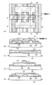
次に、図3について説明する。図3(A)は上面図であり、図3(B)はA−A’に対応する断面図、図3(C)はB−B’に対応する断面図、図3(D)はC−C’に対応する断面図である。結晶性半導体膜107上に薄膜トランジスタの活性層となる半導体領域を画定するためのパターニングを施した状態を示している。
【0060】
図3(A)において、レジストマスク108は第2絶縁膜103の凹部と凸部に跨って設けられている。これは、第2絶縁膜103の凸部に形成された結晶性の劣る結晶性半導体膜であっても、電極として活用する分には何ら問題ないためである。即ち、薄膜トランジスタのソース領域やドレイン領域といった電極として積極的に活用することにより、ソース領域やドレイン領域と各領域に接続される電極(ソース電極もしくはドレイン電極)とのコンタクト部の設計マージンを確保できる。また、こうすることでより薄膜トランジスタの集積度を上げることが可能である。
【0061】
次に、図4について説明する。図4(A)は上面図であり、図4(B)はA−A’に対応する断面図、図4(C)はB−B’に対応する断面図、図4(D)はC−C’に対応する断面図、図4(E)はD−D’に対応する断面図である。結晶性半導体膜107をパターニング後、ドライエッチングもしくはウェットエッチングを行って薄膜トランジスタの活性層109を形成した状態を示している。
【0062】
結晶性半導体膜107はフッ素系のガスと酸素とをエッチングガスとして用いることによりバッファ膜104と選択性をもってエッチングすることができる。勿論、バッファ膜104がエッチングされてしまってもその下にある第1絶縁膜102との選択性さえ確保できれば何ら問題はない。なお、エッチングガスとしては、CF4とO2の混合ガスやNF3ガスを用いたプラズマエッチング法により行っても良いし、ClF3ガス等のフッ化ハロゲンガスを励起しないで用いたプラズマレスのガスエッチングを行っても良い。プラズマレスのガスエッチングは、結晶性半導体膜にプラズマダメージを与えないで済むので結晶欠陥の抑制により効果的な手法である。
【0063】
また、活性層109を形成する際、活性層の端部(エッジ)にテーパーを設けることが望ましい。テーパー角は、5〜60°(好ましくは20〜40°)で良い。これにより後に形成するゲート絶縁膜のカバレッジ(被覆率)を向上させることができ、ゲート電極の断線や短絡等を防ぐことができる。
【0064】
ところで、本発明の特徴は、結晶性の高い第1の結晶性半導体領域107aを選択的に薄膜トランジスタのチャネル形成領域として用いることにある。そして、さらなる特徴は、第1の結晶性半導体領域が複数の結晶方位を有しながらも実質的に結晶粒界が形成されていない点にある。
【0065】
本発明を実施して得た結晶性半導体膜にはセコ・エッチングで明確になるような結晶粒界もしくは欠陥が顕在化しない、換言すれば実質的に存在しない。なお、セコ。エッチングとは、結晶性半導体膜の表面の結晶粒界を顕在化させるために一般的に知られるセコ液(HF:H2O=2:1に添加剤としてK2Cr2O7を用いて調合した薬液)を用いたエッチング手法である。本明細書において、セコ液としては、二クロム酸カリウム(K2Cr2O7)2.2gを水50ccに溶かして0.15mol/lの溶液を調製し、当該溶液にフッ酸水溶液100ccを加えてものを、さらに水で5倍に希釈したものを指し、セコ・エッチングとしては、前述のセコ液を用いて室温(10〜30℃)にて75秒のエッチング処理を施すことを指す。
【0066】
セコ・エッチングで明確になる結晶粒界は現状において特定できていないが、セコ・エッチングにより積層欠陥や結晶粒界が優先的にエッチングされることは良く知られている事実である。勿論、単結晶ではないため、セコ・エッチングで顕在化しない粒界や欠陥は当然あり得るが、そのような粒界や欠陥は半導体素子を作製した際の電気特性に影響を及ぼすようなものではないため、電気的に不活性と考えられる。通常、電気的に不活性な粒界とは、平面状粒界(低次もしくは高次の双晶又は対応粒界)と呼ばれるものであり、セコ・エッチングで顕在化しない粒界とは、平面状粒界であると推測される。その観点からすると、結晶粒界もしくは欠陥が実質的に存在しないということは、平面状粒界以外の結晶粒界が存在しないと言っても差し支えないと言える。
【0067】
また、優勢結晶面が何かについては、反射電子回折パターン(EBSP:Electron Backscatter diffraction Pattern)により求めた結果を用いれば良い。EBSPは走査型電子顕微鏡(SEM:Scanning Electron Microscopy)に専用の検出器を設け、電子ビームを結晶面に照射してその菊池線からの結晶方位同定をコンピューターで画像認識させることによって、そのミクロな結晶性を表面配向のみならず、結晶の全方向に関して測定するものである(以下、この手法を便宜上EBSP法と呼ぶ)。
【0068】
なお、本明細書において、優勢結晶面とは、EBSP法で解析した際に最も多く表面に現れた結晶面である。なお、当該結晶面は、少なからず若干のゆらぎ(結晶面に垂直な軸のずれ)を包含するものであり、本明細書では、当該ゆらぎとして±15°までを許容している。以上のように、本発明を実施して得られた結晶性半導体膜は、EBSP法で解析した際に、優勢結晶面として{110}面が現れ、その他は{100}面、{111}面及び{311}面等が混在して現れるということである。
【0069】
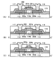
次に、図5について説明する。図5(A)は上面図であり、図5(B)はA−A’に対応する断面図、図5(C)はB−B’に対応する断面図、図5(D)はC−C’に対応する断面図、図5(E)はD−D’に対応する断面図である。活性層109を形成した後、ゲート絶縁膜110及びゲート電極111を形成した状態を示している。
【0070】
ゲート絶縁膜110は、課題を解決するための手段で説明した酸化珪素膜、窒化珪素膜、酸窒化珪素膜、窒酸化珪素膜、窒化アルミニウム膜、窒酸化アルミニウム膜、酸窒化アルミニウム膜もしくは酸化アルミニウム膜のいずれを用いても良いし、これらを適宜組み合わせた積層膜としても良い。ゲート絶縁膜のカバレッジを良くするためには、酸化珪素膜ならばTEOSを用いた酸化珪素膜が好ましく、窒酸化アルミニウム膜であればRFスパッタ法で形成した窒酸化アルミニウム膜を用いたり、当該窒酸化アルミニウム膜と酸化珪素膜の積層膜(酸化珪素膜は、活性層となる半導体膜を過酸化水素で酸化させたものであっても良い。)を用いたりすると良い。
【0071】
また、ゲート電極111は、タングステン又はタングステンを含有する合金、タンタル又はタンタルを含有する合金又はアルミニウムもしくはアルミニウム合金などで形成すれば良い。
【0072】
次に、図6について説明する。図6(A)は上面図であり、図6(B)はA−A’に対応する断面図、図6(C)はB−B’に対応する断面図、図6(D)はC−C’に対応する断面図、図6(E)はD−D’に対応する断面図である。ゲート電極111をマスクとして自己整合的(セルフアライン)にソース領域112及びドレイン領域113を形成した状態を示している。また、本工程によりチャネル形成領域114a、114bが画定する。
【0073】
本実施の形態では、ソース領域112及びドレイン領域113にp型を付与するために周期表の13族に属する元素(代表的には、ホウ素を用いる。)を添加しているが、n型を付与するために周期表の15族に属する元素(代表的には、リンもしくはヒ素を用いる。)を添加しても良い。添加方法は公知の手法によれば良い。また、必要に応じて低濃度ドレイン領域(一般的にはLDD領域と呼ばれる。)を設けても良い。
【0074】
また、ソース領域112及びドレイン領域113を形成した後、ファーネスアニール、レーザーアニールもしくはRTA(ラピッドサーマルアニール)によりソース領域112及びドレイン領域113の活性化を行う。なお、RTAは、ランプ光源を用いた赤外光もしくは紫外光によるアニールであっても良いし、加熱ガスによるアニールであっても良い。
【0075】
次に、図7について説明する。図7(A)は上面図であり、図7(B)はA−A’に対応する断面図、図7(C)はB−B’に対応する断面図、図7(D)はC−C’に対応する断面図、図7(E)はD−D’に対応する断面図である。ソース配線117及びドレイン配線119まで形成し、pチャネル型の薄膜トランジスタが完成した状態を示している。
【0076】
上記活性化工程が終了したら、ゲート電極111等を覆うように保護膜(パッシベーション膜)115を形成する。保護膜115としては、窒化珪素膜、窒酸化珪素膜、窒化アルミニウム膜もしくは窒酸化アルミニウム膜の如き窒素含有量の多い絶縁膜を用いることが好ましい。これはアルカリ金属や水分等の影響を排除するためである。
【0077】
なお、本実施の形態では、保護膜115として窒酸化珪素(SiNxOy)膜を用い、成膜後に400〜450℃の加熱処理を行う。当該保護膜115は、15〜25原子%の水素を含むため、加熱処理によって水素が拡散し、例えチャネル形成領域114a、114bに不対結合手があったとしても効果的に水素で終端できる。
【0078】
保護膜115を形成したら、層間膜(層間絶縁膜)116として、酸化珪素膜、窒化珪素膜、窒酸化珪素膜もしくは酸窒化珪素膜又はこれらの積層膜を形成する。勿論、耐熱性が許せば樹脂膜を用いても良い。膜厚は、特に限定されないが、層間膜116の表面が十分に平坦化できる膜厚が好ましい。なお、層間膜116の成膜後にCMP(ケミカルメカニカルポリッシング)等の公知の手段で平坦化を行っても良い。
【0079】
そして、層間膜116等にコンタクトホールを形成し、アルミニウム膜もしくはアルミニウム膜と他の金属膜との積層膜でソース配線117及びドレイン配線118を形成する。勿論、アルミニウムの代わりに銅その他の低抵抗導体を用いても良い。なお、119は、ソース領域112とソース配線117が接続される領域であり、ソースコンタクトと呼ぶ。また、120は、ドレイン領域113とドレイン配線118が接続される領域であり、ドレインコンタクトと呼ぶ。本実施の形態では、ソース領域及びドレイン領域が第2絶縁膜で形成される凹部及び凸部に跨って形成されているため、ソースコンタクト119及びドレインコンタクト120を形成するための設計マージンを広くとることができる。
【0080】
図7に示されるpチャネル型トランジスタは、複数のチャネル形成領域(本実施の形態では2本のチャネル形成領域114a、114b)が並列に配設され、かつ、一対の不純物領域(本実施の形態ではソース領域112及びドレイン領域113)との間に連接して設けられた構造、即ちマルチチャネル構造のトランジスタである。
【0081】
ところで、上述のように本発明を実施して得た結晶性半導体膜、具体的にはチャネル形成領域として用いる第1の結晶性半導体領域は、優勢結晶面が{110}面であることを特徴の一つとしている。ここで、優勢結晶面が{110}面であることの利点について以下に説明する。
【0082】
単結晶シリコンの結晶面について様々な研究がなされており、一般的に、{110}面はホール移動度が高いことで知られる。例えば、「VLSIデバイスの物理;岸野正剛、小柳光正共著、丸善株式会社(1995)第145頁」には、結晶面が(011)面であるとき、ホール(正孔)の移動方向が<01−1>軸に平行な方向の時に、最大の電界効果移動度(μFE=約225cm2/Vs)となることが示されている。即ち、{110}面の結晶面を有するシリコン基板において、ホールの移動方向を〈01−1>軸に一致するようにトランジスタを形成することで、pチャネル型トランジスタの電界効果移動度を最も高くすることができる。
【0083】
ここで本発明者らによれば連続発振の線状レーザー光を一定方向に走査して結晶化した結晶性半導体膜は、その線状レーザー光の長手方向に垂直な方向が結晶成長の方向となり、かつ、その結晶軸が〈110〉軸であるという知見が得られている。なお、この〈110〉軸には±15°のゆらぎが含まれている。即ち、本発明を実施して得られる第1の結晶性半導体領域は、連続発振のレーザー光の照射領域を移動させて一定方向に結晶成長させ、かつ、直線状のストライプパターンで延在する複数の第2絶縁膜によっても結晶成長が規定される。例えば、本実施の形態では線状レーザー光の照射領域の移動方向とその長手方向に垂直な方向とが一致するため、結果的に、照射領域の移動方向と結晶成長の方向とが一致することになる。そのため、図4(B)の断面図において、活性層109の切断面の結晶面は{110}面になる。
【0084】
従って、本実施の形態に記載されたpチャネル型薄膜トランジスタは、ホールの移動方向と〈110〉軸が一致することになり、かつ、優勢結晶面が{110}面となるため、上記文献に示唆されるように、pチャネル型薄膜トランジスタの電界効果移動度を最も効果的に高めることのできる構造となっている。
【0085】
[実施の形態2]
本発明の結晶性半導体膜の形成において、実施の形態1で示すように非晶質半導体膜にレーザー光を照射して結晶化させる方法の他に、固相成長により結晶化した後さらにレーザー光を照射して溶融再結晶化しても良い。例えば、図2において非晶質半導体膜105を形成した後、450〜650℃のファーネスアニール処理または700〜1100℃のRTA処理(対流させた高熱ガスによる処理も含む。)を行い、ニッケルの結晶化促進効果を利用して非晶質半導体膜105を固相成長させることにより結晶化させておくことが可能である。
【0086】
本実施の形態を実施した場合、固相成長させた結晶性半導体膜に対して実施の形態1に従ってレーザー光を照射して溶融し、再結晶化させる過程を経る。このとき結晶性半導体膜はレーザー光の照射によって溶融するが、光吸収係数は殆ど変動しない。この点については、非晶質半導体膜に直接レーザー光を照射する場合と大きく異なる点である。即ち、光吸収係数の変動が小さいということは、レーザー光の照射エネルギーが多少ばらついても膜質に影響しないということであり、事実、固相成長させた結晶性半導体膜は、非晶質半導体膜に比べてレーザー光のエネルギー密度に対するマージンが広く、生産性が良いという利点がある。
【0087】
本実施の形態により得た結晶性半導体膜も、実施の形態1で説明したように表面が平坦なものとなり、優勢結晶面が{110}面であるという特徴を有する。このような結晶性半導体膜を薄膜トランジスタのチャネル形成領域に用いると、電子移動度とホール移動度が共に大幅に向上し、ひいてはNチャネル型トランジスタ及びPチャネル型トランジスタの電界効果移動度が大幅に向上するという特徴を有する。特に、上述のように、ホール移動度の向上に伴うPチャネル型トランジスタの電界効果移動度の向上は特筆すべきものであり、優勢結晶面を{110}とする利点の一つである。
【0088】
その後、実施の形態1と同様に凹部の結晶性半導体膜をチャネル形成領域とし、かつ、凸部の結晶性半導体膜をソース領域もしくはドレイン領域として用いた薄膜トランジスタを形成する。凹部の結晶性半導体膜は、複数の結晶方位を有し結晶粒界が形成されていないという特徴を有しているため、高速動作が可能で電流駆動能力の高く、且つ複数の素子間においてばらつきの小さいトランジスタ又はそのトランジスタ群により構成される半導体装置を形成することができる。
【0089】
[実施の形態3]
本実施の形態では、結晶化を促進する元素を凹部及び凸部が設けられた絶縁膜上に付着させる手段として、絶縁膜上にニッケル、コバルト、鉄、白金、金もしくはパラジウムを含む化合物を溶媒に溶かした溶液を塗布した後、これらの元素を絶縁膜上に残して溶媒を除去する手段を用いた例を示す。
【0090】
上記溶液を用いた塗布法については、本出願人による特開平7−130652号公報等に詳しいが、酢酸ニッケル塩や硝酸ニッケル塩といった金属塩化合物を水、アルコール等の溶媒中にニッケル濃度が5〜200ppmとなるように溶解させ、当該溶液をスピンコート法により塗布するという技術である。
【0091】
具体的な条件としては、例えば、ニッケルを10ppmの濃度で含む水溶液をスピンコーターの吸着ヘッド上に設けられた被処理体の上に一定量滴下し、10〜50rpm程度の回転速度で1〜3分保持し、その後、2000〜3000rpmの回転速度で溶媒を乾燥させて、被処理体上に一定量のニッケルを付着させる。この手法では、被処理体表面にニッケルが物理吸着することになるため、過剰なニッケルが付着することなく一定量とすることができる。この点は、後の結晶化において導入させるニッケルを必要最小限に抑える上で非常に有効である。
【0092】
勿論、ニッケル以外にも上述に例示したすべてを元素を用いても良い。その際にも、それぞれに対応する各金属塩化合物を溶媒に溶かしてスピンコート法により付着させれば良いので詳細な説明は省略する。
【0093】
以上のような手段で凹部及び凸部が設けられた絶縁膜上にニッケル、コバルト、鉄、白金、金もしくはパラジウムを付着させた後は、実施の形態1の工程(図2以降の工程)に従って、薄膜トランジスタを形成すれば良い。勿論、本実施の形態は、実施の形態2と組み合わせても実施することが可能である。
【0094】
[実施の形態4]
本実施の形態では、結晶化を促進する元素を凹部及び凸部が設けられた絶縁膜上に付着させる手段として、絶縁膜上にニッケル、コバルト、鉄、白金、金もしくはパラジウムを含む化合物を溶媒に溶かした溶液を塗布した後、これらの元素を絶縁膜上に残して溶媒を除去する手段を用いた例を示す。特に、実施の形態3に示した方法とは別の手段を用いた例について説明する。説明には図8を用いる。
【0095】
まず、実施の形態1に従って基板101上に第1絶縁膜102及び第2絶縁膜103を形成する。その状態で、噴霧器を備えた塗布手段131を第2絶縁膜103の長手方向(図2におけるY軸方向)に向かって移動させると共にノズルからニッケルを含む溶液を霧状に噴射する。ニッケルを含む溶液は、実施の形態3で説明したもので良い。噴射により第1絶縁膜102及び第2絶縁膜103上にはニッケルを含む溶液層132が形成される。
【0096】
なお、塗布手段131は1回の移動で基板全面に噴射できる長さであることが好ましい。また、基板端(アライメントマーカー等を設ける部分)に噴射されないように長さを調節しても良い。
【0097】
次に、塗布手段131が移動した後、適当な間隔をおいて乾燥手段133を塗布手段131と同一の方向に移動させると共にノズルから流速の速いガスを、ニッケルを含む溶液層132を乾燥手段133の移動方向へと押しやるように噴射し、第1絶縁膜102及び第2絶縁膜103の表面を乾燥させる。その結果、乾燥手段133の通過後には第1絶縁膜102及び第2絶縁膜103の表面にNi付着面134が形成される。
【0098】
本実施の形態は、実施の形態3に記載した技術をさらに改良したものであり、特に大面積の基板を扱う際に有効な技術である。実施の形態3に示すスピンコート法による場合、基板上にはストライプパターンの絶縁膜が無数にあるため、特に大面積基板になるとスピン乾燥による方法ではスループットが低下するおそれがある。そこで、本実施の形態では、ストライプパターンに並列された絶縁膜に沿って塗布と乾燥を行うため、パターン依存性がなく、大面積基板への適用に好適である。
【0099】
本実施の形態に記載される手段で凹部及び凸部が設けられた絶縁膜上にニッケル、コバルト、鉄、白金、金もしくはパラジウムを付着させた後は、実施の形態1の工程(図2以降の工程)に従って、薄膜トランジスタを形成すれば良い。勿論、本実施の形態は、実施の形態1及び2のどちらと組み合わせても実施することが可能である。
【0100】
[実施の形態5]
本発明を実施した場合、結晶化の際にニッケル等の金属元素を用いる都合上、形成された結晶性半導体膜中にこれらの金属元素が残存する場合がある。最も、結晶化が図1における凹部103aから始まり、最終的に凸部103bに至って終了するため、ニッケル等の金属元素は凸部103bに凝集すると考えられる。しかしながら、より完全に排除するためには意図的に除去もしくは低減するための処理が必要である。
【0101】
本実施の形態では、実施の形態1〜4に記載された技術により形成された結晶性半導体膜中から積極的にニッケルを除去するために、結晶性半導体膜107の形成後、ゲッタリング処理を行うことを特徴とする。本実施の形態に用いるゲッタリング処理の詳細については、本出願人による特願2002−020801号の明細書を参照すれば良い。また、このゲッタリング処理に伴う加熱処理は、ゲッタリングと同時に結晶性半導体膜の歪みを緩和するという相乗効果も合わせ持っている。
【0102】
また、ゲッタリング処理としては、上述の技術以外にもハロゲン雰囲気中における加熱処理による除去効果を利用したゲッタリング処理(特開平10−135468号)、リンによる除去効果を利用したゲッタリング処理(特開平10−270363号)、非晶質半導体膜による除去効果を利用したゲッタリング処理(特開平8−213316号)等を用いても良い。
【0103】
以上のような手段で結晶性半導体膜107中からニッケル、コバルト、鉄、白金、金もしくはパラジウムを付着させた後は、実施の形態1の工程(図3以降の工程)に従って、薄膜トランジスタを形成すれば良い。本実施の形態を実施して得た薄膜トランジスタは、チャネル形成領域中に金属元素が残存することがないため、実施の形態1〜4を実施して得た薄膜トランジスタに比べて、さらにオフ電流(リーク電流)の小さい電気特性を得ることができる。
【0104】
[実施の形態6]
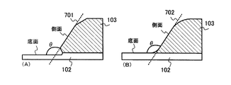
本実施の形態では、実施の形態1において、第2絶縁膜103で形成された凹部における底面と側面のなす角(θ)の角度を145±5°とした例を示す。特に、ニッケルを用いてシリコン、シリコンゲルマニウムもしくはシリコンカーバイドを結晶化する際に本実施の形態の適用は有効である。
【0105】
なお、底面と側面のなす角(θ)は、底面に平行な面と側面に平行な面のなす角であり、次のように説明される。図21(A)、(B)は、凹部の形状のパターン例が図1のような理想的な形状でない場合の例である。図21(A)は、第2絶縁膜103の形成の際、第1絶縁膜102がエッチングされて第2絶縁膜103の下に「巣」が出来てしまった場合を想定しているが、この場合、側面に平行な面(点線で示される面)701と底面のなす角でθが定義される。また、図21(B)は、第2絶縁膜103の形成の際、第2絶縁膜103の上端部や下端部に丸みが出来てしまった場合を想定しているが、この場合、やはり側面に平行な面(点線で示される面)702と底面のなす角でθが定義される。
【0106】
図8(A)は、実施の形態1に従って結晶化工程までを終了した上面図であり、201は第2絶縁膜、202は結晶性半導体膜、202aは凹部に形成された結晶性半導体領域(第1の結晶性半導体領域)、202bは凸部に形成された結晶性半導体領域(第2の結晶性半導体領域)である。
【0107】
図8(B)は、図8(A)をA−A’で切断した断面図である。図8(B)に示すように、凹部における底面と側面のなす角(θ)は145±5°であり、この角度に規定した状態で非晶質半導体膜の溶融結晶化を行うと、側面に垂直な方向(即ち、〈111〉軸方向)に向かって結晶成長が起こり、結晶学的に結晶性半導体膜202の表面には{110}面が現れることになる。多少のゆらぎの影響を受けてすべて{110}面になるとは限らないが、優勢結晶面は概ね{110}面である。
【0108】
なぜならば、ニッケルを用いた場合、非晶質半導体膜と結晶性半導体膜の間にはニッケルシリサイドが媒体として存在し、かつ、ニッケルシリサイドの結晶面は{111}面となることが判明しているからである。即ち、凹部の側面に付着したニッケルに起因する結晶成長は、<111>軸方向に進むため、上述の結果となるのである。
【0109】
本実施の形態は、実施の形態1に示したプロセスにおいて第2絶縁膜のテーパー角を145±5°に設計変更するだけで実施可能であり、その他のプロセスについてはすべて実施の形態1を参考にすれば良い。勿論、実施の形態2〜5のいずれの実施の形態と組み合わせても効果を得ることができる。
【0110】
[実施の形態7]
本実施の形態では、実施の形態1において、第1絶縁膜102を積層膜とした例を示す。図10(A)は、図7(A)をC−C’で切断した断面図に相当する図面であり、図10(B)は、図7(A)をD−D’で切断した断面図に相当する図面である。
【0111】
本実施の形態において、絶縁膜102aは酸化珪素膜、窒化珪素膜、酸窒化珪素膜もしくは窒酸化珪素膜であり、20〜30nmの厚さに設けられる。絶縁膜102bは、酸化アルミニウム膜、窒化アルミニウム膜、酸窒化アルミニウム膜もしくは窒酸化アルミニウム膜であり、10〜50nm(好ましくは20〜30nm)の厚さに設けられる。特に、酸化アルミニウム膜はナトリウム(Na)に対するブロッキング効果が期待できるため、ガラス基板からの汚染対策として有効である。
【0112】
上記絶縁膜102a及び絶縁膜102bの組み合わせは如何なる組み合わせであっても可能であるが、少なくとも絶縁膜102bはその上に設けられる第2絶縁膜103との選択比を大きくとることのできる材料であることが望ましい。また、レーザー光による結晶化工程等の際に放熱し過ぎないような材料が好ましい。そういった観点からも現状においては酸化アルミニウム膜が好ましいと考えられる。
【0113】
なお、本実施の形態では二層にした例を示しているが、三層以上の複数層にしても良いことは言うまでもない。さらに、本実施の形態は、実施の形態1〜6のいずれの構成と組み合わせ可能である。
【0114】
[実施の形態8]
実施の形態1において、トランジスタはシングルドレイン構造で示されているが、低濃度ドレイン(LDD)を設けても良い。図11はLDD構造を持ったnチャネル型の薄膜トランジスタの一例を示している。
【0115】
図11(A)で示すトランジスタの構造はゲート電極を窒化チタン又は窒化タンタルなど窒化物金属301aとタングステン又はタングステン合金など高融点金属301bで形成する一例であり、ゲート電極301bの側面にスペーサ302を設けている。スペーサ302は酸化珪素などの絶縁体で形成しても良いし、導電性を持たせるためにn型の多結晶珪素で形成しても良く、異方性ドライエッチングにより形成する。LDD領域303a、303bはこのスペーサを形成する前に形成することにより、ゲート電極301bに対し自己整合的に形成することができる。スペーサを導電性材料で形成した場合には、LDD領域303a、303bが実質的にゲート電極と重畳するゲート・オーバーラップLDD(Gate-Overlapped LDD)構造とすることができる。
【0116】
一方、図11(B)はゲート電極301aを設けない構造であり、この場合はLDD構造となる。
【0117】
図11(C)は、ソース領域112及びドレイン領域113に隣接してそれぞれLDD領域303a、303bが形成されている。このときゲート電極は下層側ゲート電極304a、上層側ゲート電極304bの二層構造からなり、ソース領域112、ドレイン領域113及びLDD領域303a、303bを自己整合的に形成することができる。このようなゲート電極と不純物領域、及びその作製方法の詳細については、特願2000−128526号出願又は特願2001−011085号出願を参照されたい。
【0118】
本実施の形態に示したようなゲート構造により自己整合的にLDD領域を形成する構造は、特にデザインルールを微細化する場合において有効である。なお、ここでは単極性のトランジスタ構造を示したが、nチャネル型トランジスタとpチャネル型トランジスタを作りわけ、相補型に組み合わせてCMOS回路を形成することもできる。また、本実施の形態は、実施の形態1〜6のいずれの構成と組み合わせ可能である。
【0119】
[実施の形態9]
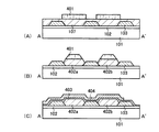
本実施の形態は、実施の形態1における活性層109の形状に関する他の例であり、チャネル形成領域となる半導体領域が、多角形(具体的には六角形)をなしていることを特徴とする。図12(A)は、図3(A)をA−A’で切断した断面図に相当する図面であり、図12(B)は、図4(A)をA−A’で切断した断面図に相当する図面(ただし、レジストマスクを残したままの状態)であり、図12(C)は、図5(A)をA−A’で切断した断面図に相当する図面である。
【0120】
図12(A)において、レジストマスク401は第2絶縁膜103に重畳するように形成される。この状態で結晶性半導体膜107をテーパー状にエッチングしていくと図12(B)に示すように、六角形状の半導体領域402a、402bを得ることができる。さらに、図12(C)に示すように、六角形状の半導体領域402a、402bの上にゲート絶縁膜403及びゲート電極404を形成する。なお、ゲート絶縁膜403及びゲート電極404を構成する材料は、実施の形態1を参照すれば良い。
【0121】
チャネル形成領域となる半導体領域を本実施の形態に示す形状とした場合、チャネル形成領域となる半導体領域402a、402bを乗り越えるための段差を緩和することができ、ゲート絶縁膜及びゲート電極のカバレッジ(被覆率)を改善することが可能である。なお、本実施の形態は、実施の形態1〜8のいずれの形態とも組み合わせることが可能であり、組み合わせた効果として前述のカバレッジの改善効果を各実施の形態に付与することができる。
【0122】
[実施の形態10]
本実施の形態では、実施の形態1において、薄膜トランジスタの活性層109を形成する工程の前に結晶性半導体膜107の一部(後にチャネル形成領域となる部分)をエッチングして薄膜化する例を示す。なお、図13(A)は結晶性半導体膜107の薄膜化後の上面図であり、図13(B)〜(E)は、図13(A)をそれぞれA−A’、B−B’、C−C’、D−D’で切断した断面図である。
【0123】
まず実施の形態1に示した作製方法に従って、図2に示すように結晶性半導体膜107を形成する。次に、結晶性半導体膜107のうち、後にソース領域またはドレイン領域となる半導体領域の上にレジストマスク501を形成する(図13(A))。
【0124】
そして、レジストマスク501をマスクとしてドライエッチング法またはウェットエッチング法により結晶性半導体膜107をエッチングし、第2絶縁膜103(もしくはその上のバッファ膜104)を露出させる。この工程により凹部のみに選択的に結晶性半導体膜502を残存させることができる。また、レジストマスク501の下には元の膜厚で結晶性半導体膜503が残存する。本実施の形態は、結晶性半導体膜502を薄膜トランジスタのチャネル形成領域として用い、元の膜厚で残存した結晶性半導体膜503を薄膜トランジスタのソース領域またはドレイン領域として用いることを特徴とする。
【0125】
なお、上記エッチング工程は、化学的手法だけでなく、CMP(ケミカルメカニカルポリッシング)の如き機械的研磨法を用いても良い。また、化学的手法及び機械的手法を併用しても構わない。
【0126】
本実施の形態によれば、第2絶縁膜103により自己整合的にチャネル形成領域を形成することができるため、パターンずれによって第2絶縁膜の凸部に誤ってチャネル形成領域が形成されることを防ぐことができ、チャネル形成領域内に結晶粒界が含まれてしまうような事態を減らすことができる。
【0127】
これ以降の工程については、実施の形態1に記載の工程を参照にすれば良いので、本実施の形態での説明は省略する。なお、本実施の形態は、実施の形態1〜8のいずれの形態とも自由に組み合わせることが可能である。
【0128】
[実施の形態11]
本実施の形態では、実施の形態1において、活性層109を形成した後に、第2絶縁膜103を除去した例を示す。なお、図14(A)は本実施の形態を実施した場合における薄膜トランジスタの上面図であり、図15(A)〜(E)は、図14(A)をそれぞれA−A’、B−B’、C−C’、D−D’、E−E’で切断した断面図である。また、各図面の符号は、実施の形態1に用いた図面の符号を参照すれば良い。
【0129】
本実施の形態の特徴として、活性層109の下以外の領域において第2絶縁膜103が除去されている点と、それにより基板面上において不必要な段差が低減される点が挙げられる。即ち、ゲート配線、ソース配線及びドレイン配線とった引き回し配線が段差を乗り越える回数を減らすことができるため、乗り越え不良に起因する断線などの不良を防ぐことが可能である。
【0130】
なお、本実施の形態は、実施の形態1〜8、10のいずれの形態とも自由に組み合わせることが可能である。
【0131】
[実施の形態12]
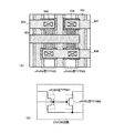
本実施の形態では、実施の形態1に示したプロセスに公知のCMOS形成技術を組み合わせてCMOS回路を形成した例を示す。なお、図16(A)は本実施の形態を実施した場合におけるCMOS回路の上面図であり、図16(B)は、図16(A)を模式的に示した回路図である。
【0132】
図16(A)において、601はnチャネル型TFT、602はpチャネル型TFTである。これらTFTは図16(B)に示すように接続されて相補型回路(具体的にはCMOS回路)を構成している。
【0133】
図16(A)において、603はnチャネル型TFT601の活性層、604はpチャネル型TFT602の活性層、605はゲート電極、606はnチャネル型TFT601のソース配線、607はpチャネル型TFT602のソース配線、608はnチャネル型TFT601及びpチャネル型TFT602に共通のドレイン配線である。
【0134】
実施の形態1によって作製されたpチャネル型TFTは、優勢結晶面を{110}面としているため、ホール移動度が高く、結果的にpチャネル型TFTとしての電界効果移動度が高いという特徴を有する。従来、nチャネル型TFTに比べてpチャネル型TFTの電気特性がかなり劣っていたため、CMOS回路を構成した際に特性バランスが悪く動作性能が低くなるということもあった。しかしながら、本発明を用いて作製したpチャネル型TFTをnチャネル型TFTと組み合わせて使用した場合、nチャネル型TFTとpチャネル型TFTの特性バランスが良くなるため、動作性能の高いCMOS回路を構成することが可能となる。
【0135】
なお、本実施の形態は、実施の形態1〜11のいずれの形態とも自由に組み合わせることが可能である。
【0136】
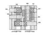
[実施の形態13]
本実施の形態では、実施の形態12に示したCMOS回路とは異なる形態を示す。なお、図面は図17を用いるが、図16と同一の符号については、実施の形態12を参考にすれば良い。
【0137】
本実施の形態では、pチャネル型TFT801とnチャネル型TFT802でCMOS回路を構成しており、803はpチャネル型TFTの活性層、804はnチャネル型TFTの活性層、805はpチャネル型TFTのゲート電極、806はnチャネル型TFTのゲート電極である。
【0138】
このとき、pチャネル型TFT801の活性層803は、ホールの移動方向と第1の半導体領域の結晶成長の方向(即ち、レーザー光の走査方向又は〈110〉軸の方向)とが一致するようにチャネル形成領域が形成される一方、nチャネル型TFT802の活性層804は、電子の移動方向と第1の半導体領域の結晶成長の方向(即ち、レーザー光の走査方向又は〈110〉軸の方向)とが直交するようにチャネル形成領域が形成される。
【0139】
実施の形態1で述べた文献である「VLSIデバイスの物理;岸野正剛、小柳光正共著、丸善株式会社(1995)第145頁」によれば、結晶面が{110}面となるシリコン基板において、〈110〉軸方向に平行な方向はホール移動度が高く、〈110〉軸方向に垂直な方向は電子移動度が高いことがわかる。即ち、本実施の形態は、pチャネル型TFT801では〈110〉軸に平行な方向にホールが流れるようにし、nチャネル型TFT802では〈110〉軸に垂直な方向に電子が流れるようにした点に特徴がある。
【0140】
本実施の形態により同じ結晶面を有する結晶性半導体領域を用いつつnチャネル型TFTとpチャネル型TFTの特性をそれぞれ向上させるに適した構造のCMOS回路を形成することが可能となる。なお、本実施の形態の構成は、実施の形態1〜12のいずれの構成とも組み合わせることが可能である。
[実施の形態14]
本実施の形態では、実施の形態1に示した線状レーザー光の照射方法について、他の構成とした例を示す。なお、説明には適宜実施の形態1で用いた符号を用いる。
【0141】
まず、図24に示した構成は、線状レーザー光の照射領域を第2絶縁膜103に対して斜め方向に移動させた例である。この場合、線状レーザー光の移動方向(長手方向に垂直な方向)とX軸とのなす角は、45±25°(好ましくは45±15°)とすれば良い。なお、この場合においても、結晶の成長方向は、線状レーザー光の移動方向に一致する。
【0142】
本実施の形態を実施した場合、凹部103aの幅が2μm以上となっても凸部103bに結晶粒界が集中するため、第2絶縁膜103のパターニング時におけるマージンを広くすることができ、プロセスの量産性が向上する。
【0143】
また、図25に示した構成は、線状レーザー光の照射領域を第2絶縁膜103に対して斜めに傾けた状態で第2絶縁膜103に沿った方向(Y軸の方向)に移動させた例である。この場合、線状レーザー光の長手方向に垂直な方向とX軸とのなす角は、45±25°(好ましくは45±15°)とすれば良い。なお、この場合においては、結晶の成長方向は、線状レーザー光の長手方向に垂直な方向となる。
【0144】
なお、本実施の形態は、実施の形態2〜13と組み合わせて実施することが可能であり、かつ、その効果を損するものではない。
【0145】
[実施の形態15]
本発明は様々な半導体装置に適用できるものであり、実施の形態1乃至14に基づいて作製される表示パネルの形態を説明する。なお、本実施の形態に示す表示パネルの具体例としては、液晶表示パネル、EL(エレクトロルミネセンス)表示パネル、FED(フィールドエミッションディスプレイ)用表示パネルといった半導体素子としてトランジスタを用いる表示パネルが挙げられる。勿論、これら表示パネルは、モジュールとして市場に流通するものを含む。
【0146】
図18は基板900には画素部902、ゲート信号側駆動回路901a、901b、データ信号側駆動回路901c、入出力端子部908、配線又は配線群917が備えられている。
【0147】
シールパターン940は、対向基板920と基板900との間に密閉空間を作るためのパターンであり、液晶表示パネルなら液晶を封入し、ELパネルならEL材料(特に有機EL材料)を外気から保護する役割を果たす。ゲート信号側駆動回路901a、901b、データ信号側駆動回路901c及び当該駆動回路部と入力端子とを接続する配線又は配線群917と一部が重なっていても良い。このようにすると、表示パネルの額縁領域(画素部の周辺領域)の面積を縮小させることができる。外部入力端子部には、FPC(フレキシブルプリントサーキット)936が固着されている。
【0148】
さらに、本発明を実施して得たトランジスタを用いて各種論理回路、高周波回路、メモリ、マイクロプロセッサ、メディアプロセッサ/DSP(Digital Signal Processor)、グラフィクス用LSI、暗号LSI、アンプなどが形成されたチップ950が実装されていても良い。これらの機能回路は、画素部902、ゲート信号側駆動回路901a、901b、データ信号側駆動回路901cとは異なるデザインルールで形成されるものであり、具体的には1μm以下のデザインルールが適用される。なお、上記外部入力端子部やチップ950は樹脂(モール樹脂等)937によって保護しておくと良い。また、実装の方法に限定はなく、TABテープを用いた方式やCOG(チップオングラス)方式などが適用することができる。
【0149】
なお、本実施の形態において、トランジスタのゲート構造としては、図11(A)、(B)などが適している。例えば、画素部902のスイッチング素子として、さらにゲート信号側駆動回路901a、901b、データ信号側駆動回路901cを構成する能動素子として適用することができる。勿論、本実施の形態は、本発明を実施して得た表示パネルの一例を示すものであり、図18の構成に限定されるものではない。
【0150】
[実施の形態16]
本実施の形態では、可撓姓を有する基板(典型的には、プラスチック基板やプラスチックフィルム)を支持基板として用い、本発明を実施して半導体装置を作製した例を示す。なお、基板上に形成される各回路構成については、実施の形態15において図18を用いて説明したような構成を選択することが可能である。さらに、可撓姓を有する基板を用いた半導体装置は、厚みが薄く軽量であるということに加えて、曲面を有するディスプレイや、ショーウィンドウ等などに応用することができる。よって、その用途は携帯機器のみに限られず、応用範囲は多岐にわたる。
【0151】
ところで、基板が非平面の場合、課題となるのは、曲率をどこまで高められるかということである。基板の曲率を高めていくと、基板上に成膜された絶縁膜に生じる応力によって、該絶縁膜上に形成される半導体素子が、所望の特性を得られなくなるという事態が生じる。特に絶縁膜の厚さが増してくるとその傾向が強い。
【0152】
従って、本実施の形態のように、本発明を可撓性基板に適用する場合においては、直線状のストライプパターンで延在する絶縁膜の長手方向(図2(A)におけるY軸方向)と、基板の曲面における母線の長手方向とを等しくすることが好ましい。勿論、基板の曲面における母線の長手方向は半導体装置の用途によって異なるため、半導体装置を電子装置等に組み込んだり、ショーウィンドウに貼り合わせたりする際に、上述の点を意識して使用することが好ましいという意味である。
【0153】
図19は、本発明の実施により可撓姓を有する基板を用いて作製された半導体装置を湾曲させた様子を示す。基板31には、画素部32、走査線駆動回路33及び信号線駆動回路34が形成されている。基板31には、後の工程における処理温度に耐え得る素材を用いる。代表的には、PET(ポリエチレンテレフタレート)、PES(ポリエチレンサルファイト)、PC(ポリカーボネート)もしくはPEN(ポリエチレンナフタレート)を用いれば良い。特に、PCは耐熱性が高く、有用である。
【0154】
走査線駆動回路33及び信号線駆動回路34において、直線状のストライプパターンで延在する絶縁膜35のそれぞれの間に設けられた凹部には、本発明の実施により得られた第1の結晶性半導体領域を用いたチャネル形成領域を有する薄膜トランジスタが形成されている。そして、直線状のストライプパターンで延在する絶縁膜35の長手方向と、基板31の曲面における母線の長手方向とが矢印で示す方向に一致している。このようにすることでえ、上述の応力を分散させることができ、薄膜トランジスタへの応力の影響を軽減することができる。
【0155】
なお、本実施の形態は、半導体装置の一例であり、実施の形態1〜15と自由に組み合わせて実施することが可能である。ただし、基板にプラスチック基板を用いる場合、耐熱性が低いため、ファーネスアニール処理は実質的に不可能である。また、RTA処理についても処理時間及び処理温度に細心の注意が必要である。
【0156】
本実施の形態は、他の実施の形態との組み合わせによってその効果を損なうものではなく、結晶性の良い半導体膜を形成することが困難な可撓性基板上において、本発明を実施する技術的意義は大きいと言える。
【0157】
[実施の形態17]
本発明を用いて様々な電子装置を完成させることができる。その一例は、携帯情報端末(電子手帳、モバイルコンピュータ、携帯電話など)、ビデオカメラ、デジタルカメラ、パーソナルコンピュータ、テレビ受像器、携帯電話などが挙げられる。それらの一例を図20に示す。なお、ここで示す電子装置はごく一例であり、これらの用途に限定するものではない。
【0158】
図20(A)は本発明を適用してテレビ受像器を完成させる一例であり、筐体3001、支持台3002、表示部3003などにより構成されている。本発明により作製されるトランジスタは表示部3003の他に、各種論理回路、高周波回路、メモリ、マイクロプロセッサ、メディアプロセッサ、グラフィクス用LSIなど様々な集積回路がガラス上に形成し組み込むことができ、本発明によりテレビ受像器を完成させることができる。
【0159】
図20(B)は本発明を適用してビデオカメラを完成させた一例であり、本体3011、表示部3012、音声入力部3013、操作スイッチ3014、バッテリー3015、受像部3016などにより構成されている。本発明により作製されるトランジスタは表示部3012の他に、各種論理回路、高周波回路、メモリ、マイクロプロセッサ、メディアプロセッサ、グラフィクス用LSIなど様々な集積回路がガラス上に形成し組み込むことができ、本発明によりビデオカメラを完成させることができる。
【0160】
図20(C)は本発明を適用してノート型のパーソナルコンピュータを完成させた一例であり、本体3021、筐体3022、表示部3023、キーボード3024などにより構成されている。本発明により作製されるトランジスタは表示部3023の他、各種論理回路、高周波回路、メモリ、マイクロプロセッサ、メディアプロセッサ、グラフィクス用LSI、暗号LSIなど様々な集積回路がガラス上に形成し組み込むことができ、本発明によりパーソナルコンピュータを完成させることができる。
【0161】
図20(D)は本発明を適用してPDA(Personal Digital Assistant)を完成させた一例であり、本体3031、スタイラス3032、表示部3033、操作ボタン3034、外部インターフェース3035などにより構成されている。本発明により作製されるトランジスタは表示部3033の他、各種論理回路、高周波回路、メモリ、マイクロプロセッサ、メディアプロセッサ、グラフィクス用LSI、暗号LSIなど様々な集積回路がガラス上に形成し組み込むことができ、本発明によりPDAを完成させることができる。
【0162】
図20(E)は本発明を適用して音響再生装置を完成させた一例であり、具体的には車載用のオーディオ装置であり、本体3041、表示部3042、操作スイッチ3043、3044などにより構成されている。本発明により作製されるトランジスタは表示部3042の他、各種論理回路、高周波回路、メモリ、マイクロプロセッサ、メディアプロセッサ、グラフィクス用LSI、増幅回路など様々な集積回路がガラス上に形成し組み込むことができ、本発明によりオーディオ装置を完成させることができる。
【0163】
図20(F)は本発明を適用してデジタルカメラを完成させた一例であり、本体3051、表示部(A)3052、接眼部3053、操作スイッチ3054、表示部(B)3055、バッテリー3056などにより構成されている。本発明により作製されるトランジスタは表示部(A)3052および表示部(B)3055の他、各種論理回路、高周波回路、メモリ、マイクロプロセッサ、メディアプロセッサ、グラフィクス用LSI、暗号LSIなど様々な集積回路がガラス上に形成し組み込むことができ、本発明によりデジタルカメラを完成させることができる。
【0164】
図20(G)は本発明を適用して携帯電話を完成させた一例であり、本体3061、音声出力部3062、音声入力部3063、表示部3064、操作スイッチ3065、アンテナ3066などにより構成されている。本発明により作製されるトランジスタは表示部3064の他、各種論理回路、高周波回路、メモリ、マイクロプロセッサ、メディアプロセッサ、グラフィクス用LSI、暗号LSI、携帯電話用LSIなど様々な集積回路がガラス上に形成し組み込むことができ、本発明により携帯電話を完成させることができる。
【0165】
[実施の形態18]
本実施の形態では、本発明の実施に用いられるレーザー照射装置の構成について、図21を用いて説明する。11はレーザー発振装置である。なお、図21では2台のレーザー発振装置を用いているが、レーザー発振装置はこの数に限定されず、3台でも4台でも良いし、それ以上であっても良い。
【0166】
また、レーザー発振装置11は、チラー12を用いてその温度を一定に保つようにしても良い。チラー12は必ずしも設ける必要はないが、レーザー発振装置11の温度を一定に保つことで、出力されるレーザー光のエネルギーが温度によってばらつくのを抑えることができる。
【0167】
また、14は光学系であり、レーザー発振装置11から出力された光路を変更したり、そのレーザービームの形状を加工したりして、レーザー光を集光することができる。さらに、図21のレーザー照射装置では、光学系14によって、複数のレーザー発振装置11から出力されたレーザー光のレーザービームを互いに一部を重ね合わせることで、合成することができる。
【0168】
なお、レーザー光を一次的に完全に遮蔽することができるAO変調器13を、被処理物である基板16とレーザー発振装置11との間の光路に設けても良い。また、AO変調器の代わりに、アテニュエイター(光量調整フィルタ)を設けて、レーザー光のエネルギー密度を調整するようにしても良い。
【0169】
また、被処理物である基板16とレーザー発振装置11との間の光路に、レーザー発振装置11から出力されたレーザー光のエネルギー密度を測定する手段(エネルギー密度測定手段)20を設け、測定したエネルギー密度の経時変化をコンピューター10において監視するようにしても良い。この場合、レーザー光のエネルギー密度の減衰を補うように、レーザー発振装置10からの出力を高めるようにしても良い。
【0170】
合成されたレーザービームは、スリット15を介して被処理物である基板16に照射される。スリット15は、レーザー光を遮ることが可能であり、なおかつレーザー光によって変形または損傷しないような材質で形成するのが望ましい。そして、スリット15はスリットの幅が可変であり、該スリットの幅によってレーザービームの幅を変更することができる。
【0171】
なお、スリット15を介さない場合の、レーザー発振装置11から発振されるレーザー光の基板16におけるレーザービームの形状は、レーザーの種類によって異なり、また光学系により成形することもできる。
【0172】
基板16はステージ17上に載置されている。図21では、位置制御手段18、19が、被処理物におけるレーザービームの位置を制御する手段に相当しており、ステージ17の位置が、位置制御手段18、19によって制御されている。図21では、位置制御手段18がX方向におけるステージ17の位置の制御を行っており、位置制御手段19はY方向におけるステージ17の位置制御を行う。
【0173】
また図21のレーザー照射装置は、メモリ等の記憶手段及び中央演算処理装置を兼ね備えたコンピューター10を有している。コンピューター10は、レーザー発振装置151の発振を制御し、レーザー光の走査経路を定め、なおかつレーザー光のレーザービームが定められた走査経路にしたがって走査されるように、位置制御手段18、19を制御し、基板を所定の位置に移動させることができる。
【0174】
なお、図21では、レーザービームの位置を、基板を移動させることで制御しているが、ガルバノミラー等の光学系を用いて移動させるようにしても良いし、その両方であってもよい。
【0175】
さらに図21では、コンピューター10によって、スリット15の幅を制御し、マスクのパターン情報に従ってレーザービームの幅を変更することができる。なおスリットは必ずしも設ける必要はない。
【0176】
さらにレーザー照射装置は、被処理物の温度を調節する手段を備えていても良い。また、レーザー光は指向性およびエネルギー密度の高い光であるため、ダンパーを設けて、反射光が不適切な箇所に照射されるのを防ぐようにしても良い。ダンパーは、反射光を吸収させる性質を有していることが望ましく、ダンパー内に冷却水を循環させておき、反射光の吸収により隔壁の温度が上昇するのを防ぐようにしても良い。また、ステージ157に基板を加熱するための手段(基板加熱手段)を設けるようにしても良い。
【0177】
なお、マーカーをレーザーで形成する場合、マーカー用のレーザー発振装置を設けるようにしても良い。この場合、マーカー用のレーザー発振装置の発振を、コンピューター10において制御するようにしても良い。さらにマーカー用のレーザー発振装置を設ける場合、マーカー用のレーザー発振装置から出力されたレーザー光を集光するための光学系を別途設ける。なおマーカーを形成する際に用いるレーザーは、代表的にはYAGレーザー、CO2レーザー等が挙げられるが、無論この他のレーザーを用いて形成することは可能である。
【0178】
またマーカーを用いた位置合わせのために、CCDカメラ21を1台、場合によっては数台設けるようにしても良い。なおCCDカメラとは、CCD(電荷結合素子)を撮像素子として用いたカメラを意味する。また、マーカーを設けずに、CCDカメラ21によって絶縁膜または半導体膜のパターンを認識し、基板の位置合わせを行うようにしても良い。この場合、コンピューター10に入力されたマスクによる絶縁膜または半導体膜のパターン情報と、CCDカメラ21において収集された実際の絶縁膜または半導体膜のパターン情報とを照らし合わせて、基板の位置情報を把握することができる。この場合マーカーを別途設ける必要がない。
【0179】
また、基板に入射したレーザー光は該基板の表面で反射し、入射したときと同じ光路を戻る、いわゆる戻り光となるが、該戻り光はレーザの出力や周波数の変動や、ロッドの破壊などの悪影響を及ぼす。そのため、前記戻り光を取り除きレーザの発振を安定させるため、アイソレータを設置するようにしても良い。
【0180】
なお、図21では、レーザー発振装置を複数台設けたレーザー照射装置の構成について示したが、こうすることで光学系の設計が容易となるメリットがある。本発明は、非晶質半導体膜の溶融に際して特に線状レーザー光を用いることがスループット向上の観点からも好ましい。しかしながら、長さの長い方向(図2におけるX軸方向)が長くなるとその光学設計が非常に精密になるため、複数の線状レーザー光を重ね合わせて用いることで光学設計の負担を軽減することができる。
【0181】
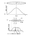
例えば、複数のレーザー発振装置から発振される複数のレーザー光を光学的に複合して一つの線状レーザー光を形成することが可能である。図22(A)に示したのは、個々のレーザー光の照射断面である。ここではレーザー光の照射領域が楕円形状となる場合を例に挙げているが、形状による違いはない。
【0182】
レーザー光の形状はレーザーの種類によって異なり、また光学系により成形することもできる。例えば、ラムダ社製のXeClエキシマレーザー(波長308nm、パルス幅30ns)L3308から射出されたレーザー光の形状は、10mm×30mm(共にビームプロファイルにおける半値幅)の矩形状である。また、YAGレーザーから射出されたレーザー光の形状は、ロッド形状が円筒形であれば円状となり、スラブ型であれば矩形状となる。このようなレーザー光を光学系により、さらに成形することにより、所望の大きさのレーザー光をつくることもできる。
【0183】
図22(B)に図22(A)に示したレーザー光の長軸方向(X軸方向)におけるレーザー光のエネルギー密度の分布を示す。図22(A)に示すレーザー光は、図22(B)におけるエネルギー密度のピーク値の1/e2のエネルギー密度を満たしている領域に相当する。レーザー光が楕円形状であるレーザー光のエネルギー密度の分布は、楕円の中心Oに向かうほど高くなっている。このように図22(A)に示したレーザー光は、中心軸方向におけるエネルギー密度がガウス分布に従っており、エネルギー密度が均一だと判断できる領域が狭くなる。
【0184】
次に、図22(A)に示したレーザー光を二つ合成したときの線状レーザー光の照射断面形状を図22(C)に示す。なお、図22(C)では二つのレーザー光を重ね合わせることで1つの線状のレーザー光を形成した場合について示しているが、重ね合わせるレーザー光の数はこれに限定されない。
【0185】
図22(C)に示すように、各レーザー光は、各楕円の長軸が一致し、なおかつ互いにレーザー光の一部が重なることで合成され、1つの線状レーザー光30が形成されている。なお以下、各楕円の中心Oを結ぶことで得られる直線をレーザービーム30の中心軸とする。
【0186】
図22(D)に、図22(C)に示した合成後の線状レーザー光の中心軸y方向におけるエネルギー密度の分布を示す。なお、図22(C)に示すレーザー光は、図22(B)におけるエネルギー密度のピーク値の1/e2のエネルギー密度を満たしている領域に相当する。合成前の各レーザー光が重なり合っている部分において、エネルギー密度が加算される。例えば図示したように重なり合ったレーザー光のエネルギー密度L1とL2を加算すると、個々のレーザー光のエネルギー密度のピーク値L3とほぼ等しくなり、各楕円の中心Oの間においてエネルギー密度が平坦化される。
【0187】
なお、L1とL2を加算するとL3と等しくなるのが理想的だが、現実的には必ずしも等しい値にはならない。L1とL2を加算した値とL3との値のずれの許容範囲は、設計者が適宜設定することが可能である。
【0188】
レーザー光を単独で用いると、エネルギー密度がガウス分布に従っているので、絶縁膜の平坦な部分に接している半導体膜全体に均一なエネルギー密度のレーザー光を照射することが難しい。しかし、図22(D)からわかるように、複数のレーザー光を重ね合わせてエネルギー密度の低い部分を互いに補い合うようにすることで、複数のレーザー光を重ね合わせないで単独で用いるよりも、エネルギー密度の均一な領域が拡大され、半導体膜の結晶性を効率良く高めることができる。
【0189】
なお、B−B’、C−C’におけるエネルギー密度の分布は、B−B’の方がC−C’よりも弱冠小さくなっているが、ほぼ同じ大きさとみなすことができ、合成前のレーザー光のピーク値の1/e2のエネルギー密度を満たしている領域における合成された線状レーザー光の形状は、線状と言って差し支えない。
【0190】
なお、合成された線状レーザー光30の照射領域の外縁近傍にはエネルギー密度の低い領域が存在する。当該領域を用いると結晶性を却って損なう可能性もあるため、図21においてスリット15を用いたように、線状レーザー光の外縁を用いない方が好ましい形態と言える。
【0191】
本実施の形態で説明したレーザー照射装置は、本発明のレーザー光照射を実施するにあたって用いることができ、実施の形態1〜17のいずれの形態を実施するに際しても使用することができる。また、合成して線状レーザー光を得るメリットはあるものの光学系やレーザー発振装置のコストは増加してしまうため、1台のレーザー発振装置及び1組みの光学系で所望の線状レーザー光を得ることができれば、そのようなレーザー照射装置を本発明の実施に使用することに何ら問題はない。
【0192】
【発明の効果】
以上説明したように、絶縁膜により凹凸形状を有する直線状のストライプパターンを形成し、該絶縁膜上に半導体の結晶化を促進する元素を付着させ、その上に非晶質半導体膜を堆積し、レーザー光の照射により溶融状態を経て結晶化させることにより凹部に半導体を流し込み凝固させ、凹部以外の領域に結晶化に伴う歪み又は応力を集中させることができ、結晶粒界など結晶性の悪い領域を選択的に形成することが可能となる。特に、その際、凹部において底面と側面とのなす角が145±5°となるように制御することにより結晶性半導体膜の優勢結晶面を{110}面とすることができ、特にpチャネル型TFTを作製するにあたって有効な技術である。
【0193】
そして、トランジスタなどの半導体素子、特にそのチャネル形成領域の場所を指定して、結晶粒界が存在しない結晶性半導体膜を形成することができる。これにより不用意に介在する結晶粒界や結晶欠陥により特性がばらつく要因を無くすことができ、特性ばらつきの小さいトランジスタ又はトランジスタ素子群を形成することができる。
【0194】
以上のように、本発明は、結晶性の良好な結晶半導体膜をチャネル形成領域として用いることにより、高速動作が可能で電流駆動能力の高く、且つ複数の素子間においてばらつきの小さい半導体素子又は該半導体素子群を集積して構成される半導体装置を提供することができる。また、当該半導体素子のキャリア移動経路(代表的には薄膜トランジスタにおけるチャネル形成領域)の優勢結晶面を{110}面とすることにより、半導体素子の電気特性のさらなる向上を図ることができる。
【図面の簡単な説明】
【図1】 本発明のトランジスタの作製工程を説明する上面図及び縦断面図。
【図2】 本発明のトランジスタの作製工程を説明する上面図及び縦断面図。
【図3】 本発明のトランジスタの作製工程を説明する上面図及び縦断面図。
【図4】 本発明のトランジスタの作製工程を説明する上面図及び縦断面図。
【図5】 本発明のトランジスタの作製工程を説明する上面図及び縦断面図。
【図6】 本発明のトランジスタの作製工程を説明する上面図及び縦断面図。
【図7】 本発明のトランジスタの作製工程を説明する上面図及び縦断面図。
【図8】 本発明のトランジスタの作製工程を説明する上面図及び縦断面図。
【図9】 本発明のトランジスタの作製工程を説明する縦断面図。
【図10】 本発明のトランジスタの作製工程を説明する縦断面図。
【図11】 本発明のトランジスタにおいて適用することができるゲート構造の一例を示す縦断面図。
【図12】 本発明のトランジスタの作製工程を説明する縦断面図。
【図13】 本発明のトランジスタの作製工程を説明する上面図及び縦断面図。
【図14】 本発明のトランジスタの作製工程を説明する上面図。
【図15】 本発明のトランジスタの作製工程を説明する縦断面図。
【図16】 本発明のトランジスタをCMOS回路に適用した例を説明する上面図及び回路図。
【図17】 本発明のトランジスタをCMOS回路に適用した例を説明する上面図。
【図18】 本発明の半導体装置の外観図の一例を示す図。
【図19】 本発明の半導体装置の外観図の一例を示す図。
【図20】 本発明の電子装置の具体例を示す図。
【図21】 本発明の実施に使用するレーザー照射装置を示す図。
【図22】 本発明の実施に使用するレーザー光の構成を示す図。
【図23】 本発明のトランジスタの作製工程を説明する縦断面図。
【図24】 本発明のトランジスタの作製工程を説明する上面図。
【図25】 本発明のトランジスタの作製工程を説明する上面図。[0001]
BACKGROUND OF THE INVENTION
The present invention relates to a semiconductor element formed using a semiconductor film having a crystal structure (also referred to as a crystalline semiconductor film), a manufacturing method thereof, a semiconductor device including a circuit in which the semiconductor element is integrated, and a manufacturing method thereof. . In particular, the present invention relates to a thin film transistor in which a channel formation region is formed using a crystalline semiconductor film formed over an insulating surface as a semiconductor element.
[0002]
[Prior art]
A technique for forming a semiconductor element such as a thin film transistor using a crystalline semiconductor film formed on an insulating substrate such as glass has been developed. In particular, a technique for crystallizing an amorphous semiconductor film by irradiating a laser beam is applied to a manufacturing technique of a thin film transistor (TFT). Thin film transistors manufactured using a crystalline semiconductor film are applied to flat display devices (flat panel displays) typified by liquid crystal display devices and EL (electroluminescence) display devices.
[0003]
In a semiconductor manufacturing process, a gas laser typified by an excimer laser or a solid-state laser typified by a YAG laser is usually used as a laser light source. An example of crystallization of an amorphous semiconductor film by laser light irradiation is disclosed in Japanese Patent Application Laid-Open No. Sho 62-104117, where the scanning speed of the laser light is set to a beam spot diameter × 5000 / second or higher. In this case, the amorphous semiconductor film is polycrystallized without reaching a complete molten state. US Pat. No. 4,330,363 discloses that the semiconductor film formed in an island shape is irradiated with a stretched laser beam. In particular, a technique for forming a single crystal region is disclosed. Alternatively, a method of processing and irradiating a beam linearly with an optical system, such as a laser processing apparatus disclosed in JP-A-8-195357, is known.
[0004]
Furthermore, as disclosed in Japanese Patent Application Laid-Open No. 2001-144027, Nd: YVO Four Using a solid-state laser oscillation device such as a laser, the amorphous semiconductor film is irradiated with laser light, which is the second harmonic, to form a crystalline semiconductor film having a larger crystal grain size than before, and a transistor is manufactured. Technology is disclosed.
[0005]
[Problems to be solved by the invention]
However, when an amorphous semiconductor film formed on a flat surface is crystallized by irradiating it with laser light, the crystal becomes polycrystals, and defects such as crystal grain boundaries are arbitrarily formed to align crystals with uniform orientation. It was difficult to get. In particular, it has been difficult to obtain crystals with uniform orientation using a laser crystallization technique on a glass substrate.
[0006]
The crystal grain boundary contains crystal defects, which become carrier traps and cause the mobility of electrons or holes to decrease. In addition, a semiconductor film free from strain or crystal defects could not be formed due to volume shrinkage of the semiconductor film accompanying crystallization, thermal stress with the base, or lattice mismatch. Therefore, without a special method such as bonding SOI (Silicon on Insulator), it is equivalent to a MOS transistor formed on a single crystal substrate with a crystalline semiconductor film formed on an insulating surface and crystallized or recrystallized. Could not get the quality.
[0007]
The flat panel display device described above is a device in which a transistor is formed by forming a semiconductor film on an inexpensive glass substrate. However, it is almost impossible to dispose a transistor so as to avoid an arbitrarily formed crystal grain boundary. there were. In other words, the crystallinity of the channel formation region of the transistor is strictly controlled, and the grain boundaries and crystal defects that are included unintentionally cannot be excluded. As a result, not only the electrical characteristics of the transistors are inferior, but also the characteristics of individual elements vary.
[0008]
In particular, when a crystalline semiconductor film is formed using laser light on an alkali-free glass substrate that is widely used in industry, the focus of the laser light varies due to the influence of the undulation of the alkali-free glass substrate itself. However, there is a problem that the crystallinity varies. Furthermore, in order to avoid contamination with alkali metals, an alkali-free glass substrate needs to be provided with a protective film such as an insulating film as a base film, and a crystalline semiconductor film from which crystal grain boundaries and crystal defects have been eliminated is large. It was almost impossible to form with a particle size.
[0009]
The present invention has been made in view of the above problems, and forms a crystalline semiconductor film having no crystal grain boundary at least in a channel formation region on an insulating surface, particularly on an insulating surface using an inexpensive glass substrate as a supporting substrate. An object of the present invention is to provide an inexpensive semiconductor device that is configured by a semiconductor element or a group of semiconductor elements that can operate at high speed, has high current driving capability, and has little variation among a plurality of elements.
[0010]
Further, in a crystalline semiconductor film in which no crystal grain boundary exists in at least the channel formation region, a crystal plane (hereinafter referred to as a dominant crystal plane) that appears most frequently on the main surface when analyzed by an EBSP (Electron Backscatter Diffraction Pattern) method. )) To the {110} plane. The EBSP method will be described later.
[0011]
As for crystal planes, the Miller index is expressed in parentheses as indicated by (110), and equivalent crystal planes such as (101) and (011) are enclosed in square brackets as indicated by {110}. Represent. As for the crystal orientation (crystal axis), the Miller index is enclosed in square brackets as indicated by [110], and equivalent crystal orientations such as [101] and [011] are indicated as <110>. Enclosed in angle brackets.
[0012]
[Means for Solving the Problems]
In order to solve the above-described problems, the present invention forms an insulating film provided with concave and convex portions extending in a linear stripe pattern on a substrate having an insulating surface, and a semiconductor crystal is formed on the insulating film. An element that promotes crystallization is attached, an amorphous semiconductor film is formed on the insulating film, and the semiconductor film is melted and poured into a portion corresponding to a concave portion of the insulating film (hereinafter simply referred to as a concave portion) to be crystallized. The crystalline semiconductor film is formed, and unnecessary regions are removed by etching to form a crystalline semiconductor film (later part of the semiconductor element) divided into islands from the crystalline semiconductor film, and at least a channel A gate insulating film and a gate electrode are provided on the crystalline semiconductor film so that a region for forming a formation region is the crystalline semiconductor film formed in the above-described recess.
[0013]
A feature of the present invention is that an element that promotes crystallization is attached to an insulating film provided with a concave portion and a convex portion, and the crystallinity of the crystalline semiconductor film is improved by utilizing the crystallization promoting effect of the element. In the point. Note that elements that promote crystallization of an amorphous semiconductor film are typically nickel (Ni), cobalt (Co), iron (Fe), platinum (Pt), gold (Au), or palladium (Pd). ) And the like. In particular, silicon (Si), silicon germanium (Si X Ge 1-X : Typically Ge content is 0.01 to 4.5 atomic%) or silicon carbide (Si X C 1-X ), Nickel is effective as an element that promotes crystallization of the semiconductor. This is because nickel silicide, which is a compound of nickel and silicon, has a lattice constant close to that of silicon, so that crystallization with very good consistency through nickel silicide proceeds.
[0014]
In the present invention, as a means for attaching the element that promotes crystallization to the insulating film provided with the concave and convex portions,
(1) Means for exposing the insulating film provided with the concave and convex portions to plasma containing the element
(2) Means for removing a solvent by leaving a solution of a compound containing the element dissolved in a solvent on the insulating film.
These two means are representatively mentioned.
[0015]
At this time, it is preferable that the concave portion has a tapered shape whose width becomes narrower toward the bottom surface, and an angle (θ) formed between the side surface and the bottom surface of the concave portion is within a range of 145 ± 5 °. . With this configuration, when silicon, silicon germanium, or silicon carbide is used as a semiconductor, a {111} plane is likely to appear in a direction perpendicular to the side surface of the recess, and as a result, the crystalline semiconductor film formed in the recess This is because the crystal plane is likely to be a {110} plane. This is because when nickel silicide is used as a medium, crystallization proceeds with the {111} plane of nickel silicide as the head.
[0016]
Note that if the insulating film extending in the linear stripe pattern is etched so that the side surface is vertical by anisotropic etching or the like, the side surface of the recess is naturally vertical, but the effect of the present invention The present invention can be applied.
[0017]
In addition, the crystallinity of the crystalline semiconductor film formed on the portion corresponding to the convex portion (hereinafter simply referred to as the convex portion) of the insulating film provided with the portion corresponding to the concave portion or the convex portion is formed in the concave portion. Although it is inferior to a crystalline semiconductor film, the crystalline semiconductor film formed over the convex portion may be positively used as an electrode (in the case of a thin film transistor, it corresponds to a source region or a drain region) or a wiring. . When used as a wiring, since the degree of freedom in designing the occupied area is high, the wiring length can be adjusted to be used as a resistor, or a bent shape can be provided as a protective circuit function.
[0018]
The above-described recess may be formed by thickly forming a silicon oxide, silicon nitride, silicon oxynitride film, or the like, and etching the same to form the recess. The recess is preferably formed in accordance with the arrangement of the semiconductor element, particularly the island-shaped semiconductor film including the channel formation region of the transistor, and is preferably formed so as to match at least the channel formation region. Further, the recess is provided so as to extend in the channel length direction, and the width (channel width direction in the case of forming a channel formation region) is 0.01 μm or more and 2 μm or less (preferably 0.1 to 1 μm). The depth is preferably 0.01 μm or more and 3 μm or less (preferably 0.1 μm or more and 2 μm or less).
[0019]
Of course, it is also possible to form an island-shaped insulating film on the insulating surface and positively form a convex portion. In that case, the convex portion extending in a plurality of linear stripe patterns forms a portion that is relatively a concave portion between adjacent ones, so that the concave portion includes an island-shaped semiconductor including a channel formation region of a semiconductor element. What is necessary is just to form according to arrangement | positioning of a film | membrane, and it is sufficient to keep the width within the aforementioned range.
[0020]
In addition, as a semiconductor film formed on the insulating film and over the recesses in the first stage, in addition to the amorphous semiconductor film formed by a known method, a polycrystalline semiconductor film (the deposited film was also solid-phase grown) Or a microcrystalline semiconductor film.
[0021]
As a means for melting and crystallizing the crystalline semiconductor film, pulsed oscillation or continuous oscillation laser light using a gas laser oscillation device or a solid laser oscillation device as a light source is applied. The laser light to be irradiated is focused in a linear shape by an optical system, and the intensity distribution may have a uniform region in the longitudinal direction and may be distributed in the lateral direction. As the oscillation device, a rectangular beam solid laser oscillation device is applied, and a slab laser oscillation device is particularly preferably applied. Alternatively, it is a solid state laser oscillation device using a rod doped with Nd, Tm, and Ho, especially YAG, YVO. Four , YLF, YAlO Three A slab structure amplifier may be combined with a solid-state laser oscillation device using a crystal doped with Nd, Tm, or Ho. As the slab material, crystals such as Nd: YAG, Nd: GGG (gadolinium / gallium / garnet), Nd: GsGG (gadolinium / scandium / gallium / garnet) are used. A slab laser travels in a zigzag optical path through this plate-like laser medium while repeating total reflection.
[0022]
Moreover, you may irradiate the strong light according to it. For example, light having a high energy density obtained by condensing light emitted from a halogen lamp, xenon lamp, high-pressure mercury lamp, metal halide lamp, or excimer lamp by a reflecting mirror or a lens may be used.
[0023]
Laser light or strong light condensed in a linear shape and extended in the longitudinal direction irradiates the crystalline semiconductor film, and relatively moves the irradiation position of the laser light and the substrate on which the crystalline semiconductor film is formed, The crystalline semiconductor film is melted by scanning a part or the entire surface of the laser beam, and crystallization or recrystallization is performed through this state. The scanning direction of the laser light is performed along the longitudinal direction of the recess formed in the insulating film and extending in a linear stripe pattern or the channel length direction of the transistor. As a result, the crystal grows along the scanning direction of the laser beam, and the crystal grain boundary can be prevented from crossing the channel length direction.
[0024]
By setting the depth of the recesses to be equal to or greater than the thickness of the semiconductor film, the semiconductor film melted by irradiation with laser light or strong light aggregates and solidifies in the recesses due to surface tension. As a result, the thickness of the semiconductor film on the convex portion of the insulating film is reduced, and stress strain can be concentrated there. The side surface of the recess has the effect of defining the crystal orientation to some extent.
[0025]
When the semiconductor film is in a molten state, the semiconductor film is aggregated in the recess formed on the insulating surface by surface tension, and crystal growth is caused from the side surface portion of the recess, so that strain generated due to crystallization can be concentrated in a region other than the recess. That is, the crystalline semiconductor region (first crystalline semiconductor region) formed so as to be filled in the concave portion can be released from strain. In addition, a crystalline semiconductor region (second crystalline semiconductor region) including crystal grain boundaries and crystal defects is formed over the insulating film. In addition, it can be expected that the elements introduced for the promotion of crystallization move to the convex portion along with the crystallization and finally aggregate on the convex portion. In particular, when nickel is used as an element that promotes crystallization, nickel silicide moves at the head of the solid-liquid interface, so it is considered that most of nickel eventually moves to the convex portion. . In the first crystalline semiconductor region formed as described above, the crystal plane is approximately the {110} plane, that is, the dominant crystal plane is the {110} plane.
[0026]
Then, after forming a crystalline semiconductor film having no crystal grain boundary in the recess, an active layer (semiconductor layer functioning as a carrier movement path) of the semiconductor element is formed by patterning, and a gate insulating film in contact with the active layer is formed Further, a gate electrode is formed. At the time of this patterning, it is desirable to provide a taper at the end of the active layer. Thereafter, a field effect transistor can be formed by a known method.
[0027]
According to the present invention, it is possible to designate a semiconductor element such as a transistor, particularly a region where a channel formation region thereof is formed, and form a crystalline semiconductor region where no crystal grain boundary exists in the region. As a result, it is possible to eliminate the factor that the characteristics vary due to inadvertently interposed crystal grain boundaries and crystal defects. In other words, it is possible to form a semiconductor device including a semiconductor element or a group of semiconductor elements that can operate at high speed, have high current driving capability, and have little variation among a plurality of elements.
[0028]
DETAILED DESCRIPTION OF THE INVENTION
[Embodiment 1]
In this embodiment mode, a mode for manufacturing a thin film transistor by implementing the present invention will be described. Note that the number of thin film transistors to be manufactured may be determined as appropriate by the practitioner, and any drawings used do not limit the present invention.
[0029]
First, FIG. 1 will be described. 1A is a top view, FIG. 1B is a cross-sectional view corresponding to AA ′, and FIG. 1C is a cross-sectional view corresponding to BB ′. A state is shown in which a first
[0030]
As the
[0031]
In order to form a linear stripe pattern with a sub-micron design rule, it is desirable that the unevenness of the substrate surface, the waviness or twist of the substrate be less than the depth of focus of the exposure apparatus (particularly the stepper). Specifically, the waviness or twist of the substrate is 1 μm or less, preferably 0.5 μm or less in one exposure light irradiation region. In this regard, care must be taken particularly when alkali-free glass is used as the support substrate.
[0032]
The width (W1) of the second
[0033]
The first
[0034]
As the silicon oxynitride (SiOxNy) film, a film containing Si at 25 to 35 atomic%, oxygen at 55 to 65 atomic%, nitrogen at 1 to 20 atomic%, and hydrogen at 0.1 to 10 atomic%. Use it. Further, as a silicon oxynitride (SiNxOy) film, a film containing Si of 25 to 35 atomic%, oxygen of 15 to 30 atomic%, nitrogen of 20 to 35 atomic%, and hydrogen of 15 to 25 atomic% may be used. good. As the aluminum oxynitride (AlOxNy) film, a film containing Al at 30 to 40 atomic%, oxygen at 50 to 70 atomic%, and nitrogen at 1 to 20 atomic% may be used. Further, as the aluminum oxynitride (AlNxOy) film, a film containing Al in an amount of 30 to 50 atomic%, oxygen in an amount of 0.01 to 20 atomic%, and nitrogen in an amount of 30 to 50 atomic% may be used.
[0035]
The second
[0036]
As shown in FIG. 1, in the case of forming a linear stripe pattern with two insulating films, it is necessary to provide a high selection ratio between the first insulating
[0037]
Note that as the second
[0038]
After the second
[0039]
The plasma treatment applied in this embodiment has a high throughput because it is completed in a treatment time of 1 to 20 minutes (typically 3 to 5 minutes). In addition, the plasma treatment may be performed while heating at 150 to 300 ° C., although the throughput is somewhat sacrificed. At this time, it is preferable to adjust the discharge power and the distance between the electrodes so as not to leave plasma damage as much as possible in the first insulating
[0040]
Next, FIG. 2 will be described. 2A is a top view, FIG. 2B is a cross-sectional view corresponding to AA ′, and FIG. 2C is a cross-sectional view corresponding to BB ′. After the plasma treatment is completed, an
[0041]
First, the
[0042]
At this time, the thickness of the
[0043]
Then, the
[0044]
For example, as an example of the crystallization condition, YVO in continuous oscillation mode Four Using a laser oscillator, the output of 5 to 10 W of the second harmonic (wavelength 532 nm) is condensed into linear laser light having a ratio of the longitudinal direction to the transverse direction of 10 or more in the optical system, and the longitudinal direction. For example, the light is condensed so as to have a uniform energy density distribution, and is crystallized by scanning at a speed of 5 to 200 cm / sec. The uniform energy density distribution does not exclude anything other than a completely constant one, and the allowable range in the energy density distribution is within a range of ± 10%.
[0045]
Further, the crystallization by the laser beam condensed linearly may be completed by only one scan (that is, one direction), or may be reciprocated to improve the crystallinity. Furthermore, after crystallizing with laser light, the surface of the silicon film is treated with an alkaline solution such as oxide removal with hydrofluoric acid or ammonia hydrogen peroxide solution treatment, and the poor quality part with high etching rate is selectively used. It may be removed and the same crystallization treatment may be performed again. In this way, crystallinity can be increased.
[0046]
Further, at the time of crystallization, it is preferable that a position where a marker used for patterning mask alignment is formed after the end of the substrate is not crystallized. This is because a crystalline semiconductor film (especially a crystalline silicon film) has a higher visible light transmittance when crystallized, so that it is difficult to identify it as a marker. However, there is no problem when performing the type of alignment control for optically identifying the difference in contrast due to the level difference of the marker.
[0047]
As the laser oscillation device, a rectangular beam solid state laser oscillation device is applied, and a slab laser oscillation device is particularly preferably applied. As the slab material, crystals such as Nd: YAG, Nd: GGG (gadolinium / gallium / garnet), Nd: GsGG (gadolinium / scandium / gallium / garnet) are used. A slab laser travels in a zigzag optical path through this plate-like laser medium while repeating total reflection. Alternatively, it is a solid state laser oscillation device using a rod doped with Nd, Tm, and Ho, especially YAG, YVO. Four , YLF, YAlO Three A slab structure amplifier may be combined with a solid-state laser oscillation device using a crystal doped with Nd, Tm, or Ho.
[0048]
Then, as indicated by arrows in FIG. 2, each of the second insulating
[0049]
The wavelength of the continuous wave laser beam is preferably 400 to 700 nm in consideration of the light absorption coefficient of the amorphous semiconductor film. Light in such a wavelength band is obtained by taking out the second harmonic and the third harmonic of the fundamental wave using a wavelength conversion element. As wavelength conversion element, ADP (ammonium dihydrogen phosphate), Ba 2 NaNb Five O 15 (Sodium barium niobate), CdSe (selenium cadmium), KDP (potassium dihydrogen phosphate), LiNbO Three (Lithium niobate), Se, Te, LBO, BBO, KB5 and the like are applied. It is particularly desirable to use LBO. A typical example is Nd: YVO Four The second harmonic (532 nm) of the laser oscillation device (fundamental wave 1064 nm) is used. The laser oscillation mode is TEM 00 Apply single mode.
[0050]
In the case of silicon selected as the most suitable material, the absorption coefficient is 10 Three -10 Four cm -1 The region which is is almost in the visible light region. When crystallizing a substrate having a high visible light transmittance such as glass and an amorphous semiconductor film formed with a thickness of 30 to 200 nm using silicon, by irradiating light in the visible light region with a wavelength of 400 to 700 nm, Crystallization can be performed without selectively damaging the base insulating film by selectively heating the semiconductor film. Specifically, the penetration depth of light with a wavelength of 532 nm is approximately 100 nm to 1000 nm with respect to the amorphous silicon film, and can sufficiently reach the inside of the
[0051]
The laser beam is scanned in a direction parallel to the direction in which the linear stripe pattern extends, and the melted semiconductor flows into the concave portion due to surface tension and solidifies. In the solidified state, the surface becomes almost flat as shown in FIG. This is because once the semiconductor is melted, the interface between the melted semiconductor and the gas phase reaches an equilibrium state, whether on the convex portion or the concave portion, and a flat interface is formed. Further, the crystal growth edge and the crystal grain boundary are formed on the second insulating film (on the convex portion) (
[0052]
In the crystallization step, if the second insulating film is a soft insulating film (insulating film having a low density), an effect of relaxing stress due to shrinkage of the semiconductor film during crystallization can be expected. On the other hand, if a hard insulating film (insulating film with high density) is used, stress is generated against the semiconductor film that is about to shrink or expand, so that it is easy to leave stress strain or the like in the semiconductor film after crystallization. It may also cause For example, in the known graphoepitaxy technology (“MWGeis, DCFlanders, HISmith: Appl. Phys. Lett. 35 (1979) pp71”), the irregularities on the substrate are directly formed on hard quartz. The thermal shrinkage and stress generation accompanying the conversion cannot be alleviated, and the generation of defects due to distortion or dislocation due to the stress may occur. Quartz is expensive and is a technique contrary to the gist of the present invention for manufacturing an inexpensive semiconductor device.
[0053]
However, in consideration of those points, the present applicant uses a soft insulating film formed by a CVD method or a PVD method in forming concave and convex portions on an inexpensive glass substrate. Since the second insulating film is made of a material softer than quartz glass, it is basically different from the known graphoepitaxy technique in that the purpose is to alleviate the generation of stress during crystallization.
[0054]
Note that an insulating film that is softer than quartz glass means, for example, an insulating film that has a higher etching rate than quartz glass (quartz glass that is industrially used as a substrate) under the same measurement conditions, or an insulation that has low hardness under the same measurement conditions. It means film. Note that the etching rate and hardness may be a relative comparison with quartz glass to the last, so the absolute value of the etching rate is not a problem and does not depend on the etching rate measurement conditions or the hardness measurement conditions.
[0055]
For example, if a silicon oxynitride film is used as the second insulating film, SiH Four Gas, N 2 A silicon oxynitride film formed by a plasma CVD method using O gas as a raw material is preferable. The silicon oxynitride film is made of ammonium hydrogen fluoride (NH Four HF 2 ) 7.13% and ammonium fluoride (NH Four The etching rate at 20 ° C. of the mixed aqueous solution containing 15.4% of F) is 110 to 130 nm / min (500 ° C., 1 hour + 550 ° C., after 4 hours of heat treatment, 90 to 100 nm / min).
[0056]
If a silicon oxynitride film is used as the second insulating film, SiH Four Gas, NH Three Gas, N 2 A silicon oxynitride film formed by a plasma CVD method using O gas as a raw material is preferable. The silicon nitride oxide film is made of ammonium hydrogen fluoride (NH Four HF 2 ) 7.13% and ammonium fluoride (NH Four The etching rate at 20 ° C. of the mixed aqueous solution containing 15.4% of F) is 60 to 70 nm / min (40 to 50 nm / min after heat treatment at 500 ° C., 1 hour + 550 ° C. for 4 hours).
[0057]
As described above, a linear stripe pattern having recesses and projections is formed by an insulating film, an amorphous semiconductor film is deposited thereon, and crystallized through a molten state by irradiation with laser light, thereby forming recesses. The semiconductor is poured and solidified, so that strain or stress accompanying crystallization can be concentrated in a region other than the concave portion, and a region having poor crystallinity such as a crystal grain boundary can be selectively formed. A semiconductor region with good crystallinity can be used as a region where carrier movement is performed, such as a channel formation region of a thin film transistor.
[0058]
After that, heat treatment is preferably performed at 500 to 600 ° C. to remove distortion accumulated in the crystalline semiconductor film. This distortion occurs due to semiconductor volume shrinkage caused by crystallization, thermal stress with the base, or lattice mismatch. This heat treatment may be performed using a normal heat treatment apparatus. For example, a gas heating rapid thermal annealing (RTA) method may be used for 1 to 10 minutes. Note that this step is not an essential requirement in the present invention, and may be appropriately selected.
[0059]
Next, FIG. 3 will be described. 3A is a top view, FIG. 3B is a cross-sectional view corresponding to AA ′, FIG. 3C is a cross-sectional view corresponding to BB ′, and FIG. It is sectional drawing corresponding to -C '. A state is shown in which patterning is performed on the
[0060]
In FIG. 3A, the resist
[0061]
Next, FIG. 4 will be described. 4A is a top view, FIG. 4B is a cross-sectional view corresponding to AA ′, FIG. 4C is a cross-sectional view corresponding to BB ′, and FIG. 4C is a cross-sectional view corresponding to DD ′. FIG. 4E is a cross-sectional view corresponding to DD ′. This shows a state in which after the
[0062]
The
[0063]
Further, when forming the
[0064]
By the way, a feature of the present invention is that the first
[0065]
In the crystalline semiconductor film obtained by carrying out the present invention, there are no crystal grain boundaries or defects that are clarified by Secco etching, in other words, there is substantially no crystal grain boundary or defect. Seco. Etching is a seco liquid (HF: H) that is generally known for making the crystal grain boundary on the surface of the crystalline semiconductor film manifest. 2 O = 2: 1 K as additive 2 Cr 2 O 7 This is an etching method using a chemical solution prepared using In this specification, as the secco solution, potassium dichromate (K 2 Cr 2 O 7 ) Dissolve 2.2 g in 50 cc of water to prepare a 0.15 mol / l solution, add 100 cc of hydrofluoric acid solution to the solution, and further dilute 5 times with water. Means performing an etching treatment for 75 seconds at room temperature (10 to 30 ° C.) using the above-mentioned secco solution.
[0066]
Although crystal grain boundaries that are clarified by Secco etching have not been identified at present, it is a well-known fact that stacking faults and crystal grain boundaries are preferentially etched by Secco etching. Of course, since it is not a single crystal, there may naturally be grain boundaries and defects that do not appear by Secco etching. However, such grain boundaries and defects do not affect the electrical characteristics when semiconductor devices are manufactured. It is considered electrically inactive. Usually, an electrically inactive grain boundary is called a planar grain boundary (low-order or higher-order twin or a corresponding grain boundary), and a grain boundary that does not appear by Secco etching is a plane. Presumed to be a grain boundary. From this point of view, it can be said that substantially no crystal grain boundaries or defects exist, it can be said that there are no crystal grain boundaries other than planar grain boundaries.
[0067]
For the dominant crystal plane, a result obtained by a reflected electron diffraction pattern (EBSP) may be used. EBSP provides a scanning electron microscope (SEM) with a dedicated detector, which irradiates the crystal plane with an electron beam and causes the computer to recognize the crystal orientation from the Kikuchi line. The crystallinity is measured not only on the surface orientation but also in all directions of the crystal (hereinafter, this method is referred to as EBSP method for convenience).
[0068]
In this specification, the dominant crystal plane is the crystal plane that appears most on the surface when analyzed by the EBSP method. Note that the crystal plane includes at least some fluctuation (shift of the axis perpendicular to the crystal plane), and in the present specification, ± 15 ° is allowed as the fluctuation. As described above, when the crystalline semiconductor film obtained by carrying out the present invention is analyzed by the EBSP method, the {110} plane appears as the dominant crystal plane, and the others are the {100} plane and the {111} plane. And {311} planes appear together.
[0069]
Next, FIG. 5 will be described. 5A is a top view, FIG. 5B is a cross-sectional view corresponding to AA ′, FIG. 5C is a cross-sectional view corresponding to BB ′, and FIG. FIG. 5E is a cross-sectional view corresponding to DD ′. A state in which the
[0070]
The
[0071]
The
[0072]
Next, FIG. 6 will be described. 6A is a top view, FIG. 6B is a cross-sectional view corresponding to AA ′, FIG. 6C is a cross-sectional view corresponding to BB ′, and FIG. FIG. 6E is a cross-sectional view corresponding to DD ′. A state in which the
[0073]
In this embodiment mode, an element belonging to Group 13 of the periodic table (typically, boron is used) is added to give p-type to the
[0074]
After the
[0075]
Next, FIG. 7 will be described. 7A is a top view, FIG. 7B is a cross-sectional view corresponding to AA ′, FIG. 7C is a cross-sectional view corresponding to BB ′, and FIG. FIG. 7E is a cross-sectional view corresponding to DD ′. A
[0076]
After the activation step is completed, a protective film (passivation film) 115 is formed so as to cover the
[0077]
Note that in this embodiment, a silicon nitride oxide (SiNxOy) film is used as the
[0078]
After the
[0079]
Then, a contact hole is formed in the
[0080]
In the p-channel transistor shown in FIG. 7, a plurality of channel formation regions (in this embodiment, two
[0081]
By the way, the crystalline semiconductor film obtained by carrying out the present invention as described above, specifically, the first crystalline semiconductor region used as the channel formation region has a dominant crystal plane of {110} plane. One of them. Here, the advantage that the dominant crystal plane is the {110} plane will be described below.
[0082]
Various studies have been made on the crystal plane of single crystal silicon, and the {110} plane is generally known to have high hole mobility. For example, in “Physics of VLSI devices; written by Masayoshi Kishino and Mitsumasa Koyanagi, page 145 of Maruzen Co., Ltd. (1995), page 145”, when the crystal plane is the (011) plane, the movement direction of holes (holes) is <01. -1> maximum field effect mobility (μFE = about 225 cm) when the direction is parallel to the axis 2 / Vs). That is, in a silicon substrate having a {110} plane crystal plane, the field effect mobility of the p-channel transistor is maximized by forming the transistor so that the hole movement direction coincides with the <01-1> axis. can do.
[0083]
Here, according to the present inventors, in a crystalline semiconductor film crystallized by scanning a continuous-wave linear laser beam in a certain direction, the direction perpendicular to the longitudinal direction of the linear laser beam becomes the crystal growth direction. And the knowledge that the crystal axis is the <110> axis has been obtained. The <110> axis includes fluctuations of ± 15 °. That is, the first crystalline semiconductor region obtained by carrying out the present invention has a plurality of crystal regions that grow in a certain direction by moving the irradiation region of the continuous wave laser beam and that extend in a linear stripe pattern. The second insulating film also defines crystal growth. For example, in the present embodiment, the moving direction of the irradiation region of the linear laser light matches the direction perpendicular to the longitudinal direction, and as a result, the moving direction of the irradiation region matches the direction of crystal growth. become. Therefore, in the cross-sectional view of FIG. 4B, the crystal plane of the cut surface of the
[0084]
Therefore, in the p-channel thin film transistor described in this embodiment, the hole moving direction and the <110> axis coincide with each other, and the dominant crystal plane is the {110} plane. As described above, the field-effect mobility of the p-channel thin film transistor can be most effectively increased.
[0085]
[Embodiment 2]
In the formation of the crystalline semiconductor film of the present invention, in addition to the method of crystallizing the amorphous semiconductor film by irradiating the amorphous semiconductor film as shown in Embodiment Mode 1, the laser light is further crystallized after crystallization by solid phase growth. May be melted and recrystallized. For example, after the
[0086]
When this embodiment mode is implemented, the crystalline semiconductor film grown by solid phase is irradiated with laser light according to Embodiment Mode 1 to be melted and recrystallized. At this time, the crystalline semiconductor film is melted by laser light irradiation, but the light absorption coefficient hardly fluctuates. This point is greatly different from the case of directly irradiating the amorphous semiconductor film with laser light. That is, the small fluctuation of the light absorption coefficient means that the film quality is not affected even if the irradiation energy of the laser light varies somewhat. In fact, the crystalline semiconductor film grown by solid phase is an amorphous semiconductor film. Compared to the above, there is an advantage that the margin for the energy density of the laser beam is wide and the productivity is good.
[0087]
The crystalline semiconductor film obtained by this embodiment also has a feature that the surface is flat as described in Embodiment 1, and the dominant crystal plane is the {110} plane. When such a crystalline semiconductor film is used for a channel formation region of a thin film transistor, both the electron mobility and the hole mobility are greatly improved, and the field effect mobility of the N channel transistor and the P channel transistor is greatly improved. It has the feature to do. In particular, as described above, the improvement in the field effect mobility of the P-channel transistor accompanying the improvement in the hole mobility is notable and is one of the advantages of setting the dominant crystal plane to {110}.
[0088]
After that, as in Embodiment Mode 1, a thin film transistor is formed using the recessed crystalline semiconductor film as a channel formation region and the protruding crystalline semiconductor film as a source region or a drain region. The crystalline semiconductor film in the recess has a feature that it has a plurality of crystal orientations and no grain boundary is formed, so that it can operate at high speed, has high current driving capability, and varies among a plurality of elements. A semiconductor device including a small transistor or a transistor group thereof can be formed.
[0089]
[Embodiment 3]
In this embodiment mode, as a means for attaching an element that promotes crystallization onto an insulating film provided with a concave portion and a convex portion, a compound containing nickel, cobalt, iron, platinum, gold, or palladium is used as a solvent on the insulating film. An example using a means for removing the solvent after applying the solution dissolved in the above, leaving these elements on the insulating film is shown.
[0090]
The application method using the above solution is described in detail in Japanese Patent Application Laid-Open No. 7-130652 by the applicant of the present application, but a metal salt compound such as nickel acetate salt or nickel nitrate salt in a solvent such as water or alcohol has a nickel concentration of 5 This is a technique of dissolving the solution to ˜200 ppm and applying the solution by a spin coating method.
[0091]
As specific conditions, for example, a certain amount of an aqueous solution containing nickel at a concentration of 10 ppm is dropped on a target object provided on the adsorption head of the spin coater, and 1 to 3 at a rotation speed of about 10 to 50 rpm. Then, the solvent is dried at a rotational speed of 2000 to 3000 rpm, and a certain amount of nickel is deposited on the object to be treated. In this method, since nickel is physically adsorbed on the surface of the object to be processed, the amount can be made constant without excessive nickel adhering. This point is very effective in minimizing the nickel introduced in the subsequent crystallization.
[0092]
Of course, all the elements exemplified above other than nickel may be used. Also in that case, each metal salt compound corresponding to each may be dissolved in a solvent and attached by a spin coating method, and thus detailed description is omitted.
[0093]
After nickel, cobalt, iron, platinum, gold, or palladium is deposited on the insulating film provided with the concave and convex portions by the above-described means, the process according to the first embodiment (the process after FIG. 2) is performed. A thin film transistor may be formed. Of course, this embodiment can also be implemented in combination with the second embodiment.
[0094]
[Embodiment 4]
In this embodiment mode, as a means for attaching an element that promotes crystallization onto an insulating film provided with a concave portion and a convex portion, a compound containing nickel, cobalt, iron, platinum, gold, or palladium is used as a solvent on the insulating film. An example using a means for removing the solvent after applying the solution dissolved in the above, leaving these elements on the insulating film is shown. In particular, an example in which means different from the method described in Embodiment 3 is used will be described. FIG. 8 is used for the description.
[0095]
First, the first insulating
[0096]
The coating means 131 preferably has a length that can be sprayed onto the entire surface of the substrate by one movement. Further, the length may be adjusted so that it is not sprayed onto the substrate end (the portion where the alignment marker or the like is provided).
[0097]
Next, after the
[0098]
The present embodiment is a further improvement of the technique described in the third embodiment, and is an effective technique particularly when a large-area substrate is handled. In the case of the spin coating method shown in Embodiment Mode 3, since there are an infinite number of stripe-pattern insulating films on the substrate, the throughput may be reduced by the spin drying method particularly in a large-area substrate. Therefore, in the present embodiment, since application and drying are performed along the insulating film arranged in parallel with the stripe pattern, there is no pattern dependency and it is suitable for application to a large area substrate.
[0099]
After nickel, cobalt, iron, platinum, gold, or palladium is deposited on the insulating film provided with the concave portions and the convex portions by the means described in this embodiment mode, the steps of the first embodiment (after FIG. 2) A thin film transistor may be formed in accordance with the step (1). Of course, this embodiment can be implemented in combination with any of Embodiments 1 and 2.
[0100]
[Embodiment 5]
In the case of carrying out the present invention, these metal elements may remain in the formed crystalline semiconductor film because of the use of metal elements such as nickel for crystallization. Mostly, since crystallization starts from the
[0101]
In this embodiment, in order to positively remove nickel from the crystalline semiconductor film formed by the techniques described in Embodiments 1 to 4, gettering treatment is performed after the
[0102]
In addition to the above-described techniques, the gettering process includes a gettering process (Japanese Patent Laid-Open No. 10-135468) using a removal effect by heat treatment in a halogen atmosphere, and a gettering process (specialized by a phosphorus removal effect). (Kaihei 10-270363), gettering treatment utilizing the removal effect of the amorphous semiconductor film (Japanese Patent Laid-Open No. 8-213316), or the like may be used.
[0103]
After nickel, cobalt, iron, platinum, gold, or palladium is deposited from the
[0104]
[Embodiment 6]
In this embodiment mode, an example in which the angle (θ) formed by the bottom surface and the side surface in the recess portion formed of the second
[0105]
The angle (θ) formed between the bottom surface and the side surface is an angle formed between the surface parallel to the bottom surface and the surface parallel to the side surface, and is described as follows. 21A and 21B are examples in the case where the pattern example of the shape of the recess is not an ideal shape as shown in FIG. FIG. 21A assumes a case where the first insulating
[0106]
FIG. 8A is a top view in which the steps up to the crystallization step are completed in accordance with
[0107]
FIG. 8B is a cross-sectional view of FIG. 8A cut along AA ′. As shown in FIG. 8B, the angle (θ) formed between the bottom surface and the side surface in the recess is 145 ± 5 °. When melt crystallization of the amorphous semiconductor film is performed in a state defined by this angle, the side surface Crystal growth occurs in a direction perpendicular to (i.e., <111> axis direction), and a {110} plane appears on the surface of the
[0108]
This is because when nickel is used, nickel silicide is present as a medium between the amorphous semiconductor film and the crystalline semiconductor film, and the crystal plane of nickel silicide is the {111} plane. Because. That is, the crystal growth caused by nickel adhering to the side surface of the recess proceeds in the <111> axis direction, and thus the above-described result is obtained.
[0109]
This embodiment can be implemented only by changing the design of the taper angle of the second insulating film to 145 ± 5 ° in the process shown in the first embodiment. For other processes, refer to the first embodiment. You can do it. Of course, an effect can be acquired even if it combines with any embodiment of Embodiment 2-5.
[0110]
[Embodiment 7]
In this embodiment, an example in which the first insulating
[0111]
In this embodiment, the insulating
[0112]
The insulating
[0113]
In this embodiment, an example of two layers is shown, but it goes without saying that a plurality of layers of three or more layers may be used. Furthermore, this embodiment can be combined with any structure of Embodiments 1-6.
[0114]
[Embodiment 8]
In Embodiment 1, the transistor has a single drain structure; however, a lightly doped drain (LDD) may be provided. FIG. 11 shows an example of an n-channel thin film transistor having an LDD structure.
[0115]
The structure of the transistor illustrated in FIG. 11A is an example in which a gate electrode is formed using a
[0116]
On the other hand, FIG. 11B shows a structure in which the
[0117]
In FIG. 11C,
[0118]
The structure in which the LDD region is formed in a self-aligning manner by the gate structure as shown in this embodiment is particularly effective when the design rule is miniaturized. Although a unipolar transistor structure is shown here, an n-channel transistor and a p-channel transistor can be separately formed and combined with each other to form a CMOS circuit. Moreover, this Embodiment can be combined with any structure of Embodiment 1-6.
[0119]
[Embodiment 9]
This embodiment is another example relating to the shape of the
[0120]
In FIG. 12A, the resist
[0121]
In the case where the semiconductor region to be a channel formation region has the shape shown in this embodiment mode, a step for overcoming the
[0122]
[Embodiment 10]
In this embodiment, an example in which a part of the crystalline semiconductor film 107 (a part that becomes a channel formation region later) is etched to thin the film before the step of forming the
[0123]
First, according to the manufacturing method shown in Embodiment Mode 1, a
[0124]
Then, the
[0125]
Note that the etching step may use not only a chemical method but also a mechanical polishing method such as CMP (Chemical Mechanical Polishing). Moreover, you may use a chemical method and a mechanical method together.
[0126]
According to this embodiment, since the channel formation region can be formed in a self-aligned manner by the second
[0127]
Regarding the subsequent steps, the steps described in Embodiment Mode 1 may be referred to, and thus the description in this embodiment mode is omitted. Note that this embodiment mode can be freely combined with any of Embodiment Modes 1 to 8.
[0128]
[Embodiment 11]
In this embodiment mode, an example in which the second
[0129]
A feature of this embodiment is that the second
[0130]
Note that this embodiment mode can be freely combined with any of Embodiment Modes 1 to 8.
[0131]
[Embodiment 12]
In this embodiment, an example in which a CMOS circuit is formed by combining the process shown in Embodiment 1 with a known CMOS forming technique is shown. Note that FIG. 16A is a top view of a CMOS circuit when this embodiment is implemented, and FIG. 16B is a circuit diagram schematically showing FIG.
[0132]
In FIG. 16A, reference numeral 601 denotes an n-channel TFT, and reference numeral 602 denotes a p-channel TFT. These TFTs are connected as shown in FIG. 16B to form a complementary circuit (specifically, a CMOS circuit).
[0133]
In FIG. 16A, 603 is an active layer of an n-
[0134]
The p-channel TFT manufactured in accordance with Embodiment Mode 1 has a feature that the dominant crystal plane is a {110} plane, so that the hole mobility is high and, as a result, the field-effect mobility as the p-channel TFT is high. Have. Conventionally, the electrical characteristics of a p-channel TFT have been considerably inferior to those of an n-channel TFT, and when the CMOS circuit is constructed, the balance of characteristics is poor and the operation performance is sometimes lowered. However, when a p-channel TFT manufactured according to the present invention is used in combination with an n-channel TFT, the balance between the characteristics of the n-channel TFT and the p-channel TFT is improved. It becomes possible to do.
[0135]
Note that this embodiment mode can be freely combined with any of Embodiment Modes 1 to 11.
[0136]
[Embodiment 13]
In this embodiment mode, a mode different from that of the CMOS circuit shown in Embodiment Mode 12 is shown. Note that FIG. 17 is used as the drawing, but the same reference numerals as those in FIG. 16 may be referred to the twelfth embodiment.
[0137]
In this embodiment mode, a p-channel TFT 801 and an n-channel TFT 802 form a CMOS circuit, 803 is an active layer of a p-channel TFT, 804 is an active layer of an n-channel TFT, and 805 is a p-channel TFT. 806 is an n-channel TFT gate electrode.
[0138]
At this time, in the
[0139]
According to the literature described in the first embodiment, “Physics of VLSI devices; written by Masayoshi Kishino and Mitsumasa Koyanagi, Maruzen Co., Ltd. (1995), page 145”, It can be seen that the direction parallel to the <110> axis direction has high hole mobility, and the direction perpendicular to the <110> axis direction has high electron mobility. That is, this embodiment is such that holes flow in a direction parallel to the <110> axis in the p-channel TFT 801 and electrons flow in a direction perpendicular to the <110> axis in the n-channel TFT 802. There are features.
[0140]
According to this embodiment mode, it is possible to form a CMOS circuit having a structure suitable for improving the characteristics of an n-channel TFT and a p-channel TFT while using a crystalline semiconductor region having the same crystal plane. Note that the configuration of this embodiment can be combined with any of the configurations of Embodiments 1 to 12.
[Embodiment 14]
In this embodiment mode, an example in which the linear laser light irradiation method described in Embodiment Mode 1 has another structure is described. In the description, the reference numerals used in Embodiment 1 are used as appropriate.
[0141]
First, the configuration illustrated in FIG. 24 is an example in which the irradiation region of the linear laser light is moved in an oblique direction with respect to the second
[0142]
In the case where this embodiment mode is implemented, even when the width of the
[0143]
In the configuration shown in FIG. 25, the irradiation region of the linear laser beam is moved in the direction along the second insulating film 103 (the Y-axis direction) while being inclined with respect to the second
[0144]
In addition, this Embodiment can be implemented in combination with Embodiments 2-13, and the effect is not impaired.
[0145]
[Embodiment 15]
The present invention can be applied to various semiconductor devices, and the mode of a display panel manufactured based on Embodiment Modes 1 to 14 will be described. Note that specific examples of the display panel described in this embodiment include a display panel using a transistor as a semiconductor element, such as a liquid crystal display panel, an EL (electroluminescence) display panel, or a display panel for FED (field emission display). . Of course, these display panels include those distributed in the market as modules.
[0146]
In FIG. 18, a
[0147]
The
[0148]
Furthermore, a chip on which various logic circuits, high-frequency circuits, memories, microprocessors, media processors / DSPs (Digital Signal Processors), graphics LSIs, cryptographic LSIs, amplifiers, and the like are formed using transistors obtained by implementing the present invention. 950 may be mounted. These functional circuits are formed with design rules different from those of the
[0149]
Note that in this embodiment, FIGS. 11A and 11B are suitable as the gate structure of the transistor. For example, it can be applied as a switching element of the
[0150]
[Embodiment 16]
In this embodiment, an example in which a semiconductor device is manufactured by implementing the present invention using a flexible substrate (typically, a plastic substrate or a plastic film) as a supporting substrate will be described. For each circuit configuration formed on the substrate, the configuration described in Embodiment 15 with reference to FIG. 18 can be selected. Further, a semiconductor device using a flexible substrate can be applied to a display having a curved surface, a show window, and the like in addition to being thin and lightweight. Therefore, the application is not limited to portable devices, and the range of applications is diverse.
[0151]
By the way, when the substrate is non-planar, the problem is how much the curvature can be increased. When the curvature of the substrate is increased, a situation occurs in which the semiconductor element formed on the insulating film cannot obtain desired characteristics due to the stress generated in the insulating film formed on the substrate. This tendency is particularly strong as the thickness of the insulating film increases.
[0152]
Therefore, when the present invention is applied to a flexible substrate as in this embodiment mode, the longitudinal direction of the insulating film extending in a linear stripe pattern (the Y-axis direction in FIG. 2A) and The longitudinal direction of the generatrix on the curved surface of the substrate is preferably made equal. Of course, the longitudinal direction of the bus bar on the curved surface of the substrate differs depending on the use of the semiconductor device. Therefore, when the semiconductor device is incorporated into an electronic device or attached to a show window, it can be used with the above points in mind. It means that it is preferable.
[0153]
FIG. 19 shows a state in which a semiconductor device manufactured using a substrate having a flexible name according to the embodiment of the present invention is bent. A pixel portion 32, a scanning line driving circuit 33, and a signal line driving circuit 34 are formed on the substrate 31. A material that can withstand a processing temperature in a later process is used for the substrate 31. Typically, PET (polyethylene terephthalate), PES (polyethylene sulfite), PC (polycarbonate), or PEN (polyethylene naphthalate) may be used. In particular, PC has high heat resistance and is useful.
[0154]
In the scanning line driving circuit 33 and the signal line driving circuit 34, the first crystallinity obtained by carrying out the present invention is formed in the recesses provided between the insulating films 35 extending in a linear stripe pattern. A thin film transistor having a channel formation region using a semiconductor region is formed. The longitudinal direction of the insulating film 35 extending in a linear stripe pattern and the longitudinal direction of the bus bar on the curved surface of the substrate 31 coincide with the direction indicated by the arrow. By doing so, the above-described stress can be dispersed, and the influence of the stress on the thin film transistor can be reduced.
[0155]
Note that this embodiment is an example of a semiconductor device, and can be implemented by freely combining with Embodiments 1 to 15. However, when a plastic substrate is used as the substrate, the furnace annealing process is substantially impossible because of low heat resistance. In addition, with regard to the RTA process, careful attention must be paid to the processing time and processing temperature.
[0156]
This embodiment mode does not impair the effect by combination with other embodiment modes, and technical aspects for implementing the present invention over a flexible substrate on which it is difficult to form a semiconductor film with good crystallinity. It can be said that the significance is great.
[0157]
[Embodiment 17]
Various electronic devices can be completed using the present invention. Examples thereof include portable information terminals (electronic notebooks, mobile computers, mobile phones, etc.), video cameras, digital cameras, personal computers, television receivers, mobile phones, and the like. An example of them is shown in FIG. Note that the electronic device shown here is just an example, and the present invention is not limited to these applications.
[0158]
FIG. 20A illustrates an example in which a television receiver is completed by applying the present invention, which includes a housing 3001, a
[0159]
FIG. 20B shows an example in which the present invention is applied to complete a video camera, which includes a
[0160]
FIG. 20C illustrates an example in which a laptop personal computer is completed by applying the present invention, which includes a main body 3021, a
[0161]
FIG. 20D is an example in which a PDA (Personal Digital Assistant) is completed by applying the present invention, and includes a
[0162]
FIG. 20E is an example in which the present invention is applied to complete a sound reproducing device. Specifically, the audio reproducing device is a vehicle-mounted audio device, which includes a
[0163]
FIG. 20F illustrates an example in which the present invention is applied to complete a digital camera. A
[0164]
FIG. 20G illustrates an example in which the present invention is applied to complete a mobile phone, which includes a
[0165]
[Embodiment 18]
In this embodiment mode, a structure of a laser irradiation apparatus used for carrying out the present invention will be described with reference to FIG. Reference numeral 11 denotes a laser oscillation device. Although two laser oscillation devices are used in FIG. 21, the number of laser oscillation devices is not limited to this number, and may be three, four, or more.
[0166]
Further, the laser oscillation device 11 may use a chiller 12 to keep the temperature constant. The chiller 12 is not necessarily provided. However, by keeping the temperature of the laser oscillation device 11 constant, it is possible to suppress the energy of the output laser light from varying depending on the temperature.
[0167]
Reference numeral 14 denotes an optical system, which can focus the laser beam by changing the optical path output from the laser oscillation device 11 or processing the shape of the laser beam. Furthermore, in the laser irradiation apparatus of FIG. 21, the laser beams of the laser beams output from the plurality of laser oscillation apparatuses 11 can be combined by the optical system 14 by overlapping a part thereof.
[0168]
Note that an
[0169]
Further, a means (energy density measuring means) 20 for measuring the energy density of the laser beam output from the laser oscillation device 11 is provided in the optical path between the substrate 16 that is the object to be processed and the laser oscillation device 11 for measurement. The computer 10 may monitor the change in energy density over time. In this case, the output from the laser oscillation device 10 may be increased so as to compensate for the attenuation of the energy density of the laser beam.
[0170]
The combined laser beam is applied to the substrate 16 as the object to be processed through the slit 15. The slit 15 is preferably formed of a material that can block the laser beam and that is not deformed or damaged by the laser beam. The slit 15 has a variable slit width, and the width of the laser beam can be changed according to the width of the slit.
[0171]
Note that the shape of the laser beam on the substrate 16 of the laser beam oscillated from the laser oscillation device 11 when not passing through the slit 15 differs depending on the type of laser, and can also be formed by an optical system.
[0172]
The substrate 16 is placed on the stage 17. In FIG. 21, the position control means 18 and 19 correspond to means for controlling the position of the laser beam on the object to be processed, and the position of the stage 17 is controlled by the position control means 18 and 19. In FIG. 21, the position control means 18 controls the position of the stage 17 in the X direction, and the position control means 19 controls the position of the stage 17 in the Y direction.
[0173]
Further, the laser irradiation apparatus of FIG. 21 has a computer 10 having both storage means such as a memory and a central processing unit. The computer 10 controls the position control means 18 and 19 so as to control the oscillation of the laser oscillating device 151, determine the scanning path of the laser light, and scan the laser beam of the laser light according to the determined scanning path. The substrate can be moved to a predetermined position.
[0174]
In FIG. 21, the position of the laser beam is controlled by moving the substrate, but it may be moved by using an optical system such as a galvanometer mirror, or both.
[0175]
Furthermore, in FIG. 21, the width of the slit 15 can be controlled by the computer 10, and the width of the laser beam can be changed according to the mask pattern information. Note that the slit is not necessarily provided.
[0176]
Further, the laser irradiation apparatus may include a means for adjusting the temperature of the object to be processed. Further, since the laser light is light having high directivity and energy density, a damper may be provided to prevent the reflected light from being irradiated to an inappropriate place. The damper desirably has a property of absorbing reflected light, and cooling water may be circulated in the damper to prevent the temperature of the partition wall from rising due to absorption of the reflected light. Further, the stage 157 may be provided with means for heating the substrate (substrate heating means).
[0177]
When the marker is formed by a laser, a marker laser oscillation device may be provided. In this case, the computer 10 may control the oscillation of the marker laser oscillator. Further, in the case where a marker laser oscillation device is provided, an optical system for condensing the laser beam output from the marker laser oscillation device is separately provided. The laser used for forming the marker is typically a YAG laser or CO. 2 A laser or the like can be mentioned, but it is of course possible to form using other lasers.
[0178]
Further, one
[0179]
In addition, the laser light incident on the substrate is reflected by the surface of the substrate and returns to the same optical path as the incident light, which is so-called return light, but the return light is a change in laser output and frequency, rod breakage, etc. Adverse effects. Therefore, an isolator may be installed in order to remove the return light and stabilize the oscillation of the laser.
[0180]
FIG. 21 shows the configuration of the laser irradiation apparatus provided with a plurality of laser oscillation apparatuses, but there is an advantage that the optical system can be easily designed by doing so. In the present invention, it is preferable to use a linear laser beam particularly from the viewpoint of improving throughput when the amorphous semiconductor film is melted. However, since the optical design becomes very precise when the longer direction (X-axis direction in FIG. 2) becomes longer, the burden of optical design can be reduced by using a plurality of linear laser beams in an overlapping manner. Can do.
[0181]
For example, it is possible to optically combine a plurality of laser beams oscillated from a plurality of laser oscillation devices to form one linear laser beam. FIG. 22A shows an irradiation cross section of each laser beam. Here, a case where the laser light irradiation area has an elliptical shape is taken as an example, but there is no difference depending on the shape.
[0182]
The shape of the laser light varies depending on the type of laser, and can also be shaped by an optical system. For example, the shape of a laser beam emitted from a Lambda XeCl excimer laser (wavelength 308 nm, pulse width 30 ns) L3308 is a rectangular shape of 10 mm × 30 mm (both half-value width in the beam profile). The shape of the laser light emitted from the YAG laser is circular if the rod shape is cylindrical, and rectangular if it is slab type. By further shaping such laser light with an optical system, laser light of a desired size can be produced.
[0183]
FIG. 22B shows the energy density distribution of the laser light in the long axis direction (X-axis direction) of the laser light shown in FIG. The laser beam shown in FIG. 22A is 1 / e of the peak value of the energy density in FIG. 2 This corresponds to a region satisfying the energy density of. The distribution of the energy density of the laser beam having an elliptical laser beam becomes higher toward the center O of the ellipse. As described above, in the laser beam illustrated in FIG. 22A, the energy density in the central axis direction follows a Gaussian distribution, and a region where it can be determined that the energy density is uniform is narrowed.
[0184]
Next, FIG. 22C shows an irradiation cross-sectional shape of the linear laser light when the two laser lights shown in FIG. Note that FIG. 22C illustrates the case where one linear laser beam is formed by superimposing two laser beams, but the number of laser beams to be superimposed is not limited thereto.
[0185]
As shown in FIG. 22C, the respective laser beams are synthesized by matching the major axes of the respective ellipses and overlapping a part of the laser beams to form one linear laser beam 30. . Hereinafter, a straight line obtained by connecting the centers O of the ellipses will be referred to as a central axis of the laser beam 30.
[0186]
FIG. 22D shows the energy density distribution in the central axis y direction of the combined linear laser light shown in FIG. Note that the laser light illustrated in FIG. 22C is 1 / e of the peak value of the energy density in FIG. 2 This corresponds to a region satisfying the energy density of. The energy density is added at the portion where the laser beams before synthesis overlap. For example, as shown in the figure, when the energy densities L1 and L2 of the overlapping laser beams are added, the energy density peak value L3 of each laser beam is approximately equal, and the energy density is flattened between the centers O of the ellipses. .
[0187]
Note that, when L1 and L2 are added, it is ideal to be equal to L3, but in reality, it is not necessarily equal. The allowable range of deviation between the value obtained by adding L1 and L2 and the value L3 can be set as appropriate by the designer.
[0188]
When the laser beam is used alone, the energy density follows a Gaussian distribution, so that it is difficult to irradiate the entire semiconductor film in contact with the flat portion of the insulating film with a uniform energy density. However, as can be seen from FIG. 22D, by superimposing a plurality of laser beams and complementing each other with a low energy density, it is possible to save energy rather than using a plurality of laser beams without overlapping. The region having a uniform density is enlarged, and the crystallinity of the semiconductor film can be increased efficiently.
[0189]
In addition, the distribution of energy density in BB ′ and CC ′ is slightly smaller than that in CC ′, but it can be regarded as almost the same size. 1 / e of the peak value of the laser beam 2 The shape of the synthesized linear laser beam in the region satisfying the energy density of can be said to be linear.
[0190]
Note that a region having a low energy density exists in the vicinity of the outer edge of the irradiation region of the synthesized linear laser light 30. If the region is used, there is a possibility that the crystallinity may be lost. Therefore, it is preferable that the outer edge of the linear laser beam is not used as in the case of using the slit 15 in FIG.
[0191]
The laser irradiation apparatus described in the present embodiment can be used for performing laser light irradiation of the present invention, and can be used for implementing any one of Embodiments 1 to 17. In addition, although there is a merit to obtain a linear laser beam by synthesis, the cost of the optical system and the laser oscillation device increases. Therefore, a desired linear laser beam can be obtained with one laser oscillation device and one optical system. If it can be obtained, there is no problem in using such a laser irradiation apparatus in the practice of the present invention.
[0192]
【The invention's effect】
As described above, a linear stripe pattern having a concavo-convex shape is formed by an insulating film, an element that promotes crystallization of a semiconductor is deposited on the insulating film, and an amorphous semiconductor film is deposited thereon. By crystallizing through a molten state by laser light irradiation, the semiconductor can be poured into a recess to solidify it, and strain or stress accompanying crystallization can be concentrated in a region other than the recess, resulting in poor crystallinity such as a crystal grain boundary. A region can be selectively formed. In particular, the dominant crystal plane of the crystalline semiconductor film can be made to be a {110} plane by controlling the angle between the bottom surface and the side surface to be 145 ± 5 ° in the recess, and in particular, the p-channel type This is an effective technique for manufacturing TFTs.
[0193]
Then, a semiconductor element such as a transistor, in particular, a location of a channel formation region thereof can be designated to form a crystalline semiconductor film having no crystal grain boundary. As a result, it is possible to eliminate a factor in which characteristics vary due to inadvertently interposed crystal grain boundaries and crystal defects, and it is possible to form a transistor or a transistor element group with small characteristic variations.
[0194]
As described above, the present invention uses a crystalline semiconductor film with favorable crystallinity as a channel formation region, so that a semiconductor element that can operate at high speed, has high current driving capability, and has little variation among a plurality of elements, or A semiconductor device configured by integrating semiconductor element groups can be provided. Further, by setting the dominant crystal plane of the carrier movement path (typically, a channel formation region in the thin film transistor) of the semiconductor element to be a {110} plane, the electrical characteristics of the semiconductor element can be further improved.
[Brief description of the drawings]
FIGS. 1A and 1B are a top view and a vertical cross-sectional view illustrating a manufacturing process of a transistor of the present invention. FIGS.
FIGS. 2A and 2B are a top view and a vertical cross-sectional view illustrating a manufacturing process of a transistor of the present invention. FIGS.
FIGS. 3A and 3B are a top view and a vertical cross-sectional view illustrating a manufacturing process of a transistor of the present invention. FIGS.
FIGS. 4A and 4B are a top view and a vertical cross-sectional view illustrating a manufacturing process of a transistor of the present invention. FIGS.
FIGS. 5A and 5B are a top view and a vertical cross-sectional view illustrating a manufacturing process of a transistor of the present invention. FIGS.
FIGS. 6A and 6B are a top view and a vertical cross-sectional view illustrating a manufacturing process of a transistor of the present invention. FIGS.
FIGS. 7A and 7B are a top view and a vertical cross-sectional view illustrating a manufacturing process of a transistor of the present invention. FIGS.
FIGS. 8A and 8B are a top view and a vertical cross-sectional view illustrating a manufacturing process of a transistor of the present invention. FIGS.
9 is a vertical cross-sectional view illustrating a manufacturing process of a transistor of the present invention. FIG.
10 is a vertical cross-sectional view illustrating a manufacturing process of a transistor of the present invention. FIG.
FIG. 11 is a vertical cross-sectional view illustrating an example of a gate structure that can be used in the transistor of the present invention.
12 is a vertical cross-sectional view illustrating a manufacturing process of a transistor of the present invention. FIG.
13A to 13C are a top view and a vertical cross-sectional view illustrating a manufacturing process of a transistor of the present invention.
14 is a top view illustrating a manufacturing process of a transistor of the present invention. FIG.
FIG. 15 is a vertical cross-sectional view illustrating a manufacturing process of a transistor of the present invention.
FIGS. 16A and 16B are a top view and a circuit diagram illustrating an example in which a transistor of the present invention is applied to a CMOS circuit. FIGS.
FIG. 17 is a top view illustrating an example in which a transistor of the present invention is applied to a CMOS circuit.
FIG. 18 is a diagram showing an example of an external view of a semiconductor device of the present invention.
FIG. 19 is a diagram showing an example of an external view of a semiconductor device of the present invention.
FIG. 20 is a diagram showing a specific example of an electronic device of the invention.
FIG. 21 is a diagram showing a laser irradiation apparatus used for carrying out the present invention.
FIG. 22 is a diagram showing a configuration of a laser beam used for carrying out the present invention.
FIG. 23 is a vertical cross-sectional view illustrating a manufacturing process of a transistor of the present invention.
24 is a top view illustrating a manufacturing process of a transistor of the present invention. FIG.
FIG. 25 is a top view illustrating a manufacturing process of a transistor of the present invention.
Claims (17)
前記絶縁表面及び前記複数の凸部に半導体の結晶化を促進する元素を付着させた後、当該絶縁表面及び複数の凸部を覆う非晶質半導体膜を形成し、
前記非晶質半導体膜にレーザー光を照射して平坦な表面を有する結晶性半導体膜を形成し、
前記結晶性半導体膜をエッチングして、前記複数の凸部それぞれの間に形成された凹部に設けられる第1の結晶性半導体領域と、前記凸部及び前記凹部に跨って設けられる第2の結晶性半導体領域とを有する活性層を形成し、
前記複数の凸部のうち、前記活性層の下に形成されている領域以外の部分を除去し、
前記活性層上にゲート絶縁膜を形成し、
前記第1の結晶性半導体領域を用いてチャネル形成領域が形成されるように前記ゲート絶縁膜上にゲート電極を形成することを特徴とする半導体装置の作製方法。Forming a plurality of convex portions extending in a linear stripe pattern made of an insulating film on the insulating surface;
After attaching an element that promotes crystallization of a semiconductor to the insulating surface and the plurality of convex portions, an amorphous semiconductor film that covers the insulating surface and the plurality of convex portions is formed,
Irradiating the amorphous semiconductor film with laser light to form a crystalline semiconductor film having a flat surface ,
A first crystalline semiconductor region provided in a recess formed between each of the plurality of projections by etching the crystalline semiconductor film, and a second crystal provided across the projection and the recess Forming an active layer having a conductive semiconductor region,
Of the plurality of convex portions, remove portions other than the region formed under the active layer,
Forming a gate insulating film on the active layer;
A method for manufacturing a semiconductor device, wherein a gate electrode is formed over the gate insulating film so that a channel formation region is formed using the first crystalline semiconductor region .
前記絶縁表面及び前記複数の凸部に半導体の結晶化を促進する元素を付着させた後、当該絶縁表面及び複数の凸部を覆う非晶質半導体膜を形成し、
前記非晶質半導体膜を固相成長により結晶化させ、
前記固相成長させた半導体膜にレーザー光を照射して平坦な表面を有する結晶性半導体膜を形成し、
前記結晶性半導体膜をエッチングして、前記複数の凸部それぞれの間に形成された凹部に設けられる第1の結晶性半導体領域と、前記凸部及び前記凹部に跨って設けられる第2の結晶性半導体領域とを有する活性層を形成し、
前記複数の凸部のうち、前記活性層の下に形成されている領域以外の部分を除去し、
前記活性層上にゲート絶縁膜を形成し、
前記第1の結晶性半導体領域を用いてチャネル形成領域が形成されるように前記ゲート絶縁膜上にゲート電極を形成することを特徴とする半導体装置の作製方法。Forming a plurality of convex portions extending in a linear stripe pattern made of an insulating film on the insulating surface;
After attaching an element that promotes crystallization of a semiconductor to the insulating surface and the plurality of convex portions, an amorphous semiconductor film that covers the insulating surface and the plurality of convex portions is formed,
Crystallizing the amorphous semiconductor film by solid phase growth;
Irradiating a laser beam to the solid phase grown semiconductor film to form a crystalline semiconductor film having a flat surface ,
A first crystalline semiconductor region provided in a recess formed between each of the plurality of projections by etching the crystalline semiconductor film, and a second crystal provided across the projection and the recess Forming an active layer having a conductive semiconductor region,
Of the plurality of convex portions, remove portions other than the region formed under the active layer,
Forming a gate insulating film on the active layer;
A method for manufacturing a semiconductor device, wherein a gate electrode is formed over the gate insulating film so that a channel formation region is formed using the first crystalline semiconductor region .
前記絶縁表面及び前記複数の凸部に半導体の結晶化を促進する元素を付着させた後、当該絶縁表面及び複数の凸部を覆う非晶質半導体膜を形成し、
前記非晶質半導体膜にレーザー光を照射して平坦な表面を有する結晶性半導体膜を形成し、
前記結晶性半導体膜をエッチングして、前記複数の凸部それぞれの間に形成された凹部に設けられる第1の結晶性半導体領域と、前記凸部及び前記凹部に跨って設けられる第2の結晶性半導体領域とを有する活性層を形成し、
前記複数の凸部のうち、前記活性層の下に形成されている領域以外の部分を除去し、
前記活性層上にゲート絶縁膜を形成し、
前記第1の結晶性半導体領域を用いてチャネル形成領域が形成されるように前記ゲート絶縁膜上にゲート電極を形成し、
前記絶縁表面と前記複数の凸部の側面とのなす角が145±5°となるように前記複数の凸部が形成されていることを特徴とする半導体装置の作製方法。Forming a plurality of convex portions extending in a linear stripe pattern made of an insulating film on the insulating surface;
After attaching an element that promotes crystallization of a semiconductor to the insulating surface and the plurality of convex portions, an amorphous semiconductor film that covers the insulating surface and the plurality of convex portions is formed,
Irradiating the amorphous semiconductor film with laser light to form a crystalline semiconductor film having a flat surface,
A first crystalline semiconductor region provided in a recess formed between each of the plurality of projections by etching the crystalline semiconductor film, and a second crystal provided across the projection and the recess Forming an active layer having a conductive semiconductor region,
Of the plurality of convex portions, remove portions other than the region formed under the active layer,
Forming a gate insulating film on the active layer;
Forming a gate electrode on the gate insulating film so that a channel formation region is formed using the first crystalline semiconductor region;
The method for manufacturing a semiconductor device, wherein the plurality of protrusions are formed so that an angle formed by the insulating surface and side surfaces of the plurality of protrusions is 145 ± 5 °.
前記絶縁表面及び前記複数の凸部に半導体の結晶化を促進する元素を付着させた後、当該絶縁表面及び複数の凸部を覆う非晶質半導体膜を形成し、
前記非晶質半導体膜を固相成長により結晶化させ、
前記固相成長させた半導体膜にレーザー光を照射して平坦な表面を有する結晶性半導体膜を形成し、
前記結晶性半導体膜をエッチングして、前記複数の凸部それぞれの間に形成された凹部に設けられる第1の結晶性半導体領域と、前記凸部及び前記凹部に跨って設けられる第2の結晶性半導体領域とを有する活性層を形成し、
前記複数の凸部のうち、前記活性層の下に形成されている領域以外の部分を除去し、
前記活性層上にゲート絶縁膜を形成し、
前記第1の結晶性半導体領域を用いてチャネル形成領域が形成されるように前記ゲート絶縁膜上にゲート電極を形成し、
前記絶縁表面と前記複数の凸部の側面とのなす角が145±5°となるように前記複数の凸部が形成されていることを特徴とする半導体装置の作製方法。Forming a plurality of convex portions extending in a linear stripe pattern made of an insulating film on the insulating surface;
After attaching an element that promotes crystallization of a semiconductor to the insulating surface and the plurality of convex portions, an amorphous semiconductor film that covers the insulating surface and the plurality of convex portions is formed,
Crystallizing the amorphous semiconductor film by solid phase growth;
Irradiating a laser beam to the solid phase grown semiconductor film to form a crystalline semiconductor film having a flat surface,
A first crystalline semiconductor region provided in a recess formed between each of the plurality of projections by etching the crystalline semiconductor film, and a second crystal provided across the projection and the recess Forming an active layer having a conductive semiconductor region,
Of the plurality of convex portions, remove portions other than the region formed under the active layer,
Forming a gate insulating film on the active layer;
Forming a gate electrode on the gate insulating film so that a channel formation region is formed using the first crystalline semiconductor region;
The method for manufacturing a semiconductor device, wherein the plurality of protrusions are formed so that an angle formed by the insulating surface and side surfaces of the plurality of protrusions is 145 ± 5 °.
前記第1の絶縁膜上に第2の絶縁膜でなる直線状のストライプパターンで延在する複数の凸部を形成し、
前記第1の絶縁膜及び前記複数の凸部に半導体の結晶化を促進する元素を付着させた後、当該第1の絶縁膜及び複数の凸部を覆う非晶質半導体膜を形成し、
前記非晶質半導体膜にレーザー光を照射して平坦な表面を有する結晶性半導体膜を形成し、
前記結晶性半導体膜をエッチングして、前記複数の凸部それぞれの間に形成された凹部に設けられる第1の結晶性半導体領域と、前記凸部及び前記凹部に跨って設けられる第2の結晶性半導体領域とを有する活性層を形成し、
前記複数の凸部のうち、前記活性層の下に形成されている領域以外の部分を除去し、
前記活性層上にゲート絶縁膜を形成し、
前記第1の結晶性半導体領域を用いてチャネル形成領域が形成されるように前記ゲート絶縁膜上にゲート電極を形成し、
前記第1の絶縁膜と前記複数の凸部の側面とのなす角が145±5°となるように前記複数の凸部が形成されていることを特徴とする半導体装置の作製方法。Forming a first insulating film on a glass substrate;
Forming a plurality of protrusions extending in a linear stripe pattern made of a second insulating film on the first insulating film;
After attaching an element that promotes crystallization of a semiconductor to the first insulating film and the plurality of protrusions, an amorphous semiconductor film that covers the first insulating film and the plurality of protrusions is formed,
Irradiating the amorphous semiconductor film with laser light to form a crystalline semiconductor film having a flat surface,
A first crystalline semiconductor region provided in a recess formed between each of the plurality of projections by etching the crystalline semiconductor film, and a second crystal provided across the projection and the recess Forming an active layer having a conductive semiconductor region,
Of the plurality of convex portions, remove portions other than the region formed under the active layer,
Forming a gate insulating film on the active layer ;
Forming a gate electrode on the gate insulating film so that a channel formation region is formed using the first crystalline semiconductor region ;
The method for manufacturing a semiconductor device, wherein the plurality of protrusions are formed such that an angle formed between the first insulating film and the side surfaces of the plurality of protrusions is 145 ± 5 °.
前記第1の絶縁膜上に第2の絶縁膜でなる直線状のストライプパターンで延在する複数の凸部を形成し、
前記第1の絶縁膜及び前記複数の凸部に半導体の結晶化を促進する元素を付着させた後、当該第1の絶縁膜及び複数の凸部を覆う非晶質半導体膜を形成し、
前記非晶質半導体膜を固相成長により結晶化させ、
前記固相成長させた半導体膜にレーザー光を照射して平坦な表面を有する結晶性半導体膜を形成し、
前記結晶性半導体膜をエッチングして、前記複数の凸部それぞれの間に形成された凹部に設けられる第1の結晶性半導体領域と、前記凸部及び前記凹部に跨って設けられる第2の結晶性半導体領域とを有する活性層を形成し、
前記複数の凸部のうち、前記活性層の下に形成されている領域以外の部分を除去し、
前記活性層上にゲート絶縁膜を形成し、
前記第1の結晶性半導体領域を用いてチャネル形成領域が形成されるように前記ゲート絶縁膜上にゲート電極を形成し、
前記第1の絶縁膜と前記複数の凸部の側面とのなす角が145±5°となるように前記複数の凸部が形成されていることを特徴とする半導体装置の作製方法。Forming a first insulating film on a glass substrate;
Forming a plurality of protrusions extending in a linear stripe pattern made of a second insulating film on the first insulating film;
After attaching an element that promotes crystallization of a semiconductor to the first insulating film and the plurality of protrusions, an amorphous semiconductor film that covers the first insulating film and the plurality of protrusions is formed,
Crystallizing the amorphous semiconductor film by solid phase growth;
Irradiating a laser beam to the solid phase grown semiconductor film to form a crystalline semiconductor film having a flat surface,
A first crystalline semiconductor region provided in a recess formed between each of the plurality of projections by etching the crystalline semiconductor film, and a second crystal provided across the projection and the recess Forming an active layer having a conductive semiconductor region,
Of the plurality of convex portions, remove portions other than the region formed under the active layer,
Forming a gate insulating film on the active layer ;
Forming a gate electrode on the gate insulating film so that a channel formation region is formed using the first crystalline semiconductor region ;
The method for manufacturing a semiconductor device, wherein the plurality of protrusions are formed such that an angle formed between the first insulating film and the side surfaces of the plurality of protrusions is 145 ± 5 °.
Priority Applications (1)
| Application Number | Priority Date | Filing Date | Title |
|---|---|---|---|
| JP2002085856A JP4230159B2 (en) | 2002-03-26 | 2002-03-26 | Method for manufacturing semiconductor device |
Applications Claiming Priority (1)
| Application Number | Priority Date | Filing Date | Title |
|---|---|---|---|
| JP2002085856A JP4230159B2 (en) | 2002-03-26 | 2002-03-26 | Method for manufacturing semiconductor device |
Publications (3)
| Publication Number | Publication Date |
|---|---|
| JP2003282437A JP2003282437A (en) | 2003-10-03 |
| JP2003282437A5 JP2003282437A5 (en) | 2005-09-02 |
| JP4230159B2 true JP4230159B2 (en) | 2009-02-25 |
Family
ID=29232657
Family Applications (1)
| Application Number | Title | Priority Date | Filing Date |
|---|---|---|---|
| JP2002085856A Expired - Fee Related JP4230159B2 (en) | 2002-03-26 | 2002-03-26 | Method for manufacturing semiconductor device |
Country Status (1)
| Country | Link |
|---|---|
| JP (1) | JP4230159B2 (en) |
Families Citing this family (5)
| Publication number | Priority date | Publication date | Assignee | Title |
|---|---|---|---|---|
| JP4534585B2 (en) * | 2004-05-11 | 2010-09-01 | 日立電線株式会社 | Thin film semiconductor substrate and manufacturing method thereof |
| JP2006332172A (en) * | 2005-05-24 | 2006-12-07 | Mitsubishi Electric Corp | Semiconductor device and its manufacturing method |
| JP2007005395A (en) * | 2005-06-21 | 2007-01-11 | Mitsubishi Electric Corp | Thin-film transistor |
| JP2007142167A (en) * | 2005-11-18 | 2007-06-07 | Hitachi Displays Ltd | Display device and its manufacturing method |
| US8047442B2 (en) * | 2007-12-03 | 2011-11-01 | Semiconductor Energy Laboratory Co., Ltd. | Semiconductor device |
-
2002
- 2002-03-26 JP JP2002085856A patent/JP4230159B2/en not_active Expired - Fee Related
Also Published As
| Publication number | Publication date |
|---|---|
| JP2003282437A (en) | 2003-10-03 |
Similar Documents
| Publication | Publication Date | Title |
|---|---|---|
| US7704812B2 (en) | Semiconductor circuit and method of fabricating the same | |
| JP7062799B2 (en) | Display panel | |
| US7795734B2 (en) | Semiconductor device and method of manufacturing the same | |
| US6841434B2 (en) | Method of fabricating semiconductor device | |
| KR100979926B1 (en) | Semiconductor element and semiconductor device using the same | |
| JP4137460B2 (en) | Method for manufacturing semiconductor device | |
| US20030218170A1 (en) | Semiconductor element and semiconductor device comprising the same | |
| JP4230159B2 (en) | Method for manufacturing semiconductor device | |
| JP4141292B2 (en) | Semiconductor device | |
| JP4137473B2 (en) | Method for manufacturing semiconductor device | |
| JP4689150B2 (en) | Semiconductor circuit and manufacturing method thereof | |
| JP4526773B2 (en) | Method for manufacturing semiconductor device | |
| JP4141307B2 (en) | Method for manufacturing semiconductor device | |
| JP4137461B2 (en) | Method for manufacturing semiconductor device | |
| JP4312466B2 (en) | Method for manufacturing semiconductor device | |
| JP4338996B2 (en) | Method for manufacturing semiconductor device | |
| JP4397599B2 (en) | Method for manufacturing semiconductor device | |
| JP2004006679A (en) | Semiconductor element and semiconductor device using it | |
| JP3921384B2 (en) | Manufacturing method of semiconductor device | |
| JP2005340852A (en) | Semiconductor device and electronic apparatus |
Legal Events
| Date | Code | Title | Description |
|---|---|---|---|
| A521 | Written amendment |
Free format text: JAPANESE INTERMEDIATE CODE: A523 Effective date: 20050304 |
|
| A621 | Written request for application examination |
Free format text: JAPANESE INTERMEDIATE CODE: A621 Effective date: 20050304 |
|
| A977 | Report on retrieval |
Free format text: JAPANESE INTERMEDIATE CODE: A971007 Effective date: 20070827 |
|
| A131 | Notification of reasons for refusal |
Free format text: JAPANESE INTERMEDIATE CODE: A131 Effective date: 20080924 |
|
| A521 | Written amendment |
Free format text: JAPANESE INTERMEDIATE CODE: A523 Effective date: 20081028 |
|
| TRDD | Decision of grant or rejection written | ||
| A01 | Written decision to grant a patent or to grant a registration (utility model) |
Free format text: JAPANESE INTERMEDIATE CODE: A01 Effective date: 20081202 |
|
| A01 | Written decision to grant a patent or to grant a registration (utility model) |
Free format text: JAPANESE INTERMEDIATE CODE: A01 |
|
| A61 | First payment of annual fees (during grant procedure) |
Free format text: JAPANESE INTERMEDIATE CODE: A61 Effective date: 20081203 |
|
| R150 | Certificate of patent or registration of utility model |
Free format text: JAPANESE INTERMEDIATE CODE: R150 |
|
| FPAY | Renewal fee payment (event date is renewal date of database) |
Free format text: PAYMENT UNTIL: 20111212 Year of fee payment: 3 |
|
| FPAY | Renewal fee payment (event date is renewal date of database) |
Free format text: PAYMENT UNTIL: 20111212 Year of fee payment: 3 |
|
| FPAY | Renewal fee payment (event date is renewal date of database) |
Free format text: PAYMENT UNTIL: 20111212 Year of fee payment: 3 |
|
| FPAY | Renewal fee payment (event date is renewal date of database) |
Free format text: PAYMENT UNTIL: 20111212 Year of fee payment: 3 |
|
| FPAY | Renewal fee payment (event date is renewal date of database) |
Free format text: PAYMENT UNTIL: 20121212 Year of fee payment: 4 |
|
| FPAY | Renewal fee payment (event date is renewal date of database) |
Free format text: PAYMENT UNTIL: 20121212 Year of fee payment: 4 |
|
| FPAY | Renewal fee payment (event date is renewal date of database) |
Free format text: PAYMENT UNTIL: 20131212 Year of fee payment: 5 |
|
| R250 | Receipt of annual fees |
Free format text: JAPANESE INTERMEDIATE CODE: R250 |
|
| R250 | Receipt of annual fees |
Free format text: JAPANESE INTERMEDIATE CODE: R250 |
|
| R250 | Receipt of annual fees |
Free format text: JAPANESE INTERMEDIATE CODE: R250 |
|
| LAPS | Cancellation because of no payment of annual fees |