JP4338996B2 - Method for manufacturing semiconductor device - Google Patents
Method for manufacturing semiconductor device Download PDFInfo
- Publication number
- JP4338996B2 JP4338996B2 JP2003071783A JP2003071783A JP4338996B2 JP 4338996 B2 JP4338996 B2 JP 4338996B2 JP 2003071783 A JP2003071783 A JP 2003071783A JP 2003071783 A JP2003071783 A JP 2003071783A JP 4338996 B2 JP4338996 B2 JP 4338996B2
- Authority
- JP
- Japan
- Prior art keywords
- film
- semiconductor film
- semiconductor
- insulating film
- region
- Prior art date
- Legal status (The legal status is an assumption and is not a legal conclusion. Google has not performed a legal analysis and makes no representation as to the accuracy of the status listed.)
- Expired - Fee Related
Links
Images


Description
【0001】
【発明の属する技術分野】
本発明は、結晶構造を有する半導体膜を用いて形成される半導体素子及びその作製方法並びにその半導体素子を集積化した回路を備えた半導体装置及びその作製方法に関する。特に半導体素子として、絶縁表面上に形成された結晶性半導体膜でチャネル形成領域を形成する電界効果型トランジスタ(代表的には薄膜トランジスタ)や結晶性半導体膜を用いた薄膜ダイオード等に関する。
【0002】
【従来の技術】
ガラスなどによる絶縁基板上に非晶質珪素膜を形成し、それを結晶化させてトランジスタなどの半導体素子を形成する技術が開発されている。特に、レーザー光を照射して非晶質珪素膜を結晶化させる技術は薄膜トランジスタ(TFT)の製造技術に応用されている。結晶構造を有する半導体膜(結晶性半導体膜)を用いて作製されるトランジスタは、液晶表示装置に代表される平面型表示装置(フラットパネルディスプレイ)に応用されている。
【0003】
半導体製造プロセスにおけるレーザー光の応用は、半導体基板又は半導体膜に形成された損傷層や非晶質層を再結晶化する技術、絶縁表面上に形成された非晶質半導体膜を結晶化させる技術に展開されている。適用されるレーザー発振装置は、エキシマレーザーに代表される気体レーザーや、YAGレーザーに代表される固体レーザーが通常用いられている。
【0004】
レーザー光の照射による非晶質半導体膜の結晶化の一例は、レーザー光の走査速度をビームスポット径×5000/秒以上として高速走査により非晶質半導体膜を完全な溶融状態に至らしめることなく多結晶化するものがある(例えば、特許文献1参照。)。また、島状に形成された半導体膜に、引き延ばされたレーザー光を照射して実質的に単結晶領域を形成する技術がある(例えば、特許文献2参照。)。或いはレーザー処理装置のように光学系にて線状にビームを加工して照射する方法が知られている(例えば、特許文献3参照。)。
【0005】
【特許文献1】
特開昭62−104117号公報
【特許文献2】
米国特許第4,330,363号明細書
【特許文献3】
特開平8−195357号公報
【0006】
さらに、Nd:YVO4レーザーなど固体レーザー発振装置を用いて、その第2高調波であるレーザー光を非晶質半導体膜に照射して、従来に比べ結晶粒径の大きい結晶性半導体膜を形成し、トランジスタを作製する技術がある(例えば、特許文献4参照。)。
【0007】
【特許文献4】
特開2001−144027号公報
【0008】
【発明が解決しようとする課題】
しかしながら、平坦な表面上に形成された非晶質半導体膜にレーザー光を照射して結晶化させると結晶は多結晶となり、結晶粒界などの欠陥が任意に形成されて配向の揃った結晶を得ることはできなかった。
【0009】
結晶粒界には結晶欠陥が含まれ、それがキャリアトラップとなって電子又は正孔の移動度が低下する要因となっている。また、結晶化に伴って起こる半導体膜の体積収縮や下地との熱応力や格子不整合などにより、歪みや結晶欠陥の存在しない半導体膜を形成することは出来なかった。従って、張り合わせSOI(Silicon on Insulator)など特殊な方法を省いては、絶縁表面上に形成され、結晶化又は再結晶化された結晶性半導体膜をもって、単結晶基板に形成されるMOSトランジスタと同等の品質を得ることはできなかった。
【0010】
前述の平面型表示装置などは、ガラス基板上に半導体膜を形成してトランジスタを作り込むものであるが、任意に形成される結晶粒界を避けるようにトランジスタを配置することは殆ど不可能であった。つまり、トランジスタのチャネル形成領域の結晶性を厳密に制御し、意図せずに含まれてしまう結晶粒界や結晶欠陥を排除することはできなかった。結局、トランジスタの電気特性が劣るばかりでなく、個々の素子特性がばらつく要因となっていた。
【0011】
特に、工業的に多用されている無アルカリガラス基板上にレーザー光を用いて結晶性半導体膜を形成する場合、無アルカリガラス基板自体のうねりの影響を受けてレーザー光の焦点がばらつき、結果的に結晶性のばらつきを招くという問題がある。さらに、無アルカリガラス基板はアルカリ金属による汚染を避けるために、絶縁膜等の保護膜を下地膜として設ける必要があり、その上に結晶粒界や結晶欠陥の排除された結晶性半導体膜を大粒径で形成することは殆ど不可能であった。
【0012】
本発明は上記問題点に鑑みなされたものであり、絶縁表面上、特にガラス基板を支持基体とする絶縁表面上に、少なくともチャネル形成領域において結晶粒界が存在しない結晶性半導体膜を形成し、高速動作が可能で電流駆動能力の高く、且つ複数の素子間においてばらつきの小さい半導体素子又は半導体素子群により構成される半導体装置を提供することを目的とする。
【0013】
【課題を解決するための手段】
上記問題点を解決するために本発明は、絶縁表面を有する基板上に直線状のストライプパターンで延在する凹部及び凸部が設けられた絶縁膜を形成し、該絶縁膜上に非晶質半導体膜を形成し、前記絶縁膜の凹部にあたる部分(以下、単に凹部という。)に半導体膜を溶融して流し込み結晶化させた結晶性半導体膜を形成し、不要な領域をエッチング除去して前記結晶性半導体膜から島状に分割された結晶性半導体膜(後に半導体素子の一部となる。)を形成し、少なくともチャネル形成領域を形成する部位が前述の凹部に形成された結晶性半導体膜となるように、前記結晶性半導体膜上にゲート絶縁膜及びゲート電極を設けたことを特徴とするものである。
【0014】
なお、前記凹部または凸部にあたる部分(以下、単に凸部という。)が設けられた絶縁膜のうち、凸部の上に形成された結晶性半導体膜の結晶性は凹部に形成された結晶性半導体膜に比べて劣るが、本発明では、当該凸部の上に形成された結晶性半導体膜を積極的に電極(薄膜トランジスタであればソース領域もしくはドレイン領域に相当する。)もしくは配線として用いることを特徴とするものである。配線として用いる場合、占有面積についての設計の自由度が高いため、配線長を調節して抵抗として用いたり、形状を屈曲した形状として保護回路としての機能を持たせることも可能である。
【0015】
前述の凹部は絶縁基板の表面を直接エッチング処理して形成しても良いし、酸化珪素、窒化珪素、又は酸窒化珪素膜などを用い、それをエッチング処理して凹部を形成しても良い。凹部は半導体素子、特にトランジスタのチャネル形成領域を含む島状の半導体膜の配置に合わせて形成し、少なくともチャネル形成領域に合致するように形成されていることが望ましい。また、凹部はチャネル長方向に延在して設けられている。凹部の幅(チャネル形成領域とする場合におけるチャネル幅方向)が0.01μm以上2μm以下、好ましくは0.1〜1μmで形成し、その深さは、0.01μm以上3μm以下、好ましくは0.1μm以上2μm以下で形成する。
【0016】
勿論、絶縁表面上に島状の絶縁膜を形成し、積極的に凸部を形成することも可能である。その場合、複数の直線状のストライプパターンで延在する凸部は、隣接間で相対的に凹部にあたる部分を形成することになるので、その凹部を半導体素子のチャネル形成領域を含む島状の半導体膜の配置に合わせて形成すれば良いし、幅についても前述の範囲に収めれば良い。
【0017】
最初の段階において絶縁膜上及び凹部にかけて形成する半導体膜はプラズマCVD法、スパッタリング法、減圧CVD法で形成される非晶質半導体膜又は多結晶半導体膜、或いは、固相成長により形成された多結晶半導体膜などが適用される。尚、本発明でいう非晶質半導体膜とは、狭義の意味で完全な非晶質構造を有するものだけではなく、微細な結晶粒子が含まれた状態、又はいわゆる微結晶半導体膜、局所的に結晶構造を含む半導体膜を含む。代表的には非晶質シリコン膜が適用され、その他に非晶質シリコンゲルマニウム膜、非晶質シリコンカーバイト膜などを適用することもできる。また、多結晶半導体膜は、これら非晶質半導体膜を公知の方法で結晶化させたものである。
【0018】
結晶性半導体膜を溶融して結晶化させる手段としては、気体レーザー発振装置、固体レーザー発振装置を光源とするパルス発振又は連続発振レーザー光を適用する。照射するレーザー光は光学系にて線状に集光されたものであり、その強度分布が長手方向において均一な領域を有し、短手方向に分布を持っていても良く、光源として用いるレーザー発振装置は、矩形ビーム固体レーザー発振装置が適用され、特に好ましくは、スラブレーザー発振装置が適用される。或いは、Nd、Tm、Hoをドープしたロッドを用いた固体レーザー発振装置であり、特にYAG、YVO4、YLF、YAlO3などの結晶にNd、Tm、Hoをドープした結晶を使った固体レーザー発振装置にスラブ構造増幅器を組み合わせたものでも良い。スラブ材料としては、Nd:YAG、Nd:GGG(ガドリニウム・ガリウム・ガーネット)、Nd:GSGG(ガドリニウム・スカンジウム・ガリウム・ガーネット)などの結晶が使用される。スラブレーザーでは、この板状のレーザー媒質の中を、全反射を繰り返しながらジグザグ光路で進む。
【0019】
また、それに準ずる強光を照射しても良い。例えば、ハロゲンランプ、キセノンランプ、高圧水銀灯、メタルハライドランプ、エキシマランプから放射される光を反射鏡やレンズなどにより集光したエネルギー密度の高い光であっても良い。
【0020】
線状に集光され長手方向に拡張されたレーザー光又は強光は結晶性半導体膜に照射し、且つレーザー光の照射位置と結晶性半導体膜が形成された基板とを相対的に動かして、レーザー光が一部又は全面を走査することにより結晶性半導体膜を溶融させ、その状態を経て結晶化又は再結晶化を行う。レーザー光の走査方向は、絶縁膜に形成され直線状のストライプパターンで延在する凹部の長手方向又はトランジスタのチャネル長方向に沿って行う。これによりレーザー光の走査方向に沿って結晶が成長し、結晶粒界がチャネル長方向と交差することを防ぐことができる。
【0021】
また、レーザー光の照射は、半導体膜の上面側からの照射が典型的ではあるが、下面側(基板側)からの照射、上面側斜め方向または下面側斜め方向からの照射もしくは上面側と下面側の両面側からの照射(斜め方向からの照射も含む)のいずれの照射方法で行っても良い。
【0022】
また他の構成として、結晶性半導体膜は、ガラス又は石英基板上に、W、Mo、Ti、Ta、Crから選ばれた一種又は複数種を含む金属層上に設けられ、金属層と結晶性半導体膜との間には絶縁層が介在して設けられていても良い。或いは、ガラス又は石英基板上にW、Mo、Ti、Ta、Crから選ばれた一種又は複数種を含む金属層と、当該金属層上に、窒化アルミニウム又は酸窒化アルミニウムから成る絶縁層が設けられ、その上に結晶性半導体膜が設けられた構成としても良い。ここで形成される金属層は、チャネル形成領域に入射する光を遮る遮光膜として機能させることもできるし、特定の電位を付与して固定電荷又は空乏層の広がりを制御することもできる。また、ジュール熱を放散させる放熱板としての機能を付与することもできる。
【0023】
凹部の深さを半導体膜の厚さと同程度かそれ以上とすることにより、レーザー光又は強光の照射により溶融した半導体膜が表面張力により凹部に凝集して固化する。その結果、絶縁膜の凸部にある半導体膜の厚さは薄くなり、そこに応力歪みを集中させることができる。また凹部の側面は結晶方位をある程度規定する効力を持つ。
【0024】
半導体膜を溶融状態として、表面張力により絶縁表面上に形成した凹部に凝集させ、凹部の底部と側面部の概略交点から結晶成長させることにより結晶化に伴い発生する歪みを凹部以外の領域に集中させることができる。即ち、凹部に充填されるように形成した結晶性半導体領域(第1の結晶性半導体領域)を歪みから開放することができる。そして、絶縁膜上に残存し、結晶粒界、結晶欠陥を含む結晶性半導体領域(第2の結晶性半導体領域)は、半導体素子のチャネル形成領域以外の部分、代表的にはソース領域もしくはドレイン領域として用いる。
【0025】
そして、凹部に結晶粒界が存在しない結晶性半導体膜を形成した後、半導体素子の活性層(キャリア移動経路として機能する半導体層)をパターニングにより形成し、当該活性層に接するゲート絶縁膜を形成し、さらにゲート電極を形成する。この後は、公知の手法によって電界効果型トランジスタを形成することができる。
【0026】
上記本発明によって、トランジスタなどの半導体素子、特にそのチャネル形成領域の形成される領域を指定して、結晶粒界が存在しない結晶性半導体領域を当該領域に形成することが可能となる。これにより不用意に介在する結晶粒界や結晶欠陥により特性がばらつく要因を無くすことができる。即ち、高速動作が可能で電流駆動能力の高く、且つ複数の素子間においてばらつきの小さい半導体素子又はその半導体素子群により構成される半導体装置を形成することができる。
【0027】
【発明の実施の形態】
[実施の形態1]
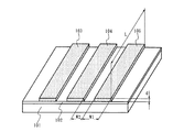
以下、図面を参照して本発明を用いて薄膜トランジスタを作製する実施の態様について説明する。図1において示す斜視図は、基板101上に第1絶縁膜102と直線状のストライプパターン形成された第2絶縁膜103〜105が形成された形態を示している。図1では第2絶縁膜による直線状のストライプパターンが3本示されているが、勿論その数に限定されることはない。
【0028】
基板は市販の無アルカリガラス基板、石英基板、サファイア基板、単結晶又は多結晶半導体基板の表面を絶縁膜で被覆した基板、金属基板の表面を絶縁膜で被覆した基板を適用することができる。サブミクロンのデザインルールで直線状のストライプパターンを形成するには、基板表面の凹凸、基板のうねり又はねじれを露光装置(特にステッパ)の焦点深度以下にしておくことが望ましい。具体的には、基板のうねり又はねじれが、1回の露光光照射領域内において1μm以下、好ましくは0.5μm以下とすることが望ましい。この点については、特に支持基体として無アルカリガラスを用いる場合には注意が必要である。
【0029】
直線状のストライプパターンに形成される第2絶縁膜の幅W1は0.1〜10μm(好ましくは0.5〜1μm)で、隣接する第2絶縁膜との間隔W2は0.01〜2μm(好ましくは0.1〜1μm)であり、第2絶縁膜の厚さdは0.01〜3μm(好ましくは0.1〜2μm)である。さらに、第2絶縁膜を覆うように設ける非晶質半導体膜の凹部における膜厚t02との関係は、d≧t02であれば良いが、dがt02に比べて厚すぎると凸部の上に結晶性半導体膜が残存しなくなるので注意が必要である。
【0030】
また、段差形状は規則的な周期パターンである必要はなく、島状の半導体膜の幅に合わせて異なる間隔で配置させても良い。その長さLも特に数値的な限定はなく、基板の一端から他端に渡るように長く形成することも可能であるし、例えばトランジスタのチャネル形成領域を形成することができる程度の長さとすることも可能である。
【0031】
第1絶縁膜102は、後に形成する第2絶縁膜との選択比の確保できる材料であれば良いが、代表的には、窒化珪素、酸化珪素、酸素含有量が窒素含有量よりも大きな酸窒化珪素(SiOxNyと示す。)、窒素含有量が酸素含有量よりも大きな窒酸化珪素(SiNxOyと示す。)、窒化アルミニウム(AlxNyと示す。)、酸素含有量が窒素含有量よりも大きな酸窒化アルミニウム(AlOxNyと示す。)、窒素含有量が酸素含有量よりも大きな窒酸化アルミニウム(AlNxOyと示す。)または酸化アルミニウムから選ばれた材料で、30〜300nmの厚さで形成する。特に、酸化アルミニウム膜はナトリウム(Na)に対するブロッキング効果が期待できるため、ガラス基板からの汚染対策として有効である。
【0032】
なお、酸窒化珪素(SiOxNy)膜としては、Siが25〜35原子%、酸素が55〜65原子%、窒素が1〜20原子%、水素が0.1〜10原子%で含まれるものを用いれば良い。また、窒酸化珪素(SiNxOy)膜としては、Siが25〜35原子%、酸素が15〜30原子%、窒素が20〜35原子%、水素が15〜25原子%で含まれるものを用いれば良い。また、酸窒化アルミニウム(AlOxNy)膜としては、Alが30〜40原子%、酸素が50〜70原子%、窒素が1〜20原子%で含まれるものを用いれば良い。また、窒酸化アルミニウム(AlNxOy)膜としては、Alが30〜50原子%、酸素が30〜40原子%、窒素が10〜30原子%で含まれるものを用いれば良い。
【0033】
また、第2絶縁膜103〜105は、10〜3000nm、好ましくは100〜2000nmの厚さの酸化珪素又は酸窒化珪素で形成すれば良い。酸化珪素はオルトケイ酸テトラエチル(Tetraethyl Ortho Silicate:TEOS)とO2とを混合しプラズマCVD法で形成することができる。窒酸化珪素膜はSiH4、NH3、N2O又は、SiH4、N2Oを原料として用いプラズマCVD法で形成することができる。
【0034】
図1で示すように、直線状のストライプパターンを二層の絶縁膜で形成する場合には、エッチング加工において第1絶縁膜102と第2絶縁膜103〜105との間に選択比をもたせる必要がある。実際には、第1絶縁膜102よりも第2絶縁膜103〜105のエッチング速度が相対的に早くなるように材料及び成膜条件を適宜調整することが望ましい。エッチングの方法としては、緩衝フッ酸を用いたエッチング、又はCHF3を用いたドライエッチングにより行う。そして、第2絶縁膜103〜105で形成される凹部の側面部の角度は5〜120度、好ましくは80〜100度の範囲で適宜設定すれば良い。
【0035】
なお、第2絶縁膜103〜105としては、CVD法(代表的には、プラズマCVD法もしくは熱CVD法)やPVD法(代表的には、スパッタ法もしくは蒸着法)によって形成された絶縁膜を用いることが好ましい。これは、非晶質半導体膜を結晶化する際、結晶化に伴う応力を緩和しうる程度の柔らかさを持つことが、良好な結晶性を得るにあたって重要な役割を果たしていると考えられるからである。その理由については、後述する。
【0036】
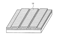
次に、図2で示すように、この第1絶縁膜102と第2絶縁膜103〜105から成る表面上および凹部を覆う非晶質半導体膜106を0.01〜3μm(好ましくは0.1〜1μm)の厚さに形成する。この時、非晶質半導体膜106の膜厚は、第2絶縁膜103〜105で形成される凹部の深さと同程度かそれ以上の厚さとすることが望ましい。非晶質半導体膜は珪素、珪素とゲルマニウムの化合物又は合金、珪素と炭素の化合物又は合金を適用することができる。
【0037】
非晶質半導体膜106は図示するように、下地の第1絶縁膜102と第2絶縁膜103〜105とで形成される凹凸構造を覆うように形成する。また、第1絶縁膜102及び第2絶縁膜103〜105の表面に付着した硼素などの化学汚染の影響を排除し、しかもその絶縁表面と非晶質半導体膜が直接に接しないように、非晶質半導体膜106を形成する直前に第3絶縁膜(図示せず)として酸窒化珪素膜を同一の成膜装置内で大気に触れさせることなく連続的に成膜すると良い。この第3絶縁膜の膜厚は、前述の化学汚染の影響の排除と密着性の向上を狙うものであり、薄いものでも十分に効果がある。典型的には、5〜50nm(化学汚染のブロッキング効果を高めるには20nm以上が好ましい。)とすれば良い。
【0038】
そして、この非晶質半導体膜106を瞬間的に溶融させ結晶化させる。この結晶化はレーザー光又はランプ光源からの放射光を光学系にて半導体膜が溶融する程度のエネルギー密度に集光して照射する。この工程においては、特に連続発振レーザー発振装置を光源とするレーザー光を適用することが好ましい。適用されるレーザー光は光学系にて線状に集光され、長さの長い方向に拡張されたものであり、その強度分布が長さの長い方向において均一な領域を有し、長さの短い方向にある程度の分布を持たせておくことが望ましい。
【0039】
なお、結晶化の際、基板の端など後にパターニングのマスク合わせに使用するマーカーを形成する位置は結晶化しないことが好ましい。結晶性半導体膜(特に結晶性珪素膜)は結晶化すると可視光の透過率が上がるため、マーカーとして識別が困難になるからである。ただし、光学的にマーカーの段差によるコントラストの違い等を識別するタイプの位置合わせ制御を行う場合には問題とならない。
【0040】
レーザー発振装置は、矩形ビーム固体レーザー発振装置が適用され、特に好ましくは、スラブレーザー発振装置が適用される。スラブ材料としては、Nd:YAG、Nd:GGG(ガドリニウム・ガリウム・ガーネット)、Nd:GSGG(ガドリニウム・スカンジウム・ガリウム・ガーネット)などの結晶が使用される。スラブレーザーでは、この板状のレーザー媒質の中を、全反射を繰り返しながらジグザグ光路で進む。或いは、Nd、Tm、Hoをドープしたロッドを用いた固体レーザー発振装置であり、特にYAG、YVO4、YLF、YAlO3などの結晶にNd、Tm、Hoをドープした結晶を使った固体レーザー発振装置にスラブ構造増幅器を組み合わせたものでも良い。
【0041】
そして、図3中に矢印で示すように、線状レーザー光の照射領域100の長さの長い方向(図中、X軸方向)が直線状のストライプパターンでなる第2絶縁膜103〜105の各々に交差するように線状のレーザー光又は強光を走査する。尚、ここでいう線状とは、長さの短い方向(図中、Y軸方向)の長さに対し、長さの長い方向(X軸方向)の長さの比が1対10以上のものをもって言う。また、図3では一部しか図示されていないが、線状レーザー光の照射領域100の端部は、矩形状となっていても曲率を持った形状となっていても良い。
【0042】
また、連続発振レーザー光の波長は、非晶質半導体膜の光吸収係数を考慮して400〜700nmであることが望ましい。このような波長帯の光は、波長変換素子を用いて基本波の第2高調波、第3高調波を取り出すことで得られる。波長変換素子としてはADP(リン酸二水素化アンモニウム)、Ba2NaNb5O15(ニオブ酸バリウムナトリウム)、CdSe(セレンカドミウム)、KDP(リン酸二水素カリウム)、LiNbO3(ニオブ酸リチウム)、Se、Te、LBO、BBO、KB5などが適用される。特にLBOを用いることが望ましい。代表的な一例は、Nd:YVO4レーザー発振装置(基本波1064nm)の第2高調波(532nm)を用いる。また、レーザーの発振モードはTEM00モードであるシングルモードを適用する。
【0043】
最も適した材料として選ばれる珪素の場合、吸収係数が103〜104cm-1である領域はほぼ可視光域にある。ガラスなど可視光透過率の高い基板と、珪素により30〜200nmの厚さをもって形成される非晶質半導体膜を結晶化する場合、波長400〜700nmの可視光域の光を照射することで、当該半導体膜を選択的に加熱して、下地絶縁膜にダメージを与えずに結晶化を行うことができる。具体的には、非晶質珪素膜に対し、波長532nmの光の侵入長は概略100nm〜1000nmであり、膜厚30nm〜200nmで形成される非晶質半導体膜106の内部まで十分達することができる。即ち、半導体膜の内側から加熱することが可能であり、レーザー光の照射領域における半導体膜のほぼ全体を均一に加熱することができる。
【0044】
レーザー光は直線状のストライプパターンが延在する方向と平行な方向に走査され、溶融した半導体は表面張力が働いて凹部に流れ込み凝固する。凝固した状態では図3で示すように表面がほぼ平坦になる。これは半導体が一旦溶融することにより、凸部上であろうと凹部上であろうと、溶融した半導体と気相との界面が平衡状態に達し、平坦な界面が形成されるためである。さらに結晶の成長端や結晶粒界は、第2絶縁膜上(凸部上)に形成される(図中ハッチングで示す領域110)。こうして結晶性半導体膜107が形成される。
【0045】
その後、好ましくは500〜600℃の加熱処理を行い、結晶性半導体膜に蓄積された歪みを除去すると良い。この歪みは、結晶化によって起こる半導体の体積収縮、下地との熱応力や格子不整合などにより発生するものである。この加熱処理は、通常の熱処理装置を用いて行えば良いが、例えばガス加熱方式の瞬間熱アニール(RTA)法を用いて1〜10分の処理を行えば良い。尚、この工程は本発明において必須な要件ではなく、適宜選択して行えば良いものである。
【0046】
その後図4で示すように、結晶性半導体膜107をエッチングして薄膜トランジスタの活性層108を形成する。この時、成長端や結晶粒界が集中する領域110は、一部に残ってしまって構わない。本発明の特徴は、領域110を含む第2の結晶性半導体領域を薄膜トランジスタのソース領域やドレイン領域といった電極として積極的に活用することにより、ソース領域やドレイン領域と各領域に接続される電極(ソース電極もしくはドレイン電極)とのコンタクト部(図4において、111、112で示される領域)の設計マージンを確保することにある。勿論、凹部に形成された結晶性の高い半導体領域(第1の結晶性半導体領域)109a、109bは、薄膜トランジスタのチャネル形成領域として用いることになる。
【0047】
結晶性の高い半導体領域109a、109bは、複数の結晶方位を有し結晶粒界が形成されていないという特徴を有している。そして、この半導体領域109a、109bがチャネル形成領域となるように、ゲート絶縁膜及びゲート電極を形成する。このような各段階を経てトランジスタを完成させることができる。
【0048】
図5は本発明者による実験結果から得られた結晶化の知見を概念図として示すものである。図5(A)〜(E)は第1絶縁膜及び第2絶縁膜により形成される凹部の深さ及び間隔と結晶成長の関係を模式的に説明している。
【0049】
尚、図5で示す長さに関する符号に関し、t01:第2絶縁膜上(凸部)の非晶質半導体膜の厚さ、t02:凹部の非晶質半導体膜の厚さ、t11:第2絶縁膜上(凸部)の結晶性半導体膜の厚さ、t12:凹部の結晶性半導体膜の厚さ、d:第2絶縁膜の厚さ(凹部の深さ)、W1:第2絶縁膜の幅、W2:凹部の幅である。
【0050】
図5(A)は、d<t02、W1,W2が1μmと同程度かそれ以下の場合であり、凹部の溝の深さが非晶質半導体膜204よりも小さい場合には、溶融結晶化の過程を経ても凹部が浅いので結晶性半導体膜205の表面が十分平坦化されることはない。即ち、結晶性半導体膜205の表面状態は下地の凹凸形状が反映された状態となる。
【0051】
図5(B)は、d≧t02、W1,W2が1μmと同程度かそれ以下の場合であり、凹部の溝の深さが非晶質半導体膜203とほぼ等しいかそれより大きい場合には、表面張力が働いて凹部に集まる。それにより固化した状態では、図5(B)で示すように表面がほぼ平坦になる。この場合、t11<t12となり、第2絶縁膜202上の膜厚が薄い部分220に応力が集中しここに歪みが蓄積され、結晶粒界が形成されることになる。
【0052】
図23(A)で示す走査電子顕微鏡(SEM)写真は図5(B)の状態の一例を示し、170nmの段差を設け、0.5μmの凸部の幅と間隔を設けた下地絶縁膜上に150nmの非晶質珪素膜を形成して結晶化した結果を示している。また、結晶性半導体膜の表面は結晶粒界を顕在化させるために一般的に知られるセコ液(HF:H2O=2:1に添加剤としてK2Cr2O7を用いて調合した薬液)でのエッチング(セコ・エッチングとも呼ばれる。)を施してある。
【0053】
図23に示す結果は、二クロム酸カリウム(K2Cr2O7)2.2gを水50ccに溶かして0.15mol/lの溶液を調製し、当該溶液にフッ酸水溶液100ccを加えてものを、さらに水で5倍に希釈したものをセコ液として使用した。また、セコ・エッチングの条件を室温(10〜30℃)にて75秒とした。なお、本明細書において、セコ液もしくはセコ・エッチングと言えば、ここで述べた溶液及び条件を指す。
【0054】
図23(B)は、図23(A)の写真の模式図である。図中、31は直線状のストライプパターンで延在する絶縁膜(第2絶縁膜)であり、その凸部32にはセコ・エッチングにより明確になった結晶粒界33が集中的に発生している様子が窺える。なお、消失部分と記載された領域34は、ストライプパターンの始点に相当する領域であり、レーザー光の走査はこの始点から始められている。詳細な理由は不明だが、当該始点上の珪素膜は溶融した際に走査方向に押しやられ、当該始点に位置する第2絶縁膜が露出してしまっていた領域である。セコ液は酸化珪素膜をエッチングしてしまうため、当該始点に位置する領域はセコ・エッチングにより消失してしまっている。
【0055】
ところで、図23(A)に示した写真と対比してみると、凹部35に形成された結晶性半導体膜にはセコ・エッチングで明確になるような結晶粒界もしくは欠陥が顕在化しない、換言すれば実質的に存在しないことが判る。セコ・エッチングで明確になる結晶粒界は現状において特定できていないが、セコ・エッチングにより積層欠陥や結晶粒界が優先的にエッチングされることは良く知られている事実であり、本発明を実施して得た結晶性半導体膜は、セコ・エッチングで顕在化するような結晶粒界もしくは欠陥が実質的に存在しないことに大きな特徴があると言える。
【0056】
勿論、単結晶ではないため、セコ・エッチングで顕在化しない粒界や欠陥は当然あり得るが、そのような粒界や欠陥は半導体素子を作製した際の電気特性に影響を及ぼすようなものではないため、電気的に不活性と考えられる。一般的にそのような電気的に不活性な粒界とは、平面状粒界(低次もしくは高次の双晶又は対応粒界)と呼ばれるものであり、セコ・エッチングで顕在化しない粒界とは、平面状粒界であると推測される。その観点からすると、結晶粒界もしくは欠陥が実質的に存在しないということは、平面状粒界以外の結晶粒界が存在しないと言っても差し支えないと言える。
【0057】
また、図25は図23(B)に示される凹部35に形成される結晶性半導体膜の配向性を反射電子回折パターン(EBSP:Electron Backscatter diffraction Pattern)により求めた結果を示している。EBSPは走査型電子顕微鏡(SEM:Scanning Electron Microscopy)に専用の検出器を設け、電子ビームを結晶面に照射してその菊池線からの結晶方位同定をコンピューターで画像認識させることによって、そのミクロな結晶性を表面配向のみならず、結晶の全方向に関して測定するものである(以下、この手法を便宜上EBSP法と呼ぶ)。
【0058】
図25のデータは、凹部35においては線状に集光されたレーザー光の走査方向と平行な方向に結晶が成長していることを示している。成長の結晶方位は<110>方位が優勢(即ち、主たる配向面は{110}面である。)であるが、<100>方位の成長も存在している。
【0059】
図5(C)は、d≧t02、W1,W2が1μmと同程度か若干大きい場合であり、凹部の幅が広がると結晶性半導体膜205が凹部を充填し、平坦化の効果はあるが、凹部の中央付近には結晶粒界が発生する。また、第2絶縁膜上にも同様に応力が集中しここに歪みが蓄積され、結晶粒界が形成される。これは、間隔が広がることで応力緩和の効果が低減するためであると推定している。この条件では、チャネル形成領域となる半導体領域にも結晶粒界が生じる可能性があるため、好ましいものではない。
【0060】
図5(D)は、d≧t02、W1,W2が1.0μmよりも大きい場合であり、図5(C)の状態がさらに顕在化してくる。この条件になるとかなりの確率でチャネル形成領域となる半導体領域に結晶粒界が生じるため、好ましいものではない。
【0061】
図24(A)で示す走査電子顕微鏡(SEM)写真は図5(D)の状態の一例を示し、170nmの段差を設け、1.8μmの凸部の幅と間隔を設けた下地絶縁膜上に150nmの非晶質珪素膜を形成して結晶化した結果を示している。結晶性半導体膜の表面は結晶粒界を顕在化させるために前述のセコ液でエッチングしてある。
【0062】
また、図24(B)は、図24(A)の写真の模式図である。図中、41は直線状のストライプパターンで延在する絶縁膜(第2絶縁膜)であり、その凸部42及びその端部にはセコ・エッチングにより明確になった結晶粒界43が集中的に発生している様子が窺える。なお、消失部分と記載された領域44は、ストライプパターンの始点に相当する領域であり、前述の理由によりセコ・エッチングで消失してしまっている。なお、図24(A)に示した写真と対比してみると、結晶粒界は、ストライプパターンの凸部42だけでなく凹部45にも発生している。
【0063】
図5(E)は、本発明においては参考例であり、d>>t02、W1,W2が1μm以下の場合である。即ち、第2絶縁膜の厚さdが凹部における非晶質半導体膜の厚さt02に比べて厚すぎる場合は結晶性半導体膜204が凹部を充填するように形成され、第2絶縁膜203上には殆ど残存しない。そのため、本発明のように、第2絶縁膜上の結晶性半導体膜をソース領域とソース電極(またはドレイン領域とドレイン電極)とのコンタクト部として用いることができない。
【0064】
以上、図5(A)〜(D)を用いて説明したように、半導体素子を形成する場合、特に薄膜トランジスタにおけるチャネル形成領域を形成する場合には、図5(B)の形態が最も適していると考えられる。即ち、上述のセコ液でセコ・エッチングを施した際に、結晶粒界や欠陥が殆ど顕在化しない結晶性半導体膜、換言すれば結晶粒界及び欠陥が実質的に存在しない結晶性半導体膜をチャネル形成領域に用いることが望ましい。
【0065】
また、ここでは結晶性半導体膜を形成する下地の凹凸形状は、第1絶縁膜と第2絶縁膜で形成する一例を示したが、ここで示す形態に限定されず同様な形状を有するものであれば代替することができる。例えば、200nm〜2μm程度の厚さの絶縁膜をエッチングして所望の深さの凹部を形成しても良い。
【0066】
なお、上記結晶化工程の際、前述のように第2絶縁膜が柔らかい絶縁膜(密度の低い絶縁膜)であると、結晶化時における半導体膜の収縮等による応力を緩和するという効果が期待できる。逆に、固い絶縁膜(密度の高い絶縁膜)であると、収縮もしくは膨張しようとする半導体膜に逆らう形で応力が発生するため、結晶化後の半導体膜に応力歪み等を残しやすく結晶欠陥の原因ともなりかねない。例えば、公知のグラフォエピタキシ技術(「M.W.Geis,D.C.Flanders,H.I.Smith:Appl.Phys.Lett.35(1979)pp71」)では基板上の凹凸を固い石英ガラスで直接形成しているが、この場合において結晶Siの配向軸は[100]軸、即ち主たる配向面は{100}面であることが判明している。
【0067】
しかしながら、本発明を実施した場合、図25に示したように主たる配向面は{110}であり、明らかに結晶形態の異なる半導体膜が形成されていることが判る。その相違は、基板上の凹凸を上述のCVD法やPVD法で形成した柔らかい絶縁膜であるためである。即ち、下地となる第2絶縁膜を石英ガラスよりも柔らかい材質としたことにより、結晶化の際の応力の発生をより緩和でき、もしくは凸部上の結晶性半導体膜に応力を集中させることができた。
【0068】
なお、石英ガラスよりも柔らかい絶縁膜という意味は、例えば一般的な石英ガラス(工業的に基板として利用されている石英ガラス)よりもエッチングレートの速い絶縁膜もしくは硬度の高い絶縁膜という意味である。石英ガラスをフッ化水素アンモニウム(NH4HF2)を7.13%とフッ化アンモニウム(NH4F)を15.4%含む混合溶液(ステラケミファ社製、商品名LAL500)をエッチャントとし、ウエットエッチングを行った結果、石英基板のエッチングレートは38nm/minであった。一方上記下地になる第2絶縁膜の同エッチャントによるエッチングレートは50〜1000nm/minであるので、石英ガラスより、柔らかい絶縁膜といえる。これらエッチングレート及び硬度に関しては、あくまで石英ガラスとの相対比較で決めれば良いので、エッチングレートの測定条件や硬度の測定条件に依存しない。
【0069】
例えば、第2絶縁膜として酸窒化珪素膜を用いるのであれば、SiH4ガス、N2Oガスを原料として用いたプラズマCVD法で成膜した酸窒化珪素膜が好ましい。当該酸窒化珪素膜は、フッ化水素アンモニウム(NH4HF2)を7.13%とフッ化アンモニウム(NH4F)を15.4%含む混合水溶液の20℃におけるエッチングレートが110〜130nm/min(500℃、1時間+550℃、4時間の熱処理後では、90〜100nm/min)である。
【0070】
また、第2絶縁膜として窒酸化珪素膜を用いるのであれば、SiH4ガス、NH3ガス、N2Oガスを原料として用いたプラズマCVD法で成膜した窒酸化珪素膜が好ましい。当該窒酸化珪素膜は、フッ化水素アンモニウム(NH4HF2)を7.13%とフッ化アンモニウム(NH4F)を15.4%含む混合水溶液の20℃におけるエッチングレートが60〜70nm/min(500℃、1時間+550℃、4時間の熱処理後では、40〜50nm/min)である。
【0071】
以上のように、絶縁膜により凹部及び凸部を有する直線状のストライプパターンを形成し、その上に非晶質半導体膜を堆積し、レーザー光の照射により溶融状態を経て結晶化させることにより凹部に半導体を流し込み凝固させ、凹部以外の領域に結晶化に伴う歪み又は応力を集中させることができ、結晶粒界など結晶性の悪い領域を選択的に形成することが可能となる。そして、結晶性の良い半導体領域を薄膜トランジスタのチャネル形成領域等のキャリア移動が行われる領域とし、結晶性の悪い半導体領域を電極とのコンタクト部として活用することが本発明の特徴である。
【0072】
即ち、凹部に複数の結晶方位を有し結晶粒界が形成されることなく、直線状のストライプパターンが延在する方向と平行な方向に延在する複数の結晶粒が集合した結晶性半導体膜を形成することができる。このような結晶性半導体膜でチャネル形成領域が配設されるようにトランジスタを形成することにより、高速動作が可能で電流駆動能力の高く、且つ複数の素子間においてばらつきの小さいトランジスタ又はそのトランジスタ群により構成される半導体装置を形成することができる。
【0073】
[実施の形態2]
本発明の結晶性半導体膜の形成において、実施の形態1で示すように非晶質半導体膜にレーザー光を照射して結晶化させる方法の他に、固相成長により結晶化した後さらにレーザー光を照射して溶融再結晶化しても良い。
【0074】
例えば、図2において非晶質半導体膜106を形成した後、当該非晶質半導体膜(例えば非晶質珪素膜)の結晶化温度を低温化させ配向性を向上させるなど、結晶化を促進する触媒作用のある金属元素としてNiを添加する。
【0075】
当該技術については、本出願人による特開平11−354442号等が詳しい。Niを添加して形成した結晶性半導体膜は、主たる配向面が{110}面であるという特徴を有し、このような結晶性半導体膜を薄膜トランジスタのチャネル形成領域に用いると、電子移動度とホール移動度が共に大幅に向上し、ひいてはNチャネル型トランジスタ及びPチャネル型トランジスタの電界効果移動度が大幅に向上するという特徴を有する。特にホール移動度の向上に伴うPチャネル型トランジスタの電界効果移動度の向上は特筆すべきものであり、主たる配向面を{110}とする利点の一つである。
【0076】
また、Niの添加法に限定はなく、スピン塗布法、蒸着法、スパッタ法などを適用するこができる。スピン塗布法による場合には酢酸ニッケル塩が5ppmの水溶液を塗布して金属元素含有層を形成する。勿論、触媒元素はNiに限定されるものではなく、他の公知の材料を用いても良い。
【0077】
その後、580℃にて4時間の加熱処理により非晶質半導体膜106を結晶化させる。この結晶化した半導体膜に対し、レーザー光又はそれと同等な強光を照射して溶融させ再結晶化する。こうして、図3と同様に表面がほぼ平坦化された結晶性半導体膜を得ることができる。この結晶性半導体膜も同様に成長端や結晶粒界110が形成された領域が形成される。
【0078】
レーザー光の被照射体として結晶化した半導体膜を用いる利点はその半導体膜の光吸収係数の変動率にあり、結晶化した半導体膜にレーザー光を照射して溶融させたとしても光吸収係数は殆ど変動しない。よって、レーザー照射条件のマージンを広くとることができる。
【0079】
こうして形成された結晶性半導体膜には金属元素が残存するが、ゲッタリング処理により取り除くことができる。この技術の詳細については、特願2001−019367号出願(又は特願2002−020801号出願)を参照されたい。また、このゲッタリング処理に伴う加熱処理は、結晶性半導体膜の歪みを緩和するという効果も合わせ持っている。
【0080】
その後、実施の形態1と同様に凹部の結晶性半導体膜をチャネル形成領域とし、かつ、凸部の結晶性半導体膜をソース領域もしくはドレイン領域として用いた薄膜トランジスタを形成する。凹部の結晶性半導体膜は、複数の結晶方位を有し結晶粒界が形成されていないという特徴を有しているため、高速動作が可能で電流駆動能力の高く、且つ複数の素子間においてばらつきの小さいトランジスタ又はそのトランジスタ群により構成される半導体装置を形成することができる。
【0081】
[実施の形態3]
次に、本実施の形態において凹部を有する下地絶縁膜上に結晶性珪素膜を形成し、その凹部に形成された半導体領域にチャネル形成領域が配設されるトランジスタを作製する一形態を図面を用いて説明する。尚、本実施の形態の係る各図面において、(A)は上面図、(B)以降はそれに対応する各部位の縦断面図を示す。
【0082】
図6において、ガラス基板301上に30〜300nmの窒化珪素、窒素含有量が酸素含有量よりも大きな酸窒化珪素、窒化アルミニウム、又は酸窒化アルミニウムでなる第1絶縁膜302を形成する。その上に凹部及び凸部を有する直線状のストライプパターンを、酸化珪素又は酸窒化珪素から成る第2絶縁膜303により形成する。酸化珪素膜はプラズマCVD法でTEOSとO2とを混合し、反応圧力40Pa、基板温度400℃とし、高周波(13.56MHz)電力密度0.6W/cm2で放電させ10〜3000nm、好ましくは100〜2000nmの厚さに堆積し、その後エッチングにより凹部304を形成する。凹部の幅は、特にチャネル形成領域が配置される場所において、0.01〜1μm、好ましくは0.05〜0.2μmで形成する。
【0083】
次に、図7で示すように第1絶縁膜302及び第2絶縁膜303上に酸化膜又は酸窒化珪素膜から成る第3絶縁膜305と非晶質珪素膜306を同一のプラズマCVD装置を用い大気に触れさせることなく連続的に成膜する。非晶質珪素膜305は珪素を主成分に含む半導体膜で形成し、プラズマCVD法でSiH4を原料気体として用い形成する。この段階では、図示するように凹部304の底面及び側面を被覆して平坦でない表面形状が形成される。
【0084】
結晶化は連続発振レーザー光を照射して行う。図8はその結晶化後の状態を示している。結晶化の条件は連続発振モードのYVO4レーザー発振器を用い、その第2高調波(波長532nm)の出力5〜10Wを、光学系にて短手方向に対する長手方向の比が10以上である線状レーザー光に集光し、且つ長手方向に均一なエネルギー密度分布を有するように集光し、5〜200cm/secの速度で走査して結晶化させる。均一なエネルギー密度分布とは、完全に一定であるもの以外を排除することではなく、エネルギー密度分布において許容される範囲は±10%である。
【0085】
線状に集光されたレーザー光の強度分布はその強度分布が長さの長い方向(図3におけるX軸方向)において均一であることが望ましい。これは加熱される半導体の温度をレーザー光の照射領域全体で均一にすることが目的である。線状に集光されたレーザー光のX軸方向に温度分布が生じると、半導体膜の結晶成長の方向をレーザー光の走査方向に規定することができなくなるためである。直線状のストライプパターンは線状に集光されたレーザー光の照射領域の走査方向と合わせて配列させておくことで、結晶の成長方向と、全てのトランジスタのチャネル長方向とを合わせることができる。これによりトランジスタの素子間の特性ばらつきを小さくすることができる。
【0086】
また、線状に集光されたレーザー光による結晶化は、1回の走査(即ち、一方向)のみで完了させても良いし、より結晶性を高めるためには往復走査しても良い。さらに、レーザー光により結晶化した後、フッ酸などによる酸化物除去、或いは、アンモニア過酸化水素水処理などアルカリ溶液により珪素膜の表面を処理し、エッチング速度の速い品質の悪い部分を選択的に除去して、再度同様の結晶化処理を行っても良い。このようにして、結晶性を高めることができる。
【0087】
この条件でレーザー光を照射することにより、非晶質半導体膜は瞬間的に溶融し結晶化する。実質的には溶融帯が移動しながら結晶化が進行する。溶融した珪素は表面張力が働いて凹部に凝集し固化する。これにより、図8に示すように凹部304を充填する形態で表面が平坦な結晶性半導体膜307が形成される。
【0088】
その後、図9に示すように、結晶性半導体膜307をエッチングし、薄膜トランジスタの活性層となる半導体領域308〜310を形成する。なお、図9は、半導体領域308〜310の形状を限定的に示すものではなく、実施の形態1で述べた如く、所定のデザインルールに従う範囲内において、特に限定されるものではない。
【0089】
結晶性半導体膜307はフッ素系のガスと酸素とをエッチングガスとして用いることにより第3絶縁膜305と選択性をもってエッチングすることができる。勿論、第3絶縁膜305がエッチングされてしまってもその下にある第1絶縁膜302や第2絶縁膜303との選択性さえ確保できれば何ら問題はない。
【0090】
なお、エッチング法として、CF4とO2の混合ガスやNF3ガスを用いたプラズマエッチング法により行っても良いし、ClF3ガス等のフッ化ハロゲンガスを励起しないで用いたプラズマレスのガスエッチングを行っても良い。プラズマレスのガスエッチングは、結晶性半導体膜にプラズマダメージを与えないで済むので結晶欠陥の抑制により効果的な手法である。
【0091】
次に、図10に示すように、半導体領域308〜310及び第2絶縁膜303の上面を覆うように第4絶縁膜(ゲート絶縁膜として機能する。)311、ゲート電極として用いる導電膜312、313を形成する。第4絶縁膜311は、実施の形態1で説明した酸化珪素膜、窒化珪素膜、酸窒化珪素膜、窒酸化珪素膜、窒化アルミニウム膜、窒酸化アルミニウム膜、酸窒化アルミニウム膜もしくは酸化アルミニウム膜のいずれを用いても良いし、これらを適宜組み合わせた積層膜としても良い。
【0092】
ゲート絶縁膜のカバレッジを良くするためには、酸化珪素膜ならばTEOSを用いた酸化珪素膜が好ましく、窒酸化アルミニウム膜であればRFスパッタ法で形成した窒酸化アルミニウム膜を用いたり、当該窒酸化アルミニウム膜と酸化珪素膜の積層膜(酸化珪素膜は、活性層となる半導体膜を過酸化水素で酸化させたものであっても良い。)を用いたりすると良い。
【0093】
また、ゲート電極として用いる導電膜312、313はタングステン又はタングステンを含有する合金や、アルミニウム又はアルミニウム合金などで形成する。
【0094】
次に、図11に示すように、半導体領域308〜310に一導電型の不純物領域314〜319を形成する。ここでは、便宜的にn型不純物領域314、315、318及び319、p型不純物領域316及び317を設けるものとする。これらの不純物領域はゲート電極として用いる導電膜312、313をマスクとして自己整合的に形成しても良いし、フォトレジストなどでマスキングして形成しても良い。不純物領域314〜319はソース及びドレイン領域を形成し、必要に応じて低濃度ドレイン領域(一般的にはLDD領域と呼ばれる。)を設けることもできる。
【0095】
この不純物領域314〜319は不純物イオンを電界で加速して半導体領域に注入するイオン注入法又はイオンドーピング法などが適用される。この場合において、注入するイオン種の質量分離の有無は本発明を適用する上で本質的な問題とはならない。
【0096】
この時、半導体領域308〜310のうち、ゲート電極312、313の下にあり、かつ、凹部304に形成された半導体領域320が、本発明の薄膜トランジスタのチャネル形成領域となる。
【0097】
そして、図12に示すように50〜100nm程度の水素を含有する窒化珪素膜又は酸窒化珪素膜による第5絶縁膜(パッシベーション膜として機能する。)321を形成する。この状態で400〜450℃に熱処理をすることにより窒化珪素膜又は酸窒化珪素膜が含有する水素が放出され島状の半導体膜に対する水素化を行うことができる。
【0098】
次いで、酸化珪素膜などで形成する第6絶縁膜(層間絶縁膜として機能する。)322を形成し、不純物領域314〜319に接続する配線323〜327を形成する。こうしてnチャネル型トランジスタ328、330及びpチャネル型トランジスタ329を形成することができる。
【0099】
図12に示されるnチャネル型トランジスタ328及びpチャネル型トランジスタ329は、複数のチャネル形成領域320が並列に配設され、かつ、一対の不純物領域314と315(または316と317)との間に連接して設けられたマルチチャネル型のトランジスタを示している。具体的には、nチャネル型マルチチャネルトランジスタ328と、pチャネル型マルチチャネルトランジスタ329とでCMOS構造の基本回路であるインバータ回路を構成する一例を示している。この構成において並列に配設するチャネル形成領域の数に限定はなく、必要に応じて複数個配設すれば良い。例えば、nチャネル型トランジスタ330のようにシングルチャネルとしても良い。
【0100】
[実施の形態4]
実施の形態3において、トランジスタはシングルドレイン構造で示されているが、低濃度ドレイン(LDD)を設けても良い。図13はLDD構造を持ったnチャネル型マルチチャネルトランジスタの一例を示している。
【0101】
図13(A)で示すトランジスタの構造はゲート電極を窒化チタン又は窒化タンタルなど窒化物金属340aとタングステン又はタングステン合金など高融点金属340bで形成する一例であり、ゲート電極340bの側面にスペーサ341を設けている。スペーサ341は酸化珪素などの絶縁体で形成しても良いし、導電性を持たせるためにn型の多結晶珪素で形成しても良く、異方性ドライエッチングにより形成する。LDD領域342a、342bはこのスペーサを形成する前に形成することにより、ゲート電極340bに対し自己整合的に形成することができる。スペーサを導電性材料で形成した場合には、LDD領域342a、342bが実質的にゲート電極と重畳するゲート・オーバーラップLDD(Gate-Overlapped LDD)構造とすることができる。
【0102】
一方、図13(B)はゲート電極340aを設けない構造であり、この場合はLDD構造となる。
【0103】
図13(C)は、n型不純物領域315に隣接してLDD領域を形成するn型不純物領域344が形成されている。ゲート電極343は下層側ゲート電極343a、上層側ゲート電極343bの二層構造であり、n型不純物領域314、315及びLDD領域344a、344bを自己整合的に形成することができる。このようなゲート電極と不純物領域、及びその作製方法の詳細については、特願2000−128526号出願又は特願2001−011085号出願を参照されたい。
【0104】
いずれにしても、このようなゲート構造により自己整合的にLDD領域を形成する構造は、特にデザインルールを微細化する場合において有効である。ここでは単極性のトランジスタ構造を示したが、実施の形態4と同様にCMOS構造を形成することもできる。
【0105】
尚、本実施の形態においてゲート電極及びLDD領域の構成以外は、実施の形態3と同じであり詳細な説明は省略する。
【0106】
[実施の形態5]
本実施の形態は、実施の形態1で説明した構成とは別の実施形態であって、電極として機能する一導電型の不純物領域をそのまま配線としても利用したことを特徴とする発明に関する。当該実施の形態は、コンタクト部の数を減らして設計マージンの縮小による集積度の向上を図るとともに歩留まりの向上を図るものである。
【0107】
説明には図14を用いる。図14(A)は上面図であり、図14(B)〜(F)は各々該当個所の断面図を示している。なお、実施の形態1における図11の状態に対応する図である。この状態に至る過程およびその後のトランジスタ形成過程については、実施の形態1を参照すれば良い。
【0108】
図14(A)において、401〜405は一導電型の不純物領域であり、401及び402はそれぞれPチャネル型トランジスタのソース領域及びドレイン領域、403及び404はそれぞれNチャネル型トランジスタのソース領域であり、405はNチャネル型トランジスタのドレイン領域として機能する。この時、ドレイン領域405が二つのトランジスタを電気的に接続する配線として機能している点に特徴がある。
【0109】
本発明の特徴として、結晶性の悪い半導体領域も電極として活用することができるため、本実施の形態のように、配線として活用することでコンタクト部の数を減らすことができる上、コンタクト形成のための設計マージンを拡げることができる。そのため、特に微細化が進んだ論理回路を形成する際には、非常に有効である。
【0110】
なお、本実施の形態は一例に過ぎず、本発明において、一導電型の不純物領域を電極だけでなく配線として用いることができるという技術思想を開示するものである。従って、実施の形態1〜4に開示されたいずれの技術と組み合わせても本実施の形態で述べた効果を得ることができる。
【0111】
[実施の形態6]
本実施の形態は、実施の形態1で説明した構成とは別の実施形態であって、一導電型の不純物領域を配線として用いることにより複数個のトランジスタを直列に接続した構成のトランジスタを形成することを特徴とする発明に関する。当該実施の形態は、ソース領域及びドレイン領域の間に複数のチャネル形成領域を有するトランジスタを得ることも可能であることを開示するものであって、本発明のさらなる実施形態を示すものである。
【0112】
説明には図15を用いる。図15(A)は上面図であり、図15(B)〜(F)は各々該当個所の断面図を示している。なお、実施の形態1における図11の状態に対応する図である。この状態に至る過程およびその後のトランジスタ形成過程については、実施の形態1を参照すれば良い。
【0113】
図15(A)において、411〜418は一導電型の不純物領域であり、411及び414はそれぞれPチャネル型トランジスタのソース領域及びドレイン領域、412及び413は、配線として用いられる不純物領域である。なお、本発明の特徴として、不純物領域412、413の占有面積を大きくできるため、当該部分を単に配線として用いても良いし、面積を拡げて電極として用いることも可能である。また、屈曲した形状に加工して保護回路としての機能を持たせることも可能である。
【0114】
また、415はシングルチャネルのNチャネル型トランジスタのソース領域であり、416はそのドレイン領域である。さらに、当該ドレイン領域416をソース領域とし、かつ、不純物領域418をドレイン領域とするトランジスタが構成される。この場合、不純物領域417は配線として機能する。当該トランジスタは、併せて三つのチャネル形成領域を有するが、うち二つが並列に設けられ、かつ、残りの一つと直列に接続された構成となっている。勿論、本実施の形態は、当該トランジスタの構造に限定されるものではない。
【0115】
なお、本実施の形態は一例に過ぎず、本発明において、一導電型の不純物領域を電極だけでなく配線として用いることができるという技術思想を開示するものである。従って、実施の形態1〜5に開示されたいずれの技術と組み合わせても良い。
【0116】
[実施の形態7]
本発明のトランジスタにおいて、下層側に導電層を設けることにより、所謂基板バイアスを印加することが可能となる。トランジスタの作製方法は実施の形態3に従うものであるが、その差異について図16を用いて説明する。
【0117】
図16(A)において、基板上には第1絶縁膜802として窒化珪素膜を形成し、その上にタングステン膜803をスパッタリング法にて形成する。特に窒化珪素膜は高周波スパッタリング法で形成すると緻密な膜を形成することが可能である。第2絶縁膜804は酸化珪素膜で形成する。酸化珪素膜はエッチングにより図示するように凹部を形成するが、下地のタングステン膜との選択比は30程度あるので容易に加工できる。
【0118】
この上に、第3絶縁膜805として酸窒化珪素膜と非晶質珪素膜806を連続して形成し、該非晶質半導体膜806を溶融結晶化し、図16(B)で示すように結晶性珪素膜807を形成する。その後、図16(C)に示すようにトランジスタのチャネル形成領域808をエッチングにより形成し、ゲート絶縁膜809、ゲート電極810を形成する。タングステン膜803上にはゲート絶縁膜809が形成されるので、ゲート電極810と短絡することはない。
【0119】
このような形態において、タングステン膜803を接地電位に固定すると、トランジスタのしきい値電圧のばらつきを小さくすることができる。また、ゲート電極810と同電位を印加して駆動すると、オン電流を増加させることができる。
【0120】
また、放熱効果を高めるためには、図17で示すようにタングステン膜803の上層に、酸窒化アルミニウム膜(又は窒化アルミニウム膜)811を形成すると良い。これらの膜を設ける目的は、エッチング加工の選択比を確保することにある。即ち、CHF3などフッ素系のエッチングガスで第2絶縁膜804である酸化珪素を除去して、且つ下地のタングステン膜803を露出させないためには、窒化珪素膜では選択比が小さく、窒化アルミニウム膜又は酸窒化アルミニウムが適している。
【0121】
本実施の形態は、凸部及び凹部を形成する第2絶縁膜の下に導電膜を設けることにより放熱効果や実際の動作時のしきい値制御を図る構成を開示するものであり、実施の形態1〜6に開示される構成との組み合わせは可能であり、組み合わせたことによって本実施の形態に記載の効果を付与することができる。
【0122】
[実施の形態8]
本実施の形態では、実施の形態3において、薄膜トランジスタの活性層308を形成する工程の前に結晶性半導体膜307の一部(後にチャネル形成領域となる部分)をエッチングして薄膜化する例を示す。
【0123】
まず実施の形態3に示した作製方法に従って、図8に示す状態を得る。次に、結晶性半導体膜307のうち、後にソース領域またはドレイン領域となる半導体領域の上にレジストマスク1801を形成する(図18(A))。
【0124】
そして、レジストマスク1801をマスクとしてドライエッチング法またはウェットエッチング法により結晶性半導体膜307をエッチングし、下地となる第3絶縁膜305を露出させる。この工程により凹部のみに選択的に結晶性半導体膜1802を残存させることができる。また、レジストマスク1801の下には元の膜厚で結晶性半導体膜1803が残存する。本実施の形態は、結晶性半導体膜1802を薄膜トランジスタのチャネル形成領域として用い、結晶性半導体膜1803を薄膜トランジスタのソース領域またはドレイン領域として用いることを特徴とする。
【0125】
なお、上記エッチング工程は、化学的手法だけでなく、CMP(ケミカルメカニカルポリッシング)の如き機械的研磨法を用いても良い。また、化学的手法及び機械的手法を併用しても構わない。
【0126】
本実施の形態によれば、第2絶縁膜303により自己整合的にチャネル形成領域を形成することができるため、パターンずれによって第2絶縁膜の凸部に誤ってチャネル形成領域が形成されることを防ぐことができ、チャネル形成領域内に結晶粒界が含まれてしまうような事態を減らすことができる。
【0127】
これ以降の工程については、実施の形態3の図10以降の工程を参照にすれば良いので、本実施の形態での説明は省略する。なお、本実施の形態は、実施の形態1〜7のいずれの形態とも自由に組み合わせることが可能である。
【0128】
[実施の形態9]
本発明は様々な半導体装置に適用できるものであり、実施の形態1乃至8に基づいて作製される表示パネルの形態を説明する。なお、本実施の形態に示す表示パネルの具体例としては、液晶表示パネル、EL(エレクトロルミネセンス)表示パネル、FED(フィールドエミッションディスプレイ)用表示パネルといった半導体素子としてトランジスタを用いる表示パネルが挙げられる。勿論、これら表示パネルは、モジュールとして市場に流通するものを含む。
【0129】
図19は基板900には画素部902、ゲート信号側駆動回路901a、901b、データ信号側駆動回路901c、入出力端子部908、配線又は配線群917が備えられている。
【0130】
シールパターン940は、対向基板920と基板900との間に密閉空間を作るためのパターンであり、液晶表示パネルなら液晶を封入し、ELパネルならEL材料(特に有機EL材料)を外気から保護する役割を果たす。ゲート信号側駆動回路901a、901b、データ信号側駆動回路901c及び当該駆動回路部と入力端子とを接続する配線又は配線群917と一部が重なっていても良い。このようにすると、表示パネルの額縁領域(画素部の周辺領域)の面積を縮小させることができる。外部入力端子部には、FPC(フレキシブルプリントサーキット)936が固着されている。
【0131】
さらに、本発明を実施して得たトランジスタを用いて各種論理回路、高周波回路、メモリ、マイクロプロセッサ、メディアプロセッサ/DSP(Digital Signal Processor)、グラフィクス用LSI、暗号LSI、アンプなどが形成されたチップ950が実装されていても良い。これらの機能回路は、画素部902、ゲート信号側駆動回路901a、901b、データ信号側駆動回路901cとは異なるデザインルールで形成されるものであり、具体的には1μm以下のデザインルールが適用される。なお、上記外部入力端子部やチップ950は樹脂(モール樹脂等)937によって保護しておくと良い。また、実装の方法に限定はなく、TABテープを用いた方式やCOG(チップオングラス)方式などが適用することができる。
【0132】
なお、本実施の形態において、トランジスタのゲート構造としては、図13(A)、(B)などが適している。例えば、実施の形態3乃至4で示すトランジスタは画素部902のスイッチング素子として、さらにゲート信号側駆動回路901a、901b、データ信号側駆動回路901cを構成する能動素子として適用することができる。勿論、本実施の形態は、本発明を実施して得た表示パネルの一例を示すものであり、図19の構成に限定されるものではない。
【0133】
[実施の形態10]
本発明を用いて様々な電子装置を完成させることができる。その一例は、携帯情報端末(電子手帳、モバイルコンピュータ、携帯電話など)、ビデオカメラ、デジタルカメラ、パーソナルコンピュータ、テレビ受像器、携帯電話などが挙げられる。それらの一例を図20に示す。なお、ここで示す電子装置はごく一例であり、これらの用途に限定するものではない。
【0134】
図20(A)は本発明を適用してテレビ受像器を完成させる一例であり、筐体3001、支持台3002、表示部3003などにより構成されている。本発明により作製されるトランジスタは表示部3003の他に、各種論理回路、高周波回路、メモリ、マイクロプロセッサ、メディアプロセッサ、グラフィクス用LSIなど様々な集積回路がガラス上に形成し組み込むことができ、本発明によりテレビ受像器を完成させることができる。
【0135】
図20(B)は本発明を適用してビデオカメラを完成させた一例であり、本体3011、表示部3012、音声入力部3013、操作スイッチ3014、バッテリー3015、受像部3016などにより構成されている。本発明により作製されるトランジスタは表示部3012の他に、各種論理回路、高周波回路、メモリ、マイクロプロセッサ、メディアプロセッサ、グラフィクス用LSIなど様々な集積回路がガラス上に形成し組み込むことができ、本発明によりビデオカメラを完成させることができる。
【0136】
図20(C)は本発明を適用してノート型のパーソナルコンピュータを完成させた一例であり、本体3021、筐体3022、表示部3023、キーボード3024などにより構成されている。本発明により作製されるトランジスタは表示部3023の他、各種論理回路、高周波回路、メモリ、マイクロプロセッサ、メディアプロセッサ、グラフィクス用LSI、暗号LSIなど様々な集積回路がガラス上に形成し組み込むことができ、本発明によりパーソナルコンピュータを完成させることができる。
【0137】
図20(D)は本発明を適用してPDA(Personal Digital Assistant)を完成させた一例であり、本体3031、スタイラス3032、表示部3033、操作ボタン3034、外部インターフェース3035などにより構成されている。本発明により作製されるトランジスタは表示部3033の他、各種論理回路、高周波回路、メモリ、マイクロプロセッサ、メディアプロセッサ、グラフィクス用LSI、暗号LSIなど様々な集積回路がガラス上に形成し組み込むことができ、本発明によりPDAを完成させることができる。
【0138】
図20(E)は本発明を適用して音響再生装置を完成させた一例であり、具体的には車載用のオーディオ装置であり、本体3041、表示部3042、操作スイッチ3043、3044などにより構成されている。本発明により作製されるトランジスタは表示部3042の他、各種論理回路、高周波回路、メモリ、マイクロプロセッサ、メディアプロセッサ、グラフィクス用LSI、増幅回路など様々な集積回路がガラス上に形成し組み込むことができ、本発明によりオーディオ装置を完成させることができる。
【0139】
図20(F)は本発明を適用してデジタルカメラを完成させた一例であり、本体3051、表示部(A)3052、接眼部3053、操作スイッチ3054、表示部(B)3055、バッテリー3056などにより構成されている。本発明により作製されるトランジスタは表示部(A)3052および表示部(B)3055の他、各種論理回路、高周波回路、メモリ、マイクロプロセッサ、メディアプロセッサ、グラフィクス用LSI、暗号LSIなど様々な集積回路がガラス上に形成し組み込むことができ、本発明によりデジタルカメラを完成させることができる。
【0140】
図20(G)は本発明を適用して携帯電話を完成させた一例であり、本体3061、音声出力部3062、音声入力部3063、表示部3064、操作スイッチ3065、アンテナ3066などにより構成されている。本発明により作製されるトランジスタは表示部3064の他、各種論理回路、高周波回路、メモリ、マイクロプロセッサ、メディアプロセッサ、グラフィクス用LSI、暗号LSI、携帯電話用LSIなど様々な集積回路がガラス上に形成し組み込むことができ、本発明により携帯電話を完成させることができる。
【0141】
[実施の形態11]
本実施の形態では、本発明の実施に用いられるレーザー照射装置の構成について、図21を用いて説明する。11はレーザー発振装置である。なお、図21では2台のレーザー発振装置を用いているが、レーザー発振装置はこの数に限定されず、3台でも4台でも良いし、それ以上であっても良い。
【0142】
また、レーザー発振装置11は、チラー12を用いてその温度を一定に保つようにしても良い。チラー12は必ずしも設ける必要はないが、レーザー発振装置11の温度を一定に保つことで、出力されるレーザー光のエネルギーが温度によってばらつくのを抑えることができる。
【0143】
また、14は光学系であり、レーザー発振装置11から出力された光路を変更したり、そのレーザービームの形状を加工したりして、レーザー光を集光することができる。さらに、図21のレーザー照射装置では、光学系14によって、複数のレーザー発振装置11から出力されたレーザー光のレーザービームを互いに一部を重ね合わせることで、合成することができる。
【0144】
なお、レーザー光を一次的に完全に遮蔽することができるAO変調器13を、被処理物である基板16とレーザー発振装置11との間の光路に設けても良い。また、AO変調器の代わりに、アテニュエイター(光量調整フィルタ)を設けて、レーザー光のエネルギー密度を調整するようにしても良い。
【0145】
また、被処理物である基板16とレーザー発振装置11との間の光路に、レーザー発振装置11から出力されたレーザー光のエネルギー密度を測定する手段(エネルギー密度測定手段)20を設け、測定したエネルギー密度の経時変化をコンピューター10において監視するようにしても良い。この場合、レーザー光のエネルギー密度の減衰を補うように、レーザー発振装置10からの出力を高めるようにしても良い。
【0146】
合成されたレーザービームは、スリット15を介して被処理物である基板16に照射される。スリット15は、レーザー光を遮ることが可能であり、なおかつレーザー光によって変形または損傷しないような材質で形成するのが望ましい。そして、スリット15はスリットの幅が可変であり、該スリットの幅によってレーザービームの幅を変更することができる。
【0147】
なお、スリット15を介さない場合の、レーザー発振装置11から発振されるレーザー光の基板16におけるレーザービームの形状は、レーザーの種類によって異なり、また光学系により成形することもできる。
【0148】
基板16はステージ17上に載置されている。図21では、位置制御手段18、19が、被処理物におけるレーザービームの位置を制御する手段に相当しており、ステージ17の位置が、位置制御手段18、19によって制御されている。図21では、位置制御手段18がX方向におけるステージ17の位置の制御を行っており、位置制御手段19はY方向におけるステージ17の位置制御を行う。
【0149】
また図21のレーザー照射装置は、メモリ等の記憶手段及び中央演算処理装置を兼ね備えたコンピューター10を有している。コンピューター10は、レーザー発振装置151の発振を制御し、レーザー光の走査経路を定め、なおかつレーザー光のレーザービームが定められた走査経路にしたがって走査されるように、位置制御手段18、19を制御し、基板を所定の位置に移動させることができる。
【0150】
なお、図21では、レーザービームの位置を、基板を移動させることで制御しているが、ガルバノミラー等の光学系を用いて移動させるようにしても良いし、その両方であってもよい。
【0151】
さらに図21では、コンピューター10によって、スリット15の幅を制御し、マスクのパターン情報に従ってレーザービームの幅を変更することができる。なおスリットは必ずしも設ける必要はない。
【0152】
さらにレーザー照射装置は、被処理物の温度を調節する手段を備えていても良い。また、レーザー光は指向性およびエネルギー密度の高い光であるため、ダンパーを設けて、反射光が不適切な箇所に照射されるのを防ぐようにしても良い。ダンパーは、反射光を吸収させる性質を有していることが望ましく、ダンパー内に冷却水を循環させておき、反射光の吸収により隔壁の温度が上昇するのを防ぐようにしても良い。また、ステージ157に基板を加熱するための手段(基板加熱手段)を設けるようにしても良い。
【0153】
なお、マーカーをレーザーで形成する場合、マーカー用のレーザー発振装置を設けるようにしても良い。この場合、マーカー用のレーザー発振装置の発振を、コンピューター10において制御するようにしても良い。さらにマーカー用のレーザー発振装置を設ける場合、マーカー用のレーザー発振装置から出力されたレーザー光を集光するための光学系を別途設ける。なおマーカーを形成する際に用いるレーザーは、代表的にはYAGレーザー、CO2レーザー等が挙げられるが、無論この他のレーザーを用いて形成することは可能である。
【0154】
またマーカーを用いた位置合わせのために、CCDカメラ21を1台、場合によっては数台設けるようにしても良い。なおCCDカメラとは、CCD(電荷結合素子)を撮像素子として用いたカメラを意味する。また、マーカーを設けずに、CCDカメラ21によって絶縁膜または半導体膜のパターンを認識し、基板の位置合わせを行うようにしても良い。この場合、コンピューター10に入力されたマスクによる絶縁膜または半導体膜のパターン情報と、CCDカメラ21において収集された実際の絶縁膜または半導体膜のパターン情報とを照らし合わせて、基板の位置情報を把握することができる。この場合マーカーを別途設ける必要がない。
【0155】
また、基板に入射したレーザー光は該基板の表面で反射し、入射したときと同じ光路を戻る、いわゆる戻り光となるが、該戻り光はレーザの出力や周波数の変動や、ロッドの破壊などの悪影響を及ぼす。そのため、前記戻り光を取り除きレーザの発振を安定させるため、アイソレータを設置するようにしても良い。
【0156】
なお、図21では、レーザー発振装置を複数台設けたレーザー照射装置の構成について示したが、こうすることで光学系の設計が容易となるメリットがある。本発明は、非晶質半導体膜の溶融に際して特に線状レーザー光を用いることがスループット向上の観点からも好ましい。しかしながら、長さの長い方向(図3におけるX軸方向)が長くなるとその光学設計が非常に精密になるため、複数の線状レーザー光を重ね合わせて用いることで光学設計の負担を軽減することができる。
【0157】
例えば、複数のレーザー発振装置から発振される複数のレーザー光を光学的に複合して一つの線状レーザー光を形成することが可能である。図22(A)に示したのは、個々のレーザー光の照射断面である。ここではレーザー光の照射領域が楕円形状となる場合を例に挙げているが、形状による違いはない。
【0158】
レーザー光の形状はレーザーの種類によって異なり、また光学系により成形することもできる。例えば、ラムダ社製のXeClエキシマレーザー(波長308nm、パルス幅30ns)L3308から射出されたレーザー光の形状は、10mm×30mm(共にビームプロファイルにおける半値幅)の矩形状である。また、YAGレーザーから射出されたレーザー光の形状は、ロッド形状が円筒形であれば円状となり、スラブ型であれば矩形状となる。このようなレーザー光を光学系により、さらに成形することにより、所望の大きさのレーザー光をつくることもできる。
【0159】
図22(B)に図22(A)に示したレーザー光の長軸方向(X軸方向)におけるレーザー光のエネルギー密度の分布を示す。図21(A)に示すレーザー光は、図22(B)におけるエネルギー密度のピーク値の1/e2のエネルギー密度を満たしている領域に相当する。レーザー光が楕円形状であるレーザー光のエネルギー密度の分布は、楕円の中心Oに向かうほど高くなっている。このように図22(A)に示したレーザー光は、中心軸方向におけるエネルギー密度がガウス分布に従っており、エネルギー密度が均一だと判断できる領域が狭くなる。
【0160】
次に、図22(A)に示したレーザー光を二つ合成したときの線状レーザー光の照射断面形状を図22(C)に示す。なお、図22(C)では二つのレーザー光を重ね合わせることで1つの線状のレーザー光を形成した場合について示しているが、重ね合わせるレーザー光の数はこれに限定されない。
【0161】
図22(C)に示すように、各レーザー光は、各楕円の長軸が一致し、なおかつ互いにレーザー光の一部が重なることで合成され、1つの線状レーザー光30が形成されている。なお以下、各楕円の中心Oを結ぶことで得られる直線をレーザービーム30の中心軸とする。
【0162】
図22(D)に、図22(C)に示した合成後の線状レーザー光の中心軸y方向におけるエネルギー密度の分布を示す。なお、図22(C)に示すレーザー光は、図22(B)におけるエネルギー密度のピーク値の1/e2のエネルギー密度を満たしている領域に相当する。合成前の各レーザー光が重なり合っている部分において、エネルギー密度が加算される。例えば図示したように重なり合ったレーザー光のエネルギー密度L1とL2を加算すると、個々のレーザー光のエネルギー密度のピーク値L3とほぼ等しくなり、各楕円の中心Oの間においてエネルギー密度が平坦化される。
【0163】
なお、L1とL2を加算するとL3と等しくなるのが理想的だが、現実的には必ずしも等しい値にはならない。L1とL2を加算した値とL3との値のずれの許容範囲は、設計者が適宜設定することが可能である。
【0164】
レーザー光を単独で用いると、エネルギー密度がガウス分布に従っているので、絶縁膜の平坦な部分に接している半導体膜全体に均一なエネルギー密度のレーザー光を照射することが難しい。しかし、図22(D)からわかるように、複数のレーザー光を重ね合わせてエネルギー密度の低い部分を互いに補い合うようにすることで、複数のレーザー光を重ね合わせないで単独で用いるよりも、エネルギー密度の均一な領域が拡大され、半導体膜の結晶性を効率良く高めることができる。
【0165】
なお、B−B’、C−C’におけるエネルギー密度の分布は、B−B’の方がC−C’よりも弱冠小さくなっているが、ほぼ同じ大きさとみなすことができ、合成前のレーザー光のピーク値の1/e2のエネルギー密度を満たしている領域における合成された線状レーザー光の形状は、線状と言って差し支えない。
【0166】
なお、合成された線状レーザー光30の照射領域の外縁近傍にはエネルギー密度の低い領域が存在する。当該領域を用いると結晶性を却って損なう可能性もあるため、図21においてスリット15を用いたように、線状レーザー光の外縁を用いない方が好ましい形態と言える。
【0167】
本実施の形態で説明したレーザー照射装置は、本発明のレーザー光照射を実施するにあたって用いることができ、実施の形態1〜10のいずれの形態を実施するに際しても使用することができる。また、合成して線状レーザー光を得るメリットはあるものの光学系やレーザー発振装置のコストは増加してしまうため、1台のレーザー発振装置及び1組みの光学系で所望の線状レーザー光を得ることができれば、そのようなレーザー照射装置を本発明の実施に使用することに何ら問題はない。
【0168】
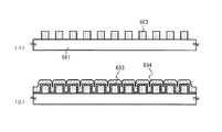
[実施の形態12]
本実施の形態では、実施の形態3において第2絶縁膜303を形成するにあたって、ガラス基板301をエッチングストッパーとして用い、第2絶縁膜303上に第1絶縁膜302に相当する絶縁膜(第3絶縁膜305をも兼ねる。)を形成する例を示す。
【0169】
図29(A)において、まずガラス基板601上に酸化珪素又は酸窒化珪素で所定の形状で凹部が形成された第2絶縁膜602を形成する。詳細は、実施の形態3と同様である。凹部の形成は、ウェットエッチングでもドライエッチングでも良いが、本実施の形態では、CHF3ガスを用いたドライエッチングを用いる。この場合、ガス流量は30〜40sccm、反応圧力は2.7〜4.0KPa、印加電力は500W、基板温度は20℃とすれば良い。
【0170】
また、本実施の形態の場合、ガラス基板601としては、酸化珪素膜との選択比の高い材質(例えば、コーニング社製1737ガラス基板等)を用いることが好ましい。選択比が高ければ第2絶縁膜602の形成にあたって、ガラス基板601をそのままエッチングストッパーとして用いることが可能だからである。
【0171】
そして、第2絶縁膜602を形成したら、その上を窒化珪素、窒素含有量が酸素含有量よりも大きな酸窒化珪素またはこれらの積層でなる第1絶縁膜603で覆い、さらにその上に非晶質半導体膜604を形成して、図29(B)の状態を得る。これら第1絶縁膜603及び非晶質半導体膜604の詳細については、実施の形態3の記載を参照すれば良い。また、図29(B)以降の工程は、実施の形態3に従えば良いのでここでの説明は省略する。
【0172】
本実施の形態によれば、ガラス基板601と第2絶縁膜602との選択比を十分高く確保することが可能であるため、第2絶縁膜602の凹部を形成する際のプロセスマージンが向上する。また、第2絶縁膜602の下端部におけるえぐれ等の問題も起こることがない。さらに、第2絶縁膜602を設けない部分は、ガラス基板上に窒化珪素膜、窒素含有量が酸素含有量よりも大きな酸窒化珪素またはこれらの積層膜という構成となるため、窒化アルミニウム等の特殊な絶縁膜を用いる必要がない。
【0173】
なお、本実施の形態は、実施の形態1〜11のいずれの構成とも自由に組み合わせて実施することが可能である。
【0174】
[実施例1]
本実施例では、本発明を実施して得た結晶性半導体膜を示す。なお、本実施例は、実施の形態2及び3に従って結晶化工程を行ったので、図6〜8を参照して説明する。
【0175】
本実施例では、図6における第1絶縁膜302として、50nmの厚さの窒酸化珪素膜を用い、第2絶縁膜303として、200nmの厚さの酸窒化珪素膜を用いた。この場合、第2絶縁膜303をエッチングした際に下地の第1絶縁膜302もエッチングされてしまったため、結果的に図1における段差dに相当する高さは250nmとなった。また、第2絶縁膜303の幅(図1におけるW1に相当する)は0.5μmとし、隣接間距離(図1におけるW2に相当する)は0.5μmとした。
【0176】
また、第2絶縁膜303上には第3絶縁膜305として20nmの厚さの酸窒化珪素膜を設けた後、大気解放せずに連続的に非晶質半導体膜306として、150nmの厚さの非晶質珪素膜を形成した。また、非晶質珪素膜は、実施の形態2の結晶化技術を用いて結晶化した。具体的には、10ppmの酢酸ニッケル水溶液を非晶質珪素膜上に保持した状態で550℃4時間の加熱処理を行って結晶化した後、線状のレーザー光を照射した。当該線状レーザー光は、連続発振モードのYVO4レーザー発振器を用い、その第2高調波(波長532nm)の出力5.5Wを光学系にて線状レーザー光に集光し、室温で50cm/secの速度で走査した。
【0177】
図26(A)は、結晶性珪素膜307を形成した状態(図8に示す状態)のTEM(透過型電子顕微鏡)写真であり、図26(B)はその模式図である。第1絶縁膜302と第2絶縁膜303との積層体は、結晶性珪素膜307の下に完全に埋まった状態で存在している。
【0178】
図27(A)は、図26(A)の断面を観察した断面TEM写真であり、図27(B)はその模式図である。ストライプパターンで形成された第2絶縁膜303の間(凹部)には、充填されるように結晶性珪素膜307aが形成され、かつ、第2絶縁膜303の上面部(凸部)には結晶性珪素膜307bが形成されている。
【0179】
図28(A)は、図27(A)の断面を拡大観察した断面TEM写真であり、図28(B)はその模式図である。当該写真では、第3絶縁膜305が観察される。結晶性珪素膜307aの内部には全く結晶粒界や欠陥らしきものが観察されず、極めて高い結晶性を有していることが判る。
【0180】
本発明は、結晶性の良好な結晶性珪素膜307aをチャネル形成領域として用い、かつ、結晶性の劣る結晶性珪素膜307bを積極的に電極または配線として用いることにより高速動作が可能で電流駆動能力の高く、且つ複数の素子間においてばらつきの小さい薄膜トランジスタ又は該薄膜トランジスタ群を高い集積度で集積して構成される半導体装置を提供することができる。
【発明の効果】
以上説明したように、絶縁膜により凹凸形状を有する直線状のストライプパターンを形成し、その上に非晶質半導体膜を堆積し、レーザー光の照射により溶融状態を経て結晶化させることにより凹部に半導体を流し込み凝固させ、凹部以外の領域に結晶化に伴う歪み又は応力を集中させることができ、結晶粒界など結晶性の悪い領域を選択的に形成することが可能となる。
【0181】
そして、トランジスタなどの半導体素子、特にそのチャネル形成領域の場所を指定して、結晶粒界が存在しない結晶性半導体膜を形成することができる。これにより不用意に介在する結晶粒界や結晶欠陥により特性がばらつく要因を無くすことができ、特性ばらつきの小さいトランジスタ又はトランジスタ素子群を形成することができる。
【0182】
以上のように、本発明は、結晶性の良好な結晶半導体膜をチャネル形成領域として用い、かつ、結晶性の劣る結晶性半導体膜を積極的に電極または配線として用いることにより高速動作が可能で電流駆動能力の高く、且つ複数の素子間においてばらつきの小さい半導体素子又は該半導体素子群を高い集積度で集積して構成される半導体装置を提供することができる。
【図面の簡単な説明】
【図1】 本発明の結晶化方法を説明する斜視図。
【図2】 本発明の結晶化方法を説明する斜視図。
【図3】 本発明で結晶化方法を説明する斜視図。
【図4】 本発明の結晶化方法を説明する斜視図。
【図5】 結晶化における開口部の形状と結晶性半導体膜の形態との関係を説明する縦断面図。
【図6】 本発明のトランジスタの作製工程を説明する上面図及び縦断面図。
【図7】 本発明のトランジスタの作製工程を説明する上面図及び縦断面図。
【図8】 本発明のトランジスタの作製工程を説明する上面図及び縦断面図。
【図9】 本発明のトランジスタの作製工程を説明する上面図及び縦断面図。
【図10】 本発明のトランジスタの作製工程を説明する上面図及び縦断面図。
【図11】 本発明のトランジスタの作製工程を説明する上面図及び縦断面図。
【図12】 本発明のトランジスタの作製工程を説明する上面図及び縦断面図。
【図13】 本発明のトランジスタにおいて適用することができるゲート構造の一例を示す縦断面図。
【図14】 本発明のトランジスタの作製工程を説明する上面図及び縦断面図。
【図15】 本発明のトランジスタの作製工程を説明する上面図及び縦断面図。
【図16】 本発明のトランジスタの作製工程を説明する縦断面図。
【図17】 本発明のトランジスタの作製工程を説明する縦断面図。
【図18】 本発明のトランジスタの作製工程を説明する上面図及び縦断面図。
【図19】 本発明の半導体装置の外観図の一例を示す図。
【図20】 本発明の電子装置の具体例を示す図。
【図21】 本発明の実施に使用するレーザー照射装置を示す図。
【図22】 本発明の実施に使用するレーザー光の構成を示す図。
【図23】 本発明を実施して得た結晶性珪素膜のセコ・エッチング後の上面を観察したTEM写真及びその模式図。
【図24】 本発明を実施して得た結晶性珪素膜のセコ・エッチング後の上面を観察したTEM写真及びその模式図。
【図25】 凹部に形成された結晶の配向を示すEBSPマッピングデータ。
【図26】 本発明を実施して得た結晶性珪素膜の上面を観察したTEM写真及びその模式図。
【図27】 本発明を実施して得た結晶性珪素膜の断面を観察したTEM写真及びその模式図。
【図28】 本発明を実施して得た結晶性珪素膜の断面を観察したTEM写真及びその模式図。
【図29】 本発明のトランジスタの作製工程を説明する縦断面図。[0001]
BACKGROUND OF THE INVENTION
The present invention relates to a semiconductor element formed using a semiconductor film having a crystal structure, a manufacturing method thereof, a semiconductor device including a circuit in which the semiconductor element is integrated, and a manufacturing method thereof. In particular, the present invention relates to a field effect transistor (typically a thin film transistor) in which a channel formation region is formed using a crystalline semiconductor film formed over an insulating surface as a semiconductor element, a thin film diode using the crystalline semiconductor film, and the like.
[0002]
[Prior art]
A technique for forming an amorphous silicon film on an insulating substrate made of glass or the like and crystallizing the film to form a semiconductor element such as a transistor has been developed. In particular, a technique for crystallizing an amorphous silicon film by irradiating a laser beam is applied to a manufacturing technique of a thin film transistor (TFT). A transistor manufactured using a semiconductor film having a crystal structure (crystalline semiconductor film) is applied to a flat display device (flat panel display) typified by a liquid crystal display device.
[0003]
Applications of laser light in semiconductor manufacturing processes include technologies for recrystallizing damaged layers and amorphous layers formed on semiconductor substrates or semiconductor films, and technologies for crystallizing amorphous semiconductor films formed on insulating surfaces. Has been deployed. As a laser oscillation device to be applied, a gas laser typified by an excimer laser or a solid-state laser typified by a YAG laser is usually used.
[0004]
An example of crystallization of an amorphous semiconductor film by laser light irradiation is that the scanning speed of the laser light is set to a beam spot diameter x 5000 / second or more without causing the amorphous semiconductor film to be in a completely molten state by high-speed scanning. Some are polycrystallized (for example, see Patent Document 1). In addition, there is a technique in which a semiconductor film formed in an island shape is irradiated with an extended laser beam to substantially form a single crystal region (see, for example, Patent Document 2). Or the method of processing and irradiating a beam linearly with an optical system like a laser processing apparatus is known (for example, refer patent document 3).
[0005]
[Patent Document 1]
JP 62-104117 A
[Patent Document 2]
U.S. Pat.No. 4,330,363
[Patent Document 3]
JP-A-8-195357
[0006]
Furthermore, Nd: YVO Four Using a solid-state laser oscillation device such as a laser, the amorphous semiconductor film is irradiated with laser light, which is the second harmonic, to form a crystalline semiconductor film having a larger crystal grain size than before, and a transistor is manufactured. There is a technique (for example, refer to Patent Document 4).
[0007]
[Patent Document 4]
JP 2001-144027 A
[0008]
[Problems to be solved by the invention]
However, when an amorphous semiconductor film formed on a flat surface is crystallized by irradiating it with laser light, the crystal becomes polycrystals, and defects such as crystal grain boundaries are arbitrarily formed to align crystals with uniform orientation. Couldn't get.
[0009]
The crystal grain boundary contains crystal defects, which become carrier traps and cause the mobility of electrons or holes to decrease. In addition, a semiconductor film free from strain or crystal defects could not be formed due to volume shrinkage of the semiconductor film accompanying crystallization, thermal stress with the base, or lattice mismatch. Therefore, without a special method such as bonding SOI (Silicon on Insulator), it is equivalent to a MOS transistor formed on a single crystal substrate with a crystalline semiconductor film formed on an insulating surface and crystallized or recrystallized. Could not get the quality.
[0010]
The above-described flat display device or the like forms a transistor by forming a semiconductor film on a glass substrate, but it is almost impossible to arrange the transistor so as to avoid an arbitrarily formed crystal grain boundary. . In other words, the crystallinity of the channel formation region of the transistor is strictly controlled, and the grain boundaries and crystal defects that are included unintentionally cannot be excluded. As a result, not only the electrical characteristics of the transistors are inferior, but also the characteristics of individual elements vary.
[0011]
In particular, when a crystalline semiconductor film is formed using laser light on an alkali-free glass substrate that is widely used in industry, the focus of the laser light varies due to the influence of the undulation of the alkali-free glass substrate itself. However, there is a problem that the crystallinity varies. Furthermore, in order to avoid contamination with alkali metals, an alkali-free glass substrate needs to be provided with a protective film such as an insulating film as a base film, and a crystalline semiconductor film from which crystal grain boundaries and crystal defects have been eliminated is large. It was almost impossible to form with a particle size.
[0012]
The present invention has been made in view of the above problems, and a crystalline semiconductor film having no crystal grain boundary at least in a channel formation region is formed on an insulating surface, particularly on an insulating surface using a glass substrate as a supporting base, An object of the present invention is to provide a semiconductor device including a semiconductor element or a group of semiconductor elements that can operate at high speed, has high current driving capability, and has little variation among a plurality of elements.
[0013]
[Means for Solving the Problems]
In order to solve the above-described problems, the present invention forms an insulating film provided with concave and convex portions extending in a linear stripe pattern on a substrate having an insulating surface, and the amorphous film is formed on the insulating film. A semiconductor film is formed, a crystalline semiconductor film is formed by melting and pouring the semiconductor film into a portion corresponding to a concave portion of the insulating film (hereinafter simply referred to as a concave portion), and crystallizing an unnecessary region. A crystalline semiconductor film in which a crystalline semiconductor film divided into islands from a crystalline semiconductor film (which will later become a part of a semiconductor element) is formed, and at least a portion for forming a channel formation region is formed in the above-described recess. As described above, a gate insulating film and a gate electrode are provided on the crystalline semiconductor film.
[0014]
Of the insulating film provided with a portion corresponding to the concave portion or the convex portion (hereinafter simply referred to as a convex portion), the crystalline semiconductor film formed on the convex portion has a crystallinity formed in the concave portion. Although inferior to a semiconductor film, in the present invention, a crystalline semiconductor film formed over the convex portion is positively used as an electrode (in the case of a thin film transistor, corresponds to a source region or a drain region) or a wiring. It is characterized by. When used as a wiring, since the degree of freedom in designing the occupied area is high, the wiring length can be adjusted to be used as a resistor, or a bent shape can be provided as a protective circuit function.
[0015]
The aforementioned recess may be formed by directly etching the surface of the insulating substrate, or a recess may be formed by etching a silicon oxide, silicon nitride, or silicon oxynitride film. The recess is preferably formed in accordance with the arrangement of the semiconductor element, particularly the island-shaped semiconductor film including the channel formation region of the transistor, and is preferably formed so as to match at least the channel formation region. The recess is provided so as to extend in the channel length direction. The recess is formed with a width (channel width direction in the case of a channel formation region) of 0.01 μm to 2 μm, preferably 0.1 to 1 μm, and a depth of 0.01 μm to 3 μm, preferably 0. It is formed at 1 μm or more and 2 μm or less.
[0016]
Of course, it is also possible to form an island-shaped insulating film on the insulating surface and positively form a convex portion. In that case, the convex portion extending in a plurality of linear stripe patterns forms a portion that is relatively a concave portion between adjacent ones, so that the concave portion includes an island-shaped semiconductor including a channel formation region of a semiconductor element. What is necessary is just to form according to arrangement | positioning of a film | membrane, and it is sufficient to keep the width within the aforementioned range.
[0017]
In the first stage, the semiconductor film formed over the insulating film and over the recess is an amorphous semiconductor film or a polycrystalline semiconductor film formed by plasma CVD, sputtering, or low pressure CVD, or a multi-layer formed by solid phase growth. A crystalline semiconductor film or the like is applied. Note that the amorphous semiconductor film referred to in the present invention is not limited to a film having a completely amorphous structure in a narrow sense, but includes a state in which fine crystal particles are included, or a so-called microcrystalline semiconductor film, local Includes a semiconductor film including a crystal structure. Typically, an amorphous silicon film is applied, and in addition, an amorphous silicon germanium film, an amorphous silicon carbide film, or the like can also be applied. The polycrystalline semiconductor film is obtained by crystallizing these amorphous semiconductor films by a known method.
[0018]
As a means for melting and crystallizing the crystalline semiconductor film, pulsed oscillation or continuous oscillation laser light using a gas laser oscillation device or a solid laser oscillation device as a light source is applied. The laser light to be irradiated is focused in a linear shape by an optical system, and the intensity distribution may have a uniform region in the longitudinal direction and may be distributed in the lateral direction. As the oscillation device, a rectangular beam solid laser oscillation device is applied, and a slab laser oscillation device is particularly preferably applied. Alternatively, it is a solid state laser oscillation device using a rod doped with Nd, Tm, and Ho, especially YAG, YVO. Four , YLF, YAlO Three A slab structure amplifier may be combined with a solid-state laser oscillation device using a crystal doped with Nd, Tm, or Ho. As the slab material, crystals such as Nd: YAG, Nd: GGG (gadolinium / gallium / garnet), Nd: GSGG (gadolinium / scandium / gallium / garnet) are used. A slab laser travels in a zigzag optical path through this plate-like laser medium while repeating total reflection.
[0019]
Moreover, you may irradiate the strong light according to it. For example, light having a high energy density obtained by condensing light emitted from a halogen lamp, xenon lamp, high-pressure mercury lamp, metal halide lamp, or excimer lamp by a reflecting mirror or a lens may be used.
[0020]
Laser light or strong light condensed in a linear shape and extended in the longitudinal direction irradiates the crystalline semiconductor film, and relatively moves the irradiation position of the laser light and the substrate on which the crystalline semiconductor film is formed, The crystalline semiconductor film is melted by scanning a part or the entire surface of the laser beam, and crystallization or recrystallization is performed through this state. The scanning direction of the laser light is performed along the longitudinal direction of the recess formed in the insulating film and extending in a linear stripe pattern or the channel length direction of the transistor. As a result, the crystal grows along the scanning direction of the laser beam, and the crystal grain boundary can be prevented from crossing the channel length direction.
[0021]
Laser light irradiation is typically from the upper surface side of the semiconductor film, but irradiation from the lower surface side (substrate side), irradiation from the upper surface side oblique direction or lower surface side oblique direction, or upper surface side and lower surface. The irradiation may be performed by any irradiation method (including irradiation from an oblique direction) from both sides.
[0022]
As another configuration, the crystalline semiconductor film is provided over a glass or quartz substrate on a metal layer including one or more kinds selected from W, Mo, Ti, Ta, and Cr, and the crystalline property of the metal layer An insulating layer may be interposed between the semiconductor film and the semiconductor film. Alternatively, a metal layer containing one or more selected from W, Mo, Ti, Ta, and Cr is provided on a glass or quartz substrate, and an insulating layer made of aluminum nitride or aluminum oxynitride is provided on the metal layer. Further, a structure in which a crystalline semiconductor film is provided thereover may be employed. The metal layer formed here can function as a light-shielding film that blocks light incident on the channel formation region, or a specific potential can be applied to control the spread of the fixed charge or the depletion layer. Moreover, the function as a heat sink which dissipates Joule heat can also be provided.
[0023]
By setting the depth of the recesses to be equal to or greater than the thickness of the semiconductor film, the semiconductor film melted by irradiation with laser light or strong light aggregates and solidifies in the recesses due to surface tension. As a result, the thickness of the semiconductor film on the convex portion of the insulating film is reduced, and stress strain can be concentrated there. The side surface of the recess has the effect of defining the crystal orientation to some extent.
[0024]
When the semiconductor film is melted, it is agglomerated in the recesses formed on the insulating surface by surface tension, and the crystal growth from the approximate intersection of the bottom and side surfaces of the recesses concentrates the strain generated by crystallization in the region other than the recesses. Can be made. That is, the crystalline semiconductor region (first crystalline semiconductor region) formed so as to be filled in the concave portion can be released from strain. The crystalline semiconductor region (second crystalline semiconductor region) remaining on the insulating film and containing crystal grain boundaries and crystal defects is a portion other than the channel formation region of the semiconductor element, typically a source region or a drain. Used as a region.
[0025]
Then, after forming a crystalline semiconductor film having no crystal grain boundary in the recess, an active layer (semiconductor layer functioning as a carrier movement path) of the semiconductor element is formed by patterning, and a gate insulating film in contact with the active layer is formed Further, a gate electrode is formed. Thereafter, a field effect transistor can be formed by a known method.
[0026]
According to the present invention, it is possible to designate a semiconductor element such as a transistor, particularly a region where a channel formation region thereof is formed, and form a crystalline semiconductor region where no crystal grain boundary exists in the region. As a result, it is possible to eliminate the factor that the characteristics vary due to inadvertently interposed crystal grain boundaries and crystal defects. In other words, it is possible to form a semiconductor device including a semiconductor element or a group of semiconductor elements that can operate at high speed, have high current driving capability, and have little variation among a plurality of elements.
[0027]
DETAILED DESCRIPTION OF THE INVENTION
[Embodiment 1]
Hereinafter, embodiments of manufacturing a thin film transistor using the present invention will be described with reference to the drawings. The perspective view shown in FIG. 1 shows a form in which the first insulating
[0028]
As the substrate, a commercially available non-alkali glass substrate, a quartz substrate, a sapphire substrate, a substrate obtained by coating the surface of a single crystal or polycrystalline semiconductor substrate with an insulating film, or a substrate obtained by coating the surface of a metal substrate with an insulating film can be applied. In order to form a linear stripe pattern with a sub-micron design rule, it is desirable that the unevenness of the substrate surface, the waviness or twist of the substrate be less than the depth of focus of the exposure apparatus (particularly the stepper). Specifically, the waviness or twist of the substrate is 1 μm or less, preferably 0.5 μm or less in one exposure light irradiation region. In this regard, care must be taken particularly when an alkali-free glass is used as the support substrate.
[0029]
The width W1 of the second insulating film formed in the linear stripe pattern is 0.1 to 10 μm (preferably 0.5 to 1 μm), and the distance W2 between the adjacent second insulating films is 0.01 to 2 μm ( Preferably, the thickness d of the second insulating film is 0.01 to 3 μm (preferably 0.1 to 2 μm). Furthermore, the relationship with the film thickness t02 in the concave portion of the amorphous semiconductor film provided so as to cover the second insulating film may be d ≧ t02, but if d is too thick compared to t02, Care must be taken because the crystalline semiconductor film does not remain.
[0030]
The step shape need not be a regular periodic pattern, and may be arranged at different intervals in accordance with the width of the island-shaped semiconductor film. The length L is not particularly limited numerically, and can be formed so as to extend from one end to the other end of the substrate. For example, the length L can be formed so that a channel formation region of a transistor can be formed. It is also possible.
[0031]
The first
[0032]
As the silicon oxynitride (SiOxNy) film, a film containing Si at 25 to 35 atomic%, oxygen at 55 to 65 atomic%, nitrogen at 1 to 20 atomic%, and hydrogen at 0.1 to 10 atomic%. Use it. Further, as a silicon oxynitride (SiNxOy) film, a film containing Si of 25 to 35 atomic%, oxygen of 15 to 30 atomic%, nitrogen of 20 to 35 atomic%, and hydrogen of 15 to 25 atomic% may be used. good. As the aluminum oxynitride (AlOxNy) film, a film containing Al at 30 to 40 atomic%, oxygen at 50 to 70 atomic%, and nitrogen at 1 to 20 atomic% may be used. Also Nitro As the aluminum oxide (AlNxOy) film, a film containing Al in an amount of 30 to 50 atomic%, oxygen in an amount of 30 to 40 atomic%, and nitrogen in an amount of 10 to 30 atomic% may be used.
[0033]
The second insulating
[0034]
As shown in FIG. 1, in the case of forming a linear stripe pattern with two insulating films, it is necessary to provide a selection ratio between the first insulating
[0035]
Note that as the second insulating
[0036]
Next, as shown in FIG. 2, an
[0037]
As shown in the figure, the
[0038]
Then, the
[0039]
Note that, at the time of crystallization, it is preferable that a position where a marker used for patterning mask alignment is formed after the end of the substrate is not crystallized. This is because a crystalline semiconductor film (especially a crystalline silicon film) has a higher visible light transmittance when crystallized, so that it is difficult to identify it as a marker. However, there is no problem when performing the type of alignment control for optically identifying the difference in contrast due to the level difference of the marker.
[0040]
As the laser oscillation device, a rectangular beam solid state laser oscillation device is applied, and a slab laser oscillation device is particularly preferably applied. As the slab material, crystals such as Nd: YAG, Nd: GGG (gadolinium / gallium / garnet), Nd: GSGG (gadolinium / scandium / gallium / garnet) are used. A slab laser travels in a zigzag optical path through this plate-like laser medium while repeating total reflection. Alternatively, it is a solid state laser oscillation device using a rod doped with Nd, Tm, and Ho, especially YAG, YVO. Four , YLF, YAlO Three A slab structure amplifier may be combined with a solid-state laser oscillation device using a crystal doped with Nd, Tm, or Ho.
[0041]
Then, as indicated by arrows in FIG. 3, the second insulating
[0042]
The wavelength of the continuous wave laser beam is preferably 400 to 700 nm in consideration of the light absorption coefficient of the amorphous semiconductor film. Light in such a wavelength band is obtained by taking out the second harmonic and the third harmonic of the fundamental wave using a wavelength conversion element. As wavelength conversion element, ADP (ammonium dihydrogen phosphate), Ba 2 NaNb Five O 15 (Sodium barium niobate), CdSe (selenium cadmium), KDP (potassium dihydrogen phosphate), LiNbO Three (Lithium niobate), Se, Te, LBO, BBO, KB5 and the like are applied. It is particularly desirable to use LBO. A typical example is Nd: YVO Four The second harmonic (532 nm) of the laser oscillation device (fundamental wave 1064 nm) is used. The laser oscillation mode is TEM 00 Apply single mode.
[0043]
In the case of silicon selected as the most suitable material, the absorption coefficient is 10 Three -10 Four cm -1 The region which is is almost in the visible light region. When crystallizing a substrate having a high visible light transmittance such as glass and an amorphous semiconductor film formed with a thickness of 30 to 200 nm using silicon, by irradiating light in the visible light region with a wavelength of 400 to 700 nm, Crystallization can be performed without selectively damaging the base insulating film by selectively heating the semiconductor film. Specifically, the penetration depth of light having a wavelength of 532 nm is approximately 100 nm to 1000 nm with respect to the amorphous silicon film, and can sufficiently reach the inside of the
[0044]
The laser beam is scanned in a direction parallel to the direction in which the linear stripe pattern extends, and the melted semiconductor flows into the concave portion due to surface tension and solidifies. In the solidified state, the surface becomes almost flat as shown in FIG. This is because once the semiconductor is melted, the interface between the melted semiconductor and the gas phase reaches an equilibrium state, whether on the convex portion or the concave portion, and a flat interface is formed. Further, the crystal growth edge and the crystal grain boundary are formed on the second insulating film (on the convex portion) (
[0045]
After that, heat treatment is preferably performed at 500 to 600 ° C. to remove distortion accumulated in the crystalline semiconductor film. This distortion occurs due to semiconductor volume shrinkage caused by crystallization, thermal stress with the base, or lattice mismatch. This heat treatment may be performed using a normal heat treatment apparatus. For example, a gas heating rapid thermal annealing (RTA) method may be used for 1 to 10 minutes. Note that this step is not an essential requirement in the present invention, and may be appropriately selected.
[0046]
Thereafter, as shown in FIG. 4, the
[0047]
The
[0048]
FIG. 5 is a conceptual diagram showing the knowledge of crystallization obtained from the experimental results by the present inventors. 5A to 5E schematically illustrate the relationship between crystal growth and the depth and interval of the recesses formed by the first insulating film and the second insulating film.
[0049]
5, t01: thickness of the amorphous semiconductor film on the second insulating film (convex portion), t02: thickness of the amorphous semiconductor film in the concave portion, t11: second Thickness of crystalline semiconductor film on insulating film (convex portion), t12: Thickness of crystalline semiconductor film in concave portion, d: Thickness of second insulating film (depth of concave portion), W1: Second insulating film , W2: the width of the recess.
[0050]
FIG. 5A shows a case where d <t02, W1, W2 is about 1 μm or less, and when the depth of the recess is smaller than that of the
[0051]
FIG. 5B shows a case where d ≧ t02 and W1 and W2 are approximately equal to or less than 1 μm. In the case where the depth of the recess is substantially equal to or greater than that of the amorphous semiconductor film 203, FIG. The surface tension works and collects in the recess. In the solidified state, the surface becomes almost flat as shown in FIG. In this case, t11 <t12, stress concentrates on the
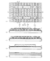
[0052]
The scanning electron microscope (SEM) photograph shown in FIG. 23 (A) shows an example of the state of FIG. 5 (B). On the base insulating film provided with a step of 170 nm and a width and interval of a convex part of 0.5 μm. The result of crystallization by forming an amorphous silicon film of 150 nm is shown. Further, the surface of the crystalline semiconductor film is a seco liquid (HF: H) which is generally known to make the crystal grain boundary manifest. 2 O = 2: 1 K as additive 2 Cr 2 O 7 Etching (also called Seco-etching) with chemicals prepared using
[0053]
The results shown in FIG. 23 indicate that potassium dichromate (K 2 Cr 2 O 7 ) 2.2 g was dissolved in 50 cc of water to prepare a 0.15 mol / l solution, and 100 cc of hydrofluoric acid solution was added to the solution, which was further diluted 5-fold with water, and used as the secco solution. Further, the conditions for the secco etching were 75 seconds at room temperature (10 to 30 ° C.). In this specification, the term “seco liquid” or “seco etching” refers to the solution and conditions described here.
[0054]
FIG. 23B is a schematic diagram of the photograph in FIG. In the figure, reference numeral 31 denotes an insulating film (second insulating film) extending in a linear stripe pattern, and crystal grain boundaries 33 clarified by Secco etching are intensively generated on the convex portions 32. I can see how they are. Note that the region 34 described as the disappearing portion is a region corresponding to the starting point of the stripe pattern, and the scanning of the laser beam is started from this starting point. Although the detailed reason is unknown, the silicon film on the starting point is a region where the second insulating film located at the starting point has been exposed by being pushed in the scanning direction when melted. Since the Seco solution etches the silicon oxide film, the region located at the starting point has disappeared by Seco etching.
[0055]
By the way, when compared with the photograph shown in FIG. 23A, the crystalline semiconductor film formed in the recess 35 does not have crystal grain boundaries or defects that are clarified by Secco etching. If it does, it turns out that it does not exist substantially. Although the grain boundaries that are clarified by Secco etching have not been identified at present, it is a well-known fact that stacking faults and grain boundaries are preferentially etched by Seco etching, and the present invention is It can be said that the crystalline semiconductor film obtained by the implementation has a great feature in that there is substantially no crystal grain boundary or defect which becomes apparent by Secco etching.
[0056]
Of course, since it is not a single crystal, there may naturally be grain boundaries and defects that do not appear by Secco etching. However, such grain boundaries and defects do not affect the electrical characteristics when semiconductor devices are manufactured. It is considered electrically inactive. In general, such an electrically inactive grain boundary is called a planar grain boundary (low-order or higher-order twin or corresponding grain boundary), and is not manifested by Secco etching. Is presumed to be a planar grain boundary. From this point of view, it can be said that substantially no crystal grain boundaries or defects exist, it can be said that there are no crystal grain boundaries other than planar grain boundaries.
[0057]
FIG. 25 shows the result of obtaining the orientation of the crystalline semiconductor film formed in the recess 35 shown in FIG. 23B by a reflected electron diffraction pattern (EBSP). EBSP provides a scanning electron microscope (SEM) with a dedicated detector, which irradiates the crystal plane with an electron beam and causes the computer to recognize the crystal orientation from the Kikuchi line. The crystallinity is measured not only on the surface orientation but also in all directions of the crystal (hereinafter, this method is referred to as EBSP method for convenience).
[0058]
The data in FIG. 25 indicates that the crystal grows in the concave portion 35 in a direction parallel to the scanning direction of the laser beam condensed linearly. As for the crystal orientation of growth, the <110> orientation is dominant (that is, the main orientation plane is the {110} plane), but growth of the <100> orientation also exists.
[0059]
FIG. 5C shows a case in which d ≧ t02 and W1 and W2 are approximately the same as or slightly larger than 1 μm. When the width of the concave portion increases, the
[0060]
FIG. 5D shows a case where d ≧ t02 and W1 and W2 are larger than 1.0 μm, and the state of FIG. This condition is not preferable because a crystal grain boundary is generated in the semiconductor region serving as the channel formation region with a considerable probability.
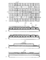
[0061]
The scanning electron microscope (SEM) photograph shown in FIG. 24 (A) shows an example of the state of FIG. 5 (D). On the base insulating film provided with a step of 170 nm and a width and interval of a projection of 1.8 μm. The result of crystallization by forming an amorphous silicon film of 150 nm is shown. The surface of the crystalline semiconductor film is etched with the aforementioned Seco solution in order to reveal the crystal grain boundaries.
[0062]
FIG. 24B is a schematic diagram of the photograph in FIG. In the figure, reference numeral 41 denotes an insulating film (second insulating film) extending in a linear stripe pattern, and crystal grain boundaries 43 clarified by secco etching are concentrated on the convex portions 42 and the end portions thereof. I can see how it is occurring. Note that the region 44 described as the disappearing portion is a region corresponding to the start point of the stripe pattern, and has disappeared by the secco etching for the reason described above. Compared with the photograph shown in FIG. 24A, the crystal grain boundary is generated not only in the convex portion 42 of the stripe pattern but also in the concave portion 45.
[0063]
FIG. 5E shows a reference example in the present invention, where d >> t02 and W1 and W2 are 1 μm or less. That is, when the thickness d of the second insulating film is too thick compared with the thickness t02 of the amorphous semiconductor film in the concave portion, the
[0064]
As described above with reference to FIGS. 5A to 5D, when a semiconductor element is formed, particularly when a channel formation region in a thin film transistor is formed, the configuration in FIG. 5B is most suitable. It is thought that there is. That is, a crystalline semiconductor film in which almost no crystal grain boundaries or defects become apparent when performing the seco-etching with the above-mentioned secco solution, in other words, a crystalline semiconductor film substantially free of crystal grain boundaries and defects is formed. It is desirable to use it for the channel formation region.
[0065]
In addition, although the example in which the uneven shape of the base for forming the crystalline semiconductor film is formed using the first insulating film and the second insulating film is shown here, it is not limited to the form shown here and has a similar shape. It can be replaced if there is one. For example, a recess having a desired depth may be formed by etching an insulating film having a thickness of about 200 nm to 2 μm.
[0066]
In the crystallization step, if the second insulating film is a soft insulating film (insulating film having a low density) as described above, an effect of relaxing stress due to shrinkage of the semiconductor film during crystallization is expected. it can. On the other hand, if a hard insulating film (insulating film with high density) is used, stress is generated against the semiconductor film that is about to shrink or expand, so that it is easy to leave stress strain or the like in the semiconductor film after crystallization. It may also cause For example, in the known graphoepitaxy technology (“MWGeis, DCFlanders, HISmith: Appl. Phys. Lett. 35 (1979) pp71”), the irregularities on the substrate are directly formed of hard quartz glass. It has been found that the orientation axis of Si is the [100] axis, that is, the main orientation plane is the {100} plane.
[0067]
However, when the present invention is carried out, the main orientation plane is {110} as shown in FIG. 25, and it can be seen that semiconductor films having clearly different crystal forms are formed. The difference is because the unevenness on the substrate is a soft insulating film formed by the above-described CVD method or PVD method. That is, by making the second insulating film serving as a base softer than quartz glass, the generation of stress during crystallization can be more relaxed, or stress can be concentrated on the crystalline semiconductor film on the convex portion. did it.
[0068]
The meaning of an insulating film that is softer than quartz glass means, for example, an insulating film having a higher etching rate or a higher hardness than general quartz glass (quartz glass that is industrially used as a substrate). . Quartz glass with ammonium hydrogen fluoride (NH Four HF 2 ) 7.13% and ammonium fluoride (NH Four As a result of wet etching using a mixed solution containing 15.4% of F) (product name: LAL500, manufactured by Stella Chemifa Co., Ltd.) as an etchant, the etching rate of the quartz substrate was 38 nm / min. On the other hand, since the etching rate of the second insulating film serving as the base by the etchant is 50 to 1000 nm / min, it can be said that the insulating film is softer than quartz glass. Since these etching rates and hardness can be determined by relative comparison with quartz glass, they do not depend on the etching rate measurement conditions or the hardness measurement conditions.
[0069]
For example, if a silicon oxynitride film is used as the second insulating film, SiH Four Gas, N 2 A silicon oxynitride film formed by a plasma CVD method using O gas as a raw material is preferable. The silicon oxynitride film is made of ammonium hydrogen fluoride (NH Four HF 2 ) 7.13% and ammonium fluoride (NH Four The etching rate at 20 ° C. of the mixed aqueous solution containing 15.4% of F) is 110 to 130 nm / min (500 ° C., 1 hour + 550 ° C., after 4 hours of heat treatment, 90 to 100 nm / min).
[0070]
If a silicon oxynitride film is used as the second insulating film, SiH Four Gas, NH Three Gas, N 2 A silicon oxynitride film formed by a plasma CVD method using O gas as a raw material is preferable. The silicon nitride oxide film is made of ammonium hydrogen fluoride (NH Four HF 2 ) 7.13% and ammonium fluoride (NH Four The etching rate at 20 ° C. of the mixed aqueous solution containing 15.4% of F) is 60 to 70 nm / min (40 to 50 nm / min after heat treatment at 500 ° C., 1 hour + 550 ° C. for 4 hours).
[0071]
As described above, a linear stripe pattern having recesses and projections is formed by an insulating film, an amorphous semiconductor film is deposited thereon, and crystallized through a molten state by irradiation with laser light, thereby forming recesses. The semiconductor is poured and solidified, so that strain or stress accompanying crystallization can be concentrated in a region other than the concave portion, and a region having poor crystallinity such as a crystal grain boundary can be selectively formed. A feature of the present invention is that a semiconductor region with good crystallinity is used as a region where carrier movement is performed, such as a channel formation region of a thin film transistor, and a semiconductor region with poor crystallinity is used as a contact portion with an electrode.
[0072]
That is, a crystalline semiconductor film in which a plurality of crystal grains extending in a direction parallel to a direction in which a linear stripe pattern extends is formed without a crystal grain boundary having a plurality of crystal orientations in a recess Can be formed. By forming a transistor so that a channel formation region is formed using such a crystalline semiconductor film, a transistor or a transistor group that can operate at high speed, has high current driving capability, and has little variation among a plurality of elements. The semiconductor device comprised by this can be formed.
[0073]
[Embodiment 2]
In the formation of the crystalline semiconductor film of the present invention, in addition to the method of crystallizing the amorphous semiconductor film by irradiating the amorphous semiconductor film as shown in
[0074]
For example, after the
[0075]
Regarding this technique, Japanese Patent Application Laid-Open No. 11-354442 by the present applicant is detailed. A crystalline semiconductor film formed by adding Ni has a feature that a main orientation plane is a {110} plane. When such a crystalline semiconductor film is used for a channel formation region of a thin film transistor, electron mobility and Both the hole mobility is greatly improved, and the field effect mobility of the N-channel transistor and the P-channel transistor is greatly improved. In particular, the improvement of the field effect mobility of the P-channel transistor accompanying the improvement of the hole mobility is notable and is one of the advantages of setting the main orientation plane to {110}.
[0076]
Further, there is no limitation on the addition method of Ni, and a spin coating method, a vapor deposition method, a sputtering method, or the like can be applied. In the case of the spin coating method, an aqueous solution containing 5 ppm of nickel acetate is applied to form a metal element-containing layer. Of course, the catalyst element is not limited to Ni, and other known materials may be used.
[0077]
Thereafter, the
[0078]
The advantage of using a crystallized semiconductor film as an object to be irradiated with laser light is the fluctuation rate of the light absorption coefficient of the semiconductor film. Even if the crystallized semiconductor film is melted by irradiation with laser light, the light absorption coefficient is Almost no change. Therefore, a wide margin of laser irradiation conditions can be taken.
[0079]
A metal element remains in the crystalline semiconductor film thus formed, but can be removed by gettering treatment. For details of this technique, refer to Japanese Patent Application No. 2001-019367 (or Japanese Patent Application No. 2002-020801). Further, the heat treatment accompanying the gettering treatment has an effect of alleviating distortion of the crystalline semiconductor film.
[0080]
After that, as in
[0081]
[Embodiment 3]
Next, one embodiment of a transistor in which a crystalline silicon film is formed over a base insulating film having a recess and a channel formation region is provided in a semiconductor region formed in the recess in this embodiment is illustrated in the drawings. It explains using. Note that, in each drawing according to the present embodiment, (A) is a top view, and (B) and subsequent drawings are longitudinal sectional views of corresponding parts.
[0082]
In FIG. 6, a first
[0083]
Next, as shown in FIG. 7, a third
[0084]
Crystallization is performed by irradiating a continuous wave laser beam. FIG. 8 shows the state after the crystallization. The crystallization conditions are YVO in continuous oscillation mode. Four Using a laser oscillator, the output of 5 to 10 W of the second harmonic (wavelength 532 nm) is condensed into linear laser light having a ratio of the longitudinal direction to the transverse direction of 10 or more in the optical system, and the longitudinal direction. Are condensed so as to have a uniform energy density distribution, and are crystallized by scanning at a speed of 5 to 200 cm / sec. A uniform energy density distribution does not exclude anything that is completely constant, but the allowable range in the energy density distribution is ± 10%.
[0085]
It is desirable that the intensity distribution of the laser light collected in a linear shape is uniform in the long length direction (X-axis direction in FIG. 3). The purpose of this is to make the temperature of the semiconductor to be heated uniform throughout the laser light irradiation region. This is because if the temperature distribution is generated in the X-axis direction of the laser light that is condensed linearly, the crystal growth direction of the semiconductor film cannot be defined as the scanning direction of the laser light. By aligning the linear stripe pattern with the scanning direction of the irradiation region of the laser beam focused in a linear manner, the crystal growth direction can be matched with the channel length direction of all transistors. . Thereby, the characteristic variation between the elements of the transistor can be reduced.
[0086]
Further, the crystallization by the laser beam condensed linearly may be completed by only one scan (that is, one direction), or may be reciprocated to improve the crystallinity. Furthermore, after crystallizing with laser light, the surface of the silicon film is treated with an alkaline solution such as oxide removal with hydrofluoric acid or ammonia hydrogen peroxide solution treatment, and the poor quality part with high etching rate is selectively used. It may be removed and the same crystallization treatment may be performed again. In this way, crystallinity can be increased.
[0087]
By irradiating with laser light under these conditions, the amorphous semiconductor film is instantaneously melted and crystallized. In practice, crystallization proceeds while the melting zone moves. The molten silicon is agglomerated and solidified in the recesses due to surface tension. As a result, as shown in FIG. 8, a
[0088]
After that, as shown in FIG. 9, the
[0089]
The
[0090]
As an etching method, CF Four And O 2 Mixed gas and NF Three It may be performed by a plasma etching method using a gas, or ClF. Three Plasmaless gas etching using a gas such as a halogen fluoride gas without being excited may be performed. Plasmaless gas etching is an effective technique for suppressing crystal defects because it does not cause plasma damage to the crystalline semiconductor film.
[0091]
Next, as shown in FIG. 10, a fourth insulating film (functioning as a gate insulating film) 311 so as to cover the upper surfaces of the semiconductor regions 308 to 310 and the second
[0092]
In order to improve the coverage of the gate insulating film, a silicon oxide film using TEOS is preferable for a silicon oxide film, and an aluminum nitride oxide film formed by RF sputtering is used for an aluminum nitride oxide film, or the nitride A stacked film of an aluminum oxide film and a silicon oxide film (a silicon oxide film may be obtained by oxidizing a semiconductor film serving as an active layer with hydrogen peroxide) may be used.
[0093]
The
[0094]
Next, as shown in FIG. 11,
[0095]
For the
[0096]
At this time, among the semiconductor regions 308 to 310, the
[0097]
Then, as shown in FIG. 12, a fifth insulating film (functioning as a passivation film) 321 made of a silicon nitride film or silicon oxynitride film containing hydrogen of about 50 to 100 nm is formed. By performing heat treatment at 400 to 450 ° C. in this state, hydrogen contained in the silicon nitride film or the silicon oxynitride film is released, and the island-shaped semiconductor film can be hydrogenated.
[0098]
Next, a sixth insulating film (functioning as an interlayer insulating film) 322 formed of a silicon oxide film or the like is formed, and wirings 323 to 327 connected to the
[0099]
In the n-
[0100]
[Embodiment 4]
In Embodiment 3, the transistor has a single drain structure; however, a lightly doped drain (LDD) may be provided. FIG. 13 shows an example of an n-channel multichannel transistor having an LDD structure.
[0101]
The structure of the transistor illustrated in FIG. 13A is an example in which a gate electrode is formed using a nitride metal 340a such as titanium nitride or tantalum nitride and a
[0102]
On the other hand, FIG. 13B shows a structure in which the gate electrode 340a is not provided. In this case, an LDD structure is formed.
[0103]
In FIG. 13C, an n-type impurity region 344 for forming an LDD region is formed adjacent to the n-
[0104]
In any case, the structure in which the LDD region is formed in a self-aligned manner by such a gate structure is particularly effective when the design rule is miniaturized. Although a unipolar transistor structure is shown here, a CMOS structure can be formed as in the fourth embodiment.
[0105]
In this embodiment, the configuration other than the configuration of the gate electrode and the LDD region is the same as that of the third embodiment, and detailed description thereof is omitted.
[0106]
[Embodiment 5]
This embodiment is an embodiment different from the structure described in
[0107]
FIG. 14 is used for the description. FIG. 14A is a top view, and FIGS. 14B to 14F are cross-sectional views of corresponding portions. In addition, it is a figure corresponding to the state of FIG. 11 in
[0108]
In FIG. 14A, 401 to 405 are impurity regions of one conductivity type, 401 and 402 are a source region and a drain region of a P-channel transistor, and 403 and 404 are source regions of an N-channel transistor, respectively. , 405 function as drain regions of the N-channel transistor. At this time, the
[0109]
As a feature of the present invention, since a semiconductor region having poor crystallinity can also be used as an electrode, the number of contact portions can be reduced by using as a wiring as in this embodiment, and contact formation can be performed. Therefore, the design margin can be expanded. Therefore, it is very effective particularly when forming a logic circuit that has been miniaturized.
[0110]
Note that this embodiment is merely an example, and in the present invention, a technical idea that an impurity region of one conductivity type can be used as a wiring as well as an electrode is disclosed. Therefore, the effects described in the present embodiment can be obtained even in combination with any technique disclosed in the first to fourth embodiments.
[0111]
[Embodiment 6]
This embodiment is an embodiment different from the structure described in
[0112]
FIG. 15 is used for the description. FIG. 15A is a top view, and FIGS. 15B to 15F are cross-sectional views of corresponding portions. In addition, it is a figure corresponding to the state of FIG. 11 in
[0113]
In FIG. 15A, 411 to 418 are impurity regions of one conductivity type, 411 and 414 are source and drain regions of a P-channel transistor, and 412 and 413 are impurity regions used as wirings. Note that the area occupied by the
[0114]
[0115]
Note that this embodiment is merely an example, and in the present invention, a technical idea that an impurity region of one conductivity type can be used as a wiring as well as an electrode is disclosed. Therefore, it may be combined with any technique disclosed in the first to fifth embodiments.
[0116]
[Embodiment 7]
In the transistor of the present invention, by providing a conductive layer on the lower layer side, a so-called substrate bias can be applied. The method for manufacturing the transistor is in accordance with Embodiment Mode 3, and the difference will be described with reference to FIGS.
[0117]
In FIG. 16A, a silicon nitride film is formed as a first insulating film 802 over a substrate, and a tungsten film 803 is formed thereon by a sputtering method. In particular, when a silicon nitride film is formed by a high frequency sputtering method, a dense film can be formed. The second insulating film 804 is formed using a silicon oxide film. The silicon oxide film forms a recess as shown in the figure by etching, but it can be easily processed because the selectivity with the underlying tungsten film is about 30.
[0118]
Over this, a silicon oxynitride film and an amorphous silicon film 806 are successively formed as a third insulating film 805, and the amorphous semiconductor film 806 is melted and crystallized, as shown in FIG. A silicon film 807 is formed. After that, as shown in FIG. 16C, a channel formation region 808 of the transistor is formed by etching, and a gate insulating film 809 and a gate electrode 810 are formed. Since the gate insulating film 809 is formed over the tungsten film 803, there is no short circuit with the gate electrode 810.
[0119]
In such a mode, when the tungsten film 803 is fixed to the ground potential, variation in threshold voltage of the transistor can be reduced. Further, when the same potential as that of the gate electrode 810 is applied to drive, the on-current can be increased.
[0120]
In order to enhance the heat dissipation effect, an aluminum oxynitride film (or aluminum nitride film) 811 is preferably formed over the tungsten film 803 as shown in FIG. The purpose of providing these films is to ensure the etching selectivity. That is, CHF Three In order to remove the silicon oxide that is the second insulating film 804 with a fluorine-based etching gas and the like, and to prevent the underlying tungsten film 803 from being exposed, the silicon nitride film has a low selectivity, and the aluminum nitride film or the aluminum oxynitride Is suitable.
[0121]
The present embodiment discloses a configuration in which a conductive film is provided under the second insulating film that forms the convex portion and the concave portion to achieve a heat dissipation effect and threshold control during actual operation. Combinations with the configurations disclosed in
[0122]
[Embodiment 8]
In this embodiment, an example in which part of the crystalline semiconductor film 307 (a portion that becomes a channel formation region later) is etched to reduce the thickness before the step of forming the active layer 308 of the thin film transistor in Embodiment 3 is described. Show.
[0123]
First, according to the manufacturing method shown in Embodiment Mode 3, the state shown in FIG. 8 is obtained. Next, a resist
[0124]
Then, the
[0125]
Note that the etching step may use not only a chemical method but also a mechanical polishing method such as CMP (Chemical Mechanical Polishing). Moreover, you may use a chemical method and a mechanical method together.
[0126]
According to the present embodiment, since the channel formation region can be formed in a self-aligned manner by the second
[0127]
As for the subsequent steps, it is only necessary to refer to the steps after FIG. 10 of the third embodiment, and thus the description in the present embodiment is omitted. Note that this embodiment mode can be freely combined with any of
[0128]
[Embodiment 9]
The present invention can be applied to various semiconductor devices. A display panel manufactured based on
[0129]
In FIG. 19, a
[0130]
The
[0131]
Furthermore, a chip on which various logic circuits, high-frequency circuits, memories, microprocessors, media processors / DSPs (Digital Signal Processors), graphics LSIs, cryptographic LSIs, amplifiers, and the like are formed using transistors obtained by implementing the present invention. 950 may be mounted. These functional circuits are formed with design rules different from those of the
[0132]
Note that in this embodiment, FIGS. 13A and 13B are suitable as the gate structure of the transistor. For example, the transistor described in any of Embodiments 3 to 4 can be used as a switching element of the
[0133]
[Embodiment 10]
Various electronic devices can be completed using the present invention. Examples thereof include portable information terminals (electronic notebooks, mobile computers, mobile phones, etc.), video cameras, digital cameras, personal computers, television receivers, mobile phones, and the like. An example of them is shown in FIG. Note that the electronic device shown here is just an example, and the present invention is not limited to these applications.
[0134]
FIG. 20A illustrates an example in which a television receiver is completed by applying the present invention, which includes a housing 3001, a
[0135]
FIG. 20B shows an example in which the present invention is applied to complete a video camera, which includes a
[0136]
FIG. 20C illustrates an example in which a laptop personal computer is completed by applying the present invention, which includes a main body 3021, a
[0137]
FIG. 20D is an example in which a PDA (Personal Digital Assistant) is completed by applying the present invention, and includes a
[0138]
FIG. 20E is an example in which the present invention is applied to complete a sound reproducing device. Specifically, the audio reproducing device is a vehicle-mounted audio device, which includes a
[0139]
FIG. 20F illustrates an example in which the present invention is applied to complete a digital camera. A main body 3051, a display portion (A) 3052, an eyepiece portion 3053, an
[0140]
FIG. 20G illustrates an example in which the present invention is applied to complete a mobile phone, which includes a
[0141]
[Embodiment 11]
In this embodiment mode, a structure of a laser irradiation apparatus used for carrying out the present invention will be described with reference to FIG. Reference numeral 11 denotes a laser oscillation device. Although two laser oscillation devices are used in FIG. 21, the number of laser oscillation devices is not limited to this number, and may be three, four, or more.
[0142]
Further, the laser oscillation device 11 may use a
[0143]
Reference numeral 14 denotes an optical system, which can focus the laser beam by changing the optical path output from the laser oscillation device 11 or processing the shape of the laser beam. Furthermore, in the laser irradiation apparatus of FIG. 21, the laser beams of the laser beams output from the plurality of laser oscillation apparatuses 11 can be combined by the optical system 14 by overlapping a part thereof.
[0144]
Note that an
[0145]
Further, a means (energy density measuring means) 20 for measuring the energy density of the laser beam output from the laser oscillation device 11 is provided in the optical path between the substrate 16 that is the object to be processed and the laser oscillation device 11 for measurement. The computer 10 may monitor the change in energy density over time. In this case, the output from the laser oscillation device 10 may be increased so as to compensate for the attenuation of the energy density of the laser beam.
[0146]
The combined laser beam is applied to the substrate 16 as the object to be processed through the slit 15. The slit 15 is preferably formed of a material that can block the laser beam and that is not deformed or damaged by the laser beam. The slit 15 has a variable slit width, and the width of the laser beam can be changed according to the width of the slit.
[0147]
Note that the shape of the laser beam on the substrate 16 of the laser beam oscillated from the laser oscillation device 11 when not passing through the slit 15 differs depending on the type of laser, and can also be formed by an optical system.
[0148]
The substrate 16 is placed on the stage 17. In FIG. 21, the position control means 18 and 19 correspond to means for controlling the position of the laser beam on the object to be processed, and the position of the stage 17 is controlled by the position control means 18 and 19. In FIG. 21, the position control means 18 controls the position of the stage 17 in the X direction, and the position control means 19 controls the position of the stage 17 in the Y direction.
[0149]
Further, the laser irradiation apparatus of FIG. 21 has a computer 10 having both storage means such as a memory and a central processing unit. The computer 10 controls the position control means 18 and 19 so as to control the oscillation of the laser oscillating device 151, determine the scanning path of the laser light, and scan the laser beam of the laser light according to the determined scanning path. The substrate can be moved to a predetermined position.
[0150]
In FIG. 21, the position of the laser beam is controlled by moving the substrate, but it may be moved by using an optical system such as a galvanometer mirror, or both.
[0151]
Furthermore, in FIG. 21, the width of the slit 15 can be controlled by the computer 10, and the width of the laser beam can be changed according to the mask pattern information. Note that the slit is not necessarily provided.
[0152]
Further, the laser irradiation apparatus may include a means for adjusting the temperature of the object to be processed. Further, since the laser light is light having high directivity and energy density, a damper may be provided to prevent the reflected light from being irradiated to an inappropriate place. The damper desirably has a property of absorbing reflected light, and cooling water may be circulated in the damper to prevent the temperature of the partition wall from rising due to absorption of the reflected light. Further, the stage 157 may be provided with means for heating the substrate (substrate heating means).
[0153]
When the marker is formed by a laser, a marker laser oscillation device may be provided. In this case, the computer 10 may control the oscillation of the marker laser oscillator. Further, in the case where a marker laser oscillation device is provided, an optical system for condensing the laser beam output from the marker laser oscillation device is separately provided. The laser used for forming the marker is typically a YAG laser or CO. 2 A laser or the like can be mentioned, but it is of course possible to form using other lasers.
[0154]
Further, one
[0155]
In addition, the laser light incident on the substrate is reflected by the surface of the substrate and returns to the same optical path as the incident light, which is so-called return light, but the return light is a change in laser output and frequency, rod breakage, etc. Adverse effects. Therefore, an isolator may be installed in order to remove the return light and stabilize the oscillation of the laser.
[0156]
FIG. 21 shows the configuration of the laser irradiation apparatus provided with a plurality of laser oscillation apparatuses, but there is an advantage that the optical system can be easily designed by doing so. In the present invention, it is preferable to use a linear laser beam particularly from the viewpoint of improving throughput when the amorphous semiconductor film is melted. However, since the optical design becomes very precise when the longer length direction (X-axis direction in FIG. 3) becomes longer, the burden of optical design can be reduced by using a plurality of linear laser beams in a superimposed manner. Can do.
[0157]
For example, it is possible to optically combine a plurality of laser beams oscillated from a plurality of laser oscillation devices to form one linear laser beam. FIG. 22A shows an irradiation cross section of each laser beam. Here, a case where the laser light irradiation area has an elliptical shape is taken as an example, but there is no difference depending on the shape.
[0158]
The shape of the laser light varies depending on the type of laser, and can also be shaped by an optical system. For example, the shape of a laser beam emitted from a Lambda XeCl excimer laser (wavelength 308 nm, pulse width 30 ns) L3308 is a rectangular shape of 10 mm × 30 mm (both half-value width in the beam profile). The shape of the laser light emitted from the YAG laser is circular if the rod shape is cylindrical, and rectangular if it is slab type. By further shaping such laser light with an optical system, laser light of a desired size can be produced.
[0159]
FIG. 22B shows the energy density distribution of the laser light in the long axis direction (X-axis direction) of the laser light shown in FIG. The laser beam shown in FIG. 21A is 1 / e of the peak value of the energy density in FIG. 2 This corresponds to a region satisfying the energy density of. The distribution of the energy density of the laser beam having an elliptical laser beam becomes higher toward the center O of the ellipse. As described above, in the laser beam illustrated in FIG. 22A, the energy density in the central axis direction follows a Gaussian distribution, and a region where it can be determined that the energy density is uniform is narrowed.
[0160]
Next, FIG. 22C shows an irradiation cross-sectional shape of the linear laser light when the two laser lights shown in FIG. Note that FIG. 22C illustrates the case where one linear laser beam is formed by superimposing two laser beams, but the number of laser beams to be superimposed is not limited thereto.
[0161]
As shown in FIG. 22C, the respective laser beams are synthesized by matching the major axes of the respective ellipses and overlapping a part of the laser beams to form one linear laser beam 30. . Hereinafter, a straight line obtained by connecting the centers O of the ellipses will be referred to as a central axis of the laser beam 30.
[0162]
FIG. 22D shows the energy density distribution in the central axis y direction of the combined linear laser light shown in FIG. Note that the laser light illustrated in FIG. 22C is 1 / e of the peak value of the energy density in FIG. 2 This corresponds to a region satisfying the energy density of. The energy density is added at the portion where the laser beams before synthesis overlap. For example, as shown in the figure, when the energy densities L1 and L2 of the overlapping laser beams are added, the energy density peak value L3 of each laser beam is approximately equal, and the energy density is flattened between the centers O of the ellipses. .
[0163]
Note that, when L1 and L2 are added, it is ideal to be equal to L3, but in reality, it is not necessarily equal. The allowable range of deviation between the value obtained by adding L1 and L2 and the value L3 can be set as appropriate by the designer.
[0164]
When the laser beam is used alone, the energy density follows a Gaussian distribution, so that it is difficult to irradiate the entire semiconductor film in contact with the flat portion of the insulating film with a uniform energy density. However, as can be seen from FIG. 22D, by superimposing a plurality of laser beams and complementing each other with a low energy density, it is possible to save energy rather than using a plurality of laser beams without overlapping. The region having a uniform density is enlarged, and the crystallinity of the semiconductor film can be increased efficiently.
[0165]
In addition, the distribution of energy density in BB ′ and CC ′ is slightly smaller than that in CC ′, but it can be regarded as almost the same size. 1 / e of the peak value of the laser beam 2 The shape of the synthesized linear laser beam in the region satisfying the energy density of can be said to be linear.
[0166]
Note that a region having a low energy density exists in the vicinity of the outer edge of the irradiation region of the synthesized linear laser light 30. If the region is used, there is a possibility that the crystallinity may be lost. Therefore, it is preferable that the outer edge of the linear laser beam is not used as in the case of using the slit 15 in FIG.
[0167]
The laser irradiation apparatus described in the present embodiment can be used for performing laser light irradiation of the present invention, and can be used for implementing any one of the first to tenth embodiments. In addition, although there is a merit to obtain a linear laser beam by synthesis, the cost of the optical system and the laser oscillation device increases. Therefore, a desired linear laser beam can be obtained with one laser oscillation device and one optical system. If it can be obtained, there is no problem in using such a laser irradiation apparatus in the practice of the present invention.
[0168]
[Embodiment 12]
In this embodiment mode, in forming the second
[0169]
In FIG. 29A, first, a second
[0170]
In the present embodiment, it is preferable to use a material having a high selectivity with respect to the silicon oxide film (for example, a 1737 glass substrate manufactured by Corning) as the
[0171]
When the second
[0172]
According to the present embodiment, since the selection ratio between the
[0173]
Note that this embodiment mode can be freely combined with any structure of
[0174]
[Example 1]
In this example, a crystalline semiconductor film obtained by carrying out the present invention is shown. In addition, since the present Example performed the crystallization process according to Embodiment 2 and 3, it demonstrates with reference to FIGS.
[0175]
In this embodiment, a silicon nitride oxide film with a thickness of 50 nm is used as the first insulating
[0176]
Further, a silicon oxynitride film having a thickness of 20 nm is provided as the third
[0177]
FIG. 26A is a TEM (transmission electron microscope) photograph in a state where the
[0178]
FIG. 27A is a cross-sectional TEM photograph in which the cross section of FIG. 26A is observed, and FIG. 27B is a schematic diagram thereof. A crystalline silicon film 307a is formed so as to be filled between the second insulating
[0179]
FIG. 28A is a cross-sectional TEM photograph in which the cross section of FIG. 27A is enlarged and observed, and FIG. 28B is a schematic diagram thereof. In the photograph, the third
[0180]
In the present invention, the crystalline silicon film 307a with good crystallinity is used as a channel formation region, and the crystalline silicon film 307b with poor crystallinity is positively used as an electrode or wiring, so that high-speed operation is possible and current driving is performed. A thin film transistor or a thin film transistor group with high capability and small variation among a plurality of elements can be provided.
【The invention's effect】
As described above, a linear stripe pattern having a concavo-convex shape is formed by an insulating film, an amorphous semiconductor film is deposited thereon, and crystallized through a molten state by irradiation with laser light to form a recess. By pouring and solidifying the semiconductor, strain or stress accompanying crystallization can be concentrated in a region other than the concave portion, and a region having poor crystallinity such as a crystal grain boundary can be selectively formed.
[0181]
Then, a semiconductor element such as a transistor, in particular, a location of a channel formation region thereof can be designated to form a crystalline semiconductor film having no crystal grain boundary. As a result, it is possible to eliminate a factor in which characteristics vary due to inadvertently interposed crystal grain boundaries and crystal defects, and it is possible to form a transistor or a transistor element group with small characteristic variations.
[0182]
As described above, the present invention can operate at high speed by using a crystalline semiconductor film with good crystallinity as a channel formation region and positively using a crystalline semiconductor film with poor crystallinity as an electrode or a wiring. It is possible to provide a semiconductor device having a high current driving capability and a small variation among a plurality of elements or a semiconductor device configured by integrating the semiconductor element group with a high degree of integration.
[Brief description of the drawings]
FIG. 1 is a perspective view illustrating a crystallization method of the present invention.
FIG. 2 is a perspective view illustrating a crystallization method of the present invention.
FIG. 3 is a perspective view illustrating a crystallization method according to the present invention.
FIG. 4 is a perspective view illustrating a crystallization method of the present invention.
FIG. 5 is a vertical cross-sectional view illustrating the relationship between the shape of an opening in crystallization and the form of a crystalline semiconductor film.
FIGS. 6A and 6B are a top view and a vertical cross-sectional view illustrating a manufacturing process of a transistor of the present invention. FIGS.
FIGS. 7A and 7B are a top view and a vertical cross-sectional view illustrating a manufacturing process of a transistor of the present invention. FIGS.
FIGS. 8A and 8B are a top view and a vertical cross-sectional view illustrating a manufacturing process of a transistor of the present invention. FIGS.
FIGS. 9A and 9B are a top view and a vertical cross-sectional view illustrating a manufacturing process of a transistor of the present invention. FIGS.
FIGS. 10A and 10B are a top view and a vertical cross-sectional view illustrating a manufacturing process of a transistor of the present invention. FIGS.
FIGS. 11A and 11B are a top view and a vertical cross-sectional view illustrating a manufacturing process of a transistor of the present invention. FIGS.
12A to 12C are a top view and a vertical cross-sectional view illustrating a manufacturing process of a transistor of the present invention.
FIG. 13 is a vertical cross-sectional view illustrating an example of a gate structure that can be used in the transistor of the present invention.
FIGS. 14A and 14B are a top view and a vertical cross-sectional view illustrating a manufacturing process of a transistor of the present invention. FIGS.
FIGS. 15A and 15B are a top view and a vertical cross-sectional view illustrating a manufacturing process of a transistor of the present invention. FIGS.
FIG. 16 is a vertical cross-sectional view illustrating a manufacturing process of a transistor of the present invention.
FIGS. 17A to 17C are vertical cross-sectional views illustrating a manufacturing process of a transistor of the present invention. FIGS.
18A to 18C are a top view and a vertical cross-sectional view illustrating a manufacturing process of a transistor of the present invention.
FIG. 19 is a diagram showing an example of an external view of a semiconductor device of the present invention.
FIG. 20 is a diagram showing a specific example of an electronic device of the invention.
FIG. 21 is a diagram showing a laser irradiation apparatus used for carrying out the present invention.
FIG. 22 is a diagram showing a configuration of a laser beam used for carrying out the present invention.
FIGS. 23A and 23B are a TEM photograph and a schematic diagram of an observed top surface of a crystalline silicon film obtained by carrying out the present invention after secco-etching. FIGS.
FIGS. 24A and 24B are a TEM photograph and a schematic diagram of an observed top surface of a crystalline silicon film obtained by carrying out the present invention after secco-etching. FIGS.
FIG. 25 is EBSP mapping data showing the orientation of crystals formed in the recesses.
26A and 26B are a TEM photograph and a schematic diagram of an observed top surface of a crystalline silicon film obtained by implementing the present invention.
FIG. 27 is a TEM photograph of an observed cross section of a crystalline silicon film obtained by carrying out the present invention, and a schematic diagram thereof.
FIGS. 28A and 28B are a TEM photograph and a schematic view of a cross section of a crystalline silicon film obtained by carrying out the present invention. FIGS.
FIG 29 is a vertical cross-sectional view illustrating a manufacturing process of a transistor of the present invention.
Claims (5)
前記第2の半導体膜の一部をエッチング除去して、前記凹部上のみに設けられ互いに離間した複数の半導体領域、及び前記複数の半導体領域を挟むように連接して設けられ且つ前記凸部と前記凹部とを覆って設けられた一対の半導体領域とからなる島状半導体膜を形成し、
前記島状半導体膜上に、ゲート絶縁膜を形成し、
前記ゲート絶縁膜上に、前記ストライプパターンと直交し、前記複数の半導体領域と重なる直線状の共通ゲート電極を形成し、
前記島状半導体膜の前記共通ゲート電極と重ならない位置に、導電型を付与する不純物元素を添加し、
前記複数の半導体領域は互いに異なる前記凹部上に設けられることを特徴とする半導体装置の作製方法。From the surface side of the first semiconductor film provided on the insulating surface on which a plurality of concave and convex portions are formed by a linear stripe pattern, the longitudinal direction of linear laser light or strong light intersects the stripe pattern. The second semiconductor film having crystallinity is formed by irradiating the first semiconductor film while scanning with the linear laser light or strong light,
A part of the second semiconductor film is removed by etching, a plurality of semiconductor regions provided only on the concave portion and spaced apart from each other , and a plurality of semiconductor regions connected to sandwich the plurality of semiconductor regions, and the convex portion Forming an island-shaped semiconductor film comprising a pair of semiconductor regions provided to cover the recesses;
Forming a gate insulating film on the island-shaped semiconductor film;
On the gate insulating film, a linear common gate electrode that is orthogonal to the stripe pattern and overlaps the plurality of semiconductor regions is formed,
An impurity element imparting conductivity type is added to a position not overlapping with the common gate electrode of the island-shaped semiconductor film ,
The method for manufacturing a semiconductor device, wherein the plurality of semiconductor regions are provided on the recesses different from each other .
前記第2の半導体膜の一部をエッチング除去して、
前記凹部上のみに設けられ互いに離間した第1の複数の半導体領域、及び前記第1の複数の半導体領域を挟むように連接して設けられ且つ前記凸部と前記凹部とを覆って設けられた第1の一対の半導体領域とからなる第1の島状半導体膜と、
前記凹部上のみに設けられ互いに離間した第2の複数の半導体領域、及び前記第2の複数の半導体領域を挟むように連接して設けられ且つ前記凸部と前記凹部とを覆って設けられた第2の一対の半導体領域とからなる第2の島状半導体膜と、を形成し、
前記第1及び第2の島状半導体膜上に、ゲート絶縁膜を形成し、
前記ゲート絶縁膜上に、前記ストライプパターンと直交し、前記第1の複数の半導体領域及び前記第2の複数の半導体領域と重なる直線状の共通ゲート電極を形成し、
前記第1の島状半導体膜の前記共通ゲート電極と重ならない位置に、導電型を付与する第1の不純物元素を添加し、
前記第2の島状半導体膜の前記共通ゲート電極と重ならない位置に、前記第1の不純物元素と逆極性の導電型を付与する第2の不純物元素を添加し、
前記第1の複数の半導体領域は互いに異なる前記凹部上に設けられ、
前記第2の複数の半導体領域は互いに異なる前記凹部上に設けられることを特徴とする半導体装置の作製方法。From the surface side of the first semiconductor film provided on the insulating surface on which a plurality of concave and convex portions are formed by a linear stripe pattern, the longitudinal direction of linear laser light or strong light intersects the stripe pattern. The second semiconductor film having crystallinity is formed by irradiating the first semiconductor film while scanning with the linear laser light or strong light,
Etching away a portion of the second semiconductor film;
A plurality of first semiconductor regions that are provided only on the recesses and are spaced apart from each other , and are provided so as to sandwich the first semiconductor regions, and are provided so as to cover the projections and the recesses. A first island-shaped semiconductor film comprising a first pair of semiconductor regions;
A plurality of second semiconductor regions provided only on the recesses and spaced apart from each other , and provided so as to sandwich the second semiconductor regions, and provided to cover the projections and the recesses Forming a second island-shaped semiconductor film composed of a second pair of semiconductor regions;
Forming a gate insulating film on the first and second island-shaped semiconductor films;
On the gate insulating film, a linear common gate electrode that is orthogonal to the stripe pattern and overlaps the first plurality of semiconductor regions and the second plurality of semiconductor regions is formed,
Adding a first impurity element imparting a conductivity type to a position not overlapping with the common gate electrode of the first island-shaped semiconductor film;
Adding a second impurity element imparting a conductivity type opposite in polarity to the first impurity element at a position not overlapping the common gate electrode of the second island-shaped semiconductor film ;
The first plurality of semiconductor regions are provided on the recesses different from each other;
The method for manufacturing a semiconductor device, wherein the second plurality of semiconductor regions are provided on the different recesses .
前記第1の半導体膜は、非晶質半導体膜であることを特徴とする半導体装置の作製方法。In claim 1 or claim 2,
The method for manufacturing a semiconductor device, wherein the first semiconductor film is an amorphous semiconductor film.
前記絶縁表面上に、非晶質半導体膜を形成し、
前記非晶質半導体膜を固相成長により結晶化することによって、前記第1の半導体膜を形成することを特徴とする半導体装置の作製方法。In claim 1 or claim 2,
Forming an amorphous semiconductor film on the insulating surface;
A method for manufacturing a semiconductor device, wherein the first semiconductor film is formed by crystallizing the amorphous semiconductor film by solid phase growth.
前記線状のレーザー光または強光の照射により、前記凸部上に設けられた前記第1の半導体膜の一部を前記凹部に流し込み凝固させることを特徴とする半導体装置の作製方法。In any one of Claims 1 thru | or 4,
A method for manufacturing a semiconductor device, wherein a part of the first semiconductor film provided on the convex portion is poured into the concave portion and solidified by irradiation with the linear laser light or strong light.
Priority Applications (1)
| Application Number | Priority Date | Filing Date | Title |
|---|---|---|---|
| JP2003071783A JP4338996B2 (en) | 2002-03-05 | 2003-03-17 | Method for manufacturing semiconductor device |
Applications Claiming Priority (3)
| Application Number | Priority Date | Filing Date | Title |
|---|---|---|---|
| JP2002059418 | 2002-03-05 | ||
| JP2002118322 | 2002-04-19 | ||
| JP2003071783A JP4338996B2 (en) | 2002-03-05 | 2003-03-17 | Method for manufacturing semiconductor device |
Related Parent Applications (1)
| Application Number | Title | Priority Date | Filing Date |
|---|---|---|---|
| JP2003056705A Division JP2004006679A (en) | 2002-03-05 | 2003-03-04 | Semiconductor element and semiconductor device using it |
Publications (3)
| Publication Number | Publication Date |
|---|---|
| JP2004006711A JP2004006711A (en) | 2004-01-08 |
| JP2004006711A5 JP2004006711A5 (en) | 2006-04-20 |
| JP4338996B2 true JP4338996B2 (en) | 2009-10-07 |
Family
ID=30449122
Family Applications (1)
| Application Number | Title | Priority Date | Filing Date |
|---|---|---|---|
| JP2003071783A Expired - Fee Related JP4338996B2 (en) | 2002-03-05 | 2003-03-17 | Method for manufacturing semiconductor device |
Country Status (1)
| Country | Link |
|---|---|
| JP (1) | JP4338996B2 (en) |
-
2003
- 2003-03-17 JP JP2003071783A patent/JP4338996B2/en not_active Expired - Fee Related
Also Published As
| Publication number | Publication date |
|---|---|
| JP2004006711A (en) | 2004-01-08 |
Similar Documents
| Publication | Publication Date | Title |
|---|---|---|
| KR100979926B1 (en) | Semiconductor element and semiconductor device using the same | |
| JP5997802B2 (en) | Semiconductor device | |
| JP6298121B2 (en) | Method for manufacturing semiconductor element and semiconductor device | |
| US7704812B2 (en) | Semiconductor circuit and method of fabricating the same | |
| US7105392B2 (en) | Semiconductor device and method of manufacturing the same | |
| JP4137460B2 (en) | Method for manufacturing semiconductor device | |
| US6847050B2 (en) | Semiconductor element and semiconductor device comprising the same | |
| JP4141292B2 (en) | Semiconductor device | |
| JP4230159B2 (en) | Method for manufacturing semiconductor device | |
| JP4141307B2 (en) | Method for manufacturing semiconductor device | |
| JP4338996B2 (en) | Method for manufacturing semiconductor device | |
| JP4137473B2 (en) | Method for manufacturing semiconductor device | |
| JP4312466B2 (en) | Method for manufacturing semiconductor device | |
| JP4137461B2 (en) | Method for manufacturing semiconductor device | |
| JP4689150B2 (en) | Semiconductor circuit and manufacturing method thereof | |
| JP2004006679A (en) | Semiconductor element and semiconductor device using it | |
| JP4526773B2 (en) | Method for manufacturing semiconductor device | |
| JP4397599B2 (en) | Method for manufacturing semiconductor device | |
| JP2005340852A (en) | Semiconductor device and electronic apparatus |
Legal Events
| Date | Code | Title | Description |
|---|---|---|---|
| A521 | Request for written amendment filed |
Free format text: JAPANESE INTERMEDIATE CODE: A523 Effective date: 20060303 |
|
| A621 | Written request for application examination |
Free format text: JAPANESE INTERMEDIATE CODE: A621 Effective date: 20060303 |
|
| A131 | Notification of reasons for refusal |
Free format text: JAPANESE INTERMEDIATE CODE: A131 Effective date: 20071016 |
|
| A521 | Request for written amendment filed |
Free format text: JAPANESE INTERMEDIATE CODE: A523 Effective date: 20071121 |
|
| A131 | Notification of reasons for refusal |
Free format text: JAPANESE INTERMEDIATE CODE: A131 Effective date: 20080610 |
|
| A521 | Request for written amendment filed |
Free format text: JAPANESE INTERMEDIATE CODE: A523 Effective date: 20080709 |
|
| A131 | Notification of reasons for refusal |
Free format text: JAPANESE INTERMEDIATE CODE: A131 Effective date: 20090106 |
|
| A521 | Request for written amendment filed |
Free format text: JAPANESE INTERMEDIATE CODE: A523 Effective date: 20090115 |
|
| TRDD | Decision of grant or rejection written | ||
| A01 | Written decision to grant a patent or to grant a registration (utility model) |
Free format text: JAPANESE INTERMEDIATE CODE: A01 Effective date: 20090630 |
|
| A01 | Written decision to grant a patent or to grant a registration (utility model) |
Free format text: JAPANESE INTERMEDIATE CODE: A01 |
|
| A61 | First payment of annual fees (during grant procedure) |
Free format text: JAPANESE INTERMEDIATE CODE: A61 Effective date: 20090701 |
|
| R150 | Certificate of patent or registration of utility model |
Ref document number: 4338996 Country of ref document: JP Free format text: JAPANESE INTERMEDIATE CODE: R150 Free format text: JAPANESE INTERMEDIATE CODE: R150 |
|
| FPAY | Renewal fee payment (event date is renewal date of database) |
Free format text: PAYMENT UNTIL: 20120710 Year of fee payment: 3 |
|
| FPAY | Renewal fee payment (event date is renewal date of database) |
Free format text: PAYMENT UNTIL: 20120710 Year of fee payment: 3 |
|
| FPAY | Renewal fee payment (event date is renewal date of database) |
Free format text: PAYMENT UNTIL: 20120710 Year of fee payment: 3 |
|
| FPAY | Renewal fee payment (event date is renewal date of database) |
Free format text: PAYMENT UNTIL: 20120710 Year of fee payment: 3 |
|
| FPAY | Renewal fee payment (event date is renewal date of database) |
Free format text: PAYMENT UNTIL: 20130710 Year of fee payment: 4 |
|
| R250 | Receipt of annual fees |
Free format text: JAPANESE INTERMEDIATE CODE: R250 |
|
| R250 | Receipt of annual fees |
Free format text: JAPANESE INTERMEDIATE CODE: R250 |
|
| R250 | Receipt of annual fees |
Free format text: JAPANESE INTERMEDIATE CODE: R250 |
|
| R250 | Receipt of annual fees |
Free format text: JAPANESE INTERMEDIATE CODE: R250 |
|
| R250 | Receipt of annual fees |
Free format text: JAPANESE INTERMEDIATE CODE: R250 |
|
| R250 | Receipt of annual fees |
Free format text: JAPANESE INTERMEDIATE CODE: R250 |
|
| R250 | Receipt of annual fees |
Free format text: JAPANESE INTERMEDIATE CODE: R250 |
|
| R250 | Receipt of annual fees |
Free format text: JAPANESE INTERMEDIATE CODE: R250 |
|
| R250 | Receipt of annual fees |
Free format text: JAPANESE INTERMEDIATE CODE: R250 |
|
| LAPS | Cancellation because of no payment of annual fees |