CN107591316B - Semiconductor device with a plurality of semiconductor chips - Google Patents
Semiconductor device with a plurality of semiconductor chips Download PDFInfo
- Publication number
- CN107591316B CN107591316B CN201710788148.XA CN201710788148A CN107591316B CN 107591316 B CN107591316 B CN 107591316B CN 201710788148 A CN201710788148 A CN 201710788148A CN 107591316 B CN107591316 B CN 107591316B
- Authority
- CN
- China
- Prior art keywords
- oxide semiconductor
- layer
- semiconductor layer
- film
- gate insulating
- Prior art date
- Legal status (The legal status is an assumption and is not a legal conclusion. Google has not performed a legal analysis and makes no representation as to the accuracy of the status listed.)
- Active
Links
- 239000004065 semiconductor Substances 0.000 title claims abstract description 555
- 238000000034 method Methods 0.000 claims description 83
- 239000007789 gas Substances 0.000 claims description 72
- 229910052733 gallium Inorganic materials 0.000 claims description 64
- 229910052738 indium Inorganic materials 0.000 claims description 62
- 239000011701 zinc Substances 0.000 claims description 62
- 229910052760 oxygen Inorganic materials 0.000 claims description 61
- 239000001301 oxygen Substances 0.000 claims description 61
- QVGXLLKOCUKJST-UHFFFAOYSA-N atomic oxygen Chemical compound [O] QVGXLLKOCUKJST-UHFFFAOYSA-N 0.000 claims description 56
- GYHNNYVSQQEPJS-UHFFFAOYSA-N Gallium Chemical compound [Ga] GYHNNYVSQQEPJS-UHFFFAOYSA-N 0.000 claims description 52
- APFVFJFRJDLVQX-UHFFFAOYSA-N indium atom Chemical compound [In] APFVFJFRJDLVQX-UHFFFAOYSA-N 0.000 claims description 52
- XUIMIQQOPSSXEZ-UHFFFAOYSA-N Silicon Chemical compound [Si] XUIMIQQOPSSXEZ-UHFFFAOYSA-N 0.000 claims description 40
- 229910052710 silicon Inorganic materials 0.000 claims description 40
- 239000010703 silicon Substances 0.000 claims description 40
- 239000010949 copper Substances 0.000 claims description 27
- 238000004519 manufacturing process Methods 0.000 claims description 27
- GQPLMRYTRLFLPF-UHFFFAOYSA-N Nitrous Oxide Chemical compound [O-][N+]#N GQPLMRYTRLFLPF-UHFFFAOYSA-N 0.000 claims description 26
- 229910052802 copper Inorganic materials 0.000 claims description 26
- RYGMFSIKBFXOCR-UHFFFAOYSA-N Copper Chemical compound [Cu] RYGMFSIKBFXOCR-UHFFFAOYSA-N 0.000 claims description 24
- 229910052581 Si3N4 Inorganic materials 0.000 claims description 23
- HQVNEWCFYHHQES-UHFFFAOYSA-N silicon nitride Chemical compound N12[Si]34N5[Si]62N3[Si]51N64 HQVNEWCFYHHQES-UHFFFAOYSA-N 0.000 claims description 23
- 229910052725 zinc Inorganic materials 0.000 claims description 22
- QGZKDVFQNNGYKY-UHFFFAOYSA-N Ammonia Chemical compound N QGZKDVFQNNGYKY-UHFFFAOYSA-N 0.000 claims description 20
- 239000000203 mixture Substances 0.000 claims description 20
- 238000005268 plasma chemical vapour deposition Methods 0.000 claims description 15
- HCHKCACWOHOZIP-UHFFFAOYSA-N Zinc Chemical compound [Zn] HCHKCACWOHOZIP-UHFFFAOYSA-N 0.000 claims description 11
- 229910021529 ammonia Inorganic materials 0.000 claims description 10
- 239000001272 nitrous oxide Substances 0.000 claims description 10
- QJGQUHMNIGDVPM-UHFFFAOYSA-N nitrogen group Chemical group [N] QJGQUHMNIGDVPM-UHFFFAOYSA-N 0.000 claims 6
- 239000000470 constituent Substances 0.000 abstract description 34
- 230000006870 function Effects 0.000 abstract description 31
- 239000010410 layer Substances 0.000 description 782
- 239000010408 film Substances 0.000 description 283
- 239000000758 substrate Substances 0.000 description 80
- IJGRMHOSHXDMSA-UHFFFAOYSA-N Atomic nitrogen Chemical compound N#N IJGRMHOSHXDMSA-UHFFFAOYSA-N 0.000 description 78
- 239000004973 liquid crystal related substance Substances 0.000 description 41
- 229910044991 metal oxide Inorganic materials 0.000 description 40
- 150000004706 metal oxides Chemical class 0.000 description 40
- 229910052757 nitrogen Inorganic materials 0.000 description 40
- 239000012535 impurity Substances 0.000 description 38
- 239000000463 material Substances 0.000 description 38
- 238000010438 heat treatment Methods 0.000 description 35
- 230000015572 biosynthetic process Effects 0.000 description 33
- 239000001257 hydrogen Substances 0.000 description 31
- 229910052739 hydrogen Inorganic materials 0.000 description 31
- 239000013078 crystal Substances 0.000 description 29
- 229910052751 metal Inorganic materials 0.000 description 27
- 239000002245 particle Substances 0.000 description 22
- 239000002184 metal Substances 0.000 description 21
- 238000004544 sputter deposition Methods 0.000 description 21
- UFHFLCQGNIYNRP-UHFFFAOYSA-N Hydrogen Chemical compound [H][H] UFHFLCQGNIYNRP-UHFFFAOYSA-N 0.000 description 20
- -1 3:1:2 (3/6: 1/6:2/6) Inorganic materials 0.000 description 18
- 238000010586 diagram Methods 0.000 description 15
- 238000005401 electroluminescence Methods 0.000 description 15
- 239000011229 interlayer Substances 0.000 description 15
- 238000009792 diffusion process Methods 0.000 description 13
- VYPSYNLAJGMNEJ-UHFFFAOYSA-N silicon dioxide Inorganic materials O=[Si]=O VYPSYNLAJGMNEJ-UHFFFAOYSA-N 0.000 description 13
- XLOMVQKBTHCTTD-UHFFFAOYSA-N Zinc monoxide Chemical compound [Zn]=O XLOMVQKBTHCTTD-UHFFFAOYSA-N 0.000 description 12
- 229910052814 silicon oxide Inorganic materials 0.000 description 12
- 239000000565 sealant Substances 0.000 description 11
- BLRPTPMANUNPDV-UHFFFAOYSA-N Silane Chemical compound [SiH4] BLRPTPMANUNPDV-UHFFFAOYSA-N 0.000 description 10
- 229910021417 amorphous silicon Inorganic materials 0.000 description 10
- 239000012298 atmosphere Substances 0.000 description 10
- 230000006866 deterioration Effects 0.000 description 10
- 239000011347 resin Substances 0.000 description 10
- 229920005989 resin Polymers 0.000 description 10
- 229910000077 silane Inorganic materials 0.000 description 10
- 239000010936 titanium Substances 0.000 description 10
- 238000005468 ion implantation Methods 0.000 description 9
- 229960001730 nitrous oxide Drugs 0.000 description 9
- 229910052719 titanium Inorganic materials 0.000 description 9
- 229910052721 tungsten Inorganic materials 0.000 description 9
- XLYOFNOQVPJJNP-UHFFFAOYSA-N water Substances O XLYOFNOQVPJJNP-UHFFFAOYSA-N 0.000 description 9
- 229910001868 water Inorganic materials 0.000 description 9
- XKRFYHLGVUSROY-UHFFFAOYSA-N Argon Chemical compound [Ar] XKRFYHLGVUSROY-UHFFFAOYSA-N 0.000 description 8
- 230000007547 defect Effects 0.000 description 8
- 239000011787 zinc oxide Substances 0.000 description 8
- 208000005156 Dehydration Diseases 0.000 description 7
- 238000003917 TEM image Methods 0.000 description 7
- 230000015556 catabolic process Effects 0.000 description 7
- 150000001875 compounds Chemical class 0.000 description 7
- 230000018044 dehydration Effects 0.000 description 7
- 238000006297 dehydration reaction Methods 0.000 description 7
- 238000006356 dehydrogenation reaction Methods 0.000 description 7
- 238000005530 etching Methods 0.000 description 7
- 150000002431 hydrogen Chemical class 0.000 description 7
- 229910003437 indium oxide Inorganic materials 0.000 description 7
- PJXISJQVUVHSOJ-UHFFFAOYSA-N indium(iii) oxide Chemical compound [O-2].[O-2].[O-2].[In+3].[In+3] PJXISJQVUVHSOJ-UHFFFAOYSA-N 0.000 description 7
- 238000001782 photodegradation Methods 0.000 description 7
- CURLTUGMZLYLDI-UHFFFAOYSA-N Carbon dioxide Chemical compound O=C=O CURLTUGMZLYLDI-UHFFFAOYSA-N 0.000 description 6
- RTAQQCXQSZGOHL-UHFFFAOYSA-N Titanium Chemical compound [Ti] RTAQQCXQSZGOHL-UHFFFAOYSA-N 0.000 description 6
- 229910052782 aluminium Inorganic materials 0.000 description 6
- 230000004888 barrier function Effects 0.000 description 6
- 239000003990 capacitor Substances 0.000 description 6
- 239000000969 carrier Substances 0.000 description 6
- AMGQUBHHOARCQH-UHFFFAOYSA-N indium;oxotin Chemical compound [In].[Sn]=O AMGQUBHHOARCQH-UHFFFAOYSA-N 0.000 description 6
- 238000005192 partition Methods 0.000 description 6
- 238000005477 sputtering target Methods 0.000 description 6
- 239000010937 tungsten Substances 0.000 description 6
- HEZMWWAKWCSUCB-PHDIDXHHSA-N (3R,4R)-3,4-dihydroxycyclohexa-1,5-diene-1-carboxylic acid Chemical compound O[C@@H]1C=CC(C(O)=O)=C[C@H]1O HEZMWWAKWCSUCB-PHDIDXHHSA-N 0.000 description 5
- MYMOFIZGZYHOMD-UHFFFAOYSA-N Dioxygen Chemical compound O=O MYMOFIZGZYHOMD-UHFFFAOYSA-N 0.000 description 5
- 229910001882 dioxygen Inorganic materials 0.000 description 5
- 230000005684 electric field Effects 0.000 description 5
- 230000005669 field effect Effects 0.000 description 5
- 239000011810 insulating material Substances 0.000 description 5
- 150000004767 nitrides Chemical class 0.000 description 5
- 238000012545 processing Methods 0.000 description 5
- XAGFODPZIPBFFR-UHFFFAOYSA-N aluminium Chemical compound [Al] XAGFODPZIPBFFR-UHFFFAOYSA-N 0.000 description 4
- 229910052786 argon Inorganic materials 0.000 description 4
- 239000005380 borophosphosilicate glass Substances 0.000 description 4
- 230000008859 change Effects 0.000 description 4
- 238000005229 chemical vapour deposition Methods 0.000 description 4
- 239000011651 chromium Substances 0.000 description 4
- 239000003086 colorant Substances 0.000 description 4
- 229920001940 conductive polymer Polymers 0.000 description 4
- 239000005262 ferroelectric liquid crystals (FLCs) Substances 0.000 description 4
- 239000003094 microcapsule Substances 0.000 description 4
- 229910052750 molybdenum Inorganic materials 0.000 description 4
- QGLKJKCYBOYXKC-UHFFFAOYSA-N nonaoxidotritungsten Chemical compound O=[W]1(=O)O[W](=O)(=O)O[W](=O)(=O)O1 QGLKJKCYBOYXKC-UHFFFAOYSA-N 0.000 description 4
- 230000003287 optical effect Effects 0.000 description 4
- 150000002894 organic compounds Chemical class 0.000 description 4
- 239000005360 phosphosilicate glass Substances 0.000 description 4
- 239000002356 single layer Substances 0.000 description 4
- 125000006850 spacer group Chemical group 0.000 description 4
- 239000003381 stabilizer Substances 0.000 description 4
- 238000002834 transmittance Methods 0.000 description 4
- 229910001930 tungsten oxide Inorganic materials 0.000 description 4
- YVTHLONGBIQYBO-UHFFFAOYSA-N zinc indium(3+) oxygen(2-) Chemical compound [O--].[Zn++].[In+3] YVTHLONGBIQYBO-UHFFFAOYSA-N 0.000 description 4
- 239000004925 Acrylic resin Substances 0.000 description 3
- 229920000178 Acrylic resin Polymers 0.000 description 3
- PXHVJJICTQNCMI-UHFFFAOYSA-N Nickel Chemical compound [Ni] PXHVJJICTQNCMI-UHFFFAOYSA-N 0.000 description 3
- 229910003910 SiCl4 Inorganic materials 0.000 description 3
- 229910004014 SiF4 Inorganic materials 0.000 description 3
- 229910003818 SiH2Cl2 Inorganic materials 0.000 description 3
- 229910003822 SiHCl3 Inorganic materials 0.000 description 3
- GWEVSGVZZGPLCZ-UHFFFAOYSA-N Titan oxide Chemical compound O=[Ti]=O GWEVSGVZZGPLCZ-UHFFFAOYSA-N 0.000 description 3
- 238000004458 analytical method Methods 0.000 description 3
- 125000004429 atom Chemical group 0.000 description 3
- 229910002092 carbon dioxide Inorganic materials 0.000 description 3
- 239000001569 carbon dioxide Substances 0.000 description 3
- 230000003098 cholesteric effect Effects 0.000 description 3
- 229910052804 chromium Inorganic materials 0.000 description 3
- 238000006731 degradation reaction Methods 0.000 description 3
- 238000001514 detection method Methods 0.000 description 3
- AJNVQOSZGJRYEI-UHFFFAOYSA-N digallium;oxygen(2-) Chemical compound [O-2].[O-2].[O-2].[Ga+3].[Ga+3] AJNVQOSZGJRYEI-UHFFFAOYSA-N 0.000 description 3
- 229910001195 gallium oxide Inorganic materials 0.000 description 3
- 150000002500 ions Chemical class 0.000 description 3
- 238000004518 low pressure chemical vapour deposition Methods 0.000 description 3
- 238000005259 measurement Methods 0.000 description 3
- 230000007246 mechanism Effects 0.000 description 3
- 238000002156 mixing Methods 0.000 description 3
- 239000012299 nitrogen atmosphere Substances 0.000 description 3
- 235000013842 nitrous oxide Nutrition 0.000 description 3
- TWNQGVIAIRXVLR-UHFFFAOYSA-N oxo(oxoalumanyloxy)alumane Chemical compound O=[Al]O[Al]=O TWNQGVIAIRXVLR-UHFFFAOYSA-N 0.000 description 3
- BASFCYQUMIYNBI-UHFFFAOYSA-N platinum Chemical compound [Pt] BASFCYQUMIYNBI-UHFFFAOYSA-N 0.000 description 3
- 229920001721 polyimide Polymers 0.000 description 3
- 239000000843 powder Substances 0.000 description 3
- 239000002243 precursor Substances 0.000 description 3
- 238000003860 storage Methods 0.000 description 3
- 229910052715 tantalum Inorganic materials 0.000 description 3
- 239000010409 thin film Substances 0.000 description 3
- XOLBLPGZBRYERU-UHFFFAOYSA-N tin dioxide Chemical compound O=[Sn]=O XOLBLPGZBRYERU-UHFFFAOYSA-N 0.000 description 3
- OGIDPMRJRNCKJF-UHFFFAOYSA-N titanium oxide Inorganic materials [Ti]=O OGIDPMRJRNCKJF-UHFFFAOYSA-N 0.000 description 3
- WFKWXMTUELFFGS-UHFFFAOYSA-N tungsten Chemical compound [W] WFKWXMTUELFFGS-UHFFFAOYSA-N 0.000 description 3
- 229910018137 Al-Zn Inorganic materials 0.000 description 2
- 229910018573 Al—Zn Inorganic materials 0.000 description 2
- PAYRUJLWNCNPSJ-UHFFFAOYSA-N Aniline Chemical compound NC1=CC=CC=C1 PAYRUJLWNCNPSJ-UHFFFAOYSA-N 0.000 description 2
- VYZAMTAEIAYCRO-UHFFFAOYSA-N Chromium Chemical compound [Cr] VYZAMTAEIAYCRO-UHFFFAOYSA-N 0.000 description 2
- 206010052128 Glare Diseases 0.000 description 2
- ZOKXTWBITQBERF-UHFFFAOYSA-N Molybdenum Chemical compound [Mo] ZOKXTWBITQBERF-UHFFFAOYSA-N 0.000 description 2
- 229910052779 Neodymium Inorganic materials 0.000 description 2
- OAICVXFJPJFONN-UHFFFAOYSA-N Phosphorus Chemical compound [P] OAICVXFJPJFONN-UHFFFAOYSA-N 0.000 description 2
- KAESVJOAVNADME-UHFFFAOYSA-N Pyrrole Chemical compound C=1C=CNC=1 KAESVJOAVNADME-UHFFFAOYSA-N 0.000 description 2
- YTPLMLYBLZKORZ-UHFFFAOYSA-N Thiophene Chemical compound C=1C=CSC=1 YTPLMLYBLZKORZ-UHFFFAOYSA-N 0.000 description 2
- NRTOMJZYCJJWKI-UHFFFAOYSA-N Titanium nitride Chemical compound [Ti]#N NRTOMJZYCJJWKI-UHFFFAOYSA-N 0.000 description 2
- 229910007541 Zn O Inorganic materials 0.000 description 2
- 230000009471 action Effects 0.000 description 2
- 239000012790 adhesive layer Substances 0.000 description 2
- 239000000956 alloy Substances 0.000 description 2
- 238000000231 atomic layer deposition Methods 0.000 description 2
- GPBUGPUPKAGMDK-UHFFFAOYSA-N azanylidynemolybdenum Chemical compound [Mo]#N GPBUGPUPKAGMDK-UHFFFAOYSA-N 0.000 description 2
- 230000008901 benefit Effects 0.000 description 2
- UMIVXZPTRXBADB-UHFFFAOYSA-N benzocyclobutene Chemical compound C1=CC=C2CCC2=C1 UMIVXZPTRXBADB-UHFFFAOYSA-N 0.000 description 2
- 229910052796 boron Inorganic materials 0.000 description 2
- 238000006243 chemical reaction Methods 0.000 description 2
- 238000004891 communication Methods 0.000 description 2
- 239000004020 conductor Substances 0.000 description 2
- 238000007598 dipping method Methods 0.000 description 2
- 238000007599 discharging Methods 0.000 description 2
- KPUWHANPEXNPJT-UHFFFAOYSA-N disiloxane Chemical class [SiH3]O[SiH3] KPUWHANPEXNPJT-UHFFFAOYSA-N 0.000 description 2
- 230000000694 effects Effects 0.000 description 2
- 230000005611 electricity Effects 0.000 description 2
- 239000003822 epoxy resin Substances 0.000 description 2
- 230000005281 excited state Effects 0.000 description 2
- 230000001747 exhibiting effect Effects 0.000 description 2
- 239000011521 glass Substances 0.000 description 2
- 229910052735 hafnium Inorganic materials 0.000 description 2
- VBJZVLUMGGDVMO-UHFFFAOYSA-N hafnium atom Chemical compound [Hf] VBJZVLUMGGDVMO-UHFFFAOYSA-N 0.000 description 2
- 239000001307 helium Substances 0.000 description 2
- 229910052734 helium Inorganic materials 0.000 description 2
- SWQJXJOGLNCZEY-UHFFFAOYSA-N helium atom Chemical compound [He] SWQJXJOGLNCZEY-UHFFFAOYSA-N 0.000 description 2
- 125000004435 hydrogen atom Chemical group [H]* 0.000 description 2
- 125000002887 hydroxy group Chemical group [H]O* 0.000 description 2
- 238000007654 immersion Methods 0.000 description 2
- 238000012905 input function Methods 0.000 description 2
- MRELNEQAGSRDBK-UHFFFAOYSA-N lanthanum(3+);oxygen(2-) Chemical compound [O-2].[O-2].[O-2].[La+3].[La+3] MRELNEQAGSRDBK-UHFFFAOYSA-N 0.000 description 2
- 239000007769 metal material Substances 0.000 description 2
- 238000001451 molecular beam epitaxy Methods 0.000 description 2
- 239000011733 molybdenum Substances 0.000 description 2
- QEFYFXOXNSNQGX-UHFFFAOYSA-N neodymium atom Chemical compound [Nd] QEFYFXOXNSNQGX-UHFFFAOYSA-N 0.000 description 2
- PLDDOISOJJCEMH-UHFFFAOYSA-N neodymium(3+);oxygen(2-) Chemical compound [O-2].[O-2].[O-2].[Nd+3].[Nd+3] PLDDOISOJJCEMH-UHFFFAOYSA-N 0.000 description 2
- 229910052754 neon Inorganic materials 0.000 description 2
- GKAOGPIIYCISHV-UHFFFAOYSA-N neon atom Chemical compound [Ne] GKAOGPIIYCISHV-UHFFFAOYSA-N 0.000 description 2
- 239000010955 niobium Substances 0.000 description 2
- 238000007645 offset printing Methods 0.000 description 2
- 239000011368 organic material Substances 0.000 description 2
- 125000004430 oxygen atom Chemical group O* 0.000 description 2
- 230000000737 periodic effect Effects 0.000 description 2
- 229910052698 phosphorus Inorganic materials 0.000 description 2
- 239000011574 phosphorus Substances 0.000 description 2
- 239000000049 pigment Substances 0.000 description 2
- 238000009832 plasma treatment Methods 0.000 description 2
- 229920006122 polyamide resin Polymers 0.000 description 2
- 229920000647 polyepoxide Polymers 0.000 description 2
- 239000009719 polyimide resin Substances 0.000 description 2
- 238000010248 power generation Methods 0.000 description 2
- 238000003825 pressing Methods 0.000 description 2
- 238000007639 printing Methods 0.000 description 2
- 230000008569 process Effects 0.000 description 2
- 230000001681 protective effect Effects 0.000 description 2
- 230000006798 recombination Effects 0.000 description 2
- 238000005215 recombination Methods 0.000 description 2
- 238000002310 reflectometry Methods 0.000 description 2
- 238000007650 screen-printing Methods 0.000 description 2
- VSZWPYCFIRKVQL-UHFFFAOYSA-N selanylidenegallium;selenium Chemical compound [Se].[Se]=[Ga].[Se]=[Ga] VSZWPYCFIRKVQL-UHFFFAOYSA-N 0.000 description 2
- 239000002904 solvent Substances 0.000 description 2
- 238000004528 spin coating Methods 0.000 description 2
- 238000005507 spraying Methods 0.000 description 2
- 230000003068 static effect Effects 0.000 description 2
- GUVRBAGPIYLISA-UHFFFAOYSA-N tantalum atom Chemical compound [Ta] GUVRBAGPIYLISA-UHFFFAOYSA-N 0.000 description 2
- 239000013077 target material Substances 0.000 description 2
- 229910001887 tin oxide Inorganic materials 0.000 description 2
- 238000012546 transfer Methods 0.000 description 2
- UWCWUCKPEYNDNV-LBPRGKRZSA-N 2,6-dimethyl-n-[[(2s)-pyrrolidin-2-yl]methyl]aniline Chemical compound CC1=CC=CC(C)=C1NC[C@H]1NCCC1 UWCWUCKPEYNDNV-LBPRGKRZSA-N 0.000 description 1
- MGWGWNFMUOTEHG-UHFFFAOYSA-N 4-(3,5-dimethylphenyl)-1,3-thiazol-2-amine Chemical compound CC1=CC(C)=CC(C=2N=C(N)SC=2)=C1 MGWGWNFMUOTEHG-UHFFFAOYSA-N 0.000 description 1
- 229910018120 Al-Ga-Zn Inorganic materials 0.000 description 1
- ZOXJGFHDIHLPTG-UHFFFAOYSA-N Boron Chemical compound [B] ZOXJGFHDIHLPTG-UHFFFAOYSA-N 0.000 description 1
- OKTJSMMVPCPJKN-UHFFFAOYSA-N Carbon Chemical compound [C] OKTJSMMVPCPJKN-UHFFFAOYSA-N 0.000 description 1
- UGFAIRIUMAVXCW-UHFFFAOYSA-N Carbon monoxide Chemical compound [O+]#[C-] UGFAIRIUMAVXCW-UHFFFAOYSA-N 0.000 description 1
- 229910052684 Cerium Inorganic materials 0.000 description 1
- 239000004986 Cholesteric liquid crystals (ChLC) Substances 0.000 description 1
- 229910052692 Dysprosium Inorganic materials 0.000 description 1
- 238000004435 EPR spectroscopy Methods 0.000 description 1
- 229910052691 Erbium Inorganic materials 0.000 description 1
- 229910052693 Europium Inorganic materials 0.000 description 1
- 229910052688 Gadolinium Inorganic materials 0.000 description 1
- 229910052689 Holmium Inorganic materials 0.000 description 1
- 108010083687 Ion Pumps Proteins 0.000 description 1
- HBBGRARXTFLTSG-UHFFFAOYSA-N Lithium ion Chemical compound [Li+] HBBGRARXTFLTSG-UHFFFAOYSA-N 0.000 description 1
- 229910052765 Lutetium Inorganic materials 0.000 description 1
- 229910052777 Praseodymium Inorganic materials 0.000 description 1
- 229910052772 Samarium Inorganic materials 0.000 description 1
- 229910000577 Silicon-germanium Inorganic materials 0.000 description 1
- BQCADISMDOOEFD-UHFFFAOYSA-N Silver Chemical compound [Ag] BQCADISMDOOEFD-UHFFFAOYSA-N 0.000 description 1
- 239000004990 Smectic liquid crystal Substances 0.000 description 1
- 229910020833 Sn-Al-Zn Inorganic materials 0.000 description 1
- 229910020868 Sn-Ga-Zn Inorganic materials 0.000 description 1
- 229910020994 Sn-Zn Inorganic materials 0.000 description 1
- 229910009069 Sn—Zn Inorganic materials 0.000 description 1
- 229910052771 Terbium Inorganic materials 0.000 description 1
- 239000004974 Thermotropic liquid crystal Substances 0.000 description 1
- 229910052775 Thulium Inorganic materials 0.000 description 1
- ATJFFYVFTNAWJD-UHFFFAOYSA-N Tin Chemical compound [Sn] ATJFFYVFTNAWJD-UHFFFAOYSA-N 0.000 description 1
- 238000002441 X-ray diffraction Methods 0.000 description 1
- 229910052769 Ytterbium Inorganic materials 0.000 description 1
- LEVVHYCKPQWKOP-UHFFFAOYSA-N [Si].[Ge] Chemical compound [Si].[Ge] LEVVHYCKPQWKOP-UHFFFAOYSA-N 0.000 description 1
- 230000001133 acceleration Effects 0.000 description 1
- NIXOWILDQLNWCW-UHFFFAOYSA-N acrylic acid group Chemical group C(C=C)(=O)O NIXOWILDQLNWCW-UHFFFAOYSA-N 0.000 description 1
- 229910045601 alloy Inorganic materials 0.000 description 1
- 239000005407 aluminoborosilicate glass Substances 0.000 description 1
- NWAIGJYBQQYSPW-UHFFFAOYSA-N azanylidyneindigane Chemical compound [In]#N NWAIGJYBQQYSPW-UHFFFAOYSA-N 0.000 description 1
- 229910052788 barium Inorganic materials 0.000 description 1
- DSAJWYNOEDNPEQ-UHFFFAOYSA-N barium atom Chemical compound [Ba] DSAJWYNOEDNPEQ-UHFFFAOYSA-N 0.000 description 1
- 239000011230 binding agent Substances 0.000 description 1
- 230000005540 biological transmission Effects 0.000 description 1
- 239000005388 borosilicate glass Substances 0.000 description 1
- 229910052799 carbon Inorganic materials 0.000 description 1
- 150000001721 carbon Chemical group 0.000 description 1
- 229910002091 carbon monoxide Inorganic materials 0.000 description 1
- 239000000919 ceramic Substances 0.000 description 1
- GWXLDORMOJMVQZ-UHFFFAOYSA-N cerium Chemical compound [Ce] GWXLDORMOJMVQZ-UHFFFAOYSA-N 0.000 description 1
- 229910000420 cerium oxide Inorganic materials 0.000 description 1
- 229910017052 cobalt Inorganic materials 0.000 description 1
- 239000010941 cobalt Substances 0.000 description 1
- GUTLYIVDDKVIGB-UHFFFAOYSA-N cobalt atom Chemical compound [Co] GUTLYIVDDKVIGB-UHFFFAOYSA-N 0.000 description 1
- 150000004696 coordination complex Chemical class 0.000 description 1
- 229920001577 copolymer Polymers 0.000 description 1
- 238000002425 crystallisation Methods 0.000 description 1
- 230000008025 crystallization Effects 0.000 description 1
- KBQHZAAAGSGFKK-UHFFFAOYSA-N dysprosium atom Chemical compound [Dy] KBQHZAAAGSGFKK-UHFFFAOYSA-N 0.000 description 1
- UYAHIZSMUZPPFV-UHFFFAOYSA-N erbium Chemical compound [Er] UYAHIZSMUZPPFV-UHFFFAOYSA-N 0.000 description 1
- OGPBJKLSAFTDLK-UHFFFAOYSA-N europium atom Chemical compound [Eu] OGPBJKLSAFTDLK-UHFFFAOYSA-N 0.000 description 1
- 230000005284 excitation Effects 0.000 description 1
- 238000011049 filling Methods 0.000 description 1
- 239000010419 fine particle Substances 0.000 description 1
- 238000007667 floating Methods 0.000 description 1
- UIWYJDYFSGRHKR-UHFFFAOYSA-N gadolinium atom Chemical compound [Gd] UIWYJDYFSGRHKR-UHFFFAOYSA-N 0.000 description 1
- 230000004313 glare Effects 0.000 description 1
- 229910021389 graphene Inorganic materials 0.000 description 1
- 230000005283 ground state Effects 0.000 description 1
- 229910000449 hafnium oxide Inorganic materials 0.000 description 1
- WIHZLLGSGQNAGK-UHFFFAOYSA-N hafnium(4+);oxygen(2-) Chemical compound [O-2].[O-2].[Hf+4] WIHZLLGSGQNAGK-UHFFFAOYSA-N 0.000 description 1
- 230000012447 hatching Effects 0.000 description 1
- 229910001385 heavy metal Inorganic materials 0.000 description 1
- KJZYNXUDTRRSPN-UHFFFAOYSA-N holmium atom Chemical compound [Ho] KJZYNXUDTRRSPN-UHFFFAOYSA-N 0.000 description 1
- 150000004678 hydrides Chemical class 0.000 description 1
- 238000005286 illumination Methods 0.000 description 1
- 150000002484 inorganic compounds Chemical class 0.000 description 1
- 229910010272 inorganic material Inorganic materials 0.000 description 1
- 229910052742 iron Inorganic materials 0.000 description 1
- 229910052747 lanthanoid Inorganic materials 0.000 description 1
- 150000002602 lanthanoids Chemical class 0.000 description 1
- 229910052746 lanthanum Inorganic materials 0.000 description 1
- FZLIPJUXYLNCLC-UHFFFAOYSA-N lanthanum atom Chemical compound [La] FZLIPJUXYLNCLC-UHFFFAOYSA-N 0.000 description 1
- 238000001307 laser spectroscopy Methods 0.000 description 1
- 239000003446 ligand Substances 0.000 description 1
- 229910001416 lithium ion Inorganic materials 0.000 description 1
- 230000007774 longterm Effects 0.000 description 1
- OHSVLFRHMCKCQY-UHFFFAOYSA-N lutetium atom Chemical compound [Lu] OHSVLFRHMCKCQY-UHFFFAOYSA-N 0.000 description 1
- 239000011777 magnesium Substances 0.000 description 1
- 239000000395 magnesium oxide Substances 0.000 description 1
- CPLXHLVBOLITMK-UHFFFAOYSA-N magnesium oxide Inorganic materials [Mg]=O CPLXHLVBOLITMK-UHFFFAOYSA-N 0.000 description 1
- AXZKOIWUVFPNLO-UHFFFAOYSA-N magnesium;oxygen(2-) Chemical compound [O-2].[Mg+2] AXZKOIWUVFPNLO-UHFFFAOYSA-N 0.000 description 1
- 229910052748 manganese Inorganic materials 0.000 description 1
- 238000004949 mass spectrometry Methods 0.000 description 1
- 239000011159 matrix material Substances 0.000 description 1
- 238000002844 melting Methods 0.000 description 1
- 230000008018 melting Effects 0.000 description 1
- 229910021645 metal ion Inorganic materials 0.000 description 1
- 230000005012 migration Effects 0.000 description 1
- 238000013508 migration Methods 0.000 description 1
- 239000000178 monomer Substances 0.000 description 1
- 239000002159 nanocrystal Substances 0.000 description 1
- 229910052759 nickel Inorganic materials 0.000 description 1
- RUFLMLWJRZAWLJ-UHFFFAOYSA-N nickel silicide Chemical compound [Ni]=[Si]=[Ni] RUFLMLWJRZAWLJ-UHFFFAOYSA-N 0.000 description 1
- 229910021334 nickel silicide Inorganic materials 0.000 description 1
- 229910052758 niobium Inorganic materials 0.000 description 1
- GUCVJGMIXFAOAE-UHFFFAOYSA-N niobium atom Chemical compound [Nb] GUCVJGMIXFAOAE-UHFFFAOYSA-N 0.000 description 1
- 125000004433 nitrogen atom Chemical group N* 0.000 description 1
- JCXJVPUVTGWSNB-UHFFFAOYSA-N nitrogen dioxide Inorganic materials O=[N]=O JCXJVPUVTGWSNB-UHFFFAOYSA-N 0.000 description 1
- 239000012788 optical film Substances 0.000 description 1
- BMMGVYCKOGBVEV-UHFFFAOYSA-N oxo(oxoceriooxy)cerium Chemical compound [Ce]=O.O=[Ce]=O BMMGVYCKOGBVEV-UHFFFAOYSA-N 0.000 description 1
- SIWVEOZUMHYXCS-UHFFFAOYSA-N oxo(oxoyttriooxy)yttrium Chemical compound O=[Y]O[Y]=O SIWVEOZUMHYXCS-UHFFFAOYSA-N 0.000 description 1
- BPUBBGLMJRNUCC-UHFFFAOYSA-N oxygen(2-);tantalum(5+) Chemical compound [O-2].[O-2].[O-2].[O-2].[O-2].[Ta+5].[Ta+5] BPUBBGLMJRNUCC-UHFFFAOYSA-N 0.000 description 1
- RVTZCBVAJQQJTK-UHFFFAOYSA-N oxygen(2-);zirconium(4+) Chemical compound [O-2].[O-2].[Zr+4] RVTZCBVAJQQJTK-UHFFFAOYSA-N 0.000 description 1
- 239000012466 permeate Substances 0.000 description 1
- 238000000206 photolithography Methods 0.000 description 1
- 229910052697 platinum Inorganic materials 0.000 description 1
- 230000010287 polarization Effects 0.000 description 1
- 229920000767 polyaniline Polymers 0.000 description 1
- 229910021420 polycrystalline silicon Inorganic materials 0.000 description 1
- 229920000642 polymer Polymers 0.000 description 1
- 239000003505 polymerization initiator Substances 0.000 description 1
- 229920000128 polypyrrole Polymers 0.000 description 1
- 229920000123 polythiophene Polymers 0.000 description 1
- PUDIUYLPXJFUGB-UHFFFAOYSA-N praseodymium atom Chemical compound [Pr] PUDIUYLPXJFUGB-UHFFFAOYSA-N 0.000 description 1
- 230000000750 progressive effect Effects 0.000 description 1
- 238000004549 pulsed laser deposition Methods 0.000 description 1
- 239000010453 quartz Substances 0.000 description 1
- 230000003252 repetitive effect Effects 0.000 description 1
- 230000004044 response Effects 0.000 description 1
- KZUNJOHGWZRPMI-UHFFFAOYSA-N samarium atom Chemical compound [Sm] KZUNJOHGWZRPMI-UHFFFAOYSA-N 0.000 description 1
- 229910052594 sapphire Inorganic materials 0.000 description 1
- 239000010980 sapphire Substances 0.000 description 1
- 229910052706 scandium Inorganic materials 0.000 description 1
- SIXSYDAISGFNSX-UHFFFAOYSA-N scandium atom Chemical compound [Sc] SIXSYDAISGFNSX-UHFFFAOYSA-N 0.000 description 1
- 238000001004 secondary ion mass spectrometry Methods 0.000 description 1
- 229910021332 silicide Inorganic materials 0.000 description 1
- FVBUAEGBCNSCDD-UHFFFAOYSA-N silicide(4-) Chemical compound [Si-4] FVBUAEGBCNSCDD-UHFFFAOYSA-N 0.000 description 1
- HBMJWWWQQXIZIP-UHFFFAOYSA-N silicon carbide Chemical compound [Si+]#[C-] HBMJWWWQQXIZIP-UHFFFAOYSA-N 0.000 description 1
- 229910010271 silicon carbide Inorganic materials 0.000 description 1
- FDNAPBUWERUEDA-UHFFFAOYSA-N silicon tetrachloride Chemical compound Cl[Si](Cl)(Cl)Cl FDNAPBUWERUEDA-UHFFFAOYSA-N 0.000 description 1
- 229910052709 silver Inorganic materials 0.000 description 1
- 239000004332 silver Substances 0.000 description 1
- 238000001179 sorption measurement Methods 0.000 description 1
- 230000006641 stabilisation Effects 0.000 description 1
- 238000011105 stabilization Methods 0.000 description 1
- 238000012916 structural analysis Methods 0.000 description 1
- 238000000859 sublimation Methods 0.000 description 1
- 230000008022 sublimation Effects 0.000 description 1
- 230000003746 surface roughness Effects 0.000 description 1
- MZLGASXMSKOWSE-UHFFFAOYSA-N tantalum nitride Chemical compound [Ta]#N MZLGASXMSKOWSE-UHFFFAOYSA-N 0.000 description 1
- 229910001936 tantalum oxide Inorganic materials 0.000 description 1
- JBQYATWDVHIOAR-UHFFFAOYSA-N tellanylidenegermanium Chemical compound [Te]=[Ge] JBQYATWDVHIOAR-UHFFFAOYSA-N 0.000 description 1
- GZCRRIHWUXGPOV-UHFFFAOYSA-N terbium atom Chemical compound [Tb] GZCRRIHWUXGPOV-UHFFFAOYSA-N 0.000 description 1
- 238000012360 testing method Methods 0.000 description 1
- 229930192474 thiophene Natural products 0.000 description 1
- FRNOGLGSGLTDKL-UHFFFAOYSA-N thulium atom Chemical compound [Tm] FRNOGLGSGLTDKL-UHFFFAOYSA-N 0.000 description 1
- 150000003608 titanium Chemical class 0.000 description 1
- 230000007704 transition Effects 0.000 description 1
- LEONUFNNVUYDNQ-UHFFFAOYSA-N vanadium atom Chemical compound [V] LEONUFNNVUYDNQ-UHFFFAOYSA-N 0.000 description 1
- 238000007740 vapor deposition Methods 0.000 description 1
- NAWDYIZEMPQZHO-UHFFFAOYSA-N ytterbium Chemical compound [Yb] NAWDYIZEMPQZHO-UHFFFAOYSA-N 0.000 description 1
- AKJVMGQSGCSQBU-UHFFFAOYSA-N zinc azanidylidenezinc Chemical compound [Zn++].[N-]=[Zn].[N-]=[Zn] AKJVMGQSGCSQBU-UHFFFAOYSA-N 0.000 description 1
- 229910001928 zirconium oxide Inorganic materials 0.000 description 1
Images


Classifications
-
- H—ELECTRICITY
- H01—ELECTRIC ELEMENTS
- H01L—SEMICONDUCTOR DEVICES NOT COVERED BY CLASS H10
- H01L29/00—Semiconductor devices adapted for rectifying, amplifying, oscillating or switching, or capacitors or resistors with at least one potential-jump barrier or surface barrier, e.g. PN junction depletion layer or carrier concentration layer; Details of semiconductor bodies or of electrodes thereof ; Multistep manufacturing processes therefor
- H01L29/66—Types of semiconductor device ; Multistep manufacturing processes therefor
- H01L29/68—Types of semiconductor device ; Multistep manufacturing processes therefor controllable by only the electric current supplied, or only the electric potential applied, to an electrode which does not carry the current to be rectified, amplified or switched
- H01L29/76—Unipolar devices, e.g. field effect transistors
- H01L29/772—Field effect transistors
- H01L29/78—Field effect transistors with field effect produced by an insulated gate
- H01L29/786—Thin film transistors, i.e. transistors with a channel being at least partly a thin film
- H01L29/7869—Thin film transistors, i.e. transistors with a channel being at least partly a thin film having a semiconductor body comprising an oxide semiconductor material, e.g. zinc oxide, copper aluminium oxide, cadmium stannate
-
- H—ELECTRICITY
- H01—ELECTRIC ELEMENTS
- H01L—SEMICONDUCTOR DEVICES NOT COVERED BY CLASS H10
- H01L21/00—Processes or apparatus adapted for the manufacture or treatment of semiconductor or solid state devices or of parts thereof
- H01L21/02—Manufacture or treatment of semiconductor devices or of parts thereof
- H01L21/02104—Forming layers
- H01L21/02107—Forming insulating materials on a substrate
- H01L21/02109—Forming insulating materials on a substrate characterised by the type of layer, e.g. type of material, porous/non-porous, pre-cursors, mixtures or laminates
- H01L21/02112—Forming insulating materials on a substrate characterised by the type of layer, e.g. type of material, porous/non-porous, pre-cursors, mixtures or laminates characterised by the material of the layer
- H01L21/02123—Forming insulating materials on a substrate characterised by the type of layer, e.g. type of material, porous/non-porous, pre-cursors, mixtures or laminates characterised by the material of the layer the material containing silicon
- H01L21/02164—Forming insulating materials on a substrate characterised by the type of layer, e.g. type of material, porous/non-porous, pre-cursors, mixtures or laminates characterised by the material of the layer the material containing silicon the material being a silicon oxide, e.g. SiO2
-
- H—ELECTRICITY
- H01—ELECTRIC ELEMENTS
- H01L—SEMICONDUCTOR DEVICES NOT COVERED BY CLASS H10
- H01L21/00—Processes or apparatus adapted for the manufacture or treatment of semiconductor or solid state devices or of parts thereof
- H01L21/02—Manufacture or treatment of semiconductor devices or of parts thereof
- H01L21/02104—Forming layers
- H01L21/02107—Forming insulating materials on a substrate
- H01L21/02109—Forming insulating materials on a substrate characterised by the type of layer, e.g. type of material, porous/non-porous, pre-cursors, mixtures or laminates
- H01L21/02112—Forming insulating materials on a substrate characterised by the type of layer, e.g. type of material, porous/non-porous, pre-cursors, mixtures or laminates characterised by the material of the layer
- H01L21/02123—Forming insulating materials on a substrate characterised by the type of layer, e.g. type of material, porous/non-porous, pre-cursors, mixtures or laminates characterised by the material of the layer the material containing silicon
- H01L21/0217—Forming insulating materials on a substrate characterised by the type of layer, e.g. type of material, porous/non-porous, pre-cursors, mixtures or laminates characterised by the material of the layer the material containing silicon the material being a silicon nitride not containing oxygen, e.g. SixNy or SixByNz
-
- H—ELECTRICITY
- H01—ELECTRIC ELEMENTS
- H01L—SEMICONDUCTOR DEVICES NOT COVERED BY CLASS H10
- H01L21/00—Processes or apparatus adapted for the manufacture or treatment of semiconductor or solid state devices or of parts thereof
- H01L21/02—Manufacture or treatment of semiconductor devices or of parts thereof
- H01L21/02104—Forming layers
- H01L21/02107—Forming insulating materials on a substrate
- H01L21/02225—Forming insulating materials on a substrate characterised by the process for the formation of the insulating layer
- H01L21/0226—Forming insulating materials on a substrate characterised by the process for the formation of the insulating layer formation by a deposition process
- H01L21/02263—Forming insulating materials on a substrate characterised by the process for the formation of the insulating layer formation by a deposition process deposition from the gas or vapour phase
- H01L21/02271—Forming insulating materials on a substrate characterised by the process for the formation of the insulating layer formation by a deposition process deposition from the gas or vapour phase deposition by decomposition or reaction of gaseous or vapour phase compounds, i.e. chemical vapour deposition
- H01L21/02274—Forming insulating materials on a substrate characterised by the process for the formation of the insulating layer formation by a deposition process deposition from the gas or vapour phase deposition by decomposition or reaction of gaseous or vapour phase compounds, i.e. chemical vapour deposition in the presence of a plasma [PECVD]
-
- H—ELECTRICITY
- H01—ELECTRIC ELEMENTS
- H01L—SEMICONDUCTOR DEVICES NOT COVERED BY CLASS H10
- H01L29/00—Semiconductor devices adapted for rectifying, amplifying, oscillating or switching, or capacitors or resistors with at least one potential-jump barrier or surface barrier, e.g. PN junction depletion layer or carrier concentration layer; Details of semiconductor bodies or of electrodes thereof ; Multistep manufacturing processes therefor
- H01L29/02—Semiconductor bodies ; Multistep manufacturing processes therefor
- H01L29/12—Semiconductor bodies ; Multistep manufacturing processes therefor characterised by the materials of which they are formed
- H01L29/24—Semiconductor bodies ; Multistep manufacturing processes therefor characterised by the materials of which they are formed including, apart from doping materials or other impurities, only semiconductor materials not provided for in groups H01L29/16, H01L29/18, H01L29/20, H01L29/22
-
- H—ELECTRICITY
- H01—ELECTRIC ELEMENTS
- H01L—SEMICONDUCTOR DEVICES NOT COVERED BY CLASS H10
- H01L29/00—Semiconductor devices adapted for rectifying, amplifying, oscillating or switching, or capacitors or resistors with at least one potential-jump barrier or surface barrier, e.g. PN junction depletion layer or carrier concentration layer; Details of semiconductor bodies or of electrodes thereof ; Multistep manufacturing processes therefor
- H01L29/40—Electrodes ; Multistep manufacturing processes therefor
- H01L29/41—Electrodes ; Multistep manufacturing processes therefor characterised by their shape, relative sizes or dispositions
- H01L29/423—Electrodes ; Multistep manufacturing processes therefor characterised by their shape, relative sizes or dispositions not carrying the current to be rectified, amplified or switched
- H01L29/42312—Gate electrodes for field effect devices
- H01L29/42316—Gate electrodes for field effect devices for field-effect transistors
- H01L29/4232—Gate electrodes for field effect devices for field-effect transistors with insulated gate
- H01L29/42356—Disposition, e.g. buried gate electrode
-
- H—ELECTRICITY
- H01—ELECTRIC ELEMENTS
- H01L—SEMICONDUCTOR DEVICES NOT COVERED BY CLASS H10
- H01L29/00—Semiconductor devices adapted for rectifying, amplifying, oscillating or switching, or capacitors or resistors with at least one potential-jump barrier or surface barrier, e.g. PN junction depletion layer or carrier concentration layer; Details of semiconductor bodies or of electrodes thereof ; Multistep manufacturing processes therefor
- H01L29/40—Electrodes ; Multistep manufacturing processes therefor
- H01L29/43—Electrodes ; Multistep manufacturing processes therefor characterised by the materials of which they are formed
- H01L29/49—Metal-insulator-semiconductor electrodes, e.g. gates of MOSFET
- H01L29/4908—Metal-insulator-semiconductor electrodes, e.g. gates of MOSFET for thin film semiconductor, e.g. gate of TFT
-
- H—ELECTRICITY
- H01—ELECTRIC ELEMENTS
- H01L—SEMICONDUCTOR DEVICES NOT COVERED BY CLASS H10
- H01L29/00—Semiconductor devices adapted for rectifying, amplifying, oscillating or switching, or capacitors or resistors with at least one potential-jump barrier or surface barrier, e.g. PN junction depletion layer or carrier concentration layer; Details of semiconductor bodies or of electrodes thereof ; Multistep manufacturing processes therefor
- H01L29/40—Electrodes ; Multistep manufacturing processes therefor
- H01L29/43—Electrodes ; Multistep manufacturing processes therefor characterised by the materials of which they are formed
- H01L29/49—Metal-insulator-semiconductor electrodes, e.g. gates of MOSFET
- H01L29/51—Insulating materials associated therewith
- H01L29/511—Insulating materials associated therewith with a compositional variation, e.g. multilayer structures
- H01L29/513—Insulating materials associated therewith with a compositional variation, e.g. multilayer structures the variation being perpendicular to the channel plane
-
- H—ELECTRICITY
- H01—ELECTRIC ELEMENTS
- H01L—SEMICONDUCTOR DEVICES NOT COVERED BY CLASS H10
- H01L29/00—Semiconductor devices adapted for rectifying, amplifying, oscillating or switching, or capacitors or resistors with at least one potential-jump barrier or surface barrier, e.g. PN junction depletion layer or carrier concentration layer; Details of semiconductor bodies or of electrodes thereof ; Multistep manufacturing processes therefor
- H01L29/40—Electrodes ; Multistep manufacturing processes therefor
- H01L29/43—Electrodes ; Multistep manufacturing processes therefor characterised by the materials of which they are formed
- H01L29/49—Metal-insulator-semiconductor electrodes, e.g. gates of MOSFET
- H01L29/51—Insulating materials associated therewith
- H01L29/518—Insulating materials associated therewith the insulating material containing nitrogen, e.g. nitride, oxynitride, nitrogen-doped material
-
- H—ELECTRICITY
- H01—ELECTRIC ELEMENTS
- H01L—SEMICONDUCTOR DEVICES NOT COVERED BY CLASS H10
- H01L29/00—Semiconductor devices adapted for rectifying, amplifying, oscillating or switching, or capacitors or resistors with at least one potential-jump barrier or surface barrier, e.g. PN junction depletion layer or carrier concentration layer; Details of semiconductor bodies or of electrodes thereof ; Multistep manufacturing processes therefor
- H01L29/66—Types of semiconductor device ; Multistep manufacturing processes therefor
- H01L29/66007—Multistep manufacturing processes
- H01L29/66969—Multistep manufacturing processes of devices having semiconductor bodies not comprising group 14 or group 13/15 materials
-
- H—ELECTRICITY
- H01—ELECTRIC ELEMENTS
- H01L—SEMICONDUCTOR DEVICES NOT COVERED BY CLASS H10
- H01L29/00—Semiconductor devices adapted for rectifying, amplifying, oscillating or switching, or capacitors or resistors with at least one potential-jump barrier or surface barrier, e.g. PN junction depletion layer or carrier concentration layer; Details of semiconductor bodies or of electrodes thereof ; Multistep manufacturing processes therefor
- H01L29/66—Types of semiconductor device ; Multistep manufacturing processes therefor
- H01L29/68—Types of semiconductor device ; Multistep manufacturing processes therefor controllable by only the electric current supplied, or only the electric potential applied, to an electrode which does not carry the current to be rectified, amplified or switched
- H01L29/76—Unipolar devices, e.g. field effect transistors
- H01L29/772—Field effect transistors
- H01L29/78—Field effect transistors with field effect produced by an insulated gate
- H01L29/786—Thin film transistors, i.e. transistors with a channel being at least partly a thin film
- H01L29/78606—Thin film transistors, i.e. transistors with a channel being at least partly a thin film with supplementary region or layer in the thin film or in the insulated bulk substrate supporting it for controlling or increasing the safety of the device
- H01L29/78618—Thin film transistors, i.e. transistors with a channel being at least partly a thin film with supplementary region or layer in the thin film or in the insulated bulk substrate supporting it for controlling or increasing the safety of the device characterised by the drain or the source properties, e.g. the doping structure, the composition, the sectional shape or the contact structure
-
- H—ELECTRICITY
- H01—ELECTRIC ELEMENTS
- H01L—SEMICONDUCTOR DEVICES NOT COVERED BY CLASS H10
- H01L29/00—Semiconductor devices adapted for rectifying, amplifying, oscillating or switching, or capacitors or resistors with at least one potential-jump barrier or surface barrier, e.g. PN junction depletion layer or carrier concentration layer; Details of semiconductor bodies or of electrodes thereof ; Multistep manufacturing processes therefor
- H01L29/66—Types of semiconductor device ; Multistep manufacturing processes therefor
- H01L29/68—Types of semiconductor device ; Multistep manufacturing processes therefor controllable by only the electric current supplied, or only the electric potential applied, to an electrode which does not carry the current to be rectified, amplified or switched
- H01L29/76—Unipolar devices, e.g. field effect transistors
- H01L29/772—Field effect transistors
- H01L29/78—Field effect transistors with field effect produced by an insulated gate
- H01L29/786—Thin film transistors, i.e. transistors with a channel being at least partly a thin film
- H01L29/78696—Thin film transistors, i.e. transistors with a channel being at least partly a thin film characterised by the structure of the channel, e.g. multichannel, transverse or longitudinal shape, length or width, doping structure, or the overlap or alignment between the channel and the gate, the source or the drain, or the contacting structure of the channel
Abstract
An object of one embodiment of the present invention is to provide a highly reliable semiconductor device in which an oxide semiconductor is used to prevent variations in electrical characteristics. An object of one embodiment of the present invention is to provide a semiconductor device including: a first oxide semiconductor layer in contact with the source electrode layer and the drain electrode layer; and a second oxide semiconductor layer which becomes a main current path (channel) of the transistor. The first oxide semiconductor layer functions as a buffer layer for preventing a constituent element of the source electrode layer and the drain electrode layer from diffusing into the channel. By providing the first oxide semiconductor layer, the constituent element can be prevented from diffusing into the interface between the first oxide semiconductor layer and the second oxide semiconductor layer.
Description
The application is a divisional application of a Chinese patent application No. 201380028160.0 with the same name of the invention, the original international application number is PCT/JP2013/064555, and the international application date is 2013, 5 months and 20 days.
Technical Field
The invention disclosed in this specification and the like relates to a semiconductor device and a method for manufacturing the semiconductor device.
In this specification and the like, a semiconductor device refers to all types of devices that can operate by utilizing semiconductor characteristics, and thus an electro-optical device, an image display device, a semiconductor circuit, and an electronic apparatus are all semiconductor devices.
Background
A technique of forming a transistor using a semiconductor thin film formed over a substrate having an insulating surface is attracting attention. The transistor is widely used in electronic devices such as an Integrated Circuit (IC), an image display device (also simply referred to as a display device), and the like. As a material that can be applied to a semiconductor thin film of a transistor, a silicon-based semiconductor material is widely known, and as another material, an oxide semiconductor is attracting attention.
For example, a technique of manufacturing a transistor using zinc oxide or an In — Ga — Zn based oxide semiconductor as an oxide semiconductor is disclosed (see patent documents 1 and 2).
In addition, non-patent document 1 discloses a transistor having a structure in which oxide semiconductors having different compositions are stacked.
[ reference documents ]
[ patent document ]
[ patent document 1] Japanese patent application laid-open No. 2007-123861
[ patent document 2] Japanese patent application laid-open No. 2007-096055
[ non-patent document ]
[ non-patent document 1]Masashi Ono et al.,“Novel High Performance IGZO-TFT with High Mobility over 40cm2/Vs and High Photostability Incorporated Oxygen Diffusion”,IDW’11Late-News Paper,pp.1689-1690
Disclosure of Invention
In a transistor using an oxide semiconductor, when a trap level (also referred to as an interface state) exists at an interface between an oxide semiconductor layer and a layer in contact with the oxide semiconductor layer, the trap level causes a variation in electrical characteristics (for example, a threshold voltage or a subthreshold swing value (S value)) of the transistor.
For example, in a bottom gate transistor, when a constituent element of a source electrode layer and a drain electrode layer diffuses into a back channel of an oxide semiconductor layer, the constituent element forms a trap level, and electric characteristics of the transistor vary. Further, the presence of a trap level at the interface between the oxide semiconductor layer and the gate insulating layer may cause variation in electrical characteristics of the transistor.
Accordingly, an object of one embodiment of the present invention is to provide a semiconductor device including an oxide semiconductor, in which variation in electrical characteristics is prevented and reliability is improved.
In one embodiment of the present invention, a bottom-gate transistor including an oxide semiconductor has a stacked-layer structure of at least a first oxide semiconductor layer which is in contact with a source electrode layer and a drain electrode layer, and a second oxide semiconductor layer which is provided between the first oxide semiconductor layer and a gate insulating layer. In the above structure, the second oxide semiconductor layer is used as a main current path (channel) of the transistor, and the first oxide semiconductor layer is used as a buffer layer for preventing diffusion of constituent elements of the source electrode layer and the drain electrode layer, whereby variation in electrical characteristics of the transistor can be prevented. More specifically, for example, the following structure can be adopted.
One embodiment of the present invention is a semiconductor device including: a gate electrode layer; a gate insulating layer over the gate electrode layer; an oxide semiconductor stack overlapping the gate electrode layer with a gate insulating layer interposed therebetween; and a source electrode layer and a drain electrode layer electrically connected to the oxide semiconductor stack, wherein the oxide semiconductor stack includes a first oxide semiconductor layer in contact with the source electrode layer and the drain electrode layer, and a second oxide semiconductor layer provided between the first oxide semiconductor layer and the gate insulating layer, the first oxide semiconductor layer contains at least indium and gallium, a content of indium is equal to or less than a content of gallium, the second oxide semiconductor layer contains at least indium and gallium, a content of indium is greater than a content of gallium, and the first oxide semiconductor layer contains a constituent element of the source electrode layer and the drain electrode layer as an impurity.
Another embodiment of the present invention is a semiconductor device including: a gate electrode layer; a gate insulating layer over the gate electrode layer; an oxide semiconductor stack overlapping the gate electrode layer with a gate insulating layer interposed therebetween; and a source electrode layer and a drain electrode layer electrically connected to the oxide semiconductor stack, wherein the oxide semiconductor stack includes a first oxide semiconductor layer in contact with the source electrode layer and the drain electrode layer, a third oxide semiconductor layer in contact with the gate insulating layer, and a second oxide semiconductor layer provided between the first oxide semiconductor layer and the third oxide semiconductor layer, the first oxide semiconductor layer and the third oxide semiconductor layer contain at least indium and gallium, and the content of indium is equal to or less than the content of gallium, the second oxide semiconductor layer contains at least indium and gallium, and the content of indium is greater than the content of gallium, and the first oxide semiconductor layer contains constituent elements of the source electrode layer and the drain electrode layer as impurities.
Another embodiment of the present invention is a semiconductor device including: a gate electrode layer; a gate insulating layer over the gate electrode layer; an oxide semiconductor stack overlapping the gate electrode layer with a gate insulating layer interposed therebetween; and a source electrode layer and a drain electrode layer electrically connected to the oxide semiconductor stack, wherein the oxide semiconductor stack includes a first oxide semiconductor layer in contact with the source electrode layer and the drain electrode layer, a third oxide semiconductor layer in contact with the gate insulating layer, and a second oxide semiconductor layer provided between the first oxide semiconductor layer and the third oxide semiconductor layer, the first oxide semiconductor layer and the third oxide semiconductor layer contain at least indium and gallium, and a content of indium is equal to or less than a content of gallium, the second oxide semiconductor layer contains at least indium and gallium, and a content of indium is larger than a content of gallium, the first oxide semiconductor layer contains a constituent element of the source electrode layer and the drain electrode layer as an impurity, and the third oxide semiconductor layer contains a constituent element of the gate insulating layer as an impurity.
In any of the semiconductor devices, the source and drain electrode layers preferably include copper.
In any of the above semiconductor devices, the gate insulating layer may include a silicon nitride film.
The effects of the configuration according to one embodiment of the present invention can be described as follows. Note that the following description is merely one consideration.
A transistor according to one embodiment of the present invention includes: a first oxide semiconductor layer in contact with the source electrode layer and the drain electrode layer; and a second oxide semiconductor layer which becomes a main current path (channel) of the transistor. Here, the first oxide semiconductor layer functions as a buffer layer for preventing the constituent elements of the source electrode layer and the drain electrode layer from diffusing into the channel. By providing the first oxide semiconductor layer, the constituent element can be prevented from diffusing into the interface between the first oxide semiconductor layer and the second oxide semiconductor layer.
Further, by making the energy gap (band gap) of the metal oxide applied to the first oxide semiconductor layer larger than the energy gap of the metal oxide applied to the second oxide semiconductor layer, a conduction band offset (conduction band offset) can be formed between the second oxide semiconductor layer and the first oxide semiconductor layer, so that it is preferable. When a conduction band offset exists in the oxide semiconductor stack, carriers flow through the second oxide semiconductor layer without flowing through the first oxide semiconductor layer and the interface thereof, whereby the oxide semiconductor stack is less susceptible to the influence of a trap level due to diffusion of a metal element even when the trap level exists on the back channel side. This stabilizes the electrical characteristics of the transistor.
In addition, in the transistor according to one embodiment of the present invention, it is preferable that the first oxide semiconductor layer and the second oxide semiconductor layer include a third oxide semiconductor layer which is provided between the second oxide semiconductor layer and the gate insulating layer and is in contact with the gate insulating layer. The third oxide semiconductor layer contains one or more metal elements selected from constituent elements of the second oxide semiconductor layer and has the same properties as the second oxide semiconductor layer. Therefore, by providing the third oxide semiconductor layer, the interface on the gate insulating layer side of the second oxide semiconductor layer which functions as a channel can be stabilized. That is, the third oxide semiconductor layer functions as a buffer layer for preventing deterioration of the interface. In particular, by preventing the interface carriers on the gate insulating layer side of the channel from being trapped, the transistor can be reduced in light degradation (for example, in negative bias temperature stress degradation), and a transistor with high reliability can be obtained.
Further, similarly to the metal oxide applied to the first oxide semiconductor layer, it is preferable that an energy gap of the metal oxide applied to the third oxide semiconductor layer is made larger than an energy gap of the metal oxide applied to the second oxide semiconductor layer, and a conduction band offset can be formed between the third oxide semiconductor layer and the second oxide semiconductor layer. In a normal MISFET, trap levels and the like are also generated at the interface between the gate insulating layer and the semiconductor, and the electrical characteristics of the FET are degraded. However, by providing the third oxide semiconductor layer, the MISFET has a structure in which carriers flow through a region distant from the gate insulating layer (so-called buried channel), and thus the influence of the interface can be reduced.
When metal oxides composed of the same constituent elements and having different compositions are applied as the first oxide semiconductor, the second oxide semiconductor, and the third oxide semiconductor, for example, a metal oxide containing at least indium and gallium can be used as the first oxide semiconductor, the second oxide semiconductor, and the third oxide semiconductor. Here, the larger the ratio of the content of indium relative to the other metal element, the higher the field effect mobility of the metal oxide, and the larger the content of gallium relative to the other metal element, the larger the energy gap of the metal oxide. Therefore, it is preferable to use a metal oxide in which the content of indium is larger than that of gallium as the second oxide semiconductor which is a channel formation region, and to use a metal oxide in which the content of indium is equal to or smaller than that of gallium as the first oxide semiconductor and the third oxide semiconductor which are buffer layers.
According to one embodiment of the present invention, a highly reliable semiconductor device in which a transistor including an oxide semiconductor can prevent variation in electrical characteristics can be provided.
Drawings
Fig. 1A to 1C are a plan view and a cross-sectional view showing one embodiment of a semiconductor device;
fig. 2A to 2D are a plan view, a sectional view, and an energy band diagram illustrating one embodiment of a semiconductor device;
fig. 3A to 3D are diagrams illustrating an example of a method of manufacturing a semiconductor device;
fig. 4A to 4C are diagrams illustrating an embodiment of a semiconductor device;
fig. 5 is a diagram illustrating one embodiment of a semiconductor device;
fig. 6A and 6B are diagrams illustrating an embodiment of a semiconductor device;
fig. 7A and 7B are diagrams illustrating an embodiment of a semiconductor device;
fig. 8A to 8C are diagrams illustrating an electronic apparatus;
fig. 9A to 9C are diagrams illustrating an electronic apparatus;
fig. 10A and 10B are cross-sectional views illustrating one embodiment of a semiconductor device;
fig. 11A to 11C are diagrams illustrating an embodiment of a semiconductor device;
FIG. 12 is a graph showing the measurement results of SSDP-SIMS in the examples;
fig. 13 is a diagram illustrating an embodiment of a semiconductor device.
Detailed Description
Embodiments and examples of the present invention will be described in detail below with reference to the accompanying drawings. However, those skilled in the art can easily understand the fact that the mode and details of the present invention can be changed into various forms without being limited to the following description. Therefore, the present invention should not be construed as being limited to the description of the embodiments and examples shown below.
In the structure of the present invention described below, the same reference numerals are used in common between different drawings to denote the same portions or portions having the same functions, and a repetitive description thereof will be omitted. In addition, when parts having the same functions are denoted by the same hatching, the same reference numerals are sometimes used without particular addition of a reference numeral.
In addition, in each drawing described in this specification, the size of each constituent element, the thickness of a film, or a region may be exaggerated for clarity. They are therefore not necessarily limited to the dimensions shown in the figures.
Note that in this specification and the like, ordinal numbers such as "first" and "second" are added for convenience, and do not indicate the order of steps or the order of stacking. Note that the present specification and the like do not denote proper names for specifying the items of the invention.
Note that in this specification, "parallel" means that an angle formed by two straight lines is-10 ° or more and 10 ° or less, and therefore includes a case where the angle is-5 ° or more and 5 ° or less. The term "perpendicular" means that an angle formed by two straight lines is 80 ° or more and 100 ° or less, and therefore includes a case where the angle is 85 ° or more and 95 ° or less.
In the present specification, the hexagonal system includes a trigonal system and a rhombohedral system.
Embodiment mode 1
In this embodiment, a semiconductor device and one embodiment of a method for manufacturing the semiconductor device will be described with reference to fig. 1A to 3D. In this embodiment, a bottom-gate transistor including an oxide semiconductor layer is described as an example of a semiconductor device.
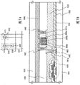
Fig. 1A to 1C show a structure example of the transistor 300. Fig. 1A is a plan view of the transistor 300, fig. 1B is a sectional view along a chain line X1-Y1 of fig. 1A, and fig. 1C is a sectional view along a chain line V1-W1 of fig. 1A.
The transistor 300 includes: a gate electrode layer 402 provided over a substrate 400 having an insulating surface; a gate insulating layer 404 over the gate electrode layer 402; an oxide semiconductor stack 408 overlying and in contact with the gate insulating layer 404 and overlapping the gate electrode layer 402; and a source electrode layer 410a and a drain electrode layer 410b electrically connected to the oxide semiconductor stack 408. The transistor 300 may include an insulating layer 412 covering the source electrode layer 410a and the drain electrode layer 410b and in contact with the oxide semiconductor stack 408.
In the transistor 300, the oxide semiconductor stack 408 includes: an oxide semiconductor layer 408a in contact with the source electrode layer 410a and the drain electrode layer 410 b; and an oxide semiconductor layer 408b provided between the oxide semiconductor layer 408b and the gate insulating layer 404.
In the oxide semiconductor stack 408, the oxide semiconductor layer 408b is a region where a channel of the transistor 300 is formed. Further, the oxide semiconductor layer 408a provided on the back channel side of the oxide semiconductor layer 408b functions as a buffer layer which prevents the constituent elements of the source electrode layer 410a and the drain electrode layer 410b from diffusing into the oxide semiconductor layer 408 b. That is, the oxide semiconductor layer 408a contains a constituent element of the source electrode layer 410a and the drain electrode layer 410b as an impurity. By providing this buffer layer, a trap level can be prevented from being formed in the channel of the transistor 300, whereby an increase in the S value due to the trap level can be prevented. Therefore, by preventing the change in the electrical characteristics of the transistor or the deterioration with time, a highly reliable semiconductor device can be provided.
The oxide semiconductor layers 408a and 408b may have different constituent elements from each other, or may have the same constituent element but different compositions from each other. However, as the oxide semiconductor layer 408b which functions as a channel of the transistor 300, an oxide semiconductor having high field-effect mobility is preferably used.
For example, when an oxide semiconductor containing at least indium and gallium is used while the constituent elements of the oxide semiconductor layers 408a and 408b are the same, an oxide semiconductor containing indium in a larger amount than gallium is preferably used as the oxide semiconductor layer 408b, and an oxide semiconductor containing indium in a smaller amount than gallium is preferably used as the oxide semiconductor layer 408 a.
In an oxide semiconductor, the s orbitals of heavy metals mainly contribute to carrier conduction, and the overlap of the s orbitals tends to increase by increasing the indium content. Therefore, by making the content of indium larger than the content of gallium in the oxide semiconductor layer 408b, the oxide semiconductor layer 408b can have high field-effect mobility as compared with an oxide in which the content of indium is lower than the content of gallium.
In addition, since the larger the ratio of gallium to other metal elements in the metal oxide, the larger the energy gap of the metal oxide, the oxide semiconductor layer 408a has a larger energy gap than the oxide semiconductor layer 408b by making the content of indium in the oxide semiconductor layer 408a equal to or less than the content of gallium. Therefore, a conduction band offset can be formed between the oxide semiconductor layer 408b and the oxide semiconductor layer 408a, and thus the above structure is preferable. Further, since the formation energy of oxygen vacancies of gallium is larger than that of indium, gallium is less likely to generate oxygen vacancies than indium. Thus, a metal oxide having an indium content of not more than a gallium content has stable characteristics as compared with a metal oxide having an indium content of more than a gallium content. This can further stabilize the back channel side of the transistor 300.
For example, when an In-Ga-Zn based oxide semiconductor is used for the oxide semiconductor layer 408a and the oxide semiconductor layer 408b, an In-Ga-Zn based oxide having an atomic ratio of In: Ga: Zn 1:1:1 (1/3: 1/3:1/3), In: Ga: Zn 1:3:2 (1/6: 3/6:2/6), In: Ga: Zn 2:4:3 (2/9: 4/9:3/9), or In: Ga: Zn 1:5:3 (1/9: 5/9:3/9), or a metal oxide similar to the above atomic ratio can be used as the oxide semiconductor layer 408 a. As the oxide semiconductor layer 408b, an In — Ga — Zn-based oxide having an atomic ratio of In, Ga, Zn, 3:1:2 (3/6: 1/6:2/6), In, Ga, Zn, 4:2:3 (4/9: 2/9:3/9), In, Ga, Zn, 5:1:3 (5/9: 1/9:3/9), In, Ga, Zn, 5:3:4 (5/12: 3/12:4/12), In, Ga, Zn, 6:2:4 (39 6/12:2/12:4/12), or In, Ga, Zn, 7:1:3 (7/11: 1/11:3/11), or a metal oxide similar to the atomic ratio can be used.
Note that, for example, the expression "the atomic ratio of In, Ga, Zn is In: ga: zn ═ a: b: the composition of the oxide of c (a + b + c ═ 1) is approximated by the atomic ratio In: ga: zn ═ A: b: the composition of an oxide of C (a + B + C ═ 1) "means that a, B, and C satisfy the formula (a-a)2+(b-B)2+(c-C)2≤r2The relationship (2) of (c). r may be, for example, 0.05.
Note that the metal oxide applied to the oxide semiconductor stack 408 is not limited to this, and a material having an appropriate composition may be used depending on desired electrical characteristics (field effect mobility, threshold value, variation, and the like). In addition, it is preferable to use an appropriate carrier concentration, impurity concentration, defect density, atomic ratio of the metal element and oxygen, interatomic distance, density, and the like so as to obtain desired electrical characteristics. For example, other metal elements may be included instead of gallium. Alternatively, a metal oxide containing no zinc may be used. However, when the composition of the metal Oxide to be used contains zinc, the Oxide Semiconductor layer to be formed later is preferably a CAAC-OS (C-Axis Aligned Crystalline Oxide Semiconductor) film because it is relatively easy to form the film.
The oxide semiconductor layer can be formed by a sputtering method, and the sputtering target contains indium, whereby generation of fine particles during film formation can be prevented. Thus, the oxide semiconductor layers 408a and 408b preferably contain indium.
Next, the structure of the oxide semiconductor layer will be described.
The oxide semiconductor layer is roughly divided into a single crystal oxide semiconductor layer and a non-single crystal oxide semiconductor layer. The non-single crystal oxide semiconductor layer includes an amorphous oxide semiconductor layer, a microcrystalline oxide semiconductor layer, a polycrystalline oxide semiconductor layer, a c-axis aligned crystalline oxide semiconductor (CAAC-OS) film, and the like.
The amorphous oxide semiconductor layer has a disordered atomic arrangement and does not have a crystalline composition. A typical example thereof is an oxide semiconductor layer which does not have a crystal portion in a minute region and has an amorphous structure as a whole.
The microcrystalline oxide semiconductor layer includes, for example, crystallites (also referred to as nanocrystals) having a size of 1nm or more and less than 10 nm. Therefore, the microcrystalline oxide semiconductor layer has a higher degree of order of atomic arrangement than the amorphous oxide semiconductor layer. Therefore, the density of defect states of the microcrystalline oxide semiconductor layer is lower than that of the amorphous oxide semiconductor layer.
The CAAC-OS film is one of oxide semiconductor layers including a plurality of crystal portions, and the size of most of the crystal portions is a size that can be accommodated in a cube having one side shorter than 100 nm. Therefore, the size of the crystal portion included in the CAAC-OS film is sometimes a size capable of being accommodated in a cube having one side shorter than 10nm, shorter than 5nm, or shorter than 3 nm. The CAAC-OS film has a lower defect state density than the microcrystalline oxide semiconductor layer. The CAAC-OS film will be described in detail below.
In a Transmission Electron Microscope (TEM) image of the CAAC-OS film, a clear boundary between the crystal portions, that is, a grain boundary (grain boundary) is not observed. Therefore, in the CAAC-OS film, a decrease in electron mobility due to grain boundaries does not easily occur.
From a TEM image (cross-sectional TEM image) of the CAAC-OS film observed from a direction substantially parallel to the sample plane, it is found that the metal atoms are arranged in a layer in the crystal portion. Each metal atomic layer has a morphology reflecting a surface on which the CAAC-OS film is formed (also referred to as a formation surface) or a top surface of the CAAC-OS film and is arranged in parallel to the formation surface or the top surface of the CAAC-OS film.
On the other hand, it is known from a TEM image (planar TEM image) of the CAAC-OS film observed from a direction substantially perpendicular to the sample surface that the metal atoms are arranged in a triangular shape or a hexagonal shape in the crystal portion. However, the arrangement of the metal atoms is not regular between different crystal portions.
From the sectional TEM image and the plane TEM image, the crystal portion of the CAAC-OS film had orientation.
The CAAC-OS film was subjected to structural analysis using an X-Ray Diffraction (XRD) apparatus. For example, when the out-of-plane method is used for analysis including InGaZnO4In the case of a crystalline CAAC-OS film, a peak appears at a diffraction angle (2. theta.) of about 31 ℃. Since the peak value is derived from InGaZnO4The (009) plane of the crystal was confirmed to have c-axis orientation in the crystal in the CAAC-OS film, and the c-axis was oriented in a direction substantially perpendicular to the formation surface or top surface of the CAAC-OS film.
On the other hand, when the CAAC-OS film is analyzed by an in-plane method in which X-rays are incident on the sample from a direction substantially perpendicular to the c-axis, a peak occurs when 2 θ is in the vicinity of 56 °. The peak value is derived from InGaZnO4Crystalline (110) face. Here, 2 θ was fixed to around 56 ° and analysis was performed under the condition that the sample was rotated around the normal vector of the sample surface (Φ axis) (Φ scan). When the sample is InGaZnO4Six of the single crystal oxide semiconductor layers are presentA peak value. The six peaks originate from a crystal plane corresponding to the (110) plane. On the other hand, when the sample was a CAAC-OS film, a clear peak could not be observed even when phi-scanning was performed in a state where 2 θ was fixed to around 56 °.
From the above results, in the CAAC-OS film having the c-axis orientation, although the directions of the a-axis and the b-axis are different between the crystal portions, the c-axis is oriented in the direction parallel to the normal vector of the formation surface or the top surface. Therefore, the metal atomic layers arranged in a layer observed in the cross-sectional TEM image correspond to a plane parallel to the a-b plane of the crystal.
Note that the crystal portion is formed when a CAAC-OS film is formed or a crystallization process such as a heat treatment is performed. As described above, the c-axis of the crystal is oriented in a direction parallel to the normal vector of the formation surface or top surface of the CAAC-OS film. Thus, for example, when the shape of the CAAC-OS film is changed by etching or the like, the c-axis of the crystal is not necessarily parallel to the normal vector of the formation surface or top surface of the CAAC-OS film.
In addition, the crystallinity in the CAAC-OS film is not necessarily uniform. For example, when the crystal portion of the CAAC-OS film is formed by crystal growth near the top surface of the CAAC-OS film, the crystallinity near the top surface may be higher than the crystallinity near the formation surface. In addition, when an impurity is added to the CAAC-OS film, the crystallinity of the region to which the impurity is added changes, so the crystallinity in the CAAC-OS film sometimes differs depending on the region.
Note that when the out-of-plane method is used for analysis including InGaZnO4In the case of a CAAC-OS film crystallized, a peak may be observed at around 36 ° 2 θ in addition to a peak at around 31 ° 2 θ. A peak value of 2 θ around 36 ° means that a part of the CAAC-OS film contains crystals having no c-axis orientation. It is preferable that a peak occurs at around 31 ° 2 θ and no peak occurs at around 36 ° 2 θ in the CAAC-OS film.
In a transistor using a CAAC-OS film, variation in electrical characteristics due to irradiation with visible light or ultraviolet light is small. Therefore, the transistor has high reliability.
Note that the oxide semiconductor layer may be a stacked film including two or more of an amorphous oxide semiconductor layer, a microcrystalline oxide semiconductor layer, and a CAAC-OS film, for example.
The CAAC-OS film can be formed by a sputtering method using a polycrystalline metal oxide sputtering target, for example. When ions collide with the sputtering target, crystal regions included in the sputtering target are cleaved from the target along the a-b surface, that is, flat or granular sputtering particles having a surface parallel to the a-b surface are separated from the sputtering target. At this time, the flat sputtered particles reach the substrate while maintaining a crystalline state, and thus a CAAC-OS film can be formed.
In addition, in order to form the CAAC-OS film, the following conditions are preferably applied.
By reducing the amount of impurities mixed in the formation of the CAAC-OS film, the crystal state damage due to the impurities can be prevented. For example, the concentration of impurities (hydrogen, water, carbon dioxide, nitrogen, and the like) present in the film forming chamber can be reduced. In addition, the impurity concentration in the film forming gas can be reduced. Specifically, a film forming gas having a dew point of-80 ℃ or lower, preferably-100 ℃ or lower is used.
In addition, by increasing the substrate heating temperature at the time of film formation, migration of sputtered particles may occur after the sputtered particles adhere to the substrate surface. Specifically, the film formation is performed in a state where the substrate heating temperature is set to 100 ℃ or higher and 740 ℃ or lower, preferably 200 ℃ or higher and 500 ℃ or lower. When the substrate heating temperature during film formation is increased, the sputtered particles in the form of flat plates migrate to the substrate surface when they reach the substrate, and the flat surfaces of the sputtered particles in the form of flat plates adhere to the substrate.
Further, it is preferable to reduce plasma damage during film formation by increasing the oxygen ratio in the film forming gas and optimizing the power. The oxygen content in the film forming gas is set to 30 vol% or more, preferably 100 vol%.
Hereinafter, an In-Ga-Zn-O compound target is shown as an example of a metal oxide target for sputtering.
Adding InOXPowder, GaOYPowder and ZnOZMixing the powders at a predetermined ratio, pressurizing, and heating at 1000 deg.C or higherAnd heat treatment is carried out at a temperature of 1500 ℃ or lower, thereby obtaining a polycrystalline In-Ga-Zn-O compound target material. X, Y and Z are arbitrary positive numbers. Here, InOXPowder, GaOYPowder and ZnOZThe predetermined molar ratio of the powders is, for example, 2:2:1, 8:4:3, 3:1:1, 1:1:1, 4:2:3 or 3:1: 2. The kind of the powder and the mixing molar ratio thereof may be appropriately changed depending on the desired target material for sputtering.
In addition, the crystallinity of the oxide semiconductor layer 408a may be different from that of the oxide semiconductor layer 408 b. However, as the oxide semiconductor layer 408b serving as a channel of the transistor 300, a CAAC-OS film is preferably applied. When the oxide semiconductor layer 408b is formed using a CAAC-OS film, the alignment of the precursor (precursor) occurs in the oxide semiconductor layer 408a over and in contact with the oxide semiconductor layer 408b, that is, the precursor has so-called order, and thus the oxide semiconductor layer 408a may be formed as the CAAC-OS film. When the oxide semiconductor layer 408a provided on the back channel side is formed of an amorphous oxide semiconductor, oxygen vacancies are generated by etching treatment in forming the source electrode layer 410a and the drain electrode layer 410b, and the oxide semiconductor layer 408a is easily made to be n-type. Therefore, an oxide semiconductor having crystallinity is preferably used for the oxide semiconductor layer 408 a.
In this embodiment, the oxide semiconductor layer 408a and the oxide semiconductor layer 408b are stacked layers of oxide semiconductors formed using the same constituent element. In this case, depending on the material of the oxide semiconductor layers and the film formation conditions, the interface between the oxide semiconductor layers may not be clear. Therefore, in fig. 1A to 1C, an interface of the oxide semiconductor layer 408a and the oxide semiconductor layer 408b is schematically illustrated with a dotted line. This is the same as in the following figures.
Fig. 2A to 2C show a structure example of the transistor 310. Fig. 2A is a plan view of the transistor 310, fig. 2B is a sectional view taken along a chain line X2-Y2 of fig. 2A, and fig. 2C is a sectional view taken along a chain line V2-W2 of fig. 2A. Like the transistor 300 shown in fig. 1A to 1C, the transistor 310 shown in fig. 2A to 2C includes: a gate electrode layer 402 provided over a substrate 400 having an insulating surface; a gate insulating layer 404 over the gate electrode layer 402; an oxide semiconductor stack 408 that contacts the gate insulating layer 404 and overlaps the gate electrode layer 402; and a source electrode layer 410a and a drain electrode layer 410b electrically connected to the oxide semiconductor stack 408. The transistor 310 may include an insulating layer 412 covering the source electrode layer 410a and the drain electrode layer 410b and in contact with the oxide semiconductor stack 408.
The transistor 310 differs from the transistor 300 in that: the transistor 310 includes an oxide semiconductor layer 408c between the oxide semiconductor layer 408b and the gate insulating layer 404. That is, in the transistor 310, the oxide semiconductor layer 408 has a stacked structure of the oxide semiconductor layer 408a, the oxide semiconductor layer 408b, and the oxide semiconductor layer 408 c.
Note that the structure of the transistor 310 is the same as that of the transistor 300 except for the oxide semiconductor layer 408c, and thus description about the transistor 300 can be referred to.
By providing the oxide semiconductor layer 408c between the oxide semiconductor layer 408b forming a channel in the transistor 310 and the gate insulating layer 404, the transistor 310 has a structure in which carriers flow through a region distant from the gate insulating layer 404 (so-called a buried channel). This stabilizes the interface between the gate insulating layer 404 and the channel, and prevents formation of trap levels at the interface. This prevents deterioration of the transistor, particularly photodegradation such as negative bias temperature stress deterioration, and enables the manufacture of a highly reliable transistor.
In the metal oxide containing indium and gallium, the larger the ratio of the content of gallium with respect to other metal elements, the larger the energy gap. In addition, a conduction band offset is formed due to a difference in band gap between the oxide semiconductor layer 408c and the oxide semiconductor layer 408 b. Therefore, when a metal oxide in which the content of indium is equal to or less than the content of gallium is used as the oxide semiconductor layer 408c, a channel can be formed efficiently in the oxide semiconductor layer 408b, which is preferable.
When an In-Ga-Zn-based oxide semiconductor is used for the oxide semiconductor layer 408c, an In-Ga-Zn-based oxide having an atomic ratio of In: Ga: Zn 1:1:1 (1/3: 1/3:1/3), In: Ga: Zn 1:3:2 (1/6: 3/6:2/6), In: Ga: Zn 2:4:3 (2/9: 4/9:3/9), or In: Ga: Zn 1:5:3 (1/9: 5/9:3/9), or an oxide similar to the above atomic ratio may be used as the oxide semiconductor layer 408 c. In addition, it is preferable to use a metal oxide in which the content of indium is equal to or less than the content of gallium as both the oxide semiconductor layer 408a and the oxide semiconductor layer 408 c. Here, the composition of the oxide semiconductor layer 408a and the composition of the oxide semiconductor layer 408c may be the same or different.
In general, most of the oxide semiconductor layer is formed by a sputtering method. On the other hand, when the oxide semiconductor layer is formed by the sputtering method, a rare gas element (for example, argon) which is ionized or particles ejected from the surface of a sputtering target may eject particles which become a film on the formation surface of the oxide semiconductor layer, such as a gate insulating layer. Therefore, particles ejected from the film which becomes the formation surface of the oxide semiconductor layer enter the oxide semiconductor layer as an impurity element. In particular, there is a concern that an impurity element with a high concentration enters into the oxide semiconductor layer in the vicinity of the formation surface. In addition, when the impurity element remains in the oxide semiconductor layer in the vicinity of the formation surface, the resistance of the oxide semiconductor layer increases, which causes deterioration in electrical characteristics of the transistor.
However, in the transistor 310 illustrated in fig. 2A to 2C, by including the oxide semiconductor layer 408C between the oxide semiconductor layer 408b forming a channel and the gate insulating layer 404, it is possible to prevent a constituent element of the gate insulating layer 404 from diffusing into the channel. That is, the oxide semiconductor layer 408c may contain a constituent element (e.g., silicon) of the gate insulating layer 404 as an impurity. By including the oxide semiconductor layer 408c, electric characteristics of the transistor 310 can be further stabilized, and a highly reliable semiconductor device can be provided.
Fig. 2D is a band diagram showing the energy band diagram in the thickness direction (between D and D') in fig. 2B. In this embodiment mode, the oxide semiconductor layers 408a to 408c are formed using an In-Ga-Zn based oxide semiconductor. In addition, a metal oxide in which the content of indium is equal to or less than that of gallium is used for the oxide semiconductor layers 408a and 408c, and a metal oxide in which the content of indium is larger than that of gallium is used for the oxide semiconductor layer 408 b. As a result, the oxide semiconductor stack 408 shown in this embodiment mode can have a so-called buried channel as shown in the band diagram of fig. 2D.
Fig. 3A to 3D illustrate an example of a method for manufacturing the transistor 310.
First, a gate electrode layer 402 (including a wiring formed with the same layer as this) is formed over a substrate 400 having an insulating surface.
A substrate which can be used as the substrate 400 having an insulating surface is not particularly limited, but the substrate 400 needs to have at least heat resistance to such an extent that it can withstand heat treatment performed later. For example, a glass substrate such as barium borosilicate glass, alumino borosilicate glass, or the like, a ceramic substrate, a quartz substrate, a sapphire substrate, or the like can be used. As the substrate 400, a single crystal semiconductor substrate or a polycrystalline semiconductor substrate made of silicon, silicon carbide, or the like, a compound semiconductor substrate made of silicon germanium, or the like, an SOI substrate, or the like can be used, and the substrate 400 in which a semiconductor element is provided over these substrates can also be used. Further, a base insulating layer may be formed over the substrate 400.
The gate electrode layer 402 can be formed using a metal material such as molybdenum, titanium, tantalum, tungsten, aluminum, copper, chromium, neodymium, scandium, or an alloy material containing these materials as a main component. The gate electrode layer 402 can be a semiconductor film typified by a polycrystalline silicon film doped with an impurity element such as phosphorus or a silicide film such as a nickel silicide film. The gate electrode layer 402 may have a single-layer structure or a stacked-layer structure. The gate electrode layer 402 may have a tapered shape, and the taper angle may be set to 15 ° or more and 70 ° or less, for example. Here, the taper angle means an angle between a side surface of a layer having a tapered shape and a bottom surface of the layer.
As a material of the gate electrode layer 402, a conductive material such as indium tin oxide, indium oxide containing tungsten oxide, indium zinc oxide containing tungsten oxide, indium oxide containing titanium oxide, indium tin oxide containing titanium oxide, indium zinc oxide, or indium tin oxide to which silicon oxide is added can be used.
Alternatively, an In — Ga — Zn based oxide containing nitrogen, an In — Sn based oxide containing nitrogen, an In — Ga based oxide containing nitrogen, an In — Zn based oxide containing nitrogen, an Sn based oxide containing nitrogen, an In based oxide containing nitrogen, or a metal nitride film (an indium nitride film, a zinc nitride film, a tantalum nitride film, a tungsten nitride film, or the like) can be used as a material of the gate electrode layer 402. Since the above-described material has a work function of 5eV or more, the threshold voltage of the transistor can be made positive by forming the gate electrode layer 402 using the above-described material, whereby a normally-off (normal-off) switching transistor can be realized.
Next, a gate insulating layer 404 is formed over the gate electrode layer 402 so as to cover the gate electrode layer 402 (see fig. 3A). As the gate insulating layer 404, a film containing at least one selected from a silicon oxide film, a silicon oxynitride film, a silicon nitride oxide film, a silicon nitride film, an aluminum oxide film, a hafnium oxide film, an yttrium oxide film, a zirconium oxide film, a gallium oxide film, a tantalum oxide film, a magnesium oxide film, a lanthanum oxide film, a cerium oxide film, and a neodymium oxide film is formed in a single layer or a stacked layer by a plasma CVD method, a sputtering method, or the like.
In addition, in the gate insulating layer 404, a region which is in contact with the oxide semiconductor stack 408 which is formed later is preferably formed using an oxide insulating layer, and more preferably includes an oxygen excess region. In order to provide the gate insulating layer 404 with an oxygen excess region, the gate insulating layer 404 may be formed in an oxygen atmosphere, for example. Alternatively, oxygen may be introduced into the gate insulating layer 404 after the film formation to form an oxygen excess region. As a method of introducing oxygen, an ion implantation method, an ion doping method, a plasma immersion ion implantation method, plasma treatment, or the like can be used.
Next, an oxide semiconductor film to be an oxide semiconductor layer 408c, an oxide semiconductor film to be an oxide semiconductor layer 408B, and an oxide semiconductor film to be an oxide semiconductor layer 408a are formed in this order over the gate insulating layer 404, and the oxide semiconductor films are processed into island shapes by etching treatment using photolithography, whereby an oxide semiconductor stack 408 is formed (see fig. 3B).
The oxide semiconductor layer 408c, the oxide semiconductor layer 408b, and the oxide semiconductor layer 408a may be an amorphous oxide semiconductor or a crystalline oxide semiconductor. However, as the oxide semiconductor layer 408b which functions as a channel of the transistor 310, a crystalline oxide semiconductor is preferably used. Further, by heat treatment of the amorphous oxide semiconductor, a crystalline oxide semiconductor can be formed. The temperature of the heat treatment for crystallizing the amorphous oxide semiconductor is set to 250 ℃ or higher and 700 ℃ or lower, preferably 400 ℃ or higher, more preferably 500 ℃ or higher, and still more preferably 550 ℃ or higher. This heat treatment may also be used as another heat treatment in the production process.
As a film formation method of each oxide semiconductor film, a sputtering method, an MBE (Molecular Beam Epitaxy) method, a CVD method, a pulsed laser Deposition method, an ALD (Atomic Layer Deposition) method, or the like can be suitably used.
When the oxide semiconductor film is formed, it is preferable to reduce the hydrogen concentration in the film as much as possible. In order to reduce the hydrogen concentration, for example, when film formation is performed by a sputtering method, the following atmosphere gas is suitably used as an atmosphere gas supplied into a film formation chamber of a sputtering apparatus: a high-purity rare gas (typically argon) from which impurities such as hydrogen, water, hydroxyl, or hydride are removed, oxygen, and a mixed gas of the rare gas and oxygen.
In addition, by removing moisture remaining in the film formation chamber and introducing a sputtering gas from which hydrogen and moisture have been removed to form a film, the hydrogen concentration of the oxide semiconductor film to be formed can be reduced. In order to remove moisture remaining in the film forming chamber, an adsorption type vacuum pump, for example, a cryopump, an ion pump, or a titanium sublimation pump is preferably used. Further, a turbo-molecular pump having a cold trap may be used as the vacuum pump. Due to the cryopump to hydrogen molecules, water (H)2O), a compound containing a hydrogen atom (preferably, a compound containing a carbon atom) or the like is high in the ability to discharge, and therefore the impurity concentration in the oxide semiconductor film formed in the film forming chamber which is discharged by using the cryopump can be reduced.
In addition, the gate insulating layer 404 and the oxide semiconductor film are preferably formed continuously without being exposed to the atmosphere. By forming the gate insulating layer 404 and the oxide semiconductor film continuously without being exposed to the atmosphere, hydrogen or a hydrogen compound (e.g., adsorbed water or the like) can be prevented from adhering to the surface of the oxide semiconductor film, and thus, mixing of impurities can be prevented.
In the case where the oxide semiconductor film is formed by a sputtering method, the relative density (filling ratio) of the metal oxide target used for film formation is 90% or more and 100% or less, and preferably 95% or more and 99.9% or less. By using a metal oxide target having a high relative density, a dense film can be formed.
In addition, in order to reduce the concentration of impurities that may be included in the oxide semiconductor film, it is also effective to form the oxide semiconductor film while the substrate 400 is kept at a high temperature. The temperature for heating the substrate 400 may be set to 150 ℃ to 450 ℃, and preferably 200 ℃ to 350 ℃. In addition, when the substrate is heated at a high temperature during film formation, a crystalline oxide semiconductor film can be formed.
When a CAAC-OS film is used as the oxide semiconductor layer (for example, the oxide semiconductor layer 408b), as a method for obtaining the CAAC-OS film, any method can be used in which, for example, the film formation temperature is set to 200 ℃ or higher and 450 ℃ or lower to form the oxide semiconductor film and c-axis alignment substantially perpendicular to the surface thereof is achieved. Alternatively, after the thin oxide semiconductor film is formed, c-axis alignment substantially perpendicular to the surface may be achieved by performing heat treatment at 200 ℃ to 700 ℃. Alternatively, after the thin first oxide semiconductor film is formed, a second oxide semiconductor film may be formed after heat treatment at 200 ℃ to 700 ℃ inclusive, so that c-axis alignment substantially perpendicular to the surface thereof can be achieved.
The oxide semiconductor used for the oxide semiconductor layers 408a to 408c contains at least indium (In). In particular, indium and zinc (Zn) are preferably contained. Further, as a stabilizer (stabilizer) for reducing a change in electrical characteristics of a transistor using the oxide semiconductor, gallium (Ga) is preferably contained in addition to the above elements.
As described above, it is preferable to use a metal oxide in which the content of indium is equal to or less than the content of gallium as the oxide semiconductor layers 408a and 408c serving as buffer layers for reducing the influence of trap levels, and to use a metal oxide in which the content of indium is larger than the content of gallium as the oxide semiconductor layer 408b serving as a channel formation region.
Further, as the stabilizer, one or more of tin (Sn), hafnium (Hf), aluminum (Al), and zirconium (Zr) may be contained instead of or in addition to gallium (Ga). The other stabilizer may contain one or more of lanthanoid elements such as lanthanum (La), cerium (Ce), praseodymium (Pr), neodymium (Nd), samarium (Sm), europium (Eu), gadolinium (Gd), terbium (Tb), dysprosium (Dy), holmium (Ho), erbium (Er), thulium (Tm), ytterbium (Yb), and lutetium (Lu).
For example, as the oxide semiconductor, there can be used: indium oxide, tin oxide, zinc oxide, and the like as the monovalent metal oxide; In-Zn-based oxides, In-Mg-based oxides, In-Ga-based oxides, and the like as binary metal oxides; In-Ga-Zn based oxides, In-Al-Zn based oxides, In-Sn-Zn based oxides, In-Hf-Zn based oxides, In-La-Zn based oxides, In-Ce-Zn based oxides, In-Pr-Zn based oxides, In-Nd-Zn based oxides, In-Sm-Zn based oxides as ternary metal oxides, In-Eu-Zn based oxide, In-Gd-Zn based oxide, In-Tb-Zn based oxide, In-Dy-Zn based oxide, In-Ho-Zn based oxide, In-Er-Zn based oxide, In-Tm-Zn based oxide, In-Yb-Zn based oxide, In-Lu-Zn based oxide, etc.; and In-Sn-Ga-Zn based oxides, In-Hf-Ga-Zn based oxides, In-Al-Ga-Zn based oxides, In-Sn-Al-Zn based oxides, In-Sn-Hf-Zn based oxides, In-Hf-Al-Zn based oxides, and the like as quaternary metal oxides.
For example, the In-Ga-Zn based oxide means an oxide containing In, Ga and Zn as main components, and the ratio of In, Ga and Zn is not limited. In addition, metal elements other than In, Ga, and Zn may be contained.
Further, as the oxide semiconductor, an oxide semiconductor may be usedFor InMO3(ZnO)m(m>0, and m is not an integer). Note that M represents one metal element or a plurality of metal elements selected from Ga, Fe, Mn, and Co. In addition, In may be used as the oxide semiconductor2SnO5(ZnO)n(n>0, and n is a natural number).
The oxide semiconductor stack 408 is preferably subjected to heat treatment (dehydration or dehydrogenation) for removing excess hydrogen (including water and hydroxyl groups). The temperature of the heat treatment is set to 300 ℃ or higher and 700 ℃ or lower than the strain point of the substrate. The heat treatment may be performed under reduced pressure, under a nitrogen atmosphere, or the like. By performing this heat treatment, hydrogen which is an impurity imparting n-type conductivity can be removed.
The heat treatment for dehydration or dehydrogenation may be performed at any timing in the manufacturing process of the transistor as long as it is performed after the oxide semiconductor film is formed. The heat treatment for dehydration or dehydrogenation may be performed a plurality of times, or may be performed as another heat treatment.
In the heat treatment, nitrogen or a rare gas such as helium, neon, or argon preferably does not contain water, hydrogen, or the like. The purity of the nitrogen or the rare gas such as helium, neon, or argon introduced into the heat treatment apparatus is preferably set to 6N (99.9999%) or more, and preferably 7N (99.99999%) or more (that is, the impurity concentration is set to 1ppm or less, and preferably 0.1ppm or less).
After the oxide semiconductor layer (or the oxide semiconductor stack) is heated by the heating treatment, a high-purity oxygen gas, a high-purity nitrous oxide gas, or ultra-dry air (a dew point meter using a CRDS (Cavity Ring Down laser Spectroscopy) method) system may be introduced into the same furnace while maintaining the heating temperature or while reducing the temperature from the heating temperature, and the water content when the test is performed may be 20ppm (as dew point — 55 ℃ c) or less, preferably 1ppm or less, and more preferably 10ppb or less). It is preferable not to include water, hydrogen, or the like in the oxygen gas or the nitrous oxide gas. Alternatively, the purity of the oxygen gas or the nitrous oxide gas introduced into the heat treatment device is preferably set to 6N or more, preferably 7N or more (that is, the impurity concentration in the oxygen gas or the nitrous oxide gas is set to 1ppm or less, preferably 0.1ppm or less). Even if oxygen, which is a main constituent of the oxide semiconductor, is reduced in the impurity removal step by dehydration or dehydrogenation, the oxide semiconductor layer can be made highly pure and electrically i-type (intrinsic) by supplying oxygen using oxygen gas or dinitrogen monoxide gas.
In addition, since there is a possibility that oxygen is desorbed and reduced when dehydration treatment or dehydrogenation treatment is performed, oxygen (including at least one of oxygen radicals, oxygen atoms, and oxygen ions) may be introduced into the oxide semiconductor layer subjected to dehydration treatment or dehydrogenation treatment to supply oxygen to the layer.
By supplying oxygen by introducing oxygen into the oxide semiconductor layer subjected to dehydration treatment or dehydrogenation treatment, the oxide semiconductor layer can be made highly pure and i-type (intrinsic). Since variations in electrical characteristics of a transistor including an i-type (intrinsic) oxide semiconductor with high purity are suppressed, the transistor is electrically stable.
When oxygen is introduced into the oxide semiconductor layer, oxygen may be introduced into the oxide semiconductor layer directly or may be introduced into the oxide semiconductor layer so as to permeate an insulating layer formed later. As a method of introducing oxygen (including at least one of oxygen radicals, oxygen atoms, and oxygen ions), an ion implantation method, an ion doping method, a plasma immersion ion implantation method, plasma treatment, or the like can be used. In addition, the oxygen introducing treatment may be performed using a gas containing oxygen. As the oxygen-containing gas, oxygen, nitrous oxide, nitrogen dioxide, carbon monoxide, or the like can be used. In the oxygen introduction treatment, the gas containing oxygen may contain a rare gas.
For example, when oxygen ions are implanted into the oxide semiconductor layer by an ion implantation method, the dose can be set to 1 × 10¹³ions/cm2Above and 5 × 10¹⁶ions/cm2The following.
The step of supplying oxygen to the oxide semiconductor layer may be performed at any timing in the manufacturing process of the transistor after the oxide semiconductor film is formed. Further, oxygen may be introduced into the oxide semiconductor layer a plurality of times.
Next, a conductive film is formed over the oxide semiconductor stack 408 and processed to form a source electrode layer 410a and a drain electrode layer 410b (including a wiring formed using the same layer as that of the conductive film) (see fig. 3C).
As the source electrode layer 410a and the drain electrode layer 410b, for example, a metal film containing an element selected from Al, Cr, Cu, Ta, Ti, Mo, and W, a metal nitride film (a titanium nitride film, a molybdenum nitride film, or a tungsten nitride film) containing the above element, or the like can be used. Further, a high melting point metal film of Ti, Mo, W, or the like, or a metal nitride film thereof (a titanium nitride film, a molybdenum nitride film, or a tungsten nitride film) may be stacked on one or both of the lower side and the upper side of the metal film of Al, Cu, or the like. The source electrode layer 410a and the drain electrode layer 410b may be formed using a conductive metal oxide. As the conductive metal oxide, for example, indium oxide (In) can be used2O3) Tin oxide (SnO)2) Zinc oxide (ZnO), indium tin oxide (In)2O3-SnO2) Indium oxide, zinc oxide (In)2O3ZnO) or materials such that these metal oxide materials contain silicon oxide.
As the source electrode layer 410a and the drain electrode layer 410b, a metal nitride film such as an In — Ga — Zn — O film containing nitrogen, an In — Sn — O film containing nitrogen, an In — Ga — O film containing nitrogen, an In — Zn — O film containing nitrogen, an Sn — O film containing nitrogen, or an In — O film containing nitrogen can be used. Since these films contain the same constituent elements as the oxide semiconductor stack 408, the interface between the source electrode layer 410a or the drain electrode layer 410b and the oxide semiconductor stack 408 can be stabilized.
Further, when a conductive film containing copper is used as the source electrode layer 410a and the drain electrode layer 410b, wiring resistance can be reduced, which is preferable. In general, since copper easily diffuses into a semiconductor or a silicon oxide film, there is a possibility that the operation of a semiconductor device is unstable and the yield is significantly lowered. However, since the transistor 310 includes the oxide semiconductor layer 408a which is in contact with the source electrode layer 410a and the drain electrode layer 410b and serves as a buffer layer for preventing diffusion of a constituent element (here, copper) of the electrode layers, it is possible to reduce the influence of the back channel side trap level due to diffusion of copper, and it is preferable to completely prevent the influence of the back channel side trap level.
Next, an insulating layer 412 is formed so as to cover the source electrode layer 410a, the drain electrode layer 410b, and the exposed oxide semiconductor stack 408 (see fig. 3D).
The insulating layer 412 can be formed using a single layer or a stacked layer of a silicon oxide film, a gallium oxide film, an aluminum oxide film, a silicon nitride film, a silicon oxynitride film, an aluminum oxynitride film, a silicon nitride oxide film, or the like by a plasma CVD method or a sputtering method. Note that when an oxide insulating layer is formed as the insulating layer 412, oxygen can be supplied to the oxide semiconductor stack 408 using the oxide insulating layer, which is preferable.
The heating treatment may be performed after the insulating layer 412 is formed. The temperature of the heat treatment is preferably set to 200 ℃ or higher, and may be set to 220 ℃, for example.
The transistor 310 of this embodiment can be formed by the above steps.
The transistor shown in this embodiment mode includes: a first oxide semiconductor layer which functions as a buffer layer for preventing diffusion of a constituent element of the source electrode layer or the drain electrode layer into the channel; and a second oxide semiconductor layer serving as a channel. With this structure, the influence of an interface state that can be formed on the back channel side of the transistor can be reduced. Further, it is more preferable that the transistor described in this embodiment mode includes a buffer layer which is provided between the oxide semiconductor layer functioning as a channel and the gate insulating layer and which functions to prevent deterioration of an interface on the gate insulating layer side of the channel. By including the third oxide semiconductor layer, photodegradation (e.g., negative bias temperature stress degradation) of the transistor can be reduced, so that a highly reliable semiconductor device can be provided.
The structures, methods, and the like described in this embodiment can be used in combination with the structures, methods, and the like described in other embodiments as appropriate.
In this embodiment, an embodiment of a semiconductor device which is different from that of embodiment 1 will be described with reference to fig. 10A and 10B. Specifically, a transistor having a structure of a gate insulating layer different from that of the transistor described in embodiment 1 will be described.
Fig. 10A shows a structure example of the transistor 320. Like the transistor 310 illustrated in fig. 2A to 2D, the transistor 320 illustrated in fig. 10A includes: a gate electrode layer 402 provided over a substrate 400 having an insulating surface; gate insulating layers 403 and 406 over the gate electrode layer 402; an oxide semiconductor stack 408 in contact with the gate insulating layer 406 and overlapping the gate electrode layer 402; and a source electrode layer 410a and a drain electrode layer 410b electrically connected to the oxide semiconductor stack 408. In the transistor 320, the oxide semiconductor stack 408 includes: an oxide semiconductor layer 408c in contact with the gate insulating layer 406; an oxide semiconductor layer 408b over and in contact with the oxide semiconductor layer 408 c; an oxide semiconductor layer 408a which is in contact with the source electrode layer 410a and the drain electrode layer 410b is provided over and in contact with the oxide semiconductor layer 408 b. The transistor 320 may include an insulating layer 412 covering the source electrode layer 410a and the drain electrode layer 410b and in contact with the oxide semiconductor stack 408.
The transistor 320 differs from the transistor 310 in that: the gate insulating layer has a stacked-layer structure of a first gate insulating layer 403 and a second gate insulating layer 406, and the first gate insulating layer 403 includes a gate insulating layer 403a, a gate insulating layer 403b, and a gate insulating layer 403c from the gate electrode layer 402 side.
Note that the structure of the transistor 320 is the same as that of the transistor 310 except for the gate insulating layer, and the description about the transistor 310 can be referred to.
In the transistor 320, a silicon film containing nitrogen is applied as the first gate insulating layer 403. Since the silicon film containing nitrogen has a higher relative permittivity than the silicon oxide film and the silicon film containing nitrogen needs to have a larger thickness than the silicon oxide film when obtaining a capacitance equal to that of the silicon oxide film, the gate insulating layer can be physically formed thicker. This can prevent a drop in the withstand voltage of the transistor 320. Further, electrostatic breakdown of the semiconductor device can be prevented by increasing the withstand voltage.
Further, as the second gate insulating layer 406 which is in contact with the oxide semiconductor stack 408, an insulating layer containing oxygen, such as a silicon oxide film, a gallium oxide film, or an aluminum oxide film, is applied. The second gate insulating layer 406 preferably includes a region containing oxygen exceeding the stoichiometric composition (oxygen excess region). This is because: by the insulating layer in contact with the oxide semiconductor stack 408 including the oxygen excess region, oxygen can be supplied to the oxide semiconductor stack 408, whereby oxygen can be prevented from being desorbed from the oxide semiconductor stack 408 and oxygen vacancies in the oxide semiconductor stack 408 can be filled. In order to provide the second gate insulating layer 406 with an oxygen excess region, the second gate insulating layer 406 may be formed in an oxygen atmosphere, for example. Alternatively, oxygen may be introduced into the second gate insulating layer 406 after the film formation to form an oxygen excess region.
Examples of the silicon film containing nitrogen which is applied to the first gate insulating layer 403 include a silicon nitride film, a silicon nitride oxide film, and a silicon oxynitride film, but a silicon nitride film is preferably used because the relative dielectric constant is higher as the content of nitrogen with respect to oxygen is higher. Further, since the energy gap of silicon nitride is 5.5eV, which is lower than the energy gap of 8eV of silicon oxide, and the resistivity of silicon oxide is also low, ESD (Electro-Static Discharge) resistance can be improved by using a silicon nitride film. Note that in this specification, "a silicon oxynitride film" refers to a film whose composition contains more oxygen than nitrogen, and "a silicon nitride oxide film" refers to a film whose composition contains more nitrogen than oxygen.
The gate insulating layer 403a which is in contact with the gate electrode layer 402 is a silicon film having an ammonia content at least smaller than that of the gate insulating layer 403 b. Ammonia acts as a ligand for the metal complex due to the action of the lone pair of electrons on the nitrogen atom. Therefore, for example, in the case where copper is used for the gate electrode layer 402, if a gate insulating layer containing a large amount of ammonia is formed so as to be in contact with the gate electrode layer, there is a possibility that copper may diffuse into the gate insulating layer by a reaction represented by the following formula (1).

In the transistor 320, by forming the gate insulating layer 403a with a low ammonia content (at least lower than the gate insulating layer 403 b) in contact with the gate electrode layer 402, a material (e.g., copper) of the gate electrode layer 402 can be prevented from diffusing into the first gate insulating layer 403. In other words, the gate insulating layer 403a can function as a barrier film for a metal material included in the gate electrode layer 402. By providing the gate insulating layer 403a, the reliability of the transistor can be further improved.
The gate insulating layer 403b is a silicon film containing nitrogen which has a film thickness thicker than that of the gate insulating layer 403a and reduces the number of defects in the film. For example, the thickness of the gate insulating layer 403b is set to 300nm to 400 nm. In addition, in the silicon film containing nitrogen used as the gate insulating layer 403b, the Spin density of a signal appearing at the Nc center (g value of 2.003) among signals measured by an Electron Spin Resonance (ESR) method was 1 × 10¹⁷spins/cm3Hereinafter, it is preferably 5 × 10¹⁶spins/cm3The following. By using a silicon film containing nitrogen which has a small number of defects in the film and has a large thickness (for example, 300nm or more) as the gate insulating layer 403b in this manner, the ESD resistance of the gate insulating layer 403b can be increased to, for example, 300V or more.
In addition, the gate insulating layer 403c uses a silicon film containing nitrogen which reduces the hydrogen concentration. The hydrogen concentration of the gate insulating layer 403c is set to be at least lower than that of the gate insulating layer 403 b. For example, in the case where the gate insulating layer 403c is formed by a plasma CVD method, the hydrogen concentration of the gate insulating layer 403c can be made lower than that of the gate insulating layer 403b by making the hydrogen concentration contained in the supply gas lower than that of the supply gas used to form the gate insulating layer 403 b. Specifically, when a silicon nitride film is formed as the gate insulating layer 403b and the gate insulating layer 403c, the flow rate of ammonia in the supply gas used for forming the gate insulating layer 403c may be lower than the flow rate of ammonia in the supply gas used for forming the gate insulating layer 403b, or the gate insulating layer 403c may be formed without using ammonia.
By providing a silicon nitride film with a reduced hydrogen concentration as the gate insulating layer 403c, hydrogen or a hydrogen compound (e.g., water) can be prevented from being mixed into the second gate insulating layer 406 and the oxide semiconductor stack 408. Since hydrogen is bonded to the oxide semiconductor, a part of hydrogen serves as a donor to generate electrons as carriers, which may cause a change (transfer) in the negative direction of the threshold voltage of the transistor, a silicon nitride film with a reduced hydrogen concentration is provided as the gate insulating layer 403c, whereby the transistor can have stable electrical characteristics. In addition, by providing a silicon nitride film that reduces the hydrogen concentration as the gate insulating layer 403c, the gate insulating layer 403c also functions as a barrier film that prevents impurities such as hydrogen or a hydrogen compound contained in the gate insulating layer 403b from diffusing into the oxide semiconductor stack 408.
In this embodiment, a silicon nitride film is used for the gate insulating layer 403a, the gate insulating layer 403b, and the gate insulating layer 403c which form the first gate insulating layer 403, a silicon oxynitride film is used for the second gate insulating layer 406, and the gate insulating layers are formed continuously by a plasma CVD method. Specifically, Silane (SiH) is supplied4) With nitrogen (N)2) A silicon nitride film serving as the gate insulating layer 403a is formed using the mixed gas of (a) and (b), and then the supplied gas is converted into Silane (SiH)4) Nitrogen (N)2) And ammonia (NH)3) A silicon nitride film serving as the gate insulating layer 403b is formed, and then the supply gas is converted into Silane (SiH)4) With nitrogen (N)2) A silicon nitride film serving as the gate insulating layer 403c is formed, and then the supply gas is converted into Silane (SiH)4) With dinitrogen monoxide (N)2O) to form a silicon oxynitride film serving as the second gate insulating layer 406.
The thickness of the gate insulating layer 403a is preferably 30nm to 100nm, and more preferably 30nm to 50 nm. The thickness of the gate insulating layer 403b provided to prevent electrostatic breakdown of the transistor is preferably set to 300nm to 400nm, and the thickness of the gate insulating layer 403c serving as a barrier film for preventing diffusion of hydrogen into the oxide semiconductor stack 408 is preferably set to 25nm to 150 nm. The thickness of the second gate insulating layer 406 is preferably set to 25nm to 100 nm. Note that the thickness of each gate insulating layer is preferably adjusted so that the sum of the thickness of the first gate insulating layer 403 (the sum of the thicknesses of the gate insulating layer 403a, the gate insulating layer 403b, and the gate insulating layer 403 c) and the thickness of the second gate insulating layer 406 is 355nm to 550 nm.
As in the transistor 330 shown in fig. 10B, a gate insulating layer including a stack of the first gate insulating layer 403 and the second gate insulating layer 406 and an oxide semiconductor stack 408 including a stack of the oxide semiconductor layer 408B and the oxide semiconductor layer 408a may be used in combination.
The transistor shown in this embodiment mode includes: a first oxide semiconductor layer serving as a buffer layer which prevents diffusion of constituent elements of the source electrode layer and the drain electrode layer into the channel; and a second oxide semiconductor layer serving as a channel. With this structure, the influence of an interface state that can be formed on the back channel side of the transistor can be reduced. Further, it is more preferable that the transistor described in this embodiment further include a third oxide semiconductor layer which is provided between the oxide semiconductor layer functioning as a channel and the gate insulating layer and which serves as a buffer layer for preventing deterioration of an interface on the gate insulating layer side of the channel. By including the third oxide semiconductor layer, photodegradation (e.g., negative bias temperature stress deterioration) of the transistor can be reduced, and a highly reliable semiconductor device can be provided.
In addition, the transistor described in this embodiment includes a stack of a first gate insulating layer including a silicon film containing nitrogen and a second gate insulating layer containing oxygen as a gate insulating layer. The first gate insulating layer includes: a silicon film containing nitrogen which serves as a barrier film for a constituent element (e.g., copper) of the gate electrode layer; a silicon film containing nitrogen which is large in thickness (e.g., 300nm thick) and which reduces the number of defects in the film; and a silicon film containing nitrogen having a barrier property to hydrogen. Therefore, the transistor of the present embodiment is suppressed in the variation of the electrical characteristics and the electrostatic breakdown. By using such a transistor, a highly reliable semiconductor device can be manufactured with high yield.
The structures, methods, and the like described in this embodiment can be used in combination with the structures, methods, and the like described in other embodiments as appropriate.
Embodiment 3
A semiconductor device having a display function (also referred to as a display device) can be manufactured by using the transistor described in embodiment mode 1 or 2. Further, a system-on-panel (system-on-panel) can be formed by forming part or all of a driver circuit including a transistor over the same substrate as a pixel portion integrally.
In fig. 4A, a sealant 4005 is provided so as to surround a pixel portion 4002 provided over a substrate 4001, and the pixel portion 4002 is sealed using a substrate 4006. In fig. 4A, a scanning line driver circuit 4004 and a signal line driver circuit 4003 which are formed over an IC chip or a substrate prepared separately using a single crystal semiconductor film or a polycrystalline semiconductor film are mounted in a region different from a region surrounded by a sealant 4005 over a substrate 4001. Further, various signals and potentials supplied to the pixel portion 4002 through the signal line driver circuit 4003 and the scan line driver circuit 4004 are supplied from FPCs (Flexible printed circuits) 4018a and 4018 b.
In fig. 4B and 4C, a sealant 4005 is provided so as to surround a pixel portion 4002 and a scan line driver circuit 4004 which are provided over a substrate 4001. Further, a substrate 4006 is provided over the pixel portion 4002 and the scan line driver circuit 4004. Therefore, the pixel portion 4002 and the scan line driver circuit 4004 are sealed together with the display element by the substrate 4001, the sealant 4005, and the substrate 4006. In fig. 4B and 4C, a signal line driver circuit 4003 formed over an IC chip or a substrate separately prepared using a single crystal semiconductor film or a polycrystalline semiconductor film is mounted in a region different from a region surrounded by the sealant 4005 over the substrate 4001. In fig. 4B and 4C, various signals and potentials supplied to the pixel portion 4002 through the signal line driver circuit 4003 and the scan line driver circuit 4004 are supplied from an FPC 4018.
Fig. 4B and 4C illustrate an example in which the signal line driver circuit 4003 is formed separately and the signal line driver circuit 4003 is mounted over the substrate 4001, but the present invention is not limited to this structure. The scanning line driver circuit may be separately formed and mounted, or only a part of the signal line driver circuit or a part of the scanning line driver circuit may be separately formed and mounted.
The connection method of the driver circuit to be formed separately is not particularly limited, and a COG (Chip On Glass) method, a wire Bonding method, a TAB (Tape Automated Bonding) method, or the like can be used. Fig. 4A shows an example in which the signal line driver circuit 4003 and the scan line driver circuit 4004 are mounted by a COG method, fig. 4B shows an example in which the signal line driver circuit 4003 is mounted by a COG method, and fig. 4C shows an example in which the signal line driver circuit 4003 is mounted by a TAB method.
Further, the display device includes a panel in which a display element is in a sealed state and a module in which an IC or the like including a controller is mounted in the panel. Note that a display device in this specification refers to an image display device, a display device, or a light source (including an illumination device). In addition, the display device includes, in addition to the panel in which the display element is sealed: a module mounted with a connector such as FPC or TCP; a module of a printed circuit board is arranged at the end part of the TCP; or a module in which an IC (integrated circuit) is directly mounted to a display element by a COG method.
The pixel portion and the scan line driver circuit provided over the substrate each have a plurality of transistors, and the transistors described in embodiment mode 1 or 2 can be applied.
As a display element provided in a display device, a liquid crystal element (also referred to as a liquid crystal display element) or a light-emitting element (also referred to as a light-emitting display element) can be used. The light-emitting element includes an element whose luminance is controlled by current or voltage, and specifically includes an inorganic EL (Electro Luminescence), an organic EL, and the like. Further, a display medium whose contrast changes by an electric action, such as an electronic ink display device (electronic paper), may be applied.
One embodiment of a semiconductor device will be described with reference to fig. 4A to 5. Fig. 5 corresponds to a sectional view along the line M-N of fig. 4B. Fig. 5 shows an example of a liquid crystal display device using a liquid crystal element as a display element.
However, the display device is not particularly limited as long as the transistor 4010 provided in the pixel portion 4002 is electrically connected to a display element, and various display elements can be used as long as the display element can perform display.
As shown in fig. 4A to 5, the semiconductor device includes a connection terminal electrode 4015 and a terminal electrode 4016, and the connection terminal electrode 4015 and the terminal electrode 4016 are electrically connected to terminals included in FPCs 4018(4018a and 4018b) through an anisotropic conductive layer 4019.
The connection terminal electrode 4015 is formed using the same conductive layer as the first electrode layer 4034, and the terminal electrode 4016 is formed using the same conductive layer as the source and drain electrode layers of the transistors 4010 and 4011.
Further, the pixel portion 4002 and the scan line driver circuit 4004 which are provided over the substrate 4001 have a plurality of transistors, and fig. 4A to 5 illustrate a transistor 4010 included in the pixel portion 4002 and a transistor 4011 included in the scan line driver circuit 4004. In fig. 5, an insulating layer 4032 is provided over the transistors 4010 and 4011.
As the transistors 4010 and 4011, the transistors described in embodiment 1 or 2 can be used. This embodiment mode illustrates an example in which a transistor having the same structure as the transistor 310 described in embodiment mode 1 is applied. The transistors 4010 and 4011 are transistors having a bottom gate structure.
The transistors 4010 and 4011 include: a first oxide semiconductor layer serving as a buffer layer for preventing diffusion of constituent elements of the source electrode layer and the drain electrode layer to the channel; a second oxide semiconductor layer serving as a channel; and a third oxide semiconductor layer which is provided between the oxide semiconductor layer serving as a channel and the gate insulating layer and serves as a buffer layer for preventing deterioration of an interface between the channel and the gate insulating layer. Therefore, the transistors 4010 and 4011 are highly reliable transistors in which the influence of an interface state which may be formed on the back channel side is reduced and photodegradation (e.g., photodegradation of an optical negative bias temperature stress) of the transistors is reduced.
Further, a conductive layer may be provided in a position overlapping with a channel formation region of the oxide semiconductor layer of the transistor 4011 for the driver circuit. By providing the conductive layer at a position overlapping with the channel formation region of the oxide semiconductor layer, the amount of change in the threshold voltage of the transistor 4011 can be further reduced. Further, the potential of the conductive layer may be the same as or different from that of the gate electrode layer of the transistor 4011, and the conductive layer may also be used as the second gate electrode layer. Further, the potential of the conductive layer may be in a floating state.
The conductive layer also has a function of shielding an external electric field, that is, a function of not causing an external electric field to affect the inside (a circuit portion including a transistor) (particularly, an electrostatic shielding function of shielding static electricity). By using the shielding function of the conductive layer, it is possible to prevent the electric characteristics of the transistor from being changed due to the influence of an external electric field such as static electricity.
In fig. 5, the liquid crystal element 4013 includes a first electrode layer 4034, a second electrode layer 4031, and a liquid crystal layer 4008. In addition, insulating layers 4038 and 4033 functioning as alignment films are provided so as to sandwich the liquid crystal layer 4008. The second electrode layer 4031 is provided on the substrate 4006 side, and the first electrode layer 4034 and the second electrode layer 4031 are stacked with the liquid crystal layer 4008 interposed therebetween.
As the first electrode layer 4034 and the second electrode layer 4031, a light-transmitting conductive material such as indium oxide containing tungsten oxide, indium zinc oxide containing tungsten oxide, indium oxide containing titanium oxide, indium tin oxide, indium zinc oxide, indium tin oxide to which silicon oxide is added, graphene, or the like can be used.
The first electrode layer 4034 and the second electrode layer 4031 can be formed using one or more of a metal such as tungsten (W), molybdenum (Mo), zirconium (Zr), hafnium (Hf), vanadium (V), niobium (Nb), tantalum (Ta), chromium (Cr), cobalt (Co), nickel (Ni), titanium (Ti), platinum (Pt), aluminum (Al), copper (Cu), or silver (Ag), an alloy thereof, or a metal nitride thereof.
In addition, the first electrode layer 4034 and the second electrode layer 4031 can be formed using a conductive composition including a conductive polymer (also referred to as a conductive polymer). As the conductive polymer, a so-called pi electron conjugated conductive polymer can be used. For example, polyaniline or a derivative thereof, polypyrrole or a derivative thereof, polythiophene or a derivative thereof, or a copolymer or a derivative thereof composed of two or more kinds of aniline, pyrrole, and thiophene can be given.
Further, the spacer 4035 is a columnar spacer obtained by selectively etching an insulating layer, and is provided for controlling the thickness (cell gap) of the liquid crystal layer 4008. In addition, a spherical spacer may also be used.
When a liquid crystal element is used as the display element, thermotropic liquid crystal, ferroelectric liquid crystal, antiferroelectric liquid crystal, or the like can be used. The liquid crystal material may be a low molecular compound or a high molecular compound. The liquid crystal material (liquid crystal composition) exhibits a cholesteric phase, a smectic phase, a cubic phase, a chiral nematic phase, and isotropy, depending on conditions.
In addition, a liquid crystal composition exhibiting a blue phase without using an alignment film may be used as the liquid crystal layer 4008. At this time, the liquid crystal layer 4008 is in contact with the first electrode layer 4034 and the second electrode layer 4031. The blue phase is one of liquid crystal phases, and is a phase appearing immediately before a cholesteric phase is transformed into an isotropic phase from a cholesteric phase when the temperature of cholesteric liquid crystal is increased. The blue phase can be exhibited by using a liquid crystal composition in which a liquid crystal and a chiral agent are mixed. In addition, in order to expand the temperature range in which the blue phase appears, a liquid crystal layer can be formed by adding a polymerizable monomer, a polymerization initiator, or the like to the liquid crystal composition in which the blue phase appears and performing a polymer stabilization treatment. Since the liquid crystal composition exhibiting a blue phase has a short response time and is optically isotropic, no alignment treatment is required and viewing angle dependence is small. Further, since the alignment film does not need to be provided and the rubbing treatment is not needed, electrostatic discharge damage due to the rubbing treatment can be prevented, and defects and breakage of the liquid crystal display device in the manufacturing process can be reduced. Therefore, the productivity of the liquid crystal display device can be improved.
Further, the liquid crystal material had a resistivity of 1 × 10⁹Omega cm or more, preferably 1X 10¹¹Omega cm or more, more preferably 1X 10¹²Ω·cm is more than m. In addition, the resistivity in the present specification is a value measured at 20 ℃.
The size of a storage capacitor provided in a liquid crystal display device is set so that charge can be held for a predetermined period in consideration of leakage current or the like of transistors arranged in a pixel portion. The size of the storage capacitor may be set according to an off-state current (off-state current) of the transistor or the like. By using a transistor including an oxide semiconductor layer disclosed in this specification, it is sufficient to provide a storage capacitor having a capacitance of 1/3 or less, preferably 1/5 or less of the liquid crystal capacitance in each pixel.
A transistor using the oxide semiconductor layer disclosed in this specification can control a current value in an off state (off-state current value) to be low. Therefore, the holding time of the electrical signal such as the image signal can be extended, and the writing interval can be extended. Therefore, the frequency of refresh operations can be reduced, and power consumption can be suppressed.
In addition, since a transistor using the oxide semiconductor layer disclosed in this specification can obtain high field-effect mobility, a circuit can be driven at high speed. For example, when such a transistor is used for a liquid crystal display device, a switching transistor in a pixel portion and a driving transistor in a driver circuit portion can be formed over the same substrate. In addition, by using such a transistor also in the pixel portion, a high-quality image can be provided.
The Liquid Crystal display device may employ a TN (Twisted Nematic) mode, an IPS (In-Plane-Switching) mode, an FFS (Fringe Field Switching) mode, an ASM (Axially Symmetric aligned Micro-cell) mode, an OCB (optically Compensated Birefringence) mode, an FLC (Ferroelectric Liquid Crystal) mode, an AFLC (Anti-Ferroelectric Liquid Crystal) mode, or the like.
In addition, a normally black type liquid crystal display device, for example, a transmissive type liquid crystal display device employing a Vertical Alignment (VA) mode may also be used. Examples of the Vertical Alignment mode include an MVA (Multi-Domain Vertical Alignment) mode, a PVA (Patterned Vertical Alignment) mode, and an ASV (Advanced Super View) mode. In addition, the liquid crystal display device can be used for a VA-type liquid crystal display device. A VA liquid crystal display device is a system for controlling the arrangement of liquid crystal molecules of a liquid crystal display panel. The VA liquid crystal display device is a type in which liquid crystal molecules are oriented in a direction perpendicular to a panel surface when no voltage is applied. In addition, a method called multilocularization or multilocularization, in which a pixel (pixel) is divided into several regions (sub-pixels) and molecules are oriented in different directions in the respective regions, may be used.
In addition, in the display device, an optical member (optical substrate) such as a black matrix (light shielding layer), a polarizing member, a phase difference member, an antireflection member, or the like is appropriately provided. For example, circular polarization using a polarizing substrate and a phase difference substrate may be used. As the light source, a backlight, a sidelight, or the like may be used.
Further, as a display method in the pixel portion, a progressive scanning method, an interlace scanning method, or the like can be employed. Further, as the color factor to be controlled in the pixel when color display is performed, there is no limitation to R, G, B (R represents red, G represents green, and B represents blue) which are three colors. For example, R, G, B, W (W represents white) or R, G, B may be added with one or more colors selected from yellow (yellow), cyan (cyan), magenta (magenta), and the like. The size of the dot display area of each color element may be different. However, the disclosed invention is not limited to a display device for color display, and can be applied to a display device for monochrome display.
Fig. 11A to 11C illustrate an example in which a common connection portion (pad portion) for electrically connecting to the second electrode layer 4031 provided over the substrate 4006 is formed over the substrate 4001 in the display device illustrated in fig. 5.
The common connection portion is provided at a position overlapping with a sealant for bonding the substrate 4001 and the substrate 4006, and is electrically connected to the second electrode layer 4031 through conductive particles included in the sealant. Alternatively, the common connection portion may be provided at a position not overlapping with the sealant (but outside the pixel portion), and the paste including the conductive particles may be provided separately from the sealant so as to overlap with the common connection portion, so that the common connection portion is electrically connected to the second electrode layer 4031.
Fig. 11A is a sectional view of the common connection portion, and fig. 11A corresponds to a section taken along a line G1-G2 in the plan view shown in fig. 11B.
The common potential line 491 is provided over the gate insulating layer 4020 and is manufactured using the same material and steps as those of the source and drain electrode layers of the transistors 4010 and 4011 shown in fig. 5.
The common potential line 491 is covered with an insulating layer 4032, and the insulating layer 4032 has a plurality of opening portions in positions overlapping with the common potential line 491. The opening portion is formed in the same step as a contact hole which connects one of a source electrode layer and a drain electrode layer of the transistor 4010 to the first electrode layer 4034.
The common electrode 492 is provided over the insulating layer 4032, and is formed using the same material and in the same step as the connection terminal electrode 4015 and the first electrode layer 4034 in the pixel portion.
In this manner, the common connection portion can be formed in the manufacturing process of the switching element of the pixel portion 4002.
The common electrode 492 is an electrode which is in contact with conductive particles included in the sealant, and is electrically connected to the second electrode layer 4031 of the substrate 4006.
As shown in fig. 11C, the common potential line 491 can be formed using the same material and in the same step as those of the gate electrode layers of the transistors 4010 and 4011.
In the common connection portion shown in fig. 11C, the common potential line 491 is provided under the gate insulating layer 4020 and the insulating layer 4032, and the gate insulating layer 4020 and the insulating layer 4032 have a plurality of openings in positions overlapping with the common potential line 491. The opening portion is formed by etching the insulating layer 4032 in the same step as a contact hole which connects one of the source electrode layer and the drain electrode layer of the transistor 4010 and the first electrode layer 4034, and then selectively etching the gate insulating layer 4020.
As a display element included in the display device, a light-emitting element using electroluminescence can be applied. Light-emitting elements utilizing electroluminescence are distinguished depending on whether a light-emitting material is an organic compound or an inorganic compound, and generally, the former is referred to as an organic EL element, and the latter is referred to as an inorganic EL element.
In an organic EL element, by applying a voltage to a light-emitting element, electrons and holes are injected from a pair of electrodes into a layer including a light-emitting organic compound, respectively, and a current flows. Then, the light-emitting organic compound forms an excited state by recombination of these carriers (electrons and holes), and emits light when returning from the excited state to a ground state. Due to such a mechanism, such a light-emitting element is called a current excitation type light-emitting element. In this embodiment, an example in which an organic EL element is used as a light-emitting element is described.
Inorganic EL elements are classified into dispersion-type inorganic EL elements and thin-film-type inorganic EL elements according to their element structures. The dispersion-type inorganic EL element has a light-emitting layer in which particles of a light-emitting material are dispersed in a binder, and its light emission mechanism is donor-acceptor recombination type light emission utilizing a donor level and an acceptor level. The thin film type inorganic EL element has a structure in which a light emitting layer is sandwiched between dielectric layers, and the dielectric layers are sandwiched between electrodes, and its light emission mechanism is localized type light emission (localized type light emission) utilizing inner shell electron transition of metal ions. Here, an organic EL element is used as a light-emitting element.
In order to extract light emission from the light-emitting element, at least one of the pair of electrodes of the light-emitting element may have a light-transmitting property. As the light emitting element, there are: a light emitting element of a top emission structure which emits light is taken out from a surface on the opposite side to the substrate; a light emitting element of a bottom emission structure which emits light is taken out from a surface on the substrate side; and a light-emitting element having a double-sided emission structure in which light emission is extracted from the substrate side and the surface opposite to the substrate side.
Fig. 6A, 6B, and 13 show examples of a light-emitting device using a light-emitting element as a display element.
Fig. 6A is a cross-sectional view of the light-emitting device, and the cross-section of fig. 6A cut by the chain lines S1-T1, S2-T2, and S3-T3 corresponds to fig. 6B. Fig. 13 corresponds to a cross-sectional view taken by a dashed-dotted line S4-T4 in fig. 6A. In the plan view of fig. 6A, the electroluminescent layer 542 and the second electrode layer 543 are omitted and are not shown.
The light-emitting device shown in fig. 6A and 6B includes a transistor 510, a capacitor 520, and a wiring layer intersection 530 over a substrate 500, and the transistor 510 and the light-emitting element 540 are electrically connected. In addition, fig. 6A and 6B illustrate a light-emitting device of a bottom emission type structure in which light is taken from the light-emitting element 540 through the substrate 500.
As the transistor 510, the transistor described in embodiment 1 or 2 can be used. This embodiment mode illustrates an example in which a transistor having the same structure as the transistor 330 described in embodiment mode 2 is applied. The transistor 510 is a bottom-gate transistor.
The transistor 510 includes: the gate electrode layers 511a and 511 b; a gate insulating layer 502 including a gate insulating layer 502a, a gate insulating layer 502b, and a gate insulating layer 502 c; an oxide semiconductor stack 512 including an oxide semiconductor layer 512b and an oxide semiconductor layer 512 a; and a conductive layer 513a and a conductive layer 513b which function as a source electrode layer and a drain electrode layer. In addition, an insulating layer 525 is formed over the transistor 510.
The capacitive element 520 includes: conductive layers 521a and 521 b; a gate insulating layer 502; an oxide semiconductor stack 522 including an oxide semiconductor layer 522b and an oxide semiconductor layer 522 a; and a conductive layer 523. The capacitor is formed so that the gate insulating layer 502 and the oxide semiconductor stack 522 are sandwiched between the conductive layer 521a, the conductive layer 521b, and the conductive layer 523.
The wiring layer intersection 530 is an intersection of the gate electrode layer 511a, the gate electrode layer 511b, and the conductive layer 533, and the gate electrode layer 511a, the gate electrode layer 511b, and the conductive layer 533 intersect with the gate insulating layer 502 interposed therebetween.
In this embodiment mode, a titanium film having a thickness of 30nm is used for the gate electrode layer 511a and the conductive layer 521a, and a copper film having a thickness of 200nm is used for the gate electrode layer 511b and the conductive layer 521 b. Therefore, the gate electrode layer has a stacked-layer structure of a titanium film and a copper film.
The transistor 510 includes: an oxide semiconductor layer 512b functioning as a channel; and an oxide semiconductor layer 512a which functions as a buffer layer for preventing the constituent elements of the conductive layer 513a and the conductive layer 513b from diffusing into the channel. Therefore, the transistor 510 is a highly reliable transistor in which the influence of an interface state which may be formed on the back channel side is reduced.
Further, the transistor 510 includes: a silicon film containing nitrogen which is used as a barrier film for copper and has a low ammonia content for the gate insulating layer 502 c; a silicon film containing nitrogen, which has a large thickness (for example, 300nm thick) and few defects, and is used as the gate insulating layer 502 a; and a silicon film containing nitrogen with low hydrogen concentration which is used as the gate insulating layer 502 b. By adopting the above structure, the electric characteristics of the transistor 510 can be improved, and electrostatic breakdown of the transistor 510 can be prevented. Thus, a highly reliable semiconductor device can be manufactured with high yield.
An interlayer insulating layer 504 is formed on the transistor 510, the capacitor 520, and the wiring layer intersection 530, and a color filter layer 505 is provided on the interlayer insulating layer 504 in a region overlapping with the light-emitting element 540. An insulating layer 506 serving as a planarizing insulating layer is provided over the interlayer insulating layer 504 and the color filter layer 505.
A light-emitting element 540 having a stacked structure in which a first electrode layer 541, an electroluminescent layer 542, and a second electrode layer 543 are stacked in this order is provided over the insulating layer 506. The light-emitting element 540 is electrically connected to the transistor 510 by the first electrode layer 541 and the conductive layer 513a being in contact with each other in the opening which reaches the conductive layer 513a and is formed in the insulating layer 506 and the interlayer insulating layer 504. Further, a partition 507 is provided so as to cover a part of the first electrode layer 541 and the opening.
A photosensitive acrylic film having a thickness of 1500nm can be used for the insulating layer 506, and a photosensitive polyimide film having a thickness of 1500nm can be used for the partition 507.
As the color filter layer 505, for example, a colored light-transmitting resin can be used. As the color light-transmitting resin, a photosensitive organic resin or a non-photosensitive organic resin can be used. When a photosensitive organic resin layer is used, the number of resist masks can be reduced to simplify the process, which is preferable.
Chromatic refers to colors other than achromatic colors such as black, gray, and white. The color filter layer is formed of a material that transmits only color light. As for the color, red, green, blue, etc. may be used. Cyan (cyan), magenta (magenta), yellow (yellow), and the like may also be used. "pass only color light" means: the light transmitted through the color filter layer has a peak in the wavelength of its color light. As for the thickness of the color filter layer, it is possible to appropriately control the film thickness to an optimum film thickness according to the relationship between the concentration of the color material contained and the transmittance of light. For example, the thickness of the color filter layer 505 may be set to 1500nm or more and 2000nm or less.
The partition 507 may be formed using an organic insulating material or an inorganic insulating material. In particular, it is preferable that the partition 507 is formed using a photosensitive resin material, an opening is formed in the first electrode layer 541, and a side wall of the opening is formed as an inclined surface having a continuous curvature.
The electroluminescent layer 542 may be formed using one layer or a stack of a plurality of layers.
In order to prevent oxygen, hydrogen, moisture, carbon dioxide, or the like from entering the light-emitting element 540, a protective film may be formed over the second electrode layer 543 and the partition 507. As the protective film, a silicon nitride film, a silicon oxynitride film, a DLC film, or the like can be formed.
In addition, a layer containing an organic compound which covers the light-emitting element 540 may be formed by a vapor deposition method so that oxygen, hydrogen, moisture, carbon dioxide, or the like does not enter the light-emitting element 540.
In addition, if necessary, optical films such as polarizing plates or circular polarizing plates (including elliptical polarizing plates), phase difference plates (λ/4 plates, λ/2 plates), color filters, and the like may be appropriately provided on the emission surface of the light emitting element. Further, an antireflection film may be provided on the polarizing plate or the circular polarizing plate. For example, an anti-glare treatment may be performed, which is a treatment for diffusing reflected light by using surface irregularities to reduce glare.
Further, as the display device, electronic paper for driving electronic ink may be provided. Electronic paper is also called an electrophoretic display device (electrophoretic display) and has the following advantages: legibility at the same level as paper; the power consumption is lower than that of other display devices; thin and light in shape.
As the electrophoretic display device, there are various forms of devices in which microcapsules including a plurality of first particles having a positive charge and second particles having a negative charge are dispersed in a solvent, and the particles in the microcapsules are moved in opposite directions to each other by applying an electric field to the microcapsules, and only the color of the particles aggregated on one side is displayed. In addition, both the first particles and the second particles include pigments, and do not move when there is no electric field. Further, the color of the first particles and the color of the second particles are different (including colorless).
The solvent in which the above microcapsules are dispersed is called electronic ink. Color display can also be performed by using a color filter or particles having a pigment.
As the insulating layer 506 serving as a planarizing insulating layer, an organic material having heat resistance, such as an acrylic resin, a polyimide resin, a benzocyclobutene resin, a polyamide resin, or an epoxy resin, can be used. In addition to the organic materials, low dielectric constant materials (low-k materials) such as siloxane-based resins, PSG (phosphosilicate glass), BPSG (borophosphosilicate glass) and the like can be used. Further, the insulating layer 506 may be formed by stacking a plurality of insulating layers formed of the above materials.
The method for forming the insulating layer 506 is not particularly limited, and sputtering, spin coating, dipping, spraying, droplet discharging (ink jet method, etc.), printing (screen printing, offset printing, etc.), and the like can be used depending on the material.
As the first electrode layer 541 and the second electrode layer 543, the same materials as the first electrode layer 4034 and the second electrode layer 4031 in the display device shown in fig. 5 can be used.
In this embodiment mode, since the light-emitting device shown in fig. 6A and 6B has a bottom emission type structure, the first electrode layer 541 has light transmittance, and the second electrode layer 543 has reflectivity. Therefore, when a metal film is used as the first electrode layer 541, the metal film is preferably formed to have a small thickness to have light transmittance. When a conductive layer having light transmittance is used as the second electrode layer 543, a conductive layer having reflectivity may be stacked.
Further, a protection circuit for protecting the drive circuit may be provided. The protection circuit is preferably formed using a nonlinear element.
As described above, by applying the transistor described in embodiment mode 1 or 2, a semiconductor device having various functions can be provided.
The structures, methods, and the like described in this embodiment can be implemented in appropriate combinations with the structures, methods, and the like described in other embodiments.
Embodiment 4
By using the transistor described in embodiment mode 1 or 2, a semiconductor device having an image sensor function for reading information of an object can be manufactured.
Fig. 7A illustrates an example of a semiconductor device having an image sensor function. Fig. 7A is an equivalent circuit of the photosensor, and fig. 7B is a sectional view showing a part of the photosensor.
One electrode of the photodiode 602 is electrically connected to the photodiode reset signal line 658 and the other electrode of the photodiode 602 is electrically connected to the gate of the transistor 640. One of a source and a drain of the transistor 640 is electrically connected to a photosensor reference signal line 672, and the other of the source and the drain of the transistor 640 is electrically connected to one of a source and a drain of a transistor 656. A gate of the transistor 656 is electrically connected to a gate signal line 659, and the other of the source and the drain of the transistor 656 is electrically connected to a photosensor output signal line 671.
Note that in the circuit diagram in this specification, in order to make a transistor using an oxide semiconductor layer clear at a glance, a symbol of the transistor using an oxide semiconductor layer is denoted by "OS". In fig. 7A, the transistors 640 and 656 shown in embodiment modes 1 and 2 can be applied to each other, and each transistor uses an oxide semiconductor layer. This embodiment mode illustrates an example in which a transistor having the same structure as the transistor 320 described in embodiment mode 1 is applied. The transistor 640 is a transistor of a bottom gate structure.
Fig. 7B is a sectional view showing a photodiode 602 and a transistor 640 in a photosensor, in which the photodiode 602 and the transistor 640 serving as a sensor are provided over a substrate 601 (element substrate) having an insulating surface. A substrate 613 is provided over the photodiode 602 and the transistor 640 by using an adhesive layer 608.
An insulating layer 632, an interlayer insulating layer 633, and an interlayer insulating layer 634 are provided over the transistor 640. The photodiode 602 has: an electrode layer 641b formed on the interlayer insulating layer 633; a first semiconductor film 606a, a second semiconductor film 606b, and a third semiconductor film 606c stacked in this order on the electrode layer 641 b; an electrode layer 642 provided over the interlayer insulating layer 634 and electrically connected to the electrode layer 641b through the first to third semiconductor films; and an electrode layer 641a provided in the same layer as the electrode layer 641b and electrically connected to the electrode layer 642.
The electrode layer 641b is electrically connected to a conductive layer 643 formed in the interlayer insulating layer 634, and the electrode layer 642 is electrically connected to the conductive layer 645 through the electrode layer 641 a. The conductive layer 645 is electrically connected to the gate electrode layer of the transistor 640, and the photodiode 602 is electrically connected to the transistor 640.
Here, a pin type photodiode in which a semiconductor film having a p-type conductivity serving as the first semiconductor film 606a, a highly resistive semiconductor film (i-type semiconductor film) serving as the second semiconductor film 606b, and a semiconductor film having an n-type conductivity serving as the third semiconductor film 606c are stacked is illustrated.
The first semiconductor film 606a is a p-type semiconductor film and can be formed using an amorphous silicon film containing an impurity element imparting p-type conductivity. The first semiconductor film 606a is formed by a plasma CVD method using a semiconductor material gas containing an impurity element belonging to group 13 in the periodic table (e.g., boron (B)). As the semiconductor material gas, Silane (SiH) can be used4). In addition, Si may be used2H6、SiH2Cl2、SiHCl3、SiCl4、SiF4And the like. In addition, the following method may be used: after an amorphous silicon film containing no impurity element is formed, an impurity element is introduced into the amorphous silicon film by a diffusion method or an ion implantation method. It is preferable to diffuse the impurity element by introducing the impurity element by an ion implantation method or the like and then heating or the like. In this case, as a method for forming the amorphous silicon film, an LPCVD method, a chemical vapor deposition method, a sputtering method, or the like can be used. The thickness of the first semiconductor film 606a is preferably set to 10nm or more and 50nm or less.
The second semiconductor film 606b is an i-type semiconductor film (intrinsic semiconductor film) and is formed using an amorphous silicon film. To form the second semiconductor film 606b, an amorphous silicon film is formed by a plasma CVD method using a semiconductor material gas. As the semiconductor material gas, Silane (SiH) can be used4). Alternatively, Si may be used2H6、SiH2Cl2、SiHCl3、SiCl4Or SiF4And the like. The second semiconductor film 606b can also be formed by an LPCVD method, a chemical vapor deposition method, a sputtering method, or the like. The thickness of the second semiconductor film 606b is preferably set to 200nm or more and 1000nm or less.
The third semiconductor film 606c is an n-type semiconductor film and is formed using an amorphous silicon film containing an impurity element imparting n-type conductivity. The third semiconductor film 606c is formed by a plasma CVD method using a semiconductor material gas containing an impurity element belonging to group 15 in the periodic table (for example, phosphorus (P)). As the semiconductor material gas, Silane (SiH) can be used4). Alternatively, Si may be used2H6、SiH2Cl2、SiHCl3、SiCl4Or SiF4And the like. In addition, the following method may be used: after an amorphous silicon film containing no impurity element is formed, an impurity element is introduced into the amorphous silicon film by a diffusion method or an ion implantation method. It is preferable to diffuse the impurity element by introducing the impurity element by an ion implantation method or the like and then heating or the like. In this case, as a method for forming the amorphous silicon film, an LPCVD method, a chemical vapor deposition method, a sputtering method, or the like can be used. The third semiconductor film is preferably used606c is set to a thickness of 20nm to 200 nm.
The first Semiconductor film 606a, the second Semiconductor film 606b, and the third Semiconductor film 606c may be formed using a polycrystalline Semiconductor or a microcrystalline Semiconductor (SAS) instead of using an Amorphous Semiconductor.
In addition, since the mobility of holes generated by the photoelectric effect is lower than that of electrons, the pin-type photodiode has a good characteristic when the surface on the p-type semiconductor film side is used as a light receiving surface. Here, an example of converting light received by the photodiode 602 from the surface of the substrate 601 on which the pin photodiode is formed into an electrical signal is shown. Further, since light from the semiconductor film having a conductivity type opposite to that of the semiconductor film serving as a light receiving surface is disturbance light, a conductive layer having a light shielding property is preferably used for the electrode layer. Further, the surface on the n-type semiconductor film side may be used as a light receiving surface.
The transistor 640 includes: a first oxide semiconductor layer serving as a buffer layer for preventing diffusion of constituent elements of the source electrode layer and the drain electrode layer to the channel; a second oxide semiconductor layer serving as a channel; and a third oxide semiconductor layer which is provided between the oxide semiconductor layer functioning as a channel and the gate insulating layer 631 and functions as a buffer layer for preventing deterioration of an interface of the channel and the gate insulating layer 631. Therefore, the transistor 640 is a highly reliable transistor in which the influence of an interface state which is likely to be formed on the back channel side is reduced and photodegradation (e.g., photodegradation of negative bias temperature stress) of the transistor is reduced.
The insulating layer 632, the interlayer insulating layers 633, 634 can be formed by using an insulating material and using a sputtering method, a plasma CVD method, a spin coating method, a dipping method, a spraying method, a droplet discharging method (e.g., an inkjet method or the like), a printing method (e.g., screen printing, offset printing), or the like depending on the material thereof.
As the interlayer insulating layers 633, 634, an insulating layer serving as a planarizing insulating layer for reducing surface roughness is preferably employed. As the interlayer insulating layers 633, 634, for example, an organic insulating material having heat resistance such as polyimide resin, acrylic resin, benzocyclobutene resin, polyamide resin, or epoxy resin can be used. In addition, a single layer or a stacked layer of a low dielectric constant material (low-k material), a siloxane resin, PSG (phosphosilicate glass), BPSG (borophosphosilicate glass), or the like may be used in addition to the above-described organic insulating material.
By detecting light incident on the photodiode 602, information of the detection object can be read. In addition, a light source such as a backlight may be used for reading information of the detection target.
The structures, methods, and the like described in this embodiment can be implemented in appropriate combinations with the structures, methods, and the like described in other embodiments.
The semiconductor device disclosed in this specification can be applied to various electronic devices (including game machines). Examples of the electronic devices include a television device (also referred to as a television or a television receiver), a monitor of a computer or the like, a video camera such as a digital camera or a digital video camera, a digital photo frame, a mobile phone, a portable game machine, a portable information terminal, an audio reproducing device, a game machine (such as a pachinko machine or slot machine), and a frame game machine. Fig. 8A to 8C show specific examples of the above-described electronic apparatus.
Fig. 8A shows a table 9000 with a display. In the table 9000, a display portion 9003 is incorporated in a housing 9001, and a video can be displayed on the display portion 9003. Further, a structure in which the frame 9001 is supported by four leg portions 9002 is shown. In addition, the housing 9001 has a power supply line 9005 for supplying power.
The semiconductor device described in any of the above embodiments can be used for the display portion 9003, whereby high reliability can be provided to an electronic device.
The display portion 9003 has a touch screen input function, and a user can perform screen operations and input information by touching the display buttons 9004 displayed on the display portion 9003 of the table 9000 with a finger or the like. When the desk has a function of communicating with other home appliances or controlling the other home appliances, the desk 9000 may also be used as a control device to control the home appliances through a screen operation. For example, by using the semiconductor device having an image sensor function described in embodiment 3, the display portion 9003 can have a touch panel input function.
Further, the panel of the display portion 9003 may be erected so as to be perpendicular to the floor by a hinge provided in the housing 9001, and the table 9000 may be used as a television device. Although the free space used when a television device having a large screen is installed in a small room is reduced, the space of the room can be effectively used when a display unit is installed in a desk.
Fig. 8B illustrates an example of a television set 9100. In the television set 9100, a display portion 9103 is incorporated in the housing 9101, and a video can be displayed on the display portion 9103. Further, a structure in which the frame body 9101 is supported by a stand 9105 is shown here.
The television set 9100 can be controlled by an operation switch provided in the housing 9101 or a separate remote controller 9110. By using operation keys 9109 provided in remote controller 9110, channels and volume can be controlled, and images displayed on display portion 9103 can be operated. Note that the remote controller 9110 may be provided with a display portion 9107 for displaying information output from the remote controller 9110.
The television set 9100 shown in fig. 8B includes a receiver, a modem, and the like. The television apparatus 9100 can receive general television broadcasts with a receiver. The television set 9100 is connected to a wired or wireless communication network via a modem, and can perform information communication in one direction (from a sender to a receiver) or in two directions (between a sender and a receiver or between receivers).
The semiconductor device described in any of the above embodiments can be used for the display portions 9103 and 9107, and high reliability can be provided to a television device and a remote controller.
Fig. 8C illustrates a computer which includes a main body 9201, a housing 9202, a display portion 9203, a keyboard 9204, an external connection port 9205, a pointing device 9206, and the like.
The semiconductor device described in any of the above embodiments can be used for the display portion 9203, and high reliability can be provided to a computer.
Fig. 9A and 9B are foldable tablet terminals. Fig. 9A is a state in which the tablet terminal is opened, and the tablet terminal includes a housing 9630, a display portion 9631a, a display portion 9631b, a display mode changeover switch 9034, a power switch 9035, a power saving mode changeover switch 9036, a grommet 9033, and an operation switch 9038.
The semiconductor device described in any of the above embodiments can be used for the display portions 9631a and 9631b, and a highly reliable tablet terminal can be realized.
In the display portion 9631a, a part thereof can be used as a region 9632a of a touch panel, and data can be input by pressing a displayed operation key 9638. Further, as an example, fig. 9A shows: a half area of the display portion 9631a has only a function of display and the other half area has a function of a touch screen, but the display portion 9631a is not limited to this structure. The entire area of the display portion 9631a may have a function of a touch panel. For example, the entire surface of the display portion 9631a may be made to display keyboard buttons to be used as a touch panel, and the display portion 9631b may be used as a display screen.
Similarly to the display portion 9631a, the display portion 9631b may be partially used as a region 9632b of the touch panel. Further, by pressing the position of the display keyboard display switching button 9639 of the touch panel with a finger, a stylus pen, or the like, a keyboard button can be displayed on the display portion 9631 b.
Further, a touch input may be performed simultaneously to the region 9632a of the touch panel and the region 9632b of the touch panel.
The display mode changeover switch 9034 is capable of switching display directions such as portrait display and landscape display, and switching between monochrome display and color display. The power saving mode switch 9036 can set the displayed brightness to the optimum brightness according to the amount of external light when the tablet terminal is used, which is detected by a photosensor built in the tablet terminal. The tablet terminal may incorporate other detection devices such as a sensor for detecting inclination, such as a gyroscope and an acceleration sensor, in addition to the optical sensor.
Further, fig. 9A shows an example in which the display area of the display portion 9631b is the same as that of the display portion 9631a, but is not limited thereto, and one size and the other size may be different and their display qualities may also be different. For example, one of the display portion 9631a and the display portion 9631b can perform higher-definition display than the other.
Fig. 9B shows a state where the tablet terminal is closed, and the tablet terminal includes a housing 9630, a solar cell 9633, and a charge/discharge control circuit 9634. Fig. 9B shows a configuration including a battery 9635 and a DCDC converter 9636 as an example of the charge/discharge control circuit 9634.
In addition, the tablet terminal can be folded, so that the frame 9630 can be closed when not in use. Therefore, the display portion 9631a and the display portion 9631b can be protected, and a tablet terminal having good durability and good reliability from the viewpoint of long-term use can be provided.
In addition, the tablet terminal shown in fig. 9A and 9B may also have the following functions: displaying various information (still images, moving images, text images, and the like); displaying a calendar, a date, a time, and the like on the display section; a touch input for operating or editing information displayed on the display unit; the processing is controlled by various software (programs).
By using the solar cell 9633 mounted on the surface of the tablet terminal, power can be supplied to the touch screen, the display portion, the image signal processing portion, or the like. Note that the solar cell 9633 can be provided on one surface or both surfaces of the housing 9630, and thus the battery 9635 can be efficiently charged. Further, when a lithium ion battery is used as the battery 9635, there is an advantage that miniaturization can be achieved.
The configuration and operation of the charge/discharge control circuit 9634 shown in fig. 9B will be described with reference to a block diagram shown in fig. 9C. Fig. 9C shows a solar cell 9633, a battery 9635, a DCDC converter 9636, a converter 9637, switches SW1 to SW3, and a display portion 9631, and the battery 9635, the DCDC converter 9636, the converter 9637, and the switches SW1 to SW3 correspond to the charge and discharge control circuit 9634 shown in fig. 9B.
First, an example of operation when the solar cell 9633 generates power by external light will be described. The electric power generated by the solar cell 9633 is boosted or stepped down using the DCDC converter 9636 to be a voltage for charging the battery 9635. When the display portion 9631 is operated by the power from the solar cell 9633, the switch SW1 is turned on, and the voltage is raised or lowered by the converter 9637 to a voltage required for the display portion 9631. When the display on the display portion 9631 is not performed, the SW1 may be turned off and the SW2 may be turned on to charge the battery 9635.
Note that the solar battery 9633 is shown as an example of the power generation unit, but the charging method of the battery 9635 is not limited to this, and the battery 9635 may be charged using another power generation unit such as a piezoelectric element (piezoelectric element) or a thermoelectric conversion element (Peltier element). For example, the charging may be performed using a contactless power transfer module capable of transmitting and receiving power wirelessly (without contact) and performing charging, or by combining other charging methods.
The structures, methods, and the like described in this embodiment can be implemented in appropriate combinations with the structures, methods, and the like described in other embodiments.
Examples
In this example, the results of measuring the concentration of a constituent element in a source electrode layer or a drain electrode layer included in each oxide semiconductor layer in a transistor in which the oxide semiconductor layers are stacked are shown. Specifically, the results of forming an electrode layer including a copper film as the source and drain electrode layers and measuring the concentration of copper in each oxide semiconductor layer are shown. The copper concentration was measured by SSDP-SIMS (Substrate Side Depth Profile Mass Spectrometry: Secondary Ion Mass Spectrometry for Substrate Side Depth profiles).
The following explains a method of manufacturing a transistor used for measurement in this embodiment. In this example, a transistor having the same structure as the transistor 300 of embodiment 1 was manufactured. Hereinafter, the same reference numerals as those of the transistor 300 will be used for description.
First, a tungsten film with a thickness of 100nm is formed over the substrate 400 as the gate electrode layer 402.
Next, as the gate insulating layer 404 covering the gate electrode layer 402, a silicon nitride film having a thickness of 50nm and a silicon oxynitride film having a thickness of 200nm were formed successively by a plasma CVD method.
A pressure in a processing chamber of a plasma CVD apparatus was controlled to 60Pa, a power of 150W was supplied from a high-frequency power source of 27.12MHz, a substrate temperature was set to 350 ℃, and a mixed gas (SiH) of silane and nitrogen was supplied4:N250sccm:5000sccm) to form a silicon nitride film. In addition, the plasma CVD apparatus was such that the electrode area was 6000cm2The parallel plate type plasma CVD apparatus. Further, by setting the pressure in the same processing chamber to 40Pa, a mixed gas (SiH) of silane and dinitrogen monoxide was supplied while maintaining the power of the high-frequency power supply and the substrate temperature4:N2O20 sccm:3000sccm) to form a silicon oxynitride film.
Next, an oxide semiconductor layer 408b having a thickness of 10nm was formed over the gate insulating layer 404 by a sputtering method using a metal oxide target In which Ga and Zn are In 1:1:1[ atomic ratio ]. The film forming conditions were as follows: under the atmosphere containing 50% of oxygen; the pressure is 0.6 Pa; the power is 5 kW; the substrate temperature was 170 ℃.
Then, the oxide semiconductor layer 408a having a thickness of 30nm was formed over the oxide semiconductor layer 408b by a sputtering method using a metal oxide target In which Ga: Zn is 3:1:2[ atomic ratio ]. The film forming conditions were as follows: under the atmosphere containing 50% of oxygen; the pressure is 0.6 Pa; the power is 5 kW; the substrate temperature was 170 ℃.
After the oxide semiconductor layers 408a and 408b are processed into the island-shaped oxide semiconductor stack 408, the oxide semiconductor stack 408 is subjected to heat treatment at 450 ℃ for 1 hour in a nitrogen atmosphere, and then the oxide semiconductor stack 408 is subjected to heat treatment at 450 ℃ for 1 hour in an atmosphere containing nitrogen and oxygen.
Next, a source electrode layer 410a and a drain electrode layer 410b which are in contact with the oxide semiconductor stack 408 are formed.
In this embodiment, the source electrode layer 410a and the drain electrode layer 410b are formed by stacking a titanium film having a thickness of 35nm and a copper film having a thickness of 200nm over the gate insulating layer 404 and the oxide semiconductor stack 408, and selectively etching a part of the titanium film and a part of the copper film.
Next, a silicon oxynitride film having a thickness of 400nm was formed by a plasma CVD method as the insulating layer 412 covering the oxide semiconductor stack 408, the source electrode layer 410a, and the drain electrode layer 410 b.
The pressure in the processing chamber of the plasma CVD apparatus was controlled to 200Pa, 1500W of power was supplied from a high-frequency power supply of 27.12MHz, the substrate temperature was set to 220 ℃, and a mixed gas (SiH) of silane and nitrous oxide was supplied4:N2O160 sccm:4000sccm) to form a silicon oxynitride film.
After heat treatment was performed at 300 ℃ for 1 hour in an atmosphere containing nitrogen and oxygen, an acrylic resin film having a thickness of 1.5 μm was formed as a planarizing film. Thereafter, a heating treatment was performed at a temperature of 250 ℃ for 1 hour under a nitrogen atmosphere.
The transistor of the present embodiment is manufactured through the above steps.
The concentration of copper of the oxide semiconductor stack 408 included in the fabricated transistor was measured using SSDP-SIMS. FIG. 12 shows the measurement results of SSDP-SIMS. Note that a region between the source electrode layer 410a and the drain electrode layer 410b (a region where a channel is formed) is measured.
As is clear from fig. 12, although copper which is a constituent element of the source electrode layer 410a and the drain electrode layer 410b is diffused into the oxide semiconductor layer stack 408, it is observed that the copper is not diffused to the outside of the oxide semiconductor layer 408a, and it is thus confirmed that the copper does not reach the oxide semiconductor layer 408b which serves as a current path (channel) of the transistor.
As described above, by providing the oxide semiconductor layer 408a on the back channel side of the oxide semiconductor layer 408b which serves as a current path in the oxide semiconductor stack 408, the oxide semiconductor layer 408a can be used as a buffer layer for preventing diffusion of the constituent elements of the source electrode layer 410a and the drain electrode layer 410 b. Accordingly, it is possible to prevent variations in the electrical characteristics of the transistor including the oxide semiconductor stack 408.
Description of the symbols
300: a transistor; 310: a transistor; 320: a transistor; 330: a transistor; 400: a substrate; 402: a gate electrode layer; 403: a gate insulating layer; 403 a: a gate insulating layer; 403 b: a gate insulating layer; 403 c: a gate insulating layer; 404: a gate insulating layer; 406: a gate insulating layer; 408: an oxide semiconductor stack; 408 a: an oxide semiconductor layer; 408 b: an oxide semiconductor layer; 408 c: an oxide semiconductor layer; 410 a: a source electrode layer; 410 b: a drain electrode layer; 412: an insulating layer; 491: a common potential line; 492: a common electrode; 500: a substrate; 502: a gate insulating layer; 502 a: a gate insulating layer; 502 b: a gate insulating layer; 502 c: a gate insulating layer; 504: an interlayer insulating layer; 505: a color filter layer; 506: an insulating layer; 507: a partition wall; 510: a transistor; 511 a: a gate electrode layer; 511 b: a gate electrode layer; 512: an oxide semiconductor stack; 512 a: an oxide semiconductor layer; 512 b: an oxide semiconductor layer; 513 a: a conductive layer; 513 b: a conductive layer; 520: a capacitive element; 521 a: a conductive layer; 521 b: a conductive layer; 522: an oxide semiconductor stack; 522 a: an oxide semiconductor layer; 522 b: an oxide semiconductor layer; 523: a conductive layer; 525: an insulating layer; 530: a wiring layer intersection section; 533: a conductive layer; 540: a light emitting element; 541: an electrode layer; 542: an electroluminescent layer; 543: an electrode layer; 601: a substrate; 602: a photodiode; 606 a: a semiconductor film; 606 b: a semiconductor film; 606 c: a semiconductor film; 608: an adhesive layer; 613: a substrate; 631: a gate insulating layer; 632: an insulating layer; 633: an interlayer insulating layer; 634: an interlayer insulating layer; 640: a transistor; 641 a: an electrode layer; 641 b: an electrode layer; 642: an electrode layer; 643: a conductive layer; 645: a conductive layer; 656: a transistor; 658: a photodiode reset signal line; 659: a gate signal line; 671: a photoelectric sensor output signal line; 672: a photosensor reference signal line; 4001: a substrate; 4002: a pixel section; 4003: a signal line drive circuit; 4004: a scanning line driving circuit; 4005: a sealant; 4006: a substrate; 4008: a liquid crystal layer; 4010: a transistor; 4011: a transistor; 4013: a liquid crystal element; 4015: connecting terminal electrodes; 4016: a terminal electrode; 4018: FPC; 4019: an anisotropic conductive layer; 4020: a gate insulating layer; 4031: an electrode layer; 4032: an insulating layer; 4033: an insulating layer; 4034: an electrode layer; 4035: a spacer; 4038: an insulating layer; 9000: a table; 9001: a frame body; 9002: a table leg portion; 9003: a display unit; 9004: a display button; 9005: a power supply line; 9033: a retaining ring; 9034: a switch; 9035: a power switch; 9036: a switch; 9038: an operating switch; 9100: a television device; 9101: a frame body; 9103: a display unit; 9105: a support; 9107: a display unit; 9109: an operation key; 9110: a remote control operator; 9201: a main body; 9202: a frame body; 9203: a display unit; 9204: a keyboard; 9205: an external connection port; 9206: a pointing device; 9630: a frame body; 9631: a display unit; 9631 a: a display unit; 9631 b: a display unit; 9632 a: an area; 9632 b: an area; 9633: a solar cell; 9634: a charge and discharge control circuit; 9635: a battery; 9636: a DCDC converter; 9637: a converter; 9638: an operation key; 9639: a button.
This application is based on Japanese patent application No.2012-125432 filed by the Japanese patent office on 5/31/2012, the entire contents of which are incorporated herein by reference.
Claims (15)
1. A method of manufacturing a semiconductor device, comprising the steps of:
forming a gate electrode layer;
forming a first gate insulating layer using a first mixed gas containing a silicon-containing gas and a nitrogen-containing gas;
forming a second gate insulating layer using a second mixed gas containing a silicon-containing gas and a gas containing nitrous oxide;
forming a first oxide semiconductor layer over the second gate insulating layer;
forming a second oxide semiconductor layer over the first oxide semiconductor layer;
forming a source electrode layer on the second oxide semiconductor layer; and
forming a drain electrode layer on the second oxide semiconductor layer,
wherein the first oxide semiconductor layer contains one or more of indium, gallium, and zinc,
the second oxide semiconductor layer contains one or more of indium, gallium, and zinc,
and an energy gap of the second oxide semiconductor layer is larger than an energy gap of the first oxide semiconductor layer.
2. A method of manufacturing a semiconductor device, comprising the steps of:
forming a gate electrode layer;
forming a first gate insulating layer using a first mixed gas containing a silicon-containing gas and a nitrogen-containing gas;
forming a second gate insulating layer using a second mixed gas containing a silicon-containing gas and a gas containing nitrous oxide;
forming a first oxide semiconductor layer over the second gate insulating layer;
forming a second oxide semiconductor layer over the first oxide semiconductor layer;
forming a source electrode layer on the second oxide semiconductor layer; and
forming a drain electrode layer on the second oxide semiconductor layer,
wherein the first oxide semiconductor layer contains one or more of indium, gallium, and zinc,
the second oxide semiconductor layer contains one or more of indium, gallium, and zinc,
the energy gap of the second oxide semiconductor layer is larger than that of the first oxide semiconductor layer,
and each of the source electrode layer and the drain electrode layer includes copper.
3. A method of manufacturing a semiconductor device, comprising the steps of:
forming a gate electrode layer;
forming a first gate insulating layer using a first mixed gas containing a silicon-containing gas and a nitrogen-containing gas;
forming a second gate insulating layer using a second mixed gas containing a silicon-containing gas and a gas containing nitrous oxide;
forming a first oxide semiconductor layer over the second gate insulating layer;
forming a second oxide semiconductor layer over the first oxide semiconductor layer;
forming a source electrode layer on the second oxide semiconductor layer; and
forming a drain electrode layer on the second oxide semiconductor layer,
wherein the second oxide semiconductor layer is a crystalline oxide semiconductor layer,
the first oxide semiconductor layer contains one or more of indium, gallium, and zinc,
and the second oxide semiconductor layer contains one or more of indium, gallium, and zinc.
4. A method of manufacturing a semiconductor device, comprising the steps of:
forming a gate electrode layer;
forming a first gate insulating layer using a first mixed gas containing a silicon-containing gas and a nitrogen-containing gas;
forming a second gate insulating layer using a second mixed gas containing a silicon-containing gas and a gas containing nitrous oxide;
forming a first oxide semiconductor layer over the second gate insulating layer;
forming a second oxide semiconductor layer over the first oxide semiconductor layer;
forming a third oxide semiconductor layer over the first oxide semiconductor layer;
forming a source electrode layer on the second oxide semiconductor layer; and
forming a drain electrode layer on the second oxide semiconductor layer,
wherein the third oxide semiconductor layer is a crystalline oxide semiconductor layer,
the first oxide semiconductor layer contains one or more of indium, gallium, and zinc,
the second oxide semiconductor layer contains one or more of indium, gallium, and zinc,
and the third oxide semiconductor layer contains one or more of indium, gallium, and zinc.
5. The method for manufacturing a semiconductor device according to any one of claims 1 to 4, further comprising a step of supplying a third mixed gas containing a silicon-containing gas, a nitrogen-containing gas, and an ammonia-containing gas after supplying the first mixed gas to form the first gate insulating layer.
6. The method for manufacturing a semiconductor device according to claim 5, further comprising a step of supplying a fourth mixed gas containing a silicon-containing gas and a nitrogen-containing gas after supplying the third mixed gas to form the first gate insulating layer.
7. The method for manufacturing a semiconductor device according to any one of claims 1 to 4, wherein each of the first gate insulating layer and the second gate insulating layer is formed by a plasma CVD method.
8. The method for manufacturing a semiconductor device according to any one of claims 1 to 4, wherein the first gate insulating layer comprises a silicon nitride film.
9. The method for manufacturing a semiconductor device according to any one of claims 1 to 4, wherein the second gate insulating layer contains oxygen in excess of a stoichiometric composition.
10. The method for manufacturing a semiconductor device according to any one of claims 1, 2, and 4, wherein the second oxide semiconductor layer is a crystalline oxide semiconductor layer.
11. The method for manufacturing a semiconductor device according to any one of claims 1 to 3, wherein a content of the indium is larger than a content of the gallium in the first oxide semiconductor layer,
and the content of indium in the second oxide semiconductor layer is equal to or less than the content of gallium.
12. The method for manufacturing a semiconductor device according to claim 3 or 4, wherein the first oxide semiconductor layer is a crystalline oxide semiconductor layer.
13. The method for manufacturing a semiconductor device according to claim 4,
wherein the first oxide semiconductor layer is a crystalline oxide semiconductor layer,
and the second oxide semiconductor layer is a crystalline oxide semiconductor layer.
14. The method for manufacturing the semiconductor device according to claim 4, wherein an energy gap of the first oxide semiconductor layer and an energy gap of the third oxide semiconductor layer are each larger than an energy gap of the second oxide semiconductor layer.
15. The method for manufacturing a semiconductor device according to claim 4,
wherein the content of indium in the first oxide semiconductor layer is equal to or less than the content of gallium,
the content of indium in the second oxide semiconductor layer is larger than the content of gallium,
in the third oxide semiconductor layer, the content of indium is equal to or less than the content of gallium.
Applications Claiming Priority (3)
| Application Number | Priority Date | Filing Date | Title |
|---|---|---|---|
| JP2012125432 | 2012-05-31 | ||
| JP2012-125432 | 2012-05-31 | ||
| CN201380028160.0A CN104380473B (en) | 2012-05-31 | 2013-05-20 | Semiconductor device |
Related Parent Applications (1)
| Application Number | Title | Priority Date | Filing Date |
|---|---|---|---|
| CN201380028160.0A Division CN104380473B (en) | 2012-05-31 | 2013-05-20 | Semiconductor device |
Publications (2)
| Publication Number | Publication Date |
|---|---|
| CN107591316A CN107591316A (en) | 2018-01-16 |
| CN107591316B true CN107591316B (en) | 2021-06-08 |
Family
ID=49669122
Family Applications (2)
| Application Number | Title | Priority Date | Filing Date |
|---|---|---|---|
| CN201380028160.0A Active CN104380473B (en) | 2012-05-31 | 2013-05-20 | Semiconductor device |
| CN201710788148.XA Active CN107591316B (en) | 2012-05-31 | 2013-05-20 | Semiconductor device with a plurality of semiconductor chips |
Family Applications Before (1)
| Application Number | Title | Priority Date | Filing Date |
|---|---|---|---|
| CN201380028160.0A Active CN104380473B (en) | 2012-05-31 | 2013-05-20 | Semiconductor device |
Country Status (6)
| Country | Link |
|---|---|
| US (3) | US9496408B2 (en) |
| JP (8) | JP6227282B2 (en) |
| KR (3) | KR102071545B1 (en) |
| CN (2) | CN104380473B (en) |
| TW (6) | TWI573272B (en) |
| WO (1) | WO2013180040A1 (en) |
Families Citing this family (284)
| Publication number | Priority date | Publication date | Assignee | Title |
|---|---|---|---|---|
| WO2013179922A1 (en) | 2012-05-31 | 2013-12-05 | Semiconductor Energy Laboratory Co., Ltd. | Semiconductor device and method for manufacturing the same |
| KR102113160B1 (en) | 2012-06-15 | 2020-05-20 | 가부시키가이샤 한도오따이 에네루기 켄큐쇼 | Semiconductor device |
| US8901557B2 (en) | 2012-06-15 | 2014-12-02 | Semiconductor Energy Laboratory Co., Ltd. | Semiconductor device |
| KR102161077B1 (en) | 2012-06-29 | 2020-09-29 | 가부시키가이샤 한도오따이 에네루기 켄큐쇼 | Semiconductor device |
| US9190525B2 (en) | 2012-07-06 | 2015-11-17 | Semiconductor Energy Laboratory Co., Ltd. | Semiconductor device including oxide semiconductor layer |
| JP6134598B2 (en) | 2012-08-02 | 2017-05-24 | 株式会社半導体エネルギー研究所 | Semiconductor device |
| KR102243843B1 (en) | 2012-08-03 | 2021-04-22 | 가부시키가이샤 한도오따이 에네루기 켄큐쇼 | Oxide semiconductor stacked film and semiconductor device |
| US9245958B2 (en) | 2012-08-10 | 2016-01-26 | Semiconductor Energy Laboratory Co., Ltd. | Semiconductor device and method for manufacturing the same |
| KR102171650B1 (en) | 2012-08-10 | 2020-10-29 | 가부시키가이샤 한도오따이 에네루기 켄큐쇼 | Semiconductor device and manufacturing method thereof |
| CN108305895B (en) | 2012-08-10 | 2021-08-03 | 株式会社半导体能源研究所 | Semiconductor device and method for manufacturing the same |
| WO2014024808A1 (en) | 2012-08-10 | 2014-02-13 | Semiconductor Energy Laboratory Co., Ltd. | Semiconductor device and manufacturing method thereof |
| US9929276B2 (en) | 2012-08-10 | 2018-03-27 | Semiconductor Energy Laboratory Co., Ltd. | Semiconductor device and method for manufacturing the same |
| JP6220597B2 (en) | 2012-08-10 | 2017-10-25 | 株式会社半導体エネルギー研究所 | Semiconductor device |
| TWI799011B (en) | 2012-09-14 | 2023-04-11 | 日商半導體能源研究所股份有限公司 | Semiconductor device and method for fabricating the same |
| TWI746200B (en) | 2012-09-24 | 2021-11-11 | 日商半導體能源研究所股份有限公司 | Semiconductor device |
| WO2014046222A1 (en) | 2012-09-24 | 2014-03-27 | Semiconductor Energy Laboratory Co., Ltd. | Display device |
| KR102227591B1 (en) | 2012-10-17 | 2021-03-15 | 가부시키가이샤 한도오따이 에네루기 켄큐쇼 | Semiconductor device |
| WO2014061762A1 (en) | 2012-10-17 | 2014-04-24 | Semiconductor Energy Laboratory Co., Ltd. | Semiconductor device and method for manufacturing the same |
| KR102220279B1 (en) | 2012-10-19 | 2021-02-24 | 가부시키가이샤 한도오따이 에네루기 켄큐쇼 | Method for forming multilayer film including oxide semiconductor film and method for manufacturing semiconductor device |
| JP6300489B2 (en) | 2012-10-24 | 2018-03-28 | 株式会社半導体エネルギー研究所 | Method for manufacturing semiconductor device |
| TWI608616B (en) | 2012-11-15 | 2017-12-11 | 半導體能源研究所股份有限公司 | Semiconductor device |
| TWI624949B (en) | 2012-11-30 | 2018-05-21 | 半導體能源研究所股份有限公司 | Semiconductor device |
| KR102207028B1 (en) | 2012-12-03 | 2021-01-22 | 가부시키가이샤 한도오따이 에네루기 켄큐쇼 | Semiconductor device |
| DE112013006219T5 (en) | 2012-12-25 | 2015-09-24 | Semiconductor Energy Laboratory Co., Ltd. | Semiconductor device and its manufacturing method |
| US9391096B2 (en) | 2013-01-18 | 2016-07-12 | Semiconductor Energy Laboratory Co., Ltd. | Semiconductor device and method for manufacturing the same |
| TWI618252B (en) | 2013-02-12 | 2018-03-11 | 半導體能源研究所股份有限公司 | Semiconductor device |
| US9231111B2 (en) | 2013-02-13 | 2016-01-05 | Semiconductor Energy Laboratory Co., Ltd. | Semiconductor device |
| US9190527B2 (en) | 2013-02-13 | 2015-11-17 | Semiconductor Energy Laboratory Co., Ltd. | Semiconductor device and manufacturing method of semiconductor device |
| KR102238682B1 (en) | 2013-02-28 | 2021-04-08 | 가부시키가이샤 한도오따이 에네루기 켄큐쇼 | Semiconductor device and method for manufacturing the same |
| KR102153110B1 (en) | 2013-03-06 | 2020-09-07 | 가부시키가이샤 한도오따이 에네루기 켄큐쇼 | Semiconductor film and semiconductor device |
| US10304859B2 (en) | 2013-04-12 | 2019-05-28 | Semiconductor Energy Laboratory Co., Ltd. | Semiconductor device having an oxide film on an oxide semiconductor film |
| TWI620324B (en) | 2013-04-12 | 2018-04-01 | 半導體能源研究所股份有限公司 | Semiconductor device |
| KR102222344B1 (en) | 2013-05-02 | 2021-03-02 | 가부시키가이샤 한도오따이 에네루기 켄큐쇼 | Semiconductor device |
| CN105190902B (en) | 2013-05-09 | 2019-01-29 | 株式会社半导体能源研究所 | Semiconductor device and its manufacturing method |
| DE102014208859B4 (en) | 2013-05-20 | 2021-03-11 | Semiconductor Energy Laboratory Co., Ltd. | Semiconductor device |
| KR102282108B1 (en) | 2013-06-13 | 2021-07-26 | 가부시키가이샤 한도오따이 에네루기 켄큐쇼 | Semiconductor device |
| US20150008428A1 (en) | 2013-07-08 | 2015-01-08 | Semiconductor Energy Laboratory Co., Ltd. | Semiconductor device and method for manufacturing semiconductor device |
| US9006736B2 (en) | 2013-07-12 | 2015-04-14 | Semiconductor Energy Laboratory Co., Ltd. | Semiconductor device |
| JP2015053477A (en) | 2013-08-05 | 2015-03-19 | 株式会社半導体エネルギー研究所 | Semiconductor device and method for manufacturing the same |
| TWI646690B (en) | 2013-09-13 | 2019-01-01 | 半導體能源研究所股份有限公司 | Semiconductor device and manufacturing method thereof |
| US9425217B2 (en) * | 2013-09-23 | 2016-08-23 | Semiconductor Energy Laboratory Co., Ltd. | Semiconductor device |
| DE102014220672A1 (en) | 2013-10-22 | 2015-05-07 | Semiconductor Energy Laboratory Co., Ltd. | Semiconductor device |
| CN105874524B (en) * | 2013-12-02 | 2019-05-28 | 株式会社半导体能源研究所 | Display device |
| US9627413B2 (en) | 2013-12-12 | 2017-04-18 | Semiconductor Energy Laboratory Co., Ltd. | Semiconductor device and display device |
| TWI721409B (en) | 2013-12-19 | 2021-03-11 | 日商半導體能源研究所股份有限公司 | Semiconductor device |
| WO2015097596A1 (en) * | 2013-12-26 | 2015-07-02 | Semiconductor Energy Laboratory Co., Ltd. | Semiconductor device |
| TWI675004B (en) * | 2014-02-21 | 2019-10-21 | 日商半導體能源研究所股份有限公司 | Semiconductor film, transistor, semiconductor device, display device, and electronic appliance |
| TWI663726B (en) | 2014-05-30 | 2019-06-21 | Semiconductor Energy Laboratory Co., Ltd. | Semiconductor device, module, and electronic device |
| US9971193B2 (en) | 2014-09-05 | 2018-05-15 | Sharp Kabushiki Kaisha | Liquid crystal display panel |
| US9991393B2 (en) * | 2014-10-16 | 2018-06-05 | Semiconductor Energy Laboratory Co., Ltd. | Semiconductor device, module, and electronic device |
| US10700210B2 (en) | 2014-11-28 | 2020-06-30 | Sharp Kabushiki Kaisha | Semiconductor device, and manufacturing method for same |
| US20170323907A1 (en) | 2014-11-28 | 2017-11-09 | Sharp Kabushiki Kaisha | Semiconductor device and method for manufacturing same |
| WO2016084699A1 (en) | 2014-11-28 | 2016-06-02 | シャープ株式会社 | Semiconductor device and production method therefor |
| US10164118B2 (en) | 2014-11-28 | 2018-12-25 | Sharp Kabushiki Kaisha | Semiconductor device and method for producing same |
| WO2016104253A1 (en) | 2014-12-25 | 2016-06-30 | シャープ株式会社 | Semiconductor device |
| US10386670B2 (en) | 2014-12-26 | 2019-08-20 | Sharp Kabushiki Kaisha | Display device |
| US10396210B2 (en) * | 2014-12-26 | 2019-08-27 | Semiconductor Energy Laboratory Co., Ltd. | Semiconductor device with stacked metal oxide and oxide semiconductor layers and display device including the semiconductor device |
| WO2016104216A1 (en) * | 2014-12-26 | 2016-06-30 | シャープ株式会社 | Semiconductor device, display device and method for manufacturing semiconductor device |
| KR20230141954A (en) * | 2015-02-12 | 2023-10-10 | 가부시키가이샤 한도오따이 에네루기 켄큐쇼 | Oxide semiconductor film and semiconductor device |
| US9818880B2 (en) * | 2015-02-12 | 2017-11-14 | Semiconductor Energy Laboratory Co., Ltd. | Semiconductor device and display device including the semiconductor device |
| KR102526654B1 (en) | 2015-03-03 | 2023-04-26 | 가부시키가이샤 한도오따이 에네루기 켄큐쇼 | An oxide semiconductor film, a semiconductor device including the oxide semiconductor film, and a display device including the semiconductor device |
| TWI718125B (en) * | 2015-03-03 | 2021-02-11 | 日商半導體能源研究所股份有限公司 | Semiconductor device and manufacturing method thereof |
| WO2016148067A1 (en) | 2015-03-19 | 2016-09-22 | シャープ株式会社 | Liquid crystal display panel |
| KR20160114511A (en) | 2015-03-24 | 2016-10-05 | 가부시키가이샤 한도오따이 에네루기 켄큐쇼 | Method for manufacturing semiconductor device |
| US9842938B2 (en) | 2015-03-24 | 2017-12-12 | Semiconductor Energy Laboratory Co., Ltd. | Semiconductor device and display device including semiconductor device |
| US10096715B2 (en) | 2015-03-26 | 2018-10-09 | Semiconductor Energy Laboratory Co., Ltd. | Semiconductor device, method for manufacturing the same, and electronic device |
| WO2016157016A1 (en) * | 2015-03-27 | 2016-10-06 | Semiconductor Energy Laboratory Co., Ltd. | Transistor and electronic device |
| US9806200B2 (en) | 2015-03-27 | 2017-10-31 | Semiconductor Energy Laboratory Co., Ltd. | Semiconductor device |
| US20160308067A1 (en) * | 2015-04-17 | 2016-10-20 | Ishiang Shih | Metal oxynitride transistor devices |
| CN104916703B (en) * | 2015-05-07 | 2018-07-31 | 京东方科技集团股份有限公司 | A kind of oxide thin film transistor, array substrate and display device |
| US10276593B2 (en) | 2015-06-05 | 2019-04-30 | Sharp Kabushiki Kaisha | Active matrix substrate and method for manufacturing same, display device using active matrix substrate |
| US10197874B2 (en) | 2015-06-30 | 2019-02-05 | Sharp Kabushiki Kaisha | Liquid crystal display device |
| US10262616B2 (en) | 2015-07-24 | 2019-04-16 | Sharp Kabushiki Kaisha | Display device and drive method therefor |
| US10283645B2 (en) | 2015-07-27 | 2019-05-07 | Sharp Kabushiki Kaisha | Semiconductor device and method for manufacturing same |
| US20170040158A1 (en) * | 2015-08-06 | 2017-02-09 | Applied Materials, Inc. | Low temperature ald on semiconductor and metallic surfaces |
| JP6524858B2 (en) * | 2015-08-24 | 2019-06-05 | オムロンヘルスケア株式会社 | Pulse wave measuring device |
| WO2017037564A1 (en) | 2015-08-28 | 2017-03-09 | Semiconductor Energy Laboratory Co., Ltd. | Oxide semiconductor, transistor, and semiconductor device |
| JP6526215B2 (en) | 2015-09-24 | 2019-06-05 | シャープ株式会社 | Semiconductor device and method of manufacturing the same |
| CN108140945B (en) | 2015-10-09 | 2020-07-07 | 夏普株式会社 | Scanning antenna and driving method thereof |
| CN107210534B (en) | 2015-10-09 | 2018-10-09 | 夏普株式会社 | TFT substrate uses the scanning antenna of the TFT substrate and the manufacturing method of TFT substrate |
| WO2017065199A1 (en) * | 2015-10-14 | 2017-04-20 | シャープ株式会社 | Semiconductor device and method for manufacturing same |
| JP6500120B2 (en) | 2015-10-15 | 2019-04-10 | シャープ株式会社 | Scanning antenna and method of manufacturing the same |
| US10777887B2 (en) | 2015-10-15 | 2020-09-15 | Sharp Kabushiki Kaisha | Scanning antenna and method for manufacturing same |
| US10153550B2 (en) | 2015-10-15 | 2018-12-11 | Sharp Kabushiki Kaisha | Scanning antenna comprising a liquid crystal layer and method for manufacturing the same |
| JP6389341B2 (en) | 2015-10-19 | 2018-09-12 | シャープ株式会社 | Shift register and display device including the same |
| US10657909B2 (en) | 2015-10-22 | 2020-05-19 | Sharp Kabushiki Kaisha | Liquid crystal display panel and method for driving same |
| US10991326B2 (en) | 2015-10-22 | 2021-04-27 | Sharp Kabushiki Kaisha | Liquid crystal display panel and correction method therefor |
| US10243083B2 (en) | 2015-11-24 | 2019-03-26 | Sharp Kabushiki Kaisha | Semiconductor device and method for manufacturing semiconductor device |
| WO2017094548A1 (en) * | 2015-12-01 | 2017-06-08 | シャープ株式会社 | Active matrix substrate and liquid crystal display panel comprising same |
| US10497330B2 (en) | 2015-12-02 | 2019-12-03 | Sharp Kabushiki Kaisha | Display device that performs pause driving |
| US20180356660A1 (en) * | 2015-12-09 | 2018-12-13 | Sharp Kabushiki Kaisha | Active matrix substrate and liquid crystal display panel provided with same |
| US10714633B2 (en) | 2015-12-15 | 2020-07-14 | Semiconductor Energy Laboratory Co., Ltd. | Semiconductor device and display device |
| WO2017115672A1 (en) | 2015-12-28 | 2017-07-06 | シャープ株式会社 | Scanned antenna and method for manufacturing same |
| KR20180099725A (en) | 2015-12-29 | 2018-09-05 | 가부시키가이샤 한도오따이 에네루기 켄큐쇼 | Metal oxide films and semiconductor devices |
| US10705395B2 (en) | 2016-01-04 | 2020-07-07 | Sharp Kabushiki Kaisha | Display device |
| WO2017125796A1 (en) | 2016-01-18 | 2017-07-27 | 株式会社半導体エネルギー研究所 | Metal oxide film, semiconductor device, and display device |
| JP6568957B2 (en) | 2016-01-20 | 2019-08-28 | シャープ株式会社 | Liquid crystal display panel and manufacturing method thereof |
| US10651209B2 (en) | 2016-01-27 | 2020-05-12 | Sharp Kabushiki Kaisha | Semiconductor device and method for manufacturing same |
| US10263016B2 (en) * | 2016-01-28 | 2019-04-16 | Sharp Kabushiki Kaisha | Active matrix substrate and method for producing the same |
| CN108496277B (en) | 2016-01-29 | 2020-09-08 | 夏普株式会社 | Scanning antenna |
| CN107408759B (en) | 2016-01-29 | 2018-11-09 | 夏普株式会社 | Scanning antenna |
| JP6796086B2 (en) | 2016-02-05 | 2020-12-02 | 株式会社半導体エネルギー研究所 | Semiconductor device |
| JP6970511B2 (en) * | 2016-02-12 | 2021-11-24 | 株式会社半導体エネルギー研究所 | Transistor |
| WO2017137869A1 (en) | 2016-02-12 | 2017-08-17 | Semiconductor Energy Laboratory Co., Ltd. | Semiconductor device and display device including the semiconductor device |
| WO2017141874A1 (en) | 2016-02-16 | 2017-08-24 | シャープ株式会社 | Scanning antenna |
| US10985469B2 (en) | 2016-02-19 | 2021-04-20 | Sharp Kabushiki Kaisha | Scanning antenna and method for manufacturing same |
| CN108701719A (en) | 2016-02-22 | 2018-10-23 | 夏普株式会社 | The manufacturing method of semiconductor device and semiconductor device |
| CN108713225B (en) | 2016-03-02 | 2021-04-13 | 夏普株式会社 | Active matrix substrate and liquid crystal display device provided with same |
| KR20180124874A (en) | 2016-03-04 | 2018-11-21 | 가부시키가이샤 한도오따이 에네루기 켄큐쇼 | Semiconductor device, method of manufacturing the same, and display device including the semiconductor device |
| US11081790B2 (en) | 2016-03-11 | 2021-08-03 | Sharp Kabushiki Kaisha | Scanned antenna and method of inspecting scanned antenna |
| KR20180123028A (en) | 2016-03-11 | 2018-11-14 | 가부시키가이샤 한도오따이 에네루기 켄큐쇼 | Semiconductor equipment, a method of manufacturing the semiconductor device, and a display device including the semiconductor device |
| US10656483B2 (en) | 2016-03-14 | 2020-05-19 | Sharp Kabushiki Kaisha | Semiconductor apparatus and method for manufacturing semiconductor apparatus |
| CN108780620A (en) | 2016-03-15 | 2018-11-09 | 夏普株式会社 | Active-matrix substrate |
| CN115241045A (en) | 2016-03-22 | 2022-10-25 | 株式会社半导体能源研究所 | Semiconductor device and display device including the same |
| US10637141B2 (en) | 2016-03-29 | 2020-04-28 | Sharp Kabushiki Kaisha | Scanning antenna, method for inspecting scanning antenna, and method for manufacturing scanning antenna |
| US10690975B2 (en) | 2016-03-31 | 2020-06-23 | Sharp Kabushiki Kaisha | Active matrix substrate, manufacturing method therefor and display device |
| WO2017168283A1 (en) | 2016-04-01 | 2017-10-05 | 株式会社半導体エネルギー研究所 | Composite oxide semiconductor, semiconductor device using said composite oxide semiconductor, and display device having said semiconductor device |
| US10388738B2 (en) | 2016-04-01 | 2019-08-20 | Semiconductor Energy Laboratory Co., Ltd. | Composite oxide semiconductor and method for manufacturing the same |
| US11302717B2 (en) * | 2016-04-08 | 2022-04-12 | Semiconductor Energy Laboratory Co., Ltd. | Transistor and method for manufacturing the same |
| CN115332356A (en) | 2016-04-13 | 2022-11-11 | 株式会社半导体能源研究所 | Semiconductor device and display device including the same |
| KR20170126398A (en) | 2016-05-09 | 2017-11-17 | 가부시키가이샤 한도오따이 에네루기 켄큐쇼 | Semiconductor device and display device including the semiconductor device |
| US10573641B2 (en) | 2016-05-16 | 2020-02-25 | Sharp Kabushiki Kaisha | TFT substrate, scanning antenna provided with TFT substrate, and method for producing TFT substrate |
| CN109075209B (en) | 2016-05-20 | 2022-05-27 | 株式会社半导体能源研究所 | Semiconductor device or display device including the same |
| US10043659B2 (en) | 2016-05-20 | 2018-08-07 | Semiconductor Energy Laboratory Co., Ltd. | Semiconductor device or display device including the same |
| CN109196716B (en) * | 2016-05-27 | 2021-01-01 | 夏普株式会社 | Scanning antenna and manufacturing method thereof |
| JP6589058B2 (en) | 2016-05-30 | 2019-10-09 | シャープ株式会社 | Scanning antenna |
| US10461197B2 (en) | 2016-06-03 | 2019-10-29 | Semiconductor Energy Laboratory Co., Ltd. | Sputtering target, oxide semiconductor, oxynitride semiconductor, and transistor |
| WO2017212363A1 (en) | 2016-06-06 | 2017-12-14 | Semiconductor Energy Laboratory Co., Ltd. | Sputtering apparatus, sputtering target, and method for forming semiconductor film with the sputtering apparatus |
| CN109314145B (en) | 2016-06-09 | 2021-07-13 | 夏普株式会社 | TFT substrate, scanning antenna provided with TFT substrate, and method for manufacturing TFT substrate |
| WO2017213148A1 (en) | 2016-06-10 | 2017-12-14 | シャープ株式会社 | Scanning antenna |
| WO2018016387A1 (en) * | 2016-07-19 | 2018-01-25 | シャープ株式会社 | Tft substrate, scanning antenna provided with tft substrate and method for producing tft substrate |
| JP6691213B2 (en) | 2016-07-26 | 2020-04-28 | シャープ株式会社 | Scanning antenna and method of manufacturing scanning antenna |
| JP6712320B2 (en) | 2016-07-27 | 2020-06-17 | シャープ株式会社 | Scanning antenna |
| WO2018021310A1 (en) | 2016-07-28 | 2018-02-01 | シャープ株式会社 | Scanning antenna |
| US10749259B2 (en) | 2016-07-29 | 2020-08-18 | Sharp Kabushiki Kaisha | TFT substrate, scanning antenna provided with TFT substrate and method for producing TFT substrate |
| WO2018030180A1 (en) | 2016-08-08 | 2018-02-15 | シャープ株式会社 | Scanned antenna |
| US10957268B2 (en) | 2016-08-12 | 2021-03-23 | Sharp Kabushiki Kaisha | Active-matrix substrate and display device |
| WO2018030279A1 (en) | 2016-08-12 | 2018-02-15 | シャープ株式会社 | Scanned antenna |
| US10756440B2 (en) | 2016-08-26 | 2020-08-25 | Sharp Kabushiki Kaisha | Scanning antenna and method of manufacturing scanning antenna |
| CN109690661B (en) | 2016-09-02 | 2021-01-01 | 夏普株式会社 | Active matrix substrate and display device provided with active matrix substrate |
| WO2018043425A1 (en) * | 2016-09-05 | 2018-03-08 | シャープ株式会社 | Semiconductor device |
| WO2018043426A1 (en) | 2016-09-05 | 2018-03-08 | シャープ株式会社 | Active matrix substrate and method for producing same |
| DE112017004584T5 (en) | 2016-09-12 | 2019-07-11 | Semiconductor Energy Laboratory Co., Ltd. | Display device and electronic device |
| US10741696B2 (en) | 2016-09-27 | 2020-08-11 | Sharp Kabushiki Kaisha | Semiconductor device and method for manufacturing same |
| TW201817014A (en) | 2016-10-07 | 2018-05-01 | 日商半導體能源研究所股份有限公司 | Display device and electronic device |
| US10833197B2 (en) | 2016-10-19 | 2020-11-10 | Sharp Kabushiki Kaisha | TFT substrate having compensation capacitance unit for change in capacitance formed between gate electrode and drain electrode |
| CN109891483A (en) | 2016-10-19 | 2019-06-14 | 夏普株式会社 | Active-matrix substrate and its manufacturing method |
| WO2018079350A1 (en) | 2016-10-27 | 2018-05-03 | シャープ株式会社 | Tft substrate, scanning antenna provided with tft substrate and method for producing tft substrate |
| US10707350B2 (en) | 2016-11-09 | 2020-07-07 | Sharp Kabushiki Kaisha | TFT substrate, scanning antenna provided with TFT substrate, and method for producing TFT substrate |
| US10627679B2 (en) * | 2016-11-21 | 2020-04-21 | Samsung Display Co., Ltd. | Display device and method for fabricating the same |
| WO2018101089A1 (en) | 2016-11-29 | 2018-06-07 | シャープ株式会社 | Liquid crystal device, method for measuring residual dc voltage in liquid crystal device, method for driving liquid crystal device, and method for manufacturing liquid crystal device |
| CN110050350B (en) | 2016-12-08 | 2021-12-07 | 夏普株式会社 | TFT substrate, scanning antenna provided with TFT substrate, and method for manufacturing TFT substrate |
| CN110050351B (en) | 2016-12-09 | 2022-06-10 | 夏普株式会社 | TFT substrate, scanning antenna provided with TFT substrate, and method for manufacturing TFT substrate |
| WO2018123659A1 (en) | 2016-12-27 | 2018-07-05 | シャープ株式会社 | Method for manufacturing semiconductor device and film forming apparatus |
| US11043600B2 (en) | 2016-12-27 | 2021-06-22 | Sharp Kabushiki Kaisha | Semiconductor device provided with oxide semiconductor TFT |
| WO2018123696A1 (en) | 2016-12-28 | 2018-07-05 | シャープ株式会社 | Tft substrate, scanning antenna comprising tft substrate, and method for producing tft substrate |
| JP6640759B2 (en) * | 2017-01-11 | 2020-02-05 | 株式会社アルバック | Vacuum processing equipment |
| WO2018131635A1 (en) | 2017-01-13 | 2018-07-19 | シャープ株式会社 | Scanned antenna and method of manufacturing scanned antenna |
| CN110226193A (en) | 2017-01-27 | 2019-09-10 | 夏普株式会社 | Active-matrix substrate and the display device for using it |
| WO2018143098A1 (en) | 2017-02-06 | 2018-08-09 | シャープ株式会社 | Active matrix substrate and liquid crystal display apparatus |
| US10957801B2 (en) | 2017-02-07 | 2021-03-23 | Semiconductor Energy Laboratory Co., Ltd. | Semiconductor device and method for manufacturing semiconductor device |
| WO2018150962A1 (en) | 2017-02-15 | 2018-08-23 | シャープ株式会社 | Active matrix substrate |
| WO2018151085A1 (en) | 2017-02-20 | 2018-08-23 | シャープ株式会社 | Active matrix substrate and liquid crystal display device |
| CN110326114B (en) | 2017-02-28 | 2022-04-22 | 夏普株式会社 | TFT substrate, scanning antenna provided with TFT substrate, and method for manufacturing TFT substrate |
| TWI778959B (en) | 2017-03-03 | 2022-10-01 | 日商半導體能源硏究所股份有限公司 | Semiconductor device and method for manufacturing the same |
| WO2018159607A1 (en) | 2017-03-03 | 2018-09-07 | シャープ株式会社 | Tft substrate and scanning antenna provided with tft substrate |
| US10991725B2 (en) | 2017-03-09 | 2021-04-27 | Sharp Kabushiki Kaisha | Active matrix substrate and method for producing same |
| US11043599B2 (en) | 2017-03-14 | 2021-06-22 | Sharp Kabushiki Kaisha | Semiconductor device and method for producing same |
| WO2018180617A1 (en) | 2017-03-27 | 2018-10-04 | シャープ株式会社 | Active matrix substrate, liquid crystal display device, and organic el display device |
| CN110521003B (en) | 2017-03-27 | 2023-06-09 | 夏普株式会社 | Active matrix substrate and method for manufacturing same |
| US10818766B2 (en) | 2017-03-30 | 2020-10-27 | Sharp Kabushiki Kaisha | Active matrix substrate and liquid crystal display panel |
| WO2018186281A1 (en) | 2017-04-06 | 2018-10-11 | シャープ株式会社 | Tft substrate, and scanning antenna provided with tft substrate |
| WO2018186311A1 (en) | 2017-04-07 | 2018-10-11 | シャープ株式会社 | Tft substrate, scanning antenna provided with tft substrate, and method for producing tft substrate |
| US10937812B2 (en) | 2017-04-07 | 2021-03-02 | Sharp Kabushiki Kaisha | TFT substrate, scanning antenna provided with TFT substrate, and method for producing TFT substrate |
| WO2018190245A1 (en) | 2017-04-10 | 2018-10-18 | シャープ株式会社 | Active matrix substrate and a display device |
| WO2018199037A1 (en) * | 2017-04-28 | 2018-11-01 | シャープ株式会社 | Active matrix substrate and manufacturing method therfor |
| US11302718B2 (en) | 2017-05-18 | 2022-04-12 | Sharp Kabushiki Kaisha | Active matrix substrate and production method therefor |
| US11152512B2 (en) | 2017-05-19 | 2021-10-19 | Semiconductor Energy Laboratory Co., Ltd. | Semiconductor device, display device, and method for manufacturing semiconductor device |
| CN110709999A (en) | 2017-05-31 | 2020-01-17 | 夏普株式会社 | TFT substrate and scanning antenna provided with TFT substrate |
| WO2018221294A1 (en) | 2017-05-31 | 2018-12-06 | シャープ株式会社 | Active matrix substrate and method of manufacturing same |
| WO2018225690A1 (en) | 2017-06-08 | 2018-12-13 | シャープ株式会社 | Active-matrix substrate and display device |
| WO2018230452A1 (en) | 2017-06-16 | 2018-12-20 | シャープ株式会社 | Liquid crystal display apparatus and method for driving same |
| WO2019044546A1 (en) | 2017-08-29 | 2019-03-07 | シャープ株式会社 | Active matrix substrate and display device |
| JP2019049590A (en) | 2017-09-08 | 2019-03-28 | シャープ株式会社 | Active matrix substrate and de-multiplexer circuit |
| JP2019050323A (en) | 2017-09-12 | 2019-03-28 | シャープ株式会社 | Active matrix substrate and demultiplexer circuit |
| JP6578334B2 (en) | 2017-09-27 | 2019-09-18 | シャープ株式会社 | TFT substrate and scanning antenna equipped with TFT substrate |
| JP2019062090A (en) | 2017-09-27 | 2019-04-18 | シャープ株式会社 | Tft substrate, scanning antenna comprising the same, and method of manufacturing tft substrate |
| JP6684769B2 (en) | 2017-09-28 | 2020-04-22 | シャープ株式会社 | Active matrix substrate, liquid crystal display device, organic EL display device, and method of manufacturing active matrix substrate |
| JP2019066505A (en) | 2017-09-28 | 2019-04-25 | シャープ株式会社 | Liquid crystal display device |
| JP2019087552A (en) | 2017-11-01 | 2019-06-06 | シャープ株式会社 | Manufacturing method of thin film transistor, and thin film transistor |
| KR20200077532A (en) | 2017-11-02 | 2020-06-30 | 가부시키가이샤 한도오따이 에네루기 켄큐쇼 | Semiconductor device |
| JP2019091794A (en) | 2017-11-14 | 2019-06-13 | シャープ株式会社 | Semiconductor device |
| JP2019091835A (en) | 2017-11-16 | 2019-06-13 | シャープ株式会社 | Tft substrate, scanning antenna comprising the same, and method of manufacturing tft substrate |
| US11349032B2 (en) | 2017-12-22 | 2022-05-31 | Semiconductor Energy Laboratory Co., Ltd. | Semiconductor device |
| KR20200101964A (en) | 2018-01-05 | 2020-08-28 | 가부시키가이샤 한도오따이 에네루기 켄큐쇼 | Semiconductor device and manufacturing method of semiconductor device |
| KR102588958B1 (en) | 2018-01-19 | 2023-10-12 | 가부시키가이샤 한도오따이 에네루기 켄큐쇼 | Manufacturing method of semiconductor device |
| JP2019134032A (en) | 2018-01-30 | 2019-08-08 | シャープ株式会社 | Tft substrate, scanning antenna comprising the same, and method of manufacturing tft substrate |
| KR102579601B1 (en) | 2018-02-08 | 2023-09-15 | 가부시키가이샤 한도오따이 에네루기 켄큐쇼 | display device |
| JP7300442B2 (en) | 2018-03-01 | 2023-06-29 | 株式会社半導体エネルギー研究所 | Manufacturing method of semiconductor device |
| JP2019153656A (en) | 2018-03-02 | 2019-09-12 | シャープ株式会社 | Active matrix substrate and demultiplexer circuit |
| KR20200138224A (en) | 2018-03-02 | 2020-12-09 | 가부시키가이샤 한도오따이 에네루기 켄큐쇼 | Semiconductor device and its manufacturing method |
| JP6706638B2 (en) | 2018-03-07 | 2020-06-10 | シャープ株式会社 | Semiconductor device and manufacturing method thereof |
| JP7228564B2 (en) | 2018-03-12 | 2023-02-24 | 株式会社半導体エネルギー研究所 | metal oxide |
| JP7242633B2 (en) | 2018-03-16 | 2023-03-20 | 株式会社半導体エネルギー研究所 | SEMICONDUCTOR DEVICE AND METHOD FOR MANUFACTURING SEMICONDUCTOR DEVICE |
| US10756116B2 (en) | 2018-03-20 | 2020-08-25 | Sharp Kabushiki Kaisha | Active matrix substrate having thin film transistors that each include copper gate electrode and oxide semiconductor layer |
| WO2019180539A1 (en) | 2018-03-23 | 2019-09-26 | 株式会社半導体エネルギー研究所 | Semiconductor device |
| JP6757353B2 (en) | 2018-03-28 | 2020-09-16 | シャープ株式会社 | Active matrix board and display device |
| JP6757352B2 (en) | 2018-03-28 | 2020-09-16 | シャープ株式会社 | Active matrix board and display device |
| WO2019186315A1 (en) | 2018-03-29 | 2019-10-03 | 株式会社半導体エネルギー研究所 | Semiconductor device and production method for semiconductor device |
| JP6753885B2 (en) | 2018-04-16 | 2020-09-09 | シャープ株式会社 | How to fix defects in active matrix boards, display devices, and active matrix boards |
| KR102551354B1 (en) * | 2018-04-20 | 2023-07-04 | 삼성전자 주식회사 | Semiconductor light emitting devices and methods of manufacturing the same |
| JP7275112B2 (en) | 2018-04-20 | 2023-05-17 | 株式会社半導体エネルギー研究所 | semiconductor equipment |
| US11423844B2 (en) | 2018-05-17 | 2022-08-23 | Semiconductor Energy Laboratory Co., Ltd. | Display device and electronic device |
| CN112385021A (en) | 2018-06-29 | 2021-02-19 | 株式会社半导体能源研究所 | Method for manufacturing semiconductor device |
| DE102019004521A1 (en) | 2018-07-02 | 2020-01-02 | Sharp Kabushiki Kaisha | ACTIVE MATRIX SUBSTRATE AND METHOD FOR PRODUCING AN ACTIVE MATRIX SUBSTRATE |
| JPWO2020012276A1 (en) | 2018-07-09 | 2021-08-12 | 株式会社半導体エネルギー研究所 | Semiconductor device |
| TW202032242A (en) | 2018-08-03 | 2020-09-01 | 日商半導體能源研究所股份有限公司 | Semiconductor device |
| US11069796B2 (en) | 2018-08-09 | 2021-07-20 | Semiconductor Energy Laboratory Co., Ltd. | Manufacturing method of semiconductor device |
| JP6868069B2 (en) | 2018-09-19 | 2021-05-12 | シャープ株式会社 | Liquid crystal display device with touch sensor using active matrix board and active matrix board |
| JP6804603B2 (en) | 2018-09-19 | 2020-12-23 | シャープ株式会社 | Manufacturing method of active matrix substrate and manufacturing method of liquid crystal display device with touch sensor using active matrix substrate |
| JP6799123B2 (en) | 2018-09-19 | 2020-12-09 | シャープ株式会社 | Active matrix substrate and its manufacturing method |
| JP2020053759A (en) | 2018-09-25 | 2020-04-02 | シャープ株式会社 | Scanning antenna and TFT substrate |
| KR20210068526A (en) | 2018-10-10 | 2021-06-09 | 가부시키가이샤 한도오따이 에네루기 켄큐쇼 | semiconductor device |
| CN113016090A (en) | 2018-11-02 | 2021-06-22 | 株式会社半导体能源研究所 | Semiconductor device with a plurality of semiconductor chips |
| WO2020089726A1 (en) | 2018-11-02 | 2020-05-07 | 株式会社半導体エネルギー研究所 | Semiconductor device |
| CN116887634A (en) | 2018-12-06 | 2023-10-13 | 株式会社半导体能源研究所 | Display device and method for manufacturing display device |
| US11637370B2 (en) | 2018-12-12 | 2023-04-25 | Sharp Kabushiki Kaisha | Scanning antenna and method for manufacturing scanning antenna |
| US11616305B2 (en) | 2018-12-12 | 2023-03-28 | Sharp Kabushiki Kaisha | Scanning antenna and method for manufacturing scanning antenna |
| WO2020121875A1 (en) | 2018-12-12 | 2020-06-18 | シャープ株式会社 | Scanning antenna and method for manufacturing scanning antenna |
| US10921669B2 (en) | 2019-01-18 | 2021-02-16 | Sharp Kabushiki Kaisha | Display device and active matrix substrate |
| CN109888019B (en) * | 2019-01-29 | 2021-04-02 | 中山大学 | Heterostructure oxide thin film transistor based on quasi-modulation doping effect |
| KR20210127183A (en) | 2019-02-15 | 2021-10-21 | 가부시키가이샤 한도오따이 에네루기 켄큐쇼 | Method of manufacturing a semiconductor device |
| WO2020170065A1 (en) | 2019-02-22 | 2020-08-27 | 株式会社半導体エネルギー研究所 | Metal oxide film, semiconductor device, and method for evaluating metal oxide film |
| WO2020178651A1 (en) | 2019-03-01 | 2020-09-10 | 株式会社半導体エネルギー研究所 | Semiconductor device |
| US20220149201A1 (en) | 2019-03-01 | 2022-05-12 | Semiconductor Energy Laboratory Co., Ltd. | Semiconductor device |
| JP7284613B2 (en) | 2019-03-29 | 2023-05-31 | シャープ株式会社 | Active matrix substrate and manufacturing method thereof |
| CN110112074A (en) * | 2019-05-08 | 2019-08-09 | 深圳市华星光电半导体显示技术有限公司 | Oxide thin film transistor device and its manufacturing method |
| DE112020002322T5 (en) | 2019-05-10 | 2022-01-27 | Semiconductor Energy Laboratory Co., Ltd. | display device |
| WO2020229920A1 (en) | 2019-05-10 | 2020-11-19 | 株式会社半導体エネルギー研究所 | Semiconductor device and method for operating semiconductor device |
| US11431106B2 (en) | 2019-06-04 | 2022-08-30 | Sharp Kabushiki Kaisha | TFT substrate, method for manufacturing TFT substrate, and scanned antenna |
| CN112054031B (en) * | 2019-06-06 | 2023-06-27 | 夏普株式会社 | Active matrix substrate and method for manufacturing same |
| US10976626B2 (en) | 2019-06-14 | 2021-04-13 | Sharp Kabushiki Kaisha | Display device |
| US11314136B2 (en) | 2019-06-28 | 2022-04-26 | Sharp Kabushiki Kaisha | Active matrix substrate and display device |
| US20220352279A1 (en) | 2019-06-28 | 2022-11-03 | Semiconductor Energy Laboratory Co., Ltd. | Display Device |
| KR20210010333A (en) | 2019-07-19 | 2021-01-27 | 가부시키가이샤 한도오따이 에네루기 켄큐쇼 | Semiconductor device |
| CN112305819B (en) | 2019-07-26 | 2024-04-02 | 夏普株式会社 | Liquid crystal display device having a light shielding layer |
| JPWO2021028750A1 (en) | 2019-08-09 | 2021-02-18 | ||
| US11476282B2 (en) | 2019-08-09 | 2022-10-18 | Sharp Kabushiki Kaisha | Active matrix substrate and method for manufacturing same |
| KR20210022187A (en) * | 2019-08-19 | 2021-03-03 | 삼성디스플레이 주식회사 | Display device |
| KR20220082845A (en) | 2019-10-11 | 2022-06-17 | 가부시키가이샤 한도오따이 에네루기 켄큐쇼 | Display devices and electronic devices |
| US11682681B2 (en) | 2019-10-17 | 2023-06-20 | Sharp Kabushiki Kaisha | Active matrix substrate and method for manufacturing same |
| US11079636B2 (en) | 2019-10-25 | 2021-08-03 | Sharp Kabushiki Kaisha | Active matrix substrate, liquid crystal display device with touch sensor using active matrix substrate, and method for manufacturing active matrix substrate |
| JP7393927B2 (en) | 2019-11-29 | 2023-12-07 | シャープ株式会社 | lcd display panel |
| CN112987382B (en) | 2019-12-13 | 2023-11-07 | 夏普株式会社 | Liquid crystal display device having a light shielding layer |
| JP7471075B2 (en) | 2019-12-17 | 2024-04-19 | シャープ株式会社 | Active matrix substrate and its manufacturing method |
| JP7299834B2 (en) | 2019-12-26 | 2023-06-28 | シャープ株式会社 | Active matrix substrate, in-cell touch panel liquid crystal display device provided with active matrix substrate, and method for manufacturing active matrix substrate |
| JP7372832B2 (en) | 2019-12-26 | 2023-11-01 | シャープ株式会社 | Liquid crystal display device and its manufacturing method |
| CN113257835A (en) | 2020-02-07 | 2021-08-13 | 夏普株式会社 | Active matrix substrate and method for manufacturing the same |
| US11557679B2 (en) | 2020-03-02 | 2023-01-17 | Sharp Kabushiki Kaisha | Active matrix substrate and display device |
| TW202204995A (en) | 2020-03-20 | 2022-02-01 | 日商半導體能源研究所股份有限公司 | Semiconductor device and method for producing semiconductor device |
| US11631704B2 (en) | 2020-04-21 | 2023-04-18 | Sharp Kabushiki Kaisha | Active matrix substrate and display device |
| US11502115B2 (en) | 2020-04-21 | 2022-11-15 | Sharp Kabushiki Kaisha | Active matrix substrate and method for manufacturing same |
| JP2021192406A (en) | 2020-06-05 | 2021-12-16 | シャープ株式会社 | Active matrix substrate and method of manufacturing the same |
| JP2022014108A (en) * | 2020-07-06 | 2022-01-19 | シャープ株式会社 | Active matrix substrate and manufacturing method for the same |
| JP2022014107A (en) | 2020-07-06 | 2022-01-19 | シャープ株式会社 | Active matrix substrate and manufacturing method for the same |
| JP2022072419A (en) | 2020-10-29 | 2022-05-17 | シャープ株式会社 | Liquid crystal display device |
| JP2022072418A (en) | 2020-10-29 | 2022-05-17 | シャープ株式会社 | Liquid crystal display device |
| JPWO2022106953A1 (en) | 2020-11-17 | 2022-05-27 | ||
| KR20220079442A (en) | 2020-12-04 | 2022-06-13 | 가부시키가이샤 한도오따이 에네루기 켄큐쇼 | Display device and manufacturing method of display device |
| US11581340B2 (en) | 2020-12-15 | 2023-02-14 | Sharp Kabushiki Kaisha | Active matrix substrate |
| JPWO2022130086A1 (en) | 2020-12-15 | 2022-06-23 | ||
| JP2022100714A (en) | 2020-12-24 | 2022-07-06 | シャープ株式会社 | Active matrix substrate and manufacturing method therefor |
| JP2022158302A (en) | 2021-04-01 | 2022-10-17 | シャープ株式会社 | Liquid crystal display device and manufacturing method for the same |
| KR20230169179A (en) | 2021-04-16 | 2023-12-15 | 가부시키가이샤 한도오따이 에네루기 켄큐쇼 | Semiconductor devices and methods of manufacturing semiconductor devices |
| JP2022167632A (en) | 2021-04-23 | 2022-11-04 | シャープディスプレイテクノロジー株式会社 | Active matrix substrate, method for manufacturing active matrix substrate, and liquid crystal display with touch sensor using active matrix substrate |
| JPWO2022238805A1 (en) | 2021-05-13 | 2022-11-17 | ||
| JP2022178523A (en) | 2021-05-20 | 2022-12-02 | シャープディスプレイテクノロジー株式会社 | Active matrix substrate and liquid crystal display device |
| JP2023007092A (en) | 2021-07-01 | 2023-01-18 | シャープディスプレイテクノロジー株式会社 | Active matrix substrate and method of manufacturing the same |
| US11644715B2 (en) | 2021-07-08 | 2023-05-09 | Sharp Display Technology Corporation | Liquid crystal display device comprising a plurality of pixels each having a reflective region with a reflective electrode and a transmissive region with a transparent electrode |
| US20230170603A1 (en) * | 2021-11-26 | 2023-06-01 | Innolux Corporation | Electronic device |
| US11830454B2 (en) | 2022-02-07 | 2023-11-28 | Sharp Display Technology Corporation | Active matrix substrate and display device |
| US20230299197A1 (en) * | 2022-03-17 | 2023-09-21 | Renesas Electronics Corporation | Semiconductor device |
| US20230335605A1 (en) | 2022-04-15 | 2023-10-19 | Semiconductor Energy Laboratory Co., Ltd. | Semiconductor device |
| JP2023163521A (en) | 2022-04-28 | 2023-11-10 | シャープディスプレイテクノロジー株式会社 | liquid crystal display device |
Citations (3)
| Publication number | Priority date | Publication date | Assignee | Title |
|---|---|---|---|---|
| JP2011124360A (en) * | 2009-12-10 | 2011-06-23 | Fujifilm Corp | Thin-film transistor and method for manufacturing the same, and device including the same |
| JP2011135061A (en) * | 2009-11-27 | 2011-07-07 | Semiconductor Energy Lab Co Ltd | Semiconductor device and method for manufacturing the same |
| JP2011243745A (en) * | 2010-05-18 | 2011-12-01 | Fujifilm Corp | Method of manufacturing thin film transistor, thin film transistor, image sensor, x-ray sensor, and x-ray digital photographing device |
Family Cites Families (171)
| Publication number | Priority date | Publication date | Assignee | Title |
|---|---|---|---|---|
| JPS60198861A (en) | 1984-03-23 | 1985-10-08 | Fujitsu Ltd | Thin film transistor |
| JPH0244256B2 (en) | 1987-01-28 | 1990-10-03 | Kagaku Gijutsucho Mukizaishitsu Kenkyushocho | INGAZN2O5DESHIMESARERUROTSUHOSHOKEINOSOJOKOZOOJUSURUKAGOBUTSUOYOBISONOSEIZOHO |
| JPH0244260B2 (en) | 1987-02-24 | 1990-10-03 | Kagaku Gijutsucho Mukizaishitsu Kenkyushocho | INGAZN5O8DESHIMESARERUROTSUHOSHOKEINOSOJOKOZOOJUSURUKAGOBUTSUOYOBISONOSEIZOHO |
| JPS63210023A (en) | 1987-02-24 | 1988-08-31 | Natl Inst For Res In Inorg Mater | Compound having laminar structure of hexagonal crystal system expressed by ingazn4o7 and its production |
| JPH0244258B2 (en) | 1987-02-24 | 1990-10-03 | Kagaku Gijutsucho Mukizaishitsu Kenkyushocho | INGAZN3O6DESHIMESARERUROTSUHOSHOKEINOSOJOKOZOOJUSURUKAGOBUTSUOYOBISONOSEIZOHO |
| JPH0244262B2 (en) | 1987-02-27 | 1990-10-03 | Kagaku Gijutsucho Mukizaishitsu Kenkyushocho | INGAZN6O9DESHIMESARERUROTSUHOSHOKEINOSOJOKOZOOJUSURUKAGOBUTSUOYOBISONOSEIZOHO |
| JPH0244263B2 (en) | 1987-04-22 | 1990-10-03 | Kagaku Gijutsucho Mukizaishitsu Kenkyushocho | INGAZN7O10DESHIMESARERUROTSUHOSHOKEINOSOJOKOZOOJUSURUKAGOBUTSUOYOBISONOSEIZOHO |
| JPH05251705A (en) | 1992-03-04 | 1993-09-28 | Fuji Xerox Co Ltd | Thin-film transistor |
| JP3479375B2 (en) | 1995-03-27 | 2003-12-15 | 科学技術振興事業団 | Metal oxide semiconductor device in which a pn junction is formed with a thin film transistor made of a metal oxide semiconductor such as cuprous oxide, and methods for manufacturing the same |
| DE69635107D1 (en) | 1995-08-03 | 2005-09-29 | Koninkl Philips Electronics Nv | SEMICONDUCTOR ARRANGEMENT WITH A TRANSPARENT CIRCUIT ELEMENT |
| JP3625598B2 (en) | 1995-12-30 | 2005-03-02 | 三星電子株式会社 | Manufacturing method of liquid crystal display device |
| JP4170454B2 (en) | 1998-07-24 | 2008-10-22 | Hoya株式会社 | Article having transparent conductive oxide thin film and method for producing the same |
| JP2000150861A (en) | 1998-11-16 | 2000-05-30 | Tdk Corp | Oxide thin film |
| JP3276930B2 (en) | 1998-11-17 | 2002-04-22 | 科学技術振興事業団 | Transistor and semiconductor device |
| KR100399556B1 (en) * | 1998-12-14 | 2003-10-17 | 엘지.필립스 엘시디 주식회사 | Wiring, thin-film transistor substrate with the wiring, method of manufacture thereof, and liquid crystal display device |
| TW460731B (en) | 1999-09-03 | 2001-10-21 | Ind Tech Res Inst | Electrode structure and production method of wide viewing angle LCD |
| JP4089858B2 (en) | 2000-09-01 | 2008-05-28 | 国立大学法人東北大学 | Semiconductor device |
| KR20020038482A (en) | 2000-11-15 | 2002-05-23 | 모리시타 요이찌 | Thin film transistor array, method for producing the same, and display panel using the same |
| JP3997731B2 (en) | 2001-03-19 | 2007-10-24 | 富士ゼロックス株式会社 | Method for forming a crystalline semiconductor thin film on a substrate |
| JP2002289859A (en) | 2001-03-23 | 2002-10-04 | Minolta Co Ltd | Thin-film transistor |
| JP4090716B2 (en) | 2001-09-10 | 2008-05-28 | 雅司 川崎 | Thin film transistor and matrix display device |
| JP3925839B2 (en) | 2001-09-10 | 2007-06-06 | シャープ株式会社 | Semiconductor memory device and test method thereof |
| US7061014B2 (en) | 2001-11-05 | 2006-06-13 | Japan Science And Technology Agency | Natural-superlattice homologous single crystal thin film, method for preparation thereof, and device using said single crystal thin film |
| JP4164562B2 (en) | 2002-09-11 | 2008-10-15 | 独立行政法人科学技術振興機構 | Transparent thin film field effect transistor using homologous thin film as active layer |
| JP2002270617A (en) | 2001-12-28 | 2002-09-20 | Seiko Instruments Inc | Semiconductor device |
| JP4083486B2 (en) | 2002-02-21 | 2008-04-30 | 独立行政法人科学技術振興機構 | Method for producing LnCuO (S, Se, Te) single crystal thin film |
| CN1445821A (en) | 2002-03-15 | 2003-10-01 | 三洋电机株式会社 | Forming method of ZnO film and ZnO semiconductor layer, semiconductor element and manufacturing method thereof |
| JP3933591B2 (en) | 2002-03-26 | 2007-06-20 | 淳二 城戸 | Organic electroluminescent device |
| US7339187B2 (en) | 2002-05-21 | 2008-03-04 | State Of Oregon Acting By And Through The Oregon State Board Of Higher Education On Behalf Of Oregon State University | Transistor structures |
| JP2004022625A (en) | 2002-06-13 | 2004-01-22 | Murata Mfg Co Ltd | Manufacturing method of semiconductor device and its manufacturing method |
| US7105868B2 (en) | 2002-06-24 | 2006-09-12 | Cermet, Inc. | High-electron mobility transistor with zinc oxide |
| US7067843B2 (en) | 2002-10-11 | 2006-06-27 | E. I. Du Pont De Nemours And Company | Transparent oxide semiconductor thin film transistors |
| JP4166105B2 (en) | 2003-03-06 | 2008-10-15 | シャープ株式会社 | Semiconductor device and manufacturing method thereof |
| JP2004273732A (en) | 2003-03-07 | 2004-09-30 | Sharp Corp | Active matrix substrate and its producing process |
| JP4108633B2 (en) | 2003-06-20 | 2008-06-25 | シャープ株式会社 | THIN FILM TRANSISTOR, MANUFACTURING METHOD THEREOF, AND ELECTRONIC DEVICE |
| US7262463B2 (en) | 2003-07-25 | 2007-08-28 | Hewlett-Packard Development Company, L.P. | Transistor including a deposited channel region having a doped portion |
| US7145174B2 (en) | 2004-03-12 | 2006-12-05 | Hewlett-Packard Development Company, Lp. | Semiconductor device |
| CN102856390B (en) | 2004-03-12 | 2015-11-25 | 独立行政法人科学技术振兴机构 | Comprise the LCD of thin-film transistor or the transition components of OLED display |
| US7282782B2 (en) | 2004-03-12 | 2007-10-16 | Hewlett-Packard Development Company, L.P. | Combined binary oxide semiconductor device |
| US7297977B2 (en) | 2004-03-12 | 2007-11-20 | Hewlett-Packard Development Company, L.P. | Semiconductor device |
| US7211825B2 (en) | 2004-06-14 | 2007-05-01 | Yi-Chi Shih | Indium oxide-based thin film transistors and circuits |
| JP2006100760A (en) | 2004-09-02 | 2006-04-13 | Casio Comput Co Ltd | Thin-film transistor and its manufacturing method |
| US7285501B2 (en) | 2004-09-17 | 2007-10-23 | Hewlett-Packard Development Company, L.P. | Method of forming a solution processed device |
| US7298084B2 (en) | 2004-11-02 | 2007-11-20 | 3M Innovative Properties Company | Methods and displays utilizing integrated zinc oxide row and column drivers in conjunction with organic light emitting diodes |
| EP1812969B1 (en) | 2004-11-10 | 2015-05-06 | Canon Kabushiki Kaisha | Field effect transistor comprising an amorphous oxide |
| US7829444B2 (en) | 2004-11-10 | 2010-11-09 | Canon Kabushiki Kaisha | Field effect transistor manufacturing method |
| WO2006051994A2 (en) | 2004-11-10 | 2006-05-18 | Canon Kabushiki Kaisha | Light-emitting device |
| US7791072B2 (en) | 2004-11-10 | 2010-09-07 | Canon Kabushiki Kaisha | Display |
| BRPI0517560B8 (en) | 2004-11-10 | 2018-12-11 | Canon Kk | field effect transistor |
| US7453065B2 (en) | 2004-11-10 | 2008-11-18 | Canon Kabushiki Kaisha | Sensor and image pickup device |
| US7863611B2 (en) | 2004-11-10 | 2011-01-04 | Canon Kabushiki Kaisha | Integrated circuits utilizing amorphous oxides |
| US7579224B2 (en) | 2005-01-21 | 2009-08-25 | Semiconductor Energy Laboratory Co., Ltd. | Method for manufacturing a thin film semiconductor device |
| TWI472037B (en) | 2005-01-28 | 2015-02-01 | Semiconductor Energy Lab | Semiconductor device, electronic device, and method of manufacturing semiconductor device |
| TWI569441B (en) | 2005-01-28 | 2017-02-01 | 半導體能源研究所股份有限公司 | Semiconductor device, electronic device, and method of manufacturing semiconductor device |
| US7858451B2 (en) | 2005-02-03 | 2010-12-28 | Semiconductor Energy Laboratory Co., Ltd. | Electronic device, semiconductor device and manufacturing method thereof |
| US7948171B2 (en) | 2005-02-18 | 2011-05-24 | Semiconductor Energy Laboratory Co., Ltd. | Light emitting device |
| US20060197092A1 (en) | 2005-03-03 | 2006-09-07 | Randy Hoffman | System and method for forming conductive material on a substrate |
| US8681077B2 (en) | 2005-03-18 | 2014-03-25 | Semiconductor Energy Laboratory Co., Ltd. | Semiconductor device, and display device, driving method and electronic apparatus thereof |
| US7544967B2 (en) | 2005-03-28 | 2009-06-09 | Massachusetts Institute Of Technology | Low voltage flexible organic/transparent transistor for selective gas sensing, photodetecting and CMOS device applications |
| US7645478B2 (en) | 2005-03-31 | 2010-01-12 | 3M Innovative Properties Company | Methods of making displays |
| US8300031B2 (en) | 2005-04-20 | 2012-10-30 | Semiconductor Energy Laboratory Co., Ltd. | Semiconductor device comprising transistor having gate and drain connected through a current-voltage conversion element |
| JP2006344849A (en) | 2005-06-10 | 2006-12-21 | Casio Comput Co Ltd | Thin film transistor |
| US7691666B2 (en) | 2005-06-16 | 2010-04-06 | Eastman Kodak Company | Methods of making thin film transistors comprising zinc-oxide-based semiconductor materials and transistors made thereby |
| US7402506B2 (en) | 2005-06-16 | 2008-07-22 | Eastman Kodak Company | Methods of making thin film transistors comprising zinc-oxide-based semiconductor materials and transistors made thereby |
| US7507618B2 (en) | 2005-06-27 | 2009-03-24 | 3M Innovative Properties Company | Method for making electronic devices using metal oxide nanoparticles |
| KR100711890B1 (en) | 2005-07-28 | 2007-04-25 | 삼성에스디아이 주식회사 | Organic Light Emitting Display and Fabrication Method for the same |
| JP2007059128A (en) | 2005-08-23 | 2007-03-08 | Canon Inc | Organic electroluminescent display device and manufacturing method thereof |
| JP4850457B2 (en) | 2005-09-06 | 2012-01-11 | キヤノン株式会社 | Thin film transistor and thin film diode |
| JP2007073705A (en) | 2005-09-06 | 2007-03-22 | Canon Inc | Oxide-semiconductor channel film transistor and its method of manufacturing same |
| JP5116225B2 (en) | 2005-09-06 | 2013-01-09 | キヤノン株式会社 | Manufacturing method of oxide semiconductor device |
| JP4280736B2 (en) | 2005-09-06 | 2009-06-17 | キヤノン株式会社 | Semiconductor element |
| EP1770788A3 (en) | 2005-09-29 | 2011-09-21 | Semiconductor Energy Laboratory Co., Ltd. | Semiconductor device having oxide semiconductor layer and manufacturing method thereof |
| JP5064747B2 (en) | 2005-09-29 | 2012-10-31 | 株式会社半導体エネルギー研究所 | Semiconductor device, electrophoretic display device, display module, electronic device, and method for manufacturing semiconductor device |
| JP5078246B2 (en) | 2005-09-29 | 2012-11-21 | 株式会社半導体エネルギー研究所 | Semiconductor device and manufacturing method of semiconductor device |
| JP5037808B2 (en) | 2005-10-20 | 2012-10-03 | キヤノン株式会社 | Field effect transistor using amorphous oxide, and display device using the transistor |
| KR101112655B1 (en) | 2005-11-15 | 2012-02-16 | 가부시키가이샤 한도오따이 에네루기 켄큐쇼 | Active Matrix Display Device and a Television Receiver Including the Same |
| TWI292281B (en) | 2005-12-29 | 2008-01-01 | Ind Tech Res Inst | Pixel structure of active organic light emitting diode and method of fabricating the same |
| US7867636B2 (en) | 2006-01-11 | 2011-01-11 | Murata Manufacturing Co., Ltd. | Transparent conductive film and method for manufacturing the same |
| JP4977478B2 (en) | 2006-01-21 | 2012-07-18 | 三星電子株式会社 | ZnO film and method of manufacturing TFT using the same |
| US7576394B2 (en) | 2006-02-02 | 2009-08-18 | Kochi Industrial Promotion Center | Thin film transistor including low resistance conductive thin films and manufacturing method thereof |
| US7977169B2 (en) | 2006-02-15 | 2011-07-12 | Kochi Industrial Promotion Center | Semiconductor device including active layer made of zinc oxide with controlled orientations and manufacturing method thereof |
| JP5084160B2 (en) * | 2006-03-20 | 2012-11-28 | キヤノン株式会社 | Thin film transistor and display device |
| KR20070101595A (en) | 2006-04-11 | 2007-10-17 | 삼성전자주식회사 | Zno thin film transistor |
| US20070252928A1 (en) | 2006-04-28 | 2007-11-01 | Toppan Printing Co., Ltd. | Structure, transmission type liquid crystal display, reflection type display and manufacturing method thereof |
| JP5028033B2 (en) | 2006-06-13 | 2012-09-19 | キヤノン株式会社 | Oxide semiconductor film dry etching method |
| JP4609797B2 (en) | 2006-08-09 | 2011-01-12 | Nec液晶テクノロジー株式会社 | Thin film device and manufacturing method thereof |
| JP4999400B2 (en) | 2006-08-09 | 2012-08-15 | キヤノン株式会社 | Oxide semiconductor film dry etching method |
| JP4332545B2 (en) | 2006-09-15 | 2009-09-16 | キヤノン株式会社 | Field effect transistor and manufacturing method thereof |
| JP5164357B2 (en) | 2006-09-27 | 2013-03-21 | キヤノン株式会社 | Semiconductor device and manufacturing method of semiconductor device |
| JP4274219B2 (en) | 2006-09-27 | 2009-06-03 | セイコーエプソン株式会社 | Electronic devices, organic electroluminescence devices, organic thin film semiconductor devices |
| US7622371B2 (en) | 2006-10-10 | 2009-11-24 | Hewlett-Packard Development Company, L.P. | Fused nanocrystal thin film semiconductor and method |
| US7772021B2 (en) | 2006-11-29 | 2010-08-10 | Samsung Electronics Co., Ltd. | Flat panel displays comprising a thin-film transistor having a semiconductive oxide in its channel and methods of fabricating the same for use in flat panel displays |
| JP2008140684A (en) | 2006-12-04 | 2008-06-19 | Toppan Printing Co Ltd | Color el display, and its manufacturing method |
| JP5305630B2 (en) | 2006-12-05 | 2013-10-02 | キヤノン株式会社 | Manufacturing method of bottom gate type thin film transistor and manufacturing method of display device |
| KR101303578B1 (en) | 2007-01-05 | 2013-09-09 | 삼성전자주식회사 | Etching method of thin film |
| US8207063B2 (en) | 2007-01-26 | 2012-06-26 | Eastman Kodak Company | Process for atomic layer deposition |
| KR100851215B1 (en) | 2007-03-14 | 2008-08-07 | 삼성에스디아이 주식회사 | Thin film transistor and organic light-emitting dislplay device having the thin film transistor |
| US7795613B2 (en) | 2007-04-17 | 2010-09-14 | Toppan Printing Co., Ltd. | Structure with transistor |
| KR101325053B1 (en) | 2007-04-18 | 2013-11-05 | 삼성디스플레이 주식회사 | Thin film transistor substrate and manufacturing method thereof |
| KR20080094300A (en) | 2007-04-19 | 2008-10-23 | 삼성전자주식회사 | Thin film transistor and method of manufacturing the same and flat panel display comprising the same |
| KR101334181B1 (en) | 2007-04-20 | 2013-11-28 | 삼성전자주식회사 | Thin Film Transistor having selectively crystallized channel layer and method of manufacturing the same |
| WO2008133345A1 (en) | 2007-04-25 | 2008-11-06 | Canon Kabushiki Kaisha | Oxynitride semiconductor |
| KR101345376B1 (en) | 2007-05-29 | 2013-12-24 | 삼성전자주식회사 | Fabrication method of ZnO family Thin film transistor |
| JP5377940B2 (en) * | 2007-12-03 | 2013-12-25 | 株式会社半導体エネルギー研究所 | Semiconductor device |
| US8384077B2 (en) * | 2007-12-13 | 2013-02-26 | Idemitsu Kosan Co., Ltd | Field effect transistor using oxide semicondutor and method for manufacturing the same |
| JP5215158B2 (en) | 2007-12-17 | 2013-06-19 | 富士フイルム株式会社 | Inorganic crystalline alignment film, method for manufacturing the same, and semiconductor device |
| JP4555358B2 (en) | 2008-03-24 | 2010-09-29 | 富士フイルム株式会社 | Thin film field effect transistor and display device |
| KR100941850B1 (en) | 2008-04-03 | 2010-02-11 | 삼성모바일디스플레이주식회사 | Thin film transistor, method of manufacturing the thin film transistor and flat panel display device having the thin film transistor |
| KR100963027B1 (en) | 2008-06-30 | 2010-06-10 | 삼성모바일디스플레이주식회사 | Thin film transistor, method of manufacturing the thin film transistor and flat panel display device having the thin film transistor |
| KR100963026B1 (en) | 2008-06-30 | 2010-06-10 | 삼성모바일디스플레이주식회사 | Thin film transistor, method of manufacturing the thin film transistor and flat panel display device having the thin film transistor |
| EP2146379B1 (en) * | 2008-07-14 | 2015-01-28 | Samsung Electronics Co., Ltd. | Transistor comprising ZnO based channel layer |
| JP2010040552A (en) * | 2008-07-31 | 2010-02-18 | Idemitsu Kosan Co Ltd | Thin film transistor and manufacturing method thereof |
| JP5345456B2 (en) | 2008-08-14 | 2013-11-20 | 富士フイルム株式会社 | Thin film field effect transistor |
| JP4623179B2 (en) | 2008-09-18 | 2011-02-02 | ソニー株式会社 | Thin film transistor and manufacturing method thereof |
| JP5345359B2 (en) * | 2008-09-18 | 2013-11-20 | 富士フイルム株式会社 | Thin film field effect transistor and display device using the same |
| JP5451280B2 (en) | 2008-10-09 | 2014-03-26 | キヤノン株式会社 | Wurtzite crystal growth substrate, manufacturing method thereof, and semiconductor device |
| KR101259727B1 (en) | 2008-10-24 | 2013-04-30 | 가부시키가이샤 한도오따이 에네루기 켄큐쇼 | Semiconductor device |
| TWI656645B (en) | 2008-11-13 | 2019-04-11 | 日商半導體能源研究所股份有限公司 | Semiconductor device and method of manufacturing same |
| KR101034686B1 (en) | 2009-01-12 | 2011-05-16 | 삼성모바일디스플레이주식회사 | Organic light emitting display device and method of manufacturing the same |
| KR101648927B1 (en) | 2009-01-16 | 2016-08-17 | 가부시키가이샤 한도오따이 에네루기 켄큐쇼 | Semiconductor device and manufacturing method thereof |
| JP5606682B2 (en) | 2009-01-29 | 2014-10-15 | 富士フイルム株式会社 | Thin film transistor, method for manufacturing polycrystalline oxide semiconductor thin film, and method for manufacturing thin film transistor |
| JP5512144B2 (en) * | 2009-02-12 | 2014-06-04 | 富士フイルム株式会社 | Thin film transistor and manufacturing method thereof |
| US8247276B2 (en) * | 2009-02-20 | 2012-08-21 | Semiconductor Energy Laboratory Co., Ltd. | Thin film transistor, method for manufacturing the same, and semiconductor device |
| WO2010098101A1 (en) | 2009-02-27 | 2010-09-02 | 株式会社アルバック | Transistor, transistor manufacturing method, and manufacturing device thereof |
| TWI476917B (en) * | 2009-04-16 | 2015-03-11 | Semiconductor Energy Lab | Semiconductor device and manufacturing method thereof |
| JP5564331B2 (en) | 2009-05-29 | 2014-07-30 | 株式会社半導体エネルギー研究所 | Method for manufacturing semiconductor device |
| JP4415062B1 (en) | 2009-06-22 | 2010-02-17 | 富士フイルム株式会社 | THIN FILM TRANSISTOR AND METHOD FOR PRODUCING THIN FILM TRANSISTOR |
| JP4571221B1 (en) | 2009-06-22 | 2010-10-27 | 富士フイルム株式会社 | IGZO-based oxide material and method for producing IGZO-based oxide material |
| CN105097946B (en) * | 2009-07-31 | 2018-05-08 | 株式会社半导体能源研究所 | Semiconductor device and its manufacture method |
| WO2011027656A1 (en) * | 2009-09-04 | 2011-03-10 | Semiconductor Energy Laboratory Co., Ltd. | Transistor and display device |
| WO2011034012A1 (en) | 2009-09-16 | 2011-03-24 | Semiconductor Energy Laboratory Co., Ltd. | Logic circuit, light emitting device, semiconductor device, and electronic device |
| JPWO2011039853A1 (en) | 2009-09-30 | 2013-02-21 | キヤノン株式会社 | Thin film transistor |
| KR101877149B1 (en) * | 2009-10-08 | 2018-07-10 | 가부시키가이샤 한도오따이 에네루기 켄큐쇼 | Oxide semiconductor layer, semiconductor device and manufacturing method thereof |
| KR102462145B1 (en) | 2009-10-16 | 2022-11-03 | 가부시키가이샤 한도오따이 에네루기 켄큐쇼 | Liquid crystal display device and electronic apparatus having the same |
| JP5604081B2 (en) * | 2009-11-11 | 2014-10-08 | 出光興産株式会社 | High mobility field effect transistor using oxide semiconductor |
| JP5596963B2 (en) * | 2009-11-19 | 2014-09-24 | 出光興産株式会社 | Sputtering target and thin film transistor using the same |
| WO2011065210A1 (en) * | 2009-11-28 | 2011-06-03 | Semiconductor Energy Laboratory Co., Ltd. | Stacked oxide material, semiconductor device, and method for manufacturing the semiconductor device |
| KR101895080B1 (en) * | 2009-11-28 | 2018-10-04 | 가부시키가이샤 한도오따이 에네루기 켄큐쇼 | Semiconductor device and manufacturing method thereof |
| WO2011068033A1 (en) | 2009-12-04 | 2011-06-09 | Semiconductor Energy Laboratory Co., Ltd. | Semiconductor device and manufacturing method thereof |
| WO2011070929A1 (en) * | 2009-12-11 | 2011-06-16 | Semiconductor Energy Laboratory Co., Ltd. | Semiconductor device and electronic device |
| KR101097322B1 (en) * | 2009-12-15 | 2011-12-23 | 삼성모바일디스플레이주식회사 | Thin film transistor, method of manufacturing the thin film transistor and organic electroluminiscent device having the thin film transistor |
| JP2011138934A (en) | 2009-12-28 | 2011-07-14 | Sony Corp | Thin film transistor, display device, and electronic equipment |
| KR101603246B1 (en) * | 2009-12-31 | 2016-03-15 | 엘지디스플레이 주식회사 | Thin film transistor |
| JP5251889B2 (en) * | 2010-01-12 | 2013-07-31 | トヨタ自動車株式会社 | Deceleration support system |
| JP2011187506A (en) | 2010-03-04 | 2011-09-22 | Sony Corp | Thin-film transistor, method of manufacturing the thin-film transistor, and display device |
| WO2011108346A1 (en) * | 2010-03-05 | 2011-09-09 | Semiconductor Energy Laboratory Co., Ltd. | Manufacturing method of oxide semiconductor film and manufacturing method of transistor |
| KR101977152B1 (en) | 2010-04-02 | 2019-05-10 | 가부시키가이샤 한도오따이 에네루기 켄큐쇼 | Semiconductor device |
| US9196739B2 (en) | 2010-04-02 | 2015-11-24 | Semiconductor Energy Laboratory Co., Ltd. | Semiconductor device including oxide semiconductor film and metal oxide film |
| US8884282B2 (en) | 2010-04-02 | 2014-11-11 | Semiconductor Energy Laboratory Co., Ltd. | Semiconductor device |
| US9147768B2 (en) | 2010-04-02 | 2015-09-29 | Semiconductor Energy Laboratory Co., Ltd. | Semiconductor device having an oxide semiconductor and a metal oxide film |
| WO2011122364A1 (en) | 2010-04-02 | 2011-10-06 | Semiconductor Energy Laboratory Co., Ltd. | Semiconductor device |
| US9190522B2 (en) | 2010-04-02 | 2015-11-17 | Semiconductor Energy Laboratory Co., Ltd. | Semiconductor device having an oxide semiconductor |
| KR101803730B1 (en) | 2010-04-09 | 2017-12-01 | 가부시키가이샤 한도오따이 에네루기 켄큐쇼 | Semiconductor device |
| WO2011145634A1 (en) | 2010-05-21 | 2011-11-24 | Semiconductor Energy Laboratory Co., Ltd. | Semiconductor device |
| CN102906882B (en) | 2010-05-21 | 2015-11-25 | 株式会社半导体能源研究所 | Semiconductor device and manufacture method thereof |
| JP5453663B2 (en) * | 2010-07-02 | 2014-03-26 | 合同会社先端配線材料研究所 | Thin film transistor |
| US8895978B2 (en) * | 2010-07-02 | 2014-11-25 | Advanced Interconnect Materials, Llc | Semiconductor device |
| US8759820B2 (en) * | 2010-08-20 | 2014-06-24 | Semiconductor Energy Laboratory Co., Ltd. | Semiconductor device |
| US8603841B2 (en) * | 2010-08-27 | 2013-12-10 | Semiconductor Energy Laboratory Co., Ltd. | Manufacturing methods of semiconductor device and light-emitting display device |
| JP5806043B2 (en) | 2010-08-27 | 2015-11-10 | 株式会社半導体エネルギー研究所 | Method for manufacturing semiconductor device |
| JP5626978B2 (en) * | 2010-09-08 | 2014-11-19 | 富士フイルム株式会社 | THIN FILM TRANSISTOR, MANUFACTURING METHOD THEREOF, AND APPARATUS HAVING THE THIN FILM TRANSISTOR |
| US8797487B2 (en) * | 2010-09-10 | 2014-08-05 | Semiconductor Energy Laboratory Co., Ltd. | Transistor, liquid crystal display device, and manufacturing method thereof |
| US8835917B2 (en) * | 2010-09-13 | 2014-09-16 | Semiconductor Energy Laboratory Co., Ltd. | Semiconductor device, power diode, and rectifier |
| US8546161B2 (en) | 2010-09-13 | 2013-10-01 | Semiconductor Energy Laboratory Co., Ltd. | Manufacturing method of thin film transistor and liquid crystal display device |
| WO2012035975A1 (en) * | 2010-09-15 | 2012-03-22 | Semiconductor Energy Laboratory Co., Ltd. | Liquid crystal display device and manufacturing method thereof |
| JP2012094853A (en) * | 2010-09-30 | 2012-05-17 | Kobe Steel Ltd | Wiring structure |
| JP2012160679A (en) | 2011-02-03 | 2012-08-23 | Sony Corp | Thin-film transistor, display device, and electronic apparatus |
| JP5052693B1 (en) * | 2011-08-12 | 2012-10-17 | 富士フイルム株式会社 | Thin film transistor and manufacturing method thereof, display device, image sensor, X-ray sensor, and X-ray digital imaging device |
| WO2013179922A1 (en) | 2012-05-31 | 2013-12-05 | Semiconductor Energy Laboratory Co., Ltd. | Semiconductor device and method for manufacturing the same |
| US8901557B2 (en) | 2012-06-15 | 2014-12-02 | Semiconductor Energy Laboratory Co., Ltd. | Semiconductor device |
| KR102113160B1 (en) | 2012-06-15 | 2020-05-20 | 가부시키가이샤 한도오따이 에네루기 켄큐쇼 | Semiconductor device |
-
2013
- 2013-05-20 KR KR1020147036201A patent/KR102071545B1/en active IP Right Grant
- 2013-05-20 KR KR1020197003807A patent/KR102316107B1/en active IP Right Grant
- 2013-05-20 CN CN201380028160.0A patent/CN104380473B/en active Active
- 2013-05-20 CN CN201710788148.XA patent/CN107591316B/en active Active
- 2013-05-20 WO PCT/JP2013/064555 patent/WO2013180040A1/en active Application Filing
- 2013-05-20 KR KR1020217033370A patent/KR102388690B1/en active IP Right Grant
- 2013-05-23 US US13/900,894 patent/US9496408B2/en active Active
- 2013-05-27 TW TW102118657A patent/TWI573272B/en active
- 2013-05-27 TW TW109132407A patent/TWI750814B/en active
- 2013-05-27 TW TW107124076A patent/TWI691083B/en active
- 2013-05-27 TW TW110146003A patent/TWI810740B/en active
- 2013-05-27 TW TW108103886A patent/TWI707476B/en not_active IP Right Cessation
- 2013-05-27 TW TW105139486A patent/TWI637519B/en active
- 2013-05-30 JP JP2013114033A patent/JP6227282B2/en active Active
-
2016
- 2016-10-11 US US15/290,442 patent/US9741865B2/en not_active Expired - Fee Related
-
2017
- 2017-07-13 US US15/648,914 patent/US9899536B2/en active Active
- 2017-10-11 JP JP2017197320A patent/JP6460610B2/en active Active
-
2018
- 2018-12-24 JP JP2018240440A patent/JP2019062233A/en not_active Withdrawn
-
2019
- 2019-01-22 JP JP2019008223A patent/JP6694976B2/en active Active
-
2020
- 2020-04-20 JP JP2020074488A patent/JP6907377B2/en active Active
-
2021
- 2021-06-30 JP JP2021108364A patent/JP7135168B2/en active Active
-
2022
- 2022-08-31 JP JP2022137603A patent/JP7362861B2/en active Active
-
2023
- 2023-10-04 JP JP2023172797A patent/JP2023178336A/en active Pending
Patent Citations (3)
| Publication number | Priority date | Publication date | Assignee | Title |
|---|---|---|---|---|
| JP2011135061A (en) * | 2009-11-27 | 2011-07-07 | Semiconductor Energy Lab Co Ltd | Semiconductor device and method for manufacturing the same |
| JP2011124360A (en) * | 2009-12-10 | 2011-06-23 | Fujifilm Corp | Thin-film transistor and method for manufacturing the same, and device including the same |
| JP2011243745A (en) * | 2010-05-18 | 2011-12-01 | Fujifilm Corp | Method of manufacturing thin film transistor, thin film transistor, image sensor, x-ray sensor, and x-ray digital photographing device |
Also Published As
Similar Documents
| Publication | Publication Date | Title |
|---|---|---|
| JP7362861B2 (en) | semiconductor equipment | |
| CN107403840B (en) | Semiconductor device with a plurality of semiconductor chips | |
| KR102551443B1 (en) | Semiconductor device | |
| TW202414840A (en) | Semiconductor device and manufacturing method thereof |
Legal Events
| Date | Code | Title | Description |
|---|---|---|---|
| PB01 | Publication | ||
| PB01 | Publication | ||
| SE01 | Entry into force of request for substantive examination | ||
| SE01 | Entry into force of request for substantive examination | ||
| GR01 | Patent grant | ||
| GR01 | Patent grant |