KR20210010333A - Semiconductor device - Google Patents
Semiconductor device Download PDFInfo
- Publication number
- KR20210010333A KR20210010333A KR1020200080056A KR20200080056A KR20210010333A KR 20210010333 A KR20210010333 A KR 20210010333A KR 1020200080056 A KR1020200080056 A KR 1020200080056A KR 20200080056 A KR20200080056 A KR 20200080056A KR 20210010333 A KR20210010333 A KR 20210010333A
- Authority
- KR
- South Korea
- Prior art keywords
- layer
- film
- insulating
- insulating layer
- insulating film
- Prior art date
Links
- 239000004065 semiconductor Substances 0.000 title claims abstract description 382
- 229910052760 oxygen Inorganic materials 0.000 claims abstract description 181
- 239000001301 oxygen Substances 0.000 claims abstract description 181
- QVGXLLKOCUKJST-UHFFFAOYSA-N atomic oxygen Chemical compound [O] QVGXLLKOCUKJST-UHFFFAOYSA-N 0.000 claims abstract description 180
- IJGRMHOSHXDMSA-UHFFFAOYSA-N Atomic nitrogen Chemical compound N#N IJGRMHOSHXDMSA-UHFFFAOYSA-N 0.000 claims abstract description 86
- 229910052710 silicon Inorganic materials 0.000 claims abstract description 65
- 239000010703 silicon Substances 0.000 claims abstract description 65
- XUIMIQQOPSSXEZ-UHFFFAOYSA-N Silicon Chemical compound [Si] XUIMIQQOPSSXEZ-UHFFFAOYSA-N 0.000 claims abstract description 59
- 229910052757 nitrogen Inorganic materials 0.000 claims abstract description 40
- 229910052738 indium Inorganic materials 0.000 claims abstract description 36
- APFVFJFRJDLVQX-UHFFFAOYSA-N indium atom Chemical compound [In] APFVFJFRJDLVQX-UHFFFAOYSA-N 0.000 claims abstract description 36
- 229910044991 metal oxide Inorganic materials 0.000 claims description 233
- 150000004706 metal oxides Chemical class 0.000 claims description 223
- 238000000034 method Methods 0.000 claims description 116
- 239000011701 zinc Substances 0.000 claims description 110
- 229910052733 gallium Inorganic materials 0.000 claims description 60
- GYHNNYVSQQEPJS-UHFFFAOYSA-N Gallium Chemical compound [Ga] GYHNNYVSQQEPJS-UHFFFAOYSA-N 0.000 claims description 59
- 229910052725 zinc Inorganic materials 0.000 claims description 26
- HCHKCACWOHOZIP-UHFFFAOYSA-N Zinc Chemical compound [Zn] HCHKCACWOHOZIP-UHFFFAOYSA-N 0.000 claims description 25
- 229910052782 aluminium Inorganic materials 0.000 claims description 25
- XAGFODPZIPBFFR-UHFFFAOYSA-N aluminium Chemical compound [Al] XAGFODPZIPBFFR-UHFFFAOYSA-N 0.000 claims description 25
- ATJFFYVFTNAWJD-UHFFFAOYSA-N Tin Chemical compound [Sn] ATJFFYVFTNAWJD-UHFFFAOYSA-N 0.000 claims description 12
- 229910052718 tin Inorganic materials 0.000 claims description 12
- 229910052735 hafnium Inorganic materials 0.000 claims description 10
- 229910052727 yttrium Inorganic materials 0.000 claims description 7
- VWQVUPCCIRVNHF-UHFFFAOYSA-N yttrium atom Chemical compound [Y] VWQVUPCCIRVNHF-UHFFFAOYSA-N 0.000 claims description 7
- VBJZVLUMGGDVMO-UHFFFAOYSA-N hafnium atom Chemical compound [Hf] VBJZVLUMGGDVMO-UHFFFAOYSA-N 0.000 claims description 6
- 239000010410 layer Substances 0.000 description 867
- 239000010408 film Substances 0.000 description 749
- 239000000758 substrate Substances 0.000 description 96
- 230000006870 function Effects 0.000 description 86
- 238000010438 heat treatment Methods 0.000 description 79
- 230000015572 biosynthetic process Effects 0.000 description 63
- 239000007789 gas Substances 0.000 description 60
- 239000012535 impurity Substances 0.000 description 58
- 229910052581 Si3N4 Inorganic materials 0.000 description 56
- HQVNEWCFYHHQES-UHFFFAOYSA-N silicon nitride Chemical compound N12[Si]34N5[Si]62N3[Si]51N64 HQVNEWCFYHHQES-UHFFFAOYSA-N 0.000 description 56
- 229910052739 hydrogen Inorganic materials 0.000 description 52
- 239000001257 hydrogen Substances 0.000 description 51
- 239000000463 material Substances 0.000 description 45
- 229910052751 metal Inorganic materials 0.000 description 45
- UFHFLCQGNIYNRP-UHFFFAOYSA-N Hydrogen Chemical compound [H][H] UFHFLCQGNIYNRP-UHFFFAOYSA-N 0.000 description 43
- 239000004973 liquid crystal related substance Substances 0.000 description 42
- 239000000523 sample Substances 0.000 description 40
- 239000013078 crystal Substances 0.000 description 37
- 239000012298 atmosphere Substances 0.000 description 33
- 238000010586 diagram Methods 0.000 description 27
- 239000002184 metal Substances 0.000 description 26
- 230000007547 defect Effects 0.000 description 24
- 239000000203 mixture Substances 0.000 description 23
- GQPLMRYTRLFLPF-UHFFFAOYSA-N Nitrous Oxide Chemical compound [O-][N+]#N GQPLMRYTRLFLPF-UHFFFAOYSA-N 0.000 description 22
- 238000004544 sputter deposition Methods 0.000 description 21
- 238000005530 etching Methods 0.000 description 20
- 150000002500 ions Chemical class 0.000 description 20
- 238000012360 testing method Methods 0.000 description 20
- 239000003990 capacitor Substances 0.000 description 19
- 238000004519 manufacturing process Methods 0.000 description 19
- 238000004458 analytical method Methods 0.000 description 18
- 230000008569 process Effects 0.000 description 18
- XLYOFNOQVPJJNP-UHFFFAOYSA-N water Substances O XLYOFNOQVPJJNP-UHFFFAOYSA-N 0.000 description 18
- 229910001868 water Inorganic materials 0.000 description 18
- 239000010409 thin film Substances 0.000 description 17
- 230000001965 increasing effect Effects 0.000 description 16
- 239000011347 resin Substances 0.000 description 16
- 229920005989 resin Polymers 0.000 description 16
- 238000005268 plasma chemical vapour deposition Methods 0.000 description 15
- 125000004429 atom Chemical group 0.000 description 14
- 238000009792 diffusion process Methods 0.000 description 14
- 238000009832 plasma treatment Methods 0.000 description 14
- 238000012545 processing Methods 0.000 description 14
- 238000005477 sputtering target Methods 0.000 description 14
- ZOXJGFHDIHLPTG-UHFFFAOYSA-N Boron Chemical group [B] ZOXJGFHDIHLPTG-UHFFFAOYSA-N 0.000 description 13
- RYGMFSIKBFXOCR-UHFFFAOYSA-N Copper Chemical group [Cu] RYGMFSIKBFXOCR-UHFFFAOYSA-N 0.000 description 13
- 229910052796 boron Inorganic materials 0.000 description 13
- 229910052802 copper Inorganic materials 0.000 description 13
- 239000010949 copper Chemical group 0.000 description 13
- 238000004833 X-ray photoelectron spectroscopy Methods 0.000 description 12
- 230000004888 barrier function Effects 0.000 description 12
- 150000004767 nitrides Chemical class 0.000 description 12
- VYPSYNLAJGMNEJ-UHFFFAOYSA-N Silicium dioxide Chemical compound O=[Si]=O VYPSYNLAJGMNEJ-UHFFFAOYSA-N 0.000 description 11
- PMHQVHHXPFUNSP-UHFFFAOYSA-M copper(1+);methylsulfanylmethane;bromide Chemical compound Br[Cu].CSC PMHQVHHXPFUNSP-UHFFFAOYSA-M 0.000 description 11
- 239000011521 glass Substances 0.000 description 11
- 229960001730 nitrous oxide Drugs 0.000 description 11
- 235000013842 nitrous oxide Nutrition 0.000 description 11
- XKRFYHLGVUSROY-UHFFFAOYSA-N Argon Chemical compound [Ar] XKRFYHLGVUSROY-UHFFFAOYSA-N 0.000 description 10
- 238000005229 chemical vapour deposition Methods 0.000 description 10
- 238000000151 deposition Methods 0.000 description 10
- 230000008021 deposition Effects 0.000 description 10
- 239000000956 alloy Substances 0.000 description 9
- XEEYBQQBJWHFJM-UHFFFAOYSA-N Iron Chemical group [Fe] XEEYBQQBJWHFJM-UHFFFAOYSA-N 0.000 description 8
- PXHVJJICTQNCMI-UHFFFAOYSA-N Nickel Chemical group [Ni] PXHVJJICTQNCMI-UHFFFAOYSA-N 0.000 description 8
- 229910045601 alloy Inorganic materials 0.000 description 8
- 239000004020 conductor Substances 0.000 description 8
- -1 hafnium nitride Chemical class 0.000 description 8
- 150000002431 hydrogen Chemical class 0.000 description 8
- 239000002159 nanocrystal Substances 0.000 description 8
- 230000003287 optical effect Effects 0.000 description 8
- 238000000623 plasma-assisted chemical vapour deposition Methods 0.000 description 8
- 239000011241 protective layer Substances 0.000 description 8
- 229910052814 silicon oxide Inorganic materials 0.000 description 8
- 239000010936 titanium Chemical group 0.000 description 8
- RTAQQCXQSZGOHL-UHFFFAOYSA-N Titanium Chemical group [Ti] RTAQQCXQSZGOHL-UHFFFAOYSA-N 0.000 description 7
- 230000005684 electric field Effects 0.000 description 7
- 239000011777 magnesium Substances 0.000 description 7
- 229910052698 phosphorus Inorganic materials 0.000 description 7
- 239000011574 phosphorus Substances 0.000 description 7
- 229910052719 titanium Inorganic materials 0.000 description 7
- WFKWXMTUELFFGS-UHFFFAOYSA-N tungsten Chemical group [W] WFKWXMTUELFFGS-UHFFFAOYSA-N 0.000 description 7
- 229910052721 tungsten Inorganic materials 0.000 description 7
- 239000010937 tungsten Chemical group 0.000 description 7
- FYYHWMGAXLPEAU-UHFFFAOYSA-N Magnesium Chemical compound [Mg] FYYHWMGAXLPEAU-UHFFFAOYSA-N 0.000 description 6
- ZOKXTWBITQBERF-UHFFFAOYSA-N Molybdenum Chemical group [Mo] ZOKXTWBITQBERF-UHFFFAOYSA-N 0.000 description 6
- OAICVXFJPJFONN-UHFFFAOYSA-N Phosphorus Chemical compound [P] OAICVXFJPJFONN-UHFFFAOYSA-N 0.000 description 6
- BLRPTPMANUNPDV-UHFFFAOYSA-N Silane Chemical compound [SiH4] BLRPTPMANUNPDV-UHFFFAOYSA-N 0.000 description 6
- 230000001133 acceleration Effects 0.000 description 6
- 229910001873 dinitrogen Inorganic materials 0.000 description 6
- 238000001312 dry etching Methods 0.000 description 6
- 230000000694 effects Effects 0.000 description 6
- 238000010894 electron beam technology Methods 0.000 description 6
- 230000005669 field effect Effects 0.000 description 6
- 229910052749 magnesium Inorganic materials 0.000 description 6
- 229910052750 molybdenum Inorganic materials 0.000 description 6
- 239000011733 molybdenum Chemical group 0.000 description 6
- TWNQGVIAIRXVLR-UHFFFAOYSA-N oxo(oxoalumanyloxy)alumane Chemical compound O=[Al]O[Al]=O TWNQGVIAIRXVLR-UHFFFAOYSA-N 0.000 description 6
- 229910000077 silane Inorganic materials 0.000 description 6
- 229910052715 tantalum Inorganic materials 0.000 description 6
- GUVRBAGPIYLISA-UHFFFAOYSA-N tantalum atom Chemical group [Ta] GUVRBAGPIYLISA-UHFFFAOYSA-N 0.000 description 6
- 238000001039 wet etching Methods 0.000 description 6
- VZSRBBMJRBPUNF-UHFFFAOYSA-N 2-(2,3-dihydro-1H-inden-2-ylamino)-N-[3-oxo-3-(2,4,6,7-tetrahydrotriazolo[4,5-c]pyridin-5-yl)propyl]pyrimidine-5-carboxamide Chemical compound C1C(CC2=CC=CC=C12)NC1=NC=C(C=N1)C(=O)NCCC(N1CC2=C(CC1)NN=N2)=O VZSRBBMJRBPUNF-UHFFFAOYSA-N 0.000 description 5
- QGZKDVFQNNGYKY-UHFFFAOYSA-N Ammonia Chemical compound N QGZKDVFQNNGYKY-UHFFFAOYSA-N 0.000 description 5
- 229910052786 argon Inorganic materials 0.000 description 5
- 238000000231 atomic layer deposition Methods 0.000 description 5
- 230000000903 blocking effect Effects 0.000 description 5
- 238000004891 communication Methods 0.000 description 5
- 229910000449 hafnium oxide Inorganic materials 0.000 description 5
- WIHZLLGSGQNAGK-UHFFFAOYSA-N hafnium(4+);oxygen(2-) Chemical compound [O-2].[O-2].[Hf+4] WIHZLLGSGQNAGK-UHFFFAOYSA-N 0.000 description 5
- 238000005468 ion implantation Methods 0.000 description 5
- 239000007788 liquid Substances 0.000 description 5
- 230000001681 protective effect Effects 0.000 description 5
- MYMOFIZGZYHOMD-UHFFFAOYSA-N Dioxygen Chemical compound O=O MYMOFIZGZYHOMD-UHFFFAOYSA-N 0.000 description 4
- AFCARXCZXQIEQB-UHFFFAOYSA-N N-[3-oxo-3-(2,4,6,7-tetrahydrotriazolo[4,5-c]pyridin-5-yl)propyl]-2-[[3-(trifluoromethoxy)phenyl]methylamino]pyrimidine-5-carboxamide Chemical compound O=C(CCNC(=O)C=1C=NC(=NC=1)NCC1=CC(=CC=C1)OC(F)(F)F)N1CC2=C(CC1)NN=N2 AFCARXCZXQIEQB-UHFFFAOYSA-N 0.000 description 4
- 239000012790 adhesive layer Substances 0.000 description 4
- 229910021417 amorphous silicon Inorganic materials 0.000 description 4
- 239000000969 carrier Substances 0.000 description 4
- 239000000470 constituent Substances 0.000 description 4
- 230000006866 deterioration Effects 0.000 description 4
- 229910001882 dioxygen Inorganic materials 0.000 description 4
- 239000001307 helium Substances 0.000 description 4
- 229910052734 helium Inorganic materials 0.000 description 4
- SWQJXJOGLNCZEY-UHFFFAOYSA-N helium atom Chemical compound [He] SWQJXJOGLNCZEY-UHFFFAOYSA-N 0.000 description 4
- 239000011810 insulating material Substances 0.000 description 4
- 229910052742 iron Inorganic materials 0.000 description 4
- MRELNEQAGSRDBK-UHFFFAOYSA-N lanthanum(3+);oxygen(2-) Chemical compound [O-2].[O-2].[O-2].[La+3].[La+3] MRELNEQAGSRDBK-UHFFFAOYSA-N 0.000 description 4
- PLDDOISOJJCEMH-UHFFFAOYSA-N neodymium(3+);oxygen(2-) Chemical compound [O-2].[O-2].[O-2].[Nd+3].[Nd+3] PLDDOISOJJCEMH-UHFFFAOYSA-N 0.000 description 4
- 229910052759 nickel Inorganic materials 0.000 description 4
- 238000004549 pulsed laser deposition Methods 0.000 description 4
- 238000005546 reactive sputtering Methods 0.000 description 4
- 238000001004 secondary ion mass spectrometry Methods 0.000 description 4
- 238000003860 storage Methods 0.000 description 4
- 238000002230 thermal chemical vapour deposition Methods 0.000 description 4
- YLZOPXRUQYQQID-UHFFFAOYSA-N 3-(2,4,6,7-tetrahydrotriazolo[4,5-c]pyridin-5-yl)-1-[4-[2-[[3-(trifluoromethoxy)phenyl]methylamino]pyrimidin-5-yl]piperazin-1-yl]propan-1-one Chemical compound N1N=NC=2CN(CCC=21)CCC(=O)N1CCN(CC1)C=1C=NC(=NC=1)NCC1=CC(=CC=C1)OC(F)(F)F YLZOPXRUQYQQID-UHFFFAOYSA-N 0.000 description 3
- OKTJSMMVPCPJKN-UHFFFAOYSA-N Carbon Chemical compound [C] OKTJSMMVPCPJKN-UHFFFAOYSA-N 0.000 description 3
- 229910052684 Cerium Inorganic materials 0.000 description 3
- NIPNSKYNPDTRPC-UHFFFAOYSA-N N-[2-oxo-2-(2,4,6,7-tetrahydrotriazolo[4,5-c]pyridin-5-yl)ethyl]-2-[[3-(trifluoromethoxy)phenyl]methylamino]pyrimidine-5-carboxamide Chemical compound O=C(CNC(=O)C=1C=NC(=NC=1)NCC1=CC(=CC=C1)OC(F)(F)F)N1CC2=C(CC1)NN=N2 NIPNSKYNPDTRPC-UHFFFAOYSA-N 0.000 description 3
- 229910052779 Neodymium Inorganic materials 0.000 description 3
- CBENFWSGALASAD-UHFFFAOYSA-N Ozone Chemical compound [O-][O+]=O CBENFWSGALASAD-UHFFFAOYSA-N 0.000 description 3
- 239000004983 Polymer Dispersed Liquid Crystal Substances 0.000 description 3
- QCWXUUIWCKQGHC-UHFFFAOYSA-N Zirconium Chemical group [Zr] QCWXUUIWCKQGHC-UHFFFAOYSA-N 0.000 description 3
- 230000009471 action Effects 0.000 description 3
- 229910052790 beryllium Inorganic materials 0.000 description 3
- ATBAMAFKBVZNFJ-UHFFFAOYSA-N beryllium atom Chemical group [Be] ATBAMAFKBVZNFJ-UHFFFAOYSA-N 0.000 description 3
- 230000015556 catabolic process Effects 0.000 description 3
- ZMIGMASIKSOYAM-UHFFFAOYSA-N cerium Chemical group [Ce][Ce][Ce][Ce][Ce][Ce][Ce][Ce][Ce][Ce][Ce][Ce][Ce][Ce][Ce][Ce][Ce][Ce][Ce][Ce][Ce][Ce][Ce][Ce][Ce][Ce][Ce][Ce][Ce][Ce][Ce][Ce][Ce][Ce][Ce][Ce][Ce][Ce] ZMIGMASIKSOYAM-UHFFFAOYSA-N 0.000 description 3
- 239000002131 composite material Substances 0.000 description 3
- 238000012937 correction Methods 0.000 description 3
- 238000002003 electron diffraction Methods 0.000 description 3
- 229910052732 germanium Inorganic materials 0.000 description 3
- GNPVGFCGXDBREM-UHFFFAOYSA-N germanium atom Chemical group [Ge] GNPVGFCGXDBREM-UHFFFAOYSA-N 0.000 description 3
- 229910003437 indium oxide Inorganic materials 0.000 description 3
- PJXISJQVUVHSOJ-UHFFFAOYSA-N indium(iii) oxide Chemical compound [O-2].[O-2].[O-2].[In+3].[In+3] PJXISJQVUVHSOJ-UHFFFAOYSA-N 0.000 description 3
- 238000009413 insulation Methods 0.000 description 3
- 238000005259 measurement Methods 0.000 description 3
- QEFYFXOXNSNQGX-UHFFFAOYSA-N neodymium atom Chemical group [Nd] QEFYFXOXNSNQGX-UHFFFAOYSA-N 0.000 description 3
- 230000001590 oxidative effect Effects 0.000 description 3
- 238000000206 photolithography Methods 0.000 description 3
- 238000002360 preparation method Methods 0.000 description 3
- 238000004151 rapid thermal annealing Methods 0.000 description 3
- 238000000926 separation method Methods 0.000 description 3
- 238000001771 vacuum deposition Methods 0.000 description 3
- 229910052720 vanadium Inorganic materials 0.000 description 3
- GPPXJZIENCGNKB-UHFFFAOYSA-N vanadium Chemical group [V]#[V] GPPXJZIENCGNKB-UHFFFAOYSA-N 0.000 description 3
- 229910052724 xenon Inorganic materials 0.000 description 3
- FHNFHKCVQCLJFQ-UHFFFAOYSA-N xenon atom Chemical compound [Xe] FHNFHKCVQCLJFQ-UHFFFAOYSA-N 0.000 description 3
- 229910052726 zirconium Inorganic materials 0.000 description 3
- VYZAMTAEIAYCRO-UHFFFAOYSA-N Chromium Chemical compound [Cr] VYZAMTAEIAYCRO-UHFFFAOYSA-N 0.000 description 2
- PXGOKWXKJXAPGV-UHFFFAOYSA-N Fluorine Chemical compound FF PXGOKWXKJXAPGV-UHFFFAOYSA-N 0.000 description 2
- NINIDFKCEFEMDL-UHFFFAOYSA-N Sulfur Chemical compound [S] NINIDFKCEFEMDL-UHFFFAOYSA-N 0.000 description 2
- NIXOWILDQLNWCW-UHFFFAOYSA-N acrylic acid group Chemical group C(C=C)(=O)O NIXOWILDQLNWCW-UHFFFAOYSA-N 0.000 description 2
- 229910052785 arsenic Inorganic materials 0.000 description 2
- RQNWIZPPADIBDY-UHFFFAOYSA-N arsenic atom Chemical compound [As] RQNWIZPPADIBDY-UHFFFAOYSA-N 0.000 description 2
- 229910052799 carbon Inorganic materials 0.000 description 2
- 229910000420 cerium oxide Inorganic materials 0.000 description 2
- 229910052804 chromium Inorganic materials 0.000 description 2
- 239000011651 chromium Substances 0.000 description 2
- 238000003776 cleavage reaction Methods 0.000 description 2
- 230000008878 coupling Effects 0.000 description 2
- 238000010168 coupling process Methods 0.000 description 2
- 238000005859 coupling reaction Methods 0.000 description 2
- 239000003085 diluting agent Substances 0.000 description 2
- 230000009977 dual effect Effects 0.000 description 2
- 238000011156 evaluation Methods 0.000 description 2
- 210000001508 eye Anatomy 0.000 description 2
- 229910052731 fluorine Inorganic materials 0.000 description 2
- 239000011737 fluorine Substances 0.000 description 2
- 238000005286 illumination Methods 0.000 description 2
- AMGQUBHHOARCQH-UHFFFAOYSA-N indium;oxotin Chemical compound [In].[Sn]=O AMGQUBHHOARCQH-UHFFFAOYSA-N 0.000 description 2
- 150000002484 inorganic compounds Chemical class 0.000 description 2
- 229910010272 inorganic material Inorganic materials 0.000 description 2
- 229910052743 krypton Inorganic materials 0.000 description 2
- DNNSSWSSYDEUBZ-UHFFFAOYSA-N krypton atom Chemical compound [Kr] DNNSSWSSYDEUBZ-UHFFFAOYSA-N 0.000 description 2
- 229910052746 lanthanum Inorganic materials 0.000 description 2
- FZLIPJUXYLNCLC-UHFFFAOYSA-N lanthanum atom Chemical group [La] FZLIPJUXYLNCLC-UHFFFAOYSA-N 0.000 description 2
- CPLXHLVBOLITMK-UHFFFAOYSA-N magnesium oxide Inorganic materials [Mg]=O CPLXHLVBOLITMK-UHFFFAOYSA-N 0.000 description 2
- 239000000395 magnesium oxide Substances 0.000 description 2
- AXZKOIWUVFPNLO-UHFFFAOYSA-N magnesium;oxygen(2-) Chemical compound [O-2].[Mg+2] AXZKOIWUVFPNLO-UHFFFAOYSA-N 0.000 description 2
- 230000007257 malfunction Effects 0.000 description 2
- 239000007769 metal material Substances 0.000 description 2
- 229910052754 neon Inorganic materials 0.000 description 2
- GKAOGPIIYCISHV-UHFFFAOYSA-N neon atom Chemical compound [Ne] GKAOGPIIYCISHV-UHFFFAOYSA-N 0.000 description 2
- BMMGVYCKOGBVEV-UHFFFAOYSA-N oxo(oxoceriooxy)cerium Chemical compound [Ce]=O.O=[Ce]=O BMMGVYCKOGBVEV-UHFFFAOYSA-N 0.000 description 2
- SIWVEOZUMHYXCS-UHFFFAOYSA-N oxo(oxoyttriooxy)yttrium Chemical compound O=[Y]O[Y]=O SIWVEOZUMHYXCS-UHFFFAOYSA-N 0.000 description 2
- BPUBBGLMJRNUCC-UHFFFAOYSA-N oxygen(2-);tantalum(5+) Chemical compound [O-2].[O-2].[O-2].[O-2].[O-2].[Ta+5].[Ta+5] BPUBBGLMJRNUCC-UHFFFAOYSA-N 0.000 description 2
- RVTZCBVAJQQJTK-UHFFFAOYSA-N oxygen(2-);zirconium(4+) Chemical compound [O-2].[O-2].[Zr+4] RVTZCBVAJQQJTK-UHFFFAOYSA-N 0.000 description 2
- 230000035699 permeability Effects 0.000 description 2
- 229910021420 polycrystalline silicon Inorganic materials 0.000 description 2
- 229920000642 polymer Polymers 0.000 description 2
- 239000000843 powder Substances 0.000 description 2
- 230000001737 promoting effect Effects 0.000 description 2
- 239000002096 quantum dot Substances 0.000 description 2
- 230000005855 radiation Effects 0.000 description 2
- 239000002994 raw material Substances 0.000 description 2
- 230000009467 reduction Effects 0.000 description 2
- 239000004576 sand Substances 0.000 description 2
- 230000007017 scission Effects 0.000 description 2
- 238000007789 sealing Methods 0.000 description 2
- 239000003566 sealing material Substances 0.000 description 2
- 229910052709 silver Inorganic materials 0.000 description 2
- 239000004332 silver Substances 0.000 description 2
- 230000003595 spectral effect Effects 0.000 description 2
- 239000000126 substance Substances 0.000 description 2
- 229910052717 sulfur Inorganic materials 0.000 description 2
- 239000011593 sulfur Substances 0.000 description 2
- MZLGASXMSKOWSE-UHFFFAOYSA-N tantalum nitride Chemical compound [Ta]#N MZLGASXMSKOWSE-UHFFFAOYSA-N 0.000 description 2
- 229910001936 tantalum oxide Inorganic materials 0.000 description 2
- 238000004627 transmission electron microscopy Methods 0.000 description 2
- YVTHLONGBIQYBO-UHFFFAOYSA-N zinc indium(3+) oxygen(2-) Chemical compound [O--].[Zn++].[In+3] YVTHLONGBIQYBO-UHFFFAOYSA-N 0.000 description 2
- 229910001928 zirconium oxide Inorganic materials 0.000 description 2
- MGWGWNFMUOTEHG-UHFFFAOYSA-N 4-(3,5-dimethylphenyl)-1,3-thiazol-2-amine Chemical compound CC1=CC(C)=CC(C=2N=C(N)SC=2)=C1 MGWGWNFMUOTEHG-UHFFFAOYSA-N 0.000 description 1
- 239000005264 High molar mass liquid crystal Substances 0.000 description 1
- MKYBYDHXWVHEJW-UHFFFAOYSA-N N-[1-oxo-1-(2,4,6,7-tetrahydrotriazolo[4,5-c]pyridin-5-yl)propan-2-yl]-2-[[3-(trifluoromethoxy)phenyl]methylamino]pyrimidine-5-carboxamide Chemical compound O=C(C(C)NC(=O)C=1C=NC(=NC=1)NCC1=CC(=CC=C1)OC(F)(F)F)N1CC2=C(CC1)NN=N2 MKYBYDHXWVHEJW-UHFFFAOYSA-N 0.000 description 1
- 239000004642 Polyimide Substances 0.000 description 1
- KJTLSVCANCCWHF-UHFFFAOYSA-N Ruthenium Chemical compound [Ru] KJTLSVCANCCWHF-UHFFFAOYSA-N 0.000 description 1
- 229910000577 Silicon-germanium Inorganic materials 0.000 description 1
- BQCADISMDOOEFD-UHFFFAOYSA-N Silver Chemical compound [Ag] BQCADISMDOOEFD-UHFFFAOYSA-N 0.000 description 1
- 229910008813 Sn—Si Inorganic materials 0.000 description 1
- 238000003917 TEM image Methods 0.000 description 1
- 239000004974 Thermotropic liquid crystal Substances 0.000 description 1
- NRTOMJZYCJJWKI-UHFFFAOYSA-N Titanium nitride Chemical compound [Ti]#N NRTOMJZYCJJWKI-UHFFFAOYSA-N 0.000 description 1
- 229910010967 Ti—Sn Inorganic materials 0.000 description 1
- LEVVHYCKPQWKOP-UHFFFAOYSA-N [Si].[Ge] Chemical compound [Si].[Ge] LEVVHYCKPQWKOP-UHFFFAOYSA-N 0.000 description 1
- UQZIWOQVLUASCR-UHFFFAOYSA-N alumane;titanium Chemical compound [AlH3].[Ti] UQZIWOQVLUASCR-UHFFFAOYSA-N 0.000 description 1
- 229910021529 ammonia Inorganic materials 0.000 description 1
- 238000004380 ashing Methods 0.000 description 1
- 230000008901 benefit Effects 0.000 description 1
- 230000005540 biological transmission Effects 0.000 description 1
- 210000000481 breast Anatomy 0.000 description 1
- 210000005252 bulbus oculi Anatomy 0.000 description 1
- 239000000919 ceramic Substances 0.000 description 1
- 239000007795 chemical reaction product Substances 0.000 description 1
- 238000000576 coating method Methods 0.000 description 1
- 229910017052 cobalt Inorganic materials 0.000 description 1
- 239000010941 cobalt Substances 0.000 description 1
- GUTLYIVDDKVIGB-UHFFFAOYSA-N cobalt atom Chemical compound [Co] GUTLYIVDDKVIGB-UHFFFAOYSA-N 0.000 description 1
- 230000000295 complement effect Effects 0.000 description 1
- 150000001875 compounds Chemical class 0.000 description 1
- 229910021419 crystalline silicon Inorganic materials 0.000 description 1
- 230000003247 decreasing effect Effects 0.000 description 1
- 230000002950 deficient Effects 0.000 description 1
- 238000006731 degradation reaction Methods 0.000 description 1
- 230000003111 delayed effect Effects 0.000 description 1
- 238000003795 desorption Methods 0.000 description 1
- 238000001514 detection method Methods 0.000 description 1
- 238000011161 development Methods 0.000 description 1
- 230000018109 developmental process Effects 0.000 description 1
- 238000002050 diffraction method Methods 0.000 description 1
- AJNVQOSZGJRYEI-UHFFFAOYSA-N digallium;oxygen(2-) Chemical compound [O-2].[O-2].[O-2].[Ga+3].[Ga+3] AJNVQOSZGJRYEI-UHFFFAOYSA-N 0.000 description 1
- 238000007865 diluting Methods 0.000 description 1
- PZPGRFITIJYNEJ-UHFFFAOYSA-N disilane Chemical compound [SiH3][SiH3] PZPGRFITIJYNEJ-UHFFFAOYSA-N 0.000 description 1
- 238000006073 displacement reaction Methods 0.000 description 1
- 238000009826 distribution Methods 0.000 description 1
- 230000005685 electric field effect Effects 0.000 description 1
- 238000001962 electrophoresis Methods 0.000 description 1
- 238000005421 electrostatic potential Methods 0.000 description 1
- 230000001747 exhibiting effect Effects 0.000 description 1
- 238000007687 exposure technique Methods 0.000 description 1
- 210000000744 eyelid Anatomy 0.000 description 1
- 239000005262 ferroelectric liquid crystals (FLCs) Substances 0.000 description 1
- 238000007667 floating Methods 0.000 description 1
- 229910001195 gallium oxide Inorganic materials 0.000 description 1
- PCHJSUWPFVWCPO-UHFFFAOYSA-N gold Chemical compound [Au] PCHJSUWPFVWCPO-UHFFFAOYSA-N 0.000 description 1
- 229910052737 gold Inorganic materials 0.000 description 1
- 239000010931 gold Substances 0.000 description 1
- 229910002804 graphite Inorganic materials 0.000 description 1
- 239000010439 graphite Substances 0.000 description 1
- 125000005843 halogen group Chemical group 0.000 description 1
- 230000012447 hatching Effects 0.000 description 1
- 210000003128 head Anatomy 0.000 description 1
- 230000017525 heat dissipation Effects 0.000 description 1
- 238000007654 immersion Methods 0.000 description 1
- 238000002513 implantation Methods 0.000 description 1
- 230000006872 improvement Effects 0.000 description 1
- 238000010348 incorporation Methods 0.000 description 1
- 230000001939 inductive effect Effects 0.000 description 1
- 239000011261 inert gas Substances 0.000 description 1
- WPBNNNQJVZRUHP-UHFFFAOYSA-L manganese(2+);methyl n-[[2-(methoxycarbonylcarbamothioylamino)phenyl]carbamothioyl]carbamate;n-[2-(sulfidocarbothioylamino)ethyl]carbamodithioate Chemical compound [Mn+2].[S-]C(=S)NCCNC([S-])=S.COC(=O)NC(=S)NC1=CC=CC=C1NC(=S)NC(=O)OC WPBNNNQJVZRUHP-UHFFFAOYSA-L 0.000 description 1
- 239000011159 matrix material Substances 0.000 description 1
- 239000011156 metal matrix composite Substances 0.000 description 1
- 238000002488 metal-organic chemical vapour deposition Methods 0.000 description 1
- 239000003094 microcapsule Substances 0.000 description 1
- 238000001000 micrograph Methods 0.000 description 1
- 238000002156 mixing Methods 0.000 description 1
- 238000012986 modification Methods 0.000 description 1
- 230000004048 modification Effects 0.000 description 1
- 238000012544 monitoring process Methods 0.000 description 1
- 229910021421 monocrystalline silicon Inorganic materials 0.000 description 1
- 239000002105 nanoparticle Substances 0.000 description 1
- 239000012299 nitrogen atmosphere Substances 0.000 description 1
- JCXJVPUVTGWSNB-UHFFFAOYSA-N nitrogen dioxide Inorganic materials O=[N]=O JCXJVPUVTGWSNB-UHFFFAOYSA-N 0.000 description 1
- 229910052756 noble gas Inorganic materials 0.000 description 1
- 238000007645 offset printing Methods 0.000 description 1
- 150000002894 organic compounds Chemical class 0.000 description 1
- 239000011368 organic material Substances 0.000 description 1
- 239000005416 organic matter Substances 0.000 description 1
- 230000001151 other effect Effects 0.000 description 1
- 230000003647 oxidation Effects 0.000 description 1
- 238000007254 oxidation reaction Methods 0.000 description 1
- 230000003071 parasitic effect Effects 0.000 description 1
- 239000012466 permeate Substances 0.000 description 1
- 230000000704 physical effect Effects 0.000 description 1
- 239000004033 plastic Substances 0.000 description 1
- 229920001721 polyimide Polymers 0.000 description 1
- 229920005591 polysilicon Polymers 0.000 description 1
- 238000003825 pressing Methods 0.000 description 1
- 230000009993 protective function Effects 0.000 description 1
- 239000010453 quartz Substances 0.000 description 1
- 229910052707 ruthenium Inorganic materials 0.000 description 1
- 229910052594 sapphire Inorganic materials 0.000 description 1
- 239000010980 sapphire Substances 0.000 description 1
- 238000007650 screen-printing Methods 0.000 description 1
- HBMJWWWQQXIZIP-UHFFFAOYSA-N silicon carbide Chemical compound [Si+]#[C-] HBMJWWWQQXIZIP-UHFFFAOYSA-N 0.000 description 1
- 229910010271 silicon carbide Inorganic materials 0.000 description 1
- 239000002356 single layer Substances 0.000 description 1
- 238000009751 slip forming Methods 0.000 description 1
- 239000007787 solid Substances 0.000 description 1
- 238000004611 spectroscopical analysis Methods 0.000 description 1
- 238000004528 spin coating Methods 0.000 description 1
- 238000005507 spraying Methods 0.000 description 1
- 238000010897 surface acoustic wave method Methods 0.000 description 1
- JBQYATWDVHIOAR-UHFFFAOYSA-N tellanylidenegermanium Chemical compound [Te]=[Ge] JBQYATWDVHIOAR-UHFFFAOYSA-N 0.000 description 1
- 238000012546 transfer Methods 0.000 description 1
Images


Classifications
-
- H—ELECTRICITY
- H01—ELECTRIC ELEMENTS
- H01L—SEMICONDUCTOR DEVICES NOT COVERED BY CLASS H10
- H01L21/00—Processes or apparatus adapted for the manufacture or treatment of semiconductor or solid state devices or of parts thereof
- H01L21/02—Manufacture or treatment of semiconductor devices or of parts thereof
- H01L21/02104—Forming layers
- H01L21/02107—Forming insulating materials on a substrate
- H01L21/02225—Forming insulating materials on a substrate characterised by the process for the formation of the insulating layer
- H01L21/0226—Forming insulating materials on a substrate characterised by the process for the formation of the insulating layer formation by a deposition process
- H01L21/02263—Forming insulating materials on a substrate characterised by the process for the formation of the insulating layer formation by a deposition process deposition from the gas or vapour phase
- H01L21/02271—Forming insulating materials on a substrate characterised by the process for the formation of the insulating layer formation by a deposition process deposition from the gas or vapour phase deposition by decomposition or reaction of gaseous or vapour phase compounds, i.e. chemical vapour deposition
- H01L21/02274—Forming insulating materials on a substrate characterised by the process for the formation of the insulating layer formation by a deposition process deposition from the gas or vapour phase deposition by decomposition or reaction of gaseous or vapour phase compounds, i.e. chemical vapour deposition in the presence of a plasma [PECVD]
-
- H—ELECTRICITY
- H01—ELECTRIC ELEMENTS
- H01L—SEMICONDUCTOR DEVICES NOT COVERED BY CLASS H10
- H01L29/00—Semiconductor devices adapted for rectifying, amplifying, oscillating or switching, or capacitors or resistors with at least one potential-jump barrier or surface barrier, e.g. PN junction depletion layer or carrier concentration layer; Details of semiconductor bodies or of electrodes thereof ; Multistep manufacturing processes therefor
- H01L29/66—Types of semiconductor device ; Multistep manufacturing processes therefor
- H01L29/68—Types of semiconductor device ; Multistep manufacturing processes therefor controllable by only the electric current supplied, or only the electric potential applied, to an electrode which does not carry the current to be rectified, amplified or switched
- H01L29/76—Unipolar devices, e.g. field effect transistors
- H01L29/772—Field effect transistors
- H01L29/78—Field effect transistors with field effect produced by an insulated gate
- H01L29/786—Thin film transistors, i.e. transistors with a channel being at least partly a thin film
- H01L29/78603—Thin film transistors, i.e. transistors with a channel being at least partly a thin film characterised by the insulating substrate or support
-
- H—ELECTRICITY
- H01—ELECTRIC ELEMENTS
- H01L—SEMICONDUCTOR DEVICES NOT COVERED BY CLASS H10
- H01L21/00—Processes or apparatus adapted for the manufacture or treatment of semiconductor or solid state devices or of parts thereof
- H01L21/02—Manufacture or treatment of semiconductor devices or of parts thereof
- H01L21/02104—Forming layers
- H01L21/02107—Forming insulating materials on a substrate
- H01L21/02109—Forming insulating materials on a substrate characterised by the type of layer, e.g. type of material, porous/non-porous, pre-cursors, mixtures or laminates
- H01L21/02112—Forming insulating materials on a substrate characterised by the type of layer, e.g. type of material, porous/non-porous, pre-cursors, mixtures or laminates characterised by the material of the layer
- H01L21/02123—Forming insulating materials on a substrate characterised by the type of layer, e.g. type of material, porous/non-porous, pre-cursors, mixtures or laminates characterised by the material of the layer the material containing silicon
- H01L21/02126—Forming insulating materials on a substrate characterised by the type of layer, e.g. type of material, porous/non-porous, pre-cursors, mixtures or laminates characterised by the material of the layer the material containing silicon the material containing Si, O, and at least one of H, N, C, F, or other non-metal elements, e.g. SiOC, SiOC:H or SiONC
- H01L21/0214—Forming insulating materials on a substrate characterised by the type of layer, e.g. type of material, porous/non-porous, pre-cursors, mixtures or laminates characterised by the material of the layer the material containing silicon the material containing Si, O, and at least one of H, N, C, F, or other non-metal elements, e.g. SiOC, SiOC:H or SiONC the material being a silicon oxynitride, e.g. SiON or SiON:H
-
- H—ELECTRICITY
- H01—ELECTRIC ELEMENTS
- H01L—SEMICONDUCTOR DEVICES NOT COVERED BY CLASS H10
- H01L21/00—Processes or apparatus adapted for the manufacture or treatment of semiconductor or solid state devices or of parts thereof
- H01L21/02—Manufacture or treatment of semiconductor devices or of parts thereof
- H01L21/02104—Forming layers
- H01L21/02107—Forming insulating materials on a substrate
- H01L21/02109—Forming insulating materials on a substrate characterised by the type of layer, e.g. type of material, porous/non-porous, pre-cursors, mixtures or laminates
- H01L21/02112—Forming insulating materials on a substrate characterised by the type of layer, e.g. type of material, porous/non-porous, pre-cursors, mixtures or laminates characterised by the material of the layer
- H01L21/02123—Forming insulating materials on a substrate characterised by the type of layer, e.g. type of material, porous/non-porous, pre-cursors, mixtures or laminates characterised by the material of the layer the material containing silicon
- H01L21/02164—Forming insulating materials on a substrate characterised by the type of layer, e.g. type of material, porous/non-porous, pre-cursors, mixtures or laminates characterised by the material of the layer the material containing silicon the material being a silicon oxide, e.g. SiO2
-
- H—ELECTRICITY
- H01—ELECTRIC ELEMENTS
- H01L—SEMICONDUCTOR DEVICES NOT COVERED BY CLASS H10
- H01L21/00—Processes or apparatus adapted for the manufacture or treatment of semiconductor or solid state devices or of parts thereof
- H01L21/02—Manufacture or treatment of semiconductor devices or of parts thereof
- H01L21/02104—Forming layers
- H01L21/02107—Forming insulating materials on a substrate
- H01L21/02109—Forming insulating materials on a substrate characterised by the type of layer, e.g. type of material, porous/non-porous, pre-cursors, mixtures or laminates
- H01L21/02112—Forming insulating materials on a substrate characterised by the type of layer, e.g. type of material, porous/non-porous, pre-cursors, mixtures or laminates characterised by the material of the layer
- H01L21/02172—Forming insulating materials on a substrate characterised by the type of layer, e.g. type of material, porous/non-porous, pre-cursors, mixtures or laminates characterised by the material of the layer the material containing at least one metal element, e.g. metal oxides, metal nitrides, metal oxynitrides or metal carbides
- H01L21/02175—Forming insulating materials on a substrate characterised by the type of layer, e.g. type of material, porous/non-porous, pre-cursors, mixtures or laminates characterised by the material of the layer the material containing at least one metal element, e.g. metal oxides, metal nitrides, metal oxynitrides or metal carbides characterised by the metal
- H01L21/02178—Forming insulating materials on a substrate characterised by the type of layer, e.g. type of material, porous/non-porous, pre-cursors, mixtures or laminates characterised by the material of the layer the material containing at least one metal element, e.g. metal oxides, metal nitrides, metal oxynitrides or metal carbides characterised by the metal the material containing aluminium, e.g. Al2O3
-
- H—ELECTRICITY
- H01—ELECTRIC ELEMENTS
- H01L—SEMICONDUCTOR DEVICES NOT COVERED BY CLASS H10
- H01L21/00—Processes or apparatus adapted for the manufacture or treatment of semiconductor or solid state devices or of parts thereof
- H01L21/02—Manufacture or treatment of semiconductor devices or of parts thereof
- H01L21/02104—Forming layers
- H01L21/02365—Forming inorganic semiconducting materials on a substrate
- H01L21/02518—Deposited layers
- H01L21/02521—Materials
- H01L21/02565—Oxide semiconducting materials not being Group 12/16 materials, e.g. ternary compounds
-
- H—ELECTRICITY
- H01—ELECTRIC ELEMENTS
- H01L—SEMICONDUCTOR DEVICES NOT COVERED BY CLASS H10
- H01L27/00—Devices consisting of a plurality of semiconductor or other solid-state components formed in or on a common substrate
- H01L27/02—Devices consisting of a plurality of semiconductor or other solid-state components formed in or on a common substrate including semiconductor components specially adapted for rectifying, oscillating, amplifying or switching and having at least one potential-jump barrier or surface barrier; including integrated passive circuit elements with at least one potential-jump barrier or surface barrier
- H01L27/12—Devices consisting of a plurality of semiconductor or other solid-state components formed in or on a common substrate including semiconductor components specially adapted for rectifying, oscillating, amplifying or switching and having at least one potential-jump barrier or surface barrier; including integrated passive circuit elements with at least one potential-jump barrier or surface barrier the substrate being other than a semiconductor body, e.g. an insulating body
- H01L27/1214—Devices consisting of a plurality of semiconductor or other solid-state components formed in or on a common substrate including semiconductor components specially adapted for rectifying, oscillating, amplifying or switching and having at least one potential-jump barrier or surface barrier; including integrated passive circuit elements with at least one potential-jump barrier or surface barrier the substrate being other than a semiconductor body, e.g. an insulating body comprising a plurality of TFTs formed on a non-semiconducting substrate, e.g. driving circuits for AMLCDs
- H01L27/1222—Devices consisting of a plurality of semiconductor or other solid-state components formed in or on a common substrate including semiconductor components specially adapted for rectifying, oscillating, amplifying or switching and having at least one potential-jump barrier or surface barrier; including integrated passive circuit elements with at least one potential-jump barrier or surface barrier the substrate being other than a semiconductor body, e.g. an insulating body comprising a plurality of TFTs formed on a non-semiconducting substrate, e.g. driving circuits for AMLCDs with a particular composition, shape or crystalline structure of the active layer
- H01L27/1225—Devices consisting of a plurality of semiconductor or other solid-state components formed in or on a common substrate including semiconductor components specially adapted for rectifying, oscillating, amplifying or switching and having at least one potential-jump barrier or surface barrier; including integrated passive circuit elements with at least one potential-jump barrier or surface barrier the substrate being other than a semiconductor body, e.g. an insulating body comprising a plurality of TFTs formed on a non-semiconducting substrate, e.g. driving circuits for AMLCDs with a particular composition, shape or crystalline structure of the active layer with semiconductor materials not belonging to the group IV of the periodic table, e.g. InGaZnO
-
- H—ELECTRICITY
- H01—ELECTRIC ELEMENTS
- H01L—SEMICONDUCTOR DEVICES NOT COVERED BY CLASS H10
- H01L29/00—Semiconductor devices adapted for rectifying, amplifying, oscillating or switching, or capacitors or resistors with at least one potential-jump barrier or surface barrier, e.g. PN junction depletion layer or carrier concentration layer; Details of semiconductor bodies or of electrodes thereof ; Multistep manufacturing processes therefor
- H01L29/40—Electrodes ; Multistep manufacturing processes therefor
- H01L29/41—Electrodes ; Multistep manufacturing processes therefor characterised by their shape, relative sizes or dispositions
- H01L29/423—Electrodes ; Multistep manufacturing processes therefor characterised by their shape, relative sizes or dispositions not carrying the current to be rectified, amplified or switched
- H01L29/42312—Gate electrodes for field effect devices
- H01L29/42316—Gate electrodes for field effect devices for field-effect transistors
- H01L29/4232—Gate electrodes for field effect devices for field-effect transistors with insulated gate
- H01L29/42384—Gate electrodes for field effect devices for field-effect transistors with insulated gate for thin film field effect transistors, e.g. characterised by the thickness or the shape of the insulator or the dimensions, the shape or the lay-out of the conductor
-
- H—ELECTRICITY
- H01—ELECTRIC ELEMENTS
- H01L—SEMICONDUCTOR DEVICES NOT COVERED BY CLASS H10
- H01L29/00—Semiconductor devices adapted for rectifying, amplifying, oscillating or switching, or capacitors or resistors with at least one potential-jump barrier or surface barrier, e.g. PN junction depletion layer or carrier concentration layer; Details of semiconductor bodies or of electrodes thereof ; Multistep manufacturing processes therefor
- H01L29/40—Electrodes ; Multistep manufacturing processes therefor
- H01L29/43—Electrodes ; Multistep manufacturing processes therefor characterised by the materials of which they are formed
- H01L29/49—Metal-insulator-semiconductor electrodes, e.g. gates of MOSFET
- H01L29/4908—Metal-insulator-semiconductor electrodes, e.g. gates of MOSFET for thin film semiconductor, e.g. gate of TFT
-
- H—ELECTRICITY
- H01—ELECTRIC ELEMENTS
- H01L—SEMICONDUCTOR DEVICES NOT COVERED BY CLASS H10
- H01L29/00—Semiconductor devices adapted for rectifying, amplifying, oscillating or switching, or capacitors or resistors with at least one potential-jump barrier or surface barrier, e.g. PN junction depletion layer or carrier concentration layer; Details of semiconductor bodies or of electrodes thereof ; Multistep manufacturing processes therefor
- H01L29/40—Electrodes ; Multistep manufacturing processes therefor
- H01L29/43—Electrodes ; Multistep manufacturing processes therefor characterised by the materials of which they are formed
- H01L29/49—Metal-insulator-semiconductor electrodes, e.g. gates of MOSFET
- H01L29/51—Insulating materials associated therewith
- H01L29/511—Insulating materials associated therewith with a compositional variation, e.g. multilayer structures
- H01L29/513—Insulating materials associated therewith with a compositional variation, e.g. multilayer structures the variation being perpendicular to the channel plane
-
- H—ELECTRICITY
- H01—ELECTRIC ELEMENTS
- H01L—SEMICONDUCTOR DEVICES NOT COVERED BY CLASS H10
- H01L29/00—Semiconductor devices adapted for rectifying, amplifying, oscillating or switching, or capacitors or resistors with at least one potential-jump barrier or surface barrier, e.g. PN junction depletion layer or carrier concentration layer; Details of semiconductor bodies or of electrodes thereof ; Multistep manufacturing processes therefor
- H01L29/66—Types of semiconductor device ; Multistep manufacturing processes therefor
- H01L29/66007—Multistep manufacturing processes
- H01L29/66969—Multistep manufacturing processes of devices having semiconductor bodies not comprising group 14 or group 13/15 materials
-
- H—ELECTRICITY
- H01—ELECTRIC ELEMENTS
- H01L—SEMICONDUCTOR DEVICES NOT COVERED BY CLASS H10
- H01L29/00—Semiconductor devices adapted for rectifying, amplifying, oscillating or switching, or capacitors or resistors with at least one potential-jump barrier or surface barrier, e.g. PN junction depletion layer or carrier concentration layer; Details of semiconductor bodies or of electrodes thereof ; Multistep manufacturing processes therefor
- H01L29/66—Types of semiconductor device ; Multistep manufacturing processes therefor
- H01L29/68—Types of semiconductor device ; Multistep manufacturing processes therefor controllable by only the electric current supplied, or only the electric potential applied, to an electrode which does not carry the current to be rectified, amplified or switched
- H01L29/76—Unipolar devices, e.g. field effect transistors
- H01L29/772—Field effect transistors
- H01L29/78—Field effect transistors with field effect produced by an insulated gate
- H01L29/786—Thin film transistors, i.e. transistors with a channel being at least partly a thin film
- H01L29/78606—Thin film transistors, i.e. transistors with a channel being at least partly a thin film with supplementary region or layer in the thin film or in the insulated bulk substrate supporting it for controlling or increasing the safety of the device
- H01L29/78618—Thin film transistors, i.e. transistors with a channel being at least partly a thin film with supplementary region or layer in the thin film or in the insulated bulk substrate supporting it for controlling or increasing the safety of the device characterised by the drain or the source properties, e.g. the doping structure, the composition, the sectional shape or the contact structure
-
- H—ELECTRICITY
- H01—ELECTRIC ELEMENTS
- H01L—SEMICONDUCTOR DEVICES NOT COVERED BY CLASS H10
- H01L29/00—Semiconductor devices adapted for rectifying, amplifying, oscillating or switching, or capacitors or resistors with at least one potential-jump barrier or surface barrier, e.g. PN junction depletion layer or carrier concentration layer; Details of semiconductor bodies or of electrodes thereof ; Multistep manufacturing processes therefor
- H01L29/66—Types of semiconductor device ; Multistep manufacturing processes therefor
- H01L29/68—Types of semiconductor device ; Multistep manufacturing processes therefor controllable by only the electric current supplied, or only the electric potential applied, to an electrode which does not carry the current to be rectified, amplified or switched
- H01L29/76—Unipolar devices, e.g. field effect transistors
- H01L29/772—Field effect transistors
- H01L29/78—Field effect transistors with field effect produced by an insulated gate
- H01L29/786—Thin film transistors, i.e. transistors with a channel being at least partly a thin film
- H01L29/78645—Thin film transistors, i.e. transistors with a channel being at least partly a thin film with multiple gate
- H01L29/78648—Thin film transistors, i.e. transistors with a channel being at least partly a thin film with multiple gate arranged on opposing sides of the channel
-
- H—ELECTRICITY
- H01—ELECTRIC ELEMENTS
- H01L—SEMICONDUCTOR DEVICES NOT COVERED BY CLASS H10
- H01L29/00—Semiconductor devices adapted for rectifying, amplifying, oscillating or switching, or capacitors or resistors with at least one potential-jump barrier or surface barrier, e.g. PN junction depletion layer or carrier concentration layer; Details of semiconductor bodies or of electrodes thereof ; Multistep manufacturing processes therefor
- H01L29/66—Types of semiconductor device ; Multistep manufacturing processes therefor
- H01L29/68—Types of semiconductor device ; Multistep manufacturing processes therefor controllable by only the electric current supplied, or only the electric potential applied, to an electrode which does not carry the current to be rectified, amplified or switched
- H01L29/76—Unipolar devices, e.g. field effect transistors
- H01L29/772—Field effect transistors
- H01L29/78—Field effect transistors with field effect produced by an insulated gate
- H01L29/786—Thin film transistors, i.e. transistors with a channel being at least partly a thin film
- H01L29/7869—Thin film transistors, i.e. transistors with a channel being at least partly a thin film having a semiconductor body comprising an oxide semiconductor material, e.g. zinc oxide, copper aluminium oxide, cadmium stannate
-
- H—ELECTRICITY
- H01—ELECTRIC ELEMENTS
- H01L—SEMICONDUCTOR DEVICES NOT COVERED BY CLASS H10
- H01L29/00—Semiconductor devices adapted for rectifying, amplifying, oscillating or switching, or capacitors or resistors with at least one potential-jump barrier or surface barrier, e.g. PN junction depletion layer or carrier concentration layer; Details of semiconductor bodies or of electrodes thereof ; Multistep manufacturing processes therefor
- H01L29/66—Types of semiconductor device ; Multistep manufacturing processes therefor
- H01L29/68—Types of semiconductor device ; Multistep manufacturing processes therefor controllable by only the electric current supplied, or only the electric potential applied, to an electrode which does not carry the current to be rectified, amplified or switched
- H01L29/76—Unipolar devices, e.g. field effect transistors
- H01L29/772—Field effect transistors
- H01L29/78—Field effect transistors with field effect produced by an insulated gate
- H01L29/786—Thin film transistors, i.e. transistors with a channel being at least partly a thin film
- H01L29/78696—Thin film transistors, i.e. transistors with a channel being at least partly a thin film characterised by the structure of the channel, e.g. multichannel, transverse or longitudinal shape, length or width, doping structure, or the overlap or alignment between the channel and the gate, the source or the drain, or the contacting structure of the channel
-
- H—ELECTRICITY
- H01—ELECTRIC ELEMENTS
- H01L—SEMICONDUCTOR DEVICES NOT COVERED BY CLASS H10
- H01L29/00—Semiconductor devices adapted for rectifying, amplifying, oscillating or switching, or capacitors or resistors with at least one potential-jump barrier or surface barrier, e.g. PN junction depletion layer or carrier concentration layer; Details of semiconductor bodies or of electrodes thereof ; Multistep manufacturing processes therefor
- H01L29/40—Electrodes ; Multistep manufacturing processes therefor
- H01L29/41—Electrodes ; Multistep manufacturing processes therefor characterised by their shape, relative sizes or dispositions
- H01L29/423—Electrodes ; Multistep manufacturing processes therefor characterised by their shape, relative sizes or dispositions not carrying the current to be rectified, amplified or switched
- H01L29/42312—Gate electrodes for field effect devices
- H01L29/42316—Gate electrodes for field effect devices for field-effect transistors
- H01L29/4232—Gate electrodes for field effect devices for field-effect transistors with insulated gate
- H01L29/42384—Gate electrodes for field effect devices for field-effect transistors with insulated gate for thin film field effect transistors, e.g. characterised by the thickness or the shape of the insulator or the dimensions, the shape or the lay-out of the conductor
- H01L2029/42388—Gate electrodes for field effect devices for field-effect transistors with insulated gate for thin film field effect transistors, e.g. characterised by the thickness or the shape of the insulator or the dimensions, the shape or the lay-out of the conductor characterised by the shape of the insulating material
Abstract
Description
본 발명의 일 형태는 반도체 장치와 그 제작 방법에 관한 것이다. 본 발명의 일 형태는 표시 장치에 관한 것이다.One aspect of the present invention relates to a semiconductor device and a method of manufacturing the same. One aspect of the present invention relates to a display device.
또한 본 발명의 일 형태는 상술한 기술분야에 한정되지 않는다. 본 명세서 등에 개시(開示)되는 본 발명의 일 형태의 기술분야로서는 반도체 장치, 표시 장치, 발광 장치, 축전 장치, 기억 장치, 전자 기기, 조명 장치, 입력 장치, 입출력 장치, 이들의 구동 방법, 또는 이들의 제조 방법을 일례로서 들 수 있다. 반도체 장치는 반도체 특성을 이용함으로써 기능할 수 있는 장치 전반을 가리킨다.In addition, one embodiment of the present invention is not limited to the above-described technical field. As a technical field of one embodiment of the present invention disclosed in this specification and the like, semiconductor devices, display devices, light emitting devices, power storage devices, memory devices, electronic devices, lighting devices, input devices, input/output devices, and driving methods thereof, or These manufacturing methods are mentioned as an example. A semiconductor device refers to an overall device that can function by using semiconductor properties.
트랜지스터에 적용 가능한 반도체 재료로서 금속 산화물을 사용한 산화물 반도체가 주목을 받고 있다. 예를 들어 특허문헌 1에는, 복수의 산화물 반도체층을 적층하고, 이 복수의 산화물 반도체층 중 채널이 되는 산화물 반도체층이 인듐 및 갈륨을 포함하고, 또한 인듐의 비율을 갈륨의 비율보다 크게 함으로써 전계 효과 이동도(단순히 이동도 또는 μFE라고 하는 경우가 있음)를 높인 반도체 장치가 개시되었다.As a semiconductor material applicable to a transistor, an oxide semiconductor using a metal oxide is attracting attention. For example, in
반도체층에 사용할 수 있는 금속 산화물은 스퍼터링법 등을 사용하여 형성할 수 있으므로, 대형 표시 장치를 구성하는 트랜지스터의 반도체층에 사용할 수 있다. 또한 다결정 실리콘이나 비정질 실리콘을 사용한 트랜지스터의 생산 설비의 일부를 개량하여 이용할 수 있기 때문에 설비 투자를 줄일 수 있다. 또한 금속 산화물을 사용한 트랜지스터는 비정질 실리콘을 사용한 경우와 비교하여 높은 전계 효과 이동도를 가지므로 구동 회로가 제공된 고성능의 표시 장치를 실현할 수 있다.Since the metal oxide that can be used for the semiconductor layer can be formed by using a sputtering method or the like, it can be used for a semiconductor layer of a transistor constituting a large display device. In addition, since some of the production facilities for transistors using polycrystalline silicon or amorphous silicon can be improved and used, equipment investment can be reduced. Further, since the transistor using a metal oxide has a high field effect mobility compared to the case where amorphous silicon is used, a high-performance display device provided with a driving circuit can be realized.
본 발명의 일 형태는 전기 특성이 양호한 반도체 장치를 제공하는 것을 과제 중 하나로 한다. 본 발명의 일 형태는 신뢰성이 높은 반도체 장치를 제공하는 것을 과제 중 하나로 한다. 본 발명의 일 형태는 전기 특성이 안정된 반도체 장치를 제공하는 것을 과제 중 하나로 한다. 본 발명의 일 형태는 신뢰성이 높은 표시 장치를 제공하는 것을 과제 중 하나로 한다.One aspect of the present invention is one of the objects to provide a semiconductor device having good electrical properties. One aspect of the present invention makes it one of the objects to provide a highly reliable semiconductor device. An aspect of the present invention is to provide a semiconductor device having stable electrical properties. One aspect of the present invention makes it one of the objects to provide a display device with high reliability.
또한 이들 과제의 기재는 다른 과제의 존재를 방해하는 것은 아니다. 또한 본 발명의 일 형태는 이들 과제 모두를 해결할 필요는 없다. 또한 이들 외의 과제는 명세서, 도면, 및 청구항 등의 기재로부터 추출될 수 있다.In addition, description of these problems does not interfere with the existence of other problems. In addition, one embodiment of the present invention does not need to solve all of these problems. In addition, tasks other than these can be extracted from descriptions such as specifications, drawings, and claims.
본 발명의 일 형태는 제 1 절연층, 제 2 절연층, 반도체층, 및 제 1 도전층을 가지는 반도체 장치이다. 제 1 절연층 위에 반도체층, 제 2 절연층, 및 제 1 도전층이 이 순서대로 적층된다. 제 1 절연층은 제 1 절연막, 제 2 절연막, 및 제 3 절연막이 이 순서대로 적층된 적층 구조를 가진다. 제 2 절연층은 산화물을 포함한다. 반도체층은 인듐 및 산소를 포함한다. 제 3 절연막은 반도체층과 접하는 부분을 가진다. 제 1 절연막은 실리콘 및 질소를 포함한다. 제 3 절연막은 실리콘 및 산소를 포함한다. 제 2 절연막은 실리콘, 질소, 및 산소를 포함한다. 제 2 절연막이 포함하는 상기 산소는 제 1 절연막보다 많고 또한 제 3 절연막보다 적다. 제 2 절연막이 포함하는 상기 질소는 제 1 절연막보다 적고 또한 제 3 절연막보다 많다.One aspect of the present invention is a semiconductor device having a first insulating layer, a second insulating layer, a semiconductor layer, and a first conductive layer. A semiconductor layer, a second insulating layer, and a first conductive layer are stacked in this order over the first insulating layer. The first insulating layer has a laminated structure in which a first insulating film, a second insulating film, and a third insulating film are stacked in this order. The second insulating layer contains an oxide. The semiconductor layer contains indium and oxygen. The third insulating film has a portion in contact with the semiconductor layer. The first insulating film contains silicon and nitrogen. The third insulating film contains silicon and oxygen. The second insulating film contains silicon, nitrogen, and oxygen. The oxygen contained in the second insulating layer is more than that of the first insulating layer and less than that of the third insulating layer. The nitrogen contained in the second insulating layer is less than that of the first insulating layer and more than that of the third insulating layer.
또한 상기에서 반도체층은 M(M은 알루미늄, 갈륨, 이트륨, 및 주석에서 선택된 1종류 또는 복수 종류) 및 아연을 가지는 것이 바람직하다. 이때, 반도체층은 인듐의 함유율이 M의 함유율보다 높은 영역을 가지는 것이 바람직하다.In addition, in the above, the semiconductor layer is preferably M (M is one or more types selected from aluminum, gallium, yttrium, and tin) and zinc. At this time, it is preferable that the semiconductor layer has a region in which the content rate of indium is higher than that of M.
또한 본 발명의 다른 일 형태는 제 1 절연층, 제 2 절연층, 반도체층, 및 제 1 도전층을 가지는 반도체 장치이다. 제 1 절연층 위에 반도체층, 제 2 절연층, 및 제 1 도전층이 이 순서대로 적층된다. 제 1 절연층은 제 1 절연막, 제 2 절연막, 및 제 3 절연막이 이 순서대로 적층된 적층 구조를 가진다. 반도체층은 제 1 금속 산화물막과 제 2 금속 산화물막이 이 순서대로 적층된 적층 구조를 가진다. 제 2 절연층은 산화물을 포함한다. 제 1 금속 산화물막 및 제 2 금속 산화물막 각각은 인듐 및 산소를 포함한다. 제 2 절연층은 제 2 금속 산화물막과 접하는 부분을 가진다. 제 3 절연막은 제 1 금속 산화물막과 접하는 부분을 가진다. 제 1 절연막은 실리콘 및 질소를 포함한다. 제 3 절연막은 실리콘 및 산소를 포함한다. 제 2 절연막은 실리콘, 질소, 및 산소를 포함한다. 제 2 절연막이 포함하는 상기 산소는 제 1 절연막보다 많고 또한 제 3 절연막보다 적다. 제 2 절연막이 포함하는 상기 질소는 제 1 절연막보다 적고 또한 제 3 절연막보다 많다.Another aspect of the present invention is a semiconductor device having a first insulating layer, a second insulating layer, a semiconductor layer, and a first conductive layer. A semiconductor layer, a second insulating layer, and a first conductive layer are stacked in this order over the first insulating layer. The first insulating layer has a laminated structure in which a first insulating film, a second insulating film, and a third insulating film are stacked in this order. The semiconductor layer has a laminated structure in which a first metal oxide film and a second metal oxide film are stacked in this order. The second insulating layer contains an oxide. Each of the first metal oxide film and the second metal oxide film contains indium and oxygen. The second insulating layer has a portion in contact with the second metal oxide film. The third insulating film has a portion in contact with the first metal oxide film. The first insulating film contains silicon and nitrogen. The third insulating film contains silicon and oxygen. The second insulating film contains silicon, nitrogen, and oxygen. The oxygen contained in the second insulating layer is more than that of the first insulating layer and less than that of the third insulating layer. The nitrogen contained in the second insulating layer is less than that of the first insulating layer and more than that of the third insulating layer.
또한 상기 구성에 있어서 제 2 도전층을 가지는 것이 바람직하다. 이때, 제 1 절연층은 제 2 도전층과 반도체층 사이에 위치한다. 또한 제 2 도전층은 반도체층 및 제 1 도전층과 중첩되는 영역을 가진다. 또한 제 1 절연막은 제 2 도전층과 접하는 부분을 가진다.Further, in the above configuration, it is preferable to have a second conductive layer. In this case, the first insulating layer is positioned between the second conductive layer and the semiconductor layer. In addition, the second conductive layer has a semiconductor layer and a region overlapping with the first conductive layer. Further, the first insulating film has a portion in contact with the second conductive layer.
또한 상기 구성에 있어서 제 2 절연막은 제 1 절연막보다 두껍고 제 2 절연막은 제 3 절연막보다 두꺼운 것이 바람직하다.Further, in the above configuration, it is preferable that the second insulating film is thicker than the first insulating film and the second insulating film is thicker than the third insulating film.
또한 상기 구성에 있어서 제 2 절연막의 두께는 제 1 절연막의 두께에 대하여 2배 이상 20배 이하인 것이 바람직하다. 또한 제 2 절연막의 두께는 제 3 절연막의 두께에 대하여 2배 이상 20배 이하인 것이 바람직하다. 또한 제 2 절연막의 두께는 제 1 절연층의 총두께에 대하여 50% 이상 95% 이하인 것이 바람직하다.In addition, in the above configuration, it is preferable that the thickness of the second insulating film is 2 times or more and 20 times or less than the thickness of the first insulating film. In addition, the thickness of the second insulating film is preferably 2 times or more and 20 times or less with respect to the thickness of the third insulating film. In addition, the thickness of the second insulating film is preferably 50% or more and 95% or less with respect to the total thickness of the first insulating layer.
또한 상기 구성에 있어서 제 2 절연층은 제 4 절연막, 제 5 절연막, 및 제 6 절연막이 이 순서대로 적층된 적층 구조를 가지는 것이 바람직하다. 이때, 제 4 절연막은 반도체층과 접하는 영역을 가진다. 또한 제 4 절연막, 제 5 절연막, 및 제 6 절연막은 각각 산화물을 포함하는 것이 바람직하다.In the above configuration, it is preferable that the second insulating layer has a laminated structure in which the fourth insulating film, the fifth insulating film, and the sixth insulating film are stacked in this order. At this time, the fourth insulating layer has a region in contact with the semiconductor layer. In addition, it is preferable that the fourth insulating film, the fifth insulating film, and the sixth insulating film each contain an oxide.
또한 상기 구성에 있어서 제 1 금속 산화물막은 갈륨 및 아연을 포함하고, 제 2 금속 산화물막은 갈륨 및 아연을 포함하는 것이 바람직하다. 이때, 제 2 금속 산화물막은 제 1 금속 산화물막과 비교하여 인듐의 함유율이 높고 또한 갈륨의 함유율이 낮은 영역을 가지는 것이 바람직하다.Further, in the above configuration, it is preferable that the first metal oxide film contains gallium and zinc, and the second metal oxide film contains gallium and zinc. At this time, it is preferable that the second metal oxide film has a region in which the content of indium is higher and the content of gallium is lower than that of the first metal oxide film.
또는 상기 구성에 있어서 제 1 금속 산화물막은 갈륨 및 아연을 포함하고, 제 2 금속 산화물막은 갈륨을 포함하지 않는 것이 바람직하다.Alternatively, in the above configuration, it is preferable that the first metal oxide film contains gallium and zinc, and the second metal oxide film does not contain gallium.
또한 상기 구성에 있어서 제 2 절연층과 제 1 도전층 사이에 금속 산화물층을 가지는 것이 바람직하다. 이때, 금속 산화물층은 알루미늄, 하프늄, 주석, 인듐, 갈륨, 및 아연에서 선택되는 하나 이상의 원소를 포함하는 것이 바람직하다.Further, in the above configuration, it is preferable to have a metal oxide layer between the second insulating layer and the first conductive layer. In this case, the metal oxide layer preferably includes at least one element selected from aluminum, hafnium, tin, indium, gallium, and zinc.
본 발명의 일 형태에 따르면, 전기 특성이 양호한 반도체 장치를 제공할 수 있다. 또는 신뢰성이 높은 반도체 장치를 제공할 수 있다. 또는 전기 특성이 안정된 반도체 장치를 제공할 수 있다. 또는 신뢰성이 높은 표시 장치를 제공할 수 있다.According to one embodiment of the present invention, a semiconductor device having good electrical characteristics can be provided. Alternatively, a highly reliable semiconductor device can be provided. Alternatively, a semiconductor device having stable electrical properties can be provided. Alternatively, a highly reliable display device can be provided.
또한 이들 효과의 기재는 다른 효과의 존재를 방해하는 것은 아니다. 또한 본 발명의 일 형태는 이들 과제 모두를 반드시 가질 필요는 없다. 또한 이들 외의 효과는 명세서, 도면, 및 청구항 등의 기재로부터 추출될 수 있다.In addition, description of these effects does not interfere with the existence of other effects. In addition, one embodiment of the present invention does not necessarily have to have all of these problems. In addition, effects other than these can be extracted from descriptions of the specification, drawings, and claims.
도 1의 (A) 및 (B)는 트랜지스터의 구성예를 도시한 도면.
도 2의 (A) 및 (B)는 트랜지스터의 구성예를 도시한 도면.
도 3의 (A) 및 (B)는 트랜지스터의 구성예를 도시한 도면.
도 4의 (A) 내지 (C)는 트랜지스터의 구성예를 도시한 도면.
도 5의 (A) 내지 (C)는 트랜지스터의 구성예를 도시한 도면.
도 6의 (A) 내지 (C)는 트랜지스터의 구성예를 도시한 도면.
도 7의 (A) 내지 (C)는 트랜지스터의 구성예를 도시한 도면.
도 8의 (A) 내지 (D)는 트랜지스터의 구성예를 도시한 도면.
도 9의 (A) 내지 (D)는 트랜지스터의 구성예를 도시한 도면.
도 10의 (A) 내지 (D)는 트랜지스터의 구성예를 도시한 도면.
도 11의 (A) 내지 (E)는 트랜지스터의 제작 방법을 설명하는 도면.
도 12의 (A) 내지 (D)는 트랜지스터의 제작 방법을 설명하는 도면.
도 13의 (A) 및 (B)는 트랜지스터의 제작 방법을 설명하는 도면.
도 14의 (A) 내지 (D)는 트랜지스터의 제작 방법을 설명하는 도면.
도 15의 (A) 내지 (C)는 표시 장치의 상면도.
도 16은 표시 장치의 단면도.
도 17은 표시 장치의 단면도.
도 18은 표시 장치의 단면도.
도 19는 표시 장치의 단면도.
도 20의 (A)는 표시 장치의 블록도이고, 도 20의 (B) 및 (C)는 표시 장치의 회로도.
도 21의 (A), (C), 및 (D)는 표시 장치의 회로도이고, 도 21의 (B)는 타이밍 차트.
도 22의 (A) 및 (B)는 표시 모듈의 구성예를 도시한 도면.
도 23의 (A) 및 (B)는 전자 기기의 구성예를 도시한 도면.
도 24의 (A) 내지 (E)는 전자 기기의 구성예를 도시한 도면.
도 25의 (A) 내지 (G)는 전자 기기의 구성예를 도시한 도면.
도 26의 (A) 내지 (D)는 전자 기기의 구성예를 도시한 도면.
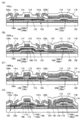
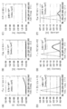
도 27의 (A) 내지 (F)는 TDS 분석 결과를 나타낸 도면.
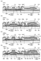
도 28의 (A) 내지 (D)는 트랜지스터의 Id-Vg 특성을 나타낸 도면.
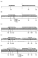
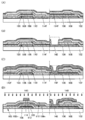
도 29는 트랜지스터의 신뢰성 시험 결과를 나타낸 도면.1A and 1B are diagrams showing a configuration example of a transistor.
2A and 2B are diagrams showing a configuration example of a transistor.
3A and 3B are diagrams showing a configuration example of a transistor.
4A to 4C are diagrams showing a configuration example of a transistor.
5A to 5C are diagrams showing a configuration example of a transistor.
6A to 6C are diagrams showing a configuration example of a transistor.
7A to 7C are diagrams showing a configuration example of a transistor.
8A to 8D are diagrams showing a configuration example of a transistor.
9A to 9D are diagrams showing a configuration example of a transistor.
10A to 10D are diagrams showing a configuration example of a transistor.
11A to 11E are diagrams for explaining a method of manufacturing a transistor.
12A to 12D are diagrams for explaining a method of manufacturing a transistor.
13A and 13B are diagrams for explaining a method of manufacturing a transistor.
14A to 14D are diagrams for explaining a method of manufacturing a transistor.
15A to 15C are top views of the display device.
16 is a cross-sectional view of a display device.
17 is a cross-sectional view of a display device.
18 is a cross-sectional view of a display device.
19 is a cross-sectional view of a display device.
20A is a block diagram of a display device, and FIGS. 20B and 20C are circuit diagrams of the display device.
21A, 21C, and 21D are circuit diagrams of a display device, and FIG. 21B is a timing chart.
22A and 22B are diagrams showing a configuration example of a display module.
23A and 23B are diagrams showing a configuration example of an electronic device.
24A to 24E are diagrams showing a configuration example of an electronic device.
25A to 25G are diagrams showing a configuration example of an electronic device.
26A to 26D are diagrams showing configuration examples of electronic devices.
27 (A) to (F) are diagrams showing the results of TDS analysis.
28A to 28D are diagrams showing Id-Vg characteristics of a transistor.
29 is a diagram showing the results of a reliability test of a transistor.
이하에서, 실시형태에 대하여 도면을 참조하면서 설명한다. 다만, 실시형태는 많은 상이한 형태에서 실시하는 것이 가능하고, 취지 및 그 범위에서 벗어남이 없이 그 형태 및 상세한 사항을 다양하게 변경할 수 있는 것은 통상의 기술자라면 용이하게 이해할 수 있다. 따라서, 본 발명은 이하의 실시형태의 기재 내용에 한정하여 해석되는 것은 아니다.Hereinafter, embodiments will be described with reference to the drawings. However, the embodiments can be implemented in many different forms, and that the form and details can be changed in various ways without departing from the spirit and scope can be easily understood by those of ordinary skill in the art. Therefore, the present invention is not interpreted as being limited to the description of the following embodiments.
또한 본 명세서에서 설명하는 각 도면에서, 각 구성 요소의 크기, 층의 두께, 또는 영역은 명료화를 위하여 과장되어 있는 경우가 있다.In addition, in each drawing described in the present specification, the size of each component, the thickness of the layer, or the area may be exaggerated for clarity.
또한 본 명세서 등에서 사용하는 '제 1', '제 2', '제 3'이라는 서수사는 구성 요소의 혼동을 피하기 위하여 붙인 것이고, 수적으로 한정하는 것이 아니다.In addition, the ordinal numbers'first','second', and'third' used in this specification and the like are attached to avoid confusion of constituent elements, and are not limited in number.
또한 본 명세서 등에서, '위에', '아래에' 등 배치를 나타내는 말은, 구성 요소끼리의 위치 관계를 도면을 참조하여 설명하기 위하여 편의상 사용하고 있다. 또한 구성 요소끼리의 위치 관계는 각 구성을 묘사하는 방향에 따라 적절히 변화되는 것이다. 따라서, 명세서에서 설명한 말에 한정되지 않고, 상황에 따라 적절히 환언할 수 있다.In addition, in this specification and the like, words indicating an arrangement such as'above' and'below' are used for convenience in order to describe the positional relationship between components with reference to the drawings. In addition, the positional relationship between components is appropriately changed according to the direction in which each component is described. Therefore, it is not limited to the words described in the specification, and can be appropriately translated according to the situation.
또한 본 명세서 등에서, 트랜지스터가 가지는 소스와 드레인의 기능은 상이한 극성의 트랜지스터를 채용하는 경우나, 회로 동작에서 전류의 방향이 변화되는 경우 등에는 서로 바뀔 수 있다. 그러므로, 소스나 드레인이라는 용어는 서로 바꿔 사용할 수 있는 것으로 한다.In addition, in the present specification and the like, the functions of the source and the drain of the transistor may be interchanged with each other when a transistor having a different polarity is employed or when the direction of current is changed in a circuit operation. Therefore, the terms source and drain are assumed to be interchangeable.
또한 본 명세서 등에서, 트랜지스터의 채널 길이 방향이란 소스 영역과 드레인 영역 사이를 최단 거리로 연결하는 직선에 평행한 방향 중 하나를 말한다. 즉 채널 길이 방향이란 트랜지스터가 온 상태일 때 반도체층을 흐르는 전류의 방향 중 하나에 상당한다. 또한 채널 폭 방향이란 상기 채널 길이 방향과 직교하는 방향을 말한다. 또한 트랜지스터의 구조나 형상에 따라서는 채널 길이 방향 및 채널 폭 방향은 하나로 정해지지 않는 경우가 있다.In addition, in the present specification and the like, the channel length direction of a transistor refers to one of directions parallel to a straight line connecting the source region and the drain region with the shortest distance. That is, the channel length direction corresponds to one of the directions of the current flowing through the semiconductor layer when the transistor is turned on. In addition, the channel width direction refers to a direction orthogonal to the channel length direction. In addition, depending on the structure and shape of the transistor, the channel length direction and the channel width direction may not be determined as one.
또한 본 명세서 등에서, '전기적으로 접속'에는, '어떠한 전기적 작용을 가지는 것'을 통하여 접속되어 있는 경우가 포함된다. 여기서, '어떠한 전기적 작용을 가지는 것'은 접속 대상 간에서의 전기 신호의 주고받음을 가능하게 하는 것이면 특별한 제한을 받지 않는다. 예를 들어, '어떠한 전기적 작용을 가지는 것'에는 전극이나 배선을 비롯하여 트랜지스터 등의 스위칭 소자, 저항 소자, 인덕터, 커패시터, 이들 외 각종 기능을 가지는 소자 등이 포함된다.In addition, in the present specification and the like, the "electrical connection" includes the case of being connected through "having some electrical action". Here,'having some electrical action' is not subject to any particular limitation as long as it enables the exchange of electrical signals between the objects to be connected. For example,'something having an electrical action' includes electrodes and wiring, as well as switching elements such as transistors, resistance elements, inductors, capacitors, and elements having various functions.
또한 본 명세서 등에서, '막'이라는 용어와 '층'이라는 용어는 서로 바꿀 수 있다. 예를 들어, '도전층'이나 '절연층'이라는 용어는 '도전막'이나 '절연막'이라는 용어로 상호적으로 교환하는 것이 가능한 경우가 있다.In addition, in the present specification and the like, the term'film' and the term'layer' may be interchanged. For example, the terms "conductive layer" or "insulating layer" may be interchanged with the terms "conductive film" or "insulating film" in some cases.
또한 본 명세서 등에서 특별히 언급하지 않는 한, 오프 전류란 트랜지스터가 오프 상태(비도통 상태, 차단 상태라고도 함)일 때의 드레인 전류를 말한다. 오프 상태란 특별히 언급하지 않는 한 n채널 트랜지스터에서는 게이트와 소스 간의 전압(Vgs)이 문턱 전압(Vth)보다 낮은(p채널형 트랜지스터에서는 Vth보다 높은) 상태를 말한다.In addition, unless specifically stated in this specification or the like, the off current refers to the drain current when the transistor is in an off state (also referred to as a non-conducting state or a blocking state). The off state refers to a state in which the voltage (V gs ) between the gate and the source is lower than the threshold voltage (V th ) in the n-channel transistor (higher than V th in the p-channel transistor) unless otherwise noted.
본 명세서 등에서 표시 장치의 일 형태인 표시 패널은 표시면에 화상 등을 표시(출력)하는 기능을 가지는 것이다. 따라서 표시 패널은 출력 장치의 일 형태이다.In this specification and the like, a display panel, which is a form of a display device, has a function of displaying (outputting) an image or the like on a display surface. Therefore, the display panel is a type of output device.
또한 본 명세서 등에서는 표시 패널의 기판에, 예를 들어 FPC(Flexible Printed Circuit) 또는 TCP(Tape Carrier Package) 등의 커넥터가 장착된 것, 또는 기판에 COG(Chip On Glass) 방식 등에 의하여 IC(Integrated Circuit)가 실장된 것을 표시 패널 모듈, 표시 모듈, 또는 단순히 표시 패널 등이라고 부르는 경우가 있다.In addition, in this specification, for example, a connector such as FPC (Flexible Printed Circuit) or TCP (Tape Carrier Package) is mounted on the substrate of the display panel, or IC (Integrated IC) is applied to the substrate by a COG (Chip On Glass) method. Circuit) mounted is sometimes called a display panel module, a display module, or simply a display panel.
또한 본 명세서 등에서 표시 장치의 일 형태인 터치 패널은 표시면에 화상 등을 표시하는 기능과, 표시면에 손가락이나 스타일러스 등 피검지체가 접촉되거나, 가압하거나, 또는 근접되는 것을 검출하는 터치 센서로서의 기능을 가진다. 따라서 터치 패널은 입출력 장치의 일 형태이다.In addition, in the present specification, a touch panel, which is a form of a display device, functions as a touch sensor that displays an image, etc. on the display surface, and detects contact, pressure, or proximity of a target object such as a finger or stylus to the display surface. Have. Therefore, the touch panel is a type of input/output device.
터치 패널은, 예를 들어 터치 센서를 구비한 표시 패널(또는 표시 장치), 터치 센서 기능을 구비한 표시 패널(또는 표시 장치)이라고도 부를 수 있다. 터치 패널은 표시 패널과 터치 센서 패널을 가지는 구성으로 할 수도 있다. 또는, 표시 패널의 내부 또는 표면에 터치 센서로서의 기능을 가지는 구성으로 할 수도 있다.The touch panel may also be referred to as, for example, a display panel (or display device) having a touch sensor or a display panel (or display device) having a touch sensor function. The touch panel may have a display panel and a touch sensor panel. Alternatively, it may be configured to have a function as a touch sensor inside or on the surface of the display panel.
또한 본 명세서 등에서는, 터치 패널의 기판에 커넥터나 IC가 실장된 것을 터치 패널 모듈, 표시 모듈, 또는 단순히 터치 패널 등이라고 부르는 경우가 있다.In addition, in this specification and the like, a connector or an IC mounted on a substrate of a touch panel may be referred to as a touch panel module, a display module, or simply a touch panel.
(실시형태 1)(Embodiment 1)
본 실시형태에서는 본 발명의 일 형태의 반도체 장치 및 그 제작 방법에 대하여 설명한다. 특히 본 실시형태에서는 반도체 장치의 일례로서, 채널이 형성되는 반도체층에 산화물 반도체를 사용한 트랜지스터에 대하여 설명한다.In this embodiment, a semiconductor device of one embodiment of the present invention and a method of manufacturing the same will be described. In particular, in this embodiment, as an example of a semiconductor device, a transistor using an oxide semiconductor for a semiconductor layer in which a channel is formed will be described.
[구성예 1][Configuration Example 1]
<구성예 1-1><Configuration Example 1-1>
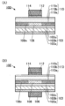
도 1의 (A)에 트랜지스터(10)의 채널 길이 방향의 단면 개략도를 도시하였다.1A is a schematic cross-sectional view of the
트랜지스터(10)는 절연층(103), 반도체층(108), 절연층(110), 금속 산화물층(114), 및 도전층(112)을 가진다. 절연층(110)은 게이트 절연층으로서 기능한다. 도전층(112)은 게이트 전극으로서 기능한다.The
도전층(112)으로서, 금속 또는 합금을 포함한 도전막을 사용하면, 전기 저항을 억제할 수 있어 바람직하다. 또한 도전층(112)으로서 산화물을 포함한 도전막을 사용하여도 좋다.As the
금속 산화물층(114)은 절연층(110) 내에 산소를 공급하는 기능을 가진다. 또한 도전층(112)으로서 산화되기 쉬운 금속 또는 합금을 포함한 도전막을 사용한 경우에는, 금속 산화물층(114)은 절연층(110) 내의 산소로 인하여 도전층(112)이 산화되는 것을 방지하는 배리어층으로서 기능시킬 수도 있다. 또한 금속 산화물층(114)을 도전층(112)의 형성 전에 제거함으로써, 도전층(112)과 절연층(110)이 접하는 구성으로 하여도 좋다. 또한 금속 산화물층(114)은 불필요한 경우에는 제공하지 않는 구성으로 하여도 좋다.The
반도체층(108)과 접하는 절연층(110)은 산화물 절연막을 가지는 것이 바람직하다. 또한 절연층(110)은 화학량론적 조성보다 과잉으로 산소를 포함한 영역을 가지는 것이 더 바람직하다. 바꿔 말하면, 절연층(110)은 산소를 방출할 수 있는 절연막을 가지는 것이 바람직하다. 예를 들어 산소 분위기하에서 절연층(110)을 형성하거나, 성막 후의 절연층(110)에 대하여 산소 분위기하에서의 열 처리, 플라스마 처리 등을 수행하거나, 또는 절연층(110) 위에 산소 분위기하에서 산화물막을 형성함으로써 절연층(110) 내에 산소를 공급할 수도 있다.It is preferable that the insulating
절연층(110)은 예를 들어 스퍼터링법, 화학 기상 퇴적(CVD: Chemical Vapor Deposition)법, 진공 증착법, 펄스 레이저 퇴적(PLD: Pulsed Laser Deposition)법, 원자층 퇴적(ALD: Atomic Layer Deposition)법 등을 사용하여 형성할 수 있다. 또한 CVD법으로서는, 플라스마 화학 기상 퇴적(PECVD: Plasma Enhanced CVD)법이나, 열 CVD법 등이 있다.The insulating
특히, 절연층(110)은 PECVD법에 의하여 형성하는 것이 바람직하다.In particular, the insulating
반도체층(108)은 반도체 특성을 나타내는 금속 산화물(이하, 산화물 반도체라고도 함)을 포함한다. 반도체층(108)은 적어도 인듐 및 산소를 포함하는 것이 바람직하다. 반도체층(108)이 인듐의 산화물을 포함함으로써 캐리어 이동도를 높일 수 있다. 예를 들어 비정질 실리콘을 사용한 경우보다 큰 전류를 흘릴 수 있는 트랜지스터를 실현할 수 있다.The
반도체층(108)에서 도전층(112)과 중첩되는 영역이 채널 형성 영역으로서 기능한다. 또한 반도체층(108)은 채널 형성 영역을 개재(介在)하여 한 쌍의 저저항 영역(108n)을 가지는 것이 바람직하다. 저저항 영역(108n)은 채널 형성 영역보다 캐리어 농도가 높은 영역이고, 소스 영역 및 드레인 영역으로서 기능한다.A region of the
저저항 영역(108n)은 채널 형성 영역보다 저저항인 영역, 캐리어 농도가 높은 영역, 산소 결손량이 많은 영역, 수소 농도가 높은 영역, 또는 불순물 농도가 높은 영역이라고도 할 수 있다.The
절연층(103)은 절연막(103a), 절연막(103b), 및 절연막(103c)이 적층된 적층 구조를 가진다. 절연막(103c)은 반도체층(108)과 접한다.The insulating
절연층(103)은 피형성면 측으로부터 불순물이 반도체층(108) 등으로 확산되는 것을 억제하는 배리어층으로서 기능하는 것이 바람직하다. 절연층(103)은 막의 응력이 작은 것, 수소나 물을 방출하기 어려운 것, 및 수소나 물을 확산시키기 어려운 것 중 하나 이상을 만족시키는 것이 바람직하고, 이들 모두를 만족시키는 것이 더 바람직하다.The insulating
절연층(103)이 가지는 3개의 절연막 중, 가장 피형성면 측에 위치하는 절연막(103a)에는 질소를 포함한 절연막을 사용하는 것이 바람직하다. 한편, 반도체층(108)과 접하는 절연막(103c)에는 산소를 포함한 절연막을 사용하는 것이 바람직하다. 또한 절연층(103)이 가지는 3개의 절연막은 각각 플라스마 CVD 장치를 사용하여, 대기에 노출시키지 않고 연속적으로 성막하는 것이 바람직하다.Among the three insulating films of the insulating
절연막(103a)은 아래쪽으로부터의 불순물 확산을 방지할 수 있는 치밀한 막인 것이 바람직하다. 절연막(103a)은 절연막(103a)의 피형성면 측의 부재(예를 들어 기판 등)에 포함되는 금속 원소, 수소, 물 등을 차단할 수 있는 막인 것이 바람직하다. 그러므로, 절연막(103a)에는 절연막(103b)보다 성막 속도가 느린 조건에서 성막한 절연막을 적용할 수 있다.The insulating
절연막(103a)으로서는, 예를 들어 질화 실리콘막, 질화산화 실리콘막, 질화 알루미늄막, 질화 하프늄막 등 질소를 포함한 절연막을 사용할 수 있다. 특히, 절연막(103a)으로서 플라스마 CVD 장치를 사용하여 성막한 치밀한 질화 실리콘막을 사용하는 것이 바람직하다. 이러한 질소를 포함한 절연막을 사용함으로써, 두께가 얇은 경우에도, 피형성면 측으로부터 불순물이 확산되는 것을 적합하게 억제할 수 있다.As the insulating
또한 본 명세서에서, 산화질화물이란, 그 조성으로서 질소보다 산소의 함유량이 많은 재료를 가리키고, 질화산화물이란, 그 조성으로서 산소보다 질소의 함유량이 많은 재료를 가리킨다. 예를 들어, 산화질화 실리콘이라고 기재한 경우에는, 그 조성으로서 질소보다 산소의 함유량이 많은 재료를 가리키고, 질화산화 실리콘이라고 기재한 경우에는, 그 조성으로서 산소보다 질소의 함유량이 많은 재료를 가리킨다.Incidentally, in this specification, the oxynitride refers to a material having more oxygen than nitrogen as its composition, and the nitride oxide refers to a material having more nitrogen than oxygen as its composition. For example, when described as silicon oxynitride, the composition refers to a material containing more oxygen than nitrogen, and when described as silicon nitride oxide, the composition refers to a material containing more nitrogen than oxygen.
또한 본 명세서에서, 각각 같은 원소를 포함하는 산화질화물과 질화산화물이 기재된 경우, 산화질화물에는, 질화산화물보다 산소의 함유량이 많은 것 및 질소의 함유량이 적은 것 중 어느 한쪽 또는 양쪽을 만족시키는 재료가 포함된다. 마찬가지로, 질화산화물에는, 산화질화물보다 산소의 함유량이 적은 것 및 질소의 함유량이 많은 것 중 어느 한쪽 또는 양쪽을 만족시키는 재료가 포함된다. 예를 들어, 산화질화 실리콘과 질화산화 실리콘이 기재된 경우, 산화질화 실리콘에는 질화산화 실리콘보다 산소의 함유량이 많고 또한 질소의 함유량이 적은 재료가 포함된다. 마찬가지로, 질화산화 실리콘에는 산화질화 실리콘보다 산소의 함유량이 적고 또한 질소의 함유량이 많은 재료가 포함된다.In addition, in the present specification, when an oxynitride and a nitride oxide each containing the same element are described, the oxynitride contains a material that satisfies either or both of those having a higher oxygen content and a lower nitrogen content than the nitride oxide. Included. Similarly, the nitride oxide contains a material that satisfies either or both of those having a lower oxygen content and a higher nitrogen content than the oxynitride. For example, when silicon oxynitride and silicon nitride oxide are described, the silicon oxynitride includes a material containing more oxygen and less nitrogen than silicon nitride oxide. Similarly, silicon nitride oxide contains a material containing less oxygen and more nitrogen than silicon oxynitride.
반도체층(108)과 접하는 절연막(103c)은 산화물을 포함한 절연막으로 형성되어 있는 것이 바람직하다. 특히 절연막(103c)에는 산화물막을 사용하는 것이 바람직하다. 또한 절연막(103c)으로서는, 그 표면에 물 등의 불순물이 흡착되기 어려운 치밀한 절연막을 사용하는 것이 바람직하다. 또한 결함이 가능한 한 적고, 물이나 수소 등의 불순물이 저감된 절연막을 사용하는 것이 바람직하다.It is preferable that the insulating
절연막(103c)은 화학량론적 조성보다 과잉으로 산소를 포함한 영역을 가지는 것이 더 바람직하다. 바꿔 말하면, 절연막(103c)은 가열에 의하여 산소를 방출할 수 있는 절연막으로 하는 것이 바람직하다. 예를 들어 산소 분위기하에서 절연막(103c)을 형성하거나, 성막 후의 절연막(103c)에 대하여 산소 분위기하에서의 열 처리, 플라스마 처리 등을 수행하거나, 또는 절연막(103c) 위에 산소 분위기하에서 산화물막을 형성함으로써 절연막(103c) 내에 산소를 공급할 수도 있다. 또는, 절연막(103c) 위에 가열에 의하여 산소를 방출할 수 있는 절연막을 형성한 후에 가열 처리를 수행함으로써, 상기 절연막으로부터 절연막(103c) 내에 산소를 공급하여도 좋다.It is more preferable that the insulating
또한 반도체층(108)이 되는 금속 산화물막을, 산소를 포함한 분위기하에서 스퍼터링법에 의하여 형성할 때, 절연막(103c) 내에 산소를 공급할 수 있다. 그리고, 반도체층이 되는 금속 산화물막을 형성한 후에 가열 처리를 수행함으로써, 절연막(103c) 내의 산소를 상기 금속 산화물막에 공급하여 금속 산화물막 내의 산소 결손을 저감할 수 있다.Further, when the metal oxide film used as the
절연막(103c)으로서는 예를 들어 산화 실리콘막, 산화질화 실리콘막, 질화산화 실리콘막, 산화 알루미늄막, 산화 하프늄막, 산화 이트륨막, 산화 지르코늄막, 산화 갈륨막, 산화 탄탈럼막, 산화 마그네슘막, 산화 란타넘막, 산화 세륨막, 및 산화 네오디뮴막 중 1종류 이상을 포함한 절연층을 사용할 수 있다. 특히, 절연막(103c)으로서 산화 실리콘막 또는 산화질화 실리콘막을 사용하는 것이 바람직하다.As the insulating
절연막(103a)과 절연막(103c) 사이에 위치하는 절연막(103b)은 응력이 작고, 성막 속도가 빠른 조건에서 성막된 절연막을 사용하는 것이 바람직하다. 예를 들어, 절연막(103b)은 절연막(103a) 및 절연막(103c)보다 응력이 작은 막인 것이 바람직하다. 또한 절연막(103b)은 절연막(103a) 및 절연막(103c)보다 성막 속도가 빠른 조건에서 성막되는 막인 것이 바람직하다.As for the insulating
절연막(103b)으로서는, 수소나 물을 가능한 한 방출하지 않는 절연막을 사용하는 것이 바람직하다. 이러한 절연막을 사용함으로써, 가열 처리나 공정 중에 가해지는 열 등에 의하여 절연막(103b)으로부터 절연막(103c)을 통하여 반도체층(108)으로 수소나 물이 확산되는 것을 방지하여, 반도체층(108)의 채널 형성 영역에서의 캐리어 농도를 낮게 할 수 있다.As the insulating
또한 절연막(103b)은 산소를 흡인하기 어려운 절연막을 사용하는 것이 바람직하다. 바꿔 말하면, 산소가 확산되기 어려운 절연막을 사용하는 것이 바람직하다. 이로써, 절연막(103c)으로부터 반도체층(108)(또는 반도체층(108)이 되는 금속 산화물막)에 산소를 공급하기 위한 열 처리를 수행할 때에 절연막(103c)으로부터 절연막(103b) 측으로 산소가 확산되어 반도체층(108)에 공급되는 산소의 양이 저감되는 것을 억제할 수 있다.In addition, it is preferable to use an insulating film that is difficult to absorb oxygen as the insulating
절연막(103b)으로서는 예를 들어 질화산화 실리콘막, 질화 실리콘막, 산화 알루미늄막, 산화 하프늄막, 질화 알루미늄막, 질화 하프늄막을 1종류 이상 포함하는 절연층을 사용할 수 있다. 특히, 절연막(103b)으로서 질화산화 실리콘막 또는 질화 실리콘막을 사용하는 것이 바람직하다.As the insulating
절연층(103)을 구성하는 절연막(103a), 절연막(103b), 및 절연막(103c) 중 절연막(103b)의 두께를 가장 두껍게 하는 것이 바람직하다. 또한 절연층(103)의 두께(총두께)는 절연층(103)에 요구되는 비유전율의 값과 절연층(103)에 요구되는 절연 내압의 성능 등을 고려하여, 각 절연막의 비유전율의 값과 각 절연막의 두께를 바탕으로 결정할 수 있다. 즉, 각 절연막의 두께는 상기 요구를 만족시키는 범위에서 각각 조정할 수 있다.Among the insulating
특히, 절연막(103b)은 절연막(103a)보다 두꺼운 것이 바람직하다. 절연막(103b)을 절연막(103a)보다 두껍게 함으로써, 절연막(103a)으로서 가열에 의하여 수소를 방출하기 쉬운 막을 사용한 경우에도, 절연막(103c)에 도달될 수 있는 수소의 양을 저감할 수 있다. 또한 절연막(103a)을 절연막(103b)보다 얇게 함으로써, 절연막(103a)의 부피를 상대적으로 작게 할 수 있기 때문에, 절연막(103a)이 방출할 수 있는 수소의 양 자체를 저감할 수 있다.In particular, the insulating
또한 절연막(103b)은 절연막(103c)보다 두꺼운 것이 바람직하다. 절연막(103c)이 지나치게 두꺼우면, 절연막(103c) 내에 산소를 공급하는 처리를 수행한 경우에, 가열에 의하여 절연막(103c)으로부터 방출되지 않고 잔류하는 산소의 양이 많아지기 때문에, 결과적으로 반도체층(108)(또는 반도체층(108)이 되는 금속 산화물막)에 공급될 수 있는 산소의 양이 저감될 우려가 있다. 그러므로, 절연막(103c)을 절연막(103b)보다 얇게 함으로써(부피를 작게 함으로써), 가열 후에 절연막(103c) 내에 잔류하는 산소의 양을 저감할 수 있다. 그 결과, 절연막(103c)에 공급된 산소 중, 반도체층(108)에 공급되는 산소의 비율을 크게 할 수 있기 때문에, 반도체층(108)에 공급되는 산소의 양을 효과적으로 늘릴 수 있다.In addition, the insulating
또한 가장 두꺼운 절연막(103b)을 성막 속도가 빠른 조건에서 형성하고, 이것보다 얇은 절연막(103a) 및 절연막(103c)을 성막 속도가 느린 조건에서 치밀한 막이 되도록 형성함으로써, 신뢰성을 손실하지 않고 절연층(103)의 성막 시간을 단축할 수 있어, 생산성을 높일 수 있다.In addition, by forming the thickest insulating
여기서, 절연막(103a)에는 적어도 실리콘 및 질소를 포함하는 절연막, 대표적으로는 질화 실리콘막 또는 질화산화 실리콘막을 사용하는 것이 바람직하다. 또한 절연막(103b)에는 적어도 실리콘, 질소, 및 산소를 포함하는 절연막, 대표적으로는 질화산화 실리콘막 또는 산화질화 실리콘막을 사용하는 것이 바람직하다. 또한 절연막(103c)에는 적어도 실리콘 및 산소를 포함하는 절연막, 대표적으로는 산화 실리콘막 또는 산화질화 실리콘막을 사용하는 것이 바람직하다. 이때, 절연막(103b)에 포함되는 산소의 양은 절연막(103a)보다 많고 또한 절연막(103c)보다 적은 것이 바람직하다. 또한 절연막(103b)에 포함되는 질소의 양은 절연막(103a)보다 적고 또한 절연막(103c)보다 많은 것이 바람직하다.Here, it is preferable to use an insulating film containing at least silicon and nitrogen, typically a silicon nitride film or a silicon nitride oxide film, for the insulating
절연막(103a), 절연막(103b), 및 절연막(103c)에 포함되는 산소 및 질소의 함유량은 이차 이온 질량 분석법(SIMS: Secondary Ion Mass Spectrometry)이나 X선 광전자 분광법(XPS: X-ray Photoelectron Spectroscopy) 등의 분석법에 의하여 분석할 수 있다. 막 내의 목적 원소의 함유율이 높은(예를 들어 0.5atoms/cm3 이상 또는 1atoms/cm3 이상) 경우에는 XPS가 적합하다. 한편, 막 내의 목적 원소의 함유율이 낮은(예를 들어 0.5atoms/cm3 이하 또는 1atoms/cm3 이하) 경우에는 SIMS가 적합하다. 막 내의 원소의 함유량을 비교할 때, SIMS와 XPS의 양쪽의 분석 방법을 사용한 복합 해석을 수행하는 것이 더 바람직하다.The content of oxygen and nitrogen contained in the insulating
절연막(103b)의 두께는 절연막(103a)의 두께에 대하여 2배 이상, 바람직하게는 3배 이상, 더 바람직하게는 5배 이상이며, 20배 이하, 바람직하게는 15배 이하이다. 또한 절연막(103b)의 두께는 절연막(103c)의 두께에 대하여 2배 이상, 바람직하게는 3배 이상, 더 바람직하게는 5배 이상이며, 20배 이하, 바람직하게는 15배 이하이다. 또한 상술한 상한값 및 하한값은 임의로 조합할 수 있다.The thickness of the insulating
또한 절연막(103b)의 두께는 절연층(103) 전체의 두께(총두께라고도 함)를 100%로 하였을 때, 34% 이상, 바람직하게는 40% 이상, 더 바람직하게는 50% 이상, 더욱 바람직하게는 60% 이상, 더더욱 바람직하게는 70% 이상, 나아가 더더욱 바람직하게는 80% 이상이며, 95% 이하 또는 90% 이하로 할 수 있다. 절연층(103)의 총두께에 대한 절연막(103b)의 두께의 비율이 높을수록 생산성을 높일 수 있다.In addition, the thickness of the insulating
절연막(103a)은 가능한 한 얇은 것이 바람직하고, 예를 들어 5㎚ 이상, 바람직하게는 8㎚ 이상, 더 바람직하게는 10㎚ 이상, 더욱 바람직하게는 15㎚ 이상이며, 50㎚ 이하, 바람직하게는 40㎚ 이하, 더 바람직하게는 30㎚ 이하, 더욱 바람직하게는 20㎚ 이하로 할 수 있다. 또한 상술한 상한값 및 하한값은 임의로 조합할 수 있다. 대표적으로는 15㎚ 이상 50㎚ 이하, 또는 15㎚ 이상 20㎚ 이하의 막 두께로 하는 것이 바람직하다.The insulating
절연막(103c)도 가능한 한 얇은 것이 바람직하고, 예를 들어 5㎚ 이상, 바람직하게는 8㎚ 이상, 더 바람직하게는 10㎚ 이상, 더욱 바람직하게는 15㎚ 이상이며, 50㎚ 이하, 바람직하게는 40㎚ 이하, 더 바람직하게는 30㎚ 이하, 더욱 바람직하게는 20㎚ 이하로 할 수 있다. 또한 상술한 상한값 및 하한값은 임의로 조합할 수 있다. 대표적으로는 15㎚ 이상 50㎚ 이하, 또는 15㎚ 이상 20㎚ 이하의 막 두께로 하는 것이 바람직하다.The insulating
절연막(103a) 및 절연막(103c)은 모두 가능한 한 얇은 것이 바람직하지만, 성막 장치의 성능에 맞추어 편차가 작은 조건에서 성막 가능한 것이 매우 중요하다. 그러므로, 절연막(103a) 및 절연막(103c) 각각에는 편차가 충분히 작게 되는 최저한도의 두께를 선택하는 것이 바람직하다.It is preferable that both the insulating
절연막(103b)으로서는, 요구되는 비유전율이나 내압 등의 물성 값을 만족시키도록 결정되는 절연층(103)의 총두께에서, 절연막(103a)과 절연막(103c)의 두께를 뺀 두께로 하면 좋다. 예를 들어, 절연막(103b)은 20㎚ 이상, 50㎚ 이상, 100㎚ 이상, 150㎚ 이상, 또는 200㎚ 이상이며, 500㎚ 이하, 400㎚ 이하, 또는 350㎚ 이하의 두께로 하는 것이 바람직하다. 또한 상술한 상한값 및 하한값은 임의로 조합할 수 있다.The insulating
또한 절연막(103a), 절연막(103b), 및 절연막(103c) 중, 절연막(103b)이 다른 2개의 절연막보다 막 밀도가 작은 막이 될 수 있다. 따라서, 절연층(103)의 단면에서의 투과형 전자 현미경(TEM: Transmission Electron Microscopy) 이미지 등에서, 상기 막 밀도의 차이가 절연막(103a), 절연막(103b), 및 절연막(103c)의 콘트라스트의 차이로서 관찰되어, 이들을 구별할 수 있는 경우가 있다. 특히, 절연막(103a) 및 절연막(103b) 각각에 플라스마 CVD법으로 형성한 질화 실리콘막 또는 질화산화 실리콘막을 사용한 경우에도, 이들의 경계를 확인할 수 있는 경우가 있다. 또한 조성이나 밀도가 가까운 경우 등에서는 이들의 경계가 불명료하게 되는 경우가 있다.In addition, of the insulating
반도체층(108)에 사용하는 반도체 재료의 결정성에 대해서는 특별히 한정되지 않고, 비정질 반도체, 단결정 반도체, 및 단결정 이외의 결정성을 가지는 반도체(미결정 반도체, 다결정 반도체, 또는 일부에 결정 영역을 가지는 반도체) 중 임의의 것을 사용하여도 좋다. 단결정 반도체 또는 결정성을 가지는 반도체를 사용하면, 트랜지스터 특성의 열화를 억제할 수 있어 바람직하다.The crystallinity of the semiconductor material used for the
트랜지스터의 반도체층은 금속 산화물(산화물 반도체라고도 함)을 가지는 것이 바람직하다. 또는 트랜지스터의 반도체층은 실리콘을 가져도 좋다. 실리콘으로서는 비정질 실리콘, 결정성 실리콘(저온 폴리 실리콘, 단결정 실리콘 등) 등을 들 수 있다.It is preferable that the semiconductor layer of the transistor has a metal oxide (also referred to as an oxide semiconductor). Alternatively, the semiconductor layer of the transistor may have silicon. Examples of silicon include amorphous silicon and crystalline silicon (low temperature polysilicon, single crystal silicon, etc.).
반도체층(108)으로서 금속 산화물을 사용하는 경우, 예를 들어 인듐, M(M은 갈륨, 알루미늄, 실리콘, 붕소, 이트륨, 주석, 구리, 바나듐, 베릴륨, 타이타늄, 철, 니켈, 저마늄, 지르코늄, 몰리브데넘, 란타넘, 세륨, 네오디뮴, 하프늄, 탄탈럼, 텅스텐, 및 마그네슘에서 선택되는 1종류 또는 복수 종류), 및 아연을 가지는 것이 바람직하다. 특히 M은 알루미늄, 갈륨, 이트륨, 및 주석에서 선택되는 1종류 또는 복수 종류인 것이 바람직하다.When a metal oxide is used as the
특히 반도체층으로서 인듐(In), 갈륨(Ga), 및 아연(Zn)을 포함한 산화물(IGZO라고도 표기함)을 사용하는 것이 바람직하다.In particular, it is preferable to use an oxide (also referred to as IGZO) containing indium (In), gallium (Ga), and zinc (Zn) as the semiconductor layer.
또한 반도체층으로서 인듐, 갈륨, 및 아연에 더하여 알루미늄, 실리콘, 붕소, 이트륨, 주석, 구리, 바나듐, 베릴륨, 타이타늄, 철, 니켈, 저마늄, 지르코늄, 몰리브데넘, 란타넘, 세륨, 네오디뮴, 하프늄, 탄탈럼, 텅스텐, 및 마그네슘 중 하나 이상을 포함한 산화물을 사용할 수도 있다. 특히, 반도체층으로서 인듐, 갈륨, 및 아연에 더하여 주석, 알루미늄, 또는 실리콘을 포함한 산화물을 사용하면, 높은 전계 효과 이동도가 실현된 트랜지스터로 할 수 있기 때문에 바람직하다.In addition to indium, gallium, and zinc as a semiconductor layer, aluminum, silicon, boron, yttrium, tin, copper, vanadium, beryllium, titanium, iron, nickel, germanium, zirconium, molybdenum, lanthanum, cerium, neodymium, Oxides containing one or more of hafnium, tantalum, tungsten, and magnesium may also be used. In particular, the use of an oxide containing tin, aluminum, or silicon in addition to indium, gallium, and zinc as the semiconductor layer is preferable because a transistor having high field effect mobility can be achieved.
반도체층이 In-M-Zn 산화물인 경우, In-M-Zn 산화물을 성막하기 위하여 사용하는 스퍼터링 타깃은 M에 대한 In의 원자수비가 1 이상인 것이 바람직하다. 이러한 스퍼터링 타깃의 금속 원소의 원자수비로서 In:M:Zn=1:1:1, In:M:Zn=1:1:1.2, In:M:Zn=2:1:3, In:M:Zn=3:1:2, In:M:Zn=4:2:3, In:M:Zn=4:2:4.1, In:M:Zn=5:1:3, In:M:Zn=10:1:3, In:M:Zn=5:1:6, In:M:Zn=5:1:7, In:M:Zn=5:1:8, In:M:Zn=6:1:6, In:M:Zn=5:2:5 등을 들 수 있다. 또한 상기 구성에서, 원소 M으로서 2종류 이상의 원소를 포함하는 경우, 상기 원자수비에서의 M의 비율은 상기 2종류 이상의 금속 원소의 원자수의 합계에 대응하는 것으로 한다.When the semiconductor layer is an In-M-Zn oxide, the sputtering target used to form an In-M-Zn oxide preferably has an atomic ratio of In to M of 1 or more. As the atomic ratio of the metal elements of the sputtering target, In:M:Zn=1:1:1, In:M:Zn=1:1:1.2, In:M:Zn=2:1:3, In:M: Zn=3:1:2, In:M:Zn=4:2:3, In:M:Zn=4:2:4.1, In:M:Zn=5:1:3, In:M:Zn= 10:1:3, In:M:Zn=5:1:6, In:M:Zn=5:1:7, In:M:Zn=5:1:8, In:M:Zn=6: 1:6, In:M:Zn=5:2:5, etc. are mentioned. In the above configuration, when two or more types of elements are included as the element M, the ratio of M in the atomic number ratio is assumed to correspond to the sum of the number of atoms of the two or more metal elements.
스퍼터링 타깃으로서는 다결정 산화물을 포함한 타깃을 사용하면, 결정성을 가지는 반도체층을 형성하기 쉬워지기 때문에 바람직하다. 또한 성막되는 반도체층의 원자수비는 상기 스퍼터링 타깃에 포함되는 금속 원소의 원자수비의 ±40%의 변동을 포함한다. 예를 들어 반도체층에 사용하는 스퍼터링 타깃의 조성이 In:M:Zn=4:2:4.1[원자수비]인 경우, 성막되는 반도체층의 조성은 In:M:Zn=4:2:3[원자수비] 근방인 경우가 있다.When a target containing a polycrystalline oxide is used as the sputtering target, it is preferable because it becomes easy to form a semiconductor layer having crystallinity. In addition, the atomic ratio of the semiconductor layer to be formed includes a variation of ±40% of the atomic ratio of the metal elements included in the sputtering target. For example, when the composition of the sputtering target used for the semiconductor layer is In:M:Zn=4:2:4.1 [atomic ratio], the composition of the semiconductor layer to be formed is In:M:Zn=4:2:3[ Atomic ratio] in some cases.
또한 원자수비가 In:M:Zn=4:2:3 또는 그 근방이라고 기재된 경우, In을 4로 하였을 때, M이 1 이상 3 이하이고, Zn이 2 이상 4 이하인 경우를 포함한다. 또한 원자수비가 In:M:Zn=5:1:6 또는 그 근방이라고 기재된 경우, In을 5로 하였을 때, M이 0.1보다 크고 2 이하이고, Zn이 5 이상 7 이하인 경우를 포함한다. 또한 원자수비가 In:M:Zn=1:1:1 또는 그 근방이라고 기재하는 경우, In을 1로 하였을 때, M이 0.1보다 크고 2 이하이고, Zn이 0.1보다 크고 2 이하인 경우를 포함한다.In addition, the case where the atomic ratio is described as In:M:Zn=4:2:3 or the vicinity thereof, when In is 4, includes the case where M is 1 or more and 3 or less, and Zn is 2 or more and 4 or less. In addition, when the atomic ratio is described as In:M:Zn=5:1:6 or the vicinity thereof, when In is 5, M is greater than 0.1 and 2 or less, and Zn is 5 or more and 7 or less. In addition, when the atomic ratio is described as In:M:Zn=1:1:1 or in the vicinity thereof, when In is 1, M is greater than 0.1 and 2 or less, and Zn is greater than 0.1 and 2 or less. .
여기서, 반도체층(108)의 조성에 대하여 설명한다. 반도체층(108)은 적어도 인듐과 산소를 포함한 금속 산화물을 포함하는 것이 바람직하다. 또한 반도체층(108)은 이들에 더하여 아연을 포함하여도 좋다. 또한 반도체층(108)은 갈륨을 포함하여도 좋다.Here, the composition of the
여기서, 반도체층(108)의 조성은 트랜지스터(10)의 전기적 특성이나 신뢰성에 큰 영향을 미친다. 예를 들어, 반도체층(108) 내의 인듐의 함유량을 많게 함으로써, 캐리어 이동도가 향상되어, 전계 효과 이동도가 높은 트랜지스터를 실현할 수 있다.Here, the composition of the
여기서, 트랜지스터의 신뢰성을 평가하는 지표의 하나로서, 게이트에 전계를 인가한 상태에서 유지시키는 게이트 바이어스 스트레스 시험(GBT: Gate Bias Stress Test)이 있다. 그 중에서도 소스 전위 및 드레인 전위에 대하여 게이트에 양의 전위를 인가한 상태에서 고온하에서 유지하는 시험을 PBTS(Positive Bias Temperature Stress) 시험, 게이트에 음의 전위를 인가한 상태에서 고온하에서 유지하는 시험을 NBTS(Negative Bias Temperature Stress) 시험이라고 부른다. 또한 백색 LED광 등의 광을 조사한 상태에서 수행하는 PBTS 시험 및 NBTS 시험을 각각 PBTIS(Positive Bias Temperature Illumination Stress) 시험, NBTIS(Negative Bias Temperature Illumination Stress) 시험이라고 부른다.Here, as one of the indexes for evaluating the reliability of a transistor, there is a gate bias stress test (GBT) in which an electric field is applied to the gate and maintained. Among them, PBTS (Positive Bias Temperature Stress) test is a test that maintains a source potential and drain potential under high temperature with a positive potential applied to the gate, and a test that maintains a high temperature with a negative potential applied to the gate. It is called the NBTS (Negative Bias Temperature Stress) test. In addition, the PBTS test and the NBTS test performed under light such as white LED light are called PBTIS (Positive Bias Temperature Illumination Stress) test and NBTIS (Negative Bias Temperature Illumination Stress) test, respectively.
특히 산화물 반도체를 사용한 n형 트랜지스터에서는 트랜지스터를 온 상태(전류를 흘리는 상태)로 할 때 게이트에 양의 전위가 인가되기 때문에, PBTS 시험에서의 문턱 전압의 변동량은 트랜지스터의 신뢰성의 지표로서 착안할 중요한 항목 중 하나가 된다.In particular, in n-type transistors using oxide semiconductors, since a positive potential is applied to the gate when the transistor is turned on (a current flowing state), the fluctuation of the threshold voltage in the PBTS test is an important indicator of the reliability of the transistor. It becomes one of the items.
여기서, 반도체층(108)의 조성으로서, 갈륨을 포함하지 않거나, 또는 갈륨의 함유율이 낮은 금속 산화물막을 사용함으로써, PBTS 시험에서의 문턱 전압의 변동량을 작게 할 수 있다. 또한 갈륨을 포함하는 경우에는, 반도체층(108)의 조성으로서, 인듐의 함유량보다 갈륨의 함유량을 작게 하는 것이 바람직하다. 이로써, 신뢰성이 높은 트랜지스터를 실현할 수 있다.Here, by using a metal oxide film that does not contain gallium or has a low gallium content as the composition of the
PBTS 시험에서 문턱 전압이 변동되는 요인 중 하나로서, 반도체층과 게이트 절연층의 계면 또는 계면 근방에서의 결함 준위를 들 수 있다. 결함 준위 밀도가 클수록, PBTS 시험에서의 열화가 현저해진다. 반도체층에서 게이트 절연층과 접하는 부분에서의 갈륨의 함유량을 작게 함으로써, 상기 결함 준위의 생성을 억제할 수 있다.One of the factors that fluctuates the threshold voltage in the PBTS test is the level of defects at or near the interface between the semiconductor layer and the gate insulating layer. The higher the density of defect states, the more remarkable the degradation in the PBTS test becomes. By reducing the gallium content in a portion of the semiconductor layer in contact with the gate insulating layer, generation of the defect level can be suppressed.
갈륨을 포함시키지 않거나, 또는 갈륨의 함유량을 작게 함으로써 PBTS 열화를 억제할 수 있는 이유로서는, 예를 들어 다음과 같은 것이 생각된다. 반도체층(108)에 포함되는 갈륨은 다른 금속 원소(예를 들어 인듐이나 아연)와 비교하여 산소를 끌어당기기 쉬운 성질을 가진다. 그러므로, 갈륨을 많이 포함한 금속 산화물막과 산화물을 포함한 절연층(110)의 계면에서, 갈륨이 절연층(110) 내의 과잉 산소와 결합함으로써, 캐리어(여기서는 전자) 트랩 장소가 생기기 쉬워진다고 추찰된다. 그러므로, 게이트에 양의 전위를 공급하였을 때, 반도체층과 게이트 절연층의 계면에 캐리어가 트랩됨으로써, 문턱 전압이 변동되는 것이 생각된다.As the reason why the PBTS deterioration can be suppressed by not including gallium or by reducing the gallium content, the following are considered, for example. Gallium contained in the
더 구체적으로는, 반도체층(108)에 In-Ga-Zn 산화물을 사용한 경우, In의 원자수비가 Ga의 원자수비보다 큰 금속 산화물막을 반도체층(108)에 적용할 수 있다. 또한 Zn의 원자수비가 Ga의 원자수비보다 큰 금속 산화물막을 사용하는 것이 더 바람직하다. 바꿔 말하면, 금속 원소의 원자수비가 In>Ga 및 Zn>Ga의 양쪽을 만족시키는 금속 산화물막을 반도체층(108)에 적용하는 것이 바람직하다.More specifically, when In-Ga-Zn oxide is used for the
예를 들어, 반도체층(108)으로서 금속 원소의 원자수비가 In:Ga:Zn=2:1:3, In:Ga:Zn=3:1:2, In:Ga:Zn=4:2:3, In:Ga:Zn=4:2:4.1, In:Ga:Zn=5:1:3, In:Ga:Zn=10:1:3, In:Ga:Zn=5:1:6, In:Ga:Zn=5:1:7, In:Ga:Zn=5:1:8, In:Ga:Zn=6:1:6, In:Ga:Zn=5:2:5, 또는 이들의 근방인 금속 산화물막을 사용할 수 있다.For example, the atomic ratio of metal elements as the
반도체층(108)으로서 인듐 및 갈륨을 포함하는 금속 산화물막을 사용한 경우, 금속 산화물에 포함되는 금속 원소의 원자수에 대한 갈륨의 원자수의 비율(원자수비)을 0보다 크고 50% 미만, 바람직하게는 0.05% 이상 30% 이하, 더 바람직하게는 0.1% 이상 15% 이하, 더욱 바람직하게는 0.1% 이상 5% 이하로 할 수 있다. 또한 반도체층(108)에 갈륨을 함유시킴으로써, 산소 결손이 생기기 어려워진다는 등의 효과가 나타난다.When a metal oxide film containing indium and gallium is used as the
또한 반도체층(108)에 갈륨을 포함하지 않은 금속 산화물막을 적용하여도 좋다. 예를 들어, In-Zn 산화물을 반도체층(108)에 적용할 수 있다. 이때, 금속 산화물막에 포함되는 금속 원소의 원자수에 대한 In의 원자수비를 높게 함으로써, 트랜지스터의 전계 효과 이동도를 높일 수 있다. 한편, 금속 산화물에 포함되는 금속 원소의 원자수에 대한 Zn의 원자수비를 높게 함으로써, 결정성이 높은 금속 산화물막이 되기 때문에, 트랜지스터의 전기 특성의 변동이 억제되어 신뢰성을 높일 수 있다. 또한 반도체층(108)에는 산화 인듐 등 갈륨 및 아연을 포함하지 않은 금속 산화물막을 적용하여도 좋다. 갈륨을 전혀 포함하지 않은 금속 산화물막을 사용함으로써, 특히 PBTS 시험에서의 문턱 전압의 변동을 매우 작게 할 수 있다.Further, a metal oxide film not containing gallium may be applied to the
예를 들어, 반도체층(108)에 인듐 및 아연을 포함한 산화물을 사용할 수 있다. 이때, 금속 원소의 원자수비가 예를 들어 In:Zn=2:3, In:Zn=4:1, 또는 이들의 근방인 금속 산화물막을 사용할 수 있다.For example, an oxide including indium and zinc may be used for the
본 발명의 일 형태의 트랜지스터(10)는 반도체층(108)에 갈륨의 함유량이 작은 금속 산화물막, 또는 갈륨을 포함하지 않은 금속 산화물막을 적용하고, 반도체층(108)의 상면에 접하는 절연층(110)으로서, 반도체층(108)에 대한 대미지가 저감된 성막 방법으로 형성한 막이 사용된다. 그러므로, 반도체층(108)과 절연층(110)의 계면에서의 결함 준위 밀도가 저감되고, 높은 신뢰성을 가지는 트랜지스터(10)로 할 수 있다.In the
또한 여기서는 대표적으로 갈륨에 대하여 설명하였지만, 갈륨 대신에 원소 M(M은 알루미늄, 실리콘, 붕소, 이트륨, 주석, 구리, 바나듐, 베릴륨, 타이타늄, 철, 니켈, 저마늄, 지르코늄, 몰리브데넘, 란타넘, 세륨, 네오디뮴, 하프늄, 탄탈럼, 텅스텐, 및 마그네슘에서 선택된 1종류 또는 복수 종류)을 사용한 경우에도 적용할 수 있다. 특히, M은 갈륨, 알루미늄, 이트륨, 및 주석에서 선택된 1종류 또는 복수 종류로 하는 것이 바람직하다.In addition, although gallium is representatively described here, the element M instead of gallium (M is aluminum, silicon, boron, yttrium, tin, copper, vanadium, beryllium, titanium, iron, nickel, germanium, zirconium, molybdenum, and lanta Num, cerium, neodymium, hafnium, tantalum, tungsten, and one or more types selected from magnesium) is also applicable. In particular, it is preferable that M is one or more types selected from gallium, aluminum, yttrium, and tin.
특히, 반도체층(108)에는 In의 원자수비가 원소 M의 원자수비보다 높은 금속 산화물막을 적용하는 것이 바람직하다. 또한 Zn의 원자수비가 원소 M의 원자수비보다 높은 금속 산화물막을 적용하는 것이 바람직하다.In particular, it is preferable to apply a metal oxide film in the
반도체층(108)에는, 결정성을 가지는 금속 산화물막을 사용하는 것이 바람직하다. 예를 들어, 후술하는 CAAC(c-axis aligned crystal) 구조, nc(nano crystal) 구조, 다결정 구조, 미결정 구조 등을 가지는 금속 산화물막을 사용할 수 있다. 결정성을 가지는 금속 산화물막을 반도체층(108)에 사용함으로써, 반도체층(108) 내의 결함 준위 밀도를 저감할 수 있어, 신뢰성이 높은 반도체 장치를 실현할 수 있다.It is preferable to use a metal oxide film having crystallinity for the
반도체층(108)은 결정성이 높을수록 막 내의 결함 준위 밀도가 저감될 수 있다. 한편, 결정성이 낮은 금속 산화물막을 사용함으로써, 큰 전류를 흘릴 수 있는 트랜지스터를 실현할 수 있다.As the crystallinity of the
금속 산화물막을 스퍼터링법으로 성막하는 경우, 성막 시의 기판 온도(스테이지 온도)가 높을수록, 결정성이 높은 금속 산화물막을 형성할 수 있다. 또한 성막 시에 사용하는 성막 가스 전체에 대한 산소 가스의 유량의 비율(산소 유량비라고도 함)이 높을수록, 결정성이 높은 금속 산화물막을 형성할 수 있다. 이와 같이, 성막되는 금속 산화물막의 결정성은 기판 온도와 성막 가스에서의 산소 유량비에 의하여 제어할 수 있다.When the metal oxide film is formed by sputtering, the higher the substrate temperature (stage temperature) at the time of film formation, the higher the crystallinity of the metal oxide film can be formed. Further, the higher the ratio of the flow rate of oxygen gas to the entire deposition gas used at the time of film formation (also referred to as oxygen flow rate ratio), the higher the crystallinity of the metal oxide film can be formed. In this way, the crystallinity of the metal oxide film to be formed can be controlled by the ratio of the temperature of the substrate to the oxygen flow rate in the film forming gas.
<구성예 1-2><Configuration Example 1-2>
도 1의 (B)는 트랜지스터(10A)의 단면 개략도이다. 트랜지스터(10A)는 상기 트랜지스터(10)와 비교하여 도전층(106)을 가지는 점이 주로 상이하다.1B is a schematic cross-sectional view of the
도전층(106)은 절연층(103)을 개재하여 반도체층(108), 절연층(110), 금속 산화물층(114), 및 도전층(112)과 중첩되는 영역을 가진다. 도전층(106)은 제 1 게이트 전극(백 게이트 전극이라고도 함)으로서 기능한다. 또한 절연층(103)은 제 1 게이트 절연층으로서 기능한다. 이때, 도전층(112)이 제 2 게이트 전극(톱 게이트 전극이라고도 함)으로서, 절연층(110)이 제 2 게이트 절연층으로서 기능한다.The
예를 들어, 트랜지스터(10A)는 도전층(112) 및 도전층(106)에 같은 전위를 공급함으로써, 온 상태 시에 흘릴 수 있는 전류를 크게 할 수 있다. 또한 트랜지스터(10A)는 도전층(112) 및 도전층(106) 중 한쪽에 문턱 전압을 제어하기 위한 전위를 공급하고, 다른 쪽에 트랜지스터(10A)의 온 상태 및 오프 상태를 제어하기 위한 전위를 공급할 수도 할 수 있다. 또한 도전층(112) 및 도전층(106) 중 한쪽과 소스를 전기적으로 접속함으로써, 트랜지스터(10A)의 전기 특성의 안정화를 도모할 수도 있다.For example, by supplying the same potential to the
절연층(103)은 도전층(106) 측에서 절연막(103a), 절연막(103b), 및 절연막(103c)이 적층된 적층 구조를 가진다. 절연막(103a)은 도전층(106)과 접한다. 또한 절연막(103c)은 반도체층(108)과 접한다.The insulating
제 1 게이트 절연층으로서 기능하는 절연층(103)은 내압이 높은 것, 막의 응력이 작은 것, 수소나 물을 방출하기 어려운 것, 막 내의 결함이 적은 것, 및 도전층(106)에 포함되는 금속 원소의 확산을 억제하는 것 중 하나 이상을 만족시키는 것이 바람직하고, 이들 모두를 만족시키는 것이 가장 바람직하다.The insulating
절연막(103a)은 아래쪽으로부터의 불순물 확산을 방지할 수 있는 치밀한 막인 것이 바람직하다. 절연막(103a)은 도전층(106)에 포함되는 금속 원소를 차단할 수 있는 막인 것이 바람직하다. 그러므로, 절연막(103a)에는 절연막(103b) 및 절연막(103c) 중 어느 한쪽 또는 양쪽보다 성막 속도가 느린 조건에서 성막한 절연막을 적용할 수 있다.The insulating
<구성예 1-3><Configuration Example 1-3>
도 2의 (A)는 트랜지스터(10B)의 단면 개략도이다. 트랜지스터(10B)는 상기 트랜지스터(10)와 비교하여 반도체층(108)의 구성이 주로 상이하다.2A is a schematic cross-sectional view of the
트랜지스터(10B)가 가지는 반도체층(108)은 절연층(103) 측에서 반도체층(108a)과 반도체층(108b)이 적층된 적층 구조를 가진다. 반도체층(108a)과 반도체층(108b)에는 각각 금속 산화물막을 사용하는 것이 바람직하다.The
또한 여기서는 간략화를 위하여, 반도체층(108a)이 가지는 저저항 영역과 반도체층(108b)이 가지는 저저항 영역을 통틀어 저저항 영역(108n)으로 하고, 같은 해치 패턴을 적용하여 명시하였다. 실제로는, 반도체층(108a)과 반도체층(108b)에서 조성 등이 상이하므로, 저저항 영역(108n)의 전기 저항률, 캐리어 농도, 산소 결손량, 수소 농도, 또는 불순물 농도 등이 상이한 경우가 있다.In addition, for simplicity, the low-
반도체층(108b)은 반도체층(108a)의 상면 및 절연층(110)의 하면과 각각 접한다. 반도체층(108b)에는 상기 구성예 1-1에서 예시한, 반도체층(108)에 사용할 수 있는 금속 산화물막을 적용할 수 있다.The
한편, 반도체층(108a)에는 반도체층(108b)보다 M의 원자수비가 높은 금속 산화물막을 사용할 수 있다. 특히, 반도체층(108a)에 인듐, 갈륨, 및 아연을 포함하고 반도체층(108b)보다 갈륨의 원자수비가 높은 금속 산화물막을 사용하는 것이 바람직하다.Meanwhile, a metal oxide film having an atomic ratio of M higher than that of the
갈륨은 인듐과 비교하여 산소와의 결합력이 강하기 때문에, 갈륨의 원자수비가 높은 금속 산화물막을 반도체층(108a)에 사용함으로써, 산소 결손이 형성되기 어려워진다. 반도체층(108a) 내에 산소 결손이 많이 존재하면, 트랜지스터의 전기 특성이나 신뢰성의 저하를 일으킨다. 따라서, 반도체층(108a)으로서 반도체층(108b)보다 갈륨의 원자수비가 높은 금속 산화물막을 사용함으로써, 전기 특성이 양호하며 신뢰성이 높은 트랜지스터(10B)를 실현할 수 있다.Since gallium has a stronger binding force with oxygen than indium, when a metal oxide film having a high atomic ratio of gallium is used for the
더 구체적으로는, 반도체층(108a)으로서 인듐, 갈륨, 및 아연을 포함한 금속 산화물막이며, 갈륨의 원자수비가 반도체층(108b)보다 높고 또한 인듐의 원자수비가 반도체층(108b)보다 낮은 영역을 가지는 금속 산화물막을 적합하게 사용할 수 있다. 바꿔 말하면, 반도체층(108b)으로서는, 반도체층(108a)과 비교하여 인듐의 원자수비가 높고 또한 갈륨의 원자수비가 낮은 영역을 가지는 금속 산화물막을 사용할 수 있다.More specifically, the
또한 반도체층(108a)으로서 아연의 원자수비가 반도체층(108b)과 동등한 영역, 또는 아연의 원자수비가 반도체층(108b)보다 낮은 영역을 가지는 금속 산화물막을 사용하는 것이 바람직하다.In addition, it is preferable to use a metal oxide film having a region in which the atomic ratio of zinc is equal to that of the
반도체층(108a)으로서는, 예를 들어 금속 원소의 원자수비가 In:Ga:Zn=1:1:1, In:Ga:Zn=1:3:2, In:Ga:Zn=1:3:4, In:Ga:Zn=1:3:6, In:Ga:Zn=2:2:1, 또는 이들의 근방인 금속 산화물막을 사용할 수 있다.As for the
대표적으로는, 반도체층(108a)에 금속 원소의 원자수비가 In:Ga:Zn=1:1:1 또는 그 근방인 금속 산화물막을 사용하고, 반도체층(108b)에 금속 원소의 원자수비가 In:Ga:Zn=4:2:3, In:Ga:Zn=5:1:6, 또는 이들의 근방인 금속 산화물막을 사용하는 것이 바람직하다.Typically, a metal oxide film having an atomic ratio of metal elements In:Ga:Zn=1:1:1 or in the vicinity thereof is used for the
또는, 반도체층(108b)에 갈륨을 포함하지 않은 금속 산화물막을 사용하는 것이 바람직하다. 예를 들어, 반도체층(108b)에 인듐 및 아연을 포함한 산화물을 사용하는 것이 바람직하다. 이때, 금속 원소의 원자수비가 예를 들어 In:Zn=2:3, In:Zn=4:1, 또는 이들의 근방인 금속 산화물막을 사용할 수 있다.Alternatively, it is preferable to use a metal oxide film that does not contain gallium for the
또한 반도체층(108a)에 산소 결손이 생기기 어려운 금속 산화물막을 적용함으로써, 상술한 NBTIS 시험에서의 열화를 저감할 수 있다.Further, by applying a metal oxide film in which oxygen vacancies are unlikely to occur in the
도 2의 (A)에 도시된 트랜지스터(10B)는 절연층(103) 측에 위치하는 반도체층(108a)에 갈륨의 함유율이 비교적 큰 금속 산화물막을 사용함으로써, 반도체층(108) 내의 산소 결손이 저감된다. 또한 절연층(110) 측에 위치하는 반도체층(108b)에 갈륨의 함유율이 낮거나, 또는 갈륨을 포함하지 않은 금속 산화물막을 사용함으로써, 반도체층(108)과 절연층(110)의 계면의 결함 밀도가 저감된다. 따라서, 트랜지스터(10B)는 매우 높은 전기 특성과 매우 높은 신뢰성이 양립된 트랜지스터이다.In the
여기서, 반도체층(108b)을 반도체층(108a)보다 얇게 형성하는 것이 바람직하다. 반도체층(108b)이 예를 들어 0.5㎚ 이상 10㎚ 이하의 매우 얇은 막인 경우에도, 절연층(110)과의 계면의 결함 밀도를 저감할 수 있다. 한편, 산소 결손이 생기기 어려운 반도체층(108a)을 상대적으로 두껍게 함으로써, 신뢰성이 더 높은 트랜지스터를 실현할 수 있다.Here, it is preferable to form the
예를 들어, 반도체층(108b)의 두께에 대하여 반도체층(108a)의 두께를 1.5배 이상 20배 이하, 바람직하게는 2배 이상 15배 이하, 더 바람직하게는 3배 이상 10배 이하로 할 수 있다. 또한 반도체층(108b)의 두께는 0.5㎚ 이상 30㎚ 이하, 바람직하게는 1㎚ 이상 20㎚ 이하, 더 바람직하게는 2㎚ 이상 10㎚ 이하로 하는 것이 바람직하다.For example, the thickness of the
반도체층(108a) 및 반도체층(108b)에는, 상술한 결정성을 가지는 금속 산화물막을 사용하는 것이 바람직하다. 반도체층(108a)과 반도체층(108b)의 양쪽에 결정성이 높은 금속 산화물막을 사용하여도 좋고, 결정성이 낮은 금속 산화물막을 사용하여도 좋다. 또는, 반도체층(108a)과 반도체층(108b)은 상이한 결정성을 가져도 좋다. 예를 들어, 반도체층(108a)을 반도체층(108b)보다 결정성이 높은 막으로 하여도 좋고, 반도체층(108b)을 반도체층(108a)보다 결정성이 높은 막으로 하여도 좋다. 반도체층(108a)과 반도체층(108b)에 사용하는 금속 산화물막의 결정성은, 요구되는 트랜지스터의 전기 특성 및 신뢰성이나, 성막 장치 등의 사양을 바탕으로 결정할 수 있다.For the
<구성예 1-4><Configuration Example 1-4>
도 2의 (B)는 트랜지스터(10C)의 단면 개략도이다. 트랜지스터(10C)는 상기 구성예 1-3(도 2의 (A) 참조)에서 예시한 트랜지스터(10B)에, 상기 구성예 1-2(도 1의 (B) 참조)에서 예시한 트랜지스터(10A)가 가지는 도전층(106)을 적용한 경우의 예이다.2B is a schematic cross-sectional view of the
이러한 구성으로 함으로써, 전기 특성이 양호하며 신뢰성이 매우 높은 트랜지스터를 실현할 수 있다.By setting it as such a structure, it is possible to realize a transistor having good electrical characteristics and very high reliability.
<구성예 1-5><Configuration Example 1-5>
도 3의 (A)는 트랜지스터(10D)의 단면 개략도이다. 트랜지스터(10D)는 상기 트랜지스터(10)와 비교하여 절연층(110)의 구성이 주로 상이하다.3A is a schematic cross-sectional view of the
절연층(110)은 절연층(103) 측에서 절연막(110a), 절연막(110b), 및 절연막(110c)이 이 순서대로 적층된 적층 구조를 가진다. 절연막(110a)은 반도체층(108)의 채널 형성 영역과 접하는 영역을 가진다. 절연막(110c)은 금속 산화물층(114)과 접하는 영역을 가진다. 절연막(110b)은 절연막(110a)과 절연막(110c) 사이에 위치한다.The insulating
절연막(110a), 절연막(110b), 및 절연막(110c)은 각각 산화물을 포함하는 절연막인 것이 바람직하다. 이때, 절연막(110a), 절연막(110b), 및 절연막(110c)은 각각 같은 성막 장치에서 연속적으로 성막되는 것이 바람직하다.The insulating
절연막(110a), 절연막(110b), 및 절연막(110c)으로서는 예를 들어 산화 실리콘막, 산화질화 실리콘막, 질화산화 실리콘막, 산화 알루미늄막, 산화 하프늄막, 산화 이트륨막, 산화 지르코늄막, 산화 갈륨막, 산화 탄탈럼막, 산화 마그네슘막, 산화 란타넘막, 산화 세륨막, 및 산화 네오디뮴막을 1종류 이상 포함하는 절연층을 사용할 수 있다.As the insulating
반도체층(108)과 접하는 절연층(110)은 산화물 절연막의 적층 구조를 가지는 것이 바람직하다. 또한 절연층(110)은 화학량론적 조성보다 과잉으로 산소를 포함한 영역을 가지는 것이 더 바람직하다. 바꿔 말하면, 절연층(110)은 산소를 방출할 수 있는 절연막을 가진다. 예를 들어 산소 분위기하에서 절연층(110)을 형성하거나, 절연층(110) 성막 후에 산소 분위기하에서 열 처리를 수행하거나, 절연층(110) 성막 후에 산소 분위기하에서 플라스마 처리 등을 수행하거나, 또는 절연층(110) 위에 산소 분위기하에서 산화물막을 형성함으로써 절연층(110) 내에 산소를 공급할 수도 있다. 또한 상기 산소를 공급하는 각 처리에서, 산소 대신에, 또는 산소에 더하여, 산화성 가스(예를 들어 일산화 이질소나 오존 등)를 사용하여도 좋다.It is preferable that the insulating
절연막(110a), 절연막(110b), 및 절연막(110c)은 예를 들어 스퍼터링법, CVD법, 진공 증착법, PLD법, ALD법 등을 사용하여 형성할 수 있다. 또한 CVD법으로서는 플라스마 CVD법이나 열 CVD법 등이 있다.The insulating
특히, 절연막(110a), 절연막(110b), 및 절연막(110c)은 플라스마 CVD법에 의하여 형성하는 것이 바람직하다.In particular, the insulating
절연막(110a)은 반도체층(108) 위에 성막되기 때문에, 가능한 한 반도체층(108)에 대미지를 주지 않는 조건에서 성막된 막인 것이 바람직하다. 예를 들어, 성막 속도(성막 레이트라고도 함)가 충분히 낮은 조건에서 성막할 수 있다.Since the insulating
예를 들어, 절연막(110a)으로서 플라스마 CVD법에 의하여 산화질화 실리콘막을 형성하는 경우, 저전력의 조건에서 형성함으로써, 반도체층(108)에 주는 대미지를 매우 작게 할 수 있다.For example, when a silicon oxynitride film is formed as the insulating
산화질화 실리콘막의 성막에 사용하는 성막 가스에는 예를 들어 실레인, 다이실레인 등의 실리콘을 포함한 퇴적성 가스와, 산소, 오존, 일산화 이질소, 이산화 질소 등의 산화성 가스를 포함한 원료 가스를 사용할 수 있다. 또한 원료 가스에 더하여 아르곤, 헬륨, 또는 질소 등의 희석 가스를 포함하여도 좋다.For the deposition gas used to form the silicon oxynitride film, for example, a deposition gas including silicon such as silane and disilane, and a raw material gas including an oxidizing gas such as oxygen, ozone, dinitrogen monoxide, and nitrogen dioxide are used. I can. Further, in addition to the raw material gas, a diluent gas such as argon, helium, or nitrogen may be included.
예를 들어, 성막 가스의 전체 유량에 대한 퇴적성 가스의 유량의 비율(이후 단순히 유량비라고도 함)을 작게 함으로써 성막 속도를 느리게 할 수 있어 치밀하고 결함이 적은 막을 형성할 수 있다.For example, by reducing the ratio of the flow rate of the deposition gas to the total flow rate of the deposition gas (hereinafter, simply referred to as the flow rate ratio), the deposition rate can be slowed, thereby forming a dense and defective film.
절연막(110b)은 절연막(110a)보다 성막 속도가 빠른 조건에서 성막된 막인 것이 바람직하다. 이로써, 생산성을 향상시킬 수 있다.The insulating
예를 들어 절연막(110b)은 절연막(110a)보다 퇴적성 가스의 유량비를 늘린 조건으로 함으로써, 성막 속도를 빠르게 한 조건에서 성막할 수 있다.For example, the insulating
절연막(110c)은 그 표면의 결함이 저감되고, 물 등 대기 중에 포함되는 불순물이 흡착되기 어려운 매우 치밀한 막인 것이 바람직하다. 예를 들어, 절연막(110a)과 마찬가지로, 성막 속도가 충분히 느린 조건에서 성막할 수 있다.The insulating
또한 절연막(110c)은 절연막(110b) 위에 성막하기 때문에, 절연막(110a)과 비교하여 절연막(110c)의 성막 시에 반도체층(108)에 미치는 영향은 작다. 그러므로, 절연막(110c)은 절연막(110a)보다 높은 전력의 조건에서 성막할 수 있다. 퇴적성 가스의 유량비를 줄이고 비교적 높은 전력으로 성막함으로써, 치밀하고 표면의 결함이 저감된 막으로 할 수 있다.Further, since the insulating
즉, 성막 속도가, 절연막(110b)이 가장 빠르고, 절연막(110a), 절연막(110c)의 순서로 느리게 되는 조건에서 성막된 적층막을 절연층(110)에 사용할 수 있다. 또한 절연층(110)은 웨트 에칭 또는 드라이 에칭의 동일 조건하에서의 에칭 속도가, 절연막(110b)이 가장 빠르고, 절연막(110a), 절연막(110c)의 순서로 느리게 된다.That is, a laminated film formed in the insulating
또한 절연막(110b)은 절연막(110a) 및 절연막(110c)보다 두껍게 형성하는 것이 바람직하다. 성막 속도가 가장 빠른 절연막(110b)을 두껍게 형성함으로써, 절연층(110)의 성막 공정에 걸리는 시간을 단축할 수 있다.In addition, the insulating
여기서, 절연막(110a)과 절연막(110b)의 경계 및 절연막(110b)과 절연막(110c)의 경계는 불명료한 경우가 있기 때문에, 도 3의 (A) 등에서는, 이들 경계를 파선으로 명시하였다. 또한 절연막(110a)과 절연막(110b)은 막 밀도가 상이하므로, 절연층(110)의 단면의 투과형 전자 현미경 이미지 등에서, 이들 경계를 콘트라스트의 차이로서 관찰할 수 있는 경우가 있다. 마찬가지로, 절연막(110b)과 절연막(110c)의 경계도 콘트라스트의 차이로서 관찰할 수 있는 경우가 있다.Here, since the boundary between the insulating
본 발명의 일 형태의 트랜지스터(10D)는 반도체층(108)에 갈륨의 함유량이 작은 금속 산화물막, 또는 갈륨을 포함하지 않은 금속 산화물막을 적용하는 것이 바람직하다. 또한 반도체층(108)의 상면에 접하는 절연막(110a)으로서, 반도체층(108)에 주는 대미지가 저감된 성막 방법으로 형성한 막을 사용하는 것이 바람직하다. 이로써, 반도체층(108)과 절연층(110)의 계면에서의 결함 준위 밀도가 저감되고, 높은 신뢰성을 가지는 트랜지스터(10D)로 할 수 있다.In the
<구성예 1-6><Configuration Example 1-6>
도 3의 (B)는 트랜지스터(10E)의 단면 개략도이다. 트랜지스터(10E)는 상기 구성예 1-5(도 3의 (A) 참조)에서 예시한 트랜지스터(10D)에, 상기 구성예 1-2(도 1의 (B) 참조)에서 예시한 트랜지스터(10A)가 가지는 도전층(106)을 적용한 경우의 예이다.3B is a schematic cross-sectional view of the
이러한 구성으로 함으로써, 전기 특성이 양호하며 신뢰성이 매우 높은 트랜지스터를 실현할 수 있다.By setting it as such a structure, it is possible to realize a transistor having good electrical characteristics and very high reliability.
또한 구성예 1-5에서 예시한 트랜지스터(10D) 및 구성예 1-6에서 예시한 트랜지스터(10E)에, 구성예 1-3에서 예시한 트랜지스터(10B)에 적용된 적층 구조를 가지는 반도체층(108)을 적용할 수도 있다. 이로써, 전기 특성이 더 양호하고 신뢰성이 높은 트랜지스터를 실현할 수 있다.In addition, the
[구성예 2][Configuration Example 2]
이하에서는, 더 구체적인 트랜지스터의 구성예에 대하여 설명한다.Hereinafter, a more specific example of the structure of the transistor will be described.
<구성예 2-1><Configuration Example 2-1>
도 4의 (A)는 트랜지스터(100)의 상면도이고, 도 4의 (B)는 도 4의 (A)에 나타낸 일점쇄선 A1-A2에서의 절단면의 단면도에 상당하고, 도 4의 (C)는 도 4의 (A)에 나타낸 일점쇄선 B1-B2에서의 절단면의 단면도에 상당한다. 또한 도 4의 (A)에서 트랜지스터(100)의 구성 요소의 일부(게이트 절연층 등)를 생략하였다. 또한 일점쇄선 A1-A2 방향은 채널 길이 방향, 일점쇄선 B1-B2 방향은 채널 폭 방향에 상당한다. 또한 트랜지스터의 상면도에 대해서는 이후의 도면에서도 도 4의 (A)와 마찬가지로 구성 요소의 일부를 생략하였다.FIG. 4A is a top view of the
트랜지스터(100)는 기판(102) 위에 제공되고, 절연층(103), 반도체층(108), 절연층(110), 금속 산화물층(114), 도전층(112), 절연층(118) 등을 가진다. 섬 형상의 반도체층(108)은 절연층(103) 위에 제공된다. 절연층(110)은 절연층(103)의 상면, 그리고 반도체층(108)의 상면 및 측면에 접하여 제공된다. 금속 산화물층(114) 및 도전층(112)은 절연층(110) 위에 이 순서대로 적층하여 제공되고, 반도체층(108)과 중첩되는 부분을 가진다. 절연층(118)은 절연층(110)의 상면, 금속 산화물층(114)의 측면, 및 도전층(112)의 상면을 덮어 제공되어 있다.
절연층(103)은 기판(102) 측에서 절연막(103a), 절연막(103b), 및 절연막(103c)이 적층된 적층 구조를 가진다. 또한 절연층(110)은 반도체층(108) 측에서 절연막(110a), 절연막(110b), 및 절연막(110c)이 적층된 적층 구조를 가진다.The insulating
또한 도 4의 (A) 및 (B)에 도시된 바와 같이, 트랜지스터(100)는 절연층(118) 위에 도전층(120a) 및 도전층(120b)을 가져도 좋다. 도전층(120a) 및 도전층(120b)은 소스 전극 또는 드레인 전극으로서 기능한다. 도전층(120a) 및 도전층(120b)은 각각 절연층(118) 및 절연층(110)에 제공된 개구부(141a) 또는 개구부(141b)를 통하여 저저항 영역(108n)과 전기적으로 접속된다.Further, as shown in FIGS. 4A and 4B, the
도전층(112)의 일부는 게이트 전극으로서 기능한다. 절연층(110)의 일부는 게이트 절연층으로서 기능한다. 트랜지스터(100)는 반도체층(108) 위에 게이트 전극이 제공된, 소위 톱 게이트형 트랜지스터이다.Part of the
도전층(112) 및 금속 산화물층(114)은 상면 형상이 서로 대략 일치하도록 가공되어 있다.The
또한 본 명세서 등에서 '상면 형상이 대략 일치'란, 적층한 층과 층 사이에서 적어도 윤곽의 일부가 중첩되는 것을 말한다. 예를 들어 위층과 아래층이 동일한 마스크 패턴, 또는 일부가 동일한 마스크 패턴을 사용하여 가공된 경우를 그 범주에 포함한다. 다만, 엄밀하게 말하면 윤곽이 중첩되지 않고 위층이 아래층의 내측에 위치하거나 위층이 아래층의 외측에 위치하는 경우도 있고, 이 경우도 '상면 형상이 대략 일치'라고 한다.In addition, in the present specification and the like, the term'the shape of the top surface is substantially identical' means that at least a part of the outline overlaps between the layered layer and the layer. For example, a case where the upper layer and the lower layer are the same mask pattern, or a case where a part is processed using the same mask pattern is included in the category. However, strictly speaking, there are cases where the outlines do not overlap and the upper layer is located inside the lower layer, or the upper layer is located outside the lower layer, and in this case, it is also said that the shape of the top surface is approximately identical.
절연층(110)과 도전층(112) 사이에 위치하는 금속 산화물층(114)은 절연층(110)에 포함되는 산소가 도전층(112) 측으로 확산되는 것을 방지하는 배리어막으로서 기능한다. 또한 금속 산화물층(114)은 도전층(112)에 포함되는 수소나 물이 절연층(110) 측으로 확산되는 것을 방지하는 배리어막으로서도 기능한다. 금속 산화물층(114)에는 예를 들어 적어도 절연층(110)보다 산소 및 수소를 투과시키기 어려운 재료를 사용하는 것이 바람직하다.The
금속 산화물층(114)에 의하여, 도전층(112)에 알루미늄이나 구리 등의 산소를 흡인하기 쉬운 금속 재료를 사용한 경우에도 절연층(110)으로부터 도전층(112)으로 산소가 확산되는 것을 방지할 수 있다. 또한 도전층(112)이 수소를 포함하는 경우에도, 절연층(110)을 통하여 도전층(112)으로부터 반도체층(108)으로 수소가 확산되는 것을 방지할 수 있다. 그 결과, 반도체층(108)의 채널 형성 영역의 캐리어 밀도를 매우 낮은 것으로 할 수 있다.The
금속 산화물층(114)으로서는, 절연성 재료 또는 도전성 재료를 사용할 수 있다. 금속 산화물층(114)이 절연성을 가지는 경우에는 금속 산화물층(114)은 게이트 절연층의 일부로서 기능한다. 한편, 금속 산화물층(114)이 도전성을 가지는 경우에는 금속 산화물층(114)은 게이트 전극의 일부로서 기능한다.As the
금속 산화물층(114)으로서, 산화 실리콘보다 유전율이 높은 절연성 재료를 사용하는 것이 바람직하다. 특히, 산화 알루미늄막, 산화 하프늄막, 또는 하프늄 알루미네이트막 등을 사용하면, 구동 전압을 저감할 수 있어 바람직하다.As the
금속 산화물층(114)으로서 예를 들어 산화 인듐, 인듐 주석 산화물(ITO), 또는 실리콘을 포함한 인듐 주석 산화물(ITSO) 등의 도전성 산화물을 사용할 수도 있다. 특히, 인듐을 포함한 도전성 산화물은 도전성이 높아 바람직하다.As the
또한 금속 산화물층(114)으로서 반도체층(108)과 동일한 원소를 하나 이상 포함한 산화물 재료를 사용하는 것이 바람직하다. 특히 상기 반도체층(108)에 적용할 수 있는 산화물 반도체 재료를 사용하는 것이 바람직하다. 이때, 금속 산화물층(114)으로서 반도체층(108)과 같은 스퍼터링 타깃을 사용하여 형성한 금속 산화물막을 적용함으로써 장치를 공통화시킬 수 있어 바람직하다.In addition, it is preferable to use an oxide material containing at least one of the same elements as the
또한 금속 산화물층(114)은 스퍼터링 장치를 사용하여 형성하면 바람직하다. 예를 들어 스퍼터링 장치를 사용하여 산화물막을 형성하는 경우, 산소 가스를 포함한 분위기하에서 형성함으로써 절연층(110)이나 반도체층(108)에 산소를 적합하게 첨가할 수 있다.Further, the
또한 금속 산화물층(114)에 사용할 수 있는 금속 산화물막을 형성하고, 절연층(110)이나 반도체층(108)에 산소를 공급한 후에 상기 금속 산화물막을 제거하여도 좋다. 또한 금속 산화물층(114), 또는 금속 산화물층(114)에 사용할 수 있는 금속 산화물막은 불필요하면 제공하지 않아도 된다.Further, a metal oxide film usable for the
반도체층(108)은 도전층(112)과 중첩되는 영역, 및 이 영역을 끼우는 한 쌍의 저저항 영역(108n)을 가진다. 반도체층(108)에서 도전층(112)과 중첩되는 영역은 트랜지스터(100)의 채널 형성 영역으로서 기능한다. 한편, 한 쌍의 저저항 영역(108n)은 트랜지스터(100)의 소스 영역 및 드레인 영역으로서 기능한다.The
또한 저저항 영역(108n)은 채널 형성 영역보다 저저항인 영역, 캐리어 농도가 높은 영역, 산소 결함 밀도가 높은 영역, 불순물 농도가 높은 영역, 또는 n형인 영역이라고도 할 수 있다.Further, the
반도체층(108)의 저저항 영역(108n)은 불순물 원소를 포함한 영역이어도 좋다. 상기 불순물 원소로서는 예를 들어 수소, 붕소, 탄소, 질소, 플루오린, 인, 황, 비소, 알루미늄, 또는 희가스 등을 들 수 있다. 또한 희가스의 대표적인 예로서는 헬륨, 네온, 아르곤, 크립톤, 및 제논 등이 있다. 특히, 붕소 또는 인을 포함하는 것이 바람직하다. 또한 이들 원소를 2종류 이상 포함하여도 좋다.The
후술하는 바와 같이, 저저항 영역(108n)에 불순물을 첨가하는 처리는 도전층(112)을 마스크로 하여 절연층(110)을 통하여 수행할 수 있다.As described later, the treatment of adding impurities to the
저저항 영역(108n)은 불순물 농도가 1×10¹⁹atoms/cm3 이상 1×10²³atoms/cm3 이하, 바람직하게는 5×10¹⁹atoms/cm3 이상 5×10²²atoms/cm3 이하, 더 바람직하게는 1×10²⁰atoms/cm3 이상 1×10²²atoms/cm3 이하인 영역을 포함하는 것이 바람직하다.The
저저항 영역(108n)에 포함되는 불순물의 농도는 예를 들어 이차 이온 질량 분석법(SIMS: Secondary Ion Mass Spectrometry)이나 X선 광전자 분광법(XPS: X-ray Photoelectron Spectroscopy) 등의 분석법으로 분석할 수 있다. XPS 분석을 사용하는 경우에는, 표면 측 또는 뒷면 측으로부터의 이온 스퍼터링과 XPS 분석을 조합함으로써 깊이 방향의 농도 분포를 알 수 있다.The concentration of impurities included in the
또한 저저항 영역(108n)에서 불순물 원소는 산화된 상태로 존재하는 것이 바람직하다. 예를 들어 불순물 원소로서 붕소, 인, 마그네슘, 알루미늄, 및 실리콘 등의 산화되기 쉬운 원소를 사용하는 것이 바람직하다. 이와 같은 산화되기 쉬운 원소는 반도체층(108) 내의 산소와 결합하여 산화된 상태로 안정적으로 존재할 수 있기 때문에, 나중의 공정에서 높은 온도(예를 들어 400℃ 이상, 600℃ 이상, 또는 800℃ 이상)가 가해진 경우에도 이탈이 억제된다. 또한 불순물 원소가 반도체층(108) 내의 산소를 빼앗음으로써, 저저항 영역(108n) 내에 많은 산소 결손이 생성된다. 이 산소 결손과 막 내의 수소가 결합됨으로써 캐리어 공급원이 되기 때문에, 저저항 영역(108n)은 극히 저저항의 상태가 된다.In addition, it is preferable that the impurity element is present in an oxidized state in the
예를 들어 불순물 원소로서 붕소를 사용한 경우, 저저항 영역(108n)에 포함되는 붕소는 산소와 결합한 상태로 존재할 수 있다. 이것은 XPS 분석에서 B2O3 결합에 기인하는 스펙트럼 피크가 관측되는 것으로부터 확인할 수 있다. 또한 XPS 분석에서 붕소 원소가 단일체로 존재하는 상태에 기인하는 스펙트럼 피크가 관측되지 않거나, 또는 측정 하한 부근에 관측되는 백그라운드 노이즈에 묻힐 정도까지 피크 강도가 매우 작아진다.For example, when boron is used as the impurity element, boron included in the low-
절연층(110)은 반도체층(108)의 채널 형성 영역과 접하는 영역, 즉 도전층(112)과 중첩되는 영역을 가진다. 또한 절연층(110)은 반도체층(108)의 저저항 영역(108n)과 접하고 또한 도전층(112)과 중첩되지 않는 영역을 가진다.The insulating
절연층(110)에서 저저항 영역(108n)과 중첩되는 영역에는 상술한 불순물 원소가 포함되는 경우가 있다. 이때, 저저항 영역(108n)과 마찬가지로, 절연층(110) 내의 불순물 원소도 산소와 결합한 상태로 존재하는 것이 바람직하다. 이러한 산화되기 쉬운 원소는 절연층(110) 내의 산소와 결합하여 산화된 상태로 안정적으로 존재할 수 있기 때문에, 추후의 공정에서 높은 온도가 가해진 경우에도 이탈이 억제된다. 또한 특히 절연층(110) 내에 가열에 의하여 이탈될 수 있는 산소(과잉 산소라고도 함)가 포함되는 경우에는, 상기 과잉 산소와 불순물 원소가 결합하여 안정화되기 때문에, 절연층(110)으로부터 저저항 영역(108n)에 산소가 공급되는 것을 억제할 수 있다. 또한 산화된 상태의 불순물 원소가 포함되는 절연층(110)의 일부는 산소가 확산되기 어려운 상태가 되기 때문에, 절연층(110)보다 위쪽으로부터 상기 절연층(110)을 통하여 저저항 영역(108n)에 산소가 공급되는 것이 억제되고, 저저항 영역(108n)이 고저항화되는 것도 방지할 수 있다.The above-described impurity element may be included in a region of the insulating
절연층(118)은 트랜지스터(100)를 보호하는 보호층으로서 기능한다. 절연층(110)으로서는 예를 들어 산화물 또는 질화물 등의 무기 절연 재료를 사용할 수 있다. 더 구체적인 예로서 산화 실리콘, 산화질화 실리콘, 질화 실리콘, 질화산화 실리콘, 산화 알루미늄, 산화질화 알루미늄, 질화 알루미늄, 산화 하프늄, 하프늄 알루미네이트 등의 무기 절연 재료를 사용할 수 있다.The insulating
<구성예 2-2><Configuration Example 2-2>
도 5의 (A)는 트랜지스터(100A)의 상면도이고, 도 5의 (B)는 트랜지스터(100A)의 채널 길이 방향의 단면도이고, 도 5의 (C)는 트랜지스터(100A)의 채널 폭 방향의 단면도이다.5A is a top view of the
트랜지스터(100A)는 기판(102)과 절연층(103) 사이에 도전층(106)을 가지는 점에서 구성예 2-1과 주로 상이하다. 도전층(106)은 반도체층(108) 및 도전층(112)과 중첩되는 영역을 가진다.The
트랜지스터(100A)에서, 도전층(112)은 제 2 게이트 전극(톱 게이트 전극이라고도 함)으로서의 기능을 가지고, 도전층(106)은 제 1 게이트 전극(보텀 게이트 전극이라고도 함)으로서의 기능을 가진다. 또한 절연층(110)의 일부는 제 2 게이트 절연층으로서 기능하고, 절연층(103)의 일부는 제 1 게이트 절연층으로서 기능한다.In the
반도체층(108)에서 도전층(112) 및 도전층(106) 중 적어도 한쪽과 중첩되는 부분은 채널 형성 영역으로서 기능한다. 또한 이하에서는 설명을 용이하게 하기 위하여, 반도체층(108)에서 도전층(112)과 중첩되는 부분을 채널 형성 영역이라고 부르는 경우가 있지만, 실제로는 도전층(112)과 중첩되지 않고, 도전층(106)과 중첩되는 부분(저저항 영역(108n)을 포함한 부분)에도 채널이 형성될 수 있다.A portion of the
또한 도 5의 (C)에 도시된 바와 같이 도전층(106)은 금속 산화물층(114), 절연층(110), 및 절연층(103)에 제공된 개구부(142)를 통하여 도전층(112)과 전기적으로 접속되어도 좋다. 이에 의하여, 도전층(106)과 도전층(112)에는 같은 전위를 공급할 수 있다.In addition, as shown in FIG. 5C, the
도전층(106)에는 도전층(112), 도전층(120a), 또는 도전층(120b)과 같은 재료를 사용할 수 있다. 특히 도전층(106)에 구리를 포함한 재료를 사용하면 배선 저항을 낮출 수 있어 바람직하다.Materials such as the
또한 도 5의 (A) 및 (C)에 도시된 바와 같이, 채널 폭 방향에서 도전층(112) 및 도전층(106)이 반도체층(108)의 단부보다 외측에 돌출하는 것이 바람직하다. 이때, 도 5의 (C)에 도시된 바와 같이, 반도체층(108)의 채널 폭 방향의 전체가 절연층(110)과 절연층(103)을 개재하여 도전층(112)과 도전층(106)으로 덮인 구성이 된다.Further, as shown in FIGS. 5A and 5C, it is preferable that the
이와 같은 구성으로 함으로써 반도체층(108)을 한 쌍의 게이트 전극에 의하여 생기는 전계로 전기적으로 둘러쌀 수 있다. 이때 특히 도전층(106)과 도전층(112)에 같은 전위를 공급하는 것이 바람직하다. 이로써, 채널을 유발시키기 위한 전계를 반도체층(108)에 효과적으로 인가할 수 있기 때문에 트랜지스터(100A)의 온 전류를 증대시킬 수 있다. 그러므로 트랜지스터(100A)를 미세화할 수도 있게 된다.With such a configuration, the
또한 도전층(112)과 도전층(106)을 접속시키지 않는 구성으로 하여도 좋다. 이때, 한 쌍의 게이트 전극의 한쪽에 정전위를 공급하고, 다른 쪽에 트랜지스터(100A)를 구동하기 위한 신호를 공급하여도 좋다. 이때 한쪽 게이트 전극에 공급하는 전위에 의하여, 트랜지스터(100A)를 다른 쪽 게이트 전극으로 구동할 때의 문턱 전압을 제어할 수도 있다.Further, the
또한 도전층(106)은 도전층(120a) 또는 도전층(120b)과 전기적으로 접속되어 있어도 좋다. 이때, 절연층(118), 절연층(110), 및 절연층(103)에 제공된 개구부를 통하여 도전층(120a) 또는 도전층(120b)과 도전층(106)이 전기적으로 접속되는 구성으로 하면 좋다.Further, the
<구성예 2-3><Configuration Example 2-3>
도 6의 (A)는 트랜지스터(100B)의 상면도이고, 도 6의 (B)는 트랜지스터(100B)의 채널 길이 방향의 단면도이고, 도 6의 (C)는 트랜지스터(100B)의 채널 폭 방향의 단면도이다.6(A) is a top view of the
트랜지스터(100B)는 구성예 2-1에서 예시한 트랜지스터(100)와 비교하여, 절연층(110)의 구성이 상이한 점 및 절연층(116)을 가지는 점에서 주로 상이하다.The
절연층(110)은 도전층(112) 및 금속 산화물층(114)과 상면 형상이 대략 일치하도록 가공되어 있다. 절연층(110)은 예를 들어 도전층(112) 및 금속 산화물층(114)을 가공하기 위한 레지스트 마스크를 사용하여 가공함으로써 형성할 수 있다.The insulating
절연층(116)은 반도체층(108)의 도전층(112), 금속 산화물층(114), 및 절연층(110)으로 덮여 있지 않은 상면 및 측면에 접하여 제공되어 있다. 또한 절연층(116)은 절연층(103)의 상면, 절연층(110)의 측면, 금속 산화물층(114)의 측면, 및 도전층(112)의 상면 및 측면을 덮어 제공되어 있다.The insulating
절연층(116)은 저저항 영역(108n)을 저저항화시키는 기능을 가진다. 이러한 절연층(116)으로서는, 절연층(116)의 성막 시 또는 성막 후에 가열함으로써 저저항 영역(108n) 내에 불순물을 공급할 수 있는 절연막을 사용할 수 있다. 또는, 절연층(116)의 성막 시 또는 성막 후에 가열함으로써 저저항 영역(108n) 내에 산소 결손이 생기게 할 수 있는 절연막을 사용할 수 있다.The insulating
예를 들어, 절연층(116)으로서 저저항 영역(108n)에 불순물을 공급하는 공급원으로서 기능하는 절연막을 사용할 수 있다. 이때, 절연층(116)은 가열에 의하여 수소를 방출하는 막인 것이 바람직하다. 이러한 절연층(116)을 반도체층(108)에 접하여 형성함으로써, 저저항 영역(108n)에 수소 등의 불순물을 공급하여 저저항 영역(108n)을 저저항화시킬 수 있다.For example, as the insulating
절연층(116)은 성막 시에 사용되는 성막 가스로서 수소 원소 등의 불순물 원소를 포함한 가스를 사용하여 성막되는 막인 것이 바람직하다. 또한 절연층(116)의 성막 온도가 낮을수록, 반도체층(108)에 많은 불순물 원소를 효과적으로 공급할 수 있다. 절연층(116)의 성막 온도로서는 예를 들어 200℃ 이상 500℃ 이하, 바람직하게는 220℃ 이상 450℃ 이하, 더 바람직하게는 230℃ 이상 400℃ 이하로 할 수 있다.It is preferable that the insulating
또한 절연층(116)의 성막을 감압하에서 가열하면서 수행함으로써, 반도체층(108) 내의 저저항 영역(108n)이 되는 영역으로부터의 산소 이탈을 촉진할 수 있다. 산소 결손이 많이 형성된 반도체층(108)에 수소 등의 불순물을 공급함으로써, 저저항 영역(108n) 내의 캐리어 밀도가 높아지고, 저저항 영역(108n)을 더 효과적으로 저저항화시킬 수 있다.Further, by performing the film formation of the insulating
절연층(116)으로서는, 예를 들어 질화 실리콘, 질화산화 실리콘, 산화질화 실리콘, 질화 알루미늄, 질화산화 알루미늄 등 질화물을 포함한 절연막을 적합하게 사용할 수 있다. 특히 질화 실리콘은 수소나 산소에 대한 차단성을 가지기 때문에, 외부로부터 반도체층으로의 수소 확산, 및 반도체층으로부터 외부로의 산소 이탈의 양쪽을 방지할 수 있어, 신뢰성이 높은 트랜지스터를 실현할 수 있다.As the insulating
또한 절연층(116)은 반도체층(108) 내의 산소를 흡인하여 산소 결손을 생성하는 기능을 가지는 절연막으로 하여도 좋다. 특히, 절연층(116)에는 예를 들어 질화 알루미늄 등의 금속 질화물을 사용하는 것이 특히 바람직하다.Further, the insulating
또한 금속 질화물을 사용하는 경우에는 알루미늄, 타이타늄, 탄탈럼, 텅스텐, 크로뮴, 또는 루테늄의 질화물을 사용하는 것이 바람직하다. 특히, 알루미늄 또는 타이타늄을 포함하는 것이 바람직하다. 예를 들어, 알루미늄을 스퍼터링 타깃에 사용하고, 성막 가스로서 질소를 포함한 가스를 사용한 반응 스퍼터링법으로 형성한 질화 알루미늄막은, 성막 가스의 유량 전체에 대한 질소 가스의 유량을 적절히 제어함으로써, 매우 높은 절연성과, 수소나 산소에 대한 매우 높은 차단성을 겸비한 막으로 할 수 있다. 그러므로 이와 같은 금속 질화물을 포함한 절연막을 반도체층에 접하여 제공함으로써, 반도체층을 저저항화시킬 수 있을 뿐만 아니라, 반도체층으로부터 산소가 이탈되는 것, 및 반도체층으로 수소가 확산되는 것을 적합하게 방지할 수 있다.In addition, when a metal nitride is used, it is preferable to use a nitride of aluminum, titanium, tantalum, tungsten, chromium, or ruthenium. In particular, it is preferable to include aluminum or titanium. For example, an aluminum nitride film formed by a reactive sputtering method using aluminum as a sputtering target and a gas containing nitrogen as a film forming gas, has very high insulating properties by appropriately controlling the flow rate of nitrogen gas to the entire flow rate of the film forming gas. And, it can be used as a film having a very high barrier property to hydrogen and oxygen. Therefore, by providing such an insulating film containing metal nitride in contact with the semiconductor layer, it is possible to reduce the resistance of the semiconductor layer, as well as to adequately prevent the oxygen from being released from the semiconductor layer and the diffusion of hydrogen into the semiconductor layer. I can.
금속 질화물로서, 질화 알루미늄을 사용한 경우, 상기 질화 알루미늄을 포함한 절연층의 두께를 5㎚ 이상으로 하는 것이 바람직하다. 이와 같이 얇은 막이어도, 수소 및 산소에 대한 높은 차단성과, 반도체층의 저저항화의 기능을 양립할 수 있다. 또한 상기 절연층의 두께는 얼마나 두꺼워도 되지만, 생산성을 고려하여, 500㎚ 이하, 바람직하게는 200㎚ 이하, 더 바람직하게는 50㎚ 이하로 하는 것이 바람직하다.When aluminum nitride is used as the metal nitride, the thickness of the insulating layer containing aluminum nitride is preferably 5 nm or more. Even with such a thin film, it is possible to achieve both a high barrier property to hydrogen and oxygen and a function of reducing the resistance of the semiconductor layer. In addition, the thickness of the insulating layer may be how thick, but in consideration of productivity, it is preferably 500 nm or less, preferably 200 nm or less, and more preferably 50 nm or less.
절연층(116)에 질화 알루미늄막을 사용하는 경우, 조성식이 AlNx(x는 0보다 크고 2 이하의 실수(實數), 바람직하게는 x는 0.5보다 크고 1.5 이하의 실수)를 만족시키는 막을 사용하는 것이 바람직하다. 이에 의하여, 절연성이 우수하며, 열 전도성이 우수한 막으로 할 수 있기 때문에, 트랜지스터(100B)를 구동하였을 때 발생되는 열의 방열성을 높일 수 있다.In the case of using an aluminum nitride film for the insulating
또는, 절연층(116)으로서 질화 알루미늄 타이타늄막, 질화 타이타늄막 등을 사용할 수 있다.Alternatively, as the insulating
이러한 절연층(116)을 저저항 영역(108n)에 접하여 제공함으로써, 절연층(116)이 저저항 영역(108n) 내의 산소를 흡인하여 저저항 영역(108n) 내에 산소 결손을 형성시킬 수 있다. 또한 이러한 절연층(116)을 형성한 후에 가열 처리를 수행함으로써, 저저항 영역(108n)에 더 많은 산소 결손을 형성할 수 있어, 저저항화를 촉진할 수 있다. 또한 절연층(116)에 금속 산화물을 포함한 막을 사용한 경우, 절연층(116)이 반도체층(108) 내의 산소를 흡인한 결과, 절연층(116)과 저저항 영역(108n) 사이에, 절연층(116)에 포함되는 금속 원소(예를 들어 알루미늄)의 산화물을 포함한 층이 형성되는 경우가 있다.By providing such an
여기서 반도체층(108)으로서 인듐을 포함하는 금속 산화물막을 사용한 경우, 저저항 영역(108n)의 절연층(116) 측의 계면 근방에, 산화 인듐이 석출한 영역, 또는 인듐 농도가 높은 영역이 형성되어 있는 경우가 있다. 이로써, 매우 저저항의 저저항 영역(108n)을 형성할 수 있다. 이러한 영역이 존재하는 것은, 예를 들어 X선 광전자 분광법(XPS: X-ray Photoelectron Spectroscopy) 등의 분석법으로 관측할 수 있는 경우가 있다.Here, when a metal oxide film containing indium is used as the
또한 여기서는 반도체층(108)의 일부를 저저항화시키기 위한 막으로서, 절연층(116)을 사용하는 예를 나타내었지만, 절연층(118)을 반도체층(108)의 일부에 접하여 제공함으로써, 반도체층(108)의 일부를 저저항화시켜도 좋다. 즉, 절연층(116)을 제공하지 않는 구성으로 할 수도 있다. 이때, 반도체층(108)의 일부와 접하는 절연층(118)으로서, 산화 실리콘막, 산화질화 실리콘막 등의 산화물을 포함한 절연막을 사용할 수도 있다.In addition, although an example in which the insulating
<구성예 2-4><Configuration Example 2-4>
도 7의 (A)는 트랜지스터(100C)의 상면도이고, 도 7의 (B)는 트랜지스터(100C)의 채널 길이 방향의 단면도이고, 도 7의 (C)는 트랜지스터(100C)의 채널 폭 방향의 단면도이다.7(A) is a top view of the
트랜지스터(100C)는 구성예 2-3에서 예시한 트랜지스터(100B)에, 구성예 2-2에서 예시한 제 1 게이트 전극으로서 기능하는 도전층(106)을 제공한 경우의 예이다.The
이러한 구성으로 함으로써, 온 전류가 높은 트랜지스터로 할 수 있다. 또는, 문턱 전압을 제어할 수 있는 트랜지스터로 할 수 있다.By setting it as such a structure, a transistor with a high ON current can be obtained. Alternatively, a transistor capable of controlling the threshold voltage may be used.
[구성예 2의 변형예 1][Modification Example 1 of Configuration Example 2]
상기 구성예 2-1 내지 구성예 2-4에서는, 반도체층(108)을 단층으로 나타내었지만, 반도체층(108)을 반도체층(108a)과 반도체층(108b)이 적층된 적층 구조로 하는 것이 바람직하다.In the above Structural Examples 2-1 to 2-4, the
도 8의 (A)에 도시된 트랜지스터(100_a)는 구성예 2-1에서 예시한 트랜지스터(100)의 반도체층(108)을 적층 구조로 한 경우의 예이다. 도 8의 (A)에서는, 일점쇄선보다 왼쪽에 채널 길이 방향의 단면을, 오른쪽에 채널 폭 방향의 단면을 나란히 명시하였다.The transistor 100_a shown in FIG. 8A is an example in which the
마찬가지로, 도 8의 (B)에 도시된 트랜지스터(100A_a), 도 8의 (C)에 도시된 트랜지스터(100B_a), 및 도 8의 (D)에 도시된 트랜지스터(100C_a)는 각각 트랜지스터(100A), 트랜지스터(100B), 또는 트랜지스터(100C)의 반도체층(108)을 적층 구조로 한 경우의 예이다.Similarly, the transistor 100A_a shown in FIG. 8B, the transistor 100B_a shown in FIG. 8C, and the transistor 100C_a shown in FIG. 8D are respectively a
[구성예 2의 변형예 2][Modified Example 2 of Configuration Example 2]
상술한 바와 같이, 절연층(110)과 도전층(112) 사이에 위치하는 금속 산화물층(114)은 절연층(110)에 산소를 공급한 후에 제거할 수도 있다. 또는, 금속 산화물층(114)을 사용하지 않는 구성으로 할 수도 있다.As described above, the
도 9의 (A)에 도시된 트랜지스터(100_b)는 도 8의 (A)에 예시한 트랜지스터(100_a)에서 금속 산화물층(114)을 제거한 경우, 또는 금속 산화물층(114)을 사용하지 않는 경우의 예이다.In the case of the transistor 100_b illustrated in FIG. 9A, when the
마찬가지로, 도 9의 (B)에 도시된 트랜지스터(100A_b), 도 9의 (C)에 도시된 트랜지스터(100B_b), 및 도 9의 (D)에 도시된 트랜지스터(100C_b)는 각각 트랜지스터(100A_a), 트랜지스터(100B_a), 또는 트랜지스터(100C_a)에서 금속 산화물층(114)을 제거한 경우, 또는 금속 산화물층(114)을 사용하지 않는 경우의 예이다.Similarly, the transistor 100A_b shown in Fig. 9B, the transistor 100B_b shown in Fig. 9C, and the transistor 100C_b shown in Fig. 9D are respectively a transistor 100A_a. , This is an example of a case where the
[구성예 2의 변형예 3][Modified Example 3 of Configuration Example 2]
상술한 바와 같이, 트랜지스터(100B) 및 트랜지스터(100C)에서 절연층(116)을 제공하지 않고 절연층(118)이 반도체층(108)의 일부와 접하는 구성으로 할 수도 있다.As described above, the insulating
도 10의 (A)에 도시된 트랜지스터(100B_c), 도 10의 (B)에 도시된 트랜지스터(100C_c)는 각각 트랜지스터(100B), 트랜지스터(100C)에서 절연층(116)을 제공하지 않는 경우의 예이다. 또한 도 10의 (C)에 도시된 트랜지스터(100B_d), 도 10의 (D)에 도시된 트랜지스터(100C_d)는 각각 절연층(116)과 금속 산화물층(114)을 가지지 않은 경우의 예이다.The transistor 100B_c shown in FIG. 10A and the transistor 100C_c shown in FIG. 10B are respectively, when the insulating
[제작 방법예 1][Production Method Example 1]
이하에서는, 본 발명의 일 형태의 트랜지스터의 제작 방법의 예에 대하여 설명한다. 여기서는, 구성예 2-2에서 예시한 트랜지스터(100A)를 예로 들어 설명한다.Hereinafter, an example of a method of manufacturing the transistor of one embodiment of the present invention will be described. Here, the
또한 반도체 장치를 구성하는 박막(절연막, 반도체막, 도전막 등)은 스퍼터링법, CVD법, 진공 증착법, PLD법, ALD법 등을 사용하여 형성할 수 있다. CVD법으로서는, PECVD법이나 열 CVD법 등이 있다. 또한 열 CVD법의 한 종류로서, 유기 금속 화학 기상 퇴적(MOCVD: Metal Organic CVD)법이 있다.Further, a thin film (an insulating film, a semiconductor film, a conductive film, etc.) constituting a semiconductor device can be formed by a sputtering method, a CVD method, a vacuum evaporation method, a PLD method, an ALD method, or the like. Examples of the CVD method include PECVD method and thermal CVD method. In addition, as one type of thermal CVD method, there is an organic metal chemical vapor deposition (MOCVD: Metal Organic CVD) method.
또한 반도체 장치를 구성하는 박막(절연막, 반도체막, 도전막 등)은 스핀 코팅, 딥, 스프레이 도포, 잉크젯, 디스펜스, 스크린 인쇄, 오프셋 인쇄 등의 방법, 닥터 나이프, 슬릿 코터, 롤 코터, 커튼 코터, 나이프 코터 등에 의하여 형성할 수 있다.In addition, thin films (insulation film, semiconductor film, conductive film, etc.) that constitute semiconductor devices are spin coating, dip, spray coating, ink jet, dispensing, screen printing, offset printing, and other methods, doctor knife, slit coater, roll coater, curtain coater. , Can be formed by a knife coater or the like.
또한 반도체 장치를 구성하는 박막을 가공할 때는 포토리소그래피법 등을 사용하여 가공할 수 있다. 그 외에 나노임프린트법, 샌드 블라스트법, 리프트 오프법 등에 의하여 박막을 가공하여도 좋다. 또한 메탈 마스크 등의 차폐 마스크를 사용하는 성막 방법에 의하여 섬 형상의 박막을 직접 형성하여도 좋다.Further, when processing a thin film constituting a semiconductor device, it can be processed using a photolithography method or the like. In addition, the thin film may be processed by a nanoimprint method, a sand blast method, a lift-off method, or the like. Further, an island-shaped thin film may be directly formed by a film forming method using a shielding mask such as a metal mask.
포토리소그래피법으로서 대표적으로는 다음 2가지 방법이 있다. 하나는 가공하고자 하는 박막 위에 레지스트 마스크를 형성하고, 에칭 등에 의하여 상기 박막을 가공하고, 레지스트 마스크를 제거하는 방법이다. 다른 하나는 감광성을 가지는 박막을 형성한 후에, 노광 및 현상을 수행하여 상기 박막을 원하는 형상으로 가공하는 방법이다.As a photolithography method, representatively, there are the following two methods. One is a method of forming a resist mask on a thin film to be processed, processing the thin film by etching or the like, and removing the resist mask. The other is a method of processing the thin film into a desired shape by performing exposure and development after forming a photosensitive thin film.
포토리소그래피법에서, 노광에 사용되는 광으로서는 예를 들어 i선(파장 365㎚), g선(파장 436㎚), h선(파장 405㎚), 또는 이들을 혼합시킨 광을 사용할 수 있다. 이 외에, 자외선이나 KrF 레이저광, 또는 ArF 레이저광 등을 사용할 수도 있다. 또한 액침 노광 기술에 의하여 노광을 수행하여도 좋다. 또한 노광에 사용되는 광으로서, 극단 자외(EUV: Extreme Ultra-violet)광이나 X선을 사용하여도 좋다. 또한 노광에 사용되는 광 대신에 전자 빔을 사용할 수도 있다. 극단 자외광, X선, 또는 전자 빔을 사용하면, 매우 미세하게 가공할 수 있기 때문에 바람직하다. 또한 전자 빔 등의 빔을 주사하여 노광을 수행하는 경우에는, 포토마스크는 불필요하다.In the photolithography method, as light used for exposure, for example, i-line (wavelength 365 nm), g-line (wavelength 436 nm), h-line (wavelength 405 nm), or light obtained by mixing these can be used. In addition, ultraviolet rays, KrF laser light, ArF laser light, or the like can also be used. Further, exposure may be performed by a liquid immersion exposure technique. In addition, as light used for exposure, extreme ultraviolet (EUV) light or X-ray may be used. It is also possible to use an electron beam instead of the light used for exposure. The use of extreme ultraviolet light, X-rays, or electron beams is preferable because it can be processed very finely. In addition, when exposure is performed by scanning a beam such as an electron beam, a photomask is unnecessary.
박막의 에칭에는, 드라이 에칭법, 웨트 에칭법, 샌드 블라스트법 등을 사용할 수 있다.For etching of the thin film, a dry etching method, a wet etching method, a sand blast method, or the like can be used.
도 11의 (A) 내지 도 13의 (B) 각각에는 트랜지스터(100A)의 제작 공정의 각 단계에서의 채널 길이 방향 및 채널 폭 방향의 단면을 나란히 도시하였다.In each of FIGS. 11A to 13B, cross-sections in the channel length direction and the channel width direction in each step of the manufacturing process of the
[도전층(106)의 형성][Formation of the conductive layer 106]
기판(102) 위에 도전막을 형성하고, 이를 에칭에 의하여 가공하여, 게이트 전극으로서 기능하는 도전층(106)을 형성한다(도 11의 (A) 참조).A conductive film is formed on the
이때, 도 11의 (A)에 도시된 바와 같이 도전층(106)의 단부가 테이퍼 형상이 되도록 가공하는 것이 바람직하다. 이로써, 다음에 형성하는 절연층(103)의 단차 피복성을 높일 수 있다.At this time, as shown in (A) of FIG. 11, it is preferable to process the end of the
또한 도전층(106)이 되는 도전막으로서 구리를 포함한 도전막을 사용함으로써, 배선 저항을 작게 할 수 있다. 예를 들어 대형의 표시 장치에 적용하는 경우나 해상도가 높은 표시 장치로 하는 경우에는, 구리를 포함한 도전막을 사용하는 것이 바람직하다. 또한 도전층(106)에 구리를 포함한 도전막을 사용한 경우에도, 절연층(103)에 의하여 구리가 반도체층(108) 측으로 확산되는 것이 억제되므로, 신뢰성이 높은 트랜지스터를 실현할 수 있다.Further, by using a conductive film containing copper as the conductive film used as the
[절연층(103)의 형성][Formation of the insulating layer 103]
이어서, 기판(102) 및 도전층(106)을 덮어 절연층(103)을 형성한다(도 11의 (B) 참조). 절연층(103)은 PECVD법, ALD법, 스퍼터링법 등을 사용하여 형성할 수 있다.Subsequently, the
여기서는, 절연층(103)으로서 절연막(103a), 절연막(103b), 및 절연막(103c)의 적층을 형성한다.Here, as the insulating
특히, 절연층(103)을 구성하는 각 절연막은 PECVD법에 의하여 형성하는 것이 바람직하다. 절연층(103)의 형성 방법으로서는, 상기 구성예 1의 기재를 원용할 수 있다.In particular, each insulating film constituting the insulating
절연층(103)을 형성한 후에, 절연층(103)에 대하여 산소를 공급하는 처리를 수행하여도 좋다. 예를 들어, 산소 분위기하에서의 플라스마 처리 또는 가열 처리 등을 수행할 수 있다. 또는, 플라스마 이온 도핑법이나 이온 주입법에 의하여 절연층(103)에 산소를 공급하여도 좋다.After the insulating
[반도체층(108)의 형성][Formation of the semiconductor layer 108]
다음으로, 절연층(103) 위에 금속 산화물막(108f)을 형성한다(도 11의 (C) 참조).Next, a
금속 산화물막(108f)은 금속 산화물 타깃을 사용한 스퍼터링법에 의하여 형성하는 것이 바람직하다.The
금속 산화물막(108f)은 가능한 한 결함이 적으며 치밀한 막으로 하는 것이 바람직하다. 또한 금속 산화물막(108f)은 가능한 한 수소나 물 등의 불순물이 저감되고, 고순도의 막인 것이 바람직하다. 특히, 금속 산화물막(108f)으로서 결정성을 가지는 금속 산화물막을 사용하는 것이 바람직하다.It is preferable that the
또한 금속 산화물막을 형성할 때, 산소 가스와 불활성 가스(예를 들어 헬륨 가스, 아르곤 가스, 또는 제논 가스 등)를 혼합시켜도 좋다. 또한 금속 산화물막을 형성할 때의 성막 가스 전체에서 차지하는 산소 가스의 비율(이후 산소 유량비라고도 함)이 높을수록 금속 산화물막의 결정성을 높일 수 있어 신뢰성이 높은 트랜지스터를 실현할 수 있다. 한편, 산소 유량비가 낮을수록 금속 산화물막의 결정성이 낮아져 온 전류가 높아진 트랜지스터로 할 수 있다.Further, when forming the metal oxide film, an oxygen gas and an inert gas (for example, helium gas, argon gas, or xenon gas) may be mixed. Further, the higher the ratio of oxygen gas (hereinafter referred to as oxygen flow rate) to the entire film forming gas when forming the metal oxide film, the higher the crystallinity of the metal oxide film can be, thereby realizing a highly reliable transistor. On the other hand, the lower the oxygen flow ratio, the lower the crystallinity of the metal oxide film and the higher the ON current can be obtained.
금속 산화물막을 형성할 때, 기판 온도가 높을수록, 결정성이 높고 치밀한 금속 산화물막으로 할 수 있다. 한편, 기판 온도가 낮을수록, 결정성이 낮고 전기 전도성이 높은 금속 산화물막으로 할 수 있다.When forming a metal oxide film, the higher the substrate temperature, the higher the crystallinity and the denser the metal oxide film can be. On the other hand, the lower the substrate temperature, the lower the crystallinity and the higher the electrical conductivity can be a metal oxide film.
금속 산화물막의 형성 조건으로서는, 기판 온도를 실온 이상 250℃ 이하, 바람직하게는 실온 이상 200℃ 이하, 더 바람직하게는 기판 온도를 실온 이상 140℃ 이하로 하면 좋다. 예를 들어 기판 온도를 실온 이상 140℃ 미만으로 하면 생산성이 높아져 바람직하다. 또한 기판 온도를 실온으로 하거나 또는 의도적으로 가열하지 않는 상태에서 금속 산화물막을 형성함으로써 결정성을 낮게 할 수 있다.As the conditions for forming the metal oxide film, the substrate temperature may be at least room temperature and at most 250°C, preferably at least room temperature and at most 200°C, and more preferably at least room temperature and at most 140°C. For example, when the substrate temperature is set to room temperature or more and less than 140° C., productivity increases, which is preferable. Further, crystallinity can be lowered by forming a metal oxide film in a state where the substrate temperature is set to room temperature or not intentionally heated.
또한 금속 산화물막(108f)을 성막하기 전에 절연층(103) 표면에 흡착된 물이나 수소, 유기물 등을 이탈시키기 위한 처리, 및 절연층(103) 내에 산소를 공급하는 처리 중 적어도 하나를 수행하는 것이 바람직하다. 예를 들어 감압 분위기하에서 70℃ 이상 200℃ 이하의 온도에서 가열 처리를 수행할 수 있다. 또는 산소를 포함한 분위기하에서 플라스마 처리를 수행하여도 좋다. 또는, 일산화 이질소(N2O) 등의 산화성 가스를 포함한 분위기하에서의 플라스마 처리에 의하여 절연층(103)에 산소를 공급하여도 좋다. 일산화 이질소 가스를 포함한 플라스마 처리를 수행하면 절연층(103) 표면의 유기물을 적합하게 제거하면서 산소를 공급할 수 있다. 이와 같은 처리를 수행한 후, 절연층(103) 표면을 대기에 노출시키지 않고 연속적으로 금속 산화물막(108f)을 성막하는 것이 바람직하다.In addition, before forming the
또한 반도체층(108)으로서, 복수의 반도체층을 적층한 적층 구조로 하는 경우에는, 먼저 형성하는 금속 산화물막을 형성한 후에, 그 표면을 대기에 노출시키지 않고 연속적으로 다음의 금속 산화물막을 형성하는 것이 바람직하다.In addition, when the
다음으로, 금속 산화물막(108f)의 일부를 에칭함으로써 섬 형상의 반도체층(108)을 형성한다(도 11의 (D) 참조).Next, an island-shaped
금속 산화물막(108f)의 가공에는 웨트 에칭법 및 드라이 에칭법 중 어느 한쪽 또는 양쪽을 사용하면 좋다. 이때 반도체층(108)과 중첩되지 않는 절연층(103)의 일부가 에칭되어 얇아지는 경우가 있다. 예를 들어, 절연층(103) 중, 절연막(103c)이 에칭에 의하여 없어지고, 절연막(103b)의 표면이 노출되는 경우도 있다.For the processing of the
여기서, 금속 산화물막(108f)의 성막 후, 또는 금속 산화물막(108f)을 반도체층(108)으로 가공한 후에 가열 처리를 수행하는 것이 바람직하다. 가열 처리에 의하여, 금속 산화물막(108f) 또는 반도체층(108) 내에 포함되거나, 또는 표면에 흡착된 수소 또는 물을 제거할 수 있다. 또한 가열 처리에 의하여, 금속 산화물막(108f) 또는 반도체층(108)의 막질이 향상되는(예를 들어 결함 저감, 결정성 향상 등) 경우가 있다.Here, it is preferable to perform heat treatment after forming the
또한 가열 처리에 의하여, 절연층(103)으로부터 금속 산화물막(108f) 또는 반도체층(108)에 산소를 공급할 수도 있다. 이때, 반도체층(108)으로 가공하기 전에 가열 처리를 수행하는 것이 더 바람직하다.Further, oxygen may be supplied from the insulating
가열 처리의 온도는 대표적으로는 150℃ 이상 기판 변형점 미만, 또는 200℃ 이상 500℃ 이하, 또는 250℃ 이상 450℃ 이하, 또는 300℃ 이상 450℃ 이하로 할 수 있다.The temperature of the heat treatment can be typically 150°C or more and less than the substrate strain point, 200°C or more and 500°C or less, or 250°C or more and 450°C or less, or 300°C or more and 450°C or less.
가열 처리는 희가스 또는 질소를 포함한 분위기에서 수행할 수 있다. 또는 상기 분위기하에서 가열한 후, 산소를 포함한 분위기에서 가열하여도 좋다. 또는, 건조 공기 분위기에서 가열하여도 좋다. 또한 상기 가열 처리 분위기에 수소, 물 등이 가능한 한 포함되지 않는 것이 바람직하다. 상기 가열 처리는 전기로, 또는 RTA(Rapid Thermal Anneal) 장치 등을 사용할 수 있다. RTA 장치를 사용함으로써 가열 처리 시간을 단축할 수 있다.The heat treatment may be performed in an atmosphere containing noble gas or nitrogen. Alternatively, after heating in the above atmosphere, it may be heated in an atmosphere containing oxygen. Alternatively, it may be heated in a dry air atmosphere. In addition, it is preferable that hydrogen, water, and the like are not contained in the heat treatment atmosphere as much as possible. The heating treatment may be performed using an electric furnace or a rapid thermal annealing (RTA) device. The heat treatment time can be shortened by using the RTA device.
또한 상기 가열 처리는 불필요하면 수행하지 않아도 된다. 또한 여기서는 가열 처리를 수행하지 않고, 추후의 공정에서 수행되는 가열 처리로 상기 가열 처리를 겸하여도 좋다. 또한 추후의 공정에서의 고온하의 처리(예를 들어 성막 공정 등) 등으로 상기 가열 처리를 겸할 수 있는 경우도 있다.Further, the heat treatment may not be performed if unnecessary. In addition, the heat treatment may not be performed here, and the heat treatment may also be performed as a heat treatment performed in a later step. In addition, there may be cases where the above-described heat treatment can also be performed by a treatment under high temperature (for example, a film forming step) in a later step.
[절연층(110)의 형성][Formation of the insulating layer 110]
다음으로, 절연층(103) 및 반도체층(108)을 덮어 절연층(110)을 형성한다(도 11의 (E) 참조).Next, the insulating
여기서는, 절연층(110)으로서 절연막(110a), 절연막(110b), 및 절연막(110c)의 적층을 형성한다.Here, as the insulating
특히, 절연층(110)을 구성하는 각 절연막은 PECVD법에 의하여 형성하는 것이 바람직하다. 절연층(110)을 구성하는 각 층의 형성 방법으로서는, 상기 구성예 1의 기재를 원용할 수 있다.In particular, each insulating film constituting the insulating
또한 절연층(110) 성막 전에 반도체층(108) 표면에 대하여 플라스마 처리를 수행하는 것이 바람직하다. 상기 플라스마 처리에 의하여 반도체층(108) 표면에 흡착된 물 등의 불순물을 저감할 수 있다. 그러므로, 반도체층(108)과 절연층(110) 사이의 계면의 불순물을 저감시킬 수 있기 때문에 신뢰성이 높은 트랜지스터를 실현할 수 있다. 특히 반도체층(108)의 형성 공정부터 절연층(110)의 성막 공정까지 사이에 반도체층(108) 표면이 대기에 노출되는 경우에는 적합하다. 플라스마 처리는 예를 들어 산소, 오존, 질소, 일산화 이질소, 아르곤 등의 분위기하에서 수행할 수 있다. 또한 플라스마 처리와 절연층(110)의 성막은 대기에 노출시키지 않고 연속적으로 수행되는 것이 바람직하다.In addition, it is preferable to perform plasma treatment on the surface of the
여기서, 절연층(110)을 성막한 후에 가열 처리를 수행하는 것이 바람직하다. 가열 처리에 의하여, 절연층(110) 내에 포함되거나, 또는 표면에 흡착된 수소 또는 물을 제거할 수 있다. 또한 절연층(110) 내의 결함을 저감할 수 있다.Here, it is preferable to perform heat treatment after the insulating
가열 처리의 조건에는 상술한 내용을 원용할 수 있다.The above-described contents can be used for the conditions of the heat treatment.
또한 상기 가열 처리는 불필요하면 수행하지 않아도 된다. 또한 여기서는 가열 처리를 수행하지 않고, 추후의 공정에서 수행되는 가열 처리로 상기 가열 처리를 겸하여도 좋다. 또한 추후의 공정에서의 고온하의 처리(예를 들어 성막 공정 등) 등으로 상기 가열 처리를 겸할 수 있는 경우도 있다.Further, the heat treatment may not be performed if unnecessary. In addition, the heat treatment may not be performed here, and the heat treatment may also be performed as a heat treatment performed in a later step. In addition, there may be cases where the above-described heat treatment can also be performed by a treatment under high temperature (for example, a film forming step) in a later step.
[금속 산화물막(114f)의 형성][Formation of
다음으로, 절연층(110) 위에 금속 산화물막(114f)을 형성한다(도 12의 (A) 참조).Next, a
금속 산화물막(114f)은 예를 들어 산소를 포함한 분위기하에서 성막하는 것이 바람직하다. 특히 산소를 포함한 분위기하에서 스퍼터링법으로 형성하는 것이 바람직하다. 이로써 금속 산화물막(114f)의 성막 시에 절연층(110)에 산소를 공급할 수 있다. 또한 금속 산화물막(114f)의 성막 시에 반도체층(108)에 산소가 공급되어도 좋다.The
금속 산화물막(114f)을 상기 반도체층(108)의 경우와 마찬가지로 금속 산화물을 포함한 산화물 타깃을 사용한 스퍼터링법으로 형성하는 경우에는 상술한 내용을 원용할 수 있다.In the case where the
예를 들어 금속 산화물막(114f)의 성막 조건으로서, 성막 가스에 산소를 사용하고 금속 타깃을 사용한 반응성 스퍼터링법으로 금속 산화물막을 형성하여도 좋다. 금속 타깃으로서 예를 들어 알루미늄을 사용한 경우에는, 산화 알루미늄막을 형성할 수 있다.For example, as the film formation conditions of the
금속 산화물막(114f)의 성막 시에 성막 장치의 성막실 내에 도입하는 성막 가스의 유량 전체에 대한 산소 유량의 비율(산소 유량비) 또는 성막실 내의 산소 분압이 높을수록 절연층(110) 내에 공급되는 산소를 증가시킬 수 있다. 산소 유량비 또는 산소 분압은 예를 들어 50% 이상 100% 이하, 바람직하게는 65% 이상 100% 이하, 더 바람직하게는 80% 이상 100% 이하, 더욱 바람직하게는 90% 이상 100% 이하로 한다. 특히 산소 유량비를 100%로 하고, 성막실 내의 산소 분압을 가능한 한 100%에 가깝게 하는 것이 바람직하다.When the
이와 같이, 산소를 포함한 분위기하에서 스퍼터링법으로 금속 산화물막(114f)을 형성함으로써, 금속 산화물막(114f)의 성막 시에 절연층(110)에 산소를 공급하면서 절연층(110)으로부터 산소가 이탈되는 것을 방지할 수 있다. 결과적으로 절연층(110)에 매우 많은 산소를 가둘 수 있다.As described above, by forming the
금속 산화물막(114f)의 성막 후에 가열 처리를 수행하는 것이 바람직하다. 가열 처리에 의하여, 절연층(110)에 포함되는 산소를 반도체층(108)에 공급할 수 있다. 금속 산화물막(114f)이 절연층(110)을 덮은 상태로 가열함으로써, 절연층(110)으로부터 외부에 산소가 이탈되는 것을 방지하여 반도체층(108)에 많은 산소를 공급할 수 있다. 결과적으로 반도체층(108) 내의 산소 결손을 저감시킬 수 있어 신뢰성이 높은 트랜지스터를 실현할 수 있다.It is preferable to perform heat treatment after the formation of the
가열 처리의 조건에는 상술한 내용을 원용할 수 있다.The above-described contents can be used for the conditions of the heat treatment.
또한 상기 가열 처리는 불필요하면 수행하지 않아도 된다. 또한 여기서는 가열 처리를 수행하지 않고, 추후의 공정에서 수행되는 가열 처리로 상기 가열 처리를 겸하여도 좋다. 또한 추후의 공정에서의 고온하의 처리(예를 들어 성막 공정 등) 등으로 상기 가열 처리를 겸할 수 있는 경우도 있다.Further, the heat treatment may not be performed if unnecessary. In addition, the heat treatment may not be performed here, and the heat treatment may also be performed as a heat treatment performed in a later step. In addition, there may be cases where the above-described heat treatment can also be performed by a treatment under high temperature (for example, a film forming step) in a later step.
또한 금속 산화물막(114f)의 성막 후 또는 상기 가열 처리 후에 금속 산화물막(114f)을 제거하여도 좋다.Further, the
[개구부(142)의 형성][Formation of opening 142]
다음으로, 금속 산화물막(114f), 절연층(110), 및 절연층(103)의 일부를 에칭함으로써, 도전층(106)에 도달하는 개구부(142)를 형성한다(도 12의 (B) 참조). 이로써, 도전층(106)과 추후에 형성하는 도전층(112)을 개구부(142)를 통하여 전기적으로 접속할 수 있다.Next, the
[도전층(112), 금속 산화물층(114)의 형성][Formation of
다음으로, 금속 산화물막(114f) 위에 도전층(112)이 되는 도전막(112f)을 형성한다(도 12의 (C) 참조).Next, a
도전막(112f)으로서는, 저저항의 금속 또는 합금 재료를 사용하는 것이 바람직하다. 또한 도전막(112f)으로서, 수소를 방출하기 어렵고 또한 산소가 확산되기 어려운 재료를 사용하는 것이 바람직하다. 또한 도전막(112f)으로서 산화되기 어려운 재료를 사용하는 것이 바람직하다.As the
예를 들어 도전막(112f)은 금속 또는 합금을 포함한 스퍼터링 타깃을 사용한 스퍼터링법에 의하여 형성하는 것이 바람직하다.For example, the
예를 들어, 도전막(112f)은, 산화되기 어렵고 수소가 확산되기 어려운 도전막과, 저저항의 도전막을 적층한 적층막으로 하는 것이 바람직하다.For example, the
다음으로, 도전막(112f) 및 금속 산화물막(114f)의 일부를 에칭함으로써, 도전층(112) 및 금속 산화물층(114)을 형성한다. 도전막(112f) 및 금속 산화물막(114f)은 각각 같은 레지스트 마스크를 사용하여 가공하는 것이 바람직하다. 또는, 에칭 후의 도전층(112)을 하드 마스크로서 사용하여 금속 산화물막(114f)을 에칭하여도 좋다.Next, the
도전막(112f) 및 금속 산화물막(114f)의 에칭에는, 특히 웨트 에칭법을 사용하는 것이 바람직하다.It is particularly preferable to use a wet etching method for etching the
이로써, 상면 형상이 대략 일치한 도전층(112) 및 금속 산화물층(114)을 형성할 수 있다.Accordingly, the
이와 같이, 절연층(110)을 에칭하지 않고 반도체층(108)의 상면 및 측면, 그리고 절연층(103)을 덮은 구조로 함으로써, 도전막(112f) 등을 에칭할 때 반도체층(108)이나 절연층(103)의 일부가 에칭되어 박막화되는 것을 방지할 수 있다.In this way, the upper and side surfaces of the
[불순물 원소의 공급 처리][Supply treatment of impurity elements]
다음으로, 도전층(112)을 마스크로 하여, 절연층(110)을 통하여 반도체층(108)에 불순물 원소(140)를 공급(첨가, 또는 주입이라고도 함)하는 처리를 수행한다(도 12의 (D) 참조). 이로써, 반도체층(108)의 도전층(112)으로 덮이지 않은 영역에 저저항 영역(108n)을 형성할 수 있다. 이때, 반도체층(108)에서 도전층(112)과 중첩되는 영역에 불순물 원소(140)가 가능한 한 공급되지 않도록, 마스크가 되는 도전층(112) 등의 재료나 두께를 고려하여 불순물 원소(140)의 공급 처리의 조건을 결정하는 것이 바람직하다. 이로써, 반도체층(108)에서 도전층(112)과 중첩되는 영역에, 불순물 농도가 충분히 저감된 채널 형성 영역을 형성할 수 있다.Next, with the
불순물 원소(140)의 공급에는 플라스마 이온 도핑법 또는 이온 주입법을 적합하게 사용할 수 있다. 이들 방법은 깊이 방향의 농도 프로파일을 이온의 가속 전압과 도즈양 등에 의하여 높은 정밀도로 제어할 수 있다. 플라스마 이온 도핑법을 사용함으로써 생산성을 높일 수 있다. 또한 질량 분리를 사용한 이온 주입법을 사용함으로써, 공급되는 불순물 원소의 순도를 높일 수 있다.For the supply of the
불순물 원소(140)의 공급 처리에서, 반도체층(108)과 절연층(110)의 계면, 또는 반도체층(108) 내에서 상기 계면에 가까운 부분, 또는 절연층(110) 내에서 상기 계면에 가까운 부분의 농도가 가장 높게 되도록 처리 조건을 제어하는 것이 바람직하다. 이로써 한 번의 처리에서 반도체층(108)과 절연층(110) 양쪽에 최적 농도의 불순물 원소(140)를 공급할 수 있다.In the supply process of the
불순물 원소(140)로서는 수소, 붕소, 탄소, 질소, 플루오린, 인, 황, 비소, 알루미늄, 마그네슘, 실리콘, 또는 희가스 등을 들 수 있다. 또한 희가스의 대표적인 예로서는 헬륨, 네온, 아르곤, 크립톤, 및 제논 등이 있다. 특히, 붕소, 인, 알루미늄, 마그네슘, 또는 실리콘을 사용하는 것이 바람직하다.Examples of the
불순물 원소(140)의 원료 가스로서 상기 불순물 원소를 포함한 가스를 사용할 수 있다. 붕소를 공급하는 경우에는 대표적으로는 B2H6 가스나 BF3 가스 등을 사용할 수 있다. 또한 인을 공급하는 경우에는 대표적으로는 PH3 가스를 사용할 수 있다. 또한 이들 원료 가스를 희가스로 희석한 혼합 가스를 사용하여도 좋다.A gas containing the impurity element may be used as a source gas for the
이 외에, 원료 가스로서 CH4, N2, NH3, AlH3, AlCl3, SiH4, Si2H6, F2, HF, H2, (C5H5)2Mg, 및 희가스 등을 사용할 수 있다. 또한 이온원은 기체에 한정되지 않고 고체나 액체를 가열하여 기화시킨 것을 사용하여도 좋다.In addition, as source gas, CH 4 , N 2 , NH 3 , AlH 3 , AlCl 3 , SiH 4 , Si 2 H 6 , F 2 , HF, H 2 , (C 5 H 5 ) 2 Mg, and rare gases Can be used. Further, the ion source is not limited to a gas, and a solid or liquid heated and vaporized may be used.
절연층(110) 및 반도체층(108)의 조성, 밀도, 두께 등을 고려하여 가속 전압이나 도즈양 등의 조건을 설정함으로써, 불순물 원소(140)의 첨가를 제어할 수 있다.The addition of the
예를 들어, 이온 주입법 또는 플라스마 이온 도핑법으로 붕소를 첨가하는 경우, 가속 전압은 예를 들어 5kV 이상 100kV 이하, 바람직하게는 7kV 이상 70kV 이하, 더 바람직하게는 10kV 이상 50kV 이하의 범위로 할 수 있다. 또한 도즈양은 예를 들어 1×10¹³ions/cm2 이상 1×10¹⁷ions/cm2 이하, 바람직하게는 1×10¹⁴ions/cm2 이상 5×10¹⁶ions/cm2 이하, 더 바람직하게는 1×10¹⁵ions/cm2 이상 3×10¹⁶ions/cm2 이하의 범위로 할 수 있다.For example, when boron is added by an ion implantation method or a plasma ion doping method, the acceleration voltage may be, for example, 5 kV or more and 100 kV or less, preferably 7 kV or more and 70 kV or less, more preferably 10 kV or more and 50 kV or less. have. In addition, the dose amount is, for example, 1×10 13 ions/cm 2 or more and 1×10 17 ions/cm 2 or less, preferably 1×10 14 ions/cm 2 or more and 5×10 16 ions/cm 2 or less, more preferably May be in the range of 1×10 15 ions/cm 2 or more and 3×10 16 ions/cm 2 or less.
또한 이온 주입법 또는 플라스마 이온 도핑법으로 인 이온을 첨가하는 경우, 가속 전압은 예를 들어 10kV 이상 100kV 이하, 바람직하게는 30kV 이상 90kV 이하, 더 바람직하게는 40kV 이상 80kV 이하의 범위로 할 수 있다. 또한 도즈양은 예를 들어 1×10¹³ions/cm2 이상 1×10¹⁷ions/cm2 이하, 바람직하게는 1×10¹⁴ions/cm2 이상 5×10¹⁶ions/cm2 이하, 더 바람직하게는 1×10¹⁵ions/cm2 이상 3×10¹⁶ions/cm2 이하의 범위로 할 수 있다.In addition, when phosphorus ions are added by ion implantation or plasma ion doping, the acceleration voltage may be, for example, 10 kV or more and 100 kV or less, preferably 30 kV or more and 90 kV or less, more preferably 40 kV or more and 80 kV or less. In addition, the dose amount is, for example, 1×10 13 ions/cm 2 or more and 1×10 17 ions/cm 2 or less, preferably 1×10 14 ions/cm 2 or more and 5×10 16 ions/cm 2 or less, more preferably May be in the range of 1×10 15 ions/cm 2 or more and 3×10 16 ions/cm 2 or less.
또한 불순물 원소(140)의 공급 방법은 이에 한정되지 않고, 예를 들어 플라스마 처리나, 가열에 의한 열 확산을 이용하는 처리 등을 사용하여도 좋다. 플라스마 처리법의 경우, 첨가하는 불순물 원소를 포함한 가스 분위기에서 플라스마를 발생시키고, 플라스마 처리를 수행함으로써 불순물 원소를 첨가할 수 있다. 상기 플라스마를 발생시키는 장치로서는, 드라이 에칭 장치, 애싱 장치, 플라스마 CVD 장치, 고밀도 플라스마 CVD 장치 등을 사용할 수 있다.In addition, the method of supplying the
본 발명의 일 형태에서는 불순물 원소(140)를, 절연층(110)을 통하여 반도체층(108)에 공급할 수 있다. 그러므로, 반도체층(108)이 결정성을 가지는 경우에도 불순물 원소(140)를 공급할 때 반도체층(108)이 받는 대미지가 경감되고, 결정성이 저하되는 것을 억제할 수 있다. 그래서 결정성의 저하로 인하여 전기 저항이 높아지는 경우에는 적합하다.In one embodiment of the present invention, the
[절연층(118)의 형성][Formation of the insulating layer 118]
다음으로, 절연층(110), 금속 산화물층(114), 및 도전층(112)을 덮어 절연층(118)을 형성한다(도 13의 (A) 참조).Next, the insulating
절연층(118)을 플라스마 CVD법으로 형성하는 경우, 성막 온도가 지나치게 높으면 저저항 영역(108n) 등에 포함되는 불순물이 반도체층(108)의 채널 형성 영역을 포함한 주변부로 확산될 우려나 저저항 영역(108n)의 전기 저항이 높아질 우려가 있다. 그러므로, 절연층(118)의 성막 온도는 이들 점을 고려하여 결정하면 좋다.When the insulating
예를 들어 절연층(118)의 성막 온도로서는 예를 들어 150℃ 이상 400℃ 이하, 바람직하게는 180℃ 이상 360℃ 이하, 더 바람직하게는 200℃ 이상 250℃ 이하로 한다. 절연층(118)을 저온으로 성막함으로써, 채널 길이가 짧은 트랜지스터의 경우에도 양호한 전기 특성을 가질 수 있다.For example, the film forming temperature of the insulating
또한 절연층(118)의 형성 후에 가열 처리를 수행하여도 좋다. 상기 가열 처리에 의하여, 저저항 영역(108n)을 더 안정하게 저저항으로 할 수 있는 경우가 있다. 예를 들어, 가열 처리를 수행함으로써, 불순물 원소(140)가 적절히 확산되고 국소적으로 균일화되고, 이상적인 불순물 원소의 농도 구배를 가지는 저저항 영역(108n)이 형성될 수 있다. 또한 가열 처리의 온도가 지나치게 높으면(예를 들어 500℃ 이상), 불순물 원소(140)가 채널 형성 영역 내까지 확산되고, 트랜지스터의 전기 특성이나 신뢰성의 악화를 초래할 우려가 있다.Further, heat treatment may be performed after the formation of the insulating
가열 처리의 조건에는 상술한 내용을 원용할 수 있다.The above-described contents can be used for the conditions of the heat treatment.
또한 상기 가열 처리는 불필요하면 수행하지 않아도 된다. 또한 여기서는 가열 처리를 수행하지 않고, 추후의 공정에서 수행되는 가열 처리로 상기 가열 처리를 겸하여도 좋다. 또한 추후의 공정에서의 고온하의 처리(예를 들어 성막 공정 등) 등으로 상기 가열 처리를 겸할 수 있는 경우도 있다.Further, the heat treatment may not be performed if unnecessary. In addition, the heat treatment may not be performed here, and the heat treatment may also be performed as a heat treatment performed in a later step. In addition, there may be cases where the above-described heat treatment can also be performed by a treatment under high temperature (for example, a film forming step) in a later step.
[개구부(141a), 개구부(141b)의 형성][Formation of
다음으로, 절연층(118) 및 절연층(110)의 일부를 에칭함으로써 저저항 영역(108n)에 도달하는 개구부(141a) 및 개구부(141b)를 형성한다.Next, the insulating
[도전층(120a), 도전층(120b)의 형성][Formation of the
이어서, 개구부(141a) 및 개구부(141b)를 덮도록 절연층(118) 위에 도전막을 형성하고, 이 도전막을 원하는 형상으로 가공함으로써, 도전층(120a) 및 도전층(120b)을 형성한다(도 13의 (B) 참조).Subsequently, a conductive film is formed on the insulating
상술한 공정에 의하여, 트랜지스터(100A)를 제작할 수 있다. 예를 들어 트랜지스터(100A)를 표시 장치의 화소에 적용하는 경우에는, 이 후, 보호 절연층, 평탄화층, 화소 전극, 및 배선 중 하나 이상을 형성하는 공정을 추가하면 좋다.By the above-described process, the
이상이 제작 방법예 1에 대한 설명이다.The above is the description of the manufacturing method example 1.
또한 구성예 2-1에서 예시한 트랜지스터(100)를 제작하는 경우에는, 상기 제작 방법예 1에서의 도전층(106)의 형성 공정 및 개구부(142)의 형성 공정을 생략하면 좋다. 또한 트랜지스터(100)와 트랜지스터(100A)는 같은 공정을 거쳐 동일 기판 위에 형성할 수 있다.In the case of fabricating the
[제작 방법예 2][Production Method Example 2]
이하에서는, 상기 제작 방법예 1과는 일부의 공정이 상이한 예에 대하여 설명한다. 여기서는, 상기 구성예 2-4에서 예시한 트랜지스터(100C)를 예로 들어 설명한다.Hereinafter, an example in which some processes are different from that of the manufacturing method example 1 will be described. Here, the
또한 이하에서는, 상기 제작 방법예 1과 중복하는 부분에 대해서는 설명을 생략하고, 상이한 부분에 대하여 자세히 설명한다.Further, in the following, descriptions of portions overlapping with the manufacturing method example 1 will be omitted, and different portions will be described in detail.
우선, 상기 제작 방법예 1과 마찬가지로 도전층(106), 절연층(103), 반도체층(108), 절연층(110), 금속 산화물막(114f), 및 도전막(112f)을 순차적으로 형성한다. 이 단계의 단면도를 도 14의 (A)에 도시하였다.First, the
다음으로, 도전막(112f) 및 금속 산화물막(114f)의 일부를 에칭하여 도전층(112) 및 금속 산화물층(114)을 형성하고, 그 후에 절연층(110)의 일부를 에칭하여 반도체층(108)의 일부를 노출시킨다(도 14의 (B) 참조). 이로써, 상면 형상이 대략 일치한 도전층(112), 금속 산화물층(114), 및 절연층(110)을 형성할 수 있다.Next, a part of the
절연층(110)의 에칭은 도전막(112f)을 에칭하기 위한 레지스트 마스크를 사용하여 수행하는 것이 바람직하다. 또한 절연층(110)의 에칭은 도전막(112f), 금속 산화물막(114f)의 에칭과 같은 공정으로 수행하여도 좋고, 도전막(112f) 및 금속 산화물막(114f)을 에칭한 후에, 이들과 상이한 에칭 방법으로 에칭하여도 좋다.Etching of the insulating
예를 들어, 도전막(112f)과 금속 산화물막(114f)을 같은 에천트를 사용한 웨트 에칭법으로 에칭한 후, 절연층(110)을 드라이 에칭법으로 에칭할 수 있다. 특히 도전막(112f) 및 금속 산화물막(114f)을 드라이 에칭법으로 가공하면, 금속을 포함하는 반응 생성물이 생김으로써, 반도체층(108)이나 절연층(110)을 오염할 우려가 있다. 그러므로, 절연층(110)을 에칭하기 전에, 도전막(112f)과 금속 산화물막(114f)을 웨트 에칭법으로 가공하는 것이 바람직하다.For example, after the
또한 에칭 조건에 따라서는 도전층(112), 금속 산화물층(114), 및 절연층(110)의 단부가 일치하지 않는 경우가 있다. 예를 들어, 절연층(110)의 단부보다 도전층(112) 및 금속 산화물층(114) 중 적어도 한쪽의 단부가 내측 또는 외측에 위치하는 형상이 되는 경우가 있다.Further, depending on the etching conditions, the ends of the
또한 절연층(110)의 에칭 시에, 노출된 반도체층(108)의 일부가 에칭되고 박막화되는 경우가 있다. 이때, 반도체층(108)은 저저항 영역(108n)의 두께가 채널 형성 영역의 두께보다 얇은 형상이 될 수 있다.In addition, when the insulating
또한 절연층(110)의 에칭 시에, 반도체층(108)으로 덮이지 않은 절연층(103)의 일부가 에칭되어 박막화되는 경우가 있다. 예를 들어 절연층(103)의 절연막(103c)이 없어지는 경우도 있다.In addition, when the insulating
다음으로, 반도체층(108)의 노출된 부분에 접하여 절연층(116)을 형성한 다음에 절연층(118)을 형성한다(도 14의 (C) 참조). 절연층(116)의 형성에 의하여, 반도체층(108)의 노출된 부분이 저저항화되어 저저항 영역(108n)이 형성된다.Next, the insulating
절연층(116)으로서는, 반도체층(108)을 저저항화시키는 기능을 가지는 불순물 원소를 방출하는 절연막을 사용할 수 있다. 특히, 수소를 방출할 수 있는 질화 실리콘막, 질화산화 실리콘막, 산화질화 실리콘막 등의 무기 절연막을 사용하는 것이 바람직하다. 이때, 수소를 포함한 성막 가스를 사용한 플라스마 CVD법을 사용함으로써, 절연층(116)의 성막 시에도 반도체층(108)에 수소를 공급할 수 있기 때문에 바람직하다.As the insulating
예를 들어 절연층(116)은, 질화 실리콘을 사용하는 경우에는 실레인 등의 실리콘을 포함한 가스와, 암모니아나 일산화 이질소 등의 질소를 포함한 가스를 포함하는 혼합 가스를 성막 가스에 사용한 PECVD법으로 형성하는 것이 바람직하다. 이때, 성막되는 질화 실리콘 내에 수소가 포함되어 있는 것이 바람직하다. 이에 의하여, 절연층(116) 내의 수소가 반도체층(108)으로 확산됨으로써, 반도체층(108)의 일부를 저저항화시키는 것이 용이해진다.For example, in the case of using silicon nitride, the insulating
또는, 반도체층(108) 내에 산소 결손을 발생시키는 기능을 가지는 절연막을 사용할 수도 있다. 특히, 금속 질화물을 포함한 절연막을 사용하는 것이 바람직하다. 예를 들어, 금속을 포함한 스퍼터링 타깃을 사용하고, 질소 가스와 희석 가스인 희가스 등의 혼합 가스를 성막 가스로서 사용한 반응성 스퍼터링법으로 형성하는 것이 바람직하다. 이에 의하여, 성막 가스의 유량비를 제어함으로써, 절연층(116)의 막질을 제어하는 것이 용이해진다.Alternatively, an insulating film having a function of generating oxygen vacancies in the
예를 들어, 절연층(116)으로서 알루미늄 타깃을 사용한 반응성 스퍼터링에 의하여 형성한 질화 알루미늄막을 사용하는 경우, 성막 가스의 유량 전체에 대한 질소 가스의 유량을 30% 이상 100% 이하, 바람직하게는 40% 이상 100% 이하, 더 바람직하게는 50% 이상 100% 이하로 하는 것이 바람직하다.For example, in the case of using an aluminum nitride film formed by reactive sputtering using an aluminum target as the insulating
여기서, 절연층(116)과 절연층(118)은, 대기에 노출시키지 않고 연속적으로 성막하는 것이 바람직하다.Here, it is preferable that the insulating
또한 절연층(118)을 반도체층(108)에 접하여 제공하는 경우에는 상기 절연층(116)의 형성 공정을 생략하면 좋다.In addition, when the insulating
절연층(116)의 성막 후 또는 절연층(118)의 성막 후에 가열 처리를 수행하여도 좋다. 가열 처리에 의하여 저저항 영역(108n)의 저저항화를 촉진시킬 수 있다.A heat treatment may be performed after the insulating
가열 처리의 조건에는 상술한 내용을 원용할 수 있다.The above-described contents can be used for the conditions of the heat treatment.
또한 상기 가열 처리는 불필요하면 수행하지 않아도 된다. 또한 여기서는 가열 처리를 수행하지 않고, 추후의 공정에서 수행되는 가열 처리로 상기 가열 처리를 겸하여도 좋다. 또한 추후의 공정에서의 고온하의 처리(예를 들어 성막 공정 등) 등으로 상기 가열 처리를 겸할 수 있는 경우도 있다.Further, the heat treatment may not be performed if unnecessary. In addition, the heat treatment may not be performed here, and the heat treatment may also be performed as a heat treatment performed in a later step. In addition, there may be cases where the above-described heat treatment can also be performed by a treatment under high temperature (for example, a film forming step) in a later step.
다음으로 절연층(118) 및 절연층(116)에, 저저항 영역(108n)에 도달하는 개구부(141a) 및 개구부(141b)를 형성한다.Next,
다음으로, 제작 방법예 1과 마찬가지로 절연층(118) 위에 도전층(120a) 및 도전층(120b)을 형성한다(도 14의 (D) 참조).Next, the
상술한 공정에 의하여, 트랜지스터(100C)를 제작할 수 있다.By the above-described process, the
또한 구성예 2-3에서 예시한 트랜지스터(100B)를 제작하는 경우에는, 상기 제작 방법예 2에서의 도전층(106)의 형성 공정 및 개구부(142)의 형성 공정을 생략하면 좋다. 또한 트랜지스터(100B)와 트랜지스터(100C)는 같은 공정을 거쳐 동일 기판 위에 형성할 수 있다.In the case of fabricating the
[반도체 장치의 구성 요소][Components of semiconductor device]
아래에서 본 실시형태의 반도체 장치에 포함되는 구성 요소에 대하여 설명한다.Hereinafter, constituent elements included in the semiconductor device of the present embodiment will be described.
[기판][Board]
기판(102)의 재질 등에 큰 제한은 없지만 적어도 추후의 열 처리에 견딜 수 있을 정도의 내열성을 가질 필요가 있다. 예를 들어 실리콘이나 탄소화 실리콘을 재료로 한 단결정 반도체 기판 및 다결정 반도체 기판, 실리콘 저마늄 등의 화합물 반도체 기판, SOI 기판, 유리 기판, 세라믹 기판, 석영 기판, 사파이어 기판 등을 기판(102)으로서 사용하여도 좋다. 또한 이들 기판 위에 반도체 소자가 제공된 것을 기판(102)으로서 사용하여도 좋다.Although there is no great limitation on the material of the
또한 기판(102)으로서 가요성 기판을 사용하고, 가요성 기판 위에 반도체 장치를 직접 형성하여도 좋다. 또는 기판(102)과 반도체 장치 사이에 박리층을 제공하여도 좋다. 박리층은, 그 위에 반도체 장치의 일부 또는 전부가 완성된 후 기판(102)으로부터 분리하여 다른 기판으로 전재(轉載)하는 데에 사용될 수 있다. 이때, 반도체 장치는 내열성이 떨어진 기판이나 가요성 기판에도 전재할 수 있다.Further, a flexible substrate may be used as the
[도전막][Conductive film]
게이트 전극으로서 기능하는 도전층(112) 및 도전층(106), 그리고 소스 전극 및 드레인 전극 중 한쪽으로서 기능하는 도전층(120a) 및 다른 쪽으로서 기능하는 도전층(120b)은 각각 크로뮴, 구리, 알루미늄, 금, 은, 아연, 몰리브데넘, 탄탈럼, 타이타늄, 텅스텐, 망가니즈, 니켈, 철, 코발트 중에서 선택되는 금속 원소, 또는 상술한 금속 원소를 성분으로 포함한 합금이나, 또는 상술한 금속 원소를 조합한 합금 등을 사용하여 형성할 수 있다.The
또한 도전층(112), 도전층(106), 도전층(120a), 및 도전층(120b)에는 In-Sn 산화물, In-W 산화물, In-W-Zn 산화물, In-Ti 산화물, In-Ti-Sn 산화물, In-Zn 산화물, In-Sn-Si 산화물, In-Ga-Zn 산화물 등의 산화물 도전체 또는 금속 산화물을 적용할 수도 있다.In addition, the
여기서, 산화물 도전체(OC: Oxide Conductor)에 대하여 설명한다. 예를 들어 반도체 특성을 가지는 금속 산화물에 산소 결손을 형성하고, 상기 산소 결손에 수소를 첨가하면 전도대 근방에 도너 준위가 형성된다. 이 결과, 금속 산화물은 도전성이 높아져 도전체화된다. 도전체화된 금속 산화물을 산화물 도전체라고 할 수 있다.Here, an oxide conductor (OC: Oxide Conductor) will be described. For example, when oxygen vacancies are formed in a metal oxide having semiconductor properties and hydrogen is added to the oxygen vacancies, a donor level is formed in the vicinity of the conduction band. As a result, the metal oxide becomes highly conductive and becomes a conductor. The conductive metal oxide can be referred to as an oxide conductor.
또한 도전층(112) 등으로서 상기 산화물 도전체(금속 산화물)를 포함한 도전막과, 금속 또는 합금을 포함한 도전막의 적층 구조로 하여도 좋다. 금속 또는 합금을 포함한 도전막을 사용함으로써, 배선 저항을 작게 할 수 있다. 이때 게이트 절연막으로서 기능하는 절연층과 접하는 측에는 산화물 도전체를 포함한 도전막을 적용하는 것이 바람직하다.Further, as the
또한 도전층(112), 도전층(106), 도전층(120a), 도전층(120b)에는 상술한 금속 원소 중에서도 특히 타이타늄, 텅스텐, 탄탈럼, 및 몰리브데넘 중에서 선택되는 어느 하나 또는 복수를 가지면 바람직하다. 특히, 질화 탄탈럼막을 사용하는 것이 적합하다. 상기 질화 탄탈럼막은 도전성을 가지고, 구리, 산소 또는 수소에 대한 배리어성이 높고, 그 자체로부터의 수소 방출이 적기 때문에, 반도체층(108)과 접하는 도전막 또는 반도체층(108) 근방의 도전막으로서 적합하게 사용할 수 있다.In addition, the
[반도체층][Semiconductor layer]
반도체층(108)이 In-M-Zn 산화물인 경우, In-M-Zn 산화물을 성막하기 위하여 사용하는 스퍼터링 타깃의 금속 원소의 원자수비로서 In:M:Zn=1:1:1, In:M:Zn=1:1:1.2, In:M:Zn=1:3:2, In:M:Zn=1:3:4, In:M:Zn=1:3:6, In:M:Zn=2:2:1, In:M:Zn=2:1:3, In:M:Zn=3:1:2, In:M:Zn=4:2:3, In:M:Zn=4:2:4.1, In:M:Zn=5:1:3, In:M:Zn=10:1:3, In:M:Zn=5:1:6, In:M:Zn=5:1:7, In:M:Zn=5:1:8, In:M:Zn=6:1:6, In:M:Zn=5:2:5 등을 들 수 있다. 또한 상기 구성에서, 원소 M으로서 2종류 이상의 원소를 포함하는 경우, 상기 원자수비에서의 M의 비율은 상기 2종류 이상의 금속 원소의 원자수의 합계에 대응하는 것으로 한다.When the
또한 스퍼터링 타깃으로서는 다결정 산화물을 포함한 타깃을 사용하면, 결정성을 가지는 반도체층(108)을 형성하기 쉬워지기 때문에 바람직하다. 또한 성막되는 반도체층(108)의 원자수비는 상기 스퍼터링 타깃에 포함되는 금속 원소의 원자수비의 ±40%의 변동을 포함한다. 예를 들어 반도체층(108)에 사용하는 스퍼터링 타깃의 조성이 In:Ga:Zn=4:2:4.1[원자수비]인 경우, 성막되는 반도체층(108)의 조성은 In:Ga:Zn=4:2:3[원자수비] 근방인 경우가 있다.In addition, if a target containing polycrystalline oxide is used as the sputtering target, since it becomes easy to form the
또한 원자수비가 In:Ga:Zn=4:2:3 또는 그 근방이라고 기재된 경우, In을 4로 하였을 때, Ga이 1 이상 3 이하이고, Zn이 2 이상 4 이하인 경우를 포함한다. 또한 원자수비가 In:Ga:Zn=5:1:6 또는 그 근방이라고 기재된 경우, In을 5로 하였을 때, Ga이 0.1보다 크고 2 이하이고, Zn이 5 이상 7 이하인 경우를 포함한다. 또한 원자수비가 In:Ga:Zn=1:1:1 또는 그 근방이라고 기재하는 경우, In을 1로 하였을 때, Ga이 0.1보다 크고 2 이하이고, Zn이 0.1보다 크고 2 이하인 경우를 포함한다.In addition, the case where the atomic ratio is described as In:Ga:Zn=4:2:3 or the vicinity thereof, when In is 4, includes a case where Ga is 1 or more and 3 or less, and Zn is 2 or more and 4 or less. In addition, the case where the atomic ratio is described as In:Ga:Zn=5:1:6 or the vicinity thereof, when In is 5, includes the case where Ga is greater than 0.1 and 2 or less, and Zn is 5 or more and 7 or less. In addition, when the atomic ratio is described as In:Ga:Zn=1:1:1 or in the vicinity thereof, when In is 1, Ga is greater than 0.1 and 2 or less, and Zn is greater than 0.1 and 2 or less. .
또한 반도체층(108)은 에너지 갭이 2eV 이상, 바람직하게는 2.5eV 이상이다. 이와 같이, 실리콘보다 에너지 갭이 넓은 금속 산화물을 사용함으로써, 트랜지스터의 오프 전류를 저감할 수 있다.In addition, the
또한 반도체층(108)은 비단결정 구조이면 바람직하다. 비단결정 구조는, 예를 들어, 후술하는 CAAC 구조, 다결정 구조, 미결정(microcrystalline) 구조, 또는 비정질 구조를 포함한다. 비단결정 구조 중, 비정질 구조는 가장 결함 준위 밀도가 높고 CAAC 구조는 가장 결함 준위 밀도가 낮다.Further, the
CAAC(c-axis aligned crystal)에 대하여 이하에서 설명한다. CAAC는 결정 구조의 일례를 나타낸다.CAAC (c-axis aligned crystal) is described below. CAAC shows an example of a crystal structure.
CAAC구조란 복수의 나노 결정(최대 직경이 10㎚ 미만인 결정 영역)을 가지는 박막 등의 결정 구조의 하나이고, 각 나노 결정은 c축이 특정의 방향으로 배향하고, 또한 a축 및 b축은 배향성을 가지지 않고, 나노 결정들이 입계를 형성하지 않고 연속적으로 연결된다는 특징을 가지는 결정 구조이다. 특히 CAAC 구조를 가지는 박막은 각 나노 결정의 c축이 박막의 두께 방향, 피형성면의 법선 방향, 또는 박막의 표면의 법선 방향으로 배향하기 쉽다는 특징을 가진다.The CAAC structure is one of a crystal structure such as a thin film having a plurality of nanocrystals (a crystal region with a maximum diameter of less than 10 nm), and each nanocrystal is oriented in a specific direction, and the a-axis and the b-axis have orientation. It is a crystal structure that does not have, and has the characteristic that nanocrystals are connected continuously without forming grain boundaries. In particular, a thin film having a CAAC structure is characterized in that the c-axis of each nanocrystal is easily oriented in the thickness direction of the thin film, the normal direction of the surface to be formed, or the normal direction of the surface of the thin film.
CAAC-OS(Oxide Semiconductor)는 결정성이 높은 산화물 반도체이다. 한편, CAAC-OS에서는 명확한 결정립계를 확인할 수 없기 때문에, 결정립계에 기인하는 전자 이동도의 저하가 일어나기 어렵다고 할 수 있다. 또한 산화물 반도체의 결정성은 불순물의 혼입이나 결함의 생성 등에 의하여 저하하는 경우가 있기 때문에, CAAC-OS는 불순물이나 결함(산소 결손 등)이 적은 산화물 반도체라고도 할 수 있다. 따라서 CAAC-OS를 가지는 산화물 반도체는 물리적 성질이 안정된다. 그러므로 CAAC-OS를 가지는 산화물 반도체는 열에 강하고, 신뢰성이 높다.CAAC-OS (Oxide Semiconductor) is an oxide semiconductor with high crystallinity. On the other hand, in CAAC-OS, since a clear grain boundary cannot be confirmed, it can be said that it is difficult to cause a decrease in electron mobility due to the grain boundary. In addition, since the crystallinity of the oxide semiconductor may decrease due to the incorporation of impurities or generation of defects, CAAC-OS can also be referred to as an oxide semiconductor with few impurities and defects (oxygen defects, etc.). Therefore, the physical properties of the oxide semiconductor having CAAC-OS are stable. Therefore, the oxide semiconductor having CAAC-OS is resistant to heat and has high reliability.
여기서 결정학에서 단위 격자를 구성하는 a축, b축, 및 c축의 3개의 축(결정축)에 대하여 특이적인 축을 c축으로 한 단위 격자를 취하는 것이 일반적이다. 특히 층상 구조를 가지는 결정에서는 층의 면 방향으로 평행한 2개의 축을 a축 및 b축으로 하고, 층에 교차하는 축을 c축으로 하는 것이 일반적이다. 이와 같은 층상 구조를 가지는 결정의 대표적인 예로서 육방정계로 분류되는 그래파이트가 있고, 그 단위 격자의 a축 및 b축은 벽개(劈開)면에 평행하고, c축은 벽개면에 직교한다. 예를 들어 층상 구조인 YbFe2O4형의 결정 구조를 가지는 InGaZnO4의 결정은 육방정계로 분류할 수 있고, 그 단위 격자의 a축 및 b축은 층의 면 방향에 평행하고, c축은 층(즉 a축 및 b축)에 직교한다.Here, in crystallography, it is common to take a unit lattice with a specific axis as the c axis for the three axes (crystal axis) of the a-axis, b-axis, and c-axis constituting the unit lattice. In particular, in a crystal having a layered structure, it is common to use two axes parallel to the plane direction of the layer as the a-axis and the b-axis, and the axis intersecting the layer as the c-axis. As a representative example of a crystal having such a layered structure, there is graphite classified as a hexagonal system, and the a-axis and b-axis of the unit grid are parallel to the cleavage plane, and the c-axis is orthogonal to the cleavage plane. For example, a crystal of InGaZnO 4 having a YbFe 2 O 4 type crystal structure, which is a layered structure, can be classified as a hexagonal system, and the a-axis and b-axis of the unit lattice are parallel to the plane direction of the layer, and the c-axis is the layer ( That is, it is orthogonal to the a-axis and b-axis).
미결정 구조를 가지는 산화물 반도체막(미결정 산화물 반도체막)은 TEM에 의한 관찰상에서는 결정부를 명확히 확인할 수 없는 경우가 있다. 미결정 산화물 반도체막에 포함되는 결정부는 1㎚ 이상 100㎚ 이하, 또는 1㎚ 이상 10㎚ 이하의 크기인 경우가 많다. 특히 1㎚ 이상 10㎚ 이하, 또는 1㎚ 이상 3㎚ 이하의 미결정인 나노 결정(nc: nanocrystal)을 가지는 산화물 반도체막을 nc-OS(nanocrystalline Oxide Semiconductor)막이라고 부른다. 또한 nc-OS막은 예를 들어 TEM에 의한 관찰상에서는 결정립계를 명확히 확인할 수 없는 경우가 있다.In the case of an oxide semiconductor film (microcrystalline oxide semiconductor film) having a microcrystalline structure, a crystal part may not be clearly identified on the observation by TEM. The crystal portion included in the microcrystalline oxide semiconductor film is often 1 nm or more and 100 nm or less, or 1 nm or more and 10 nm or less. In particular, an oxide semiconductor film having a microcrystalline nanocrystal (nc: nanocrystal) of 1 nm or more and 10 nm or less, or 1 nm or more and 3 nm or less is referred to as a nanocrystalline oxide semiconductor (nc-OS) film. In addition, in the nc-OS film, crystal grain boundaries may not be clearly confirmed in some cases, for example, on observation by TEM.
nc-OS막은 미소한 영역(예를 들어 1㎚ 이상 10㎚ 이하의 영역, 특히 1㎚ 이상 3㎚ 이하의 영역)에서 원자 배열에 주기성을 가진다. 또한 nc-OS막은 상이한 결정부 사이에서 결정 방위에 규칙성을 찾을 수 없다. 그러므로 막 전체에서 배향성을 찾을 수 없다. 따라서 nc-OS막은 분석 방법에 따라서는 비정질 산화물 반도체막과 구별할 수 없는 경우가 있다. 예를 들어 결정부보다 큰 직경의 X선을 사용하는 XRD 장치를 사용하여 nc-OS막의 구조를 out-of-plane법에 의하여 해석하면 결정면을 나타내는 피크가 검출되지 않는다. 또한 결정부보다 큰 프로브 직경(예를 들어 50㎚ 이상)의 전자선을 사용하는 전자선 회절(제한 시야 전자선 회절이라고도 함)을 nc-OS막에 대하여 수행하면 헤일로(halo) 패턴과 같은 회절 패턴이 관측된다. 한편 결정부의 크기에 가깝거나 결정부보다 작은 프로브 직경(예를 들어 1㎚ 이상 30㎚ 이하)의 전자선을 사용하는 전자선 회절(나노 빔 전자 회절이라고도 함)을 nc-OS막에 대하여 수행하면, 원을 그리듯이 휘도가 높은 링 형상의 영역이 관측되고, 상기 링 형상의 영역 내에 복수의 스폿이 관측되는 경우가 있다.The nc-OS film has periodicity in atomic arrangement in a minute region (eg, 1 nm or more and 10 nm or less, particularly 1 nm or more and 3 nm or less). In addition, the nc-OS film cannot find regularity in the crystal orientation between different crystal portions. Therefore, orientation cannot be found throughout the film. Therefore, the nc-OS film may not be distinguishable from the amorphous oxide semiconductor film depending on the analysis method. For example, when the structure of the nc-OS film is analyzed by an out-of-plane method using an XRD device that uses X-rays with a diameter larger than that of the crystal part, a peak indicating a crystal plane is not detected. In addition, when electron diffraction (also referred to as limited-field electron diffraction) using an electron beam with a probe diameter larger than the crystal part (for example, 50 nm or more) is performed on the nc-OS film, a diffraction pattern such as a halo pattern is observed. do. On the other hand, if electron beam diffraction (also referred to as nanobeam electron diffraction) using an electron beam with a probe diameter that is close to the size of the crystal part or smaller than the crystal part (for example, 1 nm to 30 nm) is performed on the nc-OS film, A ring-shaped area with high luminance is observed, and a plurality of spots may be observed in the ring-shaped area as shown in FIG.
nc-OS막은 비정질 산화물 반도체막보다 결함 준위 밀도가 낮다. 다만 nc-OS막은 상이한 결정부 사이에서 결정 방위에 규칙성을 찾을 수 없다. 그러므로 nc-OS막은 CAAC-OS막과 비교하여 결함 준위 밀도가 높아진다. 따라서, nc-OS막은 CAAC-OS막에 비하여 캐리어 밀도가 높고 전자 이동도가 높아지는 경우가 있다. 따라서, nc-OS막을 사용한 트랜지스터는 높은 전계 효과 이동도를 나타내는 경우가 있다.The nc-OS film has a lower density of defect states than the amorphous oxide semiconductor film. However, the nc-OS film cannot find regularity in the crystal orientation between different crystal parts. Therefore, the nc-OS film has a higher density of defect states compared to the CAAC-OS film. Therefore, the nc-OS film may have higher carrier density and higher electron mobility than the CAAC-OS film. Therefore, a transistor using the nc-OS film may exhibit high field effect mobility.
nc-OS막은 CAAC-OS막과 비교하여 성막 시의 산소 유량비를 작게 함으로써 형성할 수 있다. 또한 nc-OS막은 CAAC-OS막과 비교하여 성막 시의 기판 온도를 낮게 하는 것에 의해서도 형성할 수 있다. 예를 들어, nc-OS막은 기판 온도를 비교적 저온(예를 들어 130℃ 이하의 온도)으로 한 상태, 또는 기판을 가열하지 않는 상태로도 성막할 수 있기 때문에, 대형의 유리 기판이나 수지 기판 등을 사용하는 경우에 적합하고, 생산성을 높일 수 있다.The nc-OS film can be formed by reducing the oxygen flow ratio at the time of film formation compared to the CAAC-OS film. Further, the nc-OS film can be formed by lowering the substrate temperature during film formation compared to the CAAC-OS film. For example, the nc-OS film can be formed in a state in which the substrate temperature is relatively low (for example, a temperature of 130°C or less) or without heating the substrate. Therefore, large-sized glass substrates, resin substrates, etc. It is suitable for the case of using and can increase productivity.
금속 산화물의 결정 구조의 일례에 대하여 설명한다. In-Ga-Zn 산화물 타깃(In:Ga:Zn=4:2:4.1[원자수비])을 사용하고, 기판 온도를 100℃ 이상 130℃ 이하로 하고 스퍼터링법으로 형성한 금속 산화물은, nc(nano crystal) 구조 및 CAAC 구조 중 어느 한쪽의 결정 구조, 또는 이들이 혼재된 구조를 가지기 쉽다. 한편, 기판 온도를 실온(R.T.)으로 하여 형성한 금속 산화물은 nc의 결정 구조를 가지기 쉽다. 또한 여기서 실온(R.T.)은 기판을 의도적으로 가열하지 않은 경우의 온도를 포함한다.An example of the crystal structure of a metal oxide will be described. The metal oxide formed by the sputtering method using an In-Ga-Zn oxide target (In:Ga:Zn=4:2:4.1 [atomic number ratio]) and a substrate temperature of 100°C or more and 130°C or less is nc ( It is easy to have a crystal structure of either a nano crystal) structure or a CAAC structure, or a structure in which they are mixed. On the other hand, a metal oxide formed by setting the substrate temperature to room temperature (R.T.) tends to have an nc crystal structure. In addition, room temperature (R.T.) here includes the temperature when the substrate is not intentionally heated.
[금속 산화물의 구성][Composition of metal oxide]
이하에서는 본 발명의 일 형태에 개시된 트랜지스터에 사용할 수 있는 CAC(Cloud-Aligned Composite)-OS의 구성에 대하여 설명한다.Hereinafter, a configuration of a CAC (Cloud-Aligned Composite)-OS that can be used for the transistor disclosed in one embodiment of the present invention will be described.
또한 CAAC(c-axis aligned crystal)는 결정 구조의 일례를 나타내고, CAC(Cloud-Aligned Composite)는 기능 또는 재료의 구성의 일례를 나타낸다.In addition, CAAC (c-axis aligned crystal) represents an example of a crystal structure, and CAC (Cloud-Aligned Composite) represents an example of a function or a configuration of a material.
CAC-OS 또는 CAC-metal oxide는 재료의 일부에서는 도전성의 기능을 가지고, 재료의 일부에서는 절연성의 기능을 가지고, 재료 전체에서는 반도체로서의 기능을 가진다. 또한 CAC-OS 또는 CAC-metal oxide를 트랜지스터의 활성층에 사용하는 경우, 도전성의 기능은 캐리어가 되는 전자(또는 정공)를 흘리는 기능이고, 절연성의 기능은 캐리어가 되는 전자를 흘리지 않는 기능이다. 도전성 기능과 절연성 기능의 상보적인 작용에 의하여, 스위칭 기능(온/오프 기능)을 CAC-OS 또는 CAC-metal oxide에 부여할 수 있다. CAC-OS 또는 CAC-metal oxide에서, 기능을 분리시킴으로써 각 기능을 최대화할 수 있다.CAC-OS or CAC-metal oxide has a function of conductivity in part of the material, insulating function in part of the material, and function as a semiconductor in the whole material. In addition, when CAC-OS or CAC-metal oxide is used in the active layer of a transistor, the function of conductivity is the function of flowing electrons (or holes) serving as carriers, and the function of insulating property is the function of not flowing electrons serving as carriers. By the complementary action of the conductive function and the insulating function, a switching function (on/off function) can be given to CAC-OS or CAC-metal oxide. In CAC-OS or CAC-metal oxide, each function can be maximized by separating the functions.
또한 CAC-OS 또는 CAC-metal oxide는 도전성 영역 및 절연성 영역을 가진다. 도전성 영역은 상술한 도전성 기능을 가지고, 절연성 영역은 상술한 절연성 기능을 가진다. 또한 재료 내에서 도전성 영역과 절연성 영역은 나노 입자 레벨로 분리되어 있는 경우가 있다. 또한 도전성 영역과 절연성 영역은 재료 내에 각각 편재하는 경우가 있다. 또한 도전성 영역은 주변이 흐릿해져 클라우드상으로 연결되어 관찰되는 경우가 있다.In addition, CAC-OS or CAC-metal oxide has a conductive region and an insulating region. The conductive region has the above-described conductive function, and the insulating region has the above-described insulating function. In addition, there are cases where the conductive region and the insulating region are separated at the nanoparticle level in the material. In addition, the conductive region and the insulating region may be unevenly located in the material, respectively. In addition, the conductive region may be observed by being connected to the cloud because the surroundings are blurred.
또한 CAC-OS 또는 CAC-metal oxide에서 도전성 영역과 절연성 영역의 각각은 0.5㎚ 이상 10㎚ 이하, 바람직하게는 0.5㎚ 이상 3㎚ 이하의 크기로 재료 내에 분산되어 있는 경우가 있다.In addition, in CAC-OS or CAC-metal oxide, each of the conductive region and the insulating region may be dispersed in the material in a size of 0.5 nm or more and 10 nm or less, and preferably 0.5 nm or more and 3 nm or less.
또한 CAC-OS 또는 CAC-metal oxide는 상이한 밴드 갭을 가지는 성분으로 구성된다. 예를 들어 CAC-OS 또는 CAC-metal oxide는 절연성 영역에 기인하는 와이드 갭(wide gap)을 가지는 성분과, 도전성 영역에 기인하는 내로 갭(narrow gap)을 가지는 성분으로 구성된다. 상기 구성의 경우, 캐리어를 흘릴 때 내로 갭을 가지는 성분에서 주로 캐리어가 흐른다. 또한 내로 갭을 가지는 성분과 와이드 갭을 가지는 성분이 상보적으로 작용함으로써 내로 갭을 가지는 성분과 연동하여 와이드 갭을 가지는 성분에서도 캐리어가 흐른다. 이에 의하여 상기 CAC-OS 또는 CAC-metal oxide를 트랜지스터의 채널 형성 영역에 사용하는 경우, 트랜지스터의 온 상태에서 높은 전류 구동력, 즉 큰 온 전류 및 높은 전계 효과 이동도를 얻을 수 있다.In addition, CAC-OS or CAC-metal oxide is composed of components having different band gaps. For example, CAC-OS or CAC-metal oxide is composed of a component having a wide gap due to an insulating region and a component having a narrow gap due to a conductive region. In the case of the above configuration, the carrier mainly flows from a component having a gap therein when the carrier flows. In addition, since a component having an inner gap and a component having a wide gap act complementarily, carriers flow even in a component having a wide gap in connection with the component having an inner gap. Accordingly, when the CAC-OS or CAC-metal oxide is used in a channel formation region of a transistor, a high current driving force, that is, a large ON current and a high field effect mobility can be obtained in the ON state of the transistor.
즉, CAC-OS 또는 CAC-metal oxide는 매트릭스 복합재(matrix composite) 또는 금속 매트릭스 복합재(metal matrix composite)라고 부를 수도 있다.That is, CAC-OS or CAC-metal oxide may be referred to as a matrix composite or a metal matrix composite.
이상이 금속 산화물의 구성에 대한 설명이다.The above is a description of the configuration of the metal oxide.
본 실시형태에서 예시한 구성예, 및 그들에 대응하는 도면 등은 적어도 그 일부를 다른 구성예, 또는 도면 등과 적절히 조합하여 실시할 수 있다.The configuration examples illustrated in the present embodiment and drawings corresponding to them can be implemented by appropriately combining at least a part of them with other configuration examples or drawings, and the like.
본 실시형태는 적어도 그 일부를 본 명세서 중에 기재하는 다른 실시형태와 적절히 조합하여 실시할 수 있다.This embodiment can be implemented by appropriately combining at least a part thereof with other embodiments described in the present specification.
(실시형태 2)(Embodiment 2)
본 실시형태에서는, 상술한 실시형태에서 예시한 트랜지스터를 가지는 표시 장치의 일례에 대하여 설명한다.In this embodiment, an example of a display device having the transistor illustrated in the above-described embodiment will be described.
[구성예][Configuration example]
도 15의 (A)에 표시 장치(700)의 상면도를 도시하였다. 표시 장치(700)는 밀봉재(712)에 의하여 접합된 제 1 기판(701)과 제 2 기판(705)을 가진다. 또한 제 1 기판(701), 제 2 기판(705), 및 밀봉재(712)로 밀봉되는 영역에서, 제 1 기판(701) 위에 화소부(702), 소스 드라이버 회로부(704), 및 게이트 드라이버 회로부(706)가 제공된다. 또한 화소부(702)에는 복수의 표시 소자가 제공된다.A top view of the
또한 제 1 기판(701)에서 제 2 기판(705)과 중첩되지 않는 부분에, FPC(716)(FPC: Flexible printed circuit)가 접속되는 FPC 단자부(708)가 제공되어 있다. FPC(716)에 의하여, FPC 단자부(708) 및 신호선(710)을 통하여 화소부(702), 소스 드라이버 회로부(704), 및 게이트 드라이버 회로부(706) 각각에 각종 신호 등이 공급된다.Further, an FPC
게이트 드라이버 회로부(706)는 복수로 제공되어도 좋다. 또한 게이트 드라이버 회로부(706) 및 소스 드라이버 회로부(704)는 각각 반도체 기판 등에 별도로 형성되고 패키징된 IC 칩의 형태이어도 좋다. 상기 IC 칩은 제 1 기판(701) 위 또는 FPC(716)에 실장할 수 있다.A plurality of gate
화소부(702), 소스 드라이버 회로부(704), 및 게이트 드라이버 회로부(706)가 가지는 트랜지스터에 본 발명의 일 형태의 반도체 장치인 트랜지스터를 적용할 수 있다.A transistor, which is a semiconductor device of one embodiment of the present invention, can be applied to transistors included in the
화소부(702)에 제공되는 표시 소자로서는 액정 소자, 발광 소자 등을 들 수 있다. 액정 소자로서는 투과형 액정 소자, 반사형 액정 소자, 반투과형 액정 소자 등을 사용할 수 있다. 또한 발광 소자로서는 LED(Light Emitting Diode), OLED(Organic LED), QLED(Quantum-dot LED), 반도체 레이저 등의 자발광형 발광 소자를 들 수 있다. 또한 셔터 방식 또는 광간섭 방식의 MEMS(Micro Electro Mechanical Systems) 소자나, 마이크로캡슐 방식, 전기 영동 방식, 일렉트로 웨팅 방식, 또는 전자 분류체(電子粉流體, Electronic Liquid Powder(등록 상표)) 방식 등을 적용한 표시 소자 등을 사용할 수도 있다.Examples of the display element provided in the
도 15의 (B)에 도시된 표시 장치(700A)는 제 1 기판(701) 대신에 가요성을 가지는 수지층(743)이 적용되고, 플렉시블 디스플레이로서 사용할 수 있는 표시 장치의 예이다.The
표시 장치(700A)는 화소부(702)가 직사각형이 아니고 코너부가 원호 형상을 가진다. 또한 도 15의 (B)에서 영역 P1에 나타낸 바와 같이, 화소부(702) 및 수지층(743)의 일부가 잘린 노치부(notch portion)를 가진다. 한 쌍의 게이트 드라이버 회로부(706)는 화소부(702)를 개재하여 양측에 제공된다. 또한 게이트 드라이버 회로부(706)는 화소부(702)의 코너부에서 원호 형상의 윤곽을 따라 제공되어 있다.In the
수지층(743)은 FPC 단자부(708)가 제공된 부분이 돌출한 형상을 가진다. 또한 수지층(743)의 FPC 단자부(708)를 포함한 일부는 도 15의 (B) 중의 영역 P2에서 뒤쪽으로 접을 수 있다. 수지층(743)의 일부를 접음으로써 FPC(716)를 화소부(702)의 이면과 겹쳐 배치한 상태에서 표시 장치(700A)를 전자 기기에 실장할 수 있어 전자 기기의 크기 축소를 도모할 수 있다.The
또한 표시 장치(700A)에 접속되는 FPC(716)에는 IC(717)가 실장되어 있다. IC(717)는 예를 들어 소스 드라이버 회로로서의 기능을 가진다. 이때 표시 장치(700A)의 소스 드라이버 회로부(704)는 보호 회로, 버퍼 회로, 디멀티플렉서 회로 등 중 적어도 하나를 포함하는 구성으로 할 수 있다.Further, the
도 15의 (C)에 도시된 표시 장치(700B)는 대형 화면을 가지는 전자 기기에 적합하게 사용할 수 있는 표시 장치이다. 예를 들어 텔레비전 장치, 모니터 장치, 퍼스널 컴퓨터(노트북형 또는 데스크톱형을 포함함), 태블릿 단말기, 디지털 사이니지 등에 적합하게 사용할 수 있다.The
표시 장치(700B)는 복수의 소스 드라이버 IC(721)와, 한 쌍의 게이트 드라이버 회로부(722)를 가진다.The
복수의 소스 드라이버 IC(721)는 각각 FPC(723)에 장착되어 있다. 또한 복수의 FPC(723)는 한쪽 단자가 제 1 기판(701)에, 다른 쪽 단자가 인쇄 기판(724)에 각각 접속되어 있다. FPC(723)를 접음으로써, 인쇄 기판(724)을 화소부(702)의 이면에 배치하여 전자 기기에 실장할 수 있어, 전자 기기의 크기 축소를 도모할 수 있다.A plurality of
한편, 게이트 드라이버 회로부(722)는 제 1 기판(701) 위에 형성되어 있다. 이로써, 슬림 베젤의 전자 기기를 실현할 수 있다.Meanwhile, the gate
이와 같은 구성으로 함으로써, 대형이며 고해상도의 표시 장치를 실현할 수 있다. 예를 들어 화면 크기가 대각선 30인치 이상, 40인치 이상, 50인치 이상, 또는 60인치 이상의 표시 장치를 실현할 수 있다. 또한 해상도가 4K2K 또는 8K4K 등 해상도가 매우 높은 표시 장치를 실현할 수 있다.By setting it as such a structure, a large-sized and high-resolution display device can be realized. For example, a display device having a screen size of 30 inches or more, 40 inches or more, 50 inches or more, or 60 inches or more can be realized. In addition, a display device having a very high resolution, such as 4K2K or 8K4K, can be realized.
[단면 구성예][Example of section configuration]
이하에서는, 표시 소자로서 액정 소자를 사용하는 구성 및 EL 소자를 사용하는 구성에 대하여 도 16 내지 도 19를 사용하여 설명한다. 또한 도 16 내지 도 18은 각각 도 15의 (A)에 도시된 표시 장치(700)의 일점쇄선 Q-R에서의 단면도이다. 또한 도 19는 도 15의 (B)에 도시된 표시 장치(700A)의 일점쇄선 S-T에서의 단면도이다. 도 16 및 도 17은 표시 소자로서 액정 소자를 사용한 구성이고, 도 18 및 도 19는 EL 소자를 사용한 구성이다.Hereinafter, a configuration using a liquid crystal element as a display element and a configuration using an EL element will be described with reference to FIGS. 16 to 19. 16 to 18 are cross-sectional views taken along a dashed-dotted line Q-R of the
[표시 장치의 공통 부분에 관한 설명][Explanation of common parts of display devices]
도 16 내지 도 19에 도시된 표시 장치는 리드 배선부(711)와, 화소부(702)와, 소스 드라이버 회로부(704)와, FPC 단자부(708)를 가진다. 리드 배선부(711)는 신호선(710)을 가진다. 화소부(702)는 트랜지스터(750) 및 용량 소자(790)를 가진다. 소스 드라이버 회로부(704)는 트랜지스터(752)를 가진다. 도 17에는 용량 소자(790)가 없는 경우를 도시하였다.The display device shown in FIGS. 16 to 19 includes a
트랜지스터(750) 및 트랜지스터(752)에는 실시형태 1에서 예시한 트랜지스터를 적용할 수 있다.The transistor exemplified in
본 실시형태에서 사용하는 트랜지스터는 고순도화되고, 산소 결손의 형성이 억제된 산화물 반도체막을 가진다. 상기 트랜지스터는 오프 전류를 낮게 할 수 있다. 따라서, 화상 신호 등의 전기 신호의 유지 시간을 길게 할 수 있고, 화상 신호 등의 기록 간격도 길게 설정할 수 있다. 그러므로 리프레시 동작의 빈도를 적게 할 수 있기 때문에 소비전력을 저감하는 효과를 가진다.The transistor used in this embodiment has an oxide semiconductor film that is highly purified and suppresses the formation of oxygen vacancies. The transistor can lower the off current. Accordingly, it is possible to lengthen the holding time of electrical signals such as image signals, and to set the recording intervals of image signals to long. Therefore, since the frequency of the refresh operation can be reduced, it has the effect of reducing power consumption.
또한 본 실시형태에서 사용되는 트랜지스터는, 비교적 높은 전계 효과 이동도를 얻을 수 있기 때문에, 고속 구동이 가능하다. 예를 들어 이와 같은 고속 구동이 가능한 트랜지스터를 표시 장치에 사용함으로써, 화소부의 스위칭 트랜지스터와 구동 회로부에 사용되는 드라이버 트랜지스터를 동일 기판 위에 형성할 수 있다. 즉, 실리콘 웨이퍼 등으로 형성된 구동 회로를 적용하지 않는 구성도 가능하기 때문에 표시 장치의 부품 점수를 삭감할 수 있다. 또한 화소부에서도, 고속 구동이 가능한 트랜지스터를 사용함으로써, 고화질의 화상을 제공할 수 있다.Further, the transistor used in this embodiment can be driven at a high speed because a relatively high field effect mobility can be obtained. For example, by using such a transistor capable of high-speed driving in a display device, the switching transistor of the pixel portion and the driver transistor used in the driving circuit portion can be formed on the same substrate. In other words, since a configuration in which a driving circuit formed of a silicon wafer or the like is not applied is also possible, the number of parts of the display device can be reduced. Further, also in the pixel portion, a high-quality image can be provided by using a transistor capable of high-speed driving.
도 16, 도 18, 및 도 19에 도시된 용량 소자(790)는 트랜지스터(750)가 가지는 제 1 게이트 전극과 동일한 막을 가공하여 형성되는 하부 전극과, 반도체층과 동일한 금속 산화물을 가공하여 형성된 상부 전극을 가진다. 상부 전극은 트랜지스터(750)의 소스 영역 및 드레인 영역과 마찬가지로 저저항화되어 있다. 또한 하부 전극과 상부 전극 사이에는, 트랜지스터(750)의 제 1 게이트 절연층으로서 기능하는 절연막의 일부가 제공된다. 즉, 용량 소자(790)는 한 쌍의 전극 사이에 유전체막으로서 기능하는 절연막이 끼워진 적층형의 구조이다. 또한 상부 전극에는 트랜지스터의 소스 전극 및 드레인 전극과 동일한 막을 가공하여 얻어지는 배선이 접속된다.The
또한 트랜지스터(750), 트랜지스터(752), 및 용량 소자(790) 위에는 평탄화 절연막(770)이 제공되어 있다.In addition, a
화소부(702)가 가지는 트랜지스터(750)와, 소스 드라이버 회로부(704)가 가지는 트랜지스터(752)에는 상이한 구조의 트랜지스터를 사용하여도 좋다. 예를 들어 이들 중 하나에 톱 게이트형 트랜지스터를 적용하고 다른 하나에 보텀 게이트형 트랜지스터를 적용한 구성으로 하여도 좋다. 또한 상기 게이트 드라이버 회로부(706)에 대해서도 소스 드라이버 회로부(704)와 마찬가지로, 트랜지스터(750)와 같은 구조의 트랜지스터를 사용하여도 좋고, 상이한 구조의 트랜지스터를 사용하여도 좋다.Transistors of different structures may be used for the
신호선(710)은 트랜지스터(750)나 트랜지스터(752)의 소스 전극 및 드레인 전극 등과 같은 도전막으로 형성되어 있다. 이때 구리 원소를 포함한 재료 등 저항이 낮은 재료를 사용하면, 배선 저항에 기인하는 신호 지연 등이 적고 대화면 표시가 가능하게 되므로 바람직하다.The
FPC 단자부(708)는 일부가 접속 전극으로서 기능하는 배선(760), 이방성 도전막(780), 및 FPC(716)를 가진다. 배선(760)은 이방성 도전막(780)을 통하여 FPC(716)에 포함되는 단자와 전기적으로 접속된다. 여기서는 배선(760)은 트랜지스터(750)나 트랜지스터(752)의 소스 전극 및 드레인 전극 등과 같은 도전막으로 형성되어 있다.The FPC
제 1 기판(701) 및 제 2 기판(705)으로서는 예를 들어 유리 기판 또는 플라스틱 기판 등의 가요성을 가지는 기판을 사용할 수 있다. 제 1 기판(701)에 가요성을 가지는 기판을 사용하는 경우, 제 1 기판(701)과 트랜지스터(750) 등 사이에 물이나 수소에 대한 배리어성을 가지는 절연층을 제공하는 것이 바람직하다.As the
또한 제 2 기판(705) 측에는 차광막(738), 착색막(736), 및 이들과 접하는 절연막(734)이 제공된다.Further, on the side of the
[액정 소자를 사용하는 표시 장치의 구성예][Configuration example of display device using liquid crystal element]
도 16에 도시된 표시 장치(700)는 액정 소자(775)를 가진다. 액정 소자(775)는 도전층(772), 도전층(774), 및 이들 사이의 액정층(776)을 가진다. 도전층(774)은 제 2 기판(705) 측에 제공되고, 공통 전극으로서의 기능을 가진다. 또한 도전층(772)은 트랜지스터(750)의 소스 전극 또는 드레인 전극과 전기적으로 접속된다. 도전층(772)은 평탄화 절연막(770) 위에 형성되고 화소 전극으로서 기능한다.The
도전층(772)에는 가시광에 대하여 투광성의 재료 또는 반사성의 재료를 사용할 수 있다. 투광성의 재료로서는 예를 들어 인듐, 아연, 주석 등을 포함한 산화물 재료를 사용하면 좋다. 반사성의 재료로서 예를 들어 알루미늄, 은 등을 포함한 재료를 사용하면 좋다.For the
도전층(772)에 반사성의 재료를 사용한 경우, 표시 장치(700)는 반사형 액정 표시 장치가 된다. 한편, 도전층(772)에 투광성의 재료를 사용한 경우, 투과형 액정 표시 장치가 된다. 반사형 액정 표시 장치의 경우, 시인 측에 편광판을 제공한다. 한편, 투과형 액정 표시 장치의 경우, 액정 소자를 끼우도록 한 쌍의 편광판을 제공한다.When a reflective material is used for the
도 17에 도시된 표시 장치(700)는 횡전계 방식(예를 들어 FFS 모드)의 액정 소자(775)를 사용한 예를 나타낸 것이다. 도전층(772) 위에 절연층(773)을 개재하여 공통 전극으로서 기능하는 도전층(774)이 제공된다. 도전층(772)과 도전층(774) 사이에 생기는 전계에 의하여 액정층(776)의 배향 상태를 제어할 수 있다.The
도 17에서 도전층(774), 절연층(773), 및 도전층(772)의 적층 구조로 저장 용량 소자를 구성할 수 있다. 그래서 용량 소자를 별도로 제공할 필요가 없으므로 개구율을 높일 수 있다.In FIG. 17, a storage capacitor may be configured with a stacked structure of a
또한 도 16 및 도 17에는 도시하지 않았지만, 액정층(776)과 접하는 배향막을 제공하는 구성으로 하여도 좋다. 또한 편광 부재, 위상차 부재, 반사 방지 부재 등의 광학 부재(광학 기판), 그리고 백라이트 및 사이드 라이트 등의 광원을 적절히 제공할 수 있다.In addition, although not shown in FIGS. 16 and 17, an alignment film in contact with the
액정층(776)에는 서모트로픽 액정, 저분자 액정, 고분자 액정, 고분자 분산형 액정(PDLC: Polymer Dispersed Liquid Crystal), 고분자 네트워크형 액정(PNLC: Polymer Network Liquid Crystal), 강유전성 액정, 반강유전성 액정 등을 사용할 수 있다. 또한 횡전계 방식을 채용하는 경우, 배향막을 사용하지 않는 블루상을 나타내는 액정을 사용하여도 좋다.The
또한 액정 소자의 모드로서는 TN(Twisted Nematic) 모드, VA(Vertical Alignment) 모드, IPS(In-Plane-Switching) 모드, FFS(Fringe Field Switching) 모드, ASM(Axially Symmetric aligned Micro-cell) 모드, OCB(Optically Compensated Birefringence) 모드, ECB(Electrically Controlled Birefringence) 모드, 게스트 호스트 모드 등을 사용할 수 있다.In addition, the mode of the liquid crystal element is TN (Twisted Nematic) mode, VA (Vertical Alignment) mode, IPS (In-Plane-Switching) mode, FFS (Fringe Field Switching) mode, ASM (Axially Symmetric aligned Micro-cell) mode, OCB (Optically Compensated Birefringence) mode, ECB (Electrically Controlled Birefringence) mode, guest host mode, etc. can be used.
또한 액정층(776)에 고분자 분산형 액정이나, 고분자 네트워크형 액정 등을 사용한 산란형 액정을 사용할 수도 있다. 이때, 착색막(736)을 제공하지 않고 흑백 표시를 수행하는 구성으로 하여도 좋고, 착색막(736)을 사용하여 컬러 표시를 수행하는 구성으로 하여도 좋다.In addition, a scattering liquid crystal using a polymer dispersed liquid crystal or a polymer network liquid crystal may be used for the
또한 액정 소자의 구동 방법으로서 계시 가법 혼색법에 의거하여 컬러 표시를 수행하는 시간 분할 표시 방식(필드 시퀀셜 구동 방식이라고도 함)을 적용하여도 좋다. 이 경우, 착색막(736)을 제공하지 않는 구성으로 할 수 있다. 시간 분할 표시 방식을 사용한 경우, 예를 들어 R(적색), G(녹색), B(청색) 각각의 색을 나타내는 부화소를 제공할 필요가 없기 때문에, 화소의 개구율을 향상시키거나, 정세도(精細度)를 높일 수 있다는 등의 이점이 있다.Further, as a driving method of the liquid crystal element, a time division display method (also referred to as a field sequential driving method) in which color display is performed based on the time-added method and color mixture method may be applied. In this case, it can be set as the structure which does not provide the
[발광 소자를 사용하는 표시 장치][Display device using light emitting element]
도 18에 도시된 표시 장치(700)는 발광 소자(782)를 가진다. 발광 소자(782)는 도전층(772), EL층(786), 및 도전막(788)을 가진다. 또한 EL층(786)은 유기 화합물 또는 무기 화합물 등의 발광 재료를 가진다.The
발광 재료로서는 형광 재료, 인광 재료, 열 활성화 지연 형광(Thermally activated delayed fluorescence: TADF) 재료, 무기 화합물(퀀텀닷(quantum dot) 재료 등) 등을 사용할 수 있다.As the light-emitting material, a fluorescent material, a phosphorescent material, a thermally activated delayed fluorescence (TADF) material, an inorganic compound (quantum dot material, etc.) can be used.
도 18에 도시된 표시 장치(700)에는 평탄화 절연막(770) 위에 도전층(772)의 일부를 덮는 절연막(730)이 제공된다. 여기서 발광 소자(782)는 투광성의 도전막(788)을 가지는 톱 이미션형 발광 소자이다. 또한 발광 소자(782)는 도전층(772) 측으로 광을 사출하는 보텀 이미션 구조나, 도전층(772) 측과 도전막(788) 측의 양쪽으로 광을 사출하는 듀얼 이미션 구조로 하여도 좋다.In the
또한 착색막(736)은 발광 소자(782)와 중첩되는 위치에 제공되어 있다. 또한 차광막(738)은 절연막(730)과 중첩되는 위치, 리드 배선부(711), 및 소스 드라이버 회로부(704)에 제공되어 있다. 또한 착색막(736) 및 차광막(738)은 절연막(734)으로 덮여 있다. 또한 발광 소자(782)와 절연막(734) 사이는 밀봉막(732)으로 충전되어 있다. 또한 EL층(786)을 화소마다 섬 형상으로 또는 화소 열마다 스트라이프상으로 형성하는 경우, 즉 개별 도포 방식으로 형성하는 경우에는, 착색막(736)을 제공하지 않는 구성으로 하여도 좋다.Further, the
도 19에는 플렉시블 디스플레이에 적합하게 적용할 수 있는 표시 장치의 구성을 도시하였다. 도 19는 도 15의 (B)에 도시된 표시 장치(700A)의 일점쇄선 S-T에서의 단면도이다.19 shows a configuration of a display device that can be suitably applied to a flexible display. FIG. 19 is a cross-sectional view of the
도 19에 도시된 표시 장치(700A)는 도 18에 도시된 제 1 기판(701) 대신에 지지 기판(745), 접착층(742), 수지층(743), 및 절연층(744)이 적층된 구성을 가진다. 트랜지스터(750)나 용량 소자(790) 등은 수지층(743) 위에 제공된 절연층(744) 위에 제공되어 있다.In the
지지 기판(745)은 유기 수지나 유리 등을 포함하고, 가요성을 가질 정도로 얇은 기판이다. 수지층(743)은 폴리이미드나 아크릴 등의 유기 수지를 포함한 층이다. 절연층(744)은 산화 실리콘, 산화질화 실리콘, 질화 실리콘 등의 무기 절연막을 포함한다. 수지층(743)과 지지 기판(745)은 접착층(742)에 의하여 접합된다. 수지층(743)은 지지 기판(745)보다 얇은 것이 바람직하다.The
또한 도 19에 도시된 표시 장치(700A)는 도 18에 도시된 제 2 기판(705) 대신에 보호층(740)을 가진다. 보호층(740)은 밀봉막(732)과 접합된다. 보호층(740)으로서는 유리 기판이나 수지 필름 등을 사용할 수 있다. 또한 보호층(740)으로서는 편광판이나 산란판 등의 광학 부재, 터치 센서 패널 등의 입력 장치, 또는 이들을 2개 이상 적층시킨 구성을 적용하여도 좋다.In addition, the
또한 발광 소자(782)에 포함되는 EL층(786)은 절연막(730) 및 도전층(772) 위에 섬 형상으로 제공되어 있다. EL층(786)을 부화소마다 발광색이 다르게 되도록 구분하여 형성함으로써, 착색막(736)을 사용하지 않고 컬러 표시를 실현할 수 있다. 또한 발광 소자(782)를 덮어 보호층(741)이 제공되어 있다. 보호층(741)은 발광 소자(782)에 물 등의 불순물이 확산되는 것을 방지하는 기능을 가진다. 보호층(741)에는 무기 절연막을 사용하는 것이 바람직하다. 또한 무기 절연막과 유기 절연막 각각을 하나 이상 포함한 적층 구조를 가지는 것이 더 바람직하다.In addition, the
또한 도 19에 접을 수 있는 영역 P2를 도시하였다. 영역 P2에서는 지지 기판(745), 접착층(742) 외에, 절연층(744) 등의 무기 절연막이 제공되지 않은 부분을 가진다. 또한 영역 P2에서, 배선(760)을 덮어 수지층(746)이 제공되어 있다. 접을 수 있는 영역 P2에 가능한 한 무기 절연막을 제공하지 않고, 또한 금속 또는 합금을 포함한 도전층과 유기 재료를 포함한 층만을 적층시킨 구성으로 함으로써, 접었을 때 크랙이 생기는 것을 방지할 수 있다. 또한 영역 P2에 지지 기판(745)을 제공하지 않는 것에 의하여, 표시 장치(700A)의 일부를 매우 작은 곡률반경으로 접을 수 있다.In addition, the foldable area P2 is shown in FIG. 19. In the region P2, in addition to the
[표시 장치에 입력 장치를 제공하는 구성예][Configuration example providing input device to display device]
또한 도 16 내지 도 19에 도시된 표시 장치(700) 또는 표시 장치(700A)에 입력 장치를 제공하여도 좋다. 상기 입력 장치로서는 예를 들어 터치 센서 등을 들 수 있다.Further, an input device may be provided to the
예를 들어 센서의 방식으로서는, 정전 용량 방식, 저항막 방식, 표면 탄성파 방식, 적외선 방식, 광학 방식, 감압 방식 등 다양한 방식을 사용할 수 있다. 또는 이들 중 2개 이상을 조합하여 사용하여도 좋다.For example, as the sensor method, various methods such as a capacitive method, a resistive film method, a surface acoustic wave method, an infrared method, an optical method, and a pressure-sensitive method can be used. Alternatively, two or more of these may be used in combination.
또한 터치 패널의 구성에는 입력 장치를 한 쌍의 기판 사이에 형성하는 소위 인셀형 터치 패널, 입력 장치를 표시 장치(700) 위에 형성하는 소위 온셀형 터치 패널, 또는 입력 장치를 표시 장치(700)에 접합하여 사용하는 소위 아웃셀형 터치 패널 등이 있다.In addition, in the configuration of the touch panel, a so-called in-cell type touch panel in which an input device is formed between a pair of substrates, a so-called on-cell type touch panel in which an input device is formed on the
본 실시형태에서 예시한 구성예, 및 그들에 대응하는 도면 등은 적어도 그 일부를 다른 구성예, 또는 도면 등과 적절히 조합하여 실시할 수 있다.The configuration examples illustrated in the present embodiment and drawings corresponding to them can be implemented by appropriately combining at least a part of them with other configuration examples or drawings, and the like.
본 실시형태는 적어도 그 일부를 본 명세서 중에 기재하는 다른 실시형태와 적절히 조합하여 실시할 수 있다.This embodiment can be implemented by appropriately combining at least a part thereof with other embodiments described in the present specification.
(실시형태 3)(Embodiment 3)
본 실시형태에서는 본 발명의 일 형태의 반도체 장치를 가지는 표시 장치에 대하여 도 20의 (A) 내지 (C)를 참조하여 설명한다.In this embodiment, a display device having a semiconductor device according to an embodiment of the present invention will be described with reference to FIGS. 20A to 20C.
도 20의 (A)에 도시된 표시 장치는 화소부(502), 구동 회로부(504), 보호 회로(506), 및 단자부(507)를 가진다. 또한 보호 회로(506)를 제공하지 않는 구성으로 하여도 좋다.The display device shown in FIG. 20A has a
화소부(502)나 구동 회로부(504)에 포함되는 트랜지스터에 본 발명의 일 형태의 트랜지스터를 적용할 수 있다. 또한 보호 회로(506)에도 본 발명의 일 형태의 트랜지스터를 적용하여도 좋다.The transistor of one embodiment of the present invention can be applied to a transistor included in the
화소부(502)는 X행 Y열(X, Y는 각각 독립적으로 2 이상의 자연수임)로 배치된 복수의 화소 회로(501)를 가진다. 각 화소 회로(501)는 표시 소자를 구동하는 회로를 가진다.The
구동 회로부(504)는 게이트선(GL_1) 내지 게이트선(GL_X)에 주사 신호를 출력하는 게이트 드라이버(504a), 데이터선(DL_1) 내지 데이터선(DL_Y)에 데이터 신호를 공급하는 소스 드라이버(504b) 등의 구동 회로를 가진다. 게이트 드라이버(504a)는 적어도 시프트 레지스터를 가지는 구성으로 하면 된다. 또한 소스 드라이버(504b)는 예를 들어 복수의 아날로그 스위치 등을 사용하여 구성된다. 또한 시프트 레지스터 등을 사용하여 소스 드라이버(504b)를 구성하여도 좋다.The driving
단자부(507)란 외부의 회로로부터 표시 장치에 전원, 제어 신호, 및 화상 신호 등을 입력하기 위한 단자가 제공된 부분을 말한다.The
보호 회로(506)는 그 자체가 접속되는 배선에 일정한 범위 외의 전위가 공급되었을 때, 상기 배선과 다른 배선을 도통 상태로 하는 회로이다. 도 20의 (A)에 도시된 보호 회로(506)는 예를 들어 게이트 드라이버(504a)와 화소 회로(501) 사이의 배선인 게이트선(GL), 또는 소스 드라이버(504b)와 화소 회로(501) 사이의 배선인 데이터선(DL) 등의 각종 배선에 접속된다. 또한 도 20의 (A)에서는, 보호 회로(506)와 화소 회로(501)를 구별하기 위하여 보호 회로(506)에 해칭을 적용하였다.The
또한 게이트 드라이버(504a)와 소스 드라이버(504b)는 각각 화소부(502)와 같은 기판 위에 제공되어도 좋고, 게이트 드라이버 회로 또는 소스 드라이버 회로가 별도로 형성된 기판(예를 들어 단결정 반도체 또는 다결정 반도체로 형성된 구동 회로 기판)을 COG나 TAB(Tape Automated Bonding)에 의하여, 화소부(502)가 제공되는 기판에 실장하는 구성으로 하여도 좋다.In addition, the
도 20의 (B) 및 (C)에, 화소 회로(501)에 적용할 수 있는 화소 회로의 구성의 일례를 도시하였다.20B and 20C illustrate an example of a configuration of a pixel circuit applicable to the
도 20의 (B)에 도시된 화소 회로(501)는 액정 소자(570)와, 트랜지스터(550)와, 용량 소자(560)를 가진다. 또한 화소 회로(501)에는 데이터선(DL_n), 게이트선(GL_m), 전위 공급선(VL) 등이 접속되어 있다.The
액정 소자(570)의 한 쌍의 전극 중 한쪽의 전위는 화소 회로(501)의 사양에 따라 적절히 설정된다. 액정 소자(570)의 배향 상태는 기록되는 데이터에 따라 설정된다. 또한 복수의 화소 회로(501) 각각에 포함되는 액정 소자(570)의 한 쌍의 전극 중 한쪽에 공통 전위(커먼 전위)를 공급하여도 좋다. 또한 각 행의 화소 회로(501)의 액정 소자(570)의 한 쌍의 전극 중 한쪽에 상이한 전위를 공급하여도 좋다.The potential of one of the pair of electrodes of the
또한 도 20의 (C)에 도시된 화소 회로(501)는 트랜지스터(552), 트랜지스터(554), 용량 소자(562), 및 발광 소자(572)를 가진다. 또한 화소 회로(501)에는 데이터선(DL_n), 게이트선(GL_m), 전위 공급선(VL_a), 및 전위 공급선(VL_b) 등이 접속되어 있다.Further, the
또한 전위 공급선(VL_a) 및 전위 공급선(VL_b) 중 한쪽에는 고전원 전위(VDD)가 공급되고, 다른 쪽에는 저전원 전위(VSS)가 공급된다. 트랜지스터(554)의 게이트에 공급되는 전위에 따라 발광 소자(572)를 흐르는 전류가 제어됨으로써 발광 소자(572)로부터의 발광 휘도가 제어된다.Further, a high power source potential VDD is supplied to one of the potential supply line VL_a and the potential supply line VL_b, and a low power supply potential VSS is supplied to the other. The current flowing through the light-emitting
본 실시형태에서 예시한 구성예, 및 그들에 대응하는 도면 등은 적어도 그 일부를 다른 구성예, 또는 도면 등과 적절히 조합하여 실시할 수 있다.The configuration examples illustrated in the present embodiment and drawings corresponding to them can be implemented by appropriately combining at least a part of them with other configuration examples or drawings, and the like.
본 실시형태는 적어도 그 일부를 본 명세서 중에 기재하는 다른 실시형태와 적절히 조합하여 실시할 수 있다.This embodiment can be implemented by appropriately combining at least a part thereof with other embodiments described in the present specification.
(실시형태 4)(Embodiment 4)
화소에 표시되는 계조를 보정하기 위한 메모리를 구비하는 화소 회로와, 이를 가지는 표시 장치에 대하여 이하에서 설명한다. 실시형태 1에서 예시한 트랜지스터는, 이하에서 예시하는 화소 회로에 사용되는 트랜지스터에 적용할 수 있다.A pixel circuit including a memory for correcting gradation displayed on a pixel and a display device having the same will be described below. The transistor illustrated in
[회로 구성][Circuit composition]
도 21의 (A)에 화소 회로(400)의 회로도를 나타내었다. 화소 회로(400)는 트랜지스터(M1), 트랜지스터(M2), 용량 소자(C1), 및 회로(401)를 가진다. 또한 화소 회로(400)에는 배선(S1), 배선(S2), 배선(G1), 및 배선(G2)이 접속된다.A circuit diagram of the
트랜지스터(M1)는 게이트가 배선(G1)에 접속되고, 소스 및 드레인 중 한쪽이 배선(S1)에 접속되고, 다른 쪽이 용량 소자(C1)의 한쪽 전극에 접속된다. 트랜지스터(M2)는 게이트가 배선(G2)에 접속되고, 소스 및 드레인 중 한쪽이 배선(S2)에 접속되고, 다른 쪽이 용량 소자(C1)의 다른 쪽 전극 및 회로(401)에 접속된다.In the transistor M1, the gate is connected to the wiring G1, one of the source and the drain is connected to the wiring S1, and the other is connected to one electrode of the capacitor element C1. In the transistor M2, the gate is connected to the wiring G2, one of the source and the drain is connected to the wiring S2, and the other is connected to the other electrode and
회로(401)는 적어도 하나의 표시 소자를 포함하는 회로이다. 표시 소자로서 다양한 소자를 사용할 수 있지만 대표적으로는 유기 EL 소자나 LED 소자 등의 발광 소자, 액정 소자, 또는 MEMS(Micro Electro Mechanical Systems) 소자 등을 적용할 수 있다.The
트랜지스터(M1)와 용량 소자(C1)를 접속시키는 노드를 노드(N1)로 하고, 트랜지스터(M2)와 회로(401)를 접속시키는 노드를 노드(N2)로 한다.A node connecting the transistor M1 and the capacitor element C1 is referred to as a node N1, and a node connecting the transistor M2 and the
화소 회로(400)는 트랜지스터(M1)를 오프 상태로 함으로써 노드(N1)의 전위를 유지할 수 있다. 또한 트랜지스터(M2)를 오프 상태로 함으로써 노드(N2)의 전위를 유지할 수 있다. 또한 트랜지스터(M2)를 오프 상태로 한 상태에서 트랜지스터(M1)를 통하여 노드(N1)에 소정의 전위를 기록함으로써, 용량 소자(C1)를 통한 용량 결합에 의하여 노드(N1)의 전위 변화에 따라 노드(N2)의 전위를 변화시킬 수 있다.The
여기서 트랜지스터(M1) 및 트랜지스터(M2) 중 한쪽 또는 양쪽에 실시형태 1에서 예시한 산화물 반도체가 적용된 트랜지스터를 적용할 수 있다. 그러므로 매우 낮은 오프 전류에 의하여 노드(N1) 또는 노드(N2)의 전위가 장기간 유지될 수 있다. 또한 각 노드의 전위를 유지하는 기간이 짧은 경우(구체적으로는 프레임 주파수가 30㎐ 이상인 경우 등)에는 실리콘 등의 반도체를 적용한 트랜지스터를 사용하여도 좋다.Here, a transistor to which the oxide semiconductor illustrated in
[구동 방법의 예][Example of driving method]
이어서, 도 21의 (B)를 사용하여 화소 회로(400)의 동작 방법의 일례를 설명한다. 도 21의 (B)는 화소 회로(400)의 동작에 따른 타이밍 차트이다. 또한 여기서는 설명을 간단하게 하기 위하여 배선 저항 등의 각종 저항, 트랜지스터나 배선 등의 기생 용량, 및 트랜지스터의 문턱 전압 등의 영향은 고려하지 않는다.Next, an example of a method of operating the
도 21의 (B)에 도시된 동작에서는, 1프레임 기간을 기간 T1과 기간 T2로 나눈다. 기간 T1은 노드(N2)에 전위를 기록하는 기간이고, 기간 T2는 노드(N1)에 전위를 기록하는 기간이다.In the operation shown in Fig. 21B, one frame period is divided into a period T1 and a period T2. The period T1 is a period in which a potential is recorded in the node N2, and the period T2 is a period in which the potential is recorded in the node N1.
[기간 T1][Period T1]
기간 T1에서는, 배선(G1)과 배선(G2)의 양쪽에 트랜지스터를 온 상태로 하는 전위를 공급한다. 또한 배선(S1)에는 고정 전위인 전위(Vref)를 공급하고, 배선(S2)에는 제 1 데이터 전위(Vw)를 공급한다.In the period T1, a potential for turning on the transistor is supplied to both the wiring G1 and the wiring G2. Further, a fixed potential V ref is supplied to the wiring S1, and a first data potential V w is supplied to the wiring S2.
노드(N1)에는 트랜지스터(M1)를 통하여 배선(S1)으로부터 전위(Vref)가 공급된다. 또한 노드(N2)에는 트랜지스터(M2)를 통하여 배선(S2)으로부터 제 1 데이터 전위(Vw)가 공급된다. 따라서 용량 소자(C1)에 전위차(Vw-Vref)가 유지된 상태가 된다.A potential V ref is supplied to the node N1 from the wiring S1 through the transistor M1. In addition, the first data potential V w is supplied to the node N2 from the wiring S2 through the transistor M2. Therefore, the potential difference (V w -V ref ) is maintained in the capacitor element C1.
[기간 T2][Period T2]
이어서, 기간 T2에서는, 배선(G1)에 트랜지스터(M1)를 온 상태로 하는 전위를 공급하고, 배선(G2)에 트랜지스터(M2)를 오프 상태로 하는 전위를 공급한다. 또한 배선(S1)에는 제 2 데이터 전위(Vdata)를 공급한다. 배선(S2)에는 소정의 정전위를 공급하거나 또는 부유 상태로 하여도 좋다.Subsequently, in the period T2, a potential for turning on the transistor M1 is supplied to the wiring G1, and a potential for turning the transistor M2 off is supplied to the wiring G2. Also, a second data potential V data is supplied to the wiring S1. A predetermined electrostatic potential may be supplied to the wiring S2 or may be made into a floating state.
노드(N1)에는 트랜지스터(M1)를 통하여 배선(S1)으로부터 제 2 데이터 전위(Vdata)가 공급된다. 이때 용량 소자(C1)에 의한 용량 결합에 의하여 제 2 데이터 전위(Vdata)에 따라 노드(N2)의 전위가 전위(dV)만큼 변화된다. 즉 회로(401)에는 제 1 데이터 전위(Vw)와 전위(dV)를 합한 전위가 입력된다. 또한 도 21의 (B)에서는 전위(dV)를 양의 값으로 나타내었지만, 음의 값이어도 좋다. 즉 제 2 데이터 전위(Vdata)가 전위(Vref)보다 낮아도 좋다.The second data potential V data is supplied to the node N1 from the wiring S1 through the transistor M1. At this time, the potential of the node N2 is changed by the potential dV according to the second data potential V data by capacitive coupling by the capacitive element C1. That is, a potential of the sum of the first data potential V w and the potential dV is input to the
여기서 전위(dV)는 용량 소자(C1)의 용량값과 회로(401)의 용량값에 따라 대략 결정된다. 용량 소자(C1)의 용량값이 회로(401)의 용량값보다 충분히 큰 경우, 전위(dV)는 제 2 데이터 전위(Vdata)에 가까운 전위가 된다.Here, the potential dV is roughly determined according to the capacitance value of the capacitance element C1 and the capacitance value of the
이와 같이, 화소 회로(400)는 2종류의 데이터 신호를 조합하여, 표시 소자를 포함한 회로(401)에 공급하는 전위를 생성할 수 있으므로, 화소 회로(400) 내에서 계조의 보정을 수행할 수 있다.In this way, since the
또한 화소 회로(400)는 배선(S1) 및 배선(S2)에 접속되는 소스 드라이버가 공급 가능한 최대 전위를 넘는 전위를 생성할 수도 있다. 예를 들어 발광 소자를 사용한 경우에는, 하이 다이내믹 레인지(HDR) 표시 등을 할 수 있다. 또한 액정 소자를 사용한 경우에는, 오버드라이브 구동 등을 실현할 수 있다.Further, the
[적용예][Application example]
[액정 소자를 사용한 예][Example of using liquid crystal element]
도 21의 (C)에 도시된 화소 회로(400LC)는 회로(401LC)를 가진다. 회로(401LC)는 액정 소자(LC)와 용량 소자(C2)를 가진다.The pixel circuit 400LC shown in FIG. 21C has a circuit 401LC. The circuit 401LC has a liquid crystal element LC and a capacitor element C2.
액정 소자(LC)는 한쪽 전극이 노드(N2) 및 용량 소자(C2)의 한쪽 전극에 접속되고, 다른 쪽 전극이 전위(Vcom2)가 공급되는 배선에 접속된다. 용량 소자(C2)는 다른 쪽 전극이 전위(Vcom1)가 공급되는 배선에 접속된다.In the liquid crystal element LC, one electrode is connected to one electrode of the node N2 and the capacitor element C2, and the other electrode is connected to a wiring to which a potential V com2 is supplied. In the capacitor element C2, the other electrode is connected to a wiring to which a potential V com1 is supplied.
용량 소자(C2)는 저장 용량 소자로서 기능한다. 또한 용량 소자(C2)는 불필요하면 생략할 수 있다.The capacitive element C2 functions as a storage capacitive element. In addition, the capacitive element C2 can be omitted if unnecessary.
화소 회로(400LC)는 액정 소자(LC)에 높은 전압을 공급할 수 있으므로 예를 들어 오버드라이브 구동에 의하여 고속 표시를 실현하는 것, 구동 전압이 높은 액정 재료를 적용하는 것 등이 가능하다. 또한 배선(S1) 또는 배선(S2)에 보정 신호를 공급함으로써 사용 온도나 액정 소자(LC)의 열화 상태 등에 따라 계조를 보정할 수도 있다.Since the pixel circuit 400LC can supply a high voltage to the liquid crystal element LC, it is possible to realize a high-speed display by, for example, overdrive driving, to apply a liquid crystal material having a high driving voltage, and the like. In addition, by supplying a correction signal to the wiring S1 or the wiring S2, the gray level may be corrected according to the use temperature or the deterioration state of the liquid crystal element LC.
[발광 소자를 사용한 예][Example of using light emitting device]
도 21의 (D)에 도시된 화소 회로(400EL)는 회로(401EL)를 가진다. 회로(401EL)는 발광 소자(EL), 트랜지스터(M3), 및 용량 소자(C2)를 가진다.The pixel circuit 400EL shown in FIG. 21D has a circuit 401EL. The circuit 401EL has a light emitting element EL, a transistor M3, and a capacitor element C2.
트랜지스터(M3)는 게이트가 노드(N2) 및 용량 소자(C2)의 한쪽 전극에 접속되고, 소스 및 드레인 중 한쪽이 전위(VH)가 공급되는 배선에 접속되고, 다른 쪽이 발광 소자(EL)의 한쪽 전극에 접속된다. 용량 소자(C2)는 다른 쪽 전극이 전위(Vcom)가 공급되는 배선에 접속된다. 발광 소자(EL)는 다른 쪽 전극이 전위(VL)가 공급되는 배선에 접속된다.The transistor M3 has a gate connected to one electrode of the node N2 and the capacitor C2, one of the source and the drain is connected to a wiring to which a potential V H is supplied, and the other is connected to the light emitting element EL. ) Is connected to one electrode. In the capacitor element C2, the other electrode is connected to a wiring to which a potential V com is supplied. In the light emitting element EL, the other electrode is connected to a wiring to which a potential V L is supplied.
트랜지스터(M3)는 발광 소자(EL)에 공급되는 전류를 제어하는 기능을 가진다. 용량 소자(C2)는 저장 용량 소자로서 기능한다. 용량 소자(C2)는 불필요하면 생략할 수 있다.The transistor M3 has a function of controlling a current supplied to the light emitting element EL. The capacitive element C2 functions as a storage capacitive element. The capacitive element C2 can be omitted if unnecessary.
또한 여기서는 발광 소자(EL)의 애노드 측이 트랜지스터(M3)에 접속되는 구성을 나타내었지만, 캐소드 측이 트랜지스터(M3)에 접속되어도 좋다. 이때, 전위(VH)와 전위(VL)의 값을 적절히 변경할 수 있다.In addition, although the configuration in which the anode side of the light-emitting element EL is connected to the transistor M3 is shown here, the cathode side may be connected to the transistor M3. At this time, the values of the potential (V H ) and the potential (V L ) can be appropriately changed.
화소 회로(400EL)는 트랜지스터(M3)의 게이트에 높은 전위를 공급함으로써 발광 소자(EL)에 큰 전류를 흘릴 수 있기 때문에 예를 들어 HDR 표시 등을 실현할 수 있다. 배선(S1) 또는 배선(S2)에 보정 신호를 공급함으로써 트랜지스터(M3)나 발광 소자(EL)의 전기 특성의 편차를 보정할 수도 있다.Since the pixel circuit 400EL supplies a high potential to the gate of the transistor M3, a large current can flow through the light emitting element EL, so that, for example, HDR display can be realized. By supplying a correction signal to the wiring S1 or the wiring S2, variations in electrical characteristics of the transistor M3 or the light emitting element EL can be corrected.
또한 도 21의 (C) 및 (D)에서 예시한 회로에 한정되지 않고, 트랜지스터나 용량 소자 등을 별도로 추가한 구성으로 하여도 좋다.Further, it is not limited to the circuit illustrated in Figs. 21C and 21D, and a structure in which a transistor, a capacitor, or the like is separately added may be employed.
본 실시형태는 적어도 그 일부를 본 명세서 중에 기재하는 다른 실시형태와 적절히 조합하여 실시할 수 있다.This embodiment can be implemented by appropriately combining at least a part thereof with other embodiments described in the present specification.
(실시형태 5)(Embodiment 5)
본 실시형태에서는 본 발명의 일 형태를 사용하여 제작할 수 있는 표시 모듈에 대하여 설명한다.In this embodiment, a display module that can be manufactured using one embodiment of the present invention will be described.
도 22의 (A)에 도시된 표시 모듈(6000)은 상부 커버(6001)와 하부 커버(6002) 사이에 FPC(6005)가 접속된 표시 장치(6006), 프레임(6009), 인쇄 기판(6010), 및 배터리(6011)를 가진다.The
예를 들어, 본 발명의 일 형태를 사용하여 제작된 표시 장치를 표시 장치(6006)에 사용할 수 있다. 표시 장치(6006)에 의하여 소비전력이 매우 낮은 표시 모듈을 실현할 수 있다.For example, a display device manufactured using one embodiment of the present invention can be used for the
상부 커버(6001) 및 하부 커버(6002)는 표시 장치(6006)의 크기에 맞추어 형상이나 치수를 적절히 변경할 수 있다.The
표시 장치(6006)는 터치 패널로서의 기능을 가져도 좋다.The
프레임(6009)은 표시 장치(6006)의 보호 기능, 인쇄 기판(6010)의 동작에 의하여 발생하는 전자기파를 차단하는 기능, 방열판으로서의 기능 등을 가져도 좋다.The
인쇄 기판(6010)은 전원 회로, 비디오 신호 및 클럭 신호를 출력하기 위한 신호 처리 회로, 배터리 제어 회로 등을 가진다.The printed
도 22의 (B)는 광학식 터치 센서를 구비하는 표시 모듈(6000)의 단면 개략도이다.22B is a schematic cross-sectional view of a
표시 모듈(6000)은 인쇄 기판(6010)에 제공된 발광부(6015) 및 수광부(6016)를 가진다. 또한 상부 커버(6001)와 하부 커버(6002)로 둘러싸인 영역에 한 쌍의 도광부(도광부(6017a), 도광부(6017b))를 가진다.The
표시 장치(6006)는 프레임(6009)을 개재하여 인쇄 기판(6010)이나 배터리(6011)와 중첩시켜 제공된다. 표시 장치(6006)와 프레임(6009)은 도광부(6017a), 도광부(6017b)에 고정되어 있다.The
발광부(6015)로부터 방출된 광(6018)은 도광부(6017a)에 의하여 표시 장치(6006) 상부를 경유하고, 도광부(6017b)를 통과하여 수광부(6016)에 도달한다. 예를 들어 손가락이나 스타일러스 등의 피검지체에 의하여 광(6018)이 차단됨으로써 터치 조작을 검출할 수 있다.The light 6018 emitted from the light-emitting
발광부(6015)는 예를 들어 표시 장치(6006)의 인접한 2변을 따라 복수로 제공된다. 수광부(6016)는 발광부(6015)와 대향되는 위치에 복수로 제공된다. 이로써 터치 조작이 행해진 위치의 정보를 취득할 수 있다.A plurality of light emitting
발광부(6015)에는 예를 들어 LED 소자 등의 광원을 사용할 수 있고, 특히 적외선을 발하는 광원을 사용하는 것이 바람직하다. 수광부(6016)에는 발광부(6015)가 발하는 광을 수광하여 전기 신호로 변환하는 광전 소자를 사용할 수 있다. 바람직하게는 적외선을 수광할 수 있는 포토다이오드를 사용할 수 있다.For the
광(6018)을 투과시키는 도광부(6017a), 도광부(6017b)에 의하여, 발광부(6015)와 수광부(6016)를 표시 장치(6006) 아래 측에 배치할 수 있고, 외광이 수광부(6016)에 도달하여 터치 센서가 오동작하는 것을 억제할 수 있다. 특히 가시광을 흡수하고 적외선을 투과시키는 수지를 사용하면 터치 센서의 오동작을 효과적으로 억제할 수 있다.By the
본 실시형태는 적어도 그 일부를 본 명세서 중에 기재하는 다른 실시형태와 적절히 조합하여 실시할 수 있다.This embodiment can be implemented by appropriately combining at least a part thereof with other embodiments described in the present specification.
(실시형태 6)(Embodiment 6)
본 실시형태에서는 본 발명의 일 형태의 표시 장치를 적용할 수 있는 전자 기기의 예에 대하여 설명한다.In this embodiment, an example of an electronic device to which the display device of one embodiment of the present invention can be applied will be described.
도 23의 (A)에 도시된 전자 기기(6500)는 스마트폰으로서 사용할 수 있는 휴대 정보 단말기이다.The
전자 기기(6500)는 하우징(6501), 표시부(6502), 전원 버튼(6503), 버튼(6504), 스피커(6505), 마이크로폰(6506), 카메라(6507), 및 광원(6508) 등을 가진다. 표시부(6502)는 터치 패널 기능을 가진다.The
표시부(6502)에 본 발명의 일 형태의 표시 장치를 적용할 수 있다.The display device of one embodiment of the present invention can be applied to the
도 23의 (B)는 하우징(6501)의 마이크로폰(6506) 측의 단부를 포함한 단면 개략도이다.23B is a schematic cross-sectional view including an end portion of the
하우징(6501)의 표시면 측에는 투광성을 가지는 보호 부재(6510)가 제공되고, 하우징(6501)과 보호 부재(6510)로 둘러싸인 공간 내에 표시 패널(6511), 광학 부재(6512), 터치 센서 패널(6513), 인쇄 기판(6517), 배터리(6518) 등이 배치된다.A light-transmitting
보호 부재(6510)에는 표시 패널(6511), 광학 부재(6512), 및 터치 센서 패널(6513)이 접착층(미도시)에 의하여 고정되어 있다.The
또한 표시부(6502)보다 외측의 영역에서 표시 패널(6511)의 일부가 접혀 있다. 또한 이 접힌 부분에 FPC(6515)가 접속되어 있다. FPC(6515)에는 IC(6516)가 실장되어 있다. 또한 FPC(6515)는 인쇄 기판(6517)에 제공된 단자에 접속되어 있다.In addition, a part of the
표시 패널(6511)에는 본 발명의 일 형태의 플렉시블 디스플레이 패널을 적용할 수 있다. 그러므로 매우 가벼운 전자 기기를 실현할 수 있다. 또한 표시 패널(6511)이 매우 얇기 때문에 전자 기기의 두께를 얇게 하면서 대용량 배터리(6518)를 탑재할 수도 있다. 또한 표시 패널(6511)의 일부를 접어 화소부의 이면에 FPC(6515)와의 접속부를 배치함으로써 슬림 베젤의 전자 기기를 실현할 수 있다.The flexible display panel of one embodiment of the present invention can be applied to the
본 실시형태는 적어도 그 일부를 본 명세서 중에 기재하는 다른 실시형태와 적절히 조합하여 실시할 수 있다.This embodiment can be implemented by appropriately combining at least a part thereof with other embodiments described in the present specification.
(실시형태 7)(Embodiment 7)
본 실시형태에서는 본 발명의 일 형태를 사용하여 제작된 표시 장치를 구비하는 전자 기기에 대하여 설명한다.In this embodiment, an electronic device including a display device manufactured using one embodiment of the present invention will be described.
이하에서 예시하는 전자 기기는, 표시부에 본 발명의 일 형태의 표시 장치를 구비한 것이다. 따라서, 높은 해상도가 실현된 전자 기기이다. 또한 높은 해상도와 큰 화면이 양립된 전자 기기로 할 수 있다.An electronic device exemplified below is provided with a display device of one embodiment of the present invention in a display portion. Therefore, it is an electronic device in which high resolution is realized. Also, it can be done with an electronic device that has both high resolution and large screen.
본 발명의 일 형태의 전자 기기의 표시부에는, 예를 들어 풀 하이비전, 4K2K, 8K4K, 16K8K, 또는 그 이상의 해상도를 가지는 영상을 표시시킬 수 있다.On the display unit of the electronic device of one embodiment of the present invention, for example, an image having a resolution of full high-vision, 4K2K, 8K4K, 16K8K, or higher can be displayed.
전자 기기로서는 예를 들어 텔레비전 장치, 노트북형 퍼스널 컴퓨터, 모니터 장치, 디지털 사이니지, 파칭코기, 게임기 등 비교적 큰 화면을 가지는 전자 기기 외에, 디지털 카메라, 디지털 비디오 카메라, 디지털 포토 프레임, 휴대 전화기, 휴대용 게임기, 휴대 정보 단말기, 음향 재생 장치 등을 들 수 있다.Examples of electronic devices include electronic devices with relatively large screens such as television devices, notebook personal computers, monitor devices, digital signage, pachinko machines, and game machines, as well as digital cameras, digital video cameras, digital photo frames, mobile phones, and portable devices. Game consoles, portable information terminals, sound reproduction devices, and the like.
본 발명의 일 형태가 적용된 전자 기기는 가옥이나 빌딩의 내벽 또는 외벽, 자동차 등의 내장 또는 외장 등이 가지는 평면 또는 곡면을 따라 제공할 수 있다.An electronic device to which an aspect of the present invention is applied may be provided along a flat or curved surface of an interior or exterior wall of a house or building, or an interior or exterior of a vehicle.
도 24의 (A)는 파인더(8100)가 장착된 상태의 카메라(8000)의 외관을 도시한 도면이다.FIG. 24A is a view showing the appearance of the
카메라(8000)는 하우징(8001), 표시부(8002), 조작 버튼(8003), 셔터 버튼(8004) 등을 가진다. 또한 카메라(8000)에는 탈착 가능한 렌즈(8006)가 장착되어 있다.The
또한 카메라(8000)는 렌즈(8006)와 하우징이 일체화되어도 좋다.Further, as for the
카메라(8000)는 셔터 버튼(8004)을 누르거나 터치 패널로서 기능하는 표시부(8002)를 터치함으로써 촬상할 수 있다.The
하우징(8001)은 전극을 가지는 마운트를 가지고, 파인더(8100) 외에 스트로보 장치 등을 접속할 수 있다.The
파인더(8100)는 하우징(8101), 표시부(8102), 버튼(8103) 등을 가진다.The
하우징(8101)은 카메라(8000)의 마운트와 결합하는 마운트에 의하여 카메라(8000)에 장착되어 있다. 파인더(8100)는 카메라(8000)로부터 수신한 영상 등을 표시부(8102)에 표시시킬 수 있다.The
버튼(8103)은 전원 버튼 등으로서의 기능을 가진다.The
카메라(8000)의 표시부(8002), 및 파인더(8100)의 표시부(8102)에 본 발명의 일 형태의 표시 장치를 적용할 수 있다. 또한 파인더가 내장된 카메라(8000)이어도 좋다.The display device of one embodiment of the present invention can be applied to the
도 24의 (B)는 헤드 마운트 디스플레이(8200)의 외관을 도시한 도면이다.Fig. 24B is a diagram showing the appearance of the head mounted
헤드 마운트 디스플레이(8200)는 장착부(8201), 렌즈(8202), 본체(8203), 표시부(8204), 케이블(8205) 등을 가진다. 또한 장착부(8201)에는 배터리(8206)가 내장되어 있다.The head mounted
케이블(8205)은 배터리(8206)로부터 본체(8203)에 전력을 공급한다. 본체(8203)는 무선 수신기 등을 가지고, 수신한 영상 정보를 표시부(8204)에 표시시킬 수 있다. 또한 본체(8203)는 카메라를 가지고, 사용자의 안구나 눈꺼풀의 움직임의 정보를 입력 수단으로서 사용할 수 있다.The
또한 장착부(8201)는 사용자와 접하는 위치에 사용자의 안구의 움직임에 따라 흐르는 전류를 검지할 수 있는 복수의 전극이 제공되고, 시선을 인식하는 기능을 가져도 좋다. 또한 전극을 흐르는 전류에 의하여 사용자의 맥박을 모니터링하는 기능을 가져도 좋다. 또한 장착부(8201)는 온도 센서, 압력 센서, 가속도 센서 등의 각종 센서를 가져도 좋고, 사용자의 생체 정보를 표시부(8204)에 표시하는 기능이나, 사용자의 머리의 움직임에 맞추어 표시부(8204)에 표시되는 영상을 변화시키는 기능을 가져도 좋다.In addition, the mounting
표시부(8204)에 본 발명의 일 형태의 표시 장치를 적용할 수 있다.The display device of one embodiment of the present invention can be applied to the
도 24의 (C) 내지 (E)는 헤드 마운트 디스플레이(8300)의 외관을 도시한 도면이다. 헤드 마운트 디스플레이(8300)는 하우징(8301), 표시부(8302), 밴드상의 고정구(8304), 및 한 쌍의 렌즈(8305)를 가진다.24C to 24E are views showing the appearance of the head mounted
사용자는 렌즈(8305)를 통하여 표시부(8302)의 표시를 시인할 수 있다. 또한 표시부(8302)를 만곡시켜 배치하면, 사용자가 높은 임장감을 느낄 수 있어 바람직하다. 또한 표시부(8302)의 상이한 영역에 표시된 다른 화상을 렌즈(8305)를 통하여 시인함으로써 시차를 사용한 3차원 표시 등을 할 수도 있다. 또한 하나의 표시부(8302)를 제공하는 구성에 한정되지 않고, 2개의 표시부(8302)를 제공하고 사용자의 한쪽 눈마다 하나의 표시부를 배치하여도 좋다.The user may visually recognize the display of the
또한 표시부(8302)에 본 발명의 일 형태의 표시 장치를 적용할 수 있다. 본 발명의 일 형태의 반도체 장치를 가지는 표시 장치는 정세도가 매우 높기 때문에, 도 24의 (E)와 같이 렌즈(8305)를 사용하여 확대한 경우에도, 사용자에게 화소가 시인되지 않고, 현실감이 더 높은 영상을 표시할 수 있다.In addition, the display device of one embodiment of the present invention can be applied to the
도 25의 (A) 내지 (G)에 도시된 전자 기기는 하우징(9000), 표시부(9001), 스피커(9003), 조작 키(9005)(전원 스위치 또는 조작 스위치를 포함함), 접속 단자(9006), 센서(9007)(힘, 변위, 위치, 속도, 가속도, 각속도, 회전수, 거리, 광, 액체, 자기, 온도, 화학 물질, 음성, 시간, 경도, 전기장, 전류, 전압, 전력, 방사선, 유량, 습도, 경사도, 진동, 냄새, 또는 적외선을 측정하는 기능을 포함하는 것), 마이크로폰(9008) 등을 가진다.The electronic devices shown in FIGS. 25A to 25G include a
도 25의 (A) 내지 (G)에 도시된 전자 기기는 다양한 기능을 가진다. 예를 들어, 다양한 정보(정지 화상, 동영상, 텍스트 화상 등)를 표시부에 표시하는 기능, 터치 패널 기능, 달력, 날짜, 또는 시각 등을 표시하는 기능, 다양한 소프트웨어(프로그램)에 의하여 처리를 제어하는 기능, 무선 통신 기능, 기록 매체에 기록되는 프로그램 또는 데이터를 판독하여 처리하는 기능 등을 가질 수 있다. 또한 전자 기기의 기능은 이들에 한정되지 않고, 다양한 기능을 가질 수 있다. 전자 기기는 복수의 표시부를 가져도 좋다. 또한 전자 기기는 카메라 등이 제공되고, 정지 화상이나 동영상을 촬영하고 기록 매체(외부 기록 매체 또는 카메라에 내장된 기록 매체)에 저장하는 기능, 촬영한 화상을 표시부에 표시하는 기능 등을 가져도 좋다.The electronic devices shown in FIGS. 25A to 25G have various functions. For example, a function to display various information (still images, moving pictures, text images, etc.) on the display unit, a touch panel function, a function to display a calendar, date, or time, etc., and a function to control processing by various software (programs). It may have a function, a wireless communication function, a function of reading and processing a program or data recorded on a recording medium, and the like. Further, the functions of the electronic device are not limited to these, and may have various functions. The electronic device may have a plurality of display portions. Further, the electronic device is provided with a camera, and may have a function of photographing a still image or moving picture and storing it in a recording medium (an external recording medium or a recording medium built into the camera), a function of displaying the photographed image on the display unit, etc. .
도 25의 (A) 내지 (G)에 도시된 전자 기기의 상세한 사항에 대하여 아래에서 설명한다.Details of the electronic devices shown in FIGS. 25A to 25G will be described below.
도 25의 (A)는 텔레비전 장치(9100)를 도시한 사시도이다. 텔레비전 장치(9100)는 대화면, 예를 들어, 50인치 이상 또는 100인치 이상의 표시부(9001)를 제공할 수 있다.25A is a perspective view showing the
도 25의 (B)는 휴대 정보 단말기(9101)를 도시한 사시도이다. 휴대 정보 단말기(9101)는 예를 들어 스마트폰으로서 사용할 수 있다. 또한 휴대 정보 단말기(9101)에는 스피커(9003), 접속 단자(9006), 센서(9007) 등을 제공하여도 좋다. 또한 휴대 정보 단말기(9101)는 문자나 화상 정보를 그 복수의 면에 표시할 수 있다. 도 25의 (B)에는 3개의 아이콘(9050)을 표시한 예를 도시하였다. 또한 파선의 직사각형으로 나타낸 정보(9051)를 표시부(9001)의 다른 면에 표시할 수도 있다. 정보(9051)의 예로서는 전자 메일, SNS, 전화 등의 착신의 알림, 전자 메일이나 SNS 등의 제목, 송신자명, 일시, 시각, 배터리의 잔량, 안테나 수신의 강도 등이 있다. 또는 정보(9051)가 표시되는 위치에는 아이콘(9050) 등을 표시하여도 좋다.25B is a perspective view showing the
도 25의 (C)는 휴대 정보 단말기(9102)를 도시한 사시도이다. 휴대 정보 단말기(9102)는 표시부(9001)의 3면 이상에 정보를 표시하는 기능을 가진다. 여기서는 정보(9052), 정보(9053), 정보(9054)가 각각 상이한 면에 표시되어 있는 예를 나타내었다. 예를 들어, 사용자는 옷의 가슴 포켓에 휴대 정보 단말기(9102)를 수납한 상태에서, 휴대 정보 단말기(9102) 위쪽에서 볼 수 있는 위치에 표시된 정보(9053)를 확인할 수도 있다. 사용자는 휴대 정보 단말기(9102)를 포켓으로부터 꺼내지 않고 표시를 확인하고, 예를 들어 전화를 받을지 여부를 판단할 수 있다.25C is a perspective view showing the
도 25의 (D)는 손목시계형 휴대 정보 단말기(9200)를 도시한 사시도이다. 또한 표시부(9001)는 그 표시면이 만곡되어 제공되고, 만곡된 표시면을 따라 표시를 할 수 있다. 또한 휴대 정보 단말기(9200)는 예를 들어 무선 통신이 가능한 헤드세트와의 상호 통신에 의하여 핸즈프리로 통화를 할 수도 있다. 또한 휴대 정보 단말기(9200)는 접속 단자(9006)에 의하여 다른 정보 단말기와 상호로 데이터를 주고받고 하거나 충전할 수도 있다. 또한 무선 급전에 의하여 충전하여도 좋다.25D is a perspective view illustrating a wristwatch type
도 25의 (E) 내지 (G)는 접을 수 있는 휴대 정보 단말기(9201)를 도시한 사시도이다. 또한 도 25의 (E)는 휴대 정보 단말기(9201)가 펼쳐진 상태의 사시도이고, 도 25의 (G)는 접힌 상태의 사시도이고, 도 25의 (F)는 도 25의 (E) 및 (G) 중 하나로부터 다른 하나로 변화되는 도중의 상태의 사시도이다. 휴대 정보 단말기(9201)는 접힌 상태에서는 휴대성이 우수하고, 펼쳐진 상태에서는 이음매가 없는 넓은 표시 영역에 의하여 표시의 일람성이 우수하다. 휴대 정보 단말기(9201)가 가지는 표시부(9001)는 힌지(9055)에 의하여 연결된 3개의 하우징(9000)으로 지지된다. 예를 들어, 표시부(9001)는 곡률반경 1㎜ 이상 150㎜ 이하로 구부릴 수 있다.25E to 25G are perspective views illustrating a foldable
도 26의 (A)에 텔레비전 장치의 일례를 도시하였다. 텔레비전 장치(7100)는 하우징(7101)에 표시부(7500)가 제공되어 있다. 여기서는 스탠드(7103)에 의하여 하우징(7101)을 지지한 구성을 도시하였다.26A shows an example of a television device. The
도 26의 (A)에 도시된 텔레비전 장치(7100)의 조작은 하우징(7101)이 구비하는 조작 스위치나, 별체의 리모트 컨트롤러(7111)에 의하여 수행할 수 있다. 또는, 표시부(7500)에 터치 패널을 적용하고 이를 터치함으로써 텔레비전 장치(7100)를 조작하여도 좋다. 리모트 컨트롤러(7111)는 조작 버튼 외에 표시부를 가져도 좋다.The operation of the
또한 텔레비전 장치(7100)는, 텔레비전 방송의 수신기나, 네트워크 접속을 위한 통신 장치를 가져도 좋다.Further, the
도 26의 (B)에 노트북형 퍼스널 컴퓨터(7200)를 도시하였다. 노트북형 퍼스널 컴퓨터(7200)는 하우징(7211), 키보드(7212), 포인팅 디바이스(7213), 외부 접속 포트(7214) 등을 가진다. 하우징(7211)에 표시부(7500)가 제공되어 있다.A notebook-type
도 26의 (C) 및 (D)에 디지털 사이니지(Digital Signage: 전자 간판)의 일례를 도시하였다.An example of a digital signage (digital signage) is shown in FIGS. 26C and 26D.
도 26의 (C)에 도시된 디지털 사이니지(7300)는 하우징(7301), 표시부(7500), 및 스피커(7303) 등을 가진다. 또한 LED 램프, 조작 키(전원 스위치 또는 조작 스위치를 포함함), 접속 단자, 각종 센서, 마이크로폰 등을 가질 수 있다.The
또한 도 26의 (D)는 원기둥 형상의 기둥(7401)에 장착된 디지털 사이니지(7400)이다. 디지털 사이니지(7400)는 기둥(7401)의 곡면을 따라 제공된 표시부(7500)를 가진다.In addition, (D) of FIG. 26 is a
표시부(7500)가 넓을수록 한번에 제공할 수 있는 정보량을 증가시킬 수 있고 또한 사람의 눈에 띄기 쉽기 때문에, 예를 들어 광고의 홍보 효과를 높이는 효과가 있다.As the
표시부(7500)에 터치 패널을 적용하고, 사용자가 조작할 수 있는 구성으로 하면 바람직하다. 이에 의하여, 광고 용도뿐만 아니라, 노선 정보나 교통 정보, 상용 시설의 안내 정보 등, 사용자가 원하는 정보를 제공하기 위한 용도에도 사용할 수 있다.It is preferable to apply a touch panel to the
또한 도 26의 (C) 및 (D)에 도시된 바와 같이, 디지털 사이니지(7300) 또는 디지털 사이니지(7400)는 사용자가 소유하는 스마트폰 등의 정보 단말기(7311)와 무선 통신에 의하여 연계할 수 있는 것이 바람직하다. 예를 들어, 표시부(7500)에 표시되는 광고의 정보를 정보 단말기(7311)의 화면에 표시시키거나, 정보 단말기(7311)를 조작함으로써, 표시부(7500)의 표시를 전환할 수 있다.In addition, as shown in (C) and (D) of Fig. 26, the
또한 디지털 사이니지(7300) 또는 디지털 사이니지(7400)에 정보 단말기(7311)를 조작 수단(컨트롤러)으로 한 게임을 실행시킬 수도 있다. 이로써, 불특정 다수의 사용자가 동시에 게임에 참가하여 즐길 수 있다.Further, the
도 26의 (A) 내지 (D)에서의 표시부(7500)에 본 발명의 일 형태의 표시 장치를 적용할 수 있다.The display device of one embodiment of the present invention can be applied to the
본 실시형태의 전자 기기는 표시부를 가지는 구성으로 하였지만, 표시부를 가지지 않는 전자 기기에도 본 발명의 일 형태를 적용할 수 있다.Although the electronic device of the present embodiment has a display portion, one embodiment of the present invention can be applied to an electronic device that does not have a display portion.
본 실시형태는 적어도 그 일부를 본 명세서 중에 기재하는 다른 실시형태와 적절히 조합하여 실시할 수 있다.This embodiment can be implemented by appropriately combining at least a part thereof with other embodiments described in the present specification.
(실시예 1)(Example 1)
이하에서는, 본 발명의 일 형태의 트랜지스터에 적용 가능한 절연막을 형성한 시료를 제작하고, 승온 이탈 가스 분석법(TDS: Thermal Desorption Spectrometry)에 의하여 절연막으로부터의 수소 이탈량 및 절연막의 산소 투과성을 평가한 결과에 대하여 설명한다.Hereinafter, a sample formed with an insulating film applicable to the transistor of one embodiment of the present invention was prepared, and the amount of hydrogen released from the insulating film and the oxygen permeability of the insulating film were evaluated by a thermal desorption spectrometry (TDS). It will be described.
[실시예 1-1][Example 1-1]
[시료의 제작][Preparation of sample]
우선, 유리 기판 위에 절연막으로서 플라스마 CVD법에 의하여 두께 약 100㎚의 질화산화 실리콘막을 형성하였다. 여기서는, 절연막의 성막 조건을 다르게 한 3개의 시료(시료 A1 내지 시료 A3)를 제작하였다.First, a silicon nitride oxide film having a thickness of about 100 nm was formed on a glass substrate by plasma CVD as an insulating film. Here, three samples (Samples A1 to A3) having different film formation conditions for the insulating film were prepared.
시료 A1의 질화산화 실리콘막은 실레인 가스, 질소 가스, 암모니아 가스, 및 일산화 이질소 가스의 유량을 각각 150sccm, 5000sccm, 100sccm, 및 100sccm로 하고, 압력 200Pa, 성막 전력 2000W, 기판 온도 350℃의 조건에서 성막하였다.The silicon nitride oxide film of Sample A1 had flow rates of silane gas, nitrogen gas, ammonia gas, and dinitrogen monoxide gas respectively 150 sccm, 5000 sccm, 100 sccm, and 100 sccm, pressure 200 Pa, film formation power 2000 W, and
시료 A2 및 시료 A3의 질화산화 실리콘막은, 상기 시료 A1의 성막 조건에서의 일산화 이질소 가스의 유량을 각각 500sccm, 1000sccm로 한 조건에서 성막하였다.The silicon nitride oxide films of Sample A2 and Sample A3 were formed under conditions in which the flow rates of dinitrogen monoxide gas were 500 sccm and 1000 sccm, respectively, in the film forming conditions of Sample A1.
이상과 같이, 유리 기판 위에 절연막이 형성된 시료 A1 내지 시료 A3을 제작하였다.As described above, Samples A1 to A3 in which the insulating film was formed on the glass substrate were prepared.
[TDS 분석][TDS analysis]
상기 시료 A1 내지 시료 A3에 대하여 각각 TDS 분석을 수행하였다. TDS 분석은 30℃/min.의 승온 속도로 수행하였다.TDS analysis was performed on each of Samples A1 to A3. TDS analysis was performed at a temperature increase rate of 30°C/min.
도 27의 (A) 내지 (C)에 각각 시료 A1 내지 시료 A3에서의 TDS 분석 결과를 나타내었다. 도 27의 (A) 내지 (C)에는, 수소 분자에 상당하는 질량전하비(M/z) 2의 결과를 나타내었다. 가로축은 기판 온도(Sub. Temp.)이고, 세로축은 검출 강도(Intensity)이다. 또한 각 도면에는 단위 부피당 이탈량의 정량값을 같이 표기하였다.27A to 27C show the TDS analysis results in Samples A1 to A3, respectively. 27A to 27C show the results of mass charge ratio (M/z) 2 corresponding to hydrogen molecules. The horizontal axis is the substrate temperature (Sub. Temp.), and the vertical axis is the detection intensity (Intensity). In addition, the quantitative value of the amount of deviation per unit volume is also indicated in each drawing.
각 시료에서, 절연막으로부터의 수소 분자의 이탈량은 작은 것을 확인할 수 있었다. 또한 성막 시의 일산화 이질소 가스의 유량이 많을수록, 수소 분자의 이탈량이 저감되는 것을 확인할 수 있었다.In each sample, it was confirmed that the amount of desorbed hydrogen molecules from the insulating film was small. In addition, it was confirmed that as the flow rate of the dinitrogen monoxide gas during film formation increased, the amount of desorbed hydrogen molecules decreased.
[실시예 1-2][Example 1-2]
이하에서는, 가열에 의하여 산소를 방출하는 산화질화 실리콘막 위에 질화산화 실리콘막을 형성한 시료를 제작하고, TDS 분석에 의하여 질화산화 실리콘막의 산소 투과성에 대하여 평가하였다.In the following, a sample in which a silicon nitride oxide film was formed on a silicon oxynitride film that releases oxygen by heating was prepared, and the oxygen permeability of the silicon nitride oxide film was evaluated by TDS analysis.
[시료의 제작][Preparation of sample]
우선, 유리 기판 위에 플라스마 CVD법에 의하여 두께 약 100㎚의 산화질화 실리콘막을 형성하였다.First, a silicon oxynitride film having a thickness of about 100 nm was formed on a glass substrate by plasma CVD.
다음으로, 산화질화 실리콘막 위에 스퍼터링법에 의하여 금속 산화물막을 형성한 후에 산소 라디칼 처리를 수행함으로써, 산화질화 실리콘막 내에 산소를 공급하였다. 그 후, 금속 산화물막을 에칭에 의하여 제거하였다.Next, oxygen was supplied into the silicon oxynitride film by performing oxygen radical treatment after forming a metal oxide film on the silicon oxynitride film by sputtering. Thereafter, the metal oxide film was removed by etching.
다음으로, 산화질화 실리콘막 위에 플라스마 CVD법에 의하여 두께 약 100㎚의 질화산화 실리콘막을 형성하였다. 여기서는, 질화산화 실리콘막의 성막 조건을 다르게 한 3개의 시료(시료 B1 내지 시료 B3)를 제작하였다.Next, a silicon nitride oxide film having a thickness of about 100 nm was formed on the silicon oxynitride film by plasma CVD. Here, three samples (Samples B1 to B3) in which the deposition conditions of the silicon nitride oxide film were different were prepared.
시료 B1, 시료 B2, 시료 B3의 질화산화 실리콘막은 각각 상술한 시료 A1, 시료 A2, 시료 A3과 같은 조건에서 성막하였다.The silicon nitride oxide films of Sample B1, Sample B2, and Sample B3 were formed under the same conditions as Sample A1, Sample A2, and Sample A3 described above, respectively.
이상과 같이, 가열에 의하여 산소를 방출하는 산화질화 실리콘막 위에 질화산화 실리콘막이 적층된 시료를 제작하였다.As described above, a sample in which a silicon nitride oxide film was laminated on a silicon oxynitride film that releases oxygen by heating was prepared.
[TDS 분석][TDS analysis]
도 27의 (D) 내지 (F)에 시료 B1 내지 시료 B3 각각에서의 TDS 분석 결과를 나타내었다. 도 27의 (D) 내지 (F)에는, 산소 분자에 상당하는 질량전하비 32의 결과를 나타내었다. 또한 각 도면에는 단위 부피당 이탈량의 정량값을 같이 표기하였다. 또한 각 도면에는 질화산화 실리콘막을 형성하지 않는 경우의 산화질화 실리콘막의 TDS 분석 결과를 파선으로 나타내었다.The results of TDS analysis in each of Samples B1 to B3 are shown in FIGS. 27D to 27F. 27D to 27F show the result of a mass charge ratio of 32 corresponding to oxygen molecules. In addition, the quantitative value of the amount of deviation per unit volume is also indicated in each drawing. In addition, in each figure, the TDS analysis result of the silicon oxynitride film in the case where the silicon nitride oxide film is not formed is shown by a broken line.
각 시료에서, 질화산화 실리콘막을 형성함으로써 산소 분자의 이탈을 억제할 수 있었다는 것을 확인할 수 있다. 즉, 질화산화 실리콘막이 산소 차단성을 가지는 것을 알 수 있다. 특히, 성막 시의 일산화 이질소 가스의 유량이 가장 적은 시료 B1은 매우 높은 산소 차단성을 나타내는 것을 확인할 수 있었다.In each sample, it can be confirmed that the release of oxygen molecules could be suppressed by forming a silicon nitride oxide film. That is, it can be seen that the silicon nitride oxide film has oxygen barrier properties. In particular, it was confirmed that Sample B1, which had the lowest flow rate of dinitrogen monoxide gas during film formation, exhibited very high oxygen barrier properties.
이상으로부터, 본 실시예에서 제작한 질화산화 실리콘막은 수소 이탈량이 매우 작고, 또한 산소 차단성을 가지는 막인 것을 확인할 수 있었다. 이러한 질화산화 실리콘막을 실시형태 1에서 기재한 절연층(103), 특히 절연막(103a)에 적용함으로써, 신뢰성이 매우 높은 트랜지스터를 실현할 수 있다.From the above, it was confirmed that the silicon nitride oxide film prepared in the present example was a film having very small amount of desorbed hydrogen and having oxygen barrier properties. By applying such a silicon nitride oxide film to the insulating
(실시예 2)(Example 2)
이하에서는, 반도체층의 피형성면을 이루는 절연층의 구성을 다르게 한 트랜지스터를 제작하고, 이들의 전기 특성 및 신뢰성을 평가한 결과에 대하여 설명한다.Hereinafter, a result of fabricating a transistor having a different configuration of an insulating layer constituting a surface to be formed of a semiconductor layer and evaluating their electrical characteristics and reliability will be described.
[시료의 제작][Preparation of sample]
제작한 트랜지스터의 구성에는 실시형태 1에서 예시한 트랜지스터(100C)의 구성을 원용할 수 있다.The structure of the
우선, 유리 기판 위에 두께 약 100㎚의 텅스텐막을 스퍼터링법으로 형성하고, 이를 가공하여 제 1 게이트 전극을 얻었다.First, a tungsten film having a thickness of about 100 nm was formed on a glass substrate by a sputtering method, and processed to obtain a first gate electrode.
다음으로, 제 1 게이트 절연층을 형성하였다. 여기서, 제 1 게이트 절연층의 구성을 다르게 한 4개의 시료(시료 C1 내지 시료 C4)를 제작하였다.Next, a first gate insulating layer was formed. Here, four samples (Samples C1 to C4) having different configurations of the first gate insulating layer were prepared.
시료 C1 내지 시료 C3의 제 1 게이트 절연층은 각각 두께 약 30㎚의 질화 실리콘막과, 두께 약 280㎚의 질화산화 실리콘막과, 두께 약 20㎚의 산화질화 실리콘막의 적층 구조로 하였다.The first gate insulating layers of Samples C1 to C3 had a laminated structure of a silicon nitride film having a thickness of about 30 nm, a silicon nitride oxide film having a thickness of about 280 nm, and a silicon oxynitride film having a thickness of about 20 nm, respectively.
질화 실리콘막은 실레인 가스, 질소 가스, 암모니아 가스의 유량을 각각 290sccm, 2000sccm, 2000sccm로 하고, 압력 200Pa, 성막 전력 3000W, 기판 온도 350℃의 조건에서 성막하였다.The silicon nitride film was formed under the conditions of a pressure of 200 Pa, a film formation power of 3000 W, and a substrate temperature of 350°C, with flow rates of silane gas, nitrogen gas, and ammonia gas being 290 sccm, 2000 sccm, and 2000 sccm, respectively.
산화질화 실리콘막은 실레인 가스, 일산화 이질소 가스의 유량을 각각 100sccm, 4000sccm로 하고, 압력 200Pa, 성막 전력 2000W, 기판 온도 350℃의 조건에서 성막하였다.The silicon oxynitride film was formed under conditions of a pressure of 200 Pa, a film forming power of 2000 W, and a substrate temperature of 350 deg. C, with flow rates of silane gas and dinitrogen monoxide gas of 100 sccm and 4000 sccm, respectively.
시료 C1의 질화산화 실리콘막은 상기 실시예 1-1에서 설명한 시료 A1과 같은 조건에서 성막하였다. 시료 C2의 질화산화 실리콘막은 시료 A2와 같은 조건에서 성막하였다. 시료 C3의 질화산화 실리콘막은 시료 A3과 같은 조건에서 성막하였다.The silicon nitride oxide film of Sample C1 was formed under the same conditions as Sample A1 described in Example 1-1. The silicon nitride oxide film of Sample C2 was formed under the same conditions as Sample A2. The silicon nitride oxide film of Sample C3 was formed under the same conditions as Sample A3.
시료 C4의 제 1 게이트 절연층은 두께 약 200㎚의 제 1 질화 실리콘막과, 두께 약 100㎚의 제 2 질화 실리콘막과, 두께 약 20㎚의 산화질화 실리콘막의 적층 구조로 하였다.The first gate insulating layer of Sample C4 had a laminated structure of a first silicon nitride film having a thickness of about 200 nm, a second silicon nitride film having a thickness of about 100 nm, and a silicon oxynitride film having a thickness of about 20 nm.
제 1 질화 실리콘막은 상기 시료 C1 등에서의 질화 실리콘막과 같은 조건에서 성막하였다.The first silicon nitride film was formed under the same conditions as the silicon nitride film in Sample C1 or the like.
제 2 질화 실리콘막은 실레인 가스, 질소 가스, 암모니아 가스의 유량을 각각 150sccm, 5000sccm, 100sccm로 하고, 압력 200Pa, 성막 전력 2000W, 기판 온도 350℃의 조건에서 성막하였다.The second silicon nitride film was formed under conditions of a pressure of 200 Pa, a film forming power of 2000 W, and a substrate temperature of 350 deg. C, with flow rates of silane gas, nitrogen gas, and ammonia gas of 150 sccm, 5000 sccm, and 100 sccm, respectively.
산화질화 실리콘막은 상기 시료 C1 등에서의 산화질화 실리콘막과 같은 조건에서 성막하였다.The silicon oxynitride film was formed under the same conditions as the silicon oxynitride film in Sample C1 or the like.
다음으로, 제 1 게이트 절연층 위에 두께 약 30㎚의 금속 산화물막을 형성하고, 이를 가공하여 반도체층을 얻었다. 금속 산화물막은 금속 원소의 원자수비가 In:Ga:Zn=1:1:1인 스퍼터링 타깃을 사용한 스퍼터링법에 의하여 성막하였다. 그 후, 370℃에서 1시간의 가열 처리를 수행하였다.Next, a metal oxide film having a thickness of about 30 nm was formed on the first gate insulating layer, and processed to obtain a semiconductor layer. The metal oxide film was formed by a sputtering method using a sputtering target in which the atomic ratio of metal elements is In:Ga:Zn=1:1:1. Thereafter, heat treatment was performed at 370°C for 1 hour.
다음으로, 제 2 게이트 절연층이 되는 두께 약 140㎚의 산화질화 실리콘막을 플라스마 CVD법에 의하여 성막하였다.Next, a silicon oxynitride film having a thickness of about 140 nm serving as the second gate insulating layer was formed by the plasma CVD method.
다음으로, 제 2 게이트 전극이 되는 도전막으로서 두께 약 20㎚의 인듐 아연 산화물막, 두께 약 100㎚의 구리막, 및 두께 약 30㎚의 인듐 아연 산화물막을 스퍼터링법에 의하여 각각 성막하였다. 그 후, 각 도전막 및 산화질화 실리콘막을 가공하여 제 2 게이트 전극 및 제 2 게이트 절연층을 얻었다.Next, as a conductive film serving as the second gate electrode, an indium zinc oxide film having a thickness of about 20 nm, a copper film having a thickness of about 100 nm, and an indium zinc oxide film having a thickness of about 30 nm were respectively formed by sputtering. After that, each conductive film and a silicon oxynitride film were processed to obtain a second gate electrode and a second gate insulating layer.
다음으로, 트랜지스터를 덮는 보호 절연층으로서 두께 약 300㎚의 산화질화 실리콘막을 플라스마 CVD법에 의하여 형성하였다. 그 후, 에칭에 의하여 보호 절연층의 일부에 개구를 형성하고, 몰리브데넘막을 스퍼터링법에 의하여 성막한 후, 이를 가공하여 소스 전극 및 드레인 전극을 얻었다. 그 후, 평탄막으로서 두께 약 1.5㎛의 아크릴막을 형성하고, 질소 분위기하, 온도 250℃, 1시간의 조건에서 가열 처리를 수행하였다.Next, a silicon oxynitride film having a thickness of about 300 nm was formed as a protective insulating layer covering the transistor by the plasma CVD method. Thereafter, an opening was formed in a part of the protective insulating layer by etching, and a molybdenum film was formed by sputtering, and then processed to obtain a source electrode and a drain electrode. Thereafter, an acrylic film having a thickness of about 1.5 µm was formed as a flattening film, and a heat treatment was performed under the conditions of a temperature of 250°C and 1 hour in a nitrogen atmosphere.
이상의 공정에 의하여, 유리 기판 위에 형성된 트랜지스터를 각각 가지는 시료 C1 내지 시료 C4를 얻었다.Through the above process, Samples C1 to C4 each having transistors formed on a glass substrate were obtained.
[트랜지스터의 Id-Vg 특성][Id-Vg characteristics of transistor]
다음으로, 상기에서 제작한 시료 C1 내지 시료 C4에 대하여 트랜지스터의 Id-Vg 특성을 측정하였다.Next, the Id-Vg characteristics of the transistors were measured for Samples C1 to C4 prepared above.
트랜지스터의 Id-Vg 특성의 측정 조건으로서는, 게이트 전극에 인가하는 전압(이하, 게이트 전압(VG)이라고도 함)을 -15V에서 +20V까지 0.25V씩 인가하였다. 또한 소스 전극에 인가하는 전압(이하, 소스 전압(VS)이라고도 함)을 0V(comm)로 하고, 드레인 전극에 인가하는 전압(이하, 드레인 전압(VD)이라고도 함)을 0.1V 및 10V로 하였다.As a measurement condition for the Id-Vg characteristics of the transistor, a voltage applied to the gate electrode (hereinafter, also referred to as gate voltage VG) was applied in 0.25V increments from -15V to +20V. In addition, the voltage applied to the source electrode (hereinafter, also referred to as the source voltage (VS)) was set to 0V (comm), and the voltage applied to the drain electrode (hereinafter, also referred to as the drain voltage (VD)) was set to 0.1V and 10V. .
여기서는, 제 1 게이트 전극과 제 2 게이트 전극에 같은 게이트 전압을 인가한 경우의 Id-Vg 특성을 측정하였다.Here, the Id-Vg characteristics were measured when the same gate voltage was applied to the first and second gate electrodes.
또한 측정한 트랜지스터는 설곗값이 채널 길이 2㎛, 채널 폭 3㎛인 듀얼 게이트 구조의 트랜지스터로 하였다. 또한 트랜지스터의 측정 개수는 각 시료마다 20개로 하였다.In addition, the measured transistor was set to a dual-gate transistor having a channel length of 2 µm and a channel width of 3 µm. In addition, the number of measurement of the transistor was set to 20 for each sample.
도 28의 (A) 내지 (D)에 각각 시료 C1 내지 시료 C4의 Id-Vg 특성을 나타내었다. 각 도면에서 드레인 전압이 0.1V일 때 및 10V일 때의 2개의 Id-Vg 특성을 같이 표기하였다.Figure 28 (A) to (D) shows the Id-Vg characteristics of Samples C1 to C4, respectively. In each figure, two Id-Vg characteristics when the drain voltage is 0.1V and 10V are shown together.
도 28의 (A) 내지 (D)에 나타낸 바와 같이, 어느 시료에서도 편차가 적은 양호한 전기 특성이 얻어진 것을 확인할 수 있다.As shown in Figs. 28A to 28D, it can be confirmed that good electrical properties with little variation were obtained in any sample.
[신뢰성의 평가][Evaluation of reliability]
다음으로, 상기 트랜지스터의 신뢰성의 평가로서 GBT 시험을 수행하였다. GBT 시험에서는, 트랜지스터가 형성되어 있는 기판을 60℃로 유지하고, 트랜지스터의 소스와 드레인에 0V, 게이트에는 20V 또는 -20V의 전압을 인가하고, 이 상태를 1시간 유지하였다. 여기서는 특히 PBTS 시험에 대하여 기재한다.Next, a GBT test was performed as an evaluation of the reliability of the transistor. In the GBT test, the substrate on which the transistor was formed was held at 60° C., a voltage of 0 V was applied to the source and drain of the transistor, and a voltage of 20 V or -20 V was applied to the gate, and this state was maintained for 1 hour. Here, in particular, the PBTS test is described.
도 29에, 시료 C1 내지 시료 C4에서의 PBTS 시험 후의 문턱 전압의 변동량(ΔVth)을 나타내었다. 도 29에는, 각 시료에서 제 1 게이트 전극과 제 2 게이트 전극에 같은 스트레스를 준 경우(Dual Stress), 제 2 게이트 전극에만 스트레스를 준 경우(Top Stress), 및 제 1 게이트 전극에만 스트레스를 준 경우(Bottom Stress)에 대하여 각각 나타내었다.In Fig. 29, the variation (ΔVth) of the threshold voltage after the PBTS test in Samples C1 to C4 is shown. In FIG. 29, when the same stress is applied to the first gate electrode and the second gate electrode in each sample (Dual Stress), when stress is applied only to the second gate electrode (Top Stress), and stress is applied only to the first gate electrode. Each was shown for the case (Bottom Stress).
도 29로부터, 시료 C1, 시료 C2, 및 시료 C3의 문턱 전압의 변동량이 시료 C4보다 작은 것을 알 수 있다. 그러므로, 제 1 게이트 절연층에 질화산화 실리콘막을 적용함으로써, 신뢰성이 높은 트랜지스터를 실현할 수 있는 것을 확인할 수 있었다.From FIG. 29, it can be seen that the amount of variation in the threshold voltage of Sample C1, Sample C2, and Sample C3 is smaller than that of Sample C4. Therefore, it has been confirmed that a highly reliable transistor can be realized by applying a silicon nitride oxide film to the first gate insulating layer.
또한 시료 C1, 시료 C2, 및 시료 C3의 Bottom Stress의 결과를 비교하면, 이 순서대로 문턱 전압의 변동량이 작아지는 경향이 보인다. 이 결과와 상기 실시예 1-1의 결과로부터, 질화산화 실리콘막을 수소의 방출량이 보다 적은 막으로 함으로써, 문턱 전압의 변동을 억제할 수 있다고 추찰된다.Further, when comparing the results of the bottom stress of Sample C1, Sample C2, and Sample C3, in this order, there is a tendency that the amount of variation in the threshold voltage becomes small. From this result and the result of Example 1-1, it is inferred that the variation of the threshold voltage can be suppressed by making the silicon nitride oxide film a film with a smaller amount of hydrogen emission.
상술한 것으로부터, 제 1 게이트 절연층으로서 수소를 방출하기 어렵고 또한 산소가 확산되기 어려운 질화산화 실리콘막을 적용함으로써, 특성 편차가 작고, 전기 특성이 양호하며, 신뢰성이 높은 트랜지스터를 실현 가능한 것을 확인할 수 있었다.From the above, it can be confirmed that a transistor with small variation in characteristics, good electrical characteristics, and high reliability can be realized by applying a silicon nitride oxide film that is difficult to emit hydrogen and is difficult to diffuse oxygen as the first gate insulating layer. there was.
10, 10A 내지 10E: 트랜지스터, 100, 100A 내지 100C: 트랜지스터, 102: 기판, 103: 절연층, 103a 내지 103c: 절연막, 106: 도전층, 108, 108a, 108b: 반도체층, 108f: 금속 산화물막, 108n: 저저항 영역, 110, 110a 내지 110c: 절연막, 112: 도전층, 112f: 도전막, 114: 금속 산화물층, 114f: 금속 산화물막, 116, 118: 절연층, 120a, 120b: 도전층, 140: 불순물 원소, 141a, 141b, 142: 개구부10, 10A to 10E: transistor, 100, 100A to 100C: transistor, 102: substrate, 103: insulating layer, 103a to 103c: insulating film, 106: conductive layer, 108, 108a, 108b: semiconductor layer, 108f: metal oxide film , 108n: low resistance region, 110, 110a to 110c: insulating film, 112: conductive layer, 112f: conductive film, 114: metal oxide layer, 114f: metal oxide film, 116, 118: insulating layer, 120a, 120b: conductive layer , 140: impurity element, 141a, 141b, 142: opening
Claims (15)
제 1 절연층;
제 2 절연층;
반도체층; 및
제 1 도전층을 포함하고,
상기 반도체층, 상기 제 2 절연층, 및 상기 제 1 도전층은 상기 제 1 절연층 위에 이 순서대로 적층되고,
상기 제 1 절연층은 제 1 절연막, 제 2 절연막, 및 제 3 절연막이 이 순서대로 적층된 적층 구조를 가지고,
상기 제 2 절연층은 산화물을 포함하고,
상기 반도체층은 인듐 및 산소를 포함하고,
상기 제 3 절연막은 상기 반도체층과 접하는 부분을 포함하고,
상기 제 1 절연막은 실리콘 및 질소를 포함하고,
상기 제 3 절연막은 실리콘 및 산소를 포함하고,
상기 제 2 절연막은 실리콘, 질소, 및 산소를 포함하고,
상기 제 2 절연막에 포함되는 산소의 양은 상기 제 1 절연막에 포함되는 산소의 양보다 많고, 상기 제 3 절연막에 포함되는 산소의 양보다 적고,
상기 제 2 절연막에 포함되는 질소의 양은 상기 제 1 절연막에 포함되는 질소의 양보다 적고, 상기 제 3 절연막에 포함되는 질소의 양보다 많은, 반도체 장치.As a semiconductor device,
A first insulating layer;
A second insulating layer;
Semiconductor layer; And
Comprising a first conductive layer,
The semiconductor layer, the second insulating layer, and the first conductive layer are stacked on the first insulating layer in this order,
The first insulating layer has a laminated structure in which a first insulating film, a second insulating film, and a third insulating film are stacked in this order,
The second insulating layer includes an oxide,
The semiconductor layer contains indium and oxygen,
The third insulating layer includes a portion in contact with the semiconductor layer,
The first insulating layer includes silicon and nitrogen,
The third insulating layer includes silicon and oxygen,
The second insulating layer contains silicon, nitrogen, and oxygen,
The amount of oxygen included in the second insulating layer is greater than the amount of oxygen included in the first insulating layer, and is less than the amount of oxygen included in the third insulating layer,
The semiconductor device, wherein the amount of nitrogen included in the second insulating layer is less than the amount of nitrogen included in the first insulating layer and is greater than the amount of nitrogen included in the third insulating layer.
제 2 도전층을 더 포함하고,
상기 제 1 절연층은 상기 제 2 도전층과 상기 반도체층 사이에 위치하고,
상기 제 2 절연층은 상기 반도체층 및 상기 제 1 도전층과 중첩되는 영역을 포함하고,
상기 제 1 절연막은 상기 제 2 도전층과 접하는 부분을 포함하는, 반도체 장치.The method of claim 1,
Further comprising a second conductive layer,
The first insulating layer is located between the second conductive layer and the semiconductor layer,
The second insulating layer includes a region overlapping the semiconductor layer and the first conductive layer,
The semiconductor device, wherein the first insulating film includes a portion in contact with the second conductive layer.
상기 제 2 절연막의 두께는 상기 제 1 절연막의 두께보다 두껍고,
상기 제 2 절연막의 두께는 상기 제 3 절연막의 두께보다 두꺼운, 반도체 장치.The method of claim 1,
The thickness of the second insulating layer is thicker than the thickness of the first insulating layer,
The semiconductor device, wherein the thickness of the second insulating film is thicker than that of the third insulating film.
상기 제 2 절연막의 두께는 상기 제 1 절연막에 대하여 2배 이상 20배 이하이고,
상기 제 2 절연막의 두께는 상기 제 3 절연막의 두께에 대하여 2배 이상 20배 이하이고,
상기 제 2 절연막의 두께는 상기 제 1 절연층의 총두께에 대하여 50% 이상 95% 이하인, 반도체 장치.The method of claim 1,
The thickness of the second insulating film is 2 times or more and 20 times or less with respect to the first insulating film,
The thickness of the second insulating film is at least 2 times and not more than 20 times the thickness of the third insulating film,
The semiconductor device, wherein the thickness of the second insulating film is 50% or more and 95% or less with respect to the total thickness of the first insulating layer.
상기 제 2 절연층은 제 4 절연막, 제 5 절연막, 및 제 6 절연막이 이 순서대로 적층된 적층 구조를 가지고,
상기 제 4 절연막은 상기 반도체층과 접하는 영역을 포함하고,
상기 제 4 절연막, 상기 제 5 절연막, 및 상기 제 6 절연막의 각각은 산화물을 포함하는, 반도체 장치.The method of claim 1,
The second insulating layer has a laminated structure in which a fourth insulating film, a fifth insulating film, and a sixth insulating film are stacked in this order,
The fourth insulating layer includes a region in contact with the semiconductor layer,
Each of the fourth insulating film, the fifth insulating film, and the sixth insulating film contains an oxide.
상기 반도체층은 M 및 아연을 포함하고,
상기 M은 알루미늄, 갈륨, 이트륨, 및 주석 중 하나 이상이고,
상기 반도체층은 인듐의 함유율이 M의 함유율보다 높은 영역을 포함하는, 반도체 장치.The method of claim 1,
The semiconductor layer contains M and zinc,
M is at least one of aluminum, gallium, yttrium, and tin,
The semiconductor device, wherein the semiconductor layer includes a region in which the content rate of indium is higher than the content rate of M.
상기 제 2 절연층과 상기 제 1 도전층 사이에 금속 산화물층을 더 포함하고,
상기 금속 산화물층은 알루미늄, 하프늄, 주석, 인듐, 갈륨, 및 아연에서 선택되는 하나 이상의 원소를 포함하는, 반도체 장치.The method of claim 1,
Further comprising a metal oxide layer between the second insulating layer and the first conductive layer,
The metal oxide layer comprises one or more elements selected from aluminum, hafnium, tin, indium, gallium, and zinc.
제 1 절연층;
제 2 절연층;
반도체층; 및
제 1 도전층을 포함하고,
상기 반도체층, 상기 제 2 절연층, 및 상기 제 1 도전층은 상기 제 1 절연층 위에 이 순서대로 적층되고,
상기 제 1 절연층은 제 1 절연막, 제 2 절연막, 및 제 3 절연막이 이 순서대로 적층된 적층 구조를 가지고,
상기 반도체층은 제 1 금속 산화물막과 제 2 금속 산화물막이 이 순서대로 적층된 적층 구조를 가지고,
상기 제 2 절연층은 산화물을 포함하고,
상기 제 1 금속 산화물막 및 상기 제 2 금속 산화물막의 각각은 인듐 및 산소를 포함하고,
상기 제 2 절연층은 상기 제 2 금속 산화물막과 접하는 부분을 포함하고,
상기 제 3 절연막은 상기 제 1 금속 산화물막과 접하는 부분을 포함하고,
상기 제 1 절연막은 실리콘 및 질소를 포함하고,
상기 제 3 절연막은 실리콘 및 산소를 포함하고,
상기 제 2 절연막은 실리콘, 질소, 및 산소를 포함하고,
상기 제 2 절연막에 포함되는 산소의 양은 상기 제 1 절연막에 포함되는 산소의 양보다 많고, 상기 제 3 절연막에 포함되는 산소의 양보다 적고,
상기 제 2 절연막에 포함되는 질소의 양은 상기 제 1 절연막에 포함되는 질소의 양보다 적고, 상기 제 3 절연막에 포함되는 질소의 양보다 많은, 반도체 장치.As a semiconductor device,
A first insulating layer;
A second insulating layer;
Semiconductor layer; And
Comprising a first conductive layer,
The semiconductor layer, the second insulating layer, and the first conductive layer are stacked on the first insulating layer in this order,
The first insulating layer has a laminated structure in which a first insulating film, a second insulating film, and a third insulating film are stacked in this order,
The semiconductor layer has a stacked structure in which a first metal oxide film and a second metal oxide film are stacked in this order,
The second insulating layer includes an oxide,
Each of the first metal oxide film and the second metal oxide film contains indium and oxygen,
The second insulating layer includes a portion in contact with the second metal oxide film,
The third insulating layer includes a portion in contact with the first metal oxide layer,
The first insulating layer includes silicon and nitrogen,
The third insulating layer includes silicon and oxygen,
The second insulating layer contains silicon, nitrogen, and oxygen,
The amount of oxygen included in the second insulating layer is greater than the amount of oxygen included in the first insulating layer, and is less than the amount of oxygen included in the third insulating layer,
The semiconductor device, wherein the amount of nitrogen included in the second insulating layer is less than the amount of nitrogen included in the first insulating layer and is greater than the amount of nitrogen included in the third insulating layer.
제 2 도전층을 더 포함하고,
상기 제 1 절연층은 상기 제 2 도전층과 상기 반도체층 사이에 위치하고,
상기 제 2 절연층은 상기 반도체층 및 상기 제 1 도전층과 중첩되는 영역을 포함하고,
상기 제 1 절연막은 상기 제 2 도전층과 접하는 부분을 포함하는, 반도체 장치.The method of claim 8,
Further comprising a second conductive layer,
The first insulating layer is located between the second conductive layer and the semiconductor layer,
The second insulating layer includes a region overlapping the semiconductor layer and the first conductive layer,
The semiconductor device, wherein the first insulating film includes a portion in contact with the second conductive layer.
상기 제 2 절연막의 두께는 상기 제 1 절연막의 두께보다 두껍고,
상기 제 2 절연막의 두께는 상기 제 3 절연막의 두께보다 두꺼운, 반도체 장치.The method of claim 8,
The thickness of the second insulating layer is thicker than the thickness of the first insulating layer,
The semiconductor device, wherein the thickness of the second insulating film is thicker than that of the third insulating film.
상기 제 2 절연막의 두께는 상기 제 1 절연막에 대하여 2배 이상 20배 이하이고,
상기 제 2 절연막의 두께는 상기 제 3 절연막의 두께에 대하여 2배 이상 20배 이하이고,
상기 제 2 절연막의 두께는 상기 제 1 절연층의 총두께에 대하여 50% 이상 95% 이하인, 반도체 장치.The method of claim 8,
The thickness of the second insulating film is 2 times or more and 20 times or less with respect to the first insulating film,
The thickness of the second insulating film is at least 2 times and not more than 20 times the thickness of the third insulating film,
The semiconductor device, wherein the thickness of the second insulating film is 50% or more and 95% or less with respect to the total thickness of the first insulating layer.
상기 제 2 절연층은 제 4 절연막, 제 5 절연막, 및 제 6 절연막이 이 순서대로 적층된 적층 구조를 가지고,
상기 제 4 절연막은 상기 반도체층과 접하는 영역을 포함하고,
상기 제 4 절연막, 상기 제 5 절연막, 및 상기 제 6 절연막의 각각은 산화물을 포함하는, 반도체 장치.The method of claim 8,
The second insulating layer has a laminated structure in which a fourth insulating film, a fifth insulating film, and a sixth insulating film are stacked in this order,
The fourth insulating layer includes a region in contact with the semiconductor layer,
Each of the fourth insulating film, the fifth insulating film, and the sixth insulating film contains an oxide.
상기 제 1 금속 산화물막은 갈륨 및 아연을 포함하고,
상기 제 2 금속 산화물막은 갈륨 및 아연을 포함하고,
상기 제 2 금속 산화물막은 상기 제 1 금속 산화물막보다 인듐의 함유율이 높고 갈륨의 함유율이 낮은 영역을 포함하는, 반도체 장치.The method of claim 8,
The first metal oxide film includes gallium and zinc,
The second metal oxide film contains gallium and zinc,
The semiconductor device, wherein the second metal oxide film includes a region having a higher indium content and a lower gallium content than the first metal oxide film.
상기 제 1 금속 산화물막은 갈륨 및 아연을 포함하고,
상기 제 2 금속 산화물막은 갈륨을 포함하지 않는, 반도체 장치.The method of claim 8,
The first metal oxide film includes gallium and zinc,
The semiconductor device, wherein the second metal oxide film does not contain gallium.
상기 제 2 절연층과 상기 제 1 도전층 사이에 금속 산화물층을 더 포함하고,
상기 금속 산화물층은 알루미늄, 하프늄, 주석, 인듐, 갈륨, 및 아연에서 선택되는 하나 이상의 원소를 포함하는, 반도체 장치.The method of claim 8,
Further comprising a metal oxide layer between the second insulating layer and the first conductive layer,
The metal oxide layer comprises one or more elements selected from aluminum, hafnium, tin, indium, gallium, and zinc.
Applications Claiming Priority (2)
| Application Number | Priority Date | Filing Date | Title |
|---|---|---|---|
| JP2019133334 | 2019-07-19 | ||
| JPJP-P-2019-133334 | 2019-07-19 |
Publications (1)
| Publication Number | Publication Date |
|---|---|
| KR20210010333A true KR20210010333A (en) | 2021-01-27 |
Family
ID=74171497
Family Applications (1)
| Application Number | Title | Priority Date | Filing Date |
|---|---|---|---|
| KR1020200080056A KR20210010333A (en) | 2019-07-19 | 2020-06-30 | Semiconductor device |
Country Status (5)
| Country | Link |
|---|---|
| US (3) | US11211501B2 (en) |
| JP (1) | JP2021019197A (en) |
| KR (1) | KR20210010333A (en) |
| CN (1) | CN112242448A (en) |
| TW (1) | TW202111767A (en) |
Families Citing this family (1)
| Publication number | Priority date | Publication date | Assignee | Title |
|---|---|---|---|---|
| KR20210010333A (en) * | 2019-07-19 | 2021-01-27 | 가부시키가이샤 한도오따이 에네루기 켄큐쇼 | Semiconductor device |
Citations (1)
| Publication number | Priority date | Publication date | Assignee | Title |
|---|---|---|---|---|
| JP2014007399A (en) | 2012-05-31 | 2014-01-16 | Semiconductor Energy Lab Co Ltd | Semiconductor device |
Family Cites Families (5)
| Publication number | Priority date | Publication date | Assignee | Title |
|---|---|---|---|---|
| US9590109B2 (en) * | 2013-08-30 | 2017-03-07 | Semiconductor Energy Laboratory Co., Ltd. | Semiconductor device and method for manufacturing the same |
| CN106784014A (en) * | 2016-12-23 | 2017-05-31 | 京东方科技集团股份有限公司 | Thin film transistor (TFT) and preparation method thereof, display base plate, display device |
| US11069816B2 (en) * | 2017-09-01 | 2021-07-20 | Semiconductor Energy Laboratory Co., Ltd. | Semiconductor device and display device |
| WO2019186315A1 (en) * | 2018-03-29 | 2019-10-03 | 株式会社半導体エネルギー研究所 | Semiconductor device and production method for semiconductor device |
| KR20210010333A (en) * | 2019-07-19 | 2021-01-27 | 가부시키가이샤 한도오따이 에네루기 켄큐쇼 | Semiconductor device |
-
2020
- 2020-06-30 KR KR1020200080056A patent/KR20210010333A/en unknown
- 2020-06-30 US US16/916,228 patent/US11211501B2/en active Active
- 2020-07-03 TW TW109122513A patent/TW202111767A/en unknown
- 2020-07-14 JP JP2020120378A patent/JP2021019197A/en active Pending
- 2020-07-17 CN CN202010692943.0A patent/CN112242448A/en active Pending
-
2021
- 2021-11-29 US US17/536,526 patent/US11799034B2/en active Active
-
2023
- 2023-09-13 US US18/367,700 patent/US20230420571A1/en active Pending
Patent Citations (1)
| Publication number | Priority date | Publication date | Assignee | Title |
|---|---|---|---|---|
| JP2014007399A (en) | 2012-05-31 | 2014-01-16 | Semiconductor Energy Lab Co Ltd | Semiconductor device |
Also Published As
| Publication number | Publication date |
|---|---|
| JP2021019197A (en) | 2021-02-15 |
| US20230420571A1 (en) | 2023-12-28 |
| US11211501B2 (en) | 2021-12-28 |
| US20210020782A1 (en) | 2021-01-21 |
| TW202111767A (en) | 2021-03-16 |
| US20220093802A1 (en) | 2022-03-24 |
| CN112242448A (en) | 2021-01-19 |
| US11799034B2 (en) | 2023-10-24 |
Similar Documents
| Publication | Publication Date | Title |
|---|---|---|
| JP7462391B2 (en) | Semiconductor Device | |
| JP7344707B2 (en) | Method for manufacturing semiconductor devices | |
| WO2020089726A1 (en) | Semiconductor device | |
| JP7242633B2 (en) | SEMICONDUCTOR DEVICE AND METHOD FOR MANUFACTURING SEMICONDUCTOR DEVICE | |
| JP7462087B2 (en) | Semiconductor Device | |
| JP2023166508A (en) | Manufacturing method of semiconductor device | |
| WO2020089733A1 (en) | Semiconductor device | |
| KR20200102470A (en) | Manufacturing method of semiconductor device | |
| KR20200124681A (en) | Manufacturing method of semiconductor device | |
| US20230420571A1 (en) | Semiconductor device | |
| JP2024037777A (en) | Method for manufacturing semiconductor devices | |
| WO2020089762A1 (en) | Semiconductor device | |
| JP7194122B2 (en) | semiconductor equipment | |
| WO2021028750A1 (en) | Semiconductor device and method for producing semiconductor device | |
| JP7475282B2 (en) | Semiconductor Device | |
| JP7275112B2 (en) | semiconductor equipment | |
| WO2020012276A1 (en) | Semiconductor device | |
| KR20230117207A (en) | semiconductor device |