JP7475282B2 - Semiconductor Device - Google Patents
Semiconductor Device Download PDFInfo
- Publication number
- JP7475282B2 JP7475282B2 JP2020554606A JP2020554606A JP7475282B2 JP 7475282 B2 JP7475282 B2 JP 7475282B2 JP 2020554606 A JP2020554606 A JP 2020554606A JP 2020554606 A JP2020554606 A JP 2020554606A JP 7475282 B2 JP7475282 B2 JP 7475282B2
- Authority
- JP
- Japan
- Prior art keywords
- layer
- insulating layer
- film
- region
- metal oxide
- Prior art date
- Legal status (The legal status is an assumption and is not a legal conclusion. Google has not performed a legal analysis and makes no representation as to the accuracy of the status listed.)
- Active
Links
- 239000004065 semiconductor Substances 0.000 title claims description 300
- 229910044991 metal oxide Inorganic materials 0.000 claims description 336
- 150000004706 metal oxides Chemical class 0.000 claims description 326
- 239000001257 hydrogen Substances 0.000 claims description 106
- 229910052739 hydrogen Inorganic materials 0.000 claims description 106
- UFHFLCQGNIYNRP-UHFFFAOYSA-N Hydrogen Chemical compound [H][H] UFHFLCQGNIYNRP-UHFFFAOYSA-N 0.000 claims description 91
- 239000011701 zinc Substances 0.000 claims description 77
- 229910052751 metal Inorganic materials 0.000 claims description 30
- 239000002184 metal Substances 0.000 claims description 25
- 230000005540 biological transmission Effects 0.000 claims description 16
- 150000004767 nitrides Chemical class 0.000 claims description 16
- 229910052738 indium Inorganic materials 0.000 claims description 12
- APFVFJFRJDLVQX-UHFFFAOYSA-N indium atom Chemical compound [In] APFVFJFRJDLVQX-UHFFFAOYSA-N 0.000 claims description 11
- 229910052725 zinc Inorganic materials 0.000 claims description 7
- HCHKCACWOHOZIP-UHFFFAOYSA-N Zinc Chemical compound [Zn] HCHKCACWOHOZIP-UHFFFAOYSA-N 0.000 claims description 6
- 238000001000 micrograph Methods 0.000 claims description 2
- 239000010410 layer Substances 0.000 description 1279
- 239000010408 film Substances 0.000 description 1063
- 229910052581 Si3N4 Inorganic materials 0.000 description 238
- HQVNEWCFYHHQES-UHFFFAOYSA-N silicon nitride Chemical compound N12[Si]34N5[Si]62N3[Si]51N64 HQVNEWCFYHHQES-UHFFFAOYSA-N 0.000 description 238
- 239000000523 sample Substances 0.000 description 230
- 239000000758 substrate Substances 0.000 description 211
- 230000015572 biosynthetic process Effects 0.000 description 210
- 239000007789 gas Substances 0.000 description 195
- 239000001301 oxygen Substances 0.000 description 195
- 229910052760 oxygen Inorganic materials 0.000 description 195
- QVGXLLKOCUKJST-UHFFFAOYSA-N atomic oxygen Chemical compound [O] QVGXLLKOCUKJST-UHFFFAOYSA-N 0.000 description 190
- XUIMIQQOPSSXEZ-UHFFFAOYSA-N Silicon Chemical compound [Si] XUIMIQQOPSSXEZ-UHFFFAOYSA-N 0.000 description 184
- 229910052710 silicon Inorganic materials 0.000 description 184
- 239000010703 silicon Substances 0.000 description 184
- 238000010438 heat treatment Methods 0.000 description 103
- 238000000034 method Methods 0.000 description 100
- IJGRMHOSHXDMSA-UHFFFAOYSA-N Atomic nitrogen Chemical compound N#N IJGRMHOSHXDMSA-UHFFFAOYSA-N 0.000 description 99
- 230000006870 function Effects 0.000 description 96
- 238000000151 deposition Methods 0.000 description 70
- 239000010949 copper Substances 0.000 description 66
- 230000008021 deposition Effects 0.000 description 63
- 239000012535 impurity Substances 0.000 description 61
- 229910052802 copper Inorganic materials 0.000 description 59
- QGZKDVFQNNGYKY-UHFFFAOYSA-N Ammonia Chemical compound N QGZKDVFQNNGYKY-UHFFFAOYSA-N 0.000 description 57
- RYGMFSIKBFXOCR-UHFFFAOYSA-N Copper Chemical compound [Cu] RYGMFSIKBFXOCR-UHFFFAOYSA-N 0.000 description 57
- 239000000463 material Substances 0.000 description 56
- 239000011241 protective layer Substances 0.000 description 54
- 238000004544 sputter deposition Methods 0.000 description 51
- 239000012298 atmosphere Substances 0.000 description 47
- 239000004973 liquid crystal related substance Substances 0.000 description 47
- BLRPTPMANUNPDV-UHFFFAOYSA-N Silane Chemical compound [SiH4] BLRPTPMANUNPDV-UHFFFAOYSA-N 0.000 description 45
- 229910000077 silane Inorganic materials 0.000 description 45
- 238000000623 plasma-assisted chemical vapour deposition Methods 0.000 description 44
- 238000005530 etching Methods 0.000 description 41
- 239000011521 glass Substances 0.000 description 39
- GQPLMRYTRLFLPF-UHFFFAOYSA-N Nitrous Oxide Chemical compound [O-][N+]#N GQPLMRYTRLFLPF-UHFFFAOYSA-N 0.000 description 36
- 230000007547 defect Effects 0.000 description 35
- 229910001873 dinitrogen Inorganic materials 0.000 description 35
- MYMOFIZGZYHOMD-UHFFFAOYSA-N Dioxygen Chemical compound O=O MYMOFIZGZYHOMD-UHFFFAOYSA-N 0.000 description 34
- 229910001882 dioxygen Inorganic materials 0.000 description 34
- XLYOFNOQVPJJNP-UHFFFAOYSA-N water Substances O XLYOFNOQVPJJNP-UHFFFAOYSA-N 0.000 description 34
- 229910001868 water Inorganic materials 0.000 description 34
- 239000013078 crystal Substances 0.000 description 33
- 239000003990 capacitor Substances 0.000 description 32
- 229910052757 nitrogen Inorganic materials 0.000 description 32
- 238000009832 plasma treatment Methods 0.000 description 29
- 238000010586 diagram Methods 0.000 description 28
- 230000000903 blocking effect Effects 0.000 description 27
- XKRFYHLGVUSROY-UHFFFAOYSA-N Argon Chemical compound [Ar] XKRFYHLGVUSROY-UHFFFAOYSA-N 0.000 description 26
- 238000012545 processing Methods 0.000 description 26
- 238000001039 wet etching Methods 0.000 description 26
- 239000010936 titanium Substances 0.000 description 24
- RTAQQCXQSZGOHL-UHFFFAOYSA-N Titanium Chemical compound [Ti] RTAQQCXQSZGOHL-UHFFFAOYSA-N 0.000 description 23
- 229910052719 titanium Inorganic materials 0.000 description 23
- 238000004519 manufacturing process Methods 0.000 description 22
- 239000012299 nitrogen atmosphere Substances 0.000 description 22
- 230000008569 process Effects 0.000 description 22
- 239000011347 resin Substances 0.000 description 22
- 229920005989 resin Polymers 0.000 description 22
- 238000002360 preparation method Methods 0.000 description 21
- 238000012360 testing method Methods 0.000 description 21
- 229960001730 nitrous oxide Drugs 0.000 description 18
- 239000000203 mixture Substances 0.000 description 17
- NBIIXXVUZAFLBC-UHFFFAOYSA-N Phosphoric acid Chemical compound OP(O)(O)=O NBIIXXVUZAFLBC-UHFFFAOYSA-N 0.000 description 16
- 229910052782 aluminium Inorganic materials 0.000 description 16
- XAGFODPZIPBFFR-UHFFFAOYSA-N aluminium Chemical compound [Al] XAGFODPZIPBFFR-UHFFFAOYSA-N 0.000 description 16
- 230000001965 increasing effect Effects 0.000 description 16
- YVTHLONGBIQYBO-UHFFFAOYSA-N zinc indium(3+) oxygen(2-) Chemical compound [O--].[Zn++].[In+3] YVTHLONGBIQYBO-UHFFFAOYSA-N 0.000 description 16
- 150000002431 hydrogen Chemical class 0.000 description 15
- 235000013842 nitrous oxide Nutrition 0.000 description 15
- 239000010409 thin film Substances 0.000 description 15
- VYPSYNLAJGMNEJ-UHFFFAOYSA-N Silicium dioxide Chemical compound O=[Si]=O VYPSYNLAJGMNEJ-UHFFFAOYSA-N 0.000 description 13
- 229910052786 argon Inorganic materials 0.000 description 13
- 238000009792 diffusion process Methods 0.000 description 13
- 238000001312 dry etching Methods 0.000 description 13
- 230000005684 electric field Effects 0.000 description 13
- 238000005259 measurement Methods 0.000 description 13
- 238000005268 plasma chemical vapour deposition Methods 0.000 description 13
- 238000004458 analytical method Methods 0.000 description 12
- 125000004429 atom Chemical group 0.000 description 12
- 230000005669 field effect Effects 0.000 description 12
- 238000004140 cleaning Methods 0.000 description 11
- PMHQVHHXPFUNSP-UHFFFAOYSA-M copper(1+);methylsulfanylmethane;bromide Chemical compound Br[Cu].CSC PMHQVHHXPFUNSP-UHFFFAOYSA-M 0.000 description 11
- -1 silane or disilane Chemical compound 0.000 description 11
- 238000005477 sputtering target Methods 0.000 description 11
- 238000011156 evaluation Methods 0.000 description 10
- 229910052814 silicon oxide Inorganic materials 0.000 description 10
- 239000004020 conductor Substances 0.000 description 9
- 230000007423 decrease Effects 0.000 description 9
- 238000010894 electron beam technology Methods 0.000 description 9
- 229910052733 gallium Inorganic materials 0.000 description 9
- 230000001976 improved effect Effects 0.000 description 9
- 230000003287 optical effect Effects 0.000 description 9
- 229910052721 tungsten Inorganic materials 0.000 description 9
- 239000010937 tungsten Substances 0.000 description 9
- GYHNNYVSQQEPJS-UHFFFAOYSA-N Gallium Chemical compound [Ga] GYHNNYVSQQEPJS-UHFFFAOYSA-N 0.000 description 8
- 229910045601 alloy Inorganic materials 0.000 description 8
- 239000000956 alloy Substances 0.000 description 8
- 229910000147 aluminium phosphate Inorganic materials 0.000 description 8
- 229910021529 ammonia Inorganic materials 0.000 description 8
- 238000005229 chemical vapour deposition Methods 0.000 description 8
- 229910000449 hafnium oxide Inorganic materials 0.000 description 8
- WIHZLLGSGQNAGK-UHFFFAOYSA-N hafnium(4+);oxygen(2-) Chemical compound [O-2].[O-2].[Hf+4] WIHZLLGSGQNAGK-UHFFFAOYSA-N 0.000 description 8
- 239000002356 single layer Substances 0.000 description 8
- 239000000243 solution Substances 0.000 description 8
- 239000000126 substance Substances 0.000 description 8
- WFKWXMTUELFFGS-UHFFFAOYSA-N tungsten Chemical compound [W] WFKWXMTUELFFGS-UHFFFAOYSA-N 0.000 description 8
- 239000004925 Acrylic resin Substances 0.000 description 7
- 229920000178 Acrylic resin Polymers 0.000 description 7
- 239000000969 carrier Substances 0.000 description 7
- 239000002159 nanocrystal Substances 0.000 description 7
- TWNQGVIAIRXVLR-UHFFFAOYSA-N oxo(oxoalumanyloxy)alumane Chemical compound O=[Al]O[Al]=O TWNQGVIAIRXVLR-UHFFFAOYSA-N 0.000 description 7
- 239000002096 quantum dot Substances 0.000 description 7
- QTBSBXVTEAMEQO-UHFFFAOYSA-N Acetic acid Chemical compound CC(O)=O QTBSBXVTEAMEQO-UHFFFAOYSA-N 0.000 description 6
- XEEYBQQBJWHFJM-UHFFFAOYSA-N Iron Chemical compound [Fe] XEEYBQQBJWHFJM-UHFFFAOYSA-N 0.000 description 6
- PXHVJJICTQNCMI-UHFFFAOYSA-N Nickel Chemical compound [Ni] PXHVJJICTQNCMI-UHFFFAOYSA-N 0.000 description 6
- XLOMVQKBTHCTTD-UHFFFAOYSA-N Zinc monoxide Chemical compound [Zn]=O XLOMVQKBTHCTTD-UHFFFAOYSA-N 0.000 description 6
- 239000007864 aqueous solution Substances 0.000 description 6
- 238000003795 desorption Methods 0.000 description 6
- 238000001514 detection method Methods 0.000 description 6
- 230000000694 effects Effects 0.000 description 6
- AMGQUBHHOARCQH-UHFFFAOYSA-N indium;oxotin Chemical compound [In].[Sn]=O AMGQUBHHOARCQH-UHFFFAOYSA-N 0.000 description 6
- 230000001681 protective effect Effects 0.000 description 6
- 238000004549 pulsed laser deposition Methods 0.000 description 6
- ZOKXTWBITQBERF-UHFFFAOYSA-N Molybdenum Chemical compound [Mo] ZOKXTWBITQBERF-UHFFFAOYSA-N 0.000 description 5
- 238000003917 TEM image Methods 0.000 description 5
- 239000012790 adhesive layer Substances 0.000 description 5
- 238000000231 atomic layer deposition Methods 0.000 description 5
- 230000004888 barrier function Effects 0.000 description 5
- 230000015556 catabolic process Effects 0.000 description 5
- 230000008859 change Effects 0.000 description 5
- 229910052750 molybdenum Inorganic materials 0.000 description 5
- 239000011733 molybdenum Substances 0.000 description 5
- ZOXJGFHDIHLPTG-UHFFFAOYSA-N Boron Chemical compound [B] ZOXJGFHDIHLPTG-UHFFFAOYSA-N 0.000 description 4
- KRHYYFGTRYWZRS-UHFFFAOYSA-N Fluorane Chemical compound F KRHYYFGTRYWZRS-UHFFFAOYSA-N 0.000 description 4
- MHAJPDPJQMAIIY-UHFFFAOYSA-N Hydrogen peroxide Chemical compound OO MHAJPDPJQMAIIY-UHFFFAOYSA-N 0.000 description 4
- FYYHWMGAXLPEAU-UHFFFAOYSA-N Magnesium Chemical compound [Mg] FYYHWMGAXLPEAU-UHFFFAOYSA-N 0.000 description 4
- 238000004833 X-ray photoelectron spectroscopy Methods 0.000 description 4
- 229910052796 boron Inorganic materials 0.000 description 4
- 239000002131 composite material Substances 0.000 description 4
- 229910052735 hafnium Inorganic materials 0.000 description 4
- PJXISJQVUVHSOJ-UHFFFAOYSA-N indium(iii) oxide Chemical compound [O-2].[O-2].[O-2].[In+3].[In+3] PJXISJQVUVHSOJ-UHFFFAOYSA-N 0.000 description 4
- 239000011810 insulating material Substances 0.000 description 4
- MRELNEQAGSRDBK-UHFFFAOYSA-N lanthanum(3+);oxygen(2-) Chemical compound [O-2].[O-2].[O-2].[La+3].[La+3] MRELNEQAGSRDBK-UHFFFAOYSA-N 0.000 description 4
- 229910052749 magnesium Inorganic materials 0.000 description 4
- 239000011777 magnesium Substances 0.000 description 4
- PLDDOISOJJCEMH-UHFFFAOYSA-N neodymium(3+);oxygen(2-) Chemical compound [O-2].[O-2].[O-2].[Nd+3].[Nd+3] PLDDOISOJJCEMH-UHFFFAOYSA-N 0.000 description 4
- 238000000851 scanning transmission electron micrograph Methods 0.000 description 4
- 238000001004 secondary ion mass spectrometry Methods 0.000 description 4
- 238000003860 storage Methods 0.000 description 4
- 229910052715 tantalum Inorganic materials 0.000 description 4
- GUVRBAGPIYLISA-UHFFFAOYSA-N tantalum atom Chemical compound [Ta] GUVRBAGPIYLISA-UHFFFAOYSA-N 0.000 description 4
- XOLBLPGZBRYERU-UHFFFAOYSA-N tin dioxide Chemical compound O=[Sn]=O XOLBLPGZBRYERU-UHFFFAOYSA-N 0.000 description 4
- GRYLNZFGIOXLOG-UHFFFAOYSA-N Nitric acid Chemical compound O[N+]([O-])=O GRYLNZFGIOXLOG-UHFFFAOYSA-N 0.000 description 3
- MUBZPKHOEPUJKR-UHFFFAOYSA-N Oxalic acid Chemical compound OC(=O)C(O)=O MUBZPKHOEPUJKR-UHFFFAOYSA-N 0.000 description 3
- OAICVXFJPJFONN-UHFFFAOYSA-N Phosphorus Chemical compound [P] OAICVXFJPJFONN-UHFFFAOYSA-N 0.000 description 3
- ATJFFYVFTNAWJD-UHFFFAOYSA-N Tin Chemical compound [Sn] ATJFFYVFTNAWJD-UHFFFAOYSA-N 0.000 description 3
- 230000009471 action Effects 0.000 description 3
- 229910021417 amorphous silicon Inorganic materials 0.000 description 3
- 238000004891 communication Methods 0.000 description 3
- 238000012937 correction Methods 0.000 description 3
- AJNVQOSZGJRYEI-UHFFFAOYSA-N digallium;oxygen(2-) Chemical compound [O-2].[O-2].[O-2].[Ga+3].[Ga+3] AJNVQOSZGJRYEI-UHFFFAOYSA-N 0.000 description 3
- 229910001195 gallium oxide Inorganic materials 0.000 description 3
- 239000001307 helium Substances 0.000 description 3
- 229910052734 helium Inorganic materials 0.000 description 3
- SWQJXJOGLNCZEY-UHFFFAOYSA-N helium atom Chemical compound [He] SWQJXJOGLNCZEY-UHFFFAOYSA-N 0.000 description 3
- 150000002500 ions Chemical class 0.000 description 3
- 229910052742 iron Inorganic materials 0.000 description 3
- 229910052759 nickel Inorganic materials 0.000 description 3
- 229910017604 nitric acid Inorganic materials 0.000 description 3
- 229910000069 nitrogen hydride Inorganic materials 0.000 description 3
- 239000001272 nitrous oxide Substances 0.000 description 3
- 229910052698 phosphorus Inorganic materials 0.000 description 3
- 239000011574 phosphorus Substances 0.000 description 3
- 238000000206 photolithography Methods 0.000 description 3
- 229920000642 polymer Polymers 0.000 description 3
- 238000004151 rapid thermal annealing Methods 0.000 description 3
- 239000013074 reference sample Substances 0.000 description 3
- 238000007789 sealing Methods 0.000 description 3
- 235000012239 silicon dioxide Nutrition 0.000 description 3
- 229910052709 silver Inorganic materials 0.000 description 3
- 239000004332 silver Substances 0.000 description 3
- MZLGASXMSKOWSE-UHFFFAOYSA-N tantalum nitride Chemical compound [Ta]#N MZLGASXMSKOWSE-UHFFFAOYSA-N 0.000 description 3
- 238000002230 thermal chemical vapour deposition Methods 0.000 description 3
- 229910052718 tin Inorganic materials 0.000 description 3
- 239000011787 zinc oxide Substances 0.000 description 3
- 101100042630 Caenorhabditis elegans sin-3 gene Proteins 0.000 description 2
- OKTJSMMVPCPJKN-UHFFFAOYSA-N Carbon Chemical compound [C] OKTJSMMVPCPJKN-UHFFFAOYSA-N 0.000 description 2
- VYZAMTAEIAYCRO-UHFFFAOYSA-N Chromium Chemical compound [Cr] VYZAMTAEIAYCRO-UHFFFAOYSA-N 0.000 description 2
- VEXZGXHMUGYJMC-UHFFFAOYSA-N Hydrochloric acid Chemical compound Cl VEXZGXHMUGYJMC-UHFFFAOYSA-N 0.000 description 2
- CBENFWSGALASAD-UHFFFAOYSA-N Ozone Chemical compound [O-][O+]=O CBENFWSGALASAD-UHFFFAOYSA-N 0.000 description 2
- 239000004983 Polymer Dispersed Liquid Crystal Substances 0.000 description 2
- BQCADISMDOOEFD-UHFFFAOYSA-N Silver Chemical compound [Ag] BQCADISMDOOEFD-UHFFFAOYSA-N 0.000 description 2
- QAOWNCQODCNURD-UHFFFAOYSA-N Sulfuric acid Chemical compound OS(O)(=O)=O QAOWNCQODCNURD-UHFFFAOYSA-N 0.000 description 2
- NRTOMJZYCJJWKI-UHFFFAOYSA-N Titanium nitride Chemical compound [Ti]#N NRTOMJZYCJJWKI-UHFFFAOYSA-N 0.000 description 2
- 238000002441 X-ray diffraction Methods 0.000 description 2
- 230000001133 acceleration Effects 0.000 description 2
- 239000000654 additive Substances 0.000 description 2
- 230000000996 additive effect Effects 0.000 description 2
- 238000004380 ashing Methods 0.000 description 2
- 238000005452 bending Methods 0.000 description 2
- 210000005252 bulbus oculi Anatomy 0.000 description 2
- 229910000420 cerium oxide Inorganic materials 0.000 description 2
- 229910052804 chromium Inorganic materials 0.000 description 2
- 239000011651 chromium Substances 0.000 description 2
- 238000003776 cleavage reaction Methods 0.000 description 2
- 239000011248 coating agent Substances 0.000 description 2
- 238000000576 coating method Methods 0.000 description 2
- 229910052681 coesite Inorganic materials 0.000 description 2
- 150000001879 copper Chemical class 0.000 description 2
- 230000008878 coupling Effects 0.000 description 2
- 238000010168 coupling process Methods 0.000 description 2
- 238000005859 coupling reaction Methods 0.000 description 2
- 229910052906 cristobalite Inorganic materials 0.000 description 2
- 238000013461 design Methods 0.000 description 2
- 230000006866 deterioration Effects 0.000 description 2
- 238000009826 distribution Methods 0.000 description 2
- 230000002349 favourable effect Effects 0.000 description 2
- PCHJSUWPFVWCPO-UHFFFAOYSA-N gold Chemical compound [Au] PCHJSUWPFVWCPO-UHFFFAOYSA-N 0.000 description 2
- 229910052737 gold Inorganic materials 0.000 description 2
- 239000010931 gold Substances 0.000 description 2
- 238000005286 illumination Methods 0.000 description 2
- 229910003437 indium oxide Inorganic materials 0.000 description 2
- 238000005468 ion implantation Methods 0.000 description 2
- 238000010884 ion-beam technique Methods 0.000 description 2
- 230000001678 irradiating effect Effects 0.000 description 2
- 239000007788 liquid Substances 0.000 description 2
- 239000000395 magnesium oxide Substances 0.000 description 2
- CPLXHLVBOLITMK-UHFFFAOYSA-N magnesium oxide Inorganic materials [Mg]=O CPLXHLVBOLITMK-UHFFFAOYSA-N 0.000 description 2
- AXZKOIWUVFPNLO-UHFFFAOYSA-N magnesium;oxygen(2-) Chemical compound [O-2].[Mg+2] AXZKOIWUVFPNLO-UHFFFAOYSA-N 0.000 description 2
- 150000002894 organic compounds Chemical class 0.000 description 2
- BMMGVYCKOGBVEV-UHFFFAOYSA-N oxo(oxoceriooxy)cerium Chemical compound [Ce]=O.O=[Ce]=O BMMGVYCKOGBVEV-UHFFFAOYSA-N 0.000 description 2
- SIWVEOZUMHYXCS-UHFFFAOYSA-N oxo(oxoyttriooxy)yttrium Chemical compound O=[Y]O[Y]=O SIWVEOZUMHYXCS-UHFFFAOYSA-N 0.000 description 2
- BPUBBGLMJRNUCC-UHFFFAOYSA-N oxygen(2-);tantalum(5+) Chemical compound [O-2].[O-2].[O-2].[O-2].[O-2].[Ta+5].[Ta+5] BPUBBGLMJRNUCC-UHFFFAOYSA-N 0.000 description 2
- RVTZCBVAJQQJTK-UHFFFAOYSA-N oxygen(2-);zirconium(4+) Chemical compound [O-2].[O-2].[Zr+4] RVTZCBVAJQQJTK-UHFFFAOYSA-N 0.000 description 2
- 230000003071 parasitic effect Effects 0.000 description 2
- 239000012466 permeate Substances 0.000 description 2
- 238000005546 reactive sputtering Methods 0.000 description 2
- 230000009467 reduction Effects 0.000 description 2
- 238000005488 sandblasting Methods 0.000 description 2
- 230000007017 scission Effects 0.000 description 2
- 239000000565 sealant Substances 0.000 description 2
- 239000000377 silicon dioxide Substances 0.000 description 2
- 229910052682 stishovite Inorganic materials 0.000 description 2
- 230000008093 supporting effect Effects 0.000 description 2
- 238000010408 sweeping Methods 0.000 description 2
- 229910001936 tantalum oxide Inorganic materials 0.000 description 2
- 229910052905 tridymite Inorganic materials 0.000 description 2
- 238000001771 vacuum deposition Methods 0.000 description 2
- 238000005406 washing Methods 0.000 description 2
- 229910052724 xenon Inorganic materials 0.000 description 2
- FHNFHKCVQCLJFQ-UHFFFAOYSA-N xenon atom Chemical compound [Xe] FHNFHKCVQCLJFQ-UHFFFAOYSA-N 0.000 description 2
- 229910052727 yttrium Inorganic materials 0.000 description 2
- VWQVUPCCIRVNHF-UHFFFAOYSA-N yttrium atom Chemical compound [Y] VWQVUPCCIRVNHF-UHFFFAOYSA-N 0.000 description 2
- 229910001928 zirconium oxide Inorganic materials 0.000 description 2
- NCGICGYLBXGBGN-UHFFFAOYSA-N 3-morpholin-4-yl-1-oxa-3-azonia-2-azanidacyclopent-3-en-5-imine;hydrochloride Chemical group Cl.[N-]1OC(=N)C=[N+]1N1CCOCC1 NCGICGYLBXGBGN-UHFFFAOYSA-N 0.000 description 1
- MGWGWNFMUOTEHG-UHFFFAOYSA-N 4-(3,5-dimethylphenyl)-1,3-thiazol-2-amine Chemical compound CC1=CC(C)=CC(C=2N=C(N)SC=2)=C1 MGWGWNFMUOTEHG-UHFFFAOYSA-N 0.000 description 1
- VHUUQVKOLVNVRT-UHFFFAOYSA-N Ammonium hydroxide Chemical compound [NH4+].[OH-] VHUUQVKOLVNVRT-UHFFFAOYSA-N 0.000 description 1
- 229910052684 Cerium Inorganic materials 0.000 description 1
- 238000004435 EPR spectroscopy Methods 0.000 description 1
- PXGOKWXKJXAPGV-UHFFFAOYSA-N Fluorine Chemical compound FF PXGOKWXKJXAPGV-UHFFFAOYSA-N 0.000 description 1
- 239000005264 High molar mass liquid crystal Substances 0.000 description 1
- 229910052779 Neodymium Inorganic materials 0.000 description 1
- KJTLSVCANCCWHF-UHFFFAOYSA-N Ruthenium Chemical compound [Ru] KJTLSVCANCCWHF-UHFFFAOYSA-N 0.000 description 1
- 229910004298 SiO 2 Inorganic materials 0.000 description 1
- 229910000577 Silicon-germanium Inorganic materials 0.000 description 1
- 229910006404 SnO 2 Inorganic materials 0.000 description 1
- 229910008813 Sn—Si Inorganic materials 0.000 description 1
- NINIDFKCEFEMDL-UHFFFAOYSA-N Sulfur Chemical compound [S] NINIDFKCEFEMDL-UHFFFAOYSA-N 0.000 description 1
- 239000004974 Thermotropic liquid crystal Substances 0.000 description 1
- 229910010967 Ti—Sn Inorganic materials 0.000 description 1
- QCWXUUIWCKQGHC-UHFFFAOYSA-N Zirconium Chemical compound [Zr] QCWXUUIWCKQGHC-UHFFFAOYSA-N 0.000 description 1
- LEVVHYCKPQWKOP-UHFFFAOYSA-N [Si].[Ge] Chemical compound [Si].[Ge] LEVVHYCKPQWKOP-UHFFFAOYSA-N 0.000 description 1
- 229910052783 alkali metal Inorganic materials 0.000 description 1
- 150000001340 alkali metals Chemical class 0.000 description 1
- 229910052784 alkaline earth metal Inorganic materials 0.000 description 1
- 150000001342 alkaline earth metals Chemical class 0.000 description 1
- UQZIWOQVLUASCR-UHFFFAOYSA-N alumane;titanium Chemical compound [AlH3].[Ti] UQZIWOQVLUASCR-UHFFFAOYSA-N 0.000 description 1
- 235000011114 ammonium hydroxide Nutrition 0.000 description 1
- 238000013459 approach Methods 0.000 description 1
- 229910052785 arsenic Inorganic materials 0.000 description 1
- RQNWIZPPADIBDY-UHFFFAOYSA-N arsenic atom Chemical compound [As] RQNWIZPPADIBDY-UHFFFAOYSA-N 0.000 description 1
- GPBUGPUPKAGMDK-UHFFFAOYSA-N azanylidynemolybdenum Chemical compound [Mo]#N GPBUGPUPKAGMDK-UHFFFAOYSA-N 0.000 description 1
- 230000008901 benefit Effects 0.000 description 1
- 229910052790 beryllium Inorganic materials 0.000 description 1
- ATBAMAFKBVZNFJ-UHFFFAOYSA-N beryllium atom Chemical compound [Be] ATBAMAFKBVZNFJ-UHFFFAOYSA-N 0.000 description 1
- 210000000481 breast Anatomy 0.000 description 1
- 229910052799 carbon Inorganic materials 0.000 description 1
- 239000000919 ceramic Substances 0.000 description 1
- ZMIGMASIKSOYAM-UHFFFAOYSA-N cerium Chemical compound [Ce][Ce][Ce][Ce][Ce][Ce][Ce][Ce][Ce][Ce][Ce][Ce][Ce][Ce][Ce][Ce][Ce][Ce][Ce][Ce][Ce][Ce][Ce][Ce][Ce][Ce][Ce][Ce][Ce][Ce][Ce][Ce][Ce][Ce][Ce][Ce][Ce][Ce] ZMIGMASIKSOYAM-UHFFFAOYSA-N 0.000 description 1
- 229910017052 cobalt Inorganic materials 0.000 description 1
- 239000010941 cobalt Substances 0.000 description 1
- GUTLYIVDDKVIGB-UHFFFAOYSA-N cobalt atom Chemical compound [Co] GUTLYIVDDKVIGB-UHFFFAOYSA-N 0.000 description 1
- 239000003086 colorant Substances 0.000 description 1
- 238000004040 coloring Methods 0.000 description 1
- 150000001875 compounds Chemical class 0.000 description 1
- 239000011258 core-shell material Substances 0.000 description 1
- 238000007766 curtain coating Methods 0.000 description 1
- 238000005520 cutting process Methods 0.000 description 1
- 230000003247 decreasing effect Effects 0.000 description 1
- 238000006731 degradation reaction Methods 0.000 description 1
- 230000001934 delay Effects 0.000 description 1
- 238000005137 deposition process Methods 0.000 description 1
- 238000011161 development Methods 0.000 description 1
- 230000018109 developmental process Effects 0.000 description 1
- 238000002050 diffraction method Methods 0.000 description 1
- 238000010790 dilution Methods 0.000 description 1
- 239000012895 dilution Substances 0.000 description 1
- 238000007598 dipping method Methods 0.000 description 1
- PZPGRFITIJYNEJ-UHFFFAOYSA-N disilane Chemical compound [SiH3][SiH3] PZPGRFITIJYNEJ-UHFFFAOYSA-N 0.000 description 1
- 238000006073 displacement reaction Methods 0.000 description 1
- 238000001962 electrophoresis Methods 0.000 description 1
- 230000008030 elimination Effects 0.000 description 1
- 238000003379 elimination reaction Methods 0.000 description 1
- 238000005516 engineering process Methods 0.000 description 1
- 238000001704 evaporation Methods 0.000 description 1
- 230000001747 exhibiting effect Effects 0.000 description 1
- 210000001508 eye Anatomy 0.000 description 1
- 210000000744 eyelid Anatomy 0.000 description 1
- 239000005262 ferroelectric liquid crystals (FLCs) Substances 0.000 description 1
- 238000007667 floating Methods 0.000 description 1
- 229910052731 fluorine Inorganic materials 0.000 description 1
- 239000011737 fluorine Substances 0.000 description 1
- 229910052732 germanium Inorganic materials 0.000 description 1
- GNPVGFCGXDBREM-UHFFFAOYSA-N germanium atom Chemical compound [Ge] GNPVGFCGXDBREM-UHFFFAOYSA-N 0.000 description 1
- 229910002804 graphite Inorganic materials 0.000 description 1
- 239000010439 graphite Substances 0.000 description 1
- VBJZVLUMGGDVMO-UHFFFAOYSA-N hafnium atom Chemical compound [Hf] VBJZVLUMGGDVMO-UHFFFAOYSA-N 0.000 description 1
- 125000005843 halogen group Chemical group 0.000 description 1
- 230000012447 hatching Effects 0.000 description 1
- 210000003128 head Anatomy 0.000 description 1
- 230000020169 heat generation Effects 0.000 description 1
- 238000007654 immersion Methods 0.000 description 1
- 230000001939 inductive effect Effects 0.000 description 1
- 239000011261 inert gas Substances 0.000 description 1
- 150000002484 inorganic compounds Chemical class 0.000 description 1
- 229910010272 inorganic material Inorganic materials 0.000 description 1
- 229910052743 krypton Inorganic materials 0.000 description 1
- DNNSSWSSYDEUBZ-UHFFFAOYSA-N krypton atom Chemical compound [Kr] DNNSSWSSYDEUBZ-UHFFFAOYSA-N 0.000 description 1
- 229910052746 lanthanum Inorganic materials 0.000 description 1
- FZLIPJUXYLNCLC-UHFFFAOYSA-N lanthanum atom Chemical compound [La] FZLIPJUXYLNCLC-UHFFFAOYSA-N 0.000 description 1
- 238000001459 lithography Methods 0.000 description 1
- 230000005389 magnetism Effects 0.000 description 1
- 230000014759 maintenance of location Effects 0.000 description 1
- 230000007257 malfunction Effects 0.000 description 1
- WPBNNNQJVZRUHP-UHFFFAOYSA-L manganese(2+);methyl n-[[2-(methoxycarbonylcarbamothioylamino)phenyl]carbamothioyl]carbamate;n-[2-(sulfidocarbothioylamino)ethyl]carbamodithioate Chemical compound [Mn+2].[S-]C(=S)NCCNC([S-])=S.COC(=O)NC(=S)NC1=CC=CC=C1NC(=S)NC(=O)OC WPBNNNQJVZRUHP-UHFFFAOYSA-L 0.000 description 1
- 239000011159 matrix material Substances 0.000 description 1
- 238000002844 melting Methods 0.000 description 1
- 230000008018 melting Effects 0.000 description 1
- 239000007769 metal material Substances 0.000 description 1
- 239000011156 metal matrix composite Substances 0.000 description 1
- 239000003094 microcapsule Substances 0.000 description 1
- 239000013081 microcrystal Substances 0.000 description 1
- 238000002156 mixing Methods 0.000 description 1
- 238000012544 monitoring process Methods 0.000 description 1
- 239000002105 nanoparticle Substances 0.000 description 1
- QEFYFXOXNSNQGX-UHFFFAOYSA-N neodymium atom Chemical compound [Nd] QEFYFXOXNSNQGX-UHFFFAOYSA-N 0.000 description 1
- 229910052754 neon Inorganic materials 0.000 description 1
- GKAOGPIIYCISHV-UHFFFAOYSA-N neon atom Chemical compound [Ne] GKAOGPIIYCISHV-UHFFFAOYSA-N 0.000 description 1
- JCXJVPUVTGWSNB-UHFFFAOYSA-N nitrogen dioxide Inorganic materials O=[N]=O JCXJVPUVTGWSNB-UHFFFAOYSA-N 0.000 description 1
- 238000007645 offset printing Methods 0.000 description 1
- 239000011368 organic material Substances 0.000 description 1
- 230000001151 other effect Effects 0.000 description 1
- 235000006408 oxalic acid Nutrition 0.000 description 1
- 230000003647 oxidation Effects 0.000 description 1
- 238000007254 oxidation reaction Methods 0.000 description 1
- 230000001590 oxidative effect Effects 0.000 description 1
- 230000000737 periodic effect Effects 0.000 description 1
- 230000002093 peripheral effect Effects 0.000 description 1
- 235000011007 phosphoric acid Nutrition 0.000 description 1
- 230000000704 physical effect Effects 0.000 description 1
- 239000004033 plastic Substances 0.000 description 1
- 229910021420 polycrystalline silicon Inorganic materials 0.000 description 1
- 229920001721 polyimide Polymers 0.000 description 1
- 239000009719 polyimide resin Substances 0.000 description 1
- 239000000843 powder Substances 0.000 description 1
- 238000003825 pressing Methods 0.000 description 1
- 239000010453 quartz Substances 0.000 description 1
- 230000005855 radiation Effects 0.000 description 1
- 230000002040 relaxant effect Effects 0.000 description 1
- 230000004044 response Effects 0.000 description 1
- 229910052707 ruthenium Inorganic materials 0.000 description 1
- 229910052594 sapphire Inorganic materials 0.000 description 1
- 239000010980 sapphire Substances 0.000 description 1
- 238000007650 screen-printing Methods 0.000 description 1
- 239000003566 sealing material Substances 0.000 description 1
- HBMJWWWQQXIZIP-UHFFFAOYSA-N silicon carbide Chemical compound [Si+]#[C-] HBMJWWWQQXIZIP-UHFFFAOYSA-N 0.000 description 1
- 229910010271 silicon carbide Inorganic materials 0.000 description 1
- 238000009751 slip forming Methods 0.000 description 1
- 238000001179 sorption measurement Methods 0.000 description 1
- 125000006850 spacer group Chemical group 0.000 description 1
- 238000004611 spectroscopical analysis Methods 0.000 description 1
- 238000004528 spin coating Methods 0.000 description 1
- 238000005507 spraying Methods 0.000 description 1
- 238000012916 structural analysis Methods 0.000 description 1
- 229910052717 sulfur Inorganic materials 0.000 description 1
- 239000011593 sulfur Substances 0.000 description 1
- 230000001629 suppression Effects 0.000 description 1
- 238000010897 surface acoustic wave method Methods 0.000 description 1
- 238000010345 tape casting Methods 0.000 description 1
- 238000012546 transfer Methods 0.000 description 1
- 229910052720 vanadium Inorganic materials 0.000 description 1
- GPPXJZIENCGNKB-UHFFFAOYSA-N vanadium Chemical compound [V]#[V] GPPXJZIENCGNKB-UHFFFAOYSA-N 0.000 description 1
- 229910052726 zirconium Inorganic materials 0.000 description 1
Images


Classifications
-
- H—ELECTRICITY
- H01—ELECTRIC ELEMENTS
- H01L—SEMICONDUCTOR DEVICES NOT COVERED BY CLASS H10
- H01L29/00—Semiconductor devices specially adapted for rectifying, amplifying, oscillating or switching and having potential barriers; Capacitors or resistors having potential barriers, e.g. a PN-junction depletion layer or carrier concentration layer; Details of semiconductor bodies or of electrodes thereof ; Multistep manufacturing processes therefor
- H01L29/40—Electrodes ; Multistep manufacturing processes therefor
- H01L29/41—Electrodes ; Multistep manufacturing processes therefor characterised by their shape, relative sizes or dispositions
- H01L29/423—Electrodes ; Multistep manufacturing processes therefor characterised by their shape, relative sizes or dispositions not carrying the current to be rectified, amplified or switched
- H01L29/42312—Gate electrodes for field effect devices
- H01L29/42316—Gate electrodes for field effect devices for field-effect transistors
- H01L29/4232—Gate electrodes for field effect devices for field-effect transistors with insulated gate
- H01L29/42384—Gate electrodes for field effect devices for field-effect transistors with insulated gate for thin film field effect transistors, e.g. characterised by the thickness or the shape of the insulator or the dimensions, the shape or the lay-out of the conductor
-
- G—PHYSICS
- G02—OPTICS
- G02F—OPTICAL DEVICES OR ARRANGEMENTS FOR THE CONTROL OF LIGHT BY MODIFICATION OF THE OPTICAL PROPERTIES OF THE MEDIA OF THE ELEMENTS INVOLVED THEREIN; NON-LINEAR OPTICS; FREQUENCY-CHANGING OF LIGHT; OPTICAL LOGIC ELEMENTS; OPTICAL ANALOGUE/DIGITAL CONVERTERS
- G02F1/00—Devices or arrangements for the control of the intensity, colour, phase, polarisation or direction of light arriving from an independent light source, e.g. switching, gating or modulating; Non-linear optics
- G02F1/01—Devices or arrangements for the control of the intensity, colour, phase, polarisation or direction of light arriving from an independent light source, e.g. switching, gating or modulating; Non-linear optics for the control of the intensity, phase, polarisation or colour
- G02F1/13—Devices or arrangements for the control of the intensity, colour, phase, polarisation or direction of light arriving from an independent light source, e.g. switching, gating or modulating; Non-linear optics for the control of the intensity, phase, polarisation or colour based on liquid crystals, e.g. single liquid crystal display cells
- G02F1/133—Constructional arrangements; Operation of liquid crystal cells; Circuit arrangements
- G02F1/136—Liquid crystal cells structurally associated with a semi-conducting layer or substrate, e.g. cells forming part of an integrated circuit
- G02F1/1362—Active matrix addressed cells
- G02F1/1368—Active matrix addressed cells in which the switching element is a three-electrode device
-
- H—ELECTRICITY
- H01—ELECTRIC ELEMENTS
- H01L—SEMICONDUCTOR DEVICES NOT COVERED BY CLASS H10
- H01L29/00—Semiconductor devices specially adapted for rectifying, amplifying, oscillating or switching and having potential barriers; Capacitors or resistors having potential barriers, e.g. a PN-junction depletion layer or carrier concentration layer; Details of semiconductor bodies or of electrodes thereof ; Multistep manufacturing processes therefor
- H01L29/66—Types of semiconductor device ; Multistep manufacturing processes therefor
- H01L29/68—Types of semiconductor device ; Multistep manufacturing processes therefor controllable by only the electric current supplied, or only the electric potential applied, to an electrode which does not carry the current to be rectified, amplified or switched
- H01L29/76—Unipolar devices, e.g. field effect transistors
- H01L29/772—Field effect transistors
- H01L29/78—Field effect transistors with field effect produced by an insulated gate
- H01L29/786—Thin film transistors, i.e. transistors with a channel being at least partly a thin film
- H01L29/7869—Thin film transistors, i.e. transistors with a channel being at least partly a thin film having a semiconductor body comprising an oxide semiconductor material, e.g. zinc oxide, copper aluminium oxide, cadmium stannate
-
- H—ELECTRICITY
- H01—ELECTRIC ELEMENTS
- H01L—SEMICONDUCTOR DEVICES NOT COVERED BY CLASS H10
- H01L21/00—Processes or apparatus adapted for the manufacture or treatment of semiconductor or solid state devices or of parts thereof
- H01L21/02—Manufacture or treatment of semiconductor devices or of parts thereof
- H01L21/04—Manufacture or treatment of semiconductor devices or of parts thereof the devices having potential barriers, e.g. a PN junction, depletion layer or carrier concentration layer
- H01L21/18—Manufacture or treatment of semiconductor devices or of parts thereof the devices having potential barriers, e.g. a PN junction, depletion layer or carrier concentration layer the devices having semiconductor bodies comprising elements of Group IV of the Periodic Table or AIIIBV compounds with or without impurities, e.g. doping materials
- H01L21/28—Manufacture of electrodes on semiconductor bodies using processes or apparatus not provided for in groups H01L21/20 - H01L21/268
-
- H—ELECTRICITY
- H01—ELECTRIC ELEMENTS
- H01L—SEMICONDUCTOR DEVICES NOT COVERED BY CLASS H10
- H01L27/00—Devices consisting of a plurality of semiconductor or other solid-state components formed in or on a common substrate
- H01L27/02—Devices consisting of a plurality of semiconductor or other solid-state components formed in or on a common substrate including semiconductor components specially adapted for rectifying, oscillating, amplifying or switching and having potential barriers; including integrated passive circuit elements having potential barriers
- H01L27/12—Devices consisting of a plurality of semiconductor or other solid-state components formed in or on a common substrate including semiconductor components specially adapted for rectifying, oscillating, amplifying or switching and having potential barriers; including integrated passive circuit elements having potential barriers the substrate being other than a semiconductor body, e.g. an insulating body
- H01L27/1214—Devices consisting of a plurality of semiconductor or other solid-state components formed in or on a common substrate including semiconductor components specially adapted for rectifying, oscillating, amplifying or switching and having potential barriers; including integrated passive circuit elements having potential barriers the substrate being other than a semiconductor body, e.g. an insulating body comprising a plurality of TFTs formed on a non-semiconducting substrate, e.g. driving circuits for AMLCDs
- H01L27/1222—Devices consisting of a plurality of semiconductor or other solid-state components formed in or on a common substrate including semiconductor components specially adapted for rectifying, oscillating, amplifying or switching and having potential barriers; including integrated passive circuit elements having potential barriers the substrate being other than a semiconductor body, e.g. an insulating body comprising a plurality of TFTs formed on a non-semiconducting substrate, e.g. driving circuits for AMLCDs with a particular composition, shape or crystalline structure of the active layer
- H01L27/1225—Devices consisting of a plurality of semiconductor or other solid-state components formed in or on a common substrate including semiconductor components specially adapted for rectifying, oscillating, amplifying or switching and having potential barriers; including integrated passive circuit elements having potential barriers the substrate being other than a semiconductor body, e.g. an insulating body comprising a plurality of TFTs formed on a non-semiconducting substrate, e.g. driving circuits for AMLCDs with a particular composition, shape or crystalline structure of the active layer with semiconductor materials not belonging to the group IV of the periodic table, e.g. InGaZnO
-
- H—ELECTRICITY
- H01—ELECTRIC ELEMENTS
- H01L—SEMICONDUCTOR DEVICES NOT COVERED BY CLASS H10
- H01L29/00—Semiconductor devices specially adapted for rectifying, amplifying, oscillating or switching and having potential barriers; Capacitors or resistors having potential barriers, e.g. a PN-junction depletion layer or carrier concentration layer; Details of semiconductor bodies or of electrodes thereof ; Multistep manufacturing processes therefor
- H01L29/40—Electrodes ; Multistep manufacturing processes therefor
- H01L29/43—Electrodes ; Multistep manufacturing processes therefor characterised by the materials of which they are formed
- H01L29/49—Metal-insulator-semiconductor electrodes, e.g. gates of MOSFET
- H01L29/4908—Metal-insulator-semiconductor electrodes, e.g. gates of MOSFET for thin film semiconductor, e.g. gate of TFT
-
- H—ELECTRICITY
- H01—ELECTRIC ELEMENTS
- H01L—SEMICONDUCTOR DEVICES NOT COVERED BY CLASS H10
- H01L29/00—Semiconductor devices specially adapted for rectifying, amplifying, oscillating or switching and having potential barriers; Capacitors or resistors having potential barriers, e.g. a PN-junction depletion layer or carrier concentration layer; Details of semiconductor bodies or of electrodes thereof ; Multistep manufacturing processes therefor
- H01L29/66—Types of semiconductor device ; Multistep manufacturing processes therefor
- H01L29/66007—Multistep manufacturing processes
- H01L29/66969—Multistep manufacturing processes of devices having semiconductor bodies not comprising group 14 or group 13/15 materials
-
- H—ELECTRICITY
- H05—ELECTRIC TECHNIQUES NOT OTHERWISE PROVIDED FOR
- H05B—ELECTRIC HEATING; ELECTRIC LIGHT SOURCES NOT OTHERWISE PROVIDED FOR; CIRCUIT ARRANGEMENTS FOR ELECTRIC LIGHT SOURCES, IN GENERAL
- H05B33/00—Electroluminescent light sources
- H05B33/12—Light sources with substantially two-dimensional radiating surfaces
- H05B33/14—Light sources with substantially two-dimensional radiating surfaces characterised by the chemical or physical composition or the arrangement of the electroluminescent material, or by the simultaneous addition of the electroluminescent material in or onto the light source
-
- H—ELECTRICITY
- H10—SEMICONDUCTOR DEVICES; ELECTRIC SOLID-STATE DEVICES NOT OTHERWISE PROVIDED FOR
- H10K—ORGANIC ELECTRIC SOLID-STATE DEVICES
- H10K59/00—Integrated devices, or assemblies of multiple devices, comprising at least one organic light-emitting element covered by group H10K50/00
- H10K59/10—OLED displays
- H10K59/12—Active-matrix OLED [AMOLED] displays
- H10K59/129—Chiplets
-
- H—ELECTRICITY
- H01—ELECTRIC ELEMENTS
- H01L—SEMICONDUCTOR DEVICES NOT COVERED BY CLASS H10
- H01L29/00—Semiconductor devices specially adapted for rectifying, amplifying, oscillating or switching and having potential barriers; Capacitors or resistors having potential barriers, e.g. a PN-junction depletion layer or carrier concentration layer; Details of semiconductor bodies or of electrodes thereof ; Multistep manufacturing processes therefor
- H01L29/40—Electrodes ; Multistep manufacturing processes therefor
- H01L29/41—Electrodes ; Multistep manufacturing processes therefor characterised by their shape, relative sizes or dispositions
- H01L29/423—Electrodes ; Multistep manufacturing processes therefor characterised by their shape, relative sizes or dispositions not carrying the current to be rectified, amplified or switched
- H01L29/42312—Gate electrodes for field effect devices
- H01L29/42316—Gate electrodes for field effect devices for field-effect transistors
- H01L29/4232—Gate electrodes for field effect devices for field-effect transistors with insulated gate
- H01L29/42384—Gate electrodes for field effect devices for field-effect transistors with insulated gate for thin film field effect transistors, e.g. characterised by the thickness or the shape of the insulator or the dimensions, the shape or the lay-out of the conductor
- H01L2029/42388—Gate electrodes for field effect devices for field-effect transistors with insulated gate for thin film field effect transistors, e.g. characterised by the thickness or the shape of the insulator or the dimensions, the shape or the lay-out of the conductor characterised by the shape of the insulating material
-
- H—ELECTRICITY
- H01—ELECTRIC ELEMENTS
- H01L—SEMICONDUCTOR DEVICES NOT COVERED BY CLASS H10
- H01L29/00—Semiconductor devices specially adapted for rectifying, amplifying, oscillating or switching and having potential barriers; Capacitors or resistors having potential barriers, e.g. a PN-junction depletion layer or carrier concentration layer; Details of semiconductor bodies or of electrodes thereof ; Multistep manufacturing processes therefor
- H01L29/66—Types of semiconductor device ; Multistep manufacturing processes therefor
- H01L29/68—Types of semiconductor device ; Multistep manufacturing processes therefor controllable by only the electric current supplied, or only the electric potential applied, to an electrode which does not carry the current to be rectified, amplified or switched
- H01L29/76—Unipolar devices, e.g. field effect transistors
- H01L29/772—Field effect transistors
- H01L29/78—Field effect transistors with field effect produced by an insulated gate
- H01L29/786—Thin film transistors, i.e. transistors with a channel being at least partly a thin film
- H01L29/78606—Thin film transistors, i.e. transistors with a channel being at least partly a thin film with supplementary region or layer in the thin film or in the insulated bulk substrate supporting it for controlling or increasing the safety of the device
- H01L29/78618—Thin film transistors, i.e. transistors with a channel being at least partly a thin film with supplementary region or layer in the thin film or in the insulated bulk substrate supporting it for controlling or increasing the safety of the device characterised by the drain or the source properties, e.g. the doping structure, the composition, the sectional shape or the contact structure
- H01L29/78621—Thin film transistors, i.e. transistors with a channel being at least partly a thin film with supplementary region or layer in the thin film or in the insulated bulk substrate supporting it for controlling or increasing the safety of the device characterised by the drain or the source properties, e.g. the doping structure, the composition, the sectional shape or the contact structure with LDD structure or an extension or an offset region or characterised by the doping profile
Landscapes
- Engineering & Computer Science (AREA)
- Microelectronics & Electronic Packaging (AREA)
- Power Engineering (AREA)
- Physics & Mathematics (AREA)
- General Physics & Mathematics (AREA)
- Condensed Matter Physics & Semiconductors (AREA)
- Computer Hardware Design (AREA)
- Ceramic Engineering (AREA)
- Chemical & Material Sciences (AREA)
- Crystallography & Structural Chemistry (AREA)
- Nonlinear Science (AREA)
- Manufacturing & Machinery (AREA)
- Mathematical Physics (AREA)
- Optics & Photonics (AREA)
- Thin Film Transistor (AREA)
Description
本発明の一態様は、半導体装置に関する。本発明の一態様は、表示装置に関する。本発明の一態様は、半導体装置、または表示装置の作製方法に関する。1. Field of the Invention One embodiment of the present invention relates to a semiconductor device. 2. Description of the Related Art One embodiment of the present invention relates to a method for manufacturing a semiconductor device or a display device.
なお、本発明の一態様は、上記の技術分野に限定されない。本明細書等で開示する本発明の一態様の技術分野としては、半導体装置、表示装置、発光装置、蓄電装置、記憶装置、電子機器、照明装置、入力装置、入出力装置、それらの駆動方法、又はそれらの製造方法、を一例として挙げることができる。半導体装置は、半導体特性を利用することで機能しうる装置全般を指す。Note that one embodiment of the present invention is not limited to the above technical field. Examples of the technical field of one embodiment of the present invention disclosed in this specification and the like include a semiconductor device, a display device, a light-emitting device, a power storage device, a memory device, an electronic device, a lighting device, an input device, an input/output device, a driving method thereof, or a manufacturing method thereof. A semiconductor device refers to any device that can function by utilizing semiconductor characteristics.
トランジスタに適用可能な半導体材料として、金属酸化物を用いた酸化物半導体が注目されている。例えば、特許文献1では、複数の酸化物半導体層を積層し、当該複数の酸化物半導体層の中で、チャネルとなる酸化物半導体層がインジウム及びガリウムを含み、且つインジウムの割合をガリウムの割合よりも大きくすることで、電界効果移動度(単に移動度、またはμFEという場合がある)を高めた半導体装置が開示されている。As a semiconductor material applicable to transistors, oxide semiconductors using metal oxides have been attracting attention. For example,
半導体層に用いることのできる金属酸化物は、スパッタリング法などを用いて形成できるため、大型の表示装置を構成するトランジスタの半導体層に用いることができる。また、多結晶シリコンや非晶質シリコンを用いたトランジスタの生産設備の一部を改良して利用することが可能なため、設備投資を抑えられる。また、金属酸化物を用いたトランジスタは、非晶質シリコンを用いた場合に比べて高い電界効果移動度を有するため、駆動回路を設けた高性能の表示装置を実現できる。Metal oxides that can be used for the semiconductor layer can be formed by sputtering or the like, and therefore can be used for the semiconductor layer of transistors that constitute large display devices. In addition, since it is possible to use a part of the production equipment for transistors using polycrystalline silicon or amorphous silicon by improving it, capital investment can be reduced. In addition, transistors using metal oxides have higher field-effect mobility than those using amorphous silicon, and therefore a high-performance display device provided with a driver circuit can be realized.
表示装置においては、画面サイズが大型化する傾向にあり、対角60インチ以上さらには、対角120インチ以上の画面サイズも視野に入れた開発が行われている。加えて、画面の解像度もフルハイビジョン(画素数1920×1080、または「2K」などとも言われる)、ウルトラハイビジョン(画素数3840×2160、または「4K」などとも言われる)、スーパーハイビジョン(画素数7680×4320、または「8K」などとも言われる)と高精細化の傾向にある。Display devices are becoming larger in screen size, with development being carried out with a view to screen sizes of 60 inches or more diagonally, and even 120 inches or more diagonally. In addition, screen resolution is also tending to become higher, from full high vision (1920 x 1080 pixels, also known as "2K"), to ultra high vision (3840 x 2160 pixels, also known as "4K"), to super high vision (7680 x 4320 pixels, also known as "8K").
画面サイズの大型化や高精細化は、表示部内の配線抵抗を増大させる傾向にある。特許文献2では、非晶質シリコントランジスタを用いた液晶表示装置において、配線抵抗の増大を抑えるために、銅(Cu)を使用して低抵抗の配線層を形成する技術が開示されている。Larger screen sizes and higher definitions tend to increase the wiring resistance in the display section.
本発明の一態様は、電気特性の良好な半導体装置を提供することを課題の一とする。または、本発明の一態様は、信頼性の高い半導体装置を提供することを課題の一とする。または、本発明の一態様は、新規な半導体装置を提供することを課題の一とする。An object of one embodiment of the present invention is to provide a semiconductor device with favorable electrical characteristics. Another object of one embodiment of the present invention is to provide a highly reliable semiconductor device. Another object of one embodiment of the present invention is to provide a novel semiconductor device.
なお、これらの課題の記載は、他の課題の存在を妨げるものではない。なお、本発明の一態様は、これらの課題の全てを解決する必要はないものとする。なお、これら以外の課題は、明細書、図面、請求項などの記載から抽出することが可能である。Note that the description of these problems does not preclude the existence of other problems. Note that one embodiment of the present invention does not necessarily solve all of these problems. Note that problems other than these can be extracted from the description of the specification, drawings, claims, etc.
本発明の一態様は、半導体層と、第1の絶縁層と、第2の絶縁層と、第3の絶縁層と、金属酸化物層と、導電層と、を有する半導体装置である。半導体層、第2の絶縁層、金属酸化物層、及び導電層は、第1の絶縁層上にこの順に積層される。チャネル長方向の断面において、第2の絶縁層の端部は、半導体層の端部よりも内側に位置し、導電層及び金属酸化物層の端部はそれぞれ、第2の絶縁層の端部よりも内側に位置する。第3の絶縁層は、第1の絶縁層の上面、半導体層の上面及び側面、第2の絶縁層の上面及び側面、金属酸化物層の側面、並びに導電層の上面及び側面と接する。半導体層は、第1の領域と、一対の第2の領域と、一対の第3の領域と、を有する。第1の領域は、第1の絶縁層及び金属酸化物層と重なる。第2の領域は、第1の領域を挟み、第2の絶縁層と重なり、且つ金属酸化物層と重ならない。第3の領域は、第1の領域及び一対の第2の領域を挟み、且つ第2の絶縁層と重ならない。また、第3の領域は、第3の絶縁層と接し、第1の領域よりも低抵抗である部分を含む。第2の領域は、第3の領域よりも高抵抗である部分を含む。One embodiment of the present invention is a semiconductor device including a semiconductor layer, a first insulating layer, a second insulating layer, a third insulating layer, a metal oxide layer, and a conductive layer. The semiconductor layer, the second insulating layer, the metal oxide layer, and the conductive layer are stacked in this order over the first insulating layer. In a cross section in the channel length direction, an end of the second insulating layer is located inside an end of the semiconductor layer, and ends of the conductive layer and the metal oxide layer are each located inside an end of the second insulating layer. The third insulating layer is in contact with a top surface of the first insulating layer, a top surface and a side surface of the semiconductor layer, a top surface and a side surface of the second insulating layer, a side surface of the metal oxide layer, and a top surface and a side surface of the conductive layer. The semiconductor layer has a first region, a pair of second regions, and a pair of third regions. The first region overlaps with the first insulating layer and the metal oxide layer. The second region sandwiches the first region, overlaps with the second insulating layer, and does not overlap with the metal oxide layer. The third region sandwiches the first region and the pair of second regions and does not overlap the second insulating layer. The third region contacts the third insulating layer and includes a portion having a lower resistance than the first region. The second region includes a portion having a higher resistance than the third region.
前述の半導体装置において、第2の絶縁層は、金属酸化物層と重なる領域の膜厚より金属酸化物層と重ならない領域の膜厚が薄い部分を有することが好ましい。In the above-described semiconductor device, the second insulating layer preferably has a portion in which the thickness of a region not overlapping with the metal oxide layer is thinner than the thickness of a region overlapping with the metal oxide layer.
前述の半導体装置において、第2の領域は、シート抵抗が1×10³Ω/□以上1×109Ω/□以下である部分を含むことが好ましい。 In the above-described semiconductor device, the second region preferably includes a portion having a sheet resistance of not less than 1×10 3 Ω/□ and not more than 1×10 9 Ω/□.
前述の半導体装置において、第1の領域の電気抵抗は、第2の領域の電気抵抗の1×100倍以上1×10⁹倍以下であることが好ましい。 In the above-described semiconductor device, the electrical resistance of the first region is preferably 1×10 0 to 1×10 9 times the electrical resistance of the second region.
前述の半導体装置において、第2の領域の電気抵抗は、第3の領域の電気抵抗の1×100倍以上1×10⁹倍以下であることが好ましい。 In the above-described semiconductor device, the electrical resistance of the second region is preferably 1×10 0 to 1×10 9 times the electrical resistance of the third region.
前述の半導体装置において、チャネル長方向の断面で第2の領域の幅が、100nm以上2μm以下であることが好ましい。In the above-described semiconductor device, the width of the second region in a cross section in the channel length direction is preferably 100 nm or more and 2 μm or less.
前述の半導体装置において、第1の絶縁層は、窒化物を含み、第3の絶縁層は、窒化物を含むことが好ましい。In the above-described semiconductor device, it is preferable that the first insulating layer contains a nitride, and the third insulating layer contains a nitride.
前述の半導体装置において、さらに第4の絶縁層を有することが好ましい。第4の絶縁層は、第3の絶縁層の上面と接し、かつ窒化物を含むことが好ましい。The semiconductor device preferably further comprises a fourth insulating layer, the fourth insulating layer being in contact with an upper surface of the third insulating layer and preferably containing a nitride.
前述の半導体装置において、第3の絶縁層は、第4の絶縁層より水素濃度が低い領域を有することが好ましい。In the above-described semiconductor device, the third insulating layer preferably has a region having a lower hydrogen concentration than the fourth insulating layer.
前述の半導体装置において、第3の絶縁層は、第4の絶縁層より膜密度が高い領域を有することが好ましい。In the above-described semiconductor device, the third insulating layer preferably has a region having a higher film density than the fourth insulating layer.
前述の半導体装置において、導電層と、金属酸化物層とは上面形状が概略一致することが好ましい。または、導電層の端部は、金属酸化物層の端部より内側に位置することが好ましい。In the above-described semiconductor device, it is preferable that the conductive layer and the metal oxide layer have substantially the same top surface shape, or that the end of the conductive layer is located inside the end of the metal oxide layer.
前述の半導体装置において、第2の絶縁層の端部、及び金属酸化物層の端部は、それぞれテーパ形状を有することが好ましい。In the above-described semiconductor device, it is preferable that the end of the second insulating layer and the end of the metal oxide layer each have a tapered shape.
前述の半導体装置において、半導体層及び金属酸化物層は、それぞれ同じ金属元素を含むことが好ましい。In the above-described semiconductor device, the semiconductor layer and the metal oxide layer each preferably contain the same metal element.
前述の半導体装置において、金属元素は、インジウム及び亜鉛のいずれか一以上であることが好ましい。In the above-described semiconductor device, the metal element is preferably at least one of indium and zinc.
本発明の一態様によれば、電気特性の良好な半導体装置を提供できる。または、信頼性の高い半導体装置を提供できる。または、新規な半導体装置を提供できる。According to one embodiment of the present invention, a semiconductor device with favorable electrical characteristics, a highly reliable semiconductor device, or a novel semiconductor device can be provided.
なお、これらの効果の記載は、他の効果の存在を妨げるものではない。なお、本発明の一態様は、必ずしも、これらの効果の全てを有する必要はない。なお、これら以外の効果は、明細書、図面、請求項などの記載から抽出することが可能である。Note that the description of these effects does not preclude the existence of other effects. Note that one embodiment of the present invention does not necessarily have all of these effects. Note that effects other than these can be extracted from the description of the specification, drawings, claims, etc.
図1Aは半導体装置の上面図である。図1B、図1Cは半導体装置の断面図である。
図2A、図2B、図2Cは半導体装置の断面図である。
図3A、図3B、図3Cは半導体装置の断面図である。
図4A、図4B、図4Cは半導体装置の断面図である。
図5Aは半導体装置の上面図である。図5B、図5Cは半導体装置の断面図である。
図6A、図6Bは半導体装置の断面図である。
図7Aは半導体装置の上面図である。図7B、図7Cは半導体装置の断面図である。
図8A、図8B、図8Cは半導体装置の断面図である。
図9Aは半導体装置の上面図である。図9B、図9Cは半導体装置の断面図である。
図10A、図10B、図10C、図10Dは半導体装置の作製方法を説明する断面図である。
図11A、図11B、図11Cは半導体装置の作製方法を説明する断面図である。
図12A、図12B、図12Cは半導体装置の作製方法を説明する断面図である。
図13A、図13B、図13Cは半導体装置の作製方法を説明する断面図である。
図14A、図14Bは半導体装置の作製方法を説明する図である。
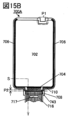
図15A、図15B、図15Cは表示装置の上面図である。
図16は表示装置の断面図である。
図17は表示装置の断面図である。
図18は表示装置の断面図である。
図19は表示装置の断面図である。
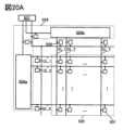
図20Aは表示装置のブロック図である。図20B、図20Cは表示装置の回路図である。
図21A、図21C、図21Dは表示装置の回路図である。図21Bは表示装置のタイミングチャートである。
図22Aは表示モジュールの構成例である。図22Bは表示モジュールの断面概略図である。
図23Aは電子機器の構成例である。図23Bは電子機器の断面概略図である。
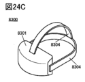
図24A、図24B、図24C、図24D、図24Eは電子機器の構成例である。
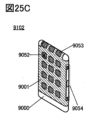
図25A、図25B、図25C、図25D、図25E、図25F、図25Gは電子機器の構成例である。
図26A、図26B、図26C、図26Dは電子機器の構成例である。
図27はトランジスタのId-Vd特性を示す図である。
図28はトランジスタのId-Vd特性を示す図である。
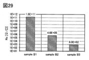
図29は金属酸化物膜の抵抗を示す図である。
図30A、図30Bは断面STEM像である。
図31はトランジスタのId-Vg特性を示す図である。
図32はトランジスタのId-Vg特性を示す図である。
図33はトランジスタのId-Vg特性を示す図である。
図34はトランジスタのId-Vg特性を示す図である。
図35はトランジスタの信頼性評価結果を示す図である。
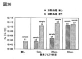
図36は金属酸化物膜の抵抗を示す図である。
図37はトランジスタのId-Vd特性を示す図である。
図38はゲートドライバの動作結果を示す図である。
図39A、図39B、図39C、図39D、図39Eは試料構造を示す断面図である。
図40A、図40Bは試料構造を示す断面図である。
図41は試料構造を示す断面図である。
図42はTDS測定結果を示す図である。
図43はTDS測定結果を示す図である。
図44はTDS測定結果を示す図である。
図45はTDS測定結果を示す図である。
図46はTDS測定結果を示す図である。
図47はトランジスタのId-Vg特性を示す図である。
図48はトランジスタのId-Vg特性を示す図である。
図49はトランジスタのId-Vg特性を示す図である。
図50はトランジスタのId-Vg特性を示す図である。
図51はトランジスタのId-Vg特性を示す図である。
図52はトランジスタのId-Vg特性を示す図である。
図53はトランジスタのId-Vg特性を示す図である。
図54A、図54Bはトランジスタの信頼性評価結果を示す図である。
図55A、図55Bはトランジスタの断面のTEM像である。Fig. 1A is a top view of the semiconductor device, and Fig. 1B and Fig. 1C are cross-sectional views of the semiconductor device.
2A, 2B, and 2C are cross-sectional views of a semiconductor device.
3A, 3B, and 3C are cross-sectional views of a semiconductor device.
4A, 4B, and 4C are cross-sectional views of the semiconductor device.
Fig. 5A is a top view of the semiconductor device, and Fig. 5B and Fig. 5C are cross-sectional views of the semiconductor device.
6A and 6B are cross-sectional views of a semiconductor device.
Fig. 7A is a top view of the semiconductor device, and Fig. 7B and Fig. 7C are cross-sectional views of the semiconductor device.
8A, 8B, and 8C are cross-sectional views of a semiconductor device.
Fig. 9A is a top view of the semiconductor device, and Fig. 9B and Fig. 9C are cross-sectional views of the semiconductor device.
10A, 10B, 10C, and 10D are cross-sectional views illustrating a method for manufacturing a semiconductor device.
11A, 11B, and 11C are cross-sectional views illustrating a method for manufacturing a semiconductor device.
12A, 12B, and 12C are cross-sectional views illustrating a method for manufacturing a semiconductor device.
13A, 13B, and 13C are cross-sectional views illustrating a method for manufacturing a semiconductor device.
14A and 14B are diagrams illustrating a method for manufacturing a semiconductor device.
15A, 15B, and 15C are top views of the display device.
FIG. 16 is a cross-sectional view of the display device.
FIG. 17 is a cross-sectional view of the display device.
FIG. 18 is a cross-sectional view of the display device.
FIG. 19 is a cross-sectional view of the display device.
Fig. 20A is a block diagram of a display device, and Fig. 20B and Fig. 20C are circuit diagrams of the display device.
21A, 21C, and 21D are circuit diagrams of the display device, and Fig. 21B is a timing chart of the display device.
Fig. 22A is a configuration example of a display module, and Fig. 22B is a schematic cross-sectional view of the display module.
Fig. 23A shows a configuration example of an electronic device, and Fig. 23B is a schematic cross-sectional view of the electronic device.
24A, 24B, 24C, 24D, and 24E show configuration examples of electronic devices.
25A, 25B, 25C, 25D, 25E, 25F, and 25G show configuration examples of electronic devices.
26A, 26B, 26C, and 26D show configuration examples of electronic devices.
FIG. 27 is a diagram showing the Id-Vd characteristics of a transistor.
FIG. 28 is a diagram showing the Id-Vd characteristics of a transistor.
FIG. 29 is a diagram showing the resistance of a metal oxide film.
30A and 30B are cross-sectional STEM images.
FIG. 31 is a diagram showing the Id-Vg characteristics of a transistor.
FIG. 32 is a diagram showing the Id-Vg characteristics of a transistor.
FIG. 33 is a diagram showing the Id-Vg characteristics of a transistor.
FIG. 34 is a diagram showing the Id-Vg characteristics of a transistor.
FIG. 35 is a diagram showing the reliability evaluation results of a transistor.
FIG. 36 is a diagram showing the resistance of a metal oxide film.
FIG. 37 is a diagram showing the Id-Vd characteristics of a transistor.
FIG. 38 is a diagram showing the operation result of the gate driver.
39A, 39B, 39C, 39D, and 39E are cross-sectional views showing sample structures.
40A and 40B are cross-sectional views showing a sample structure.
FIG. 41 is a cross-sectional view showing a sample structure.
FIG. 42 shows the results of TDS measurements.
FIG. 43 shows the results of TDS measurements.
FIG. 44 shows the results of TDS measurements.
FIG. 45 shows the results of TDS measurements.
FIG. 46 shows the results of TDS measurements.
FIG. 47 is a diagram showing the Id-Vg characteristics of a transistor.
FIG. 48 is a diagram showing the Id-Vg characteristics of a transistor.
FIG. 49 is a diagram showing the Id-Vg characteristics of a transistor.
FIG. 50 is a diagram showing the Id-Vg characteristics of a transistor.
FIG. 51 is a diagram showing the Id-Vg characteristics of a transistor.
FIG. 52 is a diagram showing the Id-Vg characteristics of a transistor.
FIG. 53 is a diagram showing the Id-Vg characteristics of a transistor.
54A and 54B are diagrams showing the reliability evaluation results of a transistor.
55A and 55B are TEM images of a cross section of a transistor.
以下、実施の形態について図面を参照しながら説明する。ただし、実施の形態は多くの異なる態様で実施することが可能であり、趣旨及びその範囲から逸脱することなくその形態及び詳細を様々に変更し得ることは当業者であれば容易に理解される。従って、本発明は、以下の実施の形態の記載内容に限定して解釈されるものではない。Hereinafter, the embodiments will be described with reference to the drawings. However, it will be easily understood by those skilled in the art that the embodiments can be implemented in many different ways, and that the modes and details can be changed in various ways without departing from the spirit and scope of the present invention. Therefore, the present invention should not be interpreted as being limited to the description of the following embodiments.
本明細書で説明する各図において、各構成要素の大きさ、層の厚さ、または領域は、明瞭化のために誇張されている場合がある。In each figure described in this specification, the size, layer thickness, or area of each component may be exaggerated for clarity.
本明細書等で用いる「第1」、「第2」、「第3」という序数詞は、構成要素の混同を避けるために付したものであり、数的に限定するものではない。The ordinal numbers "first," "second," and "third" used in this specification are used to avoid confusion of components and do not limit the numbers.
本明細書等において、「上に」、「下に」などの配置を示す語句は、構成要素同士の位置関係を、図面を参照して説明するために、便宜上用いている。また、構成要素同士の位置関係は、各構成要素を描写する方向に応じて適宜変化するものである。従って、明細書で説明した語句に限定されず、状況に応じて適切に言い換えることができる。In this specification, the terms "above" and "below" indicating the position are used for convenience in describing the positional relationship between components with reference to the drawings. The positional relationship between components changes as appropriate depending on the direction in which each component is depicted. Therefore, the terms are not limited to those described in the specification, and can be rephrased appropriately depending on the situation.
本明細書等において、トランジスタが有するソースとドレインの機能は、異なる極性のトランジスタを採用する場合や、回路動作において電流の方向が変化する場合などには入れ替わることがある。このため、ソースやドレインの用語は、入れ替えて用いることができるものとする。In this specification and the like, the functions of the source and drain of a transistor may be interchanged when transistors of different polarities are used, when the direction of current flow changes during circuit operation, etc. For this reason, the terms source and drain can be used interchangeably.
本明細書等において、トランジスタのチャネル長方向とは、ソース領域とドレイン領域間を最短距離で結ぶ直線に平行な方向のうちの1つをいう。すなわち、チャネル長方向は、トランジスタがオン状態のときに半導体層を流れる電流の方向のうちの1つに相当する。また、チャネル幅方向とは、当該チャネル長方向に直交する方向をいう。なお、トランジスタの構造や形状によっては、チャネル長方向及びチャネル幅方向は1つに定まらない場合がある。In this specification, the channel length direction of a transistor refers to one of the directions parallel to a straight line connecting a source region and a drain region at the shortest distance. In other words, the channel length direction corresponds to one of the directions of a current flowing through a semiconductor layer when a transistor is in an on-state. The channel width direction refers to a direction perpendicular to the channel length direction. Note that, depending on the structure and shape of a transistor, the channel length direction and the channel width direction may not be determined to be one.
本明細書等において、「電気的に接続」には、「何らかの電気的作用を有するもの」を介して接続されている場合が含まれる。ここで、「何らかの電気的作用を有するもの」は、接続対象間での電気信号の授受を可能とするものであれば、特に制限を受けない。例えば、「何らかの電気的作用を有するもの」には、電極や配線をはじめ、トランジスタなどのスイッチング素子、抵抗素子、インダクタ、キャパシタ、その他の各種機能を有する素子などが含まれる。In this specification, "electrically connected" includes a case where a connection is made via "something having some electrical action." Here, "something having some electrical action" is not particularly limited as long as it enables transmission and reception of an electrical signal between the objects to be connected. For example, "something having some electrical action" includes electrodes and wiring, as well as switching elements such as transistors, resistive elements, inductors, capacitors, and other elements having various functions.
本明細書等において、「膜」という用語と、「層」という用語とは、互いに入れ替えることが可能である。例えば、「導電層」や「絶縁層」という用語は、「導電膜」や「絶縁膜」という用語に相互に交換することが可能な場合がある。In this specification and the like, the terms "film" and "layer" are interchangeable. For example, the terms "conductive layer" and "insulating layer" may be interchangeable with the terms "conductive film" and "insulating film".
本明細書等において「上面形状が概略一致」とは、積層した層と層との間で少なくとも輪郭の一部が重なることをいう。例えば、上層と下層とが、同一のマスクパターン、または一部が同一のマスクパターンにより加工された場合を含む。ただし、厳密には輪郭が重なり合わず、上層の端部が下層の端部より内側に位置することや、上層の端部が下層の端部より外側に位置することもあり、この場合も「上面形状が概略一致」という。In this specification, the phrase "top surface shapes roughly match" refers to at least a portion of the contours of stacked layers overlapping. For example, this includes cases where the upper and lower layers are processed using the same mask pattern, or where a portion of the mask pattern is the same. However, strictly speaking, the contours may not overlap, and the edge of the upper layer may be located inside the edge of the lower layer, or the edge of the upper layer may be located outside the edge of the lower layer. In this case, the phrase "top surface shapes roughly match" is also used.
本明細書等において、特に断りがない場合、オフ電流とは、トランジスタがオフ状態(非導通状態、遮断状態、ともいう)にあるときのドレイン電流をいう。オフ状態とは、特に断りがない場合、nチャネル型トランジスタでは、ゲートとソースの間の電圧Vgsがしきい値電圧Vthよりも低い(pチャネル型トランジスタでは、Vthよりも高い)状態をいう。 In this specification and the like, unless otherwise specified, the off-state current refers to the drain current when a transistor is in an off state (also referred to as a non-conducting state or a cut-off state). Unless otherwise specified, the off-state refers to a state in which the voltage Vgs between the gate and the source of an n-channel transistor is lower than the threshold voltage Vth (higher than Vth for a p-channel transistor).
本明細書等において、表示装置の一態様である表示パネルは表示面に画像等を表示(出力)する機能を有するものである。したがって表示パネルは出力装置の一態様である。In this specification and the like, a display panel, which is one aspect of a display device, has a function of displaying (outputting) an image or the like on a display surface. Therefore, the display panel is one aspect of an output device.
本明細書等では、表示パネルの基板に、例えばFPC(Flexible Printed Circuit)もしくはTCP(Tape Carrier Package)などのコネクターが取り付けられたもの、または基板にCOG(Chip On Glass)方式等によりICが実装されたものを、表示パネルモジュール、表示モジュール、または単に表示パネルなどと呼ぶ場合がある。In this specification, a display panel having a connector such as an FPC (Flexible Printed Circuit) or a TCP (Tape Carrier Package) attached to the substrate, or a substrate having an IC mounted thereon using a COG (Chip On Glass) method or the like, may be referred to as a display panel module, a display module, or simply a display panel.
なお、本明細書等において、表示装置の一態様であるタッチパネルは表示面に画像等を表示する機能と、表示面に指やスタイラスなどの被検知体が触れる、押圧する、または近づくことなどを検出するタッチセンサとしての機能と、を有する。したがってタッチパネルは入出力装置の一態様である。In this specification and the like, a touch panel, which is one aspect of a display device, has a function of displaying an image or the like on a display surface and a function as a touch sensor that detects that a detectable object such as a finger or a stylus touches, presses, or approaches the display surface. Thus, the touch panel is one aspect of an input/output device.
タッチパネルは、例えばタッチセンサ付き表示パネル(または表示装置)、タッチセンサ機能つき表示パネル(または表示装置)とも呼ぶことができる。タッチパネルは、表示パネルとタッチセンサパネルとを有する構成とすることもできる。または、表示パネルの内部または表面にタッチセンサとしての機能を有する構成とすることもできる。The touch panel can also be called, for example, a display panel (or display device) with a touch sensor or a display panel (or display device) with a touch sensor function. The touch panel can have a display panel and a touch sensor panel. Alternatively, the touch panel can have a function as a touch sensor inside or on the surface of the display panel.
本明細書等では、タッチパネルの基板に、コネクターやICが実装されたものを、タッチパネルモジュール、表示モジュール、または単にタッチパネルなどと呼ぶ場合がある。In this specification and the like, a touch panel substrate on which a connector and an IC are mounted may be referred to as a touch panel module, a display module, or simply a touch panel.
(実施の形態1)
本実施の形態では、本発明の一態様の半導体装置について説明する。以下では半導体装置の一例として、トランジスタの構成例及びその作製方法例について説明する。(Embodiment 1)
In this embodiment, a semiconductor device according to one embodiment of the present invention will be described. As an example of the semiconductor device, a structure example of a transistor and a manufacturing method thereof will be described below.
本発明の一態様は、第1の絶縁層上に、チャネルが形成される半導体層と、ゲート絶縁層として機能する第2の絶縁層と、ゲート電極として機能する導電層と、を有する半導体装置である。半導体層は、半導体特性を示す金属酸化物(以下、酸化物半導体ともいう)を含んで構成されることが好ましい。One embodiment of the present invention is a semiconductor device including a semiconductor layer in which a channel is formed, a second insulating layer functioning as a gate insulating layer, and a conductive layer functioning as a gate electrode, which are formed over a first insulating layer. The semiconductor layer preferably contains a metal oxide (hereinafter also referred to as an oxide semiconductor) that exhibits semiconductor characteristics.
第2の絶縁層と導電層との間に、金属酸化物層を有する。金属酸化物層は導電性を有することが好ましく、このとき当該金属酸化物層は、ゲート電極の一部として機能する。A metal oxide layer is provided between the second insulating layer and the conductive layer. The metal oxide layer is preferably conductive, and in this case, the metal oxide layer functions as a part of the gate electrode.
チャネル長方向の断面において、第2の絶縁層の端部(輪郭)は、半導体層の端部(輪郭)よりも内側に位置することが好ましい。さらに、チャネル長方向の断面において、導電層及び金属酸化物層の端部(輪郭)は、第2の絶縁層の端部(輪郭)よりも内側に位置することが好ましい。In a cross section in the channel length direction, the end (contour) of the second insulating layer is preferably located inside the end (contour) of the semiconductor layer. Furthermore, in a cross section in the channel length direction, the ends (contours) of the conductive layer and the metal oxide layer are preferably located inside the end (contour) of the second insulating layer.
本発明の一態様である半導体装置は、さらに第3の絶縁層を有する。第3の絶縁層は、第1の絶縁層の上面、半導体層の上面及び側面、第2の絶縁層の上面及び側面、金属酸化物層の側面、並びに導電層の上面及び側面と接するように設けられることが好ましい。第1の絶縁層及び第3の絶縁層はそれぞれ、不純物の拡散を抑制する材料を用いることが好ましい。例えば、第1の絶縁層及び第3の絶縁層はそれぞれ、窒化物を用いることができる。また、第1の絶縁層と第3の絶縁層が接する領域を設けることで、トランジスタに不純物が拡散することを抑制でき、高い信頼性を備えるトランジスタとすることができる。The semiconductor device according to one embodiment of the present invention further includes a third insulating layer. The third insulating layer is preferably provided so as to be in contact with a top surface of the first insulating layer, a top surface and a side surface of the semiconductor layer, a top surface and a side surface of the second insulating layer, a side surface of the metal oxide layer, and a top surface and a side surface of the conductive layer. The first insulating layer and the third insulating layer are preferably made of a material that suppresses diffusion of impurities. For example, a nitride can be used for each of the first insulating layer and the third insulating layer. Furthermore, by providing a region where the first insulating layer and the third insulating layer are in contact with each other, diffusion of impurities into the transistor can be suppressed, and the transistor can have high reliability.
半導体層は、チャネルが形成される第1の領域と、第1の領域を挟む一対の第2の領域と、第1の領域及び第2の領域を挟み、ソース領域及びドレイン領域として機能する一対の第3の領域と、を有する。第1の領域は、第1の絶縁層及び金属酸化物層と重なる領域である。第2の領域は、第2の絶縁層と重なり、且つ金属酸化物層と重ならない領域である。第3の領域は、第2の絶縁層と重ならない領域である。また、第3の領域は、第3の絶縁層と接し、第1の領域よりも低抵抗である部分を含むことが好ましい。第2の領域は、第3の領域よりも高抵抗である部分を含むことが好ましい。The semiconductor layer has a first region in which a channel is formed, a pair of second regions sandwiching the first region, and a pair of third regions sandwiching the first region and the second region and functioning as a source region and a drain region. The first region is a region overlapping with the first insulating layer and the metal oxide layer. The second region is a region overlapping with the second insulating layer and not overlapping with the metal oxide layer. The third region is a region not overlapping with the second insulating layer. In addition, the third region is preferably in contact with the third insulating layer and includes a portion having a lower resistance than the first region. The second region is preferably included in a portion having a higher resistance than the third region.
第2の領域は、LDD(Lightly Doped Drain)領域として機能する。第2の領域を有することによりドレイン電界を緩和することができ、高電圧で駆動する場合であっても高い信頼性を備えるトランジスタとすることができる。The second region functions as a lightly doped drain (LDD) region. By providing the second region, the drain electric field can be alleviated, and the transistor can have high reliability even when driven at a high voltage.
以下では、より具体的な例について、図面を参照して説明する。A more specific example will be described below with reference to the drawings.
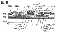
<構成例1>
図1Aは、トランジスタ100の上面図であり、図1Bは、図1Aに示す一点鎖線A1-A2における切断面の断面図に相当し、図1Cは、図1Aに示す一点鎖線B1-B2における切断面の断面図に相当する。なお、図1Aにおいて、トランジスタ100の構成要素の一部(保護層等)を省略して図示している。また、一点鎖線A1-A2方向はチャネル長方向、一点鎖線B1-B2方向はチャネル幅方向に相当する。また、トランジスタの上面図については、以降の図面においても図1Aと同様に、構成要素の一部を省略して図示するものとする。<Configuration Example 1>
1A is a top view of a
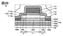
トランジスタ100は、基板102上に設けられ、絶縁層103、半導体層108、絶縁層110、金属酸化物層114、導電層112、絶縁層116、絶縁層118等を有する。島状の半導体層108は、絶縁層103上に設けられる。絶縁層110は、絶縁層103の上面の一部、及び半導体層108の一部を覆って設けられる。金属酸化物層114及び導電層112は、絶縁層110上にこの順に積層して設けられ、半導体層108と重畳する部分を有する。図1B中の一点鎖線で囲った領域Pの拡大図を、図2Aに示す。The
導電層112及び金属酸化物層114の端部は、絶縁層110の端部よりも内側に位置する。言い換えると、絶縁層110は、少なくとも半導体層108上において、導電層112及び金属酸化物層114の端部よりも外側に突出した部分を有する。The ends of the
半導体層108は、チャネル形成領域として機能する領域108Cと、領域108Cを挟む一対の領域108Lと、その外側に一対の領域108Nとを有する。領域108Lは、半導体層108のうち、絶縁層110と重なり、且つ導電層112とは重ならない領域である。図2Aでは、トランジスタ100のチャネル長方向における領域108Cの幅をL1、領域108Lの幅をL2で示している。The
領域108Cは、チャネル形成領域として機能する。ここで、金属酸化物層114が導電性を有する場合、ゲート電極の一部として機能するため、ゲート絶縁層として機能する絶縁層110を介して、ゲート電極から領域108Cに電界が与えられ、チャネルが形成される。The
領域108Lは、ドレイン電界を緩和するためのバッファ領域としての機能を有する。領域108Lは、導電層112及び金属酸化物層114とは重畳しない領域であるため、導電層112にゲート電圧が与えられた場合にもチャネルはほとんど形成されない領域である。領域108Lは、キャリア濃度が領域108Cよりも高いことが好ましい。これにより、領域108LをLDD領域として機能させることができる。The
領域108Lは、領域108Cと比較して、抵抗が同程度または低い領域、キャリア濃度が同程度または高い領域、酸素欠陥密度が同程度または高い領域、不純物濃度が同程度または高い領域ともいうことができる。
領域108Lは、領域108Nと比較して、抵抗が同程度または高い領域、キャリア濃度が同程度または低い領域、酸素欠陥密度が同程度または低い領域、不純物濃度が同程度または低い領域ともいうことができる。
このように、チャネル形成領域である領域108Cと、ソース領域またはドレイン領域である領域108Nとの間に、LDD領域として機能する領域108Lを設けることにより、高いドレイン耐圧と、高いオン電流とを兼ね備え、信頼性の高いトランジスタを実現することができる。In this manner, by providing the
領域108Nは、ソース領域またはドレイン領域として機能し、半導体層108の他の領域と比較して、最も低抵抗な領域である。または、領域108Nは、半導体層108の他の領域と比較して、最もキャリア濃度の高い領域、酸素欠陥密度の高い領域、または最も不純物濃度の高い領域とも言うことができる。The
領域108Nの電気抵抗は低いほど好ましく、例えば領域108Nのシート抵抗の値は、1Ω/□以上1×103Ω/□未満、好ましくは1Ω/□以上8×102Ω/□以下とすることが好ましい。 The lower the electrical resistance of the
チャネルが形成されていない状態における領域108Cの電気抵抗は高いほど好ましい。例えば領域108Cのシート抵抗の値は、1×10⁹Ω/□以上、好ましくは5×109Ω/□以上、より好ましくは1×1010Ω/□以上であることが好ましい。 The higher the electrical resistance of
チャネルが形成されていない状態における領域108Cの電気抵抗は高いほど好ましいため上限値を特に設ける必要はない。ただし、上限値を設けるなら、例えば領域108Cのシート抵抗の値は、1×10⁹Ω/□以上1×1012Ω/□以下、好ましくは5×109Ω/□以上1×1012Ω/□以下、より好ましくは1×1010Ω/□以上1×1012Ω/□以下であることが好ましい。 Since the electrical resistance of the
領域108Lのシート抵抗の値は、例えば1×10³Ω/□以上1×109Ω/□以下、好ましくは1×103Ω/□以上1×108Ω/□以下、より好ましくは1×103Ω/□以上1×107Ω/□とすることができる。このような抵抗の範囲とすることで、電気特性が良好でかつ信頼性の高いトランジスタとすることができる。なお、シート抵抗は、抵抗の値から算出できる。このような領域108Lを、領域108Nと領域108Cとの間に設けることで、トランジスタ100のソース-ドレイン耐圧を高めることができる。 The sheet resistance value of the
チャネルが形成されていない状態における領域108Cの電気抵抗は、領域108Nの電気抵抗の1×10⁶倍以上1×10¹²倍以下、好ましくは1×10⁶倍以上1×10¹¹倍以下、より好ましくは1×10⁶倍以上1×10¹⁰倍以下とすることができる。 The electrical resistance of
チャネルが形成されていない状態における領域108Cの電気抵抗は、領域108Lの電気抵抗の1×100倍以上1×10⁹倍以下、好ましくは1×101倍以上1×10⁸倍以下、より好ましくは1×10²倍以上1×10⁷倍以下とすることができる。 The electrical resistance of
領域108Lの電気抵抗は、領域108Nの電気抵抗の1×100倍以上1×10⁹倍以下、好ましくは1×101倍以上1×10⁸倍以下、より好ましくは1×101倍以上1×10⁷倍以下とすることができる。 The electrical resistance of
前述の抵抗を有する領域108Lを、領域108Nとチャネル形成領域との間に設けることで、トランジスタ100のソース-ドレイン耐圧を高めることができる。By providing the
半導体層108におけるキャリア濃度は、領域108Cが最も低く、領域108L、領域108Nの順に高くなるような分布を有していることが好ましい。領域108Cと領域108Nとの間に領域108Lが設けられることで、例えば作製工程中に領域108Nから水素などの不純物が拡散する場合であっても、領域108Cのキャリア濃度を極めて低く保つことができる。The
チャネル形成領域として機能する領域108Cにおけるキャリア濃度は低いほど好ましく、1×1018cm-3以下であることが好ましく、1×1017cm-3以下であることがより好ましく、1×1016cm-3以下であることがさらに好ましく、1×1013cm-3以下であることがさらに好ましく、1×1012cm-3以下であることがさらに好ましい。なお、領域108Cのキャリア濃度の下限値については、特に限定は無いが、例えば、1×10⁻⁹cm-3とすることができる。 The carrier concentration in the
一方、領域108Nにおけるキャリア濃度は、例えば5×1018cm-3以上、好ましくは1×1019cm-3以上、より好ましくは5×1019cm-3以上とすることができる。領域108Nにおけるキャリア濃度の上限値については、特に限定は無いが、例えば5×1021cm-3、または1×1022cm-3等とすることができる。 On the other hand, the carrier concentration in the
領域108Lにおけるキャリア濃度は、領域108Cと領域108Nの間の値とすることができる。例えば、1×1014cm-3以上1×1020cm-3未満の範囲の値とすればよい。 The carrier concentration in the
なお、領域108L中のキャリア濃度は均一でなくてもよく、領域108N側からチャネル形成領域にかけてキャリア濃度が小さくなるような勾配を有している場合がある。例えば、領域108L中の水素濃度または酸素欠損の濃度のいずれか一方、または両方が、領域108N側からチャネル形成領域側にかけて濃度が小さくなるような勾配を有していてもよい。The carrier concentration in the
半導体層108は、金属酸化物を含むことが好ましい。また、半導体層108のチャネル形成領域に接する絶縁層103と絶縁層110には、酸化物膜を用いることが好ましい。例えば、酸化シリコン膜、酸化窒化シリコン膜、酸化アルミニウム膜などの酸化物膜を用いることができる。これにより、トランジスタ100の作製工程における熱処理などで、絶縁層103や絶縁層110から脱離した酸素を半導体層108のチャネル形成領域に供給し、半導体層108中の酸素欠損を低減できる。The
絶縁層110の端部の一部は、半導体層108上に位置している。絶縁層110は、導電層112と重畳し、ゲート絶縁層として機能する部分と、導電層112及び金属酸化物層114と重ならない部分(すなわち、領域108Lと重なる部分)とを有する。A portion of an end of the insulating
絶縁層110は2層以上の積層構造としてもよい。図1B、図1C及び図2Aには、絶縁層110が絶縁層110aと、絶縁層110a上の絶縁層110bと、絶縁層110b上の絶縁層110cとの3層構造である例を示している。なお、絶縁層110a、絶縁層110b及び絶縁層110cは同種の材料の絶縁膜を用いることができるため、絶縁層110a、絶縁層110b及び絶縁層110cそれぞれの界面が明確に確認できない場合がある。したがって、本実施の形態においては、絶縁層110a、絶縁層110b及び絶縁層110cそれぞれの界面を破線で図示している。The insulating
絶縁層110aは、半導体層108のチャネル形成領域と接する領域を有する。絶縁層110cは、金属酸化物層114と接する領域を有する。絶縁層110bは、絶縁層110aと絶縁層110cの間に位置する。The insulating
絶縁層110a、絶縁層110b、及び絶縁層110cは、それぞれ酸化物を含む絶縁膜であることが好ましい。このとき、絶縁層110a、絶縁層110b及び絶縁層110cは、それぞれ同じ成膜装置で連続して成膜されることが好ましい。The insulating
例えば、絶縁層110a、絶縁層110b、及び絶縁層110cとして、酸化シリコン膜、酸化窒化シリコン膜、窒化酸化シリコン膜、酸化アルミニウム膜、酸化ハフニウム膜、酸化イットリウム膜、酸化ジルコニウム膜、酸化ガリウム膜、酸化タンタル膜、酸化マグネシウム膜、酸化ランタン膜、酸化セリウム膜および酸化ネオジム膜を一種以上含む絶縁層を用いることができる。For example, the insulating
半導体層108と接する絶縁層110は、酸化物絶縁膜の積層構造を有することが好ましく、化学量論的組成よりも過剰に酸素を含有する領域を有することがより好ましい。別言すると、絶縁層110は、酸素を放出することが可能な絶縁膜を有する。例えば、酸素雰囲気下にて絶縁層110を形成すること、成膜後の絶縁層110に対して酸素雰囲気下での熱処理、プラズマ処理等を行うこと、または、絶縁層110上に酸素雰囲気下で酸化物膜を成膜することなどにより、絶縁層110中に酸素を供給することもできる。The insulating
例えば、絶縁層110a、絶縁層110b及び絶縁層110cは、スパッタリング法、化学気相堆積(CVD:Chemical Vapor Deposition)法、真空蒸着法、パルスレーザー堆積(PLD:Pulsed Laser Deposition)法、原子層堆積(ALD:Atomic Layer Deposition)法等を用いて形成することができる。また、CVD法は、プラズマ化学気相堆積(PECVD:Plasma Enhanced CVD)法や、熱CVD法などがある。For example, the insulating
特に、絶縁層110a、絶縁層110b及び絶縁層110cは、プラズマCVD法により形成することが好ましい。In particular, it is preferable that the insulating
絶縁層110aは、半導体層108上に成膜されるため、出来るだけ半導体層108にダメージを与えない条件で成膜された膜であることが好ましい。例えば、成膜速度(成膜レートともいう)が十分に低い条件で成膜することができる。Since the insulating
例えば、プラズマCVD法により絶縁層110aを形成する場合、低電力の条件で形成することにより、半導体層108に与えるダメージを極めて小さくすることができる。For example, when the insulating
絶縁層110a、絶縁層110b及び絶縁層110cとして酸化窒化シリコン膜を用いる場合、酸化窒化シリコン膜の成膜に用いる成膜ガスには、例えばシラン、ジシランなどのシリコンを含む堆積性ガスと、酸素、オゾン、一酸化二窒素、二酸化窒素などの酸化性ガスと、を含む原料ガスを用いることができる。また原料ガスに加えて、アルゴンやヘリウム、窒素などの希釈ガスを含んでもよい。When silicon oxynitride films are used as the insulating
例えば、成膜ガスの全流量に対する堆積性ガスの流量の割合(以下、単に流量比ともいう)を小さくすることで、成膜速度を低くでき、緻密で欠陥の少ない膜を成膜することができる。For example, by reducing the ratio of the flow rate of the deposition gas to the total flow rate of the film-forming gas (hereinafter simply referred to as the flow rate ratio), the film-forming rate can be reduced, and a dense film with fewer defects can be formed.
絶縁層110bは、絶縁層110aよりも成膜速度の高い条件で成膜された膜であることが好ましい。これにより、生産性を向上させることができる。The insulating
例えば絶縁層110bは、絶縁層110aよりも堆積性ガスの流量比を増やした条件とすることで、成膜速度を高めた条件で成膜することができる。For example, the insulating
絶縁層110cは、その表面の欠陥が低減され、水などの大気中に含まれる不純物が吸着しにくい、極めて緻密な膜であることが好ましい。例えば、絶縁層110aと同様に、成膜速度が十分に低い条件で成膜することができる。The insulating
絶縁層110cは絶縁層110b上に成膜するため、絶縁層110aと比較して絶縁層110cの成膜時に半導体層108へ与える影響は小さい。そのため、絶縁層110cは、絶縁層110aよりも高い電力の条件で成膜することができる。堆積性ガスの流量比を減らし、比較的高い電力で成膜することで、緻密で表面の欠陥が低減された膜とすることができる。Since the insulating
すなわち、成膜速度が高い方から、絶縁層110b、絶縁層110a、絶縁層110cの順となるような条件で成膜された積層膜を、絶縁層110に用いることができる。また、絶縁層110は、絶縁層110b、絶縁層110a、絶縁層110cの順で、ウェットエッチングまたはドライエッチングに対する同一条件下でのエッチング速度が高い。That is, a stacked film formed under conditions in which the insulating
絶縁層110bは、絶縁層110a及び絶縁層110cよりも厚く形成することが好ましい。成膜速度の最も速い絶縁層110bを厚く形成することで、絶縁層110の成膜工程に係る時間を短縮することができる。The insulating
ここで、絶縁層110aと絶縁層110bの境界、及び絶縁層110bと絶縁層110cの境界は不明瞭である場合があるため、図1A等では、これらの境界を破線で図示している。なお、絶縁層110aと絶縁層110bは、膜密度が異なるため、絶縁層110の断面における透過型電子顕微鏡(TEM:Transmission Electron Microscopy)像などにおいて、これらの境界をコントラストの違いとして観察することができる場合がある。同様に、絶縁層110bと絶縁層110cの境界も観察することができる場合がある。Here, the boundary between the insulating
導電層112及び金属酸化物層114を形成する際に、導電層112と重ならない領域の絶縁層110の膜厚が薄くなる場合がある。図1B、図1C及び図2Aには、導電層112と重ならない領域の絶縁層110cが除去され、絶縁層110a及び絶縁層110bが残存する構成を示している。また、導電層112と重なる領域の絶縁層110bと比較して、導電層112と重ならない領域の絶縁層110bの厚さが薄くなる場合がある。When the
導電層112と重ならない領域の絶縁層110の膜厚を薄くすることにより、絶縁層116から供給される水素が多くなり、領域108Lの抵抗を低くすることができる。また、導電層112と重ならない領域の絶縁層110の膜厚を調整することにより、絶縁層116から供給される水素の量を調整し、領域108Lの抵抗を制御することができる。By reducing the thickness of the insulating
導電層112と重ならない領域の絶縁層110の膜厚を薄くすることにより、絶縁層110端部の段差が小さくなり、絶縁層110上に形成される層(例えば、絶縁層116)の段差被覆性が向上し、該層に段切れや鬆といった不具合が発生することを抑制できる。By reducing the thickness of the insulating
図2Bには、導電層112と重ならない領域に絶縁層110a、絶縁層110b及び絶縁層110cが残存する構成を示している。また、導電層112と重なる領域の絶縁層110cと比較して、導電層112と重ならない領域の絶縁層110cの厚さが薄くなる場合がある。図2Bに示すように、導電層112と重ならない領域に、絶縁層110cが残存すると特に好ましい。導電層112と重ならない領域に絶縁層110cが残存する構成とすることで、絶縁層110に水が吸着することを抑制できる。導電層112と重なる領域の絶縁層110cの厚さは1nm以上50nm以下、好ましくは2nm以上40nm以下、さらに好ましくは3nm以上30nm以下とする。2B shows a configuration in which the insulating
図2Cには、導電層112と重ならない領域に絶縁層110a、絶縁層110b及び絶縁層110cが残存し、導電層112と重なる領域の絶縁層110cと導電層112と重ならない領域の絶縁層110cの厚さが概略等しい例を示している。Figure 2C shows an example in which insulating
なお、絶縁層110は、絶縁層110aと、絶縁層110a上の絶縁層110cとの2層構造としてもよい。または、絶縁層110は単層構造としてもよい。絶縁層110として、目的に応じて前述の絶縁層110a、絶縁層110b又は絶縁層110cのいずれかを適宜選択することができる。The insulating
絶縁層116は、導電層112の上面及び側面、金属酸化物層114の側面、絶縁層110の上面及び側面、半導体層108の上面及び側面、並びに絶縁層103の上面を覆って設けられている。絶縁層118は、絶縁層116を覆って設けられる。絶縁層116及び絶縁層118は、保護層として機能し、外部からの不純物元素の拡散を抑制できる。The insulating
絶縁層116は、絶縁層116より上からの不純物が半導体層108に拡散することを抑制する機能を有する。また、絶縁層116は、成膜時に絶縁層116と接する半導体層108の抵抗を低下させる機能を有する。絶縁層116は、領域108Nの上面及び側面と接して設けられる。絶縁層116は、絶縁層116の成膜時、または成膜後に加熱することにより、領域108N中に不純物を供給することのできる絶縁膜を用いることができる。または、絶縁層116の成膜時、または成膜後に加熱することにより、領域108N中に酸素欠損を生じさせることのできる絶縁膜を用いることができる。The insulating
絶縁層116は、成膜の際に用いる成膜ガスに、水素などの不純物元素を含むガスを用いて成膜される膜であることが好ましい。例えば、水素を含むガスとして、シラン、アンモニア等を用いることができる。また絶縁層116の成膜温度を低くすることで、半導体層108に効果的に多くの不純物元素を供給することができる。絶縁層116の成膜温度は、例えば200℃以上500℃以下が好ましく、さらには220℃以上450℃以下が好ましく、さらには230℃以上430℃以下が好ましく、さらには250℃以上400℃以下とすることが好ましい。The insulating
絶縁層116の成膜を減圧下で、且つ加熱して行うことで、半導体層108中の領域108Nとなる領域の酸素の脱離を促進することができる。酸素欠損が多く形成された半導体層108に、水素などの不純物を供給することで、領域108N中のキャリア濃度が高まり、より効果的に領域108Nを低抵抗化させることができる。Deposition of the insulating
絶縁層116は、例えば、窒化シリコン、窒化酸化シリコン、酸化窒化シリコン、窒化アルミニウム、窒化酸化アルミニウムなどの、窒化物を含む絶縁膜を好適に用いることができる。特に窒化シリコンは、水素や酸素に対するブロッキング性を有するため、外部から半導体層108への水素の拡散と、半導体層108から外部への酸素の脱離の両方を防ぐことができ、信頼性の高いトランジスタを実現できる。For the insulating
絶縁層116は、半導体層108中の酸素を吸引し、酸素欠損を生成する機能を有する絶縁膜としてもよい。特に、絶縁層116には、例えば窒化アルミニウムなどの金属窒化物を用いることが特に好ましい。The insulating
絶縁層116に金属窒化物を用いる場合、アルミニウム、チタン、タンタル、タングステン、クロム、またはルテニウムの窒化物を用いることが好ましい。特に、アルミニウムまたはチタンを含むことが特に好ましい。例えば、アルミニウムをスパッタリングターゲットに用い、成膜ガスとして窒素を含むガスを用いた反応スパッタリング法により形成した窒化アルミニウム膜は、成膜ガスの全流量に対する窒素ガスの流量を適切に制御することで、極めて高い絶縁性と、水素や酸素に対する極めて高いブロッキング性とを兼ね備えた膜とすることができる。そのため、このような金属窒化物を含む絶縁膜を、半導体層108に接して設けることで、半導体層108を低抵抗化できるだけでなく、半導体層108から酸素が脱離すること、及び半導体層108へ水素が拡散することを好適に防ぐことができる。When a metal nitride is used for the insulating
金属窒化物として、窒化アルミニウムを用いた場合、当該窒化アルミニウムを含む絶縁層の厚さを5nm以上とすることが好ましい。このように薄い膜であっても、水素及び酸素に対する高いブロッキング性と、半導体層の低抵抗化の機能とを両立できる。なお、当該絶縁層の厚さの上限は特にないが、生産性を考慮し、500nm以下、好ましくは200nm以下、より好ましくは50nm以下とすることが好ましい。When aluminum nitride is used as the metal nitride, the thickness of the insulating layer containing the aluminum nitride is preferably 5 nm or more. Even with such a thin film, it is possible to achieve both high blocking properties against hydrogen and oxygen and a function of reducing the resistance of the semiconductor layer. Although there is no particular upper limit to the thickness of the insulating layer, it is preferable to set it to 500 nm or less, preferably 200 nm or less, and more preferably 50 nm or less in consideration of productivity.
絶縁層116に窒化アルミニウム膜を用いる場合、組成式がAlNx(xは0より大きく2以下の実数、好ましくは、xは0.5より大きく1.5以下の実数)を満たす膜を用いることが好ましい。これにより、絶縁性に優れ、且つ熱伝導性に優れた膜とすることができるため、トランジスタ100を駆動したときに生じる熱の放熱性を高めることができる。 When an aluminum nitride film is used for the insulating
または、絶縁層116として、窒化アルミニウムチタン膜、窒化チタン膜などを用いることができる。Alternatively, the insulating
このような絶縁層116を領域108Nに接して設けることで、絶縁層116が領域108N中の酸素を吸引し、領域108N中に酸素欠損を形成させることができる。またこのような絶縁層116を形成した後に、加熱処理を行うことで、領域108Nに、より多くの酸素欠損を形成することができ、低抵抗化を促進することができる。また、絶縁層116に金属酸化物を含む膜を用いた場合、絶縁層116が半導体層108中の酸素を吸引した結果、絶縁層116と領域108Nとの間に、絶縁層116に含まれる金属元素(例えばアルミニウム)の酸化物を含む層が形成される場合がある。By providing such an
領域108Lは、絶縁層110が間に存在することで絶縁層116と接しないため、絶縁層116から供給される水素は領域108Nよりも少ない。さらに、不純物濃度も領域108Nよりも小さいため、領域108Lは、領域108Nよりも高抵抗な状態とすることができる。Since the insulating
後述するように、領域108Lを自己整合的に形成することが可能となるため、領域108Lを形成するためのフォトマスクを必要とせず、作製コストを低減できる。また、自己整合的に領域108Lを形成することにより、領域108Lと導電層112の相対的な位置ずれが生じることがないため、半導体層108中の領域108Lの幅を概略一致させることができる。As described later, since the
半導体層108中のチャネル形成領域と低抵抗な領域108Nの間に、ゲートの電界が掛からない(またはチャネル形成領域よりも掛かりにくい)オフセット領域として機能する領域108Lをばらつきなく安定して形成できる。その結果、トランジスタのソース-ドレイン耐圧を向上させることができ、信頼性の高いトランジスタを実現できる。A
領域108Lの幅L2は、100nm以上2μm以下が好ましく、さらには150nm以上1μm以下が好ましく、さらに200nm以上1μm以下が好ましい。領域108Lを設けることにより、ドレイン付近に電界が集中することが緩和され、特にドレイン電圧が高い状態でのトランジスタの劣化を抑制できる。また、特に、領域108Lの幅L2を、絶縁層110の厚さよりも大きくすることで、効果的にドレイン付近への電界集中を抑制することができる。一方、幅L2が2μmよりも長いとソース-ドレイン抵抗が高まり、トランジスタの駆動速度が遅くなる場合がある。幅L2を前述の範囲とすることで、信頼性が高く、かつ駆動速度の速いトランジスタ、半導体装置とすることができる。なお、領域108Lの幅L2は、半導体層108の厚さ、絶縁層110の厚さ、トランジスタ100を駆動する際のソース-ドレイン間に印加する電圧の大きさに応じて決定することができる。The width L2 of the
チャネル形成領域と低抵抗な領域108Nの間に領域108Lを設けることにより、チャネル形成領域と領域108Nの境界での電流密度を緩和でき、チャネルとソース又はドレインの境界における発熱が抑制され、信頼性の高いトランジスタ、半導体装置とすることができる。By providing
絶縁層103は積層構造とすることができる。図1には、絶縁層103は、基板102側から、絶縁層103a、絶縁層103b、絶縁層103c、及び絶縁層103dがこの順に積層された構造を有する例を示している。絶縁層103aは基板102と接する。また、絶縁層103dは半導体層108と接する。The insulating
絶縁層103は、耐圧が高いこと、膜の応力が小さいこと、水素や水を放出しにくいこと、膜中の欠陥が少ないこと、基板102に含まれる不純物の拡散を抑制すること、のうち、1つ以上を満たすことが好ましく、これら全てを満たすことが最も好ましい。It is preferable that the insulating
絶縁層103が有する4つの絶縁膜のうち、基板102側に位置する絶縁層103a、絶縁層103b、及び絶縁層103cには、窒素を含む絶縁膜を用いることが好ましい。一方、半導体層108と接する絶縁層103dには、酸素を含む絶縁膜を用いることが好ましい。また、絶縁層103が有する4つの絶縁膜は、それぞれプラズマCVD装置を用いて、大気に触れることなく連続して成膜することが好ましい。Of the four insulating films included in the insulating
絶縁層103a、絶縁層103b、及び絶縁層103cは、例えば窒化シリコン膜、窒化酸化シリコン膜、窒化アルミニウム膜、窒化ハフニウム膜などの窒素を含む絶縁膜を好適に用いることができる。また、絶縁層103dは、絶縁層110に用いることのできる絶縁膜の記載を援用することができる。For the insulating
絶縁層103aと絶縁層103cは、これよりも下側からの不純物の拡散を防止できる、緻密な膜であることが好ましい。絶縁層103aは、基板102に含まれる不純物を、絶縁層103cは、絶縁層103bに含まれる水素や水を、それぞれブロックできる膜であることが好ましい。そのため、絶縁層103a及び絶縁層103cには、絶縁層103bよりも成膜速度の低い条件で成膜した絶縁膜を適用することができる。The insulating
一方、絶縁層103bは、応力が小さく、成膜速度の高い条件で成膜された絶縁膜を用いることが好ましい。また、絶縁層103bは、絶縁層103a及び絶縁層103cよりも厚く形成されていることが好ましい。On the other hand, the insulating
例えば絶縁層103a、絶縁層103b、及び絶縁層103cのそれぞれに、プラズマCVD法で成膜した窒化シリコン膜を用いた場合であっても、絶縁層103bが、他の2つの絶縁膜よりも膜密度が小さい膜となる。したがって、絶縁層103の断面における透過型電子顕微鏡像などにおいて、コントラストの違いとして観察することができる場合がある。なお、絶縁層103aと絶縁層103bの境界、及び絶縁層103bと絶縁層103cの境界は不明瞭である場合があるため、図1等では、これらの境界を破線で明示している。For example, even if the insulating
半導体層108と接する絶縁層103dは、その表面に水などの不純物が吸着しにくい、緻密な絶縁膜とすることが好ましい。また、可能な限り欠陥が少なく、水や水素などの不純物が低減された絶縁膜を用いることが好ましい。例えば、絶縁層103dとして、上記絶縁層110が有する絶縁層110cと同様の絶縁膜を用いることができる。The insulating
このような積層構造を有する絶縁層103により、極めて信頼性の高いトランジスタを実現することができる。With the insulating
図1B及び図1Cに示すように、トランジスタ100は絶縁層103cと、絶縁層116が接する領域を有することが好ましい。図1B中の一点鎖線で囲った領域Qの拡大図を図3Aに、図1C中の一点鎖線で囲った領域Rの拡大図を図3Bに示す。1B and 1C, the
図1B及び図3Aに示すように、チャネル長方向において、半導体層108と重ならない領域の絶縁層116は絶縁層103cと接して設けられる。また、絶縁層103dの端部は、半導体層108の端部と概略一致する。1B and 3A, the insulating
図3Bに示すように、チャネル幅方向において、絶縁層110と重ならない領域の絶縁層116は絶縁層103cと接して設けられる。また、絶縁層103dの端部は、絶縁層110の端部と概略一致する。例えば、絶縁層110を形成する際に、絶縁層110と重ならない領域の絶縁層103dとなる絶縁膜も除去することで、絶縁層103dの端部と絶縁層110の端部を概略一致させることができる。3B , in the channel width direction, the insulating
絶縁層103cと、絶縁層116が接する領域を有することで、トランジスタ100の外からの不純物がトランジスタ100に拡散することを抑制できる。特に、絶縁層116及び絶縁層103cとして、それぞれ窒素を含む絶縁膜を好適に用いることができる。The insulating
図3Cに示すように、絶縁層103dの端部は、半導体層108の端部と概略一致する構成としてもよい。例えば、半導体層108を形成する際に、半導体層108と重ならない領域の絶縁層103dとなる絶縁膜も除去することで、絶縁層103dの端部と半導体層108の端部を概略一致させることができる。3C , the end of the insulating
チャネル長方向において、半導体層108と重なる領域の絶縁層103cの膜厚より、半導体層108と重ならない領域の絶縁層103cの膜厚が薄くなる場合がある。図1B中の一点鎖線で囲った領域Qの拡大図を図4Aに示す。図4Aは、半導体層108と重なる領域の絶縁層103cの膜厚より、半導体層108と重ならない領域の絶縁層103cの膜厚が薄く、また、絶縁層103cの膜厚が薄い領域において、絶縁層103cと絶縁層116が接する例を示している。In the channel length direction, the thickness of the insulating
チャネル幅方向において、絶縁層110と重なる領域の絶縁層103cの膜厚より、絶縁層110と重ならない領域の絶縁層103cの膜厚が薄くなる場合がある。図1C中の一点鎖線で囲った領域Rの拡大図を図4B及び図4Cに示す。図4B及び図4Cは、絶縁層110と重なる領域の絶縁層103cの膜厚より、絶縁層110と重ならない領域の絶縁層103cの膜厚が薄く、また、絶縁層103cの膜厚が薄い領域において、絶縁層103cと絶縁層116が接する例を示している。また、図4Bおいて、絶縁層103dの端部は絶縁層110の端部と概略一致する。図4Cおいて、絶縁層103dの端部は半導体層108の端部と概略一致する。In the channel width direction, the thickness of the insulating
なお、図4A、図4B及び図4Cでは、絶縁層103cと絶縁層116が接する例を示したが、本発明の一態様はこれに限られない。絶縁層103bが露出し、絶縁層103bと絶縁層116が接する構成とすることができる。また、絶縁層103aが露出し、絶縁層103aと絶縁層116が接する構成とすることができる。4A, 4B, and 4C show an example in which the insulating
絶縁層110の端部、及び金属酸化物層114の端部は、それぞれテーパ形状を有することが好ましい。このような構成とすることで、絶縁層110及び金属酸化物層114上に形成される層(例えば、絶縁層116)の被覆性が向上し、該層に段切れや鬆といった不具合が発生することを抑制できる。It is preferable that the end of the insulating
導電層112の一部は、ゲート電極として機能する。絶縁層110の一部は、ゲート絶縁層として機能する。トランジスタ100は、半導体層108上にゲート電極が設けられる、いわゆるトップゲート型のトランジスタである。A part of the
図1A及び図1Bに示すように、トランジスタ100は、絶縁層118上に導電層120a及び導電層120bを有していてもよい。導電層120a及び導電層120bはソース電極またはドレイン電極として機能する。導電層120a及び導電層120bは、それぞれ絶縁層118及び絶縁層116に設けられた開口部141aまたは開口部141bを介して、領域108Nに電気的に接続される。1A and 1B, the
半導体層108は、金属酸化物を含むことが好ましい。The
例えば半導体層108は、インジウムと、元素M(元素Mは、ガリウム、アルミニウム、シリコン、ホウ素、イットリウム、スズ、銅、バナジウム、ベリリウム、チタン、鉄、ニッケル、ゲルマニウム、ジルコニウム、モリブデン、ランタン、セリウム、ネオジム、ハフニウム、タンタル、タングステン、またはマグネシウムから選ばれた一種または複数種)と、亜鉛と、を有することが好ましい。特に元素Mはアルミニウム、ガリウム、イットリウム、またはスズから選ばれた一種または複数種とすることが好ましい。For example, the
特に、半導体層108として、インジウム、ガリウム、及び亜鉛を含む酸化物を用いることが好ましい。In particular, it is preferable to use an oxide containing indium, gallium, and zinc for the
半導体層108として、組成の異なる層、または結晶性の異なる層、または不純物濃度の異なる層を積層した積層構造としてもよい。The
導電層112には、低抵抗な材料を用いることが好ましい。導電層112に低抵抗な材料を用いることにより寄生抵抗を低減し、高いオン電流を有するトランジスタとすることができ、オン電流が高い半導体装置とすることができる。また、大型の表示装置、高精細の表示装置において配線抵抗を低減することにより信号遅延を抑制し、高速駆動が可能となる。導電層112として、銅、銀、金、またはアルミニウム等を用いることができる。特に、銅は低抵抗であることに加え、量産性に優れるため好ましい。It is preferable to use a low-resistance material for the
導電層112は積層構造としてもよい。導電層112を積層構造とする場合には、低抵抗な第1導電層の上または下、またはその両方に、第2の導電層を設ける。第2の導電層として、第1の導電層よりも酸化されにくい(耐酸化性を有する)導電性材料を用いることが好ましい。また、第2の導電層として、第1の導電層の成分の拡散を抑制する材料を用いることが好ましい。第2の導電層として、例えば、酸化インジウム、インジウム亜鉛酸化物、インジウムスズ酸化物(ITO)、シリコンを含有したインジウムスズ酸化物(ITSO)、酸化亜鉛等の金属酸化物、または窒化チタン、窒化タンタル、窒化モリブデン、窒化タングステン等の金属窒化物を好適に用いることができる。The
絶縁層110と導電層112との間に位置する金属酸化物層114は、絶縁層110に含まれる酸素が導電層112側に拡散することを防ぐバリア膜として機能する。さらに金属酸化物層114は、導電層112に含まれる水素や水が絶縁層110側に拡散することを防ぐバリア膜としても機能する。金属酸化物層114は、例えば少なくとも絶縁層110よりも酸素及び水素を透過しにくい材料を用いることができる。The
金属酸化物層114により、導電層112にアルミニウムや銅などの酸素を吸引しやすい金属材料を用いた場合であっても、絶縁層110から導電層112へ酸素が拡散することを防ぐことができる。また、導電層112が水素を含む場合であっても、導電層112から絶縁層110を介して半導体層108へ水素が拡散することを防ぐことができる。その結果、半導体層108のチャネル形成領域におけるキャリア濃度を極めて低いものとすることができる。The
金属酸化物層114は、絶縁性材料または導電性材料を用いることができる。金属酸化物層114が絶縁性を有する場合には、ゲート絶縁層の一部として機能する。一方、金属酸化物層114が導電性を有する場合には、ゲート電極の一部として機能する。An insulating material or a conductive material can be used for the
金属酸化物層114として、酸化シリコンよりも誘電率の高い絶縁性材料を用いることが好ましい。特に、酸化アルミニウム膜、酸化ハフニウム膜、またはハフニウムアルミネート膜等を用いると、駆動電圧を低減できるため好ましい。It is preferable to use an insulating material having a higher dielectric constant than silicon oxide as the
金属酸化物層114として、金属酸化物を用いることができる。例えば、酸化インジウム、インジウム亜鉛酸化物、インジウムスズ酸化物(ITO)、シリコンを含有したインジウムスズ酸化物(ITSO)等のインジウムを有する酸化物を用いることができる。インジウムを含む導電性酸化物は、導電性が高いため好ましい。また、ITSOはシリコンを含有することにより結晶化しづらく、平坦性が高いことから、ITSO上に形成される膜との密着性が高くなる。金属酸化物層114として、酸化亜鉛、ガリウムを含有した酸化亜鉛等の金属酸化物を用いることができる。また、金属酸化物層114として、これらを積層した構造を用いてもよい。A metal oxide can be used as the
金属酸化物層114として、半導体層108と同一の元素を一以上含む酸化物材料を用いることが好ましい。特に、上記半導体層108に適用可能な酸化物半導体材料を用いることが好ましい。このとき、金属酸化物層114として、半導体層108と同じスパッタリングターゲットを用いて形成した金属酸化物膜を適用することで、装置を共通化できるため好ましい。It is preferable to use an oxide material containing one or more elements that are the same as those of the
または、半導体層108と金属酸化物層114の両方に、インジウム及びガリウムを含む金属酸化物材料を用いる場合、半導体層108よりもガリウムの組成(含有割合)が高い材料を用いると、酸素に対するブロッキング性をより高めることができるため好ましい。このとき、半導体層108には、金属酸化物層114よりもインジウムの組成が高い材料を用いることで、トランジスタ100の電界効果移動度を高めることができる。Alternatively, when a metal oxide material containing indium and gallium is used for both the
金属酸化物層114は、スパッタリング装置を用いて形成することが好ましい。例えば、スパッタリング装置を用いて酸化物膜を形成する場合、酸素ガスを含む雰囲気で形成することで、絶縁層110や半導体層108中に好適に酸素を添加できる。The
半導体層108は、絶縁層110を介して導電層112と重なる、チャネル形成領域を有する。また、半導体層108は、当該チャネル形成領域を挟む一対の領域108Nを有する。領域108Nは、半導体層108のうち、導電層112及び絶縁層110のいずれにも重ならない領域であって、絶縁層116と接する領域である。The
領域108Nは、チャネル形成領域よりも低抵抗な領域、キャリア濃度が高い領域、酸素欠陥密度の高い領域、不純物濃度の高い領域、またはn型である領域ともいうことができる。The
領域108Nは、不純物元素(第1の元素)を含む領域である。当該不純物元素として、例えば水素、ホウ素、炭素、窒素、フッ素、リン、硫黄、ヒ素、アルミニウム、マグネシウムまたは希ガスなどが挙げられる。なお、希ガスの代表例として、ヘリウム、ネオン、アルゴン、クリプトン、及びキセノン等がある。特に、ホウ素、リン、マグネシウム、またはアルミニウムを含むことが好ましい。またこれら元素を2以上含んでいてもよい。The
ここで、領域108Nにおける不純物濃度は、絶縁層116に近いほど濃度が高くなるような濃度勾配を有することが好ましい。これにより、領域108N全体に亘って均一な濃度とした場合に比べて、領域108N内の不純物元素の総量を低くできるため、作製工程中の熱などの影響によりチャネル形成領域に拡散しうる不純物の量を低く保つことができる。また、領域108Nの上部ほど低抵抗となるため、導電層120a(または導電層120b)との接触抵抗をより効果的に低減できる。Here, it is preferable that the impurity concentration in the
後述するように、領域108Nに不純物元素を添加する処理は、絶縁層110をマスクとして行うことができる。これにより、領域108Nを自己整合的に形成できる。As described later, the process of adding an impurity element to the
領域108Nは、不純物濃度が、1×10¹⁹atoms/cm3以上、1×1023atoms/cm3以下、好ましくは5×1019atoms/cm3以上、5×1022atoms/cm3以下、より好ましくは1×1020atoms/cm3以上、1×1022atoms/cm3以下である領域を含むことが好ましい。
領域108Nに含まれる不純物の濃度は、例えば二次イオン質量分析法(SIMS:Secondary Ion Mass Spectrometry)や、X線光電子分光法(XPS:X-ray Photoelectron Spectroscopy)等の分析法により分析できる。XPS分析を用いる場合には、表面側または裏面側からのイオンスパッタリングとXPS分析を組み合わせることで、深さ方向の濃度分布を知ることができる。The concentration of impurities contained in the
領域108Nにおいて、不純物元素は酸化した状態で存在していることが好ましい。例えば不純物元素としてホウ素、リン、マグネシウム、アルミニウム、シリコンなどの酸化しやすい元素を用いることが好ましい。このような酸化しやすい元素は、半導体層108中の酸素と結合して酸化した状態で安定に存在しうるため、後の工程で高い温度(例えば400℃以上、600℃以上、または800℃以上)がかかった場合であっても、脱離することが抑制される。また、不純物元素が半導体層108中の酸素を奪うことで、領域108N中に多くの酸素欠損(VO)が生成される。この酸素欠損(VO)に膜中の水素が入った欠陥(以下、VOHと記す)はキャリア供給源となるため、領域108Nは極めて低抵抗な状態となる。 In the
なお、後の工程で高い温度がかかる処理を行なう際、外部や領域108Nの近傍の膜から多量の酸素が領域108Nに供給されてしまうと、抵抗が上昇してしまう場合がある。そのため、高い温度のかかる処理を行なう際には、酸素に対するバリア性の高い絶縁層116で半導体層108を覆った状態で処理することが好ましい。In addition, when a high-temperature process is performed in a later step, if a large amount of oxygen is supplied to the
絶縁層116は、半導体層108の領域108Nに接して設けられている。The insulating
絶縁層116は、領域108Nに対する水素の供給源として機能する。例えば、絶縁層116は、加熱により水素を放出する膜であることが好ましい。このような絶縁層116を領域108Nに接して設け、絶縁層116の形成後に加熱処理を行なうことで、領域108Nに水素を供給して抵抗を下げることができる。The insulating
絶縁層116は、成膜の際に用いる成膜ガスに、水素を含むガスを用いて成膜される膜であることが好ましい。これにより、絶縁層116の成膜時にも、領域108Nに水素を効果的に供給できる。The insulating
絶縁層116は、例えば、窒化シリコン、窒化酸化シリコン、酸化窒化シリコン、窒化アルミニウム、窒化酸化アルミニウムなどの絶縁膜を用いることができる。The insulating
領域108Nは、上述のように不純物元素が添加されることで酸素欠損を多く含む状態である。したがって、半導体層108中に含まれる水素に加えて、絶縁層116からさらに水素を供給することで、よりキャリア濃度を高めることができる。The
絶縁層118は、トランジスタ100を保護する保護層として機能する。絶縁層118は、例えば、酸化物または窒化物などの無機絶縁材料を用いることができる。より具体的な例として、窒化シリコン、窒化酸化シリコン、酸化窒化シリコン、酸化アルミニウム、酸化窒化アルミニウム、窒化アルミニウム、酸化ハフニウム、ハフニウムアルミネートなどの無機絶縁材料を用いることができる。また、絶縁層118を平坦化層として用いることもできる。その場合、絶縁層118として有機樹脂材料を用いることができる。The insulating
なお、ここでは保護層として絶縁層116と絶縁層118の積層構造とする場合を示したが、絶縁層118は不要であれば設けなくてもよい。また、絶縁層118を2層以上の積層構造としてもよい。Although the case where the protective layer has a stacked structure of the insulating
ここで、半導体層108について、及び半導体層108中に形成されうる酸素欠損について説明する。Here, the
半導体層108のチャネル形成領域に形成される酸素欠損は、トランジスタ特性に影響を与えるため問題となる。例えば、半導体層108中に酸素欠損が形成されると、該酸素欠損に水素が入り、キャリア供給源となりうる。チャネル形成領域中にキャリア供給源が生成されると、トランジスタ100の電気特性の変動、代表的にはしきい値電圧のシフトが生じる。したがって、チャネル形成領域においては、酸素欠損が少ないほど好ましい。Oxygen vacancies formed in the channel formation region of the
そこで、本発明の一態様においては、半導体層108のチャネル形成領域近傍の絶縁膜、具体的には、チャネル形成領域の上方に位置する絶縁層110、及び下方に位置する絶縁層103が、酸化物膜を含む構成とする。作製工程中の熱などにより絶縁層103及び絶縁層110からチャネル形成領域へ酸素を移動させることで、チャネル形成領域中の酸素欠損を低減することが可能となる。Thus, in one embodiment of the present invention, an insulating film in the vicinity of a channel formation region of the
半導体層108は、元素Mに対するInの原子数比が1より大きい領域を有することが好ましい。Inの含有率が高いほど、トランジスタの電界効果移動度を向上させることができる。The
ここで、In、Ga、Znを含む金属酸化物の場合、Inと酸素の結合力は、Gaと酸素の結合力よりも弱いため、Inの含有率が高い場合には、金属酸化物膜中に酸素欠損が形成されやすい。また、Gaに代えて、上記Mで示す金属元素を用いた場合でも同様の傾向がある。金属酸化物膜中に酸素欠損が多く存在すると、トランジスタの電気特性の低下や、信頼性の低下が生じる。Here, in the case of a metal oxide containing In, Ga, and Zn, the bonding strength between In and oxygen is weaker than that between Ga and oxygen, so that oxygen vacancies are easily formed in the metal oxide film when the content of In is high. The same tendency is observed when the metal element represented by M is used instead of Ga. When many oxygen vacancies exist in the metal oxide film, the electrical characteristics and reliability of the transistor are deteriorated.
しかしながら本発明の一態様では、金属酸化物を含む半導体層108のチャネル形成領域中に極めて多くの酸素を供給できるため、Inの含有率が高い金属酸化物材料を用いることが可能となる。これにより、極めて高い電界効果移動度と、安定した電気特性と、高い信頼性とを兼ね備えたトランジスタを実現できる。However, in one embodiment of the present invention, a metal oxide material with a high In content can be used because an extremely large amount of oxygen can be supplied to the channel formation region of the
例えば、元素Mに対するInの原子数比が1.5以上、または2以上、または3以上、または3.5以上、または4以上である金属酸化物を、好適に用いることができる。For example, a metal oxide in which the atomic ratio of In to the element M is 1.5 or more, 2 or more, 3 or more, 3.5 or more, or 4 or more can be suitably used.
特に、半導体層108のIn、M、及びZnの原子数の比を、In:M:Zn=4:2:3またはその近傍とすることが好ましい。または、In、M、及びZnの原子数の比を、In:M:Zn=5:1:6またはその近傍とすることが好ましい。また、半導体層108の組成として、半導体層108のIn、元素M、及びZnの原子数の比を概略等しくしてもよい。すなわち、In、元素M、及びZnの原子数の比が、In:M:Zn=1:1:1またはその近傍の材料を含んでいてもよい。In particular, the atomic ratio of In, M, and Zn in the
例えば、上記の電界効果移動度が高いトランジスタを、ゲート信号を生成するゲートドライバに用いることで、額縁幅の狭い(狭額縁ともいう)表示装置を提供できる。また、上記の電界効果移動度が高いトランジスタを、ソースドライバ(特に、ソースドライバが有するシフトレジスタの出力端子に接続されるデマルチプレクサ)に用いることで、表示装置に接続される配線数が少ない表示装置を提供できる。For example, a display device with a narrow frame width (also called a narrow frame) can be provided by using the transistor with high field effect mobility in a gate driver that generates a gate signal. Also, a display device with a small number of wirings connected to the display device can be provided by using the transistor with high field effect mobility in a source driver (particularly, a demultiplexer connected to an output terminal of a shift register of the source driver).
なお、半導体層108が、元素Mに対するInの原子数比が1より大きい領域を有していても、半導体層108の結晶性が高い場合、電界効果移動度が低くなる場合がある。半導体層108の結晶性は、例えば、X線回折(XRD:X-Ray Diffraction)を用いて分析する、あるいは、透過型電子顕微鏡(TEM)を用いて分析することで解析できる。Note that even if the
ここで、半導体層108のチャネル形成領域は、不純物濃度が低く、欠陥準位密度を低く(酸素欠損を少なく)することにより、膜中のキャリア濃度を低くすることができる。このような金属酸化物膜を半導体層のチャネル形成領域に用いたトランジスタは、しきい値電圧がマイナスとなる電気特性(ノーマリーオンともいう)になることが少ない。また、このような金属酸化物膜を用いたトランジスタは、オフ電流が著しく小さい特性を得ることができる。Here, the channel formation region of the
半導体層108に結晶性の高い金属酸化物膜を用いると、半導体層108の加工時や、絶縁層110の成膜時のダメージを抑制することができ、信頼性の高いトランジスタを実現できる。一方、半導体層108に結晶性の比較的低い金属酸化物膜を用いることで、電気伝導性が向上し、電界効果移動度の高いトランジスタを実現できる。When a metal oxide film with high crystallinity is used for the
半導体層108は、後述するCAAC(c-axis aligned crystal)構造を有する金属酸化物膜、nc(nano crystal)構造を有する金属酸化物膜、またはCAAC構造とnc構造とが混在した金属酸化物膜を用いることが好ましい。The
半導体層108は、2層以上の積層構造を有していてもよい。The
例えば、組成の異なる2以上の金属酸化物膜を積層した半導体層108を用いることができる。例えば、In-M-Zn酸化物を用いた場合に、In、元素M、及びZnの原子数の比が、In:M:Zn=5:1:6、In:M:Zn=4:2:3、In:M:Zn=1:1:1、In:M:Zn=2:2:1、In:M:Zn=1:3:4、In:M:Zn=1:3:2、またはそれらの近傍であるスパッタリングターゲットで形成する膜のうち、2以上を積層して用いることが好ましい。For example, a
結晶性の異なる2以上の金属酸化物膜を積層した半導体層108を用いることができる。その場合、同じ酸化物ターゲットを用い、成膜条件を異ならせることで、大気に触れることなく連続して形成されることが好ましい。A
このとき、半導体層108として、nc構造を有する金属酸化物膜と、CAAC構造を有する金属酸化物膜の積層構造とすることができる。または、nc構造を有する金属酸化物膜と、nc構造を有する金属酸化物膜の積層構造としてもよい。なお、当該金属酸化物膜に好適に用いることができる金属酸化物の機能、または材料の構成については、後述するCAC(Cloud-Aligned Composite)の記載を援用できる。In this case, the
例えば、先に形成する第1の金属酸化物膜の成膜時の酸素流量比を、後に形成する第2の金属酸化物膜の成膜時の酸素流量比よりも小さくする。または、第1の金属酸化物膜の成膜時に、酸素を流さない条件とする。これにより、第2の金属酸化物膜の成膜時に、酸素を効果的に供給できる。また、第1の金属酸化物膜は第2の金属酸化物膜よりも結晶性が低く、電気伝導性の高い膜とすることができる。一方、上部に設けられる第2の金属酸化物膜を第1の金属酸化物膜よりも結晶性の高い膜とすることで、半導体層108の加工時や、絶縁層110の成膜時のダメージを抑制できる。For example, the oxygen flow ratio during the formation of the first metal oxide film is set to be smaller than the oxygen flow ratio during the formation of the second metal oxide film. Alternatively, oxygen is not allowed to flow during the formation of the first metal oxide film. This allows oxygen to be effectively supplied during the formation of the second metal oxide film. In addition, the first metal oxide film can be a film having lower crystallinity and higher electrical conductivity than the second metal oxide film. On the other hand, by making the second metal oxide film provided on the upper portion a film having higher crystallinity than the first metal oxide film, damage during processing of the
より具体的には、第1の金属酸化物膜の成膜時の酸素流量比を、0%以上50%未満、好ましくは0%以上30%以下、より好ましくは0%以上20%以下、代表的には10%とする。また第2の金属酸化物膜の成膜時の酸素流量比を、50%以上100%以下、好ましくは60%以上100%以下、より好ましくは80%以上100%以下、さらに好ましくは90%以上100%以下、代表的には100%とする。また、第1の金属酸化物膜と第2の金属酸化物膜とで、成膜時の圧力、温度、電力等の条件を異ならせてもよいが、酸素流量比以外の条件を同じとすることで、成膜工程にかかる時間を短縮できるため好ましい。More specifically, the oxygen flow ratio during the formation of the first metal oxide film is set to 0% or more and less than 50%, preferably 0% or more and 30% or less, more preferably 0% or more and 20% or less, and typically 10%. The oxygen flow ratio during the formation of the second metal oxide film is set to 50% or more and 100% or less, preferably 60% or more and 100% or less, more preferably 80% or more and 100% or less, even more preferably 90% or more and 100% or less, and typically 100%. The conditions during the formation of the first metal oxide film and the second metal oxide film, such as pressure, temperature, and power, may be different from each other, but it is preferable to set the conditions other than the oxygen flow ratio to the same, since this can shorten the time required for the film formation process.
このような構成とすることで、電気特性に優れ、且つ信頼性の高いトランジスタ100を実現できる。With such a structure, the
以下では、上記構成例1と一部の構成が異なるトランジスタの構成例について説明する。なお、以下では、上記構成例1と重複する部分は説明を省略する場合がある。また、以下で示す図面において、上記構成例と同様の機能を有する部分についてはハッチングパターンを同じくし、符号を付さない場合もある。The following describes a configuration example of a transistor having a part of its configuration different from that of the above-mentioned configuration example 1. Note that, in the following, a description of parts that overlap with the above-mentioned configuration example 1 may be omitted. Also, in the drawings shown below, parts having the same functions as those of the above-mentioned configuration example may be indicated with the same hatching pattern and may not be assigned reference numerals.
<構成例2>
図5Aは、トランジスタ100Aの上面図であり、図5Bはトランジスタ100Aのチャネル長方向の断面図であり、図5Cはトランジスタ100Aのチャネル幅方向の断面図である。図5B中の一点鎖線で囲った領域Pの拡大図を、図6Aに示す。図5C中の一点鎖線で囲った領域Rの拡大図を、図6Bに示す。<Configuration Example 2>
Fig. 5A is a top view of the
トランジスタ100Aは、導電層112の端部が金属酸化物層114の端部より内側に位置する点で、トランジスタ100と主に相違している。また、絶縁層116は、金属酸化物層の上面及び側面に接して設けられる。The
トランジスタ100Aにおいて、導電層112の端部が、金属酸化物層114の端部よりも内側に位置する。言い換えると、金属酸化物層114は、少なくとも絶縁層110上において、導電層112の端部よりも外側に突出した部分を有する。In the
導電層112の端部が、金属酸化物層114の端部よりも内側に位置することで、導電層112及び金属酸化物層114の側面の段差が緩やかとなり、導電層112及び金属酸化物層114上に形成される層(例えば、絶縁層116)の段差被覆性が向上し、該層に段切れや鬆といった不具合が発生することを抑制できる。By positioning the end of the
導電層112及び金属酸化物層114の形成には、ウェットエッチング法を好適に用いることができる。また、金属酸化物層114に、導電層112よりエッチング速度が遅い材料を用いることにより、金属酸化物層114の端部より、導電層112の端部を内側にすることができる。さらに、同一の工程で金属酸化物層114及び導電層112を形成でき、生産性を高められる。A wet etching method can be suitably used for forming the
以上が、構成例2についての説明である。The above is a description of configuration example 2.
<構成例3>
図7Aは、トランジスタ100Bの上面図であり、図7Bはトランジスタ100Bのチャネル長方向の断面図であり、図7Cはトランジスタ100Bのチャネル幅方向の断面図である。図7B中の一点鎖線で囲った領域Pの拡大図を、図8Aに示す。図7B中の一点鎖線で囲った領域Qの拡大図を、図8Bに示す。図7C中の一点鎖線で囲った領域Rの拡大図を、図8Cに示す。<Configuration Example 3>
Fig. 7A is a top view of the
トランジスタ100Bは、絶縁層116が積層構造を有している点で、トランジスタ100Aと主に相違している。絶縁層116は2層以上の積層構造とすることができる。絶縁層116を積層構造とする場合、同じ材料からなる積層構造に限定されず、異なる材料からなる積層構造でもよい。The
図7B、図7C、図8A、図8B及び図8Cは、絶縁層116が絶縁層116aと、絶縁層116a上の絶縁層116bの2層構造である例を示している。絶縁層116a及び絶縁層116bとして、絶縁層116に用いることができる材料を用いることができる。絶縁層116aと絶縁層116bは同じ材料を用いてもよいし、異なる材料を用いてもよい。なお、絶縁層116a及び絶縁層116bは同種の材料の絶縁膜を用いることができるため、絶縁層116a及び絶縁層116bそれぞれの界面が明確に確認できない場合がある。したがって、本実施の形態においては、絶縁層116a及び絶縁層116bの界面を破線で図示している。7B, 7C, 8A, 8B, and 8C show an example in which the insulating
図8A及び図8Bに示すように、絶縁層116は領域108Nと接し、領域108Nに対する水素の供給源として機能する。例えば、絶縁層116は、熱が加わることにより水素を放出する膜であることが好ましい。8A and 8B, the insulating
絶縁層116は、水素を含む雰囲気で形成することができる。例えば、絶縁層116は、水素を含む成膜ガスを用いたプラズマCVD法により形成することが好ましい。例えば、絶縁層116として、シランガスとアンモニアガスとを含む成膜ガスを用いて、窒化シリコン膜を成膜することができる。シランガスに加えてアンモニアガスを用いることで、絶縁層116中に多くの水素を含有させることができる。また、絶縁層116の成膜時においても、半導体層108の露出した部分に水素を供給することが可能となる。The insulating
しかしながら、水素を含む雰囲気で絶縁層116を形成する場合、絶縁層116の形成時に半導体層108の露出した領域が還元されてしまう場合がある。半導体層108の表面が還元されると、半導体層108表面のラフネスが大きくなり、半導体層108の上に形成される層(例えば、絶縁層116など)に段切れや鬆といった不具合が発生する場合がある。However, when the insulating
そこで、半導体層108側に位置する絶縁層116aの形成に用いる雰囲気に含まれる水素は、絶縁層116bの形成に用いる雰囲気に含まれる水素より少ないことが好ましい。例えば、絶縁層116a及び絶縁層116bそれぞれの形成に、シラン、窒素及びアンモニアの混合ガスを用い、絶縁層116aの形成に用いるアンモニアの流量を、絶縁層116bの形成に用いるアンモニアの流量より少なくすることができる。または、絶縁層116aの形成にシラン及び窒素の混合ガスを用い、絶縁層116bの形成にシラン、窒素及びアンモニアの混合ガスを用いることができる。さらに、絶縁層116bと比較して、絶縁層116aは水素濃度が低い領域を有することが好ましい。このような構成とすることで、半導体層108の表面が還元されることを抑制できる。Therefore, it is preferable that the amount of hydrogen contained in the atmosphere used to form the insulating
例えば、絶縁層116a及び絶縁層116bに、プラズマCVD法で成膜した窒化シリコン膜を用いた場合であっても、膜密度が異なるため、絶縁層110の断面における透過型電子顕微鏡(TEM)像などにおいて、これらの境界をコントラストの違いとして観察することができる場合がある。例えば、絶縁層116bと比較して、絶縁層116aは膜密度が高い領域を有する場合がある。TEM観察において、膜密度が高いと透過電子(TE)像が濃く(暗く)、膜密度が低いと透過電子(TE)像が淡く(明るく)なる。したがって、透過電子(TE)像で、絶縁層116bと比較して、絶縁層116aは濃い(暗い)像となる場合がある。また、絶縁層116bと比較して、絶縁層116aは膜中の水素濃度が低い領域を有する場合がある。絶縁層116a及び絶縁層116bの水素濃度の違いは、例えば、二次イオン質量分析法(SIMS)で評価できる。For example, even if the insulating
絶縁層116bは、水素、水及び酸素に対するブロッキング性を有する材料を用いることが好ましい。また、絶縁層116bは、絶縁層116aより水素、水及び酸素に対するブロッキング性が高いことが好ましい。絶縁層116aの上に設けられる絶縁層116bが、水素、水及び酸素に対するブロッキング性を有することにより、外部から半導体層108への水素の拡散、及び水の拡散を抑制するとともに、半導体層108から外部への酸素の脱離を抑制でき、信頼性の高いトランジスタを実現できる。The insulating
半導体層108と接する絶縁層116は、膜中の欠陥が少ないことが好ましい。例えば、絶縁層116として窒化シリコンを用いる場合、窒化シリコン膜中の欠陥として代表的にはKセンターなどがある。Kセンターはシリコンのダングリングボンドに起因し、電子スピン共鳴法(ESR:Electron Spin Resonance)で評価することができる。It is preferable that the insulating
絶縁層116aの形成に用いる雰囲気に含まれる水素を、絶縁層116bの形成に用いる雰囲気に含まれる水素より少なくすることで、絶縁層116a中の欠陥が絶縁層116bよりも多くなってしまう場合がある。したがって、絶縁層116を絶縁層116aのみの単層構造とした場合、絶縁層116全体としての膜中の欠陥が多くなってしまう。そこで、絶縁層116を絶縁層116a及び絶縁層116bの積層構造とすることで、絶縁層116全体としての膜中の欠陥を少なくすることができる。When the amount of hydrogen contained in the atmosphere used to form the insulating
絶縁層116bの膜厚は、絶縁層116aの膜厚の0.5倍以上30倍以下が好ましく、さらには1倍以上25倍以下が好ましく、さらには2倍以上20倍以下が好ましく、さらには3倍以上10倍以下が好ましく、さらには4倍以上5倍以下が好ましい。絶縁層116を積層構造とすることにより、絶縁層116が水素、水及び酸素に対するブロッキング性を有し、かつ絶縁層116形成の際に半導体層108の表面が還元されることを抑制するとともに、絶縁層116が有する欠陥の量を少なくすることができる。The thickness of the insulating
絶縁層116a及び絶縁層116bは、それぞれプラズマCVD装置を用いて、大気に触れることなく連続して成膜することが好ましい。連続して成膜することにより、絶縁層116aと絶縁層116bの界面に不純物が付着することを抑制できる。さらに、絶縁層116a、絶縁層116b及び絶縁層118は、それぞれプラズマCVD装置を用いて、大気に触れることなく連続して成膜することが好ましい。連続して成膜することにより、絶縁層116aと絶縁層116bの界面、及び絶縁層116bと絶縁層118の界面に不純物が付着することを抑制できる。The insulating
以上が、構成例3についての説明である。This concludes the description of configuration example 3.
<構成例4>
図9Aは、トランジスタ100Cの上面図であり、図9Bはトランジスタ100Cのチャネル長方向の断面図であり、図9Cはトランジスタ100Cのチャネル幅方向の断面図である。<Configuration Example 4>
9A is a top view of the transistor 100C, FIG. 9B is a cross-sectional view of the transistor 100C in the channel length direction, and FIG. 9C is a cross-sectional view of the transistor 100C in the channel width direction.
トランジスタ100Cは、基板102と絶縁層103との間に導電層106を有する点で、トランジスタ100と主に相違している。導電層106は、半導体層108のチャネル形成領域、金属酸化物層114及び導電層112と重畳する領域を有する。The transistor 100C mainly differs from the
トランジスタ100Cにおいて、導電層106は、第1のゲート電極(ボトムゲート電極ともいう)としての機能を有し、導電層112は、第2のゲート電極(トップゲート電極ともいう)としての機能を有する。また、絶縁層103の一部は第1のゲート絶縁層として機能し、絶縁層110の一部は、第2のゲート絶縁層として機能する。In the transistor 100C, the
半導体層108の、導電層112及び導電層106の少なくとも一方と重畳する部分は、チャネル形成領域として機能する。なお以下では説明を容易にするため、半導体層108の導電層112と重畳する部分をチャネル形成領域と呼ぶ場合があるが、実際には導電層112と重畳せずに、導電層106と重畳する部分(領域108Nを含む部分)にもチャネルが形成しうる。A portion of the
図9A及び図9Cに示すように、導電層106は、金属酸化物層114、絶縁層110、及び絶縁層103に設けられた開口部142を介して、導電層112と電気的に接続されていてもよい。これにより、導電層106と、導電層112には、同じ電位を与えることができる。9A and 9C , the
導電層106は、導電層112、導電層120a、または導電層120bと同様の材料を用いることができる。特に導電層106に銅を含む材料を用いると、配線抵抗を低減できるため好ましい。また、導電層106にタングステンやモリブデンなどの高融点金属を含む材料を用いると、後の工程において高い温度で処理を行なうことができる。The
図9A及び図9Cに示すように、チャネル幅方向において、導電層112及び導電層106が、半導体層108の端部よりも外側に突出していることが好ましい。このとき、図9Cに示すように、半導体層108のチャネル幅方向の全体が、絶縁層110と絶縁層103を介して、導電層112と、導電層106に覆われた構成となる。9A and 9C, in the channel width direction, the
このような構成とすることで、半導体層108を一対のゲート電極によって生じる電界で、電気的に取り囲むことができる。このとき特に、導電層106と導電層112に同じ電位を与えることが好ましい。これにより、半導体層108にチャネルを誘起させるための電界を効果的に印加できるため、トランジスタ100Cのオン電流を増大させることができる。そのため、トランジスタ100Cを微細化することも可能となる。With such a structure, the
なお、導電層112と導電層106とを接続しない構成としてもよい。このとき、一対のゲート電極の一方に定電位を与え、他方にトランジスタ100Cを駆動するための信号を与えてもよい。このとき、一方の電極に与える電位により、トランジスタ100Cを他方の電極で駆動する際のしきい値電圧を制御することもできる。Note that the
絶縁層103は、積層構造を有してもよい。図9B及び図9Cには、導電層106側から、絶縁層103a、絶縁層103b、絶縁層103c、及び絶縁層103dがこの順に積層された構造を有する例を示している。絶縁層103aは導電層106と接する。絶縁層103aは、導電層106に含まれる金属元素をブロックできる膜であることが好ましい。絶縁層103a、絶縁層103b、絶縁層103c及び絶縁層103dについては前述の記載を参照できるため、詳細な説明は省略する。The insulating
なお、導電層106として、絶縁層103に拡散しにくい金属膜または合金膜を用いる場合などでは、絶縁層103aを設けずに、絶縁層103b、絶縁層103c、及び絶縁層103dの3つの絶縁膜が積層された構成としてもよい。In addition, in the case where a metal film or an alloy film that is difficult to diffuse into the insulating
このような積層構造を有する絶縁層103により、極めて信頼性の高いトランジスタを実現することができる。With the insulating
以上が、構成例4についての説明である。This concludes the description of configuration example 4.
<作製方法例1>
以下では、本発明の一態様の半導体装置の作製方法について、図面を参照して説明する。ここでは、上記構成例で例示したトランジスタ100Cを例に挙げて説明する。<Production Method Example 1>
A method for manufacturing a semiconductor device according to one embodiment of the present invention will be described below with reference to the drawings. Here, the transistor 100C given as an example in the above structure example will be described.
なお、半導体装置を構成する薄膜(絶縁膜、半導体膜、導電膜等)は、スパッタリング法、化学気相堆積(CVD)法、真空蒸着法、パルスレーザー堆積(PLD)法、原子層堆積(ALD)法等を用いて形成できる。CVD法は、プラズマ化学気相堆積(PECVD)法や、熱CVD法などがある。また、熱CVD法のひとつに、有機金属化学気相堆積(MOCVD:Metal Organic CVD)法がある。Thin films (insulating films, semiconductor films, conductive films, etc.) constituting a semiconductor device can be formed by sputtering, chemical vapor deposition (CVD), vacuum deposition, pulsed laser deposition (PLD), atomic layer deposition (ALD), etc. CVD methods include plasma enhanced chemical vapor deposition (PECVD) and thermal CVD. One type of thermal CVD method is metal organic chemical vapor deposition (MOCVD).
半導体装置を構成する薄膜(絶縁膜、半導体膜、導電膜等)は、スピンコート、ディップ、スプレー塗布、インクジェット、ディスペンス、スクリーン印刷、オフセット印刷、ドクターナイフ、スリットコート、ロールコート、カーテンコート、ナイフコート等の方法により形成できる。Thin films (insulating films, semiconductor films, conductive films, etc.) constituting semiconductor devices can be formed by methods such as spin coating, dipping, spray coating, inkjet, dispensing, screen printing, offset printing, doctor knife, slit coating, roll coating, curtain coating, and knife coating.
半導体装置を構成する薄膜を加工する際には、フォトリソグラフィ法等を用いて加工できる。それ以外に、ナノインプリント法、サンドブラスト法、リフトオフ法などにより薄膜を加工してもよい。また、メタルマスクなどの遮蔽マスクを用いた成膜方法により、島状の薄膜を直接形成してもよい。The thin film constituting the semiconductor device can be processed by photolithography or the like. Alternatively, the thin film may be processed by nanoimprinting, sandblasting, lift-off, or the like. Also, an island-shaped thin film may be directly formed by a film formation method using a shielding mask such as a metal mask.
フォトリソグラフィ法は、代表的には以下の2つの方法がある。一つは、加工したい薄膜上にレジストマスクを形成して、エッチング等により当該薄膜を加工し、レジストマスクを除去する方法である。もう一つは、感光性を有する薄膜を成膜した後に、露光、現像を行って、当該薄膜を所望の形状に加工する方法である。There are two typical photolithography methods. One is a method in which a resist mask is formed on a thin film to be processed, the thin film is processed by etching or the like, and the resist mask is then removed. The other is a method in which a photosensitive thin film is formed, and then exposed and developed to process the thin film into a desired shape.
フォトリソグラフィ法において、露光に用いる光は、例えばi線(波長365nm)、g線(波長436nm)、h線(波長405nm)、またはこれらを混合させた光を用いることができる。そのほか、紫外線やKrFレーザ光、またはArFレーザ光等を用いることもできる。また、液浸露光技術により露光を行ってもよい。また、露光に用いる光として、極端紫外光(EUV:Extreme Ultra-violet)やX線を用いてもよい。また、露光に用いる光に代えて、電子ビームを用いることもできる。極端紫外光、X線または電子ビームを用いると、極めて微細な加工が可能となるため好ましい。なお、電子ビームなどのビームを走査することにより露光を行う場合には、フォトマスクは不要である。In the photolithography method, the light used for exposure may be, for example, i-line (wavelength 365 nm), g-line (wavelength 436 nm), h-line (wavelength 405 nm), or a mixture of these. In addition, ultraviolet light, KrF laser light, ArF laser light, or the like may be used. Exposure may also be performed by immersion exposure technology. As the light used for exposure, extreme ultraviolet light (EUV: Extreme Ultra-violet) or X-rays may also be used. Instead of the light used for exposure, an electron beam may also be used. Extreme ultraviolet light, X-rays, or an electron beam are preferable because they enable extremely fine processing. When exposure is performed by scanning a beam such as an electron beam, a photomask is not required.
薄膜のエッチングには、ドライエッチング法、ウェットエッチング法、サンドブラスト法などを用いることができる。For etching the thin film, a dry etching method, a wet etching method, a sandblasting method, or the like can be used.
図10乃至図14の各図には、トランジスタ100Cの作製工程の各段階における断面を示している。各図において、中央の破線より左側にチャネル長方向、右側にチャネル幅方向の断面を並べて示している。10 to 14 show cross sections of the transistor 100C at various stages in a manufacturing process. In each of the drawings, a cross section in the channel length direction is shown on the left side of a central dashed line, and a cross section in the channel width direction is shown on the right side.
〔導電層106の形成〕
基板102上に導電膜を成膜し、これをエッチングにより加工して、第1のゲート電極として機能する導電層106を形成する(図10A)。[Formation of Conductive Layer 106]
A conductive film is formed over a
〔絶縁層103の形成〕
続いて、基板102及び導電層106を覆って絶縁層103を形成する(図10B)。絶縁層103は、PECVD法、ALD法、スパッタリング法等を用いて形成できる。[Formation of insulating layer 103]
Subsequently, the insulating
ここでは、絶縁層103として、絶縁層103a、絶縁層103b、絶縁層103c、及び絶縁層103dを積層して形成する。特に、絶縁層103を構成する各絶縁層は、PECVD法により形成することが好ましい。Here, an insulating
絶縁層103aは不純物をブロッキングする機能を有することが好ましい。絶縁層103aを設けることにより、絶縁層103より下層からの不純物が絶縁層103より上層へ拡散することを抑制できる。絶縁層103bは応力が小さく、かつ絶縁耐圧が高いことが好ましい。絶縁層103bを設けることにより、応力が小さく、かつ絶縁耐圧が高い絶縁層103とすることができる。絶縁層103cは水素を有する不純物の放出が少なく、かつ水素を有する不純物をブロッキングする機能を有することが好ましい。絶縁層103cを設けることにより、チャネル形成領域に水素が拡散することを抑制できる。絶縁層103dは欠陥密度が低く、かつ水素を有する不純物の放出が少ないことが好ましい。The insulating
絶縁層103a、絶縁層103b及び絶縁層103cに窒化シリコン膜を用い、絶縁層103dに酸化窒化シリコン膜を用いる場合について説明する。絶縁層103aは、シラン、窒素及びアンモニアの混合ガスを用いたプラズマCVD法により形成する。次に、絶縁層103aよりアンモニア流量が多い混合ガスを用い、応力が小さく、かつ絶縁耐圧が高い絶縁層103bを形成する。次に、絶縁層103bよりアンモニア流量が少ない混合ガスを用い、水素を有する不純物の放出が少なく、かつ水素を有する不純物をブロッキングする機能を有する絶縁層103cを成膜する。次に、シラン及び一酸化二窒素の混合ガスを用い、欠陥密度が低く、かつ水素を有する不純物の放出が少ない絶縁層103dを形成し、絶縁層103を形成できる。また、同一チャンバーで成膜条件を切り替えることにより、絶縁層103a、絶縁層103b、絶縁層103c及び絶縁層103dを真空中で連続して成膜することができ、生産性高く絶縁層103を形成できる。A case where a silicon nitride film is used for the insulating
または、絶縁層103cを成膜した後に、酸素を含む雰囲気でプラズマ処理を行い、絶縁層103cの表面を酸化させることで、絶縁層103c上に絶縁層103dを形成することが出来る。Alternatively, after the insulating
絶縁層103a及び絶縁層103cと比較して、絶縁層103bは膜密度が低くなる場合がある。絶縁層103a、絶縁層103b及び絶縁層103cの膜密度の違いは、例えば、TEM像の濃度(輝度)で評価できる。また、絶縁層103a及び絶縁層103cと比較して、絶縁層103bは膜中の水素濃度が高くなる場合がある。絶縁層103a、絶縁層103b及び絶縁層103cの水素濃度の違いは、例えば、二次イオン質量分析法(SIMS)で評価できる。The insulating
絶縁層103を形成した後に、絶縁層103に対して酸素を供給する処理を行なってもよい。例えば、酸素雰囲気下でのプラズマ処理または加熱処理などを行うことができる。または、プラズマイオンドーピング法やイオン注入法などにより、絶縁層103に酸素を供給してもよい。After the insulating
〔半導体層108の形成〕
続いて、絶縁層103上に、半導体層108となる金属酸化物膜108fを成膜する(図10C)。[Formation of Semiconductor Layer 108]
Subsequently, a
金属酸化物膜108fは、金属酸化物ターゲットを用いたスパッタリング法により形成することが好ましい。The
金属酸化物膜108fを成膜する際に、酸素ガスの他に、不活性ガス(例えば、ヘリウムガス、アルゴンガス、キセノンガスなど)を混合させてもよい。なお、金属酸化物膜を成膜する際の成膜ガス全体に占める酸素ガスの割合(以下、酸素流量比ともいう)が高いほど、金属酸化物膜の結晶性を高めることができ、信頼性の高いトランジスタを実現できる。一方、酸素流量比が低いほど、金属酸化物膜の結晶性が低くなり、オン電流が高められたトランジスタとすることができる。When forming the
半導体層108を積層構造とする場合、同じスパッタリングターゲットを用いて同じ成膜室で連続して成膜することで、界面を良好なものとすることができるため好ましい。特に、各金属酸化物膜の成膜条件として、成膜時の圧力、温度、電力等の条件を異ならせてもよいが、酸素流量比以外の条件を同じとすることで、成膜工程にかかる時間を短縮できるため好ましい。また、異なる組成の金属酸化物膜を積層する場合には、大気に暴露することなく、連続して成膜することが好ましい。When the
金属酸化物膜108fは、CAAC構造を有する金属酸化物膜、nc構造を有する金属酸化物膜、またはCAAC構造とnc構造とが混在した金属酸化物膜となるように、成膜条件を設定することが好ましい。なお、成膜される金属酸化物膜がCAAC構造となる成膜条件、及びnc構造となる成膜条件は、それぞれ使用するスパッタリングターゲットの組成によって異なるため、その組成に応じて、基板温度や酸素流量比の他、圧力や電力などを適宜設定すればよい。It is preferable to set the deposition conditions so that the
金属酸化物膜108fの成膜は、基板温度を室温以上450℃以下、好ましくは室温以上300℃以下、より好ましくは室温以上200℃以下、さらに好ましくは室温以上140℃以下とすればよい。例えば基板102に大型のガラス基板や、樹脂基板を用いた場合には、成膜温度を室温以上140℃未満とすると、生産性が高くなり好ましい。また、基板温度を室温とする、または加熱しない状態で、金属酸化物膜を成膜することで、結晶性を低くすることができる。The
金属酸化物膜108fを成膜する前に、絶縁層103の表面に吸着した水や水素、有機物成分等を脱離させるための処理や、絶縁層103中に酸素を供給する処理を行うことが好ましい。例えば、減圧雰囲気下にて70℃以上200℃以下の温度で加熱処理を行うことができる。または、酸素を含む雰囲気下におけるプラズマ処理を行ってもよい。また、一酸化二窒素ガスを含むプラズマ処理を行うと、絶縁層103の表面の有機物を好適に除去できる。このような処理の後、絶縁層103の表面を大気に暴露することなく、連続して金属酸化物膜を成膜することが好ましい。Before forming the
続いて、金属酸化物膜108fを加工し、島状の半導体層108を形成する(図10D)。Subsequently, the
金属酸化物膜の加工には、ウェットエッチング法及びドライエッチング法のいずれか一方または双方を用いればよい。このとき、半導体層108と重ならない絶縁層103dの一部をエッチングし、除去してもよい。絶縁層103dの一部を除去することにより、半導体層108と絶縁層103dは、上面形状が概略一致する。また、絶縁層103dの一部を除去することにより絶縁層103cの一部が露出し、後に形成される絶縁層116と絶縁層103cが接する構成とすることができる。The metal oxide film may be processed by using either or both of a wet etching method and a dry etching method. At this time, a part of the insulating
金属酸化物膜の成膜後、または半導体層108に加工した後、金属酸化物膜または半導体層108中の水素または水を除去するために加熱処理を行ってもよい。加熱処理の温度は、代表的には、150℃以上基板の歪み点未満、または250℃以上450℃以下、または300℃以上450℃以下とすることができる。なお、金属酸化物膜の成膜後、または半導体層108に加工した後に、加熱処理を行わなくてもよい。また、加熱処理は金属酸化物膜の成膜後であればどの段階で行ってもよい。また、後の加熱処理または熱が加わる工程と兼ねてもよい。After the metal oxide film is formed or after it is processed into the
加熱処理は、希ガス、または窒素を含む雰囲気で行うことができる。または、当該雰囲気で加熱した後、酸素を含む雰囲気で加熱してもよい。窒素を含む雰囲気、又は酸素を含む雰囲気として、超乾燥空気(CDA:Clean Dry Air)を用いてもよい。なお、上記加熱処理の雰囲気に水素、水などが含まれないことが好ましい。露点が-60℃以下、好ましくは-100℃以下にまで高純度化したガスを用いることで半導体層108に水素、水などが取り込まれることを可能な限り防ぐことができる。該加熱処理は、電気炉、急速加熱(RTA:Rapid Thermal Annealing)装置等を用いることができる。RTA装置を用いることで、加熱処理時間を短縮できる。The heat treatment can be performed in an atmosphere containing a rare gas or nitrogen. Alternatively, the heat treatment can be performed in an atmosphere containing oxygen after the heat treatment in the atmosphere containing a rare gas or nitrogen. As the atmosphere containing nitrogen or the atmosphere containing oxygen, ultra dry air (CDA) can be used. Note that it is preferable that the atmosphere for the heat treatment does not contain hydrogen, water, or the like. By using a gas that has been highly purified to a dew point of −60° C. or less, preferably −100° C. or less, it is possible to prevent hydrogen, water, or the like from being taken into the
なお、半導体層108の形成後は速やかに絶縁膜110fを形成することが好ましい。半導体層108の表面が露出した状態では、半導体層108の表面に水が吸着する場合がある。半導体層108の表面に水が吸着すると、その後の加熱処理等により半導体層108中に水素が拡散し、VOHが形成される場合がある。VOHはキャリア発生源となりうることから、半導体層108の吸着水は少ないことが好ましい。 Note that it is preferable to form the insulating
〔絶縁膜110fの形成〕
続いて、絶縁層103及び半導体層108を覆って、絶縁膜110fを形成する(図11A)。[Formation of insulating
Subsequently, an insulating
絶縁膜110fは、後に絶縁層110となる膜である。絶縁膜110fは、例えば酸化シリコン膜または酸化窒化シリコン膜などの酸化物膜を、プラズマ化学気相堆積装置(PECVD装置、または単にプラズマCVD装置という)を用いて形成することが好ましい。また、マイクロ波を用いたPECVD法を用いて形成してもよい。The insulating
ここでは、絶縁層110aとなる絶縁膜110A、絶縁層110bとなる絶縁膜110B、及び絶縁層110cとなる絶縁膜110Cをこの順に積層して形成する。特に、絶縁膜110fを構成する各絶縁膜は、PECVD法により形成することが好ましい。Here, an insulating
絶縁膜110A、絶縁膜110B及び絶縁膜110Cに酸化窒化シリコン膜を用いる場合について説明する。例えば、シラン及び一酸化二窒素の混合ガスを用いたプラズマCVD法により、絶縁膜110Aを形成する。次に、絶縁膜110Aより一酸化二窒素流量に対するシラン流量比が高い混合ガスを用い、パワーが高い条件で絶縁膜110Bを成膜する。次に、絶縁膜110Bより一酸化二窒素流量に対するシラン流量比が低い混合ガスを用い、圧力が低い条件で絶縁膜110Cを成膜し、絶縁膜110fを形成できる。また、同一チャンバーで成膜条件を切り替えることにより、絶縁膜110A、絶縁膜110B及び絶縁膜110Cを真空中で連続して成膜することができ、生産性高く絶縁膜110fを形成できる。A case where a silicon oxynitride film is used for the insulating
絶縁膜110fの形成後に、加熱処理を行ってもよい。加熱処理を行うことで、絶縁膜110f中の不純物及び絶縁膜110f表面の吸着水を除去できる。加熱処理は、窒素、酸素、希ガスのうち一以上を含む雰囲気下にて、200℃以上400℃以下の温度で行うことができる。なお、絶縁膜110fの形成後に、加熱処理を行わなくてもよい。また、加熱処理は絶縁膜110fの形成後であればどの段階で行ってもよい。また、後の加熱処理または熱が加わる工程と兼ねてもよい。Heat treatment may be performed after the insulating
絶縁膜110fの成膜前に、半導体層108の表面に対してプラズマ処理を行なうことが好ましい。当該プラズマ処理により、半導体層108の表面に吸着する水などの不純物を低減することができる。そのため、半導体層108と絶縁膜110fとの界面における不純物を低減できるため、信頼性の高いトランジスタを実現できる。特に、半導体層108の形成から、絶縁膜110fの成膜までの間に半導体層108の表面が大気に曝される場合には好適である。プラズマ処理は、例えば酸素、オゾン、窒素、一酸化二窒素、アルゴンなどの雰囲気下で行うことができる。また、プラズマ処理と絶縁膜110fの成膜とは、大気に曝すことなく連続して行われることが好ましい。It is preferable to perform plasma treatment on the surface of the
ここで、絶縁膜110fを成膜した後に、加熱処理を行うことが好ましい。加熱処理により、絶縁膜110f中に含まれる、または表面に吸着した水素または水を除去することができる。また、絶縁膜110f中の欠陥を低減することができる。Here, after the insulating
加熱処理の条件は、上記を援用することができる。The heat treatment conditions may be as described above.
絶縁膜110fを形成した後、または、上記水素または水を除去する加熱処理を行なった後に、絶縁膜110fに対して酸素を供給する処理を行なってもよい。例えば、プラズマ処理または加熱処理などを、酸素を含む雰囲気下で行うことができる。または、プラズマイオンドーピング法やイオン注入法などにより、絶縁膜110fに酸素を供給してもよい。プラズマ処理には、例えば、PECVD装置を好適に用いることができる。PECVD装置を用いて絶縁膜110fを形成する場合、絶縁膜110fの形成の後に、真空中で連続してプラズマ処理を行うことが好ましい。絶縁膜110fの形成と、プラズマ処理を真空中で連続して行うことにより、生産性を高めることができる。After the insulating
絶縁膜110fに酸素を供給する処理を行った後に加熱処理を行う場合は、絶縁膜110f上に膜(例えば、金属酸化物膜114f)が形成された後に加熱処理を行うことが好ましい。絶縁膜110fが露出した状態で加熱処理を行うと、絶縁膜110fに供給された酸素が絶縁膜110fより外へ脱離してしまう場合がある。絶縁膜110f上に膜(例えば、金属酸化物膜114f)が形成した後に加熱処理を行うことで、絶縁膜110fに供給された酸素が絶縁膜110fより外へ脱離することを抑制できる。When heat treatment is performed after the treatment of supplying oxygen to the insulating
〔金属酸化物膜114fの形成〕
続いて、絶縁膜110fを覆って、金属酸化物膜114fを形成する(図11B)。[Formation of
Subsequently, a
金属酸化物膜114fは、後に金属酸化物層114となる膜である。金属酸化物膜114fは、例えば酸素を含む雰囲気下でスパッタリング法により形成することが好ましい。これにより、金属酸化物膜114fの成膜時に絶縁膜110fに酸素を供給できる。The
金属酸化物膜114fを、上記半導体層108の場合と同様の金属酸化物を含む酸化物ターゲットを用いたスパッタリング法により形成する場合には、上記を援用できる。When the
金属酸化物膜114fは、成膜ガスに酸素を用い、金属ターゲットを用いた反応性スパッタリング法により、金属酸化物膜を形成してもよい。金属ターゲットにアルミニウムを用いた場合には、酸化アルミニウム膜を成膜できる。The
金属酸化物膜114fの成膜時に、成膜装置の成膜室内に導入する成膜ガスの全流量に対する酸素流量の割合(酸素流量比)、または成膜室内の酸素分圧が高いほど、絶縁層110中に供給される酸素を増やすことができ、好ましい。酸素流量比または酸素分圧は、例えば、0%より高く100%以下、好ましくは10%以上100%以下、より好ましくは20%以上100%以下、さらに好ましくは30%以上100%以下、さらに好ましくは40%以上100%以下とする。特に、酸素流量比100%とし、酸素分圧を100%にできるだけ近づけることが好ましい。During the formation of the
このように、酸素を含む雰囲気下でスパッタリング法により金属酸化物膜114fを形成することにより、金属酸化物膜114fの成膜時に、絶縁膜110fへ酸素を供給するとともに、絶縁膜110fから酸素が脱離することを防ぐことができる。その結果、絶縁膜110fに極めて多くの酸素を閉じ込めることができる。そして、後の加熱処理によって、半導体層108のチャネル形成領域に多くの酸素が供給され、チャネル形成領域中の酸素欠損を低減でき、信頼性の高いトランジスタを実現できる。In this manner, by forming the
金属酸化物膜114fは、基板温度を室温以上450℃以下、好ましくは基板温度を室温以上300℃以下、より好ましくは室温以上200℃以下、さらに好ましくは室温以上140℃以下とすればよい。例えば基板102に大型のガラス基板や、樹脂基板を用いた場合には、成膜温度を室温以上140℃未満とすると、生産性が高くなり好ましい。また、金属酸化物膜114fの成膜温度を高いと金属酸化物膜114fの結晶性が高くなり、エッチング速度が遅くなる場合がある。金属酸化物膜114fの成膜温度を低いと金属酸化物膜114fの結晶性が低くなり、エッチング速度が速くなる場合がある。金属酸化物膜114fを加工する際に用いるエッチャントに対して望ましいエッチング速度となるよう、金属酸化物膜114fの成膜温度を適宜選択してもよい。The
金属酸化物膜114fの形成後に、加熱処理を行うことで、絶縁膜110fから半導体層108に酸素を供給してもよい。加熱処理は、窒素、酸素、希ガスのうち一以上を含む雰囲気下にて、200℃以上400℃以下の温度で行うことができる。なお、金属酸化物膜114fの形成後に、加熱処理を行わなくてもよい。また、加熱処理は金属酸化物膜114fの成膜後であればどの段階で行ってもよい。また、後の加熱処理または熱が加わる工程と兼ねてもよい。After the
〔導電膜112fの形成〕
続いて、金属酸化物膜114f、絶縁膜110f、及び絶縁層103の一部をエッチングし、導電層106に達する開口部142を形成する。これにより、後に形成する導電層112と、導電層106とを、開口部142を介して電気的に接続できる。[Formation of
Subsequently, the
続いて、金属酸化物膜114f上に、導電層112となる導電膜112fを成膜する(図11C)。導電膜112fは、金属または合金のスパッタリングターゲットを用いたスパッタリング法により成膜することが好ましい。Next, a
〔絶縁層110、金属酸化物層114、導電層112の形成〕
続いて、導電膜112f上にレジストマスク115を形成する(図12A)。その後、レジストマスク115に覆われていない領域において、導電膜112f及び金属酸化物膜114fを除去し、導電層112及び金属酸化物層114を形成する(図12B)。[Formation of insulating
Next, a resist
導電層112及び金属酸化物層114の形成には、ウェットエッチング法を好適に用いることができる。ウェットエッチング法には、例えば、過酸化水素を有するエッチャントを用いることができる。例えば、リン酸、酢酸、硝酸、塩酸又は硫酸の一以上を有するエッチャントを用いることができる。特に、導電層112に銅を有する材料を用いる場合は、リン酸、酢酸及び硝酸を有するエッチャントを好適に用いることができる。A wet etching method can be suitably used to form the
導電層112及び金属酸化物層114の端部が、レジストマスク115の輪郭よりも内側に位置するように加工する。導電層112及び金属酸化物層114の形成には、ウェットエッチング法を用いると好適である。エッチング時間を調整することにより、領域108Lの幅L2を制御できる。The
導電層112及び金属酸化物層114の形成には、異方性のエッチング法を用いて導電膜112f及び金属酸化物膜114fをエッチングした後に、等方性のエッチング法を用いて導電膜112f及び金属酸化物膜114fの側面をエッチングして、端面を後退させてもよい(サイドエッチングともいう)。これにより、平面視において、絶縁層110よりも内側に位置する導電層112及び金属酸化物層114を形成できる。The
図12Bに示すように、導電層112及び金属酸化物層114の形成の際に、導電層112と重なる領域の絶縁膜110fの膜厚より、導電層112と重ならない領域の絶縁膜110fの膜厚が薄くなる場合がある。As shown in FIG. 12B , when the
なお、導電層112及び金属酸化物層114の形成には異なるエッチング条件または手法を用いて、少なくとも2回に分けてエッチングしてもよい。例えば、導電膜112fを先にエッチングし、続いて異なるエッチング条件で金属酸化物膜114fをエッチングしてもよい。Note that the
続いて、レジストマスク115に覆われていない領域において、絶縁膜110fを除去し、絶縁層110を形成する(図12C)。絶縁層110の形成には、ウェットエッチング法及びドライエッチング法のいずれか一方または双方を用いることができる。なお、レジストマスク115を除去した状態で絶縁層110を形成してもよいが、レジストマスク115を残しておくことにより、導電層112の膜厚が薄くなることを抑制できる。また、絶縁層110を形成する際に、レジストマスク115に覆われていない領域の絶縁層103dも除去されてもよい。Next, the insulating
絶縁層110の形成条件を調整することにより、領域108Lの幅L2を制御できる。例えば、絶縁層110の形成の際にレジストマスク115が後退する条件を用いることで、レジストマスク115の幅が小さくする。レジストマスク115の幅を小さくすることで、レジストマスク115の端部と導電層112の端部との距離が近くなり、その結果、領域108Lの幅L2を小さくできる。The width L2 of the
絶縁層110の形成後、レジストマスク115を除去する。After the insulating
ここで、不純物を除去するために洗浄を行ってもよい。洗浄を行うことにより絶縁層110及び半導体層108の露出した領域に付着した不純物を除去し、トランジスタの電気特性、信頼性が低下することを抑制できる。不純物として、例えば絶縁膜110fのエッチング時に付着する、エッチングガスまたはエッチャントの成分、もしくは導電膜112fの成分、金属酸化物膜114fの成分などがある。Here, cleaning may be performed to remove impurities. By performing cleaning, impurities attached to the exposed regions of the insulating
洗浄方法は、洗浄液など用いたウェット洗浄、またはプラズマ処理などを用いることができる。また、これらの洗浄を適宜組み合わせて行ってもよい。ウェット洗浄は、シュウ酸、リン酸、アンモニア水、またはフッ化水素酸などを含む洗浄液を用いることができる。The cleaning method may be wet cleaning using a cleaning solution or plasma treatment. These cleaning methods may also be combined as appropriate. For the wet cleaning, a cleaning solution containing oxalic acid, phosphoric acid, ammonia water, hydrofluoric acid, or the like may be used.
〔絶縁層116、領域108Nの形成(水素の供給処理)〕
続いて、半導体層108の露出した領域に、水素を供給する処理を行なう。ここでは、半導体層108の露出した領域に接して、水素を含む絶縁層116を成膜することで水素を供給する(図13A)。[Formation of insulating
Next, a process of supplying hydrogen to the exposed region of the
絶縁層116は、水素を含む成膜ガスを用いたプラズマCVD法により形成することが好ましい。例えば、シランガスとアンモニアガスとを含む成膜ガスを用いて、窒化シリコン膜を成膜する。シランガスに加えてアンモニアガスを用いることで、膜中に多くの水素を含有させることができる。また、成膜時においても、半導体層108の露出した部分に水素を供給することが可能となる。The insulating
絶縁層116の成膜後に、加熱処理を行なうことで、絶縁層116から放出される水素の一部を、半導体層108の一部に供給することが好ましい。加熱処理は、窒素、酸素、希ガスのうち一以上を含む雰囲気下にて、150℃以上450℃以下、好ましくは200℃以上400℃以下の温度で行うことが好ましい。After the insulating
このように水素を供給することで、半導体層108中に極めて低抵抗な領域108Nを形成できる。By supplying hydrogen in this manner, a
加熱処理により、絶縁層110から半導体層108のチャネル形成領域に酸素を供給できる。By the heat treatment, oxygen can be supplied from the insulating
〔絶縁層118の形成〕
続いて、絶縁層116上に絶縁層118を形成する(図13B)。[Formation of insulating layer 118]
Subsequently, an insulating
絶縁層118をプラズマCVD法により形成する場合、成膜温度が高すぎると、領域108N等に含まれる不純物によっては、当該不純物が半導体層108のチャネル形成領域を含む周辺部に拡散する恐れがある。その結果、チャネル形成領域の抵抗が低下することや、領域108Nの抵抗が上昇してしまうなどの恐れがある。絶縁層116または絶縁層118の成膜温度は、例えば150℃以上400℃以下、好ましくは180℃以上360℃以下、より好ましくは200℃以上250℃以下とすることが好ましい。絶縁層118を低温で成膜することにより、チャネル長の短いトランジスタであっても、良好な電気特性を付与できる。When the insulating
絶縁層118の形成後に加熱処理を行なってもよい。After the insulating
〔開口部141a、開口部141bの形成〕
続いて、絶縁層118の所望の位置にリソグラフィによりマスクを形成した後、絶縁層118及び絶縁層116の一部をエッチングすることで、領域108Nに達する開口部141a及び開口部141bを形成する。[Formation of
Next, a mask is formed by lithography at desired positions on the insulating
〔導電層120a、導電層120bの形成〕
続いて、開口部141a及び開口部141bを覆うように、絶縁層118上に導電膜を成膜し、当該導電膜を所望の形状に加工することで、導電層120a及び導電層120bを形成する(図13C)。[Formation of
Subsequently, a conductive film is formed over the insulating
以上の工程により、トランジスタ100Cを作製できる。Through the above steps, the transistor 100C can be manufactured.
<作製方法例2>
以下では、上記構成例のトランジスタ100Aで例示した、導電層112の端部が金属酸化物層114の端部より内側に位置する構成を例に挙げて説明する。<Production Method Example 2>
In the following, a configuration in which the end of the
導電膜112f上にレジストマスク115を形成するところまでは、前述の<作製方法例1>と同様である(図12A参照)。The steps up to forming the resist
〔絶縁層110、金属酸化物層114、導電層112の形成〕
続いて、レジストマスク115に覆われていない領域において、導電膜112f及び金属酸化物膜114fを除去し、導電層112及び金属酸化物層114を形成する(図14A)。[Formation of insulating
Next, the
導電層112及び金属酸化物層114の形成には、ウェットエッチング法を好適に用いることができる。この時、金属酸化物層114の端部がレジストマスク115の輪郭よりも内側に位置し、また導電層112の端部が金属酸化物層114の輪郭より内側に位置するように加工する。また、エッチング時間を調整することにより、領域108Lの幅L2を制御できる。A wet etching method can be suitably used for forming the
導電層112及び金属酸化物層114の形成には、異方性のエッチング法を用いて導電膜112f及び金属酸化物膜114fをエッチングした後に、等方性のエッチング法を用いて導電膜112f及び金属酸化物膜114fの側面をエッチングして、端面を後退させてもよい。The
図14Aに示すように、導電層112及び金属酸化物層114の形成の際に、金属酸化物層114と重なる領域の絶縁膜110fの膜厚より、金属酸化物層114と重ならない領域の絶縁膜110fの膜厚が薄くなる場合がある。As shown in FIG. 14A , when the
導電層112及び金属酸化物層114の形成の際に、導電層112の端部が金属酸化物層114の端部より後退するとともに、導電層112と重なる領域の金属酸化物層114の膜厚より、導電層112と重ならない領域の金属酸化物層114の膜厚が薄くなる場合がある。When forming the
続いて、レジストマスク115に覆われていない領域において、絶縁膜110fを除去し、絶縁層110を形成する(図14B)。絶縁層110の形成には、ウェットエッチング法及びドライエッチング法のいずれか一方または双方を用いることができる。なお、レジストマスク115を除去した状態で絶縁層110を形成してもよいが、レジストマスク115を残しておくことにより、導電層112の膜厚が薄くなることを抑制できる。Next, the insulating
絶縁層110の形成後、レジストマスク115を除去する。After the insulating
以降、絶縁層116の形成より後の工程は、<作製方法例1>の記載を参照できるため、詳細は省略する。Since the description in <Manufacturing Method Example 1> can be referred to for steps after the formation of the insulating
<半導体装置の構成要素>
次に、本実施の形態の半導体装置に含まれる構成要素について、詳細に説明する。<Components of Semiconductor Device>
Next, components included in the semiconductor device of this embodiment will be described in detail.
〔基板〕
基板102の材質などに大きな制限はないが、少なくとも、後の熱処理に耐えうる程度の耐熱性を有している必要がある。例えば、シリコンや炭化シリコンを材料とした単結晶半導体基板、多結晶半導体基板、シリコンゲルマニウム等の化合物半導体基板、SOI基板、ガラス基板、セラミック基板、石英基板、サファイア基板等を、基板102として用いてもよい。また、これらの基板上に半導体素子が設けられたものを、基板102として用いてもよい。〔substrate〕
There are no significant limitations on the material of the
基板102として、可撓性基板を用い、可撓性基板上に直接、トランジスタ100等を形成してもよい。または、基板102とトランジスタ100等の間に剥離層を設けてもよい。剥離層は、その上に半導体装置を一部あるいは全部完成させた後、基板102より分離し、他の基板に転載するために用いることができる。その際、トランジスタ100等は耐熱性の劣る基板や可撓性の基板にも転載できる。A flexible substrate may be used as the
〔絶縁層103〕
絶縁層103は、スパッタリング法、CVD法、蒸着法、パルスレーザー堆積(PLD)法等を適宜用いて形成できる。また、絶縁層103は、例えば、酸化物絶縁膜または窒化物絶縁膜を単層または積層して形成できる。なお、半導体層108との界面特性を向上させるため、絶縁層103において少なくとも半導体層108と接する領域は酸化物絶縁膜で形成することが好ましい。また、絶縁層103には、加熱により酸素を放出する膜を用いることが好ましい。[Insulating layer 103]
The insulating
絶縁層103として、例えば酸化シリコン、酸化窒化シリコン、窒化酸化シリコン、窒化シリコン、酸化アルミニウム、酸化ハフニウム、酸化ガリウムまたはGa-Zn酸化物などを用いればよく、単層または積層で設けることができる。The insulating
絶縁層103の半導体層108に接する側に窒化シリコン膜などの酸化物膜以外の膜を用いた場合、半導体層108と接する表面に対して酸素プラズマ処理などの前処理を行い、当該表面、または表面近傍を酸化することが好ましい。In the case where a film other than an oxide film, such as a silicon nitride film, is used on the side of the insulating
〔導電膜〕
導電層106、ソース電極として機能する導電層120a、ドレイン電極として機能する導電層120bは、クロム、銅、アルミニウム、金、銀、亜鉛、モリブデン、タンタル、チタン、タングステン、マンガン、ニッケル、鉄、コバルトから選ばれた金属元素、または上述した金属元素を成分とする合金か、上述した金属元素を組み合わせた合金等を用いてそれぞれ形成できる。[Conductive Film]
The
導電層106、導電層120a、及び導電層120bには、In-Sn酸化物、In-W酸化物、In-W-Zn酸化物、In-Ti酸化物、In-Ti-Sn酸化物、In-Zn酸化物、In-Sn-Si酸化物、In-Ga-Zn酸化物等の酸化物導電体または金属酸化物膜を適用することもできる。The
ここで、酸化物導電体(OC:OxideConductor)について説明を行う。例えば、半導体特性を有する金属酸化物に酸素欠損を形成し、該酸素欠損に水素を添加すると、伝導帯近傍にドナー準位が形成される。この結果、金属酸化物は、導電性が高くなり導電体化する。導電体化された金属酸化物を、酸化物導電体ということができる。Here, an oxide conductor (OC) will be described. For example, when oxygen vacancies are formed in a metal oxide having semiconductor properties and hydrogen is added to the oxygen vacancies, a donor level is formed in the vicinity of the conduction band. As a result, the metal oxide becomes highly conductive and becomes a conductor. A metal oxide that has become a conductor can be called an oxide conductor.
導電層106等として、上記酸化物導電体(金属酸化物)を含む導電膜と、金属または合金を含む導電膜の積層構造としてもよい。金属または合金を含む導電膜を用いることで、配線抵抗を小さくすることができる。このとき、ゲート絶縁膜として機能する絶縁層と接する側には酸化物導電体を含む導電膜を適用することが好ましい。The
導電層106、導電層120a、導電層120bには、上述の金属元素の中でも、特にチタン、タングステン、タンタル、及びモリブデンの中から選ばれるいずれか一つまたは複数を有すると好適である。特に、窒化タンタル膜を用いると好適である。当該窒化タンタル膜は、導電性を有し、且つ、銅、酸素、または水素に対して、高いバリア性を有し、且つ自身からの水素の放出が少ないため、半導体層108と接する導電膜、または半導体層108の近傍の導電膜として、好適に用いることができる。The
〔絶縁層110〕
トランジスタ100等のゲート絶縁膜として機能する絶縁層110は、PECVD法、スパッタリング法等により形成できる。絶縁層110は、酸化シリコン膜、酸化窒化シリコン膜、窒化酸化シリコン膜、窒化シリコン膜、酸化アルミニウム膜、酸化ハフニウム膜、酸化イットリウム膜、酸化ジルコニウム膜、酸化ガリウム膜、酸化タンタル膜、酸化マグネシウム膜、酸化ランタン膜、酸化セリウム膜および酸化ネオジム膜を一種以上含む絶縁層を用いることができる。なお、絶縁層110を、2層の積層構造または3層以上の積層構造としてもよい。[Insulating layer 110]
The insulating
半導体層108と接する絶縁層110は、酸化物絶縁膜であることが好ましく、化学量論的組成よりも過剰に酸素を含有する領域を有することがより好ましい。別言すると、絶縁層110は、酸素を放出することが可能な絶縁膜である。例えば、酸素雰囲気下にて絶縁層110を形成すること、成膜後の絶縁層110に対して酸素雰囲気下での熱処理、プラズマ処理等を行うこと、または、絶縁層110上に酸素雰囲気下で酸化物膜を成膜することなどにより、絶縁層110中に酸素を供給することもできる。The insulating
絶縁層110として、酸化シリコンや酸化窒化シリコンと比べて比誘電率の高い酸化ハフニウム等の材料を用いることもできる。これにより絶縁層110の膜厚を厚くしトンネル電流によるリーク電流を抑制できる。特に結晶性を有する酸化ハフニウムは、非晶質の酸化ハフニウムと比べて高い比誘電率を備えるため好ましい。A material such as hafnium oxide, which has a higher dielectric constant than silicon oxide or silicon oxynitride, can be used as the insulating
〔半導体層〕
半導体層108がIn-M-Zn酸化物の場合、In-M-Zn酸化物を成膜するために用いるスパッタリングターゲットは、元素Mに対するInの原子数比が1以上であることが好ましい。このようなスパッタリングターゲットの金属元素の原子数比として、In:M:Zn=1:1:1、In:M:Zn=1:1:1.2、In:M:Zn=2:1:3、In:M:Zn=3:1:2、In:M:Zn=4:2:3、In:M:Zn=4:2:4.1、In:M:Zn=5:1:6、In:M:Zn=5:1:7、In:M:Zn=5:1:8、In:M:Zn=6:1:6、In:M:Zn=5:2:5等が挙げられる。[Semiconductor Layer]
When the
スパッタリングターゲットに多結晶の酸化物を含むターゲットを用いると、結晶性を有する半導体層108を形成しやすくなるため好ましい。なお、成膜される半導体層108の原子数比は、上記のスパッタリングターゲットに含まれる金属元素の原子数比のプラスマイナス40%の変動を含む。例えば、半導体層108に用いるスパッタリングターゲットの組成がIn:Ga:Zn=4:2:4.1[原子数比]の場合、成膜される半導体層108の組成は、In:Ga:Zn=4:2:3[原子数比]の近傍となる場合がある。It is preferable to use a target containing a polycrystalline oxide as the sputtering target because it is easy to form the
なお、原子数比がIn:Ga:Zn=4:2:3またはその近傍と記載する場合、Inを4としたとき、Gaが1以上3以下であり、Znが2以上4以下である場合を含む。また、原子数比がIn:Ga:Zn=5:1:6またはその近傍であると記載する場合、Inを5としたときに、Gaが0.1より大きく2以下であり、Znが5以上7以下である場合を含む。また、原子数比がIn:Ga:Zn=1:1:1またはその近傍であると記載する場合、Inを1としたときに、Gaが0.1より大きく2以下であり、Znが0.1より大きく2以下である場合を含む。In addition, when the atomic ratio is described as In:Ga:Zn=4:2:3 or thereabout, it includes the case where, when In is 4, Ga is 1 or more and 3 or less, and Zn is 2 or more and 4 or less. In addition, when the atomic ratio is described as In:Ga:Zn=5:1:6 or thereabout, it includes the case where, when In is 5, Ga is more than 0.1 and 2 or less, and Zn is 5 or more and 7 or less. In addition, when the atomic ratio is described as In:Ga:Zn=1:1:1 or thereabout, it includes the case where, when In is 1, Ga is more than 0.1 and 2 or less, and Zn is more than 0.1 and 2 or less.
半導体層108は、エネルギーギャップが2eV以上、好ましくは2.5eV以上である。このように、シリコンよりもエネルギーギャップの広い金属酸化物を用いることで、トランジスタのオフ電流を低減できる。The energy gap of the
半導体層108には、キャリア濃度の低い金属酸化物を用いることが好ましい。金属酸化物のキャリア濃度を低くする場合においては、金属酸化物中の不純物濃度を低くし、欠陥準位密度を低くすればよい。本明細書等において、不純物濃度が低く、欠陥準位密度の低いことを高純度真性または実質的に高純度真性という。なお、金属酸化物中の不純物は、例えば、水素、窒素、アルカリ金属、アルカリ土類金属、鉄、ニッケル、シリコン等がある。It is preferable to use a metal oxide having a low carrier concentration for the
特に、金属酸化物に含まれる水素は、金属原子と結合する酸素と反応して水になるため、金属酸化物中に酸素欠損を形成する場合がある。金属酸化物中のチャネル形成領域に酸素欠損が含まれていると、トランジスタはノーマリーオン特性となる場合がある。さらに、酸素欠損に水素が入った欠陥はドナーとして機能し、キャリアである電子が生成されることがある。また、水素の一部が金属原子と結合する酸素と結合して、キャリアである電子を生成する場合がある。従って、水素が多く含まれている金属酸化物を用いたトランジスタは、ノーマリーオン特性となりやすい。In particular, hydrogen contained in metal oxide reacts with oxygen that bonds with metal atoms to form water, which may cause oxygen vacancies in the metal oxide. If oxygen vacancies are present in the channel formation region in the metal oxide, the transistor may have normally-on characteristics. Furthermore, defects in which hydrogen has entered the oxygen vacancies may function as donors and generate electrons that serve as carriers. In addition, some of the hydrogen may bond with oxygen that bonds with metal atoms to generate electrons that serve as carriers. Therefore, transistors using metal oxides that contain a large amount of hydrogen tend to have normally-on characteristics.
酸素欠損に水素が入った欠陥は、金属酸化物のドナーとして機能しうる。しかしながら、当該欠陥を定量的に評価することは困難である。そこで、金属酸化物においては、ドナー濃度ではなく、キャリア濃度で評価される場合がある。よって、本明細書等では、金属酸化物のパラメータとして、ドナー濃度ではなく、電界が印加されない状態を想定したキャリア濃度を用いる場合がある。つまり、本明細書等に記載の「キャリア濃度」は、「ドナー濃度」と言い換えることができる場合がある。A defect in which hydrogen has entered an oxygen vacancy can function as a donor for a metal oxide. However, it is difficult to quantitatively evaluate the defect. Therefore, in a metal oxide, the carrier concentration may be used instead of the donor concentration. Therefore, in this specification, the carrier concentration assuming a state in which no electric field is applied may be used as a parameter of the metal oxide, instead of the donor concentration. In other words, the "carrier concentration" described in this specification may be rephrased as the "donor concentration".
よって、金属酸化物中の水素はできる限り低減されていることが好ましい。具体的には、金属酸化物において、二次イオン質量分析法(SIMS)により得られる水素濃度を、1×10²⁰atoms/cm3未満、好ましくは1×1019atoms/cm3未満、より好ましくは5×1018atoms/cm3未満、さらに好ましくは1×1018atoms/cm3未満とする。水素などの不純物が十分に低減された金属酸化物をトランジスタのチャネル形成領域に用いることで、安定した電気特性を付与することができる。 Therefore, it is preferable that hydrogen in the metal oxide is reduced as much as possible. Specifically, the hydrogen concentration in the metal oxide obtained by secondary ion mass spectrometry (SIMS) is less than 1×10 20 atoms/cm 3 , preferably less than 1×10 19 atoms/cm 3 , more preferably less than 5×10 18 atoms/cm 3 , and further preferably less than 1×10 18 atoms/cm 3. By using a metal oxide in which impurities such as hydrogen are sufficiently reduced for a channel formation region of a transistor, stable electrical characteristics can be imparted.
チャネル形成領域の金属酸化物のキャリア濃度は、1×1018cm-3以下であることが好ましく、1×1017cm-3未満であることがより好ましく、1×1016cm-3未満であることがさらに好ましく、1×1013cm-3未満であることがさらに好ましく、1×1012cm-3未満であることがさらに好ましい。なお、チャネル形成領域の金属酸化物のキャリア濃度の下限値については、特に限定は無いが、例えば、1×10⁻⁹cm-3とすることができる。 The carrier concentration of the metal oxide in the channel formation region is preferably 1×10 18 cm -3 or less, more preferably less than 1×10 17 cm -3 , even more preferably less than 1×10 16 cm -3 , even more preferably less than 1×10 13 cm -3 , and even more preferably less than 1×10 12 cm -3 . There is no particular limitation on the lower limit of the carrier concentration of the metal oxide in the channel formation region, but it can be, for example, 1×10 -9 cm -3 .
半導体層108は、非単結晶構造であることが好ましい。非単結晶構造は、例えば、後述するCAAC構造、多結晶構造、微結晶構造、または非晶質構造を含む。非単結晶構造において、非晶質構造は最も欠陥準位密度が高く、CAAC構造は最も欠陥準位密度が低い。The
以下では、CAAC(c-axis aligned crystal)について説明する。CAACは結晶構造の一例を表す。Below, we will explain about CAAC (c-axis aligned crystal). CAAC is an example of a crystal structure.
CAAC構造とは、複数のナノ結晶(最大径が10nm未満である結晶領域)を有する薄膜などの結晶構造の一つであり、各ナノ結晶はc軸が特定の方向に配向し、かつa軸及びb軸は配向性を有さずに、ナノ結晶同士が粒界を形成することなく連続的に連結しているといった特徴を有する結晶構造である。特にCAAC構造を有する薄膜は、各ナノ結晶のc軸が、薄膜の厚さ方向、被形成面の法線方向、または薄膜の表面の法線方向に配向しやすいといった特徴を有する。The CAAC structure is one of the crystal structures of a thin film having a plurality of nanocrystals (crystal regions with a maximum diameter of less than 10 nm), and each nanocrystal has a c-axis oriented in a specific direction, and the a-axis and b-axis have no orientation, and the nanocrystals are continuously connected to each other without forming grain boundaries. In particular, a thin film having a CAAC structure has a characteristic that the c-axis of each nanocrystal is easily oriented in the thickness direction of the thin film, the normal direction of the surface on which it is formed, or the normal direction of the surface of the thin film.
CAAC-OS(Oxide Semiconductor)は結晶性の高い酸化物半導体である。一方、CAAC-OSは、明確な結晶粒界を確認することはできないため、結晶粒界に起因する電子移動度の低下が起こりにくいといえる。また、酸化物半導体の結晶性は不純物の混入や欠陥の生成などによって低下する場合があるため、CAAC-OSは不純物や欠陥(酸素欠損など)の少ない酸化物半導体ともいえる。従って、CAAC-OSを有する酸化物半導体は、物理的性質が安定する。そのため、CAAC-OSを有する酸化物半導体は熱に強く、信頼性が高い。CAAC-OS (oxide semiconductor) is an oxide semiconductor with high crystallinity. On the other hand, since no clear crystal grain boundaries can be identified in CAAC-OS, it can be said that a decrease in electron mobility due to crystal grain boundaries is unlikely to occur. In addition, since the crystallinity of an oxide semiconductor can be decreased due to the inclusion of impurities or the generation of defects, CAAC-OS can be said to be an oxide semiconductor with few impurities and defects (such as oxygen vacancies). Therefore, an oxide semiconductor having CAAC-OS has stable physical properties. Therefore, an oxide semiconductor having CAAC-OS has high heat resistance and reliability.
ここで、結晶学において、単位格子を構成するa軸、b軸、及びc軸の3つの軸(結晶軸)について、特異的な軸をc軸とした単位格子を取ることが一般的である。特に層状構造を有する結晶では、層の面方向に平行な2つの軸をa軸及びb軸とし、層に交差する軸をc軸とすることが一般的である。このような層状構造を有する結晶の代表的な例として、六方晶系に分類されるグラファイトがあり、その単位格子のa軸及びb軸は劈開面に平行であり、c軸は劈開面に直交する。例えば層状構造であるYbFe2O4型の結晶構造をとるInGaZnO4の結晶は六方晶系に分類することができ、その単位格子のa軸及びb軸は層の面方向に平行となり、c軸は層(すなわちa軸及びb軸)に直交する。 Here, in crystallography, it is common to take a unit cell with a specific axis as the c-axis for the three axes (crystal axes) of the a-axis, b-axis, and c-axis that constitute the unit cell. In particular, in a crystal having a layered structure, it is common to take two axes parallel to the plane direction of the layer as the a-axis and b-axis, and an axis intersecting the layer as the c-axis. A representative example of such a crystal having a layered structure is graphite, which is classified as a hexagonal system, and the a-axis and b-axis of the unit cell are parallel to the cleavage plane, and the c-axis is perpendicular to the cleavage plane. For example, a crystal of InGaZnO 4 having a layered YbFe 2 O 4 type crystal structure can be classified as a hexagonal system, and the a-axis and b-axis of the unit cell are parallel to the plane direction of the layer, and the c-axis is perpendicular to the layer (i.e., the a-axis and b-axis).
微結晶構造を有する酸化物半導体膜(微結晶酸化物半導体膜)は、TEMによる観察像では、明確に結晶部を確認することができない場合がある。微結晶酸化物半導体膜に含まれる結晶部は、1nm以上100nm以下、または1nm以上10nm以下の大きさであることが多い。特に、1nm以上10nm以下、または1nm以上3nm以下の微結晶であるナノ結晶(nc:nanocrystal)を有する酸化物半導体膜を、nc-OS(nanocrystalline Oxide Semiconductor)膜と呼ぶ。また、nc-OS膜は、例えば、TEMによる観察像では、結晶粒界を明確に確認できない場合がある。In an oxide semiconductor film having a microcrystalline structure (microcrystalline oxide semiconductor film), crystal parts may not be clearly identified in a TEM image. The crystal parts included in a microcrystalline oxide semiconductor film often have a size of 1 nm to 100 nm, or 1 nm to 10 nm. In particular, an oxide semiconductor film having nanocrystals (nc), which are microcrystals with a size of 1 nm to 10 nm, or 1 nm to 3 nm, is called an nc-OS (nanocrystalline oxide semiconductor) film. In addition, in an nc-OS film, for example, crystal grain boundaries may not be clearly identified in a TEM image.
nc-OS膜は、微小な領域(例えば、1nm以上10nm以下の領域、特に1nm以上3nm以下の領域)において原子配列に周期性を有する。また、nc-OS膜は、異なる結晶部間で結晶方位に規則性が見られない。そのため、膜全体で配向性が見られない。従って、nc-OS膜は、分析方法によっては、非晶質酸化物半導体膜と区別が付かない場合がある。例えば、nc-OS膜に対し、結晶部よりも大きい径のX線を用いるXRD装置を用いて構造解析を行うと、out-of-plane法による解析では、結晶面を示すピークが検出されない。また、nc-OS膜に対し、結晶部よりも大きいプローブ径(例えば50nm以上)の電子線を用いる電子線回折(制限視野電子線回折ともいう)を行うと、ハローパターンのような回折パターンが観測される。一方、nc-OS膜に対し、結晶部の大きさと近いか結晶部より小さいプローブ径(例えば1nm以上30nm以下)の電子線を用いる電子線回折(ナノビーム電子線回折ともいう)を行うと、円を描くように(リング状に)輝度の高い領域が観測され、当該領域内に複数のスポットが観測される場合がある。The nc-OS film has periodic atomic arrangement in a microscopic region (for example, a region of 1 nm to 10 nm, particularly a region of 1 nm to 3 nm). The nc-OS film does not have regularity in crystal orientation between different crystal parts. Therefore, the entire film does not have orientation. Therefore, the nc-OS film may be indistinguishable from an amorphous oxide semiconductor film depending on the analysis method. For example, when the nc-OS film is subjected to a structural analysis using an XRD apparatus using an X-ray having a diameter larger than that of the crystal parts, a peak indicating a crystal plane is not detected in the out-of-plane analysis. When the nc-OS film is subjected to electron beam diffraction (also referred to as selected area electron beam diffraction) using an electron beam having a probe diameter larger than that of the crystal parts (for example, 50 nm or more), a diffraction pattern such as a halo pattern is observed. On the other hand, when electron beam diffraction (also referred to as nanobeam electron beam diffraction) is performed on an nc-OS film using an electron beam with a probe diameter (for example, 1 nm to 30 nm) that is close to or smaller than the size of the crystal portion, a circular (ring-shaped) region of high brightness is observed, and multiple spots may be observed within that region.
nc-OS膜は、非晶質酸化物半導体膜よりも欠陥準位密度が低い。ただし、nc-OS膜は、異なる結晶部間で結晶方位に規則性が見られない。そのため、nc-OS膜は、CAAC-OS膜と比べて欠陥準位密度が高くなる。従って、nc-OS膜はCAAC-OS膜と比べて、キャリア濃度が高く、電子移動度が高くなる場合がある。従って、nc-OS膜を用いたトランジスタは、高い電界効果移動度を示す場合がある。The nc-OS film has a lower density of defect states than an amorphous oxide semiconductor film. However, the nc-OS film does not have regularity in the crystal orientation between different crystal parts. Therefore, the nc-OS film has a higher density of defect states than the CAAC-OS film. Therefore, the nc-OS film has a higher carrier concentration and higher electron mobility than the CAAC-OS film in some cases. Therefore, a transistor using the nc-OS film may exhibit high field-effect mobility.
nc-OS膜は、CAAC-OS膜と比較して、成膜時の酸素流量比を小さくすることで形成できる。また、nc-OS膜は、CAAC-OS膜と比較して、成膜時の基板温度を低くすることでも形成できる。例えば、nc-OS膜は、基板温度を比較的低温(例えば130℃以下の温度)とした状態、または基板を加熱しない状態でも成膜できるため、大型のガラス基板や、樹脂基板などを使う場合に適しており、生産性を高めることができる。The nc-OS film can be formed by lowering the oxygen flow rate during film formation compared to the CAAC-OS film. The nc-OS film can also be formed by lowering the substrate temperature during film formation compared to the CAAC-OS film. For example, the nc-OS film can be formed at a relatively low substrate temperature (for example, 130° C. or lower) or without heating the substrate. Therefore, the nc-OS film is suitable for use on a large glass substrate, a resin substrate, or the like, and can increase productivity.
金属酸化物の結晶構造の一例について説明する。なお、以下では、In-Ga-Zn酸化物ターゲット(In:Ga:Zn=4:2:4.1[原子数比])を用いて、スパッタリング法にて成膜された金属酸化物を一例として説明する。上記ターゲットを用いて、基板温度を100℃以上130℃以下として、スパッタリング法により形成した金属酸化物は、nc(nano crystal)構造及びCAAC構造のいずれか一方の結晶構造、またはこれらが混在した構造をとりやすい。一方、基板温度を室温(R.T.)として、スパッタリング法により形成した金属酸化物は、ncの結晶構造をとりやすい。なお、ここでいう室温(R.T.)とは、基板を加熱しない場合の温度を含む。An example of the crystal structure of a metal oxide will be described. In the following, a metal oxide film formed by a sputtering method using an In-Ga-Zn oxide target (In:Ga:Zn=4:2:4.1 [atomic ratio]) will be described as an example. A metal oxide formed by a sputtering method using the above target and with a substrate temperature of 100° C. or more and 130° C. or less is likely to have either one of the crystal structures of an nc (nano crystal) structure and a CAAC structure, or a structure in which these are mixed. On the other hand, a metal oxide formed by a sputtering method with a substrate temperature of room temperature (RT) is likely to have an nc crystal structure. Note that room temperature (RT) here includes the temperature when the substrate is not heated.
<金属酸化物の構成>
以下では、本発明の一態様で開示されるトランジスタに用いることができるCAC(Cloud-Aligned Composite)-OSの構成について説明する。<Constitution of Metal Oxide>
A structure of a cloud-aligned composite (CAC)-OS that can be used for the transistor disclosed in one embodiment of the present invention will be described below.
なお、本明細書等において、CAAC(c-axis aligned crystal)、及びCAC(Cloud-Aligned Composite)と記載する場合がある。なお、CAACは結晶構造の一例を表し、CACは機能、または材料の構成の一例を表す。In this specification, etc., they may be referred to as c-axis aligned crystal (CAAC) and Cloud-Aligned Composite (CAC). CAAC represents an example of a crystal structure, and CAC represents an example of a function or material configuration.
CAC-OSまたはCAC-metal oxideとは、材料の一部では導電性の機能と、材料の一部では絶縁性の機能とを有し、材料の全体では半導体としての機能を有する。なお、CAC-OSまたはCAC-metal oxideを、トランジスタの活性層に用いる場合、導電性の機能は、キャリアとなる電子(またはホール)を流す機能であり、絶縁性の機能は、キャリアとなる電子を流さない機能である。導電性の機能と、絶縁性の機能とを、それぞれ相補的に作用させることで、スイッチングさせる機能(On/Offさせる機能)をCAC-OSまたはCAC-metal oxideに付与できる。CAC-OSまたはCAC-metal oxideにおいて、それぞれの機能を分離させることで、双方の機能を最大限に高めることができる。In the CAC-OS or CAC-metal oxide, a part of the material has a conductive function and a part of the material has an insulating function, and the whole material has a function as a semiconductor. When the CAC-OS or CAC-metal oxide is used in an active layer of a transistor, the conductive function is a function of flowing electrons (or holes) that become carriers, and the insulating function is a function of not flowing electrons that become carriers. By making the conductive function and the insulating function act complementarily, a switching function (a function of turning on/off) can be imparted to the CAC-OS or CAC-metal oxide. By separating the respective functions in the CAC-OS or CAC-metal oxide, both functions can be maximized.
CAC-OSまたはCAC-metal oxideは、導電性領域、及び絶縁性領域を有する。導電性領域は、上述の導電性の機能を有し、絶縁性領域は、上述の絶縁性の機能を有する。また、材料中において、導電性領域と、絶縁性領域とは、ナノ粒子レベルで分離している場合がある。また、導電性領域と、絶縁性領域とは、それぞれ材料中に偏在する場合がある。また、導電性領域は、周辺がぼけてクラウド状に連結して観察される場合がある。CAC-OS or CAC-metal oxide has a conductive region and an insulating region. The conductive region has the above-mentioned conductive function, and the insulating region has the above-mentioned insulating function. In addition, in the material, the conductive region and the insulating region may be separated at the nanoparticle level. In addition, the conductive region and the insulating region may be unevenly distributed in the material. In addition, the conductive region may be observed to be connected in a cloud shape with a blurred periphery.
CAC-OSまたはCAC-metal oxideにおいて、導電性領域と、絶縁性領域とは、それぞれ0.5nm以上10nm以下、好ましくは0.5nm以上3nm以下のサイズで材料中に分散している場合がある。In CAC-OS or CAC-metal oxide, the conductive regions and the insulating regions may each be dispersed in the material with a size of 0.5 nm to 10 nm, preferably 0.5 nm to 3 nm.
CAC-OSまたはCAC-metal oxideは、異なるバンドギャップを有する成分により構成される。例えば、CAC-OSまたはCAC-metal oxideは、絶縁性領域に起因するワイドギャップを有する成分と、導電性領域に起因するナローギャップを有する成分と、により構成される。当該構成の場合、キャリアを流す際に、ナローギャップを有する成分において、主にキャリアが流れる。また、ナローギャップを有する成分が、ワイドギャップを有する成分に相補的に作用し、ナローギャップを有する成分に連動してワイドギャップを有する成分にもキャリアが流れる。このため、上記CAC-OSまたはCAC-metal oxideをトランジスタのチャネル形成領域に用いる場合、トランジスタのオン状態において高い電流駆動力、つまり大きなオン電流、及び高い電界効果移動度を得ることができる。CAC-OS or CAC-metal oxide is composed of components having different band gaps. For example, CAC-OS or CAC-metal oxide is composed of a component having a wide gap due to an insulating region and a component having a narrow gap due to a conductive region. In this configuration, when carriers are caused to flow, the carriers mainly flow in the component having the narrow gap. In addition, the component having the narrow gap acts complementarily on the component having the wide gap, and carriers also flow in the component having the wide gap in conjunction with the component having the narrow gap. For this reason, when the CAC-OS or CAC-metal oxide is used in the channel formation region of a transistor, a high current driving force in the on state of the transistor, that is, a large on-current and high field-effect mobility can be obtained.
すなわち、CAC-OSまたはCAC-metal oxideは、マトリックス複合材(matrix composite)、または金属マトリックス複合材(metal matrix composite)と呼称することもできる。That is, CAC-OS or CAC-metal oxide can also be called a matrix composite or a metal matrix composite.
以上が、構成要素についての説明である。The above is a description of the components.
本実施の形態は、少なくともその一部を本明細書中に記載する他の実施の形態と適宜組み合わせて実施できる。This embodiment mode can be implemented by appropriately combining at least a part of it with other embodiment modes described in this specification.
(実施の形態2)
本実施の形態では、先の実施の形態で例示したトランジスタを有する表示装置の一例について説明する。(Embodiment 2)
In this embodiment, an example of a display device including the transistor described in the above embodiment will be described.
<構成例>
図15Aに、表示装置700の上面図を示す。表示装置700は、シール材712により貼り合された第1の基板701と第2の基板705を有する。また第1の基板701、第2の基板705、及びシール材712で封止される領域において、第1の基板701上に画素部702、ソースドライバ回路部704、及びゲートドライバ回路部706が設けられる。また画素部702には、複数の表示素子が設けられる。<Configuration example>
15A shows a top view of a
第1の基板701の第2の基板705と重ならない部分に、FPC716(FPC:Flexible printed circuit)が接続されるFPC端子部708が設けられている。FPC716によって、FPC端子部708及び信号線710を介して、画素部702、ソースドライバ回路部704、及びゲートドライバ回路部706のそれぞれに各種信号等が供給される。An FPC
ゲートドライバ回路部706は、複数設けられていてもよい。また、ゲートドライバ回路部706及びソースドライバ回路部704は、それぞれ半導体基板等に別途形成され、パッケージされたICチップの形態であってもよい。当該ICチップは、第1の基板701上、またはFPC716に実装できる。There may be a plurality of
画素部702、ソースドライバ回路部704及びゲートドライバ回路部706が有するトランジスタに、本発明の一態様の半導体装置であるトランジスタを適用できる。The transistor which is the semiconductor device of one embodiment of the present invention can be used as the transistors included in the
画素部702に設けられる表示素子は、液晶素子、発光素子などが挙げられる。液晶素子は、透過型の液晶素子、反射型の液晶素子、半透過型の液晶素子などを用いることができる。また、発光素子は、LED(Light Emitting Diode)、OLED(Organic LED)、QLED(Quantum-dot LED)、半導体レーザなどの、自発光性の発光素子が挙げられる。また、シャッター方式または光干渉方式のMEMS(Micro Electro Mechanical Systems)素子や、マイクロカプセル方式、電気泳動方式、エレクトロウェッティング方式、または電子粉流体(登録商標)方式等を適用した表示素子などを用いることもできる。Examples of the display element provided in the
図15Bに示す表示装置700Aは、第1の基板701に代えて、可撓性を有する樹脂層743が適用され、フレキシブルディスプレイとして用いることのできる表示装置の例である。A
表示装置700Aは、画素部702が矩形形状でなく、角部が円弧状の形状を有している。また、図15B中の領域P1に示すように、画素部702、及び樹脂層743の一部が切りかかれた切欠き部を有する。一対のゲートドライバ回路部706は、画素部702を挟んで両側に設けられる。またゲートドライバ回路部706は、画素部702の角部において、円弧状の輪郭に沿って設けられている。In the
樹脂層743は、FPC端子部708が設けられる部分が突出した形状を有している。また樹脂層743のFPC端子部708を含む一部は、図15B中の領域P2で裏側に折り返すことができる。樹脂層743の一部を折り返すことで、FPC716を画素部702の裏側に重ねて配置した状態で、表示装置700Aを電子機器に実装することができ、電子機器の省スペース化を図ることができる。The
表示装置700Aに接続されるFPC716には、IC717が実装されている。IC717は、例えばソースドライバ回路としての機能を有する。このとき、表示装置700Aにおけるソースドライバ回路部704は、保護回路、バッファ回路、デマルチプレクサ回路等の少なくとも一を含む構成とすることができる。An
図15Cに示す表示装置700Bは、大型の画面を有する電子機器に好適に用いることのできる表示装置である。表示装置700Bは、例えばテレビジョン装置、モニタ装置、パーソナルコンピュータ(ノート型またはデスクトップ型を含む)、タブレット端末、デジタルサイネージなどに好適に用いることができる。The
表示装置700Bは、複数のソースドライバIC721と、一対のゲートドライバ回路部722を有する。The
複数のソースドライバIC721は、それぞれFPC723に取り付けられている。また、複数のFPC723は、一方の端子が第1の基板701に、他方の端子がプリント基板724にそれぞれ接続されている。FPC723を折り曲げることで、プリント基板724を画素部702の裏側に配置して、電子機器に実装することができ、電子機器の省スペース化を図ることができる。The plurality of
一方、ゲートドライバ回路部722は、第1の基板701上に形成されている。これにより、狭額縁の電子機器を実現できる。On the other hand, the gate
このような構成とすることで、大型で且つ高解像度の表示装置を実現できる。例えば画面サイズが対角30インチ以上、40インチ以上、50インチ以上、または60インチ以上の表示装置を実現できる。また、解像度が4K2K、または8K4Kなどといった極めて高解像度の表示装置を実現できる。With this configuration, a large-sized, high-resolution display device can be realized. For example, a display device with a diagonal screen size of 30 inches or more, 40 inches or more, 50 inches or more, or 60 inches or more can be realized. Also, a display device with an extremely high resolution such as 4K2K or 8K4K resolution can be realized.
<断面構成例>
以下では、表示素子として液晶素子を用いる構成、及びEL素子を用いる構成について、図16乃至図19を用いて説明する。なお、図16乃至図18は、それぞれ図15Aに示す一点鎖線Q-Rにおける断面図である。また図19は、図15Bに示した表示装置700A中の一点鎖線S-Tにおける断面図である。図16及び図17は、表示素子として液晶素子を用いた構成であり、図18及び図19は、EL素子を用いた構成である。<Cross-sectional configuration example>
Below, a configuration using liquid crystal elements as display elements and a configuration using EL elements will be described with reference to Figures 16 to 19. Figures 16 to 18 are cross-sectional views taken along dashed line QR in Figure 15A. Also, Figure 19 is a cross-sectional view taken along dashed line ST in
〔表示装置の共通部分に関する説明〕
図16乃至図19に示す表示装置は、引き回し配線部711と、画素部702と、ソースドライバ回路部704と、FPC端子部708と、を有する。引き回し配線部711は、信号線710を有する。画素部702は、トランジスタ750及び容量素子790を有する。ソースドライバ回路部704は、トランジスタ752を有する。図17では、容量素子790が無い場合を示している。[Description of common parts of the display device]
16 to 19 includes a
トランジスタ750及びトランジスタ752は、実施の形態1で例示したトランジスタを適用できる。The transistors described in
本実施の形態で用いるトランジスタは、高純度化し、酸素欠損の形成を抑制した酸化物半導体膜を有する。該トランジスタは、オフ電流を低くできる。よって、画像信号等の電気信号の保持時間を長くでき、画像信号等の書き込み間隔も長く設定できる。よって、リフレッシュ動作の頻度を少なくできるため、消費電力を低減する効果を奏する。The transistor used in this embodiment has an oxide semiconductor film that is highly purified and in which formation of oxygen vacancies is suppressed. The off-state current of the transistor can be reduced. Thus, the retention time of an electric signal such as an image signal can be increased, and the writing interval of the image signal can be set to be long. Thus, the frequency of a refresh operation can be reduced, which leads to an effect of reducing power consumption.
本実施の形態で用いるトランジスタは、比較的高い電界効果移動度が得られるため、高速駆動が可能である。例えば、このような高速駆動が可能なトランジスタを表示装置に用いることで、画素部のスイッチングトランジスタと、駆動回路部に使用するドライバトランジスタを同一基板上に形成できる。すなわち、シリコンウェハ等により形成された駆動回路を適用しない構成も可能であり、表示装置の部品点数を削減できる。また、画素部においても、高速駆動が可能なトランジスタを用いることで、高画質な画像を提供できる。The transistor used in this embodiment mode can achieve high-speed driving because it has a relatively high field-effect mobility. For example, by using such a transistor capable of high-speed driving in a display device, a switching transistor in a pixel portion and a driver transistor used in a driver circuit portion can be formed on the same substrate. That is, a configuration without using a driver circuit formed from a silicon wafer or the like is possible, and the number of components in the display device can be reduced. Furthermore, by using a transistor capable of high-speed driving in the pixel portion, a high-quality image can be provided.
図16、図18、及び図19に示す容量素子790は、トランジスタ750が有する第1のゲート電極と同一の膜を加工して形成される下部電極と、半導体層と同一の金属酸化物を加工して形成される上部電極と、を有する。上部電極は、トランジスタ750のソース領域及びドレイン領域と同様に低抵抗化されている。また、下部電極と上部電極との間には、トランジスタ750の第1のゲート絶縁層として機能する絶縁膜の一部が設けられる。すなわち、容量素子790は、一対の電極間に誘電体膜として機能する絶縁膜が挟持された積層型の構造である。また、上部電極には、トランジスタのソース電極及びドレイン電極と同一の膜を加工して得られる配線が接続されている。The
トランジスタ750、トランジスタ752、及び容量素子790上には平坦化絶縁膜770が設けられている。A
画素部702が有するトランジスタ750と、ソースドライバ回路部704が有するトランジスタ752とは、異なる構造のトランジスタを用いてもよい。例えば、いずれか一方にトップゲート型のトランジスタを適用し、他方にボトムゲート型のトランジスタを適用した構成としてもよい。なお、上記ゲートドライバ回路部706についてもソースドライバ回路部704と同様である。The
信号線710は、トランジスタ750、752のソース電極及びドレイン電極等と同じ導電膜で形成されている。このとき、銅元素を含む材料等の低抵抗な材料を用いると、配線抵抗に起因する信号遅延等が少なく、大画面での表示が可能となるため好ましい。The
FPC端子部708は、一部が接続電極として機能する配線760、異方性導電膜780、及びFPC716を有する。配線760は、異方性導電膜780を介してFPC716が有する端子と電気的に接続される。ここでは、配線760は、トランジスタ750、752のソース電極及びドレイン電極等と同じ導電膜で形成されている。The FPC
第1の基板701及び第2の基板705は、例えばガラス基板、またはプラスチック基板等の可撓性を有する基板を用いることができる。第1の基板701に可撓性を有する基板を用いる場合には、第1の基板701とトランジスタ750等との間に、水や水素に対するバリア性を有する絶縁層を設けることが好ましい。A flexible substrate such as a glass substrate or a plastic substrate can be used as the
第2の基板705側には、遮光膜738と、着色膜736と、これらに接する絶縁膜734と、が設けられる。On the
〔液晶素子を用いる表示装置の構成例〕
図16に示す表示装置700は、液晶素子775及びスペーサ778を有する。液晶素子775は、導電層772、導電層774、及びこれらの間に液晶層776を有する。導電層774は、第2の基板705側に設けられ、共通電極としての機能を有する。また、導電層772は、トランジスタ750が有するソース電極またはドレイン電極と電気的に接続される。導電層772は、平坦化絶縁膜770上に形成され、画素電極として機能する。[Example of the configuration of a display device using a liquid crystal element]
16 includes a
導電層772には、可視光に対して透光性の材料、または反射性の材料を用いることができる。透光性の材料は、例えば、インジウム、亜鉛、スズ等を含む酸化物材料を用いるとよい。反射性の材料は、例えば、アルミニウム、銀等を含む材料を用いるとよい。A material that transmits visible light or a material that reflects visible light can be used for the
導電層772に反射性の材料を用いると、表示装置700は反射型の液晶表示装置となる。一方、導電層772に透光性の材料を用いると、透過型の液晶表示装置となる。反射型の液晶表示装置の場合、視認側に偏光板を設ける。一方、透過型の液晶表示装置の場合、液晶素子を挟むように一対の偏光板を設ける。When a reflective material is used for the
図17に示す表示装置700は、横電界方式(例えば、FFSモード)の液晶素子775を用いる例を示す。導電層772上に絶縁層773を介して、共通電極として機能する導電層774が設けられる。導電層772と導電層774との間に生じる電界によって、液晶層776の配向状態を制御できる。17 shows an example of a
図17において、導電層774、絶縁層773、導電層772の積層構造により保持容量を構成できる。そのため、別途容量素子を設ける必要がなく、開口率を高めることができる。17, a storage capacitor can be formed with a stacked structure of a
図16及び図17には図示しないが、液晶層776と接する配向膜を設ける構成としてもよい。また、偏光部材、位相差部材、反射防止部材などの光学部材(光学基板)、及びバックライト、サイドライトなどの光源を適宜設けることができる。16 and 17, an alignment film may be provided in contact with the
液晶層776には、サーモトロピック液晶、低分子液晶、高分子液晶、高分子分散型液晶(PDLC:Polymer Dispersed Liquid Crystal)、高分子ネットワーク型液晶(PNLC:Polymer Network Liquid Crystal)、強誘電性液晶、反強誘電性液晶等を用いることができる。また、横電界方式を採用する場合、配向膜を用いないブルー相を示す液晶を用いてもよい。Thermotropic liquid crystal, low molecular liquid crystal, polymer liquid crystal, polymer dispersed liquid crystal (PDLC), polymer network liquid crystal (PNLC), ferroelectric liquid crystal, antiferroelectric liquid crystal, etc. can be used for the
液晶素子のモードは、TN(Twisted Nematic)モード、VA(Vertical Alignment)モード、IPS(In-Plane-Switching)モード、FFS(Fringe Field Switching)モード、ASM(Axially Symmetric aligned Micro-cell)モード、OCB(Optically Compensated Birefringence)モード、ECB(Electrically Controlled Birefringence)モード、ゲストホストモードなどを用いることができる。The liquid crystal element can be in a Twisted Nematic (TN) mode, a Vertical Alignment (VA) mode, an In-Plane-Switching (IPS) mode, a Fringe Field Switching (FFS) mode, an Axially Symmetrically aligned Micro-cell (ASM) mode, an Optically Compensated Birefringence (OCB) mode, an Electrically Controlled Birefringence (ECB) mode, a Guest-Host mode, or the like.
液晶層776に高分子分散型液晶や、高分子ネットワーク型液晶などを用いた、散乱型の液晶を用いることもできる。このとき、着色膜736を設けずに白黒表示を行う構成としてもよいし、着色膜736を用いてカラー表示を行う構成としてもよい。A scattering type liquid crystal using a polymer dispersed type liquid crystal or a polymer network type liquid crystal can be used for the
液晶素子の駆動方法として、継時加法混色法に基づいてカラー表示を行う、時間分割表示方式(フィールドシーケンシャル駆動方式ともいう)を適用してもよい。その場合、着色膜736を設けない構成とすることができる。時間分割表示方式を用いた場合、例えばR(赤色)、G(緑色)、B(青色)のそれぞれの色を呈する副画素を設ける必要がないため、画素の開口率を向上させることや、精細度を高められるなどの利点がある。As a driving method for the liquid crystal element, a time-division display method (also called a field sequential driving method) that performs color display based on a time-sequential additive color mixing method may be applied. In that case, a configuration without providing the
〔発光素子を用いる表示装置〕
図18に示す表示装置700は、発光素子782を有する。発光素子782は、導電層772、EL層786、及び導電膜788を有する。EL層786は、有機化合物、または量子ドットなどの無機化合物を有する。[Display device using light-emitting element]
18 includes a light-emitting
有機化合物に用いることのできる材料として、蛍光性材料または燐光性材料などが挙げられる。また、量子ドットに用いることのできる材料として、コロイド状量子ドット材料、合金型量子ドット材料、コア・シェル型量子ドット材料、コア型量子ドット材料、などが挙げられる。Examples of materials that can be used for the organic compound include fluorescent materials and phosphorescent materials, while examples of materials that can be used for the quantum dots include colloidal quantum dot materials, alloy quantum dot materials, core-shell quantum dot materials, and core quantum dot materials.
図18に示す表示装置700には、平坦化絶縁膜770上に導電層772の一部を覆う絶縁膜730が設けられる。ここで、発光素子782は透光性の導電膜788を有し、トップエミッション型の発光素子である。なお、発光素子782は、導電層772側に光を射出するボトムエミッション構造や、導電層772側及び導電膜788側の双方に光を射出するデュアルエミッション構造としてもよい。18, an insulating
着色膜736は発光素子782と重なる位置に設けられ、遮光膜738は絶縁膜730と重なる位置、引き回し配線部711、及びソースドライバ回路部704に設けられている。また、着色膜736及び遮光膜738は、絶縁膜734で覆われている。また、発光素子782と絶縁膜734の間は封止膜732で充填されている。なお、EL層786を画素毎に島状または画素列毎に縞状に形成する、すなわち塗り分けにより形成する場合においては、着色膜736を設けない構成としてもよい。The
図19には、フレキシブルディスプレイに好適に適用できる表示装置の構成を示している。図19は、図15Bに示した表示装置700A中の一点鎖線S-Tにおける断面図である。A configuration of a display device that can be suitably applied to a flexible display is shown in Fig. 19. Fig. 19 is a cross-sectional view taken along dashed line ST in the
図19に示す表示装置700Aは、図18で示した第1の基板701に代えて、支持基板745、接着層742、樹脂層743、及び絶縁層744が積層された構成を有する。トランジスタ750や容量素子790等は、樹脂層743上に設けられた絶縁層744上に設けられている。19 has a structure in which a supporting
支持基板745は、有機樹脂やガラス等を含み、可撓性を有する程度に薄い基板である。樹脂層743は、ポリイミド樹脂やアクリル樹脂などの有機樹脂を含む層である。絶縁層744は、酸化シリコン、酸化窒化シリコン、窒化シリコン等の無機絶縁膜を含む。樹脂層743と支持基板745とは、接着層742によって貼りあわされている。樹脂層743は、支持基板745よりも薄いことが好ましい。The
図19に示す表示装置700は、図18で示した基板705に代えて保護層740を有する。保護層740は、封止膜732と貼りあわされている。保護層740は、ガラス基板や樹脂フィルムなどを用いることができる。また、保護層740として、偏光板、散乱板などの光学部材や、タッチセンサパネルなどの入力装置、またはこれらを2つ以上積層した構成を適用してもよい。The
発光素子782が有するEL層786は、絶縁膜730及び導電層772上に島状に設けられている。EL層786を、副画素毎に発光色が異なるように作り分けることで、着色膜736を用いずにカラー表示を実現できる。また、発光素子782を覆って、保護層741が設けられている。保護層741は発光素子782に水などの不純物が拡散することを防ぐ機能を有する。保護層741は、無機絶縁膜を用いることが好ましい。また、無機絶縁膜と有機絶縁膜をそれぞれ一以上含む積層構造とすることがより好ましい。An
図19では、折り曲げ可能な領域P2を示している。領域P2では、支持基板745、接着層742のほか、絶縁層744等の無機絶縁膜が設けられていない部分を有する。また、領域P2において、配線760を覆って樹脂層746が設けられている。折り曲げ可能な領域P2に無機絶縁膜をできるだけ設けず、且つ、金属または合金を含む導電層と、有機材料を含む層のみを積層した構成とすることで、曲げた際にクラックが生じることを防ぐことができる。また、領域P2に支持基板745を設けないことで、極めて小さい曲率半径で、表示装置700Aの一部を曲げることができる。FIG. 19 shows a bendable region P2. In the region P2, in addition to the
〔表示装置に入力装置を設ける構成例〕
図16乃至図19に示す表示装置に入力装置を設けてもよい。当該入力装置として、例えば、タッチセンサ等が挙げられる。[Example of configuration in which an input device is provided on a display device]
An input device may be provided in the display device shown in Fig. 16 to Fig. 19. As the input device, for example, a touch sensor or the like can be given.
例えばセンサの方式は、静電容量方式、抵抗膜方式、表面弾性波方式、赤外線方式、光学方式、感圧方式など様々な方式を用いることができる。または、これら2つ以上を組み合わせて用いてもよい。For example, the sensor may be of various types, such as a capacitance type, a resistive film type, a surface acoustic wave type, an infrared type, an optical type, a pressure sensitive type, etc. Alternatively, two or more of these types may be used in combination.
なお、タッチパネルの構成は、入力装置を一対の基板の間に形成する、所謂インセル型のタッチパネル、入力装置を表示装置上に形成する、所謂オンセル型のタッチパネル、または表示装置に貼り合わせて用いる、所謂アウトセル型のタッチパネルなどがある。The touch panel may have a configuration such as an in-cell type touch panel in which an input device is formed between a pair of substrates, a so-called on-cell type touch panel in which an input device is formed on a display device, or an out-cell type touch panel in which the input device is attached to a display device.
本実施の形態で例示した構成例、及びそれらに対応する図面等は、少なくともその一部を他の構成例、または図面等と適宜組み合わせて実施できる。At least a part of the configuration examples exemplified in this embodiment and the corresponding drawings can be implemented in appropriate combination with other configuration examples or drawings.
本実施の形態は、少なくともその一部を本明細書中に記載する他の実施の形態と適宜組み合わせて実施できる。This embodiment mode can be implemented by appropriately combining at least a part of it with other embodiment modes described in this specification.
(実施の形態3)
本実施の形態では、本発明の一態様の半導体装置を有する表示装置について、図20を用いて説明を行う。(Embodiment 3)
In this embodiment, a display device including a semiconductor device of one embodiment of the present invention will be described with reference to FIGS.
図20Aに示す表示装置は、画素部502と、駆動回路部504と、保護回路506と、端子部507と、を有する。なお、保護回路506は、設けない構成としてもよい。20A includes a
画素部502や駆動回路部504が有するトランジスタに、本発明の一態様のトランジスタを適用できる。また保護回路506にも、本発明の一態様のトランジスタを適用してもよい。The transistor of one embodiment of the present invention can be applied to the transistors included in the
画素部502は、X行Y列(X、Yはそれぞれ独立に2以上の自然数)に配置された複数の表示素子を駆動する複数の画素回路501を有する。The
駆動回路部504は、走査線GL_1乃至GL_Xに走査信号を出力するゲートドライバ504a、データ線DL_1乃至DL_Yにデータ信号を供給するソースドライバ504bなどの駆動回路を有する。ゲートドライバ504aは、少なくともシフトレジスタを有する構成とすればよい。またソースドライバ504bは、例えば複数のアナログスイッチなどを用いて構成される。また、シフトレジスタなどを用いてソースドライバ504bを構成してもよい。The
端子部507は、外部の回路から表示装置に電源、制御信号、及び画像信号等を入力するための端子が設けられた部分をいう。The
保護回路506は、自身が接続する配線に一定の範囲外の電位が与えられたときに、該配線と別の配線とを導通状態にする回路である。図20Aに示す保護回路506は、例えば、ゲートドライバ504aと画素回路501の間の配線である走査線GL_1乃至GL_X、またはソースドライバ504bと画素回路501の間の配線であるデータ線DL_1乃至DL_Y等の各種配線に接続される。20A is connected to various wirings such as the scanning lines GL_1 to GL_X which are wirings between the
ゲートドライバ504aとソースドライバ504bは、それぞれ画素部502と同じ基板上に設けられていてもよいし、ゲートドライバ回路またはソースドライバ回路が別途形成された基板(例えば、単結晶半導体または多結晶半導体で形成された駆動回路基板)をCOGやTAB(Tape Automated Bonding)によって基板に実装する構成としてもよい。The
図20Aに示す複数の画素回路501は、例えば、図20B及び図20Cに示す構成とすることができる。The
図20Bに示す画素回路501は、液晶素子570と、トランジスタ550と、容量素子560と、を有する。また画素回路501には、データ線DL_n、走査線GL_m、電位供給線VL等が接続されている。20B includes a
液晶素子570の一対の電極の一方の電位は、画素回路501の仕様に応じて適宜設定される。液晶素子570は、書き込まれるデータにより配向状態が設定される。なお、複数の画素回路501のそれぞれが有する液晶素子570の一対の電極の一方に共通の電位(コモン電位)を与えてもよい。また、各行の画素回路501の液晶素子570の一対の電極の一方に異なる電位を与えてもよい。The potential of one of a pair of electrodes of the
図20Cに示す画素回路501は、トランジスタ552、トランジスタ554と、容量素子562と、発光素子572と、を有する。また画素回路501には、データ線DL_n、走査線GL_m、電位供給線VL_a、電位供給線VL_b等が接続されている。20C includes a
なお、電位供給線VL_a及び電位供給線VL_bの一方には、高電源電位VDDが与えられ、他方には、低電源電位VSSが与えられる。トランジスタ554のゲートに与えられる電位に応じて、発光素子572に流れる電流が制御されることにより、発光素子572からの発光輝度が制御される。Note that a high power supply potential VDD is applied to one of the potential supply lines VL_a and VL_b, and a low power supply potential VSS is applied to the other of the potential supply lines VL_a and VL_b. A current flowing through the light-emitting
本実施の形態で例示した構成例、及びそれらに対応する図面等は、少なくともその一部を他の構成例、または図面等と適宜組み合わせて実施できる。At least a part of the configuration examples exemplified in this embodiment and the corresponding drawings can be implemented in appropriate combination with other configuration examples or drawings.
本実施の形態は、少なくともその一部を本明細書中に記載する他の実施の形態と適宜組み合わせて実施できる。This embodiment mode can be implemented by appropriately combining at least a part of it with other embodiment modes described in this specification.
(実施の形態4)
以下では、画素に表示される階調を補正するためのメモリを備える画素回路と、これを有する表示装置について説明する。実施の形態1で例示したトランジスタは、以下で例示する画素回路に用いられるトランジスタに適用できる。(Embodiment 4)
A pixel circuit including a memory for correcting a gray scale displayed in a pixel and a display device including the pixel circuit will be described below. The transistors described in
<回路構成>
図21Aに、画素回路400の回路図を示す。画素回路400は、トランジスタM1、トランジスタM2、容量C1、及び回路401を有する。また画素回路400には、配線S1、配線S2、配線G1、及び配線G2が接続される。<Circuit configuration>
21A shows a circuit diagram of a
トランジスタM1は、ゲートが配線G1と、ソース及びドレインの一方が配線S1と、ソース及びドレインの他方が容量C1の一方の電極と、それぞれ接続する。トランジスタM2は、ゲートが配線G2と、ソース及びドレインの一方が配線S2と、ソース及びドレインの他方が容量C1の他方の電極、及び回路401と、それぞれ接続する。The gate of the transistor M1 is connected to the wiring G1, one of the source and drain is connected to the wiring S1, and the other of the source and drain is connected to one electrode of the capacitor C1. The gate of the transistor M2 is connected to the wiring G2, one of the source and drain is connected to the wiring S2, and the other of the source and drain is connected to the other electrode of the capacitor C1 and the
回路401は、少なくとも一の表示素子を含む回路である。表示素子は様々な素子を用いることができるが、代表的には有機EL素子やLED素子などの発光素子、液晶素子、またはMEMS(Micro Electro Mechanical Systems)素子等を適用できる。The
トランジスタM1と容量C1とを接続するノードをノードN1、トランジスタM2と回路401とを接続するノードをノードN2とする。The node connecting the transistor M1 and the capacitor C1 is referred to as a node N1, and the node connecting the transistor M2 and the
画素回路400は、トランジスタM1をオフ状態とすることで、ノードN1の電位を保持できる。また、トランジスタM2をオフ状態とすることで、ノードN2の電位を保持できる。また、トランジスタM2をオフ状態とした状態で、トランジスタM1を介してノードN1に所定の電位を書き込むことで、容量C1を介した容量結合により、ノードN1の電位の変位に応じてノードN2の電位を変化させることができる。In the
ここで、トランジスタM1、トランジスタM2のうちの一方または両方に、実施の形態1で例示した、酸化物半導体が適用されたトランジスタを適用できる。そのため極めて低いオフ電流により、ノードN1及びノードN2の電位を長期間に亘って保持できる。なお、各ノードの電位を保持する期間が短い場合(具体的には、フレーム周波数が30Hz以上である場合等)には、シリコン等の半導体を適用したトランジスタを用いてもよい。Here, the transistor including an oxide semiconductor, as exemplified in
<駆動方法例>
続いて、図21Bを用いて、画素回路400の動作方法の一例を説明する。図21Bは、画素回路400の動作に係るタイミングチャートである。なおここでは説明を容易にするため、配線抵抗などの各種抵抗や、トランジスタや配線などの寄生容量、及びトランジスタのしきい値電圧などの影響は考慮しない。<Driving method example>
Next, an example of an operation method of the
図21Bに示す動作では、1フレーム期間を期間T1と期間T2とに分ける。期間T1はノードN2に電位を書き込む期間であり、期間T2はノードN1に電位を書き込む期間である。21B, one frame period is divided into a period T1 and a period T2. The period T1 is a period in which a potential is written to the node N2, and the period T2 is a period in which a potential is written to the node N1.
〔期間T1〕
期間T1では、配線G1と配線G2の両方に、トランジスタをオン状態にする電位を与える。また、配線S1には固定電位である電位Vrefを供給し、配線S2には第1データ電位Vwを供給する。[Period T1]
In the period T1, a potential that turns on the transistor is applied to both the wiring G1 and the wiring G2. A fixed potential Vref is supplied to the wiring S1, and a first data potential Vw is supplied to the wiring S2.
ノードN1には、トランジスタM1を介して配線S1から電位Vrefが与えられる。また、ノードN2には、トランジスタM2を介して配線S2から第1データ電位Vwが与えられる。したがって、容量C1には電位差Vw-Vrefが保持された状態となる。 The node N1 is supplied with a potential Vref from the wiring S1 through the transistor M1. The node N2 is supplied with a first data potential Vw from the wiring S2 through the transistor M2. Therefore, the potential difference Vw - Vref is held in the capacitor C1.
〔期間T2〕
続いて期間T2では、配線G1にはトランジスタM1をオン状態とする電位を与え、配線G2にはトランジスタM2をオフ状態とする電位を与える。また、配線S1には第2データ電位Vdataを供給する。配線S2には所定の定電位を与える、またはフローティング状態としてもよい。[Period T2]
In the next period T2, a potential that turns on the transistor M1 is applied to the wiring G1, and a potential that turns off the transistor M2 is applied to the wiring G2. A second data potential Vdata is supplied to the wiring S1. A predetermined constant potential is applied to the wiring S2, or the wiring S2 may be in a floating state.
ノードN1には、トランジスタM1を介して配線S1から第2データ電位Vdataが与えられる。このとき、容量C1による容量結合により、第2データ電位Vdataに応じてノードN2の電位が電位dVだけ変化する。すなわち、回路401には、第1データ電位Vwと電位dVを足した電位が入力されることとなる。なお、図21Bでは電位dVが正の値であるように示しているが、負の値であってもよい。すなわち、第2データ電位Vdataが電位Vrefより低くてもよい。 The second data potential Vdata is applied to the node N1 from the wiring S1 through the transistor M1. At this time, the potential of the node N2 changes by a potential dV in response to the second data potential Vdata due to capacitive coupling by the capacitor C1. That is, a potential obtained by adding the first data potential Vw and the potential dV is input to the
ここで、電位dVは、容量C1の容量値と、回路401の容量値によって概ね決定される。容量C1の容量値が回路401の容量値よりも十分に大きい場合、電位dVは第2データ電位Vdataに近い電位となる。 Here, the potential dV is roughly determined by the capacitance value of the capacitor C1 and the capacitance value of the
このように、画素回路400は、2種類のデータ信号を組み合わせて表示素子を含む回路401に供給する電位を生成できるため、画素回路400内で階調の補正を行うことが可能となる。In this manner, the
画素回路400は、配線S1及び配線S2に供給可能な最大電位を超える電位を生成することも可能となる。例えば発光素子を用いた場合では、ハイダイナミックレンジ(HDR)表示等を行うことができる。また、液晶素子を用いた場合では、オーバードライブ駆動等を実現できる。The
<適用例>
〔液晶素子を用いた例〕
図21Cに示す画素回路400LCは、回路401LCを有する。回路401LCは、液晶素子LCと、容量C2とを有する。<Application Examples>
[Example using liquid crystal element]
21C includes a circuit 401LC. The circuit 401LC includes a liquid crystal element LC and a capacitor C2.
液晶素子LCは、一方の電極が容量C1の他方の電極、トランジスタM2のソース及びドレインの他方の電極、及び容量C2の一方の電極と接続され、他方の電極が電位Vcom2が与えられる配線と接続する。容量C2は、他方の電極が電位Vcom1が与えられる配線と接続する。 The liquid crystal element LC has one electrode connected to the other electrode of the capacitor C1, the other of the source and drain electrodes of the transistor M2, and one electrode of the capacitor C2, and the other electrode connected to a wiring to which a potential V com2 is applied. The other electrode of the capacitor C2 is connected to a wiring to which a potential V com1 is applied.
容量C2は保持容量として機能する。なお、容量C2は不要であれば省略できる。The capacitor C2 functions as a storage capacitor. If the capacitor C2 is not required, it can be omitted.
画素回路400LCは、液晶素子LCに高い電圧を供給できるため、例えばオーバードライブ駆動により高速な表示を実現すること、駆動電圧の高い液晶材料を適用することなどができる。また、配線S1または配線S2に補正信号を供給することで、使用温度や液晶素子LCの劣化状態等に応じて階調を補正することもできる。Since the pixel circuit 400LC can supply a high voltage to the liquid crystal element LC, it is possible to, for example, realize high-speed display by overdrive driving, apply a liquid crystal material with a high driving voltage, etc. In addition, by supplying a correction signal to the wiring S1 or wiring S2, it is also possible to correct the gradation according to the operating temperature, the deterioration state of the liquid crystal element LC, etc.
〔発光素子を用いた例〕
図21Dに示す画素回路400ELは、回路401ELを有する。回路401ELは、発光素子EL、トランジスタM3、及び容量C2を有する。[Example using light-emitting element]
21D includes a circuit 401EL. The circuit 401EL includes a light-emitting element EL, a transistor M3, and a capacitor C2.
トランジスタM3は、ゲートが容量C2の一方の電極と、ソース及びドレインの一方が電位VHが与えられる配線と、他方が発光素子ELの一方の電極と、それぞれ接続される。容量C2は、他方の電極が電位Vcomが与えられる配線と接続する。発光素子ELは、他方の電極が電位VLが与えられる配線と接続する。 The transistor M3 has a gate connected to one electrode of the capacitor C2, one of its source and drain connected to a wiring to which a potential VH is applied, and the other connected to one electrode of the light-emitting element EL. The other electrode of the capacitor C2 is connected to a wiring to which a potential Vcom is applied. The other electrode of the light-emitting element EL is connected to a wiring to which a potential VL is applied.
トランジスタM3は、発光素子ELに供給する電流を制御する機能を有する。容量C2は保持容量として機能する。容量C2は不要であれば省略できる。The transistor M3 has a function of controlling the current supplied to the light emitting element EL. The capacitor C2 functions as a storage capacitor. The capacitor C2 can be omitted if not required.
なお、ここでは発光素子ELのアノード側がトランジスタM3と接続する構成を示しているが、カソード側にトランジスタM3を接続してもよい。そのとき、電位VHと電位VLの値を適宜変更できる。 Although the anode side of the light-emitting element EL is connected to the transistor M3 in this embodiment, the cathode side of the light-emitting element EL may be connected to the transistor M3. In this case, the values of the potentials VH and VL can be changed as appropriate.
画素回路400ELは、トランジスタM3のゲートに高い電位を与えることで、発光素子ELに大きな電流を流すことができるため、例えばHDR表示などを実現できる。また、また、配線S1または配線S2に補正信号を供給することで、トランジスタM3や発光素子ELの電気特性のばらつきの補正を行うこともできる。In the pixel circuit 400EL, a large current can be passed through the light-emitting element EL by applying a high potential to the gate of the transistor M3, and thus, for example, HDR display can be realized. In addition, by supplying a correction signal to the wiring S1 or the wiring S2, it is also possible to correct variations in the electrical characteristics of the transistor M3 and the light-emitting element EL.
なお、図21C及び図21Dで例示した回路に限られず、別途トランジスタや容量などを追加した構成としてもよい。Note that the circuits are not limited to those illustrated in Figures 21C and 21D, and may be configured to include additional transistors, capacitors, and the like.
本実施の形態は、少なくともその一部を本明細書中に記載する他の実施の形態と適宜組み合わせて実施できる。This embodiment mode can be implemented by appropriately combining at least a part of it with other embodiment modes described in this specification.
(実施の形態5)
本実施の形態では、本発明の一態様を用いて作製できる表示モジュールについて説明する。(Embodiment 5)
In this embodiment, a display module that can be manufactured using one embodiment of the present invention will be described.
図22Aに示す表示モジュール6000は、上部カバー6001と下部カバー6002との間に、FPC6005が接続された表示装置6006、フレーム6009、プリント基板6010、及びバッテリー6011を有する。A
例えば、本発明の一態様を用いて作製された表示装置を、表示装置6006に用いることができる。表示装置6006により、極めて消費電力の低い表示モジュールを実現できる。For example, a display device manufactured using one embodiment of the present invention can be used as the
上部カバー6001及び下部カバー6002は、表示装置6006のサイズに合わせて、形状や寸法を適宜変更できる。The shape and dimensions of the
表示装置6006はタッチパネルとしての機能を有していてもよい。The
フレーム6009は、表示装置6006の保護機能、プリント基板6010の動作により発生する電磁波を遮断する機能、放熱板としての機能等を有していてもよい。The
プリント基板6010は、電源回路、ビデオ信号及びクロック信号を出力するための信号処理回路、バッテリー制御回路等を有する。The printed
図22Bは、光学式のタッチセンサを備える表示モジュール6000の断面概略図である。FIG. 22B is a cross-sectional schematic diagram of a
表示モジュール6000は、プリント基板6010に設けられた発光部6015及び受光部6016を有する。また、上部カバー6001と下部カバー6002により囲まれた領域に一対の導光部(導光部6017a、導光部6017b)を有する。The
表示装置6006は、フレーム6009を間に介してプリント基板6010やバッテリー6011と重ねて設けられている。表示装置6006とフレーム6009は、導光部6017a、導光部6017bに固定されている。The
発光部6015から発せられた光6018は、導光部6017aにより表示装置6006の上部を経由し、導光部6017bを通って受光部6016に達する。例えば指やスタイラスなどの被検知体により、光6018が遮られることにより、タッチ操作を検出できる。
発光部6015は、例えば表示装置6006の隣接する2辺に沿って複数設けられる。受光部6016は、発光部6015と対向する位置に複数設けられる。これにより、タッチ操作がなされた位置の情報を取得できる。A plurality of light emitting
発光部6015は、例えばLED素子などの光源を用いることができ、特に、赤外線を発する光源を用いることが好ましい。受光部6016は、発光部6015が発する光を受光し、電気信号に変換する光電素子を用いることができる。好適には、赤外線を受光可能なフォトダイオードを用いることができる。The
光6018を透過する導光部6017a、導光部6017bにより、発光部6015と受光部6016とを表示装置6006の下側に配置することができ、外光が受光部6016に到達してタッチセンサが誤動作することを抑制できる。特に、可視光を吸収し、赤外線を透過する樹脂を用いると、タッチセンサの誤動作をより効果的に抑制できる。The
本実施の形態は、少なくともその一部を本明細書中に記載する他の実施の形態と適宜組み合わせて実施できる。This embodiment mode can be implemented by appropriately combining at least a part of it with other embodiment modes described in this specification.
(実施の形態6)
本実施の形態では、本発明の一態様の表示装置を適用可能な、電子機器の例について説明する。(Embodiment 6)
In this embodiment, examples of electronic devices to which the display device of one embodiment of the present invention can be applied will be described.
図23Aに示す電子機器6500は、スマートフォンとして用いることのできる携帯情報端末機である。The electronic device 6500 shown in FIG. 23A is a portable information terminal that can be used as a smartphone.
電子機器6500は、筐体6501、表示部6502、電源ボタン6503、ボタン6504、スピーカ6505、マイク6506、カメラ6507、及び光源6508等を有する。表示部6502はタッチパネル機能を備える。The electronic device 6500 includes a
表示部6502に、本発明の一態様の表示装置を適用できる。The display device of one embodiment of the present invention can be applied to the
図23Bは、筐体6501のマイク6506側の端部を含む断面概略図である。FIG. 23B is a schematic cross-sectional view including the end of the
筐体6501の表示面側には透光性を有する保護部材6510が設けられ、筐体6501と保護部材6510に囲まれた空間内に、表示パネル6511、光学部材6512、タッチセンサパネル6513、プリント基板6517、バッテリー6518等が配置されている。A light-transmitting
保護部材6510には、表示パネル6511、光学部材6512、及びタッチセンサパネル6513が図示しない接着層により固定されている。A
表示部6502よりも外側の領域において、表示パネル6511の一部が折り返されている。また、当該折り返された部分に、FPC6515が接続されている。FPC6515には、IC6516が実装されている。またFPC6515は、プリント基板6517に設けられた端子に接続されている。A part of the
表示パネル6511には本発明の一態様のフレキシブルディスプレイパネルを適用できる。そのため、極めて軽量な電子機器を実現できる。また、表示パネル6511が極めて薄いため、電子機器の厚さを抑えつつ、大容量のバッテリー6518を搭載することもできる。また、表示パネル6511の一部を折り返して、画素部の裏側にFPC6515との接続部を配置することにより、狭額縁の電子機器を実現できる。The flexible display panel of one embodiment of the present invention can be applied to the
本実施の形態は、少なくともその一部を本明細書中に記載する他の実施の形態と適宜組み合わせて実施できる。This embodiment mode can be implemented by appropriately combining at least a part of it with other embodiment modes described in this specification.
(実施の形態7)
本実施の形態では、本発明の一態様を用いて作製された表示装置を備える電子機器について説明する。(Seventh embodiment)
In this embodiment, electronic devices including a display device manufactured according to one embodiment of the present invention will be described.
以下で例示する電子機器は、表示部に本発明の一態様の表示装置を備えるものである。したがって、高い解像度が実現された電子機器である。また高い解像度と、大きな画面が両立された電子機器とすることができる。The electronic devices exemplified below each have a display device according to one embodiment of the present invention in a display portion. Therefore, the electronic devices have high resolution. In addition, the electronic devices can have both high resolution and a large screen.
本発明の一態様の電子機器の表示部には、例えばフルハイビジョン、4K2K、8K4K、16K8K、またはそれ以上の解像度を有する映像を表示させることができる。The display portion of the electronic device of one embodiment of the present invention can display images with a resolution of, for example, full high definition, 4K2K, 8K4K, 16K8K, or higher.
電子機器は、例えば、テレビジョン装置、ノート型のパーソナルコンピュータ、モニタ装置、デジタルサイネージ、パチンコ機、ゲーム機などの比較的大きな画面を備える電子機器の他、デジタルカメラ、デジタルビデオカメラ、デジタルフォトフレーム、携帯電話機、携帯型ゲーム機、携帯情報端末、音響再生装置、などが挙げられる。Examples of electronic devices include electronic devices with relatively large screens, such as television devices, notebook personal computers, monitor devices, digital signage, pachinko machines, and game machines, as well as digital cameras, digital video cameras, digital photo frames, mobile phones, portable game machines, personal digital assistants, and audio playback devices.
本発明の一態様が適用された電子機器は、家屋やビルの内壁または外壁、自動車等の内装または外装等が有する平面または曲面に沿って組み込むことができる。An electronic device to which one embodiment of the present invention is applied can be incorporated along a flat or curved surface of an inner or outer wall of a house or building, or the interior or exterior of an automobile or the like.
図24Aは、ファインダー8100を取り付けた状態のカメラ8000の外観を示す図である。FIG. 24A is a diagram showing the appearance of the
カメラ8000は、筐体8001、表示部8002、操作ボタン8003、シャッターボタン8004等を有する。またカメラ8000には、着脱可能なレンズ8006が取り付けられている。The
なおカメラ8000は、レンズ8006と筐体とが一体となっていてもよい。In addition, the
カメラ8000は、シャッターボタン8004を押す、またはタッチパネルとして機能する表示部8002をタッチすることにより撮像できる。The
筐体8001は、電極を有するマウントを有し、ファインダー8100のほか、ストロボ装置等を接続できる。The
ファインダー8100は、筐体8101、表示部8102、ボタン8103等を有する。The
筐体8101は、カメラ8000のマウントと係合するマウントにより、カメラ8000に取り付けられている。ファインダー8100はカメラ8000から受信した映像等を表示部8102に表示させることができる。The
ボタン8103は、電源ボタン等としての機能を有する。The
カメラ8000の表示部8002、及びファインダー8100の表示部8102に、本発明の一態様の表示装置を適用できる。なお、ファインダーが内蔵されたカメラ8000であってもよい。The display device of one embodiment of the present invention can be applied to a
図24Bは、ヘッドマウントディスプレイ8200の外観を示す図である。FIG. 24B is a diagram showing the external appearance of the head mounted display 8200.
ヘッドマウントディスプレイ8200は、装着部8201、レンズ8202、本体8203、表示部8204、ケーブル8205等を有している。また装着部8201には、バッテリー8206が内蔵されている。The head mounted display 8200 includes a mounting
ケーブル8205は、バッテリー8206から本体8203に電力を供給する。本体8203は無線受信機等を備え、受信した映像情報を表示部8204に表示させることができる。また、本体8203はカメラを備え、使用者の眼球やまぶたの動きの情報を入力手段として用いることができる。A
装着部8201には、使用者に触れる位置に、使用者の眼球の動きに伴って流れる電流を検知可能な複数の電極が設けられ、視線を認識する機能を有していてもよい。また、当該電極に流れる電流により、使用者の脈拍をモニタする機能を有していてもよい。また、装着部8201には、温度センサ、圧力センサ、加速度センサ等の各種センサを有していてもよく、使用者の生体情報を表示部8204に表示する機能や、使用者の頭部の動きに合わせて表示部8204に表示する映像を変化させる機能を有していてもよい。The mounting
表示部8204に、本発明の一態様の表示装置を適用できる。The display device of one embodiment of the present invention can be applied to the
図24C、図24D及び図24Eは、ヘッドマウントディスプレイ8300の外観を示す図である。ヘッドマウントディスプレイ8300は、筐体8301と、表示部8302と、バンド状の固定具8304と、一対のレンズ8305と、を有する。24C, 24D, and 24E are diagrams showing the external appearance of a head mounted
使用者は、レンズ8305を通して、表示部8302の表示を視認できる。なお、表示部8302を湾曲して配置させると、使用者が高い臨場感を感じることができるため好ましい。また、表示部8302の異なる領域に表示された別の画像を、レンズ8305を通して視認することで、視差を用いた3次元表示等を行うこともできる。なお、表示部8302を1つ設ける構成に限られず、表示部8302を2つ設け、使用者の片方の目につき1つの表示部を配置してもよい。A user can view the display on the
なお、表示部8302に、本発明の一態様の表示装置を適用できる。本発明の一態様の半導体装置を有する表示装置は、極めて精細度が高いため、図24Eのようにレンズ8305を用いて拡大したとしても、使用者に画素が視認されることなく、より現実感の高い映像を表示できる。Note that the display device of one embodiment of the present invention can be applied to the
図25A乃至図25Gに示す電子機器は、筐体9000、表示部9001、スピーカ9003、操作キー9005(電源スイッチ、又は操作スイッチを含む)、接続端子9006、センサ9007(力、変位、位置、速度、加速度、角速度、回転数、距離、光、液、磁気、温度、化学物質、音声、時間、硬度、電場、電流、電圧、電力、放射線、流量、湿度、傾度、振動、におい又は赤外線を測定する機能を含むもの)、マイクロフォン9008、等を有する。The electronic device shown in Figures 25A to 25G has a
図25A乃至図25Gに示す電子機器は、様々な機能を有する。例えば、様々な情報(静止画、動画、テキスト画像など)を表示部に表示する機能、タッチパネル機能、カレンダー、日付または時刻などを表示する機能、様々なソフトウェア(プログラム)によって処理を制御する機能、無線通信機能、記録媒体に記録されているプログラムまたはデータを読み出して処理する機能、等を有することができる。なお、電子機器の機能はこれらに限られず、様々な機能を有することができる。電子機器は、複数の表示部を有していてもよい。また、電子機器にカメラ等を設け、静止画や動画を撮影し、記録媒体(外部またはカメラに内蔵)に保存する機能、撮影した画像を表示部に表示する機能、等を有していてもよい。The electronic device shown in FIG. 25A to FIG. 25G has various functions. For example, it can have a function of displaying various information (still images, videos, text images, etc.) on the display unit, a touch panel function, a function of displaying a calendar, date or time, a function of controlling processing by various software (programs), a wireless communication function, a function of reading and processing a program or data recorded on a recording medium, etc. The functions of the electronic device are not limited to these, and can have various functions. The electronic device may have multiple display units. In addition, the electronic device may have a camera or the like to capture still images and videos and store them on a recording medium (external or built-in to the camera), a function of displaying the captured images on the display unit, etc.
図25A乃至図25Gに示す電子機器の詳細について、以下説明を行う。Details of the electronic device shown in Figures 25A to 25G will be described below.
図25Aは、テレビジョン装置9100を示す斜視図である。テレビジョン装置9100は、大画面、例えば、50インチ以上、または100インチ以上の表示部9001を組み込むことが可能である。25A is a perspective view showing a television device 9100. The television device 9100 can incorporate a
図25Bは、携帯情報端末9101を示す斜視図である。携帯情報端末9101は、例えばスマートフォンとして用いることができる。なお、携帯情報端末9101は、スピーカ9003、接続端子9006、センサ9007等を設けてもよい。また、携帯情報端末9101は、文字や画像情報をその複数の面に表示できる。図25Bでは3つのアイコン9050を表示した例を示している。また、破線の矩形で示す情報9051を表示部9001の他の面に表示することもできる。情報9051の一例として、電子メール、SNS、電話などの着信の通知、電子メールやSNSなどの題名、送信者名、日時、時刻、バッテリーの残量、アンテナ受信の強度などがある。または、情報9051が表示されている位置にはアイコン9050などを表示してもよい。FIG. 25B is a perspective view showing a mobile information terminal 9101. The mobile information terminal 9101 can be used as, for example, a smartphone. The mobile information terminal 9101 may be provided with a
図25Cは、携帯情報端末9102を示す斜視図である。携帯情報端末9102は、表示部9001の3面以上に情報を表示する機能を有する。ここでは、情報9052、情報9053、情報9054がそれぞれ異なる面に表示されている例を示す。例えば使用者は、洋服の胸ポケットに携帯情報端末9102を収納した状態で、携帯情報端末9102の上方から観察できる位置に表示された情報9053を確認することもできる。使用者は、携帯情報端末9102をポケットから取り出すことなく表示を確認し、例えば電話を受けるか否かを判断できる。25C is a perspective view showing a
図25Dは、腕時計型の携帯情報端末9200を示す斜視図である。携帯情報端末9200は、例えばスマートウォッチ(登録商標)として用いることができる。また、表示部9001はその表示面が湾曲して設けられ、湾曲した表示面に沿って表示を行うことができる。また、携帯情報端末9200は、例えば無線通信可能なヘッドセットと相互通信することによって、ハンズフリーで通話することもできる。また、携帯情報端末9200は、接続端子9006により、他の情報端末と相互にデータ伝送を行うことや、充電を行うこともできる。なお、充電動作は無線給電により行ってもよい。FIG. 25D is a perspective view showing a wristwatch type mobile information terminal 9200. The mobile information terminal 9200 can be used as, for example, a smart watch (registered trademark). The display surface of the
図25E、図25F及び図25Gは、折り畳み可能な携帯情報端末9201を示す斜視図である。また、図25Eは携帯情報端末9201を展開した状態、図25Gは折り畳んだ状態、図25Fは図25Eと図25Gの一方から他方に変化する途中の状態の斜視図である。携帯情報端末9201は、折り畳んだ状態では可搬性に優れ、展開した状態では継ぎ目のない広い表示領域により表示の一覧性に優れる。携帯情報端末9201が有する表示部9001は、ヒンジ9055によって連結された3つの筐体9000に支持されている。例えば、表示部9001は、曲率半径1mm以上150mm以下で曲げることができる。25E, 25F, and 25G are perspective views showing a foldable
図26Aにテレビジョン装置の一例を示す。テレビジョン装置7100は、筐体7101に表示部7500が組み込まれている。ここでは、スタンド7103により筐体7101を支持した構成を示している。26A shows an example of a television set. In a
図26Aに示すテレビジョン装置7100の操作は、筐体7101が備える操作スイッチや、別体のリモコン操作機7111により行うことができる。または、表示部7500にタッチパネルを適用し、これに触れることでテレビジョン装置7100を操作してもよい。リモコン操作機7111は、操作ボタンの他に表示部を有していてもよい。26A can be operated using an operation switch provided on the
なお、テレビジョン装置7100は、テレビ放送の受信機や、ネットワーク接続のための通信装置を有していてもよい。The
図26Bに、ノート型パーソナルコンピュータ7200を示す。ノート型パーソナルコンピュータ7200は、筐体7211、キーボード7212、ポインティングデバイス7213、外部接続ポート7214等を有する。筐体7211に、表示部7500が組み込まれている。26B shows a laptop personal computer 7200. The laptop personal computer 7200 includes a
図26C及び図26Dに、デジタルサイネージ(Digital Signage:電子看板)の一例を示す。26C and 26D show an example of a digital signage.
図26Cに示すデジタルサイネージ7300は、筐体7301、表示部7500、及びスピーカ7303等を有する。さらに、LEDランプ、操作キー(電源スイッチ、または操作スイッチを含む)、接続端子、各種センサ、マイクロフォン等を有することができる。26C includes a
図26Dは円柱状の柱7401に取り付けられたデジタルサイネージ7400である。デジタルサイネージ7400は、柱7401の曲面に沿って設けられた表示部7500を有する。26D shows a digital signage 7400 attached to a
表示部7500が広いほど、一度に提供できる情報量を増やすことができ、また人の目につきやすいため、例えば広告の宣伝効果を高める効果を奏する。The larger the
表示部7500にタッチパネルを適用し、使用者が操作できる構成とすることが好ましい。これにより、広告用途だけでなく、路線情報や交通情報、商用施設の案内情報など、使用者が求める情報を提供するための用途にも用いることができる。It is preferable to apply a touch panel to the
図26C及び図26Dに示すように、デジタルサイネージ7300またはデジタルサイネージ7400は、ユーザが所持するスマートフォン等の情報端末機7311と無線通信により連携可能であることが好ましい。例えば、表示部7500に表示される広告の情報を情報端末機7311の画面に表示させることや、情報端末機7311を操作することで、表示部7500の表示を切り替えることができる。26C and 26D , it is preferable that the
デジタルサイネージ7300またはデジタルサイネージ7400に、情報端末機7311を操作手段(コントローラ)としたゲームを実行させることもできる。これにより、不特定多数のユーザが同時にゲームに参加し、楽しむことができる。A game using the
図26A乃至図26Dにおける表示部7500に、本発明の一態様の表示装置を適用できる。The display device of one embodiment of the present invention can be applied to the
本実施の形態の電子機器は表示部を有する構成としたが、表示部を有さない電子機器にも本発明の一態様を適用できる。Although the electronic device in this embodiment has a display portion, one embodiment of the present invention can also be applied to an electronic device that does not have a display portion.
本実施の形態は、少なくともその一部を本明細書中に記載する他の実施の形態と適宜組み合わせて実施できる。This embodiment mode can be implemented by appropriately combining at least a part of it with other embodiment modes described in this specification.
本実施例では、図9に示すトランジスタ100Cに相当する試料(sample A1乃至sample A6)を作製し、トランジスタのドレイン電流-ドレイン電圧特性(Id-Vd特性)を評価した。In this example, samples (samples A1 to A6) corresponding to the transistor 100C shown in FIG. 9 were fabricated, and the drain current-drain voltage characteristics (Id-Vd characteristics) of the transistors were evaluated.
<試料の作製>
まず、ガラス基板上に厚さ30nmのチタン膜と、厚さ100nmの銅膜をこの順にスパッタリング法により形成し、これを加工して第1のゲート電極(ボトムゲート)を得た。<Sample Preparation>
First, a titanium film having a thickness of 30 nm and a copper film having a thickness of 100 nm were formed in this order on a glass substrate by sputtering, and then processed to obtain a first gate electrode (bottom gate).
次に、第1のゲート絶縁層として、厚さ50nmの第1の窒化シリコン膜と、厚さ150nmの第2の窒化シリコン膜と、厚さ100nmの第3の窒化シリコン膜と、厚さ3nmの第1の酸化窒化シリコン膜をこの順に成膜した。Next, as a first gate insulating layer, a first silicon nitride film having a thickness of 50 nm, a second silicon nitride film having a thickness of 150 nm, a third silicon nitride film having a thickness of 100 nm, and a first silicon oxynitride film having a thickness of 3 nm were formed in this order.
第1の窒化シリコン膜及び第3の窒化シリコン膜はそれぞれ、流量200sccmのシランガス、流量2000sccmの窒素ガス及び流量100sccmのアンモニアガスの混合ガスを用いたPECVD法により成膜した。成膜時の圧力を100Pa、成膜電力を2000W、基板温度を350℃とした。なお、第1の窒化シリコン膜は、実施の形態1に示した絶縁層103aに相当し、第3の窒化シリコン膜は、実施の形態1に示した絶縁層103cに相当する。The first silicon nitride film and the third silicon nitride film were formed by PECVD using a mixed gas of silane gas with a flow rate of 200 sccm, nitrogen gas with a flow rate of 2000 sccm, and ammonia gas with a flow rate of 100 sccm. The pressure during film formation was 100 Pa, the film formation power was 2000 W, and the substrate temperature was 350° C. The first silicon nitride film corresponds to the insulating
第2の窒化シリコン膜は、流量290sccmのシランガス、流量2000sccmの窒素ガス及び流量2000sccmのアンモニアガスの混合ガスを用いたPECVD法により成膜した。成膜時の圧力を200Pa、成膜電力を3000W、基板温度を350℃とした。なお、第2の窒化シリコン膜は、実施の形態1に示した絶縁層103bに相当する。The second silicon nitride film was formed by PECVD using a mixed gas of silane gas at a flow rate of 290 sccm, nitrogen gas at a flow rate of 2000 sccm, and ammonia gas at a flow rate of 2000 sccm. The pressure during film formation was 200 Pa, the film formation power was 3000 W, and the substrate temperature was 350° C. The second silicon nitride film corresponds to the insulating
第1の酸化窒化シリコン膜は、流量20sccmのシランガス、及び流量3000sccmの一酸化二窒素ガスの混合ガスを用いたPECVD法により成膜した。成膜時の圧力を40Pa、成膜電力を3000W、基板温度を350℃とした。なお、第1の酸化窒化シリコン膜は、実施の形態1に示した絶縁層103dに相当する。The first silicon oxynitride film was formed by PECVD using a mixed gas of silane gas at a flow rate of 20 sccm and dinitrogen monoxide gas at a flow rate of 3000 sccm under a pressure of 40 Pa, a film-forming power of 3000 W, and a substrate temperature of 350° C. The first silicon oxynitride film corresponds to the insulating
続いて、第1の酸化窒化シリコン膜上に、厚さ25nmの第1の金属酸化物膜を成膜した。第1の金属酸化物膜は、In-Ga-Zn酸化物ターゲット(In:Ga:Zn=4:2:4.1[原子数比])を用いたスパッタリング法により成膜した。成膜時の圧力を0.3Pa、電源電力を4.5kW、基板温度を室温とした。成膜ガスとして酸素ガス及びアルゴンガスの混合ガスを用い、成膜ガスの総流量に対する酸素ガスの流量の割合(以下酸素流量比とよぶ)を10%とした。なお、In:Ga:Zn=4:2:4.1[原子数比]の組成のターゲットを用いて形成された試料の膜組成は、概ねIn:Ga:Zn=4:2:3[原子数比]となる。Subsequently, a first metal oxide film having a thickness of 25 nm was formed on the first silicon oxynitride film. The first metal oxide film was formed by a sputtering method using an In-Ga-Zn oxide target (In:Ga:Zn=4:2:4.1 [atomic ratio]). The pressure during film formation was 0.3 Pa, the power source was 4.5 kW, and the substrate temperature was room temperature. A mixed gas of oxygen gas and argon gas was used as the film formation gas, and the ratio of the flow rate of oxygen gas to the total flow rate of the film formation gas (hereinafter referred to as the oxygen flow rate ratio) was 10%. The film composition of the sample formed using a target having a composition of In:Ga:Zn=4:2:4.1 [atomic ratio] was approximately In:Ga:Zn=4:2:3 [atomic ratio].
続いて、第1の金属酸化物膜を島状に加工し、第1の金属酸化物層を形成した。Subsequently, the first metal oxide film was processed into an island shape to form a first metal oxide layer.
続いて、窒素雰囲気下、370℃で1時間の加熱処理を行った後、窒素と酸素との混合ガス(窒素ガス流量:酸素ガス流量=4:1)雰囲気下で、370℃で1時間の加熱処理を行った。加熱処理にはオーブン装置を用いた。Subsequently, a heat treatment was performed at 370° C. for 1 hour in a nitrogen atmosphere, and then a heat treatment was performed at 370° C. for 1 hour in a mixed gas atmosphere of nitrogen and oxygen (nitrogen gas flow rate: oxygen gas flow rate=4:1). An oven was used for the heat treatment.
続いて、第2のゲート絶縁層として厚さ5nmの第2の酸化窒化シリコン膜と、厚さ130nmの第3の酸化窒化シリコン膜と、厚さ5nmの第4の酸化窒化シリコン膜をこの順に成膜した。Subsequently, a second silicon oxynitride film having a thickness of 5 nm, a third silicon oxynitride film having a thickness of 130 nm, and a fourth silicon oxynitride film having a thickness of 5 nm were formed in this order as a second gate insulating layer.
第2の酸化窒化シリコン膜は、流量24sccmのシランガス、及び流量18000sccmの一酸化二窒素ガスの混合ガスを用いたPECVD法により成膜した。成膜時の圧力を200Pa、成膜電力を130W、基板温度を350℃とした。なお、第2の酸化窒化シリコン膜は、実施の形態1に示した絶縁層110aに相当する。The second silicon oxynitride film was formed by PECVD using a mixed gas of silane gas with a flow rate of 24 sccm and dinitrogen monoxide gas with a flow rate of 18,000 sccm under a pressure of 200 Pa, a film-forming power of 130 W, and a substrate temperature of 350° C. The second silicon oxynitride film corresponds to the insulating
第3の酸化窒化シリコン膜は、流量200sccmのシランガス、及び流量10000sccmの一酸化二窒素ガスの混合ガスを用いたPECVD法により成膜した。成膜時の圧力を300Pa、成膜電力を750W、基板温度を350℃とした。なお、第3の酸化窒化シリコン膜は、実施の形態1に示した絶縁層110bに相当する。The third silicon oxynitride film was formed by PECVD using a mixed gas of silane gas with a flow rate of 200 sccm and dinitrogen monoxide gas with a flow rate of 10,000 sccm under a pressure of 300 Pa, a film-forming power of 750 W, and a substrate temperature of 350° C. The third silicon oxynitride film corresponds to the insulating
第4の酸化窒化シリコン膜は、流量20sccmのシランガス、及び流量3000sccmの一酸化二窒素ガスの混合ガスを用いたPECVD法により成膜した。成膜時の圧力を40Pa、成膜電力を500W、基板温度を350℃とした。なお、第4の酸化窒化シリコン膜は、実施の形態1に示した絶縁層110cに相当する。The fourth silicon oxynitride film was formed by PECVD using a mixed gas of silane gas with a flow rate of 20 sccm and dinitrogen monoxide gas with a flow rate of 3000 sccm under a pressure of 40 Pa, a film-forming power of 500 W, and a substrate temperature of 350° C. The fourth silicon oxynitride film corresponds to the insulating
続いて、窒素雰囲気下、370℃で1時間の加熱処理を行った。加熱処理にはオーブン装置を用いた。Subsequently, a heat treatment was carried out for 1 hour at 370° C. in a nitrogen atmosphere using an oven.
続いて、第4の酸化窒化シリコン膜上に、厚さ20nmの第2の金属酸化物膜を成膜した。第2の金属酸化物膜は、In-Ga-Zn酸化物ターゲット(In:Ga:Zn=4:2:4.1[原子数比])を用いたスパッタリング法により成膜した。成膜時の圧力を0.8Pa、電源電力を3.5kW、基板温度を室温とした。成膜ガスとして酸素ガス(酸素流量比100%)を用いた。Subsequently, a second metal oxide film having a thickness of 20 nm was formed on the fourth silicon oxynitride film. The second metal oxide film was formed by a sputtering method using an In-Ga-Zn oxide target (In:Ga:Zn=4:2:4.1 [atomic ratio]). The pressure during film formation was 0.8 Pa, the source power was 3.5 kW, and the substrate temperature was room temperature. Oxygen gas (oxygen
続いて、窒素と酸素との混合ガス(窒素ガス流量:酸素ガス流量=4:1)雰囲気下で、370℃で1時間の加熱処理を行った。加熱処理にはオーブン装置を用いた。Subsequently, a heat treatment was carried out for 1 hour at 370° C. in an atmosphere of a mixed gas of nitrogen and oxygen (nitrogen gas flow rate: oxygen gas flow rate=4:1) using an oven device.
続いて、第2の金属酸化物膜上に、厚さ10nmのITSO膜と、厚さ100nmの銅膜をこの順に成膜した。ITSO膜及び銅膜は、スパッタリング法により成膜した。ITSO膜の成膜は、ITSOターゲット(In2O3:SnO2:SiO2=85:10:5[重量比])を用いた。銅膜の成膜には、Cuターゲットを用いた。 Next, an ITSO film having a thickness of 10 nm and a copper film having a thickness of 100 nm were formed in this order on the second metal oxide film. The ITSO film and the copper film were formed by a sputtering method. The ITSO film was formed using an ITSO target ( In2O3 : SnO2 : SiO2 = 85 :10:5 [weight ratio]). The copper film was formed using a Cu target.
続いて、銅膜上にレジストマスクを形成し、第2の金属酸化物膜、ITSO膜及び銅膜を加工し、第2の金属酸化物層、ITSO層及び銅層を形成した。加工はウェットエッチング法を用いた。エッチャントとして薬液A及び薬液Bの2つの薬液を、使用直前に5:1[体積比]で混合した薬液を用いた。薬液Aは、リン酸(5weight%未満)、フッ化水素酸(1weight%未満)、硝酸(10weight%未満)、添加剤(22weight%未満)の水溶液を用いた。薬液Bは、過酸化水素(31weight%)の水溶液を用いた。エッチング時のエッチャント温度は30℃とした。Next, a resist mask was formed on the copper film, and the second metal oxide film, the ITSO film, and the copper film were processed to form a second metal oxide layer, an ITSO layer, and a copper layer. A wet etching method was used for the processing. As an etchant, a chemical solution was used in which two chemical solutions, chemical solution A and chemical solution B, were mixed at a volume ratio of 5:1 just before use. Chemical solution A was an aqueous solution of phosphoric acid (less than 5 weight%), hydrofluoric acid (less than 1 weight%), nitric acid (less than 10 weight%), and additive (less than 22 weight%). Chemical solution B was an aqueous solution of hydrogen peroxide (31 weight%). The etchant temperature during etching was 30°C.
sample A1乃至sample A6でそれぞれウェットエッチング処理時間を異ならせ、領域108Lの幅L2を異ならせた。sample A1はウェットエッチング処理時間を60sec、sample A2はウェットエッチング処理時間を75sec、sample A3はウェットエッチング処理時間を90sec、sample A4はウェットエッチング処理時間を105sec、sample A5はウェットエッチング処理時間を120sec、sample A6はウェットエッチング処理時間を135secとした。The wet etching process time was different for each of samples A1 to A6, and the width L2 of the
続いて、洗浄を行った。洗浄には、85weight%のリン酸を、500倍に希釈した水溶液を用いた。エッチング時のエッチャント温度は室温、処理時間は15secとした。Subsequently, cleaning was performed using an aqueous solution of 85 weight % phosphoric acid diluted 500 times. The etchant temperature during etching was room temperature, and the processing time was 15 seconds.
続いて、前述のレジストマスクをマスクとして、第2の酸化窒化シリコン膜乃至第4の酸化窒化シリコン膜を加工し、第2のゲート絶縁層を形成した。また、第2のゲート絶縁層の形成の際に、該レジストマスクと重ならない領域の第1の酸化窒化シリコン膜を除去し、第3の窒化シリコン膜の一部を露出させた。加工はドライエッチング法を用いた。この後に、レジストマスクを除去した。Next, the second silicon oxynitride film to the fourth silicon oxynitride film were processed using the resist mask described above as a mask to form a second gate insulating layer. In addition, when forming the second gate insulating layer, the first silicon oxynitride film in the region not overlapping with the resist mask was removed to expose a part of the third silicon nitride film. The processing was performed by a dry etching method. After this, the resist mask was removed.
続いて、トランジスタを覆う保護層として、厚さ100nmの第4の窒化シリコン膜と、厚さ300nmの第5の酸化窒化シリコン膜をこの順に成膜した。Subsequently, a fourth silicon nitride film having a thickness of 100 nm and a fifth silicon oxynitride film having a thickness of 300 nm were formed in this order as a protective layer covering the transistor.
第4の窒化シリコン膜は、流量150sccmのシランガス、流量5000sccmの窒素ガス及び流量100sccmのアンモニアガスの混合ガスを用いたPECVD法により成膜した。成膜時の圧力を200Pa、成膜電力を2000W、基板温度を350℃とした。The fourth silicon nitride film was formed by PECVD using a mixed gas of silane gas at a flow rate of 150 sccm, nitrogen gas at a flow rate of 5000 sccm, and ammonia gas at a flow rate of 100 sccm under a pressure of 200 Pa, a deposition power of 2000 W, and a substrate temperature of 350° C.
第5の酸化窒化シリコン膜は、流量290sccmのシランガス、及び流量4000sccmの一酸化二窒素ガスの混合ガスを用いたPECVD法により成膜した。成膜時の圧力を133Pa、成膜電力を1000W、基板温度を350℃とした。The fifth silicon oxynitride film was formed by PECVD using a mixed gas of silane gas at a flow rate of 290 sccm and dinitrogen monoxide gas at a flow rate of 4000 sccm under a pressure of 133 Pa, a deposition power of 1000 W, and a substrate temperature of 350° C.
続いて、トランジスタを覆う保護層の一部を開口し、厚さ30nmのチタン膜と、厚さ100nmの銅膜と、厚さ50nmのチタン膜をこの順にスパッタリング法により成膜した後、これを加工してソース電極及びドレイン電極を得た。その後、平坦化層として厚さ約1.5μmのアクリル樹脂膜を形成し、窒素雰囲気下、温度250℃、1時間の条件で加熱処理を行った。Next, a part of the protective layer covering the transistor was opened, and a titanium film having a thickness of 30 nm, a copper film having a thickness of 100 nm, and a titanium film having a thickness of 50 nm were formed in this order by sputtering, and then processed to obtain a source electrode and a drain electrode. After that, an acrylic resin film having a thickness of about 1.5 μm was formed as a planarizing layer, and a heat treatment was performed under conditions of a nitrogen atmosphere at a temperature of 250° C. for 1 hour.
以上の工程によりガラス基板上に形成されたトランジスタ(sample A1乃至sample A6)を得た。Through the above steps, transistors (sample A1 to sample A6) formed on a glass substrate were obtained.
<Id-Vd特性評価>
続いて、上記で作製したトランジスタのId-Vd特性を測定した。<Id-Vd characteristic evaluation>
Next, the Id-Vd characteristics of the transistor fabricated above were measured.
トランジスタのId-Vd特性は、ソース電位を接地電位(GND)とし、ドレイン電圧(Vd)を0Vから30Vの範囲で、0.25V間隔で掃引することで測定した。ゲート電圧(Vg)を0V、2V、4V及び6Vの4条件にて、同じトランジスタを用いて連続してId-Vd測定を行った。トランジスタはチャネル長が3μm、チャネル幅が10μmのサイズとした。The Id-Vd characteristics of the transistor were measured by sweeping the drain voltage (Vd) in the range of 0 V to 30 V at 0.25 V intervals with the source potential set to ground potential (GND). The Id-Vd measurements were performed continuously using the same transistor under four gate voltage (Vg) conditions of 0 V, 2 V, 4 V, and 6 V. The transistor had a channel length of 3 μm and a channel width of 10 μm.
sample A1乃至sample A6のId-Vd特性を図27及び図28に示す。図27及び図28において、横軸はドレイン電圧(Vd)を示し、縦軸はドレイン電流(Id)を示す。The Id-Vd characteristics of sample A1 to sample A6 are shown in Figures 27 and 28. In Figures 27 and 28, the horizontal axis represents the drain voltage (Vd) and the vertical axis represents the drain current (Id).
図27及び図28では横方向にsample A1乃至sample A6の結果を示している。なお、sample A1は幅L2が約200nm、sample A2は幅L2が約300nm、sample A3は幅L2が約400nm、sample A4は幅L2が約500nm、sample A5は幅L2が約600nm、sample A6は幅L2が約700nmであった。27 and 28 show the results of sample A1 to sample A6 in the horizontal direction. Note that sample A1 had a width L2 of about 200 nm, sample A2 had a width L2 of about 300 nm, sample A3 had a width L2 of about 400 nm, sample A4 had a width L2 of about 500 nm, sample A5 had a width L2 of about 600 nm, and sample A6 had a width L2 of about 700 nm.
図27及び図28では縦方向にトランジスタの構造が異なる条件を示している。Single Gateと記しているのは、導電層106を有さないトランジスタにおいて、導電層112にゲート電圧(Vg)を印加してId-Vd測定を行った結果を示している。Source Sync.と記しているのは、導電層106を有するトランジスタにおいて、導電層106(ボトムゲート電極)がソース電極(GND)と電気的に接続し、導電層112(トップゲート電極)にゲート電圧(Vg)を印加してId-Vd測定を行った結果を示している。Top Gate Sync.と記しているのは、導電層106を有するトランジスタにおいて、導電層106(ボトムゲート電極)が導電層112(トップゲート電極)と電気的に接続し、導電層112(トップゲート電極)にゲート電圧(Vg)を印加してId-Vd測定を行った結果を示している。27 and 28 show conditions in which the transistor structure is different in the vertical direction. "Single Gate" indicates the result of Id-Vd measurement performed by applying a gate voltage (Vg) to the
図27及び図28に示すように、Single Gateにおいては、いずれの条件においても良好なId-Vd特性を示した。Source Sync.及びTop Gate Sync.においては、幅L2が約200nm、約300nm及び約400nmではオン電流の低下が確認されたが、幅L2が約500nm以上ではオン電流の低下は確認されず良好なId-Vd特性を示した。幅L2を大きくすることで、高いドレイン電圧を印加した場合のオン電流低下を抑制できることを確認できた。As shown in Figures 27 and 28, the Single Gate showed good Id-Vd characteristics under all conditions. In the Source Sync. and Top Gate Sync., a decrease in on-current was confirmed when the width L2 was about 200 nm, about 300 nm, and about 400 nm, but no decrease in on-current was confirmed when the width L2 was about 500 nm or more, and good Id-Vd characteristics were shown. It was confirmed that by increasing the width L2, it is possible to suppress the decrease in on-current when a high drain voltage is applied.
本実施例では、図2に示す領域108C、領域108L、領域108Nそれぞれに相当する試料(sample B1乃至sample B3)を作製し、領域108C、領域108L、領域108Nの抵抗を評価した。sample B1は領域108Cに相当し、sample B2は領域108Lに相当し、sample B3は領域108Nに相当する。In this example, samples (samples B1 to B3) corresponding to the
<試料の作製sample B1>
まず、ガラス基板上に、厚さ25nmの第1の金属酸化物膜を成膜した。第1の金属酸化物膜は、In-Ga-Zn酸化物ターゲット(In:Ga:Zn=4:2:4.1[原子数比])を用いたスパッタリング法により成膜した。成膜時の圧力を0.6Pa、電源電力を2.5kW、基板温度を室温とした。成膜ガスとして酸素ガス及びアルゴンガスの混合ガスを用い、酸素流量比を10%とした。<Preparation of sample: sample B1>
First, a first metal oxide film having a thickness of 25 nm was formed on a glass substrate. The first metal oxide film was formed by a sputtering method using an In-Ga-Zn oxide target (In:Ga:Zn=4:2:4.1 [atomic ratio]). The pressure during film formation was 0.6 Pa, the source power was 2.5 kW, and the substrate temperature was room temperature. A mixed gas of oxygen gas and argon gas was used as the film formation gas, and the oxygen flow rate ratio was 10%.
続いて、窒素雰囲気下、370℃で1時間の加熱処理を行った後、窒素と酸素との混合ガス(窒素ガス流量:酸素ガス流量=4:1)雰囲気下で、370℃で1時間の加熱処理を行った。加熱処理にはオーブン装置を用いた。Subsequently, a heat treatment was performed at 370° C. for 1 hour in a nitrogen atmosphere, and then a heat treatment was performed at 370° C. for 1 hour in a mixed gas atmosphere of nitrogen and oxygen (nitrogen gas flow rate: oxygen gas flow rate=4:1). An oven was used for the heat treatment.
続いて、厚さ5nmの第1の酸化窒化シリコン膜と、厚さ130nmの第2の酸化窒化シリコン膜と、厚さ5nmの第3の酸化窒化シリコン膜をこの順に成膜した。Subsequently, a first silicon oxynitride film having a thickness of 5 nm, a second silicon oxynitride film having a thickness of 130 nm, and a third silicon oxynitride film having a thickness of 5 nm were formed in this order.
第1の酸化窒化シリコン膜は、流量24sccmのシランガス、及び流量18000sccmの一酸化二窒素ガスの混合ガスを用いたPECVD法により成膜した。成膜時の圧力を200Pa、成膜電力を130W、基板温度を350℃とした。The first silicon oxynitride film was formed by PECVD using a mixed gas of silane gas at a flow rate of 24 sccm and dinitrogen monoxide gas at a flow rate of 18,000 sccm under a pressure of 200 Pa, a deposition power of 130 W, and a substrate temperature of 350° C.
第2の酸化窒化シリコン膜は、流量200sccmのシランガス、及び流量10000sccmの一酸化二窒素ガスの混合ガスを用いたPECVD法により成膜した。成膜時の圧力を300Pa、成膜電力を750W、基板温度を350℃とした。The second silicon oxynitride film was formed by PECVD using a mixed gas of silane gas at a flow rate of 200 sccm and dinitrogen monoxide gas at a flow rate of 10,000 sccm under a pressure of 300 Pa, a film-forming power of 750 W, and a substrate temperature of 350° C.
第3の酸化窒化シリコン膜の成膜は、流量20sccmのシランガス、及び流量3000sccmの一酸化二窒素ガスの混合ガスを用いたPECVD法により成膜した。成膜時の圧力を40Pa、成膜電力を500W、基板温度を350℃とした。The third silicon oxynitride film was formed by PECVD using a mixed gas of silane gas at a flow rate of 20 sccm and dinitrogen monoxide gas at a flow rate of 3000 sccm under a pressure of 40 Pa, a power of 500 W, and a substrate temperature of 350° C.
続いて、窒素雰囲気下、370℃で1時間の加熱処理を行った。加熱処理にはオーブン装置を用いた。Subsequently, a heat treatment was carried out for 1 hour at 370° C. in a nitrogen atmosphere using an oven.
続いて、第3の酸化窒化シリコン膜上に、厚さ20nmの第2の金属酸化物膜を成膜した。第2の金属酸化物膜は、In-Ga-Zn酸化物ターゲット(In:Ga:Zn=4:2:4.1[原子数比])を用いたスパッタリング法により成膜した。成膜時の圧力を0.8Pa、電源電力を3.5kW、基板温度を室温とした。成膜ガスとして酸素ガス(酸素流量比100%)を用いた。Subsequently, a second metal oxide film having a thickness of 20 nm was formed on the third silicon oxynitride film. The second metal oxide film was formed by a sputtering method using an In-Ga-Zn oxide target (In:Ga:Zn=4:2:4.1 [atomic ratio]). The pressure during film formation was 0.8 Pa, the source power was 3.5 kW, and the substrate temperature was room temperature. Oxygen gas (oxygen
続いて、窒素と酸素との混合ガス(窒素ガス流量:酸素ガス流量=4:1)雰囲気下で、370℃で1時間の加熱処理を行った。加熱処理にはオーブン装置を用いた。Subsequently, a heat treatment was carried out for 1 hour at 370° C. in an atmosphere of a mixed gas of nitrogen and oxygen (nitrogen gas flow rate: oxygen gas flow rate=4:1) using an oven device.
続いて、第2の金属酸化物膜上に、厚さ10nmのITSO膜と、厚さ100nmの銅膜をこの順に成膜した。ITSO膜及び銅膜は、スパッタリング法により成膜した。ITSO膜の成膜は、ITSOターゲット(In2O3:SnO2:SiO2=85:10:5[重量比])を用いた。銅膜の成膜には、Cuターゲットを用いた。 Next, an ITSO film having a thickness of 10 nm and a copper film having a thickness of 100 nm were formed in this order on the second metal oxide film. The ITSO film and the copper film were formed by a sputtering method. The ITSO film was formed using an ITSO target ( In2O3 : SnO2 : SiO2 = 85 :10:5 [weight ratio]). The copper film was formed using a Cu target.
続いて、厚さ100nmの窒化シリコン膜を成膜した。Subsequently, a silicon nitride film was formed to a thickness of 100 nm.
窒化シリコン膜は、流量150sccmのシランガス、流量5000sccmの窒素ガス及び流量100sccmのアンモニアガスの混合ガスを用いたPECVD法により成膜した。成膜時の圧力を200Pa、成膜電力を2000W、基板温度を350℃とした。The silicon nitride film was formed by PECVD using a mixed gas of silane gas at a flow rate of 150 sccm, nitrogen gas at a flow rate of 5000 sccm, and ammonia gas at a flow rate of 100 sccm under a pressure of 200 Pa, a power of 2000 W, and a substrate temperature of 350° C.
続いて、窒化シリコン膜、銅膜、ITSO膜及び第2の金属酸化物膜を除去し、第3の酸化窒化シリコン膜を露出させた。Subsequently, the silicon nitride film, the copper film, the ITSO film and the second metal oxide film were removed to expose the third silicon oxynitride film.
続いて、第1の酸化窒化シリコン膜、第2の酸化窒化シリコン膜及び第3の酸化窒化シリコン膜に、第1の金属酸化物膜に達する開口を形成し、端子を設けた。Subsequently, openings reaching the first metal oxide film were formed in the first silicon oxynitride film, the second silicon oxynitride film, and the third silicon oxynitride film, and terminals were provided.
<試料の作製sample B2>
まず、ガラス基板上に、第1の金属酸化物膜、第1の酸化窒化シリコン膜、第2の酸化窒化シリコン膜、第3の酸化窒化シリコン膜、第2の金属酸化物膜、ITSO膜及び銅膜を形成した。銅膜の形成までは、<試料の作製sample B1>の記載を参照できるため、詳細な説明は省略する。<Sample preparation: Sample B2>
First, a first metal oxide film, a first silicon oxynitride film, a second silicon oxynitride film, a third silicon oxynitride film, a second metal oxide film, an ITSO film, and a copper film were formed on a glass substrate. Since the description of <Preparation of Samples Sample B1> can be referred to for the formation of the copper film, detailed description will be omitted.
続いて、銅膜、ITSO膜及び第2の金属酸化物膜を除去し、第3の酸化窒化シリコン膜を露出させた。Subsequently, the copper film, the ITSO film and the second metal oxide film were removed to expose the third silicon oxynitride film.
続いて、厚さ100nmの窒化シリコン膜を成膜した。Subsequently, a silicon nitride film was formed to a thickness of 100 nm.
窒化シリコン膜は、流量150sccmのシランガス、流量5000sccmの窒素ガス及び流量100sccmのアンモニアガスの混合ガスを用いたPECVD法により成膜した。成膜時の圧力を200Pa、成膜電力を2000W、基板温度を350℃とした。The silicon nitride film was formed by PECVD using a mixed gas of silane gas at a flow rate of 150 sccm, nitrogen gas at a flow rate of 5000 sccm, and ammonia gas at a flow rate of 100 sccm under a pressure of 200 Pa, a power of 2000 W, and a substrate temperature of 350° C.
続いて、第1の酸化窒化シリコン膜、第2の酸化窒化シリコン膜、第3の酸化窒化シリコン膜及び窒化シリコン膜に、第1の金属酸化物膜に達する開口を形成し、端子を設けた。Subsequently, openings reaching the first metal oxide film were formed in the first silicon oxynitride film, the second silicon oxynitride film, the third silicon oxynitride film, and the silicon nitride film, and terminals were provided.
<試料の作製sample B3>
まず、ガラス基板上に、第1の金属酸化物膜、第1の酸化窒化シリコン膜、第2の酸化窒化シリコン膜、第3の酸化窒化シリコン膜、第2の金属酸化物膜、ITSO膜及び銅膜を形成した。銅膜の形成までは、<試料の作製sample B1>の記載を参照できるため、詳細な説明は省略する。<Sample preparation: Sample B3>
First, a first metal oxide film, a first silicon oxynitride film, a second silicon oxynitride film, a third silicon oxynitride film, a second metal oxide film, an ITSO film, and a copper film were formed on a glass substrate. Since the description of <Preparation of Samples Sample B1> can be referred to for the formation of the copper film, detailed description will be omitted.
続いて、銅膜、ITSO膜、第2の金属酸化物膜、第1の酸化窒化シリコン膜、第2の酸化窒化シリコン膜及び第3の酸化窒化シリコン膜を除去し、第1の金属酸化物膜を露出させた。Subsequently, the copper film, the ITSO film, the second metal oxide film, the first silicon oxynitride film, the second silicon oxynitride film, and the third silicon oxynitride film were removed to expose the first metal oxide film.
続いて、厚さ100nmの窒化シリコン膜を成膜した。Subsequently, a silicon nitride film was formed to a thickness of 100 nm.
窒化シリコン膜は、流量150sccmのシランガス、流量5000sccmの窒素ガス及び流量100sccmのアンモニアガスの混合ガスを用いたPECVD法により成膜した。成膜時の圧力を200Pa、成膜電力を2000W、基板温度を350℃とした。The silicon nitride film was formed by PECVD using a mixed gas of silane gas at a flow rate of 150 sccm, nitrogen gas at a flow rate of 5000 sccm, and ammonia gas at a flow rate of 100 sccm under a pressure of 200 Pa, a power of 2000 W, and a substrate temperature of 350° C.
続いて、窒化シリコン膜に、第1の金属酸化物膜に達する開口を形成し、端子を設けた。Subsequently, an opening reaching the first metal oxide film was formed in the silicon nitride film, and a terminal was provided therein.
<シート抵抗測定>
続いて、上記で作製した試料のシート抵抗を測定し、第1の金属酸化物膜の抵抗を評価した。<Sheet resistance measurement>
Next, the sheet resistance of the sample prepared above was measured to evaluate the resistance of the first metal oxide film.
sample B1乃至sample B3のシート抵抗の値を図29に示す。図29において、横軸は試料名を示し、縦軸はシート抵抗Rsを示す。The sheet resistance values of samples B1 to B3 are shown in Fig. 29. In Fig. 29, the horizontal axis indicates the sample name, and the vertical axis indicates the sheet resistance Rs.
図29に示すように、領域108Cに相当するsample B1のシート抵抗は、約1.5×10¹¹Ω/□であった。領域108Lに相当するsample B2のシート抵抗は、4.6×10⁵Ω/□であった。領域108Nに相当するsample B3のシート抵抗は、8.0×10²Ω/□であった。 29, the sheet resistance of sample B1 corresponding to
本実施例では、図5に示すトランジスタ100Aに相当する試料(sample C1及びsample C2)を作製し、断面形状を評価した。In this example, samples (sample C1 and sample C2) corresponding to the
<試料の作製>
まず、ガラス基板上に厚さ30nmのチタン膜と、厚さ100nmの銅膜をこの順にスパッタリング法により形成し、これを加工して第1のゲート電極(ボトムゲート)を得た。<Sample Preparation>
First, a titanium film having a thickness of 30 nm and a copper film having a thickness of 100 nm were formed in this order on a glass substrate by sputtering, and then processed to obtain a first gate electrode (bottom gate).
次に、第1のゲート絶縁層として、厚さ50nmの第1の窒化シリコン膜と、厚さ150nmの第2の窒化シリコン膜と、厚さ100nmの第3の窒化シリコン膜と、厚さ3nmの第1の酸化窒化シリコン膜をこの順に成膜した。第1の窒化シリコン膜乃至第3の窒化シリコン膜、第1の酸化窒化シリコン膜については実施例1の記載を参照できるため、詳細な説明は省略する。Next, as a first gate insulating layer, a first silicon nitride film having a thickness of 50 nm, a second silicon nitride film having a thickness of 150 nm, a third silicon nitride film having a thickness of 100 nm, and a first silicon oxynitride film having a thickness of 3 nm were formed in this order. The first to third silicon nitride films and the first silicon oxynitride film can be referred to in the description of Example 1, and therefore detailed description thereof will be omitted.
続いて、第1の酸化窒化シリコン膜上に、厚さ25nmの第1の金属酸化物膜を成膜した。第1の金属酸化物膜については実施例1の記載を参照できるため、詳細な説明は省略する。Subsequently, a first metal oxide film having a thickness of 25 nm was formed on the first silicon oxynitride film. Since the description of the first metal oxide film can be referred to in Example 1, detailed description thereof will be omitted.
続いて、第1の金属酸化物膜を島状に加工し、第1の金属酸化物層を形成した。Subsequently, the first metal oxide film was processed into islands to form a first metal oxide layer.
続いて、窒素雰囲気下、370℃で1時間の加熱処理を行った後、窒素と酸素との混合ガス(窒素ガス流量:酸素ガス流量=4:1)雰囲気下で、370℃で1時間の加熱処理を行った。加熱処理にはオーブン装置を用いた。Subsequently, a heat treatment was performed at 370° C. for 1 hour in a nitrogen atmosphere, and then a heat treatment was performed at 370° C. for 1 hour in a mixed gas atmosphere of nitrogen and oxygen (nitrogen gas flow rate: oxygen gas flow rate=4:1). An oven was used for the heat treatment.
続いて、第2のゲート絶縁層として厚さ5nmの第2の酸化窒化シリコン膜と、厚さ130nmの第3の酸化窒化シリコン膜と、厚さ5nmの第4の酸化窒化シリコン膜をこの順に成膜した。第2の酸化窒化シリコン膜乃至第4の酸化窒化シリコン膜については実施例1の記載を参照できるため、詳細な説明は省略する。Subsequently, a second silicon oxynitride film having a thickness of 5 nm, a third silicon oxynitride film having a thickness of 130 nm, and a fourth silicon oxynitride film having a thickness of 5 nm were formed in this order as a second gate insulating layer. Since the description of Example 1 can be referred to for the second to fourth silicon oxynitride films, detailed description thereof will be omitted.
続いて、窒素雰囲気下、370℃で1時間の加熱処理を行った。加熱処理にはオーブン装置を用いた。Subsequently, a heat treatment was carried out for 1 hour at 370° C. in a nitrogen atmosphere using an oven.
続いて、第4の酸化窒化シリコン膜上に、厚さ20nmの第2の金属酸化物膜を成膜した。第2の金属酸化物膜については実施例1の記載を参照できるため、詳細な説明は省略する。Subsequently, a second metal oxide film having a thickness of 20 nm was formed on the fourth silicon oxynitride film. Since the description of the second metal oxide film can be referred to in Example 1, detailed description thereof will be omitted.
続いて、窒素と酸素との混合ガス(窒素ガス流量:酸素ガス流量=4:1)雰囲気下で、370℃で1時間の加熱処理を行った。加熱処理にはオーブン装置を用いた。Subsequently, a heat treatment was carried out for 1 hour at 370° C. in an atmosphere of a mixed gas of nitrogen and oxygen (nitrogen gas flow rate: oxygen gas flow rate=4:1) using an oven device.
続いて、第2の金属酸化物膜上に、厚さ10nmのITSO膜と、厚さ100nmの銅膜をこの順に成膜した。ITSO膜及び銅膜については実施例1の記載を参照できるため、詳細な説明は省略する。Subsequently, an ITSO film having a thickness of 10 nm and a copper film having a thickness of 100 nm were formed in this order on the second metal oxide film. Since the description of the ITSO film and the copper film can be referred to in Example 1, detailed description thereof will be omitted.
続いて、銅膜上にレジストマスクを形成し、第2の金属酸化物膜、ITSO膜及び銅膜を加工し、第2の金属酸化物層、ITSO層及び銅層を形成した。加工はウェットエッチング法を用いた。エッチャントについては実施例1の記載を参照できるため、詳細な説明は省略する。ウェットエッチング時間は、60secとした。Next, a resist mask was formed on the copper film, and the second metal oxide film, the ITSO film, and the copper film were processed to form a second metal oxide layer, an ITSO layer, and a copper layer. A wet etching method was used for the processing. The description of the etchant in Example 1 can be referred to, so a detailed description will be omitted. The wet etching time was 60 sec.
続いて、前述のレジストマスクをマスクとして、第2の酸化窒化シリコン膜乃至第4の酸化窒化シリコン膜を加工し、第2のゲート絶縁層を形成した。加工はドライエッチング法を用いた。ここで、sample C1とsample C2でドライエッチングの条件を異ならせた。Next, the second to fourth silicon oxynitride films were processed using the resist mask as a mask to form a second gate insulating layer. A dry etching method was used for the processing. Here, the dry etching conditions were different between sample C1 and sample C2.
sample C1は、エッチングガスにC4F8を用いた。ICP高周波電力を6000W、Bias高周波電力を1000W、圧力を0.67Pa、C4F8ガス流量を100sccm、エッチング時間を140sec、下部電極温度を10℃とした。 In sample C1, C4F8 was used as the etching gas. The ICP high frequency power was 6000 W , the bias high frequency power was 1000 W, the pressure was 0.67 Pa, the C4F8 gas flow rate was 100 sccm, the etching time was 140 sec, and the lower electrode temperature was 10°C.
sample C2は、エッチングガスにCF4を用いた。ICP高周波電力を6000W、Bias高周波電力を750W、圧力を0.67Pa、CF4ガス流量を100sccm、エッチング時間を112sec、下部電極温度を10℃とした。 In sample C2, CF4 was used as the etching gas. The ICP high frequency power was 6000 W, the bias high frequency power was 750 W, the pressure was 0.67 Pa, the CF4 gas flow rate was 100 sccm, the etching time was 112 sec, and the lower electrode temperature was 10° C.
続いて、レジストマスクを除去した。Then, the resist mask was removed.
続いて、トランジスタを覆う保護層として、厚さ100nmの第4の窒化シリコン膜と、厚さ300nmの第5の酸化窒化シリコン膜をこの順に成膜した。第4の窒化シリコン膜及び第5の酸化窒化シリコン膜については実施例1の記載を参照できるため、詳細な説明は省略する。Subsequently, a fourth silicon nitride film having a thickness of 100 nm and a fifth silicon oxynitride film having a thickness of 300 nm were formed in this order as a protective layer covering the transistor. Since the description of the fourth silicon nitride film and the fifth silicon oxynitride film can be referred to in Example 1, detailed description thereof will be omitted.
続いて、トランジスタを覆う保護層の一部を開口し、厚さ30nmのチタン膜と、厚さ100nmの銅膜と、厚さ50nmのチタン膜をこの順にスパッタリング法により成膜した後、これを加工してソース電極及びドレイン電極を得た。その後、平坦化層として厚さ約1.5μmのアクリル樹脂を塗布し、窒素雰囲気下、温度250℃、1時間の条件で加熱処理を行った。Next, a part of the protective layer covering the transistor was opened, and a titanium film having a thickness of 30 nm, a copper film having a thickness of 100 nm, and a titanium film having a thickness of 50 nm were formed in this order by sputtering, and then processed to obtain a source electrode and a drain electrode. After that, an acrylic resin having a thickness of about 1.5 μm was applied as a planarizing layer, and a heat treatment was performed under conditions of a nitrogen atmosphere at a temperature of 250° C. for 1 hour.
以上の工程によりガラス基板上に形成されたトランジスタ(sample C1乃至sample C2)を得た。Through the above steps, transistors (sample C1 and sample C2) formed on a glass substrate were obtained.
<断面観察>
次に、sample C1及びsample C2を集束イオンビーム(FIB:Focused Ion Beam)により薄片化し、sample C1及びsample C2の断面をSTEMで観察した。<Cross-section observation>
Next, sample C1 and sample C2 were sliced by a focused ion beam (FIB), and cross sections of sample C1 and sample C2 were observed by STEM.
<エッチング速度評価>
sample C1及びsample C2の作製において、第2の酸化窒化シリコン膜乃至第4の酸化窒化シリコン膜のエッチングに用いたドライエッチングの条件について、エッチング速度を評価した。<Etching rate evaluation>
In manufacturing sample C1 and sample C2, the etching rate was evaluated for the dry etching conditions used for etching the second to fourth silicon oxynitride films.
エッチング速度を表1に示す。表1において、上段にsample C1の作製に用いたC4F8ガスによるエッチング速度を示し、下段にsample C2の作製に用いたCF4ガスによるエッチング速度を示す。また、横方向に被エッチング膜の種類を示している。SiONは酸化窒化シリコン膜を示し、SiNは窒化シリコン膜を示し、IGZOは金属酸化物膜を示し、PRはレジスト膜を示す。 The etching rates are shown in Table 1. In Table 1, the upper row shows the etching rate by C4F8 gas used in the preparation of sample C1, and the lower row shows the etching rate by CF4 gas used in the preparation of sample C2. The types of films to be etched are shown horizontally. SiON indicates a silicon oxynitride film, SiN indicates a silicon nitride film, IGZO indicates a metal oxide film, and PR indicates a resist film.

sample C1の断面のSTEM像を図30Aに、sample C2の断面のSTEM像を図30Bに示す。図30A及び図30Bはそれぞれ、倍率8万倍の透過電子像(TE像:Transmission Electron Image)である。また、図30A及び図30Bにおいて、酸化窒化シリコン層をSiON、窒化シリコン層をSiN、金属酸化物層をIGZO、ITSO層をITSO、銅層をCuと記している。A STEM image of a cross section of sample C1 is shown in FIG. 30A, and a STEM image of a cross section of sample C2 is shown in FIG. 30B. Each of FIG. 30A and FIG. 30B is a transmission electron image (TE image) at a magnification of 80,000 times. In addition, in FIG. 30A and FIG. 30B, the silicon oxynitride layer is indicated as SiON, the silicon nitride layer is indicated as SiN, the metal oxide layer is indicated as IGZO, the ITSO layer is indicated as ITSO, and the copper layer is indicated as Cu.
図30Aに示すように、sample C1において領域108Lの幅L2は233nmであった。図30Bに示すように、sample C2において領域108Lの幅L2は157nmであった。As shown in Fig. 30A, the width L2 of the
表1に示すように、sample C1の作製に用いたC4F8ガスと比較して、sample C2の作製に用いたCF4ガスはレジスト膜に対するエッチング速度が速く、第2のゲート絶縁層の形成の際に用いたレジストの後退量が大きいと推測される。CF4ガスを用いたエッチングではレジストの後退量が大きいことにより、sample C2の幅L2が小さくなったと考えられる。つまり、第2のゲート絶縁層の形成条件を調整することにより、領域108Lの幅L2を制御できることが分かった。 As shown in Table 1, it is presumed that the CF4 gas used in the preparation of sample C2 has a higher etching rate for the resist film than the C4F8 gas used in the preparation of sample C1, and the amount of retraction of the resist used in the formation of the second gate insulating layer is large. It is considered that the width L2 of sample C2 is reduced due to the large amount of retraction of the resist in the etching using CF4 gas. In other words, it was found that the width L2 of
本実施例では、図9に示すトランジスタ100Cに相当する試料(sample D1乃至sample D4)を作製し、トランジスタのドレイン電流-ドレイン電圧特性(Id-Vd特性)及び信頼性を評価した。本実施例では、金属酸化物層114として、インジウム亜鉛酸化物層を用いた。また、導電層112として、銅層を用いた試料と、銅層と、銅層上のインジウム亜鉛酸化物層の積層構造を用いた試料を作製した。In this example, samples (samples D1 to D4) corresponding to the transistor 100C shown in FIG. 9 were fabricated, and the drain current-drain voltage characteristics (Id-Vd characteristics) and reliability of the transistors were evaluated. In this example, an indium zinc oxide layer was used as the
なお、本実施例では、導電層106(ボトムゲート電極)が導電層112(トップゲート電極)と電気的に接続するトランジスタを作製した。In this embodiment, a transistor was manufactured in which the conductive layer 106 (bottom gate electrode) was electrically connected to the conductive layer 112 (top gate electrode).
<試料の作製>
まず、ガラス基板上に厚さ30nmのチタン膜と、厚さ100nmの銅膜をこの順にスパッタリング法により形成し、これを加工して第1のゲート電極(ボトムゲート)を得た。<Sample Preparation>
First, a titanium film having a thickness of 30 nm and a copper film having a thickness of 100 nm were formed in this order on a glass substrate by sputtering, and then processed to obtain a first gate electrode (bottom gate).
次に、第1のゲート絶縁層として、厚さ50nmの第1の窒化シリコン膜と、厚さ150nmの第2の窒化シリコン膜と、厚さ100nmの第3の窒化シリコン膜と、厚さ3nmの第1の酸化窒化シリコン膜をこの順に成膜した。第1の窒化シリコン膜、第2の窒化シリコン膜、第3の窒化シリコン膜及び第1の酸化窒化シリコン膜については、実施例1の記載を参照できるため、詳細な説明は省略する。Next, as a first gate insulating layer, a first silicon nitride film having a thickness of 50 nm, a second silicon nitride film having a thickness of 150 nm, a third silicon nitride film having a thickness of 100 nm, and a first silicon oxynitride film having a thickness of 3 nm were formed in this order. Since the description of the first silicon nitride film, the second silicon nitride film, the third silicon nitride film, and the first silicon oxynitride film can be referred to in Example 1, detailed description will be omitted.
続いて、第1の酸化窒化シリコン膜上に、厚さ25nmの第1の金属酸化物膜を成膜した。第1の金属酸化物膜は、In-Ga-Zn酸化物ターゲット(In:Ga:Zn=4:2:4.1[原子数比])を用いたスパッタリング法により成膜した。成膜時の圧力を0.3Pa、電源電力を4.5kW、基板温度を室温とした。成膜ガスとして酸素ガス及びアルゴンガスの混合ガスを用い、酸素流量比を10%とした。Subsequently, a first metal oxide film having a thickness of 25 nm was formed on the first silicon oxynitride film. The first metal oxide film was formed by a sputtering method using an In-Ga-Zn oxide target (In:Ga:Zn=4:2:4.1 [atomic ratio]). The pressure during film formation was 0.3 Pa, the source power was 4.5 kW, and the substrate temperature was room temperature. A mixed gas of oxygen gas and argon gas was used as the film formation gas, and the oxygen flow rate ratio was 10%.
続いて、第1の金属酸化物膜を島状に加工し、第1の金属酸化物層を形成した。Subsequently, the first metal oxide film was processed into islands to form a first metal oxide layer.
続いて、窒素雰囲気下、370℃で1時間の加熱処理を行った後、窒素と酸素との混合ガス(窒素ガス流量:酸素ガス流量=4:1)雰囲気下で、370℃で1時間の加熱処理を行った。加熱処理にはオーブン装置を用いた。Subsequently, a heat treatment was performed at 370° C. for 1 hour in a nitrogen atmosphere, and then a heat treatment was performed at 370° C. for 1 hour in a mixed gas atmosphere of nitrogen and oxygen (nitrogen gas flow rate: oxygen gas flow rate=4:1). An oven was used for the heat treatment.
続いて、第2のゲート絶縁層として厚さ5nmの第2の酸化窒化シリコン膜と、厚さ130nmの第3の酸化窒化シリコン膜と、厚さ5nmの第4の酸化窒化シリコン膜をこの順に成膜した。第2のゲート絶縁層、第3の酸化窒化シリコン膜及び第4の酸化窒化シリコン膜については、実施例1の記載を参照できるため、詳細な説明は省略する。Subsequently, a second silicon oxynitride film having a thickness of 5 nm, a third silicon oxynitride film having a thickness of 130 nm, and a fourth silicon oxynitride film having a thickness of 5 nm were formed in this order as a second gate insulating layer. Since the description of Example 1 can be referred to for the second gate insulating layer, the third silicon oxynitride film, and the fourth silicon oxynitride film, detailed description thereof will be omitted.
続いて、窒素雰囲気下、370℃で1時間の加熱処理を行った。加熱処理にはオーブン装置を用いた。Subsequently, a heat treatment was carried out for 1 hour at 370° C. in a nitrogen atmosphere using an oven.
続いて、第4の酸化窒化シリコン膜上に、厚さ20nmの第2の金属酸化物膜を成膜した。第2の金属酸化物膜は、インジウム亜鉛酸化物ターゲット(In:Zn=2:3[原子数比])を用いたスパッタリング法により成膜した。成膜時の圧力を0.6Pa、電源電力を2.5kW、基板温度を室温とした。成膜ガスとして酸素ガス(酸素流量比100%)を用いた。Subsequently, a second metal oxide film having a thickness of 20 nm was formed on the fourth silicon oxynitride film. The second metal oxide film was formed by a sputtering method using an indium zinc oxide target (In:Zn=2:3 [atomic ratio]). The pressure during film formation was 0.6 Pa, the source power was 2.5 kW, and the substrate temperature was room temperature. Oxygen gas (oxygen
続いて、窒素と酸素との混合ガス(窒素ガス流量:酸素ガス流量=4:1)雰囲気下で、370℃で1時間の加熱処理を行った。加熱処理にはオーブン装置を用いた。Subsequently, a heat treatment was carried out for 1 hour at 370° C. in an atmosphere of a mixed gas of nitrogen and oxygen (nitrogen gas flow rate: oxygen gas flow rate=4:1) using an oven device.
続いて、sample D1及びsample D2は、導電膜として、第2の金属酸化物膜上に厚さ100nmの銅膜を成膜した。sample D3及びsample D4は、導電膜として、第2の金属酸化物膜上に厚さ100nmの銅膜と、厚さ30nmのインジウム亜鉛酸化物膜とをこの順に成膜した。銅膜及びインジウム亜鉛酸化物膜は、スパッタリング法により成膜した。銅膜の成膜には、Cuターゲットを用いた。インジウム亜鉛酸化物膜は、インジウム亜鉛酸化物ターゲット(In:Zn=2:3[原子数比])を用いたスパッタリング法により成膜した。成膜時の圧力を0.6Pa、電源電力を2.5kW、基板温度を室温とした。成膜ガスとして酸素ガス及びアルゴンガスの混合ガスを用い、酸素流量比を30%とした。Subsequently, in sample D1 and sample D2, a copper film having a thickness of 100 nm was formed on the second metal oxide film as a conductive film. In sample D3 and sample D4, a copper film having a thickness of 100 nm and an indium zinc oxide film having a thickness of 30 nm were formed in this order on the second metal oxide film as a conductive film. The copper film and the indium zinc oxide film were formed by a sputtering method. A Cu target was used for forming the copper film. The indium zinc oxide film was formed by a sputtering method using an indium zinc oxide target (In:Zn=2:3 [atomic ratio]). The pressure during film formation was 0.6 Pa, the power supply power was 2.5 kW, and the substrate temperature was room temperature. A mixed gas of oxygen gas and argon gas was used as the film formation gas, and the oxygen flow rate ratio was 30%.
続いて、導電膜上にレジストマスクを形成し、第2の金属酸化物膜及び導電膜を加工し、第2の金属酸化物層及び導電層を形成した。加工はウェットエッチング法を用いた。エッチャントについては、実施例1の記載を参照できるため、詳細な説明は省略する。いずれの試料も、ウェットエッチングの処理時間は55secとした。Next, a resist mask was formed on the conductive film, and the second metal oxide film and the conductive film were processed to form a second metal oxide layer and a conductive layer. A wet etching method was used for the processing. The description of Example 1 can be referred to for the etchant, and therefore a detailed description is omitted. The wet etching process time was 55 seconds for all samples.
続いて、前述のレジストマスクをマスクとして、第2の酸化窒化シリコン膜乃至第4の酸化窒化シリコン膜を加工し、第2のゲート絶縁層を形成した。また、第2のゲート絶縁層の形成の際に、該レジストマスクと重ならない領域の第1の酸化窒化シリコン膜を除去し、第3の窒化シリコン膜の一部を露出させた。加工はドライエッチング法を用いた。この後に、レジストマスクを除去した。Next, the second to fourth silicon oxynitride films were processed using the resist mask described above as a mask to form a second gate insulating layer. In addition, when forming the second gate insulating layer, the first silicon oxynitride film in a region not overlapping with the resist mask was removed to expose a part of the third silicon nitride film. The processing was performed by a dry etching method. After this, the resist mask was removed.
続いて、sample D2及びsample D4は洗浄を行った。洗浄には、85weight%のリン酸を、500倍に希釈した水溶液を用いた。エッチング時のエッチャント温度は室温、処理時間は15secとした。sample D1及びsample D3は洗浄を行わなかった。Subsequently, sample D2 and sample D4 were washed. For washing, an aqueous solution of 85 weight % phosphoric acid diluted 500 times was used. The etchant temperature during etching was room temperature, and the treatment time was 15 seconds. Sample D1 and sample D3 were not washed.
続いて、トランジスタを覆う保護層として、厚さ100nmの第4の窒化シリコン膜と、厚さ300nmの第5の酸化窒化シリコン膜をこの順に成膜した。第4の窒化シリコン膜及び第5の酸化窒化シリコン膜については、実施例1の記載を参照できるため、詳細な説明は省略する。Subsequently, a fourth silicon nitride film having a thickness of 100 nm and a fifth silicon oxynitride film having a thickness of 300 nm were formed in this order as a protective layer covering the transistor. Since the description of the fourth silicon nitride film and the fifth silicon oxynitride film can be referred to in Example 1, detailed description thereof will be omitted.
続いて、トランジスタを覆う保護層の一部を開口し、厚さ30nmのチタン膜と、厚さ100nmの銅膜と、厚さ50nmのチタン膜をこの順にスパッタリング法により成膜した後、これを加工してソース電極及びドレイン電極を得た。その後、平坦化層として厚さ約1.5μmのアクリル樹脂を塗布し、窒素雰囲気下、温度250℃、1時間の条件で加熱処理を行った。Next, a part of the protective layer covering the transistor was opened, and a titanium film having a thickness of 30 nm, a copper film having a thickness of 100 nm, and a titanium film having a thickness of 50 nm were formed in this order by sputtering, and then processed to obtain a source electrode and a drain electrode. After that, an acrylic resin having a thickness of about 1.5 μm was applied as a planarizing layer, and a heat treatment was performed under conditions of a nitrogen atmosphere at a temperature of 250° C. for 1 hour.
以上の工程によりガラス基板上に形成されたトランジスタ(sample D1乃至sample D4)を得た。Through the above steps, transistors (samples D1 to D4) formed on a glass substrate were obtained.
<Id-Vg特性評価>
続いて、上記で作製したトランジスタのId-Vg特性を測定した。<Id-Vg characteristic evaluation>
Next, the Id-Vg characteristics of the transistor fabricated as described above were measured.
トランジスタのId-Vg特性は、第1のゲート電極に印加する電圧(以下、ゲート電圧(Vg)ともいう)、及び第2のゲート電極に印加する電圧(以下、ゲート電圧(Vbg)ともいう)を、-15Vから+20Vまで0.25Vのステップで印加して測定した。また、ソース電極に印加する電圧(以下、ソース電圧(Vs)ともいう)を0V(common)とし、ドレイン電極に印加する電圧(以下、ドレイン電圧(Vd)ともいう)を、0.1V及び5.1Vとした。The Id-Vg characteristics of the transistor were measured by applying a voltage applied to a first gate electrode (hereinafter also referred to as a gate voltage (Vg)) and a voltage applied to a second gate electrode (hereinafter also referred to as a gate voltage (Vbg)) from −15 V to +20 V in steps of 0.25 V. In addition, the voltage applied to a source electrode (hereinafter also referred to as a source voltage (Vs)) was set to 0 V (common), and the voltage applied to a drain electrode (hereinafter also referred to as a drain voltage (Vd)) was set to 0.1 V and 5.1 V.
sample E1乃至sample E4のトランジスタのId-Vg特性をそれぞれ、図31乃至図34に示す。また、図31乃至図34ではそれぞれ、縦方向にトランジスタのチャネル長が異なる条件を示しており、チャネル長が2μm、3μm、6μm、チャネル幅が3μmの3種類のトランジスタについて示している。また、図31乃至図34において、横軸にゲート電圧(Vg)を示し、左の縦軸にドレイン電流(Id)を示し、右の縦軸にVd=5.1Vでの飽和移動度(μFE)を示す。なお、それぞれの試料で20個のトランジスタのId-Vg特性を測定した。図31乃至図34では20個のトランジスタのId-Vg特性結果をそれぞれ重ねて示している。The Id-Vg characteristics of the transistors of sample E1 to sample E4 are shown in Fig. 31 to Fig. 34, respectively. In Fig. 31 to Fig. 34, the conditions in which the channel length of the transistor is different in the vertical direction are shown, and three types of transistors with channel lengths of 2 μm, 3 μm, and 6 μm and channel widths of 3 μm are shown. In Fig. 31 to Fig. 34, the horizontal axis shows the gate voltage (Vg), the left vertical axis shows the drain current (Id), and the right vertical axis shows the saturation mobility (μFE) at Vd = 5.1 V. Note that the Id-Vg characteristics of 20 transistors were measured for each sample. In Fig. 31 to Fig. 34, the Id-Vg characteristic results of the 20 transistors are shown overlapping each other.
図31乃至図34には、設計チャネル長と、実効チャネル長との差(2ΔL)も示している。実効チャネル長については、TLM(Transmission Line Model)解析により求めた。31 to 34 also show the difference (2ΔL) between the design channel length and the effective channel length. The effective channel length was obtained by TLM (Transmission Line Model) analysis.
図31乃至図34に示すように、いずれの試料においても良好な電気特性を得ることができた。As shown in FIGS. 31 to 34, good electrical characteristics were obtained in all the samples.
<信頼性評価>
続いて、上記で作製したトランジスタの信頼性を評価した。本実施例では、ソース電位及びドレイン電位に対して、ゲートに正の電位を与えた状態で、高温下で保持するPBTS(Positive Bias Temperature Stress)試験と、光照射環境において、ゲートに負の電位を与えた状態で、高温下で保持するNBTIS(Negative Bias Temperature Illumination Stress)試験を行った。<Reliability evaluation>
Next, the reliability of the transistor fabricated above was evaluated. In this example, a PBTS (Positive Bias Temperature Stress) test was performed in which a positive potential was applied to the gate with respect to the source potential and the drain potential, and the transistor was held at a high temperature, and a NBTIS (Negative Bias Temperature Illumination Stress) test was performed in which a negative potential was applied to the gate in a light irradiation environment, and the transistor was held at a high temperature.
PBTS試験は、トランジスタが形成されている基板を60℃に保持し、トランジスタのドレインに0.1V、ゲートに20Vの電圧を印加し、この状態を1時間保持した。試験はダーク環境で行った。In the PBTS test, the substrate on which the transistor was formed was held at 60° C., a voltage of 0.1 V was applied to the drain of the transistor, and a voltage of 20 V was applied to the gate of the transistor, and this state was held for one hour. The test was performed in a dark environment.
NBTIS試験は、トランジスタが形成されている基板を60℃に保持し、トランジスタのドレインに10V、ゲートに-20Vの電圧を印加し、この状態を1時間保持した。試験は光照射環境(白色LEDにて約3400luxの光を照射)で行った。In the NBTIS test, the substrate on which the transistor was formed was held at 60° C., a voltage of 10 V was applied to the drain of the transistor, and a voltage of −20 V was applied to the gate, and this state was held for 1 hour. The test was performed in a light irradiation environment (irradiating light of about 3400 lux with a white LED).
信頼性試験にはチャネル長を2μm、チャネル幅を3μmとしたトランジスタを用い、ゲートバイアスストレス試験前後でのしきい値電圧の変動量(ΔVth)を評価した。In the reliability test, a transistor having a channel length of 2 μm and a channel width of 3 μm was used, and the amount of change in threshold voltage (ΔVth) before and after the gate bias stress test was evaluated.
sample E1乃至sample E4のしきい値電圧の変動量(ΔVth)を図35に示す。FIG. 35 shows the amount of change (ΔVth) in the threshold voltage of samples E1 to E4.
図35に示すように、保護層の形成前に洗浄を行わなかったsample D1及びsample D3と比較して、洗浄を行ったsample D2及びsample D4はPBTS試験でのしきい値電圧の変動量(ΔVth)が小さいことが確認できた。保護層の形成前に洗浄を行うことにより、ゲート絶縁層及び半導体層に付着した不純物が除去され、トランジスタの信頼性が向上することを確認できた。35, it was confirmed that the variation (ΔVth) of the threshold voltage in the PBTS test was smaller for sample D2 and sample D4, which were washed, compared with sample D1 and sample D3, which were not washed before forming the protective layer. It was confirmed that impurities attached to the gate insulating layer and the semiconductor layer were removed by washing before forming the protective layer, and the reliability of the transistor was improved.
本実施例では、半導体膜と、半導体膜上の絶縁膜の積層構造において、酸素を含む雰囲気下でプラズマ処理を行い、半導体膜の抵抗を評価した。本実施例では、プラズマ処理の条件、及びプラズマ処理後の加熱処理の条件を異ならせた試料(sample E1乃至sample 7)を作製した。In this example, a semiconductor film and an insulating film on the semiconductor film were subjected to plasma treatment in an atmosphere containing oxygen, and the resistance of the semiconductor film was evaluated. In this example, samples (samples E1 to 7) were manufactured under different conditions for the plasma treatment and the heat treatment after the plasma treatment.
<試料の作製>
まず、ガラス基板上に、半導体膜として、厚さ25nmの金属酸化物膜を成膜した。金属酸化物膜は、In-Ga-Zn酸化物ターゲット(In:Ga:Zn=4:2:4.1[原子数比])を用いたスパッタリング法により成膜した。成膜時の圧力を0.6Pa、電源電力を2.5kW、基板温度を室温とした。成膜ガスとして酸素ガス及びアルゴンガスの混合ガスを用い、酸素流量比を10%とした。<Sample Preparation>
First, a metal oxide film having a thickness of 25 nm was formed as a semiconductor film on a glass substrate. The metal oxide film was formed by a sputtering method using an In-Ga-Zn oxide target (In:Ga:Zn=4:2:4.1 [atomic ratio]). The pressure during film formation was 0.6 Pa, the source power was 2.5 kW, and the substrate temperature was room temperature. A mixed gas of oxygen gas and argon gas was used as the film formation gas, and the oxygen flow rate ratio was 10%.
続いて、窒素雰囲気下、370℃で1時間の加熱処理を行った後、窒素と酸素との混合ガス(窒素ガス流量:酸素ガス流量=4:1)雰囲気下で、370℃で1時間の加熱処理を行った。加熱処理にはオーブン装置を用いた。Subsequently, a heat treatment was performed at 370° C. for 1 hour in a nitrogen atmosphere, and then a heat treatment was performed at 370° C. for 1 hour in a mixed gas atmosphere of nitrogen and oxygen (nitrogen gas flow rate: oxygen gas flow rate=4:1). An oven was used for the heat treatment.
続いて、絶縁膜として、厚さ5nmの第1の酸化窒化シリコン膜と、厚さ130nmの第2の酸化窒化シリコン膜と、厚さ5nmの第3の酸化窒化シリコン膜をこの順に成膜した。第1の酸化窒化シリコン膜、第2の酸化窒化シリコン膜及び第3の酸化窒化シリコン膜については、実施例2の記載を参照できるため、詳細な説明は省略する。Subsequently, a first silicon oxynitride film having a thickness of 5 nm, a second silicon oxynitride film having a thickness of 130 nm, and a third silicon oxynitride film having a thickness of 5 nm were formed in this order as insulating films. Since the description of Example 2 can be referred to for the first silicon oxynitride film, the second silicon oxynitride film, and the third silicon oxynitride film, detailed description thereof will be omitted.
続いて、プラズマ処理を行った。プラズマ処理はPECVD装置を用い、前述の第1の酸化窒化シリコン膜、第2の酸化窒化シリコン膜及び第3の酸化窒化シリコン膜の成膜の後に連続して行った。プラズマ処理は、流量3000sccmの酸素ガスを用い、圧力を40Pa、電力を3000Wとした。プラズマ処理時の基板温度は350℃とした。sample E2及びsample E3は、プラズマ処理の時間を15sec、sample E4及びsample E5は30sec、sample E6及びsample E7は60secとした。sample E1はプラズマ処理を行わなかった。Subsequently, plasma treatment was performed. The plasma treatment was performed using a PECVD apparatus, and was performed continuously after the formation of the first silicon oxynitride film, the second silicon oxynitride film, and the third silicon oxynitride film. The plasma treatment was performed using oxygen gas with a flow rate of 3000 sccm, a pressure of 40 Pa, and a power of 3000 W. The substrate temperature during the plasma treatment was set to 350° C. The plasma treatment time was 15 sec for sample E2 and sample E3, 30 sec for sample E4 and sample E5, and 60 sec for sample E6 and sample E7. Sample E1 was not subjected to plasma treatment.
続いて、sample E1、sample E3、sample E5及びsample E7は、窒素雰囲気下、370℃で1時間の加熱処理を行った。加熱処理にはオーブン装置を用いた。sample E2、sample E4及びsample E6は、加熱処理を行わなかった。Next, samples E1, E3, E5, and E7 were subjected to a heat treatment at 370° C. for 1 hour in a nitrogen atmosphere. An oven was used for the heat treatment. Samples E2, E4, and E6 were not subjected to a heat treatment.
続いて、第1の酸化窒化シリコン膜、第2の酸化窒化シリコン膜及び第3の酸化窒化シリコン膜に、金属酸化物膜に達する開口を形成し、端子を設けた。Subsequently, openings reaching the metal oxide film were formed in the first silicon oxynitride film, the second silicon oxynitride film, and the third silicon oxynitride film, and terminals were provided.
<シート抵抗測定>
続いて、上記で作製した試料のシート抵抗を測定し、金属酸化物膜の抵抗を評価した。<Sheet resistance measurement>
Next, the sheet resistance of the sample prepared above was measured to evaluate the resistance of the metal oxide film.
sample E1乃至sample E7のシート抵抗の値を図36に示す。図36において、横軸はプラズマ処理時間を示し、縦軸はシート抵抗Rsを示す。The sheet resistance values of samples E1 to E7 are shown in Fig. 36. In Fig. 36, the horizontal axis indicates the plasma processing time, and the vertical axis indicates the sheet resistance Rs.
図36に示すように、酸素を含む雰囲気下でプラズマ処理を行うことにより、金属酸化物膜の抵抗が高くなることを確認できた。また、プラズマ処理時間が長くなると金属酸化物膜の抵抗が高くなり、プラズマ処理後に加熱処理を行うことにより金属酸化物膜の抵抗が高くなる傾向となった。金属酸化物膜上の絶縁膜を形成した後に、酸素を含む雰囲気下でプラズマ処理を行うことにより、金属酸化物膜に酸素が供給され、金属酸化物膜の抵抗を高くできることが分かった。As shown in Fig. 36, it was confirmed that the resistance of the metal oxide film increases by performing plasma treatment in an atmosphere containing oxygen. In addition, the resistance of the metal oxide film increases as the plasma treatment time increases, and the resistance of the metal oxide film tends to increase by performing heat treatment after the plasma treatment. It was found that oxygen is supplied to the metal oxide film by performing plasma treatment in an atmosphere containing oxygen after forming an insulating film on the metal oxide film, and the resistance of the metal oxide film can be increased.
本実施例では、前述の実施例1と異なる作製方法で作製したトランジスタ(sample F1乃至sample F3)について、評価した。In this example, transistors (samples F1 to F3) manufactured by a manufacturing method different from that of Example 1 described above were evaluated.
なお、本実施例では、導電層106(ボトムゲート電極)が導電層112(トップゲート電極)と電気的に接続するトランジスタを作製した。In this embodiment, a transistor was manufactured in which the conductive layer 106 (bottom gate electrode) was electrically connected to the conductive layer 112 (top gate electrode).
<試料の作製>
まず、ガラス基板上に厚さ30nmのチタン膜と、厚さ100nmの銅膜をこの順にスパッタリング法により形成し、これを加工して第1のゲート電極(ボトムゲート)を得た。<Sample Preparation>
First, a titanium film having a thickness of 30 nm and a copper film having a thickness of 100 nm were formed in this order on a glass substrate by sputtering, and then processed to obtain a first gate electrode (bottom gate).
次に、第1のゲート絶縁層として、厚さ50nmの第1の窒化シリコン膜と、厚さ150nmの第2の窒化シリコン膜と、厚さ100nmの第3の窒化シリコン膜と、厚さ3nmの第1の酸化窒化シリコン膜をこの順に成膜した。第1の窒化シリコン膜、第2の窒化シリコン膜、第3の窒化シリコン膜及び第1の酸化窒化シリコン膜については、実施例1の記載を参照できるため、詳細な説明は省略する。Next, as a first gate insulating layer, a first silicon nitride film having a thickness of 50 nm, a second silicon nitride film having a thickness of 150 nm, a third silicon nitride film having a thickness of 100 nm, and a first silicon oxynitride film having a thickness of 3 nm were formed in this order. Since the description of the first silicon nitride film, the second silicon nitride film, the third silicon nitride film, and the first silicon oxynitride film can be referred to in Example 1, detailed description will be omitted.
続いて、第1の酸化窒化シリコン膜上に、厚さ25nmの第1の金属酸化物膜を成膜した。第1の金属酸化物膜は、In-Ga-Zn酸化物ターゲット(In:Ga:Zn=4:2:4.1[原子数比])を用いたスパッタリング法により成膜した。成膜時の圧力を0.3Pa、電源電力を4.5kW、基板温度を室温とした。成膜ガスとして酸素ガス及びアルゴンガスの混合ガスを用い、酸素流量比を10%とした。Subsequently, a first metal oxide film having a thickness of 25 nm was formed on the first silicon oxynitride film. The first metal oxide film was formed by a sputtering method using an In-Ga-Zn oxide target (In:Ga:Zn=4:2:4.1 [atomic ratio]). The pressure during film formation was 0.3 Pa, the source power was 4.5 kW, and the substrate temperature was room temperature. A mixed gas of oxygen gas and argon gas was used as the film formation gas, and the oxygen flow rate ratio was 10%.
続いて、第1の金属酸化物膜を島状に加工し、第1の金属酸化物層を形成した。Subsequently, the first metal oxide film was processed into islands to form a first metal oxide layer.
続いて、窒素雰囲気下、370℃で1時間の加熱処理を行った後、窒素と酸素との混合ガス(窒素ガス流量:酸素ガス流量=4:1)雰囲気下で、370℃で1時間の加熱処理を行った。加熱処理にはオーブン装置を用いた。Subsequently, a heat treatment was performed at 370° C. for 1 hour in a nitrogen atmosphere, and then a heat treatment was performed at 370° C. for 1 hour in a mixed gas atmosphere of nitrogen and oxygen (nitrogen gas flow rate: oxygen gas flow rate=4:1). An oven was used for the heat treatment.
続いて、第2のゲート絶縁層として厚さ5nmの第2の酸化窒化シリコン膜と、厚さ130nmの第3の酸化窒化シリコン膜と、厚さ5nmの第4の酸化窒化シリコン膜をこの順に成膜した。第2のゲート絶縁層、第3の酸化窒化シリコン膜及び第4の酸化窒化シリコン膜については、実施例1の記載を参照できるため、詳細な説明は省略する。Subsequently, a second silicon oxynitride film having a thickness of 5 nm, a third silicon oxynitride film having a thickness of 130 nm, and a fourth silicon oxynitride film having a thickness of 5 nm were formed in this order as a second gate insulating layer. Since the description of Example 1 can be referred to for the second gate insulating layer, the third silicon oxynitride film, and the fourth silicon oxynitride film, detailed description thereof will be omitted.
続いて、窒素雰囲気下、370℃で1時間の加熱処理を行った。加熱処理にはオーブン装置を用いた。Subsequently, a heat treatment was carried out for 1 hour at 370° C. in a nitrogen atmosphere using an oven.
続いて、第4の酸化窒化シリコン膜上に、第2の金属酸化物膜を成膜した。第2の金属酸化物膜は、厚さ20nmのIn-Ga-Zn酸化物膜と、厚さ10nmのシリコンを含有したインジウムスズ酸化物(ITSO)膜との積層構造とした。In-Ga-Zn酸化物膜は、In-Ga-Zn酸化物ターゲット(In:Ga:Zn=4:2:4.1[原子数比])を用いたスパッタリング法により成膜した。成膜時の圧力を0.8Pa、電源電力を3.5kW、基板温度を室温とした。成膜ガスとして酸素ガス(酸素流量比100%)を用いた。ITSO膜は、ITSOターゲット(In2O3:SnO2:SiO2=85:10:5[重量比])を用いたスパッタリング法により成膜した。成膜時の圧力を0.15Pa、電源電力を1kW(直流)、基板温度を80℃とした。成膜ガスとしてアルゴンガスを用いた。 Subsequently, a second metal oxide film was formed on the fourth silicon oxynitride film. The second metal oxide film had a laminated structure of a 20 nm thick In-Ga-Zn oxide film and a 10 nm thick indium tin oxide (ITSO) film containing silicon. The In-Ga-Zn oxide film was formed by a sputtering method using an In-Ga-Zn oxide target (In:Ga:Zn=4:2:4.1 [atomic ratio]). The pressure during film formation was 0.8 Pa, the source power was 3.5 kW, and the substrate temperature was room temperature. Oxygen gas (oxygen
続いて、窒素と酸素との混合ガス(窒素ガス流量:酸素ガス流量=4:1)雰囲気下で、370℃で1時間の加熱処理を行った。加熱処理にはオーブン装置を用いた。Subsequently, a heat treatment was carried out for 1 hour at 370° C. in an atmosphere of a mixed gas of nitrogen and oxygen (nitrogen gas flow rate: oxygen gas flow rate=4:1) using an oven device.
続いて、第2の金属酸化物膜上に厚さ100nmの銅膜を成膜した。銅膜は、Cuターゲットを用いたスパッタリング法により成膜した。Subsequently, a copper film having a thickness of 100 nm was formed on the second metal oxide film by sputtering using a Cu target.
続いて、導電膜上にレジストマスクを形成し、第2の金属酸化物膜及び導電膜を加工し、第2の金属酸化物層及び導電層を形成した。加工はウェットエッチング法を用いた。エッチャントについては、実施例1の記載を参照できるため、詳細な説明は省略する。ここで、sample F1乃至sample F3でそれぞれウェットエッチング処理時間を異ならせ、領域108Lの幅L2を異ならせた。sample F1は幅L2を約200nm、sample F2は幅L2を約300nm、sample F3は幅L2を約400nmとした。Next, a resist mask was formed on the conductive film, and the second metal oxide film and the conductive film were processed to form a second metal oxide layer and a conductive layer. A wet etching method was used for the processing. The description of Example 1 can be referred to for the etchant, so a detailed description is omitted. Here, the wet etching processing time was made different for each of samples F1 to F3, and the width L2 of the
続いて、前述のレジストマスクをマスクとして、第2の酸化窒化シリコン膜乃至第4の酸化窒化シリコン膜を加工し、第2のゲート絶縁層を形成した。また、第2のゲート絶縁層の形成の際に、該レジストマスクと重ならない領域の第1の酸化窒化シリコン膜を除去し、第3の窒化シリコン膜の一部を露出させた。加工はドライエッチング法を用いた。この後に、レジストマスクを除去した。Next, the second to fourth silicon oxynitride films were processed using the resist mask described above as a mask to form a second gate insulating layer. In addition, when forming the second gate insulating layer, the first silicon oxynitride film in a region not overlapping with the resist mask was removed to expose a part of the third silicon nitride film. The processing was performed by a dry etching method. After this, the resist mask was removed.
続いて、洗浄を行った。洗浄には、85weight%のリン酸を、500倍に希釈した水溶液を用いた。エッチング時のエッチャント温度は室温、処理時間は15secとした。Subsequently, cleaning was performed using an aqueous solution of 85 weight % phosphoric acid diluted 500 times. The etchant temperature during etching was room temperature, and the processing time was 15 seconds.
続いて、トランジスタを覆う保護層として、厚さ100nmの第4の窒化シリコン膜と、厚さ300nmの第5の酸化窒化シリコン膜をこの順に成膜した。第4の窒化シリコン膜及び第5の酸化窒化シリコン膜については、実施例1の記載を参照できるため、詳細な説明は省略する。Subsequently, a fourth silicon nitride film having a thickness of 100 nm and a fifth silicon oxynitride film having a thickness of 300 nm were formed in this order as a protective layer covering the transistor. Since the description of the fourth silicon nitride film and the fifth silicon oxynitride film can be referred to in Example 1, detailed description thereof will be omitted.
続いて、トランジスタを覆う保護層の一部を開口し、厚さ50nmのチタン膜と、厚さ400nmのアルミニウム膜と、厚さ100nmのチタン膜をこの順にスパッタリング法により成膜した後、これを加工してソース電極及びドレイン電極を得た。その後、平坦化層として厚さ約1.5μmのアクリル樹脂を塗布し、窒素雰囲気下、温度250℃、1時間の条件で加熱処理を行った。Next, a part of the protective layer covering the transistor was opened, and a titanium film with a thickness of 50 nm, an aluminum film with a thickness of 400 nm, and a titanium film with a thickness of 100 nm were formed in this order by sputtering, and then processed to obtain source and drain electrodes. After that, an acrylic resin with a thickness of about 1.5 μm was applied as a planarizing layer, and a heat treatment was performed under conditions of a nitrogen atmosphere at a temperature of 250° C. for 1 hour.
以上の工程によりガラス基板上に形成されたトランジスタ(sample F1乃至sample F3)を得た。Through the above steps, transistors (samples F1 to F3) formed on a glass substrate were obtained.
<Id-Vd特性評価>
続いて、上記で作製したトランジスタのId-Vd特性を測定した。<Id-Vd characteristic evaluation>
Next, the Id-Vd characteristics of the transistor fabricated above were measured.
トランジスタのId-Vd特性は、ソース電位を接地電位(GND)とし、ドレイン電圧(Vd)を0Vから30Vの範囲で、0.25V間隔で掃引することで測定した。ゲート電圧(Vg)を0V、2V、4V及び6Vの4条件にて、同じトランジスタを用いて連続してId-Vd測定を行った。トランジスタはチャネル長が6μm、チャネル幅が10μmのサイズとした。The Id-Vd characteristics of the transistor were measured by sweeping the drain voltage (Vd) in the range of 0 V to 30 V at 0.25 V intervals with the source potential set to ground potential (GND). The Id-Vd measurements were performed continuously using the same transistor under four gate voltage (Vg) conditions of 0 V, 2 V, 4 V, and 6 V. The transistor had a channel length of 6 μm and a channel width of 10 μm.
sample F1乃至sample F3のId-Vd特性を図37に示す。図37において、横軸はドレイン電圧(Vd)を示し、縦軸はドレイン電流(Id)を示す。The Id-Vd characteristics of samples F1 to F3 are shown in Fig. 37. In Fig. 37, the horizontal axis represents the drain voltage (Vd) and the vertical axis represents the drain current (Id).
図37に示すように、実施例1と同様、幅L2が大きいほどオン電流の低下が抑制される傾向となり、良好なId-Vd特性を示した。As shown in FIG. 37, similarly to Example 1, the larger the width L2, the more the decrease in the on-current tends to be suppressed, and good Id-Vd characteristics were shown.
<ゲートドライバ回路の連続動作評価>
表示装置に用いることができるゲートドライバ回路を作製し、連続動作での評価を行った。なお、前述のsample F3(幅L2=約400nm)と同じ条件で作製したトランジスタを有するゲートドライバ回路を用いた。<Evaluation of continuous operation of gate driver circuits>
A gate driver circuit that can be used in a display device was fabricated and evaluated in continuous operation. The gate driver circuit used had transistors fabricated under the same conditions as the above-mentioned sample F3 (width L2 = about 400 nm).
まず、駆動電圧25V(高電源電圧VDD=+19V、低電源電圧=-6V)でゲートドライバ回路を動作させた。次に、駆動電圧40V(高電源電圧VDD=+20V、低電源電圧=-20V)でゲートドライバ回路を動作させた。次に、駆動電圧40V(高電源電圧VDD=+20V、低電源電圧=-20V)において57時間連続で動作させた。次に、駆動電圧25V(高電源電圧VDD=+19V、低電源電圧=-6V)でゲートドライバ回路を動作させた。First, the gate driver circuit was operated at a drive voltage of 25V (high power supply voltage VDD = +19V, low power supply voltage = -6V). Next, the gate driver circuit was operated at a drive voltage of 40V (high power supply voltage VDD = +20V, low power supply voltage = -20V). Next, it was operated continuously for 57 hours at a drive voltage of 40V (high power supply voltage VDD = +20V, low power supply voltage = -20V). Next, the gate driver circuit was operated at a drive voltage of 25V (high power supply voltage VDD = +19V, low power supply voltage = -6V).
ゲートドライバ回路の入力波形及び出力波形を図38に示す。図38において、縦軸は電圧、横軸は時間を示す。また、各図の上段は入力信号の波形、下段は出力信号の波形を示す。The input and output waveforms of the gate driver circuit are shown in Fig. 38. In Fig. 38, the vertical axis represents voltage and the horizontal axis represents time. The upper part of each figure represents the waveform of the input signal, and the lower part represents the waveform of the output signal.
図38に示すように、本発明の一態様であるトランジスタを用いたゲートドライバ回路において、駆動電圧40Vの高い電圧で連続動作させた場合においても正常に動作することを確認できた。As shown in FIG. 38, it was confirmed that a gate driver circuit including a transistor according to one embodiment of the present invention operated normally even when continuously operated at a high driving voltage of 40 V.
本実施例では、実施の形態1に示した絶縁層116に用いることができる窒化シリコン膜について、水素の放出量などを評価した。In this example, the amount of released hydrogen and the like were evaluated for a silicon nitride film that can be used for the insulating
<試料の作製1>
窒化シリコン膜を有する試料(sample G1乃至sample G6)を作製し、窒化シリコン膜からの水素の脱離を評価した。sample G1乃至sample G6の試料構造を、図39Aに示す。sample G1乃至sample G6は、ガラス基板200上に厚さ100nmの第1の窒化シリコン膜201を形成した。<
Samples (samples G1 to G6) having a silicon nitride film were fabricated to evaluate desorption of hydrogen from the silicon nitride film. The structures of samples G1 to G6 are shown in FIG. 39A. In samples G1 to G6, a first
本実施例では、sample G1乃至sample G6で、第1の窒化シリコン膜201の成膜に用いる成膜ガス、及び成膜時の基板温度を異ならせた。In this embodiment, the deposition gas used for depositing the first
sample G1の第1の窒化シリコン膜201は、流量150sccmのシランガス、流量5000sccmの窒素ガス及び流量100sccmのアンモニアガスの混合ガスを用いたPECVD法により成膜した。成膜時の基板温度を240℃とした。The first
sample G2の第1の窒化シリコン膜201は、流量150sccmのシランガス及び流量5000sccmの窒素ガスの混合ガスを用いたPECVD法により成膜した。成膜時の基板温度を240℃とした。The first
sample G3の第1の窒化シリコン膜201は、流量150sccmのシランガス、流量5000sccmの窒素ガス及び流量100sccmのアンモニアガスの混合ガスを用いたPECVD法により成膜した。成膜時の基板温度を300℃とした。The first
sample G4の第1の窒化シリコン膜201は、流量150sccmのシランガス及び流量5000sccmの窒素ガスの混合ガスを用いたPECVD法により成膜した。成膜時の基板温度を300℃とした。The first
sample G5の第1の窒化シリコン膜201は、流量150sccmのシランガス、流量5000sccmの窒素ガス及び流量100sccmのアンモニアガスの混合ガスを用いたPECVD法により成膜した。成膜時の基板温度を350℃とした。The first
sample G6の第1の窒化シリコン膜201は、流量150sccmのシランガス及び流量5000sccmの窒素ガスの混合ガスを用いたPECVD法により成膜した。成膜時の基板温度を350℃とした。The first
なお、sample G1乃至sample G6はいずれも、第1の窒化シリコン膜201の成膜時の圧力を200Pa、成膜電力を2000Wとした。In each of samples G1 to G6, the pressure during deposition of the first
<試料の作製2>
窒化シリコン膜を有する試料(sample H1乃至sample H6)を作製し、窒化シリコン膜の水素に対するブロッキング性を評価した。sample H1乃至sample H6の試料構造を、図39Bに示す。sample H1乃至sample H6は、ガラス基板200上に、厚さ300nmの第2の窒化シリコン膜203と、厚さ100nmの第1の窒化シリコン膜201を形成した。また、参考試料として、ガラス基板200上に、厚さ300nmの第2の窒化シリコン膜203を成膜した試料(sample J)を作製した。sample Jの試料構造を、図39Cに示す。<
Samples (sample H1 to sample H6) having a silicon nitride film were fabricated, and the hydrogen blocking properties of the silicon nitride film were evaluated. The sample structures of sample H1 to sample H6 are shown in FIG. 39B. In sample H1 to sample H6, a second
まず、sample H1乃至sample H6、及びsample Jは、ガラス基板200上に、第2の窒化シリコン膜203を成膜した。第2の窒化シリコン膜203は、流量200sccmのシランガス、流量2000sccmの窒素ガス及び流量2000sccmのアンモニアガスの混合ガスを用いたPECVD法により成膜した。成膜時の圧力を200Pa、成膜電力を1000W、基板温度を220℃とした。なお、第2の窒化シリコン膜203は、熱が加わることにより多くの水素を放出する成膜条件を用いた。First, in samples H1 to H6 and sample J, a second
次に、sample H1乃至sample H6は、第2の窒化シリコン膜203上に、第1の窒化シリコン膜201を成膜した。熱が加わることにより水素を放出する第2の窒化シリコン膜203上に、第1の窒化シリコン膜201を形成し、第1の窒化シリコン膜201の水素に対するブロッキング性を評価した。本実施例では、sample H1乃至sample H6で、第1の窒化シリコン膜201の成膜に用いる成膜ガス、及び成膜時の基板温度を異ならせた。Next, in samples H1 to H6, a first
sample H1の第1の窒化シリコン膜201の成膜は、前述のsample G1の第1の窒化シリコン膜201と同じ成膜条件を用いた。The first
sample H2の第1の窒化シリコン膜201の成膜は、前述のsample G2の第1の窒化シリコン膜201と同じ成膜条件を用いた。The first
sample H3の第1の窒化シリコン膜201の成膜は、前述のsample G3の第1の窒化シリコン膜201と同じ成膜条件を用いた。The first
sample H4の第1の窒化シリコン膜201の成膜は、前述のsample G4の第1の窒化シリコン膜201と同じ成膜条件を用いた。The first
sample H5の第1の窒化シリコン膜201の成膜は、前述のsample G5の第1の窒化シリコン膜201と同じ成膜条件を用いた。The first
sample H6の第1の窒化シリコン膜201の成膜は、前述のsample G6の第1の窒化シリコン膜201と同じ成膜条件を用いた。The first
<試料の作製3>
窒化シリコン膜を有する試料(sample K1乃至sample K4)を作製し、窒化シリコン膜の水に対するブロッキング性を評価した。sample K1乃至sample K4の試料構造を、図39Dに示す。sample K1乃至sample K4は、ガラス基板200上に、厚さ300nmの第1の酸化窒化シリコン膜205と、厚さ100nmの第1の窒化シリコン膜201を形成した。また、参考試料として、ガラス基板200上に、厚さ300nmの第1の酸化窒化シリコン膜205を成膜した試料(sample L)を作製した。sample Lの試料構造を、図39Eに示す。<
Samples (samples K1 to K4) having a silicon nitride film were fabricated, and the blocking properties of the silicon nitride film against water were evaluated. The sample structures of samples K1 to K4 are shown in FIG. 39D. In samples K1 to K4, a first
まず、sample K1乃至sample K4、及びsample Lは、ガラス基板200上に、第1の酸化窒化シリコン膜205を成膜した。第1の酸化窒化シリコン膜205は、流量160sccmのシランガス、及び流量4000sccmの一酸化二窒素ガスの混合ガスを用いたPECVD法により成膜した。成膜時の圧力を200Pa、成膜電力を1500W、基板温度を220℃とした。なお、第1の酸化窒化シリコン膜205は、熱が加わることにより多くの水を放出する成膜条件を用いた。First, in samples K1 to K4 and sample L, a first
次に、sample K1乃至sample K4は、第1の酸化窒化シリコン膜205上に、第1の窒化シリコン膜201を成膜した。熱が加わることにより水を放出する第1の酸化窒化シリコン膜205上に、第1の窒化シリコン膜201を形成し、第1の窒化シリコン膜201の水に対するブロッキング性を評価した。本実施例では、sample K1乃至sample K4で、第1の窒化シリコン膜201の成膜に用いる成膜ガス、及び成膜時の基板温度を異ならせた。Next, in samples K1 to K4, a first
sample K1の第1の窒化シリコン膜201の成膜は、前述のsample G1の第1の窒化シリコン膜201と同じ成膜条件を用いた。The first
sample K2の第1の窒化シリコン膜201の成膜は、前述のsample G2の第1の窒化シリコン膜201と同じ成膜条件を用いた。The first
sample K3の第1の窒化シリコン膜201の成膜は、前述のsample G5の第1の窒化シリコン膜201と同じ成膜条件を用いた。The first
sample K4の第1の窒化シリコン膜201の成膜は、前述のsample G6の第1の窒化シリコン膜201と同じ成膜条件を用いた。The first
<試料の作製4>
窒化シリコン膜を有する試料(sample M1乃至sample M4)を作製し、窒化シリコン膜の酸素に対するブロッキング性を評価した。sample M1乃至sample M4の試料構造を、図40Aに示す。sample M1乃至sample M4は、ガラス基板200上に、厚さ100nmの第2の酸化窒化シリコン膜207と、厚さ100nmの第1の窒化シリコン膜201を形成した。また、参考試料として、ガラス基板200上に、厚さ100nmの第2の酸化窒化シリコン膜207を成膜した試料(sample N)を作製した。sample Nの試料構造を、図40Bに示す。<
Samples (samples M1 to M4) having a silicon nitride film were fabricated, and the blocking properties of the silicon nitride film against oxygen were evaluated. The sample structures of sample M1 to M4 are shown in FIG. 40A. In sample M1 to sample M4, a second
まず、sample M1乃至sample M4、及びsample Nは、ガラス基板200上に、第2の酸化窒化シリコン膜207を成膜した。第2の酸化窒化シリコン膜207は、流量20sccmのシランガス、及び流量18000sccmの一酸化二窒素ガスの混合ガスを用いたPECVD法により成膜した。成膜時の圧力を200Pa、成膜電力を100W、基板温度を350℃とした。First, for samples M1 to M4 and N, a second
次に、sample M1乃至sample M4、及びsample Nは第2の酸化窒化シリコン膜207上に、厚さ100nmの酸化物導電膜209を成膜した。酸化物導電膜209は、シリコンを含むインジウムスズ酸化物ターゲットを用いたスパッタリング法により成膜した。Next, in samples M1 to M4 and sample N, a 100-nm-thick oxide
次に、sample M1乃至sample M4、及びsample Nは、アッシング装置を用いて酸素ラジカルドープ処理を行った。酸素ラジカルドープ処理は、ICP電力を0W、バイアス電力を4500W、圧力を15Pa、酸素流量比を100%、下部電極温度を40℃、処理時間を120秒とした。酸化物導電膜209を形成した後に酸素ラジカルドープ処理を行うことにより、酸化物導電膜209を介して第2の酸化窒化シリコン膜207に酸素を供給した。Next, oxygen radical doping treatment was performed on samples M1 to M4 and sample N using an ashing apparatus. The oxygen radical doping treatment was performed under the following conditions: ICP power was 0 W, bias power was 4500 W, pressure was 15 Pa, oxygen flow rate ratio was 100%, lower electrode temperature was 40° C., and treatment time was 120 seconds. By performing the oxygen radical doping treatment after the oxide
次に、sample M1乃至sample M4、及びsample Nは、酸化物導電膜209を除去した。Next, in samples M1 to M4 and sample N, the oxide
次に、sample M1乃至sample M4、及びsample Nは第2の酸化窒化シリコン膜207上に、厚さ20nmの金属酸化物膜211を成膜した。金属酸化物膜211は、In-Zn酸化物ターゲット(In:Zn=2:3[原子数比])を用いたスパッタリング法により成膜した。成膜時の圧力を0.3Pa、電源電力を4.5kW、基板温度を室温とした。成膜ガスとして酸素ガス(酸素流量比100%)とした。第2の酸化窒化シリコン膜207上に、厚さ20nmの金属酸化物膜211を成膜することにより、第2の酸化窒化シリコン膜207に酸素を供給した。また、当該酸素は、熱が加わることにより、第2の酸化窒化シリコン膜207から脱離する。Next, in samples M1 to M4 and N, a
次に、sample M1乃至sample M4、及びsample Nは、金属酸化物膜211を除去した。Next, in samples M1 to M4 and sample N, the
次に、sample M1乃至sample M4は、第2の酸化窒化シリコン膜207上に、第1の窒化シリコン膜201を成膜した。熱が加わることにより酸素を放出する第2の酸化窒化シリコン膜207上に、第1の窒化シリコン膜201を形成し、第1の窒化シリコン膜201の酸素に対するブロッキング性を評価した。本実施例では、sample M1乃至sample M4で、第1の窒化シリコン膜201の成膜に用いる成膜ガス、及び成膜時の基板温度を異ならせた。Next, in samples M1 to M4, the first
sample M1の第1の窒化シリコン膜201の成膜は、前述のsample G1の第1の窒化シリコン膜201と同じ成膜条件を用いた。The first
sample M2の第1の窒化シリコン膜201の成膜は、前述のsample G2の第1の窒化シリコン膜201と同じ成膜条件を用いた。The first
sample M3の第1の窒化シリコン膜201の成膜は、前述のsample G5の第1の窒化シリコン膜201と同じ成膜条件を用いた。The first
sample M4の第1の窒化シリコン膜201の成膜は、前述のsample G6の第1の窒化シリコン膜201と同じ成膜条件を用いた。The first
<試料の作製5>
試料(sample P1乃至sample P4)を作製し、窒化シリコン膜の形成による下層からの酸素の脱離を評価した。sample P1乃至sample P4の試料構造を、図41に示す。sample P1乃至sample P4は、ガラス基板200上に、厚さ100nmの第2の酸化窒化シリコン膜207を形成した。<
Samples (samples P1 to P4) were fabricated to evaluate the desorption of oxygen from the lower layer due to the formation of the silicon nitride film. The sample structures of samples P1 to P4 are shown in FIG. 41. In samples P1 to P4, a second
まず、sample P1乃至sample P4は、ガラス基板200上に、第2の酸化窒化シリコン膜207を成膜した。第2の酸化窒化シリコン膜207については、前述の記載を参照できるため、詳細な説明は省略する。First, in samples P1 to P4, a second
次に、sample P1乃至sample P4は第2の酸化窒化シリコン膜207上に、酸化物導電膜209を成膜した。酸化物導電膜209については、前述の記載を参照できるため、詳細な説明は省略する。Next, in samples P1 to P4, an oxide
次に、sample P1乃至sample P4は、アッシング装置を用いて酸素ラジカルドープ処理を行った。酸素ラジカルドープ処理については、前述の記載を参照できるため、詳細な説明は省略する。Next, samples P1 to P4 were subjected to an oxygen radical doping process using an ashing device. The oxygen radical doping process can be described in detail above, so a detailed description thereof will be omitted.
次に、sample P1乃至sample P4は、酸化物導電膜209を除去した。Next, in samples P1 to P4, the oxide
次に、sample P1乃至sample P4は第2の酸化窒化シリコン膜207上に、厚さ20nmの金属酸化物膜211を成膜した。金属酸化物膜211については、前述の記載を参照できるため、詳細な説明は省略する。Next, in samples P1 to P4, a
次に、sample P1乃至sample P4は、金属酸化物膜211を除去した。Next, in samples P1 to P4, the
次に、sample P1乃至sample P4は、第2の酸化窒化シリコン膜207上に、第1の窒化シリコン膜201を成膜した。本実施例では、sample P1乃至sample P4で、第1の窒化シリコン膜201の成膜に用いる成膜ガス、及び成膜時の基板温度を異ならせた。Next, in samples P1 to P4, a first
sample P1の第1の窒化シリコン膜201の成膜は、前述のsample G1の第1の窒化シリコン膜201と同じ成膜条件を用いた。The first
sample P2の第1の窒化シリコン膜201の成膜は、前述のsample G2の第1の窒化シリコン膜201と同じ成膜条件を用いた。The first
sample P3の第1の窒化シリコン膜201の成膜は、前述のsample G5の第1の窒化シリコン膜201と同じ成膜条件を用いた。The first
sample P4の第1の窒化シリコン膜201の成膜は、前述のsample G6の第1の窒化シリコン膜201と同じ成膜条件を用いた。The first
次に、sample P1乃至sample P4は、第1の窒化シリコン膜201を除去した。ここで、第2の酸化窒化シリコン膜207上に第1の窒化シリコン膜201を形成する際の熱により、第2の酸化窒化シリコン膜207から酸素が脱離する場合がある。本実施例では、第1の窒化シリコン膜201の形成を経た後の、第2の酸化窒化シリコン膜207からの酸素の脱離を評価した。Next, in samples P1 to P4, the first
<TDS分析>
昇温脱離ガス分析法(TDS:Thermal Desorption Spectrometry)を用いて、各試料からの脱離ガスを評価した。TDS測定では、基板温度で30℃/minとなる昇温速度で、基板温度を約50℃から約520℃まで上昇させた。<TDS Analysis>
The desorbed gas from each sample was evaluated by thermal desorption spectrometry (TDS). In the TDS measurement, the substrate temperature was increased from about 50° C. to about 520° C. at a heating rate of 30° C./min.
sample G1乃至sample G6のTDS分析結果を、図42に示す。図42は、縦方向に第1の窒化シリコン膜201の成膜時のアンモニアガスの流量を示し、横方向に第1の窒化シリコン膜201の成膜時の基板温度(Tsub)を示している。また、図42において、横軸は基板温度(Tsub)を示し、縦軸は質量電荷比2(m/z=2)の検出強度(Intensity)を示す。質量電荷比2(m/z=2)であるガスは、主に水素分子である。The TDS analysis results of samples G1 to G6 are shown in Fig. 42. In Fig. 42, the flow rate of ammonia gas during the formation of the first
図42に示すように、第1の窒化シリコン膜201の成膜時の基板温度が低いほど、水素の放出が多くなることを確認できた。また、第1の窒化シリコン膜201の成膜にアンモニアガスを用いると、水素の放出が少なくなることを確認できた。42, it was confirmed that the lower the substrate temperature during the formation of the first
sample H1乃至sample H6、及びsample JのTDS分析結果を、図43に示す。図43は、縦方向に第1の窒化シリコン膜201の成膜時のアンモニアガスの流量を示し、横方向に第1の窒化シリコン膜201の成膜時の基板温度(Tsub)を示している。また、図43において、横軸は基板温度(Tsub)を示し、縦軸は質量電荷比2(m/z=2)の検出強度(Intensity)を示す。質量電荷比2(m/z=2)であるガスは、主に水素分子である。The TDS analysis results of samples H1 to H6 and sample J are shown in Fig. 43. In Fig. 43, the flow rate of ammonia gas during the formation of the first
図43に示すように、第1の窒化シリコン膜201の成膜時の基板温度が低いほど、水素の放出が多くなった。これは、第1の窒化シリコン膜201の成膜時の基板温度が低いほど、第2の窒化シリコン膜203から放出される水素が第1の窒化シリコン膜201を透過しやすいことを示している。つまり、第1の窒化シリコン膜201の成膜時の基板温度が低いほど、第1の窒化シリコン膜201の水素に対するブロッキング性が低くなる傾向となることを確認できた。また、第1の窒化シリコン膜201の成膜にアンモニアガスを用いると、第1の窒化シリコン膜201の水素に対するブロッキング性が高くなることを確認できた。As shown in Fig. 43, the lower the substrate temperature during the formation of the first
sample K1乃至sample K4、及びsample LのTDS分析結果を、図44に示す。図44は、縦方向に第1の窒化シリコン膜201の成膜時のアンモニアガスの流量を示し、横方向に第1の窒化シリコン膜201の成膜時の基板温度(Tsub)を示している。また、図44において、横軸は基板温度(Tsub)を示し、縦軸は質量電荷比18(m/z=18)の検出強度(Intensity)を示す。質量電荷比18(m/z=18)であるガスは、主に水分子である。The TDS analysis results of samples K1 to K4 and sample L are shown in Fig. 44. In Fig. 44, the flow rate of ammonia gas during the formation of the first
図44に示すように、いずれの試料も水の放出が少なく、第1の酸化窒化シリコン膜205から放出される水が第1の窒化シリコン膜201を透過しづらいことが分かった。つまり、第1の窒化シリコン膜201が水に対するブロッキング性を有することが分かった。44, it was found that all the samples released little water, and that the water released from the first
sample M1乃至sample M4、及びsample NのTDS分析結果を、図45に示す。図45は、縦方向に第1の窒化シリコン膜201の成膜時のアンモニアガスの流量を示し、横方向に第1の窒化シリコン膜201の成膜時の基板温度(Tsub)を示している。また、図45において、横軸は基板温度(Tsub)を示し、縦軸は質量電荷比32(m/z=32)の検出強度(Intensity)を示す。質量電荷比32(m/z=32)であるガスは、主に酸素分子である。The TDS analysis results of samples M1 to M4 and sample N are shown in Fig. 45. In Fig. 45, the flow rate of ammonia gas during the formation of the first
図45に示すように、いずれの試料も酸素の放出は少なかった。これは、第1の窒化シリコン膜201の成膜時の基板温度が低くても、第2の酸化窒化シリコン膜207から放出される酸素が第1の窒化シリコン膜201を透過しにくいことを示している。つまり、第1の窒化シリコン膜201の成膜時の基板温度が低くても、第1の窒化シリコン膜201の酸素に対するブロッキング性が高いことを確認できた。また、第1の窒化シリコン膜201の成膜にアンモニアガスを用いる場合と用いない場合で、第1の窒化シリコン膜201の酸素に対するブロッキング性に差がないことを確認できた。As shown in Fig. 45, the amount of oxygen released from each sample was small. This indicates that even if the substrate temperature during the formation of the first
sample P1乃至sample P4、及びsample NのTDS分析結果を、図46に示す。図46は、縦方向に第1の窒化シリコン膜201の成膜時のアンモニアガスの流量を示し、横方向に第1の窒化シリコン膜201の成膜時の基板温度(Tsub)を示している。また、図46において、横軸は基板温度(Tsub)を示し、縦軸は質量電荷比32(m/z=32)の検出強度(Intensity)を示す。質量電荷比32(m/z=32)であるガスは、主に酸素分子である。The TDS analysis results of samples P1 to P4 and sample N are shown in Fig. 46. In Fig. 46, the flow rate of ammonia gas during the formation of the first
図46に示すように、第1の窒化シリコン膜201の成膜時の基板温度が低いほど、酸素の放出が多くなった。これは、第1の窒化シリコン膜201の成膜時の基板温度が低いほど、第1の窒化シリコン膜201の成膜の際に、第2の酸化窒化シリコン膜207から放出される酸素が少なくなることを示している。つまり、第1の窒化シリコン膜201の成膜時の基板温度が低いほど、第2の酸化窒化シリコン膜207に残存する酸素が多くなる傾向となることを確認できた。また、第1の窒化シリコン膜201の成膜にアンモニアガスを用いる場合と用いない場合で、第2の酸化窒化シリコン膜207に残存する酸素の量に差はみられなかった。As shown in Fig. 46, the lower the substrate temperature during the formation of the first
本実施例では、図7に示すトランジスタ100Bに相当する試料(sample Q1乃至sample Q7)を作製し、トランジスタのドレイン電流-ドレイン電圧特性(Id-Vd特性)及び信頼性を評価した。本実施例では、金属酸化物層114として、インジウム亜鉛酸化物層を用いた。また、導電層112として、銅層を用いた試料と、銅層と、銅層上のインジウム亜鉛酸化物層の積層構造を用いた試料を作製した。7 were fabricated, and the drain current-drain voltage characteristics (Id-Vd characteristics) and reliability of the transistors were evaluated. In this example, an indium zinc oxide layer was used as the
なお、本実施例では、図9に示す導電層106(ボトムゲート電極)を設け、導電層106(ボトムゲート電極)が導電層112(トップゲート電極)と電気的に接続するトランジスタを作製した。Note that in this embodiment, a transistor was manufactured in which the conductive layer 106 (bottom gate electrode) shown in FIG. 9 was provided and the conductive layer 106 (bottom gate electrode) was electrically connected to the conductive layer 112 (top gate electrode).
<試料の作製>
まず、ガラス基板上に厚さ30nmのチタン膜と、厚さ100nmの銅膜をこの順にスパッタリング法により形成し、これを加工して第1のゲート電極(ボトムゲート)を得た。<Sample Preparation>
First, a titanium film having a thickness of 30 nm and a copper film having a thickness of 100 nm were formed in this order on a glass substrate by sputtering, and then processed to obtain a first gate electrode (bottom gate).
次に、第1のゲート絶縁層として、厚さ50nmの第1の窒化シリコン膜と、厚さ150nmの第2の窒化シリコン膜と、厚さ100nmの第3の窒化シリコン膜と、厚さ3nmの第1の酸化窒化シリコン膜をこの順に成膜した。第1の窒化シリコン膜、第2の窒化シリコン膜、第3の窒化シリコン膜及び第1の酸化窒化シリコン膜については、実施例1の記載を参照できるため、詳細な説明は省略する。Next, as a first gate insulating layer, a first silicon nitride film having a thickness of 50 nm, a second silicon nitride film having a thickness of 150 nm, a third silicon nitride film having a thickness of 100 nm, and a first silicon oxynitride film having a thickness of 3 nm were formed in this order. Since the description of the first silicon nitride film, the second silicon nitride film, the third silicon nitride film, and the first silicon oxynitride film can be referred to in Example 1, detailed description will be omitted.
続いて、第1の酸化窒化シリコン膜上に、厚さ25nmの第1の金属酸化物膜を成膜した。第1の金属酸化物膜は、In-Ga-Zn酸化物ターゲット(In:Ga:Zn=1:1:1[原子数比])を用いたスパッタリング法により成膜した。成膜時の圧力を0.6Pa、電源電力を2.5kW、基板温度を室温とした。成膜ガスとして酸素ガス及びアルゴンガスの混合ガスを用い、酸素流量比を30%とした。Subsequently, a first metal oxide film having a thickness of 25 nm was formed on the first silicon oxynitride film. The first metal oxide film was formed by a sputtering method using an In-Ga-Zn oxide target (In:Ga:Zn=1:1:1 [atomic ratio]). The pressure during film formation was 0.6 Pa, the source power was 2.5 kW, and the substrate temperature was room temperature. A mixed gas of oxygen gas and argon gas was used as the film formation gas, and the oxygen flow rate ratio was 30%.
続いて、第1の金属酸化物膜を島状に加工し、第1の金属酸化物層を形成した。Subsequently, the first metal oxide film was processed into an island shape to form a first metal oxide layer.
続いて、窒素雰囲気下、370℃で1時間の加熱処理を行った後、窒素と酸素との混合ガス(窒素ガス流量:酸素ガス流量=4:1)雰囲気下で、370℃で1時間の加熱処理を行った。加熱処理にはオーブン装置を用いた。Subsequently, a heat treatment was performed at 370° C. for 1 hour in a nitrogen atmosphere, and then a heat treatment was performed at 370° C. for 1 hour in a mixed gas atmosphere of nitrogen and oxygen (nitrogen gas flow rate: oxygen gas flow rate=4:1). An oven was used for the heat treatment.
続いて、第2のゲート絶縁層として厚さ5nmの第2の酸化窒化シリコン膜と、厚さ130nmの第3の酸化窒化シリコン膜と、厚さ5nmの第4の酸化窒化シリコン膜をこの順に成膜した。第2のゲート絶縁層、第3の酸化窒化シリコン膜及び第4の酸化窒化シリコン膜については、実施例1の記載を参照できるため、詳細な説明は省略する。Subsequently, a second silicon oxynitride film having a thickness of 5 nm, a third silicon oxynitride film having a thickness of 130 nm, and a fourth silicon oxynitride film having a thickness of 5 nm were formed in this order as a second gate insulating layer. Since the description of Example 1 can be referred to for the second gate insulating layer, the third silicon oxynitride film, and the fourth silicon oxynitride film, detailed description thereof will be omitted.
続いて、窒素雰囲気下、370℃で1時間の加熱処理を行った。加熱処理にはオーブン装置を用いた。Subsequently, a heat treatment was carried out for 1 hour at 370° C. in a nitrogen atmosphere using an oven.
続いて、第4の酸化窒化シリコン膜上に、厚さ20nmの第2の金属酸化物膜を成膜した。第2の金属酸化物膜は、インジウム亜鉛酸化物ターゲット(In:Zn=2:3[原子数比])を用いたスパッタリング法により成膜した。成膜時の圧力を0.6Pa、電源電力を2.5kW、基板温度を室温とした。本実施例では、第2の金属酸化物膜の成膜に用いる成膜ガスの条件を異ならせた。sample Q1乃至sample Q4は、成膜ガスとして酸素ガス(酸素流量比100%)を用いた。sample Q5乃至sample Q7は、成膜ガスとして酸素ガス及びアルゴンガスの混合ガスを用い、酸素流量比を60%とした。sample Q1乃至sample Q4と比較して、sample Q5乃至sample Q7は第2の金属酸化物膜の成膜時の酸素流量比が低いことにより、第2のゲート絶縁層に供給される酸素の量が少なくなる。Next, a second metal oxide film having a thickness of 20 nm was formed on the fourth silicon oxynitride film. The second metal oxide film was formed by a sputtering method using an indium zinc oxide target (In:Zn=2:3 [atomic ratio]). The pressure during film formation was 0.6 Pa, the source power was 2.5 kW, and the substrate temperature was room temperature. In this example, the film formation gas conditions used for forming the second metal oxide film were different. Samples Q1 to Q4 used oxygen gas (
続いて、窒素と酸素との混合ガス(窒素ガス流量:酸素ガス流量=4:1)雰囲気下で、370℃で1時間の加熱処理を行った。加熱処理にはオーブン装置を用いた。Subsequently, a heat treatment was carried out for 1 hour at 370° C. in an atmosphere of a mixed gas of nitrogen and oxygen (nitrogen gas flow rate: oxygen gas flow rate=4:1) using an oven device.
続いて、導電膜として、第2の金属酸化物膜上に厚さ100nmの銅膜と、厚さ30nmのインジウム亜鉛酸化物膜とをこの順に成膜した。銅膜及びインジウム亜鉛酸化物膜は、スパッタリング法により成膜した。銅膜の成膜には、Cuターゲットを用いた。インジウム亜鉛酸化物膜は、インジウム亜鉛酸化物ターゲット(In:Zn=2:3[原子数比])を用いたスパッタリング法により成膜した。成膜時の圧力を0.6Pa、電源電力を2.5kW、基板温度を室温とした。成膜ガスとして酸素ガス及びアルゴンガスの混合ガスを用い、酸素流量比を30%とした。Subsequently, a copper film having a thickness of 100 nm and an indium zinc oxide film having a thickness of 30 nm were formed in this order on the second metal oxide film as a conductive film. The copper film and the indium zinc oxide film were formed by a sputtering method. A Cu target was used for forming the copper film. The indium zinc oxide film was formed by a sputtering method using an indium zinc oxide target (In:Zn=2:3 [atomic ratio]). The pressure during film formation was 0.6 Pa, the power supply power was 2.5 kW, and the substrate temperature was room temperature. A mixed gas of oxygen gas and argon gas was used as the film formation gas, and the oxygen flow rate ratio was 30%.
続いて、導電膜上にレジストマスクを形成し、第2の金属酸化物膜及び導電膜を加工し、第2の金属酸化物層及び導電層を形成した。加工はウェットエッチング法を用いた。エッチャントについては、実施例1の記載を参照できるため、詳細な説明は省略する。Next, a resist mask was formed on the conductive film, and the second metal oxide film and the conductive film were processed to form a second metal oxide layer and a conductive layer. The processing was performed by a wet etching method. The etchant can be referred to in the description of Example 1, and therefore a detailed description thereof will be omitted.
続いて、前述のレジストマスクをマスクとして、第2の酸化窒化シリコン膜乃至第4の酸化窒化シリコン膜を加工し、第2のゲート絶縁層を形成した。また、第2のゲート絶縁層の形成の際に、該レジストマスクと重ならない領域の第1の酸化窒化シリコン膜を除去し、第3の窒化シリコン膜の一部を露出させた。加工はドライエッチング法を用いた。この後に、レジストマスクを除去した。Next, the second to fourth silicon oxynitride films were processed using the resist mask described above as a mask to form a second gate insulating layer. In addition, when forming the second gate insulating layer, the first silicon oxynitride film in a region not overlapping with the resist mask was removed to expose a part of the third silicon nitride film. The processing was performed by a dry etching method. After this, the resist mask was removed.
続いて、洗浄を行った。洗浄には、85weight%のリン酸を、500倍に希釈した水溶液を用いた。エッチング時のエッチャント温度は室温、処理時間は15secとした。Subsequently, cleaning was performed using an aqueous solution of 85 weight % phosphoric acid diluted 500 times. The etchant temperature during etching was room temperature, and the processing time was 15 seconds.
続いて、トランジスタを覆う保護層として、厚さ100nmの第1の保護層と、厚さ300nmの第2の保護層をこの順に成膜した。本実施例では、sample Q1乃至sample Q7で第1の保護層の成膜条件を異ならせた。第2の保護層は、いずれの試料も酸化窒化シリコン膜を用いた。Next, a first protective layer having a thickness of 100 nm and a second protective layer having a thickness of 300 nm were deposited in this order as protective layers covering the transistors. In this example, the deposition conditions of the first protective layer were different for Sample Q1 to Sample Q7. A silicon oxynitride film was used as the second protective layer in all samples.
sample Q1の第1の保護層は、厚さ20nmの第4の窒化シリコン膜と、第4の窒化シリコン膜上の厚さ80nmの第5の窒化シリコン膜の積層構造とした。sample Q1の第4の窒化シリコン膜は、流量150sccmのシランガス及び流量5000sccmの窒素ガスの混合ガスを用いたPECVD法により成膜した。第4の窒化シリコン膜の成膜時の圧力を200Pa、成膜電力を2000W、基板温度を240℃とした。sample Q1の第5の窒化シリコン膜は、流量150sccmのシランガス、流量5000sccmの窒素ガス及び流量100sccmのアンモニアガスの混合ガスを用いたPECVD法により成膜した。成膜時の基板温度を240℃とした。第5の窒化シリコン膜の成膜時の圧力を200Pa、成膜電力を2000W、基板温度を240℃とした。第4の窒化シリコン膜の成膜後、大気に触れることなく連続して第5の窒化シリコン膜を成膜した。The first protective layer of sample Q1 was a laminated structure of a fourth silicon nitride film having a thickness of 20 nm and a fifth silicon nitride film having a thickness of 80 nm on the fourth silicon nitride film. The fourth silicon nitride film of sample Q1 was formed by a PECVD method using a mixed gas of silane gas with a flow rate of 150 sccm and nitrogen gas with a flow rate of 5000 sccm. The pressure during the formation of the fourth silicon nitride film was 200 Pa, the film formation power was 2000 W, and the substrate temperature was 240° C. The fifth silicon nitride film of sample Q1 was formed by a PECVD method using a mixed gas of silane gas with a flow rate of 150 sccm, nitrogen gas with a flow rate of 5000 sccm, and ammonia gas with a flow rate of 100 sccm. The substrate temperature during the film formation was 240° C. The pressure during deposition of the fifth silicon nitride film was 200 Pa, the deposition power was 2000 W, and the substrate temperature was 240° C. After deposition of the fourth silicon nitride film, a fifth silicon nitride film was deposited continuously without exposure to the air.
sample Q2及びsample Q5の第1の保護層はそれぞれ、厚さ100nmの第4の窒化シリコン膜の単層構造とした。sample Q2及びsample Q5の第4の窒化シリコン膜は、流量150sccmのシランガス、流量5000sccmの窒素ガス及び流量100sccmのアンモニアガスの混合ガスを用いたPECVD法により成膜した。成膜時の基板温度を240℃とした。The first protective layer of sample Q2 and sample Q5 was a single-layer structure of a fourth silicon nitride film having a thickness of 100 nm. The fourth silicon nitride film of sample Q2 and sample Q5 was formed by PECVD using a mixed gas of silane gas with a flow rate of 150 sccm, nitrogen gas with a flow rate of 5000 sccm, and ammonia gas with a flow rate of 100 sccm. The substrate temperature during film formation was 240°C.
sample Q3及びsample Q6の第1の保護層はそれぞれ、厚さ100nmの第4の窒化シリコン膜の単層構造とした。sample Q3及びsample Q6の第4の窒化シリコン膜は、流量150sccmのシランガス、流量5000sccmの窒素ガス及び流量100sccmのアンモニアガスの混合ガスを用いたPECVD法により成膜した。成膜時の基板温度を300℃とした。The first protective layer of sample Q3 and sample Q6 was a single-layer structure of a fourth silicon nitride film having a thickness of 100 nm. The fourth silicon nitride film of sample Q3 and sample Q6 was formed by PECVD using a mixed gas of silane gas with a flow rate of 150 sccm, nitrogen gas with a flow rate of 5000 sccm, and ammonia gas with a flow rate of 100 sccm. The substrate temperature during film formation was 300°C.
sample Q4及びsample Q7の第1の保護層はそれぞれ、厚さ100nmの第4の窒化シリコン膜の単層構造とした。sample Q4及びsample Q7の第4の窒化シリコン膜は、流量150sccmのシランガス、流量5000sccmの窒素ガス及び流量100sccmのアンモニアガスの混合ガスを用いたPECVD法により成膜した。成膜時の基板温度を350℃とした。The first protective layer of sample Q4 and sample Q7 was a single-layer structure of a fourth silicon nitride film having a thickness of 100 nm. The fourth silicon nitride film of sample Q4 and sample Q7 was formed by PECVD using a mixed gas of silane gas with a flow rate of 150 sccm, nitrogen gas with a flow rate of 5000 sccm, and ammonia gas with a flow rate of 100 sccm. The substrate temperature during film formation was 350°C.
第2の保護層はいずれの試料も、流量290sccmのシランガス、及び流量4000sccmの一酸化二窒素ガスの混合ガスを用いたPECVD法により成膜した。成膜時の圧力を133Pa、成膜電力を1000W、基板温度を350℃とした。The second protective layer was formed by PECVD using a mixed gas of silane gas at a flow rate of 290 sccm and dinitrogen monoxide gas at a flow rate of 4000 sccm in all samples. The pressure during film formation was 133 Pa, the film formation power was 1000 W, and the substrate temperature was 350° C.
続いて、トランジスタを覆う保護層の一部を開口し、厚さ30nmのチタン膜と、厚さ100nmの銅膜と、厚さ50nmのチタン膜をこの順にスパッタリング法により成膜した後、これを加工してソース電極及びドレイン電極を得た。その後、平坦化層として厚さ約1.5μmのアクリル樹脂を塗布し、窒素雰囲気下、温度250℃、1時間の条件で加熱処理を行った。Next, a part of the protective layer covering the transistor was opened, and a titanium film having a thickness of 30 nm, a copper film having a thickness of 100 nm, and a titanium film having a thickness of 50 nm were formed in this order by sputtering, and then processed to obtain a source electrode and a drain electrode. After that, an acrylic resin having a thickness of about 1.5 μm was applied as a planarizing layer, and a heat treatment was performed under conditions of a nitrogen atmosphere at a temperature of 250° C. for 1 hour.
以上の工程によりガラス基板上に形成されたトランジスタ(sample Q1乃至sample Q7)を得た。Through the above steps, transistors (sample Q1 to sample Q7) formed on a glass substrate were obtained.
<Id-Vg特性評価>
続いて、上記で作製したトランジスタのId-Vg特性を測定した。<Id-Vg characteristic evaluation>
Next, the Id-Vg characteristics of the transistor fabricated as described above were measured.
トランジスタのId-Vg特性は、第1のゲート電極に印加する電圧(以下、ゲート電圧(Vg)ともいう)、及び第2のゲート電極に印加する電圧(以下、ゲート電圧(Vbg)ともいう)を、-15Vから+20Vまで0.25Vのステップで印加して測定した。また、ソース電極に印加する電圧(以下、ソース電圧(Vs)ともいう)を0V(common)とし、ドレイン電極に印加する電圧(以下、ドレイン電圧(Vd)ともいう)を、0.1V及び5.1Vとした。The Id-Vg characteristics of the transistor were measured by applying a voltage applied to a first gate electrode (hereinafter also referred to as a gate voltage (Vg)) and a voltage applied to a second gate electrode (hereinafter also referred to as a gate voltage (Vbg)) from −15 V to +20 V in steps of 0.25 V. In addition, the voltage applied to a source electrode (hereinafter also referred to as a source voltage (Vs)) was set to 0 V (common), and the voltage applied to a drain electrode (hereinafter also referred to as a drain voltage (Vd)) was set to 0.1 V and 5.1 V.
sample Q1乃至sample Q7のトランジスタのId-Vg特性をそれぞれ、図47乃至図53に示す。図47乃至図53では、第1の保護層の構造、及び第1の保護層の成膜時の基板温度(Tsub)について示している。sample Q1は、第1の保護層を第4の窒化シリコン膜と第5の窒化シリコン膜の積層構造とし、第4の窒化シリコン膜の成膜にアンモニアガスを用いず、第5の窒化シリコン膜の成膜にアンモニアガスを用いたことを示している(SiN(w/o NH3)\SiN(w/ NH3))。sample Q2乃至sample Q7は、第1の保護層を第4の窒化シリコン膜の単層構造とし、第4の窒化シリコン膜の成膜にアンモニアガスを用いたことを示している(SiN(w/ NH3))。また、縦方向にトランジスタのチャネル長が異なる条件を示しており、チャネル長が2μm、3μm、6μm、チャネル幅が50μmの3種類のトランジスタについて示している。また、図47乃至図53において、横軸にゲート電圧(Vg)を示し、左の縦軸にドレイン電流(Id)を示し、右の縦軸にVd=5.1Vでの飽和移動度(μFE)を示す。なお、それぞれの試料で20個のトランジスタのId-Vg特性を測定した。図47乃至図53では20個のトランジスタのId-Vg特性結果をそれぞれ重ねて示している。The Id-Vg characteristics of the transistors of sample Q1 to sample Q7 are shown in FIG. 47 to FIG. 53, respectively. FIG. 47 to FIG. 53 show the structure of the first protective layer and the substrate temperature (Tsub) during the deposition of the first protective layer. Sample Q1 shows that the first protective layer has a stacked structure of a fourth silicon nitride film and a fifth silicon nitride film, and ammonia gas is not used for the deposition of the fourth silicon nitride film, but ammonia gas is used for the deposition of the fifth silicon nitride film (SiN(w/o NH3)\SiN(w/ NH3)). Sample Q2 to sample Q7 show that the first protective layer has a single-layer structure of a fourth silicon nitride film, and ammonia gas is used for the deposition of the fourth silicon nitride film (SiN(w/ NH3)). Also, the conditions of different transistor channel lengths are shown in the vertical direction, and three types of transistors with channel lengths of 2 μm, 3 μm, and 6 μm and channel widths of 50 μm are shown. In addition, in Figures 47 to 53, the horizontal axis indicates the gate voltage (Vg), the left vertical axis indicates the drain current (Id), and the right vertical axis indicates the saturation mobility (μFE) at Vd = 5.1 V. Note that the Id-Vg characteristics of 20 transistors were measured for each sample. In Figures 47 to 53, the Id-Vg characteristic results of the 20 transistors are shown overlapping each other.
図47乃至図53には、トランジスタのサイズ毎のしきい値電圧(Vth)及び飽和移動度(μFE)の平均値(ave)及び3σを示している。σは標準偏差を示す。また、図47乃至図53には、設計チャネル長と、実効チャネル長との差(2ΔL)も示している。実効チャネル長については、TLM(Transmission Line Model)解析により求めた。47 to 53 show the average value (ave) and 3σ of the threshold voltage (Vth) and saturation mobility (μFE) for each size of transistor. σ indicates standard deviation. Also, Fig. 47 to Fig. 53 show the difference (2ΔL) between the design channel length and the effective channel length. The effective channel length was obtained by TLM (Transmission Line Model) analysis.
<信頼性評価>
続いて、上記で作製したトランジスタの信頼性を評価した。本実施例では、ソース電位及びドレイン電位に対して、ゲートに正の電位を与えた状態で、高温下で保持するPBTS(Positive Bias Temperature Stress)試験と、光照射環境において、ゲートに負の電位を与えた状態で、高温下で保持するNBTIS(Negative Bias Temperature Illumination Stress)試験を行った。<Reliability evaluation>
Next, the reliability of the transistor fabricated above was evaluated. In this example, a PBTS (Positive Bias Temperature Stress) test was performed in which a positive potential was applied to the gate with respect to the source potential and the drain potential, and the transistor was held at a high temperature, and a NBTIS (Negative Bias Temperature Illumination Stress) test was performed in which a negative potential was applied to the gate in a light irradiation environment, and the transistor was held at a high temperature.
PBTS試験は、トランジスタが形成されている基板を60℃に保持し、トランジスタのドレインに0.1V、ゲートに20Vの電圧を印加し、この状態を1時間保持した。試験はダーク環境で行った。In the PBTS test, the substrate on which the transistor was formed was held at 60° C., a voltage of 0.1 V was applied to the drain of the transistor, and a voltage of 20 V was applied to the gate of the transistor, and this state was held for one hour. The test was performed in a dark environment.
NBTIS試験は、トランジスタが形成されている基板を60℃に保持し、トランジスタのドレインに10V、ゲートに-20Vの電圧を印加し、この状態を1時間保持した。試験は光照射環境(白色LEDにて約3400luxの光を照射)で行った。In the NBTIS test, the substrate on which the transistor was formed was held at 60° C., a voltage of 10 V was applied to the drain of the transistor, and a voltage of −20 V was applied to the gate, and this state was held for 1 hour. The test was performed in a light irradiation environment (irradiating light of about 3400 lux with a white LED).
信頼性試験にはチャネル長を2μm、チャネル幅を3μmとしたトランジスタを用い、ゲートバイアスストレス試験前後でのしきい値電圧の変動量(ΔVth)を評価した。In the reliability test, a transistor having a channel length of 2 μm and a channel width of 3 μm was used, and the amount of change in threshold voltage (ΔVth) before and after the gate bias stress test was evaluated.
sample Q1乃至sample Q4のしきい値電圧の変動量(ΔVth)を図54Aに示す。sample Q5及びsample Q6のしきい値電圧の変動量(ΔVth)を図54Bに示す。図54A及び図54Bでは、横方向に第1の保護層の構造、及び第1の保護層の成膜時の基板温度について示している。また、図54A及び図54Bにおいて、縦軸にしきい値電圧の変動量(ΔVth)を示す。The variation (ΔVth) of the threshold voltage of sample Q1 to sample Q4 is shown in FIG. 54A. The variation (ΔVth) of the threshold voltage of sample Q5 and sample Q6 is shown in FIG. 54B. In FIG. 54A and FIG. 54B, the structure of the first protective layer in the horizontal direction and the substrate temperature during the deposition of the first protective layer are shown. In FIG. 54A and FIG. 54B, the variation (ΔVth) of the threshold voltage is shown on the vertical axis.
図47乃至図50に示すように、第2の金属酸化物膜の成膜時の酸素流量比を100%としたsample Q1乃至sample Q4では、第1の保護層の成膜時の基板温度が低いほど電気特性のばらつきが大きくなる傾向となった。第1の保護層の成膜時の基板温度が低くなることで、第1の保護層からの水素の脱離量が多くなり、電気特性のばらつき及びNBTIS試験でのしきい値電圧の変動量が大きくなったと考えられる。また、第1の保護層を積層構造としたsample Q1は、第5の窒化シリコン膜の水素に対するブロッキング性が高いことにより、トランジスタへの水素の拡散を抑制できたと考えられる。As shown in Figures 47 to 50, in sample Q1 to sample Q4 in which the oxygen flow rate ratio during the deposition of the second metal oxide film is 100%, the lower the substrate temperature during the deposition of the first protective layer, the greater the variation in electrical characteristics. It is believed that the lower substrate temperature during the deposition of the first protective layer increases the amount of hydrogen desorbed from the first protective layer, and the variation in electrical characteristics and the amount of change in threshold voltage in the NBTIS test increase. In addition, it is believed that sample Q1 in which the first protective layer has a stacked structure was able to suppress the diffusion of hydrogen into the transistor due to the high blocking property of the fifth silicon nitride film against hydrogen.
図54Aに示すように、第2の金属酸化物膜の成膜時の酸素流量比を100%としたsample Q1乃至sample Q4では、第1の保護層の成膜時の基板温度が高いほど、NBTIS試験でのしきい値電圧の変動量(ΔVth)が小さくなる傾向となった。第1の保護層の成膜時の基板温度が高くなるほど、第2のゲート絶縁層に供給された酸素が半導体層に拡散し、半導体層中のVO及びVOHが減少することで、NBTIS試験でのしきい値電圧の変動量(ΔVth)が小さくなったと考えられる。また、第1の保護層を積層構造としたsample Q1はNBTIS試験でのしきい値電圧の変動量(ΔVth)が小さいことを確認できた。 As shown in Fig. 54A, in sample Q1 to sample Q4 in which the oxygen flow rate ratio during the formation of the second metal oxide film was 100%, the higher the substrate temperature during the formation of the first protective layer, the smaller the threshold voltage fluctuation (ΔVth) in the NBTIS test tended to be. It is considered that the higher the substrate temperature during the formation of the first protective layer, the more oxygen supplied to the second gate insulating layer diffuses into the semiconductor layer, and V2O and V2OH in the semiconductor layer are reduced, thereby reducing the threshold voltage fluctuation (ΔVth) in the NBTIS test. It was also confirmed that sample Q1, in which the first protective layer has a stacked structure, had a small threshold voltage fluctuation (ΔVth) in the NBTIS test.
図51乃至図53に示すように、第2の金属酸化物膜の成膜時の酸素流量比を60%としたsample Q5乃至sample Q7では、第1の保護層の成膜時の基板温度が高いほど電気特性のばらつきが大きくなる傾向となった。sample Q1乃至sample Q4と比較して、sample Q5乃至sample Q7は第2のゲート絶縁層に供給された酸素が少ない。さらに、第1の保護層の成膜時の基板温度が高いほど、第1の保護層の成膜の際に第2のゲート絶縁層から脱離する酸素が多くなり、半導体層へ拡散する酸素が少なくなることで、半導体層中のVO及びVOHが減少しづらくなったと考えられる。 51 to 53, in samples Q5 to Q7 in which the oxygen flow rate ratio during the formation of the second metal oxide film is 60%, the higher the substrate temperature during the formation of the first protective layer, the greater the variation in electrical characteristics. Compared to samples Q1 to Q4, samples Q5 to Q7 have less oxygen supplied to the second gate insulating layer. Furthermore, it is considered that the higher the substrate temperature during the formation of the first protective layer, the more oxygen is desorbed from the second gate insulating layer during the formation of the first protective layer, and the less oxygen diffuses into the semiconductor layer, which makes it difficult for V2O and V2OH in the semiconductor layer to decrease.
以上に示すように、第1の保護層の成膜時の基板温度を調整することで、良好な電気特性と、高い信頼性を両立できることが分かった。As described above, it was found that by adjusting the substrate temperature during deposition of the first protective layer, both good electrical characteristics and high reliability could be achieved.
本実施例では、図7に示すトランジスタ100Bに相当する試料(sample R)を作製し、絶縁層116が2層構造を有するトランジスタの断面形状を評価した。なお、本実施例では、図9に示す導電層106(ボトムゲート電極)を設けた。また、絶縁層103は、絶縁層103b及び絶縁層103cの2層構造とした。In this example, a sample (sample R) corresponding to the
<試料の作製>
まず、ガラス基板上に厚さ100nmのタングステン膜をスパッタリング法により形成し、これを加工してタングステン層(第1のゲート電極)を得た。<Sample Preparation>
First, a tungsten film having a thickness of 100 nm was formed on a glass substrate by sputtering, and then processed to obtain a tungsten layer (first gate electrode).
次に、第1のゲート絶縁層として、厚さ200nmの第1の窒化シリコン層と、厚さ50nmの第2の窒化シリコン層と、厚さ100nmの第1の酸化窒化シリコン層をこの順に成膜した。Next, as a first gate insulating layer, a first silicon nitride layer having a thickness of 200 nm, a second silicon nitride layer having a thickness of 50 nm, and a first silicon oxynitride layer having a thickness of 100 nm were deposited in this order.
続いて、第1の酸化窒化シリコン層上に、厚さ25nmの金属酸化物膜をスパッタリング法により形成した。Subsequently, a metal oxide film was formed to a thickness of 25 nm over the first silicon oxynitride layer by a sputtering method.
続いて、窒素雰囲気下、370℃で1時間の加熱処理を行った後、窒素と酸素との混合ガス(窒素ガス流量:酸素ガス流量=4:1)雰囲気下で、370℃で1時間の加熱処理を行った。加熱処理にはオーブン装置を用いた。Subsequently, a heat treatment was performed at 370° C. for 1 hour in a nitrogen atmosphere, and then a heat treatment was performed at 370° C. for 1 hour in a mixed gas atmosphere of nitrogen and oxygen (nitrogen gas flow rate: oxygen gas flow rate=4:1). An oven was used for the heat treatment.
続いて、金属酸化物膜を加工して、金属酸化物層を形成した。The metal oxide film was then processed to form a metal oxide layer.
続いて、第2のゲート絶縁層として、厚さ5nmの第2の酸化窒化シリコン膜と、厚さ130nmの第3の酸化窒化シリコン膜と、厚さ5nmの第4の酸化窒化シリコン膜をこの順に成膜した。Subsequently, as a second gate insulating layer, a second silicon oxynitride film having a thickness of 5 nm, a third silicon oxynitride film having a thickness of 130 nm, and a fourth silicon oxynitride film having a thickness of 5 nm were formed in this order.
続いて、窒素雰囲気下、370℃で1時間の加熱処理を行った。加熱処理にはオーブン装置を用いた。Subsequently, a heat treatment was carried out for 1 hour at 370° C. in a nitrogen atmosphere using an oven.
続いて、第4の酸化窒化シリコン膜上に、厚さ10nmのチタン膜と、厚さ100nmの銅膜をこの順に成膜した。Subsequently, a titanium film having a thickness of 10 nm and a copper film having a thickness of 100 nm were formed in this order on the fourth silicon oxynitride film.
続いて、銅膜上にレジストマスクを形成し、チタン膜及び銅膜を加工し、チタン層及び銅層を形成した。加工はウェットエッチング法を用いた。Then, a resist mask was formed on the copper film, and the titanium film and the copper film were processed to form a titanium layer and a copper layer by wet etching.
続いて、前述のレジストマスクをマスクとして、第2の酸化窒化シリコン膜乃至第4の酸化窒化シリコン膜を加工し、第2の酸化窒化シリコン層乃至第4の酸化窒化シリコン層(第2のゲート絶縁層)を形成した。加工はドライエッチング法を用いた。Next, the second to fourth silicon oxynitride films were processed using the resist mask as a mask to form second to fourth silicon oxynitride layers (second gate insulating layer) by dry etching.
続いて、レジストマスクを除去した。Then, the resist mask was removed.
続いて、トランジスタを覆う保護層として、厚さ20nmの第3の窒化シリコン層と、厚さ80nmの第4の窒化シリコン層と、厚さ300nmの第5の酸化窒化シリコン層をこの順に成膜した。Subsequently, as a protective layer covering the transistor, a third silicon nitride layer having a thickness of 20 nm, a fourth silicon nitride layer having a thickness of 80 nm, and a fifth silicon oxynitride layer having a thickness of 300 nm were formed in this order.
第3の窒化シリコン層及び第4の窒化シリコン層は、PECVD法により成膜し、成膜時の基板温度を350℃とした。第3の窒化シリコン層の成膜は、流量150sccmのシランガス及び流量5000sccmの窒素ガスの混合ガスを用い、成膜時の圧力を200Pa、成膜電力を2000Wとした。第4の窒化シリコン層の成膜は、流量150sccmのシランガス、流量5000sccmの窒素ガス及び流量100sccmのアンモニアガスの混合ガスを用い、成膜時の圧力を200Pa、成膜電力を2000Wとした。第3の窒化シリコン層の成膜後、大気に触れることなく連続して第4の窒化シリコン層を成膜した。The third silicon nitride layer and the fourth silicon nitride layer were formed by PECVD, and the substrate temperature during film formation was 350° C. The third silicon nitride layer was formed using a mixed gas of silane gas with a flow rate of 150 sccm and nitrogen gas with a flow rate of 5000 sccm, with a pressure during film formation of 200 Pa and a film formation power of 2000 W. The fourth silicon nitride layer was formed using a mixed gas of silane gas with a flow rate of 150 sccm, nitrogen gas with a flow rate of 5000 sccm and ammonia gas with a flow rate of 100 sccm, with a pressure during film formation of 200 Pa and a film formation power of 2000 W. After the formation of the third silicon nitride layer, the fourth silicon nitride layer was formed continuously without exposure to the air.
続いて、トランジスタを覆う保護層の一部を開口し、厚さ100nmのモリブデン膜をスパッタリング法により成膜した後、これを加工してソース電極及びドレイン電極を得た。その後、平坦化層として厚さ約1.5μmのアクリル樹脂を塗布し、窒素雰囲気下、温度250℃、1時間の条件で加熱処理を行った。Next, a part of the protective layer covering the transistor was opened, and a 100 nm thick molybdenum film was formed by sputtering, and then processed to obtain source and drain electrodes. After that, an acrylic resin was applied to a thickness of about 1.5 μm as a planarizing layer, and a heat treatment was performed under conditions of a nitrogen atmosphere at a temperature of 250° C. for 1 hour.
以上の工程によりガラス基板上に形成されたトランジスタ(sample R)を得た。Through the above steps, a transistor (sample R) formed on a glass substrate was obtained.
<断面観察>
次に、sample Rを集束イオンビーム(FIB:Focused Ion Beam)により薄片化し、sample Rの断面をSTEMで観察した。<Cross-section observation>
Next, sample R was sliced by a focused ion beam (FIB), and the cross section of sample R was observed by STEM.
sample Rの断面のSTEM像を、図55Aに示す。図55Aはそれぞれ、倍率10万倍の透過電子像(TE像:Transmission Electron Image)である。また、図55Aにおいて、ガラス基板をGlass、タングステン層をW、第1の窒化シリコン層をSiN-1、第2の窒化シリコン層をSiN-2、第3の窒化シリコン層をSiN-3、第4の窒化シリコン層をSiN-4、第1の酸化窒化シリコン層をSiON-1、第2の酸化窒化シリコン層をSiON-2、第3の酸化窒化シリコン層をSiON-3、第4の酸化窒化シリコン層をSiON-4、第5の酸化窒化シリコン層をSiON-5、金属酸化物層をIGZOと記している。The STEM image of the cross section of sample R is shown in FIG. 55A. FIG. 55A is a transmission electron image (TE image: Transmission Electron Image) with a magnification of 100,000 times. In FIG. 55A, the glass substrate is Glass, the tungsten layer is W, the first silicon nitride layer is SiN-1, the second silicon nitride layer is SiN-2, the third silicon nitride layer is SiN-3, the fourth silicon nitride layer is SiN-4, the first silicon oxynitride layer is SiON-1, the second silicon oxynitride layer is SiON-2, the third silicon oxynitride layer is SiON-3, the fourth silicon oxynitride layer is SiON-4, the fifth silicon oxynitride layer is SiON-5, and the metal oxide layer is IGZO.
図55Aに示すように、保護層である第3の窒化シリコン層と第4の窒化シリコン層は、透過電子(TE)像の濃度が異なって観察された。図55Bには、第3の窒化シリコン層(図55B中のSiN-3)及び第4の窒化シリコン層(図55B中のSiN-4)において、TEM像の濃度が異なる境界を補助線として破線で示している。具体的には、形成にアンモニアガスを用いた第4の窒化シリコン層と比較して、形成にアンモニアガスを用いなかった第3の窒化シリコン層は透過電子(TE)像で濃く(暗く)観察された。したがって、第4の窒化シリコン層と比較して、第3の窒化シリコン層は膜密度が高いと考えられる。As shown in FIG. 55A, the third silicon nitride layer and the fourth silicon nitride layer, which are protective layers, were observed to have different densities in the transmission electron (TE) image. In FIG. 55B, the boundary between the third silicon nitride layer (SiN-3 in FIG. 55B) and the fourth silicon nitride layer (SiN-4 in FIG. 55B) where the densities in the TEM image are different is shown by a dashed line as an auxiliary line. Specifically, compared to the fourth silicon nitride layer formed using ammonia gas, the third silicon nitride layer formed without ammonia gas was observed to be dense (dark) in the transmission electron (TE) image. Therefore, it is considered that the third silicon nitride layer has a higher film density than the fourth silicon nitride layer.
C1:容量、C2:容量、DL_Y:データ線、DL_1:データ線、G1:配線、G2:配線、GL_X:ゲート線、GL_1:ゲート線、M1:トランジスタ、M2:トランジスタ、M3:トランジスタ、N1:ノード、N2:ノード、P1:領域、P2:領域、S1:配線、S2:配線、T1:期間、T2:期間、100:トランジスタ、100A:トランジスタ、100B:トランジスタ、100C:トランジスタ、102:基板、103:絶縁層、103a:絶縁層、103b:絶縁層、103c:絶縁層、103d:絶縁層、106:導電層、108:半導体層、108C:領域、108f:金属酸化物膜、108L:領域、108N:領域、110:絶縁層、110a:絶縁層、110A:絶縁膜、110b:絶縁層、110B:絶縁膜、110c:絶縁層、110C:絶縁膜、110f:絶縁膜、112:導電層、112f:導電膜、114:金属酸化物層、114f:金属酸化物膜、115:レジストマスク、116:絶縁層、116a:絶縁層、116b:絶縁層、118:絶縁層、120a:導電層、120b:導電層、141a:開口部、141b:開口部、142:開口部、200:ガラス基板、201:窒化シリコン膜、203:窒化シリコン膜、205:酸化窒化シリコン膜、207:酸化窒化シリコン膜、209:酸化物導電膜、211:金属酸化物膜、400:画素回路、400EL:画素回路、400LC:画素回路、401:回路、401EL:回路、401LC:回路、501:画素回路、502:画素部、504:駆動回路部、504a:ゲートドライバ、504b:ソースドライバ、506:保護回路、507:端子部、550:トランジスタ、552:トランジスタ、554:トランジスタ、560:容量素子、562:容量素子、570:液晶素子、572:発光素子、700:表示装置、700A:表示装置、700B:表示装置、701:第1の基板、702:画素部、704:ソースドライバ回路部、705:第2の基板、706:ゲートドライバ回路部、708:FPC端子部、710:信号線、711:配線部、712:シール材、716:FPC、717:IC、721:ソースドライバIC、722:ゲートドライバ回路部、723:FPC、724:プリント基板、730:絶縁膜、732:封止膜、734:絶縁膜、736:着色膜、738:遮光膜、740:保護層、741:保護層、742:接着層、743:樹脂層、744:絶縁層、745:支持基板、746:樹脂層、750:トランジスタ、752:トランジスタ、760:配線、770:平坦化絶縁膜、772:導電層、773:絶縁層、774:導電層、775:液晶素子、776:液晶層、780:異方性導電膜、782:発光素子、786:EL層、788:導電膜、790:容量素子、6000:表示モジュール、6001:上部カバー、6002:下部カバー、6005:FPC、6006:表示装置、6009:フレーム、6010:プリント基板、6011:バッテリー、6015:発光部、6016:受光部、6017a:導光部、6017b:導光部、6018:光、6500:電子機器、6501:筐体、6502:表示部、6503:電源ボタン、6504:ボタン、6505:スピーカ、6506:マイク、6507:カメラ、6508:光源、6510:保護部材、6511:表示パネル、6512:光学部材、6513:タッチセンサパネル、6515:FPC、6516:IC、6517:プリント基板、6518:バッテリー、7100:テレビジョン装置、7101:筐体、7103:スタンド、7111:リモコン操作機、7200:ノート型パーソナルコンピュータ、7211:筐体、7212:キーボード、7213:ポインティングデバイス、7214:外部接続ポート、7300:デジタルサイネージ、7301:筐体、7303:スピーカ、7311:情報端末機、7400:デジタルサイネージ、7401:柱、7500:表示部、8000:カメラ、8001:筐体、8002:表示部、8003:操作ボタン、8004:シャッターボタン、8006:レンズ、8100:ファインダー、8101:筐体、8102:表示部、8103:ボタン、8200:ヘッドマウントディスプレイ、8201:装着部、8202:レンズ、8203:本体、8204:表示部、8205:ケーブル、8206:バッテリー、8300:ヘッドマウントディスプレイ、8301:筐体、8302:表示部、8304:固定具、8305:レンズ、9000:筐体、9001:表示部、9003:スピーカ、9005:操作キー、9006:接続端子、9007:センサ、9008:マイクロフォン、9050:アイコン、9051:情報、9052:情報、9053:情報、9054:情報、9055:ヒンジ、9100:テレビジョン装置、9101:携帯情報端末、9102:携帯情報端末、9200:携帯情報端末、9201:携帯情報端末C1: capacitance, C2: capacitance, DL_Y: data line, DL_1: data line, G1: wiring, G2: wiring, GL_X: gate line, GL_1: gate line, M1: transistor, M2: transistor, M3: transistor, N1: node, N2: node, P1: region, P2: region, S1: wiring, S2: wiring, T1: period, T2: period, 100: transistor, 100A: transistor, 100B: transistor, 100C: transistor, 102: substrate, 103: insulating layer, 103a: insulating layer, 103b: insulating layer, 103c: insulating layer, 103d: insulating layer, 106: conductive layer, 108: semiconductor layer, 1 08C: region, 108f: metal oxide film, 108L: region, 108N: region, 110: insulating layer, 110a: insulating layer, 110A: insulating film, 110b: insulating layer, 110B: insulating film, 110c: insulating layer, 110C: insulating film, 110f: insulating film, 112: conductive layer, 112f: conductive film, 114: metal oxide layer, 114f: metal oxide film, 115: resist mask, 116: insulating layer, 116a: insulating layer, 116b: insulating layer, 118: insulating layer, 120a: conductive layer, 120b: conductive layer, 141a: opening, 141b: opening, 142: opening, 200: glass substrate, 201: silicon nitride film, 20 3: silicon nitride film, 205: silicon oxynitride film, 207: silicon oxynitride film, 209: oxide conductive film, 211: metal oxide film, 400: pixel circuit, 400EL: pixel circuit, 400LC: pixel circuit, 401: circuit, 401EL: circuit, 401LC: circuit, 501: pixel circuit, 502: pixel section, 504: driver circuit section, 504a: gate driver, 504b: source driver, 506: protection circuit, 507: terminal section, 550: transistor, 552: transistor, 554: transistor, 560: capacitance element, 562: capacitance element, 570: liquid crystal element, 572: light emitting element, 700: surface display device, 700A: display device, 700B: display device, 701: first substrate, 702: pixel portion, 704: source driver circuit portion, 705: second substrate, 706: gate driver circuit portion, 708: FPC terminal portion, 710: signal line, 711: wiring portion, 712: sealing material, 716: FPC, 717: IC, 721: source driver IC, 722: gate driver circuit portion, 723: FPC, 724: printed circuit board, 730: insulating film, 732: sealing film, 734: insulating film, 736: colored film, 738: light-shielding film, 740: protective layer, 741: protective layer, 742: adhesive layer, 743: resin layer, 744: insulating layer, 745: supporting substrate, 746: resin layer, 750: transistor, 752: transistor, 760: wiring, 770: planarization insulating film, 772: conductive layer, 773: insulating layer, 774: conductive layer, 775: liquid crystal element, 776: liquid crystal layer, 780: anisotropic conductive film, 782: light emitting element, 786: EL layer, 788: conductive film, 790: capacitance element, 6000: display module, 6001: upper cover, 6002: lower cover, 6005: FPC, 6006: display device, 6009: frame, 6010: printed circuit board, 6011: battery, 6015: light emitting section, 6016: light receiving section, 6017a: light guiding section, 60 17b: light guide section, 6018: light, 6500: electronic device, 6501: housing, 6502: display section, 6503: power button, 6504: button, 6505: speaker, 6506: microphone, 6507: camera, 6508: light source, 6510: protective member, 6511: display panel, 6512: optical member, 6513: touch sensor panel, 6515: FPC, 6516: IC, 6517: printed circuit board, 6518: battery, 7100: television device, 7101: housing, 7103: stand, 7111: remote control device, 7200: notebook personal computer, 7211: housing, 721 2: keyboard, 7213: pointing device, 7214: external connection port, 7300: digital signage, 7301: housing, 7303: speaker, 7311: information terminal, 7400: digital signage, 7401: pillar, 7500: display unit, 8000: camera, 8001: housing, 8002: display unit, 8003: operation buttons, 8004: shutter button, 8006: lens, 8100: viewfinder, 8101: housing, 8102: display unit, 8103: button, 8200: head mounted display, 8201: mounting unit, 8202: lens, 8203: main body, 8204 : Display unit, 8205: Cable, 8206: Battery, 8300: Head mounted display, 8301: Housing, 8302: Display unit, 8304: Fixing device, 8305: Lens, 9000: Housing, 9001: Display unit, 9003: Speaker, 9005: Operation keys, 9006: Connection terminal, 9007: Sensor, 9008: Microphone, 9050: Icon, 9051: Information, 9052: Information, 9053: Information, 9054: Information, 9055: Hinge, 9100: Television device, 9101: Portable information terminal, 9102: Portable information terminal, 9200: Portable information terminal, 9201: Portable information terminal
Claims (15)
半導体層と、第1の絶縁層と、第2の絶縁層と、第3の絶縁層と、金属酸化物層と、導電層と、を有し、
前記半導体層、前記第2の絶縁層、前記金属酸化物層、及び前記導電層は、前記第1の絶縁層上にこの順に積層され、
前記トランジスタのチャネル長方向の断面視において、前記第2の絶縁層の端部は、前記半導体層の端部よりも内側に位置し、
前記断面視において、前記導電層及び前記金属酸化物層の端部はそれぞれ、前記第2の絶縁層の端部よりも内側に位置し、
前記第2の絶縁層は、第1の層と、前記第1の層上の第2の層と、前記第2の層上の第3の層と、を有し、
前記第1の層の膜密度は、前記第2の層の膜密度と異なり、
前記第2の層の膜密度は、前記第3の層の膜密度と異なり、
前記第3の絶縁層は、前記第1の絶縁層の上面と接する領域と、前記半導体層の上面及び側面と接する領域と、前記第3の層の側面と接する領域と、前記第2の層の上面及び側面と接する領域と、前記第3の層の側面と接する領域と、前記金属酸化物層の側面と接する領域と、前記導電層の上面及び側面と接する領域とを有し、
前記半導体層は、第1の領域と、一対の第2の領域と、一対の第3の領域と、を有し、
前記第1の領域は、前記第1の絶縁層及び前記金属酸化物層と重なり、
前記一対の第2の領域は、前記第1の領域を挟み、前記第2の絶縁層と重なり、且つ前記金属酸化物層と重ならず、
前記一対の第3の領域は、前記第1の領域及び前記一対の前記第2の領域を挟み、且つ前記第2の絶縁層と重ならず、
前記一対の第3の領域は、前記第3の絶縁層と接し、
前記一対の第3の領域は、前記第1の領域よりも低抵抗である部分を含み、
前記一対の第2の領域は、前記第3の領域よりも高抵抗である部分を含む半導体装置。 A semiconductor device having a transistor,
a semiconductor layer, a first insulating layer, a second insulating layer, a third insulating layer, a metal oxide layer, and a conductive layer;
the semiconductor layer, the second insulating layer, the metal oxide layer, and the conductive layer are stacked in this order on the first insulating layer;
In a cross-sectional view of the transistor in a channel length direction, an end of the second insulating layer is located inside an end of the semiconductor layer,
In the cross-sectional view, ends of the conductive layer and the metal oxide layer are located inside an end of the second insulating layer,
the second insulating layer includes a first layer, a second layer on the first layer, and a third layer on the second layer;
the film density of the first layer is different from the film density of the second layer;
the film density of the second layer is different from the film density of the third layer;
the third insulating layer has a region in contact with an upper surface of the first insulating layer, a region in contact with an upper surface and a side surface of the semiconductor layer, a region in contact with a side surface of the third layer , a region in contact with an upper surface and a side surface of the second layer , a region in contact with a side surface of the third layer , a region in contact with a side surface of the metal oxide layer, and a region in contact with an upper surface and a side surface of the conductive layer;
the semiconductor layer has a first region, a pair of second regions, and a pair of third regions;
the first region overlaps the first insulating layer and the metal oxide layer;
the pair of second regions sandwich the first region, overlap the second insulating layer, and do not overlap the metal oxide layer;
the pair of third regions sandwich the first region and the pair of second regions, and do not overlap the second insulating layer;
the pair of third regions are in contact with the third insulating layer;
the pair of third regions each include a portion having a lower resistance than the first region,
The pair of second regions includes a portion having a higher resistance than the third region.
前記トランジスタのチャネル長方向の断面における透過型電子顕微鏡像において、前記第1の層と前記第2の層の境界においてコントラストの違いが観察され、且つ、前記第2の層と前記第3の層の境界においてコントラストの違いが観察される半導体装置。 In claim 1,
A semiconductor device in which a difference in contrast is observed at the boundary between the first layer and the second layer, and a difference in contrast is observed at the boundary between the second layer and the third layer, in a transmission electron microscope image of a cross section of the transistor in the channel length direction .
前記第2の領域は、シート抵抗が1×10³Ω/□以上1×109Ω/□以下である部分を含む半導体装置。 In claim 1 or 2,
The second region includes a portion having a sheet resistance of 1×10 3 Ω/□ or more and 1×10 9 Ω/□ or less.
前記第1の領域の電気抵抗は、前記第2の領域の電気抵抗の1×100倍以上1×10⁹倍以下である半導体装置。 In any one of claims 1 to 3,
The semiconductor device, wherein the electrical resistance of the first region is 1×10 0 to 1×10 9 times the electrical resistance of the second region.
前記第2の領域の電気抵抗は、前記第3の領域の電気抵抗の1×100倍以上1×10⁹倍以下である半導体装置。 In any one of claims 1 to 4,
The electrical resistance of the second region is 1×10 0 to 1×10 9 times the electrical resistance of the third region.
前記断面視において、前記第2の領域の幅が、100nm以上2μm以下である半導体装置。 In any one of claims 1 to 5,
In the cross-sectional view , the width of the second region is not less than 100 nm and not more than 2 μm.
前記第1の絶縁層は、窒化物を含み、
前記第3の絶縁層は、窒化物を含む半導体装置。 In any one of claims 1 to 6,
the first insulating layer comprises a nitride;
The third insulating layer comprises a nitride.
さらに第4の絶縁層を有し、
前記第4の絶縁層は、前記第3の絶縁層の上面と接し、
前記第4の絶縁層は、窒化物を含む半導体装置。 In any one of claims 1 to 7,
Further, a fourth insulating layer is provided,
the fourth insulating layer is in contact with an upper surface of the third insulating layer;
The fourth insulating layer comprises a nitride.
前記第3の絶縁層は、前記第4の絶縁層より水素濃度が低い領域を有する半導体装置。 In claim 8,
The third insulating layer has a region having a lower hydrogen concentration than the fourth insulating layer.
前記第3の絶縁層は、前記第4の絶縁層より膜密度が高い領域を有する半導体装置。 In claim 8 or claim 9,
The third insulating layer has a region having a higher film density than the fourth insulating layer.
前記導電層と、前記金属酸化物層とは上面形状が概略一致する半導体装置。 In any one of claims 1 to 10,
The conductive layer and the metal oxide layer have generally the same top surface shape.
前記断面視において、前記導電層の端部は、前記金属酸化物層の端部より内側に位置する半導体装置。 In any one of claims 1 to 10,
In the cross-sectional view, an end of the conductive layer is located inside an end of the metal oxide layer.
前記第2の絶縁層の端部、及び前記金属酸化物層の端部は、それぞれテーパ形状を有する半導体装置。 In any one of claims 1 to 12,
The semiconductor device, wherein an end portion of the second insulating layer and an end portion of the metal oxide layer each have a tapered shape.
前記半導体層及び前記金属酸化物層は、それぞれ同じ金属元素を含む半導体装置。 In any one of claims 1 to 13,
The semiconductor layer and the metal oxide layer each contain the same metal element.
前記金属元素は、インジウム及び亜鉛のいずれか一以上である半導体装置。
In claim 14,
The metal element is at least one of indium and zinc.
Priority Applications (1)
| Application Number | Priority Date | Filing Date | Title |
|---|---|---|---|
| JP2024066047A JP2024099623A (en) | 2018-11-02 | 2024-04-16 | Semiconductor Device |
Applications Claiming Priority (9)
| Application Number | Priority Date | Filing Date | Title |
|---|---|---|---|
| JP2018207399 | 2018-11-02 | ||
| JP2018207399 | 2018-11-02 | ||
| JP2018209953 | 2018-11-07 | ||
| JP2018209953 | 2018-11-07 | ||
| JP2018237471 | 2018-12-19 | ||
| JP2018237471 | 2018-12-19 | ||
| JP2019081176 | 2019-04-22 | ||
| JP2019081176 | 2019-04-22 | ||
| PCT/IB2019/059035 WO2020089733A1 (en) | 2018-11-02 | 2019-10-23 | Semiconductor device |
Related Child Applications (1)
| Application Number | Title | Priority Date | Filing Date |
|---|---|---|---|
| JP2024066047A Division JP2024099623A (en) | 2018-11-02 | 2024-04-16 | Semiconductor Device |
Publications (2)
| Publication Number | Publication Date |
|---|---|
| JPWO2020089733A1 JPWO2020089733A1 (en) | 2020-05-07 |
| JP7475282B2 true JP7475282B2 (en) | 2024-04-26 |
Family
ID=70463508
Family Applications (2)
| Application Number | Title | Priority Date | Filing Date |
|---|---|---|---|
| JP2020554606A Active JP7475282B2 (en) | 2018-11-02 | 2019-10-23 | Semiconductor Device |
| JP2024066047A Pending JP2024099623A (en) | 2018-11-02 | 2024-04-16 | Semiconductor Device |
Family Applications After (1)
| Application Number | Title | Priority Date | Filing Date |
|---|---|---|---|
| JP2024066047A Pending JP2024099623A (en) | 2018-11-02 | 2024-04-16 | Semiconductor Device |
Country Status (5)
| Country | Link |
|---|---|
| US (1) | US20210399106A1 (en) |
| JP (2) | JP7475282B2 (en) |
| KR (1) | KR20210088564A (en) |
| CN (1) | CN113016090A (en) |
| WO (1) | WO2020089733A1 (en) |
Families Citing this family (3)
| Publication number | Priority date | Publication date | Assignee | Title |
|---|---|---|---|---|
| KR101422362B1 (en) * | 2009-07-10 | 2014-07-22 | 가부시키가이샤 한도오따이 에네루기 켄큐쇼 | Display device, display panel and electronic appliance |
| CN118763123A (en) * | 2019-09-24 | 2024-10-11 | 乐金显示有限公司 | Thin film transistor, substrate thereof and display device including the same |
| KR20220152445A (en) * | 2021-05-07 | 2022-11-16 | 삼성전자주식회사 | An electronic device including a camera module |
Citations (7)
| Publication number | Priority date | Publication date | Assignee | Title |
|---|---|---|---|---|
| JP2015188063A (en) | 2014-02-07 | 2015-10-29 | 株式会社半導体エネルギー研究所 | semiconductor device |
| WO2016009715A1 (en) | 2014-07-16 | 2016-01-21 | 株式会社Joled | Transistor, display device, and electronic apparatus |
| JP2017076788A (en) | 2015-10-12 | 2017-04-20 | 株式会社半導体エネルギー研究所 | Semiconductor device manufacturing method |
| JP2017112369A (en) | 2015-12-11 | 2017-06-22 | 株式会社半導体エネルギー研究所 | Oxide semiconductor film, semiconductor device, and display device |
| JP2017191934A (en) | 2016-04-08 | 2017-10-19 | 株式会社半導体エネルギー研究所 | Transistor and manufacturing method of the same |
| JP2017204637A (en) | 2016-05-04 | 2017-11-16 | 株式会社半導体エネルギー研究所 | Transistor and manufacturing method of the same |
| JP2018163949A (en) | 2017-03-24 | 2018-10-18 | 株式会社半導体エネルギー研究所 | Semiconductor device and manufacture method of the same |
Family Cites Families (5)
| Publication number | Priority date | Publication date | Assignee | Title |
|---|---|---|---|---|
| KR100883769B1 (en) | 2002-11-08 | 2009-02-18 | 엘지디스플레이 주식회사 | Method for fabricating of an array substrate for LCD |
| JP5552753B2 (en) * | 2008-10-08 | 2014-07-16 | ソニー株式会社 | Thin film transistor and display device |
| KR102388690B1 (en) | 2012-05-31 | 2022-04-19 | 가부시키가이샤 한도오따이 에네루기 켄큐쇼 | Semiconductor device |
| EP2738815B1 (en) * | 2012-11-30 | 2016-02-10 | Samsung Electronics Co., Ltd | Semiconductor materials, transistors including the same, and electronic devices including transistors |
| JP6559444B2 (en) * | 2014-03-14 | 2019-08-14 | 株式会社半導体エネルギー研究所 | Method for manufacturing semiconductor device |
-
2019
- 2019-10-23 CN CN201980072751.5A patent/CN113016090A/en active Pending
- 2019-10-23 JP JP2020554606A patent/JP7475282B2/en active Active
- 2019-10-23 US US17/288,680 patent/US20210399106A1/en active Pending
- 2019-10-23 KR KR1020217013217A patent/KR20210088564A/en not_active Application Discontinuation
- 2019-10-23 WO PCT/IB2019/059035 patent/WO2020089733A1/en active Application Filing
-
2024
- 2024-04-16 JP JP2024066047A patent/JP2024099623A/en active Pending
Patent Citations (7)
| Publication number | Priority date | Publication date | Assignee | Title |
|---|---|---|---|---|
| JP2015188063A (en) | 2014-02-07 | 2015-10-29 | 株式会社半導体エネルギー研究所 | semiconductor device |
| WO2016009715A1 (en) | 2014-07-16 | 2016-01-21 | 株式会社Joled | Transistor, display device, and electronic apparatus |
| JP2017076788A (en) | 2015-10-12 | 2017-04-20 | 株式会社半導体エネルギー研究所 | Semiconductor device manufacturing method |
| JP2017112369A (en) | 2015-12-11 | 2017-06-22 | 株式会社半導体エネルギー研究所 | Oxide semiconductor film, semiconductor device, and display device |
| JP2017191934A (en) | 2016-04-08 | 2017-10-19 | 株式会社半導体エネルギー研究所 | Transistor and manufacturing method of the same |
| JP2017204637A (en) | 2016-05-04 | 2017-11-16 | 株式会社半導体エネルギー研究所 | Transistor and manufacturing method of the same |
| JP2018163949A (en) | 2017-03-24 | 2018-10-18 | 株式会社半導体エネルギー研究所 | Semiconductor device and manufacture method of the same |
Also Published As
| Publication number | Publication date |
|---|---|
| CN113016090A (en) | 2021-06-22 |
| WO2020089733A1 (en) | 2020-05-07 |
| KR20210088564A (en) | 2021-07-14 |
| US20210399106A1 (en) | 2021-12-23 |
| JPWO2020089733A1 (en) | 2020-05-07 |
| JP2024099623A (en) | 2024-07-25 |
Similar Documents
| Publication | Publication Date | Title |
|---|---|---|
| JP7183184B2 (en) | semiconductor equipment | |
| JP7344869B2 (en) | Method for manufacturing semiconductor devices | |
| JP7462391B2 (en) | Semiconductor Device | |
| JP7344707B2 (en) | Method for manufacturing semiconductor devices | |
| JP7242633B2 (en) | SEMICONDUCTOR DEVICE AND METHOD FOR MANUFACTURING SEMICONDUCTOR DEVICE | |
| WO2020089726A1 (en) | Semiconductor device | |
| JP2024099623A (en) | Semiconductor Device | |
| JP7462087B2 (en) | Semiconductor Device | |
| JP2023106446A (en) | Semiconductor device | |
| JP2024117786A (en) | Semiconductor Device | |
| JP2024102210A (en) | Semiconductor Device | |
| JP2024037777A (en) | Manufacturing method of semiconductor device | |
| JP2023017043A (en) | Semiconductor device | |
| KR20210010333A (en) | Semiconductor device | |
| WO2020089762A1 (en) | Semiconductor device | |
| JP7275112B2 (en) | semiconductor equipment | |
| TWI852820B (en) | Semiconductor Devices |
Legal Events
| Date | Code | Title | Description |
|---|---|---|---|
| A621 | Written request for application examination |
Free format text: JAPANESE INTERMEDIATE CODE: A621 Effective date: 20221017 |
|
| A131 | Notification of reasons for refusal |
Free format text: JAPANESE INTERMEDIATE CODE: A131 Effective date: 20231219 |
|
| A521 | Request for written amendment filed |
Free format text: JAPANESE INTERMEDIATE CODE: A523 Effective date: 20240213 |
|
| TRDD | Decision of grant or rejection written | ||
| A01 | Written decision to grant a patent or to grant a registration (utility model) |
Free format text: JAPANESE INTERMEDIATE CODE: A01 Effective date: 20240319 |
|
| A61 | First payment of annual fees (during grant procedure) |
Free format text: JAPANESE INTERMEDIATE CODE: A61 Effective date: 20240416 |
|
| R150 | Certificate of patent or registration of utility model |
Ref document number: 7475282 Country of ref document: JP Free format text: JAPANESE INTERMEDIATE CODE: R150 |