KR20190032414A - Semiconductor device - Google Patents
Semiconductor device Download PDFInfo
- Publication number
- KR20190032414A KR20190032414A KR1020197003827A KR20197003827A KR20190032414A KR 20190032414 A KR20190032414 A KR 20190032414A KR 1020197003827 A KR1020197003827 A KR 1020197003827A KR 20197003827 A KR20197003827 A KR 20197003827A KR 20190032414 A KR20190032414 A KR 20190032414A
- Authority
- KR
- South Korea
- Prior art keywords
- insulator
- oxide
- transistor
- barrier layer
- film
- Prior art date
Links
- 239000004065 semiconductor Substances 0.000 title claims abstract description 268
- 239000012212 insulator Substances 0.000 claims abstract description 611
- 239000004020 conductor Substances 0.000 claims abstract description 376
- 230000004888 barrier function Effects 0.000 claims abstract description 313
- 229910052760 oxygen Inorganic materials 0.000 claims abstract description 236
- 239000001301 oxygen Substances 0.000 claims abstract description 234
- QVGXLLKOCUKJST-UHFFFAOYSA-N atomic oxygen Chemical group [O] QVGXLLKOCUKJST-UHFFFAOYSA-N 0.000 claims abstract description 232
- 238000000034 method Methods 0.000 claims description 175
- 239000001257 hydrogen Substances 0.000 claims description 117
- 229910052739 hydrogen Inorganic materials 0.000 claims description 117
- UFHFLCQGNIYNRP-UHFFFAOYSA-N Hydrogen Chemical compound [H][H] UFHFLCQGNIYNRP-UHFFFAOYSA-N 0.000 claims description 93
- 230000006870 function Effects 0.000 claims description 75
- 230000010354 integration Effects 0.000 abstract description 4
- 239000010408 film Substances 0.000 description 479
- 239000010410 layer Substances 0.000 description 235
- 239000000758 substrate Substances 0.000 description 162
- 239000007789 gas Substances 0.000 description 119
- 239000000463 material Substances 0.000 description 87
- TWNQGVIAIRXVLR-UHFFFAOYSA-N oxo(oxoalumanyloxy)alumane Chemical compound O=[Al]O[Al]=O TWNQGVIAIRXVLR-UHFFFAOYSA-N 0.000 description 83
- XUIMIQQOPSSXEZ-UHFFFAOYSA-N Silicon Chemical compound [Si] XUIMIQQOPSSXEZ-UHFFFAOYSA-N 0.000 description 82
- 229910052710 silicon Inorganic materials 0.000 description 82
- 239000010703 silicon Substances 0.000 description 82
- 238000004544 sputter deposition Methods 0.000 description 80
- 229910052721 tungsten Inorganic materials 0.000 description 77
- 239000010937 tungsten Substances 0.000 description 77
- WFKWXMTUELFFGS-UHFFFAOYSA-N tungsten Chemical compound [W] WFKWXMTUELFFGS-UHFFFAOYSA-N 0.000 description 75
- 238000005530 etching Methods 0.000 description 72
- 238000000151 deposition Methods 0.000 description 70
- 230000008021 deposition Effects 0.000 description 68
- 238000010438 heat treatment Methods 0.000 description 67
- 239000012298 atmosphere Substances 0.000 description 63
- 239000012535 impurity Substances 0.000 description 60
- MZLGASXMSKOWSE-UHFFFAOYSA-N tantalum nitride Chemical compound [Ta]#N MZLGASXMSKOWSE-UHFFFAOYSA-N 0.000 description 51
- IJGRMHOSHXDMSA-UHFFFAOYSA-N Atomic nitrogen Chemical compound N#N IJGRMHOSHXDMSA-UHFFFAOYSA-N 0.000 description 50
- 238000000231 atomic layer deposition Methods 0.000 description 50
- 238000004519 manufacturing process Methods 0.000 description 41
- NRTOMJZYCJJWKI-UHFFFAOYSA-N Titanium nitride Chemical compound [Ti]#N NRTOMJZYCJJWKI-UHFFFAOYSA-N 0.000 description 38
- 238000005229 chemical vapour deposition Methods 0.000 description 36
- 229910044991 metal oxide Inorganic materials 0.000 description 35
- 150000004706 metal oxides Chemical class 0.000 description 35
- 238000009792 diffusion process Methods 0.000 description 34
- 239000011701 zinc Substances 0.000 description 28
- 229910052581 Si3N4 Inorganic materials 0.000 description 27
- HQVNEWCFYHHQES-UHFFFAOYSA-N silicon nitride Chemical compound N12[Si]34N5[Si]62N3[Si]51N64 HQVNEWCFYHHQES-UHFFFAOYSA-N 0.000 description 27
- 238000011282 treatment Methods 0.000 description 27
- 230000008569 process Effects 0.000 description 26
- 238000012545 processing Methods 0.000 description 26
- 150000002431 hydrogen Chemical class 0.000 description 25
- 229910052751 metal Inorganic materials 0.000 description 25
- 239000002184 metal Substances 0.000 description 25
- VYPSYNLAJGMNEJ-UHFFFAOYSA-N Silicium dioxide Chemical compound O=[Si]=O VYPSYNLAJGMNEJ-UHFFFAOYSA-N 0.000 description 24
- 229910052757 nitrogen Inorganic materials 0.000 description 24
- 229910052814 silicon oxide Inorganic materials 0.000 description 23
- 229910052782 aluminium Inorganic materials 0.000 description 22
- XAGFODPZIPBFFR-UHFFFAOYSA-N aluminium Chemical compound [Al] XAGFODPZIPBFFR-UHFFFAOYSA-N 0.000 description 22
- 125000004429 atom Chemical group 0.000 description 22
- 238000005259 measurement Methods 0.000 description 22
- 206010021143 Hypoxia Diseases 0.000 description 21
- 229910000449 hafnium oxide Inorganic materials 0.000 description 20
- WIHZLLGSGQNAGK-UHFFFAOYSA-N hafnium(4+);oxygen(2-) Chemical compound [O-2].[O-2].[Hf+4] WIHZLLGSGQNAGK-UHFFFAOYSA-N 0.000 description 20
- XLYOFNOQVPJJNP-UHFFFAOYSA-N water Substances O XLYOFNOQVPJJNP-UHFFFAOYSA-N 0.000 description 20
- 229910001868 water Inorganic materials 0.000 description 20
- 238000001459 lithography Methods 0.000 description 19
- 230000015572 biosynthetic process Effects 0.000 description 17
- 230000007547 defect Effects 0.000 description 17
- 230000003647 oxidation Effects 0.000 description 17
- 238000007254 oxidation reaction Methods 0.000 description 17
- 238000009832 plasma treatment Methods 0.000 description 17
- 238000001312 dry etching Methods 0.000 description 16
- 229910052799 carbon Inorganic materials 0.000 description 15
- 230000035882 stress Effects 0.000 description 15
- XKRFYHLGVUSROY-UHFFFAOYSA-N Argon Chemical compound [Ar] XKRFYHLGVUSROY-UHFFFAOYSA-N 0.000 description 14
- MYMOFIZGZYHOMD-UHFFFAOYSA-N Dioxygen Chemical compound O=O MYMOFIZGZYHOMD-UHFFFAOYSA-N 0.000 description 14
- RTAQQCXQSZGOHL-UHFFFAOYSA-N Titanium Chemical compound [Ti] RTAQQCXQSZGOHL-UHFFFAOYSA-N 0.000 description 14
- 239000010949 copper Substances 0.000 description 14
- 229910001882 dioxygen Inorganic materials 0.000 description 14
- RYGMFSIKBFXOCR-UHFFFAOYSA-N Copper Chemical compound [Cu] RYGMFSIKBFXOCR-UHFFFAOYSA-N 0.000 description 13
- 230000008859 change Effects 0.000 description 13
- 229910052802 copper Inorganic materials 0.000 description 13
- 239000013078 crystal Substances 0.000 description 13
- AMGQUBHHOARCQH-UHFFFAOYSA-N indium;oxotin Chemical compound [In].[Sn]=O AMGQUBHHOARCQH-UHFFFAOYSA-N 0.000 description 13
- 238000004458 analytical method Methods 0.000 description 12
- 238000006243 chemical reaction Methods 0.000 description 12
- 238000005498 polishing Methods 0.000 description 12
- 229910052719 titanium Inorganic materials 0.000 description 12
- 239000010936 titanium Substances 0.000 description 12
- 150000002500 ions Chemical class 0.000 description 11
- 150000004767 nitrides Chemical class 0.000 description 11
- 238000005268 plasma chemical vapour deposition Methods 0.000 description 11
- 238000012360 testing method Methods 0.000 description 11
- ZOKXTWBITQBERF-UHFFFAOYSA-N Molybdenum Chemical compound [Mo] ZOKXTWBITQBERF-UHFFFAOYSA-N 0.000 description 10
- PXHVJJICTQNCMI-UHFFFAOYSA-N Nickel Chemical compound [Ni] PXHVJJICTQNCMI-UHFFFAOYSA-N 0.000 description 10
- 239000003990 capacitor Substances 0.000 description 10
- 230000000052 comparative effect Effects 0.000 description 10
- 239000011229 interlayer Substances 0.000 description 10
- 229910052750 molybdenum Inorganic materials 0.000 description 10
- 239000011733 molybdenum Substances 0.000 description 10
- 239000007800 oxidant agent Substances 0.000 description 10
- 238000004140 cleaning Methods 0.000 description 9
- 229910052738 indium Inorganic materials 0.000 description 9
- 239000007787 solid Substances 0.000 description 9
- 238000003860 storage Methods 0.000 description 9
- 229910052715 tantalum Inorganic materials 0.000 description 9
- GUVRBAGPIYLISA-UHFFFAOYSA-N tantalum atom Chemical compound [Ta] GUVRBAGPIYLISA-UHFFFAOYSA-N 0.000 description 9
- OGIDPMRJRNCKJF-UHFFFAOYSA-N titanium oxide Inorganic materials [Ti]=O OGIDPMRJRNCKJF-UHFFFAOYSA-N 0.000 description 9
- XEEYBQQBJWHFJM-UHFFFAOYSA-N Iron Chemical compound [Fe] XEEYBQQBJWHFJM-UHFFFAOYSA-N 0.000 description 8
- 239000000969 carrier Substances 0.000 description 8
- 239000000470 constituent Substances 0.000 description 8
- 238000013461 design Methods 0.000 description 8
- 238000000851 scanning transmission electron micrograph Methods 0.000 description 8
- GQPLMRYTRLFLPF-UHFFFAOYSA-N Nitrous Oxide Chemical compound [O-][N+]#N GQPLMRYTRLFLPF-UHFFFAOYSA-N 0.000 description 7
- GWEVSGVZZGPLCZ-UHFFFAOYSA-N Titan oxide Chemical compound O=[Ti]=O GWEVSGVZZGPLCZ-UHFFFAOYSA-N 0.000 description 7
- 229910052786 argon Inorganic materials 0.000 description 7
- APFVFJFRJDLVQX-UHFFFAOYSA-N indium atom Chemical compound [In] APFVFJFRJDLVQX-UHFFFAOYSA-N 0.000 description 7
- 229910003437 indium oxide Inorganic materials 0.000 description 7
- PJXISJQVUVHSOJ-UHFFFAOYSA-N indium(iii) oxide Chemical compound [O-2].[O-2].[O-2].[In+3].[In+3] PJXISJQVUVHSOJ-UHFFFAOYSA-N 0.000 description 7
- 238000003754 machining Methods 0.000 description 7
- 239000007769 metal material Substances 0.000 description 7
- 238000002488 metal-organic chemical vapour deposition Methods 0.000 description 7
- QGLKJKCYBOYXKC-UHFFFAOYSA-N nonaoxidotritungsten Chemical compound O=[W]1(=O)O[W](=O)(=O)O[W](=O)(=O)O1 QGLKJKCYBOYXKC-UHFFFAOYSA-N 0.000 description 7
- 230000001590 oxidative effect Effects 0.000 description 7
- 239000002356 single layer Substances 0.000 description 7
- 238000012546 transfer Methods 0.000 description 7
- -1 tungsten nitride Chemical class 0.000 description 7
- 229910001930 tungsten oxide Inorganic materials 0.000 description 7
- XLOMVQKBTHCTTD-UHFFFAOYSA-N Zinc monoxide Chemical compound [Zn]=O XLOMVQKBTHCTTD-UHFFFAOYSA-N 0.000 description 6
- 239000000956 alloy Substances 0.000 description 6
- 230000006378 damage Effects 0.000 description 6
- 125000004430 oxygen atom Chemical group O* 0.000 description 6
- BPUBBGLMJRNUCC-UHFFFAOYSA-N oxygen(2-);tantalum(5+) Chemical compound [O-2].[O-2].[O-2].[O-2].[O-2].[Ta+5].[Ta+5] BPUBBGLMJRNUCC-UHFFFAOYSA-N 0.000 description 6
- RVTZCBVAJQQJTK-UHFFFAOYSA-N oxygen(2-);zirconium(4+) Chemical compound [O-2].[O-2].[Zr+4] RVTZCBVAJQQJTK-UHFFFAOYSA-N 0.000 description 6
- 239000011347 resin Substances 0.000 description 6
- 229920005989 resin Polymers 0.000 description 6
- 229910001936 tantalum oxide Inorganic materials 0.000 description 6
- 229910052725 zinc Inorganic materials 0.000 description 6
- 229910001928 zirconium oxide Inorganic materials 0.000 description 6
- ZOXJGFHDIHLPTG-UHFFFAOYSA-N Boron Chemical compound [B] ZOXJGFHDIHLPTG-UHFFFAOYSA-N 0.000 description 5
- 229910052779 Neodymium Inorganic materials 0.000 description 5
- QCWXUUIWCKQGHC-UHFFFAOYSA-N Zirconium Chemical compound [Zr] QCWXUUIWCKQGHC-UHFFFAOYSA-N 0.000 description 5
- 229910052783 alkali metal Inorganic materials 0.000 description 5
- 150000001340 alkali metals Chemical class 0.000 description 5
- 229910052784 alkaline earth metal Inorganic materials 0.000 description 5
- 150000001342 alkaline earth metals Chemical class 0.000 description 5
- 239000012670 alkaline solution Substances 0.000 description 5
- GPBUGPUPKAGMDK-UHFFFAOYSA-N azanylidynemolybdenum Chemical compound [Mo]#N GPBUGPUPKAGMDK-UHFFFAOYSA-N 0.000 description 5
- 229910052796 boron Inorganic materials 0.000 description 5
- PMHQVHHXPFUNSP-UHFFFAOYSA-M copper(1+);methylsulfanylmethane;bromide Chemical compound Br[Cu].CSC PMHQVHHXPFUNSP-UHFFFAOYSA-M 0.000 description 5
- AJNVQOSZGJRYEI-UHFFFAOYSA-N digallium;oxygen(2-) Chemical compound [O-2].[O-2].[O-2].[Ga+3].[Ga+3] AJNVQOSZGJRYEI-UHFFFAOYSA-N 0.000 description 5
- 229910052733 gallium Inorganic materials 0.000 description 5
- 229910001195 gallium oxide Inorganic materials 0.000 description 5
- 238000005468 ion implantation Methods 0.000 description 5
- 238000013507 mapping Methods 0.000 description 5
- 239000000203 mixture Substances 0.000 description 5
- QEFYFXOXNSNQGX-UHFFFAOYSA-N neodymium atom Chemical compound [Nd] QEFYFXOXNSNQGX-UHFFFAOYSA-N 0.000 description 5
- 229910052759 nickel Inorganic materials 0.000 description 5
- SIWVEOZUMHYXCS-UHFFFAOYSA-N oxo(oxoyttriooxy)yttrium Chemical compound O=[Y]O[Y]=O SIWVEOZUMHYXCS-UHFFFAOYSA-N 0.000 description 5
- 230000003071 parasitic effect Effects 0.000 description 5
- 238000000206 photolithography Methods 0.000 description 5
- 238000001004 secondary ion mass spectrometry Methods 0.000 description 5
- 239000000243 solution Substances 0.000 description 5
- 238000002230 thermal chemical vapour deposition Methods 0.000 description 5
- 238000001039 wet etching Methods 0.000 description 5
- YVTHLONGBIQYBO-UHFFFAOYSA-N zinc indium(3+) oxygen(2-) Chemical compound [O--].[Zn++].[In+3] YVTHLONGBIQYBO-UHFFFAOYSA-N 0.000 description 5
- 229910052726 zirconium Inorganic materials 0.000 description 5
- CURLTUGMZLYLDI-UHFFFAOYSA-N Carbon dioxide Chemical compound O=C=O CURLTUGMZLYLDI-UHFFFAOYSA-N 0.000 description 4
- VYZAMTAEIAYCRO-UHFFFAOYSA-N Chromium Chemical compound [Cr] VYZAMTAEIAYCRO-UHFFFAOYSA-N 0.000 description 4
- HCHKCACWOHOZIP-UHFFFAOYSA-N Zinc Chemical compound [Zn] HCHKCACWOHOZIP-UHFFFAOYSA-N 0.000 description 4
- 239000000460 chlorine Substances 0.000 description 4
- 229910052804 chromium Inorganic materials 0.000 description 4
- 239000011651 chromium Substances 0.000 description 4
- 239000002131 composite material Substances 0.000 description 4
- 230000002950 deficient Effects 0.000 description 4
- 238000010893 electron trap Methods 0.000 description 4
- 238000011049 filling Methods 0.000 description 4
- 229910052732 germanium Inorganic materials 0.000 description 4
- GNPVGFCGXDBREM-UHFFFAOYSA-N germanium atom Chemical compound [Ge] GNPVGFCGXDBREM-UHFFFAOYSA-N 0.000 description 4
- 229910052735 hafnium Inorganic materials 0.000 description 4
- VBJZVLUMGGDVMO-UHFFFAOYSA-N hafnium atom Chemical compound [Hf] VBJZVLUMGGDVMO-UHFFFAOYSA-N 0.000 description 4
- 229910052742 iron Inorganic materials 0.000 description 4
- 239000011159 matrix material Substances 0.000 description 4
- 150000002739 metals Chemical class 0.000 description 4
- 239000002159 nanocrystal Substances 0.000 description 4
- MWUXSHHQAYIFBG-UHFFFAOYSA-N nitrogen oxide Inorganic materials O=[N] MWUXSHHQAYIFBG-UHFFFAOYSA-N 0.000 description 4
- 239000000126 substance Substances 0.000 description 4
- 229910052727 yttrium Inorganic materials 0.000 description 4
- VWQVUPCCIRVNHF-UHFFFAOYSA-N yttrium atom Chemical compound [Y] VWQVUPCCIRVNHF-UHFFFAOYSA-N 0.000 description 4
- JBRZTFJDHDCESZ-UHFFFAOYSA-N AsGa Chemical compound [As]#[Ga] JBRZTFJDHDCESZ-UHFFFAOYSA-N 0.000 description 3
- OKTJSMMVPCPJKN-UHFFFAOYSA-N Carbon Chemical compound [C] OKTJSMMVPCPJKN-UHFFFAOYSA-N 0.000 description 3
- 229910052684 Cerium Inorganic materials 0.000 description 3
- GYHNNYVSQQEPJS-UHFFFAOYSA-N Gallium Chemical compound [Ga] GYHNNYVSQQEPJS-UHFFFAOYSA-N 0.000 description 3
- FYYHWMGAXLPEAU-UHFFFAOYSA-N Magnesium Chemical compound [Mg] FYYHWMGAXLPEAU-UHFFFAOYSA-N 0.000 description 3
- OAICVXFJPJFONN-UHFFFAOYSA-N Phosphorus Chemical compound [P] OAICVXFJPJFONN-UHFFFAOYSA-N 0.000 description 3
- 229910000577 Silicon-germanium Inorganic materials 0.000 description 3
- 230000009471 action Effects 0.000 description 3
- 229910045601 alloy Inorganic materials 0.000 description 3
- MDPILPRLPQYEEN-UHFFFAOYSA-N aluminium arsenide Chemical compound [As]#[Al] MDPILPRLPQYEEN-UHFFFAOYSA-N 0.000 description 3
- 229910000416 bismuth oxide Inorganic materials 0.000 description 3
- ZMIGMASIKSOYAM-UHFFFAOYSA-N cerium Chemical compound [Ce][Ce][Ce][Ce][Ce][Ce][Ce][Ce][Ce][Ce][Ce][Ce][Ce][Ce][Ce][Ce][Ce][Ce][Ce][Ce][Ce][Ce][Ce][Ce][Ce][Ce][Ce][Ce][Ce][Ce][Ce][Ce][Ce][Ce][Ce][Ce][Ce][Ce] ZMIGMASIKSOYAM-UHFFFAOYSA-N 0.000 description 3
- 239000003795 chemical substances by application Substances 0.000 description 3
- 150000001875 compounds Chemical class 0.000 description 3
- TYIXMATWDRGMPF-UHFFFAOYSA-N dibismuth;oxygen(2-) Chemical compound [O-2].[O-2].[O-2].[Bi+3].[Bi+3] TYIXMATWDRGMPF-UHFFFAOYSA-N 0.000 description 3
- 230000000694 effects Effects 0.000 description 3
- 238000010894 electron beam technology Methods 0.000 description 3
- 238000000921 elemental analysis Methods 0.000 description 3
- 239000004744 fabric Substances 0.000 description 3
- YBMRDBCBODYGJE-UHFFFAOYSA-N germanium oxide Inorganic materials O=[Ge]=O YBMRDBCBODYGJE-UHFFFAOYSA-N 0.000 description 3
- 238000003475 lamination Methods 0.000 description 3
- 229910052746 lanthanum Inorganic materials 0.000 description 3
- FZLIPJUXYLNCLC-UHFFFAOYSA-N lanthanum atom Chemical compound [La] FZLIPJUXYLNCLC-UHFFFAOYSA-N 0.000 description 3
- 229910052749 magnesium Inorganic materials 0.000 description 3
- 239000011777 magnesium Substances 0.000 description 3
- 229910000484 niobium oxide Inorganic materials 0.000 description 3
- URLJKFSTXLNXLG-UHFFFAOYSA-N niobium(5+);oxygen(2-) Chemical compound [O-2].[O-2].[O-2].[O-2].[O-2].[Nb+5].[Nb+5] URLJKFSTXLNXLG-UHFFFAOYSA-N 0.000 description 3
- 238000005121 nitriding Methods 0.000 description 3
- 239000001272 nitrous oxide Substances 0.000 description 3
- PVADDRMAFCOOPC-UHFFFAOYSA-N oxogermanium Chemical compound [Ge]=O PVADDRMAFCOOPC-UHFFFAOYSA-N 0.000 description 3
- 239000002245 particle Substances 0.000 description 3
- 229910052698 phosphorus Inorganic materials 0.000 description 3
- 239000011574 phosphorus Substances 0.000 description 3
- 238000004549 pulsed laser deposition Methods 0.000 description 3
- 238000009751 slip forming Methods 0.000 description 3
- 238000004611 spectroscopical analysis Methods 0.000 description 3
- 239000011787 zinc oxide Substances 0.000 description 3
- 229910018072 Al 2 O 3 Inorganic materials 0.000 description 2
- ZAMOUSCENKQFHK-UHFFFAOYSA-N Chlorine atom Chemical compound [Cl] ZAMOUSCENKQFHK-UHFFFAOYSA-N 0.000 description 2
- KRHYYFGTRYWZRS-UHFFFAOYSA-N Fluorane Chemical compound F KRHYYFGTRYWZRS-UHFFFAOYSA-N 0.000 description 2
- YCKRFDGAMUMZLT-UHFFFAOYSA-N Fluorine atom Chemical compound [F] YCKRFDGAMUMZLT-UHFFFAOYSA-N 0.000 description 2
- 229910001218 Gallium arsenide Inorganic materials 0.000 description 2
- 229910000530 Gallium indium arsenide Inorganic materials 0.000 description 2
- CBENFWSGALASAD-UHFFFAOYSA-N Ozone Chemical compound [O-][O+]=O CBENFWSGALASAD-UHFFFAOYSA-N 0.000 description 2
- BOTDANWDWHJENH-UHFFFAOYSA-N Tetraethyl orthosilicate Chemical compound CCO[Si](OCC)(OCC)OCC BOTDANWDWHJENH-UHFFFAOYSA-N 0.000 description 2
- ATJFFYVFTNAWJD-UHFFFAOYSA-N Tin Chemical compound [Sn] ATJFFYVFTNAWJD-UHFFFAOYSA-N 0.000 description 2
- LEVVHYCKPQWKOP-UHFFFAOYSA-N [Si].[Ge] Chemical compound [Si].[Ge] LEVVHYCKPQWKOP-UHFFFAOYSA-N 0.000 description 2
- 229910052785 arsenic Inorganic materials 0.000 description 2
- RQNWIZPPADIBDY-UHFFFAOYSA-N arsenic atom Chemical compound [As] RQNWIZPPADIBDY-UHFFFAOYSA-N 0.000 description 2
- 229910052788 barium Inorganic materials 0.000 description 2
- 230000005540 biological transmission Effects 0.000 description 2
- 230000000903 blocking effect Effects 0.000 description 2
- 238000004364 calculation method Methods 0.000 description 2
- 229910002092 carbon dioxide Inorganic materials 0.000 description 2
- 239000001569 carbon dioxide Substances 0.000 description 2
- 229910052801 chlorine Inorganic materials 0.000 description 2
- 238000007796 conventional method Methods 0.000 description 2
- 238000003795 desorption Methods 0.000 description 2
- 230000002542 deteriorative effect Effects 0.000 description 2
- 238000010586 diagram Methods 0.000 description 2
- 229910001873 dinitrogen Inorganic materials 0.000 description 2
- 230000005685 electric field effect Effects 0.000 description 2
- 230000005669 field effect Effects 0.000 description 2
- 229910052731 fluorine Inorganic materials 0.000 description 2
- 239000011737 fluorine Substances 0.000 description 2
- 229910052736 halogen Inorganic materials 0.000 description 2
- 150000002367 halogens Chemical class 0.000 description 2
- 238000007654 immersion Methods 0.000 description 2
- 239000007788 liquid Substances 0.000 description 2
- 238000012986 modification Methods 0.000 description 2
- 230000004048 modification Effects 0.000 description 2
- 238000001451 molecular beam epitaxy Methods 0.000 description 2
- 239000005416 organic matter Substances 0.000 description 2
- 238000000623 plasma-assisted chemical vapour deposition Methods 0.000 description 2
- 238000002360 preparation method Methods 0.000 description 2
- 239000000047 product Substances 0.000 description 2
- 230000001681 protective effect Effects 0.000 description 2
- 238000005001 rutherford backscattering spectroscopy Methods 0.000 description 2
- 229910052706 scandium Inorganic materials 0.000 description 2
- SIXSYDAISGFNSX-UHFFFAOYSA-N scandium atom Chemical compound [Sc] SIXSYDAISGFNSX-UHFFFAOYSA-N 0.000 description 2
- 229910052712 strontium Inorganic materials 0.000 description 2
- VEALVRVVWBQVSL-UHFFFAOYSA-N strontium titanate Chemical compound [Sr+2].[O-][Ti]([O-])=O VEALVRVVWBQVSL-UHFFFAOYSA-N 0.000 description 2
- 239000010409 thin film Substances 0.000 description 2
- 229910052718 tin Inorganic materials 0.000 description 2
- LLZRNZOLAXHGLL-UHFFFAOYSA-J titanic acid Chemical compound O[Ti](O)(O)O LLZRNZOLAXHGLL-UHFFFAOYSA-J 0.000 description 2
- JPJZHBHNQJPGSG-UHFFFAOYSA-N titanium;zirconium;tetrahydrate Chemical compound O.O.O.O.[Ti].[Zr] JPJZHBHNQJPGSG-UHFFFAOYSA-N 0.000 description 2
- 229910052720 vanadium Inorganic materials 0.000 description 2
- MGWGWNFMUOTEHG-UHFFFAOYSA-N 4-(3,5-dimethylphenyl)-1,3-thiazol-2-amine Chemical compound CC1=CC(C)=CC(C=2N=C(N)SC=2)=C1 MGWGWNFMUOTEHG-UHFFFAOYSA-N 0.000 description 1
- 229910000838 Al alloy Inorganic materials 0.000 description 1
- 239000004215 Carbon black (E152) Substances 0.000 description 1
- UGFAIRIUMAVXCW-UHFFFAOYSA-N Carbon monoxide Chemical compound [O+]#[C-] UGFAIRIUMAVXCW-UHFFFAOYSA-N 0.000 description 1
- 206010010144 Completed suicide Diseases 0.000 description 1
- PWHULOQIROXLJO-UHFFFAOYSA-N Manganese Chemical compound [Mn] PWHULOQIROXLJO-UHFFFAOYSA-N 0.000 description 1
- 229910052774 Proactinium Inorganic materials 0.000 description 1
- BLRPTPMANUNPDV-UHFFFAOYSA-N Silane Chemical compound [SiH4] BLRPTPMANUNPDV-UHFFFAOYSA-N 0.000 description 1
- BQCADISMDOOEFD-UHFFFAOYSA-N Silver Chemical compound [Ag] BQCADISMDOOEFD-UHFFFAOYSA-N 0.000 description 1
- 229910008813 Sn—Si Inorganic materials 0.000 description 1
- 229910002367 SrTiO Inorganic materials 0.000 description 1
- 238000003917 TEM image Methods 0.000 description 1
- KXNLCSXBJCPWGL-UHFFFAOYSA-N [Ga].[As].[In] Chemical compound [Ga].[As].[In] KXNLCSXBJCPWGL-UHFFFAOYSA-N 0.000 description 1
- 239000002253 acid Substances 0.000 description 1
- 239000005407 aluminoborosilicate glass Substances 0.000 description 1
- DSAJWYNOEDNPEQ-UHFFFAOYSA-N barium atom Chemical compound [Ba] DSAJWYNOEDNPEQ-UHFFFAOYSA-N 0.000 description 1
- 229910052790 beryllium Inorganic materials 0.000 description 1
- ATBAMAFKBVZNFJ-UHFFFAOYSA-N beryllium atom Chemical compound [Be] ATBAMAFKBVZNFJ-UHFFFAOYSA-N 0.000 description 1
- 239000005388 borosilicate glass Substances 0.000 description 1
- 229910052800 carbon group element Inorganic materials 0.000 description 1
- 229910002091 carbon monoxide Inorganic materials 0.000 description 1
- 239000000919 ceramic Substances 0.000 description 1
- 238000005352 clarification Methods 0.000 description 1
- 239000011248 coating agent Substances 0.000 description 1
- 238000000576 coating method Methods 0.000 description 1
- 230000000295 complement effect Effects 0.000 description 1
- 238000005520 cutting process Methods 0.000 description 1
- 230000001419 dependent effect Effects 0.000 description 1
- 238000002149 energy-dispersive X-ray emission spectroscopy Methods 0.000 description 1
- 238000005516 engineering process Methods 0.000 description 1
- 238000007687 exposure technique Methods 0.000 description 1
- 238000007667 floating Methods 0.000 description 1
- 239000011521 glass Substances 0.000 description 1
- 230000012447 hatching Effects 0.000 description 1
- 229930195733 hydrocarbon Natural products 0.000 description 1
- 150000002430 hydrocarbons Chemical class 0.000 description 1
- 125000004435 hydrogen atom Chemical group [H]* 0.000 description 1
- 238000003384 imaging method Methods 0.000 description 1
- RPQDHPTXJYYUPQ-UHFFFAOYSA-N indium arsenide Chemical compound [In]#[As] RPQDHPTXJYYUPQ-UHFFFAOYSA-N 0.000 description 1
- 239000011810 insulating material Substances 0.000 description 1
- 238000001307 laser spectroscopy Methods 0.000 description 1
- 239000004973 liquid crystal related substance Substances 0.000 description 1
- 238000012423 maintenance Methods 0.000 description 1
- 229910052748 manganese Inorganic materials 0.000 description 1
- 239000011572 manganese Substances 0.000 description 1
- 230000008018 melting Effects 0.000 description 1
- 238000002844 melting Methods 0.000 description 1
- 239000012528 membrane Substances 0.000 description 1
- 239000011156 metal matrix composite Substances 0.000 description 1
- 238000005459 micromachining Methods 0.000 description 1
- WUJISAYEUPRJOG-UHFFFAOYSA-N molybdenum vanadium Chemical compound [V].[Mo] WUJISAYEUPRJOG-UHFFFAOYSA-N 0.000 description 1
- 239000002105 nanoparticle Substances 0.000 description 1
- RUFLMLWJRZAWLJ-UHFFFAOYSA-N nickel silicide Chemical compound [Ni]=[Si]=[Ni] RUFLMLWJRZAWLJ-UHFFFAOYSA-N 0.000 description 1
- 229910021334 nickel silicide Inorganic materials 0.000 description 1
- 239000012299 nitrogen atmosphere Substances 0.000 description 1
- JCXJVPUVTGWSNB-UHFFFAOYSA-N nitrogen dioxide Inorganic materials O=[N]=O JCXJVPUVTGWSNB-UHFFFAOYSA-N 0.000 description 1
- TVMXDCGIABBOFY-UHFFFAOYSA-N octane Chemical compound CCCCCCCC TVMXDCGIABBOFY-UHFFFAOYSA-N 0.000 description 1
- 230000001151 other effect Effects 0.000 description 1
- 230000035515 penetration Effects 0.000 description 1
- 230000000737 periodic effect Effects 0.000 description 1
- 230000035699 permeability Effects 0.000 description 1
- 229910021420 polycrystalline silicon Inorganic materials 0.000 description 1
- 238000012805 post-processing Methods 0.000 description 1
- 239000010453 quartz Substances 0.000 description 1
- 239000002994 raw material Substances 0.000 description 1
- 239000011435 rock Substances 0.000 description 1
- 229910052594 sapphire Inorganic materials 0.000 description 1
- 239000010980 sapphire Substances 0.000 description 1
- 238000000926 separation method Methods 0.000 description 1
- 229910000077 silane Inorganic materials 0.000 description 1
- 229910052709 silver Inorganic materials 0.000 description 1
- 239000004332 silver Substances 0.000 description 1
- 239000002002 slurry Substances 0.000 description 1
- 238000004528 spin coating Methods 0.000 description 1
- CIOAGBVUUVVLOB-UHFFFAOYSA-N strontium atom Chemical compound [Sr] CIOAGBVUUVVLOB-UHFFFAOYSA-N 0.000 description 1
- 238000006467 substitution reaction Methods 0.000 description 1
- 239000013589 supplement Substances 0.000 description 1
- 230000008646 thermal stress Effects 0.000 description 1
- XOLBLPGZBRYERU-UHFFFAOYSA-N tin dioxide Chemical compound O=[Sn]=O XOLBLPGZBRYERU-UHFFFAOYSA-N 0.000 description 1
- 229910001887 tin oxide Inorganic materials 0.000 description 1
- 230000009466 transformation Effects 0.000 description 1
- GPPXJZIENCGNKB-UHFFFAOYSA-N vanadium Chemical compound [V]#[V] GPPXJZIENCGNKB-UHFFFAOYSA-N 0.000 description 1
- 238000007740 vapor deposition Methods 0.000 description 1
- 230000008016 vaporization Effects 0.000 description 1
- 230000000007 visual effect Effects 0.000 description 1
Images


Classifications
-
- H—ELECTRICITY
- H01—ELECTRIC ELEMENTS
- H01L—SEMICONDUCTOR DEVICES NOT COVERED BY CLASS H10
- H01L29/00—Semiconductor devices adapted for rectifying, amplifying, oscillating or switching, or capacitors or resistors with at least one potential-jump barrier or surface barrier, e.g. PN junction depletion layer or carrier concentration layer; Details of semiconductor bodies or of electrodes thereof ; Multistep manufacturing processes therefor
- H01L29/66—Types of semiconductor device ; Multistep manufacturing processes therefor
- H01L29/68—Types of semiconductor device ; Multistep manufacturing processes therefor controllable by only the electric current supplied, or only the electric potential applied, to an electrode which does not carry the current to be rectified, amplified or switched
- H01L29/76—Unipolar devices, e.g. field effect transistors
- H01L29/772—Field effect transistors
- H01L29/78—Field effect transistors with field effect produced by an insulated gate
- H01L29/786—Thin film transistors, i.e. transistors with a channel being at least partly a thin film
- H01L29/7869—Thin film transistors, i.e. transistors with a channel being at least partly a thin film having a semiconductor body comprising an oxide semiconductor material, e.g. zinc oxide, copper aluminium oxide, cadmium stannate
-
- H01L27/1052—
-
- H—ELECTRICITY
- H01—ELECTRIC ELEMENTS
- H01L—SEMICONDUCTOR DEVICES NOT COVERED BY CLASS H10
- H01L27/00—Devices consisting of a plurality of semiconductor or other solid-state components formed in or on a common substrate
- H01L27/02—Devices consisting of a plurality of semiconductor or other solid-state components formed in or on a common substrate including semiconductor components specially adapted for rectifying, oscillating, amplifying or switching and having at least one potential-jump barrier or surface barrier; including integrated passive circuit elements with at least one potential-jump barrier or surface barrier
- H01L27/12—Devices consisting of a plurality of semiconductor or other solid-state components formed in or on a common substrate including semiconductor components specially adapted for rectifying, oscillating, amplifying or switching and having at least one potential-jump barrier or surface barrier; including integrated passive circuit elements with at least one potential-jump barrier or surface barrier the substrate being other than a semiconductor body, e.g. an insulating body
- H01L27/1203—Devices consisting of a plurality of semiconductor or other solid-state components formed in or on a common substrate including semiconductor components specially adapted for rectifying, oscillating, amplifying or switching and having at least one potential-jump barrier or surface barrier; including integrated passive circuit elements with at least one potential-jump barrier or surface barrier the substrate being other than a semiconductor body, e.g. an insulating body the substrate comprising an insulating body on a semiconductor body, e.g. SOI
- H01L27/1207—Devices consisting of a plurality of semiconductor or other solid-state components formed in or on a common substrate including semiconductor components specially adapted for rectifying, oscillating, amplifying or switching and having at least one potential-jump barrier or surface barrier; including integrated passive circuit elements with at least one potential-jump barrier or surface barrier the substrate being other than a semiconductor body, e.g. an insulating body the substrate comprising an insulating body on a semiconductor body, e.g. SOI combined with devices in contact with the semiconductor body, i.e. bulk/SOI hybrid circuits
-
- H—ELECTRICITY
- H01—ELECTRIC ELEMENTS
- H01L—SEMICONDUCTOR DEVICES NOT COVERED BY CLASS H10
- H01L27/00—Devices consisting of a plurality of semiconductor or other solid-state components formed in or on a common substrate
- H01L27/02—Devices consisting of a plurality of semiconductor or other solid-state components formed in or on a common substrate including semiconductor components specially adapted for rectifying, oscillating, amplifying or switching and having at least one potential-jump barrier or surface barrier; including integrated passive circuit elements with at least one potential-jump barrier or surface barrier
- H01L27/12—Devices consisting of a plurality of semiconductor or other solid-state components formed in or on a common substrate including semiconductor components specially adapted for rectifying, oscillating, amplifying or switching and having at least one potential-jump barrier or surface barrier; including integrated passive circuit elements with at least one potential-jump barrier or surface barrier the substrate being other than a semiconductor body, e.g. an insulating body
- H01L27/1214—Devices consisting of a plurality of semiconductor or other solid-state components formed in or on a common substrate including semiconductor components specially adapted for rectifying, oscillating, amplifying or switching and having at least one potential-jump barrier or surface barrier; including integrated passive circuit elements with at least one potential-jump barrier or surface barrier the substrate being other than a semiconductor body, e.g. an insulating body comprising a plurality of TFTs formed on a non-semiconducting substrate, e.g. driving circuits for AMLCDs
- H01L27/1222—Devices consisting of a plurality of semiconductor or other solid-state components formed in or on a common substrate including semiconductor components specially adapted for rectifying, oscillating, amplifying or switching and having at least one potential-jump barrier or surface barrier; including integrated passive circuit elements with at least one potential-jump barrier or surface barrier the substrate being other than a semiconductor body, e.g. an insulating body comprising a plurality of TFTs formed on a non-semiconducting substrate, e.g. driving circuits for AMLCDs with a particular composition, shape or crystalline structure of the active layer
- H01L27/1225—Devices consisting of a plurality of semiconductor or other solid-state components formed in or on a common substrate including semiconductor components specially adapted for rectifying, oscillating, amplifying or switching and having at least one potential-jump barrier or surface barrier; including integrated passive circuit elements with at least one potential-jump barrier or surface barrier the substrate being other than a semiconductor body, e.g. an insulating body comprising a plurality of TFTs formed on a non-semiconducting substrate, e.g. driving circuits for AMLCDs with a particular composition, shape or crystalline structure of the active layer with semiconductor materials not belonging to the group IV of the periodic table, e.g. InGaZnO
-
- H—ELECTRICITY
- H01—ELECTRIC ELEMENTS
- H01L—SEMICONDUCTOR DEVICES NOT COVERED BY CLASS H10
- H01L27/00—Devices consisting of a plurality of semiconductor or other solid-state components formed in or on a common substrate
- H01L27/02—Devices consisting of a plurality of semiconductor or other solid-state components formed in or on a common substrate including semiconductor components specially adapted for rectifying, oscillating, amplifying or switching and having at least one potential-jump barrier or surface barrier; including integrated passive circuit elements with at least one potential-jump barrier or surface barrier
- H01L27/12—Devices consisting of a plurality of semiconductor or other solid-state components formed in or on a common substrate including semiconductor components specially adapted for rectifying, oscillating, amplifying or switching and having at least one potential-jump barrier or surface barrier; including integrated passive circuit elements with at least one potential-jump barrier or surface barrier the substrate being other than a semiconductor body, e.g. an insulating body
- H01L27/1214—Devices consisting of a plurality of semiconductor or other solid-state components formed in or on a common substrate including semiconductor components specially adapted for rectifying, oscillating, amplifying or switching and having at least one potential-jump barrier or surface barrier; including integrated passive circuit elements with at least one potential-jump barrier or surface barrier the substrate being other than a semiconductor body, e.g. an insulating body comprising a plurality of TFTs formed on a non-semiconducting substrate, e.g. driving circuits for AMLCDs
- H01L27/1248—Devices consisting of a plurality of semiconductor or other solid-state components formed in or on a common substrate including semiconductor components specially adapted for rectifying, oscillating, amplifying or switching and having at least one potential-jump barrier or surface barrier; including integrated passive circuit elements with at least one potential-jump barrier or surface barrier the substrate being other than a semiconductor body, e.g. an insulating body comprising a plurality of TFTs formed on a non-semiconducting substrate, e.g. driving circuits for AMLCDs with a particular composition or shape of the interlayer dielectric specially adapted to the circuit arrangement
-
- H—ELECTRICITY
- H01—ELECTRIC ELEMENTS
- H01L—SEMICONDUCTOR DEVICES NOT COVERED BY CLASS H10
- H01L27/00—Devices consisting of a plurality of semiconductor or other solid-state components formed in or on a common substrate
- H01L27/02—Devices consisting of a plurality of semiconductor or other solid-state components formed in or on a common substrate including semiconductor components specially adapted for rectifying, oscillating, amplifying or switching and having at least one potential-jump barrier or surface barrier; including integrated passive circuit elements with at least one potential-jump barrier or surface barrier
- H01L27/12—Devices consisting of a plurality of semiconductor or other solid-state components formed in or on a common substrate including semiconductor components specially adapted for rectifying, oscillating, amplifying or switching and having at least one potential-jump barrier or surface barrier; including integrated passive circuit elements with at least one potential-jump barrier or surface barrier the substrate being other than a semiconductor body, e.g. an insulating body
- H01L27/1214—Devices consisting of a plurality of semiconductor or other solid-state components formed in or on a common substrate including semiconductor components specially adapted for rectifying, oscillating, amplifying or switching and having at least one potential-jump barrier or surface barrier; including integrated passive circuit elements with at least one potential-jump barrier or surface barrier the substrate being other than a semiconductor body, e.g. an insulating body comprising a plurality of TFTs formed on a non-semiconducting substrate, e.g. driving circuits for AMLCDs
- H01L27/1255—Devices consisting of a plurality of semiconductor or other solid-state components formed in or on a common substrate including semiconductor components specially adapted for rectifying, oscillating, amplifying or switching and having at least one potential-jump barrier or surface barrier; including integrated passive circuit elements with at least one potential-jump barrier or surface barrier the substrate being other than a semiconductor body, e.g. an insulating body comprising a plurality of TFTs formed on a non-semiconducting substrate, e.g. driving circuits for AMLCDs integrated with passive devices, e.g. auxiliary capacitors
-
- H—ELECTRICITY
- H01—ELECTRIC ELEMENTS
- H01L—SEMICONDUCTOR DEVICES NOT COVERED BY CLASS H10
- H01L29/00—Semiconductor devices adapted for rectifying, amplifying, oscillating or switching, or capacitors or resistors with at least one potential-jump barrier or surface barrier, e.g. PN junction depletion layer or carrier concentration layer; Details of semiconductor bodies or of electrodes thereof ; Multistep manufacturing processes therefor
- H01L29/40—Electrodes ; Multistep manufacturing processes therefor
- H01L29/43—Electrodes ; Multistep manufacturing processes therefor characterised by the materials of which they are formed
- H01L29/49—Metal-insulator-semiconductor electrodes, e.g. gates of MOSFET
- H01L29/4908—Metal-insulator-semiconductor electrodes, e.g. gates of MOSFET for thin film semiconductor, e.g. gate of TFT
-
- H—ELECTRICITY
- H01—ELECTRIC ELEMENTS
- H01L—SEMICONDUCTOR DEVICES NOT COVERED BY CLASS H10
- H01L29/00—Semiconductor devices adapted for rectifying, amplifying, oscillating or switching, or capacitors or resistors with at least one potential-jump barrier or surface barrier, e.g. PN junction depletion layer or carrier concentration layer; Details of semiconductor bodies or of electrodes thereof ; Multistep manufacturing processes therefor
- H01L29/40—Electrodes ; Multistep manufacturing processes therefor
- H01L29/43—Electrodes ; Multistep manufacturing processes therefor characterised by the materials of which they are formed
- H01L29/49—Metal-insulator-semiconductor electrodes, e.g. gates of MOSFET
- H01L29/51—Insulating materials associated therewith
- H01L29/511—Insulating materials associated therewith with a compositional variation, e.g. multilayer structures
- H01L29/513—Insulating materials associated therewith with a compositional variation, e.g. multilayer structures the variation being perpendicular to the channel plane
-
- H—ELECTRICITY
- H01—ELECTRIC ELEMENTS
- H01L—SEMICONDUCTOR DEVICES NOT COVERED BY CLASS H10
- H01L29/00—Semiconductor devices adapted for rectifying, amplifying, oscillating or switching, or capacitors or resistors with at least one potential-jump barrier or surface barrier, e.g. PN junction depletion layer or carrier concentration layer; Details of semiconductor bodies or of electrodes thereof ; Multistep manufacturing processes therefor
- H01L29/66—Types of semiconductor device ; Multistep manufacturing processes therefor
- H01L29/66007—Multistep manufacturing processes
- H01L29/66969—Multistep manufacturing processes of devices having semiconductor bodies not comprising group 14 or group 13/15 materials
-
- H—ELECTRICITY
- H01—ELECTRIC ELEMENTS
- H01L—SEMICONDUCTOR DEVICES NOT COVERED BY CLASS H10
- H01L29/00—Semiconductor devices adapted for rectifying, amplifying, oscillating or switching, or capacitors or resistors with at least one potential-jump barrier or surface barrier, e.g. PN junction depletion layer or carrier concentration layer; Details of semiconductor bodies or of electrodes thereof ; Multistep manufacturing processes therefor
- H01L29/66—Types of semiconductor device ; Multistep manufacturing processes therefor
- H01L29/68—Types of semiconductor device ; Multistep manufacturing processes therefor controllable by only the electric current supplied, or only the electric potential applied, to an electrode which does not carry the current to be rectified, amplified or switched
- H01L29/76—Unipolar devices, e.g. field effect transistors
- H01L29/772—Field effect transistors
- H01L29/78—Field effect transistors with field effect produced by an insulated gate
- H01L29/786—Thin film transistors, i.e. transistors with a channel being at least partly a thin film
- H01L29/78645—Thin film transistors, i.e. transistors with a channel being at least partly a thin film with multiple gate
- H01L29/78648—Thin film transistors, i.e. transistors with a channel being at least partly a thin film with multiple gate arranged on opposing sides of the channel
-
- H—ELECTRICITY
- H01—ELECTRIC ELEMENTS
- H01L—SEMICONDUCTOR DEVICES NOT COVERED BY CLASS H10
- H01L29/00—Semiconductor devices adapted for rectifying, amplifying, oscillating or switching, or capacitors or resistors with at least one potential-jump barrier or surface barrier, e.g. PN junction depletion layer or carrier concentration layer; Details of semiconductor bodies or of electrodes thereof ; Multistep manufacturing processes therefor
- H01L29/66—Types of semiconductor device ; Multistep manufacturing processes therefor
- H01L29/68—Types of semiconductor device ; Multistep manufacturing processes therefor controllable by only the electric current supplied, or only the electric potential applied, to an electrode which does not carry the current to be rectified, amplified or switched
- H01L29/76—Unipolar devices, e.g. field effect transistors
- H01L29/772—Field effect transistors
- H01L29/78—Field effect transistors with field effect produced by an insulated gate
- H01L29/786—Thin film transistors, i.e. transistors with a channel being at least partly a thin film
- H01L29/78696—Thin film transistors, i.e. transistors with a channel being at least partly a thin film characterised by the structure of the channel, e.g. multichannel, transverse or longitudinal shape, length or width, doping structure, or the overlap or alignment between the channel and the gate, the source or the drain, or the contacting structure of the channel
-
- H—ELECTRICITY
- H10—SEMICONDUCTOR DEVICES; ELECTRIC SOLID-STATE DEVICES NOT OTHERWISE PROVIDED FOR
- H10B—ELECTRONIC MEMORY DEVICES
- H10B99/00—Subject matter not provided for in other groups of this subclass
Abstract
전기 특성이 안정적인 반도체 장치를 제공한다. 또는, 메세화 또는 고집적화에 적합한 신뢰성이 높은 반도체 장치를 제공한다. 반도체 장치는 제 1 배리어층, 제 2 배리어층, 제 3 배리어층, 산화물을 포함하는 트랜지스터, 절연체, 및 도전체를 포함한다. 절연체는 산소 과잉 영역을 포함한다. 절연체 및 산화물은 제 1 배리어층과 제 2 배리어층 사이에 있다. 도전체는 제 3 배리어층을 개재하여, 제 1 배리어층의 개구, 제 2 배리어층의 개구, 및 절연체의 개구에 있다.A semiconductor device with stable electrical characteristics is provided. Alternatively, a highly reliable semiconductor device suitable for meshing or high integration is provided. The semiconductor device includes a first barrier layer, a second barrier layer, a third barrier layer, a transistor comprising an oxide, an insulator, and a conductor. The insulator includes an excess oxygen region. The insulator and the oxide are between the first barrier layer and the second barrier layer. The conductor lies in the openings of the first barrier layer, the openings of the second barrier layer, and the insulator via the third barrier layer.
Description
본 발명의 일 형태는 반도체 장치 및 그 제작 방법에 관한 것이다. 본 발명의 다른 일 형태는 전자 기기에 관한 것이다.One aspect of the present invention relates to a semiconductor device and a manufacturing method thereof. Another aspect of the present invention relates to an electronic apparatus.
또한, 본 발명의 일 형태는 상기 기술분야에 한정되지 않는다. 본 명세서 등에 개시(開示)된 발명의 일 형태는 물건, 방법, 또는 제작 방법에 관한 것이다. 또한 본 발명의 일 형태는 공정(process), 기계(machine), 제품(manufacture), 또는 조성물(composition of matter)에 관한 것이다.In addition, one form of the present invention is not limited to the above technical field. One aspect of the invention disclosed in this specification and the like relates to a thing, a method, or a manufacturing method. Also, one aspect of the invention relates to a process, a machine, a manufacture, or a composition of matter.
본 명세서 등에서 반도체 장치는 일반적으로, 반도체 특성을 이용함으로써 기능할 수 있는 장치를 의미한다. 표시 장치(예를 들어 액정 표시 장치 또는 발광 표시 장치), 투영 장치, 조명 장치, 전기 광학 장치, 축전 장치, 기억 장치, 반도체 회로, 촬상 장치, 및 전자 기기 등은 반도체 장치를 포함할 수 있다.In this specification and the like, a semiconductor device generally refers to a device that can function by utilizing semiconductor characteristics. A display device (e.g., a liquid crystal display or a light emitting display), a projection device, a lighting device, an electro-optical device, a power storage device, a storage device, a semiconductor circuit, an imaging device, and an electronic device may include a semiconductor device.
트랜지스터를 반도체 박막을 사용하여 형성하는 기술이 주목을 받고 있다. 이러한 트랜지스터는 집적 회로(IC) 및 화상 표시 장치(단순히 표시 장치라고도 함) 등의 광범위의 전자 기기에 적용되고 있다. 트랜지스터에 적용 가능한 반도체 박막의 재료로서 실리콘계 반도체 재료가 널리 알려져 있다. 다른 재료로서는 산화물 반도체가 주목을 받고 있다.A technique of forming a transistor by using a semiconductor thin film has attracted attention. Such a transistor is applied to a wide range of electronic devices such as an integrated circuit (IC) and an image display device (simply referred to as a display device). Silicon-based semiconductor materials are widely known as materials for semiconductor thin films applicable to transistors. As other materials, oxide semiconductors are attracting attention.
예를 들어, 산화물 반도체로서, 활성층이 산화 아연 또는 In-Ga-Zn계 산화물로 이루어지는 트랜지스터를 사용하여 표시 장치를 제작하는 기술이 각각 개시되어 있다(특허문헌 1 및 특허문헌 2 참조).For example, a technique for manufacturing a display device using a transistor in which an active layer is made of zinc oxide or an In-Ga-Zn oxide is used as an oxide semiconductor (see
또한, 근년에 들어, 산화물 반도체를 포함하는 트랜지스터를 사용하여 기억 장치의 집적 회로를 제작하는 기술이 개시되어 있다(특허문헌 3 참조). 또한, 기억 장치뿐만 아니라 연산 장치 또는 그 외의 장치도, 산화물 반도체를 포함하는 트랜지스터를 사용하여 제작되고 있다.In recent years, a technology for fabricating an integrated circuit of a storage device using a transistor including an oxide semiconductor has been disclosed (see Patent Document 3). In addition to the storage device, a computing device or other device is also fabricated using a transistor including an oxide semiconductor.
그러나, 활성층으로서 산화물 반도체를 포함하는 트랜지스터는, 산화물 반도체 내의 불순물 및 산소 결손에 의하여 전기 특성이 쉽게 변화되기 때문에 신뢰성이 낮다는 문제를 갖는 것이 알려져 있다. 예를 들어, 바이어스 온도 스트레스 시험(BT 시험) 후에 트랜지스터의 문턱 전압이 변화되는 경우가 있다.However, it is known that a transistor including an oxide semiconductor as an active layer has a problem that its reliability is low because its electrical characteristics easily change due to impurities and oxygen defects in the oxide semiconductor. For example, the threshold voltage of a transistor may change after a bias temperature stress test (BT test).
본 발명의 일 형태의 과제는 전기 특성이 양호한 반도체 장치를 제공하는 것이다. 본 발명의 일 형태의 다른 과제는 신뢰성이 높은 반도체 장치를 제공하는 것이다. 본 발명의 일 형태의 다른 과제는 미세화 또는 고집적화가 가능한 반도체 장치를 제공하는 것이다. 본 발명의 일 형태의 다른 과제는 높은 생산성으로 제작할 수 있는 반도체 장치를 제공하는 것이다.A problem of one embodiment of the present invention is to provide a semiconductor device having good electrical characteristics. Another object of one embodiment of the present invention is to provide a highly reliable semiconductor device. Another object of one embodiment of the present invention is to provide a semiconductor device capable of miniaturization or high integration. Another object of one embodiment of the present invention is to provide a semiconductor device which can be manufactured with high productivity.
본 발명의 일 형태의 다른 과제는 오랫동안 데이터를 유지할 수 있는 반도체 장치를 제공하는 것이다. 본 발명의 일 형태의 다른 과제는 고속으로 데이터를 기록할 수 있는 반도체 장치를 제공하는 것이다. 본 발명의 일 형태의 다른 과제는 설계의 유연성이 높은 반도체 장치를 제공하는 것이다. 본 발명의 일 형태의 다른 과제는 저전력의 반도체 장치를 제공하는 것이다. 본 발명의 일 형태의 다른 과제는 신규 반도체 장치를 제공하는 것이다.Another object of one aspect of the present invention is to provide a semiconductor device capable of holding data for a long time. Another object of one embodiment of the present invention is to provide a semiconductor device capable of recording data at high speed. Another object of one embodiment of the present invention is to provide a semiconductor device with high design flexibility. Another object of one aspect of the present invention is to provide a low-power semiconductor device. Another object of one aspect of the present invention is to provide a novel semiconductor device.
또한 이들 과제의 기재는 다른 과제의 존재를 방해하지 않는다. 본 발명의 일 형태에서 모든 과제를 달성할 필요는 없다. 다른 과제는 명세서, 도면, 및 청구항 등의 기재로부터 명백해질 것이며 추출될 수 있다.The description of these tasks does not hinder the existence of other tasks. In an aspect of the present invention, it is not necessary to achieve all the problems. Other matters will be apparent from and elucidated with reference to the specification, drawings, claims, and the like.
본 발명의 일 형태에서는, 과잉 산소를 산화물 반도체 근방의 산화물 절연체로부터 산화물 반도체에 공급하여 산화물 반도체 내의 산소 결손을 저감시킨다.In one aspect of the present invention, excess oxygen is supplied from the oxide insulator in the vicinity of the oxide semiconductor to the oxide semiconductor to reduce the oxygen deficiency in the oxide semiconductor.
또한, 산화물 반도체 근방의 다른 구성 요소 등으로부터의 물 및 수소 등의 불순물이 산화물 반도체에 들어가는 것을 방지할 수 있다. 외부로부터 산화물 반도체에 수소 등의 불순물이 들어가는 것을 방지하기 위하여, 물 및 수소 등의 불순물에 대한 배리어성을 갖는 절연체가 산화물 반도체를 덮도록 형성된다.It is also possible to prevent impurities such as water and hydrogen from other constituent elements near the oxide semiconductor from entering the oxide semiconductor. In order to prevent impurities such as hydrogen from entering the oxide semiconductor from the outside, an insulator having a barrier property to impurities such as water and hydrogen is formed so as to cover the oxide semiconductor.
물 및 수소 등의 불순물에 대한 배리어성을 갖는 절연체의 산소 투과성을 낮게 한다. 이에 의하여, 산소의 외부 확산을 방지할 수 있고, 산화물 반도체 및 산화물 반도체 근방의 산화물 절연체에 산소를 효율적으로 공급할 수 있다.The oxygen permeability of an insulator having a barrier property to impurities such as water and hydrogen is lowered. Thereby, external diffusion of oxygen can be prevented, and oxygen can be efficiently supplied to the oxide semiconductor and the oxide insulator in the vicinity of the oxide semiconductor.
이러한 식으로, 산화물 반도체 및 주위의 산화물 절연체에 포함되는 물 및 수소 등의 불순물을 저감할 수 있고, 산화물 반도체 내의 산소 결손을 저감할 수 있다.In this way, impurities such as water and hydrogen contained in the oxide semiconductor and the surrounding oxide insulator can be reduced, and the oxygen deficiency in the oxide semiconductor can be reduced.
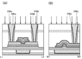
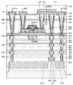
본 발명의 일 형태는 제 1 배리어층, 제 2 배리어층, 제 3 배리어층, 산화물을 포함하는 트랜지스터, 절연체, 및 도전체를 포함한다. 절연체는 산소 과잉 영역을 포함한다. 절연체 및 산화물은 제 1 배리어층과 제 2 배리어층 사이에 있다. 도전체는 제 1 배리어층의 개구, 제 2 배리어층의 개구, 및 절연체의 개구에 있다. 제 3 배리어층은 도전체와, 제 1 배리어층, 제 2 배리어층, 및 절연체와의 사이에 있다.One aspect of the invention includes a first barrier layer, a second barrier layer, a third barrier layer, a transistor comprising an oxide, an insulator, and a conductor. The insulator includes an excess oxygen region. The insulator and the oxide are between the first barrier layer and the second barrier layer. The conductor is in the opening of the first barrier layer, the opening of the second barrier layer, and the opening of the insulator. The third barrier layer is between the conductor and the first barrier layer, the second barrier layer, and the insulator.
본 발명의 일 형태는 제 1 배리어층, 제 2 배리어층, 제 3 배리어층, 산화물을 포함하는 트랜지스터, 절연체, 및 트랜지스터에 전기적으로 접속되는 도전체를 포함한다. 절연체는 산소 과잉 영역을 포함한다. 절연체 및 산화물은 제 1 배리어층과 제 2 배리어층 사이에 있다. 도전체는 제 1 배리어층의 개구 및 절연체의 개구에 있다. 제 3 배리어층은 도전체와, 제 1 배리어층 및 절연체와의 사이에 있다.One aspect of the invention includes a first barrier layer, a second barrier layer, a third barrier layer, a transistor comprising an oxide, an insulator, and a conductor electrically connected to the transistor. The insulator includes an excess oxygen region. The insulator and the oxide are between the first barrier layer and the second barrier layer. The conductor is in the opening of the first barrier layer and the opening of the insulator. The third barrier layer is between the conductor and the first barrier layer and the insulator.
본 발명의 일 형태는 제 1 배리어층, 제 2 배리어층, 제 3 배리어층, 산화물을 포함하는 트랜지스터, 절연체, 제 1 도전체, 및 제 2 도전체를 포함한다. 절연체는 산소 과잉 영역을 포함한다. 제 2 도전체는 트랜지스터에 전기적으로 접속된다. 절연체 및 산화물은 제 1 배리어층과 제 2 배리어층 사이에 있다. 제 1 도전체는 제 1 배리어층의 개구, 제 2 배리어층의 개구, 및 절연체의 개구에 있다. 제 3 배리어층은 제 1 도전체와, 제 1 배리어층, 제 2 배리어층, 및 절연체와의 사이에 있다. 제 2 도전체는 제 1 배리어층의 개구 및 절연체의 개구에 있다. 제 3 배리어층은 제 2 도전체와, 제 1 배리어층 및 절연체와의 사이에 있다.One aspect of the invention includes a first barrier layer, a second barrier layer, a third barrier layer, a transistor comprising an oxide, an insulator, a first conductor, and a second conductor. The insulator includes an excess oxygen region. The second conductor is electrically connected to the transistor. The insulator and the oxide are between the first barrier layer and the second barrier layer. The first conductor is in the opening of the first barrier layer, the opening of the second barrier layer, and the opening of the insulator. The third barrier layer is between the first conductor and the first barrier layer, the second barrier layer, and the insulator. The second conductor is in the opening of the first barrier layer and the opening of the insulator. The third barrier layer is between the second conductor and the first barrier layer and the insulator.
상기 구조 중 임의의 것에서, 제 1 배리어층의 개구의 측면 및 제 2 배리어층의 개구의 측면이 제 3 배리어층과 접촉함으로써, 트랜지스터 및 절연체가 제 1 배리어층, 제 2 배리어층, 및 제 3 배리어층에 의하여 밀봉된다.In any of the above structures, the side of the opening of the first barrier layer and the side of the opening of the second barrier layer contact the third barrier layer such that the transistor and the insulator comprise a first barrier layer, a second barrier layer, And is sealed by the barrier layer.
상기 구조 중 임의의 것에서, 400℃ 이하의 온도에서 TDS에 의하여 측정될 때, 제 1 배리어층, 제 2 배리어층, 또는 제 3 배리어층 아래의 구성 요소로부터의 수소의 방출량은 5.0×10¹⁴/cm2 이하이어도 좋다.In any of the above structures, the amount of hydrogen released from components below the first barrier layer, the second barrier layer, or the third barrier layer when measured by TDS at a temperature of 400 ° C or less is 5.0 x 10 14 / cm 2 or less.
상기 구조 중 임의의 것은 개구를 갖는 제 2 절연체 및 개구를 갖는 제 3 절연체를 포함하여도 좋다. 제 2 절연체는 제 2 배리어층 위에 있다. 제 3 절연체는 제 1 배리어층 아래에 있다. 제 2 절연체의 개구의 측면 및 제 3 절연체의 개구의 측면은 각각 제 3 배리어층으로 덮인 영역을 갖는다.Any of the above structures may include a second insulator having an opening and a third insulator having an opening. The second insulator is above the second barrier layer. The third insulator is below the first barrier layer. The side surface of the opening of the second insulator and the side surface of the opening of the third insulator each have a region covered with the third barrier layer.
상기 구조 중 임의의 것에서, 제 1 배리어층은 트랜지스터의 게이트 절연막으로서 기능하여도 좋다.In any of the above structures, the first barrier layer may function as a gate insulating film of the transistor.
본 발명의 일 형태에 따르면, 산화물 반도체를 포함하며 전기 특성이 안정적인 트랜지스터를 포함하는 반도체 장치를 제공할 수 있다. 본 발명의 일 형태에 따르면, 설계의 유연성이 높은 반도체 장치를 제공할 수 있다.According to one aspect of the present invention, a semiconductor device including an oxide semiconductor and including a transistor having stable electric characteristics can be provided. According to one aspect of the present invention, a semiconductor device with high design flexibility can be provided.
본 발명의 일 형태에 따르면, 전기 특성이 양호한 반도체 장치를 제공할 수 있다. 본 발명의 일 형태에 따르면, 신뢰성이 높은 반도체 장치를 제공할 수 있다. 본 발명의 일 형태에 따르면, 미세화 또는 고집적화가 가능한 반도체 장치를 제공할 수 있다. 본 발명의 일 형태에 따르면, 높은 생산성으로 제작할 수 있는 반도체 장치를 제공할 수 있다.According to one aspect of the present invention, a semiconductor device having good electrical characteristics can be provided. According to one aspect of the present invention, a highly reliable semiconductor device can be provided. According to one aspect of the present invention, a semiconductor device capable of miniaturization or high integration can be provided. According to one aspect of the present invention, a semiconductor device that can be manufactured with high productivity can be provided.
본 발명의 일 형태에 따르면, 오랫동안 데이터를 유지할 수 있는 반도체 장치를 제공할 수 있다. 본 발명의 일 형태에 따르면, 고속으로 데이터를 기록할 수 있는 반도체 장치를 제공할 수 있다. 본 발명의 일 형태에 따르면, 저전력의 반도체 장치를 제공할 수 있다. 본 발명의 일 형태에 따르면, 신규 반도체 장치를 제공할 수 있다.According to an aspect of the present invention, it is possible to provide a semiconductor device capable of holding data for a long time. According to one aspect of the present invention, a semiconductor device capable of recording data at high speed can be provided. According to an aspect of the present invention, a low-power semiconductor device can be provided. According to an aspect of the present invention, a novel semiconductor device can be provided.
또한 이들 효과의 기재는 다른 과제의 존재를 방해하지 않는다. 본 발명의 일 형태는 모든 효과를 반드시 실현할 필요는 없다. 다른 효과는 명세서, 도면, 및 청구항 등의 기재로부터 명백해질 것이며 추출될 수 있다.The description of these effects also does not hinder the existence of other tasks. One aspect of the present invention does not necessarily realize all effects. Other effects will be apparent from and elucidated with reference to the specification, drawings, claims, and the like.
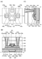
도 1의 (A) 내지 (C)는 본 발명의 일 형태의 반도체 장치의 구조를 도시한 상면도 및 단면도이다.
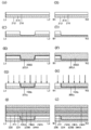
도 2의 (A) 내지 (J)는 본 발명의 일 형태의 반도체 장치의 제작 방법을 도시한 단면도이다.
도 3의 (A) 내지 (H)는 본 발명의 일 형태의 반도체 장치의 제작 방법을 도시한 단면도이다.
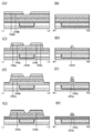
도 4의 (A) 내지 (H)는 본 발명의 일 형태의 반도체 장치의 제작 방법을 도시한 단면도이다.
도 5의 (A) 내지 (F)는 본 발명의 일 형태의 반도체 장치의 제작 방법을 도시한 단면도이다.
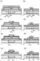
도 6의 (A) 내지 (D)는 본 발명의 일 형태의 반도체 장치의 제작 방법을 도시한 단면도이다.
도 7의 (A) 내지 (D)는 본 발명의 일 형태의 반도체 장치의 제작 방법을 도시한 단면도이다.
도 8의 (A) 내지 (D)는 본 발명의 일 형태의 반도체 장치의 제작 방법을 도시한 단면도이다.
도 9의 (A) 및 (B)는 본 발명의 일 형태의 반도체 장치의 제작 방법을 도시한 단면도이다.
도 10의 (A) 내지 (C)는 본 발명의 일 형태의 반도체 장치의 구조를 도시한 상면도 및 단면도이다.
도 11의 (A) 내지 (C)는 본 발명의 일 형태의 반도체 장치의 구조를 도시한 상면도 및 단면도이다.
도 12는 본 발명의 일 형태의 반도체 장치의 구조를 도시한 단면도이다.
도 13은 본 발명의 일 형태의 반도체 장치의 구조를 도시한 단면도이다.
도 14는 본 발명의 일 형태의 반도체 장치의 구조를 도시한 단면도이다.
도 15는 본 발명의 일 형태의 반도체 장치의 구조를 도시한 단면도이다.
도 16의 (A) 내지 (C)는 각각 실시예의 구조를 도시한 것이다.
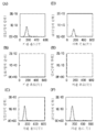
도 17의 (A) 내지 (F)는 실시예의 TDS 결과를 나타낸 것이다.
도 18의 (A) 및 (B)는 각각 실시예의 구조를 도시한 것이다.
도 19의 (A) 내지 (D)는 실시예의 TDS 결과를 나타낸 것이다.
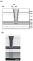
도 20의 (A) 및 (B)는 실시예의 구조의 단면도, 및 STEM 이미지이다.
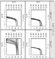
도 21은 실시예의 I d-V g 특성을 나타낸 것이다.
도 22의 (A) 및 (B)는 실시예의 구조, 및 TDS 결과를 나타낸 것이다.
도 23의 (A) 내지 (D)는 실시예의 구조의 단면도, 및 STEM 이미지이다.
도 24의 (A)는 실시예의 시료의 접촉 저항을 나타낸 것이고, 도 24의 (B) 및 (C)는 EDX 매핑 이미지를 나타낸 것이다.
도 25는 실시예의 I d-V g 특성을 나타낸 것이다.
도 26은 실시예의 I d-V g 특성을 나타낸 것이다.
도 27은 실시예의 시료의 접촉 저항을 나타낸 것이다.
도 28은 실시예의 시료의 GBT 스트레스 시험의 결과를 나타낸 것이다.1 (A) to 1 (C) are a top view and a cross-sectional view showing a structure of a semiconductor device according to one embodiment of the present invention.
2 (A) to 2 (J) are sectional views showing a manufacturing method of a semiconductor device according to one embodiment of the present invention.
3 (A) to 3 (H) are cross-sectional views showing a manufacturing method of a semiconductor device according to one embodiment of the present invention.
4 (A) to 4 (H) are cross-sectional views showing a manufacturing method of a semiconductor device according to one embodiment of the present invention.
5 (A) to 5 (F) are cross-sectional views showing a manufacturing method of a semiconductor device according to one embodiment of the present invention.
6 (A) to 6 (D) are cross-sectional views showing a manufacturing method of a semiconductor device according to one embodiment of the present invention.
7A to 7D are cross-sectional views showing a method of manufacturing a semiconductor device according to an embodiment of the present invention.
8A to 8D are cross-sectional views showing a method of manufacturing a semiconductor device according to an embodiment of the present invention.
9A and 9B are cross-sectional views showing a method of manufacturing a semiconductor device according to an embodiment of the present invention.
10A to 10C are a top view and a cross-sectional view showing a structure of a semiconductor device according to an embodiment of the present invention.
11A to 11C are a top view and a cross-sectional view showing a structure of a semiconductor device according to an embodiment of the present invention.
12 is a cross-sectional view showing the structure of a semiconductor device according to an embodiment of the present invention.
13 is a cross-sectional view showing a structure of a semiconductor device according to an embodiment of the present invention.
14 is a cross-sectional view showing a structure of a semiconductor device according to an embodiment of the present invention.
15 is a cross-sectional view showing a structure of a semiconductor device according to an embodiment of the present invention.
Figs. 16A to 16C each show the structure of the embodiment. Fig.
17 (A) to (F) show TDS results of the embodiment.
18 (A) and 18 (B) show the structure of the embodiment.
19 (A) to (D) show TDS results of the embodiment.
20 (A) and 20 (B) are a cross-sectional view and a STEM image of the structure of the embodiment.
Fig. 21 shows I d - V g characteristics of the embodiment.
Figures 22 (A) and 22 (B) show the structure of the embodiment and TDS results.
23 (A) to 23 (D) are a cross-sectional view and a STEM image of the structure of the embodiment.
24A shows the contact resistance of the sample of the embodiment, and FIGS. 24B and 24C show the EDX mapping image.
25 shows I d - V g characteristics of the embodiment.
Fig. 26 shows I d - V g characteristics of the embodiment.
27 shows the contact resistance of the sample of the embodiment.
28 shows the results of a GBT stress test of the sample of the example.
실시형태에 대하여 도면을 참조하여 이하에서 설명한다. 또한 실시형태는 많은 다른 형태로 실행할 수 있다. 본 발명의 취지 및 범위에서 벗어남이 없이 형태 및 자세한 사항이 다양하게 변경될 수 있다는 것은 통상의 기술자에 의하여 쉽게 이해될 것이다. 그러므로, 본 발명은 이하의 실시형태의 설명에 한정되어 해석되지 말아야 한다.Embodiments will be described below with reference to the drawings. Embodiments can also be implemented in many different forms. It will be understood by those skilled in the art that various changes in form and details may be made therein without departing from the spirit and scope of the present invention. Therefore, the present invention should not be construed as being limited to the description of the following embodiments.
도면에서, 크기, 층의 두께, 또는 영역은 명료화를 위하여 과장되어 있는 경우가 있다. 그러므로, 본 발명의 형태는 이러한 스케일에 한정되지 않는다. 또한, 도면은 이상적인 예를 도시한 모식도이고, 본 발명의 형태는 도면에 도시된 형상 또는 값에 한정되지 않는다. 도면에서, 같은 부분 또는 비슷한 기능을 갖는 부분은 상이한 도면에서 같은 부호로 나타내고, 그 설명은 반복하지 않는다. 또한, 비슷한 기능을 갖는 부분에는 같은 해칭 패턴을 적용하고, 이 부분을 부호로 나타내지 않는 경우가 있다.In the drawings, the size, layer thickness, or area may be exaggerated for clarity. Therefore, the form of the invention is not limited to this scale. Also, the drawings are schematic diagrams showing an ideal example, and the shapes of the present invention are not limited to the shapes or values shown in the drawings. In the drawings, parts having the same or similar functions are denoted by the same reference numerals in different drawings, and description thereof will not be repeated. The same hatching pattern may be applied to a portion having a similar function, and this portion may not be represented by a sign.
또한, 본 명세서 등에서 "제 1" 및 "제 2" 등의 서수는 편의상 사용되며, 공정 순서 또는 층의 적층 순서를 나타내지 않는다. 그러므로, 예를 들어, "제 1"을 "제 2" 또는 "제 3"으로 적절히 바꿔도 설명할 수 있다. 또한, 본 명세서 등에서의 서수는 본 발명의 일 형태를 특정하는 것과 반드시 같을 필요는 없다.In the present specification and the like, the ordinal numbers such as " first " and " second " are used for convenience and do not indicate the order of steps or the stacking order of the layers. Therefore, for example, "first" can be appropriately changed to "second" or "third". In addition, the ordinal numbers in this specification and the like do not necessarily have to be the same as those which specify one form of the present invention.
본 명세서에서, "위에" 및 "아래에" 등, 배치를 설명하기 위한 용어는, 도면을 참조하여 구성 요소들 사이의 위치 관계를 설명하기 위하여 편의상 사용된다. 구성 요소들 사이의 위치 관계는 각 구성 요소를 기재하는 방향에 따라 적절히 변화된다. 따라서, 본 명세서에서 사용되는 용어에 대한 한정은 없고, 상황에 따라 적절히 설명할 수 있다.In this specification, terms such as " above " and " below ", etc. for explaining the layout are used for convenience in describing the positional relationship among the components with reference to the drawings. The positional relationship between the components is appropriately changed according to the direction in which each component is described. Therefore, the terminology used in this specification is not limited, and can be suitably explained according to circumstances.
본 명세서 등에서, 트랜지스터는 게이트, 드레인, 및 소스의 적어도 3개의 단자를 갖는 소자이다. 트랜지스터는 드레인(드레인 단자, 드레인 영역, 또는 드레인 전극)과 소스(소스 단자, 소스 영역, 또는 소스 전극) 사이에 채널 영역을 포함하고, 채널 형성 영역을 통하여 드레인과 소스 사이에 전류를 흘릴 수 있다. 또한, 본 명세서 등에서, 채널 영역이란, 전류가 주로 흐르는 영역을 말한다.In this specification and the like, a transistor is an element having at least three terminals of a gate, a drain, and a source. The transistor includes a channel region between a drain (a drain terminal, a drain region, or a drain electrode) and a source (a source terminal, a source region, or a source electrode), and a current can flow between the drain and the source through the channel forming region . In this specification and the like, the channel region is a region in which current mainly flows.
"소스" 및 "드레인'의 기능은 예를 들어 반대 극성의 트랜지스터를 사용할 때 또는 회로 동작에서 전류가 흐르는 방향이 변화될 때, 서로 바뀌는 경우가 있다. 따라서, 본 명세서 등에서 "소스" 및 "드레인"이라는 용어는 서로 바꿀 수 있다.The functions of "source" and "drain" may be interchanged when using, for example, transistors of opposite polarity or when the direction of current flow in the circuit operation is changed. Can be interchanged.
또한 채널 길이란 예를 들어 트랜지스터의 상면도에서 반도체(또는 트랜지스터가 온일 때 반도체에서 전류가 흐르는 부분)와 게이트 전극이 서로 중첩되는 영역 또는 채널이 형성되는 영역에서의 소스(소스 영역 또는 소스 전극)와 드레인(드레인 영역 또는 드레인 전극) 사이의 거리를 말한다. 하나의 트랜지스터에서, 채널 길이는 모든 영역에서 반드시 같을 필요는 없다. 바꿔 말하면 하나의 트랜지스터의 채널 길이는 하나의 값에 한정되지 않는 경우가 있다. 그러므로, 본 명세서에서 채널 길이는, 채널이 형성되는 영역에서의 어느 하나의 값, 최대값, 최소값, 또는 평균값이다.The channel length refers to a region in which a semiconductor (or a portion where a current flows in a semiconductor when a transistor is ON) overlaps with a gate electrode in a top view of a transistor or a source (source region or source electrode) And the drain (drain region or drain electrode). In one transistor, the channel length does not necessarily have to be the same in all regions. In other words, the channel length of one transistor may not be limited to one value. Therefore, in this specification, the channel length is any value, maximum value, minimum value, or average value in the region where the channel is formed.
채널 폭이란 예를 들어, 반도체(또는 트랜지스터가 온일 때 반도체에서 전류가 흐르는 부분)와 게이트 전극이 서로 중첩되는 영역, 또는 채널이 형성되는 영역에서 소스와 드레인이 서로 대향하는 부분의 길이를 말한다. 하나의 트랜지스터에서, 채널 폭은 모든 영역에서 반드시 같을 필요는 없다. 바꿔 말하면, 하나의 트랜지스터의 채널 폭은 하나의 값으로 고정되지 않는 경우가 있다. 그러므로, 본 명세서에서 채널 폭은, 채널이 형성되는 영역에서의 어느 하나의 값, 최대값, 최소값, 또는 평균값이다.The channel width refers to a length of a portion where a source and a drain face each other in a region where a semiconductor (or a portion where a current flows in a semiconductor when a transistor is turned on) and a gate electrode overlap each other or a region where a channel is formed. In one transistor, the channel width does not necessarily have to be the same in all regions. In other words, the channel width of one transistor may not be fixed to one value. Therefore, in this specification, the channel width is any value, maximum value, minimum value, or average value in the region where the channel is formed.
또한, 트랜지스터 구조에 따라, 실제로 채널이 형성되는 영역에서의 채널 폭(이하, "실효적인 채널 폭"이라고 함)은 트랜지스터의 상면도에 나타낸 채널 폭(이하, "외견상 채널 폭"이라고 함)과 상이한 경우가 있다. 예를 들어, 반도체의 측면을 덮는 게이트 전극을 갖는 트랜지스터에서는 실효적인 채널 폭이 외견상 채널 폭보다 크고, 그 영향을 무시할 수 없는 경우가 있다. 예를 들어 반도체의 측면을 덮는 게이트 전극을 갖는 미세한 트랜지스터에서는 반도체의 측면에 형성되는 채널 형성 영역의 비율이 증가되는 경우가 있다. 이 경우, 실효적인 채널 폭이 외견상 채널 폭보다 크다.The channel width (hereinafter referred to as " effective channel width ") in the region where the channel is actually formed depends on the transistor structure, . ≪ / RTI > For example, in a transistor having a gate electrode covering a side surface of a semiconductor, the effective channel width is larger than the apparent channel width, and the influence thereof may not be negligible. For example, in a minute transistor having a gate electrode covering a side surface of a semiconductor, a ratio of a channel forming region formed on a side surface of the semiconductor may be increased. In this case, the effective channel width is larger than the apparent channel width.
이러한 경우, 실효적인 채널 폭을 측정하기 어려운 경우가 있다. 예를 들어, 설계값으로부터의 실효적인 채널 폭의 추산에는, 반도체의 형상을 알고 있다는 가정이 요구된다. 그러므로 반도체의 형상을 정확하게 모르는 경우에는 실효적인 채널 폭을 정확하게 측정하기 어렵다.In such a case, it may be difficult to measure the effective channel width. For example, in estimating the effective channel width from the design value, it is necessary to assume that the shape of the semiconductor is known. Therefore, it is difficult to accurately measure the effective channel width when the shape of the semiconductor is not precisely known.
따라서, 본 명세서에서는 외견상 채널 폭을 "SCW(surrounded channel width)"라고 하는 경우가 있다. 또한, 본 명세서에서 단순히 "채널 폭"이라는 용어를 사용하는 경우에는 SCW 또는 외견상 채널 폭을 나타낼 수 있다. 또는, 본 명세서에서 단순히 "채널 폭"이라는 용어를 사용하는 경우에는 실효적인 채널 폭을 나타내는 경우가 있다. 또한 채널 길이, 채널 폭, 실효적인 채널 폭, 외견상 채널 폭, 및 SCW 등의 값은 단면 TEM 이미지 등을 분석함으로써 결정할 수 있다.Therefore, in the present specification, the apparent channel width is sometimes referred to as " SCW (surrounded channel width) ". It is also possible to denote the SCW or apparent channel width when simply using the term " channel width " herein. Alternatively, the term " channel width " simply refers to an effective channel width in this specification. Further, values such as channel length, channel width, effective channel width, apparent channel width, and SCW can be determined by analyzing a cross-sectional TEM image or the like.
또한, 트랜지스터의 전계 효과 이동도 및 채널 폭당 전류값 등을 계산하여 얻는 경우, SCW가 계산에 사용되어도 좋다. 이 경우, 값은 실효적인 채널 폭을 사용하여 계산한 것과 상이한 경우가 있다.Further, when the field effect mobility of the transistor and the current value per channel width are obtained by calculation, SCW may be used for the calculation. In this case, the values may be different from those calculated using the effective channel width.
본 명세서 등에서, "전기적으로 접속"이라는 용어는 구성 요소가 "어떠한 전기적 기능을 갖는 물체"를 통하여 접속되어 있는 경우를 포함한다. "어떠한 전기적 기능을 갖는 물체"에는, 그 물체를 통하여 접속된 구성 요소들 사이에서 전기 신호가 송수신될 수 있기만 하면, 특별한 제한은 없다. "어떠한 전기적 기능을 갖는 물체"의 예에는 전극 및 배선뿐만 아니라, 트랜지스터 등의 스위칭 소자, 저항 소자, 인덕터, 용량 소자, 및 다양한 기능을 갖는 소자가 포함된다.In this specification and the like, the term " electrically connected " includes the case where the components are connected via " an object having any electrical function ". An " object having any electrical function " is not particularly limited as long as an electrical signal can be transmitted and received between elements connected through the object. Examples of the " object having any electrical function " include not only electrodes and wiring but also switching elements such as transistors, resistors, inductors, capacitors, and devices having various functions.
또한 본 명세서 등에서, 질화 산화물이란 산소보다 질소를 더 포함하는 화합물을 말한다. 산화 질화물이란 질소보다 산소를 더 포함하는 화합물을 말한다. 각 원소의 함유량은, 예를 들어 RBS(Rutherford backscattering spectrometry)에 의하여 측정될 수 있다.Also, in the present specification and the like, a nitride oxide means a compound containing nitrogen more than oxygen. The term " oxynitride " refers to a compound containing oxygen more than nitrogen. The content of each element can be measured, for example, by RBS (Rutherford backscattering spectrometry).
본 명세서 등에서 "막" 및 "층"이라는 용어는 서로 바꿀 수 있다. 예를 들어, "도전층"이라는 용어는 "도전막"이라는 용어로 바꿀 수 있는 경우가 있다. 또한, "절연막"이라는 용어를 "절연층"이라는 용어로 바꿀 수 있는 경우가 있다.In this specification and the like, the terms " membrane " and " layer " For example, the term " conductive layer " may be replaced with the term " conductive film ". Further, the term " insulating film " may be replaced with the term " insulating layer ".
본 명세서 등에서, "평행"이란 용어는 2개의 직선 사이에 형성되는 각도가 -10° 이상 10° 이하인 것을 나타내기 때문에, 상기 각도가 -5° 이상 5° 이하인 경우도 포함한다. 또한, "실질적으로 평행"이라는 용어는 2개의 직선 사이에 형성되는 각도가 -30° 이상 30° 이하인 것을 나타낸다. 또한, "수직"이란 용어는 2개의 직선 사이에 형성되는 각도가 80° 이상 100° 이하인 것을 나타내기 때문에 상기 각도가 85° 이상 95° 이하인 경우도 포함한다. 또한 "실질적으로 수직"이라는 용어는 2개의 직선 사이에 형성되는 각도가 60° 이상 120° 이하인 것을 나타낸다.In the present specification and the like, the term " parallel " indicates that an angle formed between two straight lines is from -10 DEG to 10 DEG, and thus includes the case where the angle is -5 DEG or more and 5 DEG or less. Further, the term " substantially parallel " indicates that an angle formed between two straight lines is not less than -30 DEG and not more than 30 DEG. Further, the term " vertical " indicates that an angle formed between two straight lines is not less than 80 degrees and not more than 100 degrees, and therefore includes the case where the angle is 85 degrees or more and 95 degrees or less. The term " substantially vertical " indicates that an angle formed between two straight lines is 60 degrees or more and 120 degrees or less.
본 명세서에서, 삼방정계 및 능면체정계(rhombohedral crystal system)는 육방정계에 포함된다.In the present specification, a rhombohedral crystal system is included in a hexagonal system.
또한 본 명세서에서, 배리어막이란 산소, 및 수소 등의 불순물의 투과를 억제하는 기능을 갖는 막을 말한다. 도전성을 갖는 배리어막을 도전성 배리어막이라고 할 수 있다.In this specification, the term "barrier film" refers to a film having a function of suppressing permeation of impurities such as oxygen and hydrogen. The barrier film having conductivity may be referred to as a conductive barrier film.
본 명세서 등에서, 노멀리 온 특성을 갖는 트랜지스터는, 전원에 의하여 전위가 인가되지 않는 경우(0V)에 온이 되는 트랜지스터이다. 예를 들어, 트랜지스터의 노멀리 온 특성은, 트랜지스터의 게이트에 공급되는 전압(V g)이 0V인 경우에 트랜지스터의 문턱 전압이 음이 되는 전기 특성을 의미하는 경우가 있다.In this specification and the like, a transistor having a normally-on characteristic is a transistor that is turned on when no potential is applied by a power source (0 V). For example, the normally-on characteristic of a transistor may mean an electrical characteristic in which the threshold voltage of the transistor becomes negative when the voltage ( V g ) supplied to the gate of the transistor is 0V.
본 명세서 등에서, 금속 산화물은 넓은 의미에서 금속의 산화물을 의미한다. 금속 산화물은 산화물 절연체, 산화물 도전체(투명 산화물 도전체를 포함함), 및 산화물 반도체(단순히 OS라고도 함) 등으로 분류된다. 예를 들어, 트랜지스터의 활성층에 사용한 금속 산화물을 산화물 반도체라고 부르는 경우가 있다. 바꿔 말하면, OS FET는 금속 산화물 또는 산화물 반도체를 포함하는 트랜지스터이다.In this specification and the like, a metal oxide means an oxide of a metal in a broad sense. The metal oxide is classified into an oxide insulator, an oxide conductor (including a transparent oxide conductor), and an oxide semiconductor (simply referred to as OS). For example, a metal oxide used for an active layer of a transistor may be referred to as an oxide semiconductor. In other words, the OSFET is a transistor including a metal oxide or an oxide semiconductor.
(실시형태 1)(Embodiment 1)
본 실시형태에서는, 반도체 장치의 일 형태에 대하여 도 1의 (A) 내지 (C), 도 2의 (A) 내지 (J), 도 3의 (A) 내지 (H), 도 4의 (A) 내지 (H), 도 5의 (A) 내지 (F), 도 6의 (A) 내지 (D), 도 7의 (A) 내지 (D), 도 8의 (A) 내지 (D), 도 9의 (A) 및 (B), 도 10의 (A) 내지 (C), 및 도 11의 (A) 내지 (C)를 참조하여 설명한다.1 (A) to 2 (C), 2 (A) to 2 (J), 3 (A) to 3 (H) 5A to 5F, 6A to 6D, 7A to 7D, 8A to 8D and 8A to 8D, Will be described with reference to Figs. 9 (A) and 9 (B), 10 (A) to (C), and 11 (A) to (C).
<반도체 장치의 구조><Structure of Semiconductor Device>
이하에서, 본 발명의 일 형태의 반도체 장치의 예에 대하여 설명한다. 도 1의 (A) 내지 (C)는 본 발명의 일 형태의 트랜지스터(200), 및 트랜지스터(200)에 전기적으로 접속되는 플러그를 도시한 상면도 및 단면도이다. 도 1의 (A)는 상면도이고, 도 1의 (B)는 도 1의 (A)에서의 일점쇄선 L1-L2를 따라 취한 단면도이고, 도 1의 (C)는 일점쇄선 W1-W2를 따라 취한 단면도이다. 도면의 명료화를 위하여, 일부의 구성 요소를 도 1의 (A)의 상면도에 도시하지 않았다.Hereinafter, an example of a semiconductor device according to one embodiment of the present invention will be described. 1 (A) to 1 (C) are a top view and a cross-sectional view showing a
본 발명의 일 형태의 반도체 장치는 트랜지스터(200), 층간막으로서 기능하는 절연체(280, 282, 및 286), 절연체(280 및 282)의 개구의 측면을 덮는 배리어층(276)(배리어층(276a, 276b, 및 276c)), 및 층간막으로서 기능하는 절연체(280, 282, 및 286)의 개구에 제공되는 도전체(246)(도전체(246a, 246b, 및 246c)) 및 도전체(248)(도전체(248a, 248b, 및 248c))를 포함한다. 배리어층(276)은 도전체(246 및 248)와 절연체(280, 282, 및 286) 사이에 있다.A semiconductor device of one embodiment of the present invention includes a
반도체 장치에서, 도전체(246 및 248)는 플러그 또는 배선으로서 기능한다. 또한 본 명세서 등에서, 배선 및 배선에 전기적으로 접속되는 플러그가 하나의 구성 요소이어도 좋다. 즉, 도전체의 일부가 배선으로서 기능하고, 도전체의 다른 부분이 플러그로서 기능하는 경우가 있다.In a semiconductor device, the
트랜지스터(200)는, 제 1 게이트 전극으로서 기능하는 도전체(260)(도전체(260a) 및 도전체(260b)를 포함함), 제 2 게이트 전극으로서 기능하는 도전체(205)(도전체(205a) 및 도전체(205b)를 포함함), 도전체(260)와 접촉하는 배리어층(270), 게이트 절연층으로서 기능하는 절연체(220, 222, 및 224) 및 절연체(250), 채널이 형성되는 영역을 포함하는 산화물(230)(산화물(230a), 산화물(230b), 및 산화물(230c)을 포함함), 소스 및 드레인 중 한쪽으로서 기능하는 도전체(240a), 소스 및 드레인 중 다른 쪽으로서 기능하는 도전체(240b), 및 도전체(240)(도전체(240a 및 240b))와 접촉하는 배리어층(244)(배리어층(244a 및 244b))을 포함한다.The
트랜지스터(200)에서, 산화물(230)은 산화물 반도체로서 기능하는 금속 산화물(이하, 금속 산화물을 산화물 반도체라고도 함)을 사용하여 형성하는 것이 바람직하다. 산화물 반도체를 사용하여 형성되는 트랜지스터는 오프 상태에서의 누설 전류가 매우 낮기 때문에, 소비전력이 낮은 반도체 장치를 제공할 수 있다. 산화물 반도체는 스퍼터링법 등으로 형성할 수 있기 때문에 고집적화된 반도체 장치에 포함되는 트랜지스터에 사용할 수 있다.In the
그러나, 산화물 반도체를 사용하여 형성되는 트랜지스터는 산화물 반도체 내의 불순물 및 산소 결손에 의하여 그 전기 특성이 변화되기 쉬워, 그 결과, 신뢰성이 저하되는 경우가 있다. 산화물 반도체에 포함되는 수소는 금속 원자와 결합되는 산소와 반응하여 물이 되기 때문에, 산소 결손을 발생시키는 경우가 있다. 산소 결손에 수소가 들어가는 것으로 인하여, 캐리어로서 기능하는 전자가 생성되는 경우가 있다. 또한, 수소의 일부가 금속 원자와 결합되는 산소와 결합됨으로써, 캐리어로서 기능하는 전자가 생성되는 경우가 있다. 따라서, 수소를 포함한 산화물 반도체를 포함하는 트랜지스터는 노멀리 온이 되기 쉽다. 따라서, 산화물 반도체 내의 수소는 가능한 한 저감되어 있는 것이 바람직하다.However, the transistor formed using an oxide semiconductor tends to change its electrical characteristics due to impurities and oxygen defects in the oxide semiconductor, and as a result, the reliability may deteriorate. Hydrogen contained in the oxide semiconductor reacts with oxygen bonded to metal atoms to form water, which may cause oxygen deficiency. Since hydrogen enters the oxygen vacancies, electrons functioning as carriers may be generated. Further, a part of hydrogen is combined with oxygen bonded to a metal atom, so that electrons functioning as a carrier are sometimes generated. Therefore, a transistor including an oxide semiconductor containing hydrogen tends to become normally on. Therefore, it is preferable that hydrogen in the oxide semiconductor be reduced as much as possible.
따라서, 트랜지스터(200) 근방에 제공되는 절연막으로서 기능하는 절연체(280)는 산화 실리콘막 또는 산화 질화 실리콘막 등, 산소를 포함하는 절연체인 것이 바람직하다.Therefore, the
절연체(280)는 화학량론적 조성보다 높은 비율로 산소를 포함하는 산화물을 사용하여 형성되는 것이 특히 바람직하다. 즉, 절연체(280)는 화학량론적 조성을 초과하여 산소를 포함하는 영역(이하, 산소 과잉 영역이라고도 함)을 갖는 것이 바람직하다. 특히, 산소 과잉 영역을 갖는 절연체를 트랜지스터(200) 근방의 층간막에 제공하면, 트랜지스터(200)에 포함되는 산화물(230) 내의 산소 결손을 저감할 수 있어, 신뢰성이 향상될 수 있다.It is particularly preferred that the
산소 과잉 영역을 포함하는 절연체로서는, 구체적으로 가열에 의하여 산소의 일부가 방출되는 산화물 재료를 사용하는 것이 바람직하다. 가열에 의하여 산소의 일부가 방출되는 산화물은, TDS(thermal desorption spectroscopy) 분석에 있어서 산소 원자로 환산한 산소의 방출량이 1.0×10¹⁸atoms/cm3 이상, 바람직하게는 3.0×10²⁰atoms/cm3 이상인 산화물막이다. 또한, TDS 분석에서의 막의 표면 온도는 바람직하게는 100℃ 이상 700℃ 이하, 또는 100℃ 이상 500℃ 이하이다.As the insulator including the oxygen excess region, it is preferable to use an oxide material in which a part of oxygen is released by heating. An oxide in which a part of oxygen is released by heating is preferably at least 1.0 x 10 18 atoms / cm 3, more preferably at least 3.0 x 10 20 atoms / cm 3 in terms of an oxygen atom in the TDS (thermal desorption spectroscopy) Or more. Further, the surface temperature of the film in the TDS analysis is preferably 100 ° C or more and 700 ° C or less, or 100 ° C or more and 500 ° C or less.
예를 들어, 산화 실리콘 또는 산화 질화 실리콘을 포함하는 재료를 사용할 수 있다. 또는, 금속 산화물을 사용할 수 있다. 또한, 본 명세서에서, "산화 질화 실리콘"이란 질소보다 높은 비율로 산소를 포함하는 재료를 말하고, "질화 산화 실리콘"이란 산소보다 높은 비율로 질소를 포함하는 재료를 말한다.For example, a material containing silicon oxide or silicon oxynitride may be used. Alternatively, a metal oxide may be used. In the present specification, the term " silicon oxynitride " refers to a material containing oxygen at a higher rate than nitrogen, and " silicon nitride oxide " refers to a material containing nitrogen at a higher rate than oxygen.
또한, 절연체(280)가 산소 과잉 영역을 포함하는 경우, 절연체(282)는 산소, 수소, 및 물에 대한 배리어성을 갖는 것이 바람직하다. 절연체(282)가 산소에 대한 배리어성을 가지면, 산소 과잉 영역의 산소가 절연체(286) 측으로 확산되지 않고 산화물(230)에 효율적으로 공급된다.Further, when the
또한, 규정되지 않는 한, 본 명세서에서의 "배리어성"이라는 용어는, 적어도 수소 및 물로 대표되는 불순물의 확산을 억제하는 기능을 말한다. 예를 들어, 수소의 확산은 350℃, 바람직하게는 400℃의 분위기에서 억제된다. 예를 들어 수소를 방출하는 제 1 막, 및 그 위에 적층된 임의의 제 2 막을 포함하는 구조에는 400℃ 이하의 온도에서 TDS 측정이 수행되고, 수소의 방출량이 5.0×10¹⁴/cm2 이하인 경우, 제 2 막은 수소에 대한 배리어성을 갖는 것으로 간주된다. 수소의 방출량은 400℃ 이하의 온도에서 3.4×10¹⁴/cm2 이하인 것이 바람직하고, 500℃ 이하의 온도에서 7.1×10¹⁴/cm2 이하인 것이 더 바람직하고, 600℃ 이하의 온도에서 1.4×10¹⁵/cm2 이하인 것이 더욱 바람직하다.Further, unless otherwise specified, the term " barrier property " in this specification refers to a function of suppressing the diffusion of at least impurities represented by hydrogen and water. For example, diffusion of hydrogen is suppressed in an atmosphere of 350 캜, preferably 400 캜. For example, if the first film, and that a structure containing any of the second film is laminated on, the TDS measurement is performed at a temperature not higher than 400 ℃, the hydrogen discharge amount 5.0 × 10 14 / cm 2 or less to release hydrogen , And the second film is considered to have barrier properties to hydrogen. The amount of hydrogen emission is preferably 3.4 x 10 14 / cm 2 or less at a temperature of 400 ° C or lower, more preferably 7.1 x 10 14 / cm 2 or lower at a temperature of 500 ° C or lower, more preferably 1.4 x 10 More preferably 15 / cm 2 or less.
나중에 자세히 설명하는 바와 같이, 절연체(282)와 마찬가지로, 트랜지스터(200)에 포함되는 절연체(222)는 산소, 수소, 및 물에 대한 배리어성을 갖는 것이 바람직하다. 절연체(222)가 산소에 대한 배리어성을 가지면, 산소 과잉 영역의 산소가 절연체(220) 측으로 확산되지 않고, 산화물(230)에 효율적으로 공급될 수 있다.As will be described in detail later, as with the
절연체(282)는 산화 질화 실리콘, 질화 산화 실리콘, 산화 알루미늄, 산화 하프늄, 산화 탄탈럼, 산화 지르코늄, 타이타늄산 지르콘산연(PZT), 타이타늄산 스트론튬(SrTiO3), 또는 (Ba,Sr)TiO3(BST) 등의 소위 high-k 재료를 포함하는 절연체를 사용한 단층 구조 또는 적층 구조를 갖는 것이 바람직하다. 특히, 산소 또는 수소에 대한 배리어성을 갖는 절연막, 예를 들어 산화 알루미늄막 또는 산화 하프늄막을 사용하는 것이 바람직하다. 이러한 재료로 형성된 절연체(282)는, 산화물(230)로부터 산소가 방출되는 것, 및 외부로부터 수소 등의 불순물이 들어가는 것을 방지하는 층으로서 기능한다.
또는, 예를 들어, 상기 절연체에 산화 알루미늄, 산화 비스무트, 산화 저마늄, 산화 나이오븀, 산화 실리콘, 산화 타이타늄, 산화 텅스텐, 산화 이트륨, 또는 산화 지르코늄을 첨가하여도 좋다. 또는 절연체에 질화 처리를 수행하여도 좋다. 상기 절연체 위에 산화 실리콘, 산화 질화 실리콘, 또는 질화 실리콘을 적층하여도 좋다.Alternatively, for example, aluminum oxide, bismuth oxide, germanium oxide, niobium oxide, silicon oxide, titanium oxide, tungsten oxide, yttrium oxide, or zirconium oxide may be added to the insulator. Or the insulator may be subjected to a nitriding treatment. Silicon oxide, silicon oxynitride, or silicon nitride may be stacked on the insulator.
또한, 절연체(280, 282, 및 286)는 각각 2층 이상의 적층 구조를 가져도 좋다. 이 경우, 적층은 반드시 같은 재료로 형성될 필요는 없고, 상이한 재료로 형성되어도 좋다. 또한, 트랜지스터(200)를 덮는 절연체(280)는 그 아래의 거칠기를 덮는 평탄화막으로서 기능하여도 좋다.The
트랜지스터(200)는, 절연체(280, 282, 및 286)에 제공되는 도전체(246 및 248) 등의 플러그 또는 배선을 통하여, 다른 구성 요소와 전기적으로 접속되는 경우가 있다. 도전체(246 및 248)가 절연체(280)와 접촉되면, 절연체(280)에 포함되는 과잉 산소가 도전체(246 및 248)에 의하여 흡수될 수 있다.
반도체 장치에 제공되는 플러그 또는 배선의 형상, 또는 플러그 또는 배선의 수에 따라서는, 절연체(280)에 포함되는 과잉 산소가 트랜지스터(200)에 포함되는 산화물(230) 내의 산소 결손을 보충하는 데 부족하므로, 반도체 장치의 신뢰성이 저하될 수 있다. 따라서, 절연체(280)의 산소 과잉 영역은 도전체(246 및 248)에 의하여 흡수되는 산소의 양을 고려하여 형성될 필요가 있다.Depending on the shape of the plug or wiring provided in the semiconductor device or the number of plugs or wirings, the excess oxygen contained in the
또한, 트랜지스터(200) 근방에 형성되는 구성 요소에 포함되는 불순물인 수소가, 플러그 또는 배선으로서 사용되는 도전체를 통하여 상기 도전체와 접촉하는 구성 요소로 확산되는 경우가 있다.In addition, hydrogen, which is an impurity contained in a constituent element formed near the
따라서, 도전체(246 및 248)와, 산소 과잉 영역을 갖는 절연체(280) 및 배리어성을 갖는 절연체(282)와의 사이에 배리어층(276)을 제공하는 것이 바람직하다. 배리어층(276)은 배리어성을 갖는 절연체(282)와 접촉하여 제공되는 것이 특히 바람직하다. 배리어층(276)은 절연체(282)와 접촉하기 때문에, 절연체(280) 및 트랜지스터(200)는 배리어성을 갖는 절연체, 및 배리어층에 의하여 밀봉될 수 있다. 배리어층(276)은 절연체(286)의 일부와 접촉하는 것도 바람직하다. 배리어층(276)이 절연체(286)와도 접촉되면, 산소 및 불순물의 확산을 더 억제할 수 있다.It is therefore desirable to provide the
즉, 배리어층(276)은 절연체(280)에 포함되는 과잉 산소가 도전체(246 및 248)에 의하여 흡수되는 것을 방지할 수 있다. 따라서, 도전체(246 및 248)에 의하여 과잉 산소가 흡수되기 때문에, 트랜지스터(200)에 포함되는 산화물(230) 내의 산소 결손이 과잉 산소로 보충되지 않음으로써 발생되는, 반도체 장치의 신뢰성의 저하를 방지할 수 있다.That is, the
또한, 배리어층(276)은 불순물인 수소의 확산을 억제할 수 있다. 예를 들어, 배리어층(276)은 절연체(282) 위의 구성 요소에 포함되는 수소가 트랜지스터(200)와 접촉하는 절연체(280)로 도전체(246 및 248)를 통하여 확산되는 것을 억제할 수 있다.Further, the
또한, 배리어층(276)에 의하여, 반도체 장치에 제공되는 플러그 또는 배선의 형상 또는 위치, 또는 플러그 또는 배선의 수에 상관없이, 절연체(280)는 적절한 양의 과잉 산소를 포함할 수 있다. 수소의 확산을 억제하면 산소 결손이 형성되기 어려워지기 때문에, 캐리어의 생성을 억제할 수 있다. 따라서, 과잉 산소를 트랜지스터(200)에 안정적으로 공급할 수 있어, 트랜지스터(200)가 안정적인 전기 특성을 가질 수 있다. 또한, 반도체 장치의 설계의 유연성을 높일 수 있다.Also, with the
또한, 배리어층(276)을 사용함으로써, 플러그 또는 배선으로서 사용되는 도전체의 재료 선택의 폭을 넓힐 수 있다. 예를 들어, 산소 흡수성 및 높은 도전성을 갖는 금속 재료를 도전체(246 및 248)에 사용함으로써, 소비전력이 낮은 반도체 장치를 제공할 수 있다. 구체적인 예로서, 텅스텐 또는 알루미늄 등의 내산화성이 낮으며 도전성이 높은 재료, 그리고 쉽게 퇴적 및 가공할 수 있는 도전체를 들 수 있다.Further, by using the
각 도전체(246 및 248)는, 금속 재료, 합금 재료, 금속 질화물 재료, 또는 금속 산화물 재료 등의 도전 재료를 사용하여 단층 구조 또는 적층 구조를 갖도록 형성할 수 있다. 예를 들어, 텅스텐 또는 몰리브데넘 등, 내열성 및 도전성의 양쪽 모두를 갖는 고융점 재료를 사용하는 것이 바람직하다. 또는, 알루미늄 또는 구리 등의 저저항 도전 재료를 사용하는 것이 바람직하다. 저저항 도전 재료를 사용하면 배선의 저항을 저감시킬 수 있다.Each of the
도전체(246)에는, 예를 들어 수소 및 산소에 대한 배리어성을 갖는 도전체인 질화 탄탈럼 등을 사용할 수 있다. 또한, 도전성이 높은 텅스텐을 도전체(248)에 사용하면, 배선으로서의 도전성을 유지하면서 외부로부터의 불순물의 확산을 억제할 수 있다.As the
배리어층(276)에는, 예를 들어 금속 산화물을 사용할 수 있다. 특히, 산소 또는 수소에 대한 배리어성을 갖는 절연막, 예를 들어 산화 알루미늄막, 산화 하프늄막, 또는 산화 갈륨막을 사용하는 것이 바람직하다. 또는 CVD(chemical vapor deposition)법에 의하여 퇴적된 질화 실리콘을 사용하여도 좋다.As the
상기에 따르면, 전기 특성이 안정적인 반도체 장치를 제공할 수 있다. 상기에 따르면, 신뢰성이 높은 반도체 장치를 제공할 수 있다. 상기에 따르면, 소비전력이 낮은 반도체 장치를 제공할 수 있다. 상기에 따르면, 반도체 장치의 설계의 유연성을 높일 수 있다.According to the above, a semiconductor device with stable electrical characteristics can be provided. According to the above, a highly reliable semiconductor device can be provided. According to the above, a semiconductor device with low power consumption can be provided. According to the above, the flexibility of the design of the semiconductor device can be improved.
<트랜지스터의 구조 1><Structure of
이하에서, 트랜지스터(200)의 예에 대하여 설명한다.Hereinafter, an example of the
몰리브데넘, 타이타늄, 탄탈럼, 텅스텐, 알루미늄, 구리, 크로뮴, 네오디뮴, 및 스칸듐에서 선택된 원소를 포함하는 금속막; 또는 그 성분으로서 상기 원소 중 임의의 것을 포함하는 금속 질화물막(예를 들어, 질화 탄탈럼막, 질화 타이타늄막, 질화 몰리브데넘막, 또는 질화 텅스텐막) 등을 사용하여 도전체(205)를 형성한다. 특히, 질화 탄탈럼막 등의 금속 질화물막은, 수소 또는 산소에 대한 배리어성을 갖고 산화되기 어렵기 때문에(내산화성이 높기 때문에) 바람직하다. 또는, 인듐 주석 산화물, 산화 텅스텐을 포함하는 인듐 산화물, 산화 텅스텐을 포함하는 인듐 아연 산화물, 산화 타이타늄을 포함하는 인듐 산화물, 산화 타이타늄을 포함하는 인듐 주석 산화물, 인듐 아연 산화물, 또는 산화 실리콘이 첨가된 인듐 주석 산화물 등의 도전 재료를 사용할 수 있다.A metal film containing an element selected from molybdenum, titanium, tantalum, tungsten, aluminum, copper, chromium, neodymium, and scandium; (For example, a tantalum nitride film, a titanium nitride film, a molybdenum nitride film or a tungsten nitride film) containing any one of the above elements is used to form the
예를 들어, 도전체(205a)로서 수소에 대한 배리어성을 갖는 도전체, 예를 들어, 질화 탄탈럼을 사용하고, 그 위에 도전체(205b)로서 도전성이 높은 텅스텐을 적층하는 것이 바람직하다. 이 재료의 조합을 사용하면 배선의 도전성을 지키면서 산화물(230)로의 수소의 확산을 방지할 수 있다. 또한, 도 1의 (A) 내지 (C)에는 도전체(205a 및 205b)의 2층 구조를 도시하였지만, 본 발명의 일 형태는 이에 한정되지 않고, 단층 구조 또는 3층 이상의 적층 구조를 사용하여도 좋다. 예를 들어, 배리어성을 갖는 도전체와 도전성이 높은 도전체 사이에, 배리어성을 갖는 도전체 및 도전성이 높은 도전체에 대한 밀착성이 높은 도전체를 형성하여도 좋다.For example, it is preferable to use a conductor having a barrier property against hydrogen as the
절연체(280)와 같이, 절연체(224)는 산화 실리콘막 또는 산화 질화 실리콘막 등, 산소를 포함하는 절연체인 것이 바람직하다. 절연체(224)는 산소 과잉 영역을 갖는 것이 특히 바람직하다. 산화물 반도체를 트랜지스터(200)에 사용하고, 산소 과잉 영역을 갖는 절연체를 트랜지스터(200) 근방의 층간막 등에 제공하면, 트랜지스터(200)에 포함되는 산화물(230) 내의 산소 결손을 저감할 수 있고 신뢰성을 향상시킬 수 있다.Like the
또한, 절연체(224)가 산소 과잉 영역을 포함하는 경우, 절연체(222)는 산소, 수소, 및 물에 대한 배리어성을 갖는 것이 바람직하다. 절연체(222)가 산소에 대한 배리어성을 가지면, 산소 과잉 영역의 산소가 도전체(205a) 측으로 확산되지 않고 산화물(230)에 효율적으로 공급된다. 도전체(205)가 절연체(224)의 산소 과잉 영역의 산소와 반응하는 것을 억제할 수 있다.Further, when the
절연체(222)는, 산화 질화 실리콘, 질화 산화 실리콘, 산화 알루미늄, 산화 하프늄, 산화 탄탈럼, 산화 지르코늄, 타이타늄산 지르콘산연(PZT), 타이타늄산 스트론튬(SrTiO3), 또는 (Ba,Sr)TiO3(BST) 등의 소위 high-k 재료를 포함하는 절연체를 사용하는 단층 구조 또는 적층 구조를 갖는 것이 바람직하다. 특히, 산소 또는 수소에 대한 배리어성을 갖는 절연막, 예를 들어 산화 알루미늄막 또는 산화 하프늄막을 사용하는 것이 바람직하다. 이러한 재료로 형성된 절연체(222)는, 산화물(230)로부터 산소가 방출되는 것, 및 외부로부터 수소 등의 불순물이 들어가는 것을 방지하는 층으로서 기능한다.The
또는, 예를 들어, 상기 절연체에 산화 알루미늄, 산화 비스무트, 산화 저마늄, 산화 나이오븀, 산화 실리콘, 산화 타이타늄, 산화 텅스텐, 산화 이트륨, 또는 산화 지르코늄을 첨가하여도 좋다. 또는, 상기 절연체에 질화 처리를 수행하여도 좋다. 상기 절연체 위에 산화 실리콘, 산화 질화 실리콘, 또는 질화 실리콘을 적층하여도 좋다.Alternatively, for example, aluminum oxide, bismuth oxide, germanium oxide, niobium oxide, silicon oxide, titanium oxide, tungsten oxide, yttrium oxide, or zirconium oxide may be added to the insulator. Alternatively, the insulator may be nitrided. Silicon oxide, silicon oxynitride, or silicon nitride may be stacked on the insulator.
또한, 절연체(220, 222, 및 224)는 각각 2층 이상의 적층 구조를 가져도 좋다. 이 경우, 적층은 반드시 같은 재료로 형성될 필요는 없고, 상이한 재료로 형성되어도 좋다.The
high-k 재료를 포함하는 절연체(222)를 절연체(220)와 절연체(224) 사이에 제공하기 때문에, 특정한 조건하에서 전자가 절연체(222)에 트랩되고, 문턱 전압이 증대될 수 있다. 이 결과, 절연체(222)가 음으로 대전되는 경우가 있다.electrons can be trapped in the
예를 들어, 절연체(220) 및 절연체(224)를 산화 실리콘을 사용하여 형성하고, 절연체(222)를 산화 하프늄, 산화 알루미늄, 또는 산화 탄탈럼 등의 전자 트랩 준위가 많은 재료를 사용하여 형성하는 경우, 반도체 장치의 동작 온도 또는 보관 온도보다 높은 온도(예를 들어, 125℃ 이상 450℃ 이하, 대표적으로는 150℃ 이상 300℃ 이하)에서, 도전체(205)의 전위가 소스 전극 또는 드레인 전극의 전위보다 높은 상태를 10밀리초 이상, 대표적으로는 1분 이상 유지한다. 이에 의하여, 트랜지스터(200)의 산화물로부터 도전체(205)로 전자가 이동한다. 이때, 이동하는 전자의 일부가 절연체(222)의 전자 트랩 준위에 의하여 트랩된다.For example, when the
필요한 양의 전자가 절연체(222)의 전자 트랩 준위에 의하여 트랩된 트랜지스터에서는, 문턱 전압이 양의 방향으로 변동된다. 도전체(205)의 전압을 제어함으로써, 트랩될 전자의 양을 제어할 수 있어, 문턱 전압을 제어할 수 있다. 상기 구조를 갖는 트랜지스터(200)는, 게이트 전압이 0V일 때도 비도통 상태(오프 상태라고도 함)에 있는 노멀리 오프 트랜지스터이다.In a transistor in which a required amount of electrons is trapped by the electron trap level of the
또한, 전자를 트랩하기 위한 처리를 트랜지스터의 제작 공정에서 수행하여도 좋다. 예를 들어, 트랜지스터의 소스 도전체 또는 드레인 도전체에 접속된 도전체의 형성 후, 전(前)처리(웨이퍼 처리) 후, 웨이퍼 다이싱 단계 후, 또는 패키징 후 등의, 공장 출하 전의 임의의 단계에서 처리가 수행되는 것이 바람직하다.Further, a process for trapping electrons may be performed in the manufacturing process of the transistor. For example, after the formation of a conductor connected to the source conductor or the drain conductor of the transistor, it is possible to perform a process such as post-processing (wafer processing), after the wafer dicing step, It is preferable that the treatment is carried out in the step.
절연체(220, 222, 및 224)의 두께를 적절히 조정함으로써, 문턱 전압을 제어할 수 있다. 예를 들어, 절연체(220, 222, 및 224)의 총 두께가 얇으면, 도전체(205)로부터 전압이 효율적으로 인가되기 때문에, 트랜지스터의 소비전력이 저감된다. 절연체(220, 222, 및 224)의 총 두께는 65nm 이하, 바람직하게는 20nm 이하이다.By appropriately adjusting the thicknesses of the
그러므로, 오프 상태에서의 누설 전류가 낮은 트랜지스터를 제공할 수 있다. 전기 특성이 안정적인 트랜지스터를 제공할 수 있다. 온 상태 전류가 높은 트랜지스터를 제공할 수 있다. 서브스레시홀드 스윙값이 작은 트랜지스터를 제공할 수 있다. 신뢰성이 높은 트랜지스터를 제공할 수 있다.Therefore, it is possible to provide a transistor having a low leakage current in the OFF state. It is possible to provide a transistor having stable electric characteristics. It is possible to provide a transistor having a high on-state current. It is possible to provide a transistor having a small subthreshold swing value. A transistor with high reliability can be provided.
산화물(230)은 산화물(230a), 산화물(230a) 위의 산화물(230b), 및 산화물(230b) 위의 산화물(230c)을 포함한다. 트랜지스터(200)를 온으로 하면, 주로 산화물(230b)에 전류가 흐른다(채널이 형성된다). 한편, 산화물(230b)과 산화물(230a 또는 230c) 사이의 계면 근방(혼합 영역인 경우도 있음)의 영역을 통하여 전류가 흐르는 경우가 있지만, 산화물(230a 및 230c)의 다른 영역은 절연체로서 기능하는 경우가 있다.The
도 1의 (C)에 도시된 바와 같이, 산화물(230c)은 산화물(230a 및 230b)의 측면을 덮도록 제공되는 것이 바람직하다. 채널이 형성되는 영역을 포함하는 산화물(230b)과 절연체(280) 사이에 제공되는 산화물(230c)은, 절연체(280)로부터 산화물(230b)로 수소, 물, 및 할로젠 등의 불순물이 확산되는 것을 방지할 수 있다.As shown in Fig. 1 (C), the
In-M-Zn 산화물(원소 M은 알루미늄, 갈륨, 이트륨, 구리, 바나듐, 베릴륨, 붕소, 실리콘, 타이타늄, 철, 니켈, 저마늄, 지르코늄, 몰리브데넘, 란타넘, 세륨, 네오디뮴, 하프늄, 탄탈럼, 텅스텐, 및 마그네슘 등에서 선택된 1종류 이상) 등의 금속 산화물을 사용하여 산화물(230a, 230b, 및 230c)을 형성한다. In-Ga 산화물 또는 In-Zn 산화물을 산화물(230)에 사용하여도 좋다.In- M- Zn oxide (the element M is at least one element selected from the group consisting of aluminum, gallium, yttrium, copper, vanadium, beryllium, boron, silicon, titanium, iron, nickel, germanium, zirconium, molybdenum, lanthanum, cerium, neodymium, hafnium, Tantalum, tungsten, magnesium, and the like) is used to form the
[금속 산화물][Metal oxide]
본 발명의 일 형태의 산화물(230)에 대하여 이하에서 설명한다. 산화물(230)은, 산화물 반도체로서 기능하는 금속 산화물(이하, 금속 산화물을 산화물 반도체라고도 함)을 사용하여 형성되는 것이 바람직하다.One embodiment of the
산화물 반도체는 적어도 인듐 또는 아연을 포함하는 것이 바람직하다. 특히, 인듐 및 아연을 포함하는 것이 바람직하다. 또한, 알루미늄, 갈륨, 이트륨, 또는 주석 등을 포함하는 것이 바람직하다. 또한, 붕소, 실리콘, 타이타늄, 철, 니켈, 저마늄, 지르코늄, 몰리브데넘, 란타넘, 세륨, 네오디뮴, 하프늄, 탄탈럼, 텅스텐, 또는 마그네슘 등에서 선택된 하나 이상의 원소를 포함하여도 좋다.The oxide semiconductor preferably includes at least indium or zinc. Particularly, it is preferable to include indium and zinc. Further, it is preferable to include aluminum, gallium, yttrium, tin or the like. It may also contain at least one element selected from boron, silicon, titanium, iron, nickel, germanium, zirconium, molybdenum, lanthanum, cerium, neodymium, hafnium, tantalum, tungsten or magnesium.
여기서, 산화물 반도체가 인듐, 원소 M, 및 아연을 포함하는 InMZnO인 경우를 생각한다. 원소 M은 알루미늄, 갈륨, 이트륨, 또는 주석 등이다. 또는, 원소 M은 붕소, 실리콘, 타이타늄, 철, 니켈, 저마늄, 지르코늄, 몰리브데넘, 란타넘, 세륨, 네오디뮴, 하프늄, 탄탈럼, 텅스텐, 또는 마그네슘 등일 수 있다. 또한, 상기 원소 중 2개 이상을 조합하여 원소 M으로서 사용하여도 좋다.Here, consider a case where an oxide semiconductor is In M ZnO containing indium, element M, and zinc. The element M is aluminum, gallium, yttrium, or tin. Alternatively, the element M may be boron, silicon, titanium, iron, nickel, germanium, zirconium, molybdenum, lanthanum, cerium, neodymium, hafnium, tantalum, tungsten or magnesium. In addition, two or more of the above elements may be used in combination as the element M.
본 명세서 등에서는, 질소를 포함하는 금속 산화물(metal oxide)도 금속 산화물이라고 부르는 경우가 있다. 또한, 질소를 포함하는 금속 산화물을 금속 산질화물(metal oxynitride)이라고 불러도 좋다.In this specification and the like, a metal oxide including nitrogen is also sometimes referred to as a metal oxide. Further, the metal oxide containing nitrogen may be referred to as a metal oxynitride.
<금속 산화물의 구성>≪ Configuration of Metal Oxide >
본 발명의 일 형태에 개시된 트랜지스터에 적용할 수 있는 CAC-OS(cloud-aligned composite oxide semiconductor)의 구성에 대하여 이하에서 설명한다.A configuration of a cloud-aligned composite oxide semiconductor (CAC-OS) applicable to a transistor disclosed in an embodiment of the present invention will be described below.
본 명세서 등에서, "CAAC(c-axis aligned crystal)" 또는 "CAC(cloud-aligned composite)"라고 말하는 경우가 있다. CAAC는 결정 구조의 예를 말하고, CAC는 기능 또는 재료 구성의 예를 말한다.In this specification and the like, there is a case where it is sometimes referred to as "c-axis aligned crystal (CAAC)" or "cloud-aligned composite (CAC)". CAAC refers to an example of a crystal structure, and CAC refers to an example of a function or material composition.
CAC-OS 또는 CAC metal oxide는 재료의 일부에서 도전성 기능을 갖고, 재료의 다른 일부에서 절연성 기능을 갖고, 전체로서는 CAC-OS 또는 CAC metal oxide는 반도체의 기능을 갖는다. CAC-OS 또는 CAC metal oxide가 트랜지스터의 활성층에 사용되는 경우, 도전성 기능은 캐리어로서 기능하는 전자(또는 정공)를 흘리게 하기 위한 것이고, 절연성 기능은 캐리어로서 기능하는 전자를 흘리지 않게 하기 위한 것이다. 도전성 기능과 절연성 기능의 상보적인 작용에 의하여, CAC-OS 또는 CAC metal oxide는 스위칭 기능(온/오프 기능)을 가질 수 있다. CAC-OS 또는 CAC metal oxide에서는, 기능을 분리함으로써 각 기능을 최대화시킬 수 있다.The CAC-OS or CAC metal oxide has a conductive function in a part of the material and has an insulating function in another part of the material. As a whole, the CAC-OS or CAC metal oxide functions as a semiconductor. When the CAC-OS or CAC metal oxide is used for the active layer of the transistor, the conductive function is to flow electrons (or holes) which function as a carrier, and the insulating function is to prevent electrons that function as carriers from flowing. CAC-OS or CAC metal oxide can have a switching function (on / off function) due to the complementary action of the conductive function and the insulating function. In CAC-OS or CAC metal oxide, each function can be maximized by separating the functions.
CAC-OS 또는 CAC metal oxide는 도전성 영역 및 절연성 영역을 포함한다. 도전성 영역은 상술한 도전성 기능을 갖고, 절연성 영역은 상술한 절연성 기능을 갖는다. 재료 내의 도전성 영역 및 절연성 영역은 나노 입자 레벨로 분리되어 있는 경우가 있다. 도전성 영역 및 절연성 영역은 재료 내에서 고르지 않게 분포되어 있는 경우가 있다. 도전성 영역은 그 경계가 흐릿해져 클라우드상(cloud-like)으로 연결되어 있는 것이 관찰되는 경우가 있다.The CAC-OS or CAC metal oxide includes a conductive region and an insulating region. The conductive region has the above-described conductive function, and the insulating region has the above-described insulating function. The conductive region and the insulating region in the material may be separated at the nanoparticle level. The conductive region and the insulating region may be unevenly distributed in the material. It may be observed that the conductive region is blurred and connected in a cloud-like manner.
또한 CAC-OS 또는 CAC metal oxide에서, 도전성 영역 및 절연성 영역 각각은 0.5nm 이상 10nm 이하, 바람직하게는 0.5nm 이상 3nm 이하의 크기를 갖고, 재료 내에서 분산되어 있는 경우가 있다.In the CAC-OS or CAC metal oxide, each of the conductive region and the insulating region has a size of 0.5 nm or more and 10 nm or less, preferably 0.5 nm or more and 3 nm or less, and may be dispersed in the material.
CAC-OS 또는 CAC metal oxide는 밴드 갭이 상이한 성분을 포함한다. 예를 들어, CAC-OS 또는 CAC metal oxide는 절연성 영역에 기인하는 넓은 갭(wide gap)을 갖는 성분 및 도전성 영역에 기인하는 좁은 갭(narrow gap)을 갖는 성분을 포함한다. 이러한 구성의 경우, 좁은 갭을 갖는 성분에서 캐리어가 주로 흐른다. 좁은 갭을 갖는 성분은 넓은 갭을 갖는 성분을 보완하고, 좁은 갭을 갖는 성분과 연동하여 넓은 갭을 갖는 성분에서도 캐리어가 흐른다. 그러므로, 상술한 CAC-OS 또는 CAC metal oxide를 트랜지스터의 채널 영역에 사용하는 경우, 트랜지스터의 온 상태에서의 높은 전류 구동 능력, 즉 높은 온 상태 전류 및 높은 전계 효과 이동도를 얻을 수 있다.The CAC-OS or CAC metal oxide contains components with different bandgaps. For example, the CAC-OS or CAC metal oxide comprises a component having a wide gap due to the insulating region and a component having a narrow gap due to the conductive region. In this configuration, the carrier mainly flows in the component having the narrow gap. The component having the narrow gap compensates the component having the wide gap, and the carrier also flows in the component having the wide gap in cooperation with the component having the narrow gap. Therefore, when the above-described CAC-OS or CAC metal oxide is used in the channel region of the transistor, a high current driving capability in the ON state of the transistor, that is, a high on state current and a high field effect mobility can be obtained.
바꿔 말하면, CAC-OS 또는 CAC-metal oxide를 매트릭스 복합재(matrix composite) 또는 금속 매트릭스 복합재(metal matrix composite)라고 부를 수 있다.In other words, the CAC-OS or CAC-metal oxide can be referred to as a matrix composite or a metal matrix composite.
<금속 산화물의 구조>≪ Structure of metal oxide &
산화물 반도체는 단결정 산화물 반도체와 비단결정 산화물 반도체로 분류할 수 있다. 비단결정 산화물 반도체의 예에는 CAAC-OS(c-axis-aligned crystalline oxide semiconductor), 다결정 산화물 반도체, nc-OS(nanocrystalline oxide semiconductor), a-like OS(amorphous-like oxide semiconductor), 및 비정질 산화물 반도체가 포함된다.The oxide semiconductor can be classified into a single crystal oxide semiconductor and a non-single crystal oxide semiconductor. Examples of the non-single crystal oxide semiconductor include c-axis-aligned crystalline oxide semiconductor (CAAC-OS), polycrystalline oxide semiconductor, nanocrystalline oxide semiconductor (nc-OS), amorphous- .
CAAC-OS는 c축 배향을 갖고, 그 나노 결정들은 a-b면 방향에서 연결되어 있고, 그 결정 구조는 변형을 갖는다. 또한 변형이란, 나노 결정들이 연결된 영역에서, 균일한 격자 배열을 갖는 영역과 균일한 격자 배열을 갖는 다른 영역 사이에서 격자 배열의 방향이 변화되는 부분을 말한다.CAAC-OS has a c-axis orientation, and the nanocrystals are connected in the a-b plane direction, and the crystal structure has a deformation. Also, deformation refers to a portion where a direction of a lattice arrangement is changed between a region having a uniform lattice arrangement and another region having a uniform lattice arrangement in a region where nanocrystals are connected.
나노 결정의 형상은 기본적으로 육각형이지만, 반드시 정육각형인 것은 아니고, 비정육각형인 경우가 있다. 오각형의 격자 배열 또는 칠각형의 격자 배열 등이 변형에 포함되는 경우가 있다. 또한 CAAC-OS의 변형 근방에서도 명확한 결정립계를 관찰할 수 없다. 즉, 격자 배열의 변형으로 인하여 결정립계의 형성이 억제된다. 이는, a-b면 방향에서 산소 원자의 배열의 밀도가 낮은 것, 및 금속 원소의 치환에 의하여 원자간 결합 거리가 변화되는 것 등에 의하여 CAAC-OS가 변형을 허용할 수 있기 때문이라고 생각된다.The shape of the nanocrystal is basically hexagonal, but it is not necessarily a regular hexagonal shape, but may be non-regular hexagon. A pentagonal lattice arrangement, or a hexagonal lattice arrangement may be included in the transformation. In addition, a clear grain boundary can not be observed even in the vicinity of the strain of CAAC-OS. That is, formation of grain boundaries is suppressed due to deformation of the lattice arrangement. This is thought to be because the CAAC-OS permits deformation by the fact that the density of oxygen atoms is low in the direction of the a-b plane and the interatomic bonding distance is changed by substitution of the metal element.
CAAC-OS는, 인듐 및 산소를 포함하는 층(이하, In층), 그리고 원소 M, 아연, 및 산소를 포함하는 층(이하, (M, Zn)층)이 적층된 층상 결정 구조(층상 구조라고도 함)를 갖는 경향이 있다. 또한 인듐 및 원소 M은 서로 치환될 수 있고, (M, Zn)층의 원소 M이 인듐으로 치환되는 경우, 상기 층을 (In, M, Zn)층이라고 할 수도 있다. In층의 인듐이 원소 M으로 치환되는 경우, 상기 층을 (In, M)층이라고 할 수도 있다.CAAC-OS is a layered crystal structure in which a layer containing indium and oxygen (hereinafter referred to as In layer) and a layer containing element M , zinc and oxygen (hereinafter referred to as ( M , Zn) ). ≪ / RTI > May also be described as indium, and the element M can be substituted with each other, (M, Zn) if the element M is replaced by a layer of indium, the layer (In, M, Zn) layer. When indium of the In layer is substituted with the element M , this layer may be referred to as (In, M ) layer.
CAAC-OS는 결정성이 높은 산화물 반도체이다. 한편, CAAC-OS에서는, 명확한 결정립계를 관찰할 수 없기 때문에, 결정립계에 기인하는 전자 이동도의 저하가 발생되기 어렵다. 불순물의 침입 또는 결함의 형성 등은 산화물 반도체의 결정성을 저하시킬 수 있다. 이는, CAAC-OS는 불순물 및 결함(예를 들어, 산소 결손)의 양이 적다는 것을 의미한다. 따라서 CAAC-OS를 포함하는 산화물 반도체는 물리적으로 안정된다. 그러므로 CAAC-OS를 포함하는 산화물 반도체는 내열성이 있고 신뢰성이 높다.CAAC-OS is a highly crystalline oxide semiconductor. On the other hand, in the CAAC-OS, since it is not possible to observe clear grain boundaries, the electron mobility due to grain boundaries is hardly reduced. The penetration of impurities or the formation of defects may deteriorate the crystallinity of the oxide semiconductor. This means that CAAC-OS has a small amount of impurities and defects (e.g., oxygen deficiency). Therefore, oxide semiconductors including CAAC-OS are physically stable. Therefore, oxide semiconductors including CAAC-OS are heat-resistant and highly reliable.
nc-OS에서, 미소 영역(예를 들어, 크기가 1nm 이상 10nm 이하인 영역, 특히 크기가 1nm 이상 3nm 이하인 영역)은 주기적인 원자 배열을 갖는다. nc-OS에서 상이한 나노 결정들 사이에 결정 배향의 규칙성은 없다. 따라서, 막 전체에서 배향이 관찰되지 않는다. 그러므로, 분석 방법에 따라서는 nc-OS를 a-like OS 또는 비정질 산화물 반도체와 구별할 수 없는 경우가 있다.In the nc-OS, a minute domain (for example, a domain having a size of 1 nm or more and 10 nm or less, particularly a domain having a size of 1 nm or more and 3 nm or less) has a periodic atomic arrangement. There is no regularity of crystal orientation between different nanocrystals in nc-OS. Therefore, no orientation is observed in the whole film. Therefore, depending on the analysis method, nc-OS may not be distinguishable from an a-like OS or an amorphous oxide semiconductor.
a-like OS는 nc-OS와 비정질 산화물 반도체의 중간의 구조를 갖는다. a-like OS는 공동 또는 밀도가 낮은 영역을 갖는다. 즉, a-like OS는 nc-OS 및 CAAC-OS와 비교하여 결정성이 낮다.The a-like OS has a structure intermediate between the nc-OS and the amorphous oxide semiconductor. The a-like OS has a cavity or low density region. That is, the a-like OS has lower crystallinity than nc-OS and CAAC-OS.
산화물 반도체는 다양한 상이한 특성을 나타내는 다양한 구조를 가질 수 있다. 비정질 산화물 반도체, 다결정 산화물 반도체, a-like OS, nc-OS, 및 CAAC-OS 중 2개 이상이 본 발명의 일 형태의 산화물 반도체에 포함되어도 좋다.Oxide semiconductors can have a variety of structures that exhibit a variety of different characteristics. Two or more of amorphous oxide semiconductors, polycrystalline oxide semiconductors, a-like OS, nc-OS, and CAAC-OS may be included in the oxide semiconductor of one embodiment of the present invention.
[산화물 반도체를 포함하는 트랜지스터][Transistors Including Oxide Semiconductor]
다음으로, 상기 산화물 반도체를 트랜지스터에 사용하는 경우에 대하여 설명한다.Next, a case where the oxide semiconductor is used for a transistor will be described.
또한 산화물 반도체를 트랜지스터에 사용하면, 전계 효과 이동도가 높은 트랜지스터로 할 수 있다. 또한, 신뢰성이 높은 트랜지스터로 할 수 있다.When an oxide semiconductor is used for a transistor, a transistor having a high electric field effect mobility can be obtained. In addition, a highly reliable transistor can be obtained.
트랜지스터에는 캐리어 밀도가 낮은 산화물 반도체를 사용하는 것이 바람직하다. 산화물 반도체막의 캐리어 밀도를 저감시키기 위해서는, 산화물 반도체막 내의 불순물 농도를 저감시킴으로써 결함 준위의 밀도를 저감시킬 수 있다. 본 명세서 등에서, 불순물 농도가 낮고 결함 준위의 밀도가 낮은 상태를 고순도 진성 또는 실질적으로 고순도 진성 상태라고 한다. 예를 들어, 캐리어 밀도가 8×10¹¹/cm3 미만, 바람직하게는 1×10¹¹/cm3 미만, 더 바람직하게는 1×10¹⁰/cm3 미만이고 1×10⁻⁹/cm3 이상인 산화물 반도체를 사용한다.It is preferable to use an oxide semiconductor having a low carrier density for the transistor. In order to reduce the carrier density of the oxide semiconductor film, the density of the defect level can be reduced by reducing the impurity concentration in the oxide semiconductor film. In this specification and the like, a state in which the impurity concentration is low and the density of the defect level is low is referred to as high purity intrinsic or substantially high purity intrinsic state. For example, the carrier density of 8 × 10 11 / cm 3, preferably less than 1 × 10 11 / cm 3 or less, more preferably 1 × 10 10 / cm 3 and less than 1 × 10 -9 / cm 3 An oxide semiconductor is used.
고순도 진성 또는 실질적으로 고순도 진성인 산화물 반도체는 결함 준위의 밀도가 낮기 때문에, 트랩 준위의 밀도가 낮은 경우가 있다.Oxide semiconductors having a high purity intrinsic property or a substantially high purity intrinsic property may have a low density of the trap level because the density of the defect level is low.
산화물 반도체 내에서 트랩 준위에 의하여 트랩된 전하는 방출되는 데 긴 시간이 걸리고, 고정 전하처럼 작용될 수 있다. 따라서, 트랩 준위의 밀도가 높은 산화물 반도체에 채널 영역이 형성되는 트랜지스터는 전기 특성이 불안정한 경우가 있다.It takes a long time to discharge the trapped charge by the trap level in the oxide semiconductor and can act like a fixed charge. Therefore, a transistor in which a channel region is formed in an oxide semiconductor having a high trap level may have unstable electric characteristics.
트랜지스터의 안정적인 전기 특성을 얻기 위해서는, 산화물 반도체 내의 불순물 농도를 저감시키는 것이 효과적이다. 또한, 산화물 반도체 내의 불순물 농도를 저감시키기 위해서는, 산화물 반도체에 인접한 막 내의 불순물 농도를 저감시키는 것이 바람직하다. 불순물의 예에는 수소, 질소, 알칼리 금속, 알칼리 토금속, 철, 니켈, 및 실리콘이 포함된다.In order to obtain a stable electric characteristic of the transistor, it is effective to reduce the impurity concentration in the oxide semiconductor. In order to reduce the impurity concentration in the oxide semiconductor, it is preferable to reduce the impurity concentration in the film adjacent to the oxide semiconductor. Examples of impurities include hydrogen, nitrogen, alkali metals, alkaline earth metals, iron, nickel, and silicon.
<불순물><Impurities>
여기서, 산화물 반도체에서의 불순물의 영향에 대하여 설명한다.Here, the influence of impurities in the oxide semiconductor will be described.
14족 원소 중 하나인 실리콘 또는 탄소가 산화물 반도체에 포함되면, 결함 준위가 형성된다. 따라서, 산화물 반도체에서의, 그리고 산화물 반도체와의 계면 근방에서의 실리콘 또는 탄소의 농도(SIMS(secondary ion mass spectrometry)에 의하여 측정됨)를 2×10¹⁸atoms/cm3 이하, 바람직하게는 2×10¹⁷atoms/cm3 이하로 한다.When silicon or carbon, which is one of the
산화물 반도체가 알칼리 금속 또는 알칼리 토금속을 포함하면, 결함 준위가 형성되고 캐리어가 생성되는 경우가 있다. 이에 의하여, 알칼리 금속 또는 알칼리 토금속을 포함하는 산화물 반도체를 포함하는 트랜지스터는 노멀리 온이 되기 쉽다. 그러므로, 산화물 반도체 내의 알칼리 금속 또는 알칼리 토금속의 농도를 저감하는 것이 바람직하다. 구체적으로는, SIMS에 의하여 측정되는 산화물 반도체의 알칼리 금속 또는 알칼리 토금속의 농도는 1×10¹⁸atoms/cm3 이하, 바람직하게는 2×10¹⁶atoms/cm3 이하이다.When the oxide semiconductor contains an alkali metal or an alkaline earth metal, a defect level may be formed and a carrier may be generated. As a result, a transistor including an oxide semiconductor containing an alkali metal or an alkaline earth metal tends to become normally on. Therefore, it is preferable to reduce the concentration of the alkali metal or alkaline earth metal in the oxide semiconductor. Specifically, the concentration of the alkali metal or alkaline earth metal of the oxide semiconductor measured by SIMS is 1 x 10 18 atoms / cm 3 or less, preferably 2 x 10 16 atoms / cm 3 or less.
산화물 반도체가 질소를 포함하면, 캐리어로서 기능하는 전자의 생성 및 캐리어 밀도의 증가에 의하여 산화물 반도체가 n형화되기 쉽다. 이에 의하여, 질소를 포함하는 산화물 반도체를 포함하는 트랜지스터는 노멀리 온이 되기 쉽다. 이러한 이유로, 상기 산화물 반도체의 질소는 가능한 한 저감되어 있는 것이 바람직하고, SIMS에 의하여 측정되는 질소 농도를 예를 들어, 5×10¹⁹atoms/cm3 미만, 바람직하게는 5×10¹⁸atoms/cm3 이하, 더 바람직하게는 1×10¹⁸atoms/cm3 이하, 더욱 바람직하게는 5×10¹⁷atoms/cm3 이하로 설정한다.When the oxide semiconductor contains nitrogen, the oxide semiconductor tends to become n-type due to generation of electrons functioning as carriers and increase in carrier density. As a result, a transistor including an oxide semiconductor containing nitrogen tends to become normally on. For this reason, the nitrogen of the oxide semiconductor is preferably reduced as much as possible, and the nitrogen concentration measured by SIMS is, for example, less than 5 x 10 19 atoms / cm 3 , preferably 5 x 10 18 atoms /
산화물 반도체에 포함되는 수소는 금속 원자와 결합되는 산소와 반응하여 물이 되기 때문에, 산소 결손을 발생시키는 경우가 있다. 산소 결손에 수소가 들어가는 것으로 인하여, 캐리어로서 기능하는 전자가 생성되는 경우가 있다. 또한, 수소의 일부가 금속 원자와 결합되는 산소와 결합됨으로써, 캐리어로서 기능하는 전자가 생성되는 경우가 있다. 따라서, 수소를 포함한 산화물 반도체를 포함하는 트랜지스터는 노멀리 온이 되기 쉽다. 따라서, 산화물 반도체 내의 수소는 가능한 한 저감되어 있는 것이 바람직하다. 구체적으로는, SIMS에 의하여 측정되는 수소 농도를 1×10²⁰atoms/cm3 미만, 바람직하게는 1×10¹⁹atoms/cm3 미만, 더 바람직하게는 5×10¹⁸atoms/cm3 미만, 더욱 바람직하게는 1×10¹⁸atoms/cm3 미만으로 설정한다.Hydrogen contained in the oxide semiconductor reacts with oxygen bonded to metal atoms to form water, which may cause oxygen deficiency. Since hydrogen enters the oxygen vacancies, electrons functioning as carriers may be generated. Further, a part of hydrogen is combined with oxygen bonded to a metal atom, so that electrons functioning as a carrier are sometimes generated. Therefore, a transistor including an oxide semiconductor containing hydrogen tends to become normally on. Therefore, it is preferable that hydrogen in the oxide semiconductor be reduced as much as possible. Specifically, the hydrogen concentration measured by SIMS is less than 1 x 10 20 atoms / cm 3 , preferably less than 1 x 10 19 atoms / cm 3 , more preferably less than 5 x 10 18 atoms / cm 3 , And preferably less than 1 x 10 18 atoms / cm 3 .
불순물 농도가 충분히 저감된 산화물 반도체를 트랜지스터의 채널 영역에 사용하면, 전기 특성이 안정적인 트랜지스터로 할 수 있다.When an oxide semiconductor whose impurity concentration is sufficiently reduced is used for the channel region of the transistor, a transistor having stable electric characteristics can be obtained.
절연체(250)로서, 예를 들어 산화 질화 실리콘, 질화 산화 실리콘, 산화 알루미늄, 산화 하프늄, 산화 탄탈럼, 산화 지르코늄, 타이타늄산 지르콘산연(PZT), 타이타늄산 스트론튬(SrTiO3), 또는 (Ba,Sr)TiO3(BST) 등의 소위 high-k 재료를 포함하는 절연체를 사용할 수 있다. 상기 절연체는 단층 구조 또는 적층 구조를 가져도 좋다. 또는, 예를 들어, 상기 절연체에 산화 알루미늄, 산화 비스무트, 산화 저마늄, 산화 나이오븀, 산화 타이타늄, 산화 텅스텐, 산화 이트륨, 또는 산화 지르코늄을 첨가하여도 좋다. 또는 절연체에 질화 처리를 수행하여도 좋다. 상기 절연체 위에 산화 실리콘, 산화 질화 실리콘, 또는 질화 실리콘을 적층하여도 좋다.As the
예를 들어, 산화 실리콘 및 산화 질화 실리콘은 열적으로 안정적이기 때문에, 비유전율이 높은 절연체와, 산화 실리콘 또는 산화 질화 실리콘을 조합함으로써, 열적으로 안정적이고 비유전율이 높은 적층 구조로 할 수 있다.For example, since silicon oxide and silicon oxynitride are thermally stable, a laminate structure that is thermally stable and has a high dielectric constant can be obtained by combining an insulator having a high dielectric constant and silicon oxide or silicon oxynitride.
절연체(250)로서, 절연체(224)와 같이, 화학량론적 조성보다 산소를 더 포함하는 산화물 절연체가 사용되는 것이 바람직하다. 과잉 산소를 포함하는 이러한 절연체가 산화물(230)과 접촉하여 제공되면, 산화물(230) 내의 산소 결손이 저감될 수 있다.As the
절연체(250)로서는, 산소 또는 수소에 대하여 배리어성을 갖는, 산화 알루미늄, 산화 질화 알루미늄, 산화 갈륨, 산화 질화 갈륨, 산화 이트륨, 산화 질화 이트륨, 산화 하프늄, 산화 질화 하프늄, 또는 질화 실리콘 등으로 형성된 절연막을 사용할 수 있다. 이러한 재료로 형성된 절연체(250)는, 산화물(230)로부터 산소가 방출되는 것, 및 외부로부터 수소 등의 불순물이 들어가는 것을 방지하는 층으로서 기능한다.The
또한, 절연체(250)는 절연체(220), 절연체(222), 및 절연체(224)와 비슷한 적층 구조를 가져도 좋다. 전자 트랩 준위에 의하여 필요한 양의 전자가 트랩된 절연체를 절연체(250)가 포함하면, 트랜지스터(200)의 문턱 전압이 양의 방향으로 변동될 수 있다. 상기 구조를 갖는 트랜지스터(200)는 게이트 전압이 0V일 때도 비도통 상태(오프 상태라고도 함)에 있는 노멀리 오프 트랜지스터이다.The
도전체(240a 및 240b) 중 한쪽은 소스 전극으로서 기능하고, 다른 쪽은 드레인 전극으로서 기능한다.One of the
알루미늄, 타이타늄, 크로뮴, 니켈, 구리, 이트륨, 지르코늄, 몰리브데넘, 은, 탄탈럼, 및 텅스텐 등의 금속 중 임의의 것, 또는 상기 금속 중 임의의 것을 주성분으로서 포함하는 합금을 도전체(240a 및 240b) 각각에 사용할 수 있다. 특히, 질화 탄탈럼막 등의 금속 질화물막은 수소 또는 산소에 대한 배리어성을 갖고, 내산화성이 높기 때문에 바람직하다.Any one of metals such as aluminum, titanium, chromium, nickel, copper, yttrium, zirconium, molybdenum, silver, tantalum and tungsten, or an alloy containing any of the metals as a main component, And 240b, respectively. In particular, a metal nitride film such as a tantalum nitride film is preferred because it has barrier properties to hydrogen or oxygen and has high oxidation resistance.
도면에는 단층 구조를 도시하였지만, 2층 이상의 적층 구조를 사용하여도 좋다. 예를 들어, 질화 탄탈럼막과 텅스텐막을 적층하여도 좋다. 또는, 타이타늄막과 알루미늄막을 적층하여도 좋다. 다른 예에는, 알루미늄막을 텅스텐막 위에 적층하는 2층 구조, 구리막을 구리-마그네슘-알루미늄 합금막 위에 적층하는 2층 구조, 구리막을 타이타늄막 위에 적층하는 2층 구조, 및 구리막을 텅스텐막 위에 적층하는 2층 구조가 포함된다.Although a single-layer structure is shown in the figure, two or more laminated structures may be used. For example, a tantalum nitride film and a tungsten film may be laminated. Alternatively, a titanium film and an aluminum film may be laminated. Another example includes a two-layer structure in which an aluminum film is laminated on a tungsten film, a two-layer structure in which a copper film is laminated on a copper-magnesium-aluminum alloy film, a two-layer structure in which a copper film is laminated on a titanium film, Two-layer structure is included.
다른 예에는, 타이타늄막 또는 질화 타이타늄막을 형성하고, 이 타이타늄막 또는 질화 타이타늄막 위에 알루미늄막 또는 구리막을 적층하고, 이 알루미늄막 또는 구리막 위에 타이타늄막 또는 질화 타이타늄막을 형성하는 3층 구조; 및 몰리브데넘막 또는 질화 몰리브데넘막을 형성하고, 이 몰리브데넘막 또는 질화 몰리브데넘막 위에 알루미늄막 또는 구리막을 적층하고, 이 알루미늄막 또는 구리막 위에 몰리브데넘막 또는 질화 몰리브데넘막을 형성하는 3층 구조가 포함된다. 또한, 산화 인듐, 산화 주석, 또는 산화 아연을 포함하는 투명 도전 재료를 사용하여도 좋다.Another example is a three-layer structure in which a titanium film or a titanium nitride film is formed, an aluminum film or a copper film is laminated on the titanium film or the titanium nitride film, and a titanium film or a titanium nitride film is formed on the aluminum film or the copper film; And a molybdenum vanadium nitride film or a molybdenum nitride film on the molybdenum nitride film or the molybdenum nitride film on the aluminum film or the copper film, Layer structure for forming a film. Further, a transparent conductive material containing indium oxide, tin oxide, or zinc oxide may be used.
또한, 도전체(240a) 및 도전체(240b) 위에, 배리어층(244a) 및 배리어층(244b)을 제공하여도 좋다. 산소 또는 수소에 대한 배리어성을 갖는 재료가 배리어층(244a) 및 배리어층(244b)에 사용되는 것이 바람직하다. 이 구조에 의하여, 산화물(230c)을 퇴적할 때, 도전체(240a) 및 도전체(240b)가 산화되는 것을 억제할 수 있다. 절연체(280)에서의 산소 과잉 영역의 산소가, 도전체(240a) 및 도전체(240b)와 반응하고, 그들이 산화되는 것을 방지할 수 있다.The
예를 들어, 금속 산화물을 배리어층(244a) 및 배리어층(244b)에 사용할 수 있다. 특히, 산소 또는 수소에 대한 배리어성을 갖는 절연막, 예를 들어 산화 알루미늄막, 산화 하프늄막, 또는 산화 갈륨막을 사용하는 것이 바람직하다. 또는 CVD법에 의하여 퇴적된 질화 실리콘을 사용하여도 좋다.For example, a metal oxide may be used for the
배리어층(244)을 사용함으로써, 도전체(240)의 재료 선택의 폭을 넓힐 수 있다. 도전체(240)에는, 예를 들어 텅스텐 또는 알루미늄 등의 내산화성이 낮으며 도전성이 높은 재료, 또는 쉽게 퇴적 및 가공할 수 있는 도전체를 사용할 수 있다.By using the barrier layer 244, it is possible to widen the selection of the material of the conductor 240. As the conductor 240, for example, a material having low oxidation resistance and high conductivity such as tungsten or aluminum, or a conductor capable of easily depositing and processing can be used.
또한, 도전체(240)의 산화를 방지할 수 있고, 절연체(224) 및 절연체(280)로부터 방출된 산소를 효율적으로 산화물(230)로 공급할 수 있다. 또한, 도전성이 높은 도전체를 도전체(240)에 사용함으로써, 소비전력이 낮은 트랜지스터(200)를 제공할 수 있다.In addition, oxidation of the conductor 240 can be prevented, and oxygen emitted from the
게이트 전극으로서 기능하는 도전체(260)는 예를 들어 알루미늄, 크로뮴, 구리, 탄탈럼, 타이타늄, 몰리브데넘, 및 텅스텐에서 선택된 금속, 이들 금속 중 임의의 것을 그 성분으로서 포함하는 합금, 또는 이들 금속 중 임의의 것을 조합하여 포함하는 합금 등을 사용하여 형성될 수 있다. 특히, 질화 탄탈럼막 등의 금속 질화물막은 수소 또는 산소에 대한 배리어성을 갖고, 내산화성이 높기 때문에 바람직하다. 또한, 망가니즈 및 지르코늄 중 한쪽 또는 양쪽이 사용되어도 좋다. 또는, 인 등의 불순물 원소를 도핑한 다결정 실리콘으로 대표되는 반도체, 또는 니켈 실리사이드 등의 실리사이드가 사용되어도 좋다.The
예를 들어, 도전체(260a)를 열 CVD법, MOCVD법, 또는 ALD(atomic layer deposition)법에 의하여 형성한다. 특히, 도전체(260a)는 ALD법에 의하여 형성되는 것이 바람직하다. ALD법 등을 채용함으로써, 퇴적 시의 절연체(250)에 대한 대미지를 저감할 수 있다. 또한, 도전체(260a)를 ALD법 등에 의하여 형성하면 피복성을 향상시킬 수 있어 바람직하다. 따라서, 신뢰성이 높은 트랜지스터(200)를 제공할 수 있다.For example, the
다음으로, 도전체(260b)를 스퍼터링법에 의하여 형성한다. 이때, 도전체(260a)는 절연체(250) 위에 제공되기 때문에, 도전체(260b)의 퇴적 시에 발생되는 대미지가 절연체(250)에 영향을 미치는 것을 방지할 수 있다. 스퍼터링법의 퇴적 속도는 ALD법보다 빠르기 때문에, 높은 수율로 생산성을 향상시킬 수 있다.Next, the
배리어층(270)은 도전체(260)를 덮도록 제공되어도 좋다. 산소를 방출하는 산화물 재료를 사용하여 절연체(280)를 형성하는 경우, 배리어층(270)은 산소에 대한 배리어성을 갖는 물질을 사용하여 형성된다. 이러한 구조에 의하여, 절연체(280)의 산소 과잉 영역의 산소가 도전체(260)와 반응하는 것, 및 도전체(260)가 산화되는 것을 방지할 수 있다.The
배리어층(270)에는, 예를 들어 금속 산화물을 사용할 수 있다. 특히, 산소 또는 수소에 대한 배리어성을 갖는 절연막, 예를 들어 산화 알루미늄막, 산화 하프늄막, 또는 산화 갈륨막을 사용하는 것이 바람직하다. 또는, CVD법에 의하여 퇴적된 질화 실리콘을 사용하여도 좋다. 배리어층(270)은 도전체(260)의 산화가 방지되는 두께로 형성된다.As the
배리어층(270)을 사용함으로써, 도전체(260)의 재료 선택의 폭을 넓힐 수 있다. 예를 들어, 도전체(260)는 텅스텐 또는 알루미늄 등, 내산화성이 낮으며 도전성이 높은 재료를 사용하여 형성할 수 있다. 또한, 예를 들어, 쉽게 퇴적 또는 가공할 수 있는 도전체를 사용할 수 있다.By using the
또한, 도전체(260)의 산화를 방지할 수 있고, 절연체(224) 및 절연체(280)로부터 방출된 산소를 효율적으로 산화물(230)로 공급할 수 있다. 또한, 도전성이 높은 도전체를 도전체(260)에 사용함으로써, 소비전력이 낮은 트랜지스터(200)를 제공할 수 있다.In addition, oxidation of the
상술한 구조는, 산화물 반도체를 포함하며 온 상태 전류가 높은 트랜지스터를 포함하는 반도체 장치를 제공하는 것을 가능하게 한다. 또는 산화물 반도체를 포함하며 오프 상태 전류가 낮은 트랜지스터를 포함하는 반도체 장치를 제공할 수 있다. 또는, 신뢰성이 높고 전기 특성의 편차가 작은 반도체 장치를 제공할 수 있다. 또는, 소비전력이 저감된 반도체 장치를 제공할 수 있다.The above-described structure makes it possible to provide a semiconductor device including an oxide semiconductor and including a transistor having a high on-state current. Or a transistor including an oxide semiconductor and having a low off-state current. Alternatively, it is possible to provide a semiconductor device having high reliability and small variations in electric characteristics. Alternatively, a semiconductor device with reduced power consumption can be provided.
<반도체 장치의 제작 방법><Manufacturing Method of Semiconductor Device>
도 1의 (A) 내지 (C)에 도시된 반도체 장치의 제작 방법의 예에 대하여, 도 2의 (A) 내지 (J), 도 3의 (A) 내지 (H), 도 4의 (A) 내지 (H), 도 5의 (A) 내지 (F), 도 6의 (A) 내지 (D), 도 7의 (A) 내지 (D), 도 8의 (A) 내지 (D), 및 도 9의 (A) 및 (B)를 참조하여 이하에서 설명한다. 도면에서, L1-L2를 따르는 단면도는 채널 길이 방향에서의 트랜지스터(200)의 단면도이고, W1-W2를 따르는 단면도는 채널 폭 방향에서의 트랜지스터(200)의 단면도이다.2 (A) to 3 (J), 3 (A) to 3 (H), 4 (A) to 4 5A to 5F, 6A to 6D, 7A to 7D, 8A to 8D and 8A to 8D, And 9 (A) and 9 (B). In the drawing, a cross-sectional view along the line L1-L2 is a cross-sectional view of the
우선, 기판을 준비한다(도시되지 않았음). 기판에 대하여 특별한 제한은 없지만, 나중에 수행하는 가열 처리에 견딜 정도로 내열성이 높은 것이 바람직하다. 예를 들어, 바륨붕규산 유리 또는 알루미노붕규산 유리 등의 유리 기판, 세라믹 기판, 석영 기판, 또는 사파이어 기판을 사용할 수 있다. 또는, 실리콘 또는 탄소화 실리콘 등의 단결정 반도체 기판 또는 다결정 반도체 기판; 실리콘 저마늄, 갈륨 비소, 인듐 비소, 또는 인듐 갈륨 비소의 화합물 반도체 기판; SOI(silicon-on-insulator) 기판; 또는 GOI(germanium-on-insulator) 기판 등을 사용할 수 있다. 또는, 반도체 소자가 제공된 이들 기판 중 임의의 것을 기판으로서 사용하여도 좋다.First, a substrate is prepared (not shown). There is no particular limitation on the substrate, but it is preferable that the substrate has high heat resistance to withstand the heat treatment to be performed later. For example, a glass substrate such as barium borosilicate glass or aluminoborosilicate glass, a ceramic substrate, a quartz substrate, or a sapphire substrate can be used. Or a single crystal semiconductor substrate or polycrystalline semiconductor substrate such as silicon or carbonized silicon; A compound semiconductor substrate of silicon germanium, gallium arsenide, indium arsenide, or indium gallium arsenide; A silicon-on-insulator (SOI) substrate; Or a germanium-on-insulator (GOI) substrate may be used. Alternatively, any of these substrates provided with semiconductor elements may be used as a substrate.
또는, 기판으로서 가요성 기판을 사용하여 반도체 장치를 제작하여도 좋다. 가요성 반도체 장치를 제작하기 위해서는, 가요성 기판 위에 트랜지스터를 직접 형성하여도 좋고, 또는 제작 기판 위에 트랜지스터를 형성한 다음, 제작 기판으로부터 분리하고 가요성 기판으로 전치하여도 좋다. 제작 기판으로부터 트랜지스터를 분리하여 가요성 기판으로 전치하기 위해서는, 제작 기판과, 산화물 반도체를 포함하는 트랜지스터 사이에 분리층을 제공하는 것이 바람직하다.Alternatively, a semiconductor device may be manufactured using a flexible substrate as a substrate. In order to manufacture a flexible semiconductor device, a transistor may be formed directly on a flexible substrate, or a transistor may be formed on a fabrication substrate, then separated from the fabrication substrate, and replaced with a flexible substrate. In order to separate the transistor from the fabrication substrate and transfer it to the flexible substrate, it is preferable to provide a separation layer between the fabrication substrate and the transistor including the oxide semiconductor.
다음으로, 절연체(212), 절연체(214), 및 절연체(216)를 형성한다(도 2의 (A) 및 (B)).Next, an
절연체(212, 214, 및 216)는 스퍼터링법, CVD법(열 CVD법, MOCVD(metal organic CVD)법, 및 PECVD(plasma-enhanced CVD)법 등을 포함함), MBE(molecular beam epitaxy)법, ALD법, 또는 PLD(pulsed laser deposition)법 등을 사용하여 형성할 수 있다. 특히, 피복성을 더 향상시킬 수 있기 때문에 CVD법, 더 바람직하게는 ALD법 등에 의하여 절연체를 퇴적하는 것이 바람직하다. 플라스마 대미지를 저감시키기 위해서는, 열 CVD법, MOCVD법, 또는 ALD법을 사용하는 것이 바람직하다. 절연체들은 TEOS(tetraethyl orthosilicate) 또는 실레인 등을 산소 또는 아산화질소 등과 반응시켜 형성한 높은 단차 피복성을 제공할 수 있는 산화 실리콘막을 사용하여 형성할 수도 있다.The
예를 들어 절연체(212)로서, 산화 알루미늄을 ALD법에 의하여 형성한다. 크랙 및 핀홀 등의 결함이 저감되거나 또는 균일한 두께를 갖는, 치밀한 절연층을 ALD법에 의하여 형성할 수 있다. 예를 들어 절연체(214)로서, 산화 알루미늄을 스퍼터링법에 의하여 형성한다. 스퍼터링법의 퇴적 속도는 ALD법보다 빠르기 때문에, 생산성을 향상시킬 수 있다. 예를 들어 절연체(216)로서, 산화 질화 실리콘을 CVD법에 의하여 형성한다. 절연체(216)는 절연체(212) 및 절연체(214)보다 유전율이 낮은 것이 바람직하다. 유전율이 낮은 재료를 층간막에 사용하는 경우, 배선들 사이의 기생 용량을 저감시킬 수 있다.For example, as the
이어서, 레지스트 마스크를 리소그래피법 등에 의하여 절연체(216) 위에 형성한다. 그리고, 절연체(214 및 216)의 불필요한 부분을 제거한다. 그 후, 레지스트 마스크를 제거하여, 개구를 형성할 수 있다(도 2의 (C) 및 (D)).Next, a resist mask is formed on the
여기서, 막을 가공하기 위한 방법을 설명한다. 막을 미세하게 가공하기 위하여 다양한 미세 가공 기술을 사용할 수 있다. 예를 들어, 리소그래피 공정 등에 의하여 형성된 레지스트 마스크에 슬리밍 처리를 수행하는 방법을 사용할 수 있다. 또는 리소그래피 공정 등에 의하여 더미 패턴을 형성하고, 이 더미 패턴에 사이드월을 제공하고 나서 제거하고, 남아 있는 사이드월을 레지스트 마스크로서 사용하여 막을 에칭한다. 높은 종횡비를 실현하기 위하여 이방성 드라이 에칭을 막의 에칭에 사용하는 것이 바람직하다. 또는 무기막 또는 금속막으로 형성되는 하드 마스크가 사용되어도 좋다.Here, a method for processing the film will be described. Various micromachining techniques can be used to finely process the film. For example, a method of performing a slimming process on a resist mask formed by a lithography process or the like can be used. Alternatively, a dummy pattern is formed by a lithography process or the like, the sidewall is provided to the dummy pattern, then removed, and the remaining sidewall is used as a resist mask to etch the film. In order to realize a high aspect ratio, it is preferable to use anisotropic dry etching for film etching. Or a hard mask formed of an inorganic film or a metal film may be used.
레지스트 마스크를 형성하기 위하여 사용되는 광으로서, i선(365nm의 파장)을 갖는 광, g선(436nm의 파장)을 갖는 광, h선(405nm의 파장)을 갖는 광, 또는 i선, g선, 및 h선이 혼합된 광을 사용할 수 있다. 또는, 자외광, KrF 레이저 광, 또는 ArF 레이저 광 등을 사용할 수 있다. 노광은 액침 노광 기술에 의하여 수행되어도 좋다. 노광을 위한 광으로서, EUV(extreme ultra-violet)광 또는 X선이 사용되어도 좋다. 노광을 위한 광 대신에, 전자빔을 사용할 수 있다. EUV광, X선, 또는 전자 빔을 사용하면 매우 미세한 가공을 수행할 수 있어 바람직하다. 또한, 전자빔 등의 빔으로 주사함으로써 노광을 수행하는 경우, 포토마스크는 필요 없다.Light having an i line (wavelength of 365 nm), light having a g line (wavelength of 436 nm), light having an h line (wavelength of 405 nm), or an i line, g line , And h-rays may be used. Alternatively, ultraviolet light, KrF laser light, ArF laser light, or the like can be used. The exposure may be performed by a liquid immersion exposure technique. As light for exposure, extreme ultra-violet (EUV) light or X-rays may be used. Instead of light for exposure, an electron beam can be used. Use of EUV light, X-ray, or electron beam is preferable because very fine processing can be performed. In addition, in the case of performing exposure by scanning with a beam of an electron beam or the like, a photomask is not required.
막과 레지스트막 사이의 밀착성을 향상시키는 기능을 갖는 유기 수지막은 레지스트 마스크로서 기능하는 레지스트막이 형성되기 전에 형성되어도 좋다. 상기 유기 수지막은 스핀 코팅법 등에 의하여, 막 아래의 단차를 덮음으로써 평탄한 면이 제공되도록 형성할 수 있어, 상기 유기 수지막 위의 레지스트 마스크의 두께의 편차를 저감할 수 있다. 미세한 가공인 경우, 특히, 노광을 위한 광이 반사되는 것을 방지하는 막으로서 기능하는 재료를 유기 수지막에 사용하는 것이 바람직하다. 이러한 기능을 갖는 유기 수지막의 예에는 BARC(bottom anti-reflection coating)막이 포함된다. 상기 유기 수지막은 레지스트 마스크와 동시에 또는 레지스트 마스크를 제거한 후에 제거하여도 좋다.The organic resin film having the function of improving the adhesion between the film and the resist film may be formed before the resist film serving as the resist mask is formed. The organic resin film can be formed so as to provide a flat surface by covering the step below the film by spin coating or the like, and the variation in the thickness of the resist mask on the organic resin film can be reduced. In the case of fine processing, it is particularly preferable to use a material which functions as a film for preventing reflection of light for exposure in the organic resin film. An example of an organic resin film having such a function includes a bottom anti-reflection coating (BARC) film. The organic resin film may be removed simultaneously with the resist mask or after removing the resist mask.
다음으로, 도전막(205A) 및 도전막(205B)을 절연체(214) 및 절연체(216) 위에 퇴적한다(도 2의 (E) 및 (F)). 도전막(205A) 및 도전막(205B)은 예를 들어 스퍼터링법, 증착법, 또는 CVD법(열 CVD법, MOCVD법, 및 PECVD법 등을 포함함)에 의하여 퇴적할 수 있다. 플라스마 대미지를 저감시키기 위해서는 열 CVD법, MOCVD법, 또는 ALD법을 사용하는 것이 바람직하다.Next, the
그 후, 도전막(205A 및 205B)의 불필요한 부분을 제거한다. 예를 들어, 도전막(205A)의 일부 및 도전막(205B)의 일부를 절연체(216)가 노출될 때까지 에치 백 처리 또는 CMP(chemical mechanical polishing) 처리 등에 의하여 제거함으로써, 도전체(205a 및 205b)를 형성한다(도 2의 (G) 및 (H), 거기서 화살표는 CMP 처리를 나타냄). 이때, 절연체(216)를 스토퍼층으로서 사용할 수 있고, 절연체(216)의 두께가 얇아지는 경우가 있다.Thereafter, unnecessary portions of the
CMP 처리는 가공될 물체의 표면을 화학적 작용과 기계적 작용의 조합에 의하여 평탄화하는 처리이다. 더 구체적으로, CMP 처리는, 연마 스테이지에 연마 천을 부착하고, 가공될 물체와 연마 천 사이에 슬러리(연마제)를 공급하면서 연마 스테이지와 가공될 물체를 각각 회전 또는 요동시키고, 슬러리와 가공될 물체의 표면 사이의 화학 반응과, 가공될 물체와 연마 천 사이의 기계적 연마 작용에 의하여, 가공될 물체의 표면을 연마하는 처리이다.The CMP process is a process in which the surface of an object to be processed is planarized by a combination of chemical action and mechanical action. More specifically, in the CMP process, an abrasive cloth is attached to a polishing stage, and a slurry (abrasive) is supplied between an object to be processed and the abrasive cloth to rotate or rock the object to be abraded and the object to be processed, A surface chemical reaction and a mechanical polishing action between an object to be processed and a polishing cloth to polish the surface of an object to be processed.
또한, CMP 처리는 한 번만 수행하여도 좋고, 복수 회 수행하여도 좋다. CMP 처리를 복수 회 수행하는 경우, 높은 연마 레이트로 제 1 연마를 수행하고, 낮은 연마 레이트로 마지막의 연마를 수행하는 것이 바람직하다. 이러한 식으로, 상이한 연마 레이트를 사용한 연마 처리를 조합하여 사용하여도 좋다.The CMP process may be performed only once, or may be performed a plurality of times. When the CMP treatment is performed a plurality of times, it is preferable to perform the first polishing at a high polishing rate and perform the final polishing at a low polishing rate. In this way, polishing treatments using different polishing rates may be used in combination.
그 후, 절연체(220), 절연체(222), 및 절연체(224)를 형성한다. 또한 절연체(220) 및 절연체(222)는 반드시 제공될 필요는 없다. 예를 들어, 절연체(224)가 산소 과잉 영역을 가지면, 배리어성을 갖는 도전체를 도전체(205) 위에 형성하여도 좋다. 배리어성을 갖는 도전체는 도전체(205)가 산소 과잉 영역에서 산소와 반응하고 산화물을 생성하는 것을 억제할 수 있다.Thereafter, an
절연체(220, 222, 및 224)는 절연체(212, 214, 및 216)를 형성하는 데 사용하는 재료 및 방법과 비슷한 것을 사용하여 형성할 수 있다. 절연체(222)에 산화 알루미늄 등의 high-k 재료를 사용하는 것이 특히 바람직하다.The
절연체(220, 222, 및 224)는 연속적으로 퇴적되는 것이 바람직하다. 연속하여 형성함으로써, 절연체(220 및 222)의 계면 및 절연체(222 및 224)의 계면에 불순물이 부착되지 않아, 신뢰성이 높은 절연체가 된다.The
예를 들어 절연체(222)로서, 산화 알루미늄을 ALD법에 의하여 형성한다. 크랙 및 핀홀 등의 결함이 저감되거나 또는 균일한 두께를 갖는, 치밀한 절연층을 ALD법에 의하여 형성할 수 있다. 예를 들어 절연체(220 및 224) 각각으로서, 산화 질화 실리콘을 CVD법에 의하여 형성한다. 절연체(224)는 과잉 산소를 포함하는 것이 바람직하다. 절연체(224)의 형성 후에, 산소 도핑 처리를 수행하여도 좋다.For example, as the
다음으로, 산화막(230A), 산화막(230B), 도전막(240A), 및 배리어막(244A)을 순차적으로 형성한다. 산화막(230A) 및 산화막(230B)을 대기에 노출시키지 않고 연속적으로 형성하는 것이 바람직하다.Next, an
다음으로, 예를 들어 산화막(230A 및 230B)을 스퍼터링법에 의하여 형성한다. 스퍼터링 가스로서 산소, 또는 산소와 희가스의 혼합 가스를 사용한다. 스퍼터링 가스 내의 산소의 비율을 높임으로써, 퇴적되는 산화막 내의 과잉 산소의 양을 증가시킬 수 있다.Next, for example,
특히, 산화막(230A)의 형성 시, 스퍼터링 가스에 포함되는 산소의 일부가 절연체(224)에 공급되는 경우가 있다. 스퍼터링 가스에 포함되는 산소의 양이 증가될수록, 절연체(224)에 공급되는 산소의 양도 증가된다. 따라서, 과잉 산소를 포함하는 영역을 절연체(224)에 형성할 수 있다. 절연체(224)에 공급되는 산소의 일부는, 절연체(224) 내에 남은 수소와 반응하여 물을 생성하고, 나중의 가열 처리에 의하여 절연체(224)로부터 방출된다. 따라서, 절연체(224) 내의 수소 농도를 저감할 수 있다.Particularly, when forming the
따라서, 스퍼터링 가스 내의 산소의 비율은 70% 이상이 바람직하고, 80% 이상이 더 바람직하고, 100%가 더욱 바람직하다. 산화막(230A)에 과잉 산소를 포함하는 산화물을 사용하면, 나중의 가열 처리에 의하여 산화물(230b)에 산소를 공급할 수 있다.Therefore, the ratio of oxygen in the sputtering gas is preferably 70% or more, more preferably 80% or more, and even more preferably 100%. If an oxide containing excess oxygen is used for the
산화막(230B)을 스퍼터링법에 의하여 형성한다. 이때, 스퍼터링 가스 내의 산소의 비율이 1% 이상 30% 이하, 바람직하게는 5% 이상 20% 이하이면, 산소 결핍형 산화물 반도체가 형성된다. 산소 결핍형 산화물 반도체를 포함하는 트랜지스터는 전계 효과 이동도를 비교적 높게 할 수 있다.An
산화막(230B)에 산소 결핍형 산화물 반도체를 사용하는 경우, 산화막(230A)으로서 과잉 산소를 포함하는 산화막을 사용하는 것이 바람직하다. 산화막(230B)의 형성 후에, 산소 도핑 처리를 수행하여도 좋다.When an oxygen-deficient type oxide semiconductor is used for the
다음으로, 도전막(240A), 배리어막(244A), 및 하드 마스크가 되는 막(290A)을 형성한다(도 2의 (I) 및 (J)).Next, a
예를 들어, 스퍼터링법에 의하여 도전막(240A)으로서 질화 탄탈럼을 형성한다. 질화 탄탈럼은 내산화성이 높기 때문에, 나중의 단계에서 가열 처리를 수행하는 경우에 사용하는 것이 바람직하다.For example, a tantalum nitride film is formed as a
도전막(240A)이 산화막(230B)과 접촉하면, 산화막(230B)의 표면에 불순물 원소가 도입되는 경우가 있다. 산화막(230B)으로의 불순물 원소의 도입에 의하여, 트랜지스터(200)의 문턱 전압을 변화시킬 수 있다. 도전막(240A)을 형성하기 전에, 이온 주입법, 이온 도핑법, 플라스마 잠입 이온 주입법, 또는 불순물 원소를 포함하는 가스를 사용한 플라스마 처리 등에 의하여 불순물 원소를 도입하여도 좋다. 또는, 도전막(240A)을 형성한 후에, 이온 주입법 등에 의하여 불순물 원소를 도입하여도 좋다.When the
예를 들어 배리어막(244A)으로서, 산화 알루미늄을 ALD법에 의하여 형성하는 것이 바람직하다. 크랙 및 핀홀 등의 결함이 저감되거나 또는 균일한 두께를 갖는, 치밀한 막을 ALD법에 의하여 형성할 수 있다.For example, as the
예를 들어 하드 마스크가 되는 막(290A)으로서, 질화 탄탈럼을 스퍼터링법에 의하여 형성한다. 상기 하드 마스크는 나중의 단계에서 도전막(240A)과 동시에 가공되기 때문에, 도전막(240A)과 같은 재료, 또는 에칭 속도가 도전막(240A)과 가까운 재료를 사용하여 형성되는 것이 바람직하다.For example, as the
다음으로, 포토리소그래피법에 의하여, 하드 마스크가 되는 막(290A) 위에 레지스트 마스크를 형성한다. 하드 마스크가 되는 막(290A), 및 배리어막(244A)의 일부가 상기 레지스트 마스크를 사용하여 선택적으로 제거됨으로써, 개구를 갖는 하드 마스크가 되는 막(290B) 및 개구를 갖는 배리어막(244B)이 형성된다(도 3의 (A) 및 (B)). 상기 레지스트 마스크를 사용한 개구의 형성은 최소 가공 치수를 사용하여 수행하는 것이 바람직하다. 이에 의하여, 배리어막(244B)은 폭이 최소 가공 치수의 개구를 갖는다.Next, a resist mask is formed on the
또한, 개구의 형성 시에, 하드 마스크가 되는 막(290B)의 측면 및 개구에서의 배리어막(244B)의 측면이 도전막(240A)의 상면에 대하여 경사지는 것이 바람직하다. 또한 테이퍼 각은 30° 이상 90° 이하, 바람직하게는 45° 이상 80° 이하로 한다.It is preferable that the side surface of the
다음으로, 포토리소그래피법에 의하여, 하드 마스크가 되는 막(290B), 및 배리어막(244B) 위에 레지스트 마스크를 형성한다. 하드 마스크가 되는 막(290B)의 일부, 배리어막(244B)의 일부, 및 도전막(240A)의 일부를 레지스트 마스크를 사용하여 선택적으로 제거함으로써, 섬 형상의 도전막(240B), 하드 마스크(290a), 하드 마스크(290b), 배리어층(244a), 및 배리어층(244b)을 형성한다(도 3의 (C) 및 (D)). 이때, 배리어막(244B)을 배리어층(244a 및 244b)으로 가공한다. 즉, 배리어막(244B)의 개구의 폭이 최소 가공 치수인 경우, 배리어층(244a)과 배리어층(244b) 사이의 거리는 최소 가공 치수이다.Next, a resist mask is formed on the
이어서, 섬 형상의 도전막(240B), 하드 마스크(290a), 및 하드 마스크(290b)를 마스크로서 사용하여 산화막(230A)의 일부 및 산화막(230B)의 일부를 선택적으로 제거한다. 이 단계에서, 절연체(224)의 일부를 제거하는 경우도 있다. 그 후, 레지스트 마스크를 제거한다. 이러한 식으로 섬 형상의 산화물(230a 및 230b)을 형성할 수 있다(도 3의 (E) 및 (F)).Subsequently, a part of the
다음으로, 하드 마스크(290a 및 290b)와 동시에, 섬 형상의 도전막(240B)의 일부를 선택적으로 제거한다. 이 단계에서, 도전막(240B)을 도전체(240a)와 도전체(240b)로 분리한다(도 3의 (G) 및 (H)).Next, at the same time as the
도전체(240a 및 240b)는 트랜지스터(200)의 소스 전극 및 드레인 전극으로서 기능하기 때문에, 서로 대향하는 도전체들(240a 및 240b) 사이의 거리는, 트랜지스터의 채널 길이라고 할 수 있다. 즉, 배리어막(244B)의 개구의 폭이 최소 가공 치수인 경우, 배리어층들(244a 및 244b) 사이의 거리가 최소 가공 치수이기 때문에, 게이트선 폭 및 채널 길이를 최소 가공 치수보다 작게 할 수 있다.Since the
또한, 산화막(230A), 산화막(230B), 도전막(240A), 및 배리어막(244A)의 부분의 제거는, 드라이 에칭법 또는 웨트 에칭법 등에 의하여 수행할 수 있다. 드라이 에칭법과 웨트 에칭법의 양쪽을 사용하여도 좋다.The removal of the
드라이 에칭법에 의하여 도전체(240a 및 240b)를 형성하는 경우에는, 산화물(230b)의 노출된 부분에 에칭 가스의 잔류 성분 등의 불순물 원소가 부착될 수 있다. 예를 들어, 에칭 가스로서 염소계 가스를 사용하면, 염소 등이 부착되는 경우가 있다. 또한, 에칭 가스로서 탄화수소계 가스를 사용하면, 탄소 및 수소 등이 부착되는 경우가 있다. 산화물(230b)의 노출된 표면에 부착된 불순물 원소를 저감시키는 것이 바람직하다. 상기 불순물 원소는, 희석된 플루오린화 수소산을 사용한 세정 처리, 오존 등을 사용한 세정 처리, 또는 자외선을 사용한 세정 처리 등에 의하여 저감될 수 있다. 또한, 복수의 세정 처리를 조합하여도 좋다.When the
산화성 가스를 사용한 플라스마 처리를 수행하여도 좋다. 예를 들어, 아산화질소 가스를 사용한 플라스마 처리를 수행한다. 플라스마 처리에 의하여, 산화물(230b) 내의 플루오린 농도를 낮출 수 있다. 또한, 플라스마 처리는 시료 표면의 유기물을 제거하는 데 효과적이다.A plasma treatment using an oxidizing gas may be performed. For example, a plasma treatment using nitrous oxide gas is performed. By the plasma treatment, the concentration of fluorine in the
노출된 산화물(230b)에 대하여, 산소 도핑 처리를 수행하여도 좋다.An oxygen doping process may be performed on the exposed
다음으로, 산화물(230a) 및 산화물(230b)에 포함되는 수분 및 수소 등의 불순물을 더 저감하고, 산화물(230a) 및 산화물(230b)을 고순도화하기 위하여 가열 처리를 수행하는 것이 바람직하다.Next, it is preferable to perform heat treatment to further reduce the impurities such as moisture and hydrogen contained in the
가열 처리 전에, 산화성 가스를 사용한 플라스마 처리를 수행하여도 좋다. 예를 들어, 아산화질소 가스를 사용한 플라스마 처리를 수행한다. 플라스마 처리에 의하여, 노출된 절연체(224) 내의 플루오린 농도를 낮출 수 있다. 또한, 플라스마 처리는 시료 표면의 유기물을 제거하는 데 효과적이다.Before the heat treatment, a plasma treatment using an oxidizing gas may be performed. For example, a plasma treatment using nitrous oxide gas is performed. By the plasma treatment, the fluorine concentration in the exposed
예를 들어, 질소 또는 희가스 등을 포함하는 불활성 분위기, 산화성 가스 분위기, 또는 초건조 공기 분위기(CRDS(cavity ring down laser spectroscopy) 시스템의 노점계에 의하여 측정한 경우에, 수분량이 20ppm(노점 환산으로 -55℃) 이하, 바람직하게는 1ppm 이하, 더 바람직하게는 10ppb 이하)에서 가열 처리를 수행한다. 또한, 산화성 가스 분위기란, 산소, 오존, 또는 산화 질소 등의 산화성 가스를 10ppm 이상 포함하는 분위기를 말한다. 불활성 분위기란, 산화성 가스가 10ppm 미만 포함되고, 질소 또는 희가스로 충전된 분위기를 말한다. 가열 처리 시의 압력에 특별한 제한은 없지만, 가열 처리는 감압하에서 수행되는 것이 바람직하다.For example, when the moisture content is 20 ppm (in terms of dew point) when measured by an inert atmosphere including nitrogen or a rare gas, an oxidizing gas atmosphere, or a superdry air atmosphere (CRDS (cavity ring down laser spectroscopy) -55 캜) or lower, preferably 1 ppm or lower, more preferably 10 ppb or lower). The oxidizing gas atmosphere refers to an atmosphere containing 10 ppm or more of oxidizing gas such as oxygen, ozone, or nitrogen oxide. The inert atmosphere refers to an atmosphere containing less than 10 ppm of oxidizing gas and filled with nitrogen or rare gas. There is no particular limitation on the pressure during the heat treatment, but the heat treatment is preferably carried out under reduced pressure.
가열 처리에 의하여, 불순물이 방출되는 것과 동시에 절연체(224)에 포함되는 산소를 산화물(230a) 및 산화물(230b)로 확산시켜 상기 산화물 내의 산소 결손을 저감할 수 있다. 또한, 불활성 분위기에서 가열 처리를 수행한 후에, 이탈된 산소를 보충하기 위하여, 산화성 가스를 10ppm 이상, 1% 이상, 또는 10% 이상 포함하는 분위기에서 다른 가열 처리를 수행하는 식으로 가열 처리를 수행하여도 좋다. 가열 처리는, 산화물(230a 및 230b)을 형성한 후라면 언제 수행하여도 좋다.The impurities are released by the heat treatment and the oxygen contained in the
가열 처리는, 250℃ 이상 650℃ 이하, 바람직하게는 300℃ 이상 500℃ 이하로 수행하면 좋다. 처리 시간은 24시간 이하이다. 24시간을 넘는 가열 처리는 생산성을 저하시키기 때문에 바람직하지 않다.The heat treatment may be performed at 250 ° C or higher and 650 ° C or lower, preferably 300 ° C or higher and 500 ° C or lower. The treatment time is 24 hours or less. Heating treatment over 24 hours is undesirable because it lowers the productivity.
예를 들어, 400℃의 질소 가스 분위기에서 1시간 가열 처리를 수행한 후, 400℃의 산소 가스 분위기에서 1시간 다른 가열 처리를 수행하는 것이 바람직하다. 먼저 질소 가스 분위기에서 가열 처리를 수행함으로써, 산화물(230a) 및 산화물(230b)에 포함되는 수분 또는 수소 등의 불순물이 방출되어, 산화물(230a 및 230b) 내의 불순물 농도가 저감된다. 다음으로 산소 가스 분위기에서 가열 처리를 수행함으로써, 산화물(230a 및 230b) 내에 산소가 도입된다.For example, it is preferable to perform a heat treatment for 1 hour in a nitrogen gas atmosphere at 400 DEG C, and then perform another heat treatment in an oxygen gas atmosphere at 400 DEG C for 1 hour. First, by performing heat treatment in a nitrogen gas atmosphere, impurities such as moisture or hydrogen contained in the
가열 처리 시, 도전체(240a 및 240b)의 상면이 배리어층(244a 및 244b)으로 부분적으로 덮여 있기 때문에, 상면으로부터 일어나는 산화를 방지할 수 있다.During the heat treatment, since the upper surfaces of the
다음으로, 산화막(230C), 절연막(250A), 도전막(260A), 및 도전막(260B)을 형성한다(도 4의 (A) 및 (B)).Next, an
산화막(230C)에는, 예를 들어 산화물(230a)과 같이, 과잉 산소를 많이 포함하는 산화물을 사용한다. 과잉 산소를 포함하는 산화물을 산화막(230C)에 사용하면, 나중의 가열 처리에 의하여 산화물(230b)에 산소를 공급할 수 있다.As the
산화물(230a)의 경우처럼, 산화막(230C)의 형성 시에, 스퍼터링 가스에 포함되는 산소의 일부가 절연체(224)에 공급되어, 산소 과잉 영역이 형성되는 경우가 있다. 절연체(224)에 공급된 산소의 일부는, 절연체(224) 내에 남은 수소와 반응하여 물을 생성하고, 나중의 가열 처리에 의하여 절연체(224)로부터 방출된다. 따라서, 절연체(224) 내의 수소 농도를 저감할 수 있다.A part of oxygen contained in the sputtering gas may be supplied to the
산화막(230C)의 형성 후에, 산소 도핑 처리 및/또는 가열 처리를 수행하여도 좋다. 가열 처리에 의하여, 산화물(230a) 및 산화막(230C)에 포함되는 산소를 산화물(230b)에 공급할 수 있다. 산화물(230b)에 산소를 공급함으로써, 산화물(230b) 내의 산소 결손을 저감시킬 수 있다. 따라서, 산화물(230b)에 산소 결핍형 산화물 반도체를 사용하는 경우, 과잉 산소를 포함하는 반도체를 산화막(230C)에 사용하는 것이 바람직하다.After formation of the
산화막(230C)의 일부는, 산화물(230b)의 채널 형성 영역과 접촉한다. 산화물(230b)의 채널 형성 영역의 상면 및 측면은 산화막(230C)으로 덮여 있다. 이러한 식으로, 산화물(230b)을 산화물(230a) 및 산화막(230C)으로 둘러쌀 수 있다. 산화물(230b)을 산화물(230a) 및 산화막(230C)으로 둘러쌈으로써, 나중의 단계에서 발생되는, 불순물의 산화물(230b)로의 확산을 억제할 수 있다.A part of the
예를 들어, 절연막(250A)에는 CVD법에 의하여 형성되는 산화 질화 실리콘을 사용한다. 절연막(250A)은 과잉 산소를 포함하는 절연층인 것이 바람직하다. 절연막(250A)에 산소 도핑 처리를 수행하여도 좋다. 절연막(250A)의 형성 후에, 가열 처리를 수행하여도 좋다.For example, silicon nitride oxide formed by the CVD method is used for the insulating
예를 들어 도전막(260A)으로서, 질화 타이타늄을 스퍼터링법에 의하여 형성한다. 예를 들어 도전막(260B)으로서, 텅스텐을 스퍼터링법에 의하여 형성한다.For example, as the
다음으로, 포토리소그래피법에 의하여 도전막(260B) 위에 레지스트 마스크를 형성한다. 도전막(260A)의 일부 및 도전막(260B)의 일부를 레지스트 마스크를 사용하여 선택적으로 제거함으로써, 도전체(260)를 형성한다(도 4의 (C) 및 (D)).Next, a resist mask is formed on the
다음으로, 배리어막(270A)을 형성한다. 예를 들어 배리어막(270A)으로서, 산화 알루미늄을 ALD법에 의하여 형성한다(도 4의 (E) 및 (F)).Next, a
이어서, 포토리소그래피법에 의하여 배리어막(270A) 위에 레지스트 마스크를 형성한다. 배리어막(270A)의 일부를 레지스트 마스크를 사용하여 선택적으로 제거함으로써 배리어층(270)을 형성한다(도 4의 (G) 및 (H)).Then, a resist mask is formed on the
예를 들어, 도전체(260)에 사용되는 재료에 따라서는, 가열 처리 등의 후공정에서의 도전체(260)의 산화에 의하여, 도전체(260)의 저항이 증가될 수 있다. 또한, 과잉 산소가 산화물(230b)에 공급되면, 도전체(260)에 의하여 산소가 흡수될 수 있다. 배리어층(270)을 사용함으로써, 도전체(260)의 산화를 억제할 수 있고, 산화물(230)에 공급되는 산소의 부족을 억제할 수 있다.For example, depending on the material used for the
배리어층(270)의 형성 후에, 가열 처리를 수행하는 것이 바람직하다. 가열 처리를 거쳐, 산화물(230) 내의 불순물이 제거된다.After the formation of the
상술한 단계를 거쳐, 본 발명의 일 형태의 트랜지스터(200)를 제작할 수 있다.The
다음으로, 절연막(280A)을 트랜지스터(200) 위에 형성한다(도 5의 (A) 및 (B)). 절연막(280A)을 형성한 후에, 절연체의 상면의 평탄성을 향상시키기 위하여, CMP법 등을 사용한 평탄화 처리를 수행하여도 좋다(도 5의 (C) 및 (D), 거기서 화살표는 CMP 처리를 나타냄).Next, an insulating
절연체(280)는 산화 실리콘막 또는 산화 질화 실리콘막 등, 산소를 포함하는 절연체이다. 과잉 산소를 포함하는 절연체로서, 적절히 설정된 조건하에서의 CVD법 또는 스퍼터링법에 의하여, 다량의 산소가 포함된 산화 실리콘막 또는 산화 질화 실리콘막을 형성할 수 있다.The
절연체(280)가 과잉 산소를 포함하게 하기 위하여, 예를 들어 산소 분위기에서 절연체(280)를 형성한다. 또는, 형성된 절연체(280)에 산소를 도입함으로써, 과잉 산소를 포함하는 영역이 형성되어도 좋다. 양쪽 방법을 조합하여 사용하여도 좋다.
예를 들어, 형성된 절연체(280)에 산소(산소 라디칼, 산소 원자, 및 산소 이온 중 임의의 것을 적어도 포함함)를 도입함으로써, 과잉 산소를 포함하는 영역을 형성한다. 산소는 이온 주입법, 이온 도핑법, 플라스마 잠입 이온 주입법, 또는 플라스마 처리 등에 의하여 도입할 수 있다.For example, by introducing oxygen (including at least any one of oxygen radicals, oxygen atoms, and oxygen ions) into the formed
산소를 포함하는 가스를 산소 도입 처리에 사용할 수 있다. 산소를 포함하는 가스로서는, 산소, 일산화 이질소, 이산화 질소, 이산화 탄소, 또는 일산화 탄소 등을 사용할 수 있다. 산소 도입 시, 희가스가 산소 함유 가스에 포함되어도 좋다. 예를 들어, 이산화 탄소와 수소와 아르곤의 혼합 가스가 사용될 수 있다.A gas containing oxygen can be used for the oxygen introduction treatment. As the gas containing oxygen, oxygen, nitrogen monoxide, nitrogen dioxide, carbon dioxide, carbon monoxide, or the like can be used. When introducing oxygen, the rare gas may be included in the oxygen-containing gas. For example, a mixed gas of carbon dioxide, hydrogen, and argon may be used.
다음으로, 절연체(280) 위에 절연체(282)를 형성한다(도 5의 (E) 및 (F)). 절연체(282)는 스퍼터링 장치로 형성되는 것이 바람직하다. 스퍼터링법을 사용함으로써, 절연체(282) 아래에 위치하는 절연체(280)에 쉽게 산소 과잉 영역을 형성할 수 있다.Next, an
스퍼터링법에 의한 퇴적 시, 타깃과 기판 사이에 이온 및 스퍼터링된 입자가 존재한다. 예를 들어, 전위 E 0은 전원이 접속되는 타깃에 공급된다. 접지 전위 등의 전위 E 1이 기판에 공급된다. 또한 기판은 전기적으로 부유 상태이어도 좋다. 또한, 타깃과 기판 사이에 전위 E 2의 영역이 있다. 전위의 관계는 E 2>E 1>E 0이다.During deposition by the sputtering method, ions and sputtered particles exist between the target and the substrate. For example, the potential E 0 is supplied to the target to which the power source is connected. The potential E 1 such as the ground potential is supplied to the substrate. The substrate may also be in an electrically floating state. Further, there is a region of potential E 2 between the target and the substrate. The relation of the potential is E 2 > E 1 > E 0 .
플라스마 내의 이온이 전위차(E 2-E 0)에 의하여 가속되고, 타깃과 충돌됨으로써, 스퍼터링된 입자가 타깃으로부터 튀어나온다. 이들 스퍼터링된 입자가 퇴적 표면에 부착되고, 그 위에 퇴적됨으로써 막이 형성된다. 일부의 이온은 타깃에 의하여 반도(反跳)되고, 반도 이온으로서, 형성된 막을 통하여, 형성된 막 아래에 위치하는 절연체(280)에 들어갈 수 있다. 플라스마 내의 이온은 전위차(E 2-E 1)에 의하여 가속되고 퇴적 표면과 충돌된다. 이때, 일부의 이온은 절연체(280) 내부에 도달한다. 이온은 절연체(280)에 들어가기 때문에, 이온이 들어간 영역이 절연체(280)에 형성된다. 즉, 이온이 산소를 포함하는 경우, 절연체(280)에 산소 과잉 영역이 형성된다.Ions in the plasma are accelerated by the potential difference ( E 2 - E 0 ) and collide with the target, so that the sputtered particles protrude from the target. These sputtered particles adhere to the deposition surface and are deposited thereon to form a film. Some of the ions are recoiled by the target and can enter the
절연체(280)로의 과잉 산소의 도입에 의하여 산소 과잉 영역을 형성할 수 있다. 절연체(280)의 과잉 산소는 산화물(230)에 공급되고 산화물(230) 내의 산소 결손을 보충할 수 있다.By introducing excess oxygen into the
따라서, 산소 가스 분위기에서 절연체(282)를 스퍼터링 장치에 의하여 형성하면, 절연체(282)를 형성하면서 절연체(280)에 산소를 도입할 수 있다. 예를 들어 배리어성을 갖는 산화 알루미늄을 절연체(282)에 사용하면, 절연체(280)에 도입된 과잉 산소를 트랜지스터(200) 측에 효과적으로 밀봉할 수 있다.Therefore, if the
다음으로, 절연체(286), 하드 마스크가 되는 막(292A), 및 하드 마스크가 되는 막(294A)을 절연체(282) 위에 형성한다.Next, an
예를 들어 절연체(286)로서, 산화 실리콘막 또는 산화 질화 실리콘막 등, 산소를 포함하는 절연체를 CVD법에 의하여 형성한다. 절연체(286)는 절연체(282)보다 유전율이 낮은 것이 바람직하다. 유전율이 낮은 재료를 층간막에 사용하는 경우, 배선들 사이의 기생 용량을 저감시킬 수 있다.For example, as the
예를 들어 하드 마스크가 되는 막(292A)으로서, 텅스텐을 스퍼터링법에 의하여 형성한다. 예를 들어 하드 마스크가 되는 막(294A)으로서, 질화 실리콘을 스퍼터링법에 의하여 형성한다.For example, tungsten is formed by a sputtering method as a
다음으로, 포토리소그래피법에 의하여, 하드 마스크가 되는 막(294A) 위에 레지스트 마스크(296)를 형성한다(도 6의 (A) 및 (B)).Next, a resist
다음으로, 하드 마스크가 되는 막(292A)의 일부 및 하드 마스크가 되는 막(294A)의 일부를 레지스트 마스크(296)를 사용하여 제거하여, 하드 마스크(292B) 및 하드 마스크(294B)를 형성한다(도 6의 (C) 및 (D)). 이때, 레지스트 마스크(296)가 에칭에 의하여 제거되는 경우가 있다.Next, a part of the
이어서, 하드 마스크(292B 및 294B)를 사용하여 절연체(286, 282, 및 280)에 개구를 형성하여 도전체(260 및 240)를 노출시킨다(도 7의 (A) 및 (B)). 이때, 하드 마스크(294B)를 에칭에 의하여 제거한다. 또한, 하드 마스크(292B)의 일부를 제거함으로써, 하드 마스크(292C)를 형성한다.The
다음으로, 하드 마스크(292C) 위, 및 상기 에칭에 의하여 형성된 개구에 배리어막(276A)을 형성한다. 예를 들어 배리어막(276A)으로서, ALD법에 의하여 산화 알루미늄을 형성한다(도 7의 (C) 및 (D)).Next, a
그 후, 배리어막(276A)이 도전체(260 및 240)와 접촉하는 영역에서, 배리어막(276A)을 부분적으로 제거한다. 예를 들어, 도전체(260 및 240)가 노출될 때까지 에치 백 처리를 수행함으로써, 배리어층(276)을 형성할 수 있다(도 8의 (A) 및 (B)).Thereafter, in a region where the
또한, 상기 에치 백 처리 후에 세정을 수행하는 것이 바람직하다. 개구에 남아 있는 배리어막(276A)의 에칭 잔류물을 세정에 의하여 제거할 수 있다. 세정에는, 예를 들어 레지스트 박리 용액 등의 알칼리성 용액을 사용할 수 있다.Further, it is preferable to perform cleaning after the etch-back treatment. The etching residue of the
에칭 처리의 결과로서, 노출된 도전체(240)의 표면에, 산화물 등으로 형성되는 불필요한 층이 형성되는 경우가 있다. 또한, 불필요한 층은, 배리어층(276)의 성분을 포함하는 잔류물을 포함하는 층, 또는 도전체(240)의 성분을 포함하는 생성물을 포함하는 층이다. 불필요한 층은 잔류물과 생성물의 복합물로 형성되어도 좋다. 불필요한 층은 도전체(240)와 도전체(246 및 248)의 접촉 저항을 증가시키기 때문에, 상기 층을 제거하는 것이 바람직하다.As a result of the etching treatment, an unnecessary layer formed of oxide or the like may be formed on the surface of the exposed conductor 240 in some cases. Also, the unwanted layer is a layer comprising a residue comprising a component of the
형성된 불필요한 층을 그 성분 또는 형상에 따라, 웨트 에칭 또는 플라스마 처리 등에 의하여 제거할 수 있다. 예를 들어, 산화 알루미늄을 포함하는 불필요한 층을 제거하기 위하여, 아르곤(Ar) 등의 희가스를 포함하는 분위기에서 플라스마 처리를 수행하는 것이 바람직하다. 질화 탄탈럼을 포함하는 불필요한 층을 제거하기 위해서는, 예를 들어 폴리머가 생성되기 어려운, CF4, BCl3, NF3, 또는 SF6 등의 할로젠을 포함하는 가스를 포함하는 분위기에서 플라스마 처리를 수행하는 것이 바람직하다.The unnecessary layer that is formed may be removed by wet etching or plasma treatment or the like depending on its component or shape. For example, in order to remove an unnecessary layer including aluminum oxide, it is preferable to perform the plasma treatment in an atmosphere containing a rare gas such as argon (Ar). In order to remove unnecessary layers including tantalum nitride, plasma treatment is performed in an atmosphere containing, for example, a gas containing a halogen such as CF 4 , BCl 3 , NF 3 , or SF 6 , .
이때, 배리어층(276)은 절연체(280 및 282)에서의 개구의 측면의 적어도 일부를 덮는 것이 바람직하다. 이러한 구조에 의하여, 절연체(280) 및 트랜지스터(200)를 밀봉할 수 있다. 따라서, 절연체(280)에 포함되는 과잉 산소가 도전체(248 및 246)에 의하여 흡수되는 것을 방지할 수 있다. 또한, 불순물인 수소가 도전체(246 및 248)를 통하여 절연체(280)로 확산되는 것을 억제할 수 있다.At this point, it is preferred that the
배리어층(276)에 의하여, 트랜지스터(200)에서 채널이 형성되는 산화물을, 결함 준위 밀도가 낮고 특성이 안정적인 산화물 반도체로 할 수 있다. 즉, 트랜지스터(200)의 전기 특성의 변동을 방지할 수 있고, 신뢰성을 향상시킬 수 있다.By the
또한, 배리어층(276)에 의하여, 반도체 장치에 제공되는 플러그 또는 배선의 형상 또는 위치, 또는 플러그 또는 배선의 수에 상관없이, 트랜지스터(200)에 과잉 산소를 안정적으로 공급할 수 있다. 수소의 확산을 억제하면 산소 결손은 형성되기 어려워지기 때문에, 캐리어의 생성을 억제할 수 있다. 따라서, 전기 특성이 안정적인 트랜지스터(200)로 할 수 있다. 또한, 반도체 장치의 설계의 유연성을 높일 수 있다.In addition, the
다음으로, 도전막(246A) 및 도전막(248A)을 형성한다. 도전막(246A) 및 도전막(248A)은 스퍼터링법, CVD법, MBE법, PLD법, 또는 ALD법 등에 의하여 형성할 수 있다. 절연체(280) 등에 형성된 개구를 메우도록 도전막(246A 및 248A)을 형성한다. 따라서, CVD법(특히 MOCVD법)을 사용하는 것이 바람직하다. MOCVD법에 의하여 형성되는 도전체의 밀착성을 높이기 위해서는, ALD법 등에 의하여 형성되는 도전체와 CVD법에 의하여 형성되는 도전체의 다층막을 형성하는 것이 바람직한 경우가 있다. 예를 들어, 질화 타이타늄을 도전막(246A)으로서 형성하고, 텅스텐을 도전막(248A)으로서 형성한다(도 8의 (C) 및 (D)).Next, a
그 후, 도전막(246A 및 248A)의 불필요한 부분을 제거한다. 예를 들어, 도전막(246A)의 일부, 도전막(248A)의 일부, 및 하드 마스크(292C)를 절연체(280)가 노출될 때까지 에치 백 처리 또는 CMP(chemical mechanical polishing) 처리 등에 의하여 제거함으로써, 도전체(246 및 248)를 형성한다(도 9의 (A) 및 (B), 거기서 화살표는 CMP 처리를 나타냄). 이때, 절연체(280)를 스토퍼층으로서 사용할 수 있고, 절연체(280)의 두께가 얇아지는 경우가 있다.Then, unnecessary portions of the
상술한 단계를 거쳐, 본 발명의 일 형태의 반도체 장치를 제작할 수 있다.Through the steps described above, one type of semiconductor device of the present invention can be manufactured.
<트랜지스터의 구조 2>≪ Structure of
도 10의 (A) 내지 (C)는 트랜지스터(200)에 적용 가능한 구조의 다른 예를 도시한 것이다. 도 10의 (A)는 트랜지스터(200)의 상면을 도시한 것이다. 도면의 명료화를 위하여, 일부의 막을 도 10의 (A)에 도시하지 않았다. 도 10의 (B)는 도 10의 (A)에서의 일점쇄선 L1-L2를 따라 취한 단면도이고, 도 10의 (C)는 일점쇄선 W1-W2를 따라 취한 단면도이다.FIGS. 10A to 10C show another example of a structure applicable to the
또한, 도 10의 (A) 내지 (C)에 도시된 트랜지스터(200)에서, 도 1의 (A) 내지 (C)의 트랜지스터(200)에서의 구성 요소와 같은 기능을 갖는 구성 요소는 같은 부호로 나타낸다.In the
도 10의 (A) 내지 (C)에 도시된 구조에서, 도전체(260)는 3층 구조를 갖는다. 예를 들어, In-Ga-Zn 산화물로 대표되는 산화물을 사용하여 도전체(260a)를 형성할 수 있다. In-Ga-Zn 산화물로 대표되는 산화물 반도체는 질소 또는 수소가 공급됨으로써 캐리어 밀도가 증가한다. 바꿔 말하면, 산화물 반도체는 산화물 도전체(OC)로서 기능한다. 도전체(260b)로서 금속 질화물을 제공하면, 산화물 반도체는 캐리어 밀도가 높아져, 도전체(260a)는 게이트 전극으로서 기능한다.In the structure shown in Figs. 10 (A) to 10 (C), the
In-Ga-Zn 산화물로 대표되는 산화물 반도체를 도전체(260a)로서 사용할 수 있다. 도전체(260a)는, 인듐 주석 산화물(ITO), 산화 텅스텐을 포함하는 산화 인듐, 산화 텅스텐을 포함하는 인듐 아연 산화물, 산화 타이타늄을 포함하는 산화 인듐, 산화 타이타늄을 포함하는 인듐 주석 산화물, 인듐 아연 산화물, 또는 실리콘을 포함하는 인듐 주석 산화물(In-Sn-Si 산화물 또는 ITSO라고도 함) 등의 투광성 도전 재료를 사용하여 형성할 수도 있다.An oxide semiconductor typified by an In-Ga-Zn oxide can be used as the
도전체(260a)는 산소 가스를 포함한 분위기에서 스퍼터링법에 의하여 형성되는 것이 바람직하다. 산소 가스를 포함한 분위기에서 도전체(260a)를 형성하는 경우, 절연체(250)에서 산소 과잉 영역을 형성할 수 있다. 또한 도전체(260a)의 형성 방법은 스퍼터링법에 한정되지 않고, ALD법 등의 다른 방법을 사용하여도 좋다.The
도전체(260b)에 금속 질화물을 사용하면, 금속 질화물의 구성 원소(특히 질소)가 도전체(260a)로 확산되는 것에 의하여 도전체(260a)의 저항이 저감되고, 도전체(260b)의 퇴적 시에 발생되는 대미지(예를 들어, 스퍼터링 대미지)에 의하여 저항이 저감되는 효과가 초래된다. 또한, 저저항 금속막을 도전체(260c)로서 적층하면, 구동 전압을 갖는 트랜지스터를 제공할 수 있다.When the metal nitride is used for the
도 10의 (A) 내지 (C)에 도시된 구조는 절연체(282) 위에 절연체(284)를 포함하여도 좋다. 예를 들어 절연체(284)로서, 산화 알루미늄을 ALD법에 의하여 형성한다. 크랙 및 핀홀 등의 결함이 저감되거나 또는 균일한 두께를 갖는, 치밀한 절연층을 ALD법에 의하여 형성할 수 있다.The structures shown in Figs. 10A to 10C may include an
도 10의 (A) 내지 (C)에 도시된 구조는, 트랜지스터(200)를 덮도록 제공되는 절연체(272) 및 절연체(274)를 더 포함하여도 좋다. 이 경우, 절연체(272)는 절연체(250)의 측면 및 절연체(224)의 상면과 접촉하는 것이 바람직하다. 절연체(272 및 274)는 각각, 절연체(272 및 274) 위의 층으로부터 트랜지스터 등에 물 또는 수소 등의 불순물이 들어가는 것을 방지하는 배리어 절연막으로서 기능할 수 있다.The structure shown in Figs. 10A to 10C may further include an
절연체(272)에는 스퍼터링법에 의하여 형성된 산화물 절연체를 사용하는 것이 바람직하고, 예를 들어 산화 알루미늄을 사용하는 것이 바람직하다. 스퍼터링법에 의하여 형성된 이러한 산화물 절연체를 사용하여 형성된 절연체(272)에 의하여, 절연체(224 및 250)와 접촉하는 면에 산소를 첨가할 수 있어, 절연체(224 및 250)를 산소 과잉 상태로 할 수 있다.It is preferable to use an oxide insulator formed by a sputtering method for the
<트랜지스터 구조 3>≪
도 11의 (A) 내지 (C)는 트랜지스터(200)에 적용 가능한, 다른 예를 도시한 것이다. 도 11의 (A)는 트랜지스터(200)의 상면을 도시한 것이다. 도면의 명료화를 위하여, 도 11의 (A)에는 일부의 막을 도시하지 않았다. 도 11의 (B)는 도 11의 (A)에서의 일점쇄선 L1-L2를 따라 취한 단면도이고, 도 11의 (C)는 도 11의 (A)에서의 일점쇄선 W1-W2를 따라 취한 단면도이다.Figs. 11A to 11C show another example applicable to the
또한 도 11의 (A) 내지 (C)에 도시된 트랜지스터(200)에서, 도 1의 (A) 내지 (C)의 트랜지스터(200)에서의 구성 요소와 같은 기능을 갖는 구성 요소는 같은 부호로 나타낸다.In the
도 11의 (A) 내지 (C)에 도시된 구조에서, 산화물(230c)은 도전체(240)의 상면 및 산화물(230a 및 230b)의 측면을 덮는다. 따라서, 산화물(230c)은 배리어층(244)으로서 기능할 수도 있어, 공정의 간략화가 가능해진다.In the structure shown in Figs. 11A to 11C, the
본 실시형태에 기재된 구조 및 방법 등은 다른 실시형태 및 실시예에 기재된 구조 및 방법 등 중 임의의 것과 적절히 조합될 수 있다.The structures and methods described in this embodiment and the like can be appropriately combined with any of structures and methods described in other embodiments and examples.
(실시형태 2)(Embodiment 2)
본 실시형태에서, 반도체 장치의 일 형태에 대하여, 도 12, 도 13, 도 14, 및 도 15를 참조하여 설명한다.In this embodiment mode, one embodiment of the semiconductor device will be described with reference to Figs. 12, 13, 14, and 15. Fig.
[기억 장치 1][Storage device 1]
본 발명의 일 형태인 트랜지스터(200)를 포함하는 반도체 장치(기억 장치)의 예를 도 12, 도 13, 도 14, 및 도 15에 도시하였다.12, 13, 14, and 15 show examples of a semiconductor device (memory device) including the
도 12 및 도 13에 도시된 반도체 장치는 각각 트랜지스터(300), 트랜지스터(200), 및 용량 소자(100)를 포함한다.The semiconductor device shown in Figs. 12 and 13 includes a
트랜지스터(200)는 산화물 반도체를 포함하는 반도체층에 채널이 형성되는 트랜지스터이다. 트랜지스터(200)의 오프 상태 전류가 낮기 때문에, 기억 장치에 트랜지스터(200)를 사용함으로써, 저장된 데이터는 오랫동안 유지될 수 있다. 바꿔 말하면, 이러한 기억 장치는 리프레시 동작이 필요하지 않거나 또는 리프레시 동작의 빈도가 매우 낮어, 소비전력이 충분히 저감된다.The
도 12 및 도 13에서는, 배선(3001)이 트랜지스터(300)의 소스에 전기적으로 접속된다. 배선(3002)이 트랜지스터(300)의 드레인에 전기적으로 접속된다. 배선(3003)이 트랜지스터(200)의 소스 및 드레인 중 한쪽에 전기적으로 접속된다. 배선(3004)이 트랜지스터(200)의 제 1 게이트에 전기적으로 접속된다. 배선(3006)이 트랜지스터(200)의 제 2 게이트에 전기적으로 접속된다. 트랜지스터(300)의 게이트 및 트랜지스터(200)의 소스 및 드레인 중 다른 쪽은 용량 소자(100)의 한쪽 전극에 전기적으로 접속된다. 배선(3005)이 용량 소자(100)의 다른 쪽 전극에 전기적으로 접속된다.In Figs. 12 and 13, the
도 12 및 도 13에 도시된 반도체 장치는 각각, 트랜지스터(300)의 게이트의 전위가 유지될 수 있다는 특징을 갖기 때문에, 이하와 같이 데이터의 기록, 유지, 및 판독이 가능하다.Each of the semiconductor devices shown in Figs. 12 and 13 is characterized in that the potential of the gate of the
데이터의 기록 및 유지에 대하여 설명한다. 우선, 배선(3004)의 전위를 트랜지스터(200)가 온이 되는 전위로 설정하여 트랜지스터(200)를 온으로 한다. 따라서 트랜지스터(300)의 게이트와 용량 소자(100)의 한쪽 전극이 서로 전기적으로 접속되는 노드 FG에 배선(3003)의 전위가 공급된다. 즉 소정의 전하가 트랜지스터(300)의 게이트에 공급된다(기록). 여기서 상이한 전위 레벨을 제공하는 2종류의 전하(이하, 로(low) 레벨 전하 및 하이(high) 레벨 전하라고 함) 중 한쪽이 공급된다. 그 후, 배선(3004)의 전위를 트랜지스터(200)가 오프가 되는 전위로 설정하여 트랜지스터(200)를 오프로 한다. 이에 의하여, 노드 FG에 전하가 유지된다(유지).The recording and maintenance of data will be described. First, the potential of the
트랜지스터(200)의 오프 상태 전류가 낮은 경우, 노드 FG의 전하가 오랫동안 유지된다.When the off-state current of the
다음으로 데이터의 판독에 대하여 설명한다. 소정의 전위(정전위)를 배선(3001)에 공급하면서 적절한 전위(판독 전위)를 배선(3005)에 공급함으로써, 노드 FG에 유지된 전하의 양에 따라 배선(3002)의 전위가 변동된다. 이는, 트랜지스터(300)로서 n채널 트랜지스터를 사용하는 경우, 트랜지스터(300)의 게이트에 하이 레벨 전하가 주어질 때의 외견상 문턱 전압 V th _H가, 트랜지스터(300)의 게이트에 로 레벨 전하가 주어질 때의 외견상 문턱 전압 V th _L보다 낮기 때문이다. 여기서 외견상 문턱 전압이란 트랜지스터(300)를 "온 상태"로 하기 위하여 필요한 배선(3005)의 전위를 말한다. 그러므로 배선(3005)의 전위를 V th _H와 V th _L 사이의 전위 V 0으로 함으로써 노드 FG에 공급된 전하를 판정할 수 있다. 예를 들어 기록에서 노드 FG에 하이 레벨 전하가 공급되고 배선(3005)의 전위가 V 0(>V th _H)인 경우에는 트랜지스터(300)는 "온 상태"가 된다. 한편, 기록에서 노드 FG에 로 레벨 전하가 공급된 경우에는 배선(3005)의 전위가 V 0(<V th _L)이어도 트랜지스터(300)는 "오프 상태"를 유지한다. 따라서 배선(3002)의 전위를 판정함으로써 노드 FG에 유지된 데이터를 판독할 수 있다.Next, the reading of data will be described. The potential of the wiring 3002 fluctuates depending on the amount of the charge held at the node FG by supplying a predetermined potential (read potential) to the wiring 3005 while supplying a predetermined potential (positive potential) to the
도 12 또는 도 13에 도시된 구조를 각각 갖는 반도체 장치들을 매트릭스로 배열함으로써, 메모리 셀 어레이를 형성할 수 있다.By arranging the semiconductor devices each having the structure shown in FIG. 12 or 13 in a matrix, a memory cell array can be formed.
또한 메모리 셀이 배열되는 경우에는, 판독 동작에서 원하는 메모리 셀의 데이터를 판독할 필요가 있다. 예를 들어, 트랜지스터(300)로서 p채널 트랜지스터를 사용하면, 메모리 셀은 NOR형 구조를 갖는다. 따라서, 노드 FG에 공급된 전하에 상관없이 트랜지스터(300)가 "오프 상태"인 전위, 즉 V th _H보다 낮은 전위를 데이터가 판독되지 않는 메모리 셀의 배선(3005)에 공급함으로써, 원하는 메모리 셀의 데이터만을 판독할 수 있다. 또는, 트랜지스터(300)로서 n채널 트랜지스터를 사용하면, 메모리 셀은 NAND형 구조를 갖는다. 따라서, 노드(FG)에 공급된 전하에 상관없이 트랜지스터(300)가 "온 상태"인 전위, 즉 V th _L보다 높은 전위를 데이터가 판독되지 않는 메모리 셀의 배선(3005)에 공급함으로써, 원하는 메모리 셀의 데이터만을 판독할 수 있다.Further, when memory cells are arranged, it is necessary to read data of a desired memory cell in a read operation. For example, when a p-channel transistor is used as the
<반도체 장치의 구조 1>≪
본 발명의 일 형태의 반도체 장치는 도 12에 도시된 바와 같이 트랜지스터(300), 트랜지스터(200), 및 용량 소자(100)를 포함한다. 트랜지스터(200)는 트랜지스터(300) 상방에 제공되고, 용량 소자(100)는 트랜지스터(300) 및 트랜지스터(200) 상방에 제공된다.A semiconductor device of one form of the present invention includes a
트랜지스터(300)는 기판(311) 위에 제공되고, 도전체(316), 절연체(315), 기판(311)의 일부인 반도체 영역(313), 및 소스 영역 및 드레인 영역으로서 기능하는 저저항 영역(314a 및 314b)을 포함한다.The
트랜지스터(300)는 p채널 트랜지스터 또는 n채널 트랜지스터이어도 좋다.The
반도체 영역(313)의 채널이 형성되는 영역, 그 근방의 영역, 및 소스 영역 및 드레인 영역으로서 기능하는 저저항 영역(314a 및 314b) 등은, 실리콘계 반도체 등의 반도체, 더 바람직하게는 단결정 실리콘을 포함하는 것이 바람직하다. 또는 저마늄(Ge), 실리콘 저마늄(SiGe), 갈륨 비소(GaAs), 또는 갈륨 알루미늄 비소(GaAlAs) 등을 포함하는 재료가 포함되어도 좋다. 결정 격자에 응력을 인가하여 격자 간격을 변화시킴으로써 유효 질량이 제어되는 실리콘이 포함되어도 좋다. 또는, 트랜지스터(300)는 GaAs 및 GaAlAs 등을 사용한 HEMT(high-electron-mobility transistor)이어도 좋다.The
저저항 영역(314a 및 314b)은, 반도체 영역(313)에 사용되는 반도체 재료에 더하여 비소 또는 인 등의 n형 도전성을 부여하는 원소 또는 붕소 등의 p형 도전성을 부여하는 원소를 포함한다.The
게이트 전극으로서 기능하는 도전체(316)는 비소 또는 인 등의 n형 도전성을 부여하는 원소, 또는 붕소 등의 p형 도전성을 부여하는 원소를 포함하는 실리콘 등의 반도체 재료, 또는 금속 재료, 합금 재료, 또는 금속 산화물 재료 등의 도전 재료를 사용하여 형성될 수 있다.The
또한 도전체의 일함수가 도전체의 재료에 의하여 결정됨으로써 문턱 전압을 조정할 수 있다. 구체적으로, 도전체로서 질화 타이타늄 또는 질화 탄탈럼 등을 사용하는 것이 바람직하다. 또한, 도전체의 도전성 및 매립성을 확보하기 위하여, 도전체로서 텅스텐 및 알루미늄 등의 금속 재료의 적층을 사용하는 것이 바람직하다. 특히 텅스텐은 내열성의 관점에서 바람직하다.And the work function of the conductor is determined by the material of the conductor, so that the threshold voltage can be adjusted. Specifically, it is preferable to use titanium nitride or tantalum nitride as the conductor. Further, in order to secure the conductivity and the filling property of the conductor, it is preferable to use a lamination of a metal material such as tungsten and aluminum as the conductor. Particularly, tungsten is preferable from the standpoint of heat resistance.
또한 도 12에 도시된 트랜지스터(300)는 예일 뿐이고, 거기에 도시된 구조에 한정되지 않고, 회로 구성 또는 구동 방법에 따라 적절한 트랜지스터를 사용하여도 좋다.Also, the
트랜지스터(300)를 덮도록 절연체(320), 절연체(322), 절연체(324), 및 절연체(326)를 순차적으로 적층한다.An
절연체(320), 절연체(322), 절연체(324), 및 절연체(326)는 예를 들어 산화 실리콘, 산화 질화 실리콘, 질화 산화 실리콘, 질화 실리콘, 산화 알루미늄, 산화 질화 알루미늄, 질화 산화 알루미늄, 또는 질화 알루미늄 등을 사용하여 형성될 수 있다.The
절연체(322)는, 절연체(322) 아래에 있는 트랜지스터(300) 등에 의하여 생긴 단차를 없애는 평탄화막으로서 기능하여도 좋다. 예를 들어 절연체(322)의 상면은 평탄화의 수준을 높이기 위하여 CMP(chemical mechanical polishing)법 등을 사용한 평탄화 처리에 의하여 평탄화되어도 좋다.The
절연체(324)는 기판(311) 또는 트랜지스터(300) 등으로부터 트랜지스터(200)가 형성되는 영역으로, 불순물 및 수소가 확산되는 것을 방지하는 배리어성을 갖는 막을 사용하여 형성되는 것이 바람직하다. 여기서 배리어성이란 내산화성이 높고, 산소 그리고 수소 및 물로 대표되는 불순물의 확산을 억제하는 기능을 말한다.The
수소에 대한 배리어성을 갖는 막의 예로서, CVD법에 의하여 형성된 질화 실리콘을 들 수 있다. 트랜지스터(200) 등, 산화물 반도체를 포함하는 반도체 소자로 수소가 확산됨으로써, 상기 반도체 소자의 특성이 저하되는 경우가 있다. 그러므로, 트랜지스터(200)와 트랜지스터(300) 사이에, 수소의 확산을 방지하는 막이 제공되는 것이 바람직하다. 구체적으로, 수소의 확산을 방지하는 막은 수소가 방출되기 어려운 막이다.As an example of a film having a barrier property to hydrogen, there is silicon nitride formed by the CVD method. Hydrogen may be diffused into a semiconductor element including an oxide semiconductor, such as the
수소의 방출량은 예를 들어, TDS(thermal desorption spectroscopy)에 의하여 측정할 수 있다. 예를 들어, 절연체(324)의 단위 면적당 수소 원자로 환산된 절연체(324)로부터의 수소의 방출량은 50℃에서 500℃의 범위에 있어서 TDS 분석에서 10×1015atoms/cm2 이하, 바람직하게는 5×10¹⁵atoms/cm2 이하이다.The amount of hydrogen emission can be measured, for example, by TDS (thermal desorption spectroscopy). For example, the amount of hydrogen released from the
또한 절연체(326)의 유전율은 절연체(324)보다 낮은 것이 바람직하다. 예를 들어, 절연체(326)의 비유전율은 바람직하게는 4 미만이고, 더 바람직하게는 3 미만이다. 예를 들어, 절연체(326)의 비유전율은 절연체(324)의 비유전율의 0.7배 이하가 바람직하고, 절연체(324)의 비유전율의 0.6배 이하가 더 바람직하다. 유전율이 낮은 재료를 층간막으로서 사용하는 경우, 배선들 사이의 기생 용량을 저감할 수 있다.It is also preferable that the dielectric constant of the
절연체(320), 절연체(322), 절연체(324), 및 절연체(326)에는 용량 소자(100) 또는 트랜지스터(200)와 전기적으로 접속되는 도전체(328) 및 도전체(330) 등이 제공되어 있다. 또한, 도전체(328) 및 도전체(330)는 각각 플러그 또는 배선으로서 기능한다. 플러그 또는 배선으로서 기능하는 도전체의 복수의 구조를 총괄하여 같은 부호로 나타내는 경우가 있다. 또한, 본 명세서 등에서는, 배선 및 배선에 전기적으로 접속되는 플러그가 하나의 구성 요소이어도 좋다. 즉, 도전체의 일부가 배선으로서 기능하고, 도전체의 일부가 플러그로서 기능하는 경우가 있다.The
각 플러그 및 배선(예를 들어, 도전체(328) 및 도전체(330))의 재료로서는, 금속 재료, 합금 재료, 금속 질화물 재료, 또는 금속 산화물 재료 등의 도전 재료를 단층 구조 또는 적층 구조에 사용할 수 있다. 내열성 및 도전성의 양쪽 모두를 갖는, 텅스텐 또는 몰리브데넘 등의 고융점 재료를 사용하는 것이 바람직하고, 특히 텅스텐을 사용하는 것이 바람직하다. 또는, 알루미늄 또는 구리 등의 저저항 도전 재료를 사용하는 것이 바람직하다. 저저항 도전 재료를 사용하면 배선의 저항을 저감시킬 수 있다.As the material of each plug and wiring (for example, the
절연체(326) 및 도전체(330) 위에 배선층을 제공하여도 좋다. 예를 들어, 도 12에서, 절연체(350), 절연체(352), 및 절연체(354)를 순차적으로 적층한다. 또한, 도전체(356)를 절연체(350), 절연체(352), 및 절연체(354)에 형성한다. 도전체(356)는 플러그 또는 배선으로서 기능한다. 또한 도전체(356)는 도전체(328) 및 도전체(330)를 형성하는 데 사용되는 것과 비슷한 재료를 사용하여 형성할 수 있다.An interconnection layer may be provided over the
또한 예를 들어, 절연체(350)는 절연체(324)와 같이, 수소에 대한 배리어성을 갖는 절연체를 사용하여 형성되는 것이 바람직하다. 또한, 도전체(356)는 수소에 대한 배리어성을 갖는 도전체가 포함되는 것이 바람직하다. 특히, 수소에 대한 배리어성을 갖는 절연체(350)의 개구에, 수소에 대한 배리어성을 갖는 도전체가 형성된다. 이러한 구조에서는, 트랜지스터(300)와 트랜지스터(200)를 배리어층에 의하여 분리할 수 있어, 트랜지스터(300)로부터 트랜지스터(200)로의 수소의 확산을 방지할 수 있다.Also, for example, the
또한 수소에 대한 배리어성을 갖는 도전체로서는 예를 들어, 질화 탄탈럼을 사용하여도 좋다. 질화 탄탈럼과 도전성이 높은 텅스텐을 적층함으로써, 배선의 도전성을 확보하면서, 트랜지스터(300)로부터의 수소의 확산을 방지할 수 있다. 이 경우, 수소에 대한 배리어성을 갖는 질화 탄탈럼층이, 수소에 대한 배리어성을 갖는 절연체(350)와 접하는 것이 바람직하다.As the conductor having a barrier property to hydrogen, for example, tantalum nitride may be used. By stacking the tantalum nitride and the highly conductive tungsten, diffusion of hydrogen from the
절연체(354) 위에, 절연체(210), 절연체(212), 절연체(214), 및 절연체(216)를 순차적으로 적층한다. 절연체(210), 절연체(212), 절연체(214), 및 절연체(216) 중 임의의 것에, 산소 및 수소에 대한 배리어성을 갖는 재료를 사용하는 것이 바람직하다.An
절연체(210 및 214)는, 예를 들어 기판(311), 또는 트랜지스터(300)가 형성되는 영역 등으로부터 트랜지스터(200)가 형성되는 영역으로, 수소 및 불순물이 확산되는 것을 방지하는 배리어성을 갖는 막을 사용하여 형성되는 것이 바람직하다. 그러므로, 절연체(210 및 214)는 절연체(324)를 형성하는 데 사용되는 것과 비슷한 재료를 사용하여 형성할 수 있다.The
수소에 대한 배리어성을 갖는 막의 예로서, CVD법에 의하여 형성된 질화 실리콘을 들 수 있다. 트랜지스터(200) 등, 산화물 반도체를 포함하는 반도체 소자로 수소가 확산됨으로써, 상기 반도체 소자의 특성이 저하되는 경우가 있다. 그러므로, 트랜지스터(200)와 트랜지스터(300) 사이에, 수소의 확산을 방지하는 막이 제공되는 것이 바람직하다. 구체적으로, 수소의 확산을 방지하는 막은 수소가 방출되기 어려운 막이다.As an example of a film having a barrier property to hydrogen, there is silicon nitride formed by the CVD method. Hydrogen may be diffused into a semiconductor element including an oxide semiconductor, such as the
수소에 대한 배리어성을 갖는 막으로서, 예를 들어, 절연체(210 및 214) 각각으로서 산화 알루미늄, 산화 하프늄, 또는 산화 탄탈럼 등의 금속 산화물을 사용하는 것이 바람직하다.As the film having a barrier property to hydrogen, for example, it is preferable to use a metal oxide such as aluminum oxide, hafnium oxide, or tantalum oxide as the
특히, 산화 알루미늄은 산소와, 트랜지스터의 전기 특성을 변화시키는 수소 및 수분 등의 불순물의 투과를 방지하는 우수한 차단 효과를 갖는다. 따라서, 산화 알루미늄을 사용하면, 트랜지스터의 제작 공정 중 및 제작 공정 후에 수소 및 수분 등의 불순물이 트랜지스터(200)에 들어가는 것을 방지할 수 있다. 또한, 트랜지스터(200)의 산화물로부터 산소가 방출되는 것을 방지할 수 있다. 그러므로, 트랜지스터(200)를 위한 보호막으로서 산화 알루미늄을 사용하는 것이 적합하다.Particularly, aluminum oxide has an excellent blocking effect for preventing permeation of oxygen and impurities such as hydrogen and moisture which change electric characteristics of the transistor. Therefore, when aluminum oxide is used, impurities such as hydrogen and moisture can be prevented from entering the
예를 들어, 절연체(212 및 216)는 절연체(320)를 형성하는 데 사용되는 것과 비슷한 재료를 사용하여 형성할 수 있다. 비교적으로 유전율이 낮은 재료로 형성되는 층간막을 절연체에 사용하는 경우, 배선들 사이의 기생 용량을 저감할 수 있다. 예를 들어, 절연체(212 및 216)에 산화 실리콘막 또는 산화 질화 실리콘막 등을 사용할 수 있다.For example, the
도전체(218), 및 트랜지스터(200)에 포함되는 도전체(도전체(205)) 등은 절연체(210, 212, 214, 및 216)에 제공되어 있다. 또한 도전체(218)는 용량 소자(100) 또는 트랜지스터(300)에 전기적으로 접속되는 플러그 또는 배선으로서 기능한다. 도전체(218)는 도전체(328 및 330)를 형성하는 데 사용된 것과 비슷한 재료를 사용하여 형성할 수 있다.The
특히, 절연체(210 및 214)와 접촉하는 도전체(218)의 일부가 산소, 수소, 및 물에 대한 배리어성을 갖는 도전체인 것이 바람직하다. 이러한 구조에서, 트랜지스터(300 및 200)는 산소, 수소, 및 물에 대한 배리어성을 갖는 층에 의하여 완전히 분리될 수 있다. 그 결과, 트랜지스터(300)로부터 트랜지스터(200)로의 수소의 확산을 방지할 수 있다.In particular, it is preferred that a portion of the
절연체(216) 위에 트랜지스터(200)를 제공한다. 또한 예를 들어, 상기 실시형태에서 설명한 트랜지스터의 구조를 트랜지스터(200)의 구조로서 사용할 수 있다. 또한, 도 12의 트랜지스터(200)는 예일 뿐이고, 거기에 도시된 구조에 한정되지 않고, 회로 구성 또는 구동 방법에 따라 적절한 트랜지스터를 사용하여도 좋다.The
트랜지스터(200) 위에 절연체(280)를 제공한다. 절연체(280)에서, 산소 과잉 영역을 형성하는 것이 바람직하다. 특히, 트랜지스터(200)에 산화물 반도체를 사용하는 경우, 트랜지스터(200) 근방의 층간막 등에, 산소 과잉 영역을 포함하는 절연체를 제공하면, 트랜지스터(200)에 포함되는 산화물(230) 내의 산소 결손을 저감함으로써, 신뢰성을 향상시킬 수 있다. 트랜지스터(200)를 덮는 절연체(280)는 그 아래의 거칠기를 덮는 평탄화막으로서 기능하여도 좋다.And provides an
산소 과잉 영역을 포함하는 절연체로서는, 구체적으로 가열에 의하여 산소의 일부가 방출되는 산화물 재료를 사용하는 것이 바람직하다. 가열에 의하여 산소의 일부가 방출되는 산화물은, TDS 분석에 있어서 산소 원자로 환산한 산소의 방출량이 1.0×10¹⁸atoms/cm3 이상, 바람직하게는 3.0×10²⁰atoms/cm3 이상인 산화물막이다. 또한, TDS 분석에서의 막의 표면 온도는 바람직하게는 100℃ 이상 700℃ 이하, 또는 100℃ 이상 500℃ 이하이다.As the insulator including the oxygen excess region, it is preferable to use an oxide material in which a part of oxygen is released by heating. The oxide in which a part of oxygen is released by heating is an oxide film in which the amount of released oxygen in terms of oxygen atoms in the TDS analysis is 1.0 x 10 18 atoms / cm 3 or higher, preferably 3.0 x 10 20 atoms / cm 3 or higher. Further, the surface temperature of the film in the TDS analysis is preferably 100 ° C or more and 700 ° C or less, or 100 ° C or more and 500 ° C or less.
예를 들어 이러한 재료로서 산화 실리콘 또는 산화 질화 실리콘을 포함하는 재료를 사용하는 것이 바람직하다. 또는, 금속 산화물을 사용할 수 있다. 또한, 본 명세서에서, "산화 질화 실리콘"이란 질소보다 높은 비율로 산소를 포함하는 재료를 말하고, "질화 산화 실리콘"이란 산소보다 높은 비율로 질소를 포함하는 재료를 말한다.For example, it is preferable to use a material containing silicon oxide or silicon oxynitride as such a material. Alternatively, a metal oxide may be used. In the present specification, the term " silicon oxynitride " refers to a material containing oxygen at a higher rate than nitrogen, and " silicon nitride oxide " refers to a material containing nitrogen at a higher rate than oxygen.
절연체(282)를 절연체(280) 위에 제공한다. 산소 또는 수소에 대한 배리어성을 갖는 재료가 절연체(282)에 사용되는 것이 바람직하다. 따라서, 절연체(282)는 절연체(214)를 형성하는 데 사용되는 것과 비슷한 재료를 사용하여 형성할 수 있다. 예를 들어, 절연체(282)로서 산화 알루미늄, 산화 하프늄, 또는 산화 탄탈럼 등의 금속 산화물이 사용되는 것이 바람직하다.An
특히, 산화 알루미늄은 산소와, 트랜지스터의 전기 특성을 변화시키는 수소 및 수분 등의 불순물의 투과를 방지하는 우수한 차단 효과를 갖는다. 따라서, 산화 알루미늄을 사용하면, 트랜지스터의 제작 공정 중 및 제작 공정 후에 수소 및 수분 등의 불순물이 트랜지스터(200)에 들어가는 것을 방지할 수 있다. 또한, 트랜지스터(200)의 산화물로부터 산소가 방출되는 것을 방지할 수 있다. 그러므로, 트랜지스터(200)를 위한 보호막으로서 산화 알루미늄을 사용하는 것이 적합하다.Particularly, aluminum oxide has an excellent blocking effect for preventing permeation of oxygen and impurities such as hydrogen and moisture which change electric characteristics of the transistor. Therefore, when aluminum oxide is used, impurities such as hydrogen and moisture can be prevented from entering the
절연체(286)를 절연체(282) 위에 제공한다. 절연체(286)는 절연체(320)와 비슷한 재료를 사용하여 형성할 수 있다. 비교적으로 유전율이 낮은 재료를 층간막에 사용하는 경우, 배선들 사이의 기생 용량을 저감할 수 있다. 예를 들어, 산화 실리콘막 또는 산화 질화 실리콘막 등을 절연체(286)에 사용할 수 있다.An
배리어층(276), 도전체(246), 및 도전체(248) 등을 절연체(220, 222, 224, 280, 282, 및 286)에 제공한다.The
도전체(246 및 248)는, 용량 소자(100), 트랜지스터(200), 또는 트랜지스터(300)에 전기적으로 접속되는 플러그 또는 배선으로서 기능한다. 도전체(246 및 248)는, 도전체(328 및 330)를 형성하는 데 사용되는 것과 비슷한 재료를 사용하여 형성할 수 있다.The
여기서 배리어층(276)을 절연체(280)와 도전체(246 및 248) 사이에 제공한다. 배리어층(276)은 배리어성을 갖는 절연체(282 및 222)와 접촉하여 제공되는 것이 특히 바람직하다. 배리어층(276)은 절연체(282 및 222)와 접촉하기 때문에, 절연체(280) 및 트랜지스터(200)는 배리어성을 갖는 절연체(222 및 282), 및 배리어층(276)에 의하여 밀봉될 수 있다. 따라서, 절연체(280)에 포함되는 과잉 산소가 트랜지스터(200) 근방의 구성 요소로 확산되는 것, 및 다른 구성 요소로부터 수소가 확산되는 것을 억제할 수 있다.Wherein a
즉, 배리어층(276)에 의하여, 도전체(246 및 248) 내의 불순물로서 기능하는 수소가 확산되는 것, 도전체(246 및 248)의 구성 원소가 확산되는 것, 및 도전체(246 및 248)를 통하여 트랜지스터(300), 용량 소자(100), 또는 외부로부터 불순물로서 기능하는 수소가 확산되는 것을 억제할 수 있다.That is, diffusion of hydrogen that functions as an impurity in
배리어층(276)에 의하여, 트랜지스터(200)에서 채널이 형성되는 산화물을, 결함 준위 밀도가 낮고 특성이 안정적인 산화물 반도체로 할 수 있다. 즉, 트랜지스터(200)의 전기 특성의 변동을 방지할 수 있고, 신뢰성을 향상시킬 수 있다.By the
또한, 배리어층(276)에 의하여, 반도체 장치에 제공되는 플러그 또는 배선의 형상 또는 위치, 또는 플러그 또는 배선의 수에 상관없이, 트랜지스터(200)에 과잉 산소를 안정적으로 공급할 수 있다. 수소의 확산을 억제하면 산소 결손은 형성되기 어려워지기 때문에, 캐리어의 생성을 억제할 수 있다. 따라서, 전기 특성이 안정적인 트랜지스터(200)로 할 수 있다. 또한, 반도체 장치의 설계의 유연성을 높일 수 있다.In addition, the
트랜지스터(200) 상방에 용량 소자(100)가 제공된다. 용량 소자(100)는 도전체(110), 도전체(120), 및 절연체(130)를 포함한다.A
도전체(112)는 도전체(246 및 248) 위에 제공되어도 좋다. 또한 도전체(112)는 용량 소자(100), 트랜지스터(200), 또는 트랜지스터(300)에 전기적으로 접속되는 플러그 또는 배선으로서 기능한다. 도전체(110)는 용량 소자(100)의 한쪽 전극으로서 기능한다. 도전체(112) 및 도전체(110)는 동시에 형성할 수 있다.
몰리브데넘, 타이타늄, 탄탈럼, 텅스텐, 알루미늄, 구리, 크로뮴, 네오디뮴, 및 스칸듐에서 선택된 원소를 포함하는 금속막; 또는 그 성분으로서 상기 원소 중 임의의 것을 포함하는 금속 질화물막(예를 들어, 질화 탄탈럼막, 질화 타이타늄막, 질화 몰리브데넘막, 또는 질화 텅스텐막) 등을 사용하여 도전체(112) 및 도전체(110)를 형성할 수 있다. 또는, 인듐 주석 산화물, 산화 텅스텐을 포함하는 인듐 산화물, 산화 텅스텐을 포함하는 인듐 아연 산화물, 산화 타이타늄을 포함하는 인듐 산화물, 산화 타이타늄을 포함하는 인듐 주석 산화물, 인듐 아연 산화물, 또는 산화 실리콘이 첨가된 인듐 주석 산화물 등의 도전 재료를 사용할 수 있다.A metal film containing an element selected from molybdenum, titanium, tantalum, tungsten, aluminum, copper, chromium, neodymium, and scandium; Or a metal nitride film (for example, a tantalum nitride film, a titanium nitride film, a molybdenum nitride film, or a tungsten nitride film) containing any of the above elements as its component, The
도 12에서 도전체(112) 및 도전체(110)는 각각 단층 구조를 갖지만, 본 발명의 일 형태는 이에 한정되지 않고, 2층 이상의 적층 구조를 사용하여도 좋다. 예를 들어, 배리어성을 갖는 도전체와 도전성이 높은 도전체 사이에, 배리어성을 갖는 도전체 및 도전성이 높은 도전체에 대한 밀착성이 높은 도전체를 형성하여도 좋다.In Fig. 12, the
용량 소자(100)의 유전체로서, 도전체(112 및 110) 위에 절연체(130)를 제공한다. 절연체(130)는 예를 들어, 산화 실리콘, 산화 질화 실리콘, 질화 산화 실리콘, 질화 실리콘, 산화 알루미늄, 산화 질화 알루미늄, 질화 산화 알루미늄, 질화 알루미늄, 산화 하프늄, 산화 질화 하프늄, 질화 산화 하프늄, 또는 질화 하프늄 등을 사용하여, 단층 또는 적층을 갖도록 형성할 수 있다.As the dielectric of the
예를 들어, 산화 질화 실리콘 등의 절연 내력이 높은 재료가 절연체(130)에 사용되는 것이 바람직하다. 상기 구조를 갖는 용량 소자(100)에서는, 절연체(130)에 의하여, 절연 내력을 높일 수 있고, 용량 소자(100)의 정전 파괴를 방지할 수 있다.For example, it is preferable that a material having a high dielectric strength such as silicon oxynitride is used for the
절연체(130) 위에는, 도전체(110)와 중첩되도록 도전체(120)를 제공한다. 또한, 도전체(120)는 금속 재료, 합금 재료, 또는 금속 산화물 재료 등의 도전 재료를 사용하여 형성할 수 있다. 텅스텐 또는 몰리브데넘 등, 내열성 및 도전성의 양쪽 모두를 갖는 고융점 재료를 사용하는 것이 바람직하고, 특히 텅스텐을 사용하는 것이 바람직하다. 도전체(120)를 도전체 등의 다른 구성 요소와 동시에 형성하는 경우에는, 저저항 금속 재료인 Cu(구리) 또는 Al(알루미늄) 등을 사용할 수 있다.On the
도전체(120) 및 절연체(130) 위에 절연체(150)가 제공된다. 절연체(150)는 절연체(320)를 형성하는 데 사용되는 것과 비슷한 재료를 사용하여 형성할 수 있다. 절연체(150)는 그 아래의 거칠기를 덮는 평탄화막으로서 기능하여도 좋다.An
이상이 구조예에 대한 설명이다. 상기 구조를 사용함으로써, 산화물 반도체를 포함하는 트랜지스터를 포함한 반도체 장치에서 전기 특성의 변동을 방지할 수 있고 신뢰성을 향상시킬 수 있다. 온 상태 전류가 높은 산화물 반도체를 포함한 트랜지스터를 제공할 수 있다. 오프 상태 전류가 낮은 산화물 반도체를 포함한 트랜지스터를 제공할 수 있다. 저소비전력의 반도체 장치를 제공할 수 있다.The above is an explanation of the structure example. By using the above structure, it is possible to prevent variations in electric characteristics in a semiconductor device including a transistor including an oxide semiconductor and improve reliability. A transistor including an oxide semiconductor having a high on-state current can be provided. It is possible to provide a transistor including an oxide semiconductor having a low off-state current. A semiconductor device with low power consumption can be provided.
<변형예 1>≪ Modification Example 1 &
도 13은 본 실시형태의 변형예를 도시한 것이다. 도 13은 트랜지스터(300)의 구조에서 도 12와 상이하다.Fig. 13 shows a modification of this embodiment. 13 differs from Fig. 12 in the structure of the
도 13에 도시된 트랜지스터(300)에서, 채널이 형성되는 반도체 영역(313)(기판(311)의 일부)이 돌출부를 갖는다. 또한, 도전체(316)는 반도체 영역(313)의 상면 및 측면을 절연체(315)를 개재(介在)하여 덮도록 제공된다. 또한 도전체(316)는 일함수를 조정하는 재료를 사용하여 형성하여도 좋다. 이러한 구조를 갖는 트랜지스터(300)는 반도체 기판의 돌출부를 이용하기 때문에 FIN형 트랜지스터라고도 한다. 돌출부를 형성하기 위한 마스크로서 기능하는 절연체가 돌출부의 상면과 접촉하여 제공되어도 좋다. 돌출부가 반도체 기판의 일부를 가공함으로써 형성되는 경우를 여기서 설명하였지만, 돌출 형상을 갖는 반도체막은 SOI 기판을 가공함으로써 형성되어도 좋다.In the
이상이 변형예에 대한 설명이다. 상기 구조를 사용함으로써, 산화물 반도체를 포함하는 트랜지스터를 포함한 반도체 장치에서 전기 특성의 변동을 방지할 수 있고 신뢰성을 향상시킬 수 있다. 온 상태 전류가 높은 산화물 반도체를 포함한 트랜지스터를 제공할 수 있다. 오프 상태 전류가 낮은 산화물 반도체를 포함한 트랜지스터를 제공할 수 있다. 저소비전력의 반도체 장치를 제공할 수 있다.The above is a description of a modified example. By using the above structure, it is possible to prevent variations in electric characteristics in a semiconductor device including a transistor including an oxide semiconductor and improve reliability. A transistor including an oxide semiconductor having a high on-state current can be provided. It is possible to provide a transistor including an oxide semiconductor having a low off-state current. A semiconductor device with low power consumption can be provided.
<메모리 셀 어레이의 구조><Structure of Memory Cell Array>
도 14는 본 실시형태의 메모리 셀 어레이의 예를 도시한 것이다. 도 14는, 도 13에 도시된 반도체 장치가 각각 매트릭스로 배열된 경우의 행의 일부를 도시한 회로도이다.14 shows an example of a memory cell array according to the present embodiment. 14 is a circuit diagram showing a part of a row in the case where the semiconductor devices shown in Fig. 13 are arranged in a matrix, respectively.
도 14에서, 트랜지스터(300), 트랜지스터(200), 및 용량 소자(100)를 포함하는 반도체 장치와, 트랜지스터(301), 트랜지스터(201), 및 용량 소자(101)를 포함하는 반도체가 같은 행에 배열되어 있다.14, the semiconductor device including the
도 14에 도시된 바와 같이, 메모리 셀 어레이는 복수의 트랜지스터(도면에서의 트랜지스터(200 및 201))를 포함한다.As shown in Fig. 14, the memory cell array includes a plurality of transistors (
복수의 트랜지스터를 포함하는 경우, 트랜지스터의 수에 따라 복수의 배선이 제공된다. 따라서, 트랜지스터의 수가 많을수록, 형성되는 배선 또는 플러그의 수도 많아진다. 트랜지스터의 집적도를 높이는 경우, 하나의 트랜지스터에서의 절연체(280)의 산소 과잉 영역의 비율은 작은 것이 바람직하다. 따라서, 배리어층(276)의 효과가 현저해진다.When a plurality of transistors are included, a plurality of wirings are provided depending on the number of transistors. Therefore, the larger the number of transistors, the larger the number of wirings or plugs to be formed. When the degree of integration of the transistor is increased, the ratio of the oxygen excess region of the
배리어층(276)에 의하여, 복수의 트랜지스터를 포함하는 경우에도, 절연체(280)에 포함되는 과잉 산소가 트랜지스터(200) 근방의 구성 요소로 확산되는 것, 및 수소가 다른 구성 요소로부터 확산되는 것을 억제할 수 있다.Even when a plurality of transistors are included by the
구체적으로는, 배리어층(276)에 의하여, 도전체(246 및 248) 내의 불순물로서 기능하는 수소가 확산되는 것, 도전체(246 및 248)의 구성 원소가 확산되는 것, 및 도전체(246 및 248)를 통하여 트랜지스터(300), 용량 소자(100), 트랜지스터(301), 용량 소자(101), 또는 외부로부터 불순물로서 기능하는 수소가 확산되는 것을 억제할 수 있다. 또한, 도전체(246 및 248)에 의하여 과잉 산소가 흡수되기 때문에 트랜지스터(200) 또는 트랜지스터(201)의 산화물(230) 내의 산소 결손이 과잉 산소로 보충되지 않는 것에 의하여 발생되는, 반도체 장치의 신뢰성의 저하를 방지할 수 있다.Specifically, the
배리어층(276)에 의하여, 트랜지스터(200) 또는 트랜지스터(201)에서 채널이 형성되는 산화물을, 결함 준위 밀도가 낮고 특성이 안정적인 산화물 반도체로 할 수 있다. 즉, 트랜지스터(200) 또는 트랜지스터(201)의 전기 특성의 변동을 방지할 수 있고, 신뢰성을 향상시킬 수 있다.The oxide in which the channel is formed in the
이러한 구조에 의하여, 반도체 장치에 제공되는 플러그 또는 배선의 형상 또는 위치, 또는 플러그 또는 배선의 수에 상관없이, 트랜지스터(200)에 과잉 산소를 안정적으로 공급할 수 있다. 수소의 확산을 억제하면 산소 결손은 형성되기 어려워지기 때문에, 캐리어의 생성을 억제할 수 있다. 따라서, 전기 특성이 안정적인 트랜지스터(200)로 할 수 있다. 또한, 반도체 장치의 설계의 유연성을 높일 수 있다.With this structure, excessive oxygen can be stably supplied to the
[기억 장치 2][Storage device 2]
도 15는 본 발명의 일 형태의 반도체 장치를 사용한 기억 장치의 예를 도시한 것이다.Fig. 15 shows an example of a storage device using a semiconductor device according to an embodiment of the present invention.
도 15에 도시된 기억 장치는, 트랜지스터(200), 트랜지스터(300), 및 용량 소자(100)를 포함하는, 도 12에 도시된 반도체 장치에 더하여 트랜지스터(400)를 포함한다.The memory device shown in Fig. 15 includes a
트랜지스터(400)는 트랜지스터(200)의 제 2 게이트 전압을 제어할 수 있다. 예를 들어, 트랜지스터(400)의 제 1 게이트 및 제 2 게이트를 소스와 다이오드 접속하고, 트랜지스터(400)의 소스를 트랜지스터(200)의 제 2 게이트와 접속한다. 이 구조에서, 트랜지스터(200)의 제 2 게이트의 음의 전위를 유지하는 경우, 트랜지스터(400)의 제 1 게이트-소스 전압 및 제 2 게이트-소스 전압은 0V이다. 트랜지스터(400)에서, 제 2 게이트 전압 및 제 1 게이트 전압이 0V인 경우의 드레인 전류는 매우 낮기 때문에, 트랜지스터(200 및 400)로의 전원 공급이 없더라도, 트랜지스터(200)의 제 2 게이트의 음의 전위를 오랫동안 유지할 수 있다. 이에 의하여, 트랜지스터(200 및 400)를 포함하는 기억 장치는 저장된 데이터를 오랫동안 유지할 수 있다.The
도 15에서는, 배선(3001)이 트랜지스터(300)의 소스에 전기적으로 접속되어 있다. 배선(3002)이 트랜지스터(300)의 드레인에 전기적으로 접속되어 있다. 배선(3003)이 트랜지스터(200)의 소스 및 드레인 중 한쪽에 전기적으로 접속되어 있다. 배선(3004)이 트랜지스터(200)의 제 1 게이트에 전기적으로 접속되어 있다. 배선(3006)이 트랜지스터(200)의 제 2 게이트에 전기적으로 접속되어 있다. 트랜지스터(300)의 게이트, 및 트랜지스터(200)의 소스 및 드레인 중 다른 쪽이 용량 소자(100)의 한쪽 전극에 전기적으로 접속되어 있다. 배선(3005)이 용량 소자(100)의 다른 쪽 전극에 전기적으로 접속되어 있다. 배선(3007)이 트랜지스터(400)의 소스에 전기적으로 접속되어 있다. 배선(3008)이 트랜지스터(400)의 제 1 게이트에 전기적으로 접속되어 있다. 배선(3009)이 트랜지스터(400)의 제 2 게이트에 전기적으로 접속되어 있다. 배선(3010)이 트랜지스터(400)의 드레인에 전기적으로 접속되어 있다. 배선(3006, 3007, 3008, 및 3009)이 서로 전기적으로 접속되어 있다.In Fig. 15, the
이에 의하여, 도 15에 도시된 기억 장치는 트랜지스터(300)의 게이트의 전위가 유지될 수 있다는 특징을 갖기 때문에, 데이터의 기록, 유지, 및 판독이 가능하다.Thus, the memory device shown in Fig. 15 has a feature that the potential of the gate of the
도 15의 기억 장치가 도 13에 도시된 기억 장치처럼 매트릭스로 배열되는 경우, 메모리 셀 어레이를 형성할 수 있다.When the memory device of Fig. 15 is arranged in a matrix like the memory device shown in Fig. 13, a memory cell array can be formed.
<기억 장치의 구조 2>≪ Structure of
트랜지스터(400) 및 트랜지스터(200)는 같은 층에 형성되기 때문에 동시에 제작할 수 있다. 트랜지스터(400)는, 제 1 게이트 전극으로서 기능하는 도전체(460)(도전체(460a) 및 도전체(460b)를 포함함), 제 2 게이트 전극으로서 기능하는 도전체(405)(도전체(405a) 및 도전체(405b)를 포함함), 도전체(460)와 접촉하는 배리어층(470), 게이트 절연층으로서 기능하는 절연체(220, 222, 및 224) 및 절연체(450), 채널이 형성되는 영역을 포함하는 산화물(430c), 소스 및 드레인 중 한쪽으로서 기능하는 도전체(440b) 및 산화물(431a 및 431b), 및 소스 및 드레인 중 다른 쪽으로서 기능하는 도전체(440a) 및 산화물(432a 및 432b)을 포함한다.Since the
트랜지스터(400)에서, 도전체(405)는 도전체(205)와 같은 층에 있다. 산화물(431a 및 432a)은 산화물(230a)과 같은 층에 있고, 산화물(431b 및 432b)은 산화물(230b)과 같은 층에 있다. 도전체(440)는 도전체(240)와 같은 층에 있다. 산화물(430c)은 산화물(230c)과 같은 층에 있다. 절연체(450)는 절연체(250)와 같은 층에 있다. 도전체(460)는 도전체(260)와 같은 층에 있다. 배리어층(470)은 배리어층(270)과 같은 층에 있다.In the
트랜지스터(400)의 활성층으로서 기능하는 산화물(430c)에서는, 산화물(230) 등에서와 같이, 산소 결손, 및 수소 또는 물 등의 불순물이 저감된다. 이에 의하여, 트랜지스터(400)의 문턱 전압을 0V보다 높게 할 수 있고, 오프 상태 전류를 저감할 수 있고, 제 2 게이트 전압 및 제 1 게이트 전압이 0V인 경우의 드레인 전류를 매우 낮게 할 수 있다.In the
대형 기판을 반도체 소자로 분할하여 복수의 반도체 장치를 각각 칩 형태로 형성하는 경우에 제공되는 다이싱 라인(스크라이브 라인, 분할 라인, 또는 절단 라인이라고도 함)에 대하여 설명한다. 분할 방법의 예에서는, 예를 들어, 반도체 소자를 나누기 위한 홈(다이싱 라인)을 기판에 형성한 다음, 기판을 다이싱 라인을 따라 절단하여, 나누어진 복수의 반도체 장치를 얻는다. 예를 들어, 도 15는 다이싱 라인 근방의 구조(500)의 단면도이다.A dicing line (also referred to as a scribe line, a dividing line, or a cutting line) provided when dividing a large substrate into semiconductor elements to form a plurality of semiconductor devices in chip form will be described. In the example of the dividing method, for example, a groove (dicing line) for dividing a semiconductor element is formed on a substrate, and then the substrate is cut along a dicing line to obtain a plurality of divided semiconductor devices. For example, FIG. 15 is a cross-sectional view of
구조(500)에서와 같이, 예를 들어, 트랜지스터(200) 또는 트랜지스터(400)를 포함하는 메모리 셀의 단부에 형성되는 다이싱 라인과 중첩되는 영역 근방의 절연체(280, 224, 222, 220, 및 216)에 개구가 제공된다. 또한, 절연체(282)는 절연체(280,224, 222, 220, 및 216)의 측면을 덮도록 제공된다.As in
따라서, 개구에서 절연체(222 및 214)가 절연체(282)와 접촉한다. 이때, 절연체들(222 및 214) 중 적어도 하나는 절연체(282)를 형성하는 데 사용되는 것과 같은 재료 및 방법을 사용하여 형성함으로써, 그들 사이의 밀착성을 향상시킬 수 있다. 예를 들어, 산화 알루미늄을 사용할 수 있다.Thus, the
이러한 구조에 의하여, 절연체(280) 및 트랜지스터(200 및 400)를 절연체(210, 222, 및 282)로 둘러쌀 수 있다. 본 실시형태의 반도체 소자가 제공되는 각 회로 영역으로 기판을 분할하여 복수의 칩을 형성하는 경우에도, 절연체(210, 222, 및 282)는 산소, 수소, 및 물의 확산을 방지하는 기능을 갖기 때문에, 분할된 기판의 측면의 방향으로부터 트랜지스터(200) 또는 트랜지스터(400)로 수소 또는 물 등의 불순물이 들어가는 것 및 확산되는 것을 방지할 수 있다.With this structure, the
또한, 상기 구조에서, 절연체(280)의 과잉 산소가 절연체(282 및 222)의 외부로 확산되는 것을 방지할 수 있다. 따라서, 절연체(280)의 과잉 산소는 트랜지스터(200) 또는 트랜지스터(400)에서 채널이 형성되는 산화물에 효율적으로 공급된다. 산소에 의하여, 트랜지스터(200) 또는 트랜지스터(400)에서 채널이 형성되는 산화물 내의 산소 결손을 저감할 수 있다. 따라서, 트랜지스터(200) 또는 트랜지스터(400)에서 채널이 형성되는 산화물을, 결함 준위 밀도가 낮고 특성이 안정적인 산화물 반도체로 할 수 있다. 즉, 트랜지스터(200) 또는 트랜지스터(400)의 전기 특성의 변동을 방지할 수 있고, 신뢰성을 향상시킬 수 있다.Further, in the above structure, it is possible to prevent the excess oxygen of the
(실시예 1)(Example 1)
본 실시예에서, 기판 위에 형성된 배리어층의 TDS 측정 결과에 대하여 설명한다. 또한 본 실시예에서, 시료 1A, 시료 1B, 시료 1C, 시료 1D, 시료 1E, 및 시료 1F를 제작하였다.In this embodiment, the TDS measurement result of the barrier layer formed on the substrate will be described. In this embodiment, Sample 1A, Sample 1B, Sample 1C, Sample 1D,
<시료의 구조 및 제작 방법>≪ Structure and production method of sample >
본 발명의 일 형태인 시료 1A 내지 시료 1F 각각에 대하여, 이하에서 설명한다. 시료 1A 내지 시료 1F는, 도 16의 (A)에 도시된 구조(801), 도 16의 (B)에 도시된 구조(802), 및 도 16의 (C)에 도시된 구조(803) 중 임의의 것을 갖는다.Each of the samples 1A to 1F, which is one form of the present invention, will be described below. The sample 1A to the sample 1F are the same as the
시료 1A 및 시료 1D는 각각, 도 16의 (A)에 도시된 구조(801)를 갖는다. 구조(801)는 기판(810), 기판(810) 위의 배리어층(813), 배리어층(813) 위의 절연체(814), 및 절연체(814) 위의 절연체(815)를 포함한다.Each of the sample 1A and the sample 1D has the
시료 1B 및 시료 1E는 각각, 도 16의 (B)에 도시된 구조(802)를 갖는다. 구조(802)는 기판(810), 기판(810) 위의 절연체(811), 절연체(811) 위의 도전체(812), 도전체(812) 위의 절연체(814), 및 절연체(814) 위의 절연체(815)를 포함한다.Sample 1B and
시료 1C 및 시료 1F는 각각, 도 16의 (C)에 도시된 구조(803)를 갖는다. 구조(803)는 기판(810), 기판(810) 위의 절연체(811), 절연체(811) 위의 도전체(812), 도전체(812) 위의 배리어층(813), 배리어층(813) 위의 절연체(814), 및 절연체(814) 위의 절연체(815)를 포함한다.Sample 1C and sample 1F each have a
또한, 절연체(815)의 형성 후에, 시료 1D, 시료 1E, 및 시료 1F에 대하여 가열 처리를 수행하였다. 표 1은 시료 1A 내지 시료 1F의 구조, 및 절연체(815)의 형성 후에 가열 처리를 수행하였는지 여부를 나타낸 것이다.After formation of the

다음으로, 시료의 제작 방법에 대하여 설명한다.Next, a method of producing a sample will be described.
실리콘 기판을 기판(810)으로서 사용하였다. 시료 1B, 시료 1C, 시료 1E, 및 시료 1F에 대하여, ALD법에 의하여 기판(810) 위에 절연체(811)로서 두께 20nm의 산화 알루미늄을 형성하였다. 형성에서는, 기판 온도를 250℃로 하고, Al(CH3)3을 포함하는 액체를 기화시킴으로써 얻어진 원료 가스를 사용하고, O3 가스 및 O2 가스를 산화제로서 사용하였다.A silicon substrate was used as the
다음으로, 시료 1B, 시료 1C, 시료 1E, 및 시료 1F에 대하여, 질화 타이타늄막 및 텅스텐막을 포함하는 적층을 절연체(811) 위에 도전체(812)로서 형성하였다. 질화 타이타늄막을 두께 5nm가 되도록 ALD법에 의하여 형성하였다. 형성에서는, 유량 50sccm의 TiCl4를 원료 가스로서 사용하고, 유량 2700sccm의 NH3을 질화 재료로서 사용하고, 퇴적 체임버의 압력을 667Pa로 하고, 기판 온도를 380℃로 하였다.Next, for the
CVD법에 의하여, 제 1 내지 제 3 퇴적 단계를 거쳐, 텅스텐막을 두께 150nm가 되도록 형성하였다. 우선, 제 1 퇴적 단계에서는, 유량 160sccm의 WF6과 유량 400sccm의 SiH4와 유량 6000sccm의 Ar와 유량 2000sccm의 N2의 혼합 가스를 퇴적 가스로서 사용하고, 퇴적 체임버의 압력을 1000Pa로 설정하고, 기판 온도를 385℃로 설정하였다. 제 2 퇴적 단계에서는, 유량 250sccm의 WF6과 유량 4000sccm의 H2와 유량 2000sccm의 Ar와 유량 2000sccm의 N2의 혼합 가스를 퇴적 가스로서 사용하고, 퇴적 체임버의 압력을 10666Pa로 하고, 기판 온도를 385℃로 하였다. 제 3 퇴적 단계에서는, 유량 250sccm의 WF6과 유량 2200sccm의 H2와 유량 2000sccm의 Ar와 유량 200sccm의 N2의 혼합 가스를 퇴적 가스로서 사용하고, 퇴적 체임버의 압력을 10666Pa로 하고, 기판 온도를 385℃로 하였다.The tungsten film was formed to have a thickness of 150 nm through the first to third deposition steps by the CVD method. First, in the first deposition step, a mixed gas of WF 6 at a flow rate of 160 sccm, SiH 4 at a flow rate of 400 sccm, Ar at a flow rate of 6000 sccm, and N 2 at a flow rate of 2000 sccm is used as a deposition gas, the pressure of the deposition chamber is set to 1000 Pa, The substrate temperature was set at 385 ° C. In the second deposition step, a mixed gas of WF 6 at a flow rate of 250 sccm, H 2 at a flow rate of 4000 sccm, Ar at a flow rate of 2000 sccm, and N 2 at a flow rate of 2000 sccm was used as a deposition gas, the pressure of the deposition chamber was set at 10666 Pa, 385 캜. In the third deposition step, a mixed gas of WF 6 at a flow rate of 250 sccm, H 2 at a flow rate of 2200 sccm, Ar at a flow rate of 2000 sccm, and N 2 at a flow rate of 200 sccm was used as a deposition gas, the pressure of the deposition chamber was set at 10666 Pa, 385 캜.
다음으로, CMP법에 의하여, 텅스텐막의 상면에 평탄화 처리를 수행함으로써, 텅스텐막의 두께는 100nm가 되었다.Next, the upper surface of the tungsten film was planarized by the CMP method, whereby the thickness of the tungsten film became 100 nm.
다음으로, 시료 1A, 시료 1C, 시료 1D, 및 시료 1F에 대하여, ALD법에 의하여 배리어층(813)으로서 두께 10nm의 산화 알루미늄을 형성하였다. 또한, 배리어층(813)을 시료 1A 및 시료 1D에 대해서는 기판(810) 위에 형성하고, 시료 1C 및 시료 1F에 대해서는 도전체(812) 위에 형성하였다. 형성에서는, 기판 온도를 250℃로 하고, Al(CH3)3을 포함하는 고체를 승화시킴으로써 얻어진 원료 가스를 사용하고, O3 가스 및 O2 가스를 산화제로서 사용하였다.Next, for the
이어서, 플라스마 CVD법에 의하여 절연체(814)로서 두께 20nm의 산화 질화 실리콘막을 형성하였다. 또한, 절연체(814)를 시료 1A, 시료 1C, 시료 1D, 및 시료 1F에 대해서는 배리어층(813) 위에 형성하고, 시료 1B 및 시료 1E에 대해서는 도전체(812) 위에 형성하였다. 형성에서는, 유량 8sccm의 SiH4 및 유량 4000sccm의 N2O를 퇴적 가스로서 사용하고, 퇴적 체임버의 압력을 800Pa로 하고, 기판 온도를 325℃로 하고, 150W(60MHz)의 RF(고주파) 전력을 인가하였다.Subsequently, a silicon oxynitride film having a thickness of 20 nm was formed as an
다음으로, 스퍼터링법에 의하여, 절연체(814) 위에 절연체(815)로서 두께 20nm의 산화 알루미늄막을 형성하였다. Al2O3 타깃을 사용하고, 유량 25sccm의 Ar 및 유량 25sccm의 O2를 퇴적 가스로서 사용하고, 퇴적 압력을 0.4Pa로 하고, 퇴적 전력을 2500W로 하고, 타깃과 기판 사이의 거리를 60mm로 한 조건하에서, 절연체(815)를 형성하였다.Next, an aluminum oxide film having a thickness of 20 nm was formed as an
그 후, 시료 1D 내지 시료 1F에 대하여, 400℃에서의 가열 처리를 질소 분위기에서 1시간 동안 수행한 다음, 상기 분위기를 산소 분위기로 치환하고, 400℃에서 1시간 동안 가열 처리를 수행하였다.Thereafter, the samples 1D to 1F were subjected to heat treatment at 400 占 폚 for 1 hour in a nitrogen atmosphere, then the atmosphere was changed to oxygen atmosphere, and heat treatment was performed at 400 占 폚 for 1 hour.
상기 단계를 거쳐, 본 실시예에서의 시료 1A 내지 시료 1F를 완성시켰다.Through the above steps, samples 1A to 1F in this example were completed.
<시료의 TDS 측정 결과><TDS measurement result of sample>
각 시료의 절연체(814)에 포함되는 산소의 양을 측정하였다. 측정에는, 절연체(815)를 제거한 후에, 각 시료의 절연체(814)에 TDS 분석을 실시하였다. 상기 TDS 분석에서는, 산소 분자에 상당하는 질량 전하비 m/z=32의 가스의 방출량을 측정하였다. 상기 TDS 분석은, 가열 속도 30℃/min에서 ESCO Ltd. 제조의 WA1000S로 실시하였다. 도 17의 (A) 내지 (F)는 측정 결과를 나타낸 것이다.And the amount of oxygen contained in the
도 17의 (A), (B), (C), (D), (E), 및 (F)는 각각, 시료 1A, 시료 1B, 시료 1C, 시료 1D, 시료 1E, 및 시료 1F에서의 산소의 방출량을 나타낸 것이다. 도 17의 (A) 내지 (F)의 각각에서, 가로축은 기판 가열 온도[℃]를 나타내고, 세로축은 상기 질량 전하비의 가스의 방출량에 비례하는 강도를 나타낸다.(A), (B), (C), (D), (E) and (F) And the amount of oxygen released. 17 (A) to (F), the horizontal axis represents the substrate heating temperature [占 폚], and the vertical axis represents the intensity proportional to the gas discharge amount of the mass transfer rate.
도 17의 (A) 및 (D)에 나타낸 바와 같이, 구조(801)를 각각 갖는 시료 1A 및 시료 1D에서는, 절연체(814)로부터의 산소의 방출이 관찰된다. 한편, 도 17의 (B) 및 (E)에 나타낸 바와 같이, 구조(802)를 각각 갖는 시료 1B 및 시료 1E에서는, 절연체(814)로부터의 산소의 방출이 관찰되지 않는다.As shown in Figs. 17A and 17D, in Sample 1A and Sample 1D each having the
도 17의 (A)와 도 17의 (B)의 비교는, 구조(802)에서 절연체(814)에 포함되는 산소가 도전체(812)에 의하여 흡수될 거라는 것을 나타낸다.A comparison of Figures 17 (A) and 17 (B) shows that the oxygen contained in the
도 17의 (C) 및 (F)에 나타낸 바와 같이, 구조(803)를 각각 갖는 시료 1C 및 시료 1F에서는, 절연체(814)로부터의 산소의 방출이 관찰된다.As shown in Fig. 17C and Fig. 17F, the emission of oxygen from the
도 17의 (B)와 도 17의 (C)의 비교는, 구조(803)에서, 절연체(814)에 포함되는 산소가 도전체(812)에 의하여 흡수되는 것을 배리어층(813)에 의하여 방지할 수 있다는 것을 나타낸다.A comparison between Fig. 17B and Fig. 17C shows that the oxygen contained in the
도 17의 (A) 내지 (F)의 결과는, 구조(801 내지 803)에서 가열 처리가 절연체(814)에 포함되는 산소의 양에 거의 영향을 미치지 않는다는 것을 나타낸다. 이에 의하여, 절연체와 도전체 사이에 배리어층을 포함하는 구조의 경우, 후공정에서 가열 처리를 수행하더라도, 절연체에 포함되는 과잉 산소는 도전체에 의하여 거의 흡수되지 않는다는 것을 알았다.17A to 17F show that the heat treatment in the
상기 결과는, 절연체에 포함되는 과잉 산소가 도전체에 의하여 흡수되는 것을 도전체와 절연체 사이에 제공되는 배리어층에 의하여 방지할 수 있다는 것을 나타낸다.The above results indicate that the excess oxygen contained in the insulator is absorbed by the conductor by the barrier layer provided between the conductor and the insulator.
본 실시예에서 설명한 구조는, 다른 실시예 및 실시형태에서 설명한 구조 중 임의의 것과 적절히 조합할 수 있다.The structure described in this embodiment can be appropriately combined with any of the structures described in the other embodiments and the embodiments.
(실시예 2)(Example 2)
본 실시예에서는, 배리어층이 기판 위에 형성되는 구조의 TDS 측정 결과에 대하여 설명한다. 또한 본 실시예에서, 시료 2A, 시료 2B, 시료 2C, 및 시료 2D를 제작하였다.In this embodiment, the TDS measurement result of the structure in which the barrier layer is formed on the substrate will be described. In this example, samples 2A, 2B, 2C, and 2D were prepared.
<시료의 구조 및 제작 방법>≪ Structure and production method of sample >
본 발명의 일 형태인 시료 2A 내지 시료 2D 각각에 대하여, 이하에서 설명한다. 시료 2A 내지 시료 2D는, 도 18의 (A)에 도시된 구조(804) 또는 도 18의 (B)에 도시된 구조(805)를 갖는다.Each of the samples 2A to 2D, which is one form of the present invention, will be described below. Samples 2A to 2D have the
시료 2A는 도 18의 (A)에 도시된 구조(804)를 갖는다. 구조(804)는 기판(820), 기판(820) 위의 절연체(821), 및 절연체(821) 위의 절연체(822)를 포함한다.The sample 2A has the
시료 2B 내지 시료 2D는 각각, 도 18의 (B)에 도시된 구조(805)를 갖는다. 구조(805)는 기판(820), 기판(820) 위의 절연체(821), 절연체(821) 위의 절연체(822), 및 절연체(822) 위의 배리어층(823)을 포함한다.Samples 2B to 2D each have a
또한, 시료 2B 내지 시료 2D에서의 배리어층(823)을, 상이한 재료를 사용하여 상이한 두께가 되도록 형성하였다. 표 2는, 시료 2A 내지 시료 2D에서의 배리어층(823)의 재료 및 두께를 나타낸 것이다.Further, the barrier layers 823 in the samples 2B to 2D were formed to have different thicknesses using different materials. Table 2 shows the material and thickness of the

다음으로, 시료의 제작 방법에 대하여 설명한다.Next, a method of producing a sample will be described.
실리콘 기판을 기판(820)으로서 사용하였다. 두께 100nm의 열 산화막을 기판(820) 위에 절연체(821)로서 형성하였다.A silicon substrate was used as the
다음으로, 플라스마 CVD법에 의하여, 절연체(821) 위에 절연체(822)로서 두께 50nm의 산화 질화 실리콘막을 형성하였다. 형성에서는, 유량 40sccm의 SiH4, 유량 300sccm의 NH3, 유량 30sccm의 N2O, 및 유량 900sccm의 N2를 퇴적 가스로서 사용하고, 반응 체임버의 압력을 160Pa로 하고, 기판 온도를 325℃로 하고, 250W(27.12MHz)의 RF(고주파) 전력을 인가하였다.Next, a silicon oxynitride film having a thickness of 50 nm was formed as an
상기 단계를 거쳐, 본 실시예에서의 시료 2A를 완성시켰다. 시료 2B 내지 시료 2D에 대하여, 배리어층(823)을 절연체(822) 위에 형성하였다.Through the above steps, the sample 2A in this embodiment was completed. A
시료 2B에 대하여, ALD법에 의하여 배리어층(823)으로서 두께 10nm의 산화 알루미늄을 형성하였다. 형성에서는, 기판 온도를 250℃로 하고, Al(CH3)3을 포함하는 고체를 승화시킴으로써 얻어진 원료 가스를 사용하고, O3 가스 및 O2 가스를 산화제로서 사용하였다.Aluminum oxide having a thickness of 10 nm was formed as the
시료 2C에 대하여, ALD법에 의하여 배리어층(823)으로서 두께 20nm의 산화 알루미늄을 형성하였다. 형성에서는, 기판 온도를 250℃로 하고, Al(CH3)3을 포함하는 고체를 승화시킴으로써 얻어진 원료 가스를 사용하고, O3 가스 및 O2 가스를 산화제로서 사용하였다.For the sample 2C, aluminum oxide having a thickness of 20 nm was formed as the
시료 2D에 대하여, 스퍼터링법에 의하여 배리어층(823)으로서 두께 10nm의 질화 탄탈럼을 형성하였다. 형성에서는, 탄탈럼(Ta) 타깃을 사용하고, 유량 25sccm의 Ar 및 유량 25sccm의 N2를 스퍼터링 가스로서 사용하고, 기판 온도를 300℃로 하고, 퇴적 압력을 0.7Pa로 하고, 퇴적 전력을 4000W로 하고, 타깃과 기판 사이의 거리를 160mm로 하였다.A tantalum nitride film having a thickness of 10 nm was formed as a
상기 단계를 거쳐, 본 실시예에서의 시료 2B 내지 시료 2D를 완성시켰다.Through the above steps, samples 2B to 2D in this example were completed.
<시료의 TDS 측정 결과><TDS measurement result of sample>
각 시료의 수소의 방출량을 측정하였다. 상기 TDS 분석에서는, 수소 분자에 상당하는 질량 전하비 m/z=2의 가스의 방출량을 측정하였다. 상기 TDS 분석은, 가열 속도 30℃/min에서 ESCO Ltd. 제조의 WA1000S로 실시하였다. 도 19의 (A) 내지 (D)는 측정 결과를 나타낸 것이다.The amount of hydrogen released from each sample was measured. In the TDS analysis, the discharge amount of the gas having the mass transfer ratio m / z = 2 corresponding to the hydrogen molecule was measured. The TDS analysis was carried out at a heating rate of 30 DEG C / min. ≪ / RTI > WA1000S. 19 (A) to (D) show measurement results.
도 19의 (A), (B), (C), 및 (D)는, 시료 2A, 시료 2B, 시료 2C, 및 시료 2D의 수소의 방출량을 나타낸 것이다. 도 19의 (A) 내지 (D)의 각각에서, 가로축은 기판 가열 온도[℃]를 나타내고, 세로축은 상기 질량 전하비의 가스의 방출량에 비례하는 강도를 나타낸다.Figs. 19A, 19B, 19C and 19D show the amount of hydrogen released from the sample 2A, the sample 2B, the sample 2C, and the sample 2D. 19A to 19D, the horizontal axis represents the substrate heating temperature [占 폚], and the vertical axis represents the intensity proportional to the gas discharge amount of the mass transfer rate.
도 19의 (A) 내지 (D)의 결과는, 배리어층(823)을 사용함으로써 절연체(822)로부터 수소가 방출되는 것을 억제할 수 있다는 것을 나타낸다. 또한, 도 19의 (B)와 도 19의 (D)의 비교는, 이들의 두께가 같은 경우(본 실시예에서는 10nm), 산화 알루미늄은 질화 탄탈럼보다 절연체(822)로부터의 수소의 방출을 더 억제할 수 있다는 것을 나타낸다. 또한, 도 19의 (B)와 도 19의 (C)의 비교는, 배리어층(823)으로서 산화 알루미늄을 사용하는 경우, 산화 알루미늄의 두께가 두꺼울수록, 절연체(822)로부터의 수소의 방출을 더 억제할 수 있다는 것을 나타낸다.19A to 19D show that hydrogen can be suppressed from being discharged from the
상기 결과는, 배리어층(823)을 사용함으로써 절연체로부터의 수소의 확산을 억제할 수 있다는 것을 나타낸다. 상기 결과는, 산화 알루미늄이 질화 탄탈럼보다 수소에 대한 배리어성이 높다는 것도 나타낸다.This result shows that the diffusion of hydrogen from the insulator can be suppressed by using the
또한, 예를 들어 두께 10nm의 질화 탄탈럼은, 400℃ 이상의 온도에서의 가열 처리가 후공정에서 수행되지 않는 한, 배리어층으로서 충분히 기능할 수 있다. 따라서, 후공정의 조건에 대하여 두께 등을 적절히 설계하면, 질화 탄탈럼을 도전성 배리어층으로서 사용할 수 있다는 것을 알았다.Further, for example, a tantalum nitride film having a thickness of 10 nm can sufficiently function as a barrier layer, unless a heat treatment at a temperature of 400 캜 or higher is carried out in a subsequent step. Therefore, it has been found that the tantalum nitride can be used as the conductive barrier layer if the thickness and the like are appropriately designed for the post-process conditions.
상기 결과는, 도전체와 절연체 사이에 제공되는 배리어층에 의하여, 절연체에 포함되는 수소의 확산을 방지할 수 있다는 것을 나타낸다.The above results show that diffusion of hydrogen contained in the insulator can be prevented by the barrier layer provided between the conductor and the insulator.
본 실시예에서 설명한 구조는, 다른 실시예 및 실시형태에서 설명한 구조 중 임의의 것과 적절히 조합할 수 있다.The structure described in this embodiment can be appropriately combined with any of the structures described in the other embodiments and the embodiments.
(실시예 3)(Example 3)
본 실시예에서, 실시형태 1에서 설명한 반도체 장치인 경우의 콘택트부 근방의 영역의 형상을 관찰하였다.In the present embodiment, the shape of the region near the contact portion in the case of the semiconductor device described in
<시료의 구조 및 제작 방법>≪ Structure and production method of sample >
본 절에서는, 본 실시예에서 사용되는 시료 3A의 구조 및 제작 방법에 대하여 설명한다.In this section, the structure and manufacturing method of the sample 3A used in this embodiment will be described.
시료 3A로서, 도 20의 (A)에 도시된 구조(900)를 제작하였다. 구조(900)는, 기판(902), 기판(902) 위의 절연체(904), 절연체(904) 위의 도전체(905), 도전체(905) 위의, 개구를 갖는 절연체(920, 922, 및 924), 절연체(924) 위의, 개구를 갖는 산화물(930), 산화물(930) 위의, 개구를 갖는 절연체(980), 절연체(980) 위의, 개구를 갖는 절연체(982), 절연체(982) 위의, 개구를 갖는 절연체(986), 절연체(920, 922, 및 924), 산화물(930), 및 절연체(980, 982, 및 986)의 개구의 측면과 접촉하는 절연체(976), 도전체(905) 및 절연체(976)와 접촉하는 도전체(946), 및 도전체(946)와 접촉하는 도전체(948)를 포함하였다.As the sample 3A, the
시료 3A의 제작 방법에 대하여 이하에서 설명한다.A method of manufacturing the sample 3A will be described below.
우선, 기판(902)으로서 실리콘 기판을 준비하였다. 다음으로, 플라스마 CVD법에 의하여, 기판(902) 위에 절연체(904)로서 두께 100nm의 산화 질화 실리콘막을 형성하였다. 형성에서는, 유량 5sccm의 SiH4 및 유량 1000sccm의 N2O를 퇴적 가스로서 사용하고, 반응 체임버의 압력을 133.30Pa로 하고, 기판 온도를 325℃로 하고, 45W(13.56MHz)의 RF(고주파) 전력을 인가하였다.First, a silicon substrate was prepared as the
다음으로, 스퍼터링법에 의하여, 절연체(904) 위에 도전체(905)로서 두께 50nm의 질화 탄탈럼막을 형성하였다. 형성에서는, 유량 50sccm의 Ar 및 유량 10sccm의 N2를 스퍼터링 가스로서 사용하고, 텅스텐 타깃을 사용하고, 퇴적 체임버의 압력을 0.6Pa로 하고, 기판 온도를 R.T.로 하고, 타깃과 기판 사이의 거리를 60mm로 하고, 1.0kW의 전력(DC)을 인가하였다.Next, a tantalum nitride film having a thickness of 50 nm was formed as the
이어서, 플라스마 CVD법에 의하여, 도전체(905) 위에 절연체(920)로서 두께 10nm의 산화 질화 실리콘막을 형성하였다. 형성에서는, 유량 1sccm의 SiH4 및 유량 800sccm의 N2O를 퇴적 가스로서 사용하고, 반응 체임버의 압력을 40.00Pa로 하고, 기판 온도를 500℃로 하고, 150W(60MHz)의 RF(고주파) 전력을 인가하였다.Subsequently, a silicon oxynitride film having a thickness of 10 nm was formed as an
다음으로, ALD법에 의하여, 절연체(920) 위에 절연체(922)로서 두께 20nm의 산화 하프늄을 형성하였다. 형성에서는, 기판 온도를 200℃로 하고, Hf(NMe2)4를 포함하는 고체를 승화시킴으로써 얻어진 원료 가스를 사용하고, O3 가스 및 O2 가스를 산화제로서 사용하였다.Next, hafnium oxide having a thickness of 20 nm was formed as an
그 후, 플라스마 CVD법에 의하여, 절연체(922) 위에 절연체(924)로서 두께 30nm의 산화 질화 실리콘막을 형성하였다. 형성에서는, 유량 5sccm의 SiH4 및 유량 1000sccm의 N2O를 퇴적 가스로서 사용하고, 반응 체임버의 압력을 133.30Pa로 하고, 기판 온도를 325℃로 하고, 45W(13.56MHz)의 RF(고주파) 전력을 인가하였다.Thereafter, a silicon oxynitride film having a thickness of 30 nm was formed as an
이어서, 스퍼터링법에 의하여 절연체(924) 위에 산화물(930)로서, In, Ga, 및 Zn을 포함하는 두께 5nm의 산화물을 형성하였다. 형성에서는, 유량 30sccm의 Ar 및 유량 15sccm의 O2를 스퍼터링 가스로서 사용하고, In, Ga, 및 Zn을 포함하는 산화물 타깃(In 대 Ga 대 Zn의 원자수비가 1:3:2)을 사용하고, 퇴적 체임버의 압력을 0.7Pa로 하고, 기판 온도를 200℃로 하고, 타깃과 기판 사이의 거리를 60mm로 하고, 500W의 전력(DC)을 인가하였다.Then, an oxide having a thickness of 5 nm including In, Ga, and Zn was formed as an
다음으로, 플라스마 CVD법에 의하여, 산화물(930) 위에 절연체(980)로서 두께 200nm의 산화 질화 실리콘막을 형성하였다. 형성에서는, 유량 5sccm의 SiH4 및 유량 1000sccm의 N2O를 퇴적 가스로서 사용하고, 반응 체임버의 압력을 133.30Pa로 하고, 기판 온도를 325℃로 하고, 45W(13.56MHz)의 RF(고주파) 전력을 인가하였다.Next, a silicon oxynitride film having a thickness of 200 nm was formed as an
다음으로, 스퍼터링법에 의하여, 절연체(980) 위에 절연체(982)로서 두께 40nm의 산화 알루미늄막을 형성하였다. 형성에서는, Al2O3 타깃을 사용하고, 유량 25sccm의 Ar 및 유량 25sccm의 O2를 스퍼터링 가스로서 사용하고, 압력을 0.4Pa로 하고, 퇴적 전력을 2500W로 하고, 타깃과 기판 사이의 거리를 60mm로 하고, 기판 온도를 250℃로 하였다.Next, an aluminum oxide film having a thickness of 40 nm was formed as an
그 후, 플라스마 CVD법에 의하여, 절연체(982) 위에 절연체(986)로서 두께 100nm의 산화 질화 실리콘막을 형성하였다. 형성에서는, 유량 5sccm의 SiH4 및 유량 1000sccm의 N2O를 퇴적 가스로서 사용하고, 반응 체임버의 압력을 133.30Pa로 하고, 기판 온도를 325℃로 하고, 45W(13.56MHz)의 RF(고주파) 전력을 인가하였다.Thereafter, a silicon oxynitride film having a thickness of 100 nm was formed as an
다음으로, 스퍼터링법에 의하여, 절연체(986) 위에, 하드 마스크로서 기능하는 도전체로서 두께 30nm의 텅스텐막을 형성하였다. 형성에서는, 유량 80sccm의 Ar를 스퍼터링 가스로서 사용하고, 텅스텐 타깃을 사용하고, 퇴적 체임버의 압력을 0.8Pa로 하고, 기판 온도를 130℃로 하고, 타깃과 기판 사이의 거리를 60mm로 하고, 1.0kW의 전력(DC)을 인가하였다.Next, a tungsten film having a thickness of 30 nm was formed as a conductor serving as a hard mask on the
다음으로, 스퍼터링법에 의하여, 하드 마스크로서 기능하는 도전체 위에, 하드 마스크로서 기능하는 절연체로서 두께 100nm의 질화 실리콘막을 형성하였다. 형성에서는, 유량 10sccm의 Ar 및 유량 10sccm의 N2를 스퍼터링 가스로서 사용하고, 도핑되지 않은(non-doped) 실리콘 타깃을 사용하고, 퇴적 체임버의 압력을 0.6Pa로 하고, 기판 온도를 100℃로 하고, 타깃과 기판 사이의 거리를 60mm로 하고, 1.0kW의 전력(DC)을 인가하였다.Next, a silicon nitride film having a thickness of 100 nm was formed as an insulator serving as a hard mask on the conductor functioning as a hard mask by a sputtering method. In the formation, the N 2 flow rate of 10sccm, and Ar flow rate 10sccm used as a sputtering gas, and the use of non-doped (non-doped) silicon target, and the deposition chamber and the pressure was 0.6Pa the substrate temperature to 100 ℃ And a power (DC) of 1.0 kW was applied with a distance of 60 mm between the target and the substrate.
이어서, 질화 실리콘막에 레지스트 밀착제를 도포하고, 레지스트 마스크를 형성하고, CCP 에칭법에 의하여 제 1 에칭, 제 2 에칭, 및 제 3 에칭을 수행하여 하드 마스크로서 기능하는 질화 실리콘막 및 하드 마스크로서 기능하는 도전체를 원하는 형상으로 가공하였다.Subsequently, a resist adhering agent is applied to the silicon nitride film, a resist mask is formed, and first etching, second etching, and third etching are performed by the CCP etching method to form a silicon nitride film and a hard mask Was processed into a desired shape.
제 1 에칭은, 압력을 3.0Pa로 하고, 상부 전극과 하부 전극 사이의 거리를 80mm로 하고, 상부 전극의 전력을 500W로 하고, 바이어스 전력을 100W로 하고, 유량 80sccm의 CF4 분위기를 사용하고, 기판 온도를 20℃로 한 조건하에서, 13초 동안 수행되었다. 이 에칭에 의하여, 레지스트 밀착제를 제거하였다.The first etching was performed by using a CF 4 atmosphere with a pressure of 3.0 Pa, a distance between the upper electrode and the lower electrode of 80 mm, an upper electrode power of 500 W, a bias power of 100 W, and a flow rate of 80 sccm , And the substrate temperature was 20 占 폚 for 13 seconds. The resist adhesion agent was removed by this etching.
제 2 에칭은, 압력을 5.3Pa로 하고, 상부 전극과 하부 전극 사이의 거리를 80mm로 하고, 상부 전극의 전력을 550W로 하고, 바이어스 전력을 350W로 하고, 유량 67sccm의 CHF3과 유량 13sccm의 O2의 혼합 분위기를 사용하고, 기판 온도를 20℃로 한 조건하에서, 26초 동안 수행되었다. 이 에칭에 의하여, 하드 마스크로서 기능하는 절연체를 원하는 형상으로 가공하였다.The second etching was performed at a pressure of 5.3 Pa, a distance between the upper electrode and the lower electrode of 80 mm, a power of the upper electrode of 550 W, a bias power of 350 W, a flow rate of 67 sccm of CHF 3 and a flow rate of 13 sccm O 2 mixed atmosphere, and the substrate temperature was 20 ° C for 26 seconds. By this etching, an insulator serving as a hard mask was processed into a desired shape.
제 3 에칭은, 압력을 0.6Pa로 하고, 상부 전극과 하부 전극 사이의 거리를 100mm로 하고, 상부 전극의 전력을 1000W로 하고, 바이어스 전력을 100W로 하고, 유량 11sccm의 Cl2와 유량 22sccm의 O2의 혼합 분위기를 사용하고, 기판 온도를 20℃로 한 조건하에서, 10초 동안 수행되었다. 이 에칭에 의하여, 하드 마스크로서 기능하는 도전체를 원하는 형상으로 가공하였다.The third etching was performed under the conditions of a pressure of 0.6 Pa, a distance between the upper electrode and the lower electrode of 100 mm, a power of the upper electrode of 1000 W, a bias power of 100 W, a flow rate of 11 sccm Cl 2 and a flow rate of 22 sccm O 2 , and the substrate temperature was 20 ° C for 10 seconds. By this etching, the conductor functioning as a hard mask was processed into a desired shape.
다음으로, CCP 에칭법에 의하여, 하드 마스크를 사용하여 제 4 에칭 내지 제 9 에칭을 수행하여, 절연체(986, 982, 및 980), 산화물(930), 및 절연체(924, 922, 및 920)에 개구를 형성하였다.Next, a fourth to ninth etching is performed using a hard mask, by CCP etching, to form
제 4 에칭은, 압력을 3.3Pa로 하고, 상부 전극과 하부 전극 사이의 거리를 25mm로 하고, 상부 전극의 전력을 1800W로 하고, 바이어스 전력을 2000W로 하고, 유량 22sccm의 C4F6과 유량 30sccm의 O2와 유량 800sccm의 Ar의 혼합 분위기를 사용하고, 기판 온도를 20℃로 한 조건하에서, 14초 동안 수행되었다.The fourth etching was performed under the conditions of a pressure of 3.3 Pa, a distance between the upper electrode and the lower electrode of 25 mm, an upper electrode power of 1800 W, a bias power of 2000 W, a flow rate of 22 sccm of C 4 F 6 , A mixed atmosphere of 30 sccm of O 2 and a flow rate of 800 sccm was used and the substrate temperature was 20 ° C for 14 seconds.
제 5 에칭은, 압력을 2.0Pa로 하고, 상부 전극과 하부 전극 사이의 거리를 40mm로 하고, 상부 전극의 전력을 500W로 하고, 바이어스 전력을 100W로 하고, 유량 200sccm의 O2 분위기를 사용하고, 기판 온도를 20℃로 한 조건하에서, 10초 동안 수행되었다.The fifth etching was performed using an O 2 atmosphere at a pressure of 2.0 Pa, a distance between the upper electrode and the lower electrode of 40 mm, a power of the upper electrode of 500 W, a bias power of 100 W, and a flow rate of 200 sccm , And the substrate temperature was 20 占 폚 for 10 seconds.
제 6 에칭은, 압력을 2.6Pa로 하고, 상부 전극과 하부 전극 사이의 거리를 25mm로 하고, 상부 전극의 전력을 1000W로 하고, 바이어스 전력을 1200W로 하고, 유량 6sccm의 C4F8과 유량 10sccm의 CF4와 유량 50sccm의 N2와 유량 500sccm의 Ar의 혼합 분위기를 사용하고, 기판 온도를 20℃로 한 조건하에서, 27초 동안 수행되었다.The sixth etching was performed under the conditions of a pressure of 2.6 Pa, a distance between the upper electrode and the lower electrode of 25 mm, a power of the upper electrode of 1000 W, a bias power of 1200 W, a flow rate of C 4 F 8 of 6 sccm, A mixed atmosphere of 10 sccm of CF 4 , 50 sccm of N 2 and a flow rate of 500 sccm of Ar was used and the substrate temperature was 20 ° C for 27 seconds.
제 7 에칭은, 압력을 2.6Pa로 하고, 상부 전극과 하부 전극 사이의 거리를 25mm로 하고, 상부 전극의 전력을 1000W로 하고, 바이어스 전력을 1200W로 하고, 유량 16sccm의 H2와 유량 8sccm의 C4F8과 유량 475sccm의 Ar의 혼합 분위기를 사용하고, 기판 온도를 20℃로 한 조건하에서, 28초 동안 수행되었다.The seventh etching was performed under the conditions of a pressure of 2.6 Pa, a distance between the upper electrode and the lower electrode of 25 mm, a power of the upper electrode of 1000 W, a bias power of 1200 W, a flow rate of 16 sccm of H 2 and a flow rate of 8 sccm A mixed atmosphere of C 4 F 8 and Ar having a flow rate of 475 sccm was used and the substrate temperature was 20 ° C for 28 seconds.
제 8 에칭은, 압력을 2.6Pa로 하고, 상부 전극과 하부 전극 사이의 거리를 25mm로 하고, 상부 전극의 전력을 1000W로 하고, 바이어스 전력을 1200W로 하고, 유량 16sccm의 H2와 유량 8sccm의 C4F8과 유량 475sccm의 Ar의 혼합 분위기를 사용하고, 기판 온도를 20℃로 한 조건하에서, 28초 동안 수행되었다.The eighth etching was performed under the conditions of a pressure of 2.6 Pa, a distance between the upper electrode and the lower electrode of 25 mm, an upper electrode power of 1000 W, a bias power of 1200 W, a flow rate of 16 sccm of H 2 and a flow rate of 8 sccm A mixed atmosphere of C 4 F 8 and Ar having a flow rate of 475 sccm was used and the substrate temperature was 20 ° C for 28 seconds.
제 9 에칭은, 압력을 2.6Pa로 하고, 상부 전극과 하부 전극 사이의 거리를 40mm로 하고, 상부 전극의 전력을 500W로 하고, 바이어스 전력을 100W로 하고, 유량 200sccm의 O2 분위기를 사용하고, 기판 온도를 20℃로 한 조건하에서, 10초 동안 수행되었다.The ninth etching was carried out using an O 2 atmosphere at a pressure of 2.6 Pa, a distance between the upper electrode and the lower electrode of 40 mm, a power of the upper electrode of 500 W, a bias power of 100 W, and a flow rate of 200 sccm , And the substrate temperature was 20 占 폚 for 10 seconds.
다음으로, ALD법에 의하여, 절연체(976)가 되는 막으로서 두께 13nm의 산화 알루미늄을 개구에 형성하였다. 형성에서는, 기판 온도를 250℃로 하고, Al(CH3)3을 포함하는 고체를 승화시킴으로써 얻어진 원료 가스를 사용하고, O3 가스 및 O2 가스를 산화제로서 사용하였다.Next, aluminum oxide having a thickness of 13 nm was formed in the opening as a film to become the
다음으로, 드라이 에칭법에 의하여, 제 10 에칭 내지 제 12 에칭을 절연체(976)가 되는 막에 수행하여, 절연체(976)를 형성하였다.Next, by the dry etching method, the tenth to twelfth etching were performed on the film to be the
제 10 에칭은, 압력을 2.6Pa로 하고, 상부 전극과 하부 전극 사이의 거리를 25mm로 하고, 상부 전극의 전력을 1000W로 하고, 바이어스 전력을 1200W로 하고, 유량 6sccm의 C4F8과 유량 10sccm의 CF4와 유량 50sccm의 N2와 유량 500sccm의 Ar의 혼합 분위기를 사용하고, 기판 온도를 20℃로 한 조건하에서, 11초 동안 수행되었다.The tenth etching was performed under the conditions of a pressure of 2.6 Pa, a distance between the upper electrode and the lower electrode of 25 mm, a power of the upper electrode of 1000 W, a bias power of 1200 W, a flow rate of C 4 F 8 of 6 sccm, A mixed atmosphere of 10 sccm of CF 4 , 50 sccm of N 2 and a flow rate of 500 sccm was used and the substrate temperature was 20 ° C for 11 seconds.
제 11 에칭은, 압력을 2.6Pa로 하고, 상부 전극과 하부 전극 사이의 거리를 40mm로 하고, 상부 전극의 전력을 500W로 하고, 바이어스 전력을 100W로 하고, 유량 200sccm의 O2 분위기를 사용하고, 기판 온도를 20℃로 한 조건하에서, 10초 동안 수행되었다.The eleventh etching was performed by using an O 2 atmosphere at a flow rate of 200 sccm with a pressure of 2.6 Pa, a distance between the upper electrode and the lower electrode of 40 mm, a power of the upper electrode of 500 W, a bias power of 100 W , And the substrate temperature was 20 占 폚 for 10 seconds.
제 12 에칭은, 압력을 4.0Pa로 하고, 상부 전극과 하부 전극 사이의 거리를 40mm로 하고, 상부 전극의 전력을 1000W로 하고, 바이어스 전력을 250W로 하고, 유량 300sccm의 Ar 분위기를 사용하고, 기판 온도를 20℃로 한 조건하에서, 10초 동안 수행되었다.The twelfth etching was performed under the conditions of a pressure of 4.0 Pa, a distance between the upper electrode and the lower electrode of 40 mm, a power of the upper electrode of 1000 W, a bias power of 250 W, a flow rate of 300 sccm, Lt; 0 > C for 10 seconds.
다음으로, ALD법에 의하여, 도전체(946)가 되는 막으로서 두께 10nm의 질화 타이타늄막을 형성하였다. 형성에서는, 유량 50sccm의 TiCl4와 유량 2700sccm의 NH3의 혼합 가스를 퇴적 가스로서 사용하고, 퇴적 체임버의 압력을 667Pa로 하고, 기판 온도를 380℃로 하였다.Next, a titanium nitride film having a thickness of 10 nm was formed as a film to be the
그 후, CVD법에 의하여, 제 1 내지 제 3 퇴적 단계를 거쳐, 도전체(948)가 되는 막으로서 두께 150nm의 텅스텐막을 형성하였다. 제 1 퇴적 단계에서는, 유량 160sccm의 WF6과 유량 400sccm의 SiH4와 유량 6000sccm의 Ar와 유량 2000sccm의 N2의 혼합 가스를 퇴적 가스로서 사용하고, 퇴적 체임버의 압력을 1000Pa로 하고, 기판 온도를 385℃로 하였다. 제 2 퇴적 단계에서는, 유량 250sccm의 WF6과 유량 4000sccm의 H2와 유량 2000sccm의 Ar와 유량 2000sccm의 N2의 혼합 가스를 퇴적 가스로서 사용하고, 퇴적 체임버의 압력을 10666Pa로 하고, 기판 온도를 385℃로 하였다. 제 3 퇴적 단계에서는, 유량 250sccm의 WF6과 유량 2200sccm의 H2와 유량 2000sccm의 Ar와 유량 200sccm의 N2의 혼합 가스를 퇴적 가스로서 사용하고, 퇴적 체임버의 압력을 10666Pa로 하고, 기판 온도를 385℃로 하였다.Thereafter, a tungsten film having a thickness of 150 nm was formed as a film to be the
다음으로, CMP법에 의하여, 도전체(948)가 되는 막의 상면에 평탄화 처리를 수행함으로써, 도전체(948 및 946)를 형성하였다.Next, the upper surface of the film to be the
상기 단계를 거쳐, 시료 3A를 완성시켰다.Through the above steps, Sample 3A was completed.
<시료의 단면 관찰><Observation of cross section of sample>
시료 3A의 단면을 관찰하였다. 도 20의 (B)는 STEM(scanning transmission electron microscope)으로 얻은 시료 3A의 명시야상이다.The cross section of the sample 3A was observed. FIG. 20 (B) is the visual field of the sample 3A obtained by STEM (scanning transmission electron microscope).
시료 3A에서, 절연체(920, 922, 및 924), 산화물(930), 및 절연체(980, 982, 및 986)의, 개구의 측면에 절연체(976)를 형성할 수 있었다는 것이 관찰되었다. 개구에 도전체(946 및 948)를 형성할 수 있었다는 것도 관찰되었다. 또한, 도전체(946) 및 도전체(905)가 서로 접촉하면, 도통 상태를 얻을 수 있다는 것이 확인되었다.It has been observed in sample 3A that insulators 920, 922, and 924,
도 20의 (B)의 STEM 이미지는, 본 실시예에서 제작되는 시료 3A가 양호한 단면 형상을 갖는 것을 나타낸다. 바꿔 말하면, 배리어로서 기능하는 층을 시료 3A의 미세한 개구의 측면에도 형성할 수 있었다. 또한, 개구에서 노출된 도전체(905)의 표면에서의 배리어로서 기능하는 층의 일부를 제거할 수 있었다.The STEM image of FIG. 20 (B) shows that the sample 3A fabricated in this embodiment has a good cross-sectional shape. In other words, a layer functioning as a barrier could be formed on the side surface of the fine opening of the sample 3A. Further, a part of the layer functioning as a barrier at the surface of the
본 실시예에서 설명한 구조는, 다른 실시예 및 실시형태에서 설명한 구조 중 임의의 것과 적절히 조합할 수 있다.The structure described in this embodiment can be appropriately combined with any of the structures described in the other embodiments and the embodiments.
(실시예 4)(Example 4)
본 실시예에서, 본 발명의 일 형태인, 도 1의 (A) 내지 (C)에 도시된 트랜지스터(200)를 포함하는 반도체 장치를 시료 4A 및 시료 4B의 각각으로서 제작하고, 트랜지스터(200)의 전기 특성 및 신뢰성에 대한 시험을 수행하였다.In this embodiment, a semiconductor device including the
시료 4A에서, 81개의 트랜지스터(200)를 동일 평면 내에 제작하였다. 시료 4A에서의 트랜지스터(200)의 밀도는 0.89개/μm2이었다.In the sample 4A, 81
시료 4B에서, 17424개의 트랜지스터(200)를 동일 평면 내에 제작하였다. 시료 4B에서의 트랜지스터(200)의 밀도는 2.9개/μm2이었다.In the sample 4B, 17424
또한, 트랜지스터(200)의 채널 길이 및 채널 폭은 각각 60nm이었다.The channel length and the channel width of the
<시료의 제작 방법>≪ Preparation of sample >
시료 4A 및 시료 4B의 제작 방법에 대하여 이하에서 설명한다.The production methods of the samples 4A and 4B will be described below.
우선, 열 산화법에 의하여, p형 실리콘 단결정 웨이퍼 위에 절연체(212)로서 두께 400nm의 산화 실리콘막을 형성하였다. 이어서, 스퍼터링법에 의하여, 절연체(212) 위에 절연체(214)로서 두께 40nm의 산화 알루미늄막을 형성하였다. 다음으로, CVD법에 의하여, 절연체(214) 위에 절연체(216)로서 두께 150nm의 산화 질화 실리콘막을 형성하였다.First, a silicon oxide film having a thickness of 400 nm was formed as an
다음으로, 스퍼터링법에 의하여, 절연체(216) 위에 두께 35nm의 텅스텐막을 형성하였다. 다음으로, 리소그래피법에 의하여 텅스텐막을 가공하고, 텅스텐막을 포함하는 하드 마스크를 형성하였다.Next, a tungsten film having a thickness of 35 nm was formed on the
다음으로, 다마신법에 의하여 절연체(214 및 216)를 가공하여, 개구, 및 배선이 제공된 홈을 형성하였다. 스퍼터링법에 의하여, 상기 개구 및 상기 홈에 질화 탄탈럼막을 형성하였다. ALD법에 의하여, 질화 탄탈럼막 위에 질화 타이타늄막을 형성하였다. CVD법에 의하여, 질화 타이타늄막 위에 텅스텐막을 형성하였다. 다음으로, 산화 질화 실리콘막의 상면이 노출될 때까지, CMP 처리에 의하여 텅스텐막, 질화 타이타늄막, 및 질화 탄탈럼막을 연마함으로써, 텅스텐, 질화 타이타늄, 및 질화 탄탈럼을 도전체(205)에 대응하는 도전체로서 개구 및 홈에 제공하였다.Next, the
다음으로, 절연체(220), 절연체(222), 및 절연체(224)로서, 산화 질화 실리콘막, 산화 하프늄막, 및 산화 질화 실리콘막을 이 순서대로 형성하였다. 산화 질화 실리콘막을 두께 10nm가 되도록 CVD법에 의하여 형성하였다. 산화 하프늄막을 두께 20nm가 되도록 ALD법에 의하여 형성하였다. 산화 질화 실리콘막을 두께 30nm가 되도록 CVD법에 의하여 형성하였다.Next, a silicon oxynitride film, a hafnium oxide film, and a silicon oxynitride film were formed in this order as the
다음으로, 가열 처리를 수행하였다. 가열 처리는 질소를 포함하는 분위기에서 400℃에서 1시간 동안 수행되었다.Next, heat treatment was performed. The heat treatment was carried out at 400 DEG C for 1 hour in an atmosphere containing nitrogen.
다음으로, 산화물(230a)이 되는 제 1 산화물로서, 두께 5nm의 In-Ga-Zn 산화물을 스퍼터링법에 의하여 형성하였다. 제 1 산화물은, In:Ga:Zn=1:3:4의 원자수비를 갖는 타깃을 사용하고, 산소 가스의 유량을 45sccm으로 하고, 압력을 0.7Pa로 하고, 기판 온도를 200℃로 한 조건하에서, 형성되었다.Next, an In-Ga-Zn oxide having a thickness of 5 nm was formed as a first oxide to be an
이어서, 산화물(230b)이 되는 제 2 산화물로서, 두께 20nm의 In-Ga-Zn 산화물을 스퍼터링법에 의하여 제 1 산화물 위에 형성하였다. 제 2 산화물은, In:Ga:Zn=4:2:4.1의 원자수비를 갖는 타깃을 사용하고, 아르곤 가스의 유량을 30sccm으로 하고, 산소 가스의 유량을 15sccm으로 하고, 압력을 0.7Pa로 하고, 기판 온도를 200℃로 한 조건하에서, 형성되었다. 또한, 제 1 산화물 및 제 2 산화물을 연속적으로 형성하였다.Then, an In-Ga-Zn oxide having a thickness of 20 nm was formed as a second oxide to be the
다음으로, 가열 처리를 수행하였다. 가열 처리로서, 질소를 포함하는 분위기에서 400℃에서 1시간 동안 처리를 수행하고, 이어서 산소를 포함하는 분위기에서 400℃에서 1시간 동안 다른 처리를 수행하였다.Next, heat treatment was performed. As the heat treatment, the treatment was performed at 400 DEG C for 1 hour in an atmosphere containing nitrogen, and then another treatment was performed at 400 DEG C for 1 hour in an atmosphere containing oxygen.
다음으로, 스퍼터링법에 의하여, 제 2 산화물 위에 두께 20nm의 질화 탄탈럼막을 형성하였다. 다음으로, ALD법에 의하여, 질화 탄탈럼막 위에 두께 5nm의 산화 알루미늄막을 형성하였다. 그 후, 스퍼터링법에 의하여, 산화 알루미늄막 위에 두께 15nm의 텅스텐막을 형성하였다.Next, a tantalum nitride film having a thickness of 20 nm was formed on the second oxide by a sputtering method. Next, an aluminum oxide film having a thickness of 5 nm was formed on the tantalum nitride film by the ALD method. Thereafter, a tungsten film having a thickness of 15 nm was formed on the aluminum oxide film by a sputtering method.
그 후, 채널이 형성되는 영역의 텅스텐막 및 산화 알루미늄막을 리소그래피법에 의하여 에칭하였다. 상기 에칭에는 드라이 에칭법을 사용하였다.Thereafter, the tungsten film and the aluminum oxide film in the region where the channel is formed were etched by the lithography method. A dry etching method was used for the etching.
다음으로, 리소그래피법에 의하여 텅스텐막, 산화 알루미늄막, 질화 탄탈럼막, 제 2 산화물, 및 제 1 산화물의 불필요한 부분을 이 순서대로 에칭하였다. 상기 에칭에는 드라이 에칭법을 사용하였다. 이 가공에 의하여, 산화물(230a 및 230b) 및 배리어층(244)을 형성하였다.Next, unnecessary portions of the tungsten film, the aluminum oxide film, the tantalum nitride film, the second oxide, and the first oxide were etched in this order by the lithography method. A dry etching method was used for the etching. By this processing,
다음으로, 채널이 형성되는 영역이 제거된 텅스텐막 및 산화 알루미늄막을 마스크로서 사용하여, 채널이 형성되는 영역의 질화 탄탈럼막을 에칭하였다. 상기 에칭에는 드라이 에칭법을 사용하였다. 이 가공에 의하여, 도전체(240)를 형성하였다. 또한, 상기 에칭에 의하여, 마스크로서 사용되는 텅스텐막을 제거하였다.Next, the tantalum nitride film in the region where the channel is to be formed was etched using the tungsten film and the aluminum oxide film from which the channel was formed, as a mask. A dry etching method was used for the etching. By this processing, the conductor 240 was formed. Further, the tungsten film used as a mask was removed by the above etching.
다음으로, 산화물(230c)이 되는 제 3 산화물로서, 두께 5nm의 In-Ga-Zn 산화물을 스퍼터링법에 의하여 형성하였다. 제 3 산화물은, In:Ga:Zn=1:1:1의 원자수비를 갖는 타깃을 사용하고, 산소 가스의 유량을 45sccm으로 하고, 압력을 0.7Pa로 하고, 기판 온도를 R.T.로 한 조건하에서, 형성되었다.Next, as the third oxide to be the
다음으로, 절연체(250)가 되는 산화 질화 실리콘막을 두께 10nm가 되도록 CVD법에 의하여 형성하였다.Next, a silicon oxynitride film to be an
다음으로, 가열 처리를 수행하였다. 가열 처리는 질소를 포함하는 분위기에서 400℃에서 1시간 동안 수행되었다.Next, heat treatment was performed. The heat treatment was carried out at 400 DEG C for 1 hour in an atmosphere containing nitrogen.
다음으로, 스퍼터링법에 의하여, 도전체(260a)가 되는 질화 타이타늄막을 절연체(250)가 되는 산화 질화 실리콘막 위에 두께 5nm가 되도록 형성하였다. 질화 타이타늄막 위에 스퍼터링법에 의하여, 도전체(260b)가 되는 텅스텐막을 두께 50nm가 되도록 형성하였다. 또한, 질화 타이타늄막 및 텅스텐막을 연속적으로 형성하였다.Next, a titanium nitride film serving as the
다음으로, 리소그래피법에 의하여, 텅스텐막 및 질화 타이타늄막을 이 순서대로 에칭하였다. 드라이 에칭법을 텅스텐막 및 질화 타이타늄막의 에칭에 사용하였다. 상기 가공에 의하여, 도전체(260)를 형성하였다.Next, the tungsten film and the titanium nitride film were etched in this order by the lithography method. The dry etching method was used for etching the tungsten film and the titanium nitride film. By the above processing, the
다음으로, 배리어층(270)이 되는 산화 알루미늄막을 ALD법에 의하여 두께 7nm가 되도록 형성하였다. 이어서, 상기 산화 알루미늄막의 일부 및 절연체(250)가 되는 산화 질화 실리콘막의 일부를 리소그래피법에 의하여 이 순서대로 에칭하였다. 드라이 에칭법에 의하여, 산화 알루미늄막 및 산화 질화 실리콘막을 에칭하였다. 이러한 식으로, 배리어층(270) 및 절연체(250)를 형성하였다.Next, an aluminum oxide film serving as the
다음으로, 마스크로서 배리어층(270) 및 절연체(250)를 사용하여, 리소그래피법에 의하여 제 3 산화물의 일부를 에칭하였다. 상기 에칭에는 웨트 에칭법을 사용하였다. 상기 가공을 거쳐, 산화물(230c)을 형성하였다.Next, a part of the third oxide was etched by a lithography method using the
그 후, 절연체(280)가 되는 산화 질화 실리콘막을 CVD법에 의하여 두께 310nm가 되도록 형성하였다. 다음으로, CMP 처리를 수행하여 산화 질화 실리콘막을 연마함으로써, 산화 질화 실리콘막의 표면을 평탄화하고, 이에 의하여 절연체(280)를 형성하였다.Thereafter, a silicon oxynitride film serving as the
다음으로, 아르곤 가스의 유량을 25sccm으로 하고, 산소 가스의 유량을 25sccm으로 하고, 압력을 0.4Pa로 하고, 기판 온도를 250℃로 한 조건하에서, 스퍼터링법에 의하여 절연체(280) 위에 절연체(282)로서 두께 40nm의 산화 알루미늄막을 형성하였다.Next, under the condition that the flow rate of the argon gas is 25 sccm, the flow rate of the oxygen gas is 25 sccm, the pressure is 0.4 Pa, and the substrate temperature is 250 캜, the insulator 282 ) To form an aluminum oxide film having a thickness of 40 nm.
그 후, 가열 처리를 수행하였다. 가열 처리는 산소를 포함하는 분위기에서 400℃에서 1시간 동안 수행되었다.Thereafter, heat treatment was performed. The heat treatment was carried out at 400 DEG C for 1 hour in an atmosphere containing oxygen.
다음으로, CVD법에 의하여, 절연체(286)로서 두께 100nm의 산화 질화 실리콘막을 형성하였다.Next, a silicon oxynitride film having a thickness of 100 nm was formed as an
다음으로, 하드 마스크가 되는 텅스텐막 및 하드 마스크가 되는 질화 실리콘막을 스퍼터링법에 의하여 형성하고, 하드 마스크를 리소그래피법에 의하여 형성하였다.Next, a tungsten film serving as a hard mask and a silicon nitride film serving as a hard mask were formed by a sputtering method, and a hard mask was formed by lithography.
이어서, 하드 마스크를 사용함으로써, 도전체(260 및 240)에 도달하는 콘택트 홀을 형성하였다.Subsequently, by using a hard mask, contact holes reaching the
다음으로, 배리어층(276)이 되는 산화 알루미늄막을 ALD법에 의하여 두께 13nm가 되도록 형성하였다. 그 후, 드라이 에칭법에 의하여, 산화 알루미늄막에 에치 백 처리를 수행하여 배리어층(276)을 형성하였다.Next, an aluminum oxide film serving as the
다음으로, ALD법에 의하여 두께 10nm의 질화 타이타늄막을 형성하고, CVD법에 의하여 두께 150nm의 텅스텐막을 형성하였다.Next, a 10 nm thick titanium nitride film was formed by the ALD method, and a 150 nm thick tungsten film was formed by the CVD method.
다음으로, 절연체(286)가 노출될 때까지 텅스텐막 및 질화 타이타늄막을 CMP 처리에 의하여 연마함으로써, 콘택트 홀을 메우는 도전체(246 및 248)를 형성하였다.Next, the tungsten film and the titanium nitride film were polished by CMP processing until the
그 후, 스퍼터링법에 의하여 두께 50nm의 텅스텐막을 형성하였다. 이어서, 리소그래피법에 의하여 상기 텅스텐막을 가공하여, 배선층을 형성하였다.Thereafter, a tungsten film having a thickness of 50 nm was formed by sputtering. Then, the tungsten film was processed by a lithography method to form a wiring layer.
상기 단계를 거쳐, 시료 4A 및 시료 4B를 완성시켰다.Through the above steps, Sample 4A and Sample 4B were completed.
<트랜지스터의 전기 특성><Electrical Characteristics of Transistor>
다음으로, 시료 4A 및 시료 4B의 전기 특성으로서 I d-V g 특성을 측정하였다. 또한 비교를 위하여, 반도체 장치를 종래의 제작 방법에 의하여 종래예 4A 및 종래예 4B로서 제작하고, 종래예 4A 및 종래예 4B에 포함되는 트랜지스터의 I d-V g 특성을 측정하였다.Next, I d - V g characteristics were measured as electric characteristics of the sample 4A and the sample 4B. Also for comparison, manufacturing a semiconductor device as a conventional example. 4A and 4B prior art by the conventional methods of manufacturing and, I d of the transistor included in the prior art conventional example. 4A and 4B - V g was measured for properties.
I d-V g 특성의 측정에서는, 트랜지스터(200)의 제 1 게이트 전극으로서 기능하는 도전체(260)에 인가되는 전위를 제 1 값에서 제 2 값까지 변화시킨 경우의, 소스 전극으로서 기능하는 도전체(240a)와 드레인 전극으로서 기능하는 도전체(240b) 사이의 전류(이하, 드레인 전류 I d라고 함)의 변화를 측정하였다. In the measurement of the I d - V g characteristic, when the potential applied to the
여기서는, 도전체(240a)와 도전체(240b) 사이의 전위차(이하, 드레인 전압 V d라고 함)를 0.1V 또는 3.3V로 설정하고, 도전체(240a)와 도전체(260) 사이의 전위차(이하, 게이트 전압 V g라고 함)를 -3.3V에서 +3.3V까지 변화시킨 경우의, 도전체(240a)와 도전체(240b) 사이의 드레인 전류(I d)의 변화를 측정하였다.Here, the potential difference between the conductor (240a) and the conductor (240b), the potential difference (hereinafter referred to as the drain voltage V d) to set to 0.1V or 3.3V, and conductor (240a) and the conductor (260) between the to measure the change in the (hereinafter referred to as gate voltage V g) when was changed from -3.3V to + 3.3V, the conductive drain current (I d) between (240a) and the conductor (240b).
또한 이 측정에서, 제 2 게이트 전극(백 게이트 전극)으로서 기능하는 도전체(205)의 전위를 0V로 설정하였다. 도 21은 그 결과를 나타낸 것이다.In this measurement, the potential of the
도 21은, 비교예의 결과로서, 종래의 방법에 의하여 제작된 트랜지스터를 포함하는 시료의 측정 결과를 나타낸 것이다. 비교예의 트랜지스터는 배리어층(276)을 갖지 않는다.Fig. 21 shows measurement results of a sample including a transistor manufactured by a conventional method as a result of a comparative example. The transistor of the comparative example does not have the
종래예 4A에서, 81개의 트랜지스터는 동일 평면 내에 제작되고, 트랜지스터(200)의 밀도는 0.89개/μm2이었다. 종래예 4B에서, 17424개의 트랜지스터(200)는 동일 평면 내에 제작되고, 트랜지스터(200)의 밀도는 2.9개/μm2이었다.In Conventional Example 4A, 81 transistors were fabricated in the same plane, and the density of the
시료 4A와 종래예 4A의 비교에 의하여, 시료 4A는 기판 내의 편차가 작았다는 것이 밝혀졌다. 제 1 게이트에 인가되는 전압이 0V인 경우, 종래예 4A의 트랜지스터의 문턱 전압은 음이었다. 한편, 제 1 게이트에 인가되는 전압이 0V인 경우, 시료 4A의 트랜지스터는 오프 상태이었다. 이에 의하여, 시료 4A의 트랜지스터는 오프 상태 특성이 매우 우수하다는 것이 확인되었다.It has been found that, by comparison between the sample 4A and the conventional example 4A, the sample 4A has a small deviation in the substrate. When the voltage applied to the first gate is 0 V, the threshold voltage of the transistor of Conventional Example 4A is negative. On the other hand, when the voltage applied to the first gate is 0V, the transistor of the sample 4A is in the OFF state. As a result, it was confirmed that the transistor of the sample 4A had an excellent off-state characteristic.
시료 4B와 종래예 4B의 비교에 의하여, 시료 4B는 기판 내의 편차가 작았다는 것이 밝혀졌다. 또한, 제 1 게이트에 인가되는 전압이 0V인 경우, 시료 4B의 트랜지스터는 오프 상태이었다. 이에 의하여, 시료 4B의 트랜지스터는 오프 상태 특성이 매우 우수하다는 것이 확인되었다.It was found that, by comparison of the sample 4B and the conventional example 4B, the deviation of the sample 4B within the substrate was small. Further, when the voltage applied to the first gate is 0V, the transistor of the sample 4B is in the OFF state. As a result, it was confirmed that the transistor of the sample 4B had an excellent off-state characteristic.
배리어층(276)을 갖지 않는 종래예에 대해서는, 기판 내의 트랜지스터의 밀도가 높아질수록, 트랜지스터의 전기 특성이 악화되고, 트랜지스터 간의 편차가 커졌다. 한편, 본 발명의 일 형태인 시료 4B에서는, 기판 내의 트랜지스터의 밀도는 높지만, 전기 특성은 악화되지 않고, 편차는 작았다.In the conventional example having no
상기 결과는, 본 발명의 일 형태의 반도체 장치가 오프 상태 특성이 우수한 트랜지스터를 포함하는 반도체 장치라는 것을 나타낸다. 상기 결과는, 트랜지스터가 집적되더라도, 트랜지스터는 전기 특성이 양호하고 편차가 작다는 것도 나타낸다.The above results indicate that the semiconductor device of one embodiment of the present invention is a semiconductor device including a transistor having an excellent off-state characteristic. The above results also show that although the transistors are integrated, the transistors have good electrical characteristics and small variations.
본 실시예의 적어도 일부는, 본 명세서에서 설명하는 다른 실시예 및 실시형태 중 임의의 것과 적절히 조합하여 실시할 수 있다.At least a part of this embodiment can be implemented in appropriate combination with any of the other embodiments and embodiments described in this specification.
(실시예 5)(Example 5)
본 실시예에서는, 배리어층이 기판 위에 형성되는 구조의 TDS 측정 결과에 대하여 설명한다. 또한 본 실시예에서, 시료 5A, 시료 5B, 시료 5C, 시료 5D, 시료 5E, 시료 5F, 및 비교예를 제작하였다.In this embodiment, the TDS measurement result of the structure in which the barrier layer is formed on the substrate will be described. In this embodiment, samples 5A, 5B, 5C, 5D, 5E, 5F and comparative examples were prepared.
<시료의 구조 및 제작 방법>≪ Structure and production method of sample >
본 발명의 일 형태인 시료 5A 내지 시료 5F 각각, 및 비교예에 대하여, 이하에서 설명한다. 시료 5A 내지 시료 5F는 각각, 도 22의 (A)에 도시된 구조(806)를 갖는다. 구조(806)는 기판(830), 기판(830) 위의 절연체(831), 절연체(831) 위의 절연체(832), 절연체(832) 위의 절연체(833), 및 절연체(833) 위의 막(834)을 포함한다.Each of the samples 5A to 5F, which is one embodiment of the present invention, and the comparative example will be described below. Samples 5A to 5F each have a
또한, 시료 5A 내지 시료 5F에서의 막(834)을, 상이한 재료를 사용하여 상이한 두께가 되도록 형성하였다. 시료 5B, 시료 5D, 및 시료 5F에 대하여, 후공정을 가정한 가열 처리를 수행하였다. 막(834)을 갖지 않는 구조를 비교예 5로서 형성하였다. 표 3은, 시료 5A 내지 시료 5F 및 비교예 5에서의 막(834)의 재료 및 두께, 그리고 가열 처리를 수행하였는지 여부를 나타낸 것이다.Further, the

다음으로, 시료의 제작 방법에 대하여 설명한다.Next, a method of producing a sample will be described.
기판(830)으로서 실리콘 기판을 사용하였다. 두께 100nm의 열 산화막을 기판(830) 위에 절연체(831)로서 형성하였다.A silicon substrate was used as the substrate 830. A thermally oxidized film having a thickness of 100 nm was formed as an
다음으로, 가열 처리를 수행하였다. 가열 처리로서, 질소를 포함하는 분위기에서 400℃에서 1시간 동안 처리를 수행하고, 이어서 산소 분위기에서 400℃에서 1시간 동안 다른 처리를 수행하였다.Next, heat treatment was performed. As the heat treatment, the treatment was performed at 400 DEG C for 1 hour in an atmosphere containing nitrogen, and then another treatment was performed at 400 DEG C for 1 hour in an oxygen atmosphere.
이어서, ALD법에 의하여, 절연체(831) 위에 절연체(832)로서 두께 10nm의 산화 알루미늄을 형성하였다. 절연체(833)에 형성되는 산소 과잉 영역에서의 산소가 기판 측에 흡수되는 것이 방지되도록, 상기 산화 알루미늄을 제공하였다. 형성에서는, 기판 온도를 250℃로 하고, Al(CH3)3을 포함하는 고체를 승화시킴으로써 얻어진 원료 가스를 사용하고, O3 가스 및 O2 가스를 산화제로서 사용하였다.Then, aluminum oxide having a thickness of 10 nm was formed as an
다음으로, 플라스마 CVD법에 의하여, 절연체(833)로서 두께 160nm의 산화 질화 실리콘막을 형성하였다. 형성에서는, 유량 8sccm의 SiH4 및 유량 4000sccm의 N2O를 퇴적 가스로서 사용하고, 반응 체임버의 압력을 800Pa로 하고, 기판 온도를 325℃로 하고, 150W(60MHz)의 RF(고주파) 전력을 인가하였다.Next, a silicon oxynitride film having a thickness of 160 nm was formed as an
그 후, 절연체(833)에 산소 과잉 영역을 형성하기 위하여, 유량 25sccm의 아르곤 가스 및 유량 25sccm의 산소 가스를 사용하고, 압력을 0.4Pa로 하고, 기판 온도를 250℃로 한 조건하에서, 스퍼터링법에 의하여, 절연체(833) 위에 두께 40nm의 산화 알루미늄막을 형성하였다. 다음으로, 가열 처리는 산소를 포함하는 분위기에서 350℃에서 1시간 동안 수행되었다. 상기 산화 알루미늄막을 85℃의 혼산 알루미늄 에천트를 사용하여 제거하였다.Thereafter, an argon gas having a flow rate of 25 sccm and an oxygen gas having a flow rate of 25 sccm were used to form an oxygen excess region in the
상기 단계를 거쳐, 본 실시예에서의 비교예를 완성시켰다. 다음으로, 시료 5A 내지 시료 5F에 대하여, 막(834)을 절연체(833) 위에 형성하였다.Through the above steps, a comparative example in this example was completed. Next, a
시료 5A 및 시료 5B 각각에는, ALD법에 의하여 막(834)으로서 두께 20nm의 질화 타이타늄을 형성하였다. 형성에서는, 기판 온도를 375℃로 하고, TiCl4 및 NH3을 포함하는 원료 가스를 사용하였다.For each of the sample 5A and the sample 5B, a film of aluminum nitride having a thickness of 20 nm was formed as a
시료 5C 및 시료 5D 각각에는, 콜리메이터를 사용한 스퍼터링법에 의하여 막(834)으로서 두께 40nm의 질화 탄탈럼을 형성하였다. 형성에서는, 탄탈럼(Ta) 타깃을 사용하고, 유량 25sccm의 Ar 및 유량 25sccm의 N2를 스퍼터링 가스로서 사용하고, 기판 온도를 300℃로 하고, 퇴적 압력을 0.7Pa로 하고, 퇴적 전력을 4000W로 하고, 타깃과 기판 사이의 거리를 160mm로 하였다. 타깃과 콜리메이터 사이의 거리가 52mm, 그리고 콜리메이터와 기판 사이의 거리가 92mm가 되도록, 두께 16mm의 콜리메이터를 배치하여, 타깃과 기판 사이의 거리 160mm를 제공하였다.For each of the sample 5C and the sample 5D, a tantalum nitride film having a thickness of 40 nm was formed as a
시료 5E 및 시료 5F 각각에는, ALD법에 의하여 막(834)으로서 두께 13nm의 산화 알루미늄을 형성하였다. 형성에서는, 기판 온도를 250℃로 하고, Al(CH3)3을 포함하는 고체를 승화시킴으로써 얻어진 원료 가스를 사용하고, O3 가스 및 O2 가스를 산화제로서 사용하였다.For each of the samples 5E and 5F, aluminum oxide having a thickness of 13 nm was formed as a
상기 단계를 거쳐, 본 실시예에서의 시료 5A, 시료 5C, 및 시료 5E를 완성시켰다. 다음으로, 시료 5B, 시료 5D, 및 시료 5F에 대하여, 가열 처리를 질소를 포함하는 분위기에서 400℃에서 1시간 동안 수행하였다.Through the above steps, the samples 5A, 5C, and 5E in this example were completed. Next, the samples 5B, 5D and 5F were subjected to heat treatment at 400 DEG C for 1 hour in an atmosphere containing nitrogen.
상기 단계를 거쳐, 본 실시예에서의 시료 5B, 시료 5D, 및 시료 5F를 완성시켰다.Through the above steps, Sample 5B, Sample 5D, and Sample 5F in this embodiment were completed.
<시료의 TDS 측정 결과><TDS measurement result of sample>
각 시료의 산소의 방출량을 측정하였다. 상기 TDS 분석에서는, 산소 분자에 상당하는 질량 전하비 m/z=32의 가스의 방출량을 측정하였다. 상기 TDS 분석은, 가열 속도 30℃/min에서 ESCO Ltd. 제조의 WA1000S로 실시하였다. 도 22의 (B)는 측정 결과를 나타낸 것이다.The amount of oxygen released from each sample was measured. In the TDS analysis, the discharge amount of gas having a mass transfer ratio m / z = 32 corresponding to oxygen molecules was measured. The TDS analysis was carried out at a heating rate of 30 DEG C / min. ≪ / RTI > WA1000S. FIG. 22 (B) shows the measurement result.
도 22의 (B)는 시료 5A 내지 시료 5F 및 비교예 5의, 산소의 방출량을 나타낸 것이다. 도 22의 (B)에서, 세로축은 산소의 방출량[molecules/cm2]을 나타낸다.FIG. 22 (B) shows the amounts of oxygen released from the samples 5A to 5F and the comparative example 5. FIG. 22 (B), the vertical axis represents the amount of oxygen released [molecules / cm 2 ].
도 22의 (B)의 결과는, 절연체(833)에 포함되는 과잉 산소가, 절연체(833)와 근접한 구조체에 의하여 흡수되는 경우가 있고, 후공정에서 수행되는 가열 처리 또는 퇴적 시의 가열에 의하여 방출되는 경우가 있다는 것을 나타낸다.22B shows that the excess oxygen included in the
특히, 시료 5A 및 시료 5B와 비교예 5의 비교는, 산소 과잉 영역을 갖는 절연체와 질화 타이타늄이 접촉하는 경우, 대부분의 과잉 산소가 질화 타이타늄에 의하여 흡수된다는 것을 나타낸다. 시료 5C 및 시료 5D와 비교예 5의 비교는, 산소 과잉 영역을 갖는 절연체와 질화 탄탈럼이 접촉하는 경우, 질화 탄탈럼이 과잉 산소를 흡수하기 어렵다는 것을 나타낸다. 그러나, 후공정에서 가열 처리를 수행하는 경우, 질화 탄탈럼은 과잉 산소를 흡수한다.In particular, the comparison of sample 5A and sample 5B with comparative example 5 shows that most excess oxygen is absorbed by the titanium nitride in the case where the insulator having an excess oxygen area contacts titanium nitride. Comparison of Sample 5C and Sample 5D with Comparative Example 5 shows that tantalum nitride tends to absorb excess oxygen when an insulator having an excess oxygen region contacts the tantalum nitride. However, when a heat treatment is performed in a post-process, the tantalum nitride absorbs excess oxygen.
한편, 산소 과잉 영역을 갖는 절연체와 산화 알루미늄이 접촉하는 경우, 과잉 산소의 흡수량은 적다. 후공정에서 가열 처리를 수행하더라도, 산화 알루미늄은 과잉 산소를 거의 흡수하지 않는다.On the other hand, when the insulator having an oxygen excess region and aluminum oxide are in contact with each other, the amount of excess oxygen absorbed is small. Even if a heat treatment is performed in a post-process, aluminum oxide scarcely absorbs excess oxygen.
상기 결과는, 산화 알루미늄에 의하여, 산소 과잉 영역을 갖는 절연체에 포함되는 소량의 과잉 산소가 흡수된다는 것을 나타낸다. 상기 결과는, 질화 타이타늄에 의하여 비교적 다량의 과잉 산소가 흡수되고, 조건에 따라 질화 탄탈럼에 의하여 비교적 다량의 과잉 산소가 흡수된다는 것도 나타낸다.The above results indicate that a small amount of excess oxygen contained in an insulator having an oxygen excess region is absorbed by aluminum oxide. The above results also show that a relatively large amount of excess oxygen is absorbed by the titanium nitride and a relatively large amount of excess oxygen is absorbed by the tantalum nitride depending on the conditions.
본 실시예에서 설명한 구조는, 다른 실시예 및 실시형태에서 설명한 구조 중 임의의 것과 적절히 조합할 수 있다.The structure described in this embodiment can be appropriately combined with any of the structures described in the other embodiments and the embodiments.
(실시예 6)(Example 6)
본 실시예에서는, 실시형태 1에서 설명한 반도체 장치를 사용하는 것을 가정하여, 콘택트부 근방의 영역의 형상을 관찰하고, 접촉 저항을 측정하였다. 변의 길이가 상이한 10종류의 정방형의 개구를 콘택트 홀로서 형성하였다. 각 종류당 9개의 개구를 준비하였다. 상기 변의 길이는 350nm, 300nm, 250nm, 200nm, 150nm, 125nm, 100nm, 90nm, 80nm, 및 70nm이었다.In this embodiment, assuming that the semiconductor device described in
<시료의 구조 및 제작 방법>≪ Structure and production method of sample >
본 절에서는, 본 실시예에서 사용되는 시료 6A 내지 시료 6C의 구조 및 제작 방법에 대하여 설명한다.In this section, the structures and production methods of the samples 6A to 6C used in the present embodiment will be described.
시료 6A 내지 시료 6C 각각으로서, 도 23의 (A)에 도시된 구조(700)를 제작하였다. 구조(700)는, 기판(702), 기판(702) 위의 절연체(704), 절연체(704) 위의 도전체(740), 도전체(740) 위의, 개구를 갖는 절연체(744), 절연체(744) 위의, 개구를 갖는 절연체(780), 절연체(780) 위의, 개구를 갖는 절연체(782), 절연체(782) 위의, 개구를 갖는 절연체(786), 절연체(744, 780, 782, 및 786)의 개구의 측면과 접촉하는 절연체(776), 도전체(740) 및 절연체(776)와 접촉하는 도전체(746), 및 도전체(746)와 접촉하는 도전체(748)를 포함하였다.As the samples 6A to 6C, the
시료 6A 내지 시료 6C의 제작 방법에 대하여 이하에서 설명한다.A method of producing samples 6A to 6C will be described below.
우선, 기판(702)으로서 실리콘 기판을 준비하였다. 다음으로, 플라스마 CVD법에 의하여, 기판(702) 위에 절연체(704)로서 두께 100nm의 산화 질화 실리콘막을 형성하였다. 형성에서는, 유량 5sccm의 SiH4 및 유량 1000sccm의 N2O를 퇴적 가스로서 사용하고, 반응 체임버의 압력을 133.30Pa로 하고, 기판 온도를 325℃로 하고, 45W(13.56MHz)의 RF(고주파) 전력을 인가하였다.First, a silicon substrate was prepared as the
다음으로, 스퍼터링법에 의하여, 절연체(704) 위에 도전체(740)로서 두께 20nm의 질화 탄탈럼막을 형성하였다. 형성에서는, 유량 50sccm의 Ar 및 유량 10sccm의 N2를 스퍼터링 가스로서 사용하고, 텅스텐 타깃을 사용하고, 퇴적 체임버의 압력을 0.6Pa로 하고, 기판 온도를 R.T.로 하고, 타깃과 기판 사이의 거리를 60mm로 하고, 1.0kW의 전력(DC)을 인가하였다.Next, a tantalum nitride film having a thickness of 20 nm was formed as the
다음으로, ALD법에 의하여, 도전체(740) 위에 절연체(744)로서 두께 5nm의 산화 알루미늄을 형성하였다. 형성에서는, 기판 온도를 250℃로 하고, Al(CH3)3을 포함하는 고체를 승화시킴으로써 얻어진 원료 가스를 사용하고, O3 가스 및 O2 가스를 산화제로서 사용하였다.Next, aluminum oxide having a thickness of 5 nm was formed as an
그 후, 플라스마 CVD법에 의하여, 절연체(744) 위에 절연체(780)로서 두께 120nm의 산화 질화 실리콘막을 형성하였다. 형성에서는, 유량 5sccm의 SiH4 및 유량 1000sccm의 N2O를 퇴적 가스로서 사용하고, 반응 체임버의 압력을 133.30Pa로 하고, 기판 온도를 325℃로 하고, 45W(13.56MHz)의 RF(고주파) 전력을 인가하였다.Thereafter, a silicon oxynitride film having a thickness of 120 nm was formed as an
다음으로, 스퍼터링법에 의하여, 절연체(780) 위에 절연체(782)로서 두께 40nm의 산화 알루미늄막을 형성하였다. 형성에서는, 산화 알루미늄 타깃을 사용하고, 유량 25sccm의 Ar 및 유량 25sccm의 O2를 스퍼터링 가스로서 사용하고, 압력을 0.4Pa로 하고, 퇴적 전력을 2500W로 하고, 타깃과 기판 사이의 거리를 60mm로 하고, 기판 온도를 250℃로 하였다.Next, an aluminum oxide film having a thickness of 40 nm was formed as an
이어서, 플라스마 CVD법에 의하여, 절연체(782) 위에 절연체(786)로서 두께 300nm의 산화 질화 실리콘막을 형성하였다. 형성에서는, 유량 5sccm의 SiH4 및 유량 1000sccm의 N2O를 퇴적 가스로서 사용하고, 반응 체임버의 압력을 133.30Pa로 하고, 기판 온도를 325℃로 하고, 45W(13.56MHz)의 RF(고주파) 전력을 인가하였다.Subsequently, a silicon oxynitride film with a thickness of 300 nm was formed as an
다음으로, 절연체(786)를 CMP 처리에 의하여 연마하여, 절연체(786)의 표면을 평탄하게 하고, 절연체(786)의 두께를 100nm로 하였다.Next, the
다음으로, 스퍼터링법에 의하여, 절연체(786) 위에, 하드 마스크로서 기능하는 도전체로서 두께 90nm의 텅스텐막을 형성하였다. 형성에서는, 유량 80sccm의 Ar를 스퍼터링 가스로서 사용하고, 텅스텐 타깃을 사용하고, 퇴적 체임버의 압력을 0.8Pa로 하고, 기판 온도를 130℃로 하고, 타깃과 기판 사이의 거리를 60mm로 하고, 1.0kW의 전력(DC)을 인가하였다.Next, a tungsten film having a thickness of 90 nm was formed as a conductor functioning as a hard mask on the
다음으로, 스퍼터링법에 의하여, 하드 마스크로서 기능하는 도전체 위에, 하드 마스크로서 기능하는 절연체로서 두께 130nm의 질화 실리콘막을 형성하였다. 형성에서는, 유량 10sccm의 Ar 및 유량 10sccm의 N2를 스퍼터링 가스로서 사용하고, 도핑되지 않은 실리콘 타깃을 사용하고, 퇴적 체임버의 압력을 0.6Pa로 하고, 기판 온도를 100℃로 하고, 타깃과 기판 사이의 거리를 60mm로 하고, 1.0kW의 전력(DC)을 인가하였다.Next, a silicon nitride film having a thickness of 130 nm was formed as an insulator serving as a hard mask on a conductor functioning as a hard mask by a sputtering method. In forming, using N 2 in Ar and a flow rate of 10sccm as a sputtering gas flow rate of 10sccm, and a silicon target is not doped, and a deposition chamber pressure of 0.6Pa, and the substrate temperature being 100 ℃, the target and the substrate And a power (DC) of 1.0 kW was applied.
이어서, 하드 마스크로서 기능하는 절연체에 레지스트 밀착제를 도포하고, 레지스트 마스크를 형성하고, 제 1 에칭, 제 2 에칭, 및 제 3 에칭을 CCP 에칭법에 의하여 형성하여, 하드 마스크로서 기능하는 절연체 및 하드 마스크로서 기능하는 도전체를 원하는 형상으로 가공하였다.Then, a resist mask is formed on the insulator serving as a hard mask, a resist mask is formed, and first etching, second etching, and third etching are performed by CCP etching to form an insulator and / A conductor functioning as a hard mask was processed into a desired shape.
제 1 에칭은, 압력을 3.0Pa로 하고, 상부 전극과 하부 전극 사이의 거리를 80mm로 하고, 상부 전극의 전력을 500W로 하고, 바이어스 전력을 100W로 하고, 유량 80sccm의 CF4 분위기를 사용하고, 기판 온도를 20℃로 한 조건하에서, 13초 동안 수행되었다. 이 에칭에 의하여, 레지스트 밀착제를 제거하였다.The first etching was performed by using a CF 4 atmosphere with a pressure of 3.0 Pa, a distance between the upper electrode and the lower electrode of 80 mm, an upper electrode power of 500 W, a bias power of 100 W, and a flow rate of 80 sccm , And the substrate temperature was 20 占 폚 for 13 seconds. The resist adhesion agent was removed by this etching.
제 2 에칭은, 압력을 5.3Pa로 하고, 상부 전극과 하부 전극 사이의 거리를 80mm로 하고, 상부 전극의 전력을 550W로 하고, 바이어스 전력을 350W로 하고, 유량 67sccm의 CHF3과 유량 13sccm의 O2의 혼합 분위기를 사용하고, 기판 온도를 20℃로 한 조건하에서, 36초 동안 수행되었다. 이 에칭에 의하여, 하드 마스크로서 기능하는 절연체를 원하는 형상으로 가공하였다.The second etching was performed at a pressure of 5.3 Pa, a distance between the upper electrode and the lower electrode of 80 mm, a power of the upper electrode of 550 W, a bias power of 350 W, a flow rate of 67 sccm of CHF 3 and a flow rate of 13 sccm O 2 mixed atmosphere, and the substrate temperature was 20 ° C for 36 seconds. By this etching, an insulator serving as a hard mask was processed into a desired shape.
제 3 에칭은, 압력을 0.6Pa로 하고, 상부 전극과 하부 전극 사이의 거리를 100mm로 하고, 상부 전극의 전력을 1000W로 하고, 바이어스 전력을 200W로 하고, 유량 11sccm의 Cl2와 유량 22sccm의 O2의 혼합 분위기를 사용하고, 기판 온도를 20℃로 한 조건하에서, 40초 동안 수행되었다. 이 에칭에 의하여, 하드 마스크로서 기능하는 도전체를 원하는 형상으로 가공하였다.The third etching was performed under the conditions of a pressure of 0.6 Pa, a distance between the upper electrode and the lower electrode of 100 mm, a power of the upper electrode of 1000 W, a bias power of 200 W, a flow rate of 11 sccm Cl 2 and a flow rate of 22 sccm O 2 , and the substrate temperature was 20 ° C for 40 seconds. By this etching, the conductor functioning as a hard mask was processed into a desired shape.
다음으로, CCP 에칭법에 의하여, 하드 마스크를 사용하여 제 4 에칭 내지 제 10 에칭을 수행하여, 절연체(786, 782, 780, 및 744)에 개구를 형성하였다.Next, the fourth to tenth etching were performed using the hard mask by the CCP etching method to form openings in the
제 4 에칭은, 압력을 3.3Pa로 하고, 상부 전극과 하부 전극 사이의 거리를 25mm로 하고, 상부 전극의 전력을 1800W로 하고, 바이어스 전력을 2000W로 하고, 유량 22sccm의 C4F6과 유량 30sccm의 O2와 유량 800sccm의 Ar의 혼합 분위기를 사용하고, 기판 온도를 20℃로 한 조건하에서, 14초 동안 수행되었다.The fourth etching was performed under the conditions of a pressure of 3.3 Pa, a distance between the upper electrode and the lower electrode of 25 mm, an upper electrode power of 1800 W, a bias power of 2000 W, a flow rate of 22 sccm of C 4 F 6 , A mixed atmosphere of 30 sccm of O 2 and a flow rate of 800 sccm was used and the substrate temperature was 20 ° C for 14 seconds.
제 5 에칭은, 압력을 2.6Pa로 하고, 상부 전극과 하부 전극 사이의 거리를 40mm로 하고, 상부 전극의 전력을 500W로 하고, 바이어스 전력을 0W로 하고, 유량 400sccm의 Ar와 유량 100sccm의 O2의 혼합 분위기를 사용하고, 기판 온도를 20℃로 한 조건하에서, 15초 동안 수행되었다.The fifth etching was performed under the conditions of a pressure of 2.6 Pa, a distance between the upper electrode and the lower electrode of 40 mm, a power of the upper electrode of 500 W, a bias power of 0 W, a flow rate of 400 sccm, and a flow rate of 100 sccm, 2 , and the substrate temperature was 20 占 폚 for 15 seconds.
제 6 에칭은, 압력을 2.0Pa로 하고, 상부 전극과 하부 전극 사이의 거리를 40mm로 하고, 상부 전극의 전력을 500W로 하고, 바이어스 전력을 100W로 하고, 유량 100sccm의 O2 분위기를 사용하고, 기판 온도를 20℃로 한 조건하에서, 10초 동안 수행되었다.The sixth etching was performed by using an O 2 atmosphere having a pressure of 2.0 Pa, a distance between the upper electrode and the lower electrode of 40 mm, a power of the upper electrode of 500 W, a bias power of 100 W, and a flow rate of 100 sccm , And the substrate temperature was 20 占 폚 for 10 seconds.
제 7 에칭은, 압력을 2.6Pa로 하고, 상부 전극과 하부 전극 사이의 거리를 25mm로 하고, 상부 전극의 전력을 1000W로 하고, 바이어스 전력을 1200W로 하고, 유량 6sccm의 C4F8과 유량 10sccm의 CF4와 유량 50sccm의 N2와 유량 500sccm의 Ar의 혼합 분위기를 사용하고, 기판 온도를 20℃로 한 조건하에서, 27초 동안 수행되었다.The seventh etching, the pressure at 2.6Pa, and the upper electrode and the distance between the lower electrode to 25mm, and the upper electrode of the electric power to 1000W, and the bias power to 1200W, the flow rate of C 4 F 8 and the flow rate 6sccm A mixed atmosphere of 10 sccm of CF 4 , 50 sccm of N 2 and a flow rate of 500 sccm of Ar was used and the substrate temperature was 20 ° C for 27 seconds.
제 8 에칭은, 압력을 2.6Pa로 하고, 상부 전극과 하부 전극 사이의 거리를 25mm로 하고, 상부 전극의 전력을 1000W로 하고, 바이어스 전력을 1200W로 하고, 유량 24sccm의 H2와 유량 12sccm의 C4F8과 유량 475sccm의 Ar의 혼합 분위기를 사용하고, 기판 온도를 20℃로 한 조건하에서, 58초 동안 수행되었다.The eighth etching was performed under the conditions of a pressure of 2.6 Pa, a distance between the upper electrode and the lower electrode of 25 mm, an upper electrode power of 1000 W, a bias power of 1200 W, a flow rate of 24 sccm of H 2 and a flow rate of 12 sccm A mixed atmosphere of C 4 F 8 and Ar having a flow rate of 475 sccm was used and the substrate temperature was 20 ° C for 58 seconds.
제 9 에칭은, 압력을 2.6Pa로 하고, 상부 전극과 하부 전극 사이의 거리를 40mm로 하고, 상부 전극의 전력을 500W로 하고, 바이어스 전력을 0W로 하고, 유량 100sccm의 O2와 유량 400sccm의 Ar의 혼합 분위기를 사용하고, 기판 온도를 20℃로 한 조건하에서, 60초 동안 수행되었다.The ninth etching was carried out under the conditions of a pressure of 2.6 Pa, a distance between the upper electrode and the lower electrode of 40 mm, a power of the upper electrode of 500 W, a bias power of 0 W, a flow rate of 100 sccm of O 2 and a flow rate of 400 sccm Ar mixed atmosphere was used and the substrate temperature was 20 占 폚 for 60 seconds.
제 10 에칭은, 압력을 2.6Pa로 하고, 상부 전극과 하부 전극 사이의 거리를 40mm로 하고, 상부 전극의 전력을 500W로 하고, 바이어스 전력을 100W로 하고, 유량 200sccm의 O2 분위기를 사용하고, 기판 온도를 20℃로 한 조건하에서, 10초 동안 수행되었다.The tenth etching was carried out using an O 2 atmosphere at a flow rate of 200 sccm at a pressure of 2.6 Pa, a distance between the upper electrode and the lower electrode of 40 mm, an electric power of the upper electrode of 500 W, a bias power of 100 W , And the substrate temperature was 20 占 폚 for 10 seconds.
다음으로, ALD법에 의하여, 절연체(776)가 되는 막으로서 두께 13nm의 산화 알루미늄을 개구에 형성하였다. 형성에서는, 기판 온도를 250℃로 하고, Al(CH3)3을 포함하는 고체를 승화시킴으로써 얻어진 원료 가스를 사용하고, O3 가스 및 O2 가스를 산화제로서 사용하였다.Next, aluminum oxide having a thickness of 13 nm was formed in the opening as a film to become the
다음으로 이하와 같이, 절연체(776)가 되는 막을 절연체(776)로 가공하였다.Next, a film to be the
우선, 시료 6A 내지 시료 6C에 대하여, 제 11 에칭을 수행하였다. 제 11 에칭은, 압력을 2.6Pa로 하고, 상부 전극과 하부 전극 사이의 거리를 25mm로 하고, 상부 전극의 전력을 1000W로 하고, 바이어스 전력을 1200W로 하고, 유량 6sccm의 C4F8과 유량 10sccm의 CF4와 유량 50sccm의 N2와 유량 500sccm의 Ar의 혼합 분위기를 사용하고, 기판 온도를 20℃로 한 조건하에서, 10초 동안 수행되었다.First, Eleventh etching was performed on Samples 6A to 6C. Claim 11 is etched, a pressure of 2.6Pa, and the upper electrode and the distance between the lower electrode to 25mm, and the upper electrode of the electric power to 1000W, and the bias power to 1200W, the flow rate of C 4 F 8 and the flow rate 6sccm A mixed atmosphere of
다음으로, 시료 6A에 제 12 에칭을 수행하였다. 제 12 에칭은, 압력을 6.6Pa로 하고, 상부 전극과 하부 전극 사이의 거리를 35mm로 하고, 상부 전극의 전력을 200W로 하고, 바이어스 전력을 150W로 하고, 유량 100sccm의 CF4 분위기를 사용하고, 기판 온도를 20℃로 한 조건하에서, 5초 동안 수행되었다.Next, a twelfth etching was performed on the sample 6A. The twelfth etching was performed by using a CF 4 atmosphere with a pressure of 6.6 Pa, a distance between the upper electrode and the lower electrode of 35 mm, a power of the upper electrode of 200 W, a bias power of 150 W, and a flow rate of 100 sccm , And the substrate temperature was 20 占 폚 for 5 seconds.
시료 6B 및 시료 6C에 세정을 수행하여, 개구의 에칭 잔류물을 제거하였다. 세정에는, 예를 들어 레지스트 박리 용액 등의 알칼리성 용액을 사용할 수 있다. 본 실시예에서는, 20% 미만의 알칸올아민을 포함하는 레지스트 박리 용액을 알칼리성 용액으로서 사용하였다.Samples 6B and 6C were cleaned to remove etch residues from the openings. For cleaning, for example, an alkaline solution such as a resist stripping solution may be used. In this example, a resist stripping solution containing less than 20% alkanolamine was used as the alkaline solution.
다음으로, 상이한 조건하에서 시료 6B 및 시료 6C에 대하여 플라스마 처리를 수행하였다.Next, plasma treatment was performed on samples 6B and 6C under different conditions.
시료 6B에 대하여, 압력을 4.0Pa로 하고, 상부 전극과 하부 전극 사이의 거리를 40mm로 하고, 상부 전극의 전력을 100W로 하고, 바이어스 전력을 250W로 하고, 유량 300sccm의 Ar 분위기를 사용한 조건하에서, 플라스마 처리를 10초 동안 수행하였다.The sample 6B was subjected to measurement under the conditions of a pressure of 4.0 Pa, a distance between the upper electrode and the lower electrode of 40 mm, a power of the upper electrode of 100 W, a bias power of 250 W, and an Ar atmosphere of a flow rate of 300 sccm , And the plasma treatment was performed for 10 seconds.
시료 6C에 대하여, 압력을 4.0Pa로 하고, 상부 전극과 하부 전극 사이의 거리를 40mm로 하고, 상부 전극의 전력을 100W로 하고, 바이어스 전력을 250W로 하고, 유량 300sccm의 Ar 분위기를 사용한 조건하에서, 플라스마 처리를 5초 동안 수행하였다. 그 후, 다른 플라스마 처리가, 압력을 6.6Pa로 하고, 상부 전극과 하부 전극 사이의 거리를 35mm로 하고, 상부 전극의 전력을 200W로 하고, 바이어스 전력을 150W로 하고, 유량 100sccm의 CF4 분위기를 사용한 조건하에서, 5초 동안 수행되었다.For the sample 6C, the pressure was set to 4.0 Pa, the distance between the upper electrode and the lower electrode was set to 40 mm, the power of the upper electrode was set to 100 W, the bias power was set to 250 W, and an Ar atmosphere at a flow rate of 300 sccm was used , And the plasma treatment was performed for 5 seconds. Then, other plasma processing, a pressure of 6.6Pa, and the distance between the upper electrode and the lower electrode to 35mm, and the upper electrode of the electric power to 200W, and 150W, and a bias power to, CF 4 atmosphere at a flow rate 100sccm Lt; / RTI > for 5 seconds.
이하의 단계는 시료 6A 내지 시료 6C에 공통된 것이다.The following steps are common to Samples 6A to 6C.
다음으로, ALD법에 의하여, 도전체(746)가 되는 막으로서 두께 10nm의 질화 타이타늄막을 형성하였다. 형성에서는, 유량 50sccm의 TiCl4와 유량 2700sccm의 NH3의 혼합 가스를 퇴적 가스로서 사용하고, 퇴적 체임버의 압력을 667Pa로 하고, 기판 온도를 380℃로 하였다.Next, a titanium nitride film having a thickness of 10 nm was formed as a film to be the
그 후, CVD법에 의하여, 제 1 내지 제 3 퇴적 단계를 거쳐, 도전체(748)가 되는 막으로서 두께 150nm의 텅스텐막을 형성하였다. 제 1 퇴적 단계에서는, 유량 160sccm의 WF6과 유량 400sccm의 SiH4와 유량 6000sccm의 Ar와 유량 2000sccm의 N2의 혼합 가스를 퇴적 가스로서 사용하고, 퇴적 체임버의 압력을 1000Pa로 하고, 기판 온도를 385℃로 하였다. 제 2 퇴적 단계에서는, 유량 250sccm의 WF6과 유량 4000sccm의 H2와 유량 2000sccm의 Ar와 유량 2000sccm의 N2의 혼합 가스를 퇴적 가스로서 사용하고, 퇴적 체임버의 압력을 10666Pa로 하고, 기판 온도를 385℃로 하였다. 제 3 퇴적 단계에서는, 유량 250sccm의 WF6과 유량 2200sccm의 H2와 유량 2000sccm의 Ar와 유량 200sccm의 N2의 혼합 가스를 퇴적 가스로서 사용하고, 퇴적 체임버의 압력을 10666Pa로 하고, 기판 온도를 385℃로 하였다.Thereafter, a tungsten film having a thickness of 150 nm was formed as a film to be the
다음으로, CMP법에 의하여, 도전체(748)가 되는 막의 상면에 평탄화 처리를 수행함으로써, 도전체(748 및 746)를 형성하였다.Next, planarization treatment was performed on the upper surface of the film to be the
상기 단계를 거쳐, 시료 6A 내지 시료 6C를 완성시켰다.Through the above steps, samples 6A to 6C were completed.
<시료의 단면 관찰><Observation of cross section of sample>
시료 6A 내지 시료 6C의 단면 관찰을 위하여, STEM(scanning transmission electron microscope)에 의하여 명시야상(이하, 상기 화상을 STEM 이미지라고도 함)을 얻었다.In order to observe the cross sections of the samples 6A to 6C, a clear sky (hereinafter, the image was also referred to as an STEM image) was obtained by STEM (scanning transmission electron microscope).
도 23의 (B), (C), 및 (D)는 각각, 시료 6A, 시료 6B, 및 시료 6C의 STEM 이미지이다.23B, 23C and 23D are STEM images of the sample 6A, the sample 6B, and the sample 6C, respectively.
시료 6A 내지 시료 6C 각각의 절연체(744, 780, 782, 및 786)의 개구의 측면에 절연체(776)를 형성할 수 있었다는 것이 관찰되었다. 개구에 도전체(746 및 748)를 형성할 수 있었다는 것도 관찰되었다. 또한, 도전체(740) 및 도전체(746)가 서로 접촉하면, 도통 상태를 얻을 수 있다는 것이 확인되었다.It was observed that the
시료 6A의 STEM 이미지는, 절연체(782)가 그 측면에 절연체의 범프(bump)를 갖는 것을 나타낸다. 시료 6B 및 시료 6C의 STEM 이미지는, 절연체(744, 780, 782, 및 786)에 형성되는 개구의 표면이 서로 실질적으로 일치하는 것을 나타낸다.The STEM image of the sample 6A shows that the
도 23의 (B) 내지 (D)의 STEM 이미지는, 도전체(746 및 748)가 절연체(744, 780, 782, 및 786)에 형성된 개구에 제공되는 양호한 단면 형상을, 본 실시예에서 제작된 시료 6A 내지 시료 6C가 각각 갖는 것을 나타낸다. 특히, 시료 6B 및 시료 6C의 개구의 측면은 서로 실질적으로 일치한다. 따라서, 예를 들어, 매립성이 낮은 재료를 도전체(746 및 748)에 사용하거나, 또는 피복성이 낮은 형성 방법을 사용한 경우에도, 도전체(746 및 748)를 개구에 형성할 수 있다고 생각된다.The STEM image of Figures 23B-D shows that a good cross-sectional shape, in which
<시료의 접촉 저항><Contact Resistance of Sample>
다음으로, 시료 6A 내지 시료 6C 각각의, 10종류, 각 9개의 구조에 대하여, 도전체(740)와 도전체(746 및 748) 사이의 켈빈 접촉 저항(Kelvin contact resistance)의 측정을 수행하였다. 도 24의 (A)는 그 결과를 나타낸 것이다. 도 24의 (A)에서, 세로축은 켈빈 접촉 저항을 나타내고, 가로축은 개구의 설계된 변의 길이[nm]를 나타낸다.Next, measurement of the Kelvin contact resistance between the
시료 6A 내지 시료 6C에서는, 콘택트 홀의 변의 길이가 100nm보다 긴 경우, 두께 13nm의 절연체(776)가 콘택트 홀의 측벽에 형성되더라도, 켈빈 접촉 저항은 1×10⁴Ω 이하이고, 도전체(740)와 도전체(746 및 748) 사이에서 도통하게 할 수 있었다. 특히, 시료 6B 및 시료 6C는, 콘택트 홀의 변의 길이가 100nm 또는 90nm인 경우에도, 편차가 작었다. 또한, 콘택트 홀의 변의 길이가 70nm인 경우에도, 시료 6C는 켈빈 접촉 저항이 1.0×10⁴Ω 이하이고, 특성이 양호하였다.Even though the
<시료의 원소 분석><Elemental analysis of sample>
콘택트부 근방의 영역의 원소 분석을 시료 6B 및 시료 6C에 수행하였다. EDX(energy dispersive X-ray) 분광법에 의하여 얻어진 EDX 매핑 이미지를 평가함으로써 얻은, 시료 6B 및 시료 6C에 수행한 원소 분석의 결과에 대하여, 여기서 설명한다. EDX 측정에서는 원소 분석 장치로서, EDAX Inc. 제조의 에너지 분산형 X선 분석 장치 Octane T Ultra를 사용하였다.Elemental analysis of a region in the vicinity of the contact portion was performed on the sample 6B and the sample 6C. The results of the elemental analysis performed on samples 6B and 6C obtained by evaluating the EDX mapping image obtained by EDX (energy dispersive X-ray) spectroscopy will be described here. As EDX measurement, EDAX Inc. The energy-dispersive X-ray analyzer Octane T Ultra was used.
도 24의 (B)는, 시료 6B의 콘택트부 근방의 영역의 EDX 매핑 이미지를 나타낸 것이다. 도 24의 (C)는, 시료 6C의 콘택트부 근방의 영역의 EDX 매핑 이미지를 나타낸 것이다. 도 24의 (B) 및 (C)의 EDX 매핑 이미지의 배율은 400000배이었다.FIG. 24B shows an EDX mapping image of a region near the contact portion of the sample 6B. FIG. 24C shows an EDX mapping image of a region near the contact portion of the sample 6C. The magnification of the EDX mapping image in FIGS. 24 (B) and 24 (C) was 400,000 times.
도 24의 (B)는, 시료 6B가 도전체(740)와 도전체(746) 사이에 다량의 산소 원자를 포함하는 층을 갖는 것을 나타낸 것이다. 즉, 시료 6B에서는, 도전체(740) 위에 매우 얇은 산화막이 형성된다고 생각된다. 한편, 도 24의 (C)에 나타낸 바와 같이, 시료 6C에서는, 다량의 산소 원자를 포함하는 영역이 도전체(740)와 도전체(746) 사이에서 관찰되지 않는다. 따라서, 시료 6C는 도전체(740)와 도전체(746 및 748) 사이의 켈빈 접촉 저항이 낮으며, 개선된 구조를 갖는 것이 확인된다.24B shows that sample 6B has a layer containing a large amount of oxygen atoms between the
이에 의하여, 배리어로서 기능하는 층을 시료 6A 내지 시료 6C 각각의 미세한 개구의 측면에도 형성할 수 있었다. 또한, 개구에서 노출된 도전체(740)의 표면에서의 배리어로서 기능하는 층의 일부를 제거할 수 있었다.As a result, the layer functioning as the barrier could be formed on the side surfaces of the fine openings of each of the samples 6A to 6C. In addition, a portion of the layer functioning as a barrier at the surface of the
본 실시예에서 설명한 구조는, 다른 실시예 및 실시형태에서 설명한 구조 중 임의의 것과 적절히 조합할 수 있다.The structure described in this embodiment can be appropriately combined with any of the structures described in the other embodiments and the embodiments.
(실시예 7)(Example 7)
본 실시예에서, 도 1의 (A) 내지 (C)에 도시된 본 발명의 일 형태인 복수의 트랜지스터(200) 각각을 포함하는 반도체 장치를 시료 7A 내지 시료 7D 각각으로서 제작하고, 트랜지스터(200)의 전기 특성 및 신뢰성에 대한 시험을 수행하였다.In this embodiment, a semiconductor device including each of the plurality of
표 4는 시료 7A 내지 시료 7D의 배리어층(276) 및 도전체(246 및 248)의 재료, 그리고 배리어층(276)의 가공 조건을 나타낸 것이다.Table 4 shows the material of the

또한, 트랜지스터(200)의 채널 길이 및 채널 폭은 각각 60nm이었다.The channel length and the channel width of the
시료 7A 내지 시료 7D 각각은, 17424개의 트랜지스터(200)가 각각 포함된 제 1 내지 제 3 영역을 갖는다. 제 1 영역, 제 2 영역, 및 제 3 영역은 17424개의 트랜지스터(200)의 밀도가 각각 1.49개/μm2, 1.97개/μm2, 및 3.94개/μm2가 되도록 설계되었다.Each of the sample 7A to the sample 7D has first to third regions each including 17424
또한, 17424개의 트랜지스터(200)의 밀도가 1.49개/μm2, 2.96개/μm2, 3.94개/μm2, 및 4.96개/μm2가 되도록 설계된 영역은 스트레스 시험을 위하여 시료 7D에 형성되었다.Also, a region designed such that the density of 17424
<시료의 제작 방법>≪ Preparation of sample >
시료 7A 내지 시료 7D의 제작 방법에 대하여 이하에서 설명한다.A method of producing the samples 7A to 7D will be described below.
우선, 열 산화법에 의하여, p형 실리콘 단결정 웨이퍼 위에 절연체(212)로서 두께 400nm의 산화 실리콘막을 형성하였다. 이어서, 스퍼터링법에 의하여, 절연체(212) 위에 절연체(214)로서 두께 40nm의 산화 알루미늄막을 형성하였다. 다음으로, CVD법에 의하여, 절연체(214) 위에 절연체(216)로서 두께 150nm의 산화 질화 실리콘막을 형성하였다.First, a silicon oxide film having a thickness of 400 nm was formed as an
다음으로, 스퍼터링법에 의하여, 절연체(216) 위에 두께 35nm의 텅스텐막을 형성하였다. 다음으로, 리소그래피법에 의하여 텅스텐막을 가공하고, 텅스텐막을 포함하는 하드 마스크를 형성하였다.Next, a tungsten film having a thickness of 35 nm was formed on the
다음으로, 다마신법에 의하여 절연체(214 및 216)를 가공하여, 개구, 및 배선이 제공된 홈을 형성하였다. 스퍼터링법에 의하여, 상기 개구 및 상기 홈에 질화 탄탈럼막을 형성하였다. ALD법에 의하여, 질화 탄탈럼막 위에 질화 타이타늄막을 형성하였다. CVD법에 의하여, 질화 타이타늄막 위에 텅스텐막을 형성하였다. 다음으로, 산화 질화 실리콘막의 상면이 노출될 때까지, CMP 처리에 의하여 텅스텐막, 질화 타이타늄막, 및 질화 탄탈럼막을 연마함으로써, 텅스텐, 질화 타이타늄, 및 질화 탄탈럼을 도전체(205)에 대응하는 도전체로서 개구 및 홈에 제공하였다.Next, the
다음으로, 절연체(220), 절연체(222), 및 절연체(224)로서, 산화 질화 실리콘막, 산화 하프늄막, 및 산화 질화 실리콘막을 이 순서대로 형성하였다. 산화 질화 실리콘막을 두께 10nm가 되도록 CVD법에 의하여 형성하였다. 산화 하프늄막을 두께 20nm가 되도록 ALD법에 의하여 형성하였다. 산화 질화 실리콘막을 두께 30nm가 되도록 CVD법에 의하여 형성하였다.Next, a silicon oxynitride film, a hafnium oxide film, and a silicon oxynitride film were formed in this order as the
다음으로, 가열 처리를 수행하였다. 가열 처리는 질소를 포함하는 분위기에서 400℃에서 1시간 동안 수행되었다.Next, heat treatment was performed. The heat treatment was carried out at 400 DEG C for 1 hour in an atmosphere containing nitrogen.
다음으로, 산화물(230a)이 되는 제 1 산화물로서, 두께 5nm의 In-Ga-Zn 산화물을 스퍼터링법에 의하여 형성하였다. 제 1 산화물은, In:Ga:Zn=1:3:4의 원자수비를 갖는 타깃을 사용하고, 산소 가스의 유량을 45sccm으로 하고, 압력을 0.7Pa로 하고, 기판 온도를 200℃로 한 조건하에서, 형성되었다.Next, an In-Ga-Zn oxide having a thickness of 5 nm was formed as a first oxide to be an
이어서, 산화물(230b)이 되는 제 2 산화물로서, 두께 20nm의 In-Ga-Zn 산화물을 스퍼터링법에 의하여 제 1 산화물 위에 형성하였다. 제 2 산화물은, In:Ga:Zn=4:2:4.1의 원자수비를 갖는 타깃을 사용하고, 아르곤 가스의 유량을 40sccm으로 하고, 산소 가스의 유량을 5sccm으로 하고, 압력을 0.7Pa로 하고, 기판 온도를 130℃로 한 조건하에서, 형성되었다. 또한, 제 1 산화물 및 제 2 산화물을 역속적으로 형성하였다.Then, an In-Ga-Zn oxide having a thickness of 20 nm was formed as a second oxide to be the
다음으로, 가열 처리를 수행하였다. 가열 처리로서, 질소를 포함하는 분위기에서 400℃에서 1시간 동안 처리를 수행하고, 이어서 산소를 포함하는 분위기에서 400℃에서 1시간 동안 다른 처리를 수행하였다.Next, heat treatment was performed. As the heat treatment, the treatment was performed at 400 DEG C for 1 hour in an atmosphere containing nitrogen, and then another treatment was performed at 400 DEG C for 1 hour in an atmosphere containing oxygen.
다음으로, 스퍼터링법에 의하여, 제 2 산화물 위에 두께 20nm의 질화 탄탈럼막을 형성하였다. 다음으로, ALD법에 의하여, 질화 탄탈럼막 위에 두께 5nm의 산화 알루미늄막을 형성하였다. 그 후, 스퍼터링법에 의하여, 산화 알루미늄막 위에 두께 15nm의 질화 탄탈럼막을 형성하였다.Next, a tantalum nitride film having a thickness of 20 nm was formed on the second oxide by a sputtering method. Next, an aluminum oxide film having a thickness of 5 nm was formed on the tantalum nitride film by the ALD method. Thereafter, a tantalum nitride film having a thickness of 15 nm was formed on the aluminum oxide film by a sputtering method.
다음으로, 채널이 형성되는 영역의 질화 탄탈럼막 및 산화 알루미늄막을 리소그래피법에 의하여 에칭하였다. 상기 에칭에는 드라이 에칭법을 사용하였다.Next, the tantalum nitride film and the aluminum oxide film in the region where the channel is formed were etched by a lithography method. A dry etching method was used for the etching.
다음으로, 리소그래피법에 의하여, 질화 탄탈럼막, 산화 알루미늄막, 질화 탄탈럼막, 제 2 산화물, 및 제 1 산화물의 불필요한 부분을 이 순서대로 에칭하였다. 상기 에칭에는 드라이 에칭법을 사용하였다. 이 가공에 의하여, 산화물(230a 및 230b) 및 배리어층(244)을 형성하였다.Next, unnecessary portions of the tantalum nitride film, the aluminum oxide film, the tantalum nitride film, the second oxide, and the first oxide were etched in this order by the lithography method. A dry etching method was used for the etching. By this processing,
다음으로, 채널이 형성되는 영역이 제거된 질화 탄탈럼막 및 산화 알루미늄막을 마스크로서 사용하여, 채널이 형성되는 영역의 질화 탄탈럼막을 에칭하였다. 상기 에칭에는 드라이 에칭법을 사용하였다. 이 가공에 의하여, 도전체(240)를 형성하였다. 또한, 상기 에칭에 의하여, 마스크로서 사용된 질화 탄탈럼막을 제거하였다.Next, the tantalum nitride film in the region where the channel is to be formed was etched by using the tantalum nitride film and the aluminum oxide film from which the channel formation region was removed as a mask. A dry etching method was used for the etching. By this processing, the conductor 240 was formed. Further, the tantalum nitride film used as a mask was removed by the above etching.
다음으로, 산화물(230c)이 되는 제 3 산화물로서, 두께 5nm의 In-Ga-Zn 산화물을 스퍼터링법에 의하여 형성하였다. 제 3 산화물은, In:Ga:Zn=4:2:4.1의 원자수비를 갖는 타깃을 사용하고, 산소 가스의 유량을 45sccm으로 하고, 압력을 0.7Pa로 하고, 기판 온도를 130℃로 한 조건하에서, 형성되었다.Next, as the third oxide to be the
다음으로, 절연체(250)가 되는 산화 질화 실리콘막을 두께 10nm가 되도록 CVD법에 의하여 형성하였다.Next, a silicon oxynitride film to be an
다음으로, 스퍼터링법에 의하여, 도전체(260a)가 되는 질화 타이타늄막을 절연체(250)가 되는 산화 질화 실리콘막 위에 두께 10nm가 되도록 형성하였다. 질화 타이타늄막 위에 스퍼터링법에 의하여, 도전체(260b)가 되는 텅스텐막을 두께 30nm가 되도록 형성하였다. 또한, 질화 타이타늄막 및 텅스텐막을 연속적으로 형성하였다.Next, a titanium nitride film serving as the
다음으로, 리소그래피법에 의하여, 텅스텐막 및 질화 타이타늄막을 이 순서대로 에칭하였다. 드라이 에칭법을 텅스텐막 및 질화 타이타늄막의 에칭에 사용하였다. 상기 가공에 의하여, 도전체(260)를 형성하였다.Next, the tungsten film and the titanium nitride film were etched in this order by the lithography method. The dry etching method was used for etching the tungsten film and the titanium nitride film. By the above processing, the
다음으로, 배리어층(270)이 되는 산화 알루미늄막을 ALD법에 의하여 두께 7nm가 되도록 형성하였다. 이어서, 상기 산화 알루미늄막의 일부 및 절연체(250)가 되는 산화 질화 실리콘막의 일부를 리소그래피법에 의하여 이 순서대로 에칭하였다. 드라이 에칭법에 의하여, 산화 알루미늄막 및 산화 질화 실리콘막을 에칭하였다. 이러한 식으로, 배리어층(270) 및 절연체(250)를 형성하였다.Next, an aluminum oxide film serving as the
다음으로, 마스크로서 배리어층(270) 및 절연체(250)를 사용하여, 리소그래피법에 의하여 제 3 산화물의 일부를 에칭하였다. 상기 에칭에는 웨트 에칭법을 사용하였다. 상기 가공을 거쳐, 산화물(230c)을 형성하였다.Next, a part of the third oxide was etched by a lithography method using the
그 후, 절연체(280)가 되는 산화 질화 실리콘막을 CVD법에 의하여 두께 310nm가 되도록 형성하였다. 다음으로, CMP 처리를 수행하여 산화 질화 실리콘막을 연마함으로써, 산화 질화 실리콘막의 표면을 평탄화하고, 이에 의하여 절연체(280)를 형성하였다.Thereafter, a silicon oxynitride film serving as the
다음으로, 아르곤 가스의 유량을 25sccm으로 하고, 산소 가스의 유량을 25sccm으로 하고, 압력을 0.4Pa로 하고, 기판 온도를 250℃로 한 조건하에서, 스퍼터링법에 의하여 절연체(280) 위에 절연체(282)로서 두께 40nm의 산화 알루미늄막을 형성하였다.Next, under the condition that the flow rate of the argon gas is 25 sccm, the flow rate of the oxygen gas is 25 sccm, the pressure is 0.4 Pa, and the substrate temperature is 250 캜, the insulator 282 ) To form an aluminum oxide film having a thickness of 40 nm.
그 후, 가열 처리를 수행하였다. 가열 처리는 산소를 포함하는 분위기에서 400℃에서 1시간 동안 수행되었다.Thereafter, heat treatment was performed. The heat treatment was carried out at 400 DEG C for 1 hour in an atmosphere containing oxygen.
다음으로, CVD법에 의하여, 절연체(286)로서 두께 100nm의 산화 질화 실리콘막을 형성하였다.Next, a silicon oxynitride film having a thickness of 100 nm was formed as an
다음으로, 하드 마스크가 되는 텅스텐막 및 하드 마스크가 되는 질화 실리콘막을 스퍼터링법에 의하여 형성하고, 하드 마스크를 리소그래피법에 의하여 형성하였다.Next, a tungsten film serving as a hard mask and a silicon nitride film serving as a hard mask were formed by a sputtering method, and a hard mask was formed by lithography.
이어서, 하드 마스크를 사용함으로써, 도전체(260 및 240)에 도달하는 콘택트 홀을 형성하였다.Subsequently, by using a hard mask, contact holes reaching the
여기서, 시료 7C 및 시료 7D에 대하여, 배리어층(276)이 되는 두께 13nm의 산화 알루미늄막을 ALD법에 의하여 형성하였다. 시료 7C에는, 제 1 조건하에서 상기 산화 알루미늄막을 배리어층(276)으로 가공하였다. 시료 7D에는, 제 2 조건하에서 상기 산화 알루미늄막을 배리어층(276)으로 가공하였다.Here, for the samples 7C and 7D, an aluminum oxide film having a thickness of 13 nm serving as the
우선, 시료 7C 및 시료 7D에 대하여, 제 1 에칭을 수행하였다. 제 1 에칭은, 압력을 2.6Pa로 하고, 상부 전극과 하부 전극 사이의 거리를 25mm로 하고, 상부 전극의 전력을 1000W로 하고, 바이어스 전력을 1200W로 하고, 유량 6sccm의 C4F8과 유량 10sccm의 CF4와 유량 50sccm의 N2와 유량 500sccm의 Ar의 혼합 분위기를 사용하고, 기판 온도를 20℃로 한 조건하에서, 10초 동안 수행되었다.First, first sample 7C and sample 7D were subjected to a first etching. The first etching was performed under the conditions of a pressure of 2.6 Pa, a distance between the upper electrode and the lower electrode of 25 mm, a power of the upper electrode of 1000 W, a bias power of 1200 W, a flow rate of C 4 F 8 of 6 sccm, A mixed atmosphere of
다음으로, 시료 7C에 제 2 에칭을 수행하였다. 제 2 에칭은, 압력을 6.6Pa로 하고, 상부 전극과 하부 전극 사이의 거리를 35mm로 하고, 상부 전극의 전력을 200W로 하고, 바이어스 전력을 150W로 하고, 유량 100sccm의 CF4 분위기를 사용하고, 기판 온도를 20℃로 한 조건하에서, 5초 동안 수행되었다.Next, a second etching was performed on the sample 7C. The second etching was performed using a CF 4 atmosphere with a pressure of 6.6 Pa, a distance between the upper electrode and the lower electrode of 35 mm, an upper electrode power of 200 W, a bias power of 150 W, and a flow rate of 100 sccm , And the substrate temperature was 20 占 폚 for 5 seconds.
시료 7D에 세정을 수행하여, 콘택트 홀의 에칭 잔류물을 제거하였다. 세정에는, 예를 들어 레지스트 박리 용액 등의 알칼리성 용액을 사용할 수 있다. 본 실시예에서는, 20% 미만의 알칸올아민을 포함하는 레지스트 박리 용액을 알칼리성 용액으로서 사용하였다.The sample 7D was cleaned to remove the etching residue of the contact hole. For cleaning, for example, an alkaline solution such as a resist stripping solution may be used. In this example, a resist stripping solution containing less than 20% alkanolamine was used as the alkaline solution.
다음으로, 시료 7D에 대하여, 압력을 4.0Pa로 하고, 상부 전극과 하부 전극 사이의 거리를 40mm로 하고, 상부 전극의 전력을 100W로 하고, 바이어스 전력을 250W로 하고, 유량 300sccm의 Ar 분위기를 사용한 조건하에서, 플라스마 처리를 5초 동안 수행하였다. 그 후, 다른 플라스마 처리가, 압력을 6.6Pa로 하고, 상부 전극과 하부 전극 사이의 거리를 35mm로 하고, 상부 전극의 전력을 200W로 하고, 바이어스 전력을 150W로 하고, 유량 100sccm의 CF4 분위기를 사용한 조건하에서, 5초 동안 수행되었다.Next, the pressure of the sample 7D was set to 4.0 Pa, the distance between the upper electrode and the lower electrode was set to 40 mm, the power of the upper electrode was set to 100 W, the bias power was set to 250 W, and an Ar atmosphere at a flow rate of 300 sccm Under the used conditions, the plasma treatment was carried out for 5 seconds. Then, other plasma processing, a pressure of 6.6Pa, and the distance between the upper electrode and the lower electrode to 35mm, and the upper electrode of the electric power to 200W, and 150W, and a bias power to, CF 4 atmosphere at a flow rate 100sccm Lt; / RTI > for 5 seconds.
여기서, 시료 7B에 대하여, 도전성 배리어막으로서 기능하는 두께 40nm의 질화 탄탈럼막을 스퍼터링법에 의하여 형성하였다.Here, for the sample 7B, a tantalum nitride film having a thickness of 40 nm serving as a conductive barrier film was formed by a sputtering method.
이하의 단계는 시료 7A 내지 시료 7D에 공통된 것이다.The following steps are common to the samples 7A to 7D.
ALD법에 의하여 두께 10nm의 질화 타이타늄막을 형성하고, CVD법에 의하여 두께 150nm의 텅스텐막을 형성하였다.A 10 nm thick titanium nitride film was formed by the ALD method and a 150 nm thick tungsten film was formed by the CVD method.
다음으로, CMP 처리를 수행하였다. 시료 7A, 시료 7B, 및 시료 7D에 대하여, 절연체(286)가 노출될 때까지 텅스텐막 및 질화 타이타늄막을 연마함으로써, 콘택트 홀을 메우는 도전체(246 및 248)를 형성하였다. 시료 7B에 대하여, 절연체(286)가 노출될 때까지 질화 탄탈럼막, 텅스텐막, 및 질화 타이타늄막을 CMP 처리에 의하여 연마함으로써, 콘택트 홀을 메우는 도전체(246 및 248)를 형성하였다.Next, CMP treatment was performed. The tungsten film and the titanium nitride film were polished to the samples 7A, 7B, and 7D until the
그 후, 스퍼터링법에 의하여 두께 50nm의 텅스텐막을 형성하였다. 이어서, 리소그래피법에 의하여 상기 텅스텐막을 가공하여, 배선층을 형성하였다.Thereafter, a tungsten film having a thickness of 50 nm was formed by sputtering. Then, the tungsten film was processed by a lithography method to form a wiring layer.
상기 단계를 거쳐, 시료 7A 내지 시료 7D를 완성시켰다.Through the above steps, samples 7A to 7D were completed.
<트랜지스터의 전기 특성><Electrical Characteristics of Transistor>
다음으로, 시료 7A 내지 시료 7D에 포함된 트랜지스터(200)의 전기 특성으로서 I d-V g 특성을 측정하였다. 또한, 트랜지스터(200)를 포함하는 모듈의 제작에서의, 접속 배선을 형성하는 단계의 전후의 I d-V g 특성을 측정하였다. 도 25는 시료 7A 내지 시료 7D에서의 트랜지스터(200)를 형성한 후의 I d-V g 특성을 나타낸 것이다. 도 26은, 모듈의 제작에서 트랜지스터(200) 및 접속 배선을 형성한 후의 시료 7A 내지 시료 7D에서의 트랜지스터(200)의 I d-V g 특성을 나타낸 것이다.Next, I d - V g characteristics were measured as electrical characteristics of the
I d-V g 특성의 측정에서는, 트랜지스터(200)의 제 1 게이트 전극으로서 기능하는 도전체(260)에 인가되는 전위를 제 1 값에서 제 2 값까지 변화시킨 경우의, 소스 전극으로서 기능하는 도전체(240a)와 드레인 전극으로서 기능하는 도전체(240b) 사이의 전류(이하, 드레인 전류 I d라고 함)의 변화를 측정하였다. In the measurement of the I d - V g characteristic, when the potential applied to the
여기서는, 도전체(240a)와 도전체(240b) 사이의 전위차(이하, 드레인 전압 V d라고 함)를 0.1V 또는 3.3V로 설정하고, 도전체(240a)와 도전체(260) 사이의 전위차(이하, 게이트 전압 V g라고 함)를 -3.3V에서 +3.3V까지 변화시킨 경우의, 도전체(240a)와 도전체(240b) 사이의 드레인 전류(I d)의 변화를 측정하였다.Here, the potential difference between the conductor (240a) and the conductor (240b), the potential difference (hereinafter referred to as the drain voltage V d) to set to 0.1V or 3.3V, and conductor (240a) and the conductor (260) between the to measure the change in the (hereinafter referred to as gate voltage V g) when was changed from -3.3V to + 3.3V, the conductive drain current (I d) between (240a) and the conductor (240b).
또한 이 측정에서, 제 2 게이트 전극(백 게이트 전극)으로서 기능하는 도전체(205)의 전위를 0V로 설정하였다. 도 25 및 도 26은 그 결과를 나타낸 것이다.In this measurement, the potential of the
도 25는, 트랜지스터(200)의 밀도가 낮은 경우, 시료 7A 내지 시료 7D는 특성이 양호하다는 것을 나타낸 것이다. 특히, 시료 7D에서는 편차가 작었다. 시료 7A 내지 시료 7C에서는, 트랜지스터(200)의 밀도가 높아질수록 편차가 커진다는 것을 알았다. 특히 트랜지스터(200)의 밀도가 3.94개/μm2의 시료 7A에서는, 특성이 현저히 악화된다. 한편, 트랜지스터(200)의 밀도가 높더라도, 시료 7D에서는 편차의 정도 및 특성은 변화하지 않는다.Fig. 25 shows that when the density of the
시료 7D에서의 트랜지스터는, 제 1 게이트에 공급된 전압이 0V인 경우에 오프 상태이었다. 따라서, 시료 7D에서의 트랜지스터는 오프 상태 특성이 매우 우수하다는 것이 확인되었다.The transistor in the sample 7D was off when the voltage supplied to the first gate was 0V. Therefore, it was confirmed that the transistor in the sample 7D had an excellent off-state characteristic.
도 26은, 트랜지스터(200)의 밀도가 낮더라도, 시료 7A에서는 특성의 편차가 큰 것을 나타낸 것이다. 시료 7A 및 시료 7B에서 트랜지스터(200)의 밀도가 높아질수록 편차가 커지고, 특성이 현저히 악화된다.Fig. 26 shows that even when the density of the
이는, 모듈의 제작에 있어서의 접속 배선을 형성하는 단계에서의 열 이력 등에 의하여, 절연체(280)에 포함되는 과잉 산소가 도전체(246 및 248)에 의하여 흡수되거나, 또는 개구를 통하여 산화물(230) 외의 다른 구성 요소로 확산되었다는 이유로, 과잉 산소가 산화물(230)에 충분히 공급되지 않았기 때문이라고 생각된다. 또는, 수소 등의 불순물이 개구를 통하여 도전체(246 및 248)로부터 산화물(230)로 확산되었다고 생각된다.This is because excess oxygen contained in the
한편, 시료 7C 및 시료 7D는 트랜지스터(200)의 밀도가 높더라도 트랜지스터 특성을 가질 수 있다. 특히, 시료 7D는 밀도에 상관없이 특성이 우수하다. 또한, 트랜지스터(200)의 밀도가 높더라도, 시료 7D에서는 편차의 정도 및 특성이 변화하지 않는다. 또한, 시료 7D에서의 트랜지스터(200)는, 트랜지스터(200)의 밀도가 낮더라도, 제 1 게이트에 공급된 전압(V g)이 0V인 경우에는 오프 상태이다. 바꿔 말하면, 시료 7D는 오프 상태 특성이 매우 우수한 트랜지스터를 포함한다.On the other hand, the sample 7C and the sample 7D can have transistor characteristics even if the density of the
이는, 배리어층(276)에 의하여, 절연체(280)에 포함되는 과잉 산소가 도전체(246 및 248)에 의하여 흡수되거나, 개구를 통하여 산화물(230) 외의 구성 요소로 확산되는 것이 방지되어, 산화물(230)에 과잉 산소가 충분히 공급되었기 때문이라고 생각된다.This prevents the excess oxygen contained in the
<트랜지스터의 소스 또는 드레인 전극의 접촉 저항>≪ Contact Resistance of Source or Drain Electrode of Transistor >
다음으로, 도전체(240)와 도전체(246 및 248) 사이의 켈빈 접촉 저항의 측정을 시료 7A 내지 시료 7D에 대하여 수행하였다. 도 27은 그 결과를 나타낸 것이다. 도 27에서, 세로축은 켈빈 접촉 저항을 나타낸다.Next, measurement of the Kelvin contact resistance between the conductor 240 and the
시료 7A와 시료 7B의 비교에 의하여, 접촉 저항은 도전체(246)의 재료에 의존한다는 것이 시사된다. 시료 7A와 시료 7C의 비교는, 시료 7C가 시료 7A보다 접촉 저항이 높다는 것을 나타낸다. 이는, 시료 7C에서, 절연체가 개구에 형성되어 개구의 실질적인 크기가 작아지거나, 또는 배리어층(276)의 가공 시에 개구에서 노출된 도전체(240)의 표면에, 절연체인 배리어층의 잔류물이 생성되었기 때문이다.By comparison of samples 7A and 7B, it is suggested that the contact resistance depends on the material of the
시료 7D는, 켈빈 접촉 저항이, 개구에 절연체를 갖지 않는 시료 7A의 접촉 저항과 동등한 1.0×10³Ω 이하이었고, 특성이 양호하였다. 또한, 시료 7D는 시료 7A보다 편차가 작었다. 이는, 시료 7D의 가공 조건에 의하여, 개구에서 노출된 도전체(240)의 표면에, 절연체인 배리어층의 잔류물이 생성되지 않았기 때문이라고 생각된다. 또한, 시료 7D의 가공 조건은 접촉 간의 편차를 작게 하고, 높은 가공 정확도를 실현하였다는 것이 확인되었다.The sample 7D had a Kelvin contact resistance of 1.0 x 10 < 3 > or less, which is equivalent to the contact resistance of the sample 7A having no insulator at the opening, and the characteristics were good. In addition, the deviation of the sample 7D was smaller than that of the sample 7A. This is presumably because the residue of the barrier layer, which is an insulator, was not formed on the surface of the conductor 240 exposed at the opening due to the processing conditions of the sample 7D. It was also confirmed that the processing conditions of the sample 7D were such that the deviation between the contacts was reduced and high machining accuracy was achieved.
상기 결과는, 본 발명의 일 형태의 반도체 장치가 오프 상태 특성이 우수한 트랜지스터를 포함하는 반도체 장치라는 것을 나타낸다. 상기 결과는, 트랜지스터가 집적되더라도, 트랜지스터는 전기 특성이 양호하고 편차가 작다는 것도 나타낸다.The above results indicate that the semiconductor device of one embodiment of the present invention is a semiconductor device including a transistor having an excellent off-state characteristic. The above results also show that although the transistors are integrated, the transistors have good electrical characteristics and small variations.
<트랜지스터에 대한 스트레스 시험>≪ Stress test for transistor &
다음으로, 전기 특성이 양호한 트랜지스터를 포함하는 시료 7D에서, 트랜지스터의 밀도가 상이한 영역의 트랜지스터(200)에 대하여, 스트레스 시험을 실시하였다. 또한, 상기 영역에서의 17424개의 트랜지스터(200)의 밀도는 1.49개/μm2, 2.96개/μm2, 3.94개/μm2, 및 4.96개/μm2이었다.Next, in the sample 7D including the transistor having good electrical characteristics, the
스트레스 시험으로서, GBT 스트레스 시험을 실시하였다. GBT 스트레스 시험에서는, 스트레스 온도를 125℃로 설정하고, 전기 특성의 측정과 같은 조건하에서, 소정의 시간 후에 I d-V g 특성을 측정하였다. 또한, 백 게이트 전위를 0.00V로 설정하였다.As a stress test, a GBT stress test was conducted. The GBT stress test, under the same conditions as the measurement of the stress set temperature to 125 ℃, and electric characteristics, after a predetermined time I d - V g was measured for properties. The back gate potential was set at 0.00 V.
본 실시예에서는, 측정을 0초 후, 100초 후, 300초 후, 600초 후, 1000초 후, 1800초(0.5시간) 후, 3600초(1시간) 후, 7200초(2시간) 후, 10000초(2.78시간) 후, 18000초(5시간) 후, 32400초(9시간) 후, 및 43200초(12시간) 후의 12번 수행하였다.In this embodiment, the measurement is performed after 0 seconds, 100 seconds, 300 seconds, 600 seconds, 1000 seconds, 1800 seconds (0.5 hour), 3600 seconds (1 hour), 7200 seconds , 1200 seconds (2.78 hours), 18000 seconds (5 hours), 32400 seconds (9 hours), and 43200 seconds (12 hours).
트랜지스터의 전기 특성의 변동량의 지표로서, 시간 경과에 따른 트랜지스터의 문턱 전압(V sh)의 변화(이하, ΔV sh라고도 함)를 사용하였다. 또한, I d-V g 특성에서, I d=1.0×10⁻¹²[A]를 만족시킬 때, V sh를 V g의 값으로서 정의한다. 예를 들어, 스트레스를 인가하기 시작할 때의 V sh가 +0.50V이고, 스트레스를 100초 동안 인가한 후의 V sh가 -0.55V이면, 스트레스를 100초 동안 인가한 후의 ΔV sh는 -1.05V이다.(Hereinafter also referred to as DELTA V sh ) of the transistor's threshold voltage V sh over time as an index of variation of the electrical characteristics of the transistor. Further, in the I d - V g characteristic, V sh is defined as a value of V g when I d = 1.0 × 10 -12 [A] is satisfied. For example, if the V sh at the start of stress application is +0.50 V, and the V sh after-100 seconds is applied at -0.55 V , then the Δ V sh after applying the stress for 100 seconds is -1.05 V to be.
도 28은, GBT 스트레스 시험의 결과로서 ΔV sh의 스트레스 시간 의존성을 나타낸 것이다. 도 28에 나타낸 GBT 스트레스 시험의 결과는, 시료 7D에서 ΔV sh가 트랜지스터의 밀도에 의존하지 않는다는 것을 나타낸다.Figure 28 shows the stress time dependence of DELTA V sh as a result of the GBT stress test. Fig result of the stress test illustrated in GBT 28 indicates that in the sample 7D Δ V sh is not dependent on the density of the transistor.
도 28의 결과는, 시료 7D에서의 트랜지스터의 문턱 전압의 변화량이 적다는 것도 나타낸다.The result of Fig. 28 also shows that the amount of change in the threshold voltage of the transistor in the sample 7D is small.
상기 결과는, 본 발명의 일 형태가 신뢰성이 높은 트랜지스터를 포함하는 반도체 장치라는 것을 나타낸다. 상기 결과는, 본 발명의 일 형태의 트랜지스터는 전기 특성이 양호하고, 편차가 작다는 것도 나타낸다.The above results indicate that one form of the present invention is a semiconductor device including a transistor with high reliability. The above results also show that the transistor of one embodiment of the present invention has good electrical characteristics and small variation.
본 실시예의 적어도 일부는, 본 명세서에서 설명하는 다른 실시예 및 실시형태 중 임의의 것과 적절히 조합하여 실시할 수 있다.At least a part of this embodiment can be implemented in appropriate combination with any of the other embodiments and embodiments described in this specification.
100: 용량 소자, 101: 용량 소자, 110: 도전체, 112: 도전체, 120: 도전체, 130: 절연체, 150: 절연체, 200: 트랜지스터, 201: 트랜지스터, 205: 도전체, 205a: 도전체, 205A: 도전막, 205b: 도전체, 205B: 도전막, 210: 절연체, 212: 절연체, 214: 절연체, 216: 절연체, 218: 도전체, 220: 절연체, 222: 절연체, 224: 절연체, 230: 산화물, 230a: 산화물, 230A: 산화막, 230b: 산화물, 230B: 산화막, 230c: 산화물, 230C: 산화막, 240: 도전체, 240a: 도전체, 240A: 도전막, 240b: 도전체, 240B: 도전막, 244: 배리어층, 244a: 배리어층, 244A: 배리어막, 244b: 배리어층, 244B: 배리어막, 246: 도전체, 246a: 도전체, 246A: 도전막, 246b: 도전체, 246c: 도전체, 248: 도전체, 248a: 도전체, 248A: 도전막, 248b: 도전체, 248c: 도전체, 250: 절연체, 250A: 절연막, 260: 도전체, 260a: 도전체, 260A: 도전막, 260b: 도전체, 260B: 도전막, 260c: 도전체, 270: 배리어층, 270A: 배리어막, 272: 절연체, 274: 절연체, 276: 배리어층, 276a: 배리어층, 276A: 배리어막, 276b: 배리어층, 276c: 배리어층, 280: 절연체, 282: 절연체, 284: 절연체, 286: 절연체, 290a: 하드 마스크, 290A: 막, 290b: 하드 마스크, 290B: 막, 292A: 막, 292B: 하드 마스크, 292C: 하드 마스크, 294A: 막, 294B: 하드 마스크, 296: 레지스트 마스크, 300: 트랜지스터, 301: 트랜지스터, 311: 기판, 313: 반도체 영역, 314a: 저저항 영역, 314b: 저저항 영역, 315: 절연체, 316: 도전체, 320: 절연체, 322: 절연체, 324: 절연체, 326: 절연체, 328: 도전체, 330: 도전체, 350: 절연체, 352: 절연체, 354: 절연체, 356: 도전체, 400: 트랜지스터, 405: 도전체, 405a: 도전체, 405b: 도전체, 430c: 산화물, 431a: 산화물, 431b: 산화물, 432a: 산화물, 432b: 산화물, 440: 도전체, 440a: 도전체, 440b: 도전체, 450: 절연체, 460: 도전체, 460a: 도전체, 460b: 도전체, 470: 배리어층, 500: 구조, 700: 구조, 702: 기판, 704: 절연체, 740: 도전체, 744: 절연체, 746: 도전체, 748: 도전체, 776: 절연체, 780: 절연체, 782: 절연체, 786: 절연체, 801: 구조, 802: 구조, 803: 구조, 804: 구조, 805: 구조, 806: 구조, 810: 기판, 811: 절연체, 812: 도전체, 813: 배리어층, 814: 절연체, 815: 절연체, 820: 기판, 821: 절연체, 822: 절연체, 823: 배리어층, 830: 기판, 831: 절연체, 832: 절연체, 833: 절연체, 834: 막, 900: 구조, 902: 기판, 904: 절연체, 905: 도전체, 920: 절연체, 922: 절연체, 924: 절연체, 930: 산화물, 946: 도전체, 948: 도전체, 976: 절연체, 980: 절연체, 982: 절연체, 986: 절연체, 3001: 배선, 3002: 배선, 3003: 배선, 3004: 배선, 3005: 배선, 3006: 배선, 3007: 배선, 3008: 배선, 3009: 배선, 3010: 배선
본 출원은 2016년 7월 26일에 일본 특허청에 출원된 일련 번호 2016-146342의 일본 특허 출원, 및 2017년 2월 16일에 일본 특허청에 출원된 일련 번호 2017-026908의 일본 특허 출원에 기초하고, 본 명세서에 그 전문이 참조로 통합된다.The present invention relates to a capacitive element, and more particularly, to a capacitive element, a capacitive element, and a method of manufacturing the same. Wherein the insulating film is formed of a conductive material and the conductive film is made of a conductive material and the conductive film is made of a conductive material. The present invention relates to a semiconductor device and a method of manufacturing the same, and more particularly, to a semiconductor device having an oxide layer and an oxide layer. 244a:
This application is based on Japanese patent application serial no. 2016-146342 filed with the Japanese Patent Office on July 26, 2016, and Japanese patent application serial no. 2017-026908 filed with the Japanese Patent Office on Feb. 16, 2017 , Which is incorporated herein by reference in its entirety.
Claims (15)
제 1 배리어층;
제 2 배리어층;
제 3 배리어층;
산화물을 포함하는 트랜지스터;
산소 과잉 영역을 포함하는 절연체; 및
도전체를 포함하고,
상기 절연체 및 상기 산화물은 상기 제 1 배리어층과 상기 제 2 배리어층 사이에 있고,
상기 제 3 배리어층 및 상기 도전체는 상기 제 1 배리어층의 개구 및 상기 절연체의 개구에 있고,
상기 도전체는 상기 절연체와 접촉되지 않는, 반도체 장치.A semiconductor device comprising:
A first barrier layer;
A second barrier layer;
A third barrier layer;
A transistor comprising an oxide;
An insulator including an oxygen excess region; And
Comprising a conductor,
Wherein the insulator and the oxide are between the first barrier layer and the second barrier layer,
The third barrier layer and the conductor are in the openings of the first barrier layer and the insulator,
Wherein the conductor is not in contact with the insulator.
상기 제 1 배리어층의 상기 개구의 측면 및 상기 제 2 배리어층의 개구의 측면이 상기 제 3 배리어층과 접촉함으로써, 상기 트랜지스터 및 상기 절연체가 상기 제 1 배리어층, 상기 제 2 배리어층, 및 상기 제 3 배리어층에 의하여 밀봉되는, 반도체 장치.The method according to claim 1,
The side of the opening of the first barrier layer and the side of the opening of the second barrier layer come into contact with the third barrier layer so that the transistor and the insulator contact the first barrier layer, And is sealed by a third barrier layer.
400℃ 이하의 온도에서 TDS에 의하여 측정될 때, 상기 제 1 배리어층, 상기 제 2 배리어층, 또는 상기 제 3 배리어층 아래의 구성 요소로부터의 수소의 방출량은 5.0×10¹⁴/cm2 이하인, 반도체 장치.The method according to claim 1,
Wherein the amount of hydrogen released from components below the first barrier layer, the second barrier layer, or the third barrier layer is not more than 5.0 x 10 < 14 > / cm < 2 & A semiconductor device.
개구를 갖는 제 2 절연체; 및
개구를 갖는 제 3 절연체를 더 포함하고,
상기 제 2 절연체는 상기 제 2 배리어층 위에 있고,
상기 제 3 절연체는 상기 제 1 배리어층 아래에 있고,
상기 제 2 절연체의 상기 개구의 측면 및 상기 제 3 절연체의 상기 개구의 측면은 각각 상기 제 3 배리어층으로 덮인 영역을 갖는, 반도체 장치.The method according to claim 1,
A second insulator having an opening; And
Further comprising a third insulator having an opening,
The second insulator is on the second barrier layer,
The third insulator being below the first barrier layer,
The sides of the opening of the second insulator and the side of the opening of the third insulator each have a region covered with the third barrier layer.
상기 제 1 배리어층은 상기 트랜지스터의 게이트 절연막으로서 기능하는, 반도체 장치.The method according to claim 1,
And the first barrier layer functions as a gate insulating film of the transistor.
제 1 배리어층;
제 2 배리어층;
제 3 배리어층;
산화물을 포함하는 트랜지스터;
산소 과잉 영역을 포함하는 절연체; 및
상기 트랜지스터에 전기적으로 접속되는 도전체를 포함하고,
상기 절연체 및 상기 산화물은 상기 제 1 배리어층과 상기 제 2 배리어층 사이에 있고,
상기 도전체는 상기 제 1 배리어층의 개구 및 상기 절연체의 개구에 있고,
상기 제 3 배리어층은 상기 도전체와 상기 절연체 사이에 있고,
상기 제 3 배리어층은 상기 도전체와 상기 제 1 배리어층 사이에 있는, 반도체 장치.A semiconductor device comprising:
A first barrier layer;
A second barrier layer;
A third barrier layer;
A transistor comprising an oxide;
An insulator including an oxygen excess region; And
And a conductor electrically connected to the transistor,
Wherein the insulator and the oxide are between the first barrier layer and the second barrier layer,
The conductor being in the opening of the first barrier layer and in the opening of the insulator,
The third barrier layer being between the conductor and the insulator,
Wherein the third barrier layer is between the conductor and the first barrier layer.
상기 제 1 배리어층의 상기 개구의 측면 및 상기 제 2 배리어층의 개구의 측면이 상기 제 3 배리어층과 접촉함으로써, 상기 트랜지스터 및 상기 절연체가 상기 제 1 배리어층, 상기 제 2 배리어층, 및 상기 제 3 배리어층에 의하여 밀봉되는, 반도체 장치.The method according to claim 6,
The side of the opening of the first barrier layer and the side of the opening of the second barrier layer come into contact with the third barrier layer so that the transistor and the insulator contact the first barrier layer, And is sealed by a third barrier layer.
400℃ 이하의 온도에서 TDS에 의하여 측정될 때, 상기 제 1 배리어층, 상기 제 2 배리어층, 또는 상기 제 3 배리어층 아래의 구성 요소로부터의 수소의 방출량은 5.0×10¹⁴/cm2 이하인, 반도체 장치.The method according to claim 6,
Wherein the amount of hydrogen released from components below the first barrier layer, the second barrier layer, or the third barrier layer is not more than 5.0 x 10 < 14 > / cm < 2 & A semiconductor device.
개구를 갖는 제 2 절연체; 및
개구를 갖는 제 3 절연체를 더 포함하고,
상기 제 2 절연체는 상기 제 2 배리어층 위에 있고,
상기 제 3 절연체는 상기 제 1 배리어층 아래에 있고,
상기 제 2 절연체의 상기 개구의 측면 및 상기 제 3 절연체의 상기 개구의 측면은 각각 상기 제 3 배리어층으로 덮인 영역을 갖는, 반도체 장치.The method according to claim 6,
A second insulator having an opening; And
Further comprising a third insulator having an opening,
The second insulator is on the second barrier layer,
The third insulator being below the first barrier layer,
The sides of the opening of the second insulator and the side of the opening of the third insulator each have a region covered with the third barrier layer.
상기 제 1 배리어층은 상기 트랜지스터의 게이트 절연막으로서 기능하는, 반도체 장치.The method according to claim 6,
And the first barrier layer functions as a gate insulating film of the transistor.
제 1 배리어층;
제 2 배리어층;
제 3 배리어층;
산화물을 포함하는 트랜지스터;
산소 과잉 영역을 포함하는 절연체;
제 1 도전체; 및
제 2 도전체를 포함하고,
상기 제 2 도전체는 상기 트랜지스터에 전기적으로 접속되고,
상기 절연체 및 상기 산화물은 상기 제 1 배리어층과 상기 제 2 배리어층 사이에 있고,
상기 제 1 도전체는 상기 제 1 배리어층의 개구, 상기 제 2 배리어층의 개구, 및 상기 절연체의 개구에 있고,
상기 제 3 배리어층은 상기 제 1 도전체와, 상기 제 1 배리어층, 상기 제 2 배리어층, 및 상기 절연체 각각과의 사이에 있고,
상기 제 2 도전체는 상기 제 1 배리어층의 상기 개구 및 상기 절연체의 상기 개구에 있고,
상기 제 3 배리어층은 상기 제 2 도전체와, 상기 제 1 배리어층 및 상기 절연체 각각과의 사이에 있는, 반도체 장치.A semiconductor device comprising:
A first barrier layer;
A second barrier layer;
A third barrier layer;
A transistor comprising an oxide;
An insulator including an oxygen excess region;
A first conductor; And
And a second conductor,
The second conductor being electrically connected to the transistor,
Wherein the insulator and the oxide are between the first barrier layer and the second barrier layer,
Wherein the first conductor is at an opening of the first barrier layer, an opening of the second barrier layer, and an opening of the insulator,
The third barrier layer is between the first conductor and the first barrier layer, the second barrier layer, and the insulator,
The second conductor being in the opening of the first barrier layer and the opening of the insulator,
And said third barrier layer is between said second conductor and said first barrier layer and said insulator, respectively.
상기 제 1 배리어층의 상기 개구의 측면 및 상기 제 2 배리어층의 상기 개구의 측면이 상기 제 3 배리어층과 접촉함으로써, 상기 트랜지스터 및 상기 절연체가 상기 제 1 배리어층, 상기 제 2 배리어층, 및 상기 제 3 배리어층에 의하여 밀봉되는, 반도체 장치.12. The method of claim 11,
Wherein the side of the opening of the first barrier layer and the side of the opening of the second barrier layer contact the third barrier layer so that the transistor and the insulator contact the first barrier layer, And is sealed by the third barrier layer.
400℃ 이하의 온도에서 TDS에 의하여 측정될 때, 상기 제 1 배리어층, 상기 제 2 배리어층, 또는 상기 제 3 배리어층 아래의 구성 요소로부터의 수소의 방출량은 5.0×10¹⁴/cm2 이하인, 반도체 장치.12. The method of claim 11,
Wherein the amount of hydrogen released from components below the first barrier layer, the second barrier layer, or the third barrier layer is not more than 5.0 x 10 < 14 > / cm < 2 & A semiconductor device.
개구를 갖는 제 2 절연체; 및
개구를 갖는 제 3 절연체를 더 포함하고,
상기 제 2 절연체는 상기 제 2 배리어층 위에 있고,
상기 제 3 절연체는 상기 제 1 배리어층 아래에 있고,
상기 제 2 절연체의 상기 개구의 측면 및 상기 제 3 절연체의 상기 개구의 측면은 각각 상기 제 3 배리어층으로 덮인 영역을 갖는, 반도체 장치.12. The method of claim 11,
A second insulator having an opening; And
Further comprising a third insulator having an opening,
The second insulator is on the second barrier layer,
The third insulator being below the first barrier layer,
The sides of the opening of the second insulator and the side of the opening of the third insulator each have a region covered with the third barrier layer.
상기 제 1 배리어층은 상기 트랜지스터의 게이트 절연막으로서 기능하는, 반도체 장치.12. The method of claim 11,
And the first barrier layer functions as a gate insulating film of the transistor.
Priority Applications (1)
| Application Number | Priority Date | Filing Date | Title |
|---|---|---|---|
| KR1020227018347A KR102613288B1 (en) | 2016-07-26 | 2017-07-13 | Semiconductor device |
Applications Claiming Priority (5)
| Application Number | Priority Date | Filing Date | Title |
|---|---|---|---|
| JP2016146342 | 2016-07-26 | ||
| JPJP-P-2016-146342 | 2016-07-26 | ||
| JPJP-P-2017-026908 | 2017-02-16 | ||
| JP2017026908 | 2017-02-16 | ||
| PCT/IB2017/054229 WO2018020350A1 (en) | 2016-07-26 | 2017-07-13 | Semiconductor device |
Related Child Applications (1)
| Application Number | Title | Priority Date | Filing Date |
|---|---|---|---|
| KR1020227018347A Division KR102613288B1 (en) | 2016-07-26 | 2017-07-13 | Semiconductor device |
Publications (1)
| Publication Number | Publication Date |
|---|---|
| KR20190032414A true KR20190032414A (en) | 2019-03-27 |
Family
ID=61010086
Family Applications (2)
| Application Number | Title | Priority Date | Filing Date |
|---|---|---|---|
| KR1020227018347A KR102613288B1 (en) | 2016-07-26 | 2017-07-13 | Semiconductor device |
| KR1020197003827A KR20190032414A (en) | 2016-07-26 | 2017-07-13 | Semiconductor device |
Family Applications Before (1)
| Application Number | Title | Priority Date | Filing Date |
|---|---|---|---|
| KR1020227018347A KR102613288B1 (en) | 2016-07-26 | 2017-07-13 | Semiconductor device |
Country Status (6)
| Country | Link |
|---|---|
| US (1) | US10236390B2 (en) |
| JP (1) | JP6995523B2 (en) |
| KR (2) | KR102613288B1 (en) |
| CN (2) | CN109478514A (en) |
| TW (1) | TWI731121B (en) |
| WO (1) | WO2018020350A1 (en) |
Cited By (1)
| Publication number | Priority date | Publication date | Assignee | Title |
|---|---|---|---|---|
| US11362034B2 (en) | 2018-04-04 | 2022-06-14 | Semiconductor Energy Laboratory Co., Ltd. | Semiconductor device having a laminate contact plug of specified configuration including a conductive metal oxide layer |
Families Citing this family (10)
| Publication number | Priority date | Publication date | Assignee | Title |
|---|---|---|---|---|
| TWI737665B (en) * | 2016-07-01 | 2021-09-01 | 日商半導體能源硏究所股份有限公司 | Semiconductor device and method for manufacturing semiconductor device |
| KR102613288B1 (en) * | 2016-07-26 | 2023-12-12 | 가부시키가이샤 한도오따이 에네루기 켄큐쇼 | Semiconductor device |
| JP7200121B2 (en) * | 2017-11-09 | 2023-01-06 | 株式会社半導体エネルギー研究所 | semiconductor equipment |
| US11245040B2 (en) | 2018-03-02 | 2022-02-08 | Semiconductor Energy Laboratory Co., Ltd. | Semiconductor device and method for manufacturing semiconductor device |
| WO2019220266A1 (en) * | 2018-05-18 | 2019-11-21 | 株式会社半導体エネルギー研究所 | Semiconductor device, and semiconductor device manufacturing method |
| JP2020047732A (en) * | 2018-09-18 | 2020-03-26 | キオクシア株式会社 | Magnetic storage device |
| KR20210151161A (en) * | 2019-04-12 | 2021-12-13 | 가부시키가이샤 한도오따이 에네루기 켄큐쇼 | Semiconductor device and method of manufacturing semiconductor device |
| US11349023B2 (en) * | 2019-10-01 | 2022-05-31 | Taiwan Semiconductor Manufacturing Company, Ltd. | Integration of p-channel and n-channel E-FET III-V devices without parasitic channels |
| KR20210154622A (en) * | 2020-06-12 | 2021-12-21 | 삼성전자주식회사 | Three dimensional semiconductor device and method of manufacturing the same |
| WO2023242664A1 (en) * | 2022-06-17 | 2023-12-21 | 株式会社半導体エネルギー研究所 | Semiconductor device and storage device |
Citations (3)
| Publication number | Priority date | Publication date | Assignee | Title |
|---|---|---|---|---|
| JP2007096055A (en) | 2005-09-29 | 2007-04-12 | Semiconductor Energy Lab Co Ltd | Semiconductor device and method for manufacturing the same |
| JP2007123861A (en) | 2005-09-29 | 2007-05-17 | Semiconductor Energy Lab Co Ltd | Semiconductor device and its manufacturing method |
| JP2011119674A (en) | 2009-10-30 | 2011-06-16 | Semiconductor Energy Lab Co Ltd | Semiconductor device |
Family Cites Families (54)
| Publication number | Priority date | Publication date | Assignee | Title |
|---|---|---|---|---|
| TW237562B (en) | 1990-11-09 | 1995-01-01 | Semiconductor Energy Res Co Ltd | |
| TW345695B (en) | 1997-07-17 | 1998-11-21 | United Microelectronics Corp | Process for producing gate oxide layer |
| US6348709B1 (en) * | 1999-03-15 | 2002-02-19 | Micron Technology, Inc. | Electrical contact for high dielectric constant capacitors and method for fabricating the same |
| US7314785B2 (en) | 2003-10-24 | 2008-01-01 | Semiconductor Energy Laboratory Co., Ltd. | Display device and manufacturing method thereof |
| US7888702B2 (en) | 2005-04-15 | 2011-02-15 | Semiconductor Energy Laboratory Co., Ltd. | Display device and manufacturing method of the display device |
| EP1770788A3 (en) | 2005-09-29 | 2011-09-21 | Semiconductor Energy Laboratory Co., Ltd. | Semiconductor device having oxide semiconductor layer and manufacturing method thereof |
| US7524713B2 (en) | 2005-11-09 | 2009-04-28 | Semiconductor Energy Laboratory Co., Ltd. | Manufacturing method of semiconductor device |
| JP5280716B2 (en) * | 2007-06-11 | 2013-09-04 | ルネサスエレクトロニクス株式会社 | Semiconductor device and manufacturing method thereof |
| EP2394263B1 (en) | 2009-02-06 | 2021-05-05 | Semiconductor Energy Laboratory Co, Ltd. | Method for driving display device |
| WO2011070901A1 (en) * | 2009-12-11 | 2011-06-16 | Semiconductor Energy Laboratory Co., Ltd. | Semiconductor device and manufacturing method thereof |
| CN105957802A (en) * | 2010-05-21 | 2016-09-21 | 株式会社半导体能源研究所 | Semiconductor device and manufacturing method thereof |
| CN102939659B (en) | 2010-06-11 | 2016-08-17 | 株式会社半导体能源研究所 | Semiconductor device and the manufacture method of semiconductor device |
| KR101809105B1 (en) | 2010-08-06 | 2017-12-14 | 가부시키가이샤 한도오따이 에네루기 켄큐쇼 | Semiconductor integrated circuit |
| KR20140054465A (en) | 2010-09-15 | 2014-05-08 | 가부시키가이샤 한도오따이 에네루기 켄큐쇼 | Semiconductor device and display device |
| US8883556B2 (en) | 2010-12-28 | 2014-11-11 | Semiconductor Energy Laboratory Co., Ltd. | Semiconductor device and manufacturing method thereof |
| JP6104522B2 (en) | 2011-06-10 | 2017-03-29 | 株式会社半導体エネルギー研究所 | Semiconductor device |
| EP2786404A4 (en) * | 2011-12-02 | 2015-07-15 | Semiconductor Energy Lab | Semiconductor device and method for manufacturing the same |
| US8916424B2 (en) * | 2012-02-07 | 2014-12-23 | Semiconductor Energy Laboratory Co., Ltd. | Method for manufacturing semiconductor device |
| US8901556B2 (en) * | 2012-04-06 | 2014-12-02 | Semiconductor Energy Laboratory Co., Ltd. | Insulating film, method for manufacturing semiconductor device, and semiconductor device |
| US9219164B2 (en) | 2012-04-20 | 2015-12-22 | Semiconductor Energy Laboratory Co., Ltd. | Semiconductor device with oxide semiconductor channel |
| KR102113160B1 (en) | 2012-06-15 | 2020-05-20 | 가부시키가이샤 한도오따이 에네루기 켄큐쇼 | Semiconductor device |
| US9190525B2 (en) | 2012-07-06 | 2015-11-17 | Semiconductor Energy Laboratory Co., Ltd. | Semiconductor device including oxide semiconductor layer |
| KR102171650B1 (en) | 2012-08-10 | 2020-10-29 | 가부시키가이샤 한도오따이 에네루기 켄큐쇼 | Semiconductor device and manufacturing method thereof |
| TWI799011B (en) * | 2012-09-14 | 2023-04-11 | 日商半導體能源研究所股份有限公司 | Semiconductor device and method for fabricating the same |
| JP6283191B2 (en) | 2012-10-17 | 2018-02-21 | 株式会社半導体エネルギー研究所 | Semiconductor device |
| WO2015060133A1 (en) * | 2013-10-22 | 2015-04-30 | Semiconductor Energy Laboratory Co., Ltd. | Semiconductor device |
| WO2015060318A1 (en) | 2013-10-22 | 2015-04-30 | Semiconductor Energy Laboratory Co., Ltd. | Semiconductor device and manufacturing method of the same |
| JP2015128151A (en) * | 2013-11-29 | 2015-07-09 | 株式会社半導体エネルギー研究所 | Semiconductor device and display device |
| JP6402017B2 (en) | 2013-12-26 | 2018-10-10 | 株式会社半導体エネルギー研究所 | Semiconductor device |
| KR102472875B1 (en) | 2013-12-26 | 2022-12-02 | 가부시키가이샤 한도오따이 에네루기 켄큐쇼 | Semiconductor device |
| JP6506961B2 (en) | 2013-12-27 | 2019-04-24 | 株式会社半導体エネルギー研究所 | Liquid crystal display |
| KR20230065379A (en) * | 2013-12-27 | 2023-05-11 | 가부시키가이샤 한도오따이 에네루기 켄큐쇼 | Semiconductor device |
| US9577110B2 (en) | 2013-12-27 | 2017-02-21 | Semiconductor Energy Laboratory Co., Ltd. | Semiconductor device including an oxide semiconductor and the display device including the semiconductor device |
| TWI665778B (en) * | 2014-02-05 | 2019-07-11 | 日商半導體能源研究所股份有限公司 | Semiconductor device, module, and electronic device |
| JP6545976B2 (en) | 2014-03-07 | 2019-07-17 | 株式会社半導体エネルギー研究所 | Semiconductor device |
| JP6559444B2 (en) | 2014-03-14 | 2019-08-14 | 株式会社半導体エネルギー研究所 | Method for manufacturing semiconductor device |
| KR102212267B1 (en) * | 2014-03-19 | 2021-02-04 | 삼성전자주식회사 | Semiconductor device and method for fabricating the same |
| WO2015151337A1 (en) * | 2014-03-31 | 2015-10-08 | 株式会社 東芝 | Thin film transistor, semiconductor device, and thin film transistor manufacturing method |
| TWI772799B (en) | 2014-05-09 | 2022-08-01 | 日商半導體能源研究所股份有限公司 | Semiconductor device |
| WO2015189731A1 (en) | 2014-06-13 | 2015-12-17 | Semiconductor Energy Laboratory Co., Ltd. | Semiconductor device and electronic device including the semiconductor device |
| US9455337B2 (en) | 2014-06-18 | 2016-09-27 | Semiconductor Energy Laboratory Co., Ltd. | Method for manufacturing semiconductor device |
| US9461179B2 (en) | 2014-07-11 | 2016-10-04 | Semiconductor Energy Laboratory Co., Ltd. | Thin film transistor device (TFT) comprising stacked oxide semiconductor layers and having a surrounded channel structure |
| JP2016072498A (en) | 2014-09-30 | 2016-05-09 | 株式会社東芝 | Semiconductor device |
| US10460984B2 (en) | 2015-04-15 | 2019-10-29 | Semiconductor Energy Laboratory Co., Ltd. | Method for fabricating electrode and semiconductor device |
| KR102549926B1 (en) | 2015-05-04 | 2023-06-29 | 가부시키가이샤 한도오따이 에네루기 켄큐쇼 | Semiconductor device, method for manufacturing the same, and electronic device |
| WO2017081579A1 (en) | 2015-11-13 | 2017-05-18 | Semiconductor Energy Laboratory Co., Ltd. | Semiconductor device and method for manufacturing the same |
| JP6887243B2 (en) | 2015-12-11 | 2021-06-16 | 株式会社半導体エネルギー研究所 | Transistors, semiconductor devices, electronic devices and semi-conducting wafers |
| US9917207B2 (en) * | 2015-12-25 | 2018-03-13 | Semiconductor Energy Laboratory Co., Ltd. | Semiconductor device and method for manufacturing the same |
| US9923001B2 (en) | 2016-01-15 | 2018-03-20 | Semiconductor Energy Laboratory Co., Ltd. | Semiconductor device and manufacturing method thereof |
| US10431583B2 (en) * | 2016-02-11 | 2019-10-01 | Samsung Electronics Co., Ltd. | Semiconductor device including transistors with adjusted threshold voltages |
| CN116782639A (en) | 2016-02-12 | 2023-09-19 | 株式会社半导体能源研究所 | Semiconductor device and method for manufacturing the same |
| US10741587B2 (en) | 2016-03-11 | 2020-08-11 | Semiconductor Energy Laboratory Co., Ltd. | Semiconductor device, semiconductor wafer, module, electronic device, and manufacturing method the same |
| US10032918B2 (en) * | 2016-04-22 | 2018-07-24 | Semiconductor Energy Laboratory Co., Ltd. | Semiconductor device and method for manufacturing the same |
| KR102613288B1 (en) * | 2016-07-26 | 2023-12-12 | 가부시키가이샤 한도오따이 에네루기 켄큐쇼 | Semiconductor device |
-
2017
- 2017-07-13 KR KR1020227018347A patent/KR102613288B1/en active IP Right Grant
- 2017-07-13 WO PCT/IB2017/054229 patent/WO2018020350A1/en active Application Filing
- 2017-07-13 CN CN201780043080.0A patent/CN109478514A/en active Pending
- 2017-07-13 KR KR1020197003827A patent/KR20190032414A/en not_active IP Right Cessation
- 2017-07-13 CN CN202211629502.1A patent/CN115799342A/en active Pending
- 2017-07-18 TW TW106124008A patent/TWI731121B/en active
- 2017-07-18 US US15/652,299 patent/US10236390B2/en not_active Expired - Fee Related
- 2017-07-20 JP JP2017140493A patent/JP6995523B2/en active Active
Patent Citations (3)
| Publication number | Priority date | Publication date | Assignee | Title |
|---|---|---|---|---|
| JP2007096055A (en) | 2005-09-29 | 2007-04-12 | Semiconductor Energy Lab Co Ltd | Semiconductor device and method for manufacturing the same |
| JP2007123861A (en) | 2005-09-29 | 2007-05-17 | Semiconductor Energy Lab Co Ltd | Semiconductor device and its manufacturing method |
| JP2011119674A (en) | 2009-10-30 | 2011-06-16 | Semiconductor Energy Lab Co Ltd | Semiconductor device |
Cited By (1)
| Publication number | Priority date | Publication date | Assignee | Title |
|---|---|---|---|---|
| US11362034B2 (en) | 2018-04-04 | 2022-06-14 | Semiconductor Energy Laboratory Co., Ltd. | Semiconductor device having a laminate contact plug of specified configuration including a conductive metal oxide layer |
Also Published As
| Publication number | Publication date |
|---|---|
| US10236390B2 (en) | 2019-03-19 |
| TW201816988A (en) | 2018-05-01 |
| JP2018133550A (en) | 2018-08-23 |
| TWI731121B (en) | 2021-06-21 |
| KR20220080017A (en) | 2022-06-14 |
| KR102613288B1 (en) | 2023-12-12 |
| US20180033892A1 (en) | 2018-02-01 |
| JP6995523B2 (en) | 2022-01-14 |
| CN109478514A (en) | 2019-03-15 |
| CN115799342A (en) | 2023-03-14 |
| WO2018020350A1 (en) | 2018-02-01 |
Similar Documents
| Publication | Publication Date | Title |
|---|---|---|
| KR102613288B1 (en) | Semiconductor device | |
| JP7291758B2 (en) | semiconductor equipment | |
| US10032918B2 (en) | Semiconductor device and method for manufacturing the same | |
| JP6884569B2 (en) | Semiconductor device and its manufacturing method | |
| JP6401483B2 (en) | Method for manufacturing semiconductor device | |
| US10964787B2 (en) | Semiconductor device and method for manufacturing semiconductor device | |
| TWI804463B (en) | Semiconductor device and manufacturing method thereof | |
| US10910359B2 (en) | Semiconductor device and method for manufacturing the same | |
| JP7300042B2 (en) | semiconductor equipment | |
| US10236357B2 (en) | Semiconductor device and manufacturing method of the same | |
| JP2018073995A (en) | Semiconductor device and semiconductor device manufacturing method | |
| US20170373194A1 (en) | Transistor | |
| WO2019016642A1 (en) | Semiconductor device, and method for manufacturing semiconductor device | |
| JP2018064090A (en) | Semiconductor device and semiconductor device manufacturing method | |
| JP2018078227A (en) | Semiconductor device and semiconductor device manufacturing method |
Legal Events
| Date | Code | Title | Description |
|---|---|---|---|
| AMND | Amendment | ||
| AMND | Amendment | ||
| E902 | Notification of reason for refusal | ||
| E601 | Decision to refuse application | ||
| X091 | Application refused [patent] | ||
| AMND | Amendment | ||
| X601 | Decision of rejection after re-examination |