JP6219562B2 - Display device and electronic device - Google Patents
Display device and electronic device Download PDFInfo
- Publication number
- JP6219562B2 JP6219562B2 JP2012238918A JP2012238918A JP6219562B2 JP 6219562 B2 JP6219562 B2 JP 6219562B2 JP 2012238918 A JP2012238918 A JP 2012238918A JP 2012238918 A JP2012238918 A JP 2012238918A JP 6219562 B2 JP6219562 B2 JP 6219562B2
- Authority
- JP
- Japan
- Prior art keywords
- insulating film
- film
- transistor
- electrode
- pixel
- Prior art date
- Legal status (The legal status is an assumption and is not a legal conclusion. Google has not performed a legal analysis and makes no representation as to the accuracy of the status listed.)
- Active
Links
- 239000004065 semiconductor Substances 0.000 claims description 104
- 229910052581 Si3N4 Inorganic materials 0.000 claims description 32
- HQVNEWCFYHHQES-UHFFFAOYSA-N silicon nitride Chemical compound N12[Si]34N5[Si]62N3[Si]51N64 HQVNEWCFYHHQES-UHFFFAOYSA-N 0.000 claims description 32
- 239000004973 liquid crystal related substance Substances 0.000 claims description 30
- 229910052710 silicon Inorganic materials 0.000 claims description 29
- 239000010703 silicon Substances 0.000 claims description 29
- XUIMIQQOPSSXEZ-UHFFFAOYSA-N Silicon Chemical compound [Si] XUIMIQQOPSSXEZ-UHFFFAOYSA-N 0.000 claims description 25
- IJGRMHOSHXDMSA-UHFFFAOYSA-N Atomic nitrogen Chemical compound N#N IJGRMHOSHXDMSA-UHFFFAOYSA-N 0.000 claims description 21
- 239000013078 crystal Substances 0.000 claims description 21
- 230000015572 biosynthetic process Effects 0.000 claims description 20
- 239000000463 material Substances 0.000 claims description 18
- 239000011368 organic material Substances 0.000 claims description 17
- 239000011701 zinc Substances 0.000 claims description 15
- QVGXLLKOCUKJST-UHFFFAOYSA-N atomic oxygen Chemical compound [O] QVGXLLKOCUKJST-UHFFFAOYSA-N 0.000 claims description 14
- 239000001301 oxygen Substances 0.000 claims description 14
- 229910052760 oxygen Inorganic materials 0.000 claims description 14
- 229910010272 inorganic material Inorganic materials 0.000 claims description 13
- 239000011147 inorganic material Substances 0.000 claims description 13
- XLOMVQKBTHCTTD-UHFFFAOYSA-N Zinc monoxide Chemical compound [Zn]=O XLOMVQKBTHCTTD-UHFFFAOYSA-N 0.000 claims description 12
- 229910052757 nitrogen Inorganic materials 0.000 claims description 11
- 239000004925 Acrylic resin Substances 0.000 claims description 9
- 229920000178 Acrylic resin Polymers 0.000 claims description 9
- VYPSYNLAJGMNEJ-UHFFFAOYSA-N Silicium dioxide Chemical class O=[Si]=O VYPSYNLAJGMNEJ-UHFFFAOYSA-N 0.000 claims description 8
- 229910052814 silicon oxide Inorganic materials 0.000 claims description 8
- 239000003990 capacitor Substances 0.000 claims description 7
- 229910003437 indium oxide Inorganic materials 0.000 claims description 6
- PJXISJQVUVHSOJ-UHFFFAOYSA-N indium(iii) oxide Chemical compound [O-2].[O-2].[O-2].[In+3].[In+3] PJXISJQVUVHSOJ-UHFFFAOYSA-N 0.000 claims description 6
- 239000011787 zinc oxide Substances 0.000 claims description 6
- 150000003376 silicon Chemical class 0.000 claims description 4
- XOLBLPGZBRYERU-UHFFFAOYSA-N tin dioxide Chemical compound O=[Sn]=O XOLBLPGZBRYERU-UHFFFAOYSA-N 0.000 claims description 4
- 229910001887 tin oxide Inorganic materials 0.000 claims description 4
- 239000011800 void material Substances 0.000 claims description 3
- 239000010408 film Substances 0.000 description 373
- 239000010410 layer Substances 0.000 description 101
- 239000000758 substrate Substances 0.000 description 48
- 239000001257 hydrogen Substances 0.000 description 18
- 229910052739 hydrogen Inorganic materials 0.000 description 18
- 229910044991 metal oxide Inorganic materials 0.000 description 18
- 150000004706 metal oxides Chemical class 0.000 description 18
- RTAQQCXQSZGOHL-UHFFFAOYSA-N Titanium Chemical compound [Ti] RTAQQCXQSZGOHL-UHFFFAOYSA-N 0.000 description 14
- 229910052719 titanium Inorganic materials 0.000 description 14
- 239000010936 titanium Substances 0.000 description 14
- UFHFLCQGNIYNRP-UHFFFAOYSA-N Hydrogen Chemical compound [H][H] UFHFLCQGNIYNRP-UHFFFAOYSA-N 0.000 description 13
- 238000012360 testing method Methods 0.000 description 13
- 229910052782 aluminium Inorganic materials 0.000 description 12
- XAGFODPZIPBFFR-UHFFFAOYSA-N aluminium Chemical compound [Al] XAGFODPZIPBFFR-UHFFFAOYSA-N 0.000 description 12
- 239000007789 gas Substances 0.000 description 11
- 229910052751 metal Inorganic materials 0.000 description 11
- 239000012535 impurity Substances 0.000 description 10
- 238000000034 method Methods 0.000 description 10
- 125000004429 atom Chemical group 0.000 description 9
- 230000001681 protective effect Effects 0.000 description 9
- 229910052721 tungsten Inorganic materials 0.000 description 9
- 239000010937 tungsten Substances 0.000 description 9
- 239000002184 metal Substances 0.000 description 8
- WFKWXMTUELFFGS-UHFFFAOYSA-N tungsten Chemical compound [W] WFKWXMTUELFFGS-UHFFFAOYSA-N 0.000 description 7
- ZOKXTWBITQBERF-UHFFFAOYSA-N Molybdenum Chemical compound [Mo] ZOKXTWBITQBERF-UHFFFAOYSA-N 0.000 description 6
- 229910052733 gallium Inorganic materials 0.000 description 6
- 239000011521 glass Substances 0.000 description 6
- 229910052738 indium Inorganic materials 0.000 description 6
- 229910052750 molybdenum Inorganic materials 0.000 description 6
- 239000011733 molybdenum Substances 0.000 description 6
- 239000011347 resin Substances 0.000 description 6
- 229920005989 resin Polymers 0.000 description 6
- RYGMFSIKBFXOCR-UHFFFAOYSA-N Copper Chemical compound [Cu] RYGMFSIKBFXOCR-UHFFFAOYSA-N 0.000 description 5
- NRTOMJZYCJJWKI-UHFFFAOYSA-N Titanium nitride Chemical compound [Ti]#N NRTOMJZYCJJWKI-UHFFFAOYSA-N 0.000 description 5
- 229910052802 copper Inorganic materials 0.000 description 5
- 239000010949 copper Substances 0.000 description 5
- 150000002431 hydrogen Chemical class 0.000 description 5
- 125000006850 spacer group Chemical group 0.000 description 5
- QGZKDVFQNNGYKY-UHFFFAOYSA-N Ammonia Chemical compound N QGZKDVFQNNGYKY-UHFFFAOYSA-N 0.000 description 4
- 230000005856 abnormality Effects 0.000 description 4
- 229910045601 alloy Inorganic materials 0.000 description 4
- 239000000956 alloy Substances 0.000 description 4
- 230000000052 comparative effect Effects 0.000 description 4
- 238000000151 deposition Methods 0.000 description 4
- 230000008021 deposition Effects 0.000 description 4
- 230000006866 deterioration Effects 0.000 description 4
- AMGQUBHHOARCQH-UHFFFAOYSA-N indium;oxotin Chemical compound [In].[Sn]=O AMGQUBHHOARCQH-UHFFFAOYSA-N 0.000 description 4
- 238000004519 manufacturing process Methods 0.000 description 4
- 239000000565 sealant Substances 0.000 description 4
- 239000002356 single layer Substances 0.000 description 4
- 229910052725 zinc Inorganic materials 0.000 description 4
- 229910018137 Al-Zn Inorganic materials 0.000 description 3
- 229910018573 Al—Zn Inorganic materials 0.000 description 3
- VYZAMTAEIAYCRO-UHFFFAOYSA-N Chromium Chemical compound [Cr] VYZAMTAEIAYCRO-UHFFFAOYSA-N 0.000 description 3
- GPBUGPUPKAGMDK-UHFFFAOYSA-N azanylidynemolybdenum Chemical compound [Mo]#N GPBUGPUPKAGMDK-UHFFFAOYSA-N 0.000 description 3
- 239000000969 carrier Substances 0.000 description 3
- 229910052804 chromium Inorganic materials 0.000 description 3
- 239000011651 chromium Substances 0.000 description 3
- 239000004020 conductor Substances 0.000 description 3
- 230000007547 defect Effects 0.000 description 3
- 238000010438 heat treatment Methods 0.000 description 3
- 238000009413 insulation Methods 0.000 description 3
- TWNQGVIAIRXVLR-UHFFFAOYSA-N oxo(oxoalumanyloxy)alumane Chemical compound O=[Al]O[Al]=O TWNQGVIAIRXVLR-UHFFFAOYSA-N 0.000 description 3
- 230000002093 peripheral effect Effects 0.000 description 3
- 238000007789 sealing Methods 0.000 description 3
- 239000003566 sealing material Substances 0.000 description 3
- 239000000126 substance Substances 0.000 description 3
- 229910052715 tantalum Inorganic materials 0.000 description 3
- GUVRBAGPIYLISA-UHFFFAOYSA-N tantalum atom Chemical compound [Ta] GUVRBAGPIYLISA-UHFFFAOYSA-N 0.000 description 3
- 239000010409 thin film Substances 0.000 description 3
- XLYOFNOQVPJJNP-UHFFFAOYSA-N water Substances O XLYOFNOQVPJJNP-UHFFFAOYSA-N 0.000 description 3
- 229910001868 water Inorganic materials 0.000 description 3
- 229910018120 Al-Ga-Zn Inorganic materials 0.000 description 2
- CURLTUGMZLYLDI-UHFFFAOYSA-N Carbon dioxide Chemical compound O=C=O CURLTUGMZLYLDI-UHFFFAOYSA-N 0.000 description 2
- GYHNNYVSQQEPJS-UHFFFAOYSA-N Gallium Chemical compound [Ga] GYHNNYVSQQEPJS-UHFFFAOYSA-N 0.000 description 2
- PXHVJJICTQNCMI-UHFFFAOYSA-N Nickel Chemical compound [Ni] PXHVJJICTQNCMI-UHFFFAOYSA-N 0.000 description 2
- 229910020833 Sn-Al-Zn Inorganic materials 0.000 description 2
- 229910020868 Sn-Ga-Zn Inorganic materials 0.000 description 2
- 229910020994 Sn-Zn Inorganic materials 0.000 description 2
- 229910009069 Sn—Zn Inorganic materials 0.000 description 2
- GWEVSGVZZGPLCZ-UHFFFAOYSA-N Titan oxide Chemical compound O=[Ti]=O GWEVSGVZZGPLCZ-UHFFFAOYSA-N 0.000 description 2
- 230000032683 aging Effects 0.000 description 2
- 229910052783 alkali metal Inorganic materials 0.000 description 2
- 150000001340 alkali metals Chemical class 0.000 description 2
- 229910052784 alkaline earth metal Inorganic materials 0.000 description 2
- 150000001342 alkaline earth metals Chemical class 0.000 description 2
- 229910021529 ammonia Inorganic materials 0.000 description 2
- UMIVXZPTRXBADB-UHFFFAOYSA-N benzocyclobutene Chemical compound C1=CC=C2CCC2=C1 UMIVXZPTRXBADB-UHFFFAOYSA-N 0.000 description 2
- 239000003086 colorant Substances 0.000 description 2
- 238000010586 diagram Methods 0.000 description 2
- 239000003822 epoxy resin Substances 0.000 description 2
- 238000011156 evaluation Methods 0.000 description 2
- 230000005669 field effect Effects 0.000 description 2
- APFVFJFRJDLVQX-UHFFFAOYSA-N indium atom Chemical compound [In] APFVFJFRJDLVQX-UHFFFAOYSA-N 0.000 description 2
- 238000005259 measurement Methods 0.000 description 2
- 239000000203 mixture Substances 0.000 description 2
- 150000004767 nitrides Chemical class 0.000 description 2
- QGLKJKCYBOYXKC-UHFFFAOYSA-N nonaoxidotritungsten Chemical compound O=[W]1(=O)O[W](=O)(=O)O[W](=O)(=O)O1 QGLKJKCYBOYXKC-UHFFFAOYSA-N 0.000 description 2
- 230000003287 optical effect Effects 0.000 description 2
- 239000000049 pigment Substances 0.000 description 2
- 229920006122 polyamide resin Polymers 0.000 description 2
- 229920000647 polyepoxide Polymers 0.000 description 2
- 229920001721 polyimide Polymers 0.000 description 2
- 239000009719 polyimide resin Substances 0.000 description 2
- 238000012545 processing Methods 0.000 description 2
- 238000001004 secondary ion mass spectrometry Methods 0.000 description 2
- 239000003381 stabilizer Substances 0.000 description 2
- JBQYATWDVHIOAR-UHFFFAOYSA-N tellanylidenegermanium Chemical compound [Te]=[Ge] JBQYATWDVHIOAR-UHFFFAOYSA-N 0.000 description 2
- OGIDPMRJRNCKJF-UHFFFAOYSA-N titanium oxide Inorganic materials [Ti]=O OGIDPMRJRNCKJF-UHFFFAOYSA-N 0.000 description 2
- -1 tungsten nitride Chemical class 0.000 description 2
- 229910001930 tungsten oxide Inorganic materials 0.000 description 2
- YVTHLONGBIQYBO-UHFFFAOYSA-N zinc indium(3+) oxygen(2-) Chemical compound [O--].[Zn++].[In+3] YVTHLONGBIQYBO-UHFFFAOYSA-N 0.000 description 2
- 229910000838 Al alloy Inorganic materials 0.000 description 1
- FIPWRIJSWJWJAI-UHFFFAOYSA-N Butyl carbitol 6-propylpiperonyl ether Chemical compound C1=C(CCC)C(COCCOCCOCCCC)=CC2=C1OCO2 FIPWRIJSWJWJAI-UHFFFAOYSA-N 0.000 description 1
- 108091006149 Electron carriers Proteins 0.000 description 1
- 239000005264 High molar mass liquid crystal Substances 0.000 description 1
- 229910052779 Neodymium Inorganic materials 0.000 description 1
- 239000004983 Polymer Dispersed Liquid Crystal Substances 0.000 description 1
- BQCADISMDOOEFD-UHFFFAOYSA-N Silver Chemical compound [Ag] BQCADISMDOOEFD-UHFFFAOYSA-N 0.000 description 1
- 239000004990 Smectic liquid crystal Substances 0.000 description 1
- 239000004974 Thermotropic liquid crystal Substances 0.000 description 1
- ATJFFYVFTNAWJD-UHFFFAOYSA-N Tin Chemical compound [Sn] ATJFFYVFTNAWJD-UHFFFAOYSA-N 0.000 description 1
- QCWXUUIWCKQGHC-UHFFFAOYSA-N Zirconium Chemical compound [Zr] QCWXUUIWCKQGHC-UHFFFAOYSA-N 0.000 description 1
- 239000005407 aluminoborosilicate glass Substances 0.000 description 1
- 239000005354 aluminosilicate glass Substances 0.000 description 1
- 229910021417 amorphous silicon Inorganic materials 0.000 description 1
- 229910052788 barium Inorganic materials 0.000 description 1
- DSAJWYNOEDNPEQ-UHFFFAOYSA-N barium atom Chemical compound [Ba] DSAJWYNOEDNPEQ-UHFFFAOYSA-N 0.000 description 1
- 230000005540 biological transmission Effects 0.000 description 1
- 239000005388 borosilicate glass Substances 0.000 description 1
- 239000001569 carbon dioxide Substances 0.000 description 1
- 229910002092 carbon dioxide Inorganic materials 0.000 description 1
- 230000015556 catabolic process Effects 0.000 description 1
- 230000003098 cholesteric effect Effects 0.000 description 1
- 239000012141 concentrate Substances 0.000 description 1
- 238000002425 crystallisation Methods 0.000 description 1
- 230000008025 crystallization Effects 0.000 description 1
- 238000013461 design Methods 0.000 description 1
- 238000009826 distribution Methods 0.000 description 1
- 230000000694 effects Effects 0.000 description 1
- 238000005530 etching Methods 0.000 description 1
- 239000005262 ferroelectric liquid crystals (FLCs) Substances 0.000 description 1
- 229910052735 hafnium Inorganic materials 0.000 description 1
- VBJZVLUMGGDVMO-UHFFFAOYSA-N hafnium atom Chemical compound [Hf] VBJZVLUMGGDVMO-UHFFFAOYSA-N 0.000 description 1
- 229910052742 iron Inorganic materials 0.000 description 1
- 229910052748 manganese Inorganic materials 0.000 description 1
- 239000011159 matrix material Substances 0.000 description 1
- 238000002156 mixing Methods 0.000 description 1
- QEFYFXOXNSNQGX-UHFFFAOYSA-N neodymium atom Chemical compound [Nd] QEFYFXOXNSNQGX-UHFFFAOYSA-N 0.000 description 1
- 229910052759 nickel Inorganic materials 0.000 description 1
- QJGQUHMNIGDVPM-UHFFFAOYSA-N nitrogen group Chemical group [N] QJGQUHMNIGDVPM-UHFFFAOYSA-N 0.000 description 1
- 125000004430 oxygen atom Chemical group O* 0.000 description 1
- 229910021420 polycrystalline silicon Inorganic materials 0.000 description 1
- 230000000750 progressive effect Effects 0.000 description 1
- 230000005855 radiation Effects 0.000 description 1
- 229910052706 scandium Inorganic materials 0.000 description 1
- SIXSYDAISGFNSX-UHFFFAOYSA-N scandium atom Chemical compound [Sc] SIXSYDAISGFNSX-UHFFFAOYSA-N 0.000 description 1
- VSZWPYCFIRKVQL-UHFFFAOYSA-N selanylidenegallium;selenium Chemical compound [Se].[Se]=[Ga].[Se]=[Ga] VSZWPYCFIRKVQL-UHFFFAOYSA-N 0.000 description 1
- 229910052709 silver Inorganic materials 0.000 description 1
- 239000004332 silver Substances 0.000 description 1
- 238000004544 sputter deposition Methods 0.000 description 1
- MZLGASXMSKOWSE-UHFFFAOYSA-N tantalum nitride Chemical compound [Ta]#N MZLGASXMSKOWSE-UHFFFAOYSA-N 0.000 description 1
- 229920001187 thermosetting polymer Polymers 0.000 description 1
- 150000003657 tungsten Chemical class 0.000 description 1
- 229910052727 yttrium Inorganic materials 0.000 description 1
- VWQVUPCCIRVNHF-UHFFFAOYSA-N yttrium atom Chemical compound [Y] VWQVUPCCIRVNHF-UHFFFAOYSA-N 0.000 description 1
- 229910052726 zirconium Inorganic materials 0.000 description 1
Images


Classifications
-
- H—ELECTRICITY
- H01—ELECTRIC ELEMENTS
- H01L—SEMICONDUCTOR DEVICES NOT COVERED BY CLASS H10
- H01L27/00—Devices consisting of a plurality of semiconductor or other solid-state components formed in or on a common substrate
- H01L27/02—Devices consisting of a plurality of semiconductor or other solid-state components formed in or on a common substrate including semiconductor components specially adapted for rectifying, oscillating, amplifying or switching and having at least one potential-jump barrier or surface barrier; including integrated passive circuit elements with at least one potential-jump barrier or surface barrier
- H01L27/12—Devices consisting of a plurality of semiconductor or other solid-state components formed in or on a common substrate including semiconductor components specially adapted for rectifying, oscillating, amplifying or switching and having at least one potential-jump barrier or surface barrier; including integrated passive circuit elements with at least one potential-jump barrier or surface barrier the substrate being other than a semiconductor body, e.g. an insulating body
- H01L27/1214—Devices consisting of a plurality of semiconductor or other solid-state components formed in or on a common substrate including semiconductor components specially adapted for rectifying, oscillating, amplifying or switching and having at least one potential-jump barrier or surface barrier; including integrated passive circuit elements with at least one potential-jump barrier or surface barrier the substrate being other than a semiconductor body, e.g. an insulating body comprising a plurality of TFTs formed on a non-semiconducting substrate, e.g. driving circuits for AMLCDs
- H01L27/1222—Devices consisting of a plurality of semiconductor or other solid-state components formed in or on a common substrate including semiconductor components specially adapted for rectifying, oscillating, amplifying or switching and having at least one potential-jump barrier or surface barrier; including integrated passive circuit elements with at least one potential-jump barrier or surface barrier the substrate being other than a semiconductor body, e.g. an insulating body comprising a plurality of TFTs formed on a non-semiconducting substrate, e.g. driving circuits for AMLCDs with a particular composition, shape or crystalline structure of the active layer
- H01L27/1225—Devices consisting of a plurality of semiconductor or other solid-state components formed in or on a common substrate including semiconductor components specially adapted for rectifying, oscillating, amplifying or switching and having at least one potential-jump barrier or surface barrier; including integrated passive circuit elements with at least one potential-jump barrier or surface barrier the substrate being other than a semiconductor body, e.g. an insulating body comprising a plurality of TFTs formed on a non-semiconducting substrate, e.g. driving circuits for AMLCDs with a particular composition, shape or crystalline structure of the active layer with semiconductor materials not belonging to the group IV of the periodic table, e.g. InGaZnO
-
- H—ELECTRICITY
- H01—ELECTRIC ELEMENTS
- H01L—SEMICONDUCTOR DEVICES NOT COVERED BY CLASS H10
- H01L29/00—Semiconductor devices adapted for rectifying, amplifying, oscillating or switching, or capacitors or resistors with at least one potential-jump barrier or surface barrier, e.g. PN junction depletion layer or carrier concentration layer; Details of semiconductor bodies or of electrodes thereof ; Multistep manufacturing processes therefor
- H01L29/66—Types of semiconductor device ; Multistep manufacturing processes therefor
- H01L29/68—Types of semiconductor device ; Multistep manufacturing processes therefor controllable by only the electric current supplied, or only the electric potential applied, to an electrode which does not carry the current to be rectified, amplified or switched
- H01L29/76—Unipolar devices, e.g. field effect transistors
- H01L29/772—Field effect transistors
- H01L29/78—Field effect transistors with field effect produced by an insulated gate
- H01L29/786—Thin film transistors, i.e. transistors with a channel being at least partly a thin film
- H01L29/7869—Thin film transistors, i.e. transistors with a channel being at least partly a thin film having a semiconductor body comprising an oxide semiconductor material, e.g. zinc oxide, copper aluminium oxide, cadmium stannate
-
- H—ELECTRICITY
- H10—SEMICONDUCTOR DEVICES; ELECTRIC SOLID-STATE DEVICES NOT OTHERWISE PROVIDED FOR
- H10K—ORGANIC ELECTRIC SOLID-STATE DEVICES
- H10K59/00—Integrated devices, or assemblies of multiple devices, comprising at least one organic light-emitting element covered by group H10K50/00
- H10K59/10—OLED displays
- H10K59/12—Active-matrix OLED [AMOLED] displays
- H10K59/121—Active-matrix OLED [AMOLED] displays characterised by the geometry or disposition of pixel elements
- H10K59/1213—Active-matrix OLED [AMOLED] displays characterised by the geometry or disposition of pixel elements the pixel elements being TFTs
Description
本発明は、表示装置及び電子機器に関する。 The present invention relates to a display device and an electronic apparatus.
近年、液晶パネルを用いる表示装置や有機ELパネルを用いる表示装置の開発が盛んである。この表示装置には、大別して画素制御用のトランジスタ(画素トランジスタ)のみを基板上に形成して走査回路(駆動回路)は周辺ICで行うものと、画素トランジスタとともに走査回路を同一基板上に形成するものに分類される。 In recent years, display devices using a liquid crystal panel and display devices using an organic EL panel have been actively developed. In this display device, roughly, only a pixel control transistor (pixel transistor) is formed on a substrate and a scanning circuit (driving circuit) is performed on a peripheral IC, and a scanning circuit is formed on the same substrate together with the pixel transistor. It is classified into what to do.
表示装置の狭額縁化または周辺ICのコスト低減のため、駆動回路一体型の表示装置の方が、有利である。しかしながら、駆動回路に用いるトランジスタとしては、画素トランジスタに用いられる電気特性(例えば、電界効果移動度(μFE)またはしきい値電圧等)よりも、高い電気特性が求められる。 A display device integrated with a drive circuit is more advantageous for narrowing the frame of the display device or reducing the cost of peripheral ICs. However, the transistor used for the driver circuit is required to have higher electric characteristics than the electric characteristics (for example, field effect mobility (μFE) or threshold voltage) used for the pixel transistor.
トランジスタに適用可能な半導体薄膜としてシリコン系半導体材料が広く知られているが、その他の材料として酸化物半導体が注目されている(例えば特許文献1,2)。例えば、トランジスタに用いる半導体薄膜として、電子キャリア濃度が1018/cm3未満であるインジウム(In)、ガリウム(Ga)、及び亜鉛(Zn)を含む非晶質酸化物を用いたトランジスタが注目されている。
Silicon-based semiconductor materials are widely known as semiconductor thin films applicable to transistors, but oxide semiconductors have attracted attention as other materials (for example,
酸化物半導体を半導体層に用いるトランジスタは、シリコン系半導体材料である非晶質シリコンを半導体層に用いるトランジスタよりも電界効果移動度が大きいため、動作速度が速く、駆動回路一体型の表示装置には好適であり、且つ多結晶シリコンを半導体層に用いるトランジスタよりも製造工程が容易である。 A transistor using an oxide semiconductor for a semiconductor layer has a higher field effect mobility than a transistor using amorphous silicon, which is a silicon-based semiconductor material, for a semiconductor layer. And is easier to manufacture than a transistor using polycrystalline silicon as a semiconductor layer.
しかし、酸化物半導体を半導体層に用いるトランジスタは、酸化物半導体に水素、水分等の不純物が入り込むことによってキャリアが形成され、該トランジスタの電気特性の一であるしきい値電圧が変動するという問題がある。 However, in a transistor in which an oxide semiconductor is used for a semiconductor layer, carriers are formed when impurities such as hydrogen and moisture enter the oxide semiconductor, and a threshold voltage which is one of the electric characteristics of the transistor fluctuates. There is.
酸化物半導体層にチャネルが形成されるトランジスタは、その電気特性を十分に維持するためには、水素、水分等を該酸化物半導体層より極力排除することが重要である。 In order to maintain sufficient electrical characteristics of a transistor in which a channel is formed in an oxide semiconductor layer, it is important to remove hydrogen, moisture, and the like from the oxide semiconductor layer as much as possible.
とくに、表示装置の画素部と、該画素部の外側に設けられる駆動回路部の双方に酸化物半導体層にチャネルが形成されるトランジスタを用いる場合、駆動方法にも依存するが、画素部よりも駆動回路部に用いるトランジスタの方が、電気的負荷が大きいため、駆動回路部に用いるトランジスタの電気特性が重要となる。 In particular, in the case where a transistor in which a channel is formed in an oxide semiconductor layer is used for both the pixel portion of the display device and the driver circuit portion provided outside the pixel portion, although depending on a driving method, Since the transistor used in the driver circuit section has a larger electrical load, the electrical characteristics of the transistor used in the driver circuit section are important.
また、酸化物半導体層にチャネルが形成されるトランジスタを、画素部及び駆動回路部に用いる表示装置では、高温高湿環境下の信頼性試験において、駆動回路部に用いるトランジスタ(駆動トランジスタともいう)の劣化が問題になっている。該駆動トランジスタの劣化原因としては、トランジスタの凹凸の低減のために設けられる有機材料から放出されうる水分等が外部へ放出することができず、酸化物半導体層へ入り込み、該酸化物半導体層のキャリア密度が増加するためである。 In a display device using a transistor in which a channel is formed in an oxide semiconductor layer for a pixel portion and a driver circuit portion, a transistor (also referred to as a driver transistor) used for a driver circuit portion in a reliability test under a high-temperature and high-humidity environment. Deterioration is a problem. As a cause of deterioration of the driving transistor, moisture or the like that can be released from an organic material provided for reducing the unevenness of the transistor cannot be released to the outside, and enters the oxide semiconductor layer. This is because the carrier density increases.
また、上記駆動トランジスタの劣化原因の一つとして、表示装置外部から浸入する水分が、駆動トランジスタの酸化物半導体層に入り込み、該駆動トランジスタが劣化する。 In addition, as one cause of deterioration of the drive transistor, moisture entering from the outside of the display device enters the oxide semiconductor layer of the drive transistor, and the drive transistor is deteriorated.
そこで、本発明の一態様は、酸化物半導体層にチャネルが形成されるトランジスタを、画素部及び駆動回路部に用いる表示装置において、該トランジスタの電気特性の変動を抑制すると共に、信頼性を向上させることを課題の一とする。とくに、本発明の一態様は、駆動回路部のトランジスタに用いる酸化物半導体層への水素、水分の入り込みを抑制し、電気特性の変動を抑制すると共に、信頼性を向上させることを課題の一とする。 Thus, according to one embodiment of the present invention, in a display device in which a transistor in which a channel is formed in an oxide semiconductor layer is used for a pixel portion and a driver circuit portion, variation in electrical characteristics of the transistor is suppressed and reliability is improved. One of the issues is to In particular, it is an object of one embodiment of the present invention to suppress entry of hydrogen and moisture into an oxide semiconductor layer used for a transistor in a driver circuit portion, suppress variation in electrical characteristics, and improve reliability. And
駆動トランジスタ上に設けられる有機材料から放出されうる水分等の不純物を好適に外部に拡散させる。より具体的には、有機材料、及び該有機材料上に設けられる無機材料に開口部を設け、該開口部から有機材料中に含まれる水分等の不純物を外部に拡散させる構造とする。また、該開口部全体で有機材料へ浸入しうる表示装置外部からの水分と、該有機材料から放出されうる水分を平衡させて、駆動トランジスタの酸化物半導体層へ入り込む水分を抑制する。 Impurities such as moisture that can be released from the organic material provided on the driving transistor are preferably diffused to the outside. More specifically, an opening is provided in the organic material and the inorganic material provided on the organic material, and an impurity such as moisture contained in the organic material is diffused to the outside from the opening. In addition, moisture from the outside of the display device that can enter the organic material over the entire opening and water that can be released from the organic material are balanced to suppress moisture entering the oxide semiconductor layer of the driving transistor.
以下に、本発明の種々の態様について説明する。
本発明の一態様は、画素部と、前記画素部の外側に設けられる駆動回路部と、を有し、前記画素部は、画素トランジスタと、前記画素トランジスタを覆う無機材料で形成される第1の絶縁膜と、前記第1の絶縁膜上に設けられ、且つ有機材料で形成される第2の絶縁膜と、前記第2の絶縁膜上に設けられ、且つ無機材料で形成される第3の絶縁膜と、を有し、前記駆動回路部は、前記画素トランジスタに信号を供給する駆動トランジスタと、前記駆動トランジスタを覆う前記第1の絶縁膜と、前記第1の絶縁膜上に形成される前記第2の絶縁膜と、を有し、前記駆動回路部において、前記第2の絶縁膜上に前記第3の絶縁膜が形成されていない第1の領域、または前記第2の絶縁膜が前記第3の絶縁膜によって覆われていない第2の領域を有することを特徴とする表示装置である。
Hereinafter, various aspects of the present invention will be described.
One embodiment of the present invention includes a pixel portion and a driver circuit portion provided outside the pixel portion, and the pixel portion is formed of a pixel transistor and an inorganic material that covers the pixel transistor. An insulating film, a second insulating film provided on the first insulating film and formed of an organic material, and a third insulating film provided on the second insulating film and formed of an inorganic material. The drive circuit section is formed on the first insulation film, the drive transistor that supplies a signal to the pixel transistor, the first insulation film that covers the drive transistor, and the first insulation film. A first region where the third insulating film is not formed on the second insulating film in the drive circuit section, or the second insulating film. Has a second region not covered by the third insulating film. A display device characterized Rukoto.
また、上記の本発明の一態様において、前記駆動回路部は、前記第2の絶縁膜上に形成される前記第3の絶縁膜と、前記第3の絶縁膜に形成される開口部と、を有し、前記第1の領域または前記第2の領域は、前記開口部下に位置するとよい。 In the above aspect of the present invention, the driving circuit section includes the third insulating film formed on the second insulating film, an opening formed in the third insulating film, The first region or the second region may be located below the opening.
また、上記の本発明の一態様において、前記駆動回路部は、前記開口部が、前記駆動トランジスタ上に形成されるとよい。 In the above embodiment of the present invention, the driver circuit portion may have the opening formed over the driver transistor.
また、上記の本発明の一態様において、前記駆動回路部の外側に設けられる非表示領域を有し、前記非表示領域は、前記第1の絶縁膜上に形成される前記第2の絶縁膜を有し、前記非表示領域において、前記第2の絶縁膜上に前記第3の絶縁膜が形成されていない第3の領域、または前記第2の絶縁膜が前記第3の絶縁膜によって覆われていない第4の領域を有するとよい。 In the aspect of the present invention described above, the second insulating film includes a non-display region provided outside the drive circuit portion, and the non-display region is formed over the first insulating film. In the non-display region, the third region where the third insulating film is not formed on the second insulating film, or the second insulating film is covered by the third insulating film. It is preferable to have a fourth region that is not broken.
また、上記の本発明の一態様において、前記駆動回路部は、前記第2の絶縁膜上に形成された、前記駆動トランジスタを覆う前記第3の絶縁膜と、前記第3の絶縁膜に形成される開口部と、を有し、前記駆動トランジスタのチャネル形成領域の中心から200μm以内に前記開口部の端部が形成されるとよい。 In the above aspect of the present invention, the driving circuit portion is formed on the third insulating film and the third insulating film, which are formed on the second insulating film and cover the driving transistor. It is preferable that the end of the opening is formed within 200 μm from the center of the channel formation region of the driving transistor.
また、上記の本発明の一態様において、前記駆動回路部は、前記第2の絶縁膜上に形成された、前記駆動トランジスタを覆う前記第3の絶縁膜と、前記駆動トランジスタのチャネル形成領域の中心から200μm以内に形成される前記第3の絶縁膜の端部と、を有するとよい。 In the above embodiment of the present invention, the driving circuit section includes: a third insulating film that is formed on the second insulating film and covers the driving transistor; and a channel formation region of the driving transistor. And an end portion of the third insulating film formed within 200 μm from the center.
また、上記の本発明の一態様において、前記画素トランジスタ及び前記駆動トランジスタそれぞれは、酸化物半導体層にチャネルが形成されるとよい。 In the above embodiment of the present invention, each of the pixel transistor and the driving transistor may have a channel formed in the oxide semiconductor layer.
また、上記の本発明の一態様において、前記画素トランジスタ及び前記駆動トランジスタそれぞれは、ゲート電極と、前記ゲート電極上に形成された酸化物半導体層と、前記酸化物半導体層上に形成されたソース電極及びドレイン電極と、を有するとよい。 In the above embodiment of the present invention, each of the pixel transistor and the driving transistor includes a gate electrode, an oxide semiconductor layer formed over the gate electrode, and a source formed over the oxide semiconductor layer. And an electrode and a drain electrode.
また、上記の本発明の一態様において、前記酸化物半導体層は、酸化インジウム、酸化スズ、及び酸化亜鉛の群から選択された少なくとも一つの酸化物を含む層であるとよい。 In the above embodiment of the present invention, the oxide semiconductor layer may be a layer containing at least one oxide selected from the group consisting of indium oxide, tin oxide, and zinc oxide.
また、上記の本発明の一態様において、前記酸化物半導体層はIn−Ga−Zn系酸化物半導体層であるとよい。 In the above embodiment of the present invention, the oxide semiconductor layer may be an In—Ga—Zn-based oxide semiconductor layer.
また、上記の本発明の一態様において、前記酸化物半導体層は、結晶部を含み、前記結晶部は、c軸が前記酸化物半導体層の被形成面の法線ベクトルに平行な方向に揃うとよい。 In the above embodiment of the present invention, the oxide semiconductor layer includes a crystal part, and the crystal part has a c-axis aligned in a direction parallel to a normal vector of a formation surface of the oxide semiconductor layer. Good.
また、上記の本発明の一態様において、前記第1の絶縁膜は、酸素または窒素を含むシリコン膜であるとよい。 In the above embodiment of the present invention, the first insulating film may be a silicon film containing oxygen or nitrogen.
また、上記の本発明の一態様において、前記第1の絶縁膜は、酸化シリコン膜と、窒化シリコン膜との積層構であるとよい。 In the above embodiment of the present invention, the first insulating film preferably has a stacked structure of a silicon oxide film and a silicon nitride film.
また、上記の本発明の一態様において、前記第1の絶縁膜は、酸化窒化シリコン膜と、窒化シリコン膜との積層構造であるとよい。 In the above embodiment of the present invention, the first insulating film preferably has a stacked structure of a silicon oxynitride film and a silicon nitride film.
また、上記の本発明の一態様において、前記窒化シリコン膜は、高温で成膜されたものであるとよい。 In the above embodiment of the present invention, the silicon nitride film is preferably formed at a high temperature.
また、上記の本発明の一態様において、前記第2の絶縁膜は、アクリル系樹脂材料であるとよい。 In the above embodiment of the present invention, the second insulating film may be an acrylic resin material.
また、上記の本発明の一態様において、前記第3の絶縁膜は、窒素を含むシリコン膜であるとよい。 In the above embodiment of the present invention, the third insulating film may be a silicon film containing nitrogen.
本発明の一態様は、画素部と、前記画素部の外側に設けられる駆動回路部と、を有し、前記画素部は、画素トランジスタと、前記画素トランジスタを覆う酸素を含むシリコン膜からなる第1の絶縁膜と、前記第1の絶縁膜上に設けられ、且つアクリル系樹脂材料からなる第2の絶縁膜と、前記第2の絶縁膜上に設けられ、且つ窒素を含むシリコン膜からなる第3の絶縁膜と、を有し、前記駆動回路部は、前記画素トランジスタに信号を供給する駆動トランジスタと、前記駆動トランジスタを覆う前記第1の絶縁膜と、前記第1の絶縁膜上に形成される前記第2の絶縁膜と、を有し、前記駆動回路部において、前記第2の絶縁膜上に前記第3の絶縁膜が形成されていない領域、または前記第2の絶縁膜が前記第3の絶縁膜によって覆われていない領域を有することを特徴とする表示装置である。 One embodiment of the present invention includes a pixel portion and a driver circuit portion provided outside the pixel portion, and the pixel portion includes a pixel transistor and a silicon film containing oxygen that covers the pixel transistor. 1 insulating film, a second insulating film provided on the first insulating film and made of an acrylic resin material, and a silicon film containing nitrogen provided on the second insulating film A driving transistor that supplies a signal to the pixel transistor; the first insulating film that covers the driving transistor; and the first insulating film on the first insulating film. A region where the third insulating film is not formed on the second insulating film, or the second insulating film is formed in the driving circuit portion. Not covered by the third insulating film A display device characterized by having an area.
また、上記の本発明の一態様において、前記画素部において、前記第2の絶縁膜上に形成された第1の電極と、前記第1の電極上に形成された前記第3の絶縁膜と、前記第3の絶縁膜上に形成された第2の電極と、を有するとよい。 In the above aspect of the present invention, in the pixel portion, the first electrode formed over the second insulating film, and the third insulating film formed over the first electrode And a second electrode formed on the third insulating film.
また、本発明の一態様は、上述した表示装置を有する電子機器である。 Another embodiment of the present invention is an electronic device including the above-described display device.
本発明の一態様を適用することで、酸化物半導体層にチャネルが形成されるトランジスタを、画素部及び駆動回路部に用いる表示装置において、該トランジスタの電気特性の変動を抑制すると共に、信頼性を向上させることができる。とくに、本発明の一態様を適用することで、駆動回路部のトランジスタに用いる酸化物半導体層への水素、水分の入り込みを抑制し、電気特性の変動を抑制すると共に、信頼性を向上させることができる。 By applying one embodiment of the present invention, in a display device in which a transistor in which a channel is formed in an oxide semiconductor layer is used for a pixel portion and a driver circuit portion, variation in electric characteristics of the transistor is suppressed and reliability is improved. Can be improved. In particular, by applying one embodiment of the present invention, entry of hydrogen and moisture into an oxide semiconductor layer used for a transistor in a driver circuit portion is suppressed, fluctuation in electrical characteristics is suppressed, and reliability is improved. Can do.
以下では、本発明の実施の形態について図面を用いて詳細に説明する。ただし、本発明は以下の説明に限定されず、本発明の趣旨及びその範囲から逸脱することなくその形態及び詳細を様々に変更し得ることは、当業者であれば容易に理解される。従って、本発明は以下に示す実施の形態の記載内容に限定して解釈されるものではない。 Hereinafter, embodiments of the present invention will be described in detail with reference to the drawings. However, the present invention is not limited to the following description, and it will be easily understood by those skilled in the art that modes and details can be variously changed without departing from the spirit and scope of the present invention. Therefore, the present invention should not be construed as being limited to the description of the embodiments below.
本実施の形態では、半導体装置の一形態を、図1及び図2を用いて説明する。 In this embodiment, one embodiment of a semiconductor device is described with reference to FIGS.
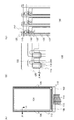
図1(A)、(B)、(C)に表示装置の一形態として、表示装置の上面図を示す。なお、図1(A)は、表示装置全体を、図1(B)は、表示装置の駆動回路部の一部を、図1(C)は表示装置の画素部の一部を、それぞれ示す。また、図2は、図1(A)、(B)、(C)におけるX1−Y1の断面図に相当する。 1A, 1B, and 1C are top views of a display device as one mode of the display device. 1A shows the entire display device, FIG. 1B shows a part of a driver circuit portion of the display device, and FIG. 1C shows a part of a pixel portion of the display device. . 2 corresponds to a cross-sectional view taken along line X1-Y1 in FIGS. 1A, 1B, and 1C.
図1(A)に示す表示装置において、第1の基板102上に設けられた画素部104と、画素部104の外側に隣接し、該画素部104に信号を供給する駆動回路であるゲートドライバ回路部106及びソースドライバ回路部108を囲むようにして、シール材112が設けられ、第2の基板110によって封止されている。よって画素部104と、ゲートドライバ回路部106と、ソースドライバ回路部108とは、第1の基板102とシール材112と第2の基板110によって、表示素子と共に封止されている。
In the display device illustrated in FIG. 1A, a
また、図1(A)においては、第1の基板102上のシール材112によって囲まれている領域とは異なる領域に、画素部104、ゲートドライバ回路部106、ソースドライバ回路部108と電気的に接続されているFPC端子部113(FPC:Flexible printed circuit)が設けられている。また、FPC端子部113には、FPC114が接続され、画素部104、ゲートドライバ回路部106、及びソースドライバ回路部108に与えられる各種信号、及び電位がFPC114により供給されている。
In FIG. 1A, the
また、図1(A)においては、ゲートドライバ回路部106及びソースドライバ回路部108を画素部104と同じ第1の基板102に形成している例を示しているが、この構成に限定されない。例えば、ゲートドライバ回路部106のみを第1の基板102に形成し、別途用意されたソースドライバ回路が形成された基板(例えば、単結晶半導体膜、多結晶半導体膜で形成された駆動回路基板)を、第1の基板102に実装する構成としても良い。
FIG. 1A illustrates an example in which the gate
また、図1(A)においては、ゲートドライバ回路部106は画素部104の両側に2列配置する構成について例示しているが、この構成に限定されない。例えば、画素部104の片側にのみゲートドライバ回路部106を配置する構成としても良い。
1A illustrates the structure in which the gate
なお、別途形成した駆動回路基板の接続方法は、特に限定されるものではなく、COG(Chip On Glass)方法、ワイヤボンディング方法、或いはTAB(Tape Automated Bonding)方法などを用いることができる。 Note that a connection method of a separately formed driver circuit substrate is not particularly limited, and a COG (Chip On Glass) method, a wire bonding method, a TAB (Tape Automated Bonding) method, or the like can be used.
このように、トランジスタを含む駆動回路の一部または全体を、画素部104と同じ第1の基板102上に一体形成し、システムオンパネルを形成することができる。
As described above, part or the whole of the driver circuit including the transistor can be formed over the
また、図1(B)においては、駆動回路であるゲートドライバ回路部106に、駆動トランジスタ250が形成されている。駆動トランジスタ250は、半導体層118に対して、ゲート電極116、ソース電極120、及びドレイン電極122が、それぞれ電気的に接続されている。また、ゲートドライバ回路部106においては、ゲート電極116を含むゲート線が左右方向に延在し、ソース電極120を含むソース線が上下方向に延在し、ドレイン電極122を含むドレイン線がソース線と離間して上下方向に延在している。
In FIG. 1B, a driving
駆動トランジスタ250を含むゲートドライバ回路部106は、画素部104の各画素に含まれるトランジスタに信号を供給することができる。
The gate
なお、ゲートドライバ回路部106における駆動トランジスタ250は、各種信号の制御、及び昇圧等を行うために、高い電圧が必要となる。具体的には、10V〜30V程度の電圧が必要となる。
Note that the driving
また、図1(C)においては、画素部104に、画素トランジスタ252が形成されている。画素トランジスタ252は、半導体層118に対して、ゲート電極116、ソース電極120、及びドレイン電極122が、それぞれ電気的に接続されている。
In FIG. 1C, a
また、画素トランジスタ252は、画素電極132と電気的に接続されており、画素電極132と対向して共通電極128が形成されている。
Further, the
図1(A)、(B)、(C)に示す表示装置の構成をより具体的に説明するため、図1(A)、(B)、(C)におけるX1−Y1の断面図に相当する図2を用いて、ゲートドライバ回路部106、及び画素部104の構成について、以下説明を行う。
In order to describe the structure of the display device illustrated in FIGS. 1A, 1 </ b> B, and 1 </ b> C more specifically, it corresponds to a cross-sectional view taken along line X <b> 1-Y <b> 1 in FIGS. The configuration of the gate
なお、図2に示す表示装置においては、表示素子として液晶素子を用い、その駆動モードは、垂直配向(VA)モードを用いた一態様について説明する。 Note that in the display device illustrated in FIG. 2, a mode in which a liquid crystal element is used as a display element and a driving mode thereof is a vertical alignment (VA) mode will be described.
まず、ゲートドライバ回路部106と画素部104上に設けられる層構造について、説明を行う。
First, a layer structure provided over the gate
ゲートドライバ回路部106は、駆動トランジスタ250上に無機材料で形成される第1の絶縁膜124と、第1の絶縁膜124上に設けられ、有機材料で形成される第2の絶縁膜126と、が設けられており、画素部104は、画素トランジスタ252上に第1の絶縁膜124と、第1の絶縁膜124上に設けられる第2の絶縁膜126と、第2の絶縁膜126上に設けられ、無機材料で形成される第3の絶縁膜130が設けられている。
The gate
すなわち、ゲートドライバ回路部106は、第3の絶縁膜130が形成されない、または第3の絶縁膜130が形成された後、第3の絶縁膜130を除去し第2の絶縁膜126が第3の絶縁膜130より露出した構造である。
別言すれば、ゲートドライバ回路部106は、第2の絶縁膜126上に第3の絶縁膜130が形成されていない領域、または第2の絶縁膜126が第3の絶縁膜130によって覆われていない領域を有している。
That is, in the gate
In other words, in the gate
第2の絶縁膜126は、表示装置を構成するトランジスタ等の凹凸を低減するために、平坦性の高い有機材料で形成される。トランジスタ等の凹凸を低減することにより、表示装置の画質を向上させることができる。しかしながら、当該有機材料は加熱等により、水素、水分、または有機成分をガスとして放出してしまう。
The second
例えば、トランジスタに用いる半導体層に、シリコン系半導体材料であるシリコン膜を用いるトランジスタにおいては、上述の水素、水分、または有機成分のガスが大きな問題になる可能性が低い。しかし、本発明の一態様においては、半導体層に酸化物半導体層を用いるため、有機材料により形成される第2の絶縁膜126から水素、水分、または有機成分のガスを外部に好適に放出させる必要がある。
For example, in a transistor in which a silicon film that is a silicon-based semiconductor material is used for a semiconductor layer used in the transistor, the above-described hydrogen, moisture, or organic component gas is unlikely to be a serious problem. However, in one embodiment of the present invention, an oxide semiconductor layer is used as the semiconductor layer; thus, hydrogen, moisture, or an organic component gas is preferably released to the outside from the second
また、例えば、ゲートドライバ回路部106上の全面に第3の絶縁膜130を形成した構成の場合、すなわち開口部が無い場合、第3の絶縁膜130に生じうるピンホール等を介し、特定領域に水分が集中して入り込んでしまい、該特定領域のトランジスタが劣化し、ゲートドライバ回路部全体として機能しなくなる。
Further, for example, in the case where the third
そこで、本実施の形態に示すように、ゲートドライバ回路部106に設けられる第2の絶縁膜126の上方には、無機材料により形成される第3の絶縁膜130が形成されない、または第3の絶縁膜130が形成された後、第3の絶縁膜130を除去し第2の絶縁膜126が第3の絶縁膜130より露出した構造とすると、第2の絶縁膜126から放出される水分等のガスをゲートドライバ回路部106の上方から放出することができる。したがって、駆動トランジスタ250、及び画素トランジスタ252内部に水分等のガスが取り込まれるのを抑制することができる。
Therefore, as shown in this embodiment mode, the third
また、ゲートドライバ回路部106において、第3の絶縁膜130に開口部を設けることによって、第2の絶縁膜126から放出される水分(表示装置内部からの水分)と、表示装置外部から浸入する水分(例えば、高温高湿環境下の信頼性試験中の雰囲気)が開口部全体で平衡して生じるため、特定領域のトランジスタが破壊されず、ゲートドライバ回路部全体として信頼性が向上する。
Further, in the gate
ここで、第3の絶縁膜130に設ける開口部の形状の一例について、図5を用いて説明を行う。図5(A)乃至(D)は、表示装置の上面図を示している。
Here, an example of the shape of the opening provided in the third
図5(A)に示す表示装置は、基板102と、基板102上に設けられた画素部104、ゲートドライバ回路部106、及びソースドライバ回路部108と、を有する。なお、ソースドライバ回路部108は、必ずしも設ける必要はなく、別途用意されたソースドライバ回路が形成された基板を、第1の基板102に実装する構成としても良い。
The display device illustrated in FIG. 5A includes a
なお、図5に示す上面図において、ハッチングで示す領域に第3の絶縁膜130が形成され、ハッチングをしていない領域には第3の絶縁膜130が形成されない。
In the top view shown in FIG. 5, the third
図5(A)に示す表示装置は、画素部104の領域のみに第3の絶縁膜130を設ける構成、すなわち開口部がゲートドライバ回路部108、及びパネル外周端(非表示領域)まで形成されている構成である。また、図5(B)に示す表示装置は、ゲートドライバ回路部106、及びソースドライバ回路部108の領域上のみ開口部を設ける構成である。また、図5(C)に示す表示装置は、ゲートドライバ回路部106、及びソースドライバ回路部108の一部(例えば、駆動トランジスタの上部)に開口部を設ける構成である。また、図5(D)は、第3の絶縁膜130が表示装置全面に設けられた構成であり、本発明の一態様と異なる参考図である。
In the display device illustrated in FIG. 5A, the third
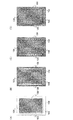
ここで、図3に示す構成の半導体装置を用いて、図2に示す第2の絶縁膜126から放出される水分等のガスがトランジスタに与える影響について、評価を行った。
Here, the semiconductor device having the structure illustrated in FIG. 3 was used to evaluate the influence of a gas such as moisture released from the second
なお、図3(A)は半導体装置の上面図を示し、図3(B)は図3(A)に示すX2−Y2の断面図に相当する。 3A is a top view of the semiconductor device, and FIG. 3B corresponds to a cross-sectional view taken along line X2-Y2 in FIG. 3A.
図3に示す半導体装置は、基板202と、基板202上に形成されたゲート電極層216と、ゲート電極216上に形成された酸化物半導体層218と、酸化物半導体層218上に形成されたソース電極220及びドレイン電極222と、を含むトランジスタ260が形成されている。トランジスタ260は、図2に示す駆動トランジスタ250に対応する。
The semiconductor device illustrated in FIG. 3 is formed over the
また、トランジスタ260上、より詳しくはゲート絶縁膜217、酸化物半導体層218、ソース電極220、及びドレイン電極222上に第1の絶縁膜224と、第1の絶縁膜224上に第2の絶縁膜226と、第2の絶縁膜226上に第3の絶縁膜228が形成されている。第1の絶縁膜224は図2に示す第1の絶縁膜124に対応し、第2の絶縁膜226は図2に示す第2の絶縁膜126に対応し、第3の絶縁膜228は図2に示す第3の絶縁膜130に対応する。
In addition, a first
また、トランジスタ260と隣接する領域に開口部262が形成されており、開口部262の領域においては、基板202と、基板202上に形成されたゲート絶縁膜217と、ゲート絶縁膜217上に形成された第1の絶縁膜224と、第1の絶縁膜224上に形成された第2の絶縁膜226と、により構成されている。すなわち、開口部262においては、トランジスタ260上に形成されている第3の絶縁膜228が設けられておらず、第2の絶縁膜226が表面に露出した構造である。
An
また、トランジスタ260の形成条件としては、基板202として、厚さ0.7mmのガラス基板を用い、ゲート電極216として、厚さ100nmのタングステン膜を用い、ゲート絶縁膜217として、厚さ400nmの酸化窒化シリコン膜を用い、酸化物半導体層218として、厚さ35nmのIGZO膜(In:Ga:Zn=1:1:1)を用い、ソース電極220、及びドレイン電極222としては、厚さ50nmのタングステン膜と、厚さ400nmのアルミニウム膜と、厚さ100nmのチタン膜の積層構造を用いた。
The
また、トランジスタ260上に形成した第1の絶縁膜224としては、厚さ450nmの酸化窒化シリコン膜と、厚さ200nmの窒化シリコン膜と、の積層膜を用い、第2の絶縁膜226としては、厚さ1.5μmのアクリル樹脂膜を用い、第3の絶縁膜228としては、厚さ50nmの窒化シリコン膜を用いた。
Further, as the first insulating
なお、トランジスタ260については、図3(A)中に示すトランジスタ260のチャネル領域の中心から開口部262の端部までの距離をL1とし、L1の距離を4種類の条件振りを行い、該4種類の条件にて、それぞれトランジスタを作製し評価を行った。
Note that for the
図4に4種類の条件のトランジスタの電気特性結果を示す。 FIG. 4 shows the electrical characteristic results of the transistors under four types of conditions.
図4(A)に示すトランジスタの電気特性結果は、L1=200μmとした場合の結果である。また、図4(B)に示すトランジスタの電気特性結果は、L1=400μmとした場合の結果である。また、図4(C)に示すトランジスタの電気特性結果は、L1=700μmとした場合の結果である。また、図4(D)に示すトランジスタの電気特性結果は、L1=1200μmとした場合の結果である。 The result of electrical characteristics of the transistor shown in FIG. 4A is a result when L1 = 200 μm. In addition, the result of electrical characteristics of the transistor illustrated in FIG. 4B is a result when L1 = 400 μm. Further, the result of electrical characteristics of the transistor illustrated in FIG. 4C is a result when L1 = 700 μm. In addition, the result of electrical characteristics of the transistor illustrated in FIG. 4D is a result when L1 = 1200 μm.
なお、図4(A)乃至(D)に示すトランジスタの条件としては、チャネル長が3μm、チャネル幅が50μmのトランジスタである。また、該トランジスタの電気特性の測定条件としては、ソース電極とドレイン電極間の電圧(Vd)を1Vとし、縦軸をドレイン電流(Id)で表し、横軸がゲート電圧(Vg)を表している。なお、ゲート電圧(Vg)を−15Vから+15Vまで0.25Vステップで変化させた際のドレイン電流(Id)を示している。 Note that the conditions of the transistors illustrated in FIGS. 4A to 4D are transistors having a channel length of 3 μm and a channel width of 50 μm. The measurement conditions of the electrical characteristics of the transistor are as follows: the voltage (Vd) between the source electrode and the drain electrode is 1 V, the vertical axis is the drain current (Id), and the horizontal axis is the gate voltage (Vg). Yes. The drain current (Id) when the gate voltage (Vg) is changed from -15 V to +15 V in 0.25 V steps is shown.
図4より、図4(A)に示す電気特性結果以外は、トランジスタのオン/オフがしていないことがわかる。これは、開口部262は、トランジスタ260の近傍(L1=200μm以内)に設ける必要があると示唆された。
FIG. 4 shows that the transistors are not turned on / off except for the electrical characteristic results shown in FIG. This suggests that the
以上のように、トランジスタ260と開口部262の端部までの距離は、トランジスタの電気特性に影響を与えることが確認された。
As described above, it was confirmed that the distance between the
図4に示す評価結果から、図2に示すゲートドライバ回路部106における駆動トランジスタ250及び第3の絶縁膜130の配置を以下のような形態とした本発明の種々の態様を採用できることが分かった。
From the evaluation results shown in FIG. 4, it was found that various aspects of the present invention can be adopted in which the arrangement of the driving
本発明の一態様は、ゲートドライバ回路部106が第2の絶縁膜126上に形成された第3の絶縁膜130を有し、この第3の絶縁膜130は駆動トランジスタ250を覆っており、第3の絶縁膜130には開口部が形成され、この開口部の端部が駆動トランジスタ250のチャネル形成領域の中心から200μm以内に形成されるものである。
In one embodiment of the present invention, the gate
別言すれば、本発明の一態様は、ゲートドライバ回路部106が第2の絶縁膜126上に形成された第3の絶縁膜130を有し、この第3の絶縁膜130は駆動トランジスタ250を覆っており、第3の絶縁膜130の端部が駆動トランジスタ250のチャネル形成領域の中心から200μm以内に形成されるものである。
In other words, according to one embodiment of the present invention, the gate
また、本発明の一態様は、ゲートドライバ回路部106が、第2の絶縁膜126上に形成された第3の絶縁膜130と、この第3の絶縁膜130に形成された開口部を有し、この開口部が駆動トランジスタ250上に形成されるものである。
In addition, according to one embodiment of the present invention, the gate
次に、図2に示すゲートドライバ回路部106及び画素部104の詳細について、以下説明を行う。
Next, details of the gate
ゲートドライバ回路部106において、第1の基板102と、第1の基板102上に形成されたゲート電極116と、ゲート電極116上に形成されたゲート絶縁膜117と、ゲート絶縁膜117上に形成された半導体層118と、ゲート絶縁膜117、及び半導体層118上に形成されたソース電極120及びドレイン電極122と、を含む駆動トランジスタ250が形成されている。
In the gate
また、ゲートドライバ回路部106において、駆動トランジスタ250上、より詳しくはゲート絶縁膜117、半導体層118、ソース電極120、及びドレイン電極122上に第1の絶縁膜124と、第1の絶縁膜124上に第2の絶縁膜126と、が形成されている。なお、ゲートドライバ回路部106において、第2の絶縁膜126上の一部に第3の絶縁膜130を設ける構成としてもよい。ただし、第3の絶縁膜130を設ける構成の場合においては、開口部を有し、第2の絶縁膜126の少なくとも一部が露出する構造とする。
In the gate
第1の絶縁膜124は、駆動トランジスタ250の保護膜としての機能を有し、第2の絶縁膜126は、駆動トランジスタ250のソース電極120、及びドレイン電極122等の凹凸を低減するための平坦化膜としての機能を有する。
The first
また、第2の絶縁膜126上には、第1の配向膜134と、第1の配向膜134上に設けられた液晶層136と、液晶層136上に設けられた第2の配向膜138と、第2の配向膜138上に設けられた有機保護絶縁膜142と、有機保護絶縁膜142上に設けられた第2の基板110が形成されている。
Further, over the second
画素部104において、第1の基板102と、第1の基板102上に形成されたゲート電極116と、ゲート電極116上に形成されたゲート絶縁膜117と、ゲート絶縁膜117上に形成された半導体層118と、ゲート絶縁膜117、及び半導体層118上に形成されたソース電極120及びドレイン電極122と、を含み、画素トランジスタ252が形成されている。
In the
また、画素部104において、画素トランジスタ252上、より詳しくはゲート絶縁膜117、半導体層118、ソース電極120、及びドレイン電極122上に第1の絶縁膜124と、第1の絶縁膜124上に形成された第2の絶縁膜126と、が形成されている。
In the
第1の絶縁膜124は、画素トランジスタ252の保護膜としての機能を有し、第2の絶縁膜126は、画素トランジスタ252のソース電極120、及びドレイン電極122等の凹凸を低減するための平坦化膜としての機能を有する。
The first
さらに、画素部104において、第2の絶縁膜126上には、容量電極128が形成されている。また、第2の絶縁膜126及び容量電極128上には、無機材料で形成される第3の絶縁膜130が形成されている。また、第1の絶縁膜124、第2の絶縁膜126、及び第3の絶縁膜130に、画素トランジスタ252のドレイン電極122に達する開口部が設けられており、該開口部、及び第3の絶縁膜130上に画素電極132が形成されている。
Further, in the
なお、容量電極128と、第3の絶縁膜130と、画素電極132により容量素子254が形成されている。容量電極128、第3の絶縁膜130、及び画素電極132を、それぞれ、可視光において、透光性を有する材料により形成することで、画素部の開口率を損ねることなく大きな容量を確保することができるので、好適である。
Note that a
また、画素電極132上には、第1の配向膜134と、第1の配向膜134上に設けられた液晶層136と、液晶層136上に設けられた第2の配向膜138と、第2の配向膜138上に設けられた対向電極140と、対向電極140上に設けられた有機保護絶縁膜142と、有機保護絶縁膜142上に設けられた有色膜144及び遮光膜146と、有色膜144及び遮光膜146上に設けられた第2の基板110が形成されている。
Further, over the
なお、画素電極132と、第1の配向膜134と、液晶層136と、第2の配向膜138と、対向電極140と、により表示素子である液晶素子148が形成されている。
Note that the
ここで、図1及び図2に示す表示装置の他の構成要素について、以下詳細な説明を行う。 Here, other components of the display device shown in FIGS. 1 and 2 will be described in detail below.
第1の基板102及び第2の基板110としては、アルミノシリケートガラス、アルミノホウケイ酸ガラス、バリウムホウケイ酸ガラスなどのガラス材料を用いる。量産する上では、第1の基板102及び第2の基板110は、第8世代(2160mm×2460mm)、第9世代(2400mm×2800mm、または2450mm×3050mm)、第10世代(2950mm×3400mm)等のマザーガラスを用いることが好ましい。マザーガラスは、処理温度が高く、処理時間が長いと大幅に収縮するため、マザーガラスを使用して量産を行う場合、作製工程の加熱処理は、好ましくは600℃以下、さらに好ましくは450℃以下、さらに好ましくは350℃以下とすることが望ましい。
As the
ゲート電極116としては、アルミニウム、クロム、銅、タンタル、チタン、モリブデン、タングステンから選ばれた金属元素、または上述した金属元素を成分とする合金か、上述した金属元素を組み合わせた合金等を用いて形成することができる。また、ゲート電極116は、単層構造でも、二層以上の積層構造としてもよい。例えば、シリコンを含むアルミニウム膜の単層構造、アルミニウム膜上にチタン膜を積層する二層構造、窒化チタン膜上にチタン膜を積層する二層構造、窒化チタン膜上にタングステン膜を積層する二層構造、窒化タンタル膜または窒化タングステン膜上にタングステン膜を積層する二層構造、チタン膜と、そのチタン膜上にアルミニウム膜を積層し、さらにその上にチタン膜を形成する三層構造等がある。また、アルミニウムに、チタン、タンタル、タングステン、モリブデン、クロム、ネオジム、スカンジウムから選ばれた元素の膜、または複数組み合わせた合金膜、もしくは窒化膜を用いてもよい。
As the
ゲート絶縁膜117としては、例えば酸化シリコン膜、酸化窒化シリコン膜、窒化酸化シリコン膜、窒化シリコン膜、酸化アルミニウム膜、窒化シリコン膜、窒化酸化シリコン膜などを用いればよく、積層または単層で設ける。
As the
また、ゲート絶縁膜117を積層構造とし、第1の窒化シリコン膜として、欠陥が少ない窒化シリコン膜とし、第1の窒化シリコン膜上に、第2の窒化シリコン膜として、水素放出量及びアンモニア放出量の少ない窒化シリコン膜を設け、第2の窒化シリコン膜上に酸化絶縁膜を設けることで、ゲート絶縁膜117として、欠陥が少なく、且つ水素及びアンモニアの放出量の少ないゲート絶縁膜117を形成することができる。この結果、ゲート絶縁膜117に含まれる水素及び窒素が、半導体層118への移動を抑制することが可能である。例えば、ゲート絶縁膜117として、50nmの酸化シリコン膜と、325nmの窒化シリコン膜との積層構造を用いることができる。
In addition, the
また、ゲート絶縁膜117に窒化シリコン膜を用いることで、以下の効果を得ることができる。窒化シリコン膜は、酸化シリコン膜と比較して比誘電率が高く、同等の静電容量を得るのに必要な膜厚が大きいため、ゲート絶縁膜を物理的に厚膜化することができる。よって、トランジスタの絶縁耐圧の低下を抑制、さらには絶縁耐圧を向上させて、トランジスタの静電破壊を抑制することができる。
Further, by using a silicon nitride film for the
ゲート絶縁膜117の厚さは、5nm以上400nm以下、より好ましくは10nm以上450nm以下、より好ましくは50nm以上400nm以下とするとよい。
The thickness of the
半導体層118は、酸化物半導体を用い、少なくともインジウム(In)若しくは亜鉛(Zn)を含むことが好ましい。または、InとZnの双方を含むことが好ましい。また、該酸化物半導体を用いたトランジスタの電気特性のばらつきを減らすため、それらと共に、スタビライザーの一または複数を有することが好ましい。
The
スタビライザーとしては、ガリウム(Ga)、スズ(Sn)、ハフニウム(Hf)、アルミニウム(Al)、またはジルコニウム(Zr)等がある。 Examples of the stabilizer include gallium (Ga), tin (Sn), hafnium (Hf), aluminum (Al), and zirconium (Zr).
例えば、酸化物半導体として、酸化インジウム、酸化スズ、酸化亜鉛、In−Zn系金属酸化物、Sn−Zn系金属酸化物、Al−Zn系金属酸化物、In−Ga系金属酸化物、In−Ga−Zn系金属酸化物(IGZOとも表記する)、In−Al−Zn系金属酸化物、In−Sn−Zn系金属酸化物、Sn−Ga−Zn系金属酸化物、Al−Ga−Zn系金属酸化物、Sn−Al−Zn系金属酸化物、In−Hf−Zn系金属酸化物、In−Sn−Ga−Zn系金属酸化物、In−Hf−Ga−Zn系金属酸化物、In−Al−Ga−Zn系金属酸化物、In−Sn−Al−Zn系金属酸化物、In−Sn−Hf−Zn系金属酸化物、In−Hf−Al−Zn系金属酸化物を用いることができる。 For example, indium oxide, tin oxide, zinc oxide, In—Zn-based metal oxide, Sn—Zn-based metal oxide, Al—Zn-based metal oxide, In—Ga-based metal oxide, In— Ga—Zn-based metal oxide (also expressed as IGZO), In—Al—Zn-based metal oxide, In—Sn—Zn-based metal oxide, Sn—Ga—Zn-based metal oxide, Al—Ga—Zn-based Metal oxide, Sn—Al—Zn-based metal oxide, In—Hf—Zn-based metal oxide, In—Sn—Ga—Zn-based metal oxide, In—Hf—Ga—Zn-based metal oxide, In— An Al—Ga—Zn-based metal oxide, an In—Sn—Al—Zn-based metal oxide, an In—Sn—Hf—Zn-based metal oxide, or an In—Hf—Al—Zn-based metal oxide can be used. .
なお、ここで、例えば、In−Ga−Zn系金属酸化物とは、InとGaとZnを主成分として有する酸化物という意味であり、InとGaとZnの比率は問わない。また、InとGaとZn以外の金属元素が入っていてもよい。 Note that here, for example, an In—Ga—Zn-based metal oxide means an oxide containing In, Ga, and Zn as its main components, and there is no limitation on the ratio of In, Ga, and Zn. Moreover, metal elements other than In, Ga, and Zn may be contained.
また、酸化物半導体として、InMO3(ZnO)m(m>0、且つ、mは整数でない)で表記される材料を用いてもよい。なお、Mは、Ga、Fe、Mn及びCoから選ばれた一の金属元素または複数の金属元素を示す。また、酸化物半導体として、In2SnO5(ZnO)n(n>0、且つ、nは整数)で表記される材料を用いてもよい。 Alternatively, a material represented by InMO 3 (ZnO) m (m> 0 is satisfied, and m is not an integer) may be used as the oxide semiconductor. Note that M represents one metal element or a plurality of metal elements selected from Ga, Fe, Mn, and Co. Alternatively, a material represented by In 2 SnO 5 (ZnO) n (n> 0 is satisfied, and n is an integer) may be used as the oxide semiconductor.
また、半導体層118として用いることのできる酸化物半導体層としては、エネルギーギャップが2eV以上、好ましくは2.5eV以上、より好ましくは3eV以上である。このように、エネルギーギャップの広い酸化物半導体層を用いることで、トランジスタのオフ電流を低減することができる。
An oxide semiconductor layer that can be used as the
また、半導体層118として用いる酸化物半導体層は、非晶質構造、単結晶構造、または多結晶構造であってもよい。
The oxide semiconductor layer used as the
また、半導体層118として用いる酸化物半導体層として、結晶化した部分を有するCAAC−OS(C Axis Aligned Crystalline Oxide Semiconductorともいう。)膜を用いてもよい。
Alternatively, a CAAC-OS (also referred to as C Axis Crystalline Oxide Semiconductor) film having a crystallized portion may be used as the oxide semiconductor layer used as the
CAAC−OS膜は、完全な単結晶ではなく、完全な非晶質でもない。CAAC−OS膜は、非晶質相に結晶部及び非晶質部を有する結晶−非晶質混相構造の酸化物半導体層である。なお、当該結晶部は、一辺が100nm未満の立方体内に収まる大きさであることが多い。また、透過型電子顕微鏡(TEM:Transmission Electron Microscope)による観察像では、CAAC−OS膜に含まれる非晶質部と結晶部との境界は明確ではない。また、TEMによってCAAC−OS膜には粒界(グレインバウンダリーともいう。)は確認できない。そのため、CAAC−OS膜は、粒界に起因する電子移動度の低下が抑制される。 The CAAC-OS film is not completely single crystal nor completely amorphous. The CAAC-OS film is an oxide semiconductor layer with a crystal-amorphous mixed phase structure where crystal parts and amorphous parts are included in an amorphous phase. Note that the crystal part is often large enough to fit in a cube whose one side is less than 100 nm. Further, in the observation image obtained by a transmission electron microscope (TEM), the boundary between the amorphous part and the crystal part included in the CAAC-OS film is not clear. Further, a grain boundary (also referred to as a grain boundary) cannot be confirmed in the CAAC-OS film by TEM. Therefore, in the CAAC-OS film, reduction in electron mobility due to grain boundaries is suppressed.
CAAC−OS膜に含まれる結晶部は、c軸がCAAC−OS膜の被形成面の法線ベクトルまたは表面の法線ベクトルに平行な方向に揃い、かつab面に垂直な方向から見て三角形状または六角形状の原子配列を有し、c軸に垂直な方向から見て金属原子が層状または金属原子と酸素原子とが層状に配列している。なお、異なる結晶部間で、それぞれa軸及びb軸の向きが異なっていてもよい。本明細書において、単に垂直と記載する場合、85°以上95°以下の範囲も含まれることとする。また、単に平行と記載する場合、−5°以上5°以下の範囲も含まれることとする。なお、酸化物半導体層を構成する酸素の一部は窒素で置換されてもよい。 In the crystal part included in the CAAC-OS film, the c-axis is aligned in a direction parallel to the normal vector of the formation surface of the CAAC-OS film or the normal vector of the surface, and triangular when viewed from the direction perpendicular to the ab plane. It has a shape or hexagonal atomic arrangement, and metal atoms are arranged in layers or metal atoms and oxygen atoms are arranged in layers as viewed from the direction perpendicular to the c-axis. Note that the directions of the a-axis and the b-axis may be different between different crystal parts. In this specification, a simple term “perpendicular” includes a range from 85 ° to 95 °. In addition, a simple term “parallel” includes a range from −5 ° to 5 °. Note that part of oxygen included in the oxide semiconductor layer may be replaced with nitrogen.
なお、CAAC−OS膜において、結晶部の分布が一様でなくてもよい。例えば、CAAC−OS膜の形成過程において、酸化物半導体層の表面側から結晶成長させる場合、被形成面の近傍に対し表面の近傍では結晶部の占める割合が高くなることがある。また、CAAC−OS膜へ不純物を添加することにより、当該不純物添加領域において結晶部が非晶質化することもある。 Note that the distribution of crystal parts in the CAAC-OS film is not necessarily uniform. For example, in the formation process of the CAAC-OS film, when crystal growth is performed from the surface side of the oxide semiconductor layer, the ratio of crystal parts in the vicinity of the surface of the oxide semiconductor layer may increase in the vicinity of the surface. In addition, when an impurity is added to the CAAC-OS film, the crystal part in a region to which the impurity is added becomes amorphous in some cases.
CAAC−OS膜に含まれる結晶部のc軸は、CAAC−OS膜の被形成面の法線ベクトルまたは表面の法線ベクトルに平行な方向に揃うため、CAAC−OS膜の形状(被形成面の断面形状または表面の断面形状)によっては互いに異なる方向を向くことがある。なお、結晶部のc軸の方向は、CAAC−OS膜が形成されたときの被形成面の法線ベクトルまたは表面の法線ベクトルに平行な方向となる。結晶部は、成膜することにより、または成膜後に加熱処理などの結晶化処理を行うことにより形成される。 Since the c-axis of the crystal part included in the CAAC-OS film is aligned in a direction parallel to the normal vector of the formation surface of the CAAC-OS film or the normal vector of the surface, the shape of the CAAC-OS film (formation surface) Depending on the cross-sectional shape of the surface or the cross-sectional shape of the surface). Note that the c-axis direction of the crystal part is parallel to the normal vector of the surface where the CAAC-OS film is formed or the normal vector of the surface. The crystal part is formed by film formation or by performing crystallization treatment such as heat treatment after film formation.
CAAC−OS膜を用いたトランジスタは、可視光や紫外光の照射による電気特性の変動が小さい。よって、当該トランジスタは、信頼性が高い。 In a transistor using a CAAC-OS film, change in electrical characteristics due to irradiation with visible light or ultraviolet light is small. Therefore, the transistor has high reliability.
また、CAAC−OS膜を成膜するために、以下の条件を適用することが好ましい。 In order to form the CAAC-OS film, the following conditions are preferably applied.
成膜時の不純物混入を低減することで、不純物によって結晶状態が崩れることを抑制できる。例えば、成膜室内に存在する不純物濃度(水素、水、二酸化炭素および窒素など)を低減すればよい。また、成膜ガス中の不純物濃度を低減すればよい。具体的には、露点が−80℃以下、好ましくは−100℃以下である成膜ガスを用いる。 By reducing the mixing of impurities during film formation, the crystal state can be prevented from being broken by impurities. For example, the concentration of impurities (such as hydrogen, water, carbon dioxide, and nitrogen) existing in the deposition chamber may be reduced. Further, the impurity concentration in the deposition gas may be reduced. Specifically, a deposition gas having a dew point of −80 ° C. or lower, preferably −100 ° C. or lower is used.
また、成膜ガス中の酸素割合を高め、電力を最適化することで成膜時のプラズマダメージを軽減すると好ましい。成膜ガス中の酸素割合は、30体積%以上、好ましくは100体積%とする。 In addition, it is preferable to reduce plasma damage during film formation by increasing the oxygen ratio in the film formation gas and optimizing electric power. The oxygen ratio in the deposition gas is 30% by volume or more, preferably 100% by volume.
半導体層118に用いる酸化物半導体層の厚さは、1nm以上100nm以下、更に好ましくは3nm以上85nm以下とすることが好ましい。
The thickness of the oxide semiconductor layer used for the
半導体層118に用いる酸化物半導体層において、二次イオン質量分析法(SIMS:Secondary Ion Mass Spectrometry)により得られるアルカリ金属またはアルカリ土類金属の濃度を、1×10¹⁸atoms/cm3以下、さらに好ましくは2×1016atoms/cm3以下であることが望ましい。アルカリ金属及びアルカリ土類金属は、酸化物半導体と結合するとキャリアを生成する場合があり、トランジスタのオフ電流の上昇の原因となるためである。
The oxide semiconductor layer used for the
また、半導体層118に用いる酸化物半導体層において、二次イオン質量分析法により得られる水素濃度を、5×10¹⁸atoms/cm3未満、好ましくは1×1018atoms/cm3以下、より好ましくは5×1017atoms/cm3以下、さらに好ましくは1×1016atoms/cm3以下とすることが好ましい。
In the oxide semiconductor layer used for the
酸化物半導体層に含まれる水素は、金属原子と結合する酸素と反応して水となると共に、酸素が脱離した格子(あるいは酸素が脱理した部分)には欠損が形成されてしまう。また、水素の一部が酸素と結合することで、キャリアである電子が生じてしまう。これらのため、酸化物半導体層の成膜工程において、水素を含む不純物を極めて減らすことにより、酸化物半導体層の水素濃度を低減することが可能である。このため、水素をできるだけ除去された酸化物半導体層をチャネル領域とすることにより、しきい値電圧のマイナスシフトを抑制することができると共に、電気特性のばらつきを低減することができる。また、トランジスタのソース及びドレインにおけるリーク電流を、代表的には、オフ電流を低減することが可能である。 Hydrogen contained in the oxide semiconductor layer reacts with oxygen bonded to metal atoms to become water, and defects are formed in a lattice from which oxygen is released (or a portion where oxygen is removed). In addition, when hydrogen is partly bonded to oxygen, electrons as carriers are generated. Therefore, in the oxide semiconductor layer formation step, the hydrogen concentration of the oxide semiconductor layer can be reduced by extremely reducing impurities containing hydrogen. Therefore, by using the oxide semiconductor layer from which hydrogen is removed as much as possible as a channel region, a negative shift in threshold voltage can be suppressed and variation in electrical characteristics can be reduced. In addition, leakage current at the source and drain of the transistor, typically, off-state current can be reduced.
ソース電極120及びドレイン電極122としては、導電材料として、アルミニウム、チタン、クロム、ニッケル、銅、イットリウム、ジルコニウム、モリブデン、銀、タンタル、またはタングステンからなる単体金属、またはこれを主成分とする合金を単層構造または積層構造として用いる。例えば、シリコンを含むアルミニウム膜の単層構造、アルミニウム膜上にチタン膜を積層する二層構造、タングステン膜上にチタン膜を積層する二層構造、銅−マグネシウム−アルミニウム合金膜上に銅膜を積層する二層構造、チタン膜または窒化チタン膜と、そのチタン膜または窒化チタン膜上に重ねてアルミニウム膜または銅膜を積層し、さらにその上にチタン膜または窒化チタン膜を形成する三層構造、モリブデン膜または窒化モリブデン膜と、そのモリブデン膜または窒化モリブデン膜上に重ねてアルミニウム膜または銅膜を積層し、さらにその上にモリブデン膜または窒化モリブデン膜を形成する三層構造等がある。なお、酸化インジウム、酸化錫または酸化亜鉛を含む透明導電材料を用いてもよい。
As the
なお、本実施の形態では、ソース電極120及びドレイン電極122を半導体層118上に設けたが、ゲート絶縁膜117と半導体層118の間に設けても良い。
Note that although the
第1の絶縁膜124としては、半導体層118として用いる酸化物半導体層との界面特性を向上させるため、無機材料の酸化物絶縁膜を用いることが好ましく、例えば酸素または窒素を含むシリコン膜を用いてもよい。第1の絶縁膜124としては、厚さ150nm以上400nm以下の酸化シリコン膜、酸化窒化シリコン膜、酸化アルミニウム膜等を用いることができる。また、第1の絶縁膜124としては、酸化物絶縁膜と窒化物絶縁膜との積層構造としてもよい。例えば、第1の絶縁膜124として、酸化窒化シリコン膜と、窒化シリコン膜との積層構造とすることができる。より具体的には、酸化窒化シリコン膜300nm上に窒化シリコン膜150nmを積層する構造などである。このとき窒化シリコン膜は、トランジスタの半導体層118への水分浸入を防止するブロック層としての機能を有する。このブロック性を高めるため窒化シリコン膜は高温で成膜されることが好ましく、例えば基板温度350℃での成膜が考えられる。このサンプルの薄膜トランジスタ断面を走査型電子顕微鏡で観察すると、ソースドレイン電極の段差被覆部分について、下層の酸化窒化シリコン膜の部分に鬆があっても、その上層の窒化シリコン膜には第2の絶縁膜まで通じるような鬆がなく良好に被覆されていることが観察できる。また高温で成膜する場合は、半導体層118として用いる酸化物半導体層から酸素が脱離し、キャリア濃度が上昇する現象が発生することがあるため、このような現象が発生しない温度が上限となる。
As the first insulating
第2の絶縁膜126としては、アクリル系樹脂、ポリイミド系樹脂、ベンゾシクロブテン系樹脂、ポリアミド系樹脂、エポキシ系樹脂等の、耐熱性を有する有機材料を用いることができる。なお、これらの材料で形成される絶縁膜を複数積層させることで、第2の絶縁膜126を形成してもよい。第2の絶縁膜126を用いることにより、トランジスタ等の凹凸を平坦化させることが可能となる。
As the second
容量電極128及び画素電極132としては、酸化タングステンを含むインジウム酸化物、酸化タングステンを含むインジウム亜鉛酸化物、酸化チタンを含むインジウム酸化物、酸化チタンを含むインジウム錫酸化物、インジウム錫酸化物(以下、ITOと示す。)、インジウム亜鉛酸化物、酸化ケイ素を添加したインジウム錫酸化物などの透光性を有する導電性材料を用いることができる。
As the
第3の絶縁膜130としては、酸化シリコン膜、酸化窒化シリコン膜、窒化酸化シリコン膜、窒化シリコン膜、酸化アルミニウム膜などの無機材料を用いることができる。
As the third
第1の配向膜134及び第2の配向膜138としては、アクリル系樹脂、ポリイミド系樹脂、ベンゾシクロブテン系樹脂、ポリアミド系樹脂、エポキシ系樹脂等の、耐熱性を有する有機材料を用いることができる。
As the
液晶層136としては、サーモトロピック液晶、低分子液晶、高分子液晶、高分子分散型液晶、強誘電性液晶、反強誘電性液晶等の液晶材料を用いることができる。これらの液晶材料は、条件により、コレステリック相、スメクチック相、キュービック相、カイラルネマチック相、等方相等を示す。
As the
また、本実施の形態においては、液晶素子148は、垂直配向(VA)モードを用いた表示装置について例示したが、これに限定されない。例えば、TN(Twisted Nematic)モード、IPS(In−Plane−Switching)モード、FFS(Fringe Field Switching)モード、ASM(Axially Symmetric aligned Micro−cell)モード、OCB(Optical Compensated Birefringence)モード、FLC(Ferroelectric Liquid Crystal)モード、AFLC(AntiFerroelectric Liquid Crystal)モードなどを用いることができる。
In this embodiment mode, the
また、上述した垂直配向モードとしては、いくつか挙げられるが、例えば、MVA(Multi−Domain Vertical Alignment)モード、PVA(Patterned Vertical Alignment)モードなどを用いることができる。また、画素(ピクセル)をいくつかの領域(サブピクセル)に分け、それぞれ別の方向に分子を倒すよう工夫されているマルチドメイン化あるいはマルチドメイン設計といわれる方法を用いてもよい。 There are several examples of the vertical alignment mode described above. For example, an MVA (Multi-Domain Vertical Alignment) mode, a PVA (Patterned Vertical Alignment) mode, or the like can be used. Alternatively, a method called multi-domain or multi-domain design may be used in which pixels (pixels) are divided into several regions (sub-pixels) and the molecules are tilted in different directions.
また、図1及び図2においては、図示していないが、偏光部材、位相差部材、反射防止部材などの光学部材(光学基板)などを適宜設けても良い。例えば、偏光基板及び位相差基板による円偏光を用いてもよい。また、光源としてバックライト、サイドライトなどを用いてもよい。 Although not shown in FIGS. 1 and 2, an optical member (optical substrate) such as a polarizing member, a retardation member, or an antireflection member may be provided as appropriate. For example, circularly polarized light using a polarizing substrate and a retardation substrate may be used. Further, a backlight, a sidelight, or the like may be used as the light source.
また、画素部104における表示方式は、プログレッシブ方式やインターレース方式等を用いることができる。また、カラー表示する際に画素で制御する色要素としては、RGB(Rは赤、Gは緑、Bは青を表す)の三色に限定されない。例えば、RGBW(Wは白を表す)、又はRGBに、イエロー、シアン、マゼンタ等を一色以上追加したものがある。なお、色要素のドット毎にその表示領域の大きさが異なっていてもよい。ただし、開示する発明はカラー表示の表示装置に限定されるものではなく、モノクロ表示の表示装置に適用することもできる。
As the display method in the
また、第2の基板110上には、スペーサ160が形成されており、第1の基板102と第2の基板110との間隔(セルギャップともいう)を制御するために設けられている。なお、セルギャップにより、液晶層136の膜厚が決定される。なお、スペーサ160としては、絶縁膜を選択的にエッチングすることで得られる柱状のスペーサ、球状のスペーサ等の任意の形状のスペーサを用いればよい。
In addition, a
また、有色膜144は、所謂カラーフィルタとして機能する。有色膜144としては、特定波長帯域の光に対して透過性を示す材料を用いればよく、染料や顔料を含有した有機樹脂膜等を用いることができる。
The
また、遮光膜146は、所謂ブラックマトリクスとして機能する。遮光膜146としては、隣接する画素間の放射光を遮光できればよく、金属膜、及び黒色染料や黒色顔料を含有した有機樹脂膜等を用いることができる。
The
また、有機保護絶縁膜142としては、有色膜144に含まれるイオン性物質が液晶層136中に拡散しないように設ける。ただし、有機保護絶縁膜142は、この構成に限定されず、設けない構成としても良い。
The organic protective
また、シール材112としては、熱硬化型樹脂、または紫外線硬化型の樹脂等を用いることができる。なお、図2に示すシール材112の封止領域においては、第1の基板102と第2の基板110との間に、ゲート絶縁膜117と、第1の絶縁膜124を設ける構成を例示したがこれに限定されない。例えば、シール材112の封止領域を、ゲート絶縁膜117と、第1の絶縁膜124と、第3の絶縁膜130と、を設ける構成としてもよい。なお、図2に示すように、シール材112の封止領域においては、有機材料である第2の絶縁膜126を除去したほうが、外部からの水分等の入り込みがないため、好適である。
As the
以上が本発明の一態様における表示装置であり、該表示装置に用いる酸化物半導体層にチャネルが形成されるトランジスタの電気特性の変動を抑制すると共に、信頼性を向上させることができる。とくに、駆動回路部のトランジスタに用いる酸化物半導体層への水素、水分の入り込みを抑制し、電気特性の変動を抑制すると共に、信頼性を向上させることができる。 The above is a display device according to one embodiment of the present invention, which can suppress variation in electrical characteristics of a transistor in which a channel is formed in an oxide semiconductor layer used in the display device and can improve reliability. In particular, entry of hydrogen and moisture into the oxide semiconductor layer used for the transistor in the driver circuit portion can be suppressed, fluctuation in electrical characteristics can be suppressed, and reliability can be improved.
また、本発明の一態様としては、上述した表示装置を有する電子機器に適用してもよい。 One embodiment of the present invention may be applied to an electronic device having the above-described display device.
本実施例では、表示装置の一例として、画素部および駆動回路部を同一基板上に形成した液晶表示パネルについて、第3の絶縁膜の開口部の有無により該液晶表示パネルの信頼性試験について調べた結果について説明する。 In this embodiment, as an example of a display device, a liquid crystal display panel in which a pixel portion and a drive circuit portion are formed over the same substrate is examined for a reliability test of the liquid crystal display panel based on the presence or absence of an opening in a third insulating film. The results will be described.
本実施例で用いた液晶表示パネルにおいては、画素部および駆動回路部に上述した実施の形態に示すトランジスタを用いた。なお、該トランジスタの半導体層としては、In−Ga−Zn系酸化物半導体層(以下IGZO膜とする)を用いた。なお、IGZO膜はIn:Ga:Zn=1:1:1の組成のターゲットを用いてスパッタリング法により形成し、その膜厚は70nmとした。 In the liquid crystal display panel used in this example, the transistor described in any of the above embodiments was used for the pixel portion and the driver circuit portion. Note that an In—Ga—Zn-based oxide semiconductor layer (hereinafter referred to as an IGZO film) was used as a semiconductor layer of the transistor. Note that the IGZO film was formed by a sputtering method using a target having a composition of In: Ga: Zn = 1: 1: 1, and the film thickness was 70 nm.
また、上記トランジスタの第1の絶縁膜としては、膜厚300nmの酸化窒化シリコン膜と、該酸化窒化シリコン膜上に形成された膜厚150nmの窒化シリコン膜と、の積層構造を用いた。なお、第1の絶縁膜として用いた窒化シリコン膜は、基板温度350℃の条件を用いた。また、第2の絶縁膜としては、膜厚2.5μmのアクリル樹脂を用いた。また、第3の絶縁膜としては、膜厚180nmの窒化シリコン膜を用いた。 As the first insulating film of the transistor, a stacked structure of a silicon oxynitride film with a thickness of 300 nm and a silicon nitride film with a thickness of 150 nm formed over the silicon oxynitride film was used. Note that the silicon nitride film used as the first insulating film was subjected to a substrate temperature of 350 ° C. Further, an acrylic resin having a film thickness of 2.5 μm was used as the second insulating film. As the third insulating film, a silicon nitride film having a thickness of 180 nm was used.
ここで、上述した構造のトランジスタの信頼性試験を行った。なお、信頼性試験としては、高温高湿動作エージング試験を行い、該高温高湿動作エージング試験条件としては、温度70℃、湿度95%、時間200hで行った。 Here, a reliability test of the transistor having the above-described structure was performed. As the reliability test, a high-temperature and high-humidity operation aging test was performed, and as the high-temperature and high-humidity operation aging test conditions, the temperature was 70 ° C., the humidity was 95%, and the time was 200 hours.
また、本実施例で示す液晶表示パネルは、実施の形態の図5(A)に示す構造を用いた。また、比較例の液晶表示パネルとしては、実施の形態の図5(D)に示す構造を用いた。すなわち、比較例の液晶表示パネルは、第3の開口部が設けられていない構造である。また、本実施例及び比較例の液晶表示パネルとしては、各々4サンプル作成し、上述の信頼性試験を行った。 In addition, the liquid crystal display panel shown in this example has the structure shown in FIG. Further, as the liquid crystal display panel of the comparative example, the structure shown in FIG. 5D of the embodiment was used. That is, the liquid crystal display panel of the comparative example has a structure in which the third opening is not provided. In addition, as the liquid crystal display panels of this example and the comparative example, four samples were prepared, respectively, and the above-described reliability test was performed.
信頼性試験の評価結果を表1に示す。 The evaluation results of the reliability test are shown in Table 1.

なお、表1において、「○」で示す欄は、信頼性試験中に異常が発生しなかったサンプルを表し、「×」で示す欄は、信頼性試験中にドライバ回路内のトランジスタにおいて、該トランジスタの特性劣化による異常が発生したサンプルを表す。 In Table 1, a column indicated with “◯” represents a sample in which no abnormality occurred during the reliability test, and a column indicated with “x” represents the transistor in the driver circuit during the reliability test. This represents a sample in which an abnormality has occurred due to deterioration of transistor characteristics.
表1に示すように、本実施例の液晶表示パネルは、第3の絶縁膜に開口部を設けることによって、4/4のサンプルにおいて、信頼性試験中に異常が発生していない。すなわち100%の歩留まりとなっているのがわかる。一方、比較例の液晶表示パネルは、第3の絶縁膜に開口部を設けていないため、2/4のサンプルにおいて、信頼性試験中に異常が発生している。すなわち50%の歩留まりとなっているのがわかる。このように、本実施例に示すように第3の絶縁膜に開口部を設けることによって、液晶表示パネルの信頼性が大幅に向上することが確認された。 As shown in Table 1, in the liquid crystal display panel of this example, no abnormality occurred during the reliability test in the 4/4 sample by providing the opening in the third insulating film. That is, it can be seen that the yield is 100%. On the other hand, since the liquid crystal display panel of the comparative example does not have an opening in the third insulating film, abnormality occurred in the reliability test in the sample of 2/4. That is, it can be seen that the yield is 50%. As described above, it was confirmed that the reliability of the liquid crystal display panel is greatly improved by providing the opening in the third insulating film as shown in this embodiment.
本実施例は、本明細書中に記載する他の実施の形態と適宜組み合わせて実施することができる。 This example can be implemented in combination with any of the other embodiments described in this specification as appropriate.
102 第1の基板
104 画素部
106 ゲートドライバ回路部
108 ソースドライバ回路部
110 第2の基板
112 シール材
113 FPC端子部
114 FPC
116 ゲート電極
117 ゲート絶縁膜
118 半導体層
120 ソース電極
122 ドレイン電極
124 第1の絶縁膜
126 第2の絶縁膜
128 容量電極(共通電極)
130 第3の絶縁膜
132 画素電極
134 第1の配向膜
136 液晶層
138 第2の配向膜
140 対向電極
142 有機保護絶縁膜
144 有色膜
146 遮光膜
148 液晶素子
202 基板
216 ゲート電極
217 ゲート絶縁膜
218 酸化物半導体層
220 ソース電極
222 ドレイン電極
224 第1の絶縁膜
226 第2の絶縁膜
228 第3の絶縁膜
250 駆動トランジスタ
252 画素トランジスタ
254 容量素子
260 トランジスタ
262 開口部
102
116
130 third
Claims (18)
前記画素部は、
画素トランジスタと、
前記画素トランジスタを覆う無機材料で形成される第1の絶縁膜と、
前記第1の絶縁膜上に設けられ、且つ有機材料で形成される第2の絶縁膜と、
前記第2の絶縁膜上に形成された第1の電極と、
前記第2の絶縁膜上に設けられ、前記第1の電極上に形成され、且つ無機材料で形成される第3の絶縁膜と、
前記第3の絶縁膜上に形成された第2の電極と、
を有し、
前記第1の電極、前記第3の絶縁膜及び前記第2の電極により容量素子が形成され、
前記駆動回路部は、
前記画素トランジスタに信号を供給する駆動トランジスタと、
前記駆動トランジスタを覆う前記第1の絶縁膜と、
前記第1の絶縁膜上に形成される前記第2の絶縁膜と、
前記第2の絶縁膜上に形成された、前記駆動トランジスタを覆う前記第3の絶縁膜と、
前記第3の絶縁膜に形成される開口部と、
を有し、
前記駆動回路部において、
前記第2の絶縁膜上に前記第3の絶縁膜が形成されていない第1の領域、または前記第2の絶縁膜が前記第3の絶縁膜によって覆われていない第2の領域を有し、
前記駆動トランジスタのチャネル形成領域の中心から200μm以内に前記開口部の端部が形成される
ことを特徴とする表示装置。 A pixel portion, and a drive circuit portion provided outside the pixel portion,
The pixel portion is
A pixel transistor;
A first insulating film formed of an inorganic material covering the pixel transistor;
A second insulating film provided on the first insulating film and formed of an organic material;
A first electrode formed on the second insulating film;
A third insulating film provided on the second insulating film, formed on the first electrode, and formed of an inorganic material;
A second electrode formed on the third insulating film;
Have
A capacitive element is formed by the first electrode, the third insulating film, and the second electrode,
The drive circuit unit is
A driving transistor for supplying a signal to the pixel transistor;
The first insulating film covering the driving transistor;
The second insulating film formed on the first insulating film;
The third insulating film formed on the second insulating film and covering the driving transistor;
An opening formed in the third insulating film;
Have
In the drive circuit unit,
Have a second region where the first region not the third insulating film is formed on the second insulating film or the second insulating film, not covered by the third insulating film ,
An end portion of the opening is formed within 200 μm from the center of the channel formation region of the driving transistor .
前記画素部は、
画素トランジスタと、
前記画素トランジスタを覆う無機材料で形成される第1の絶縁膜と、
前記第1の絶縁膜上に設けられ、且つ有機材料で形成される第2の絶縁膜と、
前記第2の絶縁膜上に形成された第1の電極と、
前記第2の絶縁膜上に設けられ、前記第1の電極上に形成され、且つ無機材料で形成される第3の絶縁膜と、
前記第3の絶縁膜上に形成された第2の電極と、
を有し、
前記第1の電極、前記第3の絶縁膜及び前記第2の電極により容量素子が形成され、
前記駆動回路部は、
前記画素トランジスタに信号を供給する駆動トランジスタと、
前記駆動トランジスタを覆う前記第1の絶縁膜と、
前記第1の絶縁膜上に形成される前記第2の絶縁膜と、
前記第2の絶縁膜上に形成された、前記駆動トランジスタを覆う前記第3の絶縁膜と、
前記駆動トランジスタのチャネル形成領域の中心から200μm以内に形成される前記第3の絶縁膜の端部と、
を有し、
前記駆動回路部において、
前記第2の絶縁膜上に前記第3の絶縁膜が形成されていない第1の領域、または前記第2の絶縁膜が前記第3の絶縁膜によって覆われていない第2の領域を有する
ことを特徴とする表示装置。 A pixel portion, and a drive circuit portion provided outside the pixel portion,
The pixel portion is
A pixel transistor;
A first insulating film formed of an inorganic material covering the pixel transistor;
A second insulating film provided on the first insulating film and formed of an organic material;
A first electrode formed on the second insulating film;
A third insulating film provided on the second insulating film, formed on the first electrode, and formed of an inorganic material;
A second electrode formed on the third insulating film;
Have
A capacitive element is formed by the first electrode, the third insulating film, and the second electrode,
The drive circuit unit is
A driving transistor for supplying a signal to the pixel transistor;
The first insulating film covering the driving transistor;
The second insulating film formed on the first insulating film;
The third insulating film formed on the second insulating film and covering the driving transistor;
An end portion of the third insulating film formed within 200 μm from the center of the channel formation region of the driving transistor;
Have
In the drive circuit unit,
A first region where the third insulating film is not formed on the second insulating film; or a second region where the second insulating film is not covered by the third insulating film. A display device.
前記駆動回路部の外側に設けられる非表示領域を有し、
前記非表示領域は、前記第1の絶縁膜上に形成される前記第2の絶縁膜を有し、
前記非表示領域において、
前記第2の絶縁膜上に前記第3の絶縁膜が形成されていない第3の領域、または前記第2の絶縁膜が前記第3の絶縁膜によって覆われていない第4の領域を有する
ことを特徴とする表示装置。 In claim 1 or 2 ,
A non-display area provided outside the drive circuit unit;
The non-display area has the second insulating film formed on the first insulating film,
In the non-display area,
A third region where the third insulating film is not formed on the second insulating film, or a fourth region where the second insulating film is not covered by the third insulating film; A display device.
前記画素トランジスタ及び前記駆動トランジスタそれぞれは、酸化物半導体層にチャネルが形成される
ことを特徴とする表示装置。 In any one of Claim 1 thru | or 3 ,
Each of the pixel transistor and the driving transistor has a channel formed in an oxide semiconductor layer.
前記画素トランジスタ及び前記駆動トランジスタそれぞれは、
ゲート電極と、
前記ゲート電極上に形成された酸化物半導体層と、
前記酸化物半導体層上に形成されたソース電極及びドレイン電極と、を有する
ことを特徴とする表示装置。 In any one of Claim 1 thru | or 3 ,
Each of the pixel transistor and the drive transistor is
A gate electrode;
An oxide semiconductor layer formed on the gate electrode;
A display device comprising: a source electrode and a drain electrode formed on the oxide semiconductor layer.
前記酸化物半導体層は、酸化インジウム、酸化スズ、及び酸化亜鉛の群から選択された少なくとも一つの酸化物を含む層である
ことを特徴とする表示装置。 In claim 4 or claim 5 ,
The display device, wherein the oxide semiconductor layer is a layer including at least one oxide selected from the group consisting of indium oxide, tin oxide, and zinc oxide.
前記酸化物半導体層は、In−Ga−Zn系酸化物半導体層である
ことを特徴とする表示装置。 In any one of Claims 4 thru | or 6 ,
The display device, wherein the oxide semiconductor layer is an In—Ga—Zn-based oxide semiconductor layer.
前記酸化物半導体層は、結晶部を含み、
前記結晶部は、c軸が前記酸化物半導体層の被形成面の法線ベクトルに平行な方向に揃う
ことを特徴とする表示装置。 In any one of Claims 4 thru | or 7 ,
The oxide semiconductor layer includes a crystal part,
The display device, wherein the crystal part has a c-axis aligned in a direction parallel to a normal vector of a formation surface of the oxide semiconductor layer.
前記第1の絶縁膜は、酸素または窒素を含むシリコン膜である
ことを特徴とする表示装置。 In any one of Claims 1 thru | or 8 ,
The display device, wherein the first insulating film is a silicon film containing oxygen or nitrogen.
前記第1の絶縁膜は、
酸化シリコン膜と、窒化シリコン膜との積層構造である
ことを特徴とする表示装置。 In claim 9 ,
The first insulating film includes:
A display device comprising a stacked structure of a silicon oxide film and a silicon nitride film.
前記第1の絶縁膜は、酸化窒化シリコン膜と、窒化シリコン膜との積層構造である
ことを特徴とする表示装置。 In claim 9 ,
The display device, wherein the first insulating film has a stacked structure of a silicon oxynitride film and a silicon nitride film.
前記窒化シリコン膜は、前記酸化窒化シリコン膜に形成された鬆を覆う
ことを特徴とする表示装置。 In claim 11 ,
The display device, wherein the silicon nitride film covers a void formed in the silicon oxynitride film.
前記第2の絶縁膜はアクリル系樹脂材料である
ことを特徴とする表示装置。 In any one of Claims 1 to 12 ,
The display device, wherein the second insulating film is an acrylic resin material.
前記第3の絶縁膜は、窒素を含むシリコン膜である
ことを特徴とする表示装置。 In any one of Claims 1 thru | or 13 ,
The display device, wherein the third insulating film is a silicon film containing nitrogen.
前記画素部は、
画素トランジスタと、
前記画素トランジスタを覆う酸素を含むシリコン膜からなる第1の絶縁膜と、
前記第1の絶縁膜上に設けられ、且つアクリル系樹脂材料からなる第2の絶縁膜と、
前記第2の絶縁膜上に形成された第1の電極と、
前記第2の絶縁膜上に設けられ、前記第1の電極上に形成され、且つ窒素を含むシリコン膜からなる第3の絶縁膜と、
前記第3の絶縁膜上に形成された第2の電極と、
を有し、
前記第1の電極、前記第3の絶縁膜及び前記第2の電極により容量素子が形成され、
前記駆動回路部は、
前記画素トランジスタに信号を供給する駆動トランジスタと、
前記駆動トランジスタを覆う前記第1の絶縁膜と、
前記第1の絶縁膜上に形成される前記第2の絶縁膜と、
前記第2の絶縁膜上に形成された、前記駆動トランジスタを覆う前記第3の絶縁膜と、
前記第3の絶縁膜に形成される開口部と、
を有し、
前記駆動回路部において、
前記第2の絶縁膜上に前記第3の絶縁膜が形成されていない領域、または前記第2の絶縁膜が前記第3の絶縁膜によって覆われていない領域を有し、
前記駆動トランジスタのチャネル形成領域の中心から200μm以内に前記開口部の端部が形成される
ことを特徴とする表示装置。 A pixel portion, and a drive circuit portion provided outside the pixel portion,
The pixel portion is
A pixel transistor;
A first insulating film made of a silicon film containing oxygen and covering the pixel transistor;
A second insulating film provided on the first insulating film and made of an acrylic resin material;
A first electrode formed on the second insulating film;
A third insulating film provided on the second insulating film, formed on the first electrode, and made of a silicon film containing nitrogen;
A second electrode formed on the third insulating film;
Have
A capacitive element is formed by the first electrode, the third insulating film, and the second electrode,
The drive circuit unit is
A driving transistor for supplying a signal to the pixel transistor;
The first insulating film covering the driving transistor;
The second insulating film formed on the first insulating film;
The third insulating film formed on the second insulating film and covering the driving transistor;
An opening formed in the third insulating film;
Have
In the drive circuit unit,
Possess the said on the second insulating film a third region the insulating film is not formed or a region where the second insulating film is not covered by the third insulating film,
An end portion of the opening is formed within 200 μm from the center of the channel formation region of the driving transistor .
前記画素部は、
画素トランジスタと、
前記画素トランジスタを覆う酸素を含むシリコン膜からなる第1の絶縁膜と、
前記第1の絶縁膜上に設けられ、且つアクリル系樹脂材料からなる第2の絶縁膜と、
前記第2の絶縁膜上に形成された第1の電極と、
前記第2の絶縁膜上に設けられ、前記第1の電極上に形成され、且つ窒素を含むシリコン膜からなる第3の絶縁膜と、
前記第3の絶縁膜上に形成された第2の電極と、
を有し、
前記第1の電極、前記第3の絶縁膜及び前記第2の電極により容量素子が形成され、
前記駆動回路部は、
前記画素トランジスタに信号を供給する駆動トランジスタと、
前記駆動トランジスタを覆う前記第1の絶縁膜と、
前記第1の絶縁膜上に形成される前記第2の絶縁膜と、
前記第2の絶縁膜上に形成された、前記駆動トランジスタを覆う前記第3の絶縁膜と、
前記駆動トランジスタのチャネル形成領域の中心から200μm以内に形成される前記第3の絶縁膜の端部と、
を有し、
前記駆動回路部において、
前記第2の絶縁膜上に前記第3の絶縁膜が形成されていない領域、または前記第2の絶縁膜が前記第3の絶縁膜によって覆われていない領域を有する
ことを特徴とする表示装置。 A pixel portion, and a drive circuit portion provided outside the pixel portion,
The pixel portion is
A pixel transistor;
A first insulating film made of a silicon film containing oxygen and covering the pixel transistor;
A second insulating film provided on the first insulating film and made of an acrylic resin material;
A first electrode formed on the second insulating film;
A third insulating film provided on the second insulating film, formed on the first electrode, and made of a silicon film containing nitrogen;
A second electrode formed on the third insulating film;
Have
A capacitive element is formed by the first electrode, the third insulating film, and the second electrode,
The drive circuit unit is
A driving transistor for supplying a signal to the pixel transistor;
The first insulating film covering the driving transistor;
The second insulating film formed on the first insulating film;
The third insulating film formed on the second insulating film and covering the driving transistor;
An end portion of the third insulating film formed within 200 μm from the center of the channel formation region of the driving transistor;
Have
In the drive circuit unit,
A display device comprising: a region where the third insulating film is not formed on the second insulating film; or a region where the second insulating film is not covered by the third insulating film. .
前記容量素子上に形成された液晶素子を有する
ことを特徴とする表示装置。 In any one of Claims 1 thru | or 16 ,
A display device comprising a liquid crystal element formed over the capacitor element.
Priority Applications (3)
| Application Number | Priority Date | Filing Date | Title |
|---|---|---|---|
| JP2012238918A JP6219562B2 (en) | 2012-10-30 | 2012-10-30 | Display device and electronic device |
| US14/062,085 US9312278B2 (en) | 2012-10-30 | 2013-10-24 | Display device and electronic device |
| CN201310526469.4A CN103794511B (en) | 2012-10-30 | 2013-10-30 | Display device and electronic equipment |
Applications Claiming Priority (1)
| Application Number | Priority Date | Filing Date | Title |
|---|---|---|---|
| JP2012238918A JP6219562B2 (en) | 2012-10-30 | 2012-10-30 | Display device and electronic device |
Publications (2)
| Publication Number | Publication Date |
|---|---|
| JP2014090068A JP2014090068A (en) | 2014-05-15 |
| JP6219562B2 true JP6219562B2 (en) | 2017-10-25 |
Family
ID=50546196
Family Applications (1)
| Application Number | Title | Priority Date | Filing Date |
|---|---|---|---|
| JP2012238918A Active JP6219562B2 (en) | 2012-10-30 | 2012-10-30 | Display device and electronic device |
Country Status (3)
| Country | Link |
|---|---|
| US (1) | US9312278B2 (en) |
| JP (1) | JP6219562B2 (en) |
| CN (1) | CN103794511B (en) |
Families Citing this family (3)
| Publication number | Priority date | Publication date | Assignee | Title |
|---|---|---|---|---|
| US20190081076A1 (en) * | 2016-03-04 | 2019-03-14 | Sharp Kabushiki Kaisha | Thin film transistor substrate and display panel |
| CN109478717A (en) * | 2016-07-15 | 2019-03-15 | 夏普株式会社 | The manufacturing method of scanning antenna and scanning antenna |
| JP6691213B2 (en) * | 2016-07-26 | 2020-04-28 | シャープ株式会社 | Scanning antenna and method of manufacturing scanning antenna |
Family Cites Families (111)
| Publication number | Priority date | Publication date | Assignee | Title |
|---|---|---|---|---|
| JPS60198861A (en) | 1984-03-23 | 1985-10-08 | Fujitsu Ltd | Thin film transistor |
| JPH0244256B2 (en) | 1987-01-28 | 1990-10-03 | Kagaku Gijutsucho Mukizaishitsu Kenkyushocho | INGAZN2O5DESHIMESARERUROTSUHOSHOKEINOSOJOKOZOOJUSURUKAGOBUTSUOYOBISONOSEIZOHO |
| JPH0244260B2 (en) | 1987-02-24 | 1990-10-03 | Kagaku Gijutsucho Mukizaishitsu Kenkyushocho | INGAZN5O8DESHIMESARERUROTSUHOSHOKEINOSOJOKOZOOJUSURUKAGOBUTSUOYOBISONOSEIZOHO |
| JPH0244258B2 (en) | 1987-02-24 | 1990-10-03 | Kagaku Gijutsucho Mukizaishitsu Kenkyushocho | INGAZN3O6DESHIMESARERUROTSUHOSHOKEINOSOJOKOZOOJUSURUKAGOBUTSUOYOBISONOSEIZOHO |
| JPS63210023A (en) | 1987-02-24 | 1988-08-31 | Natl Inst For Res In Inorg Mater | Compound having laminar structure of hexagonal crystal system expressed by ingazn4o7 and its production |
| JPH0244262B2 (en) | 1987-02-27 | 1990-10-03 | Kagaku Gijutsucho Mukizaishitsu Kenkyushocho | INGAZN6O9DESHIMESARERUROTSUHOSHOKEINOSOJOKOZOOJUSURUKAGOBUTSUOYOBISONOSEIZOHO |
| JPH0244263B2 (en) | 1987-04-22 | 1990-10-03 | Kagaku Gijutsucho Mukizaishitsu Kenkyushocho | INGAZN7O10DESHIMESARERUROTSUHOSHOKEINOSOJOKOZOOJUSURUKAGOBUTSUOYOBISONOSEIZOHO |
| JPH05251705A (en) | 1992-03-04 | 1993-09-28 | Fuji Xerox Co Ltd | Thin-film transistor |
| JP3479375B2 (en) | 1995-03-27 | 2003-12-15 | 科学技術振興事業団 | Metal oxide semiconductor device in which a pn junction is formed with a thin film transistor made of a metal oxide semiconductor such as cuprous oxide, and methods for manufacturing the same |
| DE69635107D1 (en) | 1995-08-03 | 2005-09-29 | Koninkl Philips Electronics Nv | SEMICONDUCTOR ARRANGEMENT WITH A TRANSPARENT CIRCUIT ELEMENT |
| JP3625598B2 (en) | 1995-12-30 | 2005-03-02 | 三星電子株式会社 | Manufacturing method of liquid crystal display device |
| JP4170454B2 (en) | 1998-07-24 | 2008-10-22 | Hoya株式会社 | Article having transparent conductive oxide thin film and method for producing the same |
| JP2000150861A (en) | 1998-11-16 | 2000-05-30 | Tdk Corp | Oxide thin film |
| JP3276930B2 (en) | 1998-11-17 | 2002-04-22 | 科学技術振興事業団 | Transistor and semiconductor device |
| TW460731B (en) | 1999-09-03 | 2001-10-21 | Ind Tech Res Inst | Electrode structure and production method of wide viewing angle LCD |
| JP4089858B2 (en) | 2000-09-01 | 2008-05-28 | 国立大学法人東北大学 | Semiconductor device |
| KR20020038482A (en) | 2000-11-15 | 2002-05-23 | 모리시타 요이찌 | Thin film transistor array, method for producing the same, and display panel using the same |
| JP3997731B2 (en) | 2001-03-19 | 2007-10-24 | 富士ゼロックス株式会社 | Method for forming a crystalline semiconductor thin film on a substrate |
| JP2002289859A (en) | 2001-03-23 | 2002-10-04 | Minolta Co Ltd | Thin-film transistor |
| JP4090716B2 (en) | 2001-09-10 | 2008-05-28 | 雅司 川崎 | Thin film transistor and matrix display device |
| JP3925839B2 (en) | 2001-09-10 | 2007-06-06 | シャープ株式会社 | Semiconductor memory device and test method thereof |
| JP4164562B2 (en) | 2002-09-11 | 2008-10-15 | 独立行政法人科学技術振興機構 | Transparent thin film field effect transistor using homologous thin film as active layer |
| US7061014B2 (en) | 2001-11-05 | 2006-06-13 | Japan Science And Technology Agency | Natural-superlattice homologous single crystal thin film, method for preparation thereof, and device using said single crystal thin film |
| US7483001B2 (en) * | 2001-11-21 | 2009-01-27 | Seiko Epson Corporation | Active matrix substrate, electro-optical device, and electronic device |
| JP3584928B2 (en) * | 2002-01-16 | 2004-11-04 | セイコーエプソン株式会社 | Semiconductor device |
| JP4083486B2 (en) | 2002-02-21 | 2008-04-30 | 独立行政法人科学技術振興機構 | Method for producing LnCuO (S, Se, Te) single crystal thin film |
| CN1445821A (en) | 2002-03-15 | 2003-10-01 | 三洋电机株式会社 | Forming method of ZnO film and ZnO semiconductor layer, semiconductor element and manufacturing method thereof |
| JP3933591B2 (en) | 2002-03-26 | 2007-06-20 | 淳二 城戸 | Organic electroluminescent device |
| US7339187B2 (en) | 2002-05-21 | 2008-03-04 | State Of Oregon Acting By And Through The Oregon State Board Of Higher Education On Behalf Of Oregon State University | Transistor structures |
| JP2004022625A (en) | 2002-06-13 | 2004-01-22 | Murata Mfg Co Ltd | Manufacturing method of semiconductor device and its manufacturing method |
| US7105868B2 (en) | 2002-06-24 | 2006-09-12 | Cermet, Inc. | High-electron mobility transistor with zinc oxide |
| US7067843B2 (en) | 2002-10-11 | 2006-06-27 | E. I. Du Pont De Nemours And Company | Transparent oxide semiconductor thin film transistors |
| JP4166105B2 (en) | 2003-03-06 | 2008-10-15 | シャープ株式会社 | Semiconductor device and manufacturing method thereof |
| JP2004273732A (en) | 2003-03-07 | 2004-09-30 | Sharp Corp | Active matrix substrate and its producing process |
| JP4108633B2 (en) | 2003-06-20 | 2008-06-25 | シャープ株式会社 | THIN FILM TRANSISTOR, MANUFACTURING METHOD THEREOF, AND ELECTRONIC DEVICE |
| US7262463B2 (en) | 2003-07-25 | 2007-08-28 | Hewlett-Packard Development Company, L.P. | Transistor including a deposited channel region having a doped portion |
| CN102856390B (en) | 2004-03-12 | 2015-11-25 | 独立行政法人科学技术振兴机构 | Comprise the LCD of thin-film transistor or the transition components of OLED display |
| US7297977B2 (en) | 2004-03-12 | 2007-11-20 | Hewlett-Packard Development Company, L.P. | Semiconductor device |
| US7282782B2 (en) | 2004-03-12 | 2007-10-16 | Hewlett-Packard Development Company, L.P. | Combined binary oxide semiconductor device |
| US7145174B2 (en) | 2004-03-12 | 2006-12-05 | Hewlett-Packard Development Company, Lp. | Semiconductor device |
| US7211825B2 (en) | 2004-06-14 | 2007-05-01 | Yi-Chi Shih | Indium oxide-based thin film transistors and circuits |
| JP2006100760A (en) | 2004-09-02 | 2006-04-13 | Casio Comput Co Ltd | Thin-film transistor and its manufacturing method |
| US7285501B2 (en) | 2004-09-17 | 2007-10-23 | Hewlett-Packard Development Company, L.P. | Method of forming a solution processed device |
| US7298084B2 (en) | 2004-11-02 | 2007-11-20 | 3M Innovative Properties Company | Methods and displays utilizing integrated zinc oxide row and column drivers in conjunction with organic light emitting diodes |
| WO2006051994A2 (en) | 2004-11-10 | 2006-05-18 | Canon Kabushiki Kaisha | Light-emitting device |
| EP1812969B1 (en) | 2004-11-10 | 2015-05-06 | Canon Kabushiki Kaisha | Field effect transistor comprising an amorphous oxide |
| US7863611B2 (en) | 2004-11-10 | 2011-01-04 | Canon Kabushiki Kaisha | Integrated circuits utilizing amorphous oxides |
| US7829444B2 (en) | 2004-11-10 | 2010-11-09 | Canon Kabushiki Kaisha | Field effect transistor manufacturing method |
| BRPI0517560B8 (en) | 2004-11-10 | 2018-12-11 | Canon Kk | field effect transistor |
| US7453065B2 (en) | 2004-11-10 | 2008-11-18 | Canon Kabushiki Kaisha | Sensor and image pickup device |
| US7791072B2 (en) | 2004-11-10 | 2010-09-07 | Canon Kabushiki Kaisha | Display |
| US7579224B2 (en) | 2005-01-21 | 2009-08-25 | Semiconductor Energy Laboratory Co., Ltd. | Method for manufacturing a thin film semiconductor device |
| TWI472037B (en) | 2005-01-28 | 2015-02-01 | Semiconductor Energy Lab | Semiconductor device, electronic device, and method of manufacturing semiconductor device |
| TWI569441B (en) | 2005-01-28 | 2017-02-01 | 半導體能源研究所股份有限公司 | Semiconductor device, electronic device, and method of manufacturing semiconductor device |
| US7858451B2 (en) | 2005-02-03 | 2010-12-28 | Semiconductor Energy Laboratory Co., Ltd. | Electronic device, semiconductor device and manufacturing method thereof |
| US7948171B2 (en) | 2005-02-18 | 2011-05-24 | Semiconductor Energy Laboratory Co., Ltd. | Light emitting device |
| US20060197092A1 (en) | 2005-03-03 | 2006-09-07 | Randy Hoffman | System and method for forming conductive material on a substrate |
| US8681077B2 (en) | 2005-03-18 | 2014-03-25 | Semiconductor Energy Laboratory Co., Ltd. | Semiconductor device, and display device, driving method and electronic apparatus thereof |
| US7544967B2 (en) | 2005-03-28 | 2009-06-09 | Massachusetts Institute Of Technology | Low voltage flexible organic/transparent transistor for selective gas sensing, photodetecting and CMOS device applications |
| US7645478B2 (en) | 2005-03-31 | 2010-01-12 | 3M Innovative Properties Company | Methods of making displays |
| US8300031B2 (en) | 2005-04-20 | 2012-10-30 | Semiconductor Energy Laboratory Co., Ltd. | Semiconductor device comprising transistor having gate and drain connected through a current-voltage conversion element |
| JP2006344849A (en) | 2005-06-10 | 2006-12-21 | Casio Comput Co Ltd | Thin film transistor |
| US7402506B2 (en) | 2005-06-16 | 2008-07-22 | Eastman Kodak Company | Methods of making thin film transistors comprising zinc-oxide-based semiconductor materials and transistors made thereby |
| US7691666B2 (en) | 2005-06-16 | 2010-04-06 | Eastman Kodak Company | Methods of making thin film transistors comprising zinc-oxide-based semiconductor materials and transistors made thereby |
| US7507618B2 (en) | 2005-06-27 | 2009-03-24 | 3M Innovative Properties Company | Method for making electronic devices using metal oxide nanoparticles |
| KR100711890B1 (en) | 2005-07-28 | 2007-04-25 | 삼성에스디아이 주식회사 | Organic Light Emitting Display and Fabrication Method for the same |
| JP2007059128A (en) | 2005-08-23 | 2007-03-08 | Canon Inc | Organic electroluminescent display device and manufacturing method thereof |
| JP2007073705A (en) | 2005-09-06 | 2007-03-22 | Canon Inc | Oxide-semiconductor channel film transistor and its method of manufacturing same |
| JP4280736B2 (en) | 2005-09-06 | 2009-06-17 | キヤノン株式会社 | Semiconductor element |
| JP4850457B2 (en) | 2005-09-06 | 2012-01-11 | キヤノン株式会社 | Thin film transistor and thin film diode |
| JP5116225B2 (en) | 2005-09-06 | 2013-01-09 | キヤノン株式会社 | Manufacturing method of oxide semiconductor device |
| EP1770788A3 (en) | 2005-09-29 | 2011-09-21 | Semiconductor Energy Laboratory Co., Ltd. | Semiconductor device having oxide semiconductor layer and manufacturing method thereof |
| JP5064747B2 (en) * | 2005-09-29 | 2012-10-31 | 株式会社半導体エネルギー研究所 | Semiconductor device, electrophoretic display device, display module, electronic device, and method for manufacturing semiconductor device |
| JP5078246B2 (en) * | 2005-09-29 | 2012-11-21 | 株式会社半導体エネルギー研究所 | Semiconductor device and manufacturing method of semiconductor device |
| JP5037808B2 (en) | 2005-10-20 | 2012-10-03 | キヤノン株式会社 | Field effect transistor using amorphous oxide, and display device using the transistor |
| KR101112655B1 (en) | 2005-11-15 | 2012-02-16 | 가부시키가이샤 한도오따이 에네루기 켄큐쇼 | Active Matrix Display Device and a Television Receiver Including the Same |
| TWI292281B (en) | 2005-12-29 | 2008-01-01 | Ind Tech Res Inst | Pixel structure of active organic light emitting diode and method of fabricating the same |
| US7867636B2 (en) | 2006-01-11 | 2011-01-11 | Murata Manufacturing Co., Ltd. | Transparent conductive film and method for manufacturing the same |
| JP4977478B2 (en) | 2006-01-21 | 2012-07-18 | 三星電子株式会社 | ZnO film and method of manufacturing TFT using the same |
| US7576394B2 (en) | 2006-02-02 | 2009-08-18 | Kochi Industrial Promotion Center | Thin film transistor including low resistance conductive thin films and manufacturing method thereof |
| US7977169B2 (en) | 2006-02-15 | 2011-07-12 | Kochi Industrial Promotion Center | Semiconductor device including active layer made of zinc oxide with controlled orientations and manufacturing method thereof |
| KR20070101595A (en) | 2006-04-11 | 2007-10-17 | 삼성전자주식회사 | Zno thin film transistor |
| US20070252928A1 (en) | 2006-04-28 | 2007-11-01 | Toppan Printing Co., Ltd. | Structure, transmission type liquid crystal display, reflection type display and manufacturing method thereof |
| US20070287221A1 (en) * | 2006-06-12 | 2007-12-13 | Xerox Corporation | Fabrication process for crystalline zinc oxide semiconductor layer |
| JP5028033B2 (en) | 2006-06-13 | 2012-09-19 | キヤノン株式会社 | Oxide semiconductor film dry etching method |
| JP4609797B2 (en) | 2006-08-09 | 2011-01-12 | Nec液晶テクノロジー株式会社 | Thin film device and manufacturing method thereof |
| JP4999400B2 (en) | 2006-08-09 | 2012-08-15 | キヤノン株式会社 | Oxide semiconductor film dry etching method |
| JP4332545B2 (en) | 2006-09-15 | 2009-09-16 | キヤノン株式会社 | Field effect transistor and manufacturing method thereof |
| JP5164357B2 (en) | 2006-09-27 | 2013-03-21 | キヤノン株式会社 | Semiconductor device and manufacturing method of semiconductor device |
| JP4274219B2 (en) | 2006-09-27 | 2009-06-03 | セイコーエプソン株式会社 | Electronic devices, organic electroluminescence devices, organic thin film semiconductor devices |
| US7622371B2 (en) | 2006-10-10 | 2009-11-24 | Hewlett-Packard Development Company, L.P. | Fused nanocrystal thin film semiconductor and method |
| US7772021B2 (en) | 2006-11-29 | 2010-08-10 | Samsung Electronics Co., Ltd. | Flat panel displays comprising a thin-film transistor having a semiconductive oxide in its channel and methods of fabricating the same for use in flat panel displays |
| JP2008140684A (en) | 2006-12-04 | 2008-06-19 | Toppan Printing Co Ltd | Color el display, and its manufacturing method |
| KR101303578B1 (en) | 2007-01-05 | 2013-09-09 | 삼성전자주식회사 | Etching method of thin film |
| US8207063B2 (en) | 2007-01-26 | 2012-06-26 | Eastman Kodak Company | Process for atomic layer deposition |
| KR100851215B1 (en) | 2007-03-14 | 2008-08-07 | 삼성에스디아이 주식회사 | Thin film transistor and organic light-emitting dislplay device having the thin film transistor |
| US7795613B2 (en) | 2007-04-17 | 2010-09-14 | Toppan Printing Co., Ltd. | Structure with transistor |
| KR101325053B1 (en) | 2007-04-18 | 2013-11-05 | 삼성디스플레이 주식회사 | Thin film transistor substrate and manufacturing method thereof |
| KR20080094300A (en) | 2007-04-19 | 2008-10-23 | 삼성전자주식회사 | Thin film transistor and method of manufacturing the same and flat panel display comprising the same |
| KR101334181B1 (en) | 2007-04-20 | 2013-11-28 | 삼성전자주식회사 | Thin Film Transistor having selectively crystallized channel layer and method of manufacturing the same |
| WO2008133345A1 (en) | 2007-04-25 | 2008-11-06 | Canon Kabushiki Kaisha | Oxynitride semiconductor |
| KR101345376B1 (en) | 2007-05-29 | 2013-12-24 | 삼성전자주식회사 | Fabrication method of ZnO family Thin film transistor |
| JP5215158B2 (en) | 2007-12-17 | 2013-06-19 | 富士フイルム株式会社 | Inorganic crystalline alignment film, method for manufacturing the same, and semiconductor device |
| JP4623179B2 (en) | 2008-09-18 | 2011-02-02 | ソニー株式会社 | Thin film transistor and manufacturing method thereof |
| JP5451280B2 (en) | 2008-10-09 | 2014-03-26 | キヤノン株式会社 | Wurtzite crystal growth substrate, manufacturing method thereof, and semiconductor device |
| CN102648525B (en) | 2009-12-04 | 2016-05-04 | 株式会社半导体能源研究所 | Display unit |
| WO2011129037A1 (en) * | 2010-04-16 | 2011-10-20 | シャープ株式会社 | Thin film transistor substrate, method for producing same, and display device |
| JP5582051B2 (en) * | 2011-02-03 | 2014-09-03 | セイコーエプソン株式会社 | Pulse wave measuring device and program |
| KR101519916B1 (en) * | 2011-04-07 | 2015-05-13 | 엘지디스플레이 주식회사 | Oganic electro-luminesence display device and manufactucring metod of the same |
| KR102081468B1 (en) | 2012-07-20 | 2020-02-25 | 가부시키가이샤 한도오따이 에네루기 켄큐쇼 | Display device and electronic device including the display device |
| KR102644240B1 (en) | 2012-07-20 | 2024-03-07 | 가부시키가이샤 한도오따이 에네루기 켄큐쇼 | Display device |
-
2012
- 2012-10-30 JP JP2012238918A patent/JP6219562B2/en active Active
-
2013
- 2013-10-24 US US14/062,085 patent/US9312278B2/en active Active
- 2013-10-30 CN CN201310526469.4A patent/CN103794511B/en active Active
Also Published As
| Publication number | Publication date |
|---|---|
| US20140117350A1 (en) | 2014-05-01 |
| CN103794511B (en) | 2018-08-03 |
| CN103794511A (en) | 2014-05-14 |
| US9312278B2 (en) | 2016-04-12 |
| JP2014090068A (en) | 2014-05-15 |
Similar Documents
| Publication | Publication Date | Title |
|---|---|---|
| JP7329575B2 (en) | semiconductor equipment | |
| KR102472174B1 (en) | Semiconductor device | |
| JP6552567B2 (en) | Display device | |
| KR102244511B1 (en) | Semiconductor device | |
| TWI716941B (en) | Display device | |
| JP6317059B2 (en) | Semiconductor device and display device | |
| JP6198434B2 (en) | Display device and electronic device | |
| JP6219562B2 (en) | Display device and electronic device | |
| JP6224338B2 (en) | Semiconductor device, display device, and method for manufacturing semiconductor device |
Legal Events
| Date | Code | Title | Description |
|---|---|---|---|
| A621 | Written request for application examination |
Free format text: JAPANESE INTERMEDIATE CODE: A621 Effective date: 20150929 |
|
| A131 | Notification of reasons for refusal |
Free format text: JAPANESE INTERMEDIATE CODE: A131 Effective date: 20161122 |
|
| A521 | Request for written amendment filed |
Free format text: JAPANESE INTERMEDIATE CODE: A523 Effective date: 20170110 |
|
| A131 | Notification of reasons for refusal |
Free format text: JAPANESE INTERMEDIATE CODE: A131 Effective date: 20170704 |
|
| A521 | Request for written amendment filed |
Free format text: JAPANESE INTERMEDIATE CODE: A523 Effective date: 20170829 |
|
| TRDD | Decision of grant or rejection written | ||
| A01 | Written decision to grant a patent or to grant a registration (utility model) |
Free format text: JAPANESE INTERMEDIATE CODE: A01 Effective date: 20170912 |
|
| A61 | First payment of annual fees (during grant procedure) |
Free format text: JAPANESE INTERMEDIATE CODE: A61 Effective date: 20170928 |
|
| R150 | Certificate of patent or registration of utility model |
Ref document number: 6219562 Country of ref document: JP Free format text: JAPANESE INTERMEDIATE CODE: R150 |
|
| R250 | Receipt of annual fees |
Free format text: JAPANESE INTERMEDIATE CODE: R250 |
|
| R250 | Receipt of annual fees |
Free format text: JAPANESE INTERMEDIATE CODE: R250 |
|
| R250 | Receipt of annual fees |
Free format text: JAPANESE INTERMEDIATE CODE: R250 |
|
| R250 | Receipt of annual fees |
Free format text: JAPANESE INTERMEDIATE CODE: R250 |