US9799772B2 - Thin film transistor device, method for manufacturing same and display device - Google Patents
Thin film transistor device, method for manufacturing same and display device Download PDFInfo
- Publication number
- US9799772B2 US9799772B2 US14/894,027 US201414894027A US9799772B2 US 9799772 B2 US9799772 B2 US 9799772B2 US 201414894027 A US201414894027 A US 201414894027A US 9799772 B2 US9799772 B2 US 9799772B2
- Authority
- US
- United States
- Prior art keywords
- layer
- channel
- insulating layer
- pertaining
- thin film
- Prior art date
- Legal status (The legal status is an assumption and is not a legal conclusion. Google has not performed a legal analysis and makes no representation as to the accuracy of the status listed.)
- Active
Links
Images


Classifications
-
- H—ELECTRICITY
- H10—SEMICONDUCTOR DEVICES; ELECTRIC SOLID-STATE DEVICES NOT OTHERWISE PROVIDED FOR
- H10D—INORGANIC ELECTRIC SEMICONDUCTOR DEVICES
- H10D30/00—Field-effect transistors [FET]
- H10D30/60—Insulated-gate field-effect transistors [IGFET]
- H10D30/67—Thin-film transistors [TFT]
- H10D30/6704—Thin-film transistors [TFT] having supplementary regions or layers in the thin films or in the insulated bulk substrates for controlling properties of the device
-
- H01L29/78606—
-
- H01L27/1225—
-
- H01L29/7869—
-
- H—ELECTRICITY
- H10—SEMICONDUCTOR DEVICES; ELECTRIC SOLID-STATE DEVICES NOT OTHERWISE PROVIDED FOR
- H10D—INORGANIC ELECTRIC SEMICONDUCTOR DEVICES
- H10D30/00—Field-effect transistors [FET]
- H10D30/60—Insulated-gate field-effect transistors [IGFET]
- H10D30/67—Thin-film transistors [TFT]
- H10D30/674—Thin-film transistors [TFT] characterised by the active materials
- H10D30/6755—Oxide semiconductors, e.g. zinc oxide, copper aluminium oxide or cadmium stannate
-
- H—ELECTRICITY
- H10—SEMICONDUCTOR DEVICES; ELECTRIC SOLID-STATE DEVICES NOT OTHERWISE PROVIDED FOR
- H10D—INORGANIC ELECTRIC SEMICONDUCTOR DEVICES
- H10D86/00—Integrated devices formed in or on insulating or conducting substrates, e.g. formed in silicon-on-insulator [SOI] substrates or on stainless steel or glass substrates
- H10D86/40—Integrated devices formed in or on insulating or conducting substrates, e.g. formed in silicon-on-insulator [SOI] substrates or on stainless steel or glass substrates characterised by multiple TFTs
- H10D86/421—Integrated devices formed in or on insulating or conducting substrates, e.g. formed in silicon-on-insulator [SOI] substrates or on stainless steel or glass substrates characterised by multiple TFTs having a particular composition, shape or crystalline structure of the active layer
- H10D86/423—Integrated devices formed in or on insulating or conducting substrates, e.g. formed in silicon-on-insulator [SOI] substrates or on stainless steel or glass substrates characterised by multiple TFTs having a particular composition, shape or crystalline structure of the active layer comprising semiconductor materials not belonging to the Group IV, e.g. InGaZnO
-
- H—ELECTRICITY
- H10—SEMICONDUCTOR DEVICES; ELECTRIC SOLID-STATE DEVICES NOT OTHERWISE PROVIDED FOR
- H10D—INORGANIC ELECTRIC SEMICONDUCTOR DEVICES
- H10D86/00—Integrated devices formed in or on insulating or conducting substrates, e.g. formed in silicon-on-insulator [SOI] substrates or on stainless steel or glass substrates
- H10D86/40—Integrated devices formed in or on insulating or conducting substrates, e.g. formed in silicon-on-insulator [SOI] substrates or on stainless steel or glass substrates characterised by multiple TFTs
- H10D86/451—Integrated devices formed in or on insulating or conducting substrates, e.g. formed in silicon-on-insulator [SOI] substrates or on stainless steel or glass substrates characterised by multiple TFTs characterised by the compositions or shapes of the interlayer dielectrics
-
- H—ELECTRICITY
- H10—SEMICONDUCTOR DEVICES; ELECTRIC SOLID-STATE DEVICES NOT OTHERWISE PROVIDED FOR
- H10D—INORGANIC ELECTRIC SEMICONDUCTOR DEVICES
- H10D86/00—Integrated devices formed in or on insulating or conducting substrates, e.g. formed in silicon-on-insulator [SOI] substrates or on stainless steel or glass substrates
- H10D86/40—Integrated devices formed in or on insulating or conducting substrates, e.g. formed in silicon-on-insulator [SOI] substrates or on stainless steel or glass substrates characterised by multiple TFTs
- H10D86/471—Integrated devices formed in or on insulating or conducting substrates, e.g. formed in silicon-on-insulator [SOI] substrates or on stainless steel or glass substrates characterised by multiple TFTs having different architectures, e.g. having both top-gate and bottom-gate TFTs
-
- H—ELECTRICITY
- H10—SEMICONDUCTOR DEVICES; ELECTRIC SOLID-STATE DEVICES NOT OTHERWISE PROVIDED FOR
- H10D—INORGANIC ELECTRIC SEMICONDUCTOR DEVICES
- H10D86/00—Integrated devices formed in or on insulating or conducting substrates, e.g. formed in silicon-on-insulator [SOI] substrates or on stainless steel or glass substrates
- H10D86/40—Integrated devices formed in or on insulating or conducting substrates, e.g. formed in silicon-on-insulator [SOI] substrates or on stainless steel or glass substrates characterised by multiple TFTs
- H10D86/60—Integrated devices formed in or on insulating or conducting substrates, e.g. formed in silicon-on-insulator [SOI] substrates or on stainless steel or glass substrates characterised by multiple TFTs wherein the TFTs are in active matrices
-
- H01L29/66969—
-
- H—ELECTRICITY
- H10—SEMICONDUCTOR DEVICES; ELECTRIC SOLID-STATE DEVICES NOT OTHERWISE PROVIDED FOR
- H10D—INORGANIC ELECTRIC SEMICONDUCTOR DEVICES
- H10D99/00—Subject matter not provided for in other groups of this subclass
Definitions
- the present invention relates to a thin film transistor device, a manufacturing method of the thin film transistor device, and a display device.
- the present invention relates to characteristics of a channel protection layer, a passivation layer, and the like, in a thin film transistor device.
- An active-matrix-type display device typically includes a TFT device that has a plurality of thin film transistor (TFT) elements, for achieving driving and light emission in units of sub-pixels.
- TFT thin film transistor
- TFT devices with a channel layer made of an oxide semiconductor are in development, for use in display devices and the like (refer to Patent Literature 1).
- the conventional TFT device illustrated in FIG. 23 includes a substrate 1900 . Further, the conventional TFT device includes, disposed above the substrate one on top of another in the stated order: a gate electrode 1901 ; a gate insulating film 1903 ; a channel layer 1904 ; a protection film 1912 ; a drain electrode 1907 ; and a source electrode 1908 .
- the channel layer 1904 is a layer of an oxide semiconductor including at least one of In, Zn, and Sn.
- the protection film 1912 is made of an amorphous oxide semiconductor (e.g., amorphous SiO), and is in contact with the channel layer 1904 . Further, the protection layer 1912 in this conventional TFT device is defined such that, when thermal desorption measurement is performed with respect to the protection layer 1912 , oxygen of at least 3.8 ⁇ 10 19 cm ⁇ 3 is observed as desorption gas.
- amorphous oxide semiconductor e.g., amorphous SiO
- the conventional TFT device illustrated in FIG. 23 due to including the protection film 1912 whose film characteristic is defined as such, suppresses the generation of oxygen defects in the channel layer 1904 made of an oxide semiconductor, and thus suppresses an increase in off current deriving from generation of a large number of carrier electrons that would otherwise occur.
- this conventional TFT device has desirable characteristics with an excellent on/off ratio.
- TFT devices including a channel layer made of an oxide semiconductor.
- further research and development of such TFT devices are yet to be conducted.
- the present invention aims to provide a solution to this situation, and aims to provide a thin film transistor device with high stability and reliability having a channel layer made of an oxide semiconductor, a method of manufacturing such a thin film transistor device, and a display device provided with such a thin film transistor device.
- TFT device including (i) a substrate, (ii) a gate electrode, (iii) a channel layer, (iv) a channel protection layer, (v) an electrode pair composed of a source electrode and a drain electrode, and (vi) a passivation layer.
- the gate electrode is above the substrate.
- the channel layer is above the gate electrode.
- the channel protection layer is on the channel layer.
- the electrode pair is on the channel protection layer, with the source electrode and the drain electrode spaced away from one another. A part of each of the source electrode and the drain electrode is in contact with the channel layer through the channel protection layer.
- the passivation layer extends over the gate electrode, the channel layer, the electrode pair, and the channel protection layer.
- the channel layer is made of an oxide semiconductor
- the thin film transistor device has a first sub-layer which is made of one of silicon nitride and silicon oxynitride and in which a density of H atoms bonded with Si atoms is no greater than 2.3 ⁇ 10 21 cm ⁇ 3 , the first sub-layer included in at least one of the channel protection layer and the passivation layer.
- the TFT device pertaining to one aspect of the present disclosure suppresses the influence of active hydrogen species generated during processing and after film forming.
- the TFT device pertaining to one aspect of the present invention has high stability and reliability.
- FIG. 1 is a schematic block diagram illustrating the structure of a display device 1 pertaining to embodiment 1 of the present disclosure.
- FIG. 2 is a schematic circuit diagram illustrating the circuit configuration of each subpixel 10 a of a display panel 10 .
- FIG. 3 is a schematic cross-sectional diagram illustrating the structure of each subpixel 10 a of the display panel 10 .
- FIGS. 4A through 4D is a schematic cross-sectional diagram illustrating a process in the manufacturing of the display panel 10 .
- FIGS. 5A through 5D is a schematic cross-sectional diagram illustrating a process in the manufacturing of the display panel 10 .
- FIGS. 6A and 6B is a schematic cross-sectional diagram illustrating a process in the manufacturing of the display panel 10 .
- FIG. 7A is a schematic illustrating the structure of TEG samples for assessing resistance
- FIG. 7B is a characteristics diagram illustrating the relation between Si—H density in a SiN layer and sheet resistance of TAOS.
- FIG. 8 is a characteristics diagram illustrating the relation between sheet resistance of TAOS and threshold voltage Vth.
- FIG. 9A is a table illustrating the relation between film forming conditions of SiN layers and hydrogen density
- FIG. 9B is a characteristics diagram illustrating Vg-Id characteristics of sample type 1
- FIG. 9C is a characteristics diagram illustrating Vg-Id characteristics of sample type 2 .
- FIG. 10A is a table illustrating film forming conditions of SiO layers
- FIG. 10B is a characteristic diagram illustrating spectrums of hydrogen released from the SiO layers in thermal desorption measurement.
- FIG. 11A is a characteristic diagram illustrating Vg-Id characteristics of sample types 11 and 12
- FIG. 11B is a characteristic diagram illustrating Vg-Id characteristics of sample type 13 .
- FIG. 12A is a schematic illustrating the structure of samples for measuring TAOS carrier lifetime
- FIG. 12B is a schematic illustrating how TAOS lifetime was measured.
- FIG. 13A is a table illustrating film forming conditions of SiO layer
- FIG. 13B is a characteristics diagram illustrating the relation between film forming rate and carrier lifetime
- FIG. 13C is a characteristic diagram illustrating the relation between refraction index and carrier lifetime.
- FIG. 14A is a characteristic diagram illustrating Vg-Id characteristics of sample type 21
- FIG. 14B is a characteristic diagram illustrating Vg-Id characteristics of sample type 22
- FIG. 14C is a characteristic diagram illustrating Vg-Id characteristics of sample type 23 .
- FIG. 15A is a characteristic diagram illustrating Vg-Id characteristics of a TFT pertaining to an embodiment
- FIG. 15B is a characteristic diagram illustrating Vg-Id characteristics of a TFT pertaining to a comparative example.
- FIG. 16 is a schematic cross-sectional diagram illustrating the structure of one part of a display panel 30 pertaining to embodiment 2 of the present disclosure.
- FIG. 17 is a schematic cross-sectional diagram illustrating the structure of one part of a display panel 40 pertaining to embodiment 3 of the present disclosure.
- FIG. 18 is a schematic cross-sectional diagram illustrating the structure of one part of a display panel 50 pertaining to embodiment 4 of the present disclosure.
- FIG. 19 is a schematic cross-sectional diagram illustrating the structure of one part of a display panel 60 pertaining to embodiment 5 of the present disclosure.
- FIG. 20 is a schematic cross-sectional diagram illustrating the structure of one part of a display panel 70 pertaining to embodiment 6 of the present disclosure.
- FIG. 21 is a schematic cross-sectional diagram illustrating the structure of one part of a display panel 80 pertaining to embodiment 7 of the present disclosure.
- FIG. 22 is a schematic cross-sectional diagram illustrating the structure of one part of a display panel 90 pertaining to embodiment 8 of the present disclosure.
- FIG. 23 is a cross-sectional diagram illustrating the structure of a conventional TFT device.
- TFT device including (i) a substrate, (ii) a gate electrode, (iii) a channel layer, (iv) a channel protection layer, (v) an electrode pair composed of a source electrode and a drain electrode, and (vi) a passivation layer.
- the gate electrode is above the substrate.
- the channel layer is above the gate electrode.
- the channel protection layer is on the channel layer.
- the electrode pair is on the channel protection layer, with the source electrode and the drain electrode spaced away from one another. A part of each of the source electrode and the drain electrode is in contact with the channel layer through the channel protection layer.
- the passivation layer extends over the gate electrode, the channel layer, the electrode pair, and the channel protection layer.
- the channel layer is made of an oxide semiconductor
- the thin film transistor device has a first sub-layer which is made of one of silicon nitride and silicon oxynitride and in which a density of H atoms bonded with Si atoms is no greater than 2.3 ⁇ 10 21 cm ⁇ 3 , the first sub-layer included in at least one of the channel protection layer and the passivation layer.
- the TFT device pertaining to one aspect of the present disclosure suppresses the influence of active hydrogen species generated during processing and after film forming.
- the TFT device pertaining to one aspect of the present invention has high stability and reliability.
- the channel layer achieves high electron mobility due to being made of an oxide semiconductor. Due to this, the TFT device pertaining to one aspect of the present disclosure achieves excellent electric characteristics, irrespective of temperature.
- the density of H atoms bonded with Si atoms may be no greater than 1.3 ⁇ 10 21 cm ⁇ 3 .
- the thin film transistor device may have a second sub-layer which is made of one of silicon oxide and silicon oxynitride and such that when thermal desorption measurement is performed with respect to the second sub-layer, hydrogen is observed as desorption gas and within a temperature range of 300 degrees Celsius to 350 degrees Celsius, an average increase coefficient of the desorption gas does not take a positive value, the second sub-layer included in at least one of the channel protection layer and the passivation layer.
- the TFT device pertaining to one aspect of the present disclosure has high stability and reliability in terms of carrier lifetime and carrier density.
- the second sub-layer may be included in the channel protection layer.
- the channel protection layer may be made of silicon oxide, formed at a rate between 50 nm/sec and 110 nm/sec, and have a refractive index between 1.454 and 1.461.
- the passivation layer may include a first layer, a second layer, and a third layer layered one on top of another with the first layer closest to the substrate, at least one of the first layer and the third layer may correspond to the first sub-layer, and the second layer may be made of an Al compound.
- the TFT device pertaining to one aspect of the present invention has even higher quality.
- the second layer may be made of AlOx.
- the passivation layer may further include a fourth layer on the third layer, the third layer and the fourth layer may both be made of silicon nitride, and the third layer may contain silicon nitride at a lower density than the fourth layer. Due to the third layer containing silicon nitride at a lower density than the fourth layer, forming of a tapered contact hole in the passivation layer is facilitated.
- the first layer may be made of silicon oxide, and may be in contact with the source electrode and the drain electrode. It is preferable to use silicon oxide as the material for the first layer of the passivation layer because high adhesiveness of the first layer with respect to the source and drain electrodes can be ensured and hydrogen content in the first layer can be reduced.
- One aspect of the present disclosure is a display device including any of the TFT devices described above.
- the display device achieves the effects described above.
- One aspect of the present disclosure is a method for manufacturing a TFT device including the following steps (i) through (v).
- the channel layer is made of an oxide semiconductor in step (ii), and the method includes forming a first sub-layer which is made of one of silicon nitride and silicon oxynitride and in which a density of H atoms bonded with Si atoms is no greater than 2.3 ⁇ 10 21 cm ⁇ 3 , the forming of the first sub-layer included in at least one of the forming of the channel protection layer (step (iii)) and the forming of the passivation layer (step (v)).
- the influence of active hydrogen species generated during processing and after film forming is suppressed.
- the method pertaining to one aspect of the present invention yields a TFT device having high stability and reliability.
- the channel layer is formed by using an oxide semiconductor. Due to this, the channel layer achieves high electron mobility. Due to this, the method pertaining to one aspect of the present disclosure yields a TFT device achieving excellent electric characteristics, irrespective of temperature.
- the method pertaining to one aspect of the present disclosure may further include immediately after the forming of the first sub-layer, performing annealing with respect to the first sub-layer under a temperature lower by 50 degrees than a temperature under which the first sub-layer is formed. Performing annealing under such a temperature immediately after the forming of the first sub-layer prevents the desorption of hydrogen from the first sub-layer, and thus enables the channel layer to maintain a state of high resistance. Otherwise, desorption of hydrogen from the first sub-layer may occur, which may trigger degradation of the channel layer, which is made of an oxide semiconductor, and may further result in a decrease in the resistance of the channel layer.
- the substrate having the channel layer formed thereon is placed in a vacuum. This results in oxygen defects in the channel layer, which is made of an oxide semiconductor, and a consequent decease in the resistance of the channel layer.
- annealing is performed under the temperature conditions described above immediately after the forming of the first sub-layer, whereby the channel layer maintains the state of high resistance.
- the method pertaining to one aspect of the present disclosure includes forming a second sub-layer, the second sub-layer made of one of silicon oxide and silicon oxynitride and such that, when thermal desorption measurement is performed with respect to the second sub-layer, hydrogen is observed as desorption gas and within a temperature range of 300 degrees Celsius to 350 degrees Celsius, an average increase coefficient of the desorption gas does not take a positive value, the forming of the second sub-layer included in at least one of the forming of the channel protection layer (step (iii)) and the forming of the passivation layer (step (v)).
- the forming of the second sub-layer suppresses the influence of active hydrogen species generated during processing and after film forming, and reduces a threshold shift ( ⁇ Vth) occurring in negative bias temperature stress (NBTS) measurement.
- ⁇ Vth threshold shift
- NBTS negative bias temperature stress
- the forming of the second sub-layer may at least be included in the forming of the channel protection layer (step (iii)), and the second sub-layer may be made of silicon oxide, formed at a rate between 50 nm/sec and 110 nm/sec, and have a refractive index between 1.454 and 1.461.
- the method pertaining to one aspect of the present disclosure yields a TFT device whose characteristics are even more stabile.
- the method pertaining to one aspect of the present disclosure may further include, immediately after the forming of the second sub-layer, performing annealing with respect to the second sub-layer in a dry air atmosphere or an oxygen atmosphere and under a temperature no lower than a temperature under which the second sub-layer is formed.
- performing annealing under the conditions described above immediately after the forming of the second sub-layer enables the channel layer to maintain a state of high resistance.
- the forming of the second sub-layer may at least be included in the forming of the passivation layer, and the forming of the passivation layer (step (v)) may include: forming the second sub-layer to cover the source electrode and the drain electrode, the second sub-layer made of silicon oxide; forming a layer made of an Al compound on the second sub-layer; and forming the first sub-layer on the layer made of the Al compound, the first sub-layer made of silicon nitride.
- the method pertaining to one aspect of the present disclosure yields a TFT device including a passivation layer that is composed of the second sub-layer made of silicon oxide, the layer made of an Al compound, and the first sub-layer made of silicon nitride layered one on top of another.
- the layer made of an Al compound included in the passivation layer prevents entry of moisture and/or hydrogen (functions as a barrier), and thus protects the channel layer.
- each of (i) the difference between the etching rate of the second sub-layer and the etching rate of the layer made of an Al compound and (ii) the difference between the etching rate of the layer made of an Al compound and the etching rate of the first sub-layer are great, and thus, it can be ensured that the etching of the layer below can be started with the etching of the present layer completed by performing over etching. Accordingly, the method pertaining to one aspect of the present disclosure achieves high manufacturing yield while suppressing the degradation of the channel layer, which is made of an oxide semiconductor.
- etching of each of the second sub-layer and the first sub-layer be performed through dry etching, and that etching of the layer made of an Al compound be performed through wet etching.
- the layer formed on the second layer may be made of AlOx. Accordingly, the passivation layer is formed to include a layer made of AlOx. Thus, entry of moisture and/or active hydrogen species into the channel layer, which is made of an oxide semiconductor, is suppressed with a further degree of certainty. Thus, the method pertaining to one aspect of the present invention yields a TFT device having even higher quality.
- the display device 1 includes a display panel 10 , and a drive/control circuit 20 connected to the display panel 10 .
- the display panel 10 is an organic electro-luminescent (EL) panel utilizing an electric-field light-emitting phenomenon related to organic material.
- the display panel 10 includes a plurality of organic EL elements, and for example, the organic EL elements form a matrix.
- the drive/control circuit 20 includes four drive circuits, namely drive circuits 21 , 22 , 23 , 24 and a control circuit 25 .
- the arrangement of the circuits of the drive/control circuit 20 may differ from what is illustrated in FIG. 1 .
- each subpixel 10 a in the display panel 10 includes one capacitor C, an EL element EL part that emits light, and two transistor elements, namely transistor elements Tr 1 , Tr 2 .
- the transistor element Tr 1 is a driving transistor element
- the transistor element Tr 2 is a switching transistor element.
- the switching transistor element Tr 2 includes a gate electrode G 2 , a source electrode S 2 , and a drain electrode D 2 .
- the gate electrode G 2 is connected to a scan line Vscn.
- the source electrode S 2 is connected to a data line Vdat.
- the drain electrode D 2 is connected to a gate electrode G 1 of the driving transistor element Tr 1 .
- the driving transistor element includes, in addition to the gate electrode G 1 , a drain electrode D 1 and a source electrode S 1 .
- the drain electrode D 1 is connected to a power line Va.
- the source electrode S 1 is connected to an anode of the EL element E part.
- the EL element part EL has a cathode that is connected to a ground line Vcat.
- the capacitor C connects each of the drain electrode D 2 of the switching transistor element Tr 2 and the gate electrode G 1 of the driving transistor element Tr 1 to the power line Va.
- the sub-pixels 10 a each having the circuit configuration illustrated in FIG. 2 , form a matrix, for example.
- a set of a plurality of sub-pixels 10 a adjacent to one another (for example, a set of three adjacent subpixels 10 a each corresponding to one of the light-emission colors red (R), green (G), and blue (B)) forms a pixel of the display panel 10 .
- the following describes the structure of the display panel 10 , with reference to the schematic cross-sectional view in FIG. 3 .
- the display panel 10 is a top-emission-type organic EL display panel.
- the display panel 10 includes a TFT device part and an EL element part.
- the TFT device part is arranged lower in the Z axis direction, and the EL element part is disposed on the TFT device part.
- gate electrodes 101 and 102 are disposed spaced from one another.
- a gate insulating layer 103 is disposed to cover surfaces of the gate electrodes 101 and 102 and a surface of the substrate 100 .
- Channel layers 104 and 105 are disposed on the gate insulating layer 103 .
- the channel layers 104 and 105 respectively correspond to the gate electrodes 101 and 102 .
- a channel protection layer 106 is disposed to cover surfaces of the channel layers 104 and 105 and a surface of the gate insulating layer 103 .
- a source electrode 107 and a drain electrode 108 are disposed spaced from one another on the channel protection layer 106 .
- the source electrode 107 and the drain electrode 108 correspond to the gate electrode 101 and the channel layer 104 .
- a source electrode 110 and a drain electrode 109 are disposed spaced from one another on the channel protection layer 106 .
- the source electrode 110 and the drain electrode 109 correspond to the gate electrode 102 and the channel layer 105 .
- Z-axis direction bottom portions of the source electrode 107 and the drain electrode 108 are in contact with the channel layer 104 , via respective contact holes formed in the channel protection layer 106 .
- Z-axis direction bottom portions of the source electrode 110 and the drain electrode 109 are in contact with the channel layer 105 , via respective contact holes formed in the channel protection layer 106 .
- the drain electrode 108 and the gate electrode 102 are connected via a contact plug 111 .
- the contact plug 111 penetrates through the gate insulating layer 103 and the channel protection layer 106 .
- the gate electrode 101 corresponds to the gate electrode G 2 in FIG. 2
- the source electrode 107 corresponds to the source electrode S 2 in FIG. 2
- the drain electrode 108 corresponds to the drain electrode D 2 in FIG. 2
- the gate electrode 102 corresponds to the gate electrode G 1 in FIG. 2
- the source electrode 110 corresponds to the source electrode S 1 in FIG. 2
- the drain electrode 109 corresponds to the drain electrode D 1 in FIG. 2
- FIG. 3 illustrates the switching transistor element Tr 2 in the left side thereof in the Y-axis direction, and illustrates the driving transistor element Tr 1 in the right side thereof in the Y-axis direction.
- the switching transistor element Tr 1 and the driving transistor element Tr 2 need not be arranged as illustrated in FIG. 3 .
- a passivation layer 112 is disposed to cover the source electrodes 107 and 110 , the drain electrodes 108 and 109 , and the channel protection layer 106 .
- the passivation layer 112 has a contact hole formed therein above the source electrode 110 .
- An upper electrode 113 is disposed to cover an inner wall of the passivation layer 112 defining the contact hole.
- the passivation layer 112 is composed of a lower insulating layer 1121 , a barrier layer 1122 , a first upper insulating layer 1123 , and a second upper insulating layer 1124 layered one on top of another in this order, with the lower insulating layer 1121 lowermost in the Z axis direction.
- An interlayer insulating layer 114 is deposited on the passivation layer 112 .
- An anode 115 is disposed on the interlayer insulating layer 114 .
- the anode 115 corresponds to one subpixel 10 a .
- the anode 115 is connected to the upper electrode 113 at the bottom of a contact hole formed in the interlayer insulating layer 114 and the upper insulating layer 1124 above the upper electrode 113 .
- a hole injection layer 116 is formed on the anode 115 . Further, banks 117 are formed on the anode 115 . The banks 117 each cover one edge of the hole injection layer 116 . The banks 117 define an opening that corresponds to one subpixel 10 a.
- a hole transport layer 118 , a light-emitting layer 119 , and an electron transport layer 120 are disposed in this order one on top of another with the hole transport layer 118 lowermost in the Z axis direction, inside the opening defined by the banks 117 .
- a Z-axis direction bottom portion of the hole transport layer 118 is in contact with the hole injection layer 116 .
- a cathode 121 and a sealing layer 122 are disposed in this order one on top of another to cover the electron transport layer 120 and the banks 117 .
- the cathode 121 extends continuously over the entire display panel 10 .
- the cathode 121 is connected to bus bar wirings each corresponding to one pixel or a group of a few pixels (not illustrated in FIG. 3 ).
- An adhesion layer 123 disposed on the sealing layer 122 in the Z axis direction adheres the sealing layer 122 to a color filter layer 124 and light blocking layers 125 .
- the color filter layer 124 and the light-blocking layers 125 are formed on a main surface (Z-axis direction bottom surface) of a substrate 126 .
- Each of the substrates 100 , 130 may be, for example: a glass substrate; a quartz substrate; a silicon substrate; a metal substrate made of a metal such as molybdenum sulfide, copper, zinc, aluminum, stainless steel, magnesium, iron, nickel, gold, or silver; a semiconductor substrate made of a semiconductor such as gallium arsenide; or a plastic substrate.
- the resin of the plastic substrate may either be thermoplastic resin or thermosetting resin.
- resins include polyolefins, such as polyethylene, polypropylene, ethylene-propylene copolymers, and ethylene-vinyl acetate copolymers (EVA), cyclic polyolefin, modified polyolefins, polyvinyl chloride, polyvinylidene chloride: polystyrene, polyamide, polyimide (PI), polyamide-imide, polyesters, such as polycarbonate, poly(4-methylpentene-1), ionomers, acrylic-based resins, polymethyl methacrylater acrylic-styrene copolymers (AS resins), butadiene-styrene copolymers, ethylene vinyl alcohol copolymers (EVOH), polyethylene terephthalate (PET), polybutylene terephthalate, polyethylene naphthalate (EVA), polyethylene terephthalate (PET), polybutylene tere
- Each of the gate electrodes 101 , 102 is, for example, composed of a copper layer having a thickness of 300 nm and a molybdenum layer having a thickness of 20 nm.
- the gate electrodes 101 , 102 need not have such a structure, and each may be made of only copper or a combination of copper and tungsten.
- the gate electrodes 101 , 102 may each be made of the following materials.
- Examples of other material usable for the gate electrodes 101 , 102 include: metals, such as chromium, aluminum, tantalum, niobium, silver, gold, platinum, palladium, indium, nickel, and neodymium, and alloys thereof; conductive metal oxides, such as zinc oxide, tin oxide, indium oxide, and gallium oxide; conductive metal complex oxides, such as indium tin complex oxide (ITO), indium zinc complex oxide (IZO), aluminum zinc complex oxide (AZO), and gallium zinc complex oxide (GZO); conductive polymers, such as polyaniline, polypyrrole, polythiophene, and polyacetylene, and conductive polymers doped with acids, e.g., hydrochloric acid, sulfuric acid, and sulfonic acid, Lewis acids, e.g., phosphorus pentafluoride, arsenic pentafluoride, and iron chloride, halogen elements, e.g., iod
- the gate insulating layer 103 is, for example, a combination of a silicon oxide layer having a thickness of 85 nm and a silicon nitride layer having a thickness of 65 nm.
- the gate insulating layer 103 need not have such a structure, and for example, may be made of any known organic material or inorganic having electrically-insulative properties.
- the ratio between the thicknesses of the layers composing the gate insulating layer 103 may be changed as long as the total thickness of the gate insulating layer 103 is within a range of 150 nm to 400 nm.
- increasing the thickness of the SiN layer and decreasing the thickness of the SiO layer without changing the total thickness of the gate insulating layer 103 provides the gate insulating layer 103 with higher withstand voltage but with lower electrostatic capacity.
- composing the gate insulating layer 103 with two or more layers each made of a different material increases the flexibility in device design, and further, enables providing the two or more layers each with optimum thickness considering the designed TFT characteristics.
- Examples of organic materials usable for the gate insulating layer 103 include acrylic resins, phenolic resins, fluororesins, epoxy resins, imide resins, and novolac type resins.
- Examples of inorganic materials usable for the gate insulating layer 103 include: metal oxides, such as silicon oxide, aluminum oxide, tantalum oxide, zirconium oxide, cerium oxide, zinc oxide, and cobalt oxide; metal nitrides, such as silicon nitride, aluminum nitride, zirconium nitride, cerium nitride, zinc nitride, cobalt nitride, titanium nitride, and tantalum nitride; and metal complex oxides, such as barium strontium titanate and lead zirconate titanate. These may be used alone or in combination.
- metal oxides such as silicon oxide, aluminum oxide, tantalum oxide, zirconium oxide, cerium oxide, zinc oxide, and cobalt oxide
- metal nitrides such as silicon nitride, aluminum nitride, zirconium nitride, cerium nitride, zinc nitride, cobalt nitrid
- one or more surfaces of the gate insulating layer 103 may be processed by using a surface treatment agent (ODTS OTS HMDS ⁇ PTS) or the like.
- a surface treatment agent ODTS OTS HMDS ⁇ PTS
- Each of the channel layers 104 , 105 is made of amorphous indium gallium zinc oxide (IGZO) and has a thickness of 60 nm.
- the channels layer 104 , 105 need not be made of amorphous IGZO. That is, it suffices for the channel layers 104 , 105 to be made of an oxide semiconductor including at least one of indium, gallium, and zinc.
- channel layers 104 , 105 may have any thickness within the range of 20 nm to 200 nm. Further, the channel layers 104 and 105 may have different thicknesses.
- the channel protection layer 106 is made of silicon oxide and has a thickness of 240 nm. However, the channel protection layer 106 need not be made of silicon oxide. That is, for example, the channel protection layer 106 may be made of silicon oxynitride.
- the channel protection layer 106 may have any thickness within the range of 50 nm and 500 nm.
- the channel protection layer 106 is defined such that, when thermal desorption measurement is performed with respect to the channel protection layer 106 , hydrogen is observed as desorption gas and within a temperature range of 300 degrees Celsius to 350 degrees Celsius, an average increase coefficient (average of differential coefficients) of the desorption gas does not take a positive value.
- the source and drain electrodes are each a combination of a copper-manganese layer having a thickness of 60 nm, a copper layer having a thickness of 300 nm, and a molybdenum layer having a thickness of 20 nm.
- the source and drain electrodes may each have any thickness within the range of 100 nm to 500 nm.
- the passivation layer 112 is composed of the lower insulating layer 1121 , the barrier layer 1122 , the first upper insulating layer 1123 , and the second upper insulating layer 1124 layered in this order one on top of another, with the lower insulating layer 1121 lowermost in the Z axis direction.
- the lower insulating layer 1121 is made of silicon oxide and has a thickness of 200 nm.
- the barrier layer 1122 is made of aluminum oxide and has a thickness of 30 nm.
- the first upper insulating layer 1123 is made of silicon nitride and has a thickness of 260 nm.
- the second upper insulating layer 1124 is made of silicon nitride and has a thickness of 100 nm.
- the barrier layer 1122 is sandwiched between the lower insulating layer 1121 and the first upper insulating layer 1123 .
- the lower insulating layer 1121 is made of silicon oxide, and is in contact with the source electrodes 111 , 115 and the drain electrodes 112 , 114 .
- the lower insulating layer 1121 and the first upper insulating layer 1123 are defined such that, when thermal desorption measurement is performed with respect to the lower insulating layer 1121 and the first upper insulating layer 1123 , hydrogen is observed as desorption gas and within a temperature range of 300 degrees Celsius to 350 degrees Celsius, an average increase coefficient of the desorption gas does not take a positive value.
- the barrier layer 1122 prevents the entry of moisture and/or hydrogen, and thereby suppresses degradation of the channel layers 104 , 105 , which are made of an oxide semiconductor (IGZO or the like). To achieve this function, it is preferable that the barrier layer 1122 have a density of at least 2.80 g/cm 3 . With a density lower than 2.80 g/cm 3 , the function of the barrier layer 1122 of preventing the entry of moisture and/or hydrogen would decrease rapidly, which would bring about a prominent degradation (i.e., a decrease in sheet resistance) of the channel layers 104 , 105 .
- IGZO oxide semiconductor
- the barrier layer 1122 have a density no greater than 3.25 g/cm 3 .
- the etching rate when wet etching is performed with respect to the barrier layer 1122 would become extremely low. (Note that the wet etching is for forming the hole for the upper electrode 113 in the barrier layer 1122 .)
- the barrier layer 1122 have a density no greater than 3.25 g/cm 3 .
- the second upper insulating layer 1124 which is made of SiN, is defined such that the Si—H density (the density of H atoms bonded with Si atoms) thereof is no greater than 2.3 ⁇ 10 21 cm ⁇ 3 .
- Materials other than those described above may be used for the lower insulating layer 1121 .
- Examples of such material include silicon nitride and silicon oxynitride.
- materials other than those described above may be used for the first upper insulating layer 1123 .
- Examples of such material include silicon oxide and silicon oxynitride.
- materials other than those described above may be used for the second upper insulating layer 1124 . Examples of such material include silicon oxide and silicon oxynitride.
- the passivation layer 112 may have a total thickness within the range of 200 nm to 1000 nm.
- the upper electrode 113 is a combination of a copper layer having a thickness of 300 nm and an indium tin oxide layer having a thickness of 70 nm. However, other materials are usable for the upper electrode 113 , as long as a material having electrical conductivity is selected.
- the interlayer insulating layer 114 is made of, for instance, an organic compound such as polyimide, polyamide, or acrylic resin material.
- the anode 115 is made of a metal material containing silver or aluminum. Further, in a top-emission type display panel such as the display panel 10 , it is preferable that the anode 115 have a highly-reflective surface portion.
- the anode 115 need not be composed of a single layer of the metal materials described above. That is, the anode 115 may be a combination of a metal layer and a light-transmissive electrically-conductive layer. Examples of material usable for such a light-transmissive electrically-conductive layer include indium tin oxide and indium zinc oxide.
- the hole injection layer 116 is made of, for instance, an oxide of a metal such as silver (Ag), molybdenum (Mo), chromium (Cr), vanadium (V), tungsten (W), nickel (Ni), or iridium (Ir), or an electrically-conductive polymer material such as PEDOT (an amalgam of polythiophene and polystyrene sulfonic acid).
- a metal oxide such as silver (Ag), molybdenum (Mo), chromium (Cr), vanadium (V), tungsten (W), nickel (Ni), or iridium (Ir), or an electrically-conductive polymer material such as PEDOT (an amalgam of polythiophene and polystyrene sulfonic acid).
- PEDOT an amalgam of polythiophene and polystyrene sulfonic acid
- the hole injection layer 116 When made of a metal oxide, the hole injection layer 116 is capable of assisting hole generation and injecting holes into the light-emitting layer 119 with a higher level of stability, compared to when the hole injection layer 116 is made of an electrically-conductive polymer material such as PEDOT. As such, the hole injection layer 116 , when made of a metal oxide, has a higher work function than the hole injection layer 116 , when made of an electrically-conductive polymer material.
- the hole injection layer 116 When the hole injection layer 116 is made of an oxide of a transition metal, the hole injection layer 116 has a plurality of energy levels due to having a plurality of oxidation numbers. This makes hole injection easy and allows for reduction of driving voltage. It is particularly preferable to form the hole injection layer 116 by using tungsten oxide (WO X ), since the hole injection layer 116 can be provided with the function of stably injecting holes and assisting the generation of holes.
- WO X tungsten oxide
- the banks 117 are made of an organic material such as resin and have electrically-insulative properties.
- organic material usable for forming the banks 117 include acrylic resins, polyimide resins, and novolac type phenolic resin.
- the banks 117 may undergo processes such as etching, baking, etc., when being formed, it is desirable that the banks 117 be formed by using highly resistant material that will not change excessively in shape or quality during such processes.
- the surfaces thereof can be fluoridated.
- the banks 117 need not have a single-layer structure as shown in FIG. 3 . That is, the banks 117 may be alternatively composed of two or more layers. In such a case, the above materials may be combined for each layer, or the layers may alternate between inorganic and organic material.
- the hole transport layer 118 is formed by using a high-molecular compound not containing a hydrophilic group.
- the hole transport layer 118 may be made of a high-molecular compound, such as polyfluorene or a polyfluorene derivative or polyallylamine or a polyallylamine derivative, but not containing a hydrophilic group.
- the light-emitting layer 119 has a function of emitting light when an excitation state is produced by the recombination of holes and electrons injected thereto. It is desirable that material used to form the light-emitting layer 119 be a light emitting-organic material, a film of which can be formed by wet printing.
- the light-emitting layer 119 be made of a fluorescent material such as an oxinoid compound, perylene compound, coumarin compound, azacoumarin compound, oxazole compound, oxadiazole compound, perinone compound, pyrrolo-pyrrole compound, naphthalene compound, anthracene compound, fluorene compound, fluoranthene compound, tetracene compound, pyrene compound, coronene compound, quinolone compound and azaquinolone compound, pyrazoline derivative and pyrazolone derivative, rhodamine compound, chrysene compound, phenanthrene compound, cyclopentadiene compound, stilbene compound, diphenylquinone compound, styryl compound, butadiene compound, dicyanomethylene pyran compound, dicyanomethylene thiopyran compound, fluorescein compound, pyrylium compound, thiapyrylium compound
- the electron transport layer 120 has a function of transporting, to the light-emitting layer 119 , electrons injected thereto from the cathode 121 .
- the electron transport layer 120 is made of, for instance, an oxadiazole derivative (OXD), a triazole derivative (TAZ), a phenanthroline derivative (BCP, Bphen), or the like.
- the cathode 121 is made of, for instance, indium tin oxide (ITO), indium zinc oxide (IZO), or the like. Further, in a top-emission type display panel such as the display panel 10 , it is desirable that the cathode 121 be made of light-transmissive material. When the cathode 121 is made of light-transmissive material, it is desirable that the cathode 121 have light-transmissivity of 80% or greater.
- the sealing layer 122 has a function of preventing organic layers such as the light-emitting layer 119 from being exposed to moisture and/or air, and is made of, for example, a material such as silicon nitride (SiN) or silicon oxynitride (SiON).
- the sealing layer 122 may further include a sealing resin layer made of a resin material such as acrylic resin or silicone resin disposed on the layer made of material such as silicon nitride (SiN) or silicon oxynitride (SiON).
- the sealing layer 122 be made of light-transmissive material.
- FIGS. 4A through 4D The following describes a method of manufacturing the display panel 10 , with reference to FIGS. 4A through 4D , FIGS. 5A through 5D , and FIGS. 6A and 6B .
- the gate electrodes 101 , 102 are formed spaced from another, on a Z-axis direction upper surface 100 a of the substrate 100 .
- the gate electrodes 101 , 102 are formed, for example, as specifically discussed in the following.
- a metal thin film made of Cu and a metal thin film made of Mo are formed in this order one on top of another on the surface 100 a , through metal sputtering. Then, a resist pattern is formed above the metal thin films through photolithography.
- the resist pattern is removed. This completes the forming of the gate electrodes 101 , 102 .
- a gate insulating layer 1030 is formed to cover the surfaces of the gate electrodes 101 , 102 and the surface 100 a of the substrate 100 . Further, channel layers 104 , 105 are formed spaced from one another on a surface 1030 a of the gate insulating layer 1030 .
- the gate insulating layer 1030 is formed, for example, by forming a SiO layer and a SiN layer one on top of another in this order through plasma chemical vapor deposition (CVD) or sputtering.
- the gate insulating layer 1030 is formed for example, under a temperature within the range of 350 degrees Celsius to 400 degrees Celsius.
- the channel layers 104 , 105 are formed by forming an oxide semiconductor layer through sputtering, and then patterning the oxide semiconductor layer so formed through photolithograpy and wet-etching.
- a channel protection layer 1060 is formed to cover the surfaces of the channel layers 104 , 105 , and the surface 1030 a of the gate insulating layer 1030 .
- the channel protection layer 1060 is formed by forming a SiO layer through plasma CVD or sputtering, and subsequently performing annealing under a temperature no lower than the temperature under which the SiO layer is formed, in a dry-air atmosphere or an oxygen atmosphere.
- the film-forming conditions for the channel protection layer 1060 in the present embodiment are provided in the following.
- the annealing performed after the forming of the SiO layer is for repairing oxygen defects in the channel layers 104 , 105 occurring in the forming of the SiO layer, and thereby maintaining the semiconductor characteristics of the channel layers 104 , 105 .
- the source electrodes 107 , 110 and the drain electrodes 108 , 109 are formed on the surface 1060 a of the channel protection layer 1060 .
- first, contact holes are formed in predetermined parts of the channel protection layer 1060 and in a predetermined part of the gate insulating layer 103 under the channel protection layer 1060 .
- the contact holes are formed by first forming a pattern through photolithography, and then performing dry-etching.
- the contact plug 111 is formed by filling the contact hole formed in the gate insulating layer 103 above the gate electrode 102 , and further, by filling the corresponding one of the contact holes formed in the channel protection layer 1060 .
- a CuMn thin film, a Cu thin film, and a Mo thin film are formed in this order one on top of another.
- the source electrodes 107 , 110 and the drain electrodes 108 , 109 are formed by patterning, through photolithography and wet-etching.
- the source electrode 107 and the drain electrode 108 fill the corresponding contact holes, and thus, come in contact with the channel layer 104 at the bottom of the respective contact holes.
- the source electrode 110 and the drain electrode 109 fill the corresponding contact holes, and thus, come in contact with the channel layer 105 at the bottom of the respective contact holes.
- drain electrode 108 is connected to the gate electrode 102 via the contact plug 111 .
- a lower insulating layer 11210 , a barrier layer 11220 , and a first upper insulating layer 11230 are formed in this order one on top of another, to cover the source electrodes 107 and 108 , the drain electrodes 108 and 109 , and the channel protection layer 106 .
- the lower insulating layer 11210 is formed by first forming a film through plasma CVD or sputtering, and then performing annealing in a dry air or oxygen atmosphere.
- a film through plasma CVD or sputtering, and then performing annealing in a dry air or oxygen atmosphere.
- oxygen defects occur in the channel layers 104 , 105 , which reduces the resistance of the channel layers 104 , 105 .
- the annealing performed subsequent to the forming of the lower insulating layer 11210 repairs the oxygen defects and provides the channel layers 104 , 105 with the desired level of resistance.
- the barrier layer 11220 is formed by forming a film through CVD, ALD (atomic layer deposition), or sputtering. It is preferable that the barrier layer 11220 be formed to have a thickness of 100 nm or smaller. This is due to a greater thickness of the barrier layer 11220 results in an increase in the amount of time required for later processing. For example, in the present embodiment, the barrier layer 11220 has a thickness of 30 nm.
- the first upper insulating layer 11230 is formed through plasma CVD or sputtering.
- the film-forming conditions for the lower insulating layer 11210 and the first upper insulating layer 11230 in the present embodiment are provided in the following.
- a contact hole 1120 a is formed in a part above the source electrode 110 of a combination of the lower insulating layer 11210 , the barrier layer 11220 , and the first upper insulating layer 11230 .
- the contact hole 1120 a is formed to expose at the bottom thereof a surface 110 a of the source electrode 110 .
- the forming of the contract hole 1120 a is performed as follows.
- a hole is formed in the first upper insulating layer 11230 through dry etching.
- This hole in the first upper insulating layer 11230 exposes at the bottom thereof a surface of the barrier layer 11220 .
- the dry etching is performed, for example, under the following conditions.
- a hole is formed in the barrier layer 11220 through wet etching.
- the wet etching is performed with respect to the bottom of the hole having been formed in the first upper insulating layer 1123 .
- the hole in the barrier layer 11220 exposes at the bottom thereof a surface of the lower insulating layer 11210 .
- the wet etching is performed by using a PAN (phosphoric-acetic-nitric) etchant, and for a duration of 320 seconds under a temperature of 40 degrees Celsius.
- PAN phosphoric-acetic-nitric
- a hole is formed in the lower insulating layer 11210 through dry etching, which completes the forming of the contact hole 1120 a .
- the dry etching is performed with respect to the bottom of the hole having been formed in the barrier layer 1122 .
- the contact hole 1120 a exposes at the bottom thereof the surface 110 a of the source electrode 110 .
- the dry etching for forming the hole in the lower insulating layer 11210 may be performed under the same conditions as the dry etching for forming the hole in the first upper insulating layer 11230 .
- the contact hole 1120 a is formed.
- the upper electrode 113 is formed to extend along inner walls of the lower insulating layer 1121 , the barrier layer 1122 , and the first upper insulating layer 1123 that define the contact hole 1120 a . A part of a top portion of the upper electrode 113 resides on the first upper insulating layer 1123 . Subsequently, a second upper insulating layer 11240 is formed to cover the upper electrode 113 and the first upper insulating layer 1123 .
- the upper electrode 113 is formed through sputtering.
- the upper electrode 113 is formed by first forming a metal film, and then performing patterning through photolithography and wet etching.
- the second upper insulating layer 11240 is formed by depositing a SiN layer on the first upper insulating layer 1123 through plasma CVD or sputtering.
- the film forming conditions for the second upper insulating layer 11240 are provided in the following.
- annealing is performed after the second upper insulating layer 11240 is formed, under a temperature lower by 50 degrees than the temperature under which the second upper insulating layer 11240 is formed (i.e., the annealing is performed under a temperature of 300 degrees Celsius).
- the annealing is for repairing oxygen defects in the channel layers 104 , 105 , which are made of an oxide semiconductor, and thereby maintaining the semiconductor characteristics of the channel layers 104 , 105 .
- a contact hole 112 a is formed in a part of the second upper insulating layer 11240 above the upper electrode 113 .
- the contact hole 112 a may be formed through dry etching, and for example, the dry etching may be performed under the following conditions.
- the contact hole 112 a exposes therethrough an inner surface of a side wall of the upper electrode 113 .
- the inter insulating layer 114 is formed by depositing a layer of organic material on the passivation layer 112 through application of the organic material, planarizing the surface of the layer so formed, and then forming a hole connecting with the contact hole 112 a in the layer so formed.
- the anode 115 is formed by forming a metal film covering a surface of the interlayer insulating layer 114 .
- the metal film also covers a surface of an inner wall of the interlayer insulating layer 114 that defines the hole connecting with the contact hole 112 a .
- the forming of the anode 115 is performed by first forming a metal film through sputtering, vapor deposition, or the like, and then performing patterning through photolithography and etching. Formed in such a manner, the anode 115 is electrically connected to the upper electrode 113 .
- the hole injection layer 116 is formed on the anode 115 , and then, the banks 117 are formed to cover respective edges of the hole injection layer 116 .
- the banks 117 are formed to define an opening 117 a , which corresponds to one subpixel, and such that the opening 117 a exposes a surface 116 a of the hole injection layer 116 at the bottom thereof.
- the hole injection layer 116 is formed by first forming a film made of a metal oxide (e.g., tungsten oxide) through sputtering, and then patterning the film into units each corresponding to one subpixel through photolithography and etching.
- a metal oxide e.g., tungsten oxide
- the banks 117 are formed by forming a film made of bank material (e.g., photosensitive resist material) on the hole injection layer 116 through spin-coating or the like, and then forming the opening 117 a by patterning the bank material film so formed.
- the opening 117 a is formed by disposing a mask on the bank material film, exposing the bank material film to light from above the mask, and performing developing.
- the hole transport layer 118 the light-emission layer 119 , and the electron transport layer 120 are formed in this order one on top of another with the hole transport layer 118 closest to the hole injection layer 116 .
- the hole transport layer 118 is formed by depositing a layer of ink containing hole transport layer material inside of the opening 117 a through a printing method, and then performing baking.
- the light-emission layer 119 is formed by depositing a layer of ink containing light-emission layer material on the hole transport layer 118 through a printing method, and then performing baking.
- the cathode 121 and the sealing layer 122 are formed in this order one on top of another, to cover the electron transport layer 120 and a top part of the banks 117 .
- the cathode 121 and the sealing layer 122 may be formed through sputtering or the like.
- the substrate 126 which has the color filter layer 114 and the like formed thereon, on top of the preform composed of the layers discussed above, with the adhesion layer 123 arranged therebetween.
- the channel layers 104 , 105 are made of an oxide semiconductor (IGZO).
- IGZO oxide semiconductor
- the channel layers 104 , 105 achieve high electron mobility, and thus, have excellent electric characteristics. Due to this, the TFT device part is expected to achieve high electron mobility, irrespective of temperature.
- the passivation layer 112 is composed of the lower insulating layer 1121 (first layer) made of SiO, the barrier layer 1122 (second layer) made of AlOx, the first upper insulating layer 1123 (third layer) made of SiO, and the second upper insulating layer 1124 (fourth layer) made of SiN.
- the barrier layer 1122 is made of aluminum oxide as discussed above.
- the barrier layer 1122 suppresses the entry of moisture and hydrogen (i.e., functions as a barrier), and protects (suppresses degradation of) the channel layers 104 and 105 , which are made of IGZO.
- the lower insulating layer 1121 and the first upper insulating layer 1123 are defined such that, when thermal desorption measurement is performed with respect to the lower insulating layer 1121 and the first upper insulating layer 1123 , hydrogen is observed as desorption gas and within a temperature range of 300 degrees Celsius to 350 degrees Celsius, an average increase coefficient of the desorption gas does not take a positive value. Due to this, the amount of hydrogen from the lower insulating layer 1121 and the first upper insulating layer 1123 entering the channel layers 104 , 105 , during or after the forming of the lower insulating layer 1121 and the first upper insulating layer 1123 , is reduced. Thus, degradation of the channel layers 104 , 105 is suppressed, and thus, the TFT device part is ensured to have high reliability.
- the channel protection layer 106 is also defined such that, when thermal desorption measurement is performed with respect to the channel protection layer 106 , hydrogen is observed as desorption gas and within a temperature range of 300 degrees Celsius to 350 degrees Celsius, an average increase coefficient of the desorption gas does not take a positive value. This also suppresses degradation of the channel layers 104 , 105 , and thus, the TFT device part is ensured to have high reliability.
- the second upper insulating layer 1124 which is made of SiN, is defined such that the Si—H density thereof is no greater than 2.3 ⁇ 10 21 cm ⁇ 3 . Due to this, hydrogen from the second upper insulating layer 1124 does not affect the channel layers 104 , 105 much. Thus, degradation of the channel layers 104 , 105 is suppressed, and thus, the TFT device part is ensured to have high reliability.
- the passivation layer 112 includes the lower insulating layer 1121 , the barrier layer 1122 , and the first upper insulating layer 1123 , with the lower insulating layer 1121 and the first upper insulating layer 1122 sandwiching the barrier layer 1122 .
- decrease in processing yield in forming the contact hole 112 a in the passivation layer 112 is not likely to occur.
- the TFT device part pertaining to embodiment 1 achieves high manufacturing yield while suppressing the degradation of the channel layers 104 and 105 , which are made of an oxide semiconductor (IGZO in the present embodiment).
- the following describes the results of observations performed for confirming the effects yielded by (i) defining the channel protection layer 106 , the lower insulating layer 1121 , and the first upper insulating layer 1123 each as a SiO layer such that, when thermal desorption measurement is performed with respect to the SiO layer, hydrogen is observed as desorption gas and within a temperature range of 300 degrees Celsius to 350 degrees Celsius, an average increase coefficient of the desorption gas does not take a positive value, and (ii) defining the second upper insulating layer 1124 as a SiN layer whose Si—H density is no greater than 2.3 ⁇ 10 21 cm 3 .
- the effects of defining the second upper insulating layer 1124 as a SiN layer whose Si—H density is no greater than 2.3 ⁇ 10 21 cm ⁇ 3 are described, with reference to FIGS. 7A and 7B , FIG. 8 , and FIGS. 9A through 9C .
- Samples each having the structure illustrated in FIG. 7A were prepared to confirm how the Si—H density of a SiN layer after film forming affects sheet resistance.
- Each of the samples for assessing resistance, having the structure illustrated in FIG. 7A , was prepared by: (i) forming an oxide semiconductor layer made of TAOS (transparent amorphous oxide semiconductor) on a glass substrate; (ii) forming two electrodes spaced away from one another, which correspond to a pair of a source electrode and a drain electrode, on the oxide semiconductor layer; (iii) further forming a channel protection layer made of SiO on the oxide semiconductor layer; and (iv) forming a PAS1 layer made of SiO and a PAS2 layer made of SiN on the channel protection layer in this order.
- TAOS transparent amorphous oxide semiconductor
- FIG. 7B shows a graph whose horizontal axis shows Si—H densities of the samples after film forming, and whose vertical axis shows sheet resistance of the samples.
- data indicated by a diamond corresponds to a sample without annealing
- data indicated by a square corresponds to a sample after annealing performed for one hour under a temperature of 300 degrees Celsius.
- sheet resistance after annealing is lower than 1.0 ⁇ 10 8 ⁇ / ⁇ for Si—H densities higher than 3.2 ⁇ 10 21 cm ⁇ 3 .
- a Si—H density no greater than 2.3 ⁇ 10 21 cm ⁇ 3 achieves a high TAOS resistance of at least 1.0 ⁇ 10 8 ⁇ / ⁇ , or more practically, a TAOS resistance of around 1.0 ⁇ 10 10 ⁇ / ⁇ .
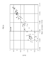
- FIG. 8 illustrates the relation between the sheet resistance values and threshold voltages of samples without annealing.
- threshold voltage Vth is proportional to sheet resistance. Further, as illustrated in FIG. 8 , the values of the threshold voltage Vth for sheet resistance values lower than 1.0 ⁇ 10 8 ⁇ / ⁇ were smaller than zero by a considerable extent.
- the sheet resistance of samples whose sheet resistance was 1.0 ⁇ 10 8 ⁇ / ⁇ or greater without annealing was increased to 1.0 ⁇ 10 10 ⁇ / ⁇ or greater after performing annealing for one hour under a temperature of 300 degrees Celsius. From this, it can be seen that the threshold voltages Vth of samples whose sheet resistance is 1.0 ⁇ 10 8 ⁇ / ⁇ or greater without annealing can be increased to around 0 V by performing annealing.
- threshold voltage Vth corresponds to sheet resistance values of 1.0 ⁇ 10 8 ⁇ / ⁇ or greater
- relatively great values of threshold voltage Vth correspond to sheet resistance values smaller than 1.0 ⁇ 10 8 ⁇ / ⁇ .
- a sheet resistance of 1.0 ⁇ 10 8 ⁇ / ⁇ or greater is acceptable.
- sample type 1 and sample type 2 two types of samples of TFTs were prepared to observe the relation between the Si—H density of the SiN layer and initial TFT characteristics.
- a plurality of samples were prepared for each sample type, the samples of sample type 1 and the samples of sample type 2 were prepared to basically have the identical structures, with only the characteristics of the SiN layer of the passivation layer differing therebetween.
- the samples of sample type 1 which is considered as a comparative example, had SiN layers having a SiN density of 3.5 ⁇ 10 21 cm ⁇ 3 .
- the samples of sample type 2 which is an implementation example of embodiment 1, had SiN layers having a SiN density of 1.3 ⁇ 10 21 cm ⁇ 3 .
- the samples of sample type 2 i.e., TFT devices whose SiN layers had a Si—H density of 1.3 ⁇ 10 21 cm ⁇ 3 ) had initial characteristics superior to those of the samples of sample type 1 .
- SiN layers in sample type 1 and sample type 2 were provided with the different Si—H densities by varying the film forming conditions applied thereto as illustrated in FIG. 9A .
- a SiN layer with a Si—H density no greater than 2.3 ⁇ 10 21 cm ⁇ 3 may be formed with sets of film forming conditions other than the set of film forming conditions applied for sample type 2 in FIG. 9A .
- forming of a SiN layer with a Si—H density no greater than 2.3 ⁇ 10 21 cm ⁇ 3 can be performed by using an appropriate or desired one of such possible sets of film forming conditions.
- the following describes the effects yielded by defining the channel protection layer 106 , the lower insulating layer 1121 , and the first upper insulating layer 1123 each as a SiO layer such that, when thermal desorption measurement is performed with respect to the SiO layer, hydrogen is observed as desorption gas and within a temperature range of 300 degrees Celsius to 350 degrees Celsius, an average increase coefficient of the desorption gas does not take a positive value.
- sample types 11 and 12 are implementation examples of embodiment 1, whereas sample type 13 is a comparative example. Further, the samples of sample types 11 through 13 were prepared by applying different film forming conditions.
- the average increase coefficients (averages of differential coefficients) of desorption gas (hydrogen) took positive values within the temperature range of 300 degrees Celsius to 350 degrees Celsius.
- the average increase coefficients had values of approximately 1.0 ⁇ 10 ⁇ 13 at 300 degrees Celsius, and the values of the average increase coefficients increased as approaching 350 degrees Celsius.
- the average increase coefficients (averages of differential coefficients) of desorption gas (hydrogen) did not take positive values and hydrogen desorption intensity did not increase within the temperature range of 300 degrees Celsius to 350 degrees Celsius.
- the average increase coefficients of desorption gas (hydrogen) observed within the temperature range of 300 degrees Celsius to 350 degrees Celsius when performing thermal desorption measurement with respect to the SiO layer can be changed.
- FIGS. 11A and 11B measurement of initial characteristics was conducted with respect to sample TFT devices including lower insulating layers, first upper insulating layers, and channel protection layers made of SiO layers having the characteristics of the sample types 11 , 12 , and 13 .
- FIG. 11A includes graphs indicating the initial characteristics of TFT samples including lower insulating layers, first upper insulating layers, and channel protection layers made of SiO layers corresponding to sample types 11 and 12 .
- FIG. 11B includes graphs indicating the initial characteristics of TFT samples including lower insulating layers, first upper insulating layers, and channel protection layers made of SiO layers corresponding to sample type 13 .
- the TFT samples having SiO layers corresponding to sample types 11 and 12 indicated excellent initial characteristics. Meanwhile, as illustrated in FIG. 11B , the TFT samples having SiO layers corresponding to sample type 13 did not have the characteristics of TFTs.
- a TFT device having excellent initial characteristics can be achieved by using, for each of the channel protection layer 106 , the lower insulating layer 1121 , and the first upper insulating layer 1123 , a SiO layer such that, when thermal desorption measurement is performed with respect to the SiO layer, hydrogen is observed as desorption gas and within a temperature range of 300 degrees Celsius to 350 degrees Celsius, an average increase coefficient of the desorption gas does not take a positive value.
- FIG. 12A illustrates the structure of samples used for measuring carrier lifetime.
- carrier lifetime was defined in this measurement, with reference to FIG. 12B .
- each sample having the structure illustrated in FIG. 12A was irradiated with a microwave having the frequency of 26 GHz, and the reflectance (base intensity) from the sample was measured as reflection intensity I 1 .
- each sample was irradiated with the microwave, the sample was also irradiated with an ultraviolet pulse laser.
- the irradiation with the ultraviolet pulse laser was performed under the following conditions.
- Measurement was performed of microwave reflectance of each sample, as reflection intensity I 2 . Further, the difference between reflection intensity I 2 and reflection intensity I 1 (I 2 ⁇ I 1 ) was calculated, and a graph as illustrated in FIG. 12B including a curve indicating the chronological change of the difference (I 2 ⁇ I 1 ) was created.
- the decay constant (the amount of time between time P 1 corresponding to the reflectance peak and time point P 2 corresponding to reflectance 1/e) in the curve illustrated in FIG. 12B was defined as a carrier lifetime T (1/e lifetime).
- sample types 21 through 24 were prepared for each of four sample types, namely sample types 21 through 24 .
- Samples of one sample type were prepared with film forming conditions differing from those for samples of the rest of the sample types.
- the film forming rates for the samples of sample type 21 (indicated by “S 21 ” in FIG. 13B ) and samples of sample type 23 (indicated by “S 23 ” in FIG. 13B ) were within the range between 50 nm/sec and 110 nm/sec. Meanwhile, the film forming rates for samples of sample type 22 (indicated by “S 22 ” in FIG. 13B ) was 150 nm/sec, and the film forming rates for samples of sample type 24 (indicated by “S 24 ” in FIG. 13B ) were 200 nm/sec.
- the carrier lifetimes T for samples of sample type 23 whose film forming rates were within the range between 50 nm/sec and 110 nm/sec, were excellent, being 3.0 ⁇ 10 ⁇ 2 ⁇ sec or longer.
- samples of sample type 23 (indicated by “S 23 ” in FIG. 13C ), whose refractive indexes were within a range between 1.454 and 1.461, had carrier lifetimes T of 3.0 ⁇ 10 ⁇ 2 ⁇ sec or longer, which are superior to the carrier lifetimes T for the samples of sample types 21 , 22 , and 24 .
- FIGS. 14A through 14C illustrate initial characteristics of TFT samples including lower insulating layers, first upper insulating layers, and channel protection layers made of SiO layers having the characteristics of the sample types 21 , 22 , and 23 .
- Vth threshold voltage
- TFT devices including SiO layers of sample type 23 whose film forming rates were within the range between 50 nm/sec and 110 nm/sec and whose refractive indexes were within the range between 1.454 and 1.461, had carrier lifetimes T (1/e lifetimes) of 3.0 ⁇ 10 ⁇ 2 ⁇ sec or longer and thus, had better TFT characteristics than TFT devices including SiO layers of sample types 21 , 22 , 24 .
- FIG. 15A illustrates the characteristics of the TFT device pertaining to the present embodiment
- FIG. 15B illustrates the characteristics of a TFT device pertaining to a comparative example. Note that the measurement in FIGS. 15A and 15B were performed under a temperature of 90 degrees Celsius, and with TFT devices with a width of 50 ⁇ m and a length of 10 ⁇ m.
- the threshold voltage shift ⁇ Vth with the TFT device pertaining to the present embodiment was ⁇ 0.20 V, which is extremely small.
- the TFT device pertaining to the present embodiment is characterized for (i) the channel protection layer 106 , the lower insulating layer 1121 , and the first upper insulating layer 1123 each being a SiO layer such that, when thermal desorption measurement is performed with respect to the SiO layer, hydrogen is observed as desorption gas and within a temperature range of 300 degrees Celsius to 350 degrees Celsius, an average increase coefficient of the desorption gas does not take a positive value, and (ii) the second upper insulating layer 1124 being a SiN layer whose Si—H density is no greater than 2.3 ⁇ 10 21 cm ⁇ 3 .
- the threshold voltage shift ⁇ Vth with the TFT device pertaining to the comparative example, whose channel protection layer and passivation layer had characteristics differing from those of the channel protection layer and the passivation layer included in the TFT device pertaining to the present embodiment was ⁇ 5.68 V and thus was greater than that with the TFT device pertaining to the present embodiment.
- a TFT device including SiO layers and a SiN layer having the above characteristics exhibits excellent characteristics in NBTS measurement.
- FIG. 16 only provides structural illustration of some parts (mainly, the structure of the TFT device part) of the display panel 30 .
- Parts of the display panel 30 not illustrated in FIG. 16 have the same structures as the corresponding parts of the display panel 10 pertaining to embodiment 1, and are provided with the same reference signs as those provided to the corresponding parts of the display panel 10 .
- the display panel 30 includes an interlayer insulating layer 327 covering the source electrodes 107 and 110 , the drain electrodes 108 and 109 , and the channel protection layer 106 , and a passivation layer 312 disposed on the interlayer insulating layer 327 .
- the display panel 30 includes an upper electrode 313 .
- the upper electrode 313 extends along an inner wall of the interlayer insulating layer 327 defining a contact hole formed in the interlayer insulating layer 327 and is connected to the source electrode 110 . Further, a part of a top portion of the upper electrode 313 is sandwiched between the interlayer insulating layer 327 and a lower insulating layer 3121 of the passivation layer 312 .
- the passivation layer 312 is composed of the lower insulating layer 3121 made of SiO, a barrier layer 3122 made of an aluminum compound (e.g., aluminum oxide), and an upper insulating layer 3123 made of SiN disposed in this order one on top of another with the lower insulating layer 3123 lowermost in the Z axis direction.
- a barrier layer 3122 made of an aluminum compound (e.g., aluminum oxide)
- an upper insulating layer 3123 made of SiN disposed in this order one on top of another with the lower insulating layer 3123 lowermost in the Z axis direction.
- an anode 315 is disposed above the passivation layer 312 , with an interlayer insulating layer 314 residing between the anode 315 and the passivation 312 at certain areas.
- the anode 315 is electrically connected to the upper electrode 313 at the bottom of a contact hole penetrating through the interlayer insulating layer 314 and the passivation layer 312 .
- the channel protection layer 106 and the lower insulating layer 3121 of the passivation layer 312 each are a SiO layer such that, when thermal desorption measurement is performed with respect to the SiO layer, hydrogen is observed as desorption gas and within a temperature range of 300 degrees Celsius to 350 degrees Celsius, an average increase coefficient of the desorption gas does not take a positive value
- the upper insulating layer 3123 is a SiN layer whose Si—H density is no greater than 2.3 ⁇ 10 21 cm ⁇ 3 .
- the channel layers 104 , 105 are made of an oxide semiconductor (IGZO).
- IGZO oxide semiconductor
- the channel layers 104 , 105 achieve high electron mobility, and thus, have excellent electric characteristics. Due to this, the TFT device part is expected to achieve high electron mobility, irrespective of temperature.
- the passivation layer 312 includes the barrier layer 3122 , which is made of an aluminum compound (e.g., AlOx).
- the barrier layer 3122 suppresses the entry of moisture and hydrogen (i.e., functions as a barrier), and protects (suppresses degradation of) the channel layers 104 and 105 , which are made of IGZO.
- the TFT device part pertaining to the present embodiment as well as a display device including the TFT device part, has high stability and reliability.
- FIG. 17 only provides structural illustration of some parts (mainly, the structure of the TFT device part) of the display panel 40 .
- Parts of the display panel 40 not illustrated in FIG. 17 have the same structures as the corresponding parts of the display panel 10 pertaining to embodiment 1, and are provided with the same reference signs as those provided to the corresponding parts of the display panel 10 .
- the display panel 40 pertaining to the present embodiment includes a passivation layer 412 covering the source electrodes 107 and 110 , the drain electrodes 108 and 109 , and the channel protection layer 106 .
- the passivation layer 412 is composed of five layers.
- the passivation layer 412 is composed of: a lower insulating layer 4121 made of SiO; a barrier layer 4122 made of an aluminum compound (e.g., AlOx); a first upper insulating layer 4123 made of SiO; a second upper insulating layer 4124 made of SiN; and a third upper insulating layer 4125 made of SiN, layered in this order one on top of another with the lower insulating layer 4121 lowermost in the Z axis direction.
- AlOx aluminum compound
- the channel protection layer 106 , and the lower insulating layer 4121 and the first upper insulating layer 4123 of the passivation layer 412 each are a SiO layer such that, when thermal desorption measurement is performed with respect to the SiO layer, hydrogen is observed as desorption gas and within a temperature range of 300 degrees Celsius to 350 degrees Celsius, an average increase coefficient of the desorption gas does not take a positive value
- the second upper insulating layer 4124 and the third upper insulating layer 4125 each are a SiN layer whose Si—H density is no greater than 2.3 ⁇ 10 21 cm ⁇ 3 .
- the display panel 40 includes an upper electrode 413 extending along inner walls of the lower insulating layer 4121 , the barrier layer 4122 , the first upper insulating layer 4123 , and the second upper insulating layer 4124 defining a contact hole penetrating through the lower insulating layer 4121 , the barrier layer 4122 , the first upper insulating layer 4123 , and the second upper insulating layer 4124 . Further, a part of a top portion of the upper electrode 413 is sandwiched between the second upper insulating layer 4124 and the third upper insulating layer 4125 .
- an anode 415 is formed above the passivation layer 412 , with an interlayer insulating layer 414 therebetween at certain areas.
- the anode 415 is electrically connected to the upper electrode 413 , at the bottom of a contact hole penetrating through the interlayer insulating layer 414 and the third upper insulating layer 4125 .
- the TFT device part pertaining to the present embodiment also achieves excellent TFT characteristics for the channel protection layer 106 and certain layers of the passivation layer 412 being a SiO layer/SiN layer having the same characteristics as in embodiment 1. Further, due to the passivation layer 412 including two SiO layers and two SiN layers, the TFT device part pertaining to the present embodiment has even higher reliability than those in embodiments 1 and 2.
- the channel layers 104 , 105 are made of an oxide semiconductor (IGZO).
- IGZO oxide semiconductor
- the channel layers 104 , 105 achieve high electron mobility, and thus, have excellent electric characteristics. Due to this, the TFT device part is expected to achieve high electron mobility, irrespective of temperature.
- the passivation layer 412 includes the barrier layer 4122 , which is made of an aluminum compound (e.g., AlOx).
- the barrier layer 4122 suppresses the entry of moisture and hydrogen (i.e., functions as a barrier), and protects (suppresses degradation of) the channel layers 104 and 105 , which are made of IGZO.
- the TFT device part pertaining to the present embodiment as well as a display device including the TFT device part, has high stability and reliability.
- FIG. 18 only provides structural illustration of some parts (mainly, the structure of the TFT device part) of the display panel 50 .
- Parts of the display panel 50 not illustrated in FIG. 18 have the same structures as the corresponding parts of the display panel 10 pertaining to embodiment 1, and are provided with the same reference signs as those provided to the corresponding parts of the display panel 10 .
- the display panel 50 pertaining to the present embodiment includes a passivation layer 512 covering the source electrodes 107 and 110 , the drain electrodes 108 and 109 , and the channel protection layer 106 .
- the passivation layer 512 is composed of four layers.
- the passivation layer 512 is composed of: a lower insulating layer 5121 made of SiO; a barrier layer 5122 made of an aluminum compound (e.g., AlOx); a first upper insulating layer 5123 made of SiN; and a second upper insulating layer 5124 made of SiN, layered in this order one on top of another with the lower insulating layer 5121 lowermost in the Z axis direction.
- the channel protection layer 106 and the lower insulating layer 5121 of the passivation layer 512 each are a SiO layer such that, when thermal desorption measurement is performed with respect to the SiO layer, hydrogen is observed as desorption gas and within a temperature range of 300 degrees Celsius to 350 degrees Celsius, an average increase coefficient of the desorption gas does not take a positive value
- the first upper insulating layer 5123 and the second upper insulating layer 5124 each are a SiN layer whose Si—H density is no greater than 2.3 ⁇ 10 21 cm 3 .
- the second upper insulating layer 5124 has lower density than the first upper insulating layer 5123 . This facilitates forming a contact hole with a tapered shape.
- the display panel 50 includes an upper electrode 513 extending along inner walls of the lower insulating layer 5121 , the barrier layer 5122 , and the first upper insulating layer 5123 defining a contact hole penetrating through the lower insulating layer 5121 , the barrier layer 5122 , and the first upper insulating layer 5123 . Further, a part of a top portion of the upper electrode 513 is sandwiched between the first upper insulating layer 5123 and the second upper insulating layer 5124 .
- anode 515 is disposed above the passivation layer 512 , with an interlayer insulating layer 514 therebetween at certain areas. Electrical connection similar to the above is formed between the anode 515 and the upper electrode 513 .
- the TFT device part pertaining to the present embodiment also achieves excellent TFT characteristics for the channel protection layer 106 and certain layers of the passivation layer 512 being a SiO layer/SiN layer having the same characteristics as in embodiment 1.
- the channel layers 104 , 105 are made of an oxide semiconductor (IGZO).
- IGZO oxide semiconductor
- the channel layers 104 , 105 achieve high electron mobility, and thus, have excellent electric characteristics. Due to this, the TFT device part is expected to achieve high electron mobility, irrespective of temperature.
- the passivation layer 512 includes the barrier layer 5122 , which is made of an aluminum compound (e.g., AlOx).
- the barrier layer 5122 suppresses the entry of moisture and hydrogen (i.e., functions as a barrier), and protects (suppresses degradation of) the channel layers 104 and 105 , which are made of IGZO.
- the TFT device part pertaining to the present embodiment as well as a display device including the TFT device part, has high stability and reliability.
- FIG. 19 only provides structural illustration of some parts (mainly, the structure of the TFT device part) of the display panel 60 .
- Parts of the display panel 60 not illustrated in FIG. 19 have the same structures as the corresponding parts of the display panel 10 pertaining to embodiment 1, and are provided with the same reference signs as those provided to the corresponding parts of the display panel 10 .
- the display panel 60 pertaining to the present embodiment includes a passivation layer 612 covering the source electrodes 107 and 110 , the drain electrodes 108 and 109 , and the channel protection layer 106 .
- the passivation layer 612 is composed of two layers.
- the passivation layer 612 is composed of: a lower insulating layer 6121 made of SiO; and a barrier layer 6122 made of an aluminum compound (e.g., AlOx), layered in this order one on top of another with the lower insulating layer 6121 lower in the Z axis direction.
- AlOx aluminum compound
- the channel protection layer 106 and the lower insulating layer 6121 of the passivation layer 612 each are a SiO layer such that, when thermal desorption measurement is performed with respect to the SiO layer, hydrogen is observed as desorption gas and within a temperature range of 300 degrees Celsius to 350 degrees Celsius, an average increase coefficient of the desorption gas does not take a positive value.
- the display panel 60 includes an upper electrode 613 extending along an inner wall of the lower insulating layer 6121 defining a contact hole penetrating through the lower insulating layer 6121 . Further, a part of a top portion of the upper electrode 613 is sandwiched between the lower insulating layer 6121 and the barrier layer 6122 .
- an anode 615 is disposed above the passivation layer 612 , with an interlayer insulating layer 614 therebetween at certain areas.
- the anode 615 is electrically connected to the upper electrode 613 , at the bottom of a contact hole penetrating through the interlayer insulating layer 614 and the barrier layer 6122 .
- the TFT device part pertaining to the present embodiment also achieves excellent TFT characteristics, similar to the TFT device part pertaining to embodiment 1, for the channel protection layer 106 and the lower insulating layer 6121 of the passivation layer 612 being SiO layers having the same characteristics as in embodiment 1.
- the channel layers 104 , 105 are made of an oxide semiconductor (IGZO).
- IGZO oxide semiconductor
- the passivation layer 612 includes the barrier layer 6122 , which is made of an aluminum compound (e.g., AlOx).
- the barrier layer 6122 suppresses the entry of moisture and hydrogen (i.e., functions as a barrier), and protects (suppresses degradation of) the channel layers 104 and 105 , which are made of IGZO.
- the TFT device part pertaining to the present embodiment as well as a display device including the TFT device part, has high stability and reliability.
- FIG. 20 only provides structural illustration of some parts (mainly, the structure of the TFT device part) of the display panel 70 .
- Parts of the display panel 70 not illustrated in FIG. 20 have the same structures as the corresponding parts of the display panel 10 pertaining to embodiment 1, and are provided with the same reference signs as those provided to the corresponding parts of the display panel 10 .
- the display panel 70 pertaining to the present embodiment includes a passivation layer 712 covering the source electrodes 107 and 110 , the drain electrodes 108 and 109 , and the channel protection layer 106 .
- the passivation layer 712 is similar to the passivation layer 512 for being composed of four layers, but the structure of the passivation layer 712 differs from the structure of the passivation layer 512 in detail.
- the passivation layer 712 is composed of: a first lower insulating layer 7121 made of SiO; a second lower insulating layer 7123 made of SiN; a third lower insulating layer 7124 made of SiN; and a barrier layer 7122 made of an aluminum compound (e.g., AlOx), layered in this order one on top of another with the barrier layer 7122 uppermost in the Z axis direction.
- a first lower insulating layer 7121 made of SiO
- a second lower insulating layer 7123 made of SiN
- a third lower insulating layer 7124 made of SiN
- a barrier layer 7122 made of an aluminum compound (e.g., AlOx), layered in this order one on top of another with the barrier layer 7122 uppermost in the Z axis direction.
- the channel protection layer 106 and the first lower insulating layer 7121 of the passivation layer 712 each are a SiO layer such that, when thermal desorption measurement is performed with respect to the SiO layer, hydrogen is observed as desorption gas and within a temperature range of 300 degrees Celsius to 350 degrees Celsius, an average increase coefficient of the desorption gas does not take a positive value
- the second lower insulating layer 7123 and the third lower insulating layer 7124 each are a SiN layer whose Si—H density is no greater than 2.3 ⁇ 10 21 cm ⁇ 3 .
- the display panel 70 includes an upper electrode 713 extending along inner walls of the first lower insulating layer 7121 , and the second lower insulating layer 7123 defining a contact hole penetrating through the first lower insulating layer 7121 and the second lower insulating layer 7123 . Further, a part of a top portion of the upper electrode 713 is sandwiched between the second lower insulating layer 7123 and the third lower insulating layer 7124 .
- anode 715 is disposed above the passivation layer 712 , with an interlayer insulating layer 714 therebetween at certain areas. Electrical connection similar to the above is formed between the anode 715 and the upper electrode 713 .
- the TFT device part pertaining to the present embodiment also achieves excellent TFT characteristics for the channel protection layer 106 and certain layers of the passivation layer 712 being a SiO layer/SiN layer having the same characteristics as in embodiment 1.
- the channel layers 104 , 105 are made of an oxide semiconductor (IGZO).
- IGZO oxide semiconductor
- the channel layers 104 , 105 achieve high electron mobility, and thus, have excellent electric characteristics. Due to this, the TFT device part is expected to achieve high electron mobility, irrespective of temperature.
- the passivation layer 712 includes the barrier layer 7122 , which is made of an aluminum compound (e.g., AlOx).
- the barrier layer 7122 suppresses the entry of moisture and hydrogen (i.e., functions as a barrier), and protects (suppresses degradation of) the channel layers 104 and 105 , which are made of IGZO.
- the TFT device part pertaining to the present embodiment as well as a display device including the TFT device part, has high stability and reliability.
- FIG. 21 only provides structural illustration of some parts (mainly, the structure of the TFT device part) of the display panel 80 .
- Parts of the display panel 80 not illustrated in FIG. 21 have the same structures as the corresponding parts of the display panel 10 pertaining to embodiment 1, and are provided with the same reference signs as those provided to the corresponding parts of the display panel 10 .
- the display panel 80 pertaining to the present embodiment includes a passivation layer 812 covering the source electrodes 107 and 110 , the drain electrodes 108 and 109 , and the channel protection layer 106 .
- the passivation layer 812 is composed of two layers.
- the passivation layer 812 is composed of: a lower insulating layer 8121 made of SiO; and an upper insulating layer 8123 made of SiN, layered in this order one on top of another with the lower insulating layer 8121 lower in the Z axis direction.
- the channel protection layer 106 and the lower insulating layer 8121 of the passivation layer 812 each are a SiO layer such that, when thermal desorption measurement is performed with respect to the SiO layer, hydrogen is observed as desorption gas and within a temperature range of 300 degrees Celsius to 350 degrees Celsius, an average increase coefficient of the desorption gas does not take a positive value; and (ii) the upper insulating layer 8123 is a SiN layer whose Si—H density is no greater than 2.3 ⁇ 10 21 cm ⁇ 3 .
- the display panel 80 includes an upper electrode 813 extending along an inner wall of the hole insulating layer 8121 defining a contact hole penetrating through the lower insulating layer 8121 . Further, a part of a top portion of the upper electrode 813 is sandwiched between the lower insulating layer 8121 and the upper insulating layer 8123 .
- anode 815 is disposed above the passivation layer 812 , with an interlayer insulating layer 814 therebetween at certain areas. Electrical connection similar to the above is formed between the anode 815 and the upper electrode 813 .
- the TFT device part pertaining to the present embodiment also achieves excellent TFT characteristics for the channel protection layer 106 and certain layers of the passivation layer 812 being a SiO layer/SiN layer having the same characteristics as in embodiment 1.
- the channel layers 104 , 105 are made of an oxide semiconductor (IGZO).
- IGZO oxide semiconductor
- the channel layers 104 , 105 achieve high electron mobility, and thus, have excellent electric characteristics. Due to this, the TFT device part is expected to achieve high electron mobility, irrespective of temperature.
- the passivation layer 812 is composed of the lower insulating layer 8121 made of SiO and the upper insulating layer 8123 made of SiN.
- the passivation layer 812 only includes a small number of layers, which reduces the number of procedures in manufacturing.
- the passivation layer 812 does not include a barrier layer made of AlOx. This is advantageous in terms of manufacturing, since forming a contact hole in a barrier layer made of AlOx is difficult.
- the TFT device part pertaining to the present embodiment as well as a display device including the TFT device part, has high stability and reliability.
- FIG. 22 only provides structural illustration of some parts (mainly, the structure of the TFT device part) of the display panel 90 .
- Parts of the display panel 90 not illustrated in FIG. 22 have the same structures as the corresponding parts of the display panel 10 pertaining to embodiment 1, and are provided with the same reference signs as those provided to the corresponding parts of the display panel 10 .
- the display panel 90 pertaining to the present embodiment includes a passivation layer 912 covering the source electrodes 107 and 110 , the drain electrodes 108 and 109 , and the channel protection layer 106 .
- the passivation layer 912 is composed of three layers.
- the passivation layer 912 is composed of: a lower insulating layer 9121 made of SiO; a first upper insulating layer 9123 made of SiN; and a second upper insulating layer 9124 made of SiN, layered in this order one on top of another with the lower insulating layer 9121 lowermost in the Z axis direction.
- the channel protection layer 106 and the lower insulating layer 9121 of the passivation layer 912 each are a SiO layer such that, when thermal desorption measurement is performed with respect to the SiO layer, hydrogen is observed as desorption gas and within a temperature range of 300 degrees Celsius to 350 degrees Celsius, an average increase coefficient of the desorption gas does not take a positive value; and (ii) the first upper insulating layer 9123 and the second upper insulating layer 9124 each are a SiN layer whose Si—H density is no greater than 2.3 ⁇ 10 21 cm ⁇ 3 .
- the second upper insulating layer 9124 has lower density than the first upper insulating layer 9123 . This facilitates forming a contact hole with a tapered shape.
- the display panel 90 includes an upper electrode 913 extending along inner walls of the lower insulating layer 9121 and the first upper insulating layer 9123 defining a contact hole penetrating through the lower insulating layer 9121 and the first upper insulating layer 9123 . Further, a part of a top portion of the upper electrode 913 is sandwiched between the first upper insulating layer 9123 and the second upper insulating layer 9124 .
- anode 915 is disposed above the passivation layer 912 , with an interlayer insulating layer 914 therebetween at certain areas. Electrical connection similar to the above is formed between the anode 915 and the upper electrode 913 .
- the TFT device part pertaining to the present embodiment also achieves excellent TFT characteristics for the channel protection layer 106 and certain layers of the passivation layer 912 being a SiO layer/SiN layer having the same characteristics as in embodiment 1.
- two upper insulating layers made of SiN i.e., the first upper insulating layer 9123 and the second upper insulating layer 9124
- the first upper insulating layer 9123 and the second upper insulating layer 9124 form a dense film suppressing the entry of moisture and hydrogen and thereby protecting the channel layers 104 and 105 .
- the channel layers 104 , 105 are made of an oxide semiconductor (IGZO).
- IGZO oxide semiconductor
- the channel layers 104 , 105 achieve high electron mobility, and thus, have excellent electric characteristics. Due to this, the TFT device part is expected to achieve high electron mobility, irrespective of temperature.
- the passivation layer 912 does not include a barrier layer made of AlOx. This is advantageous in terms of manufacturing, or more specifically, in the forming of a contact hole, for example.
- the TFT device part pertaining to the present embodiment as well as a display device including the TFT device part, has high stability and reliability.
- the passivation layer is composed of two to five layers. Nevertheless, the passivation layer may be composed of a single layer, or may be composed of six or more layers.
- the passivation layer is composed of two or more layers, whether or not to provide the passivation layer with a barrier layer made of an aluminum compound may be determined as necessary, as long as the passivation layer includes at least one of a SiO layer and a SiN layer.
- the passivation layer may include a SiON layer in place of a SiO layer, or a SiON layer in place of a SiN layer.
- a SiON layer replacing a SiO layer is to satisfy the above-described requirements of an SiO layer (i.e., the requirements related to an average increase coefficient of the desorption gas (hydrogen) when thermal desorption measurement is performed), and a SiON layer replacing a SiN layer is to satisfy the above-described requirement of an SiN layer (i.e., the requirements related to the Si—H density).
- the channel protection layer need not be a single layer made of SiO. That is, the channel protection layer made by composed of two layers, one made of SiO and the other made of SiN, or three or more layers including a SiO layer and a SiN layer.
- a SiO layer in the channel protection layer is to satisfy the above-described requirements of an SiO layer (i.e., the requirements related to an average increase coefficient of the desorption gas (hydrogen) when thermal desorption measurement is performed), and a SiN layer in the channel protection layer is to satisfy the above-described requirement of an SiN layer (i.e., the requirements related to the Si—H density).
- an SiO layer i.e., the requirements related to an average increase coefficient of the desorption gas (hydrogen) when thermal desorption measurement is performed
- a SiN layer in the channel protection layer is to satisfy the above-described requirement of an SiN layer (i.e., the requirements related to the Si—H density).
- the SiN layer when including a SiN layer in the channel protection layer, it is preferable that the SiN layer be spaced away from the channel layers with the SiO layer of the channel protection layer between the SiN layer of the channel protection layer and the channel layers.
- a channel protection layer with this structure prevents hydrogen from arriving at the channel layers to a further extent.
- Each of embodiments 1 through 8 describes a bottom gate (inverse-staggered) TFT device. Meanwhile, the technology pertaining to the present disclosure is also applicable to top gate (staggered) TFT devices. This achieves the same effects as described above.
- Each of embodiments 1 through 8 describes an EL display panel of the top-emission type as an example of a display panel.
- the technology pertaining to the present disclosure is not only applicable to top-emission type EL display panels. That is, the technology pertaining to the present disclosure is also applicable to bottom-emission type display panels, and also, to liquid crystal panels, field emission display panels, electronic papers, and the like.
- Each of embodiments 1 through 8 describes a configuration where two transistor elements (Tr 1 , Tr 2 ) are provided for each subpixel 10 a .
- the technology pertaining to the present disclosure is not only applicable to such a configuration. That is, the technology pertaining to the present disclosure is also applicable, for example, to a configuration where only one transistor element is provided for each subpixel, or a configuration where three or more transistor elements are provided for each subpixel.
- each constituent element may be formed by using any suitable material.
- the barrier layer of the passivation layer need not be made of AlOx, and instead, may be made of a nitride containing Al, or an oxynitride containing Al.
- each of such electrodes may be composed of a combination of a Mo layer and an Al layer, or a combination of a Mo layer and a metal alloy layer made of Al and Nd.
- each of embodiments 1 through 8 describes a configuration where an anode ( 115 , 315 , 415 , 515 , 615 , 715 , 815 , 915 ) is located at a bottom portion of the EL element part, and the anode is connected to the source electrode 110 of the TFT device part.
- the technology pertaining to the present disclosure is not only applicable to such a configuration. That is, the technology pertaining to the present disclosure is applicable to a configuration where a cathode is provided at the bottom portion of the EL element part, and an anode is provided at the top portion of the EL element part. With such a configuration, the cathode at the bottom portion of the EL element part is connected to a drain of the TFT device part.
- any suitable known material may be used for any of the constituent elements.
- the technology pertaining to the present disclosure is useful for realizing a thin film transistor device that has excellent electrical characteristics.
Landscapes
- Thin Film Transistor (AREA)
- Liquid Crystal (AREA)
- Electroluminescent Light Sources (AREA)
Abstract
Description
-
- YLF-3HG Laser
- λ=349 nm
- pulse interval; 15 nsec
-
- 1 Display device
- 10, 30, 40, 50, 60, 70, 80, 90 Display panel
- 10 a Subpixel
- 20 Drive/control circuit
- 21-24 Drive circuit
- 25 Control circuit
- 100, 126 Substrate
- 101, 102 Gate electrode
- 103, 1030 Gate insulating layer
- 104, 105 Channel layer
- 106, 1060 Channel protection layer
- 107, 110 Source electrode
- 108, 109 Drain electrode
- 111 Contact plug
- 112, 312, 412, 512, 612, 712, 812, 912 Passivation layer
- 113, 313, 413, 513, 613, 713, 813, 913 Upper electrode
- 114, 314, 327, 414, 514, 614, 714, 814, 914 Interlayer insulating layer
- 115, 315, 415, 515, 615, 715, 815, 915 Anode
- 116 Hole injection layer
- 117 Bank
- 118 Hole transport layer
- 119 Light-emitting layer
- 120 Electron transport layer
- 121 Cathode
- 122 Sealing layer
- 123 Adhesion layer
- 124 Color filter layer
- 125 Light-blocking layer
- 1121, 3121, 4121, 5121, 6121, 7121, 7123, 7124, 8121, 9121, 11210 Lower insulating layer
- 1122, 3122, 4122, 5122, 6122, 7122, 11220 Barrier layer
- 1123, 1124, 3123, 4123, 4124, 4125, 5123, 5124, 8123, 9123, 9124, 11230, 11240 Upper insulating layer
Claims (10)
Applications Claiming Priority (3)
| Application Number | Priority Date | Filing Date | Title |
|---|---|---|---|
| JP2013112741 | 2013-05-29 | ||
| JP2013-112741 | 2013-05-29 | ||
| PCT/JP2014/001929 WO2014192210A1 (en) | 2013-05-29 | 2014-04-03 | Thin film transistor device, method for manufacturing same and display device |
Publications (2)
| Publication Number | Publication Date |
|---|---|
| US20160093744A1 US20160093744A1 (en) | 2016-03-31 |
| US9799772B2 true US9799772B2 (en) | 2017-10-24 |
Family
ID=51988265
Family Applications (1)
| Application Number | Title | Priority Date | Filing Date |
|---|---|---|---|
| US14/894,027 Active US9799772B2 (en) | 2013-05-29 | 2014-04-03 | Thin film transistor device, method for manufacturing same and display device |
Country Status (3)
| Country | Link |
|---|---|
| US (1) | US9799772B2 (en) |
| JP (1) | JP6083053B2 (en) |
| WO (1) | WO2014192210A1 (en) |
Cited By (1)
| Publication number | Priority date | Publication date | Assignee | Title |
|---|---|---|---|---|
| US20170250374A1 (en) * | 2016-02-25 | 2017-08-31 | Japan Display Inc. | Display device |
Families Citing this family (6)
| Publication number | Priority date | Publication date | Assignee | Title |
|---|---|---|---|---|
| KR102279884B1 (en) * | 2014-12-05 | 2021-07-22 | 삼성디스플레이 주식회사 | Thin film transistor substrate and method of manufacturing the same |
| JP2018021993A (en) * | 2016-08-02 | 2018-02-08 | 株式会社ジャパンディスプレイ | Semiconductor substrate and display device using the same |
| CN106252362B (en) * | 2016-08-31 | 2019-07-12 | 深圳市华星光电技术有限公司 | A kind of array substrate and preparation method thereof |
| CN110402486B (en) * | 2017-02-10 | 2023-11-28 | 环球晶圆股份有限公司 | Methods for evaluating semiconductor structures |
| CN106876416B (en) * | 2017-03-30 | 2020-02-11 | 合肥鑫晟光电科技有限公司 | Electrostatic discharge unit, array substrate and display panel |
| CN111048523A (en) * | 2019-11-25 | 2020-04-21 | 武汉华星光电半导体显示技术有限公司 | Array substrate and preparation method thereof |
Citations (28)
| Publication number | Priority date | Publication date | Assignee | Title |
|---|---|---|---|---|
| JPH05163488A (en) | 1991-12-17 | 1993-06-29 | Konica Corp | Electroluminescent element of organic thin film |
| US5443922A (en) | 1991-11-07 | 1995-08-22 | Konica Corporation | Organic thin film electroluminescence element |
| JP2004056099A (en) | 2002-05-17 | 2004-02-19 | Semiconductor Energy Lab Co Ltd | Silicon nitride film, semiconductor device and its manufacturing method |
| US20040099915A1 (en) | 2002-05-17 | 2004-05-27 | Toru Takayama | Silicon nitride film, and semiconductor device and method of manufacturing the same |
| US20070072439A1 (en) | 2005-09-29 | 2007-03-29 | Semiconductor Energy Laboratory Co., Ltd. | Semiconductor device and manufacturing method thereof |
| JP2007123861A (en) | 2005-09-29 | 2007-05-17 | Semiconductor Energy Lab Co Ltd | Semiconductor device and manufacturing method thereof |
| JP2008166716A (en) | 2006-12-05 | 2008-07-17 | Canon Inc | Bottom-gate thin film transistor, method for manufacturing bottom-gate thin film transistor, and display device |
| US20110068336A1 (en) | 2009-09-24 | 2011-03-24 | Semiconductor Energy Laboratory Co., Ltd. | Semiconductor element and method for manufacturing the same |
| US20110140116A1 (en) * | 2009-12-01 | 2011-06-16 | Sony Corporation | Thin film transistor, display device, and electronic device |
| US20120119212A1 (en) | 2010-11-11 | 2012-05-17 | Semiconductor Energy Laboratory Co., Ltd. | Semiconductor device and method for manufacturing the same |
| JP2012104639A (en) | 2010-11-10 | 2012-05-31 | Toshiba Mobile Display Co Ltd | Thin-film transistor circuit board and method of manufacturing the same |
| US20120181533A1 (en) * | 2011-01-19 | 2012-07-19 | Samsung Electronics Co., Ltd. | Thin film transistor array panel |
| US8389989B2 (en) * | 2009-09-04 | 2013-03-05 | Semiconductor Energy Laboratory Co., Ltd. | Transistor having oxide semiconductor layer and display utilizing the same |
| US20130075719A1 (en) * | 2011-09-27 | 2013-03-28 | Kabushiki Kaisha Toshiba | Thin film transistor, method for manufacturing same, and display device |
| US20130120692A1 (en) * | 2011-11-11 | 2013-05-16 | Semiconductor Energy Laboratory Co., Ltd. | Liquid crystal element and method for manufacturing the same |
| US20140138675A1 (en) * | 2012-11-16 | 2014-05-22 | Semiconductor Energy Laboratory Co., Ltd. | Semiconductor device |
| US8890145B2 (en) * | 2010-11-17 | 2014-11-18 | Innolux Corporation | Thin film transistors and methods for manufacturing the same |
| US20150084042A1 (en) * | 2013-09-24 | 2015-03-26 | Kabushiki Kaisha Toshiba | Thin film transistor and method for manufacturing same |
| US20150171220A1 (en) * | 2012-05-28 | 2015-06-18 | Sharp Kabushiki Kaisha | Semiconductor device and method for manufacturing same |
| US20150200113A1 (en) * | 2014-01-10 | 2015-07-16 | Panasonic Corporation | Method of manufacturing thin-film transistor substrate |
| US20150221677A1 (en) * | 2012-09-24 | 2015-08-06 | Sharp Kabushiki Kaisha | Active matrix substrate, display device, and production method therefor |
| US9153601B2 (en) * | 2013-05-08 | 2015-10-06 | Au Optronics Corporation | Semiconductor device |
| US20160079437A1 (en) * | 2013-06-28 | 2016-03-17 | Kabushiki Kaisha Kobe Sho (Kobe Steel, Ltd.) | Thin film transistor and method for manufacturing same |
| US20160118244A1 (en) * | 2013-06-04 | 2016-04-28 | Joled Inc. | Thin film transistor element, production method for same, and display device |
| US20160133650A1 (en) * | 2013-05-29 | 2016-05-12 | Joled Inc. | Thin film transistor device, method for manufacturing same and display device |
| US20160204266A1 (en) * | 2015-01-08 | 2016-07-14 | Samsung Display Co., Ltd. | Thin film transistor array panel and manufacturing method thereof |
| US20160218000A1 (en) * | 2015-01-23 | 2016-07-28 | Applied Materials, Inc. | Plasma treatment on metal-oxide tft |
| US20160240565A1 (en) * | 2014-02-25 | 2016-08-18 | Lg Display Co., Ltd. | Display backplane and method of fabricating the same |
-
2014
- 2014-04-03 WO PCT/JP2014/001929 patent/WO2014192210A1/en not_active Ceased
- 2014-04-03 JP JP2015519618A patent/JP6083053B2/en active Active
- 2014-04-03 US US14/894,027 patent/US9799772B2/en active Active
Patent Citations (40)
| Publication number | Priority date | Publication date | Assignee | Title |
|---|---|---|---|---|
| US5443922A (en) | 1991-11-07 | 1995-08-22 | Konica Corporation | Organic thin film electroluminescence element |
| JPH05163488A (en) | 1991-12-17 | 1993-06-29 | Konica Corp | Electroluminescent element of organic thin film |
| US20150035058A1 (en) | 2002-05-17 | 2015-02-05 | Semiconductor Energy Laboratory Co., Ltd. | Silicon nitride film, and semiconductor device and method of manufacturing the same |
| JP2004056099A (en) | 2002-05-17 | 2004-02-19 | Semiconductor Energy Lab Co Ltd | Silicon nitride film, semiconductor device and its manufacturing method |
| US20040099915A1 (en) | 2002-05-17 | 2004-05-27 | Toru Takayama | Silicon nitride film, and semiconductor device and method of manufacturing the same |
| US20050106898A1 (en) | 2002-05-17 | 2005-05-19 | Semiconductor Energy Laboratory Co., Ltd. | Silicon nitride film and semiconductor device, and manufacturing method thereof |
| US20110095292A1 (en) | 2002-05-17 | 2011-04-28 | Semiconductor Energy Laboratory Co., Ltd. | Silicon nitride film, and semiconductor device and method of manufacturing the same |
| US20080142887A1 (en) | 2002-05-17 | 2008-06-19 | Semiconductor Energy Laboratory Co., Ltd. | Silicon nitride film and semiconductor device, and manufacturing method thereof |
| JP2007123861A (en) | 2005-09-29 | 2007-05-17 | Semiconductor Energy Lab Co Ltd | Semiconductor device and manufacturing method thereof |
| US20070072439A1 (en) | 2005-09-29 | 2007-03-29 | Semiconductor Energy Laboratory Co., Ltd. | Semiconductor device and manufacturing method thereof |
| US20100051936A1 (en) | 2006-12-05 | 2010-03-04 | Canon Kabushiki Kaisha | Bottom gate type thin film transistor, method of manufacturing the same, and display apparatus |
| JP2008166716A (en) | 2006-12-05 | 2008-07-17 | Canon Inc | Bottom-gate thin film transistor, method for manufacturing bottom-gate thin film transistor, and display device |
| US20120168750A1 (en) | 2006-12-05 | 2012-07-05 | Canon Kabushiki Kaisha | Bottom gate type thin film transistor, method of manufacturing the same, and display apparatus |
| US20150084048A1 (en) | 2006-12-05 | 2015-03-26 | Canon Kabushiki Kaisha | Bottom gate type thin film transistor, method of manufacturing the same, and display apparatus |
| US8389989B2 (en) * | 2009-09-04 | 2013-03-05 | Semiconductor Energy Laboratory Co., Ltd. | Transistor having oxide semiconductor layer and display utilizing the same |
| JP2011091381A (en) | 2009-09-24 | 2011-05-06 | Semiconductor Energy Lab Co Ltd | Semiconductor device and method of manufacturing the same |
| US20140113407A1 (en) | 2009-09-24 | 2014-04-24 | Semiconductor Energy Laboratory Co., Ltd. | Semiconductor element and method for manufacturing the same |
| US20110068336A1 (en) | 2009-09-24 | 2011-03-24 | Semiconductor Energy Laboratory Co., Ltd. | Semiconductor element and method for manufacturing the same |
| US20110140116A1 (en) * | 2009-12-01 | 2011-06-16 | Sony Corporation | Thin film transistor, display device, and electronic device |
| JP2012104639A (en) | 2010-11-10 | 2012-05-31 | Toshiba Mobile Display Co Ltd | Thin-film transistor circuit board and method of manufacturing the same |
| JP2012119667A (en) | 2010-11-11 | 2012-06-21 | Semiconductor Energy Lab Co Ltd | Semiconductor device and method of manufacturing the same |
| US20120119212A1 (en) | 2010-11-11 | 2012-05-17 | Semiconductor Energy Laboratory Co., Ltd. | Semiconductor device and method for manufacturing the same |
| US20140342498A1 (en) | 2010-11-11 | 2014-11-20 | Semiconductor Energy Laboratory Co., Ltd. | Semiconductor device and method for manufacturing the same |
| US8890145B2 (en) * | 2010-11-17 | 2014-11-18 | Innolux Corporation | Thin film transistors and methods for manufacturing the same |
| US20120181533A1 (en) * | 2011-01-19 | 2012-07-19 | Samsung Electronics Co., Ltd. | Thin film transistor array panel |
| US20130075719A1 (en) * | 2011-09-27 | 2013-03-28 | Kabushiki Kaisha Toshiba | Thin film transistor, method for manufacturing same, and display device |
| US20130120692A1 (en) * | 2011-11-11 | 2013-05-16 | Semiconductor Energy Laboratory Co., Ltd. | Liquid crystal element and method for manufacturing the same |
| US20150171220A1 (en) * | 2012-05-28 | 2015-06-18 | Sharp Kabushiki Kaisha | Semiconductor device and method for manufacturing same |
| US20150221677A1 (en) * | 2012-09-24 | 2015-08-06 | Sharp Kabushiki Kaisha | Active matrix substrate, display device, and production method therefor |
| US20140138675A1 (en) * | 2012-11-16 | 2014-05-22 | Semiconductor Energy Laboratory Co., Ltd. | Semiconductor device |
| US9153601B2 (en) * | 2013-05-08 | 2015-10-06 | Au Optronics Corporation | Semiconductor device |
| US20160133650A1 (en) * | 2013-05-29 | 2016-05-12 | Joled Inc. | Thin film transistor device, method for manufacturing same and display device |
| US20160118244A1 (en) * | 2013-06-04 | 2016-04-28 | Joled Inc. | Thin film transistor element, production method for same, and display device |
| US20160079437A1 (en) * | 2013-06-28 | 2016-03-17 | Kabushiki Kaisha Kobe Sho (Kobe Steel, Ltd.) | Thin film transistor and method for manufacturing same |
| US20150084042A1 (en) * | 2013-09-24 | 2015-03-26 | Kabushiki Kaisha Toshiba | Thin film transistor and method for manufacturing same |
| US9224871B2 (en) * | 2013-09-24 | 2015-12-29 | Kabushiki Kaisha Toshiba | Thin film transistor and method for manufacturing same |
| US20150200113A1 (en) * | 2014-01-10 | 2015-07-16 | Panasonic Corporation | Method of manufacturing thin-film transistor substrate |
| US20160240565A1 (en) * | 2014-02-25 | 2016-08-18 | Lg Display Co., Ltd. | Display backplane and method of fabricating the same |
| US20160204266A1 (en) * | 2015-01-08 | 2016-07-14 | Samsung Display Co., Ltd. | Thin film transistor array panel and manufacturing method thereof |
| US20160218000A1 (en) * | 2015-01-23 | 2016-07-28 | Applied Materials, Inc. | Plasma treatment on metal-oxide tft |
Non-Patent Citations (2)
| Title |
|---|
| International Search Report (ISR) from International Searching Authority (Japan Patent Office) in International Pat. Appl. No. PCT/JP2014/001929, dated Jul. 1, 2014. |
| U.S. Appl. No. 14/894,148 to Yuta Sugawara, which was filed Nov. 25, 2015. |
Cited By (2)
| Publication number | Priority date | Publication date | Assignee | Title |
|---|---|---|---|---|
| US20170250374A1 (en) * | 2016-02-25 | 2017-08-31 | Japan Display Inc. | Display device |
| US10062869B2 (en) * | 2016-02-25 | 2018-08-28 | Japan Display Inc. | Display device having stacked resin layers |
Also Published As
| Publication number | Publication date |
|---|---|
| JPWO2014192210A1 (en) | 2017-02-23 |
| US20160093744A1 (en) | 2016-03-31 |
| WO2014192210A1 (en) | 2014-12-04 |
| JP6083053B2 (en) | 2017-02-22 |
Similar Documents
| Publication | Publication Date | Title |
|---|---|---|
| US9893088B2 (en) | Thin film transistor device, method for manufacturing same and display device | |
| US9799772B2 (en) | Thin film transistor device, method for manufacturing same and display device | |
| US10811631B2 (en) | Thin film transistor element substrate, method of producing the substrate, and organic EL display device including the thin film transistor element substrate | |
| US8946730B2 (en) | Thin-film transistor device and method for manufacturing same, organic electroluminescent display element, and organic electroluminescent display device | |
| US8421084B2 (en) | Organic light emitting display and manufacturing method thereof | |
| US9024319B2 (en) | Thin-film transistor device and method for manufacturing same, organic electroluminescent display element, and organic electroluminescent display device | |
| JP6439194B2 (en) | Organic light emitting device | |
| US8941115B2 (en) | Thin-film transistor element and method for manufacturing same, organic electroluminescent display element, and organic electroluminescent display device | |
| US9799687B2 (en) | Method for manufacturing active-matrix display panel, and active-matrix display panel | |
| US8710503B2 (en) | Organic light-emitting display and method of manufacturing the same | |
| US8907344B2 (en) | Thin-film transistor device and method for manufacturing same, organic electroluminescent display element, and organic electroluminescent display device | |
| US10032802B2 (en) | Thin-film transistor device and display device using same | |
| US8969884B2 (en) | Thin-film transistor device and method for manufacturing same, organic electroluminescent display elements and organic electroluminescent display device | |
| US10020323B2 (en) | Thin-film transistor device and display device using same | |
| JP6779839B2 (en) | Manufacturing method of organic EL display panel and organic EL display panel | |
| US10026795B2 (en) | Organic EL element and method for manufacturing organic EL element | |
| US10680137B2 (en) | Electronic device having an intermediate layer disposed between two electrically-conductive layers |
Legal Events
| Date | Code | Title | Description |
|---|---|---|---|
| AS | Assignment |
Owner name: JOLED INC., JAPAN Free format text: ASSIGNMENT OF ASSIGNORS INTEREST;ASSIGNOR:SUGAWARA, YUTA;REEL/FRAME:037142/0516 Effective date: 20151107 |
|
| STCF | Information on status: patent grant |
Free format text: PATENTED CASE |
|
| MAFP | Maintenance fee payment |
Free format text: PAYMENT OF MAINTENANCE FEE, 4TH YEAR, LARGE ENTITY (ORIGINAL EVENT CODE: M1551); ENTITY STATUS OF PATENT OWNER: LARGE ENTITY Year of fee payment: 4 |
|
| AS | Assignment |
Owner name: INCJ, LTD., JAPAN Free format text: SECURITY INTEREST;ASSIGNOR:JOLED, INC.;REEL/FRAME:063396/0671 Effective date: 20230112 |
|
| AS | Assignment |
Owner name: JOLED, INC., JAPAN Free format text: CORRECTION BY AFFIDAVIT FILED AGAINST REEL/FRAME 063396/0671;ASSIGNOR:JOLED, INC.;REEL/FRAME:064067/0723 Effective date: 20230425 |
|
| AS | Assignment |
Owner name: JDI DESIGN AND DEVELOPMENT G.K., JAPAN Free format text: ASSIGNMENT OF ASSIGNORS INTEREST;ASSIGNOR:JOLED, INC.;REEL/FRAME:066382/0619 Effective date: 20230714 |
|
| MAFP | Maintenance fee payment |
Free format text: PAYMENT OF MAINTENANCE FEE, 8TH YEAR, LARGE ENTITY (ORIGINAL EVENT CODE: M1552); ENTITY STATUS OF PATENT OWNER: LARGE ENTITY Year of fee payment: 8 |
|
| AS | Assignment |
Owner name: MAGNOLIA BLUE CORPORATION, JAPAN Free format text: ASSIGNMENT OF ASSIGNORS INTEREST;ASSIGNOR:JDI DESIGN AND DEVELOPMENT G.K.;REEL/FRAME:072039/0656 Effective date: 20250625 |