JP5491833B2 - Semiconductor device - Google Patents
Semiconductor device Download PDFInfo
- Publication number
- JP5491833B2 JP5491833B2 JP2009273056A JP2009273056A JP5491833B2 JP 5491833 B2 JP5491833 B2 JP 5491833B2 JP 2009273056 A JP2009273056 A JP 2009273056A JP 2009273056 A JP2009273056 A JP 2009273056A JP 5491833 B2 JP5491833 B2 JP 5491833B2
- Authority
- JP
- Japan
- Prior art keywords
- light
- conductive layer
- layer
- film
- conductive
- Prior art date
- Legal status (The legal status is an assumption and is not a legal conclusion. Google has not performed a legal analysis and makes no representation as to the accuracy of the status listed.)
- Active
Links
- 239000004065 semiconductor Substances 0.000 title claims description 218
- 230000015572 biosynthetic process Effects 0.000 claims description 20
- 229910052733 gallium Inorganic materials 0.000 claims description 8
- GYHNNYVSQQEPJS-UHFFFAOYSA-N Gallium Chemical compound [Ga] GYHNNYVSQQEPJS-UHFFFAOYSA-N 0.000 claims description 5
- 229910052738 indium Inorganic materials 0.000 claims description 5
- APFVFJFRJDLVQX-UHFFFAOYSA-N indium atom Chemical compound [In] APFVFJFRJDLVQX-UHFFFAOYSA-N 0.000 claims description 4
- 229910052725 zinc Inorganic materials 0.000 claims description 3
- 239000011701 zinc Substances 0.000 claims description 3
- HCHKCACWOHOZIP-UHFFFAOYSA-N Zinc Chemical compound [Zn] HCHKCACWOHOZIP-UHFFFAOYSA-N 0.000 claims description 2
- 239000010410 layer Substances 0.000 description 525
- 239000010408 film Substances 0.000 description 364
- 239000000758 substrate Substances 0.000 description 107
- 239000003990 capacitor Substances 0.000 description 102
- 239000000463 material Substances 0.000 description 91
- 238000000034 method Methods 0.000 description 62
- 239000010409 thin film Substances 0.000 description 60
- 238000003860 storage Methods 0.000 description 56
- 239000004973 liquid crystal related substance Substances 0.000 description 45
- 238000004519 manufacturing process Methods 0.000 description 40
- 230000006870 function Effects 0.000 description 38
- 238000004544 sputter deposition Methods 0.000 description 24
- 238000005530 etching Methods 0.000 description 20
- 229910052581 Si3N4 Inorganic materials 0.000 description 17
- HQVNEWCFYHHQES-UHFFFAOYSA-N silicon nitride Chemical compound N12[Si]34N5[Si]62N3[Si]51N64 HQVNEWCFYHHQES-UHFFFAOYSA-N 0.000 description 17
- 229910052782 aluminium Inorganic materials 0.000 description 16
- 238000002834 transmittance Methods 0.000 description 16
- XAGFODPZIPBFFR-UHFFFAOYSA-N aluminium Chemical compound [Al] XAGFODPZIPBFFR-UHFFFAOYSA-N 0.000 description 15
- 229910052751 metal Inorganic materials 0.000 description 14
- 230000001681 protective effect Effects 0.000 description 14
- XLOMVQKBTHCTTD-UHFFFAOYSA-N Zinc monoxide Chemical compound [Zn]=O XLOMVQKBTHCTTD-UHFFFAOYSA-N 0.000 description 13
- 239000013078 crystal Substances 0.000 description 13
- 239000011521 glass Substances 0.000 description 13
- VYPSYNLAJGMNEJ-UHFFFAOYSA-N silicon dioxide Inorganic materials O=[Si]=O VYPSYNLAJGMNEJ-UHFFFAOYSA-N 0.000 description 13
- AMGQUBHHOARCQH-UHFFFAOYSA-N indium;oxotin Chemical compound [In].[Sn]=O AMGQUBHHOARCQH-UHFFFAOYSA-N 0.000 description 12
- 230000008569 process Effects 0.000 description 12
- PXHVJJICTQNCMI-UHFFFAOYSA-N Nickel Chemical compound [Ni] PXHVJJICTQNCMI-UHFFFAOYSA-N 0.000 description 11
- 229910007541 Zn O Inorganic materials 0.000 description 11
- QVGXLLKOCUKJST-UHFFFAOYSA-N atomic oxygen Chemical compound [O] QVGXLLKOCUKJST-UHFFFAOYSA-N 0.000 description 11
- 238000004891 communication Methods 0.000 description 11
- 239000002184 metal Substances 0.000 description 11
- 239000001301 oxygen Substances 0.000 description 11
- 229910052760 oxygen Inorganic materials 0.000 description 11
- 229920005989 resin Polymers 0.000 description 11
- 239000011347 resin Substances 0.000 description 11
- 229910052814 silicon oxide Inorganic materials 0.000 description 11
- 230000002093 peripheral effect Effects 0.000 description 10
- 239000011241 protective layer Substances 0.000 description 10
- 239000000565 sealant Substances 0.000 description 10
- ZOKXTWBITQBERF-UHFFFAOYSA-N Molybdenum Chemical compound [Mo] ZOKXTWBITQBERF-UHFFFAOYSA-N 0.000 description 9
- 229910052750 molybdenum Inorganic materials 0.000 description 9
- 239000011733 molybdenum Substances 0.000 description 9
- 239000004020 conductor Substances 0.000 description 8
- 239000011368 organic material Substances 0.000 description 8
- 239000002356 single layer Substances 0.000 description 8
- 239000010949 copper Substances 0.000 description 7
- 239000012535 impurity Substances 0.000 description 7
- 239000011159 matrix material Substances 0.000 description 7
- 230000008018 melting Effects 0.000 description 7
- 238000002844 melting Methods 0.000 description 7
- 239000010936 titanium Substances 0.000 description 7
- YVTHLONGBIQYBO-UHFFFAOYSA-N zinc indium(3+) oxygen(2-) Chemical compound [O--].[Zn++].[In+3] YVTHLONGBIQYBO-UHFFFAOYSA-N 0.000 description 7
- GWEVSGVZZGPLCZ-UHFFFAOYSA-N Titan oxide Chemical compound O=[Ti]=O GWEVSGVZZGPLCZ-UHFFFAOYSA-N 0.000 description 6
- PMHQVHHXPFUNSP-UHFFFAOYSA-M copper(1+);methylsulfanylmethane;bromide Chemical compound Br[Cu].CSC PMHQVHHXPFUNSP-UHFFFAOYSA-M 0.000 description 6
- KPUWHANPEXNPJT-UHFFFAOYSA-N disiloxane Chemical class [SiH3]O[SiH3] KPUWHANPEXNPJT-UHFFFAOYSA-N 0.000 description 6
- 229910003437 indium oxide Inorganic materials 0.000 description 6
- PJXISJQVUVHSOJ-UHFFFAOYSA-N indium(iii) oxide Chemical compound [O-2].[O-2].[O-2].[In+3].[In+3] PJXISJQVUVHSOJ-UHFFFAOYSA-N 0.000 description 6
- 239000007788 liquid Substances 0.000 description 6
- 239000011572 manganese Substances 0.000 description 6
- 239000007769 metal material Substances 0.000 description 6
- BASFCYQUMIYNBI-UHFFFAOYSA-N platinum Chemical compound [Pt] BASFCYQUMIYNBI-UHFFFAOYSA-N 0.000 description 6
- OGIDPMRJRNCKJF-UHFFFAOYSA-N titanium oxide Inorganic materials [Ti]=O OGIDPMRJRNCKJF-UHFFFAOYSA-N 0.000 description 6
- 239000011787 zinc oxide Substances 0.000 description 6
- RYGMFSIKBFXOCR-UHFFFAOYSA-N Copper Chemical compound [Cu] RYGMFSIKBFXOCR-UHFFFAOYSA-N 0.000 description 5
- XUIMIQQOPSSXEZ-UHFFFAOYSA-N Silicon Chemical compound [Si] XUIMIQQOPSSXEZ-UHFFFAOYSA-N 0.000 description 5
- BQCADISMDOOEFD-UHFFFAOYSA-N Silver Chemical compound [Ag] BQCADISMDOOEFD-UHFFFAOYSA-N 0.000 description 5
- RTAQQCXQSZGOHL-UHFFFAOYSA-N Titanium Chemical compound [Ti] RTAQQCXQSZGOHL-UHFFFAOYSA-N 0.000 description 5
- NIXOWILDQLNWCW-UHFFFAOYSA-N acrylic acid group Chemical group C(C=C)(=O)O NIXOWILDQLNWCW-UHFFFAOYSA-N 0.000 description 5
- 239000012298 atmosphere Substances 0.000 description 5
- 229910052802 copper Inorganic materials 0.000 description 5
- 239000000945 filler Substances 0.000 description 5
- 239000007789 gas Substances 0.000 description 5
- 238000010438 heat treatment Methods 0.000 description 5
- 239000001257 hydrogen Substances 0.000 description 5
- 229910052739 hydrogen Inorganic materials 0.000 description 5
- 238000005984 hydrogenation reaction Methods 0.000 description 5
- 230000007246 mechanism Effects 0.000 description 5
- 239000000203 mixture Substances 0.000 description 5
- 229910052759 nickel Inorganic materials 0.000 description 5
- QGLKJKCYBOYXKC-UHFFFAOYSA-N nonaoxidotritungsten Chemical compound O=[W]1(=O)O[W](=O)(=O)O[W](=O)(=O)O1 QGLKJKCYBOYXKC-UHFFFAOYSA-N 0.000 description 5
- 239000002245 particle Substances 0.000 description 5
- 229910052710 silicon Inorganic materials 0.000 description 5
- 239000010703 silicon Substances 0.000 description 5
- 229910052709 silver Inorganic materials 0.000 description 5
- 239000004332 silver Substances 0.000 description 5
- 239000011734 sodium Substances 0.000 description 5
- 239000012798 spherical particle Substances 0.000 description 5
- 229910052719 titanium Inorganic materials 0.000 description 5
- WFKWXMTUELFFGS-UHFFFAOYSA-N tungsten Chemical compound [W] WFKWXMTUELFFGS-UHFFFAOYSA-N 0.000 description 5
- 229910052721 tungsten Inorganic materials 0.000 description 5
- 239000010937 tungsten Substances 0.000 description 5
- 229910001930 tungsten oxide Inorganic materials 0.000 description 5
- XKRFYHLGVUSROY-UHFFFAOYSA-N Argon Chemical compound [Ar] XKRFYHLGVUSROY-UHFFFAOYSA-N 0.000 description 4
- IJGRMHOSHXDMSA-UHFFFAOYSA-N Atomic nitrogen Chemical compound N#N IJGRMHOSHXDMSA-UHFFFAOYSA-N 0.000 description 4
- VYZAMTAEIAYCRO-UHFFFAOYSA-N Chromium Chemical compound [Cr] VYZAMTAEIAYCRO-UHFFFAOYSA-N 0.000 description 4
- UFHFLCQGNIYNRP-UHFFFAOYSA-N Hydrogen Chemical compound [H][H] UFHFLCQGNIYNRP-UHFFFAOYSA-N 0.000 description 4
- 229910052779 Neodymium Inorganic materials 0.000 description 4
- 239000004642 Polyimide Substances 0.000 description 4
- -1 and the like) Inorganic materials 0.000 description 4
- 238000004380 ashing Methods 0.000 description 4
- 230000001413 cellular effect Effects 0.000 description 4
- 229910052804 chromium Inorganic materials 0.000 description 4
- 239000011651 chromium Substances 0.000 description 4
- 229920001940 conductive polymer Polymers 0.000 description 4
- 238000001312 dry etching Methods 0.000 description 4
- 239000010931 gold Substances 0.000 description 4
- QEFYFXOXNSNQGX-UHFFFAOYSA-N neodymium atom Chemical compound [Nd] QEFYFXOXNSNQGX-UHFFFAOYSA-N 0.000 description 4
- TWNQGVIAIRXVLR-UHFFFAOYSA-N oxo(oxoalumanyloxy)alumane Chemical compound O=[Al]O[Al]=O TWNQGVIAIRXVLR-UHFFFAOYSA-N 0.000 description 4
- 229920001721 polyimide Polymers 0.000 description 4
- 229910052715 tantalum Inorganic materials 0.000 description 4
- GUVRBAGPIYLISA-UHFFFAOYSA-N tantalum atom Chemical compound [Ta] GUVRBAGPIYLISA-UHFFFAOYSA-N 0.000 description 4
- QTBSBXVTEAMEQO-UHFFFAOYSA-N Acetic acid Chemical compound CC(O)=O QTBSBXVTEAMEQO-UHFFFAOYSA-N 0.000 description 3
- ZAMOUSCENKQFHK-UHFFFAOYSA-N Chlorine atom Chemical compound [Cl] ZAMOUSCENKQFHK-UHFFFAOYSA-N 0.000 description 3
- XEEYBQQBJWHFJM-UHFFFAOYSA-N Iron Chemical compound [Fe] XEEYBQQBJWHFJM-UHFFFAOYSA-N 0.000 description 3
- PWHULOQIROXLJO-UHFFFAOYSA-N Manganese Chemical compound [Mn] PWHULOQIROXLJO-UHFFFAOYSA-N 0.000 description 3
- 239000004952 Polyamide Substances 0.000 description 3
- 239000002585 base Substances 0.000 description 3
- 229910052791 calcium Inorganic materials 0.000 description 3
- 238000006243 chemical reaction Methods 0.000 description 3
- 239000000460 chlorine Substances 0.000 description 3
- 229910052801 chlorine Inorganic materials 0.000 description 3
- 238000011161 development Methods 0.000 description 3
- 239000003989 dielectric material Substances 0.000 description 3
- 239000000428 dust Substances 0.000 description 3
- 238000009616 inductively coupled plasma Methods 0.000 description 3
- 238000003475 lamination Methods 0.000 description 3
- 229910052748 manganese Inorganic materials 0.000 description 3
- 230000003287 optical effect Effects 0.000 description 3
- 150000002894 organic compounds Chemical class 0.000 description 3
- 238000005192 partition Methods 0.000 description 3
- 238000009832 plasma treatment Methods 0.000 description 3
- 229920003023 plastic Polymers 0.000 description 3
- 239000004033 plastic Substances 0.000 description 3
- 229920002647 polyamide Polymers 0.000 description 3
- 229920006267 polyester film Polymers 0.000 description 3
- 229920002620 polyvinyl fluoride Polymers 0.000 description 3
- 229910052708 sodium Inorganic materials 0.000 description 3
- 238000004528 spin coating Methods 0.000 description 3
- 238000001039 wet etching Methods 0.000 description 3
- UWCWUCKPEYNDNV-LBPRGKRZSA-N 2,6-dimethyl-n-[[(2s)-pyrrolidin-2-yl]methyl]aniline Chemical compound CC1=CC=CC(C)=C1NC[C@H]1NCCC1 UWCWUCKPEYNDNV-LBPRGKRZSA-N 0.000 description 2
- OKTJSMMVPCPJKN-UHFFFAOYSA-N Carbon Chemical compound [C] OKTJSMMVPCPJKN-UHFFFAOYSA-N 0.000 description 2
- CURLTUGMZLYLDI-UHFFFAOYSA-N Carbon dioxide Chemical compound O=C=O CURLTUGMZLYLDI-UHFFFAOYSA-N 0.000 description 2
- 239000004593 Epoxy Substances 0.000 description 2
- NBIIXXVUZAFLBC-UHFFFAOYSA-N Phosphoric acid Chemical compound OP(O)(O)=O NBIIXXVUZAFLBC-UHFFFAOYSA-N 0.000 description 2
- WGLPBDUCMAPZCE-UHFFFAOYSA-N Trioxochromium Chemical compound O=[Cr](=O)=O WGLPBDUCMAPZCE-UHFFFAOYSA-N 0.000 description 2
- 229910052783 alkali metal Inorganic materials 0.000 description 2
- 150000001340 alkali metals Chemical class 0.000 description 2
- 229910052784 alkaline earth metal Inorganic materials 0.000 description 2
- 150000001342 alkaline earth metals Chemical class 0.000 description 2
- 239000000956 alloy Substances 0.000 description 2
- 229910021417 amorphous silicon Inorganic materials 0.000 description 2
- 238000000137 annealing Methods 0.000 description 2
- 229910052786 argon Inorganic materials 0.000 description 2
- 230000008901 benefit Effects 0.000 description 2
- UMIVXZPTRXBADB-UHFFFAOYSA-N benzocyclobutene Chemical compound C1=CC=C2CCC2=C1 UMIVXZPTRXBADB-UHFFFAOYSA-N 0.000 description 2
- DQXBYHZEEUGOBF-UHFFFAOYSA-N but-3-enoic acid;ethene Chemical compound C=C.OC(=O)CC=C DQXBYHZEEUGOBF-UHFFFAOYSA-N 0.000 description 2
- 229910052799 carbon Inorganic materials 0.000 description 2
- 239000000919 ceramic Substances 0.000 description 2
- 229910000423 chromium oxide Inorganic materials 0.000 description 2
- 238000010586 diagram Methods 0.000 description 2
- 238000009792 diffusion process Methods 0.000 description 2
- 230000009977 dual effect Effects 0.000 description 2
- 230000005684 electric field Effects 0.000 description 2
- 238000005401 electroluminescence Methods 0.000 description 2
- 239000005038 ethylene vinyl acetate Substances 0.000 description 2
- 230000005281 excited state Effects 0.000 description 2
- 230000001747 exhibiting effect Effects 0.000 description 2
- 239000000284 extract Substances 0.000 description 2
- 239000005262 ferroelectric liquid crystals (FLCs) Substances 0.000 description 2
- 239000011152 fibreglass Substances 0.000 description 2
- 230000005669 field effect Effects 0.000 description 2
- PCHJSUWPFVWCPO-UHFFFAOYSA-N gold Chemical compound [Au] PCHJSUWPFVWCPO-UHFFFAOYSA-N 0.000 description 2
- 229910052737 gold Inorganic materials 0.000 description 2
- 238000002347 injection Methods 0.000 description 2
- 239000007924 injection Substances 0.000 description 2
- 238000003780 insertion Methods 0.000 description 2
- 230000037431 insertion Effects 0.000 description 2
- 239000011229 interlayer Substances 0.000 description 2
- 229910052742 iron Inorganic materials 0.000 description 2
- 229910052749 magnesium Inorganic materials 0.000 description 2
- 238000001755 magnetron sputter deposition Methods 0.000 description 2
- 239000003094 microcapsule Substances 0.000 description 2
- 239000011859 microparticle Substances 0.000 description 2
- 150000004767 nitrides Chemical class 0.000 description 2
- 229910052757 nitrogen Inorganic materials 0.000 description 2
- 230000000737 periodic effect Effects 0.000 description 2
- 238000001020 plasma etching Methods 0.000 description 2
- 229910052697 platinum Inorganic materials 0.000 description 2
- 229920001200 poly(ethylene-vinyl acetate) Polymers 0.000 description 2
- 229920002037 poly(vinyl butyral) polymer Polymers 0.000 description 2
- 229920000915 polyvinyl chloride Polymers 0.000 description 2
- 239000004800 polyvinyl chloride Substances 0.000 description 2
- 239000010453 quartz Substances 0.000 description 2
- 238000001552 radio frequency sputter deposition Methods 0.000 description 2
- 230000004044 response Effects 0.000 description 2
- 238000007650 screen-printing Methods 0.000 description 2
- 239000003566 sealing material Substances 0.000 description 2
- 125000006850 spacer group Chemical group 0.000 description 2
- 239000010935 stainless steel Substances 0.000 description 2
- 229910001220 stainless steel Inorganic materials 0.000 description 2
- 239000000126 substance Substances 0.000 description 2
- 230000007704 transition Effects 0.000 description 2
- 229910052723 transition metal Inorganic materials 0.000 description 2
- 238000007740 vapor deposition Methods 0.000 description 2
- 210000003462 vein Anatomy 0.000 description 2
- 239000004925 Acrylic resin Substances 0.000 description 1
- 229920000178 Acrylic resin Polymers 0.000 description 1
- 229910017073 AlLi Inorganic materials 0.000 description 1
- 239000004986 Cholesteric liquid crystals (ChLC) Substances 0.000 description 1
- 229910019974 CrSi Inorganic materials 0.000 description 1
- PXGOKWXKJXAPGV-UHFFFAOYSA-N Fluorine Chemical compound FF PXGOKWXKJXAPGV-UHFFFAOYSA-N 0.000 description 1
- 229910005191 Ga 2 O 3 Inorganic materials 0.000 description 1
- 206010052128 Glare Diseases 0.000 description 1
- DGAQECJNVWCQMB-PUAWFVPOSA-M Ilexoside XXIX Chemical compound C[C@@H]1CC[C@@]2(CC[C@@]3(C(=CC[C@H]4[C@]3(CC[C@@H]5[C@@]4(CC[C@@H](C5(C)C)OS(=O)(=O)[O-])C)C)[C@@H]2[C@]1(C)O)C)C(=O)O[C@H]6[C@@H]([C@H]([C@@H]([C@H](O6)CO)O)O)O.[Na+] DGAQECJNVWCQMB-PUAWFVPOSA-M 0.000 description 1
- 229910016006 MoSi Inorganic materials 0.000 description 1
- GRYLNZFGIOXLOG-UHFFFAOYSA-N Nitric acid Chemical compound O[N+]([O-])=O GRYLNZFGIOXLOG-UHFFFAOYSA-N 0.000 description 1
- OAICVXFJPJFONN-UHFFFAOYSA-N Phosphorus Chemical compound [P] OAICVXFJPJFONN-UHFFFAOYSA-N 0.000 description 1
- 229920001665 Poly-4-vinylphenol Polymers 0.000 description 1
- 229910002808 Si–O–Si Inorganic materials 0.000 description 1
- 229910006404 SnO 2 Inorganic materials 0.000 description 1
- ATJFFYVFTNAWJD-UHFFFAOYSA-N Tin Chemical compound [Sn] ATJFFYVFTNAWJD-UHFFFAOYSA-N 0.000 description 1
- NRTOMJZYCJJWKI-UHFFFAOYSA-N Titanium nitride Chemical compound [Ti]#N NRTOMJZYCJJWKI-UHFFFAOYSA-N 0.000 description 1
- GDFCWFBWQUEQIJ-UHFFFAOYSA-N [B].[P] Chemical compound [B].[P] GDFCWFBWQUEQIJ-UHFFFAOYSA-N 0.000 description 1
- ZWDRUHRMZHJKCZ-UHFFFAOYSA-N [O-2].[Zn+2].[W+2]=O.[O-2] Chemical compound [O-2].[Zn+2].[W+2]=O.[O-2] ZWDRUHRMZHJKCZ-UHFFFAOYSA-N 0.000 description 1
- 230000001133 acceleration Effects 0.000 description 1
- 125000000217 alkyl group Chemical group 0.000 description 1
- 229910000147 aluminium phosphate Inorganic materials 0.000 description 1
- 239000005407 aluminoborosilicate glass Substances 0.000 description 1
- 239000005354 aluminosilicate glass Substances 0.000 description 1
- 239000012300 argon atmosphere Substances 0.000 description 1
- 125000003118 aryl group Chemical group 0.000 description 1
- 229910052788 barium Inorganic materials 0.000 description 1
- DSAJWYNOEDNPEQ-UHFFFAOYSA-N barium atom Chemical compound [Ba] DSAJWYNOEDNPEQ-UHFFFAOYSA-N 0.000 description 1
- 230000004888 barrier function Effects 0.000 description 1
- 230000009286 beneficial effect Effects 0.000 description 1
- 230000002457 bidirectional effect Effects 0.000 description 1
- 239000011230 binding agent Substances 0.000 description 1
- 230000000903 blocking effect Effects 0.000 description 1
- 239000005380 borophosphosilicate glass Substances 0.000 description 1
- 239000005388 borosilicate glass Substances 0.000 description 1
- 239000001569 carbon dioxide Substances 0.000 description 1
- 229910002092 carbon dioxide Inorganic materials 0.000 description 1
- 239000000969 carrier Substances 0.000 description 1
- 230000003098 cholesteric effect Effects 0.000 description 1
- 239000011248 coating agent Substances 0.000 description 1
- 238000000576 coating method Methods 0.000 description 1
- 229910017052 cobalt Inorganic materials 0.000 description 1
- 239000010941 cobalt Substances 0.000 description 1
- GUTLYIVDDKVIGB-UHFFFAOYSA-N cobalt atom Chemical compound [Co] GUTLYIVDDKVIGB-UHFFFAOYSA-N 0.000 description 1
- 238000004040 coloring Methods 0.000 description 1
- 150000001875 compounds Chemical class 0.000 description 1
- 239000000356 contaminant Substances 0.000 description 1
- 229920001577 copolymer Polymers 0.000 description 1
- 229910021419 crystalline silicon Inorganic materials 0.000 description 1
- 238000007872 degassing Methods 0.000 description 1
- 238000013461 design Methods 0.000 description 1
- 238000001514 detection method Methods 0.000 description 1
- 230000000694 effects Effects 0.000 description 1
- 239000003822 epoxy resin Substances 0.000 description 1
- 238000007667 floating Methods 0.000 description 1
- 239000011737 fluorine Substances 0.000 description 1
- 229910052731 fluorine Inorganic materials 0.000 description 1
- 239000011888 foil Substances 0.000 description 1
- 230000005283 ground state Effects 0.000 description 1
- 230000005525 hole transport Effects 0.000 description 1
- 150000002431 hydrogen Chemical class 0.000 description 1
- 239000011261 inert gas Substances 0.000 description 1
- 150000002484 inorganic compounds Chemical class 0.000 description 1
- 229910010272 inorganic material Inorganic materials 0.000 description 1
- 239000012212 insulator Substances 0.000 description 1
- 150000002500 ions Chemical class 0.000 description 1
- 238000005224 laser annealing Methods 0.000 description 1
- 239000012528 membrane Substances 0.000 description 1
- 229910021645 metal ion Inorganic materials 0.000 description 1
- 229910017604 nitric acid Inorganic materials 0.000 description 1
- 239000012299 nitrogen atmosphere Substances 0.000 description 1
- 238000007645 offset printing Methods 0.000 description 1
- 239000012788 optical film Substances 0.000 description 1
- AHLBNYSZXLDEJQ-FWEHEUNISA-N orlistat Chemical compound CCCCCCCCCCC[C@H](OC(=O)[C@H](CC(C)C)NC=O)C[C@@H]1OC(=O)[C@H]1CCCCCC AHLBNYSZXLDEJQ-FWEHEUNISA-N 0.000 description 1
- BPUBBGLMJRNUCC-UHFFFAOYSA-N oxygen(2-);tantalum(5+) Chemical compound [O-2].[O-2].[O-2].[O-2].[O-2].[Ta+5].[Ta+5] BPUBBGLMJRNUCC-UHFFFAOYSA-N 0.000 description 1
- 229910052698 phosphorus Inorganic materials 0.000 description 1
- 239000011574 phosphorus Substances 0.000 description 1
- 239000000049 pigment Substances 0.000 description 1
- 238000005268 plasma chemical vapour deposition Methods 0.000 description 1
- 229920000767 polyaniline Polymers 0.000 description 1
- 229910021420 polycrystalline silicon Inorganic materials 0.000 description 1
- 229920000647 polyepoxide Polymers 0.000 description 1
- 229920000128 polypyrrole Polymers 0.000 description 1
- 229920001296 polysiloxane Polymers 0.000 description 1
- 229920000123 polythiophene Polymers 0.000 description 1
- 238000012545 processing Methods 0.000 description 1
- 230000001902 propagating effect Effects 0.000 description 1
- 238000005546 reactive sputtering Methods 0.000 description 1
- 230000008707 rearrangement Effects 0.000 description 1
- 230000006798 recombination Effects 0.000 description 1
- 238000005215 recombination Methods 0.000 description 1
- 230000009467 reduction Effects 0.000 description 1
- 230000003252 repetitive effect Effects 0.000 description 1
- 229910052594 sapphire Inorganic materials 0.000 description 1
- 239000010980 sapphire Substances 0.000 description 1
- 229920002050 silicone resin Polymers 0.000 description 1
- 239000000243 solution Substances 0.000 description 1
- 238000005507 spraying Methods 0.000 description 1
- 239000007858 starting material Substances 0.000 description 1
- 125000001424 substituent group Chemical group 0.000 description 1
- 229910001936 tantalum oxide Inorganic materials 0.000 description 1
- 239000013077 target material Substances 0.000 description 1
- 229920001187 thermosetting polymer Polymers 0.000 description 1
- XOLBLPGZBRYERU-UHFFFAOYSA-N tin dioxide Chemical compound O=[Sn]=O XOLBLPGZBRYERU-UHFFFAOYSA-N 0.000 description 1
- 229910001887 tin oxide Inorganic materials 0.000 description 1
- 229910000314 transition metal oxide Inorganic materials 0.000 description 1
- 150000003624 transition metals Chemical class 0.000 description 1
- 239000002699 waste material Substances 0.000 description 1
- XLYOFNOQVPJJNP-UHFFFAOYSA-N water Chemical compound O XLYOFNOQVPJJNP-UHFFFAOYSA-N 0.000 description 1
- TYHJXGDMRRJCRY-UHFFFAOYSA-N zinc indium(3+) oxygen(2-) tin(4+) Chemical compound [O-2].[Zn+2].[Sn+4].[In+3] TYHJXGDMRRJCRY-UHFFFAOYSA-N 0.000 description 1
Images


Classifications
-
- G—PHYSICS
- G02—OPTICS
- G02F—OPTICAL DEVICES OR ARRANGEMENTS FOR THE CONTROL OF LIGHT BY MODIFICATION OF THE OPTICAL PROPERTIES OF THE MEDIA OF THE ELEMENTS INVOLVED THEREIN; NON-LINEAR OPTICS; FREQUENCY-CHANGING OF LIGHT; OPTICAL LOGIC ELEMENTS; OPTICAL ANALOGUE/DIGITAL CONVERTERS
- G02F1/00—Devices or arrangements for the control of the intensity, colour, phase, polarisation or direction of light arriving from an independent light source, e.g. switching, gating or modulating; Non-linear optics
- G02F1/01—Devices or arrangements for the control of the intensity, colour, phase, polarisation or direction of light arriving from an independent light source, e.g. switching, gating or modulating; Non-linear optics for the control of the intensity, phase, polarisation or colour
- G02F1/13—Devices or arrangements for the control of the intensity, colour, phase, polarisation or direction of light arriving from an independent light source, e.g. switching, gating or modulating; Non-linear optics for the control of the intensity, phase, polarisation or colour based on liquid crystals, e.g. single liquid crystal display cells
- G02F1/133—Constructional arrangements; Operation of liquid crystal cells; Circuit arrangements
- G02F1/136—Liquid crystal cells structurally associated with a semi-conducting layer or substrate, e.g. cells forming part of an integrated circuit
- G02F1/1362—Active matrix addressed cells
- G02F1/1368—Active matrix addressed cells in which the switching element is a three-electrode device
-
- G—PHYSICS
- G02—OPTICS
- G02F—OPTICAL DEVICES OR ARRANGEMENTS FOR THE CONTROL OF LIGHT BY MODIFICATION OF THE OPTICAL PROPERTIES OF THE MEDIA OF THE ELEMENTS INVOLVED THEREIN; NON-LINEAR OPTICS; FREQUENCY-CHANGING OF LIGHT; OPTICAL LOGIC ELEMENTS; OPTICAL ANALOGUE/DIGITAL CONVERTERS
- G02F1/00—Devices or arrangements for the control of the intensity, colour, phase, polarisation or direction of light arriving from an independent light source, e.g. switching, gating or modulating; Non-linear optics
- G02F1/01—Devices or arrangements for the control of the intensity, colour, phase, polarisation or direction of light arriving from an independent light source, e.g. switching, gating or modulating; Non-linear optics for the control of the intensity, phase, polarisation or colour
- G02F1/13—Devices or arrangements for the control of the intensity, colour, phase, polarisation or direction of light arriving from an independent light source, e.g. switching, gating or modulating; Non-linear optics for the control of the intensity, phase, polarisation or colour based on liquid crystals, e.g. single liquid crystal display cells
- G02F1/133—Constructional arrangements; Operation of liquid crystal cells; Circuit arrangements
- G02F1/1333—Constructional arrangements; Manufacturing methods
- G02F1/133345—Insulating layers
-
- G—PHYSICS
- G02—OPTICS
- G02F—OPTICAL DEVICES OR ARRANGEMENTS FOR THE CONTROL OF LIGHT BY MODIFICATION OF THE OPTICAL PROPERTIES OF THE MEDIA OF THE ELEMENTS INVOLVED THEREIN; NON-LINEAR OPTICS; FREQUENCY-CHANGING OF LIGHT; OPTICAL LOGIC ELEMENTS; OPTICAL ANALOGUE/DIGITAL CONVERTERS
- G02F1/00—Devices or arrangements for the control of the intensity, colour, phase, polarisation or direction of light arriving from an independent light source, e.g. switching, gating or modulating; Non-linear optics
- G02F1/01—Devices or arrangements for the control of the intensity, colour, phase, polarisation or direction of light arriving from an independent light source, e.g. switching, gating or modulating; Non-linear optics for the control of the intensity, phase, polarisation or colour
- G02F1/13—Devices or arrangements for the control of the intensity, colour, phase, polarisation or direction of light arriving from an independent light source, e.g. switching, gating or modulating; Non-linear optics for the control of the intensity, phase, polarisation or colour based on liquid crystals, e.g. single liquid crystal display cells
- G02F1/133—Constructional arrangements; Operation of liquid crystal cells; Circuit arrangements
- G02F1/1333—Constructional arrangements; Manufacturing methods
- G02F1/1335—Structural association of cells with optical devices, e.g. polarisers or reflectors
- G02F1/133528—Polarisers
-
- G—PHYSICS
- G02—OPTICS
- G02F—OPTICAL DEVICES OR ARRANGEMENTS FOR THE CONTROL OF LIGHT BY MODIFICATION OF THE OPTICAL PROPERTIES OF THE MEDIA OF THE ELEMENTS INVOLVED THEREIN; NON-LINEAR OPTICS; FREQUENCY-CHANGING OF LIGHT; OPTICAL LOGIC ELEMENTS; OPTICAL ANALOGUE/DIGITAL CONVERTERS
- G02F1/00—Devices or arrangements for the control of the intensity, colour, phase, polarisation or direction of light arriving from an independent light source, e.g. switching, gating or modulating; Non-linear optics
- G02F1/01—Devices or arrangements for the control of the intensity, colour, phase, polarisation or direction of light arriving from an independent light source, e.g. switching, gating or modulating; Non-linear optics for the control of the intensity, phase, polarisation or colour
- G02F1/13—Devices or arrangements for the control of the intensity, colour, phase, polarisation or direction of light arriving from an independent light source, e.g. switching, gating or modulating; Non-linear optics for the control of the intensity, phase, polarisation or colour based on liquid crystals, e.g. single liquid crystal display cells
- G02F1/133—Constructional arrangements; Operation of liquid crystal cells; Circuit arrangements
- G02F1/1333—Constructional arrangements; Manufacturing methods
- G02F1/1343—Electrodes
- G02F1/13439—Electrodes characterised by their electrical, optical, physical properties; materials therefor; method of making
-
- G—PHYSICS
- G02—OPTICS
- G02F—OPTICAL DEVICES OR ARRANGEMENTS FOR THE CONTROL OF LIGHT BY MODIFICATION OF THE OPTICAL PROPERTIES OF THE MEDIA OF THE ELEMENTS INVOLVED THEREIN; NON-LINEAR OPTICS; FREQUENCY-CHANGING OF LIGHT; OPTICAL LOGIC ELEMENTS; OPTICAL ANALOGUE/DIGITAL CONVERTERS
- G02F1/00—Devices or arrangements for the control of the intensity, colour, phase, polarisation or direction of light arriving from an independent light source, e.g. switching, gating or modulating; Non-linear optics
- G02F1/01—Devices or arrangements for the control of the intensity, colour, phase, polarisation or direction of light arriving from an independent light source, e.g. switching, gating or modulating; Non-linear optics for the control of the intensity, phase, polarisation or colour
- G02F1/13—Devices or arrangements for the control of the intensity, colour, phase, polarisation or direction of light arriving from an independent light source, e.g. switching, gating or modulating; Non-linear optics for the control of the intensity, phase, polarisation or colour based on liquid crystals, e.g. single liquid crystal display cells
- G02F1/133—Constructional arrangements; Operation of liquid crystal cells; Circuit arrangements
- G02F1/136—Liquid crystal cells structurally associated with a semi-conducting layer or substrate, e.g. cells forming part of an integrated circuit
- G02F1/1362—Active matrix addressed cells
- G02F1/136277—Active matrix addressed cells formed on a semiconductor substrate, e.g. of silicon
-
- G—PHYSICS
- G02—OPTICS
- G02F—OPTICAL DEVICES OR ARRANGEMENTS FOR THE CONTROL OF LIGHT BY MODIFICATION OF THE OPTICAL PROPERTIES OF THE MEDIA OF THE ELEMENTS INVOLVED THEREIN; NON-LINEAR OPTICS; FREQUENCY-CHANGING OF LIGHT; OPTICAL LOGIC ELEMENTS; OPTICAL ANALOGUE/DIGITAL CONVERTERS
- G02F1/00—Devices or arrangements for the control of the intensity, colour, phase, polarisation or direction of light arriving from an independent light source, e.g. switching, gating or modulating; Non-linear optics
- G02F1/01—Devices or arrangements for the control of the intensity, colour, phase, polarisation or direction of light arriving from an independent light source, e.g. switching, gating or modulating; Non-linear optics for the control of the intensity, phase, polarisation or colour
- G02F1/13—Devices or arrangements for the control of the intensity, colour, phase, polarisation or direction of light arriving from an independent light source, e.g. switching, gating or modulating; Non-linear optics for the control of the intensity, phase, polarisation or colour based on liquid crystals, e.g. single liquid crystal display cells
- G02F1/133—Constructional arrangements; Operation of liquid crystal cells; Circuit arrangements
- G02F1/136—Liquid crystal cells structurally associated with a semi-conducting layer or substrate, e.g. cells forming part of an integrated circuit
- G02F1/1362—Active matrix addressed cells
- G02F1/136286—Wiring, e.g. gate line, drain line
-
- H—ELECTRICITY
- H01—ELECTRIC ELEMENTS
- H01L—SEMICONDUCTOR DEVICES NOT COVERED BY CLASS H10
- H01L27/00—Devices consisting of a plurality of semiconductor or other solid-state components formed in or on a common substrate
- H01L27/02—Devices consisting of a plurality of semiconductor or other solid-state components formed in or on a common substrate including semiconductor components specially adapted for rectifying, oscillating, amplifying or switching and having at least one potential-jump barrier or surface barrier; including integrated passive circuit elements with at least one potential-jump barrier or surface barrier
- H01L27/12—Devices consisting of a plurality of semiconductor or other solid-state components formed in or on a common substrate including semiconductor components specially adapted for rectifying, oscillating, amplifying or switching and having at least one potential-jump barrier or surface barrier; including integrated passive circuit elements with at least one potential-jump barrier or surface barrier the substrate being other than a semiconductor body, e.g. an insulating body
- H01L27/1214—Devices consisting of a plurality of semiconductor or other solid-state components formed in or on a common substrate including semiconductor components specially adapted for rectifying, oscillating, amplifying or switching and having at least one potential-jump barrier or surface barrier; including integrated passive circuit elements with at least one potential-jump barrier or surface barrier the substrate being other than a semiconductor body, e.g. an insulating body comprising a plurality of TFTs formed on a non-semiconducting substrate, e.g. driving circuits for AMLCDs
- H01L27/1222—Devices consisting of a plurality of semiconductor or other solid-state components formed in or on a common substrate including semiconductor components specially adapted for rectifying, oscillating, amplifying or switching and having at least one potential-jump barrier or surface barrier; including integrated passive circuit elements with at least one potential-jump barrier or surface barrier the substrate being other than a semiconductor body, e.g. an insulating body comprising a plurality of TFTs formed on a non-semiconducting substrate, e.g. driving circuits for AMLCDs with a particular composition, shape or crystalline structure of the active layer
- H01L27/1225—Devices consisting of a plurality of semiconductor or other solid-state components formed in or on a common substrate including semiconductor components specially adapted for rectifying, oscillating, amplifying or switching and having at least one potential-jump barrier or surface barrier; including integrated passive circuit elements with at least one potential-jump barrier or surface barrier the substrate being other than a semiconductor body, e.g. an insulating body comprising a plurality of TFTs formed on a non-semiconducting substrate, e.g. driving circuits for AMLCDs with a particular composition, shape or crystalline structure of the active layer with semiconductor materials not belonging to the group IV of the periodic table, e.g. InGaZnO
-
- H—ELECTRICITY
- H01—ELECTRIC ELEMENTS
- H01L—SEMICONDUCTOR DEVICES NOT COVERED BY CLASS H10
- H01L27/00—Devices consisting of a plurality of semiconductor or other solid-state components formed in or on a common substrate
- H01L27/02—Devices consisting of a plurality of semiconductor or other solid-state components formed in or on a common substrate including semiconductor components specially adapted for rectifying, oscillating, amplifying or switching and having at least one potential-jump barrier or surface barrier; including integrated passive circuit elements with at least one potential-jump barrier or surface barrier
- H01L27/12—Devices consisting of a plurality of semiconductor or other solid-state components formed in or on a common substrate including semiconductor components specially adapted for rectifying, oscillating, amplifying or switching and having at least one potential-jump barrier or surface barrier; including integrated passive circuit elements with at least one potential-jump barrier or surface barrier the substrate being other than a semiconductor body, e.g. an insulating body
- H01L27/1214—Devices consisting of a plurality of semiconductor or other solid-state components formed in or on a common substrate including semiconductor components specially adapted for rectifying, oscillating, amplifying or switching and having at least one potential-jump barrier or surface barrier; including integrated passive circuit elements with at least one potential-jump barrier or surface barrier the substrate being other than a semiconductor body, e.g. an insulating body comprising a plurality of TFTs formed on a non-semiconducting substrate, e.g. driving circuits for AMLCDs
- H01L27/124—Devices consisting of a plurality of semiconductor or other solid-state components formed in or on a common substrate including semiconductor components specially adapted for rectifying, oscillating, amplifying or switching and having at least one potential-jump barrier or surface barrier; including integrated passive circuit elements with at least one potential-jump barrier or surface barrier the substrate being other than a semiconductor body, e.g. an insulating body comprising a plurality of TFTs formed on a non-semiconducting substrate, e.g. driving circuits for AMLCDs with a particular composition, shape or layout of the wiring layers specially adapted to the circuit arrangement, e.g. scanning lines in LCD pixel circuits
-
- H—ELECTRICITY
- H01—ELECTRIC ELEMENTS
- H01L—SEMICONDUCTOR DEVICES NOT COVERED BY CLASS H10
- H01L27/00—Devices consisting of a plurality of semiconductor or other solid-state components formed in or on a common substrate
- H01L27/02—Devices consisting of a plurality of semiconductor or other solid-state components formed in or on a common substrate including semiconductor components specially adapted for rectifying, oscillating, amplifying or switching and having at least one potential-jump barrier or surface barrier; including integrated passive circuit elements with at least one potential-jump barrier or surface barrier
- H01L27/12—Devices consisting of a plurality of semiconductor or other solid-state components formed in or on a common substrate including semiconductor components specially adapted for rectifying, oscillating, amplifying or switching and having at least one potential-jump barrier or surface barrier; including integrated passive circuit elements with at least one potential-jump barrier or surface barrier the substrate being other than a semiconductor body, e.g. an insulating body
- H01L27/1214—Devices consisting of a plurality of semiconductor or other solid-state components formed in or on a common substrate including semiconductor components specially adapted for rectifying, oscillating, amplifying or switching and having at least one potential-jump barrier or surface barrier; including integrated passive circuit elements with at least one potential-jump barrier or surface barrier the substrate being other than a semiconductor body, e.g. an insulating body comprising a plurality of TFTs formed on a non-semiconducting substrate, e.g. driving circuits for AMLCDs
- H01L27/1255—Devices consisting of a plurality of semiconductor or other solid-state components formed in or on a common substrate including semiconductor components specially adapted for rectifying, oscillating, amplifying or switching and having at least one potential-jump barrier or surface barrier; including integrated passive circuit elements with at least one potential-jump barrier or surface barrier the substrate being other than a semiconductor body, e.g. an insulating body comprising a plurality of TFTs formed on a non-semiconducting substrate, e.g. driving circuits for AMLCDs integrated with passive devices, e.g. auxiliary capacitors
-
- H—ELECTRICITY
- H01—ELECTRIC ELEMENTS
- H01L—SEMICONDUCTOR DEVICES NOT COVERED BY CLASS H10
- H01L27/00—Devices consisting of a plurality of semiconductor or other solid-state components formed in or on a common substrate
- H01L27/02—Devices consisting of a plurality of semiconductor or other solid-state components formed in or on a common substrate including semiconductor components specially adapted for rectifying, oscillating, amplifying or switching and having at least one potential-jump barrier or surface barrier; including integrated passive circuit elements with at least one potential-jump barrier or surface barrier
- H01L27/12—Devices consisting of a plurality of semiconductor or other solid-state components formed in or on a common substrate including semiconductor components specially adapted for rectifying, oscillating, amplifying or switching and having at least one potential-jump barrier or surface barrier; including integrated passive circuit elements with at least one potential-jump barrier or surface barrier the substrate being other than a semiconductor body, e.g. an insulating body
- H01L27/1214—Devices consisting of a plurality of semiconductor or other solid-state components formed in or on a common substrate including semiconductor components specially adapted for rectifying, oscillating, amplifying or switching and having at least one potential-jump barrier or surface barrier; including integrated passive circuit elements with at least one potential-jump barrier or surface barrier the substrate being other than a semiconductor body, e.g. an insulating body comprising a plurality of TFTs formed on a non-semiconducting substrate, e.g. driving circuits for AMLCDs
- H01L27/1259—Multistep manufacturing methods
- H01L27/1288—Multistep manufacturing methods employing particular masking sequences or specially adapted masks, e.g. half-tone mask
-
- H—ELECTRICITY
- H01—ELECTRIC ELEMENTS
- H01L—SEMICONDUCTOR DEVICES NOT COVERED BY CLASS H10
- H01L27/00—Devices consisting of a plurality of semiconductor or other solid-state components formed in or on a common substrate
- H01L27/02—Devices consisting of a plurality of semiconductor or other solid-state components formed in or on a common substrate including semiconductor components specially adapted for rectifying, oscillating, amplifying or switching and having at least one potential-jump barrier or surface barrier; including integrated passive circuit elements with at least one potential-jump barrier or surface barrier
- H01L27/12—Devices consisting of a plurality of semiconductor or other solid-state components formed in or on a common substrate including semiconductor components specially adapted for rectifying, oscillating, amplifying or switching and having at least one potential-jump barrier or surface barrier; including integrated passive circuit elements with at least one potential-jump barrier or surface barrier the substrate being other than a semiconductor body, e.g. an insulating body
- H01L27/13—Devices consisting of a plurality of semiconductor or other solid-state components formed in or on a common substrate including semiconductor components specially adapted for rectifying, oscillating, amplifying or switching and having at least one potential-jump barrier or surface barrier; including integrated passive circuit elements with at least one potential-jump barrier or surface barrier the substrate being other than a semiconductor body, e.g. an insulating body combined with thin-film or thick-film passive components
-
- H—ELECTRICITY
- H01—ELECTRIC ELEMENTS
- H01L—SEMICONDUCTOR DEVICES NOT COVERED BY CLASS H10
- H01L29/00—Semiconductor devices adapted for rectifying, amplifying, oscillating or switching, or capacitors or resistors with at least one potential-jump barrier or surface barrier, e.g. PN junction depletion layer or carrier concentration layer; Details of semiconductor bodies or of electrodes thereof ; Multistep manufacturing processes therefor
- H01L29/40—Electrodes ; Multistep manufacturing processes therefor
- H01L29/43—Electrodes ; Multistep manufacturing processes therefor characterised by the materials of which they are formed
- H01L29/45—Ohmic electrodes
-
- H—ELECTRICITY
- H01—ELECTRIC ELEMENTS
- H01L—SEMICONDUCTOR DEVICES NOT COVERED BY CLASS H10
- H01L29/00—Semiconductor devices adapted for rectifying, amplifying, oscillating or switching, or capacitors or resistors with at least one potential-jump barrier or surface barrier, e.g. PN junction depletion layer or carrier concentration layer; Details of semiconductor bodies or of electrodes thereof ; Multistep manufacturing processes therefor
- H01L29/66—Types of semiconductor device ; Multistep manufacturing processes therefor
- H01L29/66007—Multistep manufacturing processes
- H01L29/66969—Multistep manufacturing processes of devices having semiconductor bodies not comprising group 14 or group 13/15 materials
-
- H—ELECTRICITY
- H01—ELECTRIC ELEMENTS
- H01L—SEMICONDUCTOR DEVICES NOT COVERED BY CLASS H10
- H01L29/00—Semiconductor devices adapted for rectifying, amplifying, oscillating or switching, or capacitors or resistors with at least one potential-jump barrier or surface barrier, e.g. PN junction depletion layer or carrier concentration layer; Details of semiconductor bodies or of electrodes thereof ; Multistep manufacturing processes therefor
- H01L29/66—Types of semiconductor device ; Multistep manufacturing processes therefor
- H01L29/68—Types of semiconductor device ; Multistep manufacturing processes therefor controllable by only the electric current supplied, or only the electric potential applied, to an electrode which does not carry the current to be rectified, amplified or switched
- H01L29/76—Unipolar devices, e.g. field effect transistors
- H01L29/772—Field effect transistors
- H01L29/78—Field effect transistors with field effect produced by an insulated gate
- H01L29/786—Thin film transistors, i.e. transistors with a channel being at least partly a thin film
- H01L29/7869—Thin film transistors, i.e. transistors with a channel being at least partly a thin film having a semiconductor body comprising an oxide semiconductor material, e.g. zinc oxide, copper aluminium oxide, cadmium stannate
-
- G—PHYSICS
- G02—OPTICS
- G02F—OPTICAL DEVICES OR ARRANGEMENTS FOR THE CONTROL OF LIGHT BY MODIFICATION OF THE OPTICAL PROPERTIES OF THE MEDIA OF THE ELEMENTS INVOLVED THEREIN; NON-LINEAR OPTICS; FREQUENCY-CHANGING OF LIGHT; OPTICAL LOGIC ELEMENTS; OPTICAL ANALOGUE/DIGITAL CONVERTERS
- G02F2201/00—Constructional arrangements not provided for in groups G02F1/00 - G02F7/00
- G02F2201/40—Arrangements for improving the aperture ratio
Description
チャネル形成領域に酸化物半導体膜を用いた薄膜トランジスタ(以下、TFTという)で構成された回路を有する半導体装置およびその作製方法に関する。例えば、液晶表示パネルに代表される電気光学装置や有機発光素子を有する発光表示装置を部品として搭載した電子機器に関する。 The present invention relates to a semiconductor device having a circuit including a thin film transistor (hereinafter referred to as TFT) using an oxide semiconductor film in a channel formation region and a manufacturing method thereof. For example, the present invention relates to an electronic apparatus in which an electro-optical device typified by a liquid crystal display panel or a light-emitting display device having an organic light-emitting element is mounted as a component.
液晶表示装置に代表されるように、ガラス基板等の平板に形成される薄膜トランジスタは、アモルファスシリコン、多結晶シリコンによって作製されている。アモルファスシリコンを用いた薄膜トランジスタは、電界効果移動度が低いもののガラス基板の大面積化に対応することができ、一方、結晶シリコンを用いた薄膜トランジスタは電界効果移動度が高いものの、レーザアニール等の結晶化工程が必要であり、ガラス基板の大面積化には必ずしも適応しないといった特性を有している。 As represented by a liquid crystal display device, a thin film transistor formed on a flat plate such as a glass substrate is made of amorphous silicon or polycrystalline silicon. A thin film transistor using amorphous silicon can cope with an increase in the area of a glass substrate although the field effect mobility is low. On the other hand, a thin film transistor using crystalline silicon has a high field effect mobility, but crystal such as laser annealing. Therefore, it has a characteristic that it is not necessarily adapted to increase the area of the glass substrate.
これに対し、酸化物半導体を用いて薄膜トランジスタを作製し、電子デバイスや光デバイスに応用する技術が注目されている。例えば、酸化物半導体膜として酸化亜鉛、In−Ga−Zn−O系酸化物半導体を用いて薄膜トランジスタを作製し、画像表示装置のスイッチング素子などに用いる技術が特許文献1及び特許文献2で開示されている。さらに、ゲート電極、ソース電極又はドレイン電極も透光性を有する電極を用いることによって、開口率を向上させる技術が検討されている(特許文献3、4)。
In contrast, a technique in which a thin film transistor is manufactured using an oxide semiconductor and applied to an electronic device or an optical device has attracted attention. For example,
通常、素子と素子、例えば、トランジスタとトランジスタとを接続する配線は、ゲート電極、ソース電極又はドレイン電極を構成する導電層をそのまま引き延ばし、同じ島(アイランド)で形成される。したがって、トランジスタのゲートと別のトランジスタのゲートとを接続する配線(ゲート配線と呼ぶ)は、トランジスタのゲート電極と同じ層構造や同じ材料で形成されており、トランジスタのソースと別のトランジスタのソースとを接続する配線(ソース配線と呼ぶ)は、トランジスタのソース電極と同じ層構造や同じ材料で形成されていることが多い。したがって、ゲート電極並びにソース電極もしくはドレイン電極として、透光性を有する材料を用いて形成した場合、ゲート配線およびソース配線はゲート電極並びにソース電極もしくはドレイン電極と同様、透光性を有する材料を用いて形成されることとなる。 In general, a wiring connecting an element, for example, a transistor and a transistor, is formed of the same island (island) by directly extending a conductive layer constituting a gate electrode, a source electrode, or a drain electrode. Therefore, a wiring (called a gate wiring) that connects the gate of a transistor and the gate of another transistor is formed using the same layer structure and the same material as the gate electrode of the transistor, and the source of the transistor and the source of another transistor Wiring (referred to as source wiring) is often formed with the same layer structure or the same material as the source electrode of the transistor. Therefore, when the gate electrode and the source or drain electrode are formed using a light-transmitting material, the gate wiring and the source wiring are formed using a light-transmitting material in the same manner as the gate electrode and the source or drain electrode. Will be formed.
しかしながら、通常、透光性を有する材料、例えば、インジウムスズ酸化物、インジウム亜鉛酸化物、インジウムスズ亜鉛酸化物などは、遮光性及び反射性を有する材料、例えば、アルミニウム、モリブデン、チタン、タングステン、ネオジム、銅、銀などと比較して、導電率が低い。したがって、透光性を有する材料を用いて配線を形成すると、配線抵抗が高くなってしまう。例えば、大型の表示装置を製造する場合、配線が長くなるため、配線抵抗が非常に高くなり、配線抵抗が高くなると、その配線を伝搬していく信号の波形なまりが生じ、配線抵抗での電圧降下によって、供給される電圧が小さくなる。そのため、正確な電圧や電流を供給することが困難となってしまい、正常な表示や動作を行うことが困難となってしまう。 However, normally, a light-transmitting material, for example, indium tin oxide, indium zinc oxide, indium tin zinc oxide, etc. is a light-shielding and reflective material, such as aluminum, molybdenum, titanium, tungsten, Low conductivity compared to neodymium, copper, silver, etc. Therefore, when a wiring is formed using a light-transmitting material, the wiring resistance is increased. For example, when manufacturing a large display device, the wiring becomes very long because the wiring becomes long. When the wiring resistance becomes high, the waveform of the signal propagating through the wiring becomes rounded, and the voltage at the wiring resistance is increased. The voltage supplied is reduced by the drop. For this reason, it becomes difficult to supply an accurate voltage and current, and it becomes difficult to perform normal display and operation.
また、表示性能の面から、画素には大きな容量素子を持たせるとともに、高開口率化が求められている。各画素が高い開口率を持つことにより光利用効率が向上し、表示装置の省電力化および小型化が達成できる。近年、画素サイズの微細化が進み、より高精細な画像が求められている。画素サイズの微細化は1つの画素に占めるトランジスタ及び配線の形成面積が大きくなり画素開口率を低減させている。そこで、規定の画素サイズの中で各画素の高開口率を得るためには、画素の回路構成に必要な回路要素を効率よくレイアウトすることが不可欠である。 Further, from the viewpoint of display performance, the pixel is required to have a large capacitance element and to have a high aperture ratio. Since each pixel has a high aperture ratio, light utilization efficiency is improved, and power saving and downsizing of the display device can be achieved. In recent years, pixel size has been miniaturized, and higher definition images have been demanded. Miniaturization of the pixel size increases the formation area of transistors and wirings in one pixel and reduces the pixel aperture ratio. Therefore, in order to obtain a high aperture ratio of each pixel within a specified pixel size, it is essential to efficiently lay out circuit elements necessary for the circuit configuration of the pixel.
そこで、上記課題を鑑み、開口率の高い半導体装置又はその作製方法を提供することを目的の一とする。または、消費電力の低い半導体装置又はその作製方法を提供することを目的の一とする。 In view of the above problems, an object is to provide a semiconductor device with a high aperture ratio or a manufacturing method thereof. Another object is to provide a semiconductor device with low power consumption or a manufacturing method thereof.
開示する発明の一例は、絶縁表面を有する基板上に設けられた酸化物半導体層と、酸化物半導体層を覆うゲート絶縁膜と、ゲート絶縁膜上に設けられた第1の導電層と第2の導電層との順で積層されたゲート電極を含むゲート配線と、酸化物半導体層と、ゲート電極を含むゲート配線を覆う絶縁膜と、絶縁膜上に設けられ、酸化物半導体層と電気的に接続され、第3の導電層と第4の導電層との順で積層されたソース電極を含むソース配線とを有し、ゲート電極は、第1の導電層で形成され、ゲート配線は、第1の導電層と第2の導電層で形成され、ソース電極は、第3の導電層で形成され、ソース配線は、第3の導電層と第4の導電層で形成されていることを含む半導体装置である。 An example of the disclosed invention includes an oxide semiconductor layer provided over a substrate having an insulating surface, a gate insulating film covering the oxide semiconductor layer, a first conductive layer provided over the gate insulating film, and a second conductive layer. A gate wiring including a gate electrode, an oxide semiconductor layer, an insulating film covering the gate wiring including the gate electrode, and an oxide semiconductor layer electrically connected to the oxide semiconductor layer. And a source wiring including a source electrode stacked in order of a third conductive layer and a fourth conductive layer, the gate electrode is formed of the first conductive layer, and the gate wiring is It is formed by the first conductive layer and the second conductive layer, the source electrode is formed by the third conductive layer, and the source wiring is formed by the third conductive layer and the fourth conductive layer. It is a semiconductor device including.
開示する発明の他の一例は、絶縁表面を有する基板上に設けられた酸化物半導体層と、酸化物半導体層を覆うゲート絶縁膜と、ゲート絶縁膜上に設けられた第1の導電層と第2の導電層との順で積層されたゲート電極を含むゲート配線と、酸化物半導体層と、ゲート電極を含むゲート配線を覆う絶縁膜と、絶縁膜上に設けられ、酸化物半導体層と電気的に接続され、第3の導電層と第4の導電層との順で積層されたソース電極を含むソース配線と、容量配線とを有し、ゲート電極は、第1の導電層で形成され、ゲート配線は、第1の導電層と第2の導電層で形成され、ソース電極は、第3の導電層で形成され、ソース配線は、第3の導電層と第4の導電層で形成され、容量配線は、第5の導電層と第6の導電層で形成されていることを含む半導体装置である。 Another example of the disclosed invention includes an oxide semiconductor layer provided over a substrate having an insulating surface, a gate insulating film covering the oxide semiconductor layer, and a first conductive layer provided over the gate insulating film, A gate wiring including a gate electrode stacked in order with the second conductive layer; an oxide semiconductor layer; an insulating film covering the gate wiring including the gate electrode; and an oxide semiconductor layer provided over the insulating film; A source wiring including a source electrode that is electrically connected and stacked in order of a third conductive layer and a fourth conductive layer, and a capacitor wiring, and the gate electrode is formed of the first conductive layer The gate wiring is formed of the first conductive layer and the second conductive layer, the source electrode is formed of the third conductive layer, and the source wiring is formed of the third conductive layer and the fourth conductive layer. And the capacitor wiring is formed of a fifth conductive layer and a sixth conductive layer. It is a body apparatus.
開示する発明の他の一例は、絶縁表面を有する基板上に設けられた酸化物半導体層と、酸化物半導体層を覆うゲート絶縁膜と、ゲート絶縁膜上に設けられた第1の導電層と第2の導電層との順で積層されたゲート電極を含むゲート配線と、酸化物半導体層と、ゲート電極を含むゲート配線を覆う絶縁膜と、絶縁膜上に設けられ、酸化物半導体層と電気的に接続され、第3の導電層と第4の導電層との順で積層されたソース電極を含むソース配線と、容量配線と、保持容量部とを有し、ゲート電極は、第1の導電層で形成され、ゲート配線は、第1の導電層と第2の導電層で形成され、ソース電極は、第3の導電層で形成され、ソース配線は、第3の導電層と第4の導電層で形成され、容量配線は、第5の導電層と第6の導電層で形成され、保持容量部は、酸化物半導体層、第3の導電層、第5の導電層、ゲート絶縁膜、及び絶縁膜とで形成されていることを含む半導体装置である。 Another example of the disclosed invention includes an oxide semiconductor layer provided over a substrate having an insulating surface, a gate insulating film covering the oxide semiconductor layer, and a first conductive layer provided over the gate insulating film, A gate wiring including a gate electrode stacked in order with the second conductive layer; an oxide semiconductor layer; an insulating film covering the gate wiring including the gate electrode; and an oxide semiconductor layer provided over the insulating film; A source wiring including a source electrode that is electrically connected and is stacked in order of a third conductive layer and a fourth conductive layer, a capacitor wiring, and a storage capacitor portion, and the gate electrode includes a first electrode The gate wiring is formed of the first conductive layer and the second conductive layer, the source electrode is formed of the third conductive layer, and the source wiring is formed of the third conductive layer and the second conductive layer. 4 and the capacitor wiring is formed of a fifth conductive layer and a sixth conductive layer. Capacity portion, the oxide semiconductor layer, the third conductive layer, a fifth conductive layer, a semiconductor device including what is formed by the gate insulating film, and the insulating film.
上記において、第1の導電層及び第3の導電層は、透光性を有することが好ましい。また、第2の導電層及び第4の導電層は、遮光性を有することが好ましい。 In the above, it is preferable that the first conductive layer and the third conductive layer have translucency. The second conductive layer and the fourth conductive layer preferably have a light shielding property.
また、上記において、酸化物半導体層は、インジウム、ガリウムまたは亜鉛を含んでいることが好ましい。 In the above, the oxide semiconductor layer preferably contains indium, gallium, or zinc.
本明細書中で用いることができる酸化物半導体の一例としては、InMO3(ZnO)m(m>0)で表記されるものがある。ここで、Mは、ガリウム(Ga)、鉄(Fe)、ニッケル(Ni)、マンガン(Mn)及びコバルト(Co)から選ばれた一の金属元素又は複数の金属元素を示す。例えば、MとしてGaが選択される場合には、Gaのみの場合の他に、GaとNiや、GaとFeなど、Ga以外の上記金属元素が選択される場合を含む。また、上記酸化物半導体において、Mとして含まれる金属元素の他に、不純物元素としてFe、Niその他の遷移金属元素、又は該遷移金属の酸化物が含まれているものがある。本明細書においては、上記酸化物半導体のうち、Mとして少なくともガリウムを含むものをIn−Ga−Zn−O系酸化物半導体と呼び、当該材料を用いた薄膜をIn−Ga−Zn−O系非単結晶膜と呼ぶことがある。 As an example of an oxide semiconductor that can be used in this specification, one represented by InMO 3 (ZnO) m (m> 0) is given. Here, M represents one metal element or a plurality of metal elements selected from gallium (Ga), iron (Fe), nickel (Ni), manganese (Mn), and cobalt (Co). For example, the case where Ga is selected as M includes the case where the metal element other than Ga, such as Ga and Ni or Ga and Fe, is selected in addition to the case of Ga alone. In addition to the metal element contained as M, some of the above oxide semiconductors contain Fe, Ni, other transition metal elements, or oxides of the transition metal as impurity elements. In this specification, among the above oxide semiconductors, one containing at least gallium as M is referred to as an In—Ga—Zn—O-based oxide semiconductor, and a thin film using the material is referred to as an In—Ga—Zn—O-based semiconductor. Sometimes called a non-single crystal film.
さらに、上記において、多階調マスクを用いることにより、1枚のマスク(レチクル)で、透光性を有する領域(光透過率の高い領域)と、遮光性を有する領域(光透過率の低い領域)とを形成することができる。これにより、マスク数を増加させることなく、透光性を有する領域(光透過率の高い領域)と、遮光性を有する領域(光透過率の低い領域)とを形成することができる。 Further, in the above, by using a multi-tone mask, a single mask (reticle) has a light-transmitting region (a region with high light transmittance) and a light-blocking region (a low light transmittance). Region). As a result, a light-transmitting region (a region with high light transmittance) and a light-blocking region (a region with low light transmittance) can be formed without increasing the number of masks.
なお、本明細書中において半導体装置とは、半導体特性を利用することで機能しうる装置全般を指し、半導体回路、表示装置、電気光学装置、発光表示装置及び電子機器は全て半導体装置に含まれる。 Note that in this specification, a semiconductor device refers to all devices that can function by utilizing semiconductor characteristics, and a semiconductor circuit, a display device, an electro-optical device, a light-emitting display device, and an electronic device are all included in the semiconductor device. .
なお、本明細書中において表示装置とは、画像表示デバイス、発光デバイス、もしくは光源(照明装置含む)を指す。また、コネクター、例えばFPC(Flexible printed circuit)もしくはTAB(Tape Automated Bonding)テープもしくはTCP(Tape Carrier Package)が取り付けられたモジュール、TABテープやTCPの先にプリント配線板が設けられたモジュール、または表示素子にCOG(Chip On Glass)方式によりIC(集積回路)が直接実装されたモジュールも全て表示装置に含むものとする。 Note that in this specification, a display device refers to an image display device, a light-emitting device, or a light source (including a lighting device). Also, a connector, for example, a module with a FPC (Flexible printed circuit) or TAB (Tape Automated Bonding) tape or TCP (Tape Carrier Package), a module with a printed wiring board at the end of a TAB tape or TCP, or a display It is assumed that the display device includes all modules in which an IC (integrated circuit) is directly mounted on the element by a COG (Chip On Glass) method.
開示する発明において、透光性を有するトランジスタ又は透光性を有する容量素子を形成することができる。そのため、画素内にトランジスタや容量素子を配置する場合であっても、トランジスタや容量素子が形成された部分においても光を透過させることができるため、開口率を向上させることができる。さらに、トランジスタと素子(例えば、別のトランジスタ)とを接続する配線、または容量素子と素子(例えば、別の容量素子)とを接続する配線は、抵抗率が低く導電率が高い材料を用いて形成することができるため、信号の波形なまりを低減し、配線抵抗による電圧降下を低減することができる。 In the disclosed invention, a light-transmitting transistor or a light-transmitting capacitor can be formed. Therefore, even when a transistor or a capacitor is provided in the pixel, light can be transmitted through a portion where the transistor or the capacitor is formed, so that the aperture ratio can be improved. Further, a wiring connecting a transistor and an element (eg, another transistor) or a wiring connecting a capacitor and an element (eg, another capacitive element) is formed using a material with low resistivity and high conductivity. Since it can be formed, signal waveform rounding can be reduced and voltage drop due to wiring resistance can be reduced.
実施の形態について、図面を用いて詳細に説明する。但し、本発明は以下に示す実施の形態の記載内容に限定されず、発明の趣旨から逸脱することなく形態及び詳細を様々に変更し得ることは当業者にとって自明である。また、異なる実施の形態に係る構成は、適宜組み合わせて実施することができる。なお、以下に説明する発明の構成において、同一部分又は同様な機能を有する部分には同一の符号を用い、その繰り返しの説明は省略する。 Embodiments will be described in detail with reference to the drawings. However, the present invention is not limited to the description of the embodiments described below, and it is obvious to those skilled in the art that modes and details can be variously changed without departing from the spirit of the invention. In addition, configurations according to different embodiments can be implemented in appropriate combination. Note that in the structures of the invention described below, the same portions or portions having similar functions are denoted by the same reference numerals, and repetitive description thereof is omitted.
本明細書において、「膜」とは、全面に形成され、パターン形成されていないものをいう。そして、「層」とは、レジストマスク等により所望の形状にパターン形成されたものをいう。なお、前述のような「膜」と「層」の区別は便宜的に行うものであり、膜と層を特に区別することなく用いることがある。また、積層膜の各層についても、膜と層を特に区別することなく用いることがある。 In this specification, “film” means a film formed on the entire surface and not patterned. The “layer” refers to a layer formed in a desired shape by a resist mask or the like. Note that the distinction between the “film” and the “layer” as described above is performed for convenience, and the film and the layer may be used without particular distinction. In addition, each layer of the laminated film may be used without particularly distinguishing the film and the layer.
また、本明細書において「第1」、「第2」、または「第3」等の数詞の付く用語は、要素を区別するために便宜的に付与しているものであり、数的に限定するものではなく、また配置及び段階の順序を限定するものでもない。 In addition, in this specification, terms with numerals such as “first”, “second”, or “third” are given for convenience in order to distinguish elements and are limited numerically. It is not intended to limit the order of arrangement and steps.
(実施の形態1)
本実施の形態では、半導体装置及びその作製工程について、図1乃至図12を用いて説明する。
(Embodiment 1)
In this embodiment, a semiconductor device and a manufacturing process thereof will be described with reference to FIGS.
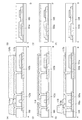
図1に、本実施の形態の半導体装置を示す。図1(A)は平面図であり、図1(B)は図1(A)におけるA−Bで切断した断面図である。 FIG. 1 shows a semiconductor device of the present embodiment. 1A is a plan view, and FIG. 1B is a cross-sectional view taken along line AB in FIG. 1A.
図1(A)に示す半導体装置は、1の方向に配置されたゲート配線及び容量配線と、ゲート配線及び容量配線と交差する2の方向に配置されたソース配線と、ゲート配線とソース配線の交差部付近のトランジスタ150aを有する画素部を含んでいる。なお、本明細書において、画素部とは、複数のゲート配線及び複数のソース配線に囲まれた領域のことを指す。
A semiconductor device illustrated in FIG. 1A includes a gate wiring and a capacitor wiring arranged in one direction, a source wiring arranged in two directions intersecting the gate wiring and the capacitor wiring, a gate wiring and a source wiring. It includes a pixel portion having a
図1に示すトランジスタ150aは、絶縁表面を有する基板100上に、酸化物半導体層103aと、酸化物半導体層103aを覆うゲート絶縁膜104と、ゲート絶縁膜104上に設けられたゲート電極として機能する導電層109aと、酸化物半導体層103aと導電層109aを覆う絶縁膜112と、絶縁膜112上に設けられ、酸化物半導体層103aと電気的に接続され、ソース電極又はドレイン電極として機能する導電層117a、117bとで構成される、いわゆるトップゲート型のトランジスタである。
A
また、トランジスタ150aは、酸化物半導体層103a、ゲート電極として機能する導電層109aと、ソース電極又はドレイン電極として機能する導電層117a、117bを、透光性を有する材料で形成している。このように、トランジスタ150aに、酸化物半導体層103a、及びゲート電極、ソース電極及びドレイン電極を、透光性を有する材料で形成することにより、トランジスタが形成された部分においても光を透過させることができるため、画素の開口率を向上させることができる。
In the
また、トランジスタ150aのゲート電極と電気的に接続されるゲート配線は、透光性を有する導電層109aと、遮光性を有する導電層111aとの順で積層されており、トランジスタ150aのソース電極又はドレイン電極と電気的に接続されるソース配線は、透光性を有する導電層117aと、遮光性を有する導電層119aとの順で積層されている。つまり、トランジスタ150aのゲート電極は、ゲート配線を構成する透光性を有する導電層109aの一部で形成されており、ソース電極又はドレイン電極は、ソース配線を構成する透光性を有する導電層117aの一部で形成されている。
The gate wiring electrically connected to the gate electrode of the
ゲート配線及びソース配線を、透光性を有する導電層と遮光性を有する導電層との順で積層することにより、配線抵抗を低減し、消費電力を低減することができる。また、ゲート配線及びソース配線は、遮光性を有する導電層を用いて構成されているため、画素間を遮光することができる。つまり、行方向に配置されたゲート配線と、列方向に配置されたソース配線とによって、ブラックマトリクスを用いることなく画素間の隙間を遮光することができる。 By stacking the gate wiring and the source wiring in the order of a light-transmitting conductive layer and a light-blocking conductive layer, wiring resistance can be reduced and power consumption can be reduced. In addition, since the gate wiring and the source wiring are formed using a light-blocking conductive layer, light shielding can be performed between the pixels. That is, the gap between the pixels can be shielded from light without using a black matrix by the gate wiring arranged in the row direction and the source wiring arranged in the column direction.
また、ゲート配線と同じ1の方向に容量配線が配置されている。容量配線は、画素領域では、透光性を有する導電層109bで形成することが望ましいが、ソース配線と重なる領域では、透光性を有する導電層109bと、遮光性を有する導電層111bとの順で積層させてもよい。また、容量配線には、保持容量部151aが形成されている。保持容量部151aは、トランジスタ150aのソース電極又はドレイン電極のいずれか一方に接続されている。保持容量部151aは、ゲート絶縁膜104と絶縁膜112を誘電体として、電極として機能する酸化物半導体層103bと導電層109bと導電層117bとで構成されている。
Further, the capacitor wiring is arranged in the same direction as the gate wiring. The capacitor wiring is preferably formed using a light-transmitting
本実施の形態では、容量配線の幅とゲート配線の幅が同じになるように形成する例を示すが、容量配線の幅とゲート配線の幅が異なるように形成してもよい。容量配線の幅は、ゲート配線の幅よりも広くすることが好ましい。容量配線の幅を広くすることにより、保持容量部151aの面積を大きくすることができる。
In this embodiment, an example in which the width of the capacitor wiring and the width of the gate wiring are the same is shown; however, the width of the capacitor wiring and the width of the gate wiring may be different. The width of the capacitor wiring is preferably larger than the width of the gate wiring. By increasing the width of the capacitor wiring, the area of the
このようにして、保持容量部151aを、酸化物半導体層103bと透光性を有する導電層109b、導電層117bとで構成することにより、保持容量部151aが形成された部分においても光を透過させることができるため、開口率を向上させることができる。また、保持容量部151aを、透光性を有する導電層で構成することにより、開口率を下げることなく保持容量部151aを大きくすることができるため、トランジスタがオフになったときでも、画素電極の電位保持特性が向上し、表示品質が向上する。また、フィードスルー電位を小さくすることができる。
In this manner, the
また、図1(A)に示すトランジスタ150aは、液晶表示装置またはEL表示装置に代表される発光表示装置の画素部に設けられる画素トランジスタに適用することができる。そのため、図示した例では、絶縁膜120にコンタクトホール126が設けられ、絶縁膜120上に画素電極層(透光性を有する導電層122b)が設けられ、絶縁膜120に設けられたコンタクトホール126を介して、画素電極層(透光性を有する導電層122b)と、導電層117bと、が接続されている。
In addition, the
次に、半導体装置の作製工程の一例について、図2乃至図5を用いて説明する。 Next, an example of a manufacturing process of the semiconductor device will be described with reference to FIGS.
はじめに、絶縁表面を有する基板100上に酸化物半導体膜101を形成する(図2(A)、(B)参照)。
First, the
絶縁表面を有する基板100としては、例えば、液晶表示装置などに使用される可視光透過性を有するガラス基板を用いることができる。上記のガラス基板は無アルカリガラス基板であることが好ましい。無アルカリガラス基板には、例えば、アルミノシリケートガラス、アルミノホウケイ酸ガラス、バリウムホウケイ酸ガラスなどのガラス材料が用いられている。他にも、絶縁表面を有する基板100として、セラミック基板、石英基板やサファイア基板などの絶縁体でなる絶縁性基板、珪素などの半導体材料でなる半導体基板の表面を絶縁材料で被覆したもの、金属やステンレスなどの導電体でなる導電性基板の表面を絶縁材料で被覆したもの、などを用いることができる。
As the
絶縁表面を有する基板100上に下地膜となる絶縁膜を設けてもよい。絶縁膜は、基板100からのアルカリ金属(Li、Cs、Na等)やアルカリ土類金属(Ca、Mg等)や他の金属元素などの不純物の拡散を防止する機能を有する。なお、Naは、5×10¹⁹/cm3以下、好ましくは1×1018/cm3以下とする。絶縁膜は、窒化シリコン膜、酸化シリコン膜、窒化酸化シリコン膜、酸化窒化シリコン膜、酸化アルミニウム膜、窒化アルミニウム膜、酸化窒化アルミニウム膜、窒化酸化アルミニウム膜から選ばれた一または複数の膜による積層構造により形成することができる。
An insulating film serving as a base film may be provided over the
酸化物半導体膜101は、In−Ga−Zn−O系非単結晶膜で形成することができる。例えば、In、Ga、及びZnを含む酸化物半導体ターゲット(In2O3:Ga2O3:ZnO=1:1:1)を用いたスパッタ法で、酸化物半導体膜101を形成する。スパッタの条件としては、例えば、基板100とターゲットとの距離を30mm〜500mm、圧力を0.1Pa〜2.0Pa、直流(DC)電源を0.25kW〜5.0kW(直径8インチのターゲット使用時)、雰囲気をアルゴン雰囲気、酸素雰囲気、又はアルゴンと酸素との混合雰囲気とすることができる。なお、酸化物半導体膜として、ZnO系非単結晶膜も用いることができる。また、酸化物半導体膜101の膜厚は、5nm〜200nm程度とすればよい。
The
上記のスパッタ法としては、スパッタ用電源に高周波電源を用いるRFスパッタ法や、DCスパッタ法、パルス的に直流バイアスを加えるパルスDCスパッタ法などを用いることができる。RFスパッタ法は主に、絶縁膜を成膜する場合に用いられ、DCスパッタ法は主に、金属膜を成膜する場合に用いられる。 As the sputtering method, an RF sputtering method using a high frequency power source as a sputtering power source, a DC sputtering method, a pulse DC sputtering method in which a direct current bias is applied in a pulsed manner, or the like can be used. The RF sputtering method is mainly used when an insulating film is formed, and the DC sputtering method is mainly used when a metal film is formed.
なお、絶縁膜を形成した場合、酸化物半導体膜101を形成する前に、絶縁膜の表面にプラズマ処理を行ってもよい。プラズマ処理を行うことにより、絶縁膜の表面に付着しているゴミを除去することができる。
Note that in the case where an insulating film is formed, plasma treatment may be performed on the surface of the insulating film before the
パルス直流(DC)電源を用いると、ごみが軽減でき、膜厚分布も均一となるため好ましい。また、上述したプラズマ処理を行った後、大気に曝すことなく酸化物半導体膜101を形成することにより、絶縁膜と酸化物半導体膜101の界面にゴミや水分が付着することを抑制することができる。
A pulse direct current (DC) power supply is preferable because dust can be reduced and the film thickness can be uniform. In addition, after the above plasma treatment is performed, the
また、材料の異なるターゲットを複数設置できる多元スパッタ装置を用いてもよい。多元スパッタ装置では、同一チャンバーで異なる膜を積層形成することも、同一チャンバーで複数種類の材料を同時にスパッタして一の膜を形成することもできる。さらに、チャンバー内部に磁界発生機構を備えたマグネトロンスパッタ装置を用いる方法(マグネトロンスパッタ法)や、マイクロ波を用いて発生させたプラズマを用いるECRスパッタ法等を用いてもよい。また、成膜中にターゲット物質とスパッタガス成分とを化学反応させてそれらの化合物を形成するリアクティブスパッタ法や、成膜中に基板にも電圧をかけるバイアススパッタ法等を用いてもよい。 Further, a multi-source sputtering apparatus that can install a plurality of targets made of different materials may be used. In the multi-source sputtering apparatus, different films can be stacked in the same chamber, or a single film can be formed by simultaneously sputtering a plurality of types of materials in the same chamber. Further, a method using a magnetron sputtering apparatus provided with a magnetic field generation mechanism inside the chamber (magnetron sputtering method), an ECR sputtering method using plasma generated using microwaves, or the like may be used. Alternatively, a reactive sputtering method in which a target material and a sputtering gas component are chemically reacted during film formation to form a compound thereof, a bias sputtering method in which a voltage is applied to the substrate during film formation, or the like may be used.
次に、酸化物半導体膜101上にレジストマスク102a、102bを形成し、当該レジストマスク102a、102bを用いて酸化物半導体膜101を選択的にエッチングして、島状の酸化物半導体層103a、103bを形成する(図2(C)、(D)参照)。レジストマスクの形成にスピンコート法を用いる場合、レジスト膜の均一性の向上のため、大量のレジスト材料や、大量の現像液が使用され、余分な材料の消費量が多い。特に基板が大型化すると、スピンコート法を用いる成膜方法では、大型の基板を回転させる機構が大規模となる点、材料液のロス及び廃液量が多い点で、大量生産上不利である。また、矩形の基板をスピンコートさせると回転軸を中心とする円形のムラが塗布膜に生じやすい。そこで、インクジェット法などの液滴吐出法やスクリーン印刷法などを用いて選択的にレジスト材料膜を形成し、露光を行ってレジストマスクを形成することが好ましい。選択的にレジスト材料膜を形成することによって、レジスト材料の使用量の削減が図れるため大幅なコストダウンが実現でき、1000mm×1200mm、1100mm×1250mm、1150mm×1300mmのような大面積基板にも対応できる。
Next, resist
この際のエッチング方法としてウエットエッチングまたはドライエッチングを用いることができる。ここでは、酢酸と硝酸と燐酸との混合液を用いたウエットエッチングにより、酸化物半導体膜101の不要な部分を除去して、島状の酸化物半導体層103a、103bを形成する。なお、上記エッチングの後にはレジストマスク102a、102bは除去する。また、ウエットエッチングに用いるエッチャントは酸化物半導体膜101をエッチングできるものであればよく、上述したものに限られない。ドライエッチングを行う場合は、塩素を含有するガス、又は塩素を含有するガスに酸素が添加されたガスを用いることが好ましい。塩素と酸素を含有するガスを用いることで、下地膜として機能する絶縁膜と、酸化物半導体膜101とのエッチング選択比がとりやすく、絶縁膜へのダメージを十分に低減できるためである。
As an etching method at this time, wet etching or dry etching can be used. Here, unnecessary portions of the
また、ドライエッチングに用いるエッチング装置としては、反応性イオンエッチング法(RIE法)を用いたエッチング装置や、ECR(Electron Cyclotron Resonance)やICP(Inductively Coupled Plasma)などの高密度プラズマ源を用いたドライエッチング装置を用いることができる。また、ICPエッチング装置と比べて広い面積に渡って一様な放電が得られやすいドライエッチング装置としては、上部電極を接地させ、下部電極に13.56MHzの高周波電源を接続し、さらに下部電極に3.2MHzの低周波電源を接地したECCP(Enhanced Capacitively Coupled Plasma)モードのエッチング装置がある。このECCPモードのエッチング装置であれば、例えば基板として第10世代の一辺が3mを超えるサイズの基板を用いる場合にも対応することができる。 As an etching apparatus used for dry etching, an etching apparatus using a reactive ion etching method (RIE method) or a dry method using a high-density plasma source such as ECR (Electron Cyclotron Resonance) or ICP (Inductively Coupled Plasma). An etching apparatus can be used. In addition, as a dry etching apparatus in which uniform discharge can be easily obtained over a wide area compared with the ICP etching apparatus, the upper electrode is grounded, a 13.56 MHz high frequency power source is connected to the lower electrode, and the lower electrode is further connected to the lower electrode. There is an ECCP (Enhanced Capacitively Coupled Plasma) mode etching apparatus in which a low-frequency power source of 3.2 MHz is grounded. This ECCP mode etching apparatus can cope with, for example, the case where a substrate having a size of one side of the 10th generation exceeding 3 m is used as the substrate.
その後、200℃〜600℃、代表的には300℃〜500℃の熱処理を行うと良い。ここでは、窒素雰囲気下で350℃、1時間の熱処理を行う。この熱処理により酸化物半導体層103a、103bを構成するIn−Ga−Zn−O系酸化物半導体の原子レベルの再配列が行われる。この熱処理(光アニール等も含む)は、酸化物半導体層103a、103b中におけるキャリアの移動を阻害する歪みを解放できる点で重要である。なお、上記の熱処理を行うタイミングは、酸化物半導体層103a、103bの形成後であれば特に限定されない。
Thereafter, heat treatment is performed at 200 ° C. to 600 ° C., typically 300 ° C. to 500 ° C. Here, heat treatment is performed at 350 ° C. for one hour in a nitrogen atmosphere. Through this heat treatment, rearrangement at the atomic level of the In—Ga—Zn—O-based oxide semiconductor included in the
次に、島状の酸化物半導体層103a、103b上にゲート絶縁膜104を形成した後、ゲート絶縁膜104上に、導電膜105を形成する(図2(E)、(F)参照)。
Next, after the
ゲート絶縁膜104は、酸化シリコン膜、酸化窒化シリコン膜、窒化シリコン膜、窒化酸化シリコン膜、酸化アルミニウム膜、窒化アルミニウム膜、酸化窒化アルミニウム膜、窒化酸化アルミニウム膜、又は酸化タンタル膜の単層または積層で設けることができる。ゲート絶縁膜104は、スパッタ法等を用いて膜厚を50nm以上250nm以下で形成することができる。例えば、ゲート絶縁膜104として、スパッタ法により酸化シリコン膜を100nmの厚さで形成することができる。または、スパッタ法により酸化アルミニウム膜を100nmの厚さで形成することができる。なお、ゲート絶縁膜104は、透光性を有していることが好ましい。
The
ゲート絶縁膜104を緻密な膜で形成することにより、基板100側から酸化物半導体層103a、103bに水分や酸素が侵入することを防止することができる。また、基板100に含まれるアルカリ金属(Li、Cs、Na等)やアルカリ土類金属(Ca、Mg等)や他の金属元素などの不純物が酸化物半導体層に侵入することを防止することができる。なお、Naは、5×10¹⁹/cm3以下、好ましくは1×1018/cm3以下とする。したがって、酸化物半導体を用いた半導体装置の半導体特性の変動を抑制することができる。また、半導体装置の信頼性を向上させることができる。
By forming the
導電膜105は、インジウム錫酸化物(Indium Tin Oxide:ITO)、酸化珪素を含むインジウム錫酸化物(ITSO)、有機インジウム、有機スズ、酸化亜鉛(ZnO)、窒化チタン等を用いることができる。また、酸化亜鉛を含むインジウム亜鉛酸化物(Indium Zinc Oxide:IZO)、酸化亜鉛にガリウム(Ga)をドープしたもの、酸化スズ(SnO2)、酸化タングステンを含むインジウム酸化物、酸化タングステンを含むインジウム亜鉛酸化物、酸化チタンを含むインジウム酸化物、酸化チタンを含むインジウム錫酸化物なども用いてもよい。これらの材料をスパッタリング法により、単層構造又は積層構造で形成することができる。ただし、積層構造とする場合には、複数の膜の全ての光透過率が十分に高いことが望ましい。
As the
次に、導電膜105上にレジストマスク107a、107bを形成し、当該レジストマスク107a、107bを用いて導電膜105を選択的にエッチングして、導電層109a、109bを形成する(図2(G)、(H)参照)。なお、上記エッチングの後にはレジストマスク107a、107bは除去する。この際、後に形成される絶縁膜112の被覆性を向上し、段切れを防止するために、ゲート電極の端部がテーパー形状となるようエッチングすることが好ましい。なお、ゲート電極にはゲート配線等、上記導電膜によって形成される電極や配線が含まれる。
Next, resist
次に、ゲート絶縁膜104、導電層109a、109b上に導電膜106を形成する(図3(A)、(B)参照)。
Next, the
導電膜106は、アルミニウム(Al)、タングステン(W)、チタン(Ti)、タンタル(Ta)、モリブデン(Mo)、ニッケル(Ni)、白金(Pt)、銅(Cu)、金(Au)、銀(Ag)、マンガン(Mn)、ネオジム(Nd)などの金属材料、またはこれらの金属材料を主成分とする合金材料、またはこれらの金属材料を成分とする窒化物を用いて、単層又は積層で形成することができる。アルミニウムなどの低抵抗導電性材料で形成することが望ましい。
The
導電膜105(又は導電層109a、109b)の上に導電膜106を形成した場合、両者の膜が反応を起こしてしまう場合がある。例えば、導電膜105にITOを用い、導電膜106にアルミニウムを用いた場合、化学反応が起きてしまう場合がある。したがって、化学反応が起きることを避けるために、導電膜105と導電膜106との間に、高融点材料を用いることが望ましい。例えば、高融点材料の例としては、モリブデン、チタン、タングステン、タンタル、クロムなどがあげられる。そして、高融点材料を用いた膜の上に、導電率の高い材料を用いて、導電膜106を多層膜とすることは、好適である。導電率の高い材料としては、アルミニウム、銅、銀などがあげられる。例えば、導電膜106を積層構造で形成する場合には、1層目をモリブデン、2層目をアルミニウム、3層目をモリブデンの積層、若しくは、1層目をモリブデン、2層目にネオジムを微量に含むアルミニウム、3層目をモリブデンの積層で形成することができる。
In the case where the
次に、導電膜106上にレジストマスク110を形成し、当該レジストマスク110を用いて導電膜106をエッチングする(図3(C)、(D)参照)。上記エッチングの後にはレジストマスク110は除去する。その結果、導電膜106は、レジストマスク110が形成されている部分を残して除去され、導電層109aが露出する。これにより、導電層111aと導電層109aとは、それぞれの層が有する表面積が異なる。つまり、導電層109aが有する表面積は、導電層111aが有する表面積よりも大きい。または、導電層111aと導電層109aとは、導電層111aと導電層109aとが重なった領域と、導電層111aと導電層109aとが重なっていない領域とを有する。
Next, a resist
少なくとも遮光性を有する導電層111aがある領域では、ゲート配線として機能し、透光性を有する導電層109aがある領域では、ゲート電極として機能する。ゲート電極として機能する導電層109aを、透光性を有する材料で形成することにより、ゲート電極が形成された部分においても光を透過させることができるため、画素の開口率を向上させることができる。また、ゲート配線として機能する導電層111aを、遮光性を有する導電層で形成することにより、配線抵抗を低減し、消費電力を低減することができる。また、ゲート配線は、遮光性を有する導電層を用いて構成されているため、画素間を遮光することができる。また、コントラストを向上させることができる。
It functions as a gate wiring in a region where there is at least a light-blocking
なお、導電層109a、109bを形成した後、遮光性を有する導電層111aを形成する工程について説明したが、形成する順番を逆としてもよい。つまり、ゲート配線として機能する遮光性を有する導電層111aを形成した後に、ゲート電極として機能する透光性を有する導電層109a、109bを形成することもできる(図8(A)、(C)参照)。
Note that although the step of forming the light-blocking
また、図3(C)、(D)に示すように、ゲート配線と同じ方向に容量配線が配置されている。容量配線は、画素領域では、透光性を有する導電層109bで形成することが望ましいが、後に形成されるソース配線と重なる領域では、透光性を有する導電層109bと、遮光性を有する導電層111bとの順で積層させてもよい(図1(A)参照)。このような構成とすることにより、抵抗を下げることができる。
Further, as shown in FIGS. 3C and 3D, the capacitor wiring is arranged in the same direction as the gate wiring. The capacitor wiring is preferably formed using a light-transmitting
本実施の形態では、容量配線の幅とゲート配線の幅が同じになるように形成する例を示すが、容量配線の幅とゲート配線の幅が異なるように形成してもよい。容量配線の幅は、ゲート配線の幅よりも広くすることが好ましい。保持容量部151aの表面積を大きくすることができる。
In this embodiment, an example in which the width of the capacitor wiring and the width of the gate wiring are the same is shown; however, the width of the capacitor wiring and the width of the gate wiring may be different. The width of the capacitor wiring is preferably larger than the width of the gate wiring. The surface area of the
なお、酸化物半導体層103a、103bの形成後、ゲート絶縁膜104の形成後、ゲート電極の形成後のいずれかにおいて、酸化物半導体層103a、103bの一部の領域又は全部の領域の導電率を高める処理を行ってもよい。例えば、導電率を高める処理として、水素化処理などが挙げられる。水素を含んだ窒化珪素を酸化物半導体層103bの上層に配置し、熱を加えることにより、酸化物半導体層の水素化処理を行うことができる。または、水素雰囲気中で熱を加えることにより、水素化することも可能である。また、図6に示すように、酸化物半導体層103aのチャネル形成領域と重なる領域に、チャネル保護層127を形成することにより、酸化物半導体層103aに、選択的に導電率が高められた領域を形成することができる。
Note that the conductivity of some or all of the regions of the
チャネル保護層127は、酸化珪素で形成されることが望ましい。これにより、酸化物半導体層103aのチャネル部に、水素が入ることを低減することができる。なお、チャネル保護層127は、導電率を高める処理を行った後、除去してもよい。または、チャネル保護層127は、レジストで形成することも可能である。その場合は、水素化処理の後、レジストを除去することが好ましい。このように、酸化物半導体層103a、103bに対し、導電率を高める処理を行うことにより、トランジスタの電流を流れやすくし、容量素子の電極の抵抗を下げることができる。
The channel protective layer 127 is preferably formed of silicon oxide. Accordingly, entry of hydrogen into the channel portion of the
図6において、チャネル保護層127は、酸化物半導体層103aに接して設ける例を示したが、ゲート絶縁膜104上に設けてもよい。また、チャネル保護層127と、ゲート電極として機能する導電層109aの形を調整して、導電層109aよりもチャネル保護層127の方を大きくすることにより、オフセット領域を形成することができる。
In FIG. 6, the channel protective layer 127 is provided in contact with the
次に、導電層109a、109b、ゲート絶縁膜104を覆うように層間絶縁膜として機能する絶縁膜112を形成した後、絶縁膜112に酸化物半導体層に達するコンタクトホールを形成し、酸化物半導体層の表面の一部を露出させる(図3(E)、(F)参照)。
Next, after forming the insulating
絶縁膜112は、酸化珪素、窒化珪素、酸化窒化珪素、窒化酸化珪素等の酸素又は窒素を有する絶縁膜、DLC(ダイヤモンドライクカーボン)等の炭素を含む膜や、エポキシ、ポリイミド、ポリアミド、ポリビニルフェノール、ベンゾシクロブテン、アクリル等の有機材料またはシロキサン樹脂等のシロキサン材料からなる膜を単層又は積層構造で設けることができる。なお、絶縁膜112は、透光性を有していることが好ましい。
The insulating
次に、絶縁膜112上に、導電膜113を形成する(図3(G)、(H)参照)。
Next, a
導電膜113は、導電膜105を形成した材料と概ね同じ材料で形成されることが望ましい。概ね同じ材料とは、主成分の元素が同じ材料のことであり、不純物レベルでは、含まれる元素の種類や濃度などが異なっている場合がある。このように、概ね同じ材料を用いることにより、スパッタや蒸着などで導電膜113を形成する場合、導電膜105と材料を共有できるというメリットがある。材料を共有できることにより、同じ製造装置を用いることができ、製造工程をスムーズに流すことができ、スループットを向上させることが可能となり、低コスト化を実現することが可能となる。
The
次に、導電膜113上にレジストマスク115a、115bを形成し、当該レジストマスク115a、115bを用いて導電膜113を選択的にエッチングして、導電層117a、及び導電層117bを形成する(図4(A)、(B)参照)。なお、上記エッチングの後にはレジストマスク115a、115bは除去する。
Next, resist
次に、導電層117a、117b、絶縁膜112上に導電膜114を形成する(図4(C)、(D)参照)。
Next, a
導電膜114は、アルミニウム(Al)、タングステン(W)、チタン(Ti)、タンタル(Ta)、モリブデン(Mo)、ニッケル(Ni)、白金(Pt)、銅(Cu)、金(Au)、銀(Ag)、マンガン(Mn)、ネオジム(Nd)などの金属材料、またはこれらの金属材料を主成分とする合金材料、またはこれらの金属材料を成分とする窒化物を用いて、単層又は積層で形成することができる。アルミニウムなどの低抵抗導電性材料で形成することが望ましい。
The
また、導電膜114は、導電膜106を形成した材料とは異なる材料で形成されることが望ましい。または、導電膜114は、導電膜106とは異なる積層構造で形成されることが望ましい。なぜなら、半導体装置の作製工程において、加えられる温度が導電膜114と導電膜106とでは異なる場合が多いからである。通常、導電膜106の方が、高温な状態になることが多い。したがって、導電膜106の方が融点の高い材料または積層構造を用いることが望ましい。または、導電膜106の方が、ヒロックがおきにくい材料または積層構造を用いることが望ましい。または、導電膜114は、映像信号が供給される信号線を構成する場合があるため、導電膜106よりも配線抵抗が小さい材料又は積層構造を用いることが望ましい。
In addition, the
導電膜105(又は導電層109a、109b)の上に導電膜106を形成した場合と同様に、導電膜113(又は、導電層117a、117b)の上に導電膜114を形成した場合、両者の膜が反応を起こしてしまう場合がある。したがって、導電膜113上に導電膜114を形成する場合においても、導電膜113と導電膜114との間に、高融点材料を用いることが望ましい。例えば、高融点材料の例としては、モリブデン、チタン、タングステン、タンタル、クロムなどがあげられる。そして、高融点材料を用いた膜の上に、導電率の高い材料を用いて、導電膜114を多層膜で形成することは、好適である。導電率の高い材料としては、アルミニウム、銅、銀などがあげられる。
Similarly to the case where the
次に、導電膜114上にレジストマスク118を形成し、当該レジストマスク118を用いて導電膜114をエッチングする(図4(E)、(F)参照)。上記エッチングの後にはレジストマスク118は除去する。その結果、導電膜114は、レジストマスク118が形成されている部分を残して除去され、導電層117aが露出する。これにより、導電層119aと導電層117aとは、それぞれの層が有する表面積が異なる。つまり、導電層117aが有する表面積は、導電層119aが有する表面積よりも大きい。または、導電層119aと117aとは、導電層119aと導電層117aとが重なった領域と、導電層119aと導電層117aとが重なっていない領域とを有する。
Next, a resist
少なくとも遮光性を有する導電層119aがある領域では、ソース配線として機能し、透光性を有する導電層117aがある領域では、ソース電極又はドレイン電極として機能する。ソース電極又はドレイン電極として機能する導電層117a、117bを、透光性を有する導電層で形成することにより、ソース電極又はドレイン電極が形成された部分においても光を透過させることができるため、画素の開口率を向上させることができる。また、ソース配線として機能する導電層119aを、遮光性を有する導電層で形成することにより、配線抵抗を低減し、消費電力を低減することができる。また、ソース配線は、遮光性を有する導電層119aを用いて構成されているため、画素間を遮光することができる。つまり、行方向に配置されたゲート配線と、列方向に配置されたソース配線とによって、ブラックマトリクスを用いることなく画素間の隙間を遮光することができる。
At least in a region where the
なお、導電層117a、117bを形成した後、遮光性を有する導電層119aを形成する工程について説明したが、形成する順番を逆としてもよい。つまり、ソース配線として機能する遮光性を有する導電層119aを形成した後に、ソース電極又はドレイン電極として機能する透光性を有する導電層109a、109bを形成することもできる(図8(A)、(B)参照)。
Note that although the step of forming the light-shielding
また、図4(E)、(F)において、導電層117bは、保持容量部151aの電極としても機能する。容量配線には、保持容量部151aが、ゲート絶縁膜104と絶縁膜112を誘電体として、電極として機能する酸化物半導体層103bと導電層109bと導電層117bとで構成される。このような構成とすることにより、抵抗を下げることができる。
4E and 4F, the
このようにして、保持容量部151aを、透光性を有する導電層で構成することにより、保持容量部151aが形成された部分においても光を透過させることができるため、開口率を向上させることができる。また、保持容量部151aを、透光性を有する材料で構成することにより、保持容量部151aを大きくすることもできるため、トランジスタがオフになったときでも、画素電極の電位保持特性が向上し、表示品質が向上する。また、フィードスルー電位を小さくすることができる。
In this manner, by forming the
以上により、トランジスタ150a、保持容量部151aを作製することができる。また、トランジスタ150a、保持容量部151aを、透光性を有する素子とすることができる。なお、酸化物半導体層103bを用いてゲート絶縁膜104を誘電体として、保持容量部を形成する場合には、導電層109bで形成する容量配線の電位は、対向電極の電位(コモン線の電位)よりも、高くしておくことが可能である。酸化物半導体層103bに電荷を誘起させることができ、酸化物半導体層103bが保持容量部の電極として機能しやすくすることができる。一方、酸化物半導体層103bを用いずに保持容量部を形成する場合、又は酸化物半導体層103bに水素化処理などにより、導電率を高める処理が行われている場合には、対向電極(共通電極)と同電位にしてもよい。これにより、配線の数を低減することができる。
Through the above steps, the
次に、絶縁膜120を形成した後、絶縁膜120上にレジストマスク(図示せず)を形成し、該レジストマスクを用いて、絶縁膜120をエッチングし、絶縁膜120にコンタクトホールを形成する(図5(A)、(B)参照)。絶縁膜120は、トランジスタ150a、保持容量部151a、又は配線などが形成された表面を平坦にする絶縁膜として機能することが可能である。トランジスタ150a、保持容量部151aを、透光性を有する素子として形成することができるため、それらが配置されている領域も、開口領域として利用することができる。そのため、トランジスタ150a、保持容量部151a、又は配線などによる凹凸を緩和して、これらの素子が形成された上部を平坦にすることは有益である。
Next, after the insulating
また、絶縁膜120は、不純物などからトランジスタ150aを保護する絶縁膜として機能することが可能である。絶縁膜120は、例えば、窒化珪素を有する膜で形成することができる。窒化珪素を有する膜は、不純物をブロッキングする効果が高いため好適である。または、絶縁膜120は、有機材料を有する膜で形成することができる。有機材料の例として、アクリル、ポリイミド、ポリアミドなどが好適である。これらの有機材料は、凹凸を平坦にする機能が高いため好適である。したがって、絶縁膜120を、窒化珪素を有する膜と、有機材料を有する膜とで積層構造とする場合には、下側に窒化珪素を有する膜を配置し、上側に有機材料を有する膜を配置することが好適である。なお、絶縁膜120を積層構造で形成する場合には、それぞれの膜の透光性が十分に高いことが望ましい。また、感光性材料も用いることができる。その場合には、絶縁膜120にエッチングを行い、コンタクトホールを形成することがなくなる。
The insulating
また、絶縁膜120は、カラーフィルタとしての機能を有することが可能である。基板100側にカラーフィルタを設けることにより、対向基板側にカラーフィルタを設ける必要がなくなり、2つの基板の位置を調整するためのマージンが必要なくなるため、パネルの製造を容易にすることができる。なお、絶縁膜120は、形成しなくてもよい。ソース電極、ソース配線と同じ層上に画素電極があってもよい。
The insulating
次に、絶縁膜120及びコンタクトホール上に導電膜121を形成する(図5(C)、(D)参照)。導電膜121は、導電膜105、導電膜113を形成した材料と概ね同じ材料を有して構成されることが望ましい。このように、概ね同じ材料を用いることにより、スパッタや蒸着などで導電膜121を形成する場合、導電膜105、導電膜113と材料を共有できるというメリットがある。材料を共有できることにより、同じ製造装置を用いることができ、製造工程をスムーズに流すことができ、スループットを向上させることが可能となり、低コスト化を実現することが可能となる。
Next, a
次に、導電膜121上にレジストマスク(図示せず)を形成し、該レジストマスクを用いて導電膜121を選択的にエッチングして、導電層122a、122bを形成する(図5(E)、(F)参照)。なお、上記エッチングの後にはレジストマスクは除去する。
Next, a resist mask (not shown) is formed over the
導電層122a、122bは、画素電極として機能させることができる。また、導電層122a、122bは、コンタクトホールを介して、ソース配線、ソース電極、ゲート配線、ゲート電極、画素電極、容量配線、保持容量部の電極などを互いに接続させることができる。したがって、導電層122a、122bは、導体と導体とを接続するための配線として機能させることができる。
The
以上により、半導体装置を作製することができる。本実施の形態で示す作製方法により、透光性を有するトランジスタ150a及び透光性を有する保持容量部151aを形成することができる。そのため、画素内に、トランジスタや保持容量部を配置する場合であっても、トランジスタや保持容量部が形成された部分においても光を透過させることができるため、開口率を向上させることができる。さらに、トランジスタと素子(例えば、別のトランジスタ)とを接続する配線は、抵抗率が低く導電率が高い材料を用いて形成することができるため、信号の波形なまりを低減し、配線抵抗による電圧降下を低減することができる。
Through the above steps, a semiconductor device can be manufactured. With the manufacturing method described in this embodiment, the light-transmitting
次に、半導体装置の他の一例について、図7を用いて説明する。なお、図7に示す半導体装置は、多くの部分で図1と共通している。したがって、以下においては、重複する部分は省略し、異なる点について説明する。また、図7(A)は、平面図であり、図7(B)は、図7(A)におけるA−Bで切断した断面図、図7(C)は、図7(A)におけるC−Dで切断した断面図である。 Next, another example of the semiconductor device is described with reference to FIGS. Note that the semiconductor device illustrated in FIG. 7 is common to FIG. Therefore, in the following, overlapping portions are omitted, and different points will be described. 7A is a plan view, FIG. 7B is a cross-sectional view taken along AB in FIG. 7A, and FIG. 7C is C in FIG. It is sectional drawing cut | disconnected by -D.
図1では、ゲート配線及びソース配線を、透光性を有する導電層上に遮光性を有する導電層との順で積層する例を示したが、遮光性を有する導電層と透光性を有する導電層との順で形成することもできる(図7参照)。ゲート電極として機能する透光性を有する導電層109aが、ゲート配線として機能する遮光性を有する導電層111aと接続されていればよい。ゲート配線と同様に、ソース電極又はドレイン電極として機能する透光性を有する導電層117aが、ソース配線として機能する遮光性を有する導電層119aと接続されていればよい。
Although FIG. 1 illustrates an example in which a gate wiring and a source wiring are stacked over a light-transmitting conductive layer in the order of a light-blocking conductive layer, the light-transmitting conductive layer and the light-transmitting layer are transparent. It can also be formed in order with the conductive layer (see FIG. 7). The light-transmitting
次に、半導体装置の他の一例について、図8を用いて説明する。なお、図8に示す半導体装置は、多くの部分で図1と共通している。したがって、以下においては、重複する部分は省略し、異なる点について説明する。また、図8(A)は、平面図であり、図8(B)は、図8(A)におけるA−Bで切断した断面図、図8(C)は、図8(A)におけるC−Dで切断した断面図である。 Next, another example of the semiconductor device is described with reference to FIGS. Note that the semiconductor device illustrated in FIG. 8 is common to FIG. Therefore, in the following, overlapping portions are omitted, and different points will be described. 8A is a plan view, FIG. 8B is a cross-sectional view cut along AB in FIG. 8A, and FIG. 8C is C in FIG. 8A. It is sectional drawing cut | disconnected by -D.
図1では、ゲート配線及びソース配線を、透光性を有する導電層と遮光性を有する導電層との順で積層する例を示したが、ゲート配線及びソース配線は、遮光性を有する導電層で形成することもできる(図8参照)。ゲート電極として機能する透光性を有する導電層109aと、ゲート配線として機能する遮光性を有する導電層111aとが接続されていればよい。ゲート配線と同様に、ソース電極又はドレイン電極として機能する透光性を有する導電層117aと、ソース配線として機能する遮光性を有する導電層119aとが接続されていればよい。
Although FIG. 1 illustrates an example in which a gate wiring and a source wiring are stacked in the order of a light-transmitting conductive layer and a light-blocking conductive layer, the gate wiring and the source wiring are light-blocking conductive layers. (See FIG. 8). It is only necessary that the light-transmitting
また、ゲート配線上にトランジスタを作製する場合、トランジスタの大きさは、トランジスタのゲート配線幅に依存するが、本実施の形態では、画素内にトランジスタを形成することができるため、トランジスタを大きく形成することができる。例えば、図9に示すように、ゲート配線幅よりもトランジスタのチャネル幅Wの方が長い、又はチャネル長Lの方が長いトランジスタを作製することができる。トランジスタを大きくすることにより、その電流能力を十分上げることができ、画素への信号書き込み時間を短縮することができる。または、オフ電流を低減することができ、ちらつきなどを低減することができる。よって、高精細な表示装置を提供することができる。 In the case where a transistor is formed over a gate wiring, the size of the transistor depends on the width of the gate wiring of the transistor; however, in this embodiment mode, the transistor can be formed in the pixel; can do. For example, as illustrated in FIG. 9, a transistor having a longer channel width W or a longer channel length L than a gate wiring width can be manufactured. By increasing the size of the transistor, the current capability can be sufficiently increased, and the signal writing time to the pixel can be shortened. Alternatively, off-state current can be reduced and flicker or the like can be reduced. Therefore, a high-definition display device can be provided.
なお、画素構成は、図1に限定されない。例えば、図10に示すように、容量配線を設けず、画素電極を隣り合う画素のゲート配線と絶縁膜、ゲート絶縁膜を介して重ねて保持容量を設けることができる。 Note that the pixel configuration is not limited to FIG. For example, as illustrated in FIG. 10, a storage capacitor can be provided by overlapping a pixel electrode with a gate wiring and an insulating film and a gate insulating film of an adjacent pixel without providing a capacitor wiring.
次に、半導体装置の他の一例について、図11を用いて説明する。なお、図11に示す半導体装置は、多くの部分で図1と共通している。したがって、以下においては、重複する部分は省略し、異なる点について説明する。また、図11(A)は、平面図であり、図11(B)は、図11(A)におけるA−Bで切断した断面図である。 Next, another example of the semiconductor device is described with reference to FIGS. Note that the semiconductor device illustrated in FIG. 11 is common to FIG. Therefore, in the following, overlapping portions are omitted, and different points will be described. 11A is a plan view, and FIG. 11B is a cross-sectional view taken along line AB in FIG. 11A.
図11の図1と異なる点は、保持容量部151cの電極として、酸化物半導体層を用いずに、容量配線を構成する透光性を有する導電層109cと、ソース電極又はドレイン電極として機能する導電層117cとを用いている点にある。そのため、容量配線は、対向電極と同じ電位とすることができる。また、保持容量部151cに、酸化物半導体層を用いていないため、容量値が小さくなってしまうので、図11に示す導電層109cと導電層117cの表面積を図1に示す導電層109bと導電層117bよりも大きくすることが好ましい。保持容量部151cの大きさは、画素ピッチの7割以上、又は8割以上とすることが好ましい。また、画素電極のコンタクトを導電層117c上の導電層119b上でとることとしている。以下、図1で示した構成と同様であるため、詳細な説明は省略する。
11 differs from FIG. 1 in that the
このような構成とすることにより、光透過率の高い保持容量部151cを大きく形成することができる。保持容量部151cを大きくすることによって、トランジスタがオフになったときでも、画素電極の電位保持特性が向上し、表示品質が向上する。また、フィードスルー電位を小さくすることができる。また、保持容量部151cを大きく形成した場合であっても、保持容量部151cが形成された部分においても光を透過させることができるため、開口率を高めることができ、消費電力を低減することができる。また、画素電極のコンタクトホールによる凹凸で、液晶の配向乱れがあったとしても、遮光性を有する導電層119bにより、光漏れを防止することができる。
With such a configuration, a large
次に、半導体装置の他の一例について、図12を用いて説明する。なお、図12に示す半導体装置は、多くの部分で図1と共通している。したがって、以下においては、重複する部分は省略し、異なる点について説明する。また、図12は、平面図である。 Next, another example of the semiconductor device is described with reference to FIGS. Note that the semiconductor device illustrated in FIG. 12 is common to FIG. Therefore, in the following, overlapping portions are omitted, and different points will be described. FIG. 12 is a plan view.
図12に、画素の構成の一例としてEL表示装置の例を示す。図12に示す画素は、導電層109aと導電層111aの順で積層されるゲート配線と、導電層117a、119aの順で積層されるソース配線と、スイッチング用のトランジスタ150a、駆動用のトランジスタ150c、保持容量部151d、導電層117eと導電層119cの順で積層される電源線を有している。
FIG. 12 illustrates an example of an EL display device as an example of a pixel structure. 12 includes a gate wiring layered in the order of the
図12に示すトランジスタ150aは、図1(B)に示すトランジスタ150aと同様であり、絶縁表面を有する基板上に、酸化物半導体層103aと、酸化物半導体層103aを覆うゲート絶縁膜と、ゲート絶縁膜上に設けられたゲート電極として機能する導電層109aと、酸化物半導体層103aと導電層109aを覆う絶縁膜と、絶縁膜上に設けられ、酸化物半導体層103aと電気的に接続され、ソース電極又はドレイン電極として機能する導電層117a、117bとで構成されている。また、駆動用のトランジスタ150cは、絶縁表面を有する基板上に酸化物半導体層103c、酸化物半導体層103cを覆うゲート絶縁膜と、ゲート絶縁膜上に設けられたゲート電極として機能する導電層109dと、酸化物半導体層103cと導電層109dを覆う絶縁膜112と、絶縁膜112上に設けられ、酸化物半導体層103cと電気的に接続され、ソース電極又はドレイン電極として機能する導電層117e、117fとを有している。保持容量部151dは、ゲート絶縁膜と絶縁膜を誘電体として、電極として機能する酸化物半導体層103dと導電層109dと導電層117eとで構成されている。
A
図12に示す半導体装置は、スイッチング用のトランジスタ150a、駆動用のトランジスタ150cの2つのトランジスタを有する場合について説明したが、1つの画素に3つ以上のトランジスタを設けることもできる。
Although the semiconductor device illustrated in FIG. 12 has been described with respect to the case where the switching
このように、1画素中に、2つ以上のトランジスタを設ける場合であっても、トランジスタが形成された部分において光を透過させることができるため、開口率を高めることができる。 In this manner, even when two or more transistors are provided in one pixel, light can be transmitted through a portion where the transistors are formed, so that the aperture ratio can be increased.
なお、保護回路やゲートドライバやソースドライバなどの周辺駆動回路部分では、トランジスタ部分で光が透過する必要がない。よって、画素部はトランジスタや容量素子を、透光性を有する材料で形成して、周辺駆動回路部分のトランジスタは、遮光性を有する材料で形成してもよい。 Note that light does not need to be transmitted through the transistor portion in the peripheral driver circuit portions such as the protection circuit, the gate driver, and the source driver. Therefore, the pixel portion may be formed of a transistor or a capacitor with a light-transmitting material, and the transistor in the peripheral driver circuit portion may be formed with a light-blocking material.
本実施の形態は、他の実施の形態と適宜組み合わせて用いることができる。 This embodiment can be combined with any of the other embodiments as appropriate.
(実施の形態2)
本実施の形態では、半導体装置の作製工程の一例について図13乃至図22を用いて説明する。なお、本実施の形態における半導体装置及びその作製工程は、多くの部分で実施の形態1と共通している。したがって、以下においては、重複する部分は省略し、異なる点について詳細に説明する。
(Embodiment 2)
In this embodiment, an example of a manufacturing process of a semiconductor device will be described with reference to FIGS. Note that the semiconductor device and its manufacturing process in this embodiment mode are common to those in
図13に、本実施の形態の半導体装置を示す。図13(A)は、平面図であり、図13(B)は、図13(A)におけるA−Bで切断した断面図である。 FIG. 13 shows the semiconductor device of this embodiment. FIG. 13A is a plan view, and FIG. 13B is a cross-sectional view taken along line AB in FIG. 13A.
図13と図1との異なる点は、図1において、トランジスタ150a用の酸化物半導体層103aと、保持容量部151a用の酸化物半導体層103bを形成したのに対して、図13では、トランジスタ250の酸化物半導体層と保持容量部251の酸化物半導体層を一つのアイランドにした点にある。
13 differs from FIG. 1 in that the
このような構成とすることにより、酸化物半導体層を形成するためのレイアウトが容易となる。また、コンタクトホールの数を低減することができるため、コンタクト抵抗を低減することができる。また、コンタクト不良を低減することができる。 With such a structure, a layout for forming the oxide semiconductor layer is facilitated. In addition, since the number of contact holes can be reduced, contact resistance can be reduced. Moreover, contact failure can be reduced.
次に、半導体装置の作製工程の一例について、図14乃至図19を用いて説明する。また、本実施の形態では、多階調マスクを用いて半導体装置を作製する場合について説明する。 Next, an example of a manufacturing process of the semiconductor device will be described with reference to FIGS. In this embodiment, the case where a semiconductor device is manufactured using a multi-tone mask is described.
はじめに、絶縁表面を有する基板200上に酸化物半導体層203a、203bを形成する(図14(A)、(B)参照)。
First,
基板200の材料、酸化物半導体層203a、203bの材料や作製方法については、実施の形態1に示す基板100、酸化物半導体層103a、103bを参照することができる。また、絶縁表面を有する基板200上に下地膜として機能する絶縁膜を設けてもよい。
For the material of the
次に、酸化物半導体層203a、203b上にゲート絶縁膜204、導電膜205、導電膜206を形成する(図14(C)、(D)参照)。
Next, the
ゲート絶縁膜204、導電膜205、導電膜206の材料及び作製方法については、実施の形態1に示すゲート絶縁膜104、導電膜105、導電膜106を参照することができる。
For materials and manufacturing methods of the
次に、導電膜206上にレジストマスク207a、207bを形成する。レジストマスク207a、207bは、多階調マスクを用いることにより、厚さの異なる領域を有するレジストマスクを形成することができる。多階調マスクを用いることで、使用するフォトマスクの枚数が低減され、作製工程が減少するため好ましい。本実施の形態において、導電膜205、206のパターンを形成する工程と、導電膜213、214のパターンを形成する工程において、多階調マスクを用いることができる。
Next, resist
多階調マスクとは、多段階の光量で露光を行うことが可能なマスクであり、代表的には、露光領域、半露光領域及び未露光領域の3段階の光量で露光を行う。多階調マスクを用いることで、一度の露光及び現像工程によって、複数(代表的には二種類)の厚さを有するレジストマスクを形成することができる。そのため、多階調マスクを用いることで、フォトマスクの枚数を削減することができる。 A multi-tone mask is a mask that can be exposed with multiple levels of light, and typically, exposure is performed with three levels of light: an exposed area, a half-exposed area, and an unexposed area. By using a multi-tone mask, a resist mask having a plurality of thicknesses (typically two types) can be formed by one exposure and development process. Therefore, the number of photomasks can be reduced by using a multi-tone mask.
図19(A−1)及び図19(B−1)は、代表的な多階調マスクの断面を示す。図19(A−1)には、グレートーンマスク403を示し、図19(B−1)にはハーフトーンマスク414を示す。
19A-1 and 19B-1 illustrate cross sections of typical multi-tone masks. FIG. 19A-1 shows a gray-
図19(A−1)に示すグレートーンマスク403は、透光性を有する基板400に遮光層により形成された遮光部401、及び遮光層のパターンにより設けられた回折格子部402で構成されている。
A gray-
回折格子部402は、露光に用いる光の解像度限界以下の間隔で設けられたスリット、ドット又はメッシュ等を有することで、光の透過率を制御する。なお、回折格子部402に設けられるスリット、ドット又はメッシュは周期的なものであってもよいし、非周期的なものであってもよい。
The
透光性を有する基板400としては、石英等を用いることができる。遮光部401及び回折格子部402を構成する遮光層は、金属膜を用いて形成すればよく、好ましくはクロム又は酸化クロム等により設けられる。
For the light-transmitting
グレートーンマスク403に露光するための光を照射した場合、図19(A−2)に示すように、遮光部401に重畳する領域における透光率は0%となり、遮光部401又は回折格子部402が設けられていない領域における透光率は100%となる。また、回折格子部402における透光率は、概ね10%〜70%の範囲であり、回折格子のスリット、ドット又はメッシュの間隔等により調節可能である。
When the
図19(B−1)に示すハーフトーンマスク414は、透光性を有する基板411上に半透光層により形成された半透光部412及び遮光層により形成された遮光部413で構成されている。
A
半透光部412は、MoSiN、MoSi、MoSiO、MoSiON、CrSi等の層を用いて形成することができる。遮光部413は、グレートーンマスクの遮光層と同様の金属膜を用いて形成すればよく、好ましくはクロム又は酸化クロム等により設けられる。
The
ハーフトーンマスク414に露光するための光を照射した場合、図19(B−2)に示すように、遮光部413に重畳する領域における透光率は0%となり、遮光部413又は半透光部412が設けられていない領域における透光率は100%となる。また、半透光部412における透光率は、概ね10%〜70%の範囲であり、形成する材料の種類又は形成する膜厚等により調整可能である。
When the exposure light is irradiated to the
多階調マスクを用いることにより、露光部分、中間露光部分、及び未露光部分の3つの露光レベルのマスクを形成することができ、一度の露光及び現像工程により、複数(代表的には二種類)の厚さの領域を有するレジストマスクを形成することができる。このため、多階調マスクを用いることで、フォトマスクの枚数を削減することができる。 By using a multi-tone mask, it is possible to form a mask with three exposure levels, an exposed portion, an intermediate exposed portion, and an unexposed portion. A plurality of (typically two types) masks can be formed by one exposure and development process. A resist mask having a region with a thickness of) can be formed. Therefore, the number of photomasks can be reduced by using a multi-tone mask.
図14(E)、(F)に示すハーフトーンマスクは、光を透過する基板300上に半透過層301a、301b及び遮光層301cで構成されている。したがって、導電膜206上には、後に保持容量部251の電極及びゲート電極となる箇所には、レジストマスク207a、207bが薄く形成され、後にゲート配線となる箇所にはレジストマスク207aが厚く形成される(14(E)、(F)参照)。
14E and 14F includes
レジストマスク207a、207bを用いて、導電膜205、206の不要な部分を選択的にエッチングして除去し、導電層208a、209a、導電層208b、209bを形成する(図15(A)、(B)参照)。
Using the resist
次に、レジストマスク207a、207bに対して、酸素プラズマによるアッシングを行う。レジストマスク207a、207bに対して酸素プラズマによるアッシングを行うことにより、レジストマスク207bは除去され、導電層208bが露出する。また、レジストマスク207aは縮小し、レジストマスク210として残存する(図15(C)、(D)参照)。このように、多階調マスクで形成したレジストマスクを用いることにより、追加のレジストマスクを用いることがなくなるため、工程を簡略化することができる。
Next, ashing using oxygen plasma is performed on the resist
次に、レジストマスク210を用いて、導電層208a、208bに対してエッチングする(図16(A)、(B)参照)。上記エッチングの後にはレジストマスク210は除去する。
その結果、導電層208bは除去され、導電層209bが露出する。また、導電層208aは、レジストマスク210が形成されている部分を残して除去され、導電層209aが露出する。これにより、導電層208aと導電層209aとは、それぞれの層が有する表面積が大きく異なる。つまり、導電層209aが有する表面積は、導電層208aが有する表面積よりも大きい。または、導電層208aと導電層209aとは、導電層208aと導電層209aとが重なった領域と、導電層208aと導電層209aとが重なっていない領域とを有する。
Next, the
As a result, the
少なくとも遮光性を有する導電層211aがある領域では、ゲート配線として機能し、透光性を有する導電層209aがある領域では、ゲート電極として機能する。ゲート電極として機能する導電層209aを、透光性を有する材料で形成することにより、画素の開口率を向上させることができる。また、ゲート配線として機能する導電層209aと導電層211aとを、透光性を有する導電層と遮光性を有する導電層との順で積層することにより、配線抵抗を低減し、消費電力を低減することができる。また、ゲート配線は、遮光性を有する導電層を用いて構成されているため、画素間を遮光することができる。
It functions as a gate wiring in a region where there is at least a light-blocking
また、ゲート配線と同じ方向に容量配線が配置されている。容量配線は、画素領域では、透光性を有する導電層209bで形成することが望ましいが、後に形成されるソース配線と重なる領域では、透光性を有する導電層209bと、遮光性を有する導電層211bとの順で積層させてもよい。
Further, the capacitor wiring is arranged in the same direction as the gate wiring. The capacitor wiring is preferably formed using a light-transmitting
このように、多階調マスクを用いることにより、1枚のマスクで、透光性を有する領域(光と透過率の高い領域)と、遮光性を有する領域(光透過率の低い領域)とを形成することができる。これにより、マスクを増加させることなく、透光性を有する領域(光透過率の高い領域)と、遮光性を有する領域(光透過率の低い領域)とを形成することができる。 In this manner, by using a multi-tone mask, a single mask can transmit a light-transmitting region (light and high transmittance region) and a light-blocking region (low light transmittance region). Can be formed. Accordingly, it is possible to form a light-transmitting region (a region with high light transmittance) and a light-blocking region (a region with low light transmittance) without increasing the mask.
次に、導電層209a、209b、ゲート絶縁膜204を覆うように層間絶縁膜として機能する絶縁膜212を形成した後、絶縁膜212に酸化物半導体層に達するコンタクトホールを形成し、酸化物半導体層の表面の一部を露出させる。絶縁膜212の材料及び作製方法については、実施の形態1に示す絶縁膜112を参照することができる。
Next, after forming the insulating
次に、絶縁膜212上に、導電膜213、導電膜214を形成する(図16(C)、(D)参照)。導電膜213、導電膜214の材料及び作製方法については、実施の形態1に示す導電膜113、導電膜114を参照することができる。
Next, a
次に、ハーフトーンマスクを用いて、導電膜214上にレジストマスク215a、215bを形成する(図17(A)、(B)参照)。ハーフトーンマスクは、光を透過する基板302上に半透過層303b及び遮光層303aで構成されている。したがって、導電膜214上には、後にソース電極又はドレイン電極なる箇所には、薄いレジストマスク215b、後に、ソース配線となる箇所には厚いレジストマスク215aが形成される。
Next, resist
レジストマスク215a、215bを用いて、導電膜213、214の不要な部分を選択的にエッチングして除去し、導電層216a、217a、導電層216b、217bを形成する(図17(C)、(D)参照)。
Using the resist
次に、レジストマスク215a、215bに対して、酸素プラズマによるアッシングを行う。レジストマスク215a、215bに対して酸素プラズマによるアッシングを行うことにより、レジストマスク215bは除去され、導電層217bが露出する。また、レジストマスク215aは縮小し、レジストマスク218として残存する。このように、多階調マスクで形成したレジストマスクを用いることにより、追加のレジストマスクを用いることがなくなるため、工程を簡略化することができる。
Next, ashing using oxygen plasma is performed on the resist
次に、レジストマスク218を用いて、導電層216a、216bに対してエッチングする(図18(A)、(B)参照)。その結果、導電層216bは除去され、導電層217bが露出する。また、導電層216aは、レジストマスク218が形成されている部分を残して除去され、導電層219aが形成される。これにより、導電層219aと導電層217aとは、それぞれの層が有する表面積が大きく異なる。つまり、導電層217aが有する表面積は、導電層219aが有する表面積よりも大きい。または、導電層219aと導電層217aとは、導電層219aと導電層217aとが重なった領域と、導電層219aと導電層217aとが重なっていない領域とを有する。なお、上記エッチングの後には、レジストマスク218は除去する。
Next, the
少なくとも遮光性を有する導電層219aがある領域では、ソース配線として機能し、透光性を有する導電層217aがある領域では、ソース電極又はドレイン電極として機能する。ソース電極又はドレイン電極として機能する導電層217a、217bを、透光性を有する導電層で形成することにより、画素の開口率を向上させることができる。また、ソース配線として機能する導電層217aと導電層219aとを、透光性を有する導電層と、遮光性を有する導電層との順で積層することにより、配線抵抗を低減し、消費電力を低減することができる。また、ソース配線は、遮光性を有する導電層219aを用いて構成されているため、画素間を遮光することができる。つまり、行方向に配置されたゲート配線と、列方向に配置されたソース配線とによって、ブラックマトリクスを用いることなく画素間の隙間を遮光することができる。
At least in a region where the
また、導電層217aは、保持容量部251の電極としても機能する。容量配線には、保持容量部251が、ゲート絶縁膜204と絶縁膜212を誘電体として、電極として機能する酸化物半導体層203aと導電層209bと導電層217bとで構成される。
The
このようにして、保持容量部251を、透光性を有する導電層で構成することにより、保持容量部251が形成された部分においても光を透過させることができるため、開口率を向上させることができる。また、保持容量部251を、透光性を有する材料で構成することにより、保持容量部251を大きくすることもできるため、トランジスタがオフになったときでも、画素電極の電位保持特性が向上し、表示品質が向上する。また、フィードスルー電位を小さくすることができる。
In this manner, by forming the
以上により、トランジスタ250、保持容量部251を作製することができる。また、トランジスタ250、保持容量部251を、透光性を有する素子とすることができる。
Through the above steps, the
次に、絶縁膜220を形成した後、絶縁膜220上にレジストマスク(図示せず)を形成し、該レジストマスクを用いて、絶縁膜220をエッチングし、絶縁膜220にコンタクトホールを形成する。次に、絶縁膜220及びコンタクトホール上に導電膜221を形成する。絶縁膜220、導電膜221の材料及び作製方法は、実施の形態1の絶縁膜120、導電膜121を参照することができる。なお、絶縁膜220は、形成しなくてもよい。ソース電極、ソース配線と同じ層上に画素電極があってもよい。
Next, after the insulating
次に、導電膜221上にレジストマスク(図示せず)を形成し、該レジストマスクを用いて導電膜221を選択的にエッチングして、導電膜222a、222bを形成する(図18(C)、(D)参照)。なお、上記エッチングの後にはレジストマスクは除去する。
Next, a resist mask (not shown) is formed over the conductive film 221, and the conductive film 221 is selectively etched using the resist mask to form
以上により、半導体装置を作製することができる。多階調マスクを用いることによって、露光部分、中間露光部分、及び未露光部分の3つの露光レベルのマスクを形成することができ、一度の露光及び現像工程により、複数(代表的には二種類)の厚さの領域を有するレジストマスクを形成することができる。このため、多階調マスクを用いることで、フォトマスクの枚数を削減することができる。また、本実施の形態で示す作製方法により、透光性を有するトランジスタ250及び透光性を有する保持容量部251を形成することができる。そのため、画素内に、トランジスタと素子(例えば、別のトランジスタ)とを接続する配線は、抵抗率が低く導電率が高い材料を用いて形成することができるため、信号の波形なまりを低減し、配線抵抗による電圧降下を低減することができる。また、トランジスタ250の半導体層と保持容量部251の酸化物半導体層を一つのアイランドにしたため、酸化物半導体層を形成するためのレイアウトが容易となる。また、コンタクトホールの数を低減することができるため、コンタクト抵抗を低減することができる。また、コンタクト不良を低減することができる。なお、本実施の形態では、ゲート配線を形成する工程と、ソース配線を形成する工程の両方の工程で多階調マスクを用いる場合について説明したが、ゲート配線を形成する工程と、ソース配線を形成する工程のどちらか一方で用いてもよい。
Through the above steps, a semiconductor device can be manufactured. By using a multi-tone mask, it is possible to form masks with three exposure levels, an exposed portion, an intermediate exposed portion, and an unexposed portion. A plurality of (typically two types) masks can be formed by one exposure and development process. A resist mask having a region with a thickness of) can be formed. Therefore, the number of photomasks can be reduced by using a multi-tone mask. Further, with the manufacturing method described in this embodiment, the light-transmitting
次に、半導体装置の他の一例について、図20を用いて説明する。なお、図20における半導体装置は、多くの部分で図1と共通している。したがって、以下においては、重複する部分は省略し、異なる点について説明する。また、図20(A)は、平面図であり、図20(B)は、図20(A)におけるA−Bで切断した断面図である。 Next, another example of the semiconductor device is described with reference to FIGS. Note that the semiconductor device in FIG. 20 is common to FIG. 1 in many parts. Therefore, in the following, overlapping portions are omitted, and different points will be described. 20A is a plan view, and FIG. 20B is a cross-sectional view taken along line AB in FIG. 20A.
図20の図1との異なる点は、容量配線において、透光性を有する導電層109bと遮光性を有する導電層111cとの順で積層し、図1よりも遮光性を有する導電層111cの面積を大きくしている点にある。また、画素電極と導電層117bとのコンタクトを容量配線の遮光性を有する導電層111c上でとることとした。以下、図1で示した構成と同様であるため、詳細な説明は省略する。
20 differs from FIG. 1 in that a
このような構成とすることにより、容量配線を抵抗率が低く、導電率が高い材料を用いて形成することができるため、信号の波形なまりを低減し、配線抵抗による電圧降下を低減することができる。また、画素電極のコンタクトホールによる凹凸で、液晶の配向乱れがあったとしても、容量配線の遮光性を有する導電層111cにより、光漏れを防止することができる。
With such a structure, the capacitor wiring can be formed using a material having low resistivity and high conductivity, so that signal waveform rounding can be reduced and voltage drop due to wiring resistance can be reduced. it can. Further, even when liquid crystal alignment is disturbed by unevenness due to the contact hole of the pixel electrode, light leakage can be prevented by the
なお、保護回路やゲートドライバやソースドライバなどの周辺駆動回路部分では、トランジスタ部分で光が透過する必要がない。よって、画素部はトランジスタや容量素子を、透光性を有する材料で形成して、周辺駆動回路部分のトランジスタは、遮光性を有する材料で形成してもよい。 Note that light does not need to be transmitted through the transistor portion in the peripheral driver circuit portions such as the protection circuit, the gate driver, and the source driver. Therefore, the pixel portion may be formed of a transistor or a capacitor with a light-transmitting material, and the transistor in the peripheral driver circuit portion may be formed with a light-blocking material.
本実施の形態は、他の実施の形態と適宜組み合わせて用いることができる。 This embodiment can be combined with any of the other embodiments as appropriate.
(実施の形態3)
本実施の形態では、表示装置において、同一基板上に少なくとも駆動回路の一部と、画素部に配置する薄膜トランジスタを作製する例について以下に説明する。
(Embodiment 3)
In this embodiment, an example in which at least part of a driver circuit and a thin film transistor provided in a pixel portion are formed over the same substrate in the display device will be described below.
表示装置の一例であるアクティブマトリクス型液晶表示装置のブロック図の一例を図21(A)に示す。図21(A)に示す表示装置は、基板5300上に表示素子を備えた画素を複数有する画素部5301と、各画素を選択する走査線駆動回路5302と、選択された画素へのビデオ信号の入力を制御する信号線駆動回路5303とを有する。
An example of a block diagram of an active matrix liquid crystal display device which is an example of a display device is illustrated in FIG. A display device illustrated in FIG. 21A includes a pixel portion 5301 having a plurality of pixels each provided with a display element over a
図21(B)に示す発光表示装置は、基板5400上に表示素子を備えた画素を複数有する画素部5401と、各画素を選択する第1の走査線駆動回路5402及び第2の走査線駆動回路5404と、選択された画素へのビデオ信号の入力を制御する信号線駆動回路5403とを有する。
A light-emitting display device illustrated in FIG. 21B includes a pixel portion 5401 having a plurality of pixels each provided with a display element over a
図21(B)に示す発光表示装置の画素に入力されるビデオ信号をデジタル形式とする場合、画素はトランジスタのオンとオフの切り替えによって、発光もしくは非発光の状態となる。よって、面積階調法または時間階調法を用いて階調の表示を行うことができる。面積階調法は、1画素を複数の副画素に分割し、各副画素を独立にビデオ信号に基づいて駆動させることによって、階調表示を行う駆動法である。また時間階調法は、画素が発光する期間を制御することによって、階調表示を行う駆動法である。 In the case where a video signal input to the pixel of the light-emitting display device illustrated in FIG. 21B is in a digital format, the pixel emits light or does not emit light by switching on and off of the transistor. Therefore, gradation display can be performed using the area gradation method or the time gradation method. The area gradation method is a driving method in which gradation display is performed by dividing one pixel into a plurality of subpixels and independently driving each subpixel based on a video signal. The time gray scale method is a driving method for performing gray scale display by controlling a period during which a pixel emits light.
発光素子は、液晶素子などに比べて応答速度が高いので、液晶素子よりも時間階調法に適している。時間階調法で表示を行なう場合、1フレーム期間を複数のサブフレーム期間に分割する。そしてビデオ信号に従い、各サブフレーム期間において画素の発光素子を発光または非発光の状態にする。複数のサブフレーム期間に分割することによって、1フレーム期間中に画素が発光する期間の合計の長さを、ビデオ信号により制御することができ、階調を表示することができる。 Since a light emitting element has a higher response speed than a liquid crystal element or the like, it is more suitable for a time gray scale method than a liquid crystal element. When displaying by the time gray scale method, one frame period is divided into a plurality of subframe periods. Then, in accordance with the video signal, the light emitting element of the pixel is turned on or off in each subframe period. By dividing into a plurality of subframe periods, the total length of the period during which the pixels emit light during one frame period can be controlled by a video signal, so that gradation can be displayed.
なお、図21(B)に示す発光表示装置では、一つの画素に2つのスイッチング用TFTを配置する場合であって、一方のスイッチング用TFTのゲート配線である第1の走査線に入力される信号を第1走査線駆動回路5402で生成し、他方のスイッチング用TFTのゲート配線である第2の走査線に入力される信号を第2の走査線駆動回路5404で生成する例を示しているが、第1の走査線に入力される信号と、第2の走査線に入力される信号とを、共に1つの走査線駆動回路で生成するようにしても良い。また、例えば、1つの画素が有するスイッチング用TFTの数によって、スイッチング素子の動作を制御するために用いられる走査線が、各画素に複数設けられることもあり得る。この場合、複数の走査線に入力される信号を、全て1つの走査線駆動回路で生成しても良いし、複数の各走査線駆動回路で生成しても良い。
Note that in the light-emitting display device illustrated in FIG. 21B, two switching TFTs are provided in one pixel, and the light is input to the first scanning line which is a gate wiring of one switching TFT. An example is shown in which a signal is generated by the first scan
液晶表示装置の画素部に配置する薄膜トランジスタは、実施の形態1、2に従って形成する。また、実施の形態1、2に示す薄膜トランジスタはnチャネル型TFTであるため、駆動回路のうち、nチャネル型TFTで構成することができる駆動回路の一部を画素部の薄膜トランジスタと同一基板上に形成する。
The thin film transistor disposed in the pixel portion of the liquid crystal display device is formed according to
また、発光表示装置においても、駆動回路のうち、nチャネル型TFTで構成することができる駆動回路の一部を画素部の薄膜トランジスタと同一基板上に形成することができる。また、信号線駆動回路及び走査線駆動回路を実施の形態1、2に示すnチャネル型TFTのみで作製することも可能である。
In the light-emitting display device, part of a driver circuit that can include n-channel TFTs among driver circuits can be formed over the same substrate as the thin film transistor in the pixel portion. In addition, the signal line driver circuit and the scan line driver circuit can be manufactured using only the n-channel TFT described in
なお、保護回路やゲートドライバやソースドライバなどの周辺駆動回路部分では、トランジスタにおいて、光を透過させる必要がない。よって、画素部分はトランジスタや容量素子において光を透過させて、周辺駆動回路部分では、トランジスタにおいて光を透過させなくてもよい。 Note that in a peripheral driver circuit portion such as a protection circuit, a gate driver, or a source driver, it is not necessary to transmit light through a transistor. Therefore, the pixel portion does not need to transmit light through the transistor and the capacitor, and the peripheral driver circuit portion does not need to transmit light through the transistor.
図22(A)は、多階調マスクを用いずに薄膜トランジスタを形成した場合、図22(B)は、多階調マスクを用いて形成した場合である。多階調マスクを用いずに薄膜トランジスタを形成する場合は、ゲート電極として機能する導電層111a、ソース電極又はドレイン電極として機能する導電層119a、119bを、遮光性を有する導電層で形成することができる(図22(A)参照)。多階調マスクを用いて薄膜トランジスタを形成する場合は、ゲート電極、ソース電極又はドレイン電極は、それぞれ、透光性を有する導電層と遮光性を有する導電層とを積層して形成することができる。
FIG. 22A shows the case where a thin film transistor is formed without using a multi-tone mask, and FIG. 22B shows the case where a thin film transistor is formed using a multi-tone mask. In the case of forming a thin film transistor without using a multi-tone mask, the
また、上述した駆動回路は、液晶表示装置や発光表示装置に限らず、スイッチング素子と電気的に接続する素子を利用して電子インクを駆動させる電子ペーパーに用いてもよい。電子ペーパーは、電気泳動表示装置(電気泳動ディスプレイ)とも呼ばれており、紙と同じ読みやすさを実現し、他の表示装置に比べ消費電力を抑え、且つ、薄型、軽量とすることが可能である。 The driving circuit described above is not limited to a liquid crystal display device or a light-emitting display device, and may be used for electronic paper that drives electronic ink using an element that is electrically connected to a switching element. Electronic paper, also called electrophoretic display (electrophoretic display), achieves the same readability as paper, consumes less power than other display devices, and can be thin and lightweight. It is.
本実施の形態は、他の実施の形態に記載した構成と適宜組み合わせて実施することが可能である。 This embodiment can be implemented in appropriate combination with the structures described in the other embodiments.
(実施の形態4)
次に、半導体装置の一形態である表示装置の構成について説明する。本実施の形態では、表示装置として、エレクトロルミネッセンスを利用する発光素子を有する発光表示装置について説明する。エレクトロルミネッセンスを利用する発光素子は、発光材料が有機化合物であるか、無機化合物であるかによって区別され、一般的に、前者は有機EL素子、後者は無機EL素子と呼ばれている。
(Embodiment 4)
Next, a structure of a display device that is one embodiment of a semiconductor device is described. In this embodiment, a light-emitting display device including a light-emitting element utilizing electroluminescence will be described as a display device. A light-emitting element using electroluminescence is distinguished depending on whether the light-emitting material is an organic compound or an inorganic compound. Generally, the former is called an organic EL element and the latter is called an inorganic EL element.
有機EL素子は、発光素子に電圧を印加することにより、一対の電極から電子および正孔がそれぞれ発光性の有機化合物を含む層に注入され、電流が流れる。そして、それらキャリア(電子および正孔)が再結合することにより、発光性の有機化合物が励起状態を形成し、その励起状態が基底状態に戻る際に発光する。このようなメカニズムから、このような発光素子は、電流励起型の発光素子と呼ばれる。 In the organic EL element, by applying a voltage to the light emitting element, electrons and holes are respectively injected from the pair of electrodes into the layer containing the light emitting organic compound, and a current flows. Then, these carriers (electrons and holes) recombine, whereby the light-emitting organic compound forms an excited state, and emits light when the excited state returns to the ground state. Due to such a mechanism, such a light-emitting element is referred to as a current-excitation light-emitting element.
無機EL素子は、その素子構成により、分散型無機EL素子と薄膜型無機EL素子とに分類される。分散型無機EL素子は、発光材料の粒子をバインダ中に分散させた発光層を有するものであり、発光メカニズムはドナー準位とアクセプター準位を利用するドナー−アクセプター再結合型発光である。薄膜型無機EL素子は、発光層を誘電体層で挟み込み、さらにそれを電極で挟んだ構造であり、発光メカニズムは金属イオンの内殻電子遷移を利用する局在型発光である。なお、ここでは、発光素子として有機EL素子を用いて説明する。 Inorganic EL elements are classified into a dispersion-type inorganic EL element and a thin-film inorganic EL element depending on the element structure. The dispersion-type inorganic EL element has a light-emitting layer in which particles of a light-emitting material are dispersed in a binder, and the light emission mechanism is donor-acceptor recombination light emission using a donor level and an acceptor level. The thin-film inorganic EL element has a structure in which a light emitting layer is sandwiched between dielectric layers and further sandwiched between electrodes, and the light emission mechanism is localized light emission utilizing inner-shell electron transition of metal ions. Note that description is made here using an organic EL element as a light-emitting element.
次に、デジタル時間階調駆動を適用可能な画素構成及び画素の動作について説明する。図23は、デジタル時間階調駆動を適用可能な画素構成の一例を示す図である。ここでは酸化物半導体層(In−Ga−Zn−O系非単結晶膜)をチャネル形成領域に用いるnチャネル型のトランジスタを1つの画素に2つ用いる例を示す。 Next, a pixel configuration and a pixel operation to which digital time gray scale driving can be applied will be described. FIG. 23 is a diagram illustrating an example of a pixel configuration to which digital time gray scale driving can be applied. Here, an example in which two n-channel transistors using an oxide semiconductor layer (In—Ga—Zn—O-based non-single-crystal film) for a channel formation region is used for one pixel is described.
画素6400は、スイッチング用トランジスタ6401、駆動用トランジスタ6402、発光素子6404及び容量素子6403を有している。スイッチング用トランジスタ6401はゲートが走査線6406に接続され、第1電極(ソース電極及びドレイン電極の一方)が信号線6405に接続され、第2電極(ソース電極及びドレイン電極の他方)が駆動用トランジスタ6402のゲートに接続されている。駆動用トランジスタ6402は、ゲートが容量素子6403を介して電源線6407に接続され、第1電極が電源線6407に接続され、第2電極が発光素子6404の第1電極(画素電極)に接続されている。発光素子6404の第2電極は共通電極6408に相当する。
The
なお、発光素子6404の第2電極(共通電極6408)には低電源電位が設定されている。なお、低電源電位とは、電源線6407に設定される高電源電位を基準にして低電源電位<高電源電位を満たす電位であり、低電源電位としては例えばGND、0Vなどが設定されていても良い。この高電源電位と低電源電位との電位差を発光素子6404に印加して、発光素子6404に電流を流して発光素子6404を発光させるため、高電源電位と低電源電位との電位差が発光素子6404の順方向しきい値電圧以上となるようにそれぞれの電位を設定する。
Note that a low power supply potential is set for the second electrode (the common electrode 6408) of the light-emitting
なお、容量素子6403は駆動用トランジスタ6402のゲート容量を代用して省略することも可能である。駆動用トランジスタ6402のゲート容量については、チャネル領域とゲート電極との間で容量が形成されていてもよい。
Note that the
ここで、電圧入力電圧駆動方式の場合には、駆動用トランジスタ6402のゲートには、駆動用トランジスタ6402が十分にオンするか、オフするかの二つの状態となるようなビデオ信号を入力する。つまり、駆動用トランジスタ6402は線形領域で動作させる。駆動用トランジスタ6402は線形領域で動作させるため、電源線6407の電圧よりも高い電圧を駆動用トランジスタ6402のゲートにかける。なお、信号線6405には、(電源線電圧+駆動用トランジスタ6402のVth)以上の電圧をかける。
Here, in the case of the voltage input voltage driving method, a video signal is input to the gate of the driving
また、デジタル時間階調駆動に代えて、アナログ階調駆動を行う場合、信号の入力を異ならせることで、図23と同じ画素構成を用いることができる。 Further, in the case of performing analog grayscale driving instead of digital time grayscale driving, the same pixel configuration as that in FIG. 23 can be used by changing signal input.
アナログ階調駆動を行う場合、駆動用トランジスタ6402のゲートに発光素子6404の順方向電圧+駆動用トランジスタ6402のVth以上の電圧をかける。発光素子6404の順方向電圧とは、所望の輝度とする場合の電圧を指しており、少なくとも順方向しきい値電圧を含む。なお、駆動用トランジスタ6402が飽和領域で動作するようなビデオ信号を入力することで、発光素子6404に電流を流すことができる。駆動用トランジスタ6402を飽和領域で動作させるため、電源線6407の電位は、駆動用トランジスタ6402のゲート電位よりも高くする。ビデオ信号をアナログとすることで、発光素子6404にビデオ信号に応じた電流を流し、アナログ階調駆動を行うことができる。
In the case of performing analog gradation driving, a voltage equal to or higher than the forward voltage of the
なお、図23に示す画素構成は、これに限定されない。例えば、図23に示す画素に新たにスイッチ、抵抗素子、容量素子、トランジスタ又は論理回路などを追加してもよい。 Note that the pixel structure illustrated in FIG. 23 is not limited thereto. For example, a switch, a resistor, a capacitor, a transistor, a logic circuit, or the like may be newly added to the pixel illustrated in FIG.
次に、発光素子の構成について、図24(A)、図24(B)、図24(C)を用いて説明する。ここでは、駆動用TFTが図12に示すトランジスタ150cの場合を例に挙げて、画素の断面構造について説明する。図24(A)、図24(B)、図24(C)の半導体装置に用いられる駆動用TFTであるTFT7001、7011、7021は、実施の形態1、2で示すトランジスタと同様に作製でき、In−Ga−Zn−O系非単結晶膜を半導体層として含む高い電気特性を有する薄膜トランジスタである。
Next, the structure of the light-emitting element will be described with reference to FIGS. 24A, 24B, and 24C. Here, the cross-sectional structure of the pixel will be described by taking the case where the driving TFT is the
発光素子は発光を取り出すために少なくとも陽極又は陰極の一方が透明であればよい。そして、基板上に薄膜トランジスタ及び発光素子を形成し、基板とは逆側の面から発光を取り出す上面射出や、基板側の面から発光を取り出す下面射出や、基板側及び基板とは反対側の面から発光を取り出す両面射出構造の発光素子があり、図23に示す画素構成はどの射出構造の発光素子にも適用することができる。 In order to extract light emitted from the light-emitting element, at least one of the anode and the cathode may be transparent. Then, a thin film transistor and a light emitting element are formed on the substrate, and a top emission that extracts light from a surface opposite to the substrate, a bottom emission that extracts light from a surface on the substrate, and a surface opposite to the substrate and the substrate are provided. There is a light-emitting element having a dual emission structure in which light emission is extracted from the pixel, and the pixel structure shown in FIG. 23 can be applied to any light-emitting element having an emission structure.
上面射出構造の発光素子について図24(A)を用いて説明する。 A light-emitting element having a top emission structure will be described with reference to FIG.
図24(A)に、駆動用TFTであるTFT7001が図12に示すトランジスタ150cであり、発光素子7002から発せられる光が陽極7005側に抜ける場合の、画素の断面図を示す。図24(A)では、発光素子7002の陰極7003と駆動用TFTであるTFT7001が電気的に接続されており、陰極7003上に発光層7004、陽極7005が順に積層されている。陰極7003は仕事関数が小さく、なおかつ光を反射する導電膜であれば様々の材料を用いることができる。例えば、Ca、Al、CaF、MgAg、AlLi等が望ましい。そして発光層7004は、単数の層で構成されていても、複数の層が積層されるように構成されていてもどちらでも良い。複数の層で構成されている場合、陰極7003上に電子注入層、電子輸送層、発光層、ホール輸送層、ホール注入層の順に積層する。なお、これらの層を全て設ける必要はない。陽極7005は光を透過する透光性を有する導電性材料を用いて形成し、例えば、酸化タングステンを含むインジウム酸化物、酸化タングステンを含むインジウム亜鉛酸化物、酸化チタンを含むインジウム酸化物、酸化チタンを含むインジウム錫酸化物、インジウム錫酸化物(以下、ITOと示す。)、インジウム亜鉛酸化物、酸化ケイ素を添加したインジウム錫酸化物などの透光性を有する導電膜を用いても良い。
FIG. 24A is a cross-sectional view of a pixel in the case where a
陰極7003及び陽極7005で発光層7004を挟んでいる領域が発光素子7002に相当する。図24(A)に示した画素の場合、発光素子7002から発せられる光は、矢印で示すように陽極7005側に射出する。
A region where the light-emitting
なお、駆動回路において酸化物半導体層上に設けるゲート電極は、陰極7003と同じ材料で形成すると工程を簡略化できるため好ましい。
Note that the gate electrode provided over the oxide semiconductor layer in the driver circuit is preferably formed using the same material as the
次に、下面射出構造の発光素子について図24(B)を用いて説明する。駆動用TFT7011が図12に示すトランジスタ150cであり、発光素子7012から発せられる光が陰極7013側に射出する場合の、画素の断面図を示す。図24(B)では、駆動用TFT7011と電気的に接続された透光性を有する導電膜7017上に、発光素子7012の陰極7013が成膜されており、陰極7013上に発光層7014、陽極7015が順に積層されている。なお、陽極7015が透光性を有する場合、陽極上を覆うように、光を反射または遮蔽するための遮蔽膜7016が成膜されていてもよい。陰極7013は、図24(A)の場合と同様に、仕事関数が小さい導電膜であれば様々な材料を用いることができる。ただし、その膜厚は、光を透過する程度(好ましくは、5nm〜30nm程度)とする。例えば20nmの膜厚を有するアルミニウム膜を、陰極7013として用いることができる。そして、発光層7014は、図24(A)と同様に、単数の層で構成されていても、複数の層が積層されるように構成されていてもどちらでも良い。陽極7015は光を透過する必要はないが、図24(A)と同様に、透光性を有する導電性材料を用いて形成することができる。そして、遮蔽膜7016は、例えば、光を反射する金属等を用いることができるが、金属膜に限定されない。例えば、黒の顔料を添加した樹脂等を用いることもできる。
Next, a light-emitting element having a bottom emission structure will be described with reference to FIG. FIG. 13 is a cross-sectional view of a pixel in the case where the driving
陰極7013及び陽極7015で、発光層7014を挟んでいる領域が発光素子7012に相当する。図24(B)に示した画素の場合、発光素子7012から発せられる光は、矢印で示すように陰極7013側に射出する。
A region where the
なお、駆動回路において酸化物半導体層上に設けるゲート電極は、陰極7013と同じ材料で形成すると工程を簡略化できるため好ましい。
Note that the gate electrode provided over the oxide semiconductor layer in the driver circuit is preferably formed using the same material as the
次に、両面射出構造の発光素子について、図24(C)を用いて説明する。図24(C)では、駆動用TFT7021と電気的に接続された透光性を有する導電膜7027上に、発光素子7022の陰極7023が成膜されており、陰極7023上に発光層7024、陽極7025が順に積層されている。陰極7023は、図24(A)の場合と同様に、仕事関数が小さい導電膜であれば様々な材料を用いることができる。ただしその膜厚は、光を透過する程度とする。例えば20nmの膜厚を有するAlを、陰極7023として用いることができる。そして発光層7024は、図24(A)と同様に、単数の層で構成されていても、複数の層が積層されるように構成されていてもどちらでも良い。陽極7025は、図24(A)と同様に、透光性を有する導電性材料を用いて形成することができる。
Next, a light-emitting element having a dual emission structure will be described with reference to FIG. In FIG. 24C, a
陰極7023と、発光層7024と、陽極7025とが重なっている部分が発光素子7022に相当する。図24(C)に示した画素の場合、発光素子7022から発せられる光は、矢印で示すように陽極7025側と陰極7023側の両方に射出する。
A portion where the
なお、駆動回路において酸化物半導体層上に設けるゲート電極は、導電膜7027と同じ材料で形成すると工程を簡略化できるため好ましい。また、駆動回路において酸化物半導体層上に設けるゲート電極は、導電膜7027及び陰極7023と同じ材料を用いて積層させると、工程を簡略化できることに加え、積層することにより配線抵抗を低下させることができ、好ましい。
Note that a gate electrode provided over the oxide semiconductor layer in the driver circuit is preferably formed using the same material as the
なお、ここでは、発光素子として有機EL素子について述べたが、発光素子として無機EL素子を設けることも可能である。 Note that although an organic EL element is described here as a light-emitting element, an inorganic EL element can also be provided as a light-emitting element.
なお、本実施の形態では、発光素子の駆動を制御する薄膜トランジスタ(駆動用TFT)と発光素子が電気的に接続されている例を示したが、駆動用TFTと発光素子との間に電流制御用TFTが接続されている構成であってもよい。 Note that in this embodiment mode, an example in which a thin film transistor (driving TFT) for controlling driving of a light emitting element and the light emitting element are electrically connected is shown; however, current control is performed between the driving TFT and the light emitting element. The configuration may be such that a TFT for use is connected.
なお、本実施の形態で示す半導体装置は、図24(A)、図24(B)、図24(C)に示した構成に限定されるものではなく、開示した技術的思想に基づく各種の変形が可能である。 Note that the semiconductor device described in this embodiment is not limited to the structure illustrated in FIGS. 24A, 24 </ b> B, and 24 </ b> C, and various types based on the disclosed technical idea. Deformation is possible.
次に、半導体装置の一形態に相当する発光表示パネル(発光パネルともいう)の上面及び断面について、図25(A)、図25(B)を用いて説明する。図25(A)は、第1の基板上に形成された薄膜トランジスタ及び発光素子を、第2の基板との間にシール材によって封止した、パネルの上面図であり、図25(B)は、図25(A)のH−Iにおける断面図に相当する。 Next, an upper surface and a cross section of a light-emitting display panel (also referred to as a light-emitting panel), which is one embodiment of a semiconductor device, will be described with reference to FIGS. FIG. 25A is a top view of a panel in which the thin film transistor and the light-emitting element formed over the first substrate are sealed with a sealant between the second substrate and FIG. 25B. 25 corresponds to a cross-sectional view taken along line HI in FIG.
第1の基板4501上に設けられた画素部4502、信号線駆動回路4503a、4503b、及び走査線駆動回路4504a、4504bを囲むようにして、シール材4505が設けられている。また画素部4502、信号線駆動回路4503a、4503b、及び走査線駆動回路4504a、4504bの上に第2の基板4506が設けられている。よって画素部4502、信号線駆動回路4503a、4503b、及び走査線駆動回路4504a、4504bは、第1の基板4501とシール材4505と第2の基板4506とによって、充填材4507と共に密封されている。このように外気に曝されないように気密性が高く、脱ガスの少ない保護フィルム(貼り合わせフィルム、紫外線硬化樹脂フィルム等)やカバー材でパッケージング(封入)することが好ましい。
A
また、第1の基板4501上に設けられた画素部4502、信号線駆動回路4503a、4503b、及び走査線駆動回路4504a、4504bは、薄膜トランジスタを複数有しており、図25(B)では、画素部4502に含まれる薄膜トランジスタ4510と、信号線駆動回路4503aに含まれる薄膜トランジスタ4509とを例示している。薄膜トランジスタ4509、4510は、In−Ga−Zn−O系非単結晶膜を半導体層として含む信頼性の高い実施の形態1〜3に示す薄膜トランジスタを適用することができる。
In addition, the
なお、保護回路やゲートドライバやソースドライバなどの周辺駆動回路部分では、トランジスタ部分において光を透過させる必要がない。よって、画素部4502ではトランジスタや容量素子を、透光性を有する材料で形成し、周辺駆動回路部分のトランジスタでは、遮光性を有する材料で形成してもよい。
Note that in the peripheral driver circuit portions such as the protection circuit, the gate driver, and the source driver, it is not necessary to transmit light through the transistor portion. Therefore, the transistor and the capacitor may be formed using a light-transmitting material in the
また、4511は発光素子に相当し、発光素子4511が有する画素電極である第1の電極層4517は、薄膜トランジスタ4510のソース電極層またはドレイン電極層と電気的に接続されている。なお、発光素子4511の構成は、第1の電極層4517、電界発光層4512、第2の電極層4513の積層構造であるが、本実施の形態に示した構成に限定されない。発光素子4511から取り出す光の方向などに合わせて、発光素子4511の構成は適宜変えることができる。
4511 corresponds to a light-emitting element, and a
隔壁4520は、有機樹脂膜、無機絶縁膜または有機ポリシロキサンを用いて形成する。特に感光性の材料を用い、第1の電極層4517上に開口部を形成し、その開口部の側壁が連続した曲率を持って形成される傾斜面となるように形成することが好ましい。
A
電界発光層4512は、単数の層で構成されていても、複数の層が積層されるように構成されていてもどちらでも良い。
The
発光素子4511に酸素、水素、水分、二酸化炭素等が侵入しないように、第2の電極層4513及び隔壁4520上に保護膜を形成してもよい。保護膜としては、窒化珪素膜、窒化酸化珪素膜、DLC膜等を形成することができる。
A protective film may be formed over the
また、信号線駆動回路4503a、4503b、走査線駆動回路4504a、4504b、または画素部4502に与えられる各種信号及び電位は、FPC4518a、4518bから供給されている。
In addition, a variety of signals and potentials are supplied to the signal
本実施の形態では、接続端子電極4515が、発光素子4511が有する第1の電極層4517と同じ導電膜から形成され、端子電極4516は、薄膜トランジスタ4509、4510が有するソース電極層及びドレイン電極層と同じ導電膜から形成されている。
In this embodiment, the
接続端子電極4515は、FPC4518aが有する端子と、異方性導電膜4519を介して電気的に接続されている。
The
発光素子4511からの光の取り出し方向に位置する基板には、第2の基板は透光性でなければならない。その場合には、ガラス板、プラスチック板、ポリエステルフィルムまたはアクリルフィルムのような透光性を有する材料を用いる。
For the substrate positioned in the direction in which light is extracted from the light-emitting
また、充填材4507としては窒素やアルゴンなどの不活性な気体の他に、紫外線硬化樹脂または熱硬化樹脂を用いることができ、PVC(ポリビニルクロライド)、アクリル、ポリイミド、エポキシ樹脂、シリコーン樹脂、PVB(ポリビニルブチラル)またはEVA(エチレンビニルアセテート)を用いることができる。
In addition to inert gas such as nitrogen and argon, an ultraviolet curable resin or a thermosetting resin can be used as the
また、必要であれば、発光素子の射出面に偏光板、又は円偏光板(楕円偏光板を含む)、位相差板(λ/4板、λ/2板)、カラーフィルタなどの光学フィルムを適宜設けてもよい。また、偏光板又は円偏光板に反射防止膜を設けてもよい。例えば、表面の凹凸により反射光を拡散し、映り込みを低減できるアンチグレア処理を施すことができる。 If necessary, an optical film such as a polarizing plate, a circular polarizing plate (including an elliptical polarizing plate), a retardation plate (λ / 4 plate, λ / 2 plate), a color filter, or the like is provided on the light emitting element exit surface. You may provide suitably. Further, an antireflection film may be provided on the polarizing plate or the circularly polarizing plate. For example, anti-glare treatment can be performed that diffuses reflected light due to surface irregularities and reduces reflection.
信号線駆動回路4503a、4503b、及び走査線駆動回路4504a、4504bは、別途用意された単結晶半導体基板、或いは絶縁基板上に単結晶半導体膜又は多結晶半導体膜によって形成された駆動回路で実装されていてもよい。また、信号線駆動回路のみ、或いは一部、又は走査線駆動回路のみ、或いは一部のみを別途形成して実装しても良く、本実施の形態は図25(A)及び図25(B)の構成に限定されない。
The signal
以上の工程により、製造コストを低減した発光表示装置を作製することができる。 Through the above steps, a light-emitting display device with reduced manufacturing costs can be manufactured.
本実施の形態は、他の実施の形態に記載した構成と適宜組み合わせて実施することが可能である。 This embodiment can be implemented in appropriate combination with the structures described in the other embodiments.
(実施の形態5)
次に、半導体装置の一形態である表示装置の他の構成について説明する。本実施の形態では、表示装置として液晶素子を有する液晶表示装置について説明する。
(Embodiment 5)
Next, another structure of the display device which is one embodiment of the semiconductor device is described. In this embodiment, a liquid crystal display device including a liquid crystal element as a display device will be described.
まず、液晶表示装置の一形態である液晶表示パネル(液晶パネルともいう)の上面及び断面について、図26(A1)、図26(A2)、図26(B)を用いて説明する。図26(A1)、図26(A2)は、第1の基板4001上に形成された実施の形態1〜3で示したIn−Ga−Zn−O系非単結晶膜を半導体層として含む薄膜トランジスタ4010、4011、及び液晶素子4013を、第2の基板4006との間にシール材4005によって封止した、パネルの上面図であり、図26(B)は、図26(A1)、図26(A2)のM−Nにおける断面図に相当する。
First, a top surface and a cross section of a liquid crystal display panel (also referred to as a liquid crystal panel) which is one embodiment of the liquid crystal display device are described with reference to FIGS. 26A1, 26A2, and 26B. 26A1 and FIG. 26A2 each illustrate a thin film transistor including the In—Ga—Zn—O-based non-single-crystal film described in any of
第1の基板4001上に設けられた画素部4002と、走査線駆動回路4004とを囲むようにして、シール材4005が設けられている。また画素部4002と、走査線駆動回路4004の上に第2の基板4006が設けられている。よって画素部4002と、走査線駆動回路4004とは、第1の基板4001とシール材4005と第2の基板4006とによって、液晶層4008と共に封止されている。また第1の基板4001上のシール材4005によって囲まれている領域とは異なる領域に、別途用意された基板上に単結晶半導体膜又は多結晶半導体膜で形成された信号線駆動回路4003が実装されている。
A
なお、別途形成した駆動回路の接続方法は、特に限定されるものではなく、COG方法、ワイヤボンディング方法、或いはTAB方法などを用いることができる。図26(A1)は、COG方法により信号線駆動回路4003を実装する例であり、図26(A2)は、TAB方法により信号線駆動回路4003を実装する例である。
Note that a connection method of a driver circuit which is separately formed is not particularly limited, and a COG method, a wire bonding method, a TAB method, or the like can be used. FIG. 26A1 illustrates an example in which the signal
また、第1の基板4001上に設けられた画素部4002と、走査線駆動回路4004は、薄膜トランジスタを複数有しており、図26(B)では、画素部4002に含まれる薄膜トランジスタ4010と、走査線駆動回路4004に含まれる薄膜トランジスタ4011とを例示している。薄膜トランジスタ4010、4011上には絶縁層4021が設けられている。薄膜トランジスタ4010、4011は、In−Ga−Zn−O系非単結晶膜を半導体層として含む実施の形態1〜3に示す薄膜トランジスタを適用することができる。
In addition, the
なお、保護回路やゲートドライバやソースドライバなどの周辺駆動回路部分では、トランジスタ部分において光を透過させる必要がない。よって、画素部4002ではトランジスタや容量素子を、透光性を有する材料で形成し、周辺駆動回路部分のトランジスタでは、遮光性を有する材料で形成してもよい。
Note that in the peripheral driver circuit portions such as the protection circuit, the gate driver, and the source driver, it is not necessary to transmit light through the transistor portion. Therefore, in the
また、液晶素子4013が有する画素電極4030は、薄膜トランジスタ4010と電気的に接続されている。そして液晶素子4013の対向電極層4031は第2の基板4006上に形成されている。画素電極4030と対向電極層4031と液晶層4008とが重なっている部分が、液晶素子4013に相当する。なお、画素電極4030、対向電極層4031はそれぞれ配向膜として機能する絶縁層4032、4033が設けられ、絶縁層4032、4033を介して液晶層4008を挟持している。
In addition, the
画素部4002においては、格子状の配線部分は光を通さないが、それ以外は光を透過させることができるため、開口率を向上させることができる。さらに、各画素電極間には隙間が必要であり、隙間部分には液晶に電界が加わらない。そのため、その隙間部分は、光を透過させないことが望ましい。そこで、格子状の配線部分をブラックマトリクスとして利用することができる。
In the
なお、第1の基板4001、第2の基板4006としては、ガラス、金属(代表的にはステンレス)、セラミックス、プラスチックを用いることができる。プラスチックとしては、FRP(Fiberglass−Reinforced Plastics)板、PVF(ポリビニルフルオライド)フィルム、ポリエステルフィルムまたはアクリル樹脂フィルムを用いることができる。また、アルミニウムホイルをPVFフィルムやポリエステルフィルムで挟んだ構造のシートを用いることもできる。
Note that as the
また4035は絶縁膜を選択的にエッチングすることで得られる柱状のスペーサであり、画素電極4030と対向電極層4031との間の距離(セルギャップ)を制御するために設けられている。なお球状のスペーサを用いていても良い。また、対向電極層4031は、薄膜トランジスタ4010と同一基板上に設けられる共通電位線と電気的に接続される。共通接続部を用いて、一対の基板間に配置される導電性粒子を介して対向電極層4031と共通電位線とを電気的に接続することができる。なお、導電性粒子はシール材4005に含有させる。
また、配向膜を用いないブルー相を示す液晶を用いてもよい。ブルー相は液晶相の一つであり、コレステリック液晶を昇温していくと、コレステリック相から等方相へ転移する直前に発現する相である。ブルー相は狭い温度範囲でしか発現しないため、温度範囲を改善するために5重量%以上のカイラル剤を混合させた液晶組成物を用いて液晶層4008に用いる。ブルー相を示す液晶とカイラル剤とを含む液晶組成物は、応答速度が10μs〜100μsと短く、光学的等方性であるため配向処理が不要であり、視野角依存性が小さい。
Alternatively, a liquid crystal exhibiting a blue phase for which an alignment film is unnecessary may be used. The blue phase is one of the liquid crystal phases. When the temperature of the cholesteric liquid crystal is increased, the blue phase appears immediately before the transition from the cholesteric phase to the isotropic phase. Since the blue phase appears only in a narrow temperature range, a liquid crystal composition mixed with 5% by weight or more of a chiral agent is used for the
なお、本実施の形態で示す液晶表示装置は透過型液晶表示装置の例であるが、反射型液晶表示装置でも半透過型液晶表示装置でも適用できる。 Note that although the liquid crystal display device described in this embodiment is an example of a transmissive liquid crystal display device, the present invention can also be applied to a reflective liquid crystal display device or a transflective liquid crystal display device.
また、本実施の形態で示す液晶表示装置は、基板の外側(視認側)に偏光板を設け、内側に着色層、表示素子に用いる電極層という順に設ける例を示すが、偏光板は基板の内側に設けてもよい。また、偏光板と着色層の積層構造も本実施の形態に限定されず、偏光板及び着色層の材料や作製工程条件によって適宜設定すればよい。また、ブラックマトリクスとして機能する遮光膜を設けてもよい。 In the liquid crystal display device described in this embodiment, a polarizing plate is provided on the outer side (viewing side) of the substrate, a colored layer is provided on the inner side, and an electrode layer used for the display element is provided in this order. It may be provided inside. Further, the stacked structure of the polarizing plate and the colored layer is not limited to this embodiment mode, and may be set as appropriate depending on the material and manufacturing process conditions of the polarizing plate and the colored layer. Further, a light shielding film functioning as a black matrix may be provided.
また、本実施の形態では、薄膜トランジスタの表面凹凸を低減するため、及び薄膜トランジスタの信頼性を向上させるため、実施の形態1〜3で得られた薄膜トランジスタを保護膜や平坦化絶縁膜として機能する絶縁層4021で覆う構成となっている。絶縁層4021は、1層又は2層以上の積層構造で形成することができる。なお、保護膜は、大気中に浮遊する有機物や金属物、水蒸気などの汚染不純物の侵入を防ぐためのものであり、緻密な膜が好ましい。保護膜は、スパッタ法を用いて、酸化珪素膜、窒化珪素膜、酸化窒化珪素膜、窒化酸化珪素膜、酸化アルミニウム膜、窒化アルミニウム膜、酸化窒化アルミニウム膜、又は窒化酸化アルミニウム膜の単層、又は積層で形成すればよい。本実施の形態では保護膜をスパッタ法で形成する例を示すが、特に限定されずプラズマCVD法などの種々の方法で形成すればよい。
Further, in this embodiment, in order to reduce the surface unevenness of the thin film transistor and to improve the reliability of the thin film transistor, the thin film transistor obtained in
保護膜として積層構造の絶縁層で形成することができる。積層構造の絶縁層を形成する場合は、保護膜の一層目として、例えばスパッタ法を用いて酸化珪素膜を形成する。保護膜として酸化珪素膜を用いると、ソース電極層及びドレイン電極層として用いるアルミニウム膜のヒロック防止に効果がある。 A protective film can be formed using an insulating layer having a stacked structure. In the case of forming an insulating layer having a stacked structure, a silicon oxide film is formed as a first protective film by using, for example, a sputtering method. The use of a silicon oxide film as the protective film is effective in preventing hillocks of the aluminum film used as the source electrode layer and the drain electrode layer.
また、保護膜の二層目として、例えばスパッタ法を用いて窒化珪素膜を形成する。保護膜として窒化珪素膜を用いると、ナトリウム等の可動イオンが半導体領域中に侵入して、TFTの電気特性を変化させることを抑制することができる。 Further, as the second layer of the protective film, a silicon nitride film is formed by using, for example, a sputtering method. When a silicon nitride film is used as the protective film, it is possible to prevent mobile ions such as sodium from entering the semiconductor region and changing the electrical characteristics of the TFT.
また、保護膜を形成した後に、半導体層のアニール(300℃〜400℃)を行ってもよい。また、保護膜を形成した後にバックゲートを形成する。 Further, after forming the protective film, the semiconductor layer may be annealed (300 ° C. to 400 ° C.). Further, the back gate is formed after the protective film is formed.
また、平坦化絶縁膜として絶縁層4021を形成する。絶縁層4021としては、ポリイミド、アクリル、ベンゾシクロブテン、ポリアミド、エポキシ等の、耐熱性を有する有機材料を用いることができる。また上記有機材料の他に、低誘電率材料(low−k材料)、シロキサン系樹脂、PSG(リンガラス)、BPSG(リンボロンガラス)等を用いることができる。なお、これらの材料で形成される絶縁膜を複数積層させることで、絶縁層4021を形成してもよい。
In addition, the insulating
なおシロキサン系樹脂とは、シロキサン系材料を出発材料として形成されたSi−O−Si結合を含む樹脂に相当する。シロキサン系樹脂は、置換基に水素の他、フッ素、アルキル基、またはアリール基のうち少なくとも1種を有していてもよい。 Note that the siloxane-based resin corresponds to a resin including a Si—O—Si bond formed using a siloxane-based material as a starting material. The siloxane-based resin may have at least one fluorine, alkyl group, or aryl group in addition to hydrogen as a substituent.
絶縁層4021の形成法は、特に限定されず、その材料に応じて、スパッタ法、SOG法、スピンコート、ディップ、スプレー塗布、液滴吐出法(インクジェット法、スクリーン印刷、オフセット印刷等)、ドクターナイフ、ロールコーター、カーテンコーター、ナイフコーター等を用いることができる。絶縁層4021を材料液を用いて形成する場合、ベークする工程で同時に、半導体層のアニール(300℃〜400℃)を行ってもよい。絶縁層4021の焼成工程と半導体層のアニールを兼ねることで効率よく半導体装置を作製することが可能となる。
The formation method of the insulating
画素電極4030、対向電極層4031は、酸化タングステンを含むインジウム酸化物、酸化タングステンを含むインジウム亜鉛酸化物、酸化チタンを含むインジウム酸化物、酸化チタンを含むインジウム錫酸化物、インジウム錫酸化物(以下、ITOと示す。)、インジウム亜鉛酸化物、酸化ケイ素を添加したインジウム錫酸化物などの透光性を有する導電性材料を用いることができる。
The
また、画素電極4030、対向電極層4031として、導電性高分子(導電性ポリマーともいう)を含む導電性組成物を用いて形成することができる。導電性組成物を用いて形成した画素電極は、シート抵抗が10000Ω/□以下、波長550nmにおける透光率が70%以上であることが好ましい。また、導電性組成物に含まれる導電性高分子の抵抗率が0.1Ω・cm以下であることが好ましい。
The
導電性高分子としては、いわゆるπ電子共役系導電性高分子が用いることができる。例えば、ポリアニリンまたはその誘導体、ポリピロールまたはその誘導体、ポリチオフェンまたはその誘導体、若しくはこれらの2種以上の共重合体などがあげられる。 As the conductive polymer, a so-called π-electron conjugated conductive polymer can be used. For example, polyaniline or a derivative thereof, polypyrrole or a derivative thereof, polythiophene or a derivative thereof, or a copolymer of two or more kinds thereof can be given.
また別途形成された信号線駆動回路4003と、走査線駆動回路4004または画素部4002に与えられる各種信号及び電位は、FPC4018から供給されている。
In addition, a variety of signals and potentials are supplied to the signal
本実施の形態では、接続端子電極4015が、液晶素子4013が有する画素電極4030と同じ導電膜から形成され、端子電極4016は、薄膜トランジスタ4010、4011のソース電極層及びドレイン電極層と同じ導電膜で形成されている。
In this embodiment, the
接続端子電極4015は、FPC4018が有する端子と、異方性導電膜4019を介して電気的に接続されている。
The
また図26(A1)、図26(A2)においては、信号線駆動回路4003を別途形成し、第1の基板4001に実装している例を示しているが、本実施の形態はこの構成に限定されない。走査線駆動回路を別途形成して実装しても良いし、信号線駆動回路の一部または走査線駆動回路の一部のみを別途形成して実装しても良い。
FIGS. 26A1 and 26A2 illustrate an example in which the signal
図27は、TFT基板2600を用いて半導体装置として液晶表示モジュールを構成する一例を示している。
FIG. 27 illustrates an example in which a liquid crystal display module is configured as a semiconductor device using a
図27は液晶表示モジュールの一例であり、TFT基板2600と対向基板2601がシール材2602により固着され、その間にTFT等を含む画素部2603、液晶層を含む表示素子2604、着色層2605が設けられ表示領域を形成している。着色層2605はカラー表示を行う場合に必要であり、RGB方式の場合は、赤、緑、青の各色に対応した着色層が各画素に対応して設けられている。TFT基板2600と対向基板2601の外側には偏光板2606、偏光板2607、拡散板2613が配設されている。光源は冷陰極管2610と反射板2611により構成され、回路基板2612は、フレキシブル配線基板2609によりTFT基板2600の配線回路部2608と接続され、コントロール回路や電源回路などの外部回路が組みこまれている。また偏光板と、液晶層との間に位相差板を有した状態で積層してもよい。
FIG. 27 illustrates an example of a liquid crystal display module, in which a
液晶表示モジュールには、TN(Twisted Nematic)モード、IPS(In−Plane−Switching)モード、FFS(Fringe Field Switching)モード、MVA(Multi−domain Vertical Alignment)モード、PVA(Patterned Vertical Alignment)、ASM(Axially Symmetric aligned Micro−cell)モード、OCB(Optical Compensated Birefringence)モード、FLC(Ferroelectric Liquid Crystal)モード、AFLC(AntiFerroelectric Liquid Crystal)などを用いることができる。 The liquid crystal display module includes a TN (Twisted Nematic) mode, an IPS (In-Plane-Switching) mode, an FFS (Fringe Field Switching) mode, an MVA (Multi-domain Vertical Alignment) mode, and a PVA (SMB). Axial Symmetrical Aligned Micro-cell (OCB) mode, OCB (Optical Compensated Birefringence) mode, FLC (Ferroelectric Liquid Crystal) mode, AFLC (Anti-Ferroelectric Liquid) Kill.
以上の工程により、製造コストを低減した液晶表示装置を作製することができる。 Through the above steps, a liquid crystal display device with reduced manufacturing costs can be manufactured.
本実施の形態は、他の実施の形態に記載した構成と適宜組み合わせて実施することが可能である。 This embodiment can be implemented in appropriate combination with the structures described in the other embodiments.
(実施の形態6)
次に、半導体装置の一形態である電子ペーパーについて説明する。電子ペーパーは、紙と同じ読みやすさを実現し、他の表示装置に比べ消費電力を抑え、且つ、薄型、軽量とすることが可能である。
(Embodiment 6)
Next, electronic paper which is one embodiment of a semiconductor device will be described. Electronic paper can achieve the same readability as paper, can consume less power than other display devices, and can be thin and lightweight.
図28に、半導体装置の一形態としてアクティブマトリクス型の電子ペーパーを示す。半導体装置の画素部に用いられる薄膜トランジスタ581としては、上記の実施形態で示す画素部の薄膜トランジスタと同様に作製でき、In−Ga−Zn−O系非単結晶膜を半導体層として含む薄膜トランジスタである。
FIG. 28 illustrates active matrix electronic paper as one embodiment of a semiconductor device. The
図28に示す電子ペーパーは、ツイストボール表示方式を用いた表示装置の例である。ツイストボール表示方式とは、白と黒に塗り分けられた球形粒子を表示素子に用いる電極層である第1の電極層及び第2の電極層の間に配置し、第1の電極層及び第2の電極層に電位差を生じさせての球形粒子の向きを制御することにより、表示を行う方法である。 The electronic paper illustrated in FIG. 28 is an example of a display device using a twisting ball display system. The twist ball display method is a method in which spherical particles separately painted in white and black are arranged between a first electrode layer and a second electrode layer which are electrode layers used for a display element, and the first electrode layer and the second electrode layer are arranged. In this method, display is performed by controlling the orientation of spherical particles by generating a potential difference between the two electrode layers.
薄膜トランジスタ581はボトムゲート構造の薄膜トランジスタであり、ソース電極層又はドレイン電極層は第1の電極層587と、絶縁層585に形成する開口で接しており電気的に接続している。第1の電極層587と第2の電極層588との間には黒色領域590a及び白色領域590bを有し、周りに液体で満たされているキャビティ594を含む球形粒子589が設けられており、球形粒子589の周囲は樹脂等の充填材595で充填されている(図28参照。)。
The
また、ツイストボールの代わりに、電気泳動表示素子を用いることも可能である。透明な液体と、正に帯電した白い微粒子と負に帯電した黒い微粒子とを封入した直径10μm〜200μm程度のマイクロカプセルを用いる。第1の電極層と第2の電極層との間に設けられるマイクロカプセルは、第1の電極層と第2の電極層によって、電場が与えられると、白い微粒子と、黒い微粒子が逆の方向に移動し、白または黒を表示することができる。この原理を応用した表示素子が電気泳動表示素子である。電気泳動表示素子は、液晶素子に比べて反射率が高いため、補助ライトは不要であり、また消費電力が小さく、薄暗い場所でも表示部を認識することが可能である。また、表示部に電源が供給されない場合であっても、一度表示した像を保持することが可能であるため、電源供給源(例えば、電波発信源)から電子ペーパーを遠ざけた場合であっても、表示された像を保存しておくことが可能となる。 Further, instead of the twisting ball, an electrophoretic display element can be used. A microcapsule having a diameter of about 10 μm to 200 μm in which transparent liquid, positively charged white microparticles, and negatively charged black microparticles are enclosed is used. In the microcapsule provided between the first electrode layer and the second electrode layer, when an electric field is applied by the first electrode layer and the second electrode layer, the white particles and the black particles are in opposite directions. And can display white or black. A display element applying this principle is an electrophoretic display element. Since the electrophoretic display element has higher reflectance than a liquid crystal element, an auxiliary light is unnecessary, power consumption is small, and a display portion can be recognized even in a dim place. In addition, even when power is not supplied to the display portion, an image once displayed can be held. Therefore, even when electronic paper is moved away from a power supply source (for example, a radio wave source). The displayed image can be saved.
以上の工程により、製造コストが低減された電子ペーパーを作製することができる。 Through the above steps, an electronic paper with reduced manufacturing costs can be manufactured.
本実施の形態は、他の実施の形態に記載した構成と適宜組み合わせて実施することが可能である。 This embodiment can be implemented in appropriate combination with the structures described in the other embodiments.
(実施の形態7)
開示した発明に係る半導体装置は、さまざまな電子機器(遊技機も含む)に適用することができる。電子機器としては、例えば、テレビジョン装置(テレビ、またはテレビジョン受信機ともいう)、コンピュータ用などのモニタ、デジタルカメラ、デジタルビデオカメラ、デジタルフォトフレーム、携帯電話機(携帯電話、携帯電話装置ともいう)、携帯型ゲーム機、携帯情報端末、音響再生装置、パチンコ機などの大型ゲーム機などが挙げられる。
(Embodiment 7)
The semiconductor device according to the disclosed invention can be applied to a variety of electronic devices (including game machines). Examples of the electronic device include a television device (also referred to as a television or a television receiver), a monitor for a computer, a digital camera, a digital video camera, a digital photo frame, a mobile phone (also referred to as a mobile phone or a mobile phone device). ), Large game machines such as portable game machines, portable information terminals, sound reproducing devices, and pachinko machines.
図29(A)は、携帯情報端末機器9200の一例を示している。携帯情報端末機器9200は、コンピュータを内蔵しており、様々なデータ処理を行うことが可能である。このような携帯情報端末機器9200としては、PDA(Personal Digital Assistance)が挙げられる。
FIG. 29A illustrates an example of a portable
携帯情報端末機器9200は、筐体9201および筐体9203の2つの筐体で構成されている。筐体9201と筐体9203は、連結部9207で折りたたみ可能に連結されている。筐体9201には表示部9202が組み込まれており、筐体9203はキーボード9205を備えている。もちろん、携帯情報端末機器9200の構成は上述のものに限定されず、少なくともバックゲート電極を有する薄膜トランジスタを備えた構成であればよく、その他付属設備が適宜設けられた構成とすることができる。同一基板上に駆動回路と画素部を形成することにより製造コストが低減され、電気特性の高い薄膜トランジスタを有する携帯情報端末機器を実現できる。
A portable
図29(B)は、デジタルビデオカメラ9500の一例を示している。デジタルビデオカメラ9500は、筐体9501に表示部9503が組み込まれ、その他に各種操作部が設けられている。なお、デジタルビデオカメラ9500の構成は特に限定されず、少なくともバックゲート電極を有する薄膜トランジスタを備えた構成であればよく、その他付属設備が適宜設けられた構成とすることができる。同一基板上に駆動回路と画素部を形成することにより製造コストが低減され、電気特性の高い薄膜トランジスタを有するデジタルビデオカメラを実現できる。
FIG. 29B illustrates an example of a
図29(C)は、携帯電話機9100の一例を示している。携帯電話機9100は、筐体9102および筐体9101の2つの筐体で構成されており、連結部9103により折りたたみ可能に連結されている。筐体9102には表示部9104が組み込まれており、筐体9101には操作キー9106が設けられている。なお、携帯電話機9100の構成は特に限定されず、少なくともバックゲート電極を有する薄膜トランジスタを備えた構成であればよく、その他付属設備が適宜設けられた構成とすることができる。同一基板上に駆動回路と画素部を形成することにより製造コストが低減され、電気特性の高い薄膜トランジスタを有する携帯電話機を実現できる。
FIG. 29C illustrates an example of a
図29(D)は、携帯可能なコンピュータ9800の一例を示している。コンピュータ9800は、開閉可能に連結された筐体9801と筐体9804を備えている。筐体9804には表示部9802が組み込まれ、筐体9801はキーボード9803などを備えている。なお、コンピュータ9800の構成は特に限定されず、少なくともバックゲート電極を有する薄膜トランジスタを備えた構成であればよく、その他付属設備が適宜設けられた構成とすることができる。同一基板上に駆動回路と画素部を形成することにより製造コストが低減され、電気特性の高い薄膜トランジスタを有するコンピュータを実現できる。
FIG. 29D illustrates an example of a
図30(A)は、テレビジョン装置9600の一例を示している。テレビジョン装置9600は、筐体9601に表示部9603が組み込まれている。表示部9603により、映像を表示することが可能である。また、ここでは、スタンド9605により筐体9601を支持した構成を示している。
FIG. 30A illustrates an example of a
テレビジョン装置9600の操作は、筐体9601が備える操作スイッチや、別体のリモコン操作機9610により行うことができる。リモコン操作機9610が備える操作キー9609により、チャンネルや音量の操作を行うことができ、表示部9603に表示される映像を操作することができる。また、リモコン操作機9610に、当該リモコン操作機9610から出力する情報を表示する表示部9607を設ける構成としてもよい。
The
なお、テレビジョン装置9600は、受信機やモデムなどを備えた構成とする。受信機により一般のテレビ放送の受信を行うことができ、さらにモデムを介して有線または無線による通信ネットワークに接続することにより、一方向(送信者から受信者)または双方向(送信者と受信者間、あるいは受信者間同士など)の情報通信を行うことも可能である。
Note that the
図30(B)は、デジタルフォトフレーム9700の一例を示している。例えば、デジタルフォトフレーム9700は、筐体9701に表示部9703が組み込まれている。表示部9703は、各種画像を表示することが可能であり、例えばデジタルカメラなどで撮影した画像データを表示させることで、通常の写真立てと同様に機能させることができる。
FIG. 30B illustrates an example of a
なお、デジタルフォトフレーム9700は、操作部、外部接続用端子(USB端子、USBケーブルなどの各種ケーブルと接続可能な端子など)、記録媒体挿入部などを備える構成とする。これらの構成は、表示部と同一面に組み込まれていてもよいが、側面や裏面に備えるとデザイン性が向上するため好ましい。例えば、デジタルフォトフレームの記録媒体挿入部に、デジタルカメラで撮影した画像データを記憶したメモリを挿入して画像データを取り込み、取り込んだ画像データを表示部9703に表示させることができる。
Note that the
また、デジタルフォトフレーム9700は、無線で情報を送受信できる構成としてもよい。無線により、所望の画像データを取り込み、表示させる構成とすることもできる。
Further, the
図31(A)は、図29(C)の携帯電話とは異なる他の携帯電話機1000の一例を示している。携帯電話機1000は、筐体1001に組み込まれた表示部1002の他、操作ボタン1003、外部接続ポート1004、スピーカ1005、マイク1006などを備えている。
FIG. 31A illustrates an example of another
図31(A)に示す携帯電話機1000は、表示部1002を指などで触れることで、情報を入力することができる。また、電話を掛ける、或いはメールを打つ操作は、表示部1002を指などで触れることにより行うことができる。
A
表示部1002の画面は主として3つのモードがある。第1は、画像の表示を主とする表示モードであり、第2は、文字等の情報の入力を主とする入力モードである。第3は表示モードと入力モードの2つのモードが混合した表示+入力モードである。
There are mainly three screen modes of the
例えば、電話を掛ける、或いはメールを作成する場合は、表示部1002を文字の入力を主とする文字入力モードとし、画面に表示させた文字の入力操作を行えばよい。この場合、表示部1002の画面のほとんどにキーボードまたは番号ボタンを表示させることが好ましい。
For example, when making a phone call or creating an e-mail, the
また、携帯電話機1000内部に、ジャイロ、加速度センサ等の傾きを検出するセンサを有する検出装置を設けることで、携帯電話機1000の向き(縦か横か)を判断して、表示部1002の画面表示を自動的に切り替えるようにすることができる。
Further, by providing a detection device having a sensor for detecting the inclination, such as a gyroscope or an acceleration sensor, in the
また、画面モードの切り替えは、表示部1002を触れること、又は筐体1001の操作ボタン1003の操作により行われる。また、表示部1002に表示される画像の種類によって切り替えるようにすることもできる。例えば、表示部に表示する画像信号が動画のデータであれば表示モード、テキストデータであれば入力モードに切り替える。
The screen mode is switched by touching the
また、入力モードにおいて、表示部1002の光センサで検出される信号を検知し、表示部1002のタッチ操作による入力が一定期間ない場合には、画面のモードを入力モードから表示モードに切り替えるように制御してもよい。
Further, in the input mode, when a signal detected by the optical sensor of the
表示部1002は、イメージセンサとして機能させることもできる。例えば、表示部1002に掌や指を触れることで、掌紋、指紋等を撮像することで、本人認証を行うことができる。また、表示部に近赤外光を発光するバックライトまたは近赤外光を発光するセンシング用光源を用いれば、指静脈、掌静脈などを撮像することもできる。
The
図31(B)も携帯電話機の一例である。図31(B)の携帯電話機は、筐体9411に、表示部9412、及び操作ボタン9413を含む表示装置9410と、筐体9401に操作ボタン9402、外部入力端子9403、マイク9404、スピーカ9405、及び着信時に発光する発光部9406を含む通信装置9400とを有しており、表示機能を有する表示装置9410は電話機能を有する通信装置9400と矢印の2方向に脱着可能である。よって、表示装置9410と通信装置9400の短軸同士を取り付けることも、表示装置9410と通信装置9400の長軸同士を取り付けることもできる。また、表示機能のみを必要とする場合、通信装置9400より表示装置9410を取り外し、表示装置9410を単独で用いることもできる。通信装置9400と表示装置9410とは無線通信又は有線通信により画像又は入力情報を授受することができ、それぞれ充電可能なバッテリーを有する。
FIG. 31B is also an example of a mobile phone. A mobile phone in FIG. 31B includes a
100 基板
101 酸化物半導体膜
102 ゲート絶縁膜
102a レジストマスク
103a 酸化物半導体層
103b 酸化物半導体層
103c 酸化物半導体層
103d 酸化物半導体層
103e 酸化物半導体層
104 ゲート絶縁膜
105 導電膜
106 導電膜
107a レジストマスク
107b レジストマスク
108a 導電層
108b 導電層
109a 導電層
109b 導電層
109c 導電層
109d 導電層
110 レジストマスク
111a 導電層
111b 導電層
111c 導電層
112 絶縁膜
113 導電膜
114 導電膜
115 導電膜
115a レジストマスク
115b レジストマスク
116a 導電層
1116b 導電層
116b 導電層
117a 導電層
117b 導電層
117c 導電層
117d 導電層
117e 導電層
117f 導電層
117g 導電層
118 レジストマスク
119a 導電層
119b 導電層
119c 導電層
120 絶縁膜
121 導電膜
122a 導電層
122b 導電層
126 コンタクトホール
127 チャネル保護層
150 トランジスタ
150a トランジスタ
150b トランジスタ
150c トランジスタ
151a 保持容量部
151b 保持容量部
151c 保持容量部
151d 保持容量部
180 グレートーンマスク
185 ハーフトーンマスク
200 基板
203a 酸化物半導体層
204 ゲート絶縁膜
205 導電膜
206 導電膜
207a レジストマスク
207b レジストマスク
208a 導電層
208b 導電層
209a 導電層
209b 導電層
210 レジストマスク
211 導電層
211a 導電層
211b 導電層
212 絶縁膜
213 導電膜
214 導電膜
215a レジストマスク
215b レジストマスク
216a 導電層
216b 導電層
217a 導電層
217b 導電層
218 レジストマスク
219a 導電層
220 絶縁膜
221 導電膜
222a 導電膜
250 トランジスタ
251 保持容量部
300 基板
301a 半透過層
301b 半透過層
301c 遮光層
302 基板
303a 遮光層
303b 半透過層
307 酸化物半導体層
308 酸化物半導体層
310a 導電層
310b 導電層
311a 酸化物半導体層
311b 酸化物半導体層
313 バリア膜
314 透明導電層
315 チャネル保護層
323 導電膜
350 薄膜トランジスタ
400 基板
401 遮光部
402 回折格子部
403 グレートーンマスク
411 基板
412 半透光部
413 遮光部
414 ハーフトーンマスク
581 薄膜トランジスタ
585 絶縁層
587 電極層
588 電極層
589 球形粒子
594 キャビティ
595 充填材
1000 携帯電話機
1001 筐体
1002 表示部
1002 表示部
1003 操作ボタン
1004 外部接続ポート
1005 スピーカ
1006 マイク
2600 TFT基板
2601 対向基板
2602 シール材
2603 画素部
2604 表示素子
2605 着色層
2606 偏光板
2607 偏光板
2608 配線回路部
2609 フレキシブル配線基板
2610 冷陰極管
2611 反射板
2612 回路基板
2613 拡散板
301a 半透過層
301c 遮光層
303a 遮光層
303b 半透過層
590a 黒色領域
590b 白色領域
4001 基板
4002 画素部
4003 信号線駆動回路
4004 走査線駆動回路
4005 シール材
4006 基板
4008 液晶層
4010 薄膜トランジスタ
4011 薄膜トランジスタ
4013 液晶素子
4015 接続端子電極
4016 端子電極
4018 FPC
4019 異方性導電膜
4020 絶縁層
4021 絶縁層
4030 画素電極
4031 対向電極層
4032 絶縁層
4501 基板
4502 画素部
4503a 信号線駆動回路
4504a 走査線駆動回路
4505 シール材
4506 基板
4507 充填材
4509 薄膜トランジスタ
4510 薄膜トランジスタ
4511 発光素子
4512 電界発光層
4513 電極層
4515 接続端子電極
4516 端子電極
4517 電極層
4518a FPC
4519 異方性導電膜
4520 隔壁
5300 基板
5301 画素部
5302 走査線駆動回路
5303 信号線駆動回路
5400 基板
5401 画素部
5402 走査線駆動回路
5403 信号線駆動回路
5404 走査線駆動回路
6400 画素
6401 スイッチング用トランジスタ
6402 駆動用トランジスタ
6403 容量素子
6404 発光素子
6405 信号線
6406 走査線
6407 電源線
6408 共通電極
7001 TFT
7002 発光素子
7003 陰極
7004 発光層
7005 陽極
7011 駆動用TFT
7012 発光素子
7013 陰極
7014 発光層
7015 陽極
7016 遮蔽膜
7017 導電膜
7021 駆動用TFT
7022 発光素子
7023 陰極
7024 発光層
7025 陽極
7027 導電膜
9100 携帯電話機
9101 筐体
9102 筐体
9103 連結部
9104 表示部
9106 操作キー
9200 携帯情報端末機器
9201 筐体
9202 表示部
9203 筐体
9205 キーボード
9207 連結部
9400 通信装置
9401 筐体
9402 操作ボタン
9403 外部入力端子
9404 マイク
9405 スピーカ
9406 発光部
9410 表示装置
9411 筐体
9412 表示部
9413 操作ボタン
9500 デジタルビデオカメラ
9501 筐体
9503 表示部
9600 テレビジョン装置
9601 筐体
9603 表示部
9605 スタンド
9607 表示部
9609 操作キー
9610 リモコン操作機
9700 デジタルフォトフレーム
9701 筐体
9703 表示部
9800 コンピュータ
9801 筐体
9802 表示部
9803 キーボード
9804 筐体
100 substrate 101 oxide semiconductor film 102 gate insulating film 102a resist mask 103a oxide semiconductor layer 103b oxide semiconductor layer 103c oxide semiconductor layer 103d oxide semiconductor layer 103e oxide semiconductor layer 104 gate insulating film 105 conductive film 106 conductive film 107a Resist mask 107b Resist mask 108a Conductive layer 108b Conductive layer 109a Conductive layer 109b Conductive layer 109c Conductive layer 109d Conductive layer 110 Resist mask 111a Conductive layer 111b Conductive layer 111c Conductive layer 112 Insulating film 113 Conductive layer 115 Conductive layer 115 Conductive layer 115a Resist mask 115 b Resist mask 116 a Conductive layer 1116 b Conductive layer 116 b Conductive layer 117 a Conductive layer 117 b Conductive layer 117 c Conductive layer 117 d Conductive layer 117 e Conductive layer 117 f Conductive layer 117 g Conductive layer 118 Resist mask 119a Conductive layer 119b Conductive layer 119c Conductive layer 120 Insulating film 121 Conductive layer 122a Conductive layer 122b Conductive layer 126 Contact hole 127 Channel protective layer 150 Transistor 150a Transistor 150b Transistor 150c Transistor 151a Storage capacitor 151b Storage capacitor 151c Storage capacitor 151d Storage capacitor 180 Graytone mask 185 Halftone mask 200 Substrate 203a Oxide semiconductor layer 204 Gate insulating film 205 Conductive film 206 Conductive film 207a Resist mask 207b Resist mask 208a Conductive layer 208b Conductive layer 209a Conductive layer 209b Conductive layer 210 resist mask 211 conductive layer 211a conductive layer 211b conductive layer 212 insulating film 213 conductive film 214 conductive film 215a Stroke mask 215b Resist mask 216a Conductive layer 216b Conductive layer 217a Conductive layer 217b Conductive layer 218 Resist mask 219a Conductive layer 220 Insulating film 221 Conductive film 222a Conductive film 250 Transistor 251 Holding capacitor 300 Substrate 301a Semi-transmissive layer 301b Semi-transmissive layer 301c Light-shielding layer 302 Substrate 303a Light-shielding layer 303b Semi-transmissive layer 307 Oxide semiconductor layer 308 Oxide semiconductor layer 310a Conductive layer 310b Conductive layer 311a Oxide semiconductor layer 311b Oxide semiconductor layer 313 Barrier film 314 Transparent conductive layer 315 Channel protective layer 323 Conductive film 350 Thin film transistor 400 Substrate 401 Light shielding part 402 Diffraction grating part 403 Gray tone mask 411 Substrate 412 Semi-transparent part 413 Light shielding part 414 Half tone mask 581 Thin film transistor 585 Layer 587 Electrode layer 588 Electrode layer 589 Spherical particle 594 Cavity 595 Filler 1000 Mobile phone 1001 Case 1002 Display unit 1002 Display unit 1003 Operation button 1004 External connection port 1005 Speaker 1006 Microphone 2600 TFT substrate 2601 Counter substrate 2602 Sealing material 2603 Pixel unit 2604 Display element 2605 Colored layer 2606 Polarizing plate 2607 Polarizing plate 2608 Wiring circuit portion 2609 Flexible wiring board 2610 Cold cathode tube 2611 Reflecting plate 2612 Circuit board 2613 Diffusing plate 301a Semi-transmissive layer 301c Light-shielding layer 303a Light-shielding layer 303b Semi-transmissive layer 590a Black region 590b White region 4001 Substrate 4002 Pixel portion 4003 Signal line driver circuit 4004 Scan line driver circuit 4005 Sealant 4006 Substrate 4008 Liquid crystal layer 4010 Thin Film transistor 4011 Thin film transistor 4013 Liquid crystal element 4015 Connection terminal electrode 4016 Terminal electrode 4018 FPC
4019 Anisotropic conductive film 4020 Insulating
4519 Anisotropic
7002
7012 Light-emitting
7022 Light-emitting
Claims (4)
前記酸化物半導体層は、チャネル形成領域を有し、The oxide semiconductor layer has a channel formation region,
前記第1の配線は、第2の導電層と第3の導電層が積層された構造を有し、The first wiring has a structure in which a second conductive layer and a third conductive layer are laminated,
前記第2の配線は、第4の導電層と第5の導電層が積層された構造を有し、The second wiring has a structure in which a fourth conductive layer and a fifth conductive layer are laminated,
前記第1の導電層は、透光性を有し、The first conductive layer has translucency,
前記第2の導電層は、透光性を有し、The second conductive layer has translucency,
前記第3の導電層は、遮光性を有し、The third conductive layer has a light shielding property,
前記第4の導電層は、透光性を有し、The fourth conductive layer has translucency,
前記第5の導電層は、遮光性を有し、The fifth conductive layer has a light shielding property,
前記第2の配線は、前記酸化物半導体層と電気的に接続され、The second wiring is electrically connected to the oxide semiconductor layer;
前記第1の導電層は、前記酸化物半導体層と電気的に接続され、The first conductive layer is electrically connected to the oxide semiconductor layer;
前記第2の導電層は、前記チャネル形成領域と重なる領域を有し、The second conductive layer has a region overlapping with the channel formation region,
前記第3の導電層は、前記チャネル形成領域と重なる領域を有しないことを特徴とする半導体装置。The semiconductor device is characterized in that the third conductive layer does not have a region overlapping with the channel formation region.
前記酸化物半導体層は、チャネル形成領域を有し、The oxide semiconductor layer has a channel formation region,
前記第1の配線は、第4の導電層と第5の導電層が積層された構造を有し、The first wiring has a structure in which a fourth conductive layer and a fifth conductive layer are laminated,
前記第2の配線は、第6の導電層と第7の導電層が積層された構造を有し、The second wiring has a structure in which a sixth conductive layer and a seventh conductive layer are laminated,
前記第1の導電層は、透光性を有し、The first conductive layer has translucency,
前記第2の導電層は、透光性を有し、The second conductive layer has translucency,
前記第3の導電層は、透光性を有し、The third conductive layer has translucency,
前記第4の導電層は、透光性を有し、The fourth conductive layer has translucency,
前記第5の導電層は、遮光性を有し、The fifth conductive layer has a light shielding property,
前記第6の導電層は、透光性を有し、The sixth conductive layer has translucency,
前記第7の導電層は、遮光性を有し、The seventh conductive layer has a light shielding property,
前記第2の配線は、前記酸化物半導体層と電気的に接続され、The second wiring is electrically connected to the oxide semiconductor layer;
前記第2の導電層は、前記酸化物半導体層と電気的に接続され、The second conductive layer is electrically connected to the oxide semiconductor layer;
前記第2の導電層は、前記第3の導電層と電気的に接続され、The second conductive layer is electrically connected to the third conductive layer;
前記第1の導電層は、前記酸化物半導体層と重なる領域を有し、The first conductive layer has a region overlapping with the oxide semiconductor layer,
前記第1の導電層は、前記第2の導電層と重なる領域を有し、The first conductive layer has a region overlapping the second conductive layer,
前記第4の導電層は、前記チャネル形成領域と重なる領域を有し、The fourth conductive layer has a region overlapping with the channel formation region,
前記第5の導電層は、前記チャネル形成領域と重なる領域を有しないことを特徴とする半導体装置。The semiconductor device, wherein the fifth conductive layer does not have a region overlapping with the channel formation region.
前記第2の配線と前記第1の導電層との間に第8の導電層を有し、An eighth conductive layer between the second wiring and the first conductive layer;
前記第8の導電層は、遮光性を有することを特徴とする半導体装置。The semiconductor device, wherein the eighth conductive layer has a light shielding property.
前記酸化物半導体層は、インジウムと、ガリウムと、亜鉛と、を有することを特徴とする半導体装置。 In any one of Claims 1 thru | or 3,
The oxide semiconductor layer includes indium, gallium, and zinc.
Priority Applications (1)
| Application Number | Priority Date | Filing Date | Title |
|---|---|---|---|
| JP2009273056A JP5491833B2 (en) | 2008-12-05 | 2009-12-01 | Semiconductor device |
Applications Claiming Priority (3)
| Application Number | Priority Date | Filing Date | Title |
|---|---|---|---|
| JP2008311146 | 2008-12-05 | ||
| JP2008311146 | 2008-12-05 | ||
| JP2009273056A JP5491833B2 (en) | 2008-12-05 | 2009-12-01 | Semiconductor device |
Related Child Applications (1)
| Application Number | Title | Priority Date | Filing Date |
|---|---|---|---|
| JP2014037934A Division JP5732156B2 (en) | 2008-12-05 | 2014-02-28 | Semiconductor device |
Publications (3)
| Publication Number | Publication Date |
|---|---|
| JP2010156963A JP2010156963A (en) | 2010-07-15 |
| JP2010156963A5 JP2010156963A5 (en) | 2012-12-27 |
| JP5491833B2 true JP5491833B2 (en) | 2014-05-14 |
Family
ID=42230060
Family Applications (13)
| Application Number | Title | Priority Date | Filing Date |
|---|---|---|---|
| JP2009273056A Active JP5491833B2 (en) | 2008-12-05 | 2009-12-01 | Semiconductor device |
| JP2014037934A Active JP5732156B2 (en) | 2008-12-05 | 2014-02-28 | Semiconductor device |
| JP2014070965A Active JP5600818B2 (en) | 2008-12-05 | 2014-03-31 | Semiconductor device, liquid crystal display module, and electronic device |
| JP2015023964A Active JP6018654B2 (en) | 2008-12-05 | 2015-02-10 | Semiconductor device |
| JP2015080832A Active JP5973615B2 (en) | 2008-12-05 | 2015-04-10 | Display device |
| JP2016194455A Active JP6351680B2 (en) | 2008-12-05 | 2016-09-30 | Semiconductor device |
| JP2018107568A Active JP6764897B2 (en) | 2008-12-05 | 2018-06-05 | Manufacturing method of semiconductor device |
| JP2019197458A Active JP6651048B1 (en) | 2008-12-05 | 2019-10-30 | Display device |
| JP2020124534A Active JP7029492B2 (en) | 2008-12-05 | 2020-07-21 | Semiconductor device |
| JP2020153919A Active JP7080286B2 (en) | 2008-12-05 | 2020-09-14 | Semiconductor device |
| JP2022023718A Active JP7362804B2 (en) | 2008-12-05 | 2022-02-18 | light emitting device |
| JP2022084709A Pending JP2022122916A (en) | 2008-12-05 | 2022-05-24 | Semiconductor device |
| JP2023172774A Pending JP2024001152A (en) | 2008-12-05 | 2023-10-04 | Semiconductor device |
Family Applications After (12)
| Application Number | Title | Priority Date | Filing Date |
|---|---|---|---|
| JP2014037934A Active JP5732156B2 (en) | 2008-12-05 | 2014-02-28 | Semiconductor device |
| JP2014070965A Active JP5600818B2 (en) | 2008-12-05 | 2014-03-31 | Semiconductor device, liquid crystal display module, and electronic device |
| JP2015023964A Active JP6018654B2 (en) | 2008-12-05 | 2015-02-10 | Semiconductor device |
| JP2015080832A Active JP5973615B2 (en) | 2008-12-05 | 2015-04-10 | Display device |
| JP2016194455A Active JP6351680B2 (en) | 2008-12-05 | 2016-09-30 | Semiconductor device |
| JP2018107568A Active JP6764897B2 (en) | 2008-12-05 | 2018-06-05 | Manufacturing method of semiconductor device |
| JP2019197458A Active JP6651048B1 (en) | 2008-12-05 | 2019-10-30 | Display device |
| JP2020124534A Active JP7029492B2 (en) | 2008-12-05 | 2020-07-21 | Semiconductor device |
| JP2020153919A Active JP7080286B2 (en) | 2008-12-05 | 2020-09-14 | Semiconductor device |
| JP2022023718A Active JP7362804B2 (en) | 2008-12-05 | 2022-02-18 | light emitting device |
| JP2022084709A Pending JP2022122916A (en) | 2008-12-05 | 2022-05-24 | Semiconductor device |
| JP2023172774A Pending JP2024001152A (en) | 2008-12-05 | 2023-10-04 | Semiconductor device |
Country Status (5)
| Country | Link |
|---|---|
| US (3) | US8476625B2 (en) |
| JP (13) | JP5491833B2 (en) |
| KR (10) | KR101563670B1 (en) |
| CN (2) | CN101752390B (en) |
| TW (9) | TWI544640B (en) |
Families Citing this family (112)
| Publication number | Priority date | Publication date | Assignee | Title |
|---|---|---|---|---|
| EP2515337B1 (en) | 2008-12-24 | 2016-02-24 | Semiconductor Energy Laboratory Co., Ltd. | Driver circuit and semiconductor device |
| US20100224878A1 (en) | 2009-03-05 | 2010-09-09 | Semiconductor Energy Laboratory Co., Ltd. | Semiconductor device |
| US8461582B2 (en) | 2009-03-05 | 2013-06-11 | Semiconductor Energy Laboratory Co., Ltd. | Semiconductor device and method for manufacturing the same |
| US20100224880A1 (en) * | 2009-03-05 | 2010-09-09 | Semiconductor Energy Laboratory Co., Ltd. | Semiconductor device |
| KR20120051727A (en) | 2009-07-31 | 2012-05-22 | 가부시키가이샤 한도오따이 에네루기 켄큐쇼 | Semiconductor device and manufacturing method thereof |
| KR101746198B1 (en) | 2009-09-04 | 2017-06-12 | 가부시키가이샤 한도오따이 에네루기 켄큐쇼 | Display device and electronic device |
| JP5758584B2 (en) * | 2010-03-18 | 2015-08-05 | 本田技研工業株式会社 | Junction box |
| WO2011142371A1 (en) | 2010-05-14 | 2011-11-17 | Semiconductor Energy Laboratory Co., Ltd. | Semiconductor device |
| KR101108175B1 (en) * | 2010-06-09 | 2012-01-31 | 삼성모바일디스플레이주식회사 | Thin film transistor, array substrate for display apparatus using the TFT and manufacturing method of the same |
| WO2011162104A1 (en) * | 2010-06-25 | 2011-12-29 | Semiconductor Energy Laboratory Co., Ltd. | Semiconductor device and method for driving the same |
| US9305496B2 (en) * | 2010-07-01 | 2016-04-05 | Semiconductor Energy Laboratory Co., Ltd. | Electric field driving display device |
| US8634228B2 (en) * | 2010-09-02 | 2014-01-21 | Semiconductor Energy Laboratory Co., Ltd. | Driving method of semiconductor device |
| US9142568B2 (en) | 2010-09-10 | 2015-09-22 | Semiconductor Energy Laboratory Co., Ltd. | Method for manufacturing light-emitting display device |
| US9230994B2 (en) | 2010-09-15 | 2016-01-05 | Semiconductor Energy Laboratory Co., Ltd. | Liquid crystal display device |
| JP5658978B2 (en) * | 2010-11-10 | 2015-01-28 | 株式会社ジャパンディスプレイ | Thin film transistor circuit board and manufacturing method thereof |
| US8936965B2 (en) * | 2010-11-26 | 2015-01-20 | Semiconductor Energy Laboratory Co., Ltd. | Semiconductor device and manufacturing method thereof |
| WO2012073862A1 (en) * | 2010-12-01 | 2012-06-07 | シャープ株式会社 | Semiconductor device, tft substrate, and method for manufacturing semiconductor device and tft substrate |
| TWI432865B (en) | 2010-12-01 | 2014-04-01 | Au Optronics Corp | Pixel structure and manufactrung method thereof |
| KR101981808B1 (en) * | 2010-12-28 | 2019-08-28 | 가부시키가이샤 한도오따이 에네루기 켄큐쇼 | Semiconductor device and method for manufacturing the same |
| TWI562142B (en) * | 2011-01-05 | 2016-12-11 | Semiconductor Energy Lab Co Ltd | Storage element, storage device, and signal processing circuit |
| KR101813492B1 (en) * | 2011-01-05 | 2018-01-02 | 삼성디스플레이 주식회사 | Organic light emitting display device and method for manufacturing the same |
| TW202320146A (en) * | 2011-01-26 | 2023-05-16 | 日商半導體能源研究所股份有限公司 | Semiconductor device and manufacturing method thereof |
| KR20120091638A (en) | 2011-02-09 | 2012-08-20 | 삼성전자주식회사 | Liquid crystal display and manufacturnig method thereof |
| JP5685989B2 (en) * | 2011-02-28 | 2015-03-18 | ソニー株式会社 | Display device and electronic device |
| TWI521612B (en) * | 2011-03-11 | 2016-02-11 | 半導體能源研究所股份有限公司 | Method of manufacturing semiconductor device |
| JP5766481B2 (en) | 2011-03-29 | 2015-08-19 | 株式会社Joled | Display device and electronic device |
| JP6019329B2 (en) * | 2011-03-31 | 2016-11-02 | 株式会社Joled | Display device and electronic device |
| US9960278B2 (en) | 2011-04-06 | 2018-05-01 | Yuhei Sato | Manufacturing method of semiconductor device |
| US8878174B2 (en) * | 2011-04-15 | 2014-11-04 | Semiconductor Energy Laboratory Co., Ltd. | Semiconductor element, memory circuit, integrated circuit, and driving method of the integrated circuit |
| JP2012237805A (en) * | 2011-05-10 | 2012-12-06 | Sony Corp | Display device and electronic apparatus |
| JP5810810B2 (en) * | 2011-10-04 | 2015-11-11 | 大日本印刷株式会社 | Top gate type active matrix substrate and manufacturing method thereof |
| KR101950824B1 (en) * | 2011-11-25 | 2019-02-22 | 엘지디스플레이 주식회사 | Thin film transistor substrate and method for fabricating the same |
| US20130137232A1 (en) * | 2011-11-30 | 2013-05-30 | Semiconductor Energy Laboratory Co., Ltd. | Method for forming oxide semiconductor film and method for manufacturing semiconductor device |
| TWI497689B (en) * | 2011-12-02 | 2015-08-21 | Ind Tech Res Inst | Semiconductor device and manufacturing method thereof |
| JP6111398B2 (en) | 2011-12-20 | 2017-04-12 | 株式会社Joled | Display device and electronic device |
| JP2013183001A (en) * | 2012-03-01 | 2013-09-12 | Semiconductor Energy Lab Co Ltd | Semiconductor device |
| JP6051960B2 (en) | 2012-03-19 | 2016-12-27 | 株式会社リコー | Conductive thin film, coating liquid for forming conductive thin film, field effect transistor, and method of manufacturing field effect transistor |
| FR2989519A1 (en) | 2012-04-13 | 2013-10-18 | St Microelectronics Crolles 2 | METHOD OF MANUFACTURING A CURVED SURFACE IMAGE SENSOR |
| FR2989518A1 (en) * | 2012-04-13 | 2013-10-18 | St Microelectronics Crolles 2 | Method for manufacturing integrated image sensor, involves forming pixels at end of columns, and deforming structure such that another end of each of columns is brought closer or separated to form surface in shape of polyhedral cap |
| WO2013161738A1 (en) * | 2012-04-23 | 2013-10-31 | シャープ株式会社 | Semiconductor device and method of manufacture thereof |
| US8658444B2 (en) | 2012-05-16 | 2014-02-25 | International Business Machines Corporation | Semiconductor active matrix on buried insulator |
| US20140014948A1 (en) * | 2012-07-12 | 2014-01-16 | Semiconductor Energy Laboratory Co. Ltd. | Semiconductor device |
| DE112013007566B3 (en) | 2012-08-03 | 2018-02-22 | Semiconductor Energy Laboratory Co., Ltd. | Semiconductor device |
| JP2014093433A (en) * | 2012-11-05 | 2014-05-19 | Sony Corp | Semiconductor device, display device and electronic apparatus |
| US9905585B2 (en) | 2012-12-25 | 2018-02-27 | Semiconductor Energy Laboratory Co., Ltd. | Semiconductor device comprising capacitor |
| TWI607510B (en) * | 2012-12-28 | 2017-12-01 | 半導體能源研究所股份有限公司 | Semiconductor device and manufacturing method of the same |
| KR20240025719A (en) | 2012-12-28 | 2024-02-27 | 가부시키가이샤 한도오따이 에네루기 켄큐쇼 | Semiconductor device and manufacturing method thereof |
| KR102109166B1 (en) * | 2013-01-15 | 2020-05-12 | 삼성디스플레이 주식회사 | Thin film transistor and display substrate having the same |
| US8981374B2 (en) | 2013-01-30 | 2015-03-17 | Semiconductor Energy Laboratory Co., Ltd. | Semiconductor device |
| JP6063766B2 (en) * | 2013-02-20 | 2017-01-18 | 株式会社ジャパンディスプレイ | Semiconductor device |
| JP6186757B2 (en) * | 2013-03-06 | 2017-08-30 | セイコーエプソン株式会社 | Electro-optical device and electronic apparatus |
| US8856695B1 (en) | 2013-03-14 | 2014-10-07 | Samsung Electronics Co., Ltd. | Method for generating post-OPC layout in consideration of top loss of etch mask layer |
| WO2014147964A1 (en) | 2013-03-18 | 2014-09-25 | パナソニック株式会社 | Thin film semiconductor substrate, light emitting panel, and method for manufacturing thin film semiconductor substrate |
| KR101361440B1 (en) | 2013-03-28 | 2014-02-24 | 경상대학교산학협력단 | Transparent thin film transistor using metal thin film as diffusion sources and method thereof |
| US10566455B2 (en) * | 2013-03-28 | 2020-02-18 | Semiconductor Energy Laboratory Co., Ltd. | Semiconductor device and manufacturing method thereof |
| JP6300589B2 (en) | 2013-04-04 | 2018-03-28 | 株式会社半導体エネルギー研究所 | Method for manufacturing semiconductor device |
| US9915848B2 (en) | 2013-04-19 | 2018-03-13 | Semiconductor Energy Laboratory Co., Ltd. | Display device and electronic device |
| JP6456598B2 (en) * | 2013-04-19 | 2019-01-23 | 株式会社半導体エネルギー研究所 | Display device |
| TWI649606B (en) | 2013-06-05 | 2019-02-01 | 日商半導體能源研究所股份有限公司 | Display device and electronic device |
| JP6475424B2 (en) * | 2013-06-05 | 2019-02-27 | 株式会社半導体エネルギー研究所 | Semiconductor device |
| KR102244553B1 (en) | 2013-08-23 | 2021-04-23 | 가부시키가이샤 한도오따이 에네루기 켄큐쇼 | Capacitor and semiconductor device |
| KR102087195B1 (en) * | 2013-09-05 | 2020-03-11 | 삼성디스플레이 주식회사 | Thin film transistor array panel for a display and manufacturing method thereof |
| JP6383616B2 (en) * | 2013-09-25 | 2018-08-29 | 株式会社半導体エネルギー研究所 | Semiconductor device |
| JP2015179247A (en) | 2013-10-22 | 2015-10-08 | 株式会社半導体エネルギー研究所 | display device |
| JP6433757B2 (en) * | 2013-10-31 | 2018-12-05 | 株式会社半導体エネルギー研究所 | Semiconductor devices, display devices, electronic equipment |
| KR102651578B1 (en) | 2013-11-27 | 2024-03-25 | 매직 립, 인코포레이티드 | Virtual and augmented reality systems and methods |
| JP6486660B2 (en) * | 2013-11-27 | 2019-03-20 | 株式会社半導体エネルギー研究所 | Display device |
| US20150155313A1 (en) * | 2013-11-29 | 2015-06-04 | Semiconductor Energy Laboratory Co., Ltd. | Semiconductor device |
| US9601634B2 (en) * | 2013-12-02 | 2017-03-21 | Semiconductor Energy Laboratory Co., Ltd. | Semiconductor device |
| JP6315966B2 (en) * | 2013-12-11 | 2018-04-25 | 三菱電機株式会社 | Active matrix substrate and manufacturing method thereof |
| JP6506545B2 (en) | 2013-12-27 | 2019-04-24 | 株式会社半導体エネルギー研究所 | Semiconductor device |
| US9577110B2 (en) * | 2013-12-27 | 2017-02-21 | Semiconductor Energy Laboratory Co., Ltd. | Semiconductor device including an oxide semiconductor and the display device including the semiconductor device |
| US9443876B2 (en) | 2014-02-05 | 2016-09-13 | Semiconductor Energy Laboratory Co., Ltd. | Semiconductor device, display device including the semiconductor device, display module including the display device, and electronic device including the semiconductor device, the display device, and the display module |
| US9276050B2 (en) * | 2014-02-25 | 2016-03-01 | Lg Display Co., Ltd. | Organic light emitting display device |
| KR101672091B1 (en) * | 2014-02-25 | 2016-11-02 | 엘지디스플레이 주식회사 | Organic emitting display device having multi-type thin film transistor |
| WO2015132694A1 (en) | 2014-03-07 | 2015-09-11 | Semiconductor Energy Laboratory Co., Ltd. | Touch sensor, touch panel, and manufacturing method of touch panel |
| TWI548067B (en) * | 2014-05-22 | 2016-09-01 | 友達光電股份有限公司 | Pixel structure |
| KR20220100106A (en) * | 2014-06-09 | 2022-07-14 | 가부시키가이샤 한도오따이 에네루기 켄큐쇼 | Imaging device |
| CN105336742A (en) * | 2014-07-03 | 2016-02-17 | 上海和辉光电有限公司 | Polycrystalline silicon display substrate and manufacturing method thereof |
| JP6432222B2 (en) * | 2014-09-03 | 2018-12-05 | セイコーエプソン株式会社 | Organic electroluminescence device and electronic device |
| US9766517B2 (en) * | 2014-09-05 | 2017-09-19 | Semiconductor Energy Laboratory Co., Ltd. | Display device and display module |
| CN107112364B (en) * | 2014-12-16 | 2020-09-08 | 夏普株式会社 | Semiconductor device, method for manufacturing the same, and display device provided with the semiconductor device |
| TWI534682B (en) * | 2015-03-24 | 2016-05-21 | 群創光電股份有限公司 | Display panel |
| KR102370474B1 (en) * | 2015-07-15 | 2022-03-07 | 삼성디스플레이 주식회사 | Display device and method for fabricating the same |
| JP6370756B2 (en) | 2015-09-25 | 2018-08-08 | 矢崎総業株式会社 | Battery wiring wires and wire harnesses |
| CN105576038A (en) | 2016-01-12 | 2016-05-11 | 京东方科技集团股份有限公司 | Thin film transistor and fabrication method thereof, display substrate and display device |
| US20190081076A1 (en) * | 2016-03-04 | 2019-03-14 | Sharp Kabushiki Kaisha | Thin film transistor substrate and display panel |
| KR20170119801A (en) * | 2016-04-19 | 2017-10-30 | 삼성디스플레이 주식회사 | Organic light emitting display device and method of manufacturing organic light emitting display device |
| DE112016006900B4 (en) * | 2016-05-25 | 2022-01-27 | Intel Corporation | Integrated circuit package, computing device, method of fabricating a substrate for an integrated circuit package, and method of operating an integrated circuit package |
| KR101831186B1 (en) * | 2016-06-30 | 2018-02-22 | 엘지디스플레이 주식회사 | Coplanar type oxide tft, method of manufacturing the same, and display panel and display apparatus using the same |
| JP6987188B2 (en) * | 2016-09-05 | 2021-12-22 | 株式会社ジャパンディスプレイ | Semiconductor device |
| CN109906405B (en) | 2016-11-09 | 2022-04-26 | 株式会社半导体能源研究所 | Display device, display module, electronic apparatus, and method for manufacturing display device |
| US10790318B2 (en) * | 2016-11-22 | 2020-09-29 | Semiconductor Energy Laboratory Co., Ltd. | Display device, method for manufacturing the same, and electronic device |
| TWI605284B (en) * | 2016-12-30 | 2017-11-11 | 友達光電股份有限公司 | Pixel structure |
| JP6811096B2 (en) * | 2017-01-12 | 2021-01-13 | 株式会社Joled | Semiconductor devices, display devices and electronic devices |
| CN117116946A (en) | 2017-05-19 | 2023-11-24 | 株式会社半导体能源研究所 | Semiconductor device, display device, and method for manufacturing semiconductor device |
| WO2019092540A1 (en) | 2017-11-09 | 2019-05-16 | Semiconductor Energy Laboratory Co., Ltd. | Semiconductor device, display device, and electronic device |
| US11417273B2 (en) | 2017-12-06 | 2022-08-16 | Semiconductor Energy Laboratory Co., Ltd. | Semiconductor device, display device, electronic device, and operation method |
| KR20200098548A (en) | 2017-12-21 | 2020-08-20 | 가부시키가이샤 한도오따이 에네루기 켄큐쇼 | Display devices and electronic devices |
| US11733574B2 (en) | 2018-01-05 | 2023-08-22 | Semiconductor Energy Laboratory Co., Ltd. | Display device, display module, and electronic device |
| JP7171738B2 (en) * | 2018-01-11 | 2022-11-15 | アプライド マテリアルズ インコーポレイテッド | Thin film transistor with metal oxide switch and small storage capacitor |
| KR102652448B1 (en) * | 2018-03-13 | 2024-03-29 | 삼성디스플레이 주식회사 | Display apparatus |
| US11545551B2 (en) | 2018-04-27 | 2023-01-03 | Semiconductor Energy Laboratory Co., Ltd. | Semiconductor device and semiconductor device manufacturing method |
| CN108873522B (en) * | 2018-06-29 | 2021-07-23 | 上海天马微电子有限公司 | Display panel, display device and manufacturing method of display panel |
| GB2576950B (en) * | 2018-09-10 | 2022-03-02 | Pragmatic Printing Ltd | Electronic circuit and method of manufacture |
| CN112639944A (en) | 2018-09-12 | 2021-04-09 | 株式会社半导体能源研究所 | Display device |
| KR20220006557A (en) | 2019-05-10 | 2022-01-17 | 가부시키가이샤 한도오따이 에네루기 켄큐쇼 | Composite device and driving method of electronic device |
| TWI693682B (en) * | 2019-08-28 | 2020-05-11 | 財團法人工業技術研究院 | Electronic device package structure |
| US11069676B2 (en) * | 2019-09-27 | 2021-07-20 | Nanya Technology Corporation | Semiconductor device and method for fabricating the same |
| JP7305510B2 (en) * | 2019-10-11 | 2023-07-10 | 株式会社ジャパンディスプレイ | Display device and semiconductor device |
| US11699391B2 (en) | 2021-05-13 | 2023-07-11 | Semiconductor Energy Laboratory Co., Ltd. | Semiconductor device, display apparatus, and electronic device |
| US20240030905A1 (en) | 2022-07-15 | 2024-01-25 | Semiconductor Energy Laboratory Co., Ltd. | Semiconductor device, display apparatus, and electronic device |
Family Cites Families (180)
| Publication number | Priority date | Publication date | Assignee | Title |
|---|---|---|---|---|
| JPS60198861A (en) | 1984-03-23 | 1985-10-08 | Fujitsu Ltd | Thin film transistor |
| JPH0244256B2 (en) | 1987-01-28 | 1990-10-03 | Kagaku Gijutsucho Mukizaishitsu Kenkyushocho | INGAZN2O5DESHIMESARERUROTSUHOSHOKEINOSOJOKOZOOJUSURUKAGOBUTSUOYOBISONOSEIZOHO |
| JPH0244258B2 (en) | 1987-02-24 | 1990-10-03 | Kagaku Gijutsucho Mukizaishitsu Kenkyushocho | INGAZN3O6DESHIMESARERUROTSUHOSHOKEINOSOJOKOZOOJUSURUKAGOBUTSUOYOBISONOSEIZOHO |
| JPH0244260B2 (en) | 1987-02-24 | 1990-10-03 | Kagaku Gijutsucho Mukizaishitsu Kenkyushocho | INGAZN5O8DESHIMESARERUROTSUHOSHOKEINOSOJOKOZOOJUSURUKAGOBUTSUOYOBISONOSEIZOHO |
| JPS63210023A (en) | 1987-02-24 | 1988-08-31 | Natl Inst For Res In Inorg Mater | Compound having laminar structure of hexagonal crystal system expressed by ingazn4o7 and its production |
| JPH0244262B2 (en) | 1987-02-27 | 1990-10-03 | Kagaku Gijutsucho Mukizaishitsu Kenkyushocho | INGAZN6O9DESHIMESARERUROTSUHOSHOKEINOSOJOKOZOOJUSURUKAGOBUTSUOYOBISONOSEIZOHO |
| JPH0244263B2 (en) | 1987-04-22 | 1990-10-03 | Kagaku Gijutsucho Mukizaishitsu Kenkyushocho | INGAZN7O10DESHIMESARERUROTSUHOSHOKEINOSOJOKOZOOJUSURUKAGOBUTSUOYOBISONOSEIZOHO |
| JPH04253030A (en) * | 1991-01-30 | 1992-09-08 | Matsushita Electron Corp | Image display device and manufacture thereof |
| JP3055237B2 (en) * | 1991-08-29 | 2000-06-26 | セイコーエプソン株式会社 | Liquid crystal display panel and method of manufacturing the same |
| JPH05251705A (en) | 1992-03-04 | 1993-09-28 | Fuji Xerox Co Ltd | Thin-film transistor |
| JPH06235939A (en) * | 1993-02-12 | 1994-08-23 | Hitachi Ltd | Liquid crystal display device and its manufacture |
| JPH0792491A (en) * | 1993-09-21 | 1995-04-07 | Matsushita Electric Ind Co Ltd | Thin-film transistor substrate for active matrix display device |
| JPH0869009A (en) * | 1994-08-30 | 1996-03-12 | Rohm Co Ltd | Tft type liquid crystal display device |
| JP3479375B2 (en) | 1995-03-27 | 2003-12-15 | 科学技術振興事業団 | Metal oxide semiconductor device in which a pn junction is formed with a thin film transistor made of a metal oxide semiconductor such as cuprous oxide, and methods for manufacturing the same |
| JPH0926600A (en) * | 1995-07-13 | 1997-01-28 | Sanyo Electric Co Ltd | Liquid crystal display device |
| KR100394896B1 (en) * | 1995-08-03 | 2003-11-28 | 코닌클리케 필립스 일렉트로닉스 엔.브이. | A semiconductor device including a transparent switching element |
| US6268895B1 (en) | 1995-10-27 | 2001-07-31 | Sharp Kabushiki Kaisha | Liquid crystal display device having light shield in periphery of display |
| JP3279929B2 (en) * | 1996-03-21 | 2002-04-30 | シャープ株式会社 | Liquid crystal display |
| JP3625598B2 (en) * | 1995-12-30 | 2005-03-02 | 三星電子株式会社 | Manufacturing method of liquid crystal display device |
| JPH10253976A (en) | 1997-03-12 | 1998-09-25 | Toshiba Corp | Liquid crystal display element |
| US5953088A (en) * | 1997-12-25 | 1999-09-14 | Kabushiki Kaisha Toshiba | Liquid crystal display with shield electrodes arranged to alternately overlap adjacent pixel electrodes |
| KR100430773B1 (en) | 1998-07-14 | 2004-05-10 | 가부시끼가이샤 도시바 | Active matrix type liquid crystal displ ay |
| JP3076030B2 (en) | 1998-07-14 | 2000-08-14 | 東芝電子エンジニアリング株式会社 | Active matrix type liquid crystal display |
| JP4170454B2 (en) | 1998-07-24 | 2008-10-22 | Hoya株式会社 | Article having transparent conductive oxide thin film and method for producing the same |
| JP2000150861A (en) * | 1998-11-16 | 2000-05-30 | Tdk Corp | Oxide thin film |
| JP3276930B2 (en) | 1998-11-17 | 2002-04-22 | 科学技術振興事業団 | Transistor and semiconductor device |
| TW460731B (en) * | 1999-09-03 | 2001-10-21 | Ind Tech Res Inst | Electrode structure and production method of wide viewing angle LCD |
| KR100669341B1 (en) * | 1999-11-11 | 2007-01-16 | 삼성전자주식회사 | A reflective-transmissive complex type tft lcd |
| KR100313125B1 (en) * | 1999-12-08 | 2001-11-07 | 김순택 | Method for manufacturing Thin Film Transistor |
| JP4238956B2 (en) * | 2000-01-12 | 2009-03-18 | エルジー ディスプレイ カンパニー リミテッド | Copper wiring board, manufacturing method thereof, and liquid crystal display device |
| JP4278834B2 (en) * | 2000-06-02 | 2009-06-17 | 株式会社日立製作所 | Liquid crystal display device and manufacturing method thereof |
| JP2002072248A (en) | 2000-08-24 | 2002-03-12 | Toshiba Corp | Liquid crystal display device |
| JP4089858B2 (en) | 2000-09-01 | 2008-05-28 | 国立大学法人東北大学 | Semiconductor device |
| JP4342711B2 (en) | 2000-09-20 | 2009-10-14 | 株式会社日立製作所 | Manufacturing method of liquid crystal display device |
| KR20020038482A (en) * | 2000-11-15 | 2002-05-23 | 모리시타 요이찌 | Thin film transistor array, method for producing the same, and display panel using the same |
| GB0029427D0 (en) * | 2000-12-02 | 2001-01-17 | Koninkl Philips Electronics Nv | Pixellated devices such as active matrix liquid crystal displays |
| JP3997731B2 (en) * | 2001-03-19 | 2007-10-24 | 富士ゼロックス株式会社 | Method for forming a crystalline semiconductor thin film on a substrate |
| JP2002289859A (en) | 2001-03-23 | 2002-10-04 | Minolta Co Ltd | Thin-film transistor |
| JP2003131590A (en) | 2001-08-16 | 2003-05-09 | Toshiba Corp | Planar display device and manufacturing method therefor |
| JP4090716B2 (en) * | 2001-09-10 | 2008-05-28 | 雅司 川崎 | Thin film transistor and matrix display device |
| JP3925839B2 (en) | 2001-09-10 | 2007-06-06 | シャープ株式会社 | Semiconductor memory device and test method thereof |
| JP4164562B2 (en) | 2002-09-11 | 2008-10-15 | 独立行政法人科学技術振興機構 | Transparent thin film field effect transistor using homologous thin film as active layer |
| EP1443130B1 (en) * | 2001-11-05 | 2011-09-28 | Japan Science and Technology Agency | Natural superlattice homologous single crystal thin film, method for preparation thereof, and device using said single crystal thin film |
| JP3718469B2 (en) * | 2001-12-17 | 2005-11-24 | セイコーエプソン株式会社 | Liquid crystal display device |
| JP4083486B2 (en) * | 2002-02-21 | 2008-04-30 | 独立行政法人科学技術振興機構 | Method for producing LnCuO (S, Se, Te) single crystal thin film |
| CN1445821A (en) * | 2002-03-15 | 2003-10-01 | 三洋电机株式会社 | Forming method of ZnO film and ZnO semiconductor layer, semiconductor element and manufacturing method thereof |
| JP3933591B2 (en) * | 2002-03-26 | 2007-06-20 | 淳二 城戸 | Organic electroluminescent device |
| JP4084080B2 (en) | 2002-05-10 | 2008-04-30 | 株式会社日立製作所 | Method for manufacturing thin film transistor substrate |
| US7339187B2 (en) * | 2002-05-21 | 2008-03-04 | State Of Oregon Acting By And Through The Oregon State Board Of Higher Education On Behalf Of Oregon State University | Transistor structures |
| JP2004014982A (en) * | 2002-06-11 | 2004-01-15 | Konica Minolta Holdings Inc | Semiconductor circuit and image display device |
| JP2004022625A (en) * | 2002-06-13 | 2004-01-22 | Murata Mfg Co Ltd | Manufacturing method of semiconductor device and its manufacturing method |
| US7105868B2 (en) * | 2002-06-24 | 2006-09-12 | Cermet, Inc. | High-electron mobility transistor with zinc oxide |
| US7067843B2 (en) * | 2002-10-11 | 2006-06-27 | E. I. Du Pont De Nemours And Company | Transparent oxide semiconductor thin film transistors |
| JP4166105B2 (en) | 2003-03-06 | 2008-10-15 | シャープ株式会社 | Semiconductor device and manufacturing method thereof |
| JP2004273732A (en) | 2003-03-07 | 2004-09-30 | Sharp Corp | Active matrix substrate and its producing process |
| JP4108633B2 (en) | 2003-06-20 | 2008-06-25 | シャープ株式会社 | THIN FILM TRANSISTOR, MANUFACTURING METHOD THEREOF, AND ELECTRONIC DEVICE |
| JP4631255B2 (en) * | 2003-07-16 | 2011-02-16 | セイコーエプソン株式会社 | Active matrix substrate, display device, and electronic device |
| US7262463B2 (en) * | 2003-07-25 | 2007-08-28 | Hewlett-Packard Development Company, L.P. | Transistor including a deposited channel region having a doped portion |
| JP4483235B2 (en) * | 2003-09-01 | 2010-06-16 | カシオ計算機株式会社 | Transistor array substrate manufacturing method and transistor array substrate |
| US7282782B2 (en) * | 2004-03-12 | 2007-10-16 | Hewlett-Packard Development Company, L.P. | Combined binary oxide semiconductor device |
| EP2413366B1 (en) | 2004-03-12 | 2017-01-11 | Japan Science And Technology Agency | A switching element of LCDs or organic EL displays |
| US7145174B2 (en) * | 2004-03-12 | 2006-12-05 | Hewlett-Packard Development Company, Lp. | Semiconductor device |
| US7297977B2 (en) * | 2004-03-12 | 2007-11-20 | Hewlett-Packard Development Company, L.P. | Semiconductor device |
| CN100474502C (en) * | 2004-05-07 | 2009-04-01 | 株式会社半导体能源研究所 | Method for manufacturing semiconductor device |
| US7521368B2 (en) * | 2004-05-07 | 2009-04-21 | Semiconductor Energy Laboratory Co., Ltd. | Method for manufacturing semiconductor device |
| US7211825B2 (en) * | 2004-06-14 | 2007-05-01 | Yi-Chi Shih | Indium oxide-based thin film transistors and circuits |
| JP2006100760A (en) * | 2004-09-02 | 2006-04-13 | Casio Comput Co Ltd | Thin-film transistor and its manufacturing method |
| US7285501B2 (en) * | 2004-09-17 | 2007-10-23 | Hewlett-Packard Development Company, L.P. | Method of forming a solution processed device |
| US7298084B2 (en) * | 2004-11-02 | 2007-11-20 | 3M Innovative Properties Company | Methods and displays utilizing integrated zinc oxide row and column drivers in conjunction with organic light emitting diodes |
| US7453065B2 (en) * | 2004-11-10 | 2008-11-18 | Canon Kabushiki Kaisha | Sensor and image pickup device |
| US7791072B2 (en) * | 2004-11-10 | 2010-09-07 | Canon Kabushiki Kaisha | Display |
| CN101057338B (en) * | 2004-11-10 | 2011-03-16 | 佳能株式会社 | Field effect transistor employing an amorphous oxide |
| CN101057339B (en) * | 2004-11-10 | 2012-12-26 | 佳能株式会社 | Amorphous oxide and field effect transistor |
| KR100953596B1 (en) * | 2004-11-10 | 2010-04-21 | 캐논 가부시끼가이샤 | Light-emitting device |
| US7829444B2 (en) * | 2004-11-10 | 2010-11-09 | Canon Kabushiki Kaisha | Field effect transistor manufacturing method |
| US7863611B2 (en) * | 2004-11-10 | 2011-01-04 | Canon Kabushiki Kaisha | Integrated circuits utilizing amorphous oxides |
| KR101054344B1 (en) | 2004-11-17 | 2011-08-04 | 삼성전자주식회사 | Thin film transistor array panel and manufacturing method thereof |
| KR101125252B1 (en) | 2004-12-31 | 2012-03-21 | 엘지디스플레이 주식회사 | Poly Liquid Crystal Dispaly Panel and Method of Fabricating The Same |
| US7579224B2 (en) * | 2005-01-21 | 2009-08-25 | Semiconductor Energy Laboratory Co., Ltd. | Method for manufacturing a thin film semiconductor device |
| TWI472037B (en) * | 2005-01-28 | 2015-02-01 | Semiconductor Energy Lab | Semiconductor device, electronic device, and method of manufacturing semiconductor device |
| TWI569441B (en) * | 2005-01-28 | 2017-02-01 | 半導體能源研究所股份有限公司 | Semiconductor device, electronic device, and method of manufacturing semiconductor device |
| US7858451B2 (en) * | 2005-02-03 | 2010-12-28 | Semiconductor Energy Laboratory Co., Ltd. | Electronic device, semiconductor device and manufacturing method thereof |
| US7948171B2 (en) * | 2005-02-18 | 2011-05-24 | Semiconductor Energy Laboratory Co., Ltd. | Light emitting device |
| JP5117667B2 (en) * | 2005-02-28 | 2013-01-16 | カシオ計算機株式会社 | Thin film transistor panel |
| US20060197092A1 (en) * | 2005-03-03 | 2006-09-07 | Randy Hoffman | System and method for forming conductive material on a substrate |
| US8681077B2 (en) * | 2005-03-18 | 2014-03-25 | Semiconductor Energy Laboratory Co., Ltd. | Semiconductor device, and display device, driving method and electronic apparatus thereof |
| WO2006105077A2 (en) * | 2005-03-28 | 2006-10-05 | Massachusetts Institute Of Technology | Low voltage thin film transistor with high-k dielectric material |
| US7645478B2 (en) * | 2005-03-31 | 2010-01-12 | 3M Innovative Properties Company | Methods of making displays |
| JP4887647B2 (en) * | 2005-03-31 | 2012-02-29 | 凸版印刷株式会社 | Method for manufacturing thin film transistor device |
| US8300031B2 (en) * | 2005-04-20 | 2012-10-30 | Semiconductor Energy Laboratory Co., Ltd. | Semiconductor device comprising transistor having gate and drain connected through a current-voltage conversion element |
| US7710739B2 (en) * | 2005-04-28 | 2010-05-04 | Semiconductor Energy Laboratory Co., Ltd. | Semiconductor device and display device |
| JP4687259B2 (en) * | 2005-06-10 | 2011-05-25 | カシオ計算機株式会社 | Liquid crystal display |
| JP2006344849A (en) | 2005-06-10 | 2006-12-21 | Casio Comput Co Ltd | Thin film transistor |
| US7402506B2 (en) * | 2005-06-16 | 2008-07-22 | Eastman Kodak Company | Methods of making thin film transistors comprising zinc-oxide-based semiconductor materials and transistors made thereby |
| US7691666B2 (en) * | 2005-06-16 | 2010-04-06 | Eastman Kodak Company | Methods of making thin film transistors comprising zinc-oxide-based semiconductor materials and transistors made thereby |
| US7507618B2 (en) | 2005-06-27 | 2009-03-24 | 3M Innovative Properties Company | Method for making electronic devices using metal oxide nanoparticles |
| JP5132097B2 (en) * | 2005-07-14 | 2013-01-30 | 株式会社半導体エネルギー研究所 | Display device |
| KR100711890B1 (en) * | 2005-07-28 | 2007-04-25 | 삼성에스디아이 주식회사 | Organic Light Emitting Display and Fabrication Method for the same |
| US7994711B2 (en) * | 2005-08-08 | 2011-08-09 | Semiconductor Energy Laboratory Co., Ltd. | Light emitting device and manufacturing method thereof |
| JP2007059128A (en) * | 2005-08-23 | 2007-03-08 | Canon Inc | Organic electroluminescent display device and manufacturing method thereof |
| EP1758072A3 (en) * | 2005-08-24 | 2007-05-02 | Semiconductor Energy Laboratory Co., Ltd. | Display device and driving method thereof |
| JP4873528B2 (en) * | 2005-09-02 | 2012-02-08 | 財団法人高知県産業振興センター | Thin film transistor manufacturing method |
| JP4850457B2 (en) * | 2005-09-06 | 2012-01-11 | キヤノン株式会社 | Thin film transistor and thin film diode |
| JP4280736B2 (en) * | 2005-09-06 | 2009-06-17 | キヤノン株式会社 | Semiconductor element |
| JP2007073705A (en) * | 2005-09-06 | 2007-03-22 | Canon Inc | Oxide-semiconductor channel film transistor and its method of manufacturing same |
| JP5116225B2 (en) * | 2005-09-06 | 2013-01-09 | キヤノン株式会社 | Manufacturing method of oxide semiconductor device |
| KR100729043B1 (en) * | 2005-09-14 | 2007-06-14 | 삼성에스디아이 주식회사 | Transparent Thin Film Transistor and Fabrication Method for the same |
| EP3614442A3 (en) | 2005-09-29 | 2020-03-25 | Semiconductor Energy Laboratory Co., Ltd. | Semiconductor device having oxide semiconductor layer and manufactoring method thereof |
| JP5064747B2 (en) * | 2005-09-29 | 2012-10-31 | 株式会社半導体エネルギー研究所 | Semiconductor device, electrophoretic display device, display module, electronic device, and method for manufacturing semiconductor device |
| JP5078246B2 (en) | 2005-09-29 | 2012-11-21 | 株式会社半導体エネルギー研究所 | Semiconductor device and manufacturing method of semiconductor device |
| JP5198066B2 (en) * | 2005-10-05 | 2013-05-15 | 出光興産株式会社 | TFT substrate and manufacturing method of TFT substrate |
| US8149346B2 (en) * | 2005-10-14 | 2012-04-03 | Semiconductor Energy Laboratory Co., Ltd. | Display device and manufacturing method thereof |
| TWI517378B (en) * | 2005-10-17 | 2016-01-11 | 半導體能源研究所股份有限公司 | Semiconductor device and manufacturing method thereof |
| JP5037808B2 (en) * | 2005-10-20 | 2012-10-03 | キヤノン株式会社 | Field effect transistor using amorphous oxide, and display device using the transistor |
| JP2007123700A (en) | 2005-10-31 | 2007-05-17 | Toppan Printing Co Ltd | Method of patterning oxide semiconductor and method of manufacturing thin-film transistor |
| KR20090115222A (en) * | 2005-11-15 | 2009-11-04 | 가부시키가이샤 한도오따이 에네루기 켄큐쇼 | Manufacturing method of semiconductor device |
| JP5099740B2 (en) * | 2005-12-19 | 2012-12-19 | 財団法人高知県産業振興センター | Thin film transistor |
| JP5244295B2 (en) * | 2005-12-21 | 2013-07-24 | 出光興産株式会社 | TFT substrate and manufacturing method of TFT substrate |
| US7821613B2 (en) * | 2005-12-28 | 2010-10-26 | Semiconductor Energy Laboratory Co., Ltd. | Display device and manufacturing method thereof |
| TWI292281B (en) * | 2005-12-29 | 2008-01-01 | Ind Tech Res Inst | Pixel structure of active organic light emitting diode and method of fabricating the same |
| US7867636B2 (en) * | 2006-01-11 | 2011-01-11 | Murata Manufacturing Co., Ltd. | Transparent conductive film and method for manufacturing the same |
| JP4977478B2 (en) * | 2006-01-21 | 2012-07-18 | 三星電子株式会社 | ZnO film and method of manufacturing TFT using the same |
| US7592627B2 (en) * | 2006-01-30 | 2009-09-22 | Wintek Corporation | Pixel structure of thin film transistor liquid crystal display |
| US7576394B2 (en) * | 2006-02-02 | 2009-08-18 | Kochi Industrial Promotion Center | Thin film transistor including low resistance conductive thin films and manufacturing method thereof |
| US7977169B2 (en) * | 2006-02-15 | 2011-07-12 | Kochi Industrial Promotion Center | Semiconductor device including active layer made of zinc oxide with controlled orientations and manufacturing method thereof |
| JP5015471B2 (en) | 2006-02-15 | 2012-08-29 | 財団法人高知県産業振興センター | Thin film transistor and manufacturing method thereof |
| US7435633B2 (en) * | 2006-03-14 | 2008-10-14 | Seiko Epson Corporation | Electroluminescence device, manufacturing method thereof, and electronic apparatus |
| JP5110803B2 (en) | 2006-03-17 | 2012-12-26 | キヤノン株式会社 | FIELD EFFECT TRANSISTOR USING OXIDE FILM FOR CHANNEL AND METHOD FOR MANUFACTURING THE SAME |
| US20070215945A1 (en) | 2006-03-20 | 2007-09-20 | Canon Kabushiki Kaisha | Light control device and display |
| KR101277606B1 (en) * | 2006-03-22 | 2013-06-21 | 삼성디스플레이 주식회사 | Display device and manufacturing method thereof |
| US20090207329A1 (en) | 2006-03-24 | 2009-08-20 | Sharp Kabushiki Kaisha | Liquid crystal display |
| JP5369367B2 (en) * | 2006-03-28 | 2013-12-18 | 凸版印刷株式会社 | Thin film transistor and manufacturing method thereof |
| TWI570691B (en) * | 2006-04-05 | 2017-02-11 | 半導體能源研究所股份有限公司 | Semiconductor device, display device, and electronic device |
| JP5148912B2 (en) * | 2006-04-06 | 2013-02-20 | 株式会社半導体エネルギー研究所 | Liquid crystal display device, semiconductor device, and electronic device |
| EP2924498A1 (en) * | 2006-04-06 | 2015-09-30 | Semiconductor Energy Laboratory Co, Ltd. | Liquid crystal desplay device, semiconductor device, and electronic appliance |
| KR20070101595A (en) * | 2006-04-11 | 2007-10-17 | 삼성전자주식회사 | Zno thin film transistor |
| JP2007286150A (en) | 2006-04-13 | 2007-11-01 | Idemitsu Kosan Co Ltd | Electrooptical device, and tft substrate for controlling electric current and method of manufacturing the same |
| KR20080020308A (en) * | 2006-08-31 | 2008-03-05 | 삼성전자주식회사 | Thin film transistor substrate and method for manufacturing thin film transistor substrate |
| US20070254415A1 (en) | 2006-04-27 | 2007-11-01 | Oh Hyun U | Thin film transistor substrate, method of manufacturing the same and method of manufacturing liquid crystal display panel including the same |
| JP5250944B2 (en) * | 2006-04-28 | 2013-07-31 | 凸版印刷株式会社 | Structure, transmissive liquid crystal display device, semiconductor circuit manufacturing method, and transmissive liquid crystal display device manufacturing method |
| US20070252928A1 (en) * | 2006-04-28 | 2007-11-01 | Toppan Printing Co., Ltd. | Structure, transmission type liquid crystal display, reflection type display and manufacturing method thereof |
| TWI444731B (en) * | 2006-05-16 | 2014-07-11 | Semiconductor Energy Lab | Liquid crystal display device and semiconductor device |
| EP1863094A2 (en) * | 2006-06-02 | 2007-12-05 | Semiconductor Energy Laboratory Co., Ltd. | Light emitting device, electronic apparatus with the light emitting device, and manufacturing method of light emitting device |
| JP5028033B2 (en) | 2006-06-13 | 2012-09-19 | キヤノン株式会社 | Oxide semiconductor film dry etching method |
| JP4999400B2 (en) * | 2006-08-09 | 2012-08-15 | キヤノン株式会社 | Oxide semiconductor film dry etching method |
| JP4609797B2 (en) * | 2006-08-09 | 2011-01-12 | Nec液晶テクノロジー株式会社 | Thin film device and manufacturing method thereof |
| US8563431B2 (en) * | 2006-08-25 | 2013-10-22 | Semiconductor Energy Laboratory Co., Ltd. | Method for manufacturing semiconductor device |
| JP4332545B2 (en) * | 2006-09-15 | 2009-09-16 | キヤノン株式会社 | Field effect transistor and manufacturing method thereof |
| JP5164357B2 (en) * | 2006-09-27 | 2013-03-21 | キヤノン株式会社 | Semiconductor device and manufacturing method of semiconductor device |
| JP4274219B2 (en) * | 2006-09-27 | 2009-06-03 | セイコーエプソン株式会社 | Electronic devices, organic electroluminescence devices, organic thin film semiconductor devices |
| US7622371B2 (en) * | 2006-10-10 | 2009-11-24 | Hewlett-Packard Development Company, L.P. | Fused nanocrystal thin film semiconductor and method |
| JP5090708B2 (en) * | 2006-10-20 | 2012-12-05 | 株式会社ジャパンディスプレイイースト | Image display device and manufacturing method thereof |
| JP2008134625A (en) | 2006-10-26 | 2008-06-12 | Semiconductor Energy Lab Co Ltd | Semiconductor device, display device and electronic apparatus |
| JP4556940B2 (en) | 2006-11-16 | 2010-10-06 | パナソニック電工株式会社 | Toilet bowl |
| US7772021B2 (en) * | 2006-11-29 | 2010-08-10 | Samsung Electronics Co., Ltd. | Flat panel displays comprising a thin-film transistor having a semiconductive oxide in its channel and methods of fabricating the same for use in flat panel displays |
| JP2008140684A (en) * | 2006-12-04 | 2008-06-19 | Toppan Printing Co Ltd | Color el display, and its manufacturing method |
| JP5105842B2 (en) * | 2006-12-05 | 2012-12-26 | キヤノン株式会社 | Display device using oxide semiconductor and manufacturing method thereof |
| JP2008151963A (en) * | 2006-12-15 | 2008-07-03 | Semiconductor Energy Lab Co Ltd | Semiconductor device and method of driving the same |
| KR101303578B1 (en) * | 2007-01-05 | 2013-09-09 | 삼성전자주식회사 | Etching method of thin film |
| KR20080068240A (en) * | 2007-01-18 | 2008-07-23 | 삼성전자주식회사 | Method of manufacturing thin film transistor substrate |
| US8207063B2 (en) * | 2007-01-26 | 2012-06-26 | Eastman Kodak Company | Process for atomic layer deposition |
| US8581260B2 (en) * | 2007-02-22 | 2013-11-12 | Semiconductor Energy Laboratory Co., Ltd. | Semiconductor device including a memory |
| KR100851215B1 (en) * | 2007-03-14 | 2008-08-07 | 삼성에스디아이 주식회사 | Thin film transistor and organic light-emitting dislplay device having the thin film transistor |
| US7795613B2 (en) * | 2007-04-17 | 2010-09-14 | Toppan Printing Co., Ltd. | Structure with transistor |
| KR100857455B1 (en) * | 2007-04-17 | 2008-09-08 | 한국전자통신연구원 | Method of fabricating thin film transistor including ald deposited protection layer on the oxide semiconductor |
| KR101325053B1 (en) * | 2007-04-18 | 2013-11-05 | 삼성디스플레이 주식회사 | Thin film transistor substrate and manufacturing method thereof |
| KR20080094300A (en) * | 2007-04-19 | 2008-10-23 | 삼성전자주식회사 | Thin film transistor and method of manufacturing the same and flat panel display comprising the same |
| KR101334181B1 (en) * | 2007-04-20 | 2013-11-28 | 삼성전자주식회사 | Thin Film Transistor having selectively crystallized channel layer and method of manufacturing the same |
| CN101663762B (en) * | 2007-04-25 | 2011-09-21 | 佳能株式会社 | Oxynitride semiconductor |
| JP5044273B2 (en) * | 2007-04-27 | 2012-10-10 | 三菱電機株式会社 | Thin film transistor array substrate, manufacturing method thereof, and display device |
| KR101345376B1 (en) | 2007-05-29 | 2013-12-24 | 삼성전자주식회사 | Fabrication method of ZnO family Thin film transistor |
| KR101376073B1 (en) * | 2007-06-14 | 2014-03-21 | 삼성디스플레이 주식회사 | Thin film transistor, array substrate having the transistor, and method of manufacturing the array substrate |
| KR101415561B1 (en) * | 2007-06-14 | 2014-08-07 | 삼성디스플레이 주식회사 | Thin film transistor array panel and manufacturing method thereof |
| JP5215158B2 (en) * | 2007-12-17 | 2013-06-19 | 富士フイルム株式会社 | Inorganic crystalline alignment film, method for manufacturing the same, and semiconductor device |
| JP5704790B2 (en) * | 2008-05-07 | 2015-04-22 | キヤノン株式会社 | Thin film transistor and display device |
| JP4623179B2 (en) * | 2008-09-18 | 2011-02-02 | ソニー株式会社 | Thin film transistor and manufacturing method thereof |
| WO2010035627A1 (en) * | 2008-09-25 | 2010-04-01 | Semiconductor Energy Laboratory Co., Ltd. | Semiconductor device |
| JP5451280B2 (en) * | 2008-10-09 | 2014-03-26 | キヤノン株式会社 | Wurtzite crystal growth substrate, manufacturing method thereof, and semiconductor device |
| TWI536577B (en) * | 2008-11-13 | 2016-06-01 | 半導體能源研究所股份有限公司 | Semiconductor device and method for manufacturing the same |
| TWI529949B (en) * | 2008-11-28 | 2016-04-11 | 半導體能源研究所股份有限公司 | Semiconductor device and method for manufacturing the same |
-
2009
- 2009-12-01 JP JP2009273056A patent/JP5491833B2/en active Active
- 2009-12-02 US US12/629,219 patent/US8476625B2/en active Active
- 2009-12-03 TW TW104108454A patent/TWI544640B/en active
- 2009-12-03 TW TW105115524A patent/TWI587521B/en active
- 2009-12-03 TW TW106109984A patent/TWI627680B/en active
- 2009-12-03 TW TW098141377A patent/TWI509799B/en active
- 2009-12-03 TW TW109136517A patent/TWI767372B/en active
- 2009-12-03 KR KR1020090119090A patent/KR101563670B1/en active IP Right Grant
- 2009-12-03 TW TW111118564A patent/TW202236666A/en unknown
- 2009-12-03 TW TW107111963A patent/TWI665738B/en active
- 2009-12-03 TW TW108114749A patent/TWI704624B/en active
- 2009-12-03 TW TW108139956A patent/TWI710031B/en active
- 2009-12-04 CN CN200910253848.4A patent/CN101752390B/en active Active
- 2009-12-04 CN CN201410408804.5A patent/CN104201179B/en active Active
-
2013
- 2013-06-17 US US13/919,615 patent/US8999750B2/en active Active
-
2014
- 2014-02-28 JP JP2014037934A patent/JP5732156B2/en active Active
- 2014-03-31 JP JP2014070965A patent/JP5600818B2/en active Active
- 2014-11-28 KR KR1020140168976A patent/KR101747419B1/en active IP Right Grant
-
2015
- 2015-02-10 JP JP2015023964A patent/JP6018654B2/en active Active
- 2015-02-24 US US14/629,772 patent/US9201280B2/en active Active
- 2015-04-10 JP JP2015080832A patent/JP5973615B2/en active Active
-
2016
- 2016-09-30 JP JP2016194455A patent/JP6351680B2/en active Active
-
2017
- 2017-06-07 KR KR1020170070977A patent/KR101787735B1/en active IP Right Grant
- 2017-10-12 KR KR1020170132861A patent/KR101816091B1/en active IP Right Grant
- 2017-12-26 KR KR1020170179899A patent/KR101879320B1/en active IP Right Grant
-
2018
- 2018-06-05 JP JP2018107568A patent/JP6764897B2/en active Active
- 2018-07-05 KR KR1020180077982A patent/KR101942384B1/en active IP Right Grant
-
2019
- 2019-01-17 KR KR1020190006160A patent/KR102171713B1/en active Application Filing
- 2019-10-25 KR KR1020190133760A patent/KR102103373B1/en active IP Right Grant
- 2019-10-30 JP JP2019197458A patent/JP6651048B1/en active Active
-
2020
- 2020-07-21 JP JP2020124534A patent/JP7029492B2/en active Active
- 2020-09-14 JP JP2020153919A patent/JP7080286B2/en active Active
- 2020-10-22 KR KR1020200137512A patent/KR102321760B1/en active IP Right Grant
-
2021
- 2021-10-29 KR KR1020210146409A patent/KR102513832B1/en active IP Right Grant
-
2022
- 2022-02-18 JP JP2022023718A patent/JP7362804B2/en active Active
- 2022-05-24 JP JP2022084709A patent/JP2022122916A/en active Pending
-
2023
- 2023-10-04 JP JP2023172774A patent/JP2024001152A/en active Pending
Also Published As
Similar Documents
| Publication | Publication Date | Title |
|---|---|---|
| JP6651048B1 (en) | Display device |
Legal Events
| Date | Code | Title | Description |
|---|---|---|---|
| A521 | Request for written amendment filed |
Free format text: JAPANESE INTERMEDIATE CODE: A523 Effective date: 20121114 |
|
| A621 | Written request for application examination |
Free format text: JAPANESE INTERMEDIATE CODE: A621 Effective date: 20121114 |
|
| A977 | Report on retrieval |
Free format text: JAPANESE INTERMEDIATE CODE: A971007 Effective date: 20130628 |
|
| A131 | Notification of reasons for refusal |
Free format text: JAPANESE INTERMEDIATE CODE: A131 Effective date: 20130723 |
|
| A521 | Request for written amendment filed |
Free format text: JAPANESE INTERMEDIATE CODE: A523 Effective date: 20130911 |
|
| TRDD | Decision of grant or rejection written | ||
| A01 | Written decision to grant a patent or to grant a registration (utility model) |
Free format text: JAPANESE INTERMEDIATE CODE: A01 Effective date: 20140218 |
|
| A61 | First payment of annual fees (during grant procedure) |
Free format text: JAPANESE INTERMEDIATE CODE: A61 Effective date: 20140228 |
|
| R150 | Certificate of patent or registration of utility model |
Ref document number: 5491833 Country of ref document: JP Free format text: JAPANESE INTERMEDIATE CODE: R150 |
|
| R250 | Receipt of annual fees |
Free format text: JAPANESE INTERMEDIATE CODE: R250 |
|
| R250 | Receipt of annual fees |
Free format text: JAPANESE INTERMEDIATE CODE: R250 |
|
| R250 | Receipt of annual fees |
Free format text: JAPANESE INTERMEDIATE CODE: R250 |
|
| R250 | Receipt of annual fees |
Free format text: JAPANESE INTERMEDIATE CODE: R250 |
|
| R250 | Receipt of annual fees |
Free format text: JAPANESE INTERMEDIATE CODE: R250 |
|
| R250 | Receipt of annual fees |
Free format text: JAPANESE INTERMEDIATE CODE: R250 |
|
| R250 | Receipt of annual fees |
Free format text: JAPANESE INTERMEDIATE CODE: R250 |
|
| R250 | Receipt of annual fees |
Free format text: JAPANESE INTERMEDIATE CODE: R250 |