JP2007123700A - Oxide semiconductor patterning method and thin film transistor manufacturing method - Google Patents
Oxide semiconductor patterning method and thin film transistor manufacturing method Download PDFInfo
- Publication number
- JP2007123700A JP2007123700A JP2005316403A JP2005316403A JP2007123700A JP 2007123700 A JP2007123700 A JP 2007123700A JP 2005316403 A JP2005316403 A JP 2005316403A JP 2005316403 A JP2005316403 A JP 2005316403A JP 2007123700 A JP2007123700 A JP 2007123700A
- Authority
- JP
- Japan
- Prior art keywords
- thin film
- etching
- forming
- patterning
- ito
- Prior art date
- Legal status (The legal status is an assumption and is not a legal conclusion. Google has not performed a legal analysis and makes no representation as to the accuracy of the status listed.)
- Pending
Links
Images
Landscapes
- Drying Of Semiconductors (AREA)
- Weting (AREA)
- Thin Film Transistor (AREA)
Abstract
【課題】
InGaZnO4薄膜を活性層に用い、ITO薄膜をソース・ドレイン電極に用いるような薄膜トランジスタにおいて、リフトオフ工程を使わずにそれぞれの層をパターニングすること、またそのような工程を用いて製造した薄膜トランジスタを提供することである。
【解決手段】
基材上に設けたITO薄膜をエッチングによりパターン化する工程と、前記パターニングされたITO薄膜上に設けたInGaZnO4薄膜をエッチングによりパターニングするに際し、前記2種の薄膜を、同種、同濃度のエッチング液またはエッチングガスを用い、それぞれ異なるエッチング時間でエッチングするか、濃度を変え、他の条件は変えずにエッチングすることにより解決した。
【選択図】図2【Task】
In a thin film transistor in which an InGaZnO 4 thin film is used as an active layer and an ITO thin film is used as a source / drain electrode, each layer is patterned without using a lift-off process, and a thin film transistor manufactured using such a process is provided. That is.
[Solution]
Etching the ITO thin film provided on the substrate by etching, and patterning the InGaZnO 4 thin film provided on the patterned ITO thin film by etching, the two kinds of thin films are of the same type and the same concentration. Alternatively, the etching gas is used for etching at different etching times or by changing the concentration and etching without changing other conditions.
[Selection] Figure 2
Description
本発明は、電子回路を構成する素子として用いることができるInGaZnO4薄膜とSnドープ酸化インジウム(ITO)薄膜が直接積層する積層薄膜のパターニング方法と、それを用いた薄膜トランジスタの製造方法に関する。 The present invention relates to a method for patterning a laminated thin film in which an InGaZnO 4 thin film and a Sn-doped indium oxide (ITO) thin film that can be used as elements constituting an electronic circuit are directly laminated, and a method for producing a thin film transistor using the same.
電界効果型トランジスタは、半導体メモリ集積回路の単位電子素子、高周波信号増幅素子、液晶駆動用素子等各種のスイッチング素子として用いられ、特に薄膜化したものは薄膜トランジスタ(以下TFT)としてよく知られている。 Field effect transistors are used as various switching elements such as unit electronic elements of semiconductor memory integrated circuits, high frequency signal amplifying elements, liquid crystal driving elements, and the thinned transistors are well known as thin film transistors (hereinafter referred to as TFTs). .
これらTFTの活性層には、シリコンまたはシリコン化合物が広く用いられている。高速動作が必要な高周波増幅素子、集積回路用素子等には、シリコン単結晶が用いられ、また、低速動作で充分な表示素子用には、大面積化の要求からアモルファスシリコンが使われている。 Silicon or silicon compounds are widely used for the active layers of these TFTs. Single-crystal silicon is used for high-frequency amplifying elements and integrated circuit elements that require high-speed operation, and amorphous silicon is used for display elements that are sufficient for low-speed operation due to the demand for large area. .
一方、フレキシブルディスプレイには、フレキシブル基板を用いたTFTが必要とされる。このようなTFTを作製するための基板は一般に耐熱温度が低いため、薄膜を形成するためのプロセス温度のさらなる低下が要求される。
前述のアモルファスシリコン薄膜の作製にはCVDが広く用いられており、特にプラズマCVDではプラズマが原料ガスであるシランを分解するため、熱CVDと比較して低い温度で成膜できる。
しかし、このプラズマCVD薄膜形成には、200〜300℃の反応温度が必要である。このため、耐熱性の低い基板への薄膜形成は困難であった。
On the other hand, a TFT using a flexible substrate is required for a flexible display. Since a substrate for manufacturing such a TFT generally has a low heat-resistant temperature, further reduction in the process temperature for forming a thin film is required.
CVD is widely used for the production of the above-described amorphous silicon thin film. In particular, in plasma CVD, plasma decomposes silane, which is a raw material gas, so that the film can be formed at a temperature lower than that in thermal CVD.
However, this plasma CVD thin film formation requires a reaction temperature of 200 to 300 ° C. For this reason, it was difficult to form a thin film on a substrate having low heat resistance.
近年、室温成膜が可能で電界効果移動度がアモルファスシリコンと同等以上の酸化物半導体InGaZnO4が提案され、薄膜トランジスタの活性層としての可能性が示された(非特許文献1参照)。 In recent years, an oxide semiconductor InGaZnO 4 that can be formed at room temperature and has a field-effect mobility equal to or higher than that of amorphous silicon has been proposed, and the possibility as an active layer of a thin film transistor has been shown (see Non-Patent Document 1).
前記非特許文献1に記載のInGaZnO4は透明導電膜として知られていた材料であるが、成膜時に酸素分圧を制御することで、キャリア源となっている酸素空孔を低減し、off電流を低減させることに成功している。また、容易にアモルファス状態が得られるため、フレキシブルディスプレイへの応用に適している。また、透明であるため、ゲート絶縁膜、ゲート電極、ソース・ドレイン電極に透明な材料を用いると透明な薄膜トランジスタが形成できる。
InGaZnO 4 described in Non-Patent
このInGaZnO4のパターニングには、透明導電膜であるITO膜と同様のエッチング方法が使用できる。すなわち、一般的な酸に可溶で、アルカリに不溶である。従って、ITOで培われたエッチング技術が、基本的にはInGaZnO4のパターニングにも適用可能である。 For the patterning of InGaZnO 4, the same etching method as that for the ITO film which is a transparent conductive film can be used. That is, it is soluble in common acids and insoluble in alkali. Therefore, the etching technique cultivated with ITO is basically applicable to the patterning of InGaZnO 4.
しかしながら、InGaZnO4薄膜を活性層に用い、ITOをソース・ドレイン電極に用いるような薄膜トランジスタの場合には一方部位が他方の部位へ、直接積層した積層構造となる。前記両部位それぞれ異なるパターンでパターニングする際に、一方の部位を形成した後、他方の部位を同様にエッチングにより形成しようとすると、先に形成した薄膜部位が、後の薄膜部位をエッチングするためのエッチャントによってエッチングされてしまうため、目的とするパターンを有する積層基板を得ることはできなかった。そこで一方の部位を形成後、他方の部位のパターニングにはリフトオフプロセスを用いるなど、複数の異なるプロセスを用意してその組み合わせによりパターニングが行われており、非効率的であった。 However, in the case of a thin film transistor in which an InGaZnO 4 thin film is used as an active layer and ITO is used as a source / drain electrode, a laminated structure in which one part is directly laminated on the other part. When patterning with different patterns for both the parts, if one part is formed and then the other part is formed by etching in the same manner, the previously formed thin film part is used to etch the subsequent thin film part. Since it was etched by the etchant, it was not possible to obtain a laminated substrate having a target pattern. Therefore, after forming one part, patterning is performed by combining a plurality of different processes, such as using a lift-off process for patterning the other part, which is inefficient.
また、エッチング以外の形成手段であるリフトオフプロセスは、リフトオフに処理時間がかかるうえ、細かいパターンが切れないなどの問題があり、微細加工を進めていく上での障害となっていた。 In addition, the lift-off process, which is a forming means other than etching, has a problem that it takes time for the lift-off and a fine pattern cannot be cut off.
本発明はかかる問題を鑑みてなされたもので、電極層であるITO薄膜と半導体活性層であるInGaZnO4薄膜の双方をエッチングによりパターニングすることで、リフトオフなど量産には不向きな工程を用いることなく酸化物薄膜半導体トランジスタを製造することを目的とする。 The present invention has been made in view of such a problem. By patterning both an ITO thin film as an electrode layer and an InGaZnO 4 thin film as a semiconductor active layer by etching, oxidation can be performed without using a process unsuitable for mass production such as lift-off. An object of the present invention is to manufacture a thin film semiconductor transistor.
上記の課題を達成するために、まず第1の発明は、基材上に設けたITO薄膜をエッチングによりパターン化する工程と、前記パターニングされたITO薄膜上に設けたInGaZnO4薄膜をエッチングによりパターニングするに際し、前記2種の薄膜を、同種のエッチング液またはエッチングガスを用い、それぞれ異なる濃度のエッチング液またはエッチングガスを用いることを特徴とする酸化物半導体薄膜パターン形成方法である。
非晶質ITO薄膜と非晶質InGaZnO4薄膜のエッチングについて検討した結果、エッチング液の濃度を適切に選択することで両者をエッチングし分けることが可能であることを見出した。この結果、濃度が高いとエッチング時間の誤差に対して、下地の膜厚の誤差の影響が大きくなる。
一方、濃度が低いとエッチング時間が長くなるため、スループットが低下してしまう。よってITO薄膜をエッチングする際には、濃度の高いエッチング液を用い、次に、InGaZnO4をエッチングする際には、同種で濃度の低いエッチング液を用いてエッチングすることにより両者をともにエッチングによってパターニングすることが可能となった。
ここで、InGaZnO4の膜厚をdとすると、ITO薄膜の膜厚を必要最小量より0.25dだけ余分に厚くすることで、エッチング終了時にITO膜厚の必要最小量を下回ることなくパターニングされた積層基板を得ることができる。
In order to achieve the above object, first, the first invention is a process of patterning an ITO thin film provided on a substrate by etching, and patterning an InGaZnO 4 thin film provided on the patterned ITO thin film by etching. In this case, the oxide semiconductor thin film pattern forming method is characterized in that the two kinds of thin films use the same kind of etching solution or etching gas, and different concentrations of etching solution or etching gas are used.
As a result of studying the etching of the amorphous ITO thin film and the amorphous InGaZnO 4 thin film, it was found that the two can be separately etched by appropriately selecting the concentration of the etching solution. As a result, when the concentration is high, the influence of the base film thickness error becomes larger with respect to the etching time error.
On the other hand, if the concentration is low, the etching time becomes long, so that the throughput decreases. Therefore, when etching the ITO thin film, an etching solution having a high concentration is used. Next, when etching InGaZnO 4, both are patterned by etching using the same type and a low concentration etching solution. It became possible.
Here, when the film thickness of InGaZnO 4 is d, the ITO thin film is patterned by 0.25 d extra thicker than the necessary minimum amount, so that the ITO film thickness is not reduced below the required minimum amount at the end of etching. A laminated substrate can be obtained.
本発明の第2の発明は、基材上に設けたITO薄膜をエッチングによりパターン化する工程と、前記パターニングされたITO薄膜上に設けたInGaZnO4薄膜をエッチングによりパターニングするに際し、前記2種の薄膜を、同種、同濃度のエッチング液またはエッチングガスを用い、それぞれ異なるエッチング時間でエッチングすることを特徴とする酸化物半導体薄膜パターン形成方法である。
同種エッチング濃度のエッチング液またはエッチングガスが使用できるのでエッチング液またはエッチングガスの管理が容易になる。
According to a second aspect of the present invention, when the ITO thin film provided on the substrate is patterned by etching, and the InGaZnO 4 thin film provided on the patterned ITO thin film is patterned by etching, the two kinds of thin films The oxide semiconductor thin film pattern forming method is characterized in that etching is performed at different etching times using the same kind and the same concentration of etching solution or etching gas.
Since an etching solution or etching gas having the same etching concentration can be used, the management of the etching solution or etching gas becomes easy.
本発明の第3の発明は、前記ITO膜が、結晶質であることを特徴とする請求項1または2に記載の酸化物半導体薄膜パターン形成方法である。
結晶質のITOはアモルファスITOと比較してエッチング速度は約1〜2桁遅くなる。これによりInGaZnO4との選択比も1〜2桁高まり、エッチングのプロセスウィンドウが広くとれる。
The third invention of the present invention is the oxide semiconductor thin film pattern forming method according to
Crystalline ITO is about 1-2 orders of magnitude slower in etching rate than amorphous ITO. As a result, the selectivity with InGaZnO 4 is also increased by 1 to 2 digits, and the etching process window can be widened.
本発明の第4の発明は、前記エッチングにおいて、ウェットエッチングの手法を用いることを特徴とする請求項1乃至3のいずれかに記載のパターン形成方法である。ウェットエッチングを用いることで、ドライエッチングに必要であった高価なエッチング装置が不要になり、製造コストを下げることができる。
A fourth invention of the present invention is the pattern forming method according to any one of
本発明の第5の発明は、前記エッチングにおいて、エッチング液として塩酸を主成分として含む酸を用いることを特徴とする請求項4に記載のパターン形成方法である。
エッチング液に塩酸を用いた場合に本発明の効果が最大となる。また塩酸は入手が容易で、水酸化ナトリウムによって容易に中和して水と食塩になるため環境負荷も低い。
The fifth aspect of the present invention is the pattern forming method according to
The effect of the present invention is maximized when hydrochloric acid is used as the etching solution. Hydrochloric acid is easily available, and it is easily neutralized with sodium hydroxide to form water and salt.
本発明の第6の発明は、活性層に非単結晶InGaZnO4薄膜を用い、ソース電極または/及びドレイン電極にITO薄膜を用いたトップゲート型薄膜トランジスタの製造方法であって、基板上にソース・ドレイン電極層を形成する工程と、該ソース・ドレイン電極層をパターニングする工程と、活性層を形成する工程と、該活性層をパターニングする工程と、ゲート絶縁膜を形成する工程と、ゲート電極層を形成する工程と、該ゲート電極層をパターニングする工程と、を含むトップゲート型薄膜トランジスタの製造方法において、少なくとも前記活性層及び前記ソース・ドレイン電極層をともにエッチングによりパターニングすることを特徴とする薄膜トランジスタの製造方法である。
このような構成にすることで、リフトオフ工程を用いずに、透明酸化物半導体を用いたトップゲート型透明薄膜トランジスタが形成可能になる。
A sixth invention of the present invention is a method of manufacturing a top gate type thin film transistor using a non-single crystal InGaZnO 4 thin film as an active layer and an ITO thin film as a source electrode and / or a drain electrode. A step of forming an electrode layer, a step of patterning the source / drain electrode layer, a step of forming an active layer, a step of patterning the active layer, a step of forming a gate insulating film, and a gate electrode layer And a step of patterning the gate electrode layer, wherein the active layer and the source / drain electrode layer are both patterned by etching. It is a manufacturing method.
With such a configuration, a top-gate transparent thin film transistor using a transparent oxide semiconductor can be formed without using a lift-off process.
本発明の第7の発明は、活性層に非単結晶InGaZnO4薄膜を用い、ソース電極または/及びドレイン電極にITO薄膜を用いたボトムゲート型ボトムコンタクト薄膜トランジスタの製造方法であって、基板上にゲート電極層を形成する工程と、該ゲート電極層をパターニングする工程と、ゲート絶縁膜を形成する工程と、ソース・ドレイン電極層を形成する工程と、該ソース・ドレイン電極層をパターニングする工程と、活性層を形成する工程と、該活性層をパターニングする工程と、を含むボトムゲート型ボトムコンタクト薄膜トランジスタの製造方法において、少なくとも前記活性層及び前記ソース・ドレイン電極をともにエッチングによりパターニングすることを特徴とする薄膜トランジスタの製造方法である。
このような構成にすることで、リフトオフ工程を用いずに、透明酸化物半導体を用いたボトムゲート型ボトムコンタクト透明薄膜トランジスタが形成可能になる。
A seventh invention of the present invention is a method of manufacturing a bottom gate type bottom contact thin film transistor using a non-single crystal InGaZnO 4 thin film as an active layer and using an ITO thin film as a source electrode and / or a drain electrode. A step of forming an electrode layer, a step of patterning the gate electrode layer, a step of forming a gate insulating film, a step of forming a source / drain electrode layer, a step of patterning the source / drain electrode layer, In a method for manufacturing a bottom gate type bottom contact thin film transistor comprising a step of forming an active layer and a step of patterning the active layer, at least the active layer and the source / drain electrodes are both patterned by etching. This is a method of manufacturing a thin film transistor.
With such a configuration, a bottom-gate bottom-contact transparent thin film transistor using a transparent oxide semiconductor can be formed without using a lift-off process.
以上の構成から、本発明には、以下の効果がある。 From the above configuration, the present invention has the following effects.
ITO薄膜およびこれに直接積層するInGaZnO4薄膜の双方をエッチングによってパターニングすることにより、リフトオフなど量産には不向きな工程を用いることなく透明酸化物半導体薄膜トランジスタを製造することが可能になる。 By patterning both the ITO thin film and the InGaZnO 4 thin film directly laminated thereon by etching, a transparent oxide semiconductor thin film transistor can be manufactured without using a process unsuitable for mass production such as lift-off.
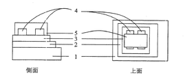
本発明の実施の形態について、図1及び図2を用いて以下詳細に説明する。 Embodiments of the present invention will be described in detail below with reference to FIGS.
本発明の薄膜トランジスタの一例を、図1に示す。図及び本例ではボトムゲート型ボトムコンタクト薄膜トランジスタについて述べているが、トップゲート型でもよい。 An example of the thin film transistor of the present invention is shown in FIG. Although the bottom gate type bottom contact thin film transistor is described in the figure and this example, a top gate type may be used.
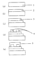
まず、基板1を用意する(図2(a))。基板1の材料としては、軽量、フレキシブルなプラスチック基板が好ましい。例えば、ポリエチレンテレフタレート(PET)、ポリエチレンナフタレート(PEN)、ポリエーテルスルフォン(PES)、ポリイミド(PI)、ポリエーテルイミド(PEI)、ポリスチレン(PS)、ポリ塩化ビニル(PVC)、ポリエチレン(PE)、ポリプロピレン(PP)、ナイロン等が使用可能である。ただし、密着性向上のためにUVやプラズマ等による表面処理を行うとよい。
First, the
次に、基板1上にゲート電極2を形成する(図2(b))。ゲート電極の材料は問わないが、透明薄膜トランジスタを作製する上で、透過率の高い材料が望ましい。透過率、導電率の観点からITOが好適である。透明性を問わない場合はこの限りではない。作製法は問わない。またゲート電極は活性層と直接接触するわけではないので、パターニング方法も問わない。金属、合金や透明導電膜の反応性マスク蒸着(スパッタを含む)などが一例として挙げられる。
Next, the
次にゲート絶縁膜3を作製する(図2(c))。ゲート絶縁膜3の材料や作製法、パターニング法は問わない。例えば、SiO2、SiN、SiON等が使用できるが、HfO2やY2O3、Ta2O5などの高誘電率(high−k)材料を用いるのが好ましい。
Next, the
次にソース・ドレイン電極4を形成する(図2(d))。ソース・ドレイン電極の材料にはITOを用いる。ITOの膜厚は、後に積層するInGaZnO4の膜厚をdとした場合、必要最小量より0.25dだけ余分に厚くするとエッチング終了時にITO膜厚の必要最小量を下回ることがない。成膜法は問わない。パターニングには、耐酸性のレジストを用いるのが望ましい。エッチングにはドライ、ウェットエッチングのいずれも適用可能である。エッチング液、エッチングガスは問わないが、環境面から、また効果を最大限に得るために、塩酸を用いたウェットエッチングが望ましい。ITO膜が結晶化している場合には50℃に加熱した6Mの塩酸と6Mの塩化第二鉄水溶液の混合溶液を用いるとエッチングが容易になる。ITO膜が結晶化してない場合は1Mの塩酸のみを用いて室温で処理するだけで充分である。エッチング終了後レジストを剥離する。
Next, source /
次に、活性層5を形成する(図2(e))。材料にはInGaZnO4を用いる。形成方法は大面積均一成膜ができるスパッタ法が好ましく、InGaZnO4ターゲットを用いると容易に形成できる。合金ターゲットを用いて反応性スパッタ法により成膜しても良い。スパッタ法に限らずパルスレーザーデポジション(PLD)など他の方法も可能である。パターニングには、耐酸性のレジストを用いるのが望ましい。エッチングにはドライ、ウェットエッチングのいずれも適用可能である。エッチング液、エッチングガスは問わないが、環境面から、また効果を最大限に得るために、塩酸を用いたウェットエッチングが望ましい。この時塩酸の濃度が高いとエッチング終了までの時間が短くなり処理時間の誤差が下地のITO膜の膜厚に無視できない影響を与えるため場合によってはITO膜も完全にエッチングされて無くなってしまう。従ってその濃度を充分に薄くとることが必要であり、好ましくは、50nmの膜厚を有するInGaZnO4活性層に対して約0.1Mの濃度である。エッチング終了後レジストを剥離する。
以上のようにして薄膜トランジスタが完成する(図1)。
Next, the
As described above, the thin film transistor is completed (FIG. 1).
基板1としてPENを用い(図2(a)参照)、前記基板1にITO層をdcマグネトロンスパッタ法により100nmの膜厚で成膜した後、パターニングしてゲート電極2を形成した(図2(b)参照)。前記ゲート電極2のパターニングは、一般的なフォトリソグラフィ法を用い、ウェットエッチングによってITO層を加工することにより形成した。
次に、プラズマCVDを用いて50℃以下の基板温度で、厚さ300nmSiO2膜を形成し、ゲート絶縁膜3とした(図2(c)参照)。
次に、前記ゲート絶縁膜3上に、ITO層をdcマグネトロンスパッタ法により100nmの膜厚で成膜し、フォトレジストを用い、通常のフォトリソグラフィによってレジストを電極の形状に加工した後、1Mの塩酸を用いてITO薄膜を2分間エッチングしてソース・ドレイン電極4を形成し、レジストを剥離した(図2(d)参照)。
最後に、InGaZnO4ターゲットを用いてrfマグネトロンスパッタ法によりInGaZnO4薄膜を50nmの厚さに成膜し、フォトレジストを用いて通常のフォトリソグラフィによって、レジストを半導体のパターンに加工し、0.1Mの塩酸を用いて前記InGaZnO4薄膜を3分間エッチングしたのちレジストを剥離し、パターニングされた活性層4を形成した(図2(e)参照)。
以上のようにしてチャネル長が50μm、チャネル幅が800μmのボトムゲート型ボトムコンタクト薄膜トランジスタが完成した(図1参照)。
PEN was used as the substrate 1 (see FIG. 2A), and an ITO layer was formed on the
Next, a 300 nm
Next, an ITO layer having a thickness of 100 nm is formed on the
Finally, an
As described above, a bottom-gate bottom contact thin film transistor having a channel length of 50 μm and a channel width of 800 μm was completed (see FIG. 1).
1・・・基板
2・・・ゲート電極
3・・・ゲート絶縁膜
4・・・ソース・ドレイン電極
5・・・活性層
DESCRIPTION OF
Claims (7)
Priority Applications (1)
| Application Number | Priority Date | Filing Date | Title |
|---|---|---|---|
| JP2005316403A JP2007123700A (en) | 2005-10-31 | 2005-10-31 | Oxide semiconductor patterning method and thin film transistor manufacturing method |
Applications Claiming Priority (1)
| Application Number | Priority Date | Filing Date | Title |
|---|---|---|---|
| JP2005316403A JP2007123700A (en) | 2005-10-31 | 2005-10-31 | Oxide semiconductor patterning method and thin film transistor manufacturing method |
Publications (1)
| Publication Number | Publication Date |
|---|---|
| JP2007123700A true JP2007123700A (en) | 2007-05-17 |
Family
ID=38147187
Family Applications (1)
| Application Number | Title | Priority Date | Filing Date |
|---|---|---|---|
| JP2005316403A Pending JP2007123700A (en) | 2005-10-31 | 2005-10-31 | Oxide semiconductor patterning method and thin film transistor manufacturing method |
Country Status (1)
| Country | Link |
|---|---|
| JP (1) | JP2007123700A (en) |
Cited By (18)
| Publication number | Priority date | Publication date | Assignee | Title |
|---|---|---|---|---|
| JP2008041695A (en) * | 2006-08-01 | 2008-02-21 | Canon Inc | Oxide etching method |
| EP2086014A2 (en) | 2008-02-01 | 2009-08-05 | Ricoh Company, Limited | Conductive oxide-deposited substrate and method for producing the same, and MIS laminated structure and method for producing the same |
| KR20100097053A (en) | 2009-02-25 | 2010-09-02 | 가부시키가이샤 한도오따이 에네루기 켄큐쇼 | Semiconductor device and manufacturing method thereof |
| KR20100109395A (en) | 2009-03-30 | 2010-10-08 | 가부시키가이샤 한도오따이 에네루기 켄큐쇼 | Semiconductor device and method for manufacturing the same |
| KR20110015377A (en) | 2009-08-07 | 2011-02-15 | 가부시키가이샤 한도오따이 에네루기 켄큐쇼 | Semiconductor device and method for manufacturing the same |
| US8343799B2 (en) | 2008-10-24 | 2013-01-01 | Semiconductor Energy Laboratory Co., Ltd. | Method for manufacturing semiconductor device |
| US8383470B2 (en) | 2008-12-25 | 2013-02-26 | Semiconductor Energy Laboratory Co., Ltd. | Thin film transistor (TFT) having a protective layer and manufacturing method thereof |
| US8384085B2 (en) | 2009-08-07 | 2013-02-26 | Semiconductor Energy Laboratory Co., Ltd. | Semiconductor device and method for manufacturing the same |
| US8461582B2 (en) | 2009-03-05 | 2013-06-11 | Semiconductor Energy Laboratory Co., Ltd. | Semiconductor device and method for manufacturing the same |
| US8476625B2 (en) | 2008-12-05 | 2013-07-02 | Semiconductor Energy Laboratory Co., Ltd. | Semiconductor device comprising gate electrode of one conductive layer and gate wiring of two conductive layers |
| KR101343677B1 (en) | 2009-02-25 | 2013-12-20 | 후지필름 가부시키가이샤 | Top gate type field effect transistor, manufacturing method thereof, and display device comprising the same |
| US8729546B2 (en) | 2008-10-24 | 2014-05-20 | Semiconductor Energy Laboratory Co., Ltd. | Method for manufacturing semiconductor device |
| US8741702B2 (en) | 2008-10-24 | 2014-06-03 | Semiconductor Energy Laboratory Co., Ltd. | Method for manufacturing semiconductor device |
| US8963146B2 (en) | 2009-11-05 | 2015-02-24 | Sumitomo Metal Mining Co., Ltd. | Method of manufacturing transparent conductive film, the transparent conductive substrate using the film, as well as device using the substrate |
| US9041202B2 (en) | 2008-05-16 | 2015-05-26 | Semiconductor Energy Laboratory Co., Ltd. | Semiconductor device and manufacturing method of the same |
| JP2016164999A (en) * | 2008-12-26 | 2016-09-08 | 株式会社半導体エネルギー研究所 | Semiconductor device |
| US9701849B2 (en) | 2010-02-17 | 2017-07-11 | Sumitomo Metal Mining Co., Ltd. | Method of manufacturing transparent conductive film, the transparent conductive film, element and transparent conductive substrate using the film, as well as device using the substrate |
| US11233132B2 (en) | 2009-03-05 | 2022-01-25 | Semiconductor Energy Laboratory Co., Ltd. | Semiconductor device |
-
2005
- 2005-10-31 JP JP2005316403A patent/JP2007123700A/en active Pending
Cited By (61)
| Publication number | Priority date | Publication date | Assignee | Title |
|---|---|---|---|---|
| JP2008041695A (en) * | 2006-08-01 | 2008-02-21 | Canon Inc | Oxide etching method |
| US8039405B2 (en) | 2008-02-01 | 2011-10-18 | Ricoh Company, Ltd. | Conductive oxide-deposited substrate and method for producing the same, and MIS laminated structure and method for producing the same |
| EP2086014A2 (en) | 2008-02-01 | 2009-08-05 | Ricoh Company, Limited | Conductive oxide-deposited substrate and method for producing the same, and MIS laminated structure and method for producing the same |
| US9041202B2 (en) | 2008-05-16 | 2015-05-26 | Semiconductor Energy Laboratory Co., Ltd. | Semiconductor device and manufacturing method of the same |
| US12300702B2 (en) | 2008-05-16 | 2025-05-13 | Semiconductor Energy Laboratory Co., Ltd. | Semiconductor device including storage capacitor having pixel electrode, directly stacked conductive layer, and insulating layer interposed between them, wherein the stacked conductive layers extending towards the gate and source wirings/lines |
| US10580797B2 (en) | 2008-05-16 | 2020-03-03 | Semiconductor Energy Laboratory Co., Ltd. | Semiconductor device and manufacturing method of the same |
| US11646322B2 (en) | 2008-05-16 | 2023-05-09 | Semiconductor Energy Laboratory Co., Ltd. | Semiconductor device having conductive oxide electrode layers in direct contact with oxide semiconductor layer |
| US9397255B2 (en) | 2008-05-16 | 2016-07-19 | Semiconductor Energy Laboratory Co., Ltd. | Semiconductor device and manufacturing method of the same |
| US11133332B2 (en) | 2008-05-16 | 2021-09-28 | Semiconductor Energy Laboratory Co., Ltd. | Semiconductor device and manufacturing method of the same |
| US9123751B2 (en) | 2008-10-24 | 2015-09-01 | Semiconductor Energy Laboratory Co., Ltd. | Method for manufacturing semiconductor device |
| US8741702B2 (en) | 2008-10-24 | 2014-06-03 | Semiconductor Energy Laboratory Co., Ltd. | Method for manufacturing semiconductor device |
| US8343799B2 (en) | 2008-10-24 | 2013-01-01 | Semiconductor Energy Laboratory Co., Ltd. | Method for manufacturing semiconductor device |
| US8878178B2 (en) | 2008-10-24 | 2014-11-04 | Semiconductor Energy Laboratory Co., Ltd. | Method for manufacturing semiconductor device |
| US8729546B2 (en) | 2008-10-24 | 2014-05-20 | Semiconductor Energy Laboratory Co., Ltd. | Method for manufacturing semiconductor device |
| KR20190123712A (en) | 2008-12-05 | 2019-11-01 | 가부시키가이샤 한도오따이 에네루기 켄큐쇼 | Semiconductor device |
| KR20180080710A (en) | 2008-12-05 | 2018-07-12 | 가부시키가이샤 한도오따이 에네루기 켄큐쇼 | Semiconductor device |
| US8476625B2 (en) | 2008-12-05 | 2013-07-02 | Semiconductor Energy Laboratory Co., Ltd. | Semiconductor device comprising gate electrode of one conductive layer and gate wiring of two conductive layers |
| JP2017050544A (en) * | 2008-12-05 | 2017-03-09 | 株式会社半導体エネルギー研究所 | Semiconductor device |
| KR20180001543A (en) | 2008-12-05 | 2018-01-04 | 가부시키가이샤 한도오따이 에네루기 켄큐쇼 | Semiconductor device |
| KR20210133931A (en) | 2008-12-05 | 2021-11-08 | 가부시키가이샤 한도오따이 에네루기 켄큐쇼 | Semiconductor device |
| KR20200123071A (en) | 2008-12-05 | 2020-10-28 | 가부시키가이샤 한도오따이 에네루기 켄큐쇼 | Semiconductor device |
| US9201280B2 (en) | 2008-12-05 | 2015-12-01 | Semiconductor Energy Laboratory Co., Ltd. | Semiconductor device |
| US8999750B2 (en) | 2008-12-05 | 2015-04-07 | Semiconductor Energy Laboratory Co., Ltd. | Semiconductor device |
| KR20190008975A (en) | 2008-12-05 | 2019-01-25 | 가부시키가이샤 한도오따이 에네루기 켄큐쇼 | Semiconductor device |
| US8383470B2 (en) | 2008-12-25 | 2013-02-26 | Semiconductor Energy Laboratory Co., Ltd. | Thin film transistor (TFT) having a protective layer and manufacturing method thereof |
| US8772784B2 (en) | 2008-12-25 | 2014-07-08 | Semiconductor Energy Laboratory Co., Ltd. | Semiconductor device including pair of electrodes and oxide semiconductor film with films of low conductivity therebetween |
| US9711651B2 (en) | 2008-12-26 | 2017-07-18 | Semiconductor Energy Laboratory Co., Ltd. | Semiconductor device and manufacturing method thereof |
| US11817506B2 (en) | 2008-12-26 | 2023-11-14 | Semiconductor Energy Laboratory Co., Ltd. | Semiconductor device and manufacturing method thereof |
| US12224355B2 (en) | 2008-12-26 | 2025-02-11 | Semiconductor Energy Laboratory Co., Ltd. | Semiconductor device and manufacturing method thereof |
| JP2016164999A (en) * | 2008-12-26 | 2016-09-08 | 株式会社半導体エネルギー研究所 | Semiconductor device |
| KR101343677B1 (en) | 2009-02-25 | 2013-12-20 | 후지필름 가부시키가이샤 | Top gate type field effect transistor, manufacturing method thereof, and display device comprising the same |
| KR20100097053A (en) | 2009-02-25 | 2010-09-02 | 가부시키가이샤 한도오따이 에네루기 켄큐쇼 | Semiconductor device and manufacturing method thereof |
| KR20160127702A (en) | 2009-02-25 | 2016-11-04 | 가부시키가이샤 한도오따이 에네루기 켄큐쇼 | Semiconductor device and manufacturing method thereof |
| US8841661B2 (en) | 2009-02-25 | 2014-09-23 | Semiconductor Energy Laboratory Co., Ltd. | Staggered oxide semiconductor TFT semiconductor device and manufacturing method thereof |
| US8759206B2 (en) | 2009-03-05 | 2014-06-24 | Semiconductor Energy Laboratory Co., Ltd. | Semiconductor device and method for manufacturing the same |
| US10686061B2 (en) | 2009-03-05 | 2020-06-16 | Semiconductor Energy Laboratory Co., Ltd. | Semiconductor device and method for manufacturing the same |
| US12336303B2 (en) | 2009-03-05 | 2025-06-17 | Semiconductor Energy Laboratory Co., Ltd. | Semiconductor device and method for manufacturing the same |
| US9941393B2 (en) | 2009-03-05 | 2018-04-10 | Semiconductor Energy Laboratory Co., Ltd. | Semiconductor device and method for manufacturing the same |
| US11961894B2 (en) | 2009-03-05 | 2024-04-16 | Semiconductor Energy Laboratory Co., Ltd. | Semiconductor device |
| US11955537B2 (en) | 2009-03-05 | 2024-04-09 | Semiconductor Energy Laboratory Co., Ltd. | Semiconductor device and method for manufacturing the same |
| US11233132B2 (en) | 2009-03-05 | 2022-01-25 | Semiconductor Energy Laboratory Co., Ltd. | Semiconductor device |
| US10326008B2 (en) | 2009-03-05 | 2019-06-18 | Semiconductor Energy Laboratory Co., Ltd. | Semiconductor device and method for manufacturing the same |
| US8461582B2 (en) | 2009-03-05 | 2013-06-11 | Semiconductor Energy Laboratory Co., Ltd. | Semiconductor device and method for manufacturing the same |
| KR20100109395A (en) | 2009-03-30 | 2010-10-08 | 가부시키가이샤 한도오따이 에네루기 켄큐쇼 | Semiconductor device and method for manufacturing the same |
| US8927981B2 (en) | 2009-03-30 | 2015-01-06 | Semiconductor Energy Laboratory Co., Ltd. | Semiconductor device and method for manufacturing the same |
| KR20190014565A (en) | 2009-08-07 | 2019-02-12 | 가부시키가이샤 한도오따이 에네루기 켄큐쇼 | Semiconductor device and method for manufacturing the same |
| KR20220140689A (en) | 2009-08-07 | 2022-10-18 | 가부시키가이샤 한도오따이 에네루기 켄큐쇼 | Display device |
| KR20160150087A (en) | 2009-08-07 | 2016-12-28 | 가부시키가이샤 한도오따이 에네루기 켄큐쇼 | Semiconductor device and method for manufacturing the same |
| KR20210071910A (en) | 2009-08-07 | 2021-06-16 | 가부시키가이샤 한도오따이 에네루기 켄큐쇼 | Display device |
| US8759132B2 (en) | 2009-08-07 | 2014-06-24 | Semiconductor Energy Laboratory Co., Ltd. | Method for manufacturing semiconductor device |
| TWI489618B (en) * | 2009-08-07 | 2015-06-21 | Semiconductor Energy Lab | Semiconductor device and method of manufacturing same |
| US9954005B2 (en) | 2009-08-07 | 2018-04-24 | Semiconductor Energy Laboratory Co., Ltd. | Semiconductor device comprising oxide semiconductor layer |
| KR20200044770A (en) | 2009-08-07 | 2020-04-29 | 가부시키가이샤 한도오따이 에네루기 켄큐쇼 | Display device |
| US8384085B2 (en) | 2009-08-07 | 2013-02-26 | Semiconductor Energy Laboratory Co., Ltd. | Semiconductor device and method for manufacturing the same |
| US8324626B2 (en) | 2009-08-07 | 2012-12-04 | Semiconductor Energy Laboratory Co., Ltd. | Semiconductor device and method for manufacturing the same |
| KR20150091290A (en) | 2009-08-07 | 2015-08-10 | 가부시키가이샤 한도오따이 에네루기 켄큐쇼 | Semiconductor device and method for manufacturing the same |
| US9171867B2 (en) | 2009-08-07 | 2015-10-27 | Semiconductor Energy Laboratory Co., Ltd. | Semiconductor device |
| KR20240146642A (en) | 2009-08-07 | 2024-10-08 | 가부시키가이샤 한도오따이 에네루기 켄큐쇼 | Display device |
| KR20110015377A (en) | 2009-08-07 | 2011-02-15 | 가부시키가이샤 한도오따이 에네루기 켄큐쇼 | Semiconductor device and method for manufacturing the same |
| US8963146B2 (en) | 2009-11-05 | 2015-02-24 | Sumitomo Metal Mining Co., Ltd. | Method of manufacturing transparent conductive film, the transparent conductive substrate using the film, as well as device using the substrate |
| US9701849B2 (en) | 2010-02-17 | 2017-07-11 | Sumitomo Metal Mining Co., Ltd. | Method of manufacturing transparent conductive film, the transparent conductive film, element and transparent conductive substrate using the film, as well as device using the substrate |
Similar Documents
| Publication | Publication Date | Title |
|---|---|---|
| JP2007123700A (en) | Oxide semiconductor patterning method and thin film transistor manufacturing method | |
| US9608127B2 (en) | Amorphous oxide thin film transistor, method for manufacturing the same, and display panel | |
| CN101496183B (en) | Oxide etching method | |
| CN101548367B (en) | Etching method for amorphous semiconductor oxide using alkaline etching solution | |
| JP6078063B2 (en) | Method for manufacturing thin film transistor device | |
| CN104934481B (en) | A kind of thin film transistor (TFT) and preparation method thereof | |
| CN110867458B (en) | Metal oxide semiconductor thin film transistor array substrate and manufacturing method | |
| CN105304500B (en) | N-type TFT preparation method | |
| JP2008171989A (en) | Field effect transistor and manufacturing method thereof | |
| WO2015165174A1 (en) | Thin film transistor and manufacturing method therefor, display substrate, and display device | |
| CN105185695A (en) | Oxide semiconductor film preparation method and thin film transistor preparation method | |
| JP2008072011A (en) | Method of manufacturing thin-film transistor | |
| JP5098152B2 (en) | Thin film transistor manufacturing method | |
| JP2007123698A (en) | Thin film transistor and manufacturing method thereof | |
| JP2008171990A (en) | Field effect transistor and method of manufacturing the same | |
| JP2007123702A (en) | Thin film transistor and manufacturing method thereof | |
| JP5098151B2 (en) | Thin film transistor manufacturing method | |
| WO2020019557A1 (en) | Manufacturing method for thin film transistor, and thin film transistor | |
| TWI401750B (en) | Thin film transistor and method for fabricating the same | |
| CN108615680B (en) | Polysilicon layer and manufacturing method thereof, thin film transistor and manufacturing method of array substrate | |
| KR101177873B1 (en) | Thin film transistor manufacturing method | |
| JP2001068681A (en) | Fabrication of active matrix | |
| JP2003023162A (en) | Thin film transistor and method for manufacturing the same | |
| CN110190065A (en) | Manufacturing method of array substrate | |
| CN105185715A (en) | Thin film transistor (TFT) substrate, TFT switch tube and manufacturing method of TFT switch tube |