JP5132097B2 - Display device - Google Patents
Display device Download PDFInfo
- Publication number
- JP5132097B2 JP5132097B2 JP2006194663A JP2006194663A JP5132097B2 JP 5132097 B2 JP5132097 B2 JP 5132097B2 JP 2006194663 A JP2006194663 A JP 2006194663A JP 2006194663 A JP2006194663 A JP 2006194663A JP 5132097 B2 JP5132097 B2 JP 5132097B2
- Authority
- JP
- Japan
- Prior art keywords
- light emitting
- gate
- source
- signal line
- tft
- Prior art date
- Legal status (The legal status is an assumption and is not a legal conclusion. Google has not performed a legal analysis and makes no representation as to the accuracy of the status listed.)
- Expired - Fee Related
Links
- 239000010408 film Substances 0.000 description 352
- 239000010410 layer Substances 0.000 description 250
- 239000004065 semiconductor Substances 0.000 description 247
- 239000003990 capacitor Substances 0.000 description 196
- 239000000758 substrate Substances 0.000 description 117
- 239000012535 impurity Substances 0.000 description 85
- 238000009832 plasma treatment Methods 0.000 description 75
- 239000000463 material Substances 0.000 description 74
- 238000000034 method Methods 0.000 description 52
- 230000003071 parasitic effect Effects 0.000 description 45
- VYPSYNLAJGMNEJ-UHFFFAOYSA-N silicon dioxide Inorganic materials O=[Si]=O VYPSYNLAJGMNEJ-UHFFFAOYSA-N 0.000 description 44
- 229910052814 silicon oxide Inorganic materials 0.000 description 38
- 238000007599 discharging Methods 0.000 description 37
- 229910052581 Si3N4 Inorganic materials 0.000 description 27
- HQVNEWCFYHHQES-UHFFFAOYSA-N silicon nitride Chemical compound N12[Si]34N5[Si]62N3[Si]51N64 HQVNEWCFYHHQES-UHFFFAOYSA-N 0.000 description 27
- 239000002585 base Substances 0.000 description 23
- IJGRMHOSHXDMSA-UHFFFAOYSA-N Atomic nitrogen Chemical compound N#N IJGRMHOSHXDMSA-UHFFFAOYSA-N 0.000 description 19
- XUIMIQQOPSSXEZ-UHFFFAOYSA-N Silicon Chemical compound [Si] XUIMIQQOPSSXEZ-UHFFFAOYSA-N 0.000 description 19
- 230000006870 function Effects 0.000 description 19
- 229910052710 silicon Inorganic materials 0.000 description 19
- 239000010703 silicon Substances 0.000 description 19
- 239000012298 atmosphere Substances 0.000 description 18
- 239000007789 gas Substances 0.000 description 18
- 150000004767 nitrides Chemical class 0.000 description 17
- 239000011521 glass Substances 0.000 description 16
- 235000019557 luminance Nutrition 0.000 description 16
- 238000004519 manufacturing process Methods 0.000 description 16
- 229910052757 nitrogen Inorganic materials 0.000 description 16
- 238000002425 crystallisation Methods 0.000 description 15
- QVGXLLKOCUKJST-UHFFFAOYSA-N atomic oxygen Chemical compound [O] QVGXLLKOCUKJST-UHFFFAOYSA-N 0.000 description 12
- 150000001875 compounds Chemical class 0.000 description 12
- 239000004973 liquid crystal related substance Substances 0.000 description 12
- 229910052751 metal Inorganic materials 0.000 description 12
- 238000005121 nitriding Methods 0.000 description 12
- 230000001590 oxidative effect Effects 0.000 description 12
- 229910052760 oxygen Inorganic materials 0.000 description 12
- 239000001301 oxygen Substances 0.000 description 12
- 239000000565 sealant Substances 0.000 description 12
- 239000002184 metal Substances 0.000 description 11
- 150000002894 organic compounds Chemical class 0.000 description 11
- 238000004544 sputter deposition Methods 0.000 description 11
- 229910021417 amorphous silicon Inorganic materials 0.000 description 10
- 239000010949 copper Substances 0.000 description 10
- 230000008025 crystallization Effects 0.000 description 10
- 230000007547 defect Effects 0.000 description 9
- 238000005530 etching Methods 0.000 description 9
- 239000001257 hydrogen Substances 0.000 description 9
- 229910052739 hydrogen Inorganic materials 0.000 description 9
- 239000011347 resin Substances 0.000 description 9
- 229920005989 resin Polymers 0.000 description 9
- 239000002356 single layer Substances 0.000 description 9
- UFHFLCQGNIYNRP-UHFFFAOYSA-N Hydrogen Chemical compound [H][H] UFHFLCQGNIYNRP-UHFFFAOYSA-N 0.000 description 8
- -1 a-InGaZnO Inorganic materials 0.000 description 8
- 230000008901 benefit Effects 0.000 description 8
- 239000013078 crystal Substances 0.000 description 8
- 239000011229 interlayer Substances 0.000 description 8
- 229910052786 argon Inorganic materials 0.000 description 7
- 238000005229 chemical vapour deposition Methods 0.000 description 7
- 230000003647 oxidation Effects 0.000 description 7
- 238000007254 oxidation reaction Methods 0.000 description 7
- 238000005268 plasma chemical vapour deposition Methods 0.000 description 7
- 230000008569 process Effects 0.000 description 7
- 230000015572 biosynthetic process Effects 0.000 description 6
- 229910052799 carbon Inorganic materials 0.000 description 6
- 229910052802 copper Inorganic materials 0.000 description 6
- 229910052733 gallium Inorganic materials 0.000 description 6
- 229910052743 krypton Inorganic materials 0.000 description 6
- 238000004518 low pressure chemical vapour deposition Methods 0.000 description 6
- 239000012299 nitrogen atmosphere Substances 0.000 description 6
- 238000000206 photolithography Methods 0.000 description 6
- 229910021420 polycrystalline silicon Inorganic materials 0.000 description 6
- 239000010453 quartz Substances 0.000 description 6
- OAICVXFJPJFONN-UHFFFAOYSA-N Phosphorus Chemical compound [P] OAICVXFJPJFONN-UHFFFAOYSA-N 0.000 description 5
- XLOMVQKBTHCTTD-UHFFFAOYSA-N Zinc monoxide Chemical compound [Zn]=O XLOMVQKBTHCTTD-UHFFFAOYSA-N 0.000 description 5
- 229910045601 alloy Inorganic materials 0.000 description 5
- 239000000956 alloy Substances 0.000 description 5
- 229910052782 aluminium Inorganic materials 0.000 description 5
- 238000006243 chemical reaction Methods 0.000 description 5
- 239000011651 chromium Substances 0.000 description 5
- 229910052734 helium Inorganic materials 0.000 description 5
- 229910010272 inorganic material Inorganic materials 0.000 description 5
- 229910052741 iridium Inorganic materials 0.000 description 5
- GKOZUEZYRPOHIO-UHFFFAOYSA-N iridium atom Chemical compound [Ir] GKOZUEZYRPOHIO-UHFFFAOYSA-N 0.000 description 5
- 229910052754 neon Inorganic materials 0.000 description 5
- 229910052698 phosphorus Inorganic materials 0.000 description 5
- 239000011574 phosphorus Substances 0.000 description 5
- 239000000843 powder Substances 0.000 description 5
- 229910052721 tungsten Inorganic materials 0.000 description 5
- 229910052724 xenon Inorganic materials 0.000 description 5
- RYGMFSIKBFXOCR-UHFFFAOYSA-N Copper Chemical compound [Cu] RYGMFSIKBFXOCR-UHFFFAOYSA-N 0.000 description 4
- FAPWRFPIFSIZLT-UHFFFAOYSA-M Sodium chloride Chemical compound [Na+].[Cl-] FAPWRFPIFSIZLT-UHFFFAOYSA-M 0.000 description 4
- 238000000137 annealing Methods 0.000 description 4
- 239000000919 ceramic Substances 0.000 description 4
- 239000000460 chlorine Substances 0.000 description 4
- 239000003086 colorant Substances 0.000 description 4
- 238000005499 laser crystallization Methods 0.000 description 4
- 239000011159 matrix material Substances 0.000 description 4
- 229910021645 metal ion Inorganic materials 0.000 description 4
- 229910052750 molybdenum Inorganic materials 0.000 description 4
- QGLKJKCYBOYXKC-UHFFFAOYSA-N nonaoxidotritungsten Chemical compound O=[W]1(=O)O[W](=O)(=O)O[W](=O)(=O)O1 QGLKJKCYBOYXKC-UHFFFAOYSA-N 0.000 description 4
- 239000004033 plastic Substances 0.000 description 4
- 229920003023 plastic Polymers 0.000 description 4
- BASFCYQUMIYNBI-UHFFFAOYSA-N platinum Substances [Pt] BASFCYQUMIYNBI-UHFFFAOYSA-N 0.000 description 4
- 239000003870 refractory metal Substances 0.000 description 4
- 229910052715 tantalum Inorganic materials 0.000 description 4
- 229910001930 tungsten oxide Inorganic materials 0.000 description 4
- POILWHVDKZOXJZ-ARJAWSKDSA-M (z)-4-oxopent-2-en-2-olate Chemical compound C\C([O-])=C\C(C)=O POILWHVDKZOXJZ-ARJAWSKDSA-M 0.000 description 3
- PIGFYZPCRLYGLF-UHFFFAOYSA-N Aluminum nitride Chemical compound [Al]#N PIGFYZPCRLYGLF-UHFFFAOYSA-N 0.000 description 3
- ZOXJGFHDIHLPTG-UHFFFAOYSA-N Boron Chemical compound [B] ZOXJGFHDIHLPTG-UHFFFAOYSA-N 0.000 description 3
- OKTJSMMVPCPJKN-UHFFFAOYSA-N Carbon Chemical compound [C] OKTJSMMVPCPJKN-UHFFFAOYSA-N 0.000 description 3
- GYHNNYVSQQEPJS-UHFFFAOYSA-N Gallium Chemical compound [Ga] GYHNNYVSQQEPJS-UHFFFAOYSA-N 0.000 description 3
- GWEVSGVZZGPLCZ-UHFFFAOYSA-N Titan oxide Chemical compound O=[Ti]=O GWEVSGVZZGPLCZ-UHFFFAOYSA-N 0.000 description 3
- 239000007983 Tris buffer Substances 0.000 description 3
- CUJRVFIICFDLGR-UHFFFAOYSA-N acetylacetonate Chemical compound CC(=O)[CH-]C(C)=O CUJRVFIICFDLGR-UHFFFAOYSA-N 0.000 description 3
- 229910052796 boron Inorganic materials 0.000 description 3
- 239000002041 carbon nanotube Substances 0.000 description 3
- 229910021393 carbon nanotube Inorganic materials 0.000 description 3
- 230000015556 catabolic process Effects 0.000 description 3
- 230000008859 change Effects 0.000 description 3
- 229910052804 chromium Inorganic materials 0.000 description 3
- 238000010586 diagram Methods 0.000 description 3
- 230000005684 electric field Effects 0.000 description 3
- 239000010931 gold Substances 0.000 description 3
- 230000006872 improvement Effects 0.000 description 3
- AMGQUBHHOARCQH-UHFFFAOYSA-N indium;oxotin Chemical compound [In].[Sn]=O AMGQUBHHOARCQH-UHFFFAOYSA-N 0.000 description 3
- 239000011147 inorganic material Substances 0.000 description 3
- 238000009413 insulation Methods 0.000 description 3
- 229910052744 lithium Inorganic materials 0.000 description 3
- 239000011572 manganese Substances 0.000 description 3
- 230000001681 protective effect Effects 0.000 description 3
- 230000009467 reduction Effects 0.000 description 3
- 239000011734 sodium Substances 0.000 description 3
- 238000003746 solid phase reaction Methods 0.000 description 3
- 239000010935 stainless steel Substances 0.000 description 3
- 229910001220 stainless steel Inorganic materials 0.000 description 3
- 125000001424 substituent group Chemical group 0.000 description 3
- MZLGASXMSKOWSE-UHFFFAOYSA-N tantalum nitride Chemical compound [Ta]#N MZLGASXMSKOWSE-UHFFFAOYSA-N 0.000 description 3
- 239000010409 thin film Substances 0.000 description 3
- OGIDPMRJRNCKJF-UHFFFAOYSA-N titanium oxide Inorganic materials [Ti]=O OGIDPMRJRNCKJF-UHFFFAOYSA-N 0.000 description 3
- WFKWXMTUELFFGS-UHFFFAOYSA-N tungsten Chemical compound [W] WFKWXMTUELFFGS-UHFFFAOYSA-N 0.000 description 3
- 239000010937 tungsten Substances 0.000 description 3
- SKJCKYVIQGBWTN-UHFFFAOYSA-N (4-hydroxyphenyl) methanesulfonate Chemical compound CS(=O)(=O)OC1=CC=C(O)C=C1 SKJCKYVIQGBWTN-UHFFFAOYSA-N 0.000 description 2
- PFNQVRZLDWYSCW-UHFFFAOYSA-N (fluoren-9-ylideneamino) n-naphthalen-1-ylcarbamate Chemical compound C12=CC=CC=C2C2=CC=CC=C2C1=NOC(=O)NC1=CC=CC2=CC=CC=C12 PFNQVRZLDWYSCW-UHFFFAOYSA-N 0.000 description 2
- POXIZPBFFUKMEQ-UHFFFAOYSA-N 2-cyanoethenylideneazanide Chemical group [N-]=C=[C+]C#N POXIZPBFFUKMEQ-UHFFFAOYSA-N 0.000 description 2
- WUPHOULIZUERAE-UHFFFAOYSA-N 3-(oxolan-2-yl)propanoic acid Chemical compound OC(=O)CCC1CCCO1 WUPHOULIZUERAE-UHFFFAOYSA-N 0.000 description 2
- XKRFYHLGVUSROY-UHFFFAOYSA-N Argon Chemical compound [Ar] XKRFYHLGVUSROY-UHFFFAOYSA-N 0.000 description 2
- JBRZTFJDHDCESZ-UHFFFAOYSA-N AsGa Chemical compound [As]#[Ga] JBRZTFJDHDCESZ-UHFFFAOYSA-N 0.000 description 2
- ZAMOUSCENKQFHK-UHFFFAOYSA-N Chlorine atom Chemical compound [Cl] ZAMOUSCENKQFHK-UHFFFAOYSA-N 0.000 description 2
- VYZAMTAEIAYCRO-UHFFFAOYSA-N Chromium Chemical compound [Cr] VYZAMTAEIAYCRO-UHFFFAOYSA-N 0.000 description 2
- 229910052691 Erbium Inorganic materials 0.000 description 2
- PXGOKWXKJXAPGV-UHFFFAOYSA-N Fluorine Chemical compound FF PXGOKWXKJXAPGV-UHFFFAOYSA-N 0.000 description 2
- ZOKXTWBITQBERF-UHFFFAOYSA-N Molybdenum Chemical compound [Mo] ZOKXTWBITQBERF-UHFFFAOYSA-N 0.000 description 2
- GQPLMRYTRLFLPF-UHFFFAOYSA-N Nitrous Oxide Chemical compound [O-][N+]#N GQPLMRYTRLFLPF-UHFFFAOYSA-N 0.000 description 2
- UCKMPCXJQFINFW-UHFFFAOYSA-N Sulphide Chemical compound [S-2] UCKMPCXJQFINFW-UHFFFAOYSA-N 0.000 description 2
- 239000005083 Zinc sulfide Substances 0.000 description 2
- XHCLAFWTIXFWPH-UHFFFAOYSA-N [O-2].[O-2].[O-2].[O-2].[O-2].[V+5].[V+5] Chemical compound [O-2].[O-2].[O-2].[O-2].[O-2].[V+5].[V+5] XHCLAFWTIXFWPH-UHFFFAOYSA-N 0.000 description 2
- 230000002159 abnormal effect Effects 0.000 description 2
- 239000012790 adhesive layer Substances 0.000 description 2
- 229910052783 alkali metal Inorganic materials 0.000 description 2
- 150000001340 alkali metals Chemical class 0.000 description 2
- 229910052784 alkaline earth metal Inorganic materials 0.000 description 2
- 150000001342 alkaline earth metals Chemical class 0.000 description 2
- XAGFODPZIPBFFR-UHFFFAOYSA-N aluminium Chemical compound [Al] XAGFODPZIPBFFR-UHFFFAOYSA-N 0.000 description 2
- 229910052785 arsenic Inorganic materials 0.000 description 2
- RQNWIZPPADIBDY-UHFFFAOYSA-N arsenic atom Chemical compound [As] RQNWIZPPADIBDY-UHFFFAOYSA-N 0.000 description 2
- 229910052788 barium Inorganic materials 0.000 description 2
- DSAJWYNOEDNPEQ-UHFFFAOYSA-N barium atom Chemical compound [Ba] DSAJWYNOEDNPEQ-UHFFFAOYSA-N 0.000 description 2
- CJDPJFRMHVXWPT-UHFFFAOYSA-N barium sulfide Chemical compound [S-2].[Ba+2] CJDPJFRMHVXWPT-UHFFFAOYSA-N 0.000 description 2
- WPYMKLBDIGXBTP-UHFFFAOYSA-N benzoic acid Chemical compound OC(=O)C1=CC=CC=C1 WPYMKLBDIGXBTP-UHFFFAOYSA-N 0.000 description 2
- 229910052980 cadmium sulfide Inorganic materials 0.000 description 2
- 229910052792 caesium Inorganic materials 0.000 description 2
- 229910052791 calcium Inorganic materials 0.000 description 2
- 239000011575 calcium Substances 0.000 description 2
- JGIATAMCQXIDNZ-UHFFFAOYSA-N calcium sulfide Chemical compound [Ca]=S JGIATAMCQXIDNZ-UHFFFAOYSA-N 0.000 description 2
- 229910052801 chlorine Inorganic materials 0.000 description 2
- 238000004140 cleaning Methods 0.000 description 2
- 239000011248 coating agent Substances 0.000 description 2
- 238000000576 coating method Methods 0.000 description 2
- 239000002131 composite material Substances 0.000 description 2
- 239000004020 conductor Substances 0.000 description 2
- OXBLHERUFWYNTN-UHFFFAOYSA-M copper(I) chloride Chemical compound [Cu]Cl OXBLHERUFWYNTN-UHFFFAOYSA-M 0.000 description 2
- 230000006866 deterioration Effects 0.000 description 2
- 238000009792 diffusion process Methods 0.000 description 2
- 125000002147 dimethylamino group Chemical group [H]C([H])([H])N(*)C([H])([H])[H] 0.000 description 2
- 238000001312 dry etching Methods 0.000 description 2
- 230000000694 effects Effects 0.000 description 2
- 229910052731 fluorine Inorganic materials 0.000 description 2
- 239000011737 fluorine Substances 0.000 description 2
- 125000001153 fluoro group Chemical group F* 0.000 description 2
- 229910052737 gold Inorganic materials 0.000 description 2
- 229910052736 halogen Inorganic materials 0.000 description 2
- 150000002367 halogens Chemical class 0.000 description 2
- 239000002784 hot electron Substances 0.000 description 2
- 238000005984 hydrogenation reaction Methods 0.000 description 2
- 239000003230 hygroscopic agent Substances 0.000 description 2
- WPYVAWXEWQSOGY-UHFFFAOYSA-N indium antimonide Chemical compound [Sb]#[In] WPYVAWXEWQSOGY-UHFFFAOYSA-N 0.000 description 2
- 229910003437 indium oxide Inorganic materials 0.000 description 2
- PJXISJQVUVHSOJ-UHFFFAOYSA-N indium(iii) oxide Chemical compound [O-2].[O-2].[O-2].[In+3].[In+3] PJXISJQVUVHSOJ-UHFFFAOYSA-N 0.000 description 2
- 238000002347 injection Methods 0.000 description 2
- 239000007924 injection Substances 0.000 description 2
- 150000002484 inorganic compounds Chemical class 0.000 description 2
- 239000011810 insulating material Substances 0.000 description 2
- 150000002500 ions Chemical class 0.000 description 2
- 239000007788 liquid Substances 0.000 description 2
- 229910052749 magnesium Inorganic materials 0.000 description 2
- 229910052748 manganese Inorganic materials 0.000 description 2
- 229910021424 microcrystalline silicon Inorganic materials 0.000 description 2
- 239000011733 molybdenum Substances 0.000 description 2
- 229910000476 molybdenum oxide Inorganic materials 0.000 description 2
- 239000004570 mortar (masonry) Substances 0.000 description 2
- 125000000962 organic group Chemical group 0.000 description 2
- 239000011368 organic material Substances 0.000 description 2
- PQQKPALAQIIWST-UHFFFAOYSA-N oxomolybdenum Chemical compound [Mo]=O PQQKPALAQIIWST-UHFFFAOYSA-N 0.000 description 2
- DYIZHKNUQPHNJY-UHFFFAOYSA-N oxorhenium Chemical compound [Re]=O DYIZHKNUQPHNJY-UHFFFAOYSA-N 0.000 description 2
- 230000002093 peripheral effect Effects 0.000 description 2
- 229920002120 photoresistant polymer Polymers 0.000 description 2
- 229910052697 platinum Inorganic materials 0.000 description 2
- 229920001721 polyimide Polymers 0.000 description 2
- 229910003449 rhenium oxide Inorganic materials 0.000 description 2
- 238000007789 sealing Methods 0.000 description 2
- 239000003566 sealing material Substances 0.000 description 2
- 229910052709 silver Inorganic materials 0.000 description 2
- 239000011780 sodium chloride Substances 0.000 description 2
- 229910052712 strontium Inorganic materials 0.000 description 2
- 125000005504 styryl group Chemical group 0.000 description 2
- GUVRBAGPIYLISA-UHFFFAOYSA-N tantalum atom Chemical compound [Ta] GUVRBAGPIYLISA-UHFFFAOYSA-N 0.000 description 2
- 229910052719 titanium Inorganic materials 0.000 description 2
- 239000010936 titanium Substances 0.000 description 2
- 229910001935 vanadium oxide Inorganic materials 0.000 description 2
- YVTHLONGBIQYBO-UHFFFAOYSA-N zinc indium(3+) oxygen(2-) Chemical compound [O--].[Zn++].[In+3] YVTHLONGBIQYBO-UHFFFAOYSA-N 0.000 description 2
- 239000011787 zinc oxide Substances 0.000 description 2
- 229910052984 zinc sulfide Inorganic materials 0.000 description 2
- IWZZBBJTIUYDPZ-DVACKJPTSA-N (z)-4-hydroxypent-3-en-2-one;iridium;2-phenylpyridine Chemical compound [Ir].C\C(O)=C\C(C)=O.[C-]1=CC=CC=C1C1=CC=CC=N1.[C-]1=CC=CC=C1C1=CC=CC=N1 IWZZBBJTIUYDPZ-DVACKJPTSA-N 0.000 description 1
- LCAKAXJAQMMVTQ-UHFFFAOYSA-N 1-(2,2-diphenylethenyl)-2-phenylbenzene Chemical group C=1C=CC=C(C=2C=CC=CC=2)C=1C=C(C=1C=CC=CC=1)C1=CC=CC=C1 LCAKAXJAQMMVTQ-UHFFFAOYSA-N 0.000 description 1
- UHXOHPVVEHBKKT-UHFFFAOYSA-N 1-(2,2-diphenylethenyl)-4-[4-(2,2-diphenylethenyl)phenyl]benzene Chemical compound C=1C=C(C=2C=CC(C=C(C=3C=CC=CC=3)C=3C=CC=CC=3)=CC=2)C=CC=1C=C(C=1C=CC=CC=1)C1=CC=CC=C1 UHXOHPVVEHBKKT-UHFFFAOYSA-N 0.000 description 1
- OBMPIWRNYHXYBC-UHFFFAOYSA-N 1-n,1-n,3-n,3-n,5-n,5-n-hexakis(3-methylphenyl)benzene-1,3,5-triamine Chemical compound CC1=CC=CC(N(C=2C=C(C)C=CC=2)C=2C=C(C=C(C=2)N(C=2C=C(C)C=CC=2)C=2C=C(C)C=CC=2)N(C=2C=C(C)C=CC=2)C=2C=C(C)C=CC=2)=C1 OBMPIWRNYHXYBC-UHFFFAOYSA-N 0.000 description 1
- BFTIPCRZWILUIY-UHFFFAOYSA-N 2,5,8,11-tetratert-butylperylene Chemical group CC(C)(C)C1=CC(C2=CC(C(C)(C)C)=CC=3C2=C2C=C(C=3)C(C)(C)C)=C3C2=CC(C(C)(C)C)=CC3=C1 BFTIPCRZWILUIY-UHFFFAOYSA-N 0.000 description 1
- JKFYKCYQEWQPTM-UHFFFAOYSA-N 2-azaniumyl-2-(4-fluorophenyl)acetate Chemical compound OC(=O)C(N)C1=CC=C(F)C=C1 JKFYKCYQEWQPTM-UHFFFAOYSA-N 0.000 description 1
- HONWGFNQCPRRFM-UHFFFAOYSA-N 2-n-(3-methylphenyl)-1-n,1-n,2-n-triphenylbenzene-1,2-diamine Chemical compound CC1=CC=CC(N(C=2C=CC=CC=2)C=2C(=CC=CC=2)N(C=2C=CC=CC=2)C=2C=CC=CC=2)=C1 HONWGFNQCPRRFM-UHFFFAOYSA-N 0.000 description 1
- VQGHOUODWALEFC-UHFFFAOYSA-N 2-phenylpyridine Chemical compound C1=CC=CC=C1C1=CC=CC=N1 VQGHOUODWALEFC-UHFFFAOYSA-N 0.000 description 1
- OBAJPWYDYFEBTF-UHFFFAOYSA-N 2-tert-butyl-9,10-dinaphthalen-2-ylanthracene Chemical compound C1=CC=CC2=CC(C3=C4C=CC=CC4=C(C=4C=C5C=CC=CC5=CC=4)C4=CC=C(C=C43)C(C)(C)C)=CC=C21 OBAJPWYDYFEBTF-UHFFFAOYSA-N 0.000 description 1
- MBXOOYPCIDHXGH-UHFFFAOYSA-N 3-butylpentane-2,4-dione Chemical compound CCCCC(C(C)=O)C(C)=O MBXOOYPCIDHXGH-UHFFFAOYSA-N 0.000 description 1
- OGGKVJMNFFSDEV-UHFFFAOYSA-N 3-methyl-n-[4-[4-(n-(3-methylphenyl)anilino)phenyl]phenyl]-n-phenylaniline Chemical compound CC1=CC=CC(N(C=2C=CC=CC=2)C=2C=CC(=CC=2)C=2C=CC(=CC=2)N(C=2C=CC=CC=2)C=2C=C(C)C=CC=2)=C1 OGGKVJMNFFSDEV-UHFFFAOYSA-N 0.000 description 1
- ZNJRONVKWRHYBF-VOTSOKGWSA-N 4-(dicyanomethylene)-2-methyl-6-julolidyl-9-enyl-4h-pyran Chemical compound O1C(C)=CC(=C(C#N)C#N)C=C1\C=C\C1=CC(CCCN2CCC3)=C2C3=C1 ZNJRONVKWRHYBF-VOTSOKGWSA-N 0.000 description 1
- DWSKWYAKBATHET-UHFFFAOYSA-N 5,12-diphenyltetracene Chemical compound C1=CC=CC=C1C(C1=CC2=CC=CC=C2C=C11)=C(C=CC=C2)C2=C1C1=CC=CC=C1 DWSKWYAKBATHET-UHFFFAOYSA-N 0.000 description 1
- ZCYVEMRRCGMTRW-UHFFFAOYSA-N 7553-56-2 Chemical compound [I] ZCYVEMRRCGMTRW-UHFFFAOYSA-N 0.000 description 1
- VIZUPBYFLORCRA-UHFFFAOYSA-N 9,10-dinaphthalen-2-ylanthracene Chemical compound C12=CC=CC=C2C(C2=CC3=CC=CC=C3C=C2)=C(C=CC=C2)C2=C1C1=CC=C(C=CC=C2)C2=C1 VIZUPBYFLORCRA-UHFFFAOYSA-N 0.000 description 1
- FCNCGHJSNVOIKE-UHFFFAOYSA-N 9,10-diphenylanthracene Chemical compound C1=CC=CC=C1C(C1=CC=CC=C11)=C(C=CC=C2)C2=C1C1=CC=CC=C1 FCNCGHJSNVOIKE-UHFFFAOYSA-N 0.000 description 1
- 239000004925 Acrylic resin Substances 0.000 description 1
- 229920000178 Acrylic resin Polymers 0.000 description 1
- 229910017115 AlSb Inorganic materials 0.000 description 1
- 239000005711 Benzoic acid Substances 0.000 description 1
- PZNSFCLAULLKQX-UHFFFAOYSA-N Boron nitride Chemical compound N#B PZNSFCLAULLKQX-UHFFFAOYSA-N 0.000 description 1
- WKBOTKDWSSQWDR-UHFFFAOYSA-N Bromine atom Chemical compound [Br] WKBOTKDWSSQWDR-UHFFFAOYSA-N 0.000 description 1
- WYZWJLZUSHFFOR-UHFFFAOYSA-N C1=CC=C2SC(C3=CC=4C=C5CCCN6CCCC(=C56)C=4OC3=O)=NC2=C1 Chemical compound C1=CC=C2SC(C3=CC=4C=C5CCCN6CCCC(=C56)C=4OC3=O)=NC2=C1 WYZWJLZUSHFFOR-UHFFFAOYSA-N 0.000 description 1
- MSDMPJCOOXURQD-UHFFFAOYSA-N C545T Chemical compound C1=CC=C2SC(C3=CC=4C=C5C6=C(C=4OC3=O)C(C)(C)CCN6CCC5(C)C)=NC2=C1 MSDMPJCOOXURQD-UHFFFAOYSA-N 0.000 description 1
- 229910004261 CaF 2 Inorganic materials 0.000 description 1
- OYPRJOBELJOOCE-UHFFFAOYSA-N Calcium Chemical compound [Ca] OYPRJOBELJOOCE-UHFFFAOYSA-N 0.000 description 1
- 229920000298 Cellophane Polymers 0.000 description 1
- 229910052684 Cerium Inorganic materials 0.000 description 1
- 229910021591 Copper(I) chloride Inorganic materials 0.000 description 1
- 229910052693 Europium Inorganic materials 0.000 description 1
- 229910001218 Gallium arsenide Inorganic materials 0.000 description 1
- JMASRVWKEDWRBT-UHFFFAOYSA-N Gallium nitride Chemical compound [Ga]#N JMASRVWKEDWRBT-UHFFFAOYSA-N 0.000 description 1
- DGAQECJNVWCQMB-PUAWFVPOSA-M Ilexoside XXIX Chemical compound C[C@@H]1CC[C@@]2(CC[C@@]3(C(=CC[C@H]4[C@]3(CC[C@@H]5[C@@]4(CC[C@@H](C5(C)C)OS(=O)(=O)[O-])C)C)[C@@H]2[C@]1(C)O)C)C(=O)O[C@H]6[C@@H]([C@H]([C@@H]([C@H](O6)CO)O)O)O.[Na+] DGAQECJNVWCQMB-PUAWFVPOSA-M 0.000 description 1
- GPXJNWSHGFTCBW-UHFFFAOYSA-N Indium phosphide Chemical compound [In]#P GPXJNWSHGFTCBW-UHFFFAOYSA-N 0.000 description 1
- WHXSMMKQMYFTQS-UHFFFAOYSA-N Lithium Chemical compound [Li] WHXSMMKQMYFTQS-UHFFFAOYSA-N 0.000 description 1
- PWHULOQIROXLJO-UHFFFAOYSA-N Manganese Chemical compound [Mn] PWHULOQIROXLJO-UHFFFAOYSA-N 0.000 description 1
- 101100476480 Mus musculus S100a8 gene Proteins 0.000 description 1
- 229910052779 Neodymium Inorganic materials 0.000 description 1
- 239000004952 Polyamide Substances 0.000 description 1
- 239000004642 Polyimide Substances 0.000 description 1
- 229920000265 Polyparaphenylene Polymers 0.000 description 1
- ZLMJMSJWJFRBEC-UHFFFAOYSA-N Potassium Chemical compound [K] ZLMJMSJWJFRBEC-UHFFFAOYSA-N 0.000 description 1
- 229910052777 Praseodymium Inorganic materials 0.000 description 1
- 229910052772 Samarium Inorganic materials 0.000 description 1
- 229910004298 SiO 2 Inorganic materials 0.000 description 1
- 229910000577 Silicon-germanium Inorganic materials 0.000 description 1
- BQCADISMDOOEFD-UHFFFAOYSA-N Silver Chemical compound [Ag] BQCADISMDOOEFD-UHFFFAOYSA-N 0.000 description 1
- 229910021607 Silver chloride Inorganic materials 0.000 description 1
- 229910021612 Silver iodide Inorganic materials 0.000 description 1
- 229910052771 Terbium Inorganic materials 0.000 description 1
- 229910052775 Thulium Inorganic materials 0.000 description 1
- 229910052769 Ytterbium Inorganic materials 0.000 description 1
- HCHKCACWOHOZIP-UHFFFAOYSA-N Zinc Chemical compound [Zn] HCHKCACWOHOZIP-UHFFFAOYSA-N 0.000 description 1
- 230000002745 absorbent Effects 0.000 description 1
- 239000002250 absorbent Substances 0.000 description 1
- 238000010521 absorption reaction Methods 0.000 description 1
- NIXOWILDQLNWCW-UHFFFAOYSA-N acrylic acid group Chemical group C(C=C)(=O)O NIXOWILDQLNWCW-UHFFFAOYSA-N 0.000 description 1
- 230000009471 action Effects 0.000 description 1
- 230000004913 activation Effects 0.000 description 1
- 230000001154 acute effect Effects 0.000 description 1
- 230000002411 adverse Effects 0.000 description 1
- 239000003513 alkali Substances 0.000 description 1
- 125000000217 alkyl group Chemical group 0.000 description 1
- 239000005407 aluminoborosilicate glass Substances 0.000 description 1
- 229910052787 antimony Inorganic materials 0.000 description 1
- WATWJIUSRGPENY-UHFFFAOYSA-N antimony atom Chemical compound [Sb] WATWJIUSRGPENY-UHFFFAOYSA-N 0.000 description 1
- 150000004945 aromatic hydrocarbons Chemical class 0.000 description 1
- NWAIGJYBQQYSPW-UHFFFAOYSA-N azanylidyneindigane Chemical compound [In]#N NWAIGJYBQQYSPW-UHFFFAOYSA-N 0.000 description 1
- 235000010233 benzoic acid Nutrition 0.000 description 1
- 229910052797 bismuth Inorganic materials 0.000 description 1
- JCXGWMGPZLAOME-UHFFFAOYSA-N bismuth atom Chemical compound [Bi] JCXGWMGPZLAOME-UHFFFAOYSA-N 0.000 description 1
- 239000005388 borosilicate glass Substances 0.000 description 1
- NNBFNNNWANBMTI-UHFFFAOYSA-M brilliant green Chemical compound OS([O-])(=O)=O.C1=CC(N(CC)CC)=CC=C1C(C=1C=CC=CC=1)=C1C=CC(=[N+](CC)CC)C=C1 NNBFNNNWANBMTI-UHFFFAOYSA-M 0.000 description 1
- GDTBXPJZTBHREO-UHFFFAOYSA-N bromine Substances BrBr GDTBXPJZTBHREO-UHFFFAOYSA-N 0.000 description 1
- 229910052794 bromium Inorganic materials 0.000 description 1
- ODWXUNBKCRECNW-UHFFFAOYSA-M bromocopper(1+) Chemical compound Br[Cu+] ODWXUNBKCRECNW-UHFFFAOYSA-M 0.000 description 1
- 239000000872 buffer Substances 0.000 description 1
- 229910052793 cadmium Inorganic materials 0.000 description 1
- BDOSMKKIYDKNTQ-UHFFFAOYSA-N cadmium atom Chemical compound [Cd] BDOSMKKIYDKNTQ-UHFFFAOYSA-N 0.000 description 1
- TVFDJXOCXUVLDH-UHFFFAOYSA-N caesium atom Chemical compound [Cs] TVFDJXOCXUVLDH-UHFFFAOYSA-N 0.000 description 1
- 239000000969 carrier Substances 0.000 description 1
- 230000001413 cellular effect Effects 0.000 description 1
- GWXLDORMOJMVQZ-UHFFFAOYSA-N cerium Chemical compound [Ce] GWXLDORMOJMVQZ-UHFFFAOYSA-N 0.000 description 1
- 239000012141 concentrate Substances 0.000 description 1
- NKNDPYCGAZPOFS-UHFFFAOYSA-M copper(i) bromide Chemical compound Br[Cu] NKNDPYCGAZPOFS-UHFFFAOYSA-M 0.000 description 1
- LSXDOTMGLUJQCM-UHFFFAOYSA-M copper(i) iodide Chemical compound I[Cu] LSXDOTMGLUJQCM-UHFFFAOYSA-M 0.000 description 1
- GWFAVIIMQDUCRA-UHFFFAOYSA-L copper(ii) fluoride Chemical compound [F-].[F-].[Cu+2] GWFAVIIMQDUCRA-UHFFFAOYSA-L 0.000 description 1
- JRUYYVYCSJCVMP-UHFFFAOYSA-N coumarin 30 Chemical compound C1=CC=C2N(C)C(C=3C4=CC=C(C=C4OC(=O)C=3)N(CC)CC)=NC2=C1 JRUYYVYCSJCVMP-UHFFFAOYSA-N 0.000 description 1
- VBVAVBCYMYWNOU-UHFFFAOYSA-N coumarin 6 Chemical compound C1=CC=C2SC(C3=CC4=CC=C(C=C4OC3=O)N(CC)CC)=NC2=C1 VBVAVBCYMYWNOU-UHFFFAOYSA-N 0.000 description 1
- 238000005520 cutting process Methods 0.000 description 1
- CFBGXYDUODCMNS-UHFFFAOYSA-N cyclobutene Chemical compound C1CC=C1 CFBGXYDUODCMNS-UHFFFAOYSA-N 0.000 description 1
- 230000002950 deficient Effects 0.000 description 1
- 238000006731 degradation reaction Methods 0.000 description 1
- BKMIWBZIQAAZBD-UHFFFAOYSA-N diindenoperylene Chemical compound C12=C3C4=CC=C2C2=CC=CC=C2C1=CC=C3C1=CC=C2C3=CC=CC=C3C3=CC=C4C1=C32 BKMIWBZIQAAZBD-UHFFFAOYSA-N 0.000 description 1
- 230000009977 dual effect Effects 0.000 description 1
- 239000000428 dust Substances 0.000 description 1
- 238000005401 electroluminescence Methods 0.000 description 1
- 230000005274 electronic transitions Effects 0.000 description 1
- UYAHIZSMUZPPFV-UHFFFAOYSA-N erbium Chemical compound [Er] UYAHIZSMUZPPFV-UHFFFAOYSA-N 0.000 description 1
- OGPBJKLSAFTDLK-UHFFFAOYSA-N europium atom Chemical compound [Eu] OGPBJKLSAFTDLK-UHFFFAOYSA-N 0.000 description 1
- 230000005669 field effect Effects 0.000 description 1
- 238000011049 filling Methods 0.000 description 1
- 238000010304 firing Methods 0.000 description 1
- 239000011888 foil Substances 0.000 description 1
- HZXMRANICFIONG-UHFFFAOYSA-N gallium phosphide Chemical compound [Ga]#P HZXMRANICFIONG-UHFFFAOYSA-N 0.000 description 1
- BVSHTEBQPBBCFT-UHFFFAOYSA-N gallium(iii) sulfide Chemical compound [S-2].[S-2].[S-2].[Ga+3].[Ga+3] BVSHTEBQPBBCFT-UHFFFAOYSA-N 0.000 description 1
- 230000007274 generation of a signal involved in cell-cell signaling Effects 0.000 description 1
- PCHJSUWPFVWCPO-UHFFFAOYSA-N gold Chemical compound [Au] PCHJSUWPFVWCPO-UHFFFAOYSA-N 0.000 description 1
- OVWPJGBVJCTEBJ-UHFFFAOYSA-K gold tribromide Chemical compound Br[Au](Br)Br OVWPJGBVJCTEBJ-UHFFFAOYSA-K 0.000 description 1
- RJHLTVSLYWWTEF-UHFFFAOYSA-K gold trichloride Chemical compound Cl[Au](Cl)Cl RJHLTVSLYWWTEF-UHFFFAOYSA-K 0.000 description 1
- 150000004820 halides Chemical class 0.000 description 1
- 230000005525 hole transport Effects 0.000 description 1
- 150000002431 hydrogen Chemical class 0.000 description 1
- 229910052738 indium Inorganic materials 0.000 description 1
- RPQDHPTXJYYUPQ-UHFFFAOYSA-N indium arsenide Chemical compound [In]#[As] RPQDHPTXJYYUPQ-UHFFFAOYSA-N 0.000 description 1
- APFVFJFRJDLVQX-UHFFFAOYSA-N indium atom Chemical compound [In] APFVFJFRJDLVQX-UHFFFAOYSA-N 0.000 description 1
- 229910052740 iodine Inorganic materials 0.000 description 1
- 239000011630 iodine Substances 0.000 description 1
- AOZVYCYMTUWJHJ-UHFFFAOYSA-K iridium(3+) pyridine-2-carboxylate Chemical compound [Ir+3].[O-]C(=O)C1=CC=CC=N1.[O-]C(=O)C1=CC=CC=N1.[O-]C(=O)C1=CC=CC=N1 AOZVYCYMTUWJHJ-UHFFFAOYSA-K 0.000 description 1
- 238000005224 laser annealing Methods 0.000 description 1
- KWGKDLIKAYFUFQ-UHFFFAOYSA-M lithium chloride Chemical compound [Li+].[Cl-] KWGKDLIKAYFUFQ-UHFFFAOYSA-M 0.000 description 1
- PQXKHYXIUOZZFA-UHFFFAOYSA-M lithium fluoride Chemical compound [Li+].[F-] PQXKHYXIUOZZFA-UHFFFAOYSA-M 0.000 description 1
- HSZCZNFXUDYRKD-UHFFFAOYSA-M lithium iodide Chemical compound [Li+].[I-] HSZCZNFXUDYRKD-UHFFFAOYSA-M 0.000 description 1
- 150000002736 metal compounds Chemical class 0.000 description 1
- 239000007769 metal material Substances 0.000 description 1
- 229910044991 metal oxide Inorganic materials 0.000 description 1
- 150000004706 metal oxides Chemical class 0.000 description 1
- 230000004048 modification Effects 0.000 description 1
- 238000012986 modification Methods 0.000 description 1
- 229910021421 monocrystalline silicon Inorganic materials 0.000 description 1
- IBHBKWKFFTZAHE-UHFFFAOYSA-N n-[4-[4-(n-naphthalen-1-ylanilino)phenyl]phenyl]-n-phenylnaphthalen-1-amine Chemical group C1=CC=CC=C1N(C=1C2=CC=CC=C2C=CC=1)C1=CC=C(C=2C=CC(=CC=2)N(C=2C=CC=CC=2)C=2C3=CC=CC=C3C=CC=2)C=C1 IBHBKWKFFTZAHE-UHFFFAOYSA-N 0.000 description 1
- 229910052759 nickel Inorganic materials 0.000 description 1
- 229960001730 nitrous oxide Drugs 0.000 description 1
- 235000013842 nitrous oxide Nutrition 0.000 description 1
- 230000003287 optical effect Effects 0.000 description 1
- SIWVEOZUMHYXCS-UHFFFAOYSA-N oxo(oxoyttriooxy)yttrium Chemical compound O=[Y]O[Y]=O SIWVEOZUMHYXCS-UHFFFAOYSA-N 0.000 description 1
- RVTZCBVAJQQJTK-UHFFFAOYSA-N oxygen(2-);zirconium(4+) Chemical compound [O-2].[O-2].[Zr+4] RVTZCBVAJQQJTK-UHFFFAOYSA-N 0.000 description 1
- 238000000059 patterning Methods 0.000 description 1
- 239000008188 pellet Substances 0.000 description 1
- 125000002080 perylenyl group Chemical group C1(=CC=C2C=CC=C3C4=CC=CC5=CC=CC(C1=C23)=C45)* 0.000 description 1
- CSHWQDPOILHKBI-UHFFFAOYSA-N peryrene Natural products C1=CC(C2=CC=CC=3C2=C2C=CC=3)=C3C2=CC=CC3=C1 CSHWQDPOILHKBI-UHFFFAOYSA-N 0.000 description 1
- 125000001997 phenyl group Chemical group [H]C1=C([H])C([H])=C(*)C([H])=C1[H] 0.000 description 1
- CLSUSRZJUQMOHH-UHFFFAOYSA-L platinum dichloride Chemical compound Cl[Pt]Cl CLSUSRZJUQMOHH-UHFFFAOYSA-L 0.000 description 1
- 238000005498 polishing Methods 0.000 description 1
- 229920002647 polyamide Polymers 0.000 description 1
- 229920002098 polyfluorene Polymers 0.000 description 1
- 239000009719 polyimide resin Substances 0.000 description 1
- 229920000642 polymer Polymers 0.000 description 1
- 229920000123 polythiophene Polymers 0.000 description 1
- 229910052700 potassium Inorganic materials 0.000 description 1
- 239000011591 potassium Substances 0.000 description 1
- PUDIUYLPXJFUGB-UHFFFAOYSA-N praseodymium atom Chemical compound [Pr] PUDIUYLPXJFUGB-UHFFFAOYSA-N 0.000 description 1
- 229910052761 rare earth metal Inorganic materials 0.000 description 1
- 150000002910 rare earth metals Chemical class 0.000 description 1
- 238000005215 recombination Methods 0.000 description 1
- 230000006798 recombination Effects 0.000 description 1
- 229910052701 rubidium Inorganic materials 0.000 description 1
- IGLNJRXAVVLDKE-UHFFFAOYSA-N rubidium atom Chemical compound [Rb] IGLNJRXAVVLDKE-UHFFFAOYSA-N 0.000 description 1
- YYMBJDOZVAITBP-UHFFFAOYSA-N rubrene Chemical compound C1=CC=CC=C1C(C1=C(C=2C=CC=CC=2)C2=CC=CC=C2C(C=2C=CC=CC=2)=C11)=C(C=CC=C2)C2=C1C1=CC=CC=C1 YYMBJDOZVAITBP-UHFFFAOYSA-N 0.000 description 1
- 229910001925 ruthenium oxide Inorganic materials 0.000 description 1
- WOCIAKWEIIZHES-UHFFFAOYSA-N ruthenium(iv) oxide Chemical compound O=[Ru]=O WOCIAKWEIIZHES-UHFFFAOYSA-N 0.000 description 1
- KZUNJOHGWZRPMI-UHFFFAOYSA-N samarium atom Chemical compound [Sm] KZUNJOHGWZRPMI-UHFFFAOYSA-N 0.000 description 1
- 229920006395 saturated elastomer Polymers 0.000 description 1
- 229910021332 silicide Inorganic materials 0.000 description 1
- FVBUAEGBCNSCDD-UHFFFAOYSA-N silicide(4-) Chemical compound [Si-4] FVBUAEGBCNSCDD-UHFFFAOYSA-N 0.000 description 1
- LIVNPJMFVYWSIS-UHFFFAOYSA-N silicon monoxide Chemical compound [Si-]#[O+] LIVNPJMFVYWSIS-UHFFFAOYSA-N 0.000 description 1
- 239000004332 silver Substances 0.000 description 1
- ADZWSOLPGZMUMY-UHFFFAOYSA-M silver bromide Chemical compound [Ag]Br ADZWSOLPGZMUMY-UHFFFAOYSA-M 0.000 description 1
- 229940096017 silver fluoride Drugs 0.000 description 1
- 229940045105 silver iodide Drugs 0.000 description 1
- HKZLPVFGJNLROG-UHFFFAOYSA-M silver monochloride Chemical compound [Cl-].[Ag+] HKZLPVFGJNLROG-UHFFFAOYSA-M 0.000 description 1
- REYHXKZHIMGNSE-UHFFFAOYSA-M silver monofluoride Chemical compound [F-].[Ag+] REYHXKZHIMGNSE-UHFFFAOYSA-M 0.000 description 1
- 229910052708 sodium Inorganic materials 0.000 description 1
- 239000007787 solid Substances 0.000 description 1
- 241000894007 species Species 0.000 description 1
- CIOAGBVUUVVLOB-UHFFFAOYSA-N strontium atom Chemical compound [Sr] CIOAGBVUUVVLOB-UHFFFAOYSA-N 0.000 description 1
- XXCMBPUMZXRBTN-UHFFFAOYSA-N strontium sulfide Chemical compound [Sr]=S XXCMBPUMZXRBTN-UHFFFAOYSA-N 0.000 description 1
- 239000000126 substance Substances 0.000 description 1
- 150000004763 sulfides Chemical class 0.000 description 1
- 229920003002 synthetic resin Polymers 0.000 description 1
- 239000000057 synthetic resin Substances 0.000 description 1
- GZCRRIHWUXGPOV-UHFFFAOYSA-N terbium atom Chemical compound [Tb] GZCRRIHWUXGPOV-UHFFFAOYSA-N 0.000 description 1
- 229910052716 thallium Inorganic materials 0.000 description 1
- BKVIYDNLLOSFOA-UHFFFAOYSA-N thallium Chemical compound [Tl] BKVIYDNLLOSFOA-UHFFFAOYSA-N 0.000 description 1
- 238000002230 thermal chemical vapour deposition Methods 0.000 description 1
- FRNOGLGSGLTDKL-UHFFFAOYSA-N thulium atom Chemical compound [Tm] FRNOGLGSGLTDKL-UHFFFAOYSA-N 0.000 description 1
- 230000007704 transition Effects 0.000 description 1
- TVIVIEFSHFOWTE-UHFFFAOYSA-K tri(quinolin-8-yloxy)alumane Chemical compound [Al+3].C1=CN=C2C([O-])=CC=CC2=C1.C1=CN=C2C([O-])=CC=CC2=C1.C1=CN=C2C([O-])=CC=CC2=C1 TVIVIEFSHFOWTE-UHFFFAOYSA-K 0.000 description 1
- 125000002023 trifluoromethyl group Chemical group FC(F)(F)* 0.000 description 1
- 125000000391 vinyl group Chemical group [H]C([*])=C([H])[H] 0.000 description 1
- 229910052725 zinc Inorganic materials 0.000 description 1
- 239000011701 zinc Substances 0.000 description 1
- DRDVZXDWVBGGMH-UHFFFAOYSA-N zinc;sulfide Chemical compound [S-2].[Zn+2] DRDVZXDWVBGGMH-UHFFFAOYSA-N 0.000 description 1
- 229910001928 zirconium oxide Inorganic materials 0.000 description 1
Images


Landscapes
- Liquid Crystal (AREA)
- Electroluminescent Light Sources (AREA)
- Liquid Crystal Display Device Control (AREA)
- Control Of Indicators Other Than Cathode Ray Tubes (AREA)
- Control Of El Displays (AREA)
Description
本発明はトランジスタを含んで構成される半導体装置及びその駆動方法に関する。特に、薄膜トランジスタ(以下、「TFT」ともいう)を含んで構成される画素を備えた半導体装置及びその駆動方法に関する。 The present invention relates to a semiconductor device including a transistor and a driving method thereof. In particular, the present invention relates to a semiconductor device including a pixel including a thin film transistor (hereinafter also referred to as “TFT”) and a driving method thereof.
近年、液晶の電気光学特性やエレクトロルミネセンスで発光する素子を用いた薄型のディスプレー(フラットパネルディスプレーとも呼ばれる)が注目を集め、市場の拡大が見込まれている。薄型ディスプレーとして、ガラス基板上に形成したTFTで画素を構成する、所謂アクティブマトリクス型のディスプレーが重要視されている。特に、多結晶シリコン膜でチャネル部を形成するTFTは、従来のアモルファスシリコン膜を用いたTFTよりも電界効果移動度が高いので、高速動作が可能となっている。そのため、画素が形成された基板と同一の基板上にTFTを用いて形成した駆動回路によって、画素の制御を行うことが可能となっている。TFTによって画素と機能回路をガラス基板上に一体形成したディスプレーは、部品点数の削減や製造工程の簡略化による歩留まり向上、生産性の向上など多くの利点が見込まれている。 In recent years, thin displays (also referred to as flat panel displays) using electroluminescent characteristics of liquid crystals and elements that emit light by electroluminescence have attracted attention, and the market is expected to expand. As a thin display, a so-called active matrix display in which pixels are formed by TFTs formed on a glass substrate is regarded as important. In particular, a TFT in which a channel portion is formed of a polycrystalline silicon film has a higher field effect mobility than a TFT using a conventional amorphous silicon film, and thus can operate at high speed. Therefore, the pixel can be controlled by a driver circuit formed using a TFT over the same substrate on which the pixel is formed. A display in which a pixel and a functional circuit are integrally formed on a glass substrate by using a TFT is expected to have many advantages such as a reduction in the number of components, an improvement in yield due to a simplified manufacturing process, and an improvement in productivity.
エレクトロルミネセンス素子(以下、本明細書では「EL素子」ともいう)とTFTを組み合わせたアクティブマトリクス型のディスプレー(以下、「ELディスプレー」ともいう)は、薄型化や軽量化を図ることができ、次世代のディスプレーとして注目が集まっている。このディスプレーは、1〜2インチの小型のものから40インチを超える大型ディスプレーの開発も検討されている。 An active matrix display (hereinafter also referred to as “EL display”) that combines an electroluminescent element (hereinafter also referred to as “EL element” in this specification) and a TFT can be reduced in thickness and weight. It is attracting attention as the next generation display. As for this display, development of a large display exceeding 40 inches from a small one having a size of 1 to 2 inches is under consideration.
EL素子の発光輝度はEL素子に流れる電流値と比例関係にある。そのため、EL素子を表示媒体として用いたELディスプレーでは、電流で階調表現をすることができるとされている。階調表現の方法として、2本の電源線の間にEL素子とTFT(以下、「駆動TFT」ともいう)とを直列に接続した構成において、飽和状態で動作する駆動TFTの、ゲートとソースの間の電圧を変化させ、EL素子に流れる電流値を制御する方法が知られている(例えば、特許文献1参照)。また、電流値を一定として、EL素子に電流が流れる時間を制御して階調を表現する駆動方法も知られている(例えば、特許文献2参照)。
しかしながら、従来の画素構成では、駆動TFT(駆動トランジスタ)のゲートにビデオ信号を出力する配線(以下、「信号線」ともいう)からビデオ信号を印加する毎に信号線の電位が変化すると、信号線の寄生容量により充放電が行われるため消費電力が大きくなってしまうという問題がある。 However, in the conventional pixel configuration, when the potential of the signal line changes every time a video signal is applied from a wiring (hereinafter also referred to as a “signal line”) that outputs a video signal to the gate of the driving TFT (driving transistor), There is a problem that power consumption increases because charging and discharging are performed by the parasitic capacitance of the line.
本発明は、このような問題点に鑑み、TFTを用いる半導体装置の低消費電力化を図ることを目的とする。 The present invention has been made in view of such problems, and an object thereof is to reduce the power consumption of a semiconductor device using TFTs.
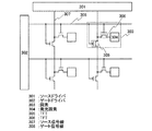
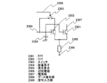
本発明は、ビデオ信号が入力される画素と、ビデオ信号が入力される画素を選択するゲート信号線及び画素にビデオ信号を入力するソース信号線を備えた半導体装置である。この半導体装置は、ソース信号線に直列に挿入されていて、ゲート信号線で画素が選択されていないときにオンとなり、画素が選択されている場合にはオフとなるように制御されるスイッチとを有している。 The present invention is a semiconductor device including a pixel to which a video signal is input, a gate signal line for selecting the pixel to which the video signal is input, and a source signal line for inputting the video signal to the pixel. This semiconductor device is inserted in series with a source signal line, and is turned on when a pixel is not selected by a gate signal line, and is controlled to be turned off when a pixel is selected. have.
本発明の一は、ビデオ信号が入力され、行方向及び列方向に配列された複数の画素と、行方向に延びる配線であって複数の画素へのビデオ信号の入力を選択する複数のゲート信号線と、列方向に延びる配線であって複数の画素へビデオ信号を入力する複数のソース信号線とを有する半導体装置である。そして、複数の画素のそれぞれに対応し、複数のソース線に直列に挿入され、複数のゲート信号線によって選択されていない行をオンとし、複数のゲート信号線によって選択された行をオフするように制御される複数のスイッチを有している。 According to one aspect of the present invention, a plurality of pixels arranged in a row direction and a column direction to which a video signal is input, and a plurality of gate signals that are wirings extending in the row direction and select input of the video signal to the plurality of pixels The semiconductor device includes a line and a plurality of source signal lines that extend in the column direction and input video signals to a plurality of pixels. A row corresponding to each of the plurality of pixels and inserted in series in the plurality of source lines and not selected by the plurality of gate signal lines is turned on, and a row selected by the plurality of gate signal lines is turned off. A plurality of switches to be controlled.
本発明の一は、ビデオ信号が入力される画素と、画素へのビデオ信号の入力を選択するゲート信号線と、画素にビデオ信号を入力するソース信号線と、ソース信号線に直列に挿入され、ゲート信号線で、画素が選択されていない場合にはオンとなり、画素が選択されている場合にはオフとなるように制御される第1のトランジスタとを備えた半導体装置である。画素は、発光素子を含み、ビデオ信号に応じて発光素子の発光及び非発光の状態を制御する発光制御回路と、ソース及びドレインの一方が第1のトランジスタと接続し、他方が発光制御回路と接続する第2のトランジスタとを有している。 In one embodiment of the present invention, a pixel to which a video signal is input, a gate signal line that selects input of the video signal to the pixel, a source signal line that inputs a video signal to the pixel, and a source signal line are inserted in series. A semiconductor device including a first transistor which is controlled to be turned on when a pixel is not selected by a gate signal line and turned off when a pixel is selected. The pixel includes a light-emitting element, and a light-emission control circuit that controls light emission and non-light-emission states of the light-emitting element according to a video signal, one of a source and a drain connected to the first transistor, and the other is a light emission control circuit And a second transistor to be connected.
本発明の一は、ビデオ信号が入力され、行方向及び列方向に配列された複数の画素と、行方向に延びる配線であって複数の画素へのビデオ信号の入力を選択する複数のゲート信号線と、列方向に延びる配線であって複数の画素へビデオ信号を入力する複数のソース信号線とを備えた半導体装置である。そして、複数の画素のそれぞれに対応し、複数のソース信号線に直列に挿入され、複数のゲート信号線によって選択されていない行をオンとし、複数のゲート信号線によって選択された行をオフするように制御される複数の第1のトランジスタとを備えた半導体装置である。当該画素は、発光素子を含み、ビデオ信号に応じて発光素子の発光及び非発光の状態を制御する発光制御回路と、ソース及びドレインの一方が第1のトランジスタと接続し、他方が発光制御回路と接続する第2のトランジスタを有している。 According to one aspect of the present invention, a plurality of pixels arranged in a row direction and a column direction to which a video signal is input, and a plurality of gate signals that are wirings extending in the row direction and select input of the video signal to the plurality of pixels The semiconductor device includes a line and a plurality of source signal lines that extend in the column direction and input video signals to a plurality of pixels. A row corresponding to each of the plurality of pixels, inserted in series with the plurality of source signal lines, and not selected by the plurality of gate signal lines is turned on, and a row selected by the plurality of gate signal lines is turned off. And a plurality of first transistors controlled in this manner. The pixel includes a light-emitting element, a light-emission control circuit that controls light emission and non-light-emission states of the light-emitting element according to a video signal, one of a source and a drain is connected to the first transistor, and the other is a light emission control circuit And a second transistor connected to.
本発明の一は、ビデオ信号が入力される画素と、画素へのビデオ信号の入力を選択する第1のゲート信号線と、第1のゲート信号線とは反転した電位を持つ第2のゲート信号線と、画素にビデオ信号を入力するソース信号線と、ソース信号線に直列に挿入され、第2のゲート信号線の電位がゲートに印加される第1のトランジスタとを備えた半導体装置である。画素は発光素子を含み、ビデオ信号に応じて発光素子の発光及び非発光の状態を制御する発光制御回路と、ソース及びドレインの一方が第1のトランジスタと接続し、他方が発光制御回路と接続し、第1のゲート信号線とゲートが接続する第2のトランジスタとを有している。 According to one embodiment of the present invention, a pixel to which a video signal is input, a first gate signal line that selects input of the video signal to the pixel, and a second gate having a potential inverted from the first gate signal line A semiconductor device including a signal line, a source signal line that inputs a video signal to a pixel, and a first transistor that is inserted in series with the source signal line and to which the potential of the second gate signal line is applied to the gate. is there. The pixel includes a light-emitting element, a light-emission control circuit that controls light emission and non-light-emission states of the light-emitting element according to a video signal, one of the source and the drain is connected to the first transistor, and the other is connected to the light emission control circuit The first gate signal line and the second transistor connected to the gate are included.
本発明の一は、ビデオ信号が入力される画素と、画素へのビデオ信号の入力を選択する第1のゲート信号線と、画素にビデオ信号を入力するソース信号線と、ソース信号線に直列に挿入される第1のトランジスタと、第1のトランジスタのゲートに接続される第2のゲート信号線を備えた半導体装置である。画素は発光素子を含み、ビデオ信号に応じて発光素子の発光及び非発光の状態を制御する発光制御回路と、ソース及びドレインの一方がソース信号線と接続し、他方が発光制御回路と接続し、第1のゲート信号線とゲートが接続する第2のトランジスタとを含み、第1のゲート信号線と第2のゲート信号線のそれぞれは、第1のゲート信号線に接続する第2のトランジスタがオンとなるときに、第2のゲート信号線によって選択された行の第1のトランジスタをオフとし、第1のゲート信号線に接続する記第2のトランジスタがオフとなるときに、第2のゲート信号線によって選択された行の第1のトランジスタをオンとする電位を有している。 According to one embodiment of the present invention, a pixel to which a video signal is input, a first gate signal line that selects input of the video signal to the pixel, a source signal line that inputs a video signal to the pixel, and a source signal line in series And a second gate signal line connected to the gate of the first transistor. The pixel includes a light emitting element, and a light emission control circuit that controls the light emitting and non-light emitting states of the light emitting element according to a video signal, one of the source and the drain is connected to the source signal line, and the other is connected to the light emitting control circuit. , And a second transistor connected to the gate, each of the first gate signal line and the second gate signal line being connected to the first gate signal line. Is turned on, the first transistor in the row selected by the second gate signal line is turned off, and the second transistor connected to the first gate signal line is turned off. And a potential for turning on the first transistors in the row selected by the gate signal line.
本発明に示すスイッチは、様々な形態のものを用いることができ、一例として、電気的スイッチや機械的なスイッチなどがある。つまり、電流の流れを制御できるものであればよく、特定のものに限定されず、様々なものを用いることができる。例えば、トランジスタでもよいし、ダイオード(例えば、PNダイオード、PINダイオード、ショットキーダイオード、ダイオード接続のトランジスタなど)でもよいし、サイリスタでもよいし、それらを組み合わせた論理回路でもよい。よって、スイッチとしてトランジスタを用いる場合、そのトランジスタは、単なるスイッチとして動作するため、トランジスタの極性(導電型)は特に限定されない。ただし、オフ電流が少ない方が望ましい場合、オフ電流が少ない方の極性のトランジスタを用いることが望ましい。オフ電流が少ないトランジスタとしては、LDD領域を設けているものやマルチゲート構造にしているもの等がある。また、スイッチとして動作させるトランジスタのソース端子の電位が、低電位側電源(Vss、GND、0Vなど)に近い状態で動作する場合はNチャネル型を、反対に、ソース端子の電位が、高電位側電源(Vddなど)に近い状態で動作する場合はPチャネル型を用いることが望ましい。なぜなら、ゲートソース間電圧の絶対値を大きくできるため、スイッチとして、動作しやすいからである。 The switch shown in the present invention can be used in various forms, and examples thereof include an electrical switch and a mechanical switch. In other words, any device can be used as long as it can control the flow of current, and it is not limited to a specific device, and various devices can be used. For example, it may be a transistor, a diode (for example, a PN diode, a PIN diode, a Schottky diode, a diode-connected transistor, or the like), a thyristor, or a logic circuit that combines them. Therefore, when a transistor is used as a switch, the transistor operates as a mere switch, and thus the polarity (conductivity type) of the transistor is not particularly limited. However, when it is desirable that the off-state current is small, it is desirable to use a transistor having a polarity with a small off-state current. As a transistor with low off-state current, there are a transistor provided with an LDD region and a transistor having a multi-gate structure. Further, when the transistor operated as a switch operates at a source terminal potential close to a low potential power source (Vss, GND, 0 V, etc.), the N-channel type is used. On the contrary, the source terminal potential is a high potential. When operating in a state close to the side power supply (Vdd or the like), it is desirable to use a P-channel type. This is because the absolute value of the voltage between the gate and the source can be increased, so that it can easily operate as a switch.
Nチャネル型とPチャネル型の両方を用いて、CMOS型のスイッチにしてもよい。CMOS型のスイッチにすると、Pチャネル型かNチャネル型かのどちらかのスイッチが導通すれば電流を流すことができるため、スイッチとして機能しやすくなる。例えば、スイッチへの入力信号の電圧が高い場合でも、低い場合でも、適切に電圧を出力させることが出来る。また、スイッチをオン・オフさせるための信号の電圧振幅値を小さくすることが出来るので、消費電力を小さくすることも出来る。 A CMOS switch may be used by using both an N channel type and a P channel type. When a CMOS switch is used, a current can flow when either the P-channel switch or the N-channel switch is turned on, so that the switch can easily function as a switch. For example, the voltage can be appropriately output regardless of whether the voltage of the input signal to the switch is high or low. In addition, since the voltage amplitude value of the signal for turning on / off the switch can be reduced, the power consumption can be reduced.
なお、スイッチとしてトランジスタを用いる場合は、入力端子(ソース端子またはドレイン端子の一方)と、出力端子(ソース端子またはドレイン端子の他方)と、導通を制御する端子(ゲート端子)とを有している。一方、スイッチとしてダイオードを用いる場合は、導通を制御する端子を有していない場合がある。そのため、端子を制御するための配線を少なくすることが出来る。 Note that in the case where a transistor is used as a switch, the transistor has an input terminal (one of a source terminal or a drain terminal), an output terminal (the other of the source terminal or the drain terminal), and a terminal for controlling conduction (a gate terminal). Yes. On the other hand, when a diode is used as a switch, it may not have a terminal for controlling conduction. Therefore, the wiring for controlling the terminals can be reduced.
本発明において、接続されているとは、電気的に接続されている場合と機能的に接続されている場合と直接接続されている場合とを含むものとする。したがって、本発明が開示する構成において、所定の接続関係以外のものも含むものとする。例えば、ある部分とある部分との間に、電気的な接続を可能とする素子(例えば、スイッチやトランジスタや容量素子やインダクタや抵抗素子やダイオードなど)が1個以上配置されていてもよい。また、機能的な接続を可能とする回路(例えば、論理回路(インバータやNAND回路やNOR回路など)や信号変換回路(DA変換回路やAD変換回路やガンマ補正回路など)や電位レベル変換回路(昇圧回路や降圧回路などの電源回路やH信号やL信号の電位レベルを変えるレベルシフタ回路など)や電圧源や電流源や切り替え回路や増幅回路(オペアンプや差動増幅回路やソースフォロワ回路やバッファ回路など、信号振幅や電流量などを大きく出来る回路など)や信号生成回路や記憶回路や制御回路など)が間に1個以上配置されていてもよい。あるいは、間に他の素子や他の回路を挟まずに、直接接続されて、配置されていてもよい。 In the present invention, the term “connected” includes the case of being electrically connected, the case of being functionally connected, and the case of being directly connected. Therefore, the configuration disclosed by the present invention includes other than the predetermined connection relationship. For example, one or more elements (for example, a switch, a transistor, a capacitor, an inductor, a resistor, a diode, or the like) that can be electrically connected may be arranged between a certain portion. In addition, a circuit (for example, a logic circuit (an inverter, a NAND circuit, a NOR circuit, etc.), a signal conversion circuit (a DA conversion circuit, an AD conversion circuit, a gamma correction circuit, etc.) or a potential level conversion circuit ( Power supply circuits such as booster circuits and step-down circuits, level shifter circuits that change the potential level of H and L signals, etc., voltage sources, current sources, switching circuits, and amplifier circuits (op amps, differential amplifier circuits, source follower circuits, and buffer circuits) Etc.), or a signal generation circuit, a memory circuit, a control circuit, etc.) may be disposed between them. Alternatively, they may be arranged directly connected without interposing other elements or other circuits therebetween.
素子や回路を間に介さずに接続されている場合のみを含む場合は、直接接続されている、と記載するものとする。また、電気的に接続されている、と記載する場合は、電気的に接続されている場合(つまり、間に別の素子を挟んで接続されている場合)と機能的に接続されている場合(つまり、間に別の回路を挟んで接続されている場合)と直接接続されている場合(つまり、間に別の素子や別の回路を挟まずに接続されている場合)とを含むものとする。 In the case of including only the case of being connected without interposing elements or circuits, it is described as being directly connected. In addition, when it is described as being electrically connected, when it is electrically connected (that is, when connected with another element in between) and when it is functionally connected (That is, connected with another circuit in between) and directly connected (that is, connected without another element or circuit in between). .
表示素子や表示装置や発光素子や発光装置は、様々な形態を用いることが出来る。例えば、画素に配置する表示素子としては、EL素子(有機EL素子、無機EL素子又は有機物及び無機物を含むEL素子)、電子放出素子、液晶素子、電子インク、グレーティングライトバルブ(GLV)、プラズマディスプレイ(PDP)、デジタルマイクロミラーデバイス(DMD)、圧電セラミック素子、カーボンナノチューブ、など、電気磁気的作用によりコントラストが変化する表示媒体を適用することができる。なお、EL素子を用いた表示装置としてはELディスプレイ、電子放出素子を用いた表示装置としてはフィールドエミッションディスプレイ(FED)やSED方式平面型ディスプレイ(SED:Surface−conduction Electron−emitter Disply)など、液晶素子を用いた表示装置としては液晶ディスプレイ、透過型液晶ディスプレイ、半透過型液晶ディスプレイ、反射型液晶ディスプレイ、電子インクを用いた表示装置としては電子ペーパーがある。 Various forms can be used for the display element, the display device, the light-emitting element, and the light-emitting device. For example, as a display element arranged in a pixel, an EL element (organic EL element, inorganic EL element or EL element including organic and inorganic substances), electron-emitting element, liquid crystal element, electronic ink, grating light valve (GLV), plasma display (PDP), a digital micromirror device (DMD), a piezoelectric ceramic element, a carbon nanotube, or the like can be used as a display medium whose contrast is changed by an electromagnetic action. Note that a display device using an EL element is an EL display, and a display device using an electron-emitting device is a liquid crystal display such as a field emission display (FED) or a SED type flat display (SED: Surface-conduction Electron-Emitter Display). A display device using the element includes a liquid crystal display, a transmissive liquid crystal display, a transflective liquid crystal display, a reflective liquid crystal display, and a display device using electronic ink includes electronic paper.
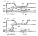
本発明において、トランジスタは、様々な形態のトランジスタを適用させることが出来る。よって、適用可能なトランジスタの種類に限定はない。したがって、例えば、非晶質シリコンや多結晶シリコンに代表される非単結晶半導体膜を有する薄膜トランジスタ(TFT)などを適用することが出来る。これらにより、製造温度が高くなくても製造できたり、低コストで製造できたり、大型基板上に製造できたり、透明基板上に製造できたり、トランジスタで光を透過させたりすることが出来る。また、半導体基板やSOI基板を用いて形成されるMOS型トランジスタ、接合型トランジスタ、バイポーラトランジスタなどを適用することが出来る。これらにより、バラツキの少ないトランジスタを製造できたり、電流供給能力の高いトランジスタを製造できたり、サイズの小さいトランジスタを製造できたり、消費電力の少ない回路を構成したりすることが出来る。また、ZnO、a−InGaZnO、SiGe、GaAsなどの化合物半導体を有するトランジスタや、さらに、それらを薄膜化した薄膜トランジスタなどを適用することが出来る。これらにより、製造温度が高くなくても製造できたり、室温で製造できたり、耐熱性の低い基板、例えばプラスチック基板やフィルム基板に直接トランジスタを形成したりすることが出来る。また、インクジェットや印刷法を用いて作成したトランジスタなどを適用することが出来る。これらにより、室温で製造したり、真空度の低い状態で製造したり、大型基板で製造したりすることができる。また、マスク(レチクル)を用いなくても製造することが可能となるため、トランジスタのレイアウトを容易に変更することが出来る。また、有機半導体やカーボンナノチューブを有するトランジスタ、その他のトランジスタを適用することができる。これらにより、曲げることが可能な基板上にトランジスタを形成することが出来る。なお、非単結晶半導体膜には水素またはハロゲンが含まれていてもよい。また、トランジスタが配置されている基板の種類は、様々なものを用いることができ、特定のものに限定されることはない。従って例えば、単結晶基板、SOI基板、ガラス基板、石英基板、プラスチック基板、紙基板、セロファン基板、ステンレススチル基板、ステンレススチルホイル基板などに配置することが出来る。また、ある基板でトランジスタを形成し、その後、別の基板にトランジスタを移動させて、別の基板上に配置するようにしてもよい。これらの基板を用いることにより、特性のよいトランジスタを形成したり、消費電力の小さいトランジスタを形成したり、壊れにくい装置にしたり、耐熱性を持たせたりすることが出来る。 In the present invention, various types of transistors can be used as the transistor. Thus, there is no limitation on the type of applicable transistor. Therefore, for example, a thin film transistor (TFT) including a non-single-crystal semiconductor film typified by amorphous silicon or polycrystalline silicon can be used. As a result, they can be manufactured even at a low manufacturing temperature, can be manufactured at low cost, can be manufactured on a large substrate, can be manufactured on a transparent substrate, and light can be transmitted through a transistor. Alternatively, a MOS transistor, a junction transistor, a bipolar transistor, or the like formed using a semiconductor substrate or an SOI substrate can be used. Accordingly, a transistor with little variation can be manufactured, a transistor with high current supply capability can be manufactured, a transistor with a small size can be manufactured, and a circuit with low power consumption can be configured. In addition, a transistor including a compound semiconductor such as ZnO, a-InGaZnO, SiGe, or GaAs, or a thin film transistor obtained by thinning them can be used. Accordingly, the transistor can be manufactured even at a low manufacturing temperature, can be manufactured at room temperature, or a transistor can be directly formed on a substrate having low heat resistance, such as a plastic substrate or a film substrate. In addition, a transistor formed using an inkjet method or a printing method can be used. By these, it can manufacture at room temperature, can manufacture in a state with a low degree of vacuum, or can manufacture with a large sized board | substrate. Further, since the transistor can be manufactured without using a mask (reticle), the layout of the transistor can be easily changed. In addition, a transistor including an organic semiconductor or a carbon nanotube, or another transistor can be used. Thus, a transistor can be formed over a substrate that can be bent. Note that the non-single-crystal semiconductor film may contain hydrogen or halogen. In addition, various types of substrates on which the transistor is arranged can be used, and the substrate is not limited to a specific type. Therefore, for example, it can be disposed on a single crystal substrate, an SOI substrate, a glass substrate, a quartz substrate, a plastic substrate, a paper substrate, a cellophane substrate, a stainless steel substrate, a stainless steel foil substrate, or the like. Alternatively, a transistor may be formed using a certain substrate, and then the transistor may be moved to another substrate and placed on another substrate. By using these substrates, it is possible to form a transistor with good characteristics, to form a transistor with low power consumption, to make the device hard to break, or to have heat resistance.
トランジスタの構成は、様々な形態をとることができる。特定の構成に限定されない。例えば、ゲート電極が2個以上になっているマルチゲート構造を用いてもよい。マルチゲート構造にすると、チャネル領域が直列に接続されるような構成となるため、複数のトランジスタが直列に接続されたような構成となる。マルチゲート構造にすることにより、オフ電流を低減したり、トランジスタの耐圧を向上させて信頼性を良くしたり、飽和領域で動作する時に、ドレイン・ソース間電圧が変化しても、ドレイン・ソース間電流があまり変化せず、フラットな特性にすることなどができる。また、チャネルの上下にゲート電極が配置されている構造でもよい。チャネルの上下にゲート電極が配置されている構造にすることにより、チャネル領域が増えるため、電流値を大きくしたり、空乏層ができやすくなってS値をよくしたりすることができる。チャネルの上下にゲート電極が配置されると、複数のトランジスタが並列に接続されたような構成となる。 The structure of the transistor can take various forms. It is not limited to a specific configuration. For example, a multi-gate structure having two or more gate electrodes may be used. When the multi-gate structure is used, the channel regions are connected in series, so that a plurality of transistors are connected in series. The multi-gate structure reduces the off current, improves the breakdown voltage of the transistor to improve reliability, and even when the drain-source voltage changes when operating in the saturation region. The inter-current does not change so much, and flat characteristics can be achieved. Alternatively, a structure in which gate electrodes are arranged above and below the channel may be employed. By adopting a structure in which gate electrodes are arranged above and below the channel, the channel region increases, so that the current value can be increased, and a depletion layer can be easily formed to improve the S value. When gate electrodes are provided above and below a channel, a structure in which a plurality of transistors are connected in parallel is obtained.
チャネルの上にゲート電極が配置されている構造でもよいし、チャネルの下にゲート電極が配置されている構造でもよいし、正スタガ構造であってもよいし、逆スタガ構造でもよいし、チャネル領域が複数の領域に分かれていてもよいし、並列に接続されていてもよいし、直列に接続されていてもよい。また、チャネル(もしくはその一部)にソース電極やドレイン電極が重なっていてもよい。チャネル(もしくはその一部)にソース電極やドレイン電極が重なっている構造にすることにより、チャネルの一部に電荷がたまって、動作が不安定になることを防ぐことができる。また、LDD領域があってもよい。LDD領域を設けることにより、オフ電流を低減したり、トランジスタの耐圧を向上させて信頼性を良くしたり、飽和領域で動作する時に、ドレイン・ソース間電圧が変化しても、ドレイン・ソース間電流があまり変化せず、フラットな特性にすることができる。 A structure in which a gate electrode is disposed above a channel, a structure in which a gate electrode is disposed below a channel, a normal staggered structure, an inverted staggered structure, or a channel The region may be divided into a plurality of regions, may be connected in parallel, or may be connected in series. In addition, a source electrode or a drain electrode may overlap with the channel (or a part thereof). By using a structure in which a source electrode or a drain electrode overlaps with a channel (or part of it), it is possible to prevent electric charges from being accumulated in part of the channel and unstable operation. There may also be an LDD region. By providing an LDD region, the off-current can be reduced, the breakdown voltage of the transistor can be improved to improve reliability, or the drain-source voltage can be changed even when the drain-source voltage changes when operating in the saturation region. The current does not change so much, and a flat characteristic can be obtained.
本発明におけるトランジスタは、様々なタイプを用いることができ、様々な基板上に形成させることができる。したがって、回路の全てが、ガラス基板上に形成されていてもよいし、プラスチック基板に形成されていてもよいし、単結晶基板に形成されていてもよいし、SOI基板上に形成されていてもよいし、どのような基板上に形成されていてもよい。回路の全てが同じ基板上に形成されていることにより、部品点数を減らしてコストを低減したり、回路部品との接続点数を減らして信頼性を向上させたりすることができる。あるいは、回路の一部が、ある基板に形成されており、回路の別の一部が、別の基板に形成されていてもよい。つまり、回路の全てが同じ基板上に形成されていなくてもよい。例えば、回路の一部は、ガラス基板上にトランジスタを用いて形成し、回路の別の一部は、単結晶基板上に形成し、そのICチップをCOG(Chip On Glass)で接続してガラス基板上に配置してもよい。あるいは、そのICチップをTAB(Tape Automated Bonding)やプリント基板を用いてガラス基板と接続してもよい。このように、回路の一部が同じ基板に形成されていることにより、部品点数を減らしてコストを低減したり、回路部品との接続点数を減らして信頼性を向上させたりすることができる。また、駆動電圧が高い部分や駆動周波数が高い部分は、消費電力が大きくなってしまうので、そのような部分は同じ基板に形成しないようにすれば、消費電力の向上を防ぐことができる。 Various types of transistors can be used in the present invention and can be formed over various substrates. Therefore, the entire circuit may be formed on a glass substrate, may be formed on a plastic substrate, may be formed on a single crystal substrate, or may be formed on an SOI substrate. Alternatively, it may be formed on any substrate. Since all the circuits are formed on the same substrate, the number of parts can be reduced to reduce the cost, and the number of connection points with circuit parts can be reduced to improve the reliability. Alternatively, a part of the circuit may be formed on a certain substrate, and another part of the circuit may be formed on another substrate. That is, all of the circuits may not be formed on the same substrate. For example, part of a circuit is formed using a transistor over a glass substrate, another part of the circuit is formed over a single crystal substrate, and the IC chip is connected with COG (Chip On Glass) to form a glass. You may arrange | position on a board | substrate. Alternatively, the IC chip may be connected to the glass substrate using TAB (Tape Automated Bonding) or a printed board. As described above, since a part of the circuit is formed on the same substrate, the number of parts can be reduced to reduce the cost, and the number of connection points with the circuit parts can be reduced to improve the reliability. In addition, since the power consumption increases in a portion where the drive voltage is high or a portion where the drive frequency is high, an improvement in power consumption can be prevented if such a portion is not formed on the same substrate.
本発明においては、一画素とは、明るさを制御できる要素一つ分を示すものとする。よって、一例としては、一画素とは、一つの色要素を示すものとし、その色要素一つで明るさを表現する。従って、そのときは、R(赤)G(緑)B(青)の色要素からなるカラー表示装置の場合には、画像の最小単位は、Rの画素とGの画素とBの画素との三画素から構成されるものとする。なお、色要素は、三色に限定されず、それ以上の数を用いても良いし、RGB以外の色を用いても良い。例えば、白色を加えて、RGBW(Wは白)としてもよい。また、RGBに、例えば、イエロー、シアン、マゼンタ、エメラルドグリーン、朱色などを一色以上追加したものでもよい。また、例えばRGBの中の少なくとも一色について、類似した色を追加してもよい。例えば、R、G、B1、B2としてもよい。B1とB2とは、どちらも青色であるが、少し吸収波長が異なっている。このような色要素を用いることにより、より実物に近い表示を行うことができたり、消費電力を低減したりすることが出来る。また、別の例としては、1つの色要素について、複数の領域を用いて明るさを制御する場合は、その領域一つ分を一画素とする。よって、一例としては、面積階調を行う場合、一つの色要素につき、明るさを制御する領域が複数あり、その全体で階調を表現するわけであるが、明るさを制御する領域の一つ分を一画素とする。よって、その場合は、一つの色要素は、複数の画素で構成されることとなる。また、その場合、画素によって、表示に寄与する領域の大きさが異なっている場合がある。また、一つの色要素につき複数ある、明るさを制御する領域において、つまり、一つの色要素を構成する複数の画素において、各々に供給する信号を僅かに異ならせるようにして、視野角を広げるようにしてもよい。 In the present invention, one pixel represents one element whose brightness can be controlled. Therefore, as an example, one pixel represents one color element, and brightness is expressed by one color element. Therefore, at that time, in the case of a color display device composed of R (red), G (green), and B (blue) color elements, the minimum unit of an image is an R pixel, a G pixel, and a B pixel. It is assumed to be composed of three pixels. Note that the color elements are not limited to three colors, and more than that may be used, or colors other than RGB may be used. For example, RGBW (W is white) may be added by adding white. Further, RGB may be obtained by adding one or more colors such as yellow, cyan, magenta, emerald green, vermilion, and the like. Further, for example, a similar color may be added for at least one of RGB. For example, R, G, B1, and B2 may be used. B1 and B2 are both blue, but have slightly different absorption wavelengths. By using such a color element, it is possible to perform display closer to the real thing or to reduce power consumption. As another example, in the case where brightness is controlled using a plurality of areas for one color element, one area corresponds to one pixel. Therefore, as an example, when performing area gradation, there are a plurality of areas for controlling the brightness for each color element, and the gradation is expressed as a whole. One portion is defined as one pixel. Therefore, in that case, one color element is composed of a plurality of pixels. In that case, the size of the region contributing to the display may be different depending on the pixel. Further, in a plurality of brightness control areas for one color element, that is, in a plurality of pixels constituting one color element, a signal supplied to each is slightly different to widen the viewing angle. You may do it.
一画素(三色分)と記載する場合は、RとGとBの三画素分を一画素と考える場合であるとする。一画素(一色分)と記載する場合は、一つの色要素につき、複数の画素がある場合、それらをまとめて一画素と考える場合であるとする。 When describing as one pixel (for three colors), it is assumed that three pixels of R, G, and B are considered as one pixel. In the case of describing one pixel (for one color), it is assumed that when there are a plurality of pixels for one color element, they are collectively considered as one pixel.
本発明において、画素は、マトリクス状に配置(配列)されている場合を含んでいる。ここで、画素がマトリクスに配置(配列)されているとは、縦方向もしくは横方向において、直線上に並んで配置されている場合や、ギザギザな線上に並んでいる場合を含んでいる。よって、例えば三色の色要素(例えばRGB)でフルカラー表示を行う場合に、ストライプ配置されている場合や、三つの色要素のドットがいわゆるデルタ配置されている場合も含むものとする。さらに、ベイヤー配置されている場合も含んでいる。また、色要素のドット毎にその表示領域の大きさが異なっていてもよい。これにより、消費電力を低下させたり、表示素子の寿命を延ばしたりすることが出来る。 In the present invention, the pixels include a case where the pixels are arranged (arranged) in a matrix. Here, the arrangement (arrangement) of pixels in a matrix includes a case where pixels are arranged side by side in a vertical direction or a horizontal direction or a case where they are arranged on a jagged line. Therefore, for example, when full color display is performed with three color elements (for example, RGB), the case where stripes are arranged and the case where dots of three color elements are arranged in a so-called delta are also included. Furthermore, the case where a Bayer is arranged is also included. Further, the size of the display area may be different for each dot of the color element. Thereby, power consumption can be reduced and the lifetime of the display element can be extended.
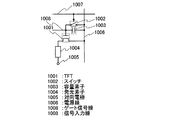
トランジスタとは、それぞれ、ゲートと、ドレインと、ソースとを含む少なくとも三つの端子を有する素子であり、ドレイン領域とソース領域の間にチャネル領域を有しており、ドレイン領域とチャネル領域とソース領域とを介して電流を流すことが出来る。ここで、ソースとドレインとは、トランジスタの構造や動作条件等によって変わるため、いずれがソースまたはドレインであるかを限定することが困難である。そこで、本発明においては、ソース及びドレインとして機能する領域を、ソースもしくはドレインと呼ばない場合がある。その場合、一例としては、それぞれを第1端子、第2端子と表記する場合がある。 A transistor is an element having at least three terminals including a gate, a drain, and a source, and has a channel region between the drain region and the source region, and the drain region, the channel region, and the source region. A current can be passed through. Here, since the source and the drain vary depending on the structure and operating conditions of the transistor, it is difficult to limit which is the source or the drain. Therefore, in the present invention, a region functioning as a source and a drain may not be called a source or a drain. In that case, as an example, there are cases where they are referred to as a first terminal and a second terminal, respectively.
なお、トランジスタは、ベースとエミッタとコレクタとを含む少なくとも三つの端子を有する素子であってもよい。この場合も同様に、エミッタとコレクタとを、第1端子、第2端子と表記する場合がある。 Note that the transistor may be an element having at least three terminals including a base, an emitter, and a collector. Similarly in this case, the emitter and the collector may be referred to as a first terminal and a second terminal.
なお、ゲートとは、ゲート電極とゲート配線(ゲート線またはゲート信号線等とも言う)とを含んだ全体、もしくは、それらの一部のことを言う。ゲート電極とは、チャネル領域やLDD(Lightly Doped Drain)領域などを形成する半導体と、ゲート絶縁膜を介してオーバーラップしている部分の導電膜のことを言う。ゲート配線とは、各画素のゲート電極の間を接続したり、ゲート電極と別の配線とを接続したりするための配線のことを言う。 Note that a gate refers to the whole or part of a gate electrode and a gate wiring (also referred to as a gate line or a gate signal line). A gate electrode refers to a conductive film which overlaps with a semiconductor that forms a channel region, an LDD (Lightly Doped Drain) region, and the like with a gate insulating film interposed therebetween. The gate wiring refers to wiring for connecting between the gate electrodes of each pixel or connecting the gate electrode to another wiring.
ただし、ゲート電極としても機能し、ゲート配線としても機能するような部分も存在する。そのような領域は、ゲート電極と呼んでも良いし、ゲート配線と呼んでも良い。つまり、ゲート電極とゲート配線とが、明確に区別できないような領域も存在する。例えば、延伸して配置されているゲート配線とオーバーラップしてチャネル領域がある場合、その領域はゲート配線として機能しているが、ゲート電極としても機能していることになる。よって、そのような領域は、ゲート電極と呼んでも良いし、ゲート配線と呼んでも良い。 However, there is a portion that functions as a gate electrode and also functions as a gate wiring. Such a region may be called a gate electrode or a gate wiring. That is, there is a region where the gate electrode and the gate wiring cannot be clearly distinguished. For example, when there is a channel region that overlaps with an extended gate wiring, the region functions as a gate wiring, but also functions as a gate electrode. Therefore, such a region may be called a gate electrode or a gate wiring.
ゲート電極と同じ材料で形成され、ゲート電極とつながっている領域も、ゲート電極と呼んでも良い。同様に、ゲート配線と同じ材料で形成され、ゲート配線とつながっている領域も、ゲート配線と呼んでも良い。このような領域は、厳密な意味では、チャネル領域とオーバーラップしていなかったり、別のゲート電極と接続させる機能を有してなかったりする場合がある。しかし、製造マージンなどの関係で、ゲート電極やゲート配線と同じ材料で形成され、ゲート電極やゲート配線とつながっている領域がある。よって、そのような領域もゲート電極やゲート配線と呼んでも良い。 A region formed of the same material as the gate electrode and connected to the gate electrode may also be called a gate electrode. Similarly, a region formed of the same material as the gate wiring and connected to the gate wiring may be called a gate wiring. In a strict sense, such a region may not overlap with the channel region or may not have a function of being connected to another gate electrode. However, there is a region that is formed of the same material as the gate electrode and the gate wiring and connected to the gate electrode and the gate wiring because of a manufacturing margin. Therefore, such a region may also be called a gate electrode or a gate wiring.
例えば、マルチゲートのトランジスタにおいて、1つのトランジスタのゲート電極と、別のトランジスタのゲート電極とは、ゲート電極と同じ材料で形成された導電膜で接続される場合が多い。そのような領域は、ゲート電極とゲート電極とを接続させるための領域であるため、ゲート配線と呼んでも良いが、マルチゲートのトランジスタを1つのトランジスタであると見なすことも出来るため、ゲート電極と呼んでも良い。つまり、ゲート電極やゲート配線と同じ材料で形成され、それらとつながって配置されているものは、ゲート電極やゲート配線と呼んでも良い。
また、例えば、ゲート電極とゲート配線とを接続してさせている部分の導電膜も、ゲート電極と呼んでも良いし、ゲート配線と呼んでも良い。
For example, in a multi-gate transistor, the gate electrode of one transistor and the gate electrode of another transistor are often connected by a conductive film formed using the same material as the gate electrode. Such a region is a region for connecting the gate electrode and the gate electrode, and may be referred to as a gate wiring. However, a multi-gate transistor can be regarded as a single transistor, and thus the gate electrode You can call it. That is, what is formed of the same material as the gate electrode and the gate wiring and is connected to the gate electrode and the gate wiring may be called a gate electrode and a gate wiring.
For example, a portion of the conductive film where the gate electrode and the gate wiring are connected may be called a gate electrode or a gate wiring.
ゲート端子とは、ゲート電極の領域や、ゲート電極と電気的に接続されている領域について、その一部分のことを言う。 The gate terminal refers to a part of a gate electrode region or a region electrically connected to the gate electrode.
ソースとは、ソース領域とソース電極とソース配線(ソース線またはソース信号線等とも言う)とを含んだ全体、もしくは、それらの一部のことを言う。ソース領域とは、P型不純物(ボロンやガリウムなど)やN型不純物(リンやヒ素など)が多く含まれる半導体領域のことを言う。従って、少しだけP型不純物やN型不純物が含まれる領域、いわゆる、LDD(Lightly Doped Drain)領域は、ソース領域には含まれない。ソース電極とは、ソース領域とは別の材料で形成され、ソース領域と電気的に接続されて配置されている部分の導電層のことを言う。ただし、ソース電極は、ソース領域も含んでソース電極と呼ぶこともある。ソース配線とは、各画素のソース電極の間を接続したり、ソース電極と別の配線とを接続したりするための配線のことを言う。 A source refers to the whole or part of a source region, a source electrode, and a source wiring (also referred to as a source line, a source signal line, or the like). The source region refers to a semiconductor region containing a large amount of P-type impurities (such as boron and gallium) and N-type impurities (such as phosphorus and arsenic). Therefore, a region containing a little P-type impurity or N-type impurity, that is, a so-called LDD (Lightly Doped Drain) region is not included in the source region. A source electrode refers to a portion of a conductive layer which is formed using a material different from that of a source region and is electrically connected to the source region. However, the source electrode may be referred to as a source electrode including the source region. The source wiring is a wiring for connecting between the source electrodes of each pixel or connecting the source electrode and another wiring.
しかしながら、ソース電極としても機能し、ソース配線としても機能するような部分も存在する。そのような領域は、ソース電極と呼んでも良いし、ソース配線と呼んでも良い。つまり、ソース電極とソース配線とが、明確に区別できないような領域も存在する。例えば、延伸して配置されているソース配線とオーバーラップしてソース領域がある場合、その領域はソース配線として機能しているが、ソース電極としても機能していることになる。よって、そのような領域は、ソース電極と呼んでも良いし、ソース配線と呼んでも良い。 However, there is a portion that functions as a source electrode and also functions as a source wiring. Such a region may be called a source electrode or a source wiring. That is, there is a region where the source electrode and the source wiring cannot be clearly distinguished. For example, when there is a source region that overlaps with an extended source wiring, the region functions as a source wiring, but also functions as a source electrode. Therefore, such a region may be called a source electrode or a source wiring.
また、ソース電極と同じ材料で形成され、ソース電極とつながっている領域や、ソース電極とソース電極とを接続する部分も、ソース電極と呼んでも良い。また、ソース領域とオーバーラップしている部分も、ソース電極と呼んでも良い。同様に、ソース配線と同じ材料で形成され、ソース配線とつながっている領域も、ソース配線と呼んでも良い。このような領域は、厳密な意味では、別のソース電極と接続させる機能を有していたりすることがない場合がある。しかし、製造マージンなどの関係で、ソース電極やソース配線と同じ材料で形成され、ソース電極やソース配線とつながっている領域がある。よって、そのような領域もソース電極やソース配線と呼んでも良い。 A region formed of the same material as the source electrode and connected to the source electrode, or a portion connecting the source electrode and the source electrode may also be referred to as a source electrode. A portion overlapping with the source region may also be called a source electrode. Similarly, a region formed of the same material as the source wiring and connected to the source wiring may be called a source wiring. In a strict sense, such a region may not have a function of connecting to another source electrode. However, there is a region formed of the same material as the source electrode and the source wiring and connected to the source electrode and the source wiring because of a manufacturing margin. Therefore, such a region may also be called a source electrode or a source wiring.
また、例えば、ソース電極とソース配線とを接続してさせている部分の導電膜も、ソース電極と呼んでも良いし、ソース配線と呼んでも良い。 Further, for example, a conductive film in a portion where the source electrode and the source wiring are connected to each other may be referred to as a source electrode or a source wiring.
ソース端子とは、ソース領域の領域や、ソース電極や、ソース電極と電気的に接続されている領域について、その一部分のことを言う。なお、ドレインについては、ソースと同様である。 The source terminal refers to a part of a source region, a source electrode, or a region electrically connected to the source electrode. The drain is the same as the source.
本発明において、半導体装置とは半導体素子(トランジスタやダイオードなど)を含む回路を有する装置をいう。また、半導体特性を利用することで機能しうる装置全般でもよい。また、表示装置とは、表示素子(液晶素子や発光素子など)を有する装置のことを言う。なお、液晶素子やEL素子などの表示素子を含む複数の画素やそれらの画素を駆動させる周辺駆動回路が同一基板上に形成された表示パネル本体のことでもよい。また、ワイヤボンディングやバンプなどによって基板上に配置された周辺駆動回路、いわゆるチップオングラス(COG)を含んでいても良い。さらに、フレキシブルプリントサーキット(FPC)やプリント配線基板(PWB)が取り付けられたもの(ICや抵抗素子や容量素子やインダクタやトランジスタなど)も含んでもよい。さらに、偏光板や位相差板などの光学シートを含んでいても良い。さらに、バックライト(導光板やプリズムシートや拡散シートや反射シートや光源(LEDや冷陰極管など)を含んでいても良い)を含んでいても良い。
また、発光装置とは、特にEL素子やFEDで用いる素子などの自発光型の表示素子を有している表示装置をいう。液晶表示装置とは、液晶素子を有している表示装置をいう。
In the present invention, a semiconductor device refers to a device having a circuit including a semiconductor element (such as a transistor or a diode). In addition, any device that can function by utilizing semiconductor characteristics may be used. A display device refers to a device having a display element (such as a liquid crystal element or a light-emitting element). Note that a display panel body in which a plurality of pixels including display elements such as a liquid crystal element and an EL element and peripheral drive circuits for driving these pixels are formed over the same substrate may be used. Further, it may include a peripheral drive circuit, so-called chip on glass (COG), which is disposed on the substrate by wire bonding or bumps. Furthermore, a device to which a flexible printed circuit (FPC) or a printed wiring board (PWB) is attached (an IC, a resistor, a capacitor, an inductor, a transistor, or the like) may also be included. Furthermore, an optical sheet such as a polarizing plate or a retardation plate may be included. Furthermore, a backlight (which may include a light guide plate, a prism sheet, a diffusion sheet, a reflection sheet, or a light source (such as an LED or a cold cathode tube)) may be included.
A light-emitting device refers to a display device including a self-luminous display element such as an EL element or an element used in an FED. A liquid crystal display device refers to a display device having a liquid crystal element.
本発明において、「ある物の上に形成されている」あるいは、「〜上に形成されている」というように、「〜の上に」あるいは、「〜上に」という記載については、ある物の上に直接接していることに限定されない。直接接してはいない場合、つまり、間に別のものが挟まっている場合も含むものとする。従って例えば、「層Aの上に(もしくは層A上に)層Bが形成されている」という場合は、層Aの上に直接接して層Bが形成されている場合と、層Aの上に直接接して別の層(例えば層Cや層Dなど)が形成されていて、その上に直接接して層Bが形成されている場合とを含むものとする。また、「〜の上方に」という記載についても同様であり、ある物の上に直接接していることに限定されず、間に別のものが挟まっている場合も含むものとする。従って例えば、「層Aの上方に層Bが形成されている」という場合は、層Aの上に直接接して層Bが形成されている場合と、層Aの上に直接接して別の層(例えば層Cや層Dなど)が形成されていて、その上に直接接して層Bが形成されている場合とを含むものとする。なお、「〜の下に」あるいは、「〜の下方に」の場合についても同様であり、直接接している場合と、接していない場合とを含むこととする。 In the present invention, the description “on top” or “on top”, such as “formed on a certain object” or “formed on top”, It is not limited to touching directly on top. This includes cases where they are not in direct contact, that is, cases where another object is sandwiched between them. Therefore, for example, when “layer B is formed on layer A (or on layer A)”, when layer B is formed in direct contact with layer A, In which another layer (for example, layer C or layer D) is formed in direct contact with layer B and layer B is formed in direct contact therewith. The same applies to the description “above” and is not limited to being in direct contact with a certain object, and includes a case in which another object is sandwiched therebetween. Therefore, for example, when “the layer B is formed above the layer A”, the layer B is formed in direct contact with the layer A, and another layer is formed in direct contact with the layer A. (For example, the layer C or the layer D) is formed, and the layer B is formed in direct contact therewith. The same applies to the case of “under” or “under” and includes the case of direct contact and the case of no contact.
本明細書において、「ソース信号線」とは、画素の動作を制御するためのビデオ信号をソースドライバから伝達する手段としてソースドライバの出力に接続されている配線のことを指している。 In this specification, the “source signal line” refers to a wiring connected to the output of the source driver as means for transmitting a video signal for controlling the operation of the pixel from the source driver.
本明細書において、「ゲート信号線」とは、画素へのビデオ信号の書込みを選択、非選択を制御するための走査信号をゲートドライバから伝達する手段としてゲートドライバの出力に接続されている配線のことを指している。 In this specification, a “gate signal line” is a wiring connected to an output of a gate driver as means for transmitting a scanning signal for controlling selection / non-selection of writing of a video signal to a pixel from the gate driver. It points to that.
本発明によれば、ゲート信号線で選択された画素にソース信号線からビデオ信号を書き込み、ゲート信号線で選択されていない画素のスイッチング素子をオンとして、ゲート信号線に選択された画素のスイッチング素子をオフとすることにより、ソース信号線の寄生容量の影響を抑制することができる。すなわち、ソース信号線の充放電に影響する寄生容量が、ソースドライバの出力から画素への書込みが選択されている画素までのソース信号線にしか影響しなくなる。こうして、ソース信号線の充放電による消費電力の増大を小さくし低消費電力化を図ることができる。 According to the present invention, the video signal is written from the source signal line to the pixel selected by the gate signal line, the switching element of the pixel not selected by the gate signal line is turned on, and the pixel selected by the gate signal line is switched. By turning off the element, the influence of the parasitic capacitance of the source signal line can be suppressed. That is, the parasitic capacitance that affects the charge / discharge of the source signal line affects only the source signal line from the output of the source driver to the pixel for which writing to the pixel is selected. Thus, an increase in power consumption due to charging / discharging of the source signal line can be reduced, and power consumption can be reduced.
本発明の実施の形態について、図面を用いて詳細に説明する。但し、本発明は以下の説明に限定されず、本発明の趣旨及びその範囲から逸脱することなくその形態及び詳細をさまざまに変更し得ることは当業者であれば容易に理解される。従って、本発明は以下に示す実施の形態の記載内容に限定して解釈されるものではない。 Embodiments of the present invention will be described in detail with reference to the drawings. However, the present invention is not limited to the following description, and it will be easily understood by those skilled in the art that modes and details can be variously changed without departing from the spirit and scope of the present invention. Therefore, the present invention should not be construed as being limited to the description of the embodiments below.
(第1の実施形態)
本発明に係る半導体装置の第1の構成について、図1を参照して説明する。
(First embodiment)
A first structure of a semiconductor device according to the present invention will be described with reference to FIG.
図1において、複数の画素103は行方向及び列方向に配列している。ソースドライバ101は、入力された制御信号に応じてビデオ信号を出力する回路を備えている。ソースドライバ101は、書き込みが選択された画素103に、ビデオ信号を、ソース信号線107を介して入力する。ゲートドライバ102は、ゲートドライバ102に入力された制御信号に応じてゲート信号線108を走査し、ビデオ信号を書込む画素を選択する回路を備えている。画素103には、発光ユニット104と、ゲート信号線108によりオン又はオフが選択されるスイッチ105及びスイッチ106を含まれている。この二つのスイッチは、スイッチ105がオンの場合はスイッチ106がオフし、スイッチ105がオフの場合はスイッチ106がオンするように動作する。なお、発光ユニット104は、発光素子と、発光素子を制御する回路を含んでいる。
In FIG. 1, a plurality of
この構成の半導体装置において、ソースドライバ101からソース信号線107を介して、ビデオ信号を画素103に書き込む場合の動作について説明する。この場合、ビデオ信号が入力される画素103は、スイッチ105がオフし、スイッチ106がオンとなっている。そして、ソースドライバ101からソース信号線107を介して発光ユニット104にビデオ信号が入力される。
An operation in the case of writing a video signal to the
次に、ビデオ信号を画素103に書き込まない場合の動作について説明する。この場合、ビデオ信号を書き込まれない画素103は、スイッチ105がオンとなり、スイッチ106がオフとなっている。そのため、ソースドライバ101からソース信号線107を介して発光ユニット104にビデオ信号が書き込まれることはない。
Next, an operation when a video signal is not written to the
ソースドライバ101から出力されるビデオ信号は、電圧信号又は電流信号のどちらの場合であっても同様に適用することができる。また、画素にビデオ信号を入力する構成であれば、画素の内部構成に限定は無い。例えば、駆動トランジスタの閾値電圧を補正するような回路、画像を鮮明にするための発光素子の発光の有無を決定する回路、時分割階調に用いられる駆動トランジスタをオフにするための消去用トランジスタなどがあっても良い。また、これらを制御するための信号線を追加されていても良い。さらに、画素に電流でビデオ信号を入力するときなどに用いられる、画素に電圧をプリチャージをするための電源線が追加されていても良い。また、必要に応じて電源線や信号線が追加されていても良い。電源線は電圧を供給しも良いし、電流を供給しても良い。信号線は電圧で制御されていても良いし、電流で制御されていても良い。
The video signal output from the
本実施形態は、ビデオ信号を書き込む画素103のスイッチ105をオフすることにより、ソースドライバ101の出力からみたソース信号線107の寄生容量の影響は、ビデオ信号を書き込む画素103までしか影響しない。そのため、ソース信号線107の寄生容量への充放電による消費電力の増大を抑制することができる。
In this embodiment, by turning off the
また、ソースドライバ101の出力からみたソース信号線107の寄生容量の影響は、ビデオ信号を書き込む画素103までしか影響しないことにより、ビデオ信号の画素103への書き込み時間は短縮される。この画素103を、電流入力型で動作させる場合には大きな利点となる。
In addition, the influence of the parasitic capacitance of the
このように、本実施の形態によれば、ソース信号線の充放電に影響する寄生容量が、ソースドライバの出力から画素への書込みが選択されている画素までのソース信号線にしか影響しなくなる。それにより、ソース信号線の充放電による消費電力の増大を小さくし低消費電力化を図ることができる。 As described above, according to the present embodiment, the parasitic capacitance that affects the charging / discharging of the source signal line affects only the source signal line from the output of the source driver to the pixel for which writing to the pixel is selected. . As a result, an increase in power consumption due to charging / discharging of the source signal line can be reduced and power consumption can be reduced.
(第2の実施形態)
本発明に係る半導体装置の第2の構成について、図2を参照して説明する。
(Second Embodiment)
A second configuration of the semiconductor device according to the present invention will be described with reference to FIG.
図2において、複数の画素203は行方向及び列方向に配列している。ソースドライバ201は、入力された制御信号に応じてビデオ信号を出力する回路であり、ビデオ信号をソース信号線207を介して書き込みが選択された画素203に入力する。ゲートドライバ202はゲートドライバ202に入力された制御信号に応じてゲート信号線208及びインバータ210を介してゲート信号線208の反転した電位を出力するゲート信号線209を走査し、ビデオ信号を書込む画素を選択する。
In FIG. 2, the plurality of
画素203は、発光素子と発光素子を制御するための回路を含む発光ユニット204と、ゲート信号線208によりオン、又はオフが選択されるスイッチ206及びゲート信号線209によりオン、又はオフが選択されるスイッチ205を含んでいる。また、スイッチ205がオンの場合はスイッチ206がオフし、スイッチ205がオフの場合はスイッチ206がオンするように動作する。
The
ソースドライバ201からソース信号線207を介して、ビデオ信号を画素203に書き込む場合の動作について説明する。この場合、ビデオ信号が書き込まれる画素203は、スイッチ205がオフとなり、スイッチ206がオンとなっている。そして、ソースドライバ201からソース信号線207を介して発光ユニット204にビデオ信号が書き込まれる。
An operation when a video signal is written to the
次に、ビデオ信号を画素203に書き込まない場合の動作について説明する。この場合、ビデオ信号が書き込まれない画素203は、スイッチ205がオンとなり、スイッチ206がオフとなっている。そのため、ソースドライバ201からソース信号線207を介して発光ユニット204にビデオ信号が書き込まれることはない。
Next, an operation when a video signal is not written to the
本実施形態は、スイッチ205とスイッチ206をそれぞれ反転した信号で制御することにより、スイッチ205及びスイッチ206の特性が同じでも、スイッチ205がオンの場合はスイッチ206がオフし、スイッチ205がオフの場合はスイッチ206がオンとすることができる。
In this embodiment, by controlling the
また、ゲート信号線208及びゲート信号線209と、スイッチ205及びスイッチ206との接続関係を逆としても良い。すなわち、スイッチ205はゲート信号線208によりオン及びオフが制御され、スイッチ206はゲート信号線209によりオン及びオフが制御されるようにしても良い。
The connection relationship between the
ソースドライバ201から出力されるビデオ信号は、電圧信号又は電流信号のどちらの場合であっても同様に適用することができる。また、画素にビデオ信号を入力する構成であれば、画素の内部構成に限定は無い。例えば、駆動トランジスタの閾値電圧を補正するような回路、画像を鮮明にするための発光素子の発光の有無を決定する回路、時分割階調に用いられる駆動トランジスタをオフにするための消去用トランジスタなどがあっても良い。また、これらを制御するための信号線を追加されていても良い。さらに、画素に電流でビデオ信号を入力するときなどに用いられる画素に電圧をプリチャージをするための電源線が追加されていても良い。また、必要に応じて電源線や信号線が追加されていても良い。電源線は電圧を供給しも良いし、電流を供給しても良い。信号線は電圧で制御されていても良いし、電流で制御されていても良い。
The video signal output from the
本実施形態は、ビデオ信号を書き込む画素203のスイッチ205をオフすることにより、ソースドライバ201の出力からみたソース信号線207の寄生容量の影響は、ビデオ信号を書き込む画素203までしか影響しない。そのため、ソース信号線207の寄生容量への充放電による消費電力の増大を抑制することができる。
In this embodiment, by turning off the
また、ソースドライバ201の出力からみたソース信号線207の寄生容量の影響は、ビデオ信号を書き込む画素203までしか影響しないことにより、ビデオ信号の画素203への書き込み時間は短縮される。この画素203を、電流入力型で動作させる場合には大きな利点となる。
In addition, since the influence of the parasitic capacitance of the
このように、本実施の形態によれば、ソース信号線の充放電に影響する寄生容量が、ソースドライバの出力から画素への書込みが選択されている画素までのソース信号線までにしか影響しなくなる。それにより、ソース信号線の充放電による消費電力の増大を小さくし低消費電力化を図ることができる。 As described above, according to the present embodiment, the parasitic capacitance that affects the charging / discharging of the source signal line affects only the source signal line from the output of the source driver to the pixel that is selected to be written to the pixel. Disappear. As a result, an increase in power consumption due to charging / discharging of the source signal line can be reduced and power consumption can be reduced.
(第3の実施形態)
本発明に係る半導体装置の第3の構成について、図3を参照して説明する。
(Third embodiment)
A third configuration of the semiconductor device according to the present invention will be described with reference to FIG.
図3において、複数の画素303は行方向及び列方向に配列している。ソースドライバ301は、入力された制御信号に応じてビデオ信号を出力する回路であり、ビデオ信号をソース信号線307を介して書き込みが選択された画素303に入力する。ゲートドライバ302は、ゲートドライバ302に入力された制御信号に応じてゲート信号線308を走査し、ビデオ信号を書込む画素を選択する。
In FIG. 3, the plurality of
画素303は、発光素子と発光素子を制御するための回路を含む発光ユニット304と、TFT305と、TFT306とを含んでいる。TFT305はソース信号線307に直列に挿入されており、TFT306はソースとドレインのうち一方がTFT305と接続し、ソースとドレインのうち他方が発光ユニット304と接続している。TFT305及びTFT306のゲートは、ゲート信号線308と接続し、ゲート信号線308により、当該TFTのオン又はオフが選択される。図3では、TFT305はPチャネル型TFTとし、TFT306はNチャネル型TFTとしているため、TFT305がオンの場合はTFT306がオフし、TFT305がオフの場合はTFT306がオンする。また、ゲート信号線308が画素303を選択しているときにTFT305をオフし、TFT306をオンするように動作する。
The
TFT305及びTFT306は異なる極性となっていればよく、例えば、TFT305をNチャネル型とする場合、TFT306はPチャネル型とすれば良い。また、TFT305をPチャネル型とする場合には、TFT306はNチャネル型とすれば良い。
The
ソースドライバ301からソース信号線307を介して、ビデオ信号を画素303に書き込む場合の動作について説明する。この場合、ビデオ信号を書き込まれる画素303は、TFT305がオフとなり、TFT306がオンとなっている。そして、ソースドライバ301からソース信号線307を介して発光ユニット304にビデオ信号が書き込まれる。
An operation when a video signal is written to the
ビデオ信号を画素303に書き込まない場合の動作について説明する。この場合、ビデオ信号を書き込まれない画素303は、TFT305がオンとなり、TFT306がオフとなっている。そのため、ソースドライバ301からソース信号線307を介して発光ユニット304にビデオ信号が書き込まれることはない。
An operation when a video signal is not written to the
本実施形態におけるソースドライバから出力されるビデオ信号は電圧で出力されても良いし、電流で出力されても良い。また、画素構成は画素にビデオ信号を入力する画素構成であれば良い。例えば、駆動トランジスタの閾値電圧を補正するような回路や画像を鮮明にするための発光素子の発光の有無を決定する回路や時分割階調に用いられる駆動トランジスタをオフにするための消去用トランジスタなどがあっても良い。また、これらを制御するための信号線を追加しても良いし、画素に電流でビデオ信号を入力するときなどに用いられる画素に電圧をプリチャージをするための電源線を追加しても良い。 The video signal output from the source driver in the present embodiment may be output as voltage or current. The pixel configuration may be any pixel configuration that inputs a video signal to the pixel. For example, a circuit for correcting the threshold voltage of the driving transistor, a circuit for determining the presence or absence of light emission of a light emitting element for sharpening an image, and an erasing transistor for turning off a driving transistor used for time division gradation There may be. In addition, a signal line for controlling these may be added, or a power supply line for precharging a voltage may be added to a pixel used when a video signal is input to the pixel with a current. .
また、必要に応じて電源線や信号線を追加しても良い。電源線は電圧を供給しも良いし、電流を供給しても良い。信号線は電圧で制御されていても良いし、電流で制御されていても良い。 Further, a power supply line and a signal line may be added as necessary. The power supply line may supply voltage or current. The signal line may be controlled by voltage or current.
本実施形態は、ビデオ信号を書き込む画素303のTFT305をオフすることにより、ソースドライバ301の出力からみたソース信号線307の寄生容量の影響は、ビデオ信号を書き込む画素303までしか影響しない。そのため、ソース信号線307の寄生容量への充放電による消費電力の増大を抑制することができる。
In this embodiment, by turning off the
また、ソースドライバ301の出力からみたソース信号線307の寄生容量の影響は、ビデオ信号を書き込む画素303までしか影響しないことにより、ビデオ信号の画素303への書き込み時間は短縮される。この画素303を、電流入力型で動作させる場合には大きな利点となる。
In addition, the influence of the parasitic capacitance of the
このように、本実施の形態によれば、ソース信号線の充放電に影響する寄生容量が、ソースドライバの出力から画素への書込みが選択されている画素までのソース信号線にしか影響しなくなる。それにより、ソース信号線の充放電による消費電力の増大を小さくし低消費電力化を図ることができる。 As described above, according to the present embodiment, the parasitic capacitance that affects the charging / discharging of the source signal line affects only the source signal line from the output of the source driver to the pixel for which writing to the pixel is selected. . As a result, an increase in power consumption due to charging / discharging of the source signal line can be reduced and power consumption can be reduced.
(第4の実施形態)
本発明に係る半導体装置の第4の構成について、図4を参照して説明する。
(Fourth embodiment)
A fourth structure of the semiconductor device according to the present invention will be described with reference to FIG.
図4において、複数の画素403は行方向及び列方向に配列している。ソースドライバ401は、入力された制御信号に応じてビデオ信号を出力する回路であり、ビデオ信号をソース信号線407を介して書き込みが選択された画素403に入力する。ゲートドライバ402はゲートドライバ402に入力された制御信号に応じてゲート信号線408を走査し、ビデオ信号を書込む画素を選択する。 In FIG. 4, the plurality of pixels 403 are arranged in the row direction and the column direction. The source driver 401 is a circuit that outputs a video signal in accordance with an input control signal, and inputs the video signal to the pixel 403 selected for writing via the source signal line 407. The gate driver 402 scans the gate signal line 408 in accordance with the control signal input to the gate driver 402, and selects a pixel into which a video signal is written.
画素403は、発光素子と発光素子を制御するための回路を含む発光ユニット404と、TFT405と、TFT406とを含んでいる。TFT405はソース信号線407に直列に挿入されており、TFT406はソースとドレインのうち一方がTFT405と接続し、ソースとドレインのうち他方が発光ユニット404と接続している。TFT405及びTFT406はゲートがゲート信号線408と接続し、ゲート信号線408によりオン又はオフが選択される。TFT405はNチャネル型TFTとし、TFT406はPチャネル型TFTとしているため、TFT405がオンの場合はTFT406がオフし、TFT405がオフの場合はTFT406がオンする。また、ゲート信号線408が画素403を選択しているときにTFT405をオフし、TFT406をオンする。 The pixel 403 includes a light emitting unit 404 including a light emitting element and a circuit for controlling the light emitting element, a TFT 405, and a TFT 406. The TFT 405 is inserted in series with the source signal line 407, and one of the source and drain of the TFT 406 is connected to the TFT 405, and the other of the source and drain is connected to the light emitting unit 404. The gates of the TFTs 405 and 406 are connected to the gate signal line 408, and ON or OFF is selected by the gate signal line 408. Since the TFT 405 is an N-channel TFT and the TFT 406 is a P-channel TFT, the TFT 406 is turned off when the TFT 405 is on, and the TFT 406 is turned on when the TFT 405 is off. Further, when the gate signal line 408 selects the pixel 403, the TFT 405 is turned off and the TFT 406 is turned on.
また、TFT405及びTFT406は別の極性となっていればよく、例えばTFT405をPチャネル型、TFT406をNチャネル型としても良い。 The TFTs 405 and 406 may have different polarities. For example, the TFT 405 may be a P-channel type and the TFT 406 may be an N-channel type.
ソースドライバ401からソース信号線407を介して、ビデオ信号を画素403に書き込む場合の動作について説明する。この場合、ビデオ信号を書き込まれる画素403は、TFT405がオフとなり、TFT406がオンとなっている。そして、ソースドライバ401からソース信号線407を介して発光ユニット404にビデオ信号が書き込まれる。 An operation in the case where a video signal is written to the pixel 403 from the source driver 401 via the source signal line 407 will be described. In this case, in the pixel 403 to which the video signal is written, the TFT 405 is turned off and the TFT 406 is turned on. Then, a video signal is written from the source driver 401 to the light emitting unit 404 via the source signal line 407.
ビデオ信号を画素403に書き込まない場合の動作について説明する。この場合、ビデオ信号を書き込まれない画素403は、TFT405がオンとなり、TFT406がオフとなっている。そのため、ソースドライバ401からソース信号線407を介して発光ユニット404にビデオ信号が書き込まれることはない。 An operation when the video signal is not written to the pixel 403 will be described. In this case, in the pixel 403 to which no video signal is written, the TFT 405 is turned on and the TFT 406 is turned off. Therefore, a video signal is not written from the source driver 401 to the light emitting unit 404 via the source signal line 407.
本実施形態におけるソースドライバから出力されるビデオ信号は電圧で出力されても良いし、電流で出力されても良い。また、画素構成は画素にビデオ信号を入力する画素構成であれば良い。例えば、駆動トランジスタの閾値電圧を補正するような回路や画像を鮮明にするための発光素子の発光の有無を決定する回路や時分割階調に用いられる駆動トランジスタをオフにするための消去用トランジスタなどがあってもよい。また、これらを制御するための信号線を追加しても良いし、画素に電流でビデオ信号を入力するときなどに用いられる画素に電圧をプリチャージをするための電源線を追加しても良い。 The video signal output from the source driver in the present embodiment may be output as voltage or current. The pixel configuration may be any pixel configuration that inputs a video signal to the pixel. For example, a circuit for correcting the threshold voltage of the driving transistor, a circuit for determining the presence or absence of light emission of a light emitting element for sharpening an image, and an erasing transistor for turning off a driving transistor used for time division gradation There may be. In addition, a signal line for controlling these may be added, or a power supply line for precharging a voltage may be added to a pixel used when a video signal is input to the pixel with a current. .
また、必要に応じて電源線や信号線を追加しても良い。電源線は電圧を供給しも良いし、電流を供給しても良い。信号線は電圧で制御されていても良いし、電流で制御されていても良い。 Further, a power supply line and a signal line may be added as necessary. The power supply line may supply voltage or current. The signal line may be controlled by voltage or current.
本実施形態は、ビデオ信号を書き込む画素403のTFT405をオフすることにより、ソースドライバ401の出力からみたソース信号線407の寄生容量の影響は、ビデオ信号を書き込む画素403までしか影響しない。そのため、ソース信号線407の寄生容量への充放電による消費電力の増大を抑制することができる。 In this embodiment, by turning off the TFT 405 of the pixel 403 for writing the video signal, the influence of the parasitic capacitance of the source signal line 407 as viewed from the output of the source driver 401 affects only the pixel 403 for writing the video signal. Therefore, an increase in power consumption due to charging / discharging of the parasitic capacitance of the source signal line 407 can be suppressed.
また、ソースドライバ401の出力からみたソース信号線407の寄生容量の影響は、ビデオ信号を書き込む画素403までしか影響しないことにより、ビデオ信号の画素403への書き込み時間は短縮される。この画素403を、電流入力型で動作させる場合には大きな利点となる。 In addition, since the influence of the parasitic capacitance of the source signal line 407 as viewed from the output of the source driver 401 affects only the pixel 403 to which the video signal is written, the video signal writing time is shortened. This is a great advantage when the pixel 403 is operated as a current input type.
(第5の実施形態)
本発明に係る半導体装置の第5の構成について、図5を参照して説明する。
(Fifth embodiment)
A fifth configuration of the semiconductor device according to the present invention will be described with reference to FIG.
図5において、複数の画素503は行方向及び列方向に配列している。ソースドライバ501は、入力された制御信号に応じてビデオ信号を出力する回路であり、ビデオ信号をソース信号線507を介して書き込みが選択された画素503に入力する。ゲートドライバ502はゲートドライバ502に入力された制御信号に応じてゲート信号線508及びインバータ510を介してゲート信号線508の反転した電位を出力するゲート信号線509を走査し、ビデオ信号を書込む画素を選択する。
In FIG. 5, the plurality of
画素503は、発光素子と、発光素子を制御するための回路を含む発光ユニット504と、TFT505と、TFT506とを含んでいる。TFT505はソース信号線507に直列に挿入されており、TFT506はソースとドレインのうち一方がTFT505と接続し、ソースとドレインのうち他方が発光ユニット504と接続している。TFT505のゲートはゲート信号線509と接続し、TFT506のゲートはゲート信号線508と接続し、TFT505はゲート信号線509によりオン又はオフが選択され、TFT506は、ゲート信号線508によりオン又はオフが選択される。TFT505及びTFT506は、Nチャネル型としているため、TFT505がオンの場合はTFT506がオフし、TFT505がオフの場合はTFT506がオンするように動作する。
The
また、TFT505及びTFT506は同じ極性となっていればよく、例えば、TFT505及びTFT506をPチャネル型としても良い。
The
ソースドライバ501からソース信号線507を介して、ビデオ信号を画素503に書き込む場合の動作について説明する。この場合、ビデオ信号を書き込まれる画素503は、TFT505がオフとなり、TFT506がオンとなっている。そして、ソースドライバ501からソース信号線507を介して発光ユニット504にビデオ信号が書き込まれる。
An operation in the case where a video signal is written to the
ビデオ信号を画素503に書き込まない場合の動作について説明する。この場合、ビデオ信号を書き込まれない画素503は、TFT505がオンとなり、TFT506がオフとなっている。そのため、ソースドライバ501からソース信号線507を介して発光ユニット504にビデオ信号が書き込まれることはない。
An operation when a video signal is not written to the
本実施形態におけるソースドライバから出力されるビデオ信号は電圧で出力されても良いし、電流で出力されても良い。また、画素構成は画素にビデオ信号を入力する画素構成であれば良い。例えば、駆動トランジスタの閾値電圧を補正するような回路や画像を鮮明にするための発光素子の発光の有無を決定する回路や時分割階調に用いられる駆動トランジスタをオフにするための消去用トランジスタなどがあっても良い。また、これらを制御するための信号線を追加しても良い。画素に電流でビデオ信号を入力するときなどに用いられる画素に電圧をプリチャージをするための電源線を追加しても良い。 The video signal output from the source driver in the present embodiment may be output as voltage or current. The pixel configuration may be any pixel configuration that inputs a video signal to the pixel. For example, a circuit for correcting the threshold voltage of the driving transistor, a circuit for determining the presence or absence of light emission of a light emitting element for sharpening an image, and an erasing transistor for turning off a driving transistor used for time division gradation There may be. Further, a signal line for controlling these may be added. A power supply line for precharging a voltage may be added to a pixel used when a video signal is input to the pixel with a current.
また、必要に応じて電源線や信号線を追加しても良い。電源線は電圧を供給しも良いし、電流を供給しても良い。信号線は電圧で制御されていても良いし、電流で制御されていても良い。 Further, a power supply line and a signal line may be added as necessary. The power supply line may supply voltage or current. The signal line may be controlled by voltage or current.
本実施形態は、ビデオ信号を書き込む画素503のTFT505をオフすることにより、ソースドライバ501の出力からみたソース信号線507の寄生容量の影響は、ビデオ信号を書き込む画素503までしか影響しない。そのため、ソース信号線507の寄生容量への充放電による消費電力の増大を抑制することができる。
In this embodiment, by turning off the
また、ソースドライバ501の出力からみたソース信号線507の寄生容量の影響は、ビデオ信号を書き込む画素503までしか影響しないことにより、ビデオ信号の画素503への書き込み時間は短縮される。この画素503を、電流入力型で動作させる場合には大きな利点となる。
Further, the influence of the parasitic capacitance of the
このように、本実施の形態によれば、ソース信号線の充放電に影響する寄生容量が、ソースドライバの出力から画素への書込みが選択されている画素までのソース信号線にしか影響しなくなる。それにより、ソース信号線の充放電による消費電力の増大を小さくし低消費電力化を図ることができる。 As described above, according to the present embodiment, the parasitic capacitance that affects the charging / discharging of the source signal line affects only the source signal line from the output of the source driver to the pixel for which writing to the pixel is selected. . As a result, an increase in power consumption due to charging / discharging of the source signal line can be reduced and power consumption can be reduced.
(第6の実施形態)
本発明に係る半導体装置の第6の構成について、図6を参照して説明する。
(Sixth embodiment)
A sixth configuration of the semiconductor device according to the present invention will be described with reference to FIG.
図6において、複数の画素603は行方向及び列方向に配列している。ソースドライバ601は、入力された制御信号に応じてビデオ信号を出力する回路であり、ビデオ信号をソース信号線607を介して書き込みが選択された画素603に入力する。ゲートドライバ602はゲートドライバ602に入力された制御信号に応じてゲート信号線608及びインバータ610を介してゲート信号線608の反転した電位を出力するゲート信号線609を走査し、ビデオ信号を書込む画素を選択する。
In FIG. 6, a plurality of
画素603は、発光素子と発光素子を制御するための回路を含む発光ユニット604と、TFT605とTFT606とを含んでいる。TFT605はソース信号線607に直列に挿入されており、TFT606はソースとドレインのうち一方がTFT605と接続し、ソースとドレインのうち他方が発光ユニット604と接続している。TFT605のゲートはゲート信号線609と接続し、TFT606のゲートはゲート信号線608と接続し、TFT605はゲート信号線609によりオン又はオフが選択され、TFT606はゲート信号線608によりオン又はオフが選択される。TFT605及びTFT606は、Pチャネル型としているため、TFT605がオンの場合はTFT606がオフし、TFT605がオフの場合はTFT606がすることを特徴とする表示装置である。
The
また、TFT605及びTFT606は同じ極性となっていればよく、例えば、TFT605及びTFT606をNチャネル型としても良い。
The
ソースドライバ601からソース信号線607を介して、ビデオ信号を画素603に書き込む場合の動作について説明する。この場合、ビデオ信号を書き込まれる画素603は、TFT605がオフとなり、TFT606がオンとなっている。そして、ソースドライバ601からソース信号線607を介して発光ユニット604にビデオ信号が書き込まれる。
An operation in the case where a video signal is written to the
ビデオ信号を画素603に書き込まない場合の動作について説明する。この場合、ビデオ信号を書き込まれない画素603は、TFT605がオンとなり、TFT606がオフとなっている。そのため、ソースドライバ601からソース信号線607を介して発光ユニット604にビデオ信号が書き込まれることはない。
An operation when the video signal is not written to the
本実施形態におけるソースドライバから出力されるビデオ信号は電圧で出力されても良いし、電流で出力されても良い。また、画素構成は画素にビデオ信号を入力する画素構成であれば良い。例えば、駆動トランジスタの閾値電圧を補正するような回路や画像を鮮明にするための発光素子の発光の有無を決定する回路や時分割階調に用いられる駆動トランジスタをオフにするための消去用トランジスタなどがあっても良い。また、これらを制御するための信号線を追加しても良いし、画素に電流でビデオ信号を入力するときなどに用いられる画素に電圧をプリチャージをするための電源線を追加しても良い。 The video signal output from the source driver in the present embodiment may be output as voltage or current. The pixel configuration may be any pixel configuration that inputs a video signal to the pixel. For example, a circuit for correcting the threshold voltage of the driving transistor, a circuit for determining the presence or absence of light emission of a light emitting element for sharpening an image, and an erasing transistor for turning off a driving transistor used for time division gradation There may be. In addition, a signal line for controlling these may be added, or a power supply line for precharging a voltage may be added to a pixel used when a video signal is input to the pixel with a current. .
第1の実施形態、第2の実施形態、第3の実施形態、第4の実施形態、第5の実施形態、及び第6の実施形態において説明した発光ユニットの構成は特に限定しない。また、すでに述べているようにソースドライバから出力されるビデオ信号は電圧で出力されても良いし、電流で出力されても良い。いずれにしても、画素は、ビデオ信号が入力されることによって動作するものであれば良い。 The configuration of the light emitting unit described in the first embodiment, the second embodiment, the third embodiment, the fourth embodiment, the fifth embodiment, and the sixth embodiment is not particularly limited. Further, as already described, the video signal output from the source driver may be output as a voltage or may be output as a current. In any case, any pixel may be used as long as it operates by inputting a video signal.
また、必要に応じて電源線や信号線を追加しても良い。電源線は電圧を供給しも良いし、電流を供給しても良い。信号線は電圧で制御されていても良いし、電流で制御されていても良い。 Further, a power supply line and a signal line may be added as necessary. The power supply line may supply voltage or current. The signal line may be controlled by voltage or current.
本実施形態は、ビデオ信号を書き込む画素603のTFT605をオフすることにより、ソースドライバ601の出力からみたソース信号線607の寄生容量の影響は、ビデオ信号を書き込む画素603までしか影響しない。そのため、ソース信号線607の寄生容量への充放電による消費電力の増大を抑制することができる。
In this embodiment, by turning off the
また、ソースドライバ601の出力からみたソース信号線607の寄生容量の影響は、ビデオ信号を書き込む画素603までしか影響しないことにより、ビデオ信号の画素603への書き込み時間は短縮される。この画素603を、電流入力型で動作させる場合には大きな利点となる。
In addition, since the influence of the parasitic capacitance of the
このように、本実施の形態によれば、ソース信号線の充放電に影響する寄生容量が、ソースドライバの出力から画素への書込みが選択されている画素までのソース信号線にしか影響しなくなる。それにより、ソース信号線の充放電による消費電力の増大を小さくし低消費電力化を図ることができる。 As described above, according to the present embodiment, the parasitic capacitance that affects the charging / discharging of the source signal line affects only the source signal line from the output of the source driver to the pixel for which writing to the pixel is selected. . As a result, an increase in power consumption due to charging / discharging of the source signal line can be reduced and power consumption can be reduced.
(第7の実施形態)
第1の実施形態乃至第6の実施形態において適用できる発光ユニットの構成例を図7を参照して説明する。
(Seventh embodiment)
A configuration example of a light emitting unit applicable in the first to sixth embodiments will be described with reference to FIG.
図7において、TFT701はPチャネル型トランジスタであり、容量素子702は一対の電極を持つ容量素子である。発光素子703は一対の電極を持つ発光素子であり、対向電極704は発光素子703の他方の電極である。電源線705はTFT701を介して発光素子703の一方の電極に電源を供給する電源線であり、信号入力線706は発光ユニットにビデオ信号を入力するための信号線である。本発光ユニットは発光素子703と発光素子703の発光及び非発光を制御する発光制御回路を有する。
In FIG. 7, a
電源線705は、TFT701のソースとドレインのうち一方と接続され、TFT701のソースとドレインのうち他方は発光素子703の一方の電極と接続され、TFT701のゲートは信号入力線706及び容量素子702の一方の電極と接続され、容量素子702の他方の電極は電源線705と接続されている。
The
電源線705は対向電極704より高い電位に設定し、信号入力線706は、書き込みを行う発光ユニットにビデオ信号を入力する。
The
次に、ビデオ信号を書き込む場合の動作について説明する。ビデオ信号は信号入力線706から入力され、容量素子702にビデオ信号が保持される。そして、容量素子702に保持された電位、電源線705の電位及び発光素子703の一方の電位との関係により、発光素子703に流れる電流値及び発光輝度が決定する。すなわち、TFT701のソースとゲート間の電位及びソースとドレイン間の電位により発光素子703に流れる電流値及び発光輝度が決定する。また、発光時間により階調(輝度)を表現する時間階調駆動の場合、TFT701をスイッチとして動作させ、ビデオ信号によりTFT701のオン及びオフを制御し、階調(輝度)を表現しても良い。
Next, an operation for writing a video signal will be described. The video signal is input from the
本実施の形態に係る発光ユニットは、図1で示す発光ユニット104、図2で示す発光ユニット204、図3で示す発光ユニット304、図4で示す発光ユニット404、図5で示す発光ユニット504、図6で示す発光ユニット604として適用することができる。それにより、ソース信号線の充放電に影響する寄生容量が、ソースドライバの出力から画素への書込みが選択されている画素までのソース信号線にしか影響しなくなる。それにより、ソース信号線の充放電による消費電力の増大を小さくし低消費電力化を図ることができる。
The light emitting unit according to this embodiment includes a
(第8の実施形態)
第1の実施形態乃至第6の実施形態において適用できる発光ユニットの構成例を図8を参照して説明する。
(Eighth embodiment)
A configuration example of a light emitting unit applicable in the first to sixth embodiments will be described with reference to FIG.
図8において、TFT801はNチャネル型トランジスタであり、容量素子802は一対の電極を持つ容量素子である。発光素子803は一対の電極を持つ発光素子であり、対向電極804は発光素子803の他方の電極である。電源線805はTFT801を介して発光素子803の一方の電極に電源を供給する電源線であり、信号入力線806は発光ユニットにビデオ信号を入力するための信号線である。本発光ユニットは発光素子803と発光素子803の発光及び非発光を制御する発光制御回路を有する。
In FIG. 8, a
電源線805はTFT801のソースとドレインのうち一方と接続され、TFT801のソースとドレインのうち他方は発光素子803の一方の電極と接続され、TFT801のゲートは信号入力線806及び容量素子802の一方の電極と接続され、容量素子802の他方の電極は電源線805と接続されている。
The
電源線805は対向電極804より高い電位に設定し、信号入力線806は、書き込みを行う発光ユニットにビデオ信号を入力する。
The
ビデオ信号を書き込む場合の動作について説明する。ビデオ信号は信号入力線806から入力され、容量素子802にビデオ信号が保持される。そして、容量素子802に保持された電位、電源線805の電位及び発光素子803の一方の電位との関係により、発光素子803に流れる電流値及び発光輝度が決定する。すなわち、TFT801のソースとゲート間の電位及びソースとドレイン間の電位により発光素子803に流れる電流値及び発光輝度が決定する。また、発光時間により発光階調を表現する時間階調駆動の場合、TFT801をスイッチとして動作させ、ビデオ信号によりTFT801のオン及びオフを制御し、発光階調を表現しても良い。
An operation for writing a video signal will be described. The video signal is input from the
本実施の形態に係る発光ユニットは、図1で示す発光ユニット104、図2で示す発光ユニット204、図3で示す発光ユニット304、図4で示す発光ユニット404、図5で示す発光ユニット504、図6で示す発光ユニット604として適用することができる。それにより、ソース信号線の充放電に影響する寄生容量が、ソースドライバの出力から画素への書込みが選択されている画素までのソース信号線にしか影響しなくなる。それにより、ソース信号線の充放電による消費電力の増大を小さくし低消費電力化を図ることができる。
The light emitting unit according to this embodiment includes a
(第9の実施形態)
第1の実施形態乃至第6の実施形態において適用できる発光ユニットの構成例を図9を参照して説明する。
(Ninth embodiment)
A configuration example of a light emitting unit applicable in the first to sixth embodiments will be described with reference to FIG.
図9において、TFT901はPチャネル型トランジスタであり、スイッチ902はオン、又はオフをゲート信号線907により制御されるスイッチである。容量素子903は一対の電極を持つ容量素子であり、発光素子904は一対の電極を持つ発光素子であり、対向電極905は発光素子904の電極である。電源線906はTFT901を介して発光素子904の一方の電極に電源を供給する電源線であり、信号入力線908は発光ユニットにビデオ信号を入力するための信号線である。本発光ユニットは発光素子904と発光素子904の発光及び非発光を制御する発光制御回路を有する。
In FIG. 9, a
電源線906はTFT901のソースとドレインのうち一方と接続され、TFT901のソースとドレインのうち他方は発光素子904の一方の電極と接続されている。TFT901のゲートは信号入力線908、容量素子903の一方の電極及びスイッチ902の一方の端子と接続され、容量素子903の他方の電極は電源線906と接続されている。TFT901はゲート信号線907によりオン及びオフが制御される。
The
電源線906は対向電極905より高い電位に設定し、信号入力線908は、書き込みを行う発光ユニットにビデオ信号を入力する。
The
一例として、時間階調駆動を用いて発光階調を表現するときの駆動について説明する。本実施形態では、書き込み期間と消去期間とに分けて駆動する駆動法を説明する。しかしこれに限定するものではなく、ビデオ信号の電位を変化させることで発光輝度を変えても良いし、ビデオ信号として電流で入力しても良い。 As an example, a description will be given of driving when light emission gradation is expressed using time gradation driving. In the present embodiment, a driving method in which driving is performed in a writing period and an erasing period will be described. However, the present invention is not limited to this, and the light emission luminance may be changed by changing the potential of the video signal, or the current may be input as a video signal.
上記に示した書き込み期間について説明する。ビデオ信号は信号入力線908から入力され、ビデオ信号はHレベル及びLレベルの2値の電位とし、容量素子903にビデオ信号が保持される。このとき、TFT901はスイッチとして動作するので、容量素子903に保持された電位によりTFT901のオン及びオフが制御する。すなわち、発光素子904の発光時間を制御する。このときスイッチ902はオフとする。
The writing period shown above will be described. The video signal is input from the
上記に示した消去期間について説明する。スイッチ902をオンとし、容量素子903に電源線906の電位を保持し、TFT901のゲートとソースの間の電位差を0V付近にすることでTFT901をオフすることができる。すなわち、発光素子904をビデオ信号に関係なく非発光とすることができる。
The erase period shown above will be described. The
本実施の形態に係る発光ユニットは、図1で示す発光ユニット104、図2で示す発光ユニット204、図3で示す発光ユニット304、図4で示す発光ユニット404、図5で示す発光ユニット504、図6で示す発光ユニット604として適用することができる。それにより、ソース信号線の充放電に影響する寄生容量が、ソースドライバの出力から画素への書込みが選択されている画素までのソース信号線にしか影響しなくなる。それにより、ソース信号線の充放電による消費電力の増大を小さくし低消費電力化を図ることができる。
The light emitting unit according to this embodiment includes a
(第10の実施形態)
第1の実施形態乃至第6の実施形態において適用できる発光ユニットの構成例を図10を参照して説明する。
(Tenth embodiment)
A configuration example of a light emitting unit applicable in the first to sixth embodiments will be described with reference to FIG.
図10において、TFT1001はNチャネル型トランジスタであり、スイッチ1002はオン、又はオフをゲート信号線1007により制御されるスイッチである。容量素子1003は一対の電極を持つ容量素子であり、発光素子1004は一対の電極を持つ発光素子であり、対向電極1005は発光素子1004の電極である。電源線1006はTFT1001を介して発光素子1004の一方の電極に電源を供給する電源線であり、ゲート信号線1007はビデオ信号の書込みが可能か否かを選択するゲート信号線であり、信号入力線1008は発光ユニットにビデオ信号を入力するための信号線である。本発光ユニットは発光素子1004と発光素子1004の発光及び非発光を制御する発光制御回路を有する。
In FIG. 10, a
電源線1006はTFT1001のソースとドレインのうち一方と接続され、TFT1001のソースとドレインのうち他方は発光素子1004の一方の電極と接続されている。TFT1001のゲートは信号入力線1008、容量素子1003の一方の電極及びスイッチ1002の一方の端子と接続され、容量素子1003の他方の電極は電源線1006と接続されている。TFT1001はゲート信号線1007によりオン及びオフが制御される。
The
電源線1006は対向電極1005より低い電位に設定し、信号入力線1008は、書き込みを行う発光ユニットにビデオ信号を入力する。
The
一例として、時間階調駆動を用いて発光階調を表現するときの駆動について説明する。本実施形態では、書き込み期間と消去期間とに分けて駆動する駆動法を説明する。しかしこれに限定するものではなく、ビデオ信号の電位を変化させることで発光輝度を変えても良いし、ビデオ信号として電流で入力しても良い。 As an example, a description will be given of driving when light emission gradation is expressed using time gradation driving. In the present embodiment, a driving method in which driving is performed in a writing period and an erasing period will be described. However, the present invention is not limited to this, and the light emission luminance may be changed by changing the potential of the video signal, or the current may be input as a video signal.
上記に示した書き込み期間について説明する。ビデオ信号は信号入力線1008から入力され、ビデオ信号はHレベル及びLレベルの2値の電位とし、容量素子1003にビデオ信号が保持される。このとき、TFT1001はスイッチとして動作するので、容量素子1003に保持された電位によりTFT1001のオン及びオフが制御する。すなわち、発光素子1004の発光時間を制御する。このときスイッチ1002はオフとする。
The writing period shown above will be described. The video signal is input from the
上記に示した消去期間について説明する。スイッチ1002をオンとし、容量素子1003に電源線1006の電位を保持し、TFT1001のゲートとソースの間の電位差を0V付近にすることでTFT1001をオフすることができる。すなわち、発光素子1004をビデオ信号に関係なく非発光とすることができる。
The erase period shown above will be described. The
本実施の形態に係る発光ユニットは、図1で示す発光ユニット104、図2で示す発光ユニット204、図3で示す発光ユニット304、図4で示す発光ユニット404、図5で示す発光ユニット504、図6で示す発光ユニット604として適用することができる。それにより、ソース信号線の充放電に影響する寄生容量が、ソースドライバの出力から画素への書込みが選択されている画素までのソース信号線にしか影響しなくなる。それにより、ソース信号線の充放電による消費電力の増大を小さくし低消費電力化を図ることができる。
The light emitting unit according to this embodiment includes a
(第11の実施形態)
第1の実施形態乃至第6の実施形態において適用できる発光ユニットの構成例を図11を参照して説明する。
(Eleventh embodiment)
A configuration example of a light emitting unit applicable in the first to sixth embodiments will be described with reference to FIG.
図11において、TFT1101はPチャネル型トランジスタであり、ダイオード1102は入力をゲート信号線1107とし、出力をTFT1101のゲートとするダイオードである。容量素子1103は一対の電極を持つ容量素子であり、発光素子1104は一対の電極を持つ発光素子であり、対向電極1105は発光素子1104の他方の電極である。電源線1106はTFT1101を介して発光素子1104の一方の電極に電源を供給する電源線であり、ゲート信号線1107はビデオ信号の書込みを可能か否かを選択するゲート信号線であり、信号入力線1108は発光ユニットにビデオ信号を入力するための信号線である。本発光ユニットは発光素子1104と発光素子1104の発光及び非発光を制御する発光制御回路を有する。
In FIG. 11, a
電源線1106はTFT1101のソースとドレインのうち一方と接続され、TFT1101のソースとドレインのうち他方は発光素子1104の一方の電極と接続されている。TFT1101のゲートは信号入力線1108、容量素子1103の一方の電極及びダイオード1102の出力と接続され、容量素子1103の他方の電極は電源線1106と接続されている。ダイオード1102の入力はゲート信号線1107と接続されている。
The
電源線1106は対向電極1105より高い電位に設定し、信号入力線1108は、書き込みを行う発光ユニットにビデオ信号を入力する。
The
一例として時間階調駆動を用いて発光階調を表現するときの駆動について説明する。本実施形態では、書き込み期間と消去期間とに分けて駆動する駆動法を説明する。しかしこれに限定するものではなく、ビデオ信号の電位を変化させることで発光輝度を変えても良いし、ビデオ信号として電流で入力しても良い。 As an example, a description will be given of driving when light emission gradation is expressed using time gradation driving. In the present embodiment, a driving method in which driving is performed in a writing period and an erasing period will be described. However, the present invention is not limited to this, and the light emission luminance may be changed by changing the potential of the video signal, or the current may be input as a video signal.
上記に示した書き込み期間について説明する。ビデオ信号は信号入力線1108から入力され、ビデオ信号はHレベル及びLレベルの2値の電位とし、容量素子1103にビデオ信号が保持される。このとき、TFT1101はスイッチとして動作するので、容量素子1103に保持された電位によりTFT1101のオン及びオフが制御する。すなわち、発光素子1104の発光時間を制御する。このときゲート信号線1107は容量素子1103に保持された電位より低い電位としておくので、ビデオ信号の電位に影響しない。
The writing period shown above will be described. The video signal is input from the
上記に示した消去期間について説明する。ゲート信号線1107の電位をTFT1101をオフさせる電位とする。ゲート信号線1107の電位を電源線1106の電位、又は電源線1106の電位以上とすることで、ゲート信号線1107の電位が容量素子1103に保持される。それにより、TFT1101のゲートとソースの間の電位差を0V、又はそれ以上にすることができるためTFT1101をオフすることができる。すなわち、発光素子1104をビデオ信号に関係なく非発光とすることができる。
The erase period shown above will be described. The potential of the
本実施の形態に係る発光ユニットは、図1で示す発光ユニット104、図2で示す発光ユニット204、図3で示す発光ユニット304、図4で示す発光ユニット404、図5で示す発光ユニット504、図6で示す発光ユニット604として適用することができる。それにより、ソース信号線の充放電に影響する寄生容量が、ソースドライバの出力から画素への書込みが選択されている画素までのソース信号線にしか影響しなくなる。それにより、ソース信号線の充放電による消費電力の増大を小さくし低消費電力化を図ることができる。
The light emitting unit according to this embodiment includes a
(第12の実施形態)
第1の実施形態乃至第6の実施形態において適用できる発光ユニットの構成例を図12を参照して説明する。
(Twelfth embodiment)
A configuration example of a light emitting unit that can be applied in the first to sixth embodiments will be described with reference to FIG.
図12において、TFT1201はNチャネル型トランジスタであり、ダイオード1202は入力をTFT1201のゲートとし、出力をゲート信号線1207とするダイオードである。容量素子1203は一対の電極を持つ容量素子であり、発光素子1204は一対の電極を持つ発光素子であり、対向電極1205は発光素子1204の他方の電極である。電源線1206はTFT1201を介して発光素子1204の一方の電極に電源を供給する電源線であり、ゲート信号線1207はビデオ信号の書込みを可能か否かを選択するゲート信号線であり、信号入力線1208は発光ユニットにビデオ信号を入力するための信号線である。本発光ユニットは発光素子1204と発光素子1204の発光及び非発光を制御する発光制御回路を有する。
In FIG. 12, a
電源線1206はTFT1201のソースとドレインのうち一方と接続され、TFT1201のソースとドレインのうち他方は発光素子1204の一方の電極と接続されている。TFT1201のゲートは信号入力線1208、容量素子1203の一方の電極及びダイオード1202の入力と接続され、容量素子1203の他方の電極は電源線1206と接続されている。ダイオード1202の出力はゲート信号線1207と接続されている。
The
電源線1206は対向電極1205より低い電位に設定し、信号入力線1208は、書き込みを行う発光ユニットにビデオ信号を入力する。
The
一例として時間階調駆動を用いて発光階調を表現するときの駆動について説明する。本実施形態では、書き込み期間と消去期間とに分けて駆動する駆動法を説明する。しかしこれに限定するものではなく、ビデオ信号の電位を変化させることで発光輝度を変えても良いし、ビデオ信号として電流で入力しても良い。 As an example, a description will be given of driving when light emission gradation is expressed using time gradation driving. In the present embodiment, a driving method in which driving is performed in a writing period and an erasing period will be described. However, the present invention is not limited to this, and the light emission luminance may be changed by changing the potential of the video signal, or the current may be input as a video signal.
上記に示した書き込み期間について説明する。ビデオ信号は信号入力線1208から入力され、ビデオ信号はHレベル及びLレベルの2値の電位とし、容量素子1203にビデオ信号が保持される。このとき、TFT1201はスイッチとして動作するので、容量素子1203に保持された電位によりTFT1201のオン及びオフを制御する。すなわち、発光素子1204の発光時間を制御する。このときゲート信号線1207は容量素子1203に保持された電位より高い電位としておくので、ビデオ信号の電位に影響しない。
The writing period shown above will be described. The video signal is input from the
上記に示した消去期間について説明する。ゲート信号線1207の電位をTFT1201をオフさせる電位とする。ゲート信号線1207の電位を電源線1206の電位、又は電源線1206の電位以下とすることで、ゲート信号線1207の電位が容量素子1203に保持される。それにより、TFT1201のゲートとソースの間の電位差を0V、又はそれ以下にすることができるためTFT1201をオフすることができる。すなわち、発光素子1204をビデオ信号に関係なく非発光とすることができる。
The erase period shown above will be described. The potential of the
本実施の形態に係る発光ユニットは、図1で示す発光ユニット104、図2で示す発光ユニット204、図3で示す発光ユニット304、図4で示す発光ユニット404、図5で示す発光ユニット504、図6で示す発光ユニット604として適用することができる。それにより、ソース信号線の充放電に影響する寄生容量が、ソースドライバの出力から画素への書込みが選択されている画素までのソース信号線にしか影響しなくなる。それにより、ソース信号線の充放電による消費電力の増大を小さくし低消費電力化を図ることができる。
The light emitting unit according to this embodiment includes a
(第13の実施形態)
第1の実施形態乃至第6の実施形態において適用できる発光ユニットの構成例を図13を参照して説明する。
(13th Embodiment)
A configuration example of a light emitting unit applicable in the first to sixth embodiments will be described with reference to FIG.
図13において、TFT1301及びTFT1302はPチャネル型トランジスタであり、容量素子1303及び容量素子1304は一対の電極を持つ容量素子である。発光素子1305及び発光素子1306は一対の電極を持つ発光素子であり、対向電極1307は発光素子1305及び発光素子1306の電極である。電源線1308はTFT1301を介して発光素子1305に電源を供給及びTFT1302を介して発光素子1306に電源を供給する電源線である。信号入力線1309及び信号入力線1310は発光ユニットにビデオ信号を入力するための信号線である。本発光ユニットは発光素子1305,1306と発光素子1305,1306の発光及び非発光を制御する発光制御回路を有する。
In FIG. 13,
電源線1308はTFT1301のソースとドレインのうち一方、及びTFT1302のソースとドレインのうち一方と接続されている。TFT1301のソースとドレインのうち他方は発光素子1305の一方の電極と接続され、TFT1302のソースとドレインのうち他方は発光素子1306の一方の電極と接続されている。TFT1301のゲートは信号入力線1310及び容量素子1303の一方の電極と接続されている。TFT1302のゲートは信号入力線1309及び容量素子1304の一方の電極と接続されている。容量素子1303の他方の電極及び容量素子1304の他方の電極は電源線1308と接続されている。
The
電源線1308は対向電極1307より高い電位に設定し、信号入力線1309及び1310は、書き込みを行う発光ユニットにビデオ信号を入力する。
The
一例として、面積階調駆動と時間階調駆動とを用いて発光階調を表現するときの駆動について説明する。本実施形態では、書き込み期間と消去期間とに分けて駆動する駆動法を説明する。しかしこれに限定するものではなく、ビデオ信号の電位を変化させることで発光輝度を変えても良いし、ビデオ信号として電流で入力しても良い。 As an example, a description will be given of driving when light emission gradation is expressed using area gradation driving and time gradation driving. In the present embodiment, a driving method in which driving is performed in a writing period and an erasing period will be described. However, the present invention is not limited to this, and the light emission luminance may be changed by changing the potential of the video signal, or the current may be input as a video signal.
上記に示した書き込み期間について説明する。ビデオ信号は信号入力線1309及び信号入力線1310から入力され、ビデオ信号はHレベル及びLレベルの2値の電位とし、信号入力線1309から入力されたビデオ信号は容量素子1304に保持され、信号入力線1310から入力されたビデオ信号は容量素子1303に保持される。このとき、TFT1301及び1302はスイッチとして動作するので、容量素子1303に保持された電位によりTFT1301のオン及びオフが制御され、容量素子1304に保持された電位によりTFT1302のオン及びオフが制御する。すなわち、発光素子1305及び発光素子1306の発光時間を制御する。
The writing period shown above will be described. The video signal is input from the
上記に示した消去期間について説明する。消去期間において、信号入力線から入力されるビデオ信号により、容量素子1303及び容量素子1304にLレベルの電位を保持することにより、TFT1301及びTFT1302のゲートとソースの間の電位差を0V付近、又はそれ以下とすることでTFT1301及びTFT1302をオフすることができる。すなわち、発光素子1305及び1306を非発光とすることができる。
The erase period shown above will be described. In the erasing period, an L-level potential is held in the capacitor 1303 and the
また、第9の実施形態において説明したように電源線1308の電位を容量素子1303及び容量素子1304に保持することで、発光素子1305及び発光素子1306を非発光とすることができる。また、第11の実施形態において説明したようにダイオードを設け入力にゲート信号線、出力にTFT1301及びTFT1302のゲートとし、消去期間にゲート信号線の電位をTFT1301及びTFT1302をオフさせる電位とすることで、発光素子1305及び発光素子1306を非発光とすることができる。
In addition, as described in the ninth embodiment, by holding the potential of the
また、本実施形態において、画素一つに二つの異なる発光面積を持った発光素子1305及び発光素子1306を有している。そのため、発光素子1305及び発光素子1306の発光輝度を別々に制御すれば、信号入力線1309及び信号入力線1310で表現できる発光階調以上の発光階調を表現することができる。
In this embodiment, each pixel includes a
また、本実施形態において、発光素子を2つ用いて面積階調駆動を行う場合の構成を示したがこれに限定されるものではなく、発光素子は複数であればよく、3つでも、4つでも良い。その場合表現できる階調が増えるため、なお鮮明に階調を表現することができる。 Further, in the present embodiment, the configuration in the case where area gradation driving is performed using two light emitting elements is shown, but the present invention is not limited to this, and there may be a plurality of light emitting elements. Any one is acceptable. In that case, the gradation that can be expressed increases, so that the gradation can be expressed clearly.
本実施の形態に係る発光ユニットは、図1で示す発光ユニット104、図2で示す発光ユニット204、図3で示す発光ユニット304、図4で示す発光ユニット404、図5で示す発光ユニット504、図6で示す発光ユニット604として適用することができる。それにより、ソース信号線の充放電に影響する寄生容量が、ソースドライバの出力から画素への書込みが選択されている画素までのソース信号線にしか影響しなくなる。それにより、ソース信号線の充放電による消費電力の増大を小さくし低消費電力化を図ることができる。
The light emitting unit according to this embodiment includes a
(第14の実施形態)
第1の実施形態乃至第6の実施形態において適用できる発光ユニットの構成例を図14を参照して説明する。
(Fourteenth embodiment)
A configuration example of a light emitting unit applicable in the first to sixth embodiments will be described with reference to FIG.
図14において、TFT1401及びTFT1402はNチャネル型トランジスタであり、容量素子1403及び容量素子1404は一対の電極を持つ容量素子である。発光素子1405及び発光素子1406は一対の電極を持つ発光素子であり、対向電極1407は発光素子1405及び発光素子1406の電極である。電源線1408はTFT1401を介して発光素子1405に電源を供給及びTFT1402を介して発光素子1406に電源を供給する電源線である。信号入力線1409及び信号入力線1410は発光ユニットにビデオ信号を入力するための信号線である。本発光ユニットは発光素子1405,1406と発光素子1405,1406の発光及び非発光を制御する発光制御回路を有する。
In FIG. 14,
電源線1408はTFT1401のソースとドレインのうち一方、及びTFT1402のソースとドレインのうち一方と接続されている。TFT1401のソースとドレインのうち他方は発光素子1405の一方の電極と接続されている。TFT1402のソースとドレインのうち他方は発光素子1406の一方の電極と接続されている。TFT1401のゲートは信号入力線1410及び容量素子1403の一方の電極と接続されている。TFT1402のゲートは信号入力線1409及び容量素子1404の一方の電極と接続されている。容量素子1403の他方の電極及び容量素子1404の他方の電極は電源線1408と接続されている。
The
電源線1408は対向電極1407より低い電位に設定し、信号入力線1409及び1410は、書き込みを行う発光ユニットにビデオ信号を入力する。
The
一例として、面積階調駆動と時間階調駆動とを用いて発光階調を表現するときの駆動について説明する。本実施形態では、書き込み期間と消去期間とに分けて駆動する駆動法を説明する。しかしこれに限定するものではなく、ビデオ信号の電位を変化させることで発光輝度を変えても良いし、ビデオ信号として電流で入力しても良い。 As an example, a description will be given of driving when light emission gradation is expressed using area gradation driving and time gradation driving. In the present embodiment, a driving method in which driving is performed in a writing period and an erasing period will be described. However, the present invention is not limited to this, and the light emission luminance may be changed by changing the potential of the video signal, or the current may be input as a video signal.
上記に示した書き込み期間について説明する。ビデオ信号は信号入力線1409及び信号入力線1410から入力され、ビデオ信号はHレベル(高電位)及びLレベル(低電位)の2値の電位とし、信号入力線1409から入力されたビデオ信号は容量素子1404に保持され、信号入力線1410から入力されたビデオ信号は容量素子1403に保持される。このとき、TFT1401、及び1402はスイッチとして動作するので、容量素子1403に保持された電位によりTFT1401のオン及びオフが制御され、容量素子1404に保持された電位によりTFT1402のオン及びオフが制御する。すなわち、発光素子1405及び発光素子1406の発光時間を制御する。
The writing period shown above will be described. The video signal is input from the
上記に示した消去期間について説明する。消去期間において、信号入力線から入力されるビデオ信号により、容量素子1403及び容量素子1404にLレベルの電位を保持することにより、TFT1401及びTFT1402のゲートとソースの間の電位差を0V付近、又はそれ以下とすることでTFT1401及びTFT1402をオフすることができる。すなわち、発光素子1405及び1406を非発光とすることができる。
The erase period shown above will be described. In the erasing period, the potential difference between the gate and the source of the
第9の実施形態において説明したように電源線1408の電位を容量素子1403及び容量素子1404に保持することで発光素子1405及び発光素子1406を非発光とすることができる。第11の実施形態において説明したようにダイオードを設け入力にゲート信号線、出力にTFT1401及びTFT1402のゲートとし、消去期間にゲート信号線の電位をTFT1401及びTFT1402をオフさせる電位とすることで、発光素子1405及び発光素子1406を非発光とすることができる。
As described in the ninth embodiment, the light-emitting
本実施形態において、画素一つに二つの異なる発光面積を持った発光素子1405及び発光素子1406を有している。そのため、発光素子1405及び発光素子1406の発光輝度を別々に制御すれば、信号入力線1409及び信号入力線1410で表現できる発光階調以上の発光階調を表現することができる。
In this embodiment, each pixel has a
本実施形態において、発光素子を2つ用いて面積階調駆動を行う場合の構成を示したがこれに限定されるものではなく、発光素子は複数であれば良い。発光素子の数に応じて表現できる階調が増えるため、なお鮮明に階調を表現することができる。 In this embodiment, the configuration in the case of performing area gradation driving using two light emitting elements is shown, but the present invention is not limited to this. Since the number of gradations that can be expressed according to the number of light-emitting elements increases, the gradation can be expressed clearly.
本実施の形態に係る発光ユニットは、図1で示す発光ユニット104、図2で示す発光ユニット204、図3で示す発光ユニット304、図4で示す発光ユニット404、図5で示す発光ユニット504、図6で示す発光ユニット604として適用することができる。それにより、ソース信号線の充放電に影響する寄生容量が、ソースドライバの出力から画素への書込みが選択されている画素までのソース信号線にしか影響しなくなる。それにより、ソース信号線の充放電による消費電力の増大を小さくし低消費電力化を図ることができる。
The light emitting unit according to this embodiment includes a
(第15の実施形態)
第1の実施形態乃至第6の実施形態において適用できる発光ユニットの構成例を図15を参照して説明する。
(Fifteenth embodiment)
A structural example of a light emitting unit applicable in the first to sixth embodiments will be described with reference to FIG.
図15において、TFT1501はPチャネル型トランジスタであり、スイッチ1502及びスイッチ1503はゲート信号線1511によりオン、又はオフ制御されるスイッチである。スイッチ1504はゲート信号線1512によりオン、又はオフが制御されるスイッチであり、容量素子1505及び容量素子1506は一対の電極を持つ容量素子である。発光素子1507は一対の電極を持つ発光素子であり、対向電極1508は発光素子1507の一方の電極であり、電源線1509はスイッチ1504及びTFT1501を介して発光素子1507の一方の電極に電源を供給する電源線である。電源線1510は基準の電位を供給するための電源線であり、ゲート信号線1511はスイッチ1502及びスイッチ1503を制御するための信号線である。ゲート信号線1512はスイッチ1504を制御するための信号線であり、信号入力線1513は発光ユニットにビデオ信号を入力するための信号線である。本発光ユニットは発光素子1507と発光素子1507の発光及び非発光を制御する発光制御回路を有する。
In FIG. 15, a
電源線1509はスイッチ1504の一方の端子及び容量素子1506の一方の電極と接続されている。スイッチ1504の他方の端子はTFT1501のソースとドレインのうち一方、及びスイッチ1502の一方の端子と接続されている。TFT1501のソースとドレインのうち他方は発光素子1507の一方の電極と接続されている。TFT1501のゲートは容量素子1505の一方の電極及びスイッチ1503の一方の端子と接続されている。スイッチ1503の他方の端子は電源線1510と接続されている。スイッチ1502の他方の端子は、容量素子1506の他方の電極と、容量素子1505の他方の電極及び信号入力線1513と接続されている。スイッチ1502及びスイッチ1503はゲート信号線1511にオン及びオフが制御され、スイッチ1504はゲート信号線1512にオン及びオフが制御されている。
The
電源線1509は対向電極1508より高い電位に設定し、電源線1510は任意の一定電位に設定し、信号入力線1513は、書き込みを行う発光ユニットにビデオ信号を入力する。また、ビデオ信号は電圧で入力する。
The
本実施形態の駆動方法は、閾値電圧取得期間、ビデオ信号書き込み期間、発光期間とに分けて駆動するため、それぞれの期間の動作について以下に示す。 Since the driving method of this embodiment is divided into a threshold voltage acquisition period, a video signal writing period, and a light emission period, the operation in each period is described below.
閾値電圧取得期間の本実施形態の動作について説明する。まず、信号入力線1513からはビデオ信号は入力されていない状態とし、スイッチ1502及びスイッチ1503はオンとし、スイッチ1504はオフとしている。ここで、容量素子1505の一方の電極は電源線1510の電位となり、容量素子1505の他方の電極及び容量素子1506の他方の電極は電源線1510の電位とTFT1501の閾値電圧との和の電位となる。
The operation of this embodiment during the threshold voltage acquisition period will be described. First, a video signal is not input from the
ビデオ信号書き込み期間の本実施形態の動作について説明する。まず、信号入力線1513からはビデオ信号を入力し、スイッチ1502及びスイッチ1503はオフとし、スイッチ1504はオフとしている。ここで、容量素子1505の他方の電極は信号入力線1513から入力された電位となり、容量素子1505の一方の電極は電源線1510の電位とビデオ信号の電位との和からTFT1501の閾値電圧を差し引いた電位となる。
The operation of this embodiment during the video signal writing period will be described. First, a video signal is input from the
発光期間の本実施形態の動作について説明する。まず、信号入力線1513からはビデオ信号は入力されていない状態とし、スイッチ1502及びスイッチ1503はオフとし、スイッチ1504はオンとしているため、容量素子1505の一方の電極の電位は保持される。ここで、容量素子1505の一方の電極は電源線1510の電位とビデオ信号の電位との和からTFT1501の閾値電圧を差し引いた電位となっているため、TFT1501の閾値電圧のバラツキを補正したゲートとソースとの間の電位に応じた電流が発光素子1507に流れることで発光素子1507を発光させることができる。
The operation of the present embodiment during the light emission period will be described. First, since no video signal is input from the
また、階調表現は、入力されるビデオ信号に応じて、TFT1501のゲートとソースとの間の電位を決定することで、発光素子1507に流れる電流を制御して行う。
The gradation expression is performed by controlling the current flowing through the
本実施の形態に係る発光ユニットは、図1で示す発光ユニット104、図2で示す発光ユニット204、図3で示す発光ユニット304、図4で示す発光ユニット404、図5で示す発光ユニット504、図6で示す発光ユニット604として適用することができる。それにより、ソース信号線の充放電に影響する寄生容量が、ソースドライバの出力から画素への書込みが選択されている画素までのソース信号線にしか影響しなくなる。それにより、ソース信号線の充放電による消費電力の増大を小さくし低消費電力化を図ることができる。
The light emitting unit according to this embodiment includes a
(第16の実施形態)
第1の実施形態乃至第6の実施形態において適用できる発光ユニットの構成例を図16を参照して説明する。
(Sixteenth embodiment)
A configuration example of a light emitting unit applicable in the first to sixth embodiments will be described with reference to FIG.
図16において、TFT1601はPチャネル型TFTであり、スイッチ1602はゲート信号線1610によりオン、又はオフが制御されるスイッチであり、スイッチ1603はゲート信号線1609によりオン、又はオフが制御されるスイッチである。容量素子1604及び容量素子1605は一対の電極を持つ容量素子であり、発光素子1606は一対の電極を持つ発光素子であり、対向電極1607は発光素子1606の一方の電極である。電源線1608はTFT1601及びスイッチ1602を介して発光素子1606の一方の電極に電源を供給する電源線である。ゲート信号線1609はスイッチ1603を制御するための信号線であり、ゲート信号線1610はスイッチ1602を制御するための信号線であり、信号入力線1611は発光ユニットにビデオ信号を入力するための信号線である。本発光ユニットは発光素子1606と発光素子1606の発光及び非発光を制御する発光制御回路を有する。
In FIG. 16, a
電源線1608はTFT1601のソースとドレインうち一方、及び容量素子1604の一方の電極と接続されている。TFT1601のソースとドレインうち他方はスイッチ1602の一方の端子及びスイッチ1603の一方の端子と接続されている。TFT1601のゲートは容量素子1604の他方の電極と、容量素子1605の一方の電極及びスイッチ1603の他方の端子と接続されている。スイッチ1602の他方の端子は発光素子1606の一方の電極と接続されている。容量素子1605の他方の電極は信号入力線1611と接続されている。スイッチ1602はゲート信号線1610にオン及びオフが制御され、スイッチ1603はゲート信号線1609にオン及びオフが制御されている。
The
電源線1608は対向電極1607より高い電位に設定し、信号入力線1611は、書き込みを行う発光ユニットにビデオ信号を入力する。また、ビデオ信号は電圧で入力する。
The
本実施形態の駆動方法は、閾値電圧取得期間、ビデオ信号書き込み期間、発光期間とに分けて駆動するため、それぞれの期間の動作について以下に示す。 Since the driving method of this embodiment is divided into a threshold voltage acquisition period, a video signal writing period, and a light emission period, the operation in each period is described below.
閾値電圧取得期間の本実施形態の動作について説明する。まず、信号入力線1611からはビデオ信号は入力されていない状態とし、スイッチ1602及びスイッチ1603はオフとしている。ここで、容量素子1604の他方の電極及び容量素子1605の一方の電極は電源線1608の電位からTFT1601の閾値電圧を差し引いた電位となる。
The operation of this embodiment during the threshold voltage acquisition period will be described. First, a video signal is not input from the
ビデオ信号書き込み期間の本実施形態の動作について説明する。まず、信号入力線1611からはビデオ信号を入力し、スイッチ1602はオフし、スイッチ1603はオンとしている。ここで、容量素子1605の他方の電極は入力されたビデオ信号の電位となり、容量素子1604の他方の電極及び容量素子1605の一方の電極は電源線1608の電位とビデオ信号の電位との和からTFT1601の閾値電圧を差し引いた電位となる。
The operation of this embodiment during the video signal writing period will be described. First, a video signal is input from the
発光期間の本実施形態の動作について説明する。まず、信号入力線1611からはビデオ信号は入力されていない状態とし、スイッチ1602及びスイッチ1603はオフとしているため、容量素子1604の他方の電極及び容量素子1605の一方の電極の電位は保持される。ここで、容量素子1604の他方の電極及び容量素子1605の一方の電極は電源線1608の電位とビデオ信号の電位との和からTFT1601の閾値電圧を差し引いた電位となる。そのため、TFT1601の閾値電圧のバラツキを補正したゲートとソースとの間の電位に応じた電流が発光素子1606に流れることで発光素子1606を発光させることができる。
The operation of the present embodiment during the light emission period will be described. First, since a video signal is not input from the
また、階調表現は、入力されるビデオ信号に応じて、TFT1601のゲートとソースとの間の電位を決定することで、発光素子1606に流れる電流を制御して行う。
The gradation expression is performed by controlling the current flowing through the
本実施の形態に係る発光ユニットは、図1で示す発光ユニット104、図2で示す発光ユニット204、図3で示す発光ユニット304、図4で示す発光ユニット404、図5で示す発光ユニット504、図6で示す発光ユニット604として適用することができる。それにより、ソース信号線の充放電に影響する寄生容量が、ソースドライバの出力から画素への書込みが選択されている画素までのソース信号線にしか影響しなくなる。それにより、ソース信号線の充放電による消費電力の増大を小さくし低消費電力化を図ることができる。
The light emitting unit according to this embodiment includes a
(第17の実施形態)
第1の実施形態乃至第6の実施形態において適用できる発光ユニットの構成例を図17を参照して説明する。
(Seventeenth embodiment)
A configuration example of a light emitting unit applicable in the first to sixth embodiments will be described with reference to FIG.
図17において、TFT1701はPチャネル型トランジスタであり、スイッチ1702はゲート信号線1708によりオン、又はオフが制御されるスイッチであり、スイッチ1703はゲート信号線1709によりオン又はオフが制御されるスイッチである。容量素子1704は一対の電極を持つ容量素子であり、発光素子1705は一対の電極を持つ発光素子であり、対向電極1706は発光素子1705の電極である。電源線1707はスイッチ1702及びTFT1701を介して発光素子1705の一方の電極に電源を供給する電源線である。ゲート信号線1708はスイッチ1702を制御するための信号線であり、ゲート信号線1709はスイッチ1703を制御するための信号線であり、信号入力線1710は発光ユニットにビデオ信号を入力するための信号線である。本発光ユニットは発光素子1705と発光素子1705の発光及び非発光を制御する発光制御回路を有する。
In FIG. 17, a
電源線1707はスイッチ1702の一方の端子と接続されている。スイッチ1702の他方の端子はTFT1701のソースとドレインうち一方、容量素子1704の一方の電極及び信号入力線1710と接続されている。TFT1701のソースとドレインうち他方は発光素子1705の一方の電極及びスイッチ1703の一方の端子と接続されている。TFT1701のゲートは容量素子1704の他方の電極及びスイッチ1703の他方の端子と接続されている。スイッチ1702はゲート信号線1708にオン及びオフが制御され、スイッチ1703はゲート信号線1709にオン及びオフが制御されている。
The
電源線1707は対向電極1706より高い電位に設定し、信号入力線1710は、書き込みを行う発光ユニットにビデオ信号を入力する。また、ビデオ信号は電流で入力する。
The
本実施形態の駆動方法は、ビデオ信号書き込み期間、発光期間とに分けて駆動するため、それぞれの期間の動作について以下に示す。 Since the driving method of this embodiment is divided into the video signal writing period and the light emission period, the operation in each period is described below.
ビデオ信号書き込み期間の本実施形態の動作について説明する。まず、信号入力線1710からはビデオ信号を入力し、スイッチ1702はオフとし、スイッチ1703はオンとしている。ここで、容量素子1704には入力したビデオ信号に対応した電位が保持される。また、ビデオ信号は電流で入力しているため、発光素子1705に流れる電流はTFT1701の閾値電圧のバラツキの影響を受けない。
The operation of this embodiment during the video signal writing period will be described. First, a video signal is input from the
発光期間の本実施形態の動作について説明する。まず、信号入力線1710からはビデオ信号は入力されていない状態とし、スイッチ1702はオンとし、スイッチ1703はオフとしている。ここで、容量素子1704の一方の電極及びTFT1701のソースとドレインのうち一方には電源線1707の電位が印加されるため、容量素子1704の他方の電極の電位は保持される。ここで、容量素子1704の他方の電極はビデオ信号書き込み期間に書込まれた電位を保持するため、TFT1701の閾値電圧のバラツキを補正したゲートとソースとの間の電位に応じた電流が発光素子1705に流れることで発光素子1705を発光させることができる。
The operation of the present embodiment during the light emission period will be described. First, a video signal is not input from the
また、階調表現は、入力されるビデオ信号に応じて、TFT1701のゲートとソースとの間の電位を決定することで、発光素子1705に流れる電流を制御して行う。
The gradation expression is performed by controlling the current flowing through the
本実施の形態に係る発光ユニットは、図1で示す発光ユニット104、図2で示す発光ユニット204、図3で示す発光ユニット304、図4で示す発光ユニット404、図5で示す発光ユニット504、図6で示す発光ユニット604として適用することができる。それにより、ソース信号線の充放電に影響する寄生容量が、ソースドライバの出力から画素への書込みが選択されている画素までのソース信号線にしか影響しなくなる。それにより、ソース信号線の充放電による消費電力の増大を小さくし低消費電力化を図ることができる。
The light emitting unit according to this embodiment includes a
(第18の実施形態)
第1の実施形態乃至第6の実施形態において適用できる発光ユニットの構成例を図18を参照して説明する。
(Eighteenth embodiment)
A configuration example of a light emitting unit that can be applied in the first to sixth embodiments will be described with reference to FIG.
図18において、TFT1801はPチャネル型トランジスタであり、スイッチ1802はゲート信号線1809によりオン、又はオフが制御されるスイッチであり、スイッチ1803はゲート信号線1808によりオン、又はオフが制御されるスイッチである。容量素子1804は一対の電極を持つ容量素子であり、発光素子1805は一対の電極を持つ発光素子であり、対向電極1806は発光素子1805の他方の電極である。電源線1807はTFT1801及びスイッチ1802を介して発光素子1805の一方の電極に電源を供給する電源線である。ゲート信号線1808はスイッチ1803を制御する信号線であり、ゲート信号線1809はスイッチ1802を制御する信号線であり、信号入力線1810は発光ユニットにビデオ信号を入力するための信号線である。本発光ユニットは発光素子1805と発光素子1805の発光及び非発光を制御する発光制御回路を有する。
In FIG. 18, a
電源線1807はTFT1801のソースとドレインうち一方及び容量素子1804の一方の電極と接続されている。TFT1801のソースとドレインのうち他方はスイッチ1802の一方の端子、スイッチ1803の一方の端子及び信号入力線1810と接続されている。スイッチ1802の他方の端子は発光素子1805の一方の電極と接続されている。TFT1801のゲートは容量素子1804の他方の電極及びスイッチ1803の他方の端子と接続されている。スイッチ1802はゲート信号線1809にオン及びオフが制御されている。スイッチ1803はゲート信号線1808にオン及びオフが制御されている。
The
電源線1807は対向電極1806より高い電位に設定し、信号入力線1810は、書き込みを行う発光ユニットにビデオ信号を入力する。また、ビデオ信号は電流で入力する。
The
本実施形態の駆動方法は、ビデオ信号書き込み期間、発光期間とに分けて駆動するため、それぞれの期間の動作について以下に示す。 Since the driving method of this embodiment is divided into the video signal writing period and the light emission period, the operation in each period is described below.
ビデオ信号書き込み期間の本実施形態の動作について説明する。まず、信号入力線1810からはビデオ信号を入力し、スイッチ1802はオフとし、スイッチ1803はオンとしている。ここで、容量素子1804には入力したビデオ信号に対応した電位が保持される。また、ビデオ信号は電流で入力しているため、発光素子1805に流れる電流はTFT1801の閾値電圧のバラツキの影響を受けない。
The operation of this embodiment during the video signal writing period will be described. First, a video signal is input from the
発光期間の本実施形態の動作について説明する。まず、信号入力線1810からはビデオ信号は入力されていない状態とし、スイッチ1802はオンとし、スイッチ1803はオフとしている。ここで、容量素子1804の一方の電極及びTFT1801のソースとドレインのうち一方には電源線1807の電位が印加されるため、容量素子1804の他方の電極の電位は保持される。ここで、容量素子1804の他方の電極はビデオ信号書き込み期間に書込まれた電位を保持するため、TFT1801の閾値電圧のバラツキを補正したゲートとソースとの間の電位に応じた電流が発光素子1805に流れることで発光素子1805を発光させることができる。
The operation of the present embodiment during the light emission period will be described. First, a video signal is not input from the
また、階調表現は、入力されるビデオ信号に応じて、TFT1801のゲートとソースとの間の電位を決定することで、発光素子1805に流れる電流を制御して行う。
The gradation expression is performed by controlling the current flowing through the
本実施の形態に係る発光ユニットは、図1で示す発光ユニット104、図2で示す発光ユニット204、図3で示す発光ユニット304、図4で示す発光ユニット404、図5で示す発光ユニット504、図6で示す発光ユニット604として適用することができる。それにより、ソース信号線の充放電に影響する寄生容量が、ソースドライバの出力から画素への書込みが選択されている画素までのソース信号線にしか影響しなくなる。それにより、ソース信号線の充放電による消費電力の増大を小さくし低消費電力化を図ることができる。
The light emitting unit according to this embodiment includes a
(第19の実施形態)
第1の実施形態乃至第6の実施形態において適用できる発光ユニットの構成例を図19を参照して説明する。
(Nineteenth embodiment)
A configuration example of a light emitting unit applicable in the first to sixth embodiments will be described with reference to FIG.
図19において、TFT1901はPチャネル型トランジスタであり、スイッチ1902はゲート信号線1908によりオン、又はオフが制御されるスイッチであり、スイッチ1903はゲート信号線1909によりオン、又はオフが制御されるスイッチである。容量素子1904は一対の電極を持つ容量素子であり、発光素子1905は一対の電極を持つ発光素子であり、対向電極1906は発光素子1905の他方の電極である。電源線1907はTFT1901及びスイッチ1903を介して発光素子1905の一方の電極に電源を供給する電源線である。ゲート信号線1908はスイッチ1902を制御する信号線であり、ゲート信号線1909はスイッチ1903を制御する信号線であり、信号入力線1910は発光ユニットにビデオ信号を入力するための信号線である。本発光ユニットは発光素子1905と発光素子1905の発光及び非発光を制御する発光制御回路を有する。
In FIG. 19, a
電源線1907はTFT1901のソースとドレインのうち一方と接続されている。TFT1901のソースとドレインのうち他方はスイッチ1903の一方の端子及びスイッチ1902の一方の端子と接続されている。スイッチ1903の他方の端子は発光素子1905の一方の電極と接続されている。TFT1901のゲートはスイッチ1902の他方の端子及び容量素子1904の一方の電極と接続されている。容量素子1904の他方の電極は信号入力線1910と接続されている。スイッチ1902はゲート信号線1908にオン及びオフが制御されている。スイッチ1903はゲート信号線1909にオン及びオフが制御されている。
The
電源線1907は対向電極1906より高い電位に設定し、信号入力線1910は、書き込みを行う発光ユニットにビデオ信号を入力する。また、ビデオ信号は電圧で入力する。
The
本実施形態の駆動方法は、閾値電圧取得期間、ビデオ信号書き込み期間、発光期間とに分けて駆動するため、それぞれの期間の動作について以下に示す。 Since the driving method of this embodiment is divided into a threshold voltage acquisition period, a video signal writing period, and a light emission period, the operation in each period is described below.
閾値電圧取得期間とビデオ信号書き込み期間の本実施形態の動作について説明する。まず、信号入力線1910からはビデオ信号を入力し、スイッチ1902はオンとし、スイッチ1903はオフとしている。ここで、容量素子1904の一方の電極は電源線1907の電位からTFT1901の閾値電圧を差し引いた電位となる。容量素子1904の他方の電極はビデオ信号の電位となる。
The operation of this embodiment during the threshold voltage acquisition period and the video signal writing period will be described. First, a video signal is input from the
発光期間の本実施形態の動作について説明する。まず、信号入力線1910からは三角波が入力され、スイッチ1902はオフとし、スイッチ1903はオンとしている。ここで、容量素子1904の一方の電極は電源線1907の電位からTFT1901の閾値電圧を差し引いた電位と信号入力線1910の電位との差となるため、閾値電圧取得期間とビデオ信号書き込み期間で入力したビデオ信号の電位により発光時間が変化する。
The operation of the present embodiment during the light emission period will be described. First, a triangular wave is input from the
また、階調表現は、入力されるビデオ信号に応じて、TFT1901のゲートとソースとの間の電位を決定することで、発光素子1905に流れる電流を制御して行う。
The gradation expression is performed by controlling the current flowing through the
本実施の形態に係る発光ユニットは、図1で示す発光ユニット104、図2で示す発光ユニット204、図3で示す発光ユニット304、図4で示す発光ユニット404、図5で示す発光ユニット504、図6で示す発光ユニット604として適用することができる。それにより、ソース信号線の充放電に影響する寄生容量が、ソースドライバの出力から画素への書込みが選択されている画素までのソース信号線にしか影響しなくなる。それにより、ソース信号線の充放電による消費電力の増大を小さくし低消費電力化を図ることができる。
The light emitting unit according to this embodiment includes a
(第20の実施形態)
第1の実施形態乃至第6の実施形態において適用できる発光ユニットの構成例を図20を参照して説明する。
(20th embodiment)
A configuration example of a light emitting unit that can be applied in the first to sixth embodiments will be described with reference to FIG.
図20において、TFT2001及びTFT2002はPチャネル型トランジスタであり、スイッチ2003はゲート信号線2008によりオン、又はオフが制御されるスイッチである。容量素子2004は一対の電極を持つ容量素子であり、発光素子2005は一対の電極を持つ発光素子であり、対向電極2006は発光素子2005の他方の電極である。電源線2007はTFT2001を介して発光素子2005の一方の電極に電源を供給する電源線であり、ゲート信号線2008はスイッチ2003を制御する信号線であり、信号入力線2009はビデオ信号を入力するための信号線である。本発光ユニットは発光素子2005と発光素子2005の発光及び非発光を制御する発光制御回路を有する。
In FIG. 20,
電源線2007はTFT2001のソースとドレインのうち一方、TFT2002のソースとドレインのうち一方及び容量素子2004の一方の電極と接続されている。TFT2001のソースとドレインのうち他方は発光素子2005の一方の電極と接続されている。TFT2002のソースとドレインのうち他方はスイッチ2003の一方の端子及び信号入力線2009と接続されている。TFT2001のゲートはTFT2002のゲート及び容量素子2004の他方の電極及びスイッチ2003の他方の端子と接続されている。スイッチ2003はゲート信号線2008にオン及びオフが制御されている。
The
電源線2007は対向電極2006より高い電位に設定し、信号入力線2009は、書き込みを行う発光ユニットにビデオ信号を入力する。また、ビデオ信号は電流で入力する。
The
本実施形態の駆動方法は、ビデオ信号書き込み期間、発光期間とに分けて駆動するため、それぞれの期間の動作について以下に示す。 Since the driving method of this embodiment is divided into the video signal writing period and the light emission period, the operation in each period is described below.
ビデオ信号書き込み期間の本実施形態の動作について説明する。まず、信号入力線2009からはビデオ信号を入力し、スイッチ2003はオンとしている。ここで、容量素子2004には入力したビデオ信号に対応した電位が保持される。また、ビデオ信号は電流で入力しているため、発光素子2005に流れる電流はTFT2002の閾値電圧のバラツキの影響を受けない。
The operation of this embodiment during the video signal writing period will be described. First, a video signal is input from the
発光期間の本実施形態の動作について説明する。まず、信号入力線2009からビデオ信号は入力されていない状態とし、スイッチ2003はオフとしているため、容量素子2004の他方の電極の電位は保持される。ここで、容量素子2004の他方の電極はビデオ信号書き込み期間に書込まれた電位を保持するため、TFT2002の閾値電圧のバラツキを補正することとなる。また、TFT2001のゲートとTFT2002のゲート及びソースとドレインのうち一方は共通となっており、TFT2001とTFT2002の閾値電圧を同じとすれば、TFT2001の閾値電圧のバラツキを補正したゲートとソースとの間の電位に応じた電流が発光素子2005に流れることで発光素子2005を発光させることができる。
The operation of the present embodiment during the light emission period will be described. First, since no video signal is input from the
また、階調表現は、入力されるビデオ信号に応じて、TFT2001及びTFT2002のゲートとソースとの間の電位を決定することで、発光素子2005に流れる電流を制御して行う。
The gradation expression is performed by controlling the current flowing through the light-emitting
本実施の形態に係る発光ユニットは、図1で示す発光ユニット104、図2で示す発光ユニット204、図3で示す発光ユニット304、図4で示す発光ユニット404、図5で示す発光ユニット504、図6で示す発光ユニット604として適用することができる。それにより、ソース信号線の充放電に影響する寄生容量が、ソースドライバの出力から画素への書込みが選択されている画素までのソース信号線にしか影響しなくなる。それにより、ソース信号線の充放電による消費電力の増大を小さくし低消費電力化を図ることができる。
The light emitting unit according to this embodiment includes a
(第21の実施形態)
第1の実施形態乃至第6の実施形態において適用できる発光ユニットの構成例を図21を参照して説明する。
(21st Embodiment)
A configuration example of a light emitting unit applicable in the first to sixth embodiments will be described with reference to FIG.
図21において、TFT2101はNチャネル型トランジスタであり、スイッチ2102はゲート信号線2107にオン、又はオフが制御がされるスイッチである。容量素子2103は一対の電極を持つ容量素子であり、発光素子2104は一対の電極を持つ発光素子であり、対向電極2105は発光素子2104の電極である対向電極でる。電源線2106はTFT2101を介して発光素子2104の一方の電極に電源を供給する電源線であり、ゲート信号線2107はスイッチ2102を制御するための信号線であり、信号入力線2108は発光ユニットにビデオ信号を入力するための信号線である。本発光ユニットは発光素子2104と発光素子2104の発光及び非発光を制御する発光制御回路を有する。
In FIG. 21, a
電源線2106はTFT2101のソースとドレインうち一方、及びスイッチ2102の一方の端子と接続されている。TFT2101のソースとドレインのうち他方は発光素子2104の一方の電極と、容量素子2103の一方の電極及び信号入力線2108と接続されている。TFT2101のゲートはスイッチ2102の他方の端子及び容量素子2103の他方の電極と接続され、スイッチ2102はゲート信号線2107にオン及びオフが制御されている。
The
電源線2106は対向電極2105より低い電位に設定し、信号入力線2108は、書き込みを行う発光ユニットにビデオ信号を入力する。また、ビデオ信号は電流で入力する。
The
本実施形態の駆動方法は、ビデオ信号書き込み期間、発光期間とに分けて駆動するため、それぞれの期間の動作について以下に示す。 Since the driving method of this embodiment is divided into the video signal writing period and the light emission period, the operation in each period is described below.
ビデオ信号書き込み期間の本実施形態の動作について説明する。まず、信号入力線2108からはビデオ信号を入力し、スイッチ2102はオンとしている。ここで、容量素子2103には入力したビデオ信号に対応した電位が保持される。また、ビデオ信号は電流で入力しているため、発光素子2104に流れる電流はTFT2101の閾値電圧のバラツキの影響を受けない。
The operation of this embodiment during the video signal writing period will be described. First, a video signal is input from the
発光期間の本実施形態の動作について説明する。まず、信号入力線2108からビデオ信号は入力されない状態とし、スイッチ2102はオフとしているため、容量素子2103の他方の電極の電位は保持される。ここで、容量素子2103の他方の電極はビデオ信号書き込み期間に保持された電位となるため、TFT2101の閾値電圧のバラツキを補正したゲートとソースとの間の電位に応じた電流が発光素子2104に流れることで発光素子2104を発光させることができる。
The operation of the present embodiment during the light emission period will be described. First, since no video signal is input from the
また、階調表現は、入力されるビデオ信号に応じて、TFT2101のゲートとソースとの間の電位を決定することで、発光素子2104に流れる電流を制御して行う。
The gradation expression is performed by controlling the current flowing through the
本実施の形態に係る発光ユニットは、図1で示す発光ユニット104、図2で示す発光ユニット204、図3で示す発光ユニット304、図4で示す発光ユニット404、図5で示す発光ユニット504、図6で示す発光ユニット604として適用することができる。それにより、ソース信号線の充放電に影響する寄生容量が、ソースドライバの出力から画素への書込みが選択されている画素までのソース信号線にしか影響しなくなる。それにより、ソース信号線の充放電による消費電力の増大を小さくし低消費電力化を図ることができる。
The light emitting unit according to this embodiment includes a
(第22の実施形態)
第1の実施形態乃至第6の実施形態において適用できる発光ユニットの構成例を図22を参照して説明する。
(Twenty-second embodiment)
A configuration example of a light emitting unit that can be applied in the first to sixth embodiments will be described with reference to FIG.
図22において、TFT2201はNチャネル型トランジスタであり、スイッチ2202はゲート信号線2207にオン、又はオフが制御がされるスイッチである。容量素子2203は一対の電極を持つ容量素子であり、発光素子2204は一対の電極を持つ発光素子であり、対向電極2205は発光素子2204の電極である対向電極である。電源線2206はTFT2201を介して発光素子2204の一方の電極に電源を供給する電源線であり、ゲート信号線2207はスイッチ2202を制御するための信号線であり、信号入力線2208は発光ユニットにビデオ信号を入力するための信号線である。本発光ユニットは発光素子2204と発光素子2204の発光及び非発光を制御する発光制御回路を有する。
In FIG. 22, a
電源線2206はTFT2201のソースとドレインのうち一方、及びスイッチ2202の一方の端子と接続されている。TFT2201のソースとドレインうち他方は発光素子2204の一方の電極及び容量素子2203の一方の電極と接続されている。TFT2201のゲートはスイッチ2202の他方の端子、容量素子2203の他方の電極及び信号入力線2208と接続されている。スイッチ2202はゲート信号線2207にオン及びオフが制御されている。
The
電源線2206は対向電極2205より低い電位に設定し、信号入力線2208は、書き込みを行う発光ユニットにビデオ信号を入力する。また、ビデオ信号は電圧で入力する。
The
本実施形態の駆動方法は、閾値電圧取得期間、ビデオ信号書き込み期間、発光期間とに分けて駆動するため、それぞれの期間の動作について以下に示す。 Since the driving method of this embodiment is divided into a threshold voltage acquisition period, a video signal writing period, and a light emission period, the operation in each period is described below.
閾値電圧取得期間の本実施形態の動作について説明する。まず、信号入力線2208からはビデオ信号されない状態として、スイッチ2202をオンとする。ここで、容量素子2203の他方の電極と発光素子2204の他方の電極との間にTFT2201の閾値電圧が保持されることになる。
The operation of this embodiment during the threshold voltage acquisition period will be described. First, the
ビデオ信号書き込み期間の本実施形態の動作について説明する。まず、信号入力線2208からはビデオ信号を入力し、スイッチ2202はオフとしている。ここで、容量素子2203の他方の電極はおよそビデオ信号の電位からTFT2201の閾値電圧を差し引いた電位となる。
The operation of this embodiment during the video signal writing period will be described. First, a video signal is input from the
発光期間の本実施形態の動作について説明する。まず、信号入力線2208からはビデオ信号は入力されていない状態とし、スイッチ2202はオフとしているため、容量素子2203の他方の電極の電位は保持される。ここで、容量素子2203の他方の電極の電位は対向電極2205の電位とビデオ信号の電位の和からTFT2201の閾値電圧を差し引いた電位となるため、TFT2201の閾値電圧のバラツキを補正したゲートとソースとの間に応じた電流が発光素子2204に流れることで発光素子2204を発光させることができる。
The operation of the present embodiment during the light emission period will be described. First, since no video signal is input from the
また、階調表現は、入力されるビデオ信号に応じて、TFT2201のゲートとソースとの間の電位を決定することで、発光素子2204に流れる電流を制御して行う。
The gradation expression is performed by controlling the current flowing through the
本実施の形態に係る発光ユニットは、図1で示す発光ユニット104、図2で示す発光ユニット204、図3で示す発光ユニット304、図4で示す発光ユニット404、図5で示す発光ユニット504、図6で示す発光ユニット604として適用することができる。それにより、ソース信号線の充放電に影響する寄生容量が、ソースドライバの出力から画素への書込みが選択されている画素までのソース信号線にしか影響しなくなる。それにより、ソース信号線の充放電による消費電力の増大を小さくし低消費電力化を図ることができる。
The light emitting unit according to this embodiment includes a
(第23の実施形態)
第1の実施形態乃至第6の実施形態において適用できる発光ユニットの構成例を図23を参照して説明する。
(23rd embodiment)
A configuration example of a light emitting unit applicable in the first to sixth embodiments will be described with reference to FIG.
図23において、TFT2301及びTFT2302はNチャネル型トランジスタであり、スイッチ2303はゲート信号線2308にオン、又はオフが制御されるスイッチである。容量素子2304は一対の電極を持つ容量素子であり、発光素子2305は一対の電極を持つ発光素子であり、対向電極2306は発光素子2305の他方の電極である。電源線2307はTFT2301を介して発光素子2305の一方の電極に電源を給する電源線であり、ゲート信号線2308はスイッチ2303を制御する信号線であり、信号入力線2309はビデオ信号を入力するための信号線である。本発光ユニットは発光素子2305と発光素子2305の発光及び非発光を制御する発光制御回路を有する。
In FIG. 23,
電源線2307はTFT2301のソースとドレインのうち一方と接続されている。TFT2301のソースとドレインのうち他方は発光素子2305の一方の電極及びTFT2302のソースとドレインのうち他方と接続されている。TFT2301のゲートはTFT2302のゲートと、容量素子2304の一方の電極、信号入力線2309及びスイッチ2303の一方の端子と接続されている。TFT2302のソースとドレインのうち一方はスイッチ2303の他方の端子と接続されている。スイッチ2303はゲート信号線2308にオン及びオフが制御されている。
The
電源線2307は対向電極2306より高い電位に設定し、信号入力線2309は、書き込みを行う発光ユニットにビデオ信号を入力する。また、ビデオ信号は電流で入力する。
The
本実施形態の駆動方法は、ビデオ信号書き込み期間、発光期間とに分けて駆動するため、それぞれの期間の動作について以下に示す。 Since the driving method of this embodiment is divided into the video signal writing period and the light emission period, the operation in each period is described below.
ビデオ信号書き込み期間の本実施形態の動作について説明する。まず、信号入力線2309からはビデオ信号を入力し、スイッチ2303はオンとしている。ここで、容量素子2304には入力したビデオ信号に対応した電位が保持される。また、ビデオ信号は電流で入力しているため、発光素子2304に流れる電流はTFT2302の閾値電圧のバラツキの影響を受けない。
The operation of this embodiment during the video signal writing period will be described. First, a video signal is input from the
発光期間の動作について説明する。まず、信号入力線2309からビデオ信号は入力されていない状態とし、スイッチ2303はオフとしているため、容量素子2304の他方の電極の電位は保持される。ここで、容量素子2304の他方の電極はビデオ信号書き込み期間に書込まれた電位を保持するため、TFT2302の閾値電圧のバラツキを補正することとなる。また、TFT2301のゲートとTFT2302のゲート及びソースとドレインのうち一方は共通となっており、TFT2301とTFT2302の閾値電圧を同じとすれば、TFT2301の閾値電圧のバラツキを補正したゲートとソースとの間の電位に応じた電流が発光素子2305に流れることで発光素子2305を発光させることができる。
The operation during the light emission period will be described. First, since no video signal is input from the
また、階調表現は、入力されるビデオ信号に応じて、TFT2301のゲートとソースとの間の電位を決定することで、発光素子2305に流れる電流を制御して行う。
The gradation expression is performed by controlling the current flowing through the
本実施の形態に係る発光ユニットは、図1で示す発光ユニット104、図2で示す発光ユニット204、図3で示す発光ユニット304、図4で示す発光ユニット404、図5で示す発光ユニット504、図6で示す発光ユニット604として適用することができる。それにより、ソース信号線の充放電に影響する寄生容量が、ソースドライバの出力から画素への書込みが選択されている画素までのソース信号線にしか影響しなくなる。それにより、ソース信号線の充放電による消費電力の増大を小さくし低消費電力化を図ることができる。
The light emitting unit according to this embodiment includes a
(第24の実施形態)
本発明は、第1の実施形態乃至第6の実施形態で説明した通り、ソース信号線にスイッチ若しくはスイッチとして機能するTFTを設けている。そのため、画素の構成は、第7の実施形態乃至第23の実施形態で示す画素以外にも、ソース信号線を介してビデオ信号を供給するものであれば、同様に適用することが出来る。また、液晶ディスプレーなどソース信号線から振幅を持った電圧及び電流を出力されているものにも適応可能である。
(24th Embodiment)
In the present invention, as described in the first to sixth embodiments, a source signal line is provided with a switch or a TFT functioning as a switch. Therefore, the configuration of the pixel can be similarly applied as long as a video signal is supplied through the source signal line in addition to the pixels described in the seventh to 23rd embodiments. Further, the present invention can be applied to a liquid crystal display or the like that outputs voltage and current having amplitude from a source signal line.
ソース信号線に設けるスイッチは、第3の実施形態乃至第6の実施形態ではnチャネル型トランジスタ、又はpチャネル型トランジスタを使用しているが、アナログスイッチであっても良い。 The switches provided in the source signal lines use n-channel transistors or p-channel transistors in the third to sixth embodiments, but may be analog switches.
スイッチング素子の一例としてトランジスタを用いた例を示したが、本発明はこれに限定されるものではない。スイッチング素子としては、電流のながれを制御できる素子であれば、電気的スイッチでも機械的スイッチでも良い。スイッチング素子として、ダイオードを用いても良いし、ダイオードとトランジスタを組み合わせた論理回路を用いても良い。 Although an example using a transistor as an example of a switching element has been shown, the present invention is not limited to this. The switching element may be an electrical switch or a mechanical switch as long as it can control the flow of current. As the switching element, a diode may be used, or a logic circuit combining a diode and a transistor may be used.
また、本発明において、スイッチング素子として適用可能なトランジスタの種類に限定はなく、非晶質シリコンや多結晶シリコンに代表される非単結晶半導体膜を用いたTFT、半導体基板やSOI基板を用いて形成されるMOS型トランジスタを適用することができる。その他にも、接合型トランジスタ、バイポーラトランジスタ、有機半導体やカーボンナノチューブを用いたトランジスタ、その他のトランジスタを適用することができる。また、トランジスタが形成される基板の種類に限定はなく、単結晶基板、SOI基板、石英基板、ガラス基板、樹脂基板などを自由に用いることができる。 In the present invention, there is no limitation on the type of transistor that can be used as a switching element, and a TFT, a semiconductor substrate, or an SOI substrate using a non-single-crystal semiconductor film typified by amorphous silicon or polycrystalline silicon is used. A formed MOS transistor can be applied. In addition, a junction transistor, a bipolar transistor, a transistor using an organic semiconductor or a carbon nanotube, and other transistors can be used. There is no limitation on the type of the substrate over which the transistor is formed, and a single crystal substrate, an SOI substrate, a quartz substrate, a glass substrate, a resin substrate, or the like can be used freely.
トランジスタは単なるスイッチング素子として動作させるため、極性(導電型)は特に限定されず、N型トランジスタでもP型トランジスタでもどちらでも良い。ただし、オフ電流が少ない方が望ましい場合、オフ電流が少ない特性のトランジスタを用いることが望ましい。オフ電流が少ないトランジスタとしては、チャネル形成領域とソース又はドレイン領域との間に低濃度で導電型を付与する不純物元素が添加された領域(LDD領域という。)が設けられたトランジスタがある。 Since the transistor operates as a simple switching element, the polarity (conductivity type) is not particularly limited, and may be either an N-type transistor or a P-type transistor. However, in the case where it is desirable that the off-state current is small, it is desirable to use a transistor having characteristics with a small off-state current. As a transistor with low off-state current, there is a transistor in which a region to which an impurity element imparting a conductivity type is added at a low concentration (referred to as an LDD region) is provided between a channel formation region and a source or drain region.
また、トランジスタのソースの電位が低電位側電源に近い状態で動作する場合には、当該トランジスタはN型とするのが望ましい。反対に、トランジスタのソースの電位が高電位側電源に近い状態で動作する場合には、当該トランジスタはP型とするのが望ましい。このような構成とすることによって、トランジスタのゲートとソース間の電圧の絶対値を大きくできるので、当該トランジスタをスイッチとして動作させやすい。なお、N型トランジスタとP型トランジスタとの両方を用いて、CMOS型のスイッチング素子としても良い。 In the case where the transistor operates in a state in which the potential of the source of the transistor is close to a low-potential-side power supply, the transistor is preferably N-type. On the other hand, when the transistor operates in a state where the source potential is close to the high-potential side power supply, the transistor is preferably P-type. With such a structure, the absolute value of the voltage between the gate and the source of the transistor can be increased, so that the transistor can be easily operated as a switch. Note that a CMOS switching element may be formed using both an N-type transistor and a P-type transistor.
また、第1の実施形態、第2の実施形態、第3の実施形態、第4の実施形態、第5の実子形態、及び第6の実施形態において、ブロック図の中の回路構成は、本文中で説明した駆動ができさえすれば、どのような回路構成でも可能である。 In the first embodiment, the second embodiment, the third embodiment, the fourth embodiment, the fifth actual child form, and the sixth embodiment, the circuit configuration in the block diagram is the text. Any circuit configuration is possible as long as the driving described above can be performed.
本実施例では、トランジスタと発光素子で構成される発光ユニットの構造について、その一例を説明する。本実施例の構造は、図7乃至図23で示した発光ユニットについて適用することができるものである。 In this embodiment, an example of a structure of a light emitting unit including a transistor and a light emitting element will be described. The structure of this embodiment can be applied to the light emitting unit shown in FIGS.
図7における信号入力線706は、図1のソース信号線107、図2のソース信号線207、図3のソース信号線307、図4のソース信号線407、図5のソース信号線507、及び図6のソース信号線607に相当する。
7 are the
図8における信号入力線806は、図1のソース信号線107、図2のソース信号線207、図3のソース信号線307、図4のソース信号線407、図5のソース信号線507、及び図6のソース信号線607に相当する。
8 are the
図9における信号入力線908は、図1のソース信号線107、図2のソース信号線207、図3のソース信号線307、図4のソース信号線407、図5のソース信号線507、及び図6のソース信号線607に相当する。
9 are the
図10における信号入力線1008は、図1のソース信号線107、図2のソース信号線207、図3のソース信号線307、図4のソース信号線407、図5のソース信号線507、及び図6のソース信号線607に相当する。
10 are the
図11における信号入力線1108は、図1のソース信号線107、図2のソース信号線207、図3のソース信号線307、図4のソース信号線407、図5のソース信号線507、及び図6のソース信号線607に相当する。
11 are the
図12における信号入力線1208は、図1のソース信号線107、図2のソース信号線207、図3のソース信号線307、図4のソース信号線407、図5のソース信号線507、及び図6のソース信号線607に相当する。
12 are the
図13における信号入力線1309、又は信号入力線1310は、図1のソース信号線107、図2のソース信号線207、図3のソース信号線307、図4のソース信号線407、図5のソース信号線507、及び図6のソース信号線607に相当する。
The
図14における信号入力線1409、又は信号入力線1410は、図1のソース信号線107、図2のソース信号線207、図3のソース信号線307、図4のソース信号線407、図5のソース信号線507、及び図6のソース信号線607に相当する。
The
図15における信号入力線1513は、図1のソース信号線107、図2のソース信号線207、図3のソース信号線307、図4のソース信号線407、図5のソース信号線507、及び図6のソース信号線607に相当する。
15 are the
図16における信号入力線1611は、図1のソース信号線107、図2のソース信号線207、図3のソース信号線307、図4のソース信号線407、図5のソース信号線507、及び図6のソース信号線607に相当する。
16 are the
図17における信号入力線1710は、図1のソース信号線107、図2のソース信号線207、図3のソース信号線307、図4のソース信号線407、図5のソース信号線507、及び図6のソース信号線607に相当する。
17 are the
図18における信号入力線1810は、図1のソース信号線107、図2のソース信号線207、図3のソース信号線307、図4のソース信号線407、図5のソース信号線507、及び図6のソース信号線607に相当する。
18 are the
図19における信号入力線1910は、図1のソース信号線107、図2のソース信号線207、図3のソース信号線307、図4のソース信号線407、図5のソース信号線507、及び図6のソース信号線607に相当する。
19 are the
図20における信号入力線2009は、図1のソース信号線107、図2のソース信号線207、図3のソース信号線307、図4のソース信号線407、図5のソース信号線507、及び図6のソース信号線607に相当する。
20, the
図21における信号入力線2108は、図1のソース信号線107、図2のソース信号線207、図3のソース信号線307、図4のソース信号線407、図5のソース信号線507、及び図6のソース信号線607に相当する。
21 are the
図22における信号入力線2208は、図1のソース信号線107、図2のソース信号線207、図3のソース信号線307、図4のソース信号線407、図5のソース信号線507、及び図6のソース信号線607に相当する。
22 includes a
図23における信号入力線2309は、図1のソース信号線107、図2のソース信号線207、図3のソース信号線307、図4のソース信号線407、図5のソース信号線507、及び図6のソース信号線607に相当する。
23 are the
なお、図7乃至図23で示したその他の配線は、図1乃至図6においては図示していない。 The other wirings shown in FIGS. 7 to 23 are not shown in FIGS.
図24(A)において、基板2400としては、例えばバリウムホウケイ酸ガラスや、アルミノホウケイ酸ガラスなどのガラス基板、石英基板、セラミック基板等を用いることができる。また、ステンレスを含む金属基板又は半導体基板の表面に絶縁膜を形成したものを用いても良い。プラスチック等の可撓性を有する合成樹脂からなる基板を用いても良い。基板2400の表面を、CMP法などの研磨により平坦化しておいても良い。
In FIG. 24A, as the
下地膜2401としては、酸化シリコン、窒化シリコン又は窒化酸化シリコンなどの絶縁膜を用いることができる。下地膜2401によって、基板2400に含まれるNaなどのアルカリ金属やアルカリ土類金属が半導体層2402に拡散しTFT2410の特性に悪影響をおよぼすのを防ぐことができる。図24では、下地膜2401を単層の構造としているが、2層あるいはそれ以上の複数層で形成しても良い。なお、石英基板など不純物の拡散がさして問題とならない場合は、下地膜2401を必ずしも設ける必要はない。
As the
半導体層2402及び半導体層2412としては、パターニングされた結晶性半導体膜や非晶質半導体膜を用いることができる。結晶性半導体膜は非晶質半導体膜を結晶化して得ることができる。結晶化方法としては、レーザ結晶化法、RTA又はファーネスアニール炉を用いる熱結晶化法、結晶化を助長する金属元素を用いる熱結晶化法等を用いることができる。半導体層2402は、チャネル形成領域と、導電型を付与する不純物元素が添加された一対の不純物領域とを有する。なお、チャネル形成領域と一対の不純物領域との間に、不純物元素が低濃度で添加された不純物領域を有していても良い。半導体層2412には、全体に導電型を付与する不純物元素が添加された構成とすることができる。
As the
第1の絶縁膜2403としては、酸化シリコン、窒化シリコン又は窒化酸化シリコン等を用い、単層又は複数の膜を積層させて形成することができる。
As the first insulating
なお、第1の絶縁膜2403として水素を含む膜を用い、半導体層2402を水素化しても良い。
Note that a film containing hydrogen may be used as the first insulating
ゲート電極2404及び電極2414としてはTa、W、Ti、Mo、Al、Cu、Cr、Ndから選ばれた一種の元素又は該元素を複数含む合金若しくは化合物からなる単層又は積層構造を用いることができる。
As the
TFT2410は、半導体層2402とゲート電極2404、及び半導体層2402とゲート電極2404の間の第1の絶縁膜2403とによって構成される。図24では、画素を構成するTFTとして、発光素子2415の第1の電極2407に接続されたTFT2410のみを示したが、複数のTFTを有する構成としても良い。また、本実施例では、TFT2410をトップゲート型のトランジスタとして示したが、半導体層の下方にゲート電極を有するボトムゲート型のトランジスタであっても良いし、半導体層の上下にゲート電極を有するデュアルゲート型のトランジスタであっても良い。
The
容量素子2411は、第1の絶縁膜2403を誘電体とし、第1の絶縁膜2403を挟んで対向する半導体層2412と電極2414とを一対の電極として構成される。なお、図24では、容量素子として、一対の電極の一方をTFT2410の半導体層2402と同時に形成される半導体層2412とし、他方の電極を、TFT2410のゲート電極2404と同時に形成される電極2414とした例を示したが、この構成に限定されない。
The
第2の絶縁膜2405としては、無機絶縁膜や有機絶縁膜の単層又は積層を用いることができる。無機絶縁膜としては、CVD法により形成された酸化シリコン膜や、SOG(Spin On Glass)法により塗布された酸化シリコン膜などを用いることができ、有機絶縁膜としてはポリイミド、ポリアミド、BCB(ベンゾシクロブテン)、アクリル又はポジ型感光性有機樹脂、ネガ型感光性有機樹脂等の膜を用いることができる。
As the second
また、第2の絶縁膜2405として、シリコン(Si)と酸素(O)との結合で骨格構造が構成される材料を用いることができる。この材料の置換基として、少なくとも水素を含む有機基(例えばアルキル基、芳香族炭化水素)が用いられる。置換基として、フルオロ基を用いても良い。又は置換基として、少なくとも水素を含む有機基と、フルオロ基とを用いても良い。
For the second
なお、第2の絶縁膜2405の表面を高密度プラズマによって処理し、窒化させても良い。高密度プラズマは、高い周波数のマイクロ波、例えば2.45GHzを使うことによって生成される。なお、高密度プラズマとしては電子密度が1×1011cm−3以上1×1013cm−3以下であり、電子温度が0.2eV以上2.0eV以下(より好ましくは0.5eV以上1.5eV以下)であるものを用いる。このように低電子温度が特徴である高密度プラズマは、活性種の運動エネルギーが低いため、従来のプラズマ処理に比べプラズマダメージが少なく欠陥が少ない膜を形成することができる。高密度プラズマ処理の際、基板2400は350℃から450℃の温度とする。また、高密度プラズマを発生させる装置において、マイクロ波を発生するアンテナから基板2400までの距離を20nm〜80mm(好ましくは20nm〜60mm)とする。
Note that the surface of the second
窒素と希ガス(He、Ne、Ar、Kr、Xeの少なくとも一つを含む)雰囲気下、又は窒素と水素と希ガス雰囲気下、又はNH3と希ガス雰囲気下などの窒素雰囲気下において、上記高密度プラズマ処理を行い第2の絶縁膜2405表面を窒化する。高密度プラズマにより窒化処理により形成された第2の絶縁膜2405表面には窒素や、He、Ne、Ar、Kr、Xeの元素が混入している。例えば、第2の絶縁膜2405として酸化シリコン膜や酸化窒化シリコン膜を用い、当該膜の表面を高密度プラズマで処理することによって窒化シリコン膜を形成する。こうして形成した窒化シリコン膜に含まれる水素を用いて、TFT2410の半導体層2402の水素化を行っても良い。なお当該水素化処理は、前述した第1の絶縁膜2403中の水素を用いた水素化処理と組み合わせても良い。
In an atmosphere of nitrogen and a rare gas (including at least one of He, Ne, Ar, Kr, and Xe), or a nitrogen atmosphere such as nitrogen and hydrogen and a rare gas atmosphere, or NH 3 and a rare gas atmosphere High density plasma treatment is performed to nitride the surface of the second
なお、上記高密度プラズマ処理によって形成された窒化膜の上に更に絶縁膜を形成して、第2の絶縁膜2405としても良い。
Note that a second
電極2406としてはAl、Ni、C、W、Mo、Ti、Pt、Cu、Ta、Au、Mnから選ばれた一種の元素又は該元素を複数含む合金からなる単層又は積層構造を用いることができる。
As the
第1の電極2407及び第2の電極2417の一方もしくは両方を透明電極とすることができる。透明電極としては、酸化タングステンを含むインジウム酸化物、酸化タングステンを含むインジウム亜鉛酸化物、酸化チタンを含むインジウム酸化物、酸化チタンを含むインジウム錫酸化物などを用いることができる。勿論、インジウム錫酸化物(ITO)、インジウム亜鉛酸化物、酸化ケイ素を添加したインジウム錫酸化物なども用いることができる。
One or both of the
発光層は、正孔注入輸送層、発光層、電子注入輸送層など、機能の異なる複数の層を用いて構成することが好ましい。 The light emitting layer is preferably formed using a plurality of layers having different functions, such as a hole injecting and transporting layer, a light emitting layer, and an electron injecting and transporting layer.
正孔注入輸送層は、ホール輸送性の有機化合物材料と、その有機化合物材料に対して電子受容性を示す無機化合物材料とを含む複合材料で形成することが好ましい。このような構成とすることで、本来内在的なキャリアをほとんど有さない有機化合物に多くのホールキャリアが発生し、極めて優れたホール注入性・輸送性が得られる。この効果により、従来よりも駆動電圧を低くすることができる。また、駆動電圧の上昇を招くことなく正孔注入輸送層を厚くすることができるため、ゴミ等に起因する発光素子の短絡も抑制することができる。 The hole injecting and transporting layer is preferably formed of a composite material including a hole transporting organic compound material and an inorganic compound material that exhibits an electron accepting property with respect to the organic compound material. By adopting such a configuration, many hole carriers are generated in an organic compound that has essentially no intrinsic carrier, and extremely excellent hole injecting and transporting properties can be obtained. Due to this effect, the drive voltage can be made lower than in the prior art. In addition, since the hole injecting and transporting layer can be thickened without causing an increase in driving voltage, a short circuit of the light emitting element due to dust or the like can be suppressed.
ホール輸送性の有機化合物材料としては、4,4’,4’’−トリス[N−(3−メチルフェニル)−N−フェニルアミノ]トリフェニルアミン(略称:MTDATA)、1,3,5−トリス[N,N−ジ(m−トリル)アミノ]ベンゼン(略称:m−MTDAB)、N,N’−ジフェニル−N,N’−ビス(3−メチルフェニル)−1,1’−ビフェニル−4,4’−ジアミン(略称:TPD)、4,4’−ビス[N−(1−ナフチル)−N−フェニルアミノ]ビフェニル(略称:NPB)などが挙げられるが、これらに限定されることはない。 As a hole-transporting organic compound material, 4,4 ′, 4 ″ -tris [N- (3-methylphenyl) -N-phenylamino] triphenylamine (abbreviation: MTDATA), 1,3,5- Tris [N, N-di (m-tolyl) amino] benzene (abbreviation: m-MTDAB), N, N′-diphenyl-N, N′-bis (3-methylphenyl) -1,1′-biphenyl- 4,4′-diamine (abbreviation: TPD), 4,4′-bis [N- (1-naphthyl) -N-phenylamino] biphenyl (abbreviation: NPB), and the like, but are not limited thereto. There is no.
電子受容性を示す無機化合物材料としては、酸化チタン、酸化ジルコニウム、酸化バナジウム、酸化モリブデン、酸化タングステン、酸化レニウム、酸化ルテニウム、酸化亜鉛などが挙げられる。特に酸化バナジウム、酸化モリブデン、酸化タングステン、酸化レニウムは真空蒸着が可能で扱いやすいため、好適である。 Examples of the inorganic compound material that exhibits electron acceptability include titanium oxide, zirconium oxide, vanadium oxide, molybdenum oxide, tungsten oxide, rhenium oxide, ruthenium oxide, and zinc oxide. Vanadium oxide, molybdenum oxide, tungsten oxide, and rhenium oxide are particularly preferable because they can be vacuum-deposited and are easy to handle.
電子注入輸送層は、電子輸送性の有機化合物材料を用いて形成する。具体的には、トリス(8−キノリノラト)アルミニウム(略称:Alq3)、トリス(4−メチル−8−キノリノラト)アルミニウム(略称:Almq3)などが挙げられるが、これらに限定されることはない。 The electron injecting and transporting layer is formed using an organic compound material having an electron transporting property. Specific examples include tris (8-quinolinolato) aluminum (abbreviation: Alq 3 ), tris (4-methyl-8-quinolinolato) aluminum (abbreviation: Almq 3 ), and the like, but are not limited thereto. .
発光層は、9,10−ジ(2−ナフチル)アントラセン(略称:DNA)、9,10−ジ(2−ナフチル)−2−tert−ブチルアントラセン(略称:t−BuDNA)、4,4’−ビス(2,2−ジフェニルビニル)ビフェニル(略称:DPVBi)、クマリン30、クマリン6、クマリン545、クマリン545T、ペリレン、ルブレン、ペリフランテン、2,5,8,11−テトラ(tert−ブチル)ペリレン(略称:TBP)、9,10−ジフェニルアントラセン(略称:DPA)、5,12−ジフェニルテトラセン、4−(ジシアノメチレン)−2−メチル−[p−(ジメチルアミノ)スチリル]−4H−ピラン(略称:DCM1)、4−(ジシアノメチレン)−2−メチル−6−[2−(ジュロリジン−9−イル)エテニル]−4H−ピラン(略称:DCM2)、4−(ジシアノメチレン)−2,6−ビス[p−(ジメチルアミノ)スチリル]−4H−ピラン(略称:BisDCM)等が挙げられる。また、ビス[2−(4’,6’−ジフルオロフェニル)ピリジナト−N,C2’]イリジウム(ピコリナート)(略称:FIrpic)、ビス{2−[3’,5’−ビス(トリフルオロメチル)フェニル]ピリジナト−N,C2’}イリジウム(ピコリナート)(略称:Ir(CF3ppy)2(pic))、トリス(2−フェニルピリジナト−N,C2’)イリジウム(略称:Ir(ppy)3)、ビス(2−フェニルピリジナト−N,C2’)イリジウム(アセチルアセトナート)(略称:Ir(ppy)2(acac))、ビス[2−(2’−チエニル)ピリジナト−N,C3’]イリジウム(アセチルアセトナート)(略称:Ir(thp)2(acac))、ビス(2−フェニルキノリナト−N,C2’)イリジウム(アセチルアセトナート)(略称:Ir(pq)2(acac))、ビス[2−(2’−ベンゾチエニル)ピリジナト−N,C3’]イリジウム(アセチルアセトナート)(略称:Ir(btp)2(acac))などの燐光を放出できる化合物用いることもできる。 The light-emitting layer is composed of 9,10-di (2-naphthyl) anthracene (abbreviation: DNA), 9,10-di (2-naphthyl) -2-tert-butylanthracene (abbreviation: t-BuDNA), 4,4 ′. -Bis (2,2-diphenylvinyl) biphenyl (abbreviation: DPVBi), coumarin 30, coumarin 6, coumarin 545, coumarin 545T, perylene, rubrene, periflanthene, 2,5,8,11-tetra (tert-butyl) perylene (Abbreviation: TBP), 9,10-diphenylanthracene (abbreviation: DPA), 5,12-diphenyltetracene, 4- (dicyanomethylene) -2-methyl- [p- (dimethylamino) styryl] -4H-pyran ( Abbreviations: DCM1), 4- (dicyanomethylene) -2-methyl-6- [2- (julolidin-9-yl) ethenyl] -4H-pyran (abbreviation: DCM2), 4- (dicyanomethylene) -2,6-bis [p- (dimethylamino) styryl] -4H-pyran (abbreviation: BisDCM), and the like. In addition, bis [2- (4 ′, 6′-difluorophenyl) pyridinato-N, C 2 ′ ] iridium (picolinate) (abbreviation: FIrpic), bis {2- [3 ′, 5′-bis (trifluoromethyl) ) Phenyl] pyridinato-N, C 2 ′ } iridium (picolinate) (abbreviation: Ir (CF 3 ppy) 2 (pic)), tris (2-phenylpyridinato-N, C 2 ′ ) iridium (abbreviation: Ir (Ppy) 3 ), bis (2-phenylpyridinato-N, C 2 ′ ) iridium (acetylacetonate) (abbreviation: Ir (ppy) 2 (acac)), bis [2- (2′-thienyl) pyridinato -N, C 3 '] iridium (acetylacetonate) (abbreviation: Ir (thp) 2 (acac )), bis (2-phenylquinolinato--N, C 2') iridium (Asechirua Tonato) (abbreviation: Ir (pq) 2 (acac )), bis [2- (2'-benzothienyl) pyridinato -N, C 3 '] iridium (acetylacetonate) (abbreviation: Ir (btp) 2 (acac A compound capable of emitting phosphorescence such as)) can also be used.
その他に、発光層の形成に用いることができる高分子系の電界発光材料は、ポリパラフェニレンビニレン系、ポリパラフェニレン系、ポリチオフェン系、ポリフルオレン系が挙げられる。 In addition, examples of the polymer electroluminescent material that can be used for forming the light emitting layer include polyparaphenylene vinylene, polyparaphenylene, polythiophene, and polyfluorene.
発光層を形成する母体材料として、無機材料を用いることができる。無機材料としては、亜鉛、カドミウム、ガリウムなど金属材料の硫化物、酸化物、窒化物を用いることが好ましい。例えば、硫化物として、硫化亜鉛(ZnS)、硫化カドミウム(CdS)、硫化カルシウム(CaS)、硫化イットリウム(Y2S3)、硫化ガリウム(Ga2S3)、硫化ストロンチウム(SrS)、硫化バリウム(BaS)などを用いることができる。酸化物としては、酸化亜鉛(ZnO)、酸化イットリウム(Y2O3)などを用いることができる。また、窒化物としては、窒化アルミニウム(AlN)、窒化ガリウム(GaN)、窒化インジウム(InN)などを用いることができる。さらに、セレン化亜鉛(ZnSe)、テルル化亜鉛(ZnTe)なども用いることができ、硫化カルシウム−ガリウム(CaGa2S4)、硫化ストロンチウム−ガリウム(SrGa2S4)、硫化バリウム−ガリウム(BaGa2S4)、などの3元系の混晶であっても良い。 An inorganic material can be used as a base material for forming the light emitting layer. As the inorganic material, a sulfide, oxide, or nitride of a metal material such as zinc, cadmium, or gallium is preferably used. For example, as sulfides, zinc sulfide (ZnS), cadmium sulfide (CdS), calcium sulfide (CaS), yttrium sulfide (Y 2 S 3 ), gallium sulfide (Ga 2 S 3 ), strontium sulfide (SrS), barium sulfide (BaS) or the like can be used. As the oxide, zinc oxide (ZnO), yttrium oxide (Y 2 O 3 ), or the like can be used. As the nitride, aluminum nitride (AlN), gallium nitride (GaN), indium nitride (InN), or the like can be used. Furthermore, zinc selenide (ZnSe), zinc telluride (ZnTe), and the like can also be used, such as calcium sulfide-gallium sulfide (CaGa 2 S 4 ), strontium sulfide-gallium (SrGa 2 S 4 ), barium sulfide-gallium (BaGa). Ternary mixed crystals such as 2 S 4 ).
不純物元素としては、金属イオンの内殻電子遷移を利用した発光中心を形成するものとして、マンガン(Mn)、銅(Cu)、サマリウム(Sm)、テルビウム(Tb)、エルビウム(Er)、ツリウム(Tm)、ユーロピウム(Eu)、セリウム(Ce)、プラセオジウム(Pr)などの金属元素を用いることができる。なお、電荷補償として、フッ素(F)、塩素(Cl)などのハロゲン元素が添加されていても良い。 As an impurity element, manganese (Mn), copper (Cu), samarium (Sm), terbium (Tb), erbium (Er), thulium (as a light emitting center utilizing inner-shell electronic transition of a metal ion) Metal elements such as Tm), europium (Eu), cerium (Ce), and praseodymium (Pr) can be used. Note that a halogen element such as fluorine (F) or chlorine (Cl) may be added as charge compensation.
また、ドナー−アクセプタ再結合を利用した発光中心として、第一の不純物元素及び第二の不純物元素を含む発光材料を用いることができる。第一の不純物元素としては、例えば、銅(Cu)、銀(Ag)、金(Au)、白金(Pt)などの金属元素、珪素(Si)などを用いることができる。第二の不純物元素は、例えば、フッ素(F)、塩素(Cl)、臭素(Br)、ヨウ素(I)、ホウ素(B)、アルミニウム(Al)、ガリウム(Ga)、インジウム(In)、タリウム(Tl)などを用いることができる。 In addition, a light-emitting material including a first impurity element and a second impurity element can be used as a light-emission center using donor-acceptor recombination. As the first impurity element, for example, a metal element such as copper (Cu), silver (Ag), gold (Au), platinum (Pt), silicon (Si), or the like can be used. Examples of the second impurity element include fluorine (F), chlorine (Cl), bromine (Br), iodine (I), boron (B), aluminum (Al), gallium (Ga), indium (In), and thallium. (Tl) or the like can be used.
発光材料は固相反応、すなわち、母体材料及び不純物元素を秤量し、乳鉢で混合、電気炉で加熱して反応させる方法により、母体材料に不純物元素を含有させる。例えば、母体材料と、第一の不純物元素又は第一の不純物元素を含む化合物と、第二の不純物元素又は第二の不純物元素を含む化合物をそれぞれ秤量し、乳鉢で混合した後、電気炉で加熱、焼成を行う。焼成温度は、700〜1500℃が好ましい。温度が低すぎる場合は固体反応が進まず、温度が高すぎる場合は母体材料が分解してしまうからである。なお、粉末状態で焼成を行っても良いが、ペレット状態で焼成を行うことが好ましい。 The luminescent material is a solid phase reaction, that is, a base material and an impurity element are weighed, mixed in a mortar, heated in an electric furnace, and reacted to cause the base material to contain the impurity element. For example, the base material, the first impurity element or the compound containing the first impurity element, and the second impurity element or the compound containing the second impurity element are weighed and mixed in a mortar, Heat and fire. The firing temperature is preferably 700 to 1500 ° C. This is because the solid reaction does not proceed when the temperature is too low, and the base material is decomposed when the temperature is too high. In addition, although baking may be performed in a powder state, it is preferable to perform baking in a pellet state.
また、固相反応を利用する場合の不純物元素として、第一の不純物元素と第二の不純物元素で構成される化合物を組み合わせて用いても良い。この場合、不純物元素が拡散されやすく固相反応が進みやすくなるため、均一な発光材料を得ることができる。さらに余分な不純物元素が入らないため、純度の高い発光材料が得ることができる。第一の不純物元素と第二の不純物元素で構成される化合物としては、例えば、フッ化銅(CuF2)、塩化銅(CuCl)、ヨウ化銅(CuI)、臭化銅(CuBr)、窒化銅(Cu3N)、リン化銅(Cu3P)、フッ化銀(CuF)、塩化銀(CuCl)、ヨウ化銀(CuI)、臭化銀(CuBr)、塩化金(AuCl3)、臭化金(AuBr3)、塩化白金(PtCl2)などを用いることができる。また、第二の不純物元素の代わりに第三の不純物元素を含んだ発光材料を用いても良い。 In addition, as an impurity element in the case of using a solid phase reaction, a compound composed of a first impurity element and a second impurity element may be used in combination. In this case, since the impurity element is easily diffused and the solid-phase reaction easily proceeds, a uniform light emitting material can be obtained. Further, since no extra impurity element is contained, a light-emitting material with high purity can be obtained. Examples of the compound composed of the first impurity element and the second impurity element include copper fluoride (CuF 2 ), copper chloride (CuCl), copper iodide (CuI), copper bromide (CuBr), and nitride Copper (Cu 3 N), copper phosphide (Cu 3 P), silver fluoride (CuF), silver chloride (CuCl), silver iodide (CuI), silver bromide (CuBr), gold chloride (AuCl 3 ), Gold bromide (AuBr 3 ), platinum chloride (PtCl 2 ), or the like can be used. Alternatively, a light emitting material containing a third impurity element may be used instead of the second impurity element.
第三の不純物元素は、例えば、リチウム(Li)、ナトリウム(Na)、カリウム(K)、ルビジウム(Rb)、セシウム(Cs)、窒素(N)、リン(P)、ヒ素(As)、アンチモン(Sb)、ビスマス(Bi)などを用いることができる。これらの不純物元素の濃度は、母体材料に対して0.01〜10mol%であれば良く、好ましくは0.1〜5mol%の範囲である。 Examples of the third impurity element include lithium (Li), sodium (Na), potassium (K), rubidium (Rb), cesium (Cs), nitrogen (N), phosphorus (P), arsenic (As), and antimony. (Sb), bismuth (Bi), or the like can be used. The concentration of these impurity elements may be 0.01 to 10 mol%, preferably 0.1 to 5 mol%, based on the base material.
高い電気導電性を有する発光材料としては、母体材料として、上述した材料を用い、上述した第一の不純物元素及び第二の不純物元素及び第三の不純物元素を含む発光材料を添加した発光材料を用いることができる。これらの不純物元素の濃度は、母体材料に対して0.01〜10mol%であれば良く、好ましくは0.1〜5mol%の範囲であれば良い。 As a light-emitting material having high electrical conductivity, a light-emitting material in which the above-described material is used as a base material and a light-emitting material containing the first impurity element, the second impurity element, and the third impurity element is added. Can be used. The concentration of these impurity elements may be 0.01 to 10 mol%, preferably 0.1 to 5 mol% with respect to the base material.
第二の不純物元素と第三の不純物元素で構成される化合物としては、例えば、フッ化リチウム(LiF)、塩化リチウム(LiCl)、ヨウ化リチウム(LiI)、臭化銅(LiBr)、塩化ナトリウム(NaCl)などのハロゲン化アルカリ、窒化ホウ素(BN)、窒化アルミニウム(AlN)、アルミニウムアンチモン(AlSb)、ガリウムリン(GaP)、ガリウムヒ素(GaAs)、インジウムリン(InP)、インジウムヒ素(InAs)、インジウムアンチモン(InSb)などを用いることができる。 Examples of the compound composed of the second impurity element and the third impurity element include lithium fluoride (LiF), lithium chloride (LiCl), lithium iodide (LiI), copper bromide (LiBr), and sodium chloride. Alkali halides such as (NaCl), boron nitride (BN), aluminum nitride (AlN), aluminum antimony (AlSb), gallium phosphide (GaP), gallium arsenide (GaAs), indium phosphide (InP), indium arsenide (InAs) Indium antimony (InSb) or the like can be used.
母体材料として、上述した材料を用い、上述した第一の不純物元素及び第二の不純物元素及び第三の不純物元素を含む発光材料を用いた発光層は、高電界により加速されたホットエレクトロンを必要とすることなく、発光することが可能である。つまり、発光素子に高電圧を印加する必要がなくなるため、低駆動電圧で動作可能な発光素子を得ることができる。また、低駆動電圧で発光可能であるため、消費電力も低減された発光素子を得ることができる。また、さらに他の発光中心となる元素が含まれていても良い。 A light-emitting layer using the above-described material as a base material and using the above-described light-emitting material including the first impurity element, the second impurity element, and the third impurity element requires hot electrons accelerated by a high electric field. Without emitting light. That is, since it is not necessary to apply a high voltage to the light emitting element, a light emitting element that can operate with a low driving voltage can be obtained. In addition, since light can be emitted with a low driving voltage, a light-emitting element with reduced power consumption can be obtained. Further, an element that becomes another light emission center may be included.
また、母体材料として上述した材料を用い、第二の不純物元素及び第三の不純物元素及び上述した金属イオンの内殻電子遷移を利用した発光中心を含む発光材料を用いることができる。この場合、発光中心となる金属イオンは、母体材料に対して0.05〜5原子%であることが好ましい。また、第二の不純物元素の濃度は、母体材料に対して0.05〜5原子%であることが好ましい。また、第三の不純物元素の濃度は、母体材料に対して0.05〜5原子%であることが好ましい。このような構成の発光材料は、低電圧で発光可能である。よっって、低駆動電圧で発光可能な発光素子を得ることができるため、消費電力が低減された発光素子を得ることができる。また、さらに他の発光中心となる元素が含まれていても良い。このような発光材料を用いることにより、発光素子の輝度劣化を抑制することができる。また、トランジスタを用いて低電圧で駆動することができる。 Alternatively, the above-described material can be used as a base material, and a light-emitting material including a light-emitting center using the second impurity element, the third impurity element, and the above-described inner-shell electron transition of a metal ion can be used. In this case, the metal ion serving as the emission center is preferably 0.05 to 5 atomic% with respect to the base material. Moreover, it is preferable that the density | concentration of a 2nd impurity element is 0.05-5 atomic% with respect to a base material. Moreover, it is preferable that the density | concentration of a 3rd impurity element is 0.05-5 atomic% with respect to a base material. The light emitting material having such a structure can emit light at a low voltage. Accordingly, a light-emitting element that can emit light at a low driving voltage can be obtained, and thus a light-emitting element with reduced power consumption can be obtained. Further, an element that becomes another light emission center may be included. By using such a light emitting material, luminance deterioration of the light emitting element can be suppressed. Further, the transistor can be driven at a low voltage.
いずれにしても、発光層の層構造は変化しうるものであり、特定の正孔又は電子注入輸送層や発光層を備えていない代わりに、もっぱらこの目的用の電極層を備えたり、発光性の材料を分散させて備えたりする変形は、発光素子としての目的を達成し得る範囲において許容されうるものである。 In any case, the layer structure of the light-emitting layer can be changed, and instead of having a specific hole or electron injecting and transporting layer or light-emitting layer, the light-emitting layer has an electrode layer exclusively for this purpose, or has a light-emitting property. Such a modification that the material is dispersed and provided can be tolerated as long as the object as the light emitting element can be achieved.
第1の電極2407及び第2の電極2417の他方は、透光性を有さない材料で形成されていても良い。例えば、LiやCs等のアルカリ金属、及びMg、Ca、Sr等のアルカリ土類金属、これらを含む合金(Mg:Ag、Al:Li、Mg:Inなど)、及びこれらの化合物(CaF2)の他、YbやEr等の希土類金属を用いることができる。
The other of the
第3の絶縁膜2408としては、第2の絶縁膜2405と同様の材料を用いて形成することができる。第3の絶縁膜2408は、第1の電極2407の端部を覆うように第1の電極2407の周辺に形成され、隣り合う画素において発光層2409を分離する機能を有する。
The third
発光層2409は、一又は複数の層で構成されている。複数の層で構成されている場合、これらの層は、キャリア輸送特性の観点から正孔注入層、正孔輸送層、発光層、電子輸送層、電子注入層などに分類することができる。なお各層の境目は必ずしも明確である必要はなく、互いの層を構成している材料が一部混合し、界面が不明瞭になっている場合もある。各層には、有機系の材料、無機系の材料を用いることが可能である。有機系の材料として、高分子系、中分子系、低分子系のいずれの材料も用いることが可能である。
The
発光素子2415は、発光層2409と、発光層2409を介して重なる第1の電極2407及び第2の電極2417とによって構成される。第1の電極2407及び第2の電極2417の一方が陽極に相当し、他方が陰極に相当する。発光素子2415は、陽極と陰極の間にしきい値電圧より大きい電圧が順バイアスで印加されると、陽極から陰極に電流が流れて発光する。
The light-emitting
次に、図24(B)の構成について説明する。なお、図24(A)と同じ部分は同じ符号を用いて示し、説明は省略する。 Next, the structure of FIG. 24B will be described. Note that the same portions as those in FIG. 24A are denoted by the same reference numerals, and description thereof is omitted.
図24(B)は、図24(A)において、第2の絶縁膜2405と第3の絶縁膜2408の間に絶縁膜2418を有する構成である。電極2406と第1の電極2407とは、絶縁膜2418に設けられたコンタクトホールにおいて電極2416によって接続されている。
FIG. 24B illustrates a structure in which the insulating
絶縁膜2418は、第2の絶縁膜2405と同様の構成とすることができる。電極2416は、電極2406と同様の構成とすることができる。
The insulating
本実施例は、図7乃至図23で示す発光ユニットの構造についての一例を示している。すなわち、図24(A)、(B)で示すTFT2410、容量素子2411、発光素子2415を用いて、図7乃至図23で示す発光ユニットを構成することができる。その発光ユニットは、図1で示す発光ユニット104、図2で示す発光ユニット204、図3で示す発光ユニット304、図4で示す発光ユニット404、図5で示す発光ユニット504、図6で示す発光ユニット604として適用することができる。それにより、ソース信号線の充放電に影響する寄生容量が、ソースドライバの出力から画素への書込みが選択されている画素までのソース信号線にしか影響しなくなる。それにより、ソース信号線の充放電による消費電力の増大を小さくし低消費電力化を図ることができる。
This embodiment shows an example of the structure of the light emitting unit shown in FIGS. In other words, the light-emitting unit illustrated in FIGS. 7 to 23 can be formed using the
本実施例は、トランジスタの半導体層に水素化アモルファスシリコン(a−Si:H)を用いた場合について説明する。図28にはトップゲートのトランジスタ、図29及び図30にはボトムゲートのトランジスタの場合について示す。 In this embodiment, a case where hydrogenated amorphous silicon (a-Si: H) is used for a semiconductor layer of a transistor will be described. FIG. 28 shows the case of a top gate transistor, and FIGS. 29 and 30 show the case of a bottom gate transistor.
水素化アモルファスシリコンを半導体層に用いたトップゲート構造のトランジスタの断面を図28(a)に示す。図に示すように、基板2801上に下地膜2802が形成されている。さらに下地膜2802上に画素電極2803が形成されている。また、画素電極2803と同層に同じ材料からなる第1の電極2804が形成されている。
FIG. 28A shows a cross section of a top-gate transistor using hydrogenated amorphous silicon as a semiconductor layer. As shown in the figure, a
基板はガラス基板、石英基板、セラミック基板などを用いることができる。また、下地膜2802としては、窒化アルミ(AlN)や酸化シリコン(SiO2)、酸化窒化シリコン(SiOxNy)などの単層やこれらの積層を用いることができる。
As the substrate, a glass substrate, a quartz substrate, a ceramic substrate, or the like can be used. As the
また、下地膜2802上に配線2805及び配線2806が形成され、画素電極2803の端部が配線2805で覆われている。配線2805及び配線2806の上部にN型の導電型を有するN型半導体層2807及びN型半導体層2808が形成されている。また、配線2805と配線2806の間であって、下地膜2802上に半導体層2809が形成されている。そして、半導体層2809の一部はN型半導体層2807及びN型半導体層2808上にまで延長されている。なお、この半導体層は水素化アモルファスシリコン(a−Si:H)等の非結晶性を有する半導体膜、微結晶シリコン(μc−Si:H)等で形成されている。また、半導体層2809上にゲート絶縁膜2810が形成されている。また、ゲート絶縁膜2810と同層の同じ材料からなる絶縁膜2811が第1の電極2804上にも形成されている。なお、ゲート絶縁膜2810としては酸化シリコン膜や窒化シリコン膜などが用いられる。
In addition, a
また、ゲート絶縁膜2810上に、ゲート電極2812が形成されている。また、ゲート電極2812と同層に同じ材料でなる第2の電極2813が第1の電極2804上に絶縁膜2811を介して形成されている。第1の電極2804及び第2の電極2813で絶縁膜2811を挟まれた容量素子2819が形成されている。また、画素電極2803の端部、駆動トランジスタ2818及び容量素子2819を覆い、層間絶縁膜2814が形成されている。
A
層間絶縁膜2814及びその開口部に位置する画素電極2803上に有機化合物を含む層2815及び対向電極2816が形成され、画素電極2803と対向電極2816とで有機化合物を含む層2815が挟まれた領域では発光素子2817が形成されている。
A
また、図28(a)に示す第1の電極2804を図28(b)に示すように第1の電極2820で形成しても良い。第1の電極2820は配線2805及び2806と同層の同一材料で形成されている。
Alternatively, the
また、水素化アモルファスシリコンを半導体層に用いたボトムゲート構造のトランジスタを用いた半導体装置のパネルの部分断面を図29に示す。 FIG. 29 shows a partial cross section of a panel of a semiconductor device using a bottom-gate transistor using hydrogenated amorphous silicon as a semiconductor layer.
基板2901上にゲート電極2903が形成されている。また、ゲート電極2903と同層に同じ材料からなる第1の電極2904が形成されている。ゲート電極2903の材料にはリンが添加された多結晶シリコンを用いることができる。多結晶シリコンの他に、金属とシリコンの化合物であるシリサイドでも良い。
A
また、ゲート電極2903及び第1の電極2904を覆うようにゲート絶縁膜2905が形成されている。ゲート絶縁膜2905としては酸化シリコン膜や窒化シリコン膜などが用いられる。
A
また、ゲート絶縁膜2905上に、半導体層2906が形成されている。また、半導体層2906と同層に同じ材料からなる半導体層2907が形成されている。基板はガラス基板、石英基板、セラミック基板などを用いることができる。
A
半導体層2906上にはN型の導電性を有するN型半導体層2908、N型半導体層2909が形成され、半導体層2907上にはN型半導体層2910が形成されている。
An N-
N型半導体層2908、N型半導体層2909にはそれぞれ配線2911、配線2912が形成され、N型半導体層2910上には配線2911及び配線2912と同層の同一材料からなる導電層2913が形成されている。
A
半導体層2907、N型半導体層2910及び導電層2913からなる第2の電極が構成される。なお、この第2の電極と第1の電極2904でゲート絶縁膜2905を挟み込んだ構造の容量素子2920が形成されている。
A second electrode including the
また、配線2911の一方の端部は延在し、その延在した配線2911上部に接して画素電極2914が形成されている。
One end of the
また、画素電極2914の端部、駆動トランジスタ2919及び容量素子2920を覆うように絶縁層2915が形成されている。
An insulating
画素電極2914及び絶縁層2915上には有機化合物を含む層2916及び対向電極2917が形成され、画素電極2914と対向電極2917とで有機化合物を含む層2916が挟まれた領域では発光素子2918が形成されている。
A
容量素子の第2の電極の一部となる半導体層2907及びN型半導体層2910は設けるなくても良い。つまり第2の電極は導電層2913とし、第1の電極2904と導電層2913でゲート絶縁膜が挟まれた構造の容量素子としても良い。
The
なお、図29(a)において、配線2911を形成する前に画素電極2914を形成することで、図29(b)に示すような、画素電極2914と同層で同じ材料からなる第2の電極2921と第1の電極2904でゲート絶縁膜2905が挟まれた構造の容量素子2920を形成することができる。
Note that in FIG. 29A, by forming the
なお、図29では、逆スタガ型のチャネルエッチ構造のトランジスタについて示したが、もちろんチャネル保護構造のトランジスタでも良い。チャネル保護構造のトランジスタの場合について、図30(a)、(b)を用いて説明する。 Note that although an inverted staggered channel-etched transistor is shown in FIG. 29, a channel-protective transistor may of course be used. The case of a transistor with a channel protective structure will be described with reference to FIGS.
図30(a)に示すチャネル保護型構造のトランジスタは図29(a)に示したチャネルエッチ構造の駆動トランジスタ2919の半導体層2906のチャネルが形成される領域上にエッチングのマスクとなる絶縁層3001が設けられている点が異なり、他の共通しているところは共通の符号を用いている。
A transistor with a channel protection structure shown in FIG. 30A has an insulating
また、同様に、図30(b)に示すチャネル保護型構造のトランジスタは図29(b)に示したチャネルエッチ構造の駆動トランジスタ2919の半導体層2906のチャネルが形成される領域上にエッチングのマスクとなる絶縁層3001が設けられている点が異なり、他の共通しているところは共通の符号を用いている。
Similarly, in the channel protection type transistor shown in FIG. 30B, an etching mask is formed on the region where the channel of the
本発明の画素を構成するトランジスタの半導体層(チャネル形成領域やソース領域やドレイン領域など)に非晶質半導体膜を用いることで、製造コストを削減することができる。例えば、図28〜図30に示す画素構成を用いることで非晶質半導体膜を適用することが可能である。 By using an amorphous semiconductor film for a semiconductor layer (a channel formation region, a source region, a drain region, or the like) of a transistor included in the pixel of the present invention, manufacturing cost can be reduced. For example, an amorphous semiconductor film can be used by using the pixel structure shown in FIGS.
なお、本発明の画素構成の適用することができるトランジスタの構造や、容量素子の構造は上述した構成に限られず、さまざまな構成のトランジスタの構造や、容量素子の構造のものを用いることができる。 Note that the structure of the transistor to which the pixel structure of the present invention can be applied and the structure of the capacitor are not limited to those described above, and transistors having various structures and structures of capacitors can be used. .
図28にはトップゲートのトランジスタ、図29及び図30にはボトムゲートのトランジスタの場合を示している。本実施例は、図7乃至図23で示す発光ユニットの構造についての一例を示している。すなわち、図28で示す駆動トランジスタ2818、容量素子2819、発光素子2817、或いは、図29及び図30で示す駆動トランジスタ2919、容量素子2920、発光素子2918を用いて、図7乃至図23で示す発光ユニットを構成することができる。その発光ユニットは、図1で示す発光ユニット104、図2で示す発光ユニット204、図3で示す発光ユニット304、図4で示す発光ユニット404、図5で示す発光ユニット504、図6で示す発光ユニット604として適用することができる。それにより、ソース信号線の充放電に影響する寄生容量が、ソースドライバの出力から画素への書込みが選択されている画素までのソース信号線にしか影響しなくなる。それにより、ソース信号線の充放電による消費電力の増大を小さくし低消費電力化を図ることができる。
FIG. 28 shows the case of a top gate transistor, and FIGS. 29 and 30 show the case of a bottom gate transistor. This embodiment shows an example of the structure of the light emitting unit shown in FIGS. That is, the light emission shown in FIGS. 7 to 23 using the
本実施例では、実施例1及び実施例2に適用することのできるトランジスタ等の作製方法として、プラズマ処理を用いて半導体装置を作製する方法について説明する。
In this embodiment, as a method for manufacturing a transistor or the like that can be applied to
図31は、トランジスタを含む半導体装置の構造例を示した図である。なお、図31において、図31(B)は図31(A)のa−b間の断面図に相当し、図31(C)は図31(A)のc−d間の断面図に相当する。 FIG. 31 is a diagram illustrating a structure example of a semiconductor device including a transistor. Note that in FIG. 31, FIG. 31B corresponds to a cross-sectional view taken along line ab in FIG. 31A, and FIG. 31C corresponds to a cross-sectional view taken along line cd in FIG. To do.
図31に示す半導体装置は、基板4601上に絶縁膜4602を介して設けられた半導体膜4603a、4603bと、当該半導体膜4603a、4603b上にゲート絶縁膜4604を介して設けられたゲート電極4605を有している。さらに、ゲート電極を覆って設けられた絶縁膜4606、4607と、半導体膜4603a、4603bのソース領域又はドレイン領域と電気的に接続し且つ絶縁膜4607上に設けられた導電膜4608とを有している。なお、図31においては、半導体膜4603aの一部をチャネル領域として用いたNチャネル型トランジスタ4610aと半導体膜4603bの一部をチャネル領域として用いたPチャネル型トランジスタ4610bとを設けた場合を示しているが、この構成に限られない。例えば、図31では、Nチャネル型トランジスタ4610aにLDD領域を設け、Pチャネル型トランジスタ4610bにはLDD領域を設けていないが、両方に設けた構成としても良いし両方に設けない構成とすることも可能である。
31 includes
なお、本実施例では、上記基板4601、絶縁膜4602、半導体膜4603a及び4603b、ゲート絶縁膜4604、絶縁膜4606又は絶縁膜4607のうち少なくともいずれか一層に、プラズマ処理を用いて酸化又は窒化を行うことにより半導体膜又は絶縁膜を酸化又は窒化することによって、図31に示した半導体装置を作製する。このように、プラズマ処理を用いて半導体膜又は絶縁膜を酸化又は窒化することによって、当該半導体膜又は絶縁膜の表面を改質し、CVD法やスパッタリング法により形成した絶縁膜と比較してより緻密な絶縁膜を形成することができるため、ピンホール等の欠陥を抑制し半導体装置の特性等を向上させることが可能となる。
Note that in this embodiment, at least one of the
本実施例では、上記図31における半導体膜4603a及び4603b又はゲート絶縁膜4604にプラズマ処理を行い、当該半導体膜4603a及び4603b又はゲート絶縁膜4604を酸化又は窒化することによって半導体装置を作製する方法について図面を参照して説明する。なお、以下の説明において、図32(A1)乃至図32(D1)は、図31(A)におけるa−b間の断面図に相当する。また、図32(A2)乃至図32(D2)は、図31(A)におけるc−d間の断面図に相当する。これは、図33乃至図37についても同様である。
In this embodiment, a method of manufacturing a semiconductor device by performing plasma treatment on the
はじめに、基板上に設けられた島状の半導体膜において、当該島状の半導体膜の端部を直角に近い形状で設ける場合について示す。 First, the case where an island-shaped semiconductor film provided over a substrate is provided with an end portion of the island-shaped semiconductor film having a shape close to a right angle is described.
まず、基板4601上に島状の半導体膜4603a、4603bを形成する(図32(A1)、(A2))。島状の半導体膜4603a、4603bは、基板4601上にあらかじめ形成された絶縁膜4602上にスパッタリング法、LPCVD法、プラズマCVD法等を用いてシリコン(Si)を主成分とする材料(例えばSixGe1−x等)等を用いて非晶質半導体膜を形成する。そして、当該非晶質半導体膜を結晶化させ、半導体膜を選択的にエッチングすることにより設けることができる。なお、非晶質半導体膜の結晶化は、レーザ結晶化法、RTA又はファーネスアニール炉を用いる熱結晶化法、結晶化を助長する金属元素を用いる熱結晶化法又はこれら方法を組み合わせた方法等により行うことができる。なお、図32(A1)、(A2)では、島状の半導体膜4603a、4603bの端部を直角に近い形状(θ=85〜100°)で設ける。
First, island-shaped
次に、プラズマ処理を行い半導体膜4603a、4603bを酸化又は窒化することによって、当該半導体膜4603a、4603bの表面にそれぞれ酸化膜又は窒化膜4621a、4621b(以下、絶縁膜4621a、絶縁膜4621bとも記す)を形成する(図32(B1)、(B2))。例えば、半導体膜4603a、4603bとしてSiを用いた場合、絶縁膜4621a及び絶縁膜4621bとして、酸化シリコン(SiOx)又は窒化シリコン(SiNx)が形成される。また、プラズマ処理により半導体膜4603a、4603bを酸化させた後に、再度プラズマ処理を行うことによって窒化させても良い。この場合、半導体膜4603a、4603bに接して酸化シリコン(SiOx)が形成され、当該酸化シリコンの表面に窒化酸化シリコン(SiNxOy)(x>y)が形成される。なお、プラズマ処理により半導体膜を酸化する場合には、酸素雰囲気下(例えば、酸素(O2)と希ガス(He、Ne、Ar、Kr、Xeの少なくとも一つを含む)雰囲気下又は酸素と水素(H2)と希ガス雰囲気下又は一酸化二窒素と希ガス雰囲気下)でプラズマ処理を行う。一方、プラズマ処理により半導体膜を窒化する場合には、窒素雰囲気下(例えば、窒素(N2)と希ガス(He、Ne、Ar、Kr、Xeの少なくとも一つを含む)雰囲気下又は窒素と水素と希ガス雰囲気下又はNH3と希ガス雰囲気下)でプラズマ処理を行う。希ガスとしては、例えばArを用いることができる。また、ArとKrを混合したガスを用いても良い。そのため、絶縁膜4621a、4621bは、プラズマ処理に用いた希ガス(He、Ne、Ar、Kr、Xeの少なくとも一つを含む)を含んでおり、Arを用いた場合には絶縁膜4621a、4621bにArが含まれている。
Next, plasma treatment is performed to oxidize or nitride the
また、プラズマ処理は、上記ガスの雰囲気中において、プラズマの電子密度が1×1011cm−3以上1×1013cm−3以下であり、プラズマの電子温度が0.5eV以上1.5eV以下で行う。プラズマの電子密度が高密度であり、基板4601上に形成された被処理物(ここでは、半導体膜4603a、4603b)付近での電子温度が低いため、被処理物に対するプラズマによる損傷を防止することができる。また、プラズマの電子密度が1×1011cm−3以上と高密度であるため、プラズマ処理を用いて、被処理物を酸化又は窒化することよって形成される酸化物又は窒化膜は、CVD法やスパッタリング法等により形成された膜と比較して膜厚等が均一性に優れ、且つ緻密な膜を形成することができる。また、プラズマの電子温度が1eV以下と低いため、従来のプラズマ処理や熱酸化法と比較して低温度で酸化又は窒化処理を行うことができる。たとえば、ガラス基板の歪点温度よりも100度以上低い温度でプラズマ処理を行っても十分に酸化又は窒化処理を行うことができる。なお、プラズマを形成するための周波数としては、マイクロ波(2.45GHz)等の高周波を用いることができる。なお、以下に特に断らない場合は、プラズマ処理として上記条件を用いて行うものとする。
In the plasma treatment, the plasma electron density is 1 × 10 11 cm −3 or more and 1 × 10 13 cm −3 or less in the gas atmosphere, and the plasma electron temperature is 0.5 eV or more and 1.5 eV or less. To do. Since the electron density of plasma is high and the electron temperature in the vicinity of the object to be processed (here, the
次に、絶縁膜4621a、4621bを覆うようにゲート絶縁膜4604を形成する(図32(C1)、(C2))。ゲート絶縁膜4604は、スパッタリング法、LPCVD法、プラズマCVD法等を用いて、酸化シリコン(SiOx)、窒化シリコン(SiNx)、酸化窒化シリコン(SiOxNy)(x>y)、窒化酸化シリコン(SiNxOy)(x>y)等の酸素又は窒素を有する絶縁膜の単層構造、又はこれらの積層構造で設けることができる。例えば、半導体膜4603a、4603bとしてSiを用い、プラズマ処理により当該Siを酸化させることによって当該半導体膜4603a、4603bの表面に絶縁膜4621a、4621bとして酸化シリコンを形成した場合、当該絶縁膜4621a、4621b上にゲート絶縁膜として酸化シリコン(SiOx)を形成する。また、上記図32(B1)、(B2)において、プラズマ処理により半導体膜4603a、4603bを酸化又は窒化することによって形成された絶縁膜4621a、4621bの膜厚が十分である場合には、当該絶縁膜4621a、4621bをゲート絶縁膜として用いることも可能である。
Next, a
次に、ゲート絶縁膜4604上にゲート電極4605等を形成することによって、島状の半導体膜4603a、4603bをチャネル領域として用いたNチャネル型トランジスタ4610a、Pチャネル型トランジスタ4610bを有する半導体装置を作製することができる(図32(D1)、(D2))。
Next, a
このように、半導体膜4603a、4603b上にゲート絶縁膜4604を設ける前に、プラズマ処理により半導体膜4603a、4603bの表面を酸化又は窒化することによって、チャネル領域の端部4651a、4651b等におけるゲート絶縁膜4604の被覆不良に起因するゲート電極と半導体膜のショート等を防止することができる。島状の半導体膜の側端部が略垂直(θ=85〜100°)に切り立っている場合には、ゲート絶縁膜を形成したときにその側端部をうまく被覆できない問題がある。しかしながら、あらかじめ半導体膜の表面にプラズマ処理を用いて酸化又は窒化しておくことによって、半導体膜の側端部におけるゲート絶縁膜の被覆不良等を防止することが可能となる。
In this manner, before the
また、上記図32(C1)、(C2)において、ゲート絶縁膜4604を形成した後にプラズマ処理を行うことによって、ゲート絶縁膜4604を酸化又は窒化させても良い。この場合、半導体膜4603a、4603bを覆うように形成されたゲート絶縁膜4604(図33(A1)、(A2))にプラズマ処理を行い、ゲート絶縁膜4604を酸化又は窒化することによって、ゲート絶縁膜4604の表面に酸化膜又は窒化膜(以下、絶縁膜4623とも記す)を形成する(図33(B1)、(B2))。プラズマ処理の条件は、上記図32(B1)、(B2)と同様に行うことができる。また、絶縁膜4623は、プラズマ処理に用いた希ガスを含んでおり、例えばArを用いた場合には絶縁膜4623にArが含まれている。
In FIGS. 32C1 and 32C2, the
また、図33(B1)、(B2)において、一旦酸素雰囲気下でプラズマ処理を行うことによりゲート絶縁膜4604を酸化させた後に、再度窒素雰囲気下でプラズマ処理を行うことにより窒化させても良い。この場合、半導体膜4603a、4603b上に酸化シリコン(SiOx)又は酸化窒化シリコン(SiOxNy)(x>y)が形成され、ゲート電極4605に接して窒化酸化シリコン(SiNxOy)(x>y)が形成される。その後、絶縁膜4623上にゲート電極4605等を形成することによって、島状の半導体膜4603a、4603bをチャネル領域として用いたNチャネル型トランジスタ4610a、Pチャネル型トランジスタ4610bを有する半導体装置を作製することができる(図33(C1)、(C2))。このように、ゲート絶縁膜にプラズマ処理を行うことにより、当該ゲート絶縁膜の表面を酸化又は窒化することによって、ゲート絶縁膜の表面を改質し緻密な膜を形成することができる。プラズマ処理を行うことによって得られた絶縁膜は、CVD法やスパッタリング法で形成された絶縁膜と比較して緻密でピンホール等の欠陥も少ないため、トランジスタの特性を向上させることができる。
In FIGS. 33B1 and 33B, the
なお、図33においては、あらかじめ半導体膜4603a、4603bにプラズマ処理を行うことによって、当該半導体膜4603a、4603bの表面を酸化又は窒化させた場合を示したが、半導体膜4603a、4603bにプラズマ処理を行わずにゲート絶縁膜4604を形成した後にプラズマ処理を行う方法を用いても良い。このように、ゲート電極を形成する前にプラズマ処理を行うことによって、ゲート絶縁膜の被覆不良により露出した半導体膜を酸化又は窒化することができるため不良の発生を防止することができる。すなわち、半導体膜の端部におけるゲート絶縁膜の被覆不良に起因するゲート電極と半導体膜のショート等を防止することができる。
Note that FIG. 33 shows the case where the surfaces of the
このように、島状の半導体膜の端部を直角に近い形状で設けた場合であっても、半導体膜又はゲート絶縁膜にプラズマ処理を行い、当該半導体膜又はゲート絶縁膜を酸化又は窒化することによって、半導体膜の端部におけるゲート絶縁膜の被覆不良に起因するゲート電極と半導体膜のショート等を防止することができる。 In this manner, even when the end portion of the island-shaped semiconductor film is provided in a shape close to a right angle, plasma treatment is performed on the semiconductor film or the gate insulating film to oxidize or nitride the semiconductor film or the gate insulating film. As a result, a short circuit between the gate electrode and the semiconductor film due to poor coverage of the gate insulating film at the end of the semiconductor film can be prevented.
次に、基板上に設けられた島状の半導体膜において、当該島状の半導体膜の端部をテーパー形状(θ=30〜85°)で設ける場合について示す。 Next, in the island-shaped semiconductor film provided over the substrate, the case where the end portion of the island-shaped semiconductor film is provided in a tapered shape (θ = 30 to 85 °) is described.
まず、基板4601上に島状の半導体膜4603a、4603bを形成する(図34(A1)、(A2))。島状の半導体膜4603a、4603bは、基板4601上にあらかじめ形成された絶縁膜4602上にスパッタリング法、LPCVD法、プラズマCVD法等を用いてシリコン(Si)を主成分とする材料(例えばSixGe1−x等)等を用いて非晶質半導体膜を形成し、それを結晶化したものである。非晶質半導体膜の結晶化は、レーザ結晶化法、RTA又はファーネスアニール炉を用いる熱結晶化法、結晶化を助長する金属元素を用いる熱結晶化法などにより行う。なお、図34(A1)、(A2)では、島状の半導体膜の端部をテーパー形状(θ=30〜85°)にエッチング加工している。
First, island-shaped
次に、半導体膜4603a、4603bを覆うようにゲート絶縁膜4604を形成する(図34(B1)、(B2))。ゲート絶縁膜4604は、スパッタリング法、LPCVD法、プラズマCVD法等を用いて、酸化シリコン(SiOx)、窒化シリコン(SiNx)、酸化窒化シリコン(SiOxNy)(x>y)、窒化酸化シリコン(SiNxOy)(x>y)等の酸素又は窒素を有する絶縁膜の単層構造、又はこれらの積層構造で設けることができる。
Next, a
次に、プラズマ処理を行いゲート絶縁膜4604を酸化又は窒化することによって、当該ゲート絶縁膜4604の表面にそれぞれ酸化膜又は窒化膜(以下、絶縁膜4624とも記す)を形成する(図34(C1)、(C2))。なお、プラズマ処理の条件は上記と同様に行うことができる。例えば、ゲート絶縁膜4604として酸化シリコン(SiOx)又は酸化窒化シリコン(SiOxNy)(x>y)を用いた場合、酸素雰囲気下でプラズマ処理を行いゲート絶縁膜4604を酸化する。当該絶縁膜は、ゲート絶縁膜の表面にはCVD法やスパッタリング法等により形成されたゲート絶縁膜と比較してピンホール等の欠陥の少ない緻密な膜を形成することができる。一方、窒素雰囲気下でプラズマ処理を行いゲート絶縁膜4604を窒化することによって、ゲート絶縁膜4604の表面に絶縁膜4624として窒化酸化シリコン(SiNxOy)(x>y)を設けることができる。また、一旦酸素雰囲気下でプラズマ処理を行うことによりゲート絶縁膜4604を酸化させた後に、再度窒素雰囲気下でプラズマ処理を行うことにより窒化させても良い。また、絶縁膜4624は、プラズマ処理に用いた希ガスを含んでおり、例えばArを用いた場合には絶縁膜4624中にArが含まれている。
Next, plasma treatment is performed to oxidize or nitride the
次に、ゲート絶縁膜4604上にゲート電極4605等を形成することによって、島状の半導体膜4603a、4603bをチャネル領域として用いたNチャネル型トランジスタ4610a、Pチャネル型トランジスタ4610bを有する半導体装置を作製することができる(図34(D1)、(D2))。
Next, a
このように、ゲート絶縁膜にプラズマ処理を行うことにより、ゲート絶縁膜の表面に酸化膜又は窒化膜からなる絶縁膜を設け、ゲート絶縁膜の表面の改質をすることができる。プラズマ処理を行うことによって酸化又は窒化された絶縁膜は、CVD法やスパッタリング法で形成されたゲート絶縁膜と比較して緻密でピンホール等の欠陥も少ないため、トランジスタの特性を向上させることができる。また、半導体膜の端部をテーパー形状とすることによって、半導体膜の端部におけるゲート絶縁膜の被覆不良に起因するゲート電極と半導体膜のショート等を抑制することができるが、ゲート絶縁膜を形成した後にプラズマ処理を行うことによって、より一層ゲート電極と半導体膜のショート等を防止することができる。 In this manner, by performing plasma treatment on the gate insulating film, an insulating film made of an oxide film or a nitride film can be provided on the surface of the gate insulating film, and the surface of the gate insulating film can be modified. An insulating film oxidized or nitrided by plasma treatment is denser and has fewer defects such as pinholes than a gate insulating film formed by a CVD method or a sputtering method, so that transistor characteristics can be improved. it can. In addition, by forming the end portion of the semiconductor film in a tapered shape, a short circuit between the gate electrode and the semiconductor film due to poor coverage of the gate insulating film at the end portion of the semiconductor film can be suppressed. By performing plasma treatment after the formation, a short circuit between the gate electrode and the semiconductor film can be further prevented.
次に、図34とは、異なる半導体装置の作製方法に関して図面を参照して説明する。具体的には、テーパー形状を有する半導体膜の端部に選択的にプラズマ処理を行う場合に関して示す。 Next, a method for manufacturing a semiconductor device which is different from that in FIG. 34 is described with reference to drawings. Specifically, a case where plasma treatment is selectively performed on an end portion of a semiconductor film having a tapered shape is described.
まず、基板4601上に島状の半導体膜4603a、4603bを形成する(図35(A1)、(A2))。島状の半導体膜4603a、4603bは、基板4601上にあらかじめ形成された絶縁膜4602上にスパッタリング法、LPCVD法、プラズマCVD法等を用いてシリコン(Si)を主成分とする材料(例えばSixGe1−x等)等を用いて非晶質半導体膜を形成したものを結晶化したものである。レジスト4625a、4625bは、半導体膜を島状にエッチングするために用いている。なお、非晶質半導体膜の結晶化は、レーザ結晶化法、RTA又はファーネスアニール炉を用いる熱結晶化法、結晶化を助長する金属元素を用いる熱結晶化法又はこれら方法を組み合わせた方法等により行うことができる。
First, island-shaped
次に、半導体膜のエッチングのために使用したレジスト4625a、4625bを除去する前に、プラズマ処理を行い島状の半導体膜4603a、4603bの端部を選択的に酸化又は窒化することによって、当該半導体膜4603a、4603bの端部にそれぞれ酸化膜又は窒化膜(以下、絶縁膜4626とも記す)を形成する(図35(B1)、(B2))。プラズマ処理は、上述した条件下で行う。また、絶縁膜4626は、プラズマ処理に用いた希ガスを含んでいる。
Next, before removing the resists 4625a and 4625b used for etching the semiconductor film, plasma treatment is performed to selectively oxidize or nitride the end portions of the island-shaped
次に、半導体膜4603a、4603bを覆うようにゲート絶縁膜4604を形成する(図35(C1)、(C2))。ゲート絶縁膜4604は、上記と同様に設けることができる。
Next, a
次に、ゲート絶縁膜4604上にゲート電極4605等を形成することによって、島状の半導体膜4603a、4603bをチャネル領域として用いたNチャネル型トランジスタ4610a、Pチャネル型トランジスタ4610bを有する半導体装置を作製することができる(図35(D1)、(D2))。
Next, a
半導体膜4603a、4603bの端部をテーパー形状に設けた場合、半導体膜4603a、4603bの一部に形成されるチャネル領域の端部4652a、4652bもテーパー形状となり半導体膜の膜厚やゲート絶縁膜の膜厚が中央部分と比較して変化するため、トランジスタの特性に影響を及ぼす場合がある。そのため、ここではプラズマ処理によりチャネル領域の端部を選択的に酸化又は窒化して、当該チャネル領域の端部となる半導体膜に絶縁膜を形成することによって、チャネル領域の端部に起因するトランジスタへの影響を低減することができる。
In the case where the end portions of the
なお、図35では、半導体膜4603a、4603bの端部に限ってプラズマ処理により酸化又は窒化を行った例を示したが、もちろん上記図34(C1)、(C2)で示したようにゲート絶縁膜4604にもプラズマ処理を行って酸化又は窒化させて絶縁膜4624を形成しても良い(図37(A1)、(A2))。
Note that FIG. 35 shows an example in which oxidation or nitridation is performed by plasma treatment only on the end portions of the
次に、上記とは異なる半導体装置の作製方法に関して図面を参照して説明する。具体的には、テーパー形状を有する半導体膜にプラズマ処理を行う場合に関して示す。 Next, a method for manufacturing a semiconductor device different from the above is described with reference to drawings. Specifically, a case where plasma treatment is performed on a semiconductor film having a tapered shape is described.
まず、基板4601上に上記と同様に島状の半導体膜4603a、4603bを形成する(図36(A1)、(A2))。
First, island-shaped
次に、プラズマ処理を行い半導体膜4603a、4603bを酸化又は窒化することによって、当該半導体膜4603a、4603bの表面にそれぞれ酸化膜又は窒化膜(以下、絶縁膜4627a、絶縁膜4627bとも記す)を形成する(図36(B1)、(B2))。プラズマ処理は上述した条件下で同様に行うことができる。例えば、半導体膜4603a、4603bとしてSiを用いた場合、絶縁膜4627a及び絶縁膜4627bとして、酸化シリコン(SiOx)又は窒化シリコン(SiNx)が形成される。また、プラズマ処理により半導体膜4603a、4603bを酸化させた後に、再度プラズマ処理を行うことによって窒化させても良い。この場合、半導体膜4603a、4603bに接して酸化シリコン(SiOx)又は酸化窒化シリコン(SiOxNy)(x>y)が形成され、当該酸化シリコンの又は酸化窒化シリコン表面に窒化酸化シリコン(SiNxOy)(x>y)が形成される。そのため、絶縁膜4627a、4627bは、プラズマ処理に用いた希ガスを含んでいる。なお、プラズマ処理を行うことにより半導体膜4603a、4603bの端部も同時に酸化又は窒化される。
Next, plasma treatment is performed to oxidize or nitride the
次に、絶縁膜4627a、4627bを覆うようにゲート絶縁膜4604を形成する(図36(C1)、(C2))。ゲート絶縁膜4604は、スパッタリング法、LPCVD法、プラズマCVD法等を用いて、酸化シリコン(SiOx)、窒化シリコン(SiNx)、酸化窒化シリコン(SiOxNy)(x>y)、窒化酸化シリコン(SiNxOy)(x>y)等の酸素又は窒素を有する絶縁膜の単層構造、又はこれらの積層構造で設けることができる。例えば、半導体膜4603a、4603bとしてSiを用いてプラズマ処理により酸化させることによって、当該半導体膜4603a、4603b表面に絶縁膜4627a、4627bとして酸化シリコンを形成した場合、当該絶縁膜4627a、4627b上にゲート絶縁膜として酸化シリコン(SiOx)を形成する。
Next, a
次に、ゲート絶縁膜4604上にゲート電極4605等を形成することによって、島状の半導体膜4603a、4603bをチャネル領域として用いたNチャネル型トランジスタ4610a、Pチャネル型トランジスタ4610bを有する半導体装置を作製することができる(図36(D1)、(D2))。
Next, a
半導体膜の端部をテーパー形状に設けた場合、半導体膜の一部に形成されるチャネル領域の端部もテーパー形状となるため、半導体素子の特性に影響を及ぼす場合がある。そのため、プラズマ処理により半導体膜を酸化又は窒化することによって、結果的にチャネル領域の端部も酸化又は窒化されるため半導体素子への影響を低減することができる。 When the end portion of the semiconductor film is provided in a tapered shape, the end portion of the channel region formed in a part of the semiconductor film also has a tapered shape, which may affect the characteristics of the semiconductor element. Therefore, by oxidizing or nitriding the semiconductor film by plasma treatment, as a result, the end portion of the channel region is also oxidized or nitrided, so that the influence on the semiconductor element can be reduced.
なお、図36では、半導体膜4603a、4603bに限ってプラズマ処理により酸化又は窒化を行った例を示したが、もちろん上記図34(C1)、(C2)で示したようにゲート絶縁膜4604にプラズマ処理を行って酸化又は窒化させて絶縁膜4624を形成することも可能である(図37(B1)、(B2))。この場合、一旦酸素雰囲気下でプラズマ処理を行うことによりゲート絶縁膜4604を酸化させた後に、再度窒素雰囲気下でプラズマ処理を行うことにより窒化させても良い。この場合、半導体膜4603a、4603b上に酸化シリコン(SiOx)又は酸化窒化シリコン(SiOxNy)(x>y)が形成され、ゲート電極4605に接して窒化酸化シリコン(SiNxOy)(x>y)が形成される。
Note that although FIG. 36 shows an example in which oxidation or nitridation is performed by plasma treatment only on the
なお、本実施例では、上記図31における半導体膜4603a及び4603b又はゲート絶縁膜4604にプラズマ処理を行い、当該半導体膜4603a及び4603b又はゲート絶縁膜4604を酸化又は窒化を行ったが、プラズマ処理を用いて酸化又は窒化を行う層は、これに限定されない。例えば、基板4601又は絶縁膜4602にプラズマ処理を行っても良いし、絶縁膜4607にプラズマ処理を行っても良い。
In this embodiment, the
なお、本実施例で述べた内容は、実施例1又は実施例2で述べた内容と自由に組み合わせて実施することができる。
Note that the contents described in this embodiment can be freely combined with the contents described in
本実施例では、実施例1及び実施例2に適用することのできるトランジスタ等の作製方法として、ハーフトーン方式について説明する。
In this embodiment, a halftone method will be described as a method for manufacturing a transistor or the like which can be applied to
図38はトランジスタ、容量素子、抵抗素子を含む半導体装置の断面構造を示す図である。図38は、Nチャネル型トランジスタ5401、Nチャネル型トランジスタ5402、容量素子5404、抵抗素子5405、Pチャネル型トランジスタ5403が示されている。各トランジスタと容量素子は半導体層5505、絶縁層5508を有し、各トランジスタはさらにゲート電極5509を備えている。ゲート電極5509は、第1導電層5503と第2導電層5502の積層構造で形成されている。また、図39(A)〜(E)は、図38で示すトランジスタ、容量素子、抵抗素子に対応する上面図であり、合わせて参照することができる。
FIG. 38 illustrates a cross-sectional structure of a semiconductor device including a transistor, a capacitor, and a resistor. FIG. 38 shows an N-
図38において、Nチャネル型トランジスタ5401は、低濃度ドレイン(LDD)構造とも呼ばれ、ソース及びドレイン領域を形成する不純物領域5506の不純物濃度よりも低濃度にドープされた不純物領域5507が半導体層5505に形成されている。不純物領域5506と不純物領域5507には、Nチャネル型トランジスタ5401を構成する場合、N型を付与する不純物としてリンなどが添加されている。LDD領域はホットエレクトロン劣化や短チャネル効果を抑制する手段として形成される。
In FIG. 38, an N-
図39(A)で示すように、Nチャネル型トランジスタ5401のゲート電極5509において、第1導電層5503は、第2導電層5502の両側に広がって形成されている。この場合において、第1導電層5503の膜厚は、第2導電層5502の膜厚よりも薄く形成されている。第1導電層5503の厚さは、10〜100kVの電界で加速されたイオン種を通過させることが可能な厚さに形成されている。不純物領域5507はゲート電極5509の第1導電層5503と重なるように形成されている。すなわち、ゲート電極5509とオーバーラップするLDD領域を形成している。この構造は、ゲート電極5509において、第2導電層5502をマスクとして、第1導電層5503を通して一導電型の不純物を添加することにより、自己整合的に不純物領域5507を形成している。すなわち、ゲート電極とオーバーラップするLDD領域を自己整合的に形成している。
As shown in FIG. 39A, in the
図38において、Nチャネル型トランジスタ5402は、不純物領域5506の片側に不純物領域5506の不純物濃度よりも低濃度にドープされた不純物領域5507が半導体層5505に形成されている。図39(B)で示すように、Nチャネル型トランジスタ5402のゲート電極5509において、第1導電層5503は、第2導電層5502の片側に広がって形成されている。この場合も同様に、第2導電層5502をマスクとして、第1導電層5503を通して一導電型の不純物を添加することにより、自己整合的にLDD領域を形成することができる。
In FIG. 38, an N-
不純物領域5506の片側にLDDを有するトランジスタは、ソース及びドレイン電極間に正電圧のみ、もしくは負電圧のみが印加されるトランジスタに適用すれば良い。具体的には、インバータ回路、NAND回路、NOR回路、ラッチ回路といった論理ゲートを構成するトランジスタや、センスアンプ、定電圧発生回路、VCOといったアナログ回路を構成するトランジスタに適用すれば良い。
A transistor having an LDD on one side of the
図38において、容量素子5404は、第1導電層5503と半導体層5505とで絶縁層5508を挟んで形成されている。容量素子5404を形成する半導体層5505には、不純物領域5510と不純物領域5511を備えている。不純物領域5511は、半導体層5505において第1導電層5503とのみ重なる位置に形成される。また、不純物領域5510は配線5504とコンタクトする。不純物領域5511は、第1導電層5503を通して一導電型の不純物を添加することができるので、不純物領域5510と不純物領域5511に含まれる不純物濃度は同じにすることもできるし、異ならせることも可能である。いずれにしても、容量素子5404において、半導体層5505は電極として機能させるので、一導電型の不純物を添加して低抵抗化しておくことが好ましい。また、第1導電層5503は、図39(C)に示すように、第2導電層5502を補助的な電極として利用することにより、電極として十分に機能させることができる。このように、第1導電層5503と第2導電層5502を組み合わせた複合的な電極構造とすることにより、容量素子5404を自己整合的に形成することができる。
In FIG. 38, the
図38において、抵抗素子5405は、第1導電層5503によって形成されている。第1導電層5503は30nm〜150nm程度の厚さに形成されるので、その幅や長さを適宜設定して抵抗素子を構成することができる。
In FIG. 38, the
抵抗素子は、高濃度に不純物元素を含む半導体層や、膜厚の薄い金属層によって構成すれば良い。抵抗値が膜厚、膜質、不純物濃度、活性化率などに依存する半導体層に対して、金属層は、膜厚、膜質で抵抗値が決定するため、ばらつきが小さく好ましい。抵抗素子5405の上面図を図39(D)に示す。
The resistance element may be formed using a semiconductor layer containing an impurity element at a high concentration or a thin metal layer. In contrast to a semiconductor layer whose resistance value depends on the film thickness, film quality, impurity concentration, activation rate, and the like, a metal layer is preferable because the resistance value is determined by the film thickness and film quality, so that variation is small. A top view of the
図38において、Pチャネル型トランジスタ5403は、半導体層5505に不純物領域5512を備えている。この不純物領域5512は、配線5504とコンタクトするソース及びドレイン領域を形成する。ゲート電極5509の構成は第1導電層5503と第2導電層5502が重畳した構成となっている。Pチャネル型トランジスタ5403はLDD領域を設けないシングルドレイン構造のトランジスタである。Pチャネル型トランジスタ5403を形成する場合、不純物領域5512にはP型を付与する不純物として硼素などが添加される。一方、不純物領域5512にリンを添加すればシングルドレイン構造のNチャネル型トランジスタとすることもできる。Pチャネル型トランジスタ5403の上面図を図39(E)に示す。
In FIG. 38, a P-
半導体層5505及びゲート絶縁層5508の一方若しくは双方に対してマイクロ波で励起され、電子温度が2eV以下、イオンエネルギーが5eV以下、電子密度が1×1011〜1×1013cm−3程度である高密度プラズマ処理によって酸化又は窒化処理しても良い。このとき、基板温度を300〜450℃とし、酸化雰囲気(O2、N2Oなど)又は窒化雰囲気(N2、NH3など)で処理することにより、半導体層5505とゲート絶縁層5508の界面の欠陥準位を低減することができる。ゲート絶縁層5508対してこの処理を行うことにより、この絶縁層の緻密化を図ることができる。すなわち、荷電欠陥の生成を抑えトランジスタのしきい値電圧の変動を抑えることができる。また、トランジスタを3V以下の電圧で駆動させる場合には、このプラズマ処理により酸化若しくは窒化された絶縁層をゲート絶縁層5508として適用することができる。また、トランジスタの駆動電圧が3V以上の場合には、このプラズマ処理で半導体層5505の表面に形成した絶縁層とCVD法(プラズマCVD法若しくは熱CVD法)で堆積した絶縁層とを組み合わせてゲート絶縁層5508を形成することができる。また、同様にこの絶縁層は、容量素子5404の誘電体層としても利用することができる。この場合、このプラズマ処理で形成された絶縁層は、1nm〜10nmの厚さで形成され、緻密な膜であるので、大きな電荷容量を持つ容量素子を形成することができる。
One or both of the
図38及び図39を参照して説明したように、膜厚の異なる導電層を組み合わせることにより、さまざまな構成の素子を形成することができる。第1導電層のみが形成される領域と、第1導電層と第2導電層が積層されている領域は、回折格子パターン或いは半透膜からなる光強度低減機能を有する補助パターンを設置したフォトマスク又はレチクルを用いて形成することができる。すなわち、フォトリソグラフィー工程において、フォトレジストを露光する際に、フォトマスクの透過光量を調節して、現像されるレジストマスクの厚さを異ならせる。この場合、フォトマスク又はレチクルに解像度限界以下のスリットを設けて上記複雑な形状を有するレジストを形成しても良い。また、現像後に約200℃のベークを行ってフォトレジスト材料で形成されるマスクパターンを変形させても良い。 As described with reference to FIGS. 38 and 39, elements having various structures can be formed by combining conductive layers having different film thicknesses. The region where only the first conductive layer is formed and the region where the first conductive layer and the second conductive layer are laminated are a photo provided with an auxiliary pattern having a light intensity reducing function consisting of a diffraction grating pattern or a semi-transmissive film. It can be formed using a mask or a reticle. That is, in the photolithography process, when the photoresist is exposed, the amount of light transmitted through the photomask is adjusted to vary the thickness of the resist mask to be developed. In this case, a resist having a complicated shape may be formed by providing a slit below the resolution limit in a photomask or reticle. Alternatively, the mask pattern formed of the photoresist material may be deformed by baking at about 200 ° C. after development.
また、回折格子パターン或いは半透膜からなる光強度低減機能を有する補助パターンを設置したフォトマスク又はレチクルを用いることにより、第1導電層のみが形成される領域と、第1導電層と第2導電層が積層されている領域を連続して形成することができる。図39(A)に示すように、第1導電層のみが形成される領域を半導体層上に選択的に形成することができる。このような領域は、半導体層上において有効であるが、それ以外の領域(ゲート電極と連続する配線領域)では必要がない。このフォトマスク若しくはレチクルを用いることにより、配線部分は、第1導電層のみの領域を作らないで済むので、配線密度を実質的に高めることができる。 Further, by using a photomask or a reticle provided with an auxiliary pattern having a light intensity reduction function consisting of a diffraction grating pattern or a semi-transmissive film, a region where only the first conductive layer is formed, the first conductive layer and the second conductive layer A region where the conductive layer is stacked can be formed continuously. As shown in FIG. 39A, a region where only the first conductive layer is formed can be selectively formed over the semiconductor layer. Such a region is effective on the semiconductor layer, but is not necessary in other regions (a wiring region continuous with the gate electrode). By using this photomask or reticle, it is not necessary to form a region of only the first conductive layer in the wiring portion, so that the wiring density can be substantially increased.
図38及び図39の場合には、第1導電層はタングステン(W)、クロム(Cr)、タンタル(Ta)、窒化タンタル(TaN)又はモリブデン(Mo)などの高融点金属、又は高融点金属を主成分とする合金もしくは化合物を30〜50nmの厚さで形成する。また、第2導電層はタングステン(W)、クロム(Cr)、タンタル(Ta)、窒化タンタル(TaN)又はモリブデン(Mo)などの高融点金属、又は高融点金属を主成分とする合金もしくは化合物で300〜600nmの厚さに形成する。例えば、第1導電層と第2導電層をそれぞれ異なる導電材料を用い、後に行うエッチング工程でエッチングレートの差が生じるようにする。一例として、第1導電層をTaNを用い、第2導電層としてタングステン膜を用いることができる。 38 and 39, the first conductive layer is a refractory metal such as tungsten (W), chromium (Cr), tantalum (Ta), tantalum nitride (TaN) or molybdenum (Mo), or a refractory metal. An alloy or a compound mainly composed of is formed with a thickness of 30 to 50 nm. The second conductive layer is made of a refractory metal such as tungsten (W), chromium (Cr), tantalum (Ta), tantalum nitride (TaN), or molybdenum (Mo), or an alloy or compound containing a refractory metal as a main component. To a thickness of 300 to 600 nm. For example, different conductive materials are used for the first conductive layer and the second conductive layer, and a difference in etching rate is caused in an etching process performed later. As an example, TaN can be used for the first conductive layer, and a tungsten film can be used for the second conductive layer.
本実施例では、回折格子パターン或いは半透膜からなる光強度低減機能を有する補助パターンを設置したフォトマスク又はレチクルを用いて、電極構造の異なるトランジスタ、容量素子、抵抗素子を、同じパターニング工程によって作り分けることができることを示している。これにより、回路の特性に応じて、形態の異なる素子を、工程を増やすことなく作り込み、集積化することができる。 In this embodiment, transistors, capacitors, and resistors having different electrode structures are formed by the same patterning process using a photomask or reticle provided with an auxiliary pattern having a light intensity reduction function consisting of a diffraction grating pattern or a semi-transmissive film. It shows that it can be made separately. Thus, elements having different forms can be formed and integrated without increasing the number of steps in accordance with circuit characteristics.
なお、本実施例で述べた内容は、実施例1〜実施例3で述べた内容と自由に組み合わせて実施することができる。
Note that the contents described in this embodiment can be freely combined with the contents described in
本実施例では、実施例1及び実施例2に適用することのできるトランジスタ等の作製方法する際のマスクパターンの例について、図40〜図42を参照して説明する。
In this embodiment, an example of a mask pattern in manufacturing a transistor or the like that can be applied to
図40(A)で示す半導体層5610、5611はシリコン若しくはシリコンを成分とする結晶性の半導体で形成することが好ましい。例えば、シリコン膜をレーザアニールなどによって結晶化された多結晶シリコン、単結晶シリコンなどが適用される。その他にも半導体特性を示す、金属酸化物半導体、アモルファスシリコン、有機半導体を適用することも可能である。 The semiconductor layers 5610 and 5611 shown in FIG. 40A are preferably formed using silicon or a crystalline semiconductor containing silicon as a component. For example, polycrystalline silicon or single crystal silicon obtained by crystallizing a silicon film by laser annealing or the like is applied. In addition, a metal oxide semiconductor, amorphous silicon, or an organic semiconductor that exhibits semiconductor characteristics can be used.
この場合、最初に形成する半導体層は絶縁表面を有する基板の全面若しくは一部(トランジスタの半導体領域として画定されるよりも広い面積を有する領域)に形成する。そして、フォトリソグラフィー技術によって、半導体層上にマスクパターンを形成する。そのマスクパターンを利用して半導体層をエッチング処理することにより、トランジスタのソース及びドレイン領域及びチャネル形成領域を含む特定形状の島状の半導体層5610、5611を形成する。その半導体層5610、5611はレイアウトの適切さを考慮して決められる。
In this case, the semiconductor layer to be formed first is formed over the entire surface or part of the substrate having an insulating surface (a region having a larger area than that defined as the semiconductor region of the transistor). Then, a mask pattern is formed on the semiconductor layer by photolithography. By etching the semiconductor layer using the mask pattern, island-shaped
図40(A)で示す半導体層5610、5611を形成するためのフォトマスクは、図40(B)に示すマスクパターン5630を備えている。このマスクパターン5630は、フォトリソグラフィー工程で用いるレジストがポジ型かネガ型かで異なる。ポジ型レジストを用いる場合には、図40(B)で示すマスクパターン5630は、遮光部として作製される。マスクパターン5630は、多角形の頂部Aを切り欠いた形状となっている。また、屈曲部Bにおいては、その角部が直角とならないように複数段に渡って屈曲する形状にしている。
A photomask for forming the
図40(B)で示すマスクパターン5630は、フォトリソグラフィー工程によって、その形状が図40(A)で示す半導体層5610、5611に反映される。その場合、マスクパターン5630と相似の形状が転写されても良いが、マスクパターン5630の頂部Aや屈曲部Bがさらに丸みを帯びるように転写されていても良い。すなわち、マスクパターン5630よりもさらにパターン形状をなめらかにした丸め部を半導体層5610、5611に形成することもできる。
The shape of the
半導体層5610、5611の上には、酸化シリコン若しくは窒化シリコンを少なくとも一部に含む絶縁層が形成される。この絶縁層を形成する目的の一つはゲート絶縁層である。そして、図41(A)で示すように、半導体層と一部が重なるようにゲート配線5712、5713、5714を形成する。ゲート配線5712は半導体層5610に対応して形成される。ゲート配線5713は半導体層5610、5611に対応して形成される。また、ゲート配線5714は半導体層5610、5611に対応して形成される。ゲート配線は、金属層又は導電性の高い半導体層を成膜し、フォトリソグラフィー技術によってその形状を絶縁層上に作り込む。
Over the
このゲート配線を形成するためのフォトマスクは、図41(B)に示すマスクパターン5731を備えている。このマスクパターン5731は、コーナー部の外側及び内側が、鋭角に折れ曲がらないように成形されている。すなわち、コーナー部の外側の頂部を切り欠き、内側を充填することによって、コーナー部が直角に折れ曲がらないパターンとなっている。
A photomask for forming this gate wiring is provided with a
図41(B)で示すマスクパターン5731は、その形状が、図41(A)で示すゲート配線5712、5713、5714に反映される。その場合、マスクパターン5731と相似の形状が転写されても良いが、マスクパターン5731の角部がさらに丸みを帯びるように転写されていても良い。すなわち、マスクパターン5731よりもさらにパターン形状をなめらかにした、丸め部を設けても良い。配線のパターンに尖った部分があると、ドライエッチングの際に、そこに電界が集中して異常放電が発生し微粉が生成されるといった不良が発生する。この場合、配線パターンの角部を丸めることで、そのような不良を無くすことが可能である。また、洗浄工程において、角部がなめらかな配線パターンは、屈曲する部分に微粉末が滞留しないで、きれいに洗い流すことができるといった利点もある。
The shape of the
層間絶縁層はゲート配線5712、5713、5714の次に形成される層である。層間絶縁層は酸化シリコンなどの無機絶縁材料若しくポリイミドやアクリル樹脂などを使った有機絶縁材料を使って形成する。この層間絶縁層とゲート配線5712、5713、5714の間には窒化シリコン若しくは窒化酸化シリコンなどの絶縁層を介在させても良い。また、層間絶縁層上にも窒化シリコン若しくは窒化酸化シリコンなどの絶縁層を設けても良い。この絶縁層は、外因性の金属イオンや水分などトランジスタにとっては良くない不純物により半導体層やゲート絶縁層を汚染するのを防ぐことができる。
The interlayer insulating layer is a layer formed next to the
層間絶縁層には所定の位置に開孔が形成されている。例えば、下層にあるゲート配線や半導体層に対応して設けられる。金属若しくは金属化合物の一層若しくは複数層で形成される配線層は、フォトリソグラフィー技術によってマスクパターンが形成され、エッチング加工により所定のパターンに形成される。そして、図42(A)で示すように、半導体層と一部が重なるように配線5815〜5820を形成する。配線はある特定の素子間を連結する。配線は特定の素子と素子の間を直線で結ぶのではなく、レイアウトの制約上屈曲部が含まれる。また、コンタクト部やその他の領域において配線幅が変化する。コンタクト部では、コンタクトホールが配線幅と同等若しくは大きい場合には、その部分で配線幅が広がるように変化する。
Openings are formed in predetermined positions in the interlayer insulating layer. For example, it is provided corresponding to the gate wiring or semiconductor layer in the lower layer. A wiring layer formed of one or more layers of metal or metal compound is formed with a mask pattern by a photolithography technique and formed into a predetermined pattern by etching. Then, as illustrated in FIG. 42A,
この配線5815〜5820を形成するためのフォトマスクは、図42(B)に示すマスクパターン5832を備えている。この場合においても、配線は、そのコーナー部に丸みを設けることで、上述したように、ドライエッチングの際の異常放電による微粉の発生や、洗浄工程における微粉末の残留を防ぐことができる。
A photomask for forming the
図42(A)には、Nチャネル型トランジスタ5821〜5824、Pチャネル型トランジスタ5825、5826が形成されている。Nチャネル型トランジスタ5823とPチャネル型トランジスタ5825及びNチャネル型トランジスタ5824とPチャネル型トランジスタ5826はインバータ5827、5828を構成している。なお、この6つのトランジスタを含む回路はSRAMを形成している。これらのトランジスタの上層には、窒化シリコンや酸化シリコンなどの絶縁層が形成されていても良い。
In FIG. 42A, N-
なお、本実施形態で述べた内容は、実施例1〜実施例4で述べた内容と自由に組み合わせて実施することができる。 Note that the contents described in this embodiment mode can be freely combined with the contents described in the first to fourth embodiments.
本実施例では、画素の形成された基板の封止を行った構成について、図25を用いて説明する。図25(A)は、画素の形成された基板を封止することによって形成されたパネルの上面図であり、図25(B)、図25(C)はそれぞれ図25(A)のA−A’における断面図である。図25(B)と図25(C)とは、異なる方法で封止を行った例である。 In this embodiment, a structure in which a substrate over which a pixel is formed is sealed will be described with reference to FIG. FIG. 25A is a top view of a panel formed by sealing a substrate on which pixels are formed. FIGS. 25B and 25C are cross-sectional views of FIGS. It is sectional drawing in A '. FIG. 25B and FIG. 25C are examples in which sealing is performed by different methods.
図25(A)乃至図25(C)において、基板2501上には、複数の画素を有する画素部2502が配置され、画素部2502を囲むようにしてシール材2506が設けられシール材2507が貼り付けられている。画素の構造については、上述の発明を実施するための最良の形態や、実施例1で示した構成を用いることができる。
25A to 25C, a
図25(B)の表示パネルでは、図25(A)のシール材2507は、対向基板2521に相当する。シール材2506を接着層として用いて透明な対向基板2521が貼り付けられ、基板2501、対向基板2521及びシール材2506によって密閉空間2522が形成される。対向基板2521には、カラーフィルタ2520と該カラーフィルタを保護する保護膜2523が設けられる。画素部2502に配置された発光素子から発せられる光は、該カラーフィルタ2520を介して外部に放出される。密閉空間2522は、不活性な樹脂もしくは液体などで充填される。なお、密閉空間2522に充填する樹脂として、吸湿材を分散させた透光性を有する樹脂を用いても良い。また、シール材2506と密閉空間2522に充填される材料とを同一の材料として、対向基板2521の接着と画素部2502の封止とを同時に行っても良い。
In the display panel in FIG. 25B, the
図25(C)に示した表示パネルでは、図25(A)のシール材2507は、シール材2524に相当する。シール材2506を接着層として用いてシール材2524が貼り付けられ、基板2501、シール材2506及びシール材2524によって密閉空間2508が形成される。シール材2524には予め凹部の中に吸湿剤2509が設けられ、上記密閉空間2508の内部において、水分や酸素等を吸着して清浄な雰囲気に保ち、発光素子の劣化を抑制する役割を果たす。この凹部は目の細かいメッシュ状のカバー材2510で覆われている。カバー材2510は空気や水分は通すが、吸湿剤2509は通さない。なお、密閉空間2508は、窒素もしくはアルゴン等の希ガスで充填しておけばよく、不活性であれば樹脂もしくは液体で充填することも可能である。
In the display panel illustrated in FIG. 25C, the
基板2501上には、画素部2502等に信号を伝達するための入力端子部2511が設けられ、該入力端子部2511へはFPC2512(フレキシブルプリントサーキット)を介して映像信号等の信号が伝達される。入力端子部2511では、基板2501上に形成された配線とFPC2512に設けられた配線とを、導電体を分散させた樹脂(異方性導電樹脂:ACF)を用いて電気的に接続してある。
An
画素部2502が形成された基板2501上に、画素部2502に信号を入力する駆動回路が一体形成されていても良い。画素部2502に信号を入力する駆動回路をICチップで形成し、基板2501上にCOG(Chip On Glass)で接続しても良いし、ICチップをTAB(Tape Auto Bonding)やプリント基板を用いて基板2501上に配置しても良い。
A driver circuit that inputs a signal to the
本実施例は、第1−6の実施形態と実施例1〜実施例5と自由に組み合わせて実施することができる。 The present embodiment can be implemented by freely combining the first to sixth embodiments and the first to fifth embodiments.
本発明は、パネルに、パネルに信号を入力する回路を実装した表示モジュールに適用することができる。 The present invention can be applied to a display module in which a circuit for inputting a signal to the panel is mounted on the panel.
図26はパネル2600と回路基板2604を組み合わせた表示モジュールを示している。図26では、回路基板2604上にコントローラ2605や信号分割回路2606などが形成されている例を示した。回路基板2604上に形成される回路はこれに限定されない。パネルを制御する信号を生成する回路であればどのような回路が形成されていても良い。
FIG. 26 shows a display module in which a
回路基板2604上に形成されたこれらの回路から出力された信号は、接続配線2607によってパネル2600に入力される。
Signals output from these circuits formed on the
パネル2600は、画素部2601と、ソースドライバ2602と、ゲートドライバ2603とを有する。パネル2600の構成は、実施例1や実施例2等で示した構成と同様とすることができる。図26では、画素部2601が形成された基板と同一基板上に、ソースドライバ2602及びゲートドライバ2603が形成されている例を示した。しかし、本発明の表示モジュールはこれに限定されない。画素部2601が形成された基板と同一基板上にゲートドライバ2603のみが形成され、ソースドライバ2602は回路基板上に形成されていても良い。ソースドライバ及びゲートドライバの両方が回路基板上に形成されていても良い。
The
このような表示モジュールを組み込んで、様々な電子機器の表示部を形成することができる。 By incorporating such a display module, display portions of various electronic devices can be formed.
本実施例は、第1−6の実施形態と実施例1〜実施例7と自由に組み合わせて実施することができる。 The present embodiment can be implemented by freely combining the first to sixth embodiments and the first to seventh embodiments.
本発明は、様々な電子機器に適用することができる。電子機器としては、カメラ(ビデオカメラ、デジタルカメラ等)、プロジェクター、ヘッドマウントディスプレイ(ゴーグル型ディスプレイ)、ナビゲーションシステム、カーステレオ、パーソナルコンピュータ、ゲーム機器、携帯情報端末(モバイルコンピュータ、携帯電話又は電子書籍等)、記録媒体を備えた画像再生装置(具体的にはDigital Versatile Disc(DVD)等の記録媒体を再生し、その画像を表示しうるディスプレイを備えた装置)などが挙げられる。電子機器の例を図27に示す。 The present invention can be applied to various electronic devices. Electronic devices include cameras (video cameras, digital cameras, etc.), projectors, head-mounted displays (goggles type displays), navigation systems, car stereos, personal computers, game devices, portable information terminals (mobile computers, mobile phones or electronic books) Etc.), and an image reproduction apparatus (specifically, an apparatus equipped with a display capable of reproducing a recording medium such as Digital Versatile Disc (DVD) and displaying the image). An example of the electronic device is illustrated in FIG.
図27(A)は、パーソナルコンピュータであり、本体2711、筐体2712、表示部2713、キーボード2714、外部接続ポート2715、ポインティングマウス2716等を含む。本発明は、表示部2713に適用される。本発明を用いることによって、表示部の消費電力を低減することができる。
FIG. 27A illustrates a personal computer, which includes a
図27(B)は記録媒体を備えた画像再生装置(具体的にはDVD再生装置)であり、本体2721、筐体2722、第1の表示部2723、第2の表示部2724、記録媒体読み込み部2725(DVD等)、操作キー2726、スピーカー部2727等を含む。第1の表示部2723は主として画像情報を表示し、第2の表示部2724は主として文字情報を表示する。本発明は、第1の表示部2723、第2の表示部2724に適用される。本発明を用いることによって、表示部の消費電力を低減することができる。
FIG. 27B shows an image reproducing device (specifically, a DVD reproducing device) provided with a recording medium, which includes a
図27(C)は携帯電話であり、本体2731、音声出力部2732、音声入力部2733、表示部2734、操作スイッチ2735、アンテナ2736等を含む。本発明は、表示部2734に適用される。本発明を用いることによって、表示部の消費電力を低減することができる。
FIG. 27C illustrates a cellular phone, which includes a
図27(D)はカメラであり、本体2741、表示部2742、筐体2743、外部接続ポート2744、リモコン受信部2745、受像部2746、バッテリー2747、音声入力部2748、操作キー2749等を含む。本発明は、表示部2742に適用される。本発明を用いることによって、表示部の消費電力を低減することができる。
FIG. 27D shows a camera, which includes a main body 2741, a
本実施は、第1−6の実施形態と実施例1乃至実施例7と自由に組み合わせて実施することができる。 This embodiment can be implemented by freely combining the first to sixth embodiments and the first to seventh embodiments.
101 ソースドライバ
102 ゲートドライバ
103 画素
104 発光ユニット
105 スイッチ
106 スイッチ
107 ソース信号線
108 ゲート信号線
201 ソースドライバ
202 ゲートドライバ
203 画素
204 発光ユニット
205 スイッチ
206 スイッチ
207 ソース信号線
208 ゲート信号線
209 ゲート信号線
210 インバータ
301 ソースドライバ
302 ゲートドライバ
303 画素
304 発光ユニット
305 TFT
306 TFT
307 ソース信号線
308 ゲート信号線
401 ソースドライバ
402 ゲートドライバ
403 画素
404 発光ユニット
405 TFT
406 TFT
407 ソース信号線
408 ゲート信号線
501 ソースドライバ
502 ゲートドライバ
503 画素
504 発光ユニット
505 TFT
506 TFT
507 ソース信号線
508 ゲート信号線
509 ゲート信号線
510 インバータ
601 ソースドライバ
602 ゲートドライバ
603 画素
604 発光ユニット
605 TFT
606 TFT
607 ソース信号線
608 ゲート信号線
608 ゲート信号線
609 ゲート信号線
610 インバータ
701 TFT
702 容量素子
703 発光素子
704 対向電極
705 電源線
706 信号入力線
801 TFT
802 容量素子
803 発光素子
804 対向電極
805 電源線
806 信号入力線
901 TFT
902 スイッチ
903 容量素子
904 発光素子
905 対向電極
906 電源線
907 ゲート信号線
908 信号入力線
1001 TFT
1002 スイッチ
1003 容量素子
1004 発光素子
1005 対向電極
1006 電源線
1007 ゲート信号線
1008 信号入力線
1101 TFT
1102 ダイオード
1103 容量素子
1104 発光素子
1105 対向電極
1106 電源線
1107 ゲート信号線
1108 信号入力線
1201 TFT
1202 ダイオード
1203 容量素子
1204 発光素子
1205 対向電極
1206 電源線
1207 ゲート信号線
1208 信号入力線
1301 TFT
1302 TFT
1303 容量素子
1304 容量素子
1305 発光素子
1306 発光素子
1307 対向電極
1308 電源線
1309 信号入力線
1310 信号入力線
1401 TFT
1402 TFT
1403 容量素子
1404 容量素子
1405 発光素子
1406 発光素子
1407 対向電極
1408 電源線
1409 信号入力線
1410 信号入力線
1501 TFT
1502 スイッチ
1503 スイッチ
1504 スイッチ
1505 容量素子
1506 容量素子
1507 発光素子
1508 対向電極
1509 電源線
1510 電源線
1511 ゲート信号線
1512 ゲート信号線
1513 信号入力線
1601 TFT
1602 スイッチ
1603 スイッチ
1604 容量素子
1605 容量素子
1606 発光素子
1607 対向電極
1608 電源線
1609 ゲート信号線
1610 ゲート信号線
1611 信号入力線
1701 TFT
1702 スイッチ
1703 スイッチ
1704 容量素子
1705 発光素子
1706 対向電極
1707 電源線
1708 ゲート信号線
1709 ゲート信号線
1710 信号入力線
1801 TFT
1802 スイッチ
1803 スイッチ
1804 容量素子
1805 発光素子
1806 対向電極
1807 電源線
1808 ゲート信号線
1809 ゲート信号線
1810 信号入力線
1901 TFT
1902 スイッチ
1903 スイッチ
1904 容量素子
1905 発光素子
1906 対向電極
1907 電源線
1908 ゲート信号線
1909 ゲート信号線
1910 信号入力線
2001 TFT
2002 TFT
2003 スイッチ
2004 容量素子
2005 発光素子
2006 対向電極
2007 電源線
2008 ゲート信号線
2009 信号入力線
2101 TFT
2102 スイッチ
2103 容量素子
2104 発光素子
2105 対向電極
2106 電源線
2107 ゲート信号線
2108 信号入力線
2201 TFT
2202 スイッチ
2203 容量素子
2204 発光素子
2205 対向電極
2206 電源線
2207 ゲート信号線
2208 信号入力線
2301 TFT
2302 TFT
2303 スイッチ
2304 容量素子
2305 発光素子
2306 対向電極
2307 電源線
2308 ゲート信号線
2309 信号入力線
2400 基板
2401 下地膜
2402 半導体層
2403 絶縁膜
2404 ゲート電極
2405 絶縁膜
2406 第1の電極
2407 第1の電極
2408 絶縁膜
2409 発光層
2410 TFT
2411 容量素子
2412 半導体層
2414 電極
2415 発光素子
2416 第2の電極
2417 第2の電極
2418 絶縁膜
2501 基板
2502 画素部
2506 シール材
2507 シール材
2508 密閉空間
2509 吸湿剤
2510 カバー材
2511 入力端子部
2512 FPC
2520 カラーフィルタ
2521 対向基板
2522 密閉空間
2523 保護膜
2524 シール材
2600 パネル
2601 画素部
2602 ソースドライバ
2603 ゲートドライバ
2604 回路基板
2605 コントローラ
2606 信号分割回路
2607 接続配線
2801 基板
2802 下地膜
2803 画素電極
2804 第1の電極
2805 配線
2806 配線
2807 N型半導体層
2808 N型半導体層
2809 半導体層
2810 ゲート絶縁膜
2811 絶縁膜
2812 ゲート電極
2813 第2の電極
2814 層間絶縁膜
2815 有機化合物を含む層
2816 対向電極
2817 発光素子
2818 駆動トランジスタ
2819 容量素子
2820 第1の電極
2901 基板
2903 ゲート電極
2904 第1の電極
2905 ゲート絶縁膜
2906 半導体層
2907 半導体層
2908 N型半導体層
2909 N型半導体層
2910 N型半導体層
2911 配線
2912 配線
2913 導電層
2914 画素電極
2915 絶縁層
2916 有機化合物を含む層
2917 対向電極
2918 発光素子
2919 駆動トランジスタ
2920 容量素子
2921 第2の電極
3001 絶縁層
4601 基板
4602 絶縁膜
4603a 半導体膜
4603b 半導体膜
4604 ゲート絶縁膜
4605 ゲート電極
4606 絶縁膜
4607 絶縁膜
4608 導電膜
4610a Nチャネル型トランジスタ
4610b Pチャネル型トランジスタ
4621a 絶縁膜
4621b 絶縁膜
4623 絶縁膜
4624 絶縁膜
4625a レジスト
4625b レジスト
4626 絶縁膜
4627a 絶縁膜
4627b 絶縁膜
4651a チャネル領域の端部
4651b チャネル領域の端部
4652a チャネル領域の端部
4652b チャネル領域の端部
5401 Nチャネル型トランジスタ
5402 Nチャネル型トランジスタ
5403 Pチャネル型トランジスタ
5404 容量素子
5405 抵抗素子
5502 導電層
5503 導電層
5504 配線
5505 半導体層
5506 不純物領域
5507 不純物領域
5508 絶縁層
5509 ゲート電極
5510 不純物領域
5511 不純物領域
5512 不純物領域
5610 半導体層
5611 半導体層
5630 マスクパターン
5712 ゲート配線
5713 ゲート配線
5714 ゲート配線
5731 マスクパターン
5815 配線
5816 配線
5817 配線
5818 配線
5819 配線
5820 配線
5821 Nチャネル型トランジスタ
5823 Nチャネル型トランジスタ
5824 Nチャネル型トランジスタ
5825 Pチャネル型トランジスタ
5826 Pチャネル型トランジスタ
5827 インバータ
5828 インバータ
5832 マスクパターン
101
306 TFT
307
406 TFT
407 Source signal line 408
506 TFT
507
606 TFT
607
702
802
902
1002
1102
1202
1302 TFT
1303
1402 TFT
1403
1502
1602
1702
1802
1902
2002 TFT
2003
2102
2202
2302 TFT
2303
2411
2520 Color filter 2521 Counter substrate 2522 Sealed space 2523 Protective film 2524 Sealing material 2600 Panel 2601 Pixel portion 2602 Source driver 2603 Gate driver 2604 Circuit board 2605 Controller 2606 Signal dividing circuit 2607 Connection wiring 2801 Substrate 2802 Base film 2803 Pixel electrode 2804 First Electrode 2805 Wiring 2806 Wiring 2807 N-type semiconductor layer 2808 N-type semiconductor layer 2809 Semiconductor layer 2810 Gate insulating film 2811 Insulating film 2812 Gate electrode 2813 Second electrode 2814 Interlayer insulating film 2815 Layer 2816 containing an organic compound Counter electrode 2817 Light-emitting element 2818 Driving transistor 2819 Capacitance element 2820 First electrode 2901 Substrate 2903 Gate electrode 2904 First electrode 2905 Gate insulating film 2 906 Semiconductor layer 2907 Semiconductor layer 2908 N-type semiconductor layer 2909 N-type semiconductor layer 2910 N-type semiconductor layer 2911 Wiring 2912 Wiring 2913 Conductive layer 2914 Pixel electrode 2915 Insulating layer 2916 Layer containing an organic compound 2917 Counter electrode 2918 Light-emitting element 2919 Drive transistor 2920 Capacitor element 2921 Second electrode 3001 Insulating layer 4601 Substrate 4602 Insulating film 4603a Semiconductor film 4603b Semiconductor film 4604 Gate insulating film 4605 Gate electrode 4606 Insulating film 4607 Insulating film 4608 Conductive film 4610a N-channel transistor 4610b P-channel transistor 4621a Insulating film 4621b Insulating film 4623 Insulating film 4624 Insulating film 4625a Resist 4625b Resist 4626 Insulating film 4627a Insulating film 4627b Insulating film 4 651a End of channel region 4651b End of channel region 4651a End of channel region 4651b End of channel region 5401 N-channel transistor 5402 N-channel transistor 5403 P-channel transistor 5404 Capacitance element 5405 Resistance element 5502 Conductive layer 5503 Conduction Layer 5504 wiring 5505 semiconductor layer 5506 impurity region 5507 impurity region 5508 insulating layer 5509 gate electrode 5510 impurity region 5511 impurity region 5512 impurity region 5610 semiconductor layer 5611 semiconductor layer 5630 mask pattern 5712 gate wiring 5713 gate wiring 5714 gate wiring 5731 mask pattern 5815 wiring 5816 Wiring 5817 Wiring 5818 Wiring 5819 Wiring 5820 Wiring 5821 N-channel type transistor DISTAR 5823 N-channel transistor 5824 N-channel transistor 5825 P-channel transistor 5826 P-channel transistor 5827 Inverter 5828 Inverter 5832 Mask pattern
Claims (1)
前記第1の画素及び前記第2の画素のそれぞれは、第1のスイッチと、第2のスイッチと、第3のスイッチと、第4のスイッチと、トランジスタと、発光素子と、を有し、
前記第1の画素及び前記第2の画素のそれぞれにおいて、
前記第1のスイッチの一方の端子は、前記第2のスイッチの一方の端子と電気的に接続され、
前記トランジスタのソース及びドレインの一方は、電源線と電気的に接続され、
前記トランジスタのソース及びドレインの他方は、前記第2のスイッチの他方の端子と電気的に接続され、
前記第3のスイッチの一方の端子は、前記トランジスタのゲートと電気的に接続され、
前記第3のスイッチの他方の端子は、前記トランジスタのソース及びドレインの他方と電気的に接続され、
前記第4のスイッチの一方の端子は、前記トランジスタのソース及びドレインの他方と電気的に接続され、
前記第4のスイッチの他方の端子は、前記発光素子と電気的に接続され、
前記第1の画素が有する前記第1のスイッチの一方の端子は、ソースドライバと電気的に接続され、
前記第2の画素が有する前記第1のスイッチの一方の端子は、前記第1の画素が有する前記第1のスイッチの他方の端子と電気的に接続されることを特徴とする表示装置。 A first pixel and a second pixel;
Each of the first pixel and the second pixel includes a first switch, a second switch, a third switch, a fourth switch, a transistor, and a light emitting element.
In each of the first pixel and the second pixel,
One terminal of the first switch is electrically connected to one terminal of the second switch;
One of a source and a drain of the transistor is electrically connected to a power supply line,
The other of the source and the drain of the transistor is electrically connected to the other terminal of the second switch;
One terminal of the third switch is electrically connected to the gate of the transistor;
The other terminal of the third switch is electrically connected to the other of the source and the drain of the transistor;
One terminal of the fourth switch is electrically connected to the other of the source and the drain of the transistor;
The other terminal of the fourth switch is electrically connected to the light emitting element,
One terminal of the first switch of the first pixel is electrically connected to a source driver;
One terminal of the first switch included in the second pixel is electrically connected to the other terminal of the first switch included in the first pixel.
Priority Applications (1)
| Application Number | Priority Date | Filing Date | Title |
|---|---|---|---|
| JP2006194663A JP5132097B2 (en) | 2005-07-14 | 2006-07-14 | Display device |
Applications Claiming Priority (3)
| Application Number | Priority Date | Filing Date | Title |
|---|---|---|---|
| JP2005205147 | 2005-07-14 | ||
| JP2005205147 | 2005-07-14 | ||
| JP2006194663A JP5132097B2 (en) | 2005-07-14 | 2006-07-14 | Display device |
Related Child Applications (1)
| Application Number | Title | Priority Date | Filing Date |
|---|---|---|---|
| JP2012224265A Division JP5577391B2 (en) | 2005-07-14 | 2012-10-09 | Display device |
Publications (3)
| Publication Number | Publication Date |
|---|---|
| JP2007047775A JP2007047775A (en) | 2007-02-22 |
| JP2007047775A5 JP2007047775A5 (en) | 2009-08-20 |
| JP5132097B2 true JP5132097B2 (en) | 2013-01-30 |
Family
ID=37850600
Family Applications (1)
| Application Number | Title | Priority Date | Filing Date |
|---|---|---|---|
| JP2006194663A Expired - Fee Related JP5132097B2 (en) | 2005-07-14 | 2006-07-14 | Display device |
Country Status (1)
| Country | Link |
|---|---|
| JP (1) | JP5132097B2 (en) |
Cited By (1)
| Publication number | Priority date | Publication date | Assignee | Title |
|---|---|---|---|---|
| JP2013029861A (en) * | 2005-07-14 | 2013-02-07 | Semiconductor Energy Lab Co Ltd | Semiconductor device |
Families Citing this family (8)
| Publication number | Priority date | Publication date | Assignee | Title |
|---|---|---|---|---|
| JP2009192745A (en) * | 2008-02-13 | 2009-08-27 | Seiko Epson Corp | Electrooptical device, driving method of the electrooptical device and electronic equipment |
| JP2010062003A (en) * | 2008-09-04 | 2010-03-18 | Hitachi Displays Ltd | Display device |
| JP5491833B2 (en) * | 2008-12-05 | 2014-05-14 | 株式会社半導体エネルギー研究所 | Semiconductor device |
| US8247276B2 (en) | 2009-02-20 | 2012-08-21 | Semiconductor Energy Laboratory Co., Ltd. | Thin film transistor, method for manufacturing the same, and semiconductor device |
| JP5548503B2 (en) * | 2010-03-31 | 2014-07-16 | 株式会社ジャパンディスプレイ | Active matrix display device |
| KR20120129592A (en) * | 2011-05-20 | 2012-11-28 | 삼성디스플레이 주식회사 | Backplane for flat panel display apparatus, flat panel display apparatus comprising the same, and manufacturing method of the backplane for flat panel display apparatus |
| JP6285158B2 (en) * | 2013-11-26 | 2018-02-28 | 株式会社ジャパンディスプレイ | Organic EL display device |
| CN114110236B (en) * | 2021-11-17 | 2024-06-21 | 中国兵器工业集团第二一四研究所苏州研发中心 | Dual-channel electromagnetic valve driving module |
Family Cites Families (2)
| Publication number | Priority date | Publication date | Assignee | Title |
|---|---|---|---|---|
| JPH06324642A (en) * | 1993-05-12 | 1994-11-25 | Fujitsu Ltd | Liquid crystal display device |
| JP2003344823A (en) * | 2002-05-23 | 2003-12-03 | Sharp Corp | Liquid crystal display device and method for driving liquid crystal display |
-
2006
- 2006-07-14 JP JP2006194663A patent/JP5132097B2/en not_active Expired - Fee Related
Cited By (2)
| Publication number | Priority date | Publication date | Assignee | Title |
|---|---|---|---|---|
| JP2013029861A (en) * | 2005-07-14 | 2013-02-07 | Semiconductor Energy Lab Co Ltd | Semiconductor device |
| US9613568B2 (en) | 2005-07-14 | 2017-04-04 | Semiconductor Energy Laboratory Co., Ltd. | Semiconductor device and driving method thereof |
Also Published As
| Publication number | Publication date |
|---|---|
| JP2007047775A (en) | 2007-02-22 |
Similar Documents
| Publication | Publication Date | Title |
|---|---|---|
| JP5577391B2 (en) | Display device | |
| JP7496853B2 (en) | Display device | |
| JP7400130B2 (en) | display device | |
| JP6246408B2 (en) | Semiconductor device | |
| US9972647B2 (en) | Display device having pixel including transistors | |
| JP5132097B2 (en) | Display device | |
| JP5386069B2 (en) | Semiconductor device, display device, liquid crystal display device, display module, and electronic apparatus | |
| JP5508664B2 (en) | Semiconductor device, display device and electronic apparatus | |
| JP4896625B2 (en) | Display device | |
| JP2008134625A (en) | Semiconductor device, display device and electronic apparatus |
Legal Events
| Date | Code | Title | Description |
|---|---|---|---|
| A521 | Request for written amendment filed |
Free format text: JAPANESE INTERMEDIATE CODE: A523 Effective date: 20090708 |
|
| A621 | Written request for application examination |
Free format text: JAPANESE INTERMEDIATE CODE: A621 Effective date: 20090708 |
|
| A977 | Report on retrieval |
Free format text: JAPANESE INTERMEDIATE CODE: A971007 Effective date: 20111102 |
|
| A131 | Notification of reasons for refusal |
Free format text: JAPANESE INTERMEDIATE CODE: A131 Effective date: 20111115 |
|
| A521 | Request for written amendment filed |
Free format text: JAPANESE INTERMEDIATE CODE: A523 Effective date: 20111201 |
|
| A131 | Notification of reasons for refusal |
Free format text: JAPANESE INTERMEDIATE CODE: A131 Effective date: 20121002 |
|
| A521 | Request for written amendment filed |
Free format text: JAPANESE INTERMEDIATE CODE: A523 Effective date: 20121010 |
|
| TRDD | Decision of grant or rejection written | ||
| A01 | Written decision to grant a patent or to grant a registration (utility model) |
Free format text: JAPANESE INTERMEDIATE CODE: A01 Effective date: 20121030 |
|
| A01 | Written decision to grant a patent or to grant a registration (utility model) |
Free format text: JAPANESE INTERMEDIATE CODE: A01 |
|
| A61 | First payment of annual fees (during grant procedure) |
Free format text: JAPANESE INTERMEDIATE CODE: A61 Effective date: 20121106 |
|
| FPAY | Renewal fee payment (event date is renewal date of database) |
Free format text: PAYMENT UNTIL: 20151116 Year of fee payment: 3 |
|
| R150 | Certificate of patent or registration of utility model |
Free format text: JAPANESE INTERMEDIATE CODE: R150 Ref document number: 5132097 Country of ref document: JP Free format text: JAPANESE INTERMEDIATE CODE: R150 |
|
| R250 | Receipt of annual fees |
Free format text: JAPANESE INTERMEDIATE CODE: R250 |
|
| R250 | Receipt of annual fees |
Free format text: JAPANESE INTERMEDIATE CODE: R250 |
|
| R250 | Receipt of annual fees |
Free format text: JAPANESE INTERMEDIATE CODE: R250 |
|
| R250 | Receipt of annual fees |
Free format text: JAPANESE INTERMEDIATE CODE: R250 |
|
| R250 | Receipt of annual fees |
Free format text: JAPANESE INTERMEDIATE CODE: R250 |
|
| R250 | Receipt of annual fees |
Free format text: JAPANESE INTERMEDIATE CODE: R250 |
|
| LAPS | Cancellation because of no payment of annual fees |