JP6907512B2 - Manufacturing method of field effect transistor - Google Patents
Manufacturing method of field effect transistor Download PDFInfo
- Publication number
- JP6907512B2 JP6907512B2 JP2016224441A JP2016224441A JP6907512B2 JP 6907512 B2 JP6907512 B2 JP 6907512B2 JP 2016224441 A JP2016224441 A JP 2016224441A JP 2016224441 A JP2016224441 A JP 2016224441A JP 6907512 B2 JP6907512 B2 JP 6907512B2
- Authority
- JP
- Japan
- Prior art keywords
- active layer
- effect transistor
- drain electrode
- layer
- film
- Prior art date
- Legal status (The legal status is an assumption and is not a legal conclusion. Google has not performed a legal analysis and makes no representation as to the accuracy of the status listed.)
- Active
Links
- 230000005669 field effect Effects 0.000 title claims description 138
- 238000004519 manufacturing process Methods 0.000 title claims description 53
- 238000005530 etching Methods 0.000 claims description 130
- 239000000243 solution Substances 0.000 claims description 84
- 238000000034 method Methods 0.000 claims description 59
- 230000015572 biosynthetic process Effects 0.000 claims description 57
- 239000004065 semiconductor Substances 0.000 claims description 42
- 238000010438 heat treatment Methods 0.000 claims description 30
- 239000011248 coating agent Substances 0.000 claims description 17
- 238000000576 coating method Methods 0.000 claims description 17
- 238000000059 patterning Methods 0.000 claims description 16
- 150000001768 cations Chemical class 0.000 claims description 15
- 229910052750 molybdenum Inorganic materials 0.000 claims description 14
- 229910052719 titanium Inorganic materials 0.000 claims description 11
- 238000012545 processing Methods 0.000 claims description 10
- 238000001039 wet etching Methods 0.000 claims description 10
- 239000002019 doping agent Substances 0.000 claims description 7
- 229910052738 indium Inorganic materials 0.000 claims description 6
- 229910052761 rare earth metal Inorganic materials 0.000 claims description 5
- 229910052718 tin Inorganic materials 0.000 claims description 5
- 229910021645 metal ion Inorganic materials 0.000 claims description 2
- 229910052725 zinc Inorganic materials 0.000 claims description 2
- 239000012670 alkaline solution Substances 0.000 claims 1
- 239000010410 layer Substances 0.000 description 327
- 239000010408 film Substances 0.000 description 173
- 239000000463 material Substances 0.000 description 42
- MUBZPKHOEPUJKR-UHFFFAOYSA-N Oxalic acid Chemical compound OC(=O)C(O)=O MUBZPKHOEPUJKR-UHFFFAOYSA-N 0.000 description 39
- VZSRBBMJRBPUNF-UHFFFAOYSA-N 2-(2,3-dihydro-1H-inden-2-ylamino)-N-[3-oxo-3-(2,4,6,7-tetrahydrotriazolo[4,5-c]pyridin-5-yl)propyl]pyrimidine-5-carboxamide Chemical compound C1C(CC2=CC=CC=C12)NC1=NC=C(C=N1)C(=O)NCCC(N1CC2=C(CC1)NN=N2)=O VZSRBBMJRBPUNF-UHFFFAOYSA-N 0.000 description 37
- 239000010936 titanium Substances 0.000 description 29
- 238000000206 photolithography Methods 0.000 description 28
- 238000004544 sputter deposition Methods 0.000 description 27
- 239000002585 base Substances 0.000 description 25
- 229910052782 aluminium Inorganic materials 0.000 description 20
- 238000005401 electroluminescence Methods 0.000 description 18
- 230000000052 comparative effect Effects 0.000 description 16
- 229910045601 alloy Inorganic materials 0.000 description 15
- 239000000956 alloy Substances 0.000 description 15
- 229910052751 metal Inorganic materials 0.000 description 15
- KRHYYFGTRYWZRS-UHFFFAOYSA-N Fluorane Chemical compound F KRHYYFGTRYWZRS-UHFFFAOYSA-N 0.000 description 14
- 239000007788 liquid Substances 0.000 description 13
- 239000002184 metal Substances 0.000 description 13
- 235000006408 oxalic acid Nutrition 0.000 description 13
- QTBSBXVTEAMEQO-UHFFFAOYSA-N Acetic acid Chemical compound CC(O)=O QTBSBXVTEAMEQO-UHFFFAOYSA-N 0.000 description 12
- 239000000203 mixture Substances 0.000 description 11
- 230000003287 optical effect Effects 0.000 description 11
- XLOMVQKBTHCTTD-UHFFFAOYSA-N Zinc monoxide Chemical class [Zn]=O XLOMVQKBTHCTTD-UHFFFAOYSA-N 0.000 description 10
- 229910003437 indium oxide Inorganic materials 0.000 description 10
- PJXISJQVUVHSOJ-UHFFFAOYSA-N indium(iii) oxide Chemical class [O-2].[O-2].[O-2].[In+3].[In+3] PJXISJQVUVHSOJ-UHFFFAOYSA-N 0.000 description 10
- 239000000758 substrate Substances 0.000 description 10
- NBIIXXVUZAFLBC-UHFFFAOYSA-N Phosphoric acid Chemical compound OP(O)(O)=O NBIIXXVUZAFLBC-UHFFFAOYSA-N 0.000 description 8
- 239000010949 copper Substances 0.000 description 8
- PXHVJJICTQNCMI-UHFFFAOYSA-N Nickel Chemical compound [Ni] PXHVJJICTQNCMI-UHFFFAOYSA-N 0.000 description 7
- 230000002378 acidificating effect Effects 0.000 description 7
- KDLHZDBZIXYQEI-UHFFFAOYSA-N Palladium Chemical compound [Pd] KDLHZDBZIXYQEI-UHFFFAOYSA-N 0.000 description 6
- 239000003990 capacitor Substances 0.000 description 6
- 239000004973 liquid crystal related substance Substances 0.000 description 6
- BASFCYQUMIYNBI-UHFFFAOYSA-N platinum Chemical compound [Pt] BASFCYQUMIYNBI-UHFFFAOYSA-N 0.000 description 6
- 239000011651 chromium Substances 0.000 description 5
- 239000011521 glass Substances 0.000 description 5
- APFVFJFRJDLVQX-UHFFFAOYSA-N indium atom Chemical compound [In] APFVFJFRJDLVQX-UHFFFAOYSA-N 0.000 description 5
- 150000002739 metals Chemical class 0.000 description 5
- 239000010409 thin film Substances 0.000 description 5
- 239000011787 zinc oxide Chemical class 0.000 description 5
- YLZOPXRUQYQQID-UHFFFAOYSA-N 3-(2,4,6,7-tetrahydrotriazolo[4,5-c]pyridin-5-yl)-1-[4-[2-[[3-(trifluoromethoxy)phenyl]methylamino]pyrimidin-5-yl]piperazin-1-yl]propan-1-one Chemical compound N1N=NC=2CN(CCC=21)CCC(=O)N1CCN(CC1)C=1C=NC(=NC=1)NCC1=CC(=CC=C1)OC(F)(F)F YLZOPXRUQYQQID-UHFFFAOYSA-N 0.000 description 4
- 229910000838 Al alloy Inorganic materials 0.000 description 4
- 206010021143 Hypoxia Diseases 0.000 description 4
- GRYLNZFGIOXLOG-UHFFFAOYSA-N Nitric acid Chemical compound O[N+]([O-])=O GRYLNZFGIOXLOG-UHFFFAOYSA-N 0.000 description 4
- 239000003513 alkali Substances 0.000 description 4
- XAGFODPZIPBFFR-UHFFFAOYSA-N aluminium Chemical compound [Al] XAGFODPZIPBFFR-UHFFFAOYSA-N 0.000 description 4
- 229910000147 aluminium phosphate Inorganic materials 0.000 description 4
- QVGXLLKOCUKJST-UHFFFAOYSA-N atomic oxygen Chemical compound [O] QVGXLLKOCUKJST-UHFFFAOYSA-N 0.000 description 4
- 238000004140 cleaning Methods 0.000 description 4
- 239000010931 gold Substances 0.000 description 4
- 239000011810 insulating material Substances 0.000 description 4
- 229910017604 nitric acid Inorganic materials 0.000 description 4
- 239000001301 oxygen Substances 0.000 description 4
- 229910052760 oxygen Inorganic materials 0.000 description 4
- 238000002360 preparation method Methods 0.000 description 4
- 230000007261 regionalization Effects 0.000 description 4
- 230000004044 response Effects 0.000 description 4
- 238000003786 synthesis reaction Methods 0.000 description 4
- 229910001182 Mo alloy Inorganic materials 0.000 description 3
- AFCARXCZXQIEQB-UHFFFAOYSA-N N-[3-oxo-3-(2,4,6,7-tetrahydrotriazolo[4,5-c]pyridin-5-yl)propyl]-2-[[3-(trifluoromethoxy)phenyl]methylamino]pyrimidine-5-carboxamide Chemical compound O=C(CCNC(=O)C=1C=NC(=NC=1)NCC1=CC(=CC=C1)OC(F)(F)F)N1CC2=C(CC1)NN=N2 AFCARXCZXQIEQB-UHFFFAOYSA-N 0.000 description 3
- 239000004642 Polyimide Substances 0.000 description 3
- VYPSYNLAJGMNEJ-UHFFFAOYSA-N Silicium dioxide Chemical compound O=[Si]=O VYPSYNLAJGMNEJ-UHFFFAOYSA-N 0.000 description 3
- 229910006404 SnO 2 Inorganic materials 0.000 description 3
- 229910001069 Ti alloy Inorganic materials 0.000 description 3
- 229910052804 chromium Inorganic materials 0.000 description 3
- 230000006854 communication Effects 0.000 description 3
- 238000004891 communication Methods 0.000 description 3
- 229910052802 copper Inorganic materials 0.000 description 3
- 239000011159 matrix material Substances 0.000 description 3
- 238000002156 mixing Methods 0.000 description 3
- 229910052759 nickel Inorganic materials 0.000 description 3
- -1 polyethylene terephthalate Polymers 0.000 description 3
- 229920001721 polyimide Polymers 0.000 description 3
- 239000002994 raw material Substances 0.000 description 3
- 239000002344 surface layer Substances 0.000 description 3
- 229910016570 AlCu Inorganic materials 0.000 description 2
- 229910000789 Aluminium-silicon alloy Inorganic materials 0.000 description 2
- 229910018516 Al—O Inorganic materials 0.000 description 2
- XKRFYHLGVUSROY-UHFFFAOYSA-N Argon Chemical compound [Ar] XKRFYHLGVUSROY-UHFFFAOYSA-N 0.000 description 2
- VYZAMTAEIAYCRO-UHFFFAOYSA-N Chromium Chemical compound [Cr] VYZAMTAEIAYCRO-UHFFFAOYSA-N 0.000 description 2
- RYGMFSIKBFXOCR-UHFFFAOYSA-N Copper Chemical compound [Cu] RYGMFSIKBFXOCR-UHFFFAOYSA-N 0.000 description 2
- 108091006149 Electron carriers Proteins 0.000 description 2
- MHAJPDPJQMAIIY-UHFFFAOYSA-N Hydrogen peroxide Chemical compound OO MHAJPDPJQMAIIY-UHFFFAOYSA-N 0.000 description 2
- ZOKXTWBITQBERF-UHFFFAOYSA-N Molybdenum Chemical compound [Mo] ZOKXTWBITQBERF-UHFFFAOYSA-N 0.000 description 2
- CBENFWSGALASAD-UHFFFAOYSA-N Ozone Chemical compound [O-][O+]=O CBENFWSGALASAD-UHFFFAOYSA-N 0.000 description 2
- BQCADISMDOOEFD-UHFFFAOYSA-N Silver Chemical compound [Ag] BQCADISMDOOEFD-UHFFFAOYSA-N 0.000 description 2
- RTAQQCXQSZGOHL-UHFFFAOYSA-N Titanium Chemical compound [Ti] RTAQQCXQSZGOHL-UHFFFAOYSA-N 0.000 description 2
- 238000010521 absorption reaction Methods 0.000 description 2
- 238000000231 atomic layer deposition Methods 0.000 description 2
- 239000011575 calcium Substances 0.000 description 2
- 238000005229 chemical vapour deposition Methods 0.000 description 2
- 238000010586 diagram Methods 0.000 description 2
- AJNVQOSZGJRYEI-UHFFFAOYSA-N digallium;oxygen(2-) Chemical class [O-2].[O-2].[O-2].[Ga+3].[Ga+3] AJNVQOSZGJRYEI-UHFFFAOYSA-N 0.000 description 2
- 230000005685 electric field effect Effects 0.000 description 2
- 238000001962 electrophoresis Methods 0.000 description 2
- 229910001195 gallium oxide Inorganic materials 0.000 description 2
- 239000007789 gas Substances 0.000 description 2
- PCHJSUWPFVWCPO-UHFFFAOYSA-N gold Chemical compound [Au] PCHJSUWPFVWCPO-UHFFFAOYSA-N 0.000 description 2
- 229910052737 gold Inorganic materials 0.000 description 2
- 229910052735 hafnium Inorganic materials 0.000 description 2
- 230000005525 hole transport Effects 0.000 description 2
- 238000010030 laminating Methods 0.000 description 2
- MRELNEQAGSRDBK-UHFFFAOYSA-N lanthanum(3+);oxygen(2-) Chemical compound [O-2].[O-2].[O-2].[La+3].[La+3] MRELNEQAGSRDBK-UHFFFAOYSA-N 0.000 description 2
- 230000015654 memory Effects 0.000 description 2
- 239000011259 mixed solution Substances 0.000 description 2
- 238000012986 modification Methods 0.000 description 2
- 230000004048 modification Effects 0.000 description 2
- 239000011733 molybdenum Substances 0.000 description 2
- 229910052763 palladium Inorganic materials 0.000 description 2
- 239000004033 plastic Substances 0.000 description 2
- 229920003023 plastic Polymers 0.000 description 2
- 229910052697 platinum Inorganic materials 0.000 description 2
- 229920003207 poly(ethylene-2,6-naphthalate) Polymers 0.000 description 2
- 239000011112 polyethylene naphthalate Substances 0.000 description 2
- 229920000139 polyethylene terephthalate Polymers 0.000 description 2
- 239000005020 polyethylene terephthalate Substances 0.000 description 2
- 229910052814 silicon oxide Inorganic materials 0.000 description 2
- 229910052709 silver Inorganic materials 0.000 description 2
- 239000004332 silver Substances 0.000 description 2
- 239000002904 solvent Substances 0.000 description 2
- 238000006467 substitution reaction Methods 0.000 description 2
- 229910052715 tantalum Inorganic materials 0.000 description 2
- GUVRBAGPIYLISA-UHFFFAOYSA-N tantalum atom Chemical compound [Ta] GUVRBAGPIYLISA-UHFFFAOYSA-N 0.000 description 2
- JBQYATWDVHIOAR-UHFFFAOYSA-N tellanylidenegermanium Chemical compound [Te]=[Ge] JBQYATWDVHIOAR-UHFFFAOYSA-N 0.000 description 2
- 238000009281 ultraviolet germicidal irradiation Methods 0.000 description 2
- 238000007740 vapor deposition Methods 0.000 description 2
- 229910052727 yttrium Inorganic materials 0.000 description 2
- VWQVUPCCIRVNHF-UHFFFAOYSA-N yttrium atom Chemical compound [Y] VWQVUPCCIRVNHF-UHFFFAOYSA-N 0.000 description 2
- 239000011701 zinc Substances 0.000 description 2
- 229910052726 zirconium Inorganic materials 0.000 description 2
- YIWGJFPJRAEKMK-UHFFFAOYSA-N 1-(2H-benzotriazol-5-yl)-3-methyl-8-[2-[[3-(trifluoromethoxy)phenyl]methylamino]pyrimidine-5-carbonyl]-1,3,8-triazaspiro[4.5]decane-2,4-dione Chemical compound CN1C(=O)N(c2ccc3n[nH]nc3c2)C2(CCN(CC2)C(=O)c2cnc(NCc3cccc(OC(F)(F)F)c3)nc2)C1=O YIWGJFPJRAEKMK-UHFFFAOYSA-N 0.000 description 1
- AGOMHFKGCMKLDA-UHFFFAOYSA-K 2-ethylhexanoate;yttrium(3+) Chemical compound [Y+3].CCCCC(CC)C([O-])=O.CCCCC(CC)C([O-])=O.CCCCC(CC)C([O-])=O AGOMHFKGCMKLDA-UHFFFAOYSA-K 0.000 description 1
- OYPRJOBELJOOCE-UHFFFAOYSA-N Calcium Chemical compound [Ca] OYPRJOBELJOOCE-UHFFFAOYSA-N 0.000 description 1
- 229910052684 Cerium Inorganic materials 0.000 description 1
- MYMOFIZGZYHOMD-UHFFFAOYSA-N Dioxygen Chemical compound O=O MYMOFIZGZYHOMD-UHFFFAOYSA-N 0.000 description 1
- 229910052692 Dysprosium Inorganic materials 0.000 description 1
- 229910052691 Erbium Inorganic materials 0.000 description 1
- 229910052688 Gadolinium Inorganic materials 0.000 description 1
- 229910052765 Lutetium Inorganic materials 0.000 description 1
- 229910019015 Mg-Ag Inorganic materials 0.000 description 1
- 229910017911 MgIn Inorganic materials 0.000 description 1
- MKYBYDHXWVHEJW-UHFFFAOYSA-N N-[1-oxo-1-(2,4,6,7-tetrahydrotriazolo[4,5-c]pyridin-5-yl)propan-2-yl]-2-[[3-(trifluoromethoxy)phenyl]methylamino]pyrimidine-5-carboxamide Chemical compound O=C(C(C)NC(=O)C=1C=NC(=NC=1)NCC1=CC(=CC=C1)OC(F)(F)F)N1CC2=C(CC1)NN=N2 MKYBYDHXWVHEJW-UHFFFAOYSA-N 0.000 description 1
- NIPNSKYNPDTRPC-UHFFFAOYSA-N N-[2-oxo-2-(2,4,6,7-tetrahydrotriazolo[4,5-c]pyridin-5-yl)ethyl]-2-[[3-(trifluoromethoxy)phenyl]methylamino]pyrimidine-5-carboxamide Chemical compound O=C(CNC(=O)C=1C=NC(=NC=1)NCC1=CC(=CC=C1)OC(F)(F)F)N1CC2=C(CC1)NN=N2 NIPNSKYNPDTRPC-UHFFFAOYSA-N 0.000 description 1
- VCUFZILGIRCDQQ-KRWDZBQOSA-N N-[[(5S)-2-oxo-3-(2-oxo-3H-1,3-benzoxazol-6-yl)-1,3-oxazolidin-5-yl]methyl]-2-[[3-(trifluoromethoxy)phenyl]methylamino]pyrimidine-5-carboxamide Chemical compound O=C1O[C@H](CN1C1=CC2=C(NC(O2)=O)C=C1)CNC(=O)C=1C=NC(=NC=1)NCC1=CC(=CC=C1)OC(F)(F)F VCUFZILGIRCDQQ-KRWDZBQOSA-N 0.000 description 1
- 229910000583 Nd alloy Inorganic materials 0.000 description 1
- 229910052779 Neodymium Inorganic materials 0.000 description 1
- 239000004952 Polyamide Substances 0.000 description 1
- 239000004372 Polyvinyl alcohol Substances 0.000 description 1
- 229910052773 Promethium Inorganic materials 0.000 description 1
- 229910052772 Samarium Inorganic materials 0.000 description 1
- 229910052581 Si3N4 Inorganic materials 0.000 description 1
- XUIMIQQOPSSXEZ-UHFFFAOYSA-N Silicon Chemical compound [Si] XUIMIQQOPSSXEZ-UHFFFAOYSA-N 0.000 description 1
- 229910052771 Terbium Inorganic materials 0.000 description 1
- 229910052775 Thulium Inorganic materials 0.000 description 1
- ATJFFYVFTNAWJD-UHFFFAOYSA-N Tin Chemical compound [Sn] ATJFFYVFTNAWJD-UHFFFAOYSA-N 0.000 description 1
- GWEVSGVZZGPLCZ-UHFFFAOYSA-N Titan oxide Chemical compound O=[Ti]=O GWEVSGVZZGPLCZ-UHFFFAOYSA-N 0.000 description 1
- JAWMENYCRQKKJY-UHFFFAOYSA-N [3-(2,4,6,7-tetrahydrotriazolo[4,5-c]pyridin-5-ylmethyl)-1-oxa-2,8-diazaspiro[4.5]dec-2-en-8-yl]-[2-[[3-(trifluoromethoxy)phenyl]methylamino]pyrimidin-5-yl]methanone Chemical compound N1N=NC=2CN(CCC=21)CC1=NOC2(C1)CCN(CC2)C(=O)C=1C=NC(=NC=1)NCC1=CC(=CC=C1)OC(F)(F)F JAWMENYCRQKKJY-UHFFFAOYSA-N 0.000 description 1
- 239000003929 acidic solution Substances 0.000 description 1
- 229910052786 argon Inorganic materials 0.000 description 1
- 229910052788 barium Inorganic materials 0.000 description 1
- DSAJWYNOEDNPEQ-UHFFFAOYSA-N barium atom Chemical compound [Ba] DSAJWYNOEDNPEQ-UHFFFAOYSA-N 0.000 description 1
- 229910052790 beryllium Inorganic materials 0.000 description 1
- ATBAMAFKBVZNFJ-UHFFFAOYSA-N beryllium atom Chemical compound [Be] ATBAMAFKBVZNFJ-UHFFFAOYSA-N 0.000 description 1
- 230000007175 bidirectional communication Effects 0.000 description 1
- FPCJKVGGYOAWIZ-UHFFFAOYSA-N butan-1-ol;titanium Chemical compound [Ti].CCCCO.CCCCO.CCCCO.CCCCO FPCJKVGGYOAWIZ-UHFFFAOYSA-N 0.000 description 1
- 229910052791 calcium Inorganic materials 0.000 description 1
- 239000000919 ceramic Substances 0.000 description 1
- GWXLDORMOJMVQZ-UHFFFAOYSA-N cerium Chemical compound [Ce] GWXLDORMOJMVQZ-UHFFFAOYSA-N 0.000 description 1
- 239000002131 composite material Chemical class 0.000 description 1
- 150000001875 compounds Chemical class 0.000 description 1
- PMHQVHHXPFUNSP-UHFFFAOYSA-M copper(1+);methylsulfanylmethane;bromide Chemical compound Br[Cu].CSC PMHQVHHXPFUNSP-UHFFFAOYSA-M 0.000 description 1
- 238000007607 die coating method Methods 0.000 description 1
- 229910001882 dioxygen Inorganic materials 0.000 description 1
- 238000003618 dip coating Methods 0.000 description 1
- 238000001035 drying Methods 0.000 description 1
- KBQHZAAAGSGFKK-UHFFFAOYSA-N dysprosium atom Chemical compound [Dy] KBQHZAAAGSGFKK-UHFFFAOYSA-N 0.000 description 1
- 238000005516 engineering process Methods 0.000 description 1
- UYAHIZSMUZPPFV-UHFFFAOYSA-N erbium Chemical compound [Er] UYAHIZSMUZPPFV-UHFFFAOYSA-N 0.000 description 1
- 238000002474 experimental method Methods 0.000 description 1
- 238000010304 firing Methods 0.000 description 1
- UIWYJDYFSGRHKR-UHFFFAOYSA-N gadolinium atom Chemical compound [Gd] UIWYJDYFSGRHKR-UHFFFAOYSA-N 0.000 description 1
- 229910000449 hafnium oxide Inorganic materials 0.000 description 1
- WIHZLLGSGQNAGK-UHFFFAOYSA-N hafnium(4+);oxygen(2-) Chemical compound [O-2].[O-2].[Hf+4] WIHZLLGSGQNAGK-UHFFFAOYSA-N 0.000 description 1
- 238000003384 imaging method Methods 0.000 description 1
- AMGQUBHHOARCQH-UHFFFAOYSA-N indium;oxotin Chemical compound [In].[Sn]=O AMGQUBHHOARCQH-UHFFFAOYSA-N 0.000 description 1
- ATFCOADKYSRZES-UHFFFAOYSA-N indium;oxotungsten Chemical compound [In].[W]=O ATFCOADKYSRZES-UHFFFAOYSA-N 0.000 description 1
- 230000001678 irradiating effect Effects 0.000 description 1
- 229910052744 lithium Inorganic materials 0.000 description 1
- OHSVLFRHMCKCQY-UHFFFAOYSA-N lutetium atom Chemical compound [Lu] OHSVLFRHMCKCQY-UHFFFAOYSA-N 0.000 description 1
- 238000001755 magnetron sputter deposition Methods 0.000 description 1
- 238000005259 measurement Methods 0.000 description 1
- SFMJNHNUOVADRW-UHFFFAOYSA-N n-[5-[9-[4-(methanesulfonamido)phenyl]-2-oxobenzo[h][1,6]naphthyridin-1-yl]-2-methylphenyl]prop-2-enamide Chemical compound C1=C(NC(=O)C=C)C(C)=CC=C1N1C(=O)C=CC2=C1C1=CC(C=3C=CC(NS(C)(=O)=O)=CC=3)=CC=C1N=C2 SFMJNHNUOVADRW-UHFFFAOYSA-N 0.000 description 1
- QEFYFXOXNSNQGX-UHFFFAOYSA-N neodymium atom Chemical compound [Nd] QEFYFXOXNSNQGX-UHFFFAOYSA-N 0.000 description 1
- 229910052758 niobium Inorganic materials 0.000 description 1
- 239000010955 niobium Substances 0.000 description 1
- 229910000484 niobium oxide Inorganic materials 0.000 description 1
- URLJKFSTXLNXLG-UHFFFAOYSA-N niobium(5+);oxygen(2-) Chemical class [O-2].[O-2].[O-2].[O-2].[O-2].[Nb+5].[Nb+5] URLJKFSTXLNXLG-UHFFFAOYSA-N 0.000 description 1
- 229920003986 novolac Polymers 0.000 description 1
- TWNQGVIAIRXVLR-UHFFFAOYSA-N oxo(oxoalumanyloxy)alumane Chemical compound O=[Al]O[Al]=O TWNQGVIAIRXVLR-UHFFFAOYSA-N 0.000 description 1
- SIWVEOZUMHYXCS-UHFFFAOYSA-N oxo(oxoyttriooxy)yttrium Chemical compound O=[Y]O[Y]=O SIWVEOZUMHYXCS-UHFFFAOYSA-N 0.000 description 1
- BPUBBGLMJRNUCC-UHFFFAOYSA-N oxygen(2-);tantalum(5+) Chemical compound [O-2].[O-2].[O-2].[O-2].[O-2].[Ta+5].[Ta+5] BPUBBGLMJRNUCC-UHFFFAOYSA-N 0.000 description 1
- RVTZCBVAJQQJTK-UHFFFAOYSA-N oxygen(2-);zirconium(4+) Chemical compound [O-2].[O-2].[Zr+4] RVTZCBVAJQQJTK-UHFFFAOYSA-N 0.000 description 1
- 229920000058 polyacrylate Polymers 0.000 description 1
- 229920002647 polyamide Polymers 0.000 description 1
- 239000004417 polycarbonate Substances 0.000 description 1
- 229920000515 polycarbonate Polymers 0.000 description 1
- 229920002451 polyvinyl alcohol Polymers 0.000 description 1
- VQMWBBYLQSCNPO-UHFFFAOYSA-N promethium atom Chemical compound [Pm] VQMWBBYLQSCNPO-UHFFFAOYSA-N 0.000 description 1
- 229910052705 radium Inorganic materials 0.000 description 1
- HCWPIIXVSYCSAN-UHFFFAOYSA-N radium atom Chemical compound [Ra] HCWPIIXVSYCSAN-UHFFFAOYSA-N 0.000 description 1
- 238000001055 reflectance spectroscopy Methods 0.000 description 1
- 229920005989 resin Polymers 0.000 description 1
- 239000011347 resin Substances 0.000 description 1
- KZUNJOHGWZRPMI-UHFFFAOYSA-N samarium atom Chemical compound [Sm] KZUNJOHGWZRPMI-UHFFFAOYSA-N 0.000 description 1
- 229910052706 scandium Inorganic materials 0.000 description 1
- SIXSYDAISGFNSX-UHFFFAOYSA-N scandium atom Chemical compound [Sc] SIXSYDAISGFNSX-UHFFFAOYSA-N 0.000 description 1
- 229910052710 silicon Inorganic materials 0.000 description 1
- 239000010703 silicon Substances 0.000 description 1
- HQVNEWCFYHHQES-UHFFFAOYSA-N silicon nitride Chemical compound N12[Si]34N5[Si]62N3[Si]51N64 HQVNEWCFYHHQES-UHFFFAOYSA-N 0.000 description 1
- 238000009751 slip forming Methods 0.000 description 1
- 238000004528 spin coating Methods 0.000 description 1
- 229910052712 strontium Inorganic materials 0.000 description 1
- CIOAGBVUUVVLOB-UHFFFAOYSA-N strontium atom Chemical compound [Sr] CIOAGBVUUVVLOB-UHFFFAOYSA-N 0.000 description 1
- 229910001936 tantalum oxide Inorganic materials 0.000 description 1
- GZCRRIHWUXGPOV-UHFFFAOYSA-N terbium atom Chemical compound [Tb] GZCRRIHWUXGPOV-UHFFFAOYSA-N 0.000 description 1
- FRNOGLGSGLTDKL-UHFFFAOYSA-N thulium atom Chemical compound [Tm] FRNOGLGSGLTDKL-UHFFFAOYSA-N 0.000 description 1
- XOLBLPGZBRYERU-UHFFFAOYSA-N tin dioxide Chemical class O=[Sn]=O XOLBLPGZBRYERU-UHFFFAOYSA-N 0.000 description 1
- 229910001887 tin oxide Inorganic materials 0.000 description 1
- OGIDPMRJRNCKJF-UHFFFAOYSA-N titanium oxide Inorganic materials [Ti]=O OGIDPMRJRNCKJF-UHFFFAOYSA-N 0.000 description 1
- WFKWXMTUELFFGS-UHFFFAOYSA-N tungsten Chemical compound [W] WFKWXMTUELFFGS-UHFFFAOYSA-N 0.000 description 1
- 229910052721 tungsten Inorganic materials 0.000 description 1
- 239000010937 tungsten Substances 0.000 description 1
- LEONUFNNVUYDNQ-UHFFFAOYSA-N vanadium atom Chemical compound [V] LEONUFNNVUYDNQ-UHFFFAOYSA-N 0.000 description 1
- 230000003936 working memory Effects 0.000 description 1
- YVTHLONGBIQYBO-UHFFFAOYSA-N zinc indium(3+) oxygen(2-) Chemical compound [O--].[Zn++].[In+3] YVTHLONGBIQYBO-UHFFFAOYSA-N 0.000 description 1
- 229910001928 zirconium oxide Inorganic materials 0.000 description 1
Images


Classifications
-
- H—ELECTRICITY
- H01—ELECTRIC ELEMENTS
- H01L—SEMICONDUCTOR DEVICES NOT COVERED BY CLASS H10
- H01L21/00—Processes or apparatus adapted for the manufacture or treatment of semiconductor or solid state devices or of parts thereof
- H01L21/02—Manufacture or treatment of semiconductor devices or of parts thereof
- H01L21/04—Manufacture or treatment of semiconductor devices or of parts thereof the devices having at least one potential-jump barrier or surface barrier, e.g. PN junction, depletion layer or carrier concentration layer
- H01L21/34—Manufacture or treatment of semiconductor devices or of parts thereof the devices having at least one potential-jump barrier or surface barrier, e.g. PN junction, depletion layer or carrier concentration layer the devices having semiconductor bodies not provided for in groups H01L21/0405, H01L21/0445, H01L21/06, H01L21/16 and H01L21/18 with or without impurities, e.g. doping materials
- H01L21/44—Manufacture of electrodes on semiconductor bodies using processes or apparatus not provided for in groups H01L21/38 - H01L21/428
-
- H—ELECTRICITY
- H01—ELECTRIC ELEMENTS
- H01L—SEMICONDUCTOR DEVICES NOT COVERED BY CLASS H10
- H01L21/00—Processes or apparatus adapted for the manufacture or treatment of semiconductor or solid state devices or of parts thereof
- H01L21/02—Manufacture or treatment of semiconductor devices or of parts thereof
- H01L21/04—Manufacture or treatment of semiconductor devices or of parts thereof the devices having at least one potential-jump barrier or surface barrier, e.g. PN junction, depletion layer or carrier concentration layer
- H01L21/34—Manufacture or treatment of semiconductor devices or of parts thereof the devices having at least one potential-jump barrier or surface barrier, e.g. PN junction, depletion layer or carrier concentration layer the devices having semiconductor bodies not provided for in groups H01L21/0405, H01L21/0445, H01L21/06, H01L21/16 and H01L21/18 with or without impurities, e.g. doping materials
- H01L21/46—Treatment of semiconductor bodies using processes or apparatus not provided for in groups H01L21/428
- H01L21/477—Thermal treatment for modifying the properties of semiconductor bodies, e.g. annealing, sintering
-
- H—ELECTRICITY
- H01—ELECTRIC ELEMENTS
- H01L—SEMICONDUCTOR DEVICES NOT COVERED BY CLASS H10
- H01L29/00—Semiconductor devices adapted for rectifying, amplifying, oscillating or switching, or capacitors or resistors with at least one potential-jump barrier or surface barrier, e.g. PN junction depletion layer or carrier concentration layer; Details of semiconductor bodies or of electrodes thereof ; Multistep manufacturing processes therefor
- H01L29/02—Semiconductor bodies ; Multistep manufacturing processes therefor
- H01L29/12—Semiconductor bodies ; Multistep manufacturing processes therefor characterised by the materials of which they are formed
- H01L29/24—Semiconductor bodies ; Multistep manufacturing processes therefor characterised by the materials of which they are formed including, apart from doping materials or other impurities, only semiconductor materials not provided for in groups H01L29/16, H01L29/18, H01L29/20, H01L29/22
-
- H—ELECTRICITY
- H01—ELECTRIC ELEMENTS
- H01L—SEMICONDUCTOR DEVICES NOT COVERED BY CLASS H10
- H01L29/00—Semiconductor devices adapted for rectifying, amplifying, oscillating or switching, or capacitors or resistors with at least one potential-jump barrier or surface barrier, e.g. PN junction depletion layer or carrier concentration layer; Details of semiconductor bodies or of electrodes thereof ; Multistep manufacturing processes therefor
- H01L29/40—Electrodes ; Multistep manufacturing processes therefor
- H01L29/43—Electrodes ; Multistep manufacturing processes therefor characterised by the materials of which they are formed
- H01L29/45—Ohmic electrodes
-
- H—ELECTRICITY
- H01—ELECTRIC ELEMENTS
- H01L—SEMICONDUCTOR DEVICES NOT COVERED BY CLASS H10
- H01L29/00—Semiconductor devices adapted for rectifying, amplifying, oscillating or switching, or capacitors or resistors with at least one potential-jump barrier or surface barrier, e.g. PN junction depletion layer or carrier concentration layer; Details of semiconductor bodies or of electrodes thereof ; Multistep manufacturing processes therefor
- H01L29/66—Types of semiconductor device ; Multistep manufacturing processes therefor
- H01L29/66007—Multistep manufacturing processes
- H01L29/66969—Multistep manufacturing processes of devices having semiconductor bodies not comprising group 14 or group 13/15 materials
-
- H—ELECTRICITY
- H01—ELECTRIC ELEMENTS
- H01L—SEMICONDUCTOR DEVICES NOT COVERED BY CLASS H10
- H01L29/00—Semiconductor devices adapted for rectifying, amplifying, oscillating or switching, or capacitors or resistors with at least one potential-jump barrier or surface barrier, e.g. PN junction depletion layer or carrier concentration layer; Details of semiconductor bodies or of electrodes thereof ; Multistep manufacturing processes therefor
- H01L29/66—Types of semiconductor device ; Multistep manufacturing processes therefor
- H01L29/68—Types of semiconductor device ; Multistep manufacturing processes therefor controllable by only the electric current supplied, or only the electric potential applied, to an electrode which does not carry the current to be rectified, amplified or switched
- H01L29/76—Unipolar devices, e.g. field effect transistors
- H01L29/772—Field effect transistors
- H01L29/78—Field effect transistors with field effect produced by an insulated gate
- H01L29/786—Thin film transistors, i.e. transistors with a channel being at least partly a thin film
- H01L29/7869—Thin film transistors, i.e. transistors with a channel being at least partly a thin film having a semiconductor body comprising an oxide semiconductor material, e.g. zinc oxide, copper aluminium oxide, cadmium stannate
Description
本発明は、電界効果型トランジスタの製造方法に関する。 The present invention relates to a method for manufacturing a field effect transistor.
電界効果型トランジスタの一例として、酸化物半導体を活性層に用いた電界効果型トランジスタが知られている。酸化物半導体を活性層に用いた電界効果型トランジスタにおいて、ソース電極及びドレイン電極のパターニングを行う際に、活性層が酸性溶液等のエッチング液に晒されるおそれがある。一般に、活性層を構成する酸化物半導体は、ソース電極及びドレイン電極のエッチング液に対しても容易に溶解される。そのため、ソース電極及びドレイン電極のパターニングを行う際に、ソース電極及びドレイン電極のエッチング液により酸化物半導体がダメージを受けないよう、酸化物半導体上にエッチングストッパ層が形成され、酸化物半導体が直接エッチング液に晒されないようにする(例えば、非特許文献1参照)。 As an example of a field-effect transistor, a field-effect transistor using an oxide semiconductor as an active layer is known. In a field-effect transistor using an oxide semiconductor as an active layer, the active layer may be exposed to an etching solution such as an acidic solution when patterning the source electrode and the drain electrode. In general, the oxide semiconductor constituting the active layer is easily dissolved in the etching solution of the source electrode and the drain electrode. Therefore, when patterning the source electrode and the drain electrode, an etching stopper layer is formed on the oxide semiconductor so that the oxide semiconductor is not damaged by the etching solution of the source electrode and the drain electrode, and the oxide semiconductor is directly formed. Avoid exposure to the etching solution (see, for example, Non-Patent Document 1).
しかしながら、電界効果型トランジスタの製造工程において、電界効果型トランジスタの層構成が多くなるほど、フォトリソグラフィによる作製工程が多くなり、又、フォトリソグラフィによる作製工程で用いるフォトマスクが多く必要となる。そのため、エッチングストッパ層を用いると電界効果型トランジスタの製造工程が煩雑となる。そこで、エッチングストッパ層を必要としない電界効果型トランジスタの製造方法が求められている。 However, in the manufacturing process of the field-effect transistor, the larger the layer structure of the field-effect transistor, the more the manufacturing process by photolithography, and the more photomasks used in the manufacturing process by photolithography are required. Therefore, if the etching stopper layer is used, the manufacturing process of the field effect transistor becomes complicated. Therefore, there is a demand for a method for manufacturing a field effect transistor that does not require an etching stopper layer.
本発明は、上記の点に鑑みてなされたものであり、エッチングストッパ層を用いることなくソース電極及びドレイン電極のパターニングを行うことが可能な電界効果型トランジスタの製造方法を提供することを目的とする。 The present invention has been made in view of the above points, and an object of the present invention is to provide a method for manufacturing a field effect transistor capable of patterning a source electrode and a drain electrode without using an etching stopper layer. do.
本電界効果型トランジスタの製造方法は、ゲート電極と、Alを含む導電膜を最下層とする積層膜を有するソース電極及びドレイン電極と、前記ソース電極と前記ドレイン電極との間にチャネルを形成する活性層と、前記ゲート電極と前記活性層との間に設けられたゲート絶縁層と、を有する電界効果型トランジスタの製造方法であって、酸化物半導体からなる前記活性層を成膜する工程と、前記ソース電極及び前記ドレイン電極となる導電膜を、前記活性層を被覆して成膜する工程と、ウェットエッチングを含む工程により前記導電膜をパターニングし、前記ソース電極及び前記ドレイン電極を形成する工程と、前記ソース電極及び前記ドレイン電極を形成する工程に用いる前記導電膜のエッチング液に対し、前記活性層のエッチングレートが前記導電膜のエッチングレートよりも低くなるように、前記活性層に耐性を付与する処理工程と、を有し、前記ソース電極及び前記ドレイン電極を形成する工程は、前記積層膜の最下層より上の層をパターニングしてできた上層のパターンをマスクとし、前記最下層をエッチングする工程を含むことを要件とする。
In the method for manufacturing this electric field effect type transistor , a channel is formed between a gate electrode, a source electrode and a drain electrode having a laminated film having a conductive film containing Al as the lowermost layer, and the source electrode and the drain electrode. A method for manufacturing an electric field effect transistor having an active layer and a gate insulating layer provided between the gate electrode and the active layer, wherein the active layer made of an oxide semiconductor is formed. The conductive film to be the source electrode and the drain electrode is patterned by a step of coating the active layer to form a film and a step including wet etching to form the source electrode and the drain electrode. a step, with respect to the etching solution of the conductive film used for forming the source electrode and the drain electrode, such that the etch rate of the active layer is lower than the etching rate of the conductive layer, before Symbol active layer a processing step of applying a resistance, possess, the step of forming the source electrode and the drain electrode, the upper layer of the pattern Deki by patterning a layer above the lowermost layer of the laminated film as a mask, the top It is required to include a step of etching the lower layer.
開示の技術によれば、電界効果型トランジスタの製造に必要なフォトマスクの枚数を減らすと共に、エッチングストッパ層を用いることなくソース電極及びドレイン電極のパターニングを行うことが可能な電界効果型トランジスタの製造方法を提供できる。 According to the disclosed technology, it is possible to reduce the number of photomasks required for manufacturing a field-effect transistor and to manufacture a field-effect transistor capable of patterning a source electrode and a drain electrode without using an etching stopper layer. A method can be provided.
以下、図面を参照して発明を実施するための形態について説明する。各図面において、同一構成部分には同一符号を付し、重複した説明を省略する場合がある。 Hereinafter, modes for carrying out the invention will be described with reference to the drawings. In each drawing, the same components may be designated by the same reference numerals and duplicate description may be omitted.
〈第1の実施の形態〉
[電界効果型トランジスタの構造]
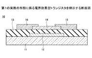
図1は、第1の実施の形態に係る電界効果型トランジスタを例示する断面図である。図1を参照するに、電界効果型トランジスタ10は、基材11と、ゲート電極12と、ゲート絶縁層13と、活性層14と、ソース電極15と、ドレイン電極16とを有するボトムゲート/トップコンタクト型の電界効果型トランジスタである。なお、電界効果型トランジスタ10は、本発明に係る電界効果型トランジスタの代表的な一例である。
<First Embodiment>
[Structure of field effect transistor]
FIG. 1 is a cross-sectional view illustrating the field effect transistor according to the first embodiment. Referring to FIG. 1, the
電界効果型トランジスタ10では、絶縁性の基材11上にゲート電極12が形成され、更に、ゲート電極12を覆うようにゲート絶縁層13が形成されている。ゲート絶縁層13上には活性層14が形成され、活性層14においてチャネルが形成されるように、活性層14上にソース電極15及びドレイン電極16が形成されている。以下、電界効果型トランジスタ10の各構成要素について、詳しく説明する。
In the
なお、本実施の形態では、便宜上、活性層14側を上側又は一方の側、基材11側を下側又は他方の側とする。又、各部位の活性層14側の面を上面又は一方の面、基材11側の面を下面又は他方の面とする。但し、電界効果型トランジスタ10は天地逆の状態で用いることができ、又は任意の角度で配置することができる。又、平面視とは対象物を基材11の上面の法線方向から視ることを指し、平面形状とは対象物を基材11の上面の法線方向から視た形状を指すものとする。又、基材11上の各部位の積層方向に切った断面を縦断面、基材11上の各部位の積層方向に垂直な方向(基材11の上面に平行な方向)に切った断面を横断面とする。
In the present embodiment, for convenience, the
基材11の形状、構造、及び大きさとしては、特に制限はなく、目的に応じて適宜選択することができる。
The shape, structure, and size of the
基材11の材料としては、特に制限はなく、目的に応じて適宜選択することができるが、例えば、ガラス基材、セラミック基材、プラスチック基材、フィルム基材等を用いることができる。ガラス基材としては、特に制限はなく、目的に応じて適宜選択することができるが、例えば、無アルカリガラス、シリカガラス等が挙げられる。又、プラスチック基材やフィルム基材としては、特に制限はなく、目的に応じて適宜選択することができるが、例えば、ポリカーボネート(PC)、ポリイミド(PI)、ポリエチレンテレフタレート(PET)、ポリエチレンナフタレート(PEN)等が挙げられる。なお、基材11としては、表面の清浄化及び密着性向上の点で、酸素プラズマ、UVオゾン、UV照射洗浄等の前処理が行われることが好ましい。
The material of the
ゲート電極12は、基材11上の所定領域に形成されている。ゲート電極12は、ゲート電圧を印加するための電極である。ゲート電極12の材料としては、特に制限はなく、目的に応じて適宜選択することができるが、例えば、アルミニウム(Al)、白金(Pt)、パラジウム(Pd)、金(Au)、銀(Ag)、銅(Cu)、亜鉛(Zn)、ニッケル(Ni)、クロム(Cr)、タンタル(Ta)、モリブデン(Mo)、チタン(Ti)等の金属、これらの合金、これら金属の混合物等を用いることができる。又、酸化インジウム、酸化亜鉛、酸化スズ、酸化ガリウム、酸化ニオブ等の導電性酸化物、これらの複合化合物、これらの混合物等を用いてもよい。ゲート電極12の平均厚みとしては、特に制限はなく、目的に応じて適宜選択することができるが、10nm〜1μmが好ましく、50nm〜300nmがより好ましい。
The
ゲート絶縁層13は、ゲート電極12と活性層14との間に設けられ、ゲート電極12と活性層14とを絶縁するための層である。ゲート絶縁層13の材料としては、特に制限はなく、目的に応じて適宜選択することができるが、例えば、無機絶縁材料、有機絶縁材料等を用いることができる。無機絶縁材料としては、例えば、酸化ケイ素、酸化アルミニウム、酸化タンタル、酸化チタン、酸化イットリウム、酸化ランタン、酸化ハフニウム、酸化ジルコニウム、窒化ケイ素、窒化アルミニウム、これらの混合物等が挙げられる。又、有機絶縁材料としては、例えば、ポリイミド、ポリアミド、ポリアクリレート、ポリビニルアルコール、ノボラック樹脂等が挙げられる。ゲート絶縁層13の平均厚みとしては、特に制限はなく、目的に応じて適宜選択することができるが、50nm〜3μmが好ましく、100nm〜1μmがより好ましい。
The
活性層14は、ゲート絶縁層13上に形成された酸化物半導体からなる薄膜であり、ゲート絶縁層13を介してゲート電極12と対向するように配置されている。活性層14は、例えばn型酸化物半導体から形成することができる。
The
活性層14を構成するn型酸化物半導体は、特に制限はなく、目的に応じて適宜選択することができるが、インジウム(In)、Zn、スズ(Sn)、及びTiの少なくとも何れかと、アルカリ土類元素、又は希土類元素と、Al、Hf、及びZrの何れかを含有することが好ましく、Inとアルカリ土類元素、希土類元素、Al、Hf、及びZrの何れかを含有することがより好ましい。
The n-type oxide semiconductor constituting the
アルカリ土類元素としては、ベリリウム(Be)、Mg、カルシウム(Ca)、ストロンチウム(Sr)、バリウム(Ba)、ラジウム(Ra)等が挙げられる。 Examples of the alkaline earth element include beryllium (Be), Mg, calcium (Ca), strontium (Sr), barium (Ba), radium (Ra) and the like.
希土類元素としては、スカンジウム(Sc)、イットリウム(Y)、ランタン(La)、セリウム(Ce)、プラセオジム(Pr)、ネオジム(Nd)、プロメチウム(Pm)、サマリウム(Sm)、ユウロピウム(Eu)、ガドリニウム(Gd)、テルビウム(Tb)、ジスプロシウム(Dy)、ホルミウム(Ho)、エルビウム(Er)、ツリウム(Tm)、イッテルビウム(Yb)、ルテチウム(Lu)等が挙げられる。 Rare earth elements include scandium (Sc), yttrium (Y), lantern (La), cerium (Ce), placeodim (Pr), neodym (Nd), promethium (Pm), samarium (Sm), uropyum (Eu), Examples thereof include gadolinium (Gd), terbium (Tb), dysprosium (Dy), formium (Ho), erbium (Er), thulium (Tm), yttrium (Yb), and lutetium (Lu).
酸化物半導体は、酸素欠損量によって電子キャリア濃度が1018cm−3〜1020cm−3程度に変化する。但し、酸化物半導体は酸素欠損ができやすい性質があり、酸化物半導体膜形成後の後工程で、意図しない酸素欠損ができる場合がある。例えば、上述したn型酸化物半導体を構成する金属元素のインジウムの酸化物である酸化インジウムでは、インジウムよりも酸素と結合しやすいアルカリ土類元素や希土類元素との主に二つの金属から酸化物を形成することは、意図しない酸素欠損を防ぐと共に、組成の制御が容易となり電子キャリア濃度を適切に制御しやすい点で特に好ましい。インジウム以外のn型酸化物半導体を構成する金属元素の酸化物に関しても同様である。 The electron carrier concentration of the oxide semiconductor changes to about 10 18 cm -3 to 10 20 cm -3 depending on the amount of oxygen deficiency. However, the oxide semiconductor has a property of easily causing oxygen deficiency, and an unintended oxygen deficiency may occur in a post-process after forming the oxide semiconductor film. For example, indium oxide, which is an oxide of indium, which is a metal element constituting the above-mentioned n-type oxide semiconductor, is mainly composed of two metals, an alkaline earth element and a rare earth element, which are more easily bonded to oxygen than indium. Is particularly preferable in that it prevents unintended oxygen deficiency, facilitates control of the composition, and facilitates appropriate control of the electron carrier concentration. The same applies to oxides of metal elements constituting n-type oxide semiconductors other than indium.
又、活性層14を構成するn型酸化物半導体は、2価のカチオン、3価のカチオン、4価のカチオン、5価のカチオン、6価のカチオン、7価のカチオン、及び8価のカチオンの少なくとも何れかのドーパントで置換ドーピングされており、ドーパントの価数が、n型酸化物半導体を構成する金属イオン(但し、ドーパントを除く)の価数よりも大きいことが好ましい。なお、置換ドーピングは、n型ドーピングともいう。
The n-type oxide semiconductor constituting the
ソース電極15及びドレイン電極16は、ゲート絶縁層13上に形成されている。ソース電極15及びドレイン電極16は、活性層14の一部を被覆し、所定の間隔を隔てて形成されている。ソース電極15及びドレイン電極16は、ゲート電極12へのゲート電圧の印加に応じて電流を取り出すための電極である。なお、ソース電極15及びドレイン電極16と共に、ソース電極15及びドレイン電極16と接続される配線が同一層に形成される。
The
ソース電極15及びドレイン電極16となる導電膜150の材料としては、特に制限はなく、目的に応じて適宜選択することができるが、例えば、アルミニウム(Al)、白金(Pt)、パラジウム(Pd)、金(Au)、銀(Ag)、銅(Cu)、亜鉛(Zn)、ニッケル(Ni)、クロム(Cr)、タンタル(Ta)、モリブデン(Mo)、チタン(Ti)等の金属、これらの合金、これら金属の混合物等を用いることができる。
The material of the
特に活性層14上でのウェットエッチングによるパターニングに使用するエッチング液の観点からAl、Mo、Al又はMoの何れかを含む合金、酸化インジウムを含む導電性酸化物を用いることがより好ましい。Alを含む合金は、Al以外に例えば、ケイ素(Si)、Ti、Cu、Ta、Nd、Zn、Ni等が含まれる。Moを含む合金は、Mo以外に例えば、Ti、Nb、Ta、Cr,バナジウム(V)、タングステン(W)等が含まれる。
In particular, from the viewpoint of the etching solution used for patterning by wet etching on the
酸化インジウムを含む導電性酸化物は、例えばITO(Indium Tin Oxide)、IZO(Indium Zinc Oxide)、IWO(Indium Tungsten Oxide)、IGO(Indium Gallium Oxide)等が挙げられるが、ウェットエッチングの観点から、導電膜150の段階ではより結晶性が低い状態が好ましい。
Examples of the conductive oxide containing indium oxide include ITO (Indium Tin Oxide), IZO (Indium Zinc Oxide), IWO (Indium Tungsten Oxide), and IGO (Indium Gallium Oxide) from the viewpoint of wet etching. At the stage of the
又、ソース電極15及びドレイン電極16は導電膜150となる材料の積層膜としてもよい。この場合も活性層14上でのウェットエッチングによるパターニングに使用するエッチング液の観点から、積層膜の最下層がAl、Mo、Al又はMoの何れかを含む合金、酸化インジウムを含む導電性酸化物の何れかであることがより好ましい。
Further, the
ソース電極15及びドレイン電極16の平均厚みとしては、特に制限はなく、目的に応じて適宜選択することができるが、10nm〜1μmが好ましく、50nm〜300nmがより好ましい。
The average thickness of the
[電界効果型トランジスタの製造方法]
次に、図1に示す電界効果型トランジスタの製造方法について説明する。図2は、第1の実施の形態に係る電界効果型トランジスタの製造工程を例示する図である。
[Manufacturing method of field effect transistor]
Next, a method of manufacturing the field-effect transistor shown in FIG. 1 will be described. FIG. 2 is a diagram illustrating a manufacturing process of the field effect transistor according to the first embodiment.
まず、図2(a)に示す工程では、ガラス基材等からなる基材11を準備する。そして、基材11上に、真空蒸着法等によりアルミニウム(Al)等からなる導電膜を形成し、形成した導電膜をフォトリソグラフィとエッチングによりパターニングして所定形状のゲート電極12を形成する。基材11の表面の清浄化及び密着性向上の点で、ゲート電極12を形成する前に、酸素プラズマ、UVオゾン、UV照射洗浄等の前処理が行われることが好ましい。基材11、ゲート電極12の材料や厚さは、前述の通り適宜選択することができる。
First, in the step shown in FIG. 2A, a
次に、図2(b)に示す工程では、基材11上に、スパッタ法等により、ゲート電極12を被覆するゲート絶縁層13を形成する。ゲート絶縁層13は、例えば、酸化ケイ素を成膜することによって形成できるが、ゲート絶縁層13の材料や厚さは、前述の通り適宜選択することができる。
Next, in the step shown in FIG. 2B, a
次に、図2(c)に示す工程では、ゲート絶縁層13上の全面に酸化物半導体層140を形成する。酸化物半導体層140の形成方法としては、特に制限はなく、目的に応じて適宜選択することができ、例えば、スパッタ法、パルスレーザーデポジッション(PLD)法、化学気相蒸着(CVD)法、原子層蒸着(ALD)法等の真空プロセスや、酸化物形成用塗布液を用いたディップコーティング、スピンコート、ダイコート等の溶液プロセスにより成膜することができる。酸化物半導体層140は、例えばn型酸化物半導体から形成することができる。形成した酸化物半導体層140は結晶質と非晶質とが混在してもよい。
Next, in the step shown in FIG. 2C, the
酸化物半導体層140の形成に酸化物形成用塗布液を用いる場合、その溶剤を除去する方法としては、特に制限はなく、目的に応じて適宜選択することができるが、加熱により溶剤を除去する方法が好ましい。前記加熱の温度としては、30℃〜300℃が好ましく、50℃〜250℃がより好ましい。前記加熱の時間としては、特に制限はなく、目的に応じて適宜選択することができる。
When the oxide-forming coating liquid is used for forming the
次に、図3(a)に示す工程では、ゲート絶縁層13上の全面に形成された酸化物半導体層140をフォトリソグラフィとウェットエッチングによりパターニングして所定形状にし、活性層14を形成する。酸化物半導体層140をエッチングする際にはPAN(燐酸・酢酸・硝酸の混合溶液)等の酸性エッチング液を用いることができるが、活性層14のパターニングを精度良く行うためには、例えば蓚酸等の弱酸性エッチング液を用いることが好ましい。なお、活性層14を形成する際には、酸化物半導体層140の形成を行う際に、メタルマスクを介して成膜することでフォトリソグラフィとウェットエッチングを行わずに活性層14を形成しても良い。
Next, in the step shown in FIG. 3A, the
次に、図3(b)に示す工程では、真空蒸着法等によりアルミニウム(Al)等からなる導電膜150を、活性層14を被覆して成膜する。次に、図3(c)に示す工程では、フォトリソグラフィとウェットエッチングにより導電膜150をパターニングして所定形状のソース電極15及びドレイン電極16を形成する。ソース電極15及びドレイン電極16の材料や厚さは、前述の通り適宜選択することができる。
Next, in the step shown in FIG. 3B, a
導電膜150のウェットエッチングには酸性エッチング液が用いられる。特に、導電膜150の材料である、Al、Mo、Al又はMoの何れかを含む合金はPAN系のエッチング液によって、酸化インジウムを含む導電性酸化物は蓚酸系エッチング液によって精度良くパターニングすることが可能である。前記燐酸、硝酸、酢酸の混合溶液の混合比は目的により適宜選択できるが、例えば混合比は燐酸40〜70%、酢酸20〜40%、硝酸1〜10%とすることがより好ましい。
An acidic etching solution is used for wet etching of the
なお、導電膜150の積層膜の最下層にAl又はAlを含む合金を用いる場合、Al又はAlを含む合金の上層には、Mo又はMoの合金、Ti又はTiの合金の順序で積層することで、導電膜150のパターニングを行う際のエッチング液の選択性を広げることができる。
When an alloy containing Al or Al is used for the lowermost layer of the laminated film of the
前述のような構成で導電膜150を成膜した場合には、最下層のAl又はAlの合金のエッチング液にPAN系ではなく、有機アルカリ系のエッチング液を用いることができる。有機アルカリ系のエッチング液を用いたパターニングにおいては、パターニングのマスクに用いるレジストが溶解するが、最下層のAl又はAlの合金の上層に、有機アルカリ系のエッチング液に対し、溶解しない金属を用いることで、最下層のAl又はAlの合金をパターニングすることが可能となる。
When the
積層膜の構成としては例えば、Al又はAlの合金の上層にMo又はMoの合金、Ti又はTiの合金を積層し、パターニングの際にはMo又はMoの合金、Ti又はTiの合金を先にエッチングして上層のパターンを形成しておくことで、Alを有機アルカリ系のエッチング液でエッチングする際のマスクとすることができる。 As a structure of the laminated film, for example, a Mo or Mo alloy or a Ti or Ti alloy is laminated on an upper layer of an Al or Al alloy, and when patterning, the Mo or Mo alloy or the Ti or Ti alloy is first used. By etching to form the upper layer pattern, it can be used as a mask when Al is etched with an organic alkaline etching solution.
この際、Ti又はTiの合金はフッ酸系のエッチング液で、Mo又はMoの合金はPAN系のエッチング液でエッチングする。この場合のMoのエッチングに用いるPAN系のエッチング液は、前述した混合比ではなく、燐酸1〜10%、酢酸30〜45%、硝酸20〜35%とすることで最下層のAlとのエッチングレートの選択比をつけることができる。 At this time, the Ti or Ti alloy is etched with a hydrofluoric acid-based etching solution, and the Mo or Mo alloy is etched with a PAN-based etching solution. In this case, the PAN-based etching solution used for etching Mo is not the above-mentioned mixing ratio, but is set to 1 to 10% phosphoric acid, 30 to 45% acetic acid, and 20 to 35% nitric acid to etch with Al in the lowermost layer. You can add a rate selection ratio.
しかしながら、これらのエッチング液は酸化物半導体層140のエッチング液と共通している。
However, these etching solutions are common to the etching solutions of the
そこで、活性層14が導電膜150をエッチングする際に用いるエッチング液によって溶解することを防止するための処理を行う。この工程により、活性層14に対するエッチングレートが導電膜150に対するエッチングレートよりも低くなる。ここで、ソース電極15及びドレイン電極16を形成する工程で用いるエッチング液の活性層14に対するエッチングレートは、このエッチング液の導電膜150に対するエッチングレートの1/10以下であることが好ましい。活性層14にダメージを与えることを回避できるからである。
Therefore, a treatment is performed to prevent the
導電膜150のエッチング液に対する耐性を付与するための活性層14に実施する処理工程は加熱処理が挙げられる。ここで、加熱処理とは、オーブンのような熱源を有する装置によって基板全体を加熱する処理を指す。例えば、図2(c)に示す工程において酸化物半導体層140を成膜した温度以上の温度で、活性層14に対して加熱処理を行う。この加熱処理により、活性層14にPAN系、蓚酸系等の酸性エッチング液に対する耐性を付与することができる。酸化物半導体層140は加熱処理前と比較して非晶質の割合が少なくなっていることが望ましく、加熱処理の温度は200℃以上500℃以下(但し、酸化物半導体層140を成膜した温度以上の温度)が好ましい。
Examples of the treatment step performed on the
この処理工程は、活性層14の形成後から、導電膜150のエッチング前までに実施すれば良いが、導電膜150の表面が加熱処理によって容易に酸化される場合、導電膜150のエッチングレートが大幅に変化するなどの影響を与える虞があるため、例えば図3(a)に示す工程と図3(b)に示す工程との間に実施することが望ましい。
This treatment step may be performed after the formation of the
又、導電膜150のエッチング液に対する耐性を付与するための活性層14に実施する処理工程はレーザー照射処理を用いることができる。レーザー照射処理は、光源からレーザー光を基板表面に照射し、瞬間的に基板表面の薄膜を加熱することで、薄膜を改質する処理である。
Further, a laser irradiation treatment can be used as the treatment step performed on the
この光源には、エキシマレーザー(KrF(波長248nm)、XeCl(波長308nm)、Nd−YAGレーザー(波長1064nm(基本波)、532nm(2倍波)、355nm(3倍波)266nm(4倍波))など活性層14がもつ吸収波長に合わせて適宜選択して用いることができる。
Excimer lasers (KrF (wavelength 248 nm), XeCl (wavelength 308 nm), Nd-YAG laser (wavelength 1064 nm (fundamental wave), 532 nm (2nd harmonic), 355 nm (3rd harmonic)) 266 nm (4th harmonic) )), Etc., can be appropriately selected and used according to the absorption wavelength of the
活性層14にレーザー照射処理を行う場合、導電膜150のエッチング液に直接曝される領域が活性層14の表面層のみであるため、レーザー照射によって改質するのは活性層14の表面層だけでも良い。この場合、表面層の厚さは2〜10nmの範囲である。
When the
また、レーザー照射を行う際に、活性層の下層に下部電極層を有するデバイスのように、活性層の下層に金属電極がある場合、活性層や基板等に吸収波長がない光源を用いても、下層の金属電極がレーザー光を吸収されることで、結果的に上層の活性層も加熱処理することが可能である。活性層の下層に下部電極層を有するデバイスとは、例えば、ボトムゲートトップコンタクト型の電界効果型トランジスタ等を指す。同様に活性層の上層に金属電極がある場合、上層の金属電極がレーザー光を吸収し下層の活性層の加熱処理が可能である。 Further, when laser irradiation is performed, if there is a metal electrode in the lower layer of the active layer, such as a device having a lower electrode layer in the lower layer of the active layer, a light source having no absorption wavelength in the active layer, the substrate, or the like may be used. As a result, the metal electrode in the lower layer absorbs the laser beam, and as a result, the active layer in the upper layer can also be heat-treated. The device having a lower electrode layer under the active layer refers to, for example, a bottom gate top contact type field effect transistor or the like. Similarly, when there is a metal electrode in the upper layer of the active layer, the metal electrode in the upper layer absorbs the laser beam and heat treatment of the active layer in the lower layer is possible.
活性層14にPAN系、蓚酸系等の酸性エッチング液、有機アルカリ系のエッチング液に対する耐性を付与することにより、ソース電極15及びドレイン電極16をPAN系、蓚酸系、有機アルカリ系等のエッチング液を用いてエッチングしても、活性層14にダメージを与えることがない。すなわち、特別なエッチングストッパ層を設けることなく、ソース電極15及びドレイン電極16をウェットエッチングすることができる。
By imparting resistance to acidic etching solutions such as PAN-based and oxalic acid-based and organic alkaline-based etching solutions to the
以上の工程により、ボトムゲート/トップコンタクト型の電界効果型トランジスタ10を作製できる。
Through the above steps, a bottom gate / top contact type
このように、発明者等は、種々の実験等を繰り返し行った結果、酸化物半導体層を活性層とする電界効果型トランジスタの製造方法において、図3(a)に示す工程と図3(b)に示す工程との間に、酸化物半導体層140を成膜した温度以上の温度で活性層14に対して加熱処理を行う熱処理工程を設けることにより、活性層14が、図3(c)に示す工程で用いるPAN系、蓚酸系等の酸性エッチング液、有機アルカリ系のエッチング液に対し殆どエッチングされることなく膜として残ることを見出した。
As described above, as a result of repeating various experiments and the like, the inventors have conducted the steps shown in FIG. 3 (a) and FIG. 3 (b) in the method for manufacturing the field effect transistor using the oxide semiconductor layer as the active layer. ), By providing a heat treatment step of heat-treating the
〈第1の実施の形態の変形例〉
第1の実施の形態の変形例では、トップゲート/トップコンタクト型の電界効果型トランジスタの例を示す。なお、第1の実施の形態の変形例において、既に説明した実施の形態と同一構成部についての説明は省略する場合がある。
<Modified example of the first embodiment>
In the modified example of the first embodiment, an example of a top gate / top contact type field effect transistor is shown. In the modified example of the first embodiment, the description of the same component as that of the above-described embodiment may be omitted.
図4は、第1の実施の形態の変形例に係る電界効果型トランジスタを例示する断面図である。図4を参照するに、電界効果型トランジスタ10Aは、トップゲート/トップコンタクト型の電界効果型トランジスタである。なお、電界効果型トランジスタ10Aは、本発明に係る電界効果型トランジスタの代表的な一例である。
FIG. 4 is a cross-sectional view illustrating the field effect transistor according to the modified example of the first embodiment. With reference to FIG. 4, the
電界効果型トランジスタ10Aは、電界効果型トランジスタ10(図1参照)とは層構造が異なっている。具体的には、電界効果型トランジスタ10Aは、基材11と、基材11上に形成されたソース電極15及びドレイン電極16と、ソース電極15とドレイン電極16との間に形成された活性層14と、活性層14、ソース電極15、及びドレイン電極16上に形成されたゲート絶縁層13と、ゲート絶縁層13上に形成されたゲート電極12とを有している。
The field-
本発明に係る電界効果型トランジスタの層構造は、特に制限はなく、図1や図4に示す構造を、目的に応じて適宜選択することができる。 The layer structure of the field-effect transistor according to the present invention is not particularly limited, and the structures shown in FIGS. 1 and 4 can be appropriately selected depending on the intended purpose.
なお、トップゲート/トップコンタクト型の電界効果型トランジスタは、活性層の形成並びにソース電極及びドレイン電極の形成後に、ゲート絶縁層の形成及びゲート電極の形成を行うことで製造できる。ソース電極及びドレイン電極の形成に用いるエッチング液等については第1の実施の形態と同様である。 The top gate / top contact type field effect transistor can be manufactured by forming a gate insulating layer and forming a gate electrode after forming an active layer and forming a source electrode and a drain electrode. The etching solution and the like used for forming the source electrode and the drain electrode are the same as those in the first embodiment.
[実施例1−1]
実施例1−1では、図1に示すボトムゲート/トップコンタクト型の電界効果型トランジスタを作製した。
[Example 1-1]
In Example 1-1, the bottom gate / top contact type field effect transistor shown in FIG. 1 was produced.
(ゲート電極の形成)
ガラスからなる基材11上に、スパッタ法を用いて100nmの厚みになるようにAl膜を形成した。形成したAl膜上にフォトリソグラフィによりレジストパターンを形成し、エッチングを行って、所定形状のゲート電極12を形成した。
(Formation of gate electrode)
An Al film was formed on the
(ゲート絶縁層の形成)
次に、スパッタ法により、200nmの厚みになるようにSiONを成膜することによって、ゲート絶縁層13を形成した。
(Formation of gate insulating layer)
Next, the
(活性層の形成)
まず、ゲート絶縁層13上に、RFマグネトロンスパッタリング法により、活性層14となるAlをドーピングしたMgIn2O4(In−Mg−Al−O)を50nmの膜厚で成膜した。ターゲットにはMgIn1.99Al0.01O4の組成を有する多結晶焼結体を用いた。スパッタガスとしてアルゴンガス及び酸素ガスを導入した。全圧を1.1Paに固定し、酸素濃度を20体積%とした。なお、基材11の温度制御は行わなかった。スパッタ中は基材11の温度が自然に上昇するが、40℃以下に保たれることが分かっている。すなわち、In−Mg−Al−O膜の成膜温度は、40℃以下である。パターニングはメタルマスクを介して成膜することで活性層14を形成した。
(Formation of active layer)
First, MgIn 2 O 4 (In-Mg-Al-O) doped with Al to be the
(活性層への処理)
形成した活性層14を更にオーブンを用いて、大気中350℃1時間で加熱処理した。
(Treatment to active layer)
The formed
(ソース電極及びドレイン電極の形成)
活性層14上に、スパッタ法を用いて100nmの厚みになるように導電膜150としてAl膜を形成した。次に、形成したAl膜上にフォトリソグラフィによりレジストパターンを形成した。そして、PAN系のエッチング液によるエッチングを行って、活性層14上に所定形状のソース電極15及びドレイン電極16を形成した。以上により、図1に示すボトムゲート/トップコンタクト型の電界効果型トランジスタが完成した。
(Formation of source electrode and drain electrode)
An Al film was formed on the
[実施例1−2]
上述した実施例1−1の電界効果型トランジスタ作製方法において、以下に記載する内容以外は実施例1−1と同様にして、電界効果型トランジスタを作製した。
[Example 1-2]
In the field-effect transistor manufacturing method of Example 1-1 described above, a field-effect transistor was manufactured in the same manner as in Example 1-1 except for the contents described below.
(活性層の形成)
活性層14作製プロセスの焼結体ターゲットを図5に示すように変えて活性層を成膜した。
(Formation of active layer)
The active layer was formed by changing the sintered body target in the process of producing the
(活性層への処理)
形成した活性層14に対して、図5に記載のようにオーブンで加熱処理した。
(Treatment to active layer)
The formed
(ソース電極及びドレイン電極の形成)
活性層14上に、スパッタ法を用いて合計130nmの厚みになるように導電膜150としてAl膜100nm、Mo膜30nmの積層膜を形成した。次に、形成したAl膜、Mo膜の積層膜上にフォトリソグラフィによりレジストパターンを形成した。そして、PAN系のエッチング液によるエッチングを行って、活性層14上に所定形状のソース電極15及びドレイン電極16を形成した。以上により、図1に示すボトムゲート/トップコンタクト型の電界効果型トランジスタが完成した。
(Formation of source electrode and drain electrode)
On the
[実施例1−3]
上述した実施例1−1の電界効果型トランジスタ作製方法において、以下に記載する内容以外は実施例1−1と同様にして、電界効果型トランジスタを作製した。
[Example 1-3]
In the field-effect transistor manufacturing method of Example 1-1 described above, a field-effect transistor was manufactured in the same manner as in Example 1-1 except for the contents described below.
(活性層の形成)
活性層14作製プロセスの焼結体ターゲットを図5に示すように変えて活性層を成膜した。
(Formation of active layer)
The active layer was formed by changing the sintered body target in the process of producing the
(活性層への処理)
形成した活性層14に対して、図5に記載のようにオーブンで加熱処理した。
(Treatment to active layer)
The formed
(ソース電極及びドレイン電極の形成)
活性層14上に、スパッタ法を用いて合計130nmの厚みになるように導電膜150としてMo膜100nm、Ti膜30nmの積層膜を形成した。次に、形成したMo膜、Ti膜の積層膜上にフォトリソグラフィによりレジストパターンを形成した。そして、Ti膜をフッ酸系のエッチング液、Mo膜をPAN系のエッチング液によるエッチングを行って、活性層14上に所定形状のソース電極15及びドレイン電極16を形成した。以上により、図1に示すボトムゲート/トップコンタクト型の電界効果型トランジスタが完成した。
(Formation of source electrode and drain electrode)
On the
[実施例1−4]
上述した実施例1−1の電界効果型トランジスタ作製方法において、以下に記載する内容以外は実施例1−1と同様にして、電界効果型トランジスタを作製した。
[Example 1-4]
In the field-effect transistor manufacturing method of Example 1-1 described above, a field-effect transistor was manufactured in the same manner as in Example 1-1 except for the contents described below.
(活性層の形成)
活性層14作製プロセスの焼結体ターゲットを図5に示すように変えて活性層を成膜した。
(Formation of active layer)
The active layer was formed by changing the sintered body target in the process of producing the
(活性層への処理)
形成した活性層14に対して、図5に記載のようにオーブンで加熱処理した。
(Treatment to active layer)
The formed
(ソース電極及びドレイン電極の形成)
活性層14上に、スパッタ法を用いて130nmの厚みになるように導電膜150として、In系透明導電膜である酸化インジウムにSnを10wt%ドープしたITO膜100nm、Mo膜30nmを連続成膜し積層膜を形成した。次に、形成した積層膜上にフォトリソグラフィによりレジストパターンを形成した。そして、Mo膜をPAN系、ITO膜を蓚酸系エッチング液によるエッチングを行って、活性層14上に所定形状のソース電極15及びドレイン電極16を形成した。
(Formation of source electrode and drain electrode)
An ITO film 100 nm and a Mo film 30 nm obtained by doping indium oxide, which is an In-based transparent conductive film, with 10 wt% of Sn, are continuously formed on the
[実施例1−5]
上述した実施例1−1の電界効果型トランジスタ作製方法において、以下に記載する内容以外は実施例1−1と同様にして、電界効果型トランジスタを作製した。
[Example 1-5]
In the field-effect transistor manufacturing method of Example 1-1 described above, a field-effect transistor was manufactured in the same manner as in Example 1-1 except for the contents described below.
(活性層の形成)
活性層14作製プロセスの焼結体ターゲットを図5に示すように変えて活性層を成膜した。
(Formation of active layer)
The active layer was formed by changing the sintered body target in the process of producing the
(活性層への処理)
形成した活性層14に対して、図5に記載のようにオーブンで加熱処理した。
(Treatment to active layer)
The formed
(ソース電極及びドレイン電極の形成)
活性層14上に、スパッタ法を用いて100nmの厚みになるように導電膜150としてSiを0.5wt%含む、AlSi合金膜を形成した。次に、形成したAlSi膜上にフォトリソグラフィによりレジストパターンを形成した。そして、PAN系のエッチング液によるエッチングを行って、活性層14上に所定形状のソース電極15及びドレイン電極16を形成した。以上により、図1に示すボトムゲート/トップコンタクト型の電界効果型トランジスタが完成した。
(Formation of source electrode and drain electrode)
An AlSi alloy film containing 0.5 wt% of Si as the
[実施例1−6]
上述した実施例1−1の電界効果型トランジスタ作製方法において、以下に記載する内容以外は実施例1−1と同様にして、電界効果型トランジスタを作製した。
[Example 1-6]
In the field-effect transistor manufacturing method of Example 1-1 described above, a field-effect transistor was manufactured in the same manner as in Example 1-1 except for the contents described below.
(活性層の形成)
活性層14作製プロセスの焼結体ターゲットを図5に示すように変えて活性層を成膜した。
(Formation of active layer)
The active layer was formed by changing the sintered body target in the process of producing the
(活性層への処理)
形成した活性層14に対して、図5に記載のようにオーブンで加熱処理した。
(Treatment to active layer)
The formed
(ソース電極及びドレイン電極の形成)
活性層14上に、スパッタ法を用いて合計130nmの厚みになるように導電膜150としてWを1wt%含むMoW合金膜100nm、Ti膜30nmの積層膜を形成した。次に、形成したMoW膜、Ti膜の積層膜上にフォトリソグラフィによりレジストパターンを形成した。そして、Ti膜をフッ酸系のエッチング液、MoW膜をPAN系のエッチング液によるエッチングを行って、活性層14上に所定形状のソース電極15及びドレイン電極16を形成した。以上により、図1に示すボトムゲート/トップコンタクト型の電界効果型トランジスタが完成した。
(Formation of source electrode and drain electrode)
On the
[実施例1−7]
上述した実施例1−1の電界効果型トランジスタ作製方法において、以下に記載する内容以外は実施例1−1と同様にして、電界効果型トランジスタを作製した。
[Example 1-7]
In the field-effect transistor manufacturing method of Example 1-1 described above, a field-effect transistor was manufactured in the same manner as in Example 1-1 except for the contents described below.
(活性層の形成)
活性層14作製プロセスの焼結体ターゲットを図5に示すように変えて活性層を成膜した。
(Formation of active layer)
The active layer was formed by changing the sintered body target in the process of producing the
(活性層への処理)
形成した活性層14に対して、図5に記載のようにオーブンで加熱処理した。
(Treatment to active layer)
The formed
(ソース電極及びドレイン電極の形成)
活性層14上に、スパッタ法を用いて100nmの厚みになるように導電膜150としてWを1wt%含むMoW膜100nmを形成した。次に、形成したMoW膜上にフォトリソグラフィによりレジストパターンを形成した。そしてPAN系のエッチング液によるエッチングを行って、活性層14上に所定形状のソース電極15及びドレイン電極16を形成した。以上により、図1に示すボトムゲート/トップコンタクト型の電界効果型トランジスタが完成した。
(Formation of source electrode and drain electrode)
On the
[実施例1−8]
上述した実施例1−1の電界効果型トランジスタ作製方法において、以下に記載する内容以外は実施例1−1と同様にして、電界効果型トランジスタを作製した。
[Example 1-8]
In the field-effect transistor manufacturing method of Example 1-1 described above, a field-effect transistor was manufactured in the same manner as in Example 1-1 except for the contents described below.
(活性層の形成)
活性層14作製プロセスの焼結体ターゲットを図5に示すように変えて活性層を成膜した。
(Formation of active layer)
The active layer was formed by changing the sintered body target in the process of producing the
(活性層への処理)
形成した活性層14に対して、図5に記載のようにオーブンで加熱処理した。
(Treatment to active layer)
The formed
(ソース電極及びドレイン電極の形成)
活性層14上に、スパッタ法を用いて100nmの厚みになるように導電膜150として、In系透明導電膜である酸化インジウムにSnを10wt%ドープしたITO膜を形成した。次に、形成したITO膜上にフォトリソグラフィによりレジストパターンを形成した。そして、蓚酸系エッチング液によるエッチングを行って、活性層14上に所定形状のソース電極15及びドレイン電極16を形成した。
(Formation of source electrode and drain electrode)
An ITO film obtained by doping indium oxide, which is an In-based transparent conductive film, with 10 wt% Sn was formed on the
[実施例1−9]
上述した実施例1−1の電界効果型トランジスタ作製方法において、以下に記載する内容以外は実施例1−1と同様にして、電界効果型トランジスタを作製した。
[Example 1-9]
In the field-effect transistor manufacturing method of Example 1-1 described above, a field-effect transistor was manufactured in the same manner as in Example 1-1 except for the contents described below.
(活性層の形成)
活性層14作製プロセスの焼結体ターゲットを図5に示すように変えて活性層を成膜した。
(Formation of active layer)
The active layer was formed by changing the sintered body target in the process of producing the
(活性層への処理)
形成した活性層14に対して、図5に記載のようにオーブンで加熱処理した。
(Treatment to active layer)
The formed
(ソース電極及びドレイン電極の形成)
活性層14上に、スパッタ法を用いて合計160nmの厚みになるように導電膜150としてAl膜100nm、Mo膜30nm、Ti膜30nmの順に連続成膜し積層膜を形成した。次に、形成したAl膜、Mo膜、Ti膜の積層膜上にフォトリソグラフィによりレジストパターンを形成した。そして、Ti膜をフッ酸系のエッチング液、Mo膜をPAN系のエッチング液によるエッチングを行ってAl膜上に上層のパターンを形成した。最下層のAl膜は、上層のパターンをマスクとして、有機アルカリ系のエッチング液によってエッチングを行って活性層14上に所定形状のソース電極15及びドレイン電極16を形成した。以上により、図1に示すボトムゲート/トップコンタクト型の電界効果型トランジスタが完成した。
(Formation of source electrode and drain electrode)
On the
[実施例1−10]
上述した実施例1−1の電界効果型トランジスタ作製方法において、以下に記載する内容以外は実施例1−1と同様にして、電界効果型トランジスタを作製した。
[Example 1-10]
In the field-effect transistor manufacturing method of Example 1-1 described above, a field-effect transistor was manufactured in the same manner as in Example 1-1 except for the contents described below.
(活性層の形成)
活性層14作製プロセスの焼結体ターゲットを図5に示すように変えて活性層を成膜した。
(Formation of active layer)
The active layer was formed by changing the sintered body target in the process of producing the
(活性層への処理)
形成した活性層14に対して、図5に記載のようにオーブンで加熱処理した。
(Treatment to active layer)
The formed
(ソース電極及びドレイン電極の形成)
活性層14上に、スパッタ法を用いて100nmの厚みになるように導電膜150としてTi膜を形成した。次に、形成したTi膜上にフォトリソグラフィによりレジストパターンを形成した。そして、フッ酸系のエッチング液によるエッチングを行って、活性層14上に所定形状のソース電極15及びドレイン電極16を形成した。以上により、図1に示すボトムゲート/トップコンタクト型の電界効果型トランジスタが完成した。
(Formation of source electrode and drain electrode)
A Ti film was formed on the
[実施例1−11]
上述した実施例1−1の電界効果型トランジスタ作製方法において、以下に記載する内容以外は実施例1−1と同様にして、電界効果型トランジスタを作製した。
[Example 1-11]
In the field-effect transistor manufacturing method of Example 1-1 described above, a field-effect transistor was manufactured in the same manner as in Example 1-1 except for the contents described below.
(活性層の形成)
活性層14作製プロセスの焼結体ターゲットを図5に示すように変えて活性層を成膜した。
(Formation of active layer)
The active layer was formed by changing the sintered body target in the process of producing the
(活性層への処理)
形成した活性層14に対して、図5に記載のようにオーブンで加熱処理した。
(Treatment to active layer)
The formed
(ソース電極及びドレイン電極の形成)
活性層14上に、スパッタ法を用いて100nmの厚みになるように導電膜150として、In系透明導電膜である酸化インジウムにSnを10wt%ドープしたITO膜を形成した。次に、形成したITO膜上にフォトリソグラフィによりレジストパターンを形成した。そして、蓚酸系エッチング液によるエッチングを行って、活性層14上に所定形状のソース電極15及びドレイン電極16を形成した。
(Formation of source electrode and drain electrode)
An ITO film obtained by doping indium oxide, which is an In-based transparent conductive film, with 10 wt% Sn was formed on the
[実施例1−12]
上述した実施例1−1の電界効果型トランジスタ作製方法において、以下に記載する内容以外は実施例1−1と同様にして、電界効果型トランジスタを作製した。
[Example 1-12]
In the field-effect transistor manufacturing method of Example 1-1 described above, a field-effect transistor was manufactured in the same manner as in Example 1-1 except for the contents described below.
(活性層の形成)
活性層14作製プロセスの焼結体ターゲットを図5に示すように変えて活性層を成膜した。
(Formation of active layer)
The active layer was formed by changing the sintered body target in the process of producing the
(活性層への処理)
形成した活性層14に対して、図5に記載のようにオーブンで加熱処理した。
(Treatment to active layer)
The formed
(ソース電極及びドレイン電極の形成)
活性層14上に、スパッタ法を用いて合計120nmの厚みになるように導電膜150としてMo膜60nm、Al膜60nmの積層膜を形成した。次に、形成したMo膜、Al膜の積層膜上にフォトリソグラフィによりレジストパターンを形成した。そして、PAN系のエッチング液によるエッチングを行って、活性層14上に所定形状のソース電極15及びドレイン電極16を形成した。以上により、図1に示すボトムゲート/トップコンタクト型の電界効果型トランジスタが完成した。
(Formation of source electrode and drain electrode)
On the
[実施例1−13]
上述した実施例1−1の電界効果型トランジスタ作製方法において、以下に記載する内容以外は実施例1−1と同様にして、電界効果型トランジスタを作製した。
[Example 1-13]
In the field-effect transistor manufacturing method of Example 1-1 described above, a field-effect transistor was manufactured in the same manner as in Example 1-1 except for the contents described below.
(活性層の形成)
活性層14作製プロセスの焼結体ターゲットを図5に示すように変えて活性層を成膜した。
(Formation of active layer)
The active layer was formed by changing the sintered body target in the process of producing the
(活性層への処理)
形成した活性層14に加熱処理ではなくレーザー照射処理を行った。レーザー照射処理は、図5に記載のように形成した活性層14に対し、エキシマレーザー(KrF、波長248nm)を基板表面のエネルギー密度が500mJ/cm2になるように照射した。
(Treatment to active layer)
The formed
(ソース電極及びドレイン電極の形成)
活性層14上に、スパッタ法を用いて合計160nmの厚みになるように導電膜150としてAl膜100nm、Mo膜30nm、Ti膜30nmの順に連続成膜し積層膜を形成した。次に、形成したAl膜、Mo膜、Ti膜の積層膜上にフォトリソグラフィによりレジストパターンを形成した。そして、Ti膜をフッ酸系のエッチング液、Mo膜をPAN系のエッチング液によるエッチングを行ってAl膜上に上層のパターンを形成した。最下層のAl膜は、上層のパターンをマスクとして、有機アルカリ系のエッチング液によってエッチングを行って活性層14上に所定形状のソース電極15及びドレイン電極16を形成した。以上により、図1に示すボトムゲート/トップコンタクト型の電界効果型トランジスタが完成した。
(Formation of source electrode and drain electrode)
On the
[実施例1−14]
上述した実施例1−1の電界効果型トランジスタ作製方法において、以下に記載する内容以外は実施例1−1と同様にして、電界効果型トランジスタを作製した。
[Example 1-14]
In the field-effect transistor manufacturing method of Example 1-1 described above, a field-effect transistor was manufactured in the same manner as in Example 1-1 except for the contents described below.
(活性層の形成)
活性層14作製プロセスの焼結体ターゲットを図5に示すように変えて活性層を成膜した。
(Formation of active layer)
The active layer was formed by changing the sintered body target in the process of producing the
(活性層への処理)
形成した活性層14に加熱処理ではなくレーザー照射処理を行った。レーザー照射処理は、図5に記載のように形成した活性層14に対し、エキシマレーザー(KrF、波長248nm)を基板表面のエネルギー密度が500mJ/cm2になるように照射した。
(Treatment to active layer)
The formed
(ソース電極及びドレイン電極の形成)
活性層14上に、スパッタ法を用いて100nmの厚みになるように導電膜150としてAl膜を形成した。次に、形成したAl膜上にフォトリソグラフィによりレジストパターンを形成した。そして、PAN系のエッチング液によるエッチングを行って活性層14上に所定形状のソース電極15及びドレイン電極16を形成した。以上により、図1に示すボトムゲート/トップコンタクト型の電界効果型トランジスタが完成した。
(Formation of source electrode and drain electrode)
An Al film was formed on the
[実施例1−15]
上述した実施例1−1の電界効果型トランジスタ作製方法において、以下に記載する内容以外は実施例1−1と同様にして、電界効果型トランジスタを作製した。
[Example 1-15]
In the field-effect transistor manufacturing method of Example 1-1 described above, a field-effect transistor was manufactured in the same manner as in Example 1-1 except for the contents described below.
(活性層の形成)
活性層14作製プロセスの焼結体ターゲットを図5に示すように変えて活性層を成膜した。
(Formation of active layer)
The active layer was formed by changing the sintered body target in the process of producing the
(活性層への処理)
形成した活性層14に加熱処理ではなくレーザー照射処理を行った。レーザー照射処理は、図5に記載のように形成した活性層14に対し、Nd−YAGレーザー(4倍波、波長266nm)を基板表面のエネルギー密度が500mJ/cm2になるように照射した。
(Treatment to active layer)
The formed
(ソース電極及びドレイン電極の形成)
活性層14上に、スパッタ法を用いて100nmの厚みになるように導電膜150としてMo膜を形成した。次に、形成したMo膜上にフォトリソグラフィによりレジストパターンを形成した。そして、PAN系のエッチング液によるエッチングを行って活性層14上に所定形状のソース電極15及びドレイン電極16を形成した。以上により、図1に示すボトムゲート/トップコンタクト型の電界効果型トランジスタが完成した。
(Formation of source electrode and drain electrode)
A Mo film was formed on the
[実施例1−16]
上述した実施例1−1の電界効果型トランジスタ作製方法において、以下に記載する内容以外は実施例1−1と同様にして、電界効果型トランジスタを作製した。
[Example 1-16]
In the field-effect transistor manufacturing method of Example 1-1 described above, a field-effect transistor was manufactured in the same manner as in Example 1-1 except for the contents described below.
(活性層の形成)
活性層14作製プロセスの焼結体ターゲットを図5に示すように変えて活性層を成膜した。
(Formation of active layer)
The active layer was formed by changing the sintered body target in the process of producing the
(活性層への処理)
形成した活性層14に加熱処理ではなくレーザー照射処理を行った。レーザー照射処理は、図5に記載のように形成した活性層14に対し、Nd−YAGレーザー(4倍波、波長266nm)を基板表面のエネルギー密度が500mJ/cm2になるように照射した。
(Treatment to active layer)
The formed
(ソース電極及びドレイン電極の形成)
活性層14上に、スパッタ法を用いて合計160nmの厚みになるように導電膜150としてAl膜100nm、Mo膜30nm、Ti膜30nmの順に連続成膜し積層膜を形成した。次に、形成したAl膜、Mo膜、Ti膜の積層膜上にフォトリソグラフィによりレジストパターンを形成した。そして、Ti膜をフッ酸系のエッチング液、Mo膜をPAN系のエッチング液によるエッチングを行ってAl膜上に上層のパターンを形成した。最下層のAl膜は、上層のパターンをマスクとして、有機アルカリ系のエッチング液によってエッチングを行って活性層14上に所定形状のソース電極15及びドレイン電極16を形成した。以上により、図1に示すボトムゲート/トップコンタクト型の電界効果型トランジスタが完成した。
(Formation of source electrode and drain electrode)
On the
[比較例1−1]
比較例1−1では、図5に示すようにソース電極及びドレイン電極の形成におけるエッチング液に対して、活性層に耐性を付与するための加熱処理を、活性層のパターン形成後に行わない以外は実施例1−1と同様にして、図1に示すボトムゲート/トップコンタクト型の電界効果型トランジスタを作製した。
[Comparative Example 1-1]
In Comparative Example 1-1, as shown in FIG. 5, the heat treatment for imparting resistance to the active layer to the etching solution in the formation of the source electrode and the drain electrode is not performed after the pattern formation of the active layer is performed. A bottom gate / top contact type field effect transistor shown in FIG. 1 was produced in the same manner as in Example 1-1.
[比較例1−2]
比較例1−2では、図5に示すようにソース電極及びドレイン電極の形成におけるエッチング液に対して、活性層に耐性を付与するための加熱処理を、活性層のパターン形成後に行わない以外は実施例1−7と同様にして、図1に示すボトムゲート/トップコンタクト型の電界効果型トランジスタを作製した。
[Comparative Example 1-2]
In Comparative Example 1-2, as shown in FIG. 5, the heat treatment for imparting resistance to the active layer to the etching solution in the formation of the source electrode and the drain electrode is not performed after the pattern formation of the active layer is performed. The bottom gate / top contact type field effect transistor shown in FIG. 1 was produced in the same manner as in Example 1-7.
[実施例2−1]
実施例2−1では、上述した実施例1−1の電界効果型トランジスタ作製方法において、以下に記載する内容以外は実施例1−1と同様にして、電界効果型トランジスタを作製した。
[Example 2-1]
In Example 2-1 the field-effect transistor was produced in the same manner as in Example 1-1 except for the contents described below in the method for producing the field-effect transistor of Example 1-1 described above.
(酸化物形成用塗布液の作製)
2−エチルヘキサン酸イットリウム溶液(Y:8質量%)と2−エチルヘキサン酸インジウムトルエン溶液(In:5質量%)とチタンn―ブトキシドとを用意し、金属元素が各々5mmol、99.8mmol、0.2mmolとなるように秤量し、ビーカーに800mLとを加え、室温で混合して溶解させ、酸化物形成用塗布液2−1を作製した。
(Preparation of coating liquid for oxide formation)
A yttrium 2-ethylhexanoate solution (Y: 8% by mass), an indium toluene 2-ethylhexanoate solution (In: 5% by mass), and titanium n-butoxide were prepared, and the metal elements were 5 mmol and 99.8 mmol, respectively. Weighed to 0.2 mmol, 800 mL was added to a beaker, and the mixture was mixed and dissolved at room temperature to prepare an oxide-forming coating solution 2-1.
(活性層の形成)
ゲート絶縁層13上に、酸化物形成用塗布液1をスピンコーターで塗布した。大気雰囲気中120℃、1時間オーブンで乾燥させた後、大気雰囲気中200℃、1時間で焼成して酸化物半導体層140を得た。形成した酸化物半導体層140上にフォトリソグラフィによりレジストパターンを形成し、蓚酸系エッチング液よるエッチングを行ってゲート絶縁層13上に活性層14を形成した。なお、形成された活性層14の厚さは30nmであった。
(Formation of active layer)
The oxide-forming
(活性層への処理)
形成した活性層14を図7に記載のように更にオーブンを用いて、大気中350℃1時間で加熱処理した。
(Treatment to active layer)
The formed
(ソース電極及びドレイン電極の形成)
活性層14上に、スパッタ法を用いて100nmの厚みになるように導電膜150として、In系透明導電膜である酸化インジウムにSnを10wt%ドープしたITO膜を形成した。次に、形成したITO膜上にフォトリソグラフィによりレジストパターンを形成した。そして、蓚酸系エッチング液によるエッチングを行って、活性層14上に所定形状のソース電極15及びドレイン電極16を形成した。
(Formation of source electrode and drain electrode)
An ITO film obtained by doping indium oxide, which is an In-based transparent conductive film, with 10 wt% Sn was formed on the
[実施例2−2]
実施例2−2では、上述した実施例2−1の電界効果型トランジスタ作製方法において、以下に記載する内容以外は実施例2−1と同様にして、電界効果型トランジスタを作製した。
[Example 2-2]
In Example 2-2, the field-effect transistor was produced in the same manner as in Example 2-1 except for the contents described below in the method for producing the field-effect transistor of Example 2-1 described above.
(酸化物形成用塗布液の作製)
図6に記載する原料組成で、実施例2−1と同様の方法で、酸化物形成用塗布液2−2を作製した。
(Preparation of coating liquid for oxide formation)
With the raw material composition shown in FIG. 6, an oxide-forming coating liquid 2-2 was prepared in the same manner as in Example 2-1.
(活性層の形成)
酸化物形成用塗布液2−2を用いて、実施例2−1と同様の方法で、活性層14を形成した。
(Formation of active layer)
The
(活性層への処理)
形成した活性層14に図7に記載のように加熱処理ではなくレーザー照射処理を行った。レーザー照射処理は、形成した活性層14に対し、Nd−YAGレーザー(4倍波、波長266nm)を基板表面のエネルギー密度が500mJ/cm2になるように照射した。
(Treatment to active layer)
The formed
(ソース電極及びドレイン電極の形成)
活性層14上に、スパッタ法を用いて100nmの厚みになるように導電膜150としてCuを5wt%含むAlCu合金膜を形成した。次に、形成したAlCu膜上にフォトリソグラフィによりレジストパターンを形成した。そして、PAN系エッチング液によるエッチングを行って活性層14上に所定形状のソース電極15及びドレイン電極16を形成した。以上により、図1に示すボトムゲート/トップコンタクト型の電界効果型トランジスタが完成した。
(Formation of source electrode and drain electrode)
On the
[実施例2−3]
実施例2−3では、上述した実施例2−1の電界効果型トランジスタ作製方法において、以下に記載する内容以外は実施例2−1と同様にして、電界効果型トランジスタを作製した。
[Example 2-3]
In Example 2-3, the field-effect transistor was produced in the same manner as in Example 2-1 except for the contents described below in the method for producing the field-effect transistor of Example 2-1 described above.
(酸化物形成用塗布液の作製)
図6に記載する原料組成で、実施例2−1と同様の方法で、酸化物形成用塗布液2−3を作製した。
(Preparation of coating liquid for oxide formation)
With the raw material composition shown in FIG. 6, an oxide-forming coating liquid 2-3 was prepared in the same manner as in Example 2-1.
(活性層の形成)
酸化物形成用塗布液2−3を用いて、実施例2−1と同様の方法で、活性層14を形成した。
(Formation of active layer)
The
(活性層への処理)
形成した活性層14に図7に記載のように加熱処理ではなくレーザー照射処理を行った。レーザー照射処理は、形成した活性層14に対し、エキシマレーザー(KrF、波長248nm)を基板表面のエネルギー密度が500mJ/cm2になるように照射した。
(Treatment to active layer)
The formed
(ソース電極及びドレイン電極の形成)
活性層14上に、スパッタ法を用いて100nmの厚みになるように導電膜150としてCu膜を形成した。次に、形成したCu膜上にフォトリソグラフィによりレジストパターンを形成した。そして、過酸化水素系のエッチング液によるエッチングを行って活性層14上に所定形状のソース電極15及びドレイン電極16を形成した。以上により、図1に示すボトムゲート/トップコンタクト型の電界効果型トランジスタが完成した。
(Formation of source electrode and drain electrode)
A Cu film was formed on the
[実施例2−4]
実施例2−4では、上述した実施例2−1の電界効果型トランジスタ作製方法において、以下に記載する内容以外は実施例2−1と同様にして、電界効果型トランジスタを作製した。
[Example 2-4]
In Example 2-4, the field-effect transistor was produced in the same manner as in Example 2-1 except for the contents described below in the method for producing the field-effect transistor of Example 2-1 described above.
(酸化物形成用塗布液の作製)
図6に記載する原料組成で、実施例2−1と同様の方法で、酸化物形成用塗布液2−4を作製した。
(Preparation of coating liquid for oxide formation)
With the raw material composition shown in FIG. 6, an oxide-forming coating liquid 2-4 was prepared in the same manner as in Example 2-1.
(活性層の形成)
酸化物形成用塗布液2−4を用いて、実施例2−1と同様の方法で、活性層14を形成した。
(Formation of active layer)
The
(活性層への処理)
形成した活性層14を図7に記載のように更にオーブンを用いて、大気中350℃1時間で加熱処理した。
(Treatment to active layer)
The formed
(ソース電極及びドレイン電極の形成)
活性層14上に、スパッタ法を用いて100nmの厚みになるように導電膜150としてMo膜を形成した。次に、形成したMo膜上にフォトリソグラフィによりレジストパターンを形成した。そして、PAN系のエッチング液によるエッチングを行って活性層14上に所定形状のソース電極15及びドレイン電極16を形成した。以上により、図1に示すボトムゲート/トップコンタクト型の電界効果型トランジスタが完成した。
(Formation of source electrode and drain electrode)
A Mo film was formed on the
[比較例2−1]
比較例2−1では、図7に示すようにソース電極及びドレイン電極の形成におけるエッチング液に対して、活性層に耐性を付与するための加熱処理を、活性層のパターン形成後に行わない以外は実施例2−1と同様にして、図1に示すボトムゲート/トップコンタクト型の電界効果型トランジスタを作製した。
[Comparative Example 2-1]
In Comparative Example 2-1 as shown in FIG. 7, the heat treatment for imparting resistance to the active layer to the etching solution in the formation of the source electrode and the drain electrode is not performed after the pattern formation of the active layer is performed. A bottom gate / top contact type field effect transistor shown in FIG. 1 was produced in the same manner as in Example 2-1.
[比較例2−2]
比較例2−2では、図7に示すようにソース電極及びドレイン電極の形成におけるエッチング液に対して、活性層に耐性を付与するための加熱処理を、活性層のパターン形成後に行わない以外は実施例2−3と同様にして、図1に示すボトムゲート/トップコンタクト型の電界効果型トランジスタを作製した。
[Comparative Example 2-2]
In Comparative Example 2-2, as shown in FIG. 7, the heat treatment for imparting resistance to the active layer to the etching solution in the formation of the source electrode and the drain electrode is not performed after the pattern formation of the active layer is performed. A bottom gate / top contact type field effect transistor shown in FIG. 1 was produced in the same manner as in Examples 2-3.
[実施例及び比較例のまとめ]
実施例1−1〜1−16、比較例1−1〜1−2の内容及び結果を図5にまとめた。図5には、ソース電極15及びドレイン電極16の形成工程における活性層14のパターンの有無を○×で示している。
[Summary of Examples and Comparative Examples]
The contents and results of Examples 1-1 to 1-16 and Comparative Examples 1-1 to 1-2 are summarized in FIG. In FIG. 5, the presence or absence of the pattern of the
ここで、活性層14のパターンの有無は、原子間力顕微鏡による活性層14の膜厚を計測することで確認を行った。原子間力顕微鏡による計測では、活性層14とゲート絶縁層の段差を膜厚とみなした。ソース電極15及びドレイン電極16の形成工程においてゲート絶縁層がエッチングされ、活性層14とゲート絶縁層の段差計測が困難だった場合、反射分光法によって活性層14の膜厚を光学的に求めた。ソース電極15及びドレイン電極16の形成工程前の活性層14のパターンの膜厚と比較して、ソース電極15及びドレイン電極16の形成工程後の活性層14のパターンの膜厚に5nm以上の減少が確認されなかった場合を○、5nm以上の減少が確認された場合を×とした。
Here, the presence or absence of the pattern of the
図5より、実施例1−1〜1−16の全てにおいて、ソース電極15及びドレイン電極16の形成工程における導電膜150のエッチングによって活性層14のパターンが溶解することなく残っていることが分かる。
From FIG. 5, it can be seen that in all of Examples 1-1 to 1-16, the pattern of the
又、実施例1−1〜1−16において、ソース電極15及びドレイン電極16のエッチングにPAN系のエッチング液や蓚酸系エッチング液を用いても活性層14は全くエッチングされないか殆どエッチングされない。
Further, in Examples 1-1 to 1-16, even if a PAN-based etching solution or a oxalic acid-based etching solution is used for etching the
一方で、比較例1−1〜1−2において、ソース電極15及びドレイン電極16の形成工程における導電膜150のエッチングによって活性層14のパターンが溶解し、パターンを残すことができなかったことが分かる。
On the other hand, in Comparative Examples 1-1 to 1-2, the pattern of the
又、活性層14の形成を真空プロセスのスパッタ法ではなく、ウェットプロセスとした実施例2−1〜2−4、比較例2−1〜2−2の内容及び結果を図6及び図7にまとめた。図7に、図5と同様に、ソース電極15及びドレイン電極16の形成工程における活性層14のパターンの有無を○×で示している。パターンの有無の確認の方法は前述した通りである。
Further, the contents and results of Examples 2-1 to 2-4 and Comparative Examples 2-1 to 2-2 in which the
図7より、実施例2−1〜2−4の全てにおいて、ソース電極15及びドレイン電極16の形成工程における導電膜150のエッチングによって活性層14のパターンが溶解することなく残っていることが分かる。
From FIG. 7, it can be seen that in all of Examples 2-1 to 2-4, the pattern of the
又、実施例2−1〜2−4において、ソース電極15及びドレイン電極16のエッチングにPAN系のエッチング液や蓚酸系エッチング液を用いても活性層14は全くエッチングされないか殆どエッチングされない。
Further, in Examples 2-1 to 2-4, even if a PAN-based etching solution or a oxalic acid-based etching solution is used for etching the
一方で、比較例2−1〜2−2において、ソース電極15及びドレイン電極16の形成工程における導電膜150のエッチングによって活性層14のパターンが溶解し、パターンを残すことができなかったことが分かる。
On the other hand, in Comparative Examples 2-1 to 2-2, the pattern of the
以上により、活性層14に適切な条件で加熱処理、レーザー照射処理を施すことにより、活性層14にPAN系等の酸性エッチング液、有機アルカリ系エッチング液に対する耐性を付与できることが確認された。
From the above, it was confirmed that the
このように、各実施例に係る電界効果型トランジスタの製造方法により、エッチングストッパ層を用いることなくソース電極及びドレイン電極のパターニングを行うことが可能であり、その際、活性層14にダメージを与えることがない(活性層14は殆どエッチングされない)ことが確認された。その結果、各実施例に係る電界効果型トランジスタは、良好な電気特性と動作安定性を得ることが可能となる。なお、良好な電気特性とは、例えば、低いオフ電流、高いオン電流、低いSS(電流を一桁増加させるために必要な電圧:Sub-threshold Slope)等を含むものである。
As described above, according to the method for manufacturing the field effect transistor according to each embodiment, it is possible to pattern the source electrode and the drain electrode without using the etching stopper layer, and at that time, the
〈第2の実施の形態〉
第2の実施の形態では、第1の実施の形態に係る電界効果型トランジスタを用いた表示素子、表示装置、及びシステムの例を示す。なお、第2の実施の形態において、既に説明した実施の形態と同一構成部についての説明は省略する場合がある。
<Second Embodiment>
The second embodiment shows an example of a display element, a display device, and a system using the field effect transistor according to the first embodiment. In the second embodiment, the description of the same components as those in the above-described embodiment may be omitted.
(表示素子)
第2の実施の形態に係る表示素子は、少なくとも、光制御素子と、光制御素子を駆動する駆動回路とを有し、更に必要に応じて、その他の部材を有する。光制御素子としては、駆動信号に応じて光出力を制御する素子である限り、特に制限はなく、目的に応じて適宜選択することができ、例えば、エレクトロルミネッセンス(EL)素子、エレクトロクロミック(EC)素子、液晶素子、電気泳動素子、エレクトロウェッティング素子等が挙げられる。
(Display element)
The display element according to the second embodiment has at least an optical control element, a drive circuit for driving the optical control element, and, if necessary, other members. The optical control element is not particularly limited as long as it is an element that controls the optical output according to the drive signal, and can be appropriately selected according to the purpose. For example, an electroluminescence (EL) element or an electrochromic (EC) element. ) Elements, liquid crystal elements, electrophoresis elements, electrowetting elements and the like.
駆動回路としては、第1の実施の形態に係る電界効果型トランジスタを有する限り、特に制限はなく、目的に応じて適宜選択することができる。その他の部材としては、特に制限はなく、目的に応じて適宜選択することができる。 The drive circuit is not particularly limited as long as it has the field-effect transistor according to the first embodiment, and can be appropriately selected depending on the intended purpose. The other members are not particularly limited and may be appropriately selected depending on the intended purpose.
第2の実施の形態に係る表示素子は、第1の実施の形態に係る電界効果型トランジスタを有しているため、良好な電気特性と動作安定性を得ることが可能となる。その結果、高品質の表示を行うことが可能となる。 Since the display element according to the second embodiment has the field effect transistor according to the first embodiment, it is possible to obtain good electrical characteristics and operational stability. As a result, high quality display can be performed.
(表示装置)
第2の実施の形態に係る表示装置は、少なくとも、第2の実施の形態に係る複数の表示素子と、複数の配線と、表示制御装置とを有し、更に必要に応じて、その他の部材を有する。複数の表示素子としては、マトリックス状に配置された複数の第2の実施の形態に係る表示素子である限り、特に制限はなく、目的に応じて適宜選択することができる。
(Display device)
The display device according to the second embodiment has at least a plurality of display elements, a plurality of wirings, and a display control device according to the second embodiment, and further, if necessary, other members. Has. The plurality of display elements are not particularly limited as long as they are the plurality of display elements according to the second embodiment arranged in a matrix, and can be appropriately selected depending on the intended purpose.
複数の配線は、複数の表示素子における各電界効果型トランジスタにゲート電圧と画像データ信号とを個別に印加可能である限り、特に制限はなく、目的に応じて適宜選択することができる。 The plurality of wirings are not particularly limited as long as the gate voltage and the image data signal can be individually applied to each field effect transistor in the plurality of display elements, and can be appropriately selected depending on the intended purpose.
表示制御装置としては、画像データに応じて、各電界効果型トランジスタのゲート電圧と信号電圧とを複数の配線を介して個別に制御可能である限り、特に制限はなく、目的に応じて適宜選択することができる。その他の部材としては、特に制限はなく、目的に応じて適宜選択することができる。 The display control device is not particularly limited as long as the gate voltage and signal voltage of each field effect transistor can be individually controlled via a plurality of wirings according to the image data, and is appropriately selected according to the purpose. can do. The other members are not particularly limited and may be appropriately selected depending on the intended purpose.
第2の実施の形態に係る表示装置は、第1の実施の形態に係る電界効果型トランジスタを備えた表示素子を有しているため、高品質の画像を表示することが可能となる。 Since the display device according to the second embodiment has a display element including the field-effect transistor according to the first embodiment, it is possible to display a high-quality image.
(システム)
第2の実施の形態に係るシステムは、少なくとも、第2の実施の形態に係る表示装置と、画像データ作成装置とを有する。画像データ作成装置は、表示する画像情報に基づいて画像データを作成し、画像データを前記表示装置に出力する。
(system)
The system according to the second embodiment includes at least a display device according to the second embodiment and an image data creation device. The image data creation device creates image data based on the image information to be displayed, and outputs the image data to the display device.
システムは、第2の実施の形態に係る表示装置を備えているため、画像情報を高精細に表示することが可能となる。 Since the system includes the display device according to the second embodiment, it is possible to display image information in high definition.
以下、第2の実施の形態に係る表示素子、表示装置、及びシステムについて、具体的に説明する。 Hereinafter, the display element, the display device, and the system according to the second embodiment will be specifically described.
図8には、第2の実施の形態に係るシステムとしてのテレビジョン装置500の概略構成が示されている。なお、図8における接続線は、代表的な信号や情報の流れを示すものであり、各ブロックの接続関係の全てを表すものではない。
FIG. 8 shows a schematic configuration of the
第2の実施の形態に係るテレビジョン装置500は、主制御装置501、チューナ503、ADコンバータ(ADC)504、復調回路505、TS(Transport Stream)デコーダ506、音声デコーダ511、DAコンバータ(DAC)512、音声出力回路513、スピーカ514、映像デコーダ521、映像・OSD合成回路522、映像出力回路523、表示装置524、OSD描画回路525、メモリ531、操作装置532、ドライブインターフェース(ドライブIF)541、ハードディスク装置542、光ディスク装置543、IR受光器551、及び通信制御装置552等を備えている。
The
主制御装置501は、テレビジョン装置500の全体を制御し、CPU、フラッシュROM、及びRAM等から構成されている。フラッシュROMには、CPUにて解読可能なコードで記述されたプログラム、及びCPUでの処理に用いられる各種データ等が格納されている。又、RAMは、作業用のメモリである。
The
チューナ503は、アンテナ610で受信された放送波の中から、予め設定されているチャンネルの放送を選局する。ADC504は、チューナ503の出力信号(アナログ情報)をデジタル情報に変換する。復調回路505は、ADC504からのデジタル情報を復調する。
The
TSデコーダ506は、復調回路505の出力信号をTSデコードし、音声情報及び映像情報を分離する。音声デコーダ511は、TSデコーダ506からの音声情報をデコードする。DAコンバータ(DAC)512は、音声デコーダ511の出力信号をアナログ信号に変換する。
The
音声出力回路513は、DAコンバータ(DAC)512の出力信号をスピーカ514に出力する。映像デコーダ521は、TSデコーダ506からの映像情報をデコードする。映像・OSD合成回路522は、映像デコーダ521の出力信号とOSD描画回路525の出力信号を合成する。
The
映像出力回路523は、映像・OSD合成回路522の出力信号を表示装置524に出力する。OSD描画回路525は、表示装置524の画面に文字や図形を表示するためのキャラクタ・ジェネレータを備えており、操作装置532やIR受光器551からの指示に応じて表示情報が含まれる信号を生成する。
The
メモリ531には、AV(Audio−Visual)データ等が一時的に蓄積される。操作装置532は、例えばコントロールパネル等の入力媒体(図示省略)を備え、ユーザから入力された各種情報を主制御装置501に通知する。ドライブIF541は、双方向の通信インターフェースであり、一例としてATAPI(AT Attachment Packet Interface)に準拠している。
AV (Audio-Visual) data and the like are temporarily stored in the
ハードディスク装置542は、ハードディスクと、このハードディスクを駆動するための駆動装置等から構成されている。駆動装置は、ハードディスクにデータを記録すると共に、ハードディスクに記録されているデータを再生する。光ディスク装置543は、光ディスク(例えば、DVD)にデータを記録すると共に、光ディスクに記録されているデータを再生する。
The
IR受光器551は、リモコン送信機620からの光信号を受信し、主制御装置501に通知する。通信制御装置552は、インターネットとの通信を制御する。インターネットを介して各種情報を取得することができる。
The
表示装置524は、一例として図9に示されるように、表示器700、及び表示制御装置780を有している。表示器700は、一例として図10に示されるように、複数(ここでは、n×m個)の表示素子702がマトリックス状に配置されたディスプレイ710を有している。
The
又、ディスプレイ710は、一例として図11に示されるように、X軸方向に沿って等間隔に配置されているn本の走査線(X0、X1、X2、X3、・・・・・、Xn−2、Xn−1)、Y軸方向に沿って等間隔に配置されているm本のデータ線(Y0、Y1、Y2、Y3、・・・・・、Ym−1)、Y軸方向に沿って等間隔に配置されているm本の電流供給線(Y0i、Y1i、Y2i、Y3i、・・・・・、Ym−1i)を有している。そして、走査線とデータ線とによって、表示素子702を特定することができる。
Further, as shown in FIG. 11 as an example, the
各表示素子702は、一例として図12に示されるように、有機EL(エレクトロルミネッセンス)素子750と、この有機EL素子750を発光させるためのドライブ回路720とを有している。すなわち、ディスプレイ710は、いわゆるアクティブマトリックス方式の有機ELディスプレイである。又、ディスプレイ710は、カラー対応の32インチ型のディスプレイである。なお、大きさは、これに限定されるものではない。
As an example, each
有機EL素子750は、一例として図13に示されるように、有機EL薄膜層740と、陰極712と、陽極714とを有している。
As shown in FIG. 13 as an example, the
有機EL素子750は、例えば、電界効果型トランジスタの横に配置することができる。この場合、有機EL素子750と電界効果型トランジスタとは、同一の基材上に形成することができる。但し、これに限定されず、例えば、電界効果型トランジスタの上に有機EL素子750が配置されても良い。この場合には、ゲート電極に透明性が要求されるので、ゲート電極には、ITO、In2O3、SnO2、ZnO、Gaが添加されたZnO、Alが添加されたZnO、Sbが添加されたSnO2等の導電性を有する透明な酸化物が用いられる。
The
有機EL素子750において、陰極712には、Alが用いられている。なお、Mg−Ag合金、Al−リチウム(Li)合金、ITO等を用いても良い。陽極714には、ITOが用いられている。なお、In2O3、SnO2、ZnO等の導電性を有する酸化物、Ag−Nd合金等を用いても良い。
In the
有機EL薄膜層740は、電子輸送層742と発光層744と正孔輸送層746とを有している。そして、電子輸送層742に陰極712が接続され、正孔輸送層746に陽極714が接続されている。陽極714と陰極712との間に所定の電圧を印加すると発光層744が発光する。
The organic EL
又、図12に示すように、ドライブ回路720は、2つの電界効果型トランジスタ810及び820、コンデンサ830を有している。電界効果型トランジスタ810は、スイッチ素子として動作する。ゲート電極Gは、所定の走査線に接続され、ソース電極Sは、所定のデータ線に接続されている。又、ドレイン電極Dは、コンデンサ830の一方の端子に接続されている。
Further, as shown in FIG. 12, the
コンデンサ830は、電界効果型トランジスタ810の状態、すなわちデータを記憶しておくためのものである。コンデンサ830の他方の端子は、所定の電流供給線に接続されている。
The
電界効果型トランジスタ820は、有機EL素子750に大きな電流を供給するためのものである。ゲート電極Gは、電界効果型トランジスタ810のドレイン電極Dと接続されている。そして、ドレイン電極Dは、有機EL素子750の陽極714に接続され、ソース電極Sは、所定の電流供給線に接続されている。
The
そこで、電界効果型トランジスタ810が「オン」状態になると、電界効果型トランジスタ820によって、有機EL素子750は駆動される。
Therefore, when the field-
表示制御装置780は、一例として図14に示されるように、画像データ処理回路782、走査線駆動回路784、及びデータ線駆動回路786を有している。
The
画像データ処理回路782は、映像出力回路523の出力信号に基づいて、ディスプレイ710における複数の表示素子702の輝度を判断する。走査線駆動回路784は、画像データ処理回路782の指示に応じてn本の走査線に個別に電圧を印加する。データ線駆動回路786は、画像データ処理回路782の指示に応じてm本のデータ線に個別に電圧を印加する。
The image
以上の説明から明らかなように、本実施の形態に係るテレビジョン装置500では、映像デコーダ521と映像・OSD合成回路522と映像出力回路523とOSD描画回路525とによって画像データ作成装置が構成されている。
As is clear from the above description, in the
又、上記においては、光制御素子が有機EL素子の場合について説明したが、これに限定されるものではなく、液晶素子、エレクトロクロミック素子、電気泳動素子、エレクトロウェッティング素子であってもよい。 Further, in the above, the case where the optical control element is an organic EL element has been described, but the present invention is not limited to this, and a liquid crystal element, an electrochromic element, an electrophoresis element, or an electrowetting element may be used.
例えば、光制御素子が液晶素子の場合は、上記ディスプレイ710として、液晶ディスプレイ用いる。この場合においては、図15に示されるように、表示素子703における電流供給線は不要となる。
For example, when the optical control element is a liquid crystal element, a liquid crystal display is used as the
又、この場合では、一例として図16に示されるように、ドライブ回路730は、図12に示される電界効果型トランジスタ(810、820)と同様な1つの電界効果型トランジスタ840のみで構成することができる。電界効果型トランジスタ840では、ゲート電極Gが所定の走査線に接続され、ソース電極Sが所定のデータ線に接続されている。又、ドレイン電極Dが液晶素子770の画素電極、及びコンデンサ760に接続されている。なお、図16における符号762、772は、夫々コンデンサ760、液晶素子770の対向電極(コモン電極)である。
Further, in this case, as shown in FIG. 16 as an example, the
又、上記実施の形態では、システムがテレビジョン装置の場合について説明したが、これに限定されるものではない。要するに画像や情報を表示する装置として上記表示装置524を備えていれば良い。例えば、コンピュータ(パソコンを含む)と表示装置524とが接続されたコンピュータシステムであっても良い。
Further, in the above embodiment, the case where the system is a television device has been described, but the present invention is not limited to this. In short, the
又、携帯電話、携帯型音楽再生装置、携帯型動画再生装置、電子BOOK、PDA(Personal Digital Assistant)等の携帯情報機器、スチルカメラやビデオカメラ等の撮像機器における表示手段に表示装置524を用いることができる。又、車、航空機、電車、船舶等の移動体システムにおける各種情報の表示手段に表示装置524を用いることができる。更に、計測装置、分析装置、医療機器、広告媒体における各種情報の表示手段に表示装置524を用いることができる。
Further, the
以上、好ましい実施の形態等について詳説したが、上述した実施の形態等に制限されることはなく、特許請求の範囲に記載された範囲を逸脱することなく、上述した実施の形態等に種々の変形及び置換を加えることができる。 Although the preferred embodiments and the like have been described in detail above, the embodiments are not limited to the above-described embodiments and the like, and various embodiments and the like described above are used without departing from the scope of the claims. Modifications and substitutions can be added.
10、10A 電界効果型トランジスタ
11 基材
12 ゲート電極
13 ゲート絶縁層
14 活性層
15 ソース電極
16 ドレイン電極
140 酸化物半導体層
150 導電膜
10, 10A
Claims (13)
Alを含む導電膜を最下層とする積層膜を有するソース電極及びドレイン電極と、
前記ソース電極と前記ドレイン電極との間にチャネルを形成する活性層と、
前記ゲート電極と前記活性層との間に設けられたゲート絶縁層と、
を有する電界効果型トランジスタの製造方法であって、
酸化物半導体からなる前記活性層を成膜する工程と、
前記ソース電極及び前記ドレイン電極となる導電膜を、前記活性層を被覆して成膜する工程と、
ウェットエッチングを含む工程により前記導電膜をパターニングし、前記ソース電極及び前記ドレイン電極を形成する工程と、
前記ソース電極及び前記ドレイン電極を形成する工程に用いる前記導電膜のエッチング液に対し、前記活性層のエッチングレートが前記導電膜のエッチングレートよりも低くなるように、前記活性層に耐性を付与する処理工程と、を有し、
前記ソース電極及び前記ドレイン電極を形成する工程は、前記積層膜の最下層より上の層をパターニングしてできた上層のパターンをマスクとし、前記最下層をエッチングする工程を含む、ことを特徴とする電界効果型トランジスタの製造方法。 With the gate electrode
A source electrode and a drain electrode having a laminated film having a conductive film containing Al as the lowermost layer, and
An active layer forming a channel between the source electrode and the drain electrode,
A gate insulating layer provided between the gate electrode and the active layer,
It is a manufacturing method of a field effect transistor having
The step of forming the active layer made of an oxide semiconductor and
A step of coating the active layer to form a film on the conductive film serving as the source electrode and the drain electrode.
A step of patterning the conductive film by a step including wet etching to form the source electrode and the drain electrode, and a step of forming the drain electrode.
To the etching solution of the conductive film used in the step of forming the source electrode and the drain electrode, resistance is imparted to the active layer so that the etching rate of the active layer is lower than the etching rate of the conductive film. Has a processing process,
The step of forming the source electrode and the drain electrode is characterized by including a step of etching the bottom layer using a pattern of the upper layer formed by patterning a layer above the bottom layer of the laminated film as a mask. A method for manufacturing a field effect transistor.
Alを含む導電膜を最下層とする積層膜を有するソース電極及びドレイン電極と、
前記ソース電極と前記ドレイン電極との間にチャネルを形成する活性層と、
前記ゲート電極と前記活性層との間に設けられたゲート絶縁層と、
を有する電界効果型トランジスタの製造方法であって、
酸化物半導体からなる前記活性層を成膜する工程と、
前記ソース電極及び前記ドレイン電極となる導電膜を、前記活性層を被覆して成膜する工程と、
ウェットエッチングを含む工程により前記導電膜をパターニングし、前記ソース電極及び前記ドレイン電極を形成する工程と、
前記ソース電極及び前記ドレイン電極を形成する工程の前に、前記導電膜のエッチング液に対し、前記活性層のエッチングレートが前記導電膜のエッチングレートよりも低くなるように、前記活性層に加熱により耐性を付与する処理工程と、を有し、
前記ソース電極及び前記ドレイン電極を形成する工程は、前記積層膜の最下層より上の層をパターニングしてできた上層のパターンをマスクとし、前記最下層をエッチングする工程を含み、
前記加熱の温度は200℃以上500℃以下であることを特徴とする電界効果型トランジスタの製造方法。 With the gate electrode
A source electrode and a drain electrode having a laminated film having a conductive film containing Al as the lowermost layer, and
An active layer forming a channel between the source electrode and the drain electrode,
A gate insulating layer provided between the gate electrode and the active layer,
It is a manufacturing method of a field effect transistor having
The step of forming the active layer made of an oxide semiconductor and
A step of coating the active layer to form a film on the conductive film serving as the source electrode and the drain electrode.
A step of patterning the conductive film by a step including wet etching to form the source electrode and the drain electrode, and a step of forming the drain electrode.
Prior to the step of forming the source electrode and the drain electrode, the active layer is heated so that the etching rate of the active layer is lower than the etching rate of the conductive film with respect to the etching solution of the conductive film. Has a processing step that imparts resistance,
The step of forming the source electrode and the drain electrode includes a step of etching the lowermost layer by using a pattern of an upper layer formed by patterning a layer above the lowermost layer of the laminated film as a mask.
A method for manufacturing a field effect transistor, wherein the heating temperature is 200 ° C. or higher and 500 ° C. or lower.
前記ドーパントの価数は、前記酸化物半導体を構成する金属イオン(但し、前記ドーパントを除く)の価数よりも大きいことを特徴とする請求項10乃至12のいずれか一項に記載の電界効果型トランジスタの製造方法。 The oxide semiconductor is n-type and is at least one of a divalent cation, a trivalent cation, a tetravalent cation, a pentavalent cation, a hexavalent cation, a hexavalent cation, a seven-valent cation, and an octavalent cation. It is substitution-doped with the dopant and
The field effect according to any one of claims 10 to 12, wherein the valence of the dopant is larger than the valence of the metal ions (excluding the dopant) constituting the oxide semiconductor. Manufacturing method of type transistor.
Priority Applications (2)
| Application Number | Priority Date | Filing Date | Title |
|---|---|---|---|
| US15/376,895 US10204799B2 (en) | 2015-12-15 | 2016-12-13 | Method for manufacturing a field-effect transistor |
| US16/232,611 US20190148168A1 (en) | 2015-12-15 | 2018-12-26 | Method for manufacturing a field-effect transistor |
Applications Claiming Priority (2)
| Application Number | Priority Date | Filing Date | Title |
|---|---|---|---|
| JP2015244316 | 2015-12-15 | ||
| JP2015244316 | 2015-12-15 |
Publications (3)
| Publication Number | Publication Date |
|---|---|
| JP2017112361A JP2017112361A (en) | 2017-06-22 |
| JP2017112361A5 JP2017112361A5 (en) | 2019-12-05 |
| JP6907512B2 true JP6907512B2 (en) | 2021-07-21 |
Family
ID=59079757
Family Applications (1)
| Application Number | Title | Priority Date | Filing Date |
|---|---|---|---|
| JP2016224441A Active JP6907512B2 (en) | 2015-12-15 | 2016-11-17 | Manufacturing method of field effect transistor |
Country Status (2)
| Country | Link |
|---|---|
| US (2) | US10204799B2 (en) |
| JP (1) | JP6907512B2 (en) |
Families Citing this family (4)
| Publication number | Priority date | Publication date | Assignee | Title |
|---|---|---|---|---|
| KR102363115B1 (en) | 2017-03-17 | 2022-02-15 | 가부시키가이샤 리코 | Field effect transistor, manufacturing method thereof, display element, display device and system |
| US20200357924A1 (en) * | 2017-11-20 | 2020-11-12 | Ulvac, Inc. | Oxide semiconductor thin film |
| KR20200011025A (en) | 2018-07-23 | 2020-01-31 | 가부시키가이샤 리코 | Metal oxide, field-effect transistor, and method for producing the same |
| JP7326795B2 (en) | 2019-03-20 | 2023-08-16 | 株式会社リコー | FIELD EFFECT TRANSISTOR, DISPLAY DEVICE, IMAGE DISPLAY DEVICE, AND SYSTEM |
Family Cites Families (26)
| Publication number | Priority date | Publication date | Assignee | Title |
|---|---|---|---|---|
| JPH0212796A (en) * | 1988-06-29 | 1990-01-17 | Nippon Seiki Co Ltd | Forming method for electrode of thin film el element |
| KR100245180B1 (en) * | 1996-05-29 | 2000-02-15 | 니시무로 타이죠 | A phothosensitive composition, a method of forming a pattern and electronic parts |
| EP1998374A3 (en) * | 2005-09-29 | 2012-01-18 | Semiconductor Energy Laboratory Co, Ltd. | Semiconductor device having oxide semiconductor layer and manufacturing method thereof |
| JP5064747B2 (en) * | 2005-09-29 | 2012-10-31 | 株式会社半導体エネルギー研究所 | Semiconductor device, electrophoretic display device, display module, electronic device, and method for manufacturing semiconductor device |
| CN101336485B (en) * | 2005-12-02 | 2012-09-26 | 出光兴产株式会社 | TFT substrate and method for manufacturing TFT substrate |
| TWI478347B (en) * | 2007-02-09 | 2015-03-21 | Idemitsu Kosan Co | A thin film transistor, a thin film transistor substrate, and an image display device, and an image display device, and a semiconductor device |
| US8158974B2 (en) * | 2007-03-23 | 2012-04-17 | Idemitsu Kosan Co., Ltd. | Semiconductor device, polycrystalline semiconductor thin film, process for producing polycrystalline semiconductor thin film, field effect transistor, and process for producing field effect transistor |
| US8530891B2 (en) * | 2007-04-05 | 2013-09-10 | Idemitsu Kosan Co., Ltd | Field-effect transistor, and process for producing field-effect transistor |
| JP2010123758A (en) * | 2008-11-19 | 2010-06-03 | Nec Corp | Thin film device and method of manufacturing the same |
| JP5606680B2 (en) * | 2009-01-19 | 2014-10-15 | 富士フイルム株式会社 | Thin film transistor manufacturing method and electro-optical device manufacturing method |
| PT104482A (en) * | 2009-04-01 | 2010-10-01 | Univ Nova De Lisboa | METHOD FOR THE MANUFACTURE AND CREATION OF FINE ELECTROCROMIC FILM TRANSIERS OF LATERAL OR VERTICAL STRUCTURE USING VITROCERAMIC, POLYMERIC, METALIC OR NATURAL CELLULAR PAPER SUBSTRATES, SYNTHETIC OR MIXED FUNCTIONALIZED OR DOES NOT WORK |
| JP5640478B2 (en) * | 2009-07-09 | 2014-12-17 | 株式会社リコー | Method for manufacturing field effect transistor and field effect transistor |
| KR101854421B1 (en) * | 2010-04-23 | 2018-05-03 | 가부시키가이샤 한도오따이 에네루기 켄큐쇼 | Method for manufacturing semiconductor device |
| JP6064314B2 (en) * | 2010-11-29 | 2017-01-25 | 株式会社リコー | Metal oxide thin film forming coating liquid, metal oxide thin film manufacturing method, and field effect transistor manufacturing method |
| JP5717546B2 (en) * | 2011-06-01 | 2015-05-13 | 三菱電機株式会社 | Thin film transistor substrate and manufacturing method thereof |
| JP5929132B2 (en) * | 2011-11-30 | 2016-06-01 | 株式会社リコー | Metal oxide thin film forming coating liquid, metal oxide thin film manufacturing method, and field effect transistor manufacturing method |
| JP5783094B2 (en) * | 2011-11-30 | 2015-09-24 | 株式会社リコー | P-type oxide, composition for producing p-type oxide, method for producing p-type oxide, semiconductor element, display element, image display apparatus, and system |
| JP6051960B2 (en) * | 2012-03-19 | 2016-12-27 | 株式会社リコー | Conductive thin film, coating liquid for forming conductive thin film, field effect transistor, and method of manufacturing field effect transistor |
| JP6015389B2 (en) * | 2012-11-30 | 2016-10-26 | 株式会社リコー | Field effect transistor, display element, image display device, and system |
| JP6077978B2 (en) * | 2012-12-28 | 2017-02-08 | 株式会社神戸製鋼所 | Thin film transistor and manufacturing method thereof |
| JP6454974B2 (en) * | 2013-03-29 | 2019-01-23 | 株式会社リコー | Metal oxide film forming coating solution, metal oxide film manufacturing method, and field effect transistor manufacturing method |
| JP6421446B2 (en) * | 2013-06-28 | 2018-11-14 | 株式会社リコー | Field effect transistor, display element, image display apparatus and system |
| JP6264090B2 (en) * | 2013-07-31 | 2018-01-24 | 株式会社リコー | FIELD EFFECT TRANSISTOR AND METHOD FOR MANUFACTURING FIELD EFFECT TRANSISTOR |
| JP6394171B2 (en) * | 2013-10-30 | 2018-09-26 | 株式会社リコー | Field effect transistor, display element, image display device, and system |
| JP6651714B2 (en) * | 2014-07-11 | 2020-02-19 | 株式会社リコー | Coating liquid for manufacturing n-type oxide semiconductor, field-effect transistor, display element, image display device, and system |
| CN105321827A (en) * | 2015-10-26 | 2016-02-10 | 华南理工大学 | Preparation method for wet etching type oxide thin film transistor and prepared thin film transistor |
-
2016
- 2016-11-17 JP JP2016224441A patent/JP6907512B2/en active Active
- 2016-12-13 US US15/376,895 patent/US10204799B2/en active Active
-
2018
- 2018-12-26 US US16/232,611 patent/US20190148168A1/en not_active Abandoned
Also Published As
| Publication number | Publication date |
|---|---|
| US10204799B2 (en) | 2019-02-12 |
| US20190148168A1 (en) | 2019-05-16 |
| US20170186626A1 (en) | 2017-06-29 |
| JP2017112361A (en) | 2017-06-22 |
Similar Documents
| Publication | Publication Date | Title |
|---|---|---|
| TWI286338B (en) | Semiconductor device and manufacturing method thereof | |
| JP6907512B2 (en) | Manufacturing method of field effect transistor | |
| JP6562089B2 (en) | FIELD EFFECT TRANSISTOR AND MANUFACTURING METHOD THEREOF, DISPLAY ELEMENT, DISPLAY DEVICE, AND SYSTEM | |
| TW201234488A (en) | Semiconductor device and manufacturing method thereof | |
| KR102483109B1 (en) | Metal oxide, field-effect transistor, and method for producing the same | |
| US11315961B2 (en) | Field-effect transistor, method for producing same, display element, display device, and system | |
| JP2012151174A (en) | Field-effect transistor, display element, image display device, and system | |
| JP6676990B2 (en) | Method for manufacturing field effect transistor | |
| JP6852296B2 (en) | Manufacturing method of field effect transistor | |
| JP6798173B2 (en) | Field-effect transistor and its manufacturing method, display element, display device, system | |
| JP2019161182A (en) | Field-effect transistor and method of manufacturing the same, display element, display device, system | |
| TWI673874B (en) | Field-effect transistor, method for producing same, display element, display device, and system | |
| TWI724472B (en) | Metal oxide, field-effect transistor, and method for producing the same | |
| JP7056274B2 (en) | Manufacturing method of field effect transistor | |
| JP2017118043A (en) | Field-effect transistor, method for manufacturing the same, display element, display device, system | |
| JP2018157167A (en) | Field-effect transistor, display element, display device, and system | |
| JP2022145974A (en) | Field effect transistor, display element, image display device, and system | |
| JP2019161142A (en) | Field effect transistor, display element, image display device, and system | |
| JP2018148145A (en) | Field effect transistor, display element, display device, and system |
Legal Events
| Date | Code | Title | Description |
|---|---|---|---|
| A521 | Written amendment |
Free format text: JAPANESE INTERMEDIATE CODE: A523 Effective date: 20191018 |
|
| A621 | Written request for application examination |
Free format text: JAPANESE INTERMEDIATE CODE: A621 Effective date: 20191018 |
|
| A977 | Report on retrieval |
Free format text: JAPANESE INTERMEDIATE CODE: A971007 Effective date: 20201022 |
|
| A131 | Notification of reasons for refusal |
Free format text: JAPANESE INTERMEDIATE CODE: A131 Effective date: 20201027 |
|
| A521 | Written amendment |
Free format text: JAPANESE INTERMEDIATE CODE: A523 Effective date: 20201222 |
|
| A131 | Notification of reasons for refusal |
Free format text: JAPANESE INTERMEDIATE CODE: A131 Effective date: 20210309 |
|
| A521 | Written amendment |
Free format text: JAPANESE INTERMEDIATE CODE: A523 Effective date: 20210325 |
|
| TRDD | Decision of grant or rejection written | ||
| A01 | Written decision to grant a patent or to grant a registration (utility model) |
Free format text: JAPANESE INTERMEDIATE CODE: A01 Effective date: 20210601 |
|
| A61 | First payment of annual fees (during grant procedure) |
Free format text: JAPANESE INTERMEDIATE CODE: A61 Effective date: 20210614 |
|
| R151 | Written notification of patent or utility model registration |
Ref document number: 6907512 Country of ref document: JP Free format text: JAPANESE INTERMEDIATE CODE: R151 |