JP2013242575A - Liquid crystal display device - Google Patents
Liquid crystal display device Download PDFInfo
- Publication number
- JP2013242575A JP2013242575A JP2013131297A JP2013131297A JP2013242575A JP 2013242575 A JP2013242575 A JP 2013242575A JP 2013131297 A JP2013131297 A JP 2013131297A JP 2013131297 A JP2013131297 A JP 2013131297A JP 2013242575 A JP2013242575 A JP 2013242575A
- Authority
- JP
- Japan
- Prior art keywords
- backlight
- image
- layer
- conductive layer
- display panel
- Prior art date
- Legal status (The legal status is an assumption and is not a legal conclusion. Google has not performed a legal analysis and makes no representation as to the accuracy of the status listed.)
- Withdrawn
Links
- 239000004973 liquid crystal related substance Substances 0.000 title claims description 618
- 239000004065 semiconductor Substances 0.000 claims description 423
- 230000015572 biosynthetic process Effects 0.000 claims description 14
- 238000000034 method Methods 0.000 description 668
- 239000010408 film Substances 0.000 description 645
- 239000000758 substrate Substances 0.000 description 634
- 239000010410 layer Substances 0.000 description 583
- 230000002829 reductive effect Effects 0.000 description 325
- 238000006243 chemical reaction Methods 0.000 description 314
- 230000033001 locomotion Effects 0.000 description 247
- 238000004519 manufacturing process Methods 0.000 description 166
- 230000006870 function Effects 0.000 description 118
- 239000003990 capacitor Substances 0.000 description 113
- 239000012535 impurity Substances 0.000 description 108
- VYPSYNLAJGMNEJ-UHFFFAOYSA-N silicon dioxide Inorganic materials O=[Si]=O VYPSYNLAJGMNEJ-UHFFFAOYSA-N 0.000 description 107
- 229910052814 silicon oxide Inorganic materials 0.000 description 101
- 230000004044 response Effects 0.000 description 96
- 239000000463 material Substances 0.000 description 93
- 229910052710 silicon Inorganic materials 0.000 description 83
- XUIMIQQOPSSXEZ-UHFFFAOYSA-N Silicon Chemical compound [Si] XUIMIQQOPSSXEZ-UHFFFAOYSA-N 0.000 description 74
- 239000010703 silicon Substances 0.000 description 74
- 238000012545 processing Methods 0.000 description 73
- 230000008859 change Effects 0.000 description 67
- 230000008901 benefit Effects 0.000 description 66
- 230000015654 memory Effects 0.000 description 65
- 239000002585 base Substances 0.000 description 61
- ATJFFYVFTNAWJD-UHFFFAOYSA-N Tin Chemical compound [Sn] ATJFFYVFTNAWJD-UHFFFAOYSA-N 0.000 description 60
- 238000009832 plasma treatment Methods 0.000 description 59
- 229910052581 Si3N4 Inorganic materials 0.000 description 52
- HQVNEWCFYHHQES-UHFFFAOYSA-N silicon nitride Chemical compound N12[Si]34N5[Si]62N3[Si]51N64 HQVNEWCFYHHQES-UHFFFAOYSA-N 0.000 description 52
- IJGRMHOSHXDMSA-UHFFFAOYSA-N Atomic nitrogen Chemical compound N#N IJGRMHOSHXDMSA-UHFFFAOYSA-N 0.000 description 42
- 230000005684 electric field Effects 0.000 description 42
- 239000011159 matrix material Substances 0.000 description 42
- 238000002834 transmittance Methods 0.000 description 42
- 230000000694 effects Effects 0.000 description 38
- 229910052782 aluminium Inorganic materials 0.000 description 35
- 239000002356 single layer Substances 0.000 description 35
- QVGXLLKOCUKJST-UHFFFAOYSA-N atomic oxygen Chemical compound [O] QVGXLLKOCUKJST-UHFFFAOYSA-N 0.000 description 33
- 239000007789 gas Substances 0.000 description 33
- 230000006872 improvement Effects 0.000 description 33
- 239000010936 titanium Substances 0.000 description 33
- 229910052760 oxygen Inorganic materials 0.000 description 32
- 239000001301 oxygen Substances 0.000 description 32
- 206010047571 Visual impairment Diseases 0.000 description 31
- 230000008569 process Effects 0.000 description 30
- 239000000956 alloy Substances 0.000 description 29
- XAGFODPZIPBFFR-UHFFFAOYSA-N aluminium Chemical compound [Al] XAGFODPZIPBFFR-UHFFFAOYSA-N 0.000 description 29
- 239000013078 crystal Substances 0.000 description 28
- 150000002500 ions Chemical class 0.000 description 28
- 230000002093 peripheral effect Effects 0.000 description 27
- 125000006850 spacer group Chemical group 0.000 description 27
- 238000004544 sputter deposition Methods 0.000 description 27
- 229910052719 titanium Inorganic materials 0.000 description 27
- 239000011521 glass Substances 0.000 description 25
- 229910052757 nitrogen Inorganic materials 0.000 description 25
- 238000010586 diagram Methods 0.000 description 24
- 238000007667 floating Methods 0.000 description 24
- 229910052750 molybdenum Inorganic materials 0.000 description 24
- 230000004888 barrier function Effects 0.000 description 23
- 229910052721 tungsten Inorganic materials 0.000 description 23
- OKTJSMMVPCPJKN-UHFFFAOYSA-N Carbon Chemical compound [C] OKTJSMMVPCPJKN-UHFFFAOYSA-N 0.000 description 22
- 239000001257 hydrogen Substances 0.000 description 22
- 229910052739 hydrogen Inorganic materials 0.000 description 22
- 229910052799 carbon Inorganic materials 0.000 description 21
- 238000005259 measurement Methods 0.000 description 21
- 229910045601 alloy Inorganic materials 0.000 description 20
- 239000010949 copper Substances 0.000 description 20
- PXHVJJICTQNCMI-UHFFFAOYSA-N nickel Substances [Ni] PXHVJJICTQNCMI-UHFFFAOYSA-N 0.000 description 20
- KPUWHANPEXNPJT-UHFFFAOYSA-N disiloxane Chemical class [SiH3]O[SiH3] KPUWHANPEXNPJT-UHFFFAOYSA-N 0.000 description 19
- 238000005530 etching Methods 0.000 description 19
- 238000010438 heat treatment Methods 0.000 description 19
- 229910052751 metal Inorganic materials 0.000 description 19
- 239000002184 metal Substances 0.000 description 19
- 238000005121 nitriding Methods 0.000 description 17
- BASFCYQUMIYNBI-UHFFFAOYSA-N platinum Substances [Pt] BASFCYQUMIYNBI-UHFFFAOYSA-N 0.000 description 17
- RTAQQCXQSZGOHL-UHFFFAOYSA-N Titanium Chemical compound [Ti] RTAQQCXQSZGOHL-UHFFFAOYSA-N 0.000 description 16
- 230000003647 oxidation Effects 0.000 description 16
- 238000007254 oxidation reaction Methods 0.000 description 16
- OAICVXFJPJFONN-UHFFFAOYSA-N Phosphorus Chemical compound [P] OAICVXFJPJFONN-UHFFFAOYSA-N 0.000 description 15
- 239000012298 atmosphere Substances 0.000 description 15
- 229910052802 copper Inorganic materials 0.000 description 15
- 230000006866 deterioration Effects 0.000 description 15
- 238000000206 photolithography Methods 0.000 description 15
- 125000001424 substituent group Chemical group 0.000 description 15
- 229910052715 tantalum Inorganic materials 0.000 description 15
- UFHFLCQGNIYNRP-UHFFFAOYSA-N Hydrogen Chemical compound [H][H] UFHFLCQGNIYNRP-UHFFFAOYSA-N 0.000 description 14
- ZOKXTWBITQBERF-UHFFFAOYSA-N Molybdenum Chemical compound [Mo] ZOKXTWBITQBERF-UHFFFAOYSA-N 0.000 description 14
- 229910052786 argon Inorganic materials 0.000 description 14
- 238000005229 chemical vapour deposition Methods 0.000 description 14
- 238000009792 diffusion process Methods 0.000 description 14
- -1 electrophoresis Substances 0.000 description 14
- 229910052734 helium Inorganic materials 0.000 description 14
- 239000011733 molybdenum Substances 0.000 description 14
- 230000001590 oxidative effect Effects 0.000 description 14
- 229910052698 phosphorus Inorganic materials 0.000 description 14
- 239000011574 phosphorus Substances 0.000 description 14
- 239000010937 tungsten Substances 0.000 description 14
- 229910021417 amorphous silicon Inorganic materials 0.000 description 13
- 230000005540 biological transmission Effects 0.000 description 13
- 239000011651 chromium Substances 0.000 description 13
- 238000012937 correction Methods 0.000 description 13
- 238000009826 distribution Methods 0.000 description 13
- 229910052743 krypton Inorganic materials 0.000 description 13
- 230000003287 optical effect Effects 0.000 description 13
- 229920005989 resin Polymers 0.000 description 13
- 239000011347 resin Substances 0.000 description 13
- 230000002123 temporal effect Effects 0.000 description 13
- 239000010409 thin film Substances 0.000 description 13
- CSDREXVUYHZDNP-UHFFFAOYSA-N alumanylidynesilicon Chemical compound [Al].[Si] CSDREXVUYHZDNP-UHFFFAOYSA-N 0.000 description 12
- 150000001875 compounds Chemical class 0.000 description 12
- 238000006073 displacement reaction Methods 0.000 description 12
- 239000000126 substance Substances 0.000 description 12
- 229910052804 chromium Inorganic materials 0.000 description 11
- 239000003086 colorant Substances 0.000 description 11
- 239000010931 gold Substances 0.000 description 11
- 229910052697 platinum Inorganic materials 0.000 description 11
- 238000007639 printing Methods 0.000 description 11
- 230000009467 reduction Effects 0.000 description 11
- WFKWXMTUELFFGS-UHFFFAOYSA-N tungsten Chemical compound [W] WFKWXMTUELFFGS-UHFFFAOYSA-N 0.000 description 11
- ZOXJGFHDIHLPTG-UHFFFAOYSA-N Boron Chemical compound [B] ZOXJGFHDIHLPTG-UHFFFAOYSA-N 0.000 description 10
- 229910052796 boron Inorganic materials 0.000 description 10
- 230000007547 defect Effects 0.000 description 10
- 125000001153 fluoro group Chemical group F* 0.000 description 10
- 229910052754 neon Inorganic materials 0.000 description 10
- 125000000962 organic group Chemical group 0.000 description 10
- 238000005268 plasma chemical vapour deposition Methods 0.000 description 10
- 229910052709 silver Inorganic materials 0.000 description 10
- 238000003860 storage Methods 0.000 description 10
- 238000000576 coating method Methods 0.000 description 9
- 238000001514 detection method Methods 0.000 description 9
- 239000012212 insulator Substances 0.000 description 9
- 229910052759 nickel Inorganic materials 0.000 description 9
- 150000004767 nitrides Chemical class 0.000 description 9
- GUVRBAGPIYLISA-UHFFFAOYSA-N tantalum atom Chemical compound [Ta] GUVRBAGPIYLISA-UHFFFAOYSA-N 0.000 description 9
- 229910052724 xenon Inorganic materials 0.000 description 9
- 229910052779 Neodymium Inorganic materials 0.000 description 8
- NRTOMJZYCJJWKI-UHFFFAOYSA-N Titanium nitride Chemical compound [Ti]#N NRTOMJZYCJJWKI-UHFFFAOYSA-N 0.000 description 8
- 238000002425 crystallisation Methods 0.000 description 8
- 229910052737 gold Inorganic materials 0.000 description 8
- 238000012966 insertion method Methods 0.000 description 8
- 230000007246 mechanism Effects 0.000 description 8
- 229920003023 plastic Polymers 0.000 description 8
- 239000004033 plastic Substances 0.000 description 8
- 238000002310 reflectometry Methods 0.000 description 8
- 229910052725 zinc Inorganic materials 0.000 description 8
- 239000011701 zinc Substances 0.000 description 8
- RYGMFSIKBFXOCR-UHFFFAOYSA-N Copper Chemical compound [Cu] RYGMFSIKBFXOCR-UHFFFAOYSA-N 0.000 description 7
- GYHNNYVSQQEPJS-UHFFFAOYSA-N Gallium Chemical compound [Ga] GYHNNYVSQQEPJS-UHFFFAOYSA-N 0.000 description 7
- NIXOWILDQLNWCW-UHFFFAOYSA-N acrylic acid group Chemical group C(C=C)(=O)O NIXOWILDQLNWCW-UHFFFAOYSA-N 0.000 description 7
- 229910052785 arsenic Inorganic materials 0.000 description 7
- RQNWIZPPADIBDY-UHFFFAOYSA-N arsenic atom Chemical compound [As] RQNWIZPPADIBDY-UHFFFAOYSA-N 0.000 description 7
- 125000004429 atom Chemical group 0.000 description 7
- 230000000295 complement effect Effects 0.000 description 7
- 229910052733 gallium Inorganic materials 0.000 description 7
- 229910052732 germanium Inorganic materials 0.000 description 7
- 239000010955 niobium Substances 0.000 description 7
- 206010040844 Skin exfoliation Diseases 0.000 description 6
- 238000001312 dry etching Methods 0.000 description 6
- 238000001962 electrophoresis Methods 0.000 description 6
- 230000001747 exhibiting effect Effects 0.000 description 6
- 150000002431 hydrogen Chemical class 0.000 description 6
- 238000004518 low pressure chemical vapour deposition Methods 0.000 description 6
- 239000011368 organic material Substances 0.000 description 6
- 229910021420 polycrystalline silicon Inorganic materials 0.000 description 6
- 239000010453 quartz Substances 0.000 description 6
- 229910021332 silicide Inorganic materials 0.000 description 6
- FVBUAEGBCNSCDD-UHFFFAOYSA-N silicide(4-) Chemical compound [Si-4] FVBUAEGBCNSCDD-UHFFFAOYSA-N 0.000 description 6
- 239000010935 stainless steel Substances 0.000 description 6
- 229910001220 stainless steel Inorganic materials 0.000 description 6
- 230000001360 synchronised effect Effects 0.000 description 6
- 229920001665 Poly-4-vinylphenol Polymers 0.000 description 5
- 239000004952 Polyamide Substances 0.000 description 5
- 239000004642 Polyimide Substances 0.000 description 5
- 125000000217 alkyl group Chemical group 0.000 description 5
- 150000004945 aromatic hydrocarbons Chemical class 0.000 description 5
- GPBUGPUPKAGMDK-UHFFFAOYSA-N azanylidynemolybdenum Chemical compound [Mo]#N GPBUGPUPKAGMDK-UHFFFAOYSA-N 0.000 description 5
- UMIVXZPTRXBADB-UHFFFAOYSA-N benzocyclobutene Chemical compound C1=CC=C2CCC2=C1 UMIVXZPTRXBADB-UHFFFAOYSA-N 0.000 description 5
- 239000002041 carbon nanotube Substances 0.000 description 5
- 229910021393 carbon nanotube Inorganic materials 0.000 description 5
- 239000000919 ceramic Substances 0.000 description 5
- 238000001816 cooling Methods 0.000 description 5
- 238000013461 design Methods 0.000 description 5
- 239000010432 diamond Substances 0.000 description 5
- 229910003460 diamond Inorganic materials 0.000 description 5
- 239000000975 dye Substances 0.000 description 5
- 239000004744 fabric Substances 0.000 description 5
- 239000011572 manganese Substances 0.000 description 5
- 229910021421 monocrystalline silicon Inorganic materials 0.000 description 5
- QEFYFXOXNSNQGX-UHFFFAOYSA-N neodymium atom Chemical compound [Nd] QEFYFXOXNSNQGX-UHFFFAOYSA-N 0.000 description 5
- QJGQUHMNIGDVPM-UHFFFAOYSA-N nitrogen group Chemical group [N] QJGQUHMNIGDVPM-UHFFFAOYSA-N 0.000 description 5
- 229920002647 polyamide Polymers 0.000 description 5
- 229920001721 polyimide Polymers 0.000 description 5
- 238000000926 separation method Methods 0.000 description 5
- 239000010944 silver (metal) Substances 0.000 description 5
- 229910000838 Al alloy Inorganic materials 0.000 description 4
- JBRZTFJDHDCESZ-UHFFFAOYSA-N AsGa Chemical compound [As]#[Ga] JBRZTFJDHDCESZ-UHFFFAOYSA-N 0.000 description 4
- VYZAMTAEIAYCRO-UHFFFAOYSA-N Chromium Chemical compound [Cr] VYZAMTAEIAYCRO-UHFFFAOYSA-N 0.000 description 4
- 239000004593 Epoxy Substances 0.000 description 4
- 229910001218 Gallium arsenide Inorganic materials 0.000 description 4
- GQPLMRYTRLFLPF-UHFFFAOYSA-N Nitrous Oxide Chemical compound [O-][N+]#N GQPLMRYTRLFLPF-UHFFFAOYSA-N 0.000 description 4
- BQCADISMDOOEFD-UHFFFAOYSA-N Silver Chemical compound [Ag] BQCADISMDOOEFD-UHFFFAOYSA-N 0.000 description 4
- BOTDANWDWHJENH-UHFFFAOYSA-N Tetraethyl orthosilicate Chemical compound CCO[Si](OCC)(OCC)OCC BOTDANWDWHJENH-UHFFFAOYSA-N 0.000 description 4
- 239000012790 adhesive layer Substances 0.000 description 4
- 229910052783 alkali metal Inorganic materials 0.000 description 4
- 150000001340 alkali metals Chemical class 0.000 description 4
- 229910052784 alkaline earth metal Inorganic materials 0.000 description 4
- 150000001342 alkaline earth metals Chemical class 0.000 description 4
- 239000005407 aluminoborosilicate glass Substances 0.000 description 4
- 229910052788 barium Inorganic materials 0.000 description 4
- DSAJWYNOEDNPEQ-UHFFFAOYSA-N barium atom Chemical compound [Ba] DSAJWYNOEDNPEQ-UHFFFAOYSA-N 0.000 description 4
- 239000005388 borosilicate glass Substances 0.000 description 4
- 239000000872 buffer Substances 0.000 description 4
- 238000007906 compression Methods 0.000 description 4
- 230000006835 compression Effects 0.000 description 4
- 239000004020 conductor Substances 0.000 description 4
- 238000005520 cutting process Methods 0.000 description 4
- 230000003111 delayed effect Effects 0.000 description 4
- 239000000835 fiber Substances 0.000 description 4
- 239000012467 final product Substances 0.000 description 4
- PCHJSUWPFVWCPO-UHFFFAOYSA-N gold Chemical group [Au] PCHJSUWPFVWCPO-UHFFFAOYSA-N 0.000 description 4
- 229910052736 halogen Inorganic materials 0.000 description 4
- 230000012447 hatching Effects 0.000 description 4
- 230000005660 hydrophilic surface Effects 0.000 description 4
- 229910021424 microcrystalline silicon Inorganic materials 0.000 description 4
- 239000002245 particle Substances 0.000 description 4
- 238000005498 polishing Methods 0.000 description 4
- 229920000728 polyester Polymers 0.000 description 4
- 229920000139 polyethylene terephthalate Polymers 0.000 description 4
- 239000005020 polyethylene terephthalate Substances 0.000 description 4
- 230000001681 protective effect Effects 0.000 description 4
- 230000008439 repair process Effects 0.000 description 4
- 230000002441 reversible effect Effects 0.000 description 4
- 239000010980 sapphire Substances 0.000 description 4
- 229910052594 sapphire Inorganic materials 0.000 description 4
- 239000000565 sealant Substances 0.000 description 4
- 239000004332 silver Substances 0.000 description 4
- 210000003491 skin Anatomy 0.000 description 4
- MZLGASXMSKOWSE-UHFFFAOYSA-N tantalum nitride Chemical compound [Ta]#N MZLGASXMSKOWSE-UHFFFAOYSA-N 0.000 description 4
- 239000012780 transparent material Substances 0.000 description 4
- XLYOFNOQVPJJNP-UHFFFAOYSA-N water Substances O XLYOFNOQVPJJNP-UHFFFAOYSA-N 0.000 description 4
- 239000004986 Cholesteric liquid crystals (ChLC) Substances 0.000 description 3
- KRHYYFGTRYWZRS-UHFFFAOYSA-N Fluorane Chemical compound F KRHYYFGTRYWZRS-UHFFFAOYSA-N 0.000 description 3
- GPXJNWSHGFTCBW-UHFFFAOYSA-N Indium phosphide Chemical compound [In]#P GPXJNWSHGFTCBW-UHFFFAOYSA-N 0.000 description 3
- 229910000583 Nd alloy Inorganic materials 0.000 description 3
- HEQWUWZWGPCGCD-UHFFFAOYSA-N cadmium(2+) oxygen(2-) tin(4+) Chemical compound [O--].[O--].[O--].[Cd++].[Sn+4] HEQWUWZWGPCGCD-UHFFFAOYSA-N 0.000 description 3
- 230000006837 decompression Effects 0.000 description 3
- 230000007423 decrease Effects 0.000 description 3
- 230000003247 decreasing effect Effects 0.000 description 3
- 238000000151 deposition Methods 0.000 description 3
- 230000008021 deposition Effects 0.000 description 3
- 150000002367 halogens Chemical class 0.000 description 3
- 239000003779 heat-resistant material Substances 0.000 description 3
- 239000001307 helium Substances 0.000 description 3
- SWQJXJOGLNCZEY-UHFFFAOYSA-N helium atom Chemical compound [He] SWQJXJOGLNCZEY-UHFFFAOYSA-N 0.000 description 3
- 238000005286 illumination Methods 0.000 description 3
- 238000002513 implantation Methods 0.000 description 3
- 238000003780 insertion Methods 0.000 description 3
- 230000037431 insertion Effects 0.000 description 3
- 230000010354 integration Effects 0.000 description 3
- 238000005468 ion implantation Methods 0.000 description 3
- 238000010884 ion-beam technique Methods 0.000 description 3
- 239000007788 liquid Substances 0.000 description 3
- 229910052748 manganese Inorganic materials 0.000 description 3
- 229910052758 niobium Inorganic materials 0.000 description 3
- GUCVJGMIXFAOAE-UHFFFAOYSA-N niobium atom Chemical compound [Nb] GUCVJGMIXFAOAE-UHFFFAOYSA-N 0.000 description 3
- 239000012299 nitrogen atmosphere Substances 0.000 description 3
- 150000001282 organosilanes Chemical class 0.000 description 3
- 239000012071 phase Substances 0.000 description 3
- PFNQVRZLDWYSCW-UHFFFAOYSA-N (fluoren-9-ylideneamino) n-naphthalen-1-ylcarbamate Chemical compound C12=CC=CC=C2C2=CC=CC=C2C1=NOC(=O)NC1=CC=CC2=CC=CC=C12 PFNQVRZLDWYSCW-UHFFFAOYSA-N 0.000 description 2
- WZJUBBHODHNQPW-UHFFFAOYSA-N 2,4,6,8-tetramethyl-1,3,5,7,2$l^{3},4$l^{3},6$l^{3},8$l^{3}-tetraoxatetrasilocane Chemical compound C[Si]1O[Si](C)O[Si](C)O[Si](C)O1 WZJUBBHODHNQPW-UHFFFAOYSA-N 0.000 description 2
- KZMAWJRXKGLWGS-UHFFFAOYSA-N 2-chloro-n-[4-(4-methoxyphenyl)-1,3-thiazol-2-yl]-n-(3-methoxypropyl)acetamide Chemical compound S1C(N(C(=O)CCl)CCCOC)=NC(C=2C=CC(OC)=CC=2)=C1 KZMAWJRXKGLWGS-UHFFFAOYSA-N 0.000 description 2
- ZCYVEMRRCGMTRW-UHFFFAOYSA-N 7553-56-2 Chemical compound [I] ZCYVEMRRCGMTRW-UHFFFAOYSA-N 0.000 description 2
- QTBSBXVTEAMEQO-UHFFFAOYSA-M Acetate Chemical compound CC([O-])=O QTBSBXVTEAMEQO-UHFFFAOYSA-M 0.000 description 2
- XKRFYHLGVUSROY-UHFFFAOYSA-N Argon Chemical compound [Ar] XKRFYHLGVUSROY-UHFFFAOYSA-N 0.000 description 2
- 244000025254 Cannabis sativa Species 0.000 description 2
- 235000012766 Cannabis sativa ssp. sativa var. sativa Nutrition 0.000 description 2
- 235000012765 Cannabis sativa ssp. sativa var. spontanea Nutrition 0.000 description 2
- 229920000298 Cellophane Polymers 0.000 description 2
- 229920000742 Cotton Polymers 0.000 description 2
- PXGOKWXKJXAPGV-UHFFFAOYSA-N Fluorine Chemical compound FF PXGOKWXKJXAPGV-UHFFFAOYSA-N 0.000 description 2
- JMASRVWKEDWRBT-UHFFFAOYSA-N Gallium nitride Chemical compound [Ga]#N JMASRVWKEDWRBT-UHFFFAOYSA-N 0.000 description 2
- 239000005264 High molar mass liquid crystal Substances 0.000 description 2
- 239000004976 Lyotropic liquid crystal Substances 0.000 description 2
- PWHULOQIROXLJO-UHFFFAOYSA-N Manganese Chemical compound [Mn] PWHULOQIROXLJO-UHFFFAOYSA-N 0.000 description 2
- 241001465754 Metazoa Species 0.000 description 2
- 239000004988 Nematic liquid crystal Substances 0.000 description 2
- 239000004677 Nylon Substances 0.000 description 2
- 229910003849 O-Si Inorganic materials 0.000 description 2
- CBENFWSGALASAD-UHFFFAOYSA-N Ozone Chemical compound [O-][O+]=O CBENFWSGALASAD-UHFFFAOYSA-N 0.000 description 2
- 229910003872 O—Si Inorganic materials 0.000 description 2
- 239000004698 Polyethylene Substances 0.000 description 2
- 229920000297 Rayon Polymers 0.000 description 2
- BLRPTPMANUNPDV-UHFFFAOYSA-N Silane Chemical compound [SiH4] BLRPTPMANUNPDV-UHFFFAOYSA-N 0.000 description 2
- 229910002808 Si–O–Si Inorganic materials 0.000 description 2
- XLOMVQKBTHCTTD-UHFFFAOYSA-N Zinc monoxide Chemical compound [Zn]=O XLOMVQKBTHCTTD-UHFFFAOYSA-N 0.000 description 2
- 230000001133 acceleration Effects 0.000 description 2
- 230000009471 action Effects 0.000 description 2
- 230000002411 adverse Effects 0.000 description 2
- 239000005354 aluminosilicate glass Substances 0.000 description 2
- UBSJOWMHLJZVDJ-UHFFFAOYSA-N aluminum neodymium Chemical compound [Al].[Nd] UBSJOWMHLJZVDJ-UHFFFAOYSA-N 0.000 description 2
- 238000000137 annealing Methods 0.000 description 2
- 235000009120 camo Nutrition 0.000 description 2
- 239000000969 carrier Substances 0.000 description 2
- 210000004027 cell Anatomy 0.000 description 2
- 235000005607 chanvre indien Nutrition 0.000 description 2
- 239000000460 chlorine Substances 0.000 description 2
- 238000003776 cleavage reaction Methods 0.000 description 2
- 238000011109 contamination Methods 0.000 description 2
- 230000008025 crystallization Effects 0.000 description 2
- 210000004207 dermis Anatomy 0.000 description 2
- 229920001971 elastomer Polymers 0.000 description 2
- 238000005516 engineering process Methods 0.000 description 2
- 239000005262 ferroelectric liquid crystals (FLCs) Substances 0.000 description 2
- 239000012530 fluid Substances 0.000 description 2
- 229910052731 fluorine Inorganic materials 0.000 description 2
- 239000011737 fluorine Substances 0.000 description 2
- 239000011888 foil Substances 0.000 description 2
- GNPVGFCGXDBREM-UHFFFAOYSA-N germanium atom Chemical compound [Ge] GNPVGFCGXDBREM-UHFFFAOYSA-N 0.000 description 2
- 230000004313 glare Effects 0.000 description 2
- 238000000227 grinding Methods 0.000 description 2
- 239000011487 hemp Substances 0.000 description 2
- AMGQUBHHOARCQH-UHFFFAOYSA-N indium;oxotin Chemical compound [In].[Sn]=O AMGQUBHHOARCQH-UHFFFAOYSA-N 0.000 description 2
- 239000011261 inert gas Substances 0.000 description 2
- 229910010272 inorganic material Inorganic materials 0.000 description 2
- 239000011147 inorganic material Substances 0.000 description 2
- PNDPGZBMCMUPRI-UHFFFAOYSA-N iodine Chemical compound II PNDPGZBMCMUPRI-UHFFFAOYSA-N 0.000 description 2
- 229910052740 iodine Inorganic materials 0.000 description 2
- 239000011630 iodine Substances 0.000 description 2
- 230000001678 irradiating effect Effects 0.000 description 2
- 238000005499 laser crystallization Methods 0.000 description 2
- 239000010985 leather Substances 0.000 description 2
- 239000011777 magnesium Substances 0.000 description 2
- 239000007769 metal material Substances 0.000 description 2
- 239000003094 microcapsule Substances 0.000 description 2
- 239000013081 microcrystal Substances 0.000 description 2
- 239000000203 mixture Substances 0.000 description 2
- 229960001730 nitrous oxide Drugs 0.000 description 2
- 235000013842 nitrous oxide Nutrition 0.000 description 2
- 229920001778 nylon Polymers 0.000 description 2
- HMMGMWAXVFQUOA-UHFFFAOYSA-N octamethylcyclotetrasiloxane Chemical compound C[Si]1(C)O[Si](C)(C)O[Si](C)(C)O[Si](C)(C)O1 HMMGMWAXVFQUOA-UHFFFAOYSA-N 0.000 description 2
- 206010033675 panniculitis Diseases 0.000 description 2
- 238000000059 patterning Methods 0.000 description 2
- 229920003207 poly(ethylene-2,6-naphthalate) Polymers 0.000 description 2
- 239000011112 polyethylene naphthalate Substances 0.000 description 2
- 239000002861 polymer material Substances 0.000 description 2
- 229920002635 polyurethane Polymers 0.000 description 2
- 239000004814 polyurethane Substances 0.000 description 2
- 239000000843 powder Substances 0.000 description 2
- 239000000047 product Substances 0.000 description 2
- 239000011241 protective layer Substances 0.000 description 2
- 230000005855 radiation Effects 0.000 description 2
- 239000002964 rayon Substances 0.000 description 2
- 230000007017 scission Effects 0.000 description 2
- 238000004904 shortening Methods 0.000 description 2
- 229910000077 silane Inorganic materials 0.000 description 2
- 239000004575 stone Substances 0.000 description 2
- 230000035882 stress Effects 0.000 description 2
- 210000004304 subcutaneous tissue Anatomy 0.000 description 2
- 229920002994 synthetic fiber Polymers 0.000 description 2
- 239000012209 synthetic fiber Substances 0.000 description 2
- 229920003002 synthetic resin Polymers 0.000 description 2
- 239000000057 synthetic resin Substances 0.000 description 2
- CZDYPVPMEAXLPK-UHFFFAOYSA-N tetramethylsilane Chemical compound C[Si](C)(C)C CZDYPVPMEAXLPK-UHFFFAOYSA-N 0.000 description 2
- XOLBLPGZBRYERU-UHFFFAOYSA-N tin dioxide Chemical compound O=[Sn]=O XOLBLPGZBRYERU-UHFFFAOYSA-N 0.000 description 2
- 229910001887 tin oxide Inorganic materials 0.000 description 2
- 239000002023 wood Substances 0.000 description 2
- 101150034533 ATIC gene Proteins 0.000 description 1
- 101100269850 Caenorhabditis elegans mask-1 gene Proteins 0.000 description 1
- 239000004985 Discotic Liquid Crystal Substance Substances 0.000 description 1
- LFQSCWFLJHTTHZ-UHFFFAOYSA-N Ethanol Chemical compound CCO LFQSCWFLJHTTHZ-UHFFFAOYSA-N 0.000 description 1
- 125000002066 L-histidyl group Chemical group [H]N1C([H])=NC(C([H])([H])[C@](C(=O)[*])([H])N([H])[H])=C1[H] 0.000 description 1
- FYYHWMGAXLPEAU-UHFFFAOYSA-N Magnesium Chemical compound [Mg] FYYHWMGAXLPEAU-UHFFFAOYSA-N 0.000 description 1
- 229910019015 Mg-Ag Inorganic materials 0.000 description 1
- 240000008790 Musa x paradisiaca Species 0.000 description 1
- 235000018290 Musa x paradisiaca Nutrition 0.000 description 1
- 229920012266 Poly(ether sulfone) PES Polymers 0.000 description 1
- 239000004695 Polyether sulfone Substances 0.000 description 1
- 239000004372 Polyvinyl alcohol Substances 0.000 description 1
- 206010037660 Pyrexia Diseases 0.000 description 1
- 238000001237 Raman spectrum Methods 0.000 description 1
- 229910003902 SiCl 4 Inorganic materials 0.000 description 1
- 229910004298 SiO 2 Inorganic materials 0.000 description 1
- 229910020751 SixGe1-x Inorganic materials 0.000 description 1
- 239000004990 Smectic liquid crystal Substances 0.000 description 1
- 229910001362 Ta alloys Inorganic materials 0.000 description 1
- 206010057040 Temperature intolerance Diseases 0.000 description 1
- 239000004974 Thermotropic liquid crystal Substances 0.000 description 1
- 238000005411 Van der Waals force Methods 0.000 description 1
- 229910001080 W alloy Inorganic materials 0.000 description 1
- 238000002441 X-ray diffraction Methods 0.000 description 1
- 239000000853 adhesive Substances 0.000 description 1
- 230000001070 adhesive effect Effects 0.000 description 1
- 238000004220 aggregation Methods 0.000 description 1
- 230000002776 aggregation Effects 0.000 description 1
- 230000032683 aging Effects 0.000 description 1
- 239000003513 alkali Substances 0.000 description 1
- 238000000149 argon plasma sintering Methods 0.000 description 1
- 238000001505 atmospheric-pressure chemical vapour deposition Methods 0.000 description 1
- 230000002238 attenuated effect Effects 0.000 description 1
- 230000006399 behavior Effects 0.000 description 1
- 230000008033 biological extinction Effects 0.000 description 1
- 230000004397 blinking Effects 0.000 description 1
- 239000011449 brick Substances 0.000 description 1
- NNBFNNNWANBMTI-UHFFFAOYSA-M brilliant green Chemical compound OS([O-])(=O)=O.C1=CC(N(CC)CC)=CC=C1C(C=1C=CC=CC=1)=C1C=CC(=[N+](CC)CC)C=C1 NNBFNNNWANBMTI-UHFFFAOYSA-M 0.000 description 1
- 229910052791 calcium Inorganic materials 0.000 description 1
- 239000011575 calcium Substances 0.000 description 1
- 238000004364 calculation method Methods 0.000 description 1
- 239000003795 chemical substances by application Substances 0.000 description 1
- 229910052801 chlorine Inorganic materials 0.000 description 1
- 229910017052 cobalt Inorganic materials 0.000 description 1
- 239000010941 cobalt Substances 0.000 description 1
- GUTLYIVDDKVIGB-UHFFFAOYSA-N cobalt atom Chemical compound [Co] GUTLYIVDDKVIGB-UHFFFAOYSA-N 0.000 description 1
- 239000000470 constituent Substances 0.000 description 1
- 229910021419 crystalline silicon Inorganic materials 0.000 description 1
- 238000013144 data compression Methods 0.000 description 1
- 238000000354 decomposition reaction Methods 0.000 description 1
- 238000007872 degassing Methods 0.000 description 1
- 230000000593 degrading effect Effects 0.000 description 1
- 238000011161 development Methods 0.000 description 1
- 230000018109 developmental process Effects 0.000 description 1
- 238000010790 dilution Methods 0.000 description 1
- 239000012895 dilution Substances 0.000 description 1
- 208000037265 diseases, disorders, signs and symptoms Diseases 0.000 description 1
- 208000035475 disorder Diseases 0.000 description 1
- 239000006185 dispersion Substances 0.000 description 1
- 238000004070 electrodeposition Methods 0.000 description 1
- 238000005401 electroluminescence Methods 0.000 description 1
- 238000010894 electron beam technology Methods 0.000 description 1
- 230000005284 excitation Effects 0.000 description 1
- 230000002349 favourable effect Effects 0.000 description 1
- 230000007274 generation of a signal involved in cell-cell signaling Effects 0.000 description 1
- 238000009499 grossing Methods 0.000 description 1
- 230000012010 growth Effects 0.000 description 1
- 230000020169 heat generation Effects 0.000 description 1
- 230000008543 heat sensitivity Effects 0.000 description 1
- FFUAGWLWBBFQJT-UHFFFAOYSA-N hexamethyldisilazane Chemical compound C[Si](C)(C)N[Si](C)(C)C FFUAGWLWBBFQJT-UHFFFAOYSA-N 0.000 description 1
- 238000000097 high energy electron diffraction Methods 0.000 description 1
- GPRLSGONYQIRFK-UHFFFAOYSA-N hydron Chemical compound [H+] GPRLSGONYQIRFK-UHFFFAOYSA-N 0.000 description 1
- 230000001771 impaired effect Effects 0.000 description 1
- 239000007943 implant Substances 0.000 description 1
- 229910052738 indium Inorganic materials 0.000 description 1
- APFVFJFRJDLVQX-UHFFFAOYSA-N indium atom Chemical compound [In] APFVFJFRJDLVQX-UHFFFAOYSA-N 0.000 description 1
- 239000011229 interlayer Substances 0.000 description 1
- 150000002497 iodine compounds Chemical class 0.000 description 1
- 229910052742 iron Inorganic materials 0.000 description 1
- XEEYBQQBJWHFJM-UHFFFAOYSA-N iron Substances [Fe] XEEYBQQBJWHFJM-UHFFFAOYSA-N 0.000 description 1
- 238000005184 irreversible process Methods 0.000 description 1
- 238000002955 isolation Methods 0.000 description 1
- 238000003698 laser cutting Methods 0.000 description 1
- 230000031700 light absorption Effects 0.000 description 1
- 230000000670 limiting effect Effects 0.000 description 1
- 229910052749 magnesium Inorganic materials 0.000 description 1
- SJCKRGFTWFGHGZ-UHFFFAOYSA-N magnesium silver Chemical compound [Mg].[Ag] SJCKRGFTWFGHGZ-UHFFFAOYSA-N 0.000 description 1
- 239000003550 marker Substances 0.000 description 1
- 238000000691 measurement method Methods 0.000 description 1
- 239000012528 membrane Substances 0.000 description 1
- QSHDDOUJBYECFT-UHFFFAOYSA-N mercury Chemical compound [Hg] QSHDDOUJBYECFT-UHFFFAOYSA-N 0.000 description 1
- 229910052753 mercury Inorganic materials 0.000 description 1
- DTSBBUTWIOVIBV-UHFFFAOYSA-N molybdenum niobium Chemical compound [Nb].[Mo] DTSBBUTWIOVIBV-UHFFFAOYSA-N 0.000 description 1
- GALOTNBSUVEISR-UHFFFAOYSA-N molybdenum;silicon Chemical compound [Mo]#[Si] GALOTNBSUVEISR-UHFFFAOYSA-N 0.000 description 1
- QPJSUIGXIBEQAC-UHFFFAOYSA-N n-(2,4-dichloro-5-propan-2-yloxyphenyl)acetamide Chemical compound CC(C)OC1=CC(NC(C)=O)=C(Cl)C=C1Cl QPJSUIGXIBEQAC-UHFFFAOYSA-N 0.000 description 1
- 230000007935 neutral effect Effects 0.000 description 1
- RUFLMLWJRZAWLJ-UHFFFAOYSA-N nickel silicide Chemical compound [Ni]=[Si]=[Ni] RUFLMLWJRZAWLJ-UHFFFAOYSA-N 0.000 description 1
- 229910021334 nickel silicide Inorganic materials 0.000 description 1
- 125000004433 nitrogen atom Chemical group N* 0.000 description 1
- 150000002894 organic compounds Chemical class 0.000 description 1
- 239000005416 organic matter Substances 0.000 description 1
- 230000010355 oscillation Effects 0.000 description 1
- 230000003071 parasitic effect Effects 0.000 description 1
- 229920006393 polyether sulfone Polymers 0.000 description 1
- 229920000642 polymer Polymers 0.000 description 1
- 229920005591 polysilicon Polymers 0.000 description 1
- 229920002451 polyvinyl alcohol Polymers 0.000 description 1
- 229910021426 porous silicon Inorganic materials 0.000 description 1
- 238000001556 precipitation Methods 0.000 description 1
- 238000003825 pressing Methods 0.000 description 1
- 239000002994 raw material Substances 0.000 description 1
- 230000002040 relaxant effect Effects 0.000 description 1
- 229910052706 scandium Inorganic materials 0.000 description 1
- SIXSYDAISGFNSX-UHFFFAOYSA-N scandium atom Chemical compound [Sc] SIXSYDAISGFNSX-UHFFFAOYSA-N 0.000 description 1
- 230000001953 sensory effect Effects 0.000 description 1
- 239000002210 silicon-based material Substances 0.000 description 1
- 238000009751 slip forming Methods 0.000 description 1
- 241000894007 species Species 0.000 description 1
- 229910052717 sulfur Inorganic materials 0.000 description 1
- 230000003746 surface roughness Effects 0.000 description 1
- 238000004381 surface treatment Methods 0.000 description 1
- JBQYATWDVHIOAR-UHFFFAOYSA-N tellanylidenegermanium Chemical compound [Te]=[Ge] JBQYATWDVHIOAR-UHFFFAOYSA-N 0.000 description 1
- 229910021341 titanium silicide Inorganic materials 0.000 description 1
- 230000001052 transient effect Effects 0.000 description 1
- QQQSFSZALRVCSZ-UHFFFAOYSA-N triethoxysilane Chemical compound CCO[SiH](OCC)OCC QQQSFSZALRVCSZ-UHFFFAOYSA-N 0.000 description 1
- PQDJYEQOELDLCP-UHFFFAOYSA-N trimethylsilane Chemical compound C[SiH](C)C PQDJYEQOELDLCP-UHFFFAOYSA-N 0.000 description 1
- WQJQOUPTWCFRMM-UHFFFAOYSA-N tungsten disilicide Chemical compound [Si]#[W]#[Si] WQJQOUPTWCFRMM-UHFFFAOYSA-N 0.000 description 1
- 229910021342 tungsten silicide Inorganic materials 0.000 description 1
- YVTHLONGBIQYBO-UHFFFAOYSA-N zinc indium(3+) oxygen(2-) Chemical compound [O--].[Zn++].[In+3] YVTHLONGBIQYBO-UHFFFAOYSA-N 0.000 description 1
Images


Landscapes
- Control Of Indicators Other Than Cathode Ray Tubes (AREA)
- Liquid Crystal (AREA)
- Liquid Crystal Display Device Control (AREA)
Abstract
Description
本発明は、装置およびその駆動方法に関する。具体的には、半導体装置およびその駆動方
法に関する。さらに具体的には、液晶表示装置およびその駆動方法、特に、コントラスト
を向上した液晶表示装置およびその駆動方法、さらに、動画の品質を向上させる方法に関
する。
The present invention relates to an apparatus and a driving method thereof. Specifically, the present invention relates to a semiconductor device and a driving method thereof. More specifically, the present invention relates to a liquid crystal display device and a driving method thereof, and more particularly to a liquid crystal display device having improved contrast and a driving method thereof, and a method of improving the quality of moving images.
近年、薄型の表示装置に対する関心が高まっている。CRTディスプレイに代わり、液晶
ディスプレイ、プラズマディスプレイ、プロジェクションディスプレイなどが開発され、
普及してきた。さらに、フィールドエミッションディスプレイ、無機エレクトロルミネセ
ンスディスプレイ、有機エレクトロルミネセンスディスプレイ、電子ペーパーなどが、次
世代の表示装置として開発が進められている。
In recent years, interest in thin display devices has increased. Instead of CRT displays, liquid crystal displays, plasma displays, projection displays, etc. have been developed.
It has become popular. Furthermore, field emission displays, inorganic electroluminescent displays, organic electroluminescent displays, electronic paper, and the like are being developed as next-generation display devices.
上述したような表示装置に備えられた表示部には、画像を構成する最小単位である画素が
並置される。そして、それぞれの画素が、画像データにしたがった輝度で発光することで
、表示部に画像が形成される。
In the display unit provided in the display device as described above, pixels that are the minimum unit constituting an image are juxtaposed. Then, each pixel emits light with luminance according to the image data, so that an image is formed on the display unit.
このような表示装置を用いて動画を表示させるときは、複数の画像を、1秒間に数十回、
素早く表示させることで行う。この、複数の画像を表示する周期(または、画像データが
表示装置に入力される周期)のことを、1フレーム期間と呼ぶ。
When displaying a moving image using such a display device, a plurality of images are displayed several tens of times per second,
This is done by displaying it quickly. This period for displaying a plurality of images (or the period for inputting image data to the display device) is called one frame period.
ここで、表示装置の駆動方法は、画素の輝度が、1フレーム期間内に、どのような時間的
分布を持っているかという観点で分類できる。アクティブマトリクス型の表示装置に主に
用いられるホールド型の駆動方法は、1フレーム期間内で、画素の輝度は一定である。一
方、CRT等に用いられるインパルス型の駆動方法は、1フレーム期間内に一度強く発光
した後、画素の輝度は直ちに減衰して発光しなくなる。インパルス型の駆動方法では、1
フレーム期間の大半は非発光状態である。
Here, the driving method of the display device can be classified from the viewpoint of what temporal distribution the pixel luminance has within one frame period. In a hold-type driving method mainly used for an active matrix display device, the luminance of a pixel is constant within one frame period. On the other hand, in the impulse-type driving method used for CRT or the like, after intense light emission once in one frame period, the luminance of the pixel is immediately attenuated and no light is emitted. In the impulse type driving method, 1
Most of the frame period is a non-light emitting state.
ホールド型の表示装置は、動画を表示したとき、画像の一部分が動いている場合では動い
ているものが尾を引いたように見えたり、画像全体で動いている場合では全体がぼやけて
見えたりする問題(動画ボケ:Motion Blur)を持つことが明らかになってき
ている。これは、人間の目は動いている物体の動きを予測して物体が動く先に視線を動か
しているのに対して、ホールド型の表示装置に表示される画像は1フレーム期間の間は止
まり続けているという不一致から起こっているといわれている。インパルス型の表示装置
では、画像は一瞬表示されてから直ちに消えるので、このような見え方と表示の不一致は
起こらず、動画ボケの問題は起こらない。
When a moving image is displayed, a hold-type display device may appear to have a trailing edge when it is moving part of the image, or it may appear blurry when it is moving as a whole image. It has become clear that it has a problem (moving motion blur). This is because the human eye predicts the movement of the moving object and moves the line of sight ahead of the moving object, whereas the image displayed on the hold-type display device stops for one frame period. It is said that it is caused by the disagreement of continuing. In the impulse-type display device, an image is displayed for a moment and then disappears immediately. Therefore, such inconsistency between the appearance and the display does not occur, and the problem of moving image blur does not occur.
ホールド型の表示装置における動画ボケの問題を解決する方法としては、主に、次の2つ
の方法が提案されている(特許文献1)。1つ目は、1フレーム期間内に、本来の画像を
表示する期間と、黒画像を表示する期間とを設けることである。こうすることで、表示を
擬似的にインパルス型に近づけることができ、目の残像を抑えることができるため、動画
の品質を向上することができる(特許文献2、3)。2つ目は、1フレーム期間の長さを
短くする(フレーム周波数を大きくする)ことである。こうすることで、画像の動きが目
の動きに追従できるようになり、画像の動きがなめらかになるため、動画の品質を向上す
ることができる(特許文献4)。さらに、1つ目の方法の改良技術として、黒画像の代わ
りに、元の画像より暗い画像を表示することでも動画の品質を向上することができること
が公開されている(特許文献5、6、非特許文献1、2、3)。さらに、条件に応じて駆
動方法を変える方法も公開されている(特許文献7、8)。
As a method of solving the problem of moving image blur in the hold type display device, the following two methods are mainly proposed (Patent Document 1). The first is to provide a period for displaying an original image and a period for displaying a black image within one frame period. By doing so, the display can be approximated to an impulse type and the afterimage of the eyes can be suppressed, so that the quality of the moving image can be improved (
さらに、表示装置が表示できる画像の品質を表す指標のひとつとして、コントラスト比が
ある。コントラスト比とは、表示装置が発することのできる輝度の明暗比(最大輝度と最
小輝度の比)のことである。コントラスト比が大きい表示装置ほど、明るさのダイナミッ
クレンジが大きく、メリハリのきいた、くっきりとした画像を表示することができる。バ
ックライトを用いた表示装置におけるコントラスト比を向上する方法としては、特許文献
9、非特許文献4などに開示されている。
Further, as one of the indexes representing the quality of an image that can be displayed by the display device, there is a contrast ratio. The contrast ratio is the brightness contrast ratio (the ratio between the maximum brightness and the minimum brightness) that the display device can emit. A display device with a higher contrast ratio has a larger dynamic range of brightness and can display a sharp and clear image. Methods for improving the contrast ratio in a display device using a backlight are disclosed in
このように、ホールド型の表示装置における動画ボケの問題を解決する方法として、様々
なものが検討されているが、その効果はまだ不十分であり、インパルス型と同等な動画の
品質を持つには至っていない。さらに、黒画像を表示する表示を擬似的にインパルス型に
近づける方法では、ちらつき(フリッカ)が増大する。また、黒画像の表示することによ
って画像の輝度が小さくなってしまい、黒画像を挿入しない場合と同等の輝度を得るため
には消費電力が増大してしまうという問題もある。フレーム周波数を大きくする方法では
、データ処理が複雑になるため、高速に処理できる駆動回路が必要になり、製造コストの
増加や、データ処理に伴う発熱や消費電力の増大が問題となる。
As described above, various methods for solving the problem of moving image blur in the hold type display device have been studied. However, the effect is still insufficient, and the moving image quality is equivalent to that of the impulse type. Has not reached. Further, flickering is increased in the method of artificially bringing the display for displaying a black image closer to the impulse type. Also, there is a problem that the luminance of the image is reduced by displaying the black image, and the power consumption is increased in order to obtain the same luminance as when the black image is not inserted. Since the method of increasing the frame frequency complicates data processing, a driving circuit capable of high-speed processing is required, and there are problems of increased manufacturing costs, heat generation and power consumption accompanying data processing.
さらに、バックライトを用いた表示装置におけるコントラスト比を向上する方法として、
様々なものが検討されているが、動画の品質も同様に向上するための方法の検討はなされ
ていない。
Furthermore, as a method for improving the contrast ratio in a display device using a backlight,
Although various things are examined, the method for improving the quality of a moving image is also not examined.
本発明は、このような問題を鑑みてなされたものであり、主なものとしては、静止画およ
び動画の品質(画質)が向上された表示装置およびその駆動方法を提供することである。
より詳細には、動画ボケの問題がない表示装置およびその駆動方法を提供すること、コン
トラスト比の向上した表示装置およびその駆動方法を提供すること、フリッカのない表示
装置およびその駆動方法を提供すること、視野角が向上された表示装置およびその駆動方
法を提供すること、応答速度が向上された表示装置およびその駆動方法を提供すること、
等を課題とする。さらに、消費電力が低減された表示装置およびその駆動方法を提供する
こと、製造コストが低減された表示装置およびその駆動方法を提供すること、等を課題と
する。
The present invention has been made in view of such a problem, and a main object is to provide a display device with improved quality (image quality) of still images and moving images and a driving method thereof.
More specifically, a display device free from the problem of moving image blur and a driving method thereof, a display device with improved contrast ratio and a driving method thereof, and a display device free from flicker and a driving method thereof are provided. Providing a display device with improved viewing angle and driving method thereof, providing a display device with improved response speed and driving method thereof,
And so on. It is another object of the present invention to provide a display device with reduced power consumption and a driving method thereof, to provide a display device with reduced manufacturing cost, and a driving method thereof.
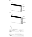
本発明の一は、バックライトと、表示パネルを有する液晶表示装置であって、バックライ
トは、明るさを個別に制御できる複数の単位領域に分割され、表示パネルは、複数の領域
の数よりも多い数の画素を有し、表示パネルに表示される画像は、液晶表示装置に入力さ
れる画像データの動きの変化量を検出することで推定された中間状態の画像データにした
がって表示される画像を含み、バックライトは、表示パネルに表示される画像にしたがっ
てそれぞれの領域の明るさが制御される期間を有し、且つ、表示パネルに表示される画像
の表示周期と同じ周期で発光状態が制御されることを特徴とする液晶表示装置である。
One aspect of the present invention is a liquid crystal display device having a backlight and a display panel, and the backlight is divided into a plurality of unit regions whose brightness can be individually controlled, and the display panel is based on the number of the plurality of regions. An image that has a large number of pixels and is displayed on the display panel is displayed according to the intermediate state image data estimated by detecting the amount of change in the movement of the image data input to the liquid crystal display device. Including the image, the backlight has a period in which the brightness of each area is controlled according to the image displayed on the display panel, and the light emission state is the same cycle as the display cycle of the image displayed on the display panel Is a liquid crystal display device.
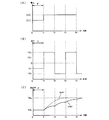
本発明の一は、バックライトと、表示パネルを有する液晶表示装置であって、バックライ
トは、明るさを個別に制御できる複数の単位領域に分割され、表示パネルは、単位領域の
数よりも多い数の画素を有し、表示パネルに表示される画像は、表示領域全域において同
じ表示状態を与える画像を含み、バックライトは、表示パネルに表示される画像にしたが
ってそれぞれの単位領域の明るさが制御される期間を有し、且つ、表示パネルに表示され
る画像の表示周期よりも長い周期で発光状態が制御されることを特徴とする液晶表示装置
である。
One aspect of the present invention is a liquid crystal display device having a backlight and a display panel, and the backlight is divided into a plurality of unit regions whose brightness can be individually controlled, and the display panel is more than the number of unit regions. The image that has a large number of pixels and is displayed on the display panel includes an image that gives the same display state in the entire display area, and the backlight has the brightness of each unit area according to the image displayed on the display panel. The liquid crystal display device is characterized in that the light emission state is controlled in a period longer than the display period of an image displayed on the display panel.
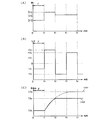
本発明の一は、バックライトと、表示パネルを有する液晶表示装置であって、バックライ
トは、明るさを個別に制御できる複数の単位領域に分割され、表示パネルは、単位領域の
数よりも多い数の画素を有し、表示パネルに表示される画像は、液晶表示装置に入力され
る画像データの周期と同じ周期で表示状態が制御され、バックライトは、表示パネルに表
示される画像にしたがってそれぞれの単位領域の明るさが制御される期間を有し、且つ、
発光領域全域において同じ発光状態を与える画像を含み、バックライトは、表示パネルに
表示される画像の表示周期よりも短い周期で発光状態が制御されることを特徴とする液晶
表示装置である。
One aspect of the present invention is a liquid crystal display device having a backlight and a display panel, and the backlight is divided into a plurality of unit regions whose brightness can be individually controlled, and the display panel is more than the number of unit regions. The display state of an image that has a large number of pixels and is displayed on the display panel is controlled in the same cycle as the cycle of image data input to the liquid crystal display device, and the backlight is an image displayed on the display panel. Therefore, it has a period in which the brightness of each unit area is controlled, and
The liquid crystal display device is characterized in that the light emission state is controlled in a cycle shorter than the display cycle of the image displayed on the display panel, including an image giving the same light emission state in the entire light emitting region.
本発明の一は、バックライトと、表示パネルを有する液晶表示装置であって、バックライ
トは、明るさを個別に制御できる複数の単位領域に分割され、表示パネルは、単位領域の
数よりも多い数の画素を有し、表示パネルに表示される画像は、表示領域全域において同
じ表示状態を与える画像を含み、バックライトは、表示パネルに表示される画像にしたが
ってそれぞれの単位領域の明るさが制御される期間を有し、バックライトに表示される画
像は、発光領域全域において同じ発光状態を与える画像を含み、且つ、表示パネルに表示
される画像の表示周期と同じ周期で発光状態が制御されることを特徴とする液晶表示装置
である。
One aspect of the present invention is a liquid crystal display device having a backlight and a display panel, and the backlight is divided into a plurality of unit regions whose brightness can be individually controlled, and the display panel is more than the number of unit regions. The image that has a large number of pixels and is displayed on the display panel includes an image that gives the same display state in the entire display area, and the backlight has the brightness of each unit area according to the image displayed on the display panel. The image displayed on the backlight includes an image that gives the same light emission state in the entire light emission region, and the light emission state is in the same cycle as the display cycle of the image displayed on the display panel. A liquid crystal display device that is controlled.
本発明の一は、バックライトと、表示パネルを有する液晶表示装置であって、バックライ
トは、明るさを個別に制御できる複数の単位領域に分割され、表示パネルは、単位領域の
数よりも多い数の画素を有し、バックライトは、明るさを制御できる段階の数が3段階以
上であり、表示パネルは、明るさを制御できる段階の数がn段階(nは2以上の整数)で
あり、液晶表示装置全体として表示できる明るさの段階の数がn段階よりも多いことを特
徴とする液晶表示装置である。
One aspect of the present invention is a liquid crystal display device having a backlight and a display panel, and the backlight is divided into a plurality of unit regions whose brightness can be individually controlled, and the display panel is more than the number of unit regions. It has a large number of pixels, the backlight has three or more stages in which the brightness can be controlled, and the display panel has n stages in which the brightness can be controlled (n is an integer of 2 or more). The liquid crystal display device is characterized in that the number of brightness steps that can be displayed as a whole liquid crystal display device is greater than n steps.
本発明において、バックライトは、明るさを制御できる段階の数が3段階以上であり、表
示パネルは、明るさを制御できる段階の数がn段階(nは2以上の整数)であり、表示装
置全体として表示できる明るさの段階の数がn段階よりも多い構成であってもよい。
In the present invention, the backlight has three or more stages in which the brightness can be controlled, and the display panel has n stages (n is an integer of 2 or more) in which the brightness can be controlled. The number of the brightness | luminance steps which can be displayed as the whole apparatus may be larger than n steps.
本発明において、液晶表示装置に入力される画像データが与える画像の明るさの平均値に
したがって、バックライトの明るさが制御される構成であってもよい。
In the present invention, the backlight brightness may be controlled in accordance with the average value of the image brightness given by the image data input to the liquid crystal display device.
本発明において、表示パネルに入力される電圧のうち、オーバードライブ電圧が含まれて
もよい。
In the present invention, an overdrive voltage may be included among the voltages input to the display panel.
本発明において、表示パネルに入力される電圧のうち、極性が周期的に切り替わる電圧が
含まれてもよい。
In the present invention, a voltage whose polarity is periodically switched among voltages input to the display panel may be included.
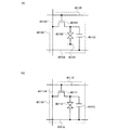
なお、スイッチは、様々な形態のものを用いることができる。例としては、電気的スイッ
チや機械的なスイッチなどがある。つまり、電流の流れを制御できるものであればよく、
特定のものに限定されない。例えば、スイッチとして、トランジスタ(例えば、バイポー
ラトランジスタ、MOSトランジスタなど)、ダイオード(例えば、PNダイオード、P
INダイオード、ショットキーダイオード、MIM(Metal Insulator
Metal)ダイオード、MIS(Metal Insulator Semicond
uctor)ダイオード、ダイオード接続のトランジスタなど)、サイリスタなどを用い
ることが出来る。または、これらを組み合わせた論理回路をスイッチとして用いることが
出来る。
Note that various types of switches can be used. Examples include electrical switches and mechanical switches. In other words, anything that can control the current flow,
It is not limited to a specific thing. For example, as a switch, a transistor (for example, bipolar transistor, MOS transistor, etc.), a diode (for example, PN diode, P, etc.)
IN diode, Schottky diode, MIM (Metal Insulator)
Metal diode, MIS (Metal Insulator Semiconductor)
uctor) diodes, diode-connected transistors, etc.), thyristors, etc. can be used. Alternatively, a logic circuit combining these can be used as a switch.
機械的なスイッチの例としては、デジタルマイクロミラーデバイス(DMD)のように、
MEMS(マイクロ・エレクトロ・メカニカル・システム)技術を用いたスイッチがある
。そのスイッチは、機械的に動かすことが出来る電極を有し、その電極が動くことによっ
て、接続と非接続とを制御して動作する。
An example of a mechanical switch is a digital micromirror device (DMD),
There is a switch using MEMS (micro electro mechanical system) technology. The switch has an electrode that can be moved mechanically, and operates by controlling connection and disconnection by moving the electrode.
スイッチとしてトランジスタを用いる場合、そのトランジスタは、単なるスイッチとし
て動作するため、トランジスタの極性(導電型)は特に限定されない。ただし、オフ電流
を抑えたい場合、オフ電流が少ない方の極性のトランジスタを用いることが望ましい。オ
フ電流が少ないトランジスタとしては、LDD領域を有するトランジスタやマルチゲート
構造を有するトランジスタ等がある。または、スイッチとして動作させるトランジスタの
ソース端子の電位が、低電位側電源(Vss、GND、0Vなど)の電位に近い状態で動
作する場合はNチャネル型トランジスタを用いることが望ましい。反対に、ソース端子の
電位が、高電位側電源(Vddなど)の電位に近い状態で動作する場合はPチャネル型ト
ランジスタを用いることが望ましい。なぜなら、Nチャネル型トランジスタではソース端
子が低電位側電源の電位に近い状態で動作するとき、Pチャネル型トランジスタではソー
ス端子が高電位側電源の電位に近い状態で動作するとき、ゲートとソースの間の電圧の絶
対値を大きくできるため、スイッチとして、より正確な動作をさせやすいからである。ソ
ースフォロワ動作をしてしまうことが少ないため、出力電圧の大きさが小さくなってしま
うことが少ないからである。
In the case where a transistor is used as a switch, the transistor operates as a mere switch, and thus the polarity (conductivity type) of the transistor is not particularly limited. However, when it is desired to suppress off-state current, it is desirable to use a transistor having a polarity with smaller off-state current. As a transistor with low off-state current, a transistor having an LDD region, a transistor having a multi-gate structure, and the like can be given. Alternatively, an N-channel transistor is preferably used in the case where the transistor operates as a switch when the potential of the source terminal of the transistor is close to the potential of the low potential power supply (Vss, GND, 0 V, or the like). On the other hand, it is desirable to use a P-channel transistor when operating in a state where the potential of the source terminal is close to the potential of the high potential side power supply (Vdd or the like). This is because an N-channel transistor operates when the source terminal is close to the potential of the low-potential side power supply, and a P-channel transistor operates when the source terminal is close to the potential of the high-potential side power supply. This is because the absolute value of the voltage between them can be increased, so that the switch can be operated more accurately. This is because the source follower operation is rare and the output voltage is less likely to decrease.
なお、Nチャネル型トランジスタとPチャネル型トランジスタの両方を用いて、CMO
S型のスイッチをスイッチとして用いてもよい。CMOS型のスイッチにすると、Pチャ
ネル型トランジスタまたはNチャネル型トランジスタのどちらか一方のトランジスタが導
通すれば電流が流れるため、スイッチとして機能しやすくなる。例えば、スイッチへの入
力信号の電圧が高い場合でも、低い場合でも、適切に電圧を出力させることが出来る。さ
らに、スイッチをオンまたはオフさせるための信号の電圧振幅値を小さくすることが出来
るので、消費電力を小さくすることも出来る。
Note that CMO using both N-channel and P-channel transistors
An S-type switch may be used as the switch. When a CMOS switch is used, a current flows when one of the P-channel transistor and the N-channel transistor is turned on, so that the switch can easily function as a switch. For example, the voltage can be appropriately output regardless of whether the voltage of the input signal to the switch is high or low. Further, since the voltage amplitude value of the signal for turning on or off the switch can be reduced, the power consumption can be reduced.
なお、スイッチとしてトランジスタを用いる場合、スイッチは、入力端子(ソース端子
またはドレイン端子の一方)と、出力端子(ソース端子またはドレイン端子の他方)と、
導通を制御する端子(ゲート端子)とを有している。一方、スイッチとしてダイオードを
用いる場合、スイッチは、導通を制御する端子を有していない場合がある。そのため、ト
ランジスタよりもダイオードをスイッチとして用いた方が、端子を制御するための配線を
少なくすることが出来る。
Note that when a transistor is used as the switch, the switch includes an input terminal (one of a source terminal or a drain terminal), an output terminal (the other of the source terminal or the drain terminal),
And a terminal for controlling conduction (gate terminal). On the other hand, when a diode is used as the switch, the switch may not have a terminal for controlling conduction. Therefore, the use of a diode as a switch rather than a transistor can reduce the wiring for controlling the terminal.
なお、AとBとが接続されている、と明示的に記載する場合は、AとBとが電気的に接
続されている場合と、AとBとが機能的に接続されている場合と、AとBとが直接接続さ
れている場合とを含むものとする。ここで、A、Bは、対象物(例えば、装置、素子、回
路、配線、電極、端子、導電膜、層、など)であるとする。したがって、所定の接続関係
、例えば、図または文章に示された接続関係に限定されず、図または文章に示された接続
関係以外のものも含むものとする。
In addition, when it is explicitly described that A and B are connected, A and B are electrically connected, and A and B are functionally connected. , A and B are directly connected. Here, A and B are objects (for example, devices, elements, circuits, wirings, electrodes, terminals, conductive films, layers, etc.). Therefore, it is not limited to a predetermined connection relationship, for example, the connection relationship shown in the figure or text, and includes things other than the connection relation shown in the figure or text.
例えば、AとBとが電気的に接続されている場合として、AとBとの電気的な接続を可
能とする素子(例えば、スイッチ、トランジスタ、容量素子、インダクタ、抵抗素子、ダ
イオードなど)が、AとBとの間に1個以上配置されていてもよい。あるいは、AとBと
が機能的に接続されている場合として、AとBとの機能的な接続を可能とする回路(例え
ば、論理回路(インバータ、NAND回路、NOR回路など)、信号変換回路(DA変換
回路、AD変換回路、ガンマ補正回路など)、電位レベル変換回路(電源回路(昇圧回路
、降圧回路など)、信号の電位レベルを変えるレベルシフタ回路など)、電圧源、電流源
、切り替え回路、増幅回路(信号振幅または電流量などを大きく出来る回路、オペアンプ
、差動増幅回路、ソースフォロワ回路、バッファ回路など)、信号生成回路、記憶回路、
制御回路など)が、AとBとの間に1個以上配置されていてもよい。あるいは、AとBと
が直接接続されている場合として、AとBとの間に他の素子や他の回路を挟まずに、Aと
Bとが直接接続されていてもよい。
For example, when A and B are electrically connected, an element (for example, a switch, a transistor, a capacitor, an inductor, a resistance element, a diode, or the like) that enables electrical connection between A and B is provided. 1 or more may be arranged between A and B. Alternatively, when A and B are functionally connected, a circuit (for example, a logic circuit (an inverter, a NAND circuit, a NOR circuit, etc.), a signal conversion circuit that enables functional connection between A and B (DA conversion circuit, AD conversion circuit, gamma correction circuit, etc.), potential level conversion circuit (power supply circuit (boost circuit, step-down circuit, etc.), level shifter circuit that changes signal potential level), voltage source, current source, switching circuit , Amplifier circuits (circuits that can increase signal amplitude or current amount, operational amplifiers, differential amplifier circuits, source follower circuits, buffer circuits, etc.), signal generation circuits, memory circuits,
One or more control circuits and the like may be arranged between A and B. Alternatively, when A and B are directly connected, A and B may be directly connected without sandwiching other elements or other circuits between A and B.
なお、AとBとが直接接続されている、と明示的に記載する場合は、AとBとが直接接
続されている場合(つまり、AとBとの間に他の素子や他の回路を間に介さずに接続され
ている場合)と、AとBとが電気的に接続されている場合(つまり、AとBとの間に別の
素子や別の回路を挟んで接続されている場合)とを含むものとする。
Note that in the case where it is explicitly described that A and B are directly connected, when A and B are directly connected (that is, another element or other circuit between A and B). ) And A and B are electrically connected (that is, A and B are connected with another element or another circuit sandwiched between them). ).
なお、AとBとが電気的に接続されている、と明示的に記載する場合は、AとBとが電
気的に接続されている場合(つまり、AとBとの間に別の素子や別の回路を挟んで接続さ
れている場合)と、AとBとが機能的に接続されている場合(つまり、AとBとの間に別
の回路を挟んで機能的に接続されている場合)と、AとBとが直接接続されている場合(
つまり、AとBとの間に別の素子や別の回路を挟まずに接続されている場合)とを含むも
のとする。つまり、電気的に接続されている、と明示的に記載する場合は、単に、接続さ
れている、とのみ明示的に記載されている場合と同じであるとする。
Note that in the case where it is explicitly described that A and B are electrically connected, another element is connected between A and B (that is, between A and B). Or when A and B are functionally connected (that is, they are functionally connected with another circuit between A and B). And A and B are directly connected (
That is, it is assumed that A and B are connected without interposing another element or another circuit). That is, when it is explicitly described that it is electrically connected, it is the same as when it is explicitly only described that it is connected.
子、電子インク、電気泳動素子、グレーティングライトバルブ(GLV)、プラズマディ
スプレイ(PDP)、デジタルマイクロミラーデバイス(DMD)、圧電セラミックディ
スプレイ、カーボンナノチューブ、など、電気磁気的作用により、コントラスト、輝度、
反射率、透過率などが変化する表示媒体を用いることができる。なお、EL素子を用いた
表示装置としてはELディスプレイ、電子放出素子を用いた表示装置としてはフィールド
エミッションディスプレイ(FED)やSED方式平面型ディスプレイ(SED:Sur
face−conduction Electron−emitter Disply)
など、液晶素子を用いた表示装置としては液晶ディスプレイ(透過型液晶ディスプレイ、
半透過型液晶ディスプレイ、反射型液晶ディスプレイ、直視型液晶ディスプレイ、投射型
液晶ディスプレイ)、電子インクや電気泳動素子を用いた表示装置としては電子ペーパー
がある。
Child, electronic ink, electrophoretic element, grating light valve (GLV), plasma display (PDP), digital micromirror device (DMD), piezoelectric ceramic display, carbon nanotube, etc.
A display medium whose reflectance, transmittance, and the like change can be used. An EL display is used as a display device using an EL element, and a field emission display (FED) or a SED type flat display (SED: Sur) is used as a display device using an electron-emitting device.
face-conduction electron-emitter display)
As a display device using a liquid crystal element, a liquid crystal display (a transmissive liquid crystal display,
There are electronic papers as display devices using a semi-transmissive liquid crystal display, a reflective liquid crystal display, a direct-view liquid crystal display, and a projection liquid crystal display) and electronic ink or electrophoretic elements.
なお、EL素子とは、陽極と、陰極と、陽極と陰極との間に挟まれたEL層とを有する
素子である。なお、EL層としては、1重項励起子からの発光(蛍光)を利用するもの、
3重項励起子からの発光(燐光)を利用するもの、1重項励起子からの発光(蛍光)を利
用するものと3重項励起子からの発光(燐光)を利用するものとを含むもの、有機物によ
って形成されたもの、無機物によって形成されたもの、有機物によって形成されたものと
無機物によって形成されたものとを含むもの、高分子の材料、低分子の材料、高分子の材
料と低分子の材料とを含むものなどを用いることができる。ただし、これに限定されず、
EL素子として様々なものを用いることができる。
Note that an EL element is an element having an anode, a cathode, and an EL layer sandwiched between the anode and the cathode. Note that the EL layer uses light emission (fluorescence) from singlet excitons,
Includes those that use light emission (phosphorescence) from triplet excitons, those that use light emission (fluorescence) from singlet excitons, and those that use light emission (phosphorescence) from triplet excitons , One formed by organic matter, one formed by inorganic matter, one containing organic and one formed by inorganic matter, polymer material, low molecular material, polymer material and low A material containing a molecular material can be used. However, it is not limited to this,
Various EL elements can be used.
なお、電子放出素子とは、先鋭な陰極に高電界を集中して電子を引き出す素子である。例
えば、電子放出素子として、スピント型、カーボンナノチューブ(CNT)型、金属―絶
縁体―金属を積層したMIM(Metal−Insulator−Metal)型、金属
―絶縁体―半導体を積層したMIS(Metal−Insulator−Semicon
ductor)型、MOS型、シリコン型、薄膜ダイオード型、ダイヤモンド型、表面伝
導エミッタSCD型、オード型、ダイヤモンド型、表面伝導エミッタSCD型、金属―絶
縁体―半導体−金属型等の薄膜型、HEED型、EL型、ポーラスシリコン型、表面伝導
(SED)型などを用いることができる。ただし、これに限定されず、電子放出素子とし
て様々なものを用いることができる。
The electron-emitting device is an element that draws electrons by concentrating a high electric field on a sharp cathode. For example, as an electron-emitting device, a Spindt type, a carbon nanotube (CNT) type, a metal-insulator-metal laminated MIM (Metal-Insulator-Metal) type, and a metal-insulator-semiconductor laminated MIS (Metal-Insulator). -Semicon
(ductor) type, MOS type, silicon type, thin film diode type, diamond type, surface conduction emitter SCD type, ode type, diamond type, surface conduction emitter SCD type, metal-insulator-semiconductor-metal thin film type, HEED, etc. A type, an EL type, a porous silicon type, a surface conduction (SED) type, or the like can be used. However, the present invention is not limited to this, and various types of electron-emitting devices can be used.
なお、液晶素子とは、液晶の光学的変調作用によって光の透過または非透過を制御する素
子であり、一対の電極、及び液晶により構成される。なお、液晶の光学的変調作用は、液
晶にかかる電界(横方向の電界、縦方向の電界又は斜め方向の電界を含む)によって制御
される。なお、液晶素子としては、ネマチック液晶、コレステリック液晶、スメクチック
液晶、ディスコチック液晶、サーモトロピック液晶、ライオトロピック液晶、リオトロピ
ック液晶、低分子液晶、高分子液晶、強誘電液晶、反強誘電液晶、主鎖型液晶、側鎖型高
分子液晶、プラズマアドレス液晶(PDLC)、バナナ型液晶、TN(Twisted
Nematic)モード、STN(Super Twisted Nematic)モー
ド、IPS(In−Plane−Switching)モード、FFS(Fringe
Field Switching)モード、MVA(Multi−domain Ver
tical Alignment)モード、PVA(Patterned Vertic
al Alignment)、ASV(Advanced Super View)モー
ド、ASM(Axially Symmetric aligned Micro−ce
ll)モード、OCB(Optical Compensated Birefring
ence)モード、ECB(Electrically Controlled Bir
efringence)モード、FLC(Ferroelectric Liquid
Crystal)モード、AFLC(AntiFerroelectric Liqui
d Crystal)モード、PDLC(Polymer Dispersed Liq
uid Crystal)モード、ゲストホストモードなどを用いることができる。ただ
し、これに限定されず、液晶素子として様々なものを用いることができる。
Note that a liquid crystal element is an element that controls transmission or non-transmission of light by an optical modulation action of liquid crystal, and includes a pair of electrodes and liquid crystal. Note that the optical modulation action of the liquid crystal is controlled by an electric field applied to the liquid crystal (including a horizontal electric field, a vertical electric field, or an oblique electric field). Liquid crystal elements include nematic liquid crystal, cholesteric liquid crystal, smectic liquid crystal, discotic liquid crystal, thermotropic liquid crystal, lyotropic liquid crystal, lyotropic liquid crystal, low molecular liquid crystal, polymer liquid crystal, ferroelectric liquid crystal, antiferroelectric liquid crystal, main chain. Type liquid crystal, side chain type polymer liquid crystal, plasma addressed liquid crystal (PDLC), banana type liquid crystal, TN (Twisted)
Nematic) mode, STN (Super Twisted Nematic) mode, IPS (In-Plane-Switching) mode, FFS (Fringe)
Field Switching mode, MVA (Multi-domain Ver.)
tick alignment mode, PVA (Patterned Vertic)
al Alignment), ASV (Advanced Super View) mode, ASM (Axial Symmetrical Aligned Micro-ce)
ll) mode, OCB (Optical Compensated Birefring)
ence) mode, ECB (Electrically Controlled Bird)
efficiency mode, FLC (Ferroelectric Liquid)
Crystal) mode, AFLC (Antiferroelectric Liquid)
d Crystal) mode, PDLC (Polymer Dispersed Liq)
uid Crystal) mode, guest host mode, etc. can be used. However, the present invention is not limited to this, and various liquid crystal elements can be used.
なお、電子ペーパーとしては、光学異方性と染料分子配向のような分子により表示される
もの、電気泳動、粒子移動、粒子回転、相変化のような粒子により表示されるもの、フィ
ルムの一端が移動することにより表示されるもの、分子の発色/相変化により表示される
もの、分子の光吸収により表示されるもの、電子とホールが結合して時発光により表示さ
れるものなどのことをいう。例えば、電子ペーパーとして、マイクロカプセル型電気泳動
、水平移動型電気泳動、垂直移動型電気泳動、球状ツイストボール、磁気ツイストボール
、円柱ツイストボール方式、帯電トナー、電子粉流体、磁気泳動型、磁気感熱式、エレク
トロウェッテイング、光散乱(透明白濁)、コレステリック液晶/光導電層、コレステリ
ック液晶、双安定性ネマチック液晶、強誘電性液晶、2色性色素・液晶分散型、可動フィ
ルム、ロイコ染料発消色、フォトクロミック、エレクトロクロミック、エレクトロデポジ
ション、フレキシブル有機ELなどを用いることができる。ただし、これに限定されず、
電子ペーパーとして様々なものを用いることができる。ここで、マイクロカプセル型電気
泳動を用いることによって、電気泳動方式の欠点である泳動粒子の凝集、沈殿を解決する
ことができる。電子粉流体は、高速応答性、高反射率、広視野角、低消費電力、メモリー
性などのメリットを有する。
Electronic paper includes those displayed by molecules such as optical anisotropy and dye molecule orientation, those displayed by particles such as electrophoresis, particle movement, particle rotation, and phase change. It is displayed by moving, displayed by color development / phase change of molecules, displayed by light absorption of molecules, displayed by light emission when electrons and holes are combined, etc. . For example, as electronic paper, microcapsule type electrophoresis, horizontal movement type electrophoresis, vertical movement type electrophoresis, spherical twist ball, magnetic twist ball, cylindrical twist ball method, charged toner, electronic powder fluid, magnetophoretic type, magnetic heat sensitivity Formula, electrowetting, light scattering (transparent white turbidity), cholesteric liquid crystal / photoconductive layer, cholesteric liquid crystal, bistable nematic liquid crystal, ferroelectric liquid crystal, dichroic dye / liquid crystal dispersion type, movable film, leuco dye extinction Color, photochromic, electrochromic, electrodeposition, flexible organic EL, etc. can be used. However, it is not limited to this,
Various electronic papers can be used. Here, by using microcapsule electrophoresis, aggregation and precipitation of electrophoretic particles, which is a drawback of the electrophoresis system, can be solved. The electronic powder fluid has advantages such as high-speed response, high reflectivity, wide viewing angle, low power consumption, and memory properties.
なお、プラズマディスプレイは、電極を表面に形成した基板と、電極及び微小な溝を表面
に形成し且つ溝内に蛍光体層を形成した基板とを狭い間隔で対向させて、希ガスを封入し
た構造を有する。なお、電極間に電圧をかけることによって紫外線を発生させ、蛍光体を
光らせることで、表示を行うことができる。なお、プラズマディスプレイとしては、DC
型PDP、AC型PDPでもよい。ここで、プラズマディスプレイパネルとしては、AS
W(Address While Sustain)駆動、サブフレームをリセット期間
、アドレス期間、維持期間に分割するADS(Address Display Sep
arated)駆動、CLEAR(Low Energy Address and R
eduction of False Contour Sequence)駆動、AL
IS(Alternate Lighting of Surfaces)方式、TER
ES(Techbology of Reciprocal Susfainer)駆動
などを用いることができる。ただし、これに限定されず、プラズマディスプレイとして様
々なものを用いることができる。
Note that the plasma display encloses a rare gas with a substrate having an electrode formed on the surface and a substrate having an electrode and a minute groove formed on the surface and a phosphor layer formed in the groove facing each other at a narrow interval. It has a structure. In addition, a display can be performed by generating an ultraviolet-ray by applying a voltage between electrodes and making fluorescent substance light. As a plasma display, DC
It may be a type PDP or an AC type PDP. Here, as a plasma display panel, AS
W (Address While Sustain) drive, ADS (Address Display Sep) that divides subframe into reset period, address period, and sustain period
driven), CLEAR (Low Energy Address and R)
instruction of false control sequence) drive, AL
IS (Alternate Lightning of Surfaces) method, TER
An ES (Technology of Reciprocal Susfainer) drive or the like can be used. However, the present invention is not limited to this, and various types of plasma displays can be used.
なお、光源を必要とする表示装置、例えば、液晶ディスプレイ(透過型液晶ディスプレイ
、半透過型液晶ディスプレイ、反射型液晶ディスプレイ、直視型液晶ディスプレイ、投射
型液晶ディスプレイ)、グレーティングライトバルブ(GLV)を用いた表示装置、デジ
タルマイクロミラーデバイス(DMD)を用いた表示装置などの光源としては、エレクト
ロルミネッセンス、冷陰極管、熱陰極管、LED、レーザー光源、水銀ランプなどを用い
ることができる。ただし、これに限定されず、光源して様々なものを用いることができる
。
Note that a display device that requires a light source, such as a liquid crystal display (transmission type liquid crystal display, transflective type liquid crystal display, reflection type liquid crystal display, direct view type liquid crystal display, projection type liquid crystal display), or a grating light valve (GLV) is used. As a light source for a display device using a conventional display device or a digital micromirror device (DMD), electroluminescence, a cold cathode tube, a hot cathode tube, an LED, a laser light source, a mercury lamp, or the like can be used. However, the present invention is not limited to this, and various light sources can be used.
なお、トランジスタの構成は、様々な形態をとることができる。特定の構成に限定され
ない。例えば、ゲート電極が2個以上のマルチゲート構造を用いてもよい。マルチゲート
構造にすると、チャネル領域が直列に接続されるため、複数のトランジスタが直列に接続
された構成となる。マルチゲート構造により、オフ電流の低減、トランジスタの耐圧向上
による信頼性の向上を図ることができる。あるいは、マルチゲート構造により、飽和領域
で動作する時に、ドレイン・ソース間電圧が変化しても、ドレイン・ソース間電流があま
り変化せず、電圧・電流特性の傾きがフラットな特性にすることができる。電圧・電流特
性の傾きがフラットである特性を利用すると、理想的な電流源回路や、非常に高い抵抗値
をもつ能動負荷を実現することが出来る。その結果、特性のよい差動回路やカレントミラ
ー回路を実現することが出来る。別の例として、チャネルの上下にゲート電極が配置され
ている構造でもよい。チャネルの上下にゲート電極が配置されている構造にすることによ
り、チャネル領域が増えるため、電流値の増加、又は空乏層ができやすくなることによる
S値の低減を図ることができる。チャネルの上下にゲート電極が配置されると、複数のト
ランジスタが並列に接続されたような構成となる。
Note that the structure of the transistor can take a variety of forms. It is not limited to a specific configuration. For example, a multi-gate structure having two or more gate electrodes may be used. When the multi-gate structure is employed, the channel regions are connected in series, so that a plurality of transistors are connected in series. With the multi-gate structure, the off-state current can be reduced and the reliability can be improved by improving the withstand voltage of the transistor. Or, when operating in the saturation region, the drain-source current does not change much even when the drain-source voltage changes, and the slope of the voltage / current characteristic is flat due to the multi-gate structure. it can. By using the characteristic that the slope of the voltage / current characteristic is flat, an ideal current source circuit and an active load having a very high resistance value can be realized. As a result, a differential circuit or a current mirror circuit with good characteristics can be realized. As another example, a structure in which gate electrodes are arranged above and below a channel may be used. With the structure in which the gate electrodes are arranged above and below the channel, the channel region increases, so that the current value can be increased or the S value can be reduced because a depletion layer can be easily formed. When gate electrodes are provided above and below a channel, a structure in which a plurality of transistors are connected in parallel is obtained.
あるいは、チャネル領域の上にゲート電極が配置されている構造でもよいし、チャネル
領域の下にゲート電極が配置されている構造でもよい。あるいは、正スタガ構造または逆
スタガ構造でもよいし、チャネル領域が複数の領域に分かれていてもよいし、チャネル領
域が並列に接続されていてもよいし、チャネル領域が直列に接続されていてもよい。ある
いは、チャネル領域(もしくはその一部)にソース電極やドレイン電極が重なっていても
よい。チャネル領域(もしくはその一部)にソース電極やドレイン電極が重なる構造にす
ることにより、チャネル領域の一部に電荷がたまって、動作が不安定になることを防ぐこ
とができる。あるいは、LDD領域を設けても良い。LDD領域を設けることにより、オ
フ電流の低減、又はトランジスタの耐圧向上による信頼性の向上を図ることができる。あ
るいは、LDD領域を設けることにより、飽和領域で動作する時に、ドレイン・ソース間
電圧が変化しても、ドレイン・ソース間電流があまり変化せず、電圧・電流特性の傾きが
フラットな特性にすることができる。
Alternatively, a structure in which a gate electrode is disposed over a channel region may be employed, or a structure in which a gate electrode is disposed under a channel region may be employed. Alternatively, a normal stagger structure or an inverted stagger structure may be used, the channel region may be divided into a plurality of regions, the channel regions may be connected in parallel, or the channel regions may be connected in series. Good. Alternatively, a source electrode or a drain electrode may overlap with the channel region (or a part thereof). With the structure in which the source electrode or the drain electrode overlaps with the channel region (or part thereof), it is possible to prevent electric charges from being accumulated in part of the channel region and unstable operation. Alternatively, an LDD region may be provided. By providing the LDD region, the off-state current can be reduced or the reliability can be improved by improving the withstand voltage of the transistor. Alternatively, by providing an LDD region, when operating in the saturation region, even if the drain-source voltage changes, the drain-source current does not change so much and the slope of the voltage-current characteristic is flat. be able to.
なお、トランジスタは、様々なタイプを用いることができ、様々な基板を用いて形成さ
せることができる。したがって、所定の機能を実現させるために必要な回路の全てが、同
一の基板に形成されていてもよい。例えば、所定の機能を実現させるために必要な回路の
全てが、ガラス基板、プラスチック基板、単結晶基板、またはSOI基板を用いて形成さ
れていてもよく、さまざまな基板を用いてに形成されていてもよい。所定の機能を実現さ
せるために必要な回路の全てが同じ基板を用いて形成されていることにより、部品点数の
削減によるコストの低減、又は回路部品との接続点数の低減による信頼性の向上を図るこ
とができる。あるいは、所定の機能を実現させるために必要な回路の一部が、ある基板に
形成されており、所定の機能を実現させるために必要な回路の別の一部が、別の基板に形
成されていてもよい。つまり、所定の機能を実現させるために必要な回路の全てが同じ基
板を用いて形成されていなくてもよい。例えば、所定の機能を実現させるために必要な回
路の一部は、ガラス基板上にトランジスタを用いて形成され、所定の機能を実現させるた
めに必要な回路の別の一部は、単結晶基板に形成され、単結晶基板を用いて形成されたト
ランジスタで構成されたICチップをCOG(Chip On Glass)でガラス基
板に接続して、ガラス基板上にそのICチップを配置してもよい。あるいは、そのICチ
ップをTAB(Tape Automated Bonding)やプリント基板を用い
てガラス基板と接続してもよい。このように、回路の一部が同じ基板に形成されているこ
とにより、部品点数の削減によるコストの低減、又は回路部品との接続点数の低減による
信頼性の向上を図ることができる。あるいは、駆動電圧が高い部分及び駆動周波数が高い
部分の回路は、消費電力が大きくなってしまうので、そのような部分の回路は同じ基板に
形成せず、そのかわりに、例えば、単結晶基板にその部分の回路を形成して、その回路で
構成されたICチップを用いるようにすれば、消費電力の増加を防ぐことができる。
Note that various types of transistors can be used, and the transistor can be formed using various substrates. Therefore, all the circuits necessary for realizing a predetermined function may be formed on the same substrate. For example, all circuits necessary for realizing a predetermined function may be formed using a glass substrate, a plastic substrate, a single crystal substrate, or an SOI substrate, and are formed using various substrates. May be. Since all the circuits necessary to realize a given function are formed using the same substrate, the cost can be reduced by reducing the number of components, or the reliability can be improved by reducing the number of connection points with circuit components. Can be planned. Alternatively, a part of the circuit necessary for realizing the predetermined function is formed on a certain substrate, and another part of the circuit necessary for realizing the predetermined function is formed on another substrate. It may be. That is, not all the circuits necessary for realizing a predetermined function may be formed using the same substrate. For example, a part of a circuit necessary for realizing a predetermined function is formed using a transistor over a glass substrate, and another part of a circuit required for realizing a predetermined function is a single crystal substrate. An IC chip formed of a transistor formed using a single crystal substrate may be connected to a glass substrate by COG (Chip On Glass), and the IC chip may be disposed on the glass substrate. Alternatively, the IC chip may be connected to the glass substrate using TAB (Tape Automated Bonding) or a printed board. As described above, since a part of the circuit is formed on the same substrate, the cost can be reduced by reducing the number of components, or the reliability can be improved by reducing the number of connection points with circuit components. Alternatively, since the power consumption of a circuit with a high drive voltage and a high drive frequency is high, such a circuit is not formed on the same substrate. Instead, for example, a single crystal substrate is used. If a circuit for that portion is formed and an IC chip constituted by the circuit is used, an increase in power consumption can be prevented.
なお、一画素とは、明るさを制御できる要素一つ分を示すものとする。よって、一例とし
ては、一画素とは、一つの色要素を示すものとし、その色要素一つで明るさを表現する。
従って、そのときは、R(赤)G(緑)B(青)の色要素からなるカラー表示装置の場合
には、画像の最小単位は、Rの画素とGの画素とBの画素との三画素から構成されるもの
とする。なお、色要素は、三色に限定されず、三色以上を用いても良いし、RGB以外の
色を用いても良い。例えば、白色を加えて、RGBW(Wは白)としてもよい。あるいは
、RGBに、例えば、イエロー、シアン、マゼンタ、エメラルドグリーン、朱色などを一
色以上追加してもよい。あるいは、例えば、RGBの中の少なくとも一色に類似した色を
、RGBに追加してもよい。例えば、R、G、B1、B2としてもよい。B1とB2とは
、どちらも青色であるが、少し周波数が異なっている。同様に、R1、R2、G、Bとし
てもよい。このような色要素を用いることにより、より実物に近い表示を行うことができ
る。このような色要素を用いることにより、消費電力を低減することが出来る。別の例と
しては、1つの色要素について、複数の領域を用いて明るさを制御する場合は、その領域
一つ分を一画素としてもよい。よって、一例として、面積階調を行う場合または副画素(
サブ画素)を有している場合、一つの色要素につき、明るさを制御する領域が複数あり、
その全体で階調を表現するわけであるが、明るさを制御する領域の一つ分を一画素として
もよい。よって、その場合は、一つの色要素は、複数の画素で構成されることとなる。あ
るいは、明るさを制御する領域が1つの色要素の中に複数あっても、それらをまとめて、
1つの色要素を1画素としてもよい。よって、その場合は、一つの色要素は、一つの画素
で構成されることとなる。あるいは、1つの色要素について、複数の領域を用いて明るさ
を制御する場合、画素によって、表示に寄与する領域の大きさが異なっている場合がある
。あるいは、一つの色要素につき複数ある、明るさを制御する領域において、各々に供給
する信号を僅かに異ならせるようにして、視野角を広げるようにしてもよい。つまり、1
つの色要素について、複数個ある領域が各々有する画素電極の電位が、各々異なっていて
もよい。その結果、液晶分子に加わる電圧が各画素電極によって各々異なる。よって、視
野角を広くすることが出来る。
One pixel means one element whose brightness can be controlled. Therefore, as an example, one pixel represents one color element, and brightness is expressed by one color element.
Therefore, at that time, in the case of a color display device composed of R (red), G (green), and B (blue) color elements, the minimum unit of an image is an R pixel, G pixel, and B pixel. It is assumed to be composed of three pixels. Note that the color elements are not limited to three colors, and three or more colors may be used, or colors other than RGB may be used. For example, RGBW (W is white) may be added by adding white. Alternatively, one or more colors such as yellow, cyan, magenta, emerald green, vermilion, and the like may be added to RGB. Alternatively, for example, a color similar to at least one of RGB may be added to RGB. For example, R, G, B1, and B2 may be used. B1 and B2 are both blue, but have slightly different frequencies. Similarly, R1, R2, G, and B may be used. By using such color elements, it is possible to perform display closer to the real thing. By using such color elements, power consumption can be reduced. As another example, when brightness is controlled using a plurality of areas for one color element, one area may be set as one pixel. Therefore, as an example, when performing area gradation or sub-pixel (
Sub-pixels), there are multiple brightness control areas for each color element,
The gradation is expressed as a whole, but one area for controlling the brightness may be one pixel. Therefore, in that case, one color element is composed of a plurality of pixels. Or, even if there are multiple areas for controlling brightness in one color element,
One color element may be one pixel. Therefore, in that case, one color element is composed of one pixel. Alternatively, when the brightness is controlled using a plurality of areas for one color element, the size of the area contributing to display may differ depending on the pixel. Alternatively, the viewing angle may be widened by slightly varying the signal supplied to each of the areas where the brightness is controlled, which is plural for each color element. That is, 1
For one color element, the potentials of the pixel electrodes in each of the plurality of regions may be different from each other. As a result, the voltage applied to the liquid crystal molecules is different for each pixel electrode. Therefore, the viewing angle can be widened.
なお、一画素(三色分)と明示的に記載する場合は、RとGとBの三画素分を一画素と
考える場合であるとする。一画素(一色分)と明示的に記載する場合は、一つの色要素に
つき、複数の領域がある場合、それらをまとめて一画素と考える場合であるとする。
In addition, when it is explicitly described as one pixel (for three colors), it is assumed that three pixels of R, G, and B are considered as one pixel. When it is explicitly described as one pixel (for one color), it is assumed that when there are a plurality of areas for one color element, they are collectively considered as one pixel.
なお、画素は、マトリクス状に配置(配列)されている場合がある。ここで、画素がマト
リクスに配置(配列)されているとは、縦方向もしくは横方向において、画素が直線上に
並んで配置されている場合、又はギザギザな線上に配置されている場合を含む。よって、
例えば三色の色要素(例えばRGB)でフルカラー表示を行う場合に、ストライプ配置さ
れている場合、又は三つの色要素のドットがデルタ配置されている場合も含む。さらに、
ベイヤー配置されている場合も含む。なお、色要素は、三色に限定されず、それ以上でも
よく、例えば、RGBW(Wは白)、又はRGBに、イエロー、シアン、マゼンタなどを
一色以上追加したものなどがある。なお、色要素のドット毎にその表示領域の大きさが異
なっていてもよい。これにより、低消費電力化、又は表示素子の長寿命化を図ることがで
きる。
Note that the pixels may be arranged (arranged) in a matrix. Here, the arrangement (arrangement) of pixels in a matrix includes a case where pixels are arranged side by side in a vertical direction or a horizontal direction, or a case where they are arranged on a jagged line. Therefore,
For example, when full-color display is performed with three color elements (for example, RGB), the case where stripes are arranged or the case where dots of three color elements are arranged in a delta is included. further,
Including cases where Bayer is arranged. The color elements are not limited to three colors, and may be more than that, for example, RGBW (W is white), or RGB in which one or more colors of yellow, cyan, magenta, and the like are added. The size of the display area may be different for each dot of the color element. Thereby, it is possible to reduce power consumption or extend the life of the display element.
なお、画素に能動素子を有するアクティブマトリクス方式、または、画素に能動素子を有
しないパッシブマトリクス方式を用いることが出来る。
Note that an active matrix method in which an active element is included in a pixel or a passive matrix method in which an active element is not included in a pixel can be used.
アクティブマトリクス方式では、能動素子(アクティブ素子、非線形素子)として、トラ
ンジスタだけでなく、さまざまな能動素子(アクティブ素子、非線形素子)を用いること
が出来る。例えば、MIM(Metal Insulator Metal)やTFD(
Thin Film Diode)などを用いることも可能である。これらの素子は、製
造工程が少ないため、製造コストの低減、又は歩留まりの向上を図ることができる。さら
に、素子のサイズが小さいため、開口率を向上させることができ、低消費電力化や高輝度
化をはかることが出来る。
In the active matrix system, not only transistors but also various active elements (active elements and nonlinear elements) can be used as active elements (active elements and nonlinear elements). For example, MIM (Metal Insulator Metal) or TFD (
It is also possible to use (Thin Film Diode) or the like. Since these elements have few manufacturing steps, manufacturing cost can be reduced or yield can be improved. Furthermore, since the size of the element is small, the aperture ratio can be improved, and low power consumption and high luminance can be achieved.
なお、アクティブマトリクス方式以外のものとして、能動素子(アクティブ素子、非線形
素子)を用いないパッシブマトリクス型を用いることも可能である。能動素子(アクティ
ブ素子、非線形素子)を用いないため、製造工程が少なく、製造コストの低減、又は歩留
まりの向上を図ることができる。能動素子(アクティブ素子、非線形素子)を用いないた
め、開口率を向上させることができ、低消費電力化や高輝度化をはかることが出来る。
Note that as a method other than the active matrix method, a passive matrix type that does not use active elements (active elements, nonlinear elements) can be used. Since no active element (active element or nonlinear element) is used, the number of manufacturing steps is small, and manufacturing costs can be reduced or yield can be improved. Since no active element (active element or nonlinear element) is used, the aperture ratio can be improved, and low power consumption and high luminance can be achieved.
なお、トランジスタとは、ゲートと、ドレインと、ソースとを含む少なくとも三つの端子
を有する素子であり、ドレイン領域とソース領域の間にチャネル領域を有しており、ドレ
イン領域とチャネル領域とソース領域とを介して電流を流すことが出来る。ここで、ソー
スとドレインとは、トランジスタの構造や動作条件等によって変わるため、いずれがソー
スまたはドレインであるかを限定することが困難である。そこで、本書類(明細書、特許
請求の範囲又は図面など)においては、ソース及びドレインとして機能する領域を、ソー
スもしくはドレインと呼ばない場合がある。その場合、一例としては、それぞれを第1端
子、第2端子と表記する場合がある。あるいは、それぞれを第1の電極、第2の電極と表
記する場合がある。あるいは、ソース領域、ドレイン領域と表記する場合がある。
Note that a transistor is an element having at least three terminals including a gate, a drain, and a source. The transistor has a channel region between the drain region and the source region, and the drain region, the channel region, and the source region. A current can be passed through. Here, since the source and the drain vary depending on the structure and operating conditions of the transistor, it is difficult to limit which is the source or the drain. Therefore, in this document (the specification, the claims, the drawings, and the like), a region functioning as a source and a drain may not be referred to as a source or a drain. In that case, as an example, there are cases where they are respectively referred to as a first terminal and a second terminal. Alternatively, they may be referred to as a first electrode and a second electrode, respectively. Alternatively, they may be referred to as a source region and a drain region.
なお、トランジスタは、ベースとエミッタとコレクタとを含む少なくとも三つの端子を
有する素子であってもよい。この場合も同様に、エミッタとコレクタとを、第1端子、第
2端子と表記する場合がある。
Note that the transistor may be an element having at least three terminals including a base, an emitter, and a collector. Similarly in this case, the emitter and the collector may be referred to as a first terminal and a second terminal.
なお、ゲートとは、ゲート電極とゲート配線(ゲート線、ゲート信号線、走査線、走査
信号線等とも言う)とを含んだ全体、もしくは、それらの一部のことを言う。ゲート電極
とは、チャネル領域を形成する半導体と、ゲート絶縁膜を介してオーバーラップしている
部分の導電膜のことを言う。なお、ゲート電極の一部は、LDD(Lightly Do
ped Drain)領域またはソース領域(またはドレイン領域)と、ゲート絶縁膜を
介してオーバーラップしている場合もある。ゲート配線とは、各トランジスタのゲート電
極の間を接続するための配線、各画素の有するゲート電極の間を接続するための配線、又
はゲート電極と別の配線とを接続するための配線のことを言う。
Note that a gate refers to the whole or part of a gate electrode and a gate wiring (also referred to as a gate line, a gate signal line, a scan line, a scan signal line, or the like). A gate electrode refers to a portion of a conductive film that overlaps with a semiconductor forming a channel region with a gate insulating film interposed therebetween. Note that a part of the gate electrode is an LDD (Lightly Dow).
In some cases, it may overlap with a ped drain region or a source region (or drain region) through a gate insulating film. A gate wiring is a wiring for connecting the gate electrodes of each transistor, a wiring for connecting the gate electrodes of each pixel, or a wiring for connecting the gate electrode to another wiring. Say.
ただし、ゲート電極としても機能し、ゲート配線としても機能するような部分(領域、
導電膜、配線など)も存在する。そのような部分(領域、導電膜、配線など)は、ゲート
電極と呼んでも良いし、ゲート配線と呼んでも良い。つまり、ゲート電極とゲート配線と
が、明確に区別できないような領域も存在する。例えば、延伸して配置されているゲート
配線の一部とチャネル領域がオーバーラップしている場合、その部分(領域、導電膜、配
線など)はゲート配線として機能しているが、ゲート電極としても機能していることにな
る。よって、そのような部分(領域、導電膜、配線など)は、ゲート電極と呼んでも良い
し、ゲート配線と呼んでも良い。
However, the portion that functions as the gate electrode and also functions as the gate wiring (region,
There are also conductive films, wirings, and the like. Such a portion (region, conductive film, wiring, or the like) may be called a gate electrode or a gate wiring. That is, there is a region where the gate electrode and the gate wiring cannot be clearly distinguished. For example, when a part of the gate wiring extended and the channel region overlap, the portion (region, conductive film, wiring, etc.) functions as the gate wiring, but also as the gate electrode It is functioning. Therefore, such a portion (region, conductive film, wiring, or the like) may be called a gate electrode or a gate wiring.
なお、ゲート電極と同じ材料で形成され、ゲート電極と同じ島(アイランド)を形成し
てつながっている部分(領域、導電膜、配線など)も、ゲート電極と呼んでも良い。同様
に、ゲート配線と同じ材料で形成され、ゲート配線と同じ島(アイランド)を形成してつ
ながっている部分(領域、導電膜、配線など)も、ゲート配線と呼んでも良い。このよう
な部分(領域、導電膜、配線など)は、厳密な意味では、チャネル領域とオーバーラップ
していない場合、又は別のゲート電極と接続させる機能を有していない場合がある。しか
し、製造時の仕様などの関係で、ゲート電極またはゲート配線と同じ材料で形成され、ゲ
ート電極またはゲート配線と同じ島(アイランド)を形成してつながっている部分(領域
、導電膜、配線など)がある。よって、そのような部分(領域、導電膜、配線など)もゲ
ート電極またはゲート配線と呼んでも良い。
Note that a portion (a region, a conductive film, a wiring, or the like) formed using the same material as the gate electrode and connected to form the same island (island) as the gate electrode may be called a gate electrode. Similarly, a portion (a region, a conductive film, a wiring, or the like) formed using the same material as the gate wiring and connected by forming the same island (island) as the gate wiring may be referred to as a gate wiring. In a strict sense, such a portion (region, conductive film, wiring, or the like) may not overlap with the channel region or may not have a function of being connected to another gate electrode. However, due to specifications at the time of manufacture, etc., the part (region, conductive film, wiring, etc.) that is formed of the same material as the gate electrode or gate wiring and forms the same island (island) as the gate electrode or gate wiring. ) Therefore, such a portion (region, conductive film, wiring, or the like) may also be referred to as a gate electrode or a gate wiring.
なお、例えば、マルチゲートのトランジスタにおいて、1つのゲート電極と、別のゲー
ト電極とは、ゲート電極と同じ材料で形成された導電膜で接続される場合が多い。そのよ
うな部分(領域、導電膜、配線など)は、ゲート電極とゲート電極とを接続させるための
部分(領域、導電膜、配線など)であるため、ゲート配線と呼んでも良いが、マルチゲー
トのトランジスタを1つのトランジスタと見なすことも出来るため、ゲート電極と呼んで
も良い。つまり、ゲート電極またはゲート配線と同じ材料で形成され、ゲート電極または
ゲート配線と同じ島(アイランド)を形成してつながっている部分(領域、導電膜、配線
など)は、ゲート電極やゲート配線と呼んでも良い。さらに、例えば、ゲート電極とゲー
ト配線とを接続させている部分の導電膜であって、ゲート電極またはゲート配線とは異な
る材料で形成された導電膜も、ゲート電極と呼んでも良いし、ゲート配線と呼んでも良い
。
Note that, for example, in a multi-gate transistor, one gate electrode and another gate electrode are often connected to each other with a conductive film formed using the same material as the gate electrode. Such a portion (region, conductive film, wiring, or the like) is a portion (region, conductive film, wiring, or the like) for connecting the gate electrode to the gate electrode, and may be called a gate wiring. These transistors can be regarded as a single transistor, and may be referred to as a gate electrode. That is, a portion (region, conductive film, wiring, or the like) that is formed using the same material as the gate electrode or the gate wiring and forms the same island (island) as the gate electrode or the gate wiring is connected to the gate electrode or the gate wiring. You can call it. Further, for example, a conductive film in a portion where the gate electrode and the gate wiring are connected and formed of a material different from the gate electrode or the gate wiring may be referred to as a gate electrode. You may call it.
なお、ゲート端子とは、ゲート電極の部分(領域、導電膜、配線など)または、ゲート
電極と電気的に接続されている部分(領域、導電膜、配線など)について、その一部分の
ことを言う。
Note that a gate terminal means a part of a part of a gate electrode (a region, a conductive film, a wiring, or the like) or a part electrically connected to the gate electrode (a region, a conductive film, a wiring, or the like). .
なお、ゲート配線、ゲート線、ゲート信号線、走査線、走査信号線などと呼ぶ場合、配
線にトランジスタのゲートが接続されていない場合もある。この場合、ゲート配線、ゲー
ト線、ゲート信号線、走査線、走査信号線は、トランジスタのゲートと同じ層で形成され
た配線、トランジスタのゲートと同じ材料で形成された配線またはトランジスタのゲート
と同時に成膜された配線を意味している場合がある。例としては、保持容量用配線、電源
線、基準電位供給配線などがある。
Note that in the case of calling a gate wiring, a gate line, a gate signal line, a scanning line, a scanning signal line, or the like, the gate of the transistor may not be connected to the wiring. In this case, the gate wiring, the gate line, the gate signal line, the scanning line, and the scanning signal line are simultaneously formed with the wiring formed in the same layer as the gate of the transistor, the wiring formed of the same material as the gate of the transistor, or the gate of the transistor. It may mean a deposited wiring. Examples include a storage capacitor wiring, a power supply line, a reference potential supply wiring, and the like.
なお、ソースとは、ソース領域とソース電極とソース配線(ソース線、ソース信号線、
データ線、データ信号線等とも言う)とを含んだ全体、もしくは、それらの一部のことを
言う。ソース領域とは、P型不純物(ボロンやガリウムなど)やN型不純物(リンやヒ素
など)が多く含まれる半導体領域のことを言う。従って、少しだけP型不純物やN型不純
物が含まれる領域、いわゆる、LDD(Lightly Doped Drain)領域
は、ソース領域には含まれない。ソース電極とは、ソース領域とは別の材料で形成され、
ソース領域と電気的に接続されて配置されている部分の導電層のことを言う。ただし、ソ
ース電極は、ソース領域も含んでソース電極と呼ぶこともある。ソース配線とは、各トラ
ンジスタのソース電極の間を接続するための配線、各画素の有するソース電極の間を接続
するための配線、又はソース電極と別の配線とを接続するための配線のことを言う。
Note that a source refers to a source region, a source electrode, and a source wiring (a source line, a source signal line,
Data line, data signal line, etc.) or a part of them. The source region refers to a semiconductor region containing a large amount of P-type impurities (such as boron and gallium) and N-type impurities (such as phosphorus and arsenic). Therefore, a region containing a little P-type impurity or N-type impurity, that is, a so-called LDD (Lightly Doped Drain) region is not included in the source region. The source electrode is formed of a material different from that of the source region,
This refers to a portion of the conductive layer that is electrically connected to the source region. However, the source electrode may be referred to as a source electrode including the source region. The source wiring is a wiring for connecting the source electrodes of the transistors, a wiring for connecting the source electrodes of each pixel, or a wiring for connecting the source electrode to another wiring. Say.
しかしながら、ソース電極としても機能し、ソース配線としても機能するような部分(
領域、導電膜、配線など)も存在する。そのような部分(領域、導電膜、配線など)は、
ソース電極と呼んでも良いし、ソース配線と呼んでも良い。つまり、ソース電極とソース
配線とが、明確に区別できないような領域も存在する。例えば、延伸して配置されている
ソース配線の一部とソース領域とがオーバーラップしている場合、その部分(領域、導電
膜、配線など)はソース配線として機能しているが、ソース電極としても機能しているこ
とになる。よって、そのような部分(領域、導電膜、配線など)は、ソース電極と呼んで
も良いし、ソース配線と呼んでも良い。
However, the part that functions as a source electrode and also functions as a source wiring (
Regions, conductive films, wirings, etc.). Such a part (region, conductive film, wiring, etc.)
It may be called a source electrode or a source wiring. That is, there is a region where the source electrode and the source wiring cannot be clearly distinguished. For example, in the case where a part of the source wiring that is arranged to extend and the source region overlap, the portion (region, conductive film, wiring, etc.) functions as the source wiring, but as the source electrode Will also work. Thus, such a portion (region, conductive film, wiring, or the like) may be called a source electrode or a source wiring.
なお、ソース電極と同じ材料で形成され、ソース電極と同じ島(アイランド)を形成し
てつながっている部分(領域、導電膜、配線など)や、ソース電極とソース電極とを接続
する部分(領域、導電膜、配線など)も、ソース電極と呼んでも良い。さらに、ソース領
域とオーバーラップしている部分も、ソース電極と呼んでも良い。同様に、ソース配線と
同じ材料で形成され、ソース配線と同じ島(アイランド)を形成してつながっている領域
も、ソース配線と呼んでも良い。このような部分(領域、導電膜、配線など)は、厳密な
意味では、別のソース電極と接続させる機能を有していない場合がある。しかし、製造時
の仕様などの関係で、ソース電極またはソース配線と同じ材料で形成され、ソース電極ま
たはソース配線とつながっている部分(領域、導電膜、配線など)がある。よって、その
ような部分(領域、導電膜、配線など)もソース電極またはソース配線と呼んでも良い。
Note that a portion (region, conductive film, wiring, or the like) that is formed using the same material as the source electrode and forms the same island (island) as the source electrode, or a portion (region) that connects the source electrode and the source electrode , Conductive film, wiring, etc.) may also be referred to as source electrodes. Further, a portion overlapping with the source region may be called a source electrode. Similarly, a region formed of the same material as the source wiring and connected by forming the same island as the source wiring may be called a source wiring. Such a portion (region, conductive film, wiring, or the like) may not have a function of connecting to another source electrode in a strict sense. However, there is a portion (a region, a conductive film, a wiring, or the like) that is formed using the same material as the source electrode or the source wiring and connected to the source electrode or the source wiring because of specifications in manufacturing. Therefore, such a portion (region, conductive film, wiring, or the like) may also be referred to as a source electrode or a source wiring.
なお、例えば、ソース電極とソース配線とを接続させている部分の導電膜であって、ソ
ース電極またはソース配線とは異なる材料で形成された導電膜も、ソース電極と呼んでも
良いし、ソース配線と呼んでも良い。
Note that, for example, a conductive film in a portion where the source electrode and the source wiring are connected and formed using a material different from that of the source electrode or the source wiring may be referred to as a source electrode or a source wiring. You may call it.
なお、ソース端子とは、ソース領域の領域や、ソース電極や、ソース電極と電気的に接
続されている部分(領域、導電膜、配線など)について、その一部分のことを言う。
Note that a source terminal refers to a part of a source region, a source electrode, or a portion (region, conductive film, wiring, or the like) electrically connected to the source electrode.
なお、ソース配線、ソース線、ソース信号線、データ線、データ信号線などと呼ぶ場合
、配線にトランジスタのソース(ドレイン)が接続されていない場合もある。この場合、
ソース配線、ソース線、ソース信号線、データ線、データ信号線は、トランジスタのソー
ス(ドレイン)と同じ層で形成された配線、トランジスタのソース(ドレイン)と同じ材
料で形成された配線またはトランジスタのソース(ドレイン)と同時に成膜された配線を
意味している場合がある。例としては、保持容量用配線、電源線、基準電位供給配線など
がある。
Note that in the case of calling a source wiring, a source line, a source signal line, a data line, a data signal line, or the like, the source (drain) of the transistor may not be connected to the wiring. in this case,
The source wiring, the source line, the source signal line, the data line, and the data signal line are a wiring formed in the same layer as the source (drain) of the transistor, a wiring formed of the same material as the source (drain) of the transistor, or the transistor It may mean a wiring formed simultaneously with the source (drain). Examples include a storage capacitor wiring, a power supply line, a reference potential supply wiring, and the like.
なお、ドレインについては、ソースと同様である。 The drain is the same as the source.
なお、半導体装置とは半導体素子(トランジスタ、ダイオード、サイリスタなど)を含
む回路を有する装置のことをいう。さらに、半導体特性を利用することで機能しうる装置
全般を半導体装置と呼んでもよい。または、半導体材料を有する装置のことを半導体装置
と言う。
Note that a semiconductor device refers to a device having a circuit including a semiconductor element (a transistor, a diode, a thyristor, or the like). Furthermore, a device that can function by utilizing semiconductor characteristics may be called a semiconductor device. Alternatively, a device including a semiconductor material is referred to as a semiconductor device.
なお、表示素子とは、光学変調素子、液晶素子、発光素子、EL素子(有機EL素子、
無機EL素子又は有機物及び無機物を含むEL素子)、電子放出素子、電気泳動素子、放
電素子、光反射素子、光回折素子、デジタルマイクロミラーデバイス(DMD)、などの
ことを言う。ただし、これに限定されない。
Note that a display element is an optical modulation element, a liquid crystal element, a light emitting element, an EL element (an organic EL element,
An inorganic EL element or an EL element including an organic substance and an inorganic substance), an electron emission element, an electrophoretic element, a discharge element, a light reflection element, a light diffraction element, a digital micromirror device (DMD), and the like. However, it is not limited to this.
なお、表示装置とは、表示素子を有する装置のことを言う。なお、表示装置は、表示素
子を含む複数の画素を含んでいても良い。なお、表示装置は、複数の画素を駆動させる周
辺駆動回路を含んでいても良い。なお、複数の画素を駆動させる周辺駆動回路は、複数の
画素と同一基板上に形成されてもよい。なお、表示装置は、ワイヤボンディングやバンプ
などによって基板上に配置された周辺駆動回路、いわゆる、チップオングラス(COG)
で接続されたICチップ、または、TABなどで接続されたICチップを含んでいても良
い。なお、表示装置は、ICチップ、抵抗素子、容量素子、インダクタ、トランジスタな
どが取り付けられたフレキシブルプリントサーキット(FPC)を含んでもよい。なお、
表示装置は、フレキシブルプリントサーキット(FPC)などを介して接続され、ICチ
ップ、抵抗素子、容量素子、インダクタ、トランジスタなどが取り付けられたプリント配
線基板(PWB)を含んでいても良い。なお、表示装置は、偏光板または位相差板などの
光学シートを含んでいても良い。なお、表示装置は、照明装置、筐体、音声入出力装置、
光センサなどを含んでいても良い。ここで、バックライトユニットのような照明装置は、
導光板、プリズムシート、拡散シート、反射シート、光源(LED、冷陰極管など)、冷
却装置(水冷式、空冷式)などを含んでいても良い。
Note that a display device refers to a device having a display element. Note that the display device may include a plurality of pixels including a display element. Note that the display device may include a peripheral driver circuit that drives a plurality of pixels. Note that the peripheral driver circuit that drives the plurality of pixels may be formed over the same substrate as the plurality of pixels. The display device is a peripheral drive circuit disposed on the substrate by wire bonding or bumps, so-called chip-on-glass (COG).
IC chips connected by TAB or IC chips connected by TAB or the like may be included. Note that the display device may include a flexible printed circuit (FPC) to which an IC chip, a resistor element, a capacitor element, an inductor, a transistor, and the like are attached. In addition,
The display device may include a printed wiring board (PWB) connected via a flexible printed circuit (FPC) or the like to which an IC chip, a resistor element, a capacitor element, an inductor, a transistor, or the like is attached. Note that the display device may include an optical sheet such as a polarizing plate or a retardation plate. The display device includes a lighting device, a housing, a voice input / output device,
An optical sensor or the like may be included. Here, an illumination device such as a backlight unit is
A light guide plate, prism sheet, diffusion sheet, reflection sheet, light source (LED, cold cathode tube, etc.), cooling device (water cooling type, air cooling type) and the like may be included.
なお、照明装置は、バックライトユニット、導光板、プリズムシート、拡散シート、反
射シート、光源(LED、冷陰極管、熱陰極管など)、冷却装置などを有している装置の
ことをいう。
Note that the lighting device refers to a device including a backlight unit, a light guide plate, a prism sheet, a diffusion sheet, a reflective sheet, a light source (such as an LED, a cold cathode tube, a hot cathode tube), a cooling device, and the like.
なお、発光装置とは、発光素子などを有している装置のことをいう。表示素子として発
光素子を有している場合は、発光装置は、表示装置の具体例の一つである。
Note that a light-emitting device refers to a device having a light-emitting element or the like. In the case where the display element includes a light-emitting element, the light-emitting device is one example of the display device.
なお、反射装置とは、光反射素子、光回折素子、光反射電極などを有している装置のこ
とをいう。
In addition, a reflection apparatus means the apparatus which has a light reflection element, a light diffraction element, a light reflection electrode, etc.
なお、液晶表示装置とは、液晶素子を有している表示装置をいう。液晶表示装置には、
直視型、投写型、透過型、反射型、半透過型などがある。
Note that a liquid crystal display device refers to a display device having a liquid crystal element. Liquid crystal display devices include
There are direct view type, projection type, transmission type, reflection type, and transflective type.
なお、駆動装置とは、半導体素子、電気回路、電子回路を有する装置のことを言う。例
えば、ソース信号線から画素内への信号の入力を制御するトランジスタ(選択用トランジ
スタ、スイッチング用トランジスタなどと呼ぶことがある)、画素電極に電圧または電流
を供給するトランジスタ、発光素子に電圧または電流を供給するトランジスタなどは、駆
動装置の一例である。さらに、ゲート信号線に信号を供給する回路(ゲートドライバ、ゲ
ート線駆動回路などと呼ぶことがある)、ソース信号線に信号を供給する回路(ソースド
ライバ、ソース線駆動回路などと呼ぶことがある)などは、駆動装置の一例である。
Note that a driving device refers to a device including a semiconductor element, an electric circuit, and an electronic circuit. For example, a transistor that controls input of a signal from a source signal line into a pixel (sometimes referred to as a selection transistor or a switching transistor), a transistor that supplies voltage or current to a pixel electrode, or a voltage or current to a light-emitting element A transistor that supplies the voltage is an example of a driving device. Further, a circuit for supplying a signal to the gate signal line (sometimes referred to as a gate driver or a gate line driver circuit) and a circuit for supplying a signal to the source signal line (sometimes referred to as a source driver or source line driver circuit). ) Is an example of a driving device.
なお、表示装置、半導体装置、照明装置、冷却装置、発光装置、反射装置、駆動装置な
どは、互いに重複して有している場合がある。例えば、表示装置が、半導体装置および発
光装置を有している場合がある。あるいは、半導体装置が、表示装置および駆動装置を有
している場合がある。
Note that a display device, a semiconductor device, a lighting device, a cooling device, a light-emitting device, a reflecting device, a driving device, and the like may overlap with each other. For example, the display device may include a semiconductor device and a light-emitting device. Alternatively, the semiconductor device may include a display device and a driving device.
なお、Aの上にBが形成されている、あるいは、A上にBが形成されている、と明示的に
記載する場合は、Aの上にBが直接接して形成されていることに限定されない。直接接し
てはいない場合、つまり、AとBと間に別の対象物が介在する場合も含むものとする。こ
こで、A、Bは、対象物(例えば、装置、素子、回路、配線、電極、端子、導電膜、層、
など)であるとする。
In addition, when it is explicitly described that B is formed on A or B is formed on A, it is limited that B is formed in direct contact with A. Not. The case where it is not in direct contact, that is, the case where another object is interposed between A and B is also included. Here, A and B are objects (for example, devices, elements, circuits, wirings, electrodes, terminals, conductive films, layers,
Etc.).
従って例えば、層Aの上に(もしくは層A上に)、層Bが形成されている、と明示的に記
載されている場合は、層Aの上に直接接して層Bが形成されている場合と、層Aの上に直
接接して別の層(例えば層Cや層Dなど)が形成されていて、その上に直接接して層Bが
形成されている場合とを含むものとする。なお、別の層(例えば層Cや層Dなど)は、単
層でもよいし、複層でもよい。
Therefore, for example, when it is explicitly described that the layer B is formed on the layer A (or on the layer A), the layer B is formed in direct contact with the layer A. And the case where another layer (for example, layer C or layer D) is formed in direct contact with the layer A, and the layer B is formed in direct contact therewith. Note that another layer (for example, the layer C or the layer D) may be a single layer or a multilayer.
さらに、Aの上方にBが形成されている、と明示的に記載されている場合についても同様
であり、Aの上にBが直接接していることに限定されず、AとBとの間に別の対象物が介
在する場合も含むものとする。従って例えば、層Aの上方に、層Bが形成されている、と
いう場合は、層Aの上に直接接して層Bが形成されている場合と、層Aの上に直接接して
別の層(例えば層Cや層Dなど)が形成されていて、その上に直接接して層Bが形成され
ている場合とを含むものとする。なお、別の層(例えば層Cや層Dなど)は、単層でもよ
いし、複層でもよい。
Further, the same applies to the case where B is explicitly described as being formed above A, and is not limited to the direct contact of B on A. This includes the case where another object is interposed in. Therefore, for example, when the layer B is formed above the layer A, the case where the layer B is formed in direct contact with the layer A and the case where another layer is formed in direct contact with the layer A. (For example, the layer C or the layer D) is formed, and the layer B is formed in direct contact therewith. Note that another layer (for example, the layer C or the layer D) may be a single layer or a multilayer.
なお、Aの上にBが直接接して形成されている、と明示的に記載する場合は、Aの上に
直接接してBが形成されている場合を含み、AとBと間に別の対象物が介在する場合は含
まないものとする。
In addition, when it is explicitly described that B is formed in direct contact with A, it includes a case in which B is formed in direct contact with A. It shall not be included when an object is present.
なお、Aの下にBが、あるいは、Aの下方にBが、の場合についても、同様である。 The same applies to the case where B is below A or B is below A.
なお、明示的に単数として記載されているものについては、単数であることが望ましい。
ただし、これに限定されず、複数であることも可能である。同様に、明示的に複数として
記載されているものについては、複数であることが望ましい。ただし、これに限定されず
、単数であることも可能である。
In addition, about what is explicitly described as singular, it is preferable that it is singular.
However, the present invention is not limited to this, and a plurality of them is also possible. Similarly, a plurality that is explicitly described as a plurality is preferably a plurality. However, the present invention is not limited to this, and the number can be singular.
入力画像データのフレームレートを様々な表示フレームレートに変換できることで、状況
に応じて最適な表示フレームレートおよび駆動方法を選択でき、さらに、コントラスト比
の大きい表示装置とすることができるので、静止画および動画の品質が向上された表示装
置およびその駆動方法を得ることができる。
Since the frame rate of the input image data can be converted into various display frame rates, an optimal display frame rate and driving method can be selected according to the situation, and a display device with a high contrast ratio can be obtained. In addition, it is possible to obtain a display device with improved moving image quality and a driving method thereof.
さらに、表示フレームレートを入力画像データのフレームレートよりも大きくすること、
または擬似的にインパルス型の駆動とすること等によって、動画ボケの問題がない表示装
置およびその駆動方法を得ることができる。さらに、明るさの変化の周期を短く、または
変化量を小さくすること等によって、フリッカのない表示装置およびその駆動方法を得る
ことができる。さらに、特に液晶表示装置において、最適な液晶モードを選択すること等
により、視野角が向上された表示装置およびその駆動方法を得ることができる。さらに、
特に液晶表示装置において、一時的に本来の電圧を超えた大きさの電圧を装置に加えるこ
と等によって、応答速度が向上された表示装置およびその駆動方法を得ることができる。
さらに、上記の効果に加えて、明るさを抑えることまたは装置の駆動周波数を小さくする
こと等の様々な手段によって、消費電力を低減された表示装置およびその駆動方法を得る
ことができる。さらに、高い駆動周波数が要求されない回路を使用すること、製造プロセ
スを簡単にすること等の様々な手段によって、製造コストが低減された表示装置およびそ
の駆動方法を得ることができる。
Furthermore, the display frame rate should be larger than the frame rate of the input image data,
Alternatively, it is possible to obtain a display device that does not have a problem of moving image blur and a method for driving the display device by performing pseudo impulse driving or the like. Further, a flicker-free display device and a driving method thereof can be obtained by shortening the brightness change cycle or reducing the change amount. Furthermore, in particular, in a liquid crystal display device, a display device with an improved viewing angle and a driving method thereof can be obtained by selecting an optimal liquid crystal mode. further,
In particular, in a liquid crystal display device, a display device with improved response speed and a driving method thereof can be obtained by temporarily applying a voltage exceeding the original voltage to the device.
Further, in addition to the above effects, a display device with reduced power consumption and a driving method thereof can be obtained by various means such as suppressing the brightness or reducing the driving frequency of the device. Furthermore, a display device with a reduced manufacturing cost and a driving method thereof can be obtained by various means such as using a circuit that does not require a high driving frequency and simplifying the manufacturing process.
以下に、本発明の実施の形態を図面に基づいて説明する。ただし、本発明は多くの異なる
態様で実施することが可能であり、本発明の趣旨及びその範囲から逸脱することなくその
形態及び詳細を様々に変更し得ることは当業者であれば容易に理解される。従って、本実
施の形態の記載内容に限定して解釈されるものではない。
Embodiments of the present invention will be described below with reference to the drawings. However, the present invention can be implemented in many different modes, and those skilled in the art can easily understand that the modes and details can be variously changed without departing from the spirit and scope of the present invention. Is done. Therefore, the present invention is not construed as being limited to the description of this embodiment mode.
(実施の形態1)
本実施の形態においては、表示装置に表示される画像の品質を向上する方法の一例につい
て説明する。具体的には、バックライトを用いた表示装置に表示される画像の品質を向上
する方法について説明する。さらに具体的には、入力される画像データの時間的変化(画
像の動き)を検出し、これらの中間状態の画像を補間画像とする方法、およびバックライ
トを複数の領域に分割し、表示される画像データに合わせて複数の領域のそれぞれの明る
さを制御する方法について説明する。
(Embodiment 1)
In this embodiment, an example of a method for improving the quality of an image displayed on a display device will be described. Specifically, a method for improving the quality of an image displayed on a display device using a backlight will be described. More specifically, a method of detecting temporal changes (image movement) of input image data and using these intermediate images as an interpolated image, and a backlight divided into a plurality of areas are displayed. A method for controlling the brightness of each of the plurality of areas in accordance with the image data to be recorded will be described.
まず、本実施の形態におけるバックライトについて説明する(図1(A)参照)。本実施
の形態におけるバックライトは、表示パネルを画像表示領域の後方から照らす発光装置で
あって、発光領域は複数の単位領域に分割され、それぞれの単位領域における明るさを個
別に制御しうる構造を有する。図1(A)に、バックライトの構造例を示す。ここでは、
図1(A)のように、発光領域をタイル状に分割した場合について説明するが、本実施の
形態における発光領域の分割状態はこれに限定されない。たとえば、単位領域が矩形の場
合では、タイル状のほかに、レンガ状(デルタ配置)もとり得る。さらに、単位領域は平
行四辺形でもよいし、三角形でもよいし、六角形でもよいし、五角形と六角形の組み合わ
せ(サッカーボール状)であってもよい。このように、発光領域の分割状態は様々なもの
をとり得る。
First, the backlight in this embodiment is described (see FIG. 1A). The backlight in the present embodiment is a light emitting device that illuminates the display panel from behind the image display area, and the light emitting area is divided into a plurality of unit areas, and the brightness in each unit area can be individually controlled. Have FIG. 1A illustrates a structure example of a backlight. here,
Although the case where the light emitting area is divided into tiles as in FIG. 1A will be described, the division state of the light emitting area in this embodiment is not limited thereto. For example, when the unit area is rectangular, in addition to the tile shape, a brick shape (delta arrangement) can be taken. Further, the unit area may be a parallelogram, a triangle, a hexagon, or a combination of pentagon and hexagon (soccer ball shape). As described above, the division state of the light emitting region can take various forms.
発光領域をタイル状に分割した場合、それぞれの単位領域について、説明のため、個別に
名称を与えることとする。ここでは、発光領域の横方向の分割数をI、発光領域の縦方向
の分割数をJ、当該領域の横方向の位置をXi、当該領域の縦方向の位置をYjと呼ぶこ
ととする。ここで、iは1以上I以下の整数、jは1以上J以下の整数である。そして、
たとえば、発光領域の左上を基準とした場合は、左からi番目、上からj番目に位置する
単位領域を、単位領域XiYjと呼ぶこととする。なお、本実施の形態においては、I=
J=8として説明を行なう。ただし、IおよびJの値はこれに限定されず、様々な値を用
いることができる。
When the light emitting area is divided into tiles, each unit area is individually given a name for explanation. Here, the horizontal division number of the light emitting area is referred to as I, the vertical division number of the light emitting area is referred to as J, the horizontal position of the area is referred to as Xi, and the vertical position of the area is referred to as Yj. Here, i is an integer from 1 to I, and j is an integer from 1 to J. And
For example, when the upper left of the light emitting area is used as a reference, the unit area located i th from the left and j th from the top is referred to as a unit area XiYj. In this embodiment, I =
The description will be made assuming that J = 8. However, the values of I and J are not limited to this, and various values can be used.
次に、本実施の形態における表示パネルについて説明する(図1(B)参照)。本実施の
形態における表示パネルは、画像表示領域の後方からバックライトによって照らされる光
バルブ装置(光透過量制御装置)であって、画像表示領域は複数の画素に分割され、それ
ぞれの画素における光の透過量(透過率とも記す)を個別に制御しうる構造を有する。図
1(B)に、表示パネルの構造例を示す。ここでは、画像表示領域の分割状態については
詳細な説明を省略するが、表示パネルが有する画素の数は、バックライトが有する単位領
域の数よりも大きいことを特徴とする。たとえば、テレビ受像機として用いられる表示装
置が有する表示パネルの場合は、横方向の分割数として1920×3以上、縦方向の分割
数として1050以上であることが好ましい。こうすることで、画像表示領域に精細な画
像を表示することができるので、表示装置の画質を向上できる。ここで、横方向の分割数
に×3としたのは、R、G、Bをそれぞれ表示することでカラー表示を行なうためである
。これは、横方向ではなく、縦方向に分割されてもよい。この場合は、好ましい分割数と
しては、横方向の分割数として1920以上、縦方向の分割数として1050×3以上と
なる。さらに、たとえば、パーソナルコンピュータのモニターとして用いられる表示装置
が有する表示パネルの場合は、その分割数は様々なものを用いることができるが、いくつ
か例を挙げると、横方向の分割数として1920、1680、1440、1280、等、
縦方向の分割数として1200、1050、900、1024、等を挙げることができる
。なお、ここでは、R、G、Bの分割(×3)は省略している。
Next, the display panel in this embodiment is described (see FIG. 1B). The display panel in the present embodiment is a light valve device (light transmission amount control device) that is illuminated by a backlight from the rear of the image display region, and the image display region is divided into a plurality of pixels, and light in each pixel is displayed. The transmission amount (also referred to as the transmittance) of each can be individually controlled. FIG. 1B illustrates a structure example of the display panel. Here, detailed description of the division state of the image display area is omitted, but the number of pixels of the display panel is larger than the number of unit areas of the backlight. For example, in the case of a display panel included in a display device used as a television receiver, it is preferable that the horizontal division number is 1920 × 3 or more and the vertical division number is 1050 or more. In this way, since a fine image can be displayed in the image display area, the image quality of the display device can be improved. Here, the reason why the number of horizontal divisions is set to x3 is that color display is performed by displaying R, G, and B, respectively. This may be divided not vertically but vertically. In this case, the preferred number of divisions is 1920 or more as the number of divisions in the horizontal direction and 1050 × 3 or more as the number of divisions in the vertical direction. Further, for example, in the case of a display panel included in a display device used as a monitor of a personal computer, the number of divisions can be various. For example, as the number of divisions in the horizontal direction, 1920, 1680, 1440, 1280, etc.
Examples of the vertical division number include 1200, 1050, 900, 1024, and the like. Here, the division of R, G, and B (× 3) is omitted.
次に、このようなバックライトおよび表示パネルを用いて、表示装置に表示される画像の
品質を向上する方法の一例について説明する。具体的には、入力される画像データの時間
的変化(画像の動き)を検出し、これらの中間状態の画像を補間画像として表示パネルに
表示し、さらにバックライトが有するそれぞれの単位領域の明るさを、表示される画像デ
ータに合わせて制御する方法について説明する。
Next, an example of a method for improving the quality of an image displayed on a display device using such a backlight and a display panel will be described. Specifically, a temporal change (image movement) of input image data is detected, an intermediate state image is displayed on the display panel as an interpolated image, and the brightness of each unit area of the backlight is also displayed. Now, a method for controlling according to the displayed image data will be described.
まず、表示パネルの画像表示領域に表示される画像について説明する。画像表示領域に表
示される画像は、入力される画像データにしたがって表示される期間を有する。入力され
る画像データは、ある周期を持っており、その周期にしたがって画像表示領域に表示され
る画像も書き換えられるとする。このような時間の経過に対して、画像表示領域に表示さ
れる画像が変化する様子を、図1(B)に示している。図1(B)に示す表示パネルは、
ある時点では画像111を表示しているとする。そして、それから入力される画像データ
の周期Tinだけ時間が経過した時点で、画像117を表示しているとする。すなわち、
図1(B)は、横軸に時間をとって、画像表示領域に表示される画像の変化の様子を表し
ているものである。
First, an image displayed in the image display area of the display panel will be described. The image displayed in the image display area has a period for display according to the input image data. Assume that the input image data has a certain cycle, and the image displayed in the image display area is also rewritten according to the cycle. FIG. 1B shows how the image displayed in the image display area changes with the passage of time. The display panel shown in FIG.
It is assumed that an image 111 is displayed at a certain time. Then, it is assumed that the
FIG. 1B shows a state of change of an image displayed in the image display area with time on the horizontal axis.
本実施の形態で説明する方法においては、画像111から画像117へ変わる間に、入力
される画像データとは異なる画像を表示することを特徴としている。具体的には、図1(
B)に示すように、画像114を表示することができる。ここでは、画像114が表示さ
れるタイミングは、画像111が表示されてから、入力される画像データの周期Tinの
1/2倍の時間が経過した時点であるとする。なお、画像114が表示されるタイミング
は、これに限定されず様々なタイミングとすることができるが、ここでは詳細な説明は省
略する。さらに、画像114は、入力される画像データの時間的変化(画像の動き)を検
出することで、これらの中間状態とした画像とする。なお、画像114としては、これに
限定されず様々な画像を用いることができるが、ここでは詳細な説明は省略する。
The method described in this embodiment is characterized in that an image different from input image data is displayed while changing from the image 111 to the
As shown in B), the
次に、表示パネルの画像表示領域に表示される画像の詳細について説明する。初めに表示
される画像111は、物体112、背景113を含んでいる。次に表示される画像114
は、物体115、背景116を含んでいる。その次に表示される画像117は、物体11
8、背景119を含んでいる。ここで、画像111および画像117は、表示装置に入力
される画像データにしたがって表示される画像であるとする。
Next, details of an image displayed in the image display area of the display panel will be described. The image 111 that is initially displayed includes an
Includes an
8 and
ここで、入力される画像データの周期Tinだけ時間が経過した時点で、画像表示領域に
表示される画像が書き換えられる方法においては、画像111が表示された後、入力され
る画像データの周期Tinだけ時間が経過した時点で、画像117が表示されることによ
って、物体111が物体118で表される位置まで動く様子が表現されることとなる。し
たがって、物体111が物体118で表される位置まで動く様子は、滑らかに表示されな
い。
Here, in the method in which the image displayed in the image display area is rewritten when time has passed for the period Tin of the input image data, the period Tin of the input image data is displayed after the image 111 is displayed. When the time elapses, the
しかし、本実施の形態で説明する方法においては、画像111が表示された後、入力され
る画像データの周期Tinの1/2倍の時間が経過した時点で、画像111および画像1
17の画像の動きを検出することで作成された中間状態の画像(画像114)を表示し、
さらに、画像114が表示された後、入力される画像データの周期Tinの1/2倍の時
間が経過した時点で、画像117を表示されることによって、物体111が物体118で
表される位置まで動く様子が表現されることとなる。したがって、物体111が物体11
8で表される位置まで動く様子は、物体115によって中間状態の表示を経由して表示さ
れることとなるため、滑らかに表示される。
However, in the method described in this embodiment, the image 111 and the
The intermediate state image (image 114) created by detecting the movement of 17 images is displayed,
Further, after the
The state of moving to the position represented by 8 is displayed smoothly because the
この方法は、表示パネルの画像表示領域に表示される画像が書き換えられる周期が、入力
される画像データの周期Tinの1/2倍となる。言い換えると、表示パネルの画像表示
領域の表示フレームレートが、入力される画像データの入力フレームレートの2倍となっ
ていることから、倍速駆動と呼ばれている。このように表示がなされることで、画像表示
領域内を動く物体の動きがより滑らかになるため、表示装置がホールド型であることによ
る動画ボケを低減でき、表示画像、特に動画の品質を向上できる。
In this method, the period at which the image displayed in the image display area of the display panel is rewritten is ½ times the period Tin of the input image data. In other words, since the display frame rate of the image display area of the display panel is twice the input frame rate of the input image data, this is called double speed driving. By displaying in this way, the movement of the moving object in the image display area becomes smoother, so that the moving image blur caused by the hold type of the display device can be reduced, and the quality of the displayed image, especially the moving image, is improved. it can.
さらに、本実施の形態で説明する方法においては、バックライトの発光領域は複数の単位
領域に分割され、それぞれの単位領域における明るさを個別に制御しうる構造を有するこ
ととしているため、さらに表示画像の品質を向上できる。具体的には、表示パネルに表示
される画像にしたがって、バックライトが有するそれぞれの単位領域の明るさを個別に制
御することによって、画像の暗い部分はより暗く、画像の明るい部分はより明るく表示さ
せること(コントラスト比を向上すること)が可能となる。これは、たとえば、表示パネ
ルが液晶素子を利用するものである場合に、特に効果的である。なぜならば、液晶素子を
利用した表示パネルは、黒を表示する際に、バックライトの光をわずかながら透過ささて
しまう性質を持ったものであるからである。すなわち、黒を表示するように液晶素子を制
御しても、バックライトが発光していれば、その光が漏れ、わずかに発光してしまうため
、黒を本当に黒く表示できない。この現象を、黒浮きと呼ぶこととする。
Furthermore, in the method described in this embodiment, the backlight emission region is divided into a plurality of unit regions, and the brightness in each unit region can be individually controlled. The image quality can be improved. Specifically, by controlling the brightness of each unit area of the backlight individually according to the image displayed on the display panel, the dark part of the image is displayed darker and the bright part of the image is displayed brighter. (Contrast ratio can be improved). This is particularly effective, for example, when the display panel uses a liquid crystal element. This is because a display panel using a liquid crystal element has a property of slightly transmitting the light of the backlight when displaying black. That is, even if the liquid crystal element is controlled to display black, if the backlight emits light, the light leaks and slightly emits light, so that black cannot be displayed really black. This phenomenon is called black float.
本実施の形態で説明する方法を用いれば、黒浮きを低減することができる。なぜならば、
黒を表示するように液晶素子を制御する部分に対応するバックライトの単位領域を発光さ
せないようにすれば、当該領域における黒浮きを無くすことができるためである。こうす
ることによって、コントラスト比を向上することができる。
If the method described in this embodiment is used, black floating can be reduced. because,
This is because if the unit area of the backlight corresponding to the portion that controls the liquid crystal element so as to display black is not made to emit light, the black floating in the area can be eliminated. By doing so, the contrast ratio can be improved.
なお、黒浮き現象自体は、液晶表示装置に限定される現象ではない。あらゆる表示装置に
おいて、黒が黒くならない現象は生じ得る。本実施の形態に示す方法は、黒を表示する場
合には発光素子の発光自体を停止させることを特徴としているため、本実施の形態に示す
方法は、液晶表示装置に限定されず、様々な表示装置において適用することができる。
The black floating phenomenon itself is not limited to the liquid crystal display device. In any display device, a phenomenon that black does not become black can occur. Since the method described in this embodiment is characterized in that light emission of the light-emitting element is stopped when displaying black, the method described in this embodiment is not limited to a liquid crystal display device, and various methods can be used. It can be applied to a display device.
さらに、本実施の形態で説明する方法においては、バックライトが有する単位領域の明る
さの個別制御を、表示パネルの画像表示領域に表示される画像の表示周期と同期して行な
うことができる。つまり、表示パネルを倍速で駆動する場合ならば、バックライトもこれ
に同期して倍速で駆動することができる。こうすることで、静止画においてコントラスト
比が高くメリハリのある画像を、動画においても実現することができる。つまり、バック
ライトの発光領域が複数の単位領域に分割され、それぞれの単位領域における明るさを個
別に制御しうる構造を有することによって、静止画のコントラスト比を向上でき、さらに
、表示パネルを倍速駆動とすることで、動画ボケを低減でき、その上でバックライトも表
示パネルに同期して倍速で駆動することによって、静止画において高いコントラスト比を
持ちつつ、動画ボケも低減された表示を得ることができる。
Furthermore, in the method described in this embodiment, the individual brightness control of the unit area of the backlight can be performed in synchronization with the display cycle of the image displayed in the image display area of the display panel. That is, if the display panel is driven at double speed, the backlight can also be driven at double speed in synchronization with the display panel. By doing so, it is possible to realize a sharp image with a high contrast ratio in a still image even in a moving image. In other words, the backlight emission area is divided into a plurality of unit areas, and the brightness of each unit area can be controlled individually, thereby improving the contrast ratio of still images and further increasing the display panel speed. By driving, moving image blur can be reduced, and the backlight is driven at double speed in synchronization with the display panel, so that a still image with a high contrast ratio and a reduced moving image blur can be obtained. be able to.
なお、詳細な説明はここでは省略するが、駆動周波数は倍速に限定されず、様々なものを
用いることができる。たとえば、3倍速、4倍速、5倍速、6倍速、7倍速、8倍速等の
整数倍の駆動周波数はもちろん、3/2倍速、4/3倍速、5/2倍速等、有理数倍の駆
動周波数とすることもできる。そして、いずれの駆動周波数であっても、表示パネルとバ
ックライトの駆動周波数を同期することによって、静止画において高いコントラスト比を
持ちつつ、動画ボケも低減された表示を得ることができる。
Although detailed description is omitted here, the driving frequency is not limited to double speed, and various types can be used. For example, driving frequency of integer multiple such as 3 × speed, 4 × speed, 5 × speed, 6 × speed, 7 × speed, and 8 × speed, as well as rational driving frequency of 3/2 speed, 4/3 speed, 5/2 speed, etc. It can also be. At any driving frequency, by synchronizing the driving frequency of the display panel and the backlight, it is possible to obtain a display with a high contrast ratio in a still image and a reduced moving image blur.
ここで、バックライトが有するそれぞれの単位領域の明るさを、表示される画像データに
合わせて制御する方法について、図1(A)および(B)を参照して説明する。図1(A
)は、図1(B)と同様に、横軸に時間をとって、バックライトの単位領域の明るさの変
化の様子を表しているものである。ここでは、簡単のため、画像111、画像114およ
び画像117における物体112、物体115および物体118は白、背景113、背景
116および背景119は黒であるとして説明する。
Here, a method for controlling the brightness of each unit area of the backlight in accordance with the displayed image data will be described with reference to FIGS. FIG.
) Represents the change in the brightness of the unit area of the backlight, taking time along the horizontal axis, as in FIG. 1B. Here, for the sake of simplicity, it is assumed that the
まず、発光領域101において、物体112の位置に対応する位置である領域102(こ
こでは、単位領域X2Y3、X2Y4、X2Y5、X2Y6、X3Y3、X3Y4、X3
Y5、X3Y6、X4Y3、X4Y4、X4Y5、X4Y6を含む)を発光させ、残りの
領域103は非発光とする。こうすることで、背景113の黒浮きを防止でき、かつ、物
体112は明るく表示することができるので、コントラスト比を向上できる。そして、物
体112は時間の経過とともに右へ移動していくが、この移動にあわせてバックライトの
単位領域の発光状態を変化させる。具体的には、物体115の位置に対応する位置である
領域105(ここでは、単位領域X3Y3、X3Y4、X3Y5、X3Y6、X4Y3、
X4Y4、X4Y5、X4Y6、X5Y3、X5Y4、X5Y5、X5Y6を含む)を発
光させ、残りの領域106は非発光とする。同様に、物体118の位置に対応する位置で
ある領域108(ここでは、単位領域X4Y3、X4Y4、X4Y5、X4Y6、X5Y
3、X5Y4、X5Y5、X5Y6、X6Y3、X6Y4、X6Y5、X6Y6を含む)
を発光させ、残りの領域109は非発光とする。このように、バックライトが有するそれ
ぞれの単位領域の明るさを、表示される画像データに合わせて制御することができる。
First, in the
Y5, X3Y6, X4Y3, X4Y4, X4Y5, and X4Y6) are emitted, and the remaining
X4Y4, X4Y5, X4Y6, X5Y3, X5Y4, X5Y5, and X5Y6) are emitted, and the remaining
3, including X5Y4, X5Y5, X5Y6, X6Y3, X6Y4, X6Y5, X6Y6)
Is emitted, and the remaining
なお、バックライトが有するそれぞれの単位領域の明るさを、表示される画像データに合
わせて制御する方法はこれに限定されず、様々なものを用いることができる。たとえば、
表示パネルに表示する画像として中間状態の画像を含む場合は、当該中間状態の画像を表
示するときのバックライトの発光状態を、中間状態の画像に合わせるのではなく、前後の
バックライトの発光状態の違いから推定することもできる。この場合、当該中間状態の画
像を表示するときのバックライトの発光状態を推定する処理は、当該中間状態の画像を推
定する処理と同じ手順で行なうことができるため、処理の効率がよく、消費電力を低減で
きる。
Note that the method of controlling the brightness of each unit area of the backlight in accordance with the image data to be displayed is not limited to this, and various methods can be used. For example,
When an intermediate state image is included as an image to be displayed on the display panel, the backlight emission state when displaying the intermediate state image is not adjusted to the intermediate state image, but the front and back backlight emission states It can also be estimated from the difference. In this case, the process for estimating the light emission state of the backlight when displaying the intermediate state image can be performed in the same procedure as the process for estimating the intermediate state image. Electric power can be reduced.
次に、バックライトおよび表示パネルを同期して駆動する方法について詳細に説明する(
図2(A)および(B)参照)。図2(A)は、横軸を時間とし、縦軸をバックライトの
縦位置として、バックライトの単位領域の明るさを書き換えるタイミングを表した図であ
る。図2(B)は、横軸を時間とし、縦軸を表示パネルの縦位置として、表示パネルの透
過率を書き換えるタイミングを表した図である。
Next, a method for driving the backlight and the display panel in synchronization will be described in detail (
(Refer FIG. 2 (A) and (B)). FIG. 2A is a diagram showing the timing of rewriting the brightness of the unit area of the backlight, where the horizontal axis is time and the vertical axis is the vertical position of the backlight. FIG. 2B is a diagram showing the timing of rewriting the transmittance of the display panel, with the horizontal axis being time and the vertical axis being the vertical position of the display panel.
図2(A)において、バックライトの単位領域は、実線で示したタイミングにおいて発光
状態の書き換えが行なわれる。なお、ここでは、縦位置が同じ単位領域は、横位置によら
ず全て同じタイミングで書き換えが行なわれるとしている(線順次)。ただし、これに限
定されず、横位置にしたがって順番に書き換えが行なわれてもよい(点順次)。特に、表
示パネルにおいて点順次で書き換えが行なわれている場合は、バックライトの単位領域も
これに合わせて点順次とするのが好ましい。グループ201は、バックライトの単位領域
全てが書き換わるのをひとまとめにしたものである。図2(A)では、グループ201に
よって示すように、バックライトの単位領域全てが書き換わる周期は、入力画像データの
周期Tinの1/2倍の期間としている。これは、バックライトの駆動を倍速駆動として
いるからである。なお、既に述べたように、駆動周波数はこれに限定されず、様々なもの
を用いることができる。そして、グループ201で示される書き換えが終了したら、グル
ープ202で示される書き換えが開始される。同様に、グループ202で示される書き換
えが終了したら、グループ203で示される書き換えが開始される。後は、これの繰り返
しである。
In FIG. 2A, the light emission state of the unit area of the backlight is rewritten at the timing indicated by the solid line. Here, it is assumed that unit areas having the same vertical position are rewritten at the same timing regardless of the horizontal position (line sequential). However, the present invention is not limited to this, and rewriting may be performed in order according to the horizontal position (dot sequential). In particular, when rewriting is performed in a dot sequential manner on the display panel, it is preferable that the unit area of the backlight is also dot sequential in accordance with this. The
図2(B)において、表示パネルの画素は、実線で示したタイミングにおいて透過率の書
き換えが行なわれる。なお、ここでは、縦位置が同じ画素は、横位置によらず全て同じタ
イミングで書き換えが行なわれるとしている(線順次)。すでに述べたように、これに限
定されず、点順次で書き換えが行なわれてもよい。いずれにしても、表示パネルとバック
ライトの書き換えタイミングを合わせることが重要である。こうすることで、表示パネル
とバックライトの状態の食い違いを低減することができるので、これによる表示上の障害
、たとえばゴーストを低減することができる。実線211は、表示パネルの画素全てが書
き換わるタイミングを模式的に表したものである。正確には、図2(A)と同様に、縦方
向の画素数の階段状となるのだが、ここでは、簡単のため、斜線で示している。図2(B
)では、実線211によって示すように、表示パネルの画素全てが書き換わる周期は、入
力画像データの周期Tinの1/2倍の期間としている。これは、表示パネルの駆動を倍
速駆動としているからである。なお、既に述べたように、駆動周波数はこれに限定されず
、様々なものを用いることができる。いずれにしても、表示パネルとバックライトの書き
換えタイミングを合わせることが重要である。理由は前述したものと同じである。そして
、実線211で示される書き換えが終了したら、実線212で示される書き換えが開始さ
れる。同様に、実線212で示される書き換えが終了したら、実線213で示される書き
換えが開始される。後は、これの繰り返しである。
In FIG. 2B, the transmittance of the pixel of the display panel is rewritten at the timing indicated by the solid line. Here, it is assumed that all pixels having the same vertical position are rewritten at the same timing regardless of the horizontal position (line sequential). As already described, the present invention is not limited to this, and rewriting may be performed in a dot sequence. In any case, it is important to match the rewrite timing of the display panel and the backlight. By doing so, it is possible to reduce the discrepancy between the state of the display panel and the backlight, so that it is possible to reduce a display failure such as a ghost. A
), As indicated by the
なお、バックライトおよび表示パネルの書き換えタイミングが同期しているかどうかの指
標としては、図2(A)および図2(B)を重ねて見たときに、実線211が、グループ
201に含まれる実線全てと交わっているかどうかで判断できる。ここで、同期している
といえるタイミングは一定の範囲を持つことが重要である。つまり、バックライトおよび
表示パネルの書き換えタイミングは、同期しているといえるタイミングに一定の範囲を持
つため、動作時におけるマージンが大きいといえる。すなわち、図2(A)および図2(
B)に示すタイミングで動作させることで、動作の安定性を高めることができる。
Note that, as an indicator of whether the rewrite timing of the backlight and the display panel is synchronized, the
By operating at the timing shown in B), the stability of the operation can be improved.
次に、バックライトの明るさの状態を、画像データに含まれる階調値によって設定する方
法について説明する。本実施の形態におけるバックライトは、個々の単位領域において独
立して、明るさを複数の段階に設定することができる。たとえば、画像データに含まれる
階調値の数をN(Nは正の整数)、バックライトの明るさの段階数をn(nは正の整数)
とした場合について説明する。ここで、Nおよびnは正の整数である。なお、たとえば、
n=1の場合は、バックライトの明るさの段階数は1であるが、バックライトの発光状態
としては、非発光と発光の2種類を選択することが可能であるとする。同様に、n=2の
場合は、バックライトの明るさの段階数は2(一番明るい状態と、中程度に明るい状態)
であるが、バックライトの発光状態としては、非発光と発光(明るさ2種類)の、計3種
類を選択することが可能であるとする。このように、バックライトの発光状態としては、
非発光状態と、n種類の発光状態の、計n+1種類を選択することが可能であるとする。
なお、N>nとすることで、バックライトの明るさの段階数を小さくすることができるた
め、バックライトおよびバックライトの駆動回路の製造コストを低減することができる。
ここでは、N>nである場合について説明する。
Next, a method for setting the brightness state of the backlight according to the gradation value included in the image data will be described. In the backlight according to this embodiment, the brightness can be set in a plurality of stages independently in each unit region. For example, the number of gradation values included in image data is N (N is a positive integer), and the number of steps of backlight brightness is n (n is a positive integer).
The case will be described. Here, N and n are positive integers. For example,
In the case of n = 1, the number of steps of the brightness of the backlight is 1. However, it is possible to select two types of light emission states of the backlight, non-light emission and light emission. Similarly, when n = 2, the number of steps of the backlight brightness is 2 (the brightest state and the moderately bright state)
However, it is assumed that a total of three types of light emission states of the backlight, that is, non-light emission and light emission (two types of brightness) can be selected. Thus, as the light emission state of the backlight,
Assume that it is possible to select a total of n + 1 types of non-light emitting state and n types of light emitting states.
Note that by setting N> n, the number of steps of the brightness of the backlight can be reduced, so that the manufacturing cost of the backlight and the backlight driving circuit can be reduced.
Here, a case where N> n is described.
まず、バックライトの明るさの段階のうち、一番明るい状態における明るさをLとする。
さらに、暗いほうから数えてk番目に明るい状態における明るさLkは、下記数式1に示
すような明るさとすることができる。
First, let L be the brightness in the brightest state among the brightness levels of the backlight.
Furthermore, the brightness L k in the k-th brightest state counted from the dark side can be set to the brightness shown in the following
ここで、kは0以上n以下の整数である。つまり、バックライトの明るさは、kに対して
比例することとすることができる。
Here, k is an integer from 0 to n. That is, the brightness of the backlight can be proportional to k.
そして、バックライトの明るさLkを与えるkを決める。kを決めるには、まず、バック
ライトのそれぞれの単位領域において、当該単位領域に対応する表示パネル領域に含まれ
る全ての画素の階調値のうち、最大のもの(単位領域内最大階調値:Glmとする)を調
べる。なお、Glmは、0以上N−1以下の整数であるとする。そして、当該単位領域内
最大階調値Glmが、どのような範囲内にあるかということで、kの値を決める。その範
囲とは、最小値Gkmin、最大値Gkmaxで表される範囲(Gkmin≦Glm≦G
kmax)であり、最小値Gkminおよび最大値Gkmaxは下記数式2および数式3
によって与えられる。
Then, k giving the backlight brightness L k is determined. In order to determine k, first, in each unit area of the backlight, the largest one among the gradation values of all the pixels included in the display panel area corresponding to the unit area (the maximum gradation value in the unit area). : G lm ). Note that Glm is an integer from 0 to N-1. Then, the value of k is determined based on the range of the maximum gradation value Glm in the unit area. The range is a range represented by a minimum value G kmin and a maximum value G kmax (G kmin ≦ G lm ≦ G
kmmax ), and the minimum value G kmin and the maximum value G kmax are represented by the following
Given by.
たとえば、N=256、n=1である場合、kは0または1である。k=0とするときは
、Glmが−255≦Glm≦0の範囲内であるときである。ここで、Glmは0以上2
55以下の整数であるため、k=0を与えるGlmは0のみとなる。このとき、バックラ
イトの明るさは、数式1にしたがってLk=0とすることが好ましい。つまり、当該単位
領域内最大階調値Glmが0であるときは、当該単位領域の明るさを0(非発光)とする
ことが好ましい。一方、k=1とするときは、Glmが1≦Glm≦256の範囲内であ
るときである。ここで、Glmは0以上255以下の整数であるため、k=0を与えるG
lmは1≦Glm≦255の範囲内であるときとなる。このとき、バックライトの明るさ
は、数式1にしたがってLk=Lとすることが好ましい。
For example, when N = 256 and n = 1, k is 0 or 1. When k = 0, G lm is in a range of −255 ≦ G lm ≦ 0. Here, G lm is 0 or more and 2
Since it is an integer of 55 or less, G lm giving k = 0 is only 0. At this time, the brightness of the backlight is preferably L k = 0 according to
lm is when 1 ≦ G lm ≦ 255. At this time, the brightness of the backlight is preferably set to L k = L according to
ここで、バックライトの明るさの状態を、画像データに含まれる階調値によって設定する
方法は、バックライトの明るさの段階数nを1とする方法と、バックライトの明るさの段
階数nを1より大きいものとする方法の、大きく2つに分けることができる。バックライ
トの明るさの段階数nを1とする方法とは、すなわち、バックライトの明るさの状態を非
発光および発光の2状態とする方法である。このようにすることで、当該単位領域内最大
階調値Glmが0である場合(当該単位領域に含まれる画素の階調値が全て0である場合
)のみ、バックライトの当該単位領域を非発光状態とし、当該単位領域内最大階調値Gl
mが0以外である場合は、通常の表示を行う駆動方法とすることができる。この駆動方法
を行なうことによって、黒表示時の黒浮きを防止することができるので、コントラスト比
を向上することができる。そして、この駆動方法を行ないつつ、表示パネルとバックライ
トの駆動周波数を同期することによって、静止画において高いコントラスト比を持ちつつ
、動画ボケも低減された表示を得ることができる。
Here, the method of setting the backlight brightness state according to the gradation value included in the image data includes a method in which the backlight brightness level n is set to 1, and a backlight brightness level. The method in which n is larger than 1 can be roughly divided into two. The method of setting the backlight brightness level n to 1 is a method of setting the backlight brightness to two states of non-light emission and light emission. In this way, the unit area of the backlight is changed only when the maximum gradation value G lm in the unit area is 0 (when the gradation values of the pixels included in the unit area are all 0). In the non-light emitting state, the maximum gradation value G l in the unit area
When m is other than 0, a driving method for performing normal display can be used. By performing this driving method, it is possible to prevent black floating during black display, and thus the contrast ratio can be improved. By performing this driving method and synchronizing the driving frequencies of the display panel and the backlight, it is possible to obtain a display with a high contrast ratio in a still image and with reduced moving image blur.
一方、バックライトの明るさの段階数nを1より大きいものとする方法においては、さら
に多様な駆動方法をとることが可能となる。たとえば、N=256、n=2とする場合、
表示できる階調の数を、およそ1.5倍とすることができる。これは、k=2の場合、バ
ックライトの明るさをLk=Lとしたとき、256段階の明るさを表示できることに加え
て、k=1の場合、バックライトの明るさをLk=L/2としたとき、Lk=Lであった
ときは表示できなかった明るさを表示できるようになるためである。具体的には、半分の
明るさよりも低階調側(0から127の階調範囲)において、256段階の明るさを表示
できるようになるため、全体としては、256(低階調側)+128(高階調側)=38
4段階の明るさを表示できるようになる。人間の目は、特に低階調側の明るさの違いに敏
感である。そのため、これによって、低階調側の階調表現を細かくすることができること
は、特に暗い画像が主となる映像(映画など)を表示するときに、より画質を向上させる
ことを可能とする。そして、この駆動方法を行ないつつ、表示パネルとバックライトの駆
動周波数を同期することによって、静止画において高いコントラスト比を持ちつつ、低階
調側の階調表現を細かくし、かつ、動画ボケも低減された表示を得ることができる。
On the other hand, in the method in which the number n of backlight brightness levels is greater than 1, various driving methods can be employed. For example, if N = 256 and n = 2,
The number of gradations that can be displayed can be approximately 1.5 times. This is because when k = 2, when the brightness of the backlight is L k = L, in addition to displaying 256 levels of brightness, when k = 1, the brightness of the backlight is L k = This is because when L / 2 is set, brightness that cannot be displayed when L k = L can be displayed. Specifically, since 256 levels of brightness can be displayed on the lower gradation side (0 to 127 gradation range) than half the brightness, 256 (low gradation side) +128 as a whole. (High gradation side) = 38
Four levels of brightness can be displayed. The human eye is particularly sensitive to differences in brightness on the low gradation side. Therefore, the fact that the gradation expression on the low gradation side can be made finer by this makes it possible to further improve the image quality, particularly when displaying a video (such as a movie) mainly composed of dark images. And, while performing this driving method, by synchronizing the driving frequency of the display panel and the backlight, the gradation expression on the low gradation side is made fine while maintaining the high contrast ratio in the still image, and the motion blur is also generated. A reduced display can be obtained.
さらに、バックライトの明るさの段階数nをより大きくすれば、表示できる階調数をさら
に向上することができる。一般的には、バックライトの明るさの段階数nとすることによ
って表示できる階調数Gnは、下記数式4に従う。
Furthermore, if the number n of backlight brightness levels is increased, the number of gradations that can be displayed can be further improved. In general, the number of gradations G n that can be displayed by setting the number of backlight brightness levels to n follows
これは、k=1のとき、表示できる階調数はNであり、k=2のとき、k=1のときと重
複しないで新たに表示できるようになる階調数はN/2であり、k=3のとき、k=1乃
至2のときと重複しないで新たに表示できるようになる階調数はN/3であり、k=sの
とき、k=1乃至s−1のときと重複しないで新たに表示できるようになる階調数はN/
sであり、k=nのとき、k=1乃至n−1のときと重複しないで新たに表示できるよう
になる階調数はN/nであり、全体の階調数としては、各々のkにおいて新たに表示でき
るようになる階調数の和になるからである(図3(A)参照:ただし図3(A)はn=3
の場合)。ここで、sは1以上n以下の整数である。
This is because when k = 1, the number of gradations that can be displayed is N, and when k = 2, the number of gradations that can be newly displayed without overlapping with that when k = 1 is N / 2. When k = 3, the number of gradations that can be newly displayed without overlapping with k = 1 to 2 is N / 3, and when k = s, k = 1 to s−1. The number of gradations that can be newly displayed without overlapping with N /
s, and when k = n, the number of gradations that can be newly displayed without overlapping with k = 1 to n−1 is N / n, and the total number of gradations is as follows. This is because the sum of the number of gradations that can be newly displayed at k is obtained (see FIG. 3A: where FIG. 3A shows n = 3).
in the case of). Here, s is an integer of 1 to n.
具体的には、n=3のとき、表示できる階調数はNの(1+1/2+1/3)倍すなわち
1.83倍であり、n=4のとき、表示できる階調数はNの(1+1/2+1/3+1/
4)倍すなわち2.08倍であり、n=5のとき、表示できる階調数はNの(1+1/2
+1/3+1/4+1/5)倍すなわち2.28倍であり、n=6のとき、表示できる階
調数はNの(1+1/2+1/3+1/4+1/5+1/6)倍すなわち2.45倍であ
り、n=7のとき、表示できる階調数はNの(1+1/2+1/3+1/4+1/5+1
/6+1/7)倍すなわち2.59倍であり、n=8のとき、表示できる階調数はNの(
1+1/2+1/3+1/4+1/5+1/6+1/7+1/8)倍すなわち2.72倍
である。それ以上は省略するが、同様に計算できる。バックライトの明るさの段階数nを
より大きくすることによって、低階調側の階調表現をさらに細かくすることができるため
、特に暗い画像が主となる映像(映画など)を表示するときに、より画質を向上すること
が可能となる。そして、この駆動方法を行ないつつ、表示パネルとバックライトの駆動周
波数を同期することによって、静止画において高いコントラスト比を持ちつつ、低階調側
の階調表現をさらに細かくし、かつ、動画ボケも低減された表示を得ることができる。
Specifically, when n = 3, the number of gradations that can be displayed is (1 + 1/2 + 1/3) times N, that is, 1.83 times, and when n = 4, the number of gradations that can be displayed is N ( 1 + 1/2 + 1/3 + 1 /
4) times, that is, 2.08 times, and when n = 5, the number of gradations that can be displayed is (1 + 1/2) of N
+ 1/3 + 1/4 + 1/5) times, that is, 2.28 times, and when n = 6, the number of gradations that can be displayed is (1 + 1/2 + 1/3 + 1/4 + 1/5 + 1/6) times, that is, 2.45 times that of N When n = 7, the number of gradations that can be displayed is N (1 + 1/2 + 1/3 + 1/4 + 1/5 + 1).
/ 6 + 1/7) times or 2.59 times, and when n = 8, the number of gradations that can be displayed is N (
1 + 1/2 + 1/3 + 1/4 + 1/5 + 1/6 + 1/7 + 1/8) times or 2.72 times. Although the rest is omitted, it can be calculated similarly. By increasing the number n of the backlight brightness levels, the gradation expression on the low gradation side can be further refined. Therefore, particularly when displaying a video (such as a movie) mainly composed of dark images. Therefore, it is possible to improve the image quality. By performing this driving method and synchronizing the driving frequency of the display panel and the backlight, the gradation expression on the low gradation side is further refined while still having a high contrast ratio in the still image, and the moving image blur is performed. In addition, a reduced display can be obtained.
さらに、別の具体的な例として、N=256およびn=8の場合、すなわち、画像データ
に含まれる階調値を256段階(8ビット)、バックライトの明るさの段階を8段階とし
た場合、単位領域内最大階調値Glmとバックライトの明るさの関係は、数式1乃至3に
より、次に示すように設定されるのが好ましい。Glm=0のときは、Lk=0とするこ
とが好ましい。1≦Glm≦32のときは、Lk=L/8とすることが好ましい。33≦
Glm≦64のときは、Lk=2L/8(L/4)とすることが好ましい。65≦Glm
≦96のときは、Lk=3L/8とすることが好ましい。97≦Glm≦128のときは
、Lk=4L/8(L/2)とすることが好ましい。129≦Glm≦160のときは、
Lk=5L/8とすることが好ましい。161≦Glm≦192のときは、Lk=6L/
8(2L/3)とすることが好ましい。193≦Glm≦224のときは、Lk=7L/
8とすることが好ましい。225≦Glm≦255のときは、Lk=8L/8(L)とす
ることが好ましい。このように、画像データに含まれる階調値を256段階(8ビット)
、バックライトの明るさの段階数nを8とした場合、数式4により、表示できる階調数を
およそ696段階とすることができる。さらに、低階調側ほど、階調表現をさらに細かく
することができるため、特に暗い画像が主となる映像(映画など)を表示するときに、よ
り画質を向上することが可能となる。そして、この駆動方法を行ないつつ、表示パネルと
バックライトの駆動周波数を同期することによって、静止画において高いコントラスト比
を持ちつつ、低階調側の階調表現をさらに細かくし、かつ、動画ボケも低減された表示を
得ることができる。
Furthermore, as another specific example, when N = 256 and n = 8, that is, the gradation value included in the image data is 256 levels (8 bits), and the backlight brightness level is 8 levels. In this case, it is preferable that the relationship between the maximum gradation value G lm in the unit area and the brightness of the backlight is set as follows according to
When G lm ≦ 64, L k = 2L / 8 (L / 4) is preferable. 65 ≦ G lm
When ≦ 96, it is preferable that L k = 3L / 8. When 97 ≦ G lm ≦ 128, it is preferable to set L k = 4L / 8 (L / 2). When 129 ≦ G lm ≦ 160,
It is preferable to set L k = 5L / 8. When 161 ≦ G lm ≦ 192, L k = 6 L /
8 (2L / 3) is preferable. When 193 ≦ G lm ≦ 224, L k = 7 L /
8 is preferable. When 225 ≦ G lm ≦ 255, it is preferable that L k = 8L / 8 (L). In this way, the gradation value included in the image data is 256 steps (8 bits).
When the number n of backlight brightness levels is set to 8, the number of gradations that can be displayed can be set to approximately 696 levels according to
さらに、別の具体的な例として、N=1024およびn=8の場合、すなわち、画像デー
タに含まれる階調値を1024段階(10ビット)、バックライトの明るさの段階を8段
階とした場合、単位領域内最大階調値Glmとバックライトの明るさの関係は、数式1乃
至3により、次に示すように設定されるのが好ましい。Glm=0のときは、Lk=0と
することが好ましい。1≦Glm≦128のときは、Lk=L/8とすることが好ましい
。129≦Glm≦256のときは、Lk=2L/8(L/4)とすることが好ましい。
257≦Glm≦384のときは、Lk=3L/8とすることが好ましい。385≦Gl
m≦512のときは、Lk=4L/8(L/2)とすることが好ましい。513≦Glm
≦640のときは、Lk=5L/8とすることが好ましい。641≦Glm≦768のと
きは、Lk=6L/8(2L/3)とすることが好ましい。769≦Glm≦896のと
きは、Lk=7L/8とすることが好ましい。897≦Glm≦1023のときは、Lk
=8L/8(L)とすることが好ましい。このように、画像データに含まれる階調値を1
024段階(8ビット)、バックライトの明るさの段階数nを8とした場合、数式4によ
り、表示できる階調数をおよそ2785段階とすることができる。さらに、低階調側ほど
、階調表現をさらに細かくすることができるため、特に暗い画像が主となる映像(映画な
ど)を表示するときに、より画質を向上することが可能となる。そして、この駆動方法を
行ないつつ、表示パネルとバックライトの駆動周波数を同期することによって、静止画に
おいて高いコントラスト比を持ちつつ、低階調側の階調表現をさらに細かくし、かつ、動
画ボケも低減された表示を得ることができる。
Furthermore, as another specific example, when N = 1024 and n = 8, that is, the gradation value included in the image data is set to 1024 levels (10 bits), and the backlight brightness level is set to 8 levels. In this case, it is preferable that the relationship between the maximum gradation value G lm in the unit area and the brightness of the backlight is set as follows according to
When 257 ≦ G lm ≦ 384, it is preferable that L k = 3L / 8. 385 ≦ G l
When m ≦ 512, it is preferable to set L k = 4L / 8 (L / 2). 513 ≦ G lm
When ≦ 640, it is preferable that L k = 5L / 8. When 641 ≦ G lm ≦ 768, it is preferable to set L k = 6L / 8 (2L / 3). When 769 ≦ G lm ≦ 896, it is preferable that L k = 7L / 8. When 897 ≦ G lm ≦ 1023, L k
= 8L / 8 (L) is preferable. Thus, the gradation value included in the image data is set to 1
When the number n of the backlight brightness level is 8 and the backlight brightness level n is 8, the number of gradations that can be displayed can be set to approximately 2785 levels according to
次に、バックライトの明るさの状態を、画像データに含まれる階調値によって設定する別
の方法について説明する。ここまででの説明では、バックライトの明るさの段階のうち、
一番明るい状態における明るさをLとしたが、Lは画像データに含まれる階調値によって
変化させることができる。具体的には、一つの画像における明るさの平均値が小さいほど
Lを大きくし(図3(B)参照)、一つの画像における明るさの平均値が大きいほどLを
小さくすることができる(図3(C)参照)。こうすることによって、暗い部分がある明
るい画像において、当該明るい部分をよりはっきりとさせることができる。一方、全体的
に明るい画像においては、全体的に明るいことによるまぶしさを低減することができる。
つまり、こうすることによって、感覚的な画像のコントラストを向上させることができる
ので、より画質を向上することができる上に、まぶしさを低減できるので、目に優しい表
示が可能となる。そして、この駆動方法を行ないつつ、表示パネルとバックライトの駆動
周波数を同期することによって、静止画において高いコントラスト比を持ちつつ、動画ボ
ケも低減された表示を得ることができる。その上で、バックライトの明るさの段階数を大
きくすることによって、低階調側の階調表現をさらに細かくすることでさらに画質を向上
させることもできる。
Next, another method for setting the backlight brightness state according to the gradation value included in the image data will be described. In the explanation so far, of the brightness levels of the backlight,
Although the brightness in the brightest state is L, L can be changed according to the gradation value included in the image data. Specifically, L is increased as the average value of brightness in one image is smaller (see FIG. 3B), and L is decreased as the average value of brightness in one image is larger (see FIG. 3B). (See FIG. 3C). By doing so, in a bright image with a dark part, the bright part can be made clearer. On the other hand, in an overall bright image, glare due to the overall brightness can be reduced.
In other words, by doing this, the contrast of the sensory image can be improved, so that the image quality can be further improved and the glare can be reduced. By performing this driving method and synchronizing the driving frequencies of the display panel and the backlight, it is possible to obtain a display with a high contrast ratio in a still image and with reduced moving image blur. In addition, by increasing the number of steps of the brightness of the backlight, the image quality can be further improved by making the gradation expression on the low gradation side finer.
さらに、バックライトが有する各単位領域の明るさの状態は、画像データに含まれる階調
値だけではなく、バックライトの単位領域間の明るさを関連付けて設定することもできる
(図4(A)(B)参照)。図4(A)は表示パネルに表示される画像、図4(B)は図
4(A)に示す表示パネルに対応するバックライトの発光状態を表している。
Further, the brightness state of each unit area of the backlight can be set not only by the gradation value included in the image data but also by associating the brightness between the unit areas of the backlight (FIG. 4A). (See (B)). 4A shows an image displayed on the display panel, and FIG. 4B shows a light emission state of the backlight corresponding to the display panel shown in FIG. 4A.
図4(A)に示す表示パネルが表示する画像401は、物体402、背景403を含んで
いる。このとき、バックライトが有する各単位領域は、画像データに含まれる階調値によ
って、単位領域X4Y4、X5Y4、X4Y5、X5Y5(中央部)だけ発光し、そのほ
かの単位領域は非発光状態となっていてもよい。この場合は、画像の暗いところは暗く、
明るいところは明るく表示できるため、コントラスト比を向上させることができる。一方
、バックライトの単位領域間の明るさを関連付けて設定する場合は、図4(B)に示すよ
うに、中央部を発光させるとともに、その周辺の単位領域である、X4Y3、X5Y3、
X3Y4、X3Y5、X6Y4、X6Y5、X4Y6、X5Y6(第1周辺部)を、中央
部の明るさよりも小さい明るさで発光させる。さらに、第1周辺部のさらに周辺の単位領
域である、X4Y2、X5Y2、X3Y3、X6Y3、X2Y4、X7Y4、X2Y5、
X7Y5、X3Y6、X6Y6、X4Y7、X5Y7(第2周辺部)については、第1周
辺部の明るさよりも小さい明るさで発光させることとしてもよい。さらに、第2周辺部の
さらに周辺の単位領域(第3周辺部)、そのまたさらに周辺の単位領域(第4周辺部)も
同様に明るさを調節することができる。それ以上の周辺部についても同様である。このよ
うに、バックライトの単位領域で隣接するもの同士の明るさに、ある一定の閾値以上の明
るさの違いがある場合には、その違いが当該閾値より大きくならないように、隣接する単
位領域の明るさを調節することができる。こうすることで、明るさの違いが急激である部
分に、単位領域の境界部が浮き出て表示されてしまう現象を回避することができ、滑らか
な表示を行なうことが可能となる。そして、この駆動方法を行ないつつ、表示パネルとバ
ックライトの駆動周波数を同期することによって、静止画において高いコントラスト比を
持ちつつ、単位領域の境界部が浮き出て表示されてしまう現象を回避することができ、動
画ボケも低減された表示を得ることができる。その上で、バックライトの明るさの段階数
を大きくすることによって、低階調側の階調表現をさらに細かくすることで、さらに画質
を向上させることもできる。
An
Since bright areas can be displayed brightly, the contrast ratio can be improved. On the other hand, when setting the brightness between the unit areas of the backlight in association with each other, as shown in FIG. 4B, the center part emits light and the surrounding unit areas X4Y3, X5Y3,
X3Y4, X3Y5, X6Y4, X6Y5, X4Y6, and X5Y6 (first peripheral portion) are caused to emit light with brightness smaller than the brightness of the central portion. Furthermore, X4Y2, X5Y2, X3Y3, X6Y3, X2Y4, X7Y4, X2Y5, which are unit areas further around the first peripheral portion,
X7Y5, X3Y6, X6Y6, X4Y7, and X5Y7 (second peripheral portion) may emit light with a brightness smaller than that of the first peripheral portion. Further, the brightness of the unit area further surrounding the second peripheral part (third peripheral part) and the unit area further surrounding the fourth peripheral part (fourth peripheral part) can be adjusted in the same manner. The same applies to the peripheral portions beyond that. In this way, when there is a difference in brightness between the neighboring unit areas of the backlight that exceeds a certain threshold value, the adjacent unit areas are set so that the difference does not exceed the threshold value. The brightness can be adjusted. By doing so, it is possible to avoid a phenomenon in which the boundary portion of the unit area is raised and displayed in a portion where the difference in brightness is abrupt, and smooth display can be performed. In addition, by synchronizing the display panel and backlight drive frequency while performing this driving method, the phenomenon that the boundary portion of the unit area is raised and displayed while having a high contrast ratio in a still image is avoided. Display with reduced motion blur. In addition, by increasing the number of steps of the brightness of the backlight, it is possible to further improve the image quality by further reducing the gradation expression on the low gradation side.
次に、表示させる明るさと、表示パネルが有する各画素に印加される電圧の関係について
説明する。バックライトの明るさの段階数nが1である場合、バックライトの発光状態は
非発光または発光の2種類となるが、表示させる明るさが0である単位領域の発光状態を
非発光とし、それ以外の単位領域は発光させる。このとき、表示パネルが有する各画素に
印加される電圧は、画像データにしたがった値であってもよいし、画像データから求めた
オーバードライブ電圧であってもよい。表示パネルが有する各画素に印加される電圧が画
像データにしたがった値である場合は、表示装置の駆動回路を簡単にすることができるた
め、製造コストおよび消費電力を低減できる。一方、表示パネルが有する各画素に印加さ
れる電圧がオーバードライブ電圧である場合は、表示素子の応答時間を短くすることがで
きるため、動画の表示時における残像、尾引き、ゴースト等の映像障害を低減することが
できる。
Next, the relationship between the brightness to be displayed and the voltage applied to each pixel included in the display panel will be described. When the backlight brightness level n is 1, there are two types of light emission states of the backlight: non-light emission or light emission, but the light emission state of the unit area where the brightness to be displayed is 0 is non-light emission, The other unit areas emit light. At this time, the voltage applied to each pixel of the display panel may be a value according to the image data, or may be an overdrive voltage obtained from the image data. When the voltage applied to each pixel included in the display panel is a value according to the image data, the driving circuit of the display device can be simplified, so that the manufacturing cost and power consumption can be reduced. On the other hand, when the voltage applied to each pixel of the display panel is an overdrive voltage, the response time of the display element can be shortened, so that image failure such as afterimage, tailing, and ghost during video display Can be reduced.
なお、ここではオーバードライブ駆動に関して詳細な説明は省略するが、特に液晶素子を
用いた表示装置において、動画の品質を向上させるために有効な駆動方法である。具体的
には、本来の透過率を与える電圧よりも大きい電圧を一時的に印加することによって、液
晶素子の応答時間を短くする駆動方法である。ここで、一時的に印加する、本来の透過率
を与える電圧よりも大きい電圧のことを、オーバードライブ電圧と呼ぶこととする。
Although a detailed description of overdrive driving is omitted here, it is an effective driving method for improving the quality of moving images, particularly in a display device using a liquid crystal element. Specifically, this is a driving method in which the response time of the liquid crystal element is shortened by temporarily applying a voltage larger than the voltage that gives the original transmittance. Here, a voltage that is temporarily applied and that is larger than the voltage that provides the original transmittance is referred to as an overdrive voltage.
さらに、バックライトの明るさの段階数nが2以上である場合を考える。このとき、バッ
クライトの明るさを小さくすることによって、表示できる明るさの段階数を大きくできる
ことは既に説明したが、この場合にオーバードライブ駆動を行なう場合には注意が必要で
ある。具体的には、通常のオーバードライブ駆動においては、表示装置に入力される画像
データにしたがってオーバードライブ電圧を求めるが、バックライトの明るさの段階数n
が2以上である場合は、表示装置に入力される画像データそのものではなく、実際に表示
パネルに書き込む階調値(または電圧値)によってオーバードライブ電圧を求める点であ
る。たとえば、N=256およびn=2の場合、すなわち、画像データに含まれる階調値
を256段階(8ビット)、バックライトの明るさの段階を3段階(非発光、中程度の明
るさ、最大の明るさ)とした場合を考える。特に、バックライトの明るさを中程度とする
場合は、たとえば、画像データの階調51を表示するときに、表示パネル側の階調値を1
02とし、バックライトの明るさをL/2とすることができるが、このとき、オーバード
ライブ電圧を求めるためのデータとして、画像データの階調(51)ではなく、表示パネ
ル側の階調値(102)を用いることが好ましい。なぜならば、実際に表示パネルに印加
されているのは階調値102であるため、オーバードライブ電圧として画像データの階調
51を用いると、求められるオーバードライブ電圧と、最適なオーバードライブ電圧にず
れが生じてしまうためである。
Further, consider a case where the number n of backlight brightness levels is 2 or more. At this time, it has already been described that the number of brightness levels that can be displayed can be increased by reducing the brightness of the backlight. However, in this case, care must be taken when overdrive driving is performed. Specifically, in normal overdrive driving, the overdrive voltage is obtained according to the image data input to the display device, but the backlight brightness level n
Is equal to or greater than 2, the overdrive voltage is obtained not by the image data itself input to the display device but by the gradation value (or voltage value) actually written to the display panel. For example, in the case of N = 256 and n = 2, that is, the gradation value included in the image data is 256 levels (8 bits), and the backlight brightness level is 3 levels (non-light emitting, medium brightness, Consider the case of maximum brightness. In particular, when the brightness of the backlight is moderate, for example, when displaying the gradation 51 of the image data, the gradation value on the display panel side is set to 1.
02, and the brightness of the backlight can be set to L / 2. At this time, as the data for obtaining the overdrive voltage, not the gradation (51) of the image data but the gradation value on the display panel side (102) is preferably used. This is because the
つまり、バックライトの明るさの段階数nが2以上である場合において、最適なオーバー
ドライブ電圧を求めるには、画像データの階調値だけではなく、実際に表示パネルに書き
込む階調値(または電圧値)の情報が必要となるといえる。そのため、バックライトの明
るさの段階数nを2以上とすることのできる表示装置において、オーバードライブ駆動を
行なうための回路(オーバードライブ回路)は、バックライトの明るさの情報または実際
に表示パネルに書き込む階調値(または電圧値)の情報が入力される構成を有するとして
もよい。こうすることによって、バックライトの明るさの段階数nが2以上である表示装
置においても、適切にオーバードライブ電圧を求めることができる。その結果、液晶素子
のように応答時間が長い素子を用いた表示装置においても、動画の品質を向上させること
ができる。そして、この駆動方法を行ないつつ、表示パネルとバックライトの駆動周波数
を同期することによって、静止画において高いコントラスト比を持ちつつ、動画ボケも低
減された表示を得ることができる。その上で、バックライトの明るさの段階数を大きくす
ることによって、低階調側の階調表現をさらに細かくすることで、さらに画質を向上させ
ることもできる。さらに、その上で、バックライトの単位領域間の明るさの違いによって
当該単位領域の明るさが調節されることによって、単位領域の境界部が浮き出て表示され
てしまう現象を回避することもできる。
That is, in the case where the backlight brightness level n is 2 or more, in order to obtain the optimum overdrive voltage, not only the gradation value of the image data but also the gradation value actually written to the display panel (or It can be said that information on the voltage value is necessary. For this reason, in a display device in which the number n of backlight brightness levels can be two or more, the circuit for overdrive driving (overdrive circuit) is information on the brightness of the backlight or actually the display panel. The information of the gradation value (or voltage value) to be written may be inputted. In this way, the overdrive voltage can be appropriately obtained even in a display device in which the backlight brightness level n is 2 or more. As a result, the quality of moving images can be improved even in a display device using an element having a long response time such as a liquid crystal element. By performing this driving method and synchronizing the driving frequencies of the display panel and the backlight, it is possible to obtain a display with a high contrast ratio in a still image and with reduced moving image blur. In addition, by increasing the number of steps of the brightness of the backlight, it is possible to further improve the image quality by further reducing the gradation expression on the low gradation side. Furthermore, by adjusting the brightness of the unit area according to the difference in brightness between the unit areas of the backlight, it is possible to avoid the phenomenon that the boundary part of the unit area is raised and displayed. .
なお、表示パネルとバックライトの駆動周波数を同期させるとき、表示パネルをこれらに
同期させて反転駆動してもよい。これは、たとえば、ソースライン反転またはゲートライ
ン反転を用いるときに有効である。なぜならば、これらの駆動方法は比較的フリッカが目
立ちやすいものであるからである。こうすることで、反転駆動の周波数を大きくすること
ができるので、表示パネルのフリッカを低減させることができる。具体的な数値としては
、入力される画像データのフレームレートが60Hz、表示パネルとバックライトの駆動
周波数が120Hzであった場合、反転駆動の周波数を60Hz(同期)とすることがで
きる。ここで、反転駆動の周波数を表示パネルおよびバックライトの駆動周波数と同期さ
せるとは、ある画素に正の電圧を書き込んだ後、次の書き込みで負の電圧を書き込み、さ
らに次の書き込みで正の電圧を書き込むという状態を指すこととする。表示装置が液晶素
子を利用したものである場合、こうすることで、液晶素子に直流電圧がかかることを回避
できるため、液晶素子の寿命を長くすることができ、かつ、フリッカを低減させることが
できる。
Note that when the drive frequency of the display panel and the backlight is synchronized, the display panel may be driven in reverse in synchronization with these. This is effective, for example, when using source line inversion or gate line inversion. This is because these driving methods are relatively prone to flicker. By doing so, the frequency of inversion driving can be increased, and flickering of the display panel can be reduced. As specific numerical values, when the frame rate of the input image data is 60 Hz and the drive frequency of the display panel and the backlight is 120 Hz, the frequency of inversion drive can be set to 60 Hz (synchronous). Here, synchronizing the inversion drive frequency with the display panel and backlight drive frequency means writing a positive voltage to a certain pixel, writing a negative voltage in the next write, and then writing a positive voltage in the next write. It refers to the state of writing voltage. When the display device uses a liquid crystal element, this can avoid applying a DC voltage to the liquid crystal element, so that the life of the liquid crystal element can be extended and flicker can be reduced. it can.
さらに、表示パネルの反転駆動は、表示パネルおよびバックライトの駆動周波数と同期さ
せなくてもよい。具体的には、表示パネルの反転駆動の駆動周波数を、表示パネルおよび
バックライトの駆動周波数の整数分の1とすることができる。これは、たとえば、ドット
反転を用いるときに有効である。なぜならば、ドット反転は、比較的駆動周波数が小さく
てもフリッカを有効に低減することができるからである。こうすることで、表示パネルの
反転駆動の駆動周波数を小さくすることができるので、消費電力を低減することができる
。具体的な数値としては、入力される画像データのフレームレートが60Hz、表示パネ
ルとバックライトの駆動周波数が120Hzであった場合、反転駆動の周波数を30Hz
(半分)とすることができる。ここで、反転駆動の周波数を表示パネルおよびバックライ
トの駆動周波数の半分とすることは、ある画素に正の電圧を書き込んだ後、次の書き込み
でも正の電圧を書き込み、さらに次の書き込みで負の電圧を書き込み、さらに次の書き込
みでも負の電圧を書き込み、さらに次の書き込みで正の電圧を書き込むという状態を指す
こととする。表示装置が液晶素子を利用したものである場合、こうすることで、液晶素子
に直流電圧がかかることを回避できるため、液晶素子の寿命を長くすることができ、かつ
、フリッカを低減させることができる。さらに、消費電力を低減できる。
Further, the inversion driving of the display panel may not be synchronized with the driving frequency of the display panel and the backlight. Specifically, the driving frequency of the inversion driving of the display panel can be set to 1 / integer of the driving frequency of the display panel and the backlight. This is effective, for example, when using dot inversion. This is because dot inversion can effectively reduce flicker even when the drive frequency is relatively low. In this way, the driving frequency of the inversion driving of the display panel can be reduced, so that power consumption can be reduced. As specific values, when the frame rate of the input image data is 60 Hz and the drive frequency of the display panel and the backlight is 120 Hz, the frequency of inversion drive is 30 Hz.
(Half). Here, setting the inversion driving frequency to half the driving frequency of the display panel and the backlight means that after writing a positive voltage to a certain pixel, the positive voltage is written in the next writing, and the negative voltage is written in the next writing. In this case, a negative voltage is written in the next write, and a positive voltage is written in the next write. When the display device uses a liquid crystal element, this can avoid applying a DC voltage to the liquid crystal element, so that the life of the liquid crystal element can be extended and flicker can be reduced. it can. Furthermore, power consumption can be reduced.
なお、本実施の形態で説明したバックライトの分割状態は、矩形以外にも様々な状態を取
ることができる。分割数が多ければ、それだけ細かく明るさを制御できるため、画質を向
上させることができる。一方、分割数が少なければ、それだけ制御するべき単位領域の数
が少なくなるため、製造コストを小さくすることができる。
Note that the backlight division state described in this embodiment can take various states other than a rectangle. If the number of divisions is large, the brightness can be controlled more finely, so that the image quality can be improved. On the other hand, if the number of divisions is small, the number of unit areas to be controlled is reduced accordingly, so that the manufacturing cost can be reduced.
ここで、バックライトの分割状態のうち、いくつかの特別な分割状態について説明する。
まず、矩形による分割のうち、縦方向又は横方向のいずれかの方向において、分割数が1
である場合を説明する(図5(A)(B)参照)。図5(A)は、このときのバックライ
トの発光状態の例を表している。図5(B)は、このときの表示パネルに表示される画像
を表している。発光領域501は、画像502にしたがった発光状態となっている。画像
502は、物体503と、背景504を含んでいる。ここで、バックライトの明るさの状
態を、画像データに含まれる階調値によって設定する方法は、これまに述べた様々な方法
を用いることができる。たとえば、一つの画像における明るさの平均値が小さいほどLを
大きくし、一つの画像における明るさの平均値が大きいほどLを小さくすることができる
。そして、この駆動方法を行ないつつ、表示パネルとバックライトの駆動周波数を同期す
ることによって、静止画において高いコントラスト比を持ちつつ、動画ボケも低減された
表示を得ることができる。さらに、バックライトの明るさの段階数を大きくすることによ
って、低階調側の階調表現をさらに細かくすることで、さらに画質を向上させることもで
きる。さらに、バックライトの単位領域間の明るさの違いによって当該単位領域の明るさ
が調節されることによって、単位領域の境界部が浮き出て表示されてしまう現象を回避す
ることもできる。さらに、実際に表示パネルに入力される階調値にしたがってオーバード
ライブ電圧を求めることで、バックライトの明るさの段階数nが2以上である表示装置に
おいても、適切にオーバードライブ電圧を求めることができるため、液晶素子のように応
答時間が長い素子を用いた表示装置においても、動画の品質を向上させることができる。
なお、バックライトの分割状態は、表示パネルにおけるゲート線に平行な形となるように
分割されていることが好ましい。こうすることによって、バックライトの駆動と表示パネ
ルの駆動を適切に同期させることができるので、ゴースト等の映像障害を低減することが
できる。
Here, some special divided states among the divided states of the backlight will be described.
First, in the rectangular division, the division number is 1 in either the vertical direction or the horizontal direction.
Will be described (see FIGS. 5A and 5B). FIG. 5A shows an example of the light emission state of the backlight at this time. FIG. 5B shows an image displayed on the display panel at this time. The
Note that the divided state of the backlight is preferably divided so as to be parallel to the gate lines in the display panel. By doing so, it is possible to appropriately synchronize the driving of the backlight and the driving of the display panel, so that it is possible to reduce image trouble such as ghost.
次に、矩形による分割のうち、縦方向又は横方向のいずれの方向においても、分割数が1
である場合を説明する(図5(C)(D)参照)。図5(C)は、このときのバックライ
トの発光状態の例を表している。図5(D)は、このときの表示パネルに表示される画像
を表している。発光領域511は、画像512にしたがった発光状態となっている。画像
512は、物体513と、背景514を含んでいる。ここで、バックライトの明るさの状
態を、画像データに含まれる階調値によって設定する方法は、これまに述べた様々な方法
を用いることができる。たとえば、一つの画像における明るさの平均値が小さいほどLを
大きくし、一つの画像における明るさの平均値が大きいほどLを小さくすることができる
。そして、この駆動方法を行ないつつ、表示パネルとバックライトの駆動周波数を同期す
ることによって、静止画において高いコントラスト比を持ちつつ、動画ボケも低減された
表示を得ることができる。さらに、バックライトの明るさの段階数を大きくすることによ
って、低階調側の階調表現をさらに細かくすることで、さらに画質を向上させることもで
きる。さらに、実際に表示パネルに入力される階調値にしたがってオーバードライブ電圧
を求めることで、バックライトの明るさの段階数nが2以上である表示装置においても、
適切にオーバードライブ電圧を求めることができるため、液晶素子のように応答時間が長
い素子を用いた表示装置においても、動画の品質を向上させることができる。
Next, of the rectangular divisions, the division number is 1 in either the vertical direction or the horizontal direction.
Will be described (see FIGS. 5C and 5D). FIG. 5C shows an example of the light emission state of the backlight at this time. FIG. 5D shows an image displayed on the display panel at this time. The light emitting area 511 is in a light emitting state according to the
Since the overdrive voltage can be obtained appropriately, the quality of moving images can be improved even in a display device using an element having a long response time such as a liquid crystal element.
次に、本実施の形態における駆動方法を実現するための回路構成について説明する(図6
乃至図9参照)。本実施の形態における表示装置は、表示パネルおよびバックライトを有
するが、さらに、これらを駆動するための回路を有することができる。たとえば、図6の
ように、表示パネル601と、バックライト602と、表示パネル制御回路603と、バ
ックライト制御回路604と、データ処理回路605と、を有することができる。ここで
、表示パネル制御回路603は、表示パネル601を制御する回路であり、バックライト
制御回路604は、バックライト602を制御する回路である。さらに、データ処理回路
605は、表示装置に入力される各種の信号(ここでは制御信号および画像データ)を、
表示パネル制御回路603およびバックライト制御回路604に入力するためのデータ処
理を行う回路である。
Next, a circuit configuration for realizing the driving method in the present embodiment will be described (FIG. 6).
Thru | or FIG. 9). Although the display device in this embodiment includes a display panel and a backlight, the display device can further include a circuit for driving them. For example, as illustrated in FIG. 6, the display panel 601, the backlight 602, the display
This is a circuit that performs data processing for input to the display
表示パネル制御回路603は、タイミングコントローラ701と、ソースドライバ(また
はデータドライバ)702と、ゲートドライバ(またはスキャンドライバ)703と、を
有することができる(図7参照)。表示パネル制御回路603には、データ処理回路60
5から出力された表示パネル用画像データおよび表示パネル周波数制御信号が、表示パネ
ル入力信号として入力される。表示パネル入力信号は、タイミングコントローラ701に
入力され、タイミングコントローラ701は、表示パネル入力信号にしたがって、ソース
ドライバ用画像データおよびソースドライバ制御信号を、ソースドライバ702へ送る。
さらに、タイミングコントローラ701は、表示パネル入力信号にしたがって、ゲートド
ライバ制御信号を、ゲートドライバ703へ送る。ソースドライバ702は、タイミング
コントローラ701の制御にしたがって、表示パネルが有するソース線を駆動する。ゲー
トドライバ703は、タイミングコントローラ701の制御にしたがって、表示パネルが
有するゲート線を駆動する。
The display
The display panel image data and display panel frequency control signal output from 5 are input as display panel input signals. The display panel input signal is input to the
Further, the
バックライト制御回路604は、バックライトの駆動方式によってその構成を選択するこ
とができる。たとえば、バックライト602が有する単位領域を、それぞれ直接的に制御
する場合は、バックライト制御回路604は、バックライトコントローラ801と、i×
j個のバックライト駆動回路802と、を有することができる(図8(A)参照)。この
場合、バックライト制御回路604には、データ処理回路605から出力されたバックラ
イト用画像データおよびバックライト周波数制御信号が、バックライト入力信号として入
力される。バックライト入力信号は、バックライトコントローラ801に入力され、バッ
クライトコントローラ801は、バックライト入力信号にしたがって、バックライト駆動
回路制御信号を、i×j個のバックライト駆動回路802のそれぞれに送る。i×j個の
バックライト駆動回路802は、それぞれ、バックライト602が有する単位領域を駆動
し、発光状態を決める。このように、バックライト602が有する単位領域を、それぞれ
直接的に制御する場合の利点としては、バックライト602が有する単位領域を個別に制
御できるため、駆動の自由度が高い点である。たとえば、全ての単位領域を同時に駆動す
ることもでき、表示パネルの駆動に同期させて駆動することもでき、任意の単位領域のみ
他とは異なった制御をすることもできる。さらに、このような自由な制御を、表示パネル
の駆動状態、周囲の環境、ユーザ設定などによって、適切に選択できるようにすることも
できる。
The
j backlight driving circuits 802 (see FIG. 8A). In this case, the backlight image data and the backlight frequency control signal output from the
さらに、たとえば、バックライト602が有する単位領域を、順番に選択して、それぞれ
の単位領域の駆動状態を書き込んでいくような構成(アクティブマトリクス)とすること
もできる。その場合は、バックライト制御回路604は、バックライトコントローラ81
1と、バックライトデータドライバ812と、バックライトスキャンドライバ813と、
を有することができる(図8(B)参照)。この場合、バックライト制御回路604には
、データ処理回路605から出力されたバックライト用画像データおよびバックライト周
波数制御信号が、バックライト入力信号として入力される。バックライト入力信号は、バ
ックライトコントローラ811に入力され、バックライトコントローラ811は、バック
ライト入力信号にしたがって、バックライトデータドライバ用画像データおよびバックラ
イトデータドライバ制御信号を、バックライトデータドライバ812へ送る。さらに、バ
ックライトコントローラ811は、バックライト入力信号にしたがって、バックライトス
キャンドライバ制御信号を、バックライトスキャンドライバ813へ送る。バックライト
データドライバ812は、バックライトコントローラ811の制御にしたがって、バック
ライトが有するデータ線を駆動する。バックライトスキャンドライバ813は、バックラ
イトコントローラ811の制御にしたがって、バックライトが有するスキャン線を駆動す
る。さらに、この場合、バックライトが有する単位領域は、それぞれ、メモリ素子を有す
ることができる。こうすることによって、それぞれの単位領域の発光状態を、少なくとも
バックライトの駆動周期だけ記憶させておくことができる。このように、バックライトが
有する単位領域をアクティブマトリクスによって駆動することによる利点としては、接続
配線数が少ないことによる装置の信頼性の向上が挙げられる。さらに、このことによって
、バックライトの額縁(発光領域の外縁部分)の面積を小さくすることができる。さらに
、表示パネルをアクティブマトリクスとする場合は、駆動方法の統一を図ることができる
ため、表示パネルおよびバックライトの駆動周波数を同期させることが容易となる利点も
有する。
Further, for example, a configuration (active matrix) in which unit areas of the backlight 602 are selected in order and a driving state of each unit area is written may be employed. In that case, the
1, a
(See FIG. 8B). In this case, the backlight image data and the backlight frequency control signal output from the
データ処理回路605は、表示装置に入力される制御信号および画像データを、表示パネ
ル制御回路603およびバックライト制御回路604で扱うことのできる状態とするため
の処理を行う回路である。さらに、データ処理回路605には、様々な付加的機能を持た
せることができる。たとえば、表示装置への入力信号と、データ処理回路605内で扱う
信号と整合を取るための機能、動き補償によって中間状態の画像を生成する機能、表示パ
ネル制御回路603およびバックライト制御回路604の駆動周波数を同期させる機能、
表示パネル用画像データをオーバードライブ駆動用の画像データに変換する機能、等を持
たせることができる。このような機能を持つデータ処理回路605は、インターフェイス
回路901と、動き推定回路902と、メモリ903と、画像生成回路904と、周波数
変換回路905と、バックライト用画像データ生成回路906と、階調データ変換回路9
07と、ルックアップテーブル(LUT)908と、メモリ909と、を有することがで
きる(図10参照)。
The
A function of converting display panel image data into image data for overdrive driving can be provided. The
07, a lookup table (LUT) 908, and a memory 909 (see FIG. 10).
データ処理回路605には、表示装置に入力される各種の信号(ここでは制御信号および
画像データ)が入力され、信号は、インターフェイス回路901に入力され、インターフ
ェイス回路901は、信号およびデータ処理回路605内で扱う信号が整合されるような
処理を行う。たとえば、垂直同期信号および水平同期信号にしたがって画像データのフォ
ーマットを行ったり、信号の電圧を昇圧または降圧するなどの処理を含む。そして、イン
ターフェイス回路901は、画像データを動き推定回路902、メモリ903、周波数変
換回路905へ送る。さらに、周波数制御信号を周波数変換回路905へ送る構成でもよ
い。
Various signals (control signals and image data here) input to the display device are input to the
メモリ903は、遅延された画像データを動き推定回路902へ送るためのものである。
動き推定回路902は、インターフェイス回路901から送られた画像データと、メモリ
903から送られた遅延された画像データから、画像の動きを検出するための回路である
。そして、動き推定回路902は、画像の動きの情報を、画像生成回路904へ送る。画
像生成回路904は、動き推定回路902から送られた画像の動きの情報から、中間画像
データを生成する回路である。さらに、画像生成回路904は、生成した中間画像データ
を周波数変換回路905へ送る。
The
The
周波数変換回路905は、インターフェイス回路901から送られた画像データと、画像
生成回路904から送られた中間画像データを、決められた順番に並べ、さらに周波数を
変換する回路である。たとえば、インターフェイス回路901から送られた画像データと
画像生成回路904から送られた中間画像データを交互に並べる場合は、周波数変換回路
905が出力するデータの周波数を、それぞれの入力信号の周波数の倍とすることができ
る。そして、周波数変換回路905は、周波数変換した画像データを、バックライト用画
像生成回路906と、会長データ変換回路907と、メモリ909と、へそれぞれ送る。
さらに、周波数変換回路905は、バックライト周波数制御信号および表示パネル周波数
制御信号を、バックライト制御回路604および表示パネル制御回路603へ、それぞれ
送る構成であってもよい。
The
Further, the
バックライト用画像生成回路906は、周波数変換回路905から送られた画像データか
ら、バックライト用画像データを生成する。ここで、バックライト用画像を生成する方法
は、本実施の形態で説明した方法を用いることができる。
The backlight
メモリ909は、遅延された画像データを階調データ変換回路907へ送るためのもので
ある。階調データ変換回路907は、周波数変換回路905から送られた画像データと、
メモリ909から送られた画像データから、オーバードライブ駆動用の画像データに変換
するための回路である。詳細な変換方法の説明はここでは省略するが、周波数変換回路9
05から送られた画像データと、メモリ909から送られた画像データによって、LUT
908を参照することで変換する構成とすることができる。または、LUT908を用い
ず、画像データを減算器、乗算器および加算器等の論理回路によって処理する構成とする
こともできる。こうすることにより、LUT908を構成するメモリを削減することがで
きるので、製造コストを低減することができる。なお、同様にメモリを削減する観点から
、メモリ903とメモリ909を共用することもできる。さらに、メモリ909の前後に
エンコーダおよびデコーダを挿入することにより、メモリ909のサイズを小さくするこ
とも可能である。
The
This is a circuit for converting image data sent from the
Based on the image data sent from 05 and the image data sent from the
なお、上述した駆動回路の構成は、あくまで一例であり、それぞれの回路をその構成要件
として必ず用いなければならないということはない。そのため、上述した回路の一部を省
略したり、一部を重複したり、一部の機能が追加および改変された場合についても、本実
施の形態に係る表示装置として用いることができる。
Note that the configuration of the drive circuit described above is merely an example, and each circuit is not necessarily used as its configuration requirement. Therefore, even when some of the above-described circuits are omitted, some are duplicated, or some functions are added and modified, the display device according to this embodiment can be used.
なお、本実施の形態におけるバックライトには、有機EL素子を発光素子として用いるこ
とができる。この場合は、塗布法、液滴吐出法などによって、大面積の発光素子を安価に
製造することができる。さらに、本実施の形態におけるバックライトには、無機EL素子
を発光素子として用いることができる。この場合は、劣化の少ない高出力の発光素子を得
ることができる。
Note that an organic EL element can be used as a light-emitting element for the backlight in this embodiment. In this case, a large-area light-emitting element can be manufactured at low cost by a coating method, a droplet discharge method, or the like. Further, an inorganic EL element can be used as a light-emitting element in the backlight in this embodiment. In this case, a high-output light-emitting element with little deterioration can be obtained.
なお、本実施の形態において、様々な図を用いて述べてきたが、各々の図で述べた内容(
一部でもよい)は、別の図で述べた内容(一部でもよい)に対して、適用、組み合わせ、
又は置き換えなどを自由に行うことが出来る。さらに、これまでに述べた図において、各
々の部分に関して、別の部分を組み合わせることにより、さらに多くの図を構成させるこ
とが出来る。
In the present embodiment, various drawings have been used, but the contents described in each drawing (
May be applied to, combined with, the content described in another figure (may be part)
Alternatively, replacement can be performed freely. Further, in the drawings described so far, more parts can be formed by combining each part with another part.
同様に、本実施の形態の各々の図で述べた内容(一部でもよい)は、別の実施の形態の図
で述べた内容(一部でもよい)対して、適用、組み合わせ、又は置き換えなどを自由に行
うことが出来る。さらに、本実施の形態の図において、各々の部分に関して、別の実施の
形態の部分を組み合わせることにより、さらに多くの図を構成させることが出来る。
Similarly, the contents (may be a part) described in each drawing of this embodiment are applied, combined, or replaced with the contents (may be a part) described in the figure of another embodiment. Can be done freely. Further, in the drawings of this embodiment mode, more drawings can be formed by combining each portion with a portion of another embodiment.
なお、本実施の形態は、他の実施の形態で述べた内容(一部でもよい)を、具現化した場
合の一例、少し変形した場合の一例、一部を変更した場合の一例、改良した場合の一例、
詳細に述べた場合の一例、応用した場合の一例、関連がある部分についての一例などを示
している。したがって、他の実施の形態で述べた内容は、本実施の形態への適用、組み合
わせ、又は置き換えを自由に行うことができる。
Note that the present embodiment is an example in which the contents (may be part) described in other embodiments are embodied, an example in which the content is slightly modified, an example in which a part is changed, and an improvement. An example of the case,
An example in the case of detailed description, an example in the case of application, an example of a related part, and the like are shown. Therefore, the contents described in other embodiments can be freely applied to, combined with, or replaced with this embodiment.
(実施の形態2)
本実施の形態においては、表示装置に表示される画像の品質を向上する方法のうち、実施
の形態1で説明した方法とは別の例について説明する。具体的には、バックライトを用い
た表示装置に表示される画像の品質を向上する方法に関する。さらに具体的には、表示パ
ネルに表示される画像として、表示装置に入力される画像データにしたがった画像のほか
に、ブランク画像を表示する期間を設ける方法、およびバックライトを複数の領域に分割
し、表示される画像データに合わせて複数の領域のそれぞれの明るさを制御する方法に関
する。
(Embodiment 2)
In the present embodiment, an example different from the method described in
ここで、ブランク画像とは、表示領域の全域において同じ明るさとなる画像のことである
。なお、本実施の形態におけるブランク画像は、表示パネルによって表示されることもで
き、バックライトによって表示されることもできる。ブランク画像としては、表示領域の
全域が黒表示となる黒画像、表示領域の全域が中程度の明るさを持ったグレイ画像、表示
領域の全域が最大の明るさを持った白画像、などが挙げられる。なお、もちろん、ブラン
ク画像のR、G、Bの明るさを制御することによって、ブランク画像を色のついた画像と
することもできる。
Here, the blank image is an image having the same brightness in the entire display area. Note that the blank image in the present embodiment can be displayed by a display panel or can be displayed by a backlight. Blank images include a black image in which the entire display area is displayed in black, a gray image in which the entire display area has medium brightness, and a white image in which the entire display area has the maximum brightness. Can be mentioned. Of course, by controlling the brightness of R, G, and B of the blank image, the blank image can be made a colored image.
本実施の形態で説明する方法におけるバックライトおよび表示パネルは、実施の形態1で
説明したバックライトおよび表示パネルを用いることができる。したがって、これらの詳
細な説明はここでは省略するが、このようなバックライトおよび表示パネルを用いること
による特徴および利点については、実施の形態1で説明したものと同様である。
As the backlight and the display panel in the method described in this embodiment, the backlight and the display panel described in
まず、本実施の形態における、表示パネルの画像表示領域に表示される画像について説明
する。画像表示領域に表示される画像は、入力される画像データにしたがって表示される
期間を有する。入力される画像データは、ある周期を持っており、その周期にしたがって
画像表示領域に表示される画像も書き換えられるとする。このような時間の経過に対して
、画像表示領域に表示される画像が変化する様子を、図11(B)に示している。図11
(B)に示す表示パネルは、ある時点では画像1011を表示しているとする。そして、
それから入力される画像データの周期Tinだけ時間が経過した時点で、画像1017を
表示しているとする。すなわち、図11(B)は、横軸に時間をとって、画像表示領域に
表示される画像の変化の様子を表しているものである。
First, an image displayed in the image display area of the display panel in the present embodiment will be described. The image displayed in the image display area has a period for display according to the input image data. Assume that the input image data has a certain cycle, and the image displayed in the image display area is also rewritten according to the cycle. FIG. 11B shows how the image displayed in the image display area changes with the passage of time. FIG.
Assume that the display panel shown in (B) displays an
Assume that an
本実施の形態で説明する方法においても、実施の形態1と同様に、画像1011から画像
1017へ変わる間に、別の画像を表示することを特徴としている。具体的には、図11
(B)に示すように、画像1014を表示することができる。ここで、本実施の形態にお
いては、画像1014は、ブランク画像であるとする。さらに、画像1014が表示され
るタイミングは、画像1011が表示されてから、入力される画像データの周期Tinの
1/2倍の時間が経過した時点であるとする。なお、画像1014が表示されるタイミン
グは、これに限定されず様々なタイミングとすることができるが、ここでは詳細な説明は
省略する。
The method described in this embodiment is also characterized in that another image is displayed while changing from the
As shown in (B), an
次に、表示パネルの画像表示領域に表示される画像の詳細について説明する。初めに表示
される画像1011は、物体1012、背景1013を含んでいる。次に表示される画像
1014は、ブランク画像である。その次に表示される画像1017は、物体1018、
背景1019を含んでいる。ここで、画像1011および画像1017は、表示装置に入
力される画像データにしたがって表示される画像であるとする。
Next, details of an image displayed in the image display area of the display panel will be described. The
A
なお、画像1011から画像1017へ変わる間に、別の画像を表示せずに画像1011
を表示し続ける方法においては、画像1011が表示された後、入力される画像データの
周期Tinの期間だけ画像1011は表示され続け、そして、入力される画像データの周
期Tinだけ時間が経過した時点で、画像1017が表示される。そのとき、表示される
画像を観察する人間の目は、物体が動き続けていると予測して物体の動きに追従しようと
する。その結果、人間の目による物体の追従と、表示される画像にずれが生じ、人間の目
には画像がぼやけて知覚されてしまう。
Note that while the
In the method of continuously displaying the
しかし、本実施の形態で説明する方法においては、画像1011が表示された後、入力さ
れる画像データの周期Tinの1/2倍の時間が経過した時点で、ブランク画像である画
像1014が表示されることによって、人間の目による物体の追従と表示される画像との
間に生じるずれを低減できるため、画像のぼやけが知覚されることを防止することができ
る。その結果、表示装置がホールド型であることによる動画ボケを低減でき、表示画像、
特に動画の品質を向上できる。
However, in the method described in this embodiment, after the
In particular, the quality of the video can be improved.
さらに、本実施の形態で説明する方法においては、バックライトの発光領域は複数の単位
領域に分割され、それぞれの単位領域における明るさを個別に制御しうる構造を有するこ
ととしているため、さらに表示画像の品質を向上できる。具体的には、表示パネルに表示
される画像にしたがって、バックライトが有するそれぞれの単位領域の明るさを個別に制
御することによって、画像の暗い部分はより暗く、画像の明るい部分はより明るく表示さ
せること(コントラスト比を向上すること)が可能となる。これは、たとえば、表示パネ
ルが液晶素子を利用するものである場合に、特に効果的である。なぜならば、液晶素子を
利用した表示パネルは、黒を表示する際に、バックライトの光をわずかながら透過ささて
しまう性質を持ったものであるからである。すなわち、黒を表示するように液晶素子を制
御しても、バックライトが発光していれば、その光が漏れ、わずかに発光してしまうため
、黒を本当に黒く表示できない。この現象を、黒浮きと呼ぶこととする。
Furthermore, in the method described in this embodiment, the backlight emission region is divided into a plurality of unit regions, and the brightness in each unit region can be individually controlled. The image quality can be improved. Specifically, by controlling the brightness of each unit area of the backlight individually according to the image displayed on the display panel, the dark part of the image is displayed darker and the bright part of the image is displayed brighter. (Contrast ratio can be improved). This is particularly effective, for example, when the display panel uses a liquid crystal element. This is because a display panel using a liquid crystal element has a property of slightly transmitting the light of the backlight when displaying black. That is, even if the liquid crystal element is controlled to display black, if the backlight emits light, the light leaks and slightly emits light, so that black cannot be displayed really black. This phenomenon is called black float.
本実施の形態で説明する方法を用いれば、黒浮きを低減することができる。なぜならば、
黒を表示するように液晶素子を制御する部分に対応するバックライトの単位領域を発光さ
せないようにすれば、当該領域における黒浮きを無くすことができるためである。こうす
ることによって、コントラスト比を向上することができる。
If the method described in this embodiment is used, black floating can be reduced. because,
This is because if the unit area of the backlight corresponding to the portion that controls the liquid crystal element so as to display black is not made to emit light, the black floating in the area can be eliminated. By doing so, the contrast ratio can be improved.
なお、黒浮き現象自体は、液晶表示装置に限定される現象ではない。あらゆる表示装置に
おいて、黒が黒くならない現象は生じ得る。本実施の形態に示す方法は、黒を表示する場
合には発光素子の発光自体を停止させることを特徴としているため、本実施の形態に示す
方法は、液晶表示装置に限定されず、様々な表示装置において適用することができる。
The black floating phenomenon itself is not limited to the liquid crystal display device. In any display device, a phenomenon that black does not become black can occur. Since the method described in this embodiment is characterized in that light emission of the light-emitting element is stopped when displaying black, the method described in this embodiment is not limited to a liquid crystal display device, and various methods can be used. It can be applied to a display device.
さらに、本実施の形態で説明する方法においては、表示パネルの画像表示領域に表示され
る画像がブランク画像を含むことに加えて、バックライトが有する単位領域の明るさの個
別制御を、入力される画像データの周期Tinと同期して行なうことによって、特別な効
果を奏することができる。つまり、表示パネルの表示にブランク画像の表示を含むことに
よって動画ボケが低減されることと、バックライトが有する単位領域の明るさの個別制御
を画像データにしたがって行うことでコントラスト比が向上されることが両立できること
だけでなく、バックライトが駆動される頻度を表示パネルが駆動される頻度の1/2倍と
することができるため、消費電力を低減することも同時に達成することができる。
Furthermore, in the method described in this embodiment, in addition to the image displayed in the image display area of the display panel including a blank image, individual control of the brightness of the unit area of the backlight is input. By performing in synchronization with the period Tin of image data to be obtained, a special effect can be obtained. In other words, the contrast ratio is improved by reducing the motion blur by including the display of the blank image in the display of the display panel, and performing the individual control of the brightness of the unit area of the backlight according to the image data. In addition, the frequency with which the backlight is driven can be ½ times the frequency with which the display panel is driven, so that power consumption can be reduced at the same time.
なお、詳細な説明はここでは省略するが、表示パネルの駆動周波数は倍速に限定されず、
様々なものを用いることができる。たとえば、3倍速、4倍速、5倍速、6倍速、7倍速
、8倍速等の整数倍の駆動周波数はもちろん、3/2倍速、4/3倍速、5/2倍速等、
有利数倍の駆動周波数とすることもできる。そして、いずれの駆動周波数であっても、バ
ックライトが駆動される頻度は表示パネルが駆動される頻度よりも小さいため、消費電力
の低減が達成される。
Although detailed description is omitted here, the drive frequency of the display panel is not limited to double speed,
Various things can be used. For example, the driving frequency is an integer multiple such as 3 × speed, 4 × speed, 5 × speed, 6 × speed, 7 × speed, 8 × speed, etc. 3/2 × speed, 4/3 × speed, 5/2 × speed, etc.
The driving frequency can also be increased several times. At any driving frequency, the frequency with which the backlight is driven is lower than the frequency with which the display panel is driven, so that power consumption can be reduced.
ここで、表示パネルにブランク画像を表示しつつ、バックライトが有するそれぞれの単位
領域の明るさを制御する方法について、図11(A)および(B)を参照して説明する。
図11(A)は、図11(B)と同様に、横軸に時間をとって、バックライトの単位領域
の明るさの変化の様子を表しているものである。ここでは、簡単のため、画像1011、
画像1014および画像1017における物体1012、物体1015および物体101
8は白または灰色、背景1013、背景1016および背景1019は黒であるとして説
明する。
Here, a method of controlling the brightness of each unit area of the backlight while displaying a blank image on the display panel will be described with reference to FIGS.
FIG. 11A shows the change in the brightness of the unit area of the backlight, with time on the horizontal axis, as in FIG. 11B. Here, for the sake of simplicity,
In the following description, 8 is white or gray, and the
まず、発光領域1001において、物体1012の位置に対応する位置である領域100
2(ここでは、単位領域X2Y3、X2Y4、X2Y5、X2Y6、X3Y3、X3Y4
、X3Y5、X3Y6、X4Y3、X4Y4、X4Y5、X4Y6を含む)を発光させ、
残りの領域1003は非発光とする。こうすることで、背景1013の黒浮きを防止でき
、かつ、物体1012は明るく表示することができるので、コントラスト比を向上できる
。そして、その後、表示パネルにはブランク画像が表示されるが、バックライトの単位領
域の発光状態は変化させない。そして、その後、物体1018の位置に対応する位置であ
る領域1008(ここでは、単位領域X4Y3、X4Y4、X4Y5、X4Y6、X5Y
3、X5Y4、X5Y5、X5Y6、X6Y3、X6Y4、X6Y5、X6Y6を含む)
を発光させ、残りの領域1009は非発光とする。このように、表示パネルにブランク画
像を表示しつつ、バックライトが有するそれぞれの単位領域の明るさを制御することがで
きる。
First, in the
2 (here, unit regions X2Y3, X2Y4, X2Y5, X2Y6, X3Y3, X3Y4
, X3Y5, X3Y6, X4Y3, X4Y4, X4Y5, X4Y6)
The remaining
3, including X5Y4, X5Y5, X5Y6, X6Y3, X6Y4, X6Y5, X6Y6)
Is emitted, and the remaining
次に、バックライトおよび表示パネルを駆動するタイミングについて詳細に説明する(図
12(A)乃至(D)参照)。図12(A)および(C)は、横軸を時間とし、縦軸をバ
ックライトの縦位置として、バックライトの単位領域の明るさを書き換えるタイミングを
表した図である。図12(B)および(D)は、横軸を時間とし、縦軸を表示パネルの縦
位置として、表示パネルの透過率を書き換えるタイミングを表した図である。なお、図1
2(A)で示されるバックライトの駆動タイミングは、図12(B)で示される表示パネ
ルの駆動タイミングと合わせて実施されることとする。同様に、図12(C)で示される
バックライトの駆動タイミングは、図12(D)で示される表示パネルの駆動タイミング
と合わせて実施されることとする。
Next, timing for driving the backlight and the display panel will be described in detail (see FIGS. 12A to 12D). FIGS. 12A and 12C are diagrams showing the timing of rewriting the brightness of the unit area of the backlight, where the horizontal axis is time and the vertical axis is the vertical position of the backlight. FIGS. 12B and 12D are diagrams showing the timing of rewriting the transmittance of the display panel, with the horizontal axis being time and the vertical axis being the vertical position of the display panel. In addition, FIG.
The backlight drive timing shown in FIG. 2 (A) is implemented in combination with the display panel drive timing shown in FIG. 12 (B). Similarly, the driving timing of the backlight shown in FIG. 12C is assumed to be combined with the driving timing of the display panel shown in FIG.
図12(A)および(C)において、バックライトの単位領域は、実線で示したタイミン
グにおいて発光状態の書き換えが行なわれる。なお、ここでは、縦位置が同じ単位領域は
、横位置によらず全て同じタイミングで書き換えが行なわれるとしている(線順次)。た
だし、これに限定されず、横位置にしたがって順番に書き換えが行なわれてもよい(点順
次)。特に、表示パネルにおいて点順次で書き換えが行なわれている場合は、バックライ
トの単位領域もこれに合わせて点順次とするのが好ましい。グループ1101、1103
、1121および1123は、バックライトの単位領域全てが書き換わるのをひとまとめ
にしたものである。
12A and 12C, the unit state of the backlight is rewritten in the light emission state at the timing indicated by the solid line. Here, it is assumed that unit areas having the same vertical position are rewritten at the same timing regardless of the horizontal position (line sequential). However, the present invention is not limited to this, and rewriting may be performed in order according to the horizontal position (dot sequential). In particular, when rewriting is performed in a dot sequential manner on the display panel, it is preferable that the unit area of the backlight is also dot sequential in accordance with this.
, 1121 and 1123 collectively indicate that all the unit areas of the backlight are rewritten.
図12(A)では、グループ1101によって示すように、バックライトの単位領域全て
が書き換わる期間は、入力画像データの周期Tinの1/2倍の期間としている。これは
、バックライトの駆動を図12(B)で示される表示パネルの駆動に合わせているからで
ある。なお、既に述べたように、バックライトの単位領域全てが書き換わる期間はこれに
限定されず、様々なものを用いることができる。そして、グループ1101で示される書
き換えが終了したら、そこから入力画像データの周期Tinの1/2倍の期間が経過する
まではバックライトの駆動は行われない。そして、その後、グループ1103で示される
書き換えが開始される。後は、これの繰り返しである。
In FIG. 12A, as indicated by the
図12(C)では、グループ1121によって示すように、バックライトの単位領域全て
が書き換わる期間は、入力画像データの周期Tinと同じ期間としている。これは、バッ
クライトの駆動を図12(D)で示される表示パネルの駆動に合わせているからである。
なお、既に述べたように、バックライトの単位領域全てが書き換わる期間はこれに限定さ
れず、様々なものを用いることができる。そして、グループ1101で示される書き換え
が終了したら、グループ1123で示される書き換えが開始される。後は、これの繰り返
しである。
In FIG. 12C, as indicated by the
As already described, the period during which the entire unit area of the backlight is rewritten is not limited to this, and various types can be used. When the rewrite indicated by the
図12(B)および(D)において、表示パネルの画素は、実線で示したタイミングにお
いて透過率の書き換えが行なわれる。なお、ここでは、縦位置が同じ画素は、横位置によ
らず全て同じタイミングで書き換えが行なわれるとしている(線順次)。すでに述べたよ
うに、これに限定されず、点順次で書き換えが行なわれてもよい。いずれにしても、表示
パネルとバックライトの書き換えタイミングを合わせることが重要である。こうすること
で、表示パネルとバックライトの状態の食い違いを低減することができるので、これによ
る表示上の障害、たとえばゴーストを低減することができる。
In FIGS. 12B and 12D, the transmittance of the pixels of the display panel is rewritten at the timing indicated by the solid line. Here, it is assumed that all pixels having the same vertical position are rewritten at the same timing regardless of the horizontal position (line sequential). As already described, the present invention is not limited to this, and rewriting may be performed in a dot sequence. In any case, it is important to match the rewrite timing of the display panel and the backlight. By doing so, it is possible to reduce the discrepancy between the state of the display panel and the backlight, so that it is possible to reduce a display failure such as a ghost.
図12(B)において、実線1111は、表示パネルの画素全てが書き換わるタイミング
を模式的に表したものである。正確には、図12(A)と同様に、縦方向の画素数の階段
状となるのだが、ここでは、簡単のため、斜線で示している。図12(B)では、実線1
111によって示すように、表示パネルの画素全てが書き換わる周期は、入力画像データ
の周期Tinの1/2倍の期間としている。これは、ブランク画像を表示するために、表
示パネルの駆動を倍速駆動としているからである。なお、既に述べたように、駆動周波数
はこれに限定されず、様々なものを用いることができる。いずれにしても、表示パネルと
バックライトの書き換えタイミングを合わせることが重要である。理由は前述したものと
同じである。そして、実線1111で示される書き換えが終了したら、実線1112で示
される書き換えが開始される。同様に、実線1112で示される書き換えが終了したら、
実線1113で示される書き換えが開始される。後は、これの繰り返しである。
In FIG. 12B, a
As indicated by reference numeral 111, the cycle in which all the pixels of the display panel are rewritten is a period that is 1/2 times the cycle Tin of the input image data. This is because the display panel is driven at double speed to display a blank image. As already described, the driving frequency is not limited to this, and various driving frequencies can be used. In any case, it is important to match the rewrite timing of the display panel and the backlight. The reason is the same as described above. When the rewriting indicated by the
Rewriting indicated by a
図12(D)において、実線1131は、表示パネルの画素全てが書き換わるタイミング
を模式的に表したものである。正確には、図12(C)と同様に、縦方向の画素数の階段
状となるのだが、ここでは、簡単のため、斜線で示している。図12(D)では、実線1
131によって示すように、表示パネルの画素全てが書き換わる周期は、入力画像データ
の周期Tinと同じ期間としている。それにも関わらず、ブランク画像が表示できるのは
、実線1131によって示す駆動が開始されてから入力画像データの周期Tinの1/2
倍の期間が経過した時点で、実線1132によって示す駆動が開始されるからである。図
12(D)に示すように、同じ時刻で複数の異なる駆動が行われているようにするために
は、いくつかの方法が考えられる。たとえば、1ゲート選択期間を2つの期間に分割し、
それぞれの期間に異なる縦位置の駆動を割り当てる方法が挙げられる。さらに、表示され
る画像がブランク画像である場合には、画素の電位を、共通の電源線によって、複数の画
素でまとめて同じ電位に設定する方法とすることもできる。こうすることによって、同じ
時刻で複数の異なる駆動が行われているようにすることができるため、図12(D)に示
す駆動を実現することができる。図12(D)に示す駆動は、見かけの周期が、入力され
る画像データの周期Tinと同じであるため、駆動周波数を小さくでき、その結果、消費
電力を低減することができる。なお、既に述べたように、駆動周波数はこれに限定されず
、様々なものを用いることができる。いずれにしても、表示パネルとバックライトの書き
換えタイミングを合わせることが重要である。理由は前述したものと同じである。そして
、実線1131で示される書き換えが終了したら、実線1133で示される書き換えが開
始される。後は、これの繰り返しである。
In FIG. 12D, a
As indicated by reference numeral 131, the cycle in which all the pixels of the display panel are rewritten is the same as the cycle Tin of the input image data. Nevertheless, a blank image can be displayed when the drive indicated by the
This is because the drive indicated by the
There is a method of assigning different vertical position driving to each period. Furthermore, when the image to be displayed is a blank image, the pixel potential may be set to the same potential for a plurality of pixels by a common power supply line. By doing so, a plurality of different drives can be performed at the same time, so that the drive shown in FIG. 12D can be realized. In the driving shown in FIG. 12D, since the apparent cycle is the same as the cycle Tin of the input image data, the drive frequency can be reduced, and as a result, power consumption can be reduced. As already described, the driving frequency is not limited to this, and various driving frequencies can be used. In any case, it is important to match the rewrite timing of the display panel and the backlight. The reason is the same as described above. When the rewriting indicated by the
なお、図12(D)における実線1132で示される駆動タイミングが開始される時点は
、実線1131によって示す駆動が開始されてから入力画像データの周期Tinの1/2
倍の期間が経過した時点以外にも、さまざまなものとすることができる。たとえば、実線
1132に隣接する矢印で示されるような範囲とすることができる。ここで、実線113
2で示される駆動タイミングが開始される時点は、実線1131によって示す駆動が開始
されてから入力画像データの周期Tinの1/4倍から3/4倍の期間が経過した時点で
あることが好ましい。実線1132で示される駆動タイミングが開始される時点をこの範
囲内とすることで、フリッカを抑えつつ、動画ボケを効果的に低減することができる。
Note that the timing at which the drive timing indicated by the
Other than the point in time when the period of double has passed, it can be various. For example, the range can be a range indicated by an arrow adjacent to the
The time point at which the drive timing indicated by 2 is started is preferably the time point at which a period of 1/4 to 3/4 times the period Tin of the input image data has elapsed since the drive indicated by the
なお、バックライトおよび表示パネルの書き換えタイミングが合っているかどうかの指標
としては、図12(A)および図12(B)、または図12(C)および図12(D)を
重ねて見たときに、実線1111または実線1131が、グループ1101またはグルー
プ1121に含まれる実線全てと交わっているかどうかで判断できる。ここで、合ってい
るといえるタイミングは一定の範囲を持つことが重要である。つまり、バックライトおよ
び表示パネルの書き換えタイミングは、合っているといえるタイミングに一定の範囲を持
つため、動作時におけるマージンが大きいといえる。すなわち、図12(A)および図1
2(B)、または図12(C)および図12(D)に示すタイミングで動作させることで
、動作の安定性を高めることができる。
Note that as an index of whether the backlight and the display panel are rewritten at the right timing, FIG. 12 (A) and FIG. 12 (B), or FIG. 12 (C) and FIG. In addition, it can be determined whether the
By operating at the timing shown in FIG. 2 (B) or FIG. 12 (C) and FIG. 12 (D), the stability of the operation can be improved.
なお、本実施の形態において、様々な図を用いて述べてきたが、各々の図で述べた内容(
一部でもよい)は、別の図で述べた内容(一部でもよい)に対して、適用、組み合わせ、
又は置き換えなどを自由に行うことが出来る。さらに、これまでに述べた図において、各
々の部分に関して、別の部分を組み合わせることにより、さらに多くの図を構成させるこ
とが出来る。
In the present embodiment, various drawings have been used, but the contents described in each drawing (
May be applied to, combined with, the content described in another figure (may be part)
Alternatively, replacement can be performed freely. Further, in the drawings described so far, more parts can be formed by combining each part with another part.
同様に、本実施の形態の各々の図で述べた内容(一部でもよい)は、別の実施の形態の図
で述べた内容(一部でもよい)対して、適用、組み合わせ、又は置き換えなどを自由に行
うことが出来る。さらに、本実施の形態の図において、各々の部分に関して、別の実施の
形態の部分を組み合わせることにより、さらに多くの図を構成させることが出来る。
Similarly, the contents (may be a part) described in each drawing of this embodiment are applied, combined, or replaced with the contents (may be a part) described in the figure of another embodiment. Can be done freely. Further, in the drawings of this embodiment mode, more drawings can be formed by combining each portion with a portion of another embodiment.
なお、本実施の形態は、他の実施の形態で述べた内容(一部でもよい)を、具現化した場
合の一例、少し変形した場合の一例、一部を変更した場合の一例、改良した場合の一例、
詳細に述べた場合の一例、応用した場合の一例、関連がある部分についての一例などを示
している。したがって、他の実施の形態で述べた内容は、本実施の形態への適用、組み合
わせ、又は置き換えを自由に行うことができる。
Note that the present embodiment is an example in which the contents (may be part) described in other embodiments are embodied, an example in which the content is slightly modified, an example in which a part is changed, and an improvement. An example of the case,
An example in the case of detailed description, an example in the case of application, an example of a related part, and the like are shown. Therefore, the contents described in other embodiments can be freely applied to, combined with, or replaced with this embodiment.
(実施の形態3)
本実施の形態においては、表示装置に表示される画像の品質を向上する方法のうち、実施
の形態1および2で説明した方法とは別の例について説明する。具体的には、バックライ
トを用いた表示装置に表示される画像の品質を向上する方法に関する。さらに具体的には
、バックライトに表示される画像として、表示パネルに表示される画像に従ったもののほ
かに、ブランク画像を表示する期間を設ける方法、およびバックライトを複数の領域に分
割し、表示される画像データに合わせて複数の領域のそれぞれの明るさを制御する方法に
関する。
(Embodiment 3)
In the present embodiment, an example different from the method described in the first and second embodiments will be described among methods for improving the quality of an image displayed on the display device. Specifically, the present invention relates to a method for improving the quality of an image displayed on a display device using a backlight. More specifically, as the image displayed on the backlight, in addition to the image according to the image displayed on the display panel, a method of providing a period for displaying a blank image, and the backlight is divided into a plurality of regions, The present invention relates to a method for controlling the brightness of each of a plurality of areas in accordance with displayed image data.
本実施の形態で説明する方法におけるバックライトおよび表示パネルは、実施の形態1で
説明したバックライトおよび表示パネルを用いることができる。したがって、これらの詳
細な説明はここでは省略するが、このようなバックライトおよび表示パネルを用いること
による特徴および利点については、実施の形態1で説明したものと同様である。
As the backlight and the display panel in the method described in this embodiment, the backlight and the display panel described in
まず、本実施の形態における、表示パネルの画像表示領域に表示される画像について説明
する。画像表示領域に表示される画像は、入力される画像データにしたがって表示される
期間を有する。入力される画像データは、ある周期を持っており、その周期にしたがって
画像表示領域に表示される画像も書き換えられるとする。このような時間の経過に対して
、画像表示領域に表示される画像が変化する様子を、図13(B)に示している。図13
(B)に示す表示パネルは、ある時点では画像1211を表示しているとする。そして、
それから入力される画像データの周期Tinだけ時間が経過した時点で、画像1217を
表示しているとする。すなわち、図13(B)は、横軸に時間をとって、画像表示領域に
表示される画像の変化の様子を表しているものである。
First, an image displayed in the image display area of the display panel in the present embodiment will be described. The image displayed in the image display area has a period for display according to the input image data. Assume that the input image data has a certain cycle, and the image displayed in the image display area is also rewritten according to the cycle. FIG. 13B shows how the image displayed in the image display area changes over time. FIG.
Assume that the display panel shown in (B) displays an
It is assumed that an
本実施の形態で説明する方法においては、実施の形態1および2とは異なり、画像121
1から画像1217へ変わる間に、別の画像を表示せず、画像1211を表示し続け、そ
の一方でバックライトにブランク画像を表示することを特徴としている。
In the method described in this embodiment, unlike the first and second embodiments, the
While changing from 1 to the
次に、表示パネルの画像表示領域に表示される画像の詳細について説明する。初めに表示
される画像1211は、物体1212、背景1213を含んでいる。次に表示される画像
1214は、物体1215、背景1216を含むが、画像1214の内容は画像1211
と同じものであるとする。その次に表示される画像1217は、物体1218、背景12
19を含んでいる。ここで、画像1211および画像1217は、表示装置に入力される
画像データにしたがって表示される画像であるとする。
Next, details of an image displayed in the image display area of the display panel will be described. An
Is the same. The
19 is included. Here, it is assumed that the
なお、本実施の形態で説明する方法においては、画像1211が表示された後、入力され
る画像データの周期Tinの1/2倍の時間が経過した時点で表示されている画像121
4は、画像1211と同じものであるが、そのときのバックライトにはブランク画像が表
示されているため、実際に人間の目に知覚される画像は、バックライトのブランク画像に
従ったものとなる。特に、このときのバックライトのブランク画像が黒画像である場合は
、画像1214の内容に関わらず、実際に人間の目に知覚される画像は黒画像となる。そ
の結果、表示装置がホールド型であることによる動画ボケを低減でき、表示画像、特に動
画の品質を向上できる。
Note that in the method described in this embodiment, the
4 is the same as the
さらに、本実施の形態で説明する方法においては、バックライトの発光領域は複数の単位
領域に分割され、それぞれの単位領域における明るさを個別に制御しうる構造を有するこ
ととしているため、さらに表示画像の品質を向上できる。具体的には、表示パネルに表示
される画像にしたがって、バックライトが有するそれぞれの単位領域の明るさを個別に制
御することによって、画像の暗い部分はより暗く、画像の明るい部分はより明るく表示さ
せること(コントラスト比を向上すること)が可能となる。これは、たとえば、表示パネ
ルが液晶素子を利用するものである場合に、特に効果的である。なぜならば、液晶素子を
利用した表示パネルは、黒を表示する際にも黒浮きが生じてしまうからである。
Furthermore, in the method described in this embodiment, the backlight emission region is divided into a plurality of unit regions, and the brightness in each unit region can be individually controlled. The image quality can be improved. Specifically, by controlling the brightness of each unit area of the backlight individually according to the image displayed on the display panel, the dark part of the image is displayed darker and the bright part of the image is displayed brighter. (Contrast ratio can be improved). This is particularly effective, for example, when the display panel uses a liquid crystal element. This is because a display panel using a liquid crystal element causes black floating even when displaying black.
本実施の形態で説明する方法を用いれば、黒浮きを低減することができる。なぜならば、
黒を表示するように液晶素子を制御する部分に対応するバックライトの単位領域を発光さ
せないようにすれば、当該領域における黒浮きを無くすことができるためである。こうす
ることによって、コントラスト比を向上することができる。
If the method described in this embodiment is used, black floating can be reduced. because,
This is because if the unit area of the backlight corresponding to the portion that controls the liquid crystal element so as to display black is not made to emit light, the black floating in the area can be eliminated. By doing so, the contrast ratio can be improved.
なお、黒浮き現象自体は、液晶表示装置に限定される現象ではない。あらゆる表示装置に
おいて、黒が黒くならない現象は生じ得る。本実施の形態に示す方法は、黒を表示する場
合には発光素子の発光自体を停止させることを特徴としているため、本実施の形態に示す
方法は、液晶表示装置に限定されず、様々な表示装置において適用することができる。
The black floating phenomenon itself is not limited to the liquid crystal display device. In any display device, a phenomenon that black does not become black can occur. Since the method described in this embodiment is characterized in that light emission of the light-emitting element is stopped when displaying black, the method described in this embodiment is not limited to a liquid crystal display device, and various methods can be used. It can be applied to a display device.
さらに、本実施の形態で説明する方法においては、バックライトに表示される画像がブラ
ンク画像を含むことに加えて、表示パネルの制御を、入力される画像データの周期Tin
と同期して行なうことによって、特別な効果を奏することができる。つまり、バックライ
トの表示にブランク画像の表示を含むことによって動画ボケが低減されることと、バック
ライトが有する単位領域の明るさの個別制御を画像データにしたがって行うことでコント
ラスト比が向上されることが両立できることだけでなく、表示パネルが駆動される頻度を
バックライトが駆動される頻度の1/2倍とすることができるため、消費電力を低減する
ことも同時に達成することができる。
Furthermore, in the method described in this embodiment, in addition to the image displayed on the backlight including a blank image, the display panel is controlled by the cycle Tin of the input image data.
A special effect can be achieved by performing in synchronization with the. In other words, the contrast ratio is improved by reducing the moving image blur by including the display of the blank image in the backlight display, and performing the individual control of the brightness of the unit area of the backlight according to the image data. In addition, the frequency with which the display panel is driven can be ½ times the frequency with which the backlight is driven, so that power consumption can be reduced at the same time.
なお、詳細な説明はここでは省略するが、バックライトおよび表示パネルの駆動周波数は
倍速に限定されず、様々なものを用いることができる。たとえば、3倍速、4倍速、5倍
速、6倍速、7倍速、8倍速等の整数倍の駆動周波数はもちろん、3/2倍速、4/3倍
速、5/2倍速等、有利数倍の駆動周波数とすることもできる。そして、いずれの駆動周
波数であっても、表示パネルが駆動される頻度はバックライトが駆動される頻度よりも小
さいため、消費電力の低減が達成される。
Although detailed description is omitted here, the driving frequency of the backlight and the display panel is not limited to double speed, and various ones can be used. For example, the drive frequency is an integer multiple such as 3 × speed, 4 × speed, 5 × speed, 6 × speed, 7 × speed, 8 × speed, etc. It can also be a frequency. At any drive frequency, the frequency with which the display panel is driven is less than the frequency with which the backlight is driven, and thus power consumption is reduced.
ここで、バックライトにブランク画像を表示しつつ、バックライトが有するそれぞれの単
位領域の明るさを制御する方法について、図13(A)および(B)を参照して説明する
。図13(A)は、図13(B)と同様に、横軸に時間をとって、バックライトの単位領
域の明るさの変化の様子を表しているものである。ここでは、簡単のため、画像1211
、画像1214および画像1217における物体1212、物体1215および物体12
18は白または灰色、背景1213、背景1216および背景1219は黒であるとして
説明する。
Here, a method for controlling the brightness of each unit area of the backlight while displaying a blank image on the backlight will be described with reference to FIGS. FIG. 13A shows the change in the brightness of the unit area of the backlight, taking time along the horizontal axis, as in FIG. 13B. Here, for simplicity, the
,
In the following description, it is assumed that 18 is white or gray, and the
まず、発光領域1201において、物体1212の位置に対応する位置である領域120
2(ここでは、単位領域X2Y3、X2Y4、X2Y5、X2Y6、X3Y3、X3Y4
、X3Y5、X3Y6、X4Y3、X4Y4、X4Y5、X4Y6を含む)を発光させ、
残りの領域1203は非発光とする。こうすることで、背景1213の黒浮きを防止でき
、かつ、物体1212は明るく表示することができるので、コントラスト比を向上できる
。そして、その後、バックライトにはブランク画像が表示されるが、表示パネルに表示さ
れる画像は変化させない。そして、その後、物体1218の位置に対応する位置である領
域1208(ここでは、単位領域X4Y3、X4Y4、X4Y5、X4Y6、X5Y3、
X5Y4、X5Y5、X5Y6、X6Y3、X6Y4、X6Y5、X6Y6を含む)を発
光させ、残りの領域1209は非発光とする。このように、バックライトにブランク画像
を表示しつつ、バックライトが有するそれぞれの単位領域の明るさを制御することができ
る。
First, in the
2 (here, unit regions X2Y3, X2Y4, X2Y5, X2Y6, X3Y3, X3Y4
, X3Y5, X3Y6, X4Y3, X4Y4, X4Y5, X4Y6)
The remaining
X5Y4, X5Y5, X5Y6, X6Y3, X6Y4, X6Y5, and X6Y6) are emitted, and the remaining
次に、バックライトおよび表示パネルを駆動するタイミングについて詳細に説明する(図
14(A)乃至(D)参照)。図14(A)および(C)は、横軸を時間とし、縦軸をバ
ックライトの縦位置として、バックライトの単位領域の明るさを書き換えるタイミングを
表した図である。図14(B)および(D)は、横軸を時間とし、縦軸を表示パネルの縦
位置として、表示パネルの透過率を書き換えるタイミングを表した図である。なお、図1
4(A)で示されるバックライトの駆動タイミングは、図14(B)で示される表示パネ
ルの駆動タイミングと合わせて実施されることとする。同様に、図14(C)で示される
バックライトの駆動タイミングは、図14(D)で示される表示パネルの駆動タイミング
と合わせて実施されることとする。
Next, timing for driving the backlight and the display panel will be described in detail (see FIGS. 14A to 14D). FIGS. 14A and 14C are diagrams showing the timing of rewriting the brightness of the unit area of the backlight, where the horizontal axis represents time and the vertical axis represents the vertical position of the backlight. FIGS. 14B and 14D are diagrams showing the timing of rewriting the transmittance of the display panel, with the horizontal axis being time and the vertical axis being the vertical position of the display panel. In addition, FIG.
The backlight drive timing shown in FIG. 4 (A) is implemented in combination with the display panel drive timing shown in FIG. 14 (B). Similarly, the driving timing of the backlight shown in FIG. 14C is assumed to be combined with the driving timing of the display panel shown in FIG.
図14(A)および(C)において、バックライトの単位領域は、実線で示したタイミン
グにおいて発光状態の書き換えが行なわれる。なお、ここでは、縦位置が同じ単位領域は
、横位置によらず全て同じタイミングで書き換えが行なわれるとしている(線順次)。た
だし、これに限定されず、横位置にしたがって順番に書き換えが行なわれてもよい(点順
次)。特に、表示パネルにおいて点順次で書き換えが行なわれている場合は、バックライ
トの単位領域もこれに合わせて点順次とするのが好ましい。グループ1301、1302
、1303、1321、1322および1323は、バックライトの単位領域全てが書き
換わるのをひとまとめにしたものである。
14A and 14C, in the unit area of the backlight, the light emission state is rewritten at the timing indicated by the solid line. Here, it is assumed that unit areas having the same vertical position are rewritten at the same timing regardless of the horizontal position (line sequential). However, the present invention is not limited to this, and rewriting may be performed in order according to the horizontal position (dot sequential). In particular, when rewriting is performed in a dot sequential manner on the display panel, it is preferable that the unit area of the backlight is also dot sequential in accordance with this.
図14(A)では、グループ1301によって示すように、バックライトの単位領域全て
が書き換わる周期は、入力画像データの周期Tinの1/2倍の期間としている。これは
、ブランク画像を表示するために、バックライトの駆動を倍速駆動としているからである
。なお、既に述べたように、バックライトの単位領域全てが書き換わる期間はこれに限定
されず、様々なものを用いることができる。そして、グループ1301で示される書き換
えが終了したら、グループ1302で示される書き換えが開始される。そして、グループ
1302で示される書き換えが終了したら、グループ1303で示される書き換えが開始
される。後は、これの繰り返しである。
In FIG. 14A, as indicated by the
図14(C)では、グループ1321によって示すように、バックライトの単位領域全て
が書き換わる期間は、入力画像データの周期Tinと同じ期間としている。それにも関わ
らず、ブランク画像が表示できるのは、グループ1321によって示す駆動が開始されて
から入力画像データの周期Tinの1/2倍の期間が経過した時点で、グループ1322
によって示す駆動が開始されるからである。図14(C)に示すように、同じ時刻で複数
の異なる駆動が行われているようにするためには、いくつかの方法が考えられる。たとえ
ば、1ゲート選択期間を2つの期間に分割し、それぞれの期間に異なる縦位置の駆動を割
り当てる方法が挙げられる。さらに、バックライトに表示される画像がブランク画像であ
る場合には、画素の電位を、共通の電源線によって、複数の画素でまとめて同じ電位に設
定する方法とすることもできる。こうすることによって、同じ時刻で複数の異なる駆動が
行われているようにすることができるため、図14(C)に示す駆動を実現することがで
きる。図14(C)に示す駆動は、見かけの周期が、入力される画像データの周期Tin
と同じであるため、駆動周波数を小さくでき、その結果、消費電力を低減することができ
る。なお、既に述べたように、バックライトの単位領域全てが書き換わる期間はこれに限
定されず、様々なものを用いることができる。そして、グループ1321で示される書き
換えが終了したら、グループ1323で示される書き換えが開始される。後は、これの繰
り返しである。
In FIG. 14C, as indicated by the
This is because the driving indicated by is started. As shown in FIG. 14C, several methods can be considered in order to perform a plurality of different driving operations at the same time. For example, there is a method in which one gate selection period is divided into two periods, and different vertical driving positions are assigned to the respective periods. Further, when the image displayed on the backlight is a blank image, the pixel potential may be set to the same potential in a plurality of pixels by a common power supply line. By doing so, a plurality of different drivings can be performed at the same time, so that the driving shown in FIG. 14C can be realized. In the driving shown in FIG. 14C, the apparent cycle is the cycle Tin of the input image data.
Therefore, the drive frequency can be reduced, and as a result, power consumption can be reduced. As already described, the period during which the entire unit area of the backlight is rewritten is not limited to this, and various types can be used. When the rewriting indicated by the
図14(B)および(D)において、表示パネルの画素は、実線で示したタイミングにお
いて透過率の書き換えが行なわれる。なお、ここでは、縦位置が同じ画素は、横位置によ
らず全て同じタイミングで書き換えが行なわれるとしている(線順次)。すでに述べたよ
うに、これに限定されず、点順次で書き換えが行なわれてもよい。いずれにしても、表示
パネルとバックライトの書き換えタイミングを合わせることが重要である。こうすること
で、表示パネルとバックライトの状態の食い違いを低減することができるので、これによ
る表示上の障害、たとえばゴーストを低減することができる。
14B and 14D, the pixel of the display panel is rewritten with transmittance at the timing indicated by the solid line. Here, it is assumed that all pixels having the same vertical position are rewritten at the same timing regardless of the horizontal position (line sequential). As already described, the present invention is not limited to this, and rewriting may be performed in a dot sequence. In any case, it is important to match the rewrite timing of the display panel and the backlight. By doing so, it is possible to reduce the discrepancy between the state of the display panel and the backlight, so that it is possible to reduce a display failure such as a ghost.
図14(B)において、実線1311は、表示パネルの画素全てが書き換わるタイミング
を模式的に表したものである。正確には、図14(A)と同様に、縦方向の画素数の階段
状となるのだが、ここでは、簡単のため、斜線で示している。図14(B)では、実線1
311によって示すように、表示パネルの画素全てが書き換わる期間は、入力画像データ
の周期Tinの1/2倍の期間としている。これは、表示パネルの駆動を図14(A)で
示される表示パネルの駆動に合わせているからである。なお、既に述べたように、表示パ
ネルの画素全てが書き換わる期間はこれに限定されず、様々なものを用いることができる
。いずれにしても、表示パネルとバックライトの書き換えタイミングを合わせることが重
要である。理由は前述したものと同じである。そして、実線1311で示される書き換え
が終了したら、そこから入力画像データの周期Tinの1/2倍の期間が経過するまでは
表示パネルの駆動は行われない。そして、その後、実線1313で示される書き換えが開
始される。後は、これの繰り返しである。
In FIG. 14B, a
As indicated by 311, the period during which all pixels of the display panel are rewritten is a period that is ½ times the period Tin of the input image data. This is because the drive of the display panel is matched with the drive of the display panel shown in FIG. Note that as described above, the period during which all the pixels of the display panel are rewritten is not limited to this, and various types can be used. In any case, it is important to match the rewrite timing of the display panel and the backlight. The reason is the same as described above. When the rewriting indicated by the
図14(D)において、実線1331は、表示パネルの画素全てが書き換わるタイミング
を模式的に表したものである。正確には、図14(C)と同様に、縦方向の画素数の階段
状となるのだが、ここでは、簡単のため、斜線で示している。図14(D)では、実線1
331によって示すように、表示パネルの画素全てが書き換わる周期は、入力画像データ
の周期Tinと同じ期間としている。図14(D)に示す駆動は、その周期が、入力され
る画像データの周期Tinと同じであるため、駆動周波数を小さくでき、その結果、消費
電力を低減することができる。なお、既に述べたように、駆動周波数はこれに限定されず
、様々なものを用いることができる。いずれにしても、表示パネルとバックライトの書き
換えタイミングを合わせることが重要である。理由は前述したものと同じである。そして
、実線1331で示される書き換えが終了したら、実線1333で示される書き換えが開
始される。後は、これの繰り返しである。
In FIG. 14D, a
As indicated by reference numeral 331, the cycle in which all the pixels of the display panel are rewritten is the same as the cycle Tin of the input image data. In the driving shown in FIG. 14D, the cycle is the same as the cycle Tin of the input image data, so that the driving frequency can be reduced, and as a result, power consumption can be reduced. As already described, the driving frequency is not limited to this, and various driving frequencies can be used. In any case, it is important to match the rewrite timing of the display panel and the backlight. The reason is the same as described above. When the rewriting indicated by the
なお、図14(C)におけるグループ1322で示される駆動タイミングが開始される時
点は、グループ1321によって示す駆動が開始されてから入力画像データの周期Tin
の1/2倍の期間が経過した時点以外にも、さまざまなものとすることができる。たとえ
ば、グループ1322に隣接する矢印で示されるような範囲とすることができる。ここで
、グループ1322で示される駆動タイミングが開始される時点は、グループ1321に
よって示す駆動が開始されてから入力画像データの周期Tinの1/4倍から3/4倍の
期間が経過した時点であることが好ましい。グループ1322で示される駆動タイミング
が開始される時点をこの範囲内とすることで、フリッカを抑えつつ、動画ボケを効果的に
低減することができる。
Note that when the drive timing indicated by the
Other than the time point when 1/2 of the period has elapsed, various values can be used. For example, the range can be a range indicated by an arrow adjacent to the
なお、バックライトおよび表示パネルの書き換えタイミングが合っているかどうかの指標
としては、図14(A)および図14(B)、または図14(C)および図14(D)を
重ねて見たときに、実線1311または実線1331が、グループ1301またはグルー
プ1321に含まれる実線全てと交わっているかどうかで判断できる。ここで、合ってい
るといえるタイミングは一定の範囲を持つことが重要である。つまり、バックライトおよ
び表示パネルの書き換えタイミングは、合っているといえるタイミングに一定の範囲を持
つため、動作時におけるマージンが大きいといえる。すなわち、図14(A)および図1
4(B)、または図14(C)および図14(D)に示すタイミングで動作させることで
、動作の安定性を高めることができる。
Note that as an indicator of whether the backlight and the display panel are rewritten at the right timing, FIG. 14A and FIG. 14B, or FIG. 14C and FIG. In addition, it can be determined whether the
By operating at the timing shown in FIG. 4 (B) or FIG. 14 (C) and FIG. 14 (D), the stability of the operation can be improved.
なお、本実施の形態において、様々な図を用いて述べてきたが、各々の図で述べた内容(
一部でもよい)は、別の図で述べた内容(一部でもよい)に対して、適用、組み合わせ、
又は置き換えなどを自由に行うことが出来る。さらに、これまでに述べた図において、各
々の部分に関して、別の部分を組み合わせることにより、さらに多くの図を構成させるこ
とが出来る。
In the present embodiment, various drawings have been used, but the contents described in each drawing (
May be applied to, combined with, the content described in another figure (may be part)
Alternatively, replacement can be performed freely. Further, in the drawings described so far, more parts can be formed by combining each part with another part.
同様に、本実施の形態の各々の図で述べた内容(一部でもよい)は、別の実施の形態の図
で述べた内容(一部でもよい)対して、適用、組み合わせ、又は置き換えなどを自由に行
うことが出来る。さらに、本実施の形態の図において、各々の部分に関して、別の実施の
形態の部分を組み合わせることにより、さらに多くの図を構成させることが出来る。
Similarly, the contents (may be a part) described in each drawing of this embodiment are applied, combined, or replaced with the contents (may be a part) described in the figure of another embodiment. Can be done freely. Further, in the drawings of this embodiment mode, more drawings can be formed by combining each portion with a portion of another embodiment.
なお、本実施の形態は、他の実施の形態で述べた内容(一部でもよい)を、具現化した場
合の一例、少し変形した場合の一例、一部を変更した場合の一例、改良した場合の一例、
詳細に述べた場合の一例、応用した場合の一例、関連がある部分についての一例などを示
している。したがって、他の実施の形態で述べた内容は、本実施の形態への適用、組み合
わせ、又は置き換えを自由に行うことができる。
Note that the present embodiment is an example in which the contents (may be part) described in other embodiments are embodied, an example in which the content is slightly modified, an example in which a part is changed, and an improvement. An example of the case,
An example in the case of detailed description, an example in the case of application, an example of a related part, and the like are shown. Therefore, the contents described in other embodiments can be freely applied to, combined with, or replaced with this embodiment.
(実施の形態4)
本実施の形態においては、表示装置に表示される画像の品質を向上する方法のうち、実施
の形態1乃至3で説明した方法とは別の例について説明する。具体的には、バックライト
を用いた表示装置に表示される画像の品質を向上する方法に関する。さらに具体的には、
バックライトに表示される画像として、表示パネルに表示される画像に従ったもののほか
に、ブランク画像を表示する期間を設け、かつ、表示パネルに表示される画像として、入
力される画像データに従ったもののほかに、ブランク画像を表示する期間を設ける方法、
およびバックライトを複数の領域に分割し、表示される画像データに合わせて複数の領域
のそれぞれの明るさを制御する方法に関する。
(Embodiment 4)
In this embodiment, among methods for improving the quality of an image displayed on a display device, an example different from the method described in
In addition to the image displayed on the display panel according to the image displayed on the display panel, a period for displaying a blank image is provided, and the image displayed on the display panel is determined according to the input image data. A method for providing a blank image display period,
The present invention also relates to a method of dividing a backlight into a plurality of areas and controlling the brightness of each of the plurality of areas in accordance with displayed image data.
本実施の形態で説明する方法におけるバックライトおよび表示パネルは、実施の形態1で
説明したバックライトおよび表示パネルを用いることができる。したがって、これらの詳
細な説明はここでは省略するが、このようなバックライトおよび表示パネルを用いること
による特徴および利点については、実施の形態1で説明したものと同様である。
As the backlight and the display panel in the method described in this embodiment, the backlight and the display panel described in
まず、本実施の形態における、表示パネルの画像表示領域に表示される画像について説明
する。画像表示領域に表示される画像は、入力される画像データにしたがって表示される
期間を有する。入力される画像データは、ある周期を持っており、その周期にしたがって
画像表示領域に表示される画像も書き換えられるとする。このような時間の経過に対して
、画像表示領域に表示される画像が変化する様子を、図15(B)に示している。図15
(B)に示す表示パネルは、ある時点では画像1411を表示しているとする。そして、
それから入力される画像データの周期Tinだけ時間が経過した時点で、画像1417を
表示しているとする。すなわち、図15(B)は、横軸に時間をとって、画像表示領域に
表示される画像の変化の様子を表しているものである。
First, an image displayed in the image display area of the display panel in the present embodiment will be described. The image displayed in the image display area has a period for display according to the input image data. Assume that the input image data has a certain cycle, and the image displayed in the image display area is also rewritten according to the cycle. FIG. 15B shows how the image displayed in the image display area changes over time. FIG.
Assume that the display panel shown in (B) displays an
Then, it is assumed that an
本実施の形態で説明する方法においては、実施の形態1と同様に、画像1411から画像
1417へ変わる間にブランク画像を表示し、その一方で、バックライトにもブランク画
像を表示することを特徴としている。
In the method described in this embodiment, a blank image is displayed while changing from the
次に、表示パネルの画像表示領域に表示される画像の詳細について説明する。初めに表示
される画像1411は、物体1412、背景1413を含んでいる。次に表示される画像
1414は、物体1415、背景1416を含んでいる。その次に表示される画像141
7は、物体1418、背景1419を含んでいる。ここで、画像1411および画像14
17は、表示装置に入力される画像データにしたがって表示される画像であるとする。
Next, details of an image displayed in the image display area of the display panel will be described. An
7 includes an
Reference numeral 17 denotes an image displayed in accordance with image data input to the display device.
なお、本実施の形態で説明する方法においては、画像1411が表示された後、入力され
る画像データの周期Tinの1/2倍の時間が経過した時点でブランク画像を表示し、か
つ、そのときのバックライトにはブランク画像が表示されているため、実際に表示される
画像を、確実にブランク画像とすることができる。つまり、表示パネルが液晶素子を用い
たものなど、応答速度が遅いものである場合に、表示パネルの画像をブランク画像とする
までの過渡状態が人間の目に知覚されることによっておこるゴーストを、効果的に低減す
ることができる。こうすることによって、表表示装置がホールド型であることによる動画
ボケを低減でき、表示画像、特に動画の品質を向上できる上に、ゴーストも低減すること
ができる。
Note that in the method described in this embodiment, a blank image is displayed at the time when 1/2 time of the period Tin of input image data has elapsed after the
さらに、本実施の形態で説明する方法においては、バックライトの発光領域は複数の単位
領域に分割され、それぞれの単位領域における明るさを個別に制御しうる構造を有するこ
ととしているため、さらに表示画像の品質を向上できる。具体的には、表示パネルに表示
される画像にしたがって、バックライトが有するそれぞれの単位領域の明るさを個別に制
御することによって、画像の暗い部分はより暗く、画像の明るい部分はより明るく表示さ
せること(コントラスト比を向上すること)が可能となる。これは、たとえば、表示パネ
ルが液晶素子を利用するものである場合に、特に効果的である。なぜならば、液晶素子を
利用した表示パネルは、黒を表示する際にも黒浮きが生じてしまうからである。
Furthermore, in the method described in this embodiment, the backlight emission region is divided into a plurality of unit regions, and the brightness in each unit region can be individually controlled. The image quality can be improved. Specifically, by controlling the brightness of each unit area of the backlight individually according to the image displayed on the display panel, the dark part of the image is displayed darker and the bright part of the image is displayed brighter. (Contrast ratio can be improved). This is particularly effective, for example, when the display panel uses a liquid crystal element. This is because a display panel using a liquid crystal element causes black floating even when displaying black.
本実施の形態で説明する方法を用いれば、黒浮きを低減することができる。なぜならば、
黒を表示するように液晶素子を制御する部分に対応するバックライトの単位領域を発光さ
せないようにすれば、当該領域における黒浮きを無くすことができるためである。こうす
ることによって、コントラスト比を向上することができる。
If the method described in this embodiment is used, black floating can be reduced. because,
This is because if the unit area of the backlight corresponding to the portion that controls the liquid crystal element so as to display black is not made to emit light, the black floating in the area can be eliminated. By doing so, the contrast ratio can be improved.
なお、黒浮き現象自体は、液晶表示装置に限定される現象ではない。あらゆる表示装置に
おいて、黒が黒くならない現象は生じ得る。本実施の形態に示す方法は、黒を表示する場
合には発光素子の発光自体を停止させることを特徴としているため、本実施の形態に示す
方法は、液晶表示装置に限定されず、様々な表示装置において適用することができる。
The black floating phenomenon itself is not limited to the liquid crystal display device. In any display device, a phenomenon that black does not become black can occur. Since the method described in this embodiment is characterized in that light emission of the light-emitting element is stopped when displaying black, the method described in this embodiment is not limited to a liquid crystal display device, and various methods can be used. It can be applied to a display device.
なお、詳細な説明はここでは省略するが、バックライトおよび表示パネルの駆動周波数は
倍速に限定されず、様々なものを用いることができる。たとえば、3倍速、4倍速、5倍
速、6倍速、7倍速、8倍速等の整数倍の駆動周波数はもちろん、3/2倍速、4/3倍
速、5/2倍速等、有利数倍の駆動周波数とすることもできる。そして、駆動周波数が大
きいほど、動画の画質の向上およびゴーストを低減する程度を大きくすることができる。
一方、駆動周波数が小さいほど、消費電力の低減が達成される。
Although detailed description is omitted here, the driving frequency of the backlight and the display panel is not limited to double speed, and various ones can be used. For example, the drive frequency is an integer multiple such as 3 × speed, 4 × speed, 5 × speed, 6 × speed, 7 × speed, 8 × speed, etc. It can also be a frequency. The higher the drive frequency, the greater the degree of improvement in moving image quality and the reduction of ghosts.
On the other hand, the lower the drive frequency, the lower the power consumption.
ここで、バックライトおよび表示パネルにブランク画像を表示しつつ、バックライトが有
するそれぞれの単位領域の明るさを制御する方法について、図15(A)および(B)を
参照して説明する。図15(A)は、図15(B)と同様に、横軸に時間をとって、バッ
クライトの単位領域の明るさの変化の様子を表しているものである。ここでは、簡単のた
め、画像1411、画像1414および画像1417における物体1412、物体141
5および物体1418は白または灰色、背景1413、背景1416および背景1419
は黒であるとして説明する。
Here, a method of controlling the brightness of each unit area of the backlight while displaying a blank image on the backlight and the display panel will be described with reference to FIGS. FIG. 15A shows the change in the brightness of the unit area of the backlight, taking time along the horizontal axis, as in FIG. 15B. Here, for simplicity, the
5 and
Will be described as being black.
まず、発光領域1401において、物体1412の位置に対応する位置である領域140
2(ここでは、単位領域X2Y3、X2Y4、X2Y5、X2Y6、X3Y3、X3Y4
、X3Y5、X3Y6、X4Y3、X4Y4、X4Y5、X4Y6を含む)を発光させ、
残りの領域1403は非発光とする。こうすることで、背景1413の黒浮きを防止でき
、かつ、物体1412は明るく表示することができるので、コントラスト比を向上できる
。そして、その後、バックライトおよび表示パネルにブランク画像が表示される。そして
、その後、物体1418の位置に対応する位置である領域1408(ここでは、単位領域
X4Y3、X4Y4、X4Y5、X4Y6、X5Y3、X5Y4、X5Y5、X5Y6、
X6Y3、X6Y4、X6Y5、X6Y6を含む)を発光させ、残りの領域1409は非
発光とする。このように、バックライトおよび表示パネルにブランク画像を表示しつつ、
バックライトが有するそれぞれの単位領域の明るさを制御することができる。
First, in the
2 (here, unit regions X2Y3, X2Y4, X2Y5, X2Y6, X3Y3, X3Y4
, X3Y5, X3Y6, X4Y3, X4Y4, X4Y5, X4Y6)
The remaining
X6Y3, X6Y4, X6Y5, and X6Y6) are emitted, and the remaining
The brightness of each unit area of the backlight can be controlled.
次に、バックライトおよび表示パネルを駆動するタイミングについて詳細に説明する(図
16(A)および(B)、図2(A)および(B)参照)。図16(A)は、横軸を時間
とし、縦軸をバックライトの縦位置として、バックライトの単位領域の明るさを書き換え
るタイミングを表した図である。図16(B)は、横軸を時間とし、縦軸を表示パネルの
縦位置として、表示パネルの透過率を書き換えるタイミングを表した図である。なお、図
16(A)で示されるバックライトの駆動タイミングは、図16(B)で示される表示パ
ネルの駆動タイミングと合わせて実施されることとする。
Next, timing for driving the backlight and the display panel will be described in detail (see FIGS. 16A and 16B and FIGS. 2A and 2B). FIG. 16A is a diagram showing the timing of rewriting the brightness of the unit area of the backlight, where the horizontal axis is time and the vertical axis is the vertical position of the backlight. FIG. 16B is a diagram illustrating the timing of rewriting the transmittance of the display panel with the horizontal axis representing time and the vertical axis representing the vertical position of the display panel. Note that the backlight driving timing shown in FIG. 16A is implemented in combination with the driving timing of the display panel shown in FIG.
図16(A)において、バックライトの単位領域は、実線で示したタイミングにおいて発
光状態の書き換えが行なわれる。なお、ここでは、縦位置が同じ単位領域は、横位置によ
らず全て同じタイミングで書き換えが行なわれるとしている(線順次)。ただし、これに
限定されず、横位置にしたがって順番に書き換えが行なわれてもよい(点順次)。特に、
表示パネルにおいて点順次で書き換えが行なわれている場合は、バックライトの単位領域
もこれに合わせて点順次とするのが好ましい。グループ1501、1502および150
3は、バックライトの単位領域全てが書き換わるのをひとまとめにしたものである。
In FIG. 16A, in the unit area of the backlight, the light emission state is rewritten at the timing indicated by the solid line. Here, it is assumed that unit areas having the same vertical position are rewritten at the same timing regardless of the horizontal position (line sequential). However, the present invention is not limited to this, and rewriting may be performed in order according to the horizontal position (dot sequential). In particular,
When rewriting is performed in a dot sequential manner on the display panel, it is preferable that the unit area of the backlight is also dot sequential in accordance with this.
3 is a summary of the rewriting of all the unit areas of the backlight.
図16(A)では、グループ1501によって示すように、バックライトの単位領域全て
が書き換わる期間は、入力画像データの周期Tinと同じ期間としている。それにも関わ
らず、ブランク画像が表示できるのは、グループ1501によって示す駆動が開始されて
から入力画像データの周期Tinの1/2倍の期間が経過した時点で、グループ1502
によって示す駆動が開始されるからである。図16(A)に示すように、同じ時刻で複数
の異なる駆動が行われているようにするためには、いくつかの方法が考えられる。たとえ
ば、1ゲート選択期間を2つの期間に分割し、それぞれの期間に異なる縦位置の駆動を割
り当てる方法が挙げられる。さらに、バックライトに表示される画像がブランク画像であ
る場合には、画素の電位を、共通の電源線によって、複数の画素でまとめて同じ電位に設
定する方法とすることもできる。こうすることによって、同じ時刻で複数の異なる駆動が
行われているようにすることができるため、図16(A)に示す駆動を実現することがで
きる。図16(A)に示す駆動は、見かけの周期が、入力される画像データの周期Tin
と同じであるため、駆動周波数を小さくでき、その結果、消費電力を低減することができ
る。なお、既に述べたように、バックライトの単位領域全てが書き換わる期間はこれに限
定されず、様々なものを用いることができる。そして、グループ1501で示される書き
換えが終了したら、グループ1503で示される書き換えが開始される。後は、これの繰
り返しである。
In FIG. 16A, as indicated by the
This is because the driving indicated by is started. As shown in FIG. 16A, several methods are conceivable in order to perform a plurality of different driving operations at the same time. For example, there is a method in which one gate selection period is divided into two periods, and different vertical driving positions are assigned to the respective periods. Further, when the image displayed on the backlight is a blank image, the pixel potential may be set to the same potential in a plurality of pixels by a common power supply line. By doing so, a plurality of different drivings can be performed at the same time, so that the driving shown in FIG. 16A can be realized. In the driving shown in FIG. 16A, the apparent cycle is the cycle Tin of the input image data.
Therefore, the drive frequency can be reduced, and as a result, power consumption can be reduced. As already described, the period during which the entire unit area of the backlight is rewritten is not limited to this, and various types can be used. When the rewriting indicated by the
図16(B)において、表示パネルの画素は、実線で示したタイミングにおいて透過率の
書き換えが行なわれる。なお、ここでは、縦位置が同じ画素は、横位置によらず全て同じ
タイミングで書き換えが行なわれるとしている(線順次)。すでに述べたように、これに
限定されず、点順次で書き換えが行なわれてもよい。いずれにしても、表示パネルとバッ
クライトの書き換えタイミングを合わせることが重要である。こうすることで、表示パネ
ルとバックライトの状態の食い違いを低減することができるので、これによる表示上の障
害、たとえばゴーストを低減することができる。
In FIG. 16B, the transmittance of the pixel of the display panel is rewritten at the timing indicated by the solid line. Here, it is assumed that all pixels having the same vertical position are rewritten at the same timing regardless of the horizontal position (line sequential). As already described, the present invention is not limited to this, and rewriting may be performed in a dot sequence. In any case, it is important to match the rewrite timing of the display panel and the backlight. By doing so, it is possible to reduce the discrepancy between the state of the display panel and the backlight, so that it is possible to reduce a display failure such as a ghost.
図16(B)において、実線1511は、表示パネルの画素全てが書き換わるタイミング
を模式的に表したものである。正確には、図16(A)と同様に、縦方向の画素数の階段
状となるのだが、ここでは、簡単のため、斜線で示している。図16(B)では、実線1
511によって示すように、表示パネルの画素全てが書き換わる周期は、入力画像データ
の周期Tinと同じ期間としている。図16(B)に示す駆動は、その周期が、入力され
る画像データの周期Tinと同じであるため、駆動周波数を小さくでき、その結果、消費
電力を低減することができる。なお、既に述べたように、駆動周波数はこれに限定されず
、様々なものを用いることができる。いずれにしても、表示パネルとバックライトの書き
換えタイミングを合わせることが重要である。理由は前述したものと同じである。そして
、実線1511で示される書き換えが終了したら、実線1513で示される書き換えが開
始される。後は、これの繰り返しである。
In FIG. 16B, a
As indicated by 511, the cycle in which all pixels of the display panel are rewritten is the same as the cycle Tin of the input image data. In the driving shown in FIG. 16B, the cycle is the same as the cycle Tin of the input image data, so that the driving frequency can be reduced, and as a result, power consumption can be reduced. As already described, the driving frequency is not limited to this, and various driving frequencies can be used. In any case, it is important to match the rewrite timing of the display panel and the backlight. The reason is the same as described above. When the rewriting indicated by the
なお、図16(A)および(B)におけるグループ1502および実線1512で示され
る駆動タイミングが開始される時点は、グループ1501および実線1511によって示
す駆動が開始されてから入力画像データの周期Tinの1/2倍の期間が経過した時点以
外にも、さまざまなものとすることができる。たとえば、グループ1502および実線1
512に隣接する矢印で示されるような範囲とすることができる。ここで、グループ15
02および実線1512で示される駆動タイミングが開始される時点は、グループ150
1および実線1511によって示す駆動が開始されてから入力画像データの周期Tinの
1/4倍から3/4倍の期間が経過した時点であることが好ましい。グループ1502お
よび実線1512で示される駆動タイミングが開始される時点をこの範囲内とすることで
、フリッカを抑えつつ、動画ボケを効果的に低減することができる。
16A and 16B, the driving timing indicated by the
The range may be as indicated by an arrow adjacent to 512. Here,
02 and the driving timing indicated by the
It is preferable that a period of ¼ to ¾ times the period Tin of the input image data has elapsed since the drive indicated by 1 and the
なお、実施の形態2および4における方法と同様に、ブランク画像を表示するために、バ
ックライトおよび表示パネルの駆動を倍速駆動とすることもできる。この場合は、実施の
形態1における図2(A)および(B)と同様な駆動タイミングとなる。そのため、詳細
な説明は省略するが、図2(A)および(B)に示す駆動タイミングと異なる点は、図2
(A)および(B)においては中間画像を表示するための駆動タイミングである、グルー
プ202および実線212で表される駆動タイミングにおいて、ブランク画像を表示する
ための駆動を行う点である。こうすることで、バックライトおよび表示パネルにブランク
画像を表示することができる。
Note that, similarly to the methods in the second and fourth embodiments, in order to display a blank image, the backlight and the display panel can be driven at double speed. In this case, the drive timing is the same as in FIGS. 2A and 2B in the first embodiment. Therefore, although detailed description is omitted, the difference from the drive timing shown in FIGS. 2A and 2B is that FIG.
In (A) and (B), driving for displaying a blank image is performed at driving timings represented by a
なお、バックライトおよび表示パネルの書き換えタイミングが合っているかどうかの指標
としては、図16(A)および図16(B)、または図2(A)および図2(B)を重ね
て見たときに、実線1511または実線211が、グループ1501またはグループ20
1に含まれる実線全てと交わっているかどうかで判断できる。ここで、合っているといえ
るタイミングは一定の範囲を持つことが重要である。つまり、バックライトおよび表示パ
ネルの書き換えタイミングは、合っているといえるタイミングに一定の範囲を持つため、
動作時におけるマージンが大きいといえる。すなわち、図16(A)および図16(B)
、または図2(A)および図2(B)に示すタイミングで動作させることで、動作の安定
性を高めることができる。
Note that as an indicator of whether the backlight and the display panel are rewritten at the right timing, FIG. 16A and FIG. 16B, or FIG. 2A and FIG. In addition, a
It can be judged whether it intersects with all the solid lines included in 1. Here, it is important to have a certain range of timing that can be said to match. In other words, the rewrite timing of the backlight and the display panel has a certain range at the timing that can be said to be correct,
It can be said that the margin during operation is large. That is, FIG. 16 (A) and FIG. 16 (B)
Alternatively, the operation stability can be improved by operating at the timing shown in FIGS. 2A and 2B.
なお、本実施の形態において、様々な図を用いて述べてきたが、各々の図で述べた内容(
一部でもよい)は、別の図で述べた内容(一部でもよい)に対して、適用、組み合わせ、
又は置き換えなどを自由に行うことが出来る。さらに、これまでに述べた図において、各
々の部分に関して、別の部分を組み合わせることにより、さらに多くの図を構成させるこ
とが出来る。
In the present embodiment, various drawings have been used, but the contents described in each drawing (
May be applied to, combined with, the content described in another figure (may be part)
Alternatively, replacement can be performed freely. Further, in the drawings described so far, more parts can be formed by combining each part with another part.
同様に、本実施の形態の各々の図で述べた内容(一部でもよい)は、別の実施の形態の図
で述べた内容(一部でもよい)対して、適用、組み合わせ、又は置き換えなどを自由に行
うことが出来る。さらに、本実施の形態の図において、各々の部分に関して、別の実施の
形態の部分を組み合わせることにより、さらに多くの図を構成させることが出来る。
Similarly, the contents (may be a part) described in each drawing of this embodiment are applied, combined, or replaced with the contents (may be a part) described in the figure of another embodiment. Can be done freely. Further, in the drawings of this embodiment mode, more drawings can be formed by combining each portion with a portion of another embodiment.
なお、本実施の形態は、他の実施の形態で述べた内容(一部でもよい)を、具現化した場
合の一例、少し変形した場合の一例、一部を変更した場合の一例、改良した場合の一例、
詳細に述べた場合の一例、応用した場合の一例、関連がある部分についての一例などを示
している。したがって、他の実施の形態で述べた内容は、本実施の形態への適用、組み合
わせ、又は置き換えを自由に行うことができる。
Note that the present embodiment is an example in which the contents (may be part) described in other embodiments are embodied, an example in which the content is slightly modified, an example in which a part is changed, and an improvement. An example of the case,
An example in the case of detailed description, an example in the case of application, an example of a related part, and the like are shown. Therefore, the contents described in other embodiments can be freely applied to, combined with, or replaced with this embodiment.
(実施の形態5)
本実施の形態においては、SOI(Silicon On Insulator)基板
について説明する。具体的には、単結晶半導体基板から、異種基板(以下、「ベース基板
」ともいう)に転写して形成するSOI基板の作成方法について説明する。
(Embodiment 5)
In this embodiment, an SOI (Silicon On Insulator) substrate will be described. Specifically, a method for manufacturing an SOI substrate formed by transferring a single crystal semiconductor substrate to a different substrate (hereinafter also referred to as a “base substrate”) will be described.
なお、SOI基板を用いて作成されたトランジスタは、通常の単結晶半導体基板を用い
て作成されたトランジスタと比べて、寄生容量が小さく、さらに短チャネル効果が出にく
いという特徴を持っている。さらに、通常の薄膜トランジスタ(アモルファスシリコンお
よび多結晶シリコンを用いた薄膜トランジスタを含む)と比べて、移動度が高く、駆動電
圧が小さく、かつ、経年劣化および特性ばらつきが小さいという特徴を持っている。この
ような特徴を持つトランジスタを作製することができるSOI基板を様々な装置に応用す
ることによって、従来の装置が持っていた様々な課題を解決することができる。
Note that a transistor manufactured using an SOI substrate has characteristics that a parasitic capacitance is small and a short channel effect is hardly generated as compared with a transistor manufactured using an ordinary single crystal semiconductor substrate. Furthermore, it has characteristics of high mobility, low driving voltage, small deterioration over time and characteristic variation as compared with normal thin film transistors (including thin film transistors using amorphous silicon and polycrystalline silicon). By applying an SOI substrate capable of manufacturing a transistor having such characteristics to various devices, various problems of conventional devices can be solved.
たとえば、トランジスタをより微細とすることで、その性能を向上することが出来る装置
(CPU:中央演算装置、半導体メモリなど)を、SOI基板を用いて作製することで、
トランジスタの短チャネル効果を抑制することができるので、さらにトランジスタを微細
なものとすることができ、性能を向上することができる。
For example, by making a transistor (a CPU, a central processing unit, a semiconductor memory, or the like) that can improve performance by making a transistor finer by using an SOI substrate,
Since the short channel effect of the transistor can be suppressed, the transistor can be further miniaturized and the performance can be improved.
さらに、たとえば、薄膜トランジスタを用いることが適している装置(表示装置など)を
、SOI基板を用いて作製することで、画素の開口率を向上させて消費電力を低減でき(
トランジスタの大きさを小さくできる)、さらに、駆動電圧を小さくして消費電力を低減
でき、さらに、信頼性を向上させることができ(経年劣化を小さくできる)、さらに、表
示画像の品質を向上させることができる(トランジスタの特性ばらつきを小さくできる)
、など、表示装置の様々な特性を向上させることができる。
Further, for example, by manufacturing a device (such as a display device) suitable for using a thin film transistor using an SOI substrate, the aperture ratio of the pixel can be improved and power consumption can be reduced (
The size of the transistor can be reduced), the power consumption can be reduced by reducing the driving voltage, the reliability can be improved (aging deterioration can be reduced), and the quality of the display image can be further improved. (Transistor characteristics variation can be reduced)
Various characteristics of the display device can be improved.
具体的には、SOI基板を用いて作製された液晶表示装置は、その特性を顕著に向上させ
ることができる。たとえば、画素のトランジスタを、SOI基板を用いて作製することで
、液晶表示装置の開口率を大きくすることができるので、消費電力を低減できる。さらに
、ゲートドライバおよびソースドライバなどの周辺駆動回路を、SOI基板を用いて作製
することで、当該回路の駆動電圧を小さくできるので、消費電力を低減できる。さらに、
画像データ処理回路およびタイミング発生回路などを、SOI基板を用いて作製すること
で、当該回路の駆動電圧を小さくできるので、消費電力を低減できる。ここで、液晶表示
装置がオーバードライブ駆動を行なうことができる構成である場合、さらに効果的である
。なぜならば、オーバードライブ駆動によって画像データの処理が頻繁に行なわれるため
、駆動電圧の低減による消費電力の低減効果がさらに顕著になるためである。さらに、ル
ックアップテーブル等、メモリを用いる回路であった場合も、駆動電圧の低減による消費
電力の低減効果が顕著である。同様に、液晶表示装置に入力される画像データのフレーム
レートを変換し、より大きいフレームレートに変えて表示を行なう駆動(倍速駆動)を行
なうことができる構成である場合も、SOI基板を用いて作製することの効果は大きい。
なぜならば、倍速駆動によって画素回路および周辺駆動回路の駆動周波数が著しく大きく
なるが、この場合、SOI基板を用いて作製することによって、駆動電圧が低減できるた
め、消費電力を大きく低減できるためである。
Specifically, a liquid crystal display device manufactured using an SOI substrate can significantly improve the characteristics. For example, when the pixel transistor is manufactured using an SOI substrate, the aperture ratio of the liquid crystal display device can be increased, so that power consumption can be reduced. Further, by manufacturing peripheral driver circuits such as a gate driver and a source driver using an SOI substrate, the driving voltage of the circuit can be reduced, so that power consumption can be reduced. further,
By manufacturing the image data processing circuit, the timing generation circuit, and the like using an SOI substrate, the driving voltage of the circuit can be reduced, so that power consumption can be reduced. Here, it is more effective when the liquid crystal display device has a configuration capable of overdrive driving. This is because the processing of image data is frequently performed by overdrive driving, and thus the effect of reducing power consumption by reducing the driving voltage becomes more remarkable. Further, even in the case of a circuit using a memory such as a lookup table, the effect of reducing power consumption by reducing the drive voltage is remarkable. Similarly, an SOI substrate is also used in the case where the frame rate of the image data input to the liquid crystal display device can be converted and the display can be changed to a higher frame rate for display (double speed drive). The effect of making is great.
This is because the driving frequency of the pixel circuit and the peripheral driving circuit is remarkably increased by the double speed driving, but in this case, since the driving voltage can be reduced by using an SOI substrate, the power consumption can be greatly reduced. .
次に、SOI基板の作成方法について説明する。 Next, a method for manufacturing an SOI substrate will be described.
SOI基板1700は、ベース基板1710の一表面上に、絶縁層1720及び単結晶
半導体層(以下、SOI層1730ともいう)が順次積層された積層体が複数設けられた
構成を有する(図17(F)および(G)参照)。SOI層1730は、絶縁層1720
を介してベース基板1710上に設けられており、いわゆるSOI構造を形成している。
ここで、1枚のベース基板1710上に複数のSOI層が設けられて、1枚のSOI基板
1700を形成していてもよい。なお、図17(F)および(G)に示す構成では、1枚
のベース基板1710に2つのSOI層1730が設けられている例を示す。
An SOI substrate 1700 has a structure in which a plurality of stacked bodies each including an insulating
Is provided on the
Here, one SOI substrate 1700 may be formed by providing a plurality of SOI layers on one
SOI層1730は単結晶半導体であり、代表的には単結晶シリコンを用いることがで
きる。その他、水素イオン注入剥離法を利用して単結晶半導体基板若しくは多結晶半導体
基板から剥離可能であるシリコン、ゲルマニウムや、ガリウムヒ素、インジウムリンなど
の化合物半導体である結晶性半導体層を用いることもできる。
The
なお、当該SOI基板を構成するSOI層1730のサイズは、所望のパネルサイズと
概同じとなっていてもよい。ここで、「パネルサイズ」とは、表示パネルの表示部及びそ
の周辺の額縁部(非表示部)を合わせたサイズを示す。また、「サイズ」とは、面積を示
すものとする。
Note that the size of the
パネルサイズは用途により適宜選択すればよいが、例えば対角10インチ未満の中小型
パネルサイズとすることができる。中小型パネルとして携帯電話機を想定する場合、表示
部のサイズ(画面サイズ)としては、例えば対角2.2インチ(56mm)、対角2.4
インチ(61mm)、対角2.6インチ(66mm)等が知られている。これらのパネル
サイズとする場合は、画面サイズに表示部周辺の額縁部のサイズ(画面額縁サイズ)を考
慮したサイズとすればよい。
The panel size may be appropriately selected depending on the application, but for example, it can be a small and medium panel size of less than 10 inches diagonal. When a mobile phone is assumed as a small and medium-sized panel, the size of the display unit (screen size) is, for example, 2.2 inches (56 mm) diagonal and 2.4 diagonals.
Inch (61 mm), diagonal 2.6 inches (66 mm), and the like are known. When these panel sizes are used, the screen size may be a size that takes into account the size of the frame portion around the display portion (screen frame size).
SOI層1730の形状は特に限定されないが、矩形状(正方形を含む)とすると加工
が容易になり、ベース基板1710にも集積度良く貼り合わせることができ好ましい。ま
た、ディスプレイ等の表示装置のパネルとする場合は、SOI層1730のアスペクト比
が4:3となるようにすることが好ましい。SOI層1730を所望のパネルサイズ程度
とすることで、完成するSOI基板を用いて製造した表示パネルを組み込んで各種表示装
置を製造する際に、パネル毎に歩留まりを管理することが可能となる。また、個々のパネ
ルを分断する際に、素子にダメージが入るのを防止することができる。よって、歩留まり
の向上を図ることができる。さらに、SOI層1730を所望のパネルサイズ程度とする
ことで、各パネル毎の素子を1つのSOI層で形成することができ、特性のばらつきを抑
えることが可能になる。
The shape of the
ベース基板1710は絶縁表面を有する基板または絶縁基板を用いる。具体的には、ア
ルミノシリケートガラス、アルミノホウケイ酸ガラス、バリウムホウケイ酸ガラスのよう
な電子工業用に使われる各種ガラス基板、石英基板、セラミック基板、サファイヤ基板が
挙げられる。好ましくはベース基板1710としてガラス基板を用いるのがよく、例えば
第6世代(17500mm×1850mm)、第7世代(1870mm×2200mm)
、第8世代(2200mm×2400mm)といわれる大面積のマザーガラス基板を用い
る。大面積のマザーガラス基板をベース基板1710として用い、本発明を適用してSO
I基板を製造することで、SOI基板の大面積化が実現できる。また、個々のSOI層を
所望のパネルサイズとすることで、1枚のベース基板で製造できる表示パネルの数(面取
り数)を増大させることができる。したがって、該表示パネルを組み込んで製造する最終
製品(表示装置)の生産性を向上させることができる。
As the
A large-area mother glass substrate, which is said to be the eighth generation (2200 mm × 2400 mm), is used. A large-area mother glass substrate is used as the
By manufacturing the I substrate, the area of the SOI substrate can be increased. In addition, by setting each SOI layer to a desired panel size, the number of display panels (number of chamfers) that can be manufactured with one base substrate can be increased. Therefore, the productivity of the final product (display device) manufactured by incorporating the display panel can be improved.
ベース基板1710とSOI層1730の間には、絶縁層1720が設けられている。
絶縁層1720は単層構造としても積層構造としてもよいが、ベース基板1710と接合
する面(以下、「接合面」ともいう)は、平滑面を有し親水性表面となるようにする。図
17(F)は絶縁層1720として接合層1722を形成する例を示している。平滑面を
有し親水性表面を形成できる接合層1722としては、酸化シリコン層が適している。特
に、有機シランを用いて化学気相成長法により作製される酸化シリコン層が好ましい。有
機シランとしては、テトラエトキシシラン(略称;TEOS:化学式Si(OC2H5)
4)、テトラメチルシラン(TMS:化学式Si(CH3)4)、トリメチルシラン((
CH3)3SIH)、テトラメチルシクロテトラシロキサン(TMCTS)、オクタメチ
ルシクロテトラシロキサン(OMCTS)、ヘキサメチルジシラザン(HMDS)、トリ
エトキシシラン(SiH(OC2H5)3)、トリスジメチルアミノシラン(SiH(N
(CH3)2)3)等のシリコン含有化合物を用いることができる。
An insulating
Although the insulating
4 ), tetramethylsilane (TMS: chemical formula Si (CH 3 ) 4 ), trimethylsilane ((
CH 3 ) 3 SIH), tetramethylcyclotetrasiloxane (TMCTS), octamethylcyclotetrasiloxane (OMCTS), hexamethyldisilazane (HMDS), triethoxysilane (SiH (OC 2 H 5 ) 3 ), trisdimethylaminosilane (SiH (N
Silicon-containing compounds such as (CH 3 ) 2 ) 3 ) can be used.
上記平滑面を有し親水性表面を形成する接合層1722は、膜厚5nm乃至500nm
の範囲で設けることが好ましい。接合層1722の膜厚を上記範囲内とすることで、被成
膜表面の表面荒れを平滑化すると共に、当該膜の成長表面の平滑性を確保することが可能
である。また、接合する基板(図17(F)ではベース基板1710)との歪みを緩和す
ることができる。なお、ベース基板1710にも、接合層1722と同様の酸化シリコン
層を設けてもよい。本発明に係るSOI基板は、絶縁表面を有する基板若しくは絶縁基板
であるベース基板1710にSOI層1730を接合するに際し、接合を形成する面の一
方若しくは双方に、好ましくは有機シランを原材料として成膜した酸化シリコン層でなる
接合層を設けることで強固な接合を形成することができる。
The
It is preferable to provide in the range. By setting the thickness of the
図17(G)は絶縁層1720を積層構造とする例を示している。具体的には、絶縁層
1720として接合層1722及び窒素含有絶縁層1724の積層構造を形成する例を示
している。なお、ベース基板1710との接合面には接合層1722が形成されるように
するため、SOI層1730と接合層1722との間に窒素含有絶縁層1724が設けら
れた構成とする。窒素含有絶縁層1724は、窒化シリコン層、窒化酸化シリコン層又は
酸化窒化シリコン層を用いて単層構造又は積層構造で形成する。例えば、SOI層173
0側から酸化窒化シリコン層、窒化酸化シリコン層を積層して窒素含有絶縁層1724と
することができる。接合層1722はベース基板1710と接合を形成するために設ける
のに対し、窒素含有絶縁層1724は、可動イオンや水分等の不純物がSOI層1730
に拡散して汚染されることを防ぐために設けることが好ましい。
FIG. 17G illustrates an example in which the insulating
A nitrogen-containing insulating
It is preferable to provide for preventing diffusion and contamination.
なお、酸化窒化シリコン層とは、その組成として、窒素よりも酸素の含有量が多いものを
示し、濃度範囲として酸素が55原子%〜65原子%、窒素が1原子%〜20原子%、S
iが25原子%〜35原子%、水素が0.1原子%〜10原子%の範囲で含まれるものを
いう。また、窒化酸化シリコン層とは、その組成として、酸素よりも窒素の含有量が多い
ものを示し、濃度範囲として酸素が15原子%〜30原子%、窒素が20原子%〜35原
子%、Siが25原子%〜35原子%、水素が15原子%〜25原子%の範囲で含まれる
ものをいう。
Note that the silicon oxynitride layer has a composition having a higher oxygen content than nitrogen, and the concentration ranges of oxygen are 55 atomic% to 65 atomic%, nitrogen is 1 atomic% to 20 atomic%, S
i includes 25 atom% to 35 atom% and hydrogen in the range of 0.1 atom% to 10 atom%. Further, the silicon nitride oxide layer has a composition having a nitrogen content higher than that of oxygen, and the concentration ranges of oxygen are 15 atomic% to 30 atomic%, nitrogen is 20 atomic% to 35 atomic%, Si In the range of 25 atomic% to 35 atomic% and hydrogen in the range of 15 atomic% to 25 atomic%.
図19(D)、(E)は、ベース基板1710に接合層を含む絶縁層1750を形成す
る例を示している。絶縁層1750は、単層構造でも積層構造でもよいが、SOI層17
30との接合面は平滑面を有し親水性表面を形成するようにする。なお、ベース基板17
10と接合層との間には、ベース基板1710として用いられるガラス基板からアルカリ
金属若しくはアルカリ土類金属などの可動イオンの拡散を防ぐため、バリア層が設けられ
ていることが好ましい。
19D and 19E illustrate an example in which an insulating
The joint surface with 30 has a smooth surface to form a hydrophilic surface. The base substrate 17
A barrier layer is preferably provided between 10 and the bonding layer in order to prevent diffusion of mobile ions such as alkali metal or alkaline earth metal from the glass substrate used as the
図19(E)は、絶縁層1750としてバリア層1752、接合層1754の積層構造
を形成する例を示している。接合層1754としては、接合層1722と同様の酸化シリ
コン層を設ければよい。また、SOI層1730に適宜接合層を設けてもよい。図19(
E)では、SOI層1730にも接合層1722を設ける例を示している。このような構
成とすることで、ベース基板1710及びSOI層1730を接合させる際に接合層同士
で接合を形成するため、より強固な接合を形成することができる。バリア層1752は、
酸化シリコン層、窒化シリコン層、酸化窒化シリコン層又は窒化酸化シリコン層を用いて
単層構造又は積層構造で形成する。好ましくは、窒素を含有する絶縁層を用いて形成する
。
FIG. 19E illustrates an example in which a stacked structure of a
E) shows an example in which the
A single-layer structure or a stacked-layer structure is formed using a silicon oxide layer, a silicon nitride layer, a silicon oxynitride layer, or a silicon nitride oxide layer. Preferably, an insulating layer containing nitrogen is used.
図19(D)は、ベース基板1710に接合層を設ける例を示している。具体的には、
ベース基板1710に絶縁層1750としてバリア層1752と接合層1754の積層構
造を設けている。また、SOI層1730には酸化シリコン層1726を設けている。ベ
ース基板1710にSOI層1730を接合する際には、酸化シリコン層1726が接合
層1754と接合を形成する。酸化シリコン層1726は、熱酸化法により形成されたも
のが好ましい。また、酸化シリコン層1726としてケミカルオキサイドを適用すること
もできる。ケミカルオキサイドは、例えばオゾン含有水で半導体基板表面を処理すること
で形成することができる。ケミカルオキサイドは半導体基板の表面の平坦性を反映して形
成されるので好ましい。
FIG. 19D illustrates an example in which a bonding layer is provided over the
A stacked structure of a
次に、本発明に係るSOI基板の製造方法について説明する。まず、図17(F)に示
すSOI基板の製造方法の例について説明する。
Next, a method for manufacturing an SOI substrate according to the present invention will be described. First, an example of a method for manufacturing the SOI substrate illustrated in FIG.
まず、半導体基板1701を準備する(図17(A)、図18(A)参照)。半導体基
板1701としては、市販の半導体基板を用いればよく、例えばシリコン基板やゲルマニ
ウム基板、ガリウムヒ素やインジウムリンなどの化合物半導体基板が挙げられる。市販の
シリコン基板としては、直径5インチ(125mm)、直径6インチ(150mm)、直
径8インチ(200mm)、直径12インチ(300mm)サイズのものが代表的であり
、その形状は円形のものがほとんどである。また、膜厚は1.5mm程度まで適宜選択で
きる。
First, a
次に、半導体基板1701の表面から電界で加速されたイオン1704を所定の深さに
注入し、イオンドーピング層1703を形成する(図17(A)、図18(A)参照)。
イオン1704の注入は、後にベース基板に転置するSOI層の膜厚を考慮して行われる
。好ましくは、SOI層の膜厚が5nm乃至500nm、より好ましくは10nm乃至2
00nmの厚さとなるようにする。イオンを注入する際の加速電圧及びイオンのドーズ量
は、転置するSOI層の膜厚を考慮して適宜選択する。イオン1704は、水素、ヘリウ
ム、又はフッ素等のハロゲンのイオンを用いることができる。なお、イオン1704とし
ては、水素、ヘリウム、又はハロゲン元素から選ばれたソースガスをプラズマ励起して生
成された一の原子又は複数の同一の原子からなるイオン種を注入することが好ましい。水
素イオンを注入する場合には、H+、H2 +、H3 +イオンを含ませると共に、H3 +イ
オンの割合を高めておくとイオンの注入効率を高めることができ、注入時間を短縮するこ
とができるため好ましい。また、このような構成とすることで、剥離を容易に行うことが
できる。
Next,
The implantation of
The thickness is set to 00 nm. The accelerating voltage and the ion dose at the time of ion implantation are appropriately selected in consideration of the thickness of the SOI layer to be transferred. As the
なお、所定の深さにイオンドーピング層1703を形成するために、イオン1704を
高ドーズ条件で注入する必要がある場合がある。このとき、条件によっては半導体基板1
701の表面が粗くなってしまう。そのため、半導体基板のイオンが注入される表面に、
保護層として窒化シリコン層又は窒化酸化シリコン層などを膜厚50nm乃至200nm
の範囲で設けておいてもよい。
Note that in order to form the
The surface of 701 becomes rough. Therefore, on the surface where ions of the semiconductor substrate are implanted,
As a protective layer, a silicon nitride layer or a silicon nitride oxide layer is formed to a thickness of 50 nm to 200 nm.
It may be provided in the range.
次に、半導体基板1701に接合層1722を形成する(図17(B)、図18(B)
参照)。接合層1722は、半導体基板1701がベース基板と接合を形成する面に形成
する。ここで形成する接合層1722としては、上述のように有機シランを原料ガスに用
いた化学気相成長法により成膜される酸化シリコン層が好ましい。その他に、シランを原
料ガスに用いた化学気相成長法により成膜される酸化シリコン層を適用することもできる
。化学気相成長法による成膜では、半導体基板1701に形成したイオンドーピング層1
703から脱ガスが起こらない程度の温度が適用される。例えば、350℃以下の成膜温
度が適用される。なお、単結晶半導体基板または多結晶半導体基板などの半導体基板から
SOI層を剥離する加熱処理は、化学気相成長法による成膜温度よりも高い加熱処理温度
が適用される。
Next, a
reference). The
A temperature at which degassing does not occur from 703 is applied. For example, a film forming temperature of 350 ° C. or lower is applied. Note that a heat treatment temperature higher than a film formation temperature by a chemical vapor deposition method is applied to heat treatment for peeling the SOI layer from a semiconductor substrate such as a single crystal semiconductor substrate or a polycrystalline semiconductor substrate.
ここで、半導体基板1701を所望の大きさ、形状に加工することができる(図17(
C)、図18(C)参照)。具体的には、所望のパネルサイズとなるように加工すること
ができる。図18(C)では、円形の半導体基板1701を分断して、矩形の半導体基板
1702を形成する例を示している。この際、接合層1722及びイオンドーピング層1
703も分断される。こうすることによって、所定の深さにイオンドーピング層1703
が形成され、表面(ベース基板との接合面)に接合層1722が形成され、さらに所望の
パネルサイズである半導体基板1702を得ることができる。
Here, the
C) and FIG. 18C). Specifically, it can be processed to have a desired panel size. FIG. 18C illustrates an example in which a
703 is also divided. In this way, the
Is formed, a
そして、半導体基板1702は、各種表示装置のパネルサイズとすることが好ましい。
パネルサイズは組み込まれる最終製品等によって適宜選択すればよいが、例えば対角10
インチ未満の中小型パネルのパネルサイズとすることができる。例えば、画面サイズ対角
2.4インチの携帯電話機に適用する場合、画面サイズ対角2.4インチに画面額縁サイ
ズを考慮したパネルサイズとする。また、半導体基板1702の形状も最終製品等、用途
によって適宜選択すればよいが、ディスプレイ等の表示装置に適用する場合、アスペクト
比3:4程度の矩形とすることが好ましい。また、半導体基板1702を矩形状にすると
、後の製造工程における加工が容易になり、さらに半導体基板1701から効率的に切り
出すことも可能になるため好ましい。半導体基板1701の分断は、ダイサー或いはワイ
ヤソー等の切断装置、レーザ切断、プラズマ切断、電子ビーム切断、その他任意の切断手
段を用いることができる。
The
The panel size may be appropriately selected depending on the final product to be incorporated.
The panel size can be a small-to-medium panel size less than one inch. For example, when applied to a mobile phone having a screen size diagonal of 2.4 inches, the panel size is set to a screen size diagonal of 2.4 inches in consideration of the screen frame size. In addition, the shape of the
なお、半導体基板表面に接合層を形成するまでの工程順序は、適宜入れ替えることが可
能である。ここでは半導体基板にイオンドーピング層を形成し、半導体基板の表面に接合
層を形成した後、半導体基板を所望のパネルサイズに加工する例を示している。これに対
し、例えば、半導体基板を所望のパネルサイズに加工した後、所望のパネルサイズの半導
体基板にイオンドーピング層を形成し、所望のパネルサイズの半導体基板の表面に接合層
を形成することもできる。
Note that the order of steps until the bonding layer is formed on the surface of the semiconductor substrate can be changed as appropriate. In this example, an ion doping layer is formed on a semiconductor substrate, a bonding layer is formed on the surface of the semiconductor substrate, and then the semiconductor substrate is processed into a desired panel size. On the other hand, for example, after processing a semiconductor substrate to a desired panel size, an ion doping layer is formed on the semiconductor substrate having the desired panel size, and a bonding layer is formed on the surface of the semiconductor substrate having the desired panel size. it can.
次に、ベース基板1710と半導体基板1702を貼り合わせる。図17(D)には、
ベース基板1710と半導体基板1702の接合層1722が形成された面とを密着させ
、ベース基板1710と接合層1722を接合させて、ベース基板1710と半導体基板
1702を貼り合わせる例を示す。なお、接合を形成する面(接合面)は十分に清浄化し
ておくことが好ましい。ベース基板1710と接合層1722を密着させることにより接
合が形成される。この接合はファンデルワールス力が作用しており、ベース基板1710
と半導体基板1702とを圧接することで、水素結合による強固な接合を形成することが
可能である。
Next, the
An example in which the
By pressing the
また、ベース基板1710と接合層1722との良好な接合を形成するために、接合面
を活性化しておいてもよい。例えば、接合を形成する面の一方又は双方に原子ビーム若し
くはイオンビームを照射する。原子ビーム若しくはイオンビームを利用する場合には、ア
ルゴン等の不活性ガス中性原子ビーム若しくは不活性ガスイオンビームを用いることがで
きる。その他に、プラズマ照射若しくはラジカル処理を行うことで接合面を活性化するこ
ともできる。このような表面処理により、400℃以下の温度であっても異種材料間の接
合を形成することが容易となる。
In order to form a favorable bond between the
また、接合層1722を介してベース基板1710と半導体基板1702を貼り合わせ
た後は、加熱処理又は加圧処理を行うことが好ましい。加熱処理又は加圧処理を行うこと
で接合強度を向上させることが可能となる。加熱処理の温度は、ベース基板1710の耐
熱温度以下であることが好ましい。加圧処理においては、接合面に垂直な方向に圧力が加
わるように行い、ベース基板1710及び半導体基板1702の耐圧性を考慮して行う。
Further, after the
次に、加熱処理を行いイオンドーピング層1703を劈開面として半導体基板1702
の一部をベース基板1710から剥離する(図17(E)参照)。加熱処理の温度は接合
層1722の成膜温度以上、ベース基板1710の耐熱温度以下で行うことが好ましい。
例えば、400℃乃至600℃の加熱処理を行うことにより、イオンドーピング層170
3に形成された微小な空洞の堆積変化が起こり、イオンドーピング層1703に沿って劈
開することが可能となる。接合層1722はベース基板1710と接合しているので、ベ
ース基板1710上には半導体基板1702と同じ結晶性のSOI層1730が残存する
こととなる。
Next, heat treatment is performed, and the
Part of the substrate is peeled from the base substrate 1710 (see FIG. 17E). The temperature of the heat treatment is preferably higher than the deposition temperature of the
For example, by performing heat treatment at 400 ° C. to 600 ° C., the ion doping layer 170 is heated.
3 changes in the deposition of the minute cavities formed in 3, and can be cleaved along the
以上で、ベース基板1710上に接合層1722を介してSOI層1730が設けられ
たSOI構造が形成される。なお、SOI基板は、1枚のベース基板上に接合層を介して
複数のSOI層が設けられた構造であるとすることができる。例えば、イオンドーピング
層が形成され、且つ表面に接合層が形成され、所望のパネルサイズに加工された半導体基
板1702を、所望の個数だけ準備する。そして、図20(A)に示すようにベース基板
1710に半導体基板1702を所望の個数貼り合わせた後、図20(B)に示すように
加熱処理により一括で剥離を行うことで、SOI基板を製造することができる。なお、加
熱処理による剥離を一括に行わず、1つ又はある程度の個数の半導体基板1702を貼り
合わせ、剥離する工程を繰り返して、SOI基板を製造することもできる。
Thus, an SOI structure in which the
また、半導体基板1702は、ベース基板1710に規則的に配列させると、後の工程
が容易になり好ましい。例えば、CCDカメラやコンピュータ等の制御装置を用いること
で、規則的に半導体基板1702を配列させて貼り合わせていくことが可能になる。また
、ベース基板1710や半導体基板1702にマーカ等を形成して、位置合わせを行って
もよい。なお、図20では隣接するSOI層間はある程度隙間を空けるような構成として
いるが、極力隙間を空けないように敷き詰めて設ける構成としてもよい。
In addition, it is preferable that the
なお、剥離により得られるSOI層は、その表面を平坦化するため、化学的機械的研磨
(Chemical Mechanical Polishing:CMP)を行っても
よい。また、CMP等の物理的研磨手段を用いず、SOI層の表面にレーザビームを照射
して平坦化を行ってもよい。なお、レーザビームを照射する際は、酸素濃度が10ppm
以下の窒素雰囲気下で行うことが好ましい。これは、酸素雰囲気下でレーザビームの照射
を行うとSOI層表面が荒れる恐れがあるからである。また、得られたSOI層の薄膜化
を目的として、CMP等を行ってもよい。
Note that an SOI layer obtained by peeling may be subjected to chemical mechanical polishing (CMP) in order to planarize the surface. Further, planarization may be performed by irradiating the surface of the SOI layer with a laser beam without using physical polishing means such as CMP. When irradiating a laser beam, the oxygen concentration is 10 ppm.
It is preferable to carry out under the following nitrogen atmosphere. This is because the surface of the SOI layer may be roughened when laser beam irradiation is performed in an oxygen atmosphere. Further, CMP or the like may be performed for the purpose of thinning the obtained SOI layer.
次に、ベース基板側に接合層を設けて、図19(D)に示すようなSOI層を形成する
工程について説明する。
Next, a process for forming an SOI layer as illustrated in FIG. 19D by providing a bonding layer on the base substrate side will be described.
図19(A)は酸化シリコン層1726が形成された半導体基板1701に電界で加速
されたイオン1704を所定の深さに注入し、イオンドーピング層1703を形成する工
程を示している。酸化シリコン層1726は、CVD法やスパッタリング法を用いて形成
することもできるが、好ましくは熱酸化法により形成する。また、酸化シリコン層172
6として、オゾン含有水等で半導体基板表面を処理することにより形成されるケミカルオ
キサイドを適用してもよい。半導体基板1701は、上述の図17(A)の場合と同様の
ものを適用できる。また、水素、ヘリウム又はフッ素等のハロゲンのイオンの注入も、上
述の図17(A)の場合と同様である。半導体基板1701の表面に酸化シリコン層17
26を形成しておくことで、イオンの注入の際に半導体基板表面がダメージを受け、平坦
性が損なわれるのを防ぐことができる。
FIG. 19A shows a step of forming an
6 may be a chemical oxide formed by treating the surface of a semiconductor substrate with ozone-containing water or the like. The
By forming 26, it is possible to prevent the surface of the semiconductor substrate from being damaged and the flatness from being impaired when ions are implanted.
図19(B)は、バリア層1752及び接合層1754が形成されたベース基板171
0と、半導体基板1702の酸化シリコン層1726が形成された面を密着させて接合を
形成する工程を示している。ベース基板1710上の接合層1754と半導体基板170
2の酸化シリコン層1726を密着させることによって接合が形成される。なお、半導体
基板1702は、イオンドーピング層1703が形成され、表面に酸化シリコン層172
6が形成された半導体基板1701を所望のパネルサイズに加工したものである。バリア
層1752は、CVD法やスパッタリング法により、酸化シリコン層、窒化シリコン層、
酸化窒化シリコン層又は窒化酸化シリコン層を用いて単層構造又は積層構造で形成すれば
よい。接合層1754は、上述の接合層1722と同様の酸化シリコン層を形成すればよ
い。
FIG. 19B illustrates a base substrate 171 on which a
0 and the surface of the
A bond is formed by closely contacting the two silicon oxide layers 1726. Note that an
6 is obtained by processing a
A single-layer structure or a stacked structure may be formed using a silicon oxynitride layer or a silicon nitride oxide layer. As the
そして、図19(C)に示すように半導体基板1702の一部を剥離する。剥離のため
の加熱処理は図17(E)の場合と同様に行い、イオンドーピング層1703を劈開面と
してベース基板1710から剥離する。剥離処理後、ベース基板1710上に半導体基板
1702と同じ結晶性のSOI層1730が残存することで、SOI基板を得ることがで
きる。ここで、SOI基板は、ベース基板1710上にバリア層1752、接合層175
4、酸化シリコン層1726を介してSOI層1730が設けられた構造とすることがで
きる。なお、剥離処理後、得られたSOI層を平坦化又は薄膜化するため、CMPやレー
ザビームの照射等を行ってもよい。
Then, as illustrated in FIG. 19C, part of the
4. A structure in which an
本実施の形態において説明したSOI基板の製造方法によって、ベース基板1710の
耐熱温度が600℃以下であっても、接合部の接着力が強固なSOI層1730を得るこ
とができる。また、600℃以下の温度プロセスを適用すればよいため、ベース基板17
10として、アルミノシリケートガラス、アルミノホウケイ酸ガラス、バリウムホウケイ
酸ガラスの如き無アルカリガラスと呼ばれる電子工業用に使われる各種ガラス基板を適用
することが可能となる。もちろん、セラミック基板、サファイヤ基板、石英基板等を適用
することも可能である。すなわち、一辺が1メートルを超える基板上に単結晶半導体層を
形成することができる。このような大面積基板を使って液晶ディスプレイのような表示装
置や、半導体集積回路を製造することができる。
With the method for manufacturing an SOI substrate described in this embodiment, an
As 10, it is possible to apply various glass substrates used in the electronic industry called alkali-free glass such as aluminosilicate glass, aluminoborosilicate glass, and barium borosilicate glass. Of course, a ceramic substrate, a sapphire substrate, a quartz substrate, or the like can also be applied. That is, a single crystal semiconductor layer can be formed over a substrate whose one side exceeds 1 meter. A display device such as a liquid crystal display or a semiconductor integrated circuit can be manufactured using such a large-area substrate.
本実施の形態において説明したSOI基板は、ベース基板上にパネルサイズのSOI層
を設ける構成である。このようにすることで、1つのSOI層で所望の表示パネルを形成
することができ、歩留まりの向上を図ることができる。また、1つのSOI層で所望の表
示パネルを形成することができるため、表示パネルを形成する素子のばらつきを抑制する
ことが可能である。
The SOI substrate described in this embodiment has a structure in which a panel-size SOI layer is provided over a base substrate. In this manner, a desired display panel can be formed using one SOI layer, and yield can be improved. In addition, since a desired display panel can be formed using one SOI layer, variation in elements forming the display panel can be suppressed.
さらに、本実施の形態において説明したSOI基板は、ベース基板にSOI層を転写し
て形成する際にSOI層の結晶に欠陥が生じても、パネル毎に歩留まりを管理することが
できる。また、ベース基板へのSOI層の転写をパネルサイズで行うため、異種材料を貼
り合わせる場合も応力等のストレスが緩和でき、歩留まりの向上を図ることができる。
Furthermore, the SOI substrate described in this embodiment mode can manage the yield for each panel even when a defect occurs in the crystal of the SOI layer when the SOI layer is transferred to the base substrate. In addition, since the SOI layer is transferred to the base substrate in a panel size, stress such as stress can be reduced even when different materials are bonded to each other, and the yield can be improved.
さらに、本実施の形態において説明したSOI基板は、ベース基板上に複数のSOI層
を設けることで大面積化を実現できる。よって、一度の製造プロセスで多数の表示パネル
を製造することが可能となり、当該表示パネルを組み込んで製造する最終製品の生産性を
向上させることができる。
Further, the SOI substrate described in this embodiment can have a large area by providing a plurality of SOI layers over a base substrate. Accordingly, a large number of display panels can be manufactured in a single manufacturing process, and the productivity of a final product manufactured by incorporating the display panel can be improved.
なお、本実施の形態において、様々な図を用いて述べてきたが、各々の図で述べた内容(
一部でもよい)は、別の図で述べた内容(一部でもよい)に対して、適用、組み合わせ、
又は置き換えなどを自由に行うことが出来る。さらに、これまでに述べた図において、各
々の部分に関して、別の部分を組み合わせることにより、さらに多くの図を構成させるこ
とが出来る。
In the present embodiment, various drawings have been used, but the contents described in each drawing (
May be applied to, combined with, the content described in another figure (may be part)
Alternatively, replacement can be performed freely. Further, in the drawings described so far, more parts can be formed by combining each part with another part.
同様に、本実施の形態の各々の図で述べた内容(一部でもよい)は、別の実施の形態の図
で述べた内容(一部でもよい)対して、適用、組み合わせ、又は置き換えなどを自由に行
うことが出来る。さらに、本実施の形態の図において、各々の部分に関して、別の実施の
形態の部分を組み合わせることにより、さらに多くの図を構成させることが出来る。
Similarly, the contents (may be a part) described in each drawing of this embodiment are applied, combined, or replaced with the contents (may be a part) described in the figure of another embodiment. Can be done freely. Further, in the drawings of this embodiment mode, more drawings can be formed by combining each portion with a portion of another embodiment.
なお、本実施の形態は、他の実施の形態で述べた内容(一部でもよい)を、具現化した場
合の一例、少し変形した場合の一例、一部を変更した場合の一例、改良した場合の一例、
詳細に述べた場合の一例、応用した場合の一例、関連がある部分についての一例などを示
している。したがって、他の実施の形態で述べた内容は、本実施の形態への適用、組み合
わせ、又は置き換えを自由に行うことができる。
Note that the present embodiment is an example in which the contents (may be part) described in other embodiments are embodied, an example in which the content is slightly modified, an example in which a part is changed, and an improvement. An example of the case,
An example in the case of detailed description, an example in the case of application, an example of a related part, and the like are shown. Therefore, the contents described in other embodiments can be freely applied to, combined with, or replaced with this embodiment.
(実施の形態6)
本実施の形態においては、トランジスタの構造及び作製方法について説明する。
(Embodiment 6)
In this embodiment, a structure and a manufacturing method of a transistor will be described.
図21(A)乃至(G)は、トランジスタの構造及び作製方法の例を示す図である。図2
1(A)は、トランジスタの構造の例を示す図である。図21(B)乃至(G)は、トラ
ンジスタの作製方法の例を示す図である。
21A to 21G illustrate an example of a structure and a manufacturing method of a transistor. FIG.
FIG. 1A illustrates an example of a structure of a transistor. 21B to 21G illustrate an example of a method for manufacturing a transistor.
なお、トランジスタの構造及び作製方法は、図21(A)乃至(G)に示すものに限定さ
れず、様々な構造及び作製方法を用いることができる。
Note that the structure and manufacturing method of the transistor are not limited to those illustrated in FIGS. 21A to 21G, and various structures and manufacturing methods can be used.
まず、図21(A)を参照し、トランジスタの構造の例について説明する。図21(A)
は複数の異なる構造を有するトランジスタの断面図である。ここで、図21(A)におい
ては、複数の異なる構造を有するトランジスタを並置して示しているが、これは、トラン
ジスタの構造を説明するための表現であり、トランジスタが、実際に図21(A)のよう
に並置されている必要はなく、必要に応じてつくり分けることができる。
First, an example of a transistor structure is described with reference to FIG. FIG.
FIG. 3 is a cross-sectional view of a transistor having a plurality of different structures. Here, in FIG. 21A, a plurality of transistors having different structures are shown side by side, but this is an expression for explaining the structure of the transistors, and the transistors are actually formed in FIG. They do not have to be juxtaposed as in A), and can be created as needed.
次に、トランジスタを構成する各層の特徴について説明する。 Next, characteristics of each layer constituting the transistor will be described.
基板110111は、バリウムホウケイ酸ガラス、アルミノホウケイ酸ガラスなどのガラ
ス基板、石英基板、セラミック基板又はステンレスを含む金属基板等を用いることができ
る。他にも、ポリエチレンテレフタレ−ト(PET)、ポリエチレンナフタレ−ト(PE
N)、ポリエ−テルサルフォン(PES)に代表されるプラスチック又はアクリル等の可
撓性を有する合成樹脂からなる基板を用いることも可能である。可撓性を有する基板を用
いることによって、折り曲げが可能である半導体装置を作製することが可能となる。可撓
性を有す基板であれば、基板の面積及び基板の形状に大きな制限はないため、基板110
111として、例えば、1辺が1メ−トル以上であって、矩形状のものを用いれば、生産
性を格段に向上させることができる。このような利点は、円形のシリコン基板を用いる場
合と比較すると、大きな優位点である。
As the
N), it is also possible to use a substrate made of a synthetic resin having flexibility such as plastic or acrylic represented by polyethylene-tersulfone (PES). By using a flexible substrate, a semiconductor device that can be bent can be manufactured. If the substrate has flexibility, the area of the substrate and the shape of the substrate are not greatly limited.
As 111, for example, if one side is 1 meter or more and a rectangular shape is used, the productivity can be remarkably improved. Such an advantage is a great advantage compared to the case of using a circular silicon substrate.
絶縁膜110112は、下地膜として機能する。基板110111からNaなどのアルカ
リ金属又はアルカリ土類金属が、半導体素子の特性に悪影響を及ぼすのを防ぐために設け
る。絶縁膜110112としては、酸化珪素(SiOx)、窒化珪素(SiNx)、酸化
窒化珪素(SiOxNy)(x>y)、窒化酸化珪素(SiNxOy)(x>y)等の酸
素又は窒素を有する絶縁膜の単層構造若しくはこれらの積層構造で設けることができる。
例えば、絶縁膜110112を2層構造で設ける場合、1層目の絶縁膜として窒化酸化珪
素膜を設け、2層目の絶縁膜として酸化窒化珪素膜を設けるとよい。別の例として、絶縁
膜110112を3層構造で設ける場合、1層目の絶縁膜として酸化窒化珪素膜を設け、
2層目の絶縁膜として窒化酸化珪素膜を設け、3層目の絶縁膜として酸化窒化珪素膜を設
けるとよい。
The insulating
For example, in the case where the insulating
A silicon nitride oxide film may be provided as a second insulating film, and a silicon oxynitride film may be provided as a third insulating film.
半導体層110113、110114、110115は、非晶質(アモルファス)半導体
又はセミアモルファス半導体(SAS)で形成することができる。あるいは、多結晶半導
体層を用いても良い。SASは、非晶質と結晶構造(単結晶、多結晶を含む)の中間的な
構造を有し、自由エネルギ−的に安定な第3の状態を有する半導体であって、短距離秩序
を持ち格子歪みを有する結晶質な領域を含んでいる。少なくとも膜中の一部の領域には、
0.5〜20nmの結晶領域を観測することができ、珪素を主成分とする場合にはラマン
スペクトルが520cm−1よりも低波数側にシフトしている。X線回折では珪素結晶格
子に由来するとされる(111)、(220)の回折ピ−クが観測される。未結合手(ダ
ングリングボンド)の補償するものとして水素又はハロゲンを少なくとも1原子%又はそ
れ以上含ませている。SASは、材料ガスをグロ−放電分解(プラズマCVD)して形成
する。材料ガスとしては、SiH4、その他にもSi2H6、SiH2Cl2、SiHC
l3、SiCl4、SiF4などを用いることが可能である。あるいは、GeF4を混合
させても良い。この材料ガスをH2、あるいは、H2とHe、Ar、Kr、Neから選ば
れた一種又は複数種の希ガス元素で希釈してもよい。希釈率は2〜1000倍の範囲。圧
力は概略0.1Pa〜133Paの範囲、電源周波数は1MHz〜120MHz、好まし
くは13MHz〜60MHz。基板加熱温度は300℃以下でよい。膜中の不純物元素と
して、酸素、窒素、炭素などの大気成分の不純物は1×1020cm−1以下とすること
が望ましく、特に、酸素濃度は5×10¹⁹/cm3以下、好ましくは1×1019/c
m3以下とする。ここでは、公知の手段(スパッタ法、LPCVD法、プラズマCVD法
等)を用いてシリコン(Si)を主成分とする材料(例えばSixGe1−x等)で非晶
質半導体層を形成し、当該非晶質半導体層をレ−ザ結晶化法、RTA又はファーネスアニ
ール炉を用いる熱結晶化法、結晶化を助長する金属元素を用いる熱結晶化法などの公知の
結晶化法により結晶化させる。
The semiconductor layers 110113, 110114, and 110115 can be formed using an amorphous semiconductor or a semi-amorphous semiconductor (SAS). Alternatively, a polycrystalline semiconductor layer may be used. SAS is a semiconductor having an intermediate structure between amorphous and crystalline structures (including single crystals and polycrystals) and having a third state which is stable in terms of free energy and has a short-range order. It includes a crystalline region having lattice distortion. At least some areas in the membrane
A crystal region of 0.5 to 20 nm can be observed. When silicon is the main component, the Raman spectrum is shifted to a lower wave number side than 520 cm −1 . In X-ray diffraction, diffraction peaks of (111) and (220) that are derived from the silicon crystal lattice are observed. As a compensation for dangling bonds (dangling bonds), hydrogen or halogen is contained at least 1 atomic% or more. The SAS is formed by glow discharge decomposition (plasma CVD) of a material gas. Examples of the material gas include SiH 4 , Si 2 H 6 , SiH 2 Cl 2 , and SiHC.
l 3 , SiCl 4 , SiF 4 or the like can be used. Alternatively, GeF 4 may be mixed. The material gas H2, or, H 2 and He, Ar, Kr, may be diluted with selected one or more kinds of rare gas elements and Ne. The dilution rate is in the range of 2 to 1000 times. The pressure is generally in the range of 0.1 Pa to 133 Pa, and the power supply frequency is 1 MHz to 120 MHz, preferably 13 MHz to 60 MHz. The substrate heating temperature may be 300 ° C. or less. As the impurity element in the film, impurity is 1 × 10 20 cm of atmospheric constituents, such as carbon - desirably set to lower than or equal to 1, in particular, oxygen concentration is 5 × 10 19 / cm 3 or less, preferably 1 × 10 19 / c
m 3 or less. Here, an amorphous semiconductor layer is formed using a known material (a sputtering method, an LPCVD method, a plasma CVD method, or the like) with a material (eg, SixGe1-x) containing silicon (Si) as a main component. The crystalline semiconductor layer is crystallized by a known crystallization method such as a laser crystallization method, a thermal crystallization method using an RTA or furnace annealing furnace, or a thermal crystallization method using a metal element that promotes crystallization.
絶縁膜110116は、酸化珪素(SiOx)、窒化珪素(SiNx)、酸化窒化珪素(
SiOxNy)(x>y)、窒化酸化珪素(SiNxOy)(x>y)等の酸素又は窒素
を有する絶縁膜の単層構造、若しくはこれらの積層構造で設けることができる。
The insulating
A single-layer structure of an insulating film containing oxygen or nitrogen such as SiOxNy) (x> y) or silicon nitride oxide (SiNxOy) (x> y), or a stacked structure thereof can be used.
ゲ−ト電極110117は、単層の導電膜、又は二層、三層の導電膜の積層構造とするこ
とができる。ゲ−ト電極110117の材料としては、公知の導電膜を用いることができ
る。たとえば、タンタル(Ta)、チタン(Ti)、モリブデン(Mo)、タングステン
(W)、クロム(Cr)、シリコン(Si)などの元素の単体膜、あるいは、元素の窒化
膜(代表的には窒化タンタル膜、窒化タングステン膜、窒化チタン膜)、あるいは、元素
を組み合わせた合金膜(代表的にはMo−W合金、Mo−Ta合金)、あるいは、元素の
シリサイド膜(代表的にはタングステンシリサイド膜、チタンシリサイド膜)などを用い
ることができる。なお、上述した単体膜、窒化膜、合金膜、シリサイド膜などは、単層で
用いてもよいし、積層して用いてもよい。
The
絶縁膜110118は、公知の手段(スパッタ法又はプラズマCVD法等)によって、酸
化珪素(SiOx)、窒化珪素(SiNx)、酸化窒化珪素(SiOxNy)(x>y)
、窒化酸化珪素(SiNxOy)(x>y)等の酸素又は窒素を有する絶縁膜やDLC(
ダイヤモンドライクカ−ボン)等の炭素を含む膜の単層構造、若しくはこれらの積層構造
で設けることができる。
The insulating
, An insulating film containing oxygen or nitrogen such as silicon nitride oxide (SiNxOy) (x> y) or DLC (
A single-layer structure of a film containing carbon such as diamond-like carbon) or a laminated structure thereof can be used.
絶縁膜110119は、シロキサン樹脂、あるいは、酸化珪素(SiOx)、窒化珪素(
SiNx)、酸化窒化珪素(SiOxNy)(x>y)、窒化酸化珪素(SiNxOy)
(x>y)等の酸素又は窒素を有する絶縁膜やDLC(ダイヤモンドライクカ−ボン)等
の炭素を含む膜、あるいは、エポキシ、ポリイミド、ポリアミド、ポリビニルフェノ−ル
、ベンゾシクロブテン、アクリル等の有機材料、からなる単層若しくは積層構造で設ける
ことができる。なお、シロキサン樹脂とは、Si−O−Si結合を含む樹脂に相当する。
シロキサンは、シリコン(Si)と酸素(O)との結合で骨格構造が構成される。置換基
として、少なくとも水素を含む有機基(例えばアルキル基、芳香族炭化水素)が用いられ
る。置換基として、フルオロ基を用いることもできる。あるいは、置換基として、少なく
とも水素を含む有機基と、フルオロ基とを用いてもよい。なお、絶縁膜110118を設
けずにゲ−ト電極110117を覆うように直接絶縁膜110119を設けることも可能
である。
The insulating
SiNx), silicon oxynitride (SiOxNy) (x> y), silicon nitride oxide (SiNxOy)
(X> y) such as an insulating film having oxygen or nitrogen, a film containing carbon such as DLC (Diamond Like Carbon), or epoxy, polyimide, polyamide, polyvinyl phenol, benzocyclobutene, acrylic, etc. A single layer or a stacked structure of an organic material can be used. Note that a siloxane resin corresponds to a resin including a Si—O—Si bond.
Siloxane has a skeleton structure formed of a bond of silicon (Si) and oxygen (O). As a substituent, an organic group containing at least hydrogen (for example, an alkyl group or an aromatic hydrocarbon) is used. A fluoro group can also be used as a substituent. Alternatively, an organic group containing at least hydrogen and a fluoro group may be used as a substituent. Note that the insulating
導電膜110123は、Al、Ni、C、W、Mo、Ti、Pt、Cu、Ta、Au、M
nなどの元素の単体膜、あるいは、元素の窒化膜、あるいは、元素を組み合わせた合金膜
、あるいは、元素のシリサイド膜などを用いることができる。例えば、元素を複数含む合
金として、C及びTiを含有したAl合金、Niを含有したAl合金、C及びNiを含有
したAl合金、C及びMnを含有したAl合金等を用いることができる。例えば、積層構
造で設ける場合、AlをMo又はTiなどで挟み込んだ構造とすることができる。こうす
ることで、Alの熱や化学反応に対する耐性を向上することができる。
The
A single element film of an element such as n, an element nitride film, an alloy film in which elements are combined, or an element silicide film can be used. For example, as an alloy containing a plurality of elements, an Al alloy containing C and Ti, an Al alloy containing Ni, an Al alloy containing C and Ni, an Al alloy containing C and Mn, or the like can be used. For example, in the case of providing a stacked structure, a structure in which Al is sandwiched between Mo or Ti can be used. By carrying out like this, the tolerance with respect to the heat | fever and chemical reaction of Al can be improved.
次に、図21(A)に示した、複数の異なる構造を有するトランジスタの断面図を参照し
て、各々の構造の特徴について説明する。
Next, characteristics of each structure will be described with reference to cross-sectional views of a plurality of transistors having different structures shown in FIG.
110101は、シングルドレイントランジスタであり、簡便な方法で製造できるため、
製造コストが低く、歩留まりを高く製造できる利点がある。ここで、半導体層11011
3、110115は、それぞれ不純物の濃度が異なり、半導体層110113はチャネル
領域、半導体層110115はソース領域及びドレイン領域として用いる。このように、
不純物の量を制御することで、半導体層の抵抗率を制御できる。半導体層と導電膜110
123との電気的な接続状態を、オ−ミック接続に近づけることができる。なお、不純物
の量の異なる半導体層を作り分ける方法としては、ゲ−ト電極110117をマスクとし
て半導体層に不純物をド−ピングする方法を用いることができる。
110101 is a single drain transistor and can be manufactured by a simple method.
There are advantages in that the manufacturing cost is low and the yield can be increased. Here, the semiconductor layer 11011
3 and 110115 have different impurity concentrations, the
The resistivity of the semiconductor layer can be controlled by controlling the amount of impurities. Semiconductor layer and conductive film 110
The electrical connection state with 123 can be brought close to ohmic connection. Note that as a method of separately forming semiconductor layers having different amounts of impurities, a method of doping impurities into the semiconductor layers using the
110102は、ゲ−ト電極110117に一定以上のテーパ角を有するトランジスタで
あり、簡便な方法で製造できるため、製造コストが低く、歩留まりを高く製造できる利点
がある。ここで、半導体層110113、110114、110115は、それぞれ不純
物濃度が異なり、半導体層110113はチャネル領域、半導体層110114は低濃度
ドレイン(Lightly Doped Drain:LDD)領域、半導体層1101
15はソース領域及びドレイン領域として用いる。このように、不純物の量を制御するこ
とで、半導体層の抵抗率を制御できる。半導体層と導電膜110123との電気的な接続
状態を、オ−ミック接続に近づけることができる。LDD領域を有するため、トランジス
タ内部に高電界がかかりにくく、ホットキャリアによる素子の劣化を抑制することができ
る。なお、不純物の量の異なる半導体層を作り分ける方法としては、ゲ−ト電極1101
17をマスクとして半導体層に不純物をド−ピングする方法を用いることができる。11
0102においては、ゲ−ト電極110117が一定以上のテーパ角を有しているため、
ゲ−ト電極110117を通過して半導体層にド−ピングされる不純物の濃度に勾配を持
たせることができ、簡便にLDD領域を形成することができる。
A
15 is used as a source region and a drain region. Thus, the resistivity of the semiconductor layer can be controlled by controlling the amount of impurities. The electrical connection state between the semiconductor layer and the
A method of doping impurities into the semiconductor layer using 17 as a mask can be used. 11
In 0102, since the
The concentration of the impurity doped into the semiconductor layer through the
110103は、ゲ−ト電極110117が少なくとも2層で構成され、下層のゲ−ト電
極が上層のゲ−ト電極よりも長い形状を有するトランジスタである。本明細書中において
は、上層のゲ−ト電極及び下層のゲ−ト電極の形状を、帽子型と呼ぶ。ゲ−ト電極110
117の形状が帽子型であることによって、フォトマスクを追加することなく、LDD領
域を形成することができる。なお、110103のように、LDD領域がゲ−ト電極11
0117と重なっている構造を、特にGOLD構造(Gate Overlapped
LDD)と呼ぶ。なお、ゲ−ト電極110117の形状を帽子型とする方法としては、次
のような方法を用いてもよい。
110103 is a transistor in which the
Since the shape of 117 is a hat shape, an LDD region can be formed without adding a photomask. Note that, like 110103, the LDD region is the
The structure overlapping with 0117, especially the GOLD structure (Gate Overlapped)
LDD). The following method may be used as a method of making the shape of the gate electrode 110117 a hat shape.
まず、ゲ−ト電極110117をパタ−ニングする際に、ドライエッチングにより、下層
のゲ−ト電極及び上層のゲ−ト電極をエッチングして側面に傾斜(テーパ)のある形状に
する。続いて、異方性エッチングにより上層のゲ−ト電極の傾斜を垂直に近くなるように
加工する。これにより、断面形状が帽子型のゲ−ト電極が形成される。その後、2回、不
純物元素をド−ピングすることによって、チャネル領域として用いる半導体層11011
3、LDD領域として用いる半導体層110114、ソ−ス電極及びドレイン電極として
用いる半導体層110115が形成される。
First, when patterning the
3. A
なお、ゲ−ト電極110117と重なっているLDD領域をLov領域、ゲ−ト電極11
0117と重なっていないLDD領域をLoff領域と呼ぶことにする。ここで、Lof
f領域はオフ電流値を抑える効果は高いが、ドレイン近傍の電界を緩和してホットキャリ
アによるオン電流値の劣化を防ぐ効果は低い。一方、Lov領域はドレイン近傍の電界を
緩和し、オン電流値の劣化の防止には有効であるが、オフ電流値を抑える効果は低い。よ
って、種々の回路毎に、求められる特性に応じた構造のトランジスタを作製することが好
ましい。たとえば、半導体装置を表示装置として用いる場合、画素トランジスタは、オフ
電流値を抑えるために、Loff領域を有するトランジスタを用いることが好適である。
一方、周辺回路におけるトランジスタは、ドレイン近傍の電界を緩和し、オン電流値の劣
化を防止するために、Lov領域を有するトランジスタを用いることが好適である。
Note that the LDD region overlapping the
An LDD region that does not overlap with 0117 will be referred to as a Loff region. Where Lof
The f region has a high effect of suppressing the off-current value, but has a low effect of relaxing the electric field near the drain and preventing the deterioration of the on-current value due to hot carriers. On the other hand, the Lov region relaxes the electric field near the drain and is effective in preventing deterioration of the on-current value, but has a low effect of suppressing the off-current value. Therefore, it is preferable to manufacture a transistor having a structure corresponding to a required characteristic for each of various circuits. For example, in the case where a semiconductor device is used as a display device, it is preferable to use a transistor having a Loff region as the pixel transistor in order to suppress an off-state current value.
On the other hand, as the transistor in the peripheral circuit, it is preferable to use a transistor having a Lov region in order to relax the electric field in the vicinity of the drain and prevent deterioration of the on-current value.
110104は、ゲ−ト電極110117の側面に接して、サイドウォ−ル110121
を有するトランジスタである。サイドウォ−ル110121を有することによって、サイ
ドウォ−ル110121と重なる領域をLDD領域とすることができる。
110104 is in contact with the side surface of the
A transistor having By having the
110105は、半導体層にマスクを用いてド−ピングすることにより、LDD(Lof
f)領域を形成したトランジスタである。こうすることにより、確実にLDD領域を形成
することができ、トランジスタのオフ電流値を低減することができる。
110105 performs LDD (Lof) by doping a semiconductor layer using a mask.
f) A transistor in which a region is formed. Thus, the LDD region can be formed reliably and the off-state current value of the transistor can be reduced.
110106は、半導体層にマスクを用いてド−ピングすることにより、LDD(Lov
)領域を形成したトランジスタである。こうすることにより、確実にLDD領域を形成す
ることができ、トランジスタのドレイン近傍の電界を緩和し、オン電流値の劣化を低減す
ることができる。
110106 performs LDD (Lov) by doping a semiconductor layer using a mask.
) Transistor in which a region is formed. Thus, the LDD region can be formed reliably, the electric field in the vicinity of the drain of the transistor can be relaxed, and the deterioration of the on-current value can be reduced.
次に、図21(B)乃至(G)を参照して、トランジスタの作製方法の例を説明する。 Next, an example of a method for manufacturing a transistor will be described with reference to FIGS.
なお、トランジスタの構造及び作製方法は、図21に示すものに限定されず、様々な構造
及び作製方法を用いることができる。
Note that the structure and manufacturing method of the transistor are not limited to those illustrated in FIGS. 21A to 21C, and various structures and manufacturing methods can be used.
本実施の形態においては、基板110111の表面に、絶縁膜110112の表面に、半
導体層110113の表面に、110114の表面に、110115の表面に、絶縁膜1
10116の表面に、絶縁膜110118の表面に、又は絶縁膜110119の表面に、
プラズマ処理を用いて酸化又は窒化を行うことにより、半導体層又は絶縁膜を酸化又は窒
化することができる。このように、プラズマ処理を用いて半導体層又は絶縁膜を酸化又は
窒化することによって、当該半導体層又は当該絶縁膜の表面を改質し、CVD法やスパッ
タ法により形成した絶縁膜と比較してより緻密な絶縁膜を形成することができるため、ピ
ンホ−ル等の欠陥を抑制し半導体装置の特性等を向上させることが可能となる。
In this embodiment, the insulating
On the surface of 10116, on the surface of the insulating
By oxidizing or nitriding using plasma treatment, the semiconductor layer or the insulating film can be oxidized or nitrided. In this manner, the surface of the semiconductor layer or the insulating film is modified by oxidizing or nitriding the semiconductor layer or the insulating film using plasma treatment, and compared with an insulating film formed by a CVD method or a sputtering method. Since a denser insulating film can be formed, defects such as pinholes can be suppressed and the characteristics of the semiconductor device can be improved.
まず、基板110111の表面をフッ酸(HF)、アルカリ又は純水を用いて洗浄する。
基板110111は、バリウムホウケイ酸ガラス、アルミノホウケイ酸ガラスなどのガラ
ス基板、石英基板、セラミック基板又はステンレスを含む金属基板等を用いることができ
る。他にも、ポリエチレンテレフタレ−ト(PET)、ポリエチレンナフタレ−ト(PE
N)、ポリエ−テルサルフォン(PES)に代表されるプラスチックや、アクリル等の可
撓性を有する合成樹脂からなる基板を用いることも可能である。なお、ここでは基板11
0111としてガラス基板を用いる場合を示す。
First, the surface of the
As the
N), it is also possible to use a plastic substrate typified by polyethersulfone (PES) or a substrate made of flexible synthetic resin such as acrylic. Here, the
A case where a glass substrate is used as 0111 is shown.
ここで、基板110111の表面にプラズマ処理を行うことで、基板110111の表面
を酸化又は窒化することによって、基板110111の表面に酸化膜又は窒化膜を形成し
てもよい(図21(B))。表面にプラズマ処理を行うことで形成された酸化膜又は窒化
膜などの絶縁膜を、以下では、プラズマ処理絶縁膜とも記す。図21(B)においては、
絶縁膜110131がプラズマ処理絶縁膜である。一般的に、ガラス又はプラスチック等
の基板上に薄膜トランジスタ等の半導体素子を設ける場合、ガラス又はプラスチック等に
含まれるNaなどの、アルカリ金属又はアルカリ土類金属等の不純物元素が半導体素子に
混入して汚染することによって、半導体素子の特性に影響を及ぼす恐れがある。しかし、
ガラス又はプラスチック等からなる基板の表面を窒化することにより、基板に含まれるN
aなどの、アルカリ金属又はアルカリ土類金属等の不純物元素が半導体素子に混入するの
を防止することができる。
Here, an oxide film or a nitride film may be formed on the surface of the
The insulating
By nitriding the surface of a substrate made of glass or plastic, N contained in the substrate
Impurity elements such as alkali metal or alkaline earth metal such as a can be prevented from entering the semiconductor element.
なお、プラズマ処理により表面を酸化する場合には、酸素雰囲気下(例えば、酸素(O2
)と希ガス(He、Ne、Ar、Kr、Xeの少なくとも一つを含む)雰囲気下、あるい
は、酸素と水素(H2)と希ガス雰囲気下、あるいは、一酸化二窒素と希ガス雰囲気下)
でプラズマ処理を行う。一方、プラズマ処理により半導体層を窒化する場合には、窒素雰
囲気下(例えば、窒素(N2)と希ガス(He、Ne、Ar、Kr、Xeの少なくとも一
つを含む)雰囲気下、あるいは、窒素と水素と希ガス雰囲気下、あるいは、NH3と希ガ
ス雰囲気下)でプラズマ処理を行う。希ガスとしては、例えばArを用いることができる
。あるいは、ArとKrを混合したガスを用いてもよい。そのため、プラズマ処理絶縁膜
は、プラズマ処理に用いた希ガス(He、Ne、Ar、Kr、Xeの少なくとも一つを含
む)を含んでいる。たとえば、Arを用いた場合にはプラズマ処理絶縁膜にArが含まれ
ている。
Note that when the surface is oxidized by plasma treatment, an oxygen atmosphere (eg, oxygen (O 2
) And a rare gas (including at least one of He, Ne, Ar, Kr, and Xe) atmosphere, oxygen and hydrogen (H 2 ) and a rare gas atmosphere, or dinitrogen monoxide and a rare gas atmosphere. )
Plasma treatment is performed at On the other hand, when the semiconductor layer is nitrided by plasma treatment, in a nitrogen atmosphere (for example, nitrogen (N 2 ) and a rare gas (including at least one of He, Ne, Ar, Kr, and Xe) atmosphere, or Plasma treatment is performed in an atmosphere of nitrogen, hydrogen, and a rare gas, or NH 3 and a rare gas. As the rare gas, for example, Ar can be used. Alternatively, a gas in which Ar and Kr are mixed may be used. Therefore, the plasma processing insulating film includes a rare gas (including at least one of He, Ne, Ar, Kr, and Xe) used for the plasma processing. For example, when Ar is used, Ar is contained in the plasma processing insulating film.
プラズマ処理は、上記ガスの雰囲気中において、電子密度が1×1011cm−3以上1
×1013cm−3以下であり、プラズマの電子温度が0.5ev以上1.5eV以下で
行うことが好適である。プラズマの電子密度が高密度であり、被処理物付近での電子温度
が低いため、被処理物に対するプラズマによる損傷を防止することができる。プラズマの
電子密度が1×1011cm−3以上と高密度であるため、プラズマ処理を用いて、被照
射物を酸化又は窒化することよって形成される酸化物又は窒化膜は、CVD法やスパッタ
法等により形成された膜と比較して膜厚等が均一性に優れ、且つ緻密な膜を形成すること
ができる。あるいは、プラズマの電子温度が1eV以下と低いため、従来のプラズマ処理
や熱酸化法と比較して低温度で酸化又は窒化処理を行うことができる。たとえば、ガラス
基板の歪点温度よりも100度以上低い温度でプラズマ処理を行っても十分に酸化又は窒
化処理を行うことができる。なお、プラズマを形成するための周波数としては、マイクロ
波(2.45GHz)等の高周波を用いることができる。なお、以下に特に断らない場合
は、プラズマ処理として上記条件を用いて行うものとする。
In the plasma treatment, the electron density is 1 × 10 11 cm −3 or more and 1 in the gas atmosphere.
× 10 13 cm −3 or less, and the plasma electron temperature is preferably 0.5 ev to 1.5 eV. Since the electron density of the plasma is high and the electron temperature in the vicinity of the object to be processed is low, damage to the object to be processed by the plasma can be prevented. Since the electron density of plasma is as high as 1 × 10 11 cm −3 or higher, an oxide or a nitride film formed by oxidizing or nitriding an irradiation object using plasma treatment can be formed by CVD or sputtering. Compared with a film formed by a method or the like, a film having excellent uniformity in film thickness and the like and a dense film can be formed. Alternatively, since the electron temperature of plasma is as low as 1 eV or less, oxidation or nitridation can be performed at a lower temperature than conventional plasma treatment or thermal oxidation. For example, even if the plasma treatment is performed at a temperature that is 100 degrees or more lower than the strain point temperature of the glass substrate, the oxidation or nitridation treatment can be sufficiently performed. Note that a high frequency such as a microwave (2.45 GHz) can be used as a frequency for forming plasma. Note that the plasma treatment is performed using the above conditions unless otherwise specified.
なお、図21(B)においては、基板110111の表面をプラズマ処理することによっ
てプラズマ処理絶縁膜を形成する場合を示しているが、本実施の形態は、基板11011
1の表面にプラズマ処理絶縁膜を形成しない場合も含む。
Note that FIG. 21B illustrates the case where a plasma treatment insulating film is formed by performing plasma treatment on the surface of the
This includes the case where a plasma processing insulating film is not formed on the surface of 1.
なお、図21(C)乃至(G)においては、被処理物の表面をプラズマ処理することによ
って形成されるプラズマ処理絶縁膜を図示しないが、本実施の形態においては、基板11
0111、絶縁膜110112、半導体層110113、110114、110115、
絶縁膜110116、絶縁膜110118、又は絶縁膜110119の表面に、プラズマ
処理を行なうことによって形成されるプラズマ処理絶縁膜が存在する場合も含む。
Note that in FIGS. 21C to 21G, a plasma treatment insulating film formed by performing plasma treatment on the surface of an object to be processed is not illustrated, but in this embodiment mode, the
0111, insulating
This includes the case where a plasma treatment insulating film formed by performing plasma treatment exists on the surface of the insulating
次に、基板110111上に公知の手段(スパッタ法、LPCVD法、プラズマCVD法
等)を用いて絶縁膜110112を形成する(図21(C))。絶縁膜110112とし
ては、酸化珪素(SiOx)又は酸化窒化珪素(SiOxNy)(x>y)を用いること
ができる。
Next, an insulating
ここで、絶縁膜110112の表面にプラズマ処理を行い、絶縁膜110112を酸化又
は窒化することによって、絶縁膜110112の表面にプラズマ処理絶縁膜を形成しても
よい。絶縁膜110112の表面を酸化することによって、絶縁膜110112の表面を
改質しピンホ−ル等の欠陥の少ない緻密な膜を得ることができる。絶縁膜110112の
表面を酸化することによって、N原子の含有率が低いプラズマ処理絶縁膜を形成すること
ができるため、プラズマ処理絶縁膜に半導体層を設けた場合にプラズマ処理絶縁膜と半導
体層界面特性が向上する。なお、プラズマ処理絶縁膜は、プラズマ処理に用いた希ガス(
He、Ne、Ar、Kr、Xeの少なくとも一つを含む)を含んでいる。なお、プラズマ
処理は上述した条件下で同様に行うことができる。
Here, a plasma treatment insulating film may be formed on the surface of the insulating
Including at least one of He, Ne, Ar, Kr, and Xe). Note that the plasma treatment can be similarly performed under the above-described conditions.
次に、絶縁膜110112上に島状の半導体層110113、110114を形成する(
図21(D))。島状の半導体層110113、110114は、絶縁膜110112上
に公知の手段(スパッタ法、LPCVD法、プラズマCVD法等)を用いてシリコン(S
i)を主成分とする材料(例えばSixGe1−x等)等を用いて非晶質半導体層を形成
し、当該非晶質半導体層を結晶化させ、半導体層を選択的にエッチングすることにより設
けることができる。なお、非晶質半導体層の結晶化は、レ−ザ結晶化法、RTA又はファ
ーネスアニール炉を用いる熱結晶化法、結晶化を助長する金属元素を用いる熱結晶化法又
はこれら方法を組み合わせた方法等の公知の結晶化法により行うことができる。なお、こ
こでは、島状の半導体層の端部を直角に近い形状(θ=85〜100°)で設ける。ある
いは、低濃度ドレイン領域となる半導体層110114は、マスクを用いて不純物をド−
ピングすることによって形成されてもよい。
Next, island-shaped semiconductor layers 110113 and 110114 are formed over the insulating film 110112 (
FIG. 21 (D)). The island-shaped semiconductor layers 110113 and 110114 are formed on the insulating
An amorphous semiconductor layer is formed using a material having i) as a main component (for example, Si x Ge 1-x or the like), the amorphous semiconductor layer is crystallized, and the semiconductor layer is selectively etched. Can be provided. The amorphous semiconductor layer is crystallized by a laser crystallization method, a thermal crystallization method using an RTA or a furnace annealing furnace, a thermal crystallization method using a metal element that promotes crystallization, or a combination of these methods. It can carry out by well-known crystallization methods, such as a method. Note that here, the end portion of the island-shaped semiconductor layer is provided in a shape close to a right angle (θ = 85 to 100 °). Alternatively, the
It may be formed by pinging.
ここで、半導体層110113、110114の表面にプラズマ処理を行い、半導体層1
10113、110114の表面を酸化又は窒化することによって、半導体層11011
3、110114の表面にプラズマ処理絶縁膜を形成してもよい。例えば、半導体層11
0113、110114としてSiを用いた場合、プラズマ処理絶縁膜として、酸化珪素
(SiOx)又は窒化珪素(SiNx)が形成される。あるいは、プラズマ処理により半
導体層110113、110114を酸化させた後に、再度プラズマ処理を行うことによ
って窒化させてもよい。この場合、半導体層110113、110114に接して酸化珪
素(SiOx)が形成され、当該酸化珪素の表面に窒化酸化珪素(SiNxOy)(x>
y)が形成される。なお、プラズマ処理により半導体層を酸化する場合には、酸素雰囲気
下(例えば、酸素(O2)と希ガス(He、Ne、Ar、Kr、Xeの少なくとも一つを
含む)雰囲気下、あるいは、酸素と水素(H2)と希ガス雰囲気下又は一酸化二窒素と希
ガス雰囲気下)、でプラズマ処理を行う。一方、プラズマ処理により半導体層を窒化する
場合には、窒素雰囲気下(例えば、窒素(N2)と希ガス(He、Ne、Ar、Kr、X
eの少なくとも一つを含む)雰囲気下、あるいは、窒素と水素と希ガス雰囲気下又はNH
3と希ガス雰囲気下)、でプラズマ処理を行う。希ガスとしては、例えばArを用いるこ
とができる。あるいは、ArとKrを混合したガスを用いてもよい。そのため、プラズマ
処理絶縁膜は、プラズマ処理に用いた希ガス(He、Ne、Ar、Kr、Xeの少なくと
も一つを含む)を含んでいる。たとえば、Arを用いた場合にはプラズマ処理絶縁膜にA
rが含まれている。
Here, the surface of the semiconductor layers 110113 and 110114 is subjected to plasma treatment, so that the
By oxidizing or nitriding the surfaces of 10113 and 110114, the semiconductor layer 11011 is obtained.
3, a plasma treatment insulating film may be formed on the surface of 110114. For example, the
When Si is used for 0113 and 110114, silicon oxide (SiOx) or silicon nitride (SiNx) is formed as the plasma processing insulating film. Alternatively, the semiconductor layers 110113 and 110114 may be oxidized by plasma treatment and then nitrided by performing plasma treatment again. In this case, silicon oxide (SiOx) is formed in contact with the semiconductor layers 110113 and 110114, and silicon nitride oxide (SiNxOy) (x>
y) is formed. Note that in the case of oxidizing the semiconductor layer by plasma treatment, in an oxygen atmosphere (for example, in an atmosphere of oxygen (O 2 ) and a rare gas (including at least one of He, Ne, Ar, Kr, and Xe), or Plasma treatment is performed in oxygen and hydrogen (H 2 ) and a rare gas atmosphere or dinitrogen monoxide and a rare gas atmosphere. On the other hand, when the semiconductor layer is nitrided by plasma treatment, nitrogen (N 2 ) and a rare gas (He, Ne, Ar, Kr, X
including at least one of e), nitrogen, hydrogen and rare gas atmosphere or NH
3 and a rare gas atmosphere). As the rare gas, for example, Ar can be used. Alternatively, a gas in which Ar and Kr are mixed may be used. Therefore, the plasma processing insulating film includes a rare gas (including at least one of He, Ne, Ar, Kr, and Xe) used for the plasma processing. For example, when Ar is used, A is used for the plasma processing insulating film.
r is included.
次に、絶縁膜110116を形成する(図21(E))。絶縁膜110116は、公知の
手段(スパッタ法、LPCVD法、プラズマCVD法等)を用いて、酸化珪素(SiOx
)、窒化珪素(SiNx)、酸化窒化珪素(SiOxNy)(x>y)、窒化酸化珪素(
SiNxOy)(x>y)等の酸素又は窒素を有する絶縁膜の単層構造、又はこれらの積
層構造で設けることができる。なお、半導体層110113、110114の表面をプラ
ズマ処理することにより、半導体層110113、110114の表面にプラズマ処理絶
縁膜を形成した場合には、プラズマ処理絶縁膜を絶縁膜110116として用いることも
可能である。
Next, an insulating
), Silicon nitride (SiNx), silicon oxynitride (SiOxNy) (x> y), silicon nitride oxide (
A single-layer structure of an insulating film containing oxygen or nitrogen such as SiNxOy) (x> y) or a stacked structure thereof can be used. Note that in the case where a plasma treatment insulating film is formed on the surfaces of the semiconductor layers 110113 and 110114 by performing plasma treatment on the surfaces of the semiconductor layers 110113 and 110114, the plasma treatment insulating film can be used as the insulating
ここで、絶縁膜110116の表面にプラズマ処理を行い、絶縁膜110116の表面を
酸化又は窒化することによって、絶縁膜110116の表面にプラズマ処理絶縁膜を形成
してもよい。なお、プラズマ処理絶縁膜は、プラズマ処理に用いた希ガス(He、Ne、
Ar、Kr、Xeの少なくとも一つを含む)を含んでいる。なお、プラズマ処理は上述し
た条件下で同様に行うことができる。
Here, the plasma treatment insulating film may be formed on the surface of the insulating
Including at least one of Ar, Kr, and Xe). Note that the plasma treatment can be similarly performed under the above-described conditions.
あるいは、一旦酸素雰囲気下でプラズマ処理を行うことにより絶縁膜110116を酸化
させた後に、再度窒素雰囲気下でプラズマ処理を行うことにより窒化させてもよい。この
ように、絶縁膜110116にプラズマ処理を行い、絶縁膜110116の表面を酸化又
は窒化することによって、絶縁膜110116の表面を改質し緻密な膜を形成することが
できる。プラズマ処理を行うことによって得られた絶縁膜は、CVD法やスパッタ法で形
成された絶縁膜と比較して緻密でピンホ−ル等の欠陥も少ないため、薄膜トランジスタの
特性を向上させることができる。
Alternatively, the insulating
次に、ゲ−ト電極110117を形成する(図21(F))。ゲ−ト電極110117は
、公知の手段(スパッタ法、LPCVD法、プラズマCVD法等)を用いて形成すること
ができる。
Next, the
110101においては、ゲ−ト電極110117を形成した後に不純物ド−ピングを行
なうことで、ソース領域及びドレイン領域として用いる半導体層110115を形成する
ことができる。
In 110101, by performing impurity doping after forming the
110102においては、ゲ−ト電極110117を形成した後に不純物ド−ピングを行
なうことで、LDD領域として用いる110114と、半導体層ソース領域及びドレイン
領域として用いる半導体層110115を形成することができる。
In 110102, by performing impurity doping after forming the
110103においては、ゲ−ト電極110117を形成した後に不純物ド−ピングを行
なうことで、LDD領域として用いる110114と、半導体層ソース領域及びドレイン
領域として用いる半導体層110115を形成することができる。
In 110103, by performing impurity doping after forming the
110104においては、ゲ−ト電極110117の側面にサイドウォ−ル110121
を形成した後、不純物ド−ピングを行なうことで、LDD領域として用いる110114
と、半導体層ソース領域及びドレイン領域として用いる半導体層110115を形成する
ことができる。
In 110104, a
110114 is used as an LDD region by performing impurity doping.
The
なお、サイドウォ−ル110121は、酸化珪素(SiOx)又は窒化珪素(SiNx)
を用いることができる。サイドウォ−ル110121をゲ−ト電極110117の側面に
形成する方法としては、たとえば、ゲ−ト電極110117を形成した後に、酸化珪素(
SiOx)又は窒化珪素(SiNx)を公知の方法で成膜した後に、異方性エッチングに
よって酸化珪素(SiOx)又は窒化珪素(SiNx)膜をエッチングする方法を用いる
ことができる。こうすることで、ゲ−ト電極110117の側面にのみ酸化珪素(SiO
x)又は窒化珪素(SiNx)膜を残すことができるので、ゲ−ト電極110117の側
面にサイドウォ−ル110121を形成することができる。
The
Can be used. As a method of forming the
A method of etching a silicon oxide (SiOx) or silicon nitride (SiNx) film by anisotropic etching after forming a film of SiOx) or silicon nitride (SiNx) by a known method can be used. Thus, silicon oxide (SiO 2) is formed only on the side surface of the
x) or a silicon nitride (SiNx) film can be left, so that the
110105においては、ゲ−ト電極110117を覆うようにマスク110122を形
成した後、不純物ド−ピングを行なうことで、LDD(Loff)領域として用いる11
0114と、半導体層ソース領域及びドレイン領域として用いる半導体層110115を
形成することができる。
In 110105, a
A
110106においては、ゲ−ト電極110117を形成した後に不純物ド−ピングを行
なうことで、LDD(Lov)領域として用いる110114と、半導体層ソース領域及
びドレイン領域として用いる半導体層110115を形成することができる。
In 110106, by performing impurity doping after forming the
次に、絶縁膜110118を形成する(図21(G))。絶縁膜110118は、公知の
手段(スパッタ法やプラズマCVD法等)により、酸化珪素(SiOx)、窒化珪素(S
iNx)、酸化窒化珪素(SiOxNy)(x>y)、窒化酸化珪素(SiNxOy)(
x>y)等の酸素又は窒素を有する絶縁膜やDLC(ダイヤモンドライクカ−ボン)等の
炭素を含む膜の単層構造、又はこれらの積層構造で設けることができる。
Next, an insulating
iNx), silicon oxynitride (SiOxNy) (x> y), silicon nitride oxide (SiNxOy) (
It can be provided with a single layer structure of an insulating film containing oxygen or nitrogen such as x> y) or a film containing carbon such as DLC (diamond like carbon), or a laminated structure thereof.
ここで、絶縁膜110118の表面にプラズマ処理を行い、絶縁膜110118の表面を
酸化又は窒化することによって、絶縁膜110118の表面にプラズマ処理絶縁膜を形成
してもよい。なお、プラズマ処理絶縁膜は、プラズマ処理に用いた希ガス(He、Ne、
Ar、Kr、Xeの少なくとも一つを含む)を含んでいる。なお、プラズマ処理は上述し
た条件下で同様に行うことができる。
Here, a plasma treatment insulating film may be formed on the surface of the insulating
Including at least one of Ar, Kr, and Xe). Note that the plasma treatment can be similarly performed under the above-described conditions.
次に、絶縁膜110119を形成する。絶縁膜110119は、公知の手段(スパッタ法
やプラズマCVD法等)により、酸化珪素(SiOx)、窒化珪素(SiNx)、酸化窒
化珪素(SiOxNy)(x>y)、窒化酸化珪素(SiNxOy)(x>y)等の酸素
又は窒素を有する絶縁膜やDLC(ダイヤモンドライクカ−ボン)等の炭素を含む膜を用
いることができる他に、エポキシ、ポリイミド、ポリアミド、ポリビニルフェノ−ル、ベ
ンゾシクロブテン、アクリル等の有機材料やシロキサン樹脂の単層構造、又はこれらの積
層構造で設けることができる。なお、シロキサン樹脂とは、Si−O−Si結合を含む樹
脂に相当する。シロキサンは、シリコン(Si)と酸素(O)との結合で骨格構造が構成
される。置換基として、少なくとも水素を含む有機基(例えばアルキル基、芳香族炭化水
素)が用いられる。置換基として、フルオロ基を用いることもできる。あるいは、置換基
として、少なくとも水素を含む有機基と、フルオロ基とを用いてもよい。なお、プラズマ
処理絶縁膜には、プラズマ処理に用いた希ガス(He、Ne、Ar、Kr、Xeの少なく
とも一つを含む)が含まれており、例えばArを用いた場合にはプラズマ処理絶縁膜中に
Arが含まれている。
Next, an insulating
絶縁膜110119としてポリイミド、ポリアミド、ポリビニルフェノ−ル、ベンゾシク
ロブテン、アクリル等の有機材料やシロキサン樹脂等を用いた場合、絶縁膜110119
の表面をプラズマ処理により酸化又は窒化することにより、当該絶縁膜の表面を改質する
ことができる。表面を改質することによって、絶縁膜110119の強度が向上し開口部
形成時等におけるクラックの発生やエッチング時の膜減り等の物理的ダメ−ジを低減する
ことが可能となる。絶縁膜110119の表面が改質されることによって、絶縁膜110
119上に導電膜110123を形成する場合に導電膜との密着性が向上する。例えば、
絶縁膜110119としてシロキサン樹脂を用いてプラズマ処理を用いて窒化を行った場
合、シロキサン樹脂の表面が窒化されることにより窒素又は希ガスを含むプラズマ処理絶
縁膜が形成され、物理的強度が向上する。
In the case where an organic material such as polyimide, polyamide, polyvinyl phenol, benzocyclobutene, or acrylic, or a siloxane resin is used as the insulating
The surface of the insulating film can be modified by oxidizing or nitriding the surface of the insulating film by plasma treatment. By modifying the surface, the strength of the insulating
When the
In the case where siloxane resin is used as the insulating
次に、半導体層110115と電気的に接続された導電膜110123を形成するため、
絶縁膜110119、絶縁膜110118、絶縁膜110116にコンタクトホ−ルを形
成する。なお、コンタクトホ−ルの形状はテーパ状であってもよい。こうすることで、導
電膜110123のカバレッジを向上させることができる。
Next, in order to form the
Contact holes are formed in the insulating
図25は、ボトムゲート型のトランジスタの断面構造及び容量素子の断面構造を示す。 FIG. 25 illustrates a cross-sectional structure of a bottom-gate transistor and a cross-sectional structure of a capacitor.
基板110501上に第1の絶縁膜(絶縁膜110502)が全面に形成されている。第
1の絶縁膜は、基板側からの不純物が半導体層に影響を及ぼし、トランジスタの性質が変
化してしまうことを防ぐ機能を有する。つまり、第1の絶縁膜は下地膜としての機能を有
する。したがって、信頼性の高いトランジスタを作製することができる。なお、第1の絶
縁膜としては、酸化シリコン膜、窒化シリコン膜又は酸化窒化シリコン膜(SiOxNy
)などの単層、又はこれらの積層を用いることができる。
A first insulating film (insulating film 110502) is formed over the entire surface of the
) Or a stack of these layers can be used.
第1の絶縁膜上に、第1の導電層(導電層110503及び導電層110504)が形成
されている。導電層110503は、トランジスタ110520のゲート電極として機能
する部分を含む。導電層110504は、容量素子110521の第1の電極として機能
する部分を含む。なお、第1の導電層としては、Ti、Mo、Ta、Cr、W、Al、N
d、Cu、Ag、Au、Pt、NA−Si、Zn、Fe、Ba、Geなど、又はこれらの
合金を用いることができる。あるいは、これらの元素(合金も含む)の積層を用いること
ができる。
A first conductive layer (a
d, Cu, Ag, Au, Pt, NA-Si, Zn, Fe, Ba, Ge, or an alloy thereof can be used. Alternatively, a stack of these elements (including alloys) can be used.
少なくとも第1の導電層を覆うように、第2の絶縁膜(絶縁膜110504)が形成され
ている。第2の絶縁膜は、ゲート絶縁膜としての機能を有する。なお、第2の絶縁膜とし
ては、酸化シリコン膜、窒化シリコン膜又は酸化窒化シリコン膜(SiOxNy)などの
単層、又はこれらの積層を用いることができる。
A second insulating film (insulating film 110504) is formed so as to cover at least the first conductive layer. The second insulating film functions as a gate insulating film. Note that as the second insulating film, a single layer such as a silicon oxide film, a silicon nitride film, or a silicon oxynitride film (SiOxNy), or a stacked layer thereof can be used.
なお、半導体層に接する部分の第2の絶縁膜としては、酸化シリコン膜を用いることが望
ましい。なぜなら、半導体層と第2の絶縁膜とが接する界面におけるトラップ準位が少な
くなるからである。
Note that a silicon oxide film is preferably used as the second insulating film in contact with the semiconductor layer. This is because the trap level at the interface between the semiconductor layer and the second insulating film is reduced.
なお、第2の絶縁膜がMoと接する場合、Moと接する部分の第2の絶縁膜としては酸化
シリコン膜を用いることが望ましい。なぜなら、酸化シリコン膜はMoを酸化させないか
らである。
Note that in the case where the second insulating film is in contact with Mo, it is preferable to use a silicon oxide film as the second insulating film in a portion in contact with Mo. This is because the silicon oxide film does not oxidize Mo.
第2の絶縁膜上のうち第1の導電層と重なって形成されている部分の一部に、フォトリソ
グラフィ法、インクジェット法又は印刷法などによって、半導体層が形成されている。そ
して、半導体層の一部は、第2の絶縁膜上のうち第1の導電層と重なって形成されていな
い部分まで延長されている。半導体層は、チャネル形成領域(チャネル形成領域1105
10)、LDD領域(LDD領域110508、LDD領域110509)、不純物領域
(不純物領域110505、不純物領域110506、不純物領域110507)を有し
ている。チャネル形成領域110510は、トランジスタ110520のチャネル形成領
域として機能する。LDD領域110508及びLDD領域110509は、トランジス
タ110520のLDD領域とし機能する。なお、LDD領域110508及びLDD領
域110509は必ずしも必要ではない。不純物領域110505は、トランジスタ11
0520のソース電極及びドレイン電極の一方として機能する部分を含む。不純物領域1
00506は、トランジスタ110520のソース電極及びドレイン電極の他方として機
能する部分を含む。不純物領域110507は、容量素子110521の第2の電極とし
て機能する部分を含む。
A semiconductor layer is formed by a photolithography method, an inkjet method, a printing method, or the like on a part of the second insulating film which is formed so as to overlap with the first conductive layer. A part of the semiconductor layer is extended to a portion of the second insulating film that is not formed so as to overlap the first conductive layer. The semiconductor layer includes a channel formation region (a channel formation region 1105
10), an LDD region (
0520 includes a portion functioning as one of a source electrode and a drain electrode.
50506 includes a portion functioning as the other of the source electrode and the drain electrode of the
全面に、第3の絶縁膜(絶縁膜110511)が形成されている。第3の絶縁膜の一部に
は、選択的にコンタクトホールが形成されている。絶縁膜110511は、層間膜として
の機能を有する。第3の絶縁膜としては、無機材料(酸化シリコン、窒化シリコン、酸化
窒化シリコンなど)あるいは、低誘電率の有機化合物材料(感光性又は非感光性の有機樹
脂材料)などを用いることができる。あるいは、シロキサンを含む材料を用いることもで
きる。なお、シロキサンは、シリコン(Si)と酸素(O)との結合で骨格構造が構成さ
れる材料である。置換基として、少なくとも水素を含む有機基(例えばアルキル基、芳香
族炭化水素)が用いられる。あるいは、置換基としてフルオロ基を用いてもよい。あるい
は、置換基として、少なくとも水素を含む有機基と、フルオロ基とを用いてもよい。
A third insulating film (insulating film 110511) is formed on the entire surface. A contact hole is selectively formed in a part of the third insulating film. The insulating
第3の絶縁膜上に、第2の導電層(導電層110512及び導電層110513)が形成
されている。導電層110512は、第3の絶縁膜に形成されたコンタクトホールを介し
てトランジスタ110520のソース電極及びドレイン電極の他方と接続されている。し
たがって、導電層110512は、トランジスタ110520のソース電極及びドレイン
電極の他方として機能する部分を含む。導電層110513は、容量素子110521の
第1の電極として機能する部分を含む。なお、第2の導電層としては、Ti、Mo、Ta
、Cr、W、Al、Nd、Cu、Ag、Au、Pt、NA−Si、Zn、Fe、Ba、G
eなど、又はこれらの合金を用いることができる。あるいは、これらの元素(合金も含む
)の積層を用いることができる。
A second conductive layer (a
, Cr, W, Al, Nd, Cu, Ag, Au, Pt, NA-Si, Zn, Fe, Ba, G
e or an alloy thereof can be used. Alternatively, a stack of these elements (including alloys) can be used.
なお、第2の導電層が形成された後の工程として、様々な絶縁膜、又は様々な導電膜が形
成されていてもよい。
Note that as a step after the second conductive layer is formed, various insulating films or various conductive films may be formed.
トランジスタの半導体層にアモルファスシリコン(a−Si:H)膜を用いた場合のトラ
ンジスタ及び容量素子の構造について説明する。
The structure of the transistor and the capacitor in the case where an amorphous silicon (a-Si: H) film is used for the semiconductor layer of the transistor will be described.
図22は、トップゲ−ト型のトランジスタの断面構造及び容量素子の断面構造を示す。 FIG. 22 shows a cross-sectional structure of a top gate transistor and a cross-sectional structure of a capacitor.
基板110201上に第1の絶縁膜(絶縁膜110202)が全面に形成されている。第
1の絶縁膜は、基板側からの不純物が半導体層に影響を及ぼし、トランジスタの性質が変
化してしまうことを防ぐ機能を有する。つまり、第1の絶縁膜は下地膜としての機能を有
する。したがって、信頼性の高いトランジスタを作製することができる。なお、第1の絶
縁膜としては、酸化シリコン膜、窒化シリコン膜又は酸化窒化シリコン膜(SiOxNy
)などの単層、又はこれらの積層を用いることができる。
A first insulating film (insulating film 110202) is formed over the entire surface of the
) Or a stack of these layers can be used.
なお、第1の絶縁膜を必ずしも形成する必要はない。この場合は、工程数の削減を図るこ
とができる。製造コストの削減を図ることができる。構造を簡単にできるので、歩留まり
の向上を図ることができる。
Note that the first insulating film is not necessarily formed. In this case, the number of processes can be reduced. The manufacturing cost can be reduced. Since the structure can be simplified, the yield can be improved.
第1の絶縁膜上に、第1の導電層(導電層110203、導電層110204及び導電層
110205)が形成されている。導電層110203は、トランジスタ110220の
ソ−ス電極及びドレイン電極の一方の電極として機能する部分を含む。導電層11020
4は、トランジスタ110220のソ−ス電極及びドレイン電極の他方の電極として機能
する部分を含む。導電層110205は、容量素子110221の第1の電極として機能
する部分を含む。なお、第1の導電層としては、Ti、Mo、Ta、Cr、W、Al、N
d、Cu、Ag、Au、Pt、NA−Si、Zn、Fe、Ba、Geなど、又はこれらの
合金を用いることができる。あるいは、これらの元素(合金も含む)の積層を用いること
ができる。
A first conductive layer (a
4 includes a portion functioning as the other of the source electrode and the drain electrode of the
d, Cu, Ag, Au, Pt, NA-Si, Zn, Fe, Ba, Ge, or an alloy thereof can be used. Alternatively, a stack of these elements (including alloys) can be used.
導電層110203及び導電層110204の上部に、第1の半導体層(半導体層110
206及び半導体層110207)が形成されている。半導体層110206は、ソ−ス
電極とドレイン電極の一方の電極として機能する部分を含む。半導体層110207は、
ソ−ス電極とドレイン電極の他方の電極として機能する部分を含む。なお、第1の半導体
層としては、リン等を含んだシリコン等を用いることができる。
A first semiconductor layer (semiconductor layer 110) is formed over the
206 and semiconductor layer 110207). The
A portion functioning as the other of the source electrode and the drain electrode is included. Note that as the first semiconductor layer, silicon containing phosphorus or the like can be used.
導電層110203と導電層110204との間であって、かつ第1の絶縁膜上に、第2
の半導体層(半導体層110208)が形成されている。そして、半導体層110208
の一部は、導電層110203上及び導電層110204上まで延長されている。半導体
層110208は、トランジスタ110220のチャネル領域として機能する部分を含む
。なお、第2の半導体層としては、アモルファスシリコン(a−Si:H)等の非結晶性
を有する半導体層、又は微結晶半導体(μ−Si:H)等の半導体層などを用いることが
できる。
The second layer is formed between the
The semiconductor layer (semiconductor layer 110208) is formed. Then, the
Is extended to the top of the
少なくとも半導体層110208及び導電層110205を覆うように、第2の絶縁膜(
絶縁膜110209及び絶縁膜110210)が形成されている。第2の絶縁膜は、ゲ−
ト絶縁膜としての機能を有する。なお、第2の絶縁膜としては、酸化シリコン膜、窒化シ
リコン膜又は酸化窒化シリコン膜(SiOxNy)などの単層、又はこれらの積層を用い
ることができる。
In order to cover at least the
An insulating
A function as an insulating film. Note that as the second insulating film, a single layer such as a silicon oxide film, a silicon nitride film, or a silicon oxynitride film (SiOxNy), or a stacked layer thereof can be used.
なお、第2の半導体層に接する部分の第2の絶縁膜としては、酸化シリコン膜を用いるこ
とが望ましい。なぜなら、第2の半導体層と第2の絶縁膜とが接する界面におけるトラッ
プ準位が少なくなるからである。
Note that a silicon oxide film is preferably used as the second insulating film in contact with the second semiconductor layer. This is because the trap level at the interface between the second semiconductor layer and the second insulating film is reduced.
なお、第2の絶縁膜がMoと接する場合、Moと接する部分の第2の絶縁膜としては酸化
シリコン膜を用いることが望ましい。なぜなら、酸化シリコン膜はMoを酸化させないか
らである。
Note that in the case where the second insulating film is in contact with Mo, it is preferable to use a silicon oxide film as the second insulating film in a portion in contact with Mo. This is because the silicon oxide film does not oxidize Mo.
第2の絶縁膜上に、第2の導電層(導電層110211及び導電層110212)が形成
されている。導電層110211は、トランジスタ110220のゲ−ト電極として機能
する部分を含む。導電層110212は、容量素子110221の第2の電極、又は配線
としての機能を有する。なお、第2の導電層としては、Ti、Mo、Ta、Cr、W、A
l、Nd、Cu、Ag、Au、Pt、NA−Si、Zn、Fe、Ba、Geなど、又はこ
れらの合金を用いることができる。あるいは、これらの元素(合金も含む)の積層を用い
ることができる。
A second conductive layer (a
l, Nd, Cu, Ag, Au, Pt, NA-Si, Zn, Fe, Ba, Ge, or an alloy thereof can be used. Alternatively, a stack of these elements (including alloys) can be used.
なお、第2の導電層が形成された後の工程として、様々な絶縁膜、又は様々な導電膜が形
成されていてもよい。
Note that as a step after the second conductive layer is formed, various insulating films or various conductive films may be formed.
図23は、逆スタガ型(ボトムゲ−ト型)のトランジスタの断面構造及び容量素子の断面
構造を示す。特に、図23に示すトランジスタは、チャネルエッチ型と呼ばれる構造であ
る。
FIG. 23 shows a cross-sectional structure of an inverted staggered (bottom gate) transistor and a cross-sectional structure of a capacitor. In particular, the transistor illustrated in FIG. 23 has a structure called a channel etch type.
基板110301上に第1の絶縁膜(絶縁膜110302)が全面に形成されている。第
1の絶縁膜は、基板側からの不純物が半導体層に影響を及ぼし、トランジスタの性質が変
化してしまうことを防ぐ機能を有する。つまり、第1の絶縁膜は下地膜としての機能を有
する。したがって、信頼性の高いトランジスタを作製することができる。なお、第1の絶
縁膜としては、酸化シリコン膜、窒化シリコン膜又は酸化窒化シリコン膜(SiOxNy
)などの単層、又はこれらの積層を用いることができる。
A first insulating film (insulating film 110302) is formed over the entire surface of the
) Or a stack of these layers can be used.
なお、第1の絶縁膜を必ずしも形成する必要はない。この場合は、工程数の削減を図るこ
とができる。製造コストの削減を図ることができる。構造を簡単にできるので、歩留まり
の向上を図ることができる。
Note that the first insulating film is not necessarily formed. In this case, the number of processes can be reduced. The manufacturing cost can be reduced. Since the structure can be simplified, the yield can be improved.
第1の絶縁膜上に、第1の導電層(導電層110303及び導電層110304)が形成
されている。導電層110303は、トランジスタ110320のゲ−ト電極として機能
する部分を含む。導電層110304は、容量素子110321の第1の電極として機能
する部分を含む。なお、第1の導電層としては、Ti、Mo、TB、Cr、W、Bl、N
d、Cu、Bg、Bu、Pt、NA−Si、Zn、Fe、BB、Geなど、又はこれらの
合金を用いることができる。あるいは、これらの元素(合金も含む)の積層を用いること
ができる。
A first conductive layer (a
d, Cu, Bg, Bu, Pt, NA-Si, Zn, Fe, BB, Ge, or an alloy thereof can be used. Alternatively, a stack of these elements (including alloys) can be used.
少なくとも第1の導電層を覆うように、第2の絶縁膜(絶縁膜110302)が形成され
ている。第2の絶縁膜は、ゲ−ト絶縁膜としての機能を有する。なお、第2の絶縁膜とし
ては、酸化シリコン膜、窒化シリコン膜又は酸化窒化シリコン膜(SiOxNy)などの
単層、又はこれらの積層を用いることができる。
A second insulating film (insulating film 110302) is formed so as to cover at least the first conductive layer. The second insulating film functions as a gate insulating film. Note that as the second insulating film, a single layer such as a silicon oxide film, a silicon nitride film, or a silicon oxynitride film (SiOxNy), or a stacked layer thereof can be used.
なお、半導体層に接する部分の第2の絶縁膜としては、酸化シリコン膜を用いることが望
ましい。なぜなら、半導体層と第2の絶縁膜とが接する界面におけるトラップ準位が少な
くなるからである。
Note that a silicon oxide film is preferably used as the second insulating film in contact with the semiconductor layer. This is because the trap level at the interface between the semiconductor layer and the second insulating film is reduced.
なお、第2の絶縁膜がMoと接する場合、Moと接する部分の第2の絶縁膜としては酸化
シリコン膜を用いることが望ましい。なぜなら、酸化シリコン膜はMoを酸化させないか
らである。
Note that in the case where the second insulating film is in contact with Mo, it is preferable to use a silicon oxide film as the second insulating film in a portion in contact with Mo. This is because the silicon oxide film does not oxidize Mo.
第2の絶縁膜上のうち第1の導電層と重なって形成されている部分の一部に、フォトリソ
グラフィ法、インクジェット法又は印刷法などによって、第1の半導体層(半導体層11
0306)が形成されている。そして、半導体層110308の一部は、第2の絶縁膜上
のうち第1の導電層と重なって形成されていない部分まで延長されている。半導体層11
0306は、トランジスタ110320のチャネル領域として機能する部分を含む。なお
、半導体層110306としては、アモルファスシリコン(A−Si:H)等の非結晶性
を有する半導体層、又は微結晶半導体(μ−Si:H)等の半導体層などを用いることが
できる。
The first semiconductor layer (semiconductor layer 11) is formed on a part of the second insulating film which is formed so as to overlap with the first conductive layer by a photolithography method, an inkjet method, a printing method, or the like.
0306) is formed. A part of the
0306 includes a portion functioning as a channel region of the
第1の半導体層上の一部に、第2の半導体層(半導体層110307及び半導体層110
307)が形成されている。半導体層110307は、ソ−ス電極とドレイン電極の一方
の電極として機能する部分を含む。半導体層110308は、ソ−ス電極とドレイン電極
の他方の電極として機能する部分を含む。なお、第2の導体層としては、リン等を含んだ
シリコン等を用いることができる。
The second semiconductor layer (
307) is formed. The
第2の半導体層上及び第2の絶縁膜上に、第2の導電層(導電層110309、導電層1
10310及び導電層110311)が形成されている。導電層110309は、トラン
ジスタ110320のソ−ス電極とドレイン電極の一方として機能する部分を含む。導電
層110310は、トランジスタ110320のソ−スとドレイン電極の他方として機能
する部分を含む。導電層110312は、容量素子110321の第2の電極として機能
する部分を含む。なお、第2の導電層としては、Ti、Mo、Ta、Cr、W、Al、N
d、Cu、Ag、Au、Pt、NA−Si、Zn、Fe、Ba、Geなど、又はこれらの
合金を用いることができる。あるいは、これらの元素(合金も含む)の積層を用いること
ができる。
A second conductive layer (a
10310 and a conductive layer 110311). The
d, Cu, Ag, Au, Pt, NA-Si, Zn, Fe, Ba, Ge, or an alloy thereof can be used. Alternatively, a stack of these elements (including alloys) can be used.
なお、第2の導電層が形成された後の工程として、様々な絶縁膜、又は様々な導電膜が形
成されていてもよい。
Note that as a step after the second conductive layer is formed, various insulating films or various conductive films may be formed.
ここで、チャネルエッチ型のトランジスタが特徴とする工程の一例を説明する。同じマス
クを用いて、第1の半導体層及び第2の半導体層を形成することができる。具体的には、
第1の半導体層と第2の半導体層とは連続して成膜される。そして、第1の半導体層及び
第2の半導体層は、同じマスクを用いて形成される。
Here, an example of a process characterized by a channel etch transistor will be described. The first semiconductor layer and the second semiconductor layer can be formed using the same mask. In particular,
The first semiconductor layer and the second semiconductor layer are continuously formed. The first semiconductor layer and the second semiconductor layer are formed using the same mask.
チャネルエッチ型のトランジスタが特徴とする工程の別の一例を説明する。新たなマスク
を用いることなく、トランジスタのチャネル領域を形成することができる。具体的には、
第2の導電層が形成された後で、第2の導電層をマスクとして用いて第2の半導体層の一
部を除去する。あるいは、第2の導電層と同じマスクを用いて第2の半導体層の一部を除
去する。そして、除去された第2の半導体層の下部に形成されている第1の半導体層がト
ランジスタのチャネル領域となる。
Another example of a process characterized by a channel etch transistor will be described. The channel region of the transistor can be formed without using a new mask. In particular,
After the second conductive layer is formed, part of the second semiconductor layer is removed using the second conductive layer as a mask. Alternatively, part of the second semiconductor layer is removed using the same mask as the second conductive layer. Then, the first semiconductor layer formed under the removed second semiconductor layer becomes a channel region of the transistor.
図24は、逆スタガ型(ボトムゲ−ト型)のトランジスタの断面構造及び容量素子の断面
構造を示す。特に、図24に示すトランジスタは、チャネル保護型(チャネルストップ型
)と呼ばれる構造である。
FIG. 24 shows a cross-sectional structure of an inverted staggered (bottom gate) transistor and a cross-sectional structure of a capacitor. In particular, the transistor illustrated in FIG. 24 has a structure called a channel protection type (channel stop type).
基板110401上に第1の絶縁膜(絶縁膜110402)が全面に形成されている。第
1の絶縁膜は、基板側からの不純物が半導体層に影響を及ぼし、トランジスタの性質が変
化してしまうことを防ぐ機能を有する。つまり、第1の絶縁膜は下地膜としての機能を有
する。したがって、信頼性の高いトランジスタを作製することができる。なお、第1の絶
縁膜としては、酸化シリコン膜、窒化シリコン膜又は酸化窒化シリコン膜(SiOxNy
)などの単層、又はこれらの積層を用いることができる。
A first insulating film (insulating film 110402) is formed over the entire surface of the
) Or a stack of these layers can be used.
なお、第1の絶縁膜を必ずしも形成する必要はない。この場合は、工程数の削減を図るこ
とができる。製造コストの削減を図ることができる。構造を簡単にできるので、歩留まり
の向上を図ることができる。
Note that the first insulating film is not necessarily formed. In this case, the number of processes can be reduced. The manufacturing cost can be reduced. Since the structure can be simplified, the yield can be improved.
第1の絶縁膜上に、第1の導電層(導電層110403及び導電層110404)が形成
されている。導電層110403は、トランジスタ110420のゲ−ト電極として機能
する部分を含む。導電層110404は、容量素子110421の第1の電極として機能
する部分を含む。なお、第1の導電層としては、Ti、Mo、TC、Cr、W、Cl、N
d、Cu、Cg、Cu、Pt、NC、Si、Zn、Fe、CC、Geなど、又はこれらの
合金を用いることができる。あるいは、これらの元素(合金も含む)の積層を用いること
ができる。
A first conductive layer (a
d, Cu, Cg, Cu, Pt, NC, Si, Zn, Fe, CC, Ge, or an alloy thereof can be used. Alternatively, a stack of these elements (including alloys) can be used.
少なくとも第1の導電層を覆うように、第2の絶縁膜(絶縁膜110402)が形成され
ている。第2の絶縁膜は、ゲ−ト絶縁膜としての機能を有する。なお、第2の絶縁膜とし
ては、酸化シリコン膜、窒化シリコン膜又は酸化窒化シリコン膜(SiOxNy)などの
単層、又はこれらの積層を用いることができる。
A second insulating film (insulating film 110402) is formed so as to cover at least the first conductive layer. The second insulating film functions as a gate insulating film. Note that as the second insulating film, a single layer such as a silicon oxide film, a silicon nitride film, or a silicon oxynitride film (SiOxNy), or a stacked layer thereof can be used.
なお、半導体層に接する部分の第2の絶縁膜としては、酸化シリコン膜を用いることが望
ましい。なぜなら、半導体層と第2の絶縁膜とが接する界面におけるトラップ準位が少な
くなるからである。
Note that a silicon oxide film is preferably used as the second insulating film in contact with the semiconductor layer. This is because the trap level at the interface between the semiconductor layer and the second insulating film is reduced.
なお、第2の絶縁膜がMoと接する場合、Moと接する部分の第2の絶縁膜としては酸化
シリコン膜を用いることが望ましい。なぜなら、酸化シリコン膜はMoを酸化させないか
らである。
Note that in the case where the second insulating film is in contact with Mo, it is preferable to use a silicon oxide film as the second insulating film in a portion in contact with Mo. This is because the silicon oxide film does not oxidize Mo.
第2の絶縁膜上のうち第1の導電層と重なって形成されている部分の一部に、フォトリソ
グラフィ法、インクジェット法又は印刷法などによって、第1の半導体層(半導体層11
0406)が形成されている。そして、半導体層110408の一部は、第2の絶縁膜上
のうち第1の導電層と重なって形成されていない部分まで延長されている。半導体層11
0406は、トランジスタ110420のチャネル領域として機能する部分を含む。なお
、半導体層110406としては、アモルファスシリコン(C−Si:H)等の非結晶性
を有する半導体層、又は微結晶半導体(μ−Si:H)等の半導体層などを用いることが
できる。
The first semiconductor layer (semiconductor layer 11) is formed on a part of the second insulating film which is formed so as to overlap with the first conductive layer by a photolithography method, an inkjet method, a printing method, or the like.
0406) is formed. A part of the
0406 includes a portion functioning as a channel region of the
第1の半導体層上の一部に、第3の絶縁膜(絶縁膜110412)が形成されている。絶
縁膜110412は、トランジスタ110420のチャネル領域がエッチングによって除
去されることを防止する機能を有する。つまり、絶縁膜110412は、チャネル保護膜
(チャネルストップ膜)として機能する。なお、第3の絶縁膜としては、酸化シリコン膜
、窒化シリコン膜又は酸化窒化シリコン膜(SiOxNy)などの単層、又はこれらの積
層を用いることができる。
A third insulating film (insulating film 110412) is formed over part of the first semiconductor layer. The insulating
第1の半導体層上の一部及び第3の絶縁膜上の一部に、第2の半導体層(半導体層110
407及び半導体層110408)が形成されている。半導体層110407は、ソ−ス
電極とドレイン電極の一方の電極として機能する部分を含む。半導体層110408は、
ソ−ス電極とドレイン電極の他方の電極として機能する部分を含む。なお、第2の導体層
としては、リン等を含んだシリコン等を用いることができる。
A second semiconductor layer (semiconductor layer 110) is formed on a part of the first semiconductor layer and a part of the third insulating film.
407 and semiconductor layer 110408). The
A portion functioning as the other of the source electrode and the drain electrode is included. Note that as the second conductor layer, silicon containing phosphorus or the like can be used.
第2の半導体層上に、第2の導電層(導電層110409、導電層110410及び導電
層110411)が形成されている。導電層110409は、トランジスタ110420
のソ−ス電極とドレイン電極の一方として機能する部分を含む。導電層110410は、
トランジスタ110420のソ−スとドレイン電極の他方として機能する部分を含む。導
電層110411は、容量素子110421の第2の電極として機能する部分を含む。な
お、第2の導電層としては、Ti、Mo、Ta、Cr、W、Al、Nd、Cu、Ag、A
u、Pt、NC、Si、Zn、Fe、Ca、Geなど、又はこれらの合金を用いることが
できる。あるいは、これらの元素(合金も含む)の積層を用いることができる。
A second conductive layer (a
A portion functioning as one of the source electrode and the drain electrode. The
A portion functioning as the other of the source and the drain electrode of the
u, Pt, NC, Si, Zn, Fe, Ca, Ge, or an alloy thereof can be used. Alternatively, a stack of these elements (including alloys) can be used.
なお、第2の導電層が形成された後の工程として、様々な絶縁膜、又は様々な導電膜が形
成されていてもよい。
Note that as a step after the second conductive layer is formed, various insulating films or various conductive films may be formed.
ここで、チャネル保護型のトランジスタが特徴とする工程の一例を説明する。同じマスク
を用いて、第1の半導体層、第2の半導体層及び第2の導電層を形成することができる。
同時に、チャネル領域を形成することができる。具体的には、第1の半導体層を成膜し、
次に第3の絶縁膜(チャネル保護膜、チャネルストップ膜)をマスクを用いて形成し、次
に第2の半導体層と第2の導電層とを連続して成膜する。そして、第2の導電層が成膜さ
れた後で、第1の半導体層、第2の半導体層及び第2の導電層が同じマスクを用いて形成
される。ただし、第3の絶縁膜の下部の第1の半導体層は、第3の絶縁膜によって保護さ
れるのでエッチングによって除去されない。この部分(第1の半導体層のうち上部に第3
の絶縁膜が形成された部分)がチャネル領域となる。
Here, an example of a process characterized by a channel protection transistor will be described. The first semiconductor layer, the second semiconductor layer, and the second conductive layer can be formed using the same mask.
At the same time, a channel region can be formed. Specifically, the first semiconductor layer is formed,
Next, a third insulating film (a channel protective film and a channel stop film) is formed using a mask, and then a second semiconductor layer and a second conductive layer are successively formed. Then, after the second conductive layer is formed, the first semiconductor layer, the second semiconductor layer, and the second conductive layer are formed using the same mask. However, since the first semiconductor layer below the third insulating film is protected by the third insulating film, it is not removed by etching. This portion (the third of the first semiconductor layer
The portion where the insulating film is formed becomes a channel region.
次に、トランジスタを製造するための基板として、半導体基板を用いた例について説明す
る。半導体基板を用いて製造されたトランジスタは、移動度が高いため、トランジスタサ
イズを小さくすることができる。その結果、単位面積当たりのトランジスタ数を増やす(
集積度を上げる)ことができ、同一の回路構成では集積度が大きいほど基板サイズを小さ
くすることができるため、製造コストを低減できる。さらに、同一の基板サイズでは集積
度が大きいほど回路規模を大きくすることができるため、製造コストはほぼ同等のままで
、より高い機能を持たせることが可能となる。その上、特性のばらつきが少ないため、製
造の歩留まりも高くすることができる。さらに、動作電圧が小さいので、消費電力を低減
することができる。さらに、移動度が高いため、高速動作が可能である。
Next, an example in which a semiconductor substrate is used as a substrate for manufacturing a transistor will be described. Since a transistor manufactured using a semiconductor substrate has high mobility, the transistor size can be reduced. As a result, increase the number of transistors per unit area (
In the same circuit configuration, the larger the degree of integration, the smaller the substrate size, so that the manufacturing cost can be reduced. Furthermore, since the circuit scale can be increased as the degree of integration increases with the same substrate size, the manufacturing cost remains substantially the same and higher functions can be provided. In addition, since the variation in characteristics is small, the manufacturing yield can be increased. Furthermore, since the operating voltage is low, power consumption can be reduced. Furthermore, high mobility is possible due to high mobility.
半導体基板を用いて製造されたトランジスタを集積して構成された回路は、ICチップ等
の形態をとって装置に実装されることで、当該装置に様々な機能を持たせることができる
。たとえば、表示装置の周辺駆動回路(データドライバ(ソースドライバ)、スキャンド
ライバ(ゲートドライバ)、タイミングコントローラ、画像処理回路、インターフェイス
回路、電源回路、発振回路等)を、半導体基板を用いて製造されたトランジスタを集積し
て構成することで、サイズが小さく、消費電力が小さく、高速動作が可能な周辺駆動回路
を、低コストで歩留まり高く製造することができる。なお、半導体基板を用いて製造され
たトランジスタを集積して構成された回路は、単一の極性のトランジスタを有する構成で
あってもよい。こうすることで、製造プロセスを簡略化できるため、製造コストを低減で
きる。
A circuit formed by integrating transistors manufactured using a semiconductor substrate is mounted on a device in the form of an IC chip or the like, so that the device can have various functions. For example, peripheral drive circuits (data drivers (source drivers), scan drivers (gate drivers), timing controllers, image processing circuits, interface circuits, power supply circuits, oscillation circuits, etc.) of display devices are manufactured using a semiconductor substrate. By integrating transistors, a peripheral driver circuit that is small in size, low in power consumption, and capable of high-speed operation can be manufactured at low cost and high yield. Note that a circuit formed by integrating transistors manufactured using a semiconductor substrate may have a single polarity transistor. By doing so, the manufacturing process can be simplified, and the manufacturing cost can be reduced.
半導体基板を用いて製造されたトランジスタを集積して構成された回路は、その他には、
たとえば、表示パネルに用いることができる。より詳細には、LCOS(Liquid
Crystal On Silicon)等の反射型液晶パネル、微小ミラーを集積した
DMD(Digital Micromirror Device)素子、ELパネル等
に用いることができる。これらの表示パネルを、半導体基板を用いて製造することで、サ
イズが小さく、消費電力が小さく、高速動作が可能な表示パネルを、低コストで歩留まり
高く製造することができる。なお、表示パネルには、大規模集積回路(LSI)など、表
示パネルの駆動以外の機能を持った素子上に形成されたものも含む。
Other circuits that are configured by integrating transistors manufactured using a semiconductor substrate include:
For example, it can be used for a display panel. More specifically, LCOS (Liquid
It can be used for reflective liquid crystal panels such as Crystal On Silicon, DMD (Digital Micromirror Device) elements in which micromirrors are integrated, EL panels, and the like. By manufacturing these display panels using a semiconductor substrate, a display panel that is small in size, low in power consumption, and capable of high speed operation can be manufactured at low cost and high yield. Note that the display panel includes a display panel formed on an element having a function other than driving of the display panel, such as a large scale integrated circuit (LSI).
以下に、半導体基板を用いてトランジスタを製造する方法について述べる。 A method for manufacturing a transistor using a semiconductor substrate will be described below.
まず、半導体基板110600に素子を分離した領域110604、110606(以下
、領域110604、110606とも記す)を形成する(図26(A)参照)。半導体
基板110600に設けられた領域110604、110606は、それぞれ絶縁膜11
0602(フィールド酸化膜ともいう)によって分離されている。ここでは、半導体基板
110600としてn型の導電型を有する単結晶Si基板を用い、半導体基板11060
0の領域110606にpウェル110607を設けた例を示している。
First, regions 110604 and 110606 (hereinafter also referred to as regions 110604 and 110606) in which elements are separated are formed in the semiconductor substrate 110600 (see FIG. 26A). The regions 110604 and 110606 provided in the
0602 (also referred to as a field oxide film). Here, a single crystal Si substrate having n-type conductivity is used as the
An example in which a p-
半導体基板110600は、半導体基板であれば特に限定されず用いることができる。例
えば、n型又はp型の導電型を有する単結晶Si基板、化合物半導体基板(GaAs基板
、InP基板、GaN基板、SiC基板、サファイア基板、ZnSe基板等)、貼り合わ
せ法またはSIMOX(Separation by Implanted Oxyge
n)法を用いて作製されたSOI(Silicon on Insulator)基板等
を用いることができる。
The
n) An SOI (Silicon on Insulator) substrate manufactured by the method can be used.
領域110604、110606は、選択酸化法(LOCOS(Local Oxida
tion of Silicon)法)又はトレンチ分離法等を適宜用いることができる
。
The regions 110604 and 110606 are formed by a selective oxidation method (LOCOS (Local Oxida).
or the trench isolation method can be used as appropriate.
半導体基板110600の領域110606に形成されたpウェルは、半導体基板110
600にp型の導電型を有する不純物元素を選択的に導入することによって形成すること
ができる。p型を示す不純物元素としては、ボロン(B)やアルミニウム(Al)やガリ
ウム(Ga)等を用いることができる。
The p-well formed in the region 110606 of the
It can be formed by selectively introducing an impurity element having p-type conductivity into 600. As the p-type impurity element, boron (B), aluminum (Al), gallium (Ga), or the like can be used.
なお、本実施例では、半導体基板110600としてn型の導電型を有する半導体基板を
用いているため、領域110604には不純物元素の導入を行っていないが、n型を示す
不純物元素を導入することにより領域110604にnウェルを形成してもよい。n型を
示す不純物元素としては、リン(P)やヒ素(As)等を用いることができる。一方、p
型の導電型を有する半導体基板を用いる場合には、領域110604にn型を示す不純物
元素を導入してnウェルを形成し、領域110606には不純物元素の導入を行わない構
成としてもよい。
Note that in this embodiment, since a semiconductor substrate having n-type conductivity is used as the
In the case of using a semiconductor substrate having a type conductivity type, an n-type impurity element may be introduced into the region 110604 to form an n-well, and the impurity element may not be introduced into the region 110606.
次に、領域110604、110606を覆うように絶縁膜110632、110634
をそれぞれ形成する(図26(B)参照)。
Next, insulating
(See FIG. 26B).
絶縁膜110632、110634は、例えば、熱処理を行い半導体基板110600に
設けられた領域110604、110606の表面を酸化させることにより酸化珪素膜で
絶縁膜110632、110634を形成することができる。熱酸化法により酸化珪素膜
を形成した後に、窒化処理を行うことによって酸化珪素膜の表面を窒化させることにより
、酸化珪素膜と酸素と窒素を有する膜(酸窒化珪素膜)との積層構造で形成してもよい。
For example, the insulating
他にも、上述したように、プラズマ処理を用いて絶縁膜110632、110634を形
成してもよい。例えば、半導体基板110600に設けられた領域110604、110
606の表面に高密度プラズマ処理により酸化処理又は窒化処理を行うことにより、絶縁
膜110632、110634として酸化珪素(SiOx)膜又は窒化珪素(SiNx)
膜で形成することができる。別の例として高密度プラズマ処理により領域110604、
110606の表面に酸化処理を行った後に、再度高密度プラズマ処理を行うことによっ
て窒化処理を行ってもよい。この場合、領域110604、110606の表面に接して
酸化珪素膜が形成され、当該酸化珪素膜に(酸窒化珪素膜)が形成され、絶縁膜1106
32、110634は酸化珪素膜と酸窒化珪素膜とが積層された膜となる。別の例として
、熱酸化法により領域110604、110606の表面に酸化珪素膜を形成した後に高
密度プラズマ処理により酸化処理又は窒化処理を行ってもよい。
In addition, as described above, the insulating
By performing oxidation treatment or nitridation treatment on the surface of 606 by high-density plasma treatment, silicon oxide (SiOx) film or silicon nitride (SiNx) is formed as the insulating
It can be formed of a film. As another example, region 110604 by high density plasma treatment,
After performing oxidation treatment on the surface of 110606, nitriding treatment may be performed by performing high density plasma treatment again. In this case, a silicon oxide film is formed in contact with the surfaces of the regions 110604 and 110606, a (silicon oxynitride film) is formed over the silicon oxide film, and the insulating film 1106
32 and 110634 are films in which a silicon oxide film and a silicon oxynitride film are stacked. As another example, a silicon oxide film may be formed on the surface of the regions 110604 and 110606 by a thermal oxidation method, and then oxidation treatment or nitridation treatment may be performed by high-density plasma treatment.
半導体基板110600の領域110604、110606に形成された絶縁膜1106
32、110634は、後に完成するトランジスタにおいてゲート絶縁膜として機能する
。
Insulating film 1106 formed in regions 110604 and 110606 of
32 and 110634 function as a gate insulating film in a transistor to be completed later.
次に、領域110604、110606に形成された絶縁膜110632、110634
を覆うように導電膜を形成する(図26(C)参照)。ここでは、導電膜として、導電膜
110636と導電膜110638を順に積層して形成した例を示している。もちろん、
導電膜は、単層又は3層以上の積層構造で形成してもよい。
Next, the insulating
A conductive film is formed so as to cover (see FIG. 26C). Here, an example is shown in which a
The conductive film may be formed with a single layer or a stacked structure of three or more layers.
導電膜110636、110638としては、タンタル(Ta)、タングステン(W)、
チタン(Ti)、モリブデン(Mo)、アルミニウム(Al)、銅(Cu)、クロム(C
r)、ニオブ(Nb)等から選択された元素またはこれらの元素を主成分とする合金材料
若しくは化合物材料で形成することができる。あるいは、これらの元素を窒化した金属窒
化膜で形成することもできる。他にも、リン等の不純物元素をドーピングした多結晶珪素
、金属材料を導入したシリサイド等に代表される半導体材料により形成することもできる
。
As the
Titanium (Ti), Molybdenum (Mo), Aluminum (Al), Copper (Cu), Chromium (C
r), niobium (Nb), or the like, or an alloy material or a compound material containing these elements as a main component. Alternatively, a metal nitride film obtained by nitriding these elements can be used. In addition, a semiconductor material typified by polycrystalline silicon doped with an impurity element such as phosphorus, silicide introduced with a metal material, or the like can be used.
ここでは、導電膜110636として窒化タンタルを用い、さらに、導電膜110638
としてタングステンを用いた積層構造とする。他にも、導電膜110636としては、窒
化タングステン、窒化モリブデン又は窒化チタンから選ばれた単層又は積層膜を用いるこ
とができる。導電膜110638としては、タンタル、モリブデン、チタンから選ばれた
単層又は積層膜を用いることができる。
Here, tantalum nitride is used as the
As a laminated structure using tungsten. In addition, as the
次に、積層して設けられた導電膜110636、110638を選択的にエッチングして
除去することによって、領域110604、110606の一部に導電膜110636、
110638を残存させ、それぞれゲート電極110640、110642を形成する(
図27(A)参照)。
Next, the
110638 is left to form
(See FIG. 27A).
次に、領域110604を覆うようにレジストマスク110648を選択的に形成し、当
該レジストマスク110648、ゲート電極110642をマスクとして領域11060
6に不純物元素を導入することによって不純物領域110652を形成する(図27(B
)参照)。不純物元素としては、n型を付与する不純物元素又はp型を付与する不純物元
素を用いる。n型を示す不純物元素としては、リン(P)やヒ素(As)等を用いること
ができる。p型を示す不純物元素としては、ボロン(B)やアルミニウム(Al)やガリ
ウム(Ga)等を用いることができる。ここでは、不純物元素として、リン(P)を用い
る。なお、不純物元素を導入後、不純物元素の拡散および結晶構造の修復のため、熱処理
を行なってもよい。
Next, a resist
)reference). As the impurity element, an impurity element imparting n-type conductivity or an impurity element imparting p-type conductivity is used. As the impurity element exhibiting n-type, phosphorus (P), arsenic (As), or the like can be used. As the p-type impurity element, boron (B), aluminum (Al), gallium (Ga), or the like can be used. Here, phosphorus (P) is used as the impurity element. Note that after the impurity element is introduced, heat treatment may be performed to diffuse the impurity element and repair the crystal structure.
図27(B)においては、不純物元素を導入することによって、領域110606にソー
ス領域又はドレイン領域を形成する不純物領域110652とチャネル形成領域1106
50が形成される。
In FIG. 27B, an impurity region 110605 and a channel formation region 1106 which form a source region or a drain region in the region 110606 by introducing an impurity element.
50 is formed.
次に、領域110606を覆うようにレジストマスク110666を選択的に形成し、当
該レジストマスク110666、ゲート電極110640をマスクとして領域11060
4に不純物元素を導入することによって不純物領域110670を形成する(図27(C
)参照)。不純物元素としては、n型を付与する不純物元素又はp型を付与する不純物元
素を用いる。n型を示す不純物元素としては、リン(P)やヒ素(As)等を用いること
ができる。p型を示す不純物元素としては、ボロン(B)やアルミニウム(Al)やガリ
ウム(Ga)等を用いることができる。ここでは、図27(C)で領域110606に導
入した不純物元素と異なる導電型を有する不純物元素(例えば、ボロン(B))を導入す
る。その結果、領域110604にソース領域又はドレイン領域を形成する不純物領域1
10670とチャネル形成領域110668が形成される。なお、不純物元素を導入後、
不純物元素の拡散および結晶構造の修復のため、熱処理を行なってもよい。
Next, a resist
)reference). As the impurity element, an impurity element imparting n-type conductivity or an impurity element imparting p-type conductivity is used. As the impurity element exhibiting n-type, phosphorus (P), arsenic (As), or the like can be used. As the p-type impurity element, boron (B), aluminum (Al), gallium (Ga), or the like can be used. Here, an impurity element (eg, boron (B)) having a conductivity type different from that of the impurity element introduced into the region 110606 in FIG. 27C is introduced. As a result, the
10670 and a
Heat treatment may be performed to diffuse the impurity element and repair the crystal structure.
次に、絶縁膜110632、110634、ゲート電極110640、110642を覆
うように第2の絶縁膜110672を形成する。さらに、領域110604、11060
6にそれぞれ形成された不純物領域110652、110670と電気的に接続する配線
110674を形成する(図27(D)参照)。
Next, a second
6 is formed with a wiring 11067 which is electrically connected to the
第2の絶縁膜110672は、CVD法やスパッタ法等により、酸化珪素(SiOx)、
窒化珪素(SiNx)、酸化窒化珪素(SiOxNy)(x>y)、窒化酸化珪素(Si
NxOy)(x>y)等の酸素または窒素を有する絶縁膜やDLC(ダイヤモンドライク
カーボン)等の炭素を含む膜、エポキシ、ポリイミド、ポリアミド、ポリビニルフェノー
ル、ベンゾシクロブテン、アクリル等の有機材料またはシロキサン樹脂等のシロキサン材
料からなる単層または積層構造で設けることができる。なお、シロキサン材料とは、Si
−O−Si結合を含む材料に相当する。シロキサンは、シリコン(Si)と酸素(O)と
の結合で骨格構造が構成される。置換基として、少なくとも水素を含む有機基(例えばア
ルキル基、芳香族炭化水素)が用いられる。置換基として、フルオロ基を用いることもで
きる。または置換基として、少なくとも水素を含む有機基と、フルオロ基とを用いてもよ
い。
The second
Silicon nitride (SiNx), silicon oxynitride (SiOxNy) (x> y), silicon nitride oxide (Si
NxOy) (x> y) or other insulating film having oxygen or nitrogen, carbon containing film such as DLC (diamond-like carbon), organic material such as epoxy, polyimide, polyamide, polyvinylphenol, benzocyclobutene, acrylic, or siloxane It can be provided in a single layer or laminated structure made of a siloxane material such as a resin. The siloxane material is Si
It corresponds to a material containing a —O—Si bond. Siloxane has a skeleton structure formed of a bond of silicon (Si) and oxygen (O). As a substituent, an organic group containing at least hydrogen (for example, an alkyl group or an aromatic hydrocarbon) is used. A fluoro group can also be used as a substituent. Alternatively, an organic group containing at least hydrogen and a fluoro group may be used as a substituent.
配線110674は、CVD法やスパッタリング法等により、アルミニウム(Al)、タ
ングステン(W)、チタン(Ti)、タンタル(Ta)、モリブデン(Mo)、ニッケル
(Ni)、白金(Pt)、銅(Cu)、金(Au)、銀(Ag)、マンガン(Mn)、ネ
オジウム(Nd)、炭素(C)、シリコン(Si)から選択された元素、又はこれらの元
素を主成分とする合金材料若しくは化合物材料で、単層又は積層で形成する。アルミニウ
ムを主成分とする合金材料とは、例えば、アルミニウムを主成分としニッケルを含む材料
、又は、アルミニウムを主成分とし、ニッケルと、炭素と珪素の一方又は両方とを含む合
金材料に相当する。配線110674は、例えば、バリア膜とアルミニウムシリコン(A
l−Si)膜とバリア膜の積層構造、バリア膜とアルミニウムシリコン(Al−Si)膜
と窒化チタン膜とバリア膜の積層構造を採用するとよい。なお、バリア膜とは、チタン、
チタンの窒化物、モリブデン、又はモリブデンの窒化物からなる薄膜に相当する。アルミ
ニウムやアルミニウムシリコンは抵抗値が低く、安価であるため、配線110674を形
成する材料として最適である。例えば、上層と下層のバリア層を設けると、アルミニウム
やアルミニウムシリコンのヒロックの発生を防止することができる。例えば、還元性の高
い元素であるチタンからなるバリア膜を形成すると、結晶質半導体膜に薄い自然酸化膜が
できていたとしても、この自然酸化膜を還元する。その結果、配線110674は、結晶
質半導体膜と、電気的および物理的に良好に接続することができる。
The wiring 11067 is formed of aluminum (Al), tungsten (W), titanium (Ti), tantalum (Ta), molybdenum (Mo), nickel (Ni), platinum (Pt), copper (Cu) by CVD or sputtering. ), Gold (Au), silver (Ag), manganese (Mn), neodymium (Nd), carbon (C), silicon (Si), or an alloy material or compound containing these elements as a main component The material is a single layer or a laminate. The alloy material containing aluminum as a main component corresponds to, for example, a material containing aluminum as a main component and containing nickel, or an alloy material containing aluminum as a main component and containing nickel and one or both of carbon and silicon. The wiring 11067 includes, for example, a barrier film and aluminum silicon (A
It is preferable to adopt a laminated structure of (l-Si) film and barrier film, and a laminated structure of barrier film, aluminum silicon (Al-Si) film, titanium nitride film, and barrier film. The barrier film is titanium,
It corresponds to a thin film made of titanium nitride, molybdenum, or molybdenum nitride. Aluminum and aluminum silicon are suitable as a material for forming the wiring 110684 because they have low resistance values and are inexpensive. For example, when an upper barrier layer and a lower barrier layer are provided, generation of hillocks of aluminum or aluminum silicon can be prevented. For example, when a barrier film made of titanium, which is a highly reducing element, is formed, even if a thin natural oxide film is formed on the crystalline semiconductor film, the natural oxide film is reduced. As a result, the wiring 11067 can be electrically and physically well connected to the crystalline semiconductor film.
なお、トランジスタの構造は図示した構造に限定されるものではないことを付記する。例
えば、逆スタガ構造、フィンFET構造等の構造のトランジスタの構造を取り得る。フィ
ンFET構造であることでトランジスタサイズの微細化に伴う短チャネル効果を抑制する
ことができるため好適である。
Note that the structure of the transistor is not limited to the illustrated structure. For example, a transistor structure such as an inverted stagger structure or a fin FET structure can be employed. The fin FET structure is preferable because the short channel effect accompanying the miniaturization of the transistor size can be suppressed.
次に、トランジスタを製造するための基板として、半導体基板を用いた別の例について説
明する。
Next, another example using a semiconductor substrate as a substrate for manufacturing a transistor will be described.
まず、基板110800に絶縁膜を形成する。ここでは、n型の導電型を有する単結晶S
iを基板110800として用い、当該基板110800に絶縁膜110802と絶縁膜
110804を形成する(図28(A)参照)。例えば、基板110800に熱処理を行
うことにより絶縁膜110802として酸化珪素(SiOx)を形成する。さらに、CV
D法等を用いて窒化珪素(SiNx)を成膜する。
First, an insulating film is formed over the
i is used as the
A silicon nitride (SiNx) film is formed using the D method or the like.
基板110800は、半導体基板であれば特に限定されず用いることができる。例えば、
n型又はp型の導電型を有する単結晶Si基板、化合物半導体基板(GaAs基板、In
P基板、GaN基板、SiC基板、サファイア基板、ZnSe基板等)、貼り合わせ法ま
たはSIMOX(Separation by IMplanted OXygen)法
を用いて作製されたSOI(Silicon on Insulator)基板等を用い
ることができる。
The
n-type or p-type single crystal Si substrate, compound semiconductor substrate (GaAs substrate, In
A P substrate, a GaN substrate, a SiC substrate, a sapphire substrate, a ZnSe substrate, or the like), an SOI (Silicon on Insulator) substrate manufactured using a bonding method or a SIMOX (Separation by IMplanted Oxygen) method, or the like can be used.
絶縁膜110804は、絶縁膜110802を形成した後に高密度プラズマ処理により当
該絶縁膜110802を窒化することにより設けてもよい。なお、絶縁膜は単層又は3層
以上の積層構造であってもよい。
The insulating
次に、選択的にレジストマスク110806のパターンを形成し、当該レジストマスク1
10806をマスクとして選択的にエッチングを行うことによって、基板110800に
選択的に凹部110808を形成する(図28(B)参照)。基板110800、絶縁膜
110802、110804のエッチングとしては、プラズマを利用したドライエッチン
グにより行うことができる。
Next, a pattern of a resist
By selectively performing etching using 10806 as a mask, a
次に、レジストマスク110806のパターンを除去した後、基板110800に形成さ
れた凹部110808を充填するように絶縁膜110810を形成する(図28(C)参
照)。
Next, after removing the pattern of the resist
絶縁膜110810は、CVD法やスパッタリング法等を用いて、酸化シリコン、窒化シ
リコン、酸化窒化シリコン(SiOxNy)(x>y>0)、窒化酸化シリコン(SiN
xOy)(x>y>0)等の絶縁材料を用いて形成する。ここでは、絶縁膜110810
として、常圧CVD法または減圧CVD法によりTEOS(テトラエチルオルソシリケー
ト)ガスを用いて酸化珪素膜を形成する。
The insulating
xOy) (x>y> 0) or the like. Here, the insulating
As described above, a silicon oxide film is formed using TEOS (tetraethylorthosilicate) gas by an atmospheric pressure CVD method or a low pressure CVD method.
次に、研削処理、研磨処理又はCMP(Chemical Mechanical Po
lishing)処理を行うことによって、基板110800の表面を露出させる。する
と、基板110800の表面は、基板110800の凹部110808に形成された絶縁
膜110810によって分断される。(図29(A)参照)ここでは、分断された領域を
、それぞれ領域110812、110813とする。なお、絶縁膜110811は、研削
処理、研磨処理又はCMP処理によって、絶縁膜110810の一部が除去されることで
得られたものである。
Next, grinding treatment, polishing treatment or CMP (Chemical Mechanical Po)
The surface of the
続いて、p型の導電型を有する不純物元素を選択的に導入することによって、基板110
800の領域110813にpウェル110815を形成する。p型を示す不純物元素と
しては、ボロン(B)やアルミニウム(Al)やガリウム(Ga)等を用いることができ
る。ここでは、不純物元素として、ボロン(B)を領域110813に導入する。なお、
不純物元素を導入後、不純物元素の拡散および結晶構造の修復のため、熱処理を行なって
もよい。
Subsequently, by selectively introducing an impurity element having p-type conductivity, the substrate 110
A p-
After introducing the impurity element, heat treatment may be performed to diffuse the impurity element and repair the crystal structure.
なお、基板110800としてn型の導電型を有する半導体基板を用いた場合、領域11
0812には不純物元素の導入を行わなくてもよいが、n型を示す不純物元素を導入する
ことにより領域110812にnウェルを形成してもよい。n型を示す不純物元素として
は、リン(P)やヒ素(As)等を用いることができる。
Note that in the case where a semiconductor substrate having n-type conductivity is used as the
Although no impurity element is introduced into 0812, an n-well may be formed in the region 110812 by introducing an impurity element exhibiting n-type conductivity. As the impurity element exhibiting n-type, phosphorus (P), arsenic (As), or the like can be used.
一方、p型の導電型を有する半導体基板を用いる場合には、領域110812にn型を示
す不純物元素を導入してnウェルを形成し、領域110812、110813には不純物
元素の導入を行わない構成としてもよい。
On the other hand, in the case where a semiconductor substrate having p-type conductivity is used, an n-type impurity element is introduced into the region 110812 to form an n-well, and no impurity element is introduced into the regions 110812 and 110813. It is good.
次に、基板110800の領域110812、110813の表面に絶縁膜110832
、110834をそれぞれ形成する(図29(B)参照)。
Next, an insulating
110834 are formed (see FIG. 29B).
絶縁膜110832、110834は、例えば、熱処理を行い基板110800に設けら
れた領域110812、110813の表面を酸化させることにより酸化珪素膜で絶縁膜
110832、110834を形成することができる。あるいは、熱酸化法により酸化珪
素膜を形成した後に、窒化処理を行うことによって酸化珪素膜の表面を窒化させることに
より、酸化珪素膜と酸素と窒素を有する膜(酸窒化珪素膜)との積層構造で形成してもよ
い。
The insulating
他にも、上述したように、プラズマ処理を用いて絶縁膜110832、110834を形
成してもよい。例えば、基板110800に設けられた領域110812、110813
の表面に高密度プラズマ処理により酸化処理又は窒化処理を行うことにより、絶縁膜11
0832、110834として酸化珪素(SiOx)膜又は窒化珪素(SiNx)膜で形
成することができる。別の例として、高密度プラズマ処理により領域110812、11
0813の表面に酸化処理を行った後に、再度高密度プラズマ処理を行うことによって窒
化処理を行ってもよい。この場合、領域110812、110813の表面に接して酸化
珪素膜が形成され、当該酸化珪素膜上に(酸窒化珪素膜)が形成され、絶縁膜11083
2、110834は酸化珪素膜と酸窒化珪素膜とが積層された膜となる。別の例として、
熱酸化法により領域110812、110813の表面に酸化珪素膜を形成した後に高密
度プラズマ処理により酸化処理又は窒化処理を行ってもよい。
In addition, as described above, the insulating
By performing oxidation treatment or nitridation treatment on the surface of the substrate by high-density plasma treatment, the insulating
As 0832 and 110834, a silicon oxide (SiOx) film or a silicon nitride (SiNx) film can be formed. As another example, the
After performing the oxidation treatment on the surface of 0813, the nitriding treatment may be performed by performing high density plasma treatment again. In this case, a silicon oxide film is formed in contact with the surfaces of the regions 110812 and 11081, a (silicon oxynitride film) is formed over the silicon oxide film, and the insulating film 11083
2 and 11034 are films in which a silicon oxide film and a silicon oxynitride film are stacked. As another example,
After silicon oxide films are formed on the surfaces of the regions 110812 and 11081 by a thermal oxidation method, oxidation treatment or nitridation treatment may be performed by high-density plasma treatment.
なお、基板110800の領域110812、110813に形成された絶縁膜1108
32、110834は、後に完成するトランジスタにおいてゲート絶縁膜として機能する
。
Note that the insulating film 1108 formed in the regions 110812 and 11081 of the
32 and 11034 function as gate insulating films in transistors to be completed later.
次に、基板110800に設けられた領域110812、110813に形成された絶縁
膜110832、110834を覆うように導電膜を形成する(図29(C)参照)。こ
こでは、導電膜として、導電膜110836と導電膜110838を順に積層して形成し
た例を示している。もちろん、導電膜は、単層又は3層以上の積層構造で形成してもよい
。
Next, a conductive film is formed so as to cover the insulating
導電膜110836、110838としては、タンタル(Ta)、タングステン(W)、
チタン(Ti)、モリブデン(Mo)、アルミニウム(Al)、銅(Cu)、クロム(C
r)、ニオブ(Nb)等から選択された元素またはこれらの元素を主成分とする合金材料
若しくは化合物材料で形成することができる。あるいは、これらの元素を窒化した金属窒
化膜で形成することもできる。他にも、リン等の不純物元素をドーピングした多結晶珪素
、金属材料を導入したシリサイド等に代表される半導体材料により形成することもできる
。
As the
Titanium (Ti), Molybdenum (Mo), Aluminum (Al), Copper (Cu), Chromium (C
r), niobium (Nb), or the like, or an alloy material or a compound material containing these elements as a main component. Alternatively, a metal nitride film obtained by nitriding these elements can be used. In addition, a semiconductor material typified by polycrystalline silicon doped with an impurity element such as phosphorus, silicide introduced with a metal material, or the like can be used.
ここでは、導電膜110836として窒化タンタルを用い、さらに導電膜110838と
してタングステンを用いた積層構造とする。他にも、導電膜110836としては、窒化
タンタル、窒化タングステン、窒化モリブデン又は窒化チタンから選ばれた単層又は積層
膜を用いることができる。導電膜110838としては、タングステン、タンタル、モリ
ブデン、チタンから選ばれた単層又は積層膜を用いることができる。
Here, tantalum nitride is used for the
次に、積層して設けられた導電膜110836、110838を選択的にエッチングして
除去することによって、基板110800の領域110812、110813の一部に導
電膜110836、110838を残存させ、それぞれゲート電極として機能する導電膜
110840、110842を形成する(図29(D)参照)。ここでは、導電膜110
840、110842と重ならない領域において、基板110800の表面が露出するよ
うにする。
Next, the
In the region that does not overlap with 840 and 110842, the surface of the
具体的には、基板110800の領域110812において、絶縁膜110832のうち
導電膜110840と重ならない部分を選択的に除去し、導電膜110840と絶縁膜1
10832の端部が概略一致するように形成する。さらに、基板110800の領域11
0813において、絶縁膜110834のうち導電膜110842と重ならない部分を選
択的に除去し、導電膜110842と絶縁膜110834の端部が概略一致するように形
成する。
Specifically, in the region 110812 of the
The end portion of 10832 is formed so as to substantially match. Further,
In 0813, a portion of the insulating film 11083 that does not overlap with the
この場合、導電膜110840、110842の形成と同時に重ならない部分の絶縁膜等
を除去してもよいし、導電膜110840、110842を形成後残存したレジストマス
ク又は当該導電膜110840、110842をマスクとして重ならない部分の絶縁膜等
を除去してもよい。
In this case, a portion of the insulating film that does not overlap with the
次に、基板110800の領域110812、110813に不純物元素を選択的に導入
する(図30(A)参照)。ここでは、領域110813に導電膜110842をマスク
としてn型を付与する低濃度の不純物元素を選択的に導入し、領域110812に導電膜
110840をマスクとしてp型を付与する低濃度の不純物元素を選択的に導入する。n
型を付与する不純物元素としては、リン(P)やヒ素(As)等を用いることができる。
p型を付与する不純物元素としては、ボロン(B)やアルミニウム(Al)やガリウム(
Ga)等を用いることができる。なお、不純物元素を導入後、不純物元素の拡散および結
晶構造の修復のため、熱処理を行なってもよい。
Next, an impurity element is selectively introduced into the regions 110812 and 110813 of the substrate 110800 (see FIG. 30A). Here, a low-concentration impurity element imparting n-type conductivity is selectively introduced into the region 110833 using the
As the impurity element imparting the mold, phosphorus (P), arsenic (As), or the like can be used.
As an impurity element imparting p-type conductivity, boron (B), aluminum (Al), gallium (
Ga) or the like can be used. Note that after the impurity element is introduced, heat treatment may be performed to diffuse the impurity element and repair the crystal structure.
次に、導電膜110840、110842の側面に接するサイドウォール110854を
形成する。具体的には、プラズマCVD法やスパッタリング法等により、珪素、珪素の酸
化物又は珪素の窒化物の無機材料を含む膜や、有機樹脂などの有機材料を含む膜を、単層
又は積層して形成する。そして、当該絶縁膜を、垂直方向を主体とした異方性エッチング
により選択的にエッチングして、導電膜110840、110842の側面に接するよう
に形成することができる。なお、サイドウォール110854は、LDD(Lightl
y Doped drain)領域を形成する際のドーピング用のマスクとして用いる。
ここでは、サイドウォール110854は、導電膜110840、110842の下方に
形成された絶縁膜や浮遊ゲート電極の側面にも接するように形成されている。
Next, sidewalls 110854 that are in contact with the side surfaces of the
It is used as a mask for doping when forming a (y Doped drain) region.
Here, the
続いて、当該サイドウォール110854、導電膜110840、110842をマスク
として基板110800の領域110812、110813に不純物元素を導入すること
によって、ソース領域又はドレイン領域として機能する不純物領域を形成する(図30(
B)参照)。ここでは、基板110800の領域110813にサイドウォール1108
54と導電膜110842をマスクとして高濃度のn型を付与する不純物元素を導入し、
領域110812にサイドウォール110854と導電膜110840をマスクとして高
濃度のp型を付与する不純物元素を導入する。
Subsequently, an impurity element functioning as a source region or a drain region is formed by introducing an impurity element into the regions 110812 and 11083 of the
B)). Here, a sidewall 1108 is formed in a region 110813 of the
54 and the
An impurity element imparting high concentration p-type is introduced into the region 110812 with the
その結果、基板110800の領域110812には、ソース領域又はドレイン領域を形
成する不純物領域110858と、LDD領域を形成する低濃度不純物領域110860
と、チャネル形成領域110856が形成される。そして、基板110800の領域11
0813には、ソース領域又はドレイン領域を形成する不純物領域110864と、LD
D領域を形成する低濃度不純物領域110866と、チャネル形成領域110862が形
成される。
As a result, in the region 110812 of the
Thus, a
0813 includes an
A low
なお、ここでは、サイドウォールを用いてLDD領域を形成する例を示したが、これに限
定されない。サイドウォールを用いずに、マスク等を用いてLDD領域を形成してもよい
し、LDD領域を形成しなくてもよい。LDD領域を形成しない場合は、製造プロセスを
簡単にすることができるため、製造コストを低減することができる。
Although an example in which the LDD region is formed using a sidewall is shown here, the present invention is not limited to this. The LDD region may be formed using a mask or the like without using the sidewall, or the LDD region may not be formed. When the LDD region is not formed, the manufacturing process can be simplified, so that the manufacturing cost can be reduced.
なお、ここでは、導電膜110840、110842と重ならない領域において基板11
0800の表面を露出させた状態で不純物元素の導入を行っている。従って、基板110
800の領域110812、110813にそれぞれ形成されるチャネル形成領域110
856、110862は導電膜110840、110842によって自己整合的に形成す
ることができる。
Note that here, in the region which does not overlap with the
The impurity element is introduced with the surface of 0800 exposed. Therefore, the substrate 110
Channel formation regions 110 formed in 800 regions 110812 and 11081, respectively.
856 and 110862 can be formed by a
次に、基板110800の領域110812、110813に設けられた絶縁膜や導電膜
等を覆うように第2の絶縁膜110877を形成し、当該絶縁膜110877に開口部1
10878を形成する(図30(C)参照)。
Next, a second
10878 is formed (see FIG. 30C).
第2の絶縁膜110877は、CVD法やスパッタ法等により、酸化珪素(SiOx)、
窒化珪素(SiNx)、酸化窒化珪素(SiOxNy)(x>y)、窒化酸化珪素(Si
NxOy)(x>y)等の酸素または窒素を有する絶縁膜やDLC(ダイヤモンドライク
カーボン)等の炭素を含む膜、エポキシ、ポリイミド、ポリアミド、ポリビニルフェノー
ル、ベンゾシクロブテン、アクリル等の有機材料またはシロキサン樹脂等のシロキサン材
料からなる単層または積層構造で設けることができる。なお、シロキサン材料とは、Si
−O−Si結合を含む材料に相当する。シロキサンは、シリコン(Si)と酸素(O)と
の結合で骨格構造が構成される。置換基として、少なくとも水素を含む有機基(例えばア
ルキル基、芳香族炭化水素)が用いられる。置換基として、フルオロ基を用いることもで
きる。または置換基として、少なくとも水素を含む有機基と、フルオロ基とを用いてもよ
い。
The second
Silicon nitride (SiNx), silicon oxynitride (SiOxNy) (x> y), silicon nitride oxide (Si
NxOy) (x> y) or other insulating film having oxygen or nitrogen, carbon containing film such as DLC (diamond-like carbon), organic material such as epoxy, polyimide, polyamide, polyvinylphenol, benzocyclobutene, acrylic, or siloxane It can be provided in a single layer or laminated structure made of a siloxane material such as a resin. The siloxane material is Si
It corresponds to a material containing a —O—Si bond. Siloxane has a skeleton structure formed of a bond of silicon (Si) and oxygen (O). As a substituent, an organic group containing at least hydrogen (for example, an alkyl group or an aromatic hydrocarbon) is used. A fluoro group can also be used as a substituent. Alternatively, an organic group containing at least hydrogen and a fluoro group may be used as a substituent.
次に、CVD法を用いて開口部110878に導電膜110880を形成し、当該導電膜
110880と電気的に接続するように絶縁膜110877上に導電膜110882a〜
110882dを選択的に形成する(図30(D)参照)。
Next, a
110882d is selectively formed (see FIG. 30D).
導電膜110880、110882a〜110882dは、CVD法やスパッタリング法
等により、アルミニウム(Al)、タングステン(W)、チタン(Ti)、タンタル(T
a)、モリブデン(Mo)、ニッケル(Ni)、白金(Pt)、銅(Cu)、金(Au)
、銀(Ag)、マンガン(Mn)、ネオジウム(Nd)、炭素(C)、シリコン(Si)
から選択された元素、又はこれらの元素を主成分とする合金材料若しくは化合物材料で、
単層又は積層で形成する。アルミニウムを主成分とする合金材料とは、例えば、アルミニ
ウムを主成分としニッケルを含む材料、又は、アルミニウムを主成分とし、ニッケルと、
炭素と珪素の一方又は両方とを含む合金材料に相当する。導電膜110880、1108
82a〜110882dは、例えば、バリア膜とアルミニウムシリコン(Al−Si)膜
とバリア膜の積層構造、バリア膜とアルミニウムシリコン(Al−Si)膜と窒化チタン
膜とバリア膜の積層構造を採用するとよい。なお、バリア膜とは、チタン、チタンの窒化
物、モリブデン、又はモリブデンの窒化物からなる薄膜に相当する。アルミニウムやアル
ミニウムシリコンは抵抗値が低く、安価であるため、導電膜110880を形成する材料
として最適である。例えば、上層と下層のバリア層を設けると、アルミニウムやアルミニ
ウムシリコンのヒロックの発生を防止することができる。例えば、還元性の高い元素であ
るチタンからなるバリア膜を形成すると、結晶質半導体膜上に薄い自然酸化膜ができてい
たとしても、この自然酸化膜を還元し、結晶質半導体膜と良好なコンタクトをとることが
できる。ここでは、導電膜110880はCVD法によりタングステン(W)を選択成長
することにより形成することができる。
The
a), molybdenum (Mo), nickel (Ni), platinum (Pt), copper (Cu), gold (Au)
, Silver (Ag), manganese (Mn), neodymium (Nd), carbon (C), silicon (Si)
Or an alloy material or a compound material containing these elements as a main component,
A single layer or a stacked layer is formed. An alloy material containing aluminum as a main component is, for example, a material containing aluminum as a main component and nickel, or aluminum as a main component, nickel,
It corresponds to an alloy material containing one or both of carbon and silicon.
82a to 110882d may adopt, for example, a laminated structure of a barrier film, an aluminum silicon (Al—Si) film, and a barrier film, or a laminated structure of a barrier film, an aluminum silicon (Al—Si) film, a titanium nitride film, and a barrier film. . Note that the barrier film corresponds to a thin film formed of titanium, titanium nitride, molybdenum, or molybdenum nitride. Aluminum and aluminum silicon are suitable materials for forming the
以上の工程により、基板110800の領域110812に形成されたp型のトランジス
タと、領域110813に形成されたn型のトランジスタとを得ることができる。
Through the above steps, a p-type transistor formed in the region 110812 of the
なお本発明のトランジスタを構成するトランジスタの構造は図示した構造に限定されるも
のではないことを付記する。例えば、逆スタガ構造、フィンFET構造等の構造のトラン
ジスタの構造を取り得る。フィンFET構造であることでトランジスタサイズの微細化に
伴う短チャネル効果を抑制することができるため好適である。
Note that the structure of the transistor constituting the transistor of the present invention is not limited to the illustrated structure. For example, a transistor structure such as an inverted stagger structure or a fin FET structure can be employed. The fin FET structure is preferable because the short channel effect accompanying the miniaturization of the transistor size can be suppressed.
ここまで、トランジスタの構造及びトランジスタの作製方法について説明した。ここで、
配線、電極、導電層、導電膜、端子、ビア、プラグなどは、アルミニウム(Al)、タン
タル(Ta)、チタン(Ti)、モリブデン(Mo)、タングステン(W)、ネオジウム
(Nd)、クロム(Cr)、ニッケル(Ni)、白金(Pt)、金(Au)、銀(Ag)
、銅(Cu)、マグネシウム (Mg) 、スカンジウム (Sc)、 コバルト( C
o) 、亜鉛( Zn) 、ニオブ( Nb) 、シリコン(Si)、リン(P)、ボ
ロン(B)、ヒ素(As)、ガリウム(Ga)、インジウム (In )、錫 (Sn
)、酸素(O)で構成された群から選ばれた一つもしくは複数の元素、または、群から選
ばれた一つもしくは複数の元素を成分とする化合物、合金材料(例えば、インジウム錫酸
化物(ITO)、インジウム亜鉛酸化物(IZO)、酸化珪素を含むインジウム錫酸化物
(ITSO)、酸化亜鉛(ZnO)、酸化錫(SnO)、酸化錫カドミウム(CTO)、
アルミネオジウム(Al−Nd)、マグネシウム銀(Mg−Ag)、モリブデンニオブ(
Mo−Nb)など)で形成されることが望ましい。または、配線、電極、導電層、導電膜
、端子などは、これらの化合物を組み合わせた物質などを有して形成されることが望まし
い。もしくは、群から選ばれた一つもしくは複数の元素とシリコンの化合物(シリサイド
)(例えば、アルミシリコン、モリブデンシリコン、ニッケルシリサイドなど)、群から
選ばれた一つもしくは複数の元素と窒素の化合物(例えば、窒化チタン、窒化タンタル、
窒化モリブデン等)を有して形成されることが望ましい。
Up to this point, the structure of the transistor and the method for manufacturing the transistor have been described. here,
Wiring, electrodes, conductive layers, conductive films, terminals, vias, plugs, etc. are made of aluminum (Al), tantalum (Ta), titanium (Ti), molybdenum (Mo), tungsten (W), neodymium (Nd), chromium ( Cr), nickel (Ni), platinum (Pt), gold (Au), silver (Ag)
, Copper (Cu), magnesium (Mg), scandium (Sc), cobalt (C
o), zinc (Zn), niobium (Nb), silicon (Si), phosphorus (P), boron (B), arsenic (As), gallium (Ga), indium (In), tin (Sn)
), One or more elements selected from the group consisting of oxygen (O), or a compound or alloy material (for example, indium tin oxide) containing one or more elements selected from the group. (ITO), indium zinc oxide (IZO), indium tin oxide containing silicon oxide (ITSO), zinc oxide (ZnO), tin oxide (SnO), tin cadmium oxide (CTO),
Aluminum neodymium (Al-Nd), magnesium silver (Mg-Ag), molybdenum niobium (
Mo—Nb) and the like. Alternatively, the wiring, the electrode, the conductive layer, the conductive film, the terminal, and the like are preferably formed using a substance in which these compounds are combined. Or one or more elements selected from the group and a compound of silicon (silicide) (eg, aluminum silicon, molybdenum silicon, nickel silicide, etc.), one or more elements selected from the group and a compound of nitrogen ( For example, titanium nitride, tantalum nitride,
(Molybdenum nitride or the like) is preferable.
なお、シリコン(Si)には、n型不純物(リンなど)またはp型不純物(ボロンなど)
を含んでいてもよい。シリコンが不純物を含むことにより、導電率が向上したり、通常の
導体と同様な振る舞いをすることが可能となる。従って、配線、電極などとして利用しや
すくなる。
Note that silicon (Si) includes n-type impurities (such as phosphorus) or p-type impurities (such as boron).
May be included. When silicon contains impurities, the conductivity can be improved or the same behavior as a normal conductor can be achieved. Therefore, it becomes easy to use as wiring, electrodes, and the like.
なお、シリコンは、単結晶、多結晶(ポリシリコン)、微結晶(マイクロクリスタルシリ
コン)など、様々な結晶性を有するシリコンを用いることが出来る。あるいは、シリコン
は非晶質(アモルファスシリコン)などの結晶性を有さないシリコンを用いることが出来
る。単結晶シリコンまたは多結晶シリコンを用いることにより、配線、電極、導電層、導
電膜、端子などの抵抗を小さくすることが出来る。非晶質シリコンまたは微結晶シリコン
を用いることにより、簡単な工程で配線などを形成することが出来る。
Note that silicon having various crystallinity such as single crystal, polycrystal (polysilicon), and microcrystal (microcrystal silicon) can be used. Alternatively, silicon having no crystallinity such as amorphous (amorphous silicon) can be used. By using single crystal silicon or polycrystalline silicon, resistance of a wiring, an electrode, a conductive layer, a conductive film, a terminal, or the like can be reduced. By using amorphous silicon or microcrystalline silicon, a wiring or the like can be formed by a simple process.
なお、アルミニウムまたは銀は、導電率が高いため、信号遅延を低減することができる。
さらに、エッチングしやすいので、パターニングしやすく、微細加工を行うことが出来る
。
Note that since aluminum or silver has high conductivity, signal delay can be reduced.
Further, since etching is easy, patterning is easy and fine processing can be performed.
なお、銅は、導電率が高いため、信号遅延を低減することが出来る。銅を用いる場合は、
密着性を向上させるため、積層構造にすることが望ましい。
Note that since copper has high conductivity, signal delay can be reduced. When using copper,
In order to improve adhesion, it is desirable to have a laminated structure.
なお、モリブデンまたはチタンは、酸化物半導体(ITO、IZOなど)またはシリコン
と接触しても、不良を起こさない、エッチングしやすい、耐熱性が高いなどの利点を有す
るため、望ましい。
Molybdenum or titanium is preferable because it has advantages such as no defects, easy etching, and high heat resistance even when in contact with an oxide semiconductor (ITO, IZO, or the like) or silicon.
なお、タングステンは、耐熱性が高いなどの利点を有するため、望ましい。 Tungsten is desirable because it has advantages such as high heat resistance.
なお、ネオジウムは、耐熱性が高いなどの利点を有するため、望ましい。特に、ネオジウ
ムとアルミニウムとの合金にすると、耐熱性が向上し、アルミニウムがヒロックをおこし
にくくなる。
Neodymium is desirable because it has advantages such as high heat resistance. In particular, when an alloy of neodymium and aluminum is used, the heat resistance is improved, and aluminum does not easily cause hillocks.
なお、シリコンは、トランジスタが有する半導体層と同時に形成できる、耐熱性が高いな
どの利点を有するため、望ましい。
Silicon is preferable because it can be formed at the same time as a semiconductor layer included in a transistor and has high heat resistance.
なお、ITO、IZO、ITSO、酸化亜鉛(ZnO)、シリコン(Si)、酸化錫(S
nO)、酸化錫カドミウム(CTO)は、透光性を有しているため、光を透過させる部分
に用いることができる。たとえば、画素電極や共通電極として用いることができる。
In addition, ITO, IZO, ITSO, zinc oxide (ZnO), silicon (Si), tin oxide (S
nO) and tin cadmium oxide (CTO) have a light-transmitting property, and thus can be used for a portion that transmits light. For example, it can be used as a pixel electrode or a common electrode.
なお、IZOは、エッチングしやすく、加工しやすいため、望ましい。IZOは、エッチ
ングしたときに、残渣が残ってしまう、ということも起こりにくい。したがって、画素電
極としてIZOを用いると、液晶素子や発光素子に不具合(ショート、配向乱れなど)を
もたらすことを低減出来る。
Note that IZO is desirable because it is easy to etch and process. It is difficult for IZO to leave a residue when it is etched. Therefore, when IZO is used as the pixel electrode, it is possible to reduce the occurrence of defects (short circuit, alignment disorder, etc.) in the liquid crystal element and the light emitting element.
なお、配線、電極、導電層、導電膜、端子、ビア、プラグなどは、単層構造でもよいし、
多層構造になっていてもよい。単層構造にすることにより、配線、電極、導電層、導電膜
、端子などの製造工程を簡略化することができ、工程日数を少なくでき、コストを低減す
ることが出来る。あるいは、多層構造にすることにより、それぞれの材料のメリットを生
かしつつ、デメリットを低減させ、性能の良い配線、電極などを形成することが出来る。
たとえば、低抵抗材料(アルミニウムなど)を多層構造の中に含むことにより、配線の低
抵抗化を図ることができる。別の例として、低耐熱性の材料を、高耐熱性の材料で挟む積
層構造にすることにより、低耐熱性の材料の持つメリットを生かしつつ、配線、電極など
の耐熱性を高くすることが出来る。例えば、アルミニウムを含む層を、モリブデン、チタ
ン、ネオジウムなどを含む層で挟む積層構造にすると望ましい。
Note that the wiring, electrode, conductive layer, conductive film, terminal, via, plug, and the like may have a single-layer structure,
It may have a multilayer structure. With a single-layer structure, a manufacturing process of wiring, electrodes, conductive layers, conductive films, terminals, and the like can be simplified, the number of process days can be reduced, and cost can be reduced. Alternatively, by using a multilayer structure, it is possible to reduce the demerits while making use of the merits of each material, and to form wirings, electrodes, and the like with good performance.
For example, by including a low resistance material (such as aluminum) in the multilayer structure, the resistance of the wiring can be reduced. As another example, it is possible to increase the heat resistance of wiring, electrodes, etc. while taking advantage of the low heat resistant material by making a laminated structure in which a low heat resistant material is sandwiched between high heat resistant materials. I can do it. For example, a layered structure in which a layer containing aluminum is sandwiched between layers containing molybdenum, titanium, neodymium, or the like is preferable.
ここで、配線、電極など同士が直接接する場合、お互いに悪影響を及ぼすことがある。例
えば、一方の配線、電極などが他方の配線、電極など材料の中に入っていって、性質を変
えてしまい、本来の目的を果たせなくなる。別の例として、高抵抗な部分を形成又は製造
するときに、問題が生じて、正常に製造できなくなったりすることがある。そのような場
合、積層構造により反応しやすい材料を、反応しにくい材料で挟んだり、覆ったりすると
よい。例えば、ITOとアルミニウムとを接続させる場合は、ITOとアルミニウムとの
間に、チタン、モリブデン、ネオジウム合金を挟むことが望ましい。別の例として、シリ
コンとアルミニウムとを接続させる場合は、ITOとアルミニウムとの間に、チタン、モ
リブデン、ネオジウム合金を挟むことが望ましい。
Here, when wires, electrodes, etc. are in direct contact with each other, they may adversely affect each other. For example, one wiring, an electrode, or the like enters a material such as the other wiring, an electrode, etc., which changes the properties and cannot fulfill its original purpose. As another example, when a high resistance portion is formed or manufactured, a problem may occur and the manufacturing may not be performed normally. In such a case, it is preferable to sandwich or cover a material that reacts more easily by a laminated structure with a material that does not react easily. For example, when ITO and aluminum are connected, it is desirable to sandwich titanium, molybdenum, or a neodymium alloy between ITO and aluminum. As another example, when silicon and aluminum are connected, it is desirable to sandwich titanium, molybdenum, or a neodymium alloy between ITO and aluminum.
なお、配線とは、導電体が配置されているものを言う。線状に伸びていても良いし、伸び
ずに短く配置されていてもよい。したがって、電極は、配線に含まれている。
In addition, wiring means what the conductor is arrange | positioned. It may extend linearly or may be arranged short without extending. Therefore, the electrode is included in the wiring.
なお、配線、電極、導電層、導電膜、端子、ビア、プラグなどとして、カーボンナノチュ
ーブを用いても良い。さらに、カーボンナノチューブは、透光性を有しているため、光を
透過させる部分に用いることができる。たとえば、画素電極や共通電極として用いること
ができる。
Note that carbon nanotubes may be used for wirings, electrodes, conductive layers, conductive films, terminals, vias, plugs, and the like. Furthermore, since the carbon nanotube has translucency, it can be used in a portion that transmits light. For example, it can be used as a pixel electrode or a common electrode.
なお、本実施の形態において、様々な図を用いて述べてきたが、各々の図で述べた内容(
一部でもよい)は、別の図で述べた内容(一部でもよい)に対して、適用、組み合わせ、
又は置き換えなどを自由に行うことが出来る。さらに、これまでに述べた図において、各
々の部分に関して、別の部分を組み合わせることにより、さらに多くの図を構成させるこ
とが出来る。
In the present embodiment, various drawings have been used, but the contents described in each drawing (
May be applied to, combined with, the content described in another figure (may be part)
Alternatively, replacement can be performed freely. Further, in the drawings described so far, more parts can be formed by combining each part with another part.
同様に、本実施の形態の各々の図で述べた内容(一部でもよい)は、別の実施の形態の図
で述べた内容(一部でもよい)対して、適用、組み合わせ、又は置き換えなどを自由に行
うことが出来る。さらに、本実施の形態の図において、各々の部分に関して、別の実施の
形態の部分を組み合わせることにより、さらに多くの図を構成させることが出来る。
Similarly, the contents (may be a part) described in each drawing of this embodiment are applied, combined, or replaced with the contents (may be a part) described in the figure of another embodiment. Can be done freely. Further, in the drawings of this embodiment mode, more drawings can be formed by combining each portion with a portion of another embodiment.
なお、本実施の形態は、他の実施の形態で述べた内容(一部でもよい)を、具現化した場
合の一例、少し変形した場合の一例、一部を変更した場合の一例、改良した場合の一例、
詳細に述べた場合の一例、応用した場合の一例、関連がある部分についての一例などを示
している。したがって、他の実施の形態で述べた内容は、本実施の形態への適用、組み合
わせ、又は置き換えを自由に行うことができる。
Note that the present embodiment is an example in which the contents (may be part) described in other embodiments are embodied, an example in which the content is slightly modified, an example in which a part is changed, and an improvement. An example of the case,
An example in the case of detailed description, an example in the case of application, an example of a related part, and the like are shown. Therefore, the contents described in other embodiments can be freely applied to, combined with, or replaced with this embodiment.
(実施の形態7)
本実施の形態においては、表示装置の構成について説明する。
(Embodiment 7)
In this embodiment, a structure of a display device is described.
図31(A)を参照して、表示装置の構成について説明する。図31(A)は、表示装置
の上面図である。
The structure of the display device is described with reference to FIG. FIG. 31A is a top view of a display device.
画素部170101、走査線側入力端子170103及び信号線側入力端子170104
が基板170100上に形成され、走査線が走査線側入力端子170103から行方向に
延在して基板170100上に形成され、信号線が信号線側入力端子170104から列
方向に延在して基板170100上に形成されている。そして、画素170102が画素
部170101に走査線と信号線とが交差するところで、マトリクス状に配置されている
。
Are formed on the
走査線側入力端子170103は、基板170100の行方向の両側に形成されている。
そして、一方の走査線側入力端子170103から延在する走査線と、他方の走査線側入
力端子170103から延在する走査線とは、交互に形成されている。この場合、画素1
70102を高密度に配置することができるため、高精細な表示装置を得ることができる
。ただし、これに限定されず、走査線側入力端子170103が基板170100の行方
向の一方だけに形成されていてもよい。この場合、表示装置の額縁を小さくすることがで
きる。画素部170101の領域の拡大を図ることができる。別の例として、一方の走査
線側入力端子170103から延在する走査線と、他方の走査線側入力端子170103
から延在する走査線とが共通になっていてもよい。この場合、大型の表示装置などの、走
査線の負荷が大きい表示装置などに適している。なお、信号が外付けの駆動回路から走査
線側入力端子170103を介して走査線に入力されている。
The scanning line
The scanning lines extending from one scanning line
Since 70102 can be arranged with high density, a high-definition display device can be obtained. However, the present invention is not limited to this, and the scanning line
And a scanning line extending from may be common. In this case, it is suitable for a display device having a large scanning line load, such as a large display device. Note that a signal is input to the scan line from the external driver circuit through the scan line
信号線側入力端子170104は、基板170100の列方向の一方に形成されている。
この場合、表示装置の額縁を小さくすることができる。画素部170101の領域の拡大
を図ることができる。ただし、これに限定されず、信号線側入力端子170104は、基
板170100の列方向の両側に形成されていてもよい。この場合、画素170102を
高密度に配置することができる。なお、信号が外付けの駆動回路から信号線側入力端子1
70104を介して走査線に入力されている。
The signal line
In this case, the frame of the display device can be reduced. The region of the
It is input to the scanning line via 70104.
画素170102は、スイッチング素子と画素電極を有している。画素170102それ
ぞれにおいて、スイッチング素子の第1端子が信号線に接続され、スイッチング素子の第
2端子が画素電極に接続されている。そして、スイッチング素子のオンとオフが走査線に
よって制御されている。ただし、これに限定されず、様々な構成を用いることができる。
例えば、画素170102は、容量素子を有していてもよい。この場合、容量線を基板1
70100上に形成することが望ましい。別の例として、画素170102は、駆動トラ
ンジスタなどの電流源を有していてもよい。この場合、電源線を基板170100上に形
成することが望ましい。
The
For example, the
It is desirable to form on 70100. As another example, the
なお、基板170100として、単結晶基板、SOI基板、ガラス基板、石英基板、プラ
スチック基板、紙基板、セロファン基板、石材基板、木材基板、布基板(天然繊維(絹、
綿、麻)、合成繊維(ナイロン、ポリウレタン、ポリエステル)若しくは再生繊維(アセ
テート、キュプラ、レーヨン、再生ポリエステル)などを含む)、皮革基板、ゴム基板、
ステンレス・スチル基板、ステンレス・スチル・ホイルを有する基板などを用いることが
出来る。あるいは、人などの動物の皮膚(皮表、真皮)又は皮下組織を基板として用いて
もよい。ただし、これに限定されず、様々なものを用いることができる。
Note that as the
Cotton, hemp), synthetic fibers (including nylon, polyurethane, polyester) or recycled fibers (including acetate, cupra, rayon, recycled polyester), leather substrates, rubber substrates,
A stainless steel substrate, a substrate having stainless steel, foil, or the like can be used. Alternatively, the skin (skin surface, dermis) or subcutaneous tissue of an animal such as a human may be used as the substrate. However, the present invention is not limited to this, and various things can be used.
なお、画素170102が有するスイッチング素子として、トランジスタ(例えば、バイ
ポーラトランジスタ、MOSトランジスタなど)、ダイオード(例えば、PNダイオード
、PINダイオード、ショットキーダイオード、MIM(Metal Insulato
r Metal)ダイオード、MIS(Metal Insulator Semico
nductor)ダイオード、ダイオード接続のトランジスタなど)、サイリスタなどを
用いることができる。ただし、これに限定されず、様々なものを用いることができる。な
お、画素170102が有するスイッチング素子としてMOSトランジスタを用いた場合
、ゲート電極が走査線に接続され、第1端子が信号線に接続され、第2端子が画素電極に
接続される。
Note that as a switching element included in the
r Metal diode, MIS (Metal Insulator Semico)
ND), a diode-connected transistor, or the like), a thyristor, or the like can be used. However, the present invention is not limited to this, and various things can be used. Note that in the case where a MOS transistor is used as a switching element included in the
ここまで、外付けの駆動回路によって信号を入力する場合について説明した。ただし、こ
れに限定されず、ICチップを表示装置に実装することができる。
So far, the case where the signal is input by the external drive circuit has been described. However, the present invention is not limited to this, and an IC chip can be mounted on a display device.
例えば、図32(A)に示すように、COG(Chip on Glass)方式によっ
て、ICチップ170201を基板170100に実装することができる。この場合、I
Cチップ170201を基板170100に実装する前に検査できるので、表示装置の歩
留まりの向上を図ることができる。信頼性を高めることができる。なお、図31(A)の
構成と共通するところは共通の符号を用いて、その説明を省略する。
For example, as illustrated in FIG. 32A, the
Since the
別の例として、図32(B)に示すように、TAB(Tape Automated B
onding)方式によって、ICチップ170201をFPC(Flexible P
rinted Circuit)170200に実装することができる。この場合、IC
チップ170201をFPC170200に実装する前に検査できるので、表示装置の歩
留まりの向上を図ることができる。信頼性を高めることができる。なお、図31(A)の
構成と共通するところは共通の符号を用いて、その説明を省略する。
As another example, as shown in FIG. 32B, TAB (Tape Automated B
printed circuit) 170200. In this case, IC
Since the
ここで、ICチップを基板170100に実装するだけでなく、駆動回路を基板1701
00上に形成することができる。
Here, not only the IC chip is mounted on the
00 can be formed.
例えば、図31(B)に示すように、走査線駆動回路170105を基板170100上
に形成することができる。この場合、部品点数の削減によるコストの低減を図ることがで
きる。回路部品との接続点数の低減による信頼性の向上を図ることができる。走査線駆動
回路170105は駆動周波数が低いので、トランジスタの半導体層として非結晶シリコ
ン又は微結晶シリコンを用いて走査線駆動回路170105を容易に形成することができ
る。なお、信号線に信号を出力するためのICチップを基板170100にCOG方式で
実装してもよい。あるいは、信号線に信号を出力するためのICチップをTAB方式で実
装したFPCを基板170100に配置してもよい。なお、走査線駆動回路170105
を制御するためのICチップを基板170100にCOG方式で実装してもよい。あるい
は、走査線駆動回路170105を制御するためのICチップをTAB方式で実装したF
PCを基板170100に配置してもよい。なお、図31(A)の構成と共通するところ
は共通の符号を用いて、その説明を省略する。
For example, the scan
An IC chip for controlling the above may be mounted on the
A PC may be placed on the
別の例として、図31(C)に示すように、走査線駆動回路170105及び信号線駆動
回路170106を基板170100上に形成することができる。このため、部品点数の
削減によるコストの低減を図ることができる。回路部品との接続点数の低減による信頼性
の向上を図ることができる。なお、走査線駆動回路170105を制御するためのICチ
ップを基板170100にCOG方式で実装してもよい。あるいは、走査線駆動回路17
0105を制御するためのICチップをTAB方式で実装したFPCを基板170100
に配置してもよい。信号線駆動回路170106を制御するためのICチップを基板17
0100にCOG方式で実装してもよい。あるいは、信号線駆動回路170106を制御
するためのICチップをTAB方式で実装したFPCを基板170100に配置してもよ
い。なお、図31(A)の構成と共通するところは共通の符号を用いて、その説明を省略
する。
As another example, the scan
An FPC on which an IC chip for controlling 0105 is mounted by a TAB method is used as a
You may arrange in. An IC chip for controlling the signal
0100 may be mounted by the COG method. Alternatively, an FPC on which an IC chip for controlling the signal
次に、図33を参照して、別の表示装置の構成について説明する。具体的には、TFT基
板と、対向基板と、TFT基板と対向基板との間に挟持された表示層とを有する表示装置
について説明する。図33は、表示装置の上面図である。
Next, a configuration of another display device will be described with reference to FIG. Specifically, a display device including a TFT substrate, a counter substrate, and a display layer sandwiched between the TFT substrate and the counter substrate will be described. FIG. 33 is a top view of the display device.
基板170300上に、画素部170301、走査線駆動回路170302a、走査線駆
動回路170302b及び信号線駆動回路170303が形成されている。そして、これ
らの画素部170301、走査線駆動回路170302a、走査線駆動回路170302
b及び信号線駆動回路170303は、シール材170321によって基板170300
と基板170310との間に封止されている。
A
b and the signal
And the
さらに、FPC107320が基板170300に配置されている。そして、ICチップ
107321がFPC170320にTAB方式で実装されている。
Further, an FPC 107320 is provided on the
画素部170301には、複数の画素がマトリクス状に配置されている。そして、走査線
が走査線駆動回路170302aから行方向に延在して基板170300上に形成されて
いる。走査線が走査線駆動回路170302bから行方向に延在して基板170300上
に形成されている。信号線が信号線駆動回路170303から列方向に延在して基板17
0300上に形成されている。
A plurality of pixels are arranged in a matrix in the
0300.
走査線駆動回路170302aが基板170300の行方向の一方に形成され、走査線駆
動回路170302bが基板170300の行方向の他方に形成されている。そして、走
査線駆動回路170302aから延在する走査線と、走査線駆動回路170302bから
延在する走査線とは、交互に形成されている。したがって、高精細な表示装置を得ること
ができる。ただし、これに限定されず、走査線駆動回路170302aと走査線駆動回路
170302bのどちらか一方だけが、基板170300上に形成されていてもよい。こ
の場合、表示装置の額縁を小さくすることができる。画素部170301の領域の拡大を
図ることができる。別の例として、走査線駆動回路170302aから延在する走査線と
、走査線駆動回路170302bから延在する走査線とが、共通になっていてもよい。こ
の場合、大型の表示装置などの、走査線の負荷が大きい表示装置などに適している。
A scan
信号線駆動回路170303は、基板170300の列方向の一方に形成されている。こ
のため、表示装置の額縁を小さくすることができる。画素部170301の領域の拡大を
図ることができる。ただし、これに限定されず、信号線駆動回路170303が基板17
0300上の列方向の両側に形成されていてもよい。この場合、高精細な表示装置を得る
ことができる。
The signal
0300 may be formed on both sides in the column direction. In this case, a high-definition display device can be obtained.
なお、基板170300として、単結晶基板、SOI基板、ガラス基板、石英基板、プラ
スチック基板、紙基板、セロファン基板、石材基板、木材基板、布基板(天然繊維(絹、
綿、麻)、合成繊維(ナイロン、ポリウレタン、ポリエステル)若しくは再生繊維(アセ
テート、キュプラ、レーヨン、再生ポリエステル)などを含む)、皮革基板、ゴム基板、
ステンレス・スチル基板、ステンレス・スチル・ホイルを有する基板などを用いることが
出来る。あるいは、人などの動物の皮膚(皮表、真皮)又は皮下組織を基板として用いて
もよい。ただし、これに限定されず、様々なものを用いることができる。
Note that as the
Cotton, hemp), synthetic fibers (including nylon, polyurethane, polyester) or recycled fibers (including acetate, cupra, rayon, recycled polyester), leather substrates, rubber substrates,
A stainless steel substrate, a substrate having stainless steel, foil, or the like can be used. Alternatively, the skin (skin surface, dermis) or subcutaneous tissue of an animal such as a human may be used as the substrate. However, the present invention is not limited to this, and various things can be used.
なお、表示装置が有するスイッチング素子として、トランジスタ(例えば、バイポーラト
ランジスタ、MOSトランジスタなど)、ダイオード(例えば、PNダイオード、PIN
ダイオード、ショットキーダイオード、MIM(Metal Insulator Me
tal)ダイオード、MIS(Metal Insulator Semiconduc
tor)ダイオード、ダイオード接続のトランジスタなど)、サイリスタなどを用いるこ
とができる。ただし、これに限定されず、様々なものを用いることができる。
Note that as a switching element included in the display device, a transistor (for example, a bipolar transistor or a MOS transistor), a diode (for example, a PN diode, PIN)
Diode, Schottky diode, MIM (Metal Insulator Me
tal) diode, MIS (Metal Insulator Semiconductor)
tor) diodes, diode-connected transistors, etc.), thyristors, etc. can be used. However, the present invention is not limited to this, and various things can be used.
ここまで、駆動回路が画素部と同じ基板上に形成されている場合について説明した。ただ
し、これに限定されず、駆動回路の一部又は全部を形成した別の基板をICチップとして
、画素部が形成されている基板に実装してもよい。
So far, the case where the driving circuit is formed over the same substrate as the pixel portion has been described. However, the present invention is not limited to this, and another substrate on which part or all of the driver circuit is formed may be mounted as an IC chip on the substrate on which the pixel portion is formed.
例えば、図34(A)に示すように、信号線駆動回路の代わりにICチップ170401
を基板170300にCOG方式で実装することができる。この場合、信号線駆動回路の
代わりにICチップ170401を基板170300にCOG方式で実装することによっ
て、消費電力の増加を防ぐことができる。なぜなら、信号線駆動回路は駆動周波数が高い
ので、消費電力が大きいからである。ICチップ170401を基板170300に実装
する前に検査できるので、表示装置の歩留まりの向上を図ることができる。信頼性を高め
ることができる。走査線駆動回路170302a及び走査線駆動回路170302bは駆
動周波数が低いので、トランジスタの半導体層として非結晶シリコン又は微結晶シリコン
を用いて走査線駆動回路170302a及び走査線駆動回路170302bを容易に形成
することができる。よって、大型の基板を用いて表示装置を製造することができる。なお
、図33の構成と共通するところは共通の符号を用いて、その説明を省略する。
For example, as shown in FIG. 34A, an
Can be mounted on the
別の例として、図34(B)に示すように、信号線駆動回路の代わりにICチップ170
401を基板170300にCOG方式で実装し、走査線駆動回路170302aの代わ
りにICチップ170501aを基板170300にCOG方式で実装し、走査線駆動回
路170302bの代わりにICチップ170501bを基板170300にCOG方式
で実装してもよい。この場合、ICチップ170401、ICチップ170501a及び
ICチップ170501bを基板170300に実装する前に検査できるので、表示装置
の歩留まりの向上を図ることができる。信頼性を高めることができる。基板170300
に形成されるトランジスタの半導体層として非結晶シリコン又は微結晶シリコンを容易に
用いることができる。よって、大型の基板を用いて表示装置を製造することができる。な
お、図33の構成と共通するところは共通の符号を用いて、その説明を省略する。
As another example, as shown in FIG. 34B, an IC chip 170 is used instead of the signal line driver circuit.
401 is mounted on the
Amorphous silicon or microcrystalline silicon can be easily used as a semiconductor layer of the transistor formed in the above. Thus, a display device can be manufactured using a large substrate. Note that portions common to the configuration in FIG. 33 are denoted by common reference numerals, and description thereof is omitted.
なお、本実施の形態において、様々な図を用いて述べてきたが、各々の図で述べた内容(
一部でもよい)は、別の図で述べた内容(一部でもよい)に対して、適用、組み合わせ、
又は置き換えなどを自由に行うことが出来る。さらに、これまでに述べた図において、各
々の部分に関して、別の部分を組み合わせることにより、さらに多くの図を構成させるこ
とが出来る。
In the present embodiment, various drawings have been used, but the contents described in each drawing (
May be applied to, combined with, the content described in another figure (may be part)
Alternatively, replacement can be performed freely. Further, in the drawings described so far, more parts can be formed by combining each part with another part.
同様に、本実施の形態の各々の図で述べた内容(一部でもよい)は、別の実施の形態の図
で述べた内容(一部でもよい)に対して、適用、組み合わせ、又は置き換えなどを自由に
行うことが出来る。さらに、本実施の形態の図において、各々の部分に関して、別の実施
の形態の部分を組み合わせることにより、さらに多くの図を構成させることが出来る。
Similarly, the contents (or part of the contents) described in each drawing of this embodiment can be applied, combined, or replaced with the contents (or part of the contents) described in the drawings of another embodiment. Etc. can be done freely. Further, in the drawings of this embodiment mode, more drawings can be formed by combining each portion with a portion of another embodiment.
なお、本実施の形態は、他の実施の形態で述べた内容(一部でもよい)を、具現化した場
合の一例、少し変形した場合の一例、一部を変更した場合の一例、改良した場合の一例、
詳細に述べた場合の一例、応用した場合の一例、関連がある部分についての一例などを示
している。したがって、他の実施の形態で述べた内容は、本実施の形態への適用、組み合
わせ、又は置き換えを自由に行うことができる。
Note that the present embodiment is an example in which the contents (may be part) described in other embodiments are embodied, an example in which the content is slightly modified, an example in which a part is changed, and an improvement. An example of the case,
An example in the case of detailed description, an example in the case of application, an example of a related part, and the like are shown. Therefore, the contents described in other embodiments can be freely applied to, combined with, or replaced with this embodiment.
(実施の形態8)
本実施の形態においては、表示装置の動作について説明する。
(Embodiment 8)
In this embodiment, the operation of the display device will be described.
図35は、表示装置の構成例を示す図である。 FIG. 35 is a diagram illustrating a configuration example of a display device.
表示装置180100は、画素部180101、信号線駆動回路180103及び走査線
駆動回路180104を有する。画素部180101には、複数の信号線S1乃至Smが
信号線駆動回路180103から列方向に延伸して配置されている。画素部180101
には、複数の走査線G1乃至Gnが走査線駆動回路180104から行方向に延伸して配
置されている。そして、複数の信号線S1乃至Smと複数の走査線G1乃至Gnとがそれ
ぞれ交差するところで、画素180102がマトリクス状に配置されている。
The
A plurality of
なお、信号線駆動回路180103は、信号線S1乃至Snそれぞれに信号を出力する機
能を有する。この信号をビデオ信号と呼んでもよい。なお、走査線駆動回路180104
は、走査線G1乃至Gmそれぞれに信号を出力する機能を有する。この信号を走査信号と
呼んでもよい。
Note that the signal
Has a function of outputting a signal to each of the scanning lines G1 to Gm. This signal may be called a scanning signal.
なお、画素180102は、少なくとも信号線と接続されたスイッチング素子を有してい
る。このスイッチング素子は、走査線の電位(走査信)によってオン、オフが制御される
。そして、スイッチング素子がオンしている場合に画素180102は選択され、オフし
ている場合に画素180102は選択されない。
Note that the
画素180102が選択されている場合(選択状態)は、信号線から画素180102に
ビデオ信号が入力される。そして、画素180102の状態(例えば、輝度、透過率、保
持容量の電圧など)は、この入力されたビデオ信号に応じて変化する。
When the
画素180102が選択されていない場合(非選択状態)は、ビデオ信号が画素1801
02に入力されない。ただし、画素180102は選択時に入力されたビデオ信号に応じ
た電位を保持しているため、画素180102はビデオ信号に応じた(例えば、輝度、透
過率、保持容量の電圧など)を維持する。
When the
02 is not entered. However, since the
なお、表示装置の構成は、図35に限定されない。例えば、画素180102の構成に応
じて、新たに配線(走査線、信号線、電源線、容量線又はコモン線など)を追加してもよ
い。別の例として、様々な機能を有する回路を追加してもよい。
Note that the configuration of the display device is not limited to FIG. For example, a wiring (a scanning line, a signal line, a power supply line, a capacitor line, a common line, or the like) may be newly added depending on the structure of the
図36は、表示装置の動作を説明するためのタイミングチャートの一例を示す。 FIG. 36 shows an example of a timing chart for explaining the operation of the display device.
図36のタイミングチャートは、1画面分の画像を表示する期間に相当する1フレーム期
間を示す。1フレーム期間は特に限定はしないが、画像を見る人がちらつき(フリッカー
)を感じないように少なくとも1/60秒以下とすることが好ましい。
The timing chart of FIG. 36 shows one frame period corresponding to a period for displaying an image for one screen. The period of one frame is not particularly limited, but is preferably at least 1/60 second or less so that a person viewing the image does not feel flicker.
図36のタイミングチャートは、1行目の走査線G1、i行目の走査線Gi(走査線G1
乃至Gmのうちいずれか一)、i+1行目の走査線Gi+1及びm行目の走査線Gmがそ
れぞれ選択されるタイミングを示している。
The timing chart of FIG. 36 shows the first scanning line G1 and the i-th scanning line Gi (scanning line G1).
1 to Gm), i + 1-th scanning line Gi + 1 and m-th scanning line Gm are respectively selected.
なお、走査線が選択されると同時に、当該走査線に接続されている画素180102も選
択される。例えば、i行目の走査線Giが選択されていると、i行目の走査線Giに接続
されている画素180102も選択される。
Note that at the same time as the scanning line is selected, the
走査線G1乃至Gmの走査線それぞれは、1行目の走査線G1からm行目の走査線Gmま
で順に選択される(以下、走査するともいう)。例えば、i行目の走査線Giが選択され
ている期間は、i行目の走査線Gi以外の走査線(G1乃至Gi−1、Gi+1乃至Gm
)は選択されない。そして、次の期間に、i+1行目の走査線Gi+1が選択される。な
お、1つの走査線が選択されている期間を1ゲート選択期間と呼ぶ。
Each of the scanning lines G1 to Gm is sequentially selected from the first scanning line G1 to the m-th scanning line Gm (hereinafter also referred to as scanning). For example, during the period when the i-th scanning line Gi is selected, scanning lines other than the i-th scanning line Gi (G1 to Gi-1, Gi + 1 to Gm).
) Is not selected. In the next period, the (i + 1) th scanning line Gi + 1 is selected. Note that a period during which one scanning line is selected is referred to as one gate selection period.
したがって、ある行の走査線が選択されると、当該走査線に接続された複数の画素180
102に、信号線G1乃至信号線Gmそれぞれからビデオ信号が入力される。例えば、i
行目の走査線Giが選択されている間、i行目の走査線Giに接続されている複数の画素
180102は、各々の信号線S1乃至Snから任意のビデオ信号をそれぞれ入力する。
こうして、個々の複数の画素180102を走査信号及びビデオ信号によって、独立して
制御することができる。
Therefore, when a scanning line in a certain row is selected, a plurality of pixels 180 connected to the scanning line.
A video signal is input to the
While the scanning line Gi of the row is selected, the plurality of
Thus, each of the plurality of
次に、1ゲート選択期間を複数のサブゲート選択期間に分割した場合について説明する。
図37は、1ゲート選択期間を2つのサブゲート選択期間(第1のサブゲート選択期間及
び第2のサブゲート選択期間)に分割した場合のタイミングチャートを示す。
Next, a case where one gate selection period is divided into a plurality of subgate selection periods will be described.
FIG. 37 shows a timing chart when one gate selection period is divided into two subgate selection periods (first subgate selection period and second subgate selection period).
なお、1ゲート選択期間を3つ以上のサブゲート選択期間に分割することもできる。 Note that one gate selection period can be divided into three or more sub-gate selection periods.
図37のタイミングチャートは、1画面分の画像を表示する期間に相当する1フレーム期
間を示す。1フレーム期間は特に限定はしないが、画像を見る人がちらつき(フリッカー
)を感じないように少なくとも1/60秒以下とすることが好ましい。
The timing chart of FIG. 37 shows one frame period corresponding to a period for displaying an image for one screen. The period of one frame is not particularly limited, but is preferably at least 1/60 second or less so that a person viewing the image does not feel flicker.
なお、1フレームは2つのサブフレーム(第1のサブフレーム及び第2のサブフレーム)
に分割されている。
One frame has two subframes (first subframe and second subframe).
It is divided into
図37のタイミングチャートは、i行目の走査線Gi、i+1行目の走査線Gi+1、j
行目の走査線Gj(走査線Gi+1乃至Gmのうちいずれか一)、j+1行目の走査線及
びGj+1行目の走査線Gj+1がそれぞれ選択されるタイミングを示している。
The timing chart of FIG. 37 shows the i-th scanning line Gi, the i + 1-th scanning line Gi + 1, j
This shows the timing at which the scanning line Gj in the row (any one of the scanning lines Gi + 1 to Gm), the scanning line in the j + 1th row, and the scanning line Gj + 1 in the Gj + 1th row are selected.
なお、走査線が選択されると同時に、当該走査線に接続されている画素180102も選
択される。例えば、i行目の走査線Giが選択されていると、i行目の走査線Giに接続
されている画素180102も選択される。
Note that at the same time as the scanning line is selected, the
なお、走査線G1乃至Gmの走査線それぞれは、各サブゲート選択期間内で順に走査され
る。例えば、ある1ゲート選択期間において、第1のサブゲート選択期間ではi行目の走
査線Giが選択され、第2のサブゲート選択期間ではj行目の走査線Gjが選択される。
すると、1ゲート選択期間において、あたかも同時に2行分の走査信号を選択したかのよ
うに動作させることが可能となる。このとき、第1のサブゲート選択期間と第2のサブゲ
ート選択期間とで、別々のビデオ信号が信号線S1乃至Snに入力される。したがって、
i行目に接続されている複数の画素180102とj行目に接続されている複数の画素1
80102とには、別々のビデオ信号を入力することができる。
Note that each of the scanning lines G1 to Gm is sequentially scanned within each sub-gate selection period. For example, in a certain gate selection period, the i-th scanning line Gi is selected in the first sub-gate selection period, and the j-th scanning line Gj is selected in the second sub-gate selection period.
Then, in one gate selection period, it is possible to operate as if scanning signals for two rows were selected at the same time. At this time, different video signals are input to the signal lines S1 to Sn in the first sub-gate selection period and the second sub-gate selection period. Therefore,
A plurality of
Separate video signals can be input to the 80102.
次に、入力される画像データのフレームレート(入力フレームレートとも記す)と、表示
のフレームレート(表示フレームレートとも記す)を変換する駆動方法について説明する
。なお、フレームレートとは、1秒間あたりのフレームの数であり、単位はHzである。
Next, a driving method for converting the frame rate of input image data (also referred to as input frame rate) and the display frame rate (also referred to as display frame rate) will be described. The frame rate is the number of frames per second, and the unit is Hz.
本実施の形態では、入力フレームレートは、表示のフレームレートと、必ずしも一致して
いなくてもよい。入力フレームレートと表示フレームレートが異なる場合は、画像データ
のフレームレートを変換する回路(フレームレート変換回路)によって、フレームレート
を変換することができる。こうすることによって、入力フレームレートと表示フレームレ
ートが異なっている場合でも、様々な表示フレームレートで表示を行なうことができる。
In the present embodiment, the input frame rate does not necessarily match the display frame rate. When the input frame rate and the display frame rate are different, the frame rate can be converted by a circuit (frame rate conversion circuit) that converts the frame rate of the image data. Thus, even when the input frame rate and the display frame rate are different, display can be performed at various display frame rates.
入力フレームレートが表示フレームレートよりも大きい場合、入力される画像データの一
部を破棄することで、様々な表示フレームレートに変換して表示を行なうことができる。
この場合は、表示フレームレートを小さくできるため、表示するための駆動回路の動作周
波数を小さくすることができ、消費電力を低減できる。一方、入力フレームレートが表示
フレームレートよりも小さい場合、入力される画像データの全部または一部を複数回表示
させる、入力される画像データから別の画像を生成する、入力される画像データとは関係
のない画像を生成する、等の手段を用いることで、様々な表示フレームレートに変換して
表示を行なうことができる。この場合は、表示フレームレートを大きくすることによって
、動画の品質を向上することができる。
When the input frame rate is higher than the display frame rate, display can be performed by converting a part of the input image data into various display frame rates by discarding part of the input image data.
In this case, since the display frame rate can be reduced, the operating frequency of the drive circuit for display can be reduced, and power consumption can be reduced. On the other hand, when the input frame rate is smaller than the display frame rate, all or part of the input image data is displayed a plurality of times. Another image is generated from the input image data. What is input image data? By using means such as generating an irrelevant image, it is possible to perform display by converting to various display frame rates. In this case, the quality of the moving image can be improved by increasing the display frame rate.
本実施の形態においては、入力フレームレートが表示フレームレートよりも小さい場合の
フレームレート変換方法について詳細に説明する。なお、入力フレームレートが表示フレ
ームレートよりも大きい場合のフレームレート変換方法については、入力フレームレート
が表示フレームレートよりも小さい場合のフレームレート変換方法の逆の手順を実行する
ことによって実現することができる。
In the present embodiment, a frame rate conversion method when the input frame rate is smaller than the display frame rate will be described in detail. Note that the frame rate conversion method when the input frame rate is larger than the display frame rate can be realized by executing the reverse procedure of the frame rate conversion method when the input frame rate is smaller than the display frame rate. it can.
本実施の形態においては、入力フレームレートと同じフレームレートで表示される画像の
ことを基本画像と呼ぶこととする。一方、基本画像とは異なるフレームレートで表示され
る画像であって、入力フレームレートと表示フレームレートの整合を取るために表示され
る画像のことを、補間画像と呼ぶこととする。基本画像には、入力される画像データと同
じ画像を用いることができる。補間画像には、基本画像と同じ画像を用いることができる
。さらに、基本画像とは異なる画像を作成し、作成した画像を補間画像とすることもでき
る。
In the present embodiment, an image displayed at the same frame rate as the input frame rate is referred to as a basic image. On the other hand, an image that is displayed at a frame rate different from the basic image and that is displayed in order to match the input frame rate and the display frame rate is referred to as an interpolated image. As the basic image, the same image as the input image data can be used. The same image as the basic image can be used as the interpolation image. Furthermore, an image different from the basic image can be created, and the created image can be used as an interpolation image.
補間画像を作成する場合は、入力される画像データの時間的変化(画像の動き)を検出し
、これらの中間状態の画像を補間画像とする方法、基本画像の輝度にある係数をかけた画
像を補間画像とする方法、入力された画像データから、異なる複数の画像を作成し、当該
複数の画像を時間的に連続して提示する(当該複数の画像のうちの1つを基本画像とし、
残りを補間画像とする)ことで、入力された画像データに対応する画像が表示されたよう
に観察者に知覚させる方法、等がある。入力された画像データから異なる複数の画像を作
成する方法としては、入力された画像データのガンマ値を変換する方法、入力された画像
データに含まれる階調値を分割する方法、等がある。
When creating an interpolated image, a method of detecting temporal changes (image motion) of the input image data and using these intermediate images as an interpolated image, an image multiplied by a coefficient in the luminance of the basic image A plurality of different images from the input image data, and presenting the plurality of images sequentially in time (one of the plurality of images as a basic image,
There is a method of causing the observer to perceive that an image corresponding to the input image data is displayed by using the rest as an interpolation image. As a method of creating a plurality of different images from input image data, there are a method of converting a gamma value of the input image data, a method of dividing a gradation value included in the input image data, and the like.
なお、中間状態の画像(中間画像)とは、入力された画像データの時間的変化(画像の動
き)を検出し、検出された動きを内挿して求められた画像である。このような方法によっ
て中間画像を求めることを、動き補償と呼ぶこととする。
The intermediate state image (intermediate image) is an image obtained by detecting temporal changes (image motion) of input image data and interpolating the detected motion. Obtaining an intermediate image by such a method is referred to as motion compensation.
次に、フレームレート変換方法の具体例について説明する。この方法によれば、任意の有
理数(n/m)倍のフレームレート変換を実現することができる。ここで、nおよびmは
1以上の整数とする。本実施の形態におけるフレームレート変換方法は、第1のステップ
と、第2のステップに分けて取り扱うことができる。ここで、第1のステップは、任意の
有理数(n/m)倍にフレームレート変換するステップである。ここでは、補間画像とし
て基本画像を用いてもよいし、動き補償によって求めた中間画像を補間画像として用いて
もよい。第2のステップは、入力された画像データまたは第1のステップにおいてフレー
ムレート変換された各々の画像から、異なる複数の画像(サブ画像)を作成し、当該複数
のサブ画像を時間的に連続して表示する方法を行なうためのステップである。第2のステ
ップによる方法を用いることによって、実際は複数の異なる画像を表示しているのにもか
かわらず、見た目上、元の画像が表示されたように人間の目に知覚させることもできる。
Next, a specific example of the frame rate conversion method will be described. According to this method, an arbitrary rational number (n / m) times frame rate conversion can be realized. Here, n and m are integers of 1 or more. The frame rate conversion method in the present embodiment can be handled by dividing it into a first step and a second step. Here, the first step is a step of converting the frame rate to an arbitrary rational number (n / m) times. Here, a basic image may be used as the interpolation image, or an intermediate image obtained by motion compensation may be used as the interpolation image. In the second step, a plurality of different images (sub-images) are created from the input image data or each of the images subjected to frame rate conversion in the first step, and the plurality of sub-images are temporally continuous. It is a step for performing the method of displaying. By using the method according to the second step, even though a plurality of different images are actually displayed, it is possible to make the human eye perceive as if the original image was displayed.
なお、本実施の形態におけるフレームレート変換方法は、第1のステップおよび第2のス
テップを両方用いてもよいし、第1のステップを省略して第2のステップのみ用いてもよ
いし、第2のステップを省略して第1のステップのみを用いてもよい。
The frame rate conversion method in the present embodiment may use both the first step and the second step, omit the first step, and use only the second step.
まず、第1のステップとして、任意の有理数(n/m)倍のフレームレート変換について
説明する。(図38参照)図38は、横軸は時間であり、縦軸は様々なnおよびmについ
て場合分けを行なって示したものである。図38内の図形は、表示される画像の模式図を
表しており、その横位置によって表示されるタイミングを表している。さらに、図形内に
表示した点によって、画像の動きを模式的に表しているものとする。ただし、これは説明
のための例であり、表示される画像はこれに限定されない。この方法は、様々な画像に対
して適用することができる。
First, as a first step, an arbitrary rational number (n / m) times frame rate conversion will be described. (See FIG. 38) In FIG. 38, the horizontal axis represents time, and the vertical axis represents various cases of n and m. The figure in FIG. 38 represents the schematic diagram of the image displayed, and represents the timing displayed by the horizontal position. Furthermore, it is assumed that the movement of the image is schematically represented by the points displayed in the figure. However, this is an example for explanation, and the displayed image is not limited to this. This method can be applied to various images.
期間Tinは、入力画像データの周期を表している。入力画像データの周期は、入力フレ
ームレートに対応している。たとえば、入力フレームレートが60Hzの場合は、入力画
像データの周期は1/60秒である。同様に、入力フレームレートが50Hzであれば、
入力画像データの周期は1/50秒である。このように、入力画像データの周期(単位:
秒)は入力フレームレート(単位:Hz)の逆数となる。なお、入力フレームレートは様
々なものを用いることができる。たとえば、24Hz、50Hz、60Hz、70Hz、
48Hz、100Hz、120Hz、140Hz、等を挙げることができる。ここで、2
4Hzはフィルム映画等に用いられるフレームレートである。50Hzは、PAL規格の
映像信号等に用いられるフレームレートである。60Hzは、NTSC規格の映像信号等
に用いられるフレームレートである。70Hzは、パーソナルコンピュータのディスプレ
イ入力信号等に用いられるフレームレートである。48Hz、100Hz、120Hz、
140Hz、は、これらの2倍のフレームレートである。なお、2倍に限らず、様々な倍
数のフレームレートであってもよい。このように、本実施の形態に示す方法によれば、様
々な規格の入力信号に対してフレームレートの変換を実現することができる。
The period Tin represents the cycle of the input image data. The period of the input image data corresponds to the input frame rate. For example, when the input frame rate is 60 Hz, the cycle of the input image data is 1/60 seconds. Similarly, if the input frame rate is 50 Hz,
The cycle of the input image data is 1/50 second. Thus, the period of the input image data (unit:
Second) is the reciprocal of the input frame rate (unit: Hz). Various input frame rates can be used. For example, 24 Hz, 50 Hz, 60 Hz, 70 Hz,
48 Hz, 100 Hz, 120 Hz, 140 Hz, etc. can be mentioned. Where 2
4 Hz is a frame rate used for film movies and the like. 50 Hz is a frame rate used for PAL standard video signals and the like. 60 Hz is a frame rate used for NTSC video signals. 70 Hz is a frame rate used for a display input signal of a personal computer. 48Hz, 100Hz, 120Hz,
140 Hz is twice the frame rate. Note that the frame rate is not limited to double and may be various multiples. Thus, according to the method shown in this embodiment, frame rate conversion can be realized for input signals of various standards.
第1のステップにおける任意の有理数(n/m)倍のフレームレート変換の手順は、以下
のとおりである。
手順1として、第1の基本画像に対する第kの補間画像(kは1以上の整数;初期値は1
)の表示タイミングを決定する。第kの補間画像の表示タイミングは、第1の基本画像が
表示されてから、入力画像データの周期をk(m/n)倍した期間が経過した時点である
とする。
手順2として、第kの補間画像の表示タイミングの決定に用いた係数k(m/n)が、整
数であるかどうかを判別する。整数であった場合は、第kの補間画像の表示タイミングに
おいて第(k(m/n)+1)の基本画像を表示し、第1のステップを終了する。整数で
なかった場合は、手順3に進む。
手順3として、第kの補間画像として用いる画像を決定する。具体的には、第kの補間画
像の表示タイミングの決定に用いた係数k(m/n)を、x+y/nの形に変換する。こ
こで、xおよびyは整数であり、yはnよりも小さい数であるとする。そして、第kの補
間画像を動き補償によって求めた中間画像とする場合は、第kの補間画像は、第(x+1
)の基本画像から第(x+2)の基本画像までの画像の動きを(y/n)倍した動きに相
当する画像として求めた中間画像とする。第kの補間画像を基本画像と同じ画像とする場
合は、第(x+1)の基本画像を用いることができる。なお、画像の動きを(y/n)倍
した動きに相当する画像として中間画像を求める方法については、別の部分で詳細に述べ
る。
手順4として、対象とする補間画像を次の補間画像に移す。具体的には、kの値を1増加
させ、手順1に戻る。
The procedure for frame rate conversion of an arbitrary rational number (n / m) times in the first step is as follows.
As
) Display timing is determined. The display timing of the k-th interpolation image is assumed to be the time when a period obtained by multiplying the cycle of the input image data by k (m / n) has elapsed since the first basic image was displayed.
As a
As a
) To the (x + 2) th basic image, an intermediate image obtained as an image corresponding to a motion obtained by multiplying the movement of the image by (y / n). When the kth interpolation image is the same as the basic image, the (x + 1) th basic image can be used. A method for obtaining an intermediate image as an image corresponding to a motion obtained by multiplying the motion of the image by (y / n) will be described in detail in another part.
In
次に、第1のステップにおける手順において、nおよびmの値を具体的に示して詳細に説
明する。
Next, in the procedure in the first step, the values of n and m are specifically shown and described in detail.
なお、第1のステップにおける手順を実行する仕組みは、装置に実装されたものであって
もよいし、装置の設計段階であらかじめ決められたものであってもよい。第1のステップ
における手順を実行する仕組みが装置に実装されていれば、状況に応じた最適な動作が行
われるように、駆動方法を切り替えることが可能となる。なお、ここでいう状況とは、画
像データの内容、装置内外の環境(温度、湿度、気圧、光、音、磁界、電界、放射線量、
高度、加速度、移動速度、等)、ユーザ設定、ソフトウエアバージョン、等を含む。一方
、第1のステップにおける手順を実行する仕組みが装置の設計段階であらかじめ決められ
たものであれば、それぞれの駆動方法に最適な駆動回路を用いることができ、さらに、仕
組みが決められていることによって、量産効果による製造コストの低減が期待できる。
Note that the mechanism for executing the procedure in the first step may be implemented in the apparatus, or may be determined in advance at the design stage of the apparatus. If the mechanism for executing the procedure in the first step is mounted on the apparatus, the driving method can be switched so that the optimum operation according to the situation is performed. The situation here refers to the contents of the image data, the environment inside and outside the device (temperature, humidity, atmospheric pressure, light, sound, magnetic field, electric field, radiation dose,
Altitude, acceleration, moving speed, etc.), user settings, software version, etc. On the other hand, if the mechanism for executing the procedure in the first step is determined in advance at the device design stage, an optimal driving circuit can be used for each driving method, and the mechanism is determined. As a result, a reduction in manufacturing cost due to mass production effects can be expected.
n=1,m=1、すなわち変換比(n/m)が1(図38のn=1,m=1の箇所)の場
合は、第1のステップにおける動作は次のようになる。まず、k=1のとき、手順1では
、第1の基本画像に対する第1の補間画像の表示タイミングを決定する。第1の補間画像
の表示タイミングは、第1の基本画像が表示されてから、入力画像データの周期をk(m
/n)倍すなわち1倍した期間が経過した時点である。
When n = 1, m = 1, that is, the conversion ratio (n / m) is 1 (where n = 1 and m = 1 in FIG. 38), the operation in the first step is as follows. First, when k = 1, in
/ N) It is the time when a period of 1 time, that is, 1 time has passed.
次に、手順2では、第1の補間画像の表示タイミングの決定に用いた係数k(m/n)が
、整数であるかどうかを判別する。ここで、係数k(m/n)は1であるので、整数であ
る。したがって、第1の補間画像の表示タイミングにおいては第(k(m/n)+1)す
なわち第2の基本画像を表示し、第1のステップを終了する。
Next, in
すなわち、変換比が1である場合は、第kの画像は基本画像であり、第k+1の画像は基
本画像であり、画像表示周期は、入力画像データの周期の1倍である。
That is, when the conversion ratio is 1, the k-th image is a basic image, the (k + 1) -th image is a basic image, and the image display cycle is one time the cycle of input image data.
具体的な表現としては、変換比が1(n/m=1)である場合は、第i(iは正の整数)
の画像データと、第i+1の画像データと、が、入力画像データとして一定の周期で順次
入力され、第k(kは正の整数)の画像と、第k+1の画像と、を、入力画像データの周
期と等倍の間隔で順次表示する表示装置の駆動方法であって、第kの画像は、第iの画像
データにしたがって表示され、第k+1の画像は、第i+1の画像データにしたがって表
示される。
Specifically, when the conversion ratio is 1 (n / m = 1), i-th (i is a positive integer)
Image data and (i + 1) th image data are sequentially input as input image data at a constant cycle, and the kth image (k is a positive integer) and the (k + 1) th image are input image data. Display apparatus that sequentially displays images at intervals equal to the period of the image, wherein the kth image is displayed according to the ith image data, and the k + 1th image is displayed according to the i + 1th image data. Is done.
ここで、変換比が1である場合は、フレームレート変換回路を省略することができるため
、製造コストを低減できるという利点を有する。さらに、変換比が1である場合は、変換
比が1より小さい場合よりも動画の品質を向上できるという利点を有する。さらに、変換
比が1である場合は、変換比が1より大きい場合よりも消費電力および製造コストを低減
できるという利点を有する。
Here, when the conversion ratio is 1, since the frame rate conversion circuit can be omitted, there is an advantage that the manufacturing cost can be reduced. Furthermore, when the conversion ratio is 1, there is an advantage that the quality of the moving image can be improved as compared with the case where the conversion ratio is smaller than 1. Furthermore, when the conversion ratio is 1, there is an advantage that power consumption and manufacturing cost can be reduced as compared with the case where the conversion ratio is larger than 1.
n=2,m=1、すなわち変換比(n/m)が2(図38のn=2,m=1の箇所)の場
合は、第1のステップにおける動作は次のようになる。まず、k=1のとき、手順1では
、第1の基本画像に対する第1の補間画像の表示タイミングを決定する。第1の補間画像
の表示タイミングは、第1の基本画像が表示されてから、入力画像データの周期をk(m
/n)倍すなわち1/2倍した期間が経過した時点である。
When n = 2 and m = 1, that is, when the conversion ratio (n / m) is 2 (location where n = 2 and m = 1 in FIG. 38), the operation in the first step is as follows. First, when k = 1, in
/ N) This is the time when a period that is doubled, that is, halved has elapsed.
次に、手順2では、第1の補間画像の表示タイミングの決定に用いた係数k(m/n)が
、整数であるかどうかを判別する。ここで、係数k(m/n)は1/2であるので、整数
ではない。したがって、手順3に進む。
Next, in
手順3では、第1の補間画像として用いる画像を決定する。そのために、係数1/2をx
+y/nの形に変換する。係数1/2の場合は、x=0,y=1である。そして、第1の
補間画像を動き補償によって求めた中間画像とする場合は、第1の補間画像は、第(x+
1)すなわち第1の基本画像から第(x+2)すなわち第2の基本画像までの画像の動き
をy/n倍すなわち1/2倍した動きに相当する画像として求めた中間画像とする。第1
の補間画像を基本画像と同じ画像とする場合は、第(x+1)すなわち第1の基本画像を
用いることができる。
In
Convert to + y / n form. In the case of the
1) That is, an intermediate image obtained as an image corresponding to a motion obtained by multiplying the motion of the image from the first basic image to the (x + 2) or second basic image by y / n times, that is, ½ times. First
When the interpolated image is the same as the basic image, the (x + 1) th, that is, the first basic image can be used.
ここまでの手順により、第1の補間画像の表示タイミングと、第1の補間画像として表示
する画像を決定することができた。次に、手順4では、対象とする補間画像を、第1の補
間画像から第2の補間画像へ移す。すなわち、kを1から2に変更し、手順1に戻る。
By the procedure so far, the display timing of the first interpolation image and the image to be displayed as the first interpolation image can be determined. Next, in
k=2のとき、手順1では、第1の基本画像に対する第2の補間画像の表示タイミングを
決定する。第2の補間画像の表示タイミングは、第1の基本画像が表示されてから、入力
画像データの周期をk(m/n)倍すなわち1倍した期間が経過した時点である。
When k = 2, in
次に、手順2では、第2の補間画像の表示タイミングの決定に用いた係数k(m/n)が
、整数であるかどうかを判別する。ここで、係数k(m/n)は1であるので、整数であ
る。したがって、第2の補間画像の表示タイミングにおいては第(k(m/n)+1)す
なわち第2の基本画像を表示し、第1のステップを終了する。
Next, in
すなわち、変換比が2(n/m=2)である場合は、第kの画像は基本画像であり、第k
+1の画像は補間画像であり、第k+2の画像は基本画像であり、画像表示周期は、入力
画像データの周期の1/2倍である。
That is, when the conversion ratio is 2 (n / m = 2), the kth image is a basic image, and the kth image
The +1 image is an interpolation image, the k + 2 image is a basic image, and the image display cycle is ½ times the cycle of the input image data.
具体的な表現としては、変換比が2(n/m=2)である場合は、第i(iは正の整数)
の画像データと、第i+1の画像データと、が、入力画像データとして一定の周期で順次
入力され、第k(kは正の整数)の画像と、第k+1の画像と、第k+2の画像と、を、
入力画像データの周期の1/2倍の間隔で順次表示する表示装置の駆動方法であって、第
kの画像は、第iの画像データにしたがって表示され、第k+1の画像は、第iの画像デ
ータから第i+1の画像データまでの動きを1/2倍した動きに相当する画像データにし
たがって表示され、第k+2の画像は、第i+1の画像データにしたがって表示される。
Specifically, when the conversion ratio is 2 (n / m = 2), the i-th (i is a positive integer)
Image data and the (i + 1) th image data are sequentially input as input image data at a constant cycle, and the kth image (k is a positive integer), the (k + 1) th image, the k + 2th image, ,
A driving method of a display device that sequentially displays at intervals of 1/2 times the cycle of input image data, the kth image is displayed according to the ith image data, and the k + 1th image is the ith image data. The image data is displayed according to the image data corresponding to the motion obtained by halving the motion from the (i + 1) th image data, and the (k + 2) th image is displayed according to the (i + 1) th image data.
さらに別の具体的な表現としては、変換比が2(n/m=2)である場合は、第i(iは
正の整数)の画像データと、第i+1の画像データと、が、入力画像データとして一定の
周期で順次入力され、第k(kは正の整数)の画像と、第k+1の画像と、第k+2の画
像と、を、入力画像データの周期の1/2倍の間隔で順次表示する表示装置の駆動方法で
あって、第kの画像は、第iの画像データにしたがって表示され、第k+1の画像は、第
iの画像データにしたがって表示され、第k+2の画像は、第i+1の画像データにした
がって表示される。
As another specific expression, when the conversion ratio is 2 (n / m = 2), the i-th (i is a positive integer) image data and the (i + 1) -th image data are input. The image data is sequentially input at a constant cycle, and the kth (k is a positive integer) image, the (k + 1) th image, and the (k + 2) th image are ½ times the cycle of the input image data. The display apparatus sequentially drives the display apparatus with the k-th image being displayed according to the i-th image data, the k + 1-th image being displayed according to the i-th image data, and the k + 2 image being Are displayed in accordance with the (i + 1) th image data.
具体的には、変換比が2である場合は、2倍速駆動、または単に倍速駆動とも呼ばれる。
たとえば、入力フレームレートが60Hzであれば、表示フレームレートは120Hz(
120Hz駆動)である。そして、ひとつの入力画像に対し、画像を2回連続して表示す
ることになる。このとき、補間画像が動き補償によって求められた中間画像である場合は
、動画の動きを滑らかにすることができるため、動画の品質を顕著に向上させることが可
能である。さらに、表示装置がアクティブマトリクス方式の液晶表示装置である場合は、
特に顕著な画質改善効果をもたらす。これは、液晶素子の静電容量が印加電圧によって変
動してしまう、いわゆるダイナミックキャパシタンスによる書き込み電圧不足の問題に関
係する。すなわち、表示フレームレートを入力フレームレートよりも大きくすることによ
って、画像データの書き込み動作の頻度を大きくできるので、ダイナミックキャパシタン
スによる書き込み電圧不足に起因する、動画の尾引き、残像等の障害を低減することがで
きる。さらに、液晶表示装置の交流駆動と120Hz駆動を組み合わせるのも効果的であ
る。すなわち、液晶表示装置の駆動周波数を120Hzとしつつ、交流駆動の周波数をそ
の整数倍または整数分の一(たとえば、30Hz、60Hz、120Hz、240Hz等
)とすることによって、交流駆動によって現れるフリッカを、人間の目に知覚されない程
度に低減することができる。
Specifically, when the conversion ratio is 2, it is also called double speed drive or simply double speed drive.
For example, if the input frame rate is 60 Hz, the display frame rate is 120 Hz (
120 Hz drive). Then, the image is continuously displayed twice for one input image. At this time, when the interpolated image is an intermediate image obtained by motion compensation, the motion of the moving image can be smoothed, so that the quality of the moving image can be significantly improved. Furthermore, when the display device is an active matrix liquid crystal display device,
It brings about a particularly remarkable image quality improvement effect. This is related to the problem of insufficient writing voltage due to so-called dynamic capacitance, in which the capacitance of the liquid crystal element varies depending on the applied voltage. That is, by making the display frame rate larger than the input frame rate, it is possible to increase the frequency of the image data write operation, thereby reducing obstacles such as moving image tailing and afterimage caused by insufficient write voltage due to dynamic capacitance. be able to. Further, it is effective to combine the AC drive and 120 Hz drive of the liquid crystal display device. That is, by setting the drive frequency of the liquid crystal display device to 120 Hz and setting the AC drive frequency to an integral multiple or a fraction thereof (for example, 30 Hz, 60 Hz, 120 Hz, 240 Hz, etc.), It can be reduced to a level not perceived by human eyes.
n=3,m=1、すなわち変換比(n/m)が3(図38のn=3,m=1の箇所)の場
合は、第1のステップにおける動作は次のようになる。まず、k=1のとき、手順1では
、第1の基本画像に対する第1の補間画像の表示タイミングを決定する。第1の補間画像
の表示タイミングは、第1の基本画像が表示されてから、入力画像データの周期をk(m
/n)倍すなわち1/3倍した期間が経過した時点である。
When n = 3, m = 1, that is, the conversion ratio (n / m) is 3 (n = 3, where m = 1 in FIG. 38), the operation in the first step is as follows. First, when k = 1, in
/ N) is the time when a period of 1/3 times has elapsed.
次に、手順2では、第1の補間画像の表示タイミングの決定に用いた係数k(m/n)が
、整数であるかどうかを判別する。ここで、係数k(m/n)は1/3であるので、整数
ではない。したがって、手順3に進む。
Next, in
手順3では、第1の補間画像として用いる画像を決定する。そのために、係数1/3をx
+y/nの形に変換する。係数1/3の場合は、x=0,y=1である。そして、第1の
補間画像を動き補償によって求めた中間画像とする場合は、第1の補間画像は、第(x+
1)すなわち第1の基本画像から第(x+2)すなわち第2の基本画像までの画像の動き
をy/n倍すなわち1/3倍した動きに相当する画像として求めた中間画像とする。第1
の補間画像を基本画像と同じ画像とする場合は、第(x+1)すなわち第1の基本画像を
用いることができる。
In
Convert to + y / n form. In the case of the
1) That is, an intermediate image obtained as an image corresponding to a movement obtained by multiplying the movement of the image from the first basic image to the (x + 2) th or second basic image by y / n times, that is, 1/3 times. First
When the interpolated image is the same as the basic image, the (x + 1) th, that is, the first basic image can be used.
ここまでの手順により、第1の補間画像の表示タイミングと、第1の補間画像として表示
する画像を決定することができた。次に、手順4では、対象とする補間画像を、第1の補
間画像から第2の補間画像へ移す。すなわち、kを1から2に変更し、手順1に戻る。
By the procedure so far, the display timing of the first interpolation image and the image to be displayed as the first interpolation image can be determined. Next, in
k=2のとき、手順1では、第1の基本画像に対する第2の補間画像の表示タイミングを
決定する。第2の補間画像の表示タイミングは、第1の基本画像が表示されてから、入力
画像データの周期をk(m/n)倍すなわち2/3倍した期間が経過した時点である。
When k = 2, in
次に、手順2では、第2の補間画像の表示タイミングの決定に用いた係数k(m/n)が
、整数であるかどうかを判別する。ここで、係数k(m/n)は2/3であるので、整数
ではない。したがって、手順3に進む。
Next, in
手順3では、第2の補間画像として用いる画像を決定する。そのために、係数2/3をx
+y/nの形に変換する。係数2/3の場合は、x=0,y=2である。そして、第2の
補間画像を動き補償によって求めた中間画像とする場合は、第2の補間画像は、第(x+
1)すなわち第1の基本画像から第(x+2)すなわち第2の基本画像までの画像の動き
をy/n倍すなわち2/3倍した動きに相当する画像として求めた中間画像とする。第2
の補間画像を基本画像と同じ画像とする場合は、第(x+1)すなわち第1の基本画像を
用いることができる。
In
Convert to + y / n form. In the case of the
1) That is, an intermediate image obtained as an image corresponding to a motion obtained by multiplying the motion of the image from the first basic image to the (x + 2) or second basic image by y / n times, that is, 2/3 times, is used. Second
When the interpolated image is the same as the basic image, the (x + 1) th, that is, the first basic image can be used.
ここまでの手順により、第2の補間画像の表示タイミングと、第2の補間画像として表示
する画像を決定することができた。次に、手順4では、対象とする補間画像を、第2の補
間画像から第3の補間画像へ移す。すなわち、kを2から3に変更し、手順1に戻る。
By the procedure so far, the display timing of the second interpolation image and the image to be displayed as the second interpolation image can be determined. Next, in
k=3のとき、手順1では、第1の基本画像に対する第3の補間画像の表示タイミングを
決定する。第3の補間画像の表示タイミングは、第1の基本画像が表示されてから、入力
画像データの周期をk(m/n)倍すなわち1倍した期間が経過した時点である。
When k = 3, in
次に、手順2では、第3の補間画像の表示タイミングの決定に用いた係数k(m/n)が
、整数であるかどうかを判別する。ここで、係数k(m/n)は1であるので、整数であ
る。したがって、第3の補間画像の表示タイミングにおいては第(k(m/n)+1)す
なわち第2の基本画像を表示し、第1のステップを終了する。
Next, in
すなわち、変換比が3(n/m=3)である場合は、第kの画像は基本画像であり、第k
+1の画像は補間画像であり、第k+2の画像は補間画像であり、第k+3の画像は基本
画像であり、画像表示周期は、入力画像データの周期の1/3倍である。
That is, when the conversion ratio is 3 (n / m = 3), the kth image is the basic image, and the kth image
The +1 image is an interpolation image, the k + 2 image is an interpolation image, the k + 3 image is a basic image, and the image display cycle is 1/3 times the cycle of the input image data.
具体的な表現としては、変換比が3(n/m=3)である場合は、第i(iは正の整数)
の画像データと、第i+1の画像データと、が、入力画像データとして一定の周期で順次
入力され、第k(kは正の整数)の画像と、第k+1の画像と、第k+2の画像と、第k
+3の画像と、を、入力画像データの周期の1/3倍の間隔で順次表示する表示装置の駆
動方法であって、第kの画像は、第iの画像データにしたがって表示され、第k+1の画
像は、第iの画像データから第i+1の画像データまでの動きを1/3倍した動きに相当
する画像データにしたがって表示され、第k+2の画像は、第iの画像から第i+1の画
像までの動きを2/3倍した動きに相当する画像データにしたがって表示され、第k+3
の画像は、第i+1の画像データにしたがって表示される。
Specifically, when the conversion ratio is 3 (n / m = 3), the i-th (i is a positive integer)
Image data and the (i + 1) th image data are sequentially input as input image data at a constant cycle, and the kth image (k is a positive integer), the (k + 1) th image, the k + 2th image, , K
+3 images are sequentially displayed at intervals of 1/3 times the cycle of the input image data, and the k-th image is displayed according to the i-th image data, and the (k + 1) -th image data is displayed. Is displayed in accordance with image data corresponding to a movement obtained by multiplying the movement from the i-th image data to the i + 1-th image data by 1/3, and the k + 2 image is displayed from the i-th image to the i + 1-th image. Is displayed in accordance with image data corresponding to a movement obtained by multiplying the movement up to 2/3, and k + 3
Is displayed in accordance with the (i + 1) -th image data.
さらに別の具体的な表現としては、変換比が3(n/m=3)である場合は、第i(iは
正の整数)の画像データと、第i+1の画像データと、が、入力画像データとして一定の
周期で順次入力され、第k(kは正の整数)の画像と、第k+1の画像と、第k+2の画
像と、第k+3の画像と、を、入力画像データの周期の1/3倍の間隔で順次表示する表
示装置の駆動方法であって、第kの画像は、第iの画像データにしたがって表示され、第
k+1の画像は、第iの画像データにしたがって表示され、第k+2の画像は、第iの画
像データにしたがって表示され、第k+3の画像は、第i+1の画像データにしたがって
表示される。
As another specific expression, when the conversion ratio is 3 (n / m = 3), the i-th (i is a positive integer) image data and the (i + 1) -th image data are input. The image data is sequentially input at a constant cycle, and the k-th image (k is a positive integer), the k + 1-th image, the k + 2-th image, and the k + 3-th image are input in the cycle of the input image data. A driving method of a display device that sequentially displays at an interval of 1/3 times, the kth image is displayed according to the i-th image data, and the k + 1th image is displayed according to the i-th image data. The k + 2 image is displayed according to the i-th image data, and the k + 3 image is displayed according to the i + 1-th image data.
ここで、変換比が3である場合は、変換比が3より小さい場合よりも動画の品質を向上で
きるという利点を有する。さらに、変換比が3である場合は、変換比が3より大きい場合
よりも消費電力および製造コストを低減できるという利点を有する。
Here, when the conversion ratio is 3, there is an advantage that the quality of the moving image can be improved as compared with the case where the conversion ratio is smaller than 3. Furthermore, when the conversion ratio is 3, there is an advantage that the power consumption and the manufacturing cost can be reduced as compared with the case where the conversion ratio is larger than 3.
具体的には、変換比が3である場合は、3倍速駆動とも呼ばれる。たとえば、入力フレー
ムレートが60Hzであれば、表示フレームレートは180Hz(180Hz駆動)であ
る。そして、ひとつの入力画像に対し、画像を3回連続して表示することになる。このと
き、補間画像が動き補償によって求められた中間画像である場合は、動画の動きを滑らか
にすることができるため、動画の品質を顕著に向上させることが可能である。さらに、表
示装置がアクティブマトリクス方式の液晶表示装置である場合は、ダイナミックキャパシ
タンスによる書き込み電圧不足の問題が回避できるため、動画の尾引き、残像等の障害に
対し特に顕著な画質改善効果をもたらす。さらに、液晶表示装置の交流駆動と180Hz
駆動を組み合わせるのも効果的である。すなわち、液晶表示装置の駆動周波数を180H
zとしつつ、交流駆動の周波数をその整数倍または整数分の一(たとえば、45Hz、9
0Hz、180Hz、360Hz等)とすることによって、交流駆動によって現れるフリ
ッカを、人間の目に知覚されない程度に低減することができる。
Specifically, when the conversion ratio is 3, it is also called triple speed driving. For example, if the input frame rate is 60 Hz, the display frame rate is 180 Hz (180 Hz drive). Then, for one input image, the image is continuously displayed three times. At this time, when the interpolated image is an intermediate image obtained by motion compensation, the motion of the moving image can be smoothed, so that the quality of the moving image can be significantly improved. Further, when the display device is an active matrix type liquid crystal display device, the problem of insufficient writing voltage due to dynamic capacitance can be avoided, so that a particularly remarkable image quality improvement effect is brought about against a failure such as a trailing image or an afterimage. Furthermore, the AC drive of the liquid crystal display device and 180 Hz
It is also effective to combine driving. That is, the driving frequency of the liquid crystal display device is set to 180H.
z, and the frequency of AC driving is an integral multiple or a fraction thereof (for example, 45 Hz, 9
By setting the frequency to 0 Hz, 180 Hz, 360 Hz, etc., flicker that appears due to AC driving can be reduced to a level that is not perceived by human eyes.
n=3,m=2、すなわち変換比(n/m)が3/2(図38のn=3,m=2の箇所)
の場合は、第1のステップにおける動作は次のようになる。まず、k=1のとき、手順1
では、第1の基本画像に対する第1の補間画像の表示タイミングを決定する。第1の補間
画像の表示タイミングは、第1の基本画像が表示されてから、入力画像データの周期をk
(m/n)倍すなわち2/3倍した期間が経過した時点である。
n = 3, m = 2, that is, the conversion ratio (n / m) is 3/2 (the place where n = 3 and m = 2 in FIG. 38).
In this case, the operation in the first step is as follows. First, when k = 1,
Then, the display timing of the 1st interpolation image with respect to a 1st basic image is determined. The display timing of the first interpolation image is the period of the input image data after the first basic image is displayed.
This is the time when (m / n) times, ie, 2/3 times, has elapsed.
次に、手順2では、第1の補間画像の表示タイミングの決定に用いた係数k(m/n)が
、整数であるかどうかを判別する。ここで、係数k(m/n)は2/3であるので、整数
ではない。したがって、手順3に進む。
Next, in
手順3では、第1の補間画像として用いる画像を決定する。そのために、係数2/3をx
+y/nの形に変換する。係数2/3の場合は、x=0,y=2である。そして、第1の
補間画像を動き補償によって求めた中間画像とする場合は、第1の補間画像は、第(x+
1)すなわち第1の基本画像から第(x+2)すなわち第2の基本画像までの画像の動き
をy/n倍すなわち2/3倍した動きに相当する画像として求めた中間画像とする。第1
の補間画像を基本画像と同じ画像とする場合は、第(x+1)すなわち第1の基本画像を
用いることができる。
In
Convert to + y / n form. In the case of the
1) That is, an intermediate image obtained as an image corresponding to a motion obtained by multiplying the motion of the image from the first basic image to the (x + 2) or second basic image by y / n times, that is, 2/3 times, is used. First
When the interpolated image is the same as the basic image, the (x + 1) th, that is, the first basic image can be used.
ここまでの手順により、第1の補間画像の表示タイミングと、第1の補間画像として表示
する画像を決定することができた。次に、手順4では、対象とする補間画像を、第1の補
間画像から第2の補間画像へ移す。すなわち、kを1から2に変更し、手順1に戻る。
By the procedure so far, the display timing of the first interpolation image and the image to be displayed as the first interpolation image can be determined. Next, in
k=2のとき、手順1では、第1の基本画像に対する第2の補間画像の表示タイミングを
決定する。第2の補間画像の表示タイミングは、第1の基本画像が表示されてから、入力
画像データの周期をk(m/n)倍すなわち4/3倍した期間が経過した時点である。
When k = 2, in
次に、手順2では、第2の補間画像の表示タイミングの決定に用いた係数k(m/n)が
、整数であるかどうかを判別する。ここで、係数k(m/n)は4/3であるので、整数
ではない。したがって、手順3に進む。
Next, in
手順3では、第2の補間画像として用いる画像を決定する。そのために、係数4/3をx
+y/nの形に変換する。係数4/3の場合は、x=1,y=1である。そして、第2の
補間画像を動き補償によって求めた中間画像とする場合は、第2の補間画像は、第(x+
1)すなわち第2の基本画像から第(x+2)すなわち第3の基本画像までの画像の動き
をy/n倍すなわち1/3倍した動きに相当する画像として求めた中間画像とする。第2
の補間画像を基本画像と同じ画像とする場合は、第(x+1)すなわち第2の基本画像を
用いることができる。
In
Convert to + y / n form. In the case of the
1) An intermediate image obtained as an image corresponding to a movement obtained by multiplying the movement of an image from the second basic image to the (x + 2) or third basic image by y / n times, that is, 1/3 times. Second
When the interpolated image is the same as the basic image, the (x + 1) th, that is, the second basic image can be used.
ここまでの手順により、第2の補間画像の表示タイミングと、第2の補間画像として表示
する画像を決定することができた。次に、手順4では、対象とする補間画像を、第2の補
間画像から第3の補間画像へ移す。すなわち、kを2から3に変更し、手順1に戻る。
By the procedure so far, the display timing of the second interpolation image and the image to be displayed as the second interpolation image can be determined. Next, in
k=3のとき、手順1では、第1の基本画像に対する第3の補間画像の表示タイミングを
決定する。第3の補間画像の表示タイミングは、第1の基本画像が表示されてから、入力
画像データの周期をk(m/n)倍すなわち2倍した期間が経過した時点である。
When k = 3, in
次に、手順2では、第3の補間画像の表示タイミングの決定に用いた係数k(m/n)が
、整数であるかどうかを判別する。ここで、係数k(m/n)は2であるので、整数であ
る。したがって、第3の補間画像の表示タイミングにおいては第(k(m/n)+1)す
なわち第3の基本画像を表示し、第1のステップを終了する。
Next, in
すなわち、変換比が3/2(n/m=3/2)である場合は、第kの画像は基本画像であ
り、第k+1の画像は補間画像であり、第k+2の画像は補間画像であり、第k+3の画
像は基本画像であり、画像表示周期は、入力画像データの周期の2/3倍である。
That is, when the conversion ratio is 3/2 (n / m = 3/2), the kth image is a basic image, the k + 1th image is an interpolation image, and the k + 2 image is an interpolation image. The k + 3th image is a basic image, and the image display cycle is 2/3 times the cycle of the input image data.
具体的な表現としては、変換比が3/2(n/m=3/2)である場合は、第i(iは正
の整数)の画像データと、第i+1の画像データと、第i+2の画像データと、が、入力
画像データとして一定の周期で順次入力され、第k(kは正の整数)の画像と、第k+1
の画像と、第k+2の画像と、第k+3の画像と、を、入力画像データの周期の2/3倍
の間隔で順次表示する表示装置の駆動方法であって、第kの画像は、第iの画像データに
したがって表示され、第k+1の画像は、第iの画像データから第i+1の画像データま
での動きを2/3倍した動きに相当する画像データにしたがって表示され、第k+2の画
像は、第i+1の画像から第i+2の画像までの動きを1/3倍した動きに相当する画像
データにしたがって表示され、第k+3の画像は、第i+2の画像データにしたがって表
示される。
Specifically, when the conversion ratio is 3/2 (n / m = 3/2), the i-th (i is a positive integer) image data, the (i + 1) -th image data, and the (i + 2) -th image data. Are sequentially input as input image data at a constant cycle, and the k-th image (k is a positive integer) and the (k + 1) -th image data.
, The k + 2 image, and the k + 3 image are sequentially displayed at intervals of 2/3 times the cycle of the input image data. The kth image is The (k + 1) -th image is displayed according to the image data corresponding to a motion that is 2/3 times the motion from the i-th image data to the (i + 1) -th image data. Are displayed according to image data corresponding to a movement obtained by multiplying the movement from the i + 1th image to the i + 2th image by 1/3, and the k + 3th image is displayed according to the i + 2th image data.
さらに別の具体的な表現としては、変換比が3/2(n/m=3/2)である場合は、第
i(iは正の整数)の画像データと、第i+1の画像データと、第i+2の画像データと
、が、入力画像データとして一定の周期で順次入力され、第k(kは正の整数)の画像と
、第k+1の画像と、第k+2の画像と、第k+3の画像と、を、入力画像データの周期
の2/3倍の間隔で順次表示する表示装置の駆動方法であって、第kの画像は、第iの画
像データにしたがって表示され、第k+1の画像は、第iの画像データにしたがって表示
され、第k+2の画像は、第i+1の画像データにしたがって表示され、第k+3の画像
は、第i+2の画像データにしたがって表示される。
As another specific expression, when the conversion ratio is 3/2 (n / m = 3/2), the i-th (i is a positive integer) image data, the i + 1-th image data, , The (i + 2) th image data are sequentially input as input image data at a constant cycle, and the kth image (k is a positive integer), the (k + 1) th image, the (k + 2) th image, and the (k + 3) th image data. And a display apparatus for sequentially displaying images at intervals of 2/3 times the cycle of input image data, wherein the kth image is displayed according to the ith image data, and the k + 1th image is displayed. Are displayed according to the i-th image data, the k + 2 image is displayed according to the i + 1-th image data, and the k + 3 image is displayed according to the i + 2-th image data.
ここで、変換比が3/2である場合は、変換比が3/2より小さい場合よりも動画の品質
を向上できるという利点を有する。さらに、変換比が3/2である場合は、変換比が3/
2より大きい場合よりも消費電力および製造コストを低減できるという利点を有する。
Here, when the conversion ratio is 3/2, there is an advantage that the quality of the moving image can be improved as compared with the case where the conversion ratio is smaller than 3/2. Further, when the conversion ratio is 3/2, the conversion ratio is 3 /
There is an advantage that power consumption and manufacturing cost can be reduced as compared with the case of larger than 2.
具体的には、変換比が3/2である場合は、3/2倍速駆動または1.5倍速駆動とも呼
ばれる。たとえば、入力フレームレートが60Hzであれば、表示フレームレートは90
Hz(90Hz駆動)である。そして、2つの入力画像に対し、画像を3回連続して表示
することになる。このとき、補間画像が動き補償によって求められた中間画像である場合
は、動画の動きを滑らかにすることができるため、動画の品質を顕著に向上させることが
可能である。特に、120Hz駆動(倍速駆動)、180Hz駆動(3倍速駆動)等の駆
動周波数の大きな駆動方法と比較すると、動き補償によって中間画像を求める回路の動作
周波数を低減できるため、安価な回路が使用でき、製造コストおよび消費電力を低減でき
る。さらに、表示装置がアクティブマトリクス方式の液晶表示装置である場合は、ダイナ
ミックキャパシタンスによる書き込み電圧不足の問題が回避できるため、動画の尾引き、
残像等の障害に対し特に顕著な画質改善効果をもたらす。さらに、液晶表示装置の交流駆
動と90Hz駆動を組み合わせるのも効果的である。すなわち、液晶表示装置の駆動周波
数を90Hzとしつつ、交流駆動の周波数をその整数倍または整数分の一(たとえば、3
0Hz、45Hz、90Hz、180Hz等)とすることによって、交流駆動によって現
れるフリッカを、人間の目に知覚されない程度に低減することができる。
Specifically, when the conversion ratio is 3/2, it is also called 3/2 speed drive or 1.5 times speed drive. For example, if the input frame rate is 60 Hz, the display frame rate is 90
Hz (90 Hz drive). Then, for two input images, the images are continuously displayed three times. At this time, when the interpolated image is an intermediate image obtained by motion compensation, the motion of the moving image can be smoothed, so that the quality of the moving image can be significantly improved. In particular, compared to driving methods with a large driving frequency such as 120 Hz driving (double speed driving) and 180 Hz driving (triple speed driving), the operation frequency of the circuit for obtaining an intermediate image can be reduced by motion compensation, so that an inexpensive circuit can be used. Manufacturing cost and power consumption can be reduced. Furthermore, if the display device is an active matrix liquid crystal display device, the problem of insufficient writing voltage due to dynamic capacitance can be avoided, so
It brings about a particularly remarkable image quality improvement effect against obstacles such as afterimages. Furthermore, it is also effective to combine AC driving and 90 Hz driving of the liquid crystal display device. That is, while the drive frequency of the liquid crystal display device is 90 Hz, the frequency of AC drive is an integer multiple or a fraction thereof (for example, 3
By setting the frequency to 0 Hz, 45 Hz, 90 Hz, 180 Hz, etc., flicker that appears due to AC driving can be reduced to a level that is not perceived by human eyes.
上記以外の正の整数nおよびmについては手順の詳細は省略するが、第1のステップにお
けるフレームレート変換の手順にしたがうことで、変換比は任意の有理数(n/m)とし
て設定することができる。なお、正の整数nおよびmの組み合わせのうち、変換比(n/
m)が約分できる組み合わせについては、約分した後の変換比と同様に取り扱うことがで
きる。
Although the details of the procedure for positive integers n and m other than the above are omitted, the conversion ratio can be set as an arbitrary rational number (n / m) by following the frame rate conversion procedure in the first step. it can. Of the combinations of positive integers n and m, the conversion ratio (n /
Combinations that can be reduced by m) can be handled in the same manner as the conversion ratio after reduction.
たとえば、n=4,m=1、すなわち変換比(n/m)が4(図38のn=4,m=1の
箇所)の場合は、第kの画像は基本画像であり、第k+1の画像は補間画像であり、第k
+2の画像は補間画像であり、第k+3の画像は補間画像であり、第k+4の画像は基本
画像であり、画像表示周期は、入力画像データの周期の1/4倍である。
For example, when n = 4, m = 1, that is, when the conversion ratio (n / m) is 4 (location of n = 4, m = 1 in FIG. 38), the k-th image is the basic image, and the (k + 1) -th image. Is an interpolated image, and the k-th image
The +2 image is an interpolation image, the k + 3 image is an interpolation image, the k + 4 image is a basic image, and the image display cycle is 1/4 times the cycle of the input image data.
さらに具体的な表現としては、変換比が4(n/m=4)である場合は、第i(iは正の
整数)の画像データと、第i+1の画像データと、が、入力画像データとして一定の周期
で順次入力され、第k(kは正の整数)の画像と、第k+1の画像と、第k+2の画像と
、第k+3の画像と、第k+4の画像と、を、入力画像データの周期の1/4倍の間隔で
順次表示する表示装置の駆動方法であって、第kの画像は、第iの画像データにしたがっ
て表示され、第k+1の画像は、第iの画像データから第i+1の画像データまでの動き
を1/4倍した動きに相当する画像データにしたがって表示され、第k+2の画像は、第
iの画像データから第i+1の画像データまでの動きを1/2倍した動きに相当する画像
データにしたがって表示され、第k+3の画像は、第iの画像データから第i+1の画像
データまでの動きを3/4倍した動きに相当する画像データにしたがって表示され、第k
+4の画像は、第i+1の画像データにしたがって表示される。
More specifically, when the conversion ratio is 4 (n / m = 4), the i-th (i is a positive integer) image data and the (i + 1) -th image data are input image data. As the input image, the kth image (k is a positive integer), the (k + 1) th image, the (k + 2) th image, the (k + 3) th image, and the (k + 4) th image. A driving method of a display device that sequentially displays at an interval of 1/4 times the cycle of data, wherein the k th image is displayed according to the i th image data, and the k + 1 th image is the i th image data. To the (i + 1) th image data is displayed in accordance with image data corresponding to a movement obtained by multiplying by a quarter, and the (k + 2) th image is ½ the movement from the ith image data to the (i + 1) th image data. Displayed according to the image data corresponding to the doubled movement (K + 3) th image is displayed in accordance with image data corresponding to 3/4 times the motion motion from the image data to the (i + 1) of the image data of the i, the k
The +4 image is displayed according to the (i + 1) th image data.
さらに別の具体的な表現としては、変換比が4(n/m=4)である場合は、第i(iは
正の整数)の画像データと、第i+1の画像データと、が、入力画像データとして一定の
周期で順次入力され、第k(kは正の整数)の画像と、第k+1の画像と、第k+2の画
像と、第k+3の画像と、第k+4の画像と、を、入力画像データの周期の1/4倍の間
隔で順次表示する表示装置の駆動方法であって、第kの画像は、第iの画像データにした
がって表示され、第k+1の画像は、第iの画像データにしたがって表示され、第k+2
の画像は、第iの画像データにしたがって表示され、第k+3の画像は、第iの画像デー
タにしたがって表示され、第k+4の画像は、第i+1の画像データにしたがって表示さ
れる。
As another specific expression, when the conversion ratio is 4 (n / m = 4), the i-th (i is a positive integer) image data and the (i + 1) -th image data are input. The image data is sequentially input at a constant cycle, and the kth image (k is a positive integer), the k + 1th image, the k + 2th image, the k + 3th image, and the k + 4th image, A driving method of a display device that sequentially displays at intervals of 1/4 times the cycle of input image data, wherein the kth image is displayed according to the ith image data, and the k + 1th image is the ith image data. Displayed according to image data,
Are displayed according to the i-th image data, the k + 3 image is displayed according to the i-th image data, and the k + 4 image is displayed according to the i + 1-th image data.
ここで、変換比が4である場合は、変換比が4より小さい場合よりも動画の品質を向上で
きるという利点を有する。さらに、変換比が4である場合は、変換比が4より大きい場合
よりも消費電力および製造コストを低減できるという利点を有する。
Here, when the conversion ratio is 4, there is an advantage that the quality of the moving image can be improved as compared with the case where the conversion ratio is smaller than 4. Further, when the conversion ratio is 4, there is an advantage that power consumption and manufacturing cost can be reduced as compared with the case where the conversion ratio is larger than 4.
具体的には、変換比が4である場合は、4倍速駆動とも呼ばれる。たとえば、入力フレー
ムレートが60Hzであれば、表示フレームレートは240Hz(240Hz駆動)であ
る。そして、1つの入力画像に対し、画像を4回連続して表示することになる。このとき
、補間画像が動き補償によって求められた中間画像である場合は、動画の動きを滑らかに
することができるため、動画の品質を顕著に向上させることが可能である。特に、120
Hz駆動(倍速駆動)、180Hz駆動(3倍速駆動)等の駆動周波数の小さな駆動方法
と比較すると、さらに精度の高い動き補償によって求めた中間画像を補間画像として用い
ることができるため、さらに動画の動きを滑らかにすることができ、動画の品質を顕著に
向上させることが可能である。さらに、表示装置がアクティブマトリクス方式の液晶表示
装置である場合は、ダイナミックキャパシタンスによる書き込み電圧不足の問題が回避で
きるため、動画の尾引き、残像等の障害に対し特に顕著な画質改善効果をもたらす。さら
に、液晶表示装置の交流駆動と240Hz駆動を組み合わせるのも効果的である。すなわ
ち、液晶表示装置の駆動周波数を240Hzとしつつ、交流駆動の周波数をその整数倍ま
たは整数分の一(たとえば、30Hz、40Hz、60Hz、120Hz等)とすること
によって、交流駆動によって現れるフリッカを、人間の目に知覚されない程度に低減する
ことができる。
Specifically, when the conversion ratio is 4, it is also referred to as quadruple speed driving. For example, if the input frame rate is 60 Hz, the display frame rate is 240 Hz (240 Hz drive). Then, four images are continuously displayed for one input image. At this time, when the interpolated image is an intermediate image obtained by motion compensation, the motion of the moving image can be smoothed, so that the quality of the moving image can be significantly improved. In particular, 120
Compared to driving methods with a low driving frequency such as Hz driving (double speed driving) and 180 Hz driving (triple speed driving), an intermediate image obtained by motion compensation with higher accuracy can be used as an interpolation image. The movement can be smoothed, and the quality of the moving image can be remarkably improved. Further, when the display device is an active matrix type liquid crystal display device, the problem of insufficient writing voltage due to dynamic capacitance can be avoided, so that a particularly remarkable image quality improvement effect is brought about against a failure such as a trailing image or an afterimage. Further, it is effective to combine the AC drive and 240 Hz drive of the liquid crystal display device. That is, by setting the driving frequency of the liquid crystal display device to 240 Hz and setting the AC driving frequency to an integral multiple or a fraction thereof (for example, 30 Hz, 40 Hz, 60 Hz, 120 Hz, etc.), It can be reduced to a level not perceived by human eyes.
さらに、たとえば、n=4,m=3、すなわち変換比(n/m)が4/3(図38のn=
4,m=3の箇所)の場合は、第kの画像は基本画像であり、第k+1の画像は補間画像
であり、第k+2の画像は補間画像であり、第k+3の画像は補間画像であり、第k+4
の画像は基本画像であり、画像表示周期は、入力画像データの周期の3/4倍である。
Further, for example, n = 4, m = 3, that is, the conversion ratio (n / m) is 4/3 (n = n in FIG. 38).
4 and m = 3), the kth image is a basic image, the k + 1th image is an interpolation image, the k + 2 image is an interpolation image, and the k + 3 image is an interpolation image. Yes,
The image is a basic image, and the image display cycle is 3/4 times the cycle of the input image data.
さらに具体的な表現としては、変換比が4/3(n/m=4/3)である場合は、第i(
iは正の整数)の画像データと、第i+1の画像データと、第i+2の画像データと、第
i+3の画像データと、が、入力画像データとして一定の周期で順次入力され、第k(k
は正の整数)の画像と、第k+1の画像と、第k+2の画像と、第k+3の画像と、第k
+4の画像と、を、入力画像データの周期の3/4倍の間隔で順次表示する表示装置の駆
動方法であって、第kの画像は、第iの画像データにしたがって表示され、第k+1の画
像は、第iの画像データから第i+1の画像データまでの動きを3/4倍した動きに相当
する画像データにしたがって表示され、第k+2の画像は、第i+1の画像から第i+2
の画像までの動きを1/2倍した動きに相当する画像データにしたがって表示され、第k
+3の画像は、第i+2の画像から第i+3の画像までの動きを1/4倍した動きに相当
する画像データにしたがって表示され、第k+4の画像は、第i+3の画像データにした
がって表示される。
More specifically, when the conversion ratio is 4/3 (n / m = 4/3), the i th (
The image data of i is a positive integer), the (i + 1) th image data, the (i + 2) th image data, and the (i + 3) th image data are sequentially input as input image data at a constant cycle, and the k (k
Is a positive integer) image, (k + 1) th image, (k + 2) th image, (k + 3) th image, and kth image
+4 images are sequentially displayed at intervals of 3/4 times the cycle of the input image data. The kth image is displayed according to the i-th image data, and the (k + 1) th image data is displayed. Is displayed in accordance with image data corresponding to a motion obtained by multiplying the motion from the i-th image data to the (i + 1) -th image data by 3/4. The k + 2 image is displayed from the (i + 1) -th image to the (i + 2) -th image.
Is displayed according to image data corresponding to a motion that is ½ times the motion up to the image of
The +3 image is displayed according to image data corresponding to a movement obtained by multiplying the movement from the i + 2 image to the i + 3 image by ¼, and the k + 4 image is displayed according to the i + 3 image data. .
さらに別の具体的な表現としては、変換比が4/3(n/m=4/3)である場合は、第
i(iは正の整数)の画像データと、第i+1の画像データと、第i+2の画像データと
、第i+3の画像データと、が、入力画像データとして一定の周期で順次入力され、第k
(kは正の整数)の画像と、第k+1の画像と、第k+2の画像と、第k+3の画像と、
第k+4の画像と、を、入力画像データの周期の3/4倍の間隔で順次表示する表示装置
の駆動方法であって、第kの画像は、第iの画像データにしたがって表示され、第k+1
の画像は、第iの画像データにしたがって表示され、第k+2の画像は、第i+1の画像
データにしたがって表示され、第k+3の画像は、第i+2の画像データにしたがって表
示され、第k+4の画像は、第i+3の画像データにしたがって表示される。
As another specific expression, when the conversion ratio is 4/3 (n / m = 4/3), the i-th (i is a positive integer) image data, the (i + 1) -th image data, , The (i + 2) th image data and the (i + 3) th image data are sequentially input as input image data at a constant cycle, and the kth
(K is a positive integer) image, (k + 1) th image, (k + 2) th image, (k + 3) th image,
A display device driving method for sequentially displaying k + 4 images at intervals of 3/4 times the cycle of input image data, wherein the kth image is displayed according to the i th image data,
Is displayed according to the i-th image data, the k + 2 image is displayed according to the i + 1-th image data, the k + 3 image is displayed according to the i + 2-th image data, and the k + 4-th image. Are displayed according to the (i + 3) th image data.
ここで、変換比が4/3である場合は、変換比が4/3より小さい場合よりも動画の品質
を向上できるという利点を有する。さらに、変換比が4/3である場合は、変換比が4/
3より大きい場合よりも消費電力および製造コストを低減できるという利点を有する。
Here, when the conversion ratio is 4/3, there is an advantage that the quality of the moving image can be improved as compared with the case where the conversion ratio is smaller than 4/3. Further, when the conversion ratio is 4/3, the conversion ratio is 4 /
There is an advantage that power consumption and manufacturing cost can be reduced as compared with the case of larger than 3.
具体的には、変換比が4/3である場合は、4/3倍速駆動または1.25倍速駆動とも
呼ばれる。たとえば、入力フレームレートが60Hzであれば、表示フレームレートは8
0Hz(80Hz駆動)である。そして、3つの入力画像に対し、画像を4回連続して表
示することになる。このとき、補間画像が動き補償によって求められた中間画像である場
合は、動画の動きを滑らかにすることができるため、動画の品質を顕著に向上させること
が可能である。特に、120Hz駆動(倍速駆動)、180Hz駆動(3倍速駆動)等の
駆動周波数の大きな駆動方法と比較すると、動き補償によって中間画像を求める回路の動
作周波数を低減できるため、安価な回路が使用でき、製造コストおよび消費電力を低減で
きる。さらに、表示装置がアクティブマトリクス方式の液晶表示装置である場合は、ダイ
ナミックキャパシタンスによる書き込み電圧不足の問題が回避できるため、動画の尾引き
、残像等の障害に対し特に顕著な画質改善効果をもたらす。さらに、液晶表示装置の交流
駆動と80Hz駆動を組み合わせるのも効果的である。すなわち、液晶表示装置の駆動周
波数を80Hzとしつつ、交流駆動の周波数をその整数倍または整数分の一(たとえば、
40Hz、80Hz、160Hz、240Hz等)とすることによって、交流駆動によっ
て現れるフリッカを、人間の目に知覚されない程度に低減することができる。
Specifically, when the conversion ratio is 4/3, it is also referred to as 4/3 times speed driving or 1.25 times speed driving. For example, if the input frame rate is 60 Hz, the display frame rate is 8
0 Hz (80 Hz drive). Then, four images are continuously displayed for three input images. At this time, when the interpolated image is an intermediate image obtained by motion compensation, the motion of the moving image can be smoothed, so that the quality of the moving image can be significantly improved. In particular, compared to driving methods with a large driving frequency such as 120 Hz driving (double speed driving) and 180 Hz driving (triple speed driving), the operation frequency of the circuit for obtaining an intermediate image can be reduced by motion compensation, so that an inexpensive circuit can be used. Manufacturing cost and power consumption can be reduced. Further, when the display device is an active matrix type liquid crystal display device, the problem of insufficient writing voltage due to dynamic capacitance can be avoided, so that a particularly remarkable image quality improvement effect is brought about against a failure such as a trailing image or an afterimage. Further, it is effective to combine the AC drive and 80 Hz drive of the liquid crystal display device. That is, while the driving frequency of the liquid crystal display device is 80 Hz, the frequency of AC driving is an integer multiple or a fraction thereof (for example,
By setting the frequency to 40 Hz, 80 Hz, 160 Hz, 240 Hz, etc., flicker that appears due to AC driving can be reduced to a level that is not perceived by human eyes.
さらに、たとえば、n=5,m=1、すなわち変換比(n/m)が5(図38のn=5,
m=1の箇所)の場合は、第kの画像は基本画像であり、第k+1の画像は補間画像であ
り、第k+2の画像は補間画像であり、第k+3の画像は補間画像であり、第k+4の画
像は補間画像であり、第k+5の画像は基本画像であり、画像表示周期は、入力画像デー
タの周期の1/5倍である。
Further, for example, n = 5, m = 1, that is, the conversion ratio (n / m) is 5 (n = 5 in FIG. 38).
m = 1), the kth image is a basic image, the k + 1th image is an interpolation image, the k + 2 image is an interpolation image, and the k + 3 image is an interpolation image. The k + 4 image is an interpolation image, the k + 5 image is a basic image, and the image display cycle is 1/5 times the cycle of the input image data.
さらに具体的な表現としては、変換比が5(n/m=5)である場合は、第i(iは正の
整数)の画像データと、第i+1の画像データと、が、入力画像データとして一定の周期
で順次入力され、第k(kは正の整数)の画像と、第k+1の画像と、第k+2の画像と
、第k+3の画像と、第k+4の画像と、第k+5の画像と、を、入力画像データの周期
の1/5倍の間隔で順次表示する表示装置の駆動方法であって、第kの画像は、第iの画
像データにしたがって表示され、第k+1の画像は、第iの画像データから第i+1の画
像データまでの動きを1/5倍した動きに相当する画像データにしたがって表示され、第
k+2の画像は、第iの画像データから第i+1の画像データまでの動きを2/5倍した
動きに相当する画像データにしたがって表示され、第k+3の画像は、第iの画像データ
から第i+1の画像データまでの動きを3/5倍した動きに相当する画像データにしたが
って表示され、第k+4の画像は、第iの画像データから第i+1の画像データまでの動
きを4/5倍した動きに相当する画像データにしたがって表示され、第k+5の画像は、
第i+1の画像データにしたがって表示される。
More specifically, when the conversion ratio is 5 (n / m = 5), the i-th (i is a positive integer) image data and the (i + 1) -th image data are input image data. Are sequentially input in a certain cycle, and are kth (k is a positive integer) image, k + 1th image, k + 2th image, k + 3th image, k + 4th image, and k + 5th image. Are sequentially displayed at intervals of 1/5 times the cycle of the input image data, the kth image is displayed according to the ith image data, and the k + 1th image is The k + 2 image is displayed from the i-th image data to the i + 1-th image data, according to the image data corresponding to the movement that is 1/5 times the movement from the i-th image data to the i + 1-th image data. Image data equivalent to 2/5 times the movement of Accordingly, the (k + 3) -th image is displayed according to the image data corresponding to the movement obtained by multiplying the movement from the i-th image data to the (i + 1) -th image data by 3/5, and the k + 4-th image is the i-th image data. Is displayed according to image data corresponding to a motion obtained by multiplying the motion from the image data to the (i + 1) th image data by 4/5, and the k + 5th image is
Displayed according to the (i + 1) th image data.
さらに別の具体的な表現としては、変換比が5(n/m=5)である場合は、第i(iは
正の整数)の画像データと、第i+1の画像データと、が、入力画像データとして一定の
周期で順次入力され、第k(kは正の整数)の画像と、第k+1の画像と、第k+2の画
像と、第k+3の画像と、第k+4の画像と、第k+5の画像と、を、入力画像データの
周期の1/5倍の間隔で順次表示する表示装置の駆動方法であって、第kの画像は、第i
の画像データにしたがって表示され、第k+1の画像は、第iの画像データにしたがって
表示され、第k+2の画像は、第iの画像データにしたがって表示され、第k+3の画像
は、第iの画像データにしたがって表示され、第k+4の画像は、第iの画像データにし
たがって表示され、第k+5の画像は、第i+1の画像データにしたがって表示される。
As another specific expression, when the conversion ratio is 5 (n / m = 5), the i-th (i is a positive integer) image data and the (i + 1) -th image data are input. The image data is sequentially input at a constant cycle, and the kth image (k is a positive integer), the k + 1th image, the k + 2th image, the k + 3th image, the k + 4th image, and the k + 5th image. , And a display device, in which the k-th image is the i-th display.
The (k + 1) -th image is displayed according to the i-th image data, the (k + 2) -th image is displayed according to the i-th image data, and the (k + 3) -th image is displayed according to the i-th image data. The k + 4 image is displayed according to the i-th image data, and the k + 5 image is displayed according to the i + 1-th image data.
ここで、変換比が5である場合は、変換比が5より小さい場合よりも動画の品質を向上で
きるという利点を有する。さらに、変換比が5である場合は、変換比が5より大きい場合
よりも消費電力および製造コストを低減できるという利点を有する。
Here, when the conversion ratio is 5, there is an advantage that the quality of the moving image can be improved as compared with the case where the conversion ratio is smaller than 5. Furthermore, when the conversion ratio is 5, there is an advantage that the power consumption and the manufacturing cost can be reduced as compared with the case where the conversion ratio is larger than 5.
具体的には、変換比が5である場合は、5倍速駆動とも呼ばれる。たとえば、入力フレー
ムレートが60Hzであれば、表示フレームレートは300Hz(300Hz駆動)であ
る。そして、1つの入力画像に対し、画像を5回連続して表示することになる。このとき
、補間画像が動き補償によって求められた中間画像である場合は、動画の動きを滑らかに
することができるため、動画の品質を顕著に向上させることが可能である。特に、120
Hz駆動(倍速駆動)、180Hz駆動(3倍速駆動)等の駆動周波数の小さな駆動方法
と比較すると、さらに精度の高い動き補償によって求めた中間画像を補間画像として用い
ることができるため、さらに動画の動きを滑らかにすることができ、動画の品質を顕著に
向上させることが可能である。さらに、表示装置がアクティブマトリクス方式の液晶表示
装置である場合は、ダイナミックキャパシタンスによる書き込み電圧不足の問題が回避で
きるため、動画の尾引き、残像等の障害に対し特に顕著な画質改善効果をもたらす。さら
に、液晶表示装置の交流駆動と300Hz駆動を組み合わせるのも効果的である。すなわ
ち、液晶表示装置の駆動周波数を300Hzとしつつ、交流駆動の周波数をその整数倍ま
たは整数分の一(たとえば、30Hz、50Hz、60Hz、100Hz等)とすること
によって、交流駆動によって現れるフリッカを、人間の目に知覚されない程度に低減する
ことができる。
Specifically, when the conversion ratio is 5, it is also referred to as 5 × speed driving. For example, if the input frame rate is 60 Hz, the display frame rate is 300 Hz (300 Hz drive). Then, the image is continuously displayed five times for one input image. At this time, when the interpolated image is an intermediate image obtained by motion compensation, the motion of the moving image can be smoothed, so that the quality of the moving image can be significantly improved. In particular, 120
Compared to driving methods with a low driving frequency such as Hz driving (double speed driving) and 180 Hz driving (triple speed driving), an intermediate image obtained by motion compensation with higher accuracy can be used as an interpolation image. The movement can be smoothed, and the quality of the moving image can be remarkably improved. Further, when the display device is an active matrix type liquid crystal display device, the problem of insufficient writing voltage due to dynamic capacitance can be avoided, so that a particularly remarkable image quality improvement effect is brought about against a failure such as a trailing image or an afterimage. Furthermore, it is also effective to combine AC driving and 300 Hz driving of the liquid crystal display device. That is, by setting the driving frequency of the liquid crystal display device to 300 Hz and setting the AC driving frequency to an integral multiple or a fraction thereof (for example, 30 Hz, 50 Hz, 60 Hz, 100 Hz, etc.), It can be reduced to a level not perceived by human eyes.
さらに、たとえば、n=5,m=2、すなわち変換比(n/m)が5/2(図38のn=
5,m=2の箇所)の場合は、第kの画像は基本画像であり、第k+1の画像は補間画像
であり、第k+2の画像は補間画像であり、第k+3の画像は補間画像であり、第k+4
の画像は補間画像であり、第k+5の画像は基本画像であり、画像表示周期は、入力画像
データの周期の1/5倍である。
Further, for example, n = 5, m = 2, that is, the conversion ratio (n / m) is 5/2 (n = n in FIG. 38).
5 and m = 2), the kth image is a basic image, the k + 1th image is an interpolation image, the k + 2 image is an interpolation image, and the k + 3 image is an interpolation image. Yes,
These images are interpolation images, the (k + 5) th image is a basic image, and the image display cycle is 1/5 times the cycle of the input image data.
さらに具体的な表現としては、変換比が5/2(n/m=5/2)である場合は、第i(
iは正の整数)の画像データと、第i+1の画像データと、第i+2の画像データと、が
、入力画像データとして一定の周期で順次入力され、第k(kは正の整数)の画像と、第
k+1の画像と、第k+2の画像と、第k+3の画像と、第k+4の画像と、第k+5の
画像と、を、入力画像データの周期の1/5倍の間隔で順次表示する表示装置の駆動方法
であって、第kの画像は、第iの画像データにしたがって表示され、第k+1の画像は、
第iの画像データから第i+1の画像データまでの動きを2/5倍した動きに相当する画
像データにしたがって表示され、第k+2の画像は、第iの画像データから第i+1の画
像データまでの動きを4/5倍した動きに相当する画像データにしたがって表示され、第
k+3の画像は、第i+1の画像データから第i+2の画像データまでの動きを1/5倍
した動きに相当する画像データにしたがって表示され、第k+4の画像は、第i+1の画
像データから第i+2の画像データまでの動きを3/5倍した動きに相当する画像データ
にしたがって表示され、第k+5の画像は、第i+2の画像データにしたがって表示され
る。
More specifically, when the conversion ratio is 5/2 (n / m = 5/2), the i-th (
(i is a positive integer) image data, (i + 1) -th image data, and (i + 2) -th image data are sequentially input as input image data in a certain cycle, and the k-th (k is a positive integer) image. , The (k + 1) th image, the (k + 2) th image, the (k + 3) th image, the (k + 4) th image, and the (k + 5) th image are sequentially displayed at intervals of 1/5 times the cycle of the input image data. A driving method of a display device, wherein the kth image is displayed according to the ith image data, and the k + 1th image is
The k + 2 image is displayed from the i-th image data to the (i + 1) -th image data, according to the image data corresponding to a movement that is 2/5 times the movement from the i-th image data to the (i + 1) -th image data. The k + 3 image is displayed in accordance with the image data corresponding to the motion obtained by multiplying the motion by 4/5, and the k + 3 image is image data corresponding to the motion obtained by multiplying the motion from the (i + 1) th image data to the (i + 2) th image data by 1/5. The k + 4 image is displayed according to the image data corresponding to the motion obtained by multiplying the motion from the (i + 1) th image data to the (i + 2) th image data by 3/5, and the (k + 5) th image is the i + 2th image data. Are displayed according to the image data.
さらに別の具体的な表現としては、変換比が5/2(n/m=5/2)である場合は、第
i(iは正の整数)の画像データと、第i+1の画像データと、第i+2の画像データと
、が、入力画像データとして一定の周期で順次入力され、第k(kは正の整数)の画像と
、第k+1の画像と、第k+2の画像と、第k+3の画像と、第k+4の画像と、第k+
5の画像と、を、入力画像データの周期の1/5倍の間隔で順次表示する表示装置の駆動
方法であって、第kの画像は、第iの画像データにしたがって表示され、第k+1の画像
は、第iの画像データにしたがって表示され、第k+2の画像は、第iの画像データにし
たがって表示され、第k+3の画像は、第i+1の画像データにしたがって表示され、第
k+4の画像は、第i+1の画像データにしたがって表示され、第k+5の画像は、第i
+2の画像データにしたがって表示される。
As another specific expression, when the conversion ratio is 5/2 (n / m = 5/2), the i-th (i is a positive integer) image data, the i + 1-th image data, , The (i + 2) th image data are sequentially input as input image data at a constant cycle, and the kth image (k is a positive integer), the (k + 1) th image, the (k + 2) th image, and the (k + 3) th image data. Image, k + 4th image, k + th
5 is a display device driving method for sequentially displaying 5 images at intervals of 1/5 times the cycle of input image data, wherein the kth image is displayed according to the ith image data, and the k + 1th image data is displayed. Is displayed according to the i-th image data, the k + 2 image is displayed according to the i-th image data, the k + 3 image is displayed according to the i + 1-th image data, and the k + 4-th image. Are displayed according to the (i + 1) th image data, and the (k + 5) th image is the i
Displayed in accordance with +2 image data.
ここで、変換比が5/2である場合は、変換比が5/2より小さい場合よりも動画の品質
を向上できるという利点を有する。さらに、変換比が5/2である場合は、変換比が5よ
り大きい場合よりも消費電力および製造コストを低減できるという利点を有する。
Here, when the conversion ratio is 5/2, there is an advantage that the quality of the moving image can be improved as compared with the case where the conversion ratio is smaller than 5/2. Further, when the conversion ratio is 5/2, there is an advantage that power consumption and manufacturing cost can be reduced as compared with the case where the conversion ratio is larger than 5.
具体的には、変換比が5である場合は、5/2倍速駆動または2.5倍速駆動とも呼ばれ
る。たとえば、入力フレームレートが60Hzであれば、表示フレームレートは150H
z(150Hz駆動)である。そして、2つの入力画像に対し、画像を5回連続して表示
することになる。このとき、補間画像が動き補償によって求められた中間画像である場合
は、動画の動きを滑らかにすることができるため、動画の品質を顕著に向上させることが
可能である。特に、120Hz駆動(倍速駆動)等の駆動周波数の小さな駆動方法と比較
すると、さらに精度の高い動き補償によって求めた中間画像を補間画像として用いること
ができるため、さらに動画の動きを滑らかにすることができ、動画の品質を顕著に向上さ
せることが可能である。さらに、180Hz駆動(3倍速駆動)等の駆動周波数の大きな
駆動方法と比較すると、動き補償によって中間画像を求める回路の動作周波数を低減でき
るため、安価な回路が使用でき、製造コストおよび消費電力を低減できる。さらに、表示
装置がアクティブマトリクス方式の液晶表示装置である場合は、ダイナミックキャパシタ
ンスによる書き込み電圧不足の問題が回避できるため、動画の尾引き、残像等の障害に対
し特に顕著な画質改善効果をもたらす。さらに、液晶表示装置の交流駆動と150Hz駆
動を組み合わせるのも効果的である。すなわち、液晶表示装置の駆動周波数を150Hz
としつつ、交流駆動の周波数をその整数倍または整数分の一(たとえば、30Hz、50
Hz、75Hz、150Hz等)とすることによって、交流駆動によって現れるフリッカ
を、人間の目に知覚されない程度に低減することができる。
Specifically, when the conversion ratio is 5, it is also called 5/2 speed driving or 2.5 times speed driving. For example, if the input frame rate is 60 Hz, the display frame rate is 150H.
z (150 Hz drive). Then, for two input images, the images are continuously displayed five times. At this time, when the interpolated image is an intermediate image obtained by motion compensation, the motion of the moving image can be smoothed, so that the quality of the moving image can be significantly improved. In particular, compared to a driving method with a low driving frequency such as 120 Hz driving (double speed driving), an intermediate image obtained by motion compensation with higher accuracy can be used as an interpolated image. It is possible to significantly improve the quality of moving images. Furthermore, compared with a driving method having a high driving frequency such as 180 Hz driving (three times speed driving), the operation frequency of a circuit for obtaining an intermediate image can be reduced by motion compensation, so that an inexpensive circuit can be used, and manufacturing cost and power consumption can be reduced. Can be reduced. Further, when the display device is an active matrix type liquid crystal display device, the problem of insufficient writing voltage due to dynamic capacitance can be avoided, so that a particularly remarkable image quality improvement effect is brought about against a failure such as a trailing image or an afterimage. Furthermore, it is also effective to combine AC driving and 150 Hz driving of the liquid crystal display device. That is, the driving frequency of the liquid crystal display device is set to 150 Hz.
And the frequency of AC driving is an integral multiple or a fraction thereof (for example, 30 Hz, 50
Hz, 75 Hz, 150 Hz, etc.) can reduce flicker that appears due to AC driving to a level that is not perceived by human eyes.
このように、正の整数nおよびmを様々に設定することによって、変換比は任意の有理数
(n/m)として設定することができる。詳細な説明は省略するが、nが10以下の範囲
では、n=1,m=1、すなわち変換比(n/m)=1(1倍速駆動、60Hz)、n=
2,m=1、すなわち変換比(n/m)=2(2倍速駆動、120Hz)、n=3,m=
1、すなわち変換比(n/m)=3(3倍速駆動、180Hz)、n=3,m=2、すな
わち変換比(n/m)=3/2(3/2倍速駆動、90Hz)、n=4,m=1、すなわ
ち変換比(n/m)=4(4倍速駆動、240Hz)、n=4,m=3、すなわち変換比
(n/m)=4/3(4/3倍速駆動、80Hz)、n=5,m=1、すなわち変換比(
n/m)=5/1(5倍速駆動、300Hz)、n=5,m=2、すなわち変換比(n/
m)=5/2(5/2倍速駆動、150Hz)、n=5,m=3、すなわち変換比(n/
m)=5/3(5/3倍速駆動、100Hz)、n=5,m=4、すなわち変換比(n/
m)=5/4(5/4倍速駆動、75Hz)、n=6,m=1、すなわち変換比(n/m
)=6(6倍速駆動、360Hz)、n=6,m=5、すなわち変換比(n/m)=6/
5(6/5倍速駆動、72Hz)、n=7,m=1、すなわち変換比(n/m)=7(7
倍速駆動、420Hz)、n=7,m=2、すなわち変換比(n/m)=7/2(7/2
倍速駆動、210Hz)、n=7,m=3、すなわち変換比(n/m)=7/3(7/3
倍速駆動、140Hz)、n=7,m=4、すなわち変換比(n/m)=7/4(7/4
倍速駆動、105Hz)、n=7,m=5、すなわち変換比(n/m)=7/5(7/5
倍速駆動、84Hz)、n=7,m=6、すなわち変換比(n/m)=7/6(7/6倍
速駆動、70Hz)、n=8,m=1、すなわち変換比(n/m)=8(8倍速駆動、4
80Hz)、n=8,m=3、すなわち変換比(n/m)=8/3(8/3倍速駆動、1
60Hz)、n=8,m=5、すなわち変換比(n/m)=8/5(8/5倍速駆動、9
6Hz)、n=8,m=7、すなわち変換比(n/m)=8/7(8/7倍速駆動、68
.6Hz)、n=9,m=1、すなわち変換比(n/m)=9(9倍速駆動、540Hz
)、n=9,m=2、すなわち変換比(n/m)=9/2(9/2倍速駆動、270Hz
)、n=9,m=4、すなわち変換比(n/m)=9/4(9/4倍速駆動、135Hz
)、n=9,m=5、すなわち変換比(n/m)=9/5(9/5倍速駆動、108Hz
)、n=9,m=7、すなわち変換比(n/m)=9/7(9/7倍速駆動、77.1H
z)、n=9,m=8、すなわち変換比(n/m)=9/8(9/8倍速駆動、67.5
Hz)、n=10,m=1、すなわち変換比(n/m)=10(10倍速駆動、600H
z)、n=10,m=3、すなわち変換比(n/m)=10/3(10/3倍速駆動、2
00Hz)、n=10,m=7、すなわち変換比(n/m)=10/7(10/7倍速駆
動、85.7Hz)、n=10,m=9、すなわち変換比(n/m)=10/9(10/
9倍速駆動、66.7Hz)、以上の組み合わせが考えられる。なお、周波数の表記は入
力フレームレートが60Hzであるときの例であり、その他の入力フレームレートに対し
ては、それぞれの変換比を入力フレームレートと積算した値が駆動周波数となる。
Thus, the conversion ratio can be set as an arbitrary rational number (n / m) by variously setting the positive integers n and m. Although detailed explanation is omitted, in the range where n is 10 or less, n = 1, m = 1, that is, conversion ratio (n / m) = 1 (1 × speed driving, 60 Hz), n =
2, m = 1, that is, conversion ratio (n / m) = 2 (double speed drive, 120 Hz), n = 3, m =
1, i.e., conversion ratio (n / m) = 3 (3 × speed drive, 180 Hz), n = 3, m = 2, ie, conversion ratio (n / m) = 3/2 (3/2 × speed drive, 90 Hz), n = 4, m = 1, i.e., conversion ratio (n / m) = 4 (4 × speed drive, 240 Hz), n = 4, m = 3, i.e., conversion ratio (n / m) = 4/3 (4/3) Double speed drive, 80 Hz), n = 5, m = 1, ie conversion ratio (
n / m) = 5/1 (5 × speed driving, 300 Hz), n = 5, m = 2, that is, the conversion ratio (n / m
m) = 5/2 (5/2 double speed drive, 150 Hz), n = 5, m = 3, that is, the conversion ratio (n /
m) = 5/3 (5/3 speed drive, 100 Hz), n = 5, m = 4, that is, the conversion ratio (n /
m) = 5/4 (5/4 double speed drive, 75 Hz), n = 6, m = 1, ie conversion ratio (n / m
) = 6 (6 × speed driving, 360 Hz), n = 6, m = 5, that is, conversion ratio (n / m) = 6 /
5 (6/5 double speed drive, 72 Hz), n = 7, m = 1, that is, conversion ratio (n / m) = 7 (7
Double speed drive, 420 Hz), n = 7, m = 2, ie conversion ratio (n / m) = 7/2 (7/2
Double speed drive, 210 Hz), n = 7, m = 3, that is, conversion ratio (n / m) = 7/3 (7/3
Double speed drive, 140 Hz), n = 7, m = 4, that is, conversion ratio (n / m) = 7/4 (7/4
Double speed drive, 105 Hz), n = 7, m = 5, ie conversion ratio (n / m) = 7/5 (7/5
Double speed drive, 84 Hz), n = 7, m = 6, ie conversion ratio (n / m) = 7/6 (7/6 double speed drive, 70 Hz), n = 8, m = 1, ie conversion ratio (n / m) = 8 (8 × speed drive, 4
80 Hz), n = 8, m = 3, that is, conversion ratio (n / m) = 8/3 (8/3 double speed drive, 1
60 Hz), n = 8, m = 5, that is, conversion ratio (n / m) = 8/5 (8/5 double speed drive, 9
6 Hz), n = 8, m = 7, ie conversion ratio (n / m) = 8/7 (8/7 double speed drive, 68
. 6 Hz), n = 9, m = 1, that is, conversion ratio (n / m) = 9 (9 × speed drive, 540 Hz)
), N = 9, m = 2, that is, conversion ratio (n / m) = 9/2 (9/2 double speed drive, 270 Hz)
), N = 9, m = 4, that is, conversion ratio (n / m) = 9/4 (9/4 double speed drive, 135 Hz)
), N = 9, m = 5, that is, conversion ratio (n / m) = 9/5 (9/5 double speed drive, 108 Hz)
), N = 9, m = 7, that is, conversion ratio (n / m) = 9/7 (9/7 double speed drive, 77.1H)
z), n = 9, m = 8, ie conversion ratio (n / m) = 9/8 (9/8 double speed drive, 67.5)
Hz), n = 10, m = 1, that is, conversion ratio (n / m) = 10 (10 × speed driving, 600H
z), n = 10, m = 3, that is, conversion ratio (n / m) = 10/3 (10/3 double speed drive, 2
00 Hz), n = 10, m = 7, that is, conversion ratio (n / m) = 10/7 (10/7 double speed drive, 85.7 Hz), n = 10, m = 9, that is, conversion ratio (n / m ) = 10/9 (10 /
A combination of the above is conceivable. The frequency notation is an example when the input frame rate is 60 Hz. For other input frame rates, the value obtained by integrating the respective conversion ratios with the input frame rate is the drive frequency.
なお、nが10より大きい整数である場合については、具体的なnおよびmの数字は挙げ
ないが、様々なnおよびmに対し、この、第1のステップにおけるフレームレート変換の
手順が適用できることは明らかである。
In the case where n is an integer greater than 10, specific numbers of n and m are not mentioned, but the frame rate conversion procedure in the first step can be applied to various n and m. Is clear.
なお、表示される画像のうち、入力される画像データに動き補償を行なうことなく表示で
きる画像がどの程度含まれているかによって、変換比を決定することができる。具体的に
は、mが小さいほど、入力される画像データに動き補償を行なうことなく表示できる画像
の割合は大きくなる。動き補償を行なう頻度が小さいと、動き補償を行なう回路の動作頻
度を減少させることができるため、消費電力を小さくでき、さらに、動き補償によってエ
ラーが含まれる画像(画像の動きを正確に反映していない中間画像)が作成されてしまう
可能性を低くすることができるため、画像の品質を向上させることができる。このような
変換比としては、nが10以下の範囲においては、たとえば、1,2,3,3/2,4,
5,5/2,6,7,7/2,8,9,9/2,10が挙げられる。このような変換比を
用いると、特に補間画像として動き補償によって求められた中間画像を用いる場合におい
て、画像の品質を高くすることができ、かつ、消費電力を低減することができる。なぜな
らば、mが2である場合は、入力される画像データに動き補償を行なうことなく表示でき
る画像の数が比較的多く(入力される画像データの総数に対して1/2だけ存在する)、
動き補償を行う頻度が減少するためである。さらに、mが1である場合は、入力される画
像データに動き補償を行なうことなく表示できる画像の数が多く(入力される画像データ
の総数に等しい)、動き補償を行うことがないためである。一方、mは大きいほど、精度
の高い動き補償によって作成された中間画像を用いることができるので、画像の動きをよ
り滑らかにできるという利点を有する。
Note that the conversion ratio can be determined depending on how much of the displayed image includes an image that can be displayed without performing motion compensation in the input image data. Specifically, the smaller m is, the larger the ratio of images that can be displayed without performing motion compensation on the input image data. If the frequency of motion compensation is low, the frequency of operation of the circuit that performs motion compensation can be reduced, so that power consumption can be reduced. Furthermore, motion compensation can accurately reflect images that contain errors (image motion is accurately reflected). The possibility that an intermediate image) is not created can be reduced, and the image quality can be improved. As such a conversion ratio, in the range where n is 10 or less, for example, 1, 2, 3, 3/2, 4,
5,5 / 2,6,7,7 / 2,8,9,9 / 2,10. When such a conversion ratio is used, particularly when an intermediate image obtained by motion compensation is used as an interpolated image, the image quality can be increased and the power consumption can be reduced. This is because when m is 2, the number of images that can be displayed without performing motion compensation on the input image data is relatively large (there is only ½ of the total number of input image data). ,
This is because the frequency of performing motion compensation decreases. Furthermore, when m is 1, the number of images that can be displayed without performing motion compensation on the input image data is large (equal to the total number of input image data), and motion compensation is not performed. is there. On the other hand, as m is larger, an intermediate image created by highly accurate motion compensation can be used, so that there is an advantage that the motion of the image can be made smoother.
なお、表示装置が液晶表示装置である場合は、液晶素子の応答時間にしたがって変換比を
決定することができる。ここでは、液晶素子の応答時間とは、液晶素子に印加する電圧を
変化させてから液晶素子が応答するまでの時間である。液晶素子の応答時間が、液晶素子
に印加する電圧の変化量によって異なる場合は、複数の代表的な電圧変化における応答時
間の平均値とすることができる。または、液晶素子の応答時間は、MPRT(Movin
g Picture Response Time)で定義されるものであってもよい。
そして、フレームレート変換によって、画像表示周期が液晶素子の応答時間に近くなるよ
うに、変換比を決定できる。具体的には、液晶素子の応答時間は、入力画像データの周期
と変換比の逆数を積算した値から、この値の半分程度の値までの時間であることが好まし
い。こうすることで、液晶素子の応答時間に合った画像表示周期とすることができるので
、画質を向上することができる。たとえば、液晶素子の応答時間が4ミリ秒以上8ミリ秒
以下の場合に、倍速駆動(120Hz駆動)とすることができる。これは、120Hz駆
動の画像表示周期が約8ミリ秒であり、120Hz駆動の画像表示周期の半分が約4ミリ
秒であることによる。同様に、たとえば、液晶素子の応答時間が3ミリ秒以上6ミリ秒以
下の場合に、3倍速駆動(180Hz駆動)とすることができ、液晶素子の応答時間が5
ミリ秒以上11ミリ秒以下の場合に、1.5倍速駆動(90Hz駆動)とすることができ
、液晶素子の応答時間が2ミリ秒以上4ミリ秒以下の場合に、4倍速駆動(240Hz駆
動)とすることができ、液晶素子の応答時間が6ミリ秒以上12ミリ秒以下の場合に、1
.25倍速駆動(80Hz駆動)とすることができる。なお、他の駆動周波数についても
同様である。
When the display device is a liquid crystal display device, the conversion ratio can be determined according to the response time of the liquid crystal element. Here, the response time of the liquid crystal element is the time from when the voltage applied to the liquid crystal element is changed until the liquid crystal element responds. In the case where the response time of the liquid crystal element varies depending on the amount of change in voltage applied to the liquid crystal element, the average value of response times in a plurality of typical voltage changes can be obtained. Alternatively, the response time of the liquid crystal element is MPRT (Movin
g Picture Response Time).
The conversion ratio can be determined by frame rate conversion so that the image display cycle is close to the response time of the liquid crystal element. Specifically, the response time of the liquid crystal element is preferably a time from a value obtained by integrating the cycle of the input image data and the reciprocal of the conversion ratio to a value about half of this value. By doing so, it is possible to obtain an image display cycle that matches the response time of the liquid crystal element, so that the image quality can be improved. For example, when the response time of the liquid crystal element is 4 milliseconds or more and 8 milliseconds or less, double speed driving (120 Hz driving) can be performed. This is because the image display cycle of 120 Hz drive is about 8 milliseconds, and half of the image display cycle of 120 Hz drive is about 4 milliseconds. Similarly, for example, in the case where the response time of the liquid crystal element is 3 milliseconds or more and 6 milliseconds or less, the triple-speed driving (180 Hz driving) can be performed, and the response time of the liquid crystal element is 5
In the case of milliseconds to 11 milliseconds, 1.5 times speed driving (90 Hz driving) can be performed, and in the case where the response time of the liquid crystal element is 2 milliseconds to 4 milliseconds, quadruple speed driving (240 Hz driving) When the response time of the liquid crystal element is 6 milliseconds or more and 12 milliseconds or less, 1
. 25-times speed driving (80 Hz driving) can be performed. The same applies to other drive frequencies.
なお、変換比は、動画の品質と、消費電力および製造コストのトレードオフによっても決
定することができる。つまり、変換比を大きくすることによって動画の品質を上げること
ができる一方で、変換比を小さくすることによって消費電力および製造コストを低減でき
る。すなわち、nが10以下の範囲における各々の変換比は、以下のような利点を有する
。
Note that the conversion ratio can also be determined by the trade-off between the quality of moving images, power consumption, and manufacturing cost. That is, increasing the conversion ratio can improve the quality of the moving image, while reducing the conversion ratio can reduce power consumption and manufacturing cost. That is, each conversion ratio in the range where n is 10 or less has the following advantages.
変換比が1である場合は、変換比が1より小さい場合よりも動画の品質を向上でき、変換
比が1より大きい場合よりも消費電力および製造コストを低減できる。さらに、mが小さ
いので、高い画質を得られる一方で消費電力を低減できる。さらに、液晶素子の応答時間
が入力画像データの周期の1倍程度である液晶表示装置に適用することで、画質を向上す
ることができる。
When the conversion ratio is 1, the quality of the moving image can be improved as compared with the case where the conversion ratio is smaller than 1, and the power consumption and the manufacturing cost can be reduced as compared with the case where the conversion ratio is larger than 1. Further, since m is small, high image quality can be obtained while power consumption can be reduced. Furthermore, the image quality can be improved by applying to a liquid crystal display device in which the response time of the liquid crystal element is about one time the cycle of the input image data.
変換比が2である場合は、変換比が2より小さい場合よりも動画の品質を向上でき、変換
比が2より大きい場合よりも消費電力および製造コストを低減できる。さらに、mが小さ
いので、高い画質を得られる一方で消費電力を低減できる。さらに、液晶素子の応答時間
が入力画像データの周期の1/2倍程度である液晶表示装置に適用することで、画質を向
上することができる。
When the conversion ratio is 2, the quality of the moving image can be improved as compared with the case where the conversion ratio is smaller than 2, and the power consumption and the manufacturing cost can be reduced as compared with the case where the conversion ratio is larger than 2. Further, since m is small, high image quality can be obtained while power consumption can be reduced. Furthermore, the image quality can be improved by applying to a liquid crystal display device in which the response time of the liquid crystal element is about ½ times the cycle of the input image data.
変換比が3である場合は、変換比が3より小さい場合よりも動画の品質を向上でき、変換
比が3より大きい場合よりも消費電力および製造コストを低減できる。さらに、mが小さ
いので、高い画質を得られる一方で消費電力を低減できる。さらに、液晶素子の応答時間
が入力画像データの周期の1/3倍程度である液晶表示装置に適用することで、画質を向
上することができる。
When the conversion ratio is 3, the quality of the moving image can be improved as compared with the case where the conversion ratio is smaller than 3, and the power consumption and the manufacturing cost can be reduced as compared with the case where the conversion ratio is larger than 3. Further, since m is small, high image quality can be obtained while power consumption can be reduced. Furthermore, the image quality can be improved by applying to a liquid crystal display device in which the response time of the liquid crystal element is about 1/3 times the cycle of the input image data.
変換比が3/2である場合は、変換比が3/2より小さい場合よりも動画の品質を向上で
き、変換比が3/2より大きい場合よりも消費電力および製造コストを低減できる。さら
に、mが小さいので、高い画質を得られる一方で消費電力を低減できる。さらに、液晶素
子の応答時間が入力画像データの周期の2/3倍程度である液晶表示装置に適用すること
で、画質を向上することができる。
When the conversion ratio is 3/2, the quality of the moving image can be improved as compared with the case where the conversion ratio is smaller than 3/2, and the power consumption and the manufacturing cost can be reduced as compared with the case where the conversion ratio is larger than 3/2. Further, since m is small, high image quality can be obtained while power consumption can be reduced. Furthermore, the image quality can be improved by applying to a liquid crystal display device in which the response time of the liquid crystal element is about 2/3 times the cycle of the input image data.
変換比が4である場合は、変換比が4より小さい場合よりも動画の品質を向上でき、変換
比が4より大きい場合よりも消費電力および製造コストを低減できる。さらに、mが小さ
いので、高い画質を得られる一方で消費電力を低減できる。さらに、液晶素子の応答時間
が入力画像データの周期の1/4倍程度である液晶表示装置に適用することで、画質を向
上することができる。
When the conversion ratio is 4, the quality of the moving image can be improved as compared with the case where the conversion ratio is smaller than 4, and the power consumption and the manufacturing cost can be reduced as compared with the case where the conversion ratio is larger than 4. Further, since m is small, high image quality can be obtained while power consumption can be reduced. Furthermore, the image quality can be improved by applying to a liquid crystal display device in which the response time of the liquid crystal element is about 1/4 times the cycle of the input image data.
変換比が4/3である場合は、変換比が4/3より小さい場合よりも動画の品質を向上で
き、変換比が4/3より大きい場合よりも消費電力および製造コストを低減できる。さら
に、mが大きいので、画像の動きをより滑らかにできる。さらに、液晶素子の応答時間が
入力画像データの周期の3/4倍程度である液晶表示装置に適用することで、画質を向上
することができる。
When the conversion ratio is 4/3, the quality of the moving image can be improved as compared with the case where the conversion ratio is smaller than 4/3, and the power consumption and the manufacturing cost can be reduced as compared with the case where the conversion ratio is larger than 4/3. Furthermore, since m is large, the movement of the image can be made smoother. Furthermore, the image quality can be improved by applying to a liquid crystal display device in which the response time of the liquid crystal element is about 3/4 times the cycle of the input image data.
変換比が5である場合は、変換比が5より小さい場合よりも動画の品質を向上でき、変換
比が5より大きい場合よりも消費電力および製造コストを低減できる。さらに、mが小さ
いので、高い画質を得られる一方で消費電力を低減できる。さらに、液晶素子の応答時間
が入力画像データの周期の1/5倍程度である液晶表示装置に適用することで、画質を向
上することができる。
When the conversion ratio is 5, the quality of the moving image can be improved as compared with the case where the conversion ratio is smaller than 5, and the power consumption and the manufacturing cost can be reduced as compared with the case where the conversion ratio is larger than 5. Further, since m is small, high image quality can be obtained while power consumption can be reduced. Furthermore, the image quality can be improved by applying to a liquid crystal display device in which the response time of the liquid crystal element is about 1/5 times the cycle of the input image data.
変換比が5/2である場合は、変換比が5/2より小さい場合よりも動画の品質を向上で
き、変換比が5/2より大きい場合よりも消費電力および製造コストを低減できる。さら
に、mが小さいので、高い画質を得られる一方で消費電力を低減できる。さらに、液晶素
子の応答時間が入力画像データの周期の2/5倍程度である液晶表示装置に適用すること
で、画質を向上することができる。
When the conversion ratio is 5/2, the quality of the moving image can be improved as compared with the case where the conversion ratio is smaller than 5/2, and the power consumption and the manufacturing cost can be reduced as compared with the case where the conversion ratio is larger than 5/2. Further, since m is small, high image quality can be obtained while power consumption can be reduced. Furthermore, the image quality can be improved by applying to a liquid crystal display device in which the response time of the liquid crystal element is about 2/5 times the cycle of the input image data.
変換比が5/3である場合は、変換比が5/3より小さい場合よりも動画の品質を向上で
き、変換比が5/3より大きい場合よりも消費電力および製造コストを低減できる。さら
に、mが大きいので、画像の動きをより滑らかにできる。さらに、液晶素子の応答時間が
入力画像データの周期の3/5倍程度である液晶表示装置に適用することで、画質を向上
することができる。
When the conversion ratio is 5/3, the quality of the moving image can be improved as compared with the case where the conversion ratio is smaller than 5/3, and the power consumption and the manufacturing cost can be reduced as compared with the case where the conversion ratio is larger than 5/3. Furthermore, since m is large, the movement of the image can be made smoother. Furthermore, the image quality can be improved by applying to a liquid crystal display device in which the response time of the liquid crystal element is about 3/5 times the cycle of the input image data.
変換比が5/4である場合は、変換比が5/4より小さい場合よりも動画の品質を向上で
き、変換比が5/4より大きい場合よりも消費電力および製造コストを低減できる。さら
に、mが大きいので、画像の動きをより滑らかにできる。さらに、液晶素子の応答時間が
入力画像データの周期の4/5倍程度である液晶表示装置に適用することで、画質を向上
することができる。
When the conversion ratio is 5/4, the quality of the moving image can be improved as compared with the case where the conversion ratio is smaller than 5/4, and the power consumption and the manufacturing cost can be reduced as compared with the case where the conversion ratio is larger than 5/4. Furthermore, since m is large, the movement of the image can be made smoother. Furthermore, the image quality can be improved by applying to a liquid crystal display device in which the response time of the liquid crystal element is about 4/5 times the cycle of the input image data.
変換比が6である場合は、変換比が6より小さい場合よりも動画の品質を向上でき、変換
比が6より大きい場合よりも消費電力および製造コストを低減できる。さらに、mが小さ
いので、高い画質を得られる一方で消費電力を低減できる。さらに、液晶素子の応答時間
が入力画像データの周期の1/6倍程度である液晶表示装置に適用することで、画質を向
上することができる。
When the conversion ratio is 6, the moving image quality can be improved as compared with the case where the conversion ratio is smaller than 6, and the power consumption and the manufacturing cost can be reduced as compared with the case where the conversion ratio is larger than 6. Further, since m is small, high image quality can be obtained while power consumption can be reduced. Furthermore, the image quality can be improved by applying to a liquid crystal display device in which the response time of the liquid crystal element is about 1/6 times the period of the input image data.
変換比が6/5である場合は、変換比が6/5より小さい場合よりも動画の品質を向上で
き、変換比が6/5より大きい場合よりも消費電力および製造コストを低減できる。さら
に、mが大きいので、画像の動きをより滑らかにできる。さらに、液晶素子の応答時間が
入力画像データの周期の5/6倍程度である液晶表示装置に適用することで、画質を向上
することができる。
When the conversion ratio is 6/5, the quality of the moving image can be improved as compared with the case where the conversion ratio is smaller than 6/5, and the power consumption and the manufacturing cost can be reduced as compared with the case where the conversion ratio is larger than 6/5. Furthermore, since m is large, the movement of the image can be made smoother. Furthermore, the image quality can be improved by applying to a liquid crystal display device in which the response time of the liquid crystal element is about 5/6 times the cycle of the input image data.
変換比が7である場合は、変換比が7より小さい場合よりも動画の品質を向上でき、変換
比が7より大きい場合よりも消費電力および製造コストを低減できる。さらに、mが小さ
いので、高い画質を得られる一方で消費電力を低減できる。さらに、液晶素子の応答時間
が入力画像データの周期の1/7倍程度である液晶表示装置に適用することで、画質を向
上することができる。
When the conversion ratio is 7, the quality of the moving image can be improved as compared with the case where the conversion ratio is smaller than 7, and the power consumption and the manufacturing cost can be reduced as compared with the case where the conversion ratio is larger than 7. Further, since m is small, high image quality can be obtained while power consumption can be reduced. Furthermore, the image quality can be improved by applying to a liquid crystal display device in which the response time of the liquid crystal element is about 1/7 times the cycle of the input image data.
変換比が7/2である場合は、変換比が7/2より小さい場合よりも動画の品質を向上で
き、変換比が7/2より大きい場合よりも消費電力および製造コストを低減できる。さら
に、mが小さいので、高い画質を得られる一方で消費電力を低減できる。さらに、液晶素
子の応答時間が入力画像データの周期の2/7倍程度である液晶表示装置に適用すること
で、画質を向上することができる。
When the conversion ratio is 7/2, the quality of the moving image can be improved as compared with the case where the conversion ratio is smaller than 7/2, and the power consumption and the manufacturing cost can be reduced as compared with the case where the conversion ratio is larger than 7/2. Further, since m is small, high image quality can be obtained while power consumption can be reduced. Furthermore, the image quality can be improved by applying to a liquid crystal display device in which the response time of the liquid crystal element is about 2/7 times the cycle of the input image data.
変換比が7/3である場合は、変換比が7/3より小さい場合よりも動画の品質を向上で
き、変換比が7/3より大きい場合よりも消費電力および製造コストを低減できる。さら
に、mが大きいので、画像の動きをより滑らかにできる。さらに、液晶素子の応答時間が
入力画像データの周期の3/7倍程度である液晶表示装置に適用することで、画質を向上
することができる。
When the conversion ratio is 7/3, the quality of the moving image can be improved as compared with the case where the conversion ratio is smaller than 7/3, and the power consumption and the manufacturing cost can be reduced as compared with the case where the conversion ratio is larger than 7/3. Furthermore, since m is large, the movement of the image can be made smoother. Furthermore, the image quality can be improved by applying to a liquid crystal display device in which the response time of the liquid crystal element is about 3/7 times the cycle of the input image data.
変換比が7/4である場合は、変換比が7/4より小さい場合よりも動画の品質を向上で
き、変換比が7/4より大きい場合よりも消費電力および製造コストを低減できる。さら
に、mが大きいので、画像の動きをより滑らかにできる。さらに、液晶素子の応答時間が
入力画像データの周期の4/7倍程度である液晶表示装置に適用することで、画質を向上
することができる。
When the conversion ratio is 7/4, the quality of the moving image can be improved as compared with the case where the conversion ratio is smaller than 7/4, and the power consumption and the manufacturing cost can be reduced as compared with the case where the conversion ratio is larger than 7/4. Furthermore, since m is large, the movement of the image can be made smoother. Furthermore, the image quality can be improved by applying to a liquid crystal display device in which the response time of the liquid crystal element is about 4/7 times the cycle of the input image data.
変換比が7/5である場合は、変換比が7/5より小さい場合よりも動画の品質を向上で
き、変換比が7/5より大きい場合よりも消費電力および製造コストを低減できる。さら
に、mが大きいので、画像の動きをより滑らかにできる。さらに、液晶素子の応答時間が
入力画像データの周期の5/7倍程度である液晶表示装置に適用することで、画質を向上
することができる。
When the conversion ratio is 7/5, the quality of the moving image can be improved as compared with the case where the conversion ratio is smaller than 7/5, and the power consumption and the manufacturing cost can be reduced as compared with the case where the conversion ratio is larger than 7/5. Furthermore, since m is large, the movement of the image can be made smoother. Furthermore, the image quality can be improved by applying to a liquid crystal display device in which the response time of the liquid crystal element is about 5/7 times the cycle of the input image data.
変換比が7/6である場合は、変換比が7/6より小さい場合よりも動画の品質を向上で
き、変換比が7/6より大きい場合よりも消費電力および製造コストを低減できる。さら
に、mが大きいので、画像の動きをより滑らかにできる。さらに、液晶素子の応答時間が
入力画像データの周期の6/7倍程度である液晶表示装置に適用することで、画質を向上
することができる。
When the conversion ratio is 7/6, the quality of the moving image can be improved as compared with the case where the conversion ratio is smaller than 7/6, and the power consumption and the manufacturing cost can be reduced as compared with the case where the conversion ratio is larger than 7/6. Furthermore, since m is large, the movement of the image can be made smoother. Furthermore, the image quality can be improved by applying to a liquid crystal display device in which the response time of the liquid crystal element is about 6/7 times the cycle of the input image data.
変換比が8である場合は、変換比が8より小さい場合よりも動画の品質を向上でき、変換
比が8より大きい場合よりも消費電力および製造コストを低減できる。さらに、mが小さ
いので、高い画質を得られる一方で消費電力を低減できる。さらに、液晶素子の応答時間
が入力画像データの周期の1/8倍程度である液晶表示装置に適用することで、画質を向
上することができる。
When the conversion ratio is 8, the quality of the moving image can be improved as compared with the case where the conversion ratio is smaller than 8, and the power consumption and the manufacturing cost can be reduced as compared with the case where the conversion ratio is larger than 8. Further, since m is small, high image quality can be obtained while power consumption can be reduced. Furthermore, the image quality can be improved by applying to a liquid crystal display device in which the response time of the liquid crystal element is about 1/8 times the cycle of the input image data.
変換比が8/3である場合は、変換比が8/3より小さい場合よりも動画の品質を向上で
き、変換比が8/3より大きい場合よりも消費電力および製造コストを低減できる。さら
に、mが大きいので、画像の動きをより滑らかにできる。さらに、液晶素子の応答時間が
入力画像データの周期の3/8倍程度である液晶表示装置に適用することで、画質を向上
することができる。
When the conversion ratio is 8/3, the quality of the moving image can be improved as compared with the case where the conversion ratio is smaller than 8/3, and the power consumption and the manufacturing cost can be reduced as compared with the case where the conversion ratio is larger than 8/3. Furthermore, since m is large, the movement of the image can be made smoother. Furthermore, image quality can be improved by applying to a liquid crystal display device in which the response time of the liquid crystal element is about 3/8 times the cycle of the input image data.
変換比が8/5である場合は、変換比が8/5より小さい場合よりも動画の品質を向上で
き、変換比が8/5より大きい場合よりも消費電力および製造コストを低減できる。さら
に、mが大きいので、画像の動きをより滑らかにできる。さらに、液晶素子の応答時間が
入力画像データの周期の5/8倍程度である液晶表示装置に適用することで、画質を向上
することができる。
When the conversion ratio is 8/5, the quality of the moving image can be improved as compared with the case where the conversion ratio is smaller than 8/5, and the power consumption and the manufacturing cost can be reduced as compared with the case where the conversion ratio is larger than 8/5. Furthermore, since m is large, the movement of the image can be made smoother. Furthermore, the image quality can be improved by applying to a liquid crystal display device in which the response time of the liquid crystal element is about 5/8 times the cycle of the input image data.
変換比が8/7である場合は、変換比が8/7より小さい場合よりも動画の品質を向上で
き、変換比が8/7より大きい場合よりも消費電力および製造コストを低減できる。さら
に、mが大きいので、画像の動きをより滑らかにできる。さらに、液晶素子の応答時間が
入力画像データの周期の7/8倍程度である液晶表示装置に適用することで、画質を向上
することができる。
When the conversion ratio is 8/7, the quality of the moving image can be improved as compared with the case where the conversion ratio is smaller than 8/7, and the power consumption and the manufacturing cost can be reduced as compared with the case where the conversion ratio is larger than 8/7. Furthermore, since m is large, the movement of the image can be made smoother. Furthermore, the image quality can be improved by applying to a liquid crystal display device in which the response time of the liquid crystal element is about 7/8 times the cycle of the input image data.
変換比が9である場合は、変換比が9より小さい場合よりも動画の品質を向上でき、変換
比が9より大きい場合よりも消費電力および製造コストを低減できる。さらに、mが小さ
いので、高い画質を得られる一方で消費電力を低減できる。さらに、液晶素子の応答時間
が入力画像データの周期の1/9倍程度である液晶表示装置に適用することで、画質を向
上することができる。
When the conversion ratio is 9, the quality of the moving image can be improved as compared with the case where the conversion ratio is smaller than 9, and the power consumption and the manufacturing cost can be reduced as compared with the case where the conversion ratio is larger than 9. Further, since m is small, high image quality can be obtained while power consumption can be reduced. Furthermore, the image quality can be improved by applying to a liquid crystal display device in which the response time of the liquid crystal element is about 1/9 times the cycle of the input image data.
変換比が9/2である場合は、変換比が9/2より小さい場合よりも動画の品質を向上で
き、変換比が9/2より大きい場合よりも消費電力および製造コストを低減できる。さら
に、mが小さいので、高い画質を得られる一方で消費電力を低減できる。さらに、液晶素
子の応答時間が入力画像データの周期の2/9倍程度である液晶表示装置に適用すること
で、画質を向上することができる。
When the conversion ratio is 9/2, the quality of the moving image can be improved as compared with the case where the conversion ratio is smaller than 9/2, and the power consumption and the manufacturing cost can be reduced as compared with the case where the conversion ratio is larger than 9/2. Further, since m is small, high image quality can be obtained while power consumption can be reduced. Furthermore, the image quality can be improved by applying to a liquid crystal display device in which the response time of the liquid crystal element is about 2/9 times the cycle of the input image data.
変換比が9/4である場合は、変換比が9/4より小さい場合よりも動画の品質を向上で
き、変換比が9/4より大きい場合よりも消費電力および製造コストを低減できる。さら
に、mが大きいので、画像の動きをより滑らかにできる。さらに、液晶素子の応答時間が
入力画像データの周期の4/9倍程度である液晶表示装置に適用することで、画質を向上
することができる。
When the conversion ratio is 9/4, the quality of the moving image can be improved as compared with the case where the conversion ratio is smaller than 9/4, and the power consumption and the manufacturing cost can be reduced as compared with the case where the conversion ratio is larger than 9/4. Furthermore, since m is large, the movement of the image can be made smoother. Furthermore, the image quality can be improved by applying to a liquid crystal display device in which the response time of the liquid crystal element is about 4/9 times the cycle of the input image data.
変換比が9/5である場合は、変換比が9/5より小さい場合よりも動画の品質を向上で
き、変換比が9/5より大きい場合よりも消費電力および製造コストを低減できる。さら
に、mが大きいので、画像の動きをより滑らかにできる。さらに、液晶素子の応答時間が
入力画像データの周期の5/9倍程度である液晶表示装置に適用することで、画質を向上
することができる。
When the conversion ratio is 9/5, the quality of the moving image can be improved as compared with the case where the conversion ratio is smaller than 9/5, and the power consumption and the manufacturing cost can be reduced as compared with the case where the conversion ratio is larger than 9/5. Furthermore, since m is large, the movement of the image can be made smoother. Furthermore, the image quality can be improved by applying to a liquid crystal display device in which the response time of the liquid crystal element is about 5/9 times the cycle of the input image data.
変換比が9/7である場合は、変換比が9/7より小さい場合よりも動画の品質を向上で
き、変換比が9/7より大きい場合よりも消費電力および製造コストを低減できる。さら
に、mが大きいので、画像の動きをより滑らかにできる。さらに、液晶素子の応答時間が
入力画像データの周期の7/9倍程度である液晶表示装置に適用することで、画質を向上
することができる。
When the conversion ratio is 9/7, the quality of the moving image can be improved as compared with the case where the conversion ratio is smaller than 9/7, and the power consumption and the manufacturing cost can be reduced as compared with the case where the conversion ratio is larger than 9/7. Furthermore, since m is large, the movement of the image can be made smoother. Furthermore, the image quality can be improved by applying to a liquid crystal display device in which the response time of the liquid crystal element is about 7/9 times the cycle of the input image data.
変換比が9/8である場合は、変換比が9/8より小さい場合よりも動画の品質を向上で
き、変換比が9/8より大きい場合よりも消費電力および製造コストを低減できる。さら
に、mが大きいので、画像の動きをより滑らかにできる。さらに、液晶素子の応答時間が
入力画像データの周期の8/9倍程度である液晶表示装置に適用することで、画質を向上
することができる。
When the conversion ratio is 9/8, the quality of the moving image can be improved as compared with the case where the conversion ratio is smaller than 9/8, and the power consumption and the manufacturing cost can be reduced as compared with the case where the conversion ratio is larger than 9/8. Furthermore, since m is large, the movement of the image can be made smoother. Furthermore, the image quality can be improved by applying to a liquid crystal display device in which the response time of the liquid crystal element is about 8/9 times the cycle of the input image data.
変換比が10である場合は、変換比が10より小さい場合よりも動画の品質を向上でき、
変換比が10より大きい場合よりも消費電力および製造コストを低減できる。さらに、m
が小さいので、高い画質を得られる一方で消費電力を低減できる。さらに、液晶素子の応
答時間が入力画像データの周期の1/10倍程度である液晶表示装置に適用することで、
画質を向上することができる。
A conversion ratio of 10 can improve the quality of the video compared to a conversion ratio of less than 10,
The power consumption and the manufacturing cost can be reduced as compared with the case where the conversion ratio is larger than 10. Furthermore, m
Therefore, high image quality can be obtained while power consumption can be reduced. Furthermore, by applying to a liquid crystal display device in which the response time of the liquid crystal element is about 1/10 times the cycle of the input image data,
The image quality can be improved.
変換比が10/3である場合は、変換比が10/3より小さい場合よりも動画の品質を向
上でき、変換比が10/3より大きい場合よりも消費電力および製造コストを低減できる
。さらに、mが大きいので、画像の動きをより滑らかにできる。さらに、液晶素子の応答
時間が入力画像データの周期の3/10倍程度である液晶表示装置に適用することで、画
質を向上することができる。
When the conversion ratio is 10/3, the quality of the moving image can be improved as compared with the case where the conversion ratio is smaller than 10/3, and the power consumption and the manufacturing cost can be reduced as compared with the case where the conversion ratio is larger than 10/3. Furthermore, since m is large, the movement of the image can be made smoother. Furthermore, the image quality can be improved by applying to a liquid crystal display device in which the response time of the liquid crystal element is about 3/10 times the cycle of the input image data.
変換比が10/7である場合は、変換比が10/7より小さい場合よりも動画の品質を向
上でき、変換比が10/7より大きい場合よりも消費電力および製造コストを低減できる
。さらに、mが大きいので、画像の動きをより滑らかにできる。さらに、液晶素子の応答
時間が入力画像データの周期の7/10倍程度である液晶表示装置に適用することで、画
質を向上することができる。
When the conversion ratio is 10/7, the quality of the moving image can be improved as compared with the case where the conversion ratio is smaller than 10/7, and the power consumption and the manufacturing cost can be reduced as compared with the case where the conversion ratio is larger than 10/7. Furthermore, since m is large, the movement of the image can be made smoother. Furthermore, the image quality can be improved by applying to a liquid crystal display device in which the response time of the liquid crystal element is about 7/10 times the cycle of the input image data.
変換比が10/9である場合は、変換比が10/9より小さい場合よりも動画の品質を向
上でき、変換比が10/9より大きい場合よりも消費電力および製造コストを低減できる
。さらに、mが大きいので、画像の動きをより滑らかにできる。さらに、液晶素子の応答
時間が入力画像データの周期の9/10倍程度である液晶表示装置に適用することで、画
質を向上することができる。
When the conversion ratio is 10/9, the quality of the moving image can be improved compared to the case where the conversion ratio is smaller than 10/9, and the power consumption and the manufacturing cost can be reduced as compared with the case where the conversion ratio is larger than 10/9. Furthermore, since m is large, the movement of the image can be made smoother. Furthermore, the image quality can be improved by applying to a liquid crystal display device in which the response time of the liquid crystal element is about 9/10 times the cycle of the input image data.
なお、nが10より大きい範囲における各々の変換比においても、同様な利点を有するの
は明らかである。
It is obvious that each conversion ratio in the range where n is larger than 10 has the same advantage.
次に、第2のステップとして、入力された画像データにしたがった画像または第1のステ
ップにおいて任意の有理数(n/m)倍にフレームレート変換された各々の画像(元画像
と呼ぶこととする)から、異なる複数の画像(サブ画像)を作成し、当該複数のサブ画像
を時間的に連続して提示する方法について説明する。こうすることによって、実際は複数
の画像を提示しているのにもかかわらず、見た目上、1つの元画像が表示されたように人
間の目に知覚させることもできる。
Next, as a second step, an image according to the input image data or each image whose frame rate is converted to an arbitrary rational number (n / m) times in the first step (referred to as an original image). ), A method of creating a plurality of different images (sub-images) and presenting the plurality of sub-images continuously in time will be described. In this way, even though a plurality of images are actually presented, it is possible to make human eyes perceive that one original image is displayed.
なお、ここでは、1つの元画像から作成されたサブ画像のうち、先に表示されるサブ画像
を、第1のサブ画像と呼ぶこととする。ここで、第1のサブ画像を表示するタイミングは
、第1のステップで決められた元画像を表示するタイミングと同じであるとする。一方、
その後に表示されるサブ画像を、第2のサブ画像と呼ぶこととする。第2のサブ画像を表
示するタイミングは、第1のステップで決められた元画像を表示するタイミングに関わら
ず、任意に決めることができる。なお、実際に表示させる画像は、第2のステップにおけ
る方法により元画像から作成された画像である。なお、サブ画像を作成するための元画像
も、様々な画像を用いることができる。なお、サブ画像の数は2つに限定されず、2つよ
り大きくてもよい。第2のステップにおいては、サブ画像の数をJ個(Jは2以上の整数
)と表記する。このとき、第1のステップで決められた元画像を表示するタイミングと同
じタイミングで表示されるサブ画像を、第1のサブ画像と呼び、それ以降に続いて表示さ
れるサブ画像を、表示される順番にしたがって第2のサブ画像、第3のサブ画像、さらに
は第Jのサブ画像、と呼ぶこととする。
Here, among the sub-images created from one original image, the sub-image displayed first is referred to as a first sub-image. Here, it is assumed that the timing for displaying the first sub-image is the same as the timing for displaying the original image determined in the first step. on the other hand,
The sub image displayed after that will be referred to as a second sub image. The timing for displaying the second sub-image can be arbitrarily determined regardless of the timing for displaying the original image determined in the first step. Note that the image to be actually displayed is an image created from the original image by the method in the second step. Various images can be used as the original image for creating the sub-image. The number of sub-images is not limited to two and may be larger than two. In the second step, the number of sub-images is expressed as J (J is an integer of 2 or more). At this time, a sub-image displayed at the same timing as the original image determined in the first step is called a first sub-image, and a sub-image displayed subsequently is displayed. The second sub-image, the third sub-image, and the J-th sub-image will be referred to according to the order in which they are arranged.
1つの元画像から複数のサブ画像を作成する方法としては、様々なものがあるが、主なも
のとしては次のような方法を挙げることができる。1つは、元画像をそのままサブ画像と
して用いる方法である。1つは、元画像の明るさを複数のサブ画像に分配する方法である
。1つは、動き補償によって求めた中間画像をサブ画像として用いる方法である。
There are various methods for creating a plurality of sub-images from one original image. The main methods include the following methods. One is a method of using the original image as it is as a sub-image. One is a method of distributing the brightness of the original image to a plurality of sub-images. One is a method of using an intermediate image obtained by motion compensation as a sub-image.
ここで、元画像の明るさを複数のサブ画像に分配する方法は、さらに複数の方法に分ける
ことができる。主なものとしては次のような方法を挙げることができる。1つは、少なく
とも1つのサブ画像を黒画像とする方法(黒挿入法と呼ぶこととする)である。1つは、
元画像の明るさを複数の範囲に分割し、当該範囲における明るさを制御するときは、全て
のサブ画像のうち唯1つのサブ画像によって行なう方法(時分割階調制御法と呼ぶことと
する)である。1つは、一方のサブ画像を、元画像のガンマ値を変更した明るい画像とし
、他方のサブ画像を、元画像のガンマ値を変更した暗い画像とする方法(ガンマ補完法と
呼ぶこととする)である。
Here, the method of distributing the brightness of the original image to a plurality of sub-images can be further divided into a plurality of methods. The main methods are as follows. One is a method in which at least one sub-image is a black image (referred to as a black insertion method). One is
When the brightness of the original image is divided into a plurality of ranges and the brightness in the range is controlled, a method using only one sub-image among all the sub-images (referred to as a time-division gradation control method). ). One is a method in which one sub-image is a bright image in which the gamma value of the original image is changed and the other sub-image is a dark image in which the gamma value of the original image is changed (referred to as a gamma complement method). ).
上に挙げたいくつかの方法を、それぞれ簡単に説明する。元画像をそのままサブ画像とし
て用いる方法は、第1のサブ画像として、元画像をそのまま用いる。さらに、第2のサブ
画像として、元画像をそのまま用いる。この方法を用いると、サブ画像を新たに作成する
回路を動作させることがない、または当該回路そのものを用いる必要がなくなるため、消
費電力および製造コストを低減することができる。特に、液晶表示装置においては、第1
のステップにおいて、動き補償によって求めた中間画像を補間画像としたフレームレート
変換を行なった後にこの方法を用いることが好ましい。なぜならば、動き補償によって求
めた中間画像を補間画像とすることで、動画の動きを滑らかにしつつ、同じ画像を繰り返
し表示することで、液晶素子のダイナミックキャパシタンスによる書き込み電圧不足に起
因する、動画の尾引き、残像等の障害を低減することができるからである。
Each of the methods listed above is briefly described. The method of using the original image as it is as the sub image uses the original image as it is as the first sub image. Further, the original image is used as it is as the second sub-image. When this method is used, a circuit for newly creating a sub-image is not operated or it is not necessary to use the circuit itself, so that power consumption and manufacturing cost can be reduced. In particular, in a liquid crystal display device, the first
In this step, it is preferable to use this method after performing frame rate conversion using an intermediate image obtained by motion compensation as an interpolated image. This is because the intermediate image obtained by motion compensation is used as an interpolated image, and the same image is repeatedly displayed while smoothing the motion of the moving image, resulting in a lack of writing voltage due to the dynamic capacitance of the liquid crystal element. This is because obstacles such as tailing and afterimage can be reduced.
次に、元画像の明るさを複数のサブ画像に分配する方法における、画像の明るさおよびサ
ブ画像が表示される期間の長さの設定方法について詳細に説明する。なお、Jはサブ画像
の数を表し、2以上の整数であるとする。小文字のjは大文字のJとは区別される。jは
1以上J以下の整数であるとする。通常のホールド駆動における画素の明るさをL、元画
像データの周期をT、第jのサブ画像における画素の明るさをLj、第jのサブ画像が表
示される期間の長さをTj、とすると、LjとTjについて積をとり、これのj=1から
j=Jまでの総和(L1T1+L2T2+・・・+LJTJ)が、LとTの積(LT)と
等しくなっていること(明るさが不変であること)が好ましい。さらに、Tjの、j=1
からj=Jまでの総和(T1+T2+・・・+TJ)が、Tと等しくなっていること(元
画像の表示周期が維持されること)が好ましい。ここで、明るさが不変であり、かつ、元
画像の表示周期が維持されることを、サブ画像分配条件と呼ぶこととする。
Next, in the method for distributing the brightness of the original image to a plurality of sub-images, a method for setting the brightness of the image and the length of the period during which the sub-image is displayed will be described in detail. J represents the number of sub-images and is an integer of 2 or more. Lowercase j is distinct from uppercase J. Let j be an integer from 1 to J. In normal hold driving, the pixel brightness is L, the original image data period is T, the pixel brightness in the j-th sub-image is L j , and the length of the period during which the j-th sub-image is displayed is T j. Then, the product of L j and T j is taken, and the sum (L 1 T 1 + L 2 T 2 +... + L J T J ) from j = 1 to j = J is It is preferably equal to the product (LT) (brightness is unchanged). In addition, the T j, j = 1
To j = J (T 1 + T 2 +... + T J ) is preferably equal to T (the display cycle of the original image is maintained). Here, the fact that the brightness remains unchanged and the display cycle of the original image is maintained is referred to as a sub-image distribution condition.
元画像の明るさを複数のサブ画像に分配する方法のうち、黒挿入法は、少なくとも1つの
サブ画像を黒画像とする方法である。こうすることによって、表示方法を擬似的にインパ
ルス型とすることができるため、表示方法がホールド型であることに起因する動画の品質
の低下を防ぐことができる。ここで、黒画像の挿入に伴う、表示画像の明るさの低下を防
ぐために、サブ画像分配条件に従うことが好ましい。しかし、表示画像の明るさの低下が
許容できるような状況(周囲が暗い等)である場合、ユーザによって表示画像の明るさの
低下が許容する設定になっている場合などであれば、サブ画像分配条件に従わなくてもよ
い。たとえば、1つのサブ画像は元画像と同じものとし、他のサブ画像を黒画像としても
よい。この場合は、サブ画像分配条件にしたがったときと比べて、消費電力を低減できる
。さらに、液晶表示装置においては、一方のサブ画像を、明るさの最大値に制限をつけず
に元画像の全体的な明るさを大きくしたものとするとき、バックライトの明るさを大きく
することで、サブ画像分配条件を実現してもよい。この場合は、画素に書き込む電圧値を
制御することなく、サブ画像分配条件を満足することができるため、画像処理回路の動作
を省略でき、消費電力を低減できる。
Of the methods for distributing the brightness of the original image to a plurality of sub-images, the black insertion method is a method in which at least one sub-image is a black image. By doing so, since the display method can be made to be an impulse type in a pseudo manner, it is possible to prevent the quality of the moving image from being deteriorated due to the hold type display method. Here, it is preferable to follow the sub-image distribution condition in order to prevent the brightness of the display image from being reduced due to the insertion of the black image. However, if the brightness of the display image is acceptable (such as dark surroundings), or if the user is set to allow the brightness of the display image to be reduced, the sub image It is not necessary to follow the distribution conditions. For example, one sub image may be the same as the original image, and the other sub image may be a black image. In this case, power consumption can be reduced compared to when the sub image distribution condition is followed. Furthermore, in a liquid crystal display device, when one sub-image is set to increase the overall brightness of the original image without limiting the maximum brightness, the brightness of the backlight is increased. Thus, the sub-image distribution condition may be realized. In this case, since the sub image distribution condition can be satisfied without controlling the voltage value written to the pixel, the operation of the image processing circuit can be omitted and the power consumption can be reduced.
なお、黒挿入法は、いずれか1つのサブ画像において、全ての画素のLjを0とすること
を特徴とする。こうすることにより、表示方法を擬似的にインパルス型とすることができ
るため、表示方法がホールド型であることに起因する動画の品質の低下を防ぐことができ
る。
The black insertion method is characterized in that L j of all pixels is set to 0 in any one sub-image. By doing so, since the display method can be made to be an impulse type in a pseudo manner, it is possible to prevent a deterioration in the quality of the moving image due to the hold type display method.
元画像の明るさを複数のサブ画像に分配する方法のうち、時分割階調制御法は、元画像の
明るさを複数の範囲に分割し、当該範囲における明るさを制御するときは、全てのサブ画
像のうち唯1つのサブ画像によって行なう方法である。こうすることによって、明るさを
低下させることなく、表示方法を擬似的にインパルス型とすることができるため、表示方
法がホールド型であることに起因する動画の品質の低下を防ぐことができる。
Of the methods for distributing the brightness of the original image to a plurality of sub-images, the time-division gradation control method divides the brightness of the original image into a plurality of ranges, and controls the brightness in the range. This is a method that uses only one of the sub-images. By doing so, the display method can be made to be a pseudo impulse type without lowering the brightness, so that the deterioration of the quality of the moving image due to the hold method being the display method can be prevented.
元画像の明るさを複数の範囲に分割する方法としては、明るさの最大値(Lmax)を、
サブ画像の数だけ分割する方法がある。これは、たとえば、0からLmaxまでの明るさ
が256段階(階調0から階調255)で調節できる表示装置において、サブ画像の数を
2としたとき、階調0から階調127までを表示するときは、一方のサブ画像の明るさを
階調0から階調255の範囲で調節する一方で、他方のサブ画像の明るさを階調0とし、
階調128から階調255までを表示するときは、一方のサブ画像の明るさを階調255
とする一方で、他方のサブ画像の明るさを階調0から階調255の範囲で調節する方法で
ある。こうすることによって、元画像が表示されたように人間の目に知覚させることがで
き、かつ、擬似的にインパルス型とすることができるので、ホールド型であることに起因
する動画の品質の低下を防ぐことができる。なお、サブ画像の数は2より大きくてもよい
。たとえば、サブ画像の数を3としたときは、元画像の明るさの段階(階調0から階調2
55)を、3つに分割する。なお、元画像の明るさの段階の数とサブ画像の数によっては
、明るさの段階の数がサブ画像の数で割り切れない場合もあるが、分割後のそれぞれの明
るさの範囲に含まれる明るさの段階の数は、ちょうど同じでなくても、適宜振り分ければ
よい。
As a method of dividing the brightness of the original image into a plurality of ranges, the maximum brightness value (L max )
There is a method of dividing by the number of sub-images. For example, in a display device in which the brightness from 0 to L max can be adjusted in 256 steps (
When displaying gradations 128 to 255, the brightness of one sub-image is set to gradation 255.
On the other hand, the brightness of the other sub-image is adjusted in the range of
55) is divided into three. Depending on the number of brightness levels of the original image and the number of sub-images, the number of brightness levels may not be divisible by the number of sub-images, but they are included in the respective brightness ranges after division. Even if the number of brightness levels is not exactly the same, they may be appropriately distributed.
なお、時分割階調制御法においても、サブ画像分配条件を満たすことによって、明るさの
低下などがおこらず、元画像と同様な画像を表示することができるため、好ましい。
Note that the time-division gradation control method is also preferable because when the sub-image distribution condition is satisfied, the brightness is not reduced and the same image as the original image can be displayed.
元画像の明るさを複数のサブ画像に分配する方法のうち、ガンマ補完法は、一方のサブ画
像を、元画像のガンマ特性を変更した明るい画像とし、他方のサブ画像を、元画像のガン
マ特性を変更した暗い画像とする方法である。こうすることによって、明るさを低下させ
ることなく、表示方法を擬似的にインパルス型とすることができるため、表示方法がホー
ルド型であることに起因する動画の品質の低下を防ぐことができる。ここで、ガンマ特性
とは、明るさの段階(階調)に対する明るさの程度のことである。通常、ガンマ特性は線
形に近くなるように調整される。これは、明るさの段階である階調に対する明るさの変化
が比例するようにすれば、滑らかな階調を得ることができるからである。ガンマ補完法で
は、一方のサブ画像のガンマ特性を線形からずらして、中間の明るさ(中間調)の領域に
おいて、線形よりも明るくなるように調整する(中間調が本来よりも明るい画像となる)
。そして、他方のサブ画像のガンマ特性も線形からずらして、同じく中間調の領域におい
て、線形よりも暗くなるように調整する(中間調が本来よりも暗い画像となる)。ここで
、一方のサブ画像を線形より明るくした量と、他方のサブ画像を線形より暗くした量を、
全ての階調において概等しくすることが好ましい。こうすることで、元画像が表示された
ように人間の目に知覚させることができ、かつ、ホールド型であることに起因する動画の
品質の低下を防ぐことができる。なお、サブ画像の数は2より大きくてもよい。たとえば
、サブ画像の数を3としたときは、3つのサブ画像について、それぞれガンマ特性を調整
し、線形から明るくした量の合計と、線形から暗くした量の合計が概等しくなるようにす
ればよい。
Of the methods that distribute the brightness of the original image to multiple sub-images, the gamma complement method uses one sub-image as a bright image with the gamma characteristics of the original image changed, and the other sub-image as the gamma of the original image. This is a method of obtaining a dark image with changed characteristics. By doing so, the display method can be made to be a pseudo impulse type without lowering the brightness, so that the deterioration of the quality of the moving image due to the hold method being the display method can be prevented. Here, the gamma characteristic is the degree of brightness with respect to the brightness level (gradation). Usually, the gamma characteristic is adjusted to be close to linear. This is because a smooth gradation can be obtained if the change in brightness is proportional to the gradation that is the stage of brightness. In the gamma interpolation method, the gamma characteristic of one of the sub-images is shifted from the linearity, and is adjusted so that it is brighter than the linearity in the intermediate brightness (halftone) region (the halftone becomes a brighter image than the original). )
. Then, the gamma characteristic of the other sub-image is also shifted from the linearity, and is adjusted so as to be darker than the linear in the same halftone region (the halftone becomes an image darker than the original). Here, the amount by which one sub-image is brighter than linear and the amount by which the other sub-image is darker than linear are
It is preferable to make them approximately equal for all gradations. By doing so, it can be perceived by the human eye as if the original image was displayed, and deterioration in the quality of the moving image due to the hold type can be prevented. Note that the number of sub-images may be greater than two. For example, if the number of sub-images is 3, if the gamma characteristics of each of the three sub-images are adjusted so that the total amount from linear to bright and the total amount from linear to dark are approximately equal Good.
なお、ガンマ補完法においても、サブ画像分配条件を満たすことによって、明るさの低下
などがおこらず、元画像と同様な画像を表示することができるため、好ましい。さらに、
ガンマ補完法においては、階調に対するそれぞれのサブ画像の明るさLjの変化がガンマ
曲線にしたがっているため、それぞれのサブ画像がそれ自体で階調を滑らかに表示でき、
最終的に人間の目で知覚される画像の品質も向上するという利点を有する。
Note that the gamma complementing method is also preferable because it can display the same image as the original image without lowering brightness by satisfying the sub-image distribution condition. further,
In the gamma complement method, since the change in the brightness L j of each sub-image with respect to the gradation follows the gamma curve, each sub-image can display the gradation smoothly by itself,
Finally, it has the advantage of improving the quality of the image perceived by the human eye.
動き補償によって求めた中間画像をサブ画像として用いる方法は、一方のサブ画像を、前
後の画像から動き補償によって求めた中間画像とする方法である。こうすることで、画像
の動きを滑らかにすることができるので、動画の品質を向上できる。
The method of using an intermediate image obtained by motion compensation as a sub image is a method in which one sub image is an intermediate image obtained by motion compensation from the preceding and succeeding images. By doing so, the motion of the image can be smoothed, so that the quality of the moving image can be improved.
次に、サブ画像を表示するタイミングと、サブ画像を作成する方法との関係について説明
する。第1のサブ画像を表示するタイミングは、第1のステップで決められた元画像を表
示するタイミングと同じであり、第2のサブ画像を表示するタイミングは、第1のステッ
プで決められた元画像を表示するタイミングに関わらず、任意に決めることができるとし
たが、第2のサブ画像を表示するタイミングにしたがって、サブ画像自体を変化させても
よい。こうすることで、第2のサブ画像を表示するタイミングを様々に変化させたとして
も、元画像が表示されたように人間の目に知覚させることができる。具体的には、第2の
サブ画像を表示するタイミングを早くした場合は、第1のサブ画像はより明るくし、第2
のサブ画像はより暗くすることができる。さらに、第2のサブ画像を表示するタイミング
を遅くした場合は、第1のサブ画像はより暗くし、第2のサブ画像はより明るくすること
ができる。これは、人間の目が知覚する明るさは、画像を表示する期間の長さによって変
わるためである。より詳細には、人間の目が知覚する明るさは、画像を表示する期間が長
いほど明るくなり、画像を表示する期間が短いほど暗くなる。すなわち、第2のサブ画像
を表示するタイミングを早くすることによって、第1のサブ画像を表示する期間の長さが
短くなり、第2のサブ画像を表示する期間の長さが長くなるため、そのままでは第1のサ
ブ画像は暗く、第2のサブ画像は明るく、人間の目に知覚されてしまう。その結果、元画
像とは異なる画像が人間の目に知覚されてしまうことになるが、これを防ぐために、第1
のサブ画像はより明るくし、第2のサブ画像はより暗くすることができる。同様に、第2
のサブ画像を表示するタイミングを遅くすることによって、第1のサブ画像を表示する期
間の長さが長くなり、第2のサブ画像を表示する期間の長さが短くなる場合は、第1のサ
ブ画像はより暗くし、第2のサブ画像はより明るくすることができる。
Next, the relationship between the timing for displaying the sub image and the method for creating the sub image will be described. The timing for displaying the first sub-image is the same as the timing for displaying the original image determined in the first step, and the timing for displaying the second sub-image is the same as the timing determined in the first step. Although it can be arbitrarily determined regardless of the timing of displaying the image, the sub image itself may be changed according to the timing of displaying the second sub image. In this way, even when the timing for displaying the second sub-image is changed variously, it can be perceived by the human eye as if the original image was displayed. Specifically, if the timing for displaying the second sub-image is advanced, the first sub-image is brightened and the second
The sub-image can be made darker. Furthermore, when the timing for displaying the second sub-image is delayed, the first sub-image can be made darker and the second sub-image can be made lighter. This is because the brightness perceived by human eyes varies depending on the length of the period during which an image is displayed. More specifically, the brightness perceived by the human eye becomes brighter as the image display period is longer and darker as the image display period is shorter. That is, by increasing the timing for displaying the second sub-image, the length of the period for displaying the first sub-image is shortened, and the length of the period for displaying the second sub-image is increased. As it is, the first sub-image is dark and the second sub-image is bright and perceived by human eyes. As a result, an image different from the original image is perceived by the human eye.
The sub-image can be brighter and the second sub-image can be darker. Similarly, the second
By delaying the timing for displaying the second sub-image, the length of the period for displaying the first sub-image becomes longer, and the length of the period for displaying the second sub-image becomes shorter. The sub-image can be darker and the second sub-image can be brighter.
上記の説明に基づいて、第2のステップにおける処理手順を、以下に示す。
手順1として、1つの元画像から複数のサブ画像を作成する方法を決定する。より詳細に
は、複数のサブ画像を作成する方法は、元画像をそのままサブ画像として用いる方法、元
画像の明るさを複数のサブ画像に分配する方法、動き補償によって求めた中間画像をサブ
画像として用いる方法、から選択することができる。
手順2として、サブ画像の数Jを決定する。なお、Jは2以上の整数である。
手順3として、第jのサブ画像における画素の明るさLj、第jのサブ画像が表示される
期間の長さTjを、手順1で選択した方法にしたがって決定する。手順3により、それぞ
れのサブ画像が表示される期間の長さと、それぞれのサブ画像に含まれる個々の画素の明
るさが具体的に決められる。
手順4として、手順1乃至手順3のそれぞれで決定された事項にしたがって、元画像を処
理し、実際に表示する。
手順5として、対象とする元画像を次の元画像に移す。そして、手順1に戻る。
Based on the above description, the processing procedure in the second step is shown below.
As
As
As
As the
In
なお、第2のステップにおける手順を実行する仕組みは、装置に実装されたものであって
もよいし、装置の設計段階であらかじめ決められたものであってもよい。第2のステップ
における手順を実行する仕組みが装置に実装されていれば、状況に応じた最適な動作が行
われるように、駆動方法を切り替えることが可能となる。なお、ここでいう状況とは、画
像データの内容、装置内外の環境(温度、湿度、気圧、光、音、磁界、電界、放射線量、
高度、加速度、移動速度、等)、ユーザ設定、ソフトウエアバージョン、等を含む。一方
、第2のステップにおける手順を実行する仕組みが装置の設計段階であらかじめ決められ
たものであれば、それぞれの駆動方法に最適な駆動回路を用いることができ、さらに、仕
組みが決められていることによって、量産効果による製造コストの低減が期待できる。
Note that the mechanism for executing the procedure in the second step may be implemented in the apparatus, or may be predetermined in the apparatus design stage. If a mechanism for executing the procedure in the second step is mounted on the apparatus, it is possible to switch the driving method so that the optimum operation according to the situation is performed. The situation here refers to the contents of the image data, the environment inside and outside the device (temperature, humidity, atmospheric pressure, light, sound, magnetic field, electric field, radiation dose,
Altitude, acceleration, moving speed, etc.), user settings, software version, etc. On the other hand, if the mechanism for executing the procedure in the second step is determined in advance at the device design stage, an optimum driving circuit for each driving method can be used, and the mechanism is determined. As a result, a reduction in manufacturing cost due to mass production effects can be expected.
次に、第2のステップにおける手順によって決められる様々な駆動方法を、それぞれ、第
1のステップにおけるnおよびmの値を具体的に示して詳細に説明する。
Next, various driving methods determined by the procedure in the second step will be described in detail by specifically showing the values of n and m in the first step.
第2のステップにおける手順1において、元画像をそのままサブ画像として用いる方法が
選択された場合、駆動方法は次のようになる。
In the
第i(iは正の整数)の画像データと、第i+1の画像データと、が、一定の周期Tで順
次用意され、周期Tは、J(Jは2以上の整数)個のサブ画像表示期間に分割され、第i
の画像データは、複数の画素にそれぞれ固有の明るさLを持たせることができるデータで
あり、第j(jは1以上J以下の整数)のサブ画像は、それぞれ固有の明るさLjを持つ
画素が複数並置されることによって構成され、第jのサブ画像表示期間Tjだけ表示され
る画像であり、L、T、Lj、Tj、を、サブ画像分配条件を満たす表示装置の駆動方法
であって、全てのjにおいて、第jのサブ画像に含まれるそれぞれの画素の明るさLjが
、それぞれの画素に対しLj=Lである。ここで、一定の周期Tで順次用意される画像デ
ータとしては、第1のステップにおいて作成された元画像データを用いることができる。
すなわち、第1のステップの説明で挙げた全ての表示パターンを、上記駆動方法と組み合
わせることができる。
The i-th (i is a positive integer) image data and the (i + 1) -th image data are sequentially prepared with a constant period T, and the period T is J (J is an integer of 2 or more) sub-image displays. Divided into periods, i
The image data is a data that allows each of a plurality of pixels to have a unique brightness L, and each of the j-th sub-images (j is an integer of 1 to J) has a unique brightness L j . The display device includes a plurality of pixels juxtaposed and is displayed for the j-th sub-image display period T j , and L, T, L j , and T j are represented by the display device satisfying the sub-image distribution condition. In all the j, the brightness L j of each pixel included in the j-th sub-image is L j = L for each pixel. Here, the original image data created in the first step can be used as the image data sequentially prepared at a fixed period T.
That is, all the display patterns mentioned in the description of the first step can be combined with the driving method.
そして、第2のステップにおける手順2において、サブ画像の数Jが2と決定され、手順
3において、T1=T2=T/2と決定された場合、上記駆動方法は、図39に示すよう
なものとなる。図39において、横軸は時間であり、縦軸は第1のステップにおいて用い
た様々なnおよびmについて場合分けを行なって示したものである。
Then, when the number J of sub-images is determined to be 2 in the
たとえば、第1のステップにおいて、n=1,m=1、すなわち変換比(n/m)が1で
あるときは、図39のn=1,m=1の箇所に示すような駆動方法となる。このとき、表
示フレームレートは入力される画像データのフレームレートの2倍(2倍速駆動)となる
。具体的には、たとえば、入力フレームレートが60Hzであれば、表示フレームレート
は120Hz(120Hz駆動)である。そして、ひとつの入力される画像データに対し
、画像を2回連続して表示することになる。ここで、2倍速駆動である場合は、フレーム
レートが2倍速より小さい場合よりも動画の品質を向上でき、2倍速より大きい場合より
も消費電力および製造コストを低減できる。さらに、第2のステップの手順1において、
元画像をそのままサブ画像として用いる方法が選択されることによって、動き補償によっ
て中間画像を作成する回路の動作を停止または当該回路自体を装置から省略することがで
きるため、消費電力および装置の製造コストを低減することができる。さらに、表示装置
がアクティブマトリクス方式の液晶表示装置である場合は、ダイナミックキャパシタンス
による書き込み電圧不足の問題が回避できるため、動画の尾引き、残像等の障害に対し特
に顕著な画質改善効果をもたらす。さらに、液晶表示装置の交流駆動と120Hz駆動を
組み合わせるのも効果的である。すなわち、液晶表示装置の駆動周波数を120Hzとし
つつ、交流駆動の周波数をその整数倍または整数分の一(たとえば、30Hz、60Hz
、120Hz、240Hz等)とすることによって、交流駆動によって現れるフリッカを
、人間の目に知覚されない程度に低減することができる。さらに、液晶素子の応答時間が
入力画像データの周期の1/2倍程度である液晶表示装置に適用することで、画質を向上
することができる。
For example, in the first step, when n = 1, m = 1, that is, when the conversion ratio (n / m) is 1, the driving method as shown in the location of n = 1, m = 1 in FIG. Become. At this time, the display frame rate is twice the frame rate of the input image data (double speed driving). Specifically, for example, if the input frame rate is 60 Hz, the display frame rate is 120 Hz (120 Hz driving). Then, an image is continuously displayed twice for one input image data. Here, in the case of the double speed drive, the quality of the moving image can be improved as compared with the case where the frame rate is smaller than the double speed, and the power consumption and the manufacturing cost can be reduced as compared with the case where it is larger than the double speed. Furthermore, in the
By selecting a method that uses the original image as a sub-image as it is, it is possible to stop the operation of a circuit that creates an intermediate image by motion compensation, or to omit the circuit itself from the device. Can be reduced. Further, when the display device is an active matrix type liquid crystal display device, the problem of insufficient writing voltage due to dynamic capacitance can be avoided, so that a particularly remarkable image quality improvement effect is brought about against a failure such as a trailing image or an afterimage. Further, it is effective to combine the AC drive and 120 Hz drive of the liquid crystal display device. That is, while the drive frequency of the liquid crystal display device is 120 Hz, the AC drive frequency is an integer multiple or a fraction thereof (for example, 30 Hz, 60 Hz).
, 120 Hz, 240 Hz, etc.), flicker that appears due to AC driving can be reduced to a level that is not perceived by human eyes. Furthermore, the image quality can be improved by applying to a liquid crystal display device in which the response time of the liquid crystal element is about ½ times the cycle of the input image data.
さらに、たとえば、第1のステップにおいて、n=2,m=1、すなわち変換比(n/m
)が2であるときは、図39のn=2,m=1の箇所に示すような駆動方法となる。この
とき、表示フレームレートは入力される画像データのフレームレートの4倍(4倍速駆動
)となる。具体的には、たとえば、入力フレームレートが60Hzであれば、表示フレー
ムレートは240Hz(240Hz駆動)である。そして、ひとつの入力される画像デー
タに対し、画像を4回連続して表示することになる。このとき、第1のステップにおける
補間画像が動き補償によって求められた中間画像である場合は、動画の動きを滑らかにす
ることができるため、動画の品質を顕著に向上させることが可能である。ここで、4倍速
駆動である場合は、フレームレートが4倍速より小さい場合よりも動画の品質を向上でき
、4倍速より大きい場合よりも消費電力および製造コストを低減できる。さらに、第2の
ステップの手順1において、元画像をそのままサブ画像として用いる方法が選択されるこ
とによって、動き補償によって中間画像を作成する回路の動作を停止または当該回路自体
を装置から省略することができるため、消費電力および装置の製造コストを低減すること
ができる。さらに、表示装置がアクティブマトリクス方式の液晶表示装置である場合は、
ダイナミックキャパシタンスによる書き込み電圧不足の問題が回避できるため、動画の尾
引き、残像等の障害に対し特に顕著な画質改善効果をもたらす。さらに、液晶表示装置の
交流駆動と240Hz駆動を組み合わせるのも効果的である。すなわち、液晶表示装置の
駆動周波数を240Hzとしつつ、交流駆動の周波数をその整数倍または整数分の一(た
とえば、30Hz、60Hz、120Hz、240Hz等)とすることによって、交流駆
動によって現れるフリッカを、人間の目に知覚されない程度に低減することができる。さ
らに、液晶素子の応答時間が入力画像データの周期の1/4倍程度である液晶表示装置に
適用することで、画質を向上することができる。
Further, for example, in the first step, n = 2, m = 1, that is, the conversion ratio (n / m
) Is 2, the driving method is as shown at n = 2 and m = 1 in FIG. At this time, the display frame rate is four times (four times speed driving) the frame rate of the input image data. Specifically, for example, if the input frame rate is 60 Hz, the display frame rate is 240 Hz (240 Hz drive). Then, four images are continuously displayed for one input image data. At this time, when the interpolated image in the first step is an intermediate image obtained by motion compensation, the motion of the moving image can be smoothed, so that the quality of the moving image can be significantly improved. Here, in the case of the quadruple speed drive, the quality of the moving image can be improved as compared with the case where the frame rate is smaller than the quadruple speed, and the power consumption and the manufacturing cost can be reduced as compared with the case where the frame rate is larger than the quadruple speed. Further, in the
Since the problem of insufficient writing voltage due to dynamic capacitance can be avoided, it brings about a particularly remarkable image quality improvement effect against obstacles such as trailing of moving images and afterimages. Further, it is effective to combine the AC drive and 240 Hz drive of the liquid crystal display device. That is, by setting the drive frequency of the liquid crystal display device to 240 Hz and setting the AC drive frequency to an integer multiple or a fraction thereof (for example, 30 Hz, 60 Hz, 120 Hz, 240 Hz, etc.), flicker that appears due to AC drive is It can be reduced to a level not perceived by human eyes. Furthermore, the image quality can be improved by applying to a liquid crystal display device in which the response time of the liquid crystal element is about 1/4 times the cycle of the input image data.
さらに、たとえば、第1のステップにおいて、n=3,m=1、すなわち変換比(n/m
)が3であるときは、図39のn=3,m=1の箇所に示すような駆動方法となる。この
とき、表示フレームレートは入力される画像データのフレームレートの6倍(6倍速駆動
)となる。具体的には、たとえば、入力フレームレートが60Hzであれば、表示フレー
ムレートは360Hz(360Hz駆動)である。そして、ひとつの入力される画像デー
タに対し、画像を6回連続して表示することになる。このとき、第1のステップにおける
補間画像が動き補償によって求められた中間画像である場合は、動画の動きを滑らかにす
ることができるため、動画の品質を顕著に向上させることが可能である。ここで、6倍速
駆動である場合は、フレームレートが6倍速より小さい場合よりも動画の品質を向上でき
、6倍速より大きい場合よりも消費電力および製造コストを低減できる。さらに、第2の
ステップの手順1において、元画像をそのままサブ画像として用いる方法が選択されるこ
とによって、動き補償によって中間画像を作成する回路の動作を停止または当該回路自体
を装置から省略することができるため、消費電力および装置の製造コストを低減すること
ができる。さらに、表示装置がアクティブマトリクス方式の液晶表示装置である場合は、
ダイナミックキャパシタンスによる書き込み電圧不足の問題が回避できるため、動画の尾
引き、残像等の障害に対し特に顕著な画質改善効果をもたらす。さらに、液晶表示装置の
交流駆動と360Hz駆動を組み合わせるのも効果的である。すなわち、液晶表示装置の
駆動周波数を360Hzとしつつ、交流駆動の周波数をその整数倍または整数分の一(た
とえば、30Hz、60Hz、120Hz、180Hz等)とすることによって、交流駆
動によって現れるフリッカを、人間の目に知覚されない程度に低減することができる。さ
らに、液晶素子の応答時間が入力画像データの周期の1/6倍程度である液晶表示装置に
適用することで、画質を向上することができる。
Further, for example, in the first step, n = 3, m = 1, that is, the conversion ratio (n / m
) Is 3, the driving method is as shown in FIG. 39 where n = 3 and m = 1. At this time, the display frame rate is 6 times (6 × speed driving) the frame rate of the input image data. Specifically, for example, if the input frame rate is 60 Hz, the display frame rate is 360 Hz (360 Hz drive). Then, six images are continuously displayed for one input image data. At this time, when the interpolated image in the first step is an intermediate image obtained by motion compensation, the motion of the moving image can be smoothed, so that the quality of the moving image can be significantly improved. Here, in the case of 6 × speed driving, the quality of the moving image can be improved as compared with the case where the frame rate is lower than 6 × speed, and the power consumption and the manufacturing cost can be reduced as compared with the case where the frame rate is higher than 6 × speed. Further, in the
Since the problem of insufficient writing voltage due to dynamic capacitance can be avoided, it brings about a particularly remarkable image quality improvement effect against obstacles such as trailing of moving images and afterimages. It is also effective to combine AC driving and 360 Hz driving of the liquid crystal display device. That is, by setting the driving frequency of the liquid crystal display device to 360 Hz and setting the frequency of AC driving to an integer multiple or a fraction thereof (for example, 30 Hz, 60 Hz, 120 Hz, 180 Hz, etc.), flicker that appears due to AC driving is It can be reduced to a level not perceived by human eyes. Furthermore, the image quality can be improved by applying to a liquid crystal display device in which the response time of the liquid crystal element is about 1/6 times the period of the input image data.
さらに、たとえば、第1のステップにおいて、n=3,m=2、すなわち変換比(n/m
)が3/2であるときは、図39のn=3,m=2の箇所に示すような駆動方法となる。
このとき、表示フレームレートは入力される画像データのフレームレートの3倍(3倍速
駆動)となる。具体的には、たとえば、入力フレームレートが60Hzであれば、表示フ
レームレートは180Hz(180Hz駆動)である。そして、ひとつの入力される画像
データに対し、画像を3回連続して表示することになる。このとき、第1のステップにお
ける補間画像が動き補償によって求められた中間画像である場合は、動画の動きを滑らか
にすることができるため、動画の品質を顕著に向上させることが可能である。ここで、3
倍速駆動である場合は、フレームレートが3倍速より小さい場合よりも動画の品質を向上
でき、3倍速より大きい場合よりも消費電力および製造コストを低減できる。さらに、第
2のステップの手順1において、元画像をそのままサブ画像として用いる方法が選択され
ることによって、動き補償によって中間画像を作成する回路の動作を停止または当該回路
自体を装置から省略することができるため、消費電力および装置の製造コストを低減する
ことができる。さらに、表示装置がアクティブマトリクス方式の液晶表示装置である場合
は、ダイナミックキャパシタンスによる書き込み電圧不足の問題が回避できるため、動画
の尾引き、残像等の障害に対し特に顕著な画質改善効果をもたらす。さらに、液晶表示装
置の交流駆動と180Hz駆動を組み合わせるのも効果的である。すなわち、液晶表示装
置の駆動周波数を180Hzとしつつ、交流駆動の周波数をその整数倍または整数分の一
(たとえば、30Hz、60Hz、120Hz、180Hz等)とすることによって、交
流駆動によって現れるフリッカを、人間の目に知覚されない程度に低減することができる
。さらに、液晶素子の応答時間が入力画像データの周期の1/3倍程度である液晶表示装
置に適用することで、画質を向上することができる。
Further, for example, in the first step, n = 3, m = 2, that is, the conversion ratio (n / m
) Is 3/2, the driving method is as shown in FIG. 39 where n = 3 and m = 2.
At this time, the display frame rate is three times (three times speed driving) the frame rate of the input image data. Specifically, for example, if the input frame rate is 60 Hz, the display frame rate is 180 Hz (180 Hz drive). An image is displayed three times in succession for one input image data. At this time, when the interpolated image in the first step is an intermediate image obtained by motion compensation, the motion of the moving image can be smoothed, so that the quality of the moving image can be significantly improved. Where 3
In the double speed drive, the quality of the moving image can be improved as compared with the case where the frame rate is smaller than the triple speed, and the power consumption and the manufacturing cost can be reduced as compared with the case where the frame rate is larger than the triple speed. Further, in the
さらに、たとえば、第1のステップにおいて、n=4,m=1、すなわち変換比(n/m
)が4であるときは、図39のn=4,m=1の箇所に示すような駆動方法となる。この
とき、表示フレームレートは入力される画像データのフレームレートの8倍(8倍速駆動
)となる。具体的には、たとえば、入力フレームレートが60Hzであれば、表示フレー
ムレートは480Hz(480Hz駆動)である。そして、ひとつの入力される画像デー
タに対し、画像を8回連続して表示することになる。このとき、第1のステップにおける
補間画像が動き補償によって求められた中間画像である場合は、動画の動きを滑らかにす
ることができるため、動画の品質を顕著に向上させることが可能である。ここで、8倍速
駆動である場合は、フレームレートが8倍速より小さい場合よりも動画の品質を向上でき
、8倍速より大きい場合よりも消費電力および製造コストを低減できる。さらに、第2の
ステップの手順1において、元画像をそのままサブ画像として用いる方法が選択されるこ
とによって、動き補償によって中間画像を作成する回路の動作を停止または当該回路自体
を装置から省略することができるため、消費電力および装置の製造コストを低減すること
ができる。さらに、表示装置がアクティブマトリクス方式の液晶表示装置である場合は、
ダイナミックキャパシタンスによる書き込み電圧不足の問題が回避できるため、動画の尾
引き、残像等の障害に対し特に顕著な画質改善効果をもたらす。さらに、液晶表示装置の
交流駆動と480Hz駆動を組み合わせるのも効果的である。すなわち、液晶表示装置の
駆動周波数を480Hzとしつつ、交流駆動の周波数をその整数倍または整数分の一(た
とえば、30Hz、60Hz、120Hz、240Hz等)とすることによって、交流駆
動によって現れるフリッカを、人間の目に知覚されない程度に低減することができる。さ
らに、液晶素子の応答時間が入力画像データの周期の1/8倍程度である液晶表示装置に
適用することで、画質を向上することができる。
Further, for example, in the first step, n = 4, m = 1, that is, the conversion ratio (n / m
) Is 4, the driving method is as shown in FIG. 39 where n = 4 and m = 1. At this time, the display frame rate is 8 times (8 times speed driving) the frame rate of the input image data. Specifically, for example, when the input frame rate is 60 Hz, the display frame rate is 480 Hz (480 Hz drive). Then, an image is continuously displayed 8 times for one input image data. At this time, when the interpolated image in the first step is an intermediate image obtained by motion compensation, the motion of the moving image can be smoothed, so that the quality of the moving image can be significantly improved. Here, in the case of 8 × speed driving, the quality of moving images can be improved as compared with the case where the frame rate is lower than 8 × speed, and the power consumption and the manufacturing cost can be reduced as compared with the case where the frame rate is higher than 8 × speed. Further, in the
Since the problem of insufficient writing voltage due to dynamic capacitance can be avoided, it brings about a particularly remarkable image quality improvement effect against obstacles such as trailing of moving images and afterimages. Further, it is effective to combine the AC drive and 480 Hz drive of the liquid crystal display device. That is, by setting the driving frequency of the liquid crystal display device to 480 Hz and setting the AC driving frequency to an integral multiple or a fraction thereof (for example, 30 Hz, 60 Hz, 120 Hz, 240 Hz, etc.), It can be reduced to a level not perceived by human eyes. Furthermore, the image quality can be improved by applying to a liquid crystal display device in which the response time of the liquid crystal element is about 1/8 times the cycle of the input image data.
さらに、たとえば、第1のステップにおいて、n=4,m=3、すなわち変換比(n/m
)が4/3であるときは、図39のn=4,m=3の箇所に示すような駆動方法となる。
このとき、表示フレームレートは入力される画像データのフレームレートの8/3倍(8
/3倍速駆動)となる。具体的には、たとえば、入力フレームレートが60Hzであれば
、表示フレームレートは160Hz(160Hz駆動)である。そして、3つの入力され
る画像データに対し、画像を8回連続して表示することになる。このとき、第1のステッ
プにおける補間画像が動き補償によって求められた中間画像である場合は、動画の動きを
滑らかにすることができるため、動画の品質を顕著に向上させることが可能である。ここ
で、8/3倍速駆動である場合は、フレームレートが8/3倍速より小さい場合よりも動
画の品質を向上でき、8/3倍速より大きい場合よりも消費電力および製造コストを低減
できる。さらに、第2のステップの手順1において、元画像をそのままサブ画像として用
いる方法が選択されることによって、動き補償によって中間画像を作成する回路の動作を
停止または当該回路自体を装置から省略することができるため、消費電力および装置の製
造コストを低減することができる。さらに、表示装置がアクティブマトリクス方式の液晶
表示装置である場合は、ダイナミックキャパシタンスによる書き込み電圧不足の問題が回
避できるため、動画の尾引き、残像等の障害に対し特に顕著な画質改善効果をもたらす。
さらに、液晶表示装置の交流駆動と160Hz駆動を組み合わせるのも効果的である。す
なわち、液晶表示装置の駆動周波数を160Hzとしつつ、交流駆動の周波数をその整数
倍または整数分の一(たとえば、40Hz、80Hz、160Hz、320Hz等)とす
ることによって、交流駆動によって現れるフリッカを、人間の目に知覚されない程度に低
減することができる。さらに、液晶素子の応答時間が入力画像データの周期の3/8倍程
度である液晶表示装置に適用することで、画質を向上することができる。
Further, for example, in the first step, n = 4, m = 3, that is, the conversion ratio (n / m
) Is 4/3, the driving method is as shown in FIG. 39 where n = 4 and m = 3.
At this time, the display frame rate is 8/3 times the frame rate of the input image data (8
/ 3 times speed driving). Specifically, for example, if the input frame rate is 60 Hz, the display frame rate is 160 Hz (160 Hz drive). Then, the image is continuously displayed eight times for the three input image data. At this time, when the interpolated image in the first step is an intermediate image obtained by motion compensation, the motion of the moving image can be smoothed, so that the quality of the moving image can be significantly improved. Here, in the case of 8/3 times speed driving, the quality of the moving image can be improved as compared with the case where the frame rate is smaller than 8/3 times speed, and the power consumption and the manufacturing cost can be reduced as compared with the case where it is larger than 8/3 times speed. Further, in the
Furthermore, it is also effective to combine AC driving and 160 Hz driving of the liquid crystal display device. That is, by setting the driving frequency of the liquid crystal display device to 160 Hz and setting the AC driving frequency to an integral multiple or a fraction thereof (for example, 40 Hz, 80 Hz, 160 Hz, 320 Hz, etc.), It can be reduced to a level not perceived by human eyes. Furthermore, image quality can be improved by applying to a liquid crystal display device in which the response time of the liquid crystal element is about 3/8 times the cycle of the input image data.
さらに、たとえば、第1のステップにおいて、n=5,m=1、すなわち変換比(n/m
)が5であるときは、図39のn=5,m=1の箇所に示すような駆動方法となる。この
とき、表示フレームレートは入力される画像データのフレームレートの10倍(10倍速
駆動)となる。具体的には、たとえば、入力フレームレートが60Hzであれば、表示フ
レームレートは600Hz(600Hz駆動)である。そして、ひとつの入力される画像
データに対し、画像を10回連続して表示することになる。このとき、第1のステップに
おける補間画像が動き補償によって求められた中間画像である場合は、動画の動きを滑ら
かにすることができるため、動画の品質を顕著に向上させることが可能である。ここで、
10倍速駆動である場合は、フレームレートが10倍速より小さい場合よりも動画の品質
を向上でき、10倍速より大きい場合よりも消費電力および製造コストを低減できる。さ
らに、第2のステップの手順1において、元画像をそのままサブ画像として用いる方法が
選択されることによって、動き補償によって中間画像を作成する回路の動作を停止または
当該回路自体を装置から省略することができるため、消費電力および装置の製造コストを
低減することができる。さらに、表示装置がアクティブマトリクス方式の液晶表示装置で
ある場合は、ダイナミックキャパシタンスによる書き込み電圧不足の問題が回避できるた
め、動画の尾引き、残像等の障害に対し特に顕著な画質改善効果をもたらす。さらに、液
晶表示装置の交流駆動と600Hz駆動を組み合わせるのも効果的である。すなわち、液
晶表示装置の駆動周波数を600Hzとしつつ、交流駆動の周波数をその整数倍または整
数分の一(たとえば、30Hz、60Hz、100Hz、120Hz等)とすることによ
って、交流駆動によって現れるフリッカを、人間の目に知覚されない程度に低減すること
ができる。さらに、液晶素子の応答時間が入力画像データの周期の1/10倍程度である
液晶表示装置に適用することで、画質を向上することができる。
Further, for example, in the first step, n = 5, m = 1, that is, the conversion ratio (n / m
) Is 5, the drive method is as shown in FIG. 39 where n = 5 and m = 1. At this time, the display frame rate is 10 times (10 times speed driving) the frame rate of the input image data. Specifically, for example, if the input frame rate is 60 Hz, the display frame rate is 600 Hz (600 Hz drive). Then, the image is continuously displayed ten times for one input image data. At this time, when the interpolated image in the first step is an intermediate image obtained by motion compensation, the motion of the moving image can be smoothed, so that the quality of the moving image can be significantly improved. here,
In the case of 10 × speed driving, the quality of the moving image can be improved as compared with the case where the frame rate is smaller than 10 × speed, and the power consumption and the manufacturing cost can be reduced as compared with the case where it is larger than 10 × speed. Further, in the
さらに、たとえば、第1のステップにおいて、n=5,m=2、すなわち変換比(n/m
)が5/2であるときは、図39のn=5,m=2の箇所に示すような駆動方法となる。
このとき、表示フレームレートは入力される画像データのフレームレートの5倍(5倍速
駆動)となる。具体的には、たとえば、入力フレームレートが60Hzであれば、表示フ
レームレートは300Hz(300Hz駆動)である。そして、1つの入力される画像デ
ータに対し、画像を5回連続して表示することになる。このとき、第1のステップにおけ
る補間画像が動き補償によって求められた中間画像である場合は、動画の動きを滑らかに
することができるため、動画の品質を顕著に向上させることが可能である。ここで、5倍
速駆動である場合は、フレームレートが5倍速より小さい場合よりも動画の品質を向上で
き、5倍速より大きい場合よりも消費電力および製造コストを低減できる。さらに、第2
のステップの手順1において、元画像をそのままサブ画像として用いる方法が選択される
ことによって、動き補償によって中間画像を作成する回路の動作を停止または当該回路自
体を装置から省略することができるため、消費電力および装置の製造コストを低減するこ
とができる。さらに、表示装置がアクティブマトリクス方式の液晶表示装置である場合は
、ダイナミックキャパシタンスによる書き込み電圧不足の問題が回避できるため、動画の
尾引き、残像等の障害に対し特に顕著な画質改善効果をもたらす。さらに、液晶表示装置
の交流駆動と300Hz駆動を組み合わせるのも効果的である。すなわち、液晶表示装置
の駆動周波数を300Hzとしつつ、交流駆動の周波数をその整数倍または整数分の一(
たとえば、30Hz、50Hz、60Hz、100Hz等)とすることによって、交流駆
動によって現れるフリッカを、人間の目に知覚されない程度に低減することができる。さ
らに、液晶素子の応答時間が入力画像データの周期の1/5倍程度である液晶表示装置に
適用することで、画質を向上することができる。
Further, for example, in the first step, n = 5, m = 2, that is, the conversion ratio (n / m
) Is 5/2, the driving method is as shown in FIG. 39 where n = 5 and m = 2.
At this time, the display frame rate is 5 times (5 times speed driving) the frame rate of the input image data. Specifically, for example, if the input frame rate is 60 Hz, the display frame rate is 300 Hz (300 Hz drive). Then, the image is continuously displayed five times for one input image data. At this time, when the interpolated image in the first step is an intermediate image obtained by motion compensation, the motion of the moving image can be smoothed, so that the quality of the moving image can be significantly improved. Here, in the case of 5 × speed driving, the quality of the moving image can be improved as compared with the case where the frame rate is lower than 5 × speed, and the power consumption and the manufacturing cost can be reduced as compared with the case where the frame rate is higher than 5 × speed. In addition, the second
In
For example, by setting the frequency to 30 Hz, 50 Hz, 60 Hz, 100 Hz, etc., flicker that appears due to AC driving can be reduced to a level that is not perceived by human eyes. Furthermore, the image quality can be improved by applying to a liquid crystal display device in which the response time of the liquid crystal element is about 1/5 times the cycle of the input image data.
このように、第2のステップにおける手順1において、元画像をそのままサブ画像として
用いる方法が選択され、第2のステップにおける手順2において、サブ画像の数が2と決
定され、第2のステップにおける手順3において、T1=T2=T/2と決定された場合
は、第1のステップにおけるnおよびmの値によって決められる変換比のフレームレート
変換に対し、表示フレームレートをさらに2倍のフレームレートとすることができるため
、動画の品質をさらに向上させることが可能となる。さらに、当該表示フレームレートよ
り小さい表示フレームレートである場合よりも動画の品質を向上でき、当該表示フレーム
レートより大きい表示フレームレートである場合よりも消費電力および製造コストを低減
できる。さらに、第2のステップの手順1において、元画像をそのままサブ画像として用
いる方法が選択されることによって、動き補償によって中間画像を作成する回路の動作を
停止または当該回路自体を装置から省略することができるため、消費電力および装置の製
造コストを低減することができる。さらに、表示装置がアクティブマトリクス方式の液晶
表示装置である場合は、ダイナミックキャパシタンスによる書き込み電圧不足の問題が回
避できるため、動画の尾引き、残像等の障害に対し特に顕著な画質改善効果をもたらす。
さらに、液晶表示装置の駆動周波数を大きくしつつ、交流駆動の周波数をその整数倍また
は整数分の一とすることによって、交流駆動によって現れるフリッカを、人間の目に知覚
されない程度に低減することができる。さらに、液晶素子の応答時間が入力画像データの
周期の(1/(変換比の2倍))倍程度である液晶表示装置に適用することで、画質を向
上することができる。
As described above, in the
Furthermore, by increasing the driving frequency of the liquid crystal display device and setting the AC driving frequency to an integral multiple or a fraction thereof, flickers that appear due to AC driving can be reduced to a level that is not perceived by human eyes. it can. Furthermore, the image quality can be improved by applying to a liquid crystal display device in which the response time of the liquid crystal element is about (1 / (twice the conversion ratio)) times the cycle of the input image data.
なお、詳細な説明が省略したが、上に上げた変換比以外の場合においても、同様な利点を
有するのは明らかである。たとえば、nが10以下の範囲においては、上に挙げたものの
ほかに、n=5,m=3、すなわち変換比(n/m)=5/3(10/3倍速駆動、20
0Hz)、n=5,m=4、すなわち変換比(n/m)=5/4(5/2倍速駆動、15
0Hz)、n=6,m=1、すなわち変換比(n/m)=6(12倍速駆動、720Hz
)、n=6,m=5、すなわち変換比(n/m)=6/5(12/5倍速駆動、144H
z)、n=7,m=1、すなわち変換比(n/m)=7(14倍速駆動、840Hz)、
n=7,m=2、すなわち変換比(n/m)=7/2(7倍速駆動、420Hz)、n=
7,m=3、すなわち変換比(n/m)=7/3(14/3倍速駆動、280Hz)、n
=7,m=4、すなわち変換比(n/m)=7/4(7/2倍速駆動、210Hz)、n
=7,m=5、すなわち変換比(n/m)=7/5(14/5倍速駆動、168Hz)、
n=7,m=6、すなわち変換比(n/m)=7/6(7/3倍速駆動、140Hz)、
n=8,m=1、すなわち変換比(n/m)=8(16倍速駆動、960Hz)、n=8
,m=3、すなわち変換比(n/m)=8/3(16/3倍速駆動、320Hz)、n=
8,m=5、すなわち変換比(n/m)=8/5(16/5倍速駆動、192Hz)、n
=8,m=7、すなわち変換比(n/m)=8/7(16/7倍速駆動、137Hz)、
n=9,m=1、すなわち変換比(n/m)=9(18倍速駆動、1080Hz)、n=
9,m=2、すなわち変換比(n/m)=9/2(9倍速駆動、540Hz)、n=9,
m=4、すなわち変換比(n/m)=9/4(9/2倍速駆動、270Hz)、n=9,
m=5、すなわち変換比(n/m)=9/5(18/5倍速駆動、216Hz)、n=9
,m=7、すなわち変換比(n/m)=9/7(18/7倍速駆動、154Hz)、n=
9,m=8、すなわち変換比(n/m)=9/8(9/4倍速駆動、135Hz)、n=
10,m=1、すなわち変換比(n/m)=10(20倍速駆動、1200Hz)、n=
10,m=3、すなわち変換比(n/m)=10/3(20/3倍速駆動、400Hz)
、n=10,m=7、すなわち変換比(n/m)=10/7(20/7倍速駆動、171
Hz)、n=10,m=9、すなわち変換比(n/m)=10/9(20/9倍速駆動、
133Hz)、以上の組み合わせが考えられる。なお、周波数の表記は入力フレームレー
トが60Hzであるときの例であり、その他の入力フレームレートに対しては、それぞれ
の変換比の2倍を入力フレームレートと積算した値が駆動周波数となる。
Although detailed description is omitted, it is clear that the same advantages can be obtained in cases other than the conversion ratio raised above. For example, in the range where n is 10 or less, in addition to the above, n = 5, m = 3, that is, conversion ratio (n / m) = 5/3 (10/3 double speed drive, 20
0 Hz), n = 5, m = 4, that is, conversion ratio (n / m) = 5/4 (5/2 double speed drive, 15
0 Hz), n = 6, m = 1, that is, conversion ratio (n / m) = 6 (12 × speed drive, 720 Hz)
), N = 6, m = 5, that is, conversion ratio (n / m) = 6/5 (12/5 double speed drive, 144H)
z), n = 7, m = 1, that is, conversion ratio (n / m) = 7 (14 × speed drive, 840 Hz),
n = 7, m = 2, that is, conversion ratio (n / m) = 7/2 (7 × speed driving, 420 Hz), n =
7, m = 3, that is, conversion ratio (n / m) = 7/3 (14/3 double speed drive, 280 Hz), n
= 7, m = 4, that is, conversion ratio (n / m) = 7/4 (7/2 double speed drive, 210 Hz), n
= 7, m = 5, that is, conversion ratio (n / m) = 7/5 (14/5 double speed drive, 168 Hz),
n = 7, m = 6, that is, conversion ratio (n / m) = 7/6 (7/3 double speed drive, 140 Hz),
n = 8, m = 1, that is, conversion ratio (n / m) = 8 (16 × speed drive, 960 Hz), n = 8
, M = 3, that is, conversion ratio (n / m) = 8/3 (16/3 double speed drive, 320 Hz), n =
8, m = 5, that is, conversion ratio (n / m) = 8/5 (16/5 double speed drive, 192 Hz), n
= 8, m = 7, that is, conversion ratio (n / m) = 8/7 (16/7 double speed drive, 137 Hz),
n = 9, m = 1, that is, conversion ratio (n / m) = 9 (18 × speed driving, 1080 Hz), n =
9, m = 2, that is, conversion ratio (n / m) = 9/2 (9-times speed driving, 540 Hz), n = 9,
m = 4, that is, conversion ratio (n / m) = 9/4 (9/2 double speed drive, 270 Hz), n = 9,
m = 5, that is, conversion ratio (n / m) = 9/5 (18/5 double speed drive, 216 Hz), n = 9
, M = 7, that is, conversion ratio (n / m) = 9/7 (18/7 double speed drive, 154 Hz), n =
9, m = 8, that is, conversion ratio (n / m) = 9/8 (9/4 double speed drive, 135 Hz), n =
10, m = 1, that is, conversion ratio (n / m) = 10 (20 × speed drive, 1200 Hz), n =
10, m = 3, that is, conversion ratio (n / m) = 10/3 (20/3 double speed drive, 400 Hz)
, N = 10, m = 7, that is, conversion ratio (n / m) = 10/7 (20/7 double speed drive, 171
Hz), n = 10, m = 9, that is, conversion ratio (n / m) = 10/9 (20/9 double speed drive)
133 Hz), a combination of the above. The frequency notation is an example when the input frame rate is 60 Hz. For other input frame rates, a value obtained by integrating twice the respective conversion ratios with the input frame rate is the drive frequency.
なお、nが10より大きい整数である場合については、具体的なnおよびmの数字は挙げ
ないが、様々なnおよびmに対し、この、第2のステップにおける手順が適用できること
は明らかである。
In the case where n is an integer greater than 10, specific numbers of n and m are not mentioned, but it is clear that the procedure in the second step can be applied to various n and m. .
なお、J=2とする場合、第1のステップにおける変換比が2より大きいと、特に効果的
である。なぜならば、第2のステップにおいて、サブ画像の数をJ=2のように比較的小
さくすれば、その分、第1のステップにおける変換比を大きくすることができるからであ
る。このような変換比は、nが10以下の範囲においては、3、4、5、5/2、6、7
、7/2、7/3、8、8/3、9、9/2、9/4、10、10/3、が挙げられる。
第1のステップ後の表示フレームレートがこのような値の場合、J=3以上とすることに
よって、第2のステップにおけるサブ画像の数が小さいことによる利点(消費電力および
製造コストの低減等)と、最終的な表示フレームレートが大きいことによる利点(動画の
品質向上、フリッカの低減等)を、両立させることが可能となる。
When J = 2, it is particularly effective if the conversion ratio in the first step is greater than 2. This is because if the number of sub-images is relatively small in the second step, such as J = 2, the conversion ratio in the first step can be increased accordingly. Such conversion ratio is 3, 4, 5, 5/2, 6, 7 in the range where n is 10 or less.
7/2, 7/3, 8, 8/3, 9, 9/2, 9/4, 10, 10/3.
When the display frame rate after the first step is such a value, an advantage of reducing the number of sub-images in the second step (reducing power consumption and manufacturing cost, etc.) by setting J = 3 or more. In addition, it is possible to achieve both the advantages (high quality of moving images, reduction of flicker, etc.) due to the large final display frame rate.
なお、ここでは、手順2においてサブ画像の数Jが2と決定され、手順3においてT1=
T2=T/2と決定された場合について説明したが、これに限定されないのは明らかであ
る。
Here, in
Although the case where T 2 = T / 2 has been described has been described, it is obvious that the present invention is not limited to this.
たとえば、第2のステップにおける手順3において、T1<T2と決定された場合は、第
1のサブ画像をより明るく、第2のサブ画像をより暗くすることができる。さらに、第2
のステップにおける手順3において、T1>T2と決定された場合は、第1のサブ画像を
より暗く、第2のサブ画像をより明るくすることができる。こうすることで、元画像をき
ちんと人間の目に知覚させることができると同時に、表示を擬似的にインパルス駆動にす
ることもできるため、動画の品質を向上できる。ただし、上記の駆動方法のように、手順
1において、元画像をそのままサブ画像として用いる方法が選択された場合は、サブ画像
の明るさを変化させずに、そのまま表示してもよい。なぜならば、この場合はサブ画像と
して用いる画像が同じであるため、サブ画像の表示タイミングに関わらず、元画像をきち
んと表示することができるからである。
For example, in the
If it is determined that T 1 > T 2 in the
さらに、手順2において、サブ画像の数Jが2ではなく、それ以外の値に決定されてもよ
いことは明らかである。この場合、第1のステップにおけるnおよびmの値によって決め
られる変換比のフレームレート変換に対し、表示フレームレートをさらにJ倍のフレーム
レートとすることができるため、動画の品質をさらに向上させることが可能となる。さら
に、当該表示フレームレートより小さい表示フレームレートである場合よりも動画の品質
を向上でき、当該表示フレームレートより大きい表示フレームレートである場合よりも消
費電力および製造コストを低減できる。さらに、第2のステップの手順1において、元画
像をそのままサブ画像として用いる方法が選択されることによって、動き補償によって中
間画像を作成する回路の動作を停止または当該回路自体を装置から省略することができる
ため、消費電力および装置の製造コストを低減することができる。さらに、表示装置がア
クティブマトリクス方式の液晶表示装置である場合は、ダイナミックキャパシタンスによ
る書き込み電圧不足の問題が回避できるため、動画の尾引き、残像等の障害に対し特に顕
著な画質改善効果をもたらす。さらに、液晶表示装置の駆動周波数を大きくしつつ、交流
駆動の周波数をその整数倍または整数分の一とすることによって、交流駆動によって現れ
るフリッカを、人間の目に知覚されない程度に低減することができる。さらに、液晶素子
の応答時間が入力画像データの周期の(1/(変換比のJ倍))倍程度である液晶表示装
置に適用することで、画質を向上することができる。
Further, in the
たとえば、J=3である場合は、特に、サブ画像の数が3より小さい場合よりも動画の品
質を向上でき、サブ画像の数が3より大きい場合よりも消費電力および製造コストを低減
できるという利点を有する。さらに、液晶素子の応答時間が入力画像データの周期の(1
/(変換比の3倍))倍程度である液晶表示装置に適用することで、画質を向上すること
ができる。
For example, when J = 3, the quality of the moving image can be improved more than when the number of sub-images is smaller than 3, and the power consumption and the manufacturing cost can be reduced as compared with the case where the number of sub-images is larger than 3. Have advantages. Further, the response time of the liquid crystal element is (1 of the cycle of the input image data.
By applying to a liquid crystal display device that is approximately / (3 times the conversion ratio)) times, the image quality can be improved.
さらに、たとえば、J=4である場合は、特に、サブ画像の数が4より小さい場合よりも
動画の品質を向上でき、サブ画像の数が4より大きい場合よりも消費電力および製造コス
トを低減できるという利点を有する。さらに、液晶素子の応答時間が入力画像データの周
期の(1/(変換比の4倍))倍程度である液晶表示装置に適用することで、画質を向上
することができる。
Furthermore, for example, when J = 4, the quality of the moving image can be improved particularly when the number of sub-images is smaller than 4, and the power consumption and the manufacturing cost are reduced as compared with the case where the number of sub-images is larger than 4. It has the advantage of being able to. Furthermore, by applying to a liquid crystal display device in which the response time of the liquid crystal element is about 1 / (4 times the conversion ratio) of the cycle of the input image data, the image quality can be improved.
さらに、たとえば、J=5である場合は、特に、サブ画像の数が5より小さい場合よりも
動画の品質を向上でき、サブ画像の数が5より大きい場合よりも消費電力および製造コス
トを低減できるという利点を有する。さらに、液晶素子の応答時間が入力画像データの周
期の(1/(変換比の5倍))倍程度である液晶表示装置に適用することで、画質を向上
することができる。
Furthermore, for example, when J = 5, the quality of the moving image can be improved particularly when the number of sub-images is smaller than 5, and the power consumption and the manufacturing cost are reduced as compared with the case where the number of sub-images is larger than 5. It has the advantage that it can. Furthermore, the image quality can be improved by applying to a liquid crystal display device in which the response time of the liquid crystal element is approximately 1 / (5 times the conversion ratio) times the cycle of the input image data.
さらに、Jが上に挙げたもの以外であっても、同様な利点を有する。 Furthermore, even if J is other than those listed above, it has similar advantages.
なお、J=3以上とする場合、第1のステップにおける変換比は様々な値をとることがで
きるが、特に、第1のステップにおける変換比が比較的小さい場合(2以下)に、J=3
以上とするのが効果的である。なぜならば、第1のステップ後の表示フレームレートが比
較的小さければ、その分、第2のステップにおいて、Jを大きくすることができるからで
ある。このような変換比は、nが10以下の範囲においては、1、2、3/2、4/3、
5/3、5/4、6/5、7/4、7/5、7/6、8/7、9/5、9/7、9/8、
10/7、10/9、が挙げられる。このうち、変換比が1、2、3/2、4/3、5/
3、5/4の場合については、図40に図示する。このように、第1のステップ後の表示
フレームレートが比較的小さな値の場合、J=3以上とすることによって、第1のステッ
プにおける表示フレームレートが小さいことによる利点(消費電力および製造コストの低
減等)と、最終的な表示フレームレートが大きいことによる利点(動画の品質向上、フリ
ッカの低減等)を、両立させることが可能となる。
When J = 3 or more, the conversion ratio in the first step can take various values. In particular, when the conversion ratio in the first step is relatively small (2 or less), J = 3
The above is effective. This is because if the display frame rate after the first step is relatively small, J can be increased by that amount in the second step. Such a conversion ratio is 1, 2, 3/2, 4/3, in the range where n is 10 or less.
5/3, 5/4, 6/5, 7/4, 7/5, 7/6, 8/7, 9/5, 9/7, 9/8,
10/7, 10/9. Of these, the conversion ratio is 1, 2, 3/2, 4/3, 5 /
The case of 3, 5/4 is illustrated in FIG. As described above, when the display frame rate after the first step is a relatively small value, by setting J = 3 or more, the advantage of the small display frame rate in the first step (the power consumption and the manufacturing cost can be reduced). Reduction) and the advantages (high quality of moving images, reduction of flicker, etc.) due to a large final display frame rate can be achieved at the same time.
次に、第2のステップにおける手順によって決められる駆動方法の別の例について説明す
る。
Next, another example of the driving method determined by the procedure in the second step will be described.
第2のステップにおける手順1において、元画像の明るさを複数のサブ画像に分配する方
法のうち、黒挿入法が選択された場合、駆動方法は次のようになる。
In the
第i(iは正の整数)の画像データと、第i+1の画像データと、が、一定の周期Tで順
次用意され、周期Tは、J(Jは2以上の整数)個のサブ画像表示期間に分割され、第i
の画像データは、複数の画素にそれぞれ固有の明るさLを持たせることができるデータで
あり、第j(jは1以上J以下の整数)のサブ画像は、それぞれ固有の明るさLjを持つ
画素が複数並置されることによって構成され、第jのサブ画像表示期間Tjだけ表示され
る画像であり、L、T、Lj、Tj、を、サブ画像分配条件を満たす表示装置の駆動方法
であって、少なくとも1つのjにおいて、第jのサブ画像に含まれる全て画素の明るさL
jが、Lj=0である。ここで、一定の周期Tで順次用意される画像データとしては、第
1のステップにおいて作成された元画像データを用いることができる。すなわち、第1の
ステップの説明で挙げた全ての表示パターンを、上記駆動方法と組み合わせることができ
る。
The i-th (i is a positive integer) image data and the (i + 1) -th image data are sequentially prepared with a constant period T, and the period T is J (J is an integer of 2 or more) sub-image displays. Divided into periods, i
The image data is a data that allows each of a plurality of pixels to have a unique brightness L, and each of the j-th sub-images (j is an integer of 1 to J) has a unique brightness L j . The display device includes a plurality of pixels juxtaposed and is displayed for the j-th sub-image display period T j , and L, T, L j , and T j are represented by the display device satisfying the sub-image distribution condition. A driving method for the brightness L of all pixels included in the j-th sub-image in at least one j
j is L j = 0. Here, the original image data created in the first step can be used as the image data sequentially prepared at a fixed period T. That is, all the display patterns mentioned in the description of the first step can be combined with the driving method.
なお、上記の駆動方法は、第1のステップにおいて用いた様々なnおよびmについて、そ
れぞれ組み合わせて実施できることは明らかである。
It should be noted that the above driving method can be implemented in combination with respect to various n and m used in the first step.
そして、第2のステップにおける手順2において、サブ画像の数Jが2と決定され、手順
3において、T1=T2=T/2と決定された場合、上記駆動方法は、図39に示すよう
なものとなる。図39に示す駆動方法(様々なnおよびmにおける表示タイミング)の特
徴および利点は既に述べたので、ここでは詳細な説明は省略するが、第2のステップにお
ける手順1において、元画像の明るさを複数のサブ画像に分配する方法のうち、黒挿入法
が選択された場合においても同様な利点を有するのは明らかである。たとえば、第1のス
テップにおける補間画像が動き補償によって求められた中間画像である場合は、動画の動
きを滑らかにすることができるため、動画の品質を顕著に向上させることが可能である。
さらに、表示フレームレートが大きい場合は、動画の品質を向上でき、表示フレームレー
トが小さい場合は、消費電力および製造コストを低減できる。さらに、表示装置がアクテ
ィブマトリクス方式の液晶表示装置である場合は、ダイナミックキャパシタンスによる書
き込み電圧不足の問題が回避できるため、動画の尾引き、残像等の障害に対し特に顕著な
画質改善効果をもたらす。さらに、交流駆動によって現れるフリッカを、人間の目に知覚
されない程度に低減することができる
Then, when the number J of sub-images is determined to be 2 in the
Furthermore, when the display frame rate is high, the quality of the moving image can be improved, and when the display frame rate is low, power consumption and manufacturing cost can be reduced. Further, when the display device is an active matrix type liquid crystal display device, the problem of insufficient writing voltage due to dynamic capacitance can be avoided, so that a particularly remarkable image quality improvement effect is brought about against a failure such as a trailing image or an afterimage. Furthermore, flicker that appears due to AC drive can be reduced to the extent that it is not perceived by the human eye.
第2のステップの手順1において、元画像の明るさを複数のサブ画像に分配する方法のう
ち、黒挿入法が選択されることによる特徴的な利点としては、動き補償によって中間画像
を作成する回路の動作を停止または当該回路自体を装置から省略することができるため、
消費電力および装置の製造コストを低減することができることである。さらに、画像デー
タに含まれる階調値によらずに擬似的にインパルス型の表示方法とすることができるため
、動画の品質を向上できる。
Among the methods for distributing the brightness of the original image to the plurality of sub-images in the
The power consumption and the manufacturing cost of the device can be reduced. Furthermore, since the impulse-type display method can be made pseudo regardless of the gradation value included in the image data, the quality of the moving image can be improved.
なお、ここでは、手順2においてサブ画像の数Jが2と決定され、手順3においてT1=
T2=T/2と決定された場合について説明したが、これに限定されないのは明らかであ
る。
Here, in
Although the case where T 2 = T / 2 has been described has been described, it is obvious that the present invention is not limited to this.
たとえば、第2のステップにおける手順3において、T1<T2と決定された場合は、第
1のサブ画像をより明るく、第2のサブ画像をより暗くすることができる。さらに、第2
のステップにおける手順3において、T1>T2と決定された場合は、第1のサブ画像を
より暗く、第2のサブ画像をより明るくすることができる。こうすることで、元画像をき
ちんと人間の目に知覚させることができると同時に、表示を擬似的にインパルス駆動にす
ることもできるため、動画の品質を向上できる。ただし、上記の駆動方法のように、手順
1において、元画像の明るさを複数のサブ画像に分配する方法のうち、黒挿入法が選択さ
れた場合は、サブ画像の明るさを変化させずに、そのまま表示してもよい。なぜならば、
この場合はサブ画像の明るさを変えない場合は、元画像の全体の明るさが暗くなって表示
されるだけであるからである。すなわち、この方法を表示装置の明るさの制御に積極的に
用いることで、動画の品質を向上させつつ、明るさの制御も可能となる。
For example, in the
If it is determined that T 1 > T 2 in the
In this case, if the brightness of the sub-image is not changed, the entire brightness of the original image is only darkened and displayed. In other words, by actively using this method for controlling the brightness of the display device, the brightness can be controlled while improving the quality of the moving image.
さらに、手順2において、サブ画像の数Jが2ではなく、それ以外の値に決定されてもよ
いことは明らかである。その場合の利点は既に述べたので、ここでは詳細な説明は省略す
るが、第2のステップにおける手順1において、元画像の明るさを複数のサブ画像に分配
する方法のうち、黒挿入法が選択された場合においても同様な利点を有するのは明らかで
ある。たとえば、液晶素子の応答時間が入力画像データの周期の(1/(変換比のJ倍)
)倍程度である液晶表示装置に適用することで、画質を向上することができる。
Further, in the
) The image quality can be improved by applying to a liquid crystal display device of about double.
次に、第2のステップにおける手順によって決められる駆動方法の別の例について説明す
る。
Next, another example of the driving method determined by the procedure in the second step will be described.
第2のステップにおける手順1において、元画像の明るさを複数のサブ画像に分配する方
法のうち、時分割階調制御法が選択された場合、駆動方法は次のようになる。
In the
第i(iは正の整数)の画像データと、第i+1の画像データと、が、一定の周期Tで順
次用意され、周期Tは、J(Jは2以上の整数)個のサブ画像表示期間に分割され、第i
の画像データは、複数の画素にそれぞれ固有の明るさLを持たせることができるデータで
あり、固有の明るさLは、最大値がLmaxであり、第j(jは1以上J以下の整数)の
サブ画像は、それぞれ固有の明るさLjを持つ画素が複数並置されることによって構成さ
れ、第jのサブ画像表示期間Tjだけ表示される画像であり、L、T、Lj、Tj、を、
サブ画像分配条件を満たす表示装置の駆動方法であって、固有の明るさLを表示するにあ
たって、(j−1)×Lmax/JからJ×Lmax/Jの明るさの範囲における明るさ
の調節は、J個のサブ画像表示期間のうち唯1つのサブ画像表示期間における明るさの調
節によって行なう。ここで、一定の周期Tで順次用意される画像データとしては、第1の
ステップにおいて作成された元画像データを用いることができる。すなわち、第1のステ
ップの説明で挙げた全ての表示パターンを、上記駆動方法と組み合わせることができる。
The i-th (i is a positive integer) image data and the (i + 1) -th image data are sequentially prepared with a constant period T, and the period T is J (J is an integer of 2 or more) sub-image displays. Divided into periods, i
The image data is a data that allows each of a plurality of pixels to have a unique brightness L. The unique brightness L has a maximum value L max , and j (j is 1 or more and J or less). (Integer) sub-image is formed by juxtaposing a plurality of pixels each having a unique brightness L j , and is an image that is displayed only during the j-th sub-image display period T j . L, T, L j , T j ,
A method of driving a display device that satisfies the sub-image distribution condition, and displays brightness in a brightness range of (j−1) × L max / J to J × L max / J when displaying the inherent brightness L. Is adjusted by adjusting the brightness in only one sub-image display period among the J sub-image display periods. Here, the original image data created in the first step can be used as the image data sequentially prepared at a fixed period T. That is, all the display patterns mentioned in the description of the first step can be combined with the driving method.
なお、上記の駆動方法は、第1のステップにおいて用いた様々なnおよびmについて、そ
れぞれ組み合わせて実施できることは明らかである。
It should be noted that the above driving method can be implemented in combination with respect to various n and m used in the first step.
そして、第2のステップにおける手順2において、サブ画像の数Jが2と決定され、手順
3において、T1=T2=T/2と決定された場合、上記駆動方法は、図39に示すよう
なものとなる。図39に示す駆動方法(様々なnおよびmにおける表示タイミング)の特
徴および利点は既に述べたので、ここでは詳細な説明は省略するが、第2のステップにお
ける手順1において、元画像の明るさを複数のサブ画像に分配する方法のうち、時分割階
調制御法が選択された場合においても同様な利点を有するのは明らかである。たとえば、
第1のステップにおける補間画像が動き補償によって求められた中間画像である場合は、
動画の動きを滑らかにすることができるため、動画の品質を顕著に向上させることが可能
である。さらに、表示フレームレートが大きい場合は、動画の品質を向上でき、表示フレ
ームレートが小さい場合は、消費電力および製造コストを低減できる。さらに、表示装置
がアクティブマトリクス方式の液晶表示装置である場合は、ダイナミックキャパシタンス
による書き込み電圧不足の問題が回避できるため、動画の尾引き、残像等の障害に対し特
に顕著な画質改善効果をもたらす。さらに、交流駆動によって現れるフリッカを、人間の
目に知覚されない程度に低減することができる
Then, when the number J of sub-images is determined to be 2 in the
When the interpolated image in the first step is an intermediate image obtained by motion compensation,
Since the motion of the moving image can be smoothed, the quality of the moving image can be remarkably improved. Furthermore, when the display frame rate is high, the quality of the moving image can be improved, and when the display frame rate is low, power consumption and manufacturing cost can be reduced. Further, when the display device is an active matrix type liquid crystal display device, the problem of insufficient writing voltage due to dynamic capacitance can be avoided, so that a particularly remarkable image quality improvement effect is brought about against a failure such as a trailing image or an afterimage. Furthermore, flicker that appears due to AC drive can be reduced to the extent that it is not perceived by the human eye.
第2のステップの手順1において、元画像の明るさを複数のサブ画像に分配する方法のう
ち、時分割階調制御法が選択されることによる特徴的な利点としては、動き補償によって
中間画像を作成する回路の動作を停止または当該回路自体を装置から省略することができ
るため、消費電力および装置の製造コストを低減することができることである。さらに、
擬似的にインパルス型の表示方法とすることができるため、動画の品質が向上でき、かつ
、表示装置の明るさが小さくなってしまうことがないため、さらに消費電力を低減できる
。
Among the methods of distributing the brightness of the original image to the plurality of sub-images in the
Since a pseudo impulse display method can be used, the quality of moving images can be improved and the brightness of the display device does not decrease, so that power consumption can be further reduced.
なお、ここでは、手順2においてサブ画像の数Jが2と決定され、手順3においてT1=
T2=T/2と決定された場合について説明したが、これに限定されないのは明らかであ
る。
Here, in
Although the case where T 2 = T / 2 has been described has been described, it is obvious that the present invention is not limited to this.
たとえば、第2のステップにおける手順3において、T1<T2と決定された場合は、第
1のサブ画像をより明るく、第2のサブ画像をより暗くすることができる。さらに、第2
のステップにおける手順3において、T1>T2と決定された場合は、第1のサブ画像を
より暗く、第2のサブ画像をより明るくすることができる。こうすることで、元画像をき
ちんと人間の目に知覚させることができると同時に、表示を擬似的にインパルス駆動にす
ることもできるため、動画の品質を向上できる。こうすることで、元画像をきちんと人間
の目に知覚させることができると同時に、表示を擬似的にインパルス駆動にすることもで
きるため、動画の品質を向上できる。
For example, in the
If it is determined that T 1 > T 2 in the
さらに、手順2において、サブ画像の数Jが2ではなく、それ以外の値に決定されてもよ
いことは明らかである。その場合の利点は既に述べたので、ここでは詳細な説明は省略す
るが、第2のステップにおける手順1において、元画像の明るさを複数のサブ画像に分配
する方法のうち、時分割階調制御法が選択された場合においても同様な利点を有するのは
明らかである。たとえば、液晶素子の応答時間が入力画像データの周期の(1/(変換比
のJ倍))倍程度である液晶表示装置に適用することで、画質を向上することができる。
Further, in the
次に、第2のステップにおける手順によって決められる駆動方法の別の例について説明す
る。
Next, another example of the driving method determined by the procedure in the second step will be described.
第2のステップにおける手順1において、元画像の明るさを複数のサブ画像に分配する方
法のうち、ガンマ補完法が選択された場合、駆動方法は次のようになる。
In the
第i(iは正の整数)の画像データと、第i+1の画像データと、が、一定の周期Tで順
次用意され、周期Tは、J(Jは2以上の整数)個のサブ画像表示期間に分割され、第i
の画像データは、複数の画素にそれぞれ固有の明るさLを持たせることができるデータで
あり、第j(jは1以上J以下の整数)のサブ画像は、それぞれ固有の明るさLjを持つ
画素が複数並置されることによって構成され、第jのサブ画像表示期間Tjだけ表示され
る画像であり、L、T、Lj、Tj、を、サブ画像分配条件を満たす表示装置の駆動方法
であって、それぞれのサブ画像において、階調に対する明るさの変化の特性を、線形から
ずらし、線形から明るい方へずらした明るさの量の合計と、線形から暗い方へずらした明
るさの量の合計が、全ての階調において概等しい。ここで、一定の周期Tで順次用意され
る画像データとしては、第1のステップにおいて作成された元画像データを用いることが
できる。すなわち、第1のステップの説明で挙げた全ての表示パターンを、上記駆動方法
と組み合わせることができる。
The i-th (i is a positive integer) image data and the (i + 1) -th image data are sequentially prepared with a constant period T, and the period T is J (J is an integer of 2 or more) sub-image displays. Divided into periods, i
The image data is a data that allows each of a plurality of pixels to have a unique brightness L, and each of the j-th sub-images (j is an integer of 1 to J) has a unique brightness L j . The display device includes a plurality of pixels juxtaposed and is displayed for the j-th sub-image display period T j , and L, T, L j , and T j are represented by the display device satisfying the sub-image distribution condition. In each sub-image, the characteristics of the change in brightness with respect to gradation are shifted from linear, the total amount of brightness shifted from linear to brighter, and brightness shifted from linear to darker. The total amount is roughly equal for all tones. Here, the original image data created in the first step can be used as the image data sequentially prepared at a fixed period T. That is, all the display patterns mentioned in the description of the first step can be combined with the driving method.
なお、上記の駆動方法は、第1のステップにおいて用いた様々なnおよびmについて、そ
れぞれ組み合わせて実施できることは明らかである。
It should be noted that the above driving method can be implemented in combination with respect to various n and m used in the first step.
そして、第2のステップにおける手順2において、サブ画像の数Jが2と決定され、手順
3において、T1=T2=T/2と決定された場合、上記駆動方法は、図39に示すよう
なものとなる。図39に示す駆動方法(様々なnおよびmにおける表示タイミング)の特
徴および利点は既に述べたので、ここでは詳細な説明は省略するが、第2のステップにお
ける手順1において、元画像の明るさを複数のサブ画像に分配する方法のうち、ガンマ補
完法が選択された場合においても同様な利点を有するのは明らかである。たとえば、第1
のステップにおける補間画像が動き補償によって求められた中間画像である場合は、動画
の動きを滑らかにすることができるため、動画の品質を顕著に向上させることが可能であ
る。さらに、表示フレームレートが大きい場合は、動画の品質を向上でき、表示フレーム
レートが小さい場合は、消費電力および製造コストを低減できる。さらに、表示装置がア
クティブマトリクス方式の液晶表示装置である場合は、ダイナミックキャパシタンスによ
る書き込み電圧不足の問題が回避できるため、動画の尾引き、残像等の障害に対し特に顕
著な画質改善効果をもたらす。さらに、交流駆動によって現れるフリッカを、人間の目に
知覚されない程度に低減することができる
Then, when the number J of sub-images is determined to be 2 in the
If the interpolated image in this step is an intermediate image obtained by motion compensation, the motion of the moving image can be smoothed, so that the quality of the moving image can be significantly improved. Furthermore, when the display frame rate is high, the quality of the moving image can be improved, and when the display frame rate is low, power consumption and manufacturing cost can be reduced. Further, when the display device is an active matrix type liquid crystal display device, the problem of insufficient writing voltage due to dynamic capacitance can be avoided, so that a particularly remarkable image quality improvement effect is brought about against a failure such as a trailing image or an afterimage. Furthermore, flicker that appears due to AC drive can be reduced to the extent that it is not perceived by the human eye.
第2のステップの手順1において、元画像の明るさを複数のサブ画像に分配する方法のう
ち、ガンマ補完法が選択されることによる特徴的な利点としては、動き補償によって中間
画像を作成する回路の動作を停止または当該回路自体を装置から省略することができるた
め、消費電力および装置の製造コストを低減することができることである。さらに、画像
データに含まれる階調値によらずに擬似的にインパルス型の表示方法とすることができる
ため、動画の品質を向上できる。さらに、画像データを直接ガンマ変換することによって
サブ画像を求めてもよい。この場合は、動画の動きの大きさなどによって、様々にガンマ
値を制御できる利点を有する。さらに、画像データは直接ガンマ変換せず、デジタルアナ
ログ変換回路(DAC)の参照電圧を変えることによって、ガンマ値を変化させたサブ画
像を求める構成であってもよい。この場合は、画像データを直接ガンマ変換することがな
いので、ガンマ変換を行なう回路を停止または当該回路自体を装置から省略することがで
きるため、消費電力および装置の製造コストを低減することができる。さらに、ガンマ補
完法においては、階調に対するそれぞれのサブ画像の明るさLjの変化がガンマ曲線にし
たがっているため、それぞれのサブ画像がそれ自体で階調を滑らかに表示でき、最終的に
人間の目で知覚される画像の品質も向上するという利点を有する。
In the
なお、ここでは、手順2においてサブ画像の数Jが2と決定され、手順3においてT1=
T2=T/2と決定された場合について説明したが、これに限定されないのは明らかであ
る。
Here, in
Although the case where T 2 = T / 2 has been described has been described, it is obvious that the present invention is not limited to this.
たとえば、第2のステップにおける手順3において、T1<T2と決定された場合は、第
1のサブ画像をより明るく、第2のサブ画像をより暗くすることができる。さらに、第2
のステップにおける手順3において、T1>T2と決定された場合は、第1のサブ画像を
より暗く、第2のサブ画像をより明るくすることができる。こうすることで、元画像をき
ちんと人間の目に知覚させることができると同時に、表示を擬似的にインパルス駆動にす
ることもできるため、動画の品質を向上できる。なお、上記の駆動方法のように、手順1
において、元画像の明るさを複数のサブ画像に分配する方法のうち、ガンマ法が選択され
た場合は、サブ画像の明るさを変化させる場合に、ガンマ値を変化させてもよい。すなわ
ち、第2のサブ画像の表示タイミングにしたがって、ガンマ値を決めてもよい。こうする
ことで、画像全体の明るさを変化させる回路を停止または当該回路自体を装置から省略す
ることができるため、消費電力および装置の製造コストを低減することができる。
For example, in the
If it is determined that T 1 > T 2 in the
In the method of distributing the brightness of the original image to the plurality of sub-images, when the gamma method is selected, the gamma value may be changed when the brightness of the sub-image is changed. That is, the gamma value may be determined according to the display timing of the second sub-image. In this way, a circuit that changes the brightness of the entire image can be stopped or the circuit itself can be omitted from the apparatus, so that power consumption and manufacturing cost of the apparatus can be reduced.
さらに、手順2において、サブ画像の数Jが2ではなく、それ以外の値に決定されてもよ
いことは明らかである。その場合の利点は既に述べたので、ここでは詳細な説明は省略す
るが、第2のステップにおける手順1において、元画像の明るさを複数のサブ画像に分配
する方法のうち、時分割階調制御法が選択された場合においても同様な利点を有するのは
明らかである。たとえば、液晶素子の応答時間が入力画像データの周期の(1/(変換比
のJ倍))倍程度である液晶表示装置に適用することで、画質を向上することができる。
Further, in the
次に、第2のステップにおける手順によって決められる駆動方法の別の例について、詳細
に説明する。
Next, another example of the driving method determined by the procedure in the second step will be described in detail.
第2のステップにおける手順1において、動き補償によって求めた中間画像をサブ画像と
して用いる方法が選択され、第2のステップにおける手順2において、サブ画像の数が2
と決定され、第2のステップにおける手順3において、T1=T2=T/2と決定された
場合は、第2のステップにおける手順によって決められる駆動方法は、次のようになる。
In the
And in the
第i(iは正の整数)の画像データと、第i+1の画像データと、が、一定の周期Tで順
次用意され、第k(kは正の整数)の画像と、第k+1の画像と、第k+2の画像と、を
、元画像データの周期の1/2倍の間隔で順次表示する表示装置の駆動方法であって、第
kの画像は、第iの画像データにしたがって表示され、第k+1の画像は、第iの画像デ
ータから第i+1の画像データまでの動きを1/2倍した動きに相当する画像データにし
たがって表示され、第k+2の画像は、第i+1の画像データにしたがって表示される。
ここで、一定の周期Tで順次用意される画像データとしては、第1のステップにおいて作
成された元画像データを用いることができる。すなわち、第1のステップの説明で挙げた
全ての表示パターンを、上記駆動方法と組み合わせることができる。
The i-th (i is a positive integer) image data and the (i + 1) -th image data are sequentially prepared at a constant period T, and the k-th (k is a positive integer) image, the k + 1-th image, , A display device driving method for sequentially displaying k + 2 images at intervals of 1/2 times the period of the original image data, wherein the kth image is displayed according to the i th image data, The (k + 1) th image is displayed according to image data corresponding to a motion obtained by halving the motion from the ith image data to the (i + 1) th image data, and the (k + 2) th image is displayed according to the (i + 1) th image data. Is displayed.
Here, the original image data created in the first step can be used as the image data sequentially prepared at a fixed period T. That is, all the display patterns mentioned in the description of the first step can be combined with the driving method.
なお、上記の駆動方法は、第1のステップにおいて用いた様々なnおよびmについて、そ
れぞれ組み合わせて実施できることは明らかである。
It should be noted that the above driving method can be implemented in combination with respect to various n and m used in the first step.
第2のステップにおける手順1において、動き補償によって求めた中間画像をサブ画像と
して用いる方法が選択されることによる特徴的な利点は、第1のステップにおける手順に
おいて、動き補償によって求めた中間画像を補間画像とする場合に、第1のステップにお
いて用いた中間画像を求める方法が、第2のステップでもそのままの方法で用いることが
できる点である。すなわち、動き補償によって中間画像を求める回路を、第1のステップ
だけではなく、第2のステップでも利用することができるので、回路を有効に利用できる
ようになり、処理効率を向上できる。また、画像の動きをさらに滑らかにすることができ
るため、動画の品質をさらに向上させることができる。
In the
なお、ここでは、手順2においてサブ画像の数Jが2と決定され、手順3においてT1=
T2=T/2と決定された場合について説明したが、これに限定されないのは明らかであ
る。
Here, in
Although the case where T 2 = T / 2 has been described has been described, it is obvious that the present invention is not limited to this.
たとえば、第2のステップにおける手順3において、T1<T2と決定された場合は、第
1のサブ画像をより明るく、第2のサブ画像をより暗くすることができる。さらに、第2
のステップにおける手順3において、T1>T2と決定された場合は、第1のサブ画像を
より暗く、第2のサブ画像をより明るくすることができる。こうすることで、元画像をき
ちんと人間の目に知覚させることができると同時に、表示を擬似的にインパルス駆動にす
ることもできるため、動画の品質を向上できる。こうすることで、元画像をきちんと人間
の目に知覚させることができると同時に、表示を擬似的にインパルス駆動にすることもで
きるため、動画の品質を向上できる。なお、上記の駆動方法のように、手順2において、
動き補償によって求めた中間画像をサブ画像として用いる方法が選択された場合は、サブ
画像の明るさを変化させなくてもよい。なぜならば、中間状態の画像はそれ自体で画像と
して完結しているため、第2のサブ画像の表示タイミングが変化しても、人間の目に知覚
される画像としては変化しないためである。この場合は、画像全体の明るさを変化させる
回路を停止または当該回路自体を装置から省略することができるため、消費電力および装
置の製造コストを低減することができる。
For example, in the
If it is determined that T 1 > T 2 in the
When a method using an intermediate image obtained by motion compensation as a sub-image is selected, the brightness of the sub-image need not be changed. This is because the image in the intermediate state is completed as an image by itself, so that even if the display timing of the second sub-image changes, the image perceived by human eyes does not change. In this case, since the circuit that changes the brightness of the entire image can be stopped or the circuit itself can be omitted from the apparatus, power consumption and manufacturing cost of the apparatus can be reduced.
さらに、手順2において、サブ画像の数Jが2ではなく、それ以外の値に決定されてもよ
いことは明らかである。その場合の利点は既に述べたので、ここでは詳細な説明は省略す
るが、第2のステップにおける手順1において、動き補償によって求めた中間画像をサブ
画像として用いる方法が選択された場合においても同様な利点を有するのは明らかである
。たとえば、液晶素子の応答時間が入力画像データの周期の(1/(変換比のJ倍))倍
程度である液晶表示装置に適用することで、画質を向上することができる。
Further, in the
次に、図41を参照して、入力フレームレートと表示フレームレートが異なる場合の、フ
レームレート変換方法の具体例について説明する。図41(A)乃至(C)に示す方法に
おいては、画像上の円形の領域がフレームによって位置が変化する領域であり、画像上の
三角形の領域がフレームによって位置がほぼ変化しない領域であるとしている。ただし、
これは説明のための例であり、表示される画像はこれに限定されない。図41(A)乃至
(C)の方法は、様々な画像に対して適用することができる。
Next, a specific example of a frame rate conversion method when the input frame rate and the display frame rate are different will be described with reference to FIG. In the methods shown in FIGS. 41A to 41C, it is assumed that a circular area on the image is an area whose position changes depending on the frame, and a triangular area on the image is an area whose position hardly changes depending on the frame. Yes. However,
This is an example for explanation, and the displayed image is not limited to this. The methods of FIGS. 41A to 41C can be applied to various images.
図41(A)は、表示フレームレートが入力フレームレートの2倍(変換比が2)である
場合を表している。変換比が2である場合は、変換比が2より小さい場合よりも動画の品
質を向上できるという利点を有する。さらに、変換比が2である場合は、変換比が2より
大きい場合よりも消費電力および製造コストを低減できるという利点を有する。図41(
A)は、横軸を時間として、表示される画像の時間的な変化の様子を、模式的に表したも
のである。ここで、注目している画像のことを、第pの画像(pは正の整数)と表記する
こととする。そして、注目している画像の次に表示される画像を、第(p+1)の画像、
注目している画像の前に表示される画像を、第(p―1)の画像、というように、注目し
ている画像からどれだけ離れて表示されるかということを、便宜的に表記することとする
。そして、画像180701は第pの画像、画像180702は第(p+1)の画像、画
像180703は第(p+2)の画像、画像180704は第(p+3)の画像、画像1
80705は第(p+4)の画像であるとする。期間Tinは、入力画像データの周期を
表している。なお、図41(A)は変換比が2である場合を表しているため、期間Tin
は、第pの画像が表示されてから第(p+1)の画像が表示されるまで期間の2倍の長さ
となる。
FIG. 41A shows a case where the display frame rate is twice the input frame rate (conversion ratio is 2). When the conversion ratio is 2, there is an advantage that the quality of the moving image can be improved as compared with the case where the conversion ratio is smaller than 2. Furthermore, when the conversion ratio is 2, there is an advantage that the power consumption and the manufacturing cost can be reduced as compared with the case where the conversion ratio is larger than 2. FIG. 41 (
A) schematically shows the temporal change of the displayed image with the horizontal axis as time. Here, the image of interest is referred to as a p-th image (p is a positive integer). The image displayed next to the image of interest is the (p + 1) th image,
For the sake of convenience, how far away from the image of interest the image that is displayed before the image of interest is displayed, such as the (p-1) -th image. I will do it. The
It is assumed that 80705 is the (p + 4) th image. The period Tin represents the cycle of the input image data. Note that FIG. 41A shows the case where the conversion ratio is 2, and thus the period Tin
Is twice as long as the period from when the p-th image is displayed until the (p + 1) -th image is displayed.
ここで、第(p+1)の画像180702は、第pの画像180701から第(p+2)
の画像180703までの画像の変化量を検出することで、第pの画像180701およ
び第(p+2)の画像180703の中間状態となるように作成された画像であってもよ
い。図41(A)では、フレームによって位置が変化する領域(円形の領域)と、フレー
ムによって位置がほぼ変化しない領域(三角形の領域)と、によって、中間状態の画像の
様子を表している。すなわち、第(p+1)の画像180702における円形の領域の位
置は、第pの画像180701における位置と、第(p+2)の画像180703におけ
る位置の中間の位置としている。つまり、第(p+1)の画像180702は、動き補償
を行なって画像データを補間したものである。このように、画像上で動きのある物体に対
して動き補償を行い、画像データを補間することによって、なめらかな表示を行なうこと
ができる。
Here, the (p + 1) -
It may be an image created so as to be in an intermediate state between the p-
さらに、第(p+1)の画像180702は、第pの画像180701および第(p+2
)の画像180703の中間状態となるように作成された上で、画像の輝度を一定の規則
で制御した画像であってもよい。一定の規則とは、たとえば、図41(A)のように、第
pの画像180701の代表的な輝度をL、第(p+1)の画像180702の代表的な
輝度をLcとしたとき、LとLcで、L>Lcという関係があってもよい。望ましくは、
0.1L<Lc<0.8Lという関係があってもよい。さらに望ましくは、0.2L<L
c<0.5Lという関係があってもよい。または、逆にLとLcで、L<Lcという関係
があってもよい。望ましくは、0.1Lc<L<0.8Lcという関係があってもよい。
さらに望ましくは、0.2Lc<L<0.5Lcという関係があってもよい。このように
することで、表示を擬似的にインパルス型とすることができるため、目の残像を抑えるこ
とができる。
Further, the (p + 1) -
The image may be an image in which the brightness of the image is controlled according to a certain rule. For example, as shown in FIG. 41 (A), the fixed rule is L when the representative luminance of the p-
There may be a relationship of 0.1L <Lc <0.8L. More desirably, 0.2L <L
There may be a relationship of c <0.5L. Or conversely, there may be a relationship of L <Lc between L and Lc. Desirably, there may be a relationship of 0.1Lc <L <0.8Lc.
More desirably, there may be a relationship of 0.2Lc <L <0.5Lc. By doing so, the display can be made pseudo-impulse type, so that an afterimage of the eye can be suppressed.
なお、画像の代表的な輝度については、後に図42を参照して詳しく述べる。 Note that typical luminance of an image will be described in detail later with reference to FIG.
このように、動画ボケに対する2つの異なる原因(画像の動きがなめらかではないこと、
および目の残像)を同時に解決することによって、動画ボケを大幅に低減することができ
る。
In this way, there are two different causes for moving image blur (that is, the movement of the image is not smooth,
And the afterimage of the eye) can be solved at the same time to greatly reduce motion blur.
さらに、第(p+3)の画像180704についても、第(p+2)の画像180703
および第(p+4)の画像180705から同様な方法を用いて作成されてもよい。すな
わち、第(p+3)の画像180704は、第(p+2)の画像180703から第(p
+4)の画像180705までの画像の変化量を検出することで、第(p+2)の画像1
80703および第(p+4)の画像180705の中間状態となるように作成された画
像であって、さらに、画像の輝度を一定の規則で制御した画像であってもよい。
Further, for the (p + 3) -
It may also be created from the (p + 4)
By detecting the amount of change in the image up to +4)
The image may be an image created so as to be in an intermediate state between the 80703 and the (p + 4)
図41(B)は、表示フレームレートが、入力フレームレートの3倍(変換比が3)であ
る場合を表している。図41(B)は、横軸を時間として、表示される画像の時間的な変
化の様子を、模式的に表したものである。画像180711は第pの画像、画像1807
12は第(p+1)の画像、画像180713は第(p+2)の画像、画像180714
は第(p+3)の画像、画像180715は第(p+4)の画像、画像180716は第
(p+5)の画像、画像180717は第(p+6)の画像であるとする。期間Tinは
、入力画像データの周期を表している。なお、図41(B)は変換比が3である場合を表
しているため、期間Tinは、第pの画像が表示されてから第(p+1)の画像が表示さ
れるまで期間の3倍の長さとなる。
FIG. 41B shows a case where the display frame rate is three times the input frame rate (conversion ratio is 3). FIG. 41B schematically shows a temporal change in the displayed image with the horizontal axis as time. An
12 is a (p + 1) th image, and
Is the (p + 3) th image,
ここで、第(p+1)の画像180712および第(p+2)の画像180713は、第
pの画像180711から第(p+3)の画像180714までの画像の変化量を検出す
ることで、第pの画像180711および第(p+3)の画像180714の中間状態と
なるように作成された画像であってもよい。図41(B)では、フレームによって位置が
変化する領域(円形の領域)と、フレームによって位置がほぼ変化しない領域(三角形の
領域)と、によって、中間状態の画像の様子を表している。すなわち、第(p+1)の画
像180712および第(p+2)の画像180713における円形の領域の位置は、第
pの画像180711における位置と、第(p+3)の画像180714における位置の
中間の位置としている。具体的には、第pの画像180711および第(p+3)の画像
180714から検出した、円形の領域が移動する量をXとしたとき、第(p+1)の画
像180712における円形の領域の位置は、第pの画像180711における位置から
、(1/3)X程度変位した位置であっても良い。さらに、第(p+2)の画像1807
13における円形の領域の位置は、第pの画像180711における位置から、(2/3
)X程度変位した位置であっても良い。つまり、第(p+1)の画像180712および
第(p+2)の画像180713は、動き補償を行なって画像データを補間したものであ
る。このように、画像上で動きのある物体に対して動き補償を行い、画像データを補間す
ることにより、なめらかな表示を行なうことができる。
Here, the (p + 1) -
The position of the circular area in 13 is (2/3) from the position in the p-
) The position may be displaced by about X. That is, the (p + 1)
さらに、第(p+1)の画像180712および第(p+2)の画像180713は、第
pの画像180711および第(p+3)の画像180714の中間状態となるように作
成された上で、画像の輝度を一定の規則で制御した画像であってもよい。一定の規則とは
、たとえば、図41(B)のように、第pの画像180711の代表的な輝度をL、第(
p+1)の画像180712の代表的な輝度をLc1、第(p+2)の画像180713
の代表的な輝度をLc2としたとき、L、Lc1、Lc2において、L>Lc1またはL
>Lc2またはLc1=Lc2という関係があってもよい。望ましくは、0.1L<Lc
1=Lc2<0.8Lという関係があってもよい。さらに望ましくは、0.2L<Lc=
Lc2<0.5Lという関係があってもよい。または、逆にL、Lc1、Lc2において
、L<Lc1またはL<Lc2またはLc1=Lc2という関係があってもよい。望まし
くは、0.1Lc1=0.1Lc2<L<0.8Lc1=0.8Lc2という関係があっ
てもよい。さらに望ましくは、0.2Lc1=0.2Lc2<L<0.5Lc1=0.5
Lc2という関係があってもよい。このようにすることで、表示を擬似的にインパルス型
とすることができるため、目の残像を抑えることができる。または、輝度を変化させる画
像が交互に現れるようにしてもよい。こうすることで、輝度が変化する周期を短くするこ
とができるので、フリッカを低減することができる。
Furthermore, the (p + 1) -
The representative luminance of the (p + 1)
When Lc2 is a representative luminance, L> Lc1 or L in L, Lc1, and Lc2
There may be a relationship of> Lc2 or Lc1 = Lc2. Desirably, 0.1 L <Lc
There may be a relationship of 1 = Lc2 <0.8L. More preferably, 0.2L <Lc =
There may be a relationship of Lc2 <0.5L. Or, conversely, in L, Lc1, and Lc2, there may be a relationship of L <Lc1 or L <Lc2 or Lc1 = Lc2. Desirably, there may be a relationship of 0.1Lc1 = 0.1Lc2 <L <0.8Lc1 = 0.8Lc2. More preferably, 0.2Lc1 = 0.2Lc2 <L <0.5Lc1 = 0.5
There may be a relationship of Lc2. By doing so, the display can be made pseudo-impulse type, so that an afterimage of the eye can be suppressed. Or you may make it the image which changes a brightness | luminance appear alternately. By doing so, the cycle in which the luminance changes can be shortened, and flicker can be reduced.
このように、動画ボケに対する2つの異なる原因(画像の動きがなめらかではないこと、
および目の残像)を同時に解決することによって、動画ボケを大幅に低減することができ
る。
In this way, there are two different causes for moving image blur (that is, the movement of the image is not smooth,
And the afterimage of the eye) can be solved at the same time to greatly reduce motion blur.
さらに、第(p+4)の画像180715および第(p+5)の画像180716につい
ても、第(p+3)の画像180714および第(p+6)の画像180717から同様
な方法を用いて作成されてもよい。すなわち、第(p+4)の画像180715および第
(p+5)の画像180716は、第(p+3)の画像180714から第(p+6)の
画像180717までの画像の変化量を検出することで、第(p+3)の画像18071
4および第(p+6)の画像180717の中間状態となるように作成された画像であっ
て、さらに、画像の輝度を一定の規則で制御した画像であってもよい。
Further, the (p + 4)
The image may be an image created so as to be in an intermediate state between the fourth and (p + 6)
なお、図41(B)の方法を用いると、表示フレームレートが大きいので、画像の動きが
目の動きによく追従できるようになり、画像の動きをなめらかに表示することができるた
め、動画ボケを大幅に低減することができる。
When the method of FIG. 41B is used, the display frame rate is large, so that the movement of the image can follow the movement of the eyes well, and the movement of the image can be displayed smoothly. Can be greatly reduced.
図41(C)は、表示フレームレートが、入力フレームレートの1.5倍(変換比1.5
)である場合を表している。図41(C)は、横軸を時間として、表示される画像の時間
的な変化の様子を、模式的に表したものである。画像180721は第pの画像、画像1
80722は第(p+1)の画像、画像180723は第(p+2)の画像、画像180
724は第(p+3)の画像であるとする。なお、実際には表示されなくてもよいが、画
像180725は入力画像データであり、第(p+1)の画像180722および第(p
+2)の画像180723が作成されるために用いられていてもよい。期間Tinは、入
力画像データの周期を表している。なお、図41(C)は変換比が1.5である場合を表
しているため、期間Tinは、第pの画像が表示されてから第(p+1)の画像が表示さ
れるまで期間の1.5倍の長さとなる。
In FIG. 41C, the display frame rate is 1.5 times the input frame rate (conversion ratio 1.5).
). FIG. 41C schematically shows the temporal change of the displayed image with the horizontal axis as time.
80722 is the (p + 1) -th image,
Suppose that 724 is the (p + 3) th image. Although not actually displayed, the
+2)
ここで、第(p+1)の画像180722および第(p+2)の画像180723は、第
pの画像180721から画像180725を経由して第(p+3)の画像180724
までの画像の変化量を検出することで、第pの画像180721および第(p+3)の画
像180724の中間状態となるように作成された画像であってもよい。図41(C)で
は、フレームによって位置が変化する領域(円形の領域)と、フレームによって位置がほ
ぼ変化しない領域(三角形の領域)と、によって、中間状態の画像の様子を表している。
すなわち、第(p+1)の画像180722および第(p+2)の画像180723にお
ける円形の領域の位置は、第pの画像180721における位置と、第(p+3)の画像
180724における位置の中間の位置としている。つまり、第(p+1)の画像180
722および第(p+2)の画像180723は、動き補償を行なって画像データを補間
したものである。このように、画像上で動きのある物体に対して動き補償を行い、画像デ
ータを補間することにより、なめらかな表示を行なうことができる。
Here, the (p + 1) -
The image may be an image created so as to be in an intermediate state between the p-
That is, the position of the circular area in the (p + 1)
The 722 and the (p + 2) -
さらに、第(p+1)の画像180722および第(p+2)の画像180723は、第
pの画像180721および第(p+3)の画像180724の中間状態となるように作
成された上で、画像の輝度を一定の規則で制御した画像であってもよい。一定の規則とは
、たとえば、図41(C)のように、第pの画像180721の代表的な輝度をL、第(
p+1)の画像180722の代表的な輝度をLc1、第(p+2)の画像180723
の代表的な輝度をLc2としたとき、L、Lc1、Lc2において、L>Lc1またはL
>Lc2またはLc1=Lc2という関係があってもよい。望ましくは、0.1L<Lc
1=Lc2<0.8Lという関係があってもよい。さらに望ましくは、0.2L<Lc=
Lc2<0.5Lという関係があってもよい。または、逆にL、Lc1、Lc2において
、L<Lc1またはL<Lc2またはLc1=Lc2という関係があってもよい。望まし
くは、0.1Lc1=0.1Lc2<L<0.8Lc1=0.8Lc2という関係があっ
てもよい。さらに望ましくは、0.2Lc1=0.2Lc2<L<0.5Lc1=0.5
Lc2という関係があってもよい。このようにすることで、表示を擬似的にインパルス型
とすることができるため、目の残像を抑えることができる。または、輝度を変化させる画
像が交互に現れるようにしてもよい。こうすることで、輝度が変化する周期を短くするこ
とができるので、フリッカを低減することができる。
Further, the (p + 1) -
The typical luminance of the (p + 1) -
When Lc2 is a representative luminance, L> Lc1 or L in L, Lc1, and Lc2
There may be a relationship of> Lc2 or Lc1 = Lc2. Desirably, 0.1 L <Lc
There may be a relationship of 1 = Lc2 <0.8L. More preferably, 0.2L <Lc =
There may be a relationship of Lc2 <0.5L. Or, conversely, in L, Lc1, and Lc2, there may be a relationship of L <Lc1 or L <Lc2 or Lc1 = Lc2. Desirably, there may be a relationship of 0.1Lc1 = 0.1Lc2 <L <0.8Lc1 = 0.8Lc2. More preferably, 0.2Lc1 = 0.2Lc2 <L <0.5Lc1 = 0.5
There may be a relationship of Lc2. By doing so, the display can be made pseudo-impulse type, so that an afterimage of the eye can be suppressed. Or you may make it the image which changes a brightness | luminance appear alternately. By doing so, the cycle in which the luminance changes can be shortened, and flicker can be reduced.
このように、動画ボケに対する2つの異なる原因(画像の動きがなめらかではないこと、
および目の残像)を同時に解決することによって、動画ボケを大幅に低減することができ
る。
In this way, there are two different causes for moving image blur (that is, the movement of the image is not smooth,
And the afterimage of the eye) can be solved at the same time to greatly reduce motion blur.
なお、図41(C)の方法を用いると、表示フレームレートが小さいので、表示装置に信
号を書き込む時間を長くすることができる。そのため、表示装置のクロック周波数を小さ
くできるので、消費電力を低減することができる。また、動き補償を行なう処理速度を遅
くできるので、消費電力を低減することができる。
Note that when the method in FIG. 41C is used, the display frame rate is low, so that the time for writing a signal to the display device can be extended. Therefore, the clock frequency of the display device can be reduced, so that power consumption can be reduced. In addition, since the processing speed for performing motion compensation can be reduced, power consumption can be reduced.
次に、図42を参照して、画像の代表的な輝度について説明する。図42(A)乃至(D
)に示す図は、横軸を時間として、表示される画像の時間的な変化の様子を、模式的に表
したものである。図42(E)は、ある領域内の画像の輝度を測定する方法の一例である
。
Next, with reference to FIG. 42, typical luminance of an image will be described. 42 (A) through (D
The diagram shown in () schematically represents a temporal change in the displayed image with the horizontal axis as time. FIG. 42E illustrates an example of a method for measuring the luminance of an image in a certain region.
画像の輝度を測定する方法としては、画像を構成するそれぞれの画素に対し、個別に輝度
を測定する方法がある。この方法を用いると、画像の細部まで厳密に輝度を測定すること
ができる。
As a method of measuring the luminance of an image, there is a method of measuring the luminance individually for each pixel constituting the image. When this method is used, it is possible to measure the brightness strictly to the details of the image.
ただし、画像を構成するそれぞれの画素に対し、個別に輝度を測定する方法は、非常に労
力を要するため、別の方法を用いてもよい。画像の輝度を測定する別の方法としては、画
像内のある領域に注目し、その領域の平均的な輝度を測定する方法がある。この方法によ
って、簡易に画像の輝度を測定することができる。本実施の形態においては、画像内のあ
る領域の平均的な輝度を測定する方法によって求めた輝度を、便宜的に、画像の代表的な
輝度と呼ぶこととする。
However, since the method of measuring the luminance individually for each pixel constituting the image is very labor intensive, another method may be used. As another method for measuring the luminance of the image, there is a method of paying attention to a certain area in the image and measuring the average luminance of the area. By this method, the brightness of the image can be easily measured. In the present embodiment, the luminance obtained by the method of measuring the average luminance of a certain area in the image is referred to as the representative luminance of the image for convenience.
そして、画像の代表的な輝度を求めるために、画像内のどの領域に注目するかという点に
ついて、以下で説明する。
Then, in order to obtain the representative luminance of the image, a description will be given below of which region in the image is focused.
図42(A)は、画像の変化に対し、位置がほぼ変化しない領域(三角形の領域)の輝度
を、画像の代表的な輝度とする方法の例を表している。期間Tinは入力画像データの周
期、画像180801は第pの画像、画像180802は第(p+1)の画像、画像18
0803は第(p+2)の画像、第1の領域180804は第pの画像180801にお
ける輝度測定領域、第2の領域180805は第(p+1)の画像180802における
輝度測定領域、第3の領域180806は第(p+2)の画像180803における輝度
測定領域を、それぞれ表している。ここで、第1乃至第3の領域は、装置内の空間的な位
置としては、概同じであるとしてよい。つまり、第1乃至第3の領域で画像の代表的な輝
度を測定することによって、画像の代表的な輝度の時間変化を求めることができる。
FIG. 42A illustrates an example of a method in which the luminance of a region (a triangular region) whose position does not substantially change with respect to a change in the image is set as a representative luminance of the image. The period Tin is the cycle of the input image data, the
0803 is the (p + 2) -th image, the
画像の代表的な輝度を測定することで、表示が擬似的にインパルス型となっているかどう
かを判断することができる。たとえば、第1の領域180804で測定される輝度をL、
第2の領域180805で測定される輝度をLcとしたとき、Lc<Lであれば、表示は
擬似的にインパルス型であるといえる。このようなときに、動画の品質は向上していると
いえる。
By measuring the representative luminance of the image, it can be determined whether or not the display is pseudo-impulse type. For example, the luminance measured in the
When the luminance measured in the
なお、輝度測定領域において、時間の変化に対する画像の代表的な輝度の変化量(相対輝
度)が、次のような範囲であると、画質を向上することができる。相対輝度としては、た
とえば、第1の領域180804と第2の領域180805、第2の領域180805と
第3の領域180806、第1の領域180804と第3の領域180806のそれぞれ
に対し、大きい方の輝度に対する小さい方の輝度の割合とすることができる。つまり、時
間の変化に対する画像の代表的な輝度の変化量が0であるとき、相対輝度は100%とな
る。そして、相対輝度が80%以下であれば、動画の品質を向上できる。特に、相対輝度
が50%以下であれば、動画の品質を顕著に向上できる。さらに、相対輝度が10%以上
であれば、消費電力を低減し、かつフリッカを抑えることができる。特に、相対輝度が2
0%以上であれば、消費電力およびフリッカを顕著に低減することができる。すなわち、
相対輝度が10%以上80%以下であれば、動画の品質を向上させ、かつ、消費電力およ
びフリッカを低減することができる。さらに、相対輝度が20%以上50%以下であれば
、動画の品質を顕著に向上させ、かつ、消費電力およびフリッカを顕著に低減することが
できる。
In the luminance measurement region, the image quality can be improved when the typical amount of change in luminance (relative luminance) of the image with respect to time changes is in the following range. As the relative luminance, for example, the larger one for each of the
If it is 0% or more, power consumption and flicker can be significantly reduced. That is,
If the relative luminance is 10% or more and 80% or less, the quality of moving images can be improved, and power consumption and flicker can be reduced. Furthermore, if the relative luminance is 20% or more and 50% or less, the quality of the moving image can be remarkably improved, and the power consumption and flicker can be significantly reduced.
図42(B)は、タイル状に分割された領域の輝度を測定し、その平均値を画像の代表的
な輝度とする方法の例を表している。期間Tinは入力画像データの周期、画像1808
11は第pの画像、画像180812は第(p+1)の画像、画像180813は第(p
+2)の画像、第1の領域180814は第pの画像180811における輝度測定領域
、第2の領域180815は第(p+1)の画像180812における輝度測定領域、第
3の領域180816は第(p+2)の画像180813における輝度測定領域を、それ
ぞれ表している。ここで、第1乃至第3の領域は、装置内の空間的な位置としては、概同
じであるとしてよい。つまり、第1乃至第3の領域で画像の代表的な輝度を測定すること
によって、画像の代表的な輝度の時間変化を求めることができる。
FIG. 42B shows an example of a method of measuring the luminance of the area divided into tiles and setting the average value as the representative luminance of the image. The period Tin is the period of the input image data, and the image 1808
11 is the p-th image,
+2) image, the
画像の代表的な輝度を測定することで、表示が擬似的にインパルス型となっているかどう
かを判断することができる。たとえば、第1の領域180814で測定される輝度の全て
の領域における平均値をL、第2の領域180815で測定される輝度の全ての領域にお
ける平均値をLcとしたとき、Lc<Lであれば、表示は擬似的にインパルス型であると
いえる。このようなときに、動画の品質は向上しているといえる。
By measuring the representative luminance of the image, it can be determined whether or not the display is pseudo-impulse type. For example, if Lc is an average value in all areas of luminance measured in the
なお、輝度測定領域において、時間の変化に対する画像の代表的な輝度の変化量(相対輝
度)が、次のような範囲であると、画質を向上することができる。相対輝度としては、た
とえば、第1の領域180814と第2の領域180815、第2の領域180815と
第3の領域180816、第1の領域180814と第3の領域180816のそれぞれ
に対し、大きい方の輝度に対する小さい方の輝度の割合とすることができる。つまり、時
間の変化に対する画像の代表的な輝度の変化量が0であるとき、相対輝度は100%とな
る。そして、相対輝度が80%以下であれば、動画の品質を向上できる。特に、相対輝度
が50%以下であれば、動画の品質を顕著に向上できる。さらに、相対輝度が10%以上
であれば、消費電力を低減し、かつフリッカを抑えることができる。特に、相対輝度が2
0%以上であれば、消費電力およびフリッカを顕著に低減することができる。すなわち、
相対輝度が10%以上80%以下であれば、動画の品質を向上させ、かつ、消費電力およ
びフリッカを低減することができる。さらに、相対輝度が20%以上50%以下であれば
、動画の品質を顕著に向上させ、かつ、消費電力およびフリッカを顕著に低減することが
できる。
In the luminance measurement region, the image quality can be improved when the typical amount of change in luminance (relative luminance) of the image with respect to time changes is in the following range. As the relative luminance, for example, the larger one of the
If it is 0% or more, power consumption and flicker can be significantly reduced. That is,
If the relative luminance is 10% or more and 80% or less, the quality of moving images can be improved, and power consumption and flicker can be reduced. Furthermore, if the relative luminance is 20% or more and 50% or less, the quality of the moving image can be remarkably improved, and the power consumption and flicker can be significantly reduced.
図42(C)は、画像の中央の領域の輝度を測定し、その平均値を画像の代表的な輝度と
する方法の例を表している。期間Tinは入力画像データの周期、画像180821は第
pの画像、画像180822は第(p+1)の画像、画像180823は第(p+2)の
画像、第1の領域180824は第pの画像180821における輝度測定領域、第2の
領域180825は第(p+1)の画像180822における輝度測定領域、第3の領域
180826は第(p+2)の画像180823における輝度測定領域を、それぞれ表し
ている。
FIG. 42C illustrates an example of a method in which the luminance of the central region of the image is measured and the average value is used as the representative luminance of the image. The period Tin is the period of the input image data, the
画像の代表的な輝度を測定することで、表示が擬似的にインパルス型となっているかどう
かを判断することができる。たとえば、第1の領域180824で測定される輝度をL、
第2の領域180825で測定される輝度をLcとしたとき、Lc<Lであれば、表示は
擬似的にインパルス型であるといえる。このようなときに、動画の品質は向上していると
いえる。
By measuring the representative luminance of the image, it can be determined whether or not the display is pseudo-impulse type. For example, the luminance measured in the
When the luminance measured in the
なお、輝度測定領域において、時間の変化に対する画像の代表的な輝度の変化量(相対輝
度)が、次のような範囲であると、画質を向上することができる。相対輝度としては、た
とえば、第1の領域180824と第2の領域180825、第2の領域180825と
第3の領域180826、第1の領域180824と第3の領域180826のそれぞれ
に対し、大きい方の輝度に対する小さい方の輝度の割合とすることができる。つまり、時
間の変化に対する画像の代表的な輝度の変化量が0であるとき、相対輝度は100%とな
る。そして、相対輝度が80%以下であれば、動画の品質を向上できる。特に、相対輝度
が50%以下であれば、動画の品質を顕著に向上できる。さらに、相対輝度が10%以上
であれば、消費電力を低減し、かつフリッカを抑えることができる。特に、相対輝度が2
0%以上であれば、消費電力およびフリッカを顕著に低減することができる。すなわち、
相対輝度が10%以上80%以下であれば、動画の品質を向上させ、かつ、消費電力およ
びフリッカを低減することができる。さらに、相対輝度が20%以上50%以下であれば
、動画の品質を顕著に向上させ、かつ、消費電力およびフリッカを顕著に低減することが
できる。
In the luminance measurement region, the image quality can be improved when the typical amount of change in luminance (relative luminance) of the image with respect to time changes is in the following range. As the relative luminance, for example, the larger one for each of the
If it is 0% or more, power consumption and flicker can be significantly reduced. That is,
If the relative luminance is 10% or more and 80% or less, the quality of moving images can be improved, and power consumption and flicker can be reduced. Furthermore, if the relative luminance is 20% or more and 50% or less, the quality of the moving image can be remarkably improved, and the power consumption and flicker can be significantly reduced.
図42(D)は、画像全体からサンプリングした複数の点の輝度を測定し、その平均値を
画像の代表的な輝度とする方法の例を表している。期間Tinは入力画像データの周期、
画像180831は第pの画像、画像180832は第(p+1)の画像、画像1808
33は第(p+2)の画像、第1の領域180834は第pの画像180831における
輝度測定領域、第2の領域180835は第(p+1)の画像180832における輝度
測定領域、第3の領域180836は第(p+2)の画像180833における輝度測定
領域を、それぞれ表している。
FIG. 42D illustrates an example of a method in which the luminance of a plurality of points sampled from the entire image is measured and the average value is used as the representative luminance of the image. The period Tin is the cycle of the input image data,
An
33 is the (p + 2) -th image, the
画像の代表的な輝度を測定することで、表示が擬似的にインパルス型となっているかどう
かを判断することができる。たとえば、第1の領域180834で測定される輝度の全て
の領域における平均値をL、第2の領域180835で測定される輝度の全ての領域にお
ける平均値をLcとしたとき、Lc<Lであれば、表示は擬似的にインパルス型であると
いえる。このようなときに、動画の品質は向上しているといえる。
By measuring the representative luminance of the image, it can be determined whether or not the display is pseudo-impulse type. For example, if Lc is an average value in all regions of luminance measured in the
なお、輝度測定領域において、時間の変化に対する画像の代表的な輝度の変化量(相対輝
度)が、次のような範囲であると、画質を向上することができる。相対輝度としては、た
とえば、第1の領域180834と第2の領域180835、第2の領域180835と
第3の領域180836、第1の領域180834と第3の領域180836のそれぞれ
に対し、大きい方の輝度に対する小さい方の輝度の割合とすることができる。つまり、時
間の変化に対する画像の代表的な輝度の変化量が0であるとき、相対輝度は100%とな
る。そして、相対輝度が80%以下であれば、動画の品質を向上できる。特に、相対輝度
が50%以下であれば、動画の品質を顕著に向上できる。さらに、相対輝度が10%以上
であれば、消費電力を低減し、かつフリッカを抑えることができる。特に、相対輝度が2
0%以上であれば、消費電力およびフリッカを顕著に低減することができる。すなわち、
相対輝度が10%以上80%以下であれば、動画の品質を向上させ、かつ、消費電力およ
びフリッカを低減することができる。さらに、相対輝度が20%以上50%以下であれば
、動画の品質を顕著に向上させ、かつ、消費電力およびフリッカを顕著に低減することが
できる。
In the luminance measurement region, the image quality can be improved when the typical amount of change in luminance (relative luminance) of the image with respect to time changes is in the following range. As the relative luminance, for example, the larger one for each of the
If it is 0% or more, power consumption and flicker can be significantly reduced. That is,
If the relative luminance is 10% or more and 80% or less, the quality of moving images can be improved, and power consumption and flicker can be reduced. Furthermore, if the relative luminance is 20% or more and 50% or less, the quality of the moving image can be remarkably improved, and the power consumption and flicker can be significantly reduced.
図42(E)は、図42(A)乃至(D)に示す図における、輝度測定領域内の測定方法
を示した図である。領域180841は注目している輝度測定領域、点180842は領
域180841内の輝度測定点である。時間分解能の高い輝度計測機器は、その測定対象
範囲が小さい場合があるため、領域180841が大きい場合は、領域全てを測定するの
ではなく、図42(E)のように、領域180841内を点状で偏り無く、複数の点で測
定し、その平均値をもって領域180841の輝度であるとしてもよい。
FIG. 42E is a diagram illustrating a measurement method in the luminance measurement region in the diagrams illustrated in FIGS. A
なお、画像がR、G、Bの3原色の組み合わせを持つ場合は、測定される輝度は、R、G
、Bを合わせた輝度であってもよいし、RおよびGを合わせた輝度、GおよびBを合わせ
た輝度、BおよびRを合わせた輝度であってもよいし、R、G、Bそれぞれの輝度であっ
てもよい。
When the image has a combination of the three primary colors R, G, and B, the measured luminance is R, G
, B may be combined, R and G combined, G and B combined, B and R combined, and each of R, G, B It may be brightness.
次に、入力画像データに含まれる画像の動きを検出し、中間状態の画像を作成する方法、
および入力画像データに含まれる画像の動き等に従って駆動方法を制御する方法について
説明する。
Next, a method of detecting the movement of the image included in the input image data and creating an intermediate state image,
A method for controlling the driving method according to the movement of the image included in the input image data will be described.
図43を参照して、入力画像データに含まれる画像の動きを検出し、中間状態の画像を作
成する方法の例について説明する。図43(A)は、表示フレームレートが、入力フレー
ムレートの2倍(変換比が2)である場合を表したものである。図43(A)は、横軸を
時間として、画像の動きを検出する方法を、模式的に表したものである。期間Tinは入
力画像データの周期、画像180901は第pの画像、画像180902は第(p+1)
の画像、画像180903は第(p+2)の画像を、それぞれ表している。また、画像中
に、時間に依存しない領域として、第1の領域180904、第2の領域180905お
よび第3の領域180906を設ける。
With reference to FIG. 43, an example of a method for detecting the motion of an image included in input image data and creating an intermediate state image will be described. FIG. 43A shows a case where the display frame rate is twice the input frame rate (conversion ratio is 2). FIG. 43A schematically shows a method of detecting the motion of an image using the horizontal axis as time. The period Tin is the cycle of the input image data, the
And
まず、第(p+2)の画像180903においては、画像をタイル状の複数の領域に分割
し、そのうちの1つの領域である第3の領域180906内の画像データに着目する。
First, in the (p + 2) -
次に、第pの画像180901において、第3の領域180906を中心とした第3の領
域180906よりも大きな範囲に着目する。ここで、第3の領域180906を中心と
した第3の領域180906よりも大きな範囲は、データ検索範囲である。データ検索範
囲は、水平方向(X方向)の範囲を180907、垂直方向(Y方向)の範囲を1809
08とする。なお、データ検索範囲の水平方向の範囲180907および垂直方向の範囲
180908は、第3の領域180906の水平方向の範囲および垂直方向の範囲を、そ
れぞれ15画素分程度拡大した範囲であってもよい。
Next, in the p-
08. Note that the
そして、データ検索範囲内において、第3の領域180906内の画像データと最も類似
した画像データを持つ領域を検索する。検索方法は、最小二乗法などを用いることができ
る。検索の結果、最も類似した画像データを持つ領域として、第1の領域180904が
導出されたとする。
Then, an area having image data most similar to the image data in the
次に、導出された第1の領域180904と、第3の領域180906との位置の違いを
表す量として、ベクトル180909を導出する。なお、ベクトル180909を、動き
ベクトルと呼ぶことにする。
Next, a
そして、第(p+1)の画像180902においては、動きベクトル180909から求
めたベクトルと、第(p+2)の画像180903における第3の領域180906内の
画像データと、第pの画像180901における第1の領域180904内の画像データ
と、によって、第2の領域180905を形成する。
In the (p + 1)
ここで、動きベクトル180909から求めたベクトルを変位ベクトル180910と呼
ぶことにする。変位ベクトル180910は、第2の領域180905を形成する位置を
決める役割を持つ。第2の領域180905は、第3の領域180906から変位ベクト
ル180910だけ離れた位置に形成される。なお、変位ベクトル180910は、動き
ベクトル180909に係数(1/2)をかけた量であってもよい。
Here, a vector obtained from the
第(p+1)の画像180902における第2の領域180905内の画像データは、第
(p+2)の画像180903における第3の領域180906内の画像データと、第p
の画像180901における第1の領域180904内の画像データによって決められる
としてもよい。たとえば、第(p+1)の画像180902における第2の領域1809
05内の画像データは、第(p+2)の画像180903における第3の領域18090
6内の画像データと、第pの画像180901における第1の領域180904内の画像
データの平均値であってもよい。
The image data in the
The image data in the
The image data in 05 is the third region 18090 in the (p + 2) -
6 and the average value of the image data in the
このようにして、第(p+2)の画像180903における第3の領域180906に対
応する、第(p+1)の画像180902における第2の領域180905を形成するこ
とができる。なお、以上の処理を、第(p+2)の画像180903における他の領域に
も行なうことで、第(p+2)の画像180903と第pの画像180901の中間状態
となる、第(p+1)の画像180902を形成することができる。
In this way, the
図43(B)は、表示フレームレートが、入力フレームレートの3倍(変換比が3)であ
る場合を表したものである。図43(B)は、横軸を時間として、画像の動きを検出する
方法を、模式的に表したものである。期間Tinは入力画像データの周期、画像1809
11は第pの画像、画像180912は第(p+1)の画像、画像180913は第(p
+2)の画像、画像180914は第(p+3)の画像を、それぞれ表している。また、
画像中に、時間に依存しない領域として、第1の領域180915、第2の領域1809
16、第3の領域180917および第4の領域180918を設ける。
FIG. 43B shows the case where the display frame rate is three times the input frame rate (conversion ratio is 3). FIG. 43B schematically shows a method of detecting the motion of an image with the horizontal axis as time. The period Tin is the cycle of the input image data, and the image 1809
11 is the p-th image,
The (+2) image and the
The
16, a
まず、第(p+3)の画像180914においては、画像をタイル状の複数の領域に分割
し、そのうちの1つの領域である第4の領域180918内の画像データに着目する。
First, in the (p + 3) -
次に、第pの画像180911において、第4の領域180918を中心とした第4の領
域180918よりも大きな範囲に着目する。ここで、第4の領域180918を中心と
した第4の領域180918よりも大きな範囲は、データ検索範囲である。データ検索範
囲は、水平方向(X方向)の範囲を180919、垂直方向(Y方向)の範囲を1809
20とする。なお、データ検索範囲の水平方向の範囲180919および垂直方向の範囲
180920は、第4の領域180918の水平方向の範囲および垂直方向の範囲を、そ
れぞれ15画素分程度拡大した範囲であってもよい。
Next, in the p-
20 Note that the
そして、データ検索範囲内において、第4の領域180918内の画像データと最も類似
した画像データを持つ領域を検索する。検索方法は、最小二乗法などを用いることができ
る。検索の結果、最も類似した画像データを持つ領域として、第1の領域180915が
導出されたとする。
Then, an area having image data most similar to the image data in the
次に、導出された第1の領域180915と、第4の領域180918との位置の違いを
表す量として、ベクトルを導出する。なお、このベクトルを、動きベクトル180921
と呼ぶことにする。
Next, a vector is derived as an amount representing a difference in position between the derived
I will call it.
そして、第(p+1)の画像180912および、第(p+2)の画像180913にお
いては、動きベクトル180921から求めた第1のベクトルおよび第2のベクトルと、
第(p+3)の画像180914における第4の領域180918内の画像データと、第
pの画像180911における第1の領域180915内の画像データと、によって、第
2の領域180916および第3の領域180917を形成する。
Then, in the (p + 1)
Based on the image data in the
ここで、動きベクトル180921から求めた第1のベクトルを第1の変位ベクトル18
0922と呼ぶことにする。また、第2のベクトルを第2の変位ベクトル180923と
呼ぶことにする。第1の変位ベクトル180922は、第2の領域180916を形成す
る位置を決める役割を持つ。第2の領域180916は、第4の領域180918から第
1の変位ベクトル180922だけ離れた位置に形成される。なお、第1の変位ベクトル
180922は、動きベクトル180921に(1/3)をかけた量であってもよい。ま
た、第2の変位ベクトル180923は、第3の領域180917を形成する位置を決め
る役割を持つ。第3の領域180917は、第4の領域180918から第2の変位ベク
トル180923だけ離れた位置に形成される。なお、第2の変位ベクトル180923
は、動きベクトル180921に(2/3)をかけた量であってもよい。
Here, the first vector obtained from the
It will be called 0922. The second vector is referred to as a
May be an amount obtained by multiplying the
第(p+1)の画像180912における第2の領域180916内の画像データは、第
(p+3)の画像180914における第4の領域180918内の画像データと、第p
の画像180911における第1の領域180915内の画像データによって決められる
としてもよい。たとえば、第(p+1)の画像180912における第2の領域1809
16内の画像データは、第(p+3)の画像180914における第4の領域18091
8内の画像データと、第pの画像180911における第1の領域180915内の画像
データの平均値であってもよい。
The image data in the
It may be determined by the image data in the
16 is the fourth area 18091 in the (p + 3) -
8 and the average value of the image data in the
第(p+2)の画像180913における第3の領域180917内の画像データは、第
(p+3)の画像180914における第4の領域180918内の画像データと、第p
の画像180911における第1の領域180915内の画像データによって決められる
としてもよい。たとえば、第(p+2)の画像180913における第3の領域1809
17内の画像データは、第(p+3)の画像180914における第4の領域18091
8内の画像データと、第pの画像180911における第1の領域180915内の画像
データの平均値であってもよい。
The image data in the
It may be determined by the image data in the
The image data in 17 is the fourth area 18091 in the (p + 3) -
8 and the average value of the image data in the
このようにして、第(p+3)の画像180914における第4の領域180918に対
応する、第(p+1)の画像180902における第2の領域180916、および第(
p+2)の画像180913における第3の領域180917を形成することができる。
なお、以上の処理を、第(p+3)の画像180914における他の領域にも行なうこと
で、第(p+3)の画像180914と第pの画像180911の中間状態となる、第(
p+1)の画像180912および第(p+2)の画像180913を形成することがで
きる。
In this way, the
A
The above processing is also performed on other regions in the (p + 3) -
A (p + 1)
次に、図44を参照して、入力画像データに含まれる画像の動きを検出し、中間状態の画
像を作成する回路の例について説明する。図44(A)は、表示領域に画像を表示するた
めのソースドライバ、ゲートドライバを含む周辺駆動回路と、周辺駆動回路を制御する制
御回路の接続関係を表した図である。図44(B)は、制御回路の詳細な回路構成の一例
を表した図である。図44(C)は、制御回路に含まれる画像処理回路の詳細な回路構成
の一例を表した図である。図44(D)は、制御回路に含まれる画像処理回路の詳細な回
路構成の別の例を表した図である。
Next, an example of a circuit that detects the movement of an image included in input image data and creates an image in an intermediate state will be described with reference to FIG. FIG. 44A illustrates a connection relationship between a peripheral driver circuit including a source driver and a gate driver for displaying an image in a display area, and a control circuit that controls the peripheral driver circuit. FIG. 44B is a diagram illustrating an example of a detailed circuit configuration of the control circuit. FIG. 44C is a diagram illustrating an example of a detailed circuit configuration of the image processing circuit included in the control circuit. FIG. 44D is a diagram illustrating another example of the detailed circuit configuration of the image processing circuit included in the control circuit.
図44(A)のように、本実施の形態における装置は、制御回路181011と、ソース
ドライバ181012と、ゲートドライバ181013と、表示領域181014と、を
含んでいてもよい。
As shown in FIG. 44A, the device in this embodiment may include a
なお、制御回路181011、ソースドライバ181012およびゲートドライバ181
013は、表示領域181014が形成されている基板と同一の基板上に形成されていて
もよい。
Note that the
013 may be formed on the same substrate as the substrate on which the
なお、制御回路181011、ソースドライバ181012およびゲートドライバ181
013は、これらのうち一部が、表示領域181014が形成されている基板と同一の基
板上に形成され、その他の回路は、表示領域181014が形成されている基板とは異な
る基板上に形成されていてもよい。たとえば、ソースドライバ181012およびゲート
ドライバ181013が、表示領域181014が形成されている基板と同一の基板上に
形成され、制御回路181011は異なる基板上に外付けICとして形成されていてもよ
い。同様に、ゲートドライバ181013が、表示領域181014が形成されている基
板と同一の基板上に形成され、その他の回路は異なる基板上に外付けICとして形成され
ていてもよい。同様に、ソースドライバ181012、ゲートドライバ181013およ
び制御回路181011の一部が、表示領域181014が形成されている基板と同一の
基板上に形成され、その他の回路は異なる基板上に外付けICとして形成されていてもよ
い。
Note that the
013 is partly formed on the same substrate as the substrate on which the
制御回路181011は、外部画像信号181000と、水平同期信号181001と、
垂直同期信号181002と、が入力され、画像信号181003と、ソーススタートパ
ルス181004と、ソースクロック181005と、ゲートスタートパルス18100
6と、ゲートクロック181007と、が出力される構成であってもよい。
The control circuit 181101 includes an
The
6 and the
ソースドライバ181012は、画像信号181003と、ソーススタートパルス181
004と、ソースクロック181005と、が入力され、画像信号181003に従った
電圧または電流を表示領域181014に出力する構成であってもよい。
The
004 and the
ゲートドライバ181013は、ゲートスタートパルス181006と、ゲートクロック
181007と、が入力され、ソースドライバ181012から出力される信号を表示領
域181014に書き込むタイミングを指定する信号が出力される構成であってもよい。
The
外部画像信号181000の周波数と、画像信号181003の周波数が異なっている場
合、ソースドライバ181012およびゲートドライバ181013を駆動するタイミン
グを制御する信号も、入力される水平同期信号181001および垂直同期信号1810
02とは異なる周波数を持つことになる。そのため、画像信号181003の処理に加え
て、ソースドライバ181012およびゲートドライバ181013を駆動するタイミン
グを制御する信号も処理する必要がある。制御回路181011は、そのための機能を持
った回路であってもよい。たとえば、外部画像信号181000の周波数に対して画像信
号181003の周波数が倍であった場合、制御回路181011は、外部画像信号18
1000に含まれる画像信号を補間して倍の周波数の画像信号181003を生成し、か
つ、タイミングを制御する信号も倍の周波数になるように制御する。
When the frequency of the
It will have a frequency different from 02. Therefore, in addition to the processing of the
An image signal included in 1000 is interpolated to generate an
また、制御回路181011は、図44(B)のように、画像処理回路181015と、
タイミング発生回路181016と、を含んでいてもよい。
The control circuit 181101 includes an
And a timing generation circuit 181016.
画像処理回路181015は、外部画像信号181000と、周波数制御信号18100
8と、が入力され、画像信号181003が出力される構成であってもよい。
The
8 may be input and the
タイミング発生回路181016は、水平同期信号181001と、垂直同期信号181
002と、が入力され、ソーススタートパルス181004と、ソースクロック1810
05と、ゲートスタートパルス181006と、ゲートクロック181007と、周波数
制御信号181008と、が出力される構成であってもよい。なお、タイミング発生回路
181016は、周波数制御信号181008の状態を指定するためのデータを保持する
メモリまたはレジスタ等を含んでいてもよい。また、タイミング発生回路181016は
、外部から周波数制御信号181008の状態を指定する信号が入力される構成であって
もよい。
The timing generation circuit 181016 includes a
002, a
05, a
画像処理回路181015は、図44(C)のように、動き検出回路181020と、第
1のメモリ181021と、第2のメモリ181022と、第3のメモリ181023と
、輝度制御回路181024と、高速処理回路181025と、を含んでいてもよい。
As shown in FIG. 44C, the
動き検出回路181020は、複数の画像データが入力され、画像の動きが検出され、複
数の画像データの中間状態である画像データが出力される構成であってもよい。
The
第1のメモリ181021は、外部画像信号181000が入力され、外部画像信号18
1000を一定期間保持しつつ、動き検出回路181020と第2のメモリ181022
に外部画像信号181000を出力する構成であってもよい。
The
While holding 1000 for a certain period, the
Alternatively, the
第2のメモリ181022は、第1のメモリ181021から出力された画像データが入
力され、画像データを一定期間保持しつつ、動き検出回路181020と高速処理回路1
81025に画像データを出力する構成であってもよい。
The
The image data may be output to 81025.
第3のメモリ181023は、動き検出回路181020から出力された画像データが入
力され、画像データを一定期間保持しつつ、輝度制御回路181024に画像データを出
力する構成であってもよい。
The
高速処理回路181025は、第2のメモリ181022から出力された画像データと、
輝度制御回路181024から出力された画像データと、周波数制御信号181008と
、が入力され、画像データを、画像信号181003として出力する構成であってもよい
。
The high-
The image data output from the
外部画像信号181000の周波数と、画像信号181003の周波数が異なっている場
合、画像処理回路181015によって、外部画像信号181000に含まれる画像信号
を補間して画像信号181003を生成してもよい。入力された外部画像信号18100
0は、一旦第1のメモリ181021に保持される。そのとき、第2のメモリ18102
2には、1つ前のフレームで入力された画像データが保持されている。動き検出回路18
1020は、第1のメモリ181021および第2のメモリ181022に保持された画
像データを適宜読み込み、両者の画像データの違いから動きベクトルを検出し、さらに、
中間状態の画像データを生成してもよい。生成された中間状態の画像データは、第3のメ
モリ181023によって保持される。
When the frequency of the
0 is once held in the
2 holds image data input in the previous frame.
1020 appropriately reads the image data held in the
Intermediate state image data may be generated. The generated intermediate state image data is held by the
動き検出回路181020が中間状態の画像データを生成しているとき、高速処理回路1
81025は、第2のメモリ181022に保持されている画像データを、画像信号18
1003として出力する。その後、第3のメモリ181023に保持された画像データを
輝度制御回路181024を通じて画像信号181003として出力する。このとき、第
2のメモリ181022および第3のメモリ181023が更新される周波数は外部画像
信号181000の周波数と同じだが、高速処理回路181025を通じて出力される画
像信号181003の周波数は、外部画像信号181000の周波数と異なっていてもよ
い。具体的には、たとえば、画像信号181003の周波数は外部画像信号181000
の周波数の1.5倍、2倍、3倍が挙げられる。しかし、これに限定されるものではなく
、様々な周波数とすることができる。なお、画像信号181003の周波数は、周波数制
御信号181008によって指定されてもよい。
When the
81025 converts the image data held in the
1003 is output. Thereafter, the image data held in the
1.5 times, 2 times, and 3 times the frequency. However, the present invention is not limited to this, and various frequencies can be used. Note that the frequency of the
図44(D)に示した画像処理回路181015の構成は、図44(C)に示した画像処
理回路181015の構成に、第4のメモリ181026を加えたものである。このよう
に、第1のメモリ181021から出力された画像データと、第2のメモリ181022
から出力された画像データに加えて、第4のメモリ181026から出力された画像デー
タも動き検出回路181020に出力することで、正確に画像の動きを検出することが可
能になる。
The configuration of the
In addition to the image data output from, the image data output from the
なお、入力される画像データが、データ圧縮等のために、すでに動きベクトルを含んでい
るような場合、たとえばMPEG(Moving Picture Expert Gr
oup)の規格に基づく画像データである場合は、これを用いて中間状態の画像を補間画
像として生成すればよい。このとき、動き検出回路181020に含まれる、動きベクト
ルを生成する部分は不要となる。また、画像信号181003に係るエンコードおよびデ
コード処理も簡単なものとなるため、消費電力を低減できる。
If the input image data already contains a motion vector for data compression or the like, for example, MPEG (Moving Picture Expert Gr
In the case of image data based on the (up) standard, an intermediate state image may be generated as an interpolated image using the image data. At this time, a part for generating a motion vector included in the
なお、本実施の形態において、様々な図を用いて述べてきたが、各々の図で述べた内容(
一部でもよい)は、別の図で述べた内容(一部でもよい)に対して、適用、組み合わせ、
又は置き換えなどを自由に行うことが出来る。さらに、これまでに述べた図において、各
々の部分に関して、別の部分を組み合わせることにより、さらに多くの図を構成させるこ
とが出来る。
In the present embodiment, various drawings have been used, but the contents described in each drawing (
May be applied to, combined with, the content described in another figure (may be part)
Alternatively, replacement can be performed freely. Further, in the drawings described so far, more parts can be formed by combining each part with another part.
同様に、本実施の形態の各々の図で述べた内容(一部でもよい)は、別の実施の形態の図
で述べた内容(一部でもよい)対して、適用、組み合わせ、又は置き換えなどを自由に行
うことが出来る。さらに、本実施の形態の図において、各々の部分に関して、別の実施の
形態の部分を組み合わせることにより、さらに多くの図を構成させることが出来る。
Similarly, the contents (may be a part) described in each drawing of this embodiment are applied, combined, or replaced with the contents (may be a part) described in the figure of another embodiment. Can be done freely. Further, in the drawings of this embodiment mode, more drawings can be formed by combining each portion with a portion of another embodiment.
なお、本実施の形態は、他の実施の形態で述べた内容(一部でもよい)を、具現化した場
合の一例、少し変形した場合の一例、一部を変更した場合の一例、改良した場合の一例、
詳細に述べた場合の一例、応用した場合の一例、関連がある部分についての一例などを示
している。したがって、他の実施の形態で述べた内容は、本実施の形態への適用、組み合
わせ、又は置き換えを自由に行うことができる。
Note that the present embodiment is an example in which the contents (may be part) described in other embodiments are embodied, an example in which the content is slightly modified, an example in which a part is changed, and an improvement. An example of the case,
An example in the case of detailed description, an example in the case of application, an example of a related part, and the like are shown. Therefore, the contents described in other embodiments can be freely applied to, combined with, or replaced with this embodiment.
(実施の形態9)
本実施の形態においては、液晶パネルの周辺部について説明する。
(Embodiment 9)
In the present embodiment, the peripheral portion of the liquid crystal panel will be described.
図45は、エッジライト式と呼ばれるバックライトユニット20101と、液晶パネル2
0107とを有している液晶表示装置の一例を示す。エッジライト式とは、バックライト
ユニットの端部に光源を配置し、その光源の蛍光を発光面全体から放射する方式である。
エッジライト式のバックライトユニットは、薄型で省電力化を図ることができる。
FIG. 45 shows a
An example of a liquid crystal display device having 0107 is shown. The edge light type is a method in which a light source is arranged at the end of the backlight unit and the fluorescence of the light source is emitted from the entire light emitting surface.
The edge-light type backlight unit is thin and can save power.
バックライトユニット20101は、拡散板20102、導光板20103、反射板20
104、ランプリフレクタ20105及び光源20106によって構成される。
The
104, a
光源20106は必要に応じて発光する機能を有している。例えば、光源20106とし
ては冷陰極管、熱陰極管、発光ダイオード、無機EL又は有機ELなどが用いられる。ラ
ンプリフレクタ20105は、光源20106からの蛍光を効率よく導光板20103に
導く機能を有する。導光板20103は、蛍光を全反射させて、全面に光を導く機能を有
する。拡散板20102は、明度のムラを低減する機能を有する。反射板20104は、
導光板20103から下方向(液晶パネル20107と反対方向)に漏れた光を反射して
再利用する機能を有する。
The
It has a function of reflecting and reusing light leaked downward from the light guide plate 20103 (the direction opposite to the liquid crystal panel 20107).
なお、バックライトユニット20101には、光源20106の輝度を調整するための制
御回路が接続されている。この制御回路によって、光源20106の輝度を調整すること
ができる。
Note that a control circuit for adjusting the luminance of the
図46(A)、(B)、(C)及び(D)は、エッジライト式のバックライトユニットの
詳細な構成を示す図である。なお、拡散板、導光板及び反射板などはその説明を省略する
。
FIGS. 46A, 46B, 46C, and 46D are diagrams showing a detailed configuration of an edge light type backlight unit. Note that description of the diffusion plate, the light guide plate, and the reflection plate is omitted.
図46(A)に示すバックライトユニット20201は、光源として冷陰極管20203
を用いた構成である。そして、冷陰極管20203からの光を効率よく反射させるため、
ランプリフレクタ20202が設けられている。このような構成は、冷陰極管からの輝度
の強度のため、大型表示装置に用いることが多い。
A
It is the structure using. And in order to reflect the light from the
A
図46(B)に示すバックライトユニット20211は、光源として発光ダイオード(L
ED)20213を用いた構成である。例えば、白色に発する発光ダイオード(LED)
20213は所定の間隔に配置される。そして、発光ダイオード(LED)20213か
らの光を効率よく反射させるため、ランプリフレクタ20212が設けられている。
A
ED) 20213 is used. For example, white light emitting diode (LED)
20213 are arranged at a predetermined interval. In order to efficiently reflect light from the light emitting diode (LED) 20213, a
発光ダイオードの輝度は高いので、発光ダイオードを用いた構成は大型表示装置に適する
。発光ダイオードは色再現性に優れているので、より実物に近い画像を表示することが出
来る。LEDはチップが小さいため、配置面積を小さくできる。したがって、表示装置の
狭額縁化を図ることができる。
Since the luminance of the light emitting diode is high, a structure using the light emitting diode is suitable for a large display device. Since the light emitting diode is excellent in color reproducibility, an image closer to the real object can be displayed. Since the LED has a small chip, the arrangement area can be reduced. Therefore, it is possible to reduce the frame of the display device.
なお、発光ダイオードが大型の表示装置に搭載される場合、発光ダイオードを該基板の背
面に配置することができる。発光ダイオードは、所定の間隔を維持し、各色の発光ダイオ
ードが順に配置される。発光ダイオードの配置によって、色再現性を高めることができる
。
Note that in the case where the light-emitting diode is mounted on a large display device, the light-emitting diode can be disposed on the back surface of the substrate. The light emitting diodes maintain a predetermined interval, and the light emitting diodes of each color are arranged in order. The color reproducibility can be improved by the arrangement of the light emitting diodes.
図46(C)に示すバックライトユニット20221は、光源として各色RGBの発光ダ
イオード(LED)20223、発光ダイオード(LED)20224、発光ダイオード
(LED)20225を用いた構成である。各色RGBの発光ダイオード(LED)20
223、発光ダイオード(LED)20224、発光ダイオード(LED)20225は
、それぞれ所定の間隔に配置される。各色RGBの発光ダイオード(LED)20223
、発光ダイオード(LED)20224、発光ダイオード(LED)20225を用いる
ことによって、色再現性を高くすることができる。そして、発光ダイオードからの光を効
率よく反射させるため、ランプリフレクタ20222が設けられている。
A
223, the light emitting diode (LED) 20224, and the light emitting diode (LED) 20225 are arranged at predetermined intervals. Light emitting diode (LED) 20223 for each color RGB
By using the light emitting diode (LED) 20224 and the light emitting diode (LED) 20225, color reproducibility can be improved. A
発光ダイオードの輝度は高いので、光源として各色RGBの発光ダイオードを用いた構成
は大型表示装置に適する。発光ダイオードは色再現性に優れているので、より実物に近い
画像を表示することが出来る。LEDはチップが小さいため、配置面積を小さくできる。
したがって、表示装置の狭額縁化を図ることができる。
Since the luminance of the light emitting diode is high, a configuration using light emitting diodes of each color RGB as a light source is suitable for a large display device. Since the light emitting diode is excellent in color reproducibility, an image closer to the real object can be displayed. Since the LED has a small chip, the arrangement area can be reduced.
Therefore, it is possible to reduce the frame of the display device.
なお、時間に応じてRGBの発光ダイオードを順次点灯させることによって、カラー表示
を行うことができる。いわいるフィールドシーケンシャルモードである。
Note that color display can be performed by sequentially lighting the RGB light emitting diodes according to time. This is the so-called field sequential mode.
なお、白色を発する発光ダイオードと、各色RGBの発光ダイオード(LED)2022
3、発光ダイオード(LED)20224、発光ダイオード(LED)20225とを組
み合わせることができる。
In addition, the light emitting diode which emits white, and the light emitting diode (LED) 2022 of each color RGB
3. A light emitting diode (LED) 20224 and a light emitting diode (LED) 20225 can be combined.
なお、発光ダイオードが大型の表示装置に搭載される場合、発光ダイオードを該基板の背
面に配置することができる。発光ダイオードは、所定の間隔を維持し、各色の発光ダイオ
ードが順に配置される。発光ダイオードの配置によって、色再現性を高めることができる
。
Note that in the case where the light-emitting diode is mounted on a large display device, the light-emitting diode can be disposed on the back surface of the substrate. The light emitting diodes maintain a predetermined interval, and the light emitting diodes of each color are arranged in order. The color reproducibility can be improved by the arrangement of the light emitting diodes.
図47(D)に示すバックライトユニット20231は、光源として各色RGBの発光ダ
イオード(LED)20233、発光ダイオード(LED)20234、発光ダイオード
(LED)20235を用いた構成である。例えば、各色RGBの発光ダイオード(LE
D)20233、発光ダイオード(LED)20234、発光ダイオード(LED)20
235のうち発光強度の低い色(例えば緑)は複数配置されている。各色RGBの発光ダ
イオード(LED)20233、発光ダイオード(LED)20234、発光ダイオード
(LED)20235を用いることによって、色再現性を高くすることができる。そして
、発光ダイオードからの光を効率よく反射させるため、ランプリフレクタ20232が設
けられている。
A
D) 20233, light emitting diode (LED) 20234, light emitting diode (LED) 20
A plurality of colors (for example, green) having low emission intensity among 235 are arranged. By using the light emitting diode (LED) 20233, the light emitting diode (LED) 20234, and the light emitting diode (LED) 20235 for each color RGB, color reproducibility can be improved. A
発光ダイオードの輝度は高いので、光源として各色RGBの発光ダイオードを用いた構成
は大型表示装置に適する。発光ダイオードは色再現性に優れているので、より実物に近い
画像を表示することが出来る。LEDはチップが小さいため、配置面積を小さくできる。
したがって、表示装置の狭額縁化を図ることができる。
Since the luminance of the light emitting diode is high, a configuration using light emitting diodes of each color RGB as a light source is suitable for a large display device. Since the light emitting diode is excellent in color reproducibility, an image closer to the real object can be displayed. Since the LED has a small chip, the arrangement area can be reduced.
Therefore, it is possible to reduce the frame of the display device.
なお、時間に応じてRGBの発光ダイオードを順次点灯させることによって、カラー表示
を行うことができる。いわいるフィールドシーケンシャルモードである。
Note that color display can be performed by sequentially lighting the RGB light emitting diodes according to time. This is the so-called field sequential mode.
なお、白色を発する発光ダイオードと、各色RGBの発光ダイオード(LED)2023
3、発光ダイオード(LED)20234、発光ダイオード(LED)20235とを組
み合わせることができる。
In addition, the light emitting diode which emits white, and the light emitting diode (LED) 2023 of each color RGB
3. A light emitting diode (LED) 20234 and a light emitting diode (LED) 20235 can be combined.
なお、発光ダイオードが大型の表示装置に搭載される場合、発光ダイオードを該基板の背
面に配置することができる。発光ダイオードは、所定の間隔を維持し、各色の発光ダイオ
ードが順に配置される。発光ダイオードの配置によって、色再現性を高めることができる
。
Note that in the case where the light-emitting diode is mounted on a large display device, the light-emitting diode can be disposed on the back surface of the substrate. The light emitting diodes maintain a predetermined interval, and the light emitting diodes of each color are arranged in order. The color reproducibility can be improved by the arrangement of the light emitting diodes.
図49(A)は、直下型と呼ばれるバックライトユニットと、液晶パネルとを有する液晶
表示装置の一例を示す。直下式とは、発光面の直下に光源を配置することで、その光源の
蛍光を発光面全体から放射する方式である。直下式のバックライトユニットは、発光光量
を効率よく利用することができる。
FIG. 49A illustrates an example of a liquid crystal display device including a backlight unit called a direct type and a liquid crystal panel. The direct type is a method in which a light source is arranged directly under a light emitting surface to emit fluorescence of the light source from the entire light emitting surface. The direct type backlight unit can efficiently use the amount of emitted light.
バックライトユニット20500は、拡散板20501、遮光板20502、ランプリフ
レクタ20503及び光源20504によって構成される。
The
光源20504から発せられた光は、ランプリフレクタ20503によってバックライト
ユニット20500の一方の面に集められる。すなわち、バックライトユニット2050
0は、強く発光する面とほとんど発光しない面を有することになる。このとき、バックラ
イトユニット20500の強く発光する面側に液晶パネル20505を配置することによ
って、光源20504から発せられた光を効率よく液晶パネル20505に照射すること
ができる。
Light emitted from the
0 has a surface that emits light strongly and a surface that emits little light. At this time, the
光源20504は、必要に応じて発光する機能を有している。例えば、光源20504と
しては、冷陰極管、熱陰極管、発光ダイオード、無機EL又は有機ELなどが用いられる
。ランプリフレクタ20503は、光源20504の蛍光を効率よく拡散板20501及
び遮光板20502に導く機能を有する。遮光板20502は、光源20504の配置に
合わせて光が強いところほど遮光を多くすることで、明度のムラを低減する機能を有する
。拡散板20501は、さらに明度のムラを低減する機能を有する。
The
なお、バックライトユニット20500には、光源20504の輝度を調整するための制
御回路が接続されている。この制御回路によって、光源20504の輝度を調整すること
ができる。
Note that a control circuit for adjusting the luminance of the
図49(B)は、直下型と呼ばれるバックライトユニットと、液晶パネルとを有する液晶
表示装置の一例を示す。直下式とは、発光面の直下に光源を配置することで、その光源の
蛍光を発光面全体から放射する方式である。直下式のバックライトユニットは、発光光量
を効率よく利用することができる。
FIG. 49B illustrates an example of a liquid crystal display device including a backlight unit called a direct type and a liquid crystal panel. The direct type is a method in which a light source is arranged directly under a light emitting surface to emit fluorescence of the light source from the entire light emitting surface. The direct type backlight unit can efficiently use the amount of emitted light.
バックライトユニット20510は、拡散板20511、遮光板20512、ランプリフ
レクタ20513、各色RGBの光源(R)20514a、光源(G)20514b及び
光源(B)20514cによって構成される。
The
光源(R)20514a、光源(G)20514b及び光源(B)20514cから発せ
られた光は、ランプリフレクタ20513によってバックライトユニット20510の一
方の面に集められる。すなわち、バックライトユニット20510は、強く発光する面と
ほとんど発光しない面を有することになる。このとき、バックライトユニット20510
の強く発光する面側に液晶パネル20515を配置することによって、光源(R)205
14a、光源(G)20514b及び光源(B)20514cから発せられた光を効率よ
く液晶パネル20515に照射することができる。
Light emitted from the light source (R) 20514a, the light source (G) 20514b, and the light source (B) 20514c is collected on one surface of the
By disposing the
14a, the light source (G) 20514b, and the light emitted from the light source (B) 20514c can be efficiently applied to the
各色RGBの光源(R)20514a、光源(G)20514b及び光源(B)2051
4cは、必要に応じて発光する機能を有する。例えば、光源(R)20514a、光源(
G)20514b及び光源(B)20514cとしては、冷陰極管、熱陰極管、発光ダイ
オード、無機EL又は有機ELなどが用いられる。ランプリフレクタ20513は、光源
20514の蛍光を効率よく拡散板20511及び遮光板20512に導く機能を有する
。遮光板20512は、光源20514の配置に合わせて光が強いところほど遮光を多く
することで、明度のムラを低減する機能を有する。拡散板20511は、さらに明度のム
ラを低減する機能を有する。
Light source (R) 20514a, light source (G) 20514b, and light source (B) 2051 for each color RGB
4c has a function of emitting light as necessary. For example, a light source (R) 20514a, a light source (
As the G) 20514b and the light source (B) 20514c, a cold cathode tube, a hot cathode tube, a light emitting diode, an inorganic EL, an organic EL, or the like is used. The
なお、バックライトユニット20510には、各色RGBの光源(R)20514a、光
源(G)20514b及び光源(B)20514cの輝度を調整するための制御回路が接
続されている。この制御回路によって、各色RGBの光源(R)20514a、光源(G
)20514b及び光源(B)20514cの輝度を調整することができる。
Note that a control circuit for adjusting the luminance of the light source (R) 20514a, the light source (G) 20514b, and the light source (B) 20514c of each color RGB is connected to the
) 20514b and the light source (B) 20514c can be adjusted.
図47は、偏光板(偏光フィルムともいう)の構成の一例を示す図である。 FIG. 47 is a diagram illustrating an example of a configuration of a polarizing plate (also referred to as a polarizing film).
偏光フィルム20300は、保護フィルム20301、基板フィルム20302、PVA
偏光フィルム20303、基板フィルム20304、粘着剤層20305及び離型フィル
ム20306を有する。
Polarizing film 20300 is protective film 20301, substrate film 20302, PVA
A polarizing film 20303, a substrate film 20304, an adhesive layer 20305, and a release film 20306 are included.
PVA偏光フィルム20303は、ある振動方向だけの光(直線偏光)を作り出す機能を
有する。具体的には、PVA偏光フィルム20303は、電子の密度が縦と横で大きく異
なる分子(偏光子)を含んでいる。PVA偏光フィルム20303は、この電子の密度が
縦と横で大きく異なる分子の方向を揃えることで、直線偏光を作り出すことができる。
The PVA polarizing film 20303 has a function of generating light only in a certain vibration direction (linearly polarized light). Specifically, the PVA polarizing film 20303 includes molecules (polarizers) whose electron densities are greatly different from each other vertically and horizontally. The PVA polarizing film 20303 can produce linearly polarized light by aligning the directions of molecules in which the electron density is greatly different in the vertical and horizontal directions.
一例として、PVA偏光フィルム20303は、ポリビニールアルコール(Poly V
inyl Alcohol)の高分子フィルムに、ヨウ素化合物をドープし、PVAフィ
ルムをある方向に引っ張ることで、一定方向にヨウ素分子の並んだフィルムを得ることが
できる。そして、ヨウ素分子の長軸と平行な光は、ヨウ素分子に吸収される。なお、高耐
久用途及び高耐熱用途として、ヨウ素の代わりに2色性の染料が用いてもよい。なお、染
料は、車載用LCD又はプロジェクタ用LCDなどの耐久性、耐熱性が求められる液晶表
示装置に用いられることが望ましい。
As an example, the PVA polarizing film 20303 is made of polyvinyl alcohol (Poly V).
Inyl Alcohol) is doped with an iodine compound, and the PVA film is pulled in a certain direction, whereby a film in which iodine molecules are arranged in a certain direction can be obtained. And the light parallel to the long axis of an iodine molecule is absorbed by the iodine molecule. In addition, a dichroic dye may be used instead of iodine for high durability use and high heat resistance use. The dye is preferably used in a liquid crystal display device that requires durability and heat resistance, such as an in-vehicle LCD or a projector LCD.
PVA偏光フィルム20303は、両側を基材となるフィルム(基板フィルム20302
及び基板フィルム20304)で挟むことで、信頼性を増すことができる。なお、PVA
偏光フィルム20303は、高透明性、高耐久性のトリアセチルロース(TAC)フィル
ムによって挟まれていてもよい。なお、基板フィルム及びTACフィルムは、PVA偏光
フィルム20303が有する偏光子の保護層として機能する。
The PVA polarizing film 20303 is a film (substrate film 20302 that serves as a base material on both sides).
And the substrate film 20304), the reliability can be increased. PVA
The polarizing film 20303 may be sandwiched between highly transparent and highly durable triacetylrose (TAC) films. In addition, a board | substrate film and a TAC film function as a protective layer of the polarizer which the PVA polarizing film 20303 has.
一方の基板フィルム(基板フィルム20304)には、液晶パネルのガラス基板に貼るた
めの粘着剤層20305が貼られている。なお、粘着剤層20305は、粘着剤を片側の
基板フィルム(基板フィルム20304)に塗布することで形成される。粘着剤層203
05には、離形フィルム20306(セパレートフィルム)が備えられている。
One substrate film (substrate film 20304) has an adhesive layer 20305 attached to a glass substrate of a liquid crystal panel. Note that the adhesive layer 20305 is formed by applying an adhesive to a substrate film (substrate film 20304) on one side.
In 05, a release film 20306 (separate film) is provided.
他方の基板フィルム(基板フィルム20302)には、保護フィルム20301が備えら
れている。
The other substrate film (substrate film 20302) is provided with a protective film 20301.
なお、偏光フィルム20300表面に、ハードコート散乱層(アンチグレア層)が備えら
れていてもよい。ハードコート散乱層は、AG処理によって表面に微細な凹凸が形成され
ており、外光を散乱させる防眩機能を有するため、液晶パネルへの外光の映り込みを防ぐ
ことができる。表面反射を防ぐことができる。
Note that a hard coat scattering layer (anti-glare layer) may be provided on the surface of the polarizing film 20300. The hard coat scattering layer has fine irregularities formed on the surface by AG treatment, and has an antiglare function for scattering external light, so that reflection of external light on the liquid crystal panel can be prevented. Surface reflection can be prevented.
なお、偏光フィルム20300表面に、複数の屈折率の異なる光学薄膜層を多層化(アン
チリフレクション処理、若しくはAR処理ともいう)してもよい。多層化された複数の屈
折率のことなる光学薄膜層は、光の干渉効果によって表面の反射率を低減することができ
る。
Note that a plurality of optical thin film layers having different refractive indexes may be formed on the surface of the polarizing film 20300 (also referred to as anti-reflection treatment or AR treatment). The multilayered optical thin film layer having a plurality of refractive indexes can reduce the reflectance of the surface due to the light interference effect.
図48は、液晶表示装置のシステムブロックの一例を示す図である。 FIG. 48 is a diagram illustrating an example of a system block of the liquid crystal display device.
画素部20405には、信号線20412が信号線駆動回路20403から延伸して配置
されている。画素部20405には、走査線20410が走査線駆動回路20404から
延伸して配置されている。そして、信号線20412と走査線20410との交差領域に
、複数の画素がマトリクス状に配置されている。なお、複数の画素それぞれはスイッチン
グ素子を有している。したがって、複数の画素それぞれに液晶分子の傾きを制御するため
の電圧を独立して入力することができる。このように各交差領域にスイッチング素子が設
けられた構造をアクティブ型と呼ぶ。ただし、このようなアクティブ型に限定されず、パ
ッシブ型の構成でもよい。パッシブ型は、各画素にスイッチング素子がないため、工程が
簡便である。
In the pixel portion 20405, a signal line 20412 is extended from the signal
駆動回路部20408は、制御回路20402、信号線駆動回路20403及び走査線駆
動回路20404を有する。制御回路20402には映像信号20401が入力されてい
る。制御回路20402は、この映像信号20401に応じて、信号線駆動回路2040
3及び走査線駆動回路20404を制御する。そのため、映像信号20401は、信号線
駆動回路20403及び走査線駆動回路20404に、それぞれ制御信号を入力する。そ
して、この制御信号に応じて、信号線駆動回路20403はビデオ信号を信号線2041
2に入力し、走査線駆動回路20404は走査信号を走査線20410に入力する。そし
て、画素が有するスイッチング素子が走査信号に応じて選択され、画素の画素電極にビデ
オ信号が入力される。
The driver circuit portion 20408 includes a
3 and the scanning
2, the scan
なお、制御回路20402は、映像信号20401に応じて電源20407も制御してい
る。電源20407は、照明手段20406へ電力を供給する手段を有している。照明手
段20406としては、エッジライト式のバックライトユニット、又は直下型のバックラ
イトユニットを用いることができる。ただし、照明手段20406としては、フロントラ
イトを用いてもよい。フロントライトとは、画素部の前面側に取りつけ、全体を照らす発
光体及び導光体で構成された板状のライトユニットである。このような照明手段により、
低消費電力で、均等に画素部を照らすことができる。
Note that the
The pixel portion can be illuminated uniformly with low power consumption.
図48(B)に示すように走査線駆動回路20404は、シフトレジスタ20441、レ
ベルシフタ20442、バッファ20443として機能する回路を有する。シフトレジス
タ20441にはゲートスタートパルス(GSP)、ゲートクロック信号(GCK)等の
信号が入力される。
As shown in FIG. 48B, the scan
図48(C)に示すように信号線駆動回路20403は、シフトレジスタ20431、第
1のラッチ20432、第2のラッチ20433、レベルシフタ20434、バッファ2
0435として機能する回路を有する。バッファ20435として機能する回路とは、弱
い信号を増幅させる機能を有する回路であり、オペアンプ等を有する。レベルシフタ20
434には、スタートパルス(SSP)等の信号が、第1のラッチ20432にはビデオ
信号等のデータ(DATA)が入力される。第2のラッチ20433にはラッチ(LAT
)信号を一時保持することができ、一斉に画素部20405へ入力させる。これを線順次
駆動と呼ぶ。そのため、線順次駆動ではなく、点順次駆動を行う画素であれば、第2のラ
ッチは不要とすることができる。
As shown in FIG. 48C, the signal
A circuit functioning as 0435 is included. The circuit functioning as the buffer 20435 is a circuit having a function of amplifying a weak signal and includes an operational amplifier and the like.
A signal such as a start pulse (SSP) is input to 434, and data (DATA) such as a video signal is input to the first latch 20432. The second latch 20433 has a latch (LAT
) Signals can be temporarily stored and input to the pixel portion 20405 all at once. This is called line sequential driving. Therefore, the second latch can be omitted if the pixel performs dot sequential driving instead of line sequential driving.
なお、本実施の形態において、液晶パネルは、公知のものを用いることができる。例えば
、液晶パネルとして、2つの基板の間に液晶層が封止された構成を用いることができる。
一方の基板上には、トランジスタ、容量素子、画素電極又は配向膜などが形成されている
。なお、一方の基板の上面と反対側には、偏光板、位相差板又はプリズムシートが配置さ
れていてもよい。他方の基板上には、カラーフィルタ、ブラックマトリクス、対向電極又
は配向膜などが形成されている。なお、他方の基板の上面と反対側には、偏光板又は位相
差板が配置されていてもよい。なお、カラーフィルタ及びブラックマトリクスは、一方の
基板の上面に形成されてもよい。なお、一方の基板の上面側又はその反対側にスリット(
格子)を配置することで、3次元表示を行うことができる。
Note that in this embodiment, a known liquid crystal panel can be used. For example, a configuration in which a liquid crystal layer is sealed between two substrates can be used as the liquid crystal panel.
On one substrate, a transistor, a capacitor, a pixel electrode, an alignment film, or the like is formed. Note that a polarizing plate, a retardation plate, or a prism sheet may be disposed on the side opposite to the upper surface of one of the substrates. On the other substrate, a color filter, a black matrix, a counter electrode, an alignment film, or the like is formed. Note that a polarizing plate or a retardation plate may be disposed on the side opposite to the upper surface of the other substrate. Note that the color filter and the black matrix may be formed on the upper surface of one of the substrates. In addition, a slit (on the upper surface side of one substrate or the opposite side (
By arranging (grid), three-dimensional display can be performed.
なお、偏光板、位相差板及びプリズムシートをそれぞれ、2つの基板の間に配置すること
が可能である。あるいは、2つの基板のうちのいずれかと一体とすることが可能である。
In addition, it is possible to arrange | position a polarizing plate, a phase difference plate, and a prism sheet between two board | substrates, respectively. Alternatively, it can be integrated with either of the two substrates.
なお、本実施の形態において、様々な図を用いて述べてきたが、各々の図で述べた内容(
一部でもよい)は、別の図で述べた内容(一部でもよい)に対して、適用、組み合わせ、
又は置き換えなどを自由に行うことが出来る。さらに、これまでに述べた図において、各
々の部分に関して、別の部分を組み合わせることにより、さらに多くの図を構成させるこ
とが出来る。
In the present embodiment, various drawings have been used, but the contents described in each drawing (
May be applied to, combined with, the content described in another figure (may be part)
Alternatively, replacement can be performed freely. Further, in the drawings described so far, more parts can be formed by combining each part with another part.
同様に、本実施の形態の各々の図で述べた内容(一部でもよい)は、別の実施の形態の図
で述べた内容(一部でもよい)対して、適用、組み合わせ、又は置き換えなどを自由に行
うことが出来る。さらに、本実施の形態の図において、各々の部分に関して、別の実施の
形態の部分を組み合わせることにより、さらに多くの図を構成させることが出来る。
Similarly, the contents (may be a part) described in each drawing of this embodiment are applied, combined, or replaced with the contents (may be a part) described in the figure of another embodiment. Can be done freely. Further, in the drawings of this embodiment mode, more drawings can be formed by combining each portion with a portion of another embodiment.
なお、本実施の形態は、他の実施の形態で述べた内容(一部でもよい)を、具現化した場
合の一例、少し変形した場合の一例、一部を変更した場合の一例、改良した場合の一例、
詳細に述べた場合の一例、応用した場合の一例、関連がある部分についての一例などを示
している。したがって、他の実施の形態で述べた内容は、本実施の形態への適用、組み合
わせ、又は置き換えを自由に行うことができる。
Note that the present embodiment is an example in which the contents (may be part) described in other embodiments are embodied, an example in which the content is slightly modified, an example in which a part is changed, and an improvement. An example of the case,
An example in the case of detailed description, an example in the case of application, an example of a related part, and the like are shown. Therefore, the contents described in other embodiments can be freely applied to, combined with, or replaced with this embodiment.
(実施の形態10)
本実施の形態においては、液晶表示装置に適用できる画素の構成及び画素の動作について
説明する。
(Embodiment 10)
In this embodiment, a structure and operation of a pixel which can be applied to a liquid crystal display device will be described.
なお、本実施の形態において、液晶の動作モードとして、TN(Twisted Nem
atic)モード、IPS(In−Plane−Switching)モード、FFS(
Fringe Field Switching)モード、MVA(Multi−dom
ain Vertical Alignment)モード、PVA(Patterned
Vertical Alignment)、ASM(Axially Symmetr
ic aligned Micro−cell)モード、OCB(Optical Co
mpensated Birefringence)モード、FLC(Ferroele
ctric Liquid Crystal)モード、AFLC(AntiFerroe
lectric Liquid Crystal)などを用いることができる。
In this embodiment, TN (Twisted Nem) is used as the operation mode of the liquid crystal.
atic) mode, IPS (In-Plane-Switching) mode, FFS (
Fringe Field Switching (MVA) mode, MVA (Multi-dom)
ain Vertical Alignment) mode, PVA (Patterned)
Vertical Alignment), ASM (Axial Symmetric)
ic aligned Micro-cell) mode, OCB (Optical Co)
mpensated birefringence) mode, FLC (Ferroele)
cttric Liquid Crystal) mode, AFLC (Anti Ferroe)
electric Liquid Crystal) or the like can be used.
図50(A)は、液晶表示装置に適用できる画素構成の一例を示す図である。 FIG. 50A illustrates an example of a pixel structure which can be applied to the liquid crystal display device.
画素40100は、トランジスタ40101、液晶素子40102及び容量素子4010
3を有している。トランジスタ40101のゲートは配線40105に接続されている。
トランジスタ40101の第1端子は配線40104に接続されている。トランジスタ4
0101の第2端子は液晶素子40102の第1電極及び容量素子40103の第1電極
に接続される。液晶素子40102の第2電極は対向電極40107に相当する。容量素
子40103の第2の電極が配線40106に接続されている。
A
3. A gate of the
A first terminal of the
The second terminal of 0101 is connected to the first electrode of the
配線40104は、信号線として機能する。配線40105は走査線として機能する。配
線40106は容量線として機能する。トランジスタ40101は、スイッチとして機能
する。容量素子40103は、保持容量として機能する。
The
トランジスタ40101はスイッチとして機能すればよく、トランジスタ40101の極
性はPチャネル型でもよいし、Nチャネル型でもよい。
The
なお、配線40104にはビデオ信号が入力されている。配線40105には走査信号が
入力されている。配線40106はある一定の電位が供給されている。なお、走査信号は
Hレベル又はLレベルのデジタル電圧信号である。トランジスタ40101がNチャネル
型の場合、走査信号のHレベルはトランジスタ40101をオンできる電位、走査信号の
Lレベルはトランジスタ40101をオフできる電位である。あるいは、トランジスタ4
0101がPチャネル型の場合、走査信号のHレベルはトランジスタ40101をオフで
きる電位、走査信号のLレベルはトランジスタ40101をオンできる電位である。なお
、ビデオ信号はアナログ電圧である。ただし、これに限定されず、ビデオ信号はデジタル
の電圧でもよい。または、ビデオ信号は電流でもよい。そして、このビデオ信号の電流は
、アナログでもデジタルでもよい。ビデオ信号は、走査信号のHレベルよりも低く、走査
信号のLレベルよりも高い電位である。なお、配線40106に供給されている一定の電
位は対向電極40107の電位と等しいことが好ましい。
Note that a video signal is input to the
When 0101 is a P-channel type, the H level of the scanning signal is a potential at which the
画素40100の動作について、トランジスタ40101がオンしている場合とトランジ
スタ40101がオフしている場合に分けて説明する。
The operation of the
トランジスタ40101がオンしている場合は、配線40104と、液晶素子40102
の第1電極(画素電極)及び容量素子40103の第1電極とが電気的に接続される。し
たがって、ビデオ信号は、配線40104からトランジスタ40101を介して、液晶素
子40102の第1電極(画素電極)及び容量素子40103の第1電極に入力される。
そして、容量素子40103はビデオ信号と配線40106に供給されている電位との電
位差を保持する。
In the case where the
The first electrode (pixel electrode) and the first electrode of the
The
トランジスタ40101がオフしている場合は、配線40104と、液晶素子40102
の第1電極(画素電極)及び容量素子40103の第1電極とが電気的に遮断される。し
たがって、液晶素子40102の第1電極及び容量素子40103の第1電極は浮遊状態
となる。容量素子40103はビデオ信号と配線40106に供給されている電位との電
位差を保持しているため、液晶素子40102の第1電極及び容量素子40103の第1
電極は、ビデオ信号と同じ(対応した)電位を維持する。なお、液晶素子40102は、
ビデオ信号に応じた透過率となる。
In the case where the
The first electrode (pixel electrode) and the first electrode of the
The electrode maintains the same (corresponding) potential as the video signal. Note that the
The transmittance corresponds to the video signal.
図50(B)は、液晶表示装置に適用できる画素構成の一例を示す図である。特に、図5
0(B)は、横電界モード(IPSモード、FFSモードを含む)に適した液晶表示装置
に適用できる画素構成の一例を示す図である。
FIG. 50B illustrates an example of a pixel structure which can be applied to the liquid crystal display device. In particular, FIG.
0B is a diagram illustrating an example of a pixel configuration which can be applied to a liquid crystal display device suitable for a horizontal electric field mode (including an IPS mode and an FFS mode).
画素40110は、トランジスタ40111、液晶素子40112及び容量素子4011
3を有している。トランジスタ40111のゲートは配線40115に接続されている。
トランジスタ40111の第1端子は配線40114に接続されている。トランジスタ4
0111の第2端子は液晶素子40112の第1電極及び容量素子40113の第1電極
に接続される。液晶素子40112の第2電極は配線40116と接続されている。容量
素子40113の第2の電極が配線40116に接続されている。
The
3. A gate of the
A first terminal of the
The second terminal of 0111 is connected to the first electrode of the
配線40114は、信号線として機能する。配線40115は走査線として機能する。配
線40116は容量線として機能する。トランジスタ40111は、スイッチとして機能
する。容量素子40113は、保持容量として機能する。
The wiring 40114 functions as a signal line. The
トランジスタ40111はスイッチとして機能すればよく、トランジスタ40111の極
性はPチャネル型でもよいし、Nチャネル型でもよい。
The
なお、配線40114にはビデオ信号が入力されている。配線40115には走査信号が
入力されている。配線40116はある一定の電位が供給されている。なお、走査信号は
Hレベル又はLレベルのデジタル電圧信号である。トランジスタ40111がNチャネル
型の場合、走査信号のHレベルはトランジスタ40111をオンできる電位、走査信号の
Lレベルはトランジスタ40111をオフできる電位である。あるいは、トランジスタ4
0111がPチャネル型の場合、走査信号のHレベルはトランジスタ40111をオフで
きる電位、走査信号のLレベルはトランジスタ40111をオンできる電位である。なお
、ビデオ信号はアナログ電圧である。ただし、これに限定されず、ビデオ信号はデジタル
の電圧でもよい。または、ビデオ信号は電流でもよい。そして、ビデオ信号の電流は、ア
ナログでもデジタルでもよい。ビデオ信号は、走査信号のHレベルよりも低く、走査信号
のLレベルよりも高い電位である。
Note that a video signal is input to the wiring 40114. A scan signal is input to the
When 0111 is a P-channel type, the H level of the scanning signal is a potential at which the
画素40110の動作について、トランジスタ40111がオンしている場合とトランジ
スタ40111がオフしている場合に分けて説明する。
The operation of the
トランジスタ40111がオンしている場合は、配線40114と、液晶素子40112
の第1電極(画素電極)及び容量素子40113の第1電極とが電気的に接続される。し
たがって、ビデオ信号は、配線40114からトランジスタ40111を介して、液晶素
子40112の第1電極(画素電極)及び容量素子40113の第1電極に入力される。
そして、容量素子40113はビデオ信号と配線40116に供給されている電位との電
位差を保持する。
In the case where the
The first electrode (pixel electrode) and the first electrode of the
The
トランジスタ40111がオフしている場合は、配線40114と、液晶素子40112
の第1電極(画素電極)及び容量素子40113の第1電極とが電気的に遮断される。し
たがって、液晶素子40112の第1電極及び容量素子40113の第1電極は浮遊状態
となる。容量素子40113はビデオ信号と配線40116に供給されている電位との電
位差を保持しているため、液晶素子40112の第1電極及び容量素子40113の第1
電極は、ビデオ信号と同じ(対応した)電位を維持する。なお、液晶素子40112は、
ビデオ信号に応じた透過率となる。
In the case where the
The first electrode (pixel electrode) and the first electrode of the
The electrode maintains the same (corresponding) potential as the video signal. Note that the
The transmittance corresponds to the video signal.
図51は、液晶表示装置に適用できる画素構成の一例を示す図である。特に、図51は、
配線数を減らして画素の開口率を大きくできる画素構成の一例である。
FIG. 51 is a diagram illustrating an example of a pixel configuration applicable to a liquid crystal display device. In particular, FIG.
This is an example of a pixel configuration that can increase the aperture ratio of the pixel by reducing the number of wirings.
図51は、同じ列方向に配置された二つの画素(画素40200及び画素40210)を
示す。例えば、画素40200がN行目に配置されている場合、画素40210はN+1
行目に配置されている。
FIG. 51 shows two pixels (
Located on the line.
画素40200は、トランジスタ40201、液晶素子40202及び容量素子4020
3を有している。トランジスタ40201のゲートは配線40205に接続されている。
トランジスタ40201の第1端子は配線40204に接続されている。トランジスタ4
0201の第2端子は液晶素子40202の第1電極及び容量素子40203の第1電極
に接続される。液晶素子40202の第2電極は対向電極40207に相当する。容量素
子40203の第2電極は、前行のトランジスタのゲートと同じ配線に接続されている。
The
3. A gate of the
A first terminal of the
A second terminal 0201 is connected to the first electrode of the
画素40210は、トランジスタ40211、液晶素子40212及び容量素子4021
3を有している。トランジスタ40211のゲートは配線40215に接続されている。
トランジスタ40211の第1端子は配線40204に接続されている。トランジスタ4
0211の第2端子は液晶素子40212の第1電極及び容量素子40213の第1電極
に接続される。液晶素子40212の第2電極は対向電極40217に相当する。容量素
子40213の第2電極は、前行のトランジスタのゲートと同じ配線(配線40205)
に接続されている。
A
3. A gate of the
A first terminal of the
The second terminal of 0211 is connected to the first electrode of the
It is connected to the.
配線40204は、信号線として機能する。配線40205はN行目の走査線として機能
する。配線40206はN行目の容量線として機能する。トランジスタ40201は、ス
イッチとして機能する。容量素子40203は、保持容量として機能する。
The
配線40214は、信号線として機能する。配線40215はN+1行目の走査線として
機能する。配線40216はN+1行目の容量線として機能する。トランジスタ4021
1は、スイッチとして機能する。容量素子40213は、保持容量として機能する。
The wiring 40214 functions as a signal line. The
1 functions as a switch. The
トランジスタ40201及びトランジスタ40211はスイッチとして機能すればよく、
トランジスタ40201の極性及びトランジスタ40211の極性はPチャネル型でもよ
いし、Nチャネル型でもよい。
The
The polarity of the
なお、配線40204にはビデオ信号が入力されている。配線40205には走査信号(
N行目)が入力されている。配線40215には走査信号(N+1行目)が入力されてい
る。
Note that a video signal is input to the
(Nth line) is input. A scanning signal (N + 1th row) is input to the
走査信号はHレベル又はLレベルのデジタル電圧信号である。トランジスタ40201(
又はトランジスタ40211)がNチャネル型の場合、走査信号のHレベルはトランジス
タ40201(又はトランジスタ40211)をオンできる電位、走査信号のLレベルは
トランジスタ40201(又はトランジスタ40211)をオフできる電位である。ある
いは、トランジスタ40201(又はトランジスタ40211)がPチャネル型の場合、
走査信号のHレベルはトランジスタ40201(又はトランジスタ40211)をオフで
きる電位、走査信号のLレベルはトランジスタ40201(又はトランジスタ40211
)をオンできる電位である。なお、ビデオ信号はアナログ電圧である。ただし、これに限
定されず、ビデオ信号はデジタルの電圧でもよい。または、ビデオ信号は電流でもよい。
そして、ビデオ信号の電流は、アナログでもデジタルでもよい。ビデオ信号は、走査信号
のHレベルよりも低く、走査信号のLレベルよりも高い電位である。
The scanning signal is an H level or L level digital voltage signal. Transistor 40201 (
In the case where the transistor 40211) is an n-channel transistor, the H level of the scanning signal is a potential at which the transistor 40201 (or the transistor 40211) can be turned on, and the L level of the scanning signal is a potential at which the transistor 40201 (or the transistor 40211) can be turned off. Alternatively, in the case where the transistor 40201 (or the transistor 40211) is a P-channel type,
The H level of the scanning signal is a potential at which the transistor 40201 (or the transistor 40211) can be turned off, and the L level of the scanning signal is the transistor 40201 (or the transistor 40211).
). The video signal is an analog voltage. However, the present invention is not limited to this, and the video signal may be a digital voltage. Alternatively, the video signal may be a current.
The current of the video signal may be analog or digital. The video signal has a potential lower than the H level of the scanning signal and higher than the L level of the scanning signal.
画素40200の動作について、トランジスタ40201がオンしている場合とトランジ
スタ40201がオフしている場合に分けて説明する。
The operation of the
トランジスタ40201がオンしている場合は、配線40204と、液晶素子40202
の第1電極(画素電極)及び容量素子40203の第1電極とが電気的に接続される。し
たがって、ビデオ信号は、配線40204からトランジスタ40201を介して、液晶素
子40202の第1電極(画素電極)及び容量素子40203の第1電極に入力される。
そして、容量素子40203はビデオ信号と前行のトランジスタのゲートと同じ配線に供
給されている電位との電位差を保持する。
In the case where the
The first electrode (pixel electrode) and the first electrode of the
The
トランジスタ40201がオフしている場合は、配線40204と、液晶素子40202
の第1電極(画素電極)及び容量素子40203の第1電極とが電気的に遮断される。し
たがって、液晶素子40202の第1電極及び容量素子40203の第1電極は浮遊状態
となる。容量素子40203はビデオ信号と前行のトランジスタのゲートと同じ配線に供
給されている電位との電位差を保持しているため、液晶素子40202の第1電極及び容
量素子40203の第1電極は、ビデオ信号と同じ(対応した)電位を維持する。なお、
液晶素子40202は、ビデオ信号に応じた透過率となる。
In the case where the
The first electrode (pixel electrode) and the first electrode of the
The
画素40210の動作について、トランジスタ40211がオンしている場合とトランジ
スタ40211がオフしている場合に分けて説明する。
The operation of the
トランジスタ40211がオンしている場合は、配線40204と、液晶素子40212
の第1電極(画素電極)及び容量素子40213の第1電極とが電気的に接続される。し
たがって、ビデオ信号は、配線40204からトランジスタ40211を介して、液晶素
子40212の第1電極(画素電極)及び容量素子40213の第1電極に入力される。
そして、容量素子40213はビデオ信号と前行のトランジスタのゲートと同じ配線(配
線40205)に供給されている電位との電位差を保持する。
In the case where the
The first electrode (pixel electrode) and the first electrode of the
The
トランジスタ40211がオフしている場合は、配線40204と、液晶素子40212
の第1電極(画素電極)及び容量素子40213の第1電極とが電気的に遮断される。し
たがって、液晶素子40212の第1電極及び容量素子40213の第1電極は浮遊状態
となる。容量素子40213はビデオ信号と前行のトランジスタのゲートと同じ配線(配
線40205)に供給されている電位との電位差を保持しているため、液晶素子4021
2の第1電極及び容量素子40213の第1電極は、ビデオ信号と同じ(対応した)電位
を維持する。なお、液晶素子40212は、ビデオ信号に応じた透過率となる。
In the case where the
The first electrode (pixel electrode) and the first electrode of the
The second first electrode and the first electrode of the
図52は、液晶表示装置に適用できる画素構成の一例を示す図である。特に、図52は、
サブ画素を用いることで視野角を向上できる画素構成の一例である。
FIG. 52 is a diagram illustrating an example of a pixel configuration applicable to the liquid crystal display device. In particular, FIG.
It is an example of the pixel structure which can improve a viewing angle by using a sub pixel.
画素40320は、サブ画素40300とサブ画素40310を有している。画素403
20が2つのサブ画素を有している場合について説明するが、画素40320は3つ以上
のサブ画素を有していてもよい。
The
Although the case where 20 has two sub-pixels will be described, the
サブ画素40300は、トランジスタ40301、液晶素子40302及び容量素子40
303を有している。トランジスタ40301のゲートは配線40305に接続されてい
る。トランジスタ40301の第1端子は配線40304に接続されている。トランジス
タ40301の第2端子は液晶素子40302の第1電極及び容量素子40303の第1
電極に接続される。液晶素子40302の第2電極は対向電極40307に相当する。容
量素子40303の第2の電極が配線40306に接続されている。
The sub-pixel 40300 includes a
303. A gate of the
Connected to the electrode. A second electrode of the
サブ画素40310は、トランジスタ40311、液晶素子40312及び容量素子40
313を有している。トランジスタ40311のゲートは配線40315に接続されてい
る。トランジスタ40301の第1端子は配線40304に接続されている。トランジス
タ40311の第2端子は液晶素子40312の第1電極及び容量素子40313の第1
電極に接続される。液晶素子40312の第2電極は対向電極40317に相当する。容
量素子40313の第2の電極が配線40306に接続されている。
The sub-pixel 40310 includes a
313. A gate of the
Connected to the electrode. A second electrode of the
配線40304は、信号線として機能する。配線40305は走査線として機能する。配
線40315は信号線として機能する。配線40306は容量線として機能する。トラン
ジスタ40301は、スイッチとして機能する。トランジスタ40311は、スイッチと
して機能する。容量素子40303は、保持容量として機能する。容量素子40313は
、保持容量として機能する。
The
トランジスタ40301はスイッチとして機能すればよく、トランジスタ40301の極
性はPチャネル型でもよいし、Nチャネル型でもよい。トランジスタ40311はスイッ
チとして機能すればよく、トランジスタ40311の極性はPチャネル型でもよいし、N
チャネル型でもよい。
The
It may be a channel type.
なお、配線40304にはビデオ信号が入力されている。配線40305には走査信号が
入力されている。配線40315には走査信号が入力されている。配線40306はある
一定の電位が供給されている。
Note that a video signal is input to the
なお、走査信号はHレベル又はLレベルのデジタル電圧信号である。トランジスタ403
01(又はトランジスタ40311)がNチャネル型の場合、走査信号のHレベルはトラ
ンジスタ40301(又はトランジスタ40311)をオンできる電位、走査信号のLレ
ベルはトランジスタ40301(又はトランジスタ40311)をオフできる電位である
。あるいは、トランジスタ40301(又はトランジスタ40311)がPチャネル型の
場合、走査信号のHレベルはトランジスタ40301(又はトランジスタ40311)を
オフできる電位、走査信号のLレベルはトランジスタ40301(又はトランジスタ40
311)をオンできる電位である。なお、ビデオ信号はアナログ電圧である。ただし、こ
れに限定されず、ビデオ信号はデジタルの電圧でもよい。または、ビデオ信号は電流でも
よい。そして、ビデオ信号の電流は、アナログでもデジタルでもよい。ビデオ信号は、走
査信号のHレベルよりも低く、走査信号のLレベルよりも高い電位である。なお、配線4
0306に供給されている一定の電位は対向電極40307の電位又は対向電極4031
7の電位と等しいことが好ましい。
The scanning signal is an H level or L level digital voltage signal.
When 01 (or the transistor 40311) is an N-channel type, the H level of the scanning signal is a potential at which the transistor 40301 (or the transistor 40311) can be turned on, and the L level of the scanning signal is a potential at which the transistor 40301 (or the transistor 40311) can be turned off. . Alternatively, when the transistor 40301 (or the transistor 40311) is a p-channel transistor, the H level of the scanning signal is a potential at which the transistor 40301 (or the transistor 40311) can be turned off, and the L level of the scanning signal is the transistor 40301 (or the transistor 40).
311) is a potential that can be turned on. The video signal is an analog voltage. However, the present invention is not limited to this, and the video signal may be a digital voltage. Alternatively, the video signal may be a current. The current of the video signal may be analog or digital. The video signal has a potential lower than the H level of the scanning signal and higher than the L level of the scanning signal.
The constant potential supplied to 0306 is the potential of the
It is preferable that the potential is equal to 7.
画素40320の動作について、トランジスタ40301がオンしトランジスタ4031
1がオフしている場合と、トランジスタ40301がオフしトランジスタ40311がオ
ンしている場合と、トランジスタ40301及びトランジスタ40311がオフしている
場合とに分けて説明する。
Regarding the operation of the
1 is turned off, the
トランジスタ40301がオンしトランジスタ40311がオフしている場合は、サブ画
素40300において、配線40304と、液晶素子40302の第1電極(画素電極)
及び容量素子40303の第1電極とが電気的に接続される。したがって、ビデオ信号は
、配線40304からトランジスタ40301を介して、液晶素子40302の第1電極
(画素電極)及び容量素子40303の第1電極に入力される。そして、容量素子403
03はビデオ信号と配線40306に供給されている電位との電位差を保持する。このと
き、サブ画素40310において、配線40304と、液晶素子40312の第1電極(
画素電極)及び容量素子40313の第1電極とが電気的に遮断される。したがって、ビ
デオ信号は、サブ画素40310には入力されない。
In the case where the
And the first electrode of the
03 holds the potential difference between the video signal and the potential supplied to the
The pixel electrode) and the first electrode of the
トランジスタ40301がオフし、トランジスタ40311がオンしている場合は、サブ
画素40300において、配線40304と、液晶素子40302の第1電極(画素電極
)及び容量素子40303の第1電極とが電気的に遮断される。したがって、液晶素子4
0302の第1電極及び容量素子40303の第1電極は浮遊状態となる。容量素子40
303はビデオ信号と配線40306に供給されている電位との電位差を保持しているた
め、液晶素子40302の第1電極及び容量素子40303の第1電極は、ビデオ信号と
同じ(対応した)電位を維持する。このとき、サブ画素40310において、配線403
04と、液晶素子40312の第1電極(画素電極)及び容量素子40313の第1電極
とが電気的に接続される。したがって、ビデオ信号は、配線40304からトランジスタ
40311を介して、液晶素子40312の第1電極(画素電極)及び容量素子4031
3の第1電極に入力される。そして、容量素子40313はビデオ信号と配線40316
に供給されている電位との電位差を保持する。
In the case where the
The first electrode of 0302 and the first electrode of the
Since 303 holds the potential difference between the video signal and the potential supplied to the
04 and the first electrode (pixel electrode) of the
3 is input to the first electrode. The
The potential difference from the potential supplied to is maintained.
トランジスタ40301及びトランジスタ40311がオフしている場合は、サブ画素4
0300において、配線40304と、液晶素子40302の第1電極(画素電極)及び
容量素子40303の第1電極とが電気的に遮断される。したがって、液晶素子4030
2の第1電極及び容量素子40303の第1電極は浮遊状態となる。容量素子40303
はビデオ信号と配線40306に供給されている電位との電位差を保持しているため、液
晶素子40302の第1電極及び容量素子40303の第1電極は、ビデオ信号と同じ(
対応した)電位を維持する。なお、液晶素子40302は、ビデオ信号に応じた透過率と
なる。このとき、このとき、サブ画素40310において、配線40304と、液晶素子
40312の第1電極(画素電極)及び容量素子40313の第1電極とが電気的に遮断
される。したがって、液晶素子40312の第1電極及び容量素子40313の第1電極
は浮遊状態となる。容量素子40313はビデオ信号と配線40306に供給されている
電位との電位差を保持しているため、液晶素子40312の第1電極及び容量素子403
13の第1電極は、ビデオ信号と同じ(対応した)電位を維持する。なお、液晶素子40
312は、ビデオ信号に応じた透過率となる。
When the
At 0300, the
The second first electrode and the first electrode of the
Holds the potential difference between the video signal and the potential supplied to the
(Corresponding) maintain the potential. Note that the
Thirteen first electrodes maintain the same (corresponding) potential as the video signal. The liquid crystal element 40
Reference numeral 312 denotes a transmittance corresponding to the video signal.
サブ画素40300に入力するビデオ信号は、サブ画素40310に入力するビデオ信号
と異なる値としてもよい。この場合、液晶素子40302の液晶分子の配向を液晶素子4
0312の液晶分子の配向と異ならせることができるため、視野角を広くすることができ
る。
The video signal input to the sub-pixel 40300 may have a value different from the video signal input to the
Since the orientation of the liquid crystal molecules can be different from that of 0312, the viewing angle can be widened.
なお、本実施の形態において、様々な図を用いて述べてきたが、各々の図で述べた内容(
一部でもよい)は、別の図で述べた内容(一部でもよい)に対して、適用、組み合わせ、
又は置き換えなどを自由に行うことが出来る。さらに、これまでに述べた図において、各
々の部分に関して、別の部分を組み合わせることにより、さらに多くの図を構成させるこ
とが出来る。
In the present embodiment, various drawings have been used, but the contents described in each drawing (
May be applied to, combined with, the content described in another figure (may be part)
Alternatively, replacement can be performed freely. Further, in the drawings described so far, more parts can be formed by combining each part with another part.
同様に、本実施の形態の各々の図で述べた内容(一部でもよい)は、別の実施の形態の図
で述べた内容(一部でもよい)対して、適用、組み合わせ、又は置き換えなどを自由に行
うことが出来る。さらに、本実施の形態の図において、各々の部分に関して、別の実施の
形態の部分を組み合わせることにより、さらに多くの図を構成させることが出来る。
Similarly, the contents (may be a part) described in each drawing of this embodiment are applied, combined, or replaced with the contents (may be a part) described in the figure of another embodiment. Can be done freely. Further, in the drawings of this embodiment mode, more drawings can be formed by combining each portion with a portion of another embodiment.
なお、本実施の形態は、他の実施の形態で述べた内容(一部でもよい)を、具現化した場
合の一例、少し変形した場合の一例、一部を変更した場合の一例、改良した場合の一例、
詳細に述べた場合の一例、応用した場合の一例、関連がある部分についての一例などを示
している。したがって、他の実施の形態で述べた内容は、本実施の形態への適用、組み合
わせ、又は置き換えを自由に行うことができる。
Note that the present embodiment is an example in which the contents (may be part) described in other embodiments are embodied, an example in which the content is slightly modified, an example in which a part is changed, and an improvement. An example of the case,
An example in the case of detailed description, an example in the case of application, an example of a related part, and the like are shown. Therefore, the contents described in other embodiments can be freely applied to, combined with, or replaced with this embodiment.
(実施の形態11)
本実施形態においては、表示装置の駆動方法について説明する。特に、液晶表示装置の駆
動方法について説明する。
(Embodiment 11)
In this embodiment, a method for driving a display device will be described. In particular, a method for driving a liquid crystal display device will be described.
本実施形態において説明する液晶表示装置に用いることのできる液晶パネルは、液晶材料
を2枚の基板によって挟んだ構造であるとする。2枚の基板は、それぞれ、液晶材料に印
加する電界を制御するための電極を備えている。液晶材料は、外部から印加される電界に
よって、光学的および電気的な性質が変化する材料である。したがって、液晶パネルは、
基板が有する電極を用いて液晶材料に印加する電圧を制御することによって、所望の光学
的および電気的な性質を得ることができるデバイスである。そして、多数の電極を平面的
に並置することでそれぞれを画素とし、画素に印加する電圧を個別に制御することにより
、精細な画像を表示できる液晶パネルとすることができる。
A liquid crystal panel that can be used in the liquid crystal display device described in this embodiment has a structure in which a liquid crystal material is sandwiched between two substrates. Each of the two substrates includes an electrode for controlling an electric field applied to the liquid crystal material. A liquid crystal material is a material whose optical and electrical properties are changed by an electric field applied from the outside. Therefore, the liquid crystal panel
It is a device that can obtain desired optical and electrical properties by controlling a voltage applied to a liquid crystal material using an electrode of a substrate. A liquid crystal panel capable of displaying a fine image can be obtained by arranging a large number of electrodes side by side to form a pixel and individually controlling the voltage applied to the pixel.
ここで、電界の変化に対する液晶材料の応答時間は、2枚の基板の間隔(セルギャップ)
および液晶材料の種類等に依存するが、一般的に数ミリ秒から数十ミリ秒である。さらに
、電界の変化量が小さい場合は、液晶材料の応答時間はさらに長くなる。この性質は、液
晶パネルによって動きのある画像を表示する場合に、残像、尾引き、コントラストの低下
といった画像表示上の障害を引き起こし、特に中間調から別の中間調へ変化する場合(電
界の変化が小さい)場合に、前述の障害の程度が著しくなる。
Here, the response time of the liquid crystal material to the change in electric field is the distance between two substrates (cell gap).
Although it depends on the type of liquid crystal material, it is generally several milliseconds to several tens of milliseconds. Furthermore, when the change amount of the electric field is small, the response time of the liquid crystal material is further increased. This property causes obstacles in image display such as afterimages, tailing, and contrast reduction when displaying moving images on a liquid crystal panel, especially when changing from halftone to another halftone (change in electric field). Is small), the above-mentioned degree of failure becomes significant.
一方、アクティブマトリクスを用いた液晶パネルに特有の問題として、定電荷駆動による
書き込み電圧の変化がある。以下に、本実施形態における定電荷駆動について説明する。
On the other hand, a problem peculiar to a liquid crystal panel using an active matrix is a change in write voltage due to constant charge driving. Hereinafter, constant charge driving in the present embodiment will be described.
アクティブマトリクスにおける画素回路は、書き込みを制御するスイッチと、電荷を保持
する容量素子を含む。アクティブマトリクスにおける画素回路の駆動方法は、スイッチを
オン状態として所定の電圧を画素回路に書き込んだ後、直ちにスイッチをオフ状態として
画素回路内の電荷を保持する(ホールド状態)というものである。ホールド状態時、画素
回路の内部と外部には電荷のやり取りが行なわれない(定電荷)。通常、スイッチがオン
状態となっている期間に比べて、オフ状態となっている期間は数百(走査線本数)倍程度
長い。そのため、画素回路のスイッチは、ほとんどオフ状態となっていると考えてよい。
以上より、本実施形態における定電荷駆動とは、液晶パネルの駆動時、画素回路はほとん
どの期間においてホールド状態である駆動方法であるとする。
A pixel circuit in the active matrix includes a switch for controlling writing and a capacitor for holding charge. The driving method of the pixel circuit in the active matrix is that the switch is turned on and a predetermined voltage is written in the pixel circuit, and then the switch is turned off and the charge in the pixel circuit is held (hold state). In the hold state, no charge is exchanged between the inside and outside of the pixel circuit (constant charge). Usually, the period in which the switch is off is several hundred times (the number of scanning lines) times longer than the period in which the switch is on. Therefore, it can be considered that the switch of the pixel circuit is almost off.
From the above, it is assumed that the constant charge driving in the present embodiment is a driving method in which the pixel circuit is in a hold state in most periods when the liquid crystal panel is driven.
次に、液晶材料の電気的特性について説明する。液晶材料は、外部から印加される電界が
変化すると、光学的性質が変化するのと同時に、誘電率も変化する。すなわち、液晶パネ
ルの各画素を2枚の電極に挟まれた容量素子(液晶素子)として考えたとき、当該容量素
子は、印加される電圧によって静電容量が変化する容量素子である。この現象を、ダイナ
ミックキャパシタンスと呼ぶこととする。
Next, electrical characteristics of the liquid crystal material will be described. In the liquid crystal material, when the electric field applied from the outside changes, the optical properties change and the dielectric constant also changes. That is, when each pixel of the liquid crystal panel is considered as a capacitive element (liquid crystal element) sandwiched between two electrodes, the capacitive element is a capacitive element whose capacitance changes according to an applied voltage. This phenomenon is called dynamic capacitance.
このように、印加される電圧によって静電容量が変化する容量素子を、上述した定電荷駆
動によって駆動する場合、次のような問題が生じる。すなわち、電荷の移動が行なわれな
いホールド状態において、液晶素子の静電容量が変化すると、印加される電圧も変化して
しまうという問題である。これは、(電荷量)=(静電容量)×(印加電圧)という関係
式において、電荷量が一定であるということから理解できる。
As described above, when the capacitive element whose capacitance is changed by the applied voltage is driven by the above-described constant charge driving, the following problem occurs. That is, there is a problem that when the capacitance of the liquid crystal element changes in the hold state where no charge is transferred, the applied voltage also changes. This can be understood from the fact that the charge amount is constant in the relational expression (charge amount) = (capacitance) × (applied voltage).
以上の理由により、アクティブマトリクスを用いた液晶パネルでは、定電荷駆動であるこ
とによって、ホールド状態時における電圧が、書き込み時における電圧から変化してしま
う。その結果、液晶素子の透過率は、ホールド状態を取らない駆動法における変化とは異
なったものとなる。この様子を示したのが、図56である。図56(A)は、横軸に時間
、縦軸に電圧の絶対値をとり、画素回路に書き込む電圧の制御例を表したものである。図
56(B)は、横軸に時間、縦軸に電圧をとった場合の、画素回路に書き込む電圧の制御
例を表したものである。図56(C)は、横軸に時間、縦軸に液晶素子の透過率をとり、
図56(A)または図56(B)によって表した電圧を画素回路に書き込んだ場合の、液
晶素子の透過率の時間変化を表したものである。図56(A)乃至(C)において、期間
Fは電圧の書き換え周期を表し、電圧を書き換える時刻をt1、t2、t3、t4、・・
・として説明する。
For the above reasons, in the liquid crystal panel using the active matrix, the voltage in the hold state changes from the voltage in the writing state due to the constant charge driving. As a result, the transmittance of the liquid crystal element is different from the change in the driving method that does not take the hold state. This is shown in FIG. FIG. 56A shows a control example of the voltage written in the pixel circuit, with time on the horizontal axis and absolute value of voltage on the vertical axis. FIG. 56B shows a control example of the voltage written to the pixel circuit when the horizontal axis represents time and the vertical axis represents voltage. In FIG. 56C, time is plotted on the horizontal axis and transmittance of the liquid crystal element is plotted on the vertical axis.
56 shows a change over time in the transmittance of the liquid crystal element when the voltage shown in FIG. 56A or FIG. 56B is written in the pixel circuit. 56A to 56C, a period F represents a voltage rewriting cycle, and the time for voltage rewriting is t 1 , t 2 , t 3 , t 4 ,.
・ I will explain as.
ここで、液晶表示装置に入力される画像データに対応する書き込み電圧は、時刻0におけ
る書き換えでは|V1|、時刻t1、t2、t3、t4、・・・における書き換えでは|
V2|であるとする。(図56(A)参照)
Here, the write voltage corresponding to the image data input to the liquid crystal display device is | V 1 | for rewriting at
Assume that V 2 |. (See FIG. 56 (A))
なお、液晶表示装置に入力される画像データに対応する書き込み電圧は、その極性を周期
的に入れ替えてもよい。(反転駆動:図56(B)参照)この方法によって、液晶に直流
電圧をできるだけ印加しないようにすることができるので、液晶素子の劣化による焼きつ
き等を防ぐことができる。なお、極性を入れ替える周期(反転周期)は、電圧の書き換え
周期と同じでもよい。この場合は、反転周期が短いので、反転駆動によるフリッカの発生
を低減することができる。さらに、反転周期は、電圧の書き換え周期の整数倍の周期であ
ってもよい。この場合は、反転周期が長く、極性を変えて電圧を書き込む頻度を減少させ
ることができるため、消費電力を低減することができる。
Note that the polarity of the writing voltage corresponding to the image data input to the liquid crystal display device may be periodically switched. (Inversion driving: see FIG. 56B) By this method, it is possible to prevent a direct current voltage from being applied to the liquid crystal as much as possible, so that burn-in due to deterioration of the liquid crystal element can be prevented. Note that the polarity switching period (inversion period) may be the same as the voltage rewriting period. In this case, since the inversion cycle is short, occurrence of flicker due to inversion driving can be reduced. Further, the inversion cycle may be a cycle that is an integral multiple of the voltage rewrite cycle. In this case, since the inversion period is long and the frequency of writing the voltage by changing the polarity can be reduced, the power consumption can be reduced.
そして、図56(A)または図56(B)に示したような電圧を液晶素子に印加したとき
の液晶素子の透過率の時間変化を、図56(C)に示す。ここで、液晶素子に電圧|V1
|が印加され、十分時間が経過した後の液晶素子の透過率をTR1とする。同様に、液晶
素子に電圧|V2|が印加され、十分時間が経過した後の液晶素子の透過率をTR2とす
る。時刻t1において、液晶素子に印加される電圧が|V1|から|V2|に変化すると
、液晶素子の透過率は、破線30401に示したように、すぐにTR2とはならず、ゆっ
くりと変化する。たとえば、電圧の書き換え周期が、60Hzの画像信号のフレーム周期
(16.7ミリ秒)と同じであるとき、透過率がTR2に変化するまでは、数フレーム程
度の時間が必要となる。
FIG. 56C shows a change over time in the transmittance of the liquid crystal element when a voltage as illustrated in FIG. 56A or FIG. 56B is applied to the liquid crystal element. Here, the voltage | V 1 is applied to the liquid crystal element.
| Is applied, the transmittance of the liquid crystal element after enough time passes corresponds to TR 1. Similarly, the transmissivity of the liquid crystal element after the voltage | V 2 | is applied to the liquid crystal element and a sufficient time has elapsed is defined as TR 2 . When the voltage applied to the liquid crystal element changes from | V 1 | to | V 2 | at time t 1 , the transmittance of the liquid crystal element does not immediately become TR 2 as indicated by a
ただし、破線30401に示したような、滑らかな透過率の時間変化は、液晶素子に正確
に電圧|V2|が印加されたときのものである。実際の液晶パネル、たとえば、アクティ
ブマトリクスを用いた液晶パネルでは、定電荷駆動であることによって、ホールド状態時
における電圧が、書き込み時における電圧から変化してしまうため、液晶素子の透過率は
破線30401に示したような時間変化とはならず、かわりに、実線30402に示した
ような、段階的な時間変化となる。これは、定電荷駆動であることによって電圧が変化し
てしまうため、1回の書き込みでは目的の電圧に到達することができないためである。そ
の結果、液晶素子の透過率の応答時間は、本来の応答時間(破線30401)よりも、見
かけ上、さらに長くなってしまい、残像、尾引き、コントラストの低下といった画像表示
上の障害を顕著に引き起こしてしまうということになる。
However, the smooth transmittance change with time as indicated by a
オーバードライブ駆動を用いることによって、液晶素子の本来の応答時間の長さと、ダイ
ナミックキャパシタンスおよび定電荷駆動による書き込み不足に起因する見かけ上の応答
時間がさらに長くなる現象を、同時に解決することができる。この様子を示したのが、図
57である。図57(A)は、横軸に時間、縦軸に電圧の絶対値をとり、画素回路に書き
込む電圧の制御例を表したものである。図57(B)は、横軸に時間、縦軸に電圧をとっ
た場合の、画素回路に書き込む電圧の制御例を表したものである。図57(C)は、横軸
に時間、縦軸に液晶素子の透過率をとり、図57(A)または図57(B)によって表し
た電圧を画素回路に書き込んだ場合の、液晶素子の透過率の時間変化を表したものである
。図57(A)乃至(C)において、期間Fは電圧の書き換え周期を表し、電圧を書き換
える時刻をt1、t2、t3、t4、・・・として説明する。
By using the overdrive drive, it is possible to simultaneously solve the phenomenon that the original response time of the liquid crystal element and the apparent response time due to insufficient writing due to dynamic capacitance and constant charge drive become even longer. This is shown in FIG. FIG. 57A shows a control example of the voltage written in the pixel circuit, with the horizontal axis representing time and the vertical axis representing the absolute value of the voltage. FIG. 57B illustrates a control example of the voltage written to the pixel circuit in the case where time is plotted on the horizontal axis and voltage is plotted on the vertical axis. FIG. 57C shows time when the horizontal axis represents time, the vertical axis represents the transmittance of the liquid crystal element, and the voltage represented by FIG. 57A or 57B is written in the pixel circuit. It shows the change in transmittance over time. 57A to 57C, a period F represents a voltage rewrite cycle, and the time for voltage rewriting is described as t 1 , t 2 , t 3 , t 4 ,...
ここで、液晶表示装置に入力される画像データに対応する書き込み電圧は、時刻0におけ
る書き換えでは|V1|、時刻t1における書き換えでは|V3|、時刻t2、t3、t
4、・・・における書き換えでは|V2|であるとする。(図57(A)参照)
Here, the writing voltage corresponding to the image data input to the liquid crystal display device is | V 1 | for rewriting at
4 ,... Are assumed to be | V 2 |. (Refer to FIG. 57 (A))
なお、液晶表示装置に入力される画像データに対応する書き込み電圧は、その極性を周期
的に入れ替えてもよい。(反転駆動:図57(B)参照)この方法によって、液晶に直流
電圧をできるだけ印加しないようにすることができるので、液晶素子の劣化による焼きつ
き等を防ぐことができる。なお、極性を入れ替える周期(反転周期)は、電圧の書き換え
周期と同じでもよい。この場合は、反転周期が短いので、反転駆動によるフリッカの発生
を低減することができる。さらに、反転周期は、電圧の書き換え周期の整数倍の周期であ
ってもよい。この場合は、反転周期が長く、極性を変えて電圧を書き込む頻度を減少させ
ることができるため、消費電力を低減することができる。
Note that the polarity of the writing voltage corresponding to the image data input to the liquid crystal display device may be periodically switched. (Inversion driving: see FIG. 57B) By this method, it is possible to prevent a direct current voltage from being applied to the liquid crystal as much as possible, so that burn-in due to deterioration of the liquid crystal element can be prevented. Note that the polarity switching period (inversion period) may be the same as the voltage rewriting period. In this case, since the inversion cycle is short, occurrence of flicker due to inversion driving can be reduced. Further, the inversion cycle may be a cycle that is an integral multiple of the voltage rewrite cycle. In this case, since the inversion period is long and the frequency of writing the voltage by changing the polarity can be reduced, the power consumption can be reduced.
そして、図57(A)または図57(B)に示したような電圧を液晶素子に印加したとき
の液晶素子の透過率の時間変化を、図57(C)に示す。ここで、液晶素子に電圧|V1
|が印加され、十分時間が経過した後の液晶素子の透過率をTR1とする。同様に、液晶
素子に電圧|V2|が印加され、十分時間が経過した後の液晶素子の透過率をTR2とす
る。同様に、液晶素子に電圧|V3|が印加され、十分時間が経過した後の液晶素子の透
過率をTR3とする。時刻t1において、液晶素子に印加される電圧が|V1|から|V
3|に変化すると、液晶素子の透過率は、破線30501に示したように、数フレームを
かけて透過率をTR3まで変化しようとする。しかし、電圧|V3|の印加は時刻t2で
終わり、時刻t2より後は、電圧|V2|が印加される。そのため、液晶素子の透過率は
破線30501に示したようにはならず、実線30502に示したようになる。ここで、
時刻t2の時点において、透過率が概ねTR2となっているように、電圧|V3|の値を
設定するのが好ましい。ここで、電圧|V3|を、オーバードライブ電圧とも呼ぶことと
する。
FIG. 57C shows a change over time in the transmittance of the liquid crystal element when a voltage as illustrated in FIG. 57A or FIG. 57B is applied to the liquid crystal element. Here, the voltage | V 1 is applied to the liquid crystal element.
| Is applied, the transmittance of the liquid crystal element after enough time passes corresponds to TR 1. Similarly, the transmissivity of the liquid crystal element after the voltage | V 2 | is applied to the liquid crystal element and a sufficient time has elapsed is defined as TR 2 . Similarly, the voltage | V 3 | is applied to the liquid crystal element, and the transmittance of the liquid crystal element after a sufficient time has elapsed is defined as TR 3 . At time t 1 , the voltage applied to the liquid crystal element changes from | V 1 | to | V
When it changes to 3 |, the transmittance of the liquid crystal element tends to change to TR 3 over several frames as indicated by a
It is preferable to set the value of the voltage | V 3 | so that the transmittance is approximately TR 2 at the time t 2 . Here, the voltage | V 3 | is also referred to as an overdrive voltage.
つまり、オーバードライブ電圧である|V3|を変化させれば、液晶素子の応答時間をあ
る程度制御することができる。なぜならば、液晶の応答時間は、電界の強さによって変化
するからである。具体的には、電界が強いほど、液晶素子の応答時間は短くなり、電界が
弱いほど、液晶素子の応答時間は長くなる。
That is, by changing the overdrive voltage | V 3 |, the response time of the liquid crystal element can be controlled to some extent. This is because the response time of the liquid crystal changes depending on the strength of the electric field. Specifically, the stronger the electric field, the shorter the response time of the liquid crystal element, and the weaker the electric field, the longer the response time of the liquid crystal element.
なお、オーバードライブ電圧である|V3|は、電圧の変化量、すなわち、目的とする透
過率TR1およびTR2を与える電圧|V1|および|V2|、にしたがって変化させる
のが好ましい。なぜならば、液晶素子の応答時間が電圧の変化量によって変わってしまっ
ても、オーバードライブ電圧である|V3|をそれに合わせて変化させれば、常に最適な
応答時間を得ることができるからである。
The overdrive voltage | V 3 | is preferably changed according to the amount of voltage change, that is, the voltages | V 1 | and | V 2 | that give the desired transmittances TR 1 and TR 2. . This is because even if the response time of the liquid crystal element changes depending on the amount of change in voltage, the optimum response time can always be obtained by changing the overdrive voltage | V 3 | accordingly. is there.
なお、オーバードライブ電圧である|V3|は、TN、VA、IPS、OCB等の液晶の
モードによって変化させるのが好ましい。なぜならば、液晶の応答速度が液晶のモードに
よって異なってしまっても、オーバードライブ電圧である|V3|をそれに合わせて変化
させれば、常に最適な応答時間を得ることができるからである。
The overdrive voltage | V 3 | is preferably changed according to the mode of the liquid crystal such as TN, VA, IPS, and OCB. This is because even if the response speed of the liquid crystal varies depending on the mode of the liquid crystal, an optimal response time can always be obtained by changing the overdrive voltage | V 3 | accordingly.
なお、電圧書き換え周期Fは、入力信号のフレーム周期と同じでもよい。この場合は、液
晶表示装置の周辺駆動回路を簡単にできるため、製造コストの低い液晶表示装置を得るこ
とができる。
Note that the voltage rewrite cycle F may be the same as the frame cycle of the input signal. In this case, since the peripheral drive circuit of the liquid crystal display device can be simplified, a liquid crystal display device with low manufacturing cost can be obtained.
なお、電圧書き換え周期Fは、入力信号のフレーム周期よりも短くてもよい。たとえば、
電圧書き換え周期Fは入力信号のフレーム周期の1/2倍でもよいし、1/3倍でもよい
し、それ以下でもよい。この方法は、黒挿入駆動、バックライト点滅、バックライトスキ
ャン、動き補償による中間画像挿入駆動等、液晶表示装置のホールド駆動に起因する動画
品質の低下の対策法と合わせて用いるのが効果的である。すなわち、液晶表示装置のホー
ルド駆動に起因する動画品質の低下の対策法は、要求される液晶素子の応答時間が短いた
め、本実施形態で説明したオーバードライブ駆動法を用いることで、比較的容易に液晶素
子の応答時間を短くすることができる。液晶素子の応答時間は、セルギャップ、液晶材料
および液晶モード等によって本質的に短くすることは可能ではあるが、技術的に困難であ
る。そのため、オーバードライブのような、駆動方法から液晶素子の応答時間を短くする
方法を用いることは、非常に重要である。
Note that the voltage rewrite cycle F may be shorter than the frame cycle of the input signal. For example,
The voltage rewriting period F may be 1/2 times the frame period of the input signal, may be 1/3 times, or may be less than that. This method is effective when used in combination with measures for reducing the quality of moving images caused by hold driving of liquid crystal display devices, such as black insertion driving, backlight blinking, backlight scanning, and intermediate image insertion driving by motion compensation. is there. That is, since the response time of the required liquid crystal element is short because the countermeasure method for the deterioration of the moving image quality caused by the hold driving of the liquid crystal display device is relatively easy by using the overdrive driving method described in this embodiment. In addition, the response time of the liquid crystal element can be shortened. Although the response time of the liquid crystal element can be essentially shortened by the cell gap, the liquid crystal material, the liquid crystal mode, and the like, it is technically difficult. Therefore, it is very important to use a method of shortening the response time of the liquid crystal element from the driving method such as overdrive.
なお、電圧書き換え周期Fは、入力信号のフレーム周期よりも長くてもよい。たとえば、
電圧書き換え周期Fは入力信号のフレーム周期の2倍でもよいし、3倍でもよいし、それ
以上でもよい。この方法は、長期間電圧の書き換えが行なわれないか否かを判断する手段
(回路)と合わせて用いるのが効果的である。すなわち、長期間電圧の書き換えが行なわ
れない場合は、電圧の書き換え動作自体を行わないことによって、回路の動作をその期間
中は停止させることができるので、消費電力の低い液晶表示装置を得ることができる。
Note that the voltage rewriting period F may be longer than the frame period of the input signal. For example,
The voltage rewrite period F may be twice, three times, or more than the frame period of the input signal. This method is effective when used in combination with means (circuit) for determining whether or not voltage rewriting is not performed for a long period of time. That is, when the voltage is not rewritten for a long time, the operation of the circuit can be stopped during the period by not performing the voltage rewriting operation itself, so that a liquid crystal display device with low power consumption is obtained. Can do.
次に、オーバードライブ電圧|V3|を、目的とする透過率TR1およびTR2を与える
電圧|V1|および|V2|、にしたがって変化させるための具体的な方法について説明
する。
Next, a specific method for changing the overdrive voltage | V 3 | according to the voltages | V 1 | and | V 2 | that give the desired transmittances TR 1 and TR 2 will be described.
オーバードライブ回路は、目的とする透過率TR1およびTR2を与える電圧|V1|お
よび|V2|にしたがって、オーバードライブ電圧|V3|を適切に制御するための回路
であるため、オーバードライブ回路に入力される信号は、透過率TR1を与える電圧|V
1|に関係する信号と、透過率TR2を与える電圧|V2|に関係する信号であり、オー
バードライブ回路から出力される信号は、オーバードライブ電圧|V3|に関係する信号
となる。ここで、これらの信号としては、液晶素子に印加する電圧(|V1|、|V2|
、|V3|)のようなアナログの電圧値であってもよいし、液晶素子に印加する電圧を与
えるためのデジタル信号であってもよい。ここでは、オーバードライブ回路に関係する信
号はデジタル信号であるとして説明する。
The overdrive circuit is a circuit for appropriately controlling the overdrive voltage | V 3 | according to the voltages | V 1 | and | V 2 | that give the desired transmittances TR 1 and TR 2. The signal input to the drive circuit is a voltage | V that gives the transmittance TR 1
1 | and a signal related to the voltage | V 2 | giving the transmittance TR 2 , and a signal output from the overdrive circuit is a signal related to the overdrive voltage | V 3 |. Here, as these signals, voltages applied to the liquid crystal element (| V 1 |, | V 2 |
, | V 3 |) or a digital signal for applying a voltage to be applied to the liquid crystal element. Here, it is assumed that the signal related to the overdrive circuit is a digital signal.
まず、図53の(A)を参照して、オーバードライブ回路の全体的な構成について説明す
る。ここでは、オーバードライブ電圧を制御するための信号として、入力画像信号301
01aおよび30101bを用いる。これらの信号を処理した結果、オーバードライブ電
圧を与える信号として、出力画像信号30104が出力されるとする。
First, an overall configuration of the overdrive circuit will be described with reference to FIG. Here, the input image signal 301 is used as a signal for controlling the overdrive voltage.
01a and 30101b are used. As a result of processing these signals, an
ここで、目的とする透過率TR1およびTR2を与える電圧|V1|および|V2|は、
互いに隣り合ったフレームにおける画像信号であるため、入力画像信号30101aおよ
び30101bも、同様に互いに隣り合ったフレームにおける画像信号であることが好ま
しい。このような信号を得るためには、入力画像信号30101aを、図53の(A)に
おける遅延回路30102に入力し、その結果出力される信号を、入力画像信号3010
1bとすることができる。遅延回路30102としては、たとえば、メモリが挙げられる
。すなわち、入力画像信号30101aを1フレーム分遅延させるために、メモリに当該
入力画像信号30101aを記憶させておき、同時に、1つ前のフレームにおいて記憶さ
せておいた信号を、入力画像信号30101bとしてメモリから取り出し、入力画像信号
30101aと、入力画像信号30101bを、同時に補正回路30103に入力するこ
とで、互いに隣り合ったフレームにおける画像信号を扱えるようにすることができる。そ
して、互いに隣り合ったフレームにおける画像信号を、補正回路30103に入力するこ
とで、出力画像信号30104を得ることができる。なお、遅延回路30102としてメ
モリを用いたときは、1フレーム分遅延させるために、1フレーム分の画像信号を記憶で
きる容量を持ったメモリ(すなわち、フレームメモリ)とすることができる。こうするこ
とで、メモリ容量の過不足なく、遅延回路としての機能を有することができる。
Here, voltages | V 1 | and | V 2 | that give the desired transmittances TR 1 and TR 2 are:
Since the image signals are in frames adjacent to each other, the input image signals 30101a and 30101b are also preferably image signals in frames adjacent to each other. In order to obtain such a signal, the
1b. An example of the
次に、メモリの容量を削減することを主な目的として構成された遅延回路30102につ
いて説明する。遅延回路30102としてこのような回路を用いることで、メモリの容量
を削減することができるため、製造コストを低減することができる。
Next, a
このような特徴を持つ遅延回路30102として、具体的には、図53の(B)に示すよ
うなものを用いることができる。図53の(B)に示す遅延回路30102は、エンコー
ダ30105と、メモリ30106と、デコーダ30107を有する。
As the
図53の(B)に示す遅延回路30102の動作としては、次のようなものとなる。まず
、入力画像信号30101aをメモリ30106に記憶させる前に、エンコーダ3010
5によって、圧縮処理を行なう。これによって、メモリ30106に記憶させるべきデー
タのサイズを減らすことができる。その結果、メモリの容量を削減することができるため
、製造コストを低減することができる。そして、圧縮処理を施された画像信号は、デコー
ダ30107に送られ、ここで伸張処理を行なう。これによって、エンコーダ30105
によって圧縮処理された前の信号を復元することができる。ここで、エンコーダ3010
5およびデコーダ30107によって行なわれる圧縮伸張処理は、可逆的な処理であって
もよい。こうすることで、圧縮伸張処理を行なった後でも画像信号の劣化がないため、最
終的に装置に表示される画像の品質を落とすことなく、メモリの容量を削減することがで
きる。さらに、エンコーダ30105およびデコーダ30107によって行なわれる圧縮
伸張処理は、非可逆的な処理であってもよい。こうすることで、圧縮後の画像信号のデー
タのサイズを非常に小さくすることができるため、メモリの容量を大幅に削減することが
できる。
The operation of the
5 is used to perform compression processing. As a result, the size of data to be stored in the
It is possible to restore the previous signal that has been compressed. Here, the encoder 3010
5 and the
なお、メモリの容量を削減するための方法としては、上に挙げたもの以外にも、様々な方
法を用いることができる。エンコーダによって画像圧縮するのではなく、画像信号が有す
る色情報を削減する(たとえば、26万色から6万5千色に減色する)、またはデータ数
を削減する(解像度を小さくする)、などの方法を用いることができる。
As a method for reducing the capacity of the memory, various methods can be used in addition to the methods listed above. Rather than compressing the image with an encoder, the color information of the image signal is reduced (for example, the color is reduced from 260,000 colors to 65,000 colors) or the number of data is reduced (the resolution is reduced). The method can be used.
次に、補正回路30103の具体例について、図53の(C)乃至(E)を参照して説明
する。補正回路30103は、2つの入力画像信号から、ある値の出力画像信号を出力す
るための回路である。ここで、2つの入力画像信号と出力画像信号の関係が非線形であり
、簡単な演算で求めることが難しい場合には、補正回路30103として、ルックアップ
テーブル(LUT)を用いてもよい。LUTには、2つの入力画像信号と出力画像信号の
関係が、測定によってあらかじめ求められているため、2つの入力画像信号に対応する出
力画像信号を、LUTを参照するだけで求めることができる。(図53の(C)参照)補
正回路30103としてLUT30108を用いることで、複雑な回路設計等を行なうこ
となく、補正回路30103を実現することができる。
Next, a specific example of the
ここで、LUTはメモリの1つであるため、メモリ容量をできるだけ削減することが、製
造コストを低減する上で、好ましい。それを実現するための補正回路30103の例とし
て、図53の(D)に示す回路が考えられる。図53の(D)に示す補正回路30103
は、LUT30109と、加算器30110を有する。LUT30109には、入力画像
信号30101aと、出力するべき出力画像信号30104の差分データが格納されてい
る。つまり、入力画像信号30101aおよび入力画像信号30101bから、対応する
差分データをLUT30109から取り出し、取り出した差分データと入力画像信号30
101aを、加算器30110によって加算することで、出力画像信号30104を得る
ことができる。なお、LUT30109に格納するデータを差分データとすることで、L
UTのメモリ容量の削減が実現できる。なぜならば、そのままの出力画像信号30104
よりも、差分データの方がデータサイズが小さいため、LUT30109に必要なメモリ
容量を小さくできるからである。
Here, since the LUT is one of the memories, it is preferable to reduce the memory capacity as much as possible in order to reduce the manufacturing cost. As an example of the
Includes an
The
Reduction of the memory capacity of the UT can be realized. This is because the
This is because the data size of the difference data is smaller than that of the differential data, so that the memory capacity required for the
さらに、出力画像信号が、2つの入力画像信号の四則演算等の簡単な演算によって求めら
れるならば、加算器、減算器、乗算器等の簡単な回路の組み合わせによって実現できる。
その結果、LUTを用いる必要が無くなり、製造コストを大幅に低減することができる。
このような回路としては、図53の(E)に示す回路を挙げることができる。図53の(
E)に示す補正回路30103は、減算器30111と、乗算器30112と、加算器3
0113、を有する。まず、入力画像信号30101aと、入力画像信号30101bの
差分を、減算器30111によって求める。その後、乗算器30112によって、適切な
係数を差分値に乗ずる。そして、入力画像信号30101aに、適切な係数を乗じた差分
値を、加算器30113によって加算することで、出力画像信号30104を得ることが
できる。このような回路を用いることによって、LUTを用いる必要が無くなり、製造コ
ストを大幅に低減することができる。
Further, if the output image signal can be obtained by a simple operation such as four arithmetic operations of two input image signals, it can be realized by a combination of simple circuits such as an adder, a subtracter, and a multiplier.
As a result, it is not necessary to use an LUT, and the manufacturing cost can be greatly reduced.
As such a circuit, a circuit shown in FIG. 53E can be given. 53 (
E) includes a
0113. First, a
なお、ある条件の下で、図53の(E)に示す補正回路30103を用いることによって
、不適切な出力画像信号30104を出力することを防止することができる。その条件と
は、オーバードライブ電圧を与える出力画像信号30104と、入力画像信号30101
aおよび入力画像信号30101bの差分値に、線形性があることである。そして、この
線形性の傾きを、乗算器30112によって乗ずる係数とする。すなわち、このような性
質を持つ液晶素子に、図53の(E)に示す補正回路30103を用いることが好ましい
。このような性質を持つ液晶素子としては、応答速度の階調依存性の小さい、IPSモー
ドの液晶素子が挙げられる。このように、たとえば、IPSモードの液晶素子に図53の
(E)に示す補正回路30103を用いることによって、製造コストを大幅に低減でき、
かつ、不適切な出力画像信号30104を出力することを防止することができるオーバー
ドライブ回路を得ることができる。
Note that by using the
The difference value between a and the
In addition, it is possible to obtain an overdrive circuit that can prevent an inappropriate
なお、図53の(A)乃至(E)に示した回路と同等の働きを、ソフトウェア処理によっ
て実現してもよい。遅延回路に用いるメモリについては、液晶表示装置が有する他のメモ
リ、液晶表示装置に表示する画像を送り出す側の装置(たとえば、パーソナルコンピュー
タやそれに準じた装置が有するビデオカード等)が有するメモリ等を流用することができ
る。こうすることで、製造コストを低減できるだけでなく、オーバードライブの強さや利
用する状況などを、ユーザが好みに応じて選択できるようにすることができる。
Note that the same function as the circuits shown in FIGS. 53A to 53E may be realized by software processing. As for the memory used for the delay circuit, other memory included in the liquid crystal display device, memory included in a device that sends an image to be displayed on the liquid crystal display device (for example, a video card included in a personal computer or a similar device, etc.) Can be diverted. By doing so, not only can the manufacturing cost be reduced, but also the user can select the strength of overdrive, the situation of use, etc. according to his / her preference.
次に、コモン線の電位を操作する駆動について、図54を参照して説明する。図54の(
A)は、液晶素子のような容量的な性質を持つ表示素子を用いた表示装置において、走査
線一本に対し、コモン線が一本配置されているときの、複数の画素回路を表した図である
。図54の(A)に示す画素回路は、トランジスタ30201、補助容量30202、表
示素子30203、映像信号線30204、走査線30205、コモン線30206、を
備えている。
Next, driving for manipulating the potential of the common line will be described with reference to FIG. 54 (
A) shows a plurality of pixel circuits when one common line is arranged for one scanning line in a display device using a capacitive display element such as a liquid crystal element. FIG. A pixel circuit illustrated in FIG. 54A includes a
トランジスタ30201のゲート電極は、走査線30205に電気的に接続され、トラン
ジスタ30201のソース電極及びドレイン電極の一方は、映像信号線30204に電気
的に接続され、トランジスタ30201のソース電極及びドレイン電極の他方は、補助容
量30202の一方の電極、及び表示素子30203の一方の電極に電気的に接続されて
いる。
また、補助容量30202の他方の電極は、コモン線30206に電気的に接続されてい
る。
The gate electrode of the
The other electrode of the
まず、走査線30205によって選択された画素は、トランジスタ30201がオンとな
るため、それぞれ、映像信号線30204を介して、表示素子30203及び補助容量3
0202に映像信号に対応した電圧がかかる。このとき、その映像信号が、コモン線30
206に接続された全ての画素に対して最低階調を表示させるものだった場合、あるいは
、コモン線30206に接続された全ての画素に対して最高階調を表示させるものだった
場合は、画素にそれぞれ映像信号線30204を介して映像信号を書き込む必要はない。
映像信号線30204を介して映像信号を書き込む代わりに、コモン線30206の電位
を動かすことで、表示素子30203にかかる電圧を変えることができる。
First, in the pixel selected by the
A voltage corresponding to the video signal is applied to 0202. At this time, the video signal is the common line 30.
When the lowest gradation is displayed for all the pixels connected to 206, or when the highest gradation is displayed for all the pixels connected to the
Instead of writing a video signal through the
次に、図54の(B)は、液晶素子のような容量的な性質を持つ表示素子を用いた表示装
置において、走査線一本に対し、コモン線が2本配置されているときの、複数の画素回路
を表した図である。図54の(B)に示す画素回路は、トランジスタ30211、補助容
量30212、表示素子30213、映像信号線30214、走査線30215、第1の
コモン線30216、第2のコモン線30217、を備えている。
Next, FIG. 54B shows a display device using a display element having a capacitive property such as a liquid crystal element when two common lines are arranged for one scanning line. It is a figure showing a plurality of pixel circuits. The pixel circuit shown in FIG. 54B includes a
トランジスタ30211のゲート電極は、走査線30215に電気的に接続され、トラン
ジスタ30211のソース電極及びドレイン電極の一方は、映像信号線30214に電気
的に接続され、トランジスタ30211のソース電極及びドレイン電極の他方は、補助容
量30212の一方の電極、及び表示素子30213の一方の電極に電気的に接続されて
いる。
また、補助容量30212の他方の電極は、第1のコモン線30216に電気的に接続さ
れている。
また、当該画素と隣接する画素においては、補助容量30212の他方の電極は、第2の
コモン線30217に電気的に接続されている。
The gate electrode of the
In addition, the other electrode of the
In the pixel adjacent to the pixel, the other electrode of the
図54の(B)に示す画素回路は、コモン線一本に対し電気的に接続されている画素が少
ないため、映像信号線30214を介して映像信号を書き込む代わりに、第1のコモン線
30216又は第2のコモン線30217の電位を動かすことで、表示素子30213に
かかる電圧を変えることができる頻度が、顕著に大きくなる。また、ソース反転駆動又は
ドット反転駆動が可能になる。ソース反転駆動又はドット反転駆動により、素子の信頼性
を向上させつつ、フリッカを抑えることができる。
The pixel circuit illustrated in FIG. 54B has a small number of pixels electrically connected to one common line; therefore, instead of writing a video signal through the
次に、走査型バックライトについて、図55を参照して説明する。図55の(A)は、冷
陰極管を並置した走査型バックライトを示す図である。図55の(A)に示す走査型バッ
クライトは、拡散板30301と、N個の冷陰極管30302―1から30302―Nと
、を備える。N個の冷陰極管30302―1から30302―Nを、拡散板30301の
後ろに並置することで、N個の冷陰極管30302―1から30302―Nは、その輝度
を変化させて走査することができる。
Next, the scanning backlight will be described with reference to FIG. FIG. 55A shows a scanning backlight in which cold cathode tubes are juxtaposed. The scanning backlight shown in FIG. 55A includes a
走査するときの各冷陰極管の輝度の変化を、図55の(C)を用いて説明する。まず、冷
陰極管30302―1の輝度を、一定時間変化させる。そして、その後に、冷陰極管30
302―1の隣に配置された冷陰極管30302―2の輝度を、同じ時間だけ変化させる
。このように、冷陰極管30302―1から30302―Nまで、輝度を順に変化させる
。なお、図55の(C)においては、一定時間変化させる輝度は、元の輝度より小さいも
のとしたが、元の輝度より大きくてもよい。また、冷陰極管30302―1から3030
2―Nまで走査するとしたが、逆方向に冷陰極管30302―Nから30302―1まで
走査してもよい。
A change in luminance of each cold cathode tube during scanning will be described with reference to FIG. First, the luminance of the cold cathode fluorescent lamp 30302-1 is changed for a certain time. Then, after that, the cold cathode tube 30
The luminance of the cold cathode fluorescent lamp 30302-2 arranged next to 302-1 is changed for the same time. In this way, the luminance is changed in order from the cold cathode fluorescent lamps 30302-1 to 30302-N. In FIG. 55C, the luminance to be changed for a certain period of time is smaller than the original luminance, but may be larger than the original luminance. Also, cold cathode fluorescent lamps 30302-1 to 3030
Although scanning up to 2-N is performed, scanning from cold cathode fluorescent lamps 30302-N to 30302-1 may be performed in the reverse direction.
図55のように駆動することで、バックライトの平均輝度を小さくすることができる。し
たがって、液晶表示装置の消費電力の大部分を占める、バックライトの消費電力を低減す
ることができる。
By driving as shown in FIG. 55, the average luminance of the backlight can be reduced. Therefore, the power consumption of the backlight, which accounts for most of the power consumption of the liquid crystal display device, can be reduced.
なお、走査型バックライトの光源として、LEDを用いてもよい。その場合の走査型バッ
クライトは、図55の(B)のようになる。図55の(B)に示す走査型バックライトは
、拡散板30311と、LEDを並置した光源30312―1から30312―Nと、を
備える。走査型バックライトの光源として、LEDを用いた場合、バックライトを薄く、
軽くできる利点がある。また、色再現範囲を広げることができるという利点がある。さら
に、LEDを並置した光源30312―1から30312―Nのそれぞれに並置したLE
Dも、同様に走査することができるので、点走査型のバックライトとすることもできる。
点走査型とすれば、動画像の画質をさらに向上させることができる。
An LED may be used as the light source of the scanning backlight. The scanning backlight in that case is as shown in FIG. The scanning backlight shown in FIG. 55B includes a
There is an advantage that can be lightened. Further, there is an advantage that the color reproduction range can be expanded. Further, LEs juxtaposed on each of the light sources 30312-1 to 30312 -N juxtaposed with LEDs.
Since D can also be scanned in the same manner, it can also be a dot scanning backlight.
If the point scanning type is adopted, the image quality of the moving image can be further improved.
なお、バックライトの光源としてLEDを用いた場合も、図55の(C)に示すように輝
度を変化させて駆動することができる。
Note that even when an LED is used as the light source of the backlight, it can be driven with varying luminance as shown in FIG.
なお、本実施の形態において、様々な図を用いて述べてきたが、各々の図で述べた内容(
一部でもよい)は、別の図で述べた内容(一部でもよい)に対して、適用、組み合わせ、
又は置き換えなどを自由に行うことが出来る。さらに、これまでに述べた図において、各
々の部分に関して、別の部分を組み合わせることにより、さらに多くの図を構成させるこ
とが出来る。
In the present embodiment, various drawings have been used, but the contents described in each drawing (
May be applied to, combined with, the content described in another figure (may be part)
Alternatively, replacement can be performed freely. Further, in the drawings described so far, more parts can be formed by combining each part with another part.
同様に、本実施の形態の各々の図で述べた内容(一部でもよい)は、別の実施の形態の図
で述べた内容(一部でもよい)対して、適用、組み合わせ、又は置き換えなどを自由に行
うことが出来る。さらに、本実施の形態の図において、各々の部分に関して、別の実施の
形態の部分を組み合わせることにより、さらに多くの図を構成させることが出来る。
Similarly, the contents (may be a part) described in each drawing of this embodiment are applied, combined, or replaced with the contents (may be a part) described in the figure of another embodiment. Can be done freely. Further, in the drawings of this embodiment mode, more drawings can be formed by combining each portion with a portion of another embodiment.
なお、本実施の形態は、他の実施の形態で述べた内容(一部でもよい)を、具現化した場
合の一例、少し変形した場合の一例、一部を変更した場合の一例、改良した場合の一例、
詳細に述べた場合の一例、応用した場合の一例、関連がある部分についての一例などを示
している。したがって、他の実施の形態で述べた内容は、本実施の形態への適用、組み合
わせ、又は置き換えを自由に行うことができる。
Note that the present embodiment is an example in which the contents (may be part) described in other embodiments are embodied, an example in which the content is slightly modified, an example in which a part is changed, and an improvement. An example of the case,
An example in the case of detailed description, an example in the case of application, an example of a related part, and the like are shown. Therefore, the contents described in other embodiments can be freely applied to, combined with, or replaced with this embodiment.
(実施の形態12)
本実施の形態においては、各種液晶モードについて説明する。
(Embodiment 12)
In this embodiment, various liquid crystal modes will be described.
まず、断面図を用いて各種液晶モードについて説明する。 First, various liquid crystal modes will be described with reference to cross-sectional views.
図58(A)、(B)は、TNモードの断面の模式図を示す。 58A and 58B are schematic views of cross sections of a TN mode.
互いに対向するように配置された第1の基板50101及び第2の基板50102に、液
晶層50100が挟持されている。第1の基板50101の上面には、第1の電極501
05が形成されている。第2の基板50102の上面には、第2の電極50106が形成
されている。第1の基板50101の液晶層と反対側には、第1の偏光板50103が配
置されている。第2の基板50102の液晶層と反対側には、第2の偏光板50104が
配置されている。なお、第1の偏光板50103と第2の偏光板50104とは、クロス
ニコルになるように配置されている。
A
05 is formed. A
第1の偏光板50103は、第1の基板50101の上面に配置されてもよい。第2の偏
光板50104は、第2の基板50102の上面に配置されてもよい。
The first
第1の電極50105及び第2の電極50106のうち、少なくとも一方(又は両方)の
電極が透光性を有していればよい(透過型又は反射型)。あるいは、両方の電極が透光性
を有し、かつ一方の電極の一部が反射性を有していてもよい(半透過型)。
It is sufficient that at least one (or both) of the
図58(A)は、第1の電極50105及び第2の電極50106に電圧が印加(縦電界
方式と呼ぶ)された場合の断面の模式図である。液晶分子が縦に並んだ状態となるため、
バックライトからの光は液晶分子の複屈折の影響を受けない。そして、第1の偏光板50
103と第2の偏光板50104とがクロスニコルになるように配置されているため、バ
ックライトからの光は基板を通過できない。したがって、黒色表示が行われる。
FIG. 58A is a schematic view of a cross section when voltage is applied to the
The light from the backlight is not affected by the birefringence of the liquid crystal molecules. And the 1st polarizing plate 50
Since 103 and the second
なお、第1の電極50105及び第2の電極50106に印加する電圧を制御することで
、液晶分子の状態を制御することが可能である。したがって、バックライトからの光が基
板を通過する量を制御できるため、所定の映像表示を行うことが可能である。
Note that by controlling voltage applied to the
図58(B)は、第1の電極50105及び第2の電極50106に電圧が印加されてい
ない場合の断面の模式図である。液晶分子が横に並び、平面内で回転している状態となる
ため、バックライトからの光は液晶分子の複屈折の影響を受ける。そして、第1の偏光板
50103と第2の偏光板50104とがクロスニコルになるように配置されているため
、バックライトからの光は基板を通過する。したがって、白色表示が行われる。いわゆる
ノーマリーホワイトモードである。
FIG. 58B is a schematic view of a cross section when voltage is not applied to the
図58(A)、(B)に示した構成を有する液晶表示装置は、カラーフィルタを設けるこ
とで、フルカラー表示を行うことができる。カラーフィルタは、第1の基板50101側
又は第2の基板50102側に設けることができる。
The liquid crystal display device having the structure illustrated in FIGS. 58A and 58B can perform full-color display by being provided with a color filter. The color filter can be provided on the
TNモードに使用される液晶材料は、公知のものを使用すればよい。 A known liquid crystal material may be used for the TN mode.
図59(A)、(B)は、VAモードの断面の模式図を示す。VAモードは、無電界の時
に液晶分子が基板に垂直となるように配向されているモードである。
59A and 59B are schematic views of cross sections of the VA mode. The VA mode is a mode in which liquid crystal molecules are aligned so as to be perpendicular to the substrate when there is no electric field.
互いに対向するように配置された第1の基板50201及び第2の基板50202に、液
晶層50200が挟持されている。第1の基板50201の上面には、第1の電極502
05が形成されている。第2の基板50202の上面には、第2の電極50206が形成
されている。第1の基板50201の液晶層と反対側には、第1の偏光板50203が配
置されている。第2の基板50202の液晶層と反対側には、第2の偏光板50204が
配置されている。なお、第1の偏光板50203と第2の偏光板50204とは、クロス
ニコルになるように配置されている。
A
05 is formed. A
第1の偏光板50203は、第1の基板50201の上面に配置されてもよい。第2の偏
光板50204は、第2の基板50202の上面に配置されてもよい。
The first
第1の電極50205及び第2の電極50206のうち、少なくとも一方(又は両方)の
電極が透光性を有していればよい(透過型又は反射型)。あるいは、両方の電極が透光性
を有し、かつ一方の電極の一部が反射性を有していてもよい(半透過型)。
It is sufficient that at least one (or both) of the
図59(A)は、第1の電極50205及び第2の電極50206に電圧が印加(縦電界
方式と呼ぶ)された場合の断面の模式図である。液晶分子が横に並んだ状態となるため、
バックライトからの光は液晶分子の複屈折の影響を受ける。そして、第1の偏光板502
03と第2の偏光板50204とがクロスニコルになるように配置されているため、バッ
クライトからの光は基板を通過する。したがって、白色表示が行われる。
FIG. 59A is a schematic view of a cross section when voltage is applied to the
Light from the backlight is affected by the birefringence of the liquid crystal molecules. Then, the first
Since 03 and the second
なお、第1の電極50205及び第2の電極50206に印加する電圧を制御することで
、液晶分子の状態を制御することが可能である。したがって、バックライトからの光が基
板を通過する量を制御できるため、所定の映像表示を行うことが可能である。
Note that the state of liquid crystal molecules can be controlled by controlling the voltage applied to the
図59(B)は、第1の電極50205及び第2の電極50206に電圧が印加されてい
ない場合の断面の模式図である。液晶分子が縦に並んだ状態となるため、バックライトか
らの光は液晶分子の複屈折の影響を受けない。そして、第1の偏光板50203と第2の
偏光板50204とがクロスニコルになるように配置されているため、バックライトから
の光は基板を通過しない。したがって、黒色表示が行われる。いわゆるノーマリーブラッ
クモードである。
FIG. 59B is a schematic view of a cross section when voltage is not applied to the
図59(A)、(B)に示した構成を有する液晶表示装置は、カラーフィルタを設けるこ
とで、フルカラー表示を行うことができる。カラーフィルタは、第1の基板50201側
又は第2の基板50202側に設けることができる。
A liquid crystal display device having the structure illustrated in FIGS. 59A and 59B can perform full-color display by being provided with a color filter. The color filter can be provided on the
VAモードに使用される液晶材料は、公知のものを使用すればよい。 As the liquid crystal material used for the VA mode, a known material may be used.
図59(C)、(D)は、MVAモードの断面の模式図を示す。MVAモードは、それぞ
れの部分の視野角依存性を互いに補償する方法である。
FIGS. 59C and 59D are schematic views of cross sections of the MVA mode. The MVA mode is a method for mutually compensating the viewing angle dependency of each part.
互いに対向するように配置された第1の基板50211及び第2の基板50212に、液
晶層50210が挟持されている。第1の基板50211の上面には、第1の電極502
15が形成されている。第2の基板50212の上面には、第2の電極50216が形成
されている。第1の電極50215上には、配向制御用に第1の突起物502117が形
成されている。第2の電極50216上には、配向制御用に第2の突起物502118が
形成されている。第1の基板50211の液晶層と反対側には、第1の偏光板50213
が配置されている。第2の基板50212の液晶層と反対側には、第2の偏光板5021
4が配置されている。なお、第1の偏光板50213と第2の偏光板50214とは、ク
ロスニコルになるように配置されている。
A
15 is formed. A
Is arranged. On the side opposite to the liquid crystal layer of the
4 is arranged. Note that the first
第1の偏光板50213は、第1の基板50211の上面に配置されてもよい。第2の偏
光板50214は、第2の基板50212の上面に配置されてもよい。
The first
第1の電極50215及び第2の電極50216のうち、少なくとも一方(又は両方)の
電極が透光性を有していればよい(透過型又は反射型)。あるいは、両方の電極が透光性
を有し、かつ一方の電極の一部が反射性を有していてもよい(半透過型)。
It is only necessary that at least one (or both) of the
図59(C)は、第1の電極50215及び第2の電極50216に電圧が印加(縦電界
方式と呼ぶ)された場合の断面の模式図である。液晶分子が第1の突起物502117及
び第2の突起物502118に対して倒れて並んだ状態となるため、バックライトからの
光は液晶分子の複屈折の影響を受ける。そして、第1の偏光板50213と第2の偏光板
50214とがクロスニコルになるように配置されているため、バックライトからの光は
基板を通過する。したがって、白色表示が行われる。
FIG. 59C is a schematic view of a cross section when voltage is applied to the
なお、第1の電極50215及び第2の電極50216に印加する電圧を制御することで
、液晶分子の状態を制御することが可能である。したがって、バックライトからの光が基
板を通過する量を制御できるため、所定の映像表示を行うことが可能である。
Note that by controlling voltage applied to the
図59(D)は、第1の電極50215及び第2の電極50216に電圧が印加されてい
ない場合の断面の模式図である。液晶分子が縦に並んだ状態となるため、バックライトか
らの光は液晶分子の複屈折の影響を受けない。そして、第1の偏光板50213と第2の
偏光板50214とがクロスニコルになるように配置されているため、バックライトから
の光は基板を通過しない。したがって、黒色表示が行われる。いわゆるノーマリーブラッ
クモードである。
FIG. 59D is a schematic view of a cross section when voltage is not applied to the
図59(C)、(D)に示した構成を有する液晶表示装置は、カラーフィルタを設けるこ
とで、フルカラー表示を行うことができる。カラーフィルタは、第1の基板50211側
又は第2の基板50212側に設けることができる。
A liquid crystal display device having a structure illustrated in FIGS. 59C and 59D can perform full-color display by being provided with a color filter. The color filter can be provided on the
MVAモードに使用される液晶材料は、公知のものを使用すればよい。 As the liquid crystal material used for the MVA mode, a known material may be used.
図60(A)、(B)は、OCBモードの断面の模式図を示す。OCBモードは、液晶層
内で液晶分子の配列が光学的に補償状態を形成しているため、視野角依存が少ない。この
液晶分子の状態は、ベンド配向と呼ばれる。
60A and 60B are schematic views of cross sections of the OCB mode. In the OCB mode, the alignment of the liquid crystal molecules forms an optically compensated state in the liquid crystal layer, and thus the viewing angle dependency is small. This state of the liquid crystal molecules is called bend alignment.
互いに対向するように配置された第1の基板50301及び第2の基板50302に、液
晶層50300が挟持されている。第1の基板50301の上面には、第1の電極503
05が形成されている。第2の基板50302の上面には、第2の電極50306が形成
されている。第1の基板50301の液晶層と反対側には、第1の偏光板50303が配
置されている。第2の基板50302の液晶層と反対側には、第2の偏光板50304が
配置されている。なお、第1の偏光板50303と第2の偏光板50304とは、クロス
ニコルになるように配置されている。
A
05 is formed. A
第1の偏光板50303は、第1の基板50301の上面に配置されてもよい。第2の偏
光板50304は、第2の基板50302の上面に配置されてもよい。
The first
第1の電極50305及び第2の電極50306のうち、少なくとも一方(又は両方)の
電極が透光性を有していればよい(透過型又は反射型)。あるいは、両方の電極が透光性
を有し、かつ一方の電極の一部が反射性を有していてもよい(半透過型)。
It is sufficient that at least one (or both) of the
図60(A)は、第1の電極50305及び第2の電極50306に電圧が印加(縦電界
方式と呼ぶ)された場合の断面の模式図である。液晶分子が縦に並んだ状態となるため、
バックライトからの光は液晶分子の複屈折の影響を受けない。そして、第1の偏光板50
303と第2の偏光板50304とがクロスニコルになるように配置されているため、バ
ックライトからの光は基板を通過しない。したがって、黒色表示が行われる。
FIG. 60A is a schematic view of a cross section in the case where voltage is applied to the
The light from the backlight is not affected by the birefringence of the liquid crystal molecules. And the 1st polarizing plate 50
Since 303 and the second
なお、第1の電極50305及び第2の電極50306に印加する電圧を制御することで
、液晶分子の状態を制御することが可能である。したがって、バックライトからの光が基
板を通過する量を制御できるため、所定の映像表示を行うことが可能である。
Note that the state of liquid crystal molecules can be controlled by controlling the voltage applied to the
図60(B)は、第1の電極50305及び第2の電極50306に電圧が印加されてい
ない場合の断面の模式図である。液晶分子がベンド配向の状態となるため、バックライト
からの光は液晶分子の複屈折の影響を受ける。そして、第1の偏光板50303と第2の
偏光板50304とがクロスニコルになるように配置されているため、バックライトから
の光は基板を通過する。したがって、白色表示が行われる。いわゆるノーマリーホワイト
モードである。
FIG. 60B is a schematic view of a cross section when voltage is not applied to the
図60(A)、(B)に示した構成を有する液晶表示装置は、カラーフィルタを設けるこ
とで、フルカラー表示を行うことができる。カラーフィルタは、第1の基板50301側
又は第2の基板50302側に設けることができる。
The liquid crystal display device having the structure illustrated in FIGS. 60A and 60B can perform full-color display by being provided with a color filter. The color filter can be provided on the
OCBモードに使用される液晶材料は、公知のものを使用すればよい。 A known material may be used as the liquid crystal material used in the OCB mode.
図60(C)、(D)は、FLCモード又はAFLCモードの断面の模式図を示す。 60C and 60D are schematic views of cross sections of the FLC mode or the AFLC mode.
互いに対向するように配置された第1の基板50311及び第2の基板50312に、液
晶層50310が挟持されている。第1の基板50311の上面には、第1の電極503
15が形成されている。第2の基板50312の上面には、第2の電極50316が形成
されている。第1の基板50311の液晶層と反対側には、第1の偏光板50313が配
置されている。第2の基板50312の液晶層と反対側には、第2の偏光板50314が
配置されている。なお、第1の偏光板50313と第2の偏光板50314とは、クロス
ニコルになるように配置されている。
A
15 is formed. A
第1の偏光板50313は、第1の基板50311の上面に配置されてもよい。第2の偏
光板50314は、第2の基板50312の上面に配置されてもよい。
The first
第1の電極50315及び第2の電極50316のうち、少なくとも一方(又は両方)の
電極が透光性を有していればよい(透過型又は反射型)。あるいは、両方の電極が透光性
を有し、かつ一方の電極の一部が反射性を有していてもよい(半透過型)。
It is only necessary that at least one (or both) of the
図60(C)は、第1の電極50315及び第2の電極50316に電圧が印加(縦電界
方式と呼ぶ)された場合の断面の模式図である。液晶分子がラビング方向からずれた方向
で横に並んでいる状態となるため、バックライトからの光は液晶分子の複屈折の影響を受
ける。そして、第1の偏光板50313と第2の偏光板50314とがクロスニコルにな
るように配置されているため、バックライトからの光は基板を通過する。したがって、白
色表示が行われる。
FIG. 60C is a schematic view of a cross section when voltage is applied to the
なお、第1の電極50315及び第2の電極50316に印加する電圧を制御することで
、液晶分子の状態を制御することが可能である。したがって、バックライトからの光が基
板を通過する量を制御できるため、所定の映像表示を行うことが可能である。
Note that the state of liquid crystal molecules can be controlled by controlling voltage applied to the
図60(D)は、第1の電極50315及び第2の電極50316に電圧が印加されてい
ない場合の断面の模式図である。液晶分子がラビング方向に沿って横に並んだ状態となる
ため、バックライトからの光は液晶分子の複屈折の影響を受けない。そして、第1の偏光
板50313と第2の偏光板50314とがクロスニコルになるように配置されているた
め、バックライトからの光は基板を通過しない。したがって、黒色表示が行われる。いわ
ゆるノーマリーブラックモードである。
FIG. 60D is a schematic view of a cross section when voltage is not applied to the
図60(C)、(D)に示した構成を有する液晶表示装置は、カラーフィルタを設けるこ
とで、フルカラー表示を行うことができる。カラーフィルタは、第1の基板50311側
又は第2の基板50312側に設けることができる。
The liquid crystal display device having the structure illustrated in FIGS. 60C and 60D can perform full-color display by being provided with a color filter. The color filter can be provided on the
FLCモード又はAFLCモードに使用される液晶材料は、公知のものを使用すればよい
。
As the liquid crystal material used in the FLC mode or AFLC mode, a known material may be used.
図61(A)、(B)は、IPSモードの断面の模式図を示す。IPSモードは、液晶層
内で液晶分子の配列が光学的に補償状態を形成しているため、液晶分子を基板に対して常
に平面内で回転させるモードであり、電極は一方の基板側のみに設けた横電界方式をとる
。
61A and 61B are schematic views of cross sections of the IPS mode. The IPS mode is a mode in which the alignment of liquid crystal molecules forms an optically compensated state in the liquid crystal layer, so that the liquid crystal molecules are always rotated in a plane with respect to the substrate, and the electrode is only on one substrate side. The provided horizontal electric field method is adopted.
互いに対向するように配置された第1の基板50401及び第2の基板50402に、液
晶層50400が挟持されている。第1の基板50401の上面には、第1の電極504
05及び第2の電極50406が形成されている。第1の基板50401の液晶層と反対
側には、第1の偏光板50403が配置されている。第2の基板50402の液晶層と反
対側には、第2の偏光板50404が配置されている。なお、第1の偏光板50403と
第2の偏光板50404とは、クロスニコルになるように配置されている。
A
05 and the
第1の偏光板50403は、第1の基板50401の上面に配置されてもよい。第2の偏
光板50404は、第2の基板50402の上面に配置されてもよい。
The first
第1の電極50405及び第2の電極50406のうち、少なくとも一方(又は両方)の
電極が透光性を有していればよい(透過型又は反射型)。あるいは、両方の電極が透光性
を有し、かつ一方の電極の一部が反射性を有していてもよい(半透過型)。
It is sufficient that at least one (or both) of the
図61(A)は、第1の電極50405及び第2の電極50406に電圧が印加(縦電界
方式と呼ぶ)された場合の断面の模式図である。液晶分子がラビング方向からずれた電気
力線に沿って配向した状態となるため、バックライトからの光は液晶分子の複屈折の影響
を受ける。そして、第1の偏光板50403と第2の偏光板50404とがクロスニコル
になるように配置されているため、バックライトからの光は基板を通過する。したがって
、白色表示が行われる。
FIG. 61A is a schematic view of a cross section when voltage is applied to the
なお、第1の電極50405及び第2の電極50406に印加する電圧を制御することで
、液晶分子の状態を制御することが可能である。したがって、バックライトからの光が基
板を通過する量を制御できるため、所定の映像表示を行うことが可能である。
Note that the state of liquid crystal molecules can be controlled by controlling the voltage applied to the
図61(B)は、第1の電極50405及び第2の電極50406に電圧が印加されてい
ない場合の断面の模式図である。液晶分子がラビング方向に沿って横に並んだ状態となる
ため、バックライトからの光は液晶分子の複屈折の影響を受けない。そして、第1の偏光
板50403と第2の偏光板50404とがクロスニコルになるように配置されているた
め、バックライトからの光は基板を通過しない。したがって、黒色表示が行われる。いわ
ゆるノーマリーブラックモードである。
FIG. 61B is a schematic view of a cross section when voltage is not applied to the
図61(A)、(B)に示した構成を有する液晶表示装置は、カラーフィルタを設けるこ
とで、フルカラー表示を行うことができる。カラーフィルタは、第1の基板50401側
又は第2の基板50402側に設けることができる。
A liquid crystal display device having the structure shown in FIGS. 61A and 61B can perform full-color display by being provided with a color filter. The color filter can be provided on the
IPSモードに使用される液晶材料は、公知のものを使用すればよい。 As the liquid crystal material used for the IPS mode, a known material may be used.
図61(C)、(D)は、FFSモードの断面の模式図を示す。FFSモードは、液晶層
内で液晶分子の配列が光学的に補償状態を形成しているため、液晶分子を基板に対して常
に平面内で回転させるモードであり、電極は一方の基板側のみに設けた横電界方式をとる
。
61C and 61D are schematic views of cross sections of the FFS mode. The FFS mode is a mode in which the alignment of liquid crystal molecules forms an optically compensated state in the liquid crystal layer, so that the liquid crystal molecules are always rotated in a plane with respect to the substrate, and the electrode is only on one substrate side. The provided horizontal electric field method is adopted.
互いに対向するように配置された第1の基板50411及び第2の基板50412に、液
晶層50410が挟持されている。第1の基板50411の上面には、第2の電極504
16が形成されている。第2の電極50416の上面には、絶縁膜50417が形成され
ている。絶縁膜50417上には、第2の電極50416が形成されている。第1の基板
50411の液晶層と反対側には、第1の偏光板50413が配置されている。第2の基
板50412の液晶層と反対側には、第2の偏光板50414が配置されている。なお、
第1の偏光板50413と第2の偏光板50414とは、クロスニコルになるように配置
されている。
A
16 is formed. An insulating
The first
第1の偏光板50413は、第1の基板50411の上面に配置されてもよい。第2の偏
光板50414は、第2の基板50412の上面に配置されてもよい。
The first
第1の電極50415及び第2の電極50416のうち、少なくとも一方(又は両方)の
電極が透光性を有していればよい(透過型又は反射型)。あるいは、両方の電極が透光性
を有し、かつ一方の電極の一部が反射性を有していてもよい(半透過型)。
It is only necessary that at least one (or both) of the
図61(C)は、第1の電極50415及び第2の電極50416に電圧が印加(縦電界
方式と呼ぶ)された場合の断面の模式図である。液晶分子がラビング方向からずれた電気
力線に沿って配向した状態となるため、バックライトからの光は液晶分子の複屈折の影響
を受ける。そして、第1の偏光板50413と第2の偏光板50414とがクロスニコル
になるように配置されているため、バックライトからの光は基板を通過する。したがって
、白色表示が行われる。
FIG. 61C is a schematic view of a cross section in the case where voltage is applied to the
なお、第1の電極50415及び第2の電極50416に印加する電圧を制御することで
、液晶分子の状態を制御することが可能である。したがって、バックライトからの光が基
板を通過する量を制御できるため、所定の映像表示を行うことが可能である。
Note that the state of liquid crystal molecules can be controlled by controlling voltage applied to the
図61(D)は、第1の電極50415及び第2の電極50416に電圧が印加されてい
ない場合の断面の模式図である。液晶分子がラビング方向に沿って横に並んだ状態となる
ため、バックライトからの光は液晶分子の複屈折の影響を受けない。そして、第1の偏光
板50413と第2の偏光板50414とがクロスニコルになるように配置されているた
め、バックライトからの光は基板を通過しない。したがって、黒色表示が行われる。いわ
ゆるノーマリーブラックモードである。
FIG. 61D is a schematic view of a cross section when voltage is not applied to the
図61(C)、(D)に示した構成を有する液晶表示装置は、カラーフィルタを設けるこ
とで、フルカラー表示を行うことができる。カラーフィルタは、第1の基板50411側
又は第2の基板50412側に設けることができる。
A liquid crystal display device having the structure shown in FIGS. 61C and 61D can perform full-color display by being provided with a color filter. The color filter can be provided on the
FFSモードに使用される液晶材料は、公知のものを使用すればよい。 As the liquid crystal material used for the FFS mode, a known material may be used.
次に、上面図を用いて各種液晶モードを説明する。 Next, various liquid crystal modes will be described with reference to top views.
図62は、MVAモードを適用した画素部の上面図を示す。MVAモードは、それぞれの
部分の視野角依存性を互いに補償する方法である。
FIG. 62 is a top view of a pixel portion to which the MVA mode is applied. The MVA mode is a method for mutually compensating the viewing angle dependency of each part.
図62は、第1の画素電極50501、第2の画素電極(50502a、50502b、
50502c)、及び突起物50503を示している。第1の画素電極50501は、対
向基板の全面に形成されている。形状がくの字型となるように、第2の画素電極(505
02a、50502b、50502c)が形成されている。形状が第2の画素電極(50
502a、50502b、50502c)と対応するように、第1の画素電極50501
上に第2の画素電極(50502a、50502b、50502c)が形成されている。
62 shows a
50502c) and
02a, 50502b, 50502c) are formed. The shape of the second pixel electrode (50
502a, 50502b, 50502c) corresponding to the
Second pixel electrodes (50502a, 50502b, 50502c) are formed thereon.
第2の画素電極(50502a、50502b、50502c)の開口部は、突起物のよ
うに機能する。
The opening of the second pixel electrode (50502a, 50502b, 50502c) functions like a protrusion.
第1の画素電極50501及び第2の画素電極(50502a、50502b、5050
2c)に電圧が印加(縦電界方式と呼ぶ)された場合、液晶分子が第2の画素電極(50
502a、50502b、50502c)の開口部及び突起物50503に対して倒れて
並んだ状態となる。一対の偏光板がクロスニコルとなるように配置されているときには、
バックライトからの光が基板を通過するため、白色表示が行われる。
The
When a voltage is applied to 2c) (referred to as a vertical electric field method), the liquid crystal molecules are transferred to the second pixel electrode (50
502a, 50502b, 50502c) and the
Since the light from the backlight passes through the substrate, white display is performed.
なお、第1の画素電極50501及び第2の画素電極(50502a、50502b、5
0502c)に印加する電圧を制御することで、液晶分子の状態を制御することが可能で
ある。したがって、バックライトからの光が基板を通過する量を制御できるため、所定の
映像表示を行うことが可能である。
Note that the
By controlling the voltage applied to 0502c), the state of the liquid crystal molecules can be controlled. Therefore, since the amount of light from the backlight passing through the substrate can be controlled, a predetermined video display can be performed.
第1の画素電極50501及び第2の画素電極(50502a、50502b、5050
2c)に電圧が印加されていない場合、液晶分子が縦に並んだ状態となる。一対の偏光板
がクロスニコルとなるように配置されているときには、バックライトからの光がパネルを
通過しないため、黒色表示が行われる。いわゆる、ノーマリーブラックモードである。
The
When no voltage is applied to 2c), the liquid crystal molecules are aligned vertically. When the pair of polarizing plates are arranged so as to be crossed Nicols, light from the backlight does not pass through the panel, so that black display is performed. This is a so-called normally black mode.
MVAモードに使用される液晶材料は、公知のものを使用すればよい。 As the liquid crystal material used for the MVA mode, a known material may be used.
図63(A)、(B)、(C)、(D)は、IPSモードを適用した画素部の上面図を示
す。IPSモードは、液晶層内で液晶分子の配列が光学的に補償状態を形成しているため
、液晶分子を基板に対して常に平面内で回転させるモードであり、電極は一方の基板側の
みに設けた横電界方式をとる。
63A, 63B, 63C, and 63D are top views of a pixel portion to which the IPS mode is applied. The IPS mode is a mode in which the alignment of liquid crystal molecules forms an optically compensated state in the liquid crystal layer, so that the liquid crystal molecules are always rotated in a plane with respect to the substrate, and the electrode is only on one substrate side. The provided horizontal electric field method is adopted.
IPSモードでは、一対の電極が異なる形状となるように形成される。 In the IPS mode, the pair of electrodes are formed to have different shapes.
図63(A)は、第1の画素電極50601及び第2の画素電極50602を示している
。第1の画素電極50601及び第2の画素電極50602は、波状形状である。
FIG. 63A illustrates a
図63(B)は、第1の画素電極50611及び第2の画素電極50612を示している
。第1の画素電極50611及び第2の画素電極50612は、同心円状の開口部を有す
る形状である。
FIG. 63B illustrates a
図63(C)は、第1の画素電極50631及び第2の画素電極50632を示している
。第1の画素電極50631及び第2の画素電極50632は、櫛場状であり一部重なっ
ている形状である。
FIG. 63C illustrates a
図63(D)は、第1の画素電極50641及び第2の画素電極50642を示している
。第1の画素電極50641及び第2の画素電極50642は、櫛場状であり電極同士が
かみ合うような形状である。
FIG. 63D illustrates a first pixel electrode 50641 and a second pixel electrode 50642. The first pixel electrode 50641 and the second pixel electrode 50642 are comb-like and have a shape in which the electrodes are engaged with each other.
第1の電極(50601、50611、50621、50631)及び第2の電極(50
602、50612、50622、50632)に電圧が印加(縦電界方式と呼ぶ)され
た場合、液晶分子がラビング方向からずれた電気力線に沿って配向した状態となる。一対
の偏光板がクロスニコルとなるように配置されているときには、バックライトからの光が
基板を通過するため、白色表示が行われる。
The first electrode (50601, 50611, 50621, 50631) and the second electrode (50
602, 50612, 50622, and 50632) are applied with a voltage (referred to as a vertical electric field method), the liquid crystal molecules are aligned along the lines of electric force deviated from the rubbing direction. When the pair of polarizing plates are arranged so as to be in crossed Nicols, white light is displayed because light from the backlight passes through the substrate.
なお、第1の電極(50601、50611、50621、50631)及び第2の電極
(50602、50612、50622、50632)に印加する電圧を制御することで
、液晶分子の状態を制御することが可能である。したがって、バックライトからの光が基
板を通過する量を制御できるため、所定の映像表示を行うことが可能である。
Note that the state of liquid crystal molecules can be controlled by controlling the voltage applied to the first electrode (50601, 50611, 50621, 50631) and the second electrode (50602, 50612, 50622, 50632). is there. Therefore, since the amount of light from the backlight passing through the substrate can be controlled, a predetermined video display can be performed.
第1の電極(50601、50611、50621、50631)及び第2の電極(50
602、50612、50622、50632)に電圧が印加されていない場合、液晶分
子がラビング方向に沿って横に並んだ状態となる。一対の偏光板がクロスニコルとなるよ
うに配置されているときには、バックライトからの光が基板を通過しないため、黒色表示
が行われる。いわいるノーマリーブラックモードである。
The first electrode (50601, 50611, 50621, 50631) and the second electrode (50
When no voltage is applied to 602, 50612, 50622, 50632), the liquid crystal molecules are arranged side by side along the rubbing direction. When the pair of polarizing plates are arranged so as to be crossed Nicols, light from the backlight does not pass through the substrate, so that black display is performed. It is a so-called normally black mode.
IPSモードに使用される液晶材料は、公知のものを使用すればよい。 As the liquid crystal material used for the IPS mode, a known material may be used.
図64(A)、(B)、(C)、(D)は、FFSモードを適用した画素部の上面図を示
す。FFSモードは、液晶層内で液晶分子の配列が光学的に補償状態を形成しているため
、液晶分子を基板に対して常に平面内で回転させるモードであり、電極は一方の基板側の
みに設けた横電界方式をとる。
64A, 64B, 64C, and 64D are top views of a pixel portion to which the FFS mode is applied. The FFS mode is a mode in which the alignment of liquid crystal molecules forms an optically compensated state in the liquid crystal layer, so that the liquid crystal molecules are always rotated in a plane with respect to the substrate, and the electrode is only on one substrate side. The provided horizontal electric field method is adopted.
FFSモードでは、第2の電極の上面に、第1の電極が様々な形状となるように形成され
る。
In the FFS mode, the first electrode is formed on the upper surface of the second electrode so as to have various shapes.
図64(A)は、第1の画素電極50701及び第2の画素電極50702を示している
。第1の画素電極50701は、屈曲したくの字形状である。第2の画素電極50702
は、パターン形成されていなくてもよい。
FIG. 64A shows a
The pattern may not be formed.
図64(B)は、第1の画素電極50711及び第2の画素電極50712を示している
。第1の画素電極50711は、同心円状の形状である。第2の画素電極50712は、
パターン形成されていなくてもよい。
FIG. 64B shows a
The pattern may not be formed.
図64(C)は、第1の画素電極50731及び第2の画素電極50732を示している
。第1の画素電極50731は、櫛場状で電極同士がかみ合うような形状である。第2の
画素電極50732は、パターン形成されていなくてもよい。
FIG. 64C illustrates a
図64(D)は、第1の画素電極50741及び第2の画素電極50742を示している
。第1の画素電極50741は、櫛場状の形状である。第2の画素電極50742は、パ
ターン形成されていなくてもよい。
FIG. 64D illustrates a first pixel electrode 50741 and a second pixel electrode 50742. The first pixel electrode 50741 has a comb-like shape. The second pixel electrode 50742 may not be patterned.
第1の電極(50701、50711、50721、50731)及び第2の電極(50
702、50712、50722、50732)に電圧が印加(縦電界方式と呼ぶ)され
た場合、液晶分子がラビング方向からずれた電気力線に沿って配向した状態となる。一対
の偏光板がクロスニコルとなるように配置されているときには、バックライトからの光が
基板を通過するため、白色表示が行われる。
The first electrode (50701, 50711, 50721, 50731) and the second electrode (50
702, 50712, 50722, and 50732) (referred to as a vertical electric field method), the liquid crystal molecules are aligned along the lines of electric force deviated from the rubbing direction. When the pair of polarizing plates are arranged so as to be in crossed Nicols, white light is displayed because light from the backlight passes through the substrate.
なお、第1の電極(50701、50711、50721、50731)及び第2の電極
(50702、50712、50722、50732)に印加する電圧を制御することで
、液晶分子の状態を制御することが可能である。したがって、バックライトからの光が基
板を通過する量を制御できるため、所定の映像表示を行うことが可能である。
Note that the state of liquid crystal molecules can be controlled by controlling the voltage applied to the first electrode (50701, 50711, 50721, 50731) and the second electrode (50702, 50712, 50722, 50732). is there. Therefore, since the amount of light from the backlight passing through the substrate can be controlled, a predetermined video display can be performed.
第1の電極(50701、50711、50721、50731)及び第2の電極(50
702、50712、50722、50732)に電圧が印加されていない場合、液晶分
子がラビング方向に沿って横に並んだ状態となる。一対の偏光板がクロスニコルとなるよ
うに配置されているときには、バックライトからの光が基板を通過しないため、黒色表示
が行われる。いわいるノーマリーブラックモードである。
The first electrode (50701, 50711, 50721, 50731) and the second electrode (50
702, 50712, 50722, and 50732), liquid crystal molecules are arranged side by side along the rubbing direction. When the pair of polarizing plates are arranged so as to be crossed Nicols, light from the backlight does not pass through the substrate, so that black display is performed. It is a so-called normally black mode.
IPSモードに使用される液晶材料は、公知のものを使用すればよい。 As the liquid crystal material used for the IPS mode, a known material may be used.
なお、本実施の形態において、様々な図を用いて述べてきたが、各々の図で述べた内容(
一部でもよい)は、別の図で述べた内容(一部でもよい)に対して、適用、組み合わせ、
又は置き換えなどを自由に行うことが出来る。さらに、これまでに述べた図において、各
々の部分に関して、別の部分を組み合わせることにより、さらに多くの図を構成させるこ
とが出来る。
In the present embodiment, various drawings have been used, but the contents described in each drawing (
May be applied to, combined with, the content described in another figure (may be part)
Alternatively, replacement can be performed freely. Further, in the drawings described so far, more parts can be formed by combining each part with another part.
同様に、本実施の形態の各々の図で述べた内容(一部でもよい)は、別の実施の形態の図
で述べた内容(一部でもよい)対して、適用、組み合わせ、又は置き換えなどを自由に行
うことが出来る。さらに、本実施の形態の図において、各々の部分に関して、別の実施の
形態の部分を組み合わせることにより、さらに多くの図を構成させることが出来る。
Similarly, the contents (may be a part) described in each drawing of this embodiment are applied, combined, or replaced with the contents (may be a part) described in the figure of another embodiment. Can be done freely. Further, in the drawings of this embodiment mode, more drawings can be formed by combining each portion with a portion of another embodiment.
なお、本実施の形態は、他の実施の形態で述べた内容(一部でもよい)を、具現化した場
合の一例、少し変形した場合の一例、一部を変更した場合の一例、改良した場合の一例、
詳細に述べた場合の一例、応用した場合の一例、関連がある部分についての一例などを示
している。したがって、他の実施の形態で述べた内容は、本実施の形態への適用、組み合
わせ、又は置き換えを自由に行うことができる。
Note that the present embodiment is an example in which the contents (may be part) described in other embodiments are embodied, an example in which the content is slightly modified, an example in which a part is changed, and an improvement. An example of the case,
An example in the case of detailed description, an example in the case of application, an example of a related part, and the like are shown. Therefore, the contents described in other embodiments can be freely applied to, combined with, or replaced with this embodiment.
(実施の形態13)
本実施の形態においては、表示装置の画素構造について説明する。特に、液晶表示装置の
画素構造について説明する。
(Embodiment 13)
In this embodiment mode, a pixel structure of a display device is described. In particular, a pixel structure of a liquid crystal display device will be described.
各液晶モードとトランジスタとを組み合わせた場合の画素構造について、画素の断面図を
参照して説明する。
A pixel structure in which each liquid crystal mode and a transistor are combined will be described with reference to a cross-sectional view of the pixel.
なお、トランジスタとしては、非晶質シリコン、多結晶シリコン、微結晶(マイクロクリ
スタル、セミアモルファスとも言う)シリコンなどに代表される非単結晶半導体層を有す
る薄膜トランジスタ(TFT)などを用いることが出来る。
Note that as the transistor, a thin film transistor (TFT) including a non-single-crystal semiconductor layer typified by amorphous silicon, polycrystalline silicon, microcrystalline (also referred to as semi-amorphous) silicon, or the like can be used.
なお、トランジスタの構造としては、トップゲート型又はボトムゲート型などを用いるこ
とができる。なお、ボトムゲート型のトランジスタとしては、チャネルエッチ型又はチャ
ネル保護型などを用いることができる。
Note that a top gate type, a bottom gate type, or the like can be used as a structure of the transistor. Note that as the bottom-gate transistor, a channel etch type, a channel protection type, or the like can be used.
図65は、TN方式とトランジスタとを組み合わせた場合の画素の断面図の一例である。
図65に示す画素構造を液晶表示装置に適用することによって、安価に液晶表示装置を製
造することができる。
FIG. 65 is an example of a cross-sectional view of a pixel in the case where a TN mode and a transistor are combined.
By applying the pixel structure shown in FIG. 65 to a liquid crystal display device, the liquid crystal display device can be manufactured at low cost.
図65に示す画素構造の特徴について説明する。図65に示した液晶分子10118は、
長軸と短軸を持った細長い分子である。液晶分子10118の向きを示すため、図65に
おいては、その長さによって表現している。すなわち、長く表現された液晶分子1011
8は、その長軸の向きが紙面に平行であり、短く表現された液晶分子10118ほど、そ
の長軸の向きが紙面の法線方向に近くなっているとする。つまり、図65に示した液晶分
子10118は、第1の基板10101に近いものと、第2の基板10116に近いもの
とでは、その長軸の向きが90度異なっており、これらの中間に位置する液晶分子101
18の長軸の向きは、これらを滑らかにつなぐような向きとなる。すなわち、図65に示
した液晶分子10118は、第1の基板10101と第2の基板10116の間で、90
度ねじれているような配向状態となっている。
Features of the pixel structure shown in FIG. 65 will be described. The liquid crystal molecules 10118 shown in FIG.
It is a long and narrow molecule with a major axis and a minor axis. In order to indicate the direction of the liquid crystal molecules 10118, the length is expressed in FIG. That is, the
8, the direction of the major axis is parallel to the paper surface, and the shorter the liquid crystal molecule 10118 expressed, the closer the major axis direction is to the normal direction of the paper surface. That is, the liquid crystal molecules 10118 shown in FIG. 65 have a major axis direction different by 90 degrees between the one close to the first substrate 10101 and the one close to the second substrate 10116, and is positioned in the middle of these.
The direction of the 18 major axes is a direction that smoothly connects them. In other words, the liquid crystal molecules 10118 illustrated in FIG. 65 are aligned between the first substrate 10101 and the second substrate 10116.
The orientation is twisted.
なお、トランジスタとして、非晶質半導体を用いたボトムゲート型のトランジスタを用い
た場合について説明する。非晶質半導体を用いたトランジスタを用いた場合、大面積の基
板を用いて、安価に液晶表示装置を製造することができる。
Note that a case where a bottom-gate transistor using an amorphous semiconductor is used as a transistor is described. In the case of using a transistor including an amorphous semiconductor, a liquid crystal display device can be manufactured at low cost using a large-area substrate.
液晶表示装置は、液晶パネルと呼ばれる、画像を表示する基幹部分を有する。液晶パネル
は、加工を施した2枚の基板を、数マイクロメートルのギャップを持たせて貼り合わせ、
2枚の基板間に液晶材料を注入することで作製される。図65において、2枚の基板は、
第1の基板10101及び第2の基板10116である。第1の基板には、トランジスタ
及び画素電極が形成される。第2の基板には、遮光膜10114、カラーフィルタ101
15、第4の導電層10113、スペーサ10117、及び第2の配向膜10112が形
成される。
The liquid crystal display device has a basic part that displays an image, called a liquid crystal panel. The liquid crystal panel is bonded with two processed substrates with a gap of several micrometers,
It is manufactured by injecting a liquid crystal material between two substrates. In FIG. 65, the two substrates are
The first substrate 10101 and the second substrate 10116. Transistors and pixel electrodes are formed on the first substrate. The second substrate includes a light shielding film 10114 and a
15, a fourth
なお、第2の基板10116に遮光膜10114が形成されていなくてもよい。遮光膜1
0114を形成しない場合は、工程数が減少するため、製造コストを低減することができ
る。構造が簡単であるので、歩留まりの向上を図ることができる。一方、遮光膜1011
4を形成する場合は、黒表示時に光漏れの少ない表示装置を得ることができる。
Note that the light-blocking film 10114 is not necessarily formed over the second substrate 10116.
In the case where 0114 is not formed, the number of steps is reduced, so that the manufacturing cost can be reduced. Since the structure is simple, the yield can be improved. On the other hand, the
When 4 is formed, a display device with little light leakage during black display can be obtained.
なお、第2の基板10116にカラーフィルタ10115が形成されていなくてもよい。
カラーフィルタ10115を形成しない場合は、工程数が減少するため、製造コストを低
減することができる。構造が簡単であるので、歩留まりの向上を図ることができる。ただ
し、カラーフィルタ10115を形成しない場合でも、フィールドシーケンシャル駆動に
よってカラー表示ができる表示装置を得ることができる。一方、カラーフィルタ1011
5を形成する場合は、カラー表示ができる表示装置を得ることができる。
Note that the color filter 10115 is not necessarily formed over the second substrate 10116.
In the case where the color filter 10115 is not formed, the number of steps is reduced, so that the manufacturing cost can be reduced. Since the structure is simple, the yield can be improved. However, even when the color filter 10115 is not formed, a display device capable of color display by field sequential driving can be obtained. On the other hand, the
When forming 5, a display device capable of color display can be obtained.
なお、スペーサ10117の代わりに、球状のスペーサを散布してもよい。球状のスペー
サを散布する場合は、工程数が減少するため、製造コストを低減することができる。構造
が簡単であるので、歩留まりの向上を図ることができる。一方、スペーサ10117を形
成する場合は、スペーサの位置がばらつかないため、2枚の基板間の距離を一様にするこ
とができ、表示ムラの少ない表示装置を得ることができる。
Note that spherical spacers may be dispersed instead of the
第1の基板10101に施す加工について説明する。 Processing performed on the first substrate 10101 will be described.
まず、第1の基板10101上に、第1の絶縁膜10102がスパッタ法、印刷法又は塗
布法などによって成膜される。ただし、第1の絶縁膜10102は成膜されていなくても
よい。第1の絶縁膜10102は、基板からの不純物が半導体層に影響を及ぼし、トラン
ジスタの性質が変化してしまうのを防ぐ機能を有する。
First, the first insulating
次に、第1の絶縁膜10102上に、第1の導電層10103がフォトリソグラフィ法、
レーザー直描法又はインクジェット法などによって形成される。
Next, a first
It is formed by a laser direct drawing method or an ink jet method.
次に、第2の絶縁膜10104がスパッタ法、印刷法又は塗布法などによって全面に成膜
されている。第2の絶縁膜10104は、基板からの不純物が半導体層に影響を及ぼし、
トランジスタの性質が変化してしまうのを防ぐ機能を有する。
Next, a second
It has a function of preventing changes in characteristics of the transistor.
次に、第1の半導体層10105及び第2の半導体層10106が形成される。なお、第
1の半導体層10105及び第2の半導体層10106は連続して成膜され、同時にその
形状が加工される。
Next, a
次に、第2の導電層10107がフォトリソグラフィ法、レーザー直描法又はインクジェ
ット法などによって形成される。なお、第2の導電層10107の形状が加工されるとき
に行われるエッチング方法としては、ドライエッチングで行なうのが好適である。なお、
第2の導電層10107としては、透明性を有する材料を用いてもよいし、反射性を有す
る材料を用いてもよい。
Next, the second
As the second
次に、トランジスタのチャネル領域を形成する。その工程の一例を説明する。第2の半導
体層10106は、第2の導電層10107をマスクとして用いてエッチングされる。あ
るいは、第2の導電層10107の形状を加工するためのマスクを用いてエッチングされ
る。そして、第2の半導体層10106が除去された部分の第1の導電層10103がト
ランジスタとチャネル領域となる。こうすることで、マスク枚数を減らすことができるの
で、製造コストを低減することができる。
Next, a channel region of the transistor is formed. An example of the process will be described. The
次に、第3の絶縁膜10108が形成され、第3の絶縁膜10108には選択的にコンタ
クトホールが形成されている。なお、第3の絶縁膜10108にコンタクトホールを形成
すると同時に、第2の絶縁膜10104にもコンタクトホールを形成してもよい。なお、
第3の絶縁膜10108の表面は、できるだけ平坦であることが好適である。なぜならば
、液晶が接する面の凹凸により、液晶分子の配向が影響を受けてしまうからである。
Next, a third
The surface of the third
次に、第3の導電層10109がフォトリソグラフィ法、レーザー直描法又はインクジェ
ット法などによって形成される。
Next, the third
次に、第1の配向膜10110が形成される。なお、第1の配向膜10110を形成後、
液晶分子の配向を制御するために、ラビングを行なってもよい。ラビングは、布で配向膜
をこすることによって、配向膜にスジをつける工程である。ラビングを行なうことによっ
て、配向膜に配向性を持たせることができる。
Next, a
In order to control the alignment of liquid crystal molecules, rubbing may be performed. The rubbing is a process of streaking the alignment film by rubbing the alignment film with a cloth. By performing rubbing, the alignment film can be provided with orientation.
以上のように作製した第1の基板10101と、遮光膜10114、カラーフィルタ10
115、第4の導電層10113、スペーサ10117及び第2の配向膜10112が形
成された第2の基板10116とがシール材によって数マイクロメートルのギャップを持
たせて貼り合わせられる。そして、2枚の基板間に液晶材料が注入される。なお、TN方
式では、第4の導電層10113は、第2の基板10116の全面に形成される。
The first substrate 10101 manufactured as described above, the light-shielding film 10114, and the
115, the fourth
図66(A)は、MVA(Multi−domain Vertical Alignm
ent)方式とトランジスタとを組み合わせた場合の画素の断面図の一例である。図66
(A)に示す画素構造を液晶表示装置に適用することによって、視野角が大きく、応答速
度が速く、コントラストの大きい液晶表示装置を得ることができる。
FIG. 66 (A) shows MVA (Multi-domain Vertical Alignnm).
ent) is an example of a cross-sectional view of a pixel when a method and a transistor are combined. Fig. 66
By applying the pixel structure shown in (A) to a liquid crystal display device, a liquid crystal display device with a large viewing angle, a high response speed, and a high contrast can be obtained.
図66(A)に示す画素構造の特徴について説明する。MVA方式の液晶パネルの画素構
造の特徴について説明する。図66(A)に示した液晶分子10218は、長軸と短軸を
持った細長い分子である。液晶分子10218の向きを示すため、図66(A)において
は、その長さによって表現している。すなわち、長く表現された液晶分子10218は、
その長軸の向きが紙面に平行であり、短く表現された液晶分子10218ほど、その長軸
の向きが紙面の法線方向に近くなっているとする。つまり、図66(A)に示した液晶分
子10218は、その長軸の向きが配向膜の法線方向を向くように配向している。よって
、配向制御用突起10219のある部分の液晶分子10218は、配向制御用突起102
19を中心として放射状に配向する。この状態となることによって、視野角の大きい液晶
表示装置を得ることができる。
Features of the pixel structure illustrated in FIG. 66A are described. The characteristics of the pixel structure of the MVA liquid crystal panel will be described. A liquid crystal molecule 10218 illustrated in FIG. 66A is an elongated molecule having a major axis and a minor axis. In order to show the direction of the liquid crystal molecules 10218, the length is expressed in FIG. That is, the long expressed liquid crystal molecule 10218 is
It is assumed that the direction of the major axis is parallel to the paper surface, and the shorter the liquid crystal molecules 10218 expressed, the closer the major axis direction is to the normal direction of the paper surface. In other words, the liquid crystal molecules 10218 illustrated in FIG. 66A are aligned so that the direction of the long axis faces the normal direction of the alignment film. Therefore, the liquid crystal molecules 10218 in the portion where the alignment control protrusion 10219 is located are aligned with the
It is oriented radially around 19. In this state, a liquid crystal display device with a large viewing angle can be obtained.
なお、トランジスタとして、非晶質半導体を用いたボトムゲート型のトランジスタを用い
た場合について説明する。非晶質半導体を用いたトランジスタを用いた場合、大面積の基
板を用いて、安価に液晶表示装置を製造することができる。
Note that a case where a bottom-gate transistor using an amorphous semiconductor is used as a transistor is described. In the case of using a transistor including an amorphous semiconductor, a liquid crystal display device can be manufactured at low cost using a large-area substrate.
液晶表示装置は、液晶パネルと呼ばれる、画像を表示する基幹部分を有する。液晶パネル
は、加工を施した2枚の基板を、数マイクロメートルのギャップを持たせて貼り合わせ、
2枚の基板間に液晶材料を注入することで作製される。図66(A)において、2枚の基
板は、第1の基板10201及び第2の基板10216である。第1の基板には、トラン
ジスタ及び画素電極が形成されている。第2の基板には、遮光膜10214、カラーフィ
ルタ10215、第4の導電層10213、スペーサ10217、第2の配向膜1021
2、及び配向制御用突起10219が形成されている。
The liquid crystal display device has a basic part that displays an image, called a liquid crystal panel. The liquid crystal panel is bonded with two processed substrates with a gap of several micrometers,
It is manufactured by injecting a liquid crystal material between two substrates. In FIG. 66A, the two substrates are a first substrate 10201 and a second substrate 10216. Transistors and pixel electrodes are formed on the first substrate. The second substrate includes a light-blocking film 10214, a color filter 10215, a fourth
2 and an alignment control protrusion 10219 are formed.
なお、第2の基板10216に遮光膜10214が形成されていなくてもよい。遮光膜1
0214を形成しない場合は、工程数が減少するため、製造コストを低減することができ
る。構造が簡単であるので、歩留まりの向上を図ることができる。一方、遮光膜1021
4を形成する場合は、黒表示時に光漏れの少ない表示装置を得ることができる。
Note that the light-blocking film 10214 is not necessarily formed over the second substrate 10216.
In the case where 0214 is not formed, the manufacturing cost can be reduced because the number of steps is reduced. Since the structure is simple, the yield can be improved. On the other hand, the light shielding film 1021
When 4 is formed, a display device with little light leakage during black display can be obtained.
なお、第2の基板10216にカラーフィルタ10215が形成されていなくてもよい。
カラーフィルタ10215を形成しない場合は、工程数が減少するため、製造コストを低
減することができる。構造が簡単であるので、歩留まりの向上を図ることができる。ただ
し、カラーフィルタ10215を作製しない場合でも、フィールドシーケンシャル駆動に
よってカラー表示ができる表示装置を得ることができる。一方、カラーフィルタ1021
5を形成する場合は、カラー表示ができる表示装置を得ることができる。
Note that the color filter 10215 is not necessarily formed over the second substrate 10216.
In the case where the color filter 10215 is not formed, the number of steps is reduced, so that the manufacturing cost can be reduced. Since the structure is simple, the yield can be improved. However, even when the color filter 10215 is not manufactured, a display device capable of color display by field sequential driving can be obtained. On the other hand, the color filter 1021
When forming 5, a display device capable of color display can be obtained.
なお、第2の基板10216にスペーサ10217の代わりに、球状のスペーサを散布し
てもよい。球状のスペーサを散布する場合は、工程数が減少するため、製造コストを低減
することができる。構造が簡単であるので、歩留まりを向上させることができる。一方、
スペーサ10217を形成する場合は、スペーサの位置がばらつかないため、2枚の基板
間の距離を一様にすることができ、表示ムラの少ない表示装置を得ることができる。
Note that spherical spacers may be dispersed over the second substrate 10216 instead of the
In the case where the
第1の基板10201に施す加工について説明する。 Processing performed on the first substrate 10201 is described.
まず、第1の基板10201上に、第1の絶縁膜10202がスパッタ法、印刷法又は塗
布法などによって成膜される。ただし、第1の絶縁膜10202は成膜されていなくても
よい。第1の絶縁膜10202は、基板からの不純物が半導体層に影響を及ぼし、トラン
ジスタの性質が変化してしまうのを防ぐ機能を有する。
First, the first insulating
次に、第1の絶縁膜10202上に、第1の導電層10203がフォトリソグラフィ法、
レーザー直描法又はインクジェット法などによって形成される。
Next, a first
It is formed by a laser direct drawing method or an ink jet method.
次に、第2の絶縁膜10204がスパッタ法、印刷法又は塗布法などによって全面に成膜
されている。第2の絶縁膜10204は、基板からの不純物が半導体層に影響を及ぼし、
トランジスタの性質が変化してしまうのを防ぐ機能を有する。
Next, a second
It has a function of preventing changes in characteristics of the transistor.
次に、第1の半導体層10205及び第2の半導体層10206が形成される。なお、第
1の半導体層10205及び第2の半導体層10206は連続して成膜され、同時にその
形状が加工される。
Next, a
次に、第2の導電層10207がフォトリソグラフィ法、レーザー直描法又はインクジェ
ット法などによって形成される。なお、第2の導電層10207の形状が加工されるとき
に行われるエッチング方法としては、ドライエッチングで行なうのが好適である。なお、
第2の導電層10207としては、透明性を有する材料を用いてもよいし、反射性を有す
る材料を用いてもよい。
Next, the second
As the second
次に、トランジスタのチャネル領域を形成する。その工程の一例を説明する。第2の半導
体層10206は、第2の導電層10207をマスクとして用いてエッチングされる。あ
るいは、第2の導電層10207の形状を加工するためのマスクを用いてエッチングされ
る。そして、第2の半導体層10206が除去された部分の第1の導電層10203がト
ランジスタとチャネル領域となる。こうすることで、マスク枚数を減らすことができるの
で、製造コストを低減することができる。
Next, a channel region of the transistor is formed. An example of the process will be described. The
次に、第3の絶縁膜10208が形成され、第3の絶縁膜10208には選択的にコンタ
クトホールが形成されている。なお、第3の絶縁膜10208にコンタクトホールを形成
すると同時に、第2の絶縁膜10204にもコンタクトホールを形成してもよい。
Next, a third
次に、第3の導電層10209がフォトリソグラフィ法、レーザー直描法又はインクジェ
ット法などによって形成される。
Next, the third
次に、第1の配向膜10210が形成される。なお、第1の配向膜10210を形成後、
液晶分子の配向を制御するために、ラビングを行なってもよい。ラビングは、布で配向膜
をこすることによって、配向膜にスジをつける工程である。ラビングを行なうことによっ
て、配向膜に配向性を持たせることができる。
Next, a
In order to control the alignment of liquid crystal molecules, rubbing may be performed. The rubbing is a process of streaking the alignment film by rubbing the alignment film with a cloth. By performing rubbing, the alignment film can be provided with orientation.
以上のように作製した第1の基板10201と、遮光膜10214、カラーフィルタ10
215、第4の導電層10213、スペーサ10217、及び第2の配向膜10212を
作製した第2の基板10216とがシール材によって数マイクロメートルのギャップを持
たせて貼り合わせられる。そして、2枚の基板間に液晶材料が注入される。なお、MVA
方式では、第4の導電層10213は、第2の基板10216の全面に形成されている。
なお、第4の導電層10213に接して、配向制御用突起10219が形成されている。
配向制御用突起10219の形状は、滑らかな曲面を持った形状であることが好ましい。
こうすることで、近接する液晶分子10218の配向が極近いものとなるため、配向不良
を低減することができる。配向膜の段切れによって起こる配向膜の不良を低減することが
できる。
The first substrate 10201 manufactured as described above, the light shielding film 10214, and the
215, the fourth
In the method, the fourth
Note that an alignment control protrusion 10219 is formed in contact with the fourth
The shape of the orientation control protrusion 10219 is preferably a shape having a smooth curved surface.
By doing so, the alignment of the adjacent liquid crystal molecules 10218 becomes extremely close, so that alignment defects can be reduced. It is possible to reduce alignment film defects caused by alignment film disconnection.
図66(B)は、PVA(Paterned Vertical Alignment)
方式とトランジスタとを組み合わせた場合の画素の断面図の一例である。図66(B)に
示す画素構造を液晶表示装置に適用することによって、視野角が大きく、応答速度が速く
、コントラストの大きい液晶表示装置を得ることができる。
FIG. 66 (B) shows a PVA (Patterned Vertical Alignment).
FIG. 3 is an example of a cross-sectional view of a pixel when a method and a transistor are combined. By applying the pixel structure shown in FIG. 66B to a liquid crystal display device, a liquid crystal display device with a wide viewing angle, a high response speed, and a high contrast can be obtained.
図66(B)に示す画素構造の特徴について説明する。図66(B)に示した液晶分子1
0248は、長軸と短軸を持った細長い分子である。液晶分子10248の向きを示すた
め、図66(B)においては、その長さによって表現している。すなわち、長く表現され
た液晶分子10248は、その長軸の向きが紙面に平行であり、短く表現された液晶分子
10248ほど、その長軸の向きが紙面の法線方向に近くなっているとする。つまり、図
66(B)に示した液晶分子10248は、その長軸の向きが配向膜の法線方向を向くよ
うに配向している。よって、電極切り欠き部10249のある部分の液晶分子10248
は、電極切り欠き部10249と第4の導電層10243の境界を中心として放射状に配
向する。この状態となることによって、視野角の大きい液晶表示装置を得ることができる
。
Features of the pixel structure illustrated in FIG. 66B are described.
0248 is an elongated molecule having a major axis and a minor axis. In order to show the direction of the
Are radially oriented around the boundary between the
なお、トランジスタとして、非晶質半導体を用いたボトムゲート型のトランジスタを用い
た場合について説明する。非晶質半導体を用いたトランジスタを用いた場合、大面積の基
板を用いて、安価に液晶表示装置を製造することができる。
Note that a case where a bottom-gate transistor using an amorphous semiconductor is used as a transistor is described. In the case of using a transistor including an amorphous semiconductor, a liquid crystal display device can be manufactured at low cost using a large-area substrate.
液晶表示装置は、液晶パネルと呼ばれる、画像を表示する基幹部分を有する。液晶パネル
は、加工を施した2枚の基板を、数マイクロメートルのギャップを持たせて貼り合わせ、
2枚の基板間に液晶材料を注入することで作製される。図66(B)において、2枚の基
板は、第1の基板10231、及び第2の基板10246である。第1の基板には、トラ
ンジスタ及び画素電極が形成されている。第2の基板には、遮光膜10244、カラーフ
ィルタ10245、第4の導電層10243、スペーサ10247、及び第2の配向膜1
0242が形成されている。
The liquid crystal display device has a basic part that displays an image, called a liquid crystal panel. The liquid crystal panel is bonded with two processed substrates with a gap of several micrometers,
It is manufactured by injecting a liquid crystal material between two substrates. In FIG. 66B, the two substrates are a first substrate 10231 and a second substrate 10246. Transistors and pixel electrodes are formed on the first substrate. The second substrate includes a light shielding film 10244, a color filter 10245, a fourth
0242 is formed.
なお、第2の基板10246に遮光膜10244が形成されていなくてもよい。遮光膜1
0244を形成しない場合は、工程数が減少するため、製造コストを低減することができ
る。構造が簡単であるので、歩留まりの向上を図ることができる。一方、遮光膜1024
4を形成する場合は、黒表示時に光漏れの少ない表示装置を得ることができる。
Note that the light-blocking film 10244 is not necessarily formed over the second substrate 10246.
In the case where 0244 is not formed, the number of steps is reduced, so that the manufacturing cost can be reduced. Since the structure is simple, the yield can be improved. Meanwhile, the light shielding film 1024
When 4 is formed, a display device with little light leakage during black display can be obtained.
なお、第2の基板10246にカラーフィルタ10245が形成されていなくてもよい。
カラーフィルタ10245を形成しない場合は、工程数が減少するため、製造コストを低
減することができる。構造が簡単であるので、歩留まりの向上を図ることができる。ただ
し、カラーフィルタ10245を作製しない場合でも、フィールドシーケンシャル駆動に
よってカラー表示ができる表示装置を得ることができる。一方、カラーフィルタ1024
5を形成する場合は、カラー表示ができる表示装置を得ることができる。
Note that the color filter 10245 is not necessarily formed over the second substrate 10246.
In the case where the color filter 10245 is not formed, the manufacturing cost can be reduced because the number of steps is reduced. Since the structure is simple, the yield can be improved. However, even when the color filter 10245 is not manufactured, a display device capable of color display by field sequential driving can be obtained. On the other hand, the color filter 1024
When forming 5, a display device capable of color display can be obtained.
なお、第2の基板10246にスペーサ10247の代わりに、球状のスペーサを散布し
てもよい。球状のスペーサを散布する場合は、工程数が減少するため、製造コストを低減
することができる。構造が簡単であるので、歩留まりを向上させることができる。一方、
スペーサ10247を形成する場合は、スペーサの位置がばらつかないため、2枚の基板
間の距離を一様にすることができ、表示ムラの少ない表示装置を得ることができる。
Note that spherical spacers may be dispersed over the second substrate 10246 instead of the
In the case of forming the
第1の基板10231に施す加工について説明する。 Processing performed on the first substrate 10231 will be described.
まず、第1の基板10231上に、第1の絶縁膜10232がスパッタ法、印刷法又は塗
布法などによって成膜される。ただし、第1の絶縁膜10232は成膜されていなくても
よい。第1の絶縁膜10232は、基板からの不純物が半導体層に影響を及ぼし、トラン
ジスタの性質が変化してしまうのを防ぐ機能を有する。
First, the first insulating
次に、第1の絶縁膜10232上に、第1の導電層10233がフォトリソグラフィ法、
レーザー直描法又はインクジェット法などによって形成される。
Next, a first
It is formed by a laser direct drawing method or an ink jet method.
次に、第2の絶縁膜10234がスパッタ法、印刷法又は塗布法などによって全面に成膜
されている。第2の絶縁膜10234は、基板からの不純物が半導体層に影響を及ぼし、
トランジスタの性質が変化してしまうのを防ぐ機能を有する。
Next, a second
It has a function of preventing changes in characteristics of the transistor.
次に、第1の半導体層10235及び第2の半導体層10236が形成される。なお、第
1の半導体層10235及び第2の半導体層10236は連続して成膜され、同時にその
形状が加工される。
Next, a
次に、第2の導電層10237がフォトリソグラフィ法、レーザー直描法又はインクジェ
ット法などによって形成される。なお、第2の導電層10237の形状が加工されるとき
に行われるエッチング方法としては、ドライエッチングで行なうのが好適である。なお、
第2の導電層10237としては、透明性を有する材料を用いてもよいし、反射性を有す
る材料を用いてもよい。
Next, the second
As the second
次に、トランジスタのチャネル領域を形成する。その工程の一例を説明する。第2の半導
体層10236は、第2の導電層10237をマスクとして用いてエッチングされる。あ
るいは、第2の導電層10237の形状を加工するためのマスクを用いてエッチングされ
る。そして、第2の半導体層10236が除去された部分の第1の導電層10233がト
ランジスタとチャネル領域となる。こうすることで、マスク枚数を減らすことができるの
で、製造コストを低減することができる。
Next, a channel region of the transistor is formed. An example of the process will be described. The
次に、第3の絶縁膜10238が形成され、第3の絶縁膜10238には選択的にコンタ
クトホールが形成されている。なお、第3の絶縁膜10238にコンタクトホールを形成
すると同時に、第2の絶縁膜10234にもコンタクトホールを形成してもよい。なお、
第3の絶縁膜10238の表面は、できるだけ平坦であることが好適である。なぜならば
、液晶が接する面の凹凸により、液晶分子の配向が影響を受けてしまうからである。
Next, a third
The surface of the third
次に、第3の導電層10239がフォトリソグラフィ法、レーザー直描法又はインクジェ
ット法などによって形成される。
Next, the third conductive layer 10239 is formed by a photolithography method, a laser direct drawing method, an inkjet method, or the like.
次に、第1の配向膜10240が形成される。なお、第1の配向膜10240を形成後、
液晶分子の配向を制御するために、ラビングを行なってもよい。ラビングは、布で配向膜
をこすることによって、配向膜にスジをつける工程である。ラビングを行なうことによっ
て、配向膜に配向性を持たせることができる。
Next, a
In order to control the alignment of liquid crystal molecules, rubbing may be performed. The rubbing is a process of streaking the alignment film by rubbing the alignment film with a cloth. By performing rubbing, the alignment film can be provided with orientation.
以上のように作製した第1の基板10231と、遮光膜10244、カラーフィルタ10
245、第4の導電層10243、スペーサ10247、及び第2の配向膜10242を
作製した第2の基板10246とがシール材によって数マイクロメートルのギャップを持
たせて貼り合わせられる。そして、2枚の基板間に液晶材料が注入される。なお、PVA
方式では、第4の導電層10243にパターン加工が施され、電極切り欠き部10249
が形成される。なお、電極切り欠き部10249の形状に限定はないが、異なる向きを持
った複数の矩形を組み合わせた形状であるのが好適である。こうすることで、配向の異な
る複数の領域が形成できるので、視野角の大きな液晶表示装置を得ることができる。なお
、電極切り欠き部10249と第4の導電層10243の境界における第4の導電層10
243の形状は、滑らかな曲線であることが好適である。こうすることで、近接する液晶
分子10248の配向が極近いものとなるため、配向不良が低減する。第2の配向膜10
242が、電極切り欠き部10249によって段切れを起こしてしまうことによる、配向
膜の不良も低減することができる。
The first substrate 10231 manufactured as described above, the light-shielding film 10244, and the
245, the fourth
In the method, pattern processing is performed on the fourth
Is formed. The shape of the
The shape of 243 is preferably a smooth curve. By doing so, the alignment of the adjacent
It is possible to reduce defects in the alignment film caused by the step 242 being cut off by the
図67(A)は、IPS(In−Plane−Switching)方式とトランジスタ
とを組み合わせた場合の画素の断面図の一例である。図67(A)に示す画素構造を液晶
表示装置に適用することによって、原理的に視野角が大きく、応答速度の階調依存性の小
さい液晶表示装置を得ることができる。
FIG. 67A is an example of a cross-sectional view of a pixel in the case where an IPS (In-Plane-Switching) method and a transistor are combined. By applying the pixel structure shown in FIG. 67A to a liquid crystal display device, a liquid crystal display device having a large viewing angle in principle and a small dependence of response speed on gray scale can be obtained.
図67(A)に示す画素構造の特徴について説明する。図67(A)に示した液晶分子1
0318は、長軸と短軸を持った細長い分子である。液晶分子10318の向きを示すた
め、図67(A)においては、その長さによって表現している。すなわち、長く表現され
た液晶分子10318は、その長軸の向きが紙面に平行であり、短く表現された液晶分子
10318ほど、その長軸の向きが紙面の法線方向に近くなっているとする。つまり、図
67(A)に示した液晶分子10318は、その長軸の向きが常に基板と水平の方向を向
くように配向している。図67(A)においては、電界のない状態における配向を表して
いるが、液晶分子10318に電界がかかったときは、その長軸の向きが常に基板と水平
の方向を保ったまま、水平面内で回転する。この状態となることによって、視野角の大き
い液晶表示装置を得ることができる。
Features of the pixel structure illustrated in FIG. 67A are described.
0318 is an elongated molecule having a major axis and a minor axis. In order to show the direction of the liquid crystal molecules 10318, the length is expressed in FIG. In other words, the liquid crystal molecule 10318 expressed in a long direction has a long axis direction parallel to the paper surface, and the liquid crystal molecule 10318 expressed in a short direction has a long axis direction closer to the normal direction of the paper surface. . That is, the liquid crystal molecules 10318 illustrated in FIG. 67A are aligned so that the direction of the long axis is always in the horizontal direction to the substrate. In FIG. 67 (A), the alignment is shown in the absence of an electric field. However, when an electric field is applied to the liquid crystal molecules 10318, the orientation of the major axis always remains horizontal with the substrate. Rotate with. In this state, a liquid crystal display device with a large viewing angle can be obtained.
なお、トランジスタとして、非晶質半導体を用いたボトムゲート型のトランジスタを用い
た場合について説明する。非晶質半導体を用いたトランジスタを用いた場合、大面積の基
板を用いて、安価に液晶表示装置を製造することができる。
Note that a case where a bottom-gate transistor using an amorphous semiconductor is used as a transistor is described. In the case of using a transistor including an amorphous semiconductor, a liquid crystal display device can be manufactured at low cost using a large-area substrate.
液晶表示装置は、液晶パネルと呼ばれる、画像を表示する基幹部分を有する。液晶パネル
は、加工を施した2枚の基板を、数マイクロメートルのギャップを持たせて貼り合わせ、
2枚の基板間に液晶材料を注入することで作製される。図67(A)において、2枚の基
板は、第1の基板10301、及び第2の基板10316である。第1の基板には、トラ
ンジスタ及び画素電極が形成されている。第2の基板には、遮光膜10314、カラーフ
ィルタ10315、スペーサ10317、及び第2の配向膜10312が形成されている
。
The liquid crystal display device has a basic part that displays an image, called a liquid crystal panel. The liquid crystal panel is bonded with two processed substrates with a gap of several micrometers,
It is manufactured by injecting a liquid crystal material between two substrates. In FIG. 67A, the two substrates are a first substrate 10301 and a second substrate 10316. Transistors and pixel electrodes are formed on the first substrate. A light-blocking film 10314, a color filter 10315, a
なお、第2の基板10316に遮光膜10314が形成されていなくてもよい。遮光膜1
0314を形成しない場合は、工程数が減少するため、製造コストを低減することができ
る。構造が簡単であるので、歩留まりの向上を図ることができる。一方、遮光膜1031
4を形成する場合は、黒表示時に光漏れの少ない表示装置を得ることができる。
Note that the light-blocking film 10314 is not necessarily formed over the second substrate 10316.
When 0314 is not formed, the manufacturing cost can be reduced because the number of steps is reduced. Since the structure is simple, the yield can be improved. On the other hand, the light shielding film 1031
When 4 is formed, a display device with little light leakage during black display can be obtained.
なお、第2の基板10316にカラーフィルタ10315が形成されていなくてもよい。
カラーフィルタ10315を形成しない場合は、工程数が減少するため、製造コストを低
減することができる。ただし、カラーフィルタ10315を形成しない場合でも、フィー
ルドシーケンシャル駆動によってカラー表示ができる表示装置を得ることができる。構造
が簡単であるので、歩留まりの向上を図ることができる。一方、カラーフィルタ1031
5を形成する場合は、カラー表示ができる表示装置を得ることができる。
Note that the color filter 10315 is not necessarily formed over the second substrate 10316.
In the case where the color filter 10315 is not formed, the number of steps is reduced, so that manufacturing cost can be reduced. However, even when the color filter 10315 is not formed, a display device capable of color display by field sequential driving can be obtained. Since the structure is simple, the yield can be improved. On the other hand, the color filter 1031
When forming 5, a display device capable of color display can be obtained.
なお、第2の基板10316にスペーサ10317の代わりに、球状のスペーサを散布し
てもよい。球状のスペーサを散布する場合は、工程数が減少するため、製造コストを低減
することができる。構造が簡単であるので、歩留まりを向上させることができる。一方、
スペーサ10317を形成する場合は、スペーサの位置がばらつかないため、2枚の基板
間の距離を一様にすることができ、表示ムラの少ない表示装置を得ることができる。
Note that spherical spacers may be dispersed over the second substrate 10316 instead of the
When the
第1の基板10301に施す加工について説明する。 Processing performed on the first substrate 10301 is described.
まず、第1の基板10301上に、第1の絶縁膜10302がスパッタ法、印刷法又は塗
布法などによって成膜される。ただし、第1の絶縁膜10302は成膜されていなくても
よい。第1の絶縁膜10302は、基板からの不純物が半導体層に影響を及ぼし、トラン
ジスタの性質が変化してしまうのを防ぐ機能を有する。
First, the first insulating
次に、第1の絶縁膜10302上に、第1の導電層10303がフォトリソグラフィ法、
レーザー直描法又はインクジェット法などによって形成される。
Next, a first
It is formed by a laser direct drawing method or an ink jet method.
次に、第2の絶縁膜10304がスパッタ法、印刷法又は塗布法などによって全面に成膜
されている。第2の絶縁膜10304は、基板からの不純物が半導体層に影響を及ぼし、
トランジスタの性質が変化してしまうのを防ぐ機能を有する。
Next, a second
It has a function of preventing changes in characteristics of the transistor.
次に、第1の半導体層10305及び第2の半導体層10306が形成される。なお、第
1の半導体層10305及び第2の半導体層10306は連続して成膜され、同時にその
形状が加工される。
Next, a
次に、第2の導電層10307がフォトリソグラフィ法、レーザー直描法又はインクジェ
ット法などによって形成される。なお、第2の導電層10307の形状が加工されるとき
に行われるエッチング方法としては、ドライエッチングで行なうのが好適である。なお、
第2の導電層10307としては、透明性を有する材料を用いてもよいし、反射性を有す
る材料を用いてもよい。
Next, the second
As the second
次に、トランジスタのチャネル領域を形成する。その工程の一例を説明する。第2の半導
体層10306は、第2の導電層10307をマスクとして用いてエッチングされる。あ
るいは、第2の導電層10307の形状を加工するためのマスクを用いてエッチングされ
る。そして、第2の半導体層10306が除去された部分の第1の導電層10303がト
ランジスタとチャネル領域となる。こうすることで、マスク枚数を減らすことができるの
で、製造コストを低減することができる。
Next, a channel region of the transistor is formed. An example of the process will be described. The
次に、第3の絶縁膜10308が形成され、第3の絶縁膜10308には選択的にコンタ
クトホールが形成されている。なお、第3の絶縁膜10308にコンタクトホールを形成
すると同時に、第2の絶縁膜10304にもコンタクトホールを形成してもよい。
Next, a third
次に、第3の導電層10309がフォトリソグラフィ法、レーザー直描法又はインクジェ
ット法などによって形成される。ここで、第3の導電層10309の形状は、互いにかみ
合った2つの櫛歯状とする。一方の櫛歯状の電極がトランジスタのソース電極及びドレイ
ン電極の一方と電気的に接続され、他方の櫛歯状の電極が共通電極と電気的に接続される
。こうすることで、液晶分子10318に効果的に横方向の電界をかけることができる。
Next, the third conductive layer 10309 is formed by a photolithography method, a laser direct drawing method, an inkjet method, or the like. Here, the shape of the third conductive layer 10309 is two comb teeth that are meshed with each other. One comb-like electrode is electrically connected to one of the source electrode and the drain electrode of the transistor, and the other comb-like electrode is electrically connected to the common electrode. By doing so, a horizontal electric field can be effectively applied to the liquid crystal molecules 10318.
次に、第1の配向膜10310が形成される。なお、第1の配向膜10310を形成後、
液晶分子の配向を制御するために、ラビングを行なってもよい。ラビングは、布で配向膜
をこすることによって、配向膜にスジをつける工程である。ラビングを行なうことによっ
て、配向膜に配向性を持たせることができる。
Next, a
In order to control the alignment of liquid crystal molecules, rubbing may be performed. The rubbing is a process of streaking the alignment film by rubbing the alignment film with a cloth. By performing rubbing, the alignment film can be provided with orientation.
以上のように作製した第1の基板10301と、遮光膜10314、カラーフィルタ10
315、スペーサ10317、及び第2の配向膜10312とがシール材によって数マイ
クロメートルのギャップを持たせて貼り合わせられる。そして、2枚の基板間に液晶材料
が注入される。
The first substrate 10301 manufactured as described above, the light shielding film 10314, and the
315, the
図67(B)は、FFS(Fringe Field Switching)方式とトラ
ンジスタとを組み合わせた場合の画素の断面図の一例である。図67(B)に示す画素構
造を液晶表示装置に適用することによって、原理的に視野角が大きく、応答速度の階調依
存性の小さい液晶表示装置を得ることができる。
FIG. 67B is an example of a cross-sectional view of a pixel in the case where an FFS (Fringe Field Switching) method and a transistor are combined. By applying the pixel structure shown in FIG. 67B to a liquid crystal display device, a liquid crystal display device having a large viewing angle in principle and a small dependence of response speed on gray scale can be obtained.
図69(B)に示す画素構造の特徴について説明する。図69(B)に示した液晶分子1
0348は、長軸と短軸を持った細長い分子である。液晶分子10348の向きを示すた
め、図69(B)においては、その長さによって表現している。すなわち、長く表現され
た液晶分子10348は、その長軸の向きが紙面に平行であり、短く表現された液晶分子
10348ほど、その長軸の向きが紙面の法線方向に近くなっているとする。つまり、図
69(B)に示した液晶分子10348は、その長軸の向きが常に基板と水平の方向を向
くように配向している。図69(B)においては、電界のない状態における配向を表して
いるが、液晶分子10348に電界がかかったときは、その長軸の向きが常に基板と水平
の方向を保ったまま、水平面内で回転する。この状態となることによって、視野角の大き
い液晶表示装置を得ることができる。
Features of the pixel structure illustrated in FIG. 69B are described.
0348 is an elongated molecule having a major axis and a minor axis. In order to indicate the direction of the
なお、トランジスタとして、非晶質半導体を用いたボトムゲート型のトランジスタを用い
た場合について説明する。非晶質半導体を用いたトランジスタを用いた場合、大面積の基
板を用いて、安価に液晶表示装置を製造することができる。
Note that a case where a bottom-gate transistor using an amorphous semiconductor is used as a transistor is described. In the case of using a transistor including an amorphous semiconductor, a liquid crystal display device can be manufactured at low cost using a large-area substrate.
液晶表示装置は、液晶パネルと呼ばれる、画像を表示する基幹部分を有する。液晶パネル
は、加工を施した2枚の基板を、数マイクロメートルのギャップを持たせて貼り合わせ、
2枚の基板間に液晶材料を注入することで作製される。図69(B)において、2枚の基
板は、第1の基板10331及び第2の基板10346である。第1の基板には、トラン
ジスタ及び画素電極が形成され、第2の基板には、遮光膜10344、カラーフィルタ1
0345、スペーサ10347、及び第2の配向膜10342が形成されている。
The liquid crystal display device has a basic part that displays an image, called a liquid crystal panel. The liquid crystal panel is bonded with two processed substrates with a gap of several micrometers,
It is manufactured by injecting a liquid crystal material between two substrates. In FIG. 69B, the two substrates are a first substrate 10331 and a second substrate 10346. Transistors and pixel electrodes are formed on the first substrate, and the light shielding film 10344 and the
0345, a
なお、第2の基板10346に遮光膜10344が形成されていなくてもよい。遮光膜1
0344を形成しない場合は、工程数が減少するため、製造コストを低減することができ
る。構造が簡単であるので、歩留まりの向上を図ることができる。一方、遮光膜1034
4を形成する場合は、黒表示時に光漏れの少ない表示装置を得ることができる。
Note that the light-blocking film 10344 is not necessarily formed over the second substrate 10346.
In the case where 0344 is not formed, the manufacturing cost can be reduced because the number of steps is reduced. Since the structure is simple, the yield can be improved. On the other hand, the light shielding film 1034
When 4 is formed, a display device with little light leakage during black display can be obtained.
なお、第2の基板10346にカラーフィルタ10345を形成されていなくてもよい。
カラーフィルタ10345を形成しない場合は、工程数が減少するため、製造コストを低
減することができる。構造が簡単であるので、歩留まりの向上を図ることができる。ただ
し、カラーフィルタ10345を形成しない場合でも、フィールドシーケンシャル駆動に
よってカラー表示ができる表示装置を得ることができる。一方、カラーフィルタ1034
5を形成する場合は、カラー表示ができる表示装置を得ることができる。
Note that the color filter 10345 is not necessarily formed over the second substrate 10346.
In the case where the color filter 10345 is not formed, the number of steps is reduced, so that the manufacturing cost can be reduced. Since the structure is simple, the yield can be improved. However, even when the color filter 10345 is not formed, a display device capable of color display by field sequential driving can be obtained. On the other hand, the color filter 1034
When forming 5, a display device capable of color display can be obtained.
なお、第2の基板10346にスペーサ10347の代わりに、球状のスペーサを散布し
てもよい。球状のスペーサを散布する場合は、工程数が減少するため、製造コストを低減
することができる。構造が簡単であるので、歩留まりを向上させることができる。一方、
スペーサ10347を形成する場合は、スペーサの位置がばらつかないため、2枚の基板
間の距離を一様にすることができ、表示ムラの少ない表示装置を得ることができる。
Note that spherical spacers may be dispersed over the second substrate 10346 instead of the
In the case where the
第1の基板10331に施す加工について説明する。 Processing performed on the first substrate 10331 will be described.
まず、第1の基板10331上に、第1の絶縁膜10332がスパッタ法、印刷法又は塗
布法などによって成膜される。ただし、第1の絶縁膜10332は成膜されていなくても
よい。第1の絶縁膜10332は、基板からの不純物が半導体層に影響を及ぼし、トラン
ジスタの性質が変化してしまうのを防ぐ機能を有する。
First, the first insulating
次に、第1の絶縁膜10332上に、第1の導電層10333がフォトリソグラフィ法、
レーザー直描法又はインクジェット法などによって形成される。
Next, a first
It is formed by a laser direct drawing method or an ink jet method.
次に、第2の絶縁膜10334がスパッタ法、印刷法又は塗布法などによって全面に成膜
されている。第2の絶縁膜10334は、基板からの不純物が半導体層に影響を及ぼし、
トランジスタの性質が変化してしまうのを防ぐ機能を有する。
Next, a second
It has a function of preventing changes in characteristics of the transistor.
次に、第1の半導体層10335及び第2の半導体層10336が形成される。なお、第
1の半導体層10335及び第2の半導体層10336は連続して成膜され、同時にその
形状が加工される。
Next, a
次に、第2の導電層10337がフォトリソグラフィ法、レーザー直描法又はインクジェ
ット法などによって形成される。なお、第2の導電層10337の形状が加工されるとき
に行われるエッチング方法としては、ドライエッチングで行なうのが好適である。なお、
第2の導電層10337としては、透明性を有する材料を用いてもよいし、反射性を有す
る材料を用いてもよい。
Next, the second
As the second
次に、トランジスタのチャネル領域を形成する。その工程の一例を説明する。第2の半導
体層10336は、第2の導電層10337をマスクとして用いてエッチングされる。あ
るいは、第2の導電層10337の形状を加工するためのマスクを用いてエッチングされ
る。そして、第2の半導体層10336が除去された部分の第1の導電層10333がト
ランジスタとチャネル領域となる。こうすることで、マスク枚数を減らすことができるの
で、製造コストを低減することができる。
Next, a channel region of the transistor is formed. An example of the process will be described. The
次に、第3の絶縁膜10338が形成され、第3の絶縁膜10338には選択的にコンタ
クトホールが形成されている。
Next, a third
次に、第4の導電層10343がフォトリソグラフィ法、レーザー直描法又はインクジェ
ット法などによって形成されている。
Next, the fourth conductive layer 10343 is formed by a photolithography method, a laser direct drawing method, an inkjet method, or the like.
次に、第4の絶縁膜10349が形成され、第4の絶縁膜10349には選択的にコンタ
クトホールが形成されている。なお、第4の絶縁膜10349の表面は、できるだけ平坦
であることが好適である。なぜならば、液晶が接する面の凹凸により、液晶分子の配向が
影響を受けてしまうからである。
Next, a fourth
次に、第3の導電層10339がフォトリソグラフィ法、レーザー直描法又はインクジェ
ット法などによって形成される。ここで、第3の導電層10339の形状は、櫛歯状とす
る。
Next, the third conductive layer 10339 is formed by a photolithography method, a laser direct drawing method, an inkjet method, or the like. Here, the third conductive layer 10339 has a comb shape.
次に、第1の配向膜10340が形成される。なお、第1の配向膜10340を形成後、
液晶分子の配向を制御するために、ラビングを行なってもよい。ラビングは、布で配向膜
をこすることによって、配向膜にスジをつける工程である。ラビングを行なうことによっ
て、配向膜に配向性を持たせることができる。
Next, a
In order to control the alignment of liquid crystal molecules, rubbing may be performed. The rubbing is a process of streaking the alignment film by rubbing the alignment film with a cloth. By performing rubbing, the alignment film can be provided with orientation.
以上のように作製した第1の基板10331と、遮光膜10344、カラーフィルタ10
345、スペーサ10347、及び第2の配向膜10342を、シール材によって数マイ
クロメートルのギャップを持たせて貼り合わせ、2枚の基板間に液晶材料を注入すること
で、液晶パネルが作製できる。
The first substrate 10331 manufactured as described above, the light shielding film 10344, and the
A liquid crystal panel can be manufactured by bonding 345, the
ここで、各導電層又は各絶縁膜に用いることができる材料について説明する。 Here, materials that can be used for each conductive layer or each insulating film will be described.
図65の第1の絶縁膜10102、図66(A)の第1の絶縁膜10202、図66(B
)の第1の絶縁膜10232、図67(A)の第1の絶縁膜10302、図67(B)の
第1の絶縁膜10332としては、酸化シリコン膜、窒化シリコン膜又は酸化窒化シリコ
ン膜(SiOxNy)等の絶縁膜を用いることができる。あるいは、第1の絶縁膜101
02は、酸化シリコン膜、窒化シリコン膜又は酸化窒化シリコン膜(SiOxNy)等の
うちの2つ以上の膜を組み合わせた積層構造の絶縁膜を用いることができる。
The first
), The first
For 02, an insulating film having a stacked structure in which two or more films of a silicon oxide film, a silicon nitride film, a silicon oxynitride film (SiOxNy), or the like are combined can be used.
図65の第1の導電層10103、図66(A)の第1の導電層10203、図66(B
)の第1の導電層10233、図67(A)の第1の導電層10303、図67(A)の
第1の導電層10303、図67(B)の第1の導電層10333としては、Mo、Ti
、Al、Nd、Crなどを用いることができる。あるいは、Mo、Ti、Al、Nd、C
rなどのうちの2つ以上を組み合わせた積層構造を用いることもできる。
The first
), The first
Al, Nd, Cr, or the like can be used. Alternatively, Mo, Ti, Al, Nd, C
A stacked structure in which two or more of r and the like are combined can also be used.
図65の第2の絶縁膜10104、図66(A)の第2の絶縁膜10204、図66(B
)の第2の絶縁膜10234、図67(A)の第2の絶縁膜10304、図67(B)の
第2の絶縁膜10334としては、熱酸化膜、酸化シリコン膜、窒化シリコン膜又は酸化
窒化シリコン膜などを用いることができる。あるいは、熱酸化膜、酸化シリコン膜、窒化
シリコン膜又は酸化窒化シリコン膜などのうち2以上を組み合わせた積層構造などを用い
ることができる。なお、半導体層と接する部分では、酸化シリコン膜であることが好まし
い。なぜなら、酸化シリコン膜にすると半導体層との界面におけるトラップ準位が少なく
なるからである。なお、Moと接する部分では、窒化シリコン膜であることが好ましい。
なぜなら、窒化シリコン膜はMoを酸化させないからである。
The second
), The second
This is because the silicon nitride film does not oxidize Mo.
図65の第1の半導体層10105、図66(A)の第1の半導体層10205、図66
(B)の第1の半導体層10235、図67(A)の第1の半導体層10305、図67
(B)の第1の半導体層10335としては、シリコン又はシリコンゲルマニウム(Si
Ge)などを用いることができる。
The
FIG. 67B shows the
As the
Ge) or the like can be used.
図65の第2の半導体層10106、図66(A)の第2の半導体層10206、図66
(B)の第2の半導体層10236、図67(A)の第2の半導体層10306、図67
(B)の第2の半導体層10336としては、リン等を含んだシリコン等を用いることが
できる。
The
The
As the
図65の第2の導電層10107及び第3の導電層10109、図66(A)の第2の導
電層10207及び第3の導電層10209、図66(B)の第2の導電層10237及
び第2の導電層10239、図67(A)の第2の導電層10307及び第2の導電層1
0309、もしくは図67(B)の第2の導電層10337、第2の導電層10339及
び第4の導電層10343の透明性を有する材料としては、酸化インジウムに酸化スズを
混ぜたインジウムスズ酸化物(ITO)膜、インジウムスズ酸化物(ITO)に酸化珪素
を混ぜたインジウムスズ珪素酸化物(ITSO)膜、酸化インジウムに酸化亜鉛を混ぜた
インジウム亜鉛酸化物(IZO)膜、酸化亜鉛膜又は酸化スズ膜などを用いることができ
る。なお、IZOとは、ITOに2〜20wt%の酸化亜鉛(ZnO)を混合させたター
ゲットを用いてスパッタリングにより形成される透明導電材料である。
The second
As a material having transparency of the second
図65の第2の導電層10107及び第3の導電層10109、図66(A)の第2の導
電層10207及び第3の導電層10209、図66(B)の第2の導電層10237及
び第2の導電層10239、図67(A)の第2の導電層10307及び第2の導電層1
0309、もしくは図67(B)の第2の導電層10337、第2の導電層10339及
び第4の導電層10343の反射性を有する材料としては、Ti、Mo、Ta、Cr、W
、Alなどを用いることができる。あるいは、Ti、Mo、Ta、Cr、WとAlを積層
させた2層構造、AlをTi、Mo、Ta、Cr、Wなどの金属で挟んだ3層積層構造と
してもよい。
The second
As the material having reflectivity for the second
Al or the like can be used. Alternatively, a two-layer structure in which Ti, Mo, Ta, Cr, W, and Al are stacked, or a three-layer structure in which Al is sandwiched between metals such as Ti, Mo, Ta, Cr, and W may be used.
図65の第3の絶縁膜10108、図66(A)の第3の絶縁膜10208、図66(B
)の第3の絶縁膜10238、図66(B)の第3の導電層10239、図67(A)の
第3の絶縁膜10308、図67(B)の第3の絶縁膜10338及び第4の絶縁膜10
349としては、無機材料(酸化シリコン、窒化シリコン、酸化窒化シリコンなど)ある
いは、低誘電率の有機化合物材料(感光性又は非感光性の有機樹脂材料)などを用いるこ
とができる。あるいは、シロキサンを含む材料を用いることもできる。なお、シロキサン
は、シリコン(Si)と酸素(O)との結合で骨格構造が構成される材料である。置換基
として、少なくとも水素を含む有機基(例えばアルキル基、芳香族炭化水素)が用いられ
る。あるいは、置換基としてフルオロ基を用いてもよい。あるいは、置換基として、少な
くとも水素を含む有機基と、フルオロ基とを用いてもよい。
65, the third
) Third insulating
As the material 349, an inorganic material (such as silicon oxide, silicon nitride, or silicon oxynitride) or a low dielectric constant organic compound material (such as a photosensitive or non-photosensitive organic resin material) can be used. Alternatively, a material containing siloxane can be used. Siloxane is a material in which a skeleton structure is formed by a bond of silicon (Si) and oxygen (O). As a substituent, an organic group containing at least hydrogen (for example, an alkyl group or an aromatic hydrocarbon) is used. Alternatively, a fluoro group may be used as a substituent. Alternatively, an organic group containing at least hydrogen and a fluoro group may be used as a substituent.
図65の第1の配向膜10110、図66(A)の第1の配向膜10210、図66(B
)の第1の配向膜10240、図66(B)の第1の配向膜10310、図67(B)の
第1の配向膜10340としては、ポリイミドなどの高分子膜を用いることができる。
The
), The
次に、各液晶モードとトランジスタとを組み合わせた場合の画素構造について、画素の上
面図(レイアウト図)を参照して説明する。
Next, a pixel structure in the case where each liquid crystal mode and a transistor are combined will be described with reference to a top view (layout diagram) of the pixel.
なお、液晶モードとしては、TN(Twisted Nematic)モード、IPS(
In−Plane−Switching)モード、FFS(Fringe Field
Switching)モード、MVA(Multi−domain Vertical
Alignment)モード、PVA(Patterned Vertical Ali
gnment)、ASM(Axially Symmetric aligned Mi
cro−cell)モード、OCB(Optical Compensated Bir
efringence)モード、FLC(Ferroelectric Liquid
Crystal)モード、AFLC(AntiFerroelectric Liqui
d Crystal)などを用いることができる。
As the liquid crystal mode, TN (Twisted Nematic) mode, IPS (
In-Plane-Switching mode, FFS (Fringe Field)
Switching mode, MVA (Multi-domain Vertical)
Alignment mode, PVA (Patterned Vertical Ali)
gmnent), ASM (Axial Symmetric Aligned Mi)
cro-cell) mode, OCB (Optical Compensated Bir)
efficiency mode, FLC (Ferroelectric Liquid)
Crystal) mode, AFLC (Antiferroelectric Liquid)
d Crystal) or the like can be used.
なお、トランジスタとしては、非晶質シリコン、多結晶シリコン、微結晶(マイクロクリ
スタル、セミアモルファスとも言う)シリコンなどに代表される非単結晶半導体層を有す
る薄膜トランジスタ(TFT)などを用いることが出来る。
Note that as the transistor, a thin film transistor (TFT) including a non-single-crystal semiconductor layer typified by amorphous silicon, polycrystalline silicon, microcrystalline (also referred to as semi-amorphous) silicon, or the like can be used.
なお、トランジスタの構造としては、トップゲート型又はボトムゲート型などを用いるこ
とができる。ボトムゲート型のトランジスタとしては、チャネルエッチ型又はチャネル保
護型などを用いることができる。
Note that a top gate type, a bottom gate type, or the like can be used as a structure of the transistor. As the bottom-gate transistor, a channel etch type, a channel protection type, or the like can be used.
図68は、TN方式とトランジスタとを組み合わせた場合の画素の上面図の一例である。
図68に示す画素構造を液晶表示装置に適用することによって、安価に液晶表示装置を製
造することができる。
FIG. 68 is an example of a top view of a pixel in the case where a TN mode and a transistor are combined.
By applying the pixel structure shown in FIG. 68 to a liquid crystal display device, the liquid crystal display device can be manufactured at low cost.
図68に示す画素は、走査線10401と、映像信号線10402と、容量線10403
と、トランジスタ10404と、画素電極10405と、画素容量10406と、を有し
ている。
68 includes a
A
走査線10401は、信号(走査信号)を画素に伝達する機能を有する。映像信号線10
402は、信号(映像信号)を画素に伝達するための機能を有する。なお、走査線104
01と映像信号線10402とは、マトリックス状に配置されるため、異なる層の導電層
で形成されている。なお、走査線10401と。映像信号線10402との交差部に、半
導体層が配置されていてもよい。こうすることで、走査線10401と。映像信号線10
402と交差容量を低減することができる。
The
Since 01 and the
402 and the cross capacitance can be reduced.
容量線10403は、画素電極10405と平行に配置されている。容量線10403と
画素電極10405とが重なって配置されている部分が画素容量10406となる。なお
、容量線10403の一部は、映像信号線10402に沿って、映像信号線10402を
囲むように延設されている。こうすることで、クロストークを低減することができる。ク
ロストークとは、映像信号線10402の電位変化に伴って、電位を保持するべき電極の
電位が変化してしまう現象のことである。なお、容量線10403と映像信号線1040
2との間に半導体層を配置することによって、交差容量を低減することができる。なお、
容量線10403は、走査線10401と同様な材料で構成されている。
The
By disposing the semiconductor layer between the two, the cross capacitance can be reduced. In addition,
The
トランジスタ10404は、映像信号線10402と画素電極10405を導通させるス
イッチとしての機能を有する。なお、トランジスタ10404のソース領域及びドレイン
領域の一方は、トランジスタ10404のソース領域及びドレイン領域の他方に囲まれる
ように配置されている。こうすることで、トランジスタ10404のチャネル幅が大きく
なるため、スイッチング能力の向上を図ることができる。なお、トランジスタ10404
のゲート電極は、半導体層を囲むように配置されている。
The
The gate electrode is disposed so as to surround the semiconductor layer.
画素電極10405は、トランジスタ10404のソース電極及びドレイン電極の一方に
電気的に接続される。画素電極10405は、映像信号線10402によって伝達された
信号電圧を液晶素子に与えるための電極である。なお、画素電極10405は、矩形であ
る。こうすることで、画素の開口率を大きくすることができる。なお、画素電極1040
5としては、透明性を有する材料又は反射性を有する材料を用いることができる。あるい
は、透明性を有する材料と反射性を有する材料とを組み合わせて、画素電極10405に
用いてもよい。
The
As 5, a material having transparency or a material having reflectivity can be used. Alternatively, a material having transparency and a material having reflectivity may be combined and used for the
図69(A)は、MVA方式とトランジスタとを組み合わせた場合の画素の上面図の一例
である。図69(A)に示す画素構造を液晶表示装置に適用することによって、視野角が
大きく、応答速度が速く、コントラストの大きい液晶表示装置を得ることができる。
FIG. 69A is an example of a top view of a pixel in the case where an MVA method and a transistor are combined. By applying the pixel structure shown in FIG. 69A to a liquid crystal display device, a liquid crystal display device with a wide viewing angle, a high response speed, and a high contrast can be obtained.
図69(A)に示す画素は、走査線10501と、映像信号線10502と、容量線10
503と、トランジスタ10504と、画素電極10505と、画素容量10506と、
配向制御用突起10507と、を有する。
69A includes a
503, a
An
走査線10501は、信号(走査信号)を画素に伝達する機能を有する。映像信号線10
502は、信号(映像信号)を画素に伝達するための機能を有する。なお、走査線105
01と映像信号線10502とは、マトリックス状に配置されるため、異なる層の導電層
で形成されている。なお、走査線10501と。映像信号線10502との交差部に、半
導体層が配置されていてもよい。こうすることで、走査線10501と。映像信号線10
502と交差容量を低減することができる。
The
Since 01 and the
502 and cross capacitance can be reduced.
容量線10503は、画素電極10505と平行に配置されている。容量線10503と
画素電極10505とが重なって配置されている部分が画素容量10506となる。なお
、容量線10503の一部は、映像信号線10502に沿って、映像信号線10502を
囲むように延設されている。こうすることで、クロストークを低減することができる。ク
ロストークとは、映像信号線10502の電位変化に伴って、電位を保持するべき電極の
電位が変化してしまう現象のことである。なお、容量線10503と映像信号線1050
2との間に半導体層を配置することによって、交差容量を低減することができる。なお、
容量線10503は、走査線10501と同様な材料で構成されている。
The
By disposing the semiconductor layer between the two, the cross capacitance can be reduced. In addition,
The
トランジスタ10504は、映像信号線10502と画素電極10505を導通させるス
イッチとしての機能を有する。なお、トランジスタ10504のソース領域及びドレイン
領域の一方は、トランジスタ10504のソース領域及びドレイン領域の他方に囲まれる
ように配置されている。こうすることで、トランジスタ10504のチャネル幅が大きく
なるため、スイッチング能力の向上を図ることができる。なお、トランジスタ10504
のゲート電極は、半導体層を囲むように配置されている。
The
The gate electrode is disposed so as to surround the semiconductor layer.
画素電極10505は、トランジスタ10504のソース電極及びドレイン電極の一方に
電気的に接続される。画素電極10505は、映像信号線10502によって伝達された
信号電圧を液晶素子に与えるための電極である。なお、画素電極10505は、矩形であ
る。こうすることで、画素の開口率を大きくすることができる。なお、画素電極1050
5としては、透明性を有する材料又は反射性を有する材料を用いることができる。あるい
は、透明性を有する材料と反射性を有する材料とを組み合わせて、画素電極10505に
用いてもよい。
The
As 5, a material having transparency or a material having reflectivity can be used. Alternatively, a material having transparency and a material having reflectivity may be combined and used for the
配向制御用突起10507は、対向基板に形成されている。配向制御用突起10507は
、液晶分子を放射状に配向させる機能を有する。なお、配向制御用突起10507の形状
に限定はない。例えば、配向制御用突起10507の形状は、くの字型となっていてもよ
い。こうすることで、液晶分子の配向が異なる複数の領域を形成することができる。視野
角の向上を図ることができる。
The
図69(B)は、PVA方式とトランジスタとを組み合わせた場合の画素の上面図の一例
である。図69(B)に示す画素構造を液晶表示装置に適用することによって、視野角が
大きく、応答速度が速く、コントラストの大きい液晶表示装置を得ることができる。
FIG. 69B is an example of a top view of a pixel in the case where a PVA mode and a transistor are combined. By applying the pixel structure shown in FIG. 69B to a liquid crystal display device, a liquid crystal display device with a wide viewing angle, a high response speed, and a high contrast can be obtained.
図69(B)に示す画素は、走査線10511と、映像信号線10512と、容量線10
513と、トランジスタ10514と、画素電極10515と、画素容量10516と、
電極切り欠き部10517、を有する。
69B includes a
513, a
An
走査線10511は、信号(走査信号)を画素に伝達する機能を有する。映像信号線10
512は、信号(映像信号)を画素に伝達するための機能を有する。なお、走査線105
11と映像信号線10512とは、マトリックス状に配置されるため、異なる層の導電層
で形成されている。なお、走査線10511と。映像信号線10512との交差部に、半
導体層が配置されていてもよい。こうすることで、走査線10511と。映像信号線10
512と交差容量を低減することができる。
The
512 has a function for transmitting a signal (video signal) to a pixel.
11 and the
512 and cross capacitance can be reduced.
容量線10513は、画素電極10515と平行に配置されている。容量線10513と
画素電極10515とが重なって配置されている部分が画素容量10516となる。なお
、容量線10513の一部は、映像信号線10512に沿って、映像信号線10512を
囲むように延設されている。こうすることで、クロストークを低減することができる。ク
ロストークとは、映像信号線10512の電位変化に伴って、電位を保持するべき電極の
電位が変化してしまう現象のことである。なお、容量線10513と映像信号線1051
2との間に半導体層を配置することによって、交差容量を低減することができる。なお、
容量線10513は、走査線10511と同様な材料で構成されている。
The
By disposing the semiconductor layer between the two, the cross capacitance can be reduced. In addition,
The
トランジスタ10514は、映像信号線10512と画素電極10515を導通させるス
イッチとしての機能を有する。なお、トランジスタ10514のソース領域及びドレイン
領域の一方は、トランジスタ10514のソース領域及びドレイン領域の他方に囲まれる
ように配置されている。こうすることで、トランジスタ10514のチャネル幅が大きく
なるため、スイッチング能力の向上を図ることができる。なお、トランジスタ10514
のゲート電極は、半導体層を囲むように配置されている。
The
The gate electrode is disposed so as to surround the semiconductor layer.
画素電極10515は、トランジスタ10514のソース電極及びドレイン電極の一方に
電気的に接続される。画素電極10515は、映像信号線10512によって伝達された
信号電圧を液晶素子に与えるための電極である。なお、画素電極10515は、電極切り
欠き部10517の形状に合わせた形状である。具体的には、電極切り欠き部10517
のない部分に、画素電極10515を切り欠いた部分を形成したような形状である。こう
することで、液晶分子の配向が異なる複数の領域を形成することができる。視野角の向上
を図ることができる。なお、画素電極10515としては、透明性を有する材料又は反射
性を有する材料を用いることができる。あるいは、透明性を有する材料と反射性を有する
材料とを組み合わせて、画素電極10515に用いてもよい。
The
The shape is such that a portion in which the
図70(A)は、IPS方式とトランジスタとを組み合わせた場合の画素の上面図の一例
である。図70(A)に示す画素構造を液晶表示装置に適用することによって、原理的に
視野角が大きく、応答速度の階調依存性の小さい液晶表示装置を得ることができる。
FIG. 70A is an example of a top view of a pixel in the case where an IPS mode and a transistor are combined. By applying the pixel structure shown in FIG. 70A to a liquid crystal display device, a liquid crystal display device having a large viewing angle in principle and a small dependence of response speed on gray scale can be obtained.
図70(A)に示す画素は、走査線10601と、映像信号線10602と、共通電極1
0603と、トランジスタ10604と、画素電極10605と、を有する。
A pixel illustrated in FIG. 70A includes a
0603, a transistor 10604, and a
走査線10601は、信号(走査信号)を画素に伝達する機能を有する。映像信号線10
602は、信号(映像信号)を画素に伝達するための機能を有する。なお、走査線106
01と映像信号線10602とは、マトリックス状に配置されるため、異なる層の導電層
で形成されている。なお、走査線10601と映像信号線10602との交差部に、半導
体層が配置されていてもよい。こうすることで、走査線10601と。映像信号線106
02と交差容量を低減することができる。なお、映像信号線10602は、画素電極10
605の形状に合わせて形成されている。
The
Reference numeral 602 denotes a function for transmitting a signal (video signal) to a pixel.
Since 01 and the
02 and cross capacitance can be reduced. Note that the
It is formed in accordance with the shape of 605.
共通電極10603は、画素電極10605と平行に配置されている。共通電極1060
3は、横方向の電界を発生させるための電極である。なお、共通電極10603の形状は
、屈曲した櫛歯状である。なお、共通電極10603の一部は、映像信号線10602に
沿って、映像信号線10602を囲むように延設されている。こうすることで、クロスト
ークを低減することができる。クロストークとは、映像信号線10602の電位変化に伴
って、電位を保持するべき電極の電位が変化してしまう現象のことである。なお、共通電
極10603と映像信号線10602との間に半導体層を配置することによって、交差容
量を低減することができる。なお、共通電極10603の走査線10601と平行に配置
されている部分では、走査線10601と同様な材料で構成されている。共通電極106
03の画素電極10605と平行に配置されている部分では、画素電極10605と同様
な材料で構成されている。
The
The portion arranged in parallel with the
トランジスタ10604は、映像信号線10602と画素電極10605を導通させるス
イッチとしての機能を有する。なお、トランジスタ10604のソース領域及びドレイン
領域の一方は、トランジスタ10604のソース領域及びドレイン領域の他方に囲まれる
ように配置されている。こうすることで、トランジスタ10604のチャネル幅が大きく
なるため、スイッチング能力の向上を図ることができる。なお、トランジスタ10604
のゲート電極は、半導体層を囲むように配置されている。
The transistor 10604 functions as a switch for electrically connecting the
The gate electrode is disposed so as to surround the semiconductor layer.
画素電極10605は、トランジスタ10604のソース電極及びドレイン電極の一方に
電気的に接続される。画素電極10505は、映像信号線10602によって伝達された
信号電圧を液晶素子に与えるための電極である。なお、画素電極10605の形状は、屈
曲した櫛歯状の形状である。こうすることで、液晶分子に横電界をかけることができる。
液晶分子の配向が異なる複数の領域を形成することができる。視野角の向上を図ることが
できる。なお、画素電極10605としては、透明性を有する材料又は反射性を有する材
料を用いることができる。あるいは、透明性を有する材料と反射性を有する材料とを組み
合わせて、画素電極10605に用いてもよい。
The
A plurality of regions having different alignment of liquid crystal molecules can be formed. The viewing angle can be improved. Note that the
なお、共通電極10603のうち櫛歯状の部分と画素電極10605とは、別々の導電層
で形成されていてもよい。例えば、共通電極10603のうち櫛歯状の部分は、走査線1
0601又は映像信号線10602と同じ導電層で形成されていてもよい。同様に、画素
電極10605は、走査線10601又は映像信号線10602と同じ導電層で形成され
ていてもよい。
Note that the comb-like portion of the
It may be formed of the same conductive layer as 0601 or the
図70(B)は、FFS方式とトランジスタとを組み合わせた場合の画素の上面図である
。図70(B)に示す画素構造を液晶表示装置に適用することによって、原理的に視野角
が大きく、応答速度の階調依存性の小さい液晶表示装置を得ることができる。
FIG. 70B is a top view of a pixel in the case where the FFS mode and a transistor are combined. By applying the pixel structure shown in FIG. 70B to a liquid crystal display device, a liquid crystal display device with a large viewing angle in principle and a small dependence of response speed on gray scale can be obtained.
図70(B)に示す画素は、走査線10611と、映像信号線10612と、共通電極1
0613と、トランジスタ10614と、画素電極10615と、を備えていてもよい。
The pixel illustrated in FIG. 70B includes a
0613, a
走査線10611は、信号(走査信号)を画素に伝達する機能を有する。映像信号線10
612は、信号(映像信号)を画素に伝達するための機能を有する。なお、走査線106
11と映像信号線10612とは、マトリックス状に配置されるため、異なる層の導電層
で形成されている。なお、走査線10611と。映像信号線10612との交差部に、半
導体層が配置されていてもよい。こうすることで、走査線10611と。映像信号線10
612と交差容量を低減することができる。なお、映像信号線10612は、画素電極1
0615の形状に合わせて形成されている。
The
Reference numeral 612 has a function of transmitting a signal (video signal) to the pixel.
11 and the
612 and the cross capacitance can be reduced. Note that the
It is formed to match the shape of 0615.
共通電極106013は、画素電極10615の下部、及び画素電極10615と画素電
極10615との間の下部に一様に形成されている。なお、共通電極106013として
は、透明性を有する材料又は反射性を有する材料を用いることができる。あるいは、透明
性を有する材料と反射性を有する材料とを組み合わせて、共通電極106013に用いて
もよい。
The common electrode 106016 is uniformly formed below the
トランジスタ10614は、映像信号線10612と画素電極10615を導通させるス
イッチとしての機能を有する。なお、トランジスタ10604のソース領域及びドレイン
領域の一方は、トランジスタ10614のソース領域及びドレイン領域の他方に囲まれる
ように配置されている。こうすることで、トランジスタ10614のチャネル幅が大きく
なるため、スイッチング能力の向上を図ることができる。なお、トランジスタ10614
のゲート電極は、半導体層を囲むように配置されている。
The
The gate electrode is disposed so as to surround the semiconductor layer.
画素電極10615は、トランジスタ10614のソース電極及びドレイン電極の一方に
電気的に接続される。画素電極10515は、映像信号線10612によって伝達された
信号電圧を液晶素子に与えるための電極である。なお、画素電極10615の形状は、屈
曲した櫛歯状の形状である。こうすることで、液晶分子に横電界をかけることができる。
なお、櫛歯状の画素電極10615は、共通電極10613の一様な部分よりも液晶層に
近いところに配置される。液晶分子の配向が異なる複数の領域を形成することができる。
視野角の向上を図ることができる。なお、画素電極10615としては、透明性を有する
材料又は反射性を有する材料を用いることができる。あるいは、透明性を有する材料と反
射性を有する材料とを組み合わせて、画素電極10615に用いてもよい。
The
Note that the comb-
The viewing angle can be improved. Note that the
なお、本実施の形態において、様々な図を用いて述べてきたが、各々の図で述べた内容(
一部でもよい)は、別の図で述べた内容(一部でもよい)に対して、適用、組み合わせ、
又は置き換えなどを自由に行うことが出来る。さらに、これまでに述べた図において、各
々の部分に関して、別の部分を組み合わせることにより、さらに多くの図を構成させるこ
とが出来る。
In the present embodiment, various drawings have been used, but the contents described in each drawing (
May be applied to, combined with, the content described in another figure (may be part)
Alternatively, replacement can be performed freely. Further, in the drawings described so far, more parts can be formed by combining each part with another part.
同様に、本実施の形態の各々の図で述べた内容(一部でもよい)は、別の実施の形態の図
で述べた内容(一部でもよい)対して、適用、組み合わせ、又は置き換えなどを自由に行
うことが出来る。さらに、本実施の形態の図において、各々の部分に関して、別の実施の
形態の部分を組み合わせることにより、さらに多くの図を構成させることが出来る。
Similarly, the contents (may be a part) described in each drawing of this embodiment are applied, combined, or replaced with the contents (may be a part) described in the figure of another embodiment. Can be done freely. Further, in the drawings of this embodiment mode, more drawings can be formed by combining each portion with a portion of another embodiment.
なお、本実施の形態は、他の実施の形態で述べた内容(一部でもよい)を、具現化した場
合の一例、少し変形した場合の一例、一部を変更した場合の一例、改良した場合の一例、
詳細に述べた場合の一例、応用した場合の一例、関連がある部分についての一例などを示
している。したがって、他の実施の形態で述べた内容は、本実施の形態への適用、組み合
わせ、又は置き換えを自由に行うことができる。
Note that the present embodiment is an example in which the contents (may be part) described in other embodiments are embodied, an example in which the content is slightly modified, an example in which a part is changed, and an improvement. An example of the case,
An example in the case of detailed description, an example in the case of application, an example of a related part, and the like are shown. Therefore, the contents described in other embodiments can be freely applied to, combined with, or replaced with this embodiment.
(実施の形態14)
本実施の形態では、液晶セル(液晶パネルともいう)の作製工程を説明する。
(Embodiment 14)
In this embodiment, a manufacturing process of a liquid crystal cell (also referred to as a liquid crystal panel) is described.
液晶の充填方法として真空注入法を用いた場合の液晶セルの作製工程について、図71(
A)乃至(E)、及び図72(A)乃至(C)を参照して説明する。
FIG. 71 (a) shows a manufacturing process of a liquid crystal cell in the case where a vacuum injection method is used as a liquid crystal filling method.
A description will be given with reference to A) to (E) and FIGS. 72 (A) to (C).
図72(C)は、液晶セルを示す断面図である。第1の基板70101と第2の基板70
107とが、スペーサ70106及びシール材70105を介して貼り付けられている。
そして、液晶70109が第1の基板70101と第2の基板70107との間に配置さ
れている。なお、配向膜70102が第1の基板70101上に形成され、配向膜701
08が第2の基板70107上に形成されている。
FIG. 72C is a cross-sectional view illustrating a liquid crystal cell.
107 are attached to each other with a
A
08 is formed over the
第1の基板70101には、複数の画素がマトリクス状に形成されている。そして、複数
の画素それぞれは、トランジスタを有していてもよい。なお、第1の基板70101をT
FT基板、アレイ基板、TFTアレイ基板と呼んでもよい。第1の基板70101として
は、単結晶基板、SOI基板、ガラス基板、石英基板、プラスチック基板、紙基板、セロ
ファン基板、石材基板、木材基板、布基板(天然繊維(絹、綿、麻)、合成繊維(ナイロ
ン、ポリウレタン、ポリエステル)若しくは再生繊維(アセテート、キュプラ、レーヨン
、再生ポリエステル)などを含む)、皮革基板、ゴム基板、ステンレス・スチル基板、ス
テンレス・スチル・ホイルを有する基板などを用いることができる。あるいは、人などの
動物の皮膚(皮表、真皮)又は皮下組織を基板として用いてもよい。ただし、これに限定
されず、様々なものを用いることができる。
A plurality of pixels are formed in a matrix on the
It may be called an FT substrate, an array substrate, or a TFT array substrate. As the
第2の基板70107には、共通電極、カラーフィルタ、ブラックマトリクスなどが形成
されている。なお、第2の基板70107を対向基板又はカラーフィルタ基板と呼んでも
よい。
A common electrode, a color filter, a black matrix, and the like are formed over the
配向膜70102は、液晶分子を一定方向に配向させる機能を有する。配向膜70102
としては、ポリイミド樹脂などを用いることができる。ただし、これに限定されず、様々
なものを用いることができる。なお、配向膜70108は、配向膜70102と同様であ
る。
The
For example, a polyimide resin can be used. However, the present invention is not limited to this, and various things can be used. Note that the
シール材70105は、液晶70109が漏れないように、第1の基板70101と第2
の基板70107を接着する機能を有する。つまり、封止材として機能する。
The
The
スペーサ70106は、第1の基板70101と第2の基板70107との間の空間(液
晶のセルギャップ)を一定に保つための機能を有する。スペーサ70106としては、粒
状スペーサ又は柱状スペーサを用いることができる。粒状スペーサとしては、ファイバ状
のものと球状のもとがある。そして、粒状スペーサの材料としては、プラスチック又はガ
ラスなどがある。なお、プラスチックで形成された球状スペーサは、プラスチックビーズ
と呼ばれ、広く利用されている。なお、ガラスで形成されたファイバ状のスペーサは、ガ
ラスファイバと呼ばれ、シール材に混入されて利用される。
The
図71(A)は、第1の基板70101上に配向膜70102を形成する工程を示した断
面図である。配向膜70102は、ローラ70103を用いたローラーコート法によって
第1の基板70101上に形成される。ただし、第1の基板70101上に配向膜701
02を形成する方法としては、ローラーコート法の他に、オフセット印刷法、ディップコ
ート法、エアーナイフコート法、カーテンコート法、ワイヤーバーコート法、グラビアコ
ート法、エクストルージョンコート法などを用いることができる。その後、仮焼成、本焼
成が配向膜70102に順に施される。
FIG. 71A is a cross-sectional view illustrating the step of forming the
As a method for forming 02, in addition to the roller coating method, an offset printing method, a dip coating method, an air knife coating method, a curtain coating method, a wire bar coating method, a gravure coating method, an extrusion coating method, or the like may be used. it can. Thereafter, temporary baking and main baking are sequentially performed on the
図71(B)は、配向膜70102にラビング処理を施す工程を示した断面図である。ラ
ビング処理は、ドラムに布を巻きつけたラビング用ローラ70104を回転させて配向膜
70102を擦ることによって行われる。このラビング処理が配向膜70102に施され
ると、液晶分子を一定方向に配向させるための溝が、配向膜70102に形成される。た
だし、これに限定されず、イオンビームを用いて配向膜に溝を形成してもよい。その後、
水洗浄処理が第1の基板70101に施される。こうすることで、第1の基板70101
の表面の異物又は汚れなどを除去することができる。
FIG. 71B is a cross-sectional view illustrating a step of performing a rubbing process on the
A water cleaning process is performed on the
It is possible to remove foreign matter or dirt on the surface of the surface.
なお、図示はしないが、第1の基板70101と同様に、配向膜70108が第2の基板
70107に形成され、ラビング処理が配向膜70108に施される。ただし、これに限
定されず、イオンビームを用いて配向膜に溝を形成してもよい。
Note that although not illustrated, an
図71(C)は、シール材70105を配向膜70102上に形成する工程を示した断面
図である。シール材70105は描画装置又はスクリーン印刷などによって塗布され、シ
ールパターンが形成される。このシールパターンは第1の基板70101の外周に沿って
形成され、シールパターンの一部に液晶注入口が設けられている。そして、仮止め用のU
V樹脂が第1の基板70101の表示領域外にディスペンサなどでスポット塗布される。
FIG. 71C is a cross-sectional view illustrating a step of forming the sealing
V resin is spot-coated by a dispenser or the like outside the display area of the
なお、シール材70105は、第2の基板70107に形成されてもよい。
Note that the
図71(D)は、スペーサ70106を第1の基板70101に散布する工程を示した断
面図である。スペーサ70106は、圧縮された気体とともにのノズルから噴出して散布
される(乾式散布)。あるいは、スペーサ70106は、揮発性の液体に混合され、この
液体を噴路露するようにして散布される(湿式散布)。このような乾式散布又は湿式散布
によって、スペーサ70106を第1の基板70101に均一に散布することができる。
FIG. 71D is a cross-sectional view illustrating a step of spraying the
ここで、スペーサ70106として、球状の粒状スペーサを用いた場合について説明した
。ただし、これに限定されず、柱状スペーサを用いることもできる。柱状スペーサは、第
1の基板70101に形成されていてもよいし、第2の基板70107に形成されていて
もよい。あるいは、スペーサの一部が第1の基板70101に形成され、残りが第2の基
板70107に形成されていてもよい。
Here, the case where a spherical granular spacer is used as the
なお、スペーサがシール材の中に混入していてもよい。こうすることで、液晶のセルギャ
ップを一定に保ちやすくできる。
In addition, the spacer may be mixed in the sealing material. By doing so, the cell gap of the liquid crystal can be easily kept constant.
図71(E)は、第1の基板70101と第2の基板70107とを張り合わせる工程を
示した断面図である。第1の基板70101と第2の基板70107とは、大気中で張り
合わされる。そして、第1の基板70101と第2の基板70107と間のギャップが一
定となるように、両基板が加圧される。その後、紫外線照射又は熱処理がシール材701
05に施されることによって、シール材70105が硬化する。
FIG. 71E is a cross-sectional view illustrating a step of bonding the
By applying to 05, the sealing
図72(A)及び(B)は、液晶を充填する工程を示した上面図である。第1の基板70
101と第2の基板70107とが張り合わされたセル(空セルともいう)が真空槽内に
入れられる。その後、真空槽内が減圧された後に、空セルの液晶注入口70113が液晶
に浸漬される。そして、真空槽内が大気に開放されると、液晶70109が差圧と毛細管
現象によって空セル内に充填される。
FIGS. 72A and 72B are top views showing a process of filling liquid crystal. First substrate 70
A cell (also referred to as an empty cell) in which 101 and the
必要な量の液晶70109が空セルに充填されると、液晶注入口が樹脂70110によっ
て封口される。そして、空セルに余分に付着した液晶が洗浄される。その後、アニール処
理によって、再配向処理が液晶70109に施される。こうして、液晶セルが完成する。
When a necessary amount of
次に、液晶の充填方法として滴下法を用いた場合の液晶セルの作製工程について、図73
(A)乃至(D)、及び図74(A)乃至(C)を参照して説明する。
Next, a manufacturing process of a liquid crystal cell when a dropping method is used as a liquid crystal filling method will be described with reference to FIG.
Description will be made with reference to (A) to (D) and FIGS. 74 (A) to (C).
図74(C)は、液晶セルを示す断面図である。第1の基板70301と第2の基板70
307とが、スペーサ70306及びシール材70305を介して貼り付けられている。
そして、液晶70309が第1の基板70301と第2の基板70307との間に配置さ
れている。なお、配向膜70302が第1の基板70301上に形成され、配向膜703
08が第2の基板70307上に形成されている。
FIG. 74C is a cross-sectional view illustrating the liquid crystal cell.
307 are attached to each other with a
A
08 is formed over the
第1の基板70301には、複数の画素がマトリクス状に形成されている。そして、複数
の画素それぞれは、トランジスタを有していてもよい。なお、第1の基板70301をT
FT基板、アレイ基板、TFTアレイ基板と呼んでもよい。第1の基板70301として
は、単結晶基板、SOI基板、ガラス基板、石英基板、プラスチック基板、紙基板、セロ
ファン基板、石材基板、木材基板、布基板(天然繊維(絹、綿、麻)、合成繊維(ナイロ
ン、ポリウレタン、ポリエステル)若しくは再生繊維(アセテート、キュプラ、レーヨン
、再生ポリエステル)などを含む)、皮革基板、ゴム基板、ステンレス・スチル基板、ス
テンレス・スチル・ホイルを有する基板などを用いることができる。あるいは、人などの
動物の皮膚(皮表、真皮)又は皮下組織を基板として用いてもよい。ただし、これに限定
されず、様々なものを用いることができる。
A plurality of pixels are formed in a matrix over the
It may be called an FT substrate, an array substrate, or a TFT array substrate. As the
第2の基板70307には、共通電極、カラーフィルタ、ブラックマトリクスなどが形成
されている。なお、第2の基板70307を対向基板又はカラーフィルタ基板と呼んでも
よい。
A common electrode, a color filter, a black matrix, and the like are formed over the
配向膜70302は、液晶分子を一定方向に配向させる機能を有する。配向膜70302
としては、ポリイミド樹脂などを用いることができる。ただし、これに限定されず、様々
なものを用いることができる。なお、配向膜70308は、配向膜70302と同様であ
る。
The
For example, a polyimide resin can be used. However, the present invention is not limited to this, and various things can be used. Note that the
シール材70305は、液晶70309が漏れないように、第1の基板70301と第2
の基板70307を接着する機能を有する。つまり、封止材として機能する。
The
The
スペーサ70306は、第1の基板70301と第2の基板70307との間の空間(液
晶のセルギャップ)を一定に保つための機能を有する。スペーサ70306としては、粒
状スペーサ又は柱状スペーサを用いることができる。粒状スペーサとしては、ファイバ状
のものと球状のもとがある。そして、粒状スペーサの材料としては、プラスチック又はガ
ラスなどがある。なお、プラスチックで形成された球状スペーサは、プラスチックビーズ
と呼ばれ、広く利用されている。なお、ガラスで形成されたファイバ状のスペーサは、ガ
ラスファイバと呼ばれ、シール材に混入されて利用される。
The
図73(A)は、第1の基板70301上に配向膜70302を形成する工程を示した断
面図である。配向膜70302は、ローラ70303を用いたローラーコート法によって
第1の基板70301上に形成される。ただし、第1の基板70301上に配向膜703
02を形成する方法としては、ローラーコート法の他に、オフセット印刷法、ディップコ
ート法、エアーナイフコート法、カーテンコート法、ワイヤーバーコート法、グラビアコ
ート法、エクストルージョンコート法などを用いることもできる。その後、仮焼成、本焼
成が配向膜70302に順に施される。
FIG. 73A is a cross-sectional view illustrating the step of forming the
As a method for forming 02, in addition to the roller coating method, an offset printing method, a dip coating method, an air knife coating method, a curtain coating method, a wire bar coating method, a gravure coating method, an extrusion coating method, or the like may be used. it can. Thereafter, temporary baking and main baking are sequentially performed on the
図73(B)は、配向膜70302にラビング処理を施す工程を示した断面図である。ラ
ビング処理は、ドラムに布を巻きつけたラビング用ローラ70304を回転させて配向膜
70302を擦ることによって行われる。このラビング処理が配向膜70302に施され
ると、液晶分子を一定方向に配向させるための溝が、配向膜70302に形成される。た
だし、これに限定されず、イオンビームを用いて配向膜に溝を形成してもよい。その後、
水洗浄処理が第1の基板70301に施される。こうすることで、第1の基板70301
の表面の異物又は汚れなどを除去することができる。
FIG. 73B is a cross-sectional view illustrating a step of performing a rubbing process on the
A water cleaning process is performed on the
It is possible to remove foreign matter or dirt on the surface of the surface.
なお、図示はしないが、第1の基板70301と同様に、配向膜70308が第2の基板
70307に形成され、ラビング処理が配向膜70308に施される。ただし、これに限
定されず、イオンビームを用いて配向膜に溝を形成してもよい。
Note that although not illustrated, an
図73(C)は、シール材70305を配向膜70302上に形成する工程を示した断面
図である。シール材70305は描画装置又はスクリーン印刷などによって塗布され、シ
ールパターンが形成される。このシールパターンは第1の基板70301の外周に沿って
形成される。ここで、シール材70305は、ラジカル型のUV樹脂又はカチオン型のU
V樹脂を用いる。そして、導電性樹脂がスポット的にディスペンサで塗布される。
FIG. 73C is a cross-sectional view illustrating a step of forming the sealing
V resin is used. Then, the conductive resin is spot-coated with a dispenser.
なお、シール材70305は、第2の基板70307に形成されてもよい。
Note that the
図73(D)は、スペーサ70306を第1の基板70301に散布する工程を示した断
面図である。スペーサ70306は、圧縮された気体とともにのノズルから噴出して散布
される(乾式散布)。あるいは、スペーサ70306は、揮発性の液体に混合され、この
液体を噴路露するようにして散布される(湿式散布)。このような乾式散布又は湿式散布
によって、スペーサ70306を第1の基板70301に均一に散布することができる。
FIG. 73D is a cross-sectional view illustrating a step of spraying the
ここで、スペーサ70306として、球状の粒状スペーサを用いた場合について説明した
。ただし、これに限定されず、柱状スペーサを用いることもできる。柱状スペーサは、第
1の基板70301に形成されていてもよいし、第2の基板70307に形成されていて
もよい。あるいは、スペーサの一部が第1の基板70301に形成され、残りが第2の基
板70307に形成されていてもよい。
Here, the case where a spherical granular spacer is used as the
なお、スペーサがシール材の中に混入していてもよい。こうすることで、液晶のセルギャ
ップを一定に保ちやすくできる。
In addition, the spacer may be mixed in the sealing material. By doing so, the cell gap of the liquid crystal can be easily kept constant.
図74(A)は、液晶70309を滴下する工程を示した断面図である。脱泡処理が液晶
70309に施された後に、液晶70309がシール材70305の内側に滴下される。
FIG. 74A is a cross-sectional view illustrating the step of dropping the
なお、図74(B)は、液晶70309を滴下した後の上面図である。シール材7030
5が第1の基板70301の外周に沿って形成されているため、液晶70309が漏れる
ことはない。
Note that FIG. 74B is a top view after the
5 is formed along the outer periphery of the
図74(C)は、第1の基板70301と第2の基板70307とを張り合わせる工程を
示した断面図である。第1の基板70301と第2の基板70307とは、真空槽内で張
り合わされる。そして、第1の基板70301と第2の基板70307と間のギャップが
一定となるように、両基板が加圧される。その後、紫外線照射がシール材70305に施
されることによって、シール材70305が硬化する。ここで、表示部をマスクで隠して
、紫外線照射をシール材70305に施すことが望ましい。なぜなら、液晶70309が
紫外線によって劣化することを防止できるからである。その後、アニール処理によって、
再配向処理が液晶70309に施される。こうして、液晶セルが完成する。
FIG. 74C is a cross-sectional view illustrating a step of bonding the
A realignment process is performed on the
なお、本実施の形態において、様々な図を用いて述べてきたが、各々の図で述べた内容(
一部でもよい)は、別の図で述べた内容(一部でもよい)に対して、適用、組み合わせ、
又は置き換えなどを自由に行うことが出来る。さらに、これまでに述べた図において、各
々の部分に関して、別の部分を組み合わせることにより、さらに多くの図を構成させるこ
とが出来る。
In the present embodiment, various drawings have been used, but the contents described in each drawing (
May be applied to, combined with, the content described in another figure (may be part)
Alternatively, replacement can be performed freely. Further, in the drawings described so far, more parts can be formed by combining each part with another part.
同様に、本実施の形態の各々の図で述べた内容(一部でもよい)は、別の実施の形態の図
で述べた内容(一部でもよい)対して、適用、組み合わせ、又は置き換えなどを自由に行
うことが出来る。さらに、本実施の形態の図において、各々の部分に関して、別の実施の
形態の部分を組み合わせることにより、さらに多くの図を構成させることが出来る。
Similarly, the contents (may be a part) described in each drawing of this embodiment are applied, combined, or replaced with the contents (may be a part) described in the figure of another embodiment. Can be done freely. Further, in the drawings of this embodiment mode, more drawings can be formed by combining each portion with a portion of another embodiment.
なお、本実施の形態は、他の実施の形態で述べた内容(一部でもよい)を、具現化した場
合の一例、少し変形した場合の一例、一部を変更した場合の一例、改良した場合の一例、
詳細に述べた場合の一例、応用した場合の一例、関連がある部分についての一例などを示
している。したがって、他の実施の形態で述べた内容は、本実施の形態への適用、組み合
わせ、又は置き換えを自由に行うことができる。
Note that the present embodiment is an example in which the contents (may be part) described in other embodiments are embodied, an example in which the content is slightly modified, an example in which a part is changed, and an improvement. An example of the case,
An example in the case of detailed description, an example in the case of application, an example of a related part, and the like are shown. Therefore, the contents described in other embodiments can be freely applied to, combined with, or replaced with this embodiment.
(実施の形態15)
本実施の形態においては、表示装置の画素の構成及び画素の動作について説明する。
(Embodiment 15)
In this embodiment mode, a structure and operation of a pixel of a display device are described.
図75(A)、(B)は、デジタル時間階調駆動の一例を示すタイミングチャートである
。図75(A)のタイミングチャートは、画素への信号書き込み期間(アドレス期間)と
発光期間(サステイン期間)とが分離されている場合の駆動方法を示す。
75A and 75B are timing charts showing an example of digital time gray scale driving. The timing chart in FIG. 75A shows a driving method in the case where a signal writing period (address period) to a pixel and a light emission period (sustain period) are separated.
なお、1表示領域分の画像を完全に表示するための期間を1フレーム期間という。1フレ
ーム期間は複数のサブフレーム期間を有し、1サブフレーム期間はアドレス期間とサステ
イン期間とを有する。アドレス期間Ta1〜Ta4は、全行分の画素への信号書き込みに
かかかる時間を示し、期間Tb1〜Tb4は一行分の画素(又は一画素分)への信号書き
込みにかかる時間を示している。サステイン期間Ts1〜Ts4は、画素へ書き込まれた
ビデオ信号にしたがって点灯又は非点灯状態を維持する時間を示し、その長さの比をTs
1:Ts2:Ts3:Ts4=23:22:21:20=8:4:2:1としている。ど
のサステイン期間で発光するかによって階調を表現している。
Note that a period for completely displaying an image for one display area is referred to as one frame period. One frame period has a plurality of subframe periods, and one subframe period has an address period and a sustain period. The address periods Ta1 to Ta4 indicate the time required for signal writing to pixels for all rows, and the periods Tb1 to Tb4 indicate the time required for signal writing to pixels for one row (or for one pixel). The sustain periods Ts1 to Ts4 indicate the time during which the lighting or non-lighting state is maintained according to the video signal written to the pixels, and the ratio of the lengths is expressed as Ts.
1: Ts2: Ts3: Ts4 = 2 3 : 2 2 : 2 1 : 2 0 = 8: 4: 2: 1. The gradation is expressed by the sustain period during which light is emitted.
動作について説明する。まず、アドレス期間Ta1において、1行目から順に走査線に画
素選択信号が入力され、画素が選択される。そして、画素が選択されているときに、信号
線から画素へビデオ信号が入力される。そして、画素にビデオ信号が書き込まれると、画
素は再び信号が入力されるまでその信号を保持する。この書き込まれたビデオ信号によっ
てサステイン期間Ts1における各画素の点灯、非点灯が制御される。同様に、アドレス
期間Ta2、Ta3、Ta4において画素へビデオ信号が入力され、そのビデオ信号によ
ってサステイン期間Ts2、Ts3、Ts4における各画素の点灯、非点灯が制御される
。そして、それぞれのサブフレーム期間において、アドレス期間中は点灯せず、アドレス
期間が終了した後、サステイン期間が始まり、点灯させるための信号が書き込まれている
画素が点灯する。
The operation will be described. First, in the address period Ta1, pixel selection signals are input to the scanning lines in order from the first row, and pixels are selected. When a pixel is selected, a video signal is input from the signal line to the pixel. When a video signal is written to the pixel, the pixel holds the signal until the signal is input again. Lighting and non-lighting of each pixel in the sustain period Ts1 are controlled by the written video signal. Similarly, video signals are input to the pixels in the address periods Ta2, Ta3, and Ta4, and lighting and non-lighting of each pixel in the sustain periods Ts2, Ts3, and Ts4 are controlled by the video signals. In each subframe period, the pixel is not lit during the address period, and after the address period ends, the sustain period starts, and the pixel in which a signal for lighting is written is lit.
ここで、図75(B)を参照して、i行目の画素行に着目して説明する。まず、アドレス
期間Ta1において、1行目から順に走査線に画素選択信号が入力され、アドレス期間T
a1のうち期間Tb1(i)においてi行目の画素が選択される。そして、i行目の画素
が選択されているときに、信号線からi行目の画素へビデオ信号が入力される。そして、
i行目の画素にビデオ信号が書き込まれると、i行目の画素は再び信号が入力されるまで
その信号を保持する。この書き込まれたビデオ信号によってサステイン期間Ts1におけ
るi行目の画素の点灯、非点灯が制御される。同様に、アドレス期間Ta2、Ta3、T
a4においてi行目の画素へビデオ信号が入力され、そのビデオ信号によってサステイン
期間Ts2、Ts3、Ts4におけるi行目の画素の点灯、非点灯が制御される。そして
、それぞれのサブフレーム期間において、アドレス期間中は点灯せず、アドレス期間が終
了した後、サステイン期間が始まり、点灯させるための信号が書き込まれている画素が点
灯する。
Here, with reference to FIG. 75B, description will be made focusing on the i-th pixel row. First, in the address period Ta1, pixel selection signals are sequentially input to the scanning lines from the first row, and the address period T
The pixel in the i-th row is selected in the period Tb1 (i) among a1. Then, when the i-th row pixel is selected, a video signal is input from the signal line to the i-th row pixel. And
When a video signal is written to the i-th row pixel, the i-th row pixel holds the signal until the signal is input again. Lighting and non-lighting of the i-th row pixel in the sustain period Ts1 are controlled by the written video signal. Similarly, address periods Ta2, Ta3, T
In a4, a video signal is input to the pixel in the i-th row, and lighting and non-lighting of the pixel in the i-th row in the sustain periods Ts2, Ts3, and Ts4 are controlled by the video signal. In each subframe period, the pixel is not lit during the address period, and after the address period ends, the sustain period starts, and the pixel in which a signal for lighting is written is lit.
なお、ここでは4ビット階調を表現する場合について説明したが、ビット数及び階調数は
これに限定されない。なお、点灯の順番はTs1、Ts2、Ts3、Ts4である必要は
なく、ランダムでもよいし、複数に分割して発光をさせてもよい。なお、Ts1、Ts2
、Ts3、Ts4の点灯時間は、2のべき乗にする必要はなく、同じ長さの点灯時間にし
てもよいし、2のべき乗からすこしだけずらしてもよい。
Although the case where a 4-bit gradation is expressed has been described here, the number of bits and the number of gradations are not limited thereto. Note that the order of lighting does not have to be Ts1, Ts2, Ts3, and Ts4, and may be random or may be divided into a plurality of light sources. Ts1, Ts2
, Ts3 and Ts4 do not need to be a power of 2, but may be the same length of lighting time or may be slightly shifted from a power of 2.
続いて、画素への信号書き込み期間(アドレス期間)と発光期間(サステイン期間)とが
分離されていない場合の駆動方法について説明する。つまり、ビデオ信号の書き込み動作
が完了した行の画素は、次に画素へ信号の書き込み(又は消去)が行われるまで、信号を
保持する。書き込み動作から次にこの画素へ信号の書き込みが行われるまでの期間をデー
タ保持時間という。そして、このデータ保持時間中は画素に書き込まれたビデオ信号に従
って、画素が点灯又は非点灯となる。同じ動作が、最終行まで行われ、アドレス期間が終
了する。そして、データ保持時間が終了した行から順に次のサブフレーム期間の信号書き
込み動作へ移る。
Next, a driving method in the case where the signal writing period (address period) to the pixel and the light emission period (sustain period) are not separated will be described. That is, the pixel in the row where the video signal writing operation is completed holds the signal until the signal is written (or erased) to the pixel next time. A period from writing operation to next signal writing to this pixel is referred to as data holding time. During this data retention time, the pixel is turned on or off according to the video signal written to the pixel. The same operation is performed up to the last line, and the address period ends. Then, the signal writing operation in the next subframe period is started in order from the row where the data holding time has ended.
このように、信号書き込み動作が完了しデータ保持時間となると、直ちに画素へ書き込ま
れたビデオ信号に従って画素が点灯又は非点灯となる駆動方法の場合には、データ保持時
間をアドレス期間より短くしようとしても、同時に2行に信号を入力できないため、アド
レス期間を重ならないようにしなければならないので、データ保持時間を短くすることが
できない。よって、その結果、高階調表示を行うことが困難になる。
As described above, when the signal writing operation is completed and the data holding time is reached, in the driving method in which the pixel is turned on or off in accordance with the video signal written to the pixel immediately, the data holding time is attempted to be shorter than the address period. However, since signals cannot be input to two rows at the same time, it is necessary to prevent the address periods from overlapping, and therefore the data holding time cannot be shortened. As a result, it becomes difficult to perform high gradation display.
よって、消去期間を設けることによって、アドレス期間より短いデータ保持時間を設定す
る。消去期間を設けアドレス期間より短いデータ保持時間を設定する場合の駆動方法につ
いて図76(A)を用いて説明する。
Therefore, a data holding time shorter than the address period is set by providing an erasing period. A driving method in the case where an erasing period is provided and a data holding time shorter than the address period is set will be described with reference to FIG.
まず、アドレス期間Ta1において、1行目から順に走査線に画素走査信号が入力され、
画素が選択される。そして、画素が選択されているときに、信号線から画素へビデオ信号
が入力される。そして、画素にビデオ信号が書き込まれると、画素は再び信号が入力され
るまでその信号を保持する。この書き込まれたビデオ信号によってサステイン期間Ts1
における各画素の点灯、非点灯が制御される。ビデオ信号の書き込み動作が完了した行に
おいては、直ちに書き込まれたビデオ信号にしたがって、画素が点灯又は非点灯の状態と
なる。同じ動作が、最終行まで行われ、アドレス期間Ta1が終了する。そして、データ
保持時間が終了した行から順に次のサブフレーム期間の信号書き込み動作へ移る。同様に
、アドレス期間Ta2、Ta3、Ta4において画素へビデオ信号が入力され、そのビデ
オ信号によってサステイン期間Ts2、Ts3、Ts4における各画素の点灯、非点灯が
制御される。そして、サステイン期間TS4はその終期を消去動作の開始によって設定さ
れる。なぜなら、各行の消去時間Teに画素に書き込まれた信号の消去が行われると、次
の画素への信号の書き込みが行われるまでは、アドレス期間に画素に書き込まれたビデオ
信号に関わらず、強制的に非点灯となるからである。つまり、消去時間Teが始まった行
の画素からデータ保持時間が終了する。
First, in the address period Ta1, pixel scanning signals are input to the scanning lines in order from the first row,
A pixel is selected. When a pixel is selected, a video signal is input from the signal line to the pixel. When a video signal is written to the pixel, the pixel holds the signal until the signal is input again. The sustain period Ts1 is determined by the written video signal.
The lighting and non-lighting of each pixel in are controlled. In the row where the video signal writing operation is completed, the pixels are turned on or off in accordance with the video signal written immediately. The same operation is performed up to the last row, and the address period Ta1 ends. Then, the signal writing operation in the next subframe period is started in order from the row where the data holding time has ended. Similarly, video signals are input to the pixels in the address periods Ta2, Ta3, and Ta4, and lighting and non-lighting of each pixel in the sustain periods Ts2, Ts3, and Ts4 are controlled by the video signals. The end of the sustain period TS4 is set by the start of the erase operation. This is because if the signal written to the pixel is erased at the erase time Te of each row, the signal is forced regardless of the video signal written to the pixel in the address period until the signal is written to the next pixel. This is because the light is not turned on. That is, the data holding time ends from the pixel in the row where the erasing time Te has started.
ここで、図76(B)を参照して、i行目の画素行に着目して説明する。i行目の画素行
において、アドレス期間Ta1において、1行目から順に走査線に画素走査信号が入力さ
れ、画素が選択される。そして、期間Tb1(i)においてi行目の画素が選択されてい
るときに、i行目の画素にビデオ信号が入力される。そして、i行目の画素にビデオ信号
が書き込まれると、i行目の画素は再び信号が入力されるまでその信号を保持する。この
書き込まれたビデオ信号によって、サステイン期間Ts1(i)におけるi行目の画素の
点灯、非点灯が制御される。つまり、i行目にビデオ信号の書き込み動作が完了したら、
直ちに書き込まれたビデオ信号にしたがって、i行目の画素が点灯又は非点灯の状態とな
る。同様に、アドレス期間Ta2、Ta3、Ta4においてi行目の画素へビデオ信号が
入力され、そのビデオ信号によってサステイン期間Ts2、Ts3、Ts4におけるi行
目の画素の点灯、非点灯が制御される。そして、サステイン期間Ts4(i)はその終期
を消去動作の開始によって設定される。なぜなら、i行目の消去時間Ts(i)にi行目
の画素に書き込まれたビデオ信号に関わらず、強制的に非点灯となるからである。つまり
、消去時間Te(i)が始まるとi行目の画素のデータ保持時間が終了する。
Here, the i-th pixel row will be described with reference to FIG. In the i-th pixel row, in the address period Ta1, pixel scanning signals are sequentially input to the scanning lines from the first row, and pixels are selected. Then, when the i-th row pixel is selected in the period Tb1 (i), a video signal is input to the i-th row pixel. When a video signal is written to the i-th row pixel, the i-th row pixel holds the signal until the signal is input again. By the written video signal, lighting and non-lighting of the pixel in the i-th row in the sustain period Ts1 (i) are controlled. That is, when the video signal writing operation is completed in the i-th row,
In accordance with the video signal immediately written, the pixels in the i-th row are turned on or off. Similarly, a video signal is input to the i-th row pixel in the address periods Ta2, Ta3, and Ta4, and lighting and non-lighting of the i-th row pixel in the sustain periods Ts2, Ts3, and Ts4 are controlled by the video signal. The end of the sustain period Ts4 (i) is set by starting the erase operation. This is because the light is forcibly turned off regardless of the video signal written to the pixel in the i-th row during the erasing time Ts (i) in the i-th row. That is, when the erasing time Te (i) starts, the data holding time of the pixel in the i-th row ends.
よって、アドレス期間とサステイン期間とを分離せずに、アドレス期間より短い高階調且
つデューティー比(1フレーム期間中の点灯期間の割合)の高い表示装置を提供すること
ができる。瞬間輝度を低くすることが可能であるため表示素子の信頼性の向上を図ること
が可能である。
Therefore, it is possible to provide a display device with a high gradation and a high duty ratio (ratio of lighting period in one frame period) shorter than the address period without separating the address period and the sustain period. Since the instantaneous luminance can be lowered, the reliability of the display element can be improved.
なお、ここでは4ビット階調を表現する場合について説明したが、ビット数及び階調数は
これに限定されない。また、点灯の順番はTs1、Ts2、Ts3、Ts4である必要は
なく、ランダムでもよいし、複数に分割して発光をしてもよい。また、Ts1、Ts2、
Ts3、Ts4の点灯時間は、2のべき乗にする必要はなく、同じ長さの点灯時間にして
もよいし、2のべき乗からすこしだけずらしてもよい。
Although the case where a 4-bit gradation is expressed has been described here, the number of bits and the number of gradations are not limited thereto. Further, the lighting order need not be Ts1, Ts2, Ts3, and Ts4, and may be random or may be divided into a plurality of light emission. Ts1, Ts2,
The lighting times of Ts3 and Ts4 do not need to be a power of 2, but may be the same lighting time, or may be slightly shifted from the power of 2.
デジタル時間階調駆動を適用可能な画素の構成及び画素の動作について説明する。 A structure and operation of a pixel to which digital time gray scale driving can be applied will be described.
図77は、デジタル時間階調駆動を適用可能な画素構成の一例を示す図である。 FIG. 77 is a diagram illustrating an example of a pixel configuration to which digital time gray scale driving can be applied.
画素80300は、スイッチング用トランジスタ80301、駆動用トランジスタ803
02、発光素子80304及び容量素子80303を有している。スイッチング用トラン
ジスタ80301はゲートが走査線80306に接続され、第1電極(ソース電極及びド
レイン電極の一方)が信号線80305に接続され、第2電極(ソース電極及びドレイン
電極の他方)が駆動用トランジスタ80302のゲートに接続されている。駆動用トラン
ジスタ80302は、ゲートが容量素子80303を介して電源線80307に接続され
、第1電極が電源線80307に接続され、第2電極が発光素子80304の第1電極(
画素電極)に接続されている。発光素子80304の第2電極は共通電極80308に相
当する。
The
02, a
Pixel electrode). The second electrode of the
なお、発光素子80304の第2電極(共通電極80308)には低電源電位が設定され
ている。なお、低電源電位とは、電源線80307に設定される高電源電位を基準にして
低電源電位<高電源電位を満たす電位であり、低電源電位としては例えばGND、0Vな
どが設定されていても良い。この高電源電位と低電源電位との電位差を発光素子8030
4に印加して、発光素子80304に電流を流して発光素子80304を発光させるため
、高電源電位と低電源電位との電位差が発光素子80304の順方向しきい値電圧以上と
なるようにそれぞれの電位を設定する。
Note that a low power supply potential is set for the second electrode (the common electrode 80308) of the light-emitting
4, current is passed through the
なお、容量素子80303は駆動用トランジスタ80302のゲート容量を代用して省略
することも可能である。駆動用トランジスタ80302のゲート容量については、ソース
領域、ドレイン領域又はLDD領域などとゲート電極とが重なってオーバーラップしてい
るような領域で容量が形成されていてもよいし、チャネル領域とゲート電極との間で容量
が形成されていてもよい。
Note that the
走査線80306で画素が選択されているとき、つまりスイッチング用トランジスタ80
301がオンになっているときに信号線80305から画素にビデオ信号が入力される。
そして、ビデオ信号に相当する電圧分の電荷が容量素子80303に蓄積され、容量素子
80303はその電圧を保持する。この電圧は駆動用トランジスタ80302のゲートと
第1電極間の電圧であり、駆動用トランジスタ80302のゲートソース間電圧Vgsに
相当する。
When a pixel is selected by the
When 301 is on, a video signal is input from the
Then, charge for a voltage corresponding to the video signal is accumulated in the
一般に、トランジスタの動作領域は、線形領域と飽和領域とに分けることが出来る。その
境目は、ドレインソース間電圧をVds、ゲートソース間電圧をVgs、しきい値電圧を
Vthとすると、(Vgs−Vth)=Vdsの時になる。(Vgs−Vth)>Vds
の場合は、線形領域であり、Vds、Vgsの大きさによって電流値が決まる。一方、(
Vgs−Vth)<Vdsの場合は飽和領域になり、理想的には、Vdsが変化しても、
電流値はほとんど変わらない。つまり、Vgsの大きさだけによって電流値が決まる。
In general, the operation region of a transistor can be divided into a linear region and a saturation region. The boundary is when (Vgs−Vth) = Vds, where Vds is the drain-source voltage, Vgs is the gate-source voltage, and Vth is the threshold voltage. (Vgs−Vth)> Vds
Is a linear region, and the current value is determined by the magnitudes of Vds and Vgs. on the other hand,(
When Vgs−Vth) <Vds, the saturation region is reached. Ideally, even if Vds changes,
The current value hardly changes. That is, the current value is determined only by the magnitude of Vgs.
ここで、電圧入力電圧駆動方式の場合には、駆動用トランジスタ80302のゲートには
、駆動用トランジスタ80302が十分にオンするか、オフするかの二つの状態となるよ
うなビデオ信号を入力する。つまり、駆動用トランジスタ80302は線形領域で動作さ
せる。
Here, in the case of the voltage input voltage driving method, a video signal is input to the gate of the driving
よって、駆動用トランジスタ80302がオンするビデオ信号であるときには、理想的に
は電源線80307に設定されている電源電位VDDをそのまま発光素子80304の第
1の電極に設定する。
Therefore, in the case of a video signal in which the driving
つまり、理想的には発光素子80304に印加する電圧を一定にし、発光素子80304
から得られる輝度を一定にする。そして、1フレーム期間内に複数のサブフレーム期間を
設け、サブフレーム期間毎に画素へのビデオ信号の書き込みを行い、サブフレーム期間毎
に画素の点灯又は非点灯を制御し、その点灯しているサブフレーム期間の合計によって、
階調を表現する。
That is, ideally, the voltage applied to the
The luminance obtained from is made constant. A plurality of subframe periods are provided within one frame period, video signals are written to the pixels for each subframe period, and lighting or non-lighting of the pixels is controlled for each subframe period. Depending on the total subframe period,
Express gradation.
なお、駆動用トランジスタ80302が飽和領域で動作するようなビデオ信号を入力する
ことで、発光素子80304に電流を流すことができる。発光素子80304が電流に応
じて輝度を決定するような素子であれば、発光素子80304の劣化による輝度の低下を
抑制することができる。さらに、ビデオ信号をアナログとすることで、発光素子8030
4にビデオ信号に応じた電流を流すことができる。この場合、アナログ階調駆動を行うこ
とができる。
Note that when a video signal that causes the driving
4 can be supplied with a current corresponding to the video signal. In this case, analog gradation driving can be performed.
図78は、デジタル時間階調駆動を適用可能な画素構成の一例を示す図である。 FIG. 78 is a diagram illustrating an example of a pixel configuration to which digital time gray scale driving can be applied.
画素80400は、スイッチング用トランジスタ80401、駆動用トランジスタ804
02、容量素子80403、発光素子80404及び整流素子80409を有している。
スイッチング用トランジスタ80401はゲートが第2の走査線80406に接続され、
第1電極(ソース電極及びドレイン電極の一方)が信号線80405に接続され、第2電
極(ソース電極及びドレイン電極の他方)が駆動用トランジスタ80402のゲートに接
続されている。駆動用トランジスタ80402は、ゲートが容量素子80403を介して
電源線80407に接続され、ゲートが整流素子80309を介して第2の走査線804
10に接続され、第1電極が電源線80407に接続され、第2電極が発光素子8040
4の第1電極(画素電極)に接続されている。発光素子80404の第2電極は共通電極
80408に相当する。
The
02, a
The switching
The first electrode (one of the source electrode and the drain electrode) is connected to the
10, the first electrode is connected to the
4 first electrodes (pixel electrodes). The second electrode of the
なお、発光素子80404の第2電極(共通電極80408)には低電源電位が設定され
ている。なお、低電源電位とは、電源線80407に設定される高電源電位を基準にして
低電源電位<高電源電位を満たす電位であり、低電源電位としては例えばGND、0Vな
どが設定されていても良い。この高電源電位と低電源電位との電位差を発光素子8040
4に印加して、発光素子80404に電流を流して発光素子80404を発光させるため
、高電源電位と低電源電位との電位差が発光素子80404の順方向しきい値電圧以上と
なるようにそれぞれの電位を設定する。
Note that a low power supply potential is set for the second electrode (the common electrode 80408) of the light-emitting
4, current is passed through the
なお、容量素子80403は駆動用トランジスタ80402のゲート容量を代用して省略
することも可能である。駆動用トランジスタ80402のゲート容量については、ソース
領域、ドレイン領域又はLDD領域などとゲート電極とが重なってオーバーラップしてい
るような領域で容量が形成されていてもよいし、チャネル領域とゲート電極との間で容量
が形成されていてもよい。
Note that the
なお、整流素子80409として、ダイオード接続したトランジスタを用いることが可能
である。ダイオード接続したトランジスタの他にも、PN接合のダイオード、PIN接合
のダイオード、ショットキー型のダイオード又はカーボンナノチューブで形成されたダイ
オードなどを用いてもよい。ダイオード接続されたトランジスタの極性は、Nチャネル型
でもよいし、Pチャネル型でもよい。
Note that a diode-connected transistor can be used as the rectifying
画素80400は、図77に示した画素に、整流素子80409と第2の走査線8041
0を追加したものである。よって、図78に示すスイッチング用トランジスタ80401
、駆動用トランジスタ80402、容量素子80403、発光素子80404、信号線8
0405、第1の走査線80406、電源線80407及び共通電極80408は、それ
ぞれ図77に示したスイッチング用トランジスタ80301、駆動用トランジスタ803
02、容量素子80303、発光素子80304、信号線80305、走査線80306
、電源線80307及び共通電極80308に相当する。したがって、図78の書き込み
の動作及び発光動作は、図77で説明した書き込みの動作及び発光動作と同様であるため
、その説明を省略する。
A
0 is added. Therefore, the switching
, Driving
Reference numeral 0405, the
02, a
, Corresponding to the
消去動作について説明する。消去動作時には、第2の走査線80410にHレベルの信号
を入力する。すると、整流素子80409に電流が流れ、容量素子80403によって保
持されていた駆動用トランジスタ80402のゲート電位をある電位に設定することがで
きる。つまり、駆動用トランジスタ80402のゲートの電位を、ある電位に設定し、画
素へ書き込まれたビデオ信号に関わらず、駆動用トランジスタ80402を強制的にオフ
することができる。
The erase operation will be described. At the time of erasing operation, an H level signal is input to the
なお、第2の走査線80410に入力するLレベルの信号は、画素に非点灯となるビデオ
信号が書き込まれているときに整流素子80409に電流が流れないような電位とする。
第2の走査線80410に入力するHレベルの信号は、画素に書き込まれたビデオ信号に
関わらず、駆動用トランジスタ80402がオフするような電位をゲートに設定すること
ができるような電位とする。
Note that the L-level signal input to the
The H level signal input to the
なお、整流素子80409として、ダイオード接続したトランジスタを用いることが可能
である。さらに、ダイオード接続したトランジスタの他にも、PN接合のダイオード、P
IN接合のダイオード、ショットキー型のダイオード又はカーボンナノチューブで形成さ
れたダイオードなどを用いてもよい。ダイオード接続されたトランジスタの極性は、Nチ
ャネル型でもよいし、Pチャネル型でもよい。
Note that a diode-connected transistor can be used as the rectifying
An IN junction diode, a Schottky diode, a diode formed of carbon nanotubes, or the like may be used. The polarity of the diode-connected transistor may be an N-channel type or a P-channel type.
図79は、デジタル時間階調駆動を適用可能な画素構成の一例を示す図である。 FIG. 79 is a diagram illustrating an example of a pixel configuration to which digital time gray scale driving can be applied.
画素80500は、スイッチング用トランジスタ80501、駆動用トランジスタ805
02、容量素子80503、発光素子80504及び消去用トランジスタ80509を有
している。スイッチング用トランジスタ80501はゲートが第2の走査線80506に
接続され、第1電極(ソース電極及びドレイン電極の一方)が信号線80505に接続さ
れ、第2電極(ソース電極及びドレイン電極の他方)が駆動用トランジスタ80502の
ゲートに接続されている。駆動用トランジスタ80502は、ゲートが容量素子8050
3を介して電源線80507に接続され、ゲートが消去用トランジスタ80509の第1
電極に接続され、第1電極が電源線80507に接続され、第2電極が発光素子8050
4の第1電極(画素電極)に接続されている。消去用トランジスタは、ゲートが第2の走
査線80510に接続され、第2電極が電源線80507に接続されている。発光素子8
0504の第2電極は共通電極80508に相当する。
The
02, a
3 is connected to the
The first electrode is connected to the
4 first electrodes (pixel electrodes). The erasing transistor has a gate connected to the
The second electrode 0504 corresponds to the
なお、発光素子80504の第2電極(共通電極80508)には低電源電位が設定され
ている。なお、低電源電位とは、電源線80507に設定される高電源電位を基準にして
低電源電位<高電源電位を満たす電位であり、低電源電位としては例えばGND、0Vな
どが設定されていても良い。この高電源電位と低電源電位との電位差を発光素子8050
4に印加して、発光素子80504に電流を流して発光素子80504を発光させるため
、高電源電位と低電源電位との電位差が発光素子80504の順方向しきい値電圧以上と
なるようにそれぞれの電位を設定する。
Note that a low power supply potential is set for the second electrode (the common electrode 80508) of the light-emitting
4, current is passed through the
なお、容量素子80503は駆動用トランジスタ80502のゲート容量を代用して省略
することも可能である。駆動用トランジスタ80502のゲート容量については、ソース
領域、ドレイン領域又はLDD領域などとゲート電極とが重なってオーバーラップしてい
るような領域で容量が形成されていてもよいし、チャネル領域とゲート電極との間で容量
が形成されていてもよい。
Note that the
画素80500は、図77に示した画素に、消去用トランジスタ80509と第2の走査
線80510を追加したものである。よって、図79に示すスイッチング用トランジスタ
80501、駆動用トランジスタ80502、容量素子80503、発光素子80504
、信号線80505、第1の走査線80506、電源線80507及び共通電極8050
8は、それぞれ図77に示したスイッチング用トランジスタ80301、駆動用トランジ
スタ80302、容量素子80303、発光素子80304、信号線80305、走査線
80306、電源線80307及び共通電極80308に相当する。したがって、図79
の書き込みの動作及び発光動作は、図77で説明した書き込みの動作及び発光動作と同様
であるため、その説明を省略する。
A
,
8 corresponds to the switching
Since the writing operation and the light emitting operation are the same as the writing operation and the light emitting operation described with reference to FIG. 77, the description thereof is omitted.
消去動作について説明する。消去動作時には、第2の走査線80510にHレベルの信号
を入力する。すると、消去用トランジスタ80509がオンして、駆動用トランジスタの
ゲートと第1電極を同電位にすることができる。つまり、駆動用トランジスタ80502
のVgsを0Vにすることができる。こうして、駆動用トランジスタ80502を強制的
にオフすることができる。
The erase operation will be described. At the time of erasing operation, an H level signal is input to the
Vgs can be set to 0V. Thus, the driving
しきい値電圧補正型と呼ばれる画素の構成及び動作について説明する。しきい値電圧補正
型の画素は、デジタル時間階調駆動及びアナログ階調駆動に適用することができる。
A configuration and operation of a pixel called a threshold voltage correction type will be described. The threshold voltage correction type pixel can be applied to digital time gray scale driving and analog gray scale driving.
図80は、しきい値電圧補正型と呼ばれる画素の構成の一例を示す図である。 FIG. 80 is a diagram illustrating an example of a pixel configuration called a threshold voltage correction type.
図80に示す画素は、駆動用トランジスタ80600、第1のスイッチ80601、第2
のスイッチ80602、第3のスイッチ80603、第1の容量素子80604、第2の
容量素子80605及び発光素子80620を有している。駆動用トランジスタ8060
0のゲートは、第1の容量素子80604と第1のスイッチ80601とを順に介して信
号線80611と接続されている。駆動用トランジスタ80600のゲートは、第2の容
量素子80605を介して電源線80612と接続されている。駆動用トランジスタ80
600の第1電極は、電源線80612と接続されている。駆動用トランジスタ8060
0の第2電極は、第3のスイッチ80603を介して発光素子80620の第1の電極と
接続されている。駆動用トランジスタ80600の第2電極は、第2のスイッチ8060
2を介して駆動用トランジスタ80600のゲートと接続されている。発光素子8062
0の第2の電極は、共通電極80621に相当する。
The pixel shown in FIG. 80 includes a driving
The 0 gate is connected to the
The first electrode 600 is connected to the
The second electrode of 0 is connected to the first electrode of the
2 is connected to the gate of the driving
The second electrode of 0 corresponds to the
発光素子80620の第2の電極には低電源電位が設定されている。なお、低電源電位と
は、電源線80612に設定される高電源電位を基準にして低電源電位<高電源電位を満
たす電位であり、低電源電位としては例えばGND、0Vなどが設定されていても良い。
この高電源電位と低電源電位との電位差を発光素子80620に印加して、発光素子80
620に電流を流して発光素子80620を発光させるため、高電源電位と低電源電位と
の電位差が発光素子80620の順方向しきい値電圧以上となるようにそれぞれの電位を
設定する。なお、第2の容量素子80605は駆動用トランジスタ80600のゲート容
量を代用して省略することも可能である。駆動用トランジスタ80600のゲート容量に
ついては、ソース領域、ドレイン領域又はLDD領域などとゲート電極とが重なってオー
バーラップしているような領域で容量が形成されていてもよいし、チャネル領域とゲート
電極との間で容量が形成されていてもよい。なお、第1のスイッチ80601、第2のス
イッチ80602、第3のスイッチ80603は、それぞれ第1の走査線80613、第
2の走査線80614、第3の走査線80614によってオンとオフが制御される。
A low power supply potential is set for the second electrode of the light-emitting
A potential difference between the high power supply potential and the low power supply potential is applied to the
In order to cause the light-emitting
図80に示す画素の駆動方法について、動作期間を初期化期間、データ書き込み期間、し
きい値取得期間、発光期間に分割して説明する。
The pixel driving method illustrated in FIG. 80 is described by dividing the operation period into an initialization period, a data writing period, a threshold value acquisition period, and a light emission period.
初期化期間では、第2のスイッチ80602及び第3のスイッチ80603がオンする。
そして、駆動用トランジスタ80600のゲートの電位が少なくとも電源線80612の
電位よりも低くなる。このとき、第1のスイッチ80601は、オンしていても、オフし
ていてもよい。なお、初期化期間は必ずしも必要ではない。
In the initialization period, the
Then, the gate potential of the driving
しきい値取得期間では、第1の走査線80613によって画素が選択される。つまり、第
1のスイッチ80601がオンし、信号線80611からある一定電圧が入力される。こ
のとき、第2のスイッチ80602がオンし、第3のスイッチ80603がオフしている
。したがって、駆動用トランジスタ80600はダイオード接続され、駆動用トランジス
タ80600の第2電極及びゲートが浮遊状態(フローティング状態)となる。そして、
駆動用トランジスタ80600のゲートの電位は、電源線80612の電位から駆動用ト
ランジスタ80600のしきい値電圧を引いた値となる。よって、第1の容量素子806
04には駆動用トランジスタ80600のしきい値電圧が保持される。第2の容量素子8
0605には、駆動用トランジスタ80600のゲートの電位と信号線80611から入
力されている一定電圧との電位差が保持される。
In the threshold acquisition period, a pixel is selected by the
The gate potential of the driving
04 holds the threshold voltage of the driving
In 0605, a potential difference between the gate potential of the driving
データ書き込み期間では、信号線80611からビデオ信号(電圧)が入力される。この
とき、第1のスイッチ80601はオンのままであり、第2のスイッチ80602はオフ
し、第3のスイッチ80603がオフのままである。そして、駆動用トランジスタ806
00のゲートは浮遊状態(フローティング状態)となっているので、駆動用トランジスタ
80600のゲートの電位は、しきい値取得期間において信号線80611入力される一
定電圧と、データ書き込み期間において信号線80611入力されるビデオ信号との電位
差に応じて変化する。例えば、第1の容量素子80604の容量値<<第2の容量素子8
0605の容量値であれば、データ書き込み期間における駆動用トランジスタ80600
のゲートの電位は、しきい値取得期間における信号線80611の電位とデータ書込み期
間における信号線80611の電位と電位差(変化量)と、電源線80612の電位から
駆動用トランジスタ80600のしきい値電圧を引いた値との和とおおむね等しくなる。
つまり、駆動用トランジスタ80600のゲートの電位は、駆動用トランジスタ8060
0のしきい値電圧を補正した電位となる。
In the data writing period, a video signal (voltage) is input from the
Since the gate of 00 is in a floating state (floating state), the gate potential of the driving
If the capacitance value is 0605, the driving
The threshold potential of the driving
That is, the potential of the gate of the driving
A potential obtained by correcting the threshold voltage of 0 is obtained.
発光期間では、駆動用トランジスタ80600のゲートと電源線80612との電位差(
Vgs)に応じた電流が発光素子80620に流れる。このとき、第1のスイッチ806
01がオフし、第2のスイッチ80602がオフのままであり、第3のスイッチ8060
3がオンする。なお、発光素子80620に流れる電流は、駆動用トランジスタ8060
0のしきい値電圧によらず一定である。
In the light emission period, the potential difference between the gate of the driving
A current corresponding to Vgs) flows to the
01 turns off, the
3 turns on. Note that a current flowing through the light-emitting
It is constant regardless of the threshold voltage of 0.
なお、図80に示す画素構成は、これに限定されない。例えば、図80に示す画素に新た
にスイッチ、抵抗素子、容量素子、トランジスタ又は論理回路などを追加してもよい。例
えば、第2のスイッチ80602をPチャネル型トランジスタ又はNチャネル型のトラン
ジスタで構成し、第3のスイッチ80603を第2のスイッチ80602とは別の極性の
トランジスタで構成し、第2のスイッチ80602及び第3のスイッチ80603を同じ
走査線で制御してもよい。
Note that the pixel structure illustrated in FIG. 80 is not limited thereto. For example, a switch, a resistor, a capacitor, a transistor, a logic circuit, or the like may be newly added to the pixel illustrated in FIG. For example, the
電流入力型と呼ばれる画素の構成及び動作について説明する。電流入力正型の画素は、デ
ジタル階調駆動及びアナログ階調駆動に適用することができる。
A structure and operation of a pixel called a current input type will be described. The current input positive type pixel can be applied to digital gradation driving and analog gradation driving.
図81は、電流入力型と呼ばれる画素の構成の一例を示す図である。 FIG. 81 is a diagram illustrating an example of a configuration of a pixel called a current input type.
図81に示す画素は、駆動用トランジスタ80700、第1のスイッチ80701、第2
のスイッチ80702、第3のスイッチ80703、容量素子80704及び発光素子8
0730を有している。駆動用トランジスタ80700のゲートは、第2のスイッチ80
702と第1のスイッチ80701とを順に介して信号線80711に接続されている。
駆動用トランジスタ80700のゲートは、容量素子80704を介して電源線8071
2に接続されている。駆動用トランジスタ80700の第1電極は、電源線80712に
接続されている。駆動用トランジスタ80700の第2電極は、第1のスイッチ8070
1を介して電源線80712に接続されている。駆動用トランジスタ80700の第2電
極は、第3のスイッチ80703を介して発光素子80730の第1の電極に接続されて
いる。発光素子80730の第2の電極は、共通電極80731に相当する。
A pixel shown in FIG. 81 includes a driving
0730. The gate of the driving
702 and a
The gate of the driving
2 is connected. A first electrode of the driving
1 to the
発光素子80730の第2の電極には低電源電位が設定されている。なお、低電源電位と
は、電源線80712に設定される高電源電位を基準にして低電源電位<高電源電位を満
たす電位であり、低電源電位としては例えばGND、0Vなどが設定されていても良い。
この高電源電位と低電源電位との電位差を発光素子80730に印加して、発光素子80
730に電流を流して発光素子80730を発光させるため、高電源電位と低電源電位と
の電位差が発光素子80730の順方向しきい値電圧以上となるようにそれぞれの電位を
設定する。なお、容量素子80704は駆動用トランジスタ80700のゲート容量を代
用して省略することも可能である。駆動用トランジスタ80700のゲート容量について
は、ソース領域、ドレイン領域又はLDD領域などとゲート電極とが重なってオーバーラ
ップしているような領域で容量が形成されていてもよいし、チャネル領域とゲート電極と
の間で容量が形成されていてもよい。なお、第1のスイッチ80701、第2のスイッチ
80702、第3のスイッチ80703は、それぞれ第1の走査線80713、第2の走
査線80714、第3の走査線80734によってオンとオフが制御される。
A low power supply potential is set for the second electrode of the light-emitting
A potential difference between the high power supply potential and the low power supply potential is applied to the
In order to cause the light-emitting
図81に示す画素の駆動方法について、動作期間をデータ書き込み期間、発光期間に分割
して説明する。
The pixel driving method illustrated in FIG. 81 is described by dividing the operation period into a data writing period and a light emission period.
データ書き込み期間では、第1の走査線80713によって画素が選択される。つまり、
第1のスイッチ80701がオンし、信号線80711からビデオ信号として電流が入力
される。このとき、第2のスイッチ80702がオンし、第3のスイッチ80703がオ
フする。したがって、駆動用トランジスタ80700のゲートの電位は、ビデオ信号に応
じた電位となる。つまり、容量素子80704には、駆動用トランジスタ80700がビ
デオ信号と同じ電流を流すような駆動用トランジスタ80700のゲート電極とソース電
極との間の電圧が保持される。
In the data writing period, a pixel is selected by the
The
次に、発光期間では、第1のスイッチ80701及び第2のスイッチ80702がオフし
、第3のスイッチ80703がオンする。したがって、発光素子80730にはビデオ信
号と同じ値の電流が流れる。
Next, in the light emission period, the
なお、図81に示す画素構成は、これに限定されない。例えば、図81に示す画素に新た
にスイッチ、抵抗素子、容量素子、トランジスタ又は論理回路などを追加してもよい。例
えば、第1のスイッチ80701をPチャネル型トランジスタ又はNチャネル型トランジ
スタで構成し、第2のスイッチ80702を第1のスイッチ80701と同じ極性のトラ
ンジスタで構成し、第1のスイッチ80701及び第2のスイッチ80702を同じ走査
線で制御してもよい。第2のスイッチ80702は駆動用トランジスタ80700のゲー
トと信号線80711との間に配置されていてもよい。
Note that the pixel structure illustrated in FIG. 81 is not limited thereto. For example, a switch, a resistor, a capacitor, a transistor, a logic circuit, or the like may be newly added to the pixel illustrated in FIG. For example, the
なお、本実施の形態において、様々な図を用いて述べてきたが、各々の図で述べた内容(
一部でもよい)は、別の図で述べた内容(一部でもよい)に対して、適用、組み合わせ、
又は置き換えなどを自由に行うことが出来る。さらに、これまでに述べた図において、各
々の部分に関して、別の部分を組み合わせることにより、さらに多くの図を構成させるこ
とが出来る。
In the present embodiment, various drawings have been used, but the contents described in each drawing (
May be applied to, combined with, the content described in another figure (may be part)
Alternatively, replacement can be performed freely. Further, in the drawings described so far, more parts can be formed by combining each part with another part.
同様に、本実施の形態の各々の図で述べた内容(一部でもよい)は、別の実施の形態の図
で述べた内容(一部でもよい)対して、適用、組み合わせ、又は置き換えなどを自由に行
うことが出来る。さらに、本実施の形態の図において、各々の部分に関して、別の実施の
形態の部分を組み合わせることにより、さらに多くの図を構成させることが出来る。
Similarly, the contents (may be a part) described in each drawing of this embodiment are applied, combined, or replaced with the contents (may be a part) described in the figure of another embodiment. Can be done freely. Further, in the drawings of this embodiment mode, more drawings can be formed by combining each portion with a portion of another embodiment.
なお、本実施の形態は、他の実施の形態で述べた内容(一部でもよい)を、具現化した場
合の一例、少し変形した場合の一例、一部を変更した場合の一例、改良した場合の一例、
詳細に述べた場合の一例、応用した場合の一例、関連がある部分についての一例などを示
している。したがって、他の実施の形態で述べた内容は、本実施の形態への適用、組み合
わせ、又は置き換えを自由に行うことができる。
Note that the present embodiment is an example in which the contents (may be part) described in other embodiments are embodied, an example in which the content is slightly modified, an example in which a part is changed, and an improvement. An example of the case,
An example in the case of detailed description, an example in the case of application, an example of a related part, and the like are shown. Therefore, the contents described in other embodiments can be freely applied to, combined with, or replaced with this embodiment.
(実施の形態16)
本実施形態においては、表示装置の画素構造について説明する。特に、有機EL素子を用
いた表示装置の画素構造について説明する。
(Embodiment 16)
In this embodiment, a pixel structure of a display device will be described. In particular, a pixel structure of a display device using an organic EL element will be described.
図82(A)は、1つの画素に2つのトランジスタを有する画素の上面図(レイアウト図
)の一例である。図82(B)は、図82(A)に示すX−X’の部分の断面図の一例で
ある。
FIG. 82A is an example of a top view (layout diagram) of a pixel having two transistors in one pixel. FIG. 82B is an example of a cross-sectional view taken along the line XX ′ illustrated in FIG.
図82(A)は、第1のトランジスタ60105、第1の配線60106、第2の配線6
0107、第2のトランジスタ60108、第3の配線60111、対向電極60112
、コンデンサ60113、画素電極60115、隔壁60116、有機導電体膜6011
7、有機薄膜60118及び基板60119を示している。なお、第1のトランジスタ6
0105はスイッチング用トランジスタとして、第1の配線60106はゲート信号線と
して、第2の配線60107はソース信号線として、第2のトランジスタ60108は駆
動用トランジスタとして、第3の配線60111は電流供給線として、それぞれ用いられ
るのが好適である。
FIG. 82A illustrates a
0107, the
,
7 shows an organic
0105 is a switching transistor, the
第1のトランジスタ60105のゲート電極は、第1の配線60106と電気的に接続さ
れ、第1のトランジスタ60105のソース電極及びドレイン電極の一方は、第2の配線
60107と電気的に接続され、第1のトランジスタ60105のソース電極及びドレイ
ン電極の他方は、第2のトランジスタ60108のゲート電極及びコンデンサ60113
の一方の電極と電気的に接続されている。なお、第1のトランジスタ60105のゲート
電極は、複数のゲート電極によって構成されている。こうすることで、第1のトランジス
タ60105のオフ状態におけるリーク電流を低減することができる。
The gate electrode of the
Is electrically connected to one of the electrodes. Note that the gate electrode of the
第2のトランジスタ60108のソース電極及びドレイン電極の一方は、第3の配線60
111と電気的に接続され、第2のトランジスタ60108のソース電極及びドレイン電
極の他方は、画素電極60115と電気的に接続されている。こうすることで、画素電極
60115に流れる電流を、第2のトランジスタ60108によって制御することができ
る。
One of the source electrode and the drain electrode of the
111, and the other of the source electrode and the drain electrode of the
画素電極60115上には、有機導電体膜60117が設けられ、さらに有機薄膜601
18(有機化合物層)が設けられている。有機薄膜60118(有機化合物層)上には、
対向電極60112が設けられている。なお、対向電極60112は、全ての画素で共通
に接続されるように、一面に形成されていてもよく、シャドーマスクなどを用いてパター
ン形成されていてもよい。
An
18 (organic compound layer) is provided. On the organic thin film 60118 (organic compound layer),
A
有機薄膜60118(有機化合物層)から発せられた光は、画素電極60115又は対向
電極60112のうちいずれかを透過して発せられる。
Light emitted from the organic thin film 60118 (organic compound layer) is transmitted through either the
図82(B)において、画素電極側、すなわちトランジスタ等が形成されている側に光が
発せられる場合を下面放射、対向電極側に光が発せられる場合を上面放射と呼ぶ。
In FIG. 82B, the case where light is emitted to the pixel electrode side, that is, the side where a transistor or the like is formed is called bottom emission, and the case where light is emitted to the counter electrode side is called top emission.
下面放射の場合、画素電極60115は透明導電膜によって形成されるのが好適である。
逆に、上面放射の場合、対向電極60112は透明導電膜によって形成されるのが好適で
ある。
In the case of bottom emission, the
Conversely, in the case of top emission, the
カラー表示の発光装置においては、R,G,Bそれぞれの発光色を持つEL素子を塗り分
けても良いし、単色のEL素子を一面に塗り、カラーフィルタによってR,G,Bの発光
を得るようにしても良い。
In a light emitting device for color display, EL elements having emission colors of R, G, and B may be applied separately, or a single color EL element is applied on one side, and R, G, and B light emission is obtained by a color filter. You may do it.
なお、図82に示した構成はあくまで一例であり、画素レイアウト、断面構成、EL素子
の電極の積層順等に関して、図82に示した構成以外にも、様々な構成をとることができ
る。また、発光層は、図示した有機薄膜で構成される素子の他に、LEDのような結晶性
の素子、無機薄膜で構成される素子など、様々な素子を用いることができる。
Note that the configuration illustrated in FIG. 82 is merely an example, and various configurations other than the configuration illustrated in FIG. 82 can be taken with respect to the pixel layout, the cross-sectional configuration, the stacking order of the electrodes of the EL element, and the like. For the light emitting layer, various elements such as a crystalline element such as an LED and an element composed of an inorganic thin film can be used in addition to the element composed of the illustrated organic thin film.
図83(A)は、1つの画素に3つのトランジスタを有する画素の上面図(レイアウト図
)の一例である。図83(B)は、図83(A) に示すX−X’の部分の断面図の一例
である。
FIG. 83A is an example of a top view (layout diagram) of a pixel having three transistors in one pixel. FIG. 83B is an example of a cross-sectional view taken along the line XX ′ shown in FIG.
図83(A)は、基板60200、第1の配線60201、第2の配線60202、第3
の配線60203、第4の配線60204、第1のトランジスタ60205、第2のトラ
ンジスタ60206、第3のトランジスタ60207、画素電極60208、隔壁602
11、有機導電体膜60212、有機薄膜60213及び対向電極60214を示す。な
お、第1の配線60201はソース信号線として、第2の配線60202は書込用ゲート
信号線として、第3の配線60203は消去用ゲート信号線として、第4の配線6020
4は電流供給線として、第1のトランジスタ60205はスイッチング用トランジスタと
して、第2のトランジスタ60206は消去用トランジスタとして、第3のトランジスタ
60207は駆動用トランジスタとして、それぞれ用いられるのが好適である。
FIG. 83A illustrates a
11 shows an
4 is used as a current supply line, the
第1のトランジスタ60205のゲート電極は、第2の配線60202と電気的に接続さ
れ、第1のトランジスタ60205のソース電極及びドレイン電極の一方は、第1の配線
60201と電気的に接続され、第1のトランジスタ60205のソース電極及びドレイ
ン電極の他方は、第3のトランジスタ60207のゲート電極と電気的に接続されている
。なお、第1のトランジスタ60205のゲート電極は、複数のゲート電極によって構成
されている。こうすることで、第1のトランジスタ60205のオフ状態におけるリーク
電流を低減することができる。
The gate electrode of the
第2のトランジスタ60206のゲート電極は、第3の配線60203と電気的に接続さ
れ、第2のトランジスタ60206のソース電極及びドレイン電極の一方は、第4の配線
60204と電気的に接続され、第2のトランジスタ60206のソース電極及びドレイ
ン電極の他方は、第3のトランジスタ60207のゲート電極と電気的に接続されている
。なお、第2のトランジスタ60206のゲート電極は、複数のゲート電極によって構成
されている。こうすることで、第2のトランジスタ60206のオフ状態におけるリーク
電流を低減することができる。
The gate electrode of the
第3のトランジスタ60207のソース電極及びドレイン電極の一方は、第4の配線60
204と電気的に接続され、第3のトランジスタ60207のソース電極及びドレイン電
極の他方は、画素電極60208と電気的に接続されている。こうすることで、画素電極
60208に流れる電流を、第3のトランジスタ60207によって制御することができ
る。
One of the source electrode and the drain electrode of the
204, and the other of the source electrode and the drain electrode of the
画素電極60208上には、有機導電体膜60212が設けられ、さらに有機薄膜602
13(有機化合物層)が設けられている。有機薄膜60213(有機化合物層)上には、
対向電極60214が設けられている。なお、対向電極60214は、全ての画素で共通
に接続されるように、一面に形成されていてもよく、シャドーマスクなどを用いてパター
ン形成されていてもよい。
An
13 (organic compound layer) is provided. On the organic thin film 60213 (organic compound layer),
A
有機薄膜60213(有機化合物層)から発せられた光は、画素電極60208もしくは
対向電極60214のうちいずれかを透過して発せられる。
Light emitted from the organic thin film 60213 (organic compound layer) is transmitted through either the
図83(B)において、画素電極側、すなわちトランジスタ等が形成されている側に光が
発せられる場合を下面放射、対向電極側に光が発せられる場合を上面放射と呼ぶ。
In FIG. 83B, the case where light is emitted to the pixel electrode side, that is, the side where a transistor or the like is formed is called bottom emission, and the case where light is emitted to the counter electrode side is called top emission.
下面放射の場合、画素電極60208は透明導電膜によって形成されるのが好適である。
逆に、上面放射の場合、対向電極60214は透明導電膜によって形成されるのが好適で
ある。
In the case of bottom emission, the
Conversely, in the case of top emission, the
カラー表示の発光装置においては、R,G,Bそれぞれの発光色を持つEL素子を塗り分
けても良いし、単色のEL素子を一面に塗り、カラーフィルタによってR,G,Bの発光
を得るようにしても良い。
In a light emitting device for color display, EL elements having emission colors of R, G, and B may be applied separately, or a single color EL element is applied on one side, and R, G, and B light emission is obtained by a color filter. You may do it.
なお、図83に示した構成はあくまで一例であり、画素レイアウト、断面構成、EL素子
の電極の積層順等に関して、図83に示した構成以外にも、様々な構成をとることができ
る。また、発光層は、図示した有機薄膜で構成される素子の他に、LEDのような結晶性
の素子、無機薄膜で構成される素子など、様々な素子を用いることができる。
Note that the structure illustrated in FIG. 83 is merely an example, and various structures other than the structure illustrated in FIG. 83 can be employed with respect to the pixel layout, the cross-sectional structure, the stacking order of the electrodes of the EL element, and the like. For the light emitting layer, various elements such as a crystalline element such as an LED and an element composed of an inorganic thin film can be used in addition to the element composed of the illustrated organic thin film.
図84(A)は、1つの画素に4つのトランジスタを有する画素の上面図(レイアウト図
)の一例である。図84(B)は、図84(A) に示すX−X’の部分の断面図の一例
である。
FIG. 84A is an example of a top view (layout diagram) of a pixel having four transistors in one pixel. FIG. 84 (B) is an example of a cross-sectional view taken along the line XX ′ shown in FIG. 84 (A).
図84(A)は、基板60300、第1の配線60301、第2の配線60302、第3
の配線60303、第4の配線60304、第1のトランジスタ60305、第2のトラ
ンジスタ60306、第3のトランジスタ60307、第4のトランジスタ60308、
画素電極60309、第5の配線60311、第6の配線60312、隔壁60321、
有機導電体膜60322、有機薄膜60323及び対向電極60324を示している。な
お、第1の配線60301はソース信号線として、第2の配線60302は書込用ゲート
信号線として、第3の配線60303は消去用ゲート信号線として、第4の配線6030
4は逆方向バイアス用信号線として、第1のトランジスタ60305はスイッチング用ト
ランジスタとして、第2のトランジスタ60306は消去用トランジスタとして、第3の
トランジスタ60307は駆動用トランジスタとして、第4のトランジスタ60308は
逆方向バイアス用トランジスタとして、第5の配線60311は電流供給線として、第6
の配線60312は逆方向バイアス用電源線として、それぞれ用いられるのが好適である
。
FIG. 84A illustrates a
An
4 is a reverse bias signal line, the
The
第1のトランジスタ60305のゲート電極は、第2の配線60302と電気的に接続さ
れ、第1のトランジスタ60305のソース電極及びドレイン電極の一方は、第1の配線
60301と電気的に接続され、第1のトランジスタ60305のソース電極及びドレイ
ン電極の他方は、第3のトランジスタ60307のゲート電極と電気的に接続されている
。なお、第1のトランジスタ60305のゲート電極は、複数のゲート電極によって構成
されている。こうすることで、第1のトランジスタ60305のオフ状態におけるリーク
電流を低減することができる。
The gate electrode of the
第2のトランジスタ60306のゲート電極は、第3の配線60303と電気的に接続さ
れ、第2のトランジスタ60306のソース電極及びドレイン電極の一方は、第5の配線
60311と電気的に接続され、第2のトランジスタ60306のソース電極及びドレイ
ン電極の他方は、第3のトランジスタ60307のゲート電極と電気的に接続されている
。なお、第2のトランジスタ60306のゲート電極は、複数のゲート電極によって構成
されている。こうすることで、第2のトランジスタ60306のオフ状態におけるリーク
電流を低減することができる。
The gate electrode of the second transistor 60306 is electrically connected to the
第3のトランジスタ60307のソース電極及びドレイン電極の一方は、第5の配線60
311と電気的に接続され、第3のトランジスタ60307のソース電極及びドレイン電
極の他方は、画素電極60309と電気的に接続されている。こうすることで、画素電極
60309に流れる電流を、第3のトランジスタ60307によって制御することができ
る。
One of the source electrode and the drain electrode of the
The other of the source electrode and the drain electrode of the
第4のトランジスタ60308のゲート電極は、第4の配線60304と電気的に接続さ
れ、第4のトランジスタ60308のソース電極及びドレイン電極の一方は、第6の配線
60312と電気的に接続され、第4のトランジスタ60308のソース電極及びドレイ
ン電極の他方は、画素電極60309と電気的に接続されている。こうすることで、画素
電極60309の電位を、第4のトランジスタ60308によって制御することができる
ので、有機導電体膜60322及び有機薄膜60323に、逆方向のバイアスを印加する
ことができる。有機導電体膜60322及び有機薄膜60323などで構成される発光素
子に逆方向のバイアスを印加することによって、発光素子の信頼性を大きく向上させるこ
とができる。
A gate electrode of the
画素電極60309上には、有機導電体膜60322が設けられ、さらに有機薄膜603
23(有機化合物層)が設けられている。有機薄膜60323(有機化合物層)上には、
対向電極60324が設けられている。なお、対向電極60324は、全ての画素で共通
に接続されるように、一面に形成されていてもよく、シャドーマスクなどを用いてパター
ン形成されていてもよい。
An
23 (organic compound layer) is provided. On the organic thin film 60323 (organic compound layer),
A
有機薄膜60323(有機化合物層)から発せられた光は、画素電極60309もしくは
対向電極60324のうちいずれかを透過して発せられる。
Light emitted from the organic thin film 60323 (organic compound layer) is transmitted through either the
図84(B)において、画素電極側、すなわちトランジスタ等が形成されている側に光が
発せられる場合を下面放射、対向電極側に光が発せられる場合を上面放射と呼ぶ。
In FIG. 84B, the case where light is emitted to the pixel electrode side, that is, the side where a transistor or the like is formed is called bottom emission, and the case where light is emitted to the counter electrode side is called top emission.
下面放射の場合、画素電極60309は透明導電膜によって形成されるのが好適である。
逆に、上面放射の場合、対向電極60324は透明導電膜によって形成されるのが好適で
ある。
In the case of bottom emission, the
On the other hand, in the case of top emission, the
カラー表示の発光装置においては、R,G,Bそれぞれの発光色を持つEL素子を塗り分
けても良いし、単色のEL素子を一面に塗り、カラーフィルタによってR,G,Bの発光
を得るようにしても良い。
In a light emitting device for color display, EL elements having emission colors of R, G, and B may be applied separately, or a single color EL element is applied on one side, and R, G, and B light emission is obtained by a color filter. You may do it.
なお、図84に示した構成はあくまで一例であり、画素レイアウト、断面構成、EL素子
の電極の積層順等に関して、図84に示した構成以外にも、様々な構成をとることができ
る。また、発光層は、図示した有機薄膜で構成される素子の他に、LEDのような結晶性
の素子、無機薄膜で構成される素子など、様々な素子を用いることができる。
Note that the configuration illustrated in FIG. 84 is merely an example, and various configurations other than the configuration illustrated in FIG. 84 can be taken with respect to the pixel layout, the cross-sectional configuration, the stacking order of the electrodes of the EL element, and the like. For the light emitting layer, various elements such as a crystalline element such as an LED and an element composed of an inorganic thin film can be used in addition to the element composed of the illustrated organic thin film.
なお、本実施の形態において、様々な図を用いて述べてきたが、各々の図で述べた内容(
一部でもよい)は、別の図で述べた内容(一部でもよい)に対して、適用、組み合わせ、
又は置き換えなどを自由に行うことが出来る。さらに、これまでに述べた図において、各
々の部分に関して、別の部分を組み合わせることにより、さらに多くの図を構成させるこ
とが出来る。
In the present embodiment, various drawings have been used, but the contents described in each drawing (
May be applied to, combined with, the content described in another figure (may be part)
Alternatively, replacement can be performed freely. Further, in the drawings described so far, more parts can be formed by combining each part with another part.
同様に、本実施の形態の各々の図で述べた内容(一部でもよい)は、別の実施の形態の図
で述べた内容(一部でもよい)対して、適用、組み合わせ、又は置き換えなどを自由に行
うことが出来る。さらに、本実施の形態の図において、各々の部分に関して、別の実施の
形態の部分を組み合わせることにより、さらに多くの図を構成させることが出来る。
Similarly, the contents (may be a part) described in each drawing of this embodiment are applied, combined, or replaced with the contents (may be a part) described in the figure of another embodiment. Can be done freely. Further, in the drawings of this embodiment mode, more drawings can be formed by combining each portion with a portion of another embodiment.
なお、本実施の形態は、他の実施の形態で述べた内容(一部でもよい)を、具現化した場
合の一例、少し変形した場合の一例、一部を変更した場合の一例、改良した場合の一例、
詳細に述べた場合の一例、応用した場合の一例、関連がある部分についての一例などを示
している。したがって、他の実施の形態で述べた内容は、本実施の形態への適用、組み合
わせ、又は置き換えを自由に行うことができる。
Note that the present embodiment is an example in which the contents (may be part) described in other embodiments are embodied, an example in which the content is slightly modified, an example in which a part is changed, and an improvement. An example of the case,
An example in the case of detailed description, an example in the case of application, an example of a related part, and the like are shown. Therefore, the contents described in other embodiments can be freely applied to, combined with, or replaced with this embodiment.
(実施の形態17)
本実施の形態においては、EL素子の構造について説明する。特に、有機EL素子の構造
について説明する。
(Embodiment 17)
In this embodiment, the structure of an EL element will be described. In particular, the structure of the organic EL element will be described.
混合接合型のEL素子の構成について説明する。その一例として、正孔注入材料からなる
正孔注入層、正孔輸送材料からなる正孔輸送層、発光材料からなる発光層、電子輸送材料
からなる電子輸送層、電子注入材料からなる電子注入層等が、明確に区別されるような積
層構造ではなく、正孔注入材料、正孔輸送材料、発光材料、電子輸送材料、電子注入材料
等の材料のうち、複数の材料が混合された層(混合層)を有する構成(以下、混合接合型
のEL素子と表記する)について説明する。
The structure of the mixed junction type EL element will be described. For example, a hole injection layer made of a hole injection material, a hole transport layer made of a hole transport material, a light emitting layer made of a light emitting material, an electron transport layer made of an electron transport material, an electron injection layer made of an electron injection material Is a layered structure in which a plurality of materials are mixed among materials such as a hole injection material, a hole transport material, a light emitting material, an electron transport material, and an electron injection material. A structure having a mixed layer (hereinafter referred to as a mixed junction type EL element) will be described.
図85(A)、(B)、(C)及び(D)は、混合接合型のEL素子の構造を示す模式図
である。なお、陽極190101と陰極190102の間に挟まれた層が、EL層に相当
する。
85A, 85B, 85C, and 85D are schematic views showing the structure of a mixed junction type EL element. Note that a layer sandwiched between the
図85(A)に、EL層が正孔輸送材料からなる正孔輸送領域190103と、電子輸送
材料からなる電子輸送領域190104とを含み、正孔輸送領域190103は電子輸送
領域190104よりも陽極側に位置し、且つ、正孔輸送領域190103と、電子輸送
領域190104の間に、正孔輸送材料及び電子輸送材料の両方を含む混合領域1901
05が設けられた構成を示す。
FIG. 85A includes a
The structure provided with 05 is shown.
なお、陽極190101から陰極190102の方向に、混合領域190105内の正孔
輸送材料の濃度が減少し、混合領域190105内の電子輸送材料の濃度が増加すること
を特徴とする。
Note that in the direction from the
なお、濃度勾配の設定の仕方は、自由に設定することが可能である。例えば、正孔輸送材
料のみからなる正孔輸送領域190103が存在せず、正孔輸送材料及び電子輸送材料の
両方を含む混合領域190105内部で各機能材料の濃度の割合が変化する(濃度勾配を
有する)構成であってもよい。あるいは、正孔輸送材料のみからなる正孔輸送領域190
103及び電子輸送材料のみからなる電子輸送領域190104が存在せず、正孔輸送材
料及び電子輸送材料の両方を含む混合領域190105内部で各機能材料の濃度の割合が
変化する(濃度勾配を有する)構成であってもよい。あるいは、濃度の割合は、陽極又は
陰極からの距離に依存して変化する構成であってもよい。なお、濃度の割合の変化は連続
的であってもよい。
The method of setting the concentration gradient can be freely set. For example, the
103 and the
混合領域190105内に、発光材料が添加された領域190106を有する。発光材料
によって、EL素子の発光色を制御することができる。発光材料によって、キャリアをト
ラップすることができる。発光材料としては、キノリン骨格を含む金属錯体、ベンゾオキ
サドール骨格を含む金属錯体、ベンゾチアゾ−ル骨格を含む金属錯体等の他、各種蛍光色
素を用いることができる。これらの発光材料を添加することによって、EL素子の発光色
を制御することができる。
In the
陽極190101としては、効率よく正孔を注入するため、仕事関数の大きな電極材料を
用いることが好ましい。例えば、錫ドープ酸化インジウム(ITO)、亜鉛ドープ酸化イ
ンジウム(IZO)、ZnO、SnO2又はIn2O3等の透明電極を用いることができ
る。あるいは、透光性を有する必要が無いならば、陽極190101は、不透明の金属材
料でもよい。
As the
正孔輸送材料としては、芳香族アミン系の化合物等を用いることができる。 An aromatic amine compound or the like can be used as the hole transport material.
電子輸送材料としては、キノリン誘導体、8−キノリノール又はその誘導体を配位子とす
る金属錯体(特に、トリス(8−キノリノライト)アルミニウム(Alq3))等を用い
ることができる。
As an electron transport material, a quinoline derivative, a metal complex having 8-quinolinol or a derivative thereof as a ligand (particularly, tris (8-quinolinolite) aluminum (Alq 3 )) or the like can be used.
陰極190102としては、効率よく電子を注入するため、仕事関数の小さな電極材料を
用いることが好ましい。アルミニウム、インジウム、マグネシウム、銀、カルシウム、バ
リウム、リチウム等の金属を単体で用いることができる。あるいは、これらの金属の合金
であっても良いし、これらの金属と他の金属との合金であっても良い。
As the
図85(A)とは異なる構成のEL素子の模式図を図85(B)に示す。なお、図85(
A)と同じ部分は同じ符号を用いて示し、説明は省略する。
FIG. 85B shows a schematic diagram of an EL element having a structure different from that in FIG. Note that FIG.
The same parts as in A) are denoted by the same reference numerals, and description thereof is omitted.
図85(B)では、発光材料が添加された領域を有さない。しかし、電子輸送領域190
104に添加する材料として、電子輸送性及び発光性の両方を有する材料(電子輸送発光
材料)、例えば、トリス(8−キノリノライト)アルミニウム(Alq3)を用いる構成
とし、発光を行うことができる。
In FIG. 85B, there is no region to which the light-emitting material is added. However, the electron transport region 190
As a material to be added to 104, a material having both an electron transporting property and a light emitting property (electron transporting light emitting material), for example, tris (8-quinolinolite) aluminum (Alq 3 ) can be used for light emission.
あるいは、正孔輸送領域190103に添加する材料として、正孔輸送性及び発光性の両
方を有する材料(正孔輸送発光材料)を用いてもよい。
Alternatively, as a material added to the hole-
図85(A)及び図85(B)とは異なる構成のEL素子の模式図を図85(C)に示す
。なお、図85(A)及び図85(B)と同じ部分は同じ符号を用いて示し、説明は省略
する。
FIG. 85C shows a schematic diagram of an EL element having a structure different from those in FIGS. 85A and 85B. Note that the same portions as those in FIGS. 85A and 85B are denoted by the same reference numerals, and description thereof is omitted.
図85(C)において、正孔輸送材料に比べて最高被占分子軌道と最低被占分子軌道との
エネルギー差が大きい正孔ブロッキング性材料が、混合領域190105内に添加された
領域190107を有する。正孔ブロッキング性材料が添加された領域190107を、
混合領域190105内の発光材料が添加された領域190106より陰極190102
側に配置することによって、キャリアの再結合率を上げ、発光効率を上げることができる
。上記、正孔ブロッキング性材料が添加された領域190107を設ける構成は、特に、
三重光励起子のよる発光(燐光)を利用するEL素子において有効である。
In FIG. 85C, a hole blocking material having a larger energy difference between the highest occupied molecular orbital and the lowest occupied molecular orbital than the hole transporting material has a
A
By disposing on the side, the carrier recombination rate can be increased and the luminous efficiency can be increased. The above-described configuration in which the
This is effective in an EL device using light emission (phosphorescence) by triple photoexcitons.
図85(A)、図85(B)及び図85(C)とは異なる構成のEL素子の模式図を図8
5(D)に示す。なお、図85(A)、図85(B)及び図85(C)と同じ部分は同じ
符号を用いて示し、説明は省略する。
FIG. 8 is a schematic diagram of an EL element having a structure different from those in FIGS. 85A, 85B, and 85C.
5 (D). Note that the same portions as those in FIGS. 85A, 85B, and 85C are denoted by the same reference numerals, and description thereof is omitted.
図85(D)において、電子輸送材料に比べて最高被占分子軌道と最低被占分子軌道との
エネルギー差が大きい電子ブロッキング性材料が、混合領域190105内に添加された
領域190108を有する。電子ブロッキング性材料が添加された領域190108を、
混合領域190105内の発光材料が添加された領域190106より陽極190101
側に配置することによって、キャリアの再結合率を上げ、発光効率を上げることができる
。上記、電子ブロッキング性材料が添加された領域190108を設ける構成は、特に、
三重光励起子のよる発光(燐光)を利用するEL素子において有効である。
In FIG. 85D, an electron blocking material having a larger energy difference between the highest occupied molecular orbital and the lowest occupied molecular orbital than the electron transporting material has a
The
By disposing on the side, the carrier recombination rate can be increased and the luminous efficiency can be increased. The above-described configuration in which the
This is effective in an EL device using light emission (phosphorescence) by triple photoexcitons.
図85(E)は、図85(A)、図85(B)、図85(C)及び図85(D)とは異な
る混合接合型のEL素子の構成を示す模式図である。図85(E)では、EL素子の電極
に接するEL層の部分に、金属材料を添加した領域190109を有する構成の例を示す
。図85(E)において、図85(A)〜図85(D)と同じ部分は同じ符号を用いて示
し説明は省略する。図85(E)に示す構成は、たとえば、陰極190102としてMg
Ag(Mg―Ag合金)を用い、電子輸送材料が添加された電子輸送領域190104の
、陰極190102に接する領域にAl(アルミニウム)合金を添加した領域19010
9を有する構成であってもよい。上記構成によって、陰極の酸化を防止し、且つ、陰極か
らの電子の注入効率を高めることができる。こうして、混合接合型のEL素子では、その
寿命を長くすることができる。駆動電圧も低くすることができる。
FIG. 85E is a schematic diagram illustrating a structure of a mixed-junction EL element different from those in FIGS. 85A, 85B, 85C, and 85D. FIG. 85E illustrates an example of a structure including a
A
9 may be used. With the above structure, oxidation of the cathode can be prevented and the efficiency of electron injection from the cathode can be increased. Thus, the life of the mixed junction type EL element can be extended. The driving voltage can also be lowered.
上記混合接合型のEL素子を作製する手法としては、共蒸着法等を用いることができる。 As a method of manufacturing the mixed junction type EL element, a co-evaporation method or the like can be used.
図85(A)〜図85(E)に示したような混合接合型のEL素子では、明確な層の界面
が存在せず、電荷の蓄積を低減することができる。こうして、その寿命を長くすることが
できる。駆動電圧も低くすることができる。
In the mixed junction type EL element as shown in FIGS. 85A to 85E, there is no clear layer interface, and charge accumulation can be reduced. In this way, the lifetime can be extended. The driving voltage can also be lowered.
なお、図85(A)〜図85(E)に示した構成は、自由に組み合わせて実施することが
可能である。
Note that the structures illustrated in FIGS. 85A to 85E can be freely combined and implemented.
なお、混合接合型のEL素子の構成は、これに限定されない。公知の構成を自由に用いる
ことができる。
Note that the structure of the mixed junction EL element is not limited thereto. A known configuration can be used freely.
なお、EL素子のEL層を構成する有機材料としては、低分子材料でも高分子材料でもよ
い。あるいは、これらの材料を両方用いてもよい。有機化合物材料として低分子材料を用
いる場合は、蒸着法によって成膜することができる。一方、EL層として高分子材料を用
いる場合では、高分子材料を溶媒に溶かし、スピン塗布法又はインクジェット方式で成膜
することができる。
Note that the organic material constituting the EL layer of the EL element may be a low molecular material or a high molecular material. Alternatively, both of these materials may be used. When a low molecular material is used as the organic compound material, the film can be formed by an evaporation method. On the other hand, in the case of using a polymer material for the EL layer, the polymer material can be dissolved in a solvent and formed into a film by a spin coating method or an inkjet method.
EL層は、中分子材料によって構成されていても良い。本明細書中において、中分子系有
機発光材料とは、昇華性を有さず、かつ、重合度が20程度以下の有機発光材料を示すも
のとする。EL層として中分子材料を用いる場合では、インクジェット方式等で成膜する
ことができる。
The EL layer may be made of a medium molecular material. In the present specification, the medium molecular organic light-emitting material refers to an organic light-emitting material having no sublimation property and having a degree of polymerization of about 20 or less. In the case where a medium molecular material is used for the EL layer, it can be formed by an inkjet method or the like.
なお、低分子材料と、高分子材料と、中分子材料とを組み合わせて用いても良い。 Note that a low molecular material, a high molecular material, and a medium molecular material may be used in combination.
EL素子は、一重項励起子からの発光(蛍光)を利用するものでも、三重項励起子からの
発光(燐光)を利用するものでも、どちらでも良い。
The EL element may be either one that uses light emission (fluorescence) from singlet excitons or one that uses light emission (phosphorescence) from triplet excitons.
次に、表示装置を製造するための蒸着装置について、図面を参照して説明する。 Next, a vapor deposition apparatus for manufacturing a display device will be described with reference to the drawings.
表示装置は、EL層を形成して製造されてもよい。EL層は、エレクトロルミネセンスを
発現する材料を少なくとも一部に含んで形成される。EL層は機能の異なる複数の層で構
成されても良い。その場合、EL層は、正孔注入輸送層、発光層、電子注入輸送層などと
も呼ばれる機能の異なる層が組み合わさって構成されていてもよい。
The display device may be manufactured by forming an EL layer. The EL layer is formed including at least part of a material that exhibits electroluminescence. The EL layer may be composed of a plurality of layers having different functions. In that case, the EL layer may be configured by combining layers having different functions called a hole injecting and transporting layer, a light emitting layer, and an electron injecting and transporting layer.
トランジスタが形成された素子基板に、EL層を形成するための蒸着装置の構成を図86
に示す。この蒸着装置は、搬送室190260、190261に複数の処理室を連結して
いる。処理室には、基板を供給するロード室190262、基板を回収するアンロード室
190263、その他、加熱処理室190268、プラズマ処理室190272、EL材
料を蒸着する成膜処理室190269〜190275、EL素子の一方の電極として、ア
ルミニウム若しくはアルミニウムを主成分とする導電膜を形成する成膜処理室19027
6を含んでいる。搬送室と各処理室の間にはゲートバルブ190277a〜190277
mが設けられていて、各処理室の圧力は独立して制御可能とされており、処理室間の相互
汚染を防いでいる。
FIG. 86 shows a configuration of a vapor deposition apparatus for forming an EL layer on an element substrate over which a transistor is formed.
Shown in In this vapor deposition apparatus, a plurality of processing chambers are connected to transfer
6 is included.
m is provided, and the pressure in each processing chamber can be controlled independently, thereby preventing cross-contamination between the processing chambers.
ロード室190262から搬送室190260に導入された基板は、回転自在に設けられ
たアーム方式の搬送手段190266により、所定の処理室へ搬入される。基板は搬送手
段190266により、ある処理室から他の処理室へ搬送される。搬送室190260と
搬送室190261とは成膜処理室190270で連結され、ここで搬送手段19026
6と搬送手段190267により基板の受け渡しが行う。
The substrate introduced into the
6 and the transfer means 190267 deliver the substrate.
搬送室190260及び搬送室190261に連結する各処理室は減圧状態に保持されて
いる。従って、この蒸着装置では、基板は大気に触れることなく連続してEL層の成膜処
理が行われる。EL層の成膜処理が終わった表示パネルは、水蒸気などにより劣化する場
合があるので、この蒸着装置では、品質を保持するために大気に触れさせる前に封止処理
を行うための封止処理室190265が搬送室190261に連結されている。封止処理
室190265は大気圧若しくはそれに近い減圧下におかれているので、搬送室1902
61と封止処理室190265の間にも中間処理室190264が備えられている。中間
処理室190264は基板の受け渡しと、室間の圧力を緩衝するために設けられている。
Each processing chamber connected to the
An
ロード室、アンロード室、搬送室及び成膜処理室には室内を減圧に保持するための排気手
段が備えられている。排気手段としては、ドライポンプ、ターボ分子ポンプ、拡散ポンプ
など各種の真空ポンプを用いることができる。
The load chamber, the unload chamber, the transfer chamber, and the film forming chamber are provided with exhaust means for maintaining the chamber at a reduced pressure. As the exhaust means, various vacuum pumps such as a dry pump, a turbo molecular pump, and a diffusion pump can be used.
図86の蒸着装置において、搬送室190260及び搬送室190261に連結される処
理室の数及びその構成は、EL素子の積層構造に応じて適宜組み合わせることができる。
以下に、その組み合わせの一例を示す。
In the vapor deposition apparatus in FIG. 86, the number of treatment chambers connected to the
An example of the combination is shown below.
加熱処理室190268は、最初に下部電極又は絶縁隔壁等が形成された基板を加熱して
脱ガス処理を行う。プラズマ処理室190272は、下地電極表面を希ガス又は酸素プラ
ズマ処理を行う。このプラズマ処理は、表面を清浄化、表面状態の安定化、表面の物理的
若しくは化学的状態(例えば、仕事関数など)を安定化させるために行う。
In the
成膜処理室190269は、EL素子の一方の電極と接触する電極バッファ層を形成する
処理室である。電極バッファ層はキャリア注入性(正孔注入若しくは電子注入)があり、
EL素子の短絡又は暗点欠陥の発生を抑制する層である。代表的には、電極バッファ層は
、有機無機混合材料であって、抵抗率が5×10⁴〜1×10⁶Ωcmであり、30〜3
00nmの厚さに形成される。なお、成膜室190271は正孔輸送層を成膜する処理室
である。
The film
It is a layer that suppresses the occurrence of short circuits or dark spot defects in EL elements. Typically, the electrode buffer layer is an organic-inorganic mixed material, and has a resistivity of 5 × 10 4 to 1 × 10 6 Ωcm, and 30 to 3
It is formed to a thickness of 00 nm. Note that the
EL素子における発光層は、単色発光をする場合と白色発光をする場合とで、その構成が
異なる。蒸着装置において成膜処理室もそれに応じて配置することが好ましい。例えば、
表示パネルに発光色が異なる三種類のEL素子を形成する場合には、各発光色に対応した
発光層を成膜する必要がある。この場合、成膜処理室190270を第1の発光層の成膜
用として、成膜処理室190273を第2の発光層の成膜用として、成膜処理室1902
74を第3の発光層の成膜用として用いることができる。発光層ごとに成膜処理室を分け
ることで、異なる発光材料による相互汚染を防止することが出来、成膜処理のスループッ
トを向上させることが出来る。
The structure of the light emitting layer in the EL element differs depending on whether the light emission is monochromatic or white. In the vapor deposition apparatus, it is preferable to arrange the film forming treatment chamber accordingly. For example,
When three types of EL elements having different emission colors are formed on the display panel, it is necessary to form a light emitting layer corresponding to each emission color. In this case, the
74 can be used for forming the third light-emitting layer. By separating the film formation chamber for each light emitting layer, mutual contamination by different light emitting materials can be prevented, and the throughput of the film formation process can be improved.
なお、成膜処理室190270、成膜処理室190273、成膜処理室190274のそ
れそれで、発光色が異なる三種類のEL材料を順次蒸着しても良い。この場合、シャドー
マスクを使い、蒸着する領域に応じて当該マスクをずらして蒸着を行うことになる。
Note that three types of EL materials having different emission colors may be sequentially deposited in the
白色発光するEL素子を形成する場合には、異なる発光色の発光層を縦積みにして形成す
る。その場合にも、素子基板が成膜処理室を順次移動して、発光層ごとに成膜することが
できる。あるいは、同じ成膜処理室で異なる発光層を連続して成膜することもできる。
In the case of forming an EL element that emits white light, light emitting layers having different light emission colors are stacked vertically. Also in that case, the element substrate can be sequentially moved through the film formation chamber to form a film for each light emitting layer. Alternatively, different light emitting layers can be successively formed in the same film formation chamber.
成膜処理室190276では、EL層の上に電極を成膜する。電極の形成は、電子ビーム
蒸着法又はスパッタリング法を適用することもできるが、好ましくは抵抗加熱蒸着法を用
いることが好ましい。
In the
電極の形成まで終了した素子基板は、中間処理室190264を経て封止処理室1902
65に搬入される。封止処理室190265は、ヘリウム、アルゴン、ネオン、若しくは
窒素などの不活性な気体が充填されており、その雰囲気下で素子基板のEL層が形成され
た側に封止板を貼り付けて封止する。封止された状態において、素子基板と封止板との間
には、不活性気体が充填されていても良いし、樹脂材料を充填しておいても良い。封止処
理室190265には、シール材を描画するディスペンサー、又は素子基板に対向して封
止板を固定する固定ステージ又はアームなどの機械的要素、樹脂材料を充填するディスペ
ンサー若しくはスピンコーターなどが備えられている。
After the formation of the electrodes, the element substrate passes through the
It is carried into 65. The sealing
図87は、成膜処理室の内部構成を示す。成膜処理室は減圧下に保たれていて、図87で
は天板190391と底板190392で挟まれる内側が室内であり、減圧状態に保たれ
る室内を示している。
FIG. 87 shows the internal structure of the film forming chamber. The film formation chamber is kept under reduced pressure. In FIG. 87, the inside between the
処理室内には、一つ又は複数個の蒸発源が備えられている。組成の異なる複数の層を成膜
する場合、又は異なる材料を共蒸着する場合は、複数個の蒸発源を設けることが好ましい
からである。図87では、蒸発源190381a、190381b、190381cが蒸
発源ホルダ190380に装着されている。蒸発源ホルダ190380は多関節アーム1
90383によって保持されている。多関節アーム190383は関節の伸縮によって、
蒸発源ホルダ190380の位置をその可動範囲内で自在に移動可能としている。あるい
は、蒸発源ホルダ190380に距離センサー190382を設け、蒸発源190381
a〜190381cと基板190389との間隔をモニターして、蒸着時における最適な
間隔を制御しても良い。その場合には、多関節アームに上下方向(Z方向)にも変位する
多関節アームとしても良い。
One or a plurality of evaporation sources are provided in the processing chamber. This is because it is preferable to provide a plurality of evaporation sources when a plurality of layers having different compositions are formed or when different materials are co-evaporated. In FIG. 87, the
90383. The
The position of the
The distance between a to 190381c and the
基板ステージ190386と基板チャック190387は一対となって基板190389
を固定する。基板ステージ190386はヒータを内蔵させて基板190389を加熱で
きるように構成しても良い。基板190389は、基板チャック190387の禁緩によ
り、基板ステージ190386に固定されまた搬出入される。蒸着に際しては、必要に応
じて蒸着するパターンに対応して開口部を備えたシャドーマスク190390を用いるこ
ともできる。その場合、シャドーマスク190390は、基板190389と蒸発源19
0381a〜190381cの間に配置されるようにする。シャドーマスク190390
はマスクチャック190388により、基板190389と密着若しくは一定の間隔を持
って固定される。シャドーマスク190390のアライメントが必要な場合には、処理室
内にカメラを配置し、マスクチャック190388にX−Y−θ方向に微動する位置決め
手段を備えることで、その位置合わせを行う。
A
To fix. The
It is arranged between 0381a and 190381c.
Is fixed to the
蒸発源190381には、蒸着材料を蒸発源に連続して供給する蒸着材料供給手段が付加
されている。蒸着材料供給手段は、蒸発源190381と離れた位置に配置される材料供
給源190385a、190385b、190385cと、その両者の間を繋ぐ材料供給
管190384を有している。典型的には、材料供給源190385a、190385b
、190385cは蒸発源190381に対応して設けられている。図87の場合は、材
料供給源190385aと蒸発源190381aが対応している。材料供給源19038
5bと蒸発源190381b、材料供給源190385cと蒸発源190381cについ
ても同様である。
The evaporation source 190381 is provided with a deposition material supply means for continuously supplying a deposition material to the evaporation source. The vapor deposition material supply means includes
, 190385c are provided corresponding to the evaporation source 190381. In the case of FIG. 87, the
The same applies to 5b and the
蒸着材料の供給方式には、気流搬送方式、エアロゾル方式などが適用できる。気流搬送方
式は、蒸着材料の微粉末を気流に乗せて搬送するもので、不活性ガスなどを用いて蒸発源
190381に搬送する。エアロゾル方式は、蒸着材料を溶剤中に溶解又は分散させた原
料液を搬送し、噴霧器によりエアロゾル化し、エアロゾル中の溶媒を気化させながら行う
蒸着である。いずれの場合にも、蒸発源190381には加熱手段が設けられ、搬送され
た蒸着材料を蒸発させて基板190389に成膜する。図87の場合、材料供給管190
384は柔軟に曲げることができ、減圧状態下においても変形しない程度の剛性を持った
細管で構成されている。
As an evaporation material supply method, an air current conveyance method, an aerosol method, or the like can be applied. In the air current conveyance method, fine powder of vapor deposition material is carried in an air current and is conveyed to the evaporation source 190381 using an inert gas or the like. The aerosol method is vapor deposition performed by conveying a raw material solution in which a vapor deposition material is dissolved or dispersed in a solvent, aerosolizing it with a sprayer, and vaporizing the solvent in the aerosol. In any case, the evaporation source 190381 is provided with a heating unit, and the conveyed evaporation material is evaporated to form a film on the
384 is formed of a thin tube that can be flexibly bent and has rigidity sufficient to prevent deformation even under reduced pressure.
気流搬送方式又はエアロゾル方式を適用する場合には、成膜処理室内を大気圧若しくはそ
れ以下であって、好ましくは133Pa〜13300Paの減圧下で成膜を行えば良い。
成膜処理室内にはヘリウム、アルゴン、ネオン、クリプトン、キセノン、若しくは窒素な
どの不活性気体を充填し、又は当該気体を供給しながら(同時に排気しながら)、圧力の
調節を行うことができる。なお、酸化膜を形成する成膜処理室では、酸素、亜酸化窒素な
どの気体を導入して酸化雰囲気としておいても良い。あるいは、有機材料を蒸着する成膜
処理室内には水素などの気体を導入して還元雰囲気にしておいても良い。
In the case of applying an air current conveyance method or an aerosol method, the film formation may be performed under a reduced pressure of 133 Pa to 13300 Pa in the film formation treatment chamber at atmospheric pressure or lower.
The film formation chamber can be filled with an inert gas such as helium, argon, neon, krypton, xenon, or nitrogen, or the pressure can be adjusted while supplying the gas (while exhausting simultaneously). Note that in the deposition treatment chamber in which the oxide film is formed, a gas such as oxygen or nitrous oxide may be introduced to form an oxidizing atmosphere. Alternatively, a reducing atmosphere may be provided by introducing a gas such as hydrogen into a film formation chamber in which an organic material is deposited.
その他の蒸着材料の供給方法として、材料供給管190384の中にスクリューを設け蒸
着材料を蒸発源に向けて連続的に押し出す構成としても良い。
As another vapor deposition material supply method, a screw may be provided in the
この蒸着装置によれば、大画面の表示パネルであっても、均一性良く、連続して成膜する
ことができる。蒸発源に蒸着材料が無くなる度に、その都度蒸着材料を補給する必要がな
いので、スループットを向上することができる。
According to this vapor deposition apparatus, even a large-screen display panel can be continuously formed with good uniformity. Since it is not necessary to replenish the vapor deposition material each time the vapor deposition material runs out of the evaporation source, the throughput can be improved.
なお、本実施の形態において、様々な図を用いて述べてきたが、各々の図で述べた内容(
一部でもよい)は、別の図で述べた内容(一部でもよい)に対して、適用、組み合わせ、
又は置き換えなどを自由に行うことが出来る。さらに、これまでに述べた図において、各
々の部分に関して、別の部分を組み合わせることにより、さらに多くの図を構成させるこ
とが出来る。
In the present embodiment, various drawings have been used, but the contents described in each drawing (
May be applied to, combined with, the content described in another figure (may be part)
Alternatively, replacement can be performed freely. Further, in the drawings described so far, more parts can be formed by combining each part with another part.
同様に、本実施の形態の各々の図で述べた内容(一部でもよい)は、別の実施の形態の図
で述べた内容(一部でもよい)対して、適用、組み合わせ、又は置き換えなどを自由に行
うことが出来る。さらに、本実施の形態の図において、各々の部分に関して、別の実施の
形態の部分を組み合わせることにより、さらに多くの図を構成させることが出来る。
Similarly, the contents (may be a part) described in each drawing of this embodiment are applied, combined, or replaced with the contents (may be a part) described in the figure of another embodiment. Can be done freely. Further, in the drawings of this embodiment mode, more drawings can be formed by combining each portion with a portion of another embodiment.
なお、本実施の形態は、他の実施の形態で述べた内容(一部でもよい)を、具現化した場
合の一例、少し変形した場合の一例、一部を変更した場合の一例、改良した場合の一例、
詳細に述べた場合の一例、応用した場合の一例、関連がある部分についての一例などを示
している。したがって、他の実施の形態で述べた内容は、本実施の形態への適用、組み合
わせ、又は置き換えを自由に行うことができる。
Note that the present embodiment is an example in which the contents (may be part) described in other embodiments are embodied, an example in which the content is slightly modified, an example in which a part is changed, and an improvement. An example of the case,
An example in the case of detailed description, an example in the case of application, an example of a related part, and the like are shown. Therefore, the contents described in other embodiments can be freely applied to, combined with, or replaced with this embodiment.
(実施の形態18)
本実施の形態においては、EL素子の構造について説明する。特に、無機EL素子の構造
について説明する。
(Embodiment 18)
In this embodiment, the structure of an EL element will be described. In particular, the structure of the inorganic EL element will be described.
無機EL素子は、その素子構成により、分散型無機EL素子と薄膜型無機EL素子とに分
類される。前者は、発光材料の粒子をバインダ中に分散させた電界発光層を有し、後者は
、発光材料の薄膜からなる電界発光層を有している点に違いはあるが、高電界で加速され
た電子を必要とする点では共通である。なお、得られる発光のメカニズムとしては、ドナ
ー準位とアクセプター準位を利用するドナー−アクセプター再結合型発光と、金属イオン
の内殻電子遷移を利用する局在型発光とがある。一般的に、分散型無機ELではドナー−
アクセプター再結合型発光、薄膜型無機EL素子では局在型発光である場合が多い。
Inorganic EL elements are classified into a dispersion-type inorganic EL element and a thin-film inorganic EL element depending on the element structure. The former has an electroluminescent layer in which particles of a luminescent material are dispersed in a binder, and the latter has an electroluminescent layer made of a thin film of luminescent material, but is accelerated by a high electric field. This is common in that it requires more electrons. Note that the obtained light emission mechanism includes donor-acceptor recombination light emission using a donor level and an acceptor level, and localized light emission using inner-shell electron transition of a metal ion. Generally, in the dispersion type inorganic EL, a donor-
In many cases, acceptor recombination light emission and thin-film inorganic EL elements emit localized light.
発光材料は、母体材料と発光中心となる不純物元素とで構成される。含有させる不純物元
素を変化させることで、様々な色の発光を得ることができる。発光材料の作製方法として
は、固相法又は液相法(共沈法)などの様々な方法を用いることができる。あるいは、噴
霧熱分解法、複分解法、プレカーサーの熱分解反応による方法、逆ミセル法又はこれらの
方法と高温焼成を組み合わせた方法、凍結乾燥法などの液相法なども用いることができる
。
The light-emitting material includes a base material and an impurity element serving as a light emission center. By changing the impurity element to be contained, light emission of various colors can be obtained. As a method for manufacturing the light-emitting material, various methods such as a solid phase method or a liquid phase method (coprecipitation method) can be used. Alternatively, a spray pyrolysis method, a metathesis method, a precursor thermal decomposition method, a reverse micelle method or a method combining these methods with high temperature firing, a liquid phase method such as a freeze drying method, or the like can also be used.
固相法は、母体材料と、不純物元素又は不純物元素を含む化合物を秤量し、乳鉢で混合、
電気炉で加熱、焼成を行い反応させ、母体材料に不純物元素を含有させる方法である。焼
成温度は、700〜1500℃が好ましい。温度が低すぎる場合は固相反応が進まず、温
度が高すぎる場合は母体材料が分解してしまうからである。なお、粉末状態で焼成を行っ
てもよいが、ペレット状態で焼成を行うことが好ましい。比較的高温での焼成を必要とす
るが、簡単な方法であるため、生産性がよく大量生産に適している。
In the solid phase method, a base material and an impurity element or a compound containing an impurity element are weighed and mixed in a mortar.
This is a method in which an impurity element is contained in the base material by reacting by heating and baking in an electric furnace. The firing temperature is preferably 700 to 1500 ° C. This is because the solid phase reaction does not proceed when the temperature is too low, and the base material is decomposed when the temperature is too high. In addition, although baking may be performed in a powder state, it is preferable to perform baking in a pellet state. Although firing at a relatively high temperature is required, it is a simple method, so it has high productivity and is suitable for mass production.
液相法(共沈法)は、母体材料又は母体材料を含む化合物と、不純物元素又は不純物元素
を含む化合物を溶液中で反応させ、乾燥させた後、焼成を行う方法である。発光材料の粒
子が均一に分布し、粒径が小さく低い焼成温度でも反応が進むことができる。
The liquid phase method (coprecipitation method) is a method in which a base material or a compound containing the base material and an impurity element or a compound containing the impurity element are reacted in a solution, dried, and then fired. The particles of the luminescent material are uniformly distributed, and the reaction can proceed even at a low firing temperature with a small particle size.
発光材料に用いる母体材料としては、硫化物、酸化物、窒化物を用いることができる。硫
化物としては、例えば、硫化亜鉛(ZnS)、硫化カドミウム(CdS)、硫化カルシウ
ム(CaS)、硫化イットリウム(Y2S3)、硫化ガリウム(Ga2S3)、硫化スト
ロンチウム(SrS)、硫化バリウム(BaS)等を用いることができる。酸化物として
は、例えば、酸化亜鉛(ZnO)、酸化イットリウム(Y2O3)等を用いることができ
る。窒化物としては、例えば、窒化アルミニウム(AlN)、窒化ガリウム(GaN)、
窒化インジウム(InN)等を用いることができる。さらに、セレン化亜鉛(ZnSe)
、テルル化亜鉛(ZnTe)等も用いることができ、硫化カルシウム−ガリウム(CaG
a2S4)、硫化ストロンチウム−ガリウム(SrGa2S4)、硫化バリウム−ガリウ
ム(BaGa2S4)、等の3元系の混晶であってもよい。
As a base material used for the light-emitting material, sulfide, oxide, or nitride can be used. Examples of the sulfide include zinc sulfide (ZnS), cadmium sulfide (CdS), calcium sulfide (CaS), yttrium sulfide (Y 2 S 3 ), gallium sulfide (Ga 2 S 3 ), strontium sulfide (SrS), sulfide. Barium (BaS) or the like can be used. As the oxide, for example, zinc oxide (ZnO), yttrium oxide (Y 2 O 3 ), or the like can be used. Examples of the nitride include aluminum nitride (AlN), gallium nitride (GaN),
Indium nitride (InN) or the like can be used. Furthermore, zinc selenide (ZnSe)
, Zinc telluride (ZnTe) and the like can also be used, such as calcium sulfide-gallium (CaG
a ternary mixed crystal such as a 2 S 4 ), strontium sulfide-gallium sulfide (SrGa 2 S 4 ), or barium sulfide-gallium sulfide (BaGa 2 S 4 ) may be used.
局在型発光の発光中心として、マンガン(Mn)、銅(Cu)、サマリウム(Sm)、テ
ルビウム(Tb)、エルビウム(Er)、ツリウム(Tm)、ユーロピウム(Eu)、セ
リウム(Ce)、プラセオジウム(Pr)などを用いることができる。なお、電荷補償と
して、フッ素(F)、塩素(Cl)などのハロゲン元素が添加されていてもよい。
As the emission center of localized emission, manganese (Mn), copper (Cu), samarium (Sm), terbium (Tb), erbium (Er), thulium (Tm), europium (Eu), cerium (Ce), praseodymium (Pr) or the like can be used. Note that a halogen element such as fluorine (F) or chlorine (Cl) may be added as charge compensation.
一方、ドナー−アクセプター再結合型発光の発光中心として、ドナー準位を形成する第1
の不純物元素及びアクセプター準位を形成する第2の不純物元素を含む発光材料を用いる
ことができる。第1の不純物元素は、例えば、フッ素(F)、塩素(Cl)、アルミニウ
ム(Al)等を用いることができる。第2の不純物元素としては、例えば、銅(Cu)、
銀(Ag)等を用いることができる。
On the other hand, as a light emission center of donor-acceptor recombination light emission, a first donor level is formed.
And a light-emitting material including a second impurity element which forms an acceptor level. As the first impurity element, for example, fluorine (F), chlorine (Cl), aluminum (Al), or the like can be used. As the second impurity element, for example, copper (Cu),
Silver (Ag) or the like can be used.
ドナー−アクセプター再結合型発光の発光材料を固相法を用いて合成する場合、母体材料
と、第1の不純物元素又は第1の不純物元素を含む化合物と、第2の不純物元素又は第2
の不純物元素を含む化合物をそれぞれ秤量し、乳鉢で混合した後、電気炉で加熱、焼成を
行う。母体材料としては、上述した母体材料を用いることができ、第1の不純物元素又は
第1の不純物元素を含む化合物としては、例えば、フッ素(F)、塩素(Cl)、硫化ア
ルミニウム(Al2S3)等を用いることができ、第2の不純物元素又は第2の不純物元
素を含む化合物としては、例えば、銅(Cu)、銀(Ag)、硫化銅(Cu2S)、硫化
銀(Ag2S)等を用いることができる。焼成温度は、700〜1500℃が好ましい。
温度が低すぎる場合は固相反応が進まず、温度が高すぎる場合は母体材料が分解してしま
うからである。なお、粉末状態で焼成を行ってもよいが、ペレット状態で焼成を行うこと
が好ましい。
In the case where a light-emitting material for donor-acceptor recombination light emission is synthesized using a solid-phase method, a base material, a first impurity element or a compound containing the first impurity element, a second impurity element, or a second impurity element
Each of the compounds containing the impurity element is weighed and mixed in a mortar, and then heated and fired in an electric furnace. As the base material, the above-described base material can be used, and examples of the first impurity element or the compound containing the first impurity element include fluorine (F), chlorine (Cl), and aluminum sulfide (Al 2 S). 3 ) or the like, and examples of the second impurity element or the compound containing the second impurity element include copper (Cu), silver (Ag), copper sulfide (Cu 2 S), and silver sulfide (Ag). 2 S) or the like can be used. The firing temperature is preferably 700 to 1500 ° C.
This is because the solid phase reaction does not proceed when the temperature is too low, and the base material is decomposed when the temperature is too high. In addition, although baking may be performed in a powder state, it is preferable to perform baking in a pellet state.
固相反応を利用する場合の不純物元素として、第1の不純物元素と第2の不純物元素で構
成される化合物を組み合わせて用いてもよい。この場合、不純物元素が拡散されやすく、
固相反応が進みやすくなるため、均一な発光材料を得ることができる。さらに、余分な不
純物元素が入らないため、純度の高い発光材料が得ることができる。第1の不純物元素と
第2の不純物元素で構成される化合物としては、例えば、塩化銅(CuCl)、塩化銀(
AgCl)等を用いることができる。
As an impurity element in the case of using a solid phase reaction, a compound composed of a first impurity element and a second impurity element may be used in combination. In this case, the impurity element is easily diffused,
Since the solid-phase reaction easily proceeds, a uniform luminescent material can be obtained. Further, since no extra impurity element is contained, a light-emitting material with high purity can be obtained. Examples of the compound composed of the first impurity element and the second impurity element include copper chloride (CuCl), silver chloride (
AgCl) or the like can be used.
なお、これらの不純物元素の濃度は、母体材料に対して0.01〜10atom%であれ
ばよく、好ましくは0.05〜5atom%の範囲である。
Note that the concentration of these impurity elements may be 0.01 to 10 atom% with respect to the base material, and is preferably in the range of 0.05 to 5 atom%.
薄膜型無機ELの場合、電界発光層は、上記発光材料を含む層であり、抵抗加熱蒸着法、
電子ビーム蒸着(EB蒸着)法等の真空蒸着法、スパッタリング法等の物理気相成長法(
PVD)、有機金属CVD法、ハイドライド輸送減圧CVD法等の化学気相成長法(CV
D)、原子層エピタキシ法(ALE)等を用いて形成することができる。
In the case of a thin film type inorganic EL, the electroluminescent layer is a layer containing the light emitting material,
Vacuum vapor deposition methods such as electron beam evaporation (EB vapor deposition), physical vapor deposition methods such as sputtering (
Chemical vapor deposition (CV) such as PVD), metal organic chemical vapor deposition, hydride transport low pressure CVD
D), an atomic layer epitaxy method (ALE) or the like.
図88(A)乃至(C)に発光素子として用いることのできる薄膜型無機EL素子の一例
を示す。図88(A)乃至(C)において、発光素子は、第1の電極層120100、電
界発光層120102、第2の電極層120103を含む。
88A to 88C illustrate an example of a thin-film inorganic EL element that can be used as a light-emitting element. 88A to 88C, the light-emitting element includes a
図88(B)及び図88(C)に示す発光素子は、図88(A)の発光素子において、電
極層と電界発光層間に絶縁膜を設ける構造である。図88(B)に示す発光素子は、第1
の電極層120100と電界発光層120102との間に絶縁膜120104を有し、図
88(C)に示す発光素子は、第1の電極層120100と電界発光層120102との
間に絶縁膜120105、第2の電極層120103と電界発光層120102との間に
絶縁膜120106とを有している。このように絶縁膜は電界発光層を挟持する一対の電
極層のうち一方の間にのみ設けてもよいし、両方の間に設けてもよい。絶縁膜は単層でも
よいし複数層を有する積層でもよい。
88B and 88C have a structure in which an insulating film is provided between the electrode layer and the electroluminescent layer in the light-emitting element in FIG. 88A. The light-emitting element illustrated in FIG.
An insulating
なお、図88(B)では第1の電極層120100に接するように絶縁膜120104が
設けられているが、絶縁膜と電界発光層の順番を逆にして、第2の電極層120103に
接するように絶縁膜120104を設けてもよい。
In FIG. 88B, the insulating
分散型無機ELの場合、粒子状の発光材料をバインダ中に分散させ膜状の電界発光層を形
成する。粒子状に加工する。発光材料の作製方法によって、十分に所望の大きさの粒子が
得られない場合は、乳鉢等で粉砕などによって粒子状に加工すればよい。バインダとは、
粒状の発光材料を分散した状態で固定し、電界発光層としての形状に保持するための物質
である。発光材料は、バインダによって電界発光層中に均一に分散し固定される。
In the case of a dispersion-type inorganic EL, a particulate luminescent material is dispersed in a binder to form a film-like electroluminescent layer. Process into particles. When particles having a desired size cannot be obtained sufficiently by the method for manufacturing a light emitting material, the particles may be processed into particles by pulverization or the like in a mortar or the like. What is a binder?
It is a substance for fixing a granular luminescent material in a dispersed state and maintaining the shape as an electroluminescent layer. The light emitting material is uniformly dispersed and fixed in the electroluminescent layer by the binder.
分散型無機ELの場合、電界発光層の形成方法は、選択的に電界発光層を形成できる液滴
吐出法、印刷法(スクリーン印刷やオフセット印刷など)、又はスピンコート法などの塗
布法、ディッピング法、ディスペンサ法などを用いることもできる。膜厚は特に限定され
ることはないが、好ましくは、10〜1000nmの範囲である。発光材料及びバインダ
を含む電界発光層において、発光材料の割合は50wt%以上80wt%以下とするよい
。
In the case of a dispersion-type inorganic EL, the electroluminescent layer can be formed by a droplet discharge method that can selectively form an electroluminescent layer, a printing method (such as screen printing or offset printing), a coating method such as a spin coating method, or dipping. It is also possible to use a method or a dispenser method. The film thickness is not particularly limited, but is preferably in the range of 10 to 1000 nm. In the electroluminescent layer including the light emitting material and the binder, the ratio of the light emitting material may be 50 wt% or more and 80 wt% or less.
図89(A)乃至(C)に発光素子として用いることのできる分散型無機EL素子の一例
を示す。図89(A)における発光素子は、第1の電極層120200、電界発光層12
0202、第2の電極層120203の積層構造を有し、電界発光層120202中にバ
インダによって保持された発光材料120201を含む。
FIGS. 89A to 89C illustrate examples of a dispersion-type inorganic EL element that can be used as a light-emitting element. The light-emitting element in FIG. 89A includes the
0202 and a
バインダは、絶縁材料を用いることができる。絶縁材料としては、有機材料及び無機材料
を用いることができる。あるいは、有機材料及び無機材料の混合材料を用いてもよい。有
機絶縁材料としては、シアノエチルセルロース系樹脂のように、比較的誘電率の高いポリ
マー、ポリエチレン、ポリプロピレン、ポリスチレン系樹脂、シリコーン樹脂、エポキシ
樹脂、又はフッ化ビニリデンなどの樹脂を用いることができる。あるいは、芳香族ポリア
ミド、又はポリベンゾイミダゾール(polybenzimidazole)などの耐熱
性高分子、又はシロキサン樹脂を用いてもよい。なお、シロキサン樹脂とは、Si−O−
Si結合を含む樹脂に相当する。シロキサンは、シリコン(Si)と酸素(O)との結合
で骨格構造が構成される。置換基として、少なくとも水素を含む有機基(例えばアルキル
基、芳香族炭化水素)が用いられる。置換基として、フルオロ基を用いてもよい。又は置
換基として、少なくとも水素を含む有機基と、フルオロ基とを用いてもよい。あるいは、
ポリビニルアルコール、ポリビニルブチラールなどのビニル樹脂、フェノール樹脂、ノボ
ラック樹脂、アクリル樹脂、メラミン樹脂、ウレタン樹脂、オキサゾール樹脂(ポリベン
ゾオキサゾール)等の樹脂材料を用いてもよい。これらの樹脂に、チタン酸バリウム(B
aTiO3)、又はチタン酸ストロンチウム(SrTiO3)などの高誘電率の微粒子を
適度に混合して誘電率を調整することもできる。
An insulating material can be used for the binder. As the insulating material, an organic material or an inorganic material can be used. Alternatively, a mixed material of an organic material and an inorganic material may be used. As the organic insulating material, a polymer having a relatively high dielectric constant, such as cyanoethyl cellulose resin, polyethylene, polypropylene, polystyrene resin, silicone resin, epoxy resin, or vinylidene fluoride can be used. Alternatively, a heat-resistant polymer such as aromatic polyamide or polybenzimidazole, or a siloxane resin may be used. Note that the siloxane resin is Si-O-.
It corresponds to a resin containing Si bonds. Siloxane has a skeleton structure formed of a bond of silicon (Si) and oxygen (O). As a substituent, an organic group containing at least hydrogen (for example, an alkyl group or an aromatic hydrocarbon) is used. A fluoro group may be used as a substituent. Alternatively, an organic group containing at least hydrogen and a fluoro group may be used as a substituent. Or
Resin materials such as vinyl resins such as polyvinyl alcohol and polyvinyl butyral, phenol resins, novolac resins, acrylic resins, melamine resins, urethane resins, and oxazole resins (polybenzoxazole) may be used. These resins include barium titanate (B
The dielectric constant can be adjusted by appropriately mixing fine particles having a high dielectric constant such as aTiO 3 ) or strontium titanate (SrTiO 3 ).
バインダに含まれる無機絶縁材料としては、酸化珪素(SiOx)、窒化珪素(SiNx
)、酸素及び窒素を含む珪素、窒化アルミニウム(AlN)、酸素及び窒素を含むアルミ
ニウム、酸素及び窒素を含む酸化アルミニウム(Al2O3)、酸化チタン(TiO2)
、BaTiO3、SrTiO3、チタン酸鉛(PbTiO3)、ニオブ酸カリウム(KN
bO3)、ニオブ酸鉛(PbNbO3)、酸化タンタル(Ta2O5)、タンタル酸バリ
ウム(BaTa2O6)、タンタル酸リチウム(LiTaO3)、酸化イットリウム(Y
2O3)、酸化ジルコニウム(ZrO2)、ZnSその他の無機絶縁性材料を含む物質か
ら選ばれた材料で形成することができる。有機材料に、誘電率の高い無機材料を含ませる
(添加等によって)ことによって、発光材料及びバインダよりなる電界発光層の誘電率を
より制御することができ、より誘電率を大きくすることができる。
Examples of the inorganic insulating material contained in the binder include silicon oxide (SiOx) and silicon nitride (SiNx).
), Silicon containing oxygen and nitrogen, aluminum nitride (AlN), aluminum containing oxygen and nitrogen, aluminum oxide containing oxygen and nitrogen (Al 2 O 3 ), titanium oxide (TiO 2 )
, BaTiO 3 , SrTiO 3 , lead titanate (PbTiO 3 ), potassium niobate (KN)
bO 3 ), lead niobate (PbNbO 3 ), tantalum oxide (Ta 2 O 5 ), barium tantalate (BaTa 2 O 6 ), lithium tantalate (LiTaO 3 ), yttrium oxide (Y
2 O 3 ), zirconium oxide (ZrO 2 ), ZnS, and other materials including inorganic insulating materials. By including an inorganic material having a high dielectric constant in the organic material (by addition or the like), the dielectric constant of the electroluminescent layer made of the light emitting material and the binder can be further controlled, and the dielectric constant can be further increased. .
作製工程において、発光材料はバインダを含む溶液中に分散される。バインダを含む溶液
の溶媒としては、バインダ材料が溶解し、電界発光層を形成する方法(各種ウエットプロ
セス)及び所望の膜厚に適した粘度の溶液を作製できるような溶媒を適宜選択すればよい
。たとえば、溶媒として有機溶媒等を用いることができる。バインダとしてシロキサン樹
脂を用いる場合は、プロピレングリコールモノメチルエーテル、プロピレングリコールモ
ノメチルエーテルアセテート(PGMEAともいう)、3−メトシキ−3メチル−1−ブ
タノール(MMBともいう)などを溶媒として用いることができる。
In the manufacturing process, the light-emitting material is dispersed in a solution containing a binder. As a solvent for the solution containing the binder, a method for forming the electroluminescent layer by dissolving the binder material (various wet processes) and a solvent capable of producing a solution having a viscosity suitable for a desired film thickness may be appropriately selected. . For example, an organic solvent or the like can be used as the solvent. When a siloxane resin is used as the binder, propylene glycol monomethyl ether, propylene glycol monomethyl ether acetate (also referred to as PGMEA), 3-methoxy-3-methyl-1-butanol (also referred to as MMB), or the like can be used as a solvent.
図89(B)及び図89(C)に示す発光素子は、図89(A)の発光素子において、電
極層と電界発光層間に絶縁膜を設ける構造である。図89(B)に示す発光素子は、第1
の電極層120200と電界発光層120202との間に絶縁膜120204を有し、図
89(C)に示す発光素子は、第1の電極層120200と電界発光層120202との
間に絶縁膜120205、第2の電極層120203と電界発光層120202との間に
絶縁膜120206とを有している。このように絶縁膜は電界発光層を挟持する一対の電
極層のうち一方の間にのみ設けてもよいし、両方の間に設けてもよい。絶縁膜は、単層で
もよいし複数層を有する積層でもよい。
The light-emitting element illustrated in FIGS. 89B and 89C has a structure in which an insulating film is provided between the electrode layer and the electroluminescent layer in the light-emitting element in FIG. 89A. The light-emitting element illustrated in FIG.
An insulating
図89(B)では第1の電極層120200に接するように絶縁膜120204が設けら
れているが、絶縁膜と電界発光層の順番を逆にして、第2の電極層120203に接する
ように絶縁膜120204を設けてもよい。
In FIG. 89B, the insulating
図88における絶縁膜120104、図89における絶縁膜120204のような絶縁膜
に用いることのできる材料は、絶縁耐性が高く、緻密な膜質であることが好ましい。さら
には、誘電率が高いことが好ましい。例えば、酸化シリコン(SiO2)、酸化イットリ
ウム(Y2O3)、酸化チタン(TiO2)、酸化アルミニウム(Al2O3)、酸化ハ
フニウム(HfO2)、酸化タンタル(Ta2O5)、チタン酸バリウム(BaTiO3
)、チタン酸ストロンチウム(SrTiO3)、チタン酸鉛(PbTiO3)、窒化シリ
コン(Si3N4)又は酸化ジルコニウム(ZrO2)等、若しくはこれらの混合膜又は
2種以上の積層膜を用いることができる。これらの絶縁膜は、スパッタリング、蒸着、C
VD等により成膜することができる。絶縁膜はこれら絶縁材料の粒子をバインダ中に分散
して成膜してもよい。バインダ材料は、電界発光層に含まれるバインダと同様な材料、方
法を用いて形成すればよい。膜厚は特に限定されることはないが、好ましくは10〜10
00nmの範囲である。
A material that can be used for the insulating film such as the insulating
), Strontium titanate (SrTiO 3 ), lead titanate (PbTiO 3 ), silicon nitride (Si 3 N 4 ), zirconium oxide (ZrO 2 ), etc., or a mixed film or a laminate of two or more of them Can do. These insulating films are formed by sputtering, vapor deposition, C
The film can be formed by VD or the like. The insulating film may be formed by dispersing particles of these insulating materials in a binder. The binder material may be formed using the same material and method as the binder contained in the electroluminescent layer. The film thickness is not particularly limited, but preferably 10 to 10
The range is 00 nm.
なお、発光素子は、電界発光層を挟持する一対の電極層間に電圧を印加することで発光が
得られるが、直流駆動又は交流駆動のいずれにおいても動作することができる。
Note that the light-emitting element can emit light by applying a voltage between a pair of electrode layers sandwiching the electroluminescent layer, but can operate in either DC driving or AC driving.
なお、本実施の形態において、様々な図を用いて述べてきたが、各々の図で述べた内容(
一部でもよい)は、別の図で述べた内容(一部でもよい)に対して、適用、組み合わせ、
又は置き換えなどを自由に行うことが出来る。さらに、これまでに述べた図において、各
々の部分に関して、別の部分を組み合わせることにより、さらに多くの図を構成させるこ
とが出来る。
In the present embodiment, various drawings have been used, but the contents described in each drawing (
May be applied to, combined with, the content described in another figure (may be part)
Alternatively, replacement can be performed freely. Further, in the drawings described so far, more parts can be formed by combining each part with another part.
同様に、本実施の形態の各々の図で述べた内容(一部でもよい)は、別の実施の形態の図
で述べた内容(一部でもよい)対して、適用、組み合わせ、又は置き換えなどを自由に行
うことが出来る。さらに、本実施の形態の図において、各々の部分に関して、別の実施の
形態の部分を組み合わせることにより、さらに多くの図を構成させることが出来る。
Similarly, the contents (may be a part) described in each drawing of this embodiment are applied, combined, or replaced with the contents (may be a part) described in the figure of another embodiment. Can be done freely. Further, in the drawings of this embodiment mode, more drawings can be formed by combining each portion with a portion of another embodiment.
なお、本実施の形態は、他の実施の形態で述べた内容(一部でもよい)を、具現化した場
合の一例、少し変形した場合の一例、一部を変更した場合の一例、改良した場合の一例、
詳細に述べた場合の一例、応用した場合の一例、関連がある部分についての一例などを示
している。したがって、他の実施の形態で述べた内容は、本実施の形態への適用、組み合
わせ、又は置き換えを自由に行うことができる。
Note that the present embodiment is an example in which the contents (may be part) described in other embodiments are embodied, an example in which the content is slightly modified, an example in which a part is changed, and an improvement. An example of the case,
An example in the case of detailed description, an example in the case of application, an example of a related part, and the like are shown. Therefore, the contents described in other embodiments can be freely applied to, combined with, or replaced with this embodiment.
(実施の形態19)
本実施の形態においては、表示装置の一例、特に光学的な取り扱いを行なう場合について
説明する。
(Embodiment 19)
In this embodiment, an example of a display device, particularly a case where optical handling is performed will be described.
図90(A)及び(B)に示す背面投影型表示装置130100は、プロジェクタユニッ
ト130111、ミラー130112、スクリーンパネル130101を備えている。そ
の他に、スピーカ130102、操作スイッチ類130104を備えていてもよい。この
プロジェクタユニット130111は、背面投影型表示装置130100の筐体1301
10の下部に配設され、映像信号に基づいて映像を映し出す投射光をミラー130112
に向けて投射する。背面投影型表示装置130100はスクリーンパネル130101の
背面から投影される映像を表示する構成となっている。
A rear
The projection light which is arrange | positioned in the lower part of 10 and projects an image | video based on an image signal is shown in
Project toward. The rear
一方、図91は、前面投影型表示装置130200を示している。前面投影型表示装置1
30200は、プロジェクタユニット130111と投射光学系130201を備えてい
る。この投射光学系130201は前面に配設するスクリーン等に映像を投影する構成と
なっている。
On the other hand, FIG. 91 shows a front
30200 includes a
図90に示す背面投影型表示装置130100、図91に示す前面投影型表示装置130
200に適用されるプロジェクタユニット130111の構成を以下に説明する。
The rear
The configuration of the
図92は、プロジェクタユニット130111の一構成例を示している。このプロジェク
タユニット130111は、光源ユニット130301及び変調ユニット130304を
備えている。光源ユニット130301は、レンズ類を含んで構成される光源光学系13
0303と、光源ランプ130302を備えている。光源ランプ130302は迷光が拡
散しないように筐体内に収納されている。光源ランプ130302としては、大光量の光
を放射可能な、例えば、高圧水銀ランプ又はキセノンランプなどが用いられる。光源光学
系130303は、光学レンズ、偏光機能を有するフィルム、位相差を調節するためのフ
ィルム、IRフィルム等を適宜設けて構成される。そして、光源ユニット130301は
、放射光が変調ユニット130304に入射するように配設されている。変調ユニット1
30304は、複数の表示パネル130308、カラーフィルター、ダイクロイックミラ
ー130305、全反射ミラー130306、プリズム130309、投射光学系130
310を備えている。光源ユニット130301から放射された光は、ダイクロイックミ
ラー130305で複数の光路に分離される。
FIG. 92 shows a configuration example of the
0303 and a
Reference numeral 30304 denotes a plurality of
310 is provided. Light emitted from the
各光路には、所定の波長若しくは波長帯の光を透過するカラーフィルターと、表示パネル
130308が備えられている。透過型である表示パネル130308は映像信号に基づ
いて透過光を変調する。表示パネル130308を透過した各色の光は、プリズム130
309に入射し投射光学系130310を通して、スクリーン上に映像を表示する。なお
、フレネルレンズがミラー及びスクリーンの間に配設されていてもよい。そして、プロジ
ェクタユニット130111によって投射されミラーで反射される投影光は、フレネルレ
ンズによって概略平行光に変換され、スクリーンに投影される。
Each optical path is provided with a color filter that transmits light of a predetermined wavelength or wavelength band, and a
An image is displayed on the screen through the projection optical system 130310. A Fresnel lens may be disposed between the mirror and the screen. The projection light projected by the
図93で示すプロジェクタユニット130111は、反射型表示パネル130407、1
30408、130409を備えた構成を示している。
A
The structure provided with 30408 and 130409 is shown.
図93で示すプロジェクタユニット130111は、光源ユニット130301と変調ユ
ニット130400を備えている。光源ユニット130301は、図92と同様の構成で
あってもよい。光源ユニット130301からの光は、ダイクロイックミラー13040
1、130402、全反射ミラー130403により、複数の光路に分けられて、偏光ビ
ームスプリッタ130404、130405、130406に入射する。偏光ビームスプ
リッタ130404、130405、130406は、各色に対応する反射型表示パネル
130407、130408、130409に対応して設けられている。反射型表示パネ
ル130407、130408、130409は、映像信号に基づいて反射光を変調する
。反射型表示パネル130407、130408、130409で反射された各色の光は
、プリズム130309に入射することで合成されて、投射光学系130411を通して
投射される。
A
1, 130402 and the total reflection mirror 130403 are divided into a plurality of optical paths and enter the
光源ユニット130301から放射された光は、ダイクロイックミラー130401で赤
の波長領域の光のみを透過し、緑及び青の波長領域の光を反射する。さらに、ダイクロイ
ックミラー130402では、緑の波長領域の光のみが反射される。ダイクロイックミラ
ー130401を透過した赤の波長領域の光は、全反射ミラー130403で反射され、
偏光ビームスプリッタ130404へ入射し、青の波長領域の光は偏光ビームスプリッタ
130405へ入射し、緑の波長領域の光は偏光ビームスプリッタ130406に入射す
る。偏光ビームスプリッタ130404、130405、130406は、入射光をP偏
光とS偏光とに分離する機能を有し、且つP偏光のみを透過させる機能を有している。反
射型表示パネル130407、130408、130409は、映像信号に基づいて、入
射した光を偏光する。
Light emitted from the
Light enters the polarization beam splitter 130404, light in the blue wavelength region enters the polarization beam splitter 130405, and light in the green wavelength region enters the
各色に対応する反射型表示パネル130407、130408、130409には各色に
対応するS偏光のみが入射する。なお、反射型表示パネル130407、130408、
130409は液晶パネルであってもよい。このとき、液晶パネルは電界制御複屈折モー
ド(ECB)で動作する。そして、液晶分子は基板に対してある角度をもって垂直配向し
ている。よって、反射型表示パネル130407、130408、130409は画素が
オフ状態にある時は入射光の偏光状態を変化させないで反射させるように表示分子が配向
している。そして、画素がオン状態にある時は表示分子の配向状態が変化し、入射光の偏
光状態が変化する。
Only S-polarized light corresponding to each color is incident on the
130409 may be a liquid crystal panel. At this time, the liquid crystal panel operates in an electric field controlled birefringence mode (ECB). The liquid crystal molecules are vertically aligned with a certain angle with respect to the substrate. Accordingly, the display molecules of the
図93に示すプロジェクタユニット130111は、図90に示す背面投影型表示装置1
30100及び、図91に示す前面投影型表示装置130200に適用することができる
。
A
30100 and the front
図94で示すプロジェクタユニットは単板式の構成を示している。図94(A)に示した
プロジェクタユニット130111は、光源ユニット130301、表示パネル1305
07、投射光学系130511、位相差板130504を備えている。投射光学系130
511は一つ又は複数のレンズにより構成されている。表示パネル130507にはカラ
ーフィルターが備えられていてもよい。
The projector unit shown in FIG. 94 has a single-plate configuration. A
07, a projection
Reference numeral 511 includes one or a plurality of lenses. The
図94(B)は、フィールドシーケンシャル方式で動作するプロジェクタユニット130
111の構成を示している。フィールドシーケンシャル方式は、赤、緑、青などの各色の
光を時間的にずらせて順次表示パネルに入射させて、カラーフィルター無しでカラー表示
を行う方式である。特に、入力信号変化に対する応答速度の大きい表示パネルと組み合わ
せると、高精細な映像を表示することができる。図94(B)では、光源ユニット130
301と表示パネル130508の間に、赤、緑、青などの複数のカラーフィルターが備
えられた回動式のカラーフィルター板130505を備えている。
FIG. 94B shows a projector unit 130 that operates in a field sequential manner.
111 shows the configuration. The field sequential method is a method in which light of each color such as red, green, and blue is temporally shifted and sequentially incident on a display panel to perform color display without a color filter. In particular, when combined with a display panel having a high response speed with respect to input signal changes, a high-definition image can be displayed. In FIG. 94B, the light source unit 130.
A rotating
図94(C)で示すプロジェクタユニット130111は、カラー表示の方式として、マ
クロレンズを使った色分離方式の構成を示している。この方式は、マイクロレンズアレイ
130506を表示パネル130509の光入射側に備え、各色の光をそれぞれの方向か
ら照明することでカラー表示を実現する方式である。この方式を採用するプロジェクタユ
ニット130111は、カラーフィルターによる光の損失が少ないので、光源ユニット1
30301からの光を有効に利用することができるという特徴を有している。図94(C
)に示すプロジェクタユニット130111は、表示パネル130509に対して各色の
光をそれぞれの方向から照明するように、ダイクロイックミラー130501、ダイクロ
イックミラー130502、赤色光用ダイクロイックミラー130503を備えている。
A
30301 has a feature that light from 30301 can be used effectively. FIG. 94 (C
Is provided with a dichroic mirror 130501, a
なお、本実施の形態において、様々な図を用いて述べてきたが、各々の図で述べた内容(
一部でもよい)は、別の図で述べた内容(一部でもよい)に対して、適用、組み合わせ、
又は置き換えなどを自由に行うことが出来る。さらに、これまでに述べた図において、各
々の部分に関して、別の部分を組み合わせることにより、さらに多くの図を構成させるこ
とが出来る。
In the present embodiment, various drawings have been used, but the contents described in each drawing (
May be applied to, combined with, the content described in another figure (may be part)
Alternatively, replacement can be performed freely. Further, in the drawings described so far, more parts can be formed by combining each part with another part.
同様に、本実施の形態の各々の図で述べた内容(一部でもよい)は、別の実施の形態の図
で述べた内容(一部でもよい)対して、適用、組み合わせ、又は置き換えなどを自由に行
うことが出来る。さらに、本実施の形態の図において、各々の部分に関して、別の実施の
形態の部分を組み合わせることにより、さらに多くの図を構成させることが出来る。
Similarly, the contents (may be a part) described in each drawing of this embodiment are applied, combined, or replaced with the contents (may be a part) described in the figure of another embodiment. Can be done freely. Further, in the drawings of this embodiment mode, more drawings can be formed by combining each portion with a portion of another embodiment.
なお、本実施の形態は、他の実施の形態で述べた内容(一部でもよい)を、具現化した場
合の一例、少し変形した場合の一例、一部を変更した場合の一例、改良した場合の一例、
詳細に述べた場合の一例、応用した場合の一例、関連がある部分についての一例などを示
している。したがって、他の実施の形態で述べた内容は、本実施の形態への適用、組み合
わせ、又は置き換えを自由に行うことができる。
Note that the present embodiment is an example in which the contents (may be part) described in other embodiments are embodied, an example in which the content is slightly modified, an example in which a part is changed, and an improvement. An example of the case,
An example in the case of detailed description, an example in the case of application, an example of a related part, and the like are shown. Therefore, the contents described in other embodiments can be freely applied to, combined with, or replaced with this embodiment.
(実施の形態20)
本実施形態においては、電子機器の例について説明する。
(Embodiment 20)
In this embodiment, an example of an electronic device will be described.
図95は表示パネル900101と、回路基板900111を組み合わせた表示パネルモ
ジュールを示している。表示パネル900101は画素部900102、走査線駆動回路
900103及び信号線駆動回路900104を有している。回路基板900111には
、例えば、コントロール回路900112及び信号分割回路900113などが形成され
ている。表示パネル900101と回路基板900111とは接続配線900114によ
って接続されている。接続配線にはFPC等を用いることができる。
FIG. 95 shows a display panel module in which a
表示パネル900101は、画素部900102と一部の周辺駆動回路(複数の駆動回路
のうち動作周波数の低い駆動回路)を基板上にトランジスタを用いて一体形成し、一部の
周辺駆動回路(複数の駆動回路のうち動作周波数の高い駆動回路)をICチップ上に形成
し、そのICチップをCOG(Chip On Glass)などで表示パネル9001
01に実装してもよい。こうすることで、回路基板900111の面積を削減でき、小型
の表示装置を得ることができる。あるいは、そのICチップをTAB(Tape Aut
o Bonding)又はプリント基板を用いて表示パネル900101に実装してもよ
い。こうすることで、表示パネル900101の面積を小さくできるので、額縁サイズの
小さい表示装置を得ることができる。
In the
You may implement in 01. Thus, the area of the circuit board 900111 can be reduced, and a small display device can be obtained. Alternatively, the IC chip is TAB (Tape Out).
o Bonding) or a printed circuit board, the
例えば、消費電力の低減を図るため、ガラス基板上にトランジスタを用いて画素部を形成
し、全ての周辺駆動回路をICチップ上に形成し、そのICチップをCOG又はTABで
表示パネルに実装してもよい。
For example, in order to reduce power consumption, a pixel portion is formed using a transistor on a glass substrate, all peripheral drive circuits are formed on an IC chip, and the IC chip is mounted on a display panel by COG or TAB. May be.
図95に示した表示パネルモジュールによって、テレビ受像機を完成させることができる
。図96は、テレビ受像機の主要な構成を示すブロック図である。チューナ900201
は映像信号と音声信号を受信する。映像信号は、映像信号増幅回路900202と、映像
信号増幅回路900202から出力される信号を赤、緑、青の各色に対応した色信号に変
換する映像信号処理回路900203と、その映像信号を駆動回路の入力仕様に変換する
ためのコントロール回路900212により処理される。コントロール回路900212
は、走査線側と信号線側にそれぞれ信号を出力する。デジタル駆動する場合には、信号線
側に信号分割回路900213を設け、入力デジタル信号をm個(mは正の整数)に分割
して供給する構成としても良い。
With the display panel module shown in FIG. 95, a television receiver can be completed. FIG. 96 is a block diagram illustrating a main configuration of a television receiver.
Receives video and audio signals. The video signal includes a video
Outputs signals to the scanning line side and the signal line side, respectively. In the case of digital driving, a
チューナ900201で受信した信号のうち、音声信号は音声信号増幅回路900205
に送られ、その出力は音声信号処理回路900206を経てスピーカ900207に供給
される。制御回路900208は受信局(受信周波数)及び音量の制御情報を入力部90
0209から受け、チューナ900201又は音声信号処理回路900206に信号を送
出する。
Of the signals received by the
The output is supplied to the
0209 is received and a signal is transmitted to the
図96とは別の形態の表示パネルモジュールを組み込んだテレビ受像器について図97(
A)に示す。図97(A)において、筐体900301内に収められた表示画面9003
02は、表示パネルモジュールで形成される。なお、スピーカ900303、操作スイッ
チ900304、入力手段900305、センサ900306(力、変位、位置、速度、
加速度、角速度、回転数、距離、光、液、磁気、温度、化学、音声、時間、硬度、電場、
電流、電圧、電力、放射線、流量、湿度、傾度、振動、におい又は赤外線を測定する機能
を含むもの)、マイクロフォン900307などが適宜備えられていてもよい。
A television receiver incorporating a display panel module different from that shown in FIG.
Shown in A). In FIG. 97A, a display screen 9003 housed in a
02 is formed of a display panel module. Note that the
Acceleration, angular velocity, rotation speed, distance, light, liquid, magnetism, temperature, chemistry, sound, time, hardness, electric field,
A function including a function of measuring current, voltage, power, radiation, flow rate, humidity, gradient, vibration, odor, or infrared light), a microphone 930307, and the like may be provided as appropriate.
図97(B)に、ワイヤレスでディスプレイのみを持ち運び可能なテレビ受像器を示す。
筐体900312にはバッテリー及び信号受信器が収められており、そのバッテリーで表
示部900313、スピーカ部900317、センサ(力、変位、位置、速度、加速度、
角速度、回転数、距離、光、液、磁気、温度、化学、音声、時間、硬度、電場、電流、電
圧、電力、放射線、流量、湿度、傾度、振動、におい又は赤外線を測定する機能を含むも
の)900319及びマクロフォン900320を駆動させる。バッテリーは充電器90
0310で繰り返し充電が可能となっている。充電器900310は映像信号を送受信す
ることが可能で、その映像信号をディスプレイの信号受信器に送信することができる。図
97(B)に示す装置は、操作キー900316によって制御される。あるいは、図97
(B)に示す装置は、操作キー900316を操作することによって、充電器90031
0に信号を送ることが可能である。つまり、映像音声双方向通信装置であってもよい。あ
るいは、図97(B)に示す装置は、操作キー900316を操作することによって、充
電器900310に信号を送り、さらに充電器900310が送信できる信号を他の電子
機器に受信させることによって、他の電子機器の通信制御も可能である。つまり、汎用遠
隔制御装置であってもよい。なお、入力手段900318などが適宜備えられていてもよ
い。なお、本実施の形態の各々の図で述べた内容(一部でもよい)を表示部900313
に適用することができる。
FIG. 97B illustrates a television receiver that can carry only a display wirelessly.
A housing and a signal receiver are housed in a
Includes the ability to measure angular velocity, number of revolutions, distance, light, liquid, magnetism, temperature, chemistry, sound, time, hardness, electric field, current, voltage, power, radiation, flow rate, humidity, gradient, vibration, odor or infrared 1) It drives 900319 and the
In 0310, repeated charging is possible. The
The device shown in (B) operates the
It is possible to send a signal to zero. That is, it may be a video / audio bidirectional communication device. Alternatively, the device illustrated in FIG. 97B operates the
Can be applied to.
図98(A)は、表示パネル900401とプリント配線基板900402を組み合わせ
たモジュールを示している。表示パネル900401は、複数の画素が設けられた画素部
900403と、第1の走査線駆動回路900404、第2の走査線駆動回路90040
5と、選択された画素にビデオ信号を供給する信号線駆動回路900406を備えていて
もよい。
FIG. 98A illustrates a module in which a display panel 900401 and a printed
5 and a signal
プリント配線基板900402には、コントローラ900407、中央処理装置(CPU
)900408、メモリ900409、電源回路900410、音声処理回路90041
1及び送受信回路900412などが備えられている。プリント配線基板900402と
表示パネル900401は、フレキシブル配線基板(FPC)900413により接続さ
れている。フレキシブル配線基板(FPC)900413には、保持容量、バッファ回路
などを設け、電源電圧又は信号にノイズの発生、及び信号の立ち上がり時間の増大を防ぐ
構成としても良い。なお、コントローラ900407、音声処理回路900411、メモ
リ900409、中央処理装置(CPU)900408、電源回路900410などは、
COG(Chip On Glass)方式を用いて表示パネル900401に実装する
こともできる。COG方式により、プリント配線基板900402の規模を縮小すること
ができる。
A printed
) 940408, memory 900409,
1 and a transmission /
The display panel 900401 can be mounted using a COG (Chip On Glass) method. The scale of the printed
プリント配線基板900402に備えられたインターフェース(I/F)部900414
を介して、各種制御信号の入出力が行われる。そして、アンテナとの間の信号の送受信を
行うためのアンテナ用ポート900415が、プリント配線基板900402に設けられ
ている。
Interface (I / F)
Various control signals are input and output via the. An
図98(B)は、図98(A)に示したモジュールのブロック図を示す。このモジュール
は、メモリ900409としてVRAM900416、DRAM900417、フラッシ
ュメモリ900418などが含まれている。VRAM900416にはパネルに表示する
画像のデータが、DRAM900417には画像データ又は音声データが、フラッシュメ
モリには各種プログラムが記憶されている。
FIG. 98 (B) shows a block diagram of the module shown in FIG. 98 (A). This module includes a
電源回路900410は、表示パネル900401、コントローラ900407、中央処
理装置(CPU)900408、音声処理回路900411、メモリ900409、送受
信回路900412を動作させる電力を供給する。ただし、パネルの仕様によっては、電
源回路900410に電流源が備えられている場合もある。
The
中央処理装置(CPU)900408は、制御信号生成回路900420、デコーダ90
0421、レジスタ900422、演算回路900423、RAM900424、中央処
理装置(CPU)900408用のインターフェース(I/F)部900419などを有
している。インターフェース(I/F)部900419を介して中央処理装置(CPU)
900408に入力された各種信号は、一旦レジスタ900422に保持された後、演算
回路900423、デコーダ900421などに入力される。演算回路900423では
、入力された信号に基づき演算を行い、各種命令を送る場所を指定する。一方デコーダ9
00421に入力された信号はデコードされ、制御信号生成回路900420に入力され
る。制御信号生成回路900420は入力された信号に基づき、各種命令を含む信号を生
成し、演算回路900423において指定された場所、具体的にはメモリ900409、
送受信回路900412、音声処理回路900411、コントローラ900407などに
送る。
A central processing unit (CPU) 9000040 includes a control
0421, a
Various signals input to 9000040 are temporarily stored in the register 9000042 and then input to the arithmetic circuit 9000042, the decoder 9000042, and the like. The
The signal input to 00421 is decoded and input to the control
The data is sent to the transmission /
メモリ900409、送受信回路900412、音声処理回路900411、コントロー
ラ900407は、それぞれ受けた命令に従って動作する。以下その動作について簡単に
説明する。
The memory 9000040, the transmission / reception circuit 9000041, the sound processing circuit 9000041, and the
入力手段900425から入力された信号は、インターフェース(I/F)部90041
4を介してプリント配線基板900402に実装された中央処理装置(CPU)9004
08に送られる。制御信号生成回路900420は、ポインティングデバイス又はキーボ
ードなどの入力手段900425から送られてきた信号に従い、VRAM900416に
格納してある画像データを所定のフォーマットに変換し、コントローラ900407に送
付する。
A signal input from the input unit 9000042 is input to an interface (I / F) unit 90041.
Central processing unit (CPU) 9004 mounted on a printed
Sent to 08. The control
コントローラ900407は、パネルの仕様に合わせて中央処理装置(CPU)9004
08から送られてきた画像データを含む信号にデータ処理を施し、表示パネル90040
1に供給する。コントローラ900407は、電源回路900410から入力された電源
電圧、又は中央処理装置(CPU)900408から入力された各種信号をもとに、Hs
ync信号、Vsync信号、クロック信号CLK、交流電圧(AC Cont)、切り
替え信号L/Rを生成し、表示パネル900401に供給する。
The
Data processing is performed on a signal including image data sent from 08, and a display panel 90040 is processed.
1 is supplied. Based on the power supply voltage input from the
A sync signal, a Vsync signal, a clock signal CLK, an AC voltage (AC Cont), and a switching signal L / R are generated and supplied to the display panel 900401.
送受信回路900412では、アンテナ900428において電波として送受信される信
号が処理されており、具体的にはアイソレータ、バンドパスフィルタ、VCO(Volt
age Controlled Oscillator)、LPF(Low Pass
Filter)、カプラ、バランなどの高周波回路を含んでいてもよい。送受信回路90
0412において送受信される信号のうち音声情報を含む信号が、中央処理装置(CPU
)900408からの命令に従って、音声処理回路900411に送られる。
In the transmission / reception circuit 9000041, a signal transmitted / received as a radio wave in the antenna 9000042 is processed. Specifically, an isolator, a band pass filter, a VCO (Volt)
age Controlled Oscillator), LPF (Low Pass)
A high frequency circuit such as a filter), a coupler, or a balun may be included. Transmission / reception circuit 90
Of the signals transmitted and received in 0412, a signal including audio information is sent to the central processing unit (CPU).
) Is sent to the
中央処理装置(CPU)900408の命令に従って送られてきた音声情報を含む信号は
、音声処理回路900411において音声信号に復調され、スピーカ900427に送ら
れる。マイク900426から送られてきた音声信号は、音声処理回路900411にお
いて変調され、中央処理装置(CPU)900408からの命令に従って、送受信回路9
00412に送られる。
A signal including audio information sent in accordance with an instruction from the central processing unit (CPU) 9000040 is demodulated into an audio signal by an audio processing circuit 9000041 and sent to a speaker 9000042. The audio signal transmitted from the microphone 9000042 is modulated in the audio processing circuit 9000041 and is transmitted and received in accordance with a command from the central processing unit (CPU) 9000040.
Sent to 00412.
コントローラ900407、中央処理装置(CPU)900408、電源回路90041
0、音声処理回路900411、メモリ900409を、本実施形態のパッケージとして
実装することができる。
Controller 9000040, central processing unit (CPU) 9000040, power supply circuit 90041
0, the
勿論、本実施の形態はテレビ受像機に限定されず、パーソナルコンピュータのモニタをは
じめ、鉄道の駅又は空港などにおける情報表示盤、街頭における広告表示盤など特に大面
積の表示媒体として様々な用途に適用することができる。
Of course, the present embodiment is not limited to a television receiver, and is used for various applications as a display medium with a particularly large area such as a monitor of a personal computer, an information display board at a railway station or airport, and an advertisement display board in a street. Can be applied.
次に、図99を参照して、携帯電話の構成例について説明する。 Next, a configuration example of a mobile phone will be described with reference to FIG.
表示パネル900501はハウジング900530に脱着自在に組み込まれる。ハウジン
グ900530は表示パネル900501のサイズに合わせて、形状又は寸法を適宜変更
することができる。表示パネル900501を固定したハウジング900530はプリン
ト基板900531に嵌入されモジュールとして組み立てられる。
The display panel 900501 is incorporated in a housing 900530 so as to be detachable. The shape or dimension of the housing 900530 can be changed as appropriate in accordance with the size of the display panel 900501. A housing 900530 to which the display panel 900501 is fixed is fitted into the printed circuit board 900531 and assembled as a module.
表示パネル900501はFPC900513を介してプリント基板900531に接続
される。プリント基板900531には、スピーカ900532、マイクロフォン900
533、送受信回路900534、CPU、コントローラなどを含む信号処理回路900
535及びセンサ900541(力、変位、位置、速度、加速度、角速度、回転数、距離
、光、液、磁気、温度、化学、音声、時間、硬度、電場、電流、電圧、電力、放射線、流
量、湿度、傾度、振動、におい又は赤外線を測定する機能を含むもの)が形成されている
。このようなモジュールと、入力手段900536、バッテリー900537を組み合わ
せ、筐体900539に収納する。表示パネル900501の画素部は筐体900539
に形成された開口窓から視認できように配置する。
The display panel 900501 is connected to the printed circuit board 900531 through the FPC 900531. A printed circuit board 900531 includes a speaker 900532 and a microphone 900.
533, a signal processing circuit 900 including a transmission / reception circuit 900534, a CPU, a controller, and the like
535 and sensor 900541 (force, displacement, position, velocity, acceleration, angular velocity, rotation speed, distance, light, liquid, magnetism, temperature, chemistry, voice, time, hardness, electric field, current, voltage, power, radiation, flow rate, Including a function of measuring humidity, gradient, vibration, odor or infrared). Such a module is combined with the input means 900566 and the battery 900577 and stored in the housing 9000053. The pixel portion of the display panel 900501 is a housing 9000053.
It arrange | positions so that it can visually recognize from the opening window formed in.
表示パネル900501は、画素部と一部の周辺駆動回路(複数の駆動回路のうち動作周
波数の低い駆動回路)を基板上にトランジスタを用いて一体形成し、一部の周辺駆動回路
(複数の駆動回路のうち動作周波数の高い駆動回路)をICチップ上に形成し、そのIC
チップをCOG(Chip On Glass)で表示パネル900501に実装しても
良い。あるいは、そのICチップをTAB(Tape Auto Bonding)又は
プリント基板を用いてガラス基板と接続してもよい。このような構成とすることで、表示
装置の低消費電力化を図り、携帯電話機の一回の充電による使用時間を長くすることがで
きる。携帯電話機の低コスト化を図ることができる。
In the display panel 900501, a pixel portion and some peripheral driver circuits (a driver circuit having a low operating frequency among a plurality of driver circuits) are formed over a substrate using transistors, and some peripheral driver circuits (a plurality of driver circuits) are formed. The driving circuit having a high operating frequency is formed on the IC chip, and the IC
The chip may be mounted on the display panel 900501 by COG (Chip On Glass). Alternatively, the IC chip may be connected to the glass substrate using TAB (Tape Auto Bonding) or a printed circuit board. With such a structure, the power consumption of the display device can be reduced, and the usage time by one charge of the mobile phone can be extended. Cost reduction of the mobile phone can be achieved.
図99に示した携帯電話は、様々な情報(静止画、動画、テキスト画像など)を表示する
機能を有する。カレンダー、日付又は時刻などを表示部に表示する機能を有する。表示部
に表示した情報を操作又は編集する機能を有する。様々なソフトウェア(プログラム)に
よって処理を制御する機能を有する。無線通信機能を有する。無線通信機能を用いて他の
携帯電話、固定電話又は音声通信機器と通話する機能を有する。無線通信機能を用いて様
々なコンピュータネットワークに接続する機能を有する。無線通信機能を用いて様々なデ
ータの送信又は受信を行う機能を有する。着信、データの受信、又はアラームに応じてバ
イブレータが動作する機能を有する。着信、データの受信、又はアラームに応じて音が発
生する機能を有する。なお、図99に示した携帯電話が有する機能はこれに限定されず、
様々な機能を有することができる。
The mobile phone shown in FIG. 99 has a function of displaying various information (still images, moving images, text images, and the like). It has a function of displaying a calendar, date or time on the display unit. It has a function of operating or editing information displayed on the display unit. It has a function of controlling processing by various software (programs). Has a wireless communication function. It has a function of making a call with another mobile phone, a fixed phone, or a voice communication device using a wireless communication function. It has a function of connecting to various computer networks using a wireless communication function. It has a function of transmitting or receiving various data using a wireless communication function. The vibrator operates in response to an incoming call, data reception, or alarm. It has a function to generate a sound in response to an incoming call, reception of data, or an alarm. Note that the function of the mobile phone shown in FIG. 99 is not limited to this,
It can have various functions.
図100で示す携帯電話機は、操作スイッチ類900604、マイクロフォン90060
5などが備えられた本体(A)900601と、表示パネル(A)900608、表示パ
ネル(B)900609、スピーカ900606、センサ900611(力、変位、位置
、速度、加速度、角速度、回転数、距離、光、液、磁気、温度、化学、音声、時間、硬度
、電場、電流、電圧、電力、放射線、流量、湿度、傾度、振動、におい又は赤外線を測定
する機能を含むもの)、入力手段900612などが備えられた本体(B)900602
とが、蝶番900610で開閉可能に連結されている。表示パネル(A)900608と
表示パネル(B)900609は、回路基板900607と共に本体(B)900602
の筐体900603の中に収納される。表示パネル(A)900608及び表示パネル(
B)900609の画素部は筐体900603に形成された開口窓から視認できるように
配置される。
A cellular phone shown in FIG. 100 includes operation switches 9000060 and a microphone 90060.
5 and the like (A) 900601, a display panel (A) 900068, a display panel (B) 900609, a speaker 9000060, and a sensor 90000601 (force, displacement, position, speed, acceleration, angular velocity, rotational speed, distance, Light, liquid, magnetism, temperature, chemistry, sound, time, hardness, electric field, current, voltage, power, radiation, flow rate, humidity, gradient, vibration, odor or infrared, etc.), input means 900612, etc. (B) 9000060 provided with
Are connected by a
Is housed in the
B) The pixel portion of 900609 is arranged so as to be visible from an opening window formed in the
表示パネル(A)900608と表示パネル(B)900609は、その携帯電話機90
0600の機能に応じて画素数などの仕様を適宜設定することができる。例えば、表示パ
ネル(A)900608を主画面とし、表示パネル(B)900609を副画面として組
み合わせることができる。
The display panel (A) 900608 and the display panel (B) 900609
Specifications such as the number of pixels can be set as appropriate in accordance with the 0600 function. For example, the display panel (A) 900608 can be combined as a main screen and the display panel (B) 900609 can be combined as a sub-screen.
本実施形態に係る携帯電話機は、その機能又は用途に応じてさまざまな態様に変容し得る
。例えば、蝶番900610の部位に撮像素子を組み込んで、カメラ付きの携帯電話機と
しても良い。操作スイッチ類900604、表示パネル(A)900608、表示パネル
(B)900609を一つの筐体内に納めた構成としても、上記した作用効果を奏するこ
とができる。表示部を複数個そなえた情報表示端末に本実施形態の構成を適用しても、同
様な効果を得ることができる。
The mobile phone according to the present embodiment can be transformed into various modes depending on the function or application. For example, a mobile phone with a camera may be provided by incorporating an image sensor at the
図100に示した携帯電話は、様々な情報(静止画、動画、テキスト画像など)を表示す
る機能を有する。カレンダー、日付又は時刻などを表示部に表示する機能を有する。表示
部に表示した情報を操作又は編集する機能を有する。様々なソフトウェア(プログラム)
によって処理を制御する機能を有する。無線通信機能を有する。無線通信機能を用いて他
の携帯電話、固定電話又は音声通信機器と通話する機能を有する。無線通信機能を用いて
様々なコンピュータネットワークに接続する機能を有する。無線通信機能を用いて様々な
データの送信又は受信を行う機能を有する。着信、データの受信、又はアラームに応じて
バイブレータが動作する機能を有する。着信、データの受信、又はアラームに応じて音が
発生する機能を有する。なお、図100に示した携帯電話が有する機能はこれに限定され
ず、様々な機能を有することができる。
The mobile phone shown in FIG. 100 has a function of displaying various information (still images, moving images, text images, and the like). It has a function of displaying a calendar, date or time on the display unit. It has a function of operating or editing information displayed on the display unit. Various software (programs)
Has a function of controlling the process. Has a wireless communication function. It has a function of making a call with another mobile phone, a fixed phone, or a voice communication device using a wireless communication function. It has a function of connecting to various computer networks using a wireless communication function. It has a function of transmitting or receiving various data using a wireless communication function. The vibrator operates in response to an incoming call, data reception, or alarm. It has a function to generate a sound in response to an incoming call, reception of data, or an alarm. Note that the function of the mobile phone illustrated in FIG. 100 is not limited thereto, and the mobile phone can have various functions.
本実施の形態の各々の図で述べた内容(一部でもよい)を様々な電子機器に適用すること
ができる。具体的には、電子機器の表示部に適用することができる。そのような電子機器
として、ビデオカメラ、デジタルカメラ、ゴーグル型ディスプレイ、ナビゲーションシス
テム、音響再生装置(カーオーディオ、オーディオコンポ等)、コンピュータ、ゲーム機
器、携帯情報端末(モバイルコンピュータ、携帯電話、携帯型ゲーム機又は電子書籍等)
、記録媒体を備えた画像再生装置(具体的にはDigital Versatile D
isc(DVD)等の記録媒体を再生し、その画像を表示しうるディスプレイを備えた装
置)などが挙げられる。
The contents (or part of them) described in each drawing of this embodiment can be applied to various electronic devices. Specifically, it can be applied to a display portion of an electronic device. Such electronic devices include video cameras, digital cameras, goggles-type displays, navigation systems, sound playback devices (car audio, audio components, etc.), computers, game devices, portable information terminals (mobile computers, mobile phones, portable games) Machine or e-book)
, An image reproducing apparatus provided with a recording medium (specifically, Digital Versatile D
for example, a device provided with a display capable of reproducing a recording medium such as an isc (DVD) and displaying the image.
図101(A)はディスプレイであり、筐体900711、支持台900712、表示部
900713、入力手段900714、センサ(力、変位、位置、速度、加速度、角速度
、回転数、距離、光、液、磁気、温度、化学、音声、時間、硬度、電場、電流、電圧、電
力、放射線、流量、湿度、傾度、振動、におい又は赤外線を測定する機能を含むもの)9
00715、マイクロフォン900716、スピーカ900717、操作キー90071
8、LEDランプ900719等を含む。図101(A)に示すディスプレイは、様々な
情報(静止画、動画、テキスト画像など)を表示部に表示する機能を有する。なお、図1
01(A)に示すディスプレイが有する機能はこれに限定されず、様々な機能を有するこ
とができる。
FIG. 101A shows a display, which includes a
0071,
8,
The function of the display shown in 01 (A) is not limited to this, and the display can have various functions.
図101(B)はカメラであり、本体900731、表示部900732、受像部900
733、操作キー900734、外部接続ポート900735、シャッターボタン900
736、入力手段900737、センサ900738(力、変位、位置、速度、加速度、
角速度、回転数、距離、光、液、磁気、温度、化学、音声、時間、硬度、電場、電流、電
圧、電力、放射線、流量、湿度、傾度、振動、におい又は赤外線を測定する機能を含むも
の)、マイクロフォン900739、スピーカ900740、LEDランプ900741
等を含む。図101(B)に示すカメラは、静止画を撮影する機能を有する。動画を撮影
する機能を有する。撮影した画像(静止画、動画)を自動で補正する機能を有する。撮影
した画像を記録媒体(外部又はデジタルカメラに内臓)に保存する機能を有する。撮影し
た画像を表示部に表示する機能を有する。なお、図101(B)に示すカメラが有する機
能はこれに限定されず、様々な機能を有することができる。
FIG. 101B shows a camera, which includes a
733, operation keys 900734,
736, input means 900737, sensor 900738 (force, displacement, position, speed, acceleration,
Includes functions to measure angular velocity, number of rotations, distance, light, liquid, magnetism, temperature, chemistry, sound, time, hardness, electric field, current, voltage, power, radiation, flow rate, humidity, gradient, vibration, odor or infrared Thing), microphone 9000073,
Etc. The camera illustrated in FIG. 101B has a function of capturing a still image. Has a function to shoot movies. It has a function of automatically correcting captured images (still images, moving images). It has a function of storing captured images in a recording medium (externally or built in a digital camera). It has a function of displaying a photographed image on the display unit. Note that the function of the camera illustrated in FIG. 101B is not limited to this, and the camera can have a variety of functions.
図101(C)はコンピュータであり、本体900751、筐体900752、表示部9
00753、キーボード900754、外部接続ポート900755、ポインティングデ
バイス900756、入力手段900757、センサ(力、変位、位置、速度、加速度、
角速度、回転数、距離、光、液、磁気、温度、化学、音声、時間、硬度、電場、電流、電
圧、電力、放射線、流量、湿度、傾度、振動、におい又は赤外線を測定する機能を含むも
の)900758、マイクロフォン900759、スピーカ900760、LEDランプ
900761、リーダ/ライタ900762等を含む。図101(C)に示すコンピュー
タは、様々な情報(静止画、動画、テキスト画像など)を表示部に表示する機能を有する
。様々なソフトウェア(プログラム)によって処理を制御する機能を有する。無線通信又
は有線通信などの通信機能を有する。通信機能を用いて様々なコンピュータネットワーク
に接続する機能を有する。通信機能を用いて様々なデータの送信又は受信を行う機能を有
する。なお、図101(C)に示すコンピュータが有する機能はこれに限定されず、様々
な機能を有することができる。
FIG. 101C illustrates a computer, which includes a
00753,
Includes the ability to measure angular velocity, number of revolutions, distance, light, liquid, magnetism, temperature, chemistry, sound, time, hardness, electric field, current, voltage, power, radiation, flow rate, humidity, gradient, vibration, odor or infrared 1980), a microphone 9000075, a
図108(A)はモバイルコンピュータであり、本体901411、表示部901412
、スイッチ901413、操作キー901414、赤外線ポート901415、入力手段
901416、センサ(力、変位、位置、速度、加速度、角速度、回転数、距離、光、液
、磁気、温度、化学、音声、時間、硬度、電場、電流、電圧、電力、放射線、流量、湿度
、傾度、振動、におい又は赤外線を測定する機能を含むもの)901417、マイクロフ
ォン901418、スピーカ901419、LEDランプ901420等を含む。図10
8(A)に示すモバイルコンピュータは、様々な情報(静止画、動画、テキスト画像など
)を表示部に表示する機能を有する。表示部にタッチパネルの機能を有する。カレンダー
、日付又は時刻などを表示する機能を表示部に有する。様々なソフトウェア(プログラム
)によって処理を制御する機能を有する。無線通信機能を有する。無線通信機能を用いて
様々なコンピュータネットワークに接続する機能を有する。無線通信機能を用いて様々な
データの送信又は受信を行う機能を有する。なお、図108(A)に示すモバイルコンピ
ュータが有する機能はこれに限定されず、様々な機能を有することができる。
FIG. 108A illustrates a mobile computer, which includes a
,
A mobile computer illustrated in FIG. 8A has a function of displaying various information (still images, moving images, text images, and the like) on a display portion. The display unit has a touch panel function. The display unit has a function of displaying a calendar, date or time. It has a function of controlling processing by various software (programs). Has a wireless communication function. It has a function of connecting to various computer networks using a wireless communication function. It has a function of transmitting or receiving various data using a wireless communication function. Note that the function of the mobile computer illustrated in FIG. 108A is not limited to this, and the mobile computer can have a variety of functions.
図108(B)は記録媒体を備えた携帯型の画像再生装置(たとえば、DVD再生装置)
であり、本体901431、筐体901432、表示部A901433、表示部B901
434、記録媒体(DVD等)読み込み部901435、操作キー901436、スピー
カ部901437、入力手段901438、センサ901439(力、変位、位置、速度
、加速度、角速度、回転数、距離、光、液、磁気、温度、化学、音声、時間、硬度、電場
、電流、電圧、電力、放射線、流量、湿度、傾度、振動、におい又は赤外線を測定する機
能を含むもの)、マイクロフォン901440、LEDランプ901441等を含む。表
示部A901433は主として画像情報を表示し、表示部B901434は主として文字
情報を表示することができる。
FIG. 108B shows a portable image reproducing device (for example, a DVD reproducing device) provided with a recording medium.
A
434, recording medium (DVD etc.)
図108(C)はゴーグル型ディスプレイであり、本体901451、表示部90145
2、イヤホン901453、支持部901454、入力手段901455、センサ(力、
変位、位置、速度、加速度、角速度、回転数、距離、光、液、磁気、温度、化学、音声、
時間、硬度、電場、電流、電圧、電力、放射線、流量、湿度、傾度、振動、におい又は赤
外線を測定する機能を含むもの)901456、マイクロフォン901457、スピーカ
901458等を含む。図108(C)に示すゴーグル型ディスプレイは、外部から取得
した画像(静止画、動画、テキスト画像など)を表示部に表示する機能を有する。なお、
図108(C)に示すゴーグル型ディスプレイが有する機能はこれに限定されず、様々な
機能を有することができる。
FIG. 108C illustrates a goggle type display, which includes a
2,
Displacement, position, velocity, acceleration, angular velocity, rotation speed, distance, light, liquid, magnetism, temperature, chemistry, voice,
Including a function of measuring time, hardness, electric field, current, voltage, power, radiation, flow rate, humidity, gradient, vibration, odor, or infrared)) 901456,
The function of the goggles display shown in FIG. 108C is not limited to this, and can have various functions.
図109(A)は携帯型遊技機であり、筐体901511、表示部901512、スピー
カ部901513、操作キー901514、記憶媒体挿入部901515、入力手段90
1516、センサ(力、変位、位置、速度、加速度、角速度、回転数、距離、光、液、磁
気、温度、化学、音声、時間、硬度、電場、電流、電圧、電力、放射線、流量、湿度、傾
度、振動、におい又は赤外線を測定する機能を含むもの)901517、マイクロフォン
901518、LEDランプ901519等を含む。図109(A)に示す携帯型遊技機
は、記録媒体に記録されているプログラム又はデータを読み出して表示部に表示する機能
を有する。他の携帯型遊技機と無線通信を行って情報を共有する機能を有する。なお、図
109(A)に示す携帯型遊技機が有する機能はこれに限定されず、様々な機能を有する
ことができる。
109A shows a portable game machine, which includes a housing 901511, a display portion 901512, a
1516, sensor (force, displacement, position, velocity, acceleration, angular velocity, rotation speed, distance, light, liquid, magnetism, temperature, chemistry, sound, time, hardness, electric field, current, voltage, power, radiation, flow rate, humidity , Including a function of measuring inclination, vibration, odor or infrared) 901517, a microphone 901518, an LED lamp 901519, and the like. A portable game machine shown in FIG. 109A has a function of reading a program or data recorded in a recording medium and displaying the program or data on a display portion. It has a function of sharing information by performing wireless communication with other portable game machines. Note that the function of the portable game machine illustrated in FIG. 109A is not limited to this, and the portable game machine can have a variety of functions.
図109(B)はテレビ受像機能付きデジタルカメラであり、本体901531、表示部
901532、操作キー901533、スピーカ901534、シャッターボタン901
535、受像部901536、アンテナ901537、入力手段901538、センサ(
力、変位、位置、速度、加速度、角速度、回転数、距離、光、液、磁気、温度、化学、音
声、時間、硬度、電場、電流、電圧、電力、放射線、流量、湿度、傾度、振動、におい又
は赤外線を測定する機能を含むもの)901539、マイクロフォン901540、LE
Dランプ901541等を含む。図109(B)に示すテレビ受像機付きデジタルカメラ
は、静止画を撮影する機能を有する。動画を撮影する機能を有する。撮影した画像を自動
で補正する機能を有する。アンテナから様々な情報を取得する機能を有する。撮影した画
像、又はアンテナから取得した情報を保存する機能を有する。撮影した画像、又はアンテ
ナから取得した情報を表示部に表示する機能を有する。なお、図101(H)に示すテレ
ビ受像機付きデジタルカメラが有する機能はこれに限定されず、様々な機能を有すること
ができる。
FIG. 109B illustrates a digital camera with a television receiving function, which includes a
535, image receiving portion 901536,
Force, displacement, position, velocity, acceleration, angular velocity, rotational speed, distance, light, liquid, magnetism, temperature, chemistry, voice, time, hardness, electric field, current, voltage, power, radiation, flow rate, humidity, gradient, vibration , Including odor or infrared measurement function) 901539,
図110は携帯型遊技機であり、筐体901611、第1表示部901612、第2表示
部901613、スピーカ部901614、操作キー901615、記録媒体挿入部90
1616、入力手段901617、センサ(力、変位、位置、速度、加速度、角速度、回
転数、距離、光、液、磁気、温度、化学、音声、時間、硬度、電場、電流、電圧、電力、
放射線、流量、湿度、傾度、振動、におい又は赤外線を測定する機能を含むもの)901
618、マイクロフォン901619、LEDランプ901620等を含む。図110に
示す携帯型遊技機は、記録媒体に記録されているプログラム又はデータを読み出して表示
部に表示する機能を有する。他の携帯型遊技機と無線通信を行って情報を共有する機能を
有する。なお、図110に示す携帯型遊技機が有する機能はこれに限定されず、様々な機
能を有することができる。
FIG. 110 illustrates a portable game machine, which includes a housing 901611, a
1616, input means 901617, sensor (force, displacement, position, velocity, acceleration, angular velocity, rotation speed, distance, light, liquid, magnetism, temperature, chemistry, voice, time, hardness, electric field, current, voltage, power,
(Including functions for measuring radiation, flow rate, humidity, gradient, vibration, odor or infrared)
618, a microphone 901619, an LED lamp 901620, and the like. The portable game machine shown in FIG. 110 has a function of reading a program or data recorded on a recording medium and displaying the program or data on a display portion. It has a function of sharing information by performing wireless communication with other portable game machines. Note that the functions of the portable game machine illustrated in FIG. 110 are not limited thereto, and the portable game machine can have various functions.
図101(A)乃至(C)、図108(A)乃至(C)、図109(A)乃至(C)、及
び図110に示したように、電子機器は、何らかの情報を表示するための表示部を有する
ことを特徴とする。本実施の形態で説明する電子機器は、何らかの情報を表示するための
表示部を有することを特徴とする。このような電子機器は、画質が向上された表示部を有
することができる。具体的には、動画ボケの問題を低減することができる。さらに、フリ
ッカの問題を低減することができる。さらに、コントラスト比の大きい表示部を有する電
子機器を得ることができる。さらに、特に液晶を用いた表示部を有する電子機器は、視野
角が向上された表示部を有することができる。さらに、応答速度が向上された表示部を有
することができる。さらに、消費電力が低減された表示部を有することができるため、消
費電力が低減された電子機器を得ることができる。さらに、製造コストが低減された表示
部を有することができるため、製造コストが低減された電子機器を得ることができる。
101 (A) to (C), 108 (A) to (C), 109 (A) to (C), and 110, an electronic device displays some information. It has a display part. The electronic device described in this embodiment includes a display portion for displaying some information. Such an electronic device can have a display portion with improved image quality. Specifically, the problem of moving image blur can be reduced. Furthermore, the problem of flicker can be reduced. Furthermore, an electronic device having a display portion with a large contrast ratio can be obtained. Furthermore, an electronic device having a display portion using liquid crystal in particular can have a display portion with an improved viewing angle. Furthermore, a display portion with improved response speed can be provided. Furthermore, since a display portion with reduced power consumption can be provided, an electronic device with reduced power consumption can be obtained. Furthermore, since a display portion with reduced manufacturing costs can be provided, an electronic device with reduced manufacturing costs can be obtained.
次に、半導体装置の応用例を説明する。 Next, application examples of the semiconductor device will be described.
図102に、半導体装置を、建造物と一体にして設けた例について示す。図102は、筐
体900810、表示部900811、操作部であるリモコン装置900812、スピー
カ部900813等を含む。半導体装置は、壁かけ型として建物と一体となっており、設
置するスペースを広く必要とすることなく設置可能である。
FIG. 102 illustrates an example in which a semiconductor device is provided so as to be integrated with a building. FIG. 102 includes a
図103に、建造物内に半導体装置を、建造物と一体にして設けた別の例について示す。
表示パネル900901は、ユニットバス900902と一体に取り付けられており、入
浴者は表示パネル900901の視聴が可能になる。表示パネル900901は入浴者が
操作することで情報を表示する機能を有する。広告又は娯楽手段として利用できる機能を
有する。
FIG. 103 shows another example in which a semiconductor device is provided integrally with a building in the building.
The
なお、半導体装置は、図103で示したユニットバス900902の側壁だけではなく、
様々な場所に設置することができる。たとえば、鏡面の一部又は浴槽自体と一体にするな
どとしてもよい。このとき、表示パネル900901の形状は、鏡面又は浴槽の形状に合
わせたものとなっていてもよい。
Note that the semiconductor device is not limited to the side wall of the
It can be installed in various places. For example, a part of the mirror surface or the bathtub itself may be integrated. At this time, the shape of the
図104に、半導体装置を、建造物と一体にして設けた別の例について示す。表示パネル
901002は、柱状体901001の曲面に合わせて湾曲させて取り付けられている。
なお、ここでは柱状体901001を電柱として説明する。
FIG. 104 illustrates another example in which the semiconductor device is provided so as to be integrated with a building. The
Here, the
図104に示す表示パネル901002は、人間の視点より高い位置に設けられている。
電柱のように屋外で繰り返し林立している建造物に表示パネル901002を設置するこ
とで、不特定多数の視認者に広告を行なうことができる。ここで、表示パネル90100
2は、外部からの制御により、同じ画像を表示させること、及び瞬時に画像を切替えるこ
とが容易であるため、極めて効率的な情報表示、及び広告効果が期待できる。表示パネル
901002に自発光型の表示素子を設けることで、夜間であっても、視認性の高い表示
媒体として有用であるといえる。電柱に設置することで、表示パネル901002の電力
供給手段の確保が容易である。災害発生時などの非常事態の際には、被災者に素早く正確
な情報を伝達する手段ともなり得る。
A
By installing the
Since it is easy to display the same image and to switch the image instantaneously by control from the outside, 2 can expect extremely efficient information display and advertisement effect. By providing a self-luminous display element in the
なお、表示パネル901002としては、たとえば、フィルム状の基板に有機トランジス
タなどのスイッチング素子を設けて表示素子を駆動することにより画像の表示を行なう表
示パネルを用いることができる。
Note that as the
なお、本実施形態において、建造物として壁、柱状体、ユニットバスを例としたが、本実
施形態はこれに限定されず、様々な建造物に半導体装置を設置することができる。
Note that in this embodiment, a wall, a columnar body, and a unit bus are taken as examples of buildings, but this embodiment is not limited to this, and semiconductor devices can be installed in various buildings.
次に、半導体装置を、移動体と一体にして設けた例について示す。 Next, an example in which the semiconductor device is provided integrally with the moving body is described.
図105は、半導体装置を、自動車と一体にして設けた例について示した図である。表示
パネル901102は、自動車の車体901101と一体に取り付けられており、車体の
動作又は車体内外から入力される情報をオンデマンドに表示することができる。なお、ナ
ビゲーション機能を有していてもよい。
FIG. 105 is a diagram illustrating an example in which a semiconductor device is provided integrally with an automobile. The
なお、半導体装置は、図105で示した車体901101だけではなく、様々な場所に設
置することができる。たとえば、ガラス窓、ドア、ハンドル、シフトレバー、座席シート
、ルームミラー等と一体にしてもよい。このとき、表示パネル901102の形状は、設
置するもの形状に合わせたものとなっていてもよい。
Note that the semiconductor device can be installed not only in the
図106は、半導体装置を、列車車両と一体にして設けた例について示した図である。 FIG. 106 is a diagram illustrating an example in which a semiconductor device is provided integrally with a train car.
図106(a)は、列車車両のドア901201のガラスに表示パネル901202を設
けた例について示した図である。従来の紙による広告に比べて、広告切替えの際に必要と
なる人件費がかからないという利点がある。表示パネル901202は、外部からの信号
により表示部で表示される画像の切り替えを瞬時に行なうことが可能であるため、たとえ
ば、電車の乗降客の客層が入れ替わる時間帯ごとに表示パネルの画像を切り替えることが
でき、より効果的な広告効果が期待できる。
FIG. 106A is a diagram showing an example in which a
図106(b)は、列車車両のドア901201のガラスの他に、ガラス窓901203
、及び天井901204に表示パネル901202を設けた例について示した図である。
このように、半導体装置は、従来では設置が困難であった場所に容易に設置することが可
能であるため、効果的な広告効果を得ることができる。半導体装置は、外部からの信号に
より表示部で表示される画像の切り替えを瞬時に行なうことが可能であるため、広告切替
え時のコスト及び時間が削減でき、より柔軟な広告の運用及び情報伝達が可能となる。
FIG. 106B shows a
FIG. 5 is a diagram illustrating an example in which a
As described above, since the semiconductor device can be easily installed in a place where it has been difficult to install in the past, an effective advertising effect can be obtained. Since the semiconductor device can instantaneously switch the image displayed on the display unit by an external signal, the cost and time at the time of advertisement switching can be reduced, and more flexible advertisement operation and information transmission can be achieved. It becomes possible.
なお、半導体装置は、図106で示したドア901201、ガラス窓901203、及び
天井901204だけではなく、様々な場所に設置することができる。たとえば、つり革
、座席シート、てすり、床等と一体にしてもよい。このとき、表示パネル901202の
形状は、設置するもの形状に合わせたものとなっていてもよい。
Note that the semiconductor device can be installed not only in the
図107は、半導体装置を、旅客用飛行機と一体にして設けた例について示した図である
。
FIG. 107 is a diagram illustrating an example in which a semiconductor device is provided integrally with a passenger airplane.
図107(a)は、旅客用飛行機の座席上部の天井901301に表示パネル90130
2を設けたときの、使用時の形状について示した図である。表示パネル901302は、
天井901301とヒンジ部901303を介して一体に取り付けられており、ヒンジ部
901303の伸縮により乗客は表示パネル901302の視聴が可能になる。表示パネ
ル901302は乗客が操作することで情報を表示する機能を有する。広告又は娯楽手段
として利用できる機能を有する。図107(b)に示すように、ヒンジ部を折り曲げて天
井901301に格納することにより、離着陸時の安全に配慮することができる。なお、
緊急時に表示パネルの表示素子を点灯させることで、情報伝達手段及び誘導灯としても利
用可能である。
FIG. 107 (a) shows a display panel 90130 on a
It is the figure shown about the shape at the time of use when 2 was provided. The
A
By turning on the display element of the display panel in an emergency, it can be used as an information transmission means and a guide light.
なお、半導体装置は、図107で示した天井901301だけではなく、様々な場所に設
置することができる。たとえば、座席シート、座席テーブル、肘掛、窓等と一体にしても
よい。多数の人が同時に視聴できる大型の表示パネルを、機体の壁に設置してもよい。こ
のとき、表示パネル901302の形状は、設置するもの形状に合わせたものとなってい
てもよい。
Note that the semiconductor device can be installed not only in the
なお、本実施形態において、移動体としては電車車両本体、自動車車体、飛行機車体につ
いて例示したがこれに限定されず、自動二輪車、自動四輪車(自動車、バス等を含む)、
電車(モノレール、鉄道等を含む)、船舶等、様々なものに設置することができる。半導
体装置は、外部からの信号により、移動体内における表示パネルの表示を瞬時に切り替え
ることが可能であるため、移動体に半導体装置を設置することにより、移動体を不特定多
数の顧客を対象とした広告表示板、災害発生時の情報表示板、等の用途に用いることが可
能となる。
In the present embodiment, the moving body is exemplified as a train car body, an automobile body, and an airplane body, but is not limited to this. A motorcycle, an automobile (including an automobile, a bus, etc.),
It can be installed on various things such as trains (including monorails, railways, etc.) and ships. Since the semiconductor device can instantly switch the display of the display panel in the moving body by an external signal, installing the semiconductor device in the moving body targets a large number of unspecified customers. It can be used for applications such as advertisement display boards and information display boards in the event of a disaster.
なお、本実施の形態において、様々な図を用いて述べてきたが、各々の図で述べた内容(
一部でもよい)は、別の図で述べた内容(一部でもよい)に対して、適用、組み合わせ、
又は置き換えなどを自由に行うことが出来る。さらに、これまでに述べた図において、各
々の部分に関して、別の部分を組み合わせることにより、さらに多くの図を構成させるこ
とが出来る。
In the present embodiment, various drawings have been used, but the contents described in each drawing (
May be applied to, combined with, the content described in another figure (may be part)
Alternatively, replacement can be performed freely. Further, in the drawings described so far, more parts can be formed by combining each part with another part.
同様に、本実施の形態の各々の図で述べた内容(一部でもよい)は、別の実施の形態の図
で述べた内容(一部でもよい)対して、適用、組み合わせ、又は置き換えなどを自由に行
うことが出来る。さらに、本実施の形態の図において、各々の部分に関して、別の実施の
形態の部分を組み合わせることにより、さらに多くの図を構成させることが出来る。
Similarly, the contents (may be a part) described in each drawing of this embodiment are applied, combined, or replaced with the contents (may be a part) described in the figure of another embodiment. Can be done freely. Further, in the drawings of this embodiment mode, more drawings can be formed by combining each portion with a portion of another embodiment.
なお、本実施の形態は、他の実施の形態で述べた内容(一部でもよい)を、具現化した場
合の一例、少し変形した場合の一例、一部を変更した場合の一例、改良した場合の一例、
詳細に述べた場合の一例、応用した場合の一例、関連がある部分についての一例などを示
している。したがって、他の実施の形態で述べた内容は、本実施の形態への適用、組み合
わせ、又は置き換えを自由に行うことができる。
Note that the present embodiment is an example in which the contents (may be part) described in other embodiments are embodied, an example in which the content is slightly modified, an example in which a part is changed, and an improvement. An example of the case,
An example in the case of detailed description, an example in the case of application, an example of a related part, and the like are shown. Therefore, the contents described in other embodiments can be freely applied to, combined with, or replaced with this embodiment.
1700 SOI基板
1701 半導体基板
1702 半導体基板
1703 イオンドーピング層
1704 イオン
1710 ベース基板
1720 絶縁層
1722 接合層
1722 接合層
1724 窒素含有絶縁層
1726 酸化シリコン層
1730 SOI層
1750 絶縁層
1752 バリア層
1754 接合層
100506 不純物領域
110111 基板
110112 絶縁膜
110113 半導体層
110114 半導体層
110115 半導体層
110116 絶縁膜
110117 ゲ−ト電極
110118 絶縁膜
110119 絶縁膜
110121 サイドウォ−ル
110122 マスク
110123 導電膜
110201 基板
110202 絶縁膜
110203 導電層
110204 導電層
110205 導電層
110206 半導体層
110207 半導体層
110208 半導体層
110209 絶縁膜(絶縁膜
110210 絶縁膜
110211 導電層
110212 導電層
110220 トランジスタ
110221 容量素子
110301 基板
110302 絶縁膜
110303 導電層
110304 導電層
110306 半導体層
110307 半導体層
110308 半導体層
110309 導電層
110310 導電層
110311 導電層
110312 導電層
110320 トランジスタ
110321 容量素子
110401 基板
110402 絶縁膜
110403 導電層
110404 導電層
110406 半導体層
110407 半導体層
110408 半導体層
110409 導電層
110410 導電層
110411 導電層
110412 絶縁膜
110420 トランジスタ
110421 容量素子
110501 基板
110502 絶縁膜
110503 導電層
110504 導電層
110505 不純物領域
110506 不純物領域
110507 不純物領域
110508 LDD領域
110509 LDD領域
110510 チャネル形成領域
110511 絶縁膜
110512 導電層
110513 導電層
110520 トランジスタ
110521 容量素子
110600 半導体基板
110602 絶縁膜
110604 領域
110606 領域
110607 pウェル
110632 絶縁膜
110636 導電膜
110638 導電膜
110640 ゲート電極
110642 ゲート電極
110648 レジストマスク
110650 チャネル形成領域
110652 不純物領域
110666 レジストマスク
110668 チャネル形成領域
110670 不純物領域
110672 絶縁膜
110674 配線
110800 基板
110802 絶縁膜
110804 絶縁膜
110806 レジストマスク
110808 凹部
110810 絶縁膜
110811 絶縁膜
110812 領域
110813 領域
110815 pウェル
110832 絶縁膜
110834 絶縁膜
110836 導電膜
110838 導電膜
110840 導電膜
110842 導電膜
110854 サイドウォール
110856 チャネル形成領域
110858 不純物領域
110860 低濃度不純物領域
110862 チャネル形成領域
110864 不純物領域
110866 低濃度不純物領域
110877 絶縁膜
110878 開口部
110880 導電膜
110882a 導電膜
107320 FPC
107321 ICチップ
170100 基板
170101 画素部
170102 画素
170103 走査線側入力端子
170104 信号線側入力端子
170105 走査線駆動回路
170106 信号線駆動回路
170200 FPC
170201 ICチップ
170300 基板
170301 画素部
170303 信号線駆動回路
170310 基板
170320 FPC
170321 シール材
170401 ICチップ
170302a 走査線駆動回路
170302b 走査線駆動回路
170501a ICチップ
170501b ICチップ
180100 表示装置
180101 画素部
180102 画素
180103 信号線駆動回路
180104 走査線駆動回路
180701 画像
180702 画像
180703 画像
180704 画像
180705 画像
180711 画像
180712 画像
180713 画像
180714 画像
180715 画像
180716 画像
180717 画像
180721 画像
180722 画像
180723 画像
180724 画像
180725 画像
180801 画像
180802 画像
180803 画像
180804 領域
180805 領域
180806 領域
180811 画像
180812 画像
180813 画像
180814 領域
180815 領域
180816 領域
180821 画像
180822 画像
180823 画像
180824 領域
180825 領域
180826 領域
180831 画像
180832 画像
180833 画像
180834 領域
180835 領域
180836 領域
180841 領域
180842 点
180901 画像
180902 画像
180903 画像
180904 領域
180905 領域
180906 領域
180907 範囲
180908 範囲
180909 ベクトル
180910 変位ベクトル
180911 画像
180912 画像
180913 画像
180914 画像
180915 領域
180916 領域
180917 領域
180918 領域
180919 範囲
180920 範囲
180921 動きベクトル
180922 変位ベクトル
180923 変位ベクトル
181000 外部画像信号
181001 水平同期信号
181002 垂直同期信号
181003 画像信号
181004 ソーススタートパルス
181005 ソースクロック
181006 ゲートスタートパルス
181007 ゲートクロック
181008 周波数制御信号
181011 制御回路
181012 ソースドライバ
181013 ゲートドライバ
181014 表示領域
181015 画像処理回路
181016 タイミング発生回路
181020 検出回路
181021 第1のメモリ
181022 第2のメモリ
181023 第3のメモリ
181023 画像信号
181024 輝度制御回路
181025 高速処理回路
181026 メモリ
20101 バックライトユニット
20102 拡散板
20103 導光板
20104 反射板
20105 ランプリフレクタ
20106 光源
20107 液晶パネル
20201 バックライトユニット
20202 ランプリフレクタ
20203 冷陰極管
20211 バックライトユニット
20212 ランプリフレクタ
20213 発光ダイオード(LED)
20213W 発光ダイオード
20221 バックライトユニット
20222 ランプリフレクタ
20223 発光ダイオード(LED)
20224 発光ダイオード(LED)
20225 発光ダイオード(LED)
20231 バックライトユニット
20232 ランプリフレクタ
20233 発光ダイオード(LED)
20234 発光ダイオード(LED)
20235 発光ダイオード(LED)
20300 偏光フィルム
20301 保護フィルム
20302 基板フィルム
20303 PVA偏光フィルム
20304 基板フィルム
20305 粘着剤層
20306 離型フィルム
20401 映像信号
20402 制御回路
20403 信号線駆動回路
20404 走査線駆動回路
20405 画素部
20406 照明手段
20407 電源
20408 駆動回路部
20410 走査線
20412 信号線
20431 シフトレジスタ
20432 ラッチ
20433 ラッチ
20434 レベルシフタ
20435 バッファ
20441 シフトレジスタ
20442 レベルシフタ
20443 バッファ
20500 バックライトユニット
20501 拡散板
20502 遮光板
20503 ランプリフレクタ
20504 光源
20505 液晶パネル
20510 バックライトユニット
20511 拡散板
20512 遮光板
20513 ランプリフレクタ
20514 光源
20515 液晶パネル
20514a 光源(R)
20514b 光源(G)
20514c 光源(B)
40100 画素
40101 トランジスタ
40102 液晶素子
40103 容量素子
40104 配線
40105 配線
40106 配線
40107 対向電極
40110 画素
40111 トランジスタ
40112 液晶素子
40113 容量素子
40114 配線
40115 配線
40116 配線
40200 画素(画素
40200 画素
40201 トランジスタ
40202 液晶素子
40203 容量素子
40204 配線
40205 配線
40206 配線
40207 対向電極
40210 画素
40211 トランジスタ
40212 液晶素子
40213 容量素子
40214 配線
40215 配線
40216 配線
40217 対向電極
40300 サブ画素
40301 トランジスタ
40302 液晶素子
40303 容量素子
40304 配線
40305 配線
40306 配線
40307 対向電極
40310 サブ画素
40311 トランジスタ
40312 液晶素子
40313 容量素子
40315 配線
40316 配線
40317 対向電極
40320 画素
30102 遅延回路
30103 補正回路
30104 出力画像信号
30105 エンコーダ
30106 メモリ
30107 デコーダ
30108 LUT
30109 LUT
30110 加算器
30111 減算器
30112 乗算器
30113 加算器
30201 トランジスタ
30202 補助容量
30203 表示素子
30204 映像信号線
30205 走査線
30206 コモン線
30211 トランジスタ
30212 補助容量
30213 表示素子
30214 映像信号線
30215 走査線
30216 コモン線
30217 コモン線
30301 拡散板
30302 冷陰極管
30311 拡散板
30312 光源
30401 破線
30402 実線
30501 破線
30502 実線
30101a 入力画像信号
30101b 入力画像信号
50100 液晶層
50101 基板
50102 基板
50103 偏光板
50104 偏光板
50105 電極
50106 電極
50200 液晶層
50201 基板
50202 基板
50203 偏光板
50204 偏光板
50205 電極
50206 電極
50210 液晶層
50211 基板
50212 基板
50213 偏光板
50214 偏光板
50215 電極
50216 電極
50300 液晶層
50301 基板
50302 基板
50303 偏光板
50304 偏光板
50305 電極
50306 電極
50310 液晶層
50311 基板
50312 基板
50313 偏光板
50314 偏光板
50315 電極
50316 電極
50400 液晶層
50401 基板
50402 基板
50403 偏光板
50404 偏光板
50405 電極
50406 電極
50410 液晶層
50411 基板
50412 基板
50413 偏光板
50414 偏光板
50415 電極
50416 電極
50417 絶縁膜
50501 画素電極
50503 突起物
50601 画素電極
50602 画素電極
50611 画素電極
50612 画素電極
50631 画素電極
50632 画素電極
50641 画素電極
50642 画素電極
50701 画素電極
50702 画素電極
50711 画素電極
50712 画素電極
50731 画素電極
50732 画素電極
50741 画素電極
50742 画素電極
502117 突起物
502118 突起物
10101 基板
10102 絶縁膜
10103 導電層
10104 絶縁膜
10105 半導体層
10106 半導体層
10107 導電層
10108 絶縁膜
10109 導電層
10110 配向膜
10112 配向膜
10113 導電層
10114 遮光膜
10115 カラーフィルタ
10116 基板
10117 スペーサ
10118 液晶分子
10201 基板
10202 絶縁膜
10203 導電層
10204 絶縁膜
10205 半導体層
10206 半導体層
10207 導電層
10208 絶縁膜
10209 導電層
10210 配向膜
10212 配向膜
10213 導電層
10214 遮光膜
10215 カラーフィルタ
10216 基板
10217 スペーサ
10218 液晶分子
10219 配向制御用突起
10231 基板
10232 絶縁膜
10233 導電層
10234 絶縁膜
10235 半導体層
10236 半導体層
10237 導電層
10238 絶縁膜
10239 導電層
10240 配向膜
10242 配向膜
10243 導電層
10244 遮光膜
10245 カラーフィルタ
10246 基板
10247 スペーサ
10248 液晶分子
10249 部
10301 基板
10302 絶縁膜
10303 導電層
10304 絶縁膜
10305 半導体層
10306 半導体層
10307 導電層
10308 絶縁膜
10309 導電層
10310 配向膜
10312 配向膜
10314 遮光膜
10315 カラーフィルタ
10316 基板
10317 スペーサ
10318 液晶分子
10331 基板
10332 絶縁膜
10333 導電層
10334 絶縁膜
10335 半導体層
10336 半導体層
10337 導電層
10338 絶縁膜
10339 導電層
10340 配向膜
10342 配向膜
10343 導電層
10344 遮光膜
10345 カラーフィルタ
10346 基板
10347 スペーサ
10348 液晶分子
10349 絶縁膜
10401 走査線
10402 映像信号線
10403 容量線
10404 トランジスタ
10405 画素電極
10406 画素容量
10501 走査線
10502 映像信号線
10503 容量線
10504 トランジスタ
10505 画素電極
10506 画素容量
10507 配向制御用突起
10511 走査線
10512 映像信号線
10513 容量線
10514 トランジスタ
10515 画素電極
10516 画素容量
10517 部
10601 走査線
10602 映像信号線
10603 共通電極
10604 トランジスタ
10605 画素電極
10611 走査線
10612 映像信号線
10613 共通電極
10614 トランジスタ
10615 画素電極
106013 共通電極
70101 基板
70102 配向膜
70103 ローラ
70104 ラビング用ローラ
70105 シール材
70106 スペーサ
70107 基板
70108 配向膜
70109 液晶
70110 樹脂
70113 液晶注入口
70301 基板
70302 配向膜
70303 ローラ
70304 ラビング用ローラ
70305 シール材
70306 スペーサ
70307 基板
70308 配向膜
70309 液晶
80300 画素
80301 スイッチング用トランジスタ
80302 駆動用トランジスタ
80303 容量素子
80304 発光素子
80305 信号線
80306 走査線
80307 電源線
80308 共通電極
80309 整流素子
80400 画素
80401 スイッチング用トランジスタ
80402 駆動用トランジスタ
80403 容量素子
80404 発光素子
80405 信号線
80406 走査線
80407 電源線
80408 共通電極
80409 整流素子
80410 走査線
80500 画素
80501 スイッチング用トランジスタ
80502 駆動用トランジスタ
80503 容量素子
80504 発光素子
80505 信号線
80506 走査線
80507 電源線
80508 共通電極
80509 消去用トランジスタ
80510 走査線
80600 駆動用トランジスタ
80601 スイッチ
80602 スイッチ
80603 スイッチ
80604 容量素子
80605 容量素子
80611 信号線
80612 電源線
80613 走査線
80614 走査線
80620 発光素子
80621 共通電極
80700 駆動用トランジスタ
80701 スイッチ
80702 スイッチ
80703 スイッチ
80704 容量素子
80711 信号線
80712 電源線
80713 走査線
80714 走査線
80730 発光素子
80731 共通電極
80734 走査線
60105 トランジスタ
60106 配線
60107 配線
60108 トランジスタ
60111 配線
60112 対向電極
60113 コンデンサ
60115 画素電極
60116 隔壁
60117 有機導電体膜
60118 有機薄膜
60119 基板
60200 基板
60201 配線
60202 配線
60203 配線
60204 配線
60205 トランジスタ
60206 トランジスタ
60207 トランジスタ
60208 画素電極
60211 隔壁
60212 有機導電体膜
60213 有機薄膜
60214 対向電極
60300 基板
60301 配線
60302 配線
60303 配線
60304 配線
60305 トランジスタ
60306 トランジスタ
60307 トランジスタ
60308 トランジスタ
60309 画素電極
60311 配線
60312 配線
60321 隔壁
60322 有機導電体膜
60323 有機薄膜
60324 対向電極
190101 陽極
190102 陰極
190103 正孔輸送領域
190104 電子輸送領域
190105 混合領域
190106 領域
190107 領域
190108 領域
190109 領域
190260 搬送室
190261 搬送室
190262 ロード室
190263 アンロード室
190264 中間処理室
190265 封止処理室
190266 搬送手段
190267 搬送手段
190268 加熱処理室
190269 成膜処理室
190270 成膜処理室
190271 成膜室
190272 プラズマ処理室
190273 成膜処理室
190274 成膜処理室
190276 成膜処理室
190380 蒸発源ホルダ
190381 蒸発源
190382 距離センサー
190383 多関節アーム
190384 材料供給管
190386 基板ステージ
190387 基板チャック
190388 マスクチャック
190389 基板
190390 シャドーマスク
190391 天板
190392 底板
190277a ゲートバルブ
190381a 蒸発源
190381b 蒸発源
190381c 蒸発源
190385a 材料供給源
190385b 材料供給源
190385c 材料供給源
120100 電極層
120102 電界発光層
120103 電極層
120104 絶縁膜
120105 絶縁膜
120106 絶縁膜
120200 電極層
120201 発光材料
120202 電界発光層
120203 電極層
120204 絶縁膜
120205 絶縁膜
120206 絶縁膜
130100 背面投影型表示装置
130101 スクリーンパネル
130102 スピーカ
130104 操作スイッチ類
130110 筐体
130111 プロジェクタユニット
130112 ミラー
130200 前面投影型表示装置
130201 投射光学系
130301 光源ユニット
130302 光源ランプ
130303 光源光学系
130304 変調ユニット
130305 ダイクロイックミラー
130306 全反射ミラー
130308 表示パネル
130309 プリズム
130310 投射光学系
130400 変調ユニット
130401 ダイクロイックミラー
130402 ダイクロイックミラー
130403 全反射ミラー
130404 偏光ビームスプリッタ
130405 偏光ビームスプリッタ
130406 偏光ビームスプリッタ
130407 反射型表示パネル
130411 投射光学系
130501 ダイクロイックミラー
130502 ダイクロイックミラー
130503 赤色光用ダイクロイックミラー
130504 位相差板
130505 カラーフィルター板
130506 マイクロレンズアレイ
130507 表示パネル
130508 表示パネル
130509 表示パネル
130511 投射光学系
900101 表示パネル
900102 画素部
900103 走査線駆動回路
900104 信号線駆動回路
900111 回路基板
900112 コントロール回路
900113 信号分割回路
900114 接続配線
900201 チューナ
900202 映像信号増幅回路
900203 映像信号処理回路
900205 音声信号増幅回路
900206 音声信号処理回路
900207 スピーカ
900208 制御回路
900209 入力部
900212 コントロール回路
900213 信号分割回路
900301 筐体
900302 表示画面
900303 スピーカ
900304 操作スイッチ
900305 入力手段
900306 センサ
900307 マイクロフォン
900310 充電器
900312 筐体
900313 表示部
900316 操作キー
900317 スピーカ部
900318 入力手段
900319 )
900320 マクロフォン
900401 表示パネル
900402 プリント配線基板
900403 画素部
900404 走査線駆動回路
900405 走査線駆動回路
900406 信号線駆動回路
900407 コントローラ
900408 中央処理装置(CPU)
900409 メモリ
900410 電源回路
900411 音声処理回路
900412 送受信回路
900413 フレキシブル配線基板(FPC)
900414 インターフェース(I/F)部
900415 アンテナ用ポート
900416 VRAM
900417 DRAM
900418 フラッシュメモリ
900419 インターフェース(I/F)部
900420 制御信号生成回路
900421 デコーダ
900421 一方デコーダ
900422 レジスタ
900423 演算回路
900424 RAM
900425 入力手段
900426 マイク
900427 スピーカ
900428 アンテナ
900501 表示パネル
900513 FPC
900530 ハウジング
900531 プリント基板
900532 スピーカ
900533 マイクロフォン
900534 送受信回路
900535 信号処理回路
900536 入力手段
900537 バッテリー
900539 筐体
900541 センサ
900600 携帯電話機
900601 本体(A)
900602 本体(B)
900603 筐体
900604 操作スイッチ類
900605 マイクロフォン
900606 スピーカ
900607 回路基板
900608 表示パネル(A)
900609 表示パネル(B)
900610 蝶番
900611 センサ
900612 入力手段
900711 筐体
900712 支持台
900713 表示部
900714 入力手段
900715 センサ
900716 マイクロフォン
900717 スピーカ
900718 操作キー
900719 LEDランプ
900731 本体
900732 表示部
900733 受像部
900734 操作キー
900735 外部接続ポート
900736 シャッターボタン
900737 入力手段
900738 センサ
900739 マイクロフォン
900740 スピーカ
900741 LEDランプ
900751 本体
900752 筐体
900753 表示部
900754 キーボード
900755 外部接続ポート
900756 ポインティングデバイス
900757 入力手段
900758 センサ
900759 マイクロフォン
900760 スピーカ
900761 LEDランプ
900762 リーダ/ライタ
900810 筐体
900811 表示部
900812 リモコン装置
900813 スピーカ部
900901 表示パネル
900902 ユニットバス
901001 柱状体
901002 表示パネル
901101 車体
901102 表示パネル
901201 ドア
901202 表示パネル
901203 ガラス窓
901204 天井
901301 天井
901302 表示パネル
901303 ヒンジ部
901411 本体
901412 表示部
901413 スイッチ
901414 操作キー
901415 赤外線ポート
901416 入力手段
901417 センサ
901418 マイクロフォン
901419 スピーカ
901420 LEDランプ
901431 本体
901432 筐体
901433 表示部A
901434 表示部B
901435 部
901436 操作キー
901437 スピーカ部
901438 入力手段
901439 センサ
901440 マイクロフォン
901441 LEDランプ
901451 本体
901452 表示部
901453 イヤホン
901454 支持部
901455 入力手段
901456 センサ
901457 マイクロフォン
901458 スピーカ
901511 筐体
901512 表示部
901513 スピーカ部
901514 操作キー
901515 記憶媒体挿入部
901516 入力手段
901517 センサ
901518 マイクロフォン
901519 LEDランプ
901531 本体
901532 表示部
901533 操作キー
901534 スピーカ
901535 シャッターボタン
901536 受像部
901537 アンテナ
901538 入力手段
901539 センサ
901540 マイクロフォン
901541 LEDランプ
901611 筐体
901612 表示部
901613 表示部
901614 スピーカ部
901615 操作キー
901616 記録媒体挿入部
901617 入力手段
901618 センサ
901619 マイクロフォン
901620 LEDランプ
1700 SOI substrate 1701 Semiconductor substrate 1702 Semiconductor substrate 1703 Ion doping layer 1704 Ion 1710 Base substrate 1720 Insulating layer 1722 Joining layer 1722 Joining layer 1724 Nitrogen-containing insulating layer 1726 Silicon oxide layer 1730 SOI layer 1750 Insulating layer 1752 Barrier layer 1754 Joining layer 100506 Impurity Region 110111 Substrate 110112 Insulating film 110113 Semiconductor layer 110114 Semiconductor layer 110115 Semiconductor layer 110116 Insulating film 110117 Gate electrode 110118 Insulating film 110119 Insulating film 110121 Side wall 110122 Mask 110123 Conductive film 110201 Substrate 110202 Insulating film 110203 Conductive layer 110204 Conductive layer 110205 Conductive layer 110206 Semiconductor layer 110207 Semiconductor layer 1 Semiconductor layer 110209 Insulating film (insulating film 110210 Insulating film 110211 Conductive layer 110212 Conductive layer 110220 Transistor 110221 Capacitor 110301 Substrate 110302 Insulating film 110303 Conductive layer 110304 Conductive layer 110306 Semiconductor layer 110307 Semiconductor layer 110308 Semiconductor layer 110309 Conductive layer 110310 Conductive layer 1103111 Conductive layer 110312 Conductive layer 110320 Transistor 110321 Capacitor element 110401 Substrate 110402 Insulating film 110403 Conductive layer 110404 Conductive layer 110406 Semiconductor layer 110407 Semiconductor layer 110408 Semiconductor layer 110409 Conductive layer 110410 Conductive layer 110411 Conductive layer 110412 Insulating film 110420 Transistor 110421 Capacitor element 110501 Substrate 110502 Insulating film 110503 Conductive layer 110504 Conductive layer 110505 Impurity region 110506 Impurity region 110507 Impurity region 110508 LDD region 110509 LDD region 110510 Channel formation region 110511 Insulating film 110512 Conductive layer 110513 Conductive layer 110520 Transistor 110521 Capacitor element 110600 Semiconductor substrate 110602 Insulating film 110602 Region 110606 region 110607 p-well 110632 insulating film 110636 conductive film 110638 conductive film 110640 gate electrode 110642 gate electrode 110648 resist mask 110650 channel formation region 110665 impurity region 110666 resist formation region 110670 channel formation region 110670 impurity region 11067 2 Insulating film 110684 Wiring 110800 Substrate 110802 Insulating film 110804 Insulating film 110806 Resist mask 110808 Recess 110810 Insulating film 11081 Insulating film 110812 Region 110831 Region 110815 P well 110082 Insulating film 110834 Insulating film 110836 Conductive film 110840 Conductive film 11084 Conductive film 11084 Side wall 110856 Channel formation region 110858 Impurity region 110860 Low concentration impurity region 110862 Channel formation region 110864 Impurity region 110866 Low concentration impurity region 110877 Insulating film 110878 Opening 110880 Conductive film 110882a Conductive film 107320 FPC
107321
170201
170321 Sealing material 170401 IC chip 170302a Scan line driver circuit 170302b Scan line driver circuit 170501a IC chip 170501b IC chip 180100 Display device 180101 Pixel portion 180102 Pixel 180103 Signal line driver circuit 180104 Scan line driver circuit 180701 Image 180702 Image 180703 Image 180704 Image 180705 Image 180711 image 180712 image 180713 image 180714 image 180715 image 180716 image 180717 image 180721 image 180722 image 180723 image 180724 image 180725 image 180801 image 180802 image 180803 image 180804 area 180805 area 180806 area 18080811 image 180 12 image 180813 image 180814 area 180815 area 180816 area 180821 image 180822 image 180823 image 180824 area 180825 area 180826 area 180831 image 180832 image 180833 image 180834 area 180835 area 180836 area 180841 area 180842 area 18090 area 1809090 image 18090 area 18090 image 18090 area 18090 image 18090 area 18090 image 180907 range 180908 range 180909 vector 180910 displacement vector 180911 image 180912 image 180913 image 180914 image 180915 region 180916 region 180913 region 180918 region 180919 range 180920 range 180921 Vector 180922 displacement vector 180923 displacement vector 181000 external image signal 181001 horizontal synchronization signal 181002 vertical synchronization signal 181003 image signal 181004 source start pulse 181005 source clock 181006 gate start pulse 181007 gate clock 181008 frequency control signal 181011 control circuit 181012 source driver 181013 gate driver 181014 Display area 181015 Image processing circuit 181016 Timing generation circuit 181020 Detection circuit 181021 First memory 181022 Second memory 181023 Third memory 181023 Image signal 181024 Brightness control circuit 181025 High-speed processing circuit 181026 Memory 20101 Backlight unit 2 102 diffusing plate 20103 light guide plate 20104 reflector 20105 lamp reflector 20106 source 20107 LCD panel 20201 backlight unit 20202 lamp reflector 20203 CCFL 20211 backlight unit 20212 lamp reflector 20213 emitting diode (LED)
20213W
20224 Light Emitting Diode (LED)
20225 Light emitting diode (LED)
20231
20234 Light Emitting Diode (LED)
20235 Light Emitting Diode (LED)
20300 Polarizing film 20301 Protective film 20302 Substrate film 20303 PVA polarizing film 20304 Substrate film 20305 Adhesive layer 20306 Release film 20401
20514b Light source (G)
20514c Light source (B)
40100
30109 LUT
30110 Adder 30111 Subtractor 30112 Multiplier 30113 Adder 30201 Transistor 30202 Auxiliary capacitor 30203 Display element 30204 Video signal line 30205 Scan line 30206 Common line 30211 Transistor 30212 Auxiliary capacitor 30213 Display element 30214 Video signal line 30215 Scan line 30216 Common line 30217 Common Line 30301 Diffuser plate 30302 Cold cathode tube 30311 Diffuser plate 30312 Light source 30401 Broken line 30402 Solid line 30501 Broken line 30502 Solid line 30101a Input image signal 30101b Input image signal 50100 Liquid crystal layer 50101 Substrate 50102 Substrate 50103 Polarizer 50104 Polarizer 50105 Electrode 50106 Electrode 50200 Liquid crystal layer 50201 Substrate 50202 Substrate 50203 Polarizing plate 5 204 Polarizer 50205 Electrode 50206 Electrode 50210 Liquid crystal layer 50211 Substrate 50212 Substrate 50213 Polarizer 50214 Polarizer 50215 Electrode 50216 Electrode 50300 Liquid crystal layer 50301 Substrate 50302 Substrate 50303 Polarizer 50304 Polarizer 50305 Electrode 50306 Electrode 50310 Liquid crystal layer 50311 Substrate 50312 Substrate 50313 Polarization Plate 50314 Polarizing plate 50315 Electrode 50316 Electrode 50400 Liquid crystal layer 50401 Substrate 50402 Substrate 50402 Polarizing plate 50404 Polarizing plate 50405 Electrode 50406 Electrode 50410 Liquid crystal layer 50411 Substrate 50412 Substrate 50413 Polarizing plate 50414 Polarizing plate 50415 Electrode 50416 Electrode 50417 Insulating film 50503 Pixel electrode 50503 Object 50601 Pixel electrode 50602 Pixel electrode 50611 Pixel electrode 50612 Pixel electrode 50631 Pixel electrode 50632 Pixel electrode 50641 Pixel electrode 50642 Pixel electrode 50701 Pixel electrode 50702 Pixel electrode 50711 Pixel electrode 50712 Pixel electrode 50731 Pixel electrode 50732 Pixel electrode 50741 Pixel electrode 50742 Projection 502 118 Projection 10101 substrate 10102 insulating film 10103 conductive layer 10104 insulating film 10105 semiconductor layer 10106 semiconductor layer 10107 conductive layer 10108 insulating film 10109 conductive layer 10110 alignment film 10112 alignment film 10113 conductive layer 10114 light shielding film 10115 color filter 10116 substrate 10117 spacer 10118 liquid crystal molecule 10201 substrate 10202 Insulating film 10203 Conductive layer 10204 Insulating 10205 Semiconductor layer 10206 Semiconductor layer 10207 Conductive layer 10208 Insulating film 10209 Conductive layer 10210 Aligned film 10212 Aligned film 10213 Conductive layer 10214 Light-shielding film 10215 Color filter 10216 Substrate 10217 Spacer 10218 Liquid crystal molecule 10219 Alignment control projection 10231 Substrate 10232 Insulating film 10233 Conductive layer 10234 Insulating film 10235 Semiconductor layer 10236 Semiconductor layer 10237 Conductive layer 10238 Insulating film 10239 Conductive layer 10240 Aligned film 10242 Aligned film 10243 Conductive layer 10244 Light shielding film 10245 Color filter 10246 Substrate 10247 Spacer 10248 Liquid crystal molecule 10249 Part 10301 Substrate 10302 Insulating film 10303 Conductive layer 10304 Insulating film 10305 Semiconductor layer 10306 Semiconductor layer 0307 conductive layer 10308 insulating film 10309 conductive layer 10310 alignment film 10312 alignment film 10314 light blocking film 10315 color filter 10316 substrate 10317 spacer 10318 liquid crystal molecule 10331 substrate 10332 insulating film 10333 conductive layer 10334 insulating film 10335 semiconductor layer 10336 semiconductor layer 10337 conductive layer 10338 insulating Film 10339 Conductive layer 10340 Alignment film 10342 Alignment film 10343 Conductive layer 10344 Light-shielding film 10345 Color filter 10346 Substrate 10347 Spacer 10348 Liquid crystal molecule 10349 Insulation film 10401 Video signal line 10403 Capacitance line 10404 Transistor 10405 Pixel electrode 10406 Pixel capacity 10501 Scan line 10502 Video signal line 10503 Capacitance line 10504 Transistor 10505 Pixel electrode 10506 Pixel capacitor 10507 Orientation control protrusion 10511 Scan line 10512 Video signal line 10513 Capacitor line 10514 Transistor 10515 Pixel electrode 10516 Pixel capacitor 10517 Unit 10601 Scan line 10602 Video signal line 10603 Common electrode 10604 Transistor 10605 Pixel electrode 10611 Scan line 10612 Video signal line 10613 Common electrode 10614 Transistor 10615 Pixel electrode 106013 Common electrode 70101 Substrate 70102 Alignment film 70103 Roller 70104 Rubbing roller 70105 Sealing material 70106 Spacer 70107 Substrate 70108 Alignment film 70109 Liquid crystal 70110 Resin 70113 Liquid crystal inlet 70301 Substrate 70302 Alignment film 70303 Roller 7030 Rubbing roller 70305 Sealing material 70306 Spacer 70307 Substrate 70308 Alignment film 70309 Liquid crystal 80300 Pixel 80301 Switching transistor 80302 Driving transistor 80303 Capacitance element 80304 Light emitting element 80305 Signal line 80306 Scanning line 80307 Power supply line 80308 Common electrode 80309 Rectifying element 80400 Pixel 80401 Switching Transistor 80402 driving transistor 80403 capacitor 80404 light emitting element 80405 signal line 80406 scanning line 80407 power line 80408 common electrode 80409 rectifying element 80410 scanning line 80500 pixel 80501 switching transistor 80502 driving transistor 80503 capacitor 80504 light emitting element 80505 signal line 805 06 Scan line 80507 Power line 80508 Common electrode 80509 Erasing transistor 80510 Scan line 80600 Drive transistor 80601 Switch 80602 Switch 80603 Switch 80604 Capacitor element 80605 Capacitor element 80611 Signal line 80612 Power line 80613 Scan line 80614 Scan line 80620 Light-emitting element 80621 Common electrode 80700 Driving transistor 80701 Switch 80702 Switch 80703 Switch 80704 Capacitance element 80711 Signal line 80712 Power line 80713 Scan line 80714 Scan line 80730 Light emitting element 80731 Common electrode 80734 Scan line 60105 Transistor 60106 Wiring 60107 Wiring 60108 Transistor 60111 Wiring 60112 Counter electrode 60113 Conde Substrate 60115 Pixel electrode 60116 Partition 60117 Organic conductive film 60118 Organic thin film 60119 Substrate 60200 Substrate 60201 Wiring 60202 Wiring 60203 Wiring 60204 Wiring 60205 Transistor 60206 Transistor 60207 Transistor 60208 Pixel electrode 60211 Barrier 60212 Organic conductor film 60213 Organic thin film 60214 Counter electrode 60300 Substrate 60301 wiring 60302 wiring 60303 wiring 60304 wiring 60305 transistor 60306 transistor 60307 transistor 60308 transistor 60309 pixel electrode 60311 wiring 60312 wiring 60321 partition 60322 organic conductor film 60323 organic thin film 60324 counter electrode 190101 anode 190102 cathode 190103 hole transport Region 190104 electron transport region 190105 mixing region 190106 region 190107 region 190108 region 190109 region 190260 transport chamber 190261 transport chamber 190262 load chamber 190263 unload chamber 190264 intermediate processing chamber 190265 sealing processing chamber 190266 transport means 190267 transport means 190268 heating processing chamber 190269 formation Film processing chamber 190270 Film forming chamber 190271 Film forming chamber 190272 Plasma processing chamber 190273 Film forming chamber 190274 Film forming chamber 190276 Film forming chamber 190380 Evaporation source holder 190381 Evaporation source 190382 Distance sensor 190383 Articulated arm 190384 Material supply pipe 190386 Substrate stage 190387 Substrate chuck 190388 Mask chuck 190 89 Substrate 190390 Shadow mask 190391 Top plate 190392 Bottom plate 190277a Gate valve 190381a Evaporation source 190381b Evaporation source 190381c Evaporation source 190385a Material supply source 190385b Material supply source 190385c Material supply source 120100 Electrode layer 120102 Electroluminescent layer 120103 Electrode layer 120104 Insulating film 120104 120106 Insulating film 120200 Electrode layer 120201 Light emitting material 120202 Electroluminescent layer 120203 Electrode layer 120204 Insulating film 120205 Insulating film 120206 Insulating film 130100 Rear projection display device 130101 Screen panel 130102 Speaker 130104 Operation switches 130110 Housing 130111 Projector unit 130112 Mirror 130 00 Front projection display device 130201 Projection optical system 130301 Light source unit 130302 Light source lamp 130303 Light source optical system 130304 Modulation unit 130305 Dichroic mirror 130306 Total reflection mirror 130308 Display panel 130309 Prism 130310 Projection optical system 130400 Modulation unit 130401 Dichroic mirror 130402 Dichroic mirror 130403 Reflective mirror 130404 Polarized beam splitter 130405 Polarized beam splitter 130406 Polarized beam splitter 130407 Reflective display panel 130411 Projection optical system 130501 Dichroic mirror 130502 Dichroic mirror 130503 Red light dichroic mirror 130504 Phase plate 130505 Color filter plate 130506 Micro lens array 130507 Display panel 130508 Display panel 130509 Display panel 130511 Projection optical system 900101 Display panel 900102 Pixel unit 900103 Scan line driver circuit 900104 Signal line driver circuit 900111 Circuit board 900112 Control circuit 900113 Signal divider circuit 900114 Connection wiring 900201 Tuner 900202 video signal amplification circuit 900203 video signal processing circuit 900205 audio signal amplification circuit 900206 audio signal processing circuit 900207 speaker 900208 control circuit 9000020 input unit 900212 control circuit 900213 signal division circuit 900301 housing 900302 display screen 900303 speaker 900304 operation switch 90 0305 Input unit 900306 Sensor 900307 Microphone 900310 Charger 900312 Case 900313 Display unit 900316 Operation key 900317 Speaker unit 900318 Input unit 900319)
900320 Macrophone 900401
9004009
900414 Interface (I / F)
900417 DRAM
900418 Flash memory 900419 Interface (I / F)
9000042 Input means 9000042 Microphone 9000042 Speaker 9000042 Antenna 9000050 Display panel 900533 FPC
900530 Housing 900531 Printed circuit board 900532 Speaker 900533 Microphone 900534 Transmission / reception circuit 90000535 Signal processing circuit 90000536 Input means 90000537 Battery 90000539
900602 body (B)
90063 Housing 9000060 Operation switches 9000060 Microphone 900706 Speaker 9000060 Circuit board 9000060 Display panel (A)
900609 Display panel (B)
900610
901434 Display unit B
901435 part 901436 Operation key 901437 Speaker part 901438 Input means 901439
Claims (3)
前記第1の導電層上方、及び、前記第4の導電層上方に、前記第1の絶縁層を有し、
前記第1の絶縁層上方に、前記半導体層を有し、
前記半導体層上方に、前記第2の導電層と、前記第3の導電層と、を有し、
前記第2の導電層上方、及び、前記第3の導電層上方に、前記第2の絶縁層を有し、
前記第2の絶縁層上方に、前記第5の導電層を有し、
前記第1の導電層は、トランジスタのゲート電極となることができる機能を有し、
前記第1の導電層は、前記第1の絶縁層を介して前記半導体層と重なる領域を有し、
前記第1の導電層は、前記トランジスタのオン状態又はオフ状態を選択する信号を伝達することができる機能を有し、
前記半導体層は、前記トランジスタのチャネル形成領域を有し、
前記第2の導電層は、前記トランジスタのソース電極又はドレイン電極の一方となることができる機能を有し、
前記第2の導電層は、映像信号を伝達することができる機能を有し、
前記第3の導電層は、前記トランジスタのソース電極又はドレイン電極の他方となることができる機能を有し、
前記第4の導電層は、前記第1の絶縁層と前記第2の絶縁層とを介して、前記第5の導電層と重なる領域を有し、
前記第5の導電層は、画素電極となることができる機能を有し、
前記第3の導電層は、前記第5の導電層と電気的に接続され、
前記第1の導電層は、第1の方向に沿うように設けられた領域を有し、
前記第2の導電層は、第2の方向に沿うように設けられた領域を有し、
前記第1の方向は前記第2の方向と交差し、
前記第4の導電層は、前記第1の方向に沿うように設けられた第1の領域と、前記第2の方向に沿うように設けられた第2の領域と、を有することを特徴とする液晶表示装置。 The first conductive layer, the second conductive layer, the third conductive layer, the fourth conductive layer, the fifth conductive layer, the semiconductor layer, the first insulating layer, and the second insulating layer With layers, and
Having the first insulating layer above the first conductive layer and above the fourth conductive layer;
Having the semiconductor layer above the first insulating layer;
Above the semiconductor layer, the second conductive layer and the third conductive layer,
The second insulating layer is provided above the second conductive layer and above the third conductive layer,
Having the fifth conductive layer above the second insulating layer;
The first conductive layer has a function to be a gate electrode of a transistor,
The first conductive layer has a region overlapping with the semiconductor layer with the first insulating layer interposed therebetween,
The first conductive layer has a function of transmitting a signal for selecting an on state or an off state of the transistor,
The semiconductor layer has a channel formation region of the transistor,
The second conductive layer has a function of being one of a source electrode and a drain electrode of the transistor,
The second conductive layer has a function of transmitting a video signal,
The third conductive layer has a function of being the other of the source electrode and the drain electrode of the transistor,
The fourth conductive layer has a region overlapping the fifth conductive layer via the first insulating layer and the second insulating layer,
The fifth conductive layer has a function of becoming a pixel electrode,
The third conductive layer is electrically connected to the fifth conductive layer;
The first conductive layer has a region provided along the first direction;
The second conductive layer has a region provided along the second direction,
The first direction intersects the second direction;
The fourth conductive layer includes: a first region provided along the first direction; and a second region provided along the second direction. Liquid crystal display device.
前記第1の導電層上方、及び、前記第4の導電層上方に、前記第1の絶縁層を有し、
前記第1の絶縁層上方に、前記第1の半導体層と、前記第2の半導体層と、を有し、
前記第1の半導体層上方に、前記第2の導電層と、前記第3の導電層と、を有し、
前記第2の導電層上方、及び、前記第3の導電層上方に、前記第2の絶縁層を有し、
前記第2の絶縁層上方に、前記第5の導電層を有し、
前記第1の導電層は、トランジスタのゲート電極となることができる機能を有し、
前記第1の導電層は、前記第1の絶縁層を介して前記第1の半導体層と重なる領域を有し、
前記第1の導電層は、前記トランジスタのオン状態又はオフ状態を選択する信号を伝達することができる機能を有し、
前記第1の半導体層は、前記トランジスタのチャネル形成領域を有し、
前記第2の導電層は、前記トランジスタのソース電極又はドレイン電極の一方となることができる機能を有し、
前記第2の導電層は、映像信号を伝達することができる機能を有し、
前記第3の導電層は、前記トランジスタのソース電極又はドレイン電極の他方となることができる機能を有し、
前記第4の導電層は、前記第1の絶縁層と前記第2の絶縁層とを介して、前記第5の導電層と重なる領域を有し、
前記第5の導電層は、画素電極となることができる機能を有し、
前記第3の導電層は、前記第5の導電層と電気的に接続され、
前記第1の導電層は、第1の方向に沿うように設けられた領域を有し、
前記第2の導電層は、第2の方向に沿うように設けられた領域を有し、
前記第1の方向は前記第2の方向と交差し、
前記第4の導電層は、前記第1の方向に沿うように設けられた第1の領域と、前記第2の方向に沿うように設けられた第2の領域と、を有し、
前記第2の半導体層は、前記第4の導電層と重なる第3の領域を有し、
前記第3の領域は、前記第2の導電層と重なる領域を有することを特徴とする液晶表示装置。 The first conductive layer, the second conductive layer, the third conductive layer, the fourth conductive layer, the fifth conductive layer, the first semiconductor layer, the second semiconductor layer, 1 insulating layer, and a second insulating layer,
Having the first insulating layer above the first conductive layer and above the fourth conductive layer;
The first semiconductor layer and the second semiconductor layer are provided above the first insulating layer,
The second conductive layer and the third conductive layer are provided above the first semiconductor layer,
The second insulating layer is provided above the second conductive layer and above the third conductive layer,
Having the fifth conductive layer above the second insulating layer;
The first conductive layer has a function to be a gate electrode of a transistor,
The first conductive layer has a region overlapping with the first semiconductor layer through the first insulating layer,
The first conductive layer has a function of transmitting a signal for selecting an on state or an off state of the transistor,
The first semiconductor layer has a channel formation region of the transistor;
The second conductive layer has a function of being one of a source electrode and a drain electrode of the transistor,
The second conductive layer has a function of transmitting a video signal,
The third conductive layer has a function of being the other of the source electrode and the drain electrode of the transistor,
The fourth conductive layer has a region overlapping the fifth conductive layer via the first insulating layer and the second insulating layer,
The fifth conductive layer has a function of becoming a pixel electrode,
The third conductive layer is electrically connected to the fifth conductive layer;
The first conductive layer has a region provided along the first direction;
The second conductive layer has a region provided along the second direction,
The first direction intersects the second direction;
The fourth conductive layer has a first region provided along the first direction and a second region provided along the second direction,
The second semiconductor layer has a third region overlapping the fourth conductive layer,
The liquid crystal display device, wherein the third region has a region overlapping with the second conductive layer.
前記第2の導電層と前記第5の導電層の間隙は、前記第2の領域と重なる領域を有することを特徴とする液晶表示装置。 In claim 1 or claim 2,
A liquid crystal display device, wherein a gap between the second conductive layer and the fifth conductive layer has a region overlapping with the second region.
Priority Applications (1)
| Application Number | Priority Date | Filing Date | Title |
|---|---|---|---|
| JP2013131297A JP2013242575A (en) | 2013-06-24 | 2013-06-24 | Liquid crystal display device |
Applications Claiming Priority (1)
| Application Number | Priority Date | Filing Date | Title |
|---|---|---|---|
| JP2013131297A JP2013242575A (en) | 2013-06-24 | 2013-06-24 | Liquid crystal display device |
Related Parent Applications (1)
| Application Number | Title | Priority Date | Filing Date |
|---|---|---|---|
| JP2012169105A Division JP2012230422A (en) | 2012-07-31 | 2012-07-31 | Liquid crystal display device |
Related Child Applications (1)
| Application Number | Title | Priority Date | Filing Date |
|---|---|---|---|
| JP2014095591A Division JP2014170240A (en) | 2014-05-05 | 2014-05-05 | Liquid crystal display device |
Publications (1)
| Publication Number | Publication Date |
|---|---|
| JP2013242575A true JP2013242575A (en) | 2013-12-05 |
Family
ID=49843448
Family Applications (1)
| Application Number | Title | Priority Date | Filing Date |
|---|---|---|---|
| JP2013131297A Withdrawn JP2013242575A (en) | 2013-06-24 | 2013-06-24 | Liquid crystal display device |
Country Status (1)
| Country | Link |
|---|---|
| JP (1) | JP2013242575A (en) |
Cited By (4)
| Publication number | Priority date | Publication date | Assignee | Title |
|---|---|---|---|---|
| CN111052213A (en) * | 2017-09-15 | 2020-04-21 | 株式会社半导体能源研究所 | Display device and electronic apparatus |
| CN114208406A (en) * | 2019-08-21 | 2022-03-18 | 株式会社富士 | Substrate working machine |
| WO2024255350A1 (en) * | 2023-06-16 | 2024-12-19 | 惠科股份有限公司 | Display module and display device |
| US12439694B2 (en) * | 2022-07-13 | 2025-10-07 | Bengbu China Optoelectronic Technology Co., Ltd | TFT-LCD float glass substrate processing line |
Citations (4)
| Publication number | Priority date | Publication date | Assignee | Title |
|---|---|---|---|---|
| JPH06250219A (en) * | 1993-02-25 | 1994-09-09 | Toshiba Corp | Liquid crystal display |
| JPH06347827A (en) * | 1993-06-07 | 1994-12-22 | Hitachi Ltd | Liquid crystal display device and its production |
| JP2002116712A (en) * | 2000-10-04 | 2002-04-19 | Advanced Display Inc | Display device and its manufacturing method |
| WO2007108181A1 (en) * | 2006-03-15 | 2007-09-27 | Sharp Kabushiki Kaisha | Active matrix substrate, display device and television receiver |
-
2013
- 2013-06-24 JP JP2013131297A patent/JP2013242575A/en not_active Withdrawn
Patent Citations (4)
| Publication number | Priority date | Publication date | Assignee | Title |
|---|---|---|---|---|
| JPH06250219A (en) * | 1993-02-25 | 1994-09-09 | Toshiba Corp | Liquid crystal display |
| JPH06347827A (en) * | 1993-06-07 | 1994-12-22 | Hitachi Ltd | Liquid crystal display device and its production |
| JP2002116712A (en) * | 2000-10-04 | 2002-04-19 | Advanced Display Inc | Display device and its manufacturing method |
| WO2007108181A1 (en) * | 2006-03-15 | 2007-09-27 | Sharp Kabushiki Kaisha | Active matrix substrate, display device and television receiver |
Cited By (6)
| Publication number | Priority date | Publication date | Assignee | Title |
|---|---|---|---|---|
| CN111052213A (en) * | 2017-09-15 | 2020-04-21 | 株式会社半导体能源研究所 | Display device and electronic apparatus |
| US11694648B2 (en) | 2017-09-15 | 2023-07-04 | Semiconductor Energy Laboratory Co., Ltd. | Display device with switches connecting signal lines and gate lines |
| CN114208406A (en) * | 2019-08-21 | 2022-03-18 | 株式会社富士 | Substrate working machine |
| CN114208406B (en) * | 2019-08-21 | 2023-09-05 | 株式会社富士 | Working machine for substrate |
| US12439694B2 (en) * | 2022-07-13 | 2025-10-07 | Bengbu China Optoelectronic Technology Co., Ltd | TFT-LCD float glass substrate processing line |
| WO2024255350A1 (en) * | 2023-06-16 | 2024-12-19 | 惠科股份有限公司 | Display module and display device |
Similar Documents
| Publication | Publication Date | Title |
|---|---|---|
| JP5117762B2 (en) | Liquid crystal display | |
| JP4989309B2 (en) | Liquid crystal display | |
| JP5227502B2 (en) | Liquid crystal display device driving method, liquid crystal display device, and electronic apparatus | |
| US8907879B2 (en) | Method for driving liquid crystal display device | |
| JP5396524B2 (en) | Liquid crystal display | |
| JP5443537B2 (en) | Liquid crystal display device and electronic device | |
| JP5859632B2 (en) | Display device | |
| JP6379259B2 (en) | Display device and electronic device | |
| JP2013242575A (en) | Liquid crystal display device | |
| JP5885821B2 (en) | Liquid crystal display device, module and electronic device | |
| JP6170544B2 (en) | Display device | |
| JP6715377B2 (en) | Display device | |
| JP2014170240A (en) | Liquid crystal display device | |
| JP2012230422A (en) | Liquid crystal display device | |
| JP2024144575A (en) | Liquid crystal display device | |
| JP7297175B2 (en) | Transmissive liquid crystal display | |
| JP2020166287A (en) | Display device | |
| JP7201742B2 (en) | liquid crystal display | |
| JP6564503B2 (en) | Liquid crystal display | |
| JP6895574B2 (en) | Transmissive liquid crystal display device | |
| JP5671598B2 (en) | Display device, module and electronic device | |
| JP6541839B2 (en) | Display device | |
| JP5674909B2 (en) | Display device | |
| JP2019191609A (en) | Liquid crystal display device |
Legal Events
| Date | Code | Title | Description |
|---|---|---|---|
| A977 | Report on retrieval |
Free format text: JAPANESE INTERMEDIATE CODE: A971007 Effective date: 20140307 |
|
| A131 | Notification of reasons for refusal |
Free format text: JAPANESE INTERMEDIATE CODE: A131 Effective date: 20140422 |
|
| A761 | Written withdrawal of application |
Free format text: JAPANESE INTERMEDIATE CODE: A761 Effective date: 20140506 |