JP5651350B2 - 半導体装置 - Google Patents
半導体装置 Download PDFInfo
- Publication number
- JP5651350B2 JP5651350B2 JP2010048615A JP2010048615A JP5651350B2 JP 5651350 B2 JP5651350 B2 JP 5651350B2 JP 2010048615 A JP2010048615 A JP 2010048615A JP 2010048615 A JP2010048615 A JP 2010048615A JP 5651350 B2 JP5651350 B2 JP 5651350B2
- Authority
- JP
- Japan
- Prior art keywords
- wiring
- electrode
- conductive layer
- light
- layer
- Prior art date
- Legal status (The legal status is an assumption and is not a legal conclusion. Google has not performed a legal analysis and makes no representation as to the accuracy of the status listed.)
- Active
Links
- 239000004065 semiconductor Substances 0.000 title claims description 248
- 239000010410 layer Substances 0.000 description 659
- 239000010408 film Substances 0.000 description 239
- 239000000758 substrate Substances 0.000 description 186
- 239000004973 liquid crystal related substance Substances 0.000 description 148
- 238000000034 method Methods 0.000 description 126
- 239000003990 capacitor Substances 0.000 description 96
- 239000000463 material Substances 0.000 description 87
- 239000010409 thin film Substances 0.000 description 69
- 230000006870 function Effects 0.000 description 63
- 238000004519 manufacturing process Methods 0.000 description 50
- 238000002834 transmittance Methods 0.000 description 39
- 238000012937 correction Methods 0.000 description 38
- 238000005401 electroluminescence Methods 0.000 description 31
- 238000003860 storage Methods 0.000 description 30
- 230000033001 locomotion Effects 0.000 description 29
- XLOMVQKBTHCTTD-UHFFFAOYSA-N Zinc monoxide Chemical compound [Zn]=O XLOMVQKBTHCTTD-UHFFFAOYSA-N 0.000 description 26
- 229910052751 metal Inorganic materials 0.000 description 25
- 239000002184 metal Substances 0.000 description 24
- 238000004544 sputter deposition Methods 0.000 description 24
- 229910052782 aluminium Inorganic materials 0.000 description 23
- 239000007769 metal material Substances 0.000 description 22
- XAGFODPZIPBFFR-UHFFFAOYSA-N aluminium Chemical compound [Al] XAGFODPZIPBFFR-UHFFFAOYSA-N 0.000 description 21
- 239000011159 matrix material Substances 0.000 description 21
- PXHVJJICTQNCMI-UHFFFAOYSA-N nickel Substances [Ni] PXHVJJICTQNCMI-UHFFFAOYSA-N 0.000 description 21
- 230000004044 response Effects 0.000 description 20
- VYPSYNLAJGMNEJ-UHFFFAOYSA-N silicon dioxide Inorganic materials O=[Si]=O VYPSYNLAJGMNEJ-UHFFFAOYSA-N 0.000 description 20
- 239000011521 glass Substances 0.000 description 19
- AMGQUBHHOARCQH-UHFFFAOYSA-N indium;oxotin Chemical compound [In].[Sn]=O AMGQUBHHOARCQH-UHFFFAOYSA-N 0.000 description 19
- 239000013078 crystal Substances 0.000 description 18
- 229910007541 Zn O Inorganic materials 0.000 description 17
- 238000010586 diagram Methods 0.000 description 17
- 230000008859 change Effects 0.000 description 16
- 229910052750 molybdenum Inorganic materials 0.000 description 16
- 230000008569 process Effects 0.000 description 16
- 230000001681 protective effect Effects 0.000 description 16
- ZOKXTWBITQBERF-UHFFFAOYSA-N Molybdenum Chemical compound [Mo] ZOKXTWBITQBERF-UHFFFAOYSA-N 0.000 description 15
- XUIMIQQOPSSXEZ-UHFFFAOYSA-N Silicon Chemical compound [Si] XUIMIQQOPSSXEZ-UHFFFAOYSA-N 0.000 description 15
- 239000011733 molybdenum Substances 0.000 description 15
- 229910052710 silicon Inorganic materials 0.000 description 15
- 239000010703 silicon Substances 0.000 description 15
- 229910052814 silicon oxide Inorganic materials 0.000 description 15
- 239000002356 single layer Substances 0.000 description 15
- 229910052581 Si3N4 Inorganic materials 0.000 description 14
- 230000015572 biosynthetic process Effects 0.000 description 14
- 230000014759 maintenance of location Effects 0.000 description 14
- HQVNEWCFYHHQES-UHFFFAOYSA-N silicon nitride Chemical compound N12[Si]34N5[Si]62N3[Si]51N64 HQVNEWCFYHHQES-UHFFFAOYSA-N 0.000 description 14
- 239000013598 vector Substances 0.000 description 14
- 238000004891 communication Methods 0.000 description 12
- 239000012535 impurity Substances 0.000 description 12
- 229910003437 indium oxide Inorganic materials 0.000 description 12
- PJXISJQVUVHSOJ-UHFFFAOYSA-N indium(iii) oxide Chemical compound [O-2].[O-2].[O-2].[In+3].[In+3] PJXISJQVUVHSOJ-UHFFFAOYSA-N 0.000 description 12
- 230000003287 optical effect Effects 0.000 description 12
- BASFCYQUMIYNBI-UHFFFAOYSA-N platinum Chemical compound [Pt] BASFCYQUMIYNBI-UHFFFAOYSA-N 0.000 description 12
- 239000010936 titanium Substances 0.000 description 12
- YVTHLONGBIQYBO-UHFFFAOYSA-N zinc indium(3+) oxygen(2-) Chemical compound [O--].[Zn++].[In+3] YVTHLONGBIQYBO-UHFFFAOYSA-N 0.000 description 12
- 238000006243 chemical reaction Methods 0.000 description 11
- 239000011651 chromium Substances 0.000 description 11
- 239000010949 copper Substances 0.000 description 11
- 239000010931 gold Substances 0.000 description 11
- 229920005989 resin Polymers 0.000 description 11
- 239000011347 resin Substances 0.000 description 11
- OGIDPMRJRNCKJF-UHFFFAOYSA-N titanium oxide Inorganic materials [Ti]=O OGIDPMRJRNCKJF-UHFFFAOYSA-N 0.000 description 11
- 239000011787 zinc oxide Substances 0.000 description 11
- GWEVSGVZZGPLCZ-UHFFFAOYSA-N Titan oxide Chemical compound O=[Ti]=O GWEVSGVZZGPLCZ-UHFFFAOYSA-N 0.000 description 10
- -1 etc. Inorganic materials 0.000 description 10
- 229910052759 nickel Inorganic materials 0.000 description 10
- 239000002245 particle Substances 0.000 description 10
- 229920003023 plastic Polymers 0.000 description 10
- 239000004033 plastic Substances 0.000 description 10
- 230000005684 electric field Effects 0.000 description 9
- 238000010438 heat treatment Methods 0.000 description 9
- 239000011572 manganese Substances 0.000 description 9
- 150000004767 nitrides Chemical class 0.000 description 9
- 229910052709 silver Inorganic materials 0.000 description 9
- WFKWXMTUELFFGS-UHFFFAOYSA-N tungsten Chemical compound [W] WFKWXMTUELFFGS-UHFFFAOYSA-N 0.000 description 9
- 229910052721 tungsten Inorganic materials 0.000 description 9
- 239000010937 tungsten Substances 0.000 description 9
- BQCADISMDOOEFD-UHFFFAOYSA-N Silver Chemical compound [Ag] BQCADISMDOOEFD-UHFFFAOYSA-N 0.000 description 8
- 206010047571 Visual impairment Diseases 0.000 description 8
- QVGXLLKOCUKJST-UHFFFAOYSA-N atomic oxygen Chemical compound [O] QVGXLLKOCUKJST-UHFFFAOYSA-N 0.000 description 8
- 230000005540 biological transmission Effects 0.000 description 8
- 229910052804 chromium Inorganic materials 0.000 description 8
- 239000004020 conductor Substances 0.000 description 8
- 229910052738 indium Inorganic materials 0.000 description 8
- QGLKJKCYBOYXKC-UHFFFAOYSA-N nonaoxidotritungsten Chemical compound O=[W]1(=O)O[W](=O)(=O)O[W](=O)(=O)O1 QGLKJKCYBOYXKC-UHFFFAOYSA-N 0.000 description 8
- 239000001301 oxygen Substances 0.000 description 8
- 229910052760 oxygen Inorganic materials 0.000 description 8
- 239000000565 sealant Substances 0.000 description 8
- 239000004332 silver Substances 0.000 description 8
- 239000010935 stainless steel Substances 0.000 description 8
- 229910001220 stainless steel Inorganic materials 0.000 description 8
- 229910052719 titanium Inorganic materials 0.000 description 8
- 229910001930 tungsten oxide Inorganic materials 0.000 description 8
- OKTJSMMVPCPJKN-UHFFFAOYSA-N Carbon Chemical compound [C] OKTJSMMVPCPJKN-UHFFFAOYSA-N 0.000 description 7
- VYZAMTAEIAYCRO-UHFFFAOYSA-N Chromium Chemical compound [Cr] VYZAMTAEIAYCRO-UHFFFAOYSA-N 0.000 description 7
- RYGMFSIKBFXOCR-UHFFFAOYSA-N Copper Chemical compound [Cu] RYGMFSIKBFXOCR-UHFFFAOYSA-N 0.000 description 7
- 229910052779 Neodymium Inorganic materials 0.000 description 7
- RTAQQCXQSZGOHL-UHFFFAOYSA-N Titanium Chemical compound [Ti] RTAQQCXQSZGOHL-UHFFFAOYSA-N 0.000 description 7
- 229910052802 copper Inorganic materials 0.000 description 7
- 239000005262 ferroelectric liquid crystals (FLCs) Substances 0.000 description 7
- APFVFJFRJDLVQX-UHFFFAOYSA-N indium atom Chemical compound [In] APFVFJFRJDLVQX-UHFFFAOYSA-N 0.000 description 7
- QEFYFXOXNSNQGX-UHFFFAOYSA-N neodymium atom Chemical compound [Nd] QEFYFXOXNSNQGX-UHFFFAOYSA-N 0.000 description 7
- 239000000126 substance Substances 0.000 description 7
- 229910052715 tantalum Inorganic materials 0.000 description 7
- IJGRMHOSHXDMSA-UHFFFAOYSA-N Atomic nitrogen Chemical compound N#N IJGRMHOSHXDMSA-UHFFFAOYSA-N 0.000 description 6
- 229910006404 SnO 2 Inorganic materials 0.000 description 6
- 239000003086 colorant Substances 0.000 description 6
- 150000001875 compounds Chemical class 0.000 description 6
- PMHQVHHXPFUNSP-UHFFFAOYSA-M copper(1+);methylsulfanylmethane;bromide Chemical compound Br[Cu].CSC PMHQVHHXPFUNSP-UHFFFAOYSA-M 0.000 description 6
- 238000002425 crystallisation Methods 0.000 description 6
- 230000008025 crystallization Effects 0.000 description 6
- KPUWHANPEXNPJT-UHFFFAOYSA-N disiloxane Chemical class [SiH3]O[SiH3] KPUWHANPEXNPJT-UHFFFAOYSA-N 0.000 description 6
- 238000001962 electrophoresis Methods 0.000 description 6
- 238000005530 etching Methods 0.000 description 6
- 239000000945 filler Substances 0.000 description 6
- 229910052733 gallium Inorganic materials 0.000 description 6
- 229910052737 gold Inorganic materials 0.000 description 6
- 239000007788 liquid Substances 0.000 description 6
- 238000002844 melting Methods 0.000 description 6
- 230000008018 melting Effects 0.000 description 6
- 239000010955 niobium Substances 0.000 description 6
- 230000002093 peripheral effect Effects 0.000 description 6
- GUVRBAGPIYLISA-UHFFFAOYSA-N tantalum atom Chemical compound [Ta] GUVRBAGPIYLISA-UHFFFAOYSA-N 0.000 description 6
- 239000000956 alloy Substances 0.000 description 5
- 239000012298 atmosphere Substances 0.000 description 5
- 230000008901 benefit Effects 0.000 description 5
- 229910021393 carbon nanotube Inorganic materials 0.000 description 5
- 239000002041 carbon nanotube Substances 0.000 description 5
- 238000001514 detection method Methods 0.000 description 5
- 230000006866 deterioration Effects 0.000 description 5
- 239000011888 foil Substances 0.000 description 5
- PCHJSUWPFVWCPO-UHFFFAOYSA-N gold Chemical compound [Au] PCHJSUWPFVWCPO-UHFFFAOYSA-N 0.000 description 5
- 238000003780 insertion Methods 0.000 description 5
- 230000037431 insertion Effects 0.000 description 5
- 229910052748 manganese Inorganic materials 0.000 description 5
- 239000000203 mixture Substances 0.000 description 5
- 239000011368 organic material Substances 0.000 description 5
- TWNQGVIAIRXVLR-UHFFFAOYSA-N oxo(oxoalumanyloxy)alumane Chemical compound O=[Al]O[Al]=O TWNQGVIAIRXVLR-UHFFFAOYSA-N 0.000 description 5
- 239000010453 quartz Substances 0.000 description 5
- 239000012798 spherical particle Substances 0.000 description 5
- XOLBLPGZBRYERU-UHFFFAOYSA-N tin dioxide Chemical compound O=[Sn]=O XOLBLPGZBRYERU-UHFFFAOYSA-N 0.000 description 5
- 229910001887 tin oxide Inorganic materials 0.000 description 5
- XKRFYHLGVUSROY-UHFFFAOYSA-N Argon Chemical compound [Ar] XKRFYHLGVUSROY-UHFFFAOYSA-N 0.000 description 4
- 239000004986 Cholesteric liquid crystals (ChLC) Substances 0.000 description 4
- GYHNNYVSQQEPJS-UHFFFAOYSA-N Gallium Chemical compound [Ga] GYHNNYVSQQEPJS-UHFFFAOYSA-N 0.000 description 4
- PWHULOQIROXLJO-UHFFFAOYSA-N Manganese Chemical compound [Mn] PWHULOQIROXLJO-UHFFFAOYSA-N 0.000 description 4
- 239000004642 Polyimide Substances 0.000 description 4
- 239000004983 Polymer Dispersed Liquid Crystal Substances 0.000 description 4
- ATJFFYVFTNAWJD-UHFFFAOYSA-N Tin Chemical compound [Sn] ATJFFYVFTNAWJD-UHFFFAOYSA-N 0.000 description 4
- NIXOWILDQLNWCW-UHFFFAOYSA-N acrylic acid group Chemical group C(C=C)(=O)O NIXOWILDQLNWCW-UHFFFAOYSA-N 0.000 description 4
- 229910021417 amorphous silicon Inorganic materials 0.000 description 4
- 238000004380 ashing Methods 0.000 description 4
- 229920001940 conductive polymer Polymers 0.000 description 4
- 238000001816 cooling Methods 0.000 description 4
- 230000003111 delayed effect Effects 0.000 description 4
- 238000005516 engineering process Methods 0.000 description 4
- 239000007789 gas Substances 0.000 description 4
- 239000001257 hydrogen Substances 0.000 description 4
- 229910052739 hydrogen Inorganic materials 0.000 description 4
- 239000012212 insulator Substances 0.000 description 4
- 230000007246 mechanism Effects 0.000 description 4
- 239000003094 microcapsule Substances 0.000 description 4
- 229910052697 platinum Inorganic materials 0.000 description 4
- 229910021420 polycrystalline silicon Inorganic materials 0.000 description 4
- 229920000728 polyester Polymers 0.000 description 4
- 229920006267 polyester film Polymers 0.000 description 4
- 229920001721 polyimide Polymers 0.000 description 4
- 229920002620 polyvinyl fluoride Polymers 0.000 description 4
- 239000011701 zinc Substances 0.000 description 4
- 229910052684 Cerium Inorganic materials 0.000 description 3
- OAICVXFJPJFONN-UHFFFAOYSA-N Phosphorus Chemical compound [P] OAICVXFJPJFONN-UHFFFAOYSA-N 0.000 description 3
- 239000004952 Polyamide Substances 0.000 description 3
- ZWDRUHRMZHJKCZ-UHFFFAOYSA-N [O-2].[Zn+2].[W+2]=O.[O-2] Chemical compound [O-2].[Zn+2].[W+2]=O.[O-2] ZWDRUHRMZHJKCZ-UHFFFAOYSA-N 0.000 description 3
- 230000009471 action Effects 0.000 description 3
- 230000015556 catabolic process Effects 0.000 description 3
- 239000003054 catalyst Substances 0.000 description 3
- 239000000919 ceramic Substances 0.000 description 3
- GWXLDORMOJMVQZ-UHFFFAOYSA-N cerium Chemical compound [Ce] GWXLDORMOJMVQZ-UHFFFAOYSA-N 0.000 description 3
- 238000011161 development Methods 0.000 description 3
- 230000000694 effects Effects 0.000 description 3
- 230000001747 exhibiting effect Effects 0.000 description 3
- 230000005669 field effect Effects 0.000 description 3
- 230000006872 improvement Effects 0.000 description 3
- 229910010272 inorganic material Inorganic materials 0.000 description 3
- 229910044991 metal oxide Inorganic materials 0.000 description 3
- 150000004706 metal oxides Chemical class 0.000 description 3
- 229910021424 microcrystalline silicon Inorganic materials 0.000 description 3
- 229910052758 niobium Inorganic materials 0.000 description 3
- GUCVJGMIXFAOAE-UHFFFAOYSA-N niobium atom Chemical compound [Nb] GUCVJGMIXFAOAE-UHFFFAOYSA-N 0.000 description 3
- 229910052757 nitrogen Inorganic materials 0.000 description 3
- 150000002894 organic compounds Chemical class 0.000 description 3
- 238000005192 partition Methods 0.000 description 3
- 229920002647 polyamide Polymers 0.000 description 3
- UWCWUCKPEYNDNV-LBPRGKRZSA-N 2,6-dimethyl-n-[[(2s)-pyrrolidin-2-yl]methyl]aniline Chemical compound CC1=CC=CC(C)=C1NC[C@H]1NCCC1 UWCWUCKPEYNDNV-LBPRGKRZSA-N 0.000 description 2
- JBRZTFJDHDCESZ-UHFFFAOYSA-N AsGa Chemical compound [As]#[Ga] JBRZTFJDHDCESZ-UHFFFAOYSA-N 0.000 description 2
- 238000012935 Averaging Methods 0.000 description 2
- CURLTUGMZLYLDI-UHFFFAOYSA-N Carbon dioxide Chemical compound O=C=O CURLTUGMZLYLDI-UHFFFAOYSA-N 0.000 description 2
- 239000004593 Epoxy Substances 0.000 description 2
- 229910001218 Gallium arsenide Inorganic materials 0.000 description 2
- UFHFLCQGNIYNRP-UHFFFAOYSA-N Hydrogen Chemical compound [H][H] UFHFLCQGNIYNRP-UHFFFAOYSA-N 0.000 description 2
- 239000004988 Nematic liquid crystal Substances 0.000 description 2
- WGLPBDUCMAPZCE-UHFFFAOYSA-N Trioxochromium Chemical compound O=[Cr](=O)=O WGLPBDUCMAPZCE-UHFFFAOYSA-N 0.000 description 2
- 230000001133 acceleration Effects 0.000 description 2
- 239000002253 acid Substances 0.000 description 2
- 238000000137 annealing Methods 0.000 description 2
- 229910052786 argon Inorganic materials 0.000 description 2
- UMIVXZPTRXBADB-UHFFFAOYSA-N benzocyclobutene Chemical compound C1=CC=C2CCC2=C1 UMIVXZPTRXBADB-UHFFFAOYSA-N 0.000 description 2
- DQXBYHZEEUGOBF-UHFFFAOYSA-N but-3-enoic acid;ethene Chemical compound C=C.OC(=O)CC=C DQXBYHZEEUGOBF-UHFFFAOYSA-N 0.000 description 2
- CXKCTMHTOKXKQT-UHFFFAOYSA-N cadmium oxide Inorganic materials [Cd]=O CXKCTMHTOKXKQT-UHFFFAOYSA-N 0.000 description 2
- CFEAAQFZALKQPA-UHFFFAOYSA-N cadmium(2+);oxygen(2-) Chemical compound [O-2].[Cd+2] CFEAAQFZALKQPA-UHFFFAOYSA-N 0.000 description 2
- 229910052799 carbon Inorganic materials 0.000 description 2
- 230000001413 cellular effect Effects 0.000 description 2
- 229910000423 chromium oxide Inorganic materials 0.000 description 2
- 238000013500 data storage Methods 0.000 description 2
- 239000003989 dielectric material Substances 0.000 description 2
- 238000009792 diffusion process Methods 0.000 description 2
- 230000009977 dual effect Effects 0.000 description 2
- 239000005038 ethylene vinyl acetate Substances 0.000 description 2
- 230000005281 excited state Effects 0.000 description 2
- 239000000284 extract Substances 0.000 description 2
- 230000002349 favourable effect Effects 0.000 description 2
- 239000000835 fiber Substances 0.000 description 2
- 239000011152 fibreglass Substances 0.000 description 2
- 239000010419 fine particle Substances 0.000 description 2
- 239000012530 fluid Substances 0.000 description 2
- 125000001153 fluoro group Chemical group F* 0.000 description 2
- 230000007274 generation of a signal involved in cell-cell signaling Effects 0.000 description 2
- YBMRDBCBODYGJE-UHFFFAOYSA-N germanium oxide Inorganic materials O=[Ge]=O YBMRDBCBODYGJE-UHFFFAOYSA-N 0.000 description 2
- 238000002347 injection Methods 0.000 description 2
- 239000007924 injection Substances 0.000 description 2
- 239000011147 inorganic material Substances 0.000 description 2
- 229910052742 iron Inorganic materials 0.000 description 2
- XEEYBQQBJWHFJM-UHFFFAOYSA-N iron Substances [Fe] XEEYBQQBJWHFJM-UHFFFAOYSA-N 0.000 description 2
- 238000003475 lamination Methods 0.000 description 2
- 238000001755 magnetron sputter deposition Methods 0.000 description 2
- 229910021421 monocrystalline silicon Inorganic materials 0.000 description 2
- 239000012299 nitrogen atmosphere Substances 0.000 description 2
- 125000000962 organic group Chemical group 0.000 description 2
- 239000005416 organic matter Substances 0.000 description 2
- PVADDRMAFCOOPC-UHFFFAOYSA-N oxogermanium Chemical compound [Ge]=O PVADDRMAFCOOPC-UHFFFAOYSA-N 0.000 description 2
- 230000000737 periodic effect Effects 0.000 description 2
- 229910052698 phosphorus Inorganic materials 0.000 description 2
- 239000011574 phosphorus Substances 0.000 description 2
- 229920001200 poly(ethylene-vinyl acetate) Polymers 0.000 description 2
- 229920002037 poly(vinyl butyral) polymer Polymers 0.000 description 2
- 229920000139 polyethylene terephthalate Polymers 0.000 description 2
- 239000005020 polyethylene terephthalate Substances 0.000 description 2
- 239000004800 polyvinyl chloride Substances 0.000 description 2
- 229920000915 polyvinyl chloride Polymers 0.000 description 2
- 239000000843 powder Substances 0.000 description 2
- 238000012545 processing Methods 0.000 description 2
- 238000001552 radio frequency sputter deposition Methods 0.000 description 2
- 230000009467 reduction Effects 0.000 description 2
- 239000003566 sealing material Substances 0.000 description 2
- 125000006850 spacer group Chemical group 0.000 description 2
- 230000002123 temporal effect Effects 0.000 description 2
- 230000007704 transition Effects 0.000 description 2
- 229910052723 transition metal Inorganic materials 0.000 description 2
- 210000003462 vein Anatomy 0.000 description 2
- XLYOFNOQVPJJNP-UHFFFAOYSA-N water Substances O XLYOFNOQVPJJNP-UHFFFAOYSA-N 0.000 description 2
- QTBSBXVTEAMEQO-UHFFFAOYSA-M Acetate Chemical compound CC([O-])=O QTBSBXVTEAMEQO-UHFFFAOYSA-M 0.000 description 1
- 239000004925 Acrylic resin Substances 0.000 description 1
- 229920000178 Acrylic resin Polymers 0.000 description 1
- 229910018120 Al-Ga-Zn Inorganic materials 0.000 description 1
- 229910017073 AlLi Inorganic materials 0.000 description 1
- ZOXJGFHDIHLPTG-UHFFFAOYSA-N Boron Chemical compound [B] ZOXJGFHDIHLPTG-UHFFFAOYSA-N 0.000 description 1
- 244000025254 Cannabis sativa Species 0.000 description 1
- 235000012766 Cannabis sativa ssp. sativa var. sativa Nutrition 0.000 description 1
- 235000012765 Cannabis sativa ssp. sativa var. spontanea Nutrition 0.000 description 1
- 229920000298 Cellophane Polymers 0.000 description 1
- 229920000742 Cotton Polymers 0.000 description 1
- 229910019974 CrSi Inorganic materials 0.000 description 1
- 239000004985 Discotic Liquid Crystal Substance Substances 0.000 description 1
- 229910005191 Ga 2 O 3 Inorganic materials 0.000 description 1
- 206010052128 Glare Diseases 0.000 description 1
- 239000005264 High molar mass liquid crystal Substances 0.000 description 1
- DGAQECJNVWCQMB-PUAWFVPOSA-M Ilexoside XXIX Chemical compound C[C@@H]1CC[C@@]2(CC[C@@]3(C(=CC[C@H]4[C@]3(CC[C@@H]5[C@@]4(CC[C@@H](C5(C)C)OS(=O)(=O)[O-])C)C)[C@@H]2[C@]1(C)O)C)C(=O)O[C@H]6[C@@H]([C@H]([C@@H]([C@H](O6)CO)O)O)O.[Na+] DGAQECJNVWCQMB-PUAWFVPOSA-M 0.000 description 1
- GPXJNWSHGFTCBW-UHFFFAOYSA-N Indium phosphide Chemical compound [In]#P GPXJNWSHGFTCBW-UHFFFAOYSA-N 0.000 description 1
- 239000004976 Lyotropic liquid crystal Substances 0.000 description 1
- 241001465754 Metazoa Species 0.000 description 1
- 229910016006 MoSi Inorganic materials 0.000 description 1
- 240000008790 Musa x paradisiaca Species 0.000 description 1
- 235000018290 Musa x paradisiaca Nutrition 0.000 description 1
- 239000004677 Nylon Substances 0.000 description 1
- 229920012266 Poly(ether sulfone) PES Polymers 0.000 description 1
- 229920001665 Poly-4-vinylphenol Polymers 0.000 description 1
- 239000004743 Polypropylene Substances 0.000 description 1
- 229920000297 Rayon Polymers 0.000 description 1
- 229910000577 Silicon-germanium Inorganic materials 0.000 description 1
- 229910002808 Si–O–Si Inorganic materials 0.000 description 1
- 239000004990 Smectic liquid crystal Substances 0.000 description 1
- 229910020923 Sn-O Inorganic materials 0.000 description 1
- 239000004974 Thermotropic liquid crystal Substances 0.000 description 1
- 208000003443 Unconsciousness Diseases 0.000 description 1
- BZHJMEDXRYGGRV-UHFFFAOYSA-N Vinyl chloride Chemical compound ClC=C BZHJMEDXRYGGRV-UHFFFAOYSA-N 0.000 description 1
- GDFCWFBWQUEQIJ-UHFFFAOYSA-N [B].[P] Chemical compound [B].[P] GDFCWFBWQUEQIJ-UHFFFAOYSA-N 0.000 description 1
- 238000009825 accumulation Methods 0.000 description 1
- 230000002776 aggregation Effects 0.000 description 1
- 238000004220 aggregation Methods 0.000 description 1
- 125000000217 alkyl group Chemical group 0.000 description 1
- 229910045601 alloy Inorganic materials 0.000 description 1
- 239000005407 aluminoborosilicate glass Substances 0.000 description 1
- 238000013459 approach Methods 0.000 description 1
- 239000012300 argon atmosphere Substances 0.000 description 1
- 238000000149 argon plasma sintering Methods 0.000 description 1
- 229910052785 arsenic Inorganic materials 0.000 description 1
- RQNWIZPPADIBDY-UHFFFAOYSA-N arsenic atom Chemical compound [As] RQNWIZPPADIBDY-UHFFFAOYSA-N 0.000 description 1
- 125000003118 aryl group Chemical group 0.000 description 1
- 229910052788 barium Inorganic materials 0.000 description 1
- DSAJWYNOEDNPEQ-UHFFFAOYSA-N barium atom Chemical compound [Ba] DSAJWYNOEDNPEQ-UHFFFAOYSA-N 0.000 description 1
- 239000011230 binding agent Substances 0.000 description 1
- 229910052796 boron Inorganic materials 0.000 description 1
- 239000005380 borophosphosilicate glass Substances 0.000 description 1
- 239000005388 borosilicate glass Substances 0.000 description 1
- NNBFNNNWANBMTI-UHFFFAOYSA-M brilliant green Chemical compound OS([O-])(=O)=O.C1=CC(N(CC)CC)=CC=C1C(C=1C=CC=CC=1)=C1C=CC(=[N+](CC)CC)C=C1 NNBFNNNWANBMTI-UHFFFAOYSA-M 0.000 description 1
- IEJHYFOJNUCIBD-UHFFFAOYSA-N cadmium(2+) indium(3+) oxygen(2-) Chemical compound [O-2].[Cd+2].[In+3] IEJHYFOJNUCIBD-UHFFFAOYSA-N 0.000 description 1
- BEQNOZDXPONEMR-UHFFFAOYSA-N cadmium;oxotin Chemical compound [Cd].[Sn]=O BEQNOZDXPONEMR-UHFFFAOYSA-N 0.000 description 1
- 235000009120 camo Nutrition 0.000 description 1
- 229910002092 carbon dioxide Inorganic materials 0.000 description 1
- 239000001569 carbon dioxide Substances 0.000 description 1
- 239000000969 carrier Substances 0.000 description 1
- 235000005607 chanvre indien Nutrition 0.000 description 1
- 238000005229 chemical vapour deposition Methods 0.000 description 1
- 230000003098 cholesteric effect Effects 0.000 description 1
- 238000004040 coloring Methods 0.000 description 1
- 239000000306 component Substances 0.000 description 1
- 239000000356 contaminant Substances 0.000 description 1
- 229920001577 copolymer Polymers 0.000 description 1
- 238000007872 degassing Methods 0.000 description 1
- 238000006731 degradation reaction Methods 0.000 description 1
- 210000004207 dermis Anatomy 0.000 description 1
- 238000013461 design Methods 0.000 description 1
- 239000010432 diamond Substances 0.000 description 1
- 229910003460 diamond Inorganic materials 0.000 description 1
- 208000037265 diseases, disorders, signs and symptoms Diseases 0.000 description 1
- 239000006185 dispersion Substances 0.000 description 1
- 238000006073 displacement reaction Methods 0.000 description 1
- 229920001971 elastomer Polymers 0.000 description 1
- 238000004070 electrodeposition Methods 0.000 description 1
- 210000002615 epidermis Anatomy 0.000 description 1
- 239000003822 epoxy resin Substances 0.000 description 1
- 239000004744 fabric Substances 0.000 description 1
- 239000002657 fibrous material Substances 0.000 description 1
- 238000007667 floating Methods 0.000 description 1
- 230000005283 ground state Effects 0.000 description 1
- 239000011487 hemp Substances 0.000 description 1
- 238000000097 high energy electron diffraction Methods 0.000 description 1
- 230000005525 hole transport Effects 0.000 description 1
- 150000002431 hydrogen Chemical class 0.000 description 1
- 239000011261 inert gas Substances 0.000 description 1
- 150000002484 inorganic compounds Chemical class 0.000 description 1
- 239000011810 insulating material Substances 0.000 description 1
- 230000010354 integration Effects 0.000 description 1
- 239000011229 interlayer Substances 0.000 description 1
- 150000002500 ions Chemical class 0.000 description 1
- 230000001678 irradiating effect Effects 0.000 description 1
- 239000010985 leather Substances 0.000 description 1
- 230000031700 light absorption Effects 0.000 description 1
- 230000005389 magnetism Effects 0.000 description 1
- QSHDDOUJBYECFT-UHFFFAOYSA-N mercury Chemical compound [Hg] QSHDDOUJBYECFT-UHFFFAOYSA-N 0.000 description 1
- 229910052753 mercury Inorganic materials 0.000 description 1
- 229910021645 metal ion Inorganic materials 0.000 description 1
- 239000013081 microcrystal Substances 0.000 description 1
- 239000002159 nanocrystal Substances 0.000 description 1
- 229920001778 nylon Polymers 0.000 description 1
- 238000007645 offset printing Methods 0.000 description 1
- 239000012788 optical film Substances 0.000 description 1
- AHLBNYSZXLDEJQ-FWEHEUNISA-N orlistat Chemical compound CCCCCCCCCCC[C@H](OC(=O)[C@H](CC(C)C)NC=O)C[C@@H]1OC(=O)[C@H]1CCCCCC AHLBNYSZXLDEJQ-FWEHEUNISA-N 0.000 description 1
- 230000003647 oxidation Effects 0.000 description 1
- 238000007254 oxidation reaction Methods 0.000 description 1
- BPUBBGLMJRNUCC-UHFFFAOYSA-N oxygen(2-);tantalum(5+) Chemical compound [O-2].[O-2].[O-2].[O-2].[O-2].[Ta+5].[Ta+5] BPUBBGLMJRNUCC-UHFFFAOYSA-N 0.000 description 1
- 206010033675 panniculitis Diseases 0.000 description 1
- 230000003071 parasitic effect Effects 0.000 description 1
- 238000000059 patterning Methods 0.000 description 1
- 239000000049 pigment Substances 0.000 description 1
- 229920000767 polyaniline Polymers 0.000 description 1
- 229920000647 polyepoxide Polymers 0.000 description 1
- 239000011112 polyethylene naphthalate Substances 0.000 description 1
- 229920001155 polypropylene Polymers 0.000 description 1
- 229920000128 polypyrrole Polymers 0.000 description 1
- 229920001296 polysiloxane Polymers 0.000 description 1
- 229920000123 polythiophene Polymers 0.000 description 1
- 229920002635 polyurethane Polymers 0.000 description 1
- 239000004814 polyurethane Substances 0.000 description 1
- 229910021426 porous silicon Inorganic materials 0.000 description 1
- 238000001556 precipitation Methods 0.000 description 1
- 238000007639 printing Methods 0.000 description 1
- 230000005855 radiation Effects 0.000 description 1
- 239000002964 rayon Substances 0.000 description 1
- 238000005546 reactive sputtering Methods 0.000 description 1
- 230000008707 rearrangement Effects 0.000 description 1
- 230000006798 recombination Effects 0.000 description 1
- 238000005215 recombination Methods 0.000 description 1
- 238000002310 reflectometry Methods 0.000 description 1
- 230000003252 repetitive effect Effects 0.000 description 1
- 239000005060 rubber Substances 0.000 description 1
- 229910052594 sapphire Inorganic materials 0.000 description 1
- 239000010980 sapphire Substances 0.000 description 1
- 238000007650 screen-printing Methods 0.000 description 1
- 238000007789 sealing Methods 0.000 description 1
- 238000004904 shortening Methods 0.000 description 1
- 239000005266 side chain polymer Substances 0.000 description 1
- 229920002050 silicone resin Polymers 0.000 description 1
- 239000010944 silver (metal) Substances 0.000 description 1
- 210000003491 skin Anatomy 0.000 description 1
- 229910052708 sodium Inorganic materials 0.000 description 1
- 239000011734 sodium Substances 0.000 description 1
- 239000007787 solid Substances 0.000 description 1
- 239000000243 solution Substances 0.000 description 1
- 238000004528 spin coating Methods 0.000 description 1
- 238000005507 spraying Methods 0.000 description 1
- 239000007858 starting material Substances 0.000 description 1
- 239000004575 stone Substances 0.000 description 1
- 230000035882 stress Effects 0.000 description 1
- 210000004304 subcutaneous tissue Anatomy 0.000 description 1
- 125000001424 substituent group Chemical group 0.000 description 1
- 229920002994 synthetic fiber Polymers 0.000 description 1
- 239000012209 synthetic fiber Substances 0.000 description 1
- 229920003002 synthetic resin Polymers 0.000 description 1
- 239000000057 synthetic resin Substances 0.000 description 1
- 229910001936 tantalum oxide Inorganic materials 0.000 description 1
- 239000013077 target material Substances 0.000 description 1
- 230000008646 thermal stress Effects 0.000 description 1
- 229920001187 thermosetting polymer Polymers 0.000 description 1
- 229910000314 transition metal oxide Inorganic materials 0.000 description 1
- 150000003624 transition metals Chemical class 0.000 description 1
- 238000007740 vapor deposition Methods 0.000 description 1
- 125000000391 vinyl group Chemical group [H]C([*])=C([H])[H] 0.000 description 1
- 229920002554 vinyl polymer Polymers 0.000 description 1
- 239000002023 wood Substances 0.000 description 1
- 229910052725 zinc Inorganic materials 0.000 description 1
- TYHJXGDMRRJCRY-UHFFFAOYSA-N zinc indium(3+) oxygen(2-) tin(4+) Chemical compound [O-2].[Zn+2].[Sn+4].[In+3] TYHJXGDMRRJCRY-UHFFFAOYSA-N 0.000 description 1
Images


Classifications
-
- H—ELECTRICITY
- H01—ELECTRIC ELEMENTS
- H01L—SEMICONDUCTOR DEVICES NOT COVERED BY CLASS H10
- H01L29/00—Semiconductor devices adapted for rectifying, amplifying, oscillating or switching, or capacitors or resistors with at least one potential-jump barrier or surface barrier, e.g. PN junction depletion layer or carrier concentration layer; Details of semiconductor bodies or of electrodes thereof ; Multistep manufacturing processes therefor
- H01L29/40—Electrodes ; Multistep manufacturing processes therefor
- H01L29/43—Electrodes ; Multistep manufacturing processes therefor characterised by the materials of which they are formed
- H01L29/49—Metal-insulator-semiconductor electrodes, e.g. gates of MOSFET
- H01L29/4908—Metal-insulator-semiconductor electrodes, e.g. gates of MOSFET for thin film semiconductor, e.g. gate of TFT
-
- H—ELECTRICITY
- H01—ELECTRIC ELEMENTS
- H01L—SEMICONDUCTOR DEVICES NOT COVERED BY CLASS H10
- H01L27/00—Devices consisting of a plurality of semiconductor or other solid-state components formed in or on a common substrate
- H01L27/02—Devices consisting of a plurality of semiconductor or other solid-state components formed in or on a common substrate including semiconductor components specially adapted for rectifying, oscillating, amplifying or switching and having at least one potential-jump barrier or surface barrier; including integrated passive circuit elements with at least one potential-jump barrier or surface barrier
- H01L27/12—Devices consisting of a plurality of semiconductor or other solid-state components formed in or on a common substrate including semiconductor components specially adapted for rectifying, oscillating, amplifying or switching and having at least one potential-jump barrier or surface barrier; including integrated passive circuit elements with at least one potential-jump barrier or surface barrier the substrate being other than a semiconductor body, e.g. an insulating body
- H01L27/1214—Devices consisting of a plurality of semiconductor or other solid-state components formed in or on a common substrate including semiconductor components specially adapted for rectifying, oscillating, amplifying or switching and having at least one potential-jump barrier or surface barrier; including integrated passive circuit elements with at least one potential-jump barrier or surface barrier the substrate being other than a semiconductor body, e.g. an insulating body comprising a plurality of TFTs formed on a non-semiconducting substrate, e.g. driving circuits for AMLCDs
- H01L27/1222—Devices consisting of a plurality of semiconductor or other solid-state components formed in or on a common substrate including semiconductor components specially adapted for rectifying, oscillating, amplifying or switching and having at least one potential-jump barrier or surface barrier; including integrated passive circuit elements with at least one potential-jump barrier or surface barrier the substrate being other than a semiconductor body, e.g. an insulating body comprising a plurality of TFTs formed on a non-semiconducting substrate, e.g. driving circuits for AMLCDs with a particular composition, shape or crystalline structure of the active layer
- H01L27/1225—Devices consisting of a plurality of semiconductor or other solid-state components formed in or on a common substrate including semiconductor components specially adapted for rectifying, oscillating, amplifying or switching and having at least one potential-jump barrier or surface barrier; including integrated passive circuit elements with at least one potential-jump barrier or surface barrier the substrate being other than a semiconductor body, e.g. an insulating body comprising a plurality of TFTs formed on a non-semiconducting substrate, e.g. driving circuits for AMLCDs with a particular composition, shape or crystalline structure of the active layer with semiconductor materials not belonging to the group IV of the periodic table, e.g. InGaZnO
-
- H—ELECTRICITY
- H01—ELECTRIC ELEMENTS
- H01L—SEMICONDUCTOR DEVICES NOT COVERED BY CLASS H10
- H01L27/00—Devices consisting of a plurality of semiconductor or other solid-state components formed in or on a common substrate
- H01L27/02—Devices consisting of a plurality of semiconductor or other solid-state components formed in or on a common substrate including semiconductor components specially adapted for rectifying, oscillating, amplifying or switching and having at least one potential-jump barrier or surface barrier; including integrated passive circuit elements with at least one potential-jump barrier or surface barrier
- H01L27/12—Devices consisting of a plurality of semiconductor or other solid-state components formed in or on a common substrate including semiconductor components specially adapted for rectifying, oscillating, amplifying or switching and having at least one potential-jump barrier or surface barrier; including integrated passive circuit elements with at least one potential-jump barrier or surface barrier the substrate being other than a semiconductor body, e.g. an insulating body
- H01L27/1214—Devices consisting of a plurality of semiconductor or other solid-state components formed in or on a common substrate including semiconductor components specially adapted for rectifying, oscillating, amplifying or switching and having at least one potential-jump barrier or surface barrier; including integrated passive circuit elements with at least one potential-jump barrier or surface barrier the substrate being other than a semiconductor body, e.g. an insulating body comprising a plurality of TFTs formed on a non-semiconducting substrate, e.g. driving circuits for AMLCDs
- H01L27/124—Devices consisting of a plurality of semiconductor or other solid-state components formed in or on a common substrate including semiconductor components specially adapted for rectifying, oscillating, amplifying or switching and having at least one potential-jump barrier or surface barrier; including integrated passive circuit elements with at least one potential-jump barrier or surface barrier the substrate being other than a semiconductor body, e.g. an insulating body comprising a plurality of TFTs formed on a non-semiconducting substrate, e.g. driving circuits for AMLCDs with a particular composition, shape or layout of the wiring layers specially adapted to the circuit arrangement, e.g. scanning lines in LCD pixel circuits
-
- H—ELECTRICITY
- H01—ELECTRIC ELEMENTS
- H01L—SEMICONDUCTOR DEVICES NOT COVERED BY CLASS H10
- H01L27/00—Devices consisting of a plurality of semiconductor or other solid-state components formed in or on a common substrate
- H01L27/02—Devices consisting of a plurality of semiconductor or other solid-state components formed in or on a common substrate including semiconductor components specially adapted for rectifying, oscillating, amplifying or switching and having at least one potential-jump barrier or surface barrier; including integrated passive circuit elements with at least one potential-jump barrier or surface barrier
- H01L27/12—Devices consisting of a plurality of semiconductor or other solid-state components formed in or on a common substrate including semiconductor components specially adapted for rectifying, oscillating, amplifying or switching and having at least one potential-jump barrier or surface barrier; including integrated passive circuit elements with at least one potential-jump barrier or surface barrier the substrate being other than a semiconductor body, e.g. an insulating body
- H01L27/1214—Devices consisting of a plurality of semiconductor or other solid-state components formed in or on a common substrate including semiconductor components specially adapted for rectifying, oscillating, amplifying or switching and having at least one potential-jump barrier or surface barrier; including integrated passive circuit elements with at least one potential-jump barrier or surface barrier the substrate being other than a semiconductor body, e.g. an insulating body comprising a plurality of TFTs formed on a non-semiconducting substrate, e.g. driving circuits for AMLCDs
- H01L27/1248—Devices consisting of a plurality of semiconductor or other solid-state components formed in or on a common substrate including semiconductor components specially adapted for rectifying, oscillating, amplifying or switching and having at least one potential-jump barrier or surface barrier; including integrated passive circuit elements with at least one potential-jump barrier or surface barrier the substrate being other than a semiconductor body, e.g. an insulating body comprising a plurality of TFTs formed on a non-semiconducting substrate, e.g. driving circuits for AMLCDs with a particular composition or shape of the interlayer dielectric specially adapted to the circuit arrangement
-
- H—ELECTRICITY
- H01—ELECTRIC ELEMENTS
- H01L—SEMICONDUCTOR DEVICES NOT COVERED BY CLASS H10
- H01L27/00—Devices consisting of a plurality of semiconductor or other solid-state components formed in or on a common substrate
- H01L27/02—Devices consisting of a plurality of semiconductor or other solid-state components formed in or on a common substrate including semiconductor components specially adapted for rectifying, oscillating, amplifying or switching and having at least one potential-jump barrier or surface barrier; including integrated passive circuit elements with at least one potential-jump barrier or surface barrier
- H01L27/12—Devices consisting of a plurality of semiconductor or other solid-state components formed in or on a common substrate including semiconductor components specially adapted for rectifying, oscillating, amplifying or switching and having at least one potential-jump barrier or surface barrier; including integrated passive circuit elements with at least one potential-jump barrier or surface barrier the substrate being other than a semiconductor body, e.g. an insulating body
- H01L27/1214—Devices consisting of a plurality of semiconductor or other solid-state components formed in or on a common substrate including semiconductor components specially adapted for rectifying, oscillating, amplifying or switching and having at least one potential-jump barrier or surface barrier; including integrated passive circuit elements with at least one potential-jump barrier or surface barrier the substrate being other than a semiconductor body, e.g. an insulating body comprising a plurality of TFTs formed on a non-semiconducting substrate, e.g. driving circuits for AMLCDs
- H01L27/1259—Multistep manufacturing methods
- H01L27/1288—Multistep manufacturing methods employing particular masking sequences or specially adapted masks, e.g. half-tone mask
-
- H—ELECTRICITY
- H01—ELECTRIC ELEMENTS
- H01L—SEMICONDUCTOR DEVICES NOT COVERED BY CLASS H10
- H01L29/00—Semiconductor devices adapted for rectifying, amplifying, oscillating or switching, or capacitors or resistors with at least one potential-jump barrier or surface barrier, e.g. PN junction depletion layer or carrier concentration layer; Details of semiconductor bodies or of electrodes thereof ; Multistep manufacturing processes therefor
- H01L29/40—Electrodes ; Multistep manufacturing processes therefor
- H01L29/43—Electrodes ; Multistep manufacturing processes therefor characterised by the materials of which they are formed
- H01L29/45—Ohmic electrodes
- H01L29/456—Ohmic electrodes on silicon
- H01L29/458—Ohmic electrodes on silicon for thin film silicon, e.g. source or drain electrode
-
- H—ELECTRICITY
- H01—ELECTRIC ELEMENTS
- H01L—SEMICONDUCTOR DEVICES NOT COVERED BY CLASS H10
- H01L29/00—Semiconductor devices adapted for rectifying, amplifying, oscillating or switching, or capacitors or resistors with at least one potential-jump barrier or surface barrier, e.g. PN junction depletion layer or carrier concentration layer; Details of semiconductor bodies or of electrodes thereof ; Multistep manufacturing processes therefor
- H01L29/66—Types of semiconductor device ; Multistep manufacturing processes therefor
- H01L29/68—Types of semiconductor device ; Multistep manufacturing processes therefor controllable by only the electric current supplied, or only the electric potential applied, to an electrode which does not carry the current to be rectified, amplified or switched
- H01L29/76—Unipolar devices, e.g. field effect transistors
- H01L29/772—Field effect transistors
- H01L29/78—Field effect transistors with field effect produced by an insulated gate
- H01L29/786—Thin film transistors, i.e. transistors with a channel being at least partly a thin film
- H01L29/7869—Thin film transistors, i.e. transistors with a channel being at least partly a thin film having a semiconductor body comprising an oxide semiconductor material, e.g. zinc oxide, copper aluminium oxide, cadmium stannate
-
- H—ELECTRICITY
- H10—SEMICONDUCTOR DEVICES; ELECTRIC SOLID-STATE DEVICES NOT OTHERWISE PROVIDED FOR
- H10K—ORGANIC ELECTRIC SOLID-STATE DEVICES
- H10K50/00—Organic light-emitting devices
- H10K50/10—OLEDs or polymer light-emitting diodes [PLED]
- H10K50/11—OLEDs or polymer light-emitting diodes [PLED] characterised by the electroluminescent [EL] layers
-
- H—ELECTRICITY
- H10—SEMICONDUCTOR DEVICES; ELECTRIC SOLID-STATE DEVICES NOT OTHERWISE PROVIDED FOR
- H10K—ORGANIC ELECTRIC SOLID-STATE DEVICES
- H10K50/00—Organic light-emitting devices
- H10K50/80—Constructional details
- H10K50/805—Electrodes
-
- H—ELECTRICITY
- H10—SEMICONDUCTOR DEVICES; ELECTRIC SOLID-STATE DEVICES NOT OTHERWISE PROVIDED FOR
- H10K—ORGANIC ELECTRIC SOLID-STATE DEVICES
- H10K59/00—Integrated devices, or assemblies of multiple devices, comprising at least one organic light-emitting element covered by group H10K50/00
- H10K59/10—OLED displays
- H10K59/12—Active-matrix OLED [AMOLED] displays
- H10K59/121—Active-matrix OLED [AMOLED] displays characterised by the geometry or disposition of pixel elements
- H10K59/1213—Active-matrix OLED [AMOLED] displays characterised by the geometry or disposition of pixel elements the pixel elements being TFTs
-
- H—ELECTRICITY
- H10—SEMICONDUCTOR DEVICES; ELECTRIC SOLID-STATE DEVICES NOT OTHERWISE PROVIDED FOR
- H10K—ORGANIC ELECTRIC SOLID-STATE DEVICES
- H10K59/00—Integrated devices, or assemblies of multiple devices, comprising at least one organic light-emitting element covered by group H10K50/00
- H10K59/10—OLED displays
- H10K59/12—Active-matrix OLED [AMOLED] displays
- H10K59/123—Connection of the pixel electrodes to the thin film transistors [TFT]
-
- H—ELECTRICITY
- H10—SEMICONDUCTOR DEVICES; ELECTRIC SOLID-STATE DEVICES NOT OTHERWISE PROVIDED FOR
- H10K—ORGANIC ELECTRIC SOLID-STATE DEVICES
- H10K59/00—Integrated devices, or assemblies of multiple devices, comprising at least one organic light-emitting element covered by group H10K50/00
- H10K59/10—OLED displays
- H10K59/12—Active-matrix OLED [AMOLED] displays
- H10K59/131—Interconnections, e.g. wiring lines or terminals
Description
本実施の形態では、半導体装置及びその作製方法について、図面を参照して説明する。
本実施の形態では、上記実施の形態1と異なる半導体装置の作製方法について、図面を参照して説明する。具体的には、多階調マスクを用いて半導体装置を作製する場合について説明する。なお、本実施の形態における半導体装置の作製工程は、多くの部分で実施の形態1と共通している。したがって、以下においては、重複する部分は省略し、異なる点について詳細に説明する。
本実施の形態では、上記実施の形態1と異なる半導体装置について、図面を参照して説明する。なお、以下に示す半導体装置の構成は、多くの部分で上記図1、図2と共通している。したがって、以下においては、重複する部分は省略し、異なる点について説明する。
本実施の形態では、上記実施の形態1、2と異なる半導体装置について、図面を参照して説明する。具体的には、一つの画素部に複数のトランジスタを設ける場合に関して説明する。なお、以下に示す半導体装置の構成は、多くの部分で上記図1、図2と共通している。したがって、以下においては、重複する部分は省略し、異なる点について説明する。
本実施の形態では、半導体装置の一形態である表示装置において、同一基板上に薄膜トランジスタを用いて少なくとも駆動回路の一部と画素部を設ける場合について以下に説明する。
本実施の形態では、薄膜トランジスタを画素部、さらには駆動回路に用いて表示機能を有する半導体装置(表示装置ともいう)を作製する場合について説明する。また、薄膜トランジスタを、駆動回路の一部または全体を、画素部と同じ基板上に一体形成し、システムオンパネルを形成することができる。
本実施の形態では、半導体装置の一例として電子ペーパーを示す。
本実施の形態では、半導体装置として発光表示装置の例を示す。表示装置の有する表示素子としては、ここではエレクトロルミネッセンスを利用する発光素子を用いて示す。エレクトロルミネッセンスを利用する発光素子は、発光材料が有機化合物であるか、無機化合物であるかによって区別され、一般的に、前者は有機EL素子、後者は無機EL素子と呼ばれている。
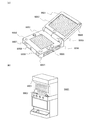
半導体装置は、電子ペーパーとして適用することができる。電子ペーパーは、情報を表示するものであればあらゆる分野の電子機器に用いることが可能である。例えば、電子ペーパーを用いて、電子書籍(電子ブック)、ポスター、電車などの乗り物の車内広告、クレジットカード等の各種カードにおける表示等に適用することができる。電子機器の一例を図30、図31に示す。
本実施の形態においては、液晶表示装置に適用できる画素の構成及び画素の動作について説明する。なお、本実施の形態における液晶素子の動作モードとして、TN(Twisted Nematic)モード、IPS(In−Plane−Switching)モード、FFS(Fringe Field Switching)モード、MVA(Multi−domain Vertical Alignment)モード、PVA(Patterned Vertical Alignment)、ASM(Axially Symmetric aligned Micro−cell)モード、OCB(Optical Compensated Birefringence)モード、FLC(Ferroelectric Liquid Crystal)モード、AFLC(AntiFerroelectric Liquid Crystal)などを用いることができる。
次に、表示装置の別の構成例およびその駆動方法について説明する。本実施の形態においては、信号書込みに対する輝度の応答が遅い(応答時間が長い)表示素子を用いた表示装置の場合について述べる。本実施の形態においては、応答時間が長い表示素子として液晶素子を例として説明するが、本実施の形態における表示素子はこれに限定されず、信号書込みに対する輝度の応答が遅い様々な表示素子を用いることができる。
次に、表示装置の別の構成例およびその駆動方法について説明する。本実施の形態においては、表示装置の外部から入力される画像(入力画像)の動きを補間する画像を、複数の入力画像を基にして表示装置の内部で生成し、当該生成された画像(生成画像)と、入力画像とを順次表示させる方法について説明する。なお、生成画像を、入力画像の動きを補間するような画像とすることで、動画の動きを滑らかにすることができ、さらに、ホールド駆動による残像等によって動画の品質が低下する問題を改善できる。ここで、動画の補間について、以下に説明する。動画の表示は、理想的には、個々の画素の輝度をリアルタイムに制御することで実現されるものであるが、画素のリアルタイム個別制御は、制御回路の数が膨大なものとなる問題、配線スペースの問題、および入力画像のデータ量が膨大なものとなる問題等が存在し、実現が困難である。したがって、表示装置による動画の表示は、複数の静止画を一定の周期で順次表示することで、表示が動画に見えるようにして行なわれている。この周期(本実施の形態においては入力画像信号周期と呼び、Tinと表す)は規格化されており、例として、NTSC規格では1/60秒、PAL規格では1/50秒である。この程度の周期でも、インパルス型表示装置であるCRTにおいては動画表示に問題は起こらなかった。しかし、ホールド型表示装置においては、これらの規格に準じた動画をそのまま表示すると、ホールド型であることに起因する残像等により表示が不鮮明となる不具合(ホールドぼけ:hold blur)が発生してしまう。ホールドぼけは、人間の目の追従による無意識的な動きの補間と、ホールド型の表示との不一致(discrepancy)で認識されるものであるので、従来の規格よりも入力画像信号周期を短くする(画素のリアルタイム個別制御に近づける)ことで低減させることができるが、入力画像信号周期を短くすることは規格の変更を伴い、さらに、データ量も増大することになるので、困難である。しかしながら、規格化された入力画像信号を基にして、入力画像の動きを補間するような画像を表示装置内部で生成し、当該生成画像によって入力画像を補間して表示することで、規格の変更またはデータ量の増大なしに、ホールドぼけを低減できる。このように、入力画像信号を基にして表示装置内部で画像信号を生成し、入力画像の動きを補間することを、動画の補間と呼ぶこととする。
半導体装置は、さまざまな電子機器(遊技機も含む)に適用することができる。電子機器としては、例えば、テレビジョン装置(テレビ、またはテレビジョン受信機ともいう)、コンピュータ用などのモニタ、デジタルカメラ、デジタルビデオカメラなどのカメラ、デジタルフォトフレーム、携帯電話機(携帯電話、携帯電話装置ともいう)、携帯型ゲーム機、携帯情報端末、音響再生装置、パチンコ機などの大型ゲーム機などが挙げられる。
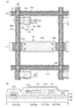
102 導電膜
104 導電膜
106 絶縁層
108 導電膜
110 導電膜
112 半導体膜
114 絶縁層
116 導電層
117 導電層
119 コンタクトホール
120 ゲート配線
122 配線
124 配線
125 コンタクトホール
126 配線
127 絶縁層
128 配線
132 電極
136 電極
138 電極
140 保持容量部
150 画素部
152 トランジスタ
154 保持容量部
156 トランジスタ
158 保持容量部
161 レジストマスク
162 レジストマスク
163 レジストマスク
164 レジストマスク
165 レジストマスク
168 レジストマスク
180 基板
182 基板
232 電極
236 電極
238 電極
400 基板
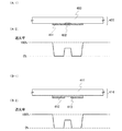
401 遮光部
402 回折格子
403 グレートーンマスク
411 基板
412 半透光部
413 遮光部
414 ハーフトーンマスク
580 基板
581 薄膜トランジスタ
583 絶縁層
587 電極層
588 電極層
589 球形粒子
594 キャビティ
595 充填材
596 基板
1000 携帯電話機
1001 筐体
1002 表示部
1003 操作ボタン
1004 外部接続ポート
1005 スピーカ
1006 マイク
102a 導電層
102b 導電層
102c 導電層
104a 導電層
104b 導電層
108a 導電層
108b 導電層
108c 導電層
108d 導電層
108e 導電層
110a 導電層
110b 導電層
110c 導電層
112a 半導体層
112b 半導体層
113a n+領域
114a 絶縁層
114b 絶縁層
118a コンタクトホール
118b コンタクトホール
171a レジストマスク
171b レジストマスク
171c レジストマスク
172a レジストマスク
172b レジストマスク
172c レジストマスク
181a 遮光層
181b 半透過層
183a 半透過層
183b 遮光層
2600 TFT基板
2601 対向基板
2602 シール材
2603 素子層
2604 表示素子
2605 着色層
2606 偏光板
2607 偏光板
2608 配線回路部
2609 フレキシブル配線基板
2610 冷陰極管
2611 反射板
2612 回路基板
2613 拡散板
2631 ポスター
2632 車内広告
2700 電子書籍
2701 筐体
2703 筐体
2705 表示部
2707 表示部
2711 軸部
2721 電源
2723 操作キー
2725 スピーカ
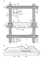
4001 基板
4002 画素部
4003 信号線駆動回路
4004 走査線駆動回路
4005 シール材
4006 基板
4008 液晶層
4010 薄膜トランジスタ
4011 薄膜トランジスタ
4013 液晶素子
4015 接続端子電極
4016 端子電極
4018 FPC
4019 異方性導電膜
4020 絶縁層
4021 絶縁層
4030 画素電極層
4031 対向電極層
4032 絶縁層
4051 基板
4501 基板
4502 画素部
4505 シール材
4506 基板
4507 充填材
4509 薄膜トランジスタ
4510 薄膜トランジスタ
4511 発光素子
4512 電界発光層
4513 電極層
4515 接続端子電極
4516 端子電極
4517 電極層
4519 異方性導電膜
4520 隔壁
5080 画素
5081 トランジスタ
5082 液晶素子
5083 容量素子
5084 配線
5085 配線
5086 配線
5087 配線
5088 電極
5101 破線
5102 実線
5103 破線
5104 実線
5105 実線
5106 実線
5107 実線
5108 実線
5121 画像
5122 画像
5123 画像
5124 領域
5125 領域
5126 領域
5127 ベクトル
5128 画像生成用ベクトル
5129 領域
5130 物体
5131 領域
5300 基板
5301 画素部
5302 走査線駆動回路
5303 信号線駆動回路
5400 基板
5401 画素部
5402 走査線駆動回路
5403 信号線駆動回路
5404 走査線駆動回路
590a 黒色領域
590b 白色領域
6400 画素
6401 スイッチング用トランジスタ
6402 駆動用トランジスタ
6403 容量素子
6404 発光素子
6405 信号線
6406 走査線
6407 電源線
6408 共通電極
6420 画素
6423 容量素子
6426 配線
7001 TFT
7002 発光素子
7003 陰極
7004 発光層
7005 陽極
7011 駆動用TFT
7012 発光素子
7013 陰極
7014 発光層
7015 陽極
7016 遮蔽膜
7017 導電膜
7021 駆動用TFT
7022 発光素子
7023 陰極
7024 発光層
7025 陽極
7027 導電膜
9400 通信装置
9401 筐体
9402 操作ボタン
9403 外部入力端子
9404 マイク
9405 スピーカ
9406 発光部
9410 表示装置
9411 筐体
9412 表示部
9413 操作ボタン
9600 テレビジョン装置
9601 筐体
9603 表示部
9605 スタンド
9607 表示部
9609 操作キー
9610 リモコン操作機
9700 デジタルフォトフレーム
9701 筐体
9703 表示部
9881 筐体
9882 表示部
9883 表示部
9884 スピーカ部
9885 操作キー
9886 記録媒体挿入部
9887 接続端子
9888 センサ
9889 マイクロフォン
9890 LEDランプ
9891 筐体
9893 連結部
9900 スロットマシン
9901 筐体
9903 表示部
4503a 信号線駆動回路
4504a 走査線駆動回路
4518a FPC
5121a 画像
5121b 画像
5122a 画像
5122b 画像
5123a 画像
5123b 画像
Claims (2)
- 第1の電極と、
前記第1の電極と電気的に接続された第1の配線と、
第2の配線と、
前記第1の電極、前記第1の配線及び前記第2の配線上に設けられた絶縁層と、
前記絶縁層上に設けられた第2の電極と、
前記第2の電極と電気的に接続された第3の配線と、
第3の電極と、
前記第2の配線上に前記絶縁層を介して設けられた第4の電極と、
前記絶縁層上に前記第1の電極と重なるように設けられると共に、前記第2の電極及び前記第3の電極上に設けられた半導体層を有し、
前記第1の電極は、透光性を有する第1の導電層で設けられ、
前記第1の配線は、前記第1の導電層と前記第1の導電層より電気抵抗が低い第2の導電層との積層構造で設けられ、
前記第2の導電層は、遮光性を有し、
前記第2の電極は、透光性を有する第4の導電層で設けられ、
前記第3の配線は、前記第4の導電層と前記第4の導電層より電気抵抗が低い第5の導電層との積層構造で設けられ、
前記第5の導電層は、遮光性を有し、
前記第3の電極は、透光性を有する第6の導電層で設けられ、
前記第4の電極は、透光性を有する第7の導電層で設けられ、
前記第3の電極と前記第4の電極とは、画素電極を介して電気的に接続され、
前記第2の配線は、前記第3の配線と重なる第1の領域において、透光性を有する第3の導電層と、前記第3の導電層より電気抵抗が低い第8の導電層との積層構造で設けられ、
前記第4の電極と前記画素電極はコンタクトホールを介して電気的に接続され、
前記第2の配線は、前記コンタクトホールと重なる第2の領域において、前記第3の導電層と、前記第3の導電層より電気抵抗が低い第9の導電層との積層構造で設けられ、
前記第8の導電層及び前記第9の導電層は、遮光性を有し、
前記第2の配線は、第3の領域を有し、
前記第3の領域は、前記第3の導電層が設けられ、且つ、前記第8の導電層及び前記第9の導電層は設けられていないことを特徴とする半導体装置。 - 請求項1において、
前記半導体層は、酸化物半導体層であることを特徴とする半導体装置。
Priority Applications (1)
| Application Number | Priority Date | Filing Date | Title |
|---|---|---|---|
| JP2010048615A JP5651350B2 (ja) | 2009-03-05 | 2010-03-05 | 半導体装置 |
Applications Claiming Priority (3)
| Application Number | Priority Date | Filing Date | Title |
|---|---|---|---|
| JP2009051779 | 2009-03-05 | ||
| JP2009051779 | 2009-03-05 | ||
| JP2010048615A JP5651350B2 (ja) | 2009-03-05 | 2010-03-05 | 半導体装置 |
Related Child Applications (1)
| Application Number | Title | Priority Date | Filing Date |
|---|---|---|---|
| JP2014178902A Division JP5917633B2 (ja) | 2009-03-05 | 2014-09-03 | 半導体装置 |
Publications (2)
| Publication Number | Publication Date |
|---|---|
| JP2010232652A JP2010232652A (ja) | 2010-10-14 |
| JP5651350B2 true JP5651350B2 (ja) | 2015-01-14 |
Family
ID=42677438
Family Applications (8)
| Application Number | Title | Priority Date | Filing Date |
|---|---|---|---|
| JP2010048615A Active JP5651350B2 (ja) | 2009-03-05 | 2010-03-05 | 半導体装置 |
| JP2014178902A Active JP5917633B2 (ja) | 2009-03-05 | 2014-09-03 | 半導体装置 |
| JP2016054137A Active JP6122985B2 (ja) | 2009-03-05 | 2016-03-17 | 半導体装置 |
| JP2017073423A Active JP6392924B2 (ja) | 2009-03-05 | 2017-04-03 | 表示装置 |
| JP2018132447A Active JP6532989B2 (ja) | 2009-03-05 | 2018-07-12 | 表示装置 |
| JP2019095952A Active JP6580806B1 (ja) | 2009-03-05 | 2019-05-22 | 表示装置 |
| JP2019155572A Withdrawn JP2020038965A (ja) | 2009-03-05 | 2019-08-28 | 表示装置 |
| JP2021200586A Pending JP2022050404A (ja) | 2009-03-05 | 2021-12-10 | 表示装置 |
Family Applications After (7)
| Application Number | Title | Priority Date | Filing Date |
|---|---|---|---|
| JP2014178902A Active JP5917633B2 (ja) | 2009-03-05 | 2014-09-03 | 半導体装置 |
| JP2016054137A Active JP6122985B2 (ja) | 2009-03-05 | 2016-03-17 | 半導体装置 |
| JP2017073423A Active JP6392924B2 (ja) | 2009-03-05 | 2017-04-03 | 表示装置 |
| JP2018132447A Active JP6532989B2 (ja) | 2009-03-05 | 2018-07-12 | 表示装置 |
| JP2019095952A Active JP6580806B1 (ja) | 2009-03-05 | 2019-05-22 | 表示装置 |
| JP2019155572A Withdrawn JP2020038965A (ja) | 2009-03-05 | 2019-08-28 | 表示装置 |
| JP2021200586A Pending JP2022050404A (ja) | 2009-03-05 | 2021-12-10 | 表示装置 |
Country Status (5)
| Country | Link |
|---|---|
| US (4) | US20100224880A1 (ja) |
| JP (8) | JP5651350B2 (ja) |
| KR (10) | KR101999526B1 (ja) |
| CN (1) | CN101826520B (ja) |
| TW (1) | TWI512976B (ja) |
Families Citing this family (69)
| Publication number | Priority date | Publication date | Assignee | Title |
|---|---|---|---|---|
| CN101710586B (zh) * | 2009-01-09 | 2011-12-28 | 深超光电(深圳)有限公司 | 提高开口率的储存电容及其制作方法 |
| US8461582B2 (en) * | 2009-03-05 | 2013-06-11 | Semiconductor Energy Laboratory Co., Ltd. | Semiconductor device and method for manufacturing the same |
| US20100224878A1 (en) | 2009-03-05 | 2010-09-09 | Semiconductor Energy Laboratory Co., Ltd. | Semiconductor device |
| CN102473733B (zh) * | 2009-07-18 | 2015-09-30 | 株式会社半导体能源研究所 | 半导体装置以及制造半导体装置的方法 |
| KR101594855B1 (ko) * | 2009-11-25 | 2016-02-18 | 삼성전자주식회사 | Blu 및 디스플레이 장치 |
| JP5351282B2 (ja) * | 2009-11-27 | 2013-11-27 | シャープ株式会社 | 半導体装置およびその製造方法 |
| TWI620176B (zh) * | 2010-10-05 | 2018-04-01 | 半導體能源研究所股份有限公司 | 半導體記憶體裝置及其驅動方法 |
| JP2012108311A (ja) * | 2010-11-17 | 2012-06-07 | Toshiba Mobile Display Co Ltd | 液晶表示装置 |
| JP2012151453A (ja) * | 2010-12-28 | 2012-08-09 | Semiconductor Energy Lab Co Ltd | 半導体装置および半導体装置の駆動方法 |
| DE102011004577B4 (de) * | 2011-02-23 | 2023-07-27 | Robert Bosch Gmbh | Bauelementträger, Verfahren zur Herstellung eines solchen Bauelementträgers sowie Bauteil mit einem MEMS-Bauelement auf einem solchen Bauelementträger |
| JP2012191008A (ja) * | 2011-03-10 | 2012-10-04 | Sony Corp | 表示装置および電子機器 |
| US9236496B2 (en) * | 2011-03-11 | 2016-01-12 | Sharp Kabushiki Kaisha | Thin film transistor and display device |
| JP2012203148A (ja) * | 2011-03-24 | 2012-10-22 | Toppan Printing Co Ltd | 薄膜トランジスタおよび反射型カラー表示装置 |
| US8922464B2 (en) * | 2011-05-11 | 2014-12-30 | Semiconductor Energy Laboratory Co., Ltd. | Active matrix display device and driving method thereof |
| KR101952570B1 (ko) * | 2011-05-13 | 2019-02-27 | 가부시키가이샤 한도오따이 에네루기 켄큐쇼 | 반도체 장치 및 그 제작 방법 |
| KR101425064B1 (ko) * | 2011-06-09 | 2014-08-01 | 엘지디스플레이 주식회사 | 산화물 박막 트랜지스터 및 그 제조방법 |
| JP6098515B2 (ja) * | 2011-09-27 | 2017-03-22 | 凸版印刷株式会社 | 薄膜トランジスタ、および画像表示装置、並びに薄膜トランジスタの製造方法 |
| JP6076038B2 (ja) * | 2011-11-11 | 2017-02-08 | 株式会社半導体エネルギー研究所 | 表示装置の作製方法 |
| JP2013130802A (ja) | 2011-12-22 | 2013-07-04 | Semiconductor Energy Lab Co Ltd | 半導体装置、画像表示装置、記憶装置、及び電子機器 |
| US9419146B2 (en) * | 2012-01-26 | 2016-08-16 | Semiconductor Energy Laboratory Co., Ltd. | Semiconductor device and method for manufacturing the same |
| JP2013222124A (ja) * | 2012-04-18 | 2013-10-28 | Sony Corp | 信号伝達装置、表示装置および電子機器 |
| KR101324240B1 (ko) * | 2012-05-04 | 2013-11-01 | 엘지디스플레이 주식회사 | 어레이 기판 및 이의 제조방법 |
| JP2014199899A (ja) * | 2012-08-10 | 2014-10-23 | 株式会社半導体エネルギー研究所 | 半導体装置 |
| TWI467301B (zh) * | 2012-10-24 | 2015-01-01 | Au Optronics Corp | 顯示面板 |
| CN102938394B (zh) * | 2012-11-16 | 2015-01-07 | 京东方科技集团股份有限公司 | 显示装置、透反式薄膜晶体管阵列基板及其制作方法 |
| US9265458B2 (en) | 2012-12-04 | 2016-02-23 | Sync-Think, Inc. | Application of smooth pursuit cognitive testing paradigms to clinical drug development |
| WO2014093057A1 (en) * | 2012-12-10 | 2014-06-19 | Shannon Lee Mutschelknaus | Encapsulation of light-emitting elements on a display module |
| WO2014091959A1 (ja) * | 2012-12-10 | 2014-06-19 | シャープ株式会社 | 半導体装置およびその製造方法 |
| TWI498797B (zh) * | 2012-12-13 | 2015-09-01 | Au Optronics Corp | 觸控面板及觸控顯示面板 |
| US9380976B2 (en) | 2013-03-11 | 2016-07-05 | Sync-Think, Inc. | Optical neuroinformatics |
| KR102179972B1 (ko) * | 2013-05-10 | 2020-11-18 | 삼성디스플레이 주식회사 | 배선 및 박막 트랜지스터 기판의 제조 방법 및 유기 발광 표시 장치 |
| KR102081107B1 (ko) * | 2013-05-30 | 2020-02-25 | 엘지디스플레이 주식회사 | 박막트랜지스터 어레이 기판 및 그의 제조방법 |
| JP6490914B2 (ja) * | 2013-06-28 | 2019-03-27 | 株式会社半導体エネルギー研究所 | 半導体装置の作製方法 |
| JP2015179247A (ja) * | 2013-10-22 | 2015-10-08 | 株式会社半導体エネルギー研究所 | 表示装置 |
| US9728567B2 (en) * | 2013-12-02 | 2017-08-08 | United Microelectronics Corp. | Semiconductor sensor device |
| TWI518430B (zh) * | 2013-12-02 | 2016-01-21 | 群創光電股份有限公司 | 顯示面板及應用其之顯示裝置 |
| KR20220046701A (ko) | 2013-12-27 | 2022-04-14 | 가부시키가이샤 한도오따이 에네루기 켄큐쇼 | 발광 장치 |
| JP6506545B2 (ja) | 2013-12-27 | 2019-04-24 | 株式会社半導体エネルギー研究所 | 半導体装置 |
| TWI686899B (zh) * | 2014-05-02 | 2020-03-01 | 日商半導體能源研究所股份有限公司 | 半導體裝置、觸控感測器、顯示裝置 |
| CN105826393B (zh) * | 2015-01-06 | 2019-03-26 | 昆山国显光电有限公司 | 薄膜晶体管及其制作方法 |
| JP6708643B2 (ja) * | 2015-06-19 | 2020-06-10 | 株式会社半導体エネルギー研究所 | 表示装置の作製方法 |
| CN105097943A (zh) * | 2015-06-24 | 2015-11-25 | 京东方科技集团股份有限公司 | 一种薄膜晶体管及其制备方法、阵列基板、显示装置 |
| WO2017081847A1 (ja) * | 2015-11-12 | 2017-05-18 | パナソニックIpマネジメント株式会社 | 光検出装置 |
| TWI560486B (en) * | 2016-01-05 | 2016-12-01 | Innolux Corp | Display panel |
| CN107018289B (zh) * | 2016-01-22 | 2021-01-19 | 松下知识产权经营株式会社 | 摄像装置 |
| CN105573555B (zh) * | 2016-01-28 | 2018-06-29 | 京东方科技集团股份有限公司 | 一种压力触控结构、触控显示面板、显示装置 |
| TWI621997B (zh) * | 2016-02-04 | 2018-04-21 | 速博思股份有限公司 | 高效能指紋辨識裝置 |
| JP6724548B2 (ja) * | 2016-05-25 | 2020-07-15 | 凸版印刷株式会社 | 薄膜トランジスタアレイ基板のパターン形成方法 |
| KR102549444B1 (ko) * | 2016-06-16 | 2023-06-29 | 삼성디스플레이 주식회사 | 표시 장치 및 이의 제조 방법 |
| JP2019523562A (ja) * | 2016-07-29 | 2019-08-22 | トリナミクス ゲゼルシャフト ミット ベシュレンクテル ハフツング | 光学的検出のための光センサおよび検出器 |
| JP7050460B2 (ja) * | 2016-11-22 | 2022-04-08 | 株式会社半導体エネルギー研究所 | 表示装置 |
| US11069722B2 (en) | 2017-05-31 | 2021-07-20 | Sharp Kabushiki Kaisha | Active matrix substrate and method of manufacturing same |
| CN109545795B (zh) | 2017-09-22 | 2020-10-30 | 群创光电股份有限公司 | 显示装置 |
| CN108154852A (zh) * | 2017-12-29 | 2018-06-12 | 深圳Tcl新技术有限公司 | 背光组件、背光模组、显示装置及其控制方法 |
| US11342362B2 (en) | 2018-03-30 | 2022-05-24 | Sharp Kabushiki Kaisha | Display device |
| KR102631177B1 (ko) * | 2018-12-28 | 2024-01-29 | 엘지디스플레이 주식회사 | 전계 발광 조명장치 |
| KR20200145966A (ko) * | 2019-06-21 | 2020-12-31 | 삼성디스플레이 주식회사 | 표시 장치 및 그의 제조 방법 |
| TWI755079B (zh) * | 2019-09-30 | 2022-02-11 | 台灣積體電路製造股份有限公司 | 半導體裝置及其形成方法 |
| CN110783204B (zh) * | 2019-10-29 | 2022-04-12 | 南京京东方显示技术有限公司 | 一种双沟道立体tft器件、显示面板及其制造方法 |
| CN110931511A (zh) * | 2019-11-26 | 2020-03-27 | 深圳市华星光电半导体显示技术有限公司 | 一种显示面板及其制备方法 |
| TWI721776B (zh) * | 2020-02-06 | 2021-03-11 | 友達光電股份有限公司 | 主動元件基板及其製造方法 |
| CN111312077A (zh) * | 2020-03-03 | 2020-06-19 | 深圳市华星光电半导体显示技术有限公司 | 显示面板及其制备方法 |
| CN112234092B (zh) * | 2020-10-30 | 2023-03-24 | 云谷(固安)科技有限公司 | 显示面板及显示装置 |
| JP2022111603A (ja) * | 2021-01-20 | 2022-08-01 | セイコーエプソン株式会社 | センサーモジュール |
| CN113467145B (zh) * | 2021-07-07 | 2023-07-25 | 昆山龙腾光电股份有限公司 | 阵列基板及制作方法、显示面板 |
| US11864452B1 (en) | 2021-08-24 | 2024-01-02 | Apple Inc. | Black masking layer in displays having transparent openings |
| CN114130674B (zh) * | 2021-11-26 | 2023-06-09 | 山东至辰信息科技股份有限公司 | 一种智慧图书馆书籍智能分拣机器人 |
| CN114203730B (zh) * | 2021-12-09 | 2023-05-30 | 深圳市华星光电半导体显示技术有限公司 | 显示面板及其制作方法 |
| CN114325288A (zh) * | 2022-01-06 | 2022-04-12 | 北一半导体科技(广东)有限公司 | 一种评估半导体模块功率循环能力的方法和半导体模块 |
Family Cites Families (139)
| Publication number | Priority date | Publication date | Assignee | Title |
|---|---|---|---|---|
| JPS6151188A (ja) * | 1984-08-21 | 1986-03-13 | セイコーインスツルメンツ株式会社 | アクテイブ・マトリクス表示装置用基板 |
| JPH0282221A (ja) | 1988-09-20 | 1990-03-22 | Seiko Epson Corp | 電気光学素子の配線方法 |
| JPH02260460A (ja) * | 1989-03-31 | 1990-10-23 | Casio Comput Co Ltd | 薄膜トランジスタ |
| JPH07113728B2 (ja) | 1989-05-26 | 1995-12-06 | シャープ株式会社 | アクティブマトリクス基板 |
| DE69107101T2 (de) * | 1990-02-06 | 1995-05-24 | Semiconductor Energy Lab | Verfahren zum Herstellen eines Oxydfilms. |
| JP2851495B2 (ja) * | 1992-08-28 | 1999-01-27 | シャープ株式会社 | アクティブマトリクス基板の製造方法 |
| JPH06317809A (ja) * | 1993-05-07 | 1994-11-15 | Fujitsu Ltd | 薄膜トランジスタマトリクスの製造方法 |
| JP3423380B2 (ja) * | 1993-11-18 | 2003-07-07 | キヤノン株式会社 | 液晶表示装置 |
| US5644327A (en) * | 1995-06-07 | 1997-07-01 | David Sarnoff Research Center, Inc. | Tessellated electroluminescent display having a multilayer ceramic substrate |
| JPH11505377A (ja) * | 1995-08-03 | 1999-05-18 | フィリップス エレクトロニクス ネムローゼ フェンノートシャップ | 半導体装置 |
| JP3541026B2 (ja) * | 1995-08-11 | 2004-07-07 | シャープ株式会社 | 液晶表示装置、およびアクティブマトリクス基板 |
| KR970011972A (ko) * | 1995-08-11 | 1997-03-29 | 쯔지 하루오 | 투과형 액정 표시 장치 및 그 제조 방법 |
| US5808691A (en) * | 1995-12-12 | 1998-09-15 | Cirrus Logic, Inc. | Digital carrier synthesis synchronized to a reference signal that is asynchronous with respect to a digital sampling clock |
| JP3625598B2 (ja) * | 1995-12-30 | 2005-03-02 | 三星電子株式会社 | 液晶表示装置の製造方法 |
| JP3325793B2 (ja) * | 1996-03-22 | 2002-09-17 | 三洋電機株式会社 | 非晶質半導体及びその製造方法並びに光起電力装置 |
| JPH10189992A (ja) * | 1996-12-27 | 1998-07-21 | Sony Corp | 半導体装置及びその製造方法 |
| KR100229613B1 (ko) * | 1996-12-30 | 1999-11-15 | 구자홍 | 액정 표시 장치 및 제조 방법 |
| JP3436487B2 (ja) * | 1998-05-18 | 2003-08-11 | シャープ株式会社 | アクティブマトリクス基板の製造方法 |
| JP3592535B2 (ja) * | 1998-07-16 | 2004-11-24 | 株式会社半導体エネルギー研究所 | 半導体装置の作製方法 |
| JP2000150861A (ja) * | 1998-11-16 | 2000-05-30 | Tdk Corp | 酸化物薄膜 |
| JP3276930B2 (ja) * | 1998-11-17 | 2002-04-22 | 科学技術振興事業団 | トランジスタ及び半導体装置 |
| US6524876B1 (en) * | 1999-04-08 | 2003-02-25 | Samsung Electronics Co., Ltd. | Thin film transistor array panels for a liquid crystal display and a method for manufacturing the same |
| US6362507B1 (en) * | 1999-04-20 | 2002-03-26 | Semiconductor Energy Laboratory Co., Ltd. | Electro-optical devices in which pixel section and the driver circuit are disposed over the same substrate |
| US6716768B2 (en) * | 2000-02-15 | 2004-04-06 | Matsushita Electric Industrial Co., Ltd. | Method of manufacturing thin-film transistor, and liquid-crystal display |
| KR20020038482A (ko) * | 2000-11-15 | 2002-05-23 | 모리시타 요이찌 | 박막 트랜지스터 어레이, 그 제조방법 및 그것을 이용한표시패널 |
| JP4801262B2 (ja) * | 2001-01-30 | 2011-10-26 | 株式会社半導体エネルギー研究所 | 半導体装置の作製方法 |
| JP3997731B2 (ja) * | 2001-03-19 | 2007-10-24 | 富士ゼロックス株式会社 | 基材上に結晶性半導体薄膜を形成する方法 |
| JP4090716B2 (ja) * | 2001-09-10 | 2008-05-28 | 雅司 川崎 | 薄膜トランジスタおよびマトリクス表示装置 |
| JP4164562B2 (ja) | 2002-09-11 | 2008-10-15 | 独立行政法人科学技術振興機構 | ホモロガス薄膜を活性層として用いる透明薄膜電界効果型トランジスタ |
| US7061014B2 (en) * | 2001-11-05 | 2006-06-13 | Japan Science And Technology Agency | Natural-superlattice homologous single crystal thin film, method for preparation thereof, and device using said single crystal thin film |
| KR100825102B1 (ko) * | 2002-01-08 | 2008-04-25 | 삼성전자주식회사 | 박막 트랜지스터 기판 및 그 제조 방법 |
| JP4083486B2 (ja) * | 2002-02-21 | 2008-04-30 | 独立行政法人科学技術振興機構 | LnCuO(S,Se,Te)単結晶薄膜の製造方法 |
| CN1445821A (zh) * | 2002-03-15 | 2003-10-01 | 三洋电机株式会社 | ZnO膜和ZnO半导体层的形成方法、半导体元件及其制造方法 |
| WO2003089206A1 (fr) | 2002-04-19 | 2003-10-30 | Max Co., Ltd. | Agrafeuse motorisee |
| JP2004022625A (ja) * | 2002-06-13 | 2004-01-22 | Murata Mfg Co Ltd | 半導体デバイス及び該半導体デバイスの製造方法 |
| US7105868B2 (en) * | 2002-06-24 | 2006-09-12 | Cermet, Inc. | High-electron mobility transistor with zinc oxide |
| JP2004077718A (ja) * | 2002-08-15 | 2004-03-11 | Hitachi Displays Ltd | 液晶表示装置 |
| US7067843B2 (en) * | 2002-10-11 | 2006-06-27 | E. I. Du Pont De Nemours And Company | Transparent oxide semiconductor thin film transistors |
| TW588462B (en) * | 2003-03-31 | 2004-05-21 | Quanta Display Inc | Method of fabricating a thin film transistor array panel |
| US7262463B2 (en) * | 2003-07-25 | 2007-08-28 | Hewlett-Packard Development Company, L.P. | Transistor including a deposited channel region having a doped portion |
| JP2005062802A (ja) * | 2003-07-28 | 2005-03-10 | Advanced Display Inc | 薄膜トランジスタアレイ基板の製法 |
| JP4712352B2 (ja) * | 2003-11-14 | 2011-06-29 | 株式会社半導体エネルギー研究所 | 発光装置の作製方法 |
| JP4737971B2 (ja) * | 2003-11-14 | 2011-08-03 | 株式会社半導体エネルギー研究所 | 液晶表示装置および液晶表示装置の作製方法 |
| JP4667051B2 (ja) * | 2004-01-29 | 2011-04-06 | 株式会社半導体エネルギー研究所 | 半導体装置の作製方法 |
| KR101019337B1 (ko) * | 2004-03-12 | 2011-03-07 | 도꾸리쯔교세이호징 가가꾸 기쥬쯔 신꼬 기꼬 | 아몰퍼스 산화물 및 박막 트랜지스터 |
| US7145174B2 (en) * | 2004-03-12 | 2006-12-05 | Hewlett-Packard Development Company, Lp. | Semiconductor device |
| US7282782B2 (en) * | 2004-03-12 | 2007-10-16 | Hewlett-Packard Development Company, L.P. | Combined binary oxide semiconductor device |
| US7211825B2 (en) * | 2004-06-14 | 2007-05-01 | Yi-Chi Shih | Indium oxide-based thin film transistors and circuits |
| JP2006100760A (ja) * | 2004-09-02 | 2006-04-13 | Casio Comput Co Ltd | 薄膜トランジスタおよびその製造方法 |
| US7285501B2 (en) * | 2004-09-17 | 2007-10-23 | Hewlett-Packard Development Company, L.P. | Method of forming a solution processed device |
| JP4633434B2 (ja) * | 2004-10-18 | 2011-02-16 | シャープ株式会社 | 半導体装置およびその製造方法 |
| US7298084B2 (en) * | 2004-11-02 | 2007-11-20 | 3M Innovative Properties Company | Methods and displays utilizing integrated zinc oxide row and column drivers in conjunction with organic light emitting diodes |
| KR101171175B1 (ko) * | 2004-11-03 | 2012-08-06 | 삼성전자주식회사 | 도전체용 식각액 및 이를 이용한 박막 트랜지스터표시판의 제조 방법 |
| CN101057333B (zh) * | 2004-11-10 | 2011-11-16 | 佳能株式会社 | 发光器件 |
| US7453065B2 (en) * | 2004-11-10 | 2008-11-18 | Canon Kabushiki Kaisha | Sensor and image pickup device |
| US7601984B2 (en) * | 2004-11-10 | 2009-10-13 | Canon Kabushiki Kaisha | Field effect transistor with amorphous oxide active layer containing microcrystals and gate electrode opposed to active layer through gate insulator |
| US7829444B2 (en) * | 2004-11-10 | 2010-11-09 | Canon Kabushiki Kaisha | Field effect transistor manufacturing method |
| US7791072B2 (en) * | 2004-11-10 | 2010-09-07 | Canon Kabushiki Kaisha | Display |
| US7863611B2 (en) * | 2004-11-10 | 2011-01-04 | Canon Kabushiki Kaisha | Integrated circuits utilizing amorphous oxides |
| EP1815530B1 (en) * | 2004-11-10 | 2021-02-17 | Canon Kabushiki Kaisha | Field effect transistor employing an amorphous oxide |
| KR101054344B1 (ko) * | 2004-11-17 | 2011-08-04 | 삼성전자주식회사 | 박막 트랜지스터 표시판 및 그 제조 방법 |
| KR101282397B1 (ko) * | 2004-12-07 | 2013-07-04 | 삼성디스플레이 주식회사 | 표시 장치용 배선, 상기 배선을 포함하는 박막 트랜지스터표시판 및 그 제조 방법 |
| US7579224B2 (en) * | 2005-01-21 | 2009-08-25 | Semiconductor Energy Laboratory Co., Ltd. | Method for manufacturing a thin film semiconductor device |
| TWI569441B (zh) * | 2005-01-28 | 2017-02-01 | 半導體能源研究所股份有限公司 | 半導體裝置,電子裝置,和半導體裝置的製造方法 |
| JP4777078B2 (ja) * | 2005-01-28 | 2011-09-21 | 株式会社半導体エネルギー研究所 | 半導体装置の作製方法 |
| TWI412138B (zh) * | 2005-01-28 | 2013-10-11 | Semiconductor Energy Lab | 半導體裝置,電子裝置,和半導體裝置的製造方法 |
| US7858451B2 (en) * | 2005-02-03 | 2010-12-28 | Semiconductor Energy Laboratory Co., Ltd. | Electronic device, semiconductor device and manufacturing method thereof |
| US7948171B2 (en) * | 2005-02-18 | 2011-05-24 | Semiconductor Energy Laboratory Co., Ltd. | Light emitting device |
| JP5117667B2 (ja) * | 2005-02-28 | 2013-01-16 | カシオ計算機株式会社 | 薄膜トランジスタパネル |
| US20060197092A1 (en) * | 2005-03-03 | 2006-09-07 | Randy Hoffman | System and method for forming conductive material on a substrate |
| KR20060097381A (ko) * | 2005-03-09 | 2006-09-14 | 삼성전자주식회사 | 박막 트랜지스터 기판 및 이의 제조 방법 |
| US8681077B2 (en) * | 2005-03-18 | 2014-03-25 | Semiconductor Energy Laboratory Co., Ltd. | Semiconductor device, and display device, driving method and electronic apparatus thereof |
| FI119894B (fi) * | 2005-03-30 | 2009-04-30 | Labmaster Oy | Elektrokemiluminesenssiin perustuva analyysimenetelmä ja siinä käytettävä laite |
| JP4687259B2 (ja) * | 2005-06-10 | 2011-05-25 | カシオ計算機株式会社 | 液晶表示装置 |
| US7402506B2 (en) * | 2005-06-16 | 2008-07-22 | Eastman Kodak Company | Methods of making thin film transistors comprising zinc-oxide-based semiconductor materials and transistors made thereby |
| US7381586B2 (en) * | 2005-06-16 | 2008-06-03 | Industrial Technology Research Institute | Methods for manufacturing thin film transistors that include selectively forming an active channel layer from a solution |
| KR100711890B1 (ko) * | 2005-07-28 | 2007-04-25 | 삼성에스디아이 주식회사 | 유기 발광표시장치 및 그의 제조방법 |
| JP2007059128A (ja) * | 2005-08-23 | 2007-03-08 | Canon Inc | 有機el表示装置およびその製造方法 |
| JP4850457B2 (ja) * | 2005-09-06 | 2012-01-11 | キヤノン株式会社 | 薄膜トランジスタ及び薄膜ダイオード |
| JP2007073705A (ja) * | 2005-09-06 | 2007-03-22 | Canon Inc | 酸化物半導体チャネル薄膜トランジスタおよびその製造方法 |
| JP5116225B2 (ja) * | 2005-09-06 | 2013-01-09 | キヤノン株式会社 | 酸化物半導体デバイスの製造方法 |
| JP4280736B2 (ja) * | 2005-09-06 | 2009-06-17 | キヤノン株式会社 | 半導体素子 |
| KR100729043B1 (ko) * | 2005-09-14 | 2007-06-14 | 삼성에스디아이 주식회사 | 투명 박막 트랜지스터 및 그의 제조방법 |
| JP5064747B2 (ja) * | 2005-09-29 | 2012-10-31 | 株式会社半導体エネルギー研究所 | 半導体装置、電気泳動表示装置、表示モジュール、電子機器、及び半導体装置の作製方法 |
| JP5078246B2 (ja) * | 2005-09-29 | 2012-11-21 | 株式会社半導体エネルギー研究所 | 半導体装置、及び半導体装置の作製方法 |
| EP1770788A3 (en) * | 2005-09-29 | 2011-09-21 | Semiconductor Energy Laboratory Co., Ltd. | Semiconductor device having oxide semiconductor layer and manufacturing method thereof |
| CN101283388B (zh) * | 2005-10-05 | 2011-04-13 | 出光兴产株式会社 | Tft基板及tft基板的制造方法 |
| EP1935027B1 (en) * | 2005-10-14 | 2017-06-28 | Semiconductor Energy Laboratory Co., Ltd. | Semiconductor device and manufacturing method thereof |
| JP2007109918A (ja) | 2005-10-14 | 2007-04-26 | Toppan Printing Co Ltd | トランジスタおよびその製造方法 |
| US8149346B2 (en) * | 2005-10-14 | 2012-04-03 | Semiconductor Energy Laboratory Co., Ltd. | Display device and manufacturing method thereof |
| JP5427340B2 (ja) * | 2005-10-14 | 2014-02-26 | 株式会社半導体エネルギー研究所 | 半導体装置 |
| JP2007115807A (ja) | 2005-10-19 | 2007-05-10 | Toppan Printing Co Ltd | トランジスタ |
| JP5037808B2 (ja) * | 2005-10-20 | 2012-10-03 | キヤノン株式会社 | アモルファス酸化物を用いた電界効果型トランジスタ、及び該トランジスタを用いた表示装置 |
| CN101577293B (zh) * | 2005-11-15 | 2012-09-19 | 株式会社半导体能源研究所 | 半导体器件及其制造方法 |
| US7821613B2 (en) * | 2005-12-28 | 2010-10-26 | Semiconductor Energy Laboratory Co., Ltd. | Display device and manufacturing method thereof |
| TWI292281B (en) * | 2005-12-29 | 2008-01-01 | Ind Tech Res Inst | Pixel structure of active organic light emitting diode and method of fabricating the same |
| US7867636B2 (en) * | 2006-01-11 | 2011-01-11 | Murata Manufacturing Co., Ltd. | Transparent conductive film and method for manufacturing the same |
| JP4977478B2 (ja) * | 2006-01-21 | 2012-07-18 | 三星電子株式会社 | ZnOフィルム及びこれを用いたTFTの製造方法 |
| US7576394B2 (en) * | 2006-02-02 | 2009-08-18 | Kochi Industrial Promotion Center | Thin film transistor including low resistance conductive thin films and manufacturing method thereof |
| KR100791290B1 (ko) | 2006-02-10 | 2008-01-04 | 삼성전자주식회사 | 디바이스 간에 악성 어플리케이션의 행위 정보를 사용하는장치 및 방법 |
| US7977169B2 (en) * | 2006-02-15 | 2011-07-12 | Kochi Industrial Promotion Center | Semiconductor device including active layer made of zinc oxide with controlled orientations and manufacturing method thereof |
| JP5110803B2 (ja) * | 2006-03-17 | 2012-12-26 | キヤノン株式会社 | 酸化物膜をチャネルに用いた電界効果型トランジスタ及びその製造方法 |
| JP2007286150A (ja) * | 2006-04-13 | 2007-11-01 | Idemitsu Kosan Co Ltd | 電気光学装置、並びに、電流制御用tft基板及びその製造方法 |
| JP2007292976A (ja) * | 2006-04-25 | 2007-11-08 | Hitachi Displays Ltd | 液晶表示装置及びその製造方法 |
| JP5060738B2 (ja) * | 2006-04-28 | 2012-10-31 | 株式会社ジャパンディスプレイイースト | 画像表示装置 |
| JP5312728B2 (ja) * | 2006-04-28 | 2013-10-09 | 凸版印刷株式会社 | 表示装置およびその製造方法 |
| JP5105044B2 (ja) * | 2006-05-09 | 2012-12-19 | 株式会社ブリヂストン | 酸化物トランジスタ及びその製造方法 |
| JP5056142B2 (ja) | 2006-05-11 | 2012-10-24 | 日亜化学工業株式会社 | 窒化物半導体レーザ素子の製造方法及び窒化物半導体レーザ素子 |
| JP2007310334A (ja) * | 2006-05-19 | 2007-11-29 | Mikuni Denshi Kk | ハーフトーン露光法を用いた液晶表示装置の製造法 |
| EP1863079B1 (en) | 2006-06-02 | 2011-08-10 | Rohm and Haas Electronic Materials, L.L.C. | Apparatus with filet radius joints |
| US8106865B2 (en) * | 2006-06-02 | 2012-01-31 | Semiconductor Energy Laboratory Co., Ltd. | Display device and driving method thereof |
| JP4609797B2 (ja) * | 2006-08-09 | 2011-01-12 | Nec液晶テクノロジー株式会社 | 薄膜デバイス及びその製造方法 |
| JP4999400B2 (ja) * | 2006-08-09 | 2012-08-15 | キヤノン株式会社 | 酸化物半導体膜のドライエッチング方法 |
| US8400599B2 (en) * | 2006-08-16 | 2013-03-19 | Samsung Display Co., Ltd. | Liquid crystal display panel having a light blocking electrode |
| JP4332545B2 (ja) * | 2006-09-15 | 2009-09-16 | キヤノン株式会社 | 電界効果型トランジスタ及びその製造方法 |
| JP5145676B2 (ja) * | 2006-09-15 | 2013-02-20 | 凸版印刷株式会社 | 薄膜トランジスタおよびその製造方法 |
| JP5164357B2 (ja) * | 2006-09-27 | 2013-03-21 | キヤノン株式会社 | 半導体装置及び半導体装置の製造方法 |
| JP4274219B2 (ja) * | 2006-09-27 | 2009-06-03 | セイコーエプソン株式会社 | 電子デバイス、有機エレクトロルミネッセンス装置、有機薄膜半導体装置 |
| KR101293573B1 (ko) * | 2006-10-02 | 2013-08-06 | 삼성디스플레이 주식회사 | 박막 트랜지스터 표시판 및 그 제조 방법 |
| US7622371B2 (en) * | 2006-10-10 | 2009-11-24 | Hewlett-Packard Development Company, L.P. | Fused nanocrystal thin film semiconductor and method |
| US7772021B2 (en) * | 2006-11-29 | 2010-08-10 | Samsung Electronics Co., Ltd. | Flat panel displays comprising a thin-film transistor having a semiconductive oxide in its channel and methods of fabricating the same for use in flat panel displays |
| JP2008140684A (ja) * | 2006-12-04 | 2008-06-19 | Toppan Printing Co Ltd | カラーelディスプレイおよびその製造方法 |
| JP5105842B2 (ja) * | 2006-12-05 | 2012-12-26 | キヤノン株式会社 | 酸化物半導体を用いた表示装置及びその製造方法 |
| KR101303578B1 (ko) * | 2007-01-05 | 2013-09-09 | 삼성전자주식회사 | 박막 식각 방법 |
| KR100787464B1 (ko) * | 2007-01-08 | 2007-12-26 | 삼성에스디아이 주식회사 | 박막 트랜지스터, 및 그 제조방법 |
| US8207063B2 (en) * | 2007-01-26 | 2012-06-26 | Eastman Kodak Company | Process for atomic layer deposition |
| JP5196870B2 (ja) * | 2007-05-23 | 2013-05-15 | キヤノン株式会社 | 酸化物半導体を用いた電子素子及びその製造方法 |
| KR100858088B1 (ko) * | 2007-02-28 | 2008-09-10 | 삼성전자주식회사 | 박막 트랜지스터 및 그 제조 방법 |
| JP5244331B2 (ja) | 2007-03-26 | 2013-07-24 | 出光興産株式会社 | 非晶質酸化物半導体薄膜、その製造方法、薄膜トランジスタの製造方法、電界効果型トランジスタ、発光装置、表示装置及びスパッタリングターゲット |
| US8513678B2 (en) * | 2007-05-18 | 2013-08-20 | Semiconductor Energy Laboratory Co., Ltd. | Light-emitting device |
| KR100873081B1 (ko) * | 2007-05-29 | 2008-12-09 | 삼성모바일디스플레이주식회사 | 박막 트랜지스터, 그의 제조 방법 및 박막 트랜지스터를구비하는 평판 표시 장치 |
| KR101415561B1 (ko) * | 2007-06-14 | 2014-08-07 | 삼성디스플레이 주식회사 | 박막 트랜지스터 표시판 및 그의 제조 방법 |
| KR101376073B1 (ko) * | 2007-06-14 | 2014-03-21 | 삼성디스플레이 주식회사 | 박막 트랜지스터, 이를 포함하는 어레이 기판 및 이의 제조방법 |
| US8202365B2 (en) * | 2007-12-17 | 2012-06-19 | Fujifilm Corporation | Process for producing oriented inorganic crystalline film, and semiconductor device using the oriented inorganic crystalline film |
| JP5540517B2 (ja) * | 2008-02-22 | 2014-07-02 | 凸版印刷株式会社 | 画像表示装置 |
| TWI770659B (zh) * | 2008-07-31 | 2022-07-11 | 日商半導體能源研究所股份有限公司 | 半導體裝置及半導體裝置的製造方法 |
| JP2008282050A (ja) * | 2008-08-11 | 2008-11-20 | Seiko Epson Corp | 電気光学装置 |
| JP5451280B2 (ja) * | 2008-10-09 | 2014-03-26 | キヤノン株式会社 | ウルツ鉱型結晶成長用基板およびその製造方法ならびに半導体装置 |
| JP5491833B2 (ja) * | 2008-12-05 | 2014-05-14 | 株式会社半導体エネルギー研究所 | 半導体装置 |
-
2010
- 2010-02-24 US US12/711,661 patent/US20100224880A1/en not_active Abandoned
- 2010-03-01 TW TW099105833A patent/TWI512976B/zh not_active IP Right Cessation
- 2010-03-04 CN CN201010134313.8A patent/CN101826520B/zh active Active
- 2010-03-04 KR KR1020100019448A patent/KR101999526B1/ko active IP Right Grant
- 2010-03-05 JP JP2010048615A patent/JP5651350B2/ja active Active
-
2014
- 2014-09-03 JP JP2014178902A patent/JP5917633B2/ja active Active
-
2016
- 2016-03-17 JP JP2016054137A patent/JP6122985B2/ja active Active
-
2017
- 2017-03-23 KR KR1020170036805A patent/KR101781794B1/ko active IP Right Grant
- 2017-04-03 JP JP2017073423A patent/JP6392924B2/ja active Active
- 2017-09-18 KR KR1020170119580A patent/KR101838471B1/ko active IP Right Grant
- 2017-12-26 US US15/854,388 patent/US20180138283A1/en not_active Abandoned
-
2018
- 2018-02-26 KR KR1020180022894A patent/KR101881734B1/ko active Application Filing
- 2018-07-09 KR KR1020180079189A patent/KR101991233B1/ko active Application Filing
- 2018-07-12 JP JP2018132447A patent/JP6532989B2/ja active Active
-
2019
- 2019-05-22 JP JP2019095952A patent/JP6580806B1/ja active Active
- 2019-06-12 KR KR1020190069030A patent/KR102025531B1/ko active IP Right Grant
- 2019-08-28 JP JP2019155572A patent/JP2020038965A/ja not_active Withdrawn
- 2019-09-19 KR KR1020190115143A patent/KR102258875B1/ko active IP Right Grant
-
2021
- 2021-03-24 US US17/210,712 patent/US20210210612A1/en not_active Abandoned
- 2021-05-25 KR KR1020210066646A patent/KR102329918B1/ko active IP Right Grant
- 2021-11-10 KR KR1020210153498A patent/KR102398135B1/ko active IP Right Grant
- 2021-12-10 JP JP2021200586A patent/JP2022050404A/ja active Pending
-
2022
- 2022-05-06 KR KR1020220055956A patent/KR20220066015A/ko not_active Application Discontinuation
-
2023
- 2023-06-02 US US18/204,993 patent/US20230317813A1/en active Pending
Also Published As
Similar Documents
| Publication | Publication Date | Title |
|---|---|---|
| JP6580806B1 (ja) | 表示装置 | |
| JP6345896B1 (ja) | 半導体装置 | |
| JP6147785B2 (ja) | 半導体装置の作製方法 |
Legal Events
| Date | Code | Title | Description |
|---|---|---|---|
| A621 | Written request for application examination |
Free format text: JAPANESE INTERMEDIATE CODE: A621 Effective date: 20130116 |
|
| A977 | Report on retrieval |
Free format text: JAPANESE INTERMEDIATE CODE: A971007 Effective date: 20131226 |
|
| A131 | Notification of reasons for refusal |
Free format text: JAPANESE INTERMEDIATE CODE: A131 Effective date: 20140204 |
|
| A521 | Request for written amendment filed |
Free format text: JAPANESE INTERMEDIATE CODE: A523 Effective date: 20140403 |
|
| A02 | Decision of refusal |
Free format text: JAPANESE INTERMEDIATE CODE: A02 Effective date: 20140729 |
|
| A521 | Request for written amendment filed |
Free format text: JAPANESE INTERMEDIATE CODE: A523 Effective date: 20140903 |
|
| A911 | Transfer to examiner for re-examination before appeal (zenchi) |
Free format text: JAPANESE INTERMEDIATE CODE: A911 Effective date: 20140929 |
|
| TRDD | Decision of grant or rejection written | ||
| A01 | Written decision to grant a patent or to grant a registration (utility model) |
Free format text: JAPANESE INTERMEDIATE CODE: A01 Effective date: 20141111 |
|
| A61 | First payment of annual fees (during grant procedure) |
Free format text: JAPANESE INTERMEDIATE CODE: A61 Effective date: 20141117 |
|
| R150 | Certificate of patent or registration of utility model |
Ref document number: 5651350 Country of ref document: JP Free format text: JAPANESE INTERMEDIATE CODE: R150 |
|
| R250 | Receipt of annual fees |
Free format text: JAPANESE INTERMEDIATE CODE: R250 |
|
| R250 | Receipt of annual fees |
Free format text: JAPANESE INTERMEDIATE CODE: R250 |
|
| R250 | Receipt of annual fees |
Free format text: JAPANESE INTERMEDIATE CODE: R250 |
|
| R250 | Receipt of annual fees |
Free format text: JAPANESE INTERMEDIATE CODE: R250 |
|
| R250 | Receipt of annual fees |
Free format text: JAPANESE INTERMEDIATE CODE: R250 |
|
| R250 | Receipt of annual fees |
Free format text: JAPANESE INTERMEDIATE CODE: R250 |
|
| R250 | Receipt of annual fees |
Free format text: JAPANESE INTERMEDIATE CODE: R250 |