EP4354131A2 - Integrierte schaltung mit hoher datenrate und mit transmitterkonfiguration - Google Patents
Integrierte schaltung mit hoher datenrate und mit transmitterkonfiguration Download PDFInfo
- Publication number
- EP4354131A2 EP4354131A2 EP23211333.2A EP23211333A EP4354131A2 EP 4354131 A2 EP4354131 A2 EP 4354131A2 EP 23211333 A EP23211333 A EP 23211333A EP 4354131 A2 EP4354131 A2 EP 4354131A2
- Authority
- EP
- European Patent Office
- Prior art keywords
- transmitter
- power
- clock
- integrated circuit
- transmitters
- Prior art date
- Legal status (The legal status is an assumption and is not a legal conclusion. Google has not performed a legal analysis and makes no representation as to the accuracy of the status listed.)
- Pending
Links
- 239000000758 substrate Substances 0.000 claims description 105
- 230000002093 peripheral effect Effects 0.000 claims description 13
- 230000005669 field effect Effects 0.000 claims description 9
- 238000009826 distribution Methods 0.000 abstract description 34
- 239000012071 phase Substances 0.000 description 73
- 238000006243 chemical reaction Methods 0.000 description 45
- 239000000872 buffer Substances 0.000 description 21
- 238000005516 engineering process Methods 0.000 description 19
- 239000012491 analyte Substances 0.000 description 16
- 230000005540 biological transmission Effects 0.000 description 16
- 239000003153 chemical reaction reagent Substances 0.000 description 16
- 150000002500 ions Chemical class 0.000 description 15
- 238000000034 method Methods 0.000 description 15
- 239000000463 material Substances 0.000 description 14
- 238000010586 diagram Methods 0.000 description 11
- 239000012530 fluid Substances 0.000 description 11
- 150000007523 nucleic acids Chemical class 0.000 description 11
- 238000003491 array Methods 0.000 description 10
- 239000010410 layer Substances 0.000 description 10
- 108020004707 nucleic acids Proteins 0.000 description 9
- 102000039446 nucleic acids Human genes 0.000 description 9
- 238000012163 sequencing technique Methods 0.000 description 9
- 239000000126 substance Substances 0.000 description 9
- 239000004020 conductor Substances 0.000 description 8
- 238000012937 correction Methods 0.000 description 8
- 238000007667 floating Methods 0.000 description 8
- 239000002773 nucleotide Substances 0.000 description 8
- 125000003729 nucleotide group Chemical group 0.000 description 8
- 238000004519 manufacturing process Methods 0.000 description 6
- 239000007787 solid Substances 0.000 description 6
- 238000001712 DNA sequencing Methods 0.000 description 5
- VYPSYNLAJGMNEJ-UHFFFAOYSA-N Silicium dioxide Chemical compound O=[Si]=O VYPSYNLAJGMNEJ-UHFFFAOYSA-N 0.000 description 5
- 238000004891 communication Methods 0.000 description 5
- 239000003989 dielectric material Substances 0.000 description 5
- 230000008569 process Effects 0.000 description 5
- 239000004065 semiconductor Substances 0.000 description 5
- 229910052751 metal Inorganic materials 0.000 description 4
- 239000002184 metal Substances 0.000 description 4
- 230000004044 response Effects 0.000 description 4
- 229910052581 Si3N4 Inorganic materials 0.000 description 3
- RTAQQCXQSZGOHL-UHFFFAOYSA-N Titanium Chemical compound [Ti] RTAQQCXQSZGOHL-UHFFFAOYSA-N 0.000 description 3
- 239000006227 byproduct Substances 0.000 description 3
- 230000008859 change Effects 0.000 description 3
- 238000001514 detection method Methods 0.000 description 3
- 238000010348 incorporation Methods 0.000 description 3
- 239000000047 product Substances 0.000 description 3
- 230000035945 sensitivity Effects 0.000 description 3
- HQVNEWCFYHHQES-UHFFFAOYSA-N silicon nitride Chemical compound N12[Si]34N5[Si]62N3[Si]51N64 HQVNEWCFYHHQES-UHFFFAOYSA-N 0.000 description 3
- 239000007790 solid phase Substances 0.000 description 3
- XOLBLPGZBRYERU-UHFFFAOYSA-N tin dioxide Chemical compound O=[Sn]=O XOLBLPGZBRYERU-UHFFFAOYSA-N 0.000 description 3
- 229910052719 titanium Inorganic materials 0.000 description 3
- 239000010936 titanium Substances 0.000 description 3
- XEEYBQQBJWHFJM-UHFFFAOYSA-N Iron Chemical compound [Fe] XEEYBQQBJWHFJM-UHFFFAOYSA-N 0.000 description 2
- PXHVJJICTQNCMI-UHFFFAOYSA-N Nickel Chemical compound [Ni] PXHVJJICTQNCMI-UHFFFAOYSA-N 0.000 description 2
- 108091028043 Nucleic acid sequence Proteins 0.000 description 2
- KDLHZDBZIXYQEI-UHFFFAOYSA-N Palladium Chemical compound [Pd] KDLHZDBZIXYQEI-UHFFFAOYSA-N 0.000 description 2
- BQCADISMDOOEFD-UHFFFAOYSA-N Silver Chemical compound [Ag] BQCADISMDOOEFD-UHFFFAOYSA-N 0.000 description 2
- GWEVSGVZZGPLCZ-UHFFFAOYSA-N Titan oxide Chemical compound O=[Ti]=O GWEVSGVZZGPLCZ-UHFFFAOYSA-N 0.000 description 2
- NRTOMJZYCJJWKI-UHFFFAOYSA-N Titanium nitride Chemical compound [Ti]#N NRTOMJZYCJJWKI-UHFFFAOYSA-N 0.000 description 2
- 229910052782 aluminium Inorganic materials 0.000 description 2
- XAGFODPZIPBFFR-UHFFFAOYSA-N aluminium Chemical compound [Al] XAGFODPZIPBFFR-UHFFFAOYSA-N 0.000 description 2
- 230000003321 amplification Effects 0.000 description 2
- 239000011324 bead Substances 0.000 description 2
- 230000008901 benefit Effects 0.000 description 2
- 229910001942 caesium oxide Inorganic materials 0.000 description 2
- 229910010293 ceramic material Inorganic materials 0.000 description 2
- PMHQVHHXPFUNSP-UHFFFAOYSA-M copper(1+);methylsulfanylmethane;bromide Chemical compound Br[Cu].CSC PMHQVHHXPFUNSP-UHFFFAOYSA-M 0.000 description 2
- 230000005595 deprotonation Effects 0.000 description 2
- 238000010537 deprotonation reaction Methods 0.000 description 2
- 230000000694 effects Effects 0.000 description 2
- 239000003792 electrolyte Substances 0.000 description 2
- 230000006870 function Effects 0.000 description 2
- 239000001257 hydrogen Substances 0.000 description 2
- 229910052739 hydrogen Inorganic materials 0.000 description 2
- -1 hydrogen ions Chemical class 0.000 description 2
- 239000011810 insulating material Substances 0.000 description 2
- 239000007769 metal material Substances 0.000 description 2
- 239000011859 microparticle Substances 0.000 description 2
- 239000000203 mixture Substances 0.000 description 2
- 238000012986 modification Methods 0.000 description 2
- 230000004048 modification Effects 0.000 description 2
- 238000012544 monitoring process Methods 0.000 description 2
- 238000003541 multi-stage reaction Methods 0.000 description 2
- 238000003199 nucleic acid amplification method Methods 0.000 description 2
- TWNQGVIAIRXVLR-UHFFFAOYSA-N oxo(oxoalumanyloxy)alumane Chemical compound O=[Al]O[Al]=O TWNQGVIAIRXVLR-UHFFFAOYSA-N 0.000 description 2
- 239000002245 particle Substances 0.000 description 2
- BASFCYQUMIYNBI-UHFFFAOYSA-N platinum Chemical compound [Pt] BASFCYQUMIYNBI-UHFFFAOYSA-N 0.000 description 2
- 238000003752 polymerase chain reaction Methods 0.000 description 2
- 230000005588 protonation Effects 0.000 description 2
- 239000011540 sensing material Substances 0.000 description 2
- 235000012239 silicon dioxide Nutrition 0.000 description 2
- 239000000377 silicon dioxide Substances 0.000 description 2
- 229910052709 silver Inorganic materials 0.000 description 2
- 239000004332 silver Substances 0.000 description 2
- 238000005406 washing Methods 0.000 description 2
- 239000002699 waste material Substances 0.000 description 2
- 108091093088 Amplicon Proteins 0.000 description 1
- WKBOTKDWSSQWDR-UHFFFAOYSA-N Bromine atom Chemical compound [Br] WKBOTKDWSSQWDR-UHFFFAOYSA-N 0.000 description 1
- OYPRJOBELJOOCE-UHFFFAOYSA-N Calcium Chemical compound [Ca] OYPRJOBELJOOCE-UHFFFAOYSA-N 0.000 description 1
- RYGMFSIKBFXOCR-UHFFFAOYSA-N Copper Chemical compound [Cu] RYGMFSIKBFXOCR-UHFFFAOYSA-N 0.000 description 1
- DGAQECJNVWCQMB-PUAWFVPOSA-M Ilexoside XXIX Chemical compound C[C@@H]1CC[C@@]2(CC[C@@]3(C(=CC[C@H]4[C@]3(CC[C@@H]5[C@@]4(CC[C@@H](C5(C)C)OS(=O)(=O)[O-])C)C)[C@@H]2[C@]1(C)O)C)C(=O)O[C@H]6[C@@H]([C@H]([C@@H]([C@H](O6)CO)O)O)O.[Na+] DGAQECJNVWCQMB-PUAWFVPOSA-M 0.000 description 1
- 229910002651 NO3 Inorganic materials 0.000 description 1
- NHNBFGGVMKEFGY-UHFFFAOYSA-N Nitrate Chemical compound [O-][N+]([O-])=O NHNBFGGVMKEFGY-UHFFFAOYSA-N 0.000 description 1
- 229910019142 PO4 Inorganic materials 0.000 description 1
- XUIMIQQOPSSXEZ-UHFFFAOYSA-N Silicon Chemical compound [Si] XUIMIQQOPSSXEZ-UHFFFAOYSA-N 0.000 description 1
- 108010067973 Valinomycin Proteins 0.000 description 1
- QCWXUUIWCKQGHC-UHFFFAOYSA-N Zirconium Chemical compound [Zr] QCWXUUIWCKQGHC-UHFFFAOYSA-N 0.000 description 1
- 239000000956 alloy Substances 0.000 description 1
- 229910045601 alloy Inorganic materials 0.000 description 1
- UQZIWOQVLUASCR-UHFFFAOYSA-N alumane;titanium Chemical compound [AlH3].[Ti] UQZIWOQVLUASCR-UHFFFAOYSA-N 0.000 description 1
- 230000031018 biological processes and functions Effects 0.000 description 1
- 230000015572 biosynthetic process Effects 0.000 description 1
- GDTBXPJZTBHREO-UHFFFAOYSA-N bromine Substances BrBr GDTBXPJZTBHREO-UHFFFAOYSA-N 0.000 description 1
- 229910052794 bromium Inorganic materials 0.000 description 1
- KOPBYBDAPCDYFK-UHFFFAOYSA-N caesium oxide Chemical compound [O-2].[Cs+].[Cs+] KOPBYBDAPCDYFK-UHFFFAOYSA-N 0.000 description 1
- 229910052791 calcium Inorganic materials 0.000 description 1
- 239000011575 calcium Substances 0.000 description 1
- 239000003990 capacitor Substances 0.000 description 1
- 239000000919 ceramic Substances 0.000 description 1
- 239000013626 chemical specie Substances 0.000 description 1
- 239000003795 chemical substances by application Substances 0.000 description 1
- 230000000295 complement effect Effects 0.000 description 1
- FCFNRCROJUBPLU-UHFFFAOYSA-N compound M126 Natural products CC(C)C1NC(=O)C(C)OC(=O)C(C(C)C)NC(=O)C(C(C)C)OC(=O)C(C(C)C)NC(=O)C(C)OC(=O)C(C(C)C)NC(=O)C(C(C)C)OC(=O)C(C(C)C)NC(=O)C(C)OC(=O)C(C(C)C)NC(=O)C(C(C)C)OC1=O FCFNRCROJUBPLU-UHFFFAOYSA-N 0.000 description 1
- 230000001010 compromised effect Effects 0.000 description 1
- 239000000470 constituent Substances 0.000 description 1
- 239000013256 coordination polymer Substances 0.000 description 1
- 229910052802 copper Inorganic materials 0.000 description 1
- 239000010949 copper Substances 0.000 description 1
- 230000008878 coupling Effects 0.000 description 1
- 238000010168 coupling process Methods 0.000 description 1
- 238000005859 coupling reaction Methods 0.000 description 1
- 230000003247 decreasing effect Effects 0.000 description 1
- 238000009792 diffusion process Methods 0.000 description 1
- 239000012634 fragment Substances 0.000 description 1
- 229910001938 gadolinium oxide Inorganic materials 0.000 description 1
- 229940075613 gadolinium oxide Drugs 0.000 description 1
- CMIHHWBVHJVIGI-UHFFFAOYSA-N gadolinium(iii) oxide Chemical compound [O-2].[O-2].[O-2].[Gd+3].[Gd+3] CMIHHWBVHJVIGI-UHFFFAOYSA-N 0.000 description 1
- 239000007789 gas Substances 0.000 description 1
- PCHJSUWPFVWCPO-UHFFFAOYSA-N gold Chemical compound [Au] PCHJSUWPFVWCPO-UHFFFAOYSA-N 0.000 description 1
- 229910052737 gold Inorganic materials 0.000 description 1
- 239000010931 gold Substances 0.000 description 1
- 229910052735 hafnium Inorganic materials 0.000 description 1
- VBJZVLUMGGDVMO-UHFFFAOYSA-N hafnium atom Chemical compound [Hf] VBJZVLUMGGDVMO-UHFFFAOYSA-N 0.000 description 1
- CJNBYAVZURUTKZ-UHFFFAOYSA-N hafnium(iv) oxide Chemical compound O=[Hf]=O CJNBYAVZURUTKZ-UHFFFAOYSA-N 0.000 description 1
- XLYOFNOQVPJJNP-UHFFFAOYSA-M hydroxide Chemical compound [OH-] XLYOFNOQVPJJNP-UHFFFAOYSA-M 0.000 description 1
- PNDPGZBMCMUPRI-UHFFFAOYSA-N iodine Chemical compound II PNDPGZBMCMUPRI-UHFFFAOYSA-N 0.000 description 1
- 229910052741 iridium Inorganic materials 0.000 description 1
- GKOZUEZYRPOHIO-UHFFFAOYSA-N iridium atom Chemical compound [Ir] GKOZUEZYRPOHIO-UHFFFAOYSA-N 0.000 description 1
- 229910052742 iron Inorganic materials 0.000 description 1
- 238000002955 isolation Methods 0.000 description 1
- 238000002372 labelling Methods 0.000 description 1
- 229910052746 lanthanum Inorganic materials 0.000 description 1
- FZLIPJUXYLNCLC-UHFFFAOYSA-N lanthanum atom Chemical compound [La] FZLIPJUXYLNCLC-UHFFFAOYSA-N 0.000 description 1
- MRELNEQAGSRDBK-UHFFFAOYSA-N lanthanum(3+);oxygen(2-) Chemical compound [O-2].[O-2].[O-2].[La+3].[La+3] MRELNEQAGSRDBK-UHFFFAOYSA-N 0.000 description 1
- 230000000670 limiting effect Effects 0.000 description 1
- 239000007788 liquid Substances 0.000 description 1
- 238000007726 management method Methods 0.000 description 1
- 238000005259 measurement Methods 0.000 description 1
- 230000007246 mechanism Effects 0.000 description 1
- 229910044991 metal oxide Inorganic materials 0.000 description 1
- 150000004706 metal oxides Chemical class 0.000 description 1
- 150000002739 metals Chemical class 0.000 description 1
- 239000002105 nanoparticle Substances 0.000 description 1
- 229930014626 natural product Natural products 0.000 description 1
- 230000001537 neural effect Effects 0.000 description 1
- 229910052759 nickel Inorganic materials 0.000 description 1
- 230000003287 optical effect Effects 0.000 description 1
- BPUBBGLMJRNUCC-UHFFFAOYSA-N oxygen(2-);tantalum(5+) Chemical class [O-2].[O-2].[O-2].[O-2].[O-2].[Ta+5].[Ta+5] BPUBBGLMJRNUCC-UHFFFAOYSA-N 0.000 description 1
- 229910052763 palladium Inorganic materials 0.000 description 1
- 230000037361 pathway Effects 0.000 description 1
- NBIIXXVUZAFLBC-UHFFFAOYSA-K phosphate Chemical compound [O-]P([O-])([O-])=O NBIIXXVUZAFLBC-UHFFFAOYSA-K 0.000 description 1
- 239000010452 phosphate Substances 0.000 description 1
- 229910052697 platinum Inorganic materials 0.000 description 1
- 229920000915 polyvinyl chloride Polymers 0.000 description 1
- 239000004800 polyvinyl chloride Substances 0.000 description 1
- 239000011148 porous material Substances 0.000 description 1
- 229910001414 potassium ion Inorganic materials 0.000 description 1
- 238000012545 processing Methods 0.000 description 1
- 239000000376 reactant Substances 0.000 description 1
- 230000002829 reductive effect Effects 0.000 description 1
- 238000011160 research Methods 0.000 description 1
- 230000004043 responsiveness Effects 0.000 description 1
- 238000012552 review Methods 0.000 description 1
- 230000000630 rising effect Effects 0.000 description 1
- 238000005096 rolling process Methods 0.000 description 1
- 238000000926 separation method Methods 0.000 description 1
- 229910052710 silicon Inorganic materials 0.000 description 1
- 239000010703 silicon Substances 0.000 description 1
- HBMJWWWQQXIZIP-UHFFFAOYSA-N silicon carbide Chemical compound [Si+]#[C-] HBMJWWWQQXIZIP-UHFFFAOYSA-N 0.000 description 1
- 229910052814 silicon oxide Inorganic materials 0.000 description 1
- 239000002356 single layer Substances 0.000 description 1
- 229910052708 sodium Inorganic materials 0.000 description 1
- 239000011734 sodium Substances 0.000 description 1
- 230000003068 static effect Effects 0.000 description 1
- 238000003860 storage Methods 0.000 description 1
- 230000001360 synchronised effect Effects 0.000 description 1
- 229910052715 tantalum Inorganic materials 0.000 description 1
- GUVRBAGPIYLISA-UHFFFAOYSA-N tantalum atom Chemical compound [Ta] GUVRBAGPIYLISA-UHFFFAOYSA-N 0.000 description 1
- MZLGASXMSKOWSE-UHFFFAOYSA-N tantalum nitride Chemical compound [Ta]#N MZLGASXMSKOWSE-UHFFFAOYSA-N 0.000 description 1
- 229910001936 tantalum oxide Inorganic materials 0.000 description 1
- 238000012360 testing method Methods 0.000 description 1
- 229910001887 tin oxide Inorganic materials 0.000 description 1
- OGIDPMRJRNCKJF-UHFFFAOYSA-N titanium oxide Inorganic materials [Ti]=O OGIDPMRJRNCKJF-UHFFFAOYSA-N 0.000 description 1
- 238000012546 transfer Methods 0.000 description 1
- 235000011178 triphosphate Nutrition 0.000 description 1
- 239000001226 triphosphate Substances 0.000 description 1
- UNXRWKVEANCORM-UHFFFAOYSA-N triphosphoric acid Chemical compound OP(O)(=O)OP(O)(=O)OP(O)(O)=O UNXRWKVEANCORM-UHFFFAOYSA-N 0.000 description 1
- WFKWXMTUELFFGS-UHFFFAOYSA-N tungsten Chemical compound [W] WFKWXMTUELFFGS-UHFFFAOYSA-N 0.000 description 1
- 229910052721 tungsten Inorganic materials 0.000 description 1
- 239000010937 tungsten Substances 0.000 description 1
- ZNOKGRXACCSDPY-UHFFFAOYSA-N tungsten trioxide Chemical compound O=[W](=O)=O ZNOKGRXACCSDPY-UHFFFAOYSA-N 0.000 description 1
- FCFNRCROJUBPLU-DNDCDFAISA-N valinomycin Chemical compound CC(C)[C@@H]1NC(=O)[C@H](C)OC(=O)[C@@H](C(C)C)NC(=O)[C@@H](C(C)C)OC(=O)[C@H](C(C)C)NC(=O)[C@H](C)OC(=O)[C@@H](C(C)C)NC(=O)[C@@H](C(C)C)OC(=O)[C@H](C(C)C)NC(=O)[C@H](C)OC(=O)[C@@H](C(C)C)NC(=O)[C@@H](C(C)C)OC1=O FCFNRCROJUBPLU-DNDCDFAISA-N 0.000 description 1
- 229910052726 zirconium Inorganic materials 0.000 description 1
Images


Classifications
-
- G—PHYSICS
- G01—MEASURING; TESTING
- G01N—INVESTIGATING OR ANALYSING MATERIALS BY DETERMINING THEIR CHEMICAL OR PHYSICAL PROPERTIES
- G01N27/00—Investigating or analysing materials by the use of electric, electrochemical, or magnetic means
- G01N27/26—Investigating or analysing materials by the use of electric, electrochemical, or magnetic means by investigating electrochemical variables; by using electrolysis or electrophoresis
- G01N27/403—Cells and electrode assemblies
- G01N27/414—Ion-sensitive or chemical field-effect transistors, i.e. ISFETS or CHEMFETS
- G01N27/4145—Ion-sensitive or chemical field-effect transistors, i.e. ISFETS or CHEMFETS specially adapted for biomolecules, e.g. gate electrode with immobilised receptors
-
- G—PHYSICS
- G01—MEASURING; TESTING
- G01N—INVESTIGATING OR ANALYSING MATERIALS BY DETERMINING THEIR CHEMICAL OR PHYSICAL PROPERTIES
- G01N27/00—Investigating or analysing materials by the use of electric, electrochemical, or magnetic means
- G01N27/26—Investigating or analysing materials by the use of electric, electrochemical, or magnetic means by investigating electrochemical variables; by using electrolysis or electrophoresis
- G01N27/403—Cells and electrode assemblies
- G01N27/414—Ion-sensitive or chemical field-effect transistors, i.e. ISFETS or CHEMFETS
- G01N27/4148—Integrated circuits therefor, e.g. fabricated by CMOS processing
-
- G—PHYSICS
- G06—COMPUTING; CALCULATING OR COUNTING
- G06F—ELECTRIC DIGITAL DATA PROCESSING
- G06F30/00—Computer-aided design [CAD]
- G06F30/30—Circuit design
- G06F30/39—Circuit design at the physical level
- G06F30/392—Floor-planning or layout, e.g. partitioning or placement
-
- G—PHYSICS
- G06—COMPUTING; CALCULATING OR COUNTING
- G06F—ELECTRIC DIGITAL DATA PROCESSING
- G06F30/00—Computer-aided design [CAD]
- G06F30/30—Circuit design
- G06F30/39—Circuit design at the physical level
- G06F30/394—Routing
Definitions
- This disclosure in general, relates to integrated circuit sensors operating at high data rates, such as used in DNA sequencing technologies, and configurations of transmitters on integrated circuits to support such data rates.
- a variety of types of sensors have been used in the detection of chemical and/or biological processes.
- One type is a chemically-sensitive field effect transistor (chemFET).
- a chemFET includes a gate, a source, a drain separated by a channel region, and a sensitive area, such as a surface on the gate adapted for contact with a fluid, coupled to the channel region.
- the operation of the chemFET is based on the modulation of channel conductance caused by changes, such as changes in voltage, at the sensitive area which can be due to a chemical and/or biological reaction occurring in the fluid, for example.
- the modulation of the channel conductance can be sensed to detect and/or determine characteristics of the chemical and/or biological reaction that cause changes at the sensitive area.
- One way to measure the channel conductance is to apply appropriate bias voltages to the source and drain, and measure a resulting current flowing through the chemFET.
- a method of measuring channel conductance can include driving a known current through the chemFET and measuring a resulting voltage at the source or drain.
- ISFET ion-sensitive field effect transistor
- An ion-sensitive field effect transistor is a type of chemFET that includes an ion-sensitive layer at the sensitive area.
- the presence of ions in a fluid containing an analyte alters the surface potential at the interface between the ion-sensitive layer and the analyte fluid which can be due to the protonation or deprotonation of surface charge groups caused by the ions present in the fluid (i.e. an analyte solution).
- the change in surface potential at the sensitive area of the ISFET affects the gate voltage of the device, and thereby channel conductance, which change can be measured to indicate the presence and/or concentration of ions within the solution.
- Arrays of ISFETs can be used for monitoring chemical and/or biological reactions, such as DNA sequencing reactions based on the detection of ions present, generated, or used during the reactions.
- chemical and/or biological reactions such as DNA sequencing reactions based on the detection of ions present, generated, or used during the reactions.
- chemFETs or other types of sensors and detectors can be employed to detect and measure static and/or dynamic amounts or concentrations of a variety of analytes in a variety of processes.
- the processes can be chemical and/or biological reactions, cell or tissue cultures or monitoring neural activity, nucleic acid sequencing, etc.
- transmitters for high-speed links to connect with a reader capable of receiving the data can be used to provide high data rates sourced from a single sensor chip comprising large arrays of chemFETs using.
- difficulties can arise in implementation of large numbers of transmitters on a single chip, so that data integrity may be compromised or the data rates desired are not achieved.
- It may be desirable to provide a technology supporting very high data rates for use in integrated circuits comprising large high-speed data sources, such as the ISFET arrays and other sensor technologies used in DNA sequencing.
- Technology is described herein which can improve the integrity of data transmission from a device that includes a data source on a substrate that produces data at high data rate, such as a large array of ISFETs in a DNA sequencing sensor chip.
- a plurality of transmitters may be disposed in pairs around the substrate, and configured to receive streams of data from the data source in parallel.
- the transmitters in the plurality of transmitters are configured to transmit the corresponding streams of data on respective output pads using a corresponding local transmit clock.
- the local transmit clocks are produced using a plurality of clock multipliers, such as phase locked loops, placed on the substrate and linked across short distances to the corresponding pair of transmitters adjacent to the clock multiplier.
- a reference clock distribution circuit may be disposed on the substrate, to distribute a reference clock having a reference frequency to the plurality of clock multipliers. Clock multipliers in the plurality provide the corresponding local transmit clocks with a transmit clock frequency that may be a multiple of the reference clock frequency.
- the clock multipliers can comprise phase locked loops with low pass filters, configured to reject jitter in the reference clock.
- the plurality of transmitters includes at least 20 transmitters capable of transmission at data rates greater than 1 Gb per second, and such transmitters are configured in at least 10 pairs.
- an integrated circuit includes 24 transmitters capable of transmission of data rates greater than 5 Gb per second, for a total throughput of 120 Gb per second or higher.
- an integrated circuit employing the plurality of transmitters can comprise a plurality of power domains.
- a clock multiplier on the integrated circuit may be deployed in a power domain that may be separate from the transmitter to which it is coupled.
- the transmitter may be deployed in a power domain separate from the data source on the integrated circuit.
- the data source includes an array of analog sensors, such as ISFETs
- the data source can include an analog power domain and a digital power domain.
- one aspect of the technology described herein includes a clock multiplier in an individual power domain on an integrated circuit having a clock signal line connected to one or more transmitters in a power domain, or power domains, separate from that of the clock multiplier.
- the integrated circuit includes a plurality of pairs of transmitters with one clock multiplier per pair.
- one clock multiplier in an individual power domain may provide a transmit clock to more than two transmitters in a separate transmitter power domain.
- all the clock multipliers in a plurality of clock multipliers may be deployed in individual power domains, which are separate from the plurality of power domains used for the sensor array, the transmitters and other peripheral circuitry on the substrate.
- the individual power domains for the clock multipliers can have separate ground and power pads on the chip, for connection to external power and ground sources.
- the power pads and ground pads used for the plurality of power domains may be arranged on the device in a repeating order, in support of the plurality of transmitter pairs and clock multipliers.
- a transmitter pair configuration is described for an integrated circuit.
- the transmitter pair configuration may be deployed on an integrated circuit that comprises a substrate and reference clock distribution circuitry.
- a plurality of pairs of transmitters may be disposed on the substrate, where each pair in the plurality comprises a first transmitter and a second transmitter disposed on the substrate in a transmitter power domain.
- each pair of transmitters includes a clock multiplier disposed between the first and second transmitters.
- the clock multiplier in each pair is connected to the reference clock distribution circuitry which produces a local transmit clock for the pair of transmitters.
- the clock multiplier may be disposed on the substrate in an individual power domain, separate from the transmitter power domain.
- FIGS. 1-13 A detailed description of embodiments of the sensor technology and components thereof is provided with reference to FIGS. 1-13 .
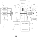
- FIG. 1 illustrates a block diagram of components of a system for nucleic acid sequencing according to some embodiments.
- Such systems include device 100, which acts as a source of data that produces over 50 Gb per second of digital data, and in examples described herein, may produce over 100 Gb per second, and more.
- a communication bus 127 supporting over 100 Gb per second may be desired in embodiments of the technology described herein.
- a sensor chip includes over 600 million sensors, producing multiple bits per sensor, and senses at high frame rates.
- a massively parallel system for transmitting data from a sensor array, or other high data rate source of data, on an integrated circuit, to a destination processor is described herein.
- a nucleic acid sequencing system may include flow cell 101 on integrated circuit device 100, reference electrode 108, a plurality of reagents 114 for sequencing, valve block 116, wash solution 110, valve 112, fluidics controller 118, lines 120/122/126, passages 104/109/111, waste container 106, array controller 124, a reference clock 128 and user interface 129.
- integrated circuit device 100 includes microwell array 107 overlying a sensor array that includes devices as described herein.
- Flow cell 101 includes inlet 102, outlet 103, and flow chamber 105 defining a flow path ofreagents over microwell array 107.
- Reference electrode 108 may be of any suitable type or shape, including a concentric cylinder with a fluid passage or a wire inserted into a lumen of passage 111.
- Reagents 114 may be driven through the fluid pathways, valves, and flow cell 101 by pumps, gas pressure, or other suitable methods, and may be discarded into waste container 106 after exiting outlet 103 of flow cell 101.
- Fluidics controller 118 can control driving forces for reagents 114 and operation of valve 112 (for wash fluid) and valve block 116 (for reagents) with a suitable processor executing software-implemented logic, other controller circuitry or combinations of controller circuitry and software-implemented logic.
- fluidics controller 118 can control delivery of individual reagents 114 to flow cell 101 and integrated circuit device 100 in a predetermined sequence, for predetermined durations, and/or at predetermined flow rates.
- Microwell array 107 includes an array of reaction regions which are operationally associated with corresponding sensors in the sensor array. For example, each reaction region may be coupled to one sensor or more than one sensor suitable for detecting an analyte or reaction property of interest within that reaction region. Microwell array 107 may be integrated in integrated circuit device 100, so that microwell array 107 and the sensor array are part of a single device or chip. Flow cell 101 can have a variety of configurations for controlling the path and flow rate of reagents 114 over microwell array 107.
- Array controller 124 provides bias voltages and timing and control signals to integrated circuit device 100 for reading the sensors of the sensor array. Array controller 124 also provides a reference bias voltage the reference electrode 108 to bias reagents 114 flowing over microwell array 107.
- Array controller 124 may also include a reader to collect output signals from the sensors of the sensor array through output ports on integrated circuit device 100 via bus 127, which comprises a plurality of high-speed serial channels for example, carrying sample data at speeds on the order of 100 gigabits per second or greater. In one example, twenty four serial channels, each of which nominally operates at 5 Gb per second, are implemented in the bus 127.
- a reference clock 128 may be coupled with the device 100 to provide a stable reference clock for use in controlling high-speed serial channels. In embodiments described herein, the reference clock 128 can operate at relatively low frequencies, on the order of 100 MHz or 200 MHz. Alternatively, the reference clock may operate at data rates desired to support the high-speed serial channels.
- Array controller 124 can include a data processing system, with a reader board including a set of field programmable gate arrays (FPGAs), having a plurality of receivers in support of the transmitters on the device 100.
- Array controller 124 can include memory for storage of data and software applications, a processor for accessing data and executing applications, and components that facilitate communication with the various components of the system in FIG. 1 .
- the values of the output signals of the sensors can indicate physical and/or chemical parameters of one or more reactions taking place in the corresponding reaction regions in microwell array 107.
- the values of the output signals may be processed using the techniques disclosed in Rearick et al., U.S. Pat. Appl. No. 13/339,846, filed December 29, 2011 , and in Hubbell, U.S. Pat. Appl. No. 13/339,753, filed December 29, 2011 , which are all incorporated by reference herein in their entirety.
- User interface 129 can display information about flow cell 101 and the output signals received from sensors in the sensor array on integrated circuit device 100.
- User interface 129 can also display instrument settings and controls, and allow a user to enter or set instrument settings and controls.
- Array controller 124 can collect and analyze the output signals of the sensors related to chemical and/or biological reactions occurring in response to the delivery of reagents 114.
- the system can also monitor and control the temperature of integrated circuit device 100 so that reactions take place and measurements are made at a known predetermined temperature.
- the system may be configured to let a single fluid or reagent contact reference electrode 108 throughout an entire multi-step reaction during operation. Valve 112 may be shut to prevent any wash solution 110 from flowing into passage I09 as reagents 114 are flowing. Although the flow of wash solution may be stopped, there can still be uninterrupted fluid and electrical communication between reference electrode 108, passage 109, and microwell array 107.
- wash solution 110 may be selected as being in continuous contact with reference electrode 108, which may be especially useful for multi-step reactions using frequent wash steps.
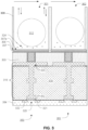
- FIG. 2 illustrates a cross-sectional view of a portion of an exemplary integrated circuit device 200, flow cell 201 and reference electrode 208.
- the device includes a sensor array (schematically 205) coupled to a microwell array (schematically 207).
- flow chamber 204 of flow cell 201 confines reagent flow 206 of delivered reagents across open ends of the reaction regions in microwell array 207.
- the volume, shape, aspect ratio (such as base width-to-well depth ratio), and other dimensional characteristics of the reaction regions may be selected based on the nature of the reaction taking place, as well as the reagents, products/byproducts, or labeling techniques (if any) that are employed.
- the sensors of sensor array 205 may be responsive to (and generate output signals related to) chemical and/or biological reactions within associated reaction regions in microwell array 207 to detect an analyte or reaction property of interest.
- the sensors of sensor array 205 may be chemically sensitive field-effect transistors (chemFETs), such as ion-sensitive field effect transistors (ISFETs). Examples of sensors and array configurations that may be used in embodiments are described in U.S. Patent Application Publication No. 2010/0300559, filed May 24, 2010 , No. 2010/0197507, filed Oct 5, 2012 , No. 2010/0301398, filed Oct 5, 2012 , No. 2010/0300895, May 4, 2010 , No. 2010/0137143, filed May 29, 2009 , and No. 2009/0026082, filed December 17, 2007 , and U.S. Patent No. 7,575,865,filed August 1 2005 , each of which are incorporated by reference herein in their entirety.
- the integrated circuit device 200 includes a large number of serial ports supporting connection to a massively parallel reader 211 via a set of serial channels 210.
- the reagent flow 206 coupled with a large array of ISFETs, presents a complex electrical and mechanical environment in which such a massively parallel communication system can operate with high integrity.
- sensor arrays may be used in systems like that of FIG. 1 , including but not limited to arrays of thermistors and arrays of optical sensors, for example.
- Fig. 3 illustrates cross-sectional view of representative sensors/detectors and corresponding reaction regions according to an exemplary embodiment.
- the sensors may be chemical sensors.
- Fig. shows 3 two exemplary sensors 350, 351, representing a small portion of a sensor array that can include millions of sensors; even billions of sensors are contemplated.
- the sensor array can comprise between 100 and 1,000 sensors, between 100 and 10,000 sensors, between 10,000 and 100,000 sensors, between 100,000 and 1,000,000 sensors, between 1,000,000 and 40,000,000 sensors, between 10,000,000 and 165,000,000 sensors, between 100,000,000 and 660,000,000 sensors, between 1,000,000,000 and 5,000,000,000 sensors, between 5,000,000,000 and 9,000,000,000 sensors, and up to 10,000,000,000 sensors. Windowing of the array is contemplated such that data can be obtained from all or fewer than all of the sensors.
- Sensor 350 is coupled to corresponding reaction region 301, and sensor 351 is coupled to corresponding reaction region 302.
- the two illustrated reaction regions are chemically and electrically isolated from one another and from neighboring reaction regions.
- the dielectric material 303 defines the reaction regions 301/302 which may be within an opening defined by an absence of dielectric material.
- Dielectric material 303 can comprise one or more layers of material, such as silicon dioxide or silicon nitride or any other suitable material or mixture of materials. The dimensions of the openings, and their pitch, can vary from embodiment to embodiment.
- the openings can have a characteristic diameter, defined as the square root of 4 times the plan view cross-sectional area (A) divided by Pi (e.g., sqrt(4*Ahc), of not greater than 5 micrometers, such as not greater than 3.5 micrometers, not greater than 2.0 micrometers, not greater than 1.6 micrometers, not greater than 1.0 micrometers, not greater than 0.8 micrometers, not greater than 0.6 micrometers, not greater than 0.4 micrometers, not greater than 0.2 micrometers or not greater than 0.1 micrometers.
- the plan view area of the sensor is determined in part by the width (or diameter) of reaction regions and may be made small to provide a high density array.
- the footprint of a sensor may be determined and/or reduced by modifying the width (e.g. diameter) of the reaction region.
- the density of the array may be increased or decreased based on the diameter selected for the reaction region.
- Low noise sensors may be provided in a high density array by reducing device and interconnect overhead, including gate area and contact area. Additional examples of sensors and their corresponding reaction regions according to additional exemplary embodiments are described in Fife et al., U.S. Pat. Appl. No. 14/198,382, filed March 5, 2014 , based on U.S. Prov. Pat. Appl. Nos.
- Sensor 350 is representative of the sensors in the sensor array.
- sensor 350 is a chemically-sensitive field effect transistor (chemFET), more specifically an ion-sensitive field effect transistor (ISFET) in this example.
- Sensor 350 includes floating gate structure 318 having sensor plate 320 coupled to reaction region 301 by electrode 307 which can have a surface adapted for contact with an electrolyte (an ionic conducting liquid).
- Sensor plate 320 is the uppermost floating gate conductor in floating gate structure 318.
- floating gate structure 318 includes multiple patterned layers of conductive material within layers of dielectric material 319.
- Sensor 350 also includes conduction terminals including source/drain region 321 and source/drain region 322 within semiconductor substrate 354.
- Source/drain region 321 and source/drain region 322 comprise doped semiconductor material having a conductivity type different from the conductivity type of substrate 354.
- source/drain region 321 and source/drain region 322 can comprise doped P-type semiconductor material
- the substrate can comprise doped N-type semiconductor material.
- Channel region 323 separates source/drain region 321 and source/drain region 322.
- Floating gate structure 318 overlies channel region 323, and is separated from substrate 354 by gate dielectric 352.
- Gate dielectric may be silicon dioxide, for example.
- gate dielectric 352 may be used for gate dielectric 352 such as, for example materials with higher dielectric constants, silicon carbide (SiC), silicon nitride (ShN 4) , Oxynitride, aluminum nitride (AIN), hafnium dioxide (HfO2), tin oxide (SnO2), cesium oxide (CeO2), titanium oxide (TiO2), tungsten oxide (WO3), aluminum oxide (Al2O3),lanthanum oxide (La2O3), gadolinium oxide and others, and any combination thereof.
- SiC silicon carbide
- silicon nitride (ShN 4) Oxynitride
- hafnium dioxide (HfO2) hafnium dioxide
- SnO2 tin oxide
- CeO2 cesium oxide
- TiO2 titanium oxide
- WO3 aluminum oxide
- Al2O3 aluminum oxide
- La2O3 lanthanum oxide
- sensor 350 includes electrode 307 overlying and in communication with an uppermost floating gate conductor in the plurality of floating gate conductors.
- Upper surface 308 of electrode 307 defines a bottom surface of a reaction region for the sensor.
- Upper surface 308 of electrode 307 can act as the sensor surface of the sensitive area for sensor 350.
- Electrode 307 can comprise one or more of a variety of different materials to facilitate sensitivity to particular ions. For example, silicon nitride or silicon oxynitride, as well as metal oxides such as silicon oxide, aluminum or tantalum oxides, generally provide sensitivity to hydrogen ions, whereas sensing materials comprising polyvinyl chloride containing valinomycin provide sensitivity to potassium ions.
- electrode 307 is shown as a single layer of material. More generally, the electrically electrode can comprise one or more layers of a variety of electrically conductive materials, such as metals or ceramics, or any other suitable conductive material or mixture of materials, depending upon the implementation.
- the conductive material may be any suitable metallic material or alloy thereof, or may be any suitable ceramic material, or a combination thereof.
- Examples of metallic materials include aluminum, copper, nickel, titanium, silver, gold, platinum, hafnium, lanthanum, tantalum, tungsten, iridium, zirconium, palladium, or any suitable material or combination thereof.
- Examples of ceramic materials include one of titanium nitride, titanium aluminum nitride, titanium oxynitride, tantalum nitride, or any suitable combination thereof.
- an additional sensing material (not shown) is deposited on upper surface 308 of electrode 307.
- the electrode may be titanium nitride, and titanium oxide or titanium oxynitride may be grown on the upper surface 308 during manufacturing and/or during exposure to fluids during use.
- the electrode may be formed in various shapes (width, height, etc.) depending on the materials and/or etch techniques and/or fabrication processes etc. used during the manufacture process.
- reactants, wash solutions, and other reagents can move in and out ofreaction region 301 by diffusion mechanism.
- Sensor 350 is responsive to (and can generate an output signal related to) charge 324 proximate to electrode 307.
- the sensor when the sensor is coupled to an electrolyte, the sensor may be responsive to an electrolytic potential at the sensor surface.
- the responsiveness of the sensor can relate to the amount of charge that is present proximate to the electrode 307.
- the presence of charge 324 in an analyte solution can alter the surface potential at the interface between the analyte solution and upper surface 308 of electrode 307.
- the surface potential may be altered by protonation or deprotonation of surface groups caused by the ions present in the analyte solution.
- the charge of surface functionality or absorbed chemical species may be altered by analytes in solution. Changes in the amount of charge present can cause changes in the voltage on floating gate structure 318, which in turn can cause an effective change in the threshold voltage of the transistor of sensor 350.
- the potential at the interface may be measured by measuring the current in channel region 323 between source region 321 and drain region 322.
- sensor 350 may be used directly to provide a current-based output signal on an array line connected to source region 321 or drain region 322, or indirectly with additional circuitry to provide a voltage-based output signal. Charge may be more highly concentrated near the bottom of reaction region 301. Accordingly, in some embodiments variations in the dimensions of the electrode can have an effect on the amplitude of the signal detected in response to charge 324.
- reactions carried out in reaction region 301 may be analytical reactions to identify or determine characteristics or properties of an analyte of interest. Such reactions can generate directly or indirectly products/byproducts that affect the amount of charge adjacent to electrode 307. If such products/byproducts are produced in small amounts or rapidly decay or react with other constituents, multiple copies of the same analyte may be analyzed in reaction region 301 at the same time in order to increase the output signal generated. In some embodiments, multiple copies of an analyte may be attached to solid phase support 312, either before or after being deposited into reaction region 301.
- Solid phase support 312 may be a particle, a microparticle, a nanoparticle.
- the analyte may be attached to a bead which may be solid or porous and can further comprise a gel, or the like, or any other suitable solid support that may be introduced to a reaction region.
- copies of an analyte may be located in a solution proximal to a sensor of a reaction region.
- copies of an analyte can bind directly to the surface of the sensor to capture agents includes the material on the surface or if there are pores on the surface (for example, copies of an analyte can bind directly to electrode 307).
- the solid phase support may be of varied size, for example, in a range of 100 nm to 10 micrometers.
- the solid support may be positioned in the opening at various places.
- multiple, connected copies may be made by rolling circle amplification (RCA), exponential RCA, polymerase chain reaction (PCR) or like techniques, to produce an amplicon without the need of a solid support.
- RCA rolling circle amplification
- PCR polymerase chain reaction
- a nucleotide incorporation event may be determined by detecting ions (e.g., hydrogen ions) that are generated as natural products of polymerase-catalyzed nucleotide extension reactions.
- ions e.g., hydrogen ions
- the detection of a nucleotide incorporation event may be used to sequence a sample or template nucleic acid, which may be a fragment of a nucleic acid sequence of interest, for example, and which may be directly or indirectly attached as a clonal population to a solid support.
- the solid support can be a a particle or a microparticle.
- the nucleic acid sequence can be attached to a bead.
- the sample or template nucleic acid may be operably associated to a primer and polymerase and may be subjected to repeated cycles or "flows" of deoxynucleoside triphosphate ("dNTP") addition (which may be referred to herein as "nucleotide flows") from which nucleotide incorporations can result and washing.
- dNTP deoxynucleoside triphosphate
- the primer may be annealed to the sample or template so that the primer's 3' end may be extended by a polymerase whenever dNTPs complementary to the next base in the template are added.
- the identity of the type, sequence and number of nucleotide(s) associated with a sample nucleic acid present in a reaction region coupled to a sensor may be determined.
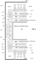
- FIG. 4 is a simplified block diagram of part of the circuitry on an integrated circuit sensor array used for DNA sequencing.
- the integrated circuit includes a 660 megapixel ISFET sensor array 401 on a substrate 400.
- An upper set of column bias/select circuits 402U and an upper row decoder (row dee) 531 are configured for access to an upper half of the array 401.
- a lower set of column bias/select circuits 402L and a lower row decoder 521 are configured for access to a lower half of the array 401.
- An upper set of analog-to-digital converter (ADC) circuits 403U is coupled to the upper set of column bias/select circuits 402U.
- An upper register array 404U is coupled to the upper set of analog-to-digital converter circuits 403U.
- the upper register array 404U may be configured to provide a plurality of streams of digital data through serializers (e.g. 511, 512) to corresponding transmitters (e.g. 405-23, 405-22). Each of the transmitters is coupled to a corresponding pair (a pair for D[23], a pair for D[22]) of output pads, which in turn are connected to transmission lines (not shown).
- a lower set of analog-to-digital converter circuits 403L is coupled to the lower set of column bias and select circuits 402L.
- a lower register array 404L is coupled to the lower set of analog-to-digital converter circuits 403L.
- the lower register array 404L may be configured to provide a plurality of streams of digital data through serializers (e.g. 501, 502) to corresponding transmitters (e.g. 405-0, 405-1). Each of the transmitters is coupled to a corresponding pair (D[0], D[l]) of output pads, which in turn are connected to transmission lines (not shown).
- the configurations described herein support a device having a large number of gigabit per second transmitters, such as at least 20 transmitters capable of transmission at a data rate greater than I Gb per second, and configured in at least 10 pairs.
- a device having a large number of gigabit per second transmitters, such as at least 20 transmitters capable of transmission at a data rate greater than I Gb per second, and configured in at least 10 pairs.
- Large numbers of gigabit per second transmitters present a context in which a class of implementation problems arises which not apparent in configurations with small numbers of transmitters.
- the device includes 24 transmitters capable of transmitting data at 5 Gb per second each, or faster, supporting throughput from a high speed data source of 120 Gb per second or more.
- Supporting peripheral circuitry including a sequencer 532, a digital-to-analog converter 533, a gray code generator 534, and bias circuitry 535 are coupled to the upper circuitry. Also, supporting circuitry including a sequencer 522, a digital-to-analog converter 523, a gray code generator 524, and bias circuitry 525 are coupled to the lower circuitry.
- the chip includes a serial peripheral interface (SPI) control block 540 to support the serial ports on the device, and a fuse array 541 used in configuration of the device.
- SPI serial peripheral interface
- sequencer logic 522, 532 causes the circuitry to perform a frame sensing sequence.
- a row of ISFETs in each of the upper and lower halves of the array may be selected and biased using the upper/lower column bias/select circuits 402U/402L so that a current that may be a function of the charge in that corresponding sensor well may be produced on each column line.
- the upper/lower analog-to-digital converter circuits 403U/403L receive a ramp signal from the digital-to-analog converter 533, 523, and produce an output signal when the current on the corresponding column line matches the level of the ramp signal.
- the gray code generator 524, 534 may be sampled in response to the output signal, and the results are stored in the upper/lower register array 404U/404L. Data in the register array 404U/404L are assembled into packets, and applied in a plurality of digital data streams to the transmitters on the chip.
- the illustrated part of the circuitry in FIG. 4 includes four transmitters out of a set of 24 transmitters on the substrate 400.
- the four transmitters illustrated include a first pair of transmitters 405-0, 405-1, and a second pair of transmitters 405-22, 405-23.
- one phase locked loop 406-0 including a low pass filter
- one phase locked loop 406-11 including a low pass filter
- the phased locked loops operate as clock multipliers, each of which produces a local transmit clock and provides the local transmit clock to the transmitter on its left and to the transmitter on its right via clock lines (e.g. 407a, 407b at phase locked loop 406-0).
- phase locked loop/low pass filter 406-0, 406-11
- phase locked loop control block 503, 513 which stores parameters used to control and calibrate phase locked loop. This pattern may be repeated across the 24 transmitters on the chip, so that there are 12 phase locked loop blocks, and 24 transmitters.
- the transmitters are grouped into pairs which are coupled to individual phase locked loops.
- the phase locked loops are disposed on the substrate between the transmitters, so that the transmission distance from the phase locked loop to the transmitter using the clock produced in the phase locked loop may be small.
- each of the phase locked loops 406-0, 406-11 is coupled to an individual power pad VDDP and an individual ground pad GNDP.
- the individual power pad VDDP and the individual ground pad GNDP for each phase locked loop are disposed on the chip adjacent the phase locked loop, and between the output pads for the transmitter on the left, and the output pads for the transmitter on the right in the corresponding transmitter pair.
- the individual power pad VDDP and the individual ground pad GNDP are connected to an off-chip voltage supply, which may be configured with bypass capacitors and other circuitry, to create a low noise power configuration for the phase locked loop circuits, and to reduce coupling of noise between the high-frequency phase locked loop circuits and other circuits on the substrate 400.
- a low-speed reference clock (not shown, see FIG. 5 ) may be distributed on the chip and connected to each of the phase locked loops.
- the clock multipliers in the illustrated embodiment are implemented using phase locked loops. Clock multipliers may be implemented using other circuitry as well, such as delay locked loops, phase interpolators, and combinations of phase locked loops, phase interpolators and/or delay locked loops.
- FIG. 5 illustrates clock distribution circuitry which may be utilized with a device like that shown in FIG. 4 .
- the clock distribution circuitry includes a clock input buffer 570 which includes CLKP and CLKN inputs configurable to receive a differential clock signal or a single ended clock signal from an off-chip clock reference.
- the output of the clock buffer 570 may be distributed in a daisy chain fashion to the phase locked loops 580-0 through 580-5 disposed along a lower side of the chip, and through a duty cycle correction DCC chain 571, which includes a group of cascaded DCC buffers to support transmission of the reference clock across the large chip, to the phase locked loops 580-6 through 580-1 lalong an upper side of the chip.
- the reference clock may be distributed to the transmitter units xmt0 to xmtl 1 on the lower side and via the DCC chain 571 to transmitter units xmtl2 to xmt23 on the upper side.
- Each of the transmitter units includes a duty cycle correction DCC buffer, and passes the reference clock from the DCC buffer in the transmitter unit to its adjacent phase locked loop, or adjacent transmitter unit.
- An example of the transmitter unit circuitry including this DCC buffer is described below with reference to FIG. 7 .
- the reference clock may be coupled directly to the phase locked loop circuit, and DCC buffers may be disposed on the chip in other configurations as necessary.
- the clock distribution circuit provides a reference clock at a relatively low frequency, such as 125 MHz, with a 50% duty cycle to each of the phase locked loops.
- the reference clock may be distributed asynchronously to the phase locked loops.
- FIG. 6 is a block diagram of the clock input buffer 570 shown in FIG. 5 .
- the clock input buffer 570 in this example includes a multiplexer 991.
- the CLKP pad is connected to both the "0" and “1" inputs of the multiplexer 991.
- the CLKN pad is connected to the "0" input of the multiplexer 991.
- a parameter set on the device labeled cmos_sel in the figure, controls the multiplexer 991 so that it converts the differential input in one mode to a single ended output, or provides the single ended input through as the single ended output.
- the single ended output of the multiplexer 991 may be supplied through a NAND gate 992 to a DCC buffer (dee) 993.
- the NAND gate 992 may be controlled by a control signal labeled ref_sel in this example.
- the output of the DCC buffer 993 may be the reference clock to be distributed on the chip.
- a duty cycle correction circuit such as that used for element 993, or used in the DCC chain 571 described with reference to FIG. 5 , may be implemented using a variety of circuit structures. Examples are described in the literature, including Ogawa, et al., "A 50% DUTY-CYCLE CORRECTION CIRCUIT FOR PLL OUTPUT,” IEEE International Symposium on Circuits and Systems (Volume:4) ISCAS 2002 ; M. Ragavan, et al. "DUTY CYCLE CORRECTOR WITH SAR FOR DDR DRAM APPLICATION,” International Journal of Advanced Research in Electrical, Electronics and Instrumentation Engineering, Vol. 2, Issue 5, May 2013 .
- FIG. 7 illustrates a configuration of a transmitter pair according to embodiments of the technology described herein.
- Each transmitter pair includes first transmitter XMT 610 and second transmitter XMT 611, which in this example correspond to the transmitter for output D[0] and the transmitter for output D[l] on the chip.
- a phase locked loop/low pass filter circuit 612 may be disposed between the transmitters 610, 611 in the pair.
- Transmitter control blocks 620, 621 are coupled to the corresponding transmitters 610, 611.
- Corresponding data streams 630, 631 are input to the transmit control block 620, 621 from the register array on the chip, respectively.
- a phase locked loop control block 622 is coupled to the phase locked loop/low pass filter 612.
- Transmitter control blocks 620, 621, and PLL control block 622 receive power in a digital power domain based on the supply terminals VDDD and GNDD.
- the transmitters 610, 611 receive power in a transmitter power domain (output "O" power) based on supply terminals VDDO, GNDO.
- the phase locked loop/low pass filter circuits are disposed in individual power domains based on supply terminals VDDP, GNDP that are directly connected to the phase locked loop/low pass filter circuitry.
- the reference clock RCLK is coupled to the phase locked loop from clock distribution circuitry, like that described above.
- a system clock SCLK is coupled to the transmitter control blocks 620, 621, and PLL control block 622.
- the system clock can operate nominally at the same frequency as the reference clock in some embodiments, but may be a different frequency.
- the phase locked loop 612 operates as a clock multiplier, producing a high speed, local transmit clock on line 650.
- the system clock and reference clock operate at 125 MHz.
- the high-speed, local transmit clock may be produced at 2.5 GHz (20x multiplication).
- the transmitters in this example transmit on both the rising and falling edges of the local transmit clock, resulting in a transmission rate of 5 Gb per second.
- a throughput of 120 Gb per second may be achieved.
- High data integrity of the transmitted data is supported using techniques including distribution of a low-speed reference clock, the configuration of the phase locked loops in individual power domains, the placement of the phase locked loops between corresponding pairs of transmitters, and local use of the locally produced high-speed transmit clocks.
- FIG. 8 is a block diagram of a transmitter and transmitter control block 700 which may be used in the configuration shown in FIGS. 5 and 7 .
- a reference clock (refclk) may be supplied as input to a single output, duty cycle correction buffer (dccl) 710.
- the output of the DCC buffer 710 may be applied as an output (refclk0) for connection in daisy chain fashion as illustrated in FIG. 5 .
- the output of DCC buffer 710 may be supplied to a clock selector 711, which also includes a differential output DCC buffer.
- Clock selector 711 is capable of selecting between the local high-speed transmit clock, labeled PLLclk in this example, and the reference clock output from the DCC buffer 710.
- a control signal (rclk_sel) may be used to determine the selection.
- the ability to select the reference clock output from DCC buffer 710 supports testing the chip.
- the local high-speed transmit clock PLLclk may be selected.
- the output of the clock selector 711 may be a duty cycle-corrected, differential clock on lines 720, at the local transmit clock frequency.
- the differential clock on lines 720 may be supplied to a synchronizer circuit (sync) 701, a serializer circuit (serializer) 702, a pre-driver 703, and an off-chip driver 704.
- the output of the off-chip driver is connected to the pads OUTP and OUTN, which are in turn connected to a transmission line.
- the synchronizer circuit 701 also receives the system clock (sys elk), and produces a synchronized system clock for the serializer 702.
- the data stream from the register arrays are applied in this example in 20 bit packets to the serializer 702.
- the output of the serializer may be applied to the pre-driver 703, and then off chip via the off-chip driver 704.
- FIG. 9 is a block diagram of a phase locked loop 800 including a low pass filter, which may be utilized in the configuration of FIGS. 5 and 7 .
- the phase locked loop 800 includes a phase and frequency detector (PFD) 801 connected to the reference clock (ref elk), a charge pump 802, a low pass filter 803, and a ring voltage controlled oscillator (VCO) 804.
- a programmable divider 805 is connected between the output of the ring VCO 804, and the input of the phase and frequency detector 801.
- the programmable divider 805 in this example includes a clock selector 811, a first divider 810, and a second divider 812.
- the clock selector 811 receives the output of the ring VCO 804 at one input, and the output of the divider 810 on a second input.
- the divider 810 in this example may be a divide-by-two block (/2).
- a control signal div ⁇ 0> controls the clock selector 811.
- the output of the clock selector 811 may be applied as the local high-speed transmit clock pllclk.
- the output of the divider 810 may be applied to the input of the second divider 812.
- the second divider is configurable to divide by five (0:/5), or to divide by 10 (0:/10), in response to a control signal div ⁇ 1>.
- combination of the first divider 810 and the second divider 812 provides a divide-by-20 operation in the 5 Gb per second example described above so that, in effect, the local high-speed transmit clock can operate at 20 times the frequency of the reference clock.
- phase locked loop 800 A variety of control parameters are coupled to the various blocks in the phase locked loop 800. Parameters "fast, lock, slow” are provided from the phase and frequency detector 801 to control circuitry.
- Charge pump bias parameters bias_CP ⁇ 3:0> are applied to the charge pump 802.
- Low pass filter parameters C1 ⁇ 5:0> and C2 ⁇ 4:0> are applied to the low pass filter 803.
- VCO control parameters band_ctl ⁇ 3:0> are applied to the ring VCO 804.
- the phase locked loop may be digitally controlled using basic phase locked loop management for calibration and configuration, driven by link control logic on the reader board in one example. In other embodiments, phase locked loop calibration and configuration may be locally driven, or a combination of local and remote operations may be utilized.
- the low pass filter in the phase locked loop may be configured with a transfer function that rejects jitter in the reference clock. This may be implemented in the charge pump and filter circuitry in the loop as it operates on the output of the phase and frequency detector nominally at the frequency of the reference clock.
- FIGS. 10A and 10B illustrate layout of the transmitter circuits and power traces of an example sensor integrated circuit, in support of a multiple power domain system.
- the reference numerals used in FIG. 4 are used again for like components.
- the device includes a substrate 400.
- a 660 megapixel ISFET sensor array 401 may be implemented on the substrate.
- Upper and lower column bias and select circuits 402U, 402L, respectively, upper and lower analog-to-digital converter circuits 403U, 403L, respectively, and upper and lower register arrays 404U, 404L respectively, are implemented in the central region of the chip. Twelve transmitter pairs are disposed around the perimeter of the chip, with six pairs on the lower side of the chip, and six pairs on the upper side of the chip.
- the plurality of transmitter pairs includes first transmitter pair 405-0, 405-1, and second transmitter pair 405-2, 405-3, illustrated in FIG. 10A ; and transmitter pair 405-8, 405-9, transmitter pair 405-10, 405-11 illustrated in FIG. 10B on the lower edge. Also, the plurality of transmitter pairs includes transmitter pair 405-12, 405-13 and transmitter pair 405-14, 405-15 illustrated in FIG. 10B and transmitter pair 405-20 405-21 transmitter pair 405-22 405-23 illustrated in FIG. 10A on the upper edge.
- Four additional transmitter pairs are implemented on the chip along the upper and lower edges, but are omitted from the drawing because of the cutout. Thus, 12 transmitter pairs are implemented on the substrate 400, for a total of 24 transmitters.
- each transmitter pair includes a local clock multiplier, implemented in this example by a phase locked loop with a low pass filter.
- FIGS. 10A and 10B show phase locked loops 406-0, 406-1, 406-4, 406-5, 406-6, 406-7, 406-10, and 406-11 each of which may be placed on the substrate between the transmitters in a corresponding pair of transmitters.
- FIGS. 10A and 10B illustrate an example of a substrate that includes one or more power domains for a high data rate data source, such as the array of ISFETs illustrated, for the transmitters and for peripheral logic including reference clock distribution circuitry.
- the clock multipliers are disposed on the substrate in individual power domains separate from one another and from the other one or more power domains.
- FIGS. 10A and 10B illustrate a configuration of power pads and power traces on the chip to support multiple power domains.
- the power domains include an analog power domain GNDA, VDDA, a digital power domain GNDD, VDDD, and a transmitter power domain GNDO, VDDO.
- the power domains include 12 individual power domains, one for each phase locked loop.
- the power pads are conductive pads on the substrate 400 adapted for connection to a pin or other connector structure for an electrical connection to off-chip structures. Such power pads often include a pad of patterned metal in the highest metal layer on the device.
- the power traces are conductive traces on the substrate adapted for distributing power across a region of the substrate. Such power traces are often implemented in the highest patterned metal layer on the device, and have relatively large width dimensions to support carrying a significant amount of current.
- the analog power domain includes power pads labeled GNDA, VDDA on each of the four comers of the substrate 400.
- the analog power domain includes a power bus including a trace 411V connected to the VDDA power pads (e.g. 420V in the lower left), and a trace 41lG connected to the GNDA power pads (e.g. 420G in the lower left). Traces 411V and 41lG are configured on the device as the inside power traces, and surround the analog core of the device, which includes the sensor array 401, and portions of the other circuitry.
- the digital power domain includes power pads labeled GNDD, VDDD distributed in pairs around the perimeter of the chip, including one pair between each transmitter.
- the digital power domain includes a power bus including a trace 412V connected to the VDDD power pads, and a trace 412G connected to the GNDD power pads.
- the traces 412V and 412G are placed on the device just outside the analog power domain traces 411V and 41lG, and are placed adjacent digital circuitry surrounding the analog core of the chip.
- the transmitter power domain includes power pads labeled GNDO, VDDO distributed in pairs around the perimeter of the chip, with one pair for every transmitter.
- Each pair of transmitter power domain power pads includes a GNDO pad on one side of the corresponding transmitter, and a VDDO pad on the opposite side of the corresponding transmitter.
- the transmitter power domain includes a power bus including trace 413V connected to the VDDO power pads and a trace 413G connected to the GNDO power pads.
- the traces 413V and 413G are configured on the device just outside the digital power domain traces 412V and 412G, and are placed for distribution of power supply voltages to the transmitters on the perimeter of the chip.
- each phase locked loop may be disposed in an individual power domain.
- Each local clock multiplier power domain includes a pair of power pads labeled GNDP, VDDP in the figure.
- the power pads GNDP and VDDP are disposed between the output pads for the transmitters.
- the power pads GNDP and VPPD for the phase locked loop 406-0 are disposed between the output pads for serial channel D[0] and the output pads for serial channel D[l].
- Each local clock multiplier power domain includes a power trace and a ground trace confined to the phase locked loop circuitry.
- phase locked loop 406-0 includes a power trace 414V and a ground trace 414G.
- phase locked loop 406-7 in FIG. lOB includes a power trace 415V and a ground trace 415G connected to the local power pad VDDP and ground pad GNDP respectively.
- the substrate 400 includes 12 pairs of transmitters having individual clock multipliers disposed in individual power domains between the transmitters in the pair.
- the circuits in each power domain are isolated electrically from one another.
- This isolation may be implemented using deep n-well technology for example, in which the active regions of the circuitry are implemented within one or more doped wells separated from the bulk substrate by a deep n-well.
- the deep n-well may be biased using a selected power supply voltage so that it remains reversed biased relative to the substrate and relative to the active region during operation. In this manner, noise produced in the ground and power circuitry is not coupled directly into the circuitry of other power domains via the substrate.
- Some or all of the power domains may be isolated using other technologies, such as by formation of the active regions in semiconductor layers deposited over layers of insulating material, so the insulating material electrically separates the active regions from the substrate.
- FIG. 11 illustrates two transmitter pairs taken from the layout of FIGS. lOA and lOB.
- FIG. 11 illustrates a transmitter pair 405-2, 405-3, with an individual phase locked loop 406-1 in between.
- transmitter pair 405-8, 405-9 is shown, with an individual phase locked loop 406-4 in between.
- the phase locked loops have individual power pads and power traces.
- phase locked loop 406-1 includes the VDDP power pad connected to the power trace 417V, and the GNDP ground pad connected to the ground trace 417G.
- Phase locked loop 406-4 includes the VDDP power pad connected to the power trace 418V, and the GNDP ground pad connected to the ground trace 418G.
- the pattern of power pads and output pads includes a set of 14 pads for each transmitter pair disposed around the substrate in a repeating sequence.
- the order from right to left for the set of 14 pads for the transmitter pair including transmitters 405-2 and 405-3, and phase locked loop 406-1 of the pads in this example is as follows: transmitter power domain ground pad GNDO, output pad pair D[2], transmitter power domain power pad VDDO, digital power domain power pad VDDD, digital power domain ground pad GNDD, local clock multiplier power pad VDDP, local clock multiplier ground pad GNDP, transmitter power domain ground pad GNDO, output pad pair D[3], transmitter power domain power pad VDDO, digital power domain power pad VDDD and digital power domain ground pad GNDD.
- one clock multiplier may be associated with only one transmitter, or with groups of more than two transmitters, as suits a particular need.
- One clock multiplier may be configured to provide a transmit clock to one or more transmitters, where the one or more transmitters are in a separate power domain than the power domain of the clock multiplier.
- a configuration in transmitter pairs can provide an advantage in that the length of a transmission line carrying the transmit clock from the clock multiplier to the adjacent transmitters in the transmitter pair may be configured locally and have short and uniform transmission paths, without traversing circuitry other than the clock multiplier and the connect transmitter.
- FIG. 12 and FIG. 13 illustrate an electrostatic discharge ESD protection configuration for the plurality of power domains on a device such as that shown in FIGS. lOA and lOB.
- the power and ground traces 411V, 41lG, respectively, for the analog power domain, the power and ground traces 412V, 412G, respectively, for the digital power domain, and the power and ground traces 413V, 413G for the transmitter power domain are shown using the reference numbers of FIGS. 10A and lOB.
- the ESD circuits used include circuit 900 between the power and ground power pads (VDDA, GNDA) respectively, and power and ground traces (411V, 411G) for the analog power domain, circuits 901, 902 between the power and ground power pads (VDDD, GNDD) and power and ground traces (412V, 412G) for the digital power domain, and circuits 903, 904, 905 for the power and ground power pads (VDDO, GNDO) and power and ground traces (413V, 413G) in the transmitter power domain.
- the ESD circuits 900-905 may be implemented for example, utilizing reversed-biased diode configurations in a grounded gate NMOS (ggNMOS) technology connected between the power and the ground traces in the corresponding power domain.
- ggNMOS grounded gate NMOS
- Other ESD circuit implementations may be used as well.
- an ESD protection array is illustrated for protecting the local clock multiplier power domains, and for cascading protection among the power traces of different power domains.
- the power trace 414V for an individual phase locked loop, and the ground trace 414G for the individual phase locked loop are shown.
- An ESD protection circuit 925 is connected between power and ground traces 414G and 414V respectively, and the corresponding pads VDDP, GNDP. Circuit 925 may be implemented using a reversed biased diode configuration in a grounded gate NMOS technology as well.
- ESD protection circuits 910, 911, 912, and 913 are connected on one terminal to the power trace 411V connected to VDDA for the analog power domain.
- Circuit 910 is connected on its opposing terminal to the power trace 412V connected to VDDD in the digital power domain.
- Circuit 911 is connected on its opposing terminal to the power trace 413V connected to VDDO in the transmitter power domain.
- circuit 912 is connected on its opposing terminal to the power trace 413V connected to VDDO in the transmitter power domain.
- Circuit 913 is connected on its opposing terminal to the power trace 412V connected to VDDD in the digital power domain.
- a second tier of ESD circuits includes circuits 914, 915, 916 and 917, connected on one terminal to the analog ground trace 411G which is connected to the analog ground pad GNDA for the analog power domain.
- Circuit 914 is connected on its opposing terminal to the ground trace 412G connected to GNDD in the digital power domain.
- Circuit 915 may be connected on its opposing terminal to the ground trace 413G connected to GNDO in the transmitter power domain.
- a similar pattern may be distributed around the chip, so that circuit 916 is connected on its opposing terminal to the ground trace 413G connected to GNDO in the transmitter power domain.
- Circuit 917 is connected on its opposing terminal to the ground trace 412G connected to GNDD in the digital power domain.
- the third tier the ESD circuits include circuits 918 and 919.
- Circuits 918, 919 each include one terminal coupled to the power trace 412V that is connected to VDDD in the digital power domain. Both of the circuits 918, 919 have opposing terminals connected to the power trace 413V that is connected to VDDO in the transmitter power domain.
- a fourth tier of ESD circuits include circuits 920 and 921. Circuits 920 and 921 are both connected between the ground trace 412G that is connected to GNDD in the digital power domain, and the ground trace 413G that is connected to GNDO in the transmitter power domain.
- ESD circuits 926, 927 and 930 are also protected by ESD circuits 926, 927 and 930.
- ESD circuits 926 and 927 have one terminal connected to the power trace 414V that is connected to the VDDP for the local clock multiplier power domain.
- Circuit 926 has an opposing terminal connected to the trace 411V that is connected to VDDA in the analog power domain.
- Circuit 927 has an opposing terminal connected to ground trace 413G in the transmitter power domain.
- the ESD circuit 930 has one terminal connected to the ground trace 414G that is connected to GNDP of the local clock multiplier power domain, and an opposing terminal connected to the ground trace 413G that is connected to GNDO in the transmitter power domain.
- Circuit 927 which is connected between a ground trace and a power trace, may be implemented using a reversed biased diode configuration in a grounded gate NMOS technology, consistent with the example given above for protection between power and ground traces.
- circuits which protect between power traces in different power domains including the circuits 910, 911, 912, 913, 918, 919 and 926, may be implemented using a reversed biased diode configuration in a grounded gate NMOS technology, consistent with the example given above for protection between power and ground traces.
- Circuits which protect between ground traces in different power domains including the circuits 914, 915, 916, 917, 920, 921 and 930 may be implemented using back-to-back parallel diodes.
- a manufacturing method for an integrated circuit includes forming a plurality of power domains on an integrated circuit; placing a data source comprising an analog sensor array on the substrate in an analog power domain; placing peripheral circuitry coupled to the sensor array to produce a plurality of streams of digital data using a system clock in a digital power domain; placing reference clock distribution circuitry on the substrate which distributes a reference clock having a reference frequency; placing in individual power domains a plurality of clock multipliers which produce respective local transmit clocks having transmit clock frequencies that are multiples of the reference clock frequency; routing the reference clock from the reference clock distribution circuitry to the plurality of clock multipliers; and placing a plurality of sets of transmitters on the substrate configured to receive corresponding streams of data from the data source; routing the local transmit clock from one clock multiplier in the plurality of clock multipliers to each set of transmitters.
- a configuration for implementing an array of high-speed transmitters on an integrated circuit is described.
- Features of the implementation include local high-speed transmit clock generation, and provide a clock multiplier such as a phase locked loop, between each pair of transmitters which provides a local high-speed transmit clock over short connectors to the adjacent transmitters.
- Another feature of the implementation includes low-speed reference clock distribution, allowing for the distribution of the reference clock to the transmitter array at low power and low-frequency, minimizing disturbance of the transmitters from reference clock noise.
- features of the implementation include power supply separation, providing individual power domains for the clock multiplier circuitry, separate from the transmitters, from digital circuitry and from analog circuitry on the device minimizing disturbance of the transmitter from noise arising in other portions of the chip which operate on separate clocks and introduce additional noise sources.
- An integrated circuit which includes a substrate having a data source, with peripheral circuitry on the substrate coupled to the data source to produce a stream of digital data.
- a clock multiplier may be provided on the substrate which produces a transmit clock.
- the clock multiplier may be disposed in an individual power domain on the substrate to reduce noise and improve quality of the transmit clock.
- a transmitter may be on the substrate and configured to receive the stream of data from the data source. The transmitter is connected to transmit the stream of data on an output pad using the transmit clock.
- the transmitter may be disposed in a transmitter power domain on the substrate separate from the individual power domain of the clock multiplier.
- the data source and the peripheral circuitry are disposed in a power domain or power domains separate from the individual power domain.
- the integrated circuit can include a plurality of transmitters on the substrate connected to, and thereby sharing, the clock multiplier.
- a plurality of clock multipliers may be disposed on the substrate which produce respective local transmit clocks, in which each clock multiplier may be disposed in an individual power domains on the substrate.
- a plurality of transmitters on the subset are arranged in sets having one or more members, and wherein each set may be placed in proximity to, and connected to, one clock multiplier in the plurality of the clock multipliers.
Landscapes
- Engineering & Computer Science (AREA)
- Physics & Mathematics (AREA)
- Health & Medical Sciences (AREA)
- Life Sciences & Earth Sciences (AREA)
- Computer Hardware Design (AREA)
- Chemical & Material Sciences (AREA)
- General Physics & Mathematics (AREA)
- Theoretical Computer Science (AREA)
- Microelectronics & Electronic Packaging (AREA)
- Molecular Biology (AREA)
- Analytical Chemistry (AREA)
- Electrochemistry (AREA)
- Pathology (AREA)
- Immunology (AREA)
- General Health & Medical Sciences (AREA)
- Biochemistry (AREA)
- Chemical Kinetics & Catalysis (AREA)
- Evolutionary Computation (AREA)
- Geometry (AREA)
- General Engineering & Computer Science (AREA)
- Spectroscopy & Molecular Physics (AREA)
- Computer Networks & Wireless Communication (AREA)
- Architecture (AREA)
- Apparatus Associated With Microorganisms And Enzymes (AREA)
- Arrangements For Transmission Of Measured Signals (AREA)
- Investigating Or Analyzing Materials By The Use Of Electric Means (AREA)
- Semiconductor Integrated Circuits (AREA)
Applications Claiming Priority (3)
| Application Number | Priority Date | Filing Date | Title |
|---|---|---|---|
| US201462093548P | 2014-12-18 | 2014-12-18 | |
| EP15828589.0A EP3234576B1 (de) | 2014-12-18 | 2015-12-16 | Integrierte schaltung mit hoher datenrate und mit transmitterkonfiguration |
| PCT/US2015/066052 WO2016100486A1 (en) | 2014-12-18 | 2015-12-16 | High data rate integrated circuit with transmitter configuration |
Related Parent Applications (1)
| Application Number | Title | Priority Date | Filing Date |
|---|---|---|---|
| EP15828589.0A Division EP3234576B1 (de) | 2014-12-18 | 2015-12-16 | Integrierte schaltung mit hoher datenrate und mit transmitterkonfiguration |
Publications (1)
| Publication Number | Publication Date |
|---|---|
| EP4354131A2 true EP4354131A2 (de) | 2024-04-17 |
Family
ID=55229818
Family Applications (2)
| Application Number | Title | Priority Date | Filing Date |
|---|---|---|---|
| EP23211333.2A Pending EP4354131A2 (de) | 2014-12-18 | 2015-12-16 | Integrierte schaltung mit hoher datenrate und mit transmitterkonfiguration |
| EP15828589.0A Active EP3234576B1 (de) | 2014-12-18 | 2015-12-16 | Integrierte schaltung mit hoher datenrate und mit transmitterkonfiguration |
Family Applications After (1)
| Application Number | Title | Priority Date | Filing Date |
|---|---|---|---|
| EP15828589.0A Active EP3234576B1 (de) | 2014-12-18 | 2015-12-16 | Integrierte schaltung mit hoher datenrate und mit transmitterkonfiguration |
Country Status (6)
| Country | Link |
|---|---|
| US (3) | US10605767B2 (de) |
| EP (2) | EP4354131A2 (de) |
| KR (1) | KR102593647B1 (de) |
| CN (1) | CN107250784B (de) |
| TW (3) | TWI756167B (de) |
| WO (1) | WO2016100486A1 (de) |
Families Citing this family (1)
| Publication number | Priority date | Publication date | Assignee | Title |
|---|---|---|---|---|
| US11496164B2 (en) | 2021-03-12 | 2022-11-08 | International Business Machines Corporation | Efficient multi-band transmitter |
Citations (7)
| Publication number | Priority date | Publication date | Assignee | Title |
|---|---|---|---|---|
| US20090026082A1 (en) | 2006-12-14 | 2009-01-29 | Ion Torrent Systems Incorporated | Methods and apparatus for measuring analytes using large scale FET arrays |
| US7575865B2 (en) | 2003-01-29 | 2009-08-18 | 454 Life Sciences Corporation | Methods of amplifying and sequencing nucleic acids |
| US20100137143A1 (en) | 2008-10-22 | 2010-06-03 | Ion Torrent Systems Incorporated | Methods and apparatus for measuring analytes |
| US20100197507A1 (en) | 2006-12-14 | 2010-08-05 | Ion Torrent Systems Incorporated | Methods and apparatus for measuring analytes using large scale fet arrays |
| US20100300559A1 (en) | 2008-10-22 | 2010-12-02 | Ion Torrent Systems, Inc. | Fluidics system for sequential delivery of reagents |
| US20100300895A1 (en) | 2009-05-29 | 2010-12-02 | Ion Torrent Systems, Inc. | Apparatus and methods for performing electrochemical reactions |
| US20100301398A1 (en) | 2009-05-29 | 2010-12-02 | Ion Torrent Systems Incorporated | Methods and apparatus for measuring analytes |
Family Cites Families (497)
| Publication number | Priority date | Publication date | Assignee | Title |
|---|---|---|---|---|
| JPS5530312B2 (de) | 1975-01-16 | 1980-08-09 | ||
| US4133735A (en) * | 1977-09-27 | 1979-01-09 | The Board Of Regents Of The University Of Washington | Ion-sensitive electrode and processes for making the same |
| US5132418A (en) | 1980-02-29 | 1992-07-21 | University Patents, Inc. | Process for preparing polynucleotides |
| JPS57136158A (en) | 1981-02-17 | 1982-08-23 | Sumitomo Electric Ind Ltd | Ph electrode |
| GB2096824A (en) | 1981-04-09 | 1982-10-20 | Sibbald Alastair | Chemically sensitive field effect transistor |
| DE3269784D1 (en) | 1981-05-15 | 1986-04-17 | Licentia Gmbh | Method for measuring ionic concentrations |
| FR2510260A1 (fr) | 1981-07-24 | 1983-01-28 | Suisse Fond Rech Microtech | Dispositif semiconducteur sensible aux ions |
| US4438354A (en) | 1981-08-14 | 1984-03-20 | American Microsystems, Incorporated | Monolithic programmable gain-integrator stage |
| US4411741A (en) | 1982-01-12 | 1983-10-25 | University Of Utah | Apparatus and method for measuring the concentration of components in fluids |
| NL8302964A (nl) | 1983-08-24 | 1985-03-18 | Cordis Europ | Inrichting voor het bepalen van de aktiviteit van een ion (pion) in een vloeistof. |
| NL8303792A (nl) | 1983-11-03 | 1985-06-03 | Cordis Europ | Inrichting voorzien van een op een isfet gebaseerd meetcircuit; voor toepassing in het meetcircuit geschikte isfet en werkwijze ter vervaardiging van een in het meetcircuit toe te passen isfet. |
| JPS60128345A (ja) | 1983-12-15 | 1985-07-09 | Olympus Optical Co Ltd | イオン濃度測定装置 |
| US4660063A (en) | 1985-03-18 | 1987-04-21 | General Electric Company | Immersion type ISFET |
| DE3513168A1 (de) | 1985-04-12 | 1986-10-16 | Thomas 8000 München Dandekar | Biosensor bestehend aus einem halbleiter auf silizium oder kohlenstoffbasis (elektronischer teil) und nukleinbasen (od. anderen biol. monomeren) |
| US4743954A (en) | 1985-06-07 | 1988-05-10 | University Of Utah | Integrated circuit for a chemical-selective sensor with voltage output |
| US4863849A (en) | 1985-07-18 | 1989-09-05 | New York Medical College | Automatable process for sequencing nucleotide |
| EP0213825A3 (de) | 1985-08-22 | 1989-04-26 | Molecular Devices Corporation | Chemisch-modulierte Mehrfachkapazitanz |
| GB8522785D0 (en) | 1985-09-14 | 1985-10-16 | Emi Plc Thorn | Chemical-sensitive semiconductor device |
| US5140393A (en) | 1985-10-08 | 1992-08-18 | Sharp Kabushiki Kaisha | Sensor device |
| US4822566A (en) | 1985-11-19 | 1989-04-18 | The Johns Hopkins University | Optimized capacitive sensor for chemical analysis and measurement |
| JPS62237349A (ja) | 1986-04-08 | 1987-10-17 | Nec Corp | 水素イオン濃度分布測定装置 |
| US4864229A (en) | 1986-05-03 | 1989-09-05 | Integrated Ionics, Inc. | Method and apparatus for testing chemical and ionic sensors |
| US4722830A (en) | 1986-05-05 | 1988-02-02 | General Electric Company | Automated multiple stream analysis system |
| US5082788A (en) | 1986-08-27 | 1992-01-21 | Porton Instruments, Inc. | Method of sequencing peptides and proteins using a valve block assembly |
| US5113870A (en) | 1987-05-01 | 1992-05-19 | Rossenfeld Joel P | Method and apparatus for the analysis, display and classification of event related potentials by interpretation of P3 responses |
| US4927736A (en) | 1987-07-21 | 1990-05-22 | Hoechst Celanese Corporation | Hydroxy polyimides and high temperature positive photoresists therefrom |
| KR0157220B1 (ko) | 1988-02-08 | 1999-03-30 | 리이드 알. 프리오어 | 금속 산화물 전극 |
| US4971903A (en) | 1988-03-25 | 1990-11-20 | Edward Hyman | Pyrophosphate-based method and apparatus for sequencing nucleic acids |
| US4874499A (en) | 1988-05-23 | 1989-10-17 | Massachusetts Institute Of Technology | Electrochemical microsensors and method of making such sensors |
| US5200051A (en) | 1988-11-14 | 1993-04-06 | I-Stat Corporation | Wholly microfabricated biosensors and process for the manufacture and use thereof |
| US4893088A (en) | 1988-11-16 | 1990-01-09 | Harris Corporation | Transimpedance focal plane processor |
| US4990974A (en) | 1989-03-02 | 1991-02-05 | Thunderbird Technologies, Inc. | Fermi threshold field effect transistor |
| JPH02250331A (ja) | 1989-03-24 | 1990-10-08 | Hitachi Ltd | 半導体装置およびその製造方法 |
| DE68925897T2 (de) | 1989-04-28 | 1996-10-02 | Ibm | Gate-Array-Zelle, bestehend aus FET's von verschiedener und optimierter Grösse |
| JP2789109B2 (ja) | 1989-05-25 | 1998-08-20 | 三菱電機株式会社 | 半導体装置およびその製造方法 |
| US6919211B1 (en) | 1989-06-07 | 2005-07-19 | Affymetrix, Inc. | Polypeptide arrays |
| US5143854A (en) | 1989-06-07 | 1992-09-01 | Affymax Technologies N.V. | Large scale photolithographic solid phase synthesis of polypeptides and receptor binding screening thereof |
| JP3001104B2 (ja) | 1989-10-04 | 2000-01-24 | オリンパス光学工業株式会社 | センサー構造体及びその製造法 |
| IT1238117B (it) | 1989-10-16 | 1993-07-07 | Marelli Autronica | Circuito a condensatori commutati, integrabile in tecnologia mos, con funzione di raddrizzatore a doppia semionda e di integratore |
| US5118607A (en) | 1989-10-23 | 1992-06-02 | Hawaii Biotechnology Group, Inc. | Non-aqueous solvent specific binding protein assays |
| US5110441A (en) | 1989-12-14 | 1992-05-05 | Monsanto Company | Solid state ph sensor |
| JP3120237B2 (ja) | 1990-01-10 | 2000-12-25 | セイコーインスツルメンツ株式会社 | イメージセンサ |
| US5126022A (en) | 1990-02-28 | 1992-06-30 | Soane Tecnologies, Inc. | Method and device for moving molecules by the application of a plurality of electrical fields |
| US5126759A (en) | 1990-06-26 | 1992-06-30 | Eastman Kodak Company | Non-impact printer with token bit control of data and current regulation signals |
| US5202576A (en) | 1990-08-29 | 1993-04-13 | Texas Instruments Incorporated | Asymmetrical non-volatile memory cell, arrays and methods for fabricating same |
| US5317407A (en) | 1991-03-11 | 1994-05-31 | General Electric Company | Fixed-pattern noise correction circuitry for solid-state imager |
| KR940010562B1 (ko) | 1991-09-06 | 1994-10-24 | 손병기 | Ta_2O_5수소이온 감지막을 갖는 감이온 전계효과 트랜지스터의 제조방법 |
| JPH0580115A (ja) | 1991-09-19 | 1993-04-02 | Fujitsu Ltd | 不揮発性ランダムアクセスメモリ装置及び不揮発性ランダムアクセスメモリ装置における浮遊ゲート電圧レベルの検出方法 |
| GB2278235B (en) | 1991-10-21 | 1996-05-08 | Holm Kennedy James W | Method and device for biochemical sensing |
| US5846708A (en) | 1991-11-19 | 1998-12-08 | Massachusetts Institiute Of Technology | Optical and electrical methods and apparatus for molecule detection |
| US5637469A (en) | 1992-05-01 | 1997-06-10 | Trustees Of The University Of Pennsylvania | Methods and apparatus for the detection of an analyte utilizing mesoscale flow systems |
| JPH0645875A (ja) | 1992-07-24 | 1994-02-18 | Nec Corp | スイッチトキャパシタ回路 |
| DE4232532A1 (de) | 1992-09-29 | 1994-04-28 | Ct Fuer Intelligente Sensorik | Anordnung und Verfahren zur Erhöhung der Zuverlässigkeit von ionensensitiven Feldeffekttransistoren |
| US5284566A (en) | 1993-01-04 | 1994-02-08 | Bacharach, Inc. | Electrochemical gas sensor with wraparound reference electrode |
| US5436149A (en) | 1993-02-19 | 1995-07-25 | Barnes; Wayne M. | Thermostable DNA polymerase with enhanced thermostability and enhanced length and efficiency of primer extension |
| WO1994026029A1 (en) | 1993-04-26 | 1994-11-10 | Unifet Incorporated | Method and apparatus for multiplexing devices having long thermal time constants |
| DE69333722T2 (de) | 1993-05-31 | 2005-12-08 | Stmicroelectronics S.R.L., Agrate Brianza | Verfahren zur Verbesserung der Haftung zwischen Dielektrikschichten, an ihrer Grenzfläche, in der Herstellung von Halbleiterbauelementen |
| JP3413664B2 (ja) | 1993-08-12 | 2003-06-03 | ソニー株式会社 | 電荷転送装置 |
| US5965452A (en) | 1996-07-09 | 1999-10-12 | Nanogen, Inc. | Multiplexed active biologic array |
| US5414284A (en) | 1994-01-19 | 1995-05-09 | Baxter; Ronald D. | ESD Protection of ISFET sensors |
| US6021172A (en) | 1994-01-28 | 2000-02-01 | California Institute Of Technology | Active pixel sensor having intra-pixel charge transfer with analog-to-digital converter |
| EP0752099A1 (de) | 1994-02-09 | 1997-01-08 | Abbott Laboratories | Vorrichtung mit durchflusszelle |
| JP3351088B2 (ja) | 1994-03-28 | 2002-11-25 | 松下電工株式会社 | 電源装置 |
| US5439839A (en) | 1994-07-13 | 1995-08-08 | Winbond Electronics Corporation | Self-aligned source/drain MOS process |
| DE4430811C1 (de) | 1994-08-30 | 1995-09-07 | Fraunhofer Ges Forschung | Verfahren zum Herstellen eines integrierten ionensensitiven Feldeffekttransistors in CMOS-Silizium-Planartechnologie |
| US6654505B2 (en) | 1994-10-13 | 2003-11-25 | Lynx Therapeutics, Inc. | System and apparatus for sequential processing of analytes |
| US5631704A (en) | 1994-10-14 | 1997-05-20 | Lucent Technologies, Inc. | Active pixel sensor and imaging system having differential mode |
| US5490971A (en) | 1994-10-25 | 1996-02-13 | Sippican, Inc. | Chemical detector |
| US5585069A (en) | 1994-11-10 | 1996-12-17 | David Sarnoff Research Center, Inc. | Partitioned microelectronic and fluidic device array for clinical diagnostics and chemical synthesis |
| DE19512117A1 (de) | 1995-04-04 | 1996-10-10 | Itt Ind Gmbh Deutsche | Meßeinrichtung |
| US5856174A (en) | 1995-06-29 | 1999-01-05 | Affymetrix, Inc. | Integrated nucleic acid diagnostic device |
| FR2736205B1 (fr) | 1995-06-30 | 1997-09-19 | Motorola Semiconducteurs | Dispositif detecteur a semiconducteur et son procede de formation |
| US5646558A (en) | 1995-09-27 | 1997-07-08 | Intel Corporation | Plurality of distinct multiplexers that operate as a single multiplexer |
| US5702964A (en) | 1995-10-17 | 1997-12-30 | Lg Semicon, Co., Ltd. | Method for forming a semiconductor device having a floating gate |
| US6825047B1 (en) | 1996-04-03 | 2004-11-30 | Applera Corporation | Device and method for multiple analyte detection |
| JP3788519B2 (ja) | 1996-06-28 | 2006-06-21 | カリパー・ライフ・サイエンシズ・インコーポレーテッド | 微小スケール流体装置の高処理能力スクリーニングアッセイシステム |
| JP2002515044A (ja) | 1996-08-21 | 2002-05-21 | スミスクライン・ビーチャム・コーポレイション | ビーズ−ベースのコンビナトリアルライブラリーを配列し合成する迅速方法 |
| JPH1078827A (ja) | 1996-09-02 | 1998-03-24 | Yokogawa Electric Corp | Icのスタート回路 |
| GB9620209D0 (en) | 1996-09-27 | 1996-11-13 | Cemu Bioteknik Ab | Method of sequencing DNA |
| US5894284A (en) | 1996-12-02 | 1999-04-13 | Motorola, Inc. | Common-mode output sensing circuit |
| US5958703A (en) | 1996-12-03 | 1999-09-28 | Glaxo Group Limited | Use of modified tethers in screening compound libraries |
| ATE290205T1 (de) | 1996-12-12 | 2005-03-15 | Prolume Ltd | Vorrichtung und verfahren zum nachweis und identifizieren von infektiösen wirkstoffen |
| US6605428B2 (en) | 1996-12-20 | 2003-08-12 | Roche Diagnostics Gmbh | Method for the direct, exponential amplification and sequencing of DNA molecules and its application |
| DE19653439A1 (de) | 1996-12-20 | 1998-07-02 | Svante Dr Paeaebo | Verfahren zur direkten, exponentiellen Amplifikation und Sequenzierung von DNA Molekülen und dessen Anwendung |
| US20030215857A1 (en) | 1996-12-20 | 2003-11-20 | Roche Diagnostics Gmbh | Method for the direct, exponential amplification and sequencing of DNA molecules and its application |
| US5912560A (en) | 1997-02-25 | 1999-06-15 | Waferscale Integration Inc. | Charge pump circuit for voltage boosting in integrated semiconductor circuits |
| US5793230A (en) | 1997-02-26 | 1998-08-11 | Sandia Corporation | Sensor readout detector circuit |
| US6197557B1 (en) | 1997-03-05 | 2001-03-06 | The Regents Of The University Of Michigan | Compositions and methods for analysis of nucleic acids |
| US7622294B2 (en) | 1997-03-14 | 2009-11-24 | Trustees Of Tufts College | Methods for detecting target analytes and enzymatic reactions |
| US6327410B1 (en) | 1997-03-14 | 2001-12-04 | The Trustees Of Tufts College | Target analyte sensors utilizing Microspheres |
| US6391622B1 (en) | 1997-04-04 | 2002-05-21 | Caliper Technologies Corp. | Closed-loop biochemical analyzers |
| US6872527B2 (en) | 1997-04-16 | 2005-03-29 | Xtrana, Inc. | Nucleic acid archiving |
| DE69836587T2 (de) | 1997-04-16 | 2007-10-11 | Applera Corp., Foster City | Nukleinsäuresammlung |
| US5944970A (en) | 1997-04-29 | 1999-08-31 | Honeywell Inc. | Solid state electrochemical sensors |
| US5911873A (en) | 1997-05-02 | 1999-06-15 | Rosemount Analytical Inc. | Apparatus and method for operating an ISFET at multiple drain currents and gate-source voltages allowing for diagnostics and control of isopotential points |
| EP0985142A4 (de) | 1997-05-23 | 2006-09-13 | Lynx Therapeutics Inc | System und gerät zur sequentiellen behandlung von analyten |
| US6969488B2 (en) | 1998-05-22 | 2005-11-29 | Solexa, Inc. | System and apparatus for sequential processing of analytes |
| JP4231560B2 (ja) | 1997-05-29 | 2009-03-04 | 株式会社堀場製作所 | 化学量の分布の電気化学的測定方法および装置 |
| US6002299A (en) | 1997-06-10 | 1999-12-14 | Cirrus Logic, Inc. | High-order multipath operational amplifier with dynamic offset reduction, controlled saturation current limiting, and current feedback for enhanced conditional stability |
| FR2764702B1 (fr) | 1997-06-11 | 1999-09-03 | Lyon Ecole Centrale | Procede d'identification et/ou de dosage de substances biologiques, presentes dans un liquide conducteur, dispositif et capteur d'affinite utiles pour la mise en oeuvre de ce procede |
| US5923421A (en) | 1997-07-24 | 1999-07-13 | Lockheed Martin Energy Research Corporation | Chemical detection using calorimetric spectroscopy |
| US6465178B2 (en) | 1997-09-30 | 2002-10-15 | Surmodics, Inc. | Target molecule attachment to surfaces |
| CA2305449A1 (en) | 1997-10-10 | 1999-04-22 | President & Fellows Of Harvard College | Replica amplification of nucleic acid arrays |
| US6485944B1 (en) | 1997-10-10 | 2002-11-26 | President And Fellows Of Harvard College | Replica amplification of nucleic acid arrays |
| US6511803B1 (en) | 1997-10-10 | 2003-01-28 | President And Fellows Of Harvard College | Replica amplification of nucleic acid arrays |
| KR100251528B1 (ko) | 1997-10-22 | 2000-04-15 | 김덕중 | 복수개의 센스 소오스 패드를 구비한 센스 전계효과 트랜지스터 |
| US6369737B1 (en) | 1997-10-30 | 2002-04-09 | The Board Of Trustees Of The Leland Stanford Junior University | Method and apparatus for converting a low dynamic range analog signal to a large dynamic range floating-point digital representation |
| EP0928101A3 (de) | 1997-12-31 | 2001-05-02 | Texas Instruments Incorporated | CMOS-Matrixsensoren |
| JP4183789B2 (ja) | 1998-01-14 | 2008-11-19 | 株式会社堀場製作所 | 物理現象および/または化学現象の検出装置 |
| US7090804B2 (en) | 1998-01-27 | 2006-08-15 | Clinical Mirco Sensors, Inc. | Amplification of nucleic acids with electronic detection |
| WO1999053287A2 (en) | 1998-04-09 | 1999-10-21 | California Institute Of Technology | Electronic techniques for analyte detection |
| JP3813818B2 (ja) | 1998-05-01 | 2006-08-23 | アリゾナ ボード オブ リージェンツ | オリゴヌクレオチドおよびdna分子のヌクレオチド配列の決定方法 |
| US7875440B2 (en) | 1998-05-01 | 2011-01-25 | Arizona Board Of Regents | Method of determining the nucleotide sequence of oligonucleotides and DNA molecules |
| DE69940430D1 (de) | 1998-06-24 | 2009-04-02 | Illumina Inc | Dekodierung von matrixartig-angeordneten Sensoren durch Mikropartikel |
| US6195585B1 (en) | 1998-06-26 | 2001-02-27 | Advanced Bionics Corporation | Remote monitoring of implantable cochlear stimulator |
| US6787111B2 (en) | 1998-07-02 | 2004-09-07 | Amersham Biosciences (Sv) Corp. | Apparatus and method for filling and cleaning channels and inlet ports in microchips used for biological analysis |
| JP4137239B2 (ja) | 1998-08-03 | 2008-08-20 | 株式会社堀場製作所 | Isfetアレイ |
| US6191444B1 (en) | 1998-09-03 | 2001-02-20 | Micron Technology, Inc. | Mini flash process and circuit |
| KR100324914B1 (ko) | 1998-09-25 | 2002-02-28 | 니시무로 타이죠 | 기판의 검사방법 |
| WO2000028337A2 (en) | 1998-11-06 | 2000-05-18 | Onguard Systems, Inc. | Electronic circuit with a non-continuous discharge path |
| JP2002532717A (ja) | 1998-12-11 | 2002-10-02 | サイミックス テクノロジーズ、インク | 迅速な物質特性評価のためのセンサ配列に基づくシステム及びその方法 |
| DE19857953C2 (de) | 1998-12-16 | 2001-02-15 | Conducta Endress & Hauser | Vorrichtung zum Messen der Konzentration von Ionen in einer Meßflüssigkeit |
| US6429027B1 (en) | 1998-12-28 | 2002-08-06 | Illumina, Inc. | Composite arrays utilizing microspheres |
| US6361671B1 (en) | 1999-01-11 | 2002-03-26 | The Regents Of The University Of California | Microfabricated capillary electrophoresis chip and method for simultaneously detecting multiple redox labels |
| GB9901475D0 (en) | 1999-01-22 | 1999-03-17 | Pyrosequencing Ab | A method of DNA sequencing |
| US20020150909A1 (en) | 1999-02-09 | 2002-10-17 | Stuelpnagel John R. | Automated information processing in randomly ordered arrays |
| IL145020A0 (en) | 1999-02-22 | 2002-06-30 | Yissum Res Dev Co | A hybrid electrical device with biological components |
| AU3372800A (en) | 1999-02-23 | 2000-09-14 | Caliper Technologies Corporation | Manipulation of microparticles in microfluidic systems |
| US20050181440A1 (en) | 1999-04-20 | 2005-08-18 | Illumina, Inc. | Nucleic acid sequencing using microsphere arrays |
| US20030108867A1 (en) | 1999-04-20 | 2003-06-12 | Chee Mark S | Nucleic acid sequencing using microsphere arrays |
| US6355431B1 (en) | 1999-04-20 | 2002-03-12 | Illumina, Inc. | Detection of nucleic acid amplification reactions using bead arrays |
| US20040053290A1 (en) | 2000-01-11 | 2004-03-18 | Terbrueggen Robert Henry | Devices and methods for biochip multiplexing |
| US7097973B1 (en) | 1999-06-14 | 2006-08-29 | Alpha Mos | Method for monitoring molecular species within a medium |
| US6818395B1 (en) | 1999-06-28 | 2004-11-16 | California Institute Of Technology | Methods and apparatus for analyzing polynucleotide sequences |
| WO2001006239A2 (en) | 1999-07-16 | 2001-01-25 | Board Of Regents, The University Of Texas System | Method and apparatus for the delivery of samples to a chemical sensor array |
| US6459398B1 (en) | 1999-07-20 | 2002-10-01 | D.S.P.C. Technologies Ltd. | Pulse modulated digital to analog converter (DAC) |
| JP3926625B2 (ja) | 1999-07-26 | 2007-06-06 | クリニカル・マイクロ・センサーズ・インコーポレイテッド | 電子検出を用いる核酸の配列決定 |
| US6977145B2 (en) | 1999-07-28 | 2005-12-20 | Serono Genetics Institute S.A. | Method for carrying out a biochemical protocol in continuous flow in a microreactor |
| US6423536B1 (en) | 1999-08-02 | 2002-07-23 | Molecular Dynamics, Inc. | Low volume chemical and biochemical reaction system |
| US6274320B1 (en) | 1999-09-16 | 2001-08-14 | Curagen Corporation | Method of sequencing a nucleic acid |
| US7211390B2 (en) | 1999-09-16 | 2007-05-01 | 454 Life Sciences Corporation | Method of sequencing a nucleic acid |
| US7244559B2 (en) | 1999-09-16 | 2007-07-17 | 454 Life Sciences Corporation | Method of sequencing a nucleic acid |
| US6671341B1 (en) | 1999-09-17 | 2003-12-30 | Agere Systems, Inc. | Glitch-free phase switching synthesizer |
| US7124221B1 (en) | 1999-10-19 | 2006-10-17 | Rambus Inc. | Low latency multi-level communication interface |
| US6878255B1 (en) | 1999-11-05 | 2005-04-12 | Arrowhead Center, Inc. | Microfluidic devices with thick-film electrochemical detection |
| GB9926956D0 (en) | 1999-11-13 | 2000-01-12 | Koninkl Philips Electronics Nv | Amplifier |
| US6518024B2 (en) | 1999-12-13 | 2003-02-11 | Motorola, Inc. | Electrochemical detection of single base extension |
| US20030148301A1 (en) | 1999-12-10 | 2003-08-07 | Toshiya Aono | Method of detecting nucleotide polymorphism |
| JP3937136B2 (ja) | 1999-12-10 | 2007-06-27 | 東洋紡績株式会社 | 塩基多型の検出方法 |
| JP2001175340A (ja) | 1999-12-14 | 2001-06-29 | Matsushita Electric Ind Co Ltd | 電位発生回路 |
| US6372291B1 (en) | 1999-12-23 | 2002-04-16 | Applied Materials, Inc. | In situ deposition and integration of silicon nitride in a high density plasma reactor |
| DE19963509A1 (de) | 1999-12-28 | 2001-07-05 | Merck Patent Gmbh | Verfahren zur Herstellung hochreiner Schwefelsäure |
| JP4674307B2 (ja) | 2000-02-14 | 2011-04-20 | エスティー‐エリクソン、ソシエテ、アノニム | 利得が制御可能な電流/電圧変換器及びこのような変換器を有する信号処理回路 |
| EP1198596A1 (de) | 2000-02-15 | 2002-04-24 | Lynx Therapeutics, Inc. | Datenanalyse und anzeigesystem für die dna-sequenzierung auf der basis von ligation |
| CA2400457A1 (en) | 2000-02-16 | 2001-08-23 | Illumina, Inc. | Parallel genotyping of multiple patient samples |
| US6649416B1 (en) | 2000-02-18 | 2003-11-18 | Trustees Of Tufts College | Intelligent electro-optical sensor array and method for analyte detection |
| FR2805826B1 (fr) | 2000-03-01 | 2002-09-20 | Nucleica | Nouvelles puces a adn |
| CA2399842C (en) | 2000-03-02 | 2006-11-14 | Microchips, Inc. | Microfabricated devices for the storage and selective exposure of chemicals and devices |
| JP3442338B2 (ja) | 2000-03-17 | 2003-09-02 | 株式会社日立製作所 | Dna分析装置、dna塩基配列決定装置、dna塩基配列決定方法、および反応モジュール |
| ATE301837T1 (de) | 2000-03-30 | 2005-08-15 | Infineon Technologies Ag | Sensor-anordnung und verfahren zum erfassen eines zustands eines transistors einer sensor-anordnung |
| US20040002470A1 (en) | 2000-04-13 | 2004-01-01 | Tim Keith | Novel human gene relating to respiratory diseases, obesity, and inflammatory bowel disease |
| US8232582B2 (en) | 2000-04-24 | 2012-07-31 | Life Technologies Corporation | Ultra-fast nucleic acid sequencing device and a method for making and using the same |
| US6413792B1 (en) | 2000-04-24 | 2002-07-02 | Eagle Research Development, Llc | Ultra-fast nucleic acid sequencing device and a method for making and using the same |
| US7001792B2 (en) | 2000-04-24 | 2006-02-21 | Eagle Research & Development, Llc | Ultra-fast nucleic acid sequencing device and a method for making and using the same |
| JP4719906B2 (ja) | 2000-04-24 | 2011-07-06 | ライフ テクノロジーズ コーポレーション | 超高速の核酸配列決定のための電界効果トランジスタ装置 |
| US7682837B2 (en) | 2000-05-05 | 2010-03-23 | Board Of Trustees Of Leland Stanford Junior University | Devices and methods to form a randomly ordered array of magnetic beads and uses thereof |
| US20020042388A1 (en) | 2001-05-01 | 2002-04-11 | Cooper Mark J. | Lyophilizable and enhanced compacted nucleic acids |
| US20020168678A1 (en) | 2000-06-07 | 2002-11-14 | Li-Cor, Inc. | Flowcell system for nucleic acid sequencing |
| AU2001271401A1 (en) | 2000-06-23 | 2002-01-08 | The United States Of America As Represented By The Secretary Of The Navy | Microelectronic device and method for label-free detection and quantification ofbiological and chemical molecules |
| CN100462433C (zh) | 2000-07-07 | 2009-02-18 | 维西根生物技术公司 | 实时序列测定 |
| US6611037B1 (en) | 2000-08-28 | 2003-08-26 | Micron Technology, Inc. | Multi-trench region for accumulation of photo-generated charge in a CMOS imager |
| US6939451B2 (en) | 2000-09-19 | 2005-09-06 | Aclara Biosciences, Inc. | Microfluidic chip having integrated electrodes |
| US6932893B2 (en) | 2000-10-02 | 2005-08-23 | Sophion Bioscience A/S | System for electrophysiological measurements |
| CA2425476C (en) | 2000-10-10 | 2011-02-01 | Biotrove, Inc. | Apparatus for assay, synthesis and storage, and methods of manufacture, use, and manipulation thereof |
| US6537881B1 (en) | 2000-10-16 | 2003-03-25 | Advanced Micro Devices, Inc. | Process for fabricating a non-volatile memory device |
| US6558626B1 (en) | 2000-10-17 | 2003-05-06 | Nomadics, Inc. | Vapor sensing instrument for ultra trace chemical detection |
| US20020155476A1 (en) | 2000-10-20 | 2002-10-24 | Nader Pourmand | Transient electrical signal based methods and devices for characterizing molecular interaction and/or motion in a sample |
| US6770472B2 (en) | 2000-11-17 | 2004-08-03 | The Board Of Trustees Of The Leland Stanford Junior University | Direct DNA sequencing with a transcription protein and a nanometer scale electrometer |
| GB2370410A (en) | 2000-12-22 | 2002-06-26 | Seiko Epson Corp | Thin film transistor sensor |
| DE10065013B4 (de) | 2000-12-23 | 2009-12-24 | Robert Bosch Gmbh | Verfahren zum Herstellen eines mikromechanischen Bauelements |
| KR20020055785A (ko) | 2000-12-29 | 2002-07-10 | 구본준, 론 위라하디락사 | 횡전계 방식의 액정표시장치 |
| WO2002079514A1 (en) | 2001-01-10 | 2002-10-10 | The Trustees Of Boston College | Dna-bridged carbon nanotube arrays |
| JP2002221510A (ja) | 2001-01-26 | 2002-08-09 | Japan Science & Technology Corp | 蓄積型化学・物理現象検出装置 |
| JP4809983B2 (ja) | 2001-02-14 | 2011-11-09 | 明彦 谷岡 | 生体高分子とリガンドとの相互作用を検出する装置及びその方法 |
| EP1236804A1 (de) | 2001-03-02 | 2002-09-04 | Boehringer Mannheim Gmbh | Verfahren zur Bestimmung von Nukleinsäuren mittels einer Kontrolle |
| GB0105831D0 (en) | 2001-03-09 | 2001-04-25 | Toumaz Technology Ltd | Method for dna sequencing utilising enzyme linked field effect transistors |
| DE10111458B4 (de) | 2001-03-09 | 2008-09-11 | Siemens Ag | Analyseeinrichtung |
| JP2004523243A (ja) | 2001-03-12 | 2004-08-05 | カリフォルニア インスティチュート オブ テクノロジー | 非同期性塩基伸長によってポリヌクレオチド配列を分析するための方法および装置 |
| JP2002272463A (ja) | 2001-03-22 | 2002-09-24 | Olympus Optical Co Ltd | 一塩基多型の型を判定する方法 |
| US20040146849A1 (en) | 2002-01-24 | 2004-07-29 | Mingxian Huang | Biochips including ion transport detecting structures and methods of use |
| US20050058990A1 (en) | 2001-03-24 | 2005-03-17 | Antonio Guia | Biochip devices for ion transport measurement, methods of manufacture, and methods of use |
| US6418968B1 (en) | 2001-04-20 | 2002-07-16 | Nanostream, Inc. | Porous microfluidic valves |
| KR100455283B1 (ko) | 2001-04-23 | 2004-11-08 | 삼성전자주식회사 | 물질 유로의 측벽에 형성된 mosfet으로 이루어진물질 검출용 칩, 이를 포함하는 물질 검출 장치, 이의제조 방법 및 물질 검출 장치를 이용한 물질 검출 방법 |
| KR100442838B1 (ko) | 2001-12-11 | 2004-08-02 | 삼성전자주식회사 | 프로브의 고정화 검출방법 및 상기 프로브와 표적시료의결합정도 검출방법 |
| CN1325658C (zh) | 2001-04-23 | 2007-07-11 | 三星电子株式会社 | 包含mosfet分子检测芯片和采用该芯片的分子检测装置以及使用该装置的分子检测方法 |
| US6571189B2 (en) | 2001-05-14 | 2003-05-27 | Hewlett-Packard Company | System and method for scanner calibration |
| US20040023253A1 (en) | 2001-06-11 | 2004-02-05 | Sandeep Kunwar | Device structure for closely spaced electrodes |
| JP2005520484A (ja) | 2001-07-06 | 2005-07-14 | 454 コーポレイション | 多孔性フィルターを使用し、独立した並行する化学的微量反応を隔離するための方法 |
| DE10133363A1 (de) | 2001-07-10 | 2003-01-30 | Infineon Technologies Ag | Messzelle und Messfeld mit solchen Messzellen sowie Verwendung einer Messzelle und Verwendung eines Messfeldes |
| US7485443B2 (en) | 2001-07-17 | 2009-02-03 | Northwestern University | Solid-phase reactions |
| JP2003032908A (ja) | 2001-07-19 | 2003-01-31 | Nisshinbo Ind Inc | キャパシタ組電池、その制御方法、その制御装置及び自動車用蓄電システム |
| EP1412487B1 (de) | 2001-07-30 | 2010-06-16 | Meso Scale Technologies LLC | Assay-elektroden mit schichten aus immobilisiertem lipid/protein sowie verfahren zu deren herstellung und verwendung |
| US6490220B1 (en) | 2001-08-13 | 2002-12-03 | Micron Technology, Inc. | Method for reliably shutting off oscillator pulses to a charge-pump |
| US6871290B2 (en) | 2001-08-14 | 2005-03-22 | Sun Microsystems, Inc. | Method for reducing a magnitude of a rate of current change of an integrated circuit |
| JP4623887B2 (ja) | 2001-08-27 | 2011-02-02 | オー・エイチ・ティー株式会社 | 検査装置用センサ及び検査装置 |
| US6929944B2 (en) | 2001-08-31 | 2005-08-16 | Beckman Coulter, Inc. | Analysis using a distributed sample |
| GB0121602D0 (en) | 2001-09-06 | 2001-10-24 | Randox Lab Ltd | Molecular array |
| US20030054396A1 (en) | 2001-09-07 | 2003-03-20 | Weiner Michael P. | Enzymatic light amplification |
| DE10151021A1 (de) | 2001-10-16 | 2003-04-30 | Infineon Technologies Ag | Sensor-Anordnung |
| DE10151020A1 (de) | 2001-10-16 | 2003-04-30 | Infineon Technologies Ag | Schaltkreis-Anordnung, Sensor-Array und Biosensor-Array |
| US6795117B2 (en) | 2001-11-06 | 2004-09-21 | Candela Microsystems, Inc. | CMOS image sensor with noise cancellation |
| US20030124599A1 (en) | 2001-11-14 | 2003-07-03 | Shiping Chen | Biochemical analysis system with combinatorial chemistry applications |
| US7049645B2 (en) | 2001-11-16 | 2006-05-23 | Bio-X Inc. | FET type sensor, ion density detecting method comprising this sensor, and base sequence detecting method |
| JP3946701B2 (ja) | 2001-12-19 | 2007-07-18 | 株式会社日立ハイテクノロジーズ | ポテンシオメトリックdnaマイクロアレイ、その製造方法、及び核酸解析方法 |
| US20050106587A1 (en) | 2001-12-21 | 2005-05-19 | Micronas Gmbh | Method for determining of nucleic acid analytes |
| US6518146B1 (en) | 2002-01-09 | 2003-02-11 | Motorola, Inc. | Semiconductor device structure and method for forming |
| FR2835058B1 (fr) | 2002-01-21 | 2004-03-12 | Centre Nat Rech Scient | Procede de detection d'au moins un parametre caracteristique de molecules sondes fixees sur au moins une zone active d'un capteur |
| US7772383B2 (en) | 2002-01-25 | 2010-08-10 | The Trustees Of Princeton University | Chemical PCR: Compositions for enhancing polynucleotide amplification reactions |
| KR100403637B1 (ko) | 2002-01-26 | 2003-10-30 | 삼성전자주식회사 | 출력 일그러짐을 최소화하는 파워 앰프 클리핑 회로 |
| US6614301B2 (en) | 2002-01-31 | 2003-09-02 | Intel Corporation | Differential amplifier offset adjustment |
| US7276749B2 (en) | 2002-02-05 | 2007-10-02 | E-Phocus, Inc. | Image sensor with microcrystalline germanium photodiode layer |
| US6926865B2 (en) | 2002-02-11 | 2005-08-09 | Matsushita Electric Industrial Co., Ltd. | Method and apparatus for detecting DNA hybridization |
| JP2003258128A (ja) | 2002-02-27 | 2003-09-12 | Nec Electronics Corp | 不揮発性半導体記憶装置およびその製造方法ならびにその動作方法 |
| US20050266455A1 (en) | 2002-03-02 | 2005-12-01 | Sci Tec, Inc. | Method and microelectronic device for multi-site molecule detection |
| US7223371B2 (en) | 2002-03-14 | 2007-05-29 | Micronics, Inc. | Microfluidic channel network device |
| US6953958B2 (en) | 2002-03-19 | 2005-10-11 | Cornell Research Foundation, Inc. | Electronic gain cell based charge sensor |
| JP2003279532A (ja) | 2002-03-22 | 2003-10-02 | Horiba Ltd | 化学濃度センサおよび化学濃度センサの製造方法 |
| JP3856380B2 (ja) | 2002-04-26 | 2006-12-13 | テイカ株式会社 | コンポジット圧電振動子およびその製造方法 |
| JP2003322633A (ja) | 2002-05-01 | 2003-11-14 | Seiko Epson Corp | センサセル、バイオセンサ及びこれらの製造方法 |
| US6894930B2 (en) | 2002-06-19 | 2005-05-17 | Sandisk Corporation | Deep wordline trench to shield cross coupling between adjacent cells for scaled NAND |
| AU2003258969A1 (en) | 2002-06-27 | 2004-01-19 | Nanosys Inc. | Planar nanowire based sensor elements, devices, systems and methods for using and making same |
| US7092757B2 (en) | 2002-07-12 | 2006-08-15 | Cardiac Pacemakers, Inc. | Minute ventilation sensor with dynamically adjusted excitation current |
| US6885827B2 (en) | 2002-07-30 | 2005-04-26 | Amplification Technologies, Inc. | High sensitivity, high resolution detection of signals |
| EP1525470A2 (de) | 2002-07-31 | 2005-04-27 | Infineon Technologies AG | Sensor-anordnung |
| US7842377B2 (en) | 2003-08-08 | 2010-11-30 | Boston Scientific Scimed, Inc. | Porous polymeric particle comprising polyvinyl alcohol and having interior to surface porosity-gradient |
| JP3980030B2 (ja) | 2002-08-12 | 2007-09-19 | 株式会社日立ハイテクノロジーズ | Dnaマイクロアレイを用いた核酸検出方法及び核酸検出装置 |
| US7267751B2 (en) | 2002-08-20 | 2007-09-11 | Nanogen, Inc. | Programmable multiplexed active biologic array |
| GB0219541D0 (en) | 2002-08-22 | 2002-10-02 | Secr Defence | Method and apparatus for stand-off chemical detection |
| JP4092990B2 (ja) | 2002-09-06 | 2008-05-28 | 株式会社日立製作所 | 生体および化学試料検査装置 |
| US8449824B2 (en) | 2002-09-09 | 2013-05-28 | Yizhong Sun | Sensor instrument system including method for detecting analytes in fluids |
| US7595883B1 (en) | 2002-09-16 | 2009-09-29 | The Board Of Trustees Of The Leland Stanford Junior University | Biological analysis arrangement and approach therefor |
| SE0202867D0 (sv) | 2002-09-27 | 2002-09-27 | Pyrosequencing Ab | New sequencing method |
| CN1500887A (zh) | 2002-10-01 | 2004-06-02 | 松下电器产业株式会社 | 引物伸长反应检测方法、碱基种类判别方法及其装置 |
| AU2003282548A1 (en) | 2002-10-10 | 2004-05-04 | Nanosys, Inc. | Nano-chem-fet based biosensors |
| DE10247889A1 (de) | 2002-10-14 | 2004-04-22 | Infineon Technologies Ag | Sensor-Anordnung und Verfahren zum Betreiben einer Sensor-Anordnung |
| US20040079636A1 (en) | 2002-10-25 | 2004-04-29 | Chin Hsia | Biomedical ion sensitive semiconductor sensor and sensor array |
| AU2003285092A1 (en) | 2002-10-29 | 2004-05-25 | Cornell Research Foundation, Inc. | Chemical-sensitive floating gate field effect transistor |
| US6700814B1 (en) | 2002-10-30 | 2004-03-02 | Motorola, Inc. | Sense amplifier bias circuit for a memory having at least two distinct resistance states |
| KR101032670B1 (ko) | 2002-11-01 | 2011-05-06 | 조지아 테크 리서치 코오포레이션 | 희생 조성물, 그의 사용 방법 및 그의 분해 방법 |
| DE10251757B4 (de) | 2002-11-05 | 2006-03-09 | Micronas Holding Gmbh | Vorrichtung zur Bestimmung der Konzentration von in einer zu untersuchenden Probe enthaltenen Liganden |
| US7122384B2 (en) | 2002-11-06 | 2006-10-17 | E. I. Du Pont De Nemours And Company | Resonant light scattering microparticle methods |
| US7022288B1 (en) | 2002-11-13 | 2006-04-04 | The United States Of America As Represented By The Secretary Of The Navy | Chemical detection sensor system |
| US20040130377A1 (en) | 2002-11-26 | 2004-07-08 | Akira Takeda | Switched capacitor amplifier circuit and electronic device |
| DE10255755B4 (de) | 2002-11-28 | 2006-07-13 | Schneider, Christian, Dr. | Integrierte elektronische Schaltung mit Feldeffekt-Sensoren zum Nachweis von Biomolekülen |
| US20060000772A1 (en) | 2002-11-29 | 2006-01-05 | Toru Sano | Separation apparatus and separation method |
| US7163659B2 (en) | 2002-12-03 | 2007-01-16 | Hewlett-Packard Development Company, L.P. | Free-standing nanowire sensor and method for detecting an analyte in a fluid |
| AU2003298938A1 (en) | 2002-12-05 | 2004-06-30 | Protasis Corporation | Configurable microfluidic substrate assembly |
| US20040197803A1 (en) | 2002-12-06 | 2004-10-07 | Hidenobu Yaku | Method, primer and kit for determining base type |
| AU2003301061A1 (en) | 2002-12-18 | 2004-07-22 | West Virginia University Research Corporation | Apparatus and method for edman degradation using a microfluidic system |
| EP2159285B1 (de) | 2003-01-29 | 2012-09-26 | 454 Life Sciences Corporation | Verfahren zur Verstärkung und Sequenzierung von Nukleinsäuren |
| US20050006234A1 (en) | 2003-02-13 | 2005-01-13 | Arjang Hassibi | Semiconductor electrochemical bio-sensor array |
| US7317484B2 (en) | 2003-02-26 | 2008-01-08 | Digital Imaging Systems Gmbh | CMOS APS readout scheme that combines reset drain current and the source follower output |
| US20070262363A1 (en) | 2003-02-28 | 2007-11-15 | Board Of Regents, University Of Texas System | Low temperature fabrication of discrete silicon-containing substrates and devices |
| KR100700126B1 (ko) | 2003-03-10 | 2007-03-28 | 가시오게산키 가부시키가이샤 | Dna 분석 장치, dna 센서, 그리고 분석 방법 |
| JP4586329B2 (ja) | 2003-03-10 | 2010-11-24 | カシオ計算機株式会社 | Dna分析装置及び分析方法 |
| TW586228B (en) | 2003-03-19 | 2004-05-01 | Univ Chung Yuan Christian | Method for fabricating a titanium nitride sensing membrane on an EGFET |
| TWI235236B (en) | 2003-05-09 | 2005-07-01 | Univ Chung Yuan Christian | Ion-sensitive circuit |
| JP2004343441A (ja) | 2003-05-15 | 2004-12-02 | Denso Corp | 受光回路および距離計測装置 |
| JP3760411B2 (ja) | 2003-05-21 | 2006-03-29 | インターナショナル・ビジネス・マシーンズ・コーポレーション | アクティブマトリックスパネルの検査装置、検査方法、およびアクティブマトリックスoledパネルの製造方法 |
| US7291496B2 (en) | 2003-05-22 | 2007-11-06 | University Of Hawaii | Ultrasensitive biochemical sensor |
| US7795039B2 (en) | 2003-06-10 | 2010-09-14 | Yissum Research Development Company Of The Hebrew University Of Jerusalem | Electronic device for communication with living cells |
| US7250115B2 (en) | 2003-06-12 | 2007-07-31 | Agilent Technologies, Inc | Nanopore with resonant tunneling electrodes |
| US6795006B1 (en) | 2003-07-18 | 2004-09-21 | Zarlink Semiconductor Ab | Integrator reset mechanism |
| WO2005015156A2 (en) | 2003-08-04 | 2005-02-17 | Idaho Research Foundation, Inc. | Molecular detector |
| US6927604B2 (en) | 2003-08-21 | 2005-08-09 | International Business Machines Corporation | Clock signal selector circuit with reduced probability of erroneous output due to metastability |
| JP2005077210A (ja) | 2003-08-29 | 2005-03-24 | National Institute For Materials Science | 生体分子検出素子及びそれを用いた核酸解析方法 |
| TWI223062B (en) | 2003-09-03 | 2004-11-01 | Univ Chung Yuan Christian | Manufacture of an array pH sensor and device of its readout circuit |
| GB0322010D0 (en) | 2003-09-19 | 2003-10-22 | Univ Cambridge Tech | Detection of molecular interactions using field effect transistors |
| JP2005124126A (ja) | 2003-09-24 | 2005-05-12 | Seiko Epson Corp | インピーダンス回路網、これを用いたフィルタ回路、増幅回路、半導体集積回路、電子機器及び無線通信装置 |
| US7008550B2 (en) | 2003-09-25 | 2006-03-07 | Hitachi Global Storage Technologies Netherlands B.V. | Method for forming a read transducer by ion milling and chemical mechanical polishing to eliminate nonuniformity near the MR sensor |
| GB0323224D0 (en) | 2003-10-03 | 2003-11-05 | Rolls Royce Plc | A module for a fuel cell stack |
| US20070087401A1 (en) | 2003-10-17 | 2007-04-19 | Andy Neilson | Analysis of metabolic activity in cells using extracellular flux rate measurements |
| US7317216B2 (en) | 2003-10-31 | 2008-01-08 | University Of Hawaii | Ultrasensitive biochemical sensing platform |
| US20050095602A1 (en) | 2003-11-04 | 2005-05-05 | West Jason A. | Microfluidic integrated microarrays for biological detection |
| US7067886B2 (en) | 2003-11-04 | 2006-06-27 | International Business Machines Corporation | Method of assessing potential for charging damage in SOI designs and structures for eliminating potential for damage |
| US7981362B2 (en) | 2003-11-04 | 2011-07-19 | Meso Scale Technologies, Llc | Modular assay plates, reader systems and methods for test measurements |
| CA2545356A1 (en) | 2003-11-10 | 2005-05-26 | Geneohm Sciences, Inc. | Nucleic acid detection method having increased sensitivity |
| DE10352917A1 (de) | 2003-11-11 | 2005-06-16 | Endress + Hauser Conducta Gesellschaft für Mess- und Regeltechnik mbH + Co. KG | Sensoranordnung mit mehreren potentiometrischen Sensoren |
| WO2005054431A2 (en) | 2003-12-01 | 2005-06-16 | 454 Corporation | Method for isolation of independent, parallel chemical micro-reactions using a porous filter |
| EP1697749B1 (de) | 2003-12-22 | 2013-04-17 | Imec | Verwendung mikroelektronischer strukturen zur strukturierten abscheidung von molekülen auf oberflächen |
| US6998666B2 (en) | 2004-01-09 | 2006-02-14 | International Business Machines Corporation | Nitrided STI liner oxide for reduced corner device impact on vertical device performance |
| US7462512B2 (en) | 2004-01-12 | 2008-12-09 | Polytechnic University | Floating gate field effect transistors for chemical and/or biological sensing |
| AU2005208303A1 (en) | 2004-01-21 | 2005-08-11 | Rosemount Analytical Inc. | Ion sensitive field effect transistor (ISFET) sensor with improved gate configuration |
| JP4065855B2 (ja) | 2004-01-21 | 2008-03-26 | 株式会社日立製作所 | 生体および化学試料検査装置 |
| JP3903183B2 (ja) | 2004-02-03 | 2007-04-11 | 独立行政法人物質・材料研究機構 | 遺伝子検出電界効果デバイスおよびこれを用いた遺伝子多型解析方法 |
| US7129883B2 (en) | 2004-02-23 | 2006-10-31 | Sony Corporation | Method and apparatus for AD conversion, semiconductor device for detecting distribution of physical quantity, and electronic apparatus |
| JP2005242001A (ja) | 2004-02-26 | 2005-09-08 | Agilent Technol Inc | Tftアレイ試験方法 |
| JP2007526772A (ja) | 2004-02-27 | 2007-09-20 | プレジデント・アンド・フェロウズ・オブ・ハーバード・カレッジ | インサイチュー配列決定用ポロニー蛍光ビーズ |
| CA2557818A1 (en) | 2004-03-03 | 2005-09-15 | The Trustees Of Columbia University In The City Of New York | Photocleavable fluorescent nucleotides for dna sequencing on chip constructed by site-specific coupling chemistry |
| US20060057604A1 (en) | 2004-03-15 | 2006-03-16 | Thinkfar Nanotechnology Corporation | Method for electrically detecting oligo-nucleotides with nano-particles |
| JP4127679B2 (ja) | 2004-03-18 | 2008-07-30 | 株式会社東芝 | 核酸検出カセット及び核酸検出装置 |
| DE102004014537A1 (de) | 2004-03-23 | 2005-10-13 | Fujitsu Ltd., Kawasaki | Chipintegrierter Detektor zum Analysieren von Flüssigkeiten |
| WO2005090961A1 (ja) | 2004-03-24 | 2005-09-29 | Japan Science And Technology Agency | 生体分子に関する形態及び情報をis−fetを利用して検出する測定法およびシステム |
| US20050221473A1 (en) | 2004-03-30 | 2005-10-06 | Intel Corporation | Sensor array integrated circuits |
| US8138496B2 (en) | 2004-04-01 | 2012-03-20 | Nanyang Technological University | Addressable transistor chip for conducting assays |
| US7117605B2 (en) | 2004-04-13 | 2006-10-10 | Gyrodata, Incorporated | System and method for using microgyros to measure the orientation of a survey tool within a borehole |
| US7544979B2 (en) | 2004-04-16 | 2009-06-09 | Technion Research & Development Foundation Ltd. | Ion concentration transistor and dual-mode sensors |
| US7462452B2 (en) | 2004-04-30 | 2008-12-09 | Pacific Biosciences Of California, Inc. | Field-switch sequencing |
| TWI261801B (en) | 2004-05-24 | 2006-09-11 | Rohm Co Ltd | Organic EL drive circuit and organic EL display device using the same organic EL drive circuit |
| ITTO20040386A1 (it) | 2004-06-09 | 2004-09-09 | Infm Istituto Naz Per La Fisi | Dispositivo ad effetto di campo per la rilevazione di piccole quantita' di carica elettrica, come quelle generate in processi biomolecolari, immobilizzate nelle vicinanze della superficie. |
| US7264934B2 (en) | 2004-06-10 | 2007-09-04 | Ge Healthcare Bio-Sciences Corp. | Rapid parallel nucleic acid analysis |
| US7361946B2 (en) | 2004-06-28 | 2008-04-22 | Nitronex Corporation | Semiconductor device-based sensors |
| US20060024711A1 (en) | 2004-07-02 | 2006-02-02 | Helicos Biosciences Corporation | Methods for nucleic acid amplification and sequence determination |
| GB2416210B (en) | 2004-07-13 | 2008-02-20 | Christofer Toumazou | Ion sensitive field effect transistors |
| JP3874772B2 (ja) | 2004-07-21 | 2007-01-31 | 株式会社日立製作所 | 生体関連物質測定装置及び測定方法 |
| CA2575077A1 (en) | 2004-07-23 | 2006-02-02 | Biosystem Development, Llc | Immunoassay assembly and methods of use |
| JP4455215B2 (ja) | 2004-08-06 | 2010-04-21 | キヤノン株式会社 | 撮像装置 |
| TWI258173B (en) | 2004-10-08 | 2006-07-11 | Ind Tech Res Inst | Polysilicon thin-film ion sensitive FET device and fabrication method thereof |
| US7276453B2 (en) | 2004-08-10 | 2007-10-02 | E.I. Du Pont De Nemours And Company | Methods for forming an undercut region and electronic devices incorporating the same |
| US7190026B2 (en) | 2004-08-23 | 2007-03-13 | Enpirion, Inc. | Integrated circuit employable with a power converter |
| JP4608697B2 (ja) | 2004-08-27 | 2011-01-12 | 独立行政法人物質・材料研究機構 | 電界効果デバイスを用いたdna塩基配列解析方法及び塩基配列解析装置 |
| US20070212681A1 (en) | 2004-08-30 | 2007-09-13 | Benjamin Shapiro | Cell canaries for biochemical pathogen detection |
| US20080063566A1 (en) | 2004-09-03 | 2008-03-13 | Mitsubishi Chemical Corporation | Sensor Unit and Reaction Field Cell Unit and Analyzer |
| DE102004044299A1 (de) | 2004-09-10 | 2006-03-30 | Forschungszentrum Jülich GmbH | Vorrichtung und Verfahren zum Nachweis von geladenen Makromolekülen |
| US7635423B2 (en) | 2004-09-30 | 2009-12-22 | E. I. Du Pont De Nemours And Company | Redox potential mediated, heterogeneous, carbon nanotube biosensing |
| US7609303B1 (en) | 2004-10-12 | 2009-10-27 | Melexis Tessenderlo Nv | Low noise active pixel image sensor using a modified reset value |
| JP2006138846A (ja) | 2004-10-14 | 2006-06-01 | Toshiba Corp | 核酸検出センサ、核酸検出チップ及び核酸検出装置 |
| US7381936B2 (en) | 2004-10-29 | 2008-06-03 | Ess Technology, Inc. | Self-calibrating anti-blooming circuit for CMOS image sensor having a spillover protection performance in response to a spillover condition |
| US8340914B2 (en) | 2004-11-08 | 2012-12-25 | Gatewood Joe M | Methods and systems for compressing and comparing genomic data |
| JP2008521011A (ja) | 2004-11-18 | 2008-06-19 | モーガン・リサーチ・コーポレーション | 小型のフーリエ変換分光計 |
| US20060205061A1 (en) | 2004-11-24 | 2006-09-14 | California Institute Of Technology | Biosensors based upon actuated desorption |
| US7777283B2 (en) | 2004-11-26 | 2010-08-17 | Micronas Gmbh | Electric component |
| JP4678676B2 (ja) | 2004-12-10 | 2011-04-27 | 株式会社堀場製作所 | 物理現象または化学現象の測定方法または測定装置 |
| US7417231B2 (en) | 2004-12-22 | 2008-08-26 | Cti Pet Systems, Inc. | Fourier re-binning of time-of-flight positron emission tomography data |
| US7499513B1 (en) | 2004-12-23 | 2009-03-03 | Xilinx, Inc. | Method and apparatus for providing frequency synthesis and phase alignment in an integrated circuit |
| KR100623177B1 (ko) | 2005-01-25 | 2006-09-13 | 삼성전자주식회사 | 높은 유전율을 갖는 유전체 구조물, 이의 제조 방법, 이를포함하는 불휘발성 반도체 메모리 장치 및 그 제조 방법 |
| US20060199493A1 (en) | 2005-02-04 | 2006-09-07 | Hartmann Richard Jr | Vent assembly |
| US20060182664A1 (en) | 2005-02-14 | 2006-08-17 | Peck Bill J | Flow cell devices, systems and methods of using the same |
| US9040237B2 (en) | 2005-03-04 | 2015-05-26 | Intel Corporation | Sensor arrays and nucleic acid sequencing applications |
| WO2006095903A1 (ja) | 2005-03-11 | 2006-09-14 | National University Corporation Toyohashi University Of Technology | 累積型化学・物理現象検出装置 |
| JP2006284225A (ja) | 2005-03-31 | 2006-10-19 | Horiba Ltd | ポテンシャルの測定方法および測定装置 |
| US20060219558A1 (en) | 2005-04-05 | 2006-10-05 | Hafeman Dean G | Improved Methods and Devices for Concentration and Fractionation of Analytes for Chemical Analysis including Matrix-Assisted Laser Desorption/Ionization (MALDI) Mass Spectrometry (MS) |
| US20060228721A1 (en) | 2005-04-12 | 2006-10-12 | Leamon John H | Methods for determining sequence variants using ultra-deep sequencing |
| TWI287041B (en) | 2005-04-27 | 2007-09-21 | Jung-Tang Huang | An ultra-rapid DNA sequencing method with nano-transistors array based devices |
| GB0509275D0 (en) | 2005-05-06 | 2005-06-15 | Univ Cranfield | Synthetic receptor |
| US20060269927A1 (en) | 2005-05-25 | 2006-11-30 | Lieber Charles M | Nanoscale sensors |
| DE102005027245A1 (de) | 2005-06-13 | 2006-12-21 | Siemens Ag | Schaltkreisanordnung |
| CN1881457A (zh) | 2005-06-14 | 2006-12-20 | 松下电器产业株式会社 | 致动器控制方法和使用该方法的盘装置 |
| DK1907583T4 (da) | 2005-06-15 | 2020-01-27 | Complete Genomics Inc | Enkeltmolekyle-arrays til genetisk og kemisk analyse |
| WO2007002204A2 (en) | 2005-06-21 | 2007-01-04 | The Trustees Of Columbia University In The City Of New York | Pyrosequencing methods and related compostions |
| TW200701588A (en) | 2005-06-29 | 2007-01-01 | Leadtrend Tech Corp | Dual loop voltage regulation circuit of power supply chip |
| JP2007035726A (ja) | 2005-07-22 | 2007-02-08 | Rohm Co Ltd | 半導体装置、モジュールおよび電子機器 |
| EP1913372A1 (de) | 2005-08-08 | 2008-04-23 | MicroGaN GmbH | Halbleitersensor mit grosser bandlücke und isolierender deckschicht |
| JP5383190B2 (ja) | 2005-08-08 | 2014-01-08 | コーニング インコーポレイテッド | Ccd検出器の読み出し速度を増加させる方法 |
| US7365597B2 (en) | 2005-08-19 | 2008-04-29 | Micron Technology, Inc. | Switched capacitor amplifier with higher gain and improved closed-loop gain accuracy |
| SG130066A1 (en) | 2005-08-26 | 2007-03-20 | Micron Technology Inc | Microelectronic device packages, stacked microelectronic device packages, and methods for manufacturing microelectronic devices |
| US8075851B2 (en) | 2005-09-29 | 2011-12-13 | Siemens Medical Solutions Usa, Inc. | Microfluidic chip capable of synthesizing radioactively labeled molecules on a scale suitable for human imaging with positron emission tomography |
| US7466258B1 (en) | 2005-10-07 | 2008-12-16 | Cornell Research Foundation, Inc. | Asynchronous analog-to-digital converter and method |
| US7794584B2 (en) | 2005-10-12 | 2010-09-14 | The Research Foundation Of State University Of New York | pH-change sensor and method |
| US7335526B2 (en) | 2005-10-31 | 2008-02-26 | Hewlett-Packard Development Company, L.P. | Sensing system |
| US20070096164A1 (en) | 2005-10-31 | 2007-05-03 | Peters Kevin F | Sensing system |
| TWI295729B (en) | 2005-11-01 | 2008-04-11 | Univ Nat Yunlin Sci & Tech | Preparation of a ph sensor, the prepared ph sensor, systems comprising the same, and measurement using the systems |
| US7239188B1 (en) | 2005-11-01 | 2007-07-03 | Integrated Device Technology, Inc. | Locked-loop integrated circuits having speed tracking circuits therein |
| US7538827B2 (en) | 2005-11-17 | 2009-05-26 | Chunghwa Picture Tubes, Ltd. | Pixel structure |
| US7576037B2 (en) | 2005-11-18 | 2009-08-18 | Mei Technologies, Inc. | Process and apparatus for combinatorial synthesis |
| US20080178692A1 (en) | 2007-01-29 | 2008-07-31 | Searete Llc, A Limited Liability Corporation Of The State Of Delaware | Fluidic methods |
| US7566913B2 (en) | 2005-12-02 | 2009-07-28 | Nitronex Corporation | Gallium nitride material devices including conductive regions and methods associated with the same |
| GB2436619B (en) | 2005-12-19 | 2010-10-06 | Toumaz Technology Ltd | Sensor circuits |
| KR100718144B1 (ko) | 2006-01-09 | 2007-05-14 | 삼성전자주식회사 | 이온 물질 검출용 fet 기반 센서, 그를 포함하는 이온물질 검출 장치 및 그를 이용한 이온 물질 검출 방법 |
| JP2007243003A (ja) | 2006-03-10 | 2007-09-20 | Oki Electric Ind Co Ltd | 半導体装置の製造方法 |
| CA2646465C (en) | 2006-03-17 | 2015-06-16 | The Government Of The United States Of America As Represented By The Secretary, Department Of Health And Human Services | Apparatus for microarray binding sensors having biological probe materials using carbon nanotube transistors |
| US20070233477A1 (en) | 2006-03-30 | 2007-10-04 | Infima Ltd. | Lossless Data Compression Using Adaptive Context Modeling |
| US7923240B2 (en) | 2006-03-31 | 2011-04-12 | Intel Corporation | Photo-activated field effect transistor for bioanalyte detection |
| US7590211B1 (en) * | 2006-04-07 | 2009-09-15 | Altera Corporation | Programmable logic device integrated circuit with communications channels having sharing phase-locked-loop circuitry |
| WO2007123908A2 (en) | 2006-04-18 | 2007-11-01 | Advanced Liquid Logic, Inc. | Droplet-based multiwell operations |
| KR100723426B1 (ko) | 2006-04-26 | 2007-05-30 | 삼성전자주식회사 | 이온 물질 검출용 전계 효과 트랜지스터 및 그를 이용한이온 물질 검출 방법 |
| WO2007133710A2 (en) | 2006-05-11 | 2007-11-22 | Raindance Technologies, Inc. | Microfluidic devices and methods of use thereof |
| KR101432766B1 (ko) | 2006-05-26 | 2014-08-21 | 가부시키가이샤 한도오따이 에네루기 켄큐쇼 | 반도체 장치 및 그 제작방법 |
| JP4211805B2 (ja) | 2006-06-01 | 2009-01-21 | エプソンイメージングデバイス株式会社 | 電気光学装置および電子機器 |
| JP4404074B2 (ja) | 2006-06-30 | 2010-01-27 | ソニー株式会社 | 固体撮像装置及びデータ伝送方法並びに撮像装置 |
| JP4883812B2 (ja) | 2006-07-13 | 2012-02-22 | 国立大学法人名古屋大学 | 物質検出装置 |
| KR100799577B1 (ko) | 2006-08-31 | 2008-01-30 | 한국전자통신연구원 | 가스 및 생화학물질 감지용 센서 제조 방법과 그 센서를포함하는 집적회로 및 그 제조 방법 |
| US7960776B2 (en) | 2006-09-27 | 2011-06-14 | Cornell Research Foundation, Inc. | Transistor with floating gate and electret |
| US20080085219A1 (en) | 2006-10-05 | 2008-04-10 | Beebe David J | Microfluidic platform and method |
| US8231831B2 (en) | 2006-10-06 | 2012-07-31 | Sharp Laboratories Of America, Inc. | Micro-pixelated fluid-assay structure |
| WO2008133719A2 (en) | 2006-11-06 | 2008-11-06 | Biowarn Llc | Methodology and apparatus for the detection of biological substances |
| US20090075343A1 (en) | 2006-11-09 | 2009-03-19 | Complete Genomics, Inc. | Selection of dna adaptor orientation by nicking |
| DE102006052863B4 (de) | 2006-11-09 | 2018-03-01 | Fraunhofer-Gesellschaft zur Förderung der angewandten Forschung e.V. | Schutzstruktur für Halbleitersensoren und deren Verwendung |
| US20080136933A1 (en) | 2006-12-11 | 2008-06-12 | Digital Imaging Systems Gmbh | Apparatus for controlling operation of a multiple photosensor pixel image sensor |
| US8349167B2 (en) | 2006-12-14 | 2013-01-08 | Life Technologies Corporation | Methods and apparatus for detecting molecular interactions using FET arrays |
| US7972828B2 (en) | 2006-12-19 | 2011-07-05 | Sigma-Aldrich Co. | Stabilized compositions of thermostable DNA polymerase and anionic or zwitterionic detergent |
| US7932034B2 (en) | 2006-12-20 | 2011-04-26 | The Board Of Trustees Of The Leland Stanford Junior University | Heat and pH measurement for sequencing of DNA |
| US7486145B2 (en) | 2007-01-10 | 2009-02-03 | International Business Machines Corporation | Circuits and methods for implementing sub-integer-N frequency dividers using phase rotators |
| WO2008089282A2 (en) | 2007-01-16 | 2008-07-24 | Silver James H | Sensors for detecting subtances indicative of stroke, ischemia, infection or inflammation |
| JP4325684B2 (ja) | 2007-02-20 | 2009-09-02 | 株式会社デンソー | センサ制御装置、及び印加電圧特性の調整方法 |
| US8031809B2 (en) | 2007-02-28 | 2011-10-04 | Seiko Epson Corporation | Template pulse generating circuit, communication device, and communication method |
| CN101743319B (zh) | 2007-03-02 | 2013-03-06 | Dna电子有限公司 | 使用固态pH传感器的qPCR |
| JP2008215974A (ja) | 2007-03-02 | 2008-09-18 | Citizen Holdings Co Ltd | 電界効果トランジスタ型イオンセンサ |
| EP1975246A1 (de) | 2007-03-29 | 2008-10-01 | Micronas Holding GmbH | Markierungsfreie Sequenzierung auf einer Festphase mittels Feldeffekttransistoren |
| CN101848757B (zh) | 2007-07-13 | 2013-12-04 | 里兰斯坦福初级大学理事会 | 用于改进的生物测定法的使用电场的方法和设备 |
| US20100176463A1 (en) | 2007-07-19 | 2010-07-15 | Renesas Technology Corp. | Semiconductor device and manufacturing method of the same |
| WO2009014155A1 (en) | 2007-07-25 | 2009-01-29 | Semiconductor Energy Laboratory Co., Ltd. | Photoelectric conversion device and electronic device having the same |
| US7609093B2 (en) | 2007-08-03 | 2009-10-27 | Tower Semiconductor Ltd. | Comparator with low supply current spike and input offset cancellation |
| WO2009029728A1 (en) | 2007-08-29 | 2009-03-05 | Applied Biosystems Inc. | Alternative nucleic acid sequencing methods |
| KR100879781B1 (ko) | 2007-08-30 | 2009-01-22 | 주식회사 하이닉스반도체 | 확산-스펙트럼 클럭 발생장치 |
| WO2009041917A1 (en) | 2007-09-28 | 2009-04-02 | Agency For Science, Technology And Research | Method of electrically detecting a nucleic acid molecule |
| US7847621B2 (en) | 2007-11-13 | 2010-12-07 | Rohm Co., Ltd. | Control circuit and control method for charge pump circuit |
| US7936042B2 (en) | 2007-11-13 | 2011-05-03 | International Business Machines Corporation | Field effect transistor containing a wide band gap semiconductor material in a drain |
| KR100940415B1 (ko) | 2007-12-03 | 2010-02-02 | 주식회사 동부하이텍 | 배면 드레인 구조 웨이퍼의 온저항 측정방법 |
| WO2009074926A1 (en) | 2007-12-13 | 2009-06-18 | Nxp B.V. | A biosensor device and a method of sequencing biological particles |
| US8124936B1 (en) | 2007-12-13 | 2012-02-28 | The United States Of America As Represented By The Secretary Of The Army | Stand-off chemical detector |
| KR101491532B1 (ko) | 2007-12-20 | 2015-02-09 | 고꾸리쯔 다이가꾸 호우징 도요하시 기쥬쯔 가가꾸 다이가꾸 | 복합검출장치 |
| US20090194416A1 (en) | 2008-01-31 | 2009-08-06 | Chung Yuan Christian University | Potentiometric biosensor for detection of creatinine and forming method thereof |
| DE102008012899A1 (de) | 2008-03-06 | 2009-09-10 | Robert Bosch Gmbh | Verfahren zum Betreiben eines Gassensors |
| US8067731B2 (en) | 2008-03-08 | 2011-11-29 | Scott Technologies, Inc. | Chemical detection method and system |
| US7885490B2 (en) | 2008-03-10 | 2011-02-08 | Octrolix Bv | Optical chemical detector and method |
| US7667501B2 (en) | 2008-03-19 | 2010-02-23 | Texas Instruments Incorporated | Correlated double sampling technique |
| JP5259219B2 (ja) | 2008-03-19 | 2013-08-07 | 株式会社三社電機製作所 | 電源装置 |
| US20090273386A1 (en) | 2008-05-01 | 2009-11-05 | Custom One Design, Inc | Apparatus for current-to-voltage integration for current-to-digital converter |
| US9019411B2 (en) | 2008-05-01 | 2015-04-28 | Alexander Krymski | Image sensors and methods with pipelined readout |
| TWI377342B (en) | 2008-05-08 | 2012-11-21 | Univ Nat Yunlin Sci & Tech | Method for forming an extended gate field effect transistor (egfet) based sensor and the sensor formed thereby |
| JP5377888B2 (ja) | 2008-06-03 | 2013-12-25 | オリンパスメディカルシステムズ株式会社 | 撮像装置および被検体内画像取得装置 |
| US7821806B2 (en) | 2008-06-18 | 2010-10-26 | Nscore Inc. | Nonvolatile semiconductor memory circuit utilizing a MIS transistor as a memory cell |
| EP2982437B1 (de) | 2008-06-25 | 2017-12-06 | Life Technologies Corporation | Verfahren und vorrichtung zur messung von analyten mithilfe grossskaliger fet-arrays |
| GB2461127B (en) | 2008-06-25 | 2010-07-14 | Ion Torrent Systems Inc | Methods and apparatus for measuring analytes using large scale FET arrays |
| WO2009158006A2 (en) | 2008-06-26 | 2009-12-30 | Ion Torrent Systems Incorporated | Methods and apparatus for detecting molecular interactions using fet arrays |
| US7893718B2 (en) | 2008-08-13 | 2011-02-22 | Samsung Electronics Co., Ltd. | High-speed multiplexer and semiconductor device including the same |
| US7847588B2 (en) | 2008-08-14 | 2010-12-07 | Nantero, Inc. | Nonvolatile nanotube programmable logic devices and a nonvolatile nanotube field programmable gate array using same |
| JP5260193B2 (ja) | 2008-09-03 | 2013-08-14 | ルネサスエレクトロニクス株式会社 | 半導体集積回路及びそのスイッチングノイズ平準化方法 |
| KR101026468B1 (ko) | 2008-09-10 | 2011-04-01 | 한국전자통신연구원 | 생분자 검출 장치 및 검출 방법 |
| CN101676714A (zh) | 2008-09-16 | 2010-03-24 | 中研应用感测科技股份有限公司 | 整合式离子感测器 |
| WO2010037085A1 (en) | 2008-09-29 | 2010-04-01 | The Board Of Trustees Of The University Of Illinois | Dna sequencing and amplification systems using nanoscale field effect sensor arrays |
| CN102301228A (zh) | 2008-10-22 | 2011-12-28 | 生命技术公司 | 用于生物和化学分析的集成式传感器阵列 |
| US8248356B2 (en) | 2008-10-24 | 2012-08-21 | Au Optronics Corp. | Driving circuit for detecting line short defects |
| US8634817B2 (en) | 2008-10-28 | 2014-01-21 | Qualcomm Incorporated | Location information for control of mode/technology |
| US7898277B2 (en) | 2008-12-24 | 2011-03-01 | Agere Systems Inc. | Hot-electronic injection testing of transistors on a wafer |
| MY159174A (en) * | 2009-02-24 | 2016-12-30 | Gala Inc | Continuous bagging processes and systems |
| US8101479B2 (en) | 2009-03-27 | 2012-01-24 | National Semiconductor Corporation | Fabrication of asymmetric field-effect transistors using L-shaped spacers |
| US9309557B2 (en) | 2010-12-17 | 2016-04-12 | Life Technologies Corporation | Nucleic acid amplification |
| US9334531B2 (en) | 2010-12-17 | 2016-05-10 | Life Technologies Corporation | Nucleic acid amplification |
| US20120261274A1 (en) | 2009-05-29 | 2012-10-18 | Life Technologies Corporation | Methods and apparatus for measuring analytes |
| US8776573B2 (en) | 2009-05-29 | 2014-07-15 | Life Technologies Corporation | Methods and apparatus for measuring analytes |
| AT508322B1 (de) | 2009-06-05 | 2012-04-15 | Boehler Schmiedetechnik Gmbh & Co Kg | Verfahren zur warmformgebung eines werkstückes |
| US20110037121A1 (en) | 2009-08-16 | 2011-02-17 | Tung-Hsing Lee | Input/output electrostatic discharge device with reduced junction breakdown voltage |
| JP2011041205A (ja) | 2009-08-18 | 2011-02-24 | Panasonic Corp | 電圧発生回路、デジタルアナログ変換器、ランプ波発生回路、アナログデジタル変換器、イメージセンサシステム及び電圧発生方法 |
| US8860442B2 (en) | 2009-09-11 | 2014-10-14 | Agency For Science, Technology And Research | Method of determining a sensitivity of a biosensor arrangement, and biosensor sensitivity determining system |
| US9018684B2 (en) | 2009-11-23 | 2015-04-28 | California Institute Of Technology | Chemical sensing and/or measuring devices and methods |
| US8545248B2 (en) | 2010-01-07 | 2013-10-01 | Life Technologies Corporation | System to control fluid flow based on a leak detected by a sensor |
| TWI422818B (zh) | 2010-01-11 | 2014-01-11 | Nat Chip Implementation Ct Nat Applied Res Lab | 氫離子感測場效電晶體及其製造方法 |
| US9088208B2 (en) | 2010-01-27 | 2015-07-21 | Intersil Americas LLC | System and method for high precision current sensing |
| EP2539471B1 (de) | 2010-02-26 | 2014-08-06 | Life Technologies Corporation | Verfahren zur sequenzierung bei verwendung einer modifizierte polymerase |
| US8878257B2 (en) | 2010-06-04 | 2014-11-04 | Freescale Semiconductor, Inc. | Methods and apparatus for an ISFET |
| CN106932456B (zh) | 2010-06-30 | 2020-02-21 | 生命科技公司 | 用于测试isfet阵列的方法和装置 |
| US8858782B2 (en) | 2010-06-30 | 2014-10-14 | Life Technologies Corporation | Ion-sensing charge-accumulation circuits and methods |
| CN103392233B (zh) | 2010-06-30 | 2016-08-24 | 生命科技公司 | 阵列列积分器 |
| JP5876044B2 (ja) | 2010-07-03 | 2016-03-02 | ライフ テクノロジーズ コーポレーション | 低濃度ドープドレインを有する化学的感応性センサ |
| US8227877B2 (en) | 2010-07-14 | 2012-07-24 | Macronix International Co., Ltd. | Semiconductor bio-sensors and methods of manufacturing the same |
| EP2606343A4 (de) | 2010-08-18 | 2017-08-16 | Life Technologies Corporation | Chemische beschichtung einer mikrovertiefung für eine elektrochemische detektionsvorrichtung |
| EP2609476B1 (de) | 2010-08-23 | 2022-04-20 | Life Technologies Corporation | Temperatursteuerung eines chemischen erkennungssystems |
| US8453494B2 (en) | 2010-09-13 | 2013-06-04 | National Semiconductor Corporation | Gas detector that utilizes an electric field to assist in the collection and removal of gas molecules |
| US9618475B2 (en) | 2010-09-15 | 2017-04-11 | Life Technologies Corporation | Methods and apparatus for measuring analytes |
| US8685324B2 (en) | 2010-09-24 | 2014-04-01 | Life Technologies Corporation | Matched pair transistor circuits |
| GB201017023D0 (en) | 2010-10-08 | 2010-11-24 | Dna Electronics Ltd | ISFET switch |
| JP5735268B2 (ja) | 2010-12-20 | 2015-06-17 | サムソン エレクトロ−メカニックス カンパニーリミテッド. | 高周波半導体スイッチ |
| US10241075B2 (en) | 2010-12-30 | 2019-03-26 | Life Technologies Corporation | Methods, systems, and computer readable media for nucleic acid sequencing |
| JP5613605B2 (ja) | 2011-03-28 | 2014-10-29 | ルネサスエレクトロニクス株式会社 | クロック生成回路、それを用いたプロセッサシステム、及びクロック周波数制御方法 |
| CN105861645B (zh) | 2011-04-08 | 2020-02-21 | 生命科技股份有限公司 | 用于合成测序中的相保护试剂流排序 |
| WO2012152308A1 (en) | 2011-05-06 | 2012-11-15 | X-Fab Semiconductor Foundries Ag | Ion sensitive field effect transistor |
| WO2013025527A1 (en) * | 2011-08-12 | 2013-02-21 | Life Technologies Corporation | Apparatuses, methods, computer program products, and kits for hi-throughput glycan analysis |
| US9518953B2 (en) | 2011-09-07 | 2016-12-13 | Technion Research And Development Foundation Ltd. | Ion sensitive detector |
| WO2013049463A2 (en) | 2011-09-30 | 2013-04-04 | Stc.Unm | Double gate ion sensitive field effect transistor |
| WO2013055553A1 (en) | 2011-10-03 | 2013-04-18 | Life Technologies Corporation | Electric field directed loading of microwell array |
| US9459234B2 (en) | 2011-10-31 | 2016-10-04 | Taiwan Semiconductor Manufacturing Company, Ltd., (“TSMC”) | CMOS compatible BioFET |
| US8547151B2 (en) | 2011-11-30 | 2013-10-01 | Taiwan Semiconductor Manufacturing Company, Ltd. | Phase-locked loops that share a loop filter |
| AT12462U3 (de) | 2012-01-09 | 2013-05-15 | Plansee Se | Röntgendrehanode mit zumindest anteilig radial ausgerichteter schleifstruktur |
| US8747748B2 (en) | 2012-01-19 | 2014-06-10 | Life Technologies Corporation | Chemical sensor with conductive cup-shaped sensor surface |
| US8821798B2 (en) | 2012-01-19 | 2014-09-02 | Life Technologies Corporation | Titanium nitride as sensing layer for microwell structure |
| US9194840B2 (en) | 2012-01-19 | 2015-11-24 | Life Technologies Corporation | Sensor arrays and methods for making same |
| GB2500715A (en) | 2012-03-30 | 2013-10-02 | Gene Onyx Ltd | Single nucleotide polymorphism detection using an ISFET array |
| US8847637B1 (en) | 2012-05-24 | 2014-09-30 | Massachusetts Institute Of Technology | Time-interleaved multi-modulus frequency divider |
| US8786331B2 (en) | 2012-05-29 | 2014-07-22 | Life Technologies Corporation | System for reducing noise in a chemical sensor array |
| EP2677307B1 (de) | 2012-06-21 | 2016-05-11 | Nxp B.V. | Integrierte Schaltung mit Sensoren und Herstellungsverfahren |
| WO2014077783A1 (en) | 2012-11-15 | 2014-05-22 | Nanyang Technological University | Image capture device and image capture system |
| US8728844B1 (en) | 2012-12-05 | 2014-05-20 | Taiwan Semiconductor Manufacturing Company, Ltd. | Backside CMOS compatible bioFET with no plasma induced damage |
| US8962366B2 (en) | 2013-01-28 | 2015-02-24 | Life Technologies Corporation | Self-aligned well structures for low-noise chemical sensors |
| US8963216B2 (en) | 2013-03-13 | 2015-02-24 | Life Technologies Corporation | Chemical sensor with sidewall spacer sensor surface |
| US8841217B1 (en) | 2013-03-13 | 2014-09-23 | Life Technologies Corporation | Chemical sensor with protruded sensor surface |
| US9389199B2 (en) | 2013-03-14 | 2016-07-12 | Taiwan Semiconductor Manufacturing Company, Ltd. | Backside sensing bioFET with enhanced performance |
| JP2016510895A (ja) | 2013-03-15 | 2016-04-11 | ライフ テクノロジーズ コーポレーション | 一貫性のあるセンサ表面積を有する化学センサ |
| US9228974B2 (en) | 2013-04-10 | 2016-01-05 | Taiwan Semiconductor Manufacturing Company, Ltd. | Biosensing well array by self-alignment and selective etching |
| US10458942B2 (en) * | 2013-06-10 | 2019-10-29 | Life Technologies Corporation | Chemical sensor array having multiple sensors per well |
| US20140367748A1 (en) | 2013-06-14 | 2014-12-18 | International Business Machines Corporation | EXTENDED GATE SENSOR FOR pH SENSING |
| US9023674B2 (en) | 2013-09-20 | 2015-05-05 | Taiwan Semiconductor Manufacturing Company, Ltd. | Biosensing well array with protective layer |
| US20150097214A1 (en) | 2013-10-09 | 2015-04-09 | Taiwan Semiconductor Manufacturing Company Limited | Structures, apparatuses and methods for fabricating sensors in multi-layer structures |
| US9488615B2 (en) | 2014-12-17 | 2016-11-08 | Taiwan Semiconductor Manufacturing Co., Ltd. | Biosensor with a sensing surface on an interlayer dielectric |
| US10006910B2 (en) | 2014-12-18 | 2018-06-26 | Agilome, Inc. | Chemically-sensitive field effect transistors, systems, and methods for manufacturing and using the same |
| US10048220B2 (en) | 2015-10-08 | 2018-08-14 | Taiwan Semiconductor Manufacturing Company Ltd. | Biosensor field effect transistor having specific well structure and method of forming the same |
-
2015
- 2015-12-16 EP EP23211333.2A patent/EP4354131A2/de active Pending
- 2015-12-16 EP EP15828589.0A patent/EP3234576B1/de active Active
- 2015-12-16 US US14/971,173 patent/US10605767B2/en active Active
- 2015-12-16 KR KR1020177019842A patent/KR102593647B1/ko active IP Right Grant
- 2015-12-16 CN CN201580076484.0A patent/CN107250784B/zh active Active
- 2015-12-16 WO PCT/US2015/066052 patent/WO2016100486A1/en active Application Filing
- 2015-12-16 TW TW104142338A patent/TWI756167B/zh active
- 2015-12-16 TW TW111104670A patent/TWI794007B/zh active
- 2015-12-16 TW TW112101569A patent/TWI832669B/zh active
-
2020
- 2020-03-03 US US16/808,276 patent/US11536688B2/en active Active
-
2022
- 2022-11-16 US US18/056,194 patent/US20230204537A1/en active Pending
Patent Citations (8)
| Publication number | Priority date | Publication date | Assignee | Title |
|---|---|---|---|---|
| US7575865B2 (en) | 2003-01-29 | 2009-08-18 | 454 Life Sciences Corporation | Methods of amplifying and sequencing nucleic acids |
| US20090026082A1 (en) | 2006-12-14 | 2009-01-29 | Ion Torrent Systems Incorporated | Methods and apparatus for measuring analytes using large scale FET arrays |
| US20100197507A1 (en) | 2006-12-14 | 2010-08-05 | Ion Torrent Systems Incorporated | Methods and apparatus for measuring analytes using large scale fet arrays |
| US7948015B2 (en) | 2006-12-14 | 2011-05-24 | Life Technologies Corporation | Methods and apparatus for measuring analytes using large scale FET arrays |
| US20100137143A1 (en) | 2008-10-22 | 2010-06-03 | Ion Torrent Systems Incorporated | Methods and apparatus for measuring analytes |
| US20100300559A1 (en) | 2008-10-22 | 2010-12-02 | Ion Torrent Systems, Inc. | Fluidics system for sequential delivery of reagents |
| US20100300895A1 (en) | 2009-05-29 | 2010-12-02 | Ion Torrent Systems, Inc. | Apparatus and methods for performing electrochemical reactions |
| US20100301398A1 (en) | 2009-05-29 | 2010-12-02 | Ion Torrent Systems Incorporated | Methods and apparatus for measuring analytes |
Non-Patent Citations (2)
| Title |
|---|
| M. RAGAVAN ET AL.: "DUTY CYCLE CORRECTOR WITH SAR FOR DDR DRAM APPLICATION", INTERNATIONAL JOURNAL OF ADVANCED RESEARCH IN ELECTRICAL, ELECTRONICS AND INSTRUMENTATION ENGINEERING, vol. 2, May 2013 (2013-05-01) |
| OGAWA ET AL.: "A 50% DUTY-CYCLE CORRECTION CIRCUIT FOR PLL OUTPUT", IEEE INTERNATIONAL SYMPOSIUM ON CIRCUITS AND SYSTEMS, vol. 4, 2002 |
Also Published As
| Publication number | Publication date |
|---|---|
| KR102593647B1 (ko) | 2023-10-26 |
| TW202235869A (zh) | 2022-09-16 |
| KR20170097138A (ko) | 2017-08-25 |
| TWI756167B (zh) | 2022-03-01 |
| US10605767B2 (en) | 2020-03-31 |
| TW202332260A (zh) | 2023-08-01 |
| TW201632880A (zh) | 2016-09-16 |
| EP3234576B1 (de) | 2023-11-22 |
| TWI832669B (zh) | 2024-02-11 |
| WO2016100486A1 (en) | 2016-06-23 |
| US11536688B2 (en) | 2022-12-27 |
| TWI794007B (zh) | 2023-02-21 |
| US20230204537A1 (en) | 2023-06-29 |
| CN107250784A (zh) | 2017-10-13 |
| US20200284754A1 (en) | 2020-09-10 |
| EP3234576A1 (de) | 2017-10-25 |
| CN107250784B (zh) | 2020-10-23 |
| US20160178566A1 (en) | 2016-06-23 |
Similar Documents
| Publication | Publication Date | Title |
|---|---|---|
| US10767224B2 (en) | High data rate integrated circuit with power management | |
| US9806033B2 (en) | Noise shielding techniques for ultra low current measurements in biochemical applications | |
| US9995708B2 (en) | Chemical sensor with sidewall spacer sensor surface | |
| US8841217B1 (en) | Chemical sensor with protruded sensor surface | |
| EP2972280B1 (de) | Chemischer sensor mit stetigen sensoroberflächen | |
| JP2020042034A6 (ja) | 一貫性のあるセンサ表面積を有する化学センサ | |
| CN105452856B (zh) | 具有每孔多个传感器的化学传感器阵列 | |
| US20230204537A1 (en) | High data rate integrated circuit with transmitter configuration | |
| US20160153930A1 (en) | Chemical device with thin conductive element | |
| US9935283B2 (en) | Thin film device with protective layer | |
| TWI697668B (zh) | 感測器裝置及用於操作包含一核酸定序系統的方法 | |
| TW201518722A (zh) | 具固定感測器表面積之化學感測器 |
Legal Events
| Date | Code | Title | Description |
|---|---|---|---|
| PUAI | Public reference made under article 153(3) epc to a published international application that has entered the european phase |
Free format text: ORIGINAL CODE: 0009012 |
|
| STAA | Information on the status of an ep patent application or granted ep patent |
Free format text: STATUS: REQUEST FOR EXAMINATION WAS MADE |
|
| 17P | Request for examination filed |
Effective date: 20231121 |
|
| AC | Divisional application: reference to earlier application |
Ref document number: 3234576 Country of ref document: EP Kind code of ref document: P |
|
| AK | Designated contracting states |
Kind code of ref document: A2 Designated state(s): AL AT BE BG CH CY CZ DE DK EE ES FI FR GB GR HR HU IE IS IT LI LT LU LV MC MK MT NL NO PL PT RO RS SE SI SK SM TR |