EP3242318A1 - Monodisperses produkt von mikrostrukturen oder nanostrukturen - Google Patents
Monodisperses produkt von mikrostrukturen oder nanostrukturen Download PDFInfo
- Publication number
- EP3242318A1 EP3242318A1 EP17156921.3A EP17156921A EP3242318A1 EP 3242318 A1 EP3242318 A1 EP 3242318A1 EP 17156921 A EP17156921 A EP 17156921A EP 3242318 A1 EP3242318 A1 EP 3242318A1
- Authority
- EP
- European Patent Office
- Prior art keywords
- pfpe
- patterned
- mold
- particles
- substrate
- Prior art date
- Legal status (The legal status is an assumption and is not a legal conclusion. Google has not performed a legal analysis and makes no representation as to the accuracy of the status listed.)
- Pending
Links
- 0 CCC(CC(C)(C)*)C1C[C@@](C)CC1 Chemical compound CCC(CC(C)(C)*)C1C[C@@](C)CC1 0.000 description 5
Images


Classifications
-
- H—ELECTRICITY
- H01—ELECTRIC ELEMENTS
- H01L—SEMICONDUCTOR DEVICES NOT COVERED BY CLASS H10
- H01L21/00—Processes or apparatus adapted for the manufacture or treatment of semiconductor or solid state devices or of parts thereof
- H01L21/02—Manufacture or treatment of semiconductor devices or of parts thereof
- H01L21/027—Making masks on semiconductor bodies for further photolithographic processing not provided for in group H01L21/18 or H01L21/34
- H01L21/0271—Making masks on semiconductor bodies for further photolithographic processing not provided for in group H01L21/18 or H01L21/34 comprising organic layers
- H01L21/0273—Making masks on semiconductor bodies for further photolithographic processing not provided for in group H01L21/18 or H01L21/34 comprising organic layers characterised by the treatment of photoresist layers
- H01L21/0274—Photolithographic processes
-
- A—HUMAN NECESSITIES
- A61—MEDICAL OR VETERINARY SCIENCE; HYGIENE
- A61K—PREPARATIONS FOR MEDICAL, DENTAL OR TOILETRY PURPOSES
- A61K9/00—Medicinal preparations characterised by special physical form
- A61K9/14—Particulate form, e.g. powders, Processes for size reducing of pure drugs or the resulting products, Pure drug nanoparticles
-
- A—HUMAN NECESSITIES
- A61—MEDICAL OR VETERINARY SCIENCE; HYGIENE
- A61K—PREPARATIONS FOR MEDICAL, DENTAL OR TOILETRY PURPOSES
- A61K47/00—Medicinal preparations characterised by the non-active ingredients used, e.g. carriers or inert additives; Targeting or modifying agents chemically bound to the active ingredient
- A61K47/30—Macromolecular organic or inorganic compounds, e.g. inorganic polyphosphates
- A61K47/34—Macromolecular compounds obtained otherwise than by reactions only involving carbon-to-carbon unsaturated bonds, e.g. polyesters, polyamino acids, polysiloxanes, polyphosphazines, copolymers of polyalkylene glycol or poloxamers
-
- A—HUMAN NECESSITIES
- A61—MEDICAL OR VETERINARY SCIENCE; HYGIENE
- A61K—PREPARATIONS FOR MEDICAL, DENTAL OR TOILETRY PURPOSES
- A61K9/00—Medicinal preparations characterised by special physical form
- A61K9/0087—Galenical forms not covered by A61K9/02 - A61K9/7023
- A61K9/0097—Micromachined devices; Microelectromechanical systems [MEMS]; Devices obtained by lithographic treatment of silicon; Devices comprising chips
-
- A—HUMAN NECESSITIES
- A61—MEDICAL OR VETERINARY SCIENCE; HYGIENE
- A61K—PREPARATIONS FOR MEDICAL, DENTAL OR TOILETRY PURPOSES
- A61K9/00—Medicinal preparations characterised by special physical form
- A61K9/48—Preparations in capsules, e.g. of gelatin, of chocolate
- A61K9/50—Microcapsules having a gas, liquid or semi-solid filling; Solid microparticles or pellets surrounded by a distinct coating layer, e.g. coated microspheres, coated drug crystals
- A61K9/51—Nanocapsules; Nanoparticles
- A61K9/5107—Excipients; Inactive ingredients
- A61K9/513—Organic macromolecular compounds; Dendrimers
- A61K9/5138—Organic macromolecular compounds; Dendrimers obtained by reactions only involving carbon-to-carbon unsaturated bonds, e.g. polyvinyl pyrrolidone, poly(meth)acrylates
-
- A—HUMAN NECESSITIES
- A61—MEDICAL OR VETERINARY SCIENCE; HYGIENE
- A61K—PREPARATIONS FOR MEDICAL, DENTAL OR TOILETRY PURPOSES
- A61K9/00—Medicinal preparations characterised by special physical form
- A61K9/48—Preparations in capsules, e.g. of gelatin, of chocolate
- A61K9/50—Microcapsules having a gas, liquid or semi-solid filling; Solid microparticles or pellets surrounded by a distinct coating layer, e.g. coated microspheres, coated drug crystals
- A61K9/51—Nanocapsules; Nanoparticles
- A61K9/5107—Excipients; Inactive ingredients
- A61K9/513—Organic macromolecular compounds; Dendrimers
- A61K9/5146—Organic macromolecular compounds; Dendrimers obtained otherwise than by reactions only involving carbon-to-carbon unsaturated bonds, e.g. polyethylene glycol, polyamines, polyanhydrides
- A61K9/5153—Polyesters, e.g. poly(lactide-co-glycolide)
-
- A—HUMAN NECESSITIES
- A61—MEDICAL OR VETERINARY SCIENCE; HYGIENE
- A61K—PREPARATIONS FOR MEDICAL, DENTAL OR TOILETRY PURPOSES
- A61K9/00—Medicinal preparations characterised by special physical form
- A61K9/48—Preparations in capsules, e.g. of gelatin, of chocolate
- A61K9/50—Microcapsules having a gas, liquid or semi-solid filling; Solid microparticles or pellets surrounded by a distinct coating layer, e.g. coated microspheres, coated drug crystals
- A61K9/51—Nanocapsules; Nanoparticles
- A61K9/5192—Processes
-
- B—PERFORMING OPERATIONS; TRANSPORTING
- B81—MICROSTRUCTURAL TECHNOLOGY
- B81C—PROCESSES OR APPARATUS SPECIALLY ADAPTED FOR THE MANUFACTURE OR TREATMENT OF MICROSTRUCTURAL DEVICES OR SYSTEMS
- B81C99/00—Subject matter not provided for in other groups of this subclass
- B81C99/0075—Manufacture of substrate-free structures
- B81C99/0085—Manufacture of substrate-free structures using moulds and master templates, e.g. for hot-embossing
-
- B—PERFORMING OPERATIONS; TRANSPORTING
- B82—NANOTECHNOLOGY
- B82Y—SPECIFIC USES OR APPLICATIONS OF NANOSTRUCTURES; MEASUREMENT OR ANALYSIS OF NANOSTRUCTURES; MANUFACTURE OR TREATMENT OF NANOSTRUCTURES
- B82Y10/00—Nanotechnology for information processing, storage or transmission, e.g. quantum computing or single electron logic
-
- B—PERFORMING OPERATIONS; TRANSPORTING
- B82—NANOTECHNOLOGY
- B82Y—SPECIFIC USES OR APPLICATIONS OF NANOSTRUCTURES; MEASUREMENT OR ANALYSIS OF NANOSTRUCTURES; MANUFACTURE OR TREATMENT OF NANOSTRUCTURES
- B82Y40/00—Manufacture or treatment of nanostructures
-
- G—PHYSICS
- G03—PHOTOGRAPHY; CINEMATOGRAPHY; ANALOGOUS TECHNIQUES USING WAVES OTHER THAN OPTICAL WAVES; ELECTROGRAPHY; HOLOGRAPHY
- G03F—PHOTOMECHANICAL PRODUCTION OF TEXTURED OR PATTERNED SURFACES, e.g. FOR PRINTING, FOR PROCESSING OF SEMICONDUCTOR DEVICES; MATERIALS THEREFOR; ORIGINALS THEREFOR; APPARATUS SPECIALLY ADAPTED THEREFOR
- G03F7/00—Photomechanical, e.g. photolithographic, production of textured or patterned surfaces, e.g. printing surfaces; Materials therefor, e.g. comprising photoresists; Apparatus specially adapted therefor
- G03F7/0002—Lithographic processes using patterning methods other than those involving the exposure to radiation, e.g. by stamping
-
- H—ELECTRICITY
- H10—SEMICONDUCTOR DEVICES; ELECTRIC SOLID-STATE DEVICES NOT OTHERWISE PROVIDED FOR
- H10K—ORGANIC ELECTRIC SOLID-STATE DEVICES
- H10K71/00—Manufacture or treatment specially adapted for the organic devices covered by this subclass
- H10K71/10—Deposition of organic active material
- H10K71/12—Deposition of organic active material using liquid deposition, e.g. spin coating
- H10K71/13—Deposition of organic active material using liquid deposition, e.g. spin coating using printing techniques, e.g. ink-jet printing or screen printing
-
- H—ELECTRICITY
- H10—SEMICONDUCTOR DEVICES; ELECTRIC SOLID-STATE DEVICES NOT OTHERWISE PROVIDED FOR
- H10K—ORGANIC ELECTRIC SOLID-STATE DEVICES
- H10K71/00—Manufacture or treatment specially adapted for the organic devices covered by this subclass
- H10K71/60—Forming conductive regions or layers, e.g. electrodes
-
- Y—GENERAL TAGGING OF NEW TECHNOLOGICAL DEVELOPMENTS; GENERAL TAGGING OF CROSS-SECTIONAL TECHNOLOGIES SPANNING OVER SEVERAL SECTIONS OF THE IPC; TECHNICAL SUBJECTS COVERED BY FORMER USPC CROSS-REFERENCE ART COLLECTIONS [XRACs] AND DIGESTS
- Y02—TECHNOLOGIES OR APPLICATIONS FOR MITIGATION OR ADAPTATION AGAINST CLIMATE CHANGE
- Y02E—REDUCTION OF GREENHOUSE GAS [GHG] EMISSIONS, RELATED TO ENERGY GENERATION, TRANSMISSION OR DISTRIBUTION
- Y02E10/00—Energy generation through renewable energy sources
- Y02E10/50—Photovoltaic [PV] energy
- Y02E10/549—Organic PV cells
-
- Y—GENERAL TAGGING OF NEW TECHNOLOGICAL DEVELOPMENTS; GENERAL TAGGING OF CROSS-SECTIONAL TECHNOLOGIES SPANNING OVER SEVERAL SECTIONS OF THE IPC; TECHNICAL SUBJECTS COVERED BY FORMER USPC CROSS-REFERENCE ART COLLECTIONS [XRACs] AND DIGESTS
- Y02—TECHNOLOGIES OR APPLICATIONS FOR MITIGATION OR ADAPTATION AGAINST CLIMATE CHANGE
- Y02P—CLIMATE CHANGE MITIGATION TECHNOLOGIES IN THE PRODUCTION OR PROCESSING OF GOODS
- Y02P70/00—Climate change mitigation technologies in the production process for final industrial or consumer products
- Y02P70/50—Manufacturing or production processes characterised by the final manufactured product
-
- Y—GENERAL TAGGING OF NEW TECHNOLOGICAL DEVELOPMENTS; GENERAL TAGGING OF CROSS-SECTIONAL TECHNOLOGIES SPANNING OVER SEVERAL SECTIONS OF THE IPC; TECHNICAL SUBJECTS COVERED BY FORMER USPC CROSS-REFERENCE ART COLLECTIONS [XRACs] AND DIGESTS
- Y10—TECHNICAL SUBJECTS COVERED BY FORMER USPC
- Y10T—TECHNICAL SUBJECTS COVERED BY FORMER US CLASSIFICATION
- Y10T428/00—Stock material or miscellaneous articles
- Y10T428/24—Structurally defined web or sheet [e.g., overall dimension, etc.]
- Y10T428/24273—Structurally defined web or sheet [e.g., overall dimension, etc.] including aperture
-
- Y—GENERAL TAGGING OF NEW TECHNOLOGICAL DEVELOPMENTS; GENERAL TAGGING OF CROSS-SECTIONAL TECHNOLOGIES SPANNING OVER SEVERAL SECTIONS OF THE IPC; TECHNICAL SUBJECTS COVERED BY FORMER USPC CROSS-REFERENCE ART COLLECTIONS [XRACs] AND DIGESTS
- Y10—TECHNICAL SUBJECTS COVERED BY FORMER USPC
- Y10T—TECHNICAL SUBJECTS COVERED BY FORMER US CLASSIFICATION
- Y10T428/00—Stock material or miscellaneous articles
- Y10T428/24—Structurally defined web or sheet [e.g., overall dimension, etc.]
- Y10T428/24479—Structurally defined web or sheet [e.g., overall dimension, etc.] including variation in thickness
-
- Y—GENERAL TAGGING OF NEW TECHNOLOGICAL DEVELOPMENTS; GENERAL TAGGING OF CROSS-SECTIONAL TECHNOLOGIES SPANNING OVER SEVERAL SECTIONS OF THE IPC; TECHNICAL SUBJECTS COVERED BY FORMER USPC CROSS-REFERENCE ART COLLECTIONS [XRACs] AND DIGESTS
- Y10—TECHNICAL SUBJECTS COVERED BY FORMER USPC
- Y10T—TECHNICAL SUBJECTS COVERED BY FORMER US CLASSIFICATION
- Y10T428/00—Stock material or miscellaneous articles
- Y10T428/31504—Composite [nonstructural laminate]
- Y10T428/3154—Of fluorinated addition polymer from unsaturated monomers
Definitions
- Methods for preparing micro- and/or nanoscale particles using soft or imprint lithography A method for delivering a therapeutic agent to a target. Methods for forming a micro- or nano-scale pattern on a substrate using soft or imprint lithography.
- DBTDA dibutyltin diacetate
- DMA dimethylacrylate
- DMPA 2,2-dimethoxy-2-phenylacetophenone
- EIM 2-isocyanatoethyl methacrylate
- FEP fluorinated ethylene propylene
- MCP microcontact printing
- MIMIC micro-molding
- IL imprint lithographic
- Imprint lithography comprises at least two areas: (1) soft lithographic techniques, see Xia, Y., et al., Angew. Chem. Int. Ed., 1998, 37, 550-575 , such as solvent-assisted micro-molding (SAMIM); micro-molding in capillaries (MIMIC); and microcontact printing (MCP); and (2) rigid imprint lithographic techniques, such as nano-contact molding (NCM), see McClelland, G. M., et al., Appl. Phys. Lett., 2002, 81, 1483 ; Otto, M., et al., Microelectron.
- soft lithographic techniques see Xia, Y., et al., Angew. Chem. Int. Ed., 1998, 37, 550-575 , such as solvent-assisted micro-molding (SAMIM); micro-molding in capillaries (MIMIC); and microcontact printing (MCP); and
- step and flash imprint lithographic see Bailey, T., et al., J. Vac. Sci. Technol., B, 2000, 18, 3571 ; and nanoimprint lithography (NIL), see Chou, S. Y., et al., J. Vac. Sci. Technol. B, 1996, 14, 4129 .
- PDMS Polydimethylsiloxane
- PDMS polymethyl methacrylate
- UV radiation ultraviolet
- Young's modulus approximately 750 kPa
- Young's modulus approximately 750 kPa
- molds made from brittle, high-modulus materials such as etched silicon and glass. See Bietsch, A., et al., J. Appl. Phys., 2000, 88, 4310-4318 .
- flexibility in a mold facilitates the easy release of the mold from masters and replicates without cracking and allows the mold to endure multiple imprinting steps without damaging fragile features. Additionally, many soft, elastomeric materials are gas permeable, a property that can be used to advantage in soft lithography applications.
- PDMS offers some advantages in soft lithography applications
- several properties inherent to PDMS severely limit its capabilities in soft lithography.
- PDMS-based elastomers swell when exposed to most organic soluble compounds. See Lee, J. N., et al., Anal. Chem., 2003, 75, 6544-6554 .
- MCP microcontact printing
- swelling resistance is critically important in the majority of other soft lithographic techniques, especially for SAMIM and MIMIC, and for IL techniques in which a mold is brought into contact with a small amount of curable organic monomer or resin. Otherwise, the fidelity of the features on the mold is lost and an unsolvable adhesion problem ensues due to infiltration of the curable liquid into the mold.
- Such problems commonly occur with PDMS-based molds because most organic liquids swell PDMS.
- Organic materials are the materials most desirable to mold. Additionally, acidic or basic aqueous solutions react with PDMS, causing breakage of the polymer chain.
- the surface energy of PDMS (approximately 25 mN/m) is not low enough for soft lithography procedures that require high fidelity.
- the patterned surface of PDMS-based molds is often fluorinated using a plasma treatment followed by vapor deposition of a fluoroalkyl trichlorosilane. See Xia, Y., et al., Angew. Chem. Int. Ed., 1998, 37, 550-575 . These fluorine-treated silicones swell, however, when exposed to organic solvents.
- Rigid materials such as quartz glass and silicon, also have been used in imprint lithography. See Xia, Y., et al., Angew. Chem. Int. Ed., 1998, 37, 550-575 ; Resnick, D. J., et al., Semiconductor International, 2002, June, 71-78 ; McClelland, G. M., et al., Appl. Phys. Lett., 2002, 81, 1483 ; Chou, S. Y., et al., J. Vac. Sci. Technol. B, 1996, 14, 4129 ; Otto, M., et al., Microelectron.
- PFPE photocurable perfluoropolyether
- PFPE-based materials are highly fluorinated and resist swelling by organic solvents, such as methylene chloride, tetrahydrofuran, toluene, hexanes, and acetonitrile among others, which are desirable for use in microchemistry platforms based on elastomeric microfluidic devices.
- organic solvents such as methylene chloride, tetrahydrofuran, toluene, hexanes, and acetonitrile among others, which are desirable for use in microchemistry platforms based on elastomeric microfluidic devices.
- polymer electrets refers to dielectrics with stored charge, either on the surface or in the bulk, and dielectrics with oriented dipoles, frozen-in, ferrielectric, or ferroelectric.
- polymer electrets are used, for example, for electronic packaging and charge electret devices, such as microphones and the like. See Kressman, R., et al., Space-Charge Electrets, Vol. 2, Laplacian Press, 1999 ; and Harrison, J. S., et al., Piezoelectic Polymers, NASA/CR-2001-211422, ICASE Report No.
- PVDF Poly(vinylidene fluoride)
- FEP Teflon-fluorinated ethylene propylene
- PTFE polytetrafluoroethylene
- the presently disclosed subject matter describes a method for forming one or more particles, the method comprising:
- the patterned template comprises a solvent resistant, low surface energy polymeric material derived from casting low viscosity liquid materials onto a master template and then curing the low viscosity liquid materials to generate a patterned template.
- the patterned template comprises a solvent resistant elastomeric material.
- At least one of the patterned template and substrate comprises a material selected from the group consisting of a perfluoropolyether material, a fluoroolefin material, an acrylate material, a silicone material, a styrenic material, a fluorinated thermoplastic elastomer (TPE), a triazine fluoropolymer, a perfluorocyclobutyl material, a fluorinated epoxy resin, and a fluorinated monomer or fluorinated oligomer that can be polymerized or crosslinked by a metathesis polymerization reaction.
- the presently disclosed subject matter comprises a method for delivering a therapeutic agent to a target, the method comprising:
- the presently disclosed subject matter describes a method for forming a pattern on a substrate, the method comprising:
- the patterned template comprises a solvent resistant, low surface energy polymeric material derived from casting low viscosity liquid materials onto a master template and then curing the low viscosity liquid materials to generate a patterned template.
- the patterned template comprises a solvent resistant elastomeric material.
- At least one of the patterned template and substrate comprises a material selected from the group consisting of a perfluoropolyether material, a fluoroolefin material, an acrylate material, a silicone material, a styrenic material, a fluorinated thermoplastic elastomer (TPE), a triazine fluoropolymer, a perfluorocyclobutyl material, a fluorinated epoxy resin, and a fluorinated monomer or fluorinated oligomer that can be polymerized or crosslinked by a metathesis polymerization reaction.
- the presently disclosed subject matter broadly describes solvent resistant, low surface energy polymeric materials, derived from casting low viscosity liquid materials onto a master template and then curing the low viscosity liquid materials to generate a patterned template for use in high-resolution soft or imprint lithographic applications, such as micro- and nanoscale replica molding.
- the patterned template comprises a solvent resistant, elastomer-based material, such as but not limited to a fluorinated elastomer-based materials.
- the presently disclosed subject matter describes the first nano-contact molding of organic materials to generate high fidelity features using an elastomeric mold. Accordingly, the presently disclosed subject matter describes a method for producing free-standing, isolated micro- and nanostructures of any shape using soft or imprint lithography techniques. Representative micro- and nanostructures include but are not limited to micro- and nanoparticles, and micro- and nano-patterned substrates.
- the nanostructures described by the presently disclosed subject matter can be used in several applications, including, but not limited to, semiconductor manufacturing, such as molding etch barriers without scum layers for the fabrication of semiconductor devices; crystals; materials for displays; photovoltaics; a solar cell device; optoelectronic devices; routers; gratings; radio frequency identification (RFID) devices; catalysts; fillers and additives; detoxifying agents; etch barriers; atomic force microscope (AFM) tips; parts for nano-machines; the delivery of a therapeutic agent, such as a drug or genetic material; cosmetics; chemical mechanical planarization (CMP) particles; and porous particles and shapes of any kind that will enable the nanotechnology industry.
- semiconductor manufacturing such as molding etch barriers without scum layers for the fabrication of semiconductor devices; crystals; materials for displays; photovoltaics; a solar cell device; optoelectronic devices; routers; gratings; radio frequency identification (RFID) devices; catalysts; fillers and additives; detoxifying agents; etch
- Representative solvent resistant elastomer-based materials include but are not limited to fluorinated elastomer-based materials.
- solvent resistant refers to a material, such as an elastomeric material that neither swells nor dissolves in common hydrocarbon-based organic solvents or acidic or basic aqueous solutions.
- Representative fluorinated elastomer-based materials include but are not limited to perfluoropolyether (PFPE)-based materials.
- PFPE perfluoropolyether
- a photocurable liquid PFPE exhibits desirable properties for soft lithography.
- Scheme 1 A representative scheme for the synthesis and photocuring of functional PFPEs is provided in Scheme 1.
- This PFPE material has a low surface energy (for example, about 12 mN/m);is nontoxic, UV transparent, and highly gas permeable; and cures into a tough, durable, highly fluorinated elastomer with excellent release properties and resistance to swelling.
- the properties of these materials can be tuned over a wide range through the judicious choice of additives, fillers, reactive co-monomers, and functionalization agents. Such properties that are desirable to modify, include, but are not limited to, modulus, tear strength, surface energy, permeability, functionality, mode of cure, solubility and swelling characteristics, and the like.
- the non-swelling nature and easy release properties of the presently disclosed PFPE materials allows for nanostructures to be fabricated from any material. Further, the presently disclosed subject matter can be expanded to large scale rollers or conveyor belt technology or rapid stamping that allow for the fabrication of nanostructures on an industrial scale.
- the patterned template comprises a solvent resistant, low surface energy polymeric material derived from casting low viscosity liquid materials onto a master template and then curing the low viscosity liquid materials to generate a patterned template.
- the patterned template comprises a solvent resistant elastomeric material.
- At least one of the patterned template and substrate comprises a material selected from the group consisting of a perfluoropolyether material, a fluoroolefin material, an acrylate material, a silicone material, a styrenic material, a fluorinated thermoplastic elastomer (TPE), a triazine fluoropolymer, a perfluorocyclobutyl material, a fluorinated epoxy resin, and a fluorinated monomer or fluorinated oligomer that can be polymerized or crosslinked by a metathesis polymerization reaction.
- the perfluoropolyether material comprises a backbone structure selected from the group consisting of: wherein X is present or absent, and when present comprises an endcapping group.
- the fluoroolefin material is selected from the group consisting of: and wherein CSM comprises a cure site monomer.
- the fluoroolefin material is made from monomers which comprise tetrafluoroethylene, vinylidene fluoride or hexafluoropropylene. 2,2-bis(trifluoromethyl)-4,5-difluoro-1,3-dioxole, a functional fluoroolefin, functional acrylic monomer, a functional methacrylic monomer.
- the silicone material comprises a fluoroalkyl functionalized polydimethylsiloxane (PDMS) having the following structure: wherein:
- the styrenic material comprises a fluorinated styrene monomer selected from the group consisting of: wherein Rf comprises a fluoroalkyl chain.
- the acrylate material comprises a fluorinated acrylate or a fluorinated methacrylate having the following structure: wherein:
- the triazine fluoropolymer comprises a fluorinated monomer.
- the fluorinated monomer or fluorinated oligomer that can be polymerized or crosslinked by a metathesis polymerization reaction comprises a functionalized olefin.
- the functionalized olefin comprises a functionalized cyclic olefin.
- At least one of the patterned template and the substrate has a surface energy lower than 18 mN/m. In some embodiments, at least one of the patterned template and the substrate has a surface energy lower than 15 mN/m.
- the exact properties of these molding materials can be adjusted by adjusting the composition of the ingredients used to make the materials.
- the modulus can be adjusted from low (approximately 1 MPa) to multiple GPa.
- the presently disclosed subject matter provides a method for making isolated micro- and/or nanoparticles.
- the process comprises initially forming a patterned substrate.
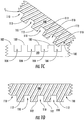
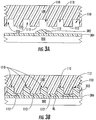
- a patterned master 100 is provided.
- Patterned master 100 comprises a plurality of non-recessed surface areas 102 and a plurality of recesses 104.
- patterned master 100 comprises an etched substrate, such as a silicon wafer, which is etched in the desired pattern to form patterned master 100.
- a liquid material 106 for example, a liquid fluoropolymer composition, such as a PFPE-based precursor, is then poured onto patterned master 100.
- Liquid material 106 is treated by treating process T r , for example exposure to UV light, thereby forming a treated liquid material 108 in the desired pattern.
- treated liquid material 108 comprises a plurality of recesses 110, which are mirror images of the plurality of non-recessed surface areas 102 of patterned master 100.
- treated liquid material 108 comprises a plurality of first patterned surface areas 112, which are mirror images of the plurality of recesses 104 of patterned master 100.
- Treated liquid material 108 can now be used as a patterned template for soft lithography and imprint lithography applications.
- treated liquid material 108 can be used as a patterned template for the formation of isolated micro- and nanoparticles.
- Figures 1A-1D , 2A-2E , and 3A-3F the numbering scheme for like structures is retained throughout.
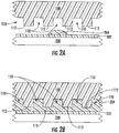
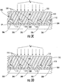
- a substrate 200 for example, a silicon wafer, is treated or is coated with a non-wetting material 202.
- non-wetting material 202 comprises an elastomer (such a solvent resistant elastomer, including but not limited to a PFPE elastomer) that can be further exposed to UV light and cured to form a thin, non-wetting layer on the surface of substrate 200.
- Substrate 200 also can be made non-wetting by treating substrate 200 with non-wetting agent 202, for example a small molecule, such as an alkyl- or fluoroalkyl-silane, or other surface treatment.
- a droplet 204 of a curable resin, a monomer, or a solution in which the desired particles will be formed is then placed on the coated substrate 200.
- patterned template 108 (as shown in Figure 1D ) is then contacted with droplet 204 so that droplet 204 fills the plurality of recessed areas 110 of patterned template 108.
- a force F a is applied to patterned template 108. While not wishing to be bound by any particular theory, once force F a is applied, the affinity of patterned template 108 for non-wetting coating or surface treatment 202 on substrate 200 in combination with the non-wetting behavior of patterned template 108 and surface treated or coated substrate 200 causes droplet 204 to be excluded from all areas except for recessed areas 110. Further, in embodiments essentially free of non-wetting or low wetting material 202 with which to sandwich droplet 204, a "scum" layer that interconnects the objects being stamped forms.
- the material filling recessed areas 110 e.g., a resin, monomer, solvent, and combinations thereof, is then treated by a treating process T r , e.g., photocured through patterned template 108 or thermally cured while under pressure, to form a plurality of micro- and/or nanoparticles 206.
- a material including but not limited to a polymer, an organic compound, or an inorganic compound, can be dissolved in a solvent, patterned using patterned template 108, and the solvent can be released.
- patterned template 108 is removed from substrate 200.
- Micro- and/or nanoparticles 206 are confined to recessed areas 110 of patterned template 108.
- micro- and/or nanoparticles 206 can be retained on substrate 200 in defined regions once patterned template 108 is removed.
- This embodiment can be used in the manufacture of semiconductor devices where essentially scum-layer free features could be used as etch barriers or as conductive, semiconductive, or dielectric layers directly, mitigating or reducing the need to use traditional and expensive photolithographic processes.
- micro- and/or nanoparticles 206 can be removed from patterned template 108 to provide freestanding particles by a variety of methods, which include but are not limited to: (1) applying patterned template 108 to a surface that has an affinity for the particles 206; (2) deforming patterned template 108, or using other mechanical methods, including sonication, in such a manner that the particles 206 are naturally released from patterned template 108; (3) swelling patterned template 108 reversibly with supercritical carbon dioxide or another solvent that will extrude the particles 206; and (4) washing patterned template 108 with a solvent that has an affinity for the particles 206 and will wash them out of patterned template 108.
- the method comprises a batch process.
- the batch process is selected from one of a semi-batch process and a continuous batch process.
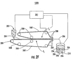
- FIG 2F an embodiment of the presently disclosed subject matter wherein particles 206 are produced in a continuous process is schematically presented.
- An apparatus 199 is provided for carrying out the process. Indeed, while Figure 2F schematically presents a continuous process for particles, apparatus 199 can be adapted for batch processes, and for providing a pattern on a substrate continuously or in batch, in accordance with the presently disclosed subject matter and based on a review of the presently disclosed subject matter by one of ordinary skill in the art.
- droplet 204 of liquid material is applied to substrate 200' via reservoir 203.
- Substrate 202' can be coated or not coated with a non-wetting agent.
- Substrate 200' and pattern template 108' are placed in a spaced relationship with respect to each other and are also operably disposed with respect to each other to provide for the conveyance of droplet 204 between patterned template 108' and substrate 200'. Conveyance is facilitated through the provision of pulleys 208, which are in operative communication with controller 201.
- controller 201 can comprise a computing system, appropriate software, a power source, a radiation source, and/or other suitable devices for controlling the functions of apparatus 199.
- controller 201 provides for power for and other control of the operation of pulleys 208 to provide for the conveyance of droplet 204 between patterned template 108' and substrate 200'.
- Particles 206 are formed and treated between substrate 200' and patterned template 108' by a treating process T R , which is also controlled by controller 201.
- Particles 206 are collected in an inspecting device 210, which is also controlled by controller 201.
- Inspecting device 210 provides for one of inspecting, measuring, and both inspecting and measuring one or more characteristics of particles 206. Representative examples of inspecting devices 210 are disclosed elsewhere herein.
- the method for forming one or more particles comprises:
- the patterned template comprises a solvent resistant, low surface energy polymeric material derived from casting low viscosity liquid materials onto a master template and then curing the low viscosity liquid materials to generate a patterned template.
- the patterned template comprises a solvent resistant elastomeric material.
- At least one of the patterned template and substrate comprises a material selected from the group consisting of a perfluoropolyether material, a fluoroolefin material, an acrylate material, a silicone material, a styrenic material, a fluorinated thermoplastic elastomer (TPE), a triazine fluoropolymer, a perfluorocyclobutyl material, a fluorinated epoxy resin, and a fluorinated monomer or fluorinated oligomer that can be polymerized or crosslinked by a metathesis polymerization reaction.
- the perfluoropolyether material comprises a backbone structure selected from the group consisting of: wherein X is present or absent, and when present comprises an endcapping group.
- the fluoroolefin material is selected from the group consisting of: and wherein CSM comprises a cure site monomer.
- the fluoroolefin material is made from monomers which comprise tetrafluoroethylene, vinylidene fluoride or hexafluoropropylene. 2,2-bis(trifluoromethyl)-4,5-difluoro-1,3-dioxole, a functional fluoroolefin, functional acrylic monomer, a functional methacrylic monomer.
- the silicone material comprises a fluoroalkyl functionalized polydimethylsiloxane (PDMS) having the following structure: wherein:
- the styrenic material comprises a fluorinated styrene monomer selected from the group consisting of: wherein Rf comprises a fluoroalkyl chain.
- the acrylate material comprises a fluorinated acrylate or a fluorinated methacrylate having the following structure: wherein:
- the triazine fluoropolymer comprises a fluorinated monomer.
- the fluorinated monomer or fluorinated oligomer that can be polymerized or crosslinked by a metathesis polymerization reaction comprises a functionalized olefin.
- the functionalized olefin comprises a functionalized cyclic olefin.
- At least one of the patterned template and the substrate has a surface energy lower than 18 mN/m. In some embodiments, at least one of the patterned template and the substrate has a surface energy lower than 15 mN/m.
- the substrate is selected from the group consisting of a polymer material, an inorganic material, a silicon material, a quartz material, a glass material, and surface treated variants thereof. In some embodiments, the substrate comprises a patterned area.
- the plurality of recessed areas comprises a plurality of cavities. In some embodiments, the plurality of cavities comprises a plurality of structural features. In some embodiments, the plurality of structural features has a dimension ranging from about 10 microns to about 1 nanometer in size. In some embodiments, the plurality of structural features has a dimension ranging from about 10 microns to about 1 micron in size. In some embodiments, the plurality of structural features has a dimension ranging from about 1 micron to about 100 nm in size. In some embodiments, the plurality of structural features has a dimension ranging from about 100 nm to about 1 nm in size.
- the patterned template comprises a patterned template formed by a replica molding process.
- the replica molding process comprises: providing a master template; contacting a liquid material with the master template; and curing the liquid material to form a patterned template.
- the master template is selected from the group consisting of: a template formed from a lithography process; a naturally occurring template; and combinations thereof.
- the natural template is selected from one of a biological structure and a self-assembled structure.
- the one of a biological structure and a self-assembled structure is selected from the group consisting of a naturally occurring crystal, an enzyme, a virus, a protein, a micelle, and a tissue surface.
- the method comprises modifying the patterned template surface by a surface modification step.
- the surface modification step is selected from the group consisting of a plasma treatment, a chemical treatment, and an adsorption process.
- the adsorption process comprises adsorbing molecules selected from the group consisting of a polyelectrolyte, a poly(vinylalcohol), an alkylhalosilane, and a ligand.
- the method comprises positioning the patterned template and the substrate in a spaced relationship to each other such that the patterned template surface and the substrate face each other in a predetermined alignment.
- the liquid material is selected from the group consisting of a polymer, a solution, a monomer, a plurality of monomers, a polymerization initiator, a polymerization catalyst, an inorganic precursor, a metal precursor, a pharmaceutical agent, a tag, a magnetic material, a paramagnetic material, a ligand, a cell penetrating peptide, a porogen, a surfactant, a plurality of immiscible liquids, a solvent, a charged species, and combinations thereof.
- the pharmaceutical agent is selected from the group consisting of a drug, a peptide, RNAi, and DNA.
- the tag is selected from the group consisting of a fluorescence tag, a radiolabeled tag, and a contrast agent.
- the ligand comprises a cell targeting peptide.
- the liquid material comprises a non-wetting agent. In some embodiments, the liquid material comprises one phase. In some embodiments, the liquid material comprises a plurality of phases. In some embodiments, the liquid material is selected from the group consisting of multiple liquids, multiple immiscible liquids, surfactants, dispersions, emulsions, micro-emulsions, micelles, particulates, colloids, porogens, active ingredients, and combinations thereof.
- the disposing of the volume of liquid material on one of the patterned template and the substrate is regulated by a spreading process.
- the spreading process comprises:
- an article is contacted with the layer of liquid material and a force is applied to the article to thereby remove the liquid material from the one of the patterned material and the substrate.
- the article is selected from the group consisting of a roller and a "squeegee" blade.
- the liquid material is removed by some other mechanical means.
- the contacting of the patterned template surface with the substrate forces essentially all of the disposed liquid material from between the patterned template surface and the substrate.
- the treating of the liquid material comprises a process selected from the group consisting of a thermal process, a photochemical process, and a chemical process.
- the method further comprises:
- the releasing of the one or more particles is performed by one of:
- the method comprises harvesting or collecting the particles.
- the harvesting or collecting of the particles comprises a process selected from the group consisting of scraping with a doctor blade, a brushing process, a dissolution process, an ultrasound process, a megasonics process, an electrostatic process, and a magnetic process.
- the presently disclosed subject matter describes a particle or plurality of particles formed by the methods described herein.
- the plurality of particles comprises a plurality of monodisperse particles.
- the particle or plurality of particles is selected from the group consisting of a semiconductor device, a crystal, a drug delivery vector, a gene delivery vector, a disease detecting device, a disease locating device, a photovoltaic device, a porogen, a cosmetic, an electret, an additive, a catalyst, a sensor, a detoxifying agent, an abrasive, such as a CMP, a micro-electro-mechanical system (MEMS), a cellular scaffold, a taggart, a pharmaceutical agent, and a biomarker.
- the particle or plurality of particles comprise a freestanding structure.
- the presently disclosed subject matter describes a method of fabricating isolated liquid objects, the method comprising (a) contacting a liquid material with the surface of a first low surface energy material; (b) contacting the surface of a second low surface energy material with the liquid, wherein at least one of the surfaces of either the first or second low surface energy material is patterned; (c) sealing the surfaces of the first and the second low surface energy materials together; and (d) separating the two low surface energy materials to produce a replica pattern comprising liquid droplets.
- the liquid material comprises poly(ethylene glycol)-diacrylate.
- the low surface energy material comprises perfluoropolyether-diacrylate.
- a chemical process is used to seal the surfaces of the first and the second low surface energy materials.
- a physical process is used to seal the surfaces of the first and the second low surface energy materials.
- one of the surfaces of the low surface energy material is patterned. In some embodiments, one of the surfaces of the low surface energy material is not patterned.
- the method further comprises using the replica pattern composed of liquid droplets to fabricate other objects.
- the replica pattern of liquid droplets is formed on the surface of the low surface energy material that is not patterned.
- the liquid droplets undergo direct or partial solidification.
- the liquid droplets undergo a chemical transformation.
- the solidification of the liquid droplets or the chemical transformation of the liquid droplets produce freestanding objects.
- the freestanding objects are harvested.
- the freestanding objects are bonded in place.
- the freestanding objects are directly solidified, partially solidified, or chemically transformed.
- the liquid droplets are directly solidified, partially solidified, or chemically transformed on or in the patterned template to produce objects embedded in the recesses of the patterned template.
- the embedded objects are harvested.
- the embedded objects are bonded in place.
- the embedded objects are used in other fabrication processes.
- the replica pattern of liquid droplets is transferred to other surfaces. In some embodiments, the transfer takes place before the solidification or chemical transformation process. In some embodiments, the transfer takes place after the solidification or chemical transformation process. In some embodiments, the surface to which the replica pattern of liquid droplets is transferred is selected from the group consisting of a non-low surface energy surface, a low surface energy surface, a functionalized surface, and a sacrificial surface. In some embodiments, the method produces a pattern on a surface that is essentially free of one or more scum layers. In some embodiments, the method is used to fabricate semiconductors and other electronic and photonic devices or arrays. In some embodiments, the method is used to create freestanding objects.
- the method is used to create three-dimensional objects using multiple patterning steps.
- the isolated or patterned object comprises materials selected from the group consisting of organic, inorganic, polymeric, and biological materials.
- a surface adhesive agent is used to anchor the isolated structures on a surface.
- the liquid droplet arrays or solid arrays on patterned or non-patterned surfaces are used as regiospecific delivery devices or reaction vessels for additional chemical processing steps.
- the additional chemical processing steps are selected from the group consisting of printing of organic, inorganic, polymeric, biological, and catalytic systems onto surfaces; synthesis of organic, inorganic, polymeric, biological materials; and other applications in which localized delivery of materials to surfaces is desired.
- Applications of the presently disclosed subject matter include, but are not limited to, micro and nanoscale patterning or printing of materials.
- the materials to be patterned or printed are selected from the group consisting of surface-binding molecules, inorganic compounds, organic compounds, polymers, biological molecules, nanoparticles, viruses, biological arrays, and the like.
- the applications of the presently disclosed subject matter include, but are not limited to, the synthesis of polymer brushes, catalyst patterning for CVD carbon nanotube growth, cell scaffold fabrication, the application of patterned sacrificial layers, such as etch resists, and the combinatorial fabrication of organic, inorganic, polymeric, and biological arrays.
- non-wetting imprint lithography, and related techniques are combined with methods to control the location and orientation of chemical components within an individual object. In some embodiments, such methods improve the performance of an object by rationally structuring the object so that it is optimized for a particular application.
- the method comprises incorporating biological targeting agents into particles for drug delivery, vaccination, and other applications.
- the method comprises designing the particles to include a specific biological recognition motif.
- the biological recognition motif comprises biotin/avidin and/or other proteins.
- the method comprises tailoring the chemical composition of these materials and controlling the reaction conditions, whereby it is then possible to organize the biorecognition motifs so that the efficacy of the particle is optimized.
- the particles are designed and synthesized so that recognition elements are located on the surface of the particle in such a way to be accessible to cellular binding sites, wherein the core of the particle is preserved to contain bioactive agents, such as therapeutic molecules.
- a non-wetting imprint lithography method is used to fabricate the objects, wherein the objects are optimized for a particular application by incorporating functional motifs, such as biorecognition agents, into the object composition.
- the method further comprises controlling the microscale and nanoscale structure of the object by using methods selected from the group consisting of self-assembly, stepwise fabrication procedures, reaction conditions, chemical composition, crosslinking, branching, hydrogen bonding, ionic interactions, covalent interactions, and the like.
- the method further comprises controlling the microscale and nanoscale structure of the object by incorporating chemically organized precursors into the object.
- the chemically organized precursors are selected from the group consisting of block copolymers and core-shell structures.
- the presently disclosed subject matter describes a non-wetting imprint lithography technique that is scalable and offers a simple, direct route to such particles without the use of self-assembled, difficult to fabricate block copolymers and other systems.
- the presently disclosed subject matter provides a "liquid reduction" process for forming particles that have shapes that are not conformal to the shape of the template, including but not limited to spherical micro- and nanoparticles.
- a "cube-shaped” template can allow for sphereical particles to be made
- a “Block arrow-shaped” template can allow for "lolli-pop" shaped particles or objects to be made wherein the introduction of a gas allows surface tension forces to reshape the resident liquid prior to treating it.
- the non-wetting characteristics that can be provided in some embodiments of the presently disclosed patterned template and/or treated or coated substrate allows for the generation of rounded, e.g., spherical, particles.
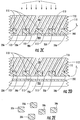
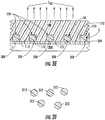
- droplet 302 of a liquid material is disposed on substrate 300, which in some embodiments is coated or treated with a non-wetting material 304.
- a patterned template 108 which comprises a plurality of recessed areas 110 and patterned surface areas 112, also is provided.
- patterned template 108 is contacted with droplet 302.
- the liquid material comprising droplet 302 then enters recessed areas 110 of patterned template 108.
- a residual, or "scum,” layer RL of the liquid material comprising droplet 302 remains between the patterned template 108 and substrate 300.
- a first force F a1 is applied to patterned template 108.
- a contact point CP is formed between the patterned template 108 and the substrate and displacing residual layer RL.
- Particles 306 are formed in the recessed areas 110 of patterned template 108.
- a second force F a2 wherein the force applied by F a2 is greater than the force applied by F a1 , is then applied to patterned template 108, thereby forming smaller liquid particles 308 inside recessed areas 112 and forcing a portion of the liquid material comprising droplet 302 out of recessed areas 112.
- patterned template 108 comprises a gas permeable material, which allows a portion of space with recessed areas 112 to be filled with a gas, such as nitrogen, thereby forming a plurality of liquid spherical droplets 310. Once this liquid reduction is achieved, the plurality of liquid spherical droplets 310 are treated by a treating process T r .
- treated liquid spherical droplets 310 are released from patterned template 108 to provide a plurality of freestanding spherical particles 312.
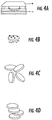
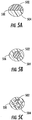
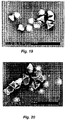
- the presently disclosed subject matter describes a method for preparing polymeric nano- to micro-electrets by applying an electric field during the polymerization and/or crystallization step during molding ( Figure 4A ) to yield a charged polymeric particle ( Figure 4B ).
- the charged polymeric particles spontaneously aggregate into chain-like structures ( Figure 4D ) instead of the random configurations shown in Figure 4C .
- the charged polymeric particle comprises a polymeric electret. In some embodiments, the polymeric electret comprises a polymeric nano-electret. In some embodiments, the charged polymeric particles aggregate into chain-like structures. In some embodiments, the charged polymeric particles comprise an additive for an electro-rheological device. In some embodiments, the electro-rheological device is selected from the group consisting of clutches and active dampening devices. In some embodiments, the charged polymeric particles comprise nano-piezoelectric devices. In some embodiments, the nano-piezoelectric devices are selected from the group consisting of actuators, switches, and mechanical sensors.
- the presently disclosed subject matter provides a method for forming multilayer structures, including multilayer particles.
- the multilayer structures, including multilayer particles comprise nanoscale multilayer structures.
- multilayer structures are formed by depositing multiple thin layers of immisible liquids and/or solutions onto a substrate and forming particles as described by any of the methods hereinabove. The immiscibility of the liquid can be based on any physical characteristic, including but not limited to density, polarity, and volatility.
- Figures 5A-5C Examples of possible morphologies of the presently disclosed subject matter are illustrated in Figures 5A-5C and include, but are not limited to, multi-phase sandwich stuctures, core-shell particles, and internal emulsions, microemulsions and/or nano-sized emulsions.
- a multi-phase sandwich structure 500 of the presently disclosed subject matter is shown, which by way of example, comprises a first liquid material 502 and a second liquid material 504.
- a core-shell particle 506 of the presently disclosed subject matter is shown, which by way of example, comprises a first liquid material 502 and a second liquid material 504.
- an internal emulsion particle 508 of the presently disclosed subject matter is shown, which by way of example, comprises a first liquid material 502 and a second liquid material 504.
- the method comprises disposing a plurality of immiscible liquids between the patterned template and substrate to form a multilayer structure, e.g., a multilayer nanostructure.
- the multilayer structure comprises a multilayer particle.
- the multilayer structure comprises a structure selected from the group consisting of multi-phase sandwich structures, core-shell particles, internal emulsions, microemulsions, and nanosized emulsions.
- the currently disclosed subject matter provides a process for fabricating complex, multi-dimensional structures.
- complex multi-dimensional structures can be formed by performing the steps illustrated in Figures 2A-2E .
- the method comprises imprinting onto a patterned template that is aligned with a second patterned template (instead of imprinting onto a smooth substrate) to generate isolated multi-dimensional structures that are cured and released as described herein.
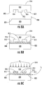
- a schematic illustration of an embodiment of a process for forming complex multi-dimensional structures and examples of such structures are provided in Figures 6A-6C .
- First patterned template 600 comprises a plurality of recessed areas 602 and a plurality of non-recessed surfaces 604. Also provided is a second patterned template 606. Second patterned template 606 comprises a plurality of recessed areas 608 and a plurality of non-recessed surfaces 610. As shown in Figure 6A , first patterned template 600 and second patterned template 606 are aligned in a predetermined spaced relationship. A droplet of liquid material 612 is disposed between first patterned template 600 and second patterned template 606.
- patterned template 600 is contacted with patterned template 606.
- a force F a is applied to patterned template 600 causing the liquid material comprising droplet 612 to migrate to the plurality of recessed areas 602 and 608.
- the liquid material comprising droplet 612 is then treated by treating process T r to form a patterned, treated liquid material 614.
- the patterned, treated liquid material 614 of Figure 6B is released by any of the releasing methods described herein to provide a plurality of multi-dimensional patterned structures 616.
- patterned structure 616 comprises a nanoscale-patterned structure. In some embodiments, patterned structure 616 comprises a multi-dimensional structure. In some embodiments, the multi-dimensional structure comprises a nanoscale multi-dimensional structure. In some embodiments, the multi-dimensional structure comprises a plurality of structural features. In some embodiments, the structural features comprise a plurality of heights.
- a microelectronic device comprising patterned structure 616 is provided.
- patterned structure 616 can be any structure imaginable, including "dual damscene" structures for microelectronics.
- the microelectronic device is selected from the group consisting of integrated circuits, semiconductor particles, quantum dots, and dual damascene structures.
- the microelectronic device exhibits certain physical properties selected from the group consisting of etch resistance, low dielectric constant, high dielectric constant, conducting, semiconducting, insulating, porosity, and non-porosity.
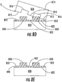
- First patterned template 700 comprises a plurality of non-recessed surface areas 702 and a plurality of recessed surface areas 704.
- substrate 706 is coated with a non-wetting agent 708.
- a droplet of a first liquid material 710 is disposed on substrate 706.
- first patterned template 700 is contacted with substrate 706.
- a force F a is applied to first patterned template 700 such that the droplet of the first liquid material 710 is forced into recesses 704.
- the liquid material comprising the droplet of first liquid material 710 is treated by a first treating process T r1 to form a treated first liquid material within the plurality of recesses 704.
- first treating process T r1 comprises a partial curing process causing the treated first liquid material to adhere to substrate 706.
- first patterned template 700 is removed to provide a plurality of structural features 712 on substrate 706.
- Second patterned substrate 714 comprises a plurality of recesses 716, which are filled with a second liquid material 718.
- the filling of recesses 716 can be accomplished in a manner similar to that described in Figures 7A and 7B with respect to recesses 704.
- second patterned template 714 is contacted with structural features 712.
- Second liquid material 718 is treated with a second treating process T r2 such that the second liquid material 718 adheres to the plurality of structural feature 712, thereby forming a multidimensional structure 720.
- second patterned template 714 and substrate 706 are removed, providing a plurality of free standing multidimensional structures 722.
- the process schematically presented in Figures 7A-7F can be carried out multiple times as desired to form intricate nanostructures.
- a method for forming multidimensional structures comprising:
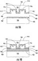
- FIGS 8A-8D a method for forming a pattern on a substrate is illustrated.
- an imprint lithography technique is used to form a pattern on a substrate.
- patterned template 810 comprises a solvent resistant, low surface energy polymeric material, derived from casting low viscosity liquid materials onto a master template and then curing the low viscosity liquid materials to generate a patterned template as defined hereinabove.
- Patterned template 810 further comprises a first patterned template surface 812 and a second template surface 814.
- the first patterned template surface 812 further comprises a plurality of recesses 816.
- the patterned template derived from a solvent resistant, low surface energy polymeric material could be mounted on another material to facilitate alignment of the patterned template or to facilitate continuous processing such as a conveyor belt. This might be particularly useful in the fabrication of precisely placed structures on a surface, such as in the fabrication of a complex devices or a semiconductor, electronic or photonic devices.
- a substrate 820 is provided.
- Substrate 820 comprises a substrate surface 822.
- substrate 820 is selected from the group consisting of a polymer material, an inorganic material, a silicon material, a quartz material, a glass material, and surface treated variants thereof.
- at least one of patterned template 810 and substrate 820 has a surface energy lower than 18 mN/m. In some embodiments, at least one of patterned template 810 and substrate 820 has a surface energy lower than 15 mN/m.
- patterned template 810 and substrate 820 are positioned in a spaced relationship to each other such that first patterned template surface 812 faces substrate surface 822 and a gap 830 is created between first patterned template surface 812 and substrate surface 822. This is an example of a predetermined relationship.
- a volume of liquid material 840 is disposed in the gap 830 between first patterned template surface 82 and substrate surface 822.
- the volume of liquid material 840 is disposed directed on a non-wetting agent (not shown), which is disposed on first patterned template surface 812.
- first patterned template 812 is contacted with the volume of liquid material 840.
- a force F a is applied to second template surface 814 thereby forcing the volume of liquid material 840 into the plurality of recesses 816.
- a portion of the volume of liquid material 840 remains between first patterned template surface 812 and substrate surface 820 after force F a is applied.
- treating process T r comprises a process selected from the group consisting of a thermal process, a photochemical process, and a chemical process.
- a force F r is applied to patterned template 810 to remove patterned template 810 from treated liquid material 842 to reveal a pattern 850 on substrate 820 as shown in Figure 8E .
- a residual, or "scum,” layer 852 of treated liquid material 842 remains on substrate 820.
- the method for forming a pattern on a substrate comprises:
- the patterned template comprises a solvent resistant, low surface energy polymeric material derived from casting low viscosity liquid materials onto a master template and then curing the low viscosity liquid materials to generate a patterned template.
- the patterned template comprises a solvent resistant elastomeric material.
- At least one of the patterned template and substrate comprises a material selected from the group consisting of a perfluoropolyether material, a fluoroolefin material, an acrylate material, a silicone material, a styrenic material, a fluorinated thermoplastic elastomer (TPE), a triazine fluoropolymer, a perfluorocyclobutyl material, a fluorinated epoxy resin, and a fluorinated monomer or fluorinated oligomer that can be polymerized or crosslinked by a metathesis polymerization reaction.
- the perfluoropolyether material comprises a backbone structure selected from the group consisting of: wherein X is present or absent, and when present comprises an endcapping group.
- the fluoroolefin material is selected from the group consisting of: and wherein CSM comprises a cure site monomer.
- the fluoroolefin material is made from monomers, which comprise tetrafluoroethylene, vinylidene fluoride or hexafluoropropylene. 2,2-bis(trifluoromethyl)-4,5-difluoro-1,3-dioxole, a functional fluoroolefin, functional acrylic monomer, a functional methacrylic monomer.
- the silicone material comprises a fluoroalkyl functionalized polydimethylsiloxane (PDMS) having the following structure: wherein:
- the styrenic material comprises a fluorinated styrene monomer selected from the group consisting of: wherein Rf comprises a fluoroalkyl chain.
- the acrylate material comprises a fluorinated acrylate or a fluorinated methacrylate having the following structure: wherein:
- the triazine fluoropolymer comprises a fluorinated monomer.
- the fluorinated monomer or fluorinated oligomer that can be polymerized or crosslinked by a metathesis polymerization reaction comprises a functionalized olefin.
- the functionalized olefin comprises a functionalized cyclic olefin.
- At least one of the patterned template and the substrate has a surface energy lower than 18 mN/m. In some embodiments, at least one of the patterned template and the substrate has a surface energy lower than 15 mN/m.
- the substrate is selected from the group consisting of a polymer material, an inorganic material, a silicon material, a quartz material, a glass material, and surface treated variants thereof.
- the substrate is selected from one of an electronic device in the process of being manufactured and a photonic device in the process of being manufactured.
- the substrate comprises a patterned area.
- the plurality of recessed areas comprises a plurality of cavities. In some embodiments, the plurality of cavities comprise a plurality of structural features. In some embodiments, the plurality of structural features has a dimension ranging from about 10 microns to about 1 nanometer in size. In some embodiments, the plurality of structural features has a dimension ranging from about 10 microns to about 1 micron in size. In some embodiments, the plurality of structural features has a dimension ranging from about 1 micron to about 100 nm in size. In some embodiments, the plurality of structural features has a dimension ranging from about 100 nm to about 1 nm in size.
- the liquid material is selected from the group consisting of a polymer, a solution, a monomer, a plurality of monomers, a polymerization initiator, a polymerization catalyst, an inorganic precursor, a metal precursor, a pharmaceutical agent, a tag, a magnetic material, a paramagnetic material, a superparamagnetic material, a ligand, a cell penetrating peptide, a porogen, a surfactant, a plurality of immiscible liquids, a solvent, and a charged species.
- the pharmaceutical agent is selected from the group consisting of a drug, a peptide, RNAi, and DNA.
- the tag is selected from the group consisting of a fluorescence tag, a radiolabeled tag, and a contrast agent.
- the ligand comprises a cell targeting peptide.
- Representative superparamagnetic or paramagnetic materials include but are not limited to Fe 2 O 3 , Fe 3 O 4 , FePt, Co, MnFe 2 O 4 , CoFe 2 O 4 , CuFe 2 O 4 , NiFe 2 O 4 and ZnS doped with Mn for magneto-optical applications, CdSe for optical applications, and borates for boron neutron capture treatment.
- the liquid material is selected from one of a resist polymer and a low-k dielectric. In some embodiments, the liquid material comprises a non-wetting agent.
- the disposing of the volume of liquid material is regulated by a spreading process.
- the spreading process comprises:
- the treating of the liquid material comprises a process selected from the group consisting of a thermal process, a photochemical process, and a chemical process.
- the method comprises a batch process.
- the batch process is selected from one of a semi-batch process and a continuous batch process.
- the presently disclosed subject matter describes a patterned substrate formed by the presently disclosed methods.
- a characteristic of imprint lithography that has restrained its full potential is the formation of a "scum layer” once the liquid material, e.g., a resin, is patterned.
- the "scum layer” comprises residual liquid material that remains between the stamp and the substrate.
- the presently disclosed subject matter provides a process for generating patterns essentially free of a scum layer.
- a method for forming a pattern on a substrate wherein the pattern is essentially free of a scum layer.
- a patterned template 910 is provided. Patterned template 910 further comprises a first patterned template surface 912 and a second template surface 914. The first patterned template surface 912 further comprises a plurality of recesses 916.
- a non-wetting agent 960 is disposed on the first patterned template surface 912.
- a substrate 920 is provided.
- Substrate 920 comprises a substrate surface 922.
- a non-wetting agent 960 is disposed on substrate surface 920.
- patterned template 910 and substrate 920 are positioned in a spaced relationship to each other such that first patterned template surface 912 faces substrate surface 922 and a gap 930 is created between first patterned template surface 912 and substrate surface 922.
- a volume of liquid material 940 is disposed in the gap 930 between first patterned template surface 912 and substrate surface 922.
- the volume of liquid material 940 is disposed directly on first patterned template surface 912.
- the volume of liquid material 940 is disposed directly on non-wetting agent 960, which is disposed on first patterned template surface 912.
- the volume of liquid material 940 is disposed directly on substrate surface 920.
- the volume of liquid material 940 is disposed directly on non-wetting agent 960, which is disposed on substrate surface 920.
- first patterned template 912 is contacted with the volume of liquid material 940.
- a force F a is applied to second template surface 914 thereby forcing the volume of liquid material 940 into the plurality of recesses 916.
- a portion of the volume of liquid material 940 is forced out of gap 930 by force F o when force F a is applied.
- the volume of liquid material 940 is treated by a treating process T while force F a is being applied to form a treated liquid material 942.
- a force F r is applied to patterned template 9 10 to remove patterned template 910 from treated liquid material 942 to reveal a pattern 950 on substrate 920 as shown in Figure 9E .
- substrate 920 is essentially free of a residual, or "scum,” layer of treated liquid material 942.
- the template surface and substrate comprises a functionalized surface element.
- the functionalized surface element is functionalized with a non-wetting material.
- the non-wetting material comprises functional groups that bind to the liquid material.
- the non-wetting material is selected from the group consisting of a trichloro silane, a trialkoxy silane, a trichloro silane comprising non-wetting and reactive functional groups, a trialkoxy silane comprising non-wetting and reactive functional groups, and mixtures thereof.
- the point of contact between the two surface elements is free of liquid material. In some embodiments, the point of contact between the two surface elements comprises residual liquid material. In some embodiments, the height of the residual liquid material is less than 30% of the height of the structure. In some embodiments, the height of the residual liquid material is less than 20% of the height of the structure. In some embodiments, the height of the residual liquid material is less than 10% of the height of the structure. In some embodiments, the height of the residual liquid material is less than 5% of the height of the structure. In some embodiments, the volume of liquid material is less than the volume of the patterned template. In some embodiments, substantially all of the volume of liquid material is confined to the patterned template of at least one of the surface elements. In some embodiments, having the point of contact between the two surface elements free of liquid material retards slippage between the two surface elements.
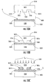
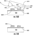
- the presently disclosed subject matter describes a solvent-assisted micro-molding (SAMIM) method for forming a pattern on a substrate.
- SAMIM solvent-assisted micro-molding
- Patterned template 1010 further comprises a first patterned template surface 1012 and a second template surface 1014.
- the first patterned template surface 1012 further comprises a plurality of recesses 1016.
- a substrate 1020 is provided.
- Substrate 1020 comprises a substrate surface 1022.
- a polymeric material 1070 is disposed on substrate surface 1022.
- polymeric material 1070 comprises a resist polymer.
- patterned template 1010 and substrate 1020 are positioned in a spaced relationship to each other such that first patterned template surface 1012 faces substrate surface 1022 and a gap 1030 is created between first patterned template surface 1012 and substrate surface 1022.
- a solvent S is disposed within gap 1030, such that solvent S contacts polymeric material 1070 forming a swollen polymeric material 1072.
- first patterned template 1012 is contacted with swollen polymeric material 1072.
- a force F a is applied to second template surface 1014 thereby forcing a portion of swollen polymeric material 1072 into the plurality of recesses 1016 and leaving a portion of swollen polymeric material 1072 between first patterned template surface 1012 and substrate surface 1020.
- the swollen polymeric material 1072 is then treated by a treating process T r while under pressure.
- a force F r is applied to patterned template 1010 to remove patterned template 1010 from treated swollen polymeric material 1072 to reveal a polymeric pattern 1074 on substrate 1020 as shown in Figure 10E .
- the patterned structure (e.g., a patterned micro- or nanostructure) is removed from at least one of the patterned template and/or the substrate.
- This can be accomplished by a number of approaches, including but not limited to applying the surface element containing the patterned structure to a surface that has an affinity for the patterned structure; deforming the surface element containing the patterned structure such that the patterned structure is released from the surface element; swelling the surface element containing the patterned structure with a first solvent to extrude the patterned structure; and washing the surface element containing the patterned structure with a second solvent that has an affinity for the patterned structure.
- the first solvent comprises supercritical fluid carbon dioxide. In some embodiments, the first solvent comprises water. In some embodiments, the first solvent comprises an aqueous solution comprising water and a detergent. In embodiments, the deforming the surface element is performed by applying a mechanical force to the surface element. In some embodiments, the method of removing the patterned structure further comprises a sonication method.
- the presently disclosed subject matter describes methods and processes, and products by processes, for fabricating "molecules," for use in drug discovery and drug therapies.
- the method or process for fabricating a molecule comprises a combinatorial method or process.
- the method for fabricating molecules comprises a non-wetting imprint lithography method.
- the non-wetting imprint lithography method further comprises a surface derived from or comprising a solvent resistant, low surface energy polymeric material derived from casting low viscosity liquid materials onto a master template and then curing the low viscosity liquid materials to generate a patterned template.
- the surface comprises a solvent resistant elastomeric material.
- the non-wetting imprint lithography method is used to generate isolated structures.
- the isolated structures comprise isolated microstructures.
- the isolated structures comprise isolated nano-structures.
- the isolated structures comprise a biodegradable material.
- the isolated structures comprise a hydrophilic material.
- the isolated structures comprise a hydrophobic material.
- the isolated structures comprise a particular shape. In some embodiments, the isolated structures further comprise "cargo.”
- the non-wetting imprint lithography method further comprises adding molecular modules, fragments, or domains to the solution to be molded.
- the molecular modules, fragments, or domains impart functionality to the isolated structures.
- the functionality imparted to the isolated structure comprises a therapeutic functionality.
- a therapeutic agent such as a drug
- the physiologically active drug is tethered to a linker to facilitate its incorporation into the isolated structure.
- the domain of an enzyme or a catalyst is added to the isolated structure.
- a ligand or an oligopeptide is added to the isolated structure.
- the oligopeptide is functional.
- the functional oligopeptide comprises a cell targeting peptide.
- the functional oligopeptide comprises a cell penetrating peptide.
- an antibody or functional fragment thereof is added to the isolated structure.
- a binder is added to the isolated structure.
- the isolated structure comprising the binder is used to fabricate identical structures.
- the isolated structure comprising the binder is used to fabricate structures of a varying structure.
- the structures of a varying structure are used to explore the efficacy of a molecule as a therapeutic agent.
- the shape of the isolated structure mimics a biological agent.
- the method further comprises a method for drug discovery.
- a method of delivering a therapeutic agent to a target comprising: providing a particle produced as described herein; admixing the therapeutic agent with the particle; and delivering the particle comprising the therapeutic agent to the target.
- the therapeutic agent comprises a drug. In some embodiments, the therapeutic agent comprises genetic material. In some embodiments, the genetic material is selected from the group consisting of a non-viral gene vector, DNA, RNA, RNAi, and a viral particle.
- the particle has a diameter of less than 100 microns. In some embodiments, the particle has a diameter of less than 10 microns. In some embodiments, the particle has a diameter of less than 1 micron. In some embodiments, the particle has a diameter of less than 100 nm. In some embodiments, the particle has a diameter of less than 10 nm.
- the particle comprises a biodegradable polymer.
- the biodegradable polymer is selected from the group consisting of a polyester, a polyanhydride, a polyamide, a phosphorous-based polymer, a poly(cyanoacrylate), a polyurethane, a polyorthoester, a polydihydropyran, and a polyacetal.
- the polyester is selected from the group consisting of polylactic acid, polyglycolic acid, poly(hydroxybutyrate), poly( ⁇ -caprolactone), poly( ⁇ -malic acid), and poly(dioxanones).
- the polyanhydride is selected from the group consisting of poly(sebacic acid), poly(adipic acid), and poly(terpthalic acid).
- the polyamide is selected from the group consisting of poly(imino carbonates) and polyaminoacids.
- the phosphorous-based polymer is selected from the group consisting of polyphosphates, polyphosphonates, and polyphosphazenes.
- the polymer is responsive to stimuli, such as pH, radiation, ionic strength, temperature, and alternating magnetic or electric fields.
- Responses to such stimuli can include swelling and/or heating, which can facilitate release of its cargo, or degradation.
- the presently disclosed subject matter describes magneto containing particles for applications in hyperthermia therapy, cancer and gene therapy, drug delivery, magnetic resonance imaging contrast agents, vaccine adjuvants, memory devices, and spintronics.
- the magneto containing particles e.g., a magnetic nanoparticle
- the heat is used to (i) induce a phase change in the polymer component (for example melt and release an encapsulated material) and/or (ii) hyperthermia treatment of specific cells and/or (iii) increase the effectiveness of the encapsulated material.
- the triggering mechanism of the magnetic nanoparticles via electromagnetic heating enhance the (iv) degradation rate of the particulate; (v) can induce swelling; and/or (vi) induce dissolution/phase change that can lead to a greater surface area, which can be beneficial when treating a variety of diseases.
- the presently disclosed subject matter describes an alternative therapeutic agent delivery method, which utilizes "non-wetting" imprint lithography to fabricate monodisperse magnetic nanoparticles for use in a drug delivery system.
- Such particles can be used for: (1) hyperthermia treatment of cancer cells; (2) MRI contrast agents; (3) guided delivery of the particle; and (4) triggered degradation of the drug delivery vector.
- the therapeutic agent delivery system comprises a biocompatible material and a magnetic nanoparticle.
- the biocompatible material has a melting point below 100 °C.
- the biocompatible material is selected from the group consisting of, but not limited to, a polylactide, a polyglycolide, a hydroxypropylcellulose, and a wax.
- the magnetic nanoparticle is exposed to an AC-magnetic field.
- the exposure to the AC-magnetic field causes the magnetic nanoparticle to undergo a controlled heating.
- the controlled heating is a result of a thermo ablation process.
- the heat is used to induce a phase change in the polymer component of the nanoparticle.
- the phase change comprises a melting process.
- the phase change results in the release of an encapsulated material.
- the release of an encapsulated material comprises a controlled release.
- the controlled release of the encapsulated material results in a concentrated dosing of the therapeutic agent.
- the heating results in the hyperthermic treatment of the target, e.g., specific cells.
- the heating results in an increase in the effectiveness of the encapsulated material.
- the triggering mechanism of the magnetic nanoparticles induced by the electromagnetic heating enhances the degradation rate of the particle and can induce swelling and/or a dissolution/phase change that can lead to a greater surface area which can be beneficial when treating a variety of diseases.
- additional components including drugs, such as an anticancer agent, e.g., nitrogen mustard, cisplatin, and doxorubicin; targeting ligands, such as celltargeting peptides, cell-penetrating peptides, integrin receptor peptide (GRGDSP), melanocyte stimulating hormone, vasoactive intestional peptide, anti-Her2 mouse antibodies, and a variety of vitamins; viruses, polysaccharides, cyclodextrins, proteins, liposomes, optical nanoparticles, such as CdSe for optical applications, and borate nanoparticles to aid in boron neutron capture therapy (BNCT) targets.
- drugs such as an anticancer agent, e.g., nitrogen mustard, cisplatin, and doxorubicin
- targeting ligands such as celltargeting peptides, cell-penetrating peptides, integrin receptor peptide (GRGDSP), melanocyte stimulating hormone, vasoactive intest
- the presently described magnetic containing materials also lend themselves to other applications.
- the magneto-particles can be assembled into well-defined arrays driven by their shape, functionalization of the surface and/or exposure to a magnetic field for investigations of and not limited to magnetic assay devices, memory devices, spintronic applications, and separations of solutions.
- the presently disclosed subject matter provides a method for delivering a therapeutic agent to a target, the method comprising:
- the therapeutic agent is selected from one of a drug and genetic material.
- the genetic material is selected from the group consisting of a non-viral gene vector, DNA, RNA, RNAi, and a viral particle.
- the particle comprises a biodegradable polymer.
- the biodegradable polymer is selected from the group consisting of a polyester, a polyanhydride, a polyamide, a phosphorous-based polymer, a poly(cyanoacrylate), a polyurethane, a polyorthoester, a polydihydropyran, and a polyacetal.
- the polyester is selected from the group consisting of polylactic acid, polyglycolic acid, poly(hydroxybutyrate), poly( ⁇ -caprolactone), poly( ⁇ -malic acid), and poly(dioxanones).
- the polyanhydride is selected from the group consisting of poly(sebacic acid), poly(adipic acid), and poly(terpthalic acid).
- the polyamide is selected from the group consisting of poly(imino carbonates) and polyaminoacids.
- the phosphorous-based polymer is selected from the group consisting of a polyphosphate, a polyphosphonate, and a polyphosphazene.
- the biodegradable polymer further comprises a polymer that is responsive to a stimulus.
- the stimulus is selected from the group consisting of pH, radiation, ionic strength, temperature, an alternating magnetic field, and an alternating electric field. In some embodiments, the stimulus comprises an alternating magnetic field.
- the method comprises exposing the particle to an alternating magnetic field once the particle is delivered to the target. In some embodiments, the exposing of the particle to an alternating magnetic field causes the particle to produce heat through one of a hypothermia process and a thermo ablation process.
- the heat produced by the particle induces one of a phase change in the polymer component of the particle and a hyperthermic treatment of the target.
- the phase change in the polymer component of the particle comprises a change from a solid phase to a liquid phase.
- the phase change from a solid phase to a liquid phase causes the therapeutic agent to be released from the particle.
- the release of the therapeutic agent from the particle comprises a controlled release.
- the target is selected from the group consisting of a celltargeting peptide, a cell-penetrating peptide, an integrin receptor peptide (GRGDSP), a melanocyte stimulating hormone, a vasoactive intestional peptide, an anti-Her2 mouse antibody, and a vitamin.
- a celltargeting peptide a cell-penetrating peptide
- an integrin receptor peptide GRGDSP
- melanocyte stimulating hormone a vasoactive intestional peptide
- an anti-Her2 mouse antibody an anti-Her2 mouse antibody
- any animal subject can be treated.
- subject refers to any vertebrate species.
- the methods of the presently claimed subject matter are particularly useful in the diagnosis of warm-blooded vertebrates.
- the presently claimed subject matter concerns mammals.
- mammals such as humans, as well as those mammals of importance due to being endangered (such as Siberian tigers), of economical importance (animals raised on farms for consumption by humans) and/or social importance (animals kept as pets or in zoos) to humans, for instance, carnivores other than humans (such as cats and dogs), swine (pigs, hogs, and wild boars), ruminants (such as cattle, oxen, sheep, giraffes, deer, goats, bison, and camels), and horses.
- livestock including, but not limited to domesticated swine (pigs and hogs), ruminants, horses, poultry, and the like.
- the presently disclosed subject matter describes methods and processes, and products by processes, for generating surfaces and molds from natural structures, single molecules, or self-assembled structures. Accordingly, in some embodiments, the presently disclosed subject matter describes a method of patterning a natural structure, single molecule, and/or a self-assembled structure. In some embodiments, the method further comprises replicating the natural structure, single molecule, and/or a self-assembled structure. In some embodiments, the method further comprises replicating the functionality of the natural structure, single molecule, and/or a self-assembled structure.
- the method further comprises taking the impression or mold of a natural structure, single molecule, and/or a self-assembled structure.
- the impression or mold is taken with a low surface energy polymeric precursor.
- the low surface energy polymeric precursor comprises a perfluoropolyether (PFPE) functionally terminated diacrylate.
- PFPE perfluoropolyether
- the natural structure, single molecule, and/or self-assembled structure is selected from the group consisting of enzymes, viruses, antibodies, micelles, and tissue surfaces.
- the impression or mold is used to replicate the features of the natural structure, single molecule, and/or a self-assembled structure into an isolated object or a surface.
- a non-wetting imprint lithography method is used to impart the features into a molded part or surface.
- the molded part or surface produced by this process can be used in many applications, including, but not limited to, drug delivery, medical devices, coatings, catalysts, or mimics of the natural structures from which they are derived.
- the natural structure comprises biological tissue.
- the biological tissue comprises tissue from a bodily organ, such as a heart.
- the biological tissue comprises vessels and bone.
- the biological tissue comprises tendon or cartilage.
- the presently disclosed subject matter can be used to pattern surfaces for tendon and cartilage repair.
- Such repair typically requires the use of collagen tissue, which comes from cadavers and must be machined for use as replacements. Most of these replacements fail because one cannot lay down the primary pattern that is required for replacement.
- the soft lithographic methods described herein alleviate this problem.
- the presently disclosed subject matter can be applied to tissue regeneration using stem cells.
- stem cell approaches known in the art require molecular patterns for the cells to seed and then grow, thereby taking the shape of an organ, such as a liver, a kidney, or the like.
- the molecular scaffold is cast and used as crystals to seed an organ in a form of transplant therapy.
- the stem cell and nano-substrate is seeded into a dying tissue, e.g., liver tissue, to promote growth and tissue regeneration.
- the material to be replicated in the mold comprises a material that is similar to or the same as the material that was originally molded.
- the material to be replicated in the mold comprises a material that is different from and/or has different properties than the material that was originally molded. This approach could play an important role in addressing the organ transplant shortage.
- the presently disclosed subject matter is used to take the impression of one of an enzyme, a bacterium, and a virus.
- the enzyme, bacterium, or virus is then replicated into a discrete object or onto a surface that has the shape reminiscent of that particular enzyme, bacterium, or virus replicated into it.
- the mold itself is replicated on a surface, wherein the surface-attached replicated mold acts as a receptor site for an enzyme, bacterium, or virus particle.
- the replicated mold is useful as a catalyst, a diagnostic sensor, a therapeutic agent, a vaccine, and the like.
- the surface-attached replicated mold is used to facilitate the discovery of new therapeutic agents.
- the macromolecular, e.g., enzyme, bacterial, or viral, molded "mimics" serve as non-self-replicating entities that have the same surface topography as the original macromolecule, bacterium, or virus.
- the molded mimics are used to create biological responses, e.g., an allergic response, to their presence, thereby creating antibodies or activating receptors.
- the molded mimics function as a vaccine.
- the efficacy of the biologically-active shape of the molded mimics is enhanced by a surface modification technique.
- the presently disclosed subject matter describes a method of modifying the surface of an imprint lithography mold.
- the method further comprises imparting surface characteristics to a molded product.
- the molded product comprises an isolated molded product.
- the isolate molded product is formed using a non-wetting imprint lithography technique.
- the molded product comprises a contact lens, a medical device, and the like.
- the surface of a solvent resistant, low surface energy polymeric material, or more particularly a PFPE mold is modified by a surface modification step, wherein the surface modification step is selected from the group consisting of plasma treatment, chemical treatment, and the adsorption of molecules.
- the molecules adsorbed during the surface modification step are selected from the group consisting of polyelectrolytes, poly(vinylalcohol), alkylhalosilanes, and ligands.
- the structures, particles, or objects obtained from the surface-treated molds can be modified by the surface treatments in the mold.
- the modification comprises the pre-orientation of molecules or moieties with the molecules comprising the molded products.
- the pre-orientation of the molecules or moieties imparts certain properties to the molded products, including catalytic, wettable, adhesive, non-stick, interactive, or not interactive, when the molded product is placed in another environment. In some embodiments, such properties are used to facilitate interactions with biological tissue or to prevent interaction with biological tissues.
- Applications of the presently disclosed subject matter include sensors, arrays, medical implants, medical diagnostics, disease detection, and separation media.
- Also disclosed herein is a method for selectively exposing the surface of an article to an agent.
- the method comprises:
- the elastomeric mask comprises a plurality of channels. In some embodiments, each of the channels has a cross-sectional dimension of less than about 1 millimeter. In some embodiments, each of the channels has a cross-sectional dimension of less than about 1 micron. In some embodiments, each of the channels has a cross-sectional dimension of less than about 100 nm. In some embodiments, each of the channels has a cross-sectional dimension of about 1 nm. In some embodiments, the agent swells the elastomeric mask less than 25%.
- the agent comprises an organic electroluminescent material or a precursor thereof.
- the method further comprising allowing the organic electroluminescent material to form from the agent at the second portion of the surface, and establishing electrical communication between the organic electroluminescent material and an electrical circuit.
- the agent comprises a liquid or is carried in a liquid. In some embodiments, the agent comprises the product of chemical vapor deposition. In some embodiments, the agent comprises a product of deposition from a gas phase. In some embodiments, the agent comprises a product of e-beam deposition, evaporation, or sputtering. In some embodiments, the agent comprises a product of electrochemical deposition. In some embodiments, the agent comprises a product of electroless deposition. In some embodiments, the agent is applied from a fluid precursor. In some embodiments, comprises a solution or suspension of an inorganic compound. In some embodiments, the inorganic compound hardens on the second portion of the article surface.
- the fluid precursor comprises a suspension of particles in a fluid carrier. In some embodiments, the method further comprises allowing the fluid carrier to dissipate thereby depositing the particles at the first region of the article surface. In some embodiments, the fluid precursor comprises a chemically active agent in a fluid carrier. In some embodiments, the method further comprises allowing the fluid carrier to dissipate thereby depositing the chemically active agent at the first region of the article surface.
- the chemically active agent comprises a polymer precursor. In some embodiments, the method further comprises forming a polymeric article from the polymer precursor. In some embodiments, the chemically active agent comprises an agent capable of promoting deposition of a material. In some embodiments, the chemically active agent comprises an etchant. In some embodiments, the method further comprises allowing the second portion of the surface of the article to be etched. In some embodiments, the method further comprises removing the elastomeric mask of the masking system from the first portion of the article surface while leaving the agent adhered to the second portion of the article surface.
- a patterned non-wetting template is formed by contacting a first liquid material, such as a PFPE material, with a patterned substrate and treating the first liquid material, for example, by curing through exposure to UV light to form a patterned non-wetting template.
- the patterned substrate comprises a plurality of recesses or cavities configured in a specific shape such that the patterned non-wetting template comprises a plurality of extruding features.
- the patterned non-wetting template is contacted with a second liquid material, for example, a photocurable resin.
- a force is then applied to the patterned non-wetting template to displace an excess amount of second liquid material or "scum layer.”
- the second liquid material is then treated, for example, by curing through exposure to UV light to form an interconnected structure comprising a plurality of shape and size specific holes.
- the interconnected structure is then removed from the non-wetting template.
- the interconnected structure is used as a membrane for separations.
- the range of approaches and monitoring devices useful for such inspections include: air gages, which use pneumatic pressure and flow to measure or sort dimensional attributes; balancing machines and systems, which dynamically measure and/or correct machine or component balance; biological microscopes, which typically are used to study organisms and their vital processes; bore and ID gages, which are designed for internal diameter dimensional measurement or assessment; boroscopes, which are inspection tools with rigid or flexible optical tubes for interior inspection of holes, bores, cavities, and the like; calipers, which typically use a precise slide movement for inside, outside, depth or step measurements, some of which are used for comparing or transferring dimensions; CMM probes, which are transducers that convert physical measurements into electrical signals, using various measuring systems within the probe structure; color and appearance instruments, which, for example, typically are used to measure the properties of paints and coatings including color
- Standard Gages Sheet / Plate
- Weld Gages and Wire Gages specialty/form gages, which are used to inspect parameters such as roundness, angularity, squareness, straightness, flatness, runout, taper and concentricity
- gage blocks which are manufactured to precise gagemaker tolerance grades for calibrating, checking, and setting fixed and comparative gages
- height gages which are used for measuring the height of components or product features
- indicators and comparators which measure where the linear movement of a precision spindle or probe is amplified
- inspection and gaging accessories such as layout and marking tolls, including hand tools, supplies and accessories for dimensional measurement, marking, layout or other machine shop applications such as scribes, transfer punches, dividers, and layout fluid
- interferometers which are used to measure distance in terms of wavelength and to determine wavelengths of particular light sources
- laser micrometers which measure extremely small distances using laser technology
- levels which are mechanical or electronic tools that measure the inclination of a surface relative to the earth'
- Noncontact laser micrometers are also available; microscopes (all types), which are instruments that are capable of producing a magnified image of a small object; optical/light microscopes, which use the visible or near-visible portion of the electromagnetic spectrum; optical comparators, which are instruments that project a magnified image or profile of a part onto a screen for comparison to a standard overlay profile or scale; plug/pin gages, which are used for a "go/no-go” assessment of hole and slot dimensions or locations compared to specified tolerances; protractors and angle gages, which measure the angle between two surfaces of a part or assembly; ring gages, which are used for "go/no-go” assessment compared to the specified dimensional tolerances or attributes of pins, shafts, or threaded studs; rules and scales, which are flat, graduated scales used for length measurement, and which for OEM applications, digital or electronic linear scales are often used; snap gages, which are used in production settings where specific diametrical or thickness measurements must be repeated frequently with precision and accuracy
- PFPE DMA perfluoropolyether dimethacrylate
- ZDOL average M n ca. 3,800 g/mol, 95%, Aldrich Chemical Company, Milwaukee, Wisconsin, United States of America
- PFPE DMA 2,2-dimethoxy-2-phenyl acetophenone
- DMPA 2,2-dimethoxy-2-phenyl acetophenone
- a PFPE DMA device such as a stamp
- a PFPE DMA device was fabricated according to the method described by Rolland, J. P., et al., J. Am. Chem. Soc., 2004, 126, 2322-2323 . Briefly, the PFPE DMA containing a photoinitiator, such as DMPA, was spin coated (800 rpm) to a thickness of 20 ⁇ m onto a Si wafer containing the desired photoresist pattern. This coated wafer was then placed into the UV curing chamber and irradiated for 6 seconds.
- DMPA photoinitiator
- a thick layer (about 5 mm) of the material was produced by pouring the PFPE DMA containing photoinitiator into a mold surrounding the Si wafer containing the desired photoresist pattern. This wafer was irradiated with UV light for one minute. Following this, the thick layer was removed. The thick layer was then placed on top of the thin layer such that the patterns in the two layers were precisely aligned, and then the entire device was irradiated for 10 minutes. Once complete, the entire device was peeled from the Si wafer with both layers adhered together.
- a patterned perfluoropolyether (PFPE) mold is generated by pouring a PFPE-dimethacrylate (PFPE-DMA) containing 1-hydroxycyclohexyl phenyl ketone over a silicon substrate patterned with 200-nm trapezoidal shapes (See Figure 13 ).
- PFPE-DMA PFPE-dimethacrylate
- a poly(dimethylsiloxane) mold is used to confine the liquid PFPE-DMA to the desired area.
- the fully cured PFPE-DMA mold is then released from the silicon master.
- PEG poly(ethylene glycol)
- Flat, uniform, non-wetting surfaces are generated by treating a silicon wafer cleaned with "piranha” solution (1:1 concentrated sulfuric acid: 30% hydrogen peroxide (aq) solution) with trichloro(1H, 1H, 2H, 2H-perfluorooctyl) silane via vapor deposition in a desiccator for 20 minutes.
- 50 ⁇ L of PEG diacrylate is then placed on the treated silicon wafer and the patterned PFPE mold placed on top of it.
- the substrate is then placed in a molding apparatus and a small pressure is applied to push out excess PEG-diacrylate.
- a patterned perfluoropolyether (PFPE) mold is generated by pouring a PFPE-dimethacrylate (PFPE-DMA) containing 1-hydroxycyclohexyl phenyl ketone over a silicon substrate patterned with 500-nm conical shapes (see Figure 12 ).
- PFPE-DMA PFPE-dimethacrylate
- a poly(dimethylsiloxane) mold is used to confine the liquid PFPE-DMA to the desired area.
- the fully cured PFPE-DMA mold is then released from the silicon master.
- PEG poly(ethylene glycol)
- Flat, uniform, non-wetting surfaces are generated by treating a silicon wafer cleaned with "piranha” solution (1:1 concentrated sulfuric acid: 30% hydrogen peroxide (aq) solution) with trichloro(1H, 1 H, 2H, 2H-perfluorooctyl) silane via vapor deposition in a desiccator for 20 minutes.
- 50 ⁇ L of PEG diacrylate is then placed on the treated silicon wafer and the patterned PFPE mold placed on top of it.
- the substrate is then placed in a molding apparatus and a small pressure is applied to push out excess PEG-diacrylate.
- a patterned perfluoropolyether (PFPE) mold is generated by pouring a PFPE-dimethacrylate (PFPE-DMA) containing 1-hydroxycyclohexyl phenyl ketone over a silicon substrate patterned with 3- ⁇ m arrow shapes (see Figure 11 ).
- PFPE-DMA PFPE-dimethacrylate
- a poly(dimethylsiloxane) mold is used to confine the liquid PFPE-DMA to the desired area.
- the fully cured PFPE-DMA mold is then released from the silicon master.
- PEG poly(ethylene glycol)
- Flat, uniform, non-wetting surfaces are generated by treating a silicon wafer cleaned with "piranha” solution (1:1 concentrated sulfuric acid: 30% hydrogen peroxide (aq) solution) with trichloro(1H, 1H, 2H, 2H-perfluorooctyl) silane via vapor deposition in a desiccator for 20 minutes.
- 50 ⁇ L of PEG diacrylate is then placed on the treated silicon wafer and the patterned PFPE mold placed on top of it.
- the substrate is then placed in a molding apparatus and a small pressure is applied to push out excess PEG-diacrylate.
- a patterned perfluoropolyether (PFPE) mold is generated by pouring a PFPE-dimethacrylate (PFPE-DMA) containing 1-hydroxycyclohexyl phenyl ketone over a silicon substrate patterned with 200-nm x 750-nm x 250-nm rectangular shapes.
- PFPE-DMA PFPE-dimethacrylate
- a poly(dimethylsiloxane) mold is used to confine the liquid PFPE-DMA to the desired area.
- the fully cured PFPE-DMA mold is then released from the silicon master.
- PEG poly(ethylene glycol)
- Flat, uniform, non-wetting surfaces are generated by treating a silicon wafer cleaned with "piranha” solution (1:1 concentrated sulfuric acid: 30% hydrogen peroxide (aq) solution) with trichloro(1H, 1 H, 2H, 2H-perfluorooctyl) silane via vapor deposition in a desiccator for 20 minutes.
- 50 ⁇ L of PEG diacrylate is then placed on the treated silicon wafer and the patterned PFPE mold placed on top of it.
- the substrate is then placed in a molding apparatus and a small pressure is applied to push out excess PEG-diacrylate.
- TMPTA trapezoidal trimethylopropane triacrylate
- a patterned perfluoropolyether (PFPE) mold is generated by pouring a PFPE-dimethacrylate (PFPE-DMA) containing 1-hydroxycyclohexyl phenyl ketone over a silicon substrate patterned with 200-nm trapezoidal shapes (see Figure 13 ).
- PFPE-DMA PFPE-dimethacrylate
- a poly(dimethylsiloxane) mold is used to confine the liquid PFPE-DMA to the desired area.
- the fully cured PFPE-DMA mold is then released from the silicon master.
- TMPTA is blended with 1 wt% of a photoinitiator, 1-hydroxycyclohexyl phenyl ketone.
- Flat, uniform, non-wetting surfaces are generated by treating a silicon wafer cleaned with "piranha" solution (1:1 concentrated sulfuric acid: 30% hydrogen peroxide (aq) solution) with trichloro(1H, 1 H, 2H, 2H-perfluorooctyl) silane via vapor deposition in a desiccator for 20 minutes.
- 50 ⁇ L of TMPTA is then placed on the treated silicon wafer and the patterned PFPE mold placed on top of it.
- the substrate is then placed in a molding apparatus and a small pressure is applied to push out excess TMPTA.
- SEM scanning electron microscopy
- TMPTA 500-nm conical trimethylopropane triacrylate
- a patterned perfluoropolyether (PFPE) mold is generated by pouring a PFPE-dimethacrylate (PFPE-DMA) containing 1-hydroxycyclohexyl phenyl ketone over a silicon substrate patterned with 500-nm conical shapes (see Figure 12 ).
- PFPE-DMA PFPE-dimethacrylate
- a poly(dimethylsiloxane) mold is used to confine the liquid PFPE-DMA to the desired area.
- the fully cured PFPE-DMA mold is then released from the silicon master.
- TMPTA is blended with 1 wt% of a photoinitiator, 1-hydroxycyclohexyl phenyl ketone.
- Flat, uniform, non-wetting surfaces are generated by treating a silicon wafer cleaned with "piranha" solution (1:1 concentrated sulfuric acid: 30% hydrogen peroxide (aq) solution) with trichloro(1H, 1 H, 2H, 2H-perfluorooctyl) silane via vapor deposition in a desiccator for 20 minutes.
- 50 ⁇ L of TMPTA is then placed on the treated silicon wafer and the patterned PFPE mold placed on top of it.
- the substrate is then placed in a molding apparatus and a small pressure is applied to push out excess TMPTA.
- FIG. 20 shows a scanning electron micrograph of 500-nm isolated conical particles of TMPTA, which have been printed using an embodiment of the presently described non-wetting imprint lithography method and harvested mechanically using a doctor blade. The ability to harvest particles in such a way offers conclusive evidence for the absence of a "scum layer.”
- a patterned perfluoropolyether (PFPE) mold is generated by pouring a PFPE-dimethacrylate (PFPE-DMA) containing 1-hydroxycyclohexyl phenyl ketone over a silicon substrate patterned with 3- ⁇ m arrow shapes (see Figure 11 ).
- PFPE-DMA PFPE-dimethacrylate
- a poly(dimethylsiloxane) mold is used to confine the liquid PFPE-DMA to the desired area.
- the fully cured PFPE-DMA mold is then released from the silicon master.
- TMPTA is blended with 1 wt% of a photoinitiator, 1-hydroxycyclohexyl phenyl ketone.
- Flat, uniform, non-wetting surfaces are generated by treating a silicon wafer cleaned with "piranha" solution (1:1 concentrated sulfuric acid: 30% hydrogen peroxide (aq) solution) with trichloro(1H, 1 H, 2H, 2H-perfluorooctyl) silane via vapor deposition in a desiccator for 20 minutes.
- 50 ⁇ L of TMPTA is then placed on the treated silicon wafer and the patterned PFPE mold placed on top of it.
- the substrate is then placed in a molding apparatus and a small pressure is applied to push out excess TMPTA.
- a patterned perfluoropolyether (PFPE) mold is generated by pouring a PFPE-dimethacrylate (PFPE-DMA) containing 1-hydroxycyclohexyl phenyl ketone over a silicon substrate patterned with 200-nm trapezoidal shapes (see Figure 13 ).
- PFPE-DMA PFPE-dimethacrylate
- a poly(dimethylsiloxane) mold is used to confine the liquid PFPE-DMA to the desired area.
- the fully cured PFPE-DMA mold is then released from the silicon master.
- FIG. 22 is a scanning electron micrograph of 200-nm isolated trapezoidal particles of poly(lactic acid) (PLA), which have been printed using an embodiment of the presently described non-wetting imprint lithography method and harvested mechanically using a doctor blade. The ability to harvest particles in such a way offers conclusive evidence for the absence of a "scum layer.”
- a patterned perfluoropolyether (PFPE) mold is generated by pouring a PFPE-dimethacrylate (PFPE-DMA) containing 1-hydroxycyclohexyl phenyl ketone over a silicon substrate patterned with 3- ⁇ m arrow shapes (see Figure 11 ).
- PFPE-DMA PFPE-dimethacrylate
- a poly(dimethylsiloxane) mold is used to confine the liquid PFPE-DMA to the desired area.
- the fully cured PFPE-DMA mold is then released from the silicon master.
- a patterned perfluoropolyether (PFPE) mold is generated by pouring a PFPE-dimethacrylate (PFPE-DMA) containing 1-hydroxycyclohexyl phenyl ketone over a silicon substrate patterned with 500-nm conical shapes (see Figure 12 ).
- PFPE-DMA PFPE-dimethacrylate
- a poly(dimethylsiloxane) mold is used to confine the liquid PFPE-DMA to the desired area.
- the fully cured PFPE-DMA mold is then released from the silicon master.
- a patterned perfluoropolyether (PFPE) mold is generated by pouring a PFPE-dimethacrylate (PFPE-DMA) containing 1-hydroxycyclohexyl phenyl ketone over a silicon substrate patterned with 200-nm trapezoidal shapes (see Figure 13 ).
- PFPE-DMA PFPE-dimethacrylate
- a poly(dimethylsiloxane) mold is used to confine the liquid PFPE-DMA to the desired area.
- the fully cured PFPE-DMA mold is then released from the silicon master.
- Flat, uniform, non-wetting surfaces are generated by treating a silicon wafer cleaned with "piranha” solution (1:1 concentrated sulfuric acid: 30% hydrogen peroxide (aq) solution) with trichloro(1H, 1 H, 2H, 2H-perfluorooctyl) silane via vapor deposition in a desiccator for 20 minutes.
- piranha 1:1 concentrated sulfuric acid: 30% hydrogen peroxide (aq) solution
- trichloro(1H, 1 H, 2H, 2H-perfluorooctyl) silane via vapor deposition in a desiccator for 20 minutes.
- 50 ⁇ L of a 1:1 v:v solution of tetrahydrofuran:pyrrole is added to 50 ⁇ L of 70% perchloric acid (aq).
- a clear, homogenous, brown solution quickly forms and develops into black, solid, polypyrrole in 15 minutes.
- a patterned perfluoropolyether (PFPE) mold is generated by pouring a PFPE-dimethacrylate (PFPE-DMA) containing 1-hydroxycyclohexyl phenyl ketone over a silicon substrate patterned with 3- ⁇ m arrow shapes (see Figure 11 ).
- PFPE-DMA PFPE-dimethacrylate
- a poly(dimethylsiloxane) mold is used to confine the liquid PFPE-DMA to the desired area.
- the fully cured PFPE-DMA mold is then released from the silicon master.
- Flat, uniform, non-wetting surfaces are generated by treating a silicon wafer cleaned with "piranha” solution (1:1 concentrated sulfuric acid: 30% hydrogen peroxide (aq) solution) with trichloro(1H, 1 H, 2H, 2H-perfluorooctyl) silane via vapor deposition in a desiccator for 20 minutes.
- piranha 1:1 concentrated sulfuric acid: 30% hydrogen peroxide (aq) solution
- trichloro(1H, 1 H, 2H, 2H-perfluorooctyl) silane via vapor deposition in a desiccator for 20 minutes.
- 50 ⁇ L of a 1:1 v:v solution of tetrahydrofuran:pyrrole is added to 50 ⁇ L of 70% perchloric acid (aq).
- a clear, homogenous, brown solution quickly forms and develops into black, solid, polypyrrole in 15 minutes.
- a patterned perfluoropolyether (PFPE) mold is generated by pouring a PFPE-dimethacrylate (PFPE-DMA) containing 1-hydroxycyclohexyl phenyl ketone over a silicon substrate patterned with 500-nm conical shapes (see Figure 12 ).
- PFPE-DMA PFPE-dimethacrylate
- a poly(dimethylsiloxane) mold is used to confine the liquid PFPE-DMA to the desired area.
- the fully cured PFPE-DMA mold is then released from the silicon master.
- Flat, uniform, non-wetting surfaces are generated by treating a silicon wafer cleaned with "piranha” solution (1:1 concentrated sulfuric acid: 30% hydrogen peroxide (aq) solution) with trichloro(1H, 1 H, 2H, 2H-perfluorooctyl) silane via vapor deposition in a desiccator for 20 minutes.
- piranha 1:1 concentrated sulfuric acid: 30% hydrogen peroxide (aq) solution
- trichloro(1H, 1 H, 2H, 2H-perfluorooctyl) silane via vapor deposition in a desiccator for 20 minutes.
- 50 ⁇ L of a 1:1 v:v solution of tetrahydrofuran:pyrrole is added to 50 ⁇ L of 70% perchloric acid (aq).
- a clear, homogenous, brown solution quickly forms and develops into black, solid, polypyrrole in 15 minutes.
- a patterned perfluoropolyether (PFPE) mold is generated by pouring a PFPE-dimethacrylate (PFPE-DMA) containing 1-hydroxycyclohexyl phenyl ketone over a silicon substrate patterned with 200-nm trapezoidal shapes (see Figure 13 ).
- PFPE-DMA PFPE-dimethacrylate
- a poly(dimethylsiloxane) mold is used to confine the liquid PFPE-DMA to the desired area.
- the fully cured PFPE-DMA mold is then released from the silicon master.
- Figure 28A shows a fluorescent confocal micrograph of 200 nm trapezoidal PEG nanoparticles which contain 24-mer DNA strands that are tagged with CY-3.
- Figure 28B is optical micrograph of the 200-nm isolated trapezoidal particles of PEG diacrylate that contain fluorescently tagged DNA.
- Figure 28C is the overlay of the images provided in Figures 28A and 28B , showing that every particle contains DNA.
- a patterned perfluoropolyether (PFPE) mold is generated by pouring a PFPE-dimethacrylate (PFPE-DMA) containing 1-hydroxycyclohexyl phenyl ketone over a silicon substrate patterned with 500-nm conical shapes (see Figure 12 ).
- PFPE-DMA PFPE-dimethacrylate
- a poly(dimethylsiloxane) mold is used to confine the liquid PFPE-DMA to the desired area.
- the fully cured PFPE-DMA mold is then released from the silicon master.
- this PEG diacrylate/particle solution is then placed on the treated silicon wafer and the patterned PFPE mold placed on top of it.
- the substrate is then placed in a molding apparatus and a small pressure is applied to push out excess PEG-diacrylate/particle solution.
- a patterned perfluoropolyether (PFPE) mold is generated by pouring a PFPE-dimethacrylate (PFPE-DMA) containing 1-hydroxycyclohexyl phenyl ketone over a silicon substrate patterned with 200-nm trapezoidal shapes (see Figure 13 ).
- PFPE-DMA PFPE-dimethacrylate
- a poly(dimethylsiloxane) mold is used to confine the liquid PFPE-DMA to the desired area.
- the fully cured PFPE-DMA mold is then released from the silicon master.
- a flat, non-wetting surface is generated by photocuring a film of PFPE-DMA onto a glass slide, according to the procedure outlined for generating a patterned PFPE-DMA mold. 5 ⁇ L of the PEG-diacrylate/photoinitiator solution is pressed between the PFPE-DMA mold and the flat PFPE-DMA surface, and pressure is applied to squeeze out excess PEG-diacrylate monomer.
- SEM scanning electron microscopy
- Example 3.17 Encapsulation of viruses in PEG-diacrylate nanoparticles.
- a patterned perfluoropolyether (PFPE) mold is generated by pouring PFPE-dimethacrylate (PFPE-DMA) containing 1-hydroxycyclohexyl phenyl ketone over a silicon substrate patterned with 200-nm trapezoidal shapes (see Figure 13 ).
- PFPE-DMA PFPE-dimethacrylate
- a poly(dimethylsiloxane) mold is used to confine the liquid PFPE-DMA to the desired area.
- the fully cured PFPE-DMA mold is then released from the silicon master.
- Virus-containing particles are observed after separation of the PFPE mold and the treated silicon wafer using transmission electron microscopy or, in the case of fluorescently-labeled viruses, confocal fluorescence microscopy.
- Example 3.18 Encapsulation of proteins in PEG-diacrylate nanoparticles.
- a patterned perfluoropolyether (PFPE) mold is generated by pouring PFPE-dimethacrylate (PFPE-DMA) containing 1-hydroxycyclohexyl phenyl ketone over a silicon substrate patterned with 200-nm trapezoidal shapes (see Figure 13 ).
- PFPE-DMA PFPE-dimethacrylate
- a poly(dimethylsiloxane) mold is used to confine the liquid PFPE-DMA to the desired area.
- the fully cured PFPE-DMA mold is then released from the silicon master.
- Fluorescently-labeled or unlabeled protein solutions are added to this PEG-diacrylate monomer solution and mixed thoroughly.
- Flat, uniform, non-wetting surfaces are generated by treating a silicon wafer cleaned with "piranha” solution (1:1 concentrated sulfuric acid: 30% hydrogen peroxide (aq) solution) with trichloro(1H, 1 H, 2H, 2H-perfluorooctyl) silane via vapor deposition in a desiccator for 20 minutes.
- a patterned perfluoropolyether (PFPE) mold is generated by pouring a PFPE-dimethacrylate (PFPE-DMA) containing 1-hydroxycyclohexyl phenyl ketone over a silicon substrate patterned with 200-nm trapezoidal shapes (see Figure 13 ).
- PFPE-DMA PFPE-dimethacrylate
- a poly(dimethylsiloxane) mold is used to confine the liquid PFPE-DMA to the desired area.
- the fully cured PFPE-DMA mold is then released from the silicon master.
- 1 g of Pluronic P123 is dissolved in 12 g of absolute ethanol.
- a patterned perfluoropolyether (PFPE) mold is generated by pouring a PFPE-dimethacrylate (PFPE-DMA) containing 1-hydroxycyclohexyl phenyl ketone over a silicon substrate patterned with 200-nm trapezoidal shapes (see Figure 13 ).
- PFPE-DMA PFPE-dimethacrylate
- a poly(dimethylsiloxane) mold is used to confine the liquid PFPE-DMA to the desired area.
- the fully cured PFPE-DMA mold is then released from the silicon master.
- sol-gel solution 50 ⁇ L is then placed on the treated silicon wafer and the patterned PFPE mold placed on top of it.
- the substrate is then placed in a molding apparatus and a small pressure is applied to push out excess sol-gel precursor.
- the entire apparatus is then set aside until the sol-gel precursor has solidified. Particles are observed after separation of the PFPE mold and the treated silicon wafer using scanning electron microscopy (SEM).
- a patterned perfluoropolyether (PFPE) mold is generated by pouring a PFPE-dimethacrylate (PFPE-DMA) containing 1-hydroxycyclohexyl phenyl ketone over a silicon substrate patterned with 200-nm trapezoidal shapes (see Figure 13 ).
- PFPE-DMA PFPE-dimethacrylate
- a poly(dimethylsiloxane) mold is used to confine the liquid PFPE-DMA to the desired area.
- the fully cured PFPE-DMA mold is then released from the silicon master.
- Flat, uniform, non-wetting surfaces are generated by treating a silicon wafer cleaned with "piranha” solution (1:1 concentrated sulfuric acid: 30% hydrogen peroxide (aq) solution) with trichloro(1H, 1 H, 2H, 2H-perfluorooctyl) silane via vapor deposition in a desiccator for 20 minutes.
- piranha concentrated sulfuric acid: 30% hydrogen peroxide (aq) solution
- trichloro(1H, 1 H, 2H, 2H-perfluorooctyl) silane via vapor deposition in a desiccator for 20 minutes.
- 0.5 g of sodium citrate and 2 mL of 0.04 M cadmium perchlorate are dissolved in 45 mL of water, and the pH is adjusted to of the solution to 9 with 0.1 M NaOH.
- the solution is bubbled with nitrogen for 15 minutes.
- a template, or "master,” for perfluoropolyether-dimethacrylate (PFPE-DMA) mold fabrication is generated by dispersing adenovirus particles on a silicon wafer.
- This master can be used to template a patterned mold by pouring PFPE-DMA containing 1-hydroxycyclohexyl phenyl ketone over the patterned area of the master.
- a poly(dimethylsiloxane) mold is used to confine the liquid PFPE-DMA to the desired area.
- the fully cured PFPE-DMA mold is then released from the master.
- TMPTA is blended with 1 wt% of a photoinitiator, 1-hydroxycyclohexyl phenyl ketone.
- Flat, uniform, non-wetting surfaces are generated by treating a silicon wafer cleaned with "piranha" solution (1:1 concentrated sulfuric acid: 30% hydrogen peroxide (aq) solution) with trichloro(1H, 1 H, 2H, 2H-perfluorooctyl) silane via vapor deposition in a desiccator for 20 minutes.
- 50 ⁇ L of TMPTA is then placed on the treated silicon wafer and the patterned PFPE mold placed on top of it.
- the substrate is then placed in a molding apparatus and a small pressure is applied to push out excess TMPTA.
- SEM scanning electron microscopy
- TEM transmission electron microscopy
- a template, or "master,” for perfluoropolyether-dimethacrylate (PFPE-DMA) mold fabrication is generated by dispersing earthworm hemoglobin protein on a silicon wafer.
- This master can be used to template a patterned mold by pouring PFPE-DMA containing 1-hydroxycyclohexyl phenyl ketone over the patterned area of the master.
- a poly(dimethylsiloxane) mold is used to confine the liquid PFPE-DMA to the desired area.
- the fully cured PFPE-DMA mold is then released from the master.
- TMPTA is blended with 1 wt% of a photoinitiator, 1-hydroxycyclohexyl phenyl ketone.
- Flat, uniform, non-wetting surfaces are generated by treating a silicon wafer cleaned with "piranha" solution (1:1 concentrated sulfuric acid: 30% hydrogen peroxide (aq) solution) with trichloro(1H, 1 H, 2H, 2H-perfluorooctyl) silane via vapor deposition in a desiccator for 20 minutes.
- 50 ⁇ L of TMPTA is then placed on the treated silicon wafer and the patterned PFPE mold placed on top of it.
- the substrate is then placed in a molding apparatus and a small pressure is applied to push out excess TMPTA.
- a patterned perfluoropolyether (PFPE) mold is generated by pouring a PFPE-dimethacrylate (PFPE-DMA) containing 1-hydroxycyclohexyl phenyl ketone over a silicon substrate patterned with 100-nm cubic shapes.
- PFPE-DMA PFPE-dimethacrylate
- a poly(dimethylsiloxane) mold is used to confine the liquid PFPE-DMA to the desired area.
- the fully cured PFPE-DMA mold is then released from the silicon master.
- Other therapeutic agents i.e., small molecule drugs, proteins, polysaccharides, DNA, etc.
- tissue targeting agents cell penetrating peptides and ligands, hormones, antibodies, etc.
- therapeutic release/transfection agents other controlled-release monomer formulations, cationic lipids, etc.
- miscibility enhancing agents cosolvents, charged monomers, etc.
- the PFPE-DMA mold is then separated from the treated wafer, and particles are harvested and the therapeutic efficacy of each combinatorially generated nanoparticle is established.
- a patterned perfluoropolyether (PFPE) mold is generated by pouring a PFPE-dimethacrylate (PFPE-DMA) containing 1-hydroxycyclohexyl phenyl ketone over a silicon substrate patterned with 3- ⁇ m cylindrical holes that are 5 ⁇ m deep.
- PFPE-DMA PFPE-dimethacrylate
- a poly(dimethylsiloxane) mold is used to confine the liquid PFPE-DMA to the desired area.
- the fully cured PFPE-DMA mold is then released from the silicon master.
- PEG poly(ethylene glycol)
- Flat, uniform, non-wetting surfaces are generated by treating a silicon wafer cleaned with "piranha” solution (1:1 concentrated sulfuric acid:30% hydrogen peroxide (aq) solution) with trichloro(1H, 1 H, 2H, 2H-perfluorooctyl) silane via vapor deposition in a desiccator for 20 minutes.
- 50 ⁇ L of PEG diacrylate is then placed on the treated silicon wafer and the patterned PFPE mold placed on top of it.
- the substrate is then placed in a molding apparatus and a small pressure is applied to push out excess PEG-diacrylate.
- An interconnected membrane is observed after separation of the PFPE mold and the treated silicon wafer using scanning electron microscopy (SEM). The membrane is released from the surface by soaking in water and allowing it to lift off the surface.
- a patterned perfluoropolyether (PFPE) mold is generated by pouring a PFPE-dimethacrylate (PFPE-DMA) containing 1-hydroxycyclohexyl phenyl ketone over a silicon substrate patterned with 140-nm lines separated by 70 nm.
- PFPE-DMA PFPE-dimethacrylate
- a poly(dimethylsiloxane) mold is used to confine the liquid PFPE-DMA to the desired area.
- the fully cured PFPE-DMA mold is then released from the silicon master.
- TMPTA is blended with 1 wt% of a photoinitiator, 1-hydroxycyclohexyl phenyl ketone.
- Flat, uniform, surfaces are generated by treating a silicon wafer cleaned with "piranha” solution (1:1 concentrated sulfuric acid:30% hydrogen peroxide (aq) solution) and treating the wafer with an adhesion promoter, (trimethoxysilyl propyl methacryalte).
- piranha 1:1 concentrated sulfuric acid:30% hydrogen peroxide (aq) solution
- an adhesion promoter trimethoxysilyl propyl methacryalte
- Example 4.1 Molding of a polystyrene solution
- a patterned perfluoropolyether (PFPE) mold is generated by pouring a PFPE-dimethacrylate (PFPE-DMA) containing 1-hydroxycyclohexyl phenyl ketone over a silicon substrate patterned with 140-nm lines separated by 70 nm.
- PFPE-DMA PFPE-dimethacrylate
- a poly(dimethylsiloxane) mold is used to confine the liquid PFPE-DMA to the desired area.
- the fully cured PFPE-DMA mold is then released from the silicon master.
- polystyrene is dissolved in 1 to 99 wt% of toluene.
- Example 4.2 Molding of isolated features on microelectronics-compatible surfaces using "double stamping"
- a patterned perfluoropolyether (PFPE) mold is generated by pouring a PFPE-dimethacrylate (PFPE-DMA) containing 1-hydroxycyclohexyl phenyl ketone over a silicon substrate patterned with 140-nm lines separated by 70 nm.
- PFPE-DMA PFPE-dimethacrylate
- a poly(dimethylsiloxane) mold is used to confine the liquid PFPE-DMA to the desired area.
- the fully cured PFPE-DMA mold is then released from the silicon master.
- TMPTA is blended with 1 wt% of a photoinitiator, 1-hydroxycyclohexyl phenyl ketone.
- a flat, non-wetting surface is generated by photocuring a film of PFPE-DMA onto a glass slide, according to the procedure outlined for generating a patterned PFPE-DMA mold. 50 ⁇ L of the TMPTA/photoinitiator solution is pressed between the PFPE-DMA mold and the flat PFPE-DMA surface, and pressure is applied to squeeze out excess TMPTA monomer.
- SEM scanning electron microscopy
- a patterned perfluoropolyether (PFPE) mold is generated by pouring a PFPE-dimethacrylate (PFPE-DMA) containing 1-hydroxycyclohexyl phenyl ketone over a silicon substrate patterned with 140-nm lines separated by 70 nm.
- PFPE-DMA PFPE-dimethacrylate
- a poly(dimethylsiloxane) mold is used to confine the liquid PFPE-DMA to the desired area.
- the fully cured PFPE-DMA mold is then released from the silicon master.
- 1 g of Pluronic P123 is dissolved in 12 g of absolute ethanol.
- Example 4.4 Fabrication of 200-nm silica structures for microelectronics
- a patterned perfluoropolyether (PFPE) mold is generated by pouring a PFPE-dimethacrylate (PFPE-DMA) containing 1-hydroxycyclohexyl phenyl ketone over a silicon substrate patterned with 140-nm lines separated by 70 nm.
- PFPE-DMA PFPE-dimethacrylate
- a poly(dimethylsiloxane) mold is used to confine the liquid PFPE-DMA to the desired area.
- the fully cured PFPE-DMA mold is then released from the silicon master.
- Example 4.5 Fabrication of 200-nm europium-doped titania structures for microelectronics
- a patterned perfluoropolyether (PFPE) mold is generated by pouring a PFPE-dimethacrylate (PFPE-DMA) containing 1-hydroxycyclohexyl phenyl ketone over a silicon substrate patterned with 140-nm lines separated by 70 nm.
- PFPE-DMA PFPE-dimethacrylate
- a poly(dimethylsiloxane) mold is used to confine the liquid PFPE-DMA to the desired area.
- the fully cured PFPE-DMA mold is then released from the silicon master.
- TMPTA is blended with 1 wt% of a photoinitiator, 1-hydroxycyclohexyl phenyl ketone.
- Flat, uniform, non-wetting surfaces capable of adhering to the resist material are generated by treating a silicon wafer cleaned with "piranha" solution (1:1 concentrated sulfuric acid:30% hydrogen peroxide (aq) solution) and treating the wafer with a mixture of an adhesion promoter, (trimethoxysilyl propyl methacryalte) and a non-wetting silane agent (1 H, 1 H, 2H, 2H-perfluorooctyl trimethoxysilane).
- the mixture can range from 100% of the adhesion promoter to 100% of the non-wetting silane.
- 50 ⁇ L of TMPTA is then placed on the treated silicon wafer and the patterned PFPE mold placed on top of it.
- the substrate is then placed in a molding apparatus and a small pressure is applied to ensure a conformal contact and to push out excess TMPTA.
- a template, or "master,” for perfluoropolyether-dimethacrylate (PFPE-DMA) mold fabrication is generated using electron beam lithography by spin coating a bilayer resist of 200,000 MW PMMA and 900,000 MW PMMA onto a silicon wafer with 500-nm thermal oxide, and exposing this resist layer to an electron beam that is translating in a pre-programmed pattern.
- the resist is developed in 3:1 isopropanol:methyl isobutyl ketone solution to remove exposed regions of the resist.
- a corresponding metal pattern is formed on the silicon oxide surface by evaporating 5 nm Cr and 15 nm Au onto the resist covered surface and lifting off the residual PMMA/Cr/Au film in refluxing acetone.
- This pattern is transferred to the underlying silicon oxide surface by reactive ion etching with CF 4 /O 2 plasma and removal of the Cr/Au film in aqua regia.
- This master can be used to template a patterned mold by pouring PFPE-DMA containing 1-hydroxycyclohexyl phenyl ketone over the patterned area of the master.
- a poly(dimethylsiloxane) mold is used to confine the liquid PFPE-DMA to the desired area.
- the fully cured PFPE-DMA mold is then released from the master.
- This mold can be used for the fabrication of particles using non-wetting imprint lithography as specified in Particle Fabrication Examples 3.3 and 3.4.
- a template, or "master,” for perfluoropolyether-dimethacrylate (PFPE-DMA) mold fabrication is generated using photolithography by spin coating a film of SU-8 photoresist onto a silicon wafer. This resist is baked on a hotplate at 95°C and exposed through a pre-patterned photomask. The wafer is baked again at 95°C and developed using a commercial developer solution to remove unexposed SU-8 resist. The resulting patterned surface is fully cured at 175°C.
- This master can be used to template a patterned mold by pouring PFPE-DMA containing 1-hydroxycyclohexyl phenyl ketone over the patterned area of the master.
- a poly(dimethylsiloxane) mold is used to confine the liquid PFPE-DMA to the desired area.
- the fully cured PFPE-DMA mold is then released from the master, and can be imaged by optical microscopy to reveal the patterned PFPE-DMA mold (see Figure 32 ).
- PFPE-DMA perfluoropolyether-dimethacrylate
- a template, or "master,” for perfluoropolyether-dimethacrylate (PFPE-DMA) mold fabrication is generated by dispersing tobacco mosaic virus (TMV) particles on a silicon wafer ( Figure 33a ).
- This master can be used to template a patterned mold by pouring PFPE-DMA containing 1-hydroxycyclohexyl phenyl ketone over the patterned area of the master.
- a poly(dimethylsiloxane) mold is used to confine the liquid PFPE-DMA to the desired area.
- the fully cured PFPE-DMA mold is then released from the master.
- the morphology of the mold can then be confirmed using Atomic Force Microscopy ( Figure 33b ).
- a template, or "master,” for perfluoropolyether-dimethacrylate (PFPE-DMA) mold fabrication is generated by dispersing polystyrene-polyisoprene block copolymer micelles on a freshly-cleaved mica surface.
- This master can be used to template a patterned mold by pouring PFPE-DMA containing 1-hydroxycyclohexyl phenyl ketone over the patterned area of the master.
- a poly(dimethylsiloxane) mold is used to confine the liquid PFPE-DMA to the desired area.
- the fully cured PFPE-DMA mold is then released from the master.
- the morphology of the mold can then be confirmed using Atomic Force Microscopy (see Figure 34 ).
- a template, or "master,” for perfluoropolyether-dimethacrylate (PFPE-DMA) mold fabrication is generated by dispersing poly(butyl acrylate) brush polymers on a freshly-cleaved mica surface.
- This master can be used to template a patterned mold by pouring PFPE-DMA containing 1-hydroxycyclohexyl phenyl ketone over the patterned area of the master.
- a poly(dimethylsiloxane) mold is used to confine the liquid PFPE-DMA to the desired area.
- the fully cured PFPE-DMA mold is then released from the master.
- the morphology of the mold can then be confirmed using Atomic Force Microscopy ( Figure 35 ).
- Example 5.6 Fabrication of a perfluoropolyether-dimethacrylate (PFPE-DMA) mold from a template generated from earthworm hemoglobin protein.
- PFPE-DMA perfluoropolyether-dimethacrylate
- a template, or "master,” for perfluoropolyether-dimethacrylate (PFPE-DMA) mold fabrication is generated by dispersing earthworm hemoglobin proteins on a freshly-cleaved mica surface.
- This master can be used to template a patterned mold by pouring PFPE-DMA containing 1-hydroxycyclohexyl phenyl ketone over the patterned area of the master.
- a poly(dimethylsiloxane) mold is used to confine the liquid PFPE-DMA to the desired area.
- the fully cured PFPE-DMA mold is then released from the master.
- the morphology of the mold can then be confirmed using Atomic Force Microscopy.
- Example 5.7 Fabrication of a perfluoropolyether-dimethacrylate (PFPE-DMA) mold from a template generated from patterned DNA nanostructures.
- PFPE-DMA perfluoropolyether-dimethacrylate
- a template, or "master,” for perfluoropolyether-dimethacrylate (PFPE-DMA) mold fabrication is generated by dispersing DNA nanostructures on a freshly-cleaved mica surface.
- This master can be used to template a patterned mold by pouring PFPE-DMA containing 1-hydroxycyclohexyl phenyl ketone over the patterned area of the master.
- a poly(dimethylsiloxane) mold is used to confine the liquid PFPE-DMA to the desired area.
- the fully cured PFPE-DMA mold is then released from the master.
- the morphology of the mold can then be confirmed using Atomic Force Microscopy.
- Example 5.8 Fabrication of a perfluoropolyether-dimethacrylate (PFPE-DMA) mold from a template generated from carbon nanotubes
- PFPE-DMA perfluoropolyether-dimethacrylate
- a template, or "master,” for perfluoropolyether-dimethacrylate (PFPE-DMA) mold fabrication is generated by dispersing or growing carbon nanotubes on a silicon oxide wafer.
- This master can be used to template a patterned mold by pouring PFPE-DMA containing 1-hydroxycyclohexyl phenyl ketone over the patterned area of the master.
- a poly(dimethylsiloxane) mold is used to confine the liquid PFPE-DMA to the desired area.
- the fully cured PFPE-DMA mold is then released from the master.
- the morphology of the mold can then be confirmed using Atomic Force Microscopy.
- the presently disclosed subject matter describes a novel "top down" soft lithographic technique; non-wetting imprint lithography (NoWIL) which allows completely isolated nanostructures to be generated by taking advantage of the inherent low surface energy and swelling resistance of cured PFPE-based materials.
- NoWIL non-wetting imprint lithography
- NoWIL non-wetting imprint lithography
- the liquid is confined only to the features of the mold and the scum layer is eliminated as a seal forms between the elastomeric mold and the surface under a slight pressure.
- nanoparticles composed of 3 different polymers were generated from a variety of engineered silicon masters.
- Representative patterns include, but are not limited to, 3- ⁇ m arrows (see Figure 11 ), conical shapes that are 500 nm at the base and converge to ⁇ 50 nm at the tip (see Figure 12 ), and 200-nm trapezoidal structures (see Figure 13 ).
- Definitive proof that all particles were indeed "scum-free” was demonstrated by the ability to mechanically harvest these particles by simply pushing a doctor's blade across the surface. See Figures 20 and 22 .
- Polyethylene glycol is a material of interest for drug delivery applications because it is readily available, non-toxic, and biocompatible.
- PEG nanoparticles generated by inverse microemulsions to be used as gene delivery vectors has previously been reported.
- K. McAllister et al. Journal of the American Chemical Society 124, 15198-15207 (Dec 25, 2002 ).
- NoWIL was performed using a commercially available PEG-diacrylate and blending it with 1 wt% of a photoinitiator, 1-hydroxycyclohexyl phenyl ketone.
- PFPE molds were generated from a variety of patterned silicon substrates using a dimethacrylate functionalized PFPE oligomer (PFPE DMA) as described previously. See J. P. Rolland, E. C. Hagberg, G. M. Denison, K. R. Carter, J. M. DeSimone, Angewandte Chemie-International Edition 43, 5796-5799 (2004 ). Flat, uniform, non-wetting surfaces were generated by using a silicon wafer treated with a fluoroalkyl trichlorosilane or by drawing a doctor's blade across a small drop of PFPE-DMA on a glass substrate and photocuring.
- PFPE DMA dimethacrylate functionalized PFPE oligomer
- a small drop of PEG diacrylate was then placed on the non-wetting surface and the patterned PFPE mold placed on top of it.
- the substrate was then placed in a molding apparatus and a small pressure was applied to push out the excess PEG-diacrylate.
- PVA poly(lactide-co-glycolide)
- PLGA poly(lactide-co-glycolide)
- NoWIL NoWIL
- 3S)- cis -3,6-dimethyl-1,4-dioxane-2,5-dione was heated above its melting temperature to 110°C and -20 ⁇ L of stannous octoate catalyst/initiator was added to the liquid monomer.
- a drop of the PLA monomer solution was then placed into a preheated molding apparatus which contained a non-wetting flat substrate and mold.
- a small pressure was applied as previously described to push out excess PLA monomer.
- the apparatus was allowed to heat at 110 °C for 15h until the polymerization was complete.
- the PFPE-DMA mold and the flat, non-wetting substrate were then separated to reveal the PLA particles.
- NoWIL particles composed of a conducting polymer polypyrrole (PPy) were generated.
- PPy particles have been formed using dispersion methods, see M. R. Simmons, P. A. Chaloner, S. P. Armes, Langmuir 11, 4222 (1995 ), as well as "lost-wax” techniques, see P. Jiang, J. F. Bertone, V. L. Colvin, Science 291, 453 (2001 ).
- the presently disclosed subject matter takes advantage of this property in the formation of PPy particles by NoWIL.
- 50 ⁇ L of a 1:1 v/v solution of THF:pyrrole was added to 50 ⁇ L of 70% perchloric acid.
- a drop of this clear, brown solution (prior to complete polymerization) into the molding apparatus and applied pressure to remove excess solution.
- the apparatus was then placed into the vacuum oven overnight to remove the THF and water.
- PPy particles were fabricated with good fidelity using the same masters as previously described.
- PLA is a high-modulus, semicrystalline polymer formed using a metal-catalyzed ring opening polymerization at high temperature
- PEG is a malleable, waxy solid that is photocured free radically
- PPy is a conducting polymer polymerized using harsh oxidants.
- NoWIL can be used to fabricate particles from these diverse classes of polymeric materials that require very different reaction conditions underscores its generality and importance.
- NoWIL offers tremendous opportunities for the facile encapsulation of agents into nanoparticles.
- NoWIL can be used to encapsulate a 24-mer DNA strand fluorescently tagged with CY-3 inside the previously described 200 nm trapezoidal PEG particles. This was accomplished by simply adding the DNA to the monomer/water solution and molding them as described. We were able to confirm the encapsulation by observing the particles using confocal fluorescence microscopy (see Figure 28 ).
- the presently described approach offers a distinct advantage over other encapsulation methods in that no surfactants, condensation agents, and the like are required.
- the method also is amenable to non-biologically oriented agents, such as metal nanoparticles, crystals, or catalysts. Further, the simplicity of this system allows for straightforward adjustment of particle properties, such as crosslink density, charge, and composition by the addition of other comonomers, and combinatorial generation of particle formulations that can be tailored for specific applications.
- NoWIL is a highly versatile method for the production of isolated, discrete nanostructures of nearly any size and shape.
- the shapes presented herein were engineered non-arbitrary shapes.
- NoWIL can easily be used to mold and replicate non-engineered shapes found in nature, such as viruses, crystals, proteins, and the like.
- the technique can generate particles from a wide variety of organic and inorganic materials containing nearly any cargo.
- the method is simplistically elegant in that it does not involve complex surfactants or reaction conditions to generate nanoparticles.
- the process can be amplified to an industrial scale by using existing soft lithography roller technology, see Y. N. Xia, D. Qin, G. M. Whitesides, Advanced Materials 8, 1015-1017 (Dec, 1996 ), or silk screen printing methods.
- Example 7.4 Example of Krytox® DuPont, Wilmington, Delaware, United States of America) Diol to be Used as a Functional PFPE
- X includes, but is not limited to an isocyanate, an acid chloride, an epoxy, and a halogen
- R includes, but is not limited to an acrylate, a methacrylate, a styrene, an epoxy, and an amine
- the circle represents any multifunctional molecule, such a cyclic compound.
- PFPE can be any perfluoropolyether material as described herein, including, but not limited to a perfluoropolyether material comprising a backbone structure as follows:
- PFPE can be any perfluoropolyether material as described herein, including, but not limited to a perfluoropolyether material comprising a backbone structure as follows:
Applications Claiming Priority (4)
| Application Number | Priority Date | Filing Date | Title |
|---|---|---|---|
| US53153103P | 2003-12-19 | 2003-12-19 | |
| US58317004P | 2004-06-25 | 2004-06-25 | |
| US60497004P | 2004-08-27 | 2004-08-27 | |
| EP04821787.1A EP1704585B1 (de) | 2003-12-19 | 2004-12-20 | Verfahren zur herstellung isolierter mikro- und nanostrukturen unter verwendung von soft- oder druck-lithographie |
Related Parent Applications (1)
| Application Number | Title | Priority Date | Filing Date |
|---|---|---|---|
| EP04821787.1A Division EP1704585B1 (de) | 2003-12-19 | 2004-12-20 | Verfahren zur herstellung isolierter mikro- und nanostrukturen unter verwendung von soft- oder druck-lithographie |
Publications (1)
| Publication Number | Publication Date |
|---|---|
| EP3242318A1 true EP3242318A1 (de) | 2017-11-08 |
Family
ID=35150638
Family Applications (2)
| Application Number | Title | Priority Date | Filing Date |
|---|---|---|---|
| EP04821787.1A Active EP1704585B1 (de) | 2003-12-19 | 2004-12-20 | Verfahren zur herstellung isolierter mikro- und nanostrukturen unter verwendung von soft- oder druck-lithographie |
| EP17156921.3A Pending EP3242318A1 (de) | 2003-12-19 | 2004-12-20 | Monodisperses produkt von mikrostrukturen oder nanostrukturen |
Family Applications Before (1)
| Application Number | Title | Priority Date | Filing Date |
|---|---|---|---|
| EP04821787.1A Active EP1704585B1 (de) | 2003-12-19 | 2004-12-20 | Verfahren zur herstellung isolierter mikro- und nanostrukturen unter verwendung von soft- oder druck-lithographie |
Country Status (13)
| Country | Link |
|---|---|
| US (8) | US8263129B2 (de) |
| EP (2) | EP1704585B1 (de) |
| JP (2) | JP6067954B2 (de) |
| KR (4) | KR20120105062A (de) |
| AU (1) | AU2004318602B2 (de) |
| BR (1) | BRPI0417848B1 (de) |
| CA (2) | CA2847260C (de) |
| DK (1) | DK1704585T3 (de) |
| ES (1) | ES2625345T3 (de) |
| IL (2) | IL176254A (de) |
| MX (1) | MXPA06006738A (de) |
| PT (1) | PT1704585T (de) |
| WO (1) | WO2005101466A2 (de) |
Cited By (1)
| Publication number | Priority date | Publication date | Assignee | Title |
|---|---|---|---|---|
| CN110607127B (zh) * | 2019-09-26 | 2021-03-02 | 中山大学 | 一种基于“类液”聚合物接枝表面的自清洁涂层的制备方法 |
Families Citing this family (309)
| Publication number | Priority date | Publication date | Assignee | Title |
|---|---|---|---|---|
| US8801690B2 (en) * | 2002-02-14 | 2014-08-12 | Gholam A. Peyman | Method and composition for hyperthermally treating cells |
| US9214590B2 (en) | 2003-12-19 | 2015-12-15 | The University Of North Carolina At Chapel Hill | High fidelity nano-structures and arrays for photovoltaics and methods of making the same |
| US9040090B2 (en) | 2003-12-19 | 2015-05-26 | The University Of North Carolina At Chapel Hill | Isolated and fixed micro and nano structures and methods thereof |
| JP2008502151A (ja) | 2004-06-04 | 2008-01-24 | ザ ボード オブ トラスティーズ オブ ザ ユニヴァーシティー オブ イリノイ | 印刷可能半導体素子を製造して組み立てるための方法及びデバイス |
| WO2007001448A2 (en) * | 2004-11-04 | 2007-01-04 | Massachusetts Institute Of Technology | Coated controlled release polymer particles as efficient oral delivery vehicles for biopharmaceuticals |
| US7161056B2 (en) * | 2005-01-28 | 2007-01-09 | Ossur Hf | Wound dressing and method for manufacturing the same |
| JP4736522B2 (ja) * | 2005-04-28 | 2011-07-27 | 旭硝子株式会社 | エッチング処理された処理基板の製造方法 |
| JP4742665B2 (ja) * | 2005-04-28 | 2011-08-10 | 旭硝子株式会社 | エッチング処理された処理基板の製造方法 |
| US20070228608A1 (en) * | 2006-04-03 | 2007-10-04 | Molecular Imprints, Inc. | Preserving Filled Features when Vacuum Wiping |
| WO2006135258A1 (en) * | 2005-06-13 | 2006-12-21 | Advanced Nano Imaging Limited | Moulding |
| MX2007016039A (es) * | 2005-06-17 | 2008-10-27 | Univ North Carolina | Metodos, sistemas y materiales de fabricacion de nanoparticulas. |
| EP1922364A4 (de) | 2005-08-09 | 2010-04-21 | Univ North Carolina | Verfahren und materialien zur herstellung mikrofluidischer vorrichtungen |
| US7662299B2 (en) * | 2005-08-30 | 2010-02-16 | Micron Technology, Inc. | Nanoimprint lithography template techniques for use during the fabrication of a semiconductor device and systems including same |
| WO2007120193A2 (en) * | 2005-11-01 | 2007-10-25 | University Of South Carolina | Bionanomaterials and their synthesis |
| US7677877B2 (en) * | 2005-11-04 | 2010-03-16 | Asml Netherlands B.V. | Imprint lithography |
| US9267937B2 (en) * | 2005-12-15 | 2016-02-23 | Massachusetts Institute Of Technology | System for screening particles |
| US8944804B2 (en) * | 2006-01-04 | 2015-02-03 | Liquidia Technologies, Inc. | Nanostructured surfaces for biomedical/biomaterial applications and processes thereof |
| GB0605360D0 (en) * | 2006-03-16 | 2006-04-26 | Dupont Teijin Films Us Ltd | Method of manufacture |
| US20100028614A1 (en) * | 2006-03-29 | 2010-02-04 | Anne Shim | Method of forming nanoscale features using soft lithography |
| EP2007435B1 (de) | 2006-03-31 | 2019-12-18 | Massachusetts Institute Of Technology | System zur gezielten verabreichung von heilmitteln |
| KR20090025229A (ko) * | 2006-05-09 | 2009-03-10 | 더 유니버시티 오브 노쓰 캐롤라이나 엣 채플 힐 | 태양광 발전 장치용 고신뢰성 나노 구조체와 어레이 및 이의 제조 방법 |
| EP2019691B1 (de) | 2006-05-15 | 2020-08-12 | Massachusetts Institute of Technology | Polymere für funktionelle partikel |
| WO2007137117A2 (en) * | 2006-05-17 | 2007-11-29 | Massachusetts Institute Of Technology | Aptamer-directed drug delivery |
| KR100857521B1 (ko) * | 2006-06-13 | 2008-09-08 | 엘지디스플레이 주식회사 | 박막트랜지스터 제조용 몰드의 제조방법 및 그 제조장비 |
| US20080181958A1 (en) * | 2006-06-19 | 2008-07-31 | Rothrock Ginger D | Nanoparticle fabrication methods, systems, and materials |
| US9381477B2 (en) | 2006-06-23 | 2016-07-05 | Massachusetts Institute Of Technology | Microfluidic synthesis of organic nanoparticles |
| EP2044485B1 (de) * | 2006-06-28 | 2013-06-05 | Northwestern University | Ätzen von loch-arrays |
| US7947211B2 (en) * | 2006-06-29 | 2011-05-24 | Cabot Security Materials Inc. | Catalytic nanotemplates |
| KR100832298B1 (ko) * | 2006-06-29 | 2008-05-26 | 엘지디스플레이 주식회사 | 패턴 형성용 레지스트와 이를 이용한 소프트몰드 제조방법 |
| US20080000373A1 (en) * | 2006-06-30 | 2008-01-03 | Maria Petrucci-Samija | Printing form precursor and process for preparing a stamp from the precursor |
| WO2008027571A2 (en) * | 2006-08-30 | 2008-03-06 | Liquidia Technologies, Inc. | Nanoparticles having functional additives for self and directed assembly and methods of fabricating same |
| JP5309436B2 (ja) * | 2006-10-16 | 2013-10-09 | 日立化成株式会社 | 樹脂製微細構造物、その製造方法及び重合性樹脂組成物 |
| CN102967993A (zh) | 2006-11-01 | 2013-03-13 | 皇家飞利浦电子股份有限公司 | 一种氧化硅化合物溶液及其应用 |
| CA2704769C (en) | 2006-11-03 | 2016-01-12 | Trustees Of Tufts College | Nanopatterned biopolymer optical device and method of manufacturing the same |
| CA2704768A1 (en) * | 2006-11-03 | 2008-10-23 | Trustees Of Tufts College | Biopolymer sensor and method of manufacturing the same |
| US20100046902A1 (en) | 2006-11-03 | 2010-02-25 | Trustees Of Tufts College | Biopolymer photonic crystals and method of manufacturing the same |
| US8195021B2 (en) * | 2006-11-03 | 2012-06-05 | Tufts University/Trustees Of Tufts College | Biopolymer optical waveguide and method of manufacturing the same |
| US20100303723A1 (en) * | 2006-11-20 | 2010-12-02 | Massachusetts Institute Of Technology | Drug delivery systems using fc fragments |
| US8128393B2 (en) | 2006-12-04 | 2012-03-06 | Liquidia Technologies, Inc. | Methods and materials for fabricating laminate nanomolds and nanoparticles therefrom |
| EP2091666B1 (de) | 2006-12-04 | 2017-10-18 | Koninklijke Philips N.V. | Verfahren und vorrichtung zum anbringen eines blattes auf einem substrat |
| WO2008127455A2 (en) * | 2006-12-05 | 2008-10-23 | Liquidia Technologies, Inc. | Nanoarrays and methods and materials for fabricating same |
| US7710269B2 (en) * | 2007-01-11 | 2010-05-04 | University Of Southern California | Systems and methods to prevent counterfeit, grey and black market proliferation of pharmaceutical, medical and other products |
| EP2134830A2 (de) * | 2007-02-09 | 2009-12-23 | Massachusetts Institute of Technology | Oszillations-zellkultur-bioreaktor |
| WO2008106245A2 (en) * | 2007-02-12 | 2008-09-04 | Dow Corning Corporation | Method of forming soft lithographic molds with fluorine modified elastomers |
| US20130177598A1 (en) * | 2007-02-27 | 2013-07-11 | The University Of North Carolina At Chapel Hill | Discrete size and shape specific pharmaceutical organic nanoparticles |
| TW200837349A (en) * | 2007-03-07 | 2008-09-16 | Nat Univ Tsing Hua | Biochip and manufacturing method thereof |
| JP2010523595A (ja) | 2007-04-04 | 2010-07-15 | マサチューセッツ インスティテュート オブ テクノロジー | ポリ(アミノ酸)ターゲッティング部分 |
| WO2008124634A1 (en) | 2007-04-04 | 2008-10-16 | Massachusetts Institute Of Technology | Polymer-encapsulated reverse micelles |
| US7875313B2 (en) | 2007-04-05 | 2011-01-25 | E. I. Du Pont De Nemours And Company | Method to form a pattern of functional material on a substrate using a mask material |
| US7777631B2 (en) * | 2007-04-29 | 2010-08-17 | James Neil Rodgers | Body chip |
| WO2009023547A2 (en) | 2007-08-14 | 2009-02-19 | Arcxis Biotechnologies | Polymer microfluidic biochip fabrication |
| JP2010537867A (ja) | 2007-09-06 | 2010-12-09 | スリーエム イノベイティブ プロパティズ カンパニー | 型を形成する方法及びかかる型を使用して物品を成形する方法 |
| CN105770878A (zh) | 2007-10-12 | 2016-07-20 | 麻省理工学院 | 疫苗纳米技术 |
| CN103660089B (zh) * | 2007-10-12 | 2017-04-12 | 流体科技公司 | 用于生产颗粒和图案化膜的系统和方法 |
| WO2009061823A1 (en) | 2007-11-05 | 2009-05-14 | Trustees Of Tufts College | Fabrication of silk fibroin photonic structures by nanocontact imprinting |
| WO2009108543A2 (en) | 2008-02-26 | 2009-09-03 | 3M Innovative Properties Company | Multi-photon exposure system |
| US20110151015A1 (en) * | 2008-03-04 | 2011-06-23 | Liquikia Technologies, Inc. | Immunomodulator particles and methods of treating |
| JP5198117B2 (ja) * | 2008-03-28 | 2013-05-15 | 富士フイルム株式会社 | ナノインプリント用硬化性組成物、微細パターンとその製造方法、カラーフィルタ、表示装置、および処理基板の製造方法 |
| JP5619734B2 (ja) * | 2008-06-13 | 2014-11-05 | アーケマ・インコーポレイテッド | 耐衝撃性が改良された生分解性ポリマー組成物 |
| JP5149083B2 (ja) * | 2008-06-16 | 2013-02-20 | 富士フイルム株式会社 | パターン形成方法、並びに基板加工方法、モールド構造体の複製方法、及びモールド構造体 |
| US20110135697A1 (en) * | 2008-06-18 | 2011-06-09 | Trustees Of Tufts College | Edible holographic silk products |
| US20110215045A1 (en) * | 2008-06-24 | 2011-09-08 | Zhilian Zhou | High fidelity through hole film, and associated method |
| JP2010037541A (ja) * | 2008-07-10 | 2010-02-18 | Fujifilm Corp | インプリント用硬化性組成物、パターン形成方法およびパターン |
| WO2010017441A2 (en) * | 2008-08-07 | 2010-02-11 | Massachusetts Institute Of Technology | Method and apparatus for simultaneous lateral and vertical patterning of molecular organic films |
| WO2010021291A1 (ja) * | 2008-08-22 | 2010-02-25 | コニカミノルタオプト株式会社 | 基板の製造方法、その製造方法により製造された基板、及びその基板を用いた磁気記録媒体 |
| US8614189B2 (en) * | 2008-09-24 | 2013-12-24 | University Of Connecticut | Carbon nanotube composite scaffolds for bone tissue engineering |
| US8372726B2 (en) * | 2008-10-07 | 2013-02-12 | Mc10, Inc. | Methods and applications of non-planar imaging arrays |
| US8097926B2 (en) | 2008-10-07 | 2012-01-17 | Mc10, Inc. | Systems, methods, and devices having stretchable integrated circuitry for sensing and delivering therapy |
| EP2349440B1 (de) * | 2008-10-07 | 2019-08-21 | Mc10, Inc. | Katheterballon mit dehnbarer integrierter schaltung und sensoranordnung |
| US8886334B2 (en) * | 2008-10-07 | 2014-11-11 | Mc10, Inc. | Systems, methods, and devices using stretchable or flexible electronics for medical applications |
| US8389862B2 (en) | 2008-10-07 | 2013-03-05 | Mc10, Inc. | Extremely stretchable electronics |
| US8343497B2 (en) | 2008-10-12 | 2013-01-01 | The Brigham And Women's Hospital, Inc. | Targeting of antigen presenting cells with immunonanotherapeutics |
| US8591905B2 (en) | 2008-10-12 | 2013-11-26 | The Brigham And Women's Hospital, Inc. | Nicotine immunonanotherapeutics |
| US8277812B2 (en) | 2008-10-12 | 2012-10-02 | Massachusetts Institute Of Technology | Immunonanotherapeutics that provide IgG humoral response without T-cell antigen |
| US8343498B2 (en) | 2008-10-12 | 2013-01-01 | Massachusetts Institute Of Technology | Adjuvant incorporation in immunonanotherapeutics |
| BRPI0923282B1 (pt) * | 2008-12-05 | 2019-09-03 | Liquidia Tech Inc | método para a produção de materiais padronizados |
| EP2370401B1 (de) * | 2008-12-11 | 2018-01-24 | 3M Innovative Properties Company | Amid-verknüpfte perfluorpolyetherthiolverbindungen sowie verfahren zu ihrer herstellung und verwendung |
| EP2199855B1 (de) | 2008-12-19 | 2016-07-20 | Obducat | Verfahren und Prozesse zur Modifizierung von Polymermaterialoberflächeninteraktionen |
| EP2199854B1 (de) * | 2008-12-19 | 2015-12-16 | Obducat AB | Hybridpolymerform für nanoimprintverfahren und verfahren zu seiner herstellung |
| EP2396276B1 (de) | 2009-02-12 | 2016-08-31 | Trustees Of Tufts College | Nanoprägung von seidenfibroinstrukturen für biomedizinische und biophotonische anwendungen |
| JP5327743B2 (ja) * | 2009-02-18 | 2013-10-30 | 国立大学法人信州大学 | 凹凸パターン形成方法 |
| EP2221664A1 (de) | 2009-02-19 | 2010-08-25 | Solvay Solexis S.p.A. | Nanolithografieverfahren |
| WO2010099321A1 (en) | 2009-02-26 | 2010-09-02 | The University Of North Carolina At Chapel Hill | Interventional drug delivery system and associated methods |
| EP2411129A4 (de) * | 2009-03-25 | 2013-04-10 | Univ Nanyang Tech | Filter |
| US20110223201A1 (en) * | 2009-04-21 | 2011-09-15 | Selecta Biosciences, Inc. | Immunonanotherapeutics Providing a Th1-Biased Response |
| US8697985B2 (en) | 2009-05-25 | 2014-04-15 | Solvay Solexis, S.PA. | Protective film for a solar cell module |
| JP6297776B2 (ja) | 2009-05-27 | 2018-03-20 | セレクタ バイオサイエンシーズ インコーポレーテッドSelecta Biosciences,Inc. | 免疫調節薬−高分子化合物 |
| WO2010144809A2 (en) * | 2009-06-12 | 2010-12-16 | Interfacial Solutions Ip, Llc | Microfabricated particles in composite materials and methods for producing the same |
| US8283840B2 (en) * | 2009-06-15 | 2012-10-09 | Farrokh Mohamadi | High-efficiency compact miniaturized energy harvesting and storage device |
| US8309489B2 (en) * | 2009-06-18 | 2012-11-13 | University Of Central Florida Research Foundation, Inc. | Thermally stable nanoparticles on supports |
| US10105317B2 (en) * | 2009-07-07 | 2018-10-23 | Anpac Bio-Medical Science Co., Ltd. | Method of drug delivery |
| JP5656996B2 (ja) | 2009-07-13 | 2015-01-21 | ザ ユニバーシティ オブ ノース キャロライナ アット チャペル ヒル | 工学的に作製されたエアロゾル粒子、およびそれに関連した方法 |
| US9016875B2 (en) | 2009-07-20 | 2015-04-28 | Tufts University/Trustees Of Tufts College | All-protein implantable, resorbable reflectors |
| TWI385033B (zh) * | 2009-08-19 | 2013-02-11 | Univ Nat Pingtung Sci & Tech | 微槽孔過篩板之製作方法 |
| EP2286981B1 (de) | 2009-08-22 | 2012-12-12 | EV Group E. Thallner GmbH | Verfahren zum Heissprägen einer Polymerschicht |
| KR101873179B1 (ko) | 2009-08-26 | 2018-06-29 | 셀렉타 바이오사이언시즈, 인크. | T-세포 도움을 유도하는 조성물 |
| JP2013503057A (ja) * | 2009-08-26 | 2013-01-31 | モレキュラー・インプリンツ・インコーポレーテッド | 機能ナノ粒子 |
| EP2474054A4 (de) | 2009-08-31 | 2013-03-13 | Tufts University Trustees Of Tufts College | Seidentransistorvorrichtungen |
| US8228575B2 (en) * | 2009-09-17 | 2012-07-24 | Verizon Patent And Licensing Inc. | System, method, and device for producing, transmitting and displaying images in holographic form of up to three dimensions |
| US8899957B2 (en) * | 2009-09-25 | 2014-12-02 | HGST Netherlands B.V. | System, method and apparatus for manufacturing magnetic recording media |
| US9723122B2 (en) | 2009-10-01 | 2017-08-01 | Mc10, Inc. | Protective cases with integrated electronics |
| US20110218756A1 (en) * | 2009-10-01 | 2011-09-08 | Mc10, Inc. | Methods and apparatus for conformal sensing of force and/or acceleration at a person's head |
| KR101296684B1 (ko) * | 2009-11-18 | 2013-08-19 | 한국전자통신연구원 | 상 분리 현상을 이용한 유기 발광 다이오드 및 그 제조 방법 |
| US8666471B2 (en) | 2010-03-17 | 2014-03-04 | The Board Of Trustees Of The University Of Illinois | Implantable biomedical devices on bioresorbable substrates |
| US10441185B2 (en) | 2009-12-16 | 2019-10-15 | The Board Of Trustees Of The University Of Illinois | Flexible and stretchable electronic systems for epidermal electronics |
| US10918298B2 (en) | 2009-12-16 | 2021-02-16 | The Board Of Trustees Of The University Of Illinois | High-speed, high-resolution electrophysiology in-vivo using conformal electronics |
| US9936574B2 (en) | 2009-12-16 | 2018-04-03 | The Board Of Trustees Of The University Of Illinois | Waterproof stretchable optoelectronics |
| TWI384636B (zh) * | 2009-12-31 | 2013-02-01 | Nat Univ Tsing Hua | 以液態或凝膠態前驅物形成圖案化金屬氧化物層或圖案化金屬層之製作方法 |
| KR100974288B1 (ko) * | 2010-01-13 | 2010-08-05 | 한국기계연구원 | 나노임프린트를 이용한 금속 산화박막 패턴 형성방법 및 이를 이용한 led 소자의 제조방법 |
| JP2013517943A (ja) * | 2010-01-29 | 2013-05-20 | モレキュラー・インプリンツ・インコーポレーテッド | ナノ粒子を形成するためのナノインプリントリソグラフィプロセス |
| JP2011163766A (ja) * | 2010-02-04 | 2011-08-25 | Omron Corp | 画像処理方法および画像処理システム |
| JP5762686B2 (ja) * | 2010-02-15 | 2015-08-12 | 公益財団法人神奈川科学技術アカデミー | 微粒子の製造方法 |
| US8828246B2 (en) * | 2010-02-18 | 2014-09-09 | Anpac Bio-Medical Science Co., Ltd. | Method of fabricating micro-devices |
| WO2011103588A1 (en) * | 2010-02-22 | 2011-08-25 | Liquidia Technologies, Inc. | Polysaccharide particle vaccines |
| FR2959833B1 (fr) * | 2010-05-07 | 2015-06-12 | Inst Nat Sciences Appliq | Procede de nano-structure topographique et electrique d'un film mince de polymere electret et film mince de polymere electret obtenu |
| AU2011251991B2 (en) | 2010-05-10 | 2014-05-22 | University Of Connecticut | Lactoferrin -based biomaterials for tissue regeneration and drug delivery |
| AU2011258171B2 (en) | 2010-05-26 | 2016-11-24 | Selecta Biosciences, Inc. | Synthetic nanocarrier combination vaccines |
| WO2011163551A2 (en) * | 2010-06-25 | 2011-12-29 | Cornell University | Biomimetic tissue scaffold and methods of making and using same |
| US10170764B2 (en) | 2010-06-30 | 2019-01-01 | Semiconductor Energy Laboratory Co., Ltd. | Method for manufacturing ultra small particle, positive electrode active material of second battery using the method for manufacturing ultra small particle and method for manufacturing the same, and secondary battery using the positive electrode active material and method for manufacturing the same |
| JP5755229B2 (ja) * | 2010-07-02 | 2015-07-29 | 株式会社トクヤマ | 光硬化性インプリント用組成物及び該組成物を用いたパターンの形成方法 |
| JP5722445B2 (ja) * | 2010-08-16 | 2015-05-20 | エーエスエムエル ネザーランズ ビー.ブイ. | インプリントリソグラフィのための検査方法及びそのための装置 |
| US20130203675A1 (en) | 2010-09-16 | 2013-08-08 | Joseph M. DeSimone | Asymmetric biofunctional silyl monomers and particles thereof as prodrugs and delivery vehicles for pharmaceutical, chemical and biological agents |
| TWI414647B (zh) * | 2010-09-27 | 2013-11-11 | 私立中原大學 | 製作次微米圖樣化藍寶石基板之方法 |
| US8916200B2 (en) | 2010-11-05 | 2014-12-23 | Molecular Imprints, Inc. | Nanoimprint lithography formation of functional nanoparticles using dual release layers |
| JP2012121173A (ja) | 2010-12-06 | 2012-06-28 | Dainippon Printing Co Ltd | タガント粒子群、ならびにそれを有する偽造防止用インク、偽造防止用トナー、偽造防止用シートおよび偽造防止媒体 |
| WO2012122628A1 (en) | 2011-03-15 | 2012-09-20 | National Research Council Of Canada | Microfluidic system having monolithic nanoplasmonic structures |
| JP6401609B2 (ja) | 2011-04-29 | 2018-10-10 | セレクタ バイオサイエンシーズ インコーポレーテッドSelecta Biosciences,Inc. | 抗体反応を低下させる寛容原性合成ナノキャリア |
| US9765934B2 (en) | 2011-05-16 | 2017-09-19 | The Board Of Trustees Of The University Of Illinois | Thermally managed LED arrays assembled by printing |
| JP2014523633A (ja) | 2011-05-27 | 2014-09-11 | エムシー10 インコーポレイテッド | 電子的、光学的、且つ/又は機械的装置及びシステム並びにこれらの装置及びシステムを製造する方法 |
| WO2012166053A1 (en) * | 2011-05-31 | 2012-12-06 | National University Of Singapore | A filtering membrane |
| EP2713863B1 (de) | 2011-06-03 | 2020-01-15 | The Board of Trustees of the University of Illionis | Anpassbare aktiv multiplexierte elektrodenanordnung mit hochdichter oberfläche zur elektrophysiologischen messung am gehirn |
| EP2718751B1 (de) | 2011-06-09 | 2015-07-22 | Novartis AG | Silikon-hydrogel-linsen mit nanotexturierten oberflächen |
| CN106268389A (zh) | 2011-07-06 | 2017-01-04 | 哈佛学院院长等 | 多重乳剂和用于配制多重乳剂的技术 |
| CA2843415C (en) | 2011-07-29 | 2019-12-31 | University Of Saskatchewan | Polymer-based resonator antennas |
| CA2843274A1 (en) | 2011-07-29 | 2013-02-07 | Selecta Biosciences, Inc. | Synthetic nanocarriers that generate humoral and cytotoxic t lymphocyte (ctl) immune responses |
| AU2012321400B2 (en) | 2011-10-14 | 2016-04-14 | Digital Sensing Limited | Arrays and methods of manufacture |
| US20150037428A1 (en) | 2011-11-29 | 2015-02-05 | The University Of North Carolina At Chapel Hill | Geometrically engineered particles and methods for modulating macrophage or immune responses |
| JP6231489B2 (ja) | 2011-12-01 | 2017-11-15 | ザ ボード オブ トラスティーズ オブ ザ ユニヴァーシティー オブ イリノイ | プログラム可能な変化を被るように設計された遷移デバイス |
| JP2015521303A (ja) | 2012-03-30 | 2015-07-27 | ザ ボード オブ トラスティーズ オブ ザ ユニヴァーシ | 表面への形状適合可能な付属物装着可能電子デバイス |
| KR101151220B1 (ko) * | 2012-04-10 | 2012-06-11 | 서울과학기술대학교 산학협력단 | 초음파를 이용한 선택적 미세 패턴 성형 장치 및 방법 |
| US10035107B2 (en) | 2012-05-02 | 2018-07-31 | Solvay Specialty Polymers Italy S.P.A. | Composite membrane comprising layer of perfluoropolyether on hydrophilic substrate |
| EP2856258B1 (de) | 2012-05-25 | 2021-01-06 | Micro Resist Technology Gesellschaft für chemische Materialien spezieller Photoresistsysteme mbH | Verfahren zur herstellung von einem nanostrukturierten artikel unter verwendung von nanoimprint-lithografie, nanostrukturierter artikel und verwendung davon |
| US8842910B2 (en) | 2012-08-17 | 2014-09-23 | Tandent Vision Science, Inc. | Spatially varying log-chromaticity normals for use in an image process |
| US9171794B2 (en) | 2012-10-09 | 2015-10-27 | Mc10, Inc. | Embedding thin chips in polymer |
| WO2014078589A1 (en) | 2012-11-15 | 2014-05-22 | Micro-Tracers, Inc. | Tracer particles, and methods for making same |
| US8986596B2 (en) * | 2012-11-18 | 2015-03-24 | International Business Machines Corporation | Methods of forming nanoparticles using semiconductor manufacturing infrastructure |
| WO2014104074A1 (ja) | 2012-12-28 | 2014-07-03 | 東洋合成工業株式会社 | 硬化性樹脂組成物、インプリント用樹脂モールド、光インプリント方法、半導体集積回路の製造方法及び微細光学素子の製造方法 |
| CA2899236C (en) * | 2013-01-31 | 2023-02-14 | Atabak RASHIDIAN | Meta-material resonator antennas |
| CN105122136B (zh) | 2013-02-12 | 2020-03-24 | 卡本有限公司 | 三维制造的方法和设备 |
| CN105452958B (zh) | 2013-02-12 | 2020-03-20 | 卡本有限公司 | 通过承载体利用进料的三维制造的方法和设备 |
| CN105026449B (zh) * | 2013-03-04 | 2021-05-04 | 东洋合成工业株式会社 | 组合物、树脂模具、光压印法、光学元件的制法及电子元件的制法 |
| US9572815B2 (en) | 2013-03-15 | 2017-02-21 | St. Jude Children's Research Hospital | Methods and compositions of p27KIP1 transcriptional modulators |
| ITTO20130284A1 (it) * | 2013-04-09 | 2014-10-10 | Fond Istituto Italiano Di Tecnologia | Procedimento per la produzione di microparticelle polimeriche sagomate |
| US9840038B2 (en) * | 2013-04-11 | 2017-12-12 | Toyo Gosei Co., Ltd. | Resin mold |
| JP6029522B2 (ja) * | 2013-04-16 | 2016-11-24 | 東京エレクトロン株式会社 | パターンを形成する方法 |
| CN110841066A (zh) | 2013-05-03 | 2020-02-28 | 西莱克塔生物科技公司 | 用于降低的或增强的药效学作用的致耐受性合成纳米载体和治疗性大分子 |
| CN103268966B (zh) * | 2013-05-07 | 2015-09-16 | 杭州储蕴丰科技有限公司 | 大幅延长铅钙电池寿命的电解液添加剂及制备、使用方法 |
| CN112933234A (zh) | 2013-06-04 | 2021-06-11 | 西莱克塔生物科技公司 | 非免疫抑制性抗原特异性免疫治疗剂的重复施用 |
| US9025863B2 (en) * | 2013-06-27 | 2015-05-05 | Intel Corporation | Depth camera system with machine learning for recognition of patches within a structured light pattern |
| US20150069667A1 (en) * | 2013-09-12 | 2015-03-12 | Yi Li | Nano-parts fabrication method |
| CA2924733C (en) | 2013-09-29 | 2018-02-27 | St. Jude Children's Research Hospital, Inc. | Aryl substituted aminomethyl spectinomycin analogs as antibacterial agents |
| US9255779B2 (en) | 2013-10-09 | 2016-02-09 | General Electric Company | Wireless taper gauge and method of using same |
| US9513543B2 (en) | 2013-11-20 | 2016-12-06 | Eastman Kodak Company | Method for forming a non-deformable patterned template |
| US9329026B2 (en) * | 2013-12-06 | 2016-05-03 | Mitutoyo Corporation | Hole-measurement systems and methods using a non-rotating chromatic point sensor (CPS) pen |
| JP6546194B2 (ja) | 2013-12-06 | 2019-07-17 | アラーガン、インコーポレイテッドAllergan,Incorporated | 眼性状態を処置するための前房内インプラント |
| WO2015089643A1 (en) | 2013-12-20 | 2015-06-25 | Tayfeh Aligodarz Mohammadreza | Dielectric resonator antenna arrays |
| US10344244B2 (en) * | 2014-03-14 | 2019-07-09 | Hrl Laboratories, Llc | Low-friction and low-adhesion materials and coatings |
| US10232605B2 (en) | 2014-03-21 | 2019-03-19 | Carbon, Inc. | Method for three-dimensional fabrication with gas injection through carrier |
| EP3126909B1 (de) | 2014-03-31 | 2021-12-01 | Koninklijke Philips N.V. | Prägeverfahren, computerprogrammprodukt und vorrichtung dafür |
| US9190285B1 (en) | 2014-05-06 | 2015-11-17 | International Business Machines Corporation | Rework and stripping of complex patterning layers using chemical mechanical polishing |
| WO2015176025A1 (en) | 2014-05-15 | 2015-11-19 | The Methodist Hospital | Discoidal polymeric nanoconstructs and methods of use in cancer theranostics |
| ES2555790B1 (es) * | 2014-06-05 | 2016-10-13 | Consejo Superior De Investigaciones Científicas (Csic) | Método de obtención de un array de micropartículas planares con multiplexado molecular superficial, array obtenido y su uso |
| US10569465B2 (en) | 2014-06-20 | 2020-02-25 | Carbon, Inc. | Three-dimensional printing using tiled light engines |
| WO2015195920A1 (en) | 2014-06-20 | 2015-12-23 | Carbon3D, Inc. | Three-dimensional printing method using increased light intensity and apparatus therefore |
| MX2016017099A (es) | 2014-06-20 | 2017-08-07 | Carbon Inc | Impresion tridimensional con alimentacion reciproca de liquido polimerizable. |
| JP6720092B2 (ja) | 2014-06-23 | 2020-07-08 | カーボン,インコーポレイテッド | 多様な硬化機構を有する材料からのポリウレタン三次元物体製造方法 |
| AU2015279738A1 (en) | 2014-06-25 | 2016-12-22 | Selecta Biosciences, Inc. | Methods and compositions for treatment with synthetic nanocarriers and immune checkpoint inhibitors |
| US10252463B2 (en) | 2014-07-22 | 2019-04-09 | Nabil A. Amro | Compact instrument with exchangeable modules for multiple microfabrication and/or nanofabrication methods |
| US10252466B2 (en) | 2014-07-28 | 2019-04-09 | Massachusetts Institute Of Technology | Systems and methods of machine vision assisted additive fabrication |
| JP2015005760A (ja) * | 2014-07-31 | 2015-01-08 | キヤノン株式会社 | インプリント装置、および物品の製造方法 |
| US11390062B2 (en) | 2014-08-12 | 2022-07-19 | Carbon, Inc. | Three-dimensional printing with supported build plates |
| KR101960203B1 (ko) * | 2014-08-13 | 2019-03-19 | 미쓰이 가가쿠 가부시키가이샤 | 의료 기구, 세포 배양 방법, 불소 함유 환상 올레핀 폴리머, 불소 함유 환상 올레핀 폴리머 조성물, 및 배양 세포 |
| BR112017001311A2 (pt) | 2014-09-07 | 2017-11-14 | Selecta Biosciences Inc | métodos e composições para atenuar as respostas imunes do vetor de transferência anti-viral de salto de éxon |
| KR102552850B1 (ko) | 2014-09-22 | 2023-07-10 | 코닌클리케 필립스 엔.브이. | 전사 방법 및 장치 그리고 컴퓨터 프로그램 제품 |
| JPWO2016051928A1 (ja) * | 2014-10-04 | 2017-09-28 | 富山県 | インプリント用テンプレート及びその製造方法 |
| WO2016061095A1 (en) * | 2014-10-14 | 2016-04-21 | President And Fellows Of Harvard College | Microcapsules and uses thereof |
| US20160124205A1 (en) * | 2014-10-27 | 2016-05-05 | Yale University | Simple, Fast and Plasma-Free Method of Fabricating PDMS Microstructures on Glass by Pop Slide Pattering |
| US20160148631A1 (en) * | 2014-11-26 | 2016-05-26 | Seagate Technology Llc | Slider with micro-patterned coating |
| DE102014119470A1 (de) * | 2014-12-22 | 2016-06-23 | Leibniz-Institut Für Neue Materialien Gemeinnützige Gmbh | Strukturierte Oberfläche mit stufenweise schaltbarer Adhäsion |
| WO2016109550A1 (en) | 2014-12-31 | 2016-07-07 | Carbon3D, Inc. | Three-dimensional printing of objects with breathing orifices |
| WO2016112084A1 (en) | 2015-01-06 | 2016-07-14 | Carbon3D, Inc. | Build plate for three dimensional printing having a rough or patterned surface |
| WO2016112090A1 (en) | 2015-01-07 | 2016-07-14 | Carbon3D, Inc. | Microfluidic devices and methods of making the same |
| EP3245044B1 (de) | 2015-01-13 | 2021-05-05 | Carbon, Inc. | Dreidimensionales drucken mit bauplatten mit oberflächentopologien zur erhöhung der durchlässigkeit und zugehöriges verfahren |
| KR101636450B1 (ko) * | 2015-01-23 | 2016-07-06 | 인하대학교 산학협력단 | 전도성 접착제 필름의 제조방법 및 이에 따라 제조되는 전도성 접착제 필름 |
| EP3250369B8 (de) | 2015-01-30 | 2020-10-28 | Carbon, Inc. | Bauplatten für clip-druckverfahren mit durchlässiger basis und haftmittel zur erhöhung der durchlässigkeit sowie zugehörige verfahren, systeme und vorrichtungen |
| WO2016123506A1 (en) | 2015-01-30 | 2016-08-04 | Carbon3D, Inc. | Build plates for continuous liquid interface printing having permeable sheets and related methods, systems and devices |
| EP3253558B1 (de) | 2015-02-05 | 2020-04-08 | Carbon, Inc. | Verfahren zur generativen fertigung durch herstellung durch mehrere zonen |
| KR101649557B1 (ko) * | 2015-02-10 | 2016-08-22 | 인하대학교 산학협력단 | 전도성 패턴의 제조방법 및 이에 따라 제조되는 전도성 패턴 |
| KR101586331B1 (ko) * | 2015-02-10 | 2016-01-20 | 인하대학교 산학협력단 | 터치스크린 패널의 제조방법 및 이에 따라 제조되는 터치스크린 패널 |
| WO2016140891A1 (en) | 2015-03-05 | 2016-09-09 | Carbon3D, Inc. | Continuous liquid interface production with sequential patterned exposure |
| WO2016140888A1 (en) | 2015-03-05 | 2016-09-09 | Carbon3D, Inc. | Fabrication of three dimensional objects with variable slice thickness |
| WO2016140886A1 (en) | 2015-03-05 | 2016-09-09 | Carbon3D, Inc. | Fabrication of three dimensional objects with multiple operating modes |
| WO2016145050A1 (en) | 2015-03-10 | 2016-09-15 | Carbon3D, Inc. | Microfluidic devices having flexible features and methods of making the same |
| WO2016149104A1 (en) | 2015-03-13 | 2016-09-22 | Carbon3D, Inc. | Three-dimensional printing with flexible build plates |
| US10843402B2 (en) | 2015-03-13 | 2020-11-24 | Carbon, Inc. | Three-dimensional printing with reduced pressure build plate unit |
| WO2016149151A1 (en) | 2015-03-13 | 2016-09-22 | Carbon3D, Inc. | Three-dimensional printing with concurrent delivery of different polymerizable liquids |
| WO2016158039A1 (ja) * | 2015-03-31 | 2016-10-06 | 三井化学株式会社 | 医療器具、フッ素含有環状オレフィンポリマー、フッ素含有環状オレフィンポリマー組成物、および細胞培養方法 |
| JP5989177B2 (ja) * | 2015-04-20 | 2016-09-07 | キヤノン株式会社 | インプリント装置、および物品の製造方法 |
| EP3302382A4 (de) | 2015-05-29 | 2019-02-20 | Allergan, Inc. | Implantat zur behandlung eines augenleidens |
| US10677647B2 (en) | 2015-06-01 | 2020-06-09 | The Board Of Trustees Of The University Of Illinois | Miniaturized electronic systems with wireless power and near-field communication capabilities |
| AU2016270805A1 (en) | 2015-06-01 | 2017-12-14 | The Board Of Trustees Of The University Of Illinois | Alternative approach to UV sensing |
| WO2016196953A1 (en) * | 2015-06-04 | 2016-12-08 | Thomas Kim | Process for protecting an electronic device with a hydrophobic coating |
| WO2016205806A1 (en) | 2015-06-18 | 2016-12-22 | St. Jude Children's Research Hospital | Methods and compositions for the prevention and treatment of hearing loss |
| US20210228408A1 (en) | 2015-07-23 | 2021-07-29 | Allergan, Inc. | Glaucoma Treatment Via Intracameral Ocular Implants |
| TW201722965A (zh) | 2015-08-16 | 2017-07-01 | 葛蘭素史密斯克藍智慧財產發展有限公司 | 用於抗菌應用之化合物 |
| AR106018A1 (es) | 2015-08-26 | 2017-12-06 | Achillion Pharmaceuticals Inc | Compuestos de arilo, heteroarilo y heterocíclicos para el tratamiento de trastornos médicos |
| WO2017035408A1 (en) | 2015-08-26 | 2017-03-02 | Achillion Pharmaceuticals, Inc. | Compounds for treatment of immune and inflammatory disorders |
| US10213943B2 (en) * | 2015-09-11 | 2019-02-26 | Toyo Gosei Co., Ltd. | Composition |
| KR20180081489A (ko) | 2015-09-25 | 2018-07-16 | 카본, 인크. | 조명 패널을 갖는 연속적인 액체 상간 프린팅을 위한 빌드 플레이트 조립체 및 이와 관련된 방법, 시스템 및 장치 |
| KR101730802B1 (ko) | 2015-10-21 | 2017-04-28 | (주)켐옵틱스 | 광경화형 레진 조성물 및 이를 이용한 패턴의 형성방법 |
| US10384439B2 (en) | 2015-11-06 | 2019-08-20 | Stratasys, Inc. | Continuous liquid interface production system with viscosity pump |
| US10925543B2 (en) | 2015-11-11 | 2021-02-23 | The Board Of Trustees Of The University Of Illinois | Bioresorbable silicon electronics for transient implants |
| AU2016357651A1 (en) | 2015-11-18 | 2018-05-17 | Glaxosmithkline Intellectual Property (No.2) Limited | Pharmaceutical compositions of ribavirin |
| BG112154A (bg) | 2015-11-19 | 2017-05-31 | СОФИЙСКИ УНИВЕРСИТЕТ "Св. Кл. Охридски" | Метод за получаване на течни, полутечни и твърди органични частици с контролирана форма и/или размер |
| WO2017096262A1 (en) | 2015-12-04 | 2017-06-08 | Jomoco, Corp. | Compositions and methods to mitigate or prevent an immune response to an immunogenic therapeutic molecule in non-human primates |
| EP3394673A1 (de) * | 2015-12-22 | 2018-10-31 | Carbon, Inc. | Herstellung von verbundprodukten aus mehreren zwischenprodukten durch generative fertigung mit zweifachhärtungsharzen |
| US10647054B2 (en) | 2015-12-22 | 2020-05-12 | Carbon, Inc. | Accelerants for additive manufacturing with dual cure resins |
| US10538031B2 (en) | 2015-12-22 | 2020-01-21 | Carbon, Inc. | Dual cure additive manufacturing of rigid intermediates that generate semi-rigid, flexible, or elastic final products |
| WO2017112521A1 (en) | 2015-12-22 | 2017-06-29 | Carbon, Inc. | Production of flexible products by additive manufacturing with dual cure resins |
| US10350823B2 (en) | 2015-12-22 | 2019-07-16 | Carbon, Inc. | Dual precursor resin systems for additive manufacturing with dual cure resins |
| US20180361652A1 (en) * | 2016-01-12 | 2018-12-20 | Massachusetts Institute Of Technology | Techniques for fluid control in additive fabrication and related systems and methods |
| MX2018010858A (es) | 2016-03-07 | 2019-05-22 | Glaxosmithkline Biologicals Sa | Particulas de liberacion de farmacos. |
| CA3017365A1 (en) | 2016-03-11 | 2017-09-14 | Selecta Biosciences, Inc. | Formulations and doses of pegylated uricase |
| US10687632B1 (en) | 2016-04-03 | 2020-06-23 | Soothsoft Innovations Worldwide, Inc. | PCM containing liquid saturated foam device |
| ES2913073T3 (es) | 2016-04-29 | 2022-05-31 | Icahn School Med Mount Sinai | Direccionamiento del sistema inmunitario innato para inducir tolerancia a largo plazo y resolver la acumulación de macrófagos en aterosclerosis |
| CA3023257A1 (en) | 2016-05-05 | 2017-11-09 | Liquidia Technologies, Inc. | Dry powder treprostinil for the treatment of pulmonary hypertension |
| AU2017290593A1 (en) | 2016-06-27 | 2019-01-03 | Achillion Pharmaceuticals, Inc. | Quinazoline and indole compounds to treat medical disorders |
| WO2018006029A1 (en) | 2016-07-01 | 2018-01-04 | Carbon, Inc. | Three-dimensional printing with build plates having reduced pressure and/or channels for increased fluid flow |
| RU2629135C1 (ru) * | 2016-09-16 | 2017-08-24 | Федеральное государственное бюджетное образовательное учреждение высшего образования "Московский государственный университет имени М.В. Ломоносова" (МГУ) | Способ сухой электронно-лучевой литографии |
| JP2019533718A (ja) | 2016-09-27 | 2019-11-21 | セレクタ バイオサイエンシーズ インコーポレーテッドSelecta Biosciences,Inc. | がんの処置における使用のための組換え免疫毒素 |
| US11471515B2 (en) | 2016-11-09 | 2022-10-18 | The Brigham And Women's Hospital, Inc. | Restoration of tumor suppression using MRNA-based delivery system |
| US11001586B2 (en) | 2016-11-17 | 2021-05-11 | The University Of North Carolina At Chapel Hill | Alkyl pyrrolopyrimidine analogs and methods of making and using same |
| KR20180057890A (ko) * | 2016-11-23 | 2018-05-31 | 소문숙 | RF 또는 DC power 스퍼터(Sputter)용 나노캡슐화 된 유기발광소자 Target |
| TWI825005B (zh) | 2016-12-14 | 2023-12-11 | 義大利商首威專業聚合物義大利公司 | (全)氟聚醚聚合物 |
| WO2018169587A2 (en) | 2016-12-16 | 2018-09-20 | Massachusetts Institute Of Technology | Adaptive material deposition for additive manufacturing |
| US20180193482A1 (en) | 2017-01-07 | 2018-07-12 | Selecta Biosciences, Inc. | Patterned dosing of immunosuppressants coupled to synthetic nanocarriers |
| US10737479B2 (en) | 2017-01-12 | 2020-08-11 | Global Filtration Systems | Method of making three-dimensional objects using both continuous and discontinuous solidification |
| JP7328888B2 (ja) * | 2017-03-08 | 2023-08-17 | キヤノン株式会社 | 硬化物パターンの製造方法、光学部品、回路基板および石英モールドレプリカの製造方法、ならびにインプリント前処理コート用材料およびその硬化物 |
| BR112019018748A2 (pt) | 2017-03-11 | 2020-04-07 | Selecta Biosciences Inc | métodos e composições relacionados ao tratamento combinado com anti-inflamatórios e nanocarreadores sintéticos compreendendo um imunossupressor |
| WO2018195230A1 (en) | 2017-04-18 | 2018-10-25 | Massachusetts Institute Of Technology | Electrostatic acoustic transducer |
| US10316213B1 (en) | 2017-05-01 | 2019-06-11 | Formlabs, Inc. | Dual-cure resins and related methods |
| CN107216655B (zh) * | 2017-06-08 | 2020-04-28 | 京东方科技集团股份有限公司 | 压印模板及其制作方法、压印装置、压印方法和基板 |
| US20200196995A1 (en) * | 2017-06-26 | 2020-06-25 | Bionaut Labs Ltd. | Methods and systems to control particles and implantable devices |
| US10890843B2 (en) | 2017-07-28 | 2021-01-12 | Tokyo Electron Limited | Fast imprint lithography |
| WO2019075360A1 (en) | 2017-10-13 | 2019-04-18 | Selecta Biosciences, Inc. | METHODS AND COMPOSITIONS FOR MITIGATING ANTI-VECTOR VIRAL TRANSFER IGM RESPONSES |
| EP3743505A4 (de) * | 2018-01-25 | 2021-10-20 | Board of Supervisors of Louisiana State University and Agricultural and Mechanical College | Gewalztes gerüst für die zellkultur im grossen massstab in einer monoschicht |
| US11950372B2 (en) | 2018-06-28 | 2024-04-02 | 3M Innovation Properties | Methods of making metal patterns on flexible substrate |
| CA3106639A1 (en) | 2018-07-16 | 2020-01-23 | Selecta Biosciences, Inc. | Methods and compositions of otc constructs and vectors |
| WO2020018587A1 (en) | 2018-07-16 | 2020-01-23 | Selecta Biosciences, Inc. | Methods and compositions of mma constructs and vectors |
| US20230022157A1 (en) | 2018-08-20 | 2023-01-26 | Achillion Pharmaceuticals, Inc. | Pharmaceutical compounds for the treatment of complement factor d medical disorders |
| EP3866773A4 (de) | 2018-10-16 | 2022-10-26 | Georgia State University Research Foundation, Inc. | Kohlenmonoxid-prodrugs zur behandlung von erkrankungen |
| WO2020099265A1 (en) | 2018-11-14 | 2020-05-22 | Koninklijke Philips N.V. | Pneumatic system, imprint apparatus and use thereof |
| EP3654101A1 (de) | 2018-11-15 | 2020-05-20 | Koninklijke Philips N.V. | Pneumatisches system, prägegerät und deren anwendung |
| WO2020116397A1 (ja) * | 2018-12-07 | 2020-06-11 | 日産化学株式会社 | インプリント用レプリカモールド及びその作製方法 |
| WO2020124074A1 (en) * | 2018-12-14 | 2020-06-18 | Smartlens, Inc. | Methods and devices for wearable contact lenses for monitoring intraocular pressure |
| KR20200097379A (ko) | 2019-02-07 | 2020-08-19 | 삼성디스플레이 주식회사 | 표시패널 및 그 제조방법 |
| CN109991853B (zh) * | 2019-04-23 | 2022-01-25 | 海南师范大学 | 多阶段间歇过程2d输入输出约束跟踪控制方法 |
| KR20220004121A (ko) | 2019-04-28 | 2022-01-11 | 셀렉타 바이오사이언시즈, 인크. | 바이러스 전달 벡터에 대한 기존의 면역을 갖는 대상체의 치료 방법 |
| US11718580B2 (en) | 2019-05-08 | 2023-08-08 | Meta Platforms Technologies, Llc | Fluorene derivatized monomers and polymers for volume Bragg gratings |
| JP2022534741A (ja) | 2019-05-28 | 2022-08-03 | セレクタ バイオサイエンシーズ インコーポレーテッド | 減弱化された抗ウイルス導入ベクター免疫応答のための方法および組成物 |
| AU2020287627A1 (en) | 2019-06-04 | 2021-11-18 | Selecta Biosciences, Inc. | Formulations and doses of PEGylated uricase |
| CN110655622B (zh) * | 2019-09-04 | 2023-05-05 | 华东理工大学 | 一种基于无掩模光刻系统制备聚合物刷微图案的方法 |
| MX2022004759A (es) | 2019-10-21 | 2022-08-19 | Selecta Biosciences Inc | Métodos y composiciones para tratar enfermedades y trastornos hepáticos. |
| US11839998B2 (en) * | 2019-10-23 | 2023-12-12 | Hong Kong Baptist University | Crack engineering as a new route for the construction of arbitrary hierarchical architectures |
| AU2020380944A1 (en) | 2019-11-08 | 2022-06-02 | Selecta Biosciences, Inc. | Formulations and doses of pegylated uricase |
| US11780819B2 (en) | 2019-11-27 | 2023-10-10 | Meta Platforms Technologies, Llc | Aromatic substituted alkane-core monomers and polymers thereof for volume Bragg gratings |
| US20210223686A1 (en) * | 2020-01-22 | 2021-07-22 | Applied Materials, Inc. | High refractive index imprint compositions and materials and processes for making the same |
| WO2021174013A1 (en) | 2020-02-26 | 2021-09-02 | Selecta Biosciences, Inc. | Methods and compositions using synthetic nanocarriers comprising immunosuppressant |
| EP4132767A1 (de) * | 2020-04-07 | 2023-02-15 | Smart Material Solutions, Inc. | Konforme mikro- oder nanostrukturierte nanoimprint-lithographievorlage und verfahren zur herstellung und verwendung davon |
| EP4135693A1 (de) | 2020-04-14 | 2023-02-22 | Selecta Biosciences, Inc. | Verfahren und zusammensetzungen zur induktion von autophagie |
| US11879024B1 (en) * | 2020-07-14 | 2024-01-23 | Meta Platforms Technologies, Llc | Soft mold formulations for surface relief grating fabrication with imprinting lithography |
| JP2023548601A (ja) | 2020-11-04 | 2023-11-17 | セレクタ バイオサイエンシーズ インコーポレーテッド | 免疫グロブリンプロテアーゼに対する免疫応答を低減するための組成物 |
| EP4248273A1 (de) | 2020-11-18 | 2023-09-27 | Applied Materials, Inc. | Imprint-zusammensetzungen mit passivierten nanopartikeln und materialien und verfahren zu ihrer herstellung |
| CN112614945B (zh) * | 2020-12-16 | 2023-02-10 | 同济大学 | 具有沟槽阵列结构的微纳单晶柔性光电探测器及其制备 |
| EP4274571A1 (de) | 2021-01-05 | 2023-11-15 | Selecta Biosciences, Inc. | Dosierungsprotokolle für virale vektoren |
| WO2022198101A1 (en) | 2021-03-19 | 2022-09-22 | Trained Therapeutix Discovery, Inc. | Compounds for regulating trained immunity, and their methods of use |
| BR112023020597A2 (pt) | 2021-04-09 | 2023-12-12 | Selecta Biosciences Inc | Nanocarreadores sintéticos que compreendem um imunossupressante em combinação com agonistas do receptor de il-2 de alta afinidade para aumentar a tolerância imune |
| US20220390839A1 (en) * | 2021-06-03 | 2022-12-08 | Viavi Solutions Inc. | Method of replicating a microstructure pattern |
| EP4123377A1 (de) | 2021-07-21 | 2023-01-25 | Koninklijke Philips N.V. | Prägevorrichtung |
| EP4123379A1 (de) | 2021-07-21 | 2023-01-25 | Koninklijke Philips N.V. | Prägevorrichtung |
| EP4123374A1 (de) | 2021-07-21 | 2023-01-25 | Koninklijke Philips N.V. | Prägevorrichtung |
| EP4123378A1 (de) | 2021-07-21 | 2023-01-25 | Koninklijke Philips N.V. | Prägevorrichtung |
| EP4123373A1 (de) | 2021-07-21 | 2023-01-25 | Koninklijke Philips N.V. | Prägevorrichtung |
| EP4123376A1 (de) | 2021-07-21 | 2023-01-25 | Koninklijke Philips N.V. | Prägevorrichtung |
| WO2023001802A1 (en) | 2021-07-21 | 2023-01-26 | Koninklijke Philips N.V. | Imprinting apparatus |
| EP4123375A1 (de) | 2021-07-21 | 2023-01-25 | Koninklijke Philips N.V. | Prägevorrichtung |
| US20230141563A1 (en) | 2021-10-12 | 2023-05-11 | Selecta Biosciences, Inc. | Methods and compositions for attenuating anti-viral transfer vector igm responses |
| CA3235269A1 (en) | 2021-10-12 | 2023-04-20 | Cartesian Therapeutics, Inc. | Viral vector dosing protocols |
| WO2023086615A1 (en) | 2021-11-14 | 2023-05-19 | Selecta Biosciences, Inc. | Multiple dosing with viral vectors |
| WO2023133319A1 (en) | 2022-01-10 | 2023-07-13 | Selecta Biosciences, Inc. | High affinity il-2 receptor agonists and synthetic nanocarrier dose sparing |
| WO2023136726A1 (en) * | 2022-01-17 | 2023-07-20 | Morphotonics Holding B.V. | Composite article and method for manufacturing a composite article |
| WO2023172624A1 (en) | 2022-03-09 | 2023-09-14 | Selecta Biosciences, Inc. | Immunosuppressants in combination with anti-igm agents and related dosing |
| US20230322884A1 (en) | 2022-03-09 | 2023-10-12 | Selecta Biosciences, Inc. | Immunosuppressant in combination with high affinity il-2 receptor agonists and related dosing |
| EP4250006A1 (de) | 2022-03-23 | 2023-09-27 | Koninklijke Philips N.V. | Qualitätskontrollverfahren für drucklithographie |
| US20230372535A1 (en) | 2022-03-25 | 2023-11-23 | Selecta Biosciences, Inc. | Synthetic nanocarriers comprising an immunosuppressant in combination with high affinity il-2 receptor agonists and anti-igm agents |
| WO2023196566A1 (en) | 2022-04-08 | 2023-10-12 | Selecta Biosciences, Inc. | High affinity il-2 receptor agonists and immunosuppressants to enhance immune tolerance |
| CN114920982B (zh) * | 2022-05-16 | 2023-04-28 | 西南民族大学 | 一种表面液膜自更新的光滑液体灌注多孔涂层 |
| US20240148841A1 (en) | 2022-08-11 | 2024-05-09 | Selecta Biosciences Inc. | Compositions and methods related to immunoglobulin proteases and fusions thereof |
| WO2024074585A2 (en) | 2022-10-05 | 2024-04-11 | Mireca Medicines Gmbh | MICROPARTICLE AND IMPLANT FORMULATIONS FOR cGMP ANALOG THERAPY |
Citations (14)
| Publication number | Priority date | Publication date | Assignee | Title |
|---|---|---|---|---|
| US4735890A (en) | 1982-09-16 | 1988-04-05 | Tokyo Ohka Kogyo Kabushiki Kaisha | Photomasks for photolithographic fine patterning |
| EP0374532A2 (de) * | 1988-12-22 | 1990-06-27 | American Cyanamid Company | Durch Phasentrennung microinkapsulierte Arzneimittelzusammensetzung zur Verminderung der Zahnkrankheit |
| CA2316052A1 (en) * | 1989-07-07 | 1991-01-08 | David Bodmer | Sustained release formulations of water soluble peptides |
| US5147763A (en) | 1988-10-19 | 1992-09-15 | Canon Kabushiki Kaisha | Process for producing molding stamper for data recording medium substrate |
| US5259926A (en) | 1991-09-24 | 1993-11-09 | Hitachi, Ltd. | Method of manufacturing a thin-film pattern on a substrate |
| WO1999054786A1 (en) | 1998-04-21 | 1999-10-28 | President And Fellows Of Harvard College | Elastomeric mask and use in fabrication of devices, inlcuding pixelated electroluminescent displays |
| WO2000066192A1 (de) | 1999-04-30 | 2000-11-09 | Magforce Applications Gmbh | Stent zur offenhaltung gangartiger strukturen |
| US6159443A (en) | 1999-04-29 | 2000-12-12 | Vanderbilt University | X-ray guided drug delivery |
| US20020115747A1 (en) * | 1999-12-15 | 2002-08-22 | North Carolina State University | Nanoparticle composites and nanocapsules for guest encapsulation and methods for synthesizing same |
| US6528080B2 (en) | 1999-11-16 | 2003-03-04 | Atrix Laboratories, Inc. | Biodegradable polymer composition |
| US20030114366A1 (en) * | 1999-01-11 | 2003-06-19 | Francis J. Martin | Microfabricated particles and method for treating solid tumors |
| US6592579B2 (en) | 1996-04-17 | 2003-07-15 | The United States Of America As Represented By The Administrator Of The National Aeronautics And Space Administration | Method for selective thermal ablation |
| WO2003066066A1 (en) | 2002-02-01 | 2003-08-14 | Vanderbilt University | Targeted drug delivery methods |
| WO2004081666A1 (en) | 2003-03-11 | 2004-09-23 | University Of North Carolina At Chapel Hill | Immersion lithography methods using carbon dioxide |
Family Cites Families (173)
| Publication number | Priority date | Publication date | Assignee | Title |
|---|---|---|---|---|
| US2128179A (en) | 1937-07-22 | 1938-08-23 | Blanche E Bouchard | Dispensing machine |
| US4697514A (en) | 1965-10-07 | 1987-10-06 | Gravure Association Of America | Method and apparatus for transferring ink in gravure printing |
| US3997376A (en) | 1974-06-19 | 1976-12-14 | Midland-Ross Corporation | Spray mist cooling method |
| US4191321A (en) | 1978-12-29 | 1980-03-04 | Samsing Rolf A | Container having paper-board end cap and oval sleeve |
| CA1160880A (en) | 1979-02-02 | 1984-01-24 | Keith E. Whitmore | Imaging with nonplanar support elements |
| IT1121575B (it) * | 1979-06-14 | 1986-04-02 | Montedison Spa | Fluoropoliammidi quali coadiuvanti elastomerici di lavorazione per i fluoroelastomeri |
| JPS5725911A (en) * | 1980-07-22 | 1982-02-10 | Sony Corp | Manufacture of a plurality of molded products and device used in said products |
| US4332887A (en) | 1980-10-06 | 1982-06-01 | Polaroid Corporation | Method for preparing photosensitive silver halide emulsions |
| US4366235A (en) | 1981-02-17 | 1982-12-28 | Polaroid Corporation | Photosensitive element and method of preparing same |
| US4353977A (en) | 1981-09-02 | 1982-10-12 | Polaroid Corporation | Method for forming a photosensitive silver halide element |
| US4352874A (en) | 1981-09-02 | 1982-10-05 | Polaroid Corporation | Method for forming a photosensitive silver halide element |
| US4356257A (en) | 1981-09-02 | 1982-10-26 | Polaroid Corporation | Photosensitive silver halide element and method of preparing same |
| US4359526A (en) | 1981-09-02 | 1982-11-16 | Polaroid Corporation | Method for forming a photosensitive silver halide element |
| US4359525A (en) | 1981-11-23 | 1982-11-16 | Polaroid Corporation | Method of preparing a photosensitive silver halide element |
| US4818801A (en) | 1982-01-18 | 1989-04-04 | Minnesota Mining And Manufacturing Company | Ophthalmic device comprising a polymer of a telechelic perfluoropolyether |
| US4526833A (en) | 1983-10-03 | 1985-07-02 | Minnesota Mining And Manufacturing Company | Magnetic recording medium having a perfluoropolyether polymer protective coating |
| US4512848A (en) | 1984-02-06 | 1985-04-23 | Exxon Research And Engineering Co. | Procedure for fabrication of microstructures over large areas using physical replication |
| US4614667A (en) | 1984-05-21 | 1986-09-30 | Minnesota Mining And Manufacturing Company | Composite low surface energy liner of perfluoropolyether |
| IT1185520B (it) | 1985-02-22 | 1987-11-12 | Montefluos Spa | Poliacrilati e poliacrilammidi fluorurati a grado di reticolazione controllato e loro procedimento di preparazione |
| US4663274A (en) | 1985-04-01 | 1987-05-05 | Polaroid Corporation | Method for forming a photosensitive silver halide element |
| NL8500992A (nl) | 1985-04-03 | 1986-11-03 | Stork Screens Bv | Werkwijze voor het vormen van een gedessineerde fotopolymeerbekleding op een drukwals alsmede drukwals met gedessineerde fotopolymeerbekleding. |
| US4830910A (en) | 1987-11-18 | 1989-05-16 | Minnesota Mining And Manufacturing Company | Low adhesion compositions of perfluoropolyethers |
| US4964945A (en) | 1988-12-09 | 1990-10-23 | Minnesota Mining And Manufacturing Company | Lift off patterning process on a flexible substrate |
| US5175030A (en) | 1989-02-10 | 1992-12-29 | Minnesota Mining And Manufacturing Company | Microstructure-bearing composite plastic articles and method of making |
| US5279689A (en) | 1989-06-30 | 1994-01-18 | E. I. Du Pont De Nemours And Company | Method for replicating holographic optical elements |
| US5368789A (en) | 1990-09-28 | 1994-11-29 | Canon Kabushiki Kaisha | Method for forming substrate sheet for optical recording medium |
| DE4307869C2 (de) | 1993-03-12 | 1996-04-04 | Microparts Gmbh | Mikrostrukturkörper und Verfahren zu deren Herstellung |
| DE69405451T2 (de) | 1993-03-16 | 1998-03-12 | Koninkl Philips Electronics Nv | Verfahren und Vorrichtung zur Herstellung eines strukturierten Reliefbildes aus vernetztem Photoresist auf einer flachen Substratoberfläche |
| US5457895A (en) | 1993-10-01 | 1995-10-17 | R. P. Scherer Corporation | Method of identifying freeze-dried dosage forms |
| US5512131A (en) | 1993-10-04 | 1996-04-30 | President And Fellows Of Harvard College | Formation of microstamped patterns on surfaces and derivative articles |
| GB9412273D0 (en) | 1994-06-18 | 1994-08-10 | Univ Nottingham | Administration means |
| JP3133899B2 (ja) | 1994-07-07 | 2001-02-13 | 株式会社三共製作所 | 錠剤製造方法およびその装置 |
| US5575878A (en) | 1994-11-30 | 1996-11-19 | Honeywell Inc. | Method for making surface relief profilers |
| US5630902A (en) | 1994-12-30 | 1997-05-20 | Honeywell Inc. | Apparatus for use in high fidelty replication of diffractive optical elements |
| WO1996020698A2 (en) | 1995-01-05 | 1996-07-11 | The Board Of Regents Acting For And On Behalf Of The University Of Michigan | Surface-modified nanoparticles and method of making and using same |
| ATE190900T1 (de) * | 1995-03-31 | 2000-04-15 | Karlsruhe Forschzent | Verfahren und vorrichtung zur herstellung von zweischichtigen, lichtleitenden mikrostrukturen durch abformtechnik |
| US5994133A (en) | 1995-04-04 | 1999-11-30 | Novartis Ag | Cell growth substrate polymer |
| WO1997006012A1 (en) | 1995-08-04 | 1997-02-20 | International Business Machines Corporation | Stamp for a lithographic process |
| US5834025A (en) | 1995-09-29 | 1998-11-10 | Nanosystems L.L.C. | Reduction of intravenously administered nanoparticulate-formulation-induced adverse physiological reactions |
| US6518189B1 (en) | 1995-11-15 | 2003-02-11 | Regents Of The University Of Minnesota | Method and apparatus for high density nanostructures |
| US5772905A (en) | 1995-11-15 | 1998-06-30 | Regents Of The University Of Minnesota | Nanoimprint lithography |
| US20040137734A1 (en) | 1995-11-15 | 2004-07-15 | Princeton University | Compositions and processes for nanoimprinting |
| US6355198B1 (en) | 1996-03-15 | 2002-03-12 | President And Fellows Of Harvard College | Method of forming articles including waveguides via capillary micromolding and microtransfer molding |
| US6753131B1 (en) | 1996-07-22 | 2004-06-22 | President And Fellows Of Harvard College | Transparent elastomeric, contact-mode photolithography mask, sensor, and wavefront engineering element |
| US6402876B1 (en) | 1997-08-01 | 2002-06-11 | Loctite (R&D) Ireland | Method of forming a monolayer of particles, and products formed thereby |
| GB9623185D0 (en) | 1996-11-09 | 1997-01-08 | Epigem Limited | Improved micro relief element and preparation thereof |
| US6507989B1 (en) | 1997-03-13 | 2003-01-21 | President And Fellows Of Harvard College | Self-assembly of mesoscale objects |
| CA2572499A1 (en) | 1997-04-04 | 1998-10-15 | University Of Southern California | Method for electrochemical fabrication including use of multiple structural and/or sacrificial materials |
| US6000603A (en) | 1997-05-23 | 1999-12-14 | 3M Innovative Properties Company | Patterned array of metal balls and methods of making |
| US6284345B1 (en) * | 1997-12-08 | 2001-09-04 | Washington University | Designer particles of micron and submicron dimension |
| DE69941447D1 (de) | 1998-01-05 | 2009-11-05 | Univ Washington | Erhöhter transport unter benutzung membranzerstörender stoffe |
| US6719868B1 (en) | 1998-03-23 | 2004-04-13 | President And Fellows Of Harvard College | Methods for fabricating microfluidic structures |
| US6027595A (en) | 1998-07-02 | 2000-02-22 | Samsung Electronics Co., Ltd. | Method of making optical replicas by stamping in photoresist and replicas formed thereby |
| US6607683B1 (en) | 1998-09-04 | 2003-08-19 | Bruce E. Harrington | Methods and apparatus for producing manufactured articles having natural characteristics |
| JP3015883B1 (ja) | 1998-10-26 | 2000-03-06 | 東京大学長 | 超微粒子構造の作製方法 |
| EP1003078A3 (de) | 1998-11-17 | 2001-11-07 | Corning Incorporated | Verfahren zur Vervielfältigung eines Nanomusters |
| US6300042B1 (en) | 1998-11-24 | 2001-10-09 | Motorola, Inc. | Lithographic printing method using a low surface energy layer |
| US6855202B2 (en) | 2001-11-30 | 2005-02-15 | The Regents Of The University Of California | Shaped nanocrystal particles and methods for making the same |
| US6247986B1 (en) | 1998-12-23 | 2001-06-19 | 3M Innovative Properties Company | Method for precise molding and alignment of structures on a substrate using a stretchable mold |
| JP2002533236A (ja) * | 1998-12-23 | 2002-10-08 | モーフォメトリックス テクノロジーズ インコーポレーテッド | 薄膜ミクロフィルタの現場での製造 |
| US6334960B1 (en) | 1999-03-11 | 2002-01-01 | Board Of Regents, The University Of Texas System | Step and flash imprint lithography |
| JP4304754B2 (ja) | 1999-03-24 | 2009-07-29 | 住友電気工業株式会社 | 微細構造を有するセラミックス部品の製造方法 |
| KR100335070B1 (ko) | 1999-04-21 | 2002-05-03 | 백승준 | 압축 성형 기법을 이용한 미세 패턴 형성 방법 |
| US6245849B1 (en) | 1999-06-02 | 2001-06-12 | Sandia Corporation | Fabrication of ceramic microstructures from polymer compositions containing ceramic nanoparticles |
| US6306563B1 (en) | 1999-06-21 | 2001-10-23 | Corning Inc. | Optical devices made from radiation curable fluorinated compositions |
| US6517995B1 (en) * | 1999-09-14 | 2003-02-11 | Massachusetts Institute Of Technology | Fabrication of finely featured devices by liquid embossing |
| US6331266B1 (en) | 1999-09-29 | 2001-12-18 | Becton Dickinson And Company | Process of making a molded device |
| US20030205552A1 (en) | 1999-11-17 | 2003-11-06 | The Regents Of The University Of California | Method of forming a membrane with nanometer scale pores and application to biofiltration |
| US6993655B1 (en) | 1999-12-20 | 2006-01-31 | Xerox Corporation | Record and related method for storing encoded information using overt code characteristics to identify covert code characteristics |
| TW562755B (en) | 1999-12-31 | 2003-11-21 | Ibm | Stamp device for printing a pattern on a surface of a substrate |
| AU2001228987A1 (en) | 2000-01-21 | 2001-07-31 | Obducat Aktiebolag | A mold for nano imprinting |
| US6294450B1 (en) | 2000-03-01 | 2001-09-25 | Hewlett-Packard Company | Nanoscale patterning for the formation of extensive wires |
| US20010037455A1 (en) | 2000-03-09 | 2001-11-01 | Lawandy Nabil M. | Authentication using a digital watermark |
| FR2808704B1 (fr) | 2000-05-10 | 2002-08-16 | Rhodia Chimie Sa | Agents tensioactifs formes par des particules minerales de dimension nanometrique de surface modifiee |
| US6686184B1 (en) | 2000-05-25 | 2004-02-03 | President And Fellows Of Harvard College | Patterning of surfaces utilizing microfluidic stamps including three-dimensionally arrayed channel networks |
| US6645432B1 (en) * | 2000-05-25 | 2003-11-11 | President & Fellows Of Harvard College | Microfluidic systems including three-dimensionally arrayed channel networks |
| US6649715B1 (en) | 2000-06-27 | 2003-11-18 | Clemson University | Fluoropolymers and methods of applying fluoropolymers in molding processes |
| WO2002014078A2 (en) | 2000-08-14 | 2002-02-21 | Surface Logix, Inc. | Deformable stamp for patterning three-dimensional surfaces |
| US6948068B2 (en) | 2000-08-15 | 2005-09-20 | Spectra Systems Corporation | Method and apparatus for reading digital watermarks with a hand-held reader device |
| US8054416B2 (en) | 2000-08-15 | 2011-11-08 | Reflexite Corporation | Light polarizer |
| KR100867392B1 (ko) * | 2000-08-15 | 2008-11-06 | 더 보드 오브 트러스티즈 오브 더 유니버시티 오브 일리노이 | 마이크로입자 |
| US6589629B1 (en) | 2000-09-11 | 2003-07-08 | Lucent Technologies Inc. | Process for fabricating patterned, functionalized particles and article formed from particles |
| KR100568383B1 (ko) * | 2000-09-14 | 2006-04-05 | 알코아 인코포레이티드 | 인쇄 평판 |
| US6673519B2 (en) | 2000-09-14 | 2004-01-06 | Alcoa Inc. | Printing plate having printing layer with changeable affinity for printing fluid |
| US7198747B2 (en) | 2000-09-18 | 2007-04-03 | President And Fellows Of Harvard College | Fabrication of ceramic microstructures |
| JP2004517304A (ja) | 2000-10-05 | 2004-06-10 | イー・アイ・デュポン・ドウ・ヌムール・アンド・カンパニー | 紫外線検出に好適なポリマー微細加工流体素子 |
| WO2002067055A2 (en) | 2000-10-12 | 2002-08-29 | Board Of Regents, The University Of Texas System | Template for room temperature, low pressure micro- and nano-imprint lithography |
| AU2001295333A1 (en) | 2000-10-16 | 2002-04-29 | Hernan Miguez | Method of self-assembly and optical applications of crystalline colloidal patterns on substrates |
| US7294294B1 (en) | 2000-10-17 | 2007-11-13 | Seagate Technology Llc | Surface modified stamper for imprint lithography |
| US6770721B1 (en) | 2000-11-02 | 2004-08-03 | Surface Logix, Inc. | Polymer gel contact masks and methods and molds for making same |
| US20020128179A1 (en) * | 2000-12-01 | 2002-09-12 | Tacon William C. | Shaped microparticles for pulmonary drug delivery |
| US6422528B1 (en) | 2001-01-17 | 2002-07-23 | Sandia National Laboratories | Sacrificial plastic mold with electroplatable base |
| JP2002214414A (ja) | 2001-01-22 | 2002-07-31 | Omron Corp | マイクロ凹凸パターンを有する樹脂薄膜を備えた光学素子、該光学素子の製造方法及び装置 |
| JP2002268057A (ja) | 2001-03-06 | 2002-09-18 | Omron Corp | マイクロ凹凸パターンを有する樹脂薄膜を備えた光学素子、反射板の製造方法及び装置 |
| US6663820B2 (en) | 2001-03-14 | 2003-12-16 | The Procter & Gamble Company | Method of manufacturing microneedle structures using soft lithography and photolithography |
| JP4524943B2 (ja) * | 2001-03-27 | 2010-08-18 | ダイキン工業株式会社 | 半導体素子のパターン形成方法及びインプリント加工用モールドの製造方法 |
| US20050120902A1 (en) | 2001-04-25 | 2005-06-09 | David Adams | Edge transfer lithography |
| US6964793B2 (en) | 2002-05-16 | 2005-11-15 | Board Of Regents, The University Of Texas System | Method for fabricating nanoscale patterns in light curable compositions using an electric field |
| US6673287B2 (en) | 2001-05-16 | 2004-01-06 | International Business Machines Corporation | Vapor phase surface modification of composite substrates to form a molecularly thin release layer |
| US6656398B2 (en) | 2001-06-19 | 2003-12-02 | Corning Incorporated | Process of making a pattern in a film |
| US20030006527A1 (en) | 2001-06-22 | 2003-01-09 | Rabolt John F. | Method of fabricating micron-and submicron-scale elastomeric templates for surface patterning |
| SE519573C2 (sv) | 2001-07-05 | 2003-03-11 | Obducat Ab | Stamp med antividhäftningsskikt samt sätt att framställa och sätt att reparera en sådan stamp |
| WO2003035932A1 (en) | 2001-09-25 | 2003-05-01 | Minuta Technology Co., Ltd. | Method for forming a micro-pattern on a substrate by using capillary force |
| US6936181B2 (en) | 2001-10-11 | 2005-08-30 | Kovio, Inc. | Methods for patterning using liquid embossing |
| US20030071016A1 (en) | 2001-10-11 | 2003-04-17 | Wu-Sheng Shih | Patterned structure reproduction using nonsticking mold |
| AU2003217184A1 (en) | 2002-01-11 | 2003-09-02 | Massachusetts Institute Of Technology | Microcontact printing |
| EP1333680A3 (de) | 2002-01-16 | 2007-06-13 | Koninklijke Philips Electronics N.V. | Verfahren zur Verarbeitung von einem digitalen Bild |
| KR100422763B1 (ko) * | 2002-01-17 | 2004-03-12 | 주식회사 태평양 | 경피흡수 촉진 능력이 우수한 식물성 나노입자의 제조 및이를 함유하는 화장료 및 의약용 외용제 조성물 |
| US6653030B2 (en) | 2002-01-23 | 2003-11-25 | Hewlett-Packard Development Company, L.P. | Optical-mechanical feature fabrication during manufacture of semiconductors and other micro-devices and nano-devices that include micron and sub-micron features |
| KR20030075971A (ko) * | 2002-03-22 | 2003-09-26 | 이홍희 | 유기 전자 소자의 박막 패턴 형성 방법 |
| US6869557B1 (en) | 2002-03-29 | 2005-03-22 | Seagate Technology Llc | Multi-level stamper for improved thermal imprint lithography |
| US6872645B2 (en) | 2002-04-02 | 2005-03-29 | Nanosys, Inc. | Methods of positioning and/or orienting nanostructures |
| US6783717B2 (en) | 2002-04-22 | 2004-08-31 | International Business Machines Corporation | Process of fabricating a precision microcontact printing stamp |
| US6656308B2 (en) | 2002-04-22 | 2003-12-02 | International Business Machines Corporation | Process of fabricating a precision microcontact printing stamp |
| US7288320B2 (en) | 2002-05-17 | 2007-10-30 | Nanoventions Holdings, Llc | Microstructured taggant particles, applications and methods of making the same |
| US6699347B2 (en) | 2002-05-20 | 2004-03-02 | The Procter & Gamble Company | High speed embossing and adhesive printing process |
| US6849558B2 (en) | 2002-05-22 | 2005-02-01 | The Board Of Trustees Of The Leland Stanford Junior University | Replication and transfer of microstructures and nanostructures |
| EP1516228B1 (de) | 2002-05-30 | 2009-03-18 | International Business Machines Corporation | Strukturierungsverfahren |
| US6900881B2 (en) | 2002-07-11 | 2005-05-31 | Molecular Imprints, Inc. | Step and repeat imprint lithography systems |
| US7442336B2 (en) | 2003-08-21 | 2008-10-28 | Molecular Imprints, Inc. | Capillary imprinting technique |
| US6932934B2 (en) | 2002-07-11 | 2005-08-23 | Molecular Imprints, Inc. | Formation of discontinuous films during an imprint lithography process |
| US20040028804A1 (en) | 2002-08-07 | 2004-02-12 | Anderson Daniel G. | Production of polymeric microarrays |
| US6936194B2 (en) | 2002-09-05 | 2005-08-30 | Molecular Imprints, Inc. | Functional patterning material for imprint lithography processes |
| WO2004096896A2 (en) | 2002-09-06 | 2004-11-11 | Hansford Derek J | Microfabrication of polymer microparticles |
| EP1558373B1 (de) | 2002-09-09 | 2006-12-13 | International Business Machines Corporation | Druckverfahren mit gummistempel |
| CN100477319C (zh) | 2002-09-19 | 2009-04-08 | 大金工业株式会社 | 以图案表面为模板的材料及其制造方法 |
| WO2004027385A2 (en) * | 2002-09-20 | 2004-04-01 | The Children's Hospital Of Philadelphia | Engineering of material surfaces |
| US20040065252A1 (en) | 2002-10-04 | 2004-04-08 | Sreenivasan Sidlgata V. | Method of forming a layer on a substrate to facilitate fabrication of metrology standards |
| KR100537722B1 (ko) | 2002-10-11 | 2005-12-20 | 강신일 | 미세형상 구조물의 연속 성형장치 및 방법 그리고 그 미세형상의 성형을 위한 스탬퍼 제작방법 |
| US6755984B2 (en) | 2002-10-24 | 2004-06-29 | Hewlett-Packard Development Company, L.P. | Micro-casted silicon carbide nano-imprinting stamp |
| US20040097371A1 (en) | 2002-11-19 | 2004-05-20 | Juzer Jangbarwala | Application of conductive adsorbents, activated carbon granules and carbon fibers as substrates in catalysis |
| US7750059B2 (en) | 2002-12-04 | 2010-07-06 | Hewlett-Packard Development Company, L.P. | Polymer solution for nanoimprint lithography to reduce imprint temperature and pressure |
| US20040115270A1 (en) | 2002-12-13 | 2004-06-17 | Dharmendra Jani | Absorption and controlled release of polyethers from hydrogel biomaterials |
| JP4317375B2 (ja) | 2003-03-20 | 2009-08-19 | 株式会社日立製作所 | ナノプリント装置、及び微細構造転写方法 |
| US20040202865A1 (en) | 2003-04-08 | 2004-10-14 | Andrew Homola | Release coating for stamper |
| KR100568581B1 (ko) | 2003-04-14 | 2006-04-07 | 주식회사 미뉴타텍 | 미세패턴 형성 몰드용 조성물 및 이로부터 제작된 몰드 |
| US7056409B2 (en) | 2003-04-17 | 2006-06-06 | Nanosys, Inc. | Structures, systems and methods for joining articles and materials and uses therefor |
| WO2004097371A2 (en) | 2003-04-25 | 2004-11-11 | Board Of Regents, The University Of Texas System | System and method for the detection of analytes |
| WO2004096892A1 (ja) | 2003-04-25 | 2004-11-11 | Japan Science And Technology Agency | 物質を捕捉する機能を有する機能性ポリマー、当該ポリマーを含む物質捕捉用試薬キット、および当該ポリマーを利用した物質の回収方法 |
| US7070406B2 (en) | 2003-04-29 | 2006-07-04 | Hewlett-Packard Development Company, L.P. | Apparatus for embossing a flexible substrate with a pattern carried by an optically transparent compliant media |
| US6808646B1 (en) | 2003-04-29 | 2004-10-26 | Hewlett-Packard Development Company, L.P. | Method of replicating a high resolution three-dimensional imprint pattern on a compliant media of arbitrary size |
| JP2004351608A (ja) * | 2003-05-07 | 2004-12-16 | Institute Of Physical & Chemical Research | ナノ材料の製造方法およびナノ材料 |
| US6860956B2 (en) | 2003-05-23 | 2005-03-01 | Agency For Science, Technology & Research | Methods of creating patterns on substrates and articles of manufacture resulting therefrom |
| KR100508337B1 (ko) | 2003-06-27 | 2005-08-17 | 한국과학기술원 | 나노미터 수준으로 패턴화된 고분자 박막의 제조 방법 |
| WO2005059952A2 (en) | 2003-07-28 | 2005-06-30 | The Regents Of The University Of California | Langmuir-blodgett nanostructure monolayers |
| US20050038180A1 (en) | 2003-08-13 | 2005-02-17 | Jeans Albert H. | Silicone elastomer material for high-resolution lithography |
| US20050046209A1 (en) * | 2003-08-26 | 2005-03-03 | Howard Bessette | Arrow remover |
| US7166418B2 (en) | 2003-09-03 | 2007-01-23 | Matsushita Electric Industrial Co., Ltd. | Sulfonamide compound, polymer compound, resist material and pattern formation method |
| JP4450596B2 (ja) * | 2003-09-22 | 2010-04-14 | 独立行政法人科学技術振興機構 | 微粒子の製造方法 |
| US7122482B2 (en) * | 2003-10-27 | 2006-10-17 | Molecular Imprints, Inc. | Methods for fabricating patterned features utilizing imprint lithography |
| WO2005047575A1 (en) | 2003-11-12 | 2005-05-26 | National University Of Singapore | Colloidal structure and method of forming |
| US6940433B2 (en) | 2003-11-14 | 2005-09-06 | Northrop Grumman Corporation | Modulation method for signal crosstalk mitigation in electrostatically driven devices |
| EP1533657B1 (de) | 2003-11-21 | 2011-03-09 | Obducat AB | Nanoimprint Lithographie in Mehrschichtsystemem |
| JP4808385B2 (ja) * | 2003-11-27 | 2011-11-02 | 東京応化工業株式会社 | ナノ材料の製造方法 |
| JP2005181662A (ja) | 2003-12-19 | 2005-07-07 | Fuji Xerox Co Ltd | 高分子光導波路の製造方法 |
| US7052618B2 (en) | 2004-01-28 | 2006-05-30 | Agilent Technologies, Inc. | Nanostructures and methods of making the same |
| US7056834B2 (en) | 2004-02-10 | 2006-06-06 | Hewlett-Packard Development Company, L.P. | Forming a plurality of thin-film devices using imprint lithography |
| US20050064209A1 (en) | 2004-02-17 | 2005-03-24 | Daniel Haines | Low-fluorescent, chemically durable hydrophobic patterned substrates for the attachment of biomolecules |
| US7192693B2 (en) | 2004-02-24 | 2007-03-20 | University Of Washington | Methods for photopatterning hydrogels |
| US7168939B2 (en) | 2004-02-26 | 2007-01-30 | Hitachi Global Storage Technologies Netherlands Bv | System, method, and apparatus for multilevel UV molding lithography for air bearing surface patterning |
| WO2005089106A2 (en) | 2004-02-27 | 2005-09-29 | Molecular Therapeutics, Inc. | Degradable nanoparticles |
| US7435074B2 (en) | 2004-03-13 | 2008-10-14 | International Business Machines Corporation | Method for fabricating dual damascence structures using photo-imprint lithography, methods for fabricating imprint lithography molds for dual damascene structures, materials for imprintable dielectrics and equipment for photo-imprint lithography used in dual damascence patterning |
| US7597814B2 (en) | 2004-03-23 | 2009-10-06 | Hewlett Packard Development Company, L.P. | Structure formed with template having nanoscale features |
| US7140861B2 (en) | 2004-04-27 | 2006-11-28 | Molecular Imprints, Inc. | Compliant hard template for UV imprinting |
| EP1742893B1 (de) | 2004-04-27 | 2012-10-10 | The Board Of Trustees Of The University Of Illinois | Verbundstrukturierungsvorrichtungen für weiche lithografie |
| US7141275B2 (en) | 2004-06-16 | 2006-11-28 | Hewlett-Packard Development Company, L.P. | Imprinting lithography using the liquid/solid transition of metals and their alloys |
| US7148142B1 (en) | 2004-06-23 | 2006-12-12 | Advanced Micro Devices, Inc. | System and method for imprint lithography to facilitate dual damascene integration in a single imprint act |
| US20060021533A1 (en) | 2004-07-30 | 2006-02-02 | Jeans Albert H | Imprint stamp |
| EP1778462B1 (de) | 2004-08-05 | 2008-02-20 | Pirelli & C. S.p.A. | Verfahren zur herstellung von optischen vorrichtungen |
| JP2008512281A (ja) | 2004-09-13 | 2008-04-24 | ダウ・コーニング・コーポレイション | シリコーン型を使用するリソグラフィ技法 |
| US20060068128A1 (en) | 2004-09-30 | 2006-03-30 | Eastman Kodak Company | Optical films and process for making them |
| KR101226039B1 (ko) | 2004-10-08 | 2013-01-25 | 다우 코닝 코포레이션 | 상 변화 조성물을 사용하는 리소그라피 공정 |
| EP1838431A4 (de) | 2004-12-03 | 2012-08-22 | California Inst Of Techn | Mikrofluidikvorrichtungen mit kreisläufen für chemische reaktionen |
-
2004
- 2004-12-20 EP EP04821787.1A patent/EP1704585B1/de active Active
- 2004-12-20 KR KR1020127023665A patent/KR20120105062A/ko not_active Application Discontinuation
- 2004-12-20 BR BRPI0417848A patent/BRPI0417848B1/pt active IP Right Grant
- 2004-12-20 WO PCT/US2004/042706 patent/WO2005101466A2/en active Application Filing
- 2004-12-20 KR KR1020117020441A patent/KR101376715B1/ko active IP Right Grant
- 2004-12-20 EP EP17156921.3A patent/EP3242318A1/de active Pending
- 2004-12-20 CA CA2847260A patent/CA2847260C/en active Active
- 2004-12-20 PT PT48217871T patent/PT1704585T/pt unknown
- 2004-12-20 KR KR1020067012179A patent/KR101281775B1/ko active IP Right Grant
- 2004-12-20 US US10/583,570 patent/US8263129B2/en active Active
- 2004-12-20 ES ES04821787.1T patent/ES2625345T3/es active Active
- 2004-12-20 MX MXPA06006738A patent/MXPA06006738A/es active IP Right Grant
- 2004-12-20 AU AU2004318602A patent/AU2004318602B2/en active Active
- 2004-12-20 KR KR1020147018396A patent/KR102005840B1/ko active IP Right Grant
- 2004-12-20 CA CA2549341A patent/CA2549341C/en active Active
- 2004-12-20 DK DK04821787.1T patent/DK1704585T3/en active
- 2004-12-20 JP JP2006545541A patent/JP6067954B2/ja active Active
-
2006
- 2006-06-12 IL IL176254A patent/IL176254A/en active IP Right Grant
-
2007
- 2007-07-06 US US11/825,469 patent/US8420124B2/en active Active
-
2011
- 2011-05-10 JP JP2011104856A patent/JP5956116B2/ja active Active
-
2013
- 2013-03-28 US US13/852,683 patent/US8992992B2/en active Active
-
2015
- 2015-03-16 US US14/658,386 patent/US9877920B2/en active Active
-
2016
- 2016-04-12 IL IL245063A patent/IL245063B/en active IP Right Grant
-
2017
- 2017-12-19 US US15/846,827 patent/US10517824B2/en active Active
-
2019
- 2019-11-20 US US16/689,733 patent/US10842748B2/en active Active
-
2020
- 2020-11-11 US US17/095,301 patent/US11642313B2/en active Active
-
2023
- 2023-04-21 US US18/305,051 patent/US20230248651A1/en active Pending
Patent Citations (14)
| Publication number | Priority date | Publication date | Assignee | Title |
|---|---|---|---|---|
| US4735890A (en) | 1982-09-16 | 1988-04-05 | Tokyo Ohka Kogyo Kabushiki Kaisha | Photomasks for photolithographic fine patterning |
| US5147763A (en) | 1988-10-19 | 1992-09-15 | Canon Kabushiki Kaisha | Process for producing molding stamper for data recording medium substrate |
| EP0374532A2 (de) * | 1988-12-22 | 1990-06-27 | American Cyanamid Company | Durch Phasentrennung microinkapsulierte Arzneimittelzusammensetzung zur Verminderung der Zahnkrankheit |
| CA2316052A1 (en) * | 1989-07-07 | 1991-01-08 | David Bodmer | Sustained release formulations of water soluble peptides |
| US5259926A (en) | 1991-09-24 | 1993-11-09 | Hitachi, Ltd. | Method of manufacturing a thin-film pattern on a substrate |
| US6592579B2 (en) | 1996-04-17 | 2003-07-15 | The United States Of America As Represented By The Administrator Of The National Aeronautics And Space Administration | Method for selective thermal ablation |
| WO1999054786A1 (en) | 1998-04-21 | 1999-10-28 | President And Fellows Of Harvard College | Elastomeric mask and use in fabrication of devices, inlcuding pixelated electroluminescent displays |
| US20030114366A1 (en) * | 1999-01-11 | 2003-06-19 | Francis J. Martin | Microfabricated particles and method for treating solid tumors |
| US6159443A (en) | 1999-04-29 | 2000-12-12 | Vanderbilt University | X-ray guided drug delivery |
| WO2000066192A1 (de) | 1999-04-30 | 2000-11-09 | Magforce Applications Gmbh | Stent zur offenhaltung gangartiger strukturen |
| US6528080B2 (en) | 1999-11-16 | 2003-03-04 | Atrix Laboratories, Inc. | Biodegradable polymer composition |
| US20020115747A1 (en) * | 1999-12-15 | 2002-08-22 | North Carolina State University | Nanoparticle composites and nanocapsules for guest encapsulation and methods for synthesizing same |
| WO2003066066A1 (en) | 2002-02-01 | 2003-08-14 | Vanderbilt University | Targeted drug delivery methods |
| WO2004081666A1 (en) | 2003-03-11 | 2004-09-23 | University Of North Carolina At Chapel Hill | Immersion lithography methods using carbon dioxide |
Non-Patent Citations (52)
| Title |
|---|
| "Biomedical Polymers", 1994, HARNER/GARDNER PUBLICATIONS, INC. |
| "Bioreversible Carriers in Drug Design: Theory and Applications", 1987, PERGAMON PRESS |
| "Cellular Drug Delivery: Principles and Practices", 2004, HUMANA PRESS |
| "Controlled Drug Delivery", 2000, AMERICAN CHEMICAL SOCIETY SYMPOSIUM SERIES 752 |
| "Polymeric Biomaterials", 1994, MARCEL DEKKAR, INC. |
| A. C. ALBERTSSON; I. K. VARMA, BIOMACROMOLECULES, vol. 4, November 2003 (2003-11-01), pages 1466 - 1486 |
| BABINCOVA, M. ET AL., BIOELECTROCHEMISTRY, vol. 55, 2002, pages 17 - 19 |
| BAILEY, T. ET AL., J. VAC. SCI. TECHNOL., B, vol. 18, 2000, pages 3571 |
| BERRY, C.C. ET AL., J. PHYS. D: APPLIED PHYSICS, vol. 36, 2003, pages R198 - R206 |
| BIETSCH, A. ET AL., J. APPL. PHYS., vol. 88, 2000, pages 4310 - 4318 |
| BIETSCH, A., J. APPL. PHYS., vol. 88, 2000, pages 4310 - 4318 |
| C. CUI; S. P. SCHWENDEMAN, LANGMUIR, vol. 34, 2001, pages 8426 |
| CHOI, K. M. ET AL., J. AM. CHEM. SOC., vol. 125, 2003, pages 4060 - 4061 |
| CHOU, S. Y. ET AL., J. VAC. SCI. TECHNOL. B, vol. 14, 1996, pages 4129 |
| CHOU, S. Y. ET AL., SCIENCE, vol. 272, 1996, pages 85 - 87 |
| CSUCS, G. ET AL., LANGMUIR, vol. 19, 2003, pages 6104 - 6109 |
| GUMARQALIEVA ET AL.: "Biodegradation and Biodeterioration of Polymers: Kinetic Aspects", 1998, NOVA SCIENCE PUBLISHERS, INC. |
| HARRISON, J. S. ET AL.: "Piezoelectic Polymers", NASA/CR-2001-211422, ICASE REPORT NO. 2001-43 |
| HILQER, I. ET AL., RADIOLOGY, 2001, pages 570 - 575 |
| J. P. ROLLAND; E. C. HAGBERG; G. M. DENISON; K. R. CARTER; J. M. DESIMONE, ANGEWANDTE CHEMIE-INTERNATIONAL EDITION, vol. 43, 2004, pages 5796 - 5799 |
| JUNG, G. Y. ET AL., NANOLETTERS, 2004 |
| K. E. UHRICH; S. M. CANNIZZARO; R. S. LANGER; K. M. SHAKESHEFF, CHEMICAL REVIEWS, vol. 99, November 1999 (1999-11-01), pages 3181 - 3198 |
| K. MCALLISTER ET AL., JOURNAL OF THE AMERICAN CHEMICAL SOCIETY, vol. 124, 25 December 2002 (2002-12-25), pages 15198 - 15207 |
| KHANQ, D. Y. ET AL., LANGMUIR, vol. 20, 2004, pages 2445 - 2448 |
| KRESSMAN, R. ET AL.: "Space-Charge Electrets", vol. 2, 1999, LAPLACIAN PRESS |
| LEE, J. N. ET AL., ANAL. CHEM., vol. 75, 2003, pages 6544 - 6554 |
| M. R. SIMMONS; P. A. CHALONER; S. P. ARMES, LANGMUIR, vol. 11, 1995, pages 4222 |
| M. SU; M. ASLAM; L. FU; N. Q. WU; V. P. DRAVID, APPLIED PHYSICS LETTERS, vol. 84, 24 May 2004 (2004-05-24), pages 4200 - 4202 |
| MCCLELLAND, G. M. ET AL., APPL. PHYS. LETT., vol. 81, 2002, pages 1483 |
| MORNET, S. ET AL., J. MAT. CHEM., 2004, pages 2161 - 2175 |
| ODOM, T. W. ET AL., J. AM. CHEM. SOC., vol. 124, 2002, pages 12112 - 12113 |
| ODOM, T. W. ET AL., LANGMUIR, vol. 18, 2002, pages 5314 - 5320 |
| OTTO, M. ET AL., MICROELECTRON. ENG. |
| OTTO, M. ET AL., MICROELECTRON. ENG., vol. 57, 2001, pages 361 |
| P. JIANG: "A Lost-Wax Approach to Monodisperse Colloids and Their Crystals", SCIENCE, vol. 291, no. 5503, 19 January 2001 (2001-01-19), pages 453 - 457, XP055034599, ISSN: 0036-8075, DOI: 10.1126/science.291.5503.453 * |
| P. JIANG; J. F. BERTONE; V. L. COLVIN, SCIENCE, vol. 291, 2001, pages 453 |
| PARK, K. ET AL.: "Biodegradable Hydrogels for Drug Delivery", 1993, TECHNOMIC PUBLISHING COMPANY, INC. |
| QUAKE, S. R. ET AL., SCIENCE, vol. 290, 2000, pages 1536 |
| RESNICK, D. J. ET AL., J. VAC. SCI. TECHNOL. B, vol. 21, 2003, pages 2624 - 2631 |
| RESNICK, D. J. ET AL., SEMICONDUCTOR INTERNATIONAL, June 2002 (2002-06-01), pages 71 - 78 |
| ROLLAND, J. P ET AL., J. AM. CHEM. SOC., vol. 126, 2004, pages 2322 - 2323 |
| ROLLAND, J. P. ET AL., J. AM. CHEM. SOC., vol. 126, 2004, pages 2322 - 2323 |
| SCHMID, H. ET AL., MACROMOLECULES, vol. 33, 2000, pages 3042 - 3049 |
| SUN, S. ET AL., SCIENCE, vol. 287, 2000, pages 1989 - 1992 |
| TRIMBACH, D. ET AL., LANGMUIR, vol. 19, 2003, pages 10957 - 10961 |
| VON WERNE, T. A. ET AL., J. AM. CHEM. SOC., vol. 125, 2003, pages 3831 - 3838 |
| WOLF, S.A. ET AL., SCIENCE, vol. 16, 2001, pages 1488 - 1495 |
| XIA, Y. ET AL., ANGEW. CHEM. INT. ED., vol. 37, 1998, pages 550 - 575 |
| XIA, Y. ET AL., CHEM. REV., vol. 99, 1999, pages 1823 - 1848 |
| Y. N. XIA ET AL., CHEM. REV., vol. 99, 1999, pages 1823 |
| Y. N. XIA; D. QIN; G. M. WHITESIDES, ADVANCED MATERIALS, vol. 8, December 1996 (1996-12-01), pages 1015 - 1017 |
| Y. N. XIA; G. M. WHITESIDES, ANGEW. CHEM. INT. ED. ENGL., vol. 37, 1998, pages 551 |
Cited By (1)
| Publication number | Priority date | Publication date | Assignee | Title |
|---|---|---|---|---|
| CN110607127B (zh) * | 2019-09-26 | 2021-03-02 | 中山大学 | 一种基于“类液”聚合物接枝表面的自清洁涂层的制备方法 |
Also Published As
Similar Documents
| Publication | Publication Date | Title |
|---|---|---|
| US11642313B2 (en) | Methods for fabricating isolated micro- or nano-structures using soft or imprint lithography | |
| AU2006282042B2 (en) | Nanoparticle fabrication methods, systems, and materials | |
| WO2007030698A2 (en) | Materials and methods for fabricating isolated micro-and nano-structures having chemical functionality | |
| JP6232352B6 (ja) | ソフトリソグラフィー又はインプリントリソグラフィーを用いる分離微小構造及び分離ナノ構造の作製方法 | |
| JP6232320B6 (ja) | ソフトリソグラフィー又はインプリントリソグラフィーを用いる分離微小構造及び分離ナノ構造の作製方法 |
Legal Events
| Date | Code | Title | Description |
|---|---|---|---|
| PUAI | Public reference made under article 153(3) epc to a published international application that has entered the european phase |
Free format text: ORIGINAL CODE: 0009012 |
|
| STAA | Information on the status of an ep patent application or granted ep patent |
Free format text: STATUS: THE APPLICATION HAS BEEN PUBLISHED |
|
| AC | Divisional application: reference to earlier application |
Ref document number: 1704585 Country of ref document: EP Kind code of ref document: P |
|
| AK | Designated contracting states |
Kind code of ref document: A1 Designated state(s): AT BE BG CH CY CZ DE DK EE ES FI FR GB GR HU IE IS IT LI LT LU MC NL PL PT RO SE SI SK TR |
|
| AX | Request for extension of the european patent |
Extension state: AL BA HR LV MK YU |
|
| RIN1 | Information on inventor provided before grant (corrected) |
Inventor name: SAMULSKI, EDWARD T. Inventor name: ROLLAND, JASON P. Inventor name: EXNER, ANSLEY E. Inventor name: DENISON, GINGER M. Inventor name: MAYNOR, BENJAMIN W. Inventor name: EULISS, LARKEN E. Inventor name: DESIMONE, JOSEPH M. Inventor name: SAMULSKI, R. JUDE |
|
| STAA | Information on the status of an ep patent application or granted ep patent |
Free format text: STATUS: REQUEST FOR EXAMINATION WAS MADE |
|
| RIN1 | Information on inventor provided before grant (corrected) |
Inventor name: DESIMONE, JOSEPH M. Inventor name: MAYNOR, BENJAMIN W. Inventor name: SAMULSKI, R. JUDE Inventor name: ROLLAND, JASON P. Inventor name: DENNIS, ANSLEY E. Inventor name: DENISON, GINGER M. Inventor name: EULISS, LARKEN E. Inventor name: SAMULSKI, EDWARD T. |
|
| 17P | Request for examination filed |
Effective date: 20180504 |
|
| RBV | Designated contracting states (corrected) |
Designated state(s): AT BE BG CH CY CZ DE DK EE ES FI FR GB GR HU IE IS IT LI LT LU MC NL PL PT RO SE SI SK TR |
|
| STAA | Information on the status of an ep patent application or granted ep patent |
Free format text: STATUS: EXAMINATION IS IN PROGRESS |
|
| 17Q | First examination report despatched |
Effective date: 20210625 |
|
| STAA | Information on the status of an ep patent application or granted ep patent |
Free format text: STATUS: EXAMINATION IS IN PROGRESS |