EP0844809A2 - Lötmaskenzusammensetzung und gedruckte Leiterplatten - Google Patents
Lötmaskenzusammensetzung und gedruckte Leiterplatten Download PDFInfo
- Publication number
- EP0844809A2 EP0844809A2 EP97116093A EP97116093A EP0844809A2 EP 0844809 A2 EP0844809 A2 EP 0844809A2 EP 97116093 A EP97116093 A EP 97116093A EP 97116093 A EP97116093 A EP 97116093A EP 0844809 A2 EP0844809 A2 EP 0844809A2
- Authority
- EP
- European Patent Office
- Prior art keywords
- layer
- solder resist
- solder
- printed circuit
- circuit board
- Prior art date
- Legal status (The legal status is an assumption and is not a legal conclusion. Google has not performed a legal analysis and makes no representation as to the accuracy of the status listed.)
- Granted
Links
Images


Classifications
-
- G—PHYSICS
- G03—PHOTOGRAPHY; CINEMATOGRAPHY; ANALOGOUS TECHNIQUES USING WAVES OTHER THAN OPTICAL WAVES; ELECTROGRAPHY; HOLOGRAPHY
- G03F—PHOTOMECHANICAL PRODUCTION OF TEXTURED OR PATTERNED SURFACES, e.g. FOR PRINTING, FOR PROCESSING OF SEMICONDUCTOR DEVICES; MATERIALS THEREFOR; ORIGINALS THEREFOR; APPARATUS SPECIALLY ADAPTED THEREFOR
- G03F7/00—Photomechanical, e.g. photolithographic, production of textured or patterned surfaces, e.g. printing surfaces; Materials therefor, e.g. comprising photoresists; Apparatus specially adapted therefor
- G03F7/004—Photosensitive materials
-
- H—ELECTRICITY
- H05—ELECTRIC TECHNIQUES NOT OTHERWISE PROVIDED FOR
- H05K—PRINTED CIRCUITS; CASINGS OR CONSTRUCTIONAL DETAILS OF ELECTRIC APPARATUS; MANUFACTURE OF ASSEMBLAGES OF ELECTRICAL COMPONENTS
- H05K3/00—Apparatus or processes for manufacturing printed circuits
- H05K3/22—Secondary treatment of printed circuits
- H05K3/24—Reinforcing of the conductive pattern
- H05K3/244—Finish plating of conductors, especially of copper conductors, e.g. for pads or lands
-
- G—PHYSICS
- G03—PHOTOGRAPHY; CINEMATOGRAPHY; ANALOGOUS TECHNIQUES USING WAVES OTHER THAN OPTICAL WAVES; ELECTROGRAPHY; HOLOGRAPHY
- G03F—PHOTOMECHANICAL PRODUCTION OF TEXTURED OR PATTERNED SURFACES, e.g. FOR PRINTING, FOR PROCESSING OF SEMICONDUCTOR DEVICES; MATERIALS THEREFOR; ORIGINALS THEREFOR; APPARATUS SPECIALLY ADAPTED THEREFOR
- G03F7/00—Photomechanical, e.g. photolithographic, production of textured or patterned surfaces, e.g. printing surfaces; Materials therefor, e.g. comprising photoresists; Apparatus specially adapted therefor
- G03F7/004—Photosensitive materials
- G03F7/027—Non-macromolecular photopolymerisable compounds having carbon-to-carbon double bonds, e.g. ethylenic compounds
- G03F7/032—Non-macromolecular photopolymerisable compounds having carbon-to-carbon double bonds, e.g. ethylenic compounds with binders
-
- G—PHYSICS
- G03—PHOTOGRAPHY; CINEMATOGRAPHY; ANALOGOUS TECHNIQUES USING WAVES OTHER THAN OPTICAL WAVES; ELECTROGRAPHY; HOLOGRAPHY
- G03F—PHOTOMECHANICAL PRODUCTION OF TEXTURED OR PATTERNED SURFACES, e.g. FOR PRINTING, FOR PROCESSING OF SEMICONDUCTOR DEVICES; MATERIALS THEREFOR; ORIGINALS THEREFOR; APPARATUS SPECIALLY ADAPTED THEREFOR
- G03F7/00—Photomechanical, e.g. photolithographic, production of textured or patterned surfaces, e.g. printing surfaces; Materials therefor, e.g. comprising photoresists; Apparatus specially adapted therefor
- G03F7/004—Photosensitive materials
- G03F7/038—Macromolecular compounds which are rendered insoluble or differentially wettable
- G03F7/0388—Macromolecular compounds which are rendered insoluble or differentially wettable with ethylenic or acetylenic bands in the side chains of the photopolymer
-
- H—ELECTRICITY
- H05—ELECTRIC TECHNIQUES NOT OTHERWISE PROVIDED FOR
- H05K—PRINTED CIRCUITS; CASINGS OR CONSTRUCTIONAL DETAILS OF ELECTRIC APPARATUS; MANUFACTURE OF ASSEMBLAGES OF ELECTRICAL COMPONENTS
- H05K3/00—Apparatus or processes for manufacturing printed circuits
- H05K3/22—Secondary treatment of printed circuits
- H05K3/28—Applying non-metallic protective coatings
- H05K3/285—Permanent coating compositions
- H05K3/287—Photosensitive compositions
-
- H—ELECTRICITY
- H05—ELECTRIC TECHNIQUES NOT OTHERWISE PROVIDED FOR
- H05K—PRINTED CIRCUITS; CASINGS OR CONSTRUCTIONAL DETAILS OF ELECTRIC APPARATUS; MANUFACTURE OF ASSEMBLAGES OF ELECTRICAL COMPONENTS
- H05K3/00—Apparatus or processes for manufacturing printed circuits
- H05K3/38—Improvement of the adhesion between the insulating substrate and the metal
- H05K3/382—Improvement of the adhesion between the insulating substrate and the metal by special treatment of the metal
- H05K3/384—Improvement of the adhesion between the insulating substrate and the metal by special treatment of the metal by plating
-
- H—ELECTRICITY
- H05—ELECTRIC TECHNIQUES NOT OTHERWISE PROVIDED FOR
- H05K—PRINTED CIRCUITS; CASINGS OR CONSTRUCTIONAL DETAILS OF ELECTRIC APPARATUS; MANUFACTURE OF ASSEMBLAGES OF ELECTRICAL COMPONENTS
- H05K1/00—Printed circuits
- H05K1/02—Details
- H05K1/11—Printed elements for providing electric connections to or between printed circuits
- H05K1/111—Pads for surface mounting, e.g. lay-out
- H05K1/112—Pads for surface mounting, e.g. lay-out directly combined with via connections
-
- H—ELECTRICITY
- H05—ELECTRIC TECHNIQUES NOT OTHERWISE PROVIDED FOR
- H05K—PRINTED CIRCUITS; CASINGS OR CONSTRUCTIONAL DETAILS OF ELECTRIC APPARATUS; MANUFACTURE OF ASSEMBLAGES OF ELECTRICAL COMPONENTS
- H05K2201/00—Indexing scheme relating to printed circuits covered by H05K1/00
- H05K2201/09—Shape and layout
- H05K2201/09209—Shape and layout details of conductors
- H05K2201/09372—Pads and lands
- H05K2201/09472—Recessed pad for surface mounting; Recessed electrode of component
-
- H—ELECTRICITY
- H05—ELECTRIC TECHNIQUES NOT OTHERWISE PROVIDED FOR
- H05K—PRINTED CIRCUITS; CASINGS OR CONSTRUCTIONAL DETAILS OF ELECTRIC APPARATUS; MANUFACTURE OF ASSEMBLAGES OF ELECTRICAL COMPONENTS
- H05K2201/00—Indexing scheme relating to printed circuits covered by H05K1/00
- H05K2201/09—Shape and layout
- H05K2201/09209—Shape and layout details of conductors
- H05K2201/095—Conductive through-holes or vias
- H05K2201/09509—Blind vias, i.e. vias having one side closed
-
- H—ELECTRICITY
- H05—ELECTRIC TECHNIQUES NOT OTHERWISE PROVIDED FOR
- H05K—PRINTED CIRCUITS; CASINGS OR CONSTRUCTIONAL DETAILS OF ELECTRIC APPARATUS; MANUFACTURE OF ASSEMBLAGES OF ELECTRICAL COMPONENTS
- H05K2203/00—Indexing scheme relating to apparatus or processes for manufacturing printed circuits covered by H05K3/00
- H05K2203/03—Metal processing
- H05K2203/0307—Providing micro- or nanometer scale roughness on a metal surface, e.g. by plating of nodules or dendrites
-
- H—ELECTRICITY
- H05—ELECTRIC TECHNIQUES NOT OTHERWISE PROVIDED FOR
- H05K—PRINTED CIRCUITS; CASINGS OR CONSTRUCTIONAL DETAILS OF ELECTRIC APPARATUS; MANUFACTURE OF ASSEMBLAGES OF ELECTRICAL COMPONENTS
- H05K2203/00—Indexing scheme relating to apparatus or processes for manufacturing printed circuits covered by H05K3/00
- H05K2203/03—Metal processing
- H05K2203/0392—Pretreatment of metal, e.g. before finish plating, etching
-
- H—ELECTRICITY
- H05—ELECTRIC TECHNIQUES NOT OTHERWISE PROVIDED FOR
- H05K—PRINTED CIRCUITS; CASINGS OR CONSTRUCTIONAL DETAILS OF ELECTRIC APPARATUS; MANUFACTURE OF ASSEMBLAGES OF ELECTRICAL COMPONENTS
- H05K2203/00—Indexing scheme relating to apparatus or processes for manufacturing printed circuits covered by H05K3/00
- H05K2203/07—Treatments involving liquids, e.g. plating, rinsing
- H05K2203/0703—Plating
- H05K2203/072—Electroless plating, e.g. finish plating or initial plating
-
- H—ELECTRICITY
- H05—ELECTRIC TECHNIQUES NOT OTHERWISE PROVIDED FOR
- H05K—PRINTED CIRCUITS; CASINGS OR CONSTRUCTIONAL DETAILS OF ELECTRIC APPARATUS; MANUFACTURE OF ASSEMBLAGES OF ELECTRICAL COMPONENTS
- H05K3/00—Apparatus or processes for manufacturing printed circuits
- H05K3/10—Apparatus or processes for manufacturing printed circuits in which conductive material is applied to the insulating support in such a manner as to form the desired conductive pattern
- H05K3/18—Apparatus or processes for manufacturing printed circuits in which conductive material is applied to the insulating support in such a manner as to form the desired conductive pattern using precipitation techniques to apply the conductive material
- H05K3/181—Apparatus or processes for manufacturing printed circuits in which conductive material is applied to the insulating support in such a manner as to form the desired conductive pattern using precipitation techniques to apply the conductive material by electroless plating
- H05K3/182—Apparatus or processes for manufacturing printed circuits in which conductive material is applied to the insulating support in such a manner as to form the desired conductive pattern using precipitation techniques to apply the conductive material by electroless plating characterised by the patterning method
- H05K3/184—Apparatus or processes for manufacturing printed circuits in which conductive material is applied to the insulating support in such a manner as to form the desired conductive pattern using precipitation techniques to apply the conductive material by electroless plating characterised by the patterning method using masks
-
- H—ELECTRICITY
- H05—ELECTRIC TECHNIQUES NOT OTHERWISE PROVIDED FOR
- H05K—PRINTED CIRCUITS; CASINGS OR CONSTRUCTIONAL DETAILS OF ELECTRIC APPARATUS; MANUFACTURE OF ASSEMBLAGES OF ELECTRICAL COMPONENTS
- H05K3/00—Apparatus or processes for manufacturing printed circuits
- H05K3/22—Secondary treatment of printed circuits
- H05K3/28—Applying non-metallic protective coatings
-
- H—ELECTRICITY
- H05—ELECTRIC TECHNIQUES NOT OTHERWISE PROVIDED FOR
- H05K—PRINTED CIRCUITS; CASINGS OR CONSTRUCTIONAL DETAILS OF ELECTRIC APPARATUS; MANUFACTURE OF ASSEMBLAGES OF ELECTRICAL COMPONENTS
- H05K3/00—Apparatus or processes for manufacturing printed circuits
- H05K3/30—Assembling printed circuits with electric components, e.g. with resistors
- H05K3/32—Assembling printed circuits with electric components, e.g. with resistors electrically connecting electric components or wires to printed circuits
- H05K3/34—Assembling printed circuits with electric components, e.g. with resistors electrically connecting electric components or wires to printed circuits by soldering
- H05K3/3465—Application of solder
-
- H—ELECTRICITY
- H05—ELECTRIC TECHNIQUES NOT OTHERWISE PROVIDED FOR
- H05K—PRINTED CIRCUITS; CASINGS OR CONSTRUCTIONAL DETAILS OF ELECTRIC APPARATUS; MANUFACTURE OF ASSEMBLAGES OF ELECTRICAL COMPONENTS
- H05K3/00—Apparatus or processes for manufacturing printed circuits
- H05K3/46—Manufacturing multilayer circuits
- H05K3/4644—Manufacturing multilayer circuits by building the multilayer layer by layer, i.e. build-up multilayer circuits
-
- Y—GENERAL TAGGING OF NEW TECHNOLOGICAL DEVELOPMENTS; GENERAL TAGGING OF CROSS-SECTIONAL TECHNOLOGIES SPANNING OVER SEVERAL SECTIONS OF THE IPC; TECHNICAL SUBJECTS COVERED BY FORMER USPC CROSS-REFERENCE ART COLLECTIONS [XRACs] AND DIGESTS
- Y10—TECHNICAL SUBJECTS COVERED BY FORMER USPC
- Y10S—TECHNICAL SUBJECTS COVERED BY FORMER USPC CROSS-REFERENCE ART COLLECTIONS [XRACs] AND DIGESTS
- Y10S428/00—Stock material or miscellaneous articles
- Y10S428/901—Printed circuit
-
- Y—GENERAL TAGGING OF NEW TECHNOLOGICAL DEVELOPMENTS; GENERAL TAGGING OF CROSS-SECTIONAL TECHNOLOGIES SPANNING OVER SEVERAL SECTIONS OF THE IPC; TECHNICAL SUBJECTS COVERED BY FORMER USPC CROSS-REFERENCE ART COLLECTIONS [XRACs] AND DIGESTS
- Y10—TECHNICAL SUBJECTS COVERED BY FORMER USPC
- Y10T—TECHNICAL SUBJECTS COVERED BY FORMER US CLASSIFICATION
- Y10T428/00—Stock material or miscellaneous articles
- Y10T428/24—Structurally defined web or sheet [e.g., overall dimension, etc.]
- Y10T428/24802—Discontinuous or differential coating, impregnation or bond [e.g., artwork, printing, retouched photograph, etc.]
- Y10T428/24917—Discontinuous or differential coating, impregnation or bond [e.g., artwork, printing, retouched photograph, etc.] including metal layer
Definitions
- This invention relates to a solder resist composition and a printed circuit board, and more particularly to a solder resist composition capable of easily applying by means of a roller coater and having less lead migration as well as a printed circuit board using such a solder resist composition.
- a solder resist layer is formed in an outermost surface layer portion of a printed circuit board.
- This solder resist layer possesses a function of protecting a conductor circuit exposed at the surface layer portion and a function as a dam for preventing solder flowing and solder bridge of a solder body (for example, solder bump) supplied onto surfaces of pads to be mounted with an electron component.
- solder resist composition obtained by dissolving epoxy acrylate and an imidazole curing agent in cellosolve acetate and adjusting a viscosity thereof to 0.1-0.2 Pa ⁇ s, and the like are used as disclosed, for example, in JP-A-63-286841 (USP 4,902,726).
- solder resist composition should be applied onto both surfaces of the wiring board.
- the solder resist composition of the conventional technique has a problem that the dropping is caused because of low viscosity.
- This flip chip mounting is a technique wherein conductor circuits including pads are formed on the surface of the printed wiring substrate to be mounted and a solder is fed to resist-opening portions through the solder resist to form solder bumps on the pads and then the solder bumps are subjected to a reflowing treatment to conduct electrical connection between the solder bump and IC chip (electron component).
- a printed circuit board having an excellent adhesion property between solder resist layer and metal pad as a technique capable of preventing the peeling of the solder resist layer (see Japanese Patent Application No. 7-68656).
- Such a proposed technique is a method of forming a solder body through electroless plating wherein a surface of a metal pad is roughened and a copper layer is formed thereon and then substitution plating of copper with tin or tin unhomogeneous plating and further substitution plating of lead are carried out thereon.
- the surface of the copper layer is liable to be oxidized and it is difficult to maintain a pure metal surface. If the surface is oxidized, the wettability to solder is poor and hence it is difficult to form solder by a method suitable for mass production such as solder transferring method, solder printing method or the like.
- the invention is based on the above discoveries and constructed as follows.
- the solder resist layer is preferable to be formed by curing a solder resist composition comprising an acrylate of novolac type epoxy resin and an imidazole curing agent and having a viscosity of 0.5-10 Pa ⁇ s at 25° adjusted by using a glycol ether type solvent and to have a thickness of 5-30 ⁇ m.
- the solder resist composition is preferable to contain a polymer of acrylic ester.
- the metal layer is preferable to be composed of nickel layer and gold layer, or of copper layer, nickel layer and gold layer.
- the electrically conductive roughened layer is preferable to have a thickness of 0.5-7 ⁇ m and to be an alloy layer of copper-nickel-phoshprus.
- the wiring substrate is formed by forming a plating resist on a roughened surface of an insulating resin layer and forming a conductor circuit on a non-resist formed portion of the plating resist.
- numeral 1 is a substrate, numeral 2 an interlaminar insulating resin layer (adhesive layer for electroless plating), numeral 2a an insulating layer, numeral 2b an adhesive layer, numeral 3 a plating resist, numeral 4 an innerlayer conductor circuit (innerlayer copper pattern), numeral 5 an outerlayer conductor circuit (outerlayer copper pattern), numeral 6 an opening for viahole, numeral 7 a viahole (BVH), numeral 8 a copper foil, numeral 9 a through-hole, numeral 10 a filling resin (resin filler), numeral 11 a roughened layer, numeral 12 an electroless copper plated film, numeral 13 an electrolytic copper plated film, numeral 14 a solder resist layer, numeral 15 a nickel plated layer, numeral 16 a gold plated layer, numerals 17, 170 solder bumps (solder body), numeral 18, 180 solder pads (conductor pads), numeral 20 a roll coater, numeral 21 a roll, and
- solder resist composition according to the invention lies in a point that it comprises an acrylate of novolac type epoxy resin and an imidazole curing agent.
- the solder resist layer formed by curing this composition is excellent in the heat resistance and the resistance to alkali, and is not degraded even at a melting temperature of a solder (about 200°C) and is not decomposed by a plating solution such as nickel plating solution or a gold plating solution. Furthermore, the solder resist composition is possible to be developed with a solvent, so that a developed surface is not rough as in the case of alkali developing.
- the solder resist composition according to the invention lies in another point that the viscosity at 25°C is adjusted to 0.5-10 Pa ⁇ s, preferably 1-10 Pa ⁇ s, more particularly 2-3 Pa ⁇ s by using a glycol ether type solvent.
- the solder resist layer obtained from the solder resist composition having a viscosity at 25°C adjusted to not less than 0.5 Pa ⁇ s is small in the gap between resin molecular chains and the diffusion of Pb moving in the gap (lead migration) becomes small, and hence the short-circuit failure of the printed circuit board is reduced. Further, when the viscosity of the solder resist composition is not less than 0.5 Pa ⁇ s at 25°C, even if the composition is simultaneously applied to both surfaces of the substrate at a vertically standing state, the good application can be attained without dropping down. However, when the viscosity at 25°C of the solder resist composition exceeds 10 Pa ⁇ s, the application by means of the roll coater can not be conducted, so that the upper limit is 10 Pa ⁇ s.
- epoxy resin obtained by reacting glycidyl ether of phenol novolac or cresol novolac with acrylic acid or methacrylic acid, and the like.
- the imidazole curing agent use may be made of available ones, but they are desirable to be liquid at 25°C. In case of powder, the uniform kneading is difficult, while the liquid can uniformly be kneaded.
- liquid imidazole curing agent use may be made of 1-benzyl-2-methyl imidazole (trade name: 1B2MZ), 1-cyanoethyl-2-ethyl-4-methyl imidazole (trade name: 2E4MZ-CN), and 4-methyl-2-ethyl imidazole (trade name: 2E4MZ).
- the amount of the imidazole curing agent added is desirable to be 1-10% by weight based on a total solid content of the solder resist composition. When the addition amount is within the above range, the uniform mixing is easily conducted.
- glycol ether type solvent is used as a solvent, so that the solder resist layer made from such a composition does not generate free oxygen nor oxidize the surface of the copper pad. Further, it is less in the harmful action to human body.
- the amount of the glycol ether type solvent is favorable to be 10-40% by weight per total weight of the solder resist composition.
- the solder resist composition may be added with other additives such as an antifoamer, a leveling agent, a thermosetting resin for improving heat resistance and resistance to base and imparting flexibility, a photosensitive monomer for improving resolution and so on.
- additives such as an antifoamer, a leveling agent, a thermosetting resin for improving heat resistance and resistance to base and imparting flexibility, a photosensitive monomer for improving resolution and so on.
- a coloring matter and a pigment may be added to the solder resist composition because they can conceal the wiring pattern.
- the coloring matter it is desirable to use phthalocyanine green.
- inorganic particles made of materials such as silica, alumina and the like and resin particles made of materials such as epoxy resin, polyimide and the like into the solder resist composition so as to lower thermal expansion coefficient.
- thermosetting resin can be used bisphenol type epoxy resin.
- bisphenol type epoxy resin there are bisphenol A-type epoxy resin and bisphenol F-type epoxy resin. The former is desirable in case of attaching importance to the resistance to base, while the latter is desirable in case of requiring the decrease of the viscosity ( in case of attaching importance to the application property).
- the photosensitive monomer can be used a polyvalent acrylic monomer because the polyvalent acrylic monomer can improve the resolution.
- a polyvalent acrylic monomer having the following chemical formulae 1 and 2.
- the chemical formula 1 is DPE-6A made by Nippon Kayaku Co., Ltd.
- the chemical formula 2 is R-604 made by Kyoei Kagaku Co., Ltd.
- solder resist composition it is desirable to add a polymer of acrylic ester having a molecular weight of about 500-5000 to the solder resist composition.
- This polymer is liquid at 25°C and is compatible with acrylate of cresol novolac epoxy resin and has leveling and anti-foaming actions. Therefore, the resulting solder resist layer is excellent in the surface smoothness and does not cause unevenness due to cissing and bubbles.
- polymer of acrylic ester it is desirable to use at least one polymer selected from polymers of esters obtained by reacting alcohol having a carbon number of about 1-10 with acrylic acid or methacrylic acid, preferably 2-ethylhexyl acrylate (2EHA), butyl acrylate (BA), ethyl acrylate (EA) and hydroxyethyl acrylate (HEA).
- EHA 2-ethylhexyl acrylate
- BA butyl acrylate
- EA ethyl acrylate
- HSA hydroxyethyl acrylate
- the amount of the polymer of acrylic ester added is preferable to be 0.1-5 parts by weight per 100 parts by weight of a photosensitive resin component.
- benzophenone (BP) and Micheler's ketone (MK) may be added to the solder resist composition as an additional component. They serve as an initiator or a reaction promoter.
- BP and MK are uniformly mixed with the other components by simultaneously dissolving them in the glycol ether type solvent heated to 30-70°C because they can completely be dissolved without dissolution residue.
- the printed circuit board according to the invention lies in a printed circuit board having a solder resist layer on a surface of a wiring substrate provided with conductor circuits, in which the solder resist layer is formed by curing the aforementioned solder resist composition according to the invention. That is, the solder resist layer is a cured product of a composition comprising an acrylate of novolac type epoxy resin and an imidazole curing agent.
- the solder resist layer is constructed with a resin having a rigid skeleton, so that there is a fear of causing the peeling through heat cycle.
- the resulting solder resist layer has a problem of causing the peeling from the wiring substrate under the exposure to high temperature, high humidity and high pressure.
- the printed circuit board according to the invention can prevent the occurrence of the peeling by forming the roughening layer on the surface of the conductor circuit.
- the printed circuit board according to the invention lies in another point that the roughened layer is formed on the surface of the conductor circuit located on an outermost surface layer provided with the solder resist layer.
- the roughened layer formed on the surface of the conductor circuit acts as an anchor to strongly adhere the conductor circuit to the solder resist layer. Therefore, even when a resin having a rigid skeleton such as novolac type epoxy resin is used as a resin component of the solder resist layer, the interlaminar peeling hardly occurs, so that any resin in addition to the novolac type epoxy resin can be used.
- a composition including novolac type epoxy resin or an acrylate of novolac type epoxy resin and an imidazole curing agent more preferably the solder resist composition defined in the invention or a composition comprising an acrylate of novolac type epoxy resin and an imidazole curing agent and having a viscosity at 25°C of 1-10 Pa ⁇ s adjusted by using glycol ether type solvent as a solder resist composition.
- the roughened layer is a roughened surface of copper formed by subjecting the surface of the conductor circuit to an etching treatment, a polishing treatment, an oxidation treatment or a redox treatment, or a roughened surface of a plated film formed by subjecting the surface of the conductor circuit to a plating treatment.
- the alloy layer formed by copper-nickel-phosphorus plating is a needle-shaped crystal layer and is excellent in the adhesion property to the solder resist layer, so that it is desired as a roughened layer.
- This alloy layer is electrically conductive, so that the removal thereof is not necessary even if the solder body is formed on the pad surface.
- the composition of the alloy layer is desirable to be 90-96 wt% of copper, 1-5 wt% of nickel and 0.5-2 wt% of phosphorus because the needle-shaped structure is obtained in this composition ratio.
- the oxidation treatment of the conductor circuit surface is desirable to be carried out by using a solution of an oxidizing agent comprising sodium chlorite, sodium hydroxide and sodium phosphate.
- the redox treatment of the conductor circuit surface is desirable to be carried out by immersing a solution of sodium hydroxide and sodium borohydride after the above oxidation treatment.
- the roughened layer is desirable to have a thickness of 0.5-10 ⁇ m, preferably 0.5-7 ⁇ m. If the thickness is too thick, the roughened layer itself is apt to be peeled, while if it is too thin, the adhesion effect is insufficient. In any case, the adhesion property to the solder resist layer lowers.
- the printed circuit board according to the invention lies in a point that when a part of the conductor circuit exposed from the opening portion of the solder resist layer is rendered into a pad and a solder body is fed on the pad, the surface of the pad or conductor circuit is an electrically conductive roughened layer and a metal layer having a non-oxidizing metal on at least a surface thereof is formed on the electrically conductive roughened layer arranged on the pad surface exposed from the opening portion and the solder body is strongly held through the metal layer.
- solder body onto the roughened layer formed on the pad surface by a transferring method wherein a carrier film provided with a solder pattern is laminated on the surface of the wiring substrate coated with a flux and then transferred thereto by heating, or a printing method wherein a solder cream is printed on the surface of the wiring substrate in a pattern because of the surface tension of the solder.
- the solder body is held by the roughened layer through the metal layer of "nickel-gold", “copper-nickel-gold” or the like having a non-oxidizing metal on at least a surface thereof, so that the solder body is closely adhered to the mounting pad even when the formation of the solder body is carried out by a method suitable for mass production such as solder transferring method, solder printing method or the like.
- solder body is never peeled off from the pad by the difference of thermal expansion coefficient between the surface layer portion of the wiring substrate forming the solder body and the IC chip mounted through the solder body.
- the roughened layer is electrically conductive, so that it is not necessary to remove this layer even if the solder body is formed. Therefore, the process becomes simple.
- non-oxidizing metal in the above structure it is desirable to use a noble metal, for example, gold, silver, platinum, palladium or the like because these metals are non-oxidizing and excellent in the adhesion property to the solder body.
- a noble metal for example, gold, silver, platinum, palladium or the like because these metals are non-oxidizing and excellent in the adhesion property to the solder body.
- the metal layer having the non-oxidizing metal on at least a surface thereof is desirable to be arranged in order of "nickel-gold" or “copper-nickel-gold” from the side close to the pad.
- the metal layer comprised of nickel layer and gold layer is desirable to have a nickel layer thickness of 1-7 ⁇ m and a gold layer thickness of 0.01-0.06 ⁇ m.
- the nickel layer improves the adhesion property to roughened layer (for example, needle-shaped copper-nickel-phosphorus alloy layer) located at the side of the pad, while the gold layer improves the adhesion property to the solder body.
- roughened layer for example, needle-shaped copper-nickel-phosphorus alloy layer
- the reason why the thickness of the nickel layer is limited to 1-7 ⁇ m is due to the fact that the unevenness of the needle-shaped structure of the roughened layer formed on the side of the pad is mitigated to facilitate the formation of the solder body, while the thickness of the gold layer is controlled so as not to excessively mitigate the needle-shaped structure of the roughened layer.
- the pad holding the solder body is exposed from opening portion formed in the solder resist layer.
- the exposing degree 1 ⁇ a part of the surface of the pad may be exposed from the opening portion, or 2 ⁇ a full surface of the pad may be exposed from the opening portion.
- the pad and the solder resist layer are strongly adhered to each other through the roughened layer, so that the adhesion property between the solder resist layer and the pad is not lowered even in the immersion in the above plating solution.
- the conductor circuit including the pads is formed in non-resist formed portion of the plating resist. Therefore, cracks are liable to be created in an insulating resin layer (adhesive layer for electroless plating) at a boundary portion between the plating resist and the metal pad due to the difference of thermal expansion coefficient therebetween.
- the solder resist layer covers the boundary between the plating resist and the metal pad and also the metal pad and the solder resist layer are strongly adhered to each other through the roughened layer, so that the occurrence of cracks can be prevented in the vicinity of the boundary between the metal pad and the plating resist.
- the opening portion is larger than the metal pad, and particularly in case of the additive type printed circuit board, not only the metal pad but also the surrounding thereof are exposed from the opening portion.
- the resin as the plating resist and the solder resist layer is not wetted to the solder body and repels the solder body, so that the flowing out of the solder can be prevented.
- the solder resist layer is usually formed by applying and drying a photosensitive resin, placing a photomask film thereon and subjecting light exposure and development treatments.
- the opening size in the solder resist layer is larger than the diameter of the metal pad, so that the metal pad is hardly covered with the solder resist layer even if the position shifting of the photomask film is caused.
- the opening size in the solder resist layer is larger than the diameter of the metal pad, so that when the solder body is the solder bump, the constricted portion is not caused in the solder bump because the solder bump does not contact with the solder resist layer.
- the cracks in the solder bump due to the presence of the constricted portion in the solder bump can be prevented.
- the printed circuit board according to the invention is a printed circuit board wherein a conductor circuit is formed on an insulating layer and a roughened layer is formed on at least a part of the surface of the conductor circuit and the conductor circuit is covered with a solder resist layer (hereinafter referred to as a wiring board A simply) or a printed circuit board wherein a solder pad is formed on an insulating layer and a roughened layer is formed on at least a part of the surface of the solder pad and a solder body is formed through the roughened layer (hereinafter referred to as wiring board B simply) and lies in a point that the conductor circuit or the solder pad is comprised of an electroless plated film and an electrolytic plated film.
- the electrolytic plated film is formed on the side of an outer layer or the side of the solder resist layer or the solder body, while the electroless plated film is formed on the side of the insulating layer.
- the roughened layer on the surface of the conductor circuit or solder pad encroaches into the solder resist layer or the solder body to attain strong adhesion. Further, even when the solder resist layer or the solder body is expanded or shrunk by heat cycle, water absorption or drying, the soft electrolytic plated film follows to such a deformation, so that the peeling of the solder resist layer or the solder body is not caused by the heat cycle, water absorption or drying.
- the solder body is formed on the metal layer, for example a multi-metal layer arranged in order of "nickel-gold", “copper-nickel-gold” or the like from the innerlayer side in which the metal layer may be adhered to the solder pad through the roughened layer (see Figs. 23, 24). It is desirable that the thickness of nickel layer is 0.5-7 ⁇ m and the thickness of gold layer is 0.01-0.06 ⁇ m.
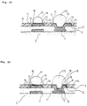
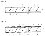
- solder pad may be a flat conductor such as a conductor pad (numeral 18 in Fig. 20) or a viahole (numeral 180 in Fig. 20).
- the viahole is connected to the innerlayer conductor circuit beneath the insulating layer and the roughened layer is formed on the surface thereof and the solder body is arranged on the roughened layer.
- the solder resist layer is formed on the outermost layer of the board.
- the viahole acting as a solder pad can adopt either a form of exposing a part thereof from the solder resist layer (see Fig. 23) or a form of exposing the whole thereof (see Fig. 24).
- the crack created from a side face of the conductor pad or the viahole toward the insulating resin layer can be prevented, while in the later case, the allowable range of the position shifting of the opening can be made large.
- various resins can be used as a solder resist composition.
- resins obtained by curing bisphenol A-type epoxy resin, acrylate of bisphenol A-type epoxy resin, novolac type epoxy resin, or acrylate of novolac type epoxy resin with an amine curing agent, an imidazole curing agent or the like Particularly, when an opening is formed in the solder resist layer to form a solder bump, it is preferable to use " a resin obtained by curing novolac type epoxy resin or acrylate of novolac type epoxy resin with an imidazole curing agent.”
- the wiring substrate is not particularly restricted, but it is desirable to be so-called additive type printed circuit board or build-up type multilayer printed circuit board in which a plating resist is formed on an insulating resin layer having a roughened surface and a conductor circuit including a pad is formed on a portion not forming the plating resist.
- a printed circuit board produced by a semi-additive method is desirable.
- the solder resist layer is desirable to have a thickness of 5-40 ⁇ m. If the thickness is too thin, the effect of the solder body as a dam lowers, while if it is too thick, it is difficult to conduct the developing treatment.
- the most suitable structure as the printed circuit board according to the invention is a structure of a printed circuit board comprising a wiring substrate provided with a conductor circuit, a solder resist layer formed on a surface thereof, a pad formed by exposing a part of the conductor circuit from an opening portion in the solder resist layer and a solder body fed and held onto the pad as shown in Fig. 3, in which the solder resist layer is formed by curing the solder resist composition according to the invention and a roughened layer is formed on the surface of the conductor circuit and a metal layer having a non-oxidizing metal on at least a surface thereof is formed on the pad portion constituting a part of the conductor circuit exposed from the opening portion and the solder body is held through the metal layer.
- the roughened layer formed on the surface of the conductor circuit including the pad serves as an anchor to strongly adhere the conductor circuit to the solder resist layer. And also, the adhesion property to the solder body held on the pad surface is improved.
- the acrylate of novolac type epoxy resin is excellent in the heat resistance and resistance to base, but is poor in the flexibility because of the rigid skeleton, so that the peeling is liable to be caused under conditions of high temperature and high humidity.
- the above structure of forming the roughened layer on the surface of the conductor circuit such a peeling can be prevented.
- solder body may be layer-like or ball-like or so-called "solder bump".
- solder transferring method As the method of feeding the solder body, use may be made of solder transferring method and solder printing method.
- the solder transferring method is a method wherein a solder foil is attached to a prepreg and etched so as to leave only a portion corresponding to the opening portion to render into a solder carrier film having a solder pattern, and the solder carrier film is laminated so as to contact the solder pattern with the pad after a flux is applied to he opening portion in the solder resist of the substrate and heated to transfer the solder onto the pad.
- the solder printing method is a method wherein a metal mask having through-holes corresponding to the pads is placed onto the substrate and a solder paste is printed and heated.
- the steps (1)-(16) are repeated in the same manner as in Example 1 except that 14 g of DMDG is added to the composition in the step (15) of Example 1 and the viscosity is adjusted to 0.2 Pa ⁇ s as the solder resist composition.
- solder resist composition is too low in the viscosity and is easily dropped down, so that it can not simultaneously be applied onto both surfaces of the wiring substrate at the vertically standing state.
- solder resist composition is applied to the wiring substrate at a horizontal state through a curtain coat method, whereby the printed circuit board having the solder bumps is produced likewise Example 1.
- a printed circuit board having solder bumps is produced in the same manner as in Example 1 except that cresol novolac type epoxy resin having a solid content of 70% is used in the solder resist composition of the step (15) of Example 1 and the viscosity is adjusted to 15 Pa ⁇ s.
- the steps (1)-(16) are repeated in the same manner as in Example 1 except that a composition described in Run No. 1-1 of JP-A-63-286841 (solder resist composition containing orthocresol novolac type epoxy resin, cellosolve acetate, benzophenone and Micheler's ketone and having a viscosity of 0.2 Pa ⁇ s) is used as a solder resist composition.
- a composition described in Run No. 1-1 of JP-A-63-286841 solder resist composition containing orthocresol novolac type epoxy resin, cellosolve acetate, benzophenone and Micheler's ketone and having a viscosity of 0.2 Pa ⁇ s
- solder resist composition is too low in the viscosity and is easily dropped down, so that it can not simultaneously be applied onto both surfaces of the wiring substrate at the vertically standing state.
- solder resist composition is applied to the surface of the wiring substrate through a curtain coat method described on JP-A-63-286841, and then the printed circuit board having the solder bumps is produced in the same manner as in Example 1.
- a printed circuit board having solder bumps is produced in the same manner as in Example 1 except that a composition described in JP-A-62-23036 is used as a solder resist composition and a solder resist layer is developed with an alkali.
- HAST test high acceleration stress test
- test conditions are temperature of 135°C, humidity of 85%, voltage of 3.3 V and 48 hours.
- Example 1 when the solder resist composition is applied to the wiring substrate at a vertically standing state by means of a roll coater, the application property is good. On the other hand, the application property of the solder resist composition is poor in Comparative Example 1 having a too low viscosity and Comparative Example 2 having a too high viscosity.
- Example 1 the lead migration is not confirmed and the occurrence of short-circuit due to the lead migration is not confirmed after the HAST test. On the contrary, In Comparative Examples 2 and 4 using the same solder resist composition as in Example 1, the lead migration is confirmed and the occurrence of the short-circuit is confirmed after the HAST test due to the low viscosity.
- Example 1 Since glycol ether type solvent is used in Example 1, there are not observed the oxidation of the conductor circuit, the hallow phenomenon and the peeling of the solder resist layer due to heat cycle. On the contrary, the hallow phenomenon and the peeling due to heat cycle is observed in Comparative Example 3 using cellosolve acetate.
- a printed circuit board having solder bumps is produced in the same manner as in Example 1 except that a roughened layer is formed by a redox treatment in the step (14) of Example 1.
- a redox treatment there are used an oxidation aqueous solution of NaOH (10 g/l), NaClO 2 (40 g/l) and Na 3 PO 4 (6 g/l) and a reducing aqueous solution of NaOH (10 g/l) and NaBH 4 (6 g/l).
- a printed circuit board having solder bumps is produced in the same manner as in Example 1 except that the step (14) of Example 1 (formation of roughened layer) is not carried out and the step (18) of Example 1 is the same condition as in Example 2.
- a heat cycle test of 1000 cycles at -55°C ⁇ 125°C is carried out with respect to the printed circuit boards of Examples 1 and 2 and Comparative Example 5 to measure the presence or absence of the peeling of solder resist layer by means of an optical microscope. Further, a PCT test (pressure cooker test) leaving under conditions that a temperature is 121°C, a humidity is 100%, a pressure is 2 atmospheric pressure and a time is 200 hours is carried out to visually measure the presence or absence of the peeling of solder resist layer.
- PCT test pressure cooker test
- a printed circuit board having solder bumps is produced in the same manner as in Example 1 except that a copper layer having a thickness of 3 ⁇ m is formed by the electroless copper plating of the step (13) after the roughening treatment at the step (14) of Example 1 and then nickel layer and gold layer are successively formed thereon and thereafter solder bumps are formed by solder transferring method.
- the solder transferring method is a method wherein a solder foil is attached to a prepreg by heating under pressure and etched with borofluoric acid to form a solder pattern and then laminated on a substrate coated with flux so as to contact a pad with the solder pattern and heated at 200°C.
- a printed circuit board having solder bumps is produced in the same manner as in Example 1 except that the roughening treatment in the step (14) is not conducted.
- Example 4 The same procedure as in Example 4 is repeated except that copper layer is formed on the copper-nickel-phosphorus roughened layer and then solder bumps are formed thereon through solder transferring method without forming the nickel layer and gold layer.
- oxide film is formed on the surface of the copper layer by bonding with oxygen in air to degrade the wettability to the solder.
- the solder fed onto the surface of the copper layer becomes spherical on the surface of the copper layer, which is easily dropped off by washing and hence the solder body can not be formed.
- the heat cycle test of 1000 cycles at -65°C ⁇ 125°C after the mounting of an IC chip consisting of Ga-As is carried out to measure the presence or absence of the peeling of solder bump.
- the connecting portion between the IC chip and the printed circuit board is sealed with a silicon resin, but in order to remarkably confirm the effect of the invention, the resin sealing is not carried out.
- a printed circuit board having solder bumps is produced in the same manner as in Example 4 except that the roughening of the conductor circuit is carried out by etching.
- an etching solution of Durabond (trade name, made by Meck Co., Ltd.) is used.
- the measurement is carried out at room temperature after a sample is dissolved in bichloroform and added with 5 droplets of pyridine d5.
- a printed circuit board having solder bumps is produced in the same manner as in Example 1 except that the flat-type conductor pad 18 and viahole 180 are formed on the upper layer by repeating the steps (6)-(12) in the step (14) of Example 1 without forming the roughened layer 11 on the surface thereof.
- PCT test pressure cooker test
- a humidity of 100% a temperature of 121°C and a 2 atmospheric pressure for 200 hours.
- solder resist layer of Example 6 When the solder resist layer of Example 6 is compared with the solder resist layer of Example 1, air-bubble is observed in Example 1, but not observed in Example 6. And also, the solder resist layer of Example 6 is high in the light permeation and excellent in developing property as compared with the solder resist layer of Example 1. Peeling of solder body Peeling of solder resist layer 1000 cycles 2000 cycles Example 4 none none none Example 5 none none Example 6 none none Comparative Example 8 presence presence presence presence presence presence
- the peeling between the conductor circuit and the solder resist layer hardly occurs in the heat cycle or under conditions of high temperature, high humidity and high pressure, and also the peeling of the solder bump (solder body) from the solder pad is not caused even in case of mounting the IC chip or the like.
- solder resist composition according to the invention it is possible to simultaneously apply the solder resist composition according to the invention onto both surfaces of the substrate by means of a roll coater and the lead migration is not caused. Further, oxide film is not formed on the surface of the conductor pad, so that there is caused no hallow phenomenon and peeling of solder resist layer due to heat cycle.
- the peeling of the solder resist layer can effectively be prevented in the heat cycle or under conditions of high temperature, high humidity and high pressure.
- the formation of the solder body can be realized by solder transferring method or solder printing method to ensure the mass productivity on of the printed circuit board and the peeling of solder resist layer and peeling of solder bump can effectively be prevented in the heat cycle without damaging the mass productivity.
Landscapes
- Engineering & Computer Science (AREA)
- Physics & Mathematics (AREA)
- Manufacturing & Machinery (AREA)
- Microelectronics & Electronic Packaging (AREA)
- General Physics & Mathematics (AREA)
- Spectroscopy & Molecular Physics (AREA)
- Non-Metallic Protective Coatings For Printed Circuits (AREA)
- Manufacturing Of Printed Wiring (AREA)
- Electric Connection Of Electric Components To Printed Circuits (AREA)
- Materials For Photolithography (AREA)
- Macromonomer-Based Addition Polymer (AREA)
- Inks, Pencil-Leads, Or Crayons (AREA)
Priority Applications (2)
| Application Number | Priority Date | Filing Date | Title |
|---|---|---|---|
| EP07006712A EP1802186B1 (de) | 1996-11-20 | 1997-09-16 | Leiterplatte |
| EP07006711A EP1796446B1 (de) | 1996-11-20 | 1997-09-16 | Leiterplatten |
Applications Claiming Priority (12)
| Application Number | Priority Date | Filing Date | Title |
|---|---|---|---|
| JP8308845A JPH10150249A (ja) | 1996-11-20 | 1996-11-20 | プリント配線板 |
| JP308844/96 | 1996-11-20 | ||
| JP30884696A JP3253873B2 (ja) | 1996-11-20 | 1996-11-20 | プリント配線板 |
| JP308846/96 | 1996-11-20 | ||
| JP30884596 | 1996-11-20 | ||
| JP30884696 | 1996-11-20 | ||
| JP308845/96 | 1996-11-20 | ||
| JP30884496 | 1996-11-20 | ||
| JP30884496 | 1996-11-20 | ||
| JP35796296 | 1996-12-27 | ||
| JP357962/96 | 1996-12-27 | ||
| JP35796296 | 1996-12-27 |
Related Child Applications (4)
| Application Number | Title | Priority Date | Filing Date |
|---|---|---|---|
| EP07006712A Division EP1802186B1 (de) | 1996-11-20 | 1997-09-16 | Leiterplatte |
| EP07006711A Division EP1796446B1 (de) | 1996-11-20 | 1997-09-16 | Leiterplatten |
| EP07006711.1 Division-Into | 2007-03-30 | ||
| EP07006712.9 Division-Into | 2007-03-30 |
Publications (3)
| Publication Number | Publication Date |
|---|---|
| EP0844809A2 true EP0844809A2 (de) | 1998-05-27 |
| EP0844809A3 EP0844809A3 (de) | 1999-12-01 |
| EP0844809B1 EP0844809B1 (de) | 2011-08-17 |
Family
ID=27479981
Family Applications (3)
| Application Number | Title | Priority Date | Filing Date |
|---|---|---|---|
| EP97116093A Expired - Lifetime EP0844809B1 (de) | 1996-11-20 | 1997-09-16 | Lötmaskenzusammensetzung und gedruckte Leiterplatten |
| EP07006711A Expired - Lifetime EP1796446B1 (de) | 1996-11-20 | 1997-09-16 | Leiterplatten |
| EP07006712A Expired - Lifetime EP1802186B1 (de) | 1996-11-20 | 1997-09-16 | Leiterplatte |
Family Applications After (2)
| Application Number | Title | Priority Date | Filing Date |
|---|---|---|---|
| EP07006711A Expired - Lifetime EP1796446B1 (de) | 1996-11-20 | 1997-09-16 | Leiterplatten |
| EP07006712A Expired - Lifetime EP1802186B1 (de) | 1996-11-20 | 1997-09-16 | Leiterplatte |
Country Status (6)
| Country | Link |
|---|---|
| US (1) | US6217987B1 (de) |
| EP (3) | EP0844809B1 (de) |
| KR (2) | KR100277838B1 (de) |
| CN (2) | CN1150079C (de) |
| MY (1) | MY116975A (de) |
| SG (1) | SG73469A1 (de) |
Cited By (12)
| Publication number | Priority date | Publication date | Assignee | Title |
|---|---|---|---|---|
| EP1252966A4 (de) * | 1999-12-27 | 2004-11-03 | Sumitomo Bakelite Co | Lötmittel, lötwiderstand, halbleitergehäuse verstärkt durch lötmittel, halbleiterbauelement und herstellungsverfahren für halbleitergehäuse und halbleiterbauelement |
| EP1121008A4 (de) * | 1998-09-03 | 2005-02-02 | Ibiden Co Ltd | Mehrschichtige leiterplatte und verfahren zu deren herstellung |
| EP1102523A4 (de) * | 1998-07-08 | 2005-11-30 | Ibiden Co Ltd | Leiterplatte und verfahren zu ihrer herstellung |
| EP1656004A1 (de) * | 1999-05-13 | 2006-05-10 | Ibiden Co., Ltd. | Mehrschichtige gedruckte Leiterplatte und ihr Herstellungsverfahren |
| EP2028915A1 (de) * | 1999-08-12 | 2009-02-25 | Ibiden Co., Ltd. | Mehrschichtdruckleiterplatte, Lötabdeckungszusammensetzung, Verfahren zur Herstellung der Mehrschichtdruckleiterplatte und Halbleitervorrichtung |
| US7514779B2 (en) | 1998-09-17 | 2009-04-07 | Ibiden Co., Ltd. | Multilayer build-up wiring board |
| WO2012084569A1 (de) * | 2010-12-21 | 2012-06-28 | Elantas Gmbh | Epoxidharz-zusammensetzungen enthaltend epoxy- und vinylestergruppen |
| CN103153004A (zh) * | 2013-03-29 | 2013-06-12 | 景旺电子(深圳)有限公司 | 一种pcb防焊通孔的制作方法 |
| US10189706B2 (en) | 2016-11-08 | 2019-01-29 | Dunan Microstaq, Inc. | Method for self-aligning solder-attached MEMS die to a mounting surface |
| US10457547B2 (en) | 2017-05-05 | 2019-10-29 | Dunan Microstaq, Inc. | Multi-layer, stress-isolation platform for a MEMS die |
| US10544040B2 (en) | 2017-05-05 | 2020-01-28 | Dunan Microstaq, Inc. | Method and structure for preventing solder flow into a MEMS pressure port during MEMS die attachment |
| US10640374B2 (en) | 2017-05-18 | 2020-05-05 | Dunan Microstaq, Inc. | Method and structure of attachment layer for reducing stress transmission to attached MEMS die |
Families Citing this family (81)
| Publication number | Priority date | Publication date | Assignee | Title |
|---|---|---|---|---|
| USRE43509E1 (en) * | 1996-12-19 | 2012-07-17 | Ibiden Co., Ltd. | Printed wiring board and method for manufacturing the same |
| US6141870A (en) | 1997-08-04 | 2000-11-07 | Peter K. Trzyna | Method for making electrical device |
| US6159586A (en) * | 1997-09-25 | 2000-12-12 | Nitto Denko Corporation | Multilayer wiring substrate and method for producing the same |
| WO1999034654A1 (en) * | 1997-12-29 | 1999-07-08 | Ibiden Co., Ltd. | Multilayer printed wiring board |
| EP0943392B1 (de) * | 1998-03-18 | 2004-06-23 | Mitsubishi Gas Chemical Company, Inc. | Ein Verfahren zur Herstellung von Durchgangslöchern mittels Laser, kupferkaschiertes Laminat geeignet zur Herstellung von Löchern, und Zusatzmaterial zur Herstellung von Löchern |
| MY120077A (en) * | 1998-06-26 | 2005-08-30 | Ibiden Co Ltd | Multilayer printed wiring board having a roughened inner conductor layer and production method thereof |
| MY144573A (en) * | 1998-09-14 | 2011-10-14 | Ibiden Co Ltd | Printed circuit board and method for its production |
| EP1845759A1 (de) | 1998-12-16 | 2007-10-17 | Ibiden Co., Ltd. | Leiterverbindungsstift und Verpackungssubstrat |
| JP3635219B2 (ja) * | 1999-03-11 | 2005-04-06 | 新光電気工業株式会社 | 半導体装置用多層基板及びその製造方法 |
| JP2000294921A (ja) * | 1999-04-01 | 2000-10-20 | Victor Co Of Japan Ltd | プリンス基板及びその製造方法 |
| US6762921B1 (en) * | 1999-05-13 | 2004-07-13 | Ibiden Co., Ltd. | Multilayer printed-circuit board and method of manufacture |
| US6708404B1 (en) * | 1999-06-17 | 2004-03-23 | Mitsubishi Gas Chemical Company, Inc. | Method of producing high-density copper clad multi-layered printed wiring board having highly reliable through hole |
| US6570251B1 (en) * | 1999-09-02 | 2003-05-27 | Micron Technology, Inc. | Under bump metalization pad and solder bump connections |
| JP3865115B2 (ja) * | 1999-09-13 | 2007-01-10 | Hoya株式会社 | 多層配線基板及びその製造方法、並びに該多層配線基板を有するウエハ一括コンタクトボード |
| EP1162867B1 (de) | 1999-10-26 | 2006-04-05 | Ibiden Co., Ltd. | Gedruckte mehrschichtleiterplatte und herstellungsverfahren für gedruckte mehrschichtleiterplatte |
| JP2001209918A (ja) * | 1999-11-19 | 2001-08-03 | Nitto Denko Corp | 回路付サスペンション基板 |
| TW512653B (en) * | 1999-11-26 | 2002-12-01 | Ibiden Co Ltd | Multilayer circuit board and semiconductor device |
| JP2001251040A (ja) * | 2000-03-06 | 2001-09-14 | Stanley Electric Co Ltd | 高周波用回路基板及びその製造方法 |
| US6320137B1 (en) * | 2000-04-11 | 2001-11-20 | 3M Innovative Properties Company | Flexible circuit with coverplate layer and overlapping protective layer |
| US6474536B1 (en) * | 2000-09-28 | 2002-11-05 | Peter Kukanskis | Flux composition and corresponding soldering method |
| JP3888573B2 (ja) * | 2001-06-29 | 2007-03-07 | 富士電機ホールディングス株式会社 | ハンダ組成物 |
| JP4062907B2 (ja) * | 2001-11-12 | 2008-03-19 | 松下電器産業株式会社 | 回路基板およびその製造方法 |
| TWI227102B (en) * | 2002-03-15 | 2005-01-21 | United Test Ct Inc | Fabrication method for circuit carrier |
| US6650022B1 (en) * | 2002-09-11 | 2003-11-18 | Motorola, Inc. | Semiconductor device exhibiting enhanced pattern recognition when illuminated in a machine vision system |
| US6905914B1 (en) | 2002-11-08 | 2005-06-14 | Amkor Technology, Inc. | Wafer level package and fabrication method |
| US7723210B2 (en) | 2002-11-08 | 2010-05-25 | Amkor Technology, Inc. | Direct-write wafer level chip scale package |
| KR20040042999A (ko) * | 2002-11-15 | 2004-05-22 | 주식회사 코오롱 | 솔더 레지스트용 잉크 조성물 |
| US7253510B2 (en) * | 2003-01-16 | 2007-08-07 | International Business Machines Corporation | Ball grid array package construction with raised solder ball pads |
| US7326859B2 (en) | 2003-12-16 | 2008-02-05 | Intel Corporation | Printed circuit boards having pads for solder balls and methods for the implementation thereof |
| JP3886513B2 (ja) * | 2004-02-02 | 2007-02-28 | 松下電器産業株式会社 | フィルム基板およびその製造方法 |
| TWI234248B (en) * | 2004-09-06 | 2005-06-11 | Advanced Semiconductor Eng | Method for bonding flip chip on leadframe |
| US20060099786A1 (en) * | 2004-10-22 | 2006-05-11 | Taiwan Semiconductor Manufacturing Co. | Copper interconnect structure with modulated topography and method for forming the same |
| US7626829B2 (en) * | 2004-10-27 | 2009-12-01 | Ibiden Co., Ltd. | Multilayer printed wiring board and manufacturing method of the multilayer printed wiring board |
| TW200630447A (en) * | 2004-11-19 | 2006-09-01 | Showa Denko Kk | Resin cured film for flexible printed wiring board and production process thereof |
| JP4883996B2 (ja) * | 2005-05-24 | 2012-02-22 | 四国化成工業株式会社 | 水溶性プレフラックス及びその利用 |
| US7572681B1 (en) | 2005-12-08 | 2009-08-11 | Amkor Technology, Inc. | Embedded electronic component package |
| US7659193B2 (en) * | 2005-12-23 | 2010-02-09 | Phoenix Precision Technology Corporation | Conductive structures for electrically conductive pads of circuit board and fabrication method thereof |
| WO2007086551A1 (ja) * | 2006-01-27 | 2007-08-02 | Ibiden Co., Ltd. | プリント配線板及びプリント配線板の製造方法 |
| US7902660B1 (en) * | 2006-05-24 | 2011-03-08 | Amkor Technology, Inc. | Substrate for semiconductor device and manufacturing method thereof |
| TWI330660B (en) * | 2006-12-14 | 2010-09-21 | Ind Tech Res Inst | Halogen-free, thermal resistant composition |
| CN101210077B (zh) * | 2006-12-28 | 2010-07-14 | 财团法人工业技术研究院 | 无卤耐高温组合物 |
| EP2106318A4 (de) * | 2007-01-04 | 2013-05-01 | Fry Metals Inc | Flussmittelzusammensetzungen |
| US7807560B2 (en) * | 2007-07-17 | 2010-10-05 | Shinko Electric Industries Co., Ltd. | Solder bump forming method |
| JP2009049051A (ja) * | 2007-08-14 | 2009-03-05 | Elpida Memory Inc | 半導体基板の接合方法及びそれにより製造された積層体 |
| US7759787B2 (en) * | 2007-11-06 | 2010-07-20 | International Business Machines Corporation | Packaging substrate having pattern-matched metal layers |
| JP5154271B2 (ja) * | 2008-03-17 | 2013-02-27 | 日本特殊陶業株式会社 | はんだバンプを有する配線基板及びその製造方法 |
| CN101393400B (zh) * | 2008-10-29 | 2011-12-14 | 清溢精密光电(深圳)有限公司 | 液体感光性树脂凸版表面除粘方法 |
| JP5142967B2 (ja) * | 2008-12-10 | 2013-02-13 | ルネサスエレクトロニクス株式会社 | 半導体装置 |
| TWI385770B (zh) * | 2009-05-27 | 2013-02-11 | Unimicron Technology Corp | 封裝基板及其製法 |
| US8426959B2 (en) * | 2009-08-19 | 2013-04-23 | Samsung Electronics Co., Ltd. | Semiconductor package and method of manufacturing the same |
| KR101070098B1 (ko) * | 2009-09-15 | 2011-10-04 | 삼성전기주식회사 | 인쇄회로기판 및 그의 제조 방법 |
| CN102054712A (zh) * | 2009-11-05 | 2011-05-11 | 北大方正集团有限公司 | 一种控制线路板表面粗糙度的方法 |
| JP2012014021A (ja) * | 2010-07-01 | 2012-01-19 | Fujifilm Corp | 感光性組成物、パターン形成材料、並びに、これを用いた感光性膜、パターン形成方法、パターン膜、反射防止膜、絶縁膜、光学デバイス及び電子デバイス |
| JP6081044B2 (ja) | 2010-09-16 | 2017-02-15 | 富士通株式会社 | パッケージ基板ユニットの製造方法 |
| KR101158218B1 (ko) * | 2010-11-02 | 2012-06-19 | 삼성전기주식회사 | 인쇄회로기판 및 이의 제조방법 |
| JP2012164965A (ja) * | 2011-01-21 | 2012-08-30 | Ngk Spark Plug Co Ltd | 配線基板及びその製造方法 |
| JP2012169591A (ja) * | 2011-01-24 | 2012-09-06 | Ngk Spark Plug Co Ltd | 多層配線基板 |
| JP2012182437A (ja) * | 2011-02-09 | 2012-09-20 | Ngk Spark Plug Co Ltd | 配線基板及びその製造方法 |
| JP5530955B2 (ja) * | 2011-02-21 | 2014-06-25 | 日本特殊陶業株式会社 | 多層配線基板 |
| CN102325427B (zh) * | 2011-08-30 | 2014-12-31 | 陈国富 | 印刷线路板阻焊油的涂布工艺及涂布装置 |
| WO2013032277A2 (en) | 2011-09-02 | 2013-03-07 | Lg Innotek Co., Ltd. | Method of manufacturing substrate for chip packages and method of manufacturing chip package |
| KR101895416B1 (ko) * | 2011-12-23 | 2018-09-06 | 엘지이노텍 주식회사 | 인쇄회로기판 및 그 제조방법 |
| US20130168132A1 (en) * | 2011-12-29 | 2013-07-04 | Sumsung Electro-Mechanics Co., Ltd. | Printed circuit board and method of manufacturing the same |
| US9646942B2 (en) * | 2012-02-23 | 2017-05-09 | Taiwan Semiconductor Manufacturing Company, Ltd. | Mechanisms for controlling bump height variation |
| KR20140008923A (ko) * | 2012-07-13 | 2014-01-22 | 삼성전기주식회사 | 코어리스 인쇄회로기판 및 그 제조 방법 |
| JP6266907B2 (ja) * | 2013-07-03 | 2018-01-24 | 新光電気工業株式会社 | 配線基板及び配線基板の製造方法 |
| JP5681824B1 (ja) | 2013-10-01 | 2015-03-11 | 株式会社フジクラ | 配線板組立体及びその製造方法 |
| JP2015115432A (ja) * | 2013-12-11 | 2015-06-22 | ローム株式会社 | 半導体装置 |
| JP2015231003A (ja) * | 2014-06-06 | 2015-12-21 | イビデン株式会社 | 回路基板および回路基板の製造方法 |
| JP5918809B2 (ja) | 2014-07-04 | 2016-05-18 | 株式会社イースタン | 配線基板の製造方法および配線基板 |
| JP6324876B2 (ja) * | 2014-07-16 | 2018-05-16 | 新光電気工業株式会社 | 配線基板、半導体装置及び配線基板の製造方法 |
| DE102015003226A1 (de) | 2015-03-13 | 2015-12-03 | Daimler Ag | Leiterplattenanordnung für eine Wandlereinrichtung eines Kraftfahrzeugs und Bauelement mit einer Leiterplattenanordnung |
| KR102046006B1 (ko) * | 2016-06-07 | 2019-11-18 | 주식회사 엘지화학 | 일반 인쇄회로기판을 활용한 고전류 전송 방법 |
| CN210579551U (zh) * | 2016-12-02 | 2020-05-19 | 株式会社村田制作所 | 多层布线基板 |
| KR101878908B1 (ko) * | 2017-03-31 | 2018-07-17 | (주)호전에이블 | 젖음성이 우수한 에폭시 플럭스 페이스트 조성물 |
| US10892671B2 (en) * | 2017-07-25 | 2021-01-12 | GM Global Technology Operations LLC | Electrically conductive copper components and joining processes therefor |
| CN109283793B (zh) * | 2018-10-16 | 2021-02-23 | 武汉华星光电半导体显示技术有限公司 | 光刻胶及其制备方法 |
| CN111263532A (zh) * | 2020-01-21 | 2020-06-09 | 李荣根 | 一种pcb板材垂直浸涂方法 |
| KR102933114B1 (ko) * | 2020-09-10 | 2026-03-03 | 엘지이노텍 주식회사 | 인쇄회로기판 및 이의 제조 방법 |
| US20220312591A1 (en) * | 2021-03-26 | 2022-09-29 | Juniper Networks, Inc. | Substrate with conductive pads and conductive layers |
| CN113825322B (zh) * | 2021-09-15 | 2023-02-10 | 常州硕成半导体材料有限公司 | 一种阻焊胶层的制备工艺及其应用 |
Citations (7)
| Publication number | Priority date | Publication date | Assignee | Title |
|---|---|---|---|---|
| JPS6223036A (ja) | 1985-07-23 | 1987-01-31 | Japan Synthetic Rubber Co Ltd | 固体状感光性樹脂組成物 |
| JPS63286841A (ja) | 1987-05-19 | 1988-11-24 | Hitachi Chem Co Ltd | 感光性樹脂組成物溶液 |
| US4888269A (en) | 1985-06-29 | 1989-12-19 | Dainippon Ink & Chemicals, Inc. | Resin composition for solder resist ink |
| US5055378A (en) | 1987-11-13 | 1991-10-08 | Kabushiki Kaisha Toshiba | Solder resist composition |
| JPH06283860A (ja) | 1993-01-26 | 1994-10-07 | Ibiden Co Ltd | 多層プリント配線板およびその製造方法 |
| JPH0768656A (ja) | 1993-08-31 | 1995-03-14 | Mitsubishi Rayon Co Ltd | 抗菌性アクリルフイルム |
| JPH08242064A (ja) | 1995-03-01 | 1996-09-17 | Ibiden Co Ltd | プリント配線板 |
Family Cites Families (39)
| Publication number | Priority date | Publication date | Assignee | Title |
|---|---|---|---|---|
| US3356624A (en) | 1964-12-28 | 1967-12-05 | Shell Oil Co | Epoxy resin based traffic paint compositions |
| US3847767A (en) * | 1973-03-13 | 1974-11-12 | Grace W R & Co | Method of producing a screen printable photocurable solder resist |
| US4510276A (en) | 1979-12-13 | 1985-04-09 | Kollmorgen Technologies Corporation | Epoxy resin coating compositions for printed circuit boards |
| US4504607A (en) | 1979-12-13 | 1985-03-12 | Kollmorgen Technologies Corporation | Epoxy resin coating composition for printed circuit boards |
| JPS5790072A (en) | 1980-11-25 | 1982-06-04 | Hitachi Ltd | Resist ink composition for chemical plating |
| JPS60208377A (ja) | 1984-04-02 | 1985-10-19 | Asahi Kagaku Kenkyusho:Kk | ソルダ−レジストインキ用樹脂組成物 |
| JPS6159447A (ja) | 1984-08-31 | 1986-03-26 | Sony Corp | 感光性樹脂組成物 |
| US4750976A (en) | 1984-12-19 | 1988-06-14 | Blasberg Oberflachentechnik Gmbh | Electrically conductive copper layers and process for preparing same |
| US4615950A (en) | 1985-03-15 | 1986-10-07 | M&T Chemicals Inc. | Printed circuit boards having improved adhesion between solder mask and metal |
| US4713298A (en) | 1985-03-15 | 1987-12-15 | M&T Chemicals Inc. | Printed circuit boards having improved adhesion between solder mask and metal |
| JPS61243869A (ja) | 1985-04-19 | 1986-10-30 | Taiyo Ink Seizo Kk | レジストインキ組成物 |
| US4752499A (en) | 1985-05-16 | 1988-06-21 | Ibiden Co. Ltd. | Adhesive for electroless plating and method of preparation of circuit board using this adhesive |
| US4789620A (en) * | 1986-03-03 | 1988-12-06 | Mitsubishi Rayon Co. Ltd. | Liquid photosensitive resin composition containing carboxylated epoxy acrylates or methacrylates |
| JPH07103217B2 (ja) | 1986-05-14 | 1995-11-08 | 株式会社日立製作所 | 樹脂組成物 |
| JPS62273226A (ja) | 1986-05-20 | 1987-11-27 | Nippon Soda Co Ltd | 無電解メッキ用光硬化性レジスト樹脂組成物 |
| JPH01101697A (ja) * | 1987-10-14 | 1989-04-19 | Sumitomo Electric Ind Ltd | フレキシブル印刷配線板の製造方法 |
| JP2571800B2 (ja) | 1987-11-27 | 1997-01-16 | イビデン株式会社 | 無電解めっき用感光性接着剤およびプリント配線板 |
| JPH0748108B2 (ja) | 1988-02-02 | 1995-05-24 | イビデン株式会社 | 感光性樹脂組成物 |
| JPH0748109B2 (ja) | 1988-04-01 | 1995-05-24 | イビデン株式会社 | 感光性樹脂組成物 |
| DE3913966B4 (de) | 1988-04-28 | 2005-06-02 | Ibiden Co., Ltd., Ogaki | Klebstoffdispersion zum stromlosen Plattieren, sowie Verwendung zur Herstellung einer gedruckten Schaltung |
| JPH0823694B2 (ja) | 1988-08-04 | 1996-03-06 | 富士写真フイルム株式会社 | 液状感光性樹脂組成物 |
| US5302492A (en) | 1989-06-16 | 1994-04-12 | Hewlett-Packard Company | Method of manufacturing printing circuit boards |
| CA2018208C (en) * | 1989-06-16 | 1995-01-31 | Albert Ott | Method of manufacturing printed circuit boards |
| US5175060A (en) | 1989-07-01 | 1992-12-29 | Ibiden Co., Ltd. | Leadframe semiconductor-mounting substrate having a roughened adhesive conductor circuit substrate and method of producing the same |
| CA1338252C (en) * | 1989-07-05 | 1996-04-16 | Osamu Ogitani | Resist ink composition |
| JP2679849B2 (ja) | 1989-07-26 | 1997-11-19 | 松下電器産業株式会社 | 電子部品の実装方法およびこの方法に用いる接着剤 |
| SE469320B (sv) * | 1990-11-02 | 1993-06-21 | Thams Johan Petter B | Foerfarande foer belaeggning av moensterkort med en lackbelaeggning, speciellt en loedmask |
| JPH0521951A (ja) * | 1991-07-16 | 1993-01-29 | Cmk Corp | 銅張積層板用銅箔 |
| US5344893A (en) * | 1991-07-23 | 1994-09-06 | Ibiden Co., Ltd. | Epoxy/amino powder resin adhesive for printed circuit board |
| JP2868190B2 (ja) | 1991-07-29 | 1999-03-10 | 日本化薬株式会社 | 樹脂組成物、ソルダーレジスト樹脂組成物及びこれらの硬化物 |
| JP2770252B2 (ja) * | 1991-12-11 | 1998-06-25 | 日本石油株式会社 | エポキシ樹脂組成物、封止材用エポキシ樹脂組成物、積層板用エポキシ樹脂組成物及びソルダーレジスト用エポキシ樹脂組成物 |
| JPH05206622A (ja) * | 1992-07-23 | 1993-08-13 | Ibiden Co Ltd | プリント配線板 |
| JP3364266B2 (ja) * | 1993-03-17 | 2003-01-08 | ローム株式会社 | バンプの形成法 |
| JP3115449B2 (ja) | 1993-05-07 | 2000-12-04 | イビデン株式会社 | 配線板用めっきレジスト組成物およびプリント配線板 |
| US5519177A (en) * | 1993-05-19 | 1996-05-21 | Ibiden Co., Ltd. | Adhesives, adhesive layers for electroless plating and printed circuit boards |
| JP2586797B2 (ja) * | 1993-09-03 | 1997-03-05 | 日本電気株式会社 | 印刷配線板の製造方法 |
| JP2781954B2 (ja) * | 1994-03-04 | 1998-07-30 | メック株式会社 | 銅および銅合金の表面処理剤 |
| JP3190251B2 (ja) * | 1995-06-06 | 2001-07-23 | 太陽インキ製造株式会社 | アルカリ現像型のフレキシブルプリント配線板用光硬化性・熱硬化性樹脂組成物 |
| JP3276833B2 (ja) * | 1995-12-13 | 2002-04-22 | 太陽インキ製造株式会社 | 光硬化性・熱硬化性艶消しレジストインキ組成物 |
-
1997
- 1997-09-16 EP EP97116093A patent/EP0844809B1/de not_active Expired - Lifetime
- 1997-09-16 EP EP07006711A patent/EP1796446B1/de not_active Expired - Lifetime
- 1997-09-16 US US08/931,364 patent/US6217987B1/en not_active Expired - Lifetime
- 1997-09-16 EP EP07006712A patent/EP1802186B1/de not_active Expired - Lifetime
- 1997-09-16 SG SG1997003432A patent/SG73469A1/en unknown
- 1997-09-17 MY MYPI97004321A patent/MY116975A/en unknown
- 1997-09-18 CN CNB971186448A patent/CN1150079C/zh not_active Expired - Fee Related
- 1997-09-18 CN CNB2004100319193A patent/CN100401190C/zh not_active Expired - Lifetime
- 1997-09-19 KR KR1019970047663A patent/KR100277838B1/ko not_active Expired - Fee Related
-
2000
- 2000-06-30 KR KR1020000036966A patent/KR100330277B1/ko not_active Expired - Fee Related
Patent Citations (8)
| Publication number | Priority date | Publication date | Assignee | Title |
|---|---|---|---|---|
| US4888269A (en) | 1985-06-29 | 1989-12-19 | Dainippon Ink & Chemicals, Inc. | Resin composition for solder resist ink |
| JPS6223036A (ja) | 1985-07-23 | 1987-01-31 | Japan Synthetic Rubber Co Ltd | 固体状感光性樹脂組成物 |
| JPS63286841A (ja) | 1987-05-19 | 1988-11-24 | Hitachi Chem Co Ltd | 感光性樹脂組成物溶液 |
| US4902726A (en) | 1987-05-19 | 1990-02-20 | Hitachi Chemical Company, Ltd. | Photosensitive resin composition solution |
| US5055378A (en) | 1987-11-13 | 1991-10-08 | Kabushiki Kaisha Toshiba | Solder resist composition |
| JPH06283860A (ja) | 1993-01-26 | 1994-10-07 | Ibiden Co Ltd | 多層プリント配線板およびその製造方法 |
| JPH0768656A (ja) | 1993-08-31 | 1995-03-14 | Mitsubishi Rayon Co Ltd | 抗菌性アクリルフイルム |
| JPH08242064A (ja) | 1995-03-01 | 1996-09-17 | Ibiden Co Ltd | プリント配線板 |
Cited By (23)
| Publication number | Priority date | Publication date | Assignee | Title |
|---|---|---|---|---|
| EP1940209A3 (de) * | 1998-07-08 | 2009-04-29 | Ibiden Co., Ltd. | Leiterplatte und Herstellungsverfahren dafür |
| EP1102523A4 (de) * | 1998-07-08 | 2005-11-30 | Ibiden Co Ltd | Leiterplatte und verfahren zu ihrer herstellung |
| EP1121008A4 (de) * | 1998-09-03 | 2005-02-02 | Ibiden Co Ltd | Mehrschichtige leiterplatte und verfahren zu deren herstellung |
| US8148643B2 (en) | 1998-09-03 | 2012-04-03 | Ibiden Co., Ltd. | Multilayered printed circuit board and manufacturing method thereof |
| EP1843650A3 (de) * | 1998-09-03 | 2007-11-07 | Ibiden Co., Ltd. | Mehrschichtige Leiterplatte und Verfahren zu deren Herstellung |
| US7415761B2 (en) | 1998-09-03 | 2008-08-26 | Ibiden Co., Ltd. | Method of manufacturing multilayered circuit board |
| US7832098B2 (en) | 1998-09-03 | 2010-11-16 | Ibiden Co., Ltd. | Method of manufacturing a multilayered printed circuit board |
| US7847318B2 (en) | 1998-09-17 | 2010-12-07 | Ibiden Co., Ltd. | Multilayer build-up wiring board including a chip mount region |
| US7514779B2 (en) | 1998-09-17 | 2009-04-07 | Ibiden Co., Ltd. | Multilayer build-up wiring board |
| EP1656004A1 (de) * | 1999-05-13 | 2006-05-10 | Ibiden Co., Ltd. | Mehrschichtige gedruckte Leiterplatte und ihr Herstellungsverfahren |
| EP2028915A1 (de) * | 1999-08-12 | 2009-02-25 | Ibiden Co., Ltd. | Mehrschichtdruckleiterplatte, Lötabdeckungszusammensetzung, Verfahren zur Herstellung der Mehrschichtdruckleiterplatte und Halbleitervorrichtung |
| US7910836B2 (en) | 1999-08-12 | 2011-03-22 | Ibiden Co. Ltd. | Multilayered printed circuit board, solder resist composition, and semiconductor device |
| US7916492B1 (en) | 1999-08-12 | 2011-03-29 | Ibiden Co., Ltd. | Multilayered printed circuit board |
| EP1252966A4 (de) * | 1999-12-27 | 2004-11-03 | Sumitomo Bakelite Co | Lötmittel, lötwiderstand, halbleitergehäuse verstärkt durch lötmittel, halbleiterbauelement und herstellungsverfahren für halbleitergehäuse und halbleiterbauelement |
| WO2012084569A1 (de) * | 2010-12-21 | 2012-06-28 | Elantas Gmbh | Epoxidharz-zusammensetzungen enthaltend epoxy- und vinylestergruppen |
| US10381129B2 (en) | 2010-12-21 | 2019-08-13 | Elantas Gmbh | Epoxy resin compositions comprising epoxy and vinyl ester groups |
| CN103153004A (zh) * | 2013-03-29 | 2013-06-12 | 景旺电子(深圳)有限公司 | 一种pcb防焊通孔的制作方法 |
| CN103153004B (zh) * | 2013-03-29 | 2016-03-30 | 深圳市景旺电子股份有限公司 | 一种pcb防焊通孔的制作方法 |
| US10189706B2 (en) | 2016-11-08 | 2019-01-29 | Dunan Microstaq, Inc. | Method for self-aligning solder-attached MEMS die to a mounting surface |
| US10662057B2 (en) | 2016-11-08 | 2020-05-26 | Dunan Microstaq, Inc. | Method for self-aligning solder-attached mems die to a mounting surface |
| US10457547B2 (en) | 2017-05-05 | 2019-10-29 | Dunan Microstaq, Inc. | Multi-layer, stress-isolation platform for a MEMS die |
| US10544040B2 (en) | 2017-05-05 | 2020-01-28 | Dunan Microstaq, Inc. | Method and structure for preventing solder flow into a MEMS pressure port during MEMS die attachment |
| US10640374B2 (en) | 2017-05-18 | 2020-05-05 | Dunan Microstaq, Inc. | Method and structure of attachment layer for reducing stress transmission to attached MEMS die |
Also Published As
| Publication number | Publication date |
|---|---|
| EP1796446A3 (de) | 2007-09-19 |
| MY116975A (en) | 2004-04-30 |
| KR100330277B1 (ko) | 2002-04-03 |
| EP1802186A2 (de) | 2007-06-27 |
| EP0844809A3 (de) | 1999-12-01 |
| SG73469A1 (en) | 2000-06-20 |
| EP1796446B1 (de) | 2011-05-11 |
| EP1802186A3 (de) | 2007-09-19 |
| US6217987B1 (en) | 2001-04-17 |
| KR100277838B1 (ko) | 2001-02-01 |
| CN1182660A (zh) | 1998-05-27 |
| CN1541051A (zh) | 2004-10-27 |
| CN1150079C (zh) | 2004-05-19 |
| CN100401190C (zh) | 2008-07-09 |
| KR19980041884A (ko) | 1998-08-17 |
| EP0844809B1 (de) | 2011-08-17 |
| EP1796446A2 (de) | 2007-06-13 |
| EP1802186B1 (de) | 2011-05-11 |
Similar Documents
| Publication | Publication Date | Title |
|---|---|---|
| EP0844809B1 (de) | Lötmaskenzusammensetzung und gedruckte Leiterplatten | |
| EP1921902B1 (de) | Mehrlagige Leiterplatte | |
| JP3152633B2 (ja) | 多層プリント配線板およびその製造方法 | |
| JP3853142B2 (ja) | ソルダーレジスト組成物およびプリント配線板の製造方法 | |
| JP3224211B2 (ja) | ソルダーレジスト組成物およびプリント配線板 | |
| JP4037526B2 (ja) | ソルダーレジスト組成物およびプリント配線板 | |
| JPH10242639A (ja) | 多層プリント配線板およびその製造方法 | |
| JP2000332395A (ja) | プリント配線板 | |
| JP3459767B2 (ja) | プリント配線板 | |
| JP2000010276A (ja) | ソルダーレジスト組成物およびプリント配線板 | |
| JP2000022304A (ja) | プリント配線板 | |
| JPH10150249A (ja) | プリント配線板 | |
| JPH10242640A (ja) | プリント配線板 | |
| JP2003060342A (ja) | 多層プリント配線板およびその製造方法 |
Legal Events
| Date | Code | Title | Description |
|---|---|---|---|
| PUAI | Public reference made under article 153(3) epc to a published international application that has entered the european phase |
Free format text: ORIGINAL CODE: 0009012 |
|
| AK | Designated contracting states |
Kind code of ref document: A2 Designated state(s): DE FI GB NL |
|
| AX | Request for extension of the european patent |
Free format text: AL;LT;LV;RO;SI |
|
| PUAL | Search report despatched |
Free format text: ORIGINAL CODE: 0009013 |
|
| AK | Designated contracting states |
Kind code of ref document: A3 Designated state(s): AT BE CH DE DK ES FI FR GB GR IE IT LI LU MC NL PT SE |
|
| AX | Request for extension of the european patent |
Free format text: AL;LT;LV;RO;SI |
|
| 17P | Request for examination filed |
Effective date: 20000310 |
|
| AKX | Designation fees paid |
Free format text: DE FI GB NL |
|
| 17Q | First examination report despatched |
Effective date: 20061228 |
|
| GRAP | Despatch of communication of intention to grant a patent |
Free format text: ORIGINAL CODE: EPIDOSNIGR1 |
|
| GRAJ | Information related to disapproval of communication of intention to grant by the applicant or resumption of examination proceedings by the epo deleted |
Free format text: ORIGINAL CODE: EPIDOSDIGR1 |
|
| GRAP | Despatch of communication of intention to grant a patent |
Free format text: ORIGINAL CODE: EPIDOSNIGR1 |
|
| GRAS | Grant fee paid |
Free format text: ORIGINAL CODE: EPIDOSNIGR3 |
|
| GRAA | (expected) grant |
Free format text: ORIGINAL CODE: 0009210 |
|
| AK | Designated contracting states |
Kind code of ref document: B1 Designated state(s): DE FI GB NL |
|
| REG | Reference to a national code |
Ref country code: GB Ref legal event code: FG4D |
|
| REG | Reference to a national code |
Ref country code: DE Ref legal event code: R096 Ref document number: 69740265 Country of ref document: DE Effective date: 20111027 |
|
| REG | Reference to a national code |
Ref country code: NL Ref legal event code: VDEP Effective date: 20110817 |
|
| PG25 | Lapsed in a contracting state [announced via postgrant information from national office to epo] |
Ref country code: FI Free format text: LAPSE BECAUSE OF FAILURE TO SUBMIT A TRANSLATION OF THE DESCRIPTION OR TO PAY THE FEE WITHIN THE PRESCRIBED TIME-LIMIT Effective date: 20110817 Ref country code: NL Free format text: LAPSE BECAUSE OF FAILURE TO SUBMIT A TRANSLATION OF THE DESCRIPTION OR TO PAY THE FEE WITHIN THE PRESCRIBED TIME-LIMIT Effective date: 20110817 |
|
| PLBE | No opposition filed within time limit |
Free format text: ORIGINAL CODE: 0009261 |
|
| STAA | Information on the status of an ep patent application or granted ep patent |
Free format text: STATUS: NO OPPOSITION FILED WITHIN TIME LIMIT |
|
| 26N | No opposition filed |
Effective date: 20120521 |
|
| REG | Reference to a national code |
Ref country code: DE Ref legal event code: R097 Ref document number: 69740265 Country of ref document: DE Effective date: 20120521 |
|
| PGFP | Annual fee paid to national office [announced via postgrant information from national office to epo] |
Ref country code: GB Payment date: 20120912 Year of fee payment: 16 |
|
| PGFP | Annual fee paid to national office [announced via postgrant information from national office to epo] |
Ref country code: DE Payment date: 20120912 Year of fee payment: 16 |
|
| GBPC | Gb: european patent ceased through non-payment of renewal fee |
Effective date: 20130916 |
|
| REG | Reference to a national code |
Ref country code: DE Ref legal event code: R119 Ref document number: 69740265 Country of ref document: DE Effective date: 20140401 |
|
| PG25 | Lapsed in a contracting state [announced via postgrant information from national office to epo] |
Ref country code: GB Free format text: LAPSE BECAUSE OF NON-PAYMENT OF DUE FEES Effective date: 20130916 |
|
| PG25 | Lapsed in a contracting state [announced via postgrant information from national office to epo] |
Ref country code: DE Free format text: LAPSE BECAUSE OF NON-PAYMENT OF DUE FEES Effective date: 20140401 |