EP0578108A1 - Halbleiter-Leistungsmodul - Google Patents
Halbleiter-Leistungsmodul Download PDFInfo
- Publication number
- EP0578108A1 EP0578108A1 EP93110363A EP93110363A EP0578108A1 EP 0578108 A1 EP0578108 A1 EP 0578108A1 EP 93110363 A EP93110363 A EP 93110363A EP 93110363 A EP93110363 A EP 93110363A EP 0578108 A1 EP0578108 A1 EP 0578108A1
- Authority
- EP
- European Patent Office
- Prior art keywords
- power source
- circuit board
- wiring patterns
- terminal
- semiconductor
- Prior art date
- Legal status (The legal status is an assumption and is not a legal conclusion. Google has not performed a legal analysis and makes no representation as to the accuracy of the status listed.)
- Granted
Links
Images


Classifications
-
- H—ELECTRICITY
- H01—ELECTRIC ELEMENTS
- H01L—SEMICONDUCTOR DEVICES NOT COVERED BY CLASS H10
- H01L24/00—Arrangements for connecting or disconnecting semiconductor or solid-state bodies; Methods or apparatus related thereto
- H01L24/01—Means for bonding being attached to, or being formed on, the surface to be connected, e.g. chip-to-package, die-attach, "first-level" interconnects; Manufacturing methods related thereto
- H01L24/02—Bonding areas ; Manufacturing methods related thereto
- H01L24/04—Structure, shape, material or disposition of the bonding areas prior to the connecting process
- H01L24/06—Structure, shape, material or disposition of the bonding areas prior to the connecting process of a plurality of bonding areas
-
- H—ELECTRICITY
- H01—ELECTRIC ELEMENTS
- H01L—SEMICONDUCTOR DEVICES NOT COVERED BY CLASS H10
- H01L23/00—Details of semiconductor or other solid state devices
- H01L23/48—Arrangements for conducting electric current to or from the solid state body in operation, e.g. leads, terminal arrangements ; Selection of materials therefor
- H01L23/50—Arrangements for conducting electric current to or from the solid state body in operation, e.g. leads, terminal arrangements ; Selection of materials therefor for integrated circuit devices, e.g. power bus, number of leads
-
- H—ELECTRICITY
- H01—ELECTRIC ELEMENTS
- H01L—SEMICONDUCTOR DEVICES NOT COVERED BY CLASS H10
- H01L23/00—Details of semiconductor or other solid state devices
- H01L23/58—Structural electrical arrangements for semiconductor devices not otherwise provided for, e.g. in combination with batteries
- H01L23/64—Impedance arrangements
- H01L23/645—Inductive arrangements
-
- H—ELECTRICITY
- H01—ELECTRIC ELEMENTS
- H01L—SEMICONDUCTOR DEVICES NOT COVERED BY CLASS H10
- H01L24/00—Arrangements for connecting or disconnecting semiconductor or solid-state bodies; Methods or apparatus related thereto
- H01L24/01—Means for bonding being attached to, or being formed on, the surface to be connected, e.g. chip-to-package, die-attach, "first-level" interconnects; Manufacturing methods related thereto
- H01L24/42—Wire connectors; Manufacturing methods related thereto
- H01L24/47—Structure, shape, material or disposition of the wire connectors after the connecting process
- H01L24/49—Structure, shape, material or disposition of the wire connectors after the connecting process of a plurality of wire connectors
-
- H—ELECTRICITY
- H01—ELECTRIC ELEMENTS
- H01L—SEMICONDUCTOR DEVICES NOT COVERED BY CLASS H10
- H01L25/00—Assemblies consisting of a plurality of individual semiconductor or other solid state devices ; Multistep manufacturing processes thereof
- H01L25/16—Assemblies consisting of a plurality of individual semiconductor or other solid state devices ; Multistep manufacturing processes thereof the devices being of types provided for in two or more different main groups of groups H01L27/00 - H01L33/00, or in a single subclass of H10K, H10N, e.g. forming hybrid circuits
- H01L25/162—Assemblies consisting of a plurality of individual semiconductor or other solid state devices ; Multistep manufacturing processes thereof the devices being of types provided for in two or more different main groups of groups H01L27/00 - H01L33/00, or in a single subclass of H10K, H10N, e.g. forming hybrid circuits the devices being mounted on two or more different substrates
-
- H—ELECTRICITY
- H02—GENERATION; CONVERSION OR DISTRIBUTION OF ELECTRIC POWER
- H02M—APPARATUS FOR CONVERSION BETWEEN AC AND AC, BETWEEN AC AND DC, OR BETWEEN DC AND DC, AND FOR USE WITH MAINS OR SIMILAR POWER SUPPLY SYSTEMS; CONVERSION OF DC OR AC INPUT POWER INTO SURGE OUTPUT POWER; CONTROL OR REGULATION THEREOF
- H02M7/00—Conversion of ac power input into dc power output; Conversion of dc power input into ac power output
- H02M7/003—Constructional details, e.g. physical layout, assembly, wiring or busbar connections
-
- H—ELECTRICITY
- H01—ELECTRIC ELEMENTS
- H01L—SEMICONDUCTOR DEVICES NOT COVERED BY CLASS H10
- H01L2224/00—Indexing scheme for arrangements for connecting or disconnecting semiconductor or solid-state bodies and methods related thereto as covered by H01L24/00
- H01L2224/01—Means for bonding being attached to, or being formed on, the surface to be connected, e.g. chip-to-package, die-attach, "first-level" interconnects; Manufacturing methods related thereto
- H01L2224/02—Bonding areas; Manufacturing methods related thereto
- H01L2224/04—Structure, shape, material or disposition of the bonding areas prior to the connecting process
- H01L2224/04042—Bonding areas specifically adapted for wire connectors, e.g. wirebond pads
-
- H—ELECTRICITY
- H01—ELECTRIC ELEMENTS
- H01L—SEMICONDUCTOR DEVICES NOT COVERED BY CLASS H10
- H01L2224/00—Indexing scheme for arrangements for connecting or disconnecting semiconductor or solid-state bodies and methods related thereto as covered by H01L24/00
- H01L2224/01—Means for bonding being attached to, or being formed on, the surface to be connected, e.g. chip-to-package, die-attach, "first-level" interconnects; Manufacturing methods related thereto
- H01L2224/02—Bonding areas; Manufacturing methods related thereto
- H01L2224/04—Structure, shape, material or disposition of the bonding areas prior to the connecting process
- H01L2224/05—Structure, shape, material or disposition of the bonding areas prior to the connecting process of an individual bonding area
- H01L2224/0554—External layer
- H01L2224/0555—Shape
- H01L2224/05552—Shape in top view
- H01L2224/05553—Shape in top view being rectangular
-
- H—ELECTRICITY
- H01—ELECTRIC ELEMENTS
- H01L—SEMICONDUCTOR DEVICES NOT COVERED BY CLASS H10
- H01L2224/00—Indexing scheme for arrangements for connecting or disconnecting semiconductor or solid-state bodies and methods related thereto as covered by H01L24/00
- H01L2224/01—Means for bonding being attached to, or being formed on, the surface to be connected, e.g. chip-to-package, die-attach, "first-level" interconnects; Manufacturing methods related thereto
- H01L2224/42—Wire connectors; Manufacturing methods related thereto
- H01L2224/47—Structure, shape, material or disposition of the wire connectors after the connecting process
- H01L2224/48—Structure, shape, material or disposition of the wire connectors after the connecting process of an individual wire connector
- H01L2224/4805—Shape
- H01L2224/4809—Loop shape
- H01L2224/48091—Arched
-
- H—ELECTRICITY
- H01—ELECTRIC ELEMENTS
- H01L—SEMICONDUCTOR DEVICES NOT COVERED BY CLASS H10
- H01L2224/00—Indexing scheme for arrangements for connecting or disconnecting semiconductor or solid-state bodies and methods related thereto as covered by H01L24/00
- H01L2224/01—Means for bonding being attached to, or being formed on, the surface to be connected, e.g. chip-to-package, die-attach, "first-level" interconnects; Manufacturing methods related thereto
- H01L2224/42—Wire connectors; Manufacturing methods related thereto
- H01L2224/47—Structure, shape, material or disposition of the wire connectors after the connecting process
- H01L2224/48—Structure, shape, material or disposition of the wire connectors after the connecting process of an individual wire connector
- H01L2224/481—Disposition
- H01L2224/48151—Connecting between a semiconductor or solid-state body and an item not being a semiconductor or solid-state body, e.g. chip-to-substrate, chip-to-passive
- H01L2224/48221—Connecting between a semiconductor or solid-state body and an item not being a semiconductor or solid-state body, e.g. chip-to-substrate, chip-to-passive the body and the item being stacked
- H01L2224/48225—Connecting between a semiconductor or solid-state body and an item not being a semiconductor or solid-state body, e.g. chip-to-substrate, chip-to-passive the body and the item being stacked the item being non-metallic, e.g. insulating substrate with or without metallisation
- H01L2224/48227—Connecting between a semiconductor or solid-state body and an item not being a semiconductor or solid-state body, e.g. chip-to-substrate, chip-to-passive the body and the item being stacked the item being non-metallic, e.g. insulating substrate with or without metallisation connecting the wire to a bond pad of the item
-
- H—ELECTRICITY
- H01—ELECTRIC ELEMENTS
- H01L—SEMICONDUCTOR DEVICES NOT COVERED BY CLASS H10
- H01L2224/00—Indexing scheme for arrangements for connecting or disconnecting semiconductor or solid-state bodies and methods related thereto as covered by H01L24/00
- H01L2224/01—Means for bonding being attached to, or being formed on, the surface to be connected, e.g. chip-to-package, die-attach, "first-level" interconnects; Manufacturing methods related thereto
- H01L2224/42—Wire connectors; Manufacturing methods related thereto
- H01L2224/47—Structure, shape, material or disposition of the wire connectors after the connecting process
- H01L2224/48—Structure, shape, material or disposition of the wire connectors after the connecting process of an individual wire connector
- H01L2224/484—Connecting portions
- H01L2224/4847—Connecting portions the connecting portion on the bonding area of the semiconductor or solid-state body being a wedge bond
- H01L2224/48472—Connecting portions the connecting portion on the bonding area of the semiconductor or solid-state body being a wedge bond the other connecting portion not on the bonding area also being a wedge bond, i.e. wedge-to-wedge
-
- H—ELECTRICITY
- H01—ELECTRIC ELEMENTS
- H01L—SEMICONDUCTOR DEVICES NOT COVERED BY CLASS H10
- H01L2224/00—Indexing scheme for arrangements for connecting or disconnecting semiconductor or solid-state bodies and methods related thereto as covered by H01L24/00
- H01L2224/01—Means for bonding being attached to, or being formed on, the surface to be connected, e.g. chip-to-package, die-attach, "first-level" interconnects; Manufacturing methods related thereto
- H01L2224/42—Wire connectors; Manufacturing methods related thereto
- H01L2224/47—Structure, shape, material or disposition of the wire connectors after the connecting process
- H01L2224/49—Structure, shape, material or disposition of the wire connectors after the connecting process of a plurality of wire connectors
- H01L2224/491—Disposition
- H01L2224/4911—Disposition the connectors being bonded to at least one common bonding area, e.g. daisy chain
- H01L2224/49111—Disposition the connectors being bonded to at least one common bonding area, e.g. daisy chain the connectors connecting two common bonding areas, e.g. Litz or braid wires
-
- H—ELECTRICITY
- H01—ELECTRIC ELEMENTS
- H01L—SEMICONDUCTOR DEVICES NOT COVERED BY CLASS H10
- H01L2224/00—Indexing scheme for arrangements for connecting or disconnecting semiconductor or solid-state bodies and methods related thereto as covered by H01L24/00
- H01L2224/01—Means for bonding being attached to, or being formed on, the surface to be connected, e.g. chip-to-package, die-attach, "first-level" interconnects; Manufacturing methods related thereto
- H01L2224/42—Wire connectors; Manufacturing methods related thereto
- H01L2224/47—Structure, shape, material or disposition of the wire connectors after the connecting process
- H01L2224/49—Structure, shape, material or disposition of the wire connectors after the connecting process of a plurality of wire connectors
- H01L2224/491—Disposition
- H01L2224/4912—Layout
- H01L2224/49175—Parallel arrangements
-
- H—ELECTRICITY
- H01—ELECTRIC ELEMENTS
- H01L—SEMICONDUCTOR DEVICES NOT COVERED BY CLASS H10
- H01L2224/00—Indexing scheme for arrangements for connecting or disconnecting semiconductor or solid-state bodies and methods related thereto as covered by H01L24/00
- H01L2224/01—Means for bonding being attached to, or being formed on, the surface to be connected, e.g. chip-to-package, die-attach, "first-level" interconnects; Manufacturing methods related thereto
- H01L2224/42—Wire connectors; Manufacturing methods related thereto
- H01L2224/47—Structure, shape, material or disposition of the wire connectors after the connecting process
- H01L2224/49—Structure, shape, material or disposition of the wire connectors after the connecting process of a plurality of wire connectors
- H01L2224/494—Connecting portions
- H01L2224/4943—Connecting portions the connecting portions being staggered
- H01L2224/49431—Connecting portions the connecting portions being staggered on the semiconductor or solid-state body
-
- H—ELECTRICITY
- H01—ELECTRIC ELEMENTS
- H01L—SEMICONDUCTOR DEVICES NOT COVERED BY CLASS H10
- H01L2224/00—Indexing scheme for arrangements for connecting or disconnecting semiconductor or solid-state bodies and methods related thereto as covered by H01L24/00
- H01L2224/01—Means for bonding being attached to, or being formed on, the surface to be connected, e.g. chip-to-package, die-attach, "first-level" interconnects; Manufacturing methods related thereto
- H01L2224/42—Wire connectors; Manufacturing methods related thereto
- H01L2224/47—Structure, shape, material or disposition of the wire connectors after the connecting process
- H01L2224/49—Structure, shape, material or disposition of the wire connectors after the connecting process of a plurality of wire connectors
- H01L2224/494—Connecting portions
- H01L2224/4943—Connecting portions the connecting portions being staggered
- H01L2224/49433—Connecting portions the connecting portions being staggered outside the semiconductor or solid-state body
-
- H—ELECTRICITY
- H01—ELECTRIC ELEMENTS
- H01L—SEMICONDUCTOR DEVICES NOT COVERED BY CLASS H10
- H01L24/00—Arrangements for connecting or disconnecting semiconductor or solid-state bodies; Methods or apparatus related thereto
- H01L24/01—Means for bonding being attached to, or being formed on, the surface to be connected, e.g. chip-to-package, die-attach, "first-level" interconnects; Manufacturing methods related thereto
- H01L24/42—Wire connectors; Manufacturing methods related thereto
- H01L24/47—Structure, shape, material or disposition of the wire connectors after the connecting process
- H01L24/48—Structure, shape, material or disposition of the wire connectors after the connecting process of an individual wire connector
-
- H—ELECTRICITY
- H01—ELECTRIC ELEMENTS
- H01L—SEMICONDUCTOR DEVICES NOT COVERED BY CLASS H10
- H01L2924/00—Indexing scheme for arrangements or methods for connecting or disconnecting semiconductor or solid-state bodies as covered by H01L24/00
- H01L2924/0001—Technical content checked by a classifier
- H01L2924/00014—Technical content checked by a classifier the subject-matter covered by the group, the symbol of which is combined with the symbol of this group, being disclosed without further technical details
-
- H—ELECTRICITY
- H01—ELECTRIC ELEMENTS
- H01L—SEMICONDUCTOR DEVICES NOT COVERED BY CLASS H10
- H01L2924/00—Indexing scheme for arrangements or methods for connecting or disconnecting semiconductor or solid-state bodies as covered by H01L24/00
- H01L2924/01—Chemical elements
- H01L2924/01005—Boron [B]
-
- H—ELECTRICITY
- H01—ELECTRIC ELEMENTS
- H01L—SEMICONDUCTOR DEVICES NOT COVERED BY CLASS H10
- H01L2924/00—Indexing scheme for arrangements or methods for connecting or disconnecting semiconductor or solid-state bodies as covered by H01L24/00
- H01L2924/01—Chemical elements
- H01L2924/01006—Carbon [C]
-
- H—ELECTRICITY
- H01—ELECTRIC ELEMENTS
- H01L—SEMICONDUCTOR DEVICES NOT COVERED BY CLASS H10
- H01L2924/00—Indexing scheme for arrangements or methods for connecting or disconnecting semiconductor or solid-state bodies as covered by H01L24/00
- H01L2924/01—Chemical elements
- H01L2924/01013—Aluminum [Al]
-
- H—ELECTRICITY
- H01—ELECTRIC ELEMENTS
- H01L—SEMICONDUCTOR DEVICES NOT COVERED BY CLASS H10
- H01L2924/00—Indexing scheme for arrangements or methods for connecting or disconnecting semiconductor or solid-state bodies as covered by H01L24/00
- H01L2924/01—Chemical elements
- H01L2924/01015—Phosphorus [P]
-
- H—ELECTRICITY
- H01—ELECTRIC ELEMENTS
- H01L—SEMICONDUCTOR DEVICES NOT COVERED BY CLASS H10
- H01L2924/00—Indexing scheme for arrangements or methods for connecting or disconnecting semiconductor or solid-state bodies as covered by H01L24/00
- H01L2924/01—Chemical elements
- H01L2924/01023—Vanadium [V]
-
- H—ELECTRICITY
- H01—ELECTRIC ELEMENTS
- H01L—SEMICONDUCTOR DEVICES NOT COVERED BY CLASS H10
- H01L2924/00—Indexing scheme for arrangements or methods for connecting or disconnecting semiconductor or solid-state bodies as covered by H01L24/00
- H01L2924/01—Chemical elements
- H01L2924/01029—Copper [Cu]
-
- H—ELECTRICITY
- H01—ELECTRIC ELEMENTS
- H01L—SEMICONDUCTOR DEVICES NOT COVERED BY CLASS H10
- H01L2924/00—Indexing scheme for arrangements or methods for connecting or disconnecting semiconductor or solid-state bodies as covered by H01L24/00
- H01L2924/01—Chemical elements
- H01L2924/01074—Tungsten [W]
-
- H—ELECTRICITY
- H01—ELECTRIC ELEMENTS
- H01L—SEMICONDUCTOR DEVICES NOT COVERED BY CLASS H10
- H01L2924/00—Indexing scheme for arrangements or methods for connecting or disconnecting semiconductor or solid-state bodies as covered by H01L24/00
- H01L2924/01—Chemical elements
- H01L2924/01093—Neptunium [Np]
-
- H—ELECTRICITY
- H01—ELECTRIC ELEMENTS
- H01L—SEMICONDUCTOR DEVICES NOT COVERED BY CLASS H10
- H01L2924/00—Indexing scheme for arrangements or methods for connecting or disconnecting semiconductor or solid-state bodies as covered by H01L24/00
- H01L2924/013—Alloys
- H01L2924/014—Solder alloys
-
- H—ELECTRICITY
- H01—ELECTRIC ELEMENTS
- H01L—SEMICONDUCTOR DEVICES NOT COVERED BY CLASS H10
- H01L2924/00—Indexing scheme for arrangements or methods for connecting or disconnecting semiconductor or solid-state bodies as covered by H01L24/00
- H01L2924/10—Details of semiconductor or other solid state devices to be connected
- H01L2924/11—Device type
- H01L2924/13—Discrete devices, e.g. 3 terminal devices
- H01L2924/1304—Transistor
- H01L2924/1305—Bipolar Junction Transistor [BJT]
- H01L2924/13055—Insulated gate bipolar transistor [IGBT]
-
- H—ELECTRICITY
- H01—ELECTRIC ELEMENTS
- H01L—SEMICONDUCTOR DEVICES NOT COVERED BY CLASS H10
- H01L2924/00—Indexing scheme for arrangements or methods for connecting or disconnecting semiconductor or solid-state bodies as covered by H01L24/00
- H01L2924/19—Details of hybrid assemblies other than the semiconductor or other solid state devices to be connected
- H01L2924/191—Disposition
- H01L2924/19101—Disposition of discrete passive components
- H01L2924/19107—Disposition of discrete passive components off-chip wires
-
- H—ELECTRICITY
- H01—ELECTRIC ELEMENTS
- H01L—SEMICONDUCTOR DEVICES NOT COVERED BY CLASS H10
- H01L2924/00—Indexing scheme for arrangements or methods for connecting or disconnecting semiconductor or solid-state bodies as covered by H01L24/00
- H01L2924/30—Technical effects
- H01L2924/301—Electrical effects
- H01L2924/30107—Inductance
-
- H—ELECTRICITY
- H01—ELECTRIC ELEMENTS
- H01L—SEMICONDUCTOR DEVICES NOT COVERED BY CLASS H10
- H01L2924/00—Indexing scheme for arrangements or methods for connecting or disconnecting semiconductor or solid-state bodies as covered by H01L24/00
- H01L2924/30—Technical effects
- H01L2924/301—Electrical effects
- H01L2924/3025—Electromagnetic shielding
Definitions
- the present invention relates to a semiconductor power module, and particularly to improvement for suppressing a surge voltage.
- a semiconductor power module is a device which comprises a circuit which controls electric power by using an active semiconductor element for electric power control.
- Some semiconductor power modules further comprise a control circuit which comprises an active semiconductor element.
- the circuit for controlling electric power mentioned above is regarded as a main circuit and the active semiconductor element of the control circuit controls operations of the main circuit by means of signal transmission between the active semiconductor element and the main circuit.
- the most commonly encountered application of a semiconductor power module is an invertor or the like for controlling operations of a motor or the like.
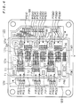
- Fig. 14 is a plan view of a circuit part of a conventional semiconductor power module.
- the normal rated output power is about 0.5 kW and an electric power is cyclically blocked and connected at a frequency of about 5 kHz.
- conductive wiring patterns P(P), P(N), P(U), P(V), P(W) and P(G1) to P(G6) are formed on the top surfaces of insulative circuit board bodies SB1 to SB3.
- IGBT elements Insulative gate bipolar transistor elements
- IGBT elements Ta4 and Tb4 are disposed on the top surface of the wiring pattern P(U), IGBT elements Ta5 and Tb5 are disposed on the top surface of the wiring pattern P(V), and IGBT elements Ta6 and Tb6 are disposed on the top surface of the wiring pattern P(W).
- the conductive wiring patterns P(P), which are respectively formed on the top surfaces of the circuit board bodies SB1 to SB3, are electrically connected to each other by jumpers J1 and J2 while the conductive wiring patterns P(N) are electrically connected to each other by jumpers J3 and J4 in a similar manner.
- the portions shadowed by oblique lines in Fig. 14 represent terminals which are connected to the wiring patterns.
- a number of conductive wires w attain electrical connection between the IGBT elements and the wiring patterns and electrical connection between the wiring patterns.
- the wiring patterns P(P) and P(N) transfer a positive and a negative power source potentials, respectively, and supply a power source current to the IGBT elements.
- the wiring patterns P(U), P(V) and P(W) each carry each one of three-phase output currents.
- the wiring patterns P(G1) to P(G6) are wiring patterns for transmitting gate voltages which are developed at the IGBT elements.
- the wiring patterns P(P) and P(N) are located near opposite ends of the circuit board bodies SB1 to SB3. Between the wiring patterns P(P) and P(N), other wiring patterns including the wiring pattern P(U), the IGBT and other elements are disposed. Mounted near the opposite ends of the circuit board bodies SB1 to SB3, the power source terminals PS(P) and PS(N) are spaced apart from each other.
- a semiconductor power module having a high frequency is desired since the higher frequency for cyclically blocking and connecting electric power a semiconductor power module has, e.g, about 10 kHz or higher, the better performance the semiconductor power module attains including reduced electric power loss, improvement in response and operation accuracy of an object to be electric-power controlled such as a motor or etc.
- Another demand for a semiconductor power module is the ability of controlling a larger electric power, for example, an electric power of around 1 kW or more, which is necessary to drive a large, industrial use motor or the like.
- the power source current mentioned above intermittently flows because of operations of the IGBT elements.
- a surge voltage is developed in the path.
- the surge voltage increases in proportion to an increase in the value or the frequency of the power source current which is cyclically blocked and connected. If excessively high, the surge voltage causes an electrical noise which leads to circuit failure in the device and eventually to destruction of the circuit elements which form the circuit.
- a semiconductor power module comprises: (a) a semiconductor element for electric power control, respectively; (b) a circuit board, comprising: (b-1) a circuit board body having a plate-like insulator; and (b-2) a first and a second wiring patterns disposed on one major surface of the circuit board in such a manner that principal parts of the first and the second wiring patterns are adjacent each other, the first and the second wiring patterns transmitting a first and a second power source potentials to the semiconductor element for electric power control; and (c) a first and a second power source terminals which are connected to the first and the second wiring patterns, respectively, the first and the second power source terminals being arranged in the vicinity of each other so that power source currents flow in the first and the second wiring patterns in substantially antiparallel directions.
- a semiconductor power module comprises: (a) a semiconductor element for electric power control; and (b) a power source terminal for transmitting a first and a second power source potentials to the semiconductor element for electric power control.
- the power source terminal comprises: (b-1) an insulative sheet having an insulator of a substantially plate shape; and (b-2) a first and a second conductors each having a substantially plate shape for transmitting the first and the second power source potentials, respectively, the first and the second conductors being respectively mounted along a first and a second major surfaces of the insulative sheet, the first and the second conductors carrying power source currents in substantially antiparallel directions.
- a semiconductor power module comprises: (a) a semiconductor element for electric power control; (b) a circuit board, comprising: (b-1) a circuit board body having a plate-like insulator; and (b-2) a first and a second wiring patterns respectively formed in a first and a second different planes which are parallel to a major surface of the circuit board body in such a manner that principal parts of the first and the second wiring patterns are facing each other, the first and the second wiring patterns transmitting a first and a second power source potentials to the semiconductor element for electric power control, respectively; and (c) a first and a second power source terminals which are connected to the first and the second wiring patterns, respectively, the first and the second power source terminals being arranged in the vicinity of each other so that power source currents flow in the first and the second wiring patterns in substantially antiparallel directions.
- a semiconductor power module comprises: (a) a semiconductor element for electric power control; and (b) a power source terminal for transmitting a first and a second power source potentials to the semiconductor element for electric power control, the power source terminal comprises: (b-1) a first insulative sheet having an insulator of a substantially plate shape; and (b-2) a first and a second conductors each having a substantially plate shape for transmitting the first and the second power source potentials, respectively, the first and the second conductors being respectively mounted along a first and a second major surfaces of the first insulative sheet, the first and the second conductors carrying power source currents in substantially antiparallel directions; and (c) an external power source terminal connected to the power source terminal by a connection member of an excellent conductivity, the external power source terminal comprising: (c-1) a second insulative sheet having an insulator of a substantially plate shape; and (c-2) a third and a fourth conductors each having a substantially plate
- the power source terminal and the external power source terminal are connected by the connection member in such a manner that the first and the third conductors are in pressure contact and hence in electrical connection to each other, and the second and the fourth conductors, each in pressure contact to the connection member, are electrically coupled to each other through the connection member.
- the semiconductor power module further comprises (c) a circuit board, the circuit board comprising (c-1) a circuit board body having a plate-like insulator; and (c-2) a first and a second wiring patterns disposed on one major surface of the circuit board body in such a manner that principal parts of the first and the second wiring patterns are adjacent each other, the first and the second wiring patterns transmitting a first and a second power source potentials to the semiconductor element for electric power control, respectively, the first and the second wiring patterns being connected to the first and the second conductors, respectively.
- the semiconductor power module further comprises (c) a circuit board, the circuit board comprising (c-1) a circuit board body having a plate-like insulator; and (c-2) a first and a second wiring patterns respectively formed in a first and a second different planes which are parallel to a major surface of the circuit board body in such a manner that principal parts of the first and the second wiring patterns are facing each other, the first and the second wiring patterns transmitting a first and a second power source potentials to the semiconductor element for electric power control, respectively, the first and the second wiring patterns being connected to the first and the second conductors, respectively.
- the first and the second wiring patterns for transmitting the first and the second power source potentials to the semiconductor element for electric power control are disposed on the major surface of the circuit board in such a manner that the principal parts of the first and the second wiring patterns are adjacent each other.
- the first and the second power source terminals connected to these wiring patterns are disposed adjacent each other so that power source currents flow in the first and the second wiring patterns in substantially antiparallel directions.
- a parasitic inductance is reduced which is present in the path of the power source current which extends from the first power source terminal to the second power source terminal through the first wiring pattern, the semiconductor element for electric power control and the second wiring pattern.
- a surge voltage is suppressed which is created by intermittent variations in a current which flows in the path in accordance with operations of the semiconductor element for electric power control.
- the power source terminal for transmitting the first and the second power source potentials to the semiconductor element for electric power control is comprised of the first and the second substantially plate-like shaped conductors and the substantially plate-like shaped insulative sheet which is interposed between the first and the second conductors.
- the first and the second power source potentials are transferred by the first and the second conductors, respectively.
- the power source currents flow in substantially antiparallel directions. This restrains a parasitic inductance which is present in the path of the power source current which extends from the first power source terminal to the second power source terminal through the semiconductor element for electric power control.
- a surge voltage is suppressed which is created by intermittent variations in a current which flows in the path in accordance with operations of the semiconductor element for electric power control.
- the wiring patterns for transmitting the first and the second power source potentials to the semiconductor element for electric power control are formed on the circuit board in such a manner that their principal parts are facing each other.
- the first and the second power source terminals connected to these wiring patterns are disposed adjacent each other so that power source currents flow in the first and the second wiring patterns in substantially antiparallel directions.
- a parasitic inductance is reduced which is present in the path of the power source current which extends from the first power source terminal to the second power source terminal through the first wiring pattern, the semiconductor element for electric power control and the second wiring pattern.
- a surge voltage is suppressed which is created by intermittent variations in a current which flows in the path in accordance with operations of the semiconductor element for electric power control.
- the power source terminal for transmitting the first and the second power source potentials to the semiconductor element for electric power control is comprised of the first and the second substantially plate-like shaped conductors and the substantially plate-like shaped insulative sheet which is interposed between the first and the second conductors.
- the first and the second power source potentials are transferred by the first and the second conductors, respectively.
- the power source currents flow in substantially antiparallel directions.
- the external power source terminal for coupling the external power source and the power source terminal has a similar structure. Hence, a parasitic inductance is reduced which is present in the path of the power source current which extends from the third conductor to the fourth conductor through the semiconductor element for electric power control.
- the external power source terminal and the power source terminal are connected to each other by the connection member in an easy manner. Since the first and the third conductors are in direct contact each other and the second and the fourth conductors are coupled through the connection member, an inductance is restrained which is present at the connection part at which the power source terminal and the external power source terminal are connected to each other.
- Fig. 2 is a schematic circuitry diagram showing a principal portion of a circuit 110 of a semiconductor power module 100 according to a first preferred embodiment of the present invention.
- the normal rated output power and the maximum output current of the device 100 are respectively 440 V and 30 A to 600 A, for instance.
- a frequency for blocking and connecting an output current is 10 to 20 kHz.
- the circuit 110 comprises two circuit parts 120 and 130.
- the main circuit 120 is a circuit part for control and output of an electric power.
- a high electric potential P and a low electric potential N of a direct current are applied to a power source terminal PS(P) and a power source terminal PS(N), respectively, from an external power source (not shown). That is, supply of an electric power to the main circuit 120 from the external power source is attained through the power source terminals PS(P) and PS(N).
- the main circuit 120 comprises six active elements for electric power control, i.e., IGBT elements T1 to T6. An electric power supplied to the main circuit 120 is controlled in accordance with U-, V- and W- three phases to create controlled electric powers which will be respectively outputted outside the device 100 from three output terminals OUT(U), OUT(V) and OUT(W).
- the control circuit 130 is a circuit part for control of operations of the IGBT elements T1 to T6.
- the control circuit 130 comprises six active semiconductor elements IC1 to IC6.
- the semiconductor elements IC1 to IC6 in response to input signals V IN 1 to V IN 6 received at signal input terminals IN1 to IN6 from outside, send gate voltage signals V G 1 to V G 6 to gates G of the IGBT elements T1 to T6.
- the IGBT elements T1 to T6 block and connect currents between collectors C and emitters E.
- the negative power source terminals V EE 1 to V EE 3 are electrically connected to the emitters E of the IGBT elements T1 to T3.
- the negative power source terminal V EE 4 is connected to the emitters E of the IGBT elements T4 to T6 which are at a common electric potential.
- the main circuit 120 is to conduct a relatively large current, and therefore, its circuit structure is designed to endure a large current and accompanying large heat generation.
- the control circuit 130 intended to process a voltage signal, is to carry a very small current. Hence, the circuit structure of the control circuit 130 is not designed to handle a large current.
- Fig. 3 is a perspective view showing the appearance of the device 100.
- the device 100 comprises a case 101 which is made of insulative material such as synthetic resin. On the top surface of the case 101, a lid 102 is placed. A terminal 103 of the main circuit 120 and a terminal 104 of the control circuit 130 are projected from the top surface of the case 101 to outside the device 100.
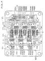
- Fig. 4 is a plan view of a circuit board 121 of the main circuit housed in the case 101 at a predetermined location.
- the circuit board 121 comprises four circuit board bodies 121a to 121d which are disposed on the top surface of a copper base 122 which forms the bottom of the case 101.
- the IGBT elements T1 to T6 passive circuit elements D1 to D6 associated to the IGBT elements T1 to T6 and the wiring patterns are disposed.
- the wiring patterns P(P), P(N), P(U), P(V) and P(W) transmit the high electric potential P, the low electric potential N, the U-phase output, the V-phase output and the W-phase output, respectively.
- wiring patterns are enough wide and thick to carry a large current.
- the wiring patterns are each connected to associated one of the power source terminals PS(P) and PS(N) and the output terminals OUT(U), OUT(V) and OUT(W) at a portion which is shadowed with oblique lines.
- the circuit board bodies 121c and 121d are a body part of the circuit board for connecting the IGBT elements T1 to T6 and the control circuit 130.
- wiring patterns P(E1) to P(E6) are each connected to each one of the emitters E of the IGBT elements T1 to T6, the wiring patterns P(G1) to P(G6) are each connected to each one of the gates G of the IGBT elements T1 to T6.
- the IGBT elements T1 to T6 each comprise a detection circuit for detecting a current which flows through the collector C of the IGBT element (i.e., collector current) and for sending a voltage signal which corresponds to the collector current.
- Wiring patterns P(S1) to P(S6) are connected to the detection circuits of the IGBT elements T1 to T6 and transmit the detection signals regarding the collector currents.
- the wiring pattern P(EX) is a wiring pattern for transmitting other signal.
- These wiring patterns are each connected, at a portion which is shadowed with oblique lines in the drawing, to an end of one of conductive pins (described later) which are connected to the control circuit 130.
- the wiring patterns are electrically connected to the control circuit 130 through the conductive pins. Electrical connection is attained among the afore-mentioned elements and between the elements and the wiring patterns by means of a number of conductive wires w.
- the wiring patterns P(P) and P(N) formed on the circuit board body 121a transmit a positive and a negative power source potentials to the IGBT elements T1 to T6 to thereby supply the power source current to the IGBT elements T1 to T6.
- a large current flows in the wiring patterns P(P) and P(N) while intermittently and rapidly varying in accordance with operations of the IGBT elements T1 to T6.
- wirings which form a circuit includes a parasitic inductance. The inductance gives rise to a high surge voltage in the wirings when a large current flows in the wirings and changes rapidly.
- the wiring patterns P(P) and P(N), in which a large current rapidly and intermittently varies, are disposed on the circuit board body 121a with most areas (principal parts) located adjacent each other. Since alike the wiring patterns P(P) and P(N), the power source terminals PS(P) and PS(N) connected to the wiring patterns P(P) and P(N) are disposed in the vicinity to each other, power source currents flow in the wiring patterns P(P) and P(N) approximately parallel to each other but in opposite directions, i.e., these currents flow in substantially antiparallel directions. As mentioned above, the power source terminals PS(P) and PS(N) are disposed close to each other.
- Fig. 5 is a plan view of a circuit board 131 of the control circuit 130. Since the device 100 is used in a large current, the control circuit 130 is formed on a different board from the board mounting the main circuit 120 in which large heat is generated. On the circuit board 131, active semiconductor elements IC1 to IC7, passive circuit elements EL associated with the semiconductor elements IC1 to IC7 and wiring patterns are seated. To prevent malfunction of the semiconductor elements IC1 to IC7 which is induced by an electrical noise, the semiconductor elements IC1 to IC7 and the circuit elements EL associated with the same are located close to each other.
- the major surface of the circuit board 131 is conceptually devided into a plurality of separated areas A1 to A7 by imaginary boundaries shown with the dotted lines in Fig. 5.
- each one of the semiconductor elements IC1 to IC7 and the associated circuit element EL are arranged.
- the semiconductor element IC7 is formed for a different purpose.
- the circuit board 131 comprises the terminal 104 which is connected to the wiring patterns and further to the external power source and the like mentioned earlier.
- the circuit elements formed on the circuit boards 121 and 131 are arranged so that each one of the semiconductor elements IC1 to IC6 and the associated circuit element EL are located approximately above the relevant one of the IGBT elements T1 to T6 to be controlled and the relevant one of the circuit elements D1 to D6 when the circuit boards are disposed to face each other one above the other as shown in Fig. 6.
- the area A1 of the circuit board 131 including the semiconductor element IC1 and its associated circuit element EL is to be located approximately right above the circuit board 121 at an area in which the IGBT element T1, the associated circuit element D1 and the like are arranged. This is also true of the other areas A2 to A7.
- the negative power source potential at the semiconductor elements IC1 to IC4 and IC7 is the same as the common emitter potential of the IGBT elements T4 to T6.
- the areas A4 to A7 are each required only to be located above the circuit board 131 at an region where the IGBT elements T4 to T6 are included.
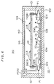
- Fig. 6 is a front cross sectional view of the device 100.
- the circuit boards 131 and 121 are arranged one above the other in the device 100.
- a plurality of conductive pins PI electrically connect the circuit which is formed on the circuit board 121 to the circuit which is formed on the circuit board 131.
- the circuit board bodies 121a to 121d are made of ceramic or aluminum nitride and the bottom surfaces of the circuit board bodies 121a to 121d are entirely covered with copper foils. By soldering the copper foil surfaces onto the top surface of a copper base 122, the circuit board 121 is fixed to the copper base 122.
- the wiring patterns such as P(N) and P(W) are formed.
- circuit elements such as the IGBT elements T3 and T6 are soldered.
- the copper base 122 which occupies most of the bottom of the device 100 is intended primarily for heat dissipation. More precisely, the copper base 122 discharges heat which is generated by power loss in the main circuit 120 to outside the device 100 to thereby prevent an excessive increase in the temperatures of the main circuit 120 and the control circuit 130.
- the lid 102 is made of electrically insulative material such as synthetic resin.
- the bottom surface of the lid 102 is approximately covered in its entirety with a copper sheet 105 applied thereto.
- the copper sheet 105 is electrically connected to the power source terminal PS(N) and insulated from the other terminals except for the power source terminal PS(N), namely, the terminals 103 and 104.
- This means that an electric potential at the copper sheet 105 is kept the same as the lower electric potential N, or a stable potential of the device 100.
- the copper sheet 105 shields an electromagnetic radiation noise. That is, the copper sheet 105 prevents the control circuit 103 and the like from malfunctioning by allowing less electromagnetic radiation noise into the device 100.
- the copper sheet 105 also arrests leakage of an electromagnetic radiation noise which is generated in the main circuit 120 and the like to outside the device 100.
- the external power source and other external device connected to the device 100 are disposed in the vicinity of the device 100.
- the bottom of the device 100, to which the circuit board 121 creating large heat is mounted includes a heat dissipation structure as described earlier, the external device is to be disposed on the top surface of the device 100. This is the reason why the terminals 103 and 104 are located in the top surface of the device 100.
- the external device connected to the terminal 103 is a source of a particularly strong electrical noise which could cause the control circuit 130 to fail to normally operate upon entrance into the control circuit 130.
- the structure that the copper sheet 105 is attached to the lid 102 effectively prevents entrance of an electrical noise into the control circuit 130.
- a semiconductor power module 200 according to a second preferred embodiment of the present invention is equal to the device 100 of the first preferred embodiment as it is modified to further obviate a surge voltage by means of an improved structure as to the power source terminals PS(P) and PS(N).
- Fig. 7 is a plan view of the circuit board 121 of the main circuit which is mounted within the case 101 of the device 200 at a predetermined location.
- the principal part of the circuit 110 of the device 200 is similar to that of the device 100 as schematically shown in Fig. 2.
- the wiring patterns P(P) and P(N) of the circuit board 121 are formed on the circuit board body 121a in the vicinity to each other.
- Fig. 8 is a partially expanded plan view showing a connection part at which the power source terminals PS(P) and PS(N) and the wiring patterns P(P) and P(N) are connected. As shown in Fig. 8, the power source terminals PS(P) and PS(N) are incorporated into one power terminal PS(NP).
- An external power source terminal EPS(NP) is a terminal which is electrically connected to the power source terminal PS(NP) and connects the external power source to the power source terminal PS(NP).
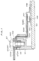
- Fig. 1 is a cross sectional view taken along the line A-A of Fig. 8.
- the two power source terminals PS(P) and PS(N) each formed by a conductive plate are arranged adjacent each other through a plate-like insulative sheet INS1 made of insulative synthetic resin or the like sandwitched therebetween.
- the power source terminals PS(P) and PS(N) are electrically connected to the wiring patterns P(P) and P(N), respectively.
- the insulative sheet INS1 is 0.5 mm to 1.5 mm in thickness, for instance.
- the power source terminal PS(NP) is connected to the external power source terminal EPS(NP).
- the external power source terminal EPS(NP) is also comprised of external power source terminals EPS(P) and EPS(N) which are each formed by a conductive plate and arranged adjacent each other with an insulative sheet INS2 made of insulative synthetic resin or the like sandwitched therebetween.
- the insulative sheet INS2 has the same thickness as that of the insulative sheet INS1.
- the power source terminal (NP) and the external power source terminal EPS(NP) are bolted together by a conductive nut 126 which is buried in the top surface of the case 101 and a conductive bolt 127 which is engaged with the nut 126.
- An insulative bushing INS3 is a cylindrical insulator and electrically insulates the bolt 127 from the power source terminals PS(P) and PS(N) and from the external power source terminals EPS(P) and EPS(N).
- the power source terminal PS(N) and the external power source terminal EPS(N), being in contact each other, are electrically connected to each other.
- the power source terminal PS(P) and the external power source terminal EPS(P) are electrically connected to each other through the conductive nut 126 and the conductive bolt 127.
- the structure as above restrains the inductance present in the path mentioned above which includes the external power source terminals EPS(P) and EPS(N), and hence, reduces a surge voltage which is created in the path.
- Fig. 9 is a perspective view showing the appearance of the device 200.
- the device 200 instead of the power source terminals PS(P) and PS(N) which are disposed in the device 100 separately from each other, one power source terminal PS(NP) is disposed as it is partially projected from the top surface of the case 101.
- the external power source terminal EPS(NP) is omitted.
- the circuit board 321 includes seven circuit board bodies 321a to 321h.
- the circuit board bodies 321a to 321h are each made of ceramic or aluminum nitride and the bottom surfaces of the circuit board bodies 321a to 321h are approximately entirely covered with copper foils 323a to 323h respectively (Fig. 11 shows only the copper foils 323a, 323b, 323e and 323h).
- the surfaces of the copper foils 323a and 323c to 323h are soldered to the top surface of a copper base 322, whereby the circuit board bodies 321a and 321c to 321h are fixed to the copper base 322.
- the copper base 322 which occupies most of the bottom of the device 300 is intended primarily for heat dissipation. More precisely, the copper base 322 discharges heat which is generated by power loss in the circuit to outside the device 300 to thereby prevent an excessive increase in the temperature of the circuit.
- the wiring pattern P(N) for maintaining the low electric potential N and the wiring patterns P(U), P(V) and P(W) for respectively transmitting the U-, the V- and the W-phase outputs are formed.
- wiring patterns P(G1) to P(G6) are formed, respectively.
- the wiring patterns P(G1) to P(G6) are wiring patterns for transmitting the gate voltage signals V G 1 to V G 6 for the IGBT elements T1 to T6.
- the IGBT elements T1 to T3 and the passive circuit elements D1 to D3 are formed on the top surface of the wiring pattern P(P).
- the IGBT elements T4 to T6 and the passive circuit elements D4 to D6 are soldered to the top surfaces of the wiring patterns P(U), P(V) and P(W), respectively.
- the respective elements and the wiring patterns are electrically connected to each other by the conductive wires w where necessary.
- the wiring patterns P(P), P(N), P(U), P(V), P(W) and P(G1) to P(G6) are connected to the power source terminals PS(P) and PS(N), the output terminals OUT(U), OUT(V), OUT(W) and the input terminals PS(G1) to PS(G6) to electrically connect the wiring patterns to outside the device 300.
- it is at portions which are shadowed with oblique lines where the wiring patterns and the terminals are connected to each other.
- Fig. 12 is a perspective view showing the appearance of the device 300.
- the copper base 322 is disposed at the bottom of a case 301. In the top surface of the case 301, the terminals mentioned above are partially projected outside.
- the power source terminals PS(P) and PS(N) are formed as one integrated power source terminal PS(NP) as shown in Fig. 1.
- the power source terminal PS(NP) is connected to the external power source terminals EPS(NP) through the bolt 127.
- Fig. 13 is an explanatory diagram showing the paths of principal currents within the device 300.
- a power source current supplied from the power source terminal PS(P) is appropriately shunted into each one of the IGBT elements T1 to T3 through the wiring pattern P(P).
- the shunted currents are respectively outputted to outside from the output terminals OUT(U), OUT(V) and OUT(W) through the wiring patterns P1(U), P1(V) and P1(W) and the wiring patterns P(U), P(V) and P(W).
- currents flow into the device 300 from the output terminals OUT(U), OUT(V) and OUT(W) when necessary.
- These currents entering the device 300 flow through the wiring patterns P(U), P(V) and P(W), respectively, join into one current at the wiring pattern P(N) and return to the power source terminal PS(N).
- the wiring patterns P(P) and P(N) are disposed almost in contact each other with the circuit board body 321b sandwitched therebetween. In a region where these wiring patterns are formed, most portions (principal parts) of the wiring patterns are faced each other.
- the thickness of the circuit board body 321b is 0.5 mm to 1.5 mm, for instance.
- the power source terminals PS(P) and PS(N) connected to the wiring patterns P(P) and P(N) are also disposed close to each other.
- currents flow close to each other with the circuit board body 321b sandwitched therebetween.
- the directions of the currents are opposite each other in the principal parts of the wiring patterns P(P) and P(N).
- the parasitic inductance present in the current path from the power source terminal PS(P) to the power source terminal PS(N) is suppressed.
- a surge voltage developed in the current path is restrained, thereby preventing malfunction and destruction of the circuit elements.
Applications Claiming Priority (2)
| Application Number | Priority Date | Filing Date | Title |
|---|---|---|---|
| JP4172774A JP2725952B2 (ja) | 1992-06-30 | 1992-06-30 | 半導体パワーモジュール |
| JP172774/92 | 1992-06-30 |
Publications (2)
| Publication Number | Publication Date |
|---|---|
| EP0578108A1 true EP0578108A1 (de) | 1994-01-12 |
| EP0578108B1 EP0578108B1 (de) | 1998-06-10 |
Family
ID=15948096
Family Applications (1)
| Application Number | Title | Priority Date | Filing Date |
|---|---|---|---|
| EP93110363A Expired - Lifetime EP0578108B1 (de) | 1992-06-30 | 1993-06-29 | Halbleiter-Leistungsmodul |
Country Status (4)
| Country | Link |
|---|---|
| US (1) | US5471089A (de) |
| EP (1) | EP0578108B1 (de) |
| JP (1) | JP2725952B2 (de) |
| DE (1) | DE69319026T2 (de) |
Cited By (36)
| Publication number | Priority date | Publication date | Assignee | Title |
|---|---|---|---|---|
| FR2726940A1 (fr) * | 1994-05-31 | 1996-05-15 | Mitsubishi Electric Corp | Dispositif a semiconducteurs comportant un boitier et une embase isolante, et procede de fabrication de ce dispositif |
| EP0752167A1 (de) * | 1994-03-21 | 1997-01-08 | Intel Corporation | Verfahren und einrichtung für integrierbare spannungsregelungsschaltungsanordnung |
| EP0772235A2 (de) * | 1995-10-25 | 1997-05-07 | Mitsubishi Denki Kabushiki Kaisha | Halbleiteranordnung mit einem Schaltungssubstrat und einem Gehäuse |
| WO1999000845A1 (de) * | 1997-06-28 | 1999-01-07 | Robert Bosch Gmbh | Elektronisches steuergerät |
| EP0907310A2 (de) * | 1997-10-01 | 1999-04-07 | Siemens Aktiengesellschaft | Anschlussvorrichtung für thermisch belastete Stromleiter, insbesondere in Umrichtern oder dergleichen |
| EP0924845A2 (de) * | 1997-12-22 | 1999-06-23 | Omnirel LLC | Leistungshalbleitermodul |
| FR2782597A1 (fr) * | 1998-08-24 | 2000-02-25 | Int Rectifier Corp | Module d'alimentation electrique |
| EP0987761A2 (de) * | 1998-09-08 | 2000-03-22 | Kabushiki Kaisha Toyoda Jidoshokki Seisakusho | Anschlussflächenstruktur eines Halbleitermoduls |
| FR2794580A1 (fr) * | 1999-06-04 | 2000-12-08 | Mitsubishi Electric Corp | Onduleur |
| FR2803138A1 (fr) * | 1999-12-27 | 2001-06-29 | Mitsubishi Electric Corp | Convertisseur de courant continu en courant alternatif |
| FR2809882A1 (fr) * | 2000-05-31 | 2001-12-07 | Mitsubishi Electric Corp | Module d'alimentation |
| EP1174992A2 (de) * | 2000-07-21 | 2002-01-23 | Hitachi, Ltd. | Halbleitervorrichtung, Stromwandler und Fahrzeug |
| WO2002025704A2 (en) * | 2000-09-20 | 2002-03-28 | Ecostar Electric Drive Systems L.L.C. | Leadframe-based module dc bus design to reduce module inductance |
| FR2816462A1 (fr) * | 2000-11-03 | 2002-05-10 | Mannesmann Sachs Ag | Module convertisseur de puissance et dispositif convertisseur de puissance pour moteur a phases multiples avec pour chaque phase un tel module convertisseur de puissance |
| EP1237189A1 (de) * | 2001-02-28 | 2002-09-04 | Motorola, Inc. | Verfahren und Vorrichtung zur Impedanzanpassung |
| WO2002082543A1 (en) | 2001-03-30 | 2002-10-17 | Hitachi, Ltd. | Semiconductor device |
| WO2003085738A2 (de) * | 2002-04-04 | 2003-10-16 | Infineon Technologies Ag | Leistungsmodul mit zwei substraten und verfahren zu seiner herstellung |
| US6845017B2 (en) | 2000-09-20 | 2005-01-18 | Ballard Power Systems Corporation | Substrate-level DC bus design to reduce module inductance |
| US6906404B2 (en) | 2003-05-16 | 2005-06-14 | Ballard Power Systems Corporation | Power module with voltage overshoot limiting |
| US6987670B2 (en) | 2003-05-16 | 2006-01-17 | Ballard Power Systems Corporation | Dual power module power system architecture |
| US7012810B2 (en) | 2000-09-20 | 2006-03-14 | Ballard Power Systems Corporation | Leadframe-based module DC bus design to reduce module inductance |
| WO2006069935A1 (de) * | 2004-12-28 | 2006-07-06 | Siemens Aktiengesellschaft | Elektrische baugruppe mit abstandshaltern zwischen mehreren schaltungsträgern |
| US7158395B2 (en) | 2003-05-02 | 2007-01-02 | Ballard Power Systems Corporation | Method and apparatus for tracking maximum power point for inverters, for example, in photovoltaic applications |
| US7180763B2 (en) | 2004-09-21 | 2007-02-20 | Ballard Power Systems Corporation | Power converter |
| US7269036B2 (en) | 2003-05-12 | 2007-09-11 | Siemens Vdo Automotive Corporation | Method and apparatus for adjusting wakeup time in electrical power converter systems and transformer isolation |
| US7289329B2 (en) | 2004-06-04 | 2007-10-30 | Siemens Vdo Automotive Corporation | Integration of planar transformer and/or planar inductor with power switches in power converter |
| US7295448B2 (en) | 2004-06-04 | 2007-11-13 | Siemens Vdo Automotive Corporation | Interleaved power converter |
| US7426099B2 (en) | 2005-06-30 | 2008-09-16 | Continental Automotive Systems Us, Inc. | Controller method, apparatus and article suitable for electric drive |
| US7443692B2 (en) | 2003-05-16 | 2008-10-28 | Continental Automotive Systems Us, Inc. | Power converter architecture employing at least one capacitor across a DC bus |
| WO2009127179A1 (de) * | 2008-04-15 | 2009-10-22 | Conti Temic Microelectonic Gmbh | Verfahren zur herstellung und aufbau eines leistungsmoduls |
| US7670163B2 (en) | 2006-04-20 | 2010-03-02 | Abb Oy | Electric connection and electric component |
| DE102010000908A1 (de) * | 2010-01-14 | 2011-07-21 | Infineon Technologies AG, 85579 | Leistungshalbleitermodul mit niederinduktiven Hochstromkontakten |
| EP2416450A1 (de) * | 2010-08-04 | 2012-02-08 | SEMIKRON Elektronik GmbH & Co. KG | Einrichtung zur elektrischen Verbindung einer Leistungsbaugruppe mit Terminalflächenelementen |
| WO2021144925A1 (en) * | 2020-01-16 | 2021-07-22 | Sumitomo Electric Industries, Ltd. | Semiconductor module |
| EP3869548A4 (de) * | 2018-10-18 | 2021-12-01 | Nissan Arc, Ltd. | Halbleiterbauelement und verfahren zur herstellung davon |
| US11887902B2 (en) | 2021-03-19 | 2024-01-30 | Fuji Electric Co., Ltd. | Semiconductor device |
Families Citing this family (74)
| Publication number | Priority date | Publication date | Assignee | Title |
|---|---|---|---|---|
| EP0660119B1 (de) * | 1993-12-27 | 2003-04-02 | Hitachi, Ltd. | Beschleunigungsmessaufnehmer |
| EP0706221B8 (de) * | 1994-10-07 | 2008-09-03 | Hitachi, Ltd. | Halbleiteranordnung mit einer Mehrzahl von Halbleiterelementen |
| US5687072A (en) * | 1995-10-05 | 1997-11-11 | Semipower Systems | Low inductance inverter |
| US5748456A (en) * | 1995-11-24 | 1998-05-05 | Asea Brown Boveri Ag | Power semiconductor module system |
| JP3480771B2 (ja) * | 1995-12-20 | 2003-12-22 | 三菱電機株式会社 | 半導体装置 |
| JP3168901B2 (ja) * | 1996-02-22 | 2001-05-21 | 株式会社日立製作所 | パワー半導体モジュール |
| US6954368B1 (en) | 1996-07-22 | 2005-10-11 | HYDRO-QUéBEC | Low stray interconnection inductance power converting molecule for converting a DC voltage into an AC voltage, and a method therefor |
| JP3576727B2 (ja) * | 1996-12-10 | 2004-10-13 | 株式会社デンソー | 表面実装型パッケージ |
| US6011302A (en) * | 1997-05-29 | 2000-01-04 | Fuji Electric Co., Ltd. | Semiconductor device with reduced amount of sealing resin |
| US6069403A (en) * | 1998-10-06 | 2000-05-30 | Intersil Corporation | Power module with lowered inductance and reduced voltage overshoots |
| US6249024B1 (en) * | 1998-12-09 | 2001-06-19 | International Rectifier Corp. | Power module with repositioned positive and reduced inductance and capacitance |
| WO2000068992A1 (en) * | 1999-05-11 | 2000-11-16 | Mitsubishi Denki Kabushiki Kaisha | Semiconductor device |
| GB9911905D0 (en) * | 1999-05-22 | 1999-07-21 | Trw Lucas Varity Electric | Improvement relating to electrical power assisted steering |
| DE10010919A1 (de) * | 2000-03-06 | 2001-09-20 | Grundfos As | Frequenzumrichter |
| JP3633432B2 (ja) * | 2000-03-30 | 2005-03-30 | 株式会社日立製作所 | 半導体装置及び電力変換装置 |
| JP4475757B2 (ja) * | 2000-07-19 | 2010-06-09 | 京セラ株式会社 | インバータ制御モジュール |
| JP3635012B2 (ja) * | 2000-07-26 | 2005-03-30 | 京セラ株式会社 | インバータ制御モジュール |
| DE10037533C1 (de) * | 2000-08-01 | 2002-01-31 | Semikron Elektronik Gmbh | Induktivitätsarme Schaltungsanordnung |
| JP4475773B2 (ja) * | 2000-08-11 | 2010-06-09 | 京セラ株式会社 | インバータ制御モジュール |
| WO2002091474A1 (en) * | 2001-05-09 | 2002-11-14 | Shindengen Electric Manufacturing Co., Ltd. | Semiconductor device and its manufacturing method |
| DE10141114C1 (de) * | 2001-06-08 | 2002-11-21 | Semikron Elektronik Gmbh | Schaltungsanordnung |
| JP4601874B2 (ja) * | 2001-07-30 | 2010-12-22 | 三菱電機株式会社 | 半導体装置 |
| FR2829661B1 (fr) * | 2001-08-17 | 2004-12-03 | Valeo Equip Electr Moteur | Module de composants electroniques de puissance et procede d'assemblage d'un tel module |
| JP4561015B2 (ja) * | 2001-08-24 | 2010-10-13 | 富士電機システムズ株式会社 | 半導体装置 |
| KR100442847B1 (ko) | 2001-09-17 | 2004-08-02 | 페어차일드코리아반도체 주식회사 | 3차원 구조를 갖는 전력 반도체 모듈 및 그 제조방법 |
| US6774465B2 (en) | 2001-10-05 | 2004-08-10 | Fairchild Korea Semiconductor, Ltd. | Semiconductor power package module |
| JP2004071371A (ja) * | 2002-08-07 | 2004-03-04 | Mitsubishi Electric Corp | 半導体装置 |
| US20040042689A1 (en) | 2002-08-30 | 2004-03-04 | Hardinge Inc. | Hydrostatic bearing for linear motion guidance |
| JP4338620B2 (ja) * | 2004-11-01 | 2009-10-07 | 三菱電機株式会社 | 半導体装置及びその製造方法 |
| KR101255334B1 (ko) * | 2006-05-08 | 2013-04-16 | 페어차일드코리아반도체 주식회사 | 저 열저항 파워 모듈 및 그 제조방법 |
| KR101194041B1 (ko) * | 2006-12-07 | 2012-10-24 | 페어차일드코리아반도체 주식회사 | 고전력 반도체 패키지 |
| KR101391924B1 (ko) * | 2007-01-05 | 2014-05-07 | 페어차일드코리아반도체 주식회사 | 반도체 패키지 |
| JP2008211166A (ja) * | 2007-01-31 | 2008-09-11 | Shin Kobe Electric Mach Co Ltd | 配線板 |
| EP2099119B1 (de) | 2008-03-04 | 2014-11-19 | Kabushiki Kaisha Toyota Jidoshokki | Umrichtervorrichtung |
| JP4640423B2 (ja) * | 2008-03-04 | 2011-03-02 | 株式会社豊田自動織機 | 電力変換装置 |
| JP4572247B2 (ja) * | 2008-06-02 | 2010-11-04 | 本田技研工業株式会社 | ハイブリッド車両 |
| US7952856B2 (en) | 2008-06-02 | 2011-05-31 | Honda Motor Co., Ltd. | Power control unit and hybrid vehicle comprising same |
| DE102010000035B4 (de) * | 2010-01-11 | 2015-10-29 | LOEWE Technologies GmbH | Verfahren zur Herstellung einer Elektronikbaugruppe und eine nach dem Verfahren hergestellte Elektronikbaugruppe |
| JP5336413B2 (ja) | 2010-04-02 | 2013-11-06 | 株式会社豊田中央研究所 | パワーモジュール |
| DE202011100820U1 (de) * | 2011-05-17 | 2011-12-01 | Ixys Semiconductor Gmbh | Leistungshalbleiter |
| US8405206B1 (en) * | 2011-09-30 | 2013-03-26 | Infineon Technologies Ag | Low-inductive semiconductor module |
| EP2862202B1 (de) * | 2012-06-19 | 2016-04-27 | ABB Technology AG | Substrat zur montage mehrerer leistungstransistoren darauf und leistungshalbleitermodul |
| KR101443985B1 (ko) * | 2012-12-14 | 2014-11-03 | 삼성전기주식회사 | 전력 모듈 패키지 |
| US9885743B2 (en) * | 2012-12-17 | 2018-02-06 | Itron, Inc. | Electric meter base level printed circuit board |
| JP6136659B2 (ja) * | 2013-07-02 | 2017-05-31 | 住友電気工業株式会社 | 半導体モジュール |
| JP6136657B2 (ja) * | 2013-07-02 | 2017-05-31 | 住友電気工業株式会社 | 半導体モジュール |
| JP6136656B2 (ja) * | 2013-07-02 | 2017-05-31 | 住友電気工業株式会社 | 半導体モジュール |
| JP6139332B2 (ja) * | 2013-08-26 | 2017-05-31 | 京セラ株式会社 | パワー半導体モジュール |
| WO2015058073A1 (en) * | 2013-10-17 | 2015-04-23 | Arkansas Power Electronics Int'l., Inc. | High voltage power chip module |
| KR101983160B1 (ko) * | 2013-11-29 | 2019-05-28 | 삼성전기주식회사 | 전력반도체 모듈 |
| DE102014102018B3 (de) * | 2014-02-18 | 2015-02-19 | Semikron Elektronik Gmbh & Co. Kg | Leistungshalbleitermodul mit niederinduktiv ausgestalteten modulinternen Last- und Hilfsverbindungseinrichtungen |
| DE102014116662B4 (de) * | 2014-11-14 | 2018-03-08 | Infineon Technologies Ag | Elektrische anschlussbaugruppe, halbleitermodul und verfahren zurherstellung eines halbleitermoduls |
| US9839146B2 (en) * | 2015-10-20 | 2017-12-05 | Cree, Inc. | High voltage power module |
| JP6468984B2 (ja) * | 2015-10-22 | 2019-02-13 | 三菱電機株式会社 | 半導体装置 |
| WO2017209191A1 (ja) | 2016-06-01 | 2017-12-07 | ローム株式会社 | 半導体パワーモジュール |
| DE102016112602A1 (de) * | 2016-07-08 | 2018-01-11 | Danfoss Silicon Power Gmbh | Niederinduktives Leistungsmoduldesign |
| JP6770456B2 (ja) * | 2017-02-17 | 2020-10-14 | ルネサスエレクトロニクス株式会社 | 電子装置 |
| JP2018182860A (ja) * | 2017-04-10 | 2018-11-15 | ファナック株式会社 | モータ駆動装置 |
| DE102017115883B4 (de) * | 2017-07-14 | 2020-04-02 | Semikron Elektronik Gmbh & Co. Kg | Leistungselektronisches Submodul mit Gleich- und Wechselspannungsanschlusselementen und Anordnung hiermit |
| JP7060099B2 (ja) * | 2018-08-16 | 2022-04-26 | 住友電気工業株式会社 | 半導体モジュール |
| JP7280278B2 (ja) * | 2018-09-12 | 2023-05-23 | ローム株式会社 | 半導体装置 |
| USD908632S1 (en) | 2018-09-17 | 2021-01-26 | Cree Fayetteville, Inc. | Power module |
| USD1012050S1 (en) * | 2019-06-21 | 2024-01-23 | Raspberry Pi (Trading) Limited | Computer |
| JPWO2021033600A1 (de) * | 2019-08-21 | 2021-02-25 | ||
| JP1659678S (de) | 2019-08-29 | 2020-05-18 | ||
| JP1659674S (de) * | 2019-08-29 | 2020-05-18 | ||
| JP1659673S (de) * | 2019-08-29 | 2020-05-18 | ||
| JP1659716S (de) * | 2019-08-29 | 2020-05-18 | ||
| JP1659676S (de) | 2019-08-29 | 2020-05-18 | ||
| JP1659675S (de) | 2019-08-29 | 2020-05-18 | ||
| JP1659677S (de) * | 2019-08-29 | 2020-05-18 | ||
| JP6960984B2 (ja) * | 2019-12-26 | 2021-11-05 | 三菱電機株式会社 | 電子装置及びその絶縁部材 |
| JP2022111597A (ja) | 2021-01-20 | 2022-08-01 | 三菱電機株式会社 | 半導体モジュール |
| DE102021202723A1 (de) | 2021-03-19 | 2022-09-22 | Magna powertrain gmbh & co kg | Vorrichtung zur elektrischen Verbindung mit zumindest einer elektrischen Komponente |
Citations (4)
| Publication number | Priority date | Publication date | Assignee | Title |
|---|---|---|---|---|
| EP0277546A1 (de) * | 1987-01-21 | 1988-08-10 | Siemens Aktiengesellschaft | Halbleiteranordnung mit mindestens einem Halbleiterkörper |
| JPH01194344A (ja) * | 1988-01-28 | 1989-08-04 | Fuji Electric Co Ltd | パワートランジスタの並列接続方法 |
| US4965710A (en) * | 1989-11-16 | 1990-10-23 | International Rectifier Corporation | Insulated gate bipolar transistor power module |
| EP0427143A2 (de) * | 1989-11-07 | 1991-05-15 | IXYS Semiconductor GmbH | Leistungshalbleitermodul |
Family Cites Families (1)
| Publication number | Priority date | Publication date | Assignee | Title |
|---|---|---|---|---|
| JP2661619B2 (ja) * | 1988-11-11 | 1997-10-08 | 富士電機株式会社 | 逆阻止形トランジスタモジュール |
-
1992
- 1992-06-30 JP JP4172774A patent/JP2725952B2/ja not_active Expired - Lifetime
-
1993
- 1993-06-24 US US08/080,781 patent/US5471089A/en not_active Expired - Fee Related
- 1993-06-29 DE DE69319026T patent/DE69319026T2/de not_active Expired - Fee Related
- 1993-06-29 EP EP93110363A patent/EP0578108B1/de not_active Expired - Lifetime
Patent Citations (4)
| Publication number | Priority date | Publication date | Assignee | Title |
|---|---|---|---|---|
| EP0277546A1 (de) * | 1987-01-21 | 1988-08-10 | Siemens Aktiengesellschaft | Halbleiteranordnung mit mindestens einem Halbleiterkörper |
| JPH01194344A (ja) * | 1988-01-28 | 1989-08-04 | Fuji Electric Co Ltd | パワートランジスタの並列接続方法 |
| EP0427143A2 (de) * | 1989-11-07 | 1991-05-15 | IXYS Semiconductor GmbH | Leistungshalbleitermodul |
| US4965710A (en) * | 1989-11-16 | 1990-10-23 | International Rectifier Corporation | Insulated gate bipolar transistor power module |
Non-Patent Citations (1)
| Title |
|---|
| PATENT ABSTRACTS OF JAPAN vol. 13, no. 486 (E - 840) 6 November 1989 (1989-11-06) * |
Cited By (61)
| Publication number | Priority date | Publication date | Assignee | Title |
|---|---|---|---|---|
| EP0752167A1 (de) * | 1994-03-21 | 1997-01-08 | Intel Corporation | Verfahren und einrichtung für integrierbare spannungsregelungsschaltungsanordnung |
| EP0752167A4 (de) * | 1994-03-21 | 1998-09-02 | Intel Corp | Verfahren und einrichtung für integrierbare spannungsregelungsschaltungsanordnung |
| FR2726940A1 (fr) * | 1994-05-31 | 1996-05-15 | Mitsubishi Electric Corp | Dispositif a semiconducteurs comportant un boitier et une embase isolante, et procede de fabrication de ce dispositif |
| EP0772235A2 (de) * | 1995-10-25 | 1997-05-07 | Mitsubishi Denki Kabushiki Kaisha | Halbleiteranordnung mit einem Schaltungssubstrat und einem Gehäuse |
| EP0772235A3 (de) * | 1995-10-25 | 1999-05-06 | Mitsubishi Denki Kabushiki Kaisha | Halbleiteranordnung mit einem Schaltungssubstrat und einem Gehäuse |
| US6205031B1 (en) | 1997-06-28 | 2001-03-20 | Robert Bosch Gmbh | Electronic control apparatus |
| WO1999000845A1 (de) * | 1997-06-28 | 1999-01-07 | Robert Bosch Gmbh | Elektronisches steuergerät |
| EP0907310A3 (de) * | 1997-10-01 | 1999-11-03 | Siemens Aktiengesellschaft | Anschlussvorrichtung für thermisch belastete Stromleiter, insbesondere in Umrichtern oder dergleichen |
| EP0907310A2 (de) * | 1997-10-01 | 1999-04-07 | Siemens Aktiengesellschaft | Anschlussvorrichtung für thermisch belastete Stromleiter, insbesondere in Umrichtern oder dergleichen |
| EP0924845A2 (de) * | 1997-12-22 | 1999-06-23 | Omnirel LLC | Leistungshalbleitermodul |
| EP0924845A3 (de) * | 1997-12-22 | 2001-05-23 | Omnirel LLC | Leistungshalbleitermodul |
| FR2782597A1 (fr) * | 1998-08-24 | 2000-02-25 | Int Rectifier Corp | Module d'alimentation electrique |
| US6380617B1 (en) | 1998-09-08 | 2002-04-30 | Kabushiki Kaisha Toyoda Jidoshokki Seisakusho | Electrode terminal connection structure of semiconductor module |
| EP0987761A2 (de) * | 1998-09-08 | 2000-03-22 | Kabushiki Kaisha Toyoda Jidoshokki Seisakusho | Anschlussflächenstruktur eines Halbleitermoduls |
| EP0987761A3 (de) * | 1998-09-08 | 2000-09-13 | Kabushiki Kaisha Toyoda Jidoshokki Seisakusho | Anschlussflächenstruktur eines Halbleitermoduls |
| FR2794580A1 (fr) * | 1999-06-04 | 2000-12-08 | Mitsubishi Electric Corp | Onduleur |
| FR2803138A1 (fr) * | 1999-12-27 | 2001-06-29 | Mitsubishi Electric Corp | Convertisseur de courant continu en courant alternatif |
| FR2809882A1 (fr) * | 2000-05-31 | 2001-12-07 | Mitsubishi Electric Corp | Module d'alimentation |
| US6541838B1 (en) | 2000-05-31 | 2003-04-01 | Mitsubishi Denki Kabushiki Kaisha | Power module |
| EP1174992B1 (de) * | 2000-07-21 | 2006-04-26 | Hitachi, Ltd. | Halbleitervorrichtung, Stromwandler und Fahrzeug |
| EP1174992A2 (de) * | 2000-07-21 | 2002-01-23 | Hitachi, Ltd. | Halbleitervorrichtung, Stromwandler und Fahrzeug |
| US6791854B2 (en) | 2000-07-21 | 2004-09-14 | Hitachi, Ltd. | Semiconductor apparatus, power converter and automobile |
| WO2002025704A2 (en) * | 2000-09-20 | 2002-03-28 | Ecostar Electric Drive Systems L.L.C. | Leadframe-based module dc bus design to reduce module inductance |
| WO2002025704A3 (en) * | 2000-09-20 | 2002-09-06 | Ecostar Electric Drive Systems Llc | Leadframe-based module dc bus design to reduce module inductance |
| WO2002025703A3 (en) * | 2000-09-20 | 2002-09-06 | Ecostar Electric Drive Systems Llc | Substrate-level dc bus design to reduce module inductance |
| US6845017B2 (en) | 2000-09-20 | 2005-01-18 | Ballard Power Systems Corporation | Substrate-level DC bus design to reduce module inductance |
| WO2002025703A2 (en) * | 2000-09-20 | 2002-03-28 | Ecostar Electric Drive Systems L.L.C. | Substrate-level dc bus design to reduce module inductance |
| US7193860B2 (en) | 2000-09-20 | 2007-03-20 | Ballard Power Systems Corporation | Leadframe-based module DC bus design to reduce module inductance |
| US7012810B2 (en) | 2000-09-20 | 2006-03-14 | Ballard Power Systems Corporation | Leadframe-based module DC bus design to reduce module inductance |
| US7187558B2 (en) | 2000-09-20 | 2007-03-06 | Ballard Power Systems Corporation | Leadframe-based module DC bus design to reduce module inductance |
| FR2816462A1 (fr) * | 2000-11-03 | 2002-05-10 | Mannesmann Sachs Ag | Module convertisseur de puissance et dispositif convertisseur de puissance pour moteur a phases multiples avec pour chaque phase un tel module convertisseur de puissance |
| EP1237189A1 (de) * | 2001-02-28 | 2002-09-04 | Motorola, Inc. | Verfahren und Vorrichtung zur Impedanzanpassung |
| KR100862874B1 (ko) * | 2001-02-28 | 2008-10-15 | 프리스케일 세미컨덕터, 인크. | 임피던스 매칭 장치 및 방법 |
| WO2002069403A1 (en) * | 2001-02-28 | 2002-09-06 | Motorola Inc | Arrangement and method for impedance matching |
| EP1376696A1 (de) * | 2001-03-30 | 2004-01-02 | Hitachi, Ltd. | Halbleiterbauelement |
| WO2002082543A1 (en) | 2001-03-30 | 2002-10-17 | Hitachi, Ltd. | Semiconductor device |
| EP1376696A4 (de) * | 2001-03-30 | 2009-08-26 | Hitachi Ltd | Halbleiterbauelement |
| WO2003085738A2 (de) * | 2002-04-04 | 2003-10-16 | Infineon Technologies Ag | Leistungsmodul mit zwei substraten und verfahren zu seiner herstellung |
| WO2003085738A3 (de) * | 2002-04-04 | 2004-04-08 | Infineon Technologies Ag | Leistungsmodul mit zwei substraten und verfahren zu seiner herstellung |
| US7256566B2 (en) | 2003-05-02 | 2007-08-14 | Ballard Power Systems Corporation | Method and apparatus for determining a maximum power point of photovoltaic cells |
| US7158395B2 (en) | 2003-05-02 | 2007-01-02 | Ballard Power Systems Corporation | Method and apparatus for tracking maximum power point for inverters, for example, in photovoltaic applications |
| US7466571B2 (en) | 2003-05-12 | 2008-12-16 | Continental Automotive Systems Us, Inc. | Method and apparatus for adjusting wakeup time in electrical power converter systems and transformer isolation |
| US7269036B2 (en) | 2003-05-12 | 2007-09-11 | Siemens Vdo Automotive Corporation | Method and apparatus for adjusting wakeup time in electrical power converter systems and transformer isolation |
| US7443692B2 (en) | 2003-05-16 | 2008-10-28 | Continental Automotive Systems Us, Inc. | Power converter architecture employing at least one capacitor across a DC bus |
| US6987670B2 (en) | 2003-05-16 | 2006-01-17 | Ballard Power Systems Corporation | Dual power module power system architecture |
| US6906404B2 (en) | 2003-05-16 | 2005-06-14 | Ballard Power Systems Corporation | Power module with voltage overshoot limiting |
| US7289329B2 (en) | 2004-06-04 | 2007-10-30 | Siemens Vdo Automotive Corporation | Integration of planar transformer and/or planar inductor with power switches in power converter |
| US7295448B2 (en) | 2004-06-04 | 2007-11-13 | Siemens Vdo Automotive Corporation | Interleaved power converter |
| US7180763B2 (en) | 2004-09-21 | 2007-02-20 | Ballard Power Systems Corporation | Power converter |
| WO2006069935A1 (de) * | 2004-12-28 | 2006-07-06 | Siemens Aktiengesellschaft | Elektrische baugruppe mit abstandshaltern zwischen mehreren schaltungsträgern |
| US7426099B2 (en) | 2005-06-30 | 2008-09-16 | Continental Automotive Systems Us, Inc. | Controller method, apparatus and article suitable for electric drive |
| US7670163B2 (en) | 2006-04-20 | 2010-03-02 | Abb Oy | Electric connection and electric component |
| WO2009127179A1 (de) * | 2008-04-15 | 2009-10-22 | Conti Temic Microelectonic Gmbh | Verfahren zur herstellung und aufbau eines leistungsmoduls |
| DE102010000908A1 (de) * | 2010-01-14 | 2011-07-21 | Infineon Technologies AG, 85579 | Leistungshalbleitermodul mit niederinduktiven Hochstromkontakten |
| DE102010000908B4 (de) * | 2010-01-14 | 2015-07-16 | Infineon Technologies Ag | Leistungshalbleitermodul mit niederinduktiven Hochstromkontakten, Leistungshalbleitermodulsystem, Leistungshalbleitermodulanordnung und Verfahren zur Herstellung einer Leisungshalbleitermodulanordnung |
| EP2416450A1 (de) * | 2010-08-04 | 2012-02-08 | SEMIKRON Elektronik GmbH & Co. KG | Einrichtung zur elektrischen Verbindung einer Leistungsbaugruppe mit Terminalflächenelementen |
| DE102010033374A1 (de) * | 2010-08-04 | 2012-02-09 | Semikron Elektronik Gmbh & Co. Kg | Einrichtung zur elektrischen Verbindung einer Leistungsbaugruppe mit Terminalflächenelementen |
| DE102010033374B4 (de) * | 2010-08-04 | 2014-03-20 | Semikron Elektronik Gmbh & Co. Kg | Einrichtung zur elektrischen Verbindung einer Leistungsbaugruppe mit Terminalflächenelementen |
| EP3869548A4 (de) * | 2018-10-18 | 2021-12-01 | Nissan Arc, Ltd. | Halbleiterbauelement und verfahren zur herstellung davon |
| WO2021144925A1 (en) * | 2020-01-16 | 2021-07-22 | Sumitomo Electric Industries, Ltd. | Semiconductor module |
| US11887902B2 (en) | 2021-03-19 | 2024-01-30 | Fuji Electric Co., Ltd. | Semiconductor device |
Also Published As
| Publication number | Publication date |
|---|---|
| JPH0621323A (ja) | 1994-01-28 |
| EP0578108B1 (de) | 1998-06-10 |
| US5471089A (en) | 1995-11-28 |
| JP2725952B2 (ja) | 1998-03-11 |
| DE69319026T2 (de) | 1998-12-10 |
| DE69319026D1 (de) | 1998-07-16 |
Similar Documents
| Publication | Publication Date | Title |
|---|---|---|
| US5471089A (en) | Semiconductor power module | |
| EP0697732B1 (de) | Steuerschaltungsmodul | |
| KR102398496B1 (ko) | 전력 디바이스들을 병렬화하기 위한 저 인덕턴스 및 고속 스위칭을 갖는 고 전력 다층 모듈 | |
| JP3053298B2 (ja) | 半導体装置 | |
| JP3343730B2 (ja) | 実装基板及び電気部品の実装方法 | |
| JP4640213B2 (ja) | 電力半導体装置及びそれを使用したインバータブリッジモジュール | |
| US6262902B1 (en) | Power conversion component with integral output current shunt and its manufacturing method | |
| JP4292652B2 (ja) | パワー半導体モジュール | |
| KR100284241B1 (ko) | 반도체장치 | |
| US20050051874A1 (en) | Power semiconductor device | |
| US6541838B1 (en) | Power module | |
| US5202578A (en) | Module-type semiconductor device of high power capacity | |
| JP2979930B2 (ja) | 電力用半導体装置のパッケージ | |
| EP0145256B1 (de) | Aus einem Darlington-Transistor-Paar bestehende Einheit | |
| JP2000133768A (ja) | 半導体パワーモジュール | |
| JPH08288456A (ja) | パワー半導体モジュール | |
| US6795324B2 (en) | Power converter | |
| JPH0621330A (ja) | 半導体パワーモジュール | |
| KR940008343B1 (ko) | 대전력 반도체장치 | |
| US6459605B1 (en) | Low inductance transistor module with distributed bus | |
| JP2002033446A (ja) | 半導体装置 | |
| JP3394448B2 (ja) | パワー半導体装置およびそれを用いた電力変換装置 | |
| JPH03108749A (ja) | 電力変換装置用トランジスタモジュール | |
| JPH04345082A (ja) | 大電流配線基板 | |
| JP2005191233A (ja) | パワーモジュール |
Legal Events
| Date | Code | Title | Description |
|---|---|---|---|
| PUAI | Public reference made under article 153(3) epc to a published international application that has entered the european phase |
Free format text: ORIGINAL CODE: 0009012 |
|
| AK | Designated contracting states |
Kind code of ref document: A1 Designated state(s): DE FR GB |
|
| 17P | Request for examination filed |
Effective date: 19940621 |
|
| 17Q | First examination report despatched |
Effective date: 19960304 |
|
| GRAG | Despatch of communication of intention to grant |
Free format text: ORIGINAL CODE: EPIDOS AGRA |
|
| GRAG | Despatch of communication of intention to grant |
Free format text: ORIGINAL CODE: EPIDOS AGRA |
|
| GRAH | Despatch of communication of intention to grant a patent |
Free format text: ORIGINAL CODE: EPIDOS IGRA |
|
| GRAH | Despatch of communication of intention to grant a patent |
Free format text: ORIGINAL CODE: EPIDOS IGRA |
|
| GRAA | (expected) grant |
Free format text: ORIGINAL CODE: 0009210 |
|
| AK | Designated contracting states |
Kind code of ref document: B1 Designated state(s): DE FR GB |
|
| REF | Corresponds to: |
Ref document number: 69319026 Country of ref document: DE Date of ref document: 19980716 |
|
| ET | Fr: translation filed | ||
| PLBE | No opposition filed within time limit |
Free format text: ORIGINAL CODE: 0009261 |
|
| STAA | Information on the status of an ep patent application or granted ep patent |
Free format text: STATUS: NO OPPOSITION FILED WITHIN TIME LIMIT |
|
| 26N | No opposition filed | ||
| PGFP | Annual fee paid to national office [announced via postgrant information from national office to epo] |
Ref country code: FR Payment date: 20010611 Year of fee payment: 9 |
|
| PGFP | Annual fee paid to national office [announced via postgrant information from national office to epo] |
Ref country code: DE Payment date: 20010625 Year of fee payment: 9 |
|
| PGFP | Annual fee paid to national office [announced via postgrant information from national office to epo] |
Ref country code: GB Payment date: 20010627 Year of fee payment: 9 |
|
| REG | Reference to a national code |
Ref country code: GB Ref legal event code: IF02 |
|
| PG25 | Lapsed in a contracting state [announced via postgrant information from national office to epo] |
Ref country code: GB Free format text: LAPSE BECAUSE OF NON-PAYMENT OF DUE FEES Effective date: 20020629 |
|
| PG25 | Lapsed in a contracting state [announced via postgrant information from national office to epo] |
Ref country code: DE Free format text: LAPSE BECAUSE OF NON-PAYMENT OF DUE FEES Effective date: 20030101 |
|
| GBPC | Gb: european patent ceased through non-payment of renewal fee |
Effective date: 20020629 |
|
| PG25 | Lapsed in a contracting state [announced via postgrant information from national office to epo] |
Ref country code: FR Free format text: LAPSE BECAUSE OF NON-PAYMENT OF DUE FEES Effective date: 20030228 |
|
| REG | Reference to a national code |
Ref country code: FR Ref legal event code: ST |