EP0924845A2 - Leistungshalbleitermodul - Google Patents
Leistungshalbleitermodul Download PDFInfo
- Publication number
- EP0924845A2 EP0924845A2 EP98204418A EP98204418A EP0924845A2 EP 0924845 A2 EP0924845 A2 EP 0924845A2 EP 98204418 A EP98204418 A EP 98204418A EP 98204418 A EP98204418 A EP 98204418A EP 0924845 A2 EP0924845 A2 EP 0924845A2
- Authority
- EP
- European Patent Office
- Prior art keywords
- terminal
- baseplate
- cover
- terminals
- hermetically sealed
- Prior art date
- Legal status (The legal status is an assumption and is not a legal conclusion. Google has not performed a legal analysis and makes no representation as to the accuracy of the status listed.)
- Withdrawn
Links
Images


Classifications
-
- H—ELECTRICITY
- H02—GENERATION; CONVERSION OR DISTRIBUTION OF ELECTRIC POWER
- H02M—APPARATUS FOR CONVERSION BETWEEN AC AND AC, BETWEEN AC AND DC, OR BETWEEN DC AND DC, AND FOR USE WITH MAINS OR SIMILAR POWER SUPPLY SYSTEMS; CONVERSION OF DC OR AC INPUT POWER INTO SURGE OUTPUT POWER; CONTROL OR REGULATION THEREOF
- H02M7/00—Conversion of AC power input into DC power output; Conversion of DC power input into AC power output
- H02M7/003—Constructional details, e.g. physical layout, assembly, wiring or busbar connections
-
- H—ELECTRICITY
- H10—SEMICONDUCTOR DEVICES; ELECTRIC SOLID-STATE DEVICES NOT OTHERWISE PROVIDED FOR
- H10W—GENERIC PACKAGES, INTERCONNECTIONS, CONNECTORS OR OTHER CONSTRUCTIONAL DETAILS OF DEVICES COVERED BY CLASS H10
- H10W72/00—Interconnections or connectors in packages
- H10W72/50—Bond wires
- H10W72/531—Shapes of wire connectors
- H10W72/5363—Shapes of wire connectors the connected ends being wedge-shaped
-
- H—ELECTRICITY
- H10—SEMICONDUCTOR DEVICES; ELECTRIC SOLID-STATE DEVICES NOT OTHERWISE PROVIDED FOR
- H10W—GENERIC PACKAGES, INTERCONNECTIONS, CONNECTORS OR OTHER CONSTRUCTIONAL DETAILS OF DEVICES COVERED BY CLASS H10
- H10W72/00—Interconnections or connectors in packages
- H10W72/50—Bond wires
- H10W72/541—Dispositions of bond wires
- H10W72/547—Dispositions of multiple bond wires
- H10W72/5475—Dispositions of multiple bond wires multiple bond wires connected to common bond pads at both ends of the wires
-
- H—ELECTRICITY
- H10—SEMICONDUCTOR DEVICES; ELECTRIC SOLID-STATE DEVICES NOT OTHERWISE PROVIDED FOR
- H10W—GENERIC PACKAGES, INTERCONNECTIONS, CONNECTORS OR OTHER CONSTRUCTIONAL DETAILS OF DEVICES COVERED BY CLASS H10
- H10W90/00—Package configurations
- H10W90/701—Package configurations characterised by the relative positions of pads or connectors relative to package parts
- H10W90/751—Package configurations characterised by the relative positions of pads or connectors relative to package parts of bond wires
- H10W90/753—Package configurations characterised by the relative positions of pads or connectors relative to package parts of bond wires between laterally-adjacent chips
Definitions
- This invention relates to electronic packages and more particularly to modular electronic power packages.
- Electronic power packages or modules are generally known for providing electrical power to circuits and devices such as motors, actuators, controllers and the like.
- the module is preferably hermetically sealed to prevent infiltration of moisture, dust or other contaminants into the module interior which can cause impairment or failure of the module.
- Hermetically sealed modules are usually of sufficient high cost to limit their use for many commercial and industrial applications where cost is a significant factor. It would be desirable to provide a high reliability and relatively low cost module for high performance industrial, commercial and other applications.
- the present invention provides an electronic module or package for providing high reliability and high performance and which can be manufactured at relatively low cost.
- the package comprises a hermetically sealed enclosure having a metallic baseplate and a ceramic cover, and containing circuits which are typically comprised of active and passive electronic components in various circuit configurations which may include power switching elements, as well as drive, supervisory and control circuitry.
- One or more power terminals are disposed on a terminal block compliantly supported on the baseplate, the terminals extending through the cover in hermetically sealed manner.
- Signal or control terminals may also be disposed on a terminal block compliantly supported on the baseplate, these terminals also extending through the cover in hermetically sealed manner.
- one or more power terminals can be compliantly supported above the baseplate and retained in position by attachment to the cover and external terminals.
- an adapter plate is mounted on the cover and contains a plurality of terminals connected to the module terminals.
- the terminals of the adapter plate can be in any configuration to suit user requirements without requiring a change in the terminal configuration of the module itself.
- the adapter plate may also contain active and/or passive circuitry.
- a circuit board is disposed within the module and contains control or other circuitry or devices appropriate to the particular module implementation.
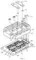
- a high power semiconductor package or module in accordance with the invention is shown in Figs. 1-3 includes a baseplate 10 having one or more electronic circuits or devices 12 disposed on a surface thereof, a first terminal block 14 disposed along a side edge of the baseplate and a second terminal block 16 disposed along an end edge of the baseplate, and an electrically insulating cover 18 attachable to the baseplate and enclosing the circuits 12 and terminal blocks 14 and 16.
- the high power package or module embodying the invention is intended for high reliability applications in the fields of aerospace and industry.
- the module has a temperature range from minus 55° C to 150° C and power ratings up to 3000 amps and up to 4500 volts.
- the module can achieve hermeticity and meet fine leak hermeticity testing standards such as MIL-STD-883E method 1014.
- the baseplate 10 is of a material which has good thermal conductivity, a thermal coefficient of expansion which is compatible with the substrates of the circuits or devices 12 disposed thereon, and also compatible with the cover 18 which is sealed to the baseplate.
- the baseplate is made of a laminate or composite of metallic materials in a combination to achieve the requisite thermal conductivity and thermal coefficient of expansion.
- the metallic materials typically include copper, copper tungsten, copper molybdenum, copper alloys or aluminum silicone carbide.
- the surface of the baseplate 10 may be plated to facilitate attachment of the substrates thereon as is known in the art. The plating may be on the entire surface of the baseplate or only in those areas where the substrates are to be attached.
- each of the circuits 12 is typically a hybrid circuit or high power device attached to or formed on a ceramic substrate 30 which includes one or more contact areas 32.
- the contact areas are connected to contact areas 34 provided on the baseplate by one or more wire bonds or current straps 36.
- the number of wire bonds or current straps connecting particular contact areas 32 to associated contact area 34 is selected to accommodate the current to be carried between those contacts areas.
- the contact areas 32 of a circuit substrate 30 can also be wire bonded directly to contact areas of a terminal block.
- the terminal block 14 provides terminals for carrying relatively high power
- the terminal block 16 provides terminals for carrying relatively lower power such as for control and signal purposes.
- the terminal block includes a body 40 of electrically insulating plastic or other material having conductive terminals 42 retained therein. Typically the terminals are molded into the body.
- the terminals each include a post portion 44 outwardly extending from the body 40 in a array, and a flat shelf portion 46 which is disposed generally at a right angle to the post portion 44.
- the shelf portion is disposed on a laterally extending portion of the body 40, as shown, which serves as a support for the shelf portions of the terminals.
- the conductive terminal 42 which typically is copper, is fabricated as shown in Figs. 4C-4E and then molded into body 40. As seen in Figs. 4C-4E, the post portion 44 is brazed or otherwise attached to the flat shelf portion 46 and this assembly is molded to body 40 to complete the assembly of the terminal block.
- the terminal block 16 is more particularly illustrated in Figs. 5A-5D, and is similar in construction to the terminal block 14 illustrated in Fig. 4 above.
- the terminal block 16 includes a plastic or other electrically insulating body 41 having conductive terminal posts 43, each attached to a conductive shelf portion 45.
- Each conductive post 43 is brazed or otherwise attached to conductive shelf portion or plate 45, and this assembly is molded into body 41 to provide the completed terminal block structure.
- the body of the terminal blocks 14 and 16 are each attached to the confronting surface of the baseplate 10 by a compliant material 48 which typically is a silicone rubber.
- the compliant layer is bonded to the body 40 and to the baseplate by a suitable adhesive such as epoxy.
- Wire bonds or current straps 36 are provided to electrically connect the shelf portion 46 of each terminal to an intermediate contact area 34 or directly to a contact area 32 of a circuit substrate 30.
- the compliant material 48 accommodates thermal expansion and contraction of the terminal block and baseplate and minimizes stress on the terminal block which could cause the block to separate from the baseplate or to crack or otherwise fail.
- the terminal blocks are of a size and configuration to suit the performance requirements of particular implementations.
- the terminals include cylindrical post portions which may or may not be threaded.
- the post portions may be of other than cylindrical shape. It will also be recognized that the size of the post portions can be selected to accommodate the power requirements of the terminal and module in which it is employed as well as the mechanical characteristics desired for a particular instance.
- the shelf portions 46 of the terminals can be sized to accommodate the number of wire bonds or straps intended for a particular device and to provided intended mechanical properties.
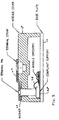
- the cover 18 is preferably a ceramic material such as alumina having a metalized edge 19 which is bonded to the confronting surface of baseplate 10 to hermetically enclose the terminal blocks and circuitry.
- the terminal posts extend through openings 21 provided in the top wall of the cover, and a washer or ring 23 typically of non-ferrous material is disposed around the upstanding end of the terminal post.
- Flat terminals 22 are disposed within respective recessed areas of the cover, as illustrated, and each have an opening to accommodate the outer end of the respective terminal posts of terminal block 14.
- flat terminals 24 are disposed within respective recessed areas of the cover and have openings to accommodate the outer end of the terminal posts of terminal block 16.
- the terminal posts are soldered, brazed or otherwise bonded to the washers 23 and terminals 22 to provide a hermetically sealed package.
- Hex nuts 72 can be disposed or retained within respective hexagonal openings in cover 18. The hex nuts can receive threaded terminals for electrical connection to associated circuitry or apparatus. These hex nuts can also serve for the mounting of an adapter plate as described below.
- the cover shown has a ribbed construction to provide physical separation between the terminals for greater electrical isolation and satisfy various governing agency requirements such as Underwriter's Laboratory (U.L.) specifications.
- U.L. Underwriter's Laboratory
- the cover 18 is a single piece which is hermetically sealed to the confronting baseplate.
- the cover can be formed of two or more elements such as a wall of one material and a top plate of the same or different material which are bonded together to form the cover unit. This construction can offer the benefits of lower manufacturing cost and simplicity for certain applications.
- An adapter plate can be mounted on the upper surface of the cover as illustrated in Fig. 6.
- the adapter plate allows placement of the electrical terminals in any configuration desired to suit user requirements.
- a module can be constructed having a standardized terminal arrangement, such as that shown in Fig. 1, to minimize the need for stocking and fabricating various versions having different terminal arrangements while still providing package terminations to suit a user's requirements.
- the adapter plate 20 is typically made of an electrically insulating material such as a plastic or a printed circuit board material having openings to accommodate the hardware to be disposed thereon. In the illustrated embodiment of Fig. 2, three openings 70 are shown to accommodate respective machine screws 72 and washers 71.
- Three flat terminals 74 have first ends 76 with openings aligned with the openings 70, and outer ends 78 configured to mate with an associated connector.
- the adapter plate can be retained on the module by fasteners such as machine screws 72, or by an adhesive or other retention elements.
- the terminal configuration illustrated provides three power terminals generally disposed along the module and four signal or control terminals disposed along one of the shorter sides of the module.
- Other terminal configurations can be readily provided by an adapter plate which has transitional connections between the terminals of the module accessible on the upper surface of the cover and the terminal positions in intended position on the upper surface of the adapter plate.
- the adapter plate may extend beyond the periphery of the cover, such as along one or more edges of the cover.
- edge terminals 100 can be provided along one or more edges of the adapter plate for connection to external circuitry.
- the adapter plate can have circuit traces or circuit elements thereon as shown in Fig. 6.
- the adapter plate can itself be part of a power control board or a portion of such a power control board.
- a circuit board 90 is mounted within the module and can contain circuitry or components appropriate to the functionality of the particular module implementation.
- the circuit board 90 has openings 91 and 92 to accommodate the respective terminal posts 44 and 43.
- the board 90 is retained in a position within the module spaced from the inner surface of baseplate 10 by any suitable means known in the art.
- the circuit board 90 can be retained solely by the terminal posts 43 and 44 to which the board can be bonded, or the board may be spaced from the confronting surface of the baseplate 10 by standoffs or other hardware elements.
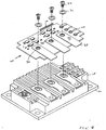
- FIGs. 8-10 A further embodiment of the invention is illustrated in Figs. 8-10.
- the terminal block 100 includes a conductive plate 102 mounted on the baseplate 104.
- a terminal post 106 is affixed and upstanding from the plate 102.
- Smaller terminal blocks 108 and 110 are mounted on ceramic plates 112 and 114, respectively, which in turn are mounted on the upper surface of plate 102.
- Terminal posts 116 and 118 are affixed to and upstanding from respective terminal blocks 108 and 110.
- the terminal blocks are connected to appropriate portions of the circuitry of the module by current straps or wire bonds as in the above embodiments.
- the plate 102 is removably attached to the baseplate 104 by a suitable adhesive such that the terminal block 100 can be separated from the underlying baseplate 104 after bonding of the current straps and before installation of the module cover.
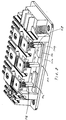
- the cover 120 (Fig. 10) is installed onto the baseplate 104 with the terminal posts 106, 116 and 118 extending through respective openings in the cover.
- the terminal posts are soldered or otherwise connected to the terminals and hermetically sealed to the cover during which step the terminal block is pulled upward away from the baseplate to provide a space between the bottom surface of the plate 102 and confronting surface of the baseplate 104.
- Terminal block 100 is thereby resiliently supported on the module to accommodate thermal expansion and contraction of the terminal block and baseplate and to minimize stress on the terminal block which could result from the block being rigidly attached to the baseplate.
- the terminal posts in the illustrated embodiment of Figs. 8-10 are of rectangular cross-section having an upper cylindrical end.
- the cylindrical end is sized to mate with and be bonded to the ring seal and opening at the end of the external terminal.
Landscapes
- Engineering & Computer Science (AREA)
- Power Engineering (AREA)
- Connections Arranged To Contact A Plurality Of Conductors (AREA)
- Multi-Conductor Connections (AREA)
Applications Claiming Priority (4)
| Application Number | Priority Date | Filing Date | Title |
|---|---|---|---|
| US99530897A | 1997-12-22 | 1997-12-22 | |
| US995308 | 1997-12-22 | ||
| US09/215,580 US6078501A (en) | 1997-12-22 | 1998-12-17 | Power semiconductor module |
| US215580 | 1998-12-17 |
Publications (2)
| Publication Number | Publication Date |
|---|---|
| EP0924845A2 true EP0924845A2 (de) | 1999-06-23 |
| EP0924845A3 EP0924845A3 (de) | 2001-05-23 |
Family
ID=26910181
Family Applications (1)
| Application Number | Title | Priority Date | Filing Date |
|---|---|---|---|
| EP98204418A Withdrawn EP0924845A3 (de) | 1997-12-22 | 1998-12-22 | Leistungshalbleitermodul |
Country Status (1)
| Country | Link |
|---|---|
| EP (1) | EP0924845A3 (de) |
Cited By (12)
| Publication number | Priority date | Publication date | Assignee | Title |
|---|---|---|---|---|
| WO2002037654A3 (en) * | 2000-11-03 | 2003-01-23 | Smc Electrical Products Inc | Microdrive |
| WO2004028226A1 (en) * | 2002-09-23 | 2004-04-01 | Siemens Energy & Automation, Inc. | Reversible housing base for motor controller |
| WO2005048347A3 (de) * | 2003-11-11 | 2005-08-11 | Eupec Gmbh & Co Kg | Leistungsmodul |
| EP1750300A3 (de) * | 2005-08-01 | 2009-03-11 | Semikron Elektronik GmbH & Co. KG Patentabteilung | Elektrisches Bauteil |
| EP1601016A3 (de) * | 2004-05-25 | 2009-11-11 | Semikron Elektronik GmbH & Co. KG Patentabteilung | Anordnung in Schraub-Druckkontakierung mit einem Leistungshalbleitermodul |
| EP1966812A4 (de) * | 2005-12-30 | 2010-11-03 | Smc Electrical Products Inc | System, vorrichtung und verfahren zur variablen frequenzansteuerung für verringerten massenleckstrom und transistorschutz |
| GB2487185A (en) * | 2011-01-05 | 2012-07-18 | Pg Drives Technology Ltd | Power Switching Circuitry with electrically conductive standoff and urging mechanism. |
| AU2011203353B2 (en) * | 2005-12-30 | 2014-08-28 | Smc Electrical Products, Inc. | Variable frequency drive system apparatus and method for reduced ground leakage current and transistor protection |
| KR101465015B1 (ko) * | 2013-11-01 | 2014-11-25 | (주)선재하이테크 | 파워 터미널 그리고 이를 적용한 전력반도체 파워 모듈 |
| EP2897276A3 (de) * | 2014-01-17 | 2016-01-27 | Kabushiki Kaisha Toyota Jidoshokki | Halbleiterbauelement |
| DE102004005545B4 (de) | 2004-02-04 | 2018-10-31 | Siemens Healthcare Gmbh | Verbindungsanordnung und Flachbaugruppe |
| CN110040081A (zh) * | 2019-04-19 | 2019-07-23 | 新乡市光明电器有限公司 | 用于车辆电气控制器的电源输入结构及车辆电气控制器 |
Family Cites Families (20)
| Publication number | Priority date | Publication date | Assignee | Title |
|---|---|---|---|---|
| DE3538933A1 (de) * | 1985-11-02 | 1987-05-14 | Bbc Brown Boveri & Cie | Leistungshalbleitermodul |
| US4739443A (en) * | 1985-12-30 | 1988-04-19 | Olin Corporation | Thermally conductive module |
| JPS62237750A (ja) * | 1986-04-09 | 1987-10-17 | Hitachi Ltd | 半導体モジユ−ル素子 |
| JP2658427B2 (ja) * | 1989-01-17 | 1997-09-30 | 富士電機株式会社 | 電力変換用半導体素子のスナバ回路とそのモジュール装置 |
| US4965710A (en) * | 1989-11-16 | 1990-10-23 | International Rectifier Corporation | Insulated gate bipolar transistor power module |
| JP2993278B2 (ja) * | 1992-06-26 | 1999-12-20 | 富士電機株式会社 | 半導体装置 |
| JP2725952B2 (ja) * | 1992-06-30 | 1998-03-11 | 三菱電機株式会社 | 半導体パワーモジュール |
| JP2924498B2 (ja) * | 1992-07-16 | 1999-07-26 | 富士電機株式会社 | 半導体装置 |
| JP3053298B2 (ja) * | 1992-08-19 | 2000-06-19 | 株式会社東芝 | 半導体装置 |
| JPH0750372A (ja) * | 1993-08-06 | 1995-02-21 | Hitachi Ltd | パワー半導体モジュール |
| US5563447A (en) * | 1993-09-07 | 1996-10-08 | Delco Electronics Corp. | High power semiconductor switch module |
| US5523620A (en) * | 1994-02-14 | 1996-06-04 | Delco Electronics Corporation | Coplanar linear dual switch module |
| US5512790A (en) * | 1994-07-21 | 1996-04-30 | Delco Electronics Corporation | Triaxial double switch module |
| DE69535775D1 (de) * | 1994-10-07 | 2008-08-07 | Hitachi Ltd | Halbleiteranordnung mit einer Mehrzahl von Halbleiterelementen |
| JPH08130290A (ja) * | 1994-10-31 | 1996-05-21 | Fuji Electric Co Ltd | 半導体装置 |
| JP3201187B2 (ja) * | 1994-12-08 | 2001-08-20 | 富士電機株式会社 | 半導体装置 |
| US5705848A (en) * | 1995-11-24 | 1998-01-06 | Asea Brown Boveri Ag | Power semiconductor module having a plurality of submodules |
| JPH09234826A (ja) * | 1995-12-28 | 1997-09-09 | Dowa Mining Co Ltd | 金属−セラミックス複合基板及びその製造法 |
| JP3168901B2 (ja) * | 1996-02-22 | 2001-05-21 | 株式会社日立製作所 | パワー半導体モジュール |
| WO1998010508A1 (en) * | 1996-09-06 | 1998-03-12 | Hitachi, Ltd. | Semiconductor device |
-
1998
- 1998-12-22 EP EP98204418A patent/EP0924845A3/de not_active Withdrawn
Cited By (23)
| Publication number | Priority date | Publication date | Assignee | Title |
|---|---|---|---|---|
| US6822866B2 (en) | 2000-11-03 | 2004-11-23 | Smc Electrical Products Inc. | Microdrive |
| AU2002224323B2 (en) * | 2000-11-03 | 2006-03-16 | Smc Electrical Products, Inc. | Microdrive |
| CN1305211C (zh) * | 2000-11-03 | 2007-03-14 | Smc电气产品公司 | 微型驱动器 |
| KR100915778B1 (ko) * | 2000-11-03 | 2009-09-04 | 에스엠씨 일렉트리칼 프로덕츠, 인크 | 마이크로드라이브 |
| WO2002037654A3 (en) * | 2000-11-03 | 2003-01-23 | Smc Electrical Products Inc | Microdrive |
| WO2004028226A1 (en) * | 2002-09-23 | 2004-04-01 | Siemens Energy & Automation, Inc. | Reversible housing base for motor controller |
| US6841747B2 (en) | 2002-09-23 | 2005-01-11 | Siemens Energy & Automation, Inc. | System and method for motor controller with a reversible housing base |
| CN100367836C (zh) * | 2002-09-23 | 2008-02-06 | 西门子能量及自动化公司 | 用于电机控制器的可翻转的壳体底座 |
| US7656672B2 (en) | 2003-11-11 | 2010-02-02 | Infineon Technologies Ag | Power module |
| WO2005048347A3 (de) * | 2003-11-11 | 2005-08-11 | Eupec Gmbh & Co Kg | Leistungsmodul |
| DE102004005545B4 (de) | 2004-02-04 | 2018-10-31 | Siemens Healthcare Gmbh | Verbindungsanordnung und Flachbaugruppe |
| EP1601016A3 (de) * | 2004-05-25 | 2009-11-11 | Semikron Elektronik GmbH & Co. KG Patentabteilung | Anordnung in Schraub-Druckkontakierung mit einem Leistungshalbleitermodul |
| EP1750300A3 (de) * | 2005-08-01 | 2009-03-11 | Semikron Elektronik GmbH & Co. KG Patentabteilung | Elektrisches Bauteil |
| EP1966812A4 (de) * | 2005-12-30 | 2010-11-03 | Smc Electrical Products Inc | System, vorrichtung und verfahren zur variablen frequenzansteuerung für verringerten massenleckstrom und transistorschutz |
| US8503180B2 (en) | 2005-12-30 | 2013-08-06 | Smc Electrical Products, Inc. | Variable frequency drive system apparatus and method for reduced ground leakage current and transistor protection |
| AU2011203353B2 (en) * | 2005-12-30 | 2014-08-28 | Smc Electrical Products, Inc. | Variable frequency drive system apparatus and method for reduced ground leakage current and transistor protection |
| GB2487185A (en) * | 2011-01-05 | 2012-07-18 | Pg Drives Technology Ltd | Power Switching Circuitry with electrically conductive standoff and urging mechanism. |
| US8665596B2 (en) | 2011-01-05 | 2014-03-04 | Pg Drives Technology Limited | Power switching circuitry |
| GB2487185B (en) * | 2011-01-05 | 2015-06-03 | Penny & Giles Controls Ltd | Power Switching Circuitry |
| KR101465015B1 (ko) * | 2013-11-01 | 2014-11-25 | (주)선재하이테크 | 파워 터미널 그리고 이를 적용한 전력반도체 파워 모듈 |
| EP2897276A3 (de) * | 2014-01-17 | 2016-01-27 | Kabushiki Kaisha Toyota Jidoshokki | Halbleiterbauelement |
| CN110040081A (zh) * | 2019-04-19 | 2019-07-23 | 新乡市光明电器有限公司 | 用于车辆电气控制器的电源输入结构及车辆电气控制器 |
| CN110040081B (zh) * | 2019-04-19 | 2024-05-17 | 新乡市光明电器有限公司 | 用于车辆电气控制器的电源输入结构及车辆电气控制器 |
Also Published As
| Publication number | Publication date |
|---|---|
| EP0924845A3 (de) | 2001-05-23 |
Similar Documents
| Publication | Publication Date | Title |
|---|---|---|
| US6078501A (en) | Power semiconductor module | |
| US6421244B1 (en) | Power module | |
| US6570774B1 (en) | Capacitor module for use in inverter, inverter, and capacitor module | |
| KR101062260B1 (ko) | 집적 회로 조립체 | |
| US5943213A (en) | Three-dimensional electronic module | |
| US4147889A (en) | Chip carrier | |
| KR960000711B1 (ko) | 반도체장치 및 그 제조방법 | |
| US4941033A (en) | Semiconductor integrated circuit device | |
| US5241456A (en) | Compact high density interconnect structure | |
| CA1201820A (en) | Semiconductor integrated circuit including a lead frame chip support | |
| EP0924845A2 (de) | Leistungshalbleitermodul | |
| US5311058A (en) | Integrated circuit power distribution system | |
| US4643499A (en) | Component mounting apparatus | |
| RU2001119053A (ru) | Композиционный материал и его применение | |
| WO1993003871A1 (en) | Improved ceramic package | |
| US4885662A (en) | Circuit module connection system | |
| US6119333A (en) | Mini-module with upwardly directed leads | |
| US5038197A (en) | Hermetically sealed die package with floating source | |
| JPH0453101B2 (de) | ||
| USRE37416E1 (en) | Method for manufacturing a modular semiconductor power device | |
| KR100843734B1 (ko) | 반도체 전력용 모듈 및 그 제조방법 | |
| EP4102555A1 (de) | Leistungshalbleitermodul | |
| JPH0834278B2 (ja) | 半導体チップキャリヤー装置 | |
| CN106449526B (zh) | 具有改善的密封的功率半导体模块 | |
| TW550713B (en) | Package for electronic components and method for forming a package for electronic components |
Legal Events
| Date | Code | Title | Description |
|---|---|---|---|
| PUAI | Public reference made under article 153(3) epc to a published international application that has entered the european phase |
Free format text: ORIGINAL CODE: 0009012 |
|
| 17P | Request for examination filed |
Effective date: 19981222 |
|
| AK | Designated contracting states |
Kind code of ref document: A2 Designated state(s): AT BE CH CY DE DK ES FI FR GB GR IE IT LI LU MC NL PT SE |
|
| AX | Request for extension of the european patent |
Free format text: AL;LT;LV;MK;RO;SI |
|
| PUAL | Search report despatched |
Free format text: ORIGINAL CODE: 0009013 |
|
| AK | Designated contracting states |
Kind code of ref document: A3 Designated state(s): AT BE CH CY DE DK ES FI FR GB GR IE IT LI LU MC NL PT SE |
|
| AX | Request for extension of the european patent |
Free format text: AL;LT;LV;MK;RO;SI |
|
| AKX | Designation fees paid | ||
| REG | Reference to a national code |
Ref country code: DE Ref legal event code: 8566 |
|
| STAA | Information on the status of an ep patent application or granted ep patent |
Free format text: STATUS: THE APPLICATION IS DEEMED TO BE WITHDRAWN |
|
| 18D | Application deemed to be withdrawn |
Effective date: 20011124 |