EP1376696A1 - Halbleiterbauelement - Google Patents
Halbleiterbauelement Download PDFInfo
- Publication number
- EP1376696A1 EP1376696A1 EP02713259A EP02713259A EP1376696A1 EP 1376696 A1 EP1376696 A1 EP 1376696A1 EP 02713259 A EP02713259 A EP 02713259A EP 02713259 A EP02713259 A EP 02713259A EP 1376696 A1 EP1376696 A1 EP 1376696A1
- Authority
- EP
- European Patent Office
- Prior art keywords
- conductor
- semiconductor switches
- insulating
- insulating substrate
- semiconductor
- Prior art date
- Legal status (The legal status is an assumption and is not a legal conclusion. Google has not performed a legal analysis and makes no representation as to the accuracy of the status listed.)
- Granted
Links
Images


Classifications
-
- H—ELECTRICITY
- H02—GENERATION; CONVERSION OR DISTRIBUTION OF ELECTRIC POWER
- H02M—APPARATUS FOR CONVERSION BETWEEN AC AND AC, BETWEEN AC AND DC, OR BETWEEN DC AND DC, AND FOR USE WITH MAINS OR SIMILAR POWER SUPPLY SYSTEMS; CONVERSION OF DC OR AC INPUT POWER INTO SURGE OUTPUT POWER; CONTROL OR REGULATION THEREOF
- H02M7/00—Conversion of ac power input into dc power output; Conversion of dc power input into ac power output
- H02M7/003—Constructional details, e.g. physical layout, assembly, wiring or busbar connections
-
- H—ELECTRICITY
- H01—ELECTRIC ELEMENTS
- H01L—SEMICONDUCTOR DEVICES NOT COVERED BY CLASS H10
- H01L23/00—Details of semiconductor or other solid state devices
- H01L23/52—Arrangements for conducting electric current within the device in operation from one component to another, i.e. interconnections, e.g. wires, lead frames
- H01L23/538—Arrangements for conducting electric current within the device in operation from one component to another, i.e. interconnections, e.g. wires, lead frames the interconnection structure between a plurality of semiconductor chips being formed on, or in, insulating substrates
- H01L23/5383—Multilayer substrates
-
- H—ELECTRICITY
- H01—ELECTRIC ELEMENTS
- H01L—SEMICONDUCTOR DEVICES NOT COVERED BY CLASS H10
- H01L24/00—Arrangements for connecting or disconnecting semiconductor or solid-state bodies; Methods or apparatus related thereto
- H01L24/01—Means for bonding being attached to, or being formed on, the surface to be connected, e.g. chip-to-package, die-attach, "first-level" interconnects; Manufacturing methods related thereto
- H01L24/42—Wire connectors; Manufacturing methods related thereto
- H01L24/47—Structure, shape, material or disposition of the wire connectors after the connecting process
- H01L24/49—Structure, shape, material or disposition of the wire connectors after the connecting process of a plurality of wire connectors
-
- H—ELECTRICITY
- H01—ELECTRIC ELEMENTS
- H01L—SEMICONDUCTOR DEVICES NOT COVERED BY CLASS H10
- H01L25/00—Assemblies consisting of a plurality of individual semiconductor or other solid state devices ; Multistep manufacturing processes thereof
- H01L25/03—Assemblies consisting of a plurality of individual semiconductor or other solid state devices ; Multistep manufacturing processes thereof all the devices being of a type provided for in the same subgroup of groups H01L27/00 - H01L33/00, or in a single subclass of H10K, H10N, e.g. assemblies of rectifier diodes
- H01L25/04—Assemblies consisting of a plurality of individual semiconductor or other solid state devices ; Multistep manufacturing processes thereof all the devices being of a type provided for in the same subgroup of groups H01L27/00 - H01L33/00, or in a single subclass of H10K, H10N, e.g. assemblies of rectifier diodes the devices not having separate containers
- H01L25/07—Assemblies consisting of a plurality of individual semiconductor or other solid state devices ; Multistep manufacturing processes thereof all the devices being of a type provided for in the same subgroup of groups H01L27/00 - H01L33/00, or in a single subclass of H10K, H10N, e.g. assemblies of rectifier diodes the devices not having separate containers the devices being of a type provided for in group H01L29/00
- H01L25/072—Assemblies consisting of a plurality of individual semiconductor or other solid state devices ; Multistep manufacturing processes thereof all the devices being of a type provided for in the same subgroup of groups H01L27/00 - H01L33/00, or in a single subclass of H10K, H10N, e.g. assemblies of rectifier diodes the devices not having separate containers the devices being of a type provided for in group H01L29/00 the devices being arranged next to each other
-
- H—ELECTRICITY
- H01—ELECTRIC ELEMENTS
- H01L—SEMICONDUCTOR DEVICES NOT COVERED BY CLASS H10
- H01L25/00—Assemblies consisting of a plurality of individual semiconductor or other solid state devices ; Multistep manufacturing processes thereof
- H01L25/18—Assemblies consisting of a plurality of individual semiconductor or other solid state devices ; Multistep manufacturing processes thereof the devices being of types provided for in two or more different subgroups of the same main group of groups H01L27/00 - H01L33/00, or in a single subclass of H10K, H10N
-
- H—ELECTRICITY
- H01—ELECTRIC ELEMENTS
- H01L—SEMICONDUCTOR DEVICES NOT COVERED BY CLASS H10
- H01L2224/00—Indexing scheme for arrangements for connecting or disconnecting semiconductor or solid-state bodies and methods related thereto as covered by H01L24/00
- H01L2224/01—Means for bonding being attached to, or being formed on, the surface to be connected, e.g. chip-to-package, die-attach, "first-level" interconnects; Manufacturing methods related thereto
- H01L2224/02—Bonding areas; Manufacturing methods related thereto
- H01L2224/04—Structure, shape, material or disposition of the bonding areas prior to the connecting process
- H01L2224/06—Structure, shape, material or disposition of the bonding areas prior to the connecting process of a plurality of bonding areas
- H01L2224/0601—Structure
- H01L2224/0603—Bonding areas having different sizes, e.g. different heights or widths
-
- H—ELECTRICITY
- H01—ELECTRIC ELEMENTS
- H01L—SEMICONDUCTOR DEVICES NOT COVERED BY CLASS H10
- H01L2224/00—Indexing scheme for arrangements for connecting or disconnecting semiconductor or solid-state bodies and methods related thereto as covered by H01L24/00
- H01L2224/01—Means for bonding being attached to, or being formed on, the surface to be connected, e.g. chip-to-package, die-attach, "first-level" interconnects; Manufacturing methods related thereto
- H01L2224/26—Layer connectors, e.g. plate connectors, solder or adhesive layers; Manufacturing methods related thereto
- H01L2224/31—Structure, shape, material or disposition of the layer connectors after the connecting process
- H01L2224/32—Structure, shape, material or disposition of the layer connectors after the connecting process of an individual layer connector
- H01L2224/321—Disposition
- H01L2224/32151—Disposition the layer connector connecting between a semiconductor or solid-state body and an item not being a semiconductor or solid-state body, e.g. chip-to-substrate, chip-to-passive
- H01L2224/32221—Disposition the layer connector connecting between a semiconductor or solid-state body and an item not being a semiconductor or solid-state body, e.g. chip-to-substrate, chip-to-passive the body and the item being stacked
- H01L2224/32225—Disposition the layer connector connecting between a semiconductor or solid-state body and an item not being a semiconductor or solid-state body, e.g. chip-to-substrate, chip-to-passive the body and the item being stacked the item being non-metallic, e.g. insulating substrate with or without metallisation
-
- H—ELECTRICITY
- H01—ELECTRIC ELEMENTS
- H01L—SEMICONDUCTOR DEVICES NOT COVERED BY CLASS H10
- H01L2224/00—Indexing scheme for arrangements for connecting or disconnecting semiconductor or solid-state bodies and methods related thereto as covered by H01L24/00
- H01L2224/01—Means for bonding being attached to, or being formed on, the surface to be connected, e.g. chip-to-package, die-attach, "first-level" interconnects; Manufacturing methods related thereto
- H01L2224/34—Strap connectors, e.g. copper straps for grounding power devices; Manufacturing methods related thereto
- H01L2224/39—Structure, shape, material or disposition of the strap connectors after the connecting process
- H01L2224/40—Structure, shape, material or disposition of the strap connectors after the connecting process of an individual strap connector
- H01L2224/401—Disposition
- H01L2224/40151—Connecting between a semiconductor or solid-state body and an item not being a semiconductor or solid-state body, e.g. chip-to-substrate, chip-to-passive
- H01L2224/40221—Connecting between a semiconductor or solid-state body and an item not being a semiconductor or solid-state body, e.g. chip-to-substrate, chip-to-passive the body and the item being stacked
- H01L2224/40225—Connecting between a semiconductor or solid-state body and an item not being a semiconductor or solid-state body, e.g. chip-to-substrate, chip-to-passive the body and the item being stacked the item being non-metallic, e.g. insulating substrate with or without metallisation
-
- H—ELECTRICITY
- H01—ELECTRIC ELEMENTS
- H01L—SEMICONDUCTOR DEVICES NOT COVERED BY CLASS H10
- H01L2224/00—Indexing scheme for arrangements for connecting or disconnecting semiconductor or solid-state bodies and methods related thereto as covered by H01L24/00
- H01L2224/01—Means for bonding being attached to, or being formed on, the surface to be connected, e.g. chip-to-package, die-attach, "first-level" interconnects; Manufacturing methods related thereto
- H01L2224/42—Wire connectors; Manufacturing methods related thereto
- H01L2224/47—Structure, shape, material or disposition of the wire connectors after the connecting process
- H01L2224/48—Structure, shape, material or disposition of the wire connectors after the connecting process of an individual wire connector
- H01L2224/4805—Shape
- H01L2224/4809—Loop shape
- H01L2224/48091—Arched
-
- H—ELECTRICITY
- H01—ELECTRIC ELEMENTS
- H01L—SEMICONDUCTOR DEVICES NOT COVERED BY CLASS H10
- H01L2224/00—Indexing scheme for arrangements for connecting or disconnecting semiconductor or solid-state bodies and methods related thereto as covered by H01L24/00
- H01L2224/01—Means for bonding being attached to, or being formed on, the surface to be connected, e.g. chip-to-package, die-attach, "first-level" interconnects; Manufacturing methods related thereto
- H01L2224/42—Wire connectors; Manufacturing methods related thereto
- H01L2224/47—Structure, shape, material or disposition of the wire connectors after the connecting process
- H01L2224/48—Structure, shape, material or disposition of the wire connectors after the connecting process of an individual wire connector
- H01L2224/481—Disposition
- H01L2224/48111—Disposition the wire connector extending above another semiconductor or solid-state body
-
- H—ELECTRICITY
- H01—ELECTRIC ELEMENTS
- H01L—SEMICONDUCTOR DEVICES NOT COVERED BY CLASS H10
- H01L2224/00—Indexing scheme for arrangements for connecting or disconnecting semiconductor or solid-state bodies and methods related thereto as covered by H01L24/00
- H01L2224/01—Means for bonding being attached to, or being formed on, the surface to be connected, e.g. chip-to-package, die-attach, "first-level" interconnects; Manufacturing methods related thereto
- H01L2224/42—Wire connectors; Manufacturing methods related thereto
- H01L2224/47—Structure, shape, material or disposition of the wire connectors after the connecting process
- H01L2224/48—Structure, shape, material or disposition of the wire connectors after the connecting process of an individual wire connector
- H01L2224/481—Disposition
- H01L2224/48151—Connecting between a semiconductor or solid-state body and an item not being a semiconductor or solid-state body, e.g. chip-to-substrate, chip-to-passive
- H01L2224/48221—Connecting between a semiconductor or solid-state body and an item not being a semiconductor or solid-state body, e.g. chip-to-substrate, chip-to-passive the body and the item being stacked
- H01L2224/48225—Connecting between a semiconductor or solid-state body and an item not being a semiconductor or solid-state body, e.g. chip-to-substrate, chip-to-passive the body and the item being stacked the item being non-metallic, e.g. insulating substrate with or without metallisation
- H01L2224/48227—Connecting between a semiconductor or solid-state body and an item not being a semiconductor or solid-state body, e.g. chip-to-substrate, chip-to-passive the body and the item being stacked the item being non-metallic, e.g. insulating substrate with or without metallisation connecting the wire to a bond pad of the item
-
- H—ELECTRICITY
- H01—ELECTRIC ELEMENTS
- H01L—SEMICONDUCTOR DEVICES NOT COVERED BY CLASS H10
- H01L2224/00—Indexing scheme for arrangements for connecting or disconnecting semiconductor or solid-state bodies and methods related thereto as covered by H01L24/00
- H01L2224/01—Means for bonding being attached to, or being formed on, the surface to be connected, e.g. chip-to-package, die-attach, "first-level" interconnects; Manufacturing methods related thereto
- H01L2224/42—Wire connectors; Manufacturing methods related thereto
- H01L2224/47—Structure, shape, material or disposition of the wire connectors after the connecting process
- H01L2224/48—Structure, shape, material or disposition of the wire connectors after the connecting process of an individual wire connector
- H01L2224/484—Connecting portions
- H01L2224/4847—Connecting portions the connecting portion on the bonding area of the semiconductor or solid-state body being a wedge bond
- H01L2224/48472—Connecting portions the connecting portion on the bonding area of the semiconductor or solid-state body being a wedge bond the other connecting portion not on the bonding area also being a wedge bond, i.e. wedge-to-wedge
-
- H—ELECTRICITY
- H01—ELECTRIC ELEMENTS
- H01L—SEMICONDUCTOR DEVICES NOT COVERED BY CLASS H10
- H01L2224/00—Indexing scheme for arrangements for connecting or disconnecting semiconductor or solid-state bodies and methods related thereto as covered by H01L24/00
- H01L2224/01—Means for bonding being attached to, or being formed on, the surface to be connected, e.g. chip-to-package, die-attach, "first-level" interconnects; Manufacturing methods related thereto
- H01L2224/42—Wire connectors; Manufacturing methods related thereto
- H01L2224/47—Structure, shape, material or disposition of the wire connectors after the connecting process
- H01L2224/49—Structure, shape, material or disposition of the wire connectors after the connecting process of a plurality of wire connectors
- H01L2224/491—Disposition
- H01L2224/4911—Disposition the connectors being bonded to at least one common bonding area, e.g. daisy chain
- H01L2224/49111—Disposition the connectors being bonded to at least one common bonding area, e.g. daisy chain the connectors connecting two common bonding areas, e.g. Litz or braid wires
-
- H—ELECTRICITY
- H01—ELECTRIC ELEMENTS
- H01L—SEMICONDUCTOR DEVICES NOT COVERED BY CLASS H10
- H01L2224/00—Indexing scheme for arrangements for connecting or disconnecting semiconductor or solid-state bodies and methods related thereto as covered by H01L24/00
- H01L2224/01—Means for bonding being attached to, or being formed on, the surface to be connected, e.g. chip-to-package, die-attach, "first-level" interconnects; Manufacturing methods related thereto
- H01L2224/42—Wire connectors; Manufacturing methods related thereto
- H01L2224/47—Structure, shape, material or disposition of the wire connectors after the connecting process
- H01L2224/49—Structure, shape, material or disposition of the wire connectors after the connecting process of a plurality of wire connectors
- H01L2224/491—Disposition
- H01L2224/4912—Layout
- H01L2224/49175—Parallel arrangements
-
- H—ELECTRICITY
- H01—ELECTRIC ELEMENTS
- H01L—SEMICONDUCTOR DEVICES NOT COVERED BY CLASS H10
- H01L2224/00—Indexing scheme for arrangements for connecting or disconnecting semiconductor or solid-state bodies and methods related thereto as covered by H01L24/00
- H01L2224/01—Means for bonding being attached to, or being formed on, the surface to be connected, e.g. chip-to-package, die-attach, "first-level" interconnects; Manufacturing methods related thereto
- H01L2224/42—Wire connectors; Manufacturing methods related thereto
- H01L2224/47—Structure, shape, material or disposition of the wire connectors after the connecting process
- H01L2224/49—Structure, shape, material or disposition of the wire connectors after the connecting process of a plurality of wire connectors
- H01L2224/494—Connecting portions
- H01L2224/4943—Connecting portions the connecting portions being staggered
- H01L2224/49431—Connecting portions the connecting portions being staggered on the semiconductor or solid-state body
-
- H—ELECTRICITY
- H01—ELECTRIC ELEMENTS
- H01L—SEMICONDUCTOR DEVICES NOT COVERED BY CLASS H10
- H01L2224/00—Indexing scheme for arrangements for connecting or disconnecting semiconductor or solid-state bodies and methods related thereto as covered by H01L24/00
- H01L2224/01—Means for bonding being attached to, or being formed on, the surface to be connected, e.g. chip-to-package, die-attach, "first-level" interconnects; Manufacturing methods related thereto
- H01L2224/42—Wire connectors; Manufacturing methods related thereto
- H01L2224/47—Structure, shape, material or disposition of the wire connectors after the connecting process
- H01L2224/49—Structure, shape, material or disposition of the wire connectors after the connecting process of a plurality of wire connectors
- H01L2224/494—Connecting portions
- H01L2224/4943—Connecting portions the connecting portions being staggered
- H01L2224/49433—Connecting portions the connecting portions being staggered outside the semiconductor or solid-state body
-
- H—ELECTRICITY
- H01—ELECTRIC ELEMENTS
- H01L—SEMICONDUCTOR DEVICES NOT COVERED BY CLASS H10
- H01L2224/00—Indexing scheme for arrangements for connecting or disconnecting semiconductor or solid-state bodies and methods related thereto as covered by H01L24/00
- H01L2224/73—Means for bonding being of different types provided for in two or more of groups H01L2224/10, H01L2224/18, H01L2224/26, H01L2224/34, H01L2224/42, H01L2224/50, H01L2224/63, H01L2224/71
- H01L2224/732—Location after the connecting process
- H01L2224/73201—Location after the connecting process on the same surface
- H01L2224/73221—Strap and wire connectors
-
- H—ELECTRICITY
- H01—ELECTRIC ELEMENTS
- H01L—SEMICONDUCTOR DEVICES NOT COVERED BY CLASS H10
- H01L2224/00—Indexing scheme for arrangements for connecting or disconnecting semiconductor or solid-state bodies and methods related thereto as covered by H01L24/00
- H01L2224/73—Means for bonding being of different types provided for in two or more of groups H01L2224/10, H01L2224/18, H01L2224/26, H01L2224/34, H01L2224/42, H01L2224/50, H01L2224/63, H01L2224/71
- H01L2224/732—Location after the connecting process
- H01L2224/73251—Location after the connecting process on different surfaces
- H01L2224/73265—Layer and wire connectors
-
- H—ELECTRICITY
- H01—ELECTRIC ELEMENTS
- H01L—SEMICONDUCTOR DEVICES NOT COVERED BY CLASS H10
- H01L23/00—Details of semiconductor or other solid state devices
- H01L23/58—Structural electrical arrangements for semiconductor devices not otherwise provided for, e.g. in combination with batteries
- H01L23/64—Impedance arrangements
- H01L23/645—Inductive arrangements
-
- H—ELECTRICITY
- H01—ELECTRIC ELEMENTS
- H01L—SEMICONDUCTOR DEVICES NOT COVERED BY CLASS H10
- H01L24/00—Arrangements for connecting or disconnecting semiconductor or solid-state bodies; Methods or apparatus related thereto
- H01L24/01—Means for bonding being attached to, or being formed on, the surface to be connected, e.g. chip-to-package, die-attach, "first-level" interconnects; Manufacturing methods related thereto
- H01L24/42—Wire connectors; Manufacturing methods related thereto
- H01L24/47—Structure, shape, material or disposition of the wire connectors after the connecting process
- H01L24/48—Structure, shape, material or disposition of the wire connectors after the connecting process of an individual wire connector
-
- H—ELECTRICITY
- H01—ELECTRIC ELEMENTS
- H01L—SEMICONDUCTOR DEVICES NOT COVERED BY CLASS H10
- H01L2924/00—Indexing scheme for arrangements or methods for connecting or disconnecting semiconductor or solid-state bodies as covered by H01L24/00
- H01L2924/0001—Technical content checked by a classifier
- H01L2924/00014—Technical content checked by a classifier the subject-matter covered by the group, the symbol of which is combined with the symbol of this group, being disclosed without further technical details
-
- H—ELECTRICITY
- H01—ELECTRIC ELEMENTS
- H01L—SEMICONDUCTOR DEVICES NOT COVERED BY CLASS H10
- H01L2924/00—Indexing scheme for arrangements or methods for connecting or disconnecting semiconductor or solid-state bodies as covered by H01L24/00
- H01L2924/01—Chemical elements
- H01L2924/01005—Boron [B]
-
- H—ELECTRICITY
- H01—ELECTRIC ELEMENTS
- H01L—SEMICONDUCTOR DEVICES NOT COVERED BY CLASS H10
- H01L2924/00—Indexing scheme for arrangements or methods for connecting or disconnecting semiconductor or solid-state bodies as covered by H01L24/00
- H01L2924/01—Chemical elements
- H01L2924/01006—Carbon [C]
-
- H—ELECTRICITY
- H01—ELECTRIC ELEMENTS
- H01L—SEMICONDUCTOR DEVICES NOT COVERED BY CLASS H10
- H01L2924/00—Indexing scheme for arrangements or methods for connecting or disconnecting semiconductor or solid-state bodies as covered by H01L24/00
- H01L2924/01—Chemical elements
- H01L2924/01013—Aluminum [Al]
-
- H—ELECTRICITY
- H01—ELECTRIC ELEMENTS
- H01L—SEMICONDUCTOR DEVICES NOT COVERED BY CLASS H10
- H01L2924/00—Indexing scheme for arrangements or methods for connecting or disconnecting semiconductor or solid-state bodies as covered by H01L24/00
- H01L2924/01—Chemical elements
- H01L2924/01014—Silicon [Si]
-
- H—ELECTRICITY
- H01—ELECTRIC ELEMENTS
- H01L—SEMICONDUCTOR DEVICES NOT COVERED BY CLASS H10
- H01L2924/00—Indexing scheme for arrangements or methods for connecting or disconnecting semiconductor or solid-state bodies as covered by H01L24/00
- H01L2924/01—Chemical elements
- H01L2924/01023—Vanadium [V]
-
- H—ELECTRICITY
- H01—ELECTRIC ELEMENTS
- H01L—SEMICONDUCTOR DEVICES NOT COVERED BY CLASS H10
- H01L2924/00—Indexing scheme for arrangements or methods for connecting or disconnecting semiconductor or solid-state bodies as covered by H01L24/00
- H01L2924/01—Chemical elements
- H01L2924/01029—Copper [Cu]
-
- H—ELECTRICITY
- H01—ELECTRIC ELEMENTS
- H01L—SEMICONDUCTOR DEVICES NOT COVERED BY CLASS H10
- H01L2924/00—Indexing scheme for arrangements or methods for connecting or disconnecting semiconductor or solid-state bodies as covered by H01L24/00
- H01L2924/01—Chemical elements
- H01L2924/01074—Tungsten [W]
-
- H—ELECTRICITY
- H01—ELECTRIC ELEMENTS
- H01L—SEMICONDUCTOR DEVICES NOT COVERED BY CLASS H10
- H01L2924/00—Indexing scheme for arrangements or methods for connecting or disconnecting semiconductor or solid-state bodies as covered by H01L24/00
- H01L2924/013—Alloys
- H01L2924/014—Solder alloys
-
- H—ELECTRICITY
- H01—ELECTRIC ELEMENTS
- H01L—SEMICONDUCTOR DEVICES NOT COVERED BY CLASS H10
- H01L2924/00—Indexing scheme for arrangements or methods for connecting or disconnecting semiconductor or solid-state bodies as covered by H01L24/00
- H01L2924/10—Details of semiconductor or other solid state devices to be connected
- H01L2924/11—Device type
- H01L2924/13—Discrete devices, e.g. 3 terminal devices
- H01L2924/1304—Transistor
- H01L2924/1305—Bipolar Junction Transistor [BJT]
- H01L2924/13055—Insulated gate bipolar transistor [IGBT]
-
- H—ELECTRICITY
- H01—ELECTRIC ELEMENTS
- H01L—SEMICONDUCTOR DEVICES NOT COVERED BY CLASS H10
- H01L2924/00—Indexing scheme for arrangements or methods for connecting or disconnecting semiconductor or solid-state bodies as covered by H01L24/00
- H01L2924/10—Details of semiconductor or other solid state devices to be connected
- H01L2924/11—Device type
- H01L2924/13—Discrete devices, e.g. 3 terminal devices
- H01L2924/1304—Transistor
- H01L2924/1306—Field-effect transistor [FET]
- H01L2924/13091—Metal-Oxide-Semiconductor Field-Effect Transistor [MOSFET]
-
- H—ELECTRICITY
- H01—ELECTRIC ELEMENTS
- H01L—SEMICONDUCTOR DEVICES NOT COVERED BY CLASS H10
- H01L2924/00—Indexing scheme for arrangements or methods for connecting or disconnecting semiconductor or solid-state bodies as covered by H01L24/00
- H01L2924/19—Details of hybrid assemblies other than the semiconductor or other solid state devices to be connected
- H01L2924/1901—Structure
- H01L2924/1904—Component type
- H01L2924/19041—Component type being a capacitor
-
- H—ELECTRICITY
- H01—ELECTRIC ELEMENTS
- H01L—SEMICONDUCTOR DEVICES NOT COVERED BY CLASS H10
- H01L2924/00—Indexing scheme for arrangements or methods for connecting or disconnecting semiconductor or solid-state bodies as covered by H01L24/00
- H01L2924/19—Details of hybrid assemblies other than the semiconductor or other solid state devices to be connected
- H01L2924/1901—Structure
- H01L2924/1904—Component type
- H01L2924/19043—Component type being a resistor
-
- H—ELECTRICITY
- H01—ELECTRIC ELEMENTS
- H01L—SEMICONDUCTOR DEVICES NOT COVERED BY CLASS H10
- H01L2924/00—Indexing scheme for arrangements or methods for connecting or disconnecting semiconductor or solid-state bodies as covered by H01L24/00
- H01L2924/19—Details of hybrid assemblies other than the semiconductor or other solid state devices to be connected
- H01L2924/191—Disposition
- H01L2924/19101—Disposition of discrete passive components
- H01L2924/19107—Disposition of discrete passive components off-chip wires
-
- H—ELECTRICITY
- H01—ELECTRIC ELEMENTS
- H01L—SEMICONDUCTOR DEVICES NOT COVERED BY CLASS H10
- H01L2924/00—Indexing scheme for arrangements or methods for connecting or disconnecting semiconductor or solid-state bodies as covered by H01L24/00
- H01L2924/30—Technical effects
- H01L2924/301—Electrical effects
- H01L2924/30105—Capacitance
-
- H—ELECTRICITY
- H01—ELECTRIC ELEMENTS
- H01L—SEMICONDUCTOR DEVICES NOT COVERED BY CLASS H10
- H01L2924/00—Indexing scheme for arrangements or methods for connecting or disconnecting semiconductor or solid-state bodies as covered by H01L24/00
- H01L2924/30—Technical effects
- H01L2924/301—Electrical effects
- H01L2924/30107—Inductance
Definitions
- the present invention relates to a semiconductor device, and particularly to a technology for reducing wiring inductance that leads to an increase in loss at switching and the occurrence of a pop-up voltage.
- the prior technology is a method that reduces the inductance of wiring for connecting the semiconductor device and the capacitors with a conductor board laminated by interposing an insulator between the semiconductor device and the capacitors. Thereby the wiring inductance that leads to an increase in loss at switching and the occurrence of a pop-up voltage is reduced.
- the power converter 32 comprises a semiconductor device 30 and an electrolytic capacitor 29. It is equipped with a DC power source 31, a main circuit wiring 33a, a main circuit wiring 33b, a output wiring 34 and an induction motor 35.
- the semiconductor device 30 inputs a DC voltage and outputs an AC current of a variable frequency to the UVE-phase output wiring 34.
- the induction motor 35 is driven by a current/voltage supplied through the output wiring 34.
- the electrolytic capacitor 29 has the function of suppressing variations in the DC voltage due to a switching operation of the semiconductor device.
- the power converter is made up of a circuit substrate for controlling the switching operation of the semiconductor device 30, a cooling fin for cooling the semiconductor device 30, a cooling fan, etc.
- the semiconductor device 30 comprises semiconductor switches 13a, 13b, 13c, 13d, 13e and 13f, diodes 13a', 13b', 13c', 13d', 13e' and 13f', semiconductor switch control terminals 24a, 24b, 24c, 24d, 24e and 24f, a positive polarity DC terminal 3, a negative polarity DC terminal 2, a U-phase output terminal 4, a V-phase output terminal 5, and a W-phase output terminal 6.
- the terminals 4, 5 and 6 form a set of three-phase AC terminals.
- a DC voltage is applied between the positive polarity terminal 3 and the negative polarity terminal 2.
- a drive circuit for outputting an on-off signal of each semiconductor switch has been omitted in drawings.
- Power MOSFETs Metal Oxide Semiconductor Field Effect Transistors
- IGBTs Insulated Gate Bipolar Transistors
- the semiconductor switches 13a, 13c and 13e are bridge-connected with the semiconductor switches 13b, 13d and 13f, respectively.
- the semiconductor device 30a applies a PWM (pulse Width Modulation) control signal voltage to the semiconductor switch control terminals 24a through 24f to control time intervals taken to turn on (open) or off (close) the bridge-connected semiconductor switches 13a through 13f.
- PWM pulse Width Modulation
- three-phase AC currents of variable frequencies/variable voltages are outputted from the three-phase AC output terminals 4, 5 and 6 to the induction motor 35.
- a device composition for outputting the UVW three-phase currents can be realized even by three semiconductor devices each constituted by the positive polarity terminal 3, negative polarity terminal 2, bridge-connected semiconductor switches 13a and 13b, and output terminal 6.
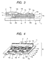
- FIG. 4 is a perspective view showing the wiring structure in the conventional semiconductor device.
- reference numeral 2 designates a negative polarity DC terminal
- 3 designates a positive polarity DC terminal
- 4 5 and 6 designate output terminals
- 11 designates an insulator
- 12a, 12b and 12c designate substrate conductor patterns
- 13a and 13b designate diode and semiconductor switches
- 14a, 14b, 14c, 14d and 14e designate wire interconnections.
- reference numeral 7 designates a radiating plate
- 30 designates a semiconductor device
- 15a, 15b and 15c designate insulating boards or substrates.
- Fig. 4 corresponds to the case in which MOSFETs are used in the semiconductor switches and shows combinations of the semiconductor switches and diodes in the form of one part.
- the radiating plate 7 is made of copper, an Al-SiC alloy or the like as a material.
- wire interconnections 14a, 14b, 14c, 14d and 14e are illustrated four by four in Fig. 4, the number of wire interconnections varies according to specifications of the semiconductor device and the diameter 'of each wire interconnection, and the number of the wire interconnections is by no means limited to four. Since the semiconductor switches and wire interconnections or the like mounted on the insulating substrates 15b and 15c are similar in structure and operation to those of the insulating substrate 15a, the insulating substrate 15a will be explained below. In the following description, the negative polarity DC terminal 2 and the positive polarity DC terminal 3 indicate conductor boards that constitute them.
- the substrate conductor patterns 12a, 12b, and 12c are formed on the insulating substrate 15a, and the semiconductor switches 13a and 13b are respectively implemented on the substrate conductor patterns 12a and 12b.
- the insulating substrate 15a electrically insulates the conductor patterns formed on the insulating substrate from the radiating plate 7.
- the wire interconnections 14a connect the positive polarity DC terminal 3 and the substrate conductor pattern 12a
- the wire interconnections 14b connect the semiconductor switch 13a and the substrate conductor pattern 12b
- the wire interconnections 14c connect the semiconductor switch 13b and the substrate conductor patterns 12c
- the wire interconnections 14d connect the negative polarity DC terminal 2 and the substrate conductor pattern 12c
- the wire interconnections 14e connect the output terminal 4 and the substrate conductor pattern 12b.
- a current value greatly changes in a path constituted by wiring for bridge-connecting the semiconductor switches switched from on to off, wiring connected to an electrolytic capacitor and the DC terminals of the semiconductor device 30, the negative polarity DC terminal 2 and positive polarity DC terminal 3, and the electrolytic capacitor.
- the wiring for bridge-connecting the semiconductor switches correspond to the substrate conductor patterns 12a, 12b and 12c and the wire interconnections 14a, 14b, 14c and 14d in Fig. 4. A voltage exceeding the voltage of the electrolytic capacitor is momentarily applied to the corresponding semiconductor switch switched from on to off.
- the voltage (hereinafter called pop-up voltage) exceeding the electrolytic capacitor voltage is determined by the product of the total inductance of the path and electrolytic capacitor and a time-differentiated value of the current flowing through the path.
- pop-up voltage increases and the voltage applied to the corresponding semiconductor switch switched from on to off exceeds a device withstand voltage, an electrical breakdown occurs.
- a countermeasure for using each semiconductor switch high in withstand voltage is taken to cope with a problem about the pop-up voltage.
- the semiconductor switch has a tendency that the resistance value in its on-state becomes large.
- a system in which a power supply voltage is low and a large current flows in each semiconductor switch causes a problem that a loss at the semiconductor switch increases.
- Suppressing the pop-up voltage with the reduction in inductance makes it possible to use a semiconductor switch low in withstand voltage.
- large merits to the problem about the pop-up voltage such as suppression of a rise in temperature by a reduction in the generated heat, improvements in life and reliability, or a reduction in cooling cost, etc. as its effects are brought about.
- This effect results from the fact that mutual inductance caused between the current flowing through the wiring for bridge-connecting the semiconductor switches and its opposed current reduces self-inductance generated in the wiring for bridge-connecting the semiconductor switches. Also this effect has a limit due to the fact that while the current flowing through the wiring for bridge-connecting the semiconductor switches and its opposite current come close to each other and increase to such an extent as to be equal in amount, the wiring for bridge-connecting the semiconductor switches and the radiating plate 7 are spaced away from each other, and the opposite eddy current becomes a small value due to the resistance of the radiating plate 7 as compared with the amount of the current flowing through the wiring for bridge-connecting the semiconductor switches.
- an objective of the present invention is to provide a semiconductor device which reduces the inductance of wiring for bridge-connecting semiconductor switches and realizes a reduction in size.
- a conductor block is used for a connection between an upper surface electrode of the semiconductor switch and the surface conductor layer of the insulating substrate to form a radiation path of the semiconductor switch to a radiating plate.
- the semiconductor device has a wiring layout at low inductance in the insulating substrate obtained by laminating the conductor boards constituting the current path. It is therefore possible to suppress the voltage applied to the corresponding semiconductor switch at switching and use a semiconductor element of a lower withstand voltage. As a result, the semiconductor device has the effect of reducing heat generated therein.
- the reduction in inductance brings about the effect of reducing a loss of the semiconductor element at switching. Also the reduction in the generated heat is effective in improving reliability and in reducing cooling cost.
- the present invention is effective even in reducing the semiconductor device in size. Owing to the effect, a power converter can be provided using a semiconductor device which realizes a significant increase in current and a reduction in size.
- Fig. 1 is a general view showing a wiring structure of a semiconductor device according to a first embodiment of the present invention
- Fig. 2 is a plan view of an insulating substrate in Fig. 1
- Fig. 3 is a schematic diagram illustrating a sectional structure of the laminated insulating substrate in Fig. 1
- Fig. 4 is a perspective view depicting a wiring structure of a conventional semiconductor device
- Fig. 5 is a configurational view of a power converter using a semiconductor device of the present invention
- Fig. 6 is a required minimum circuit configurational view of a power converter
- Fig. 7 is a circuit configurational view of a semiconductor device set to the minimum necessary to output a UVW three-phase alternating current
- Fig. 1 is a general view showing a wiring structure of a semiconductor device according to a first embodiment of the present invention
- Fig. 2 is a plan view of an insulating substrate in Fig. 1
- Fig. 3 is a schematic diagram illustrating a
- FIG. 8 is a perspective view showing a wiring structure of a semiconductor device according to a second embodiment of the present invention
- Fig. 9 is a sectional structural view of the semiconductor device shown in Fig. 8
- Fig. 10 is a wiring structural view of a semiconductor device with semiconductor switches arranged in parallel, according to a third embodiment of the present invention
- Fig. 11 is a sectional structural view of the semiconductor device shown in Fig. 10
- Fig. 12 is a wiring structural view of a semiconductor device according to a fourth embodiment of the present invention, from which current of one phase is output
- Fig. 13 is a wiring structural view of the semiconductor device shown in Fig. 12
- Fig. 14 is a wiring structural view of a semiconductor device according to a fourth embodiment of the present invention
- Fig. 15 is a section structural view of the semiconductor device shown in Fig. 14; and Fig. 16 is a configurational view of a drive system of a vehicle equipped with a power converter using a semiconductor device of the present invention, illustrated as a sixth embodiment of the present invention.
- Fig. 1 is a general view showing a wiring structure of a semiconductor device according to a first embodiment of the present invention.
- a semiconductor device 30 is shown.
- Reference numeral 2 designates a negative polarity DC terminal
- 3 designates a positive polarity DC terminal
- 4, 5 and 6 designate output terminals and a wiring board
- 7 designates a radiating plate
- 8 designate threaded holes
- 11 designates an insulating board.
- reference numerals 12a, 12b and 12c designate substrate conductor patterns
- 13a and 13b designate diode and semiconductor switches
- 14a, 14b, 14c and 14d designate wire interconnections
- 15a, 15b and 15c designate insulating boards or substrates
- 24a and 24b designate gate signal terminals
- 25a and 25b designate ground terminals.
- the respective terminals 2, 3, 4, 5 and 6 are provided with wiring mounting holes.
- the threaded holes 8 are used when a cooling fin and the radiating plate 7 are fixed with bolts or the like.
- wire interconnections 14a, 14b, 14c and 14d are illustrated four by four in Fig. 1, the number of wire interconnections varies according to specifications of the semiconductor device and the diameter of each wire interconnection. In the present embodiment, the number of the wire interconnections is not limited to four. Since the semiconductor switches and wire interconnections or the like mounted on the insulating substrates 15b and 15c are similar in structure and operation to those of the insulating substrate 15a, the insulating substrate 15a will be explained below.
- the substrate conductor patterns 12a, 12b, and 12c are formed on the insulating substrate 15a, and the semiconductor switches 13a and 13b are respectively implemented on the substrate conductor patterns 12a and 12b.
- the wire interconnections 14a connect the positive polarity DC terminal 3 and the substrate conductor pattern 12a
- the wire interconnections 14b connect the semiconductor switch 13a and the substrate conductor pattern 12b
- the wire interconnections 14c connect the semiconductor switch 13b and the substrate conductor patterns 12c
- the wire interconnections 14d connect the negative polarity DC terminal 2 and the substrate conductor pattern 12c
- the wire interconnections 14e connect the output terminal 4 and the substrate conductor pattern 12b.
- the surface thereof connected to the corresponding wire interconnections is a source electrode surface
- the surface thereof connected to the corresponding substrate conductor pattern is a drain electrode surface.
- the diode and semiconductor switches comprise MOSFETs.
- the gate signal terminals 24a and 24b are respectively connected to gate electrodes of the semiconductor switches 13a and 13b, and the ground terminals 25a and 25b are respectively connected to source electrodes of the semiconductor switches 13a and 13b.
- the gate signal terminals 24a and 24b and the ground terminals 25a and 25b are connected to an unillustrated drive circuit substrate.
- the diode and semiconductor switches employed in the present embodiment are not necessarily limited to the MOSFETs. They may be a combined one of IGBTs and diodes.
- the insulating substrate 15a constitutes a laminated structure made up of a plurality of conductor boards and insulating boards. Its structure will be explained with reference to Fig. 3.
- the substrate conductor patterns 12a, 12b and 12c are formed in the insulating substrate 15a.
- the conductor boards 12a and 12b are brought into conduction by a conductor lying in an internal layer of the insulating substrate 15a and other conductors passing or extending through an insulating layer located therebetween.
- Fig. 1 shows a structure wherein in the semiconductor device, the positive polarity DC terminal 3 and the substrate conductor pattern 12a are connected by the wire interconnections 14a, the semiconductor switch 13a mounted on the substrate conductor pattern 12b and the substrate conductor pattern 12c are connected by the wire interconnections 14b, and the semiconductor switch 13b mounted on the substrate conductor pattern 12c and the negative polarity DC terminal 2 are connected by the wire interconnections 14c.
- Fig. 2 is a plan view of the insulating substrate 15a in Fig. 1.
- reference numerals 12a, 12b and 12c designate substrate conductor patterns
- 13a and 13b designate semiconductor switches
- 14a, 14b and 14c designate wire interconnections
- 15a designates an insulating substrate
- 16 designates an insulating board
- 24a and 24b designate gate signal terminals
- 25a and 25b designate ground terminals.
- Fig. 3 is a schematic diagram showing a sectional structure of the laminated insulating substrate 15a shown in Fig. 1.
- reference numeral 2 designates a negative polarity DC terminal
- 3 designates a positive polarity DC terminal
- 7 designates a radiating plate
- 11 designates an insulating board
- 12a, 12b and 12c designate substrate conductor patterns
- 13a and 13b designate semiconductor switches
- 14a, 14b and 14c designate wire interconnections
- 15a designates an insulating substrate
- 16 and 18 designate insulating boards
- 17 and 19 designate conductor boards
- 20a and 20b designate conductors
- 44 designates solder.
- the insulating substrate 15a has a structure wherein as shown in Fig. 3, the insulating boards 16 and 18 and the conductor boards 17 and 19 are laminated, the substrate conductor patterns 12a, 12b and 12c for mounting the semiconductor switches and wire interconnections are formed on its upper surface, and the substrate conductor patterns 12a and 12b are respectively connected to the conductor board 17 by the conductors 20a and 20b extending or passing through the insulating board 16.
- the insulting board and the conductor board take an integral structure in which they are face-bonded to each other with a brazing filler metal or the like.
- the conductor board 19 is used to bond and fix the insulating substrate 15a to the radiating plate 7 with the solder 44 or the like but unnecessary where it can be fixedly secured to the radiating plate 7 by another technique.
- the conductor board 17 Since the conductor board 17 is a portion through which current flows, as will be described below, it is necessary to electrically isolate the conductor board 17 from the radiating plate or a cooler. Thus, there is a need to newly interpose an insulating sheet between the radiating plate or cooler and the conductor board if the conductor board 17 has a bare structure.
- the effect of suppressing an increase in temperature which is equivalent to the effect of the present embodiment, comes to nothing in that the insulating sheet non-adhered to the conductor board 17 increases in thermal resistance and hence thermal radiation becomes hard.
- the conductor board 17 is electrically isolated from the radiating plate 7 by the insulating board 18 of the insulating substrate, and the radiating plate 7 is brought into surface-contact with the cooler so as to constitute a path for transmitting heat generated in the semiconductor switches 13a and 13b to the cooler.
- the present embodiment is characterizes by using an insulating substrate wherein at least a conductor layer serving as a surface on which semiconductor switches are mounted, an insulating layer, another conductor layer and another insulating layer are laminated in order.
- gate signal terminals and ground terminals are provided at an upper surface of the insulating substrate 15a.
- Aluminum nitride, silicon nitride or alumina is used for the insulators 16 and 17 of the insulating substrate 15a as a material.
- a material having good conductivity, such as copper or the like is used for the conductor boards 12a, 12b, 12c, 17 and 19 as a material.
- the wire interconnections 14a, 14b, 14c and 14d are made of alumina as a material.
- the wire interconnections shown in Fig. 3 may be replaced with plate-shaped conductors made of copper or alumina or the like by using technologies such as solder, ultrasonic bonding, etc.
- FIG. 3 A description will be made below using Fig. 3, of a case in which in the semiconductor device 30 shown in Fig. 1, the mount structure of the insulating substrate shown in Figs 2 and 3 is a structure for reducing inductance that leads to the occurrence of a pop-up voltage, which presents the problem to be solved by the present invention.
- a current path that causes the pop-up voltage is as indicated by a dotted line and extends in the order of the positive polarity DC terminal 3, wire interconnections 14a, substrate conductor pattern 12a, conductor 20a, conductor board 17, conductor 20b, substrate conductor pattern 12b, semiconductor switch 13a, wire interconnections 14b, substrate conductor pattern 12c, semiconductor switch 13b, wire interconnections 14c, and negative polarity DC terminal 2.
- the present structure takes such a layout that current that varies when the semiconductor switches 13a and 13b are respectively switched from on to off, is in an opposing relation between the conductor board 17 and substrate conductor patterns 12a, 12b and 12c, and flows therethrough in the same amount. Owing to electromagnetic induction produced between the current paths opposed therebetween, the absolute value of the mutual inductance generated thereat is therefore close to the absolute value of self-inductance, so that the inductance generated in the current path on the insulating substrate is further reduced.
- the size of the insulating substrate 15a is assumed to be about 3 cm square in the structure of Fig. 4, the inductance generated in a path of current flowing over the insulating substrate is about 10 nH.
- the size of the insulating substrate employed in the present embodiment results in about 1.5 cm ⁇ 3 cm, and the inductance generated on the insulating substrate becomes about 5 nH.
- the present embodiment reduces the area of the insulating substrate to about 1/2 and reduces the inductance to about 5 nH, and bring about its large effect. Also the reduction in the area of the insulating substrate enables miniaturization of the semiconductor device.
- the present embodiment produces a large effect on the reductions in both the area of the insulating substrate and the inductance.
- the current path is isolated from the radiating plate or cooler by the insulator 18, and the radiation of from the insulating substrate to the radiating plate and cooler is identical to the conventional structure. Therefore, the present structure results in a structure wherein the effect of suppressing an increase in the generated heat/temperature due to the reduction in inductance is not impaired.
- Fig. 5 is one example of a power converter using the first embodiment of Fig. 1.
- reference numeral 32 designates a power converter
- 1 designates a case
- 2 designates a negative polarity DC terminal
- 3 designates a positive polarity DC terminal
- 4, 5 and 6 designate output terminals
- 21 and 22 designate conductor boards
- 23 designates an insulating board
- 26 designate auxiliary control terminals
- 29 designate electrolytic capacitors
- 30 designates a semiconductor device
- 31 designates a DC power source
- 35 designates an induction motor
- 40, 41, 42 and 43 designate bolts.
- the negative polarity DC terminal 2 and the conductor board 21, and the positive polarity DC terminal 3 and the conductor board 22 are respectively brought into conduction by the bolts 40 and 41.
- the conductor board 21 and the conductor board 22 constitute a layered structure in which the insulating board 23 is interposed therebetween. Terminals of the electrolytic capacitors 29 are respectively connected to the conductor boards 21 and 22 by using the bolts 42 and 43.
- the auxiliary control terminals 26 are used for transmission and reception of an output command signal or the like.
- the power converter 32 comprises the semiconductor device 30, the electrolytic capacitors 29 and wiring for connecting them to one another.
- the electrolytic capacitors 29 in the power converter according to the present embodiment are not limited to the electrolytic capacitors and may be capacitors each having electrostatic capacity sufficient to meet usage conditions.
- the inductance leading to the pop-up voltage is reduced by use of the semiconductor device according to the first embodiment of Fig. 1. Therefore, a reduction in cooling cost is enabled owing to a reduction in the generated heat, which is indicative of above effect. With a size reduction in the semiconductor device, the power converter can be also brought into less size.
- the present invention is related to an insulating substrate constituting a bridge circuit corresponding to one phase.
- the present invention can obtain a similar effect even in the case of a semiconductor device that outputs current of one phase.
- Fig. 8 is a perspective view showing a wiring structure of the semiconductor device according to the present embodiment, with a case portion of the semiconductor device omitted in drawing.
- reference numeral 30 designates the semiconductor device
- reference numeral 2 designates a negative polarity DC terminal
- 3 designates a positive polarity DC terminal
- 4, 5 and 6 designate output terminals and a wiring board
- 7 designates a radiating plate
- reference numerals 8 designate threaded holes
- 11 designates an insulating board
- 12a, 12b, 12c and 12d designate substrate conductor patterns
- 13a and 13b designate diode and semiconductor switches
- 14a, 14b, 14c, 14d and 14e designate wire interconnections
- 15a, 15b, and 15c designate insulating substrates
- 24a and 24b designate gate signal terminals
- 25a and 25b designate ground terminals
- 27a and 27b designate drain signal terminals.
- the terminals 2, 3, 4, 5 and 6 are respectively provided with wiring mounting holes.
- the threaded holes 8 are used when a cooling fin and the radiating plate 7 are fixed with bolts or the like.
- the respective terminals 24a, 24b, 25a, 25b, 27a and 27b are connected to their corresponding conductor patterns provided on the insulating substrate 15a by solder or the like.
- wire interconnections 14a, 14b, 14c, 14d and 14e are illustrated four by four in Fig. 8, the number of wire interconnections varies according to specifications of the semiconductor device and the diameter of each wire interconnection. In the present embodiment, the number of the wire interconnections is not limited to four.
- the semiconductor device shown in Fig. 8 is a device for outputting a three-phase alternating current, and the semiconductor switches and wire interconnections or the like mounted on the insulating substrates 15b and 15c are similar in structure and operation to those of the insulating substrate 15a. Therefore, the insulating substrate 15a will be explained below.
- the substrate conductor patterns 12a, 12b, 12c and 12d are formed on the insulating substrate 15a, and the semiconductor switches 13a and 13b are respectively implemented on the substrate conductor patterns 12a and 12b by solder.
- the wire interconnections 14a connect the positive polarity DC terminal 3 and the substrate conductor pattern 12a
- the wire interconnections 14b connect the semiconductor switch 13a and the substrate conductor pattern 12b
- the wire interconnections 14e connect the semiconductor switch 13b and the substrate conductor pattern 12c
- the wire interconnections 14c connect the negative polarity DC terminal 2 and the substrate conductor pattern 12d
- the wire interconnections 14d connect the output terminal 4 and the substrate conductor pattern 12b.
- the surface thereof connected to the corresponding wire interconnections is a source electrode surface
- the surface thereof connected to the corresponding substrate conductor pattern is a drain electrode surface.
- the diode and semiconductor switches comprise MOSFETs.
- the gate signal terminals 24a and 24b are respectively connected to gate electrodes of the semiconductor switches 13a and 13b, the ground terminals 25a and 25b are respectively connected to source electrodes of the semiconductor switches 13a and 13b, and the drain signal terminals 27a and 27b are respectively connected to the substrate conductor patterns 12a and 12b.
- the gate signal terminals 24a and 24b and ground terminals 25a and 25b, and the drain signal terminals 27a and 27b are connected to an unillustrated drive circuit substrate.
- the diode and semiconductor switches employed in the present embodiment are not limited to the MOSFETs. They may be a combination of IGBTs and diodes.
- the insulating substrate 15a has a laminated structure made up of a plurality of conductor boards and insulating boards. Its structure will be explained with reference to Fig. 9.
- Fig. 9 shows a sectional structure of the semiconductor device according to the present embodiment.
- reference numeral 30 designates a semiconductor device
- 1 designates a case
- 2 designates a negative polarity DC terminal
- 3 designates a positive polarity DC terminal
- 7 designates a radiating plate
- 11 designates an insulating board
- 12a, 12b, 12c and 12d designate substrate conductor patterns
- 13a and 13b designate semiconductor switches
- 14a, 14b and 14c designate wire interconnections
- 15a designates an insulating substrate
- 16 and 18 designate insulating boards
- 17 and 19 designate conductor boards
- 20a and 20b designate conductors
- 44 designates solder
- 45a and 45b designate solders, respectively.
- the insulating substrate 15a comprises the substrate conductor patterns 12a, 12b, 12c and 12d, and the insulating boards 16 and 18 are respectively made up of the conductor boards 17 and 19, and the conductors 20a and 20b.
- the substrate conductor patters 12c and 12d formed on the insulating substrate 15a are respectively brought into conduction by the conductor 17 lying in an inner layer of the insulating substrate 15a, and the conductors 20a and 20b extending or passing through an insulating layer lying therebetween.
- the insulating board 18 insulates the conductor board 17 from the conductor board 19.
- a current path that generates a pop-up voltage extends in the order of the positive polarity DC terminal 3, wire interconnections 14a, substrate conductor pattern 12a, semiconductor switch 13a, wire interconnections 14b, substrate conductor pattern 12b, semiconductor switch 13b, wire interconnections 14e, substrate conductor pattern 12c, conductor 20a, conductor board 17, conductor 20b, substrate conductor pattern 12d, wire interconnections 14c, and negative polarity DC terminal 2.
- the structure shown in Figs. 8 and 9 takes a layout in which the semiconductor switches 13a and 13b are not located on the substrate conductor patterns 12c and 12d connected to the conductors 20a and 20b respectively. This is effective in enhancing the reliability of solder for connecting semiconductor chips and substrate conductor patterns, which is described later.
- the parts of the semiconductor device repeat their expansion and shrinkage according to temperature cycles indicative of increases in temperatures of the semiconductor switch, insulating substrate, radiating plate and the like during the operation, and decreases in their temperatures during the non-operation.
- Distortion caused by the difference between expansion rates or coefficients developed in the semiconductor switch, insulating substrate and radiating plate plastically deforms solder for bonding them together and produces cracks little by little every temperature cycles. It is therefore necessary to reduce the distortion in order to increase the life of the solder.
- the coefficient of thermal expansion of the semiconductor switch using silicon is about 3 m ⁇ /°C
- the coefficient of thermal expansion of the insulating substrate is set so as to range from about 3 m ⁇ /°C to about 4 m ⁇ /°C
- the coefficient of thermal expansion of the radiating plate (copper) is about 18 m ⁇ /°C
- the substrate conductor patterns 12c and 12d to which the conductors 20a and 20b shown in Fig. 9 are connected become high in the proportion of copper in the volume and increase in the coefficient of expansion as compared with other portions of the insulating substrate. Therefore, when the semiconductor switches are located on their corresponding conductor patterns 12c and 12d, distortion of solder for bonding the semiconductor switch and the conductor pattern increases.
- the semiconductor switches are located on their corresponding conductor patterns 12a and 12b unconnected with the conductors 20a and 20b in the semiconductor device described in Figs. 8 and 9. Since the layout shown in each of Figs. 8 and 9 corresponds to such a layout that the conductor 17 of the internal layer in the insulating substrate is connected to the negative polarity DC terminal so as to take the same potential as the negative polarity, the effect of reducing a leakage current developed due to the floating electrostatic capacity from the insulating substrate to the radiating plate is also obtained.
- FIG. 10 is a plan view of the semiconductor device employed in the present embodiment with the semiconductor switches arranged in a two parallel form.
- the upper surface portion of a case of the semiconductor device has been omitted from Fig. 10 to show an internal wiring structure.
- reference numeral 30 designates a semiconductor device
- reference numeral 2 designates a negative polarity DC terminal
- 3 designates a positive polarity DC terminal
- 4, 5 and 6 designate output terminals and a wiring board
- 13a, 13b, 13c and 13d designate diode and semiconductor switches
- 14b and 14e designate wire interconnections
- 15a, 15b and 15c designate insulating substrates
- 24a and 24b designate gate signal terminals
- 25a and 25b designate ground terminals
- 27a and 27b designate drain signal terminals
- 36 designates a resistor.
- the terminals 2, 3, 4, 5 and 6 are respectively provided with wire mounting holes.
- Threaded holes 8 are used to secure a cooling fin and a radiating plate 7 with bolts or the like.
- the respective terminals 24a, 24b, 25a, 25b, 27a and 27b are connected to their corresponding conductor patterns provided on the insulating substrate 15a by solder or the like.
- the resistor 36 is a circuit element located in a gate wiring to suppress an oscillation phenomenon caused by gate-to-drain capacitances of the semiconductor switches 13a and 13c located in parallel, and the inductance of wiring including the gate wiring. Similar resistors are located also in gate wiring for the semiconductor switches 13b and 13d although their explanation of numerals has been omitted.
- Fig. 11 shows a sectional structure of the semiconductor device of Fig. 10, which is taken along line A - A'.
- reference numeral 30 designates a semiconductor device
- 1 designates a case
- reference numeral 2 designates a negative polarity DC terminal
- 3 designates a positive polarity DC terminal
- 7 designates a radiating plate
- 11 designates an insulating board
- 12a, 12b, 12c and 12d designate substrate conductor patterns
- 13a and 13b designate semiconductor switches
- 14a, 14b and 14c designate wire interconnections
- 15a designates an insulating substrate
- 16 and 18 designate insulating boards
- 17 and 19 designate conductor boards
- 20a and 20b designate conductors.
- the insulating substrate 15a comprises the substrate conductor patterns 12a, 12b, 12c and 12d, the insulating boards 16 and 18, the conductor boards 17 and 19, and the conductors 20a and 20b.
- the substrate conductor patterns 12c and 12d formed on the insulating substrate 15a are respectively brought into conduction by the conductor 17 lying in an internal layer of the insulating substrate 15a, and the conductors 20a and 20b extending through an insulating layer lying therebetween. Further, the insulating board 18 insulates the conductor board 17 from the conductor board 19.
- the sectional structure of the insulating substrate 15 taken along line A - A' is substantially identical to the sectional structure shown in Fig. 9.
- the negative polarity DC terminal 1 and the positive polarity DC terminal 3 are made up of plates or boards each having a bent structure and bonded to their corresponding substrate conductor patterns of the insulating substrate 15a by solder or the like.
- the conductors lying in the internal layer of the insulating substrate are configured as the current paths, and the wiring patterns for the gate signal terminals, ground terminals and drain terminals necessary for switching control are located in the center of the insulating substrate.
- the current path through which the current flows from the semiconductor switch 13a to the semiconductor switch 13b, and the current path through which the current flows from the semiconductor switch 13c to the semiconductor switch 13d are symmetrized using the conductors lying in the internal layer of the insulating substrate, whereby a size reduction in the insulating substrate is realized in a state in which a current unbalance has been kept.
- the conductor boards of the negative polarity DC terminal 1 and the positive polarity DC terminal 3 each having the bent structure are laid out in laminated form with the insulator interposed therebetween to thereby realize reductions in inductance at the DC terminals in addition to the reduction in inductance by the layout of the insulating substrate.
- the semiconductor device reduces the amount of generated heat owing to the parallel arrangement of the semiconductor switches to enable larger current switching, in this case there is a need to further suppress the pop-up voltage. Therefore, the inductance reduction showing the characteristic of the present wiring layout becomes more effective on the semiconductor device in which the semiconductor switches are arranged in parallel for the purpose of a substantial increase in current.
- FIG. 12 is a plan view of the semiconductor device according to the present embodiment.
- the upper surface portion of a case of the semiconductor device has been omitted to show an internal wiring structure.
- reference numeral 30 designates a semiconductor device
- 1 designates a case
- 2 designates a negative polarity DC terminal
- 3 designates a positive polarity DC terminal
- 4 designates an output terminal
- 13a and 13b designate diode and semiconductor switches
- 14a, 14b, 14c and 14e designate wire interconnections
- 15a designates an insulating substrate
- 24a and 24b designate gate signal terminals
- 25a and 25b designate ground terminals
- 27a and 27b designate drain signal terminals.
- the terminals 2, 3 and 4 are respectively provided with wiring mounting holes.
- a conductor board constituting the output terminal 4 is bonded to its corresponding substrate conductor pattern 12b by solder or the like. Threaded holes 8 are used to secure a cooling fin and a radiating plate 7 with bolts or the like.
- Fig. 13 shows a sectional structure taken along line A - A', of the semiconductor device shown in Fig. 12.
- reference numeral 30 designates a semiconductor device
- 1 designates a case
- 2 designates a negative polarity DC terminal
- 3 designates a positive polarity DC terminal
- 7 designates a radiating plate
- 11 designates an insulating board
- 12a, 12b, 12c and 12d designate substrate conductor patterns
- 13a and 13b designate semiconductor switches
- 14a, 14b and 14c designate wire interconnections
- 15a designates an insulating substrate
- 16 and 18 designate insulating boards
- 17 and 19 designate conductor boards
- 20a and 20b designate conductors
- 40 designates solder
- 45a and 45b designate solders.
- the insulating substrate 15a comprises the substrate conductor patterns 12a, 12b, 12c and 12d, the insulating boards 16 and 18, the conductor boards 17 and 19, and the conductors 20a and 20b.
- the substrate conductor patterns 12c and 12d formed on the insulating substrate 15a are respectively brought into conduction by the conductor 17 lying in an internal layer of the insulating substrate 15a, and the conductors 20a and 20b extending through an insulating layer lying therebetween. Further, the insulating board 18 insulates the conductor board 17 from the conductor board 19.
- the present embodiment provides a wiring structure wherein in the second embodiment shown in Fig. 8, one insulating substrate and its peripheral wiring constituting one bridge circuit have been extracted.
- the present embodiment brings about effects such as a size reduction, a reduction in inductance, etc. for the reasons similar to those of the second embodiment of Fig. 8.
- the present embodiment is set to the form of a layout in which the inductance of each terminal portion is reduced in a manner similar to Fig. 10.
- the preset embodiment realizes a wiring layout in which each DC terminal portion is simple in structure and the effect of reducing the inductance is great, as compared with the wiring structure of Fig. 8.
- the present embodiment is effective in downsizing a device constitutable by one bridge circuit and enhancing its reliability as in a DC current/DC current converting device.
- the present embodiment constitutes the bridge circuit by the two semiconductor switches on the basis of the second embodiment of Fig. 8
- the present embodiment may be laid out based on the bridge circuit in which the semiconductor switches are arranged in parallel as in the third embodiment of Fig. 10.
- FIG. 14 is a plan view of the semiconductor device according to the present embodiment.
- the upper surface portion of a case of the semiconductor device has been omitted to show an internal wiring structure.
- reference numeral 30 designates a semiconductor device
- 1 designates a case
- 2 designates a negative polarity DC terminal
- 3 designates a positive polarity DC terminal
- 4 designates an output terminal
- 13a and 13b designate diode and semiconductor switches
- 15a designates an insulating substrate
- 24a and 24b designate gate signal terminals
- 25a and 25b designate ground terminals
- 27a and 27b designate drain signal terminals
- 46a and 46b designate conductor blocks.
- the terminals 2, 3 and 4 are respectively provided with wiring mounting holes.
- a conductor board constituting the output terminal 4 is bonded to its corresponding substrate conductor pattern 12b by solder or the like. Threaded holes 8 are used to secure a cooling fin and a radiating plate 7 with bolts or the like.
- Fig. 15 shows a sectional structure taken along line A - A', of the semiconductor device shown in Fig. 14.
- reference numeral 30 designates a semiconductor device
- 1 designates a case
- 2 designates a negative polarity DC terminal
- 3 designates a positive polarity DC terminal
- 7 designates a radiating plate
- 11 designates an insulating board
- 12a, 12b, 12c and 12d designate substrate conductor patterns
- 13a and 13b designate semiconductor switches
- 15a designates an insulating substrate
- 16 and 18 designate insulating boards
- 17 and 19 designate conductor boards
- 20a and 20b designate conductors
- 40 designates solder, 45a and 45b designate solders
- 46a and 46b designate conductor blocks.
- the conductor block 46a is made of a material such as copper good in electrical conductivity and thermal conductivity and electrically connects the semiconductor switch 13a and the substrate conductor pattern 12b by bonding based on solder or the like, or by pressure developed using a pressure mechanism provided at its upper surface. Similarly, the conductor block 46b also electrically connects the semiconductor switch 13b and the substrate conductor pattern 12c.
- the spots where the wire interconnections are used are replaced by the conductor blocks 46a and 46b in the third embodiment of Fig. 10 and the like, so that heat generated in the semiconductor switches are radiated also from paths passing through the conductor blocks as indicated by dotted lines in Fig. 15.
- the conductor block 46b is bonded onto the structure good in thermal conductivity, wherein the substrate conductor pattern 12c and the conductor board 17 are connected by the conductor 20a. Consequently, the conductor block 46b has the effect of enhancing the efficiency of thermal radiation. This is effective in reducing the cost from the result that a rise in the temperature of each semiconductor chip is suppressed by the enhancement of radiation, and an improvement in reliability or an ability required of a cooler could be lightened.
- FIG. 16 is a configurational diagram of the vehicle drive system according to the present embodiment.
- reference numeral 35 designates a motor
- 32 designates a power converter
- 31 designates a DC power source
- 34 designates an output wiring
- 50 designates a vehicle
- 51 designates a controller
- 52 designates a transmission system
- 53 designates an engine
- 54a, 54b, 54c and 54d designate wheels
- 55 designates signal terminals.
- the signal terminals respectively receive signals with respect to the state of vehicle's driving, and start, acceleration, deceleration and stop commands given from a driver.
- the controller 51 transmits a control signal to the power converter, based on information received from the corresponding signal terminal to drive the motor 35.
- the motor 35 transmits torque to an engine shaft to drive the wheels through the transmission system 52.
- the drive system shown in Fig. 16 is capable of driving the wheels 54a and 54b by use of the motor 35. Even when the engine 53 is running, the drive system is capable of providing also torque assist. Further, the motor 35 is driven by the engine 53, and an ac current generated in the motor 35 is converted into a DC current by the power converter 32, whereby it can be used for charging the DC power supply 31 and some of kinetic energy can be used in the generation of power by the above method during engine deceleration.
- the drive system of Fig. 16 needs large torque during driving the wheels by the motor 35 alone or torque assist drive, it is necessary to drive the motor 35 with a large current.
- a power converter capable of controlling the large current is therefore essential. Since a mountable space is restricted, there is a need to provide a semiconductor device that makes it possible to implement a small-sized power converter. Using the semiconductor device of the present invention makes it possible to realize a power converter capable of controlling a large current and small in size. A vehicle having a drive system using such a power converter can be provided.
Applications Claiming Priority (3)
| Application Number | Priority Date | Filing Date | Title |
|---|---|---|---|
| JP2001097950 | 2001-03-30 | ||
| JP2001097950 | 2001-03-30 | ||
| PCT/JP2002/003182 WO2002082543A1 (en) | 2001-03-30 | 2002-03-29 | Semiconductor device |
Publications (3)
| Publication Number | Publication Date |
|---|---|
| EP1376696A1 true EP1376696A1 (de) | 2004-01-02 |
| EP1376696A4 EP1376696A4 (de) | 2009-08-26 |
| EP1376696B1 EP1376696B1 (de) | 2012-01-25 |
Family
ID=18951654
Family Applications (1)
| Application Number | Title | Priority Date | Filing Date |
|---|---|---|---|
| EP02713259A Expired - Lifetime EP1376696B1 (de) | 2001-03-30 | 2002-03-29 | Halbleiterbauelement |
Country Status (3)
| Country | Link |
|---|---|
| US (1) | US6943445B2 (de) |
| EP (1) | EP1376696B1 (de) |
| WO (1) | WO2002082543A1 (de) |
Cited By (13)
| Publication number | Priority date | Publication date | Assignee | Title |
|---|---|---|---|---|
| EP1553629A2 (de) * | 2004-01-06 | 2005-07-13 | Hitachi, Ltd. | Elektrisch-leitende Klebefolie, ihre Herstellung und elektrischer Leistungswandler |
| EP1643625A1 (de) | 2004-10-04 | 2006-04-05 | Hitachi, Ltd. | Wechselrichtermodul |
| EP1755163A1 (de) * | 2005-08-19 | 2007-02-21 | SEMIKRON Elektronik GmbH & Co. KG | Leistungshalbleitermodul mit Leitungssegment |
| WO2009127179A1 (de) * | 2008-04-15 | 2009-10-22 | Conti Temic Microelectonic Gmbh | Verfahren zur herstellung und aufbau eines leistungsmoduls |
| EP2015626A3 (de) * | 2007-06-22 | 2010-11-03 | Hitachi Ltd. | Gehäuseaufbau eines Stromwandlers |
| EP2521175A1 (de) * | 2011-05-03 | 2012-11-07 | ALSTOM Transport SA | Elektrische Anschlussvorrichtung zum Anschluss mindestens eines elektronischen Bauelements mit einer Stromversorgung, welche Anschlussvorrichtung Mittel zur Verringerung der Induktivität der Schleife zwischen einer ersten und einer zweiten Anschlussklemme umfasst |
| EP2590309A1 (de) * | 2011-11-02 | 2013-05-08 | Hitachi Ltd. | Leistungshalbleitermodul |
| WO2014184030A1 (de) * | 2013-05-14 | 2014-11-20 | Audi Ag | Vorrichtung und elektrische baugruppe zum wandeln einer gleichspannung in eine wechselspannung |
| WO2017058354A1 (en) * | 2015-09-30 | 2017-04-06 | General Electric Company | Low profile, low inductance power switching module and method of forming thereof |
| EP3252813A3 (de) * | 2016-06-02 | 2017-12-27 | Jtekt Corporation | Leistungsmodul |
| EP3063859A4 (de) * | 2013-10-29 | 2018-02-14 | HRL Laboratories, LLC | Halbbrückenschaltung |
| IT201700033230A1 (it) * | 2017-03-27 | 2018-09-27 | S M E S P A | Modulo di potenza per un convertitore di grandezze elettriche |
| US10659032B2 (en) | 2015-10-09 | 2020-05-19 | Hrl Laboratories, Llc | GaN-on-sapphire monolithically integrated power converter |
Families Citing this family (40)
| Publication number | Priority date | Publication date | Assignee | Title |
|---|---|---|---|---|
| US7193336B1 (en) * | 2002-10-23 | 2007-03-20 | Mueller Otward M | Switchable low-loss cryogenic lead system |
| US20060063930A1 (en) * | 2004-08-20 | 2006-03-23 | Agoston Gregory E | Compositions and methods comprising proteinase activated receptor antagonists |
| ATE512446T1 (de) * | 2005-05-02 | 2011-06-15 | Epcos Ag | Modul der leistungselektronik umfassend einen kondensator |
| US8416556B2 (en) * | 2005-05-02 | 2013-04-09 | Conti Temic Microelectronic Gmbh | Power capacitor |
| US20070075419A1 (en) * | 2005-09-06 | 2007-04-05 | Denso Corporation | Semiconductor device having metallic lead and electronic device having lead frame |
| KR20080094917A (ko) * | 2006-02-17 | 2008-10-27 | 가부시키가이샤 야스카와덴키 | 버스 바를 구비한 전력 변환 장치 |
| JP4564937B2 (ja) | 2006-04-27 | 2010-10-20 | 日立オートモティブシステムズ株式会社 | 電気回路装置及び電気回路モジュール並びに電力変換装置 |
| KR101221807B1 (ko) * | 2006-12-29 | 2013-01-14 | 페어차일드코리아반도체 주식회사 | 전력 소자 패키지 |
| FR2916096B1 (fr) * | 2007-05-11 | 2015-05-22 | Valeo Equip Electr Moteur | Sous-ensemble de puissance d'un systeme micro-hybride pour vehicule automobile |
| JP4452953B2 (ja) | 2007-08-09 | 2010-04-21 | 日立オートモティブシステムズ株式会社 | 電力変換装置 |
| JP5386246B2 (ja) * | 2009-06-26 | 2014-01-15 | パナソニック株式会社 | 電力変換装置 |
| US20120057313A1 (en) * | 2010-09-03 | 2012-03-08 | National Semiconductor Corporation | Package for system level electronic products |
| KR102010099B1 (ko) * | 2011-09-16 | 2019-10-21 | 에어 모션 시스템즈, 인크. | 고출력 led 소자용 어셈블리 및 상호 연결 방법 |
| JP5763026B2 (ja) * | 2012-09-24 | 2015-08-12 | 株式会社東芝 | 半導体装置 |
| CN104919589B (zh) * | 2012-10-15 | 2019-01-29 | 富士电机株式会社 | 半导体装置 |
| JP2014179547A (ja) * | 2013-03-15 | 2014-09-25 | Toshiba Corp | 半導体モジュール及びその製造方法 |
| GB2515318B (en) * | 2013-06-19 | 2016-05-18 | Protean Electric Ltd | Inverter for an electric motor or generator |
| US9846182B2 (en) * | 2014-05-30 | 2017-12-19 | Infineon Technologies Ag | High di/dt capacity measurement hardware |
| JP6245365B2 (ja) * | 2014-07-03 | 2017-12-13 | 日産自動車株式会社 | ハーフブリッジパワー半導体モジュール及びその製造方法 |
| JP6179490B2 (ja) * | 2014-09-05 | 2017-08-16 | トヨタ自動車株式会社 | パワーモジュール |
| EP3226294B1 (de) * | 2014-11-28 | 2021-04-07 | Nissan Motor Co., Ltd. | Halbbrückenleistungshalbleitermodul und verfahren zu dessen herstellung |
| US10396057B2 (en) | 2015-02-13 | 2019-08-27 | Nissan Arc, Ltd. | Half-bridge power semiconductor module and method for manufacturing same |
| CN110416205B (zh) | 2015-03-24 | 2024-01-02 | 株式会社东芝 | 半导体装置、逆变电路、驱动装置、车辆以及升降机 |
| US9950898B2 (en) | 2015-03-24 | 2018-04-24 | Kabushiki Kaisha Toshiba | Semiconductor device, inverter circuit, driving device, vehicle, and elevator |
| US9881912B2 (en) | 2015-03-24 | 2018-01-30 | Kabushiki Kaisha Toshiba | Semiconductor device, inverter circuit, driving device, vehicle, and elevator |
| JP6485257B2 (ja) * | 2015-07-01 | 2019-03-20 | 富士電機株式会社 | 半導体装置及び半導体装置の製造方法 |
| US10014794B2 (en) * | 2015-07-28 | 2018-07-03 | Ford Global Technologies, Llc | Power inverter assembly for a vehicle |
| US9241428B1 (en) | 2015-08-31 | 2016-01-19 | Faraday & Future Inc. | Inverter assembly |
| US11218080B2 (en) * | 2015-08-31 | 2022-01-04 | Faraday & Future Inc. | Inverter AC bus bar assembly |
| US10135355B2 (en) | 2015-08-31 | 2018-11-20 | Faraday&Future Inc. | Inverter DC bus bar assembly |
| JP6517642B2 (ja) | 2015-09-11 | 2019-05-22 | 株式会社東芝 | 半導体装置、インバータ回路、及び、駆動装置 |
| JP6771447B2 (ja) * | 2017-09-29 | 2020-10-21 | 日立オートモティブシステムズ株式会社 | パワー半導体装置およびそれを用いた電力変換装置 |
| FR3076175B1 (fr) * | 2017-12-22 | 2020-01-10 | Valeo Siemens Eautomotive France Sas | Equipement electrique a paroi deportee |
| JPWO2019234911A1 (ja) * | 2018-06-08 | 2020-06-18 | 新電元工業株式会社 | 半導体モジュール |
| CN109921612A (zh) * | 2019-01-15 | 2019-06-21 | 山东师范大学 | 一种多层基板低电感功率模块 |
| DE102020200566A1 (de) | 2020-01-17 | 2021-07-22 | Zf Friedrichshafen Ag | Leistungsmodul zum Betreiben eines Elektrofahrzeugantriebs mit erhöhter Störfestigkeit |
| CN113161309A (zh) * | 2020-01-22 | 2021-07-23 | 台达电子企业管理(上海)有限公司 | 载板及其适用的功率模块 |
| EP3855872A1 (de) | 2020-01-22 | 2021-07-28 | Delta Electronics (Shanghai) Co., Ltd. | Trägerplatte umfassend einen metallblock |
| EP3855490A3 (de) * | 2020-01-22 | 2021-10-13 | Delta Electronics (Shanghai) Co., Ltd. | Leistungsmodul |
| DE102020207701A1 (de) * | 2020-06-22 | 2021-12-23 | Zf Friedrichshafen Ag | Leistungsmodul zum Betreiben eines Elektrofahrzeugantriebs mit einem Zwischenkreiskondensator |
Citations (5)
| Publication number | Priority date | Publication date | Assignee | Title |
|---|---|---|---|---|
| US4458305A (en) * | 1981-05-12 | 1984-07-03 | Lucas Industries Plc | Multi-phase transistor/diode bridge circuit |
| EP0427143A2 (de) * | 1989-11-07 | 1991-05-15 | IXYS Semiconductor GmbH | Leistungshalbleitermodul |
| EP0533158A2 (de) * | 1991-09-20 | 1993-03-24 | Hitachi, Ltd. | Leistungsumwandlungsvorrichtung und zum Gebrauch in der Vorrichtung geeigneter Halbleitermodul |
| EP0578108A1 (de) * | 1992-06-30 | 1994-01-12 | Mitsubishi Denki Kabushiki Kaisha | Halbleiter-Leistungsmodul |
| JPH11145376A (ja) * | 1997-11-04 | 1999-05-28 | Hitachi Ltd | 半導体装置 |
Family Cites Families (8)
| Publication number | Priority date | Publication date | Assignee | Title |
|---|---|---|---|---|
| US5777528A (en) * | 1995-05-26 | 1998-07-07 | Motorola, Inc. | Mode suppressing coplanar waveguide transition and method |
| JP3245329B2 (ja) * | 1995-06-19 | 2002-01-15 | 京セラ株式会社 | 半導体素子収納用パッケージ |
| US6462976B1 (en) * | 1997-02-21 | 2002-10-08 | University Of Arkansas | Conversion of electrical energy from one form to another, and its management through multichip module structures |
| JPH10253612A (ja) | 1997-03-14 | 1998-09-25 | Mitsubishi Heavy Ind Ltd | 放射性ガス濃度計測装置 |
| JPH1189247A (ja) * | 1997-09-02 | 1999-03-30 | Denso Corp | 電力変換器 |
| CN1146988C (zh) * | 1997-12-08 | 2004-04-21 | 东芝株式会社 | 半导体功率器件的封装及其组装方法 |
| JP3521757B2 (ja) * | 1998-09-08 | 2004-04-19 | 株式会社豊田自動織機 | 半導体モジュール電極構造 |
| JP3642012B2 (ja) * | 2000-07-21 | 2005-04-27 | 株式会社日立製作所 | 半導体装置,電力変換装置及び自動車 |
-
2002
- 2002-03-29 WO PCT/JP2002/003182 patent/WO2002082543A1/ja active Application Filing
- 2002-03-29 US US10/468,038 patent/US6943445B2/en not_active Expired - Lifetime
- 2002-03-29 EP EP02713259A patent/EP1376696B1/de not_active Expired - Lifetime
Patent Citations (5)
| Publication number | Priority date | Publication date | Assignee | Title |
|---|---|---|---|---|
| US4458305A (en) * | 1981-05-12 | 1984-07-03 | Lucas Industries Plc | Multi-phase transistor/diode bridge circuit |
| EP0427143A2 (de) * | 1989-11-07 | 1991-05-15 | IXYS Semiconductor GmbH | Leistungshalbleitermodul |
| EP0533158A2 (de) * | 1991-09-20 | 1993-03-24 | Hitachi, Ltd. | Leistungsumwandlungsvorrichtung und zum Gebrauch in der Vorrichtung geeigneter Halbleitermodul |
| EP0578108A1 (de) * | 1992-06-30 | 1994-01-12 | Mitsubishi Denki Kabushiki Kaisha | Halbleiter-Leistungsmodul |
| JPH11145376A (ja) * | 1997-11-04 | 1999-05-28 | Hitachi Ltd | 半導体装置 |
Non-Patent Citations (1)
| Title |
|---|
| See also references of WO02082543A1 * |
Cited By (25)
| Publication number | Priority date | Publication date | Assignee | Title |
|---|---|---|---|---|
| EP1553629A2 (de) * | 2004-01-06 | 2005-07-13 | Hitachi, Ltd. | Elektrisch-leitende Klebefolie, ihre Herstellung und elektrischer Leistungswandler |
| EP1553629A3 (de) * | 2004-01-06 | 2007-11-14 | Hitachi, Ltd. | Elektrisch-leitende Klebefolie, ihre Herstellung und elektrischer Leistungswandler |
| US7589400B2 (en) | 2004-10-04 | 2009-09-15 | Hitachi, Ltd. | Inverter and vehicle drive unit using the same |
| EP1643625A1 (de) | 2004-10-04 | 2006-04-05 | Hitachi, Ltd. | Wechselrichtermodul |
| CN1917203B (zh) * | 2005-08-19 | 2010-10-06 | 塞米克朗电子有限及两合公司 | 具有线路元件的功率半导体模块 |
| EP1755163A1 (de) * | 2005-08-19 | 2007-02-21 | SEMIKRON Elektronik GmbH & Co. KG | Leistungshalbleitermodul mit Leitungssegment |
| EP2015626A3 (de) * | 2007-06-22 | 2010-11-03 | Hitachi Ltd. | Gehäuseaufbau eines Stromwandlers |
| US8054633B2 (en) | 2007-06-22 | 2011-11-08 | Hitachi, Ltd. | Power converter |
| WO2009127179A1 (de) * | 2008-04-15 | 2009-10-22 | Conti Temic Microelectonic Gmbh | Verfahren zur herstellung und aufbau eines leistungsmoduls |
| DE112009000737B4 (de) | 2008-04-15 | 2023-02-02 | Vitesco Technologies Germany Gmbh | Aufbau eines Dreiphasen-Wechselrichtermoduls |
| EP2521175A1 (de) * | 2011-05-03 | 2012-11-07 | ALSTOM Transport SA | Elektrische Anschlussvorrichtung zum Anschluss mindestens eines elektronischen Bauelements mit einer Stromversorgung, welche Anschlussvorrichtung Mittel zur Verringerung der Induktivität der Schleife zwischen einer ersten und einer zweiten Anschlussklemme umfasst |
| FR2974969A1 (fr) * | 2011-05-03 | 2012-11-09 | Alstom Transport Sa | Dispositif d'interconnexion electrique d'au moins un composant electronique avec une alimentation electrique comprenant des moyens de diminution d'une inductance de boucle entre des premiere et deuxieme bornes |
| EP2590309A1 (de) * | 2011-11-02 | 2013-05-08 | Hitachi Ltd. | Leistungshalbleitermodul |
| WO2014184030A1 (de) * | 2013-05-14 | 2014-11-20 | Audi Ag | Vorrichtung und elektrische baugruppe zum wandeln einer gleichspannung in eine wechselspannung |
| US9742312B2 (en) | 2013-05-14 | 2017-08-22 | Audi Ag | Apparatus and electrical assembly for converting a direct voltage into an alternating voltage |
| EP3063859A4 (de) * | 2013-10-29 | 2018-02-14 | HRL Laboratories, LLC | Halbbrückenschaltung |
| US9893646B2 (en) | 2015-09-30 | 2018-02-13 | General Electric Company | System for a low profile, low inductance power switching module |
| WO2017058354A1 (en) * | 2015-09-30 | 2017-04-06 | General Electric Company | Low profile, low inductance power switching module and method of forming thereof |
| US10659032B2 (en) | 2015-10-09 | 2020-05-19 | Hrl Laboratories, Llc | GaN-on-sapphire monolithically integrated power converter |
| EP3252813A3 (de) * | 2016-06-02 | 2017-12-27 | Jtekt Corporation | Leistungsmodul |
| US9893642B2 (en) | 2016-06-02 | 2018-02-13 | Jtekt Corporation | Power module |
| IT201700033230A1 (it) * | 2017-03-27 | 2018-09-27 | S M E S P A | Modulo di potenza per un convertitore di grandezze elettriche |
| WO2018178855A1 (en) * | 2017-03-27 | 2018-10-04 | S.M.E S.P.A. | Low inductance half-bridge power module |
| CN110506384A (zh) * | 2017-03-27 | 2019-11-26 | Sme股份公司 | 低电感半桥功率模块 |
| CN110506384B (zh) * | 2017-03-27 | 2022-02-11 | Sme股份公司 | 低电感半桥功率模块 |
Also Published As
| Publication number | Publication date |
|---|---|
| EP1376696A4 (de) | 2009-08-26 |
| EP1376696B1 (de) | 2012-01-25 |
| US6943445B2 (en) | 2005-09-13 |
| WO2002082543A1 (en) | 2002-10-17 |
| US20040113268A1 (en) | 2004-06-17 |
Similar Documents
| Publication | Publication Date | Title |
|---|---|---|
| EP1376696B1 (de) | Halbleiterbauelement | |
| JP3723869B2 (ja) | 半導体装置 | |
| JP3642012B2 (ja) | 半導体装置,電力変換装置及び自動車 | |
| JP3460973B2 (ja) | 電力変換装置 | |
| US6843335B2 (en) | Power conversion apparatus and mobile object incorporating thereof | |
| CN103782380B (zh) | 半导体模块 | |
| JP3501685B2 (ja) | 電力変換装置 | |
| JP4478618B2 (ja) | パワー半導体モジュール | |
| US20110198919A1 (en) | Circuit Board | |
| EP1263041A2 (de) | Halbleitermodul | |
| EP1134807B1 (de) | Halbleiterbauelement | |
| JP6962945B2 (ja) | パワー半導体モジュールおよびそれを用いた電力変換装置 | |
| CN116325135A (zh) | 半导体封装、半导体装置以及电力变换装置 | |
| JP4687414B2 (ja) | パワー半導体モジュール | |
| JP3673776B2 (ja) | 半導体モジュール及び電力変換装置 | |
| CN110622307B (zh) | 半导体模块以及电力变换装置 | |
| JP2024015807A (ja) | インバータ | |
| JP3819838B2 (ja) | 半導体装置及び電力変換装置 | |
| KR20190065768A (ko) | 적층 구조를 이용한 파워모듈 및 이를 이용한 전기자동차용 3상 구동 모듈 | |
| JP4581911B2 (ja) | 半導体装置 | |
| JP6721066B2 (ja) | 電力変換装置 | |
| CN112968622A (zh) | 智能功率模块及采用其的智能功率模块结构 | |
| US20230395457A1 (en) | Power Semiconductor Device, Power Conversion Device, and Electric System | |
| JP2019160969A (ja) | 電力変換装置 | |
| CN214480328U (zh) | 智能功率模块及采用其的智能功率模块结构 |
Legal Events
| Date | Code | Title | Description |
|---|---|---|---|
| PUAI | Public reference made under article 153(3) epc to a published international application that has entered the european phase |
Free format text: ORIGINAL CODE: 0009012 |
|
| 17P | Request for examination filed |
Effective date: 20031016 |
|
| AK | Designated contracting states |
Kind code of ref document: A1 Designated state(s): AT BE CH CY DE DK ES FI FR GB GR IE IT LI LU MC NL PT SE TR |
|
| A4 | Supplementary search report drawn up and despatched |
Effective date: 20090727 |
|
| RIC1 | Information provided on ipc code assigned before grant |
Ipc: H01L 29/78 20060101ALI20090721BHEP Ipc: H01L 25/04 20060101AFI20021023BHEP Ipc: H01L 23/66 20060101ALI20090721BHEP |
|
| 17Q | First examination report despatched |
Effective date: 20090925 |
|
| GRAP | Despatch of communication of intention to grant a patent |
Free format text: ORIGINAL CODE: EPIDOSNIGR1 |
|
| GRAS | Grant fee paid |
Free format text: ORIGINAL CODE: EPIDOSNIGR3 |
|
| RIN1 | Information on inventor provided before grant (corrected) |
Inventor name: OCHIAI, YOSHITAKA, Inventor name: ANAN, HIROMICHI, Inventor name: FUJINO, SHINICHI, Inventor name: INNAMI, TOSHIYUKI, Inventor name: MASHINO, KEIICHI, Inventor name: MISHIMA, AKIRA, Inventor name: SHIRAKAWA, SHINJI, |
|
| GRAA | (expected) grant |
Free format text: ORIGINAL CODE: 0009210 |
|
| RAP1 | Party data changed (applicant data changed or rights of an application transferred) |
Owner name: HITACHI, LTD. |
|
| AK | Designated contracting states |
Kind code of ref document: B1 Designated state(s): DE |
|
| REG | Reference to a national code |
Ref country code: DE Ref legal event code: R096 Ref document number: 60242071 Country of ref document: DE Effective date: 20120329 |
|
| PLBE | No opposition filed within time limit |
Free format text: ORIGINAL CODE: 0009261 |
|
| STAA | Information on the status of an ep patent application or granted ep patent |
Free format text: STATUS: NO OPPOSITION FILED WITHIN TIME LIMIT |
|
| 26N | No opposition filed |
Effective date: 20121026 |
|
| REG | Reference to a national code |
Ref country code: DE Ref legal event code: R097 Ref document number: 60242071 Country of ref document: DE Effective date: 20121026 |
|
| PGFP | Annual fee paid to national office [announced via postgrant information from national office to epo] |
Ref country code: DE Payment date: 20200317 Year of fee payment: 19 |
|
| REG | Reference to a national code |
Ref country code: DE Ref legal event code: R119 Ref document number: 60242071 Country of ref document: DE |
|
| PG25 | Lapsed in a contracting state [announced via postgrant information from national office to epo] |
Ref country code: DE Free format text: LAPSE BECAUSE OF NON-PAYMENT OF DUE FEES Effective date: 20211001 |