JP6485257B2 - 半導体装置及び半導体装置の製造方法 - Google Patents
半導体装置及び半導体装置の製造方法 Download PDFInfo
- Publication number
- JP6485257B2 JP6485257B2 JP2015132789A JP2015132789A JP6485257B2 JP 6485257 B2 JP6485257 B2 JP 6485257B2 JP 2015132789 A JP2015132789 A JP 2015132789A JP 2015132789 A JP2015132789 A JP 2015132789A JP 6485257 B2 JP6485257 B2 JP 6485257B2
- Authority
- JP
- Japan
- Prior art keywords
- circuit board
- semiconductor device
- terminal
- printed circuit
- case
- Prior art date
- Legal status (The legal status is an assumption and is not a legal conclusion. Google has not performed a legal analysis and makes no representation as to the accuracy of the status listed.)
- Active
Links
- 239000004065 semiconductor Substances 0.000 title claims description 175
- 238000004519 manufacturing process Methods 0.000 title claims description 14
- 239000000758 substrate Substances 0.000 claims description 72
- 229920005989 resin Polymers 0.000 claims description 36
- 239000011347 resin Substances 0.000 claims description 36
- 238000003860 storage Methods 0.000 claims description 30
- 238000000034 method Methods 0.000 claims description 12
- RYGMFSIKBFXOCR-UHFFFAOYSA-N Copper Chemical compound [Cu] RYGMFSIKBFXOCR-UHFFFAOYSA-N 0.000 description 11
- 238000000465 moulding Methods 0.000 description 9
- 229910000679 solder Inorganic materials 0.000 description 9
- 229910052802 copper Inorganic materials 0.000 description 8
- 239000010949 copper Substances 0.000 description 8
- 230000002093 peripheral effect Effects 0.000 description 5
- 239000010410 layer Substances 0.000 description 4
- 230000007257 malfunction Effects 0.000 description 4
- 238000007789 sealing Methods 0.000 description 4
- 239000011889 copper foil Substances 0.000 description 3
- 239000003822 epoxy resin Substances 0.000 description 3
- 229920000647 polyepoxide Polymers 0.000 description 3
- 238000003466 welding Methods 0.000 description 3
- 239000004734 Polyphenylene sulfide Substances 0.000 description 2
- 238000010586 diagram Methods 0.000 description 2
- 238000001746 injection moulding Methods 0.000 description 2
- 239000000463 material Substances 0.000 description 2
- 229920000069 polyphenylene sulfide Polymers 0.000 description 2
- 238000005476 soldering Methods 0.000 description 2
- 229910052782 aluminium Inorganic materials 0.000 description 1
- XAGFODPZIPBFFR-UHFFFAOYSA-N aluminium Chemical compound [Al] XAGFODPZIPBFFR-UHFFFAOYSA-N 0.000 description 1
- 238000005452 bending Methods 0.000 description 1
- 238000009529 body temperature measurement Methods 0.000 description 1
- 238000006243 chemical reaction Methods 0.000 description 1
- 239000004020 conductor Substances 0.000 description 1
- 230000005669 field effect Effects 0.000 description 1
- 239000000155 melt Substances 0.000 description 1
- 229910044991 metal oxide Inorganic materials 0.000 description 1
- 150000004706 metal oxides Chemical class 0.000 description 1
- 230000000149 penetrating effect Effects 0.000 description 1
- 239000002356 single layer Substances 0.000 description 1
- 239000007787 solid Substances 0.000 description 1
- 229920005992 thermoplastic resin Polymers 0.000 description 1
Images


Classifications
-
- H—ELECTRICITY
- H01—ELECTRIC ELEMENTS
- H01L—SEMICONDUCTOR DEVICES NOT COVERED BY CLASS H10
- H01L23/00—Details of semiconductor or other solid state devices
- H01L23/48—Arrangements for conducting electric current to or from the solid state body in operation, e.g. leads, terminal arrangements ; Selection of materials therefor
- H01L23/488—Arrangements for conducting electric current to or from the solid state body in operation, e.g. leads, terminal arrangements ; Selection of materials therefor consisting of soldered or bonded constructions
- H01L23/49—Arrangements for conducting electric current to or from the solid state body in operation, e.g. leads, terminal arrangements ; Selection of materials therefor consisting of soldered or bonded constructions wire-like arrangements or pins or rods
-
- H—ELECTRICITY
- H01—ELECTRIC ELEMENTS
- H01L—SEMICONDUCTOR DEVICES NOT COVERED BY CLASS H10
- H01L25/00—Assemblies consisting of a plurality of individual semiconductor or other solid state devices ; Multistep manufacturing processes thereof
- H01L25/03—Assemblies consisting of a plurality of individual semiconductor or other solid state devices ; Multistep manufacturing processes thereof all the devices being of a type provided for in the same subgroup of groups H01L27/00 - H01L33/00, or in a single subclass of H10K, H10N, e.g. assemblies of rectifier diodes
- H01L25/04—Assemblies consisting of a plurality of individual semiconductor or other solid state devices ; Multistep manufacturing processes thereof all the devices being of a type provided for in the same subgroup of groups H01L27/00 - H01L33/00, or in a single subclass of H10K, H10N, e.g. assemblies of rectifier diodes the devices not having separate containers
- H01L25/07—Assemblies consisting of a plurality of individual semiconductor or other solid state devices ; Multistep manufacturing processes thereof all the devices being of a type provided for in the same subgroup of groups H01L27/00 - H01L33/00, or in a single subclass of H10K, H10N, e.g. assemblies of rectifier diodes the devices not having separate containers the devices being of a type provided for in group H01L29/00
- H01L25/072—Assemblies consisting of a plurality of individual semiconductor or other solid state devices ; Multistep manufacturing processes thereof all the devices being of a type provided for in the same subgroup of groups H01L27/00 - H01L33/00, or in a single subclass of H10K, H10N, e.g. assemblies of rectifier diodes the devices not having separate containers the devices being of a type provided for in group H01L29/00 the devices being arranged next to each other
-
- H—ELECTRICITY
- H01—ELECTRIC ELEMENTS
- H01L—SEMICONDUCTOR DEVICES NOT COVERED BY CLASS H10
- H01L25/00—Assemblies consisting of a plurality of individual semiconductor or other solid state devices ; Multistep manufacturing processes thereof
- H01L25/03—Assemblies consisting of a plurality of individual semiconductor or other solid state devices ; Multistep manufacturing processes thereof all the devices being of a type provided for in the same subgroup of groups H01L27/00 - H01L33/00, or in a single subclass of H10K, H10N, e.g. assemblies of rectifier diodes
- H01L25/04—Assemblies consisting of a plurality of individual semiconductor or other solid state devices ; Multistep manufacturing processes thereof all the devices being of a type provided for in the same subgroup of groups H01L27/00 - H01L33/00, or in a single subclass of H10K, H10N, e.g. assemblies of rectifier diodes the devices not having separate containers
- H01L25/07—Assemblies consisting of a plurality of individual semiconductor or other solid state devices ; Multistep manufacturing processes thereof all the devices being of a type provided for in the same subgroup of groups H01L27/00 - H01L33/00, or in a single subclass of H10K, H10N, e.g. assemblies of rectifier diodes the devices not having separate containers the devices being of a type provided for in group H01L29/00
-
- H—ELECTRICITY
- H01—ELECTRIC ELEMENTS
- H01L—SEMICONDUCTOR DEVICES NOT COVERED BY CLASS H10
- H01L21/00—Processes or apparatus adapted for the manufacture or treatment of semiconductor or solid state devices or of parts thereof
- H01L21/02—Manufacture or treatment of semiconductor devices or of parts thereof
- H01L21/04—Manufacture or treatment of semiconductor devices or of parts thereof the devices having at least one potential-jump barrier or surface barrier, e.g. PN junction, depletion layer or carrier concentration layer
- H01L21/48—Manufacture or treatment of parts, e.g. containers, prior to assembly of the devices, using processes not provided for in a single one of the subgroups H01L21/06 - H01L21/326
- H01L21/4814—Conductive parts
- H01L21/4885—Wire-like parts or pins
- H01L21/4889—Connection or disconnection of other leads to or from wire-like parts, e.g. wires
-
- H—ELECTRICITY
- H01—ELECTRIC ELEMENTS
- H01L—SEMICONDUCTOR DEVICES NOT COVERED BY CLASS H10
- H01L25/00—Assemblies consisting of a plurality of individual semiconductor or other solid state devices ; Multistep manufacturing processes thereof
- H01L25/18—Assemblies consisting of a plurality of individual semiconductor or other solid state devices ; Multistep manufacturing processes thereof the devices being of types provided for in two or more different subgroups of the same main group of groups H01L27/00 - H01L33/00, or in a single subclass of H10K, H10N
-
- H—ELECTRICITY
- H05—ELECTRIC TECHNIQUES NOT OTHERWISE PROVIDED FOR
- H05K—PRINTED CIRCUITS; CASINGS OR CONSTRUCTIONAL DETAILS OF ELECTRIC APPARATUS; MANUFACTURE OF ASSEMBLAGES OF ELECTRICAL COMPONENTS
- H05K1/00—Printed circuits
- H05K1/02—Details
- H05K1/0213—Electrical arrangements not otherwise provided for
- H05K1/0263—High current adaptations, e.g. printed high current conductors or using auxiliary non-printed means; Fine and coarse circuit patterns on one circuit board
-
- H—ELECTRICITY
- H01—ELECTRIC ELEMENTS
- H01L—SEMICONDUCTOR DEVICES NOT COVERED BY CLASS H10
- H01L2224/00—Indexing scheme for arrangements for connecting or disconnecting semiconductor or solid-state bodies and methods related thereto as covered by H01L24/00
- H01L2224/01—Means for bonding being attached to, or being formed on, the surface to be connected, e.g. chip-to-package, die-attach, "first-level" interconnects; Manufacturing methods related thereto
- H01L2224/42—Wire connectors; Manufacturing methods related thereto
- H01L2224/47—Structure, shape, material or disposition of the wire connectors after the connecting process
- H01L2224/48—Structure, shape, material or disposition of the wire connectors after the connecting process of an individual wire connector
- H01L2224/484—Connecting portions
- H01L2224/4847—Connecting portions the connecting portion on the bonding area of the semiconductor or solid-state body being a wedge bond
- H01L2224/48472—Connecting portions the connecting portion on the bonding area of the semiconductor or solid-state body being a wedge bond the other connecting portion not on the bonding area also being a wedge bond, i.e. wedge-to-wedge
-
- H—ELECTRICITY
- H01—ELECTRIC ELEMENTS
- H01L—SEMICONDUCTOR DEVICES NOT COVERED BY CLASS H10
- H01L2224/00—Indexing scheme for arrangements for connecting or disconnecting semiconductor or solid-state bodies and methods related thereto as covered by H01L24/00
- H01L2224/01—Means for bonding being attached to, or being formed on, the surface to be connected, e.g. chip-to-package, die-attach, "first-level" interconnects; Manufacturing methods related thereto
- H01L2224/42—Wire connectors; Manufacturing methods related thereto
- H01L2224/47—Structure, shape, material or disposition of the wire connectors after the connecting process
- H01L2224/49—Structure, shape, material or disposition of the wire connectors after the connecting process of a plurality of wire connectors
- H01L2224/491—Disposition
- H01L2224/4911—Disposition the connectors being bonded to at least one common bonding area, e.g. daisy chain
- H01L2224/49111—Disposition the connectors being bonded to at least one common bonding area, e.g. daisy chain the connectors connecting two common bonding areas, e.g. Litz or braid wires
-
- H—ELECTRICITY
- H01—ELECTRIC ELEMENTS
- H01L—SEMICONDUCTOR DEVICES NOT COVERED BY CLASS H10
- H01L2224/00—Indexing scheme for arrangements for connecting or disconnecting semiconductor or solid-state bodies and methods related thereto as covered by H01L24/00
- H01L2224/01—Means for bonding being attached to, or being formed on, the surface to be connected, e.g. chip-to-package, die-attach, "first-level" interconnects; Manufacturing methods related thereto
- H01L2224/42—Wire connectors; Manufacturing methods related thereto
- H01L2224/47—Structure, shape, material or disposition of the wire connectors after the connecting process
- H01L2224/49—Structure, shape, material or disposition of the wire connectors after the connecting process of a plurality of wire connectors
- H01L2224/491—Disposition
- H01L2224/4912—Layout
- H01L2224/4917—Crossed wires
-
- H—ELECTRICITY
- H01—ELECTRIC ELEMENTS
- H01L—SEMICONDUCTOR DEVICES NOT COVERED BY CLASS H10
- H01L2224/00—Indexing scheme for arrangements for connecting or disconnecting semiconductor or solid-state bodies and methods related thereto as covered by H01L24/00
- H01L2224/01—Means for bonding being attached to, or being formed on, the surface to be connected, e.g. chip-to-package, die-attach, "first-level" interconnects; Manufacturing methods related thereto
- H01L2224/42—Wire connectors; Manufacturing methods related thereto
- H01L2224/47—Structure, shape, material or disposition of the wire connectors after the connecting process
- H01L2224/49—Structure, shape, material or disposition of the wire connectors after the connecting process of a plurality of wire connectors
- H01L2224/491—Disposition
- H01L2224/4912—Layout
- H01L2224/49175—Parallel arrangements
-
- H—ELECTRICITY
- H01—ELECTRIC ELEMENTS
- H01L—SEMICONDUCTOR DEVICES NOT COVERED BY CLASS H10
- H01L2224/00—Indexing scheme for arrangements for connecting or disconnecting semiconductor or solid-state bodies and methods related thereto as covered by H01L24/00
- H01L2224/01—Means for bonding being attached to, or being formed on, the surface to be connected, e.g. chip-to-package, die-attach, "first-level" interconnects; Manufacturing methods related thereto
- H01L2224/42—Wire connectors; Manufacturing methods related thereto
- H01L2224/47—Structure, shape, material or disposition of the wire connectors after the connecting process
- H01L2224/49—Structure, shape, material or disposition of the wire connectors after the connecting process of a plurality of wire connectors
- H01L2224/494—Connecting portions
- H01L2224/4943—Connecting portions the connecting portions being staggered
- H01L2224/49431—Connecting portions the connecting portions being staggered on the semiconductor or solid-state body
-
- H—ELECTRICITY
- H01—ELECTRIC ELEMENTS
- H01L—SEMICONDUCTOR DEVICES NOT COVERED BY CLASS H10
- H01L2924/00—Indexing scheme for arrangements or methods for connecting or disconnecting semiconductor or solid-state bodies as covered by H01L24/00
- H01L2924/19—Details of hybrid assemblies other than the semiconductor or other solid state devices to be connected
- H01L2924/191—Disposition
- H01L2924/19101—Disposition of discrete passive components
- H01L2924/19107—Disposition of discrete passive components off-chip wires
-
- H—ELECTRICITY
- H05—ELECTRIC TECHNIQUES NOT OTHERWISE PROVIDED FOR
- H05K—PRINTED CIRCUITS; CASINGS OR CONSTRUCTIONAL DETAILS OF ELECTRIC APPARATUS; MANUFACTURE OF ASSEMBLAGES OF ELECTRICAL COMPONENTS
- H05K2201/00—Indexing scheme relating to printed circuits covered by H05K1/00
- H05K2201/10—Details of components or other objects attached to or integrated in a printed circuit board
- H05K2201/10227—Other objects, e.g. metallic pieces
- H05K2201/10272—Busbars, i.e. thick metal bars mounted on the PCB as high-current conductors
-
- H—ELECTRICITY
- H05—ELECTRIC TECHNIQUES NOT OTHERWISE PROVIDED FOR
- H05K—PRINTED CIRCUITS; CASINGS OR CONSTRUCTIONAL DETAILS OF ELECTRIC APPARATUS; MANUFACTURE OF ASSEMBLAGES OF ELECTRICAL COMPONENTS
- H05K2201/00—Indexing scheme relating to printed circuits covered by H05K1/00
- H05K2201/10—Details of components or other objects attached to or integrated in a printed circuit board
- H05K2201/10431—Details of mounted components
- H05K2201/1059—Connections made by press-fit insertion
-
- H—ELECTRICITY
- H05—ELECTRIC TECHNIQUES NOT OTHERWISE PROVIDED FOR
- H05K—PRINTED CIRCUITS; CASINGS OR CONSTRUCTIONAL DETAILS OF ELECTRIC APPARATUS; MANUFACTURE OF ASSEMBLAGES OF ELECTRICAL COMPONENTS
- H05K2203/00—Indexing scheme relating to apparatus or processes for manufacturing printed circuits covered by H05K3/00
- H05K2203/13—Moulding and encapsulation; Deposition techniques; Protective layers
- H05K2203/1305—Moulding and encapsulation
- H05K2203/1327—Moulding over PCB locally or completely
Description
[第1の実施の形態]
まず、第1の実施の形態の半導体装置について、図1を用いて説明する。
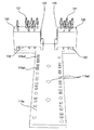
半導体装置100は、ケース110と、ケース110の収納部112a,112b,112cにそれぞれ収納された積層基板140とを含む。
ここで、半導体装置100の製造方法について、図2を用いて説明する。
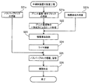
[ステップS11] プリント基板119a,119b及び端子ブロック120,130を用意する(ステップS11a)。また、積層基板140を用意する(ステップS11b)。ステップS11aにおいて、端子ブロック120,130の制御端子121,131は、それぞれプリント基板119a,119bに圧入され、プリント基板119a,119bを端子ブロック120,130の下面側に保持する。
図3は、第1の実施の形態の半導体装置の絶縁基板に部品搭載した斜視図である。
積層基板140は、絶縁基板141の下面に銅等により構成された放熱板(図示を省略)と、絶縁基板141の上面に銅箔等により構成された回路板142a,142bとがそれぞれ配置されている。
図4は、第1の実施の形態の半導体装置の端子ブロックの斜視図であり、図5は、第1の実施の形態の半導体装置の端子ブロックの他の例の斜視図である。
[ステップS12] 端子ブロック120,130が配置されたプリント基板119a,119b、配線端子116,117,118、P端子113a,113b,113c、N端子114a,114b,114c、U端子115a、V端子115b、W端子115c等を一体成形により樹脂を用いてケース110を形成する。
図9は、第1の実施の形態の半導体装置のケースの平面図であり、図10は、第1の実施の形態の半導体装置のケースの裏面図である。
図8は、第1の実施の形態の半導体装置のプロント基板及び積層基板の要部断面図である。
なお、各制御電極がプリント基板119aに沿って整列する様、半導体チップ144a,144b,144cを配置するとよい。半導体チップ146a,146b,146cについても同様である。このような配置によりワイヤ148による接続が容易になる。半導体チップ144a等としてRC−IGBTを用いると図3に示すように制御電極の整列が容易になる。
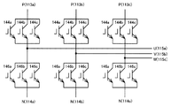
図11は、第1の実施の形態の半導体装置内に構成された回路構成を示す回路図である。
したがって、P端子113aに正極が、N端子114aに負極が接続された状態で、制御端子121,131及びプリント基板119a,119bを経由して外部回路との間で制御信号が入出力される。この制御信号に応じて、プリント基板119a,119b及びワイヤ148を経由して、半導体チップ144a,144b,144c並びに半導体チップ146a,146b,146cのゲート電極に制御信号が入力されて、制御信号に応じてU端子115aから出力される。
図12は、参考例の半導体装置の平面図である。
ケース310は、射出形成により、樹脂を用いて、制御端子311と、制御端子311に電気的に接続されている制御電極312と、P端子313a,313b,313cと、N端子314a,314b,314cと、U端子315a、V端子315b、W端子315cとが一体成形されている。
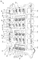
第2の実施の形態では、別の半導体装置について、図13を用いて説明する。
図13は、第2の実施の形態の半導体装置の斜視図である。
このような半導体装置200の製造方法について、図14を用いて説明する。
[ステップS21] プリント基板119a,119b及び端子ブロック120,130を用意する(ステップS21a)。また、積層基板140を用意する(ステップS21b)。さらに、バスバーブロック210を用意する(ステップS21c)。ステップS21aにおいて、端子ブロック120,130の制御端子121,131は、それぞれプリント基板119a,119bに圧入され、プリント基板119a,119bを端子ブロック120,130の下面側に保持する。
バスバーブロック210について、図15を用いて説明する。
バスバーブロック210は、樹脂で形成されており、半導体装置200の中央部の凹部に嵌まるように、例えば、複数のフレームにより枠型に組まれた構成をしている。また、このように組まれたフレームの裏面側には、収納部112a,112b,112cに対応して配線端子116,117が、例えば、一体成形されている。
具体的には、図3で説明した積層基板140を銅板あるいは冷却器に設置する。銅板あるいは冷却器に設置された積層基板140が、ステップ22で形成したケース110の収納部112a,112b,112cにそれぞれ収納されるように、ケース110を接着する。この際、収納部112aでは、積層基板140の導電端子143aが、P端子113aに電気的に接続された配線端子118に接合する。収納部112bでは、積層基板140の導電端子143aが、P端子113bに電気的に接続された配線端子118に接合する。収納部112cでは、積層基板140の導電端子143aが、P端子113cに電気的に接続された配線端子118に接合する。
図16は、第2の実施の形態の半導体装置の絶縁基板が収納されたケースの平面図である。
[ステップS26] ケース110の凹部内の積層基板140、プリント基板119a,119b、ワイヤ148、バスバーブロック210等を封止樹脂で封止して、硬化する。これにより半導体装置200が完成する。
110 ケース
111a,111b 樹脂梁
112a,112b,112c 収納部
113a,113b,113c P端子
114a,114b,114c N端子
115a U端子
115b V端子
115c W端子
116,117,118 配線端子
119a,119b プリント基板
120,130 端子ブロック
121,131 制御端子
122,132 隙間
123,133 段差部
140 積層基板
141 絶縁基板
142a,142b 回路板
143a,143b 導電端子
144a,144b,144c,146a,146b,146c 半導体チップ(半導体素子)
145a,145b リードフレーム
148 ワイヤ
Claims (15)
- 絶縁基板と、前記絶縁基板のおもて面に配置された回路板とを有する積層基板と、
前記回路板に配置された半導体チップと、
前記積層基板及び前記半導体チップを収納する収納領域を備えるケースと、
第1面及び前記第1面に対向する第2面を備え、前記第1面及び第2面から突出する外部接続端子を保持している端子ブロックと、
第1主面及び前記第1主面に対向する第2主面を備え、前記収納領域の周縁に配置され、前記端子ブロックの前記第2面側に保持され、前記半導体チップの制御電極と接続部材により電気的に接続され、かつ、前記外部接続端子と接続されたプリント基板と、
を有する半導体装置。 - 前記外部接続端子が前記プリント基板に圧入されることにより、前記プリント基板が前記端子ブロックの前記第2面側に保持されている請求項1記載の半導体装置。
- 前記端子ブロックは、前記第1面と第2面の間に、前記第1面と接続する第3面を備え、前記第2面及び前記第3面の少なくとも一方が前記ケースと接合している請求項2記載の半導体装置。
- 前記プリント基板が複数の貫通孔を備え、前記貫通孔において前記ケースと接合している請求項2記載の半導体装置。
- 前記プリント基板の端部が前記ケースから前記収納領域の内側へ張り出している請求項4記載の半導体装置。
- 前記端子ブロックが前記第3面に設けられた段差を備え、前記ケースの一部が前記段差の前記第1面側に配置されている請求項3記載の半導体装置。
- 前記端子ブロックは前記プリント基板の前記第1主面側に配置され、
前記外部接続端子の端部は前記プリント基板の前記第2主面側に露出もしくは突出して、前記ケースと接しており、
前記プリント基板は前記端子ブロックの前記第2面側と前記ケースの間に保持されている請求項2記載の半導体装置。 - 前記端子ブロックは、前記第2面側に、前記プリント基板との間の隙間を規定する突起を備え、前記ケースの一部が前記隙間内に配置され前記端子ブロックと接合し、かつ前記外部接続端子と接している請求項2記載の半導体装置。
- 前記半導体装置は前記半導体チップを複数備え、前記半導体チップは、前記積層基板の前記回路板上に、前記プリント基板に沿って配置され、さらに、前記半導体チップの各制御電極が、前記プリント基板に沿って配置され、前記制御電極がそれぞれ前記プリント基板と電気的に接続されている請求項1記載の半導体装置。
- 前記半導体チップがそれぞれ主電極を備え、前記主電極と接続され、前記プリント基板に沿って配置された配線端子を備える請求項9記載の半導体装置。
- 前記周縁に嵌まり、前記収納領域を塞ぎ、前記配線端子が設けられたバスバーブロックを有する請求項10に記載の半導体装置。
- 第1面及び前記第1面に対向する第2面を備え、前記第1面及び第2面から突出する外部接続端子を保持している端子ブロックと、
第1主面及び前記第1主面に対向する第2主面を備えるプリント基板と、を準備し、
前記外部接続端子を前記プリント基板に圧入し、前記端子ブロックの前記第2面側に前記プリント基板を保持しながら、前記端子ブロックの周囲に加熱された樹脂を配置し、前記端子ブロック及び前記プリント基板を一体成形してケースを形成する半導体装置の製造方法。 - 前記外部接続端子が前記プリント基板に圧入されることにより、前記プリント基板が前記端子ブロックの前記第2面側に保持されている請求項12記載の半導体装置の製造方法。
- 前記端子ブロックが前記プリント基板の前記第1主面側に配置され、前記外部接続端子の端部が前記プリント基板の前記第2主面側に露出もしくは突出し、前記樹脂と接しながら、
前記端子ブロック及び前記プリント基板を一体成形される請求項13記載の半導体装置の製造方法。 - さらに、絶縁基板と、前記絶縁基板のおもて面に形成された回路板とを有する積層基板と、
半導体チップと、を準備し、
前記ケースの収納領域に前記積層基板を収納し、
前記回路板に前記半導体チップを配置し、
前記半導体チップの制御電極と前記プリント基板とを導電性の接続部材により接続する請求項13記載の半導体装置の製造方法。
Priority Applications (5)
| Application Number | Priority Date | Filing Date | Title |
|---|---|---|---|
| JP2015132789A JP6485257B2 (ja) | 2015-07-01 | 2015-07-01 | 半導体装置及び半導体装置の製造方法 |
| CN201610398878.4A CN106328622B (zh) | 2015-07-01 | 2016-06-07 | 半导体装置及半导体装置的制造方法 |
| US15/176,211 US10396056B2 (en) | 2015-07-01 | 2016-06-08 | Semiconductor device and semiconductor device fabrication method |
| DE102016210161.7A DE102016210161A1 (de) | 2015-07-01 | 2016-06-08 | Halbleiterbauelement und Halbleiterbauelementherstellungsverfahren |
| US16/521,613 US11075190B2 (en) | 2015-07-01 | 2019-07-25 | Semiconductor device and semiconductor device fabrication method |
Applications Claiming Priority (1)
| Application Number | Priority Date | Filing Date | Title |
|---|---|---|---|
| JP2015132789A JP6485257B2 (ja) | 2015-07-01 | 2015-07-01 | 半導体装置及び半導体装置の製造方法 |
Related Child Applications (1)
| Application Number | Title | Priority Date | Filing Date |
|---|---|---|---|
| JP2019028757A Division JP6841291B2 (ja) | 2019-02-20 | 2019-02-20 | 半導体装置及び半導体装置の製造方法 |
Publications (2)
| Publication Number | Publication Date |
|---|---|
| JP2017017195A JP2017017195A (ja) | 2017-01-19 |
| JP6485257B2 true JP6485257B2 (ja) | 2019-03-20 |
Family
ID=57582610
Family Applications (1)
| Application Number | Title | Priority Date | Filing Date |
|---|---|---|---|
| JP2015132789A Active JP6485257B2 (ja) | 2015-07-01 | 2015-07-01 | 半導体装置及び半導体装置の製造方法 |
Country Status (4)
| Country | Link |
|---|---|
| US (2) | US10396056B2 (ja) |
| JP (1) | JP6485257B2 (ja) |
| CN (1) | CN106328622B (ja) |
| DE (1) | DE102016210161A1 (ja) |
Families Citing this family (16)
| Publication number | Priority date | Publication date | Assignee | Title |
|---|---|---|---|---|
| TWI598766B (zh) * | 2016-03-14 | 2017-09-11 | 神雲科技股份有限公司 | 防竄改系統及其防竄改電路 |
| WO2018142864A1 (ja) | 2017-02-06 | 2018-08-09 | 富士電機株式会社 | 半導体モジュール、電気自動車およびパワーコントロールユニット |
| JP6753475B2 (ja) | 2017-02-06 | 2020-09-09 | 富士電機株式会社 | 半導体モジュール、電気自動車、及びパワーコントロールユニット |
| CN110476237B (zh) * | 2017-10-19 | 2023-06-02 | 富士电机株式会社 | 半导体装置及半导体装置的制造方法 |
| JP6493612B1 (ja) | 2018-08-13 | 2019-04-03 | 富士電機株式会社 | パワー半導体モジュールおよび車両 |
| CN111886695A (zh) | 2018-10-05 | 2020-11-03 | 富士电机株式会社 | 半导体装置、半导体模块及车辆 |
| JP7187992B2 (ja) | 2018-11-06 | 2022-12-13 | 富士電機株式会社 | 半導体モジュールおよび車両 |
| JP7038645B2 (ja) * | 2018-12-06 | 2022-03-18 | 三菱電機株式会社 | 半導体装置および半導体装置の製造方法 |
| JP1650295S (ja) | 2019-01-11 | 2020-01-20 | 半導体モジュール | |
| JP1649258S (ja) | 2019-01-11 | 2022-12-21 | 半導体モジュール | |
| JP6841291B2 (ja) * | 2019-02-20 | 2021-03-10 | 富士電機株式会社 | 半導体装置及び半導体装置の製造方法 |
| JP2021145082A (ja) | 2020-03-13 | 2021-09-24 | 富士電機株式会社 | 半導体モジュール及びワイヤボンディング方法 |
| CN113097159A (zh) * | 2021-03-22 | 2021-07-09 | 西安交通大学 | 一种碳化硅mosfet芯片双向开关功率模块及其制备方法 |
| DE102022201175A1 (de) | 2022-02-04 | 2023-08-10 | Zf Friedrichshafen Ag | Leistungsmodul für einen Stromrichter mit einstückiger Schutzverkleidung und Signalpinhalterung |
| WO2024010003A1 (ja) * | 2022-07-07 | 2024-01-11 | 住友電気工業株式会社 | 半導体装置 |
| DE102023202126A1 (de) | 2022-12-20 | 2024-04-04 | Vitesco Technologies Germany Gmbh | Inverter |
Family Cites Families (37)
| Publication number | Priority date | Publication date | Assignee | Title |
|---|---|---|---|---|
| JPH05206183A (ja) | 1992-01-29 | 1993-08-13 | Sharp Corp | 半導体装置の製造方法 |
| JP2725954B2 (ja) * | 1992-07-21 | 1998-03-11 | 三菱電機株式会社 | 半導体装置およびその製造方法 |
| JPH07176336A (ja) * | 1993-09-30 | 1995-07-14 | Siemon Co:The | ブレーク・テスト機能を含む電気的に拡張された配線ブロック |
| JP3201187B2 (ja) * | 1994-12-08 | 2001-08-20 | 富士電機株式会社 | 半導体装置 |
| JP3168901B2 (ja) * | 1996-02-22 | 2001-05-21 | 株式会社日立製作所 | パワー半導体モジュール |
| EP0884781A3 (en) * | 1997-06-12 | 1999-06-30 | Hitachi, Ltd. | Power semiconductor module |
| JP3410969B2 (ja) * | 1997-06-30 | 2003-05-26 | 株式会社東芝 | 半導体装置 |
| JP3017137B2 (ja) * | 1997-08-28 | 2000-03-06 | 東北日本電気株式会社 | 非対称型コネクタ及びその実装方法 |
| JP2000183276A (ja) * | 1998-12-15 | 2000-06-30 | Mitsubishi Electric Corp | 半導体パワーモジュール |
| JP3519300B2 (ja) * | 1999-01-11 | 2004-04-12 | 富士電機デバイステクノロジー株式会社 | パワーモジュールのパッケージ構造 |
| JP3547333B2 (ja) * | 1999-02-22 | 2004-07-28 | 株式会社日立産機システム | 電力変換装置 |
| JP2000323646A (ja) | 1999-05-14 | 2000-11-24 | Mitsubishi Electric Corp | 絶縁材料ケース及び半導体装置 |
| JP3747699B2 (ja) * | 1999-08-06 | 2006-02-22 | 富士電機デバイステクノロジー株式会社 | 半導体装置 |
| JP3919398B2 (ja) * | 1999-10-27 | 2007-05-23 | 三菱電機株式会社 | 半導体モジュール |
| JP2001189416A (ja) * | 1999-12-28 | 2001-07-10 | Mitsubishi Electric Corp | パワーモジュール |
| WO2001082376A1 (fr) * | 2000-04-25 | 2001-11-01 | Kabushiki Kaisha Toyota Jidoshokki | Dispositif a semi-conducteur |
| JP4543542B2 (ja) * | 2000-11-27 | 2010-09-15 | 富士電機システムズ株式会社 | 半導体装置 |
| JP3723869B2 (ja) * | 2001-03-30 | 2005-12-07 | 株式会社日立製作所 | 半導体装置 |
| US6943445B2 (en) * | 2001-03-30 | 2005-09-13 | Hitachi, Ltd. | Semiconductor device having bridge-connected wiring structure |
| JP4490041B2 (ja) * | 2001-04-02 | 2010-06-23 | 三菱電機株式会社 | 電力用半導体装置 |
| JP4540884B2 (ja) * | 2001-06-19 | 2010-09-08 | 三菱電機株式会社 | 半導体装置 |
| JP3901038B2 (ja) * | 2001-07-23 | 2007-04-04 | 富士電機デバイステクノロジー株式会社 | 半導体装置およびそれを用いたインバータ装置 |
| DE10232566B4 (de) * | 2001-07-23 | 2015-11-12 | Fuji Electric Co., Ltd. | Halbleiterbauteil |
| JP2003078304A (ja) * | 2001-08-30 | 2003-03-14 | Murata Mfg Co Ltd | 電子モジュールおよびそれを用いた通信機モジュール |
| WO2005004563A1 (ja) * | 2003-07-03 | 2005-01-13 | Hitachi, Ltd. | モジュール装置及びその製造方法 |
| US7697300B2 (en) * | 2003-08-01 | 2010-04-13 | Siemens Aktiengesellschaft | Electronic unit and method for manufacturing an electronic unit |
| US7083431B1 (en) * | 2005-09-02 | 2006-08-01 | Lear Corporation | Method and system of electrically connecting multiple printed circuit boards |
| EP2202793A3 (en) * | 2006-06-09 | 2010-11-10 | Honda Motor Co., Ltd. | Semiconductor device |
| JP5176507B2 (ja) * | 2007-12-04 | 2013-04-03 | 富士電機株式会社 | 半導体装置 |
| JP4638923B2 (ja) * | 2008-03-31 | 2011-02-23 | 日立オートモティブシステムズ株式会社 | 制御装置 |
| JP4666185B2 (ja) * | 2008-06-26 | 2011-04-06 | 三菱電機株式会社 | 半導体装置 |
| EP2432014B1 (en) * | 2009-05-14 | 2019-09-18 | Rohm Co., Ltd. | Semiconductor device |
| WO2013047354A1 (ja) * | 2011-09-26 | 2013-04-04 | 日本電気株式会社 | 中空封止構造 |
| JP6105887B2 (ja) * | 2012-09-28 | 2017-03-29 | 日立オートモティブシステムズ株式会社 | 電子制御装置 |
| US9214415B2 (en) * | 2013-04-11 | 2015-12-15 | Texas Instruments Incorporated | Integrating multi-output power converters having vertically stacked semiconductor chips |
| CN203481423U (zh) * | 2013-08-09 | 2014-03-12 | 光宝电子(广州)有限公司 | 电连接器及其与电路板的组合 |
| JP5745127B1 (ja) * | 2014-03-28 | 2015-07-08 | 三菱電機株式会社 | 防水型制御ユニット |
-
2015
- 2015-07-01 JP JP2015132789A patent/JP6485257B2/ja active Active
-
2016
- 2016-06-07 CN CN201610398878.4A patent/CN106328622B/zh active Active
- 2016-06-08 DE DE102016210161.7A patent/DE102016210161A1/de active Pending
- 2016-06-08 US US15/176,211 patent/US10396056B2/en active Active
-
2019
- 2019-07-25 US US16/521,613 patent/US11075190B2/en active Active
Also Published As
| Publication number | Publication date |
|---|---|
| DE102016210161A1 (de) | 2017-01-05 |
| JP2017017195A (ja) | 2017-01-19 |
| US11075190B2 (en) | 2021-07-27 |
| CN106328622B (zh) | 2020-10-30 |
| US20190348402A1 (en) | 2019-11-14 |
| US10396056B2 (en) | 2019-08-27 |
| US20170006721A1 (en) | 2017-01-05 |
| CN106328622A (zh) | 2017-01-11 |
Similar Documents
| Publication | Publication Date | Title |
|---|---|---|
| JP6485257B2 (ja) | 半導体装置及び半導体装置の製造方法 | |
| JP6488940B2 (ja) | 半導体装置 | |
| US9917031B2 (en) | Semiconductor device, and method for assembling semiconductor device | |
| JP6979864B2 (ja) | パワー半導体装置及びその製造方法 | |
| US9379083B2 (en) | Semiconductor device and method for manufacturing semiconductor device | |
| US9312192B2 (en) | Semiconductor device | |
| US7247929B2 (en) | Molded semiconductor device with heat conducting members | |
| JP3910383B2 (ja) | パワーモジュールおよびインバータ | |
| JP4459883B2 (ja) | 半導体装置 | |
| JP5017332B2 (ja) | インバータ | |
| JPWO2018179981A1 (ja) | 半導体装置 | |
| US10741478B2 (en) | Power module and method of manufacturing the same, and power electronic apparatus and method of manufacturing the same | |
| JP7046742B2 (ja) | パワーモジュール | |
| US20110024896A1 (en) | Power semiconductor device | |
| JP6841291B2 (ja) | 半導体装置及び半導体装置の製造方法 | |
| JP4403166B2 (ja) | パワーモジュールおよび電力変換装置 | |
| JP6948855B2 (ja) | パワー半導体装置及びそれを用いた電力変換装置 | |
| JP2013085470A (ja) | インバータ | |
| JP5188602B2 (ja) | インバータ | |
| CN111354709B (zh) | 半导体装置及其制造方法 | |
| US11521925B2 (en) | Semiconductor module | |
| JP2022143167A (ja) | 半導体装置 | |
| CN113016068A (zh) | 半导体模块、功率转换装置及半导体模块的制作方法 | |
| US20240021496A1 (en) | Semiconductor device | |
| JP5202685B2 (ja) | インバータ |
Legal Events
| Date | Code | Title | Description |
|---|---|---|---|
| A621 | Written request for application examination |
Free format text: JAPANESE INTERMEDIATE CODE: A621 Effective date: 20180416 |
|
| A977 | Report on retrieval |
Free format text: JAPANESE INTERMEDIATE CODE: A971007 Effective date: 20181219 |
|
| TRDD | Decision of grant or rejection written | ||
| A01 | Written decision to grant a patent or to grant a registration (utility model) |
Free format text: JAPANESE INTERMEDIATE CODE: A01 Effective date: 20190122 |
|
| A61 | First payment of annual fees (during grant procedure) |
Free format text: JAPANESE INTERMEDIATE CODE: A61 Effective date: 20190204 |
|
| R150 | Certificate of patent or registration of utility model |
Ref document number: 6485257 Country of ref document: JP Free format text: JAPANESE INTERMEDIATE CODE: R150 |
|
| R250 | Receipt of annual fees |
Free format text: JAPANESE INTERMEDIATE CODE: R250 |
|
| R250 | Receipt of annual fees |
Free format text: JAPANESE INTERMEDIATE CODE: R250 |
|
| R250 | Receipt of annual fees |
Free format text: JAPANESE INTERMEDIATE CODE: R250 |