WO2013011856A1 - Wireless communication device - Google Patents
Wireless communication device Download PDFInfo
- Publication number
- WO2013011856A1 WO2013011856A1 PCT/JP2012/067454 JP2012067454W WO2013011856A1 WO 2013011856 A1 WO2013011856 A1 WO 2013011856A1 JP 2012067454 W JP2012067454 W JP 2012067454W WO 2013011856 A1 WO2013011856 A1 WO 2013011856A1
- Authority
- WO
- WIPO (PCT)
- Prior art keywords
- coil pattern
- loop portion
- communication device
- wireless communication
- pattern
- Prior art date
Links
- 238000004891 communication Methods 0.000 title claims abstract description 75
- 230000005855 radiation Effects 0.000 claims abstract description 5
- 239000004020 conductor Substances 0.000 claims description 41
- 239000003990 capacitor Substances 0.000 claims description 9
- 238000004804 winding Methods 0.000 claims description 6
- 238000010030 laminating Methods 0.000 claims description 5
- 230000008878 coupling Effects 0.000 claims description 4
- 238000010168 coupling process Methods 0.000 claims description 4
- 238000005859 coupling reaction Methods 0.000 claims description 4
- 239000012212 insulator Substances 0.000 claims description 3
- 239000002184 metal Substances 0.000 description 8
- 229910052751 metal Inorganic materials 0.000 description 8
- 239000000758 substrate Substances 0.000 description 5
- 229920005989 resin Polymers 0.000 description 4
- 239000011347 resin Substances 0.000 description 4
- 239000000919 ceramic Substances 0.000 description 3
- 230000000694 effects Effects 0.000 description 3
- 230000006870 function Effects 0.000 description 3
- 230000006698 induction Effects 0.000 description 2
- 239000000463 material Substances 0.000 description 2
- 230000002093 peripheral effect Effects 0.000 description 2
- RYGMFSIKBFXOCR-UHFFFAOYSA-N Copper Chemical compound [Cu] RYGMFSIKBFXOCR-UHFFFAOYSA-N 0.000 description 1
- XUIMIQQOPSSXEZ-UHFFFAOYSA-N Silicon Chemical compound [Si] XUIMIQQOPSSXEZ-UHFFFAOYSA-N 0.000 description 1
- 230000015572 biosynthetic process Effects 0.000 description 1
- 229910010293 ceramic material Inorganic materials 0.000 description 1
- 229910052802 copper Inorganic materials 0.000 description 1
- 239000010949 copper Substances 0.000 description 1
- 238000010586 diagram Methods 0.000 description 1
- 238000010304 firing Methods 0.000 description 1
- 238000007667 floating Methods 0.000 description 1
- 230000012447 hatching Effects 0.000 description 1
- 239000004973 liquid crystal related substance Substances 0.000 description 1
- 239000007769 metal material Substances 0.000 description 1
- 238000003825 pressing Methods 0.000 description 1
- 230000001681 protective effect Effects 0.000 description 1
- 239000004065 semiconductor Substances 0.000 description 1
- 229910052710 silicon Inorganic materials 0.000 description 1
- 239000010703 silicon Substances 0.000 description 1
- 229910052709 silver Inorganic materials 0.000 description 1
- 239000004332 silver Substances 0.000 description 1
- 229920005992 thermoplastic resin Polymers 0.000 description 1
- 229920001187 thermosetting polymer Polymers 0.000 description 1
Images


Classifications
-
- H—ELECTRICITY
- H04—ELECTRIC COMMUNICATION TECHNIQUE
- H04B—TRANSMISSION
- H04B5/00—Near-field transmission systems, e.g. inductive or capacitive transmission systems
- H04B5/20—Near-field transmission systems, e.g. inductive or capacitive transmission systems characterised by the transmission technique; characterised by the transmission medium
- H04B5/24—Inductive coupling
-
- G—PHYSICS
- G06—COMPUTING; CALCULATING OR COUNTING
- G06K—GRAPHICAL DATA READING; PRESENTATION OF DATA; RECORD CARRIERS; HANDLING RECORD CARRIERS
- G06K19/00—Record carriers for use with machines and with at least a part designed to carry digital markings
- G06K19/06—Record carriers for use with machines and with at least a part designed to carry digital markings characterised by the kind of the digital marking, e.g. shape, nature, code
- G06K19/067—Record carriers with conductive marks, printed circuits or semiconductor circuit elements, e.g. credit or identity cards also with resonating or responding marks without active components
- G06K19/07—Record carriers with conductive marks, printed circuits or semiconductor circuit elements, e.g. credit or identity cards also with resonating or responding marks without active components with integrated circuit chips
- G06K19/077—Constructional details, e.g. mounting of circuits in the carrier
- G06K19/07749—Constructional details, e.g. mounting of circuits in the carrier the record carrier being capable of non-contact communication, e.g. constructional details of the antenna of a non-contact smart card
- G06K19/07773—Antenna details
- G06K19/07777—Antenna details the antenna being of the inductive type
- G06K19/07779—Antenna details the antenna being of the inductive type the inductive antenna being a coil
- G06K19/07783—Antenna details the antenna being of the inductive type the inductive antenna being a coil the coil being planar
-
- H—ELECTRICITY
- H04—ELECTRIC COMMUNICATION TECHNIQUE
- H04B—TRANSMISSION
- H04B5/00—Near-field transmission systems, e.g. inductive or capacitive transmission systems
- H04B5/70—Near-field transmission systems, e.g. inductive or capacitive transmission systems specially adapted for specific purposes
- H04B5/79—Near-field transmission systems, e.g. inductive or capacitive transmission systems specially adapted for specific purposes for data transfer in combination with power transfer
Definitions
- the present invention relates to a wireless communication device, and more particularly to a wireless communication device used for communication with a reader / writer in an RFID (Radio Frequency Identification) system.
- RFID Radio Frequency Identification
- Reader / writers and RFID tags each include a radiating element (antenna) for transmitting and receiving wireless signals.
- an HF band system using a high frequency of 13.56 MHz band and a UHF band system using a high frequency of 900 MHz band are typical.
- RFID tags and reader / writer antennas are usually configured with coil antennas. Both coil antennas are coupled mainly via an induction magnetic field. That is, a radio signal is transmitted via a near magnetic field.
- the housing of the communication terminal is provided with a liquid crystal display panel, a keyboard, an RF circuit board, a battery pack, and the like, and formation of an induction magnetic field in the coil antenna is hindered by metal objects attached to these components. As a result, the resonance frequency of the coil antenna may fluctuate and a sufficient communication distance may not be ensured.
- an object of the present invention is to provide a wireless communication device that is small in size, has a long communication distance, and has stable frequency characteristics.
- a wireless communication device having a planar shape including a loop portion having one end and the other end;
- a power feeding element including a coil pattern connected to the one end of the loop portion;
- a wireless IC element connected to the coil pattern;
- the coil pattern is disposed in the vicinity of the loop portion, and the current flowing through the coil pattern and the current flowing through the loop portion are in the same direction when power is supplied to the coil pattern. Is wound, The coil pattern and the loop portion are connected in series and are coupled via a magnetic field, It is characterized by.
- the coil pattern is wound such that when power is supplied, the current flowing through the coil pattern and the current flowing through the loop portion of the planar radiating element are in the same direction, and Since the coil pattern and the loop portion are coupled via a magnetic field, when a current is supplied to the wireless IC element, the induced magnetic field generated in the coil pattern and the induced magnetic field generated in the loop portion strengthen each other. As a result, an induced current flows through substantially the entire planar radiating element, and a high-frequency signal is radiated from the entire planar radiating element.
- the wireless communication device since the frequency characteristic of the radiating element is substantially determined by the size of the loop portion and the inductance value of the coil pattern, there is little influence on the frequency characteristic due to the metal object arranged in proximity. Therefore, the wireless communication device is small, has a long communication distance, and stabilizes frequency characteristics.
- the present invention it is possible to obtain a wireless communication device that is small in size, has a long communication distance, and has stable frequency characteristics.
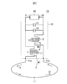
- the wireless communication device which is 1st Example is shown, (A) is a top view, (B) is an enlarged plan view of the principal part.
- the wireless communication device includes a planar radiating element including a loop portion having one end and another end adjacent to each other, a power feeding element including a coil pattern connected to one end of the loop, and the coil pattern. And a connected wireless IC element.
- the coil pattern is arranged in the vicinity of the loop portion, and is wound so that the current flowing in the coil pattern and the current flowing in the loop portion are in the same direction when power is supplied to the coil pattern.
- the coil pattern and the loop portion are connected in series and are coupled via a magnetic field.
- the planar radiating element functions as an antenna for transmitting and receiving radio signals and can be formed of a metal conductor.
- a metal conductor For example, it is preferable to use a ground conductor or the like provided on the printed wiring board.
- the housing of the communication terminal is made of metal, this metal housing may be used as the radiating element, or the metal protective film of the battery pack may be used as the radiating element.
- the planar shape may be a plane, a curved surface, a rectangle, an ellipse or a polygon.
- the loop portion is formed in a part of the planar radiating element, and is formed as an annular conductive pattern having one end and the other end. It is advantageous in terms of processing and space to form the loop portion by the edge portion formed by cutting out a part of the planar radiating element.
- a loop portion may be formed by adding a loop-shaped conductor to one side of the radiation element having a rectangular planar shape.
- the wireless IC element is an integrated circuit element for processing a high-frequency signal, and includes a logic circuit, a memory circuit, and the like, and necessary information is stored in the memory. It may be configured as a chip element made of a silicon semiconductor. A package product mounted on or built in a ceramic substrate or a resin substrate may be used, or a bare chip may be used. When using a ceramic substrate or a resin substrate, a matching circuit or a resonance circuit may be provided on the surface or inside of the substrate.
- the power feeding element has at least one coil pattern and is connected between the wireless IC element and the radiation element. That is, the high frequency signal received by the radiating element is supplied to the wireless IC element, and the high frequency signal generated by the wireless IC element is transmitted to the radiating element.
- the coil pattern is connected to one end of the loop portion. That is, when the wireless IC element is a differential feeding type, the first feeding terminal of the wireless IC element is connected to one end of the coil pattern, and the other end of the coil pattern is connected to one end of the loop part. Furthermore, the other end of the loop portion is connected to the second power supply terminal of the wireless IC element via the power supply element.
- the power feeding element may further include a capacitor connected in parallel to the wireless IC element.
- an LC resonance circuit is formed by the capacitor and the coil pattern (inductor).
- the power feeding element is constituted by a laminated body formed by laminating a plurality of insulator layers as an element body, and the coil pattern is preferably incorporated in the laminated body in a spiral shape.
- a ceramic material such as LTCC ceramic can be used, and a resin material such as a thermosetting resin or a thermoplastic resin can also be used.
- the element body may be a dielectric layer or a magnetic layer.
- a conductor pattern such as a mounting land and a connection wiring is provided on the laminate constituting the power feeding element.
- This type of conductor pattern is preferably formed of a metal material mainly composed of silver or copper having a small specific resistance.
- a conductor pattern that prevents coupling via a magnetic field between the coil pattern and the loop portion more specifically, in a region where the opening surface of the coil pattern and the loop surface of the loop portion overlap. It is preferable not to have.
- a planar conductor pattern that blocks the entire opening surface of the coil pattern prevents magnetic coupling between the coil pattern and the loop portion.
- the wireless IC element does not have to be mounted on the surface of the laminated body that constitutes the power feeding element, and may be built in the laminated body or may be provided in an element body other than the laminated body.
- the coil pattern is electrically connected in series to the loop portion of the radiating element and coupled via a magnetic field. That is, the coil pattern and the loop portion are directly connected to DC and are connected via mutual inductance. For this reason, it is preferable that the winding axis of the coil pattern is arranged in substantially the same direction as the central axis of the loop portion. Furthermore, the coil pattern is preferably disposed inside the loop portion in plan view.
- the coil pattern is wound such that when power is supplied to the coil pattern, the current flowing in the coil pattern and the current flowing in the loop portion are in the same direction (in phase). Therefore, when a current is supplied from the wireless IC element, the induced magnetic field generated in the coil pattern and the induced magnetic field generated in the loop portion have a common magnetic field loop. An induced current flows through almost the entire radiating element, and a high-frequency signal is radiated from the entire planar radiating element.
- the frequency characteristic of the radiating element is substantially determined by the size of the loop portion and the inductance value of the coil pattern, there is little influence on the frequency characteristic due to the metal object arranged in proximity. Therefore, the wireless communication device is small, has a long communication distance, and stabilizes frequency characteristics.
- the inductance value of the coil pattern is preferably larger than the inductance value formed by the loop portion. If the inductance value of both is such a relationship, the resonance frequency of the system including the coil pattern and the loop portion is dominated by the inductance value of the coil pattern, and the frequency characteristics are the size of the loop portion and the loop portion (and more It becomes difficult to be influenced by the external environment of the radiating element.
- the feeding element may include another coil pattern connected to the other end of the loop portion.
- the other coil pattern is arranged in the vicinity of the loop portion, and when power is supplied to the other coil pattern, the current flowing in the coil pattern and the current flowing in the loop portion are in the same direction (in phase). It is wound to become.
- the other coil pattern has its winding axis arranged in the same direction as the center axis of the loop portion, and the coil pattern is adjacent to the coil pattern in substantially the same position in plan view. Preferably, they are arranged and coupled to each other via a magnetic field.
- the element value of the coil pattern necessary to obtain a predetermined resonance frequency can be reduced, and the power supply element can be reduced in size.
- the phase difference is 180 ° at one end and the other end of the loop portion when the operating frequency increases.
- the wireless communication device is suitable as a reader / writer or RFID tag for an RFID system used in the HF band.
- the application can be widely applied not only to the HF band but also to the UHF band RFID system and communication systems such as W-LAN and BlueTooth (registered trademark).
- W-LAN and BlueTooth registered trademark
- a ground conductor can be used as a radiating element and a reduction in size can be realized, it has a great advantage for mounting in a wireless communication terminal such as a mobile phone.
- the wireless communication device 1A includes a radiating element 10 having a planar shape including a loop portion 11 having one end portion 11a and another end portion 11b adjacent to each other, and a loop.
- the feeding element 20 includes coil patterns L1 and L2 (see FIG. 2) connected to one end 11a and the other end 11b of the part 11 and capacitors C1 and C2 connected in series to the other ends of the coil patterns L1 and L2, respectively.
- a wireless IC element 30 connected to the other ends of the coil patterns L1, L2.
- the coil patterns L1 and L2 are arranged in the vicinity of the loop portion 11, and currents I1 and I2 (see FIG.
- the coil is wound so that the current I3 flowing through the loop part 11 is in the same direction, and the coil patterns L1, L2 and the loop part 11 are connected in series.
- the coil patterns L1 and L2 are magnetically coupled M2, and the coil patterns L1 and L2 and the loop portion 11 are also magnetically coupled M1 to each other.
- the planar radiating element 10 functions as an antenna for transmitting and receiving a radio signal.
- a ground conductor provided on the printed wiring board 5 is used.
- the loop portion 11 is formed by an edge portion formed by cutting out a part of the planar radiating element 10.
- the wireless IC element 30 is an integrated circuit element for processing a high-frequency signal, and is a known element that includes a logic circuit, a memory circuit, and the like and stores necessary information.
- the first power supply terminal 31 of the wireless IC element 30 is connected to the other end of the coil pattern L1, and the second power supply terminal 32 is connected to the other end of the coil pattern L2.
- the power feeding element 20 is connected between the wireless IC element 30 and the radiating element 10, supplies a high frequency signal received by the radiating element 10 to the wireless IC element 30, and generates a high frequency signal generated by the wireless IC element 30. Is transmitted to the radiating element 10.
- an LC resonance circuit is formed by the capacitors C1 and C2 and the coil patterns (inductors) L1 and L2.
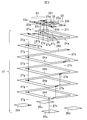
- the feeding element 20 is configured by using a laminated body 21 formed by laminating a plurality of insulating layers as a base body.
- the coil patterns L1 and L2 are spirally incorporated in the multilayer body 21, and the wireless IC element 30 and the capacitors C1 and C2 are mounted on the upper surface of the multilayer body 21.
- the laminate 21 is obtained by laminating, pressing, and firing the sheets 22a to 22h shown in FIG. 4 as necessary.
- electrodes 23a to 23h and via hole conductors 27a to 27f are formed.
- Conductive patterns 24a and 25 and via-hole conductors 27a and 27g are formed on the sheet 22b.
- Conductive patterns 24b to 24f and via-hole conductors 27g and 27h are formed on the sheets 22c to 22g.
- electrodes 26a to 26d (formed on the back surface) and via-hole conductors 27g and 27h are formed on the sheet 22a.
- the electrode 23a on the sheet 22a is connected to the conductor patterns 25 and 24b via the via-hole conductors 27a. Is connected to the conductor pattern 25 via the via hole conductor 27b, the electrode 23d is connected to the conductor pattern 25 via the via hole conductor 27c, the electrode 23e is connected to the conductor pattern 24a via the via hole conductor 27d, and the electrode 23f is connected to the via hole.
- the conductor 27e is connected to the conductor pattern 24a, and the electrode 23h is connected to the conductor pattern 24a via the via-hole conductor 27f.
- one end of the conductor pattern 24a on the sheet 22b is connected to the electrode 26b formed on the back surface of the sheet 22h via the via-hole conductor 27g.
- the other end of the conductor pattern 24b on the sheet 22c is spirally connected to the conductor patterns 24c to 24f via the via-hole conductor 27h.
- the other end of the conductor pattern 24f on the sheet 22g is connected to an electrode 26a formed on the back surface of the sheet 22h through a via-hole conductor 27h.
- the electrodes 23c, 23g, 26c, and 26d formed on the sheets 22a and 22h are floating electrodes for mounting.
- the coil pattern L1 is formed by the conductor patterns 24b to 24f, and the coil pattern L2 is formed by the conductor pattern 24a.
- the details of the conductor pattern 25 on the sheet 22b and the conductor pattern 24a facing the pattern 25 function as a routing pattern.
- the first power feeding terminal 31 and the second power feeding terminal 32 of the wireless IC element 30 are connected to the electrodes 23b and 23f, the capacitor C1 is connected to the electrodes 23a and 23e, and the electrodes 23d, The capacitor C2 is connected to 23h.
- the electrode 26 a is connected to one end 11 a of the loop portion 11
- the electrode 26 b is connected to the other end 11 b of the loop portion 11
- the electrodes 26 c and 26 d are mounting electrodes 11 c formed in the inner region of the loop portion 11. 11d (see FIG. 1B).
- the wireless communication device 1A configured as described above, when power is supplied to the coil patterns L1 and L2, the currents I1 and I2 flowing through the coil patterns L1 and L2 and the current I3 flowing through the loop portion 11 are in the same direction ( Therefore, when a current is supplied from the wireless IC element 30, the induced magnetic field generated in the coil patterns L1 and L2 and the induced magnetic field generated in the loop portion 11 strengthen each other. As a result, an induced current I4 (see FIG. 1A) flows through almost the entire radiating element 10, and a high-frequency signal is radiated from the entire radiating element 10.
- the wireless communication device 1A is small, has a long communication distance, and stabilizes frequency characteristics.
- FIG. 5 schematically shows the magnetic field strength in the wireless communication device 1A.
- the x, y, and z directions correspond to the x, y, and z directions starting from the loop portion 11 shown in FIG. 1A, and the cross hatching density is drawn higher in the region where the magnetic field strength is larger.
- FIG. 6 shows a resonance frequency characteristic in the wireless communication device 1A, and the point A is a resonance point.
- the coil patterns L1 and L2 have winding axes arranged in the same direction as the central axis of the loop portion 11, and the coil patterns L1 and L2 are located inside the loop portion 11 in plan view. Since they are arranged, the coupling via the mutual inductance M1 is strengthened.
- the inductance value of the coil pattern L1 is set to be larger than the inductance value formed by the loop portion 11. If the inductance values of the two are such a relationship, the resonance frequency of the system including the coil pattern L1 and the loop portion 11 is dominated by the inductance value of the coil pattern L1, and the frequency characteristics are the size of the loop portion 11 and the loop. It is not affected by the external environment of the part (and the radiating element 10).
- the wireless communication device 1 ⁇ / b> B is provided with a coil portion 13 between the other end portion 11 b of the loop portion 11 and the radiating element 10.
- the coil portion 13 has an outermost peripheral portion connected to the other end portion 11 b and an innermost peripheral portion connected to one end of a conductor pattern 6 formed on the back surface of the printed wiring board 5 via a via-hole conductor 7 a.
- the end is connected to the radiating element 10 via the via-hole conductor 7b.
- the radiating element 10 may be formed on the back side of the printed wiring board 5.
- This wireless communication device 1B has the same configuration as that of the wireless communication device 1A according to the first embodiment except for the above-described configuration, and the operation and effect thereof are basically the same as those of the wireless communication device 1A. Not only can the frequency characteristics of the wireless communication device 1B be adjusted by the coil part 13, but also the potential difference between the one end part 11a and the other end part 11b is increased, so that the energy radiated from the radiating element 10 can be increased.
- the wireless communication device 1C according to the third embodiment is formed by forming a slit-like cutout portion 12 in the loop portion 11, and the other configuration is the wireless communication according to the first embodiment. It is the same as that of the device 1A, and its operation effect is basically the same. In particular, the inductance value of the loop portion 11 can be adjusted by the notch portion 12.
- a wireless communication device 1D according to the fourth embodiment is obtained by omitting the coil pattern L2 from the wireless communication device 1A according to the first embodiment as shown in the equivalent circuit of FIG.
- Other configurations are the same as those of the wireless communication device 1A according to the first embodiment, and the operational effects are basically the same.
- the resonance frequency f 0 is determined by the following equation (1).
- f 0 1 / ⁇ 2 ⁇ (L 1 + L + 2M) ⁇ (1)
- L 1 Inductance value of the coil pattern
- the wireless communication device according to the present invention is not limited to the above-described embodiments, and can be variously modified within the scope of the gist.
- the present invention is useful for a wireless communication device, and is particularly excellent in that it is small in size, has a long communication distance, and has stable frequency characteristics.
Landscapes
- Engineering & Computer Science (AREA)
- Computer Networks & Wireless Communication (AREA)
- Signal Processing (AREA)
- Computer Hardware Design (AREA)
- Microelectronics & Electronic Packaging (AREA)
- Physics & Mathematics (AREA)
- General Physics & Mathematics (AREA)
- Theoretical Computer Science (AREA)
- Near-Field Transmission Systems (AREA)
- Details Of Aerials (AREA)
Abstract
Description
一端部及び他端部を有するループ部を含む面状をなす放射素子と、
前記ループ部の前記一端部に接続されたコイルパターンを含む給電素子と、
前記コイルパターンに接続された無線IC素子と、
を備えた無線通信デバイスにおいて、
前記コイルパターンは、前記ループ部の近傍に配置されており、かつ、前記コイルパターンに電力が供給されたときに前記コイルパターンに流れる電流と前記ループ部に流れる電流とが同方向となるように巻回されており、
前記コイルパターンと前記ループ部とは、直列的に接続されているとともに、磁界を介して結合されていること、
を特徴とする。 A wireless communication device according to one aspect of the present invention is provided.
A radiating element having a planar shape including a loop portion having one end and the other end;
A power feeding element including a coil pattern connected to the one end of the loop portion;
A wireless IC element connected to the coil pattern;
In a wireless communication device comprising:
The coil pattern is disposed in the vicinity of the loop portion, and the current flowing through the coil pattern and the current flowing through the loop portion are in the same direction when power is supplied to the coil pattern. Is wound,
The coil pattern and the loop portion are connected in series and are coupled via a magnetic field,
It is characterized by.
まず、本発明に係る無線通信デバイスについてその概略を説明する。この無線通信デバイスは、互いに隣接する一端部及び他端部を有するループ部を含む面状をなす放射素子と、ループ部の一端部に接続されたコイルパターンを含む給電素子と、前記コイルパターンに接続された無線IC素子と、を備えている。コイルパターンは、ループ部の近傍に配置されており、かつ、コイルパターンに電力が供給されたときにコイルパターンに流れる電流とループ部に流れる電流とが同方向となるように巻回されており、コイルパターンとループ部とは、直列的に接続されているとともに、磁界を介して結合されている。 (Overview of wireless communication device)
First, the outline of the wireless communication device according to the present invention will be described. The wireless communication device includes a planar radiating element including a loop portion having one end and another end adjacent to each other, a power feeding element including a coil pattern connected to one end of the loop, and the coil pattern. And a connected wireless IC element. The coil pattern is arranged in the vicinity of the loop portion, and is wound so that the current flowing in the coil pattern and the current flowing in the loop portion are in the same direction when power is supplied to the coil pattern. The coil pattern and the loop portion are connected in series and are coupled via a magnetic field.
第1実施例である無線通信デバイス1Aは、図1及び図2に示すように、互いに隣接する一端部11a及び他端部11bを有するループ部11を含む面状をなす放射素子10と、ループ部11の一端部11a及び他端部11bにそれぞれ接続されたコイルパターンL1,L2(図2参照)及びコイルパターンL1,L2の他端に直列に接続されたコンデンサC1,C2を含む給電素子20と、前記コイルパターンL1,L2の他端に接続された無線IC素子30と、を備えている。コイルパターンL1,L2は、ループ部11の近傍に配置されており、かつ、コイルパターンL1,L2に電力が供給されたときにコイルパターンL1,L2に流れる電流I1,I2(図2参照)とループ部11に流れる電流I3とが同方向となるように巻回されており、コイルパターンL1,L2とループ部11とは直列的に接続されている。コイルパターンL1,L2は磁界結合M2しており、コイルパターンL1,L2とループ部11も互いに磁界結合M1している。 (Refer to the first embodiment, FIGS. 1 to 6)
As shown in FIGS. 1 and 2, the wireless communication device 1A according to the first embodiment includes a radiating
第2実施例である無線通信デバイス1Bは、図7に示すように、ループ部11の他端部11bと放射素子10との間にコイル部13を設けたものである。コイル部13は最外周部が他端部11bに接続され、最内周部がプリント配線板5の裏面に形成した導体パターン6の一端にビアホール導体7aを介して接続され、導体パターン6の他端はビアホール導体7bを介して放射素子10に接続されている。なお、放射素子10はプリント配線板5の裏面側に形成されていてもよい。 (Refer to the second embodiment, FIG. 7)
As shown in FIG. 7, the
第3実施例である無線通信デバイス1Cは、図8に示すように、ループ部11にスリット状の切欠き部12を形成したものであり、その他の構成は前記第1実施例である無線通信デバイス1Aと同様であり、その作用効果も基本的に同様である。特に、切欠き部12によってループ部11のインダクタンス値を調整することができる。 (Refer to the third embodiment, FIG. 8)
As shown in FIG. 8, the wireless communication device 1C according to the third embodiment is formed by forming a slit-
第4実施例である無線通信デバイス1Dは、図9の等価回路に示すように、前記第1実施例である無線通信デバイス1AにおいてコイルパターンL2を省略したものである。その他の構成は前記第1実施例である無線通信デバイス1Aと同様であり、作用効果も基本的に同様である。 (Refer to the fourth embodiment, FIG. 9)
A
られる。
f0=1/{2π√(L1+L+2M)} …(1)
L1:コイルパターンL1のインダクタンス値
L:ループ部のインダクタンス値
M=k√(L1L) In this
f 0 = 1 / {2π√ (L 1 + L + 2M)} (1)
L 1 : Inductance value of the coil pattern L 1 L: Inductance value of the loop part M = k√ (L 1 L)
なお、本発明に係る無線通信デバイスは前記実施例に限定するものではなく、その要旨の範囲内で種々に変更できることは勿論である。 (Other examples)
The wireless communication device according to the present invention is not limited to the above-described embodiments, and can be variously modified within the scope of the gist.
5…プリント配線板
10…放射素子
11…ループ部
20…給電素子
21…積層体
30…無線IC素子
L1,L2…コイルパターン
C1,C2…コンデンサ DESCRIPTION OF SYMBOLS 1A-1D ...
Claims (12)
- 一端部及び他端部を有するループ部を含む面状をなす放射素子と、
前記ループ部の前記一端部に接続されたコイルパターンを含む給電素子と、
前記コイルパターンに接続された無線IC素子と、
を備えた無線通信デバイスにおいて、
前記コイルパターンは、前記ループ部の近傍に配置されており、かつ、前記コイルパターンに電力が供給されたときに前記コイルパターンに流れる電流と前記ループ部に流れる電流とが同方向となるように巻回されており、
前記コイルパターンと前記ループ部とは、直列的に接続されているとともに、磁界を介して結合されていること、
を特徴とする無線通信デバイス。 A radiating element having a planar shape including a loop portion having one end portion and the other end portion;
A power feeding element including a coil pattern connected to the one end of the loop portion;
A wireless IC element connected to the coil pattern;
In a wireless communication device comprising:
The coil pattern is disposed in the vicinity of the loop portion, and the current flowing through the coil pattern and the current flowing through the loop portion are in the same direction when power is supplied to the coil pattern. Is wound,
The coil pattern and the loop portion are connected in series and are coupled via a magnetic field,
A wireless communication device. - 前記コイルパターンはその巻回軸が前記ループ部の中心軸とほぼ同方向に配置されていること、を特徴とする請求項1に記載の無線通信デバイス。 The wireless communication device according to claim 1, wherein the coil pattern has a winding axis disposed in substantially the same direction as a central axis of the loop portion.
- 前記コイルパターンは平面視で前記ループ部の内側に配置されていること、を特徴とする請求項1又は請求項2に記載の無線通信デバイス。 The wireless communication device according to claim 1 or 2, wherein the coil pattern is disposed inside the loop portion in plan view.
- 前記コイルパターンのインダクタンス値は前記ループ部によって形成されるインダクタンス値よりも大きいこと、を特徴とする請求項1ないし請求項3のいずれかに記載の無線通信デバイス。 The wireless communication device according to any one of claims 1 to 3, wherein an inductance value of the coil pattern is larger than an inductance value formed by the loop portion.
- 前記ループ部は前記放射素子の一部を切り欠くことによって形成された縁端部によって構成されていること、を特徴とする請求項1ないし請求項4のいずれかに記載の無線通信デバイス。 The wireless communication device according to any one of claims 1 to 4, wherein the loop portion is configured by an edge portion formed by cutting out a part of the radiating element.
- 前記放射素子はプリント配線基板に設けられたグランド導体であること、を特徴とする請求項1ないし請求項5のいずれかに記載の無線通信デバイス。 6. The wireless communication device according to claim 1, wherein the radiation element is a ground conductor provided on a printed wiring board.
- 前記給電素子は前記無線IC素子に並列に接続されたコンデンサをさらに含んでいること、を特徴とする請求項1ないし請求項6のいずれかに記載の無線通信デバイス。 The wireless communication device according to any one of claims 1 to 6, wherein the power feeding element further includes a capacitor connected in parallel to the wireless IC element.
- 前記給電素子は複数の絶縁体層を積層してなる積層体を素体とし、前記コイルパターンは前記積層体に螺旋状に内蔵されていること、を特徴とする請求項1ないし請求項7のいずれかに記載の無線通信デバイス。 8. The feed element according to claim 1, wherein the power feeding element includes a laminated body formed by laminating a plurality of insulator layers, and the coil pattern is spirally incorporated in the laminated body. The wireless communication device according to any one of the above.
- 前記コイルパターンと前記ループ部との間には磁界を介しての結合を妨げる導体パターンを有していないこと、を特徴とする請求項1ないし請求項8のいずれかに記載の無線通信デバイス。 The wireless communication device according to any one of claims 1 to 8, wherein a conductor pattern that prevents coupling via a magnetic field is not provided between the coil pattern and the loop portion.
- 前記給電素子は前記ループ部の前記他端部に接続されたいま一つのコイルパターンを含み、
前記いま一つのコイルパターンは、前記ループ部の近傍に配置されており、かつ、いま一つのコイルパターンに電力が供給されたときにいま一つのコイルパターンに流れる電流と前記ループ部に流れる電流とが同方向となるように巻回されていること、
を特徴とする請求項1ないし請求項9のいずれかに記載の無線通信デバイス。 The feeding element includes another coil pattern connected to the other end of the loop portion,
The another coil pattern is disposed in the vicinity of the loop portion, and when power is supplied to the other coil pattern, the current flowing in the one coil pattern and the current flowing in the loop portion are Are wound in the same direction,
The wireless communication device according to claim 1, wherein: - 前記いま一つのコイルパターンはその巻回軸が前記ループ部の中心軸とほぼ同方向に配置されていること、を特徴とする請求項10に記載の無線通信デバイス。 11. The wireless communication device according to claim 10, wherein the winding axis of the another coil pattern is arranged in substantially the same direction as the central axis of the loop portion.
- 前記コイルパターンと前記いま一つのコイルパターンとは、それぞれの巻回軸が平面視でほぼ同一位置に隣接して配置されていること、を特徴とする請求項10又は請求項11に記載の無線通信デバイス。 12. The radio according to claim 10, wherein the coil pattern and the another coil pattern are arranged such that respective winding axes are adjacent to each other at substantially the same position in plan view. Communication device.
Priority Applications (4)
| Application Number | Priority Date | Filing Date | Title |
|---|---|---|---|
| JP2013523798A JP5333707B2 (en) | 2011-07-15 | 2012-07-09 | Wireless communication device |
| DE112012001977.6T DE112012001977T5 (en) | 2011-07-15 | 2012-07-09 | Radio communication equipment |
| CN201280008674.5A CN103370886B (en) | 2011-07-15 | 2012-07-09 | Wireless communication device |
| US14/027,384 US8770489B2 (en) | 2011-07-15 | 2013-09-16 | Radio communication device |
Applications Claiming Priority (2)
| Application Number | Priority Date | Filing Date | Title |
|---|---|---|---|
| JP2011156664 | 2011-07-15 | ||
| JP2011-156664 | 2011-07-15 |
Related Child Applications (1)
| Application Number | Title | Priority Date | Filing Date |
|---|---|---|---|
| US14/027,384 Continuation US8770489B2 (en) | 2011-07-15 | 2013-09-16 | Radio communication device |
Publications (1)
| Publication Number | Publication Date |
|---|---|
| WO2013011856A1 true WO2013011856A1 (en) | 2013-01-24 |
Family
ID=47558034
Family Applications (1)
| Application Number | Title | Priority Date | Filing Date |
|---|---|---|---|
| PCT/JP2012/067454 WO2013011856A1 (en) | 2011-07-15 | 2012-07-09 | Wireless communication device |
Country Status (5)
| Country | Link |
|---|---|
| US (1) | US8770489B2 (en) |
| JP (1) | JP5333707B2 (en) |
| CN (1) | CN103370886B (en) |
| DE (1) | DE112012001977T5 (en) |
| WO (1) | WO2013011856A1 (en) |
Cited By (3)
| Publication number | Priority date | Publication date | Assignee | Title |
|---|---|---|---|---|
| WO2015079934A1 (en) * | 2013-11-29 | 2015-06-04 | 株式会社村田製作所 | Wireless-communication device and article provided therewith |
| JP2015142279A (en) * | 2014-01-29 | 2015-08-03 | アルプス電気株式会社 | Push button switch |
| JP2020178366A (en) * | 2020-07-20 | 2020-10-29 | 株式会社バンダイ | toy |
Families Citing this family (6)
| Publication number | Priority date | Publication date | Assignee | Title |
|---|---|---|---|---|
| CN104466363A (en) * | 2014-12-11 | 2015-03-25 | 深圳市信维通信股份有限公司 | NFC antenna structure applied to wearable device and intelligent watch |
| JP6024733B2 (en) * | 2014-12-17 | 2016-11-16 | Tdk株式会社 | ANTENNA ELEMENT, ANTENNA DEVICE, AND WIRELESS COMMUNICATION DEVICE USING THE SAME |
| CN104767033B (en) * | 2015-03-26 | 2016-06-22 | 上海安费诺永亿通讯电子有限公司 | The antenna assembly of near-field communication or wireless charging and electronic equipment |
| EP4332516A3 (en) | 2015-07-12 | 2024-05-22 | Patients Pending Ltd. | Cover for a liquid delivery system with intergrated plunger position sensing, and corresponding method |
| KR102443196B1 (en) | 2015-09-25 | 2022-09-15 | 삼성전자주식회사 | Electronic device |
| CN111081463B (en) * | 2018-10-19 | 2021-01-26 | 立锜科技股份有限公司 | Transmission interface with noise reduction |
Citations (5)
| Publication number | Priority date | Publication date | Assignee | Title |
|---|---|---|---|---|
| JP2002245416A (en) * | 2001-02-16 | 2002-08-30 | Denso Corp | Reader/writer for id tag |
| JP2004336604A (en) * | 2003-05-12 | 2004-11-25 | Hanex Co Ltd | Structure for installing data carrier |
| JP2007068073A (en) * | 2005-09-02 | 2007-03-15 | Sony Corp | Information processing device |
| JP2007194924A (en) * | 2006-01-19 | 2007-08-02 | Yokogawa Electric Corp | Antenna, and radio tag device and radio tag communication device using same |
| JP2011076567A (en) * | 2009-10-02 | 2011-04-14 | Murata Mfg Co Ltd | Radio ic device and electromagnetic coupling module |
Family Cites Families (469)
| Publication number | Priority date | Publication date | Assignee | Title |
|---|---|---|---|---|
| US3364564A (en) | 1965-06-28 | 1968-01-23 | Gregory Ind Inc | Method of producing welding studs dischargeable in end-to-end relationship |
| JPS6193701A (en) | 1984-10-13 | 1986-05-12 | Toyota Motor Corp | Antenna system for automobile |
| US4782342A (en) * | 1986-08-04 | 1988-11-01 | Walton Charles A | Proximity identification system with lateral flux paths |
| US5253969A (en) | 1989-03-10 | 1993-10-19 | Sms Schloemann-Siemag Aktiengesellschaft | Feeding system for strip material, particularly in treatment plants for metal strips |
| JP2763664B2 (en) | 1990-07-25 | 1998-06-11 | 日本碍子株式会社 | Wiring board for distributed constant circuit |
| NL9100176A (en) | 1991-02-01 | 1992-03-02 | Nedap Nv | Antenna configuration for contactless identification label - forms part of tuned circuit of ID or credit card interrogated via inductive coupling |
| NL9100347A (en) | 1991-02-26 | 1992-03-02 | Nedap Nv | Integrated transformer circuit for ID or credit card - is interrogated via contactless inductive coupling using capacitor to form tuned circuit |
| JPH04321190A (en) | 1991-04-22 | 1992-11-11 | Mitsubishi Electric Corp | Antenna circuit and its production for non-contact type portable storage |
| DE69215283T2 (en) | 1991-07-08 | 1997-03-20 | Nippon Telegraph & Telephone | Extendable antenna system |
| US5491483A (en) | 1994-01-05 | 1996-02-13 | Texas Instruments Incorporated | Single loop transponder system and method |
| US6096431A (en) | 1994-07-25 | 2000-08-01 | Toppan Printing Co., Ltd. | Biodegradable cards |
| JP3141692B2 (en) | 1994-08-11 | 2001-03-05 | 松下電器産業株式会社 | Millimeter wave detector |
| US5528222A (en) | 1994-09-09 | 1996-06-18 | International Business Machines Corporation | Radio frequency circuit and memory in thin flexible package |
| US5955723A (en) | 1995-05-03 | 1999-09-21 | Siemens Aktiengesellschaft | Contactless chip card |
| US5629241A (en) | 1995-07-07 | 1997-05-13 | Hughes Aircraft Company | Microwave/millimeter wave circuit structure with discrete flip-chip mounted elements, and method of fabricating the same |
| JP3150575B2 (en) | 1995-07-18 | 2001-03-26 | 沖電気工業株式会社 | Tag device and manufacturing method thereof |
| GB2305075A (en) | 1995-09-05 | 1997-03-26 | Ibm | Radio Frequency Tag for Electronic Apparatus |
| DE19534229A1 (en) | 1995-09-15 | 1997-03-20 | Licentia Gmbh | Transponder arrangement |
| AUPO055296A0 (en) | 1996-06-19 | 1996-07-11 | Integrated Silicon Design Pty Ltd | Enhanced range transponder system |
| US6104311A (en) | 1996-08-26 | 2000-08-15 | Addison Technologies | Information storage and identification tag |
| BR9711887A (en) | 1996-10-09 | 2002-01-02 | Pav Card Gmbh | Connective arrangement and process for producing a smart card |
| JP3279205B2 (en) | 1996-12-10 | 2002-04-30 | 株式会社村田製作所 | Surface mount antenna and communication equipment |
| JPH10193849A (en) | 1996-12-27 | 1998-07-28 | Rohm Co Ltd | Circuit chip-mounted card and circuit chip module |
| DE19703029A1 (en) | 1997-01-28 | 1998-07-30 | Amatech Gmbh & Co Kg | Transmission module for a transponder device and transponder device and method for operating a transponder device |
| JP2001514777A (en) | 1997-03-10 | 2001-09-11 | プレシジョン ダイナミクス コーポレイション | Reactively connected elements of a circuit provided on a flexible substrate |
| EP1031939B1 (en) | 1997-11-14 | 2005-09-14 | Toppan Printing Co., Ltd. | Composite ic card |
| JP2001084463A (en) | 1999-09-14 | 2001-03-30 | Miyake:Kk | Resonance circuit |
| JPH11261325A (en) | 1998-03-10 | 1999-09-24 | Shiro Sugimura | Coil element and its manufacture |
| JP4260917B2 (en) | 1998-03-31 | 2009-04-30 | 株式会社東芝 | Loop antenna |
| EP0987789A4 (en) | 1998-03-31 | 2004-09-22 | Matsushita Electric Ind Co Ltd | Antenna unit and digital television receiver |
| US5936150A (en) | 1998-04-13 | 1999-08-10 | Rockwell Science Center, Llc | Thin film resonant chemical sensor with resonant acoustic isolator |
| CA2293228A1 (en) | 1998-04-14 | 1999-10-21 | Robert A. Katchmazenski | Container for compressors and other goods |
| US6107920A (en) | 1998-06-09 | 2000-08-22 | Motorola, Inc. | Radio frequency identification tag having an article integrated antenna |
| US6018299A (en) | 1998-06-09 | 2000-01-25 | Motorola, Inc. | Radio frequency identification tag having a printed antenna and method |
| JP2000021639A (en) | 1998-07-02 | 2000-01-21 | Sharp Corp | Inductor, resonance circuit using the same, matching circuit, antenna circuit, and oscillation circuit |
| JP2000022421A (en) | 1998-07-03 | 2000-01-21 | Murata Mfg Co Ltd | Chip antenna and radio device mounted with it |
| AUPP473898A0 (en) | 1998-07-20 | 1998-08-13 | Integrated Silicon Design Pty Ltd | Metal screened electronic labelling system |
| EP0977145A3 (en) | 1998-07-28 | 2002-11-06 | Kabushiki Kaisha Toshiba | Radio IC card |
| JP2000311226A (en) | 1998-07-28 | 2000-11-07 | Toshiba Corp | Radio ic card and its production and read and write system of the same |
| JP3956172B2 (en) | 1998-07-31 | 2007-08-08 | 吉川アールエフシステム株式会社 | Data carrier and antenna for data carrier |
| JP2000059260A (en) | 1998-08-04 | 2000-02-25 | Sony Corp | Storage device |
| DE69938671D1 (en) | 1998-08-14 | 2008-06-19 | 3M Innovative Properties Co | APPLICATIONS FOR RF IDENTIFICATION SYSTEMS |
| EP1298573A3 (en) | 1998-08-14 | 2003-09-17 | 3M Innovative Properties Company | Radio frequency identification system comprising a plurality of antennas |
| JP4411670B2 (en) | 1998-09-08 | 2010-02-10 | 凸版印刷株式会社 | Non-contact IC card manufacturing method |
| JP4508301B2 (en) | 1998-09-16 | 2010-07-21 | 大日本印刷株式会社 | Non-contact IC card |
| JP3632466B2 (en) | 1998-10-23 | 2005-03-23 | 凸版印刷株式会社 | Inspection device and inspection method for non-contact IC card |
| JP2000137779A (en) | 1998-10-30 | 2000-05-16 | Hitachi Maxell Ltd | Non-contact information medium and production thereof |
| US6837438B1 (en) | 1998-10-30 | 2005-01-04 | Hitachi Maxell, Ltd. | Non-contact information medium and communication system utilizing the same |
| JP2000137785A (en) | 1998-10-30 | 2000-05-16 | Sony Corp | Manufacture of noncontact type ic card and noncontact type ic card |
| JP3924962B2 (en) | 1998-10-30 | 2007-06-06 | 株式会社デンソー | ID tag for dishes |
| JP2000148948A (en) | 1998-11-05 | 2000-05-30 | Sony Corp | Non-contact ic label and its manufacture |
| JP2000172812A (en) | 1998-12-08 | 2000-06-23 | Hitachi Maxell Ltd | Noncontact information medium |
| FR2787640B1 (en) | 1998-12-22 | 2003-02-14 | Gemplus Card Int | ARRANGEMENT OF AN ANTENNA IN A METALLIC ENVIRONMENT |
| JP3088404B2 (en) | 1999-01-14 | 2000-09-18 | 埼玉日本電気株式会社 | Mobile radio terminal and built-in antenna |
| JP2000222540A (en) | 1999-02-03 | 2000-08-11 | Hitachi Maxell Ltd | Non-contact type semiconductor tag |
| JP2000228602A (en) | 1999-02-08 | 2000-08-15 | Alps Electric Co Ltd | Resonance line |
| JP2000243797A (en) | 1999-02-18 | 2000-09-08 | Sanken Electric Co Ltd | Semiconductor wafer, and cutting method thereof, and semiconductor wafer assembly and cutting method thereof |
| JP3967487B2 (en) | 1999-02-23 | 2007-08-29 | 株式会社東芝 | IC card |
| JP2000251049A (en) | 1999-03-03 | 2000-09-14 | Konica Corp | Card and production thereof |
| JP4106673B2 (en) | 1999-03-05 | 2008-06-25 | 株式会社エフ・イー・シー | Antenna device using coil unit, printed circuit board |
| JP4349597B2 (en) | 1999-03-26 | 2009-10-21 | 大日本印刷株式会社 | IC chip manufacturing method and memory medium manufacturing method incorporating the same |
| US6542050B1 (en) | 1999-03-30 | 2003-04-01 | Ngk Insulators, Ltd. | Transmitter-receiver |
| JP3751178B2 (en) | 1999-03-30 | 2006-03-01 | 日本碍子株式会社 | Transceiver |
| JP2000286634A (en) | 1999-03-30 | 2000-10-13 | Ngk Insulators Ltd | Antenna system and its manufacture |
| JP3067764B1 (en) | 1999-03-31 | 2000-07-24 | 株式会社豊田自動織機製作所 | Mobile communication coupler, mobile body, and mobile communication method |
| JP2000321984A (en) | 1999-05-12 | 2000-11-24 | Hitachi Ltd | Label with rf-id tag |
| JP3557130B2 (en) | 1999-07-14 | 2004-08-25 | 新光電気工業株式会社 | Method for manufacturing semiconductor device |
| JP2001043340A (en) | 1999-07-29 | 2001-02-16 | Toppan Printing Co Ltd | Composite ic card |
| US6259369B1 (en) | 1999-09-30 | 2001-07-10 | Moore North America, Inc. | Low cost long distance RFID reading |
| JP2001101369A (en) | 1999-10-01 | 2001-04-13 | Matsushita Electric Ind Co Ltd | Rf tag |
| JP3451373B2 (en) | 1999-11-24 | 2003-09-29 | オムロン株式会社 | Manufacturing method of data carrier capable of reading electromagnetic wave |
| JP4186149B2 (en) | 1999-12-06 | 2008-11-26 | 株式会社エフ・イー・シー | Auxiliary antenna for IC card |
| JP2001188890A (en) | 2000-01-05 | 2001-07-10 | Omron Corp | Non-contact tag |
| JP4221878B2 (en) * | 2000-01-25 | 2009-02-12 | ソニー株式会社 | Antenna device |
| JP2001209767A (en) | 2000-01-27 | 2001-08-03 | Hitachi Maxell Ltd | Object to be accessed provided with non-contact ic module |
| US7334734B2 (en) | 2000-01-27 | 2008-02-26 | Hitachi Maxwell, Ltd. | Non-contact IC module |
| JP2001240046A (en) | 2000-02-25 | 2001-09-04 | Toppan Forms Co Ltd | Container and manufacturing method thereof |
| JP4514880B2 (en) | 2000-02-28 | 2010-07-28 | 大日本印刷株式会社 | Book delivery, returns and inventory management system |
| JP2001257292A (en) | 2000-03-10 | 2001-09-21 | Hitachi Maxell Ltd | Semiconductor device |
| JP2001256457A (en) | 2000-03-13 | 2001-09-21 | Toshiba Corp | Semiconductor device, its manufacture and ic card communication system |
| JP2003529163A (en) | 2000-03-28 | 2003-09-30 | ルカトロン アーゲー | RFID label having member for adjusting resonance frequency |
| JP4624537B2 (en) | 2000-04-04 | 2011-02-02 | 大日本印刷株式会社 | Non-contact data carrier device, storage |
| JP4624536B2 (en) | 2000-04-04 | 2011-02-02 | 大日本印刷株式会社 | Non-contact data carrier device |
| JP2001291181A (en) | 2000-04-07 | 2001-10-19 | Ricoh Elemex Corp | Sensor and sensor system |
| JP2001319380A (en) | 2000-05-11 | 2001-11-16 | Mitsubishi Materials Corp | Optical disk with rfid |
| JP2001331976A (en) | 2000-05-17 | 2001-11-30 | Casio Comput Co Ltd | Optical recording type recording medium |
| JP4223174B2 (en) | 2000-05-19 | 2009-02-12 | Dxアンテナ株式会社 | Film antenna |
| JP2001339226A (en) | 2000-05-26 | 2001-12-07 | Nec Saitama Ltd | Antenna system |
| JP2001344574A (en) | 2000-05-30 | 2001-12-14 | Mitsubishi Materials Corp | Antenna device for interrogator |
| JP2001352176A (en) | 2000-06-05 | 2001-12-21 | Fuji Xerox Co Ltd | Multilayer printed wiring board and manufacturing method of multilayer printed wiring board |
| JP2003536302A (en) | 2000-06-06 | 2003-12-02 | バッテル メモリアル インスティテュート | Telecommunications systems and methods |
| JP2001358527A (en) | 2000-06-12 | 2001-12-26 | Matsushita Electric Ind Co Ltd | Antenna device |
| JP2002157564A (en) | 2000-11-21 | 2002-05-31 | Toyo Aluminium Kk | Antenna coil for ic card and its manufacturing method |
| US6400323B2 (en) | 2000-06-23 | 2002-06-04 | Toyo Aluminium Kabushiki Kaisha | Antenna coil for IC card and manufacturing method thereof |
| CN1604492A (en) | 2000-07-04 | 2005-04-06 | 克里蒂帕斯株式会社 | Credit-card type transponder |
| JP4138211B2 (en) | 2000-07-06 | 2008-08-27 | 株式会社村田製作所 | Electronic component and manufacturing method thereof, collective electronic component, mounting structure of electronic component, and electronic apparatus |
| JP2002024776A (en) | 2000-07-07 | 2002-01-25 | Nippon Signal Co Ltd:The | Ic card reader/writer |
| WO2002007078A1 (en) | 2000-07-19 | 2002-01-24 | Hanex Co., Ltd. | Rfid tag housing structure, rfid tag installation structure and rfid tag communication method |
| RU2163739C1 (en) | 2000-07-20 | 2001-02-27 | Криштопов Александр Владимирович | Antenna |
| JP2002042076A (en) | 2000-07-21 | 2002-02-08 | Dainippon Printing Co Ltd | Non-contact data carrier and booklet therewith |
| JP2002042083A (en) | 2000-07-27 | 2002-02-08 | Hitachi Maxell Ltd | Non-contact communication type information carrier |
| JP3075400U (en) | 2000-08-03 | 2001-02-16 | 昌栄印刷株式会社 | Non-contact IC card |
| US6466007B1 (en) | 2000-08-14 | 2002-10-15 | Teradyne, Inc. | Test system for smart card and indentification devices and the like |
| JP2002063557A (en) | 2000-08-21 | 2002-02-28 | Mitsubishi Materials Corp | Tag for rfid |
| JP2002076750A (en) | 2000-08-24 | 2002-03-15 | Murata Mfg Co Ltd | Antenna device and radio equipment equipped with it |
| JP2002143826A (en) | 2000-08-30 | 2002-05-21 | Denso Corp | System for recycling waste and system for detecting unlawful dumping |
| JP3481575B2 (en) | 2000-09-28 | 2003-12-22 | 寛児 川上 | antenna |
| JP4615695B2 (en) | 2000-10-19 | 2011-01-19 | 三星エスディーエス株式会社 | IC module for IC card and IC card using it |
| US6634564B2 (en) | 2000-10-24 | 2003-10-21 | Dai Nippon Printing Co., Ltd. | Contact/noncontact type data carrier module |
| JP4628611B2 (en) | 2000-10-27 | 2011-02-09 | 三菱マテリアル株式会社 | antenna |
| JP4432254B2 (en) | 2000-11-20 | 2010-03-17 | 株式会社村田製作所 | Surface mount antenna structure and communication device including the same |
| JP2002185358A (en) | 2000-11-24 | 2002-06-28 | Supersensor Pty Ltd | Method for fitting rf transponder to container |
| JP4641096B2 (en) | 2000-12-07 | 2011-03-02 | 大日本印刷株式会社 | Non-contact data carrier device and wiring member for booster antenna |
| JP2002175920A (en) | 2000-12-08 | 2002-06-21 | Murata Mfg Co Ltd | High-frequency filter element |
| JP2002183676A (en) | 2000-12-08 | 2002-06-28 | Hitachi Ltd | Information reader |
| JP2002183690A (en) | 2000-12-11 | 2002-06-28 | Hitachi Maxell Ltd | Noncontact ic tag device |
| WO2002048980A1 (en) | 2000-12-15 | 2002-06-20 | Electrox Corp. | Process for the manufacture of novel, inexpensive radio frequency identification devices |
| JP3788325B2 (en) | 2000-12-19 | 2006-06-21 | 株式会社村田製作所 | Multilayer coil component and manufacturing method thereof |
| TW531976B (en) | 2001-01-11 | 2003-05-11 | Hanex Co Ltd | Communication apparatus and installing structure, manufacturing method and communication method |
| JP3621655B2 (en) | 2001-04-23 | 2005-02-16 | 株式会社ハネックス中央研究所 | RFID tag structure and manufacturing method thereof |
| JP2002280821A (en) | 2001-01-12 | 2002-09-27 | Furukawa Electric Co Ltd:The | Antenna system and terminal equipment |
| KR20020061103A (en) | 2001-01-12 | 2002-07-22 | 후루까와덴끼고오교 가부시끼가이샤 | Antenna device and terminal with the antenna device |
| JP2002222398A (en) | 2001-01-25 | 2002-08-09 | Jstm Kk | Non-contact data carrier |
| JP2002232221A (en) | 2001-01-30 | 2002-08-16 | Alps Electric Co Ltd | Transmission and reception unit |
| JPWO2002061675A1 (en) | 2001-01-31 | 2004-06-03 | 株式会社ルネサステクノロジ | Non-contact identification medium |
| JP4662400B2 (en) | 2001-02-05 | 2011-03-30 | 大日本印刷株式会社 | Articles with coil-on-chip semiconductor modules |
| JP2002246828A (en) | 2001-02-15 | 2002-08-30 | Mitsubishi Materials Corp | Antenna for transponder |
| EP1368858B1 (en) | 2001-03-02 | 2011-02-23 | Nxp B.V. | Module and electronic device |
| JP4712986B2 (en) | 2001-03-06 | 2011-06-29 | 大日本印刷株式会社 | Liquid container with RFID tag |
| JP2002290130A (en) | 2001-03-28 | 2002-10-04 | Aiwa Co Ltd | Radio communication unit |
| JP3570386B2 (en) | 2001-03-30 | 2004-09-29 | 松下電器産業株式会社 | Portable information terminal with built-in wireless function |
| JP3772778B2 (en) | 2001-03-30 | 2006-05-10 | 三菱マテリアル株式会社 | Antenna coil, identification tag using the same, reader / writer device, reader device and writer device |
| JP2002298109A (en) | 2001-03-30 | 2002-10-11 | Toppan Forms Co Ltd | Contactless ic medium and manufacturing method thereof |
| JP2002308437A (en) | 2001-04-16 | 2002-10-23 | Dainippon Printing Co Ltd | Inspection system using rfid tag |
| JP2002319812A (en) | 2001-04-20 | 2002-10-31 | Oji Paper Co Ltd | Data carrier adhesion method |
| JP4700831B2 (en) | 2001-04-23 | 2011-06-15 | 株式会社ハネックス | RFID tag communication distance expansion method |
| JP2002325013A (en) | 2001-04-26 | 2002-11-08 | Mitsubishi Materials Corp | Antenna coil |
| JP2005236339A (en) | 2001-07-19 | 2005-09-02 | Oji Paper Co Ltd | Ic chip mounted body |
| FI112550B (en) | 2001-05-31 | 2003-12-15 | Rafsec Oy | Smart label and smart label path |
| JP2002366917A (en) | 2001-06-07 | 2002-12-20 | Hitachi Ltd | Ic card incorporating antenna |
| JP2002362613A (en) | 2001-06-07 | 2002-12-18 | Toppan Printing Co Ltd | Laminated packaging material having non-contact ic, packaging container using laminated packaging material and method for detecting opened seal of packaging container |
| JP4710174B2 (en) | 2001-06-13 | 2011-06-29 | 株式会社村田製作所 | Balanced LC filter |
| JP2002373029A (en) | 2001-06-18 | 2002-12-26 | Hitachi Ltd | Method for preventing illegal copy of software by using ic tag |
| JP4882167B2 (en) | 2001-06-18 | 2012-02-22 | 大日本印刷株式会社 | Card-integrated form with non-contact IC chip |
| JP4759854B2 (en) | 2001-06-19 | 2011-08-31 | 株式会社寺岡精工 | Mounting method of IC tag to metal object and IC tag built-in marker |
| JP2003087008A (en) | 2001-07-02 | 2003-03-20 | Ngk Insulators Ltd | Laminated type dielectric filter |
| JP4058919B2 (en) | 2001-07-03 | 2008-03-12 | 日立化成工業株式会社 | Non-contact IC label, non-contact IC card, non-contact IC label or IC module for non-contact IC card |
| JP2003026177A (en) | 2001-07-12 | 2003-01-29 | Toppan Printing Co Ltd | Packaging member with non-contact type ic chip |
| JP2003030612A (en) | 2001-07-19 | 2003-01-31 | Oji Paper Co Ltd | Ic chip mounting body |
| JP4670195B2 (en) | 2001-07-23 | 2011-04-13 | 凸版印刷株式会社 | Mobile phone case with non-contact IC card |
| US7274285B2 (en) | 2001-07-24 | 2007-09-25 | Hewlett-Packard Development Company, L.P. | System and method for improved object identification |
| ES2295105T3 (en) | 2001-07-26 | 2008-04-16 | Irdeto Access B.V. | SYSTEM FOR THE VALIDATION OF TIME TIME. |
| JP3629448B2 (en) | 2001-07-27 | 2005-03-16 | Tdk株式会社 | ANTENNA DEVICE AND ELECTRONIC DEVICE HAVING THE SAME |
| JP2003069335A (en) | 2001-08-28 | 2003-03-07 | Hitachi Kokusai Electric Inc | Auxiliary antenna |
| JP2003067711A (en) | 2001-08-29 | 2003-03-07 | Toppan Forms Co Ltd | Article provided with ic chip mounting body or antenna part |
| JP2003078333A (en) | 2001-08-30 | 2003-03-14 | Murata Mfg Co Ltd | Radio communication apparatus |
| JP2003078336A (en) | 2001-08-30 | 2003-03-14 | Tokai Univ | Laminated spiral antenna |
| JP4514374B2 (en) | 2001-09-05 | 2010-07-28 | トッパン・フォームズ株式会社 | RF-ID inspection system |
| JP4747467B2 (en) | 2001-09-07 | 2011-08-17 | 大日本印刷株式会社 | Non-contact IC tag |
| JP2003085520A (en) | 2001-09-11 | 2003-03-20 | Oji Paper Co Ltd | Manufacturing method for ic card |
| JP2003099184A (en) | 2001-09-25 | 2003-04-04 | Sharp Corp | Information system and information processor and input pen to be used for the same system |
| JP4845306B2 (en) | 2001-09-25 | 2011-12-28 | トッパン・フォームズ株式会社 | RF-ID inspection system |
| JP4698096B2 (en) | 2001-09-25 | 2011-06-08 | トッパン・フォームズ株式会社 | RF-ID inspection system |
| JP2003110344A (en) | 2001-09-26 | 2003-04-11 | Hitachi Metals Ltd | Surface-mounting type antenna and antenna device mounting the same |
| JP2003132330A (en) | 2001-10-25 | 2003-05-09 | Sato Corp | Rfid label printer |
| JP2003134007A (en) | 2001-10-30 | 2003-05-09 | Auto Network Gijutsu Kenkyusho:Kk | System and method for exchanging signal between on- vehicle equipment |
| JP3984458B2 (en) | 2001-11-20 | 2007-10-03 | 大日本印刷株式会社 | Manufacturing method of package with IC tag |
| JP3908514B2 (en) | 2001-11-20 | 2007-04-25 | 大日本印刷株式会社 | Package with IC tag and method of manufacturing package with IC tag |
| US6812707B2 (en) | 2001-11-27 | 2004-11-02 | Mitsubishi Materials Corporation | Detection element for objects and detection device using the same |
| JP3894540B2 (en) | 2001-11-30 | 2007-03-22 | トッパン・フォームズ株式会社 | Interposer with conductive connection |
| JP2003188338A (en) | 2001-12-13 | 2003-07-04 | Sony Corp | Circuit board and its manufacturing method |
| JP3700777B2 (en) | 2001-12-17 | 2005-09-28 | 三菱マテリアル株式会社 | Electrode structure of RFID tag and method for adjusting resonance frequency using the electrode |
| JP2003188620A (en) | 2001-12-19 | 2003-07-04 | Murata Mfg Co Ltd | Antenna integral with module |
| JP4028224B2 (en) | 2001-12-20 | 2007-12-26 | 大日本印刷株式会社 | Paper IC card substrate having non-contact communication function |
| JP3895175B2 (en) | 2001-12-28 | 2007-03-22 | Ntn株式会社 | Dielectric resin integrated antenna |
| JP2003209421A (en) | 2002-01-17 | 2003-07-25 | Dainippon Printing Co Ltd | Rfid tag having transparent antenna and production method therefor |
| JP3915092B2 (en) | 2002-01-21 | 2007-05-16 | 株式会社エフ・イー・シー | Booster antenna for IC card |
| JP2003216919A (en) | 2002-01-23 | 2003-07-31 | Toppan Forms Co Ltd | Rf-id media |
| JP2003233780A (en) | 2002-02-06 | 2003-08-22 | Mitsubishi Electric Corp | Data communication device |
| JP3998992B2 (en) | 2002-02-14 | 2007-10-31 | 大日本印刷株式会社 | Method for forming antenna pattern on IC chip mounted on web and package with IC tag |
| JP2003243918A (en) | 2002-02-18 | 2003-08-29 | Dainippon Printing Co Ltd | Antenna for non-contact ic tag, and non-contact ic tag |
| JP2003249813A (en) | 2002-02-25 | 2003-09-05 | Tecdia Kk | Tag for rfid with loop antenna |
| US7119693B1 (en) | 2002-03-13 | 2006-10-10 | Celis Semiconductor Corp. | Integrated circuit with enhanced coupling |
| JP2003288560A (en) | 2002-03-27 | 2003-10-10 | Toppan Forms Co Ltd | Interposer and inlet sheet with antistatic function |
| US7129834B2 (en) | 2002-03-28 | 2006-10-31 | Kabushiki Kaisha Toshiba | String wireless sensor and its manufacturing method |
| JP2003309418A (en) | 2002-04-17 | 2003-10-31 | Alps Electric Co Ltd | Dipole antenna |
| JP2003308363A (en) | 2002-04-18 | 2003-10-31 | Oki Electric Ind Co Ltd | Product and related information management method |
| JP2003317060A (en) | 2002-04-22 | 2003-11-07 | Dainippon Printing Co Ltd | Ic card |
| US7135974B2 (en) | 2002-04-22 | 2006-11-14 | Symbol Technologies, Inc. | Power source system for RF location/identification tags |
| JP2003317052A (en) | 2002-04-24 | 2003-11-07 | Smart Card:Kk | Ic tag system |
| JP3879098B2 (en) | 2002-05-10 | 2007-02-07 | 株式会社エフ・イー・シー | Booster antenna for IC card |
| JP3979178B2 (en) | 2002-05-14 | 2007-09-19 | 凸版印刷株式会社 | Non-contact IC medium module and non-contact IC medium |
| US6753814B2 (en) | 2002-06-27 | 2004-06-22 | Harris Corporation | Dipole arrangements using dielectric substrates of meta-materials |
| JP3863464B2 (en) | 2002-07-05 | 2006-12-27 | 株式会社ヨコオ | Filter built-in antenna |
| JP3803085B2 (en) | 2002-08-08 | 2006-08-02 | 株式会社日立製作所 | Wireless IC tag |
| JP4100993B2 (en) | 2002-08-09 | 2008-06-11 | キヤノン株式会社 | Electronics |
| JP4107381B2 (en) | 2002-08-23 | 2008-06-25 | 横浜ゴム株式会社 | Pneumatic tire |
| JP2004096566A (en) | 2002-09-02 | 2004-03-25 | Toenec Corp | Inductive communication equipment |
| JP3925364B2 (en) | 2002-09-03 | 2007-06-06 | 株式会社豊田中央研究所 | Antenna and diversity receiver |
| JP3645239B2 (en) | 2002-09-06 | 2005-05-11 | シャープ株式会社 | Dipole antenna, tag and moving object identification system using the same |
| WO2004027681A2 (en) | 2002-09-20 | 2004-04-01 | Fairchild Semiconductor Corporation | Rfid tag wide bandwidth logarithmic spiral antenna method and system |
| JP3975918B2 (en) | 2002-09-27 | 2007-09-12 | ソニー株式会社 | Antenna device |
| JP2004126750A (en) | 2002-09-30 | 2004-04-22 | Toppan Forms Co Ltd | Information write/read device, antenna and rf-id medium |
| JP2004121412A (en) | 2002-09-30 | 2004-04-22 | Toppan Printing Co Ltd | Surgical gauze, and its management device |
| JP3958667B2 (en) | 2002-10-16 | 2007-08-15 | 株式会社日立国際電気 | Loop antenna for reader / writer, and article management shelf and book management system provided with the loop antenna |
| CA2502547C (en) | 2002-10-17 | 2012-01-17 | Ambient Corporation | Highly insulated inductive data couplers |
| JP4158483B2 (en) | 2002-10-22 | 2008-10-01 | ソニー株式会社 | IC module |
| JP3659956B2 (en) | 2002-11-11 | 2005-06-15 | 松下電器産業株式会社 | Pressure measuring device and pressure measuring system |
| JP3789424B2 (en) | 2002-11-20 | 2006-06-21 | 埼玉日本電気株式会社 | Mobile device |
| JP2004213582A (en) | 2003-01-09 | 2004-07-29 | Mitsubishi Materials Corp | Rfid tag, reader/writer and rfid system with tag |
| JP2004234595A (en) | 2003-02-03 | 2004-08-19 | Matsushita Electric Ind Co Ltd | Information recording medium reader |
| JP3735635B2 (en) | 2003-02-03 | 2006-01-18 | 松下電器産業株式会社 | ANTENNA DEVICE AND RADIO COMMUNICATION DEVICE USING THE SAME |
| EP1445821A1 (en) | 2003-02-06 | 2004-08-11 | Matsushita Electric Industrial Co., Ltd. | Portable radio communication apparatus provided with a boom portion |
| US7225992B2 (en) | 2003-02-13 | 2007-06-05 | Avery Dennison Corporation | RFID device tester and method |
| JP2004253858A (en) | 2003-02-18 | 2004-09-09 | Minerva:Kk | Booster antenna device for ic tag |
| JP2004280390A (en) | 2003-03-14 | 2004-10-07 | Toppan Forms Co Ltd | Rf-id media and method for manufacturing the same |
| JP4010263B2 (en) | 2003-03-14 | 2007-11-21 | 富士電機ホールディングス株式会社 | Antenna and data reader |
| JP4034676B2 (en) | 2003-03-20 | 2008-01-16 | 日立マクセル株式会社 | Non-contact communication type information carrier |
| JP4097139B2 (en) | 2003-03-26 | 2008-06-11 | Necトーキン株式会社 | Wireless tag |
| JP2004297249A (en) | 2003-03-26 | 2004-10-21 | Matsushita Electric Ind Co Ltd | Coupler between different phase lines, mounting method therefor, and coupling method between different phase lines |
| JP2004304370A (en) | 2003-03-28 | 2004-10-28 | Sony Corp | Antenna coil and communication equipment |
| JP2004297681A (en) | 2003-03-28 | 2004-10-21 | Toppan Forms Co Ltd | Non-contact information recording medium |
| JP4208631B2 (en) | 2003-04-17 | 2009-01-14 | 日本ミクロン株式会社 | Manufacturing method of semiconductor device |
| JP2004326380A (en) | 2003-04-24 | 2004-11-18 | Dainippon Printing Co Ltd | Rfid tag |
| JP2004334268A (en) | 2003-04-30 | 2004-11-25 | Dainippon Printing Co Ltd | Paper slip ic tag, book/magazine with it, and book with it |
| JP2004336250A (en) | 2003-05-02 | 2004-11-25 | Taiyo Yuden Co Ltd | Antenna matching circuit, and mobile communication apparatus and dielectric antenna having the same |
| JP2004343000A (en) | 2003-05-19 | 2004-12-02 | Fujikura Ltd | Semiconductor module, non-contact integrated circuit tag having the semiconductor module, and method of manufacturing semiconductor module |
| JP2004362190A (en) | 2003-06-04 | 2004-12-24 | Hitachi Ltd | Semiconductor device |
| JP4828088B2 (en) | 2003-06-05 | 2011-11-30 | 凸版印刷株式会社 | IC tag |
| JP2005005866A (en) | 2003-06-10 | 2005-01-06 | Alps Electric Co Ltd | Antenna-integrated module |
| JP3596774B1 (en) | 2003-06-12 | 2004-12-02 | 松下電器産業株式会社 | Portable radio |
| JP2005033461A (en) | 2003-07-11 | 2005-02-03 | Mitsubishi Materials Corp | Rfid system and structure of antenna therein |
| JP2005050581A (en) | 2003-07-30 | 2005-02-24 | Seiko Epson Corp | Power supply cord, power supply code inspection device, and power supply code inspection method |
| JP2005064799A (en) | 2003-08-11 | 2005-03-10 | Toppan Printing Co Ltd | Rfid antenna for portable information terminal unit |
| JP3982476B2 (en) | 2003-10-01 | 2007-09-26 | ソニー株式会社 | Communications system |
| JP4062233B2 (en) | 2003-10-20 | 2008-03-19 | トヨタ自動車株式会社 | Loop antenna device |
| JP4680489B2 (en) | 2003-10-21 | 2011-05-11 | 三菱電機株式会社 | Information record reading system |
| JP2005134942A (en) | 2003-10-28 | 2005-05-26 | Mitsubishi Materials Corp | Rfid reader/writer and structure of antenna |
| JP3570430B1 (en) | 2003-10-29 | 2004-09-29 | オムロン株式会社 | Loop coil antenna |
| JP4402426B2 (en) | 2003-10-30 | 2010-01-20 | 大日本印刷株式会社 | Temperature change detection system |
| JP4343655B2 (en) | 2003-11-12 | 2009-10-14 | 株式会社日立製作所 | antenna |
| JP4451125B2 (en) | 2003-11-28 | 2010-04-14 | シャープ株式会社 | Small antenna |
| JP4177241B2 (en) | 2003-12-04 | 2008-11-05 | 株式会社日立情報制御ソリューションズ | Wireless IC tag antenna, wireless IC tag, and container with wireless IC tag |
| JP2005165839A (en) | 2003-12-04 | 2005-06-23 | Nippon Signal Co Ltd:The | Reader/writer, ic tag, article control device, and optical disk device |
| JP4916658B2 (en) | 2003-12-19 | 2012-04-18 | 株式会社半導体エネルギー研究所 | Semiconductor device |
| US7494066B2 (en) | 2003-12-19 | 2009-02-24 | Semiconductor Energy Laboratory Co., Ltd. | Semiconductor device |
| US6999028B2 (en) | 2003-12-23 | 2006-02-14 | 3M Innovative Properties Company | Ultra high frequency radio frequency identification tag |
| JP4326936B2 (en) | 2003-12-24 | 2009-09-09 | シャープ株式会社 | Wireless tag |
| JP2005210676A (en) | 2003-12-25 | 2005-08-04 | Hitachi Ltd | Wireless ic tag, and method and apparatus for manufacturing the same |
| JP4089680B2 (en) | 2003-12-25 | 2008-05-28 | 三菱マテリアル株式会社 | Antenna device |
| KR100995265B1 (en) | 2003-12-25 | 2010-11-19 | 미쓰비시 마테리알 가부시키가이샤 | Antenna device and communication apparatus |
| EP1548674A1 (en) | 2003-12-25 | 2005-06-29 | Hitachi, Ltd. | Radio IC tag, method and apparatus for manufacturing the same |
| JP4218519B2 (en) | 2003-12-26 | 2009-02-04 | 戸田工業株式会社 | Magnetic field antenna, wireless system and communication system using the same |
| JP2005190417A (en) | 2003-12-26 | 2005-07-14 | Taketani Shoji:Kk | Fixed object management system and individual identifier for use therein |
| JP4174801B2 (en) | 2004-01-15 | 2008-11-05 | 株式会社エフ・イー・シー | Identification tag reader / writer antenna |
| FR2865329B1 (en) | 2004-01-19 | 2006-04-21 | Pygmalyon | PASSIVE RECEIVER-RECEIVER DEVICE POWERED BY AN ELECTROMAGNETIC WAVE |
| JP2005210223A (en) | 2004-01-20 | 2005-08-04 | Tdk Corp | Antenna device |
| KR101107555B1 (en) | 2004-01-22 | 2012-01-31 | 미코 코포레이션 | A modular radio frequency identification tagging method |
| JP4271591B2 (en) | 2004-01-30 | 2009-06-03 | 双信電機株式会社 | Antenna device |
| KR101270180B1 (en) | 2004-01-30 | 2013-05-31 | 가부시키가이샤 한도오따이 에네루기 켄큐쇼 | An inspection apparatus, inspenction method, and method for manufacturing a semiconductor device |
| JP2005229474A (en) | 2004-02-16 | 2005-08-25 | Olympus Corp | Information terminal device |
| JP4393228B2 (en) | 2004-02-27 | 2010-01-06 | シャープ株式会社 | Small antenna and wireless tag provided with the same |
| JP2005252853A (en) | 2004-03-05 | 2005-09-15 | Fec Inc | Antenna for rf-id |
| JP2005277579A (en) | 2004-03-23 | 2005-10-06 | Kyocera Corp | High frequency module and communication apparatus employing the same |
| WO2005091434A1 (en) | 2004-03-24 | 2005-09-29 | Uchida Yoko Co.,Ltd. | Recording medium ic tag sticking sheet and recording medium |
| JP2005275870A (en) | 2004-03-25 | 2005-10-06 | Matsushita Electric Ind Co Ltd | Insertion type radio communication medium device and electronic equipment |
| JP2005284352A (en) | 2004-03-26 | 2005-10-13 | Toshiba Corp | Portable electronic equipment |
| JP2005284455A (en) | 2004-03-29 | 2005-10-13 | Fujita Denki Seisakusho:Kk | Rfid system |
| JP4067510B2 (en) | 2004-03-31 | 2008-03-26 | シャープ株式会社 | Television receiver |
| JP2005293537A (en) | 2004-04-05 | 2005-10-20 | Fuji Xynetics Kk | Cardboard with ic tag |
| US8139759B2 (en) | 2004-04-16 | 2012-03-20 | Panasonic Corporation | Line state detecting apparatus and transmitting apparatus and receiving apparatus of balanced transmission system |
| JP2005311205A (en) | 2004-04-23 | 2005-11-04 | Nec Corp | Semiconductor device |
| JP2005306696A (en) | 2004-04-26 | 2005-11-04 | Matsushita Electric Ind Co Ltd | Magnetic ferrite, and common mode noise filter and chip transformer using the same |
| JP2005340759A (en) | 2004-04-27 | 2005-12-08 | Sony Corp | Magnetic core member for antenna module, antenna module, and personal digital assistant equipped with this |
| JP2005322119A (en) | 2004-05-11 | 2005-11-17 | Ic Brains Co Ltd | Device for preventing illegal taking of article equipped with ic tag |
| JP2005321305A (en) | 2004-05-10 | 2005-11-17 | Murata Mfg Co Ltd | Electronic component measurement jig |
| JP3867085B2 (en) | 2004-05-13 | 2007-01-10 | 東芝テック株式会社 | Wireless communication device, RF tag reader / writer, and printer |
| JP4191088B2 (en) | 2004-05-14 | 2008-12-03 | 株式会社デンソー | Electronic equipment |
| JP2005333244A (en) | 2004-05-18 | 2005-12-02 | Mitsubishi Electric Corp | Mobile telephone set |
| JP4551122B2 (en) | 2004-05-26 | 2010-09-22 | 株式会社岩田レーベル | RFID label affixing device |
| JP4360276B2 (en) | 2004-06-02 | 2009-11-11 | 船井電機株式会社 | Optical disc having wireless IC tag and optical disc reproducing apparatus |
| US7317396B2 (en) | 2004-05-26 | 2008-01-08 | Funai Electric Co., Ltd. | Optical disc having RFID tag, optical disc apparatus, and system for preventing unauthorized copying |
| JP2005345802A (en) | 2004-06-03 | 2005-12-15 | Casio Comput Co Ltd | Imaging device, replacement unit used for the imaging device, and replacement unit use control method and program |
| JP4348282B2 (en) | 2004-06-11 | 2009-10-21 | 株式会社日立製作所 | Wireless IC tag and method of manufacturing wireless IC tag |
| JP2005352858A (en) | 2004-06-11 | 2005-12-22 | Hitachi Maxell Ltd | Communication type recording medium |
| JP4530140B2 (en) | 2004-06-28 | 2010-08-25 | Tdk株式会社 | Soft magnetic material and antenna device using the same |
| JP4359198B2 (en) | 2004-06-30 | 2009-11-04 | 株式会社日立製作所 | IC tag mounting substrate manufacturing method |
| JP4328682B2 (en) | 2004-07-13 | 2009-09-09 | 富士通株式会社 | Radio tag antenna structure for optical recording medium and optical recording medium housing case with radio tag antenna |
| JP2006033312A (en) | 2004-07-15 | 2006-02-02 | Matsushita Electric Ind Co Ltd | Antenna and antenna fitting method |
| JP2004362602A (en) | 2004-07-26 | 2004-12-24 | Hitachi Ltd | Rfid tag |
| JP2006039947A (en) | 2004-07-27 | 2006-02-09 | Daido Steel Co Ltd | Composite magnetic sheet |
| JP2006050200A (en) | 2004-08-04 | 2006-02-16 | Matsushita Electric Ind Co Ltd | Reader/writer |
| JP4653440B2 (en) | 2004-08-13 | 2011-03-16 | 富士通株式会社 | RFID tag and manufacturing method thereof |
| JP4186895B2 (en) | 2004-09-01 | 2008-11-26 | 株式会社デンソーウェーブ | Coil antenna for non-contact communication device and manufacturing method thereof |
| JP2005129019A (en) | 2004-09-03 | 2005-05-19 | Sony Chem Corp | Ic card |
| US20060055531A1 (en) | 2004-09-14 | 2006-03-16 | Honeywell International, Inc. | Combined RF tag and SAW sensor |
| JP4600742B2 (en) | 2004-09-30 | 2010-12-15 | ブラザー工業株式会社 | Print head and tag label producing apparatus |
| JP2006107296A (en) | 2004-10-08 | 2006-04-20 | Dainippon Printing Co Ltd | Non-contact ic tag and antenna for non-contact ic tag |
| GB2419779A (en) | 2004-10-29 | 2006-05-03 | Hewlett Packard Development Co | Document having conductive tracks for coupling to a memory tag and a reader |
| JP2008519347A (en) | 2004-11-05 | 2008-06-05 | キネテイツク・リミテツド | Detunable radio frequency tag |
| WO2006049068A1 (en) | 2004-11-08 | 2006-05-11 | Matsushita Electric Industrial Co., Ltd. | Antenna assembly and wireless communication system employing same |
| JP4088797B2 (en) | 2004-11-18 | 2008-05-21 | 日本電気株式会社 | RFID tag |
| JP2006148518A (en) | 2004-11-19 | 2006-06-08 | Matsushita Electric Works Ltd | Adjuster and adjusting method of non-contact ic card |
| JP2006151402A (en) | 2004-11-25 | 2006-06-15 | Rengo Co Ltd | Corrugated box with radio tag |
| US7545328B2 (en) | 2004-12-08 | 2009-06-09 | Electronics And Telecommunications Research Institute | Antenna using inductively coupled feeding method, RFID tag using the same and antenna impedance matching method thereof |
| JP4281683B2 (en) | 2004-12-16 | 2009-06-17 | 株式会社デンソー | IC tag mounting structure |
| EP1829102A4 (en) | 2004-12-24 | 2014-08-13 | Semiconductor Energy Lab | Semiconductor device |
| JP4541246B2 (en) | 2004-12-24 | 2010-09-08 | トッパン・フォームズ株式会社 | Non-contact IC module |
| JP4942998B2 (en) | 2004-12-24 | 2012-05-30 | 株式会社半導体エネルギー研究所 | Semiconductor device and manufacturing method of semiconductor device |
| JP4737505B2 (en) | 2005-01-14 | 2011-08-03 | 日立化成工業株式会社 | IC tag inlet and manufacturing method of IC tag inlet |
| US7714794B2 (en) | 2005-01-19 | 2010-05-11 | Behzad Tavassoli Hozouri | RFID antenna |
| JP4711692B2 (en) | 2005-02-01 | 2011-06-29 | 富士通株式会社 | Meander line antenna |
| JP2006232292A (en) | 2005-02-22 | 2006-09-07 | Nippon Sheet Glass Co Ltd | Container with electronic tag, and rfid system |
| JP2006237674A (en) | 2005-02-22 | 2006-09-07 | Suncall Corp | Patch antenna and rfid inlet |
| JP2006238282A (en) | 2005-02-28 | 2006-09-07 | Matsushita Electric Ind Co Ltd | Antenna unit, transmitter/receiver, wireless tag reading apparatus, and wireless tag read system |
| JP4639857B2 (en) | 2005-03-07 | 2011-02-23 | 富士ゼロックス株式会社 | A storage box for storing articles to which RFID tags are attached, an arrangement method thereof, a communication method, a communication confirmation method, and a packaging structure. |
| US7964413B2 (en) | 2005-03-10 | 2011-06-21 | Gen-Probe Incorporated | Method for continuous mode processing of multiple reaction receptacles in a real-time amplification assay |
| JP4330575B2 (en) | 2005-03-17 | 2009-09-16 | 富士通株式会社 | Tag antenna |
| JP4437965B2 (en) | 2005-03-22 | 2010-03-24 | Necトーキン株式会社 | Wireless tag |
| JP2006270681A (en) | 2005-03-25 | 2006-10-05 | Sony Corp | Portable equipment |
| JP4087859B2 (en) | 2005-03-25 | 2008-05-21 | 東芝テック株式会社 | Wireless tag |
| JP2006287659A (en) | 2005-03-31 | 2006-10-19 | Tdk Corp | Antenna device |
| EP1865574B1 (en) | 2005-04-01 | 2015-06-17 | Fujitsu Frontech Limited | Rfid tag applicable to metal and rfid tag section of the same |
| JP4750450B2 (en) | 2005-04-05 | 2011-08-17 | 富士通株式会社 | RFID tag |
| JP2006302219A (en) | 2005-04-25 | 2006-11-02 | Fujita Denki Seisakusho:Kk | Rfid tag communication range setting device |
| WO2006115363A1 (en) | 2005-04-26 | 2006-11-02 | E.M.W. Antenna Co., Ltd. | Ultra-wideband antenna having a band notch characteristic |
| JP4771115B2 (en) | 2005-04-27 | 2011-09-14 | 日立化成工業株式会社 | IC tag |
| JP4529786B2 (en) | 2005-04-28 | 2010-08-25 | 株式会社日立製作所 | Signal processing circuit and non-contact IC card and tag using the same |
| JP4452865B2 (en) | 2005-04-28 | 2010-04-21 | 智三 太田 | Wireless IC tag device and RFID system |
| US8111143B2 (en) | 2005-04-29 | 2012-02-07 | Hewlett-Packard Development Company, L.P. | Assembly for monitoring an environment |
| JP4740645B2 (en) | 2005-05-17 | 2011-08-03 | 富士通株式会社 | Manufacturing method of semiconductor device |
| JP2007013120A (en) | 2005-05-30 | 2007-01-18 | Semiconductor Energy Lab Co Ltd | Semiconductor device |
| US7688272B2 (en) | 2005-05-30 | 2010-03-30 | Semiconductor Energy Laboratory Co., Ltd. | Semiconductor device |
| JP4255931B2 (en) | 2005-06-01 | 2009-04-22 | 日本電信電話株式会社 | Non-contact IC medium and control device |
| JP2007007888A (en) | 2005-06-28 | 2007-01-18 | Oji Paper Co Ltd | Non-contact ic chip mount body mounting corrugated cardboard and its manufacturing method |
| JP4286813B2 (en) | 2005-07-08 | 2009-07-01 | 富士通株式会社 | Antenna and RFID tag equipped with the same |
| JP2007028002A (en) | 2005-07-13 | 2007-02-01 | Matsushita Electric Ind Co Ltd | Antenna of reader/writer, and communication system |
| WO2007013168A1 (en) | 2005-07-29 | 2007-02-01 | Fujitsu Limited | Rf tag and rf tag manufacturing method |
| JP2007040702A (en) | 2005-07-29 | 2007-02-15 | Oki Electric Ind Co Ltd | Semiconductor ic, wireless ic tag and sensor |
| JP4720348B2 (en) | 2005-08-04 | 2011-07-13 | パナソニック株式会社 | Antenna for RF-ID reader / writer device, RF-ID reader / writer device using the antenna, and RF-ID system |
| JP4737716B2 (en) | 2005-08-11 | 2011-08-03 | ブラザー工業株式会社 | RFID tag IC circuit holder, tag tape roll, RFID tag cartridge |
| JP4801951B2 (en) | 2005-08-18 | 2011-10-26 | 富士通フロンテック株式会社 | RFID tag |
| DE102005042444B4 (en) | 2005-09-06 | 2007-10-11 | Ksw Microtec Ag | Arrangement for an RFID transponder antenna |
| JP4384102B2 (en) | 2005-09-13 | 2009-12-16 | 株式会社東芝 | Portable radio device and antenna device |
| JP2007096655A (en) | 2005-09-28 | 2007-04-12 | Oji Paper Co Ltd | Antenna for rfid tag and rfid tag |
| JP4075919B2 (en) | 2005-09-29 | 2008-04-16 | オムロン株式会社 | Antenna unit and non-contact IC tag |
| JP4826195B2 (en) | 2005-09-30 | 2011-11-30 | 大日本印刷株式会社 | RFID tag |
| JP2007116347A (en) | 2005-10-19 | 2007-05-10 | Mitsubishi Materials Corp | Tag antenna and mobile radio equipment |
| JP4774273B2 (en) | 2005-10-31 | 2011-09-14 | 株式会社サトー | RFID label and RFID label attaching method |
| JP2007159083A (en) | 2005-11-09 | 2007-06-21 | Alps Electric Co Ltd | Antenna matching circuit |
| JP4803184B2 (en) | 2005-11-22 | 2011-10-26 | 株式会社村田製作所 | Coil antenna and portable electronic device |
| JP4899446B2 (en) | 2005-11-24 | 2012-03-21 | Tdk株式会社 | Composite electronic component and manufacturing method thereof |
| JP2007150642A (en) | 2005-11-28 | 2007-06-14 | Hitachi Ulsi Systems Co Ltd | Interrogator for wireless tag, antenna for wireless tag, wireless tag system, and wireless tag selector |
| JP2007150868A (en) | 2005-11-29 | 2007-06-14 | Renesas Technology Corp | Electronic equipment and method of manufacturing the same |
| US7573388B2 (en) | 2005-12-08 | 2009-08-11 | The Kennedy Group, Inc. | RFID device with augmented grain |
| JP4560480B2 (en) | 2005-12-13 | 2010-10-13 | Necトーキン株式会社 | Wireless tag |
| JP4815211B2 (en) | 2005-12-22 | 2011-11-16 | 株式会社サトー | RFID label and RFID label attaching method |
| JP4848764B2 (en) | 2005-12-26 | 2011-12-28 | 大日本印刷株式会社 | Non-contact data carrier device |
| WO2007083575A1 (en) | 2006-01-19 | 2007-07-26 | Murata Manufacturing Co., Ltd. | Radio ic device |
| US7519328B2 (en) | 2006-01-19 | 2009-04-14 | Murata Manufacturing Co., Ltd. | Wireless IC device and component for wireless IC device |
| EP1976056A4 (en) | 2006-01-19 | 2008-12-24 | Murata Manufacturing Co | Radio ic device and radio ic device part |
| WO2007086130A1 (en) | 2006-01-27 | 2007-08-02 | Totoku Electric Co., Ltd. | Tag device, transceiver device and tag system |
| KR101061648B1 (en) | 2006-02-19 | 2011-09-01 | 니폰샤신인사츠가부시키가이샤 | Feeding structure of the housing with antenna |
| KR101314036B1 (en) | 2006-02-22 | 2013-10-01 | 도요세이칸 그룹 홀딩스 가부시키가이샤 | Base material for rfid tag adapted to metallic material |
| JP4524674B2 (en) | 2006-02-23 | 2010-08-18 | ブラザー工業株式会社 | Interrogator for RFID tag communication system |
| JP4026080B2 (en) | 2006-02-24 | 2007-12-26 | オムロン株式会社 | Antenna and RFID tag |
| JP4755921B2 (en) | 2006-02-24 | 2011-08-24 | 富士通株式会社 | RFID tag |
| JP5055478B2 (en) | 2006-02-28 | 2012-10-24 | 凸版印刷株式会社 | IC tag |
| WO2007099602A1 (en) | 2006-02-28 | 2007-09-07 | Matsushita Electric Industrial Co., Ltd. | Portable radio apparatus |
| JP3121577U (en) | 2006-03-02 | 2006-05-18 | 株式会社スマート | Eccentric magnetic coil system |
| EP1993170A4 (en) | 2006-03-06 | 2011-11-16 | Mitsubishi Electric Corp | Rfid tag, method for manufacturing rfid tag and method for arranging rfid tag |
| JP2007241789A (en) | 2006-03-10 | 2007-09-20 | Ic Brains Co Ltd | Radio tag reader/writer, communication device and communication system |
| JP3933191B1 (en) | 2006-03-13 | 2007-06-20 | 株式会社村田製作所 | Portable electronic devices |
| JP2007249620A (en) | 2006-03-16 | 2007-09-27 | Nec Tokin Corp | Wireless tag |
| JP2007287128A (en) | 2006-03-22 | 2007-11-01 | Orient Sokki Computer Kk | Non-contact ic medium |
| JP4735368B2 (en) | 2006-03-28 | 2011-07-27 | 富士通株式会社 | Planar antenna |
| JP4854362B2 (en) | 2006-03-30 | 2012-01-18 | 富士通株式会社 | RFID tag and manufacturing method thereof |
| JP4927625B2 (en) | 2006-03-31 | 2012-05-09 | ニッタ株式会社 | Magnetic shield sheet, non-contact IC card communication improving method, and non-contact IC card container |
| JP2007279782A (en) | 2006-04-03 | 2007-10-25 | Dainippon Printing Co Ltd | Non-contact ic tag having ic chip breakdown prevention structure, connecting element of the non-contact ic tag, and manufacturing method of the non-contact ic tag connecting element |
| CN101416353B (en) | 2006-04-10 | 2013-04-10 | 株式会社村田制作所 | Wireless IC device |
| WO2007119310A1 (en) | 2006-04-14 | 2007-10-25 | Murata Manufacturing Co., Ltd. | Antenna |
| JP4572983B2 (en) | 2006-04-14 | 2010-11-04 | 株式会社村田製作所 | Wireless IC device |
| JP4853095B2 (en) | 2006-04-24 | 2012-01-11 | 大日本印刷株式会社 | Non-contact data carrier, wiring board for non-contact data carrier |
| US9064198B2 (en) * | 2006-04-26 | 2015-06-23 | Murata Manufacturing Co., Ltd. | Electromagnetic-coupling-module-attached article |
| JP4674638B2 (en) | 2006-04-26 | 2011-04-20 | 株式会社村田製作所 | Article with electromagnetic coupling module |
| JP2007295395A (en) | 2006-04-26 | 2007-11-08 | Fujitsu Ltd | Antenna for tag, and tag using the same |
| EP2012388B1 (en) | 2006-04-26 | 2011-12-28 | Murata Manufacturing Co. Ltd. | Article provided with feed circuit board |
| US20080068132A1 (en) | 2006-05-16 | 2008-03-20 | Georges Kayanakis | Contactless radiofrequency device featuring several antennas and related antenna selection circuit |
| US7589675B2 (en) | 2006-05-19 | 2009-09-15 | Industrial Technology Research Institute | Broadband antenna |
| JP2007324865A (en) | 2006-05-31 | 2007-12-13 | Sony Chemical & Information Device Corp | Antenna circuit, and transponder |
| WO2007138857A1 (en) | 2006-06-01 | 2007-12-06 | Murata Manufacturing Co., Ltd. | Radio frequency ic device and composite component for radio frequency ic device |
| CN101467209B (en) | 2006-06-30 | 2012-03-21 | 株式会社村田制作所 | Optical disc |
| WO2008007606A1 (en) | 2006-07-11 | 2008-01-17 | Murata Manufacturing Co., Ltd. | Antenna and radio ic device |
| JP2008033716A (en) | 2006-07-31 | 2008-02-14 | Sankyo Kk | Coin type rfid tag |
| KR100797172B1 (en) | 2006-08-08 | 2008-01-23 | 삼성전자주식회사 | Loop-antenna having a matching circuit on it |
| JP4836899B2 (en) | 2006-09-05 | 2011-12-14 | パナソニック株式会社 | Magnetic striped array sheet, RFID magnetic sheet, electromagnetic shielding sheet, and manufacturing method thereof |
| US7981528B2 (en) | 2006-09-05 | 2011-07-19 | Panasonic Corporation | Magnetic sheet with stripe-arranged magnetic grains, RFID magnetic sheet, magnetic shielding sheet and method of manufacturing the same |
| US8120462B2 (en) | 2006-09-25 | 2012-02-21 | Sensomatic Electronics, LLC | Method and system for standing wave detection for radio frequency identification marker readers |
| JP2008083867A (en) | 2006-09-26 | 2008-04-10 | Matsushita Electric Works Ltd | Memory card socket |
| JP2008092131A (en) | 2006-09-29 | 2008-04-17 | Tdk Corp | Antenna element and mobile information terminal |
| JP2008098993A (en) | 2006-10-12 | 2008-04-24 | Dx Antenna Co Ltd | Antenna |
| JP4913529B2 (en) | 2006-10-13 | 2012-04-11 | トッパン・フォームズ株式会社 | RFID media |
| JP2008107947A (en) | 2006-10-24 | 2008-05-08 | Toppan Printing Co Ltd | Rfid tag |
| JP2008118359A (en) | 2006-11-02 | 2008-05-22 | Nec Corp | Walkie-talkie |
| US7605761B2 (en) | 2006-11-30 | 2009-10-20 | Semiconductor Energy Laboratory Co., Ltd. | Antenna and semiconductor device having the same |
| DE102006057369A1 (en) | 2006-12-04 | 2008-06-05 | Airbus Deutschland Gmbh | Radio frequency identification tag for e.g. identifying metal container, has radio frequency identification scanning antenna with conductor loop that is aligned diagonally or perpendicularly to attachment surface |
| WO2008081699A1 (en) | 2006-12-28 | 2008-07-10 | Philtech Inc. | Base sheet |
| JP2008167190A (en) | 2006-12-28 | 2008-07-17 | Philtech Inc | Base body sheet |
| JP2008182438A (en) | 2007-01-24 | 2008-08-07 | Nec Tokin Corp | Radio tag |
| US7886315B2 (en) | 2007-01-30 | 2011-02-08 | Sony Corporation | Optical disc case, optical disc tray, card member, and manufacturing method |
| JP2008207875A (en) | 2007-01-30 | 2008-09-11 | Sony Corp | Optical disk case, optical disk tray, card member and manufacturing method |
| JP2008197714A (en) | 2007-02-08 | 2008-08-28 | Dainippon Printing Co Ltd | Non-contact data carrier device, and auxiliary antenna for non-contact data carrier |
| JP4872713B2 (en) | 2007-02-27 | 2012-02-08 | 大日本印刷株式会社 | Non-contact data carrier device |
| JP5061657B2 (en) | 2007-03-05 | 2012-10-31 | 大日本印刷株式会社 | Non-contact data carrier device |
| JP2008226099A (en) | 2007-03-15 | 2008-09-25 | Dainippon Printing Co Ltd | Noncontact data carrier device |
| JP4867753B2 (en) | 2007-03-30 | 2012-02-01 | Tdk株式会社 | ANTENNA DEVICE AND RADIO COMMUNICATION DEVICE USING THE SAME |
| JP5024372B2 (en) | 2007-04-06 | 2012-09-12 | 株式会社村田製作所 | Wireless IC device |
| GB2485318B (en) | 2007-04-13 | 2012-10-10 | Murata Manufacturing Co | Magnetic field coupling antenna module and magnetic field coupling antenna device |
| US7762472B2 (en) | 2007-07-04 | 2010-07-27 | Murata Manufacturing Co., Ltd | Wireless IC device |
| CN101568934A (en) | 2007-05-10 | 2009-10-28 | 株式会社村田制作所 | Wireless IC device |
| EP2148449B1 (en) | 2007-05-11 | 2012-12-12 | Murata Manufacturing Co., Ltd. | Wireless ic device |
| JP4770792B2 (en) | 2007-05-18 | 2011-09-14 | パナソニック電工株式会社 | Antenna device |
| JP4867787B2 (en) | 2007-05-22 | 2012-02-01 | Tdk株式会社 | Antenna device |
| JP4885093B2 (en) | 2007-06-11 | 2012-02-29 | 株式会社タムラ製作所 | Booster antenna coil |
| CN104092019B (en) | 2007-07-04 | 2017-04-19 | 株式会社村田制作所 | Wireless IC device and component for wireless IC device |
| JP2009017284A (en) | 2007-07-05 | 2009-01-22 | Panasonic Corp | Antenna device |
| JP4466795B2 (en) | 2007-07-09 | 2010-05-26 | 株式会社村田製作所 | Wireless IC device |
| EP2166490B1 (en) | 2007-07-17 | 2015-04-01 | Murata Manufacturing Co. Ltd. | Wireless ic device and electronic apparatus |
| JP4561932B2 (en) | 2007-07-18 | 2010-10-13 | 株式会社村田製作所 | Wireless IC device |
| JP4867830B2 (en) | 2007-07-18 | 2012-02-01 | 株式会社村田製作所 | Wireless IC device |
| CN102915462B (en) | 2007-07-18 | 2017-03-01 | 株式会社村田制作所 | Wireless IC device |
| US20090021352A1 (en) | 2007-07-18 | 2009-01-22 | Murata Manufacturing Co., Ltd. | Radio frequency ic device and electronic apparatus |
| US7830311B2 (en) | 2007-07-18 | 2010-11-09 | Murata Manufacturing Co., Ltd. | Wireless IC device and electronic device |
| JP2009037413A (en) | 2007-08-01 | 2009-02-19 | Murata Mfg Co Ltd | Radio ic device |
| JP4702336B2 (en) | 2007-08-10 | 2011-06-15 | 株式会社デンソーウェーブ | Portable RFID tag reader |
| JP4885092B2 (en) | 2007-09-06 | 2012-02-29 | 株式会社タムラ製作所 | Booster antenna coil |
| US8717244B2 (en) | 2007-10-11 | 2014-05-06 | 3M Innovative Properties Company | RFID tag with a modified dipole antenna |
| JP2009110144A (en) | 2007-10-29 | 2009-05-21 | Oji Paper Co Ltd | Coin-shaped rfid tag |
| TW200919327A (en) | 2007-10-29 | 2009-05-01 | China Steel Corp | Three-dimensional wireless identification label adhered onto metal |
| JP5155642B2 (en) | 2007-11-28 | 2013-03-06 | ルネサスエレクトロニクス株式会社 | ID tag |
| JP2009135166A (en) | 2007-11-29 | 2009-06-18 | Nikon Corp | Exposure method and exposure device, exposure unit, and device manufacturing method |
| EP2096709B1 (en) | 2007-12-20 | 2012-04-25 | Murata Manufacturing Co., Ltd. | Radio ic device |
| JP2009181246A (en) | 2008-01-29 | 2009-08-13 | Toppan Forms Co Ltd | Rfid inspection system |
| JP2009182630A (en) | 2008-01-30 | 2009-08-13 | Dainippon Printing Co Ltd | Booster antenna board, booster antenna board sheet and non-contact type data carrier device |
| EP2251933A4 (en) | 2008-03-03 | 2012-09-12 | Murata Manufacturing Co | Composite antenna |
| EP2251934B1 (en) | 2008-03-03 | 2018-05-02 | Murata Manufacturing Co. Ltd. | Wireless ic device and wireless communication system |
| CN101960665B (en) | 2008-03-26 | 2014-03-26 | 株式会社村田制作所 | Radio IC device |
| CN101953025A (en) | 2008-04-14 | 2011-01-19 | 株式会社村田制作所 | Radio IC device, electronic device, and method for adjusting resonance frequency of radio IC device |
| JP2009260758A (en) | 2008-04-18 | 2009-11-05 | Murata Mfg Co Ltd | Radio ic device |
| US9178387B2 (en) | 2008-05-13 | 2015-11-03 | Qualcomm Incorporated | Receive antenna for wireless power transfer |
| JP4927781B2 (en) | 2008-05-15 | 2012-05-09 | 株式会社東海理化電機製作所 | Portable machine |
| EP2284949B1 (en) | 2008-05-21 | 2016-08-03 | Murata Manufacturing Co. Ltd. | Wireless ic device |
| JP5078022B2 (en) | 2008-05-22 | 2012-11-21 | Necトーキン株式会社 | Wireless tag and method of using wireless tag |
| JP4557186B2 (en) | 2008-06-25 | 2010-10-06 | 株式会社村田製作所 | Wireless IC device and manufacturing method thereof |
| JP2010015342A (en) | 2008-07-03 | 2010-01-21 | Dainippon Printing Co Ltd | Antenna sheet, inlet, and ic tag |
| JP2010050844A (en) | 2008-08-22 | 2010-03-04 | Sony Corp | Loop antenna and communication device |
| JP5319313B2 (en) | 2008-08-29 | 2013-10-16 | 峰光電子株式会社 | Loop antenna |
| JP4618459B2 (en) | 2008-09-05 | 2011-01-26 | オムロン株式会社 | RFID tag, RFID tag set and RFID system |
| JP3148168U (en) | 2008-10-21 | 2009-02-05 | 株式会社村田製作所 | Wireless IC device |
| CN102197537B (en) | 2008-10-29 | 2014-06-18 | 株式会社村田制作所 | Wireless IC device |
| JP5041075B2 (en) | 2009-01-09 | 2012-10-03 | 株式会社村田製作所 | Wireless IC device and wireless IC module |
| WO2010104179A1 (en) | 2009-03-13 | 2010-09-16 | 株式会社村田製作所 | Signal processing circuit and antenna apparatus |
| JP5510450B2 (en) | 2009-04-14 | 2014-06-04 | 株式会社村田製作所 | Wireless IC device |
| JP4883136B2 (en) | 2009-05-15 | 2012-02-22 | 株式会社村田製作所 | Coil antenna |
| JP2011015395A (en) | 2009-06-03 | 2011-01-20 | Nippon Information System:Kk | Cloth with rfid tag, and system for managing cloth with rfid tag |
| JP2010051012A (en) | 2009-11-06 | 2010-03-04 | Tdk Corp | Antenna, and radio ic memory |
| WO2011062274A1 (en) | 2009-11-20 | 2011-05-26 | 日立金属株式会社 | Antenna |
| JP5521686B2 (en) | 2010-03-25 | 2014-06-18 | 株式会社村田製作所 | Antenna apparatus and wireless communication device |
| JP5558960B2 (en) | 2010-07-30 | 2014-07-23 | トッパン・フォームズ株式会社 | RF-ID media inspection device |
-
2012
- 2012-07-09 JP JP2013523798A patent/JP5333707B2/en not_active Expired - Fee Related
- 2012-07-09 WO PCT/JP2012/067454 patent/WO2013011856A1/en active Application Filing
- 2012-07-09 CN CN201280008674.5A patent/CN103370886B/en active Active
- 2012-07-09 DE DE112012001977.6T patent/DE112012001977T5/en not_active Withdrawn
-
2013
- 2013-09-16 US US14/027,384 patent/US8770489B2/en active Active
Patent Citations (5)
| Publication number | Priority date | Publication date | Assignee | Title |
|---|---|---|---|---|
| JP2002245416A (en) * | 2001-02-16 | 2002-08-30 | Denso Corp | Reader/writer for id tag |
| JP2004336604A (en) * | 2003-05-12 | 2004-11-25 | Hanex Co Ltd | Structure for installing data carrier |
| JP2007068073A (en) * | 2005-09-02 | 2007-03-15 | Sony Corp | Information processing device |
| JP2007194924A (en) * | 2006-01-19 | 2007-08-02 | Yokogawa Electric Corp | Antenna, and radio tag device and radio tag communication device using same |
| JP2011076567A (en) * | 2009-10-02 | 2011-04-14 | Murata Mfg Co Ltd | Radio ic device and electromagnetic coupling module |
Cited By (7)
| Publication number | Priority date | Publication date | Assignee | Title |
|---|---|---|---|---|
| WO2015079934A1 (en) * | 2013-11-29 | 2015-06-04 | 株式会社村田製作所 | Wireless-communication device and article provided therewith |
| JP6041059B2 (en) * | 2013-11-29 | 2016-12-07 | 株式会社村田製作所 | Wireless communication device and article equipped with the device |
| JP2017069968A (en) * | 2013-11-29 | 2017-04-06 | 株式会社村田製作所 | Radio communication device and item comprising the same |
| US9639801B2 (en) | 2013-11-29 | 2017-05-02 | Murata Manufacturing Co., Ltd. | Wireless communication device and article including the same |
| JP2015142279A (en) * | 2014-01-29 | 2015-08-03 | アルプス電気株式会社 | Push button switch |
| JP2020178366A (en) * | 2020-07-20 | 2020-10-29 | 株式会社バンダイ | toy |
| JP7002609B2 (en) | 2020-07-20 | 2022-01-20 | 株式会社バンダイ | toy |
Also Published As
| Publication number | Publication date |
|---|---|
| JPWO2013011856A1 (en) | 2015-02-23 |
| CN103370886A (en) | 2013-10-23 |
| CN103370886B (en) | 2015-05-20 |
| US20140014733A1 (en) | 2014-01-16 |
| JP5333707B2 (en) | 2013-11-06 |
| US8770489B2 (en) | 2014-07-08 |
| DE112012001977T5 (en) | 2014-02-20 |
Similar Documents
| Publication | Publication Date | Title |
|---|---|---|
| JP5333707B2 (en) | Wireless communication device | |
| US9997834B1 (en) | Antenna device and communication terminal apparatus | |
| JP5024171B2 (en) | Wireless IC device and electronic apparatus | |
| KR101318707B1 (en) | Antenna device and mobile communication terminal | |
| JP5435130B2 (en) | Communication terminal device and antenna device | |
| US8610636B2 (en) | Radio frequency IC device | |
| US10181637B2 (en) | Antenna device and communication apparatus | |
| JPWO2012005278A1 (en) | Antenna and RFID device | |
| JP5737448B2 (en) | Wireless communication device | |
| JP2011193245A (en) | Antenna device, radio communication device and radio communication terminal | |
| US10380478B2 (en) | Wireless communication device and wireless communication module manufacturing method | |
| JP2012059015A (en) | Radio ic tag and rfid system | |
| JP2013141164A (en) | Antenna device and communication terminal device | |
| JP5655602B2 (en) | Antenna and RFID device | |
| JP5605251B2 (en) | Wireless IC device | |
| JP5630166B2 (en) | Wireless IC tag and RFID system | |
| JP5983724B2 (en) | Wireless IC tag and RFID system |
Legal Events
| Date | Code | Title | Description |
|---|---|---|---|
| 121 | Ep: the epo has been informed by wipo that ep was designated in this application |
Ref document number: 12814650 Country of ref document: EP Kind code of ref document: A1 |
|
| ENP | Entry into the national phase |
Ref document number: 2013523798 Country of ref document: JP Kind code of ref document: A |
|
| WWE | Wipo information: entry into national phase |
Ref document number: 1120120019776 Country of ref document: DE Ref document number: 112012001977 Country of ref document: DE |
|
| 122 | Ep: pct application non-entry in european phase |
Ref document number: 12814650 Country of ref document: EP Kind code of ref document: A1 |