JP2004362602A - Rfid tag - Google Patents
Rfid tag Download PDFInfo
- Publication number
- JP2004362602A JP2004362602A JP2004216691A JP2004216691A JP2004362602A JP 2004362602 A JP2004362602 A JP 2004362602A JP 2004216691 A JP2004216691 A JP 2004216691A JP 2004216691 A JP2004216691 A JP 2004216691A JP 2004362602 A JP2004362602 A JP 2004362602A
- Authority
- JP
- Japan
- Prior art keywords
- semiconductor device
- rfid tag
- antenna
- connection
- terminal
- Prior art date
- Legal status (The legal status is an assumption and is not a legal conclusion. Google has not performed a legal analysis and makes no representation as to the accuracy of the status listed.)
- Pending
Links
Images

Landscapes
- Credit Cards Or The Like (AREA)
Abstract
Description
本発明は、RFIDタグに関する。 The present invention relates to an RFID tag.
一般的な半導体装置の実装技術を大きく分類すると、ワイヤボンディングとワイヤレスボンディングに分けられる。 The general semiconductor device mounting techniques can be broadly classified into wire bonding and wireless bonding.
ワイヤボンディングは、半導体装置の端子と配線基板のパッドとの間を弧を描くようにボンディングするため、RFIDタグの薄型化を実現するのには向かない技術である。 Wire bonding is a technique that is not suitable for realizing a thin RFID tag because bonding is performed so as to draw an arc between a terminal of a semiconductor device and a pad of a wiring board.
一方、ワイヤレスボンディングは、半導体装置の端子と配線基板との距離が短かく、直線的に接続することができるので、RFIDタグの薄型化に好適である。 On the other hand, wireless bonding is suitable for reducing the thickness of an RFID tag because the distance between a terminal of a semiconductor device and a wiring board is short and linear connection is possible.
このワイヤレスボンディングには接触接続と金属接続がある。 The wireless bonding includes a contact connection and a metal connection.
接触接続の一例として、異方導電性接着剤(ACF:Anisometric Conductive Film)を用いた実装方式(以下ACF接続方式)が、特開平2001−24568号公報に記載されている。 As an example of the contact connection, a mounting method using an anisotropic conductive adhesive (ACF: Anisometric Conductive Film) (hereinafter referred to as ACF connection method) is described in Japanese Patent Application Laid-Open No. 2001-24568.
この文献によれば、ICとアンテナとの間をACF接続方式で接合することにより、ワイヤボンディングや樹脂によるモールドを省くことができるので、ICカードの薄型化に好適であるとされている。 According to this document, by bonding an IC and an antenna by an ACF connection method, wire bonding and resin molding can be omitted, which is suitable for reducing the thickness of an IC card.
本出願人に属する従業者らは、0.5mm角以下のRFIDタグ用の半導体装置を開発した。そこで、本発明者らはこの半導体装置をアンテナに実装するのに、上記無線ICカードで採用したACF実装方式を適用することを検討した。 Employees belonging to the present applicant have developed a semiconductor device for an RFID tag of 0.5 mm square or less. Therefore, the present inventors have studied the application of the ACF mounting method adopted in the wireless IC card to mount the semiconductor device on an antenna.
実際に試作した結果、アンテナと半導体装置との間で接続不良を生じるものがあった。 As a result of actual trial production, there was a case where a connection failure occurred between the antenna and the semiconductor device.
つまり、無線ICカードで採用している数mm角程度の半導体装置の実装技術が1mm角以下、特に0.5mm角以下(面積換算で0.25mm2以下)の半導体装置の実装にはそのまま適用できず、他のパラメータを検討する必要が生じることがわかった。 That is, the technology for mounting a semiconductor device having a size of several mm square employed in a wireless IC card is directly applied to the mounting of a semiconductor device having a size of 1 mm square or less, particularly 0.5 mm square or less (0.25 mm 2 or less in area conversion). It was found that it was not possible to consider other parameters.
本発明の目的は、0.5mm角以下の半導体装置を実装したRFIDタグの接続信頼性を高めることにある。 An object of the present invention is to improve connection reliability of an RFID tag on which a semiconductor device having a size of 0.5 mm square or less is mounted.
上記課題は次の構成により解決できる。 The above problem can be solved by the following configuration.
0.5mm角よりも小さい半導体装置を金属接合で金属製のアンテナに接合した構造とすれば、接触接合のように硬化収縮力や熱収縮力を気にしなくてもよくなるので、単位面積あたりの端子面積が大きな半導体装置を採用しても接続不良が生じにくくなる。 If a semiconductor device smaller than 0.5 mm square is bonded to a metal antenna by metal bonding, it is not necessary to worry about the curing shrinkage force and the heat shrinkage force as in the case of contact bonding. Even if a semiconductor device having a large terminal area is employed, poor connection hardly occurs.
また、この金属接合として、鉛フリー化、短タクト化を実現する観点から、金と錫の合金でなされることが好ましい。 In addition, it is preferable that the metal bonding is made of an alloy of gold and tin from the viewpoint of realizing lead-free and shorter tact time.
これらの構造を実現するのに、端子上に金バンプが形成された0.5mm角よりも小さい半導体装置と、該銅箔上に錫メッキがなされたアンテナとを用いるようにすると、高価な金の使用量を抑えることができるので、好ましい。 To realize these structures, a semiconductor device smaller than 0.5 mm square having a gold bump formed on a terminal and an antenna plated with tin on the copper foil are used. It is preferable because the amount of used can be suppressed.
本発明によれば、接続不良の少ないRFIDタグを提供することができる。 According to the present invention, an RFID tag with less connection failure can be provided.
(実施例1)
以下、本発明のRFIDタグを、図を用いて説明する。
(Example 1)
Hereinafter, the RFID tag of the present invention will be described with reference to the drawings.
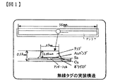
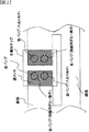
図1にRFIDタグの上面図及び断面図を、図2に半導体装置とアンテナとの接合部の拡大透過図を示す。 FIG. 1 is a top view and a cross-sectional view of an RFID tag, and FIG. 2 is an enlarged transmission view of a joint between a semiconductor device and an antenna.
本態様のRFIDタグは、図1に示すように、アンテナに、ID発信機能を備えたフリップチップ方式で実装された半導体装置で、タグ全体で0.13mmの厚みがある。 As shown in FIG. 1, the RFID tag of this embodiment is a semiconductor device mounted on an antenna by a flip chip method having an ID transmitting function, and has a thickness of 0.13 mm as a whole tag.
また、半導体装置は、厚みが0.06mmとなるようにバックグラインドされており、0.5mm角の外形をしている。また、半導体装置内部の集積回路と直接配線で接続されている2つの入出力端子と半導体装置内の集積回路に直接されていない2つの接続用端子の計4つの端子が、半導体装置の重心を中心として90°づつずれて入出力端子、接続用端子、入出力端子、接続用端子の順に形成されている(入出力端子同士及び接続用端子同士が対向配置)。また、この半導体装置は、2.45GHz帯のマイクロ波をアンテナで受信し、そのマイクロ波から生じる自己整流を電力源として動作する半導体装置で、かかるマイクロ波の信号を受け取ったことをトリガとして、内臓している記憶装置に格納された128ビットのデータを送信信号に変換してアンテナに送り返す機能を備えている。 The semiconductor device is back-ground so as to have a thickness of 0.06 mm, and has an outer shape of 0.5 mm square. A total of four terminals, two input / output terminals connected directly to the integrated circuit inside the semiconductor device by wiring and two connection terminals not directly connected to the integrated circuit inside the semiconductor device, form a center of gravity of the semiconductor device. The input / output terminals, the connection terminals, the input / output terminals, and the connection terminals are formed in the order of 90 ° shifted from the center (the input / output terminals and the connection terminals are opposed to each other). In addition, this semiconductor device is a semiconductor device that receives microwaves in the 2.45 GHz band with an antenna, and operates using self-rectification generated by the microwaves as a power source. It has a function of converting 128-bit data stored in the storage device into a transmission signal and sending it back to the antenna.
また、アンテナは、ポリイミドテープ上の外縁に若干すき間を開けた56mmの長さの銅箔が形成され、半導体装置が実装されるアンテナの端部には、錫のメッキ膜が形成されている。 The antenna has a 56 mm long copper foil with a slight gap formed on the outer edge of the polyimide tape, and a tin plating film is formed on the end of the antenna on which the semiconductor device is mounted.
この半導体装置の全端子とアンテナの銅箔とが金と錫の合金で接合されている。 All the terminals of this semiconductor device and the copper foil of the antenna are joined by an alloy of gold and tin.
また、半導体装置の側面及び下面と銅箔との間にはアンダーフィルが配置されている。 An underfill is arranged between the side and bottom surfaces of the semiconductor device and the copper foil.
なお、接続用端子は接合のバランスを確保するために設けたので、2つの入出力端子と1つの接続用端子を備えているだけでもよい。 Since the connection terminals are provided in order to secure the balance of the joining, only two input / output terminals and one connection terminal may be provided.
この構造は、次の工程により製造することができる。
工程1:樹脂フィルムであるポリイミドフィルム(ポリイミドテープ)の一つの主平面上に、銅箔を接着剤で接着することでアンテナを形成する。接着した銅箔の上に錫をメッキして、接続パッド(接続電極)とする。
工程2:次に、半導体装置の全端子上に金バンプを形成する。
工程3:工程1でメッキした錫が最上層になるようにアンテナを固定する。さらに、工程2で形成した金バンプとアンテナの錫が対面するように半導体装置の端子面を下方に向けて、アンテナと半導体装置の位置合わせを行う。
工程4:非端子面である半導体装置の上方から下方へ200MPaの圧力で加圧するとともに、150℃で1.5秒加熱することで仮固定する。
工程5:さらに、精度の高い位置合わせを行い、200MPaの圧力で加圧するとともに、280℃で3秒加熱する。この加熱により錫が金に拡散するので、半導体装置の端子とアンテナの銅箔とが金錫合金による金属接合となる。
工程6:半導体装置の下方にアンダーフィルを形成する。
This structure can be manufactured by the following steps.
Step 1: An antenna is formed by bonding a copper foil with an adhesive on one main plane of a polyimide film (polyimide tape) which is a resin film. Tin is plated on the adhered copper foil to form connection pads (connection electrodes).
Step 2: Next, gold bumps are formed on all terminals of the semiconductor device.
Step 3: Fix the antenna so that the tin plated in step 1 is the uppermost layer. Further, the antenna and the semiconductor device are aligned with the terminal surface of the semiconductor device facing downward such that the gold bump formed in the step 2 and the tin of the antenna face each other.
Step 4: The semiconductor device as the non-terminal surface is pressurized from above to below with a pressure of 200 MPa, and is temporarily fixed by heating at 150 ° C. for 1.5 seconds.
Step 5: Further, highly accurate positioning is performed, and pressure is applied at a pressure of 200 MPa, and heating is performed at 280 ° C. for 3 seconds. The tin diffuses into the gold by this heating, so that the terminal of the semiconductor device and the copper foil of the antenna are metal-joined by a gold-tin alloy.
Step 6: An underfill is formed below the semiconductor device.
次に、本態様のRFIDタグの接続抵抗値に関する特性について図3を用いて説明する。 Next, a characteristic of the RFID tag according to this embodiment relating to a connection resistance value will be described with reference to FIG.
上記製造方法で製造したRFIDタグは図3の(a)の特性を示す。 The RFID tag manufactured by the above manufacturing method has the characteristics shown in FIG.
85℃85%RHの高温高湿試験の結果、350サイクル程度で10mΩ程度の接続抵抗しか生じなかった。100mΩ程度で送信特性に影響を与えることがわかっているので、かかる特性は良好な接続抵抗といえる。 As a result of a high-temperature and high-humidity test at 85 ° C. and 85% RH, only a connection resistance of about 10 mΩ was generated in about 350 cycles. Since it is known that about 100 mΩ affects transmission characteristics, such characteristics can be said to be good connection resistance.
−50℃〜125℃、各30分の温度サイクル試験の結果、350サイクルで20mΩ以下の接続抵抗しか発生しなかったので、高温高湿試験の結果と同様に、良好な接続抵抗であるといえる。 As a result of a temperature cycle test at −50 ° C. to 125 ° C. for 30 minutes each, only a connection resistance of 20 mΩ or less was generated in 350 cycles, and thus it can be said that the connection resistance was good, similarly to the result of the high temperature and high humidity test .
上記製造工程4における仮固定の温度を225℃にした場合について、温度サイクル試験をやった場合でも、430サイクルで10mΩ程度しか生じていないので、仮固定の温度を150℃とした場合と同様に、良好な接続抵抗とすることができた。 Regarding the case where the temperature of the temporary fixing in the above-mentioned manufacturing process 4 was set to 225 ° C., even when the temperature cycle test was performed, since only about 10 mΩ was generated in 430 cycles, the same as when the temperature of the temporary fixing was set to 150 ° C. And good connection resistance.
このように、本態様のRFIDタグは、0.5mm角以下の半導体装置とアンテナとの接合に金属接合を採用しているので、所望の接続不良の発生を低減できている。 As described above, since the RFID tag of this embodiment employs metal bonding for bonding the semiconductor device having a size of 0.5 mm square or less and the antenna, the occurrence of desired connection failure can be reduced.
また、本構造では接合する金属として、錫と金の合金を用いている。このように構成すると、鉛フリーのRFIDタグを実現することができるだけでなく、挟ピッチにしても、短タクトで接続信頼性を高めることができるようになっている。 In this structure, an alloy of tin and gold is used as the metal to be joined. With this configuration, not only a lead-free RFID tag can be realized, but also the connection reliability can be improved with a short tact even if the pitch is narrow.
また、このような接続方法を入出力端子と接続端子のどちらかに採用しても効果を得ることができるが、双方の端子に採用することで、一括リフローが可能になっている。 The effect can be obtained by adopting such a connection method for either the input / output terminal or the connection terminal. However, by adopting the connection method for both terminals, batch reflow is possible.
また、入出力端子は、双方同じ機能であるため、半導体装置の対角に対向するように配置することにより、180度逆向きに接合することができるようになる。 In addition, since the input / output terminals have the same function, by arranging them so as to be opposite to the diagonal of the semiconductor device, they can be joined by 180 degrees in the opposite direction.
また、アンテナの錫メッキを2端子分つまり、入出力端子1つと接続用端子1つの2つを1つの接続端子で接合する構造とすることにより、多少の回転ずれでも接続不良とならない構造とすることができるようになる。また、この構造では90度、270度に回転させても、接合することが可能になるので、さらに接合を容易にすることができる。 In addition, the tin plating of the antenna for two terminals, that is, a structure in which one input / output terminal and one connection terminal are joined by one connection terminal, is a structure that does not cause a connection failure even with a slight rotational displacement. Will be able to do it. Further, in this structure, even if the structure is rotated by 90 degrees or 270 degrees, the bonding can be performed, so that the bonding can be further facilitated.
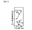
図7にアンダーフィルがあった場合となかった場合の強度の差を示す。 FIG. 7 shows the difference in intensity between the case with and without the underfill.
上記のように、本実施例の半導体装置は、バックグラインドを行うことにより、厚みを薄くしている。このバックグラインドにより、半導体装置には小さなマイクロクラックが生じている。かかる構造にアンダーフィルを形成すると、アンダーフィルがない場合に比べて外部からの点圧破壊に2倍以上強くなることがわかる。
(比較例)
次に、比較例として接触接合方式であるACF方式で実装した場合について説明する。
As described above, the thickness of the semiconductor device of this embodiment is reduced by performing back grinding. Due to this back grinding, small microcracks are generated in the semiconductor device. It can be seen that forming an underfill in such a structure is more than twice as strong against external point pressure breakdown as compared to the case without underfill.
(Comparative example)
Next, as a comparative example, a case where the semiconductor device is mounted by an ACF method which is a contact bonding method will be described.
図4にACF方式を採用した場合の実装方式を示す。 FIG. 4 shows a mounting method when the ACF method is adopted.
透明なポリエチレンテレフタラートフィルム(以下、PETフィルム)上に長さ56mmの銅箔を接着してアンテナを形成する。 An antenna is formed by bonding a 56 mm long copper foil on a transparent polyethylene terephthalate film (hereinafter, PET film).
接着した銅箔上にACFを仮圧着する。 ACF is temporarily pressed on the adhered copper foil.
半導体装置に金バンプを形成し、その金バンプとACFが対向するように半導体装置とアンテナを配置し、仮固定する。 A gold bump is formed on a semiconductor device, and the semiconductor device and an antenna are arranged so that the gold bump and the ACF face each other, and are temporarily fixed.
さらに、精度の高い位置合わせを再度行って、加圧加熱する。この加圧加熱によりACFが硬化して金バンプと銅箔を直接接続する。 Furthermore, high-precision positioning is performed again, and pressure heating is performed. The ACF is cured by the heating under pressure, and the gold bump and the copper foil are directly connected.
図4の方法で製造したACF方式で接合した場合の高温高湿試験(85℃85%RH)の結果を図5に示す。 FIG. 5 shows the results of a high-temperature and high-humidity test (85 ° C., 85% RH) in the case of joining by the ACF method manufactured by the method of FIG.
0.3mm角の半導体装置を実装した場合、25時間で数百mΩの接続抵抗が発生している。 When a 0.3 mm square semiconductor device is mounted, a connection resistance of several hundred mΩ is generated in 25 hours.
また、0.5mm角の半導体装置を実装した場合でも、100時間経過時には、数百mΩ以上の接続抵抗が生じる。このように、0.5mm角以下の半導体装置の実装にACF方式を用いた場合、従来の半導体装置では生じなかった接続抵抗の顕著な増加が生じてしまう。 Even when a 0.5 mm square semiconductor device is mounted, a connection resistance of several hundred mΩ or more occurs after 100 hours. As described above, when the ACF method is used for mounting a semiconductor device having a size of 0.5 mm square or less, a remarkable increase in connection resistance that does not occur in a conventional semiconductor device occurs.
通常の半導体装置は端子のない領域も多いので、端子数が多くても端子あたりのACFの面積を十分に確保でき、所望の接続安定性を得ることが出来ているが、本態様のようなRFIDタグを構成する0.5mm以下角の半導体装置では端子面積が装置面積に対して非常に大きくなるため、端子あたりのACFの接着能力(熱収縮力+硬化収縮力)が低下することになり、銅箔との接続安定性が低下してしまうからであると考えられる。 Since a normal semiconductor device has many regions without terminals, even if the number of terminals is large, the area of the ACF per terminal can be sufficiently secured, and desired connection stability can be obtained. In a semiconductor device having a square of 0.5 mm or less constituting an RFID tag, since the terminal area becomes very large with respect to the device area, the bonding ability of the ACF per terminal (heat shrinking force + curing shrinking force) is reduced. It is considered that this is because the connection stability with the copper foil is reduced.
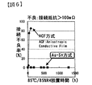
図6にACF方式と金と錫の金属接合方式との接続不良率を対比する。 FIG. 6 compares the connection failure rate between the ACF method and the gold / tin metal bonding method.
ACF方式を採用したRFIDタグは、1時間も経たない内に接続不良が発生し始め、50時間までに約85%が不良となった。 In less than one hour, the connection failure of the RFID tag employing the ACF method began to occur, and about 50% of the RFID tags became defective by 50 hours.
一方、金錫接続方式では1300時間経過後も不良率1%以下の良好な接続を維持することができた。 On the other hand, the gold-tin connection method was able to maintain a good connection with a failure rate of 1% or less even after the elapse of 1300 hours.
Claims (8)
0.5mm角よりも小さい半導体装置が金属接合で該アンテナに接合されていることを特徴とするRFIDタグ。 An RFID tag including a metal antenna and a semiconductor device having a terminal joined to the antenna,
An RFID tag, wherein a semiconductor device smaller than 0.5 mm square is bonded to the antenna by metal bonding.
前記金属接合は金と錫の合金でなされていることを特徴とするRFIDタグ。 In claim 1,
The RFID tag, wherein the metal bonding is made of an alloy of gold and tin.
端子上に金バンプが形成された0.5mm角よりも小さい半導体装置と、該銅箔上に錫メッキがなされたアンテナとが用いられていることを特徴とするRFIDタグ。 An RFID tag having an antenna in which a copper foil is bonded to a polymer film and a semiconductor device in which a terminal is bonded to the copper foil,
An RFID tag characterized by using a semiconductor device smaller than 0.5 mm square having a gold bump formed on a terminal and an antenna plated with tin on the copper foil.
前記端子は入出力端子を含むことを特徴とするRFIDタグ。 In any one of claims 1 to 3,
The terminal includes an input / output terminal.
前記端子は接続端子を含むことを特徴とするRFIDタグ。 In claim 4,
The RFID tag, wherein the terminal includes a connection terminal.
前記半導体装置は、前記入出力端子が半導体装置の対角する位置に設けた半導体装置であることを特徴とするRFIDタグ。 An RFID tag including an antenna and a semiconductor device having two input / output terminals connected to the antenna,
An RFID tag, wherein the semiconductor device is a semiconductor device in which the input / output terminals are provided at diagonal positions of the semiconductor device.
前記半導体装置は、もう一方の対角する位置に設けられた2つの接続用端子を備えていることを特徴とするRFIDタグ。 In claim 6,
An RFID tag, wherein the semiconductor device includes two connection terminals provided at the other diagonal positions.
前記アンテナは接続端子を2つ備え、
該アンテナの1つの接続端子と前記半導体装置の隣接する2つの端子とが接合されていることを特徴とするRFIDタグ。 In claim 7,
The antenna includes two connection terminals,
An RFID tag, wherein one connection terminal of the antenna and two adjacent terminals of the semiconductor device are joined.
Priority Applications (1)
| Application Number | Priority Date | Filing Date | Title |
|---|---|---|---|
| JP2004216691A JP2004362602A (en) | 2004-07-26 | 2004-07-26 | Rfid tag |
Applications Claiming Priority (1)
| Application Number | Priority Date | Filing Date | Title |
|---|---|---|---|
| JP2004216691A JP2004362602A (en) | 2004-07-26 | 2004-07-26 | Rfid tag |
Related Parent Applications (1)
| Application Number | Title | Priority Date | Filing Date |
|---|---|---|---|
| JP2002258391A Division JP2004094839A (en) | 2002-09-04 | 2002-09-04 | Rfid tag |
Publications (2)
| Publication Number | Publication Date |
|---|---|
| JP2004362602A true JP2004362602A (en) | 2004-12-24 |
| JP2004362602A5 JP2004362602A5 (en) | 2005-10-27 |
Family
ID=34056402
Family Applications (1)
| Application Number | Title | Priority Date | Filing Date |
|---|---|---|---|
| JP2004216691A Pending JP2004362602A (en) | 2004-07-26 | 2004-07-26 | Rfid tag |
Country Status (1)
| Country | Link |
|---|---|
| JP (1) | JP2004362602A (en) |
Cited By (95)
| Publication number | Priority date | Publication date | Assignee | Title |
|---|---|---|---|---|
| US7762472B2 (en) | 2007-07-04 | 2010-07-27 | Murata Manufacturing Co., Ltd | Wireless IC device |
| US7764928B2 (en) | 2006-01-19 | 2010-07-27 | Murata Manufacturing Co., Ltd. | Wireless IC device and component for wireless IC device |
| US7786949B2 (en) | 2006-04-14 | 2010-08-31 | Murata Manufacturing Co., Ltd. | Antenna |
| US7830311B2 (en) | 2007-07-18 | 2010-11-09 | Murata Manufacturing Co., Ltd. | Wireless IC device and electronic device |
| US7857230B2 (en) | 2007-07-18 | 2010-12-28 | Murata Manufacturing Co., Ltd. | Wireless IC device and manufacturing method thereof |
| US7871008B2 (en) | 2008-06-25 | 2011-01-18 | Murata Manufacturing Co., Ltd. | Wireless IC device and manufacturing method thereof |
| US7931206B2 (en) | 2007-05-10 | 2011-04-26 | Murata Manufacturing Co., Ltd. | Wireless IC device |
| US7932730B2 (en) | 2006-06-12 | 2011-04-26 | Murata Manufacturing Co., Ltd. | System for inspecting electromagnetic coupling modules and radio IC devices and method for manufacturing electromagnetic coupling modules and radio IC devices using the system |
| US7967216B2 (en) | 2008-05-22 | 2011-06-28 | Murata Manufacturing Co., Ltd. | Wireless IC device |
| US7990337B2 (en) | 2007-12-20 | 2011-08-02 | Murata Manufacturing Co., Ltd. | Radio frequency IC device |
| US7997501B2 (en) | 2007-07-17 | 2011-08-16 | Murata Manufacturing Co., Ltd. | Wireless IC device and electronic apparatus |
| US8009101B2 (en) | 2007-04-06 | 2011-08-30 | Murata Manufacturing Co., Ltd. | Wireless IC device |
| US8031124B2 (en) | 2007-01-26 | 2011-10-04 | Murata Manufacturing Co., Ltd. | Container with electromagnetic coupling module |
| US8070070B2 (en) | 2007-12-26 | 2011-12-06 | Murata Manufacturing Co., Ltd. | Antenna device and radio frequency IC device |
| US8081125B2 (en) | 2006-07-11 | 2011-12-20 | Murata Manufacturing Co., Ltd. | Antenna and radio IC device |
| US8081119B2 (en) | 2006-04-26 | 2011-12-20 | Murata Manufacturing Co., Ltd. | Product including power supply circuit board |
| US8081541B2 (en) | 2006-06-30 | 2011-12-20 | Murata Manufacturing Co., Ltd. | Optical disc |
| US8081121B2 (en) | 2006-10-27 | 2011-12-20 | Murata Manufacturing Co., Ltd. | Article having electromagnetic coupling module attached thereto |
| US8177138B2 (en) | 2008-10-29 | 2012-05-15 | Murata Manufacturing Co., Ltd. | Radio IC device |
| US8179329B2 (en) | 2008-03-03 | 2012-05-15 | Murata Manufacturing Co., Ltd. | Composite antenna |
| US8193939B2 (en) | 2007-07-09 | 2012-06-05 | Murata Manufacturing Co., Ltd. | Wireless IC device |
| US8228252B2 (en) | 2006-05-26 | 2012-07-24 | Murata Manufacturing Co., Ltd. | Data coupler |
| US8228075B2 (en) | 2006-08-24 | 2012-07-24 | Murata Manufacturing Co., Ltd. | Test system for radio frequency IC devices and method of manufacturing radio frequency IC devices using the same |
| US8235299B2 (en) | 2007-07-04 | 2012-08-07 | Murata Manufacturing Co., Ltd. | Wireless IC device and component for wireless IC device |
| US8264357B2 (en) | 2007-06-27 | 2012-09-11 | Murata Manufacturing Co., Ltd. | Wireless IC device |
| US8299929B2 (en) | 2006-09-26 | 2012-10-30 | Murata Manufacturing Co., Ltd. | Inductively coupled module and item with inductively coupled module |
| US8299968B2 (en) | 2007-02-06 | 2012-10-30 | Murata Manufacturing Co., Ltd. | Packaging material with electromagnetic coupling module |
| US8336786B2 (en) | 2010-03-12 | 2012-12-25 | Murata Manufacturing Co., Ltd. | Wireless communication device and metal article |
| US8342416B2 (en) | 2009-01-09 | 2013-01-01 | Murata Manufacturing Co., Ltd. | Wireless IC device, wireless IC module and method of manufacturing wireless IC module |
| US8360324B2 (en) | 2007-04-09 | 2013-01-29 | Murata Manufacturing Co., Ltd. | Wireless IC device |
| US8360325B2 (en) | 2008-04-14 | 2013-01-29 | Murata Manufacturing Co., Ltd. | Wireless IC device, electronic apparatus, and method for adjusting resonant frequency of wireless IC device |
| US8381997B2 (en) | 2009-06-03 | 2013-02-26 | Murata Manufacturing Co., Ltd. | Radio frequency IC device and method of manufacturing the same |
| US8384547B2 (en) | 2006-04-10 | 2013-02-26 | Murata Manufacturing Co., Ltd. | Wireless IC device |
| US8390459B2 (en) | 2007-04-06 | 2013-03-05 | Murata Manufacturing Co., Ltd. | Wireless IC device |
| US8400307B2 (en) | 2007-07-18 | 2013-03-19 | Murata Manufacturing Co., Ltd. | Radio frequency IC device and electronic apparatus |
| US8400365B2 (en) | 2009-11-20 | 2013-03-19 | Murata Manufacturing Co., Ltd. | Antenna device and mobile communication terminal |
| US8418928B2 (en) | 2009-04-14 | 2013-04-16 | Murata Manufacturing Co., Ltd. | Wireless IC device component and wireless IC device |
| US8424769B2 (en) | 2010-07-08 | 2013-04-23 | Murata Manufacturing Co., Ltd. | Antenna and RFID device |
| US8474725B2 (en) | 2007-04-27 | 2013-07-02 | Murata Manufacturing Co., Ltd. | Wireless IC device |
| US8531346B2 (en) | 2007-04-26 | 2013-09-10 | Murata Manufacturing Co., Ltd. | Wireless IC device |
| US8546927B2 (en) | 2010-09-03 | 2013-10-01 | Murata Manufacturing Co., Ltd. | RFIC chip mounting structure |
| US8544754B2 (en) | 2006-06-01 | 2013-10-01 | Murata Manufacturing Co., Ltd. | Wireless IC device and wireless IC device composite component |
| US8583043B2 (en) | 2009-01-16 | 2013-11-12 | Murata Manufacturing Co., Ltd. | High-frequency device and wireless IC device |
| US8590797B2 (en) | 2008-05-21 | 2013-11-26 | Murata Manufacturing Co., Ltd. | Wireless IC device |
| US8596545B2 (en) | 2008-05-28 | 2013-12-03 | Murata Manufacturing Co., Ltd. | Component of wireless IC device and wireless IC device |
| US8602310B2 (en) | 2010-03-03 | 2013-12-10 | Murata Manufacturing Co., Ltd. | Radio communication device and radio communication terminal |
| US8613395B2 (en) | 2011-02-28 | 2013-12-24 | Murata Manufacturing Co., Ltd. | Wireless communication device |
| US8632014B2 (en) | 2007-04-27 | 2014-01-21 | Murata Manufacturing Co., Ltd. | Wireless IC device |
| US8668151B2 (en) | 2008-03-26 | 2014-03-11 | Murata Manufacturing Co., Ltd. | Wireless IC device |
| US8680971B2 (en) | 2009-09-28 | 2014-03-25 | Murata Manufacturing Co., Ltd. | Wireless IC device and method of detecting environmental state using the device |
| US8692718B2 (en) | 2008-11-17 | 2014-04-08 | Murata Manufacturing Co., Ltd. | Antenna and wireless IC device |
| US8718727B2 (en) | 2009-12-24 | 2014-05-06 | Murata Manufacturing Co., Ltd. | Antenna having structure for multi-angled reception and mobile terminal including the antenna |
| US8720789B2 (en) | 2012-01-30 | 2014-05-13 | Murata Manufacturing Co., Ltd. | Wireless IC device |
| US8740093B2 (en) | 2011-04-13 | 2014-06-03 | Murata Manufacturing Co., Ltd. | Radio IC device and radio communication terminal |
| US8757500B2 (en) | 2007-05-11 | 2014-06-24 | Murata Manufacturing Co., Ltd. | Wireless IC device |
| US8770489B2 (en) | 2011-07-15 | 2014-07-08 | Murata Manufacturing Co., Ltd. | Radio communication device |
| US8797225B2 (en) | 2011-03-08 | 2014-08-05 | Murata Manufacturing Co., Ltd. | Antenna device and communication terminal apparatus |
| US8797148B2 (en) | 2008-03-03 | 2014-08-05 | Murata Manufacturing Co., Ltd. | Radio frequency IC device and radio communication system |
| US8810456B2 (en) | 2009-06-19 | 2014-08-19 | Murata Manufacturing Co., Ltd. | Wireless IC device and coupling method for power feeding circuit and radiation plate |
| US8814056B2 (en) | 2011-07-19 | 2014-08-26 | Murata Manufacturing Co., Ltd. | Antenna device, RFID tag, and communication terminal apparatus |
| US8847831B2 (en) | 2009-07-03 | 2014-09-30 | Murata Manufacturing Co., Ltd. | Antenna and antenna module |
| US8853549B2 (en) | 2009-09-30 | 2014-10-07 | Murata Manufacturing Co., Ltd. | Circuit substrate and method of manufacturing same |
| US8870077B2 (en) | 2008-08-19 | 2014-10-28 | Murata Manufacturing Co., Ltd. | Wireless IC device and method for manufacturing same |
| US8878739B2 (en) | 2011-07-14 | 2014-11-04 | Murata Manufacturing Co., Ltd. | Wireless communication device |
| US8905296B2 (en) | 2011-12-01 | 2014-12-09 | Murata Manufacturing Co., Ltd. | Wireless integrated circuit device and method of manufacturing the same |
| US8905316B2 (en) | 2010-05-14 | 2014-12-09 | Murata Manufacturing Co., Ltd. | Wireless IC device |
| US8937576B2 (en) | 2011-04-05 | 2015-01-20 | Murata Manufacturing Co., Ltd. | Wireless communication device |
| US8944335B2 (en) | 2010-09-30 | 2015-02-03 | Murata Manufacturing Co., Ltd. | Wireless IC device |
| US8976075B2 (en) | 2009-04-21 | 2015-03-10 | Murata Manufacturing Co., Ltd. | Antenna device and method of setting resonant frequency of antenna device |
| US8981906B2 (en) | 2010-08-10 | 2015-03-17 | Murata Manufacturing Co., Ltd. | Printed wiring board and wireless communication system |
| US8991713B2 (en) | 2011-01-14 | 2015-03-31 | Murata Manufacturing Co., Ltd. | RFID chip package and RFID tag |
| US8994605B2 (en) | 2009-10-02 | 2015-03-31 | Murata Manufacturing Co., Ltd. | Wireless IC device and electromagnetic coupling module |
| US9024837B2 (en) | 2010-03-31 | 2015-05-05 | Murata Manufacturing Co., Ltd. | Antenna and wireless communication device |
| US9024725B2 (en) | 2009-11-04 | 2015-05-05 | Murata Manufacturing Co., Ltd. | Communication terminal and information processing system |
| US9064198B2 (en) | 2006-04-26 | 2015-06-23 | Murata Manufacturing Co., Ltd. | Electromagnetic-coupling-module-attached article |
| US9077067B2 (en) | 2008-07-04 | 2015-07-07 | Murata Manufacturing Co., Ltd. | Radio IC device |
| US9104950B2 (en) | 2009-01-30 | 2015-08-11 | Murata Manufacturing Co., Ltd. | Antenna and wireless IC device |
| US9123996B2 (en) | 2010-05-14 | 2015-09-01 | Murata Manufacturing Co., Ltd. | Wireless IC device |
| US9166291B2 (en) | 2010-10-12 | 2015-10-20 | Murata Manufacturing Co., Ltd. | Antenna device and communication terminal apparatus |
| US9178279B2 (en) | 2009-11-04 | 2015-11-03 | Murata Manufacturing Co., Ltd. | Wireless IC tag, reader-writer, and information processing system |
| US9231305B2 (en) | 2008-10-24 | 2016-01-05 | Murata Manufacturing Co., Ltd. | Wireless IC device |
| US9236651B2 (en) | 2010-10-21 | 2016-01-12 | Murata Manufacturing Co., Ltd. | Communication terminal device |
| US9281873B2 (en) | 2008-05-26 | 2016-03-08 | Murata Manufacturing Co., Ltd. | Wireless IC device system and method of determining authenticity of wireless IC device |
| US9378452B2 (en) | 2011-05-16 | 2016-06-28 | Murata Manufacturing Co., Ltd. | Radio IC device |
| US9444143B2 (en) | 2009-10-16 | 2016-09-13 | Murata Manufacturing Co., Ltd. | Antenna and wireless IC device |
| US9460320B2 (en) | 2009-10-27 | 2016-10-04 | Murata Manufacturing Co., Ltd. | Transceiver and radio frequency identification tag reader |
| US9461363B2 (en) | 2009-11-04 | 2016-10-04 | Murata Manufacturing Co., Ltd. | Communication terminal and information processing system |
| US9460376B2 (en) | 2007-07-18 | 2016-10-04 | Murata Manufacturing Co., Ltd. | Radio IC device |
| US9543642B2 (en) | 2011-09-09 | 2017-01-10 | Murata Manufacturing Co., Ltd. | Antenna device and wireless device |
| US9558384B2 (en) | 2010-07-28 | 2017-01-31 | Murata Manufacturing Co., Ltd. | Antenna apparatus and communication terminal instrument |
| US9692128B2 (en) | 2012-02-24 | 2017-06-27 | Murata Manufacturing Co., Ltd. | Antenna device and wireless communication device |
| US9727765B2 (en) | 2010-03-24 | 2017-08-08 | Murata Manufacturing Co., Ltd. | RFID system including a reader/writer and RFID tag |
| US9761923B2 (en) | 2011-01-05 | 2017-09-12 | Murata Manufacturing Co., Ltd. | Wireless communication device |
| US10013650B2 (en) | 2010-03-03 | 2018-07-03 | Murata Manufacturing Co., Ltd. | Wireless communication module and wireless communication device |
| US10235544B2 (en) | 2012-04-13 | 2019-03-19 | Murata Manufacturing Co., Ltd. | Inspection method and inspection device for RFID tag |
-
2004
- 2004-07-26 JP JP2004216691A patent/JP2004362602A/en active Pending
Cited By (126)
| Publication number | Priority date | Publication date | Assignee | Title |
|---|---|---|---|---|
| US8725071B2 (en) | 2006-01-19 | 2014-05-13 | Murata Manufacturing Co., Ltd. | Wireless IC device and component for wireless IC device |
| US7764928B2 (en) | 2006-01-19 | 2010-07-27 | Murata Manufacturing Co., Ltd. | Wireless IC device and component for wireless IC device |
| US8078106B2 (en) | 2006-01-19 | 2011-12-13 | Murata Manufacturing Co., Ltd. | Wireless IC device and component for wireless IC device |
| US8676117B2 (en) | 2006-01-19 | 2014-03-18 | Murata Manufacturing Co., Ltd. | Wireless IC device and component for wireless IC device |
| US8326223B2 (en) | 2006-01-19 | 2012-12-04 | Murata Manufacturing Co., Ltd. | Wireless IC device and component for wireless IC device |
| US8384547B2 (en) | 2006-04-10 | 2013-02-26 | Murata Manufacturing Co., Ltd. | Wireless IC device |
| US7786949B2 (en) | 2006-04-14 | 2010-08-31 | Murata Manufacturing Co., Ltd. | Antenna |
| US8081119B2 (en) | 2006-04-26 | 2011-12-20 | Murata Manufacturing Co., Ltd. | Product including power supply circuit board |
| US9165239B2 (en) | 2006-04-26 | 2015-10-20 | Murata Manufacturing Co., Ltd. | Electromagnetic-coupling-module-attached article |
| US9064198B2 (en) | 2006-04-26 | 2015-06-23 | Murata Manufacturing Co., Ltd. | Electromagnetic-coupling-module-attached article |
| US8228252B2 (en) | 2006-05-26 | 2012-07-24 | Murata Manufacturing Co., Ltd. | Data coupler |
| US8544754B2 (en) | 2006-06-01 | 2013-10-01 | Murata Manufacturing Co., Ltd. | Wireless IC device and wireless IC device composite component |
| US7932730B2 (en) | 2006-06-12 | 2011-04-26 | Murata Manufacturing Co., Ltd. | System for inspecting electromagnetic coupling modules and radio IC devices and method for manufacturing electromagnetic coupling modules and radio IC devices using the system |
| US8228765B2 (en) | 2006-06-30 | 2012-07-24 | Murata Manufacturing Co., Ltd. | Optical disc |
| US8081541B2 (en) | 2006-06-30 | 2011-12-20 | Murata Manufacturing Co., Ltd. | Optical disc |
| US8081125B2 (en) | 2006-07-11 | 2011-12-20 | Murata Manufacturing Co., Ltd. | Antenna and radio IC device |
| US8228075B2 (en) | 2006-08-24 | 2012-07-24 | Murata Manufacturing Co., Ltd. | Test system for radio frequency IC devices and method of manufacturing radio frequency IC devices using the same |
| US8299929B2 (en) | 2006-09-26 | 2012-10-30 | Murata Manufacturing Co., Ltd. | Inductively coupled module and item with inductively coupled module |
| US8081121B2 (en) | 2006-10-27 | 2011-12-20 | Murata Manufacturing Co., Ltd. | Article having electromagnetic coupling module attached thereto |
| US8031124B2 (en) | 2007-01-26 | 2011-10-04 | Murata Manufacturing Co., Ltd. | Container with electromagnetic coupling module |
| US8299968B2 (en) | 2007-02-06 | 2012-10-30 | Murata Manufacturing Co., Ltd. | Packaging material with electromagnetic coupling module |
| US8009101B2 (en) | 2007-04-06 | 2011-08-30 | Murata Manufacturing Co., Ltd. | Wireless IC device |
| US8390459B2 (en) | 2007-04-06 | 2013-03-05 | Murata Manufacturing Co., Ltd. | Wireless IC device |
| US8360324B2 (en) | 2007-04-09 | 2013-01-29 | Murata Manufacturing Co., Ltd. | Wireless IC device |
| US8424762B2 (en) | 2007-04-14 | 2013-04-23 | Murata Manufacturing Co., Ltd. | Wireless IC device and component for wireless IC device |
| US8531346B2 (en) | 2007-04-26 | 2013-09-10 | Murata Manufacturing Co., Ltd. | Wireless IC device |
| US8474725B2 (en) | 2007-04-27 | 2013-07-02 | Murata Manufacturing Co., Ltd. | Wireless IC device |
| US8632014B2 (en) | 2007-04-27 | 2014-01-21 | Murata Manufacturing Co., Ltd. | Wireless IC device |
| US7931206B2 (en) | 2007-05-10 | 2011-04-26 | Murata Manufacturing Co., Ltd. | Wireless IC device |
| US8757500B2 (en) | 2007-05-11 | 2014-06-24 | Murata Manufacturing Co., Ltd. | Wireless IC device |
| US8264357B2 (en) | 2007-06-27 | 2012-09-11 | Murata Manufacturing Co., Ltd. | Wireless IC device |
| US8662403B2 (en) | 2007-07-04 | 2014-03-04 | Murata Manufacturing Co., Ltd. | Wireless IC device and component for wireless IC device |
| US8235299B2 (en) | 2007-07-04 | 2012-08-07 | Murata Manufacturing Co., Ltd. | Wireless IC device and component for wireless IC device |
| US7762472B2 (en) | 2007-07-04 | 2010-07-27 | Murata Manufacturing Co., Ltd | Wireless IC device |
| US8552870B2 (en) | 2007-07-09 | 2013-10-08 | Murata Manufacturing Co., Ltd. | Wireless IC device |
| US8193939B2 (en) | 2007-07-09 | 2012-06-05 | Murata Manufacturing Co., Ltd. | Wireless IC device |
| US7997501B2 (en) | 2007-07-17 | 2011-08-16 | Murata Manufacturing Co., Ltd. | Wireless IC device and electronic apparatus |
| US8191791B2 (en) | 2007-07-17 | 2012-06-05 | Murata Manufacturing Co., Ltd. | Wireless IC device and electronic apparatus |
| US8413907B2 (en) | 2007-07-17 | 2013-04-09 | Murata Manufacturing Co., Ltd. | Wireless IC device and electronic apparatus |
| US9460376B2 (en) | 2007-07-18 | 2016-10-04 | Murata Manufacturing Co., Ltd. | Radio IC device |
| US9830552B2 (en) | 2007-07-18 | 2017-11-28 | Murata Manufacturing Co., Ltd. | Radio IC device |
| US7857230B2 (en) | 2007-07-18 | 2010-12-28 | Murata Manufacturing Co., Ltd. | Wireless IC device and manufacturing method thereof |
| US8400307B2 (en) | 2007-07-18 | 2013-03-19 | Murata Manufacturing Co., Ltd. | Radio frequency IC device and electronic apparatus |
| US7830311B2 (en) | 2007-07-18 | 2010-11-09 | Murata Manufacturing Co., Ltd. | Wireless IC device and electronic device |
| US7990337B2 (en) | 2007-12-20 | 2011-08-02 | Murata Manufacturing Co., Ltd. | Radio frequency IC device |
| US8610636B2 (en) | 2007-12-20 | 2013-12-17 | Murata Manufacturing Co., Ltd. | Radio frequency IC device |
| US8915448B2 (en) | 2007-12-26 | 2014-12-23 | Murata Manufacturing Co., Ltd. | Antenna device and radio frequency IC device |
| US8070070B2 (en) | 2007-12-26 | 2011-12-06 | Murata Manufacturing Co., Ltd. | Antenna device and radio frequency IC device |
| US8360330B2 (en) | 2007-12-26 | 2013-01-29 | Murata Manufacturing Co., Ltd. | Antenna device and radio frequency IC device |
| US8797148B2 (en) | 2008-03-03 | 2014-08-05 | Murata Manufacturing Co., Ltd. | Radio frequency IC device and radio communication system |
| US8179329B2 (en) | 2008-03-03 | 2012-05-15 | Murata Manufacturing Co., Ltd. | Composite antenna |
| US8668151B2 (en) | 2008-03-26 | 2014-03-11 | Murata Manufacturing Co., Ltd. | Wireless IC device |
| US8360325B2 (en) | 2008-04-14 | 2013-01-29 | Murata Manufacturing Co., Ltd. | Wireless IC device, electronic apparatus, and method for adjusting resonant frequency of wireless IC device |
| US8960557B2 (en) | 2008-05-21 | 2015-02-24 | Murata Manufacturing Co., Ltd. | Wireless IC device |
| US8590797B2 (en) | 2008-05-21 | 2013-11-26 | Murata Manufacturing Co., Ltd. | Wireless IC device |
| US8973841B2 (en) | 2008-05-21 | 2015-03-10 | Murata Manufacturing Co., Ltd. | Wireless IC device |
| US9022295B2 (en) | 2008-05-21 | 2015-05-05 | Murata Manufacturing Co., Ltd. | Wireless IC device |
| US8047445B2 (en) | 2008-05-22 | 2011-11-01 | Murata Manufacturing Co., Ltd. | Wireless IC device and method of manufacturing the same |
| US7967216B2 (en) | 2008-05-22 | 2011-06-28 | Murata Manufacturing Co., Ltd. | Wireless IC device |
| US9281873B2 (en) | 2008-05-26 | 2016-03-08 | Murata Manufacturing Co., Ltd. | Wireless IC device system and method of determining authenticity of wireless IC device |
| US8596545B2 (en) | 2008-05-28 | 2013-12-03 | Murata Manufacturing Co., Ltd. | Component of wireless IC device and wireless IC device |
| US7871008B2 (en) | 2008-06-25 | 2011-01-18 | Murata Manufacturing Co., Ltd. | Wireless IC device and manufacturing method thereof |
| US8011589B2 (en) | 2008-06-25 | 2011-09-06 | Murata Manufacturing Co., Ltd. | Wireless IC device and manufacturing method thereof |
| US9077067B2 (en) | 2008-07-04 | 2015-07-07 | Murata Manufacturing Co., Ltd. | Radio IC device |
| US8870077B2 (en) | 2008-08-19 | 2014-10-28 | Murata Manufacturing Co., Ltd. | Wireless IC device and method for manufacturing same |
| US9231305B2 (en) | 2008-10-24 | 2016-01-05 | Murata Manufacturing Co., Ltd. | Wireless IC device |
| US8177138B2 (en) | 2008-10-29 | 2012-05-15 | Murata Manufacturing Co., Ltd. | Radio IC device |
| US8692718B2 (en) | 2008-11-17 | 2014-04-08 | Murata Manufacturing Co., Ltd. | Antenna and wireless IC device |
| US8917211B2 (en) | 2008-11-17 | 2014-12-23 | Murata Manufacturing Co., Ltd. | Antenna and wireless IC device |
| US8342416B2 (en) | 2009-01-09 | 2013-01-01 | Murata Manufacturing Co., Ltd. | Wireless IC device, wireless IC module and method of manufacturing wireless IC module |
| US8544759B2 (en) | 2009-01-09 | 2013-10-01 | Murata Manufacturing., Ltd. | Wireless IC device, wireless IC module and method of manufacturing wireless IC module |
| US8583043B2 (en) | 2009-01-16 | 2013-11-12 | Murata Manufacturing Co., Ltd. | High-frequency device and wireless IC device |
| US9104950B2 (en) | 2009-01-30 | 2015-08-11 | Murata Manufacturing Co., Ltd. | Antenna and wireless IC device |
| US8418928B2 (en) | 2009-04-14 | 2013-04-16 | Murata Manufacturing Co., Ltd. | Wireless IC device component and wireless IC device |
| US8876010B2 (en) | 2009-04-14 | 2014-11-04 | Murata Manufacturing Co., Ltd | Wireless IC device component and wireless IC device |
| US8690070B2 (en) | 2009-04-14 | 2014-04-08 | Murata Manufacturing Co., Ltd. | Wireless IC device component and wireless IC device |
| US9203157B2 (en) | 2009-04-21 | 2015-12-01 | Murata Manufacturing Co., Ltd. | Antenna device and method of setting resonant frequency of antenna device |
| US8976075B2 (en) | 2009-04-21 | 2015-03-10 | Murata Manufacturing Co., Ltd. | Antenna device and method of setting resonant frequency of antenna device |
| US9564678B2 (en) | 2009-04-21 | 2017-02-07 | Murata Manufacturing Co., Ltd. | Antenna device and method of setting resonant frequency of antenna device |
| US8381997B2 (en) | 2009-06-03 | 2013-02-26 | Murata Manufacturing Co., Ltd. | Radio frequency IC device and method of manufacturing the same |
| US8810456B2 (en) | 2009-06-19 | 2014-08-19 | Murata Manufacturing Co., Ltd. | Wireless IC device and coupling method for power feeding circuit and radiation plate |
| US8847831B2 (en) | 2009-07-03 | 2014-09-30 | Murata Manufacturing Co., Ltd. | Antenna and antenna module |
| US8680971B2 (en) | 2009-09-28 | 2014-03-25 | Murata Manufacturing Co., Ltd. | Wireless IC device and method of detecting environmental state using the device |
| US8853549B2 (en) | 2009-09-30 | 2014-10-07 | Murata Manufacturing Co., Ltd. | Circuit substrate and method of manufacturing same |
| US8994605B2 (en) | 2009-10-02 | 2015-03-31 | Murata Manufacturing Co., Ltd. | Wireless IC device and electromagnetic coupling module |
| US9117157B2 (en) | 2009-10-02 | 2015-08-25 | Murata Manufacturing Co., Ltd. | Wireless IC device and electromagnetic coupling module |
| US9444143B2 (en) | 2009-10-16 | 2016-09-13 | Murata Manufacturing Co., Ltd. | Antenna and wireless IC device |
| US9460320B2 (en) | 2009-10-27 | 2016-10-04 | Murata Manufacturing Co., Ltd. | Transceiver and radio frequency identification tag reader |
| US9024725B2 (en) | 2009-11-04 | 2015-05-05 | Murata Manufacturing Co., Ltd. | Communication terminal and information processing system |
| US9461363B2 (en) | 2009-11-04 | 2016-10-04 | Murata Manufacturing Co., Ltd. | Communication terminal and information processing system |
| US9178279B2 (en) | 2009-11-04 | 2015-11-03 | Murata Manufacturing Co., Ltd. | Wireless IC tag, reader-writer, and information processing system |
| US8704716B2 (en) | 2009-11-20 | 2014-04-22 | Murata Manufacturing Co., Ltd. | Antenna device and mobile communication terminal |
| US8400365B2 (en) | 2009-11-20 | 2013-03-19 | Murata Manufacturing Co., Ltd. | Antenna device and mobile communication terminal |
| US8718727B2 (en) | 2009-12-24 | 2014-05-06 | Murata Manufacturing Co., Ltd. | Antenna having structure for multi-angled reception and mobile terminal including the antenna |
| US8602310B2 (en) | 2010-03-03 | 2013-12-10 | Murata Manufacturing Co., Ltd. | Radio communication device and radio communication terminal |
| US10013650B2 (en) | 2010-03-03 | 2018-07-03 | Murata Manufacturing Co., Ltd. | Wireless communication module and wireless communication device |
| US8528829B2 (en) | 2010-03-12 | 2013-09-10 | Murata Manufacturing Co., Ltd. | Wireless communication device and metal article |
| US8336786B2 (en) | 2010-03-12 | 2012-12-25 | Murata Manufacturing Co., Ltd. | Wireless communication device and metal article |
| US9727765B2 (en) | 2010-03-24 | 2017-08-08 | Murata Manufacturing Co., Ltd. | RFID system including a reader/writer and RFID tag |
| US9024837B2 (en) | 2010-03-31 | 2015-05-05 | Murata Manufacturing Co., Ltd. | Antenna and wireless communication device |
| US9123996B2 (en) | 2010-05-14 | 2015-09-01 | Murata Manufacturing Co., Ltd. | Wireless IC device |
| US8905316B2 (en) | 2010-05-14 | 2014-12-09 | Murata Manufacturing Co., Ltd. | Wireless IC device |
| US8424769B2 (en) | 2010-07-08 | 2013-04-23 | Murata Manufacturing Co., Ltd. | Antenna and RFID device |
| US9558384B2 (en) | 2010-07-28 | 2017-01-31 | Murata Manufacturing Co., Ltd. | Antenna apparatus and communication terminal instrument |
| US8981906B2 (en) | 2010-08-10 | 2015-03-17 | Murata Manufacturing Co., Ltd. | Printed wiring board and wireless communication system |
| US8546927B2 (en) | 2010-09-03 | 2013-10-01 | Murata Manufacturing Co., Ltd. | RFIC chip mounting structure |
| US8944335B2 (en) | 2010-09-30 | 2015-02-03 | Murata Manufacturing Co., Ltd. | Wireless IC device |
| US9166291B2 (en) | 2010-10-12 | 2015-10-20 | Murata Manufacturing Co., Ltd. | Antenna device and communication terminal apparatus |
| US9236651B2 (en) | 2010-10-21 | 2016-01-12 | Murata Manufacturing Co., Ltd. | Communication terminal device |
| US9761923B2 (en) | 2011-01-05 | 2017-09-12 | Murata Manufacturing Co., Ltd. | Wireless communication device |
| US8991713B2 (en) | 2011-01-14 | 2015-03-31 | Murata Manufacturing Co., Ltd. | RFID chip package and RFID tag |
| US8960561B2 (en) | 2011-02-28 | 2015-02-24 | Murata Manufacturing Co., Ltd. | Wireless communication device |
| US8613395B2 (en) | 2011-02-28 | 2013-12-24 | Murata Manufacturing Co., Ltd. | Wireless communication device |
| US8757502B2 (en) | 2011-02-28 | 2014-06-24 | Murata Manufacturing Co., Ltd. | Wireless communication device |
| US8797225B2 (en) | 2011-03-08 | 2014-08-05 | Murata Manufacturing Co., Ltd. | Antenna device and communication terminal apparatus |
| US8937576B2 (en) | 2011-04-05 | 2015-01-20 | Murata Manufacturing Co., Ltd. | Wireless communication device |
| US8740093B2 (en) | 2011-04-13 | 2014-06-03 | Murata Manufacturing Co., Ltd. | Radio IC device and radio communication terminal |
| US9378452B2 (en) | 2011-05-16 | 2016-06-28 | Murata Manufacturing Co., Ltd. | Radio IC device |
| US8878739B2 (en) | 2011-07-14 | 2014-11-04 | Murata Manufacturing Co., Ltd. | Wireless communication device |
| US8770489B2 (en) | 2011-07-15 | 2014-07-08 | Murata Manufacturing Co., Ltd. | Radio communication device |
| US8814056B2 (en) | 2011-07-19 | 2014-08-26 | Murata Manufacturing Co., Ltd. | Antenna device, RFID tag, and communication terminal apparatus |
| US9543642B2 (en) | 2011-09-09 | 2017-01-10 | Murata Manufacturing Co., Ltd. | Antenna device and wireless device |
| US8905296B2 (en) | 2011-12-01 | 2014-12-09 | Murata Manufacturing Co., Ltd. | Wireless integrated circuit device and method of manufacturing the same |
| US8720789B2 (en) | 2012-01-30 | 2014-05-13 | Murata Manufacturing Co., Ltd. | Wireless IC device |
| US9692128B2 (en) | 2012-02-24 | 2017-06-27 | Murata Manufacturing Co., Ltd. | Antenna device and wireless communication device |
| US10235544B2 (en) | 2012-04-13 | 2019-03-19 | Murata Manufacturing Co., Ltd. | Inspection method and inspection device for RFID tag |
Similar Documents
| Publication | Publication Date | Title |
|---|---|---|
| JP2004362602A (en) | Rfid tag | |
| JP3967133B2 (en) | Manufacturing method of semiconductor device and electronic device | |
| US6781241B2 (en) | Semiconductor device and manufacturing method thereof | |
| US8599571B2 (en) | Memory card | |
| US20060278970A1 (en) | Semiconductor device, stacked semiconductor device, and manufacturing method for semiconductor device | |
| KR101115930B1 (en) | Semiconductor package | |
| JP2009278064A (en) | Semiconductor device and method of manufacturing the same | |
| KR100642356B1 (en) | Semiconductor device and mu1ti1ayer substrate therefor | |
| JP2004094839A (en) | Rfid tag | |
| JP4635836B2 (en) | Sheet electronic circuit module | |
| KR20060097308A (en) | Semiconductor package including solder for packaging | |
| JP2002289735A (en) | Semiconductor device | |
| JP4243077B2 (en) | Semiconductor device and manufacturing method thereof | |
| JP2003318322A (en) | Interposer substrate, its manufacturing method, semiconductor device and its manufacturing method | |
| US20180358320A1 (en) | Electronic device, electronic device manufacturing method, and electronic apparatus | |
| JP2004006705A (en) | Mounting structure of semiconductor device and circuit board | |
| TWI393197B (en) | Chip package | |
| JP4439339B2 (en) | Semiconductor device and manufacturing method thereof | |
| JP2009071159A (en) | Flexible wiring board and bare chip mounting method | |
| JP2011071267A (en) | Electronic device package, method of manufacturing the same, and electronic equipment | |
| JP2010251566A (en) | Wiring board, semiconductor device, semiconductor module, and method of manufacturing the module | |
| JP5271402B2 (en) | Manufacturing method of semiconductor device | |
| JP5399130B2 (en) | Manufacturing method of electronic component built-in substrate | |
| JP2007208211A (en) | Semiconductor device | |
| JP2000340692A (en) | Wiring board, semiconductor device, electronic device and manufacture thereof |
Legal Events
| Date | Code | Title | Description |
|---|---|---|---|
| A521 | Written amendment |
Free format text: JAPANESE INTERMEDIATE CODE: A523 Effective date: 20050819 |
|
| A621 | Written request for application examination |
Free format text: JAPANESE INTERMEDIATE CODE: A621 Effective date: 20050819 |
|
| RD01 | Notification of change of attorney |
Free format text: JAPANESE INTERMEDIATE CODE: A7421 Effective date: 20060421 |
|
| A977 | Report on retrieval |
Free format text: JAPANESE INTERMEDIATE CODE: A971007 Effective date: 20070612 |
|
| A131 | Notification of reasons for refusal |
Free format text: JAPANESE INTERMEDIATE CODE: A131 Effective date: 20070703 |
|
| A521 | Written amendment |
Free format text: JAPANESE INTERMEDIATE CODE: A523 Effective date: 20070830 |
|
| A02 | Decision of refusal |
Free format text: JAPANESE INTERMEDIATE CODE: A02 Effective date: 20071113 |