JP3998992B2 - Method for forming antenna pattern on IC chip mounted on web and package with IC tag - Google Patents
Method for forming antenna pattern on IC chip mounted on web and package with IC tag Download PDFInfo
- Publication number
- JP3998992B2 JP3998992B2 JP2002036151A JP2002036151A JP3998992B2 JP 3998992 B2 JP3998992 B2 JP 3998992B2 JP 2002036151 A JP2002036151 A JP 2002036151A JP 2002036151 A JP2002036151 A JP 2002036151A JP 3998992 B2 JP3998992 B2 JP 3998992B2
- Authority
- JP
- Japan
- Prior art keywords
- chip
- antenna pattern
- tag
- web material
- concave hole
- Prior art date
- Legal status (The legal status is an assumption and is not a legal conclusion. Google has not performed a legal analysis and makes no representation as to the accuracy of the status listed.)
- Expired - Fee Related
Links
Images


Classifications
-
- H—ELECTRICITY
- H01—ELECTRIC ELEMENTS
- H01L—SEMICONDUCTOR DEVICES NOT COVERED BY CLASS H10
- H01L24/00—Arrangements for connecting or disconnecting semiconductor or solid-state bodies; Methods or apparatus related thereto
- H01L24/93—Batch processes
- H01L24/95—Batch processes at chip-level, i.e. with connecting carried out on a plurality of singulated devices, i.e. on diced chips
-
- H—ELECTRICITY
- H01—ELECTRIC ELEMENTS
- H01L—SEMICONDUCTOR DEVICES NOT COVERED BY CLASS H10
- H01L2224/00—Indexing scheme for arrangements for connecting or disconnecting semiconductor or solid-state bodies and methods related thereto as covered by H01L24/00
- H01L2224/93—Batch processes
- H01L2224/95—Batch processes at chip-level, i.e. with connecting carried out on a plurality of singulated devices, i.e. on diced chips
- H01L2224/95053—Bonding environment
- H01L2224/95085—Bonding environment being a liquid, e.g. for fluidic self-assembly
-
- H—ELECTRICITY
- H01—ELECTRIC ELEMENTS
- H01L—SEMICONDUCTOR DEVICES NOT COVERED BY CLASS H10
- H01L2924/00—Indexing scheme for arrangements or methods for connecting or disconnecting semiconductor or solid-state bodies as covered by H01L24/00
- H01L2924/01—Chemical elements
- H01L2924/01004—Beryllium [Be]
-
- H—ELECTRICITY
- H01—ELECTRIC ELEMENTS
- H01L—SEMICONDUCTOR DEVICES NOT COVERED BY CLASS H10
- H01L2924/00—Indexing scheme for arrangements or methods for connecting or disconnecting semiconductor or solid-state bodies as covered by H01L24/00
- H01L2924/01—Chemical elements
- H01L2924/01005—Boron [B]
-
- H—ELECTRICITY
- H01—ELECTRIC ELEMENTS
- H01L—SEMICONDUCTOR DEVICES NOT COVERED BY CLASS H10
- H01L2924/00—Indexing scheme for arrangements or methods for connecting or disconnecting semiconductor or solid-state bodies as covered by H01L24/00
- H01L2924/01—Chemical elements
- H01L2924/01006—Carbon [C]
-
- H—ELECTRICITY
- H01—ELECTRIC ELEMENTS
- H01L—SEMICONDUCTOR DEVICES NOT COVERED BY CLASS H10
- H01L2924/00—Indexing scheme for arrangements or methods for connecting or disconnecting semiconductor or solid-state bodies as covered by H01L24/00
- H01L2924/01—Chemical elements
- H01L2924/01009—Fluorine [F]
-
- H—ELECTRICITY
- H01—ELECTRIC ELEMENTS
- H01L—SEMICONDUCTOR DEVICES NOT COVERED BY CLASS H10
- H01L2924/00—Indexing scheme for arrangements or methods for connecting or disconnecting semiconductor or solid-state bodies as covered by H01L24/00
- H01L2924/01—Chemical elements
- H01L2924/01013—Aluminum [Al]
-
- H—ELECTRICITY
- H01—ELECTRIC ELEMENTS
- H01L—SEMICONDUCTOR DEVICES NOT COVERED BY CLASS H10
- H01L2924/00—Indexing scheme for arrangements or methods for connecting or disconnecting semiconductor or solid-state bodies as covered by H01L24/00
- H01L2924/01—Chemical elements
- H01L2924/01015—Phosphorus [P]
-
- H—ELECTRICITY
- H01—ELECTRIC ELEMENTS
- H01L—SEMICONDUCTOR DEVICES NOT COVERED BY CLASS H10
- H01L2924/00—Indexing scheme for arrangements or methods for connecting or disconnecting semiconductor or solid-state bodies as covered by H01L24/00
- H01L2924/01—Chemical elements
- H01L2924/01018—Argon [Ar]
-
- H—ELECTRICITY
- H01—ELECTRIC ELEMENTS
- H01L—SEMICONDUCTOR DEVICES NOT COVERED BY CLASS H10
- H01L2924/00—Indexing scheme for arrangements or methods for connecting or disconnecting semiconductor or solid-state bodies as covered by H01L24/00
- H01L2924/01—Chemical elements
- H01L2924/01019—Potassium [K]
-
- H—ELECTRICITY
- H01—ELECTRIC ELEMENTS
- H01L—SEMICONDUCTOR DEVICES NOT COVERED BY CLASS H10
- H01L2924/00—Indexing scheme for arrangements or methods for connecting or disconnecting semiconductor or solid-state bodies as covered by H01L24/00
- H01L2924/01—Chemical elements
- H01L2924/01027—Cobalt [Co]
-
- H—ELECTRICITY
- H01—ELECTRIC ELEMENTS
- H01L—SEMICONDUCTOR DEVICES NOT COVERED BY CLASS H10
- H01L2924/00—Indexing scheme for arrangements or methods for connecting or disconnecting semiconductor or solid-state bodies as covered by H01L24/00
- H01L2924/01—Chemical elements
- H01L2924/01029—Copper [Cu]
-
- H—ELECTRICITY
- H01—ELECTRIC ELEMENTS
- H01L—SEMICONDUCTOR DEVICES NOT COVERED BY CLASS H10
- H01L2924/00—Indexing scheme for arrangements or methods for connecting or disconnecting semiconductor or solid-state bodies as covered by H01L24/00
- H01L2924/01—Chemical elements
- H01L2924/01033—Arsenic [As]
-
- H—ELECTRICITY
- H01—ELECTRIC ELEMENTS
- H01L—SEMICONDUCTOR DEVICES NOT COVERED BY CLASS H10
- H01L2924/00—Indexing scheme for arrangements or methods for connecting or disconnecting semiconductor or solid-state bodies as covered by H01L24/00
- H01L2924/01—Chemical elements
- H01L2924/01039—Yttrium [Y]
-
- H—ELECTRICITY
- H01—ELECTRIC ELEMENTS
- H01L—SEMICONDUCTOR DEVICES NOT COVERED BY CLASS H10
- H01L2924/00—Indexing scheme for arrangements or methods for connecting or disconnecting semiconductor or solid-state bodies as covered by H01L24/00
- H01L2924/01—Chemical elements
- H01L2924/01047—Silver [Ag]
-
- H—ELECTRICITY
- H01—ELECTRIC ELEMENTS
- H01L—SEMICONDUCTOR DEVICES NOT COVERED BY CLASS H10
- H01L2924/00—Indexing scheme for arrangements or methods for connecting or disconnecting semiconductor or solid-state bodies as covered by H01L24/00
- H01L2924/01—Chemical elements
- H01L2924/01049—Indium [In]
-
- H—ELECTRICITY
- H01—ELECTRIC ELEMENTS
- H01L—SEMICONDUCTOR DEVICES NOT COVERED BY CLASS H10
- H01L2924/00—Indexing scheme for arrangements or methods for connecting or disconnecting semiconductor or solid-state bodies as covered by H01L24/00
- H01L2924/01—Chemical elements
- H01L2924/01082—Lead [Pb]
-
- H—ELECTRICITY
- H01—ELECTRIC ELEMENTS
- H01L—SEMICONDUCTOR DEVICES NOT COVERED BY CLASS H10
- H01L2924/00—Indexing scheme for arrangements or methods for connecting or disconnecting semiconductor or solid-state bodies as covered by H01L24/00
- H01L2924/10—Details of semiconductor or other solid state devices to be connected
- H01L2924/11—Device type
- H01L2924/14—Integrated circuits
-
- H—ELECTRICITY
- H01—ELECTRIC ELEMENTS
- H01L—SEMICONDUCTOR DEVICES NOT COVERED BY CLASS H10
- H01L2924/00—Indexing scheme for arrangements or methods for connecting or disconnecting semiconductor or solid-state bodies as covered by H01L24/00
- H01L2924/15—Details of package parts other than the semiconductor or other solid state devices to be connected
- H01L2924/151—Die mounting substrate
- H01L2924/1515—Shape
- H01L2924/15153—Shape the die mounting substrate comprising a recess for hosting the device
Landscapes
- Engineering & Computer Science (AREA)
- Computer Hardware Design (AREA)
- Microelectronics & Electronic Packaging (AREA)
- Power Engineering (AREA)
- Credit Cards Or The Like (AREA)
- Details Of Aerials (AREA)
- Support Of Aerials (AREA)
Description
【0001】
【発明の属する技術分野】
この発明は、連続的に供給するウェブ材料にICチップを実装し、当該ICチップにアンテナパターンの印刷を行って非接触通信機能を有するICタグ付き包装体を製造する方法等に関する。
包装体に非接触通信機能を有するICタグを装着することが行われるようになってきている。本発明はかかる非接触ICタグ用のICチップを包装体の製造工程において、直接、ウェブ材料に実装し、さらにアンテナパターンの印刷を行う技術に関する。
【0002】
【従来技術】
非接触で情報を記録し、かつ読み取りできる「非接触ICタグ」(一般に、「非接触データキャリア」、「無線ICタグ」、「非接触IC」、「非接触ICラベル」、「RFIDタグ」等と表現される場合もある。)が、物品や商品の情報管理、物流管理等に広く利用されるようになってきている。
食品等の包装体の分野でも非接触ICタグを装着して、流通や品質管理、使用期限管理等に利用することが行われようとしている。
【0003】
包装材料における非接触ICタグの形態について検討すると、基材や包装材料面にアンテナパターンを導電性インキで印刷し、これに、インターポーザ形態のICタグラベルを装着することが行われている。
図7は、従来法による非接触ICタグの実施形態を示す図である。図7(A)は、ICタグラベル20をパッケージ基材のアンテナパターン11,12の双方に接続するように貼着した平面状態、図7(B)は、アンテナパターン11,12からICタグラベル20を部分的に剥離した状態を示し、図7(C)は、図7(A)のA−A線において拡大した断面を示す図である。
この実施形態の場合、非接触ICタグ10は、パッケージ基材1bにアンテナパターンを直接印刷し、当該アンテナパターン11,12にICタグラベル20を装着した構成となる。
【0004】
なお、ICタグラベル20とは、シリコン基板に集積回路またはメモリあるいはその双方を設けたICチップ21をアンテナパターン11,12に装着可能にタックラベル化した状態のものを意味し、当該ラベル自体にもICチップ21に接続した小型のアンテナ部22,23有するものである(図7(C)参照)。
インターポーザ形態のラベルとしては、モトローラ社の「BiStatix」(商標)が主に使用され、ラベラを用いて簡単に実装できる利点がある反面、ICチップ単体で実装する場合に比べてコスト高になる問題がある。
【0005】
【発明が解決しようとする課題】
従来、このようにタックラベル状のインターポーザが使用されるているのは、ICチップ単体をウェブ材料に加工速度に連動して効率的に装着する技術が無かったことに起因すると考えられる。
一方、ガラス等の枚用状の媒体にICチップを実装する技術は、電子部品基盤等に見られるように古くから確立している。これらの技術では、ICチップをロボットアーム、真空吸引等により実装するものであるが、ICチップの微小化に伴い機械的操作が困難になってきている。
ところで、近年、特開平9-120943号公報、特表平9-506742号公報、または米国特許 5,284,186号、 5,783,856号、 5,904,545号、 6,274,508号、 6,281,038号に見られるように流体を使用して硬質や軟質基材に微小な半導体等を実装する技術(FSA=Fluidic Self Assembly ) が提案されている。
【0006】
本発明は、包装体へのICタグラベルの実装を従来のように、非接触ICタグラベルの貼着によるのではなく、包装材料の製造工程において、特にFSA技術を用いて軟質ウェブ材料に直接ICチップを実装し、さらにアンテナパターンを印刷して非接触ICタグ付き包装体製造の効率化と製造コスト低減を図ろうとするものである。
【0007】
【課題を解決するための手段】
上記課題を解決するための本発明の要旨の第1は、ウェブ材料に対してICタグ用ICチップを実装し、アンテナパターンを形成する方法であって、(1)走行するウェブ材料に、ホットメルト剤をライン状に印刷した後、当該ライン上に間隔を置いてICチップの外形、深さに相当する凹孔を形成する工程と、(2)当該ウェブ材料の凹孔内に、前記外形、深さに相応する形状を有するICチップを嵌合した状態で各1個残す工程と、(3)ホットメルト剤によりICチップを固定する工程と、(4)前記凹孔内に嵌合したICチップのパッドに接続するようにアンテナパターンを、ポリジメチルシロキサンをゴム凸版とするラバースタンプ法で印刷する工程と、からなることを特徴とするウェブに実装されたICチップへのアンテナパターン形成方法、にある。かかる形成方法であるため、効率良くICチップを実装しアンテナパターンを位置合わせして印刷することができる。
【0008】
上記課題を解決するための本発明の要旨の第2は、ウェブ材料に対してICタグ用ICチップを実装し、アンテナパターンを形成する方法であって、(1)走行するウェブ材料に、ホットメルト剤をライン状に印刷した後、当該ライン上に間隔を置いてICチップの外形、深さに相当する凹孔を形成する工程と、(2)当該ウェブ材料の凹孔内に、前記外形、深さに相応する形状を有するICチップを嵌合した状態で各1個残す工程と、(3)ホットメルト剤によりICチップを固定する工程と、(4)前記凹孔内に嵌合したICチップのパッドに接続するようにアンテナパターンを、ポリジメチルシロキサンをゴム凸版とするラバースタンプ法で印刷する工程と、(5)ICチップが嵌合し、アンテナパターンを印刷したウェブ材料の凹孔部を含む全面に、EC層または接着剤層を介してシーラントフィルムを被覆する工程と、からなることを特徴とするウェブに実装されたICチップへのアンテナパターン形成方法、にある。かかる形成方法であるため、効率良くICチップを実装しアンテナパターンを位置合わせして印刷し、かつチップの脱落を防止できる。
【0009】
上記課題を解決するための本発明の要旨の第3は、非接触ICタグ機能を有するICタグ付き包装体であって、ウェブ材料に、ホットメルト剤をライン状に印刷した後、当該ライン上に間隔を置いてICチップの外形、深さに相当する凹孔が形成され、当該凹孔内にICチップが嵌合し、ホットメルト剤によりウェブ材料に固定した状態で、当該ICチップのパッドに接続するように、アンテナパターンがラバースタンプ法で印刷され、さらに当該ICチップ、アンテナパターン上に、EC層または接着剤層を介してシーラントフィルムが被覆されていることを特徴とするICタグ付き包装体、にある。かかるICタグ付き包装体であるため、低コストで量産性のあるICタグ付き包装体となる。
【0010】
上記において、アンテナパターンを、パッチアンテナ、平面コイル状アンテナ、ダイポール型アンテナのいずれか、とすることができる。
【0013】
【発明の実施の形態】
非接触ICタグ付き包装体は、食品等の内容物充填後にICタグを貼着する手間の省略と、流通過程における剥落を防止する観点から、軟包装材料やカートンの場合は、積層するフィルム間にICタグをあらかじめ保持した構成が有利となる。
したがって、非接触ICタグは、ウェブ材料にアンテナパターンを印刷し、当該アンテナパターンにICチップを装着し、その後、接着剤を介してまたは介さずシーラントフィルムを積層する形態が有利である。
本発明は従来のように、アンテナパターンにICタグラベルを実装するものではなく、ウェブ材料に凹孔を設けてICチップを充填し、当該充填したICチップのパッド(またはバンプ)に接続するようにアンテナパターンを印刷する。これにより非接触ICタグの機能を持たせるものである。
【0014】
以下、まず本発明のICタグ付き包装体について図面を参照し説明する。
図1は、本発明のICタグ付き包装体の例を示す図である。図1(A)は、ICタグ付き包装体1の平面図であって、図1(B)は、図1(A)のA−A線において、包装体上側基材のICチップ部を示す断面図である。厚み方向の倍率は横方向よりも拡大して図示している。
図1のように、ICタグ付き包装体1は、凹孔4がウェブ材料1bに形成され当該凹孔内にICチップ2が嵌合している。アンテナパターン11,12は導電性インキによりICチップのパッドに接続するように印刷されている。
図1において包装体1は、製袋して内容物を充填した後の状態が示されているが、本発明のICタグ付き包装体は製袋や製函後の状態のみを意味せず、積層フィルムや積層シートであって製袋や製函前の巻き取り状等の形態のものをも包含するものとする。
【0015】
図1(B)のように、アンテナパターン11,12はICチップのパッド2p,2qに接続するように印刷するので、ICチップ2を凹孔4内に充填後に印刷することになる。この際、ICチップが凹孔内に固定された状態にあるのが好ましく、比較的低温で溶融する熱溶融性樹脂層6を設けて固定する。
熱溶融性樹脂層6は、ウェブ材料1bの全面に塗工されているものであっても良いが、少なくとも凹孔4の底面部分に塗工されていることが必要になる。したがって、熱溶融性樹脂層6はICチップの底部2bに事前に塗工されたものであってもよい。
当該ICチップ2とアンテナパターン11,12とにより非接触ICタグ10を構成している。
【0016】
アンテナパターン11,12と共に、包装体に必要な他の絵柄印刷5をすることができる。これはアンテナパターンと同時の工程であっても良く、別工程の異なる印刷方式であっても良い。
ICチップとアンテナパターン面には、EC層または接着剤層等を介してシーラントフィルム3が積層されている。
【0017】
図1(B)の断面図のように、本発明のICタグ付き包装体1では、凹孔4がICチップ2と略同一サイズ、形状で同じ厚みの深さに形成されていて(ICチップ2と凹孔4が相補形状にされている趣旨)、ICチップ2は当該凹孔4内に嵌合するようにして装着されている。このICチップは、後に詳述するように流体中において凹孔4内にセルフアライン(自己整列)させることで充填できるが、他の方式により嵌合させるものであってもよい。
ICチップ2は実際には、図1(B)断面図よりも平面的のものであるが、表面2uと底部2bとでは面積が異なるので、表裏が逆転して凹孔4内に嵌合しない特徴がある。ICチップ2のパッド2p,2qは通常状態では、表面側に現われるようになる。
【0018】
また、ICチップの表面を矩形状にし、表裏が正しければ左右の向きが入れ替わっても特性に影響ないようにされている。表面が正方形状であるとパッド間を結ぶ方向とそれに直交する方向の制御ができなくなるからである。
もっとも、ICチップの左右の形状を異なるものとし、凹孔の左右の形状も異なるようにし、ICチップの向きと凹孔が一致した場合にのみ嵌合するようにすれば(一方位性とする意味)、表面が正方形状であっても表裏および上下左右の位置規制も可能となる。
【0019】
ICチップはシリコン基盤に半導体を形成後、ダイシングして切断する場合は、矩形状の立方体に形成され、形状のみで表裏を区別することはできない。
しかし、微小なICチップを低コストで製造する場合は、ダイシング溝面積を減少させ収率を高める必要から分離は、基盤の背面側からのエッチングにより行う。そのため、パッド部分が有る表面側に対し背面側は必然的に狭い面積になり、表面と背面間の面は傾斜面になるのが通常である。
チップの表面形状は通常矩形状であるので、ICチップの全体形状は断面台形状であり、特に四角錐の截頭ピラミッド形状となるのが一般的である。
ただし、目的と用途によって、直方体や立方体、円形や円柱状、その他の形状とされる場合もある。
【0020】
ICチップが四角錐の截頭ピラミッド形状である場合、凹孔4とICチップ2の外形形状は完全に同一であるよりは、凹孔の斜面とICチップの斜面の間には、2〜20°、好ましくは3〜5°程度範囲内の角度αがあるのが好ましい。
この角度によりICチップの円滑な嵌合が促進されるからである。また、微小な間隙があってもアンテナパターンの印刷の際は導電性インキが充填されるので導通不良となるようなことはない。
ICチップ2の上面側は、シーラントフィルム3等により被覆されているので、凹孔からICチップが脱落を防止できる。シーラントフィルム3によりウェブ材料の強度が補強されると共に、ヒートシール性や耐湿性の付与、あるいは内容物への印刷インキの付着等も防止できる。
【0021】
アンテナパターンとICチップのパッド(またはバンプ)間は直接的に接続するのが原則であるが、多少位置ずれがあっても「オーミックコンタクト」(オーム性接合)により非接触ICタグとして動作可能となる。
ただし、アンテナパターンの接続端子11c,12cに対し、ICチップのパッドが一方の接続端子側に極端にずれる場合は、パッド間が短絡した状態になり通信回路を形成できない。これはICチップのパッド2p,2qに対するアンテナパターン11,12の印刷位置精度の問題に帰結することになる。
【0022】
図2は、アンテナパターンの接続端子とICチップの相対位置を示す図である。図2(A)は正常の場合、図2(B)は、アンテナパターン11,12の位置がずれた状態を示している。図2(B)では、ICチップの双方のパッド2p,2qが、アンテナパターン12側に接近するので短絡が生じることになる。
結論的には、ICチップのパッド2p,2q間距離Lの1/2以上に、アンテナパターンの接続端子11c,12cの中心位置との距離が、離れた場合は通信回路を形成し難くなることになる。
ちなみに表面が長方形状のICチップの一辺は、10μm〜5mm程度であるから、図2のようなアンテナパターンの場合は、それぞれ5μm〜2.5mm程度の位置精度で形成する必要がある。ICチップが微小になるにしたがい高い開孔位置精度が求められることになる。
なお、ICチップの厚みは5μm〜1000μm程度である。
【0023】
ICチップ2に対してアンテナパターン11,12の位置がずれても、短絡し難くするためには、ICチップのパッド2p,2q間を結ぶ線に対して直交する長い辺を有する接続端子11c,12cを設けるのが有利である。
すなわち、図2(A)において、矢印Y方向に接続端子11c,12cの対向する辺が長ければ、凹孔の位置ずれに対する許容を大きくすることができる。
一般的には、ウェブの走行方向の位置ずれに対して、ウェブの幅方向の位置ずれは小さく制御できるので、矢印Yの方向をウェブの走行方向としてアンテナパターンを印刷するのが有利と考えられる。
ただし、位置制御の容易な方向は、装置によってまちまちであって一律なものではない。したがって、通常の電気部品の場合よりも拡大または延長した方向を有する接続端子部であれば、凹孔の位置ずれに対する許容を大きくできる。
【0024】
アンテナパターンは、図1、図2図示のように静電結合型パターンに限らず、図3のようにコイル状(平面捲線状)の電磁誘導型パターンであってもよい。
静電結合型の場合は、図1、図2のように2片に分離したパッチアンテナ型に印刷し125kHzの通信に使用する。電磁誘導型の場合は、図3(A)の平面コイル状パターン(13.56MHz)や図3(B)のようなダイポール型(UHF−SHF帯)パターンとなる。図3(A)の場合、両接続端子13c,13c間は、ICチップが搭載できるように細線にするのが通常である。
【0025】
パッチアンテナの場合、図1、図2のようにICチップ2を装着したパッド部分に2片のアンテナパターン接続端子部11c,12cを設ける。
コイル状パターンの場合もICチップの接続端子が形成されるが、図3(A)のようにパターン13の両端部を接近した位置に形成すれば、当該部分を接続端子13cとしてICチップ2に位置合わせして印刷することができる。
図3(B)のダイポール型パターン14の場合も同様であって、ICチップ2の部分に接続端子14cを設けることができる。
図3(C)のように、コイルが13tの部分で折り返すような平面コイルであっても良い。この場合、接続端子13cはコイルの内側にすることもできる。
図3(A),(C)のいずれの場合も、従来のように裏面に回路を設け、かしめ金具で接続したりジャンピング回路を設ける必要がない。
いずれの場合もICチップ2のパッドに対して拡張したまたは延長した接続端子形状とすることにより、印刷位置ずれに対する許容を大きくすることができる。
【0026】
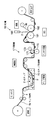
次に、本発明のウェブ材料へのICチップ実装方法について説明する。
図4は、ウェブ材料へのICチップ実装を行う製造ライン図である。パッケー等に使用するウェブ材料1bを給紙部から供給し凹孔4を形成し、当該凹孔内にICチップ2を実装し、アンテナパターンを印刷し、さらに、ICチップ2とアンテナパターンを含むウェブ材料面にシーラントフィルム3を被覆する一連の製造ラインを示している。
ただし、本発明は全ての工程を連続したラインで行うことを要件とするものではないので、例えば、ICチップ充填とアンテナパターン印刷を別工程で行うもの、アンテナパターン印刷とその後のEC工程を別工程で行うもの、であっても良い。
【0027】
図4において、エンボス工程では、図示しないエンボス機等によりウェブ材料1bへ凹孔4を形成する。
凹孔の形成とは、ウェブ材料に「くぼみ」状部分を設けることであり、凹孔の深さは実質的に実装されるICチップの厚みや高さに相当し、開口形状はICチップが平面的なものであれば当該平面形状、角錐状または截頭ピラミッド形状等であれば当該外形形状に合わせた形状にする。
通常使用のICチップは厚みは5μm〜1000μm程度であって、表面形状は、一辺が10μm〜5mm角程度の截頭ピラミッド形状のものが多いが、目的により多角錐形状としたり平面な矩形状、等とすることもできる。
凹孔の形成は、加熱可能な適宜な型具を用いる熱エンボス、あるいは熱条件下における真空/圧空成形、レーザー照射等により形成する。
【0028】
ICチップ実装工程では、凹孔4内にICチップ2を嵌合させて充填する。
この工程には、流体を使用するICチップ実装方法(FSA実装)が好適に用いられICチップ充填槽15内で行われる。
ICチップ2は上記の形状に均一に切断または立体形状化したものを、流体内に分散したスラリー状にして使用する。
ICチップをウェブ走行方向に平行な一定ライン上にのみ配列して実装する場合は、ICチップを分散した流体を液中においてディスペンサー等から当該ライン上に流出するようにするのがよい。同一特性、形状のICチップを各凹孔内に1個づつ嵌合させることが原則となるが、複数の特性、形状のICチップを各目的の位置に、それぞれ充填させることもできる。
後者の場合は、異なる特性のICチップ毎に共通の形状を保持させて、流体中にも異なる特性、形状のICチップを分散し、それぞれの形状に合致する凹孔を基材に設け、ICチップ形状と凹孔形状が一致する場合に、当該凹孔内にICチップが嵌合するようにする。
【0029】
用いられる流体は、水や有機溶剤が使用される。有機溶剤としては、エチルアルコールやメチルアルコール、アセトン、シリコンオイル等であってICやプラスチックフィルムに作用せず、かつ包装体に使用する場合は食品の変質や人体に悪影響を及ぼさないものに限られることになる。包装体の場合、現実的には水やエチルアルコールが好ましく用いられることになる。
分散するICチップの数は、基材に充填する密度により調整する必要があるが、分散量を多くし過剰なICチップは、ウェブ材料を振動させて落下させるようにすれば、充填の効率を高めることができる。分散するICチップの数は、目的とICチップの大きさ等にも関係するが、通常1000〜1000000個/リットル程度とする。
包装材料に非接触ICタグとして実装する場合は、ウェブ材料の1m2 に対して、通常1個以上〜100個以下の数量になる。
【0030】
ICチップを分散した流体が、ICチップが常時流体中に拡散し流動する状態でウェブ基材に当接するためには、ポンプにより液流をつくり層流状態にして基材面に流すことが好ましい。前記のように、ピペットやディスペンサー状の先端部から凹孔のラインに沿って流すようにすることもできる。
凹孔内に嵌合しないICチップは、ウェブ表面に沿って液体を吸引するヘッドを設けて充填槽内で除去することができる。
【0031】
ウェブ材料が充填槽から引き出された直後に凹孔以外の部分にもICチップが付着し液体も残っている場合はこれらを除去する必要がある。
このためにはウェブ材料を傾斜して振動を与えるか、ドクターブレード、ブラシ、スクレーパ等の機械的手段により不要なICチップの落下、除去を促進させるが凹孔内に充填したICチップまで取り去らないようにする。
温風や空気流により残余の液体の乾燥を促進することも好ましい。
【0032】
本発明では、上記のようにFSA技術を用いて凹孔にICチップを充填するのが効率良い充填方法であるが、当該方法に限定しない充填方法を採用できる。充填効率の問題もあるが、ICチップをロボットアーム、真空吸引等によりピックアップし、所定の目標位置に実装する技術は既に確立しており、それらの技術を採用することができる。
【0033】
ICチップを凹孔内に一時的に固定するためには、凹孔内の少なくとも底部部分またはICチップの底面に塗工した熱溶融性樹脂層6(図1)を加熱して溶融してから冷却し(室温に戻し)、ICチップをウェブ材料に固定する必要がある。その後のEC工程やラミネート工程での脱落を防止するためである。
これには、前記のように集積回路を形成したシリコン基盤の底面に熱溶融性樹脂を塗工するものでも良く、ウェブ材料の少なくとも凹孔内に部分的に塗工層を設けるものであっても良い。凹孔4の形成と同時に樹脂層を設ける方法も可能である。
【0034】
アンテナ印刷工程では、ICチップ2の充填後、ICチップのパッドに接続するようにアンテナパターン11,12の印刷を行う。印刷方式は要求されるアンテナ精度により異なるが、グラビア印刷やオフセット印刷、スクリーン印刷等が採用できる。精度の高い印刷の場合はシルクスクリーン印刷や後述するラバースタンプ法の印刷方式が好ましい。
ウェブ材料1bが印刷機17の版胴171と圧胴172の間を通過してICチップ面にアンテナパターンが印刷される。導電性インキはインキ付けローラ173から供給される。アンテナ印刷はこのようにウェブを連続的に走行させる状態で行っても良いし、一時的にウェブの走行を停止させて印刷し、次いでウェブを送る間欠動作で印刷するものであっても良い。
アンテナパターン印刷と同時にまたは別工程で絵柄印刷5(図1)をしても良いのは前記のとおりである。
【0035】
本発明では、アンテナパターンの印刷をラバースタンプ法で行うのが、精度の高い印刷を可能とする。ラバースタンプ法はナノ構造を作る新技術として開発された技術であって、ソフトリソグラフィーともいわれる。
本発明で印刷するアンテナパターンは、最も細い線でも数μmの単位であり、パッドとの位置合わせでも2〜3μmの許容が認められるので、ナノメートル単位の精度が必要とされるものではないが、高精度を達成するため当該印刷方法に準じた方法を採用する。
【0036】
以下に当該ラバースタンプ技術による印刷方法について説明する。
図5は、ラバースタンプ法の工程を示す図である。
ラバースタンプ法の場合は、まず鋳型またはスタンプを用意する。通常、ナノメータの精度を達成する場合は、フォトリソグラフィーか電子ビームリソグラフィーを使って、型材料であるシリコン基板表面にフォトレジストパターンを作成するが、アンテナパターンの場合の型材料は、42合金(ニッケル42%:鉄合金)や銅合金、あるいは金属アルミであってよい。これに対し、フォトマスクを使用するフォトエッチング法を採用して型を作る。
エッチング後には金属材料の凹凸型7が形成される(図5(A))。次に液状のPDMS(ポリジメチルシロキサン)材料8を型7表面の凹凸上に注ぎ込み、低温加熱して硬化させゴム状に固める(図5(B))。
PDMSを型から分離すれば、元のパターンに合ったPDMSスタンプ9が完成する(図5(C))。
【0037】
このPDMSスタンプ9をゴム凸版として導電性インキを用いてウェブ材料に対する印刷を行う。PDMSスタンプ9は平板状でもシリンダに巻き付けた輪転印刷機でも使用できる。
導電性インキには、導電性カーボンや黒鉛、銀粉やアルミ粉、あるいはこれらの混合体をビヒクルに分散したインキを使用する。
あるいはまた、インキコストは割高となるが、酸化錫、酸化インジウム、ドープ酸化インジウム(ITO)、酸化チタン粉末、7,7,8,8−テトラシアノキノジメタン錯体(TCNQ錯体)を溶解したもの等を使用した透明導電性インキであってもよい。
アンテナパターンの表面抵抗は、JISK6911による測定値で、106 Ω/ □以下が適用でき、好ましくは104 Ω/□以下で、交信の信頼性を高められる。
【0038】
EC工程では、ウェブ材料にシーラントフィルムを積層して被覆する。凹孔内に充填されたICチップはウェブ基材と物理的に完全に接合した状態にはないので、フィルムが揺れたり振動したり、下向きになれば凹孔内から脱落することが生じ得る。そこで、ICチップを充填後、凹孔およびウェブ材料の他の部分を含む全面をシーラントフィルムを被覆する。図4では、イクストルージョンコーター(EC)機の場合を例示している。
ウェブ材料1bに溶融したポリエチレン(シーラントフィルム)3等を被覆する場合は、EC機18のゴムロールであるニップロール181側からウェブ材料1bを供給し、Tダイ183から溶融ポリエチレンを押し出し、ウェブ材料と溶融ポリエチレンの一体化フィルムを金属ロールであるチルロール182に押圧して積層する。この際、チルロール側からフィルム3bを供給して3層積層体としてもよい。
本実装方法では、実装したICチップ2が凹孔内に嵌合しているので、ICチップ2がチルロール182側に面するように実装されていても、チルロールを損傷することはない。前工程にAC剤の塗工工程を設ける場合も同様である。
【0039】
シーラントフィルムのラミネート方法としては、EC以外にドライラミネート方式あるいは接着剤を使用するラミネート等、適宜の形態を採用することができる。このようにしてシーラントフィルムが被覆された状態では、ICチップ2は安定した状態になり、その後の製袋や内容物を充填する加工を行っても凹孔4内から脱落するようなことはない。
【0040】
図6は、ICチップ充填槽を示す詳細図である。
ICチップ充填槽15は、ガラスまたは透明アクリル板等で形成する漏斗状の容器からなる。容器の材質は、スラリーで影響を受けることのない他の金属やプラスチックを使用できる。この充填槽に液体を満たし、凹孔4を形成したウェブ材料1bを液体中に走行させる。図6においては、搬送ロールR3とR4間の傾斜面において、ディスペンサー151からICチップの分散したスラリーをウェブ表面に流すようにしている。
ウェブ材料面を流れるスラリーの流速は、1mm/secから約1000mm/sec程度であるが、ウェブ材料の搬送速度やICチップの嵌合速度、ウェブからの除去速度を勘案して適宜に調整するのが好ましい。
ICチップ充填槽15内の液体とスラリーの液体はもちろん同質の液体であるので、ディスペンサー151から流れた液体は速やかに充填槽内に拡散するが、液体よりはやや比重の大きいICチップは沈降してウェブ表面に落ちる。沈降したICチップの幾つかは凹孔に嵌合するが、嵌合しない残余の大多数のICチップはウェブ表面から除去される。
【0041】
ICチップ充填槽15中では凹孔にICチップ2を嵌合させて充填すると共に、余分なICチップを迅速に落下させる必要があるので、ウェブに連続的な振動を与えたり、ICチップを分散しない弱い液流を与えてICチップの嵌合と落下を促進させる。
ウェブ材料は、図6のようにウェブ材料の進行方向に上昇して傾斜するものでなく、進行方向に向かって下降したり、右または左に傾斜して走行するものであっても良い。
【0042】
ディスペンサー151は、ポンプ152からのガス噴出流により加速した流体をウェブ表面に流出させることができる。ディスペンサー151の先端部分は、凹孔の並ぶラインに近い部分に位置させる。1つのディスペンサーで凹孔が完全に充填されない場合は複数のディスペンサーを凹孔のラインに沿って配列することができる。
凹孔に嵌合しないICチップは振動により加速されてウェブの傾斜面を滑り落ちるが、前記のように吸引や強制落下させる機構を設けても良い。
落下したICチップは、漏斗状の受容槽153面に蓄積するので、導通管(カラム)を通じて液流を循環させてディスペンサー151に戻す。これには、空気や水素(H2 )や酸素(O2 )、窒素ガス(N2 )や炭酸ガス、あるいはアルゴンやヘリウム等の不活性ガスをポンプを用いて気泡と共にに流す搬送方法を採用できる。
【0043】
次に、本発明に使用する他の材料について説明する。
包装体のウェブ材料には、被覆したカートン紙や板紙、樹脂含浸紙、PETやPBT等のポリエステル、ポリオレフィン、アクリル、ナイロン6、ナイロン66等のポリアミド、また、無機蒸着フィルムやEVOH等のバリアフィルムが用いられる。流体塗工を行う関係から被覆されていないカートン紙や板紙、通常の紙類は適切とは考えられない。
シーラントフィルムにはPEやPP等のポリオレフィンもしくはそれらの2種以上のフィルムやシートの積層体を使用できる。
基材やシーラントフィルムの厚みは15〜500μmが使用できるが、強度、加工作業性、コスト等の点から20〜200μmがより好ましい。
【0044】
熱溶融性樹脂層6としては、ポリエチレンもしくはエチレンと(メタ)アクリル酸との共重合体などのオレフィン系、エチレン−酢酸ビニル系共重合体、ポリアミド系、ポリエステル系、熱可塑性エラストマー系、反応ホットメルト系などのホットメルト系樹脂、ワックス等がある。
【0045】
【実施例】
(実施例)
図1、図4、図5等を参照して、ICタグ付き包装体の実施例を説明する。 厚み40μm、幅300mmのポリエチレンテレフタレート(PET)フィルム(東洋紡績株式会社製「E−5102」)をウェブ材料1bとし、これに、アクリル系ホットメルト剤(熱溶融性樹脂6)を幅1cm、厚み2μmのライン状になるように印刷してウェブ材料を作成した。
次に、ホットメルト剤塗工ライン上に、開孔4の表面が1520×2040μm、底面が1200×1700μmの矩形状、深さが200μmの逆截頭ピラミッド型になるように、当該形状を有する雄型と雌型の熱成形具を用いて、10cm間隔置きに各1個の凹孔を連続して形成した。
【0046】
ICチップ塗布用スラリーとして、ICチップ約8000個を1リットルの水に分散させたものを準備した。当該ICチップは、表面が1500×2000μm、底面が1200×1700μmの矩形状で、厚みが200μmの截頭ピラミッド型形状、非接触ICタグ用途のものである。
このICチップを分散したスラリーを、図6図示の充填層内において、前記ウェブ材料面にディスペンサー151から噴射した。
ICチップ充填後のウェブ材料を加熱して熱溶融性樹脂層6によりICチップ2を基材に固定した。
【0047】
別に、アンテナパターン印刷用のPDMSスタンプを以下のようにして準備した。まず、厚み2.0mmの銅合金にレジストを塗工し、図3(A)図示の平面コイル状アンテナパターンを作製したフォトマスクを重ねて露光した。レジスト作製後、エッチングして深さ0.5mmのスタンプ型7を作製した。
このスタンプ型材に、ポリジメチルシロキサン(ダウコーニング社「SYLPOT」)の液体を塗工して固め、その後剥離して凹凸パターンのPDMSスタンプ9を完成した。
【0048】
このPDMSスタンプ9をゴム凸版として、導電性インキ(藤倉化成株式会社製「銀ペースト」)を使用してアンテナパターンを印刷した。当該インキは、有機銀化合物と銀フレークの混合物ペーストからなる材料である。当該インキは焼成によりさらに低抵抗の導電体になるが、未焼成でもICタグとして十分な導電性が得られる。
アンテナパターンをパッチアンテナ形状(図2)とし、接続端子11c,12cの大きさを1.0mm×1.0mm、端子間距離を0.8mmとしたところパッドに対して見当位置合わせを容易に行うことができた。
【0049】
その後、シングルEC機を用いて、ICチップ側にAC(アンカーコート)剤(武田薬品工業株式会社製「A3210/A3075」、固形分5%)を塗布し、乾燥後、樹脂温度320°Cの押出しPE(三井化学株式会社製「ミラソン16P」);押出し厚み20μmにて、厚み40μmのPEフィルム(大日本樹脂株式会社製「SKLフィルム」)と押出しラミネーションを行い、シーラントフィルムを作製した。
【0050】
上記の工程により作製した、ICタグ付き包装体の構成は、
(表)PET40μm/ICチップ/アンテナパターン印刷/AC/PE20μm/PEフィルム40μm(裏)
となった。
【0051】
実施例のICタグ付き包装体を使用して、スナック菓子用包装材料を作製した。確認事項として非接触ICタグ10に対して所定のデータの記録を行った後、読取装置として、モトローラ社製BiStatixリーダー「WAVE」を用いて、情報の読取り試験を行ったところ、全ての包装体の非接触ICタグを正しく読み取りすることができた。
【0052】
本発明のICタグ付き包装体は、データの書き換えができるので、出荷検査結果のデータ、成分表示や賞味期限、製造者名、出荷日等の各種の記録ができ、商品の流通管理、品質管理に好適である。
本発明の包装体は軟包装材料に限らず、紙−フィルム等を積層するカートン等にも適用が可能であり函体状の包装体を除外するものではない。
【0053】
【発明の効果】
上述のように、本発明のウェブに実装されたICチップへのアンテナパターン形成方法によれば、ICチップを実装したウェブ材料に対して、高い精度でアンテナパターンを印刷することができる。また、インラインで高速にICタグ付き包装体を製造できる利点がある。
本発明のICタグ付き包装体は、従来のように、非接触ICタグラベルを使用しないので、製造原価を低くすることができる。
【図面の簡単な説明】
【図1】 本発明のICタグ付き包装体の例を示す図である。
【図2】 アンテナパターンの接続端子とICチップの相対位置を示す図である。
【図3】 電磁誘導型アンテナパターンを示す。
【図4】 ウェブ材料へのICチップ実装を行う製造ライン図である。
【図5】 ラバースタンプ法の工程を示す図である。
【図6】 ICチップ充填槽を示す図である。
【図7】 従来法による非接触ICタグの実施形態を示す図である。
【符号の説明】
1 ICタグ付き包装体
1b パッケージ基材、ウェブ材料
2 ICチップ
2b ICチップの底部
2u ICチップの表面
3 シーラントフィルム
4 凹孔
5 絵柄印刷
6 熱溶融性樹脂層
7 型
8 PDMS材料
9 PDMSスタンプ
10 非接触ICタグ
11,12 アンテナパターン
13 コイル状パターン
14 ダイポール型パターン
15 ICチップ充填槽
17 印刷機
18 EC機
20 ICタグラベル
21 ICチップ[0001]
BACKGROUND OF THE INVENTION
The present invention relates to a method for manufacturing an IC tag package having a non-contact communication function by mounting an IC chip on a continuously supplied web material and printing an antenna pattern on the IC chip.
Attaching an IC tag having a non-contact communication function to a package has been performed. The present invention relates to a technique for mounting an IC chip for such a non-contact IC tag directly on a web material and printing an antenna pattern in a manufacturing process of a package.
[0002]
[Prior art]
"Non-contact IC tag" that can record and read information in a non-contact manner (generally, "Non-contact data carrier", "Wireless IC tag", "Non-contact IC", "Non-contact IC label", "RFID tag" Have been widely used for information management of goods and merchandise, logistics management, and the like.
Even in the field of packaging bodies such as foods, non-contact IC tags are attached and used for distribution, quality control, expiration date management, and the like.
[0003]
When the form of the non-contact IC tag in the packaging material is examined, an antenna pattern is printed with a conductive ink on a base material or a packaging material surface, and an IC tag label in the form of an interposer is attached thereto.
FIG. 7 is a diagram showing an embodiment of a non-contact IC tag according to a conventional method. 7A is a plan view in which the
In the case of this embodiment, the
[0004]
The
Motorola's “BiStatix” (trademark) is mainly used as an interposer-type label, and there is an advantage that it can be easily mounted using a labeler. There is.
[0005]
[Problems to be solved by the invention]
Conventionally, the reason why such a tack label-shaped interposer is used is thought to be because there is no technique for efficiently mounting a single IC chip on a web material in conjunction with the processing speed.
On the other hand, a technique for mounting an IC chip on a sheet-like medium such as glass has been established for a long time as seen in electronic component boards. In these techniques, an IC chip is mounted by a robot arm, vacuum suction, or the like. However, mechanical operation has become difficult with the miniaturization of the IC chip.
By the way, in recent years, as shown in JP-A-9-20943, JP-A-9-506742, or U.S. Pat. A technique (FSA = Fluidic Self Assembly) for mounting a minute semiconductor or the like on a soft substrate has been proposed.
[0006]
In the present invention, an IC tag label is not directly attached to a package by attaching a non-contact IC tag label as in the prior art. Is mounted, and an antenna pattern is printed to increase the efficiency of manufacturing a package with a non-contact IC tag and reduce the manufacturing cost.
[0007]
[Means for Solving the Problems]
The first of the gist of the present invention for solving the above problems is a method of mounting an IC chip for an IC tag on a web material and forming an antenna pattern. After printing the hot melt agent in a line, on the line Forming a concave hole corresponding to the outer shape and depth of the IC chip at intervals, and (2) fitting an IC chip having a shape corresponding to the outer shape and depth into the concave hole of the web material. The process of leaving one each in the finished state, (3) fixing the IC chip with a hot melt agent; ( 4 ) The antenna pattern is connected to the pad of the IC chip fitted in the concave hole. The rubber stamp method using polydimethylsiloxane as a rubber relief And a method for forming an antenna pattern on an IC chip mounted on a web. Because of this formation method, the IC chip can be efficiently mounted and the antenna pattern can be aligned and printed.
[0008]
A second aspect of the present invention for solving the above problems is a method of mounting an IC tag for an IC tag on a web material and forming an antenna pattern. After printing the hot melt agent in a line, on the line Forming a concave hole corresponding to the outer shape and depth of the IC chip at intervals, and (2) fitting an IC chip having a shape corresponding to the outer shape and depth into the concave hole of the web material. The process of leaving one each in the finished state, (3) fixing the IC chip with a hot melt agent; ( 4 ) The antenna pattern is connected to the pad of the IC chip fitted in the concave hole. The rubber stamp method using polydimethylsiloxane as a rubber relief Printing process and ( 5 ) IC chip is fitted on the entire surface including the concave portion of the web material printed with the antenna pattern. Sealant through EC layer or adhesive layer And a method of forming an antenna pattern on an IC chip mounted on a web, characterized by comprising a step of coating a film. Because of this formation method, it is possible to efficiently mount an IC chip, align and print an antenna pattern, and prevent the chip from falling off.
[0009]
The third of the gist of the present invention for solving the above problems is a package with an IC tag having a non-contact IC tag function, which is a web material. After printing the hot melt agent in a line, leave a space on the line A concave hole corresponding to the outer shape and depth of the IC chip is formed, and the IC chip is fitted into the concave hole. Fixed to web material with hot melt agent In such a state, the antenna pattern is connected to the pad of the IC chip. With rubber stamp method Printed on the IC chip and antenna pattern Through EC layer or adhesive layer A package with an IC tag, wherein a sealant film is coated. Since it is a package with such an IC tag, it becomes a package with an IC tag that is low-cost and mass-productive.
[0010]
In the above, the antenna pattern may be a patch antenna, a planar coil antenna, or a dipole antenna. it can .
[0013]
DETAILED DESCRIPTION OF THE INVENTION
For non-contact IC tag packaging, in the case of flexible packaging materials or cartons, the need to stick the IC tag after filling the contents such as food, and to prevent peeling in the distribution process, between the laminated films A configuration in which an IC tag is held in advance is advantageous.
Therefore, the non-contact IC tag is advantageous in that an antenna pattern is printed on a web material, an IC chip is attached to the antenna pattern, and then a sealant film is laminated with or without an adhesive.
In the present invention, an IC tag label is not mounted on an antenna pattern as in the prior art, but a concave hole is provided in a web material to fill an IC chip and connect to a pad (or bump) of the filled IC chip. Print the antenna pattern. Thus, the function of a non-contact IC tag is given.
[0014]
Hereinafter, the package with IC tag of the present invention will be described with reference to the drawings.
FIG. 1 is a diagram showing an example of a package with an IC tag according to the present invention. FIG. 1A is a plan view of a package 1 with an IC tag, and FIG. 1B shows an IC chip portion of the package upper substrate along the line AA in FIG. It is sectional drawing. The magnification in the thickness direction is shown enlarged in the horizontal direction.
As shown in FIG. 1, the package 1 with an IC tag has a concave hole 4 formed in the
In FIG. 1, the package 1 is shown in a state after bag making and filling the contents, but the package with an IC tag of the present invention does not mean only the state after bag making or box making, A laminated film or a laminated sheet including a form such as a wound form before bag making or box making is also included.
[0015]
As shown in FIG. 1B, since the
The heat-meltable resin layer 6 may be coated on the entire surface of the
The
[0016]
Together with the
A sealant film 3 is laminated on the IC chip and the antenna pattern surface via an EC layer or an adhesive layer.
[0017]
As shown in the cross-sectional view of FIG. 1B, in the package 1 with an IC tag of the present invention, the concave hole 4 is formed to have the same size and shape as the
The
[0018]
Also, the surface of the IC chip is rectangular, and if the front and back sides are correct, the characteristics are not affected even if the left and right directions are switched. This is because if the surface is square, it is impossible to control the direction connecting the pads and the direction perpendicular thereto.
However, if the left and right shapes of the IC chip are different, the left and right shapes of the concave holes are also different, and the IC chip is fitted only when the direction of the IC chip matches the concave hole (one-sided) Meaning), even if the surface is square, front / back and top / bottom / left / right position regulation is possible.
[0019]
When a semiconductor chip is formed on a silicon substrate and then cut by dicing, the IC chip is formed in a rectangular cube, and the front and back cannot be distinguished only by the shape.
However, when a small IC chip is manufactured at low cost, the separation is performed by etching from the back side of the substrate because it is necessary to reduce the dicing groove area and increase the yield. For this reason, the back side is inevitably narrower than the front side where the pad portion is present, and the surface between the front and back surfaces is usually an inclined surface.
Since the surface shape of the chip is usually rectangular, the overall shape of the IC chip is trapezoidal in cross section, and is generally a quadrangular pyramid shape.
However, it may be a rectangular parallelepiped, a cube, a circle, a cylinder, or other shapes depending on the purpose and application.
[0020]
When the IC chip is a quadrangular pyramid-shaped pyramid shape, the outer shape of the concave hole 4 and the
This is because smooth fitting of the IC chip is promoted by this angle. Even if there is a minute gap, the conductive ink is filled when the antenna pattern is printed, so that there is no conduction failure.
Since the upper surface side of the
[0021]
In principle, the antenna pattern and the IC chip pads (or bumps) are connected directly, but even if there is a slight misalignment, it can operate as a non-contact IC tag by “ohmic contact” (ohmic bonding). Become.
However, when the pads of the IC chip are extremely displaced to one connection terminal side with respect to the
[0022]
FIG. 2 is a diagram illustrating a relative position between the connection terminal of the antenna pattern and the IC chip. 2A shows a normal state, and FIG. 2B shows a state where the positions of the
In conclusion, it is difficult to form a communication circuit when the distance from the center position of the
Incidentally, since one side of the IC chip whose surface is rectangular is about 10 μm to 5 mm, in the case of the antenna pattern as shown in FIG. 2, it is necessary to form each side with a positional accuracy of about 5 μm to 2.5 mm. As the IC chip becomes minute, high hole position accuracy is required.
The thickness of the IC chip is about 5 μm to 1000 μm.
[0023]
In order to prevent short-circuiting even if the
That is, in FIG. 2A, if the opposing sides of the
In general, since the positional deviation in the web width direction can be controlled to be smaller than the positional deviation in the web traveling direction, it is considered advantageous to print the antenna pattern with the direction of arrow Y as the web traveling direction. .
However, the easy direction of position control varies depending on the apparatus and is not uniform. Therefore, if the connecting terminal portion has a direction expanded or extended as compared with the case of a normal electrical component, the tolerance for the displacement of the concave hole can be increased.
[0024]
The antenna pattern is not limited to the electrostatic coupling pattern as shown in FIGS. 1 and 2, but may be a coiled (planar winding) electromagnetic induction pattern as shown in FIG.
In the case of the electrostatic coupling type, it is printed on a patch antenna type separated into two pieces as shown in FIGS. 1 and 2 and used for communication at 125 kHz. In the case of the electromagnetic induction type, a planar coil pattern (13.56 MHz) in FIG. 3A or a dipole type (UHF-SHF band) pattern as shown in FIG. In the case of FIG. 3 (A), the
[0025]
In the case of a patch antenna, two pieces of antenna pattern
In the case of a coiled pattern, the connection terminals of the IC chip are formed. However, if both ends of the
The same applies to the
As shown in FIG. 3C, a planar coil in which the coil is folded back at a portion of 13t may be used. In this case, the
In either case of FIGS. 3A and 3C, it is not necessary to provide a circuit on the back surface and connect with a caulking bracket or a jumping circuit as in the prior art.
In any case, the tolerance for the printing position deviation can be increased by forming the connection terminal shape extended or extended with respect to the pad of the
[0026]
Next, the IC chip mounting method on the web material of the present invention will be described.
FIG. 4 is a production line diagram for mounting an IC chip on a web material. A
However, the present invention does not require that all processes be performed on a continuous line. For example, IC chip filling and antenna pattern printing are performed in separate processes, and antenna pattern printing and subsequent EC processes are performed separately. What is performed in a process may be sufficient.
[0027]
In FIG. 4, in the embossing process, a concave hole 4 is formed in the
The formation of the concave hole is to provide a “dent” -like portion in the web material, the depth of the concave hole substantially corresponds to the thickness and height of the IC chip to be mounted, and the opening shape is determined by the IC chip. If it is planar, if it is a planar shape, a pyramid shape or a truncated pyramid shape, etc., the shape is matched to the outer shape.
Normally used IC chips have a thickness of about 5 μm to 1000 μm, and the surface shape is often a truncated pyramid shape with a side of about 10 μm to 5 mm square. Etc.
The concave hole is formed by hot embossing using a suitable mold that can be heated, vacuum / pressure forming under thermal conditions, laser irradiation, or the like.
[0028]
In the IC chip mounting step, the
In this step, an IC chip mounting method (FSA mounting) using a fluid is preferably used and performed in the IC chip filling tank 15.
The
When the IC chips are arranged and mounted only on a certain line parallel to the web running direction, it is preferable that the fluid in which the IC chips are dispersed flows out from the dispenser or the like into the line in the liquid. In principle, IC chips having the same characteristics and shape are fitted into the concave holes one by one. However, IC chips having a plurality of characteristics and shapes can be filled in each target position.
In the latter case, a common shape is maintained for each IC chip having different characteristics, the IC chips having different characteristics and shapes are dispersed in the fluid, and concave holes that match the respective shapes are provided in the base material. When the chip shape matches the concave hole shape, the IC chip is fitted into the concave hole.
[0029]
The fluid used is water or an organic solvent. Organic solvents include ethyl alcohol, methyl alcohol, acetone, silicone oil, etc., which do not act on ICs and plastic films, and when used for packaging, are limited to those that do not affect the quality of food or the human body. It will be. In the case of a package, water or ethyl alcohol is preferably used in practice.
The number of IC chips to be dispersed must be adjusted according to the density of filling the base material. However, if the amount of dispersion is increased and the excess IC chips are caused to drop by vibrating the web material, the efficiency of filling can be improved. Can be increased. Although the number of IC chips to be dispersed is related to the purpose and the size of the IC chip, it is usually set to about 1000 to 1000000 pieces / liter.
When mounted as a non-contact IC tag on packaging material, 1m of web material 2 On the other hand, the quantity is usually 1 or more and 100 or less.
[0030]
In order for the fluid in which the IC chip is dispersed to contact the web substrate in a state where the IC chip is always diffused and flows into the fluid, it is preferable to create a liquid flow by a pump and make it flow in a laminar state on the substrate surface. . As mentioned above, it can also be made to flow along the line of the concave hole from the tip of the pipette or dispenser.
The IC chip that does not fit in the concave hole can be removed in the filling tank by providing a head for sucking liquid along the web surface.
[0031]
Immediately after the web material is drawn out from the filling tank, if the IC chip adheres to the portion other than the concave hole and the liquid remains, it is necessary to remove these.
For this purpose, the web material is inclined to give vibrations, or mechanical means such as doctor blades, brushes, and scrapers are used to promote the dropping and removal of unnecessary IC chips, but the IC chips filled in the concave holes are not removed. Like that.
It is also preferable to promote drying of the remaining liquid by warm air or air flow.
[0032]
In the present invention, as described above, an efficient filling method is to fill the IC chip into the concave hole using the FSA technique. But this A filling method not limited to this method can be adopted. Although there is a problem of filling efficiency, technologies for picking up an IC chip by a robot arm, vacuum suction, etc., and mounting it at a predetermined target position have already been established, and these technologies can be adopted.
[0033]
In order to temporarily fix the IC chip in the concave hole, the hot-melt resin layer 6 (FIG. 1) applied to at least the bottom portion of the concave hole or the bottom surface of the IC chip is heated and melted. It is necessary to cool (return to room temperature) and fix the IC chip to the web material. This is to prevent dropping in the subsequent EC process and laminating process.
For this, a heat-meltable resin may be applied to the bottom surface of the silicon substrate on which the integrated circuit is formed as described above, and a coating layer is provided at least partially in the concave hole of the web material. Also good. A method of providing a resin layer simultaneously with the formation of the concave hole 4 is also possible.
[0034]
In the antenna printing process, after the
The
As described above, the pattern printing 5 (FIG. 1) may be performed simultaneously with the antenna pattern printing or in a separate process.
[0035]
In the present invention, printing of the antenna pattern by the rubber stamp method enables printing with high accuracy. The rubber stamp method is a technology developed as a new technology for creating nanostructures, and is also called soft lithography.
The antenna pattern printed in the present invention is a unit of several μm even at the thinnest line, and an allowance of 2 to 3 μm is recognized even in alignment with the pad. In order to achieve high accuracy, a method according to the printing method is adopted.
[0036]
Hereinafter, a printing method using the rubber stamp technology will be described.
FIG. 5 is a diagram illustrating a process of the rubber stamp method.
In the case of the rubber stamp method, a mold or a stamp is first prepared. Normally, when achieving nanometer accuracy, a photoresist pattern is created on the surface of a silicon substrate, which is a mold material, using photolithography or electron beam lithography, but in the case of an antenna pattern, the mold material is 42 alloy (nickel 42%: iron alloy), copper alloy, or metal aluminum. In contrast, a photoetching method using a photomask is employed to make a mold.
After etching, a concavo-
When the PDMS is separated from the mold, the PDMS stamp 9 matching the original pattern is completed (FIG. 5C).
[0037]
The PDMS stamp 9 is used as a rubber relief plate to print on the web material using conductive ink. The PDMS stamp 9 can be a flat plate or a rotary printing machine wound around a cylinder.
As the conductive ink, an ink in which conductive carbon, graphite, silver powder, aluminum powder, or a mixture thereof is dispersed in a vehicle is used.
Alternatively, the ink cost is higher, but tin oxide, indium oxide, doped indium oxide (ITO), titanium oxide powder, and 7,7,8,8-tetracyanoquinodimethane complex (TCNQ complex) are dissolved. The transparent conductive ink using etc. may be sufficient.
The surface resistance of the antenna pattern is a measured value according to JIS K6911, 10 6 Ω / □ or less can be applied, preferably 10 Four Communication reliability can be improved at Ω / □ or less.
[0038]
In the EC process, a sealant film is laminated and coated on the web material. Since the IC chip filled in the concave hole is not physically bonded to the web substrate, the film may be shaken or vibrated, or may fall out of the concave hole if the film faces downward. Therefore, after filling the IC chip, the entire surface including the concave holes and other portions of the web material is covered with a sealant film. FIG. 4 illustrates the case of an extrusion coater (EC) machine.
When the melted polyethylene (sealant film) 3 or the like is coated on the
In this mounting method, since the mounted
[0039]
As a method for laminating the sealant film, an appropriate form such as a dry laminating method or a laminating method using an adhesive can be adopted in addition to EC. In such a state where the sealant film is coated, the
[0040]
FIG. 6 is a detailed view showing the IC chip filling tank.
The IC chip filling tank 15 is formed of a funnel-shaped container formed of glass or a transparent acrylic plate. As the material of the container, other metals and plastics that are not affected by the slurry can be used. The filling tank is filled with a liquid, and the
The flow rate of the slurry flowing on the surface of the web material is about 1 mm / sec to about 1000 mm / sec. However, the flow rate of the web material, the fitting speed of the IC chip, and the removal speed from the web can be adjusted as appropriate. Is preferred.
Since the liquid in the IC chip filling tank 15 and the liquid in the slurry are of course the same liquid, the liquid flowing from the
[0041]
In the IC chip filling tank 15, the
The web material does not rise and incline in the direction of travel of the web material as shown in FIG. 6, but may descend in the direction of travel or run while tilting to the right or left.
[0042]
The
The IC chip that does not fit into the concave hole is accelerated by vibration and slides down the inclined surface of the web. However, a mechanism for sucking or forcibly dropping as described above may be provided.
Since the dropped IC chip accumulates on the surface of the funnel-shaped
[0043]
Next, other materials used in the present invention will be described.
Packaging web materials include coated carton paper, paperboard, resin-impregnated paper, polyesters such as PET and PBT, polyamides such as polyolefin, acrylic, nylon 6 and nylon 66, and inorganic vapor deposition films and barrier films such as EVOH Is used. Carton paper, paperboard, and ordinary paper that are not coated are not considered appropriate because of the fluid application.
As the sealant film, polyolefin such as PE or PP or a laminate of two or more kinds of films or sheets can be used.
The thickness of the base material or sealant film can be 15 to 500 μm, but 20 to 200 μm is more preferable from the viewpoint of strength, workability, cost, and the like.
[0044]
Examples of the heat-meltable resin layer 6 include olefins such as polyethylene or a copolymer of ethylene and (meth) acrylic acid, ethylene-vinyl acetate copolymers, polyamides, polyesters, thermoplastic elastomers, reaction hot There are hot-melt resins such as melt-based resins and waxes.
[0045]
【Example】
(Example)
An example of a package with an IC tag will be described with reference to FIGS. A polyethylene terephthalate (PET) film (“E-5102” manufactured by Toyobo Co., Ltd.) having a thickness of 40 μm and a width of 300 mm is used as the
Next, on the hot melt agent coating line, the surface of the opening 4 is 1520 × 2040 μm, the bottom is 1200 × 1700 μm in a rectangular shape, and the depth is 200 μm. Using a male and female thermoforming tool, one concave hole was formed continuously at intervals of 10 cm.
[0046]
As an IC chip coating slurry, a slurry in which about 8000 IC chips were dispersed in 1 liter of water was prepared. The IC chip is a rectangular pyramid shape with a surface of 1500 × 2000 μm, a bottom surface of 1200 × 1700 μm and a thickness of 200 μm, for non-contact IC tags.
The slurry in which the IC chips are dispersed was sprayed from the
The
[0047]
Separately, a PDMS stamp for antenna pattern printing was prepared as follows. First, a resist was applied to a copper alloy having a thickness of 2.0 mm, and a photomask on which a planar coiled antenna pattern shown in FIG. After producing the resist, etching was performed to produce a stamp die 7 having a depth of 0.5 mm.
The stamp mold was coated with a liquid of polydimethylsiloxane (“SYLPOT” manufactured by Dow Corning), and then peeled to complete a PDMS stamp 9 having a concavo-convex pattern.
[0048]
This PDMS stamp 9 was used as a rubber relief plate, and an antenna pattern was printed using conductive ink (“silver paste” manufactured by Fujikura Kasei Co., Ltd.). The ink is a material made of a mixture paste of an organic silver compound and silver flakes. The ink becomes a conductor having a lower resistance when fired, but sufficient conductivity as an IC tag can be obtained even when unfired.
The antenna pattern is a patch antenna shape (FIG. 2), the size of the
[0049]
Thereafter, using a single EC machine, an AC (anchor coat) agent (“A3210 / A3075” manufactured by Takeda Pharmaceutical Co., Ltd., solid content 5%) is applied to the IC chip side, and after drying, the resin temperature is 320 ° C. Extruded PE (“Mirason 16P” manufactured by Mitsui Chemicals, Inc.); Extrusion lamination was performed with a PE film having a thickness of 40 μm (“SKL film” manufactured by Dainippon Resin Co., Ltd.) at an extrusion thickness of 20 μm to produce a sealant film.
[0050]
The configuration of the package with an IC tag produced by the above process is as follows:
(Table) PET 40 μm / IC chip / antenna pattern printing / AC /
It became.
[0051]
The packaging material for snacks was produced using the package with an IC tag of the example. After recording predetermined data on the
[0052]
Since the package with IC tag of the present invention can rewrite data, it can record various data such as shipping inspection result data, component display, expiration date, manufacturer name, shipping date, etc., product distribution management, quality control It is suitable for.
The packaging body of the present invention is not limited to a soft packaging material, but can be applied to a carton or the like in which paper-films are laminated, and does not exclude a box-shaped packaging body.
[0053]
【The invention's effect】
As described above, according to the method for forming an antenna pattern on an IC chip mounted on a web according to the present invention, an antenna pattern can be printed with high accuracy on a web material on which the IC chip is mounted. Moreover, there exists an advantage which can manufacture a package body with an IC tag in-line at high speed.
Since the package with an IC tag of the present invention does not use a non-contact IC tag label as in the prior art, the manufacturing cost can be reduced.
[Brief description of the drawings]
FIG. 1 is a view showing an example of a package with an IC tag according to the present invention.
FIG. 2 is a diagram showing a relative position between an antenna pattern connection terminal and an IC chip;
FIG. 3 shows an electromagnetic induction antenna pattern.
FIG. 4 is a production line diagram for mounting an IC chip on a web material.
FIG. 5 is a diagram showing a process of a rubber stamp method.
FIG. 6 is a diagram showing an IC chip filling tank.
FIG. 7 is a diagram showing an embodiment of a non-contact IC tag according to a conventional method.
[Explanation of symbols]
1 Package with IC tag
1b Package base material, web material
2 IC chip
2b IC chip bottom
2u IC chip surface
3 Sealant film
4 recessed holes
5 Pattern printing
6 Hot-melt resin layer
7 type
8 PDMS materials
9 PDMS stamp
10 Non-contact IC tag
11,12 Antenna pattern
13 Coil pattern
14 Dipole pattern
15 IC chip filling tank
17 Printing machine
18 EC machine
20 IC tag label
21 IC chip
Claims (5)
Priority Applications (1)
| Application Number | Priority Date | Filing Date | Title |
|---|---|---|---|
| JP2002036151A JP3998992B2 (en) | 2002-02-14 | 2002-02-14 | Method for forming antenna pattern on IC chip mounted on web and package with IC tag |
Applications Claiming Priority (1)
| Application Number | Priority Date | Filing Date | Title |
|---|---|---|---|
| JP2002036151A JP3998992B2 (en) | 2002-02-14 | 2002-02-14 | Method for forming antenna pattern on IC chip mounted on web and package with IC tag |
Publications (3)
| Publication Number | Publication Date |
|---|---|
| JP2003242471A JP2003242471A (en) | 2003-08-29 |
| JP2003242471A5 JP2003242471A5 (en) | 2005-08-25 |
| JP3998992B2 true JP3998992B2 (en) | 2007-10-31 |
Family
ID=27778113
Family Applications (1)
| Application Number | Title | Priority Date | Filing Date |
|---|---|---|---|
| JP2002036151A Expired - Fee Related JP3998992B2 (en) | 2002-02-14 | 2002-02-14 | Method for forming antenna pattern on IC chip mounted on web and package with IC tag |
Country Status (1)
| Country | Link |
|---|---|
| JP (1) | JP3998992B2 (en) |
Cited By (1)
| Publication number | Priority date | Publication date | Assignee | Title |
|---|---|---|---|---|
| US20160072183A1 (en) * | 2014-09-09 | 2016-03-10 | Max Echo Technology Corporation | Method of Making a Double-Sided Flexible Printed Circuit Type Antenna Device |
Families Citing this family (111)
| Publication number | Priority date | Publication date | Assignee | Title |
|---|---|---|---|---|
| US6867983B2 (en) | 2002-08-07 | 2005-03-15 | Avery Dennison Corporation | Radio frequency identification device and method |
| US7224280B2 (en) | 2002-12-31 | 2007-05-29 | Avery Dennison Corporation | RFID device and method of forming |
| US6940408B2 (en) | 2002-12-31 | 2005-09-06 | Avery Dennison Corporation | RFID device and method of forming |
| DE102004007457A1 (en) * | 2004-02-13 | 2005-09-01 | Man Roland Druckmaschinen Ag | In-line printing of intelligent packaging films has an initial station to print a conductive circuit, as an antenna, followed by four-color printing stations and a chip application station as a radio frequency identity tag |
| JP4030947B2 (en) * | 2003-10-06 | 2008-01-09 | シーケーディ株式会社 | Blister packing machine |
| KR101107555B1 (en) * | 2004-01-22 | 2012-01-31 | 미코 코포레이션 | A modular radio frequency identification tagging method |
| JP2005321935A (en) * | 2004-05-07 | 2005-11-17 | Toyo Seikan Kaisha Ltd | Ic tag incorporated cap |
| JP4563731B2 (en) * | 2004-06-21 | 2010-10-13 | 東洋アルミニウム株式会社 | Circuit structure and function card having the same |
| JP2006031336A (en) | 2004-07-15 | 2006-02-02 | Fujitsu Ltd | Method for manufacturing rfid tag |
| US7353598B2 (en) * | 2004-11-08 | 2008-04-08 | Alien Technology Corporation | Assembly comprising functional devices and method of making same |
| US7615479B1 (en) | 2004-11-08 | 2009-11-10 | Alien Technology Corporation | Assembly comprising functional block deposited therein |
| JP4330575B2 (en) | 2005-03-17 | 2009-09-16 | 富士通株式会社 | Tag antenna |
| US7519328B2 (en) | 2006-01-19 | 2009-04-14 | Murata Manufacturing Co., Ltd. | Wireless IC device and component for wireless IC device |
| CN101416353B (en) | 2006-04-10 | 2013-04-10 | 株式会社村田制作所 | Wireless IC device |
| WO2007119310A1 (en) | 2006-04-14 | 2007-10-25 | Murata Manufacturing Co., Ltd. | Antenna |
| JP4572983B2 (en) * | 2006-04-14 | 2010-11-04 | 株式会社村田製作所 | Wireless IC device |
| EP2012388B1 (en) | 2006-04-26 | 2011-12-28 | Murata Manufacturing Co. Ltd. | Article provided with feed circuit board |
| US9064198B2 (en) | 2006-04-26 | 2015-06-23 | Murata Manufacturing Co., Ltd. | Electromagnetic-coupling-module-attached article |
| CN101454992B (en) | 2006-05-26 | 2015-07-15 | 株式会社村田制作所 | Data coupler |
| WO2007138857A1 (en) | 2006-06-01 | 2007-12-06 | Murata Manufacturing Co., Ltd. | Radio frequency ic device and composite component for radio frequency ic device |
| WO2007145053A1 (en) | 2006-06-12 | 2007-12-21 | Murata Manufacturing Co., Ltd. | Electromagnetically coupled module, wireless ic device inspecting system, electromagnetically coupled module using the wireless ic device inspecting system, and wireless ic device manufacturing method |
| CN101467209B (en) | 2006-06-30 | 2012-03-21 | 株式会社村田制作所 | Optical disc |
| WO2008007606A1 (en) | 2006-07-11 | 2008-01-17 | Murata Manufacturing Co., Ltd. | Antenna and radio ic device |
| JP4310589B2 (en) | 2006-08-24 | 2009-08-12 | 株式会社村田製作所 | Wireless IC device inspection system and wireless IC device manufacturing method using the same |
| WO2008050535A1 (en) | 2006-09-26 | 2008-05-02 | Murata Manufacturing Co., Ltd. | Electromagnetically coupled module and article with electromagnetically coupled module |
| CN101523750B (en) | 2006-10-27 | 2016-08-31 | 株式会社村田制作所 | The article of charged magnetic coupling module |
| WO2008090943A1 (en) | 2007-01-26 | 2008-07-31 | Murata Manufacturing Co., Ltd. | Container with electromagnetically coupling module |
| JP4888494B2 (en) | 2007-02-06 | 2012-02-29 | 株式会社村田製作所 | Packaging material with electromagnetic coupling module |
| JP5024372B2 (en) | 2007-04-06 | 2012-09-12 | 株式会社村田製作所 | Wireless IC device |
| US8009101B2 (en) | 2007-04-06 | 2011-08-30 | Murata Manufacturing Co., Ltd. | Wireless IC device |
| JP4697332B2 (en) | 2007-04-09 | 2011-06-08 | 株式会社村田製作所 | Wireless IC device |
| US7762472B2 (en) | 2007-07-04 | 2010-07-27 | Murata Manufacturing Co., Ltd | Wireless IC device |
| US8235299B2 (en) | 2007-07-04 | 2012-08-07 | Murata Manufacturing Co., Ltd. | Wireless IC device and component for wireless IC device |
| JP4930586B2 (en) | 2007-04-26 | 2012-05-16 | 株式会社村田製作所 | Wireless IC device |
| EP2141769A4 (en) | 2007-04-27 | 2010-08-11 | Murata Manufacturing Co | Wireless ic device |
| ATE544129T1 (en) | 2007-04-27 | 2012-02-15 | Murata Manufacturing Co | WIRELESS IC DEVICE |
| CN101568934A (en) | 2007-05-10 | 2009-10-28 | 株式会社村田制作所 | Wireless IC device |
| EP2148449B1 (en) | 2007-05-11 | 2012-12-12 | Murata Manufacturing Co., Ltd. | Wireless ic device |
| JP4396785B2 (en) | 2007-06-27 | 2010-01-13 | 株式会社村田製作所 | Wireless IC device |
| JP4466795B2 (en) | 2007-07-09 | 2010-05-26 | 株式会社村田製作所 | Wireless IC device |
| EP2166490B1 (en) | 2007-07-17 | 2015-04-01 | Murata Manufacturing Co. Ltd. | Wireless ic device and electronic apparatus |
| US20090021352A1 (en) | 2007-07-18 | 2009-01-22 | Murata Manufacturing Co., Ltd. | Radio frequency ic device and electronic apparatus |
| JP4434311B2 (en) | 2007-07-18 | 2010-03-17 | 株式会社村田製作所 | Wireless IC device and manufacturing method thereof |
| CN102915462B (en) | 2007-07-18 | 2017-03-01 | 株式会社村田制作所 | Wireless IC device |
| US7830311B2 (en) | 2007-07-18 | 2010-11-09 | Murata Manufacturing Co., Ltd. | Wireless IC device and electronic device |
| EP2096709B1 (en) | 2007-12-20 | 2012-04-25 | Murata Manufacturing Co., Ltd. | Radio ic device |
| JP4561931B2 (en) | 2007-12-26 | 2010-10-13 | 株式会社村田製作所 | Antenna device and wireless IC device |
| EP2251934B1 (en) | 2008-03-03 | 2018-05-02 | Murata Manufacturing Co. Ltd. | Wireless ic device and wireless communication system |
| EP2251933A4 (en) | 2008-03-03 | 2012-09-12 | Murata Manufacturing Co | Composite antenna |
| CN101960665B (en) | 2008-03-26 | 2014-03-26 | 株式会社村田制作所 | Radio IC device |
| CN101953025A (en) | 2008-04-14 | 2011-01-19 | 株式会社村田制作所 | Radio IC device, electronic device, and method for adjusting resonance frequency of radio IC device |
| JP2009258943A (en) * | 2008-04-16 | 2009-11-05 | Omron Corp | Strap, tag inlet, and rfid tag |
| EP2284949B1 (en) | 2008-05-21 | 2016-08-03 | Murata Manufacturing Co. Ltd. | Wireless ic device |
| WO2009142068A1 (en) | 2008-05-22 | 2009-11-26 | 株式会社村田製作所 | Wireless ic device and method for manufacturing the same |
| CN102047271B (en) | 2008-05-26 | 2014-12-17 | 株式会社村田制作所 | Wireless IC device system and method for authenticating wireless IC device |
| WO2009145218A1 (en) | 2008-05-28 | 2009-12-03 | 株式会社村田製作所 | Wireless ic device and component for a wireless ic device |
| JP4557186B2 (en) | 2008-06-25 | 2010-10-06 | 株式会社村田製作所 | Wireless IC device and manufacturing method thereof |
| JP4671001B2 (en) | 2008-07-04 | 2011-04-13 | 株式会社村田製作所 | Wireless IC device |
| JP5434920B2 (en) | 2008-08-19 | 2014-03-05 | 株式会社村田製作所 | Wireless IC device and manufacturing method thereof |
| WO2010047214A1 (en) | 2008-10-24 | 2010-04-29 | 株式会社村田製作所 | Radio ic device |
| CN102197537B (en) | 2008-10-29 | 2014-06-18 | 株式会社村田制作所 | Wireless IC device |
| DE112009002384B4 (en) | 2008-11-17 | 2021-05-06 | Murata Manufacturing Co., Ltd. | Antenna and wireless IC component |
| JP5041075B2 (en) | 2009-01-09 | 2012-10-03 | 株式会社村田製作所 | Wireless IC device and wireless IC module |
| CN103594455A (en) | 2009-01-16 | 2014-02-19 | 株式会社村田制作所 | Wireless IC device |
| EP2385580B1 (en) | 2009-01-30 | 2014-04-09 | Murata Manufacturing Co., Ltd. | Antenna and wireless ic device |
| JP5510450B2 (en) | 2009-04-14 | 2014-06-04 | 株式会社村田製作所 | Wireless IC device |
| EP2568534A3 (en) | 2009-04-21 | 2014-05-14 | Murata Manufacturing Co., Ltd. | Antenna devie and method of setting resonant frequency of antenna device |
| CN102449846B (en) | 2009-06-03 | 2015-02-04 | 株式会社村田制作所 | Wireless IC device and production method thereof |
| WO2010146944A1 (en) | 2009-06-19 | 2010-12-23 | 株式会社村田製作所 | Wireless ic device and method for coupling power supply circuit and radiating plates |
| CN102474009B (en) | 2009-07-03 | 2015-01-07 | 株式会社村田制作所 | Antenna and antenna module |
| JP5182431B2 (en) | 2009-09-28 | 2013-04-17 | 株式会社村田製作所 | Wireless IC device and environmental state detection method using the same |
| CN102577646B (en) | 2009-09-30 | 2015-03-04 | 株式会社村田制作所 | Circuit substrate and method of manufacture thereof |
| JP5304580B2 (en) | 2009-10-02 | 2013-10-02 | 株式会社村田製作所 | Wireless IC device |
| JP5522177B2 (en) | 2009-10-16 | 2014-06-18 | 株式会社村田製作所 | Antenna and wireless IC device |
| WO2011052310A1 (en) | 2009-10-27 | 2011-05-05 | 株式会社村田製作所 | Transmitting/receiving apparatus and wireless tag reader |
| JP5333601B2 (en) | 2009-11-04 | 2013-11-06 | 株式会社村田製作所 | Communication terminal and information processing system |
| JP5327334B2 (en) | 2009-11-04 | 2013-10-30 | 株式会社村田製作所 | Communication terminal and information processing system |
| EP2498207B1 (en) | 2009-11-04 | 2014-12-31 | Murata Manufacturing Co., Ltd. | Wireless ic tag, reader/writer, and information processing system |
| CN104617374B (en) | 2009-11-20 | 2018-04-06 | 株式会社村田制作所 | Mobile communication terminal |
| WO2011077877A1 (en) | 2009-12-24 | 2011-06-30 | 株式会社村田製作所 | Antenna and handheld terminal |
| JP5403146B2 (en) | 2010-03-03 | 2014-01-29 | 株式会社村田製作所 | Wireless communication device and wireless communication terminal |
| CN102792520B (en) | 2010-03-03 | 2017-08-25 | 株式会社村田制作所 | Wireless communication module and Wireless Telecom Equipment |
| CN102576940B (en) | 2010-03-12 | 2016-05-04 | 株式会社村田制作所 | Wireless communication devices and metal article processed |
| WO2011118379A1 (en) | 2010-03-24 | 2011-09-29 | 株式会社村田製作所 | Rfid system |
| JP5630499B2 (en) | 2010-03-31 | 2014-11-26 | 株式会社村田製作所 | Antenna apparatus and wireless communication device |
| JP5170156B2 (en) | 2010-05-14 | 2013-03-27 | 株式会社村田製作所 | Wireless IC device |
| JP5299351B2 (en) | 2010-05-14 | 2013-09-25 | 株式会社村田製作所 | Wireless IC device |
| WO2012005278A1 (en) | 2010-07-08 | 2012-01-12 | 株式会社村田製作所 | Antenna and rfid device |
| WO2012014939A1 (en) | 2010-07-28 | 2012-02-02 | 株式会社村田製作所 | Antenna device and communications terminal device |
| WO2012020748A1 (en) | 2010-08-10 | 2012-02-16 | 株式会社村田製作所 | Printed wire board and wireless communication system |
| JP5234071B2 (en) | 2010-09-03 | 2013-07-10 | 株式会社村田製作所 | RFIC module |
| CN103038939B (en) | 2010-09-30 | 2015-11-25 | 株式会社村田制作所 | Wireless IC device |
| CN105206919B (en) | 2010-10-12 | 2018-11-02 | 株式会社村田制作所 | Antenna assembly and terminal installation |
| CN102971909B (en) | 2010-10-21 | 2014-10-15 | 株式会社村田制作所 | Communication terminal device |
| CN103119785B (en) | 2011-01-05 | 2016-08-03 | 株式会社村田制作所 | Wireless communication devices |
| CN103299325B (en) | 2011-01-14 | 2016-03-02 | 株式会社村田制作所 | RFID chip package and RFID label tag |
| CN104899639B (en) | 2011-02-28 | 2018-08-07 | 株式会社村田制作所 | Wireless communication devices |
| WO2012121185A1 (en) | 2011-03-08 | 2012-09-13 | 株式会社村田製作所 | Antenna device and communication terminal apparatus |
| JP5273326B2 (en) | 2011-04-05 | 2013-08-28 | 株式会社村田製作所 | Wireless communication device |
| JP5482964B2 (en) | 2011-04-13 | 2014-05-07 | 株式会社村田製作所 | Wireless IC device and wireless communication terminal |
| WO2012157596A1 (en) | 2011-05-16 | 2012-11-22 | 株式会社村田製作所 | Wireless ic device |
| KR101338173B1 (en) | 2011-07-14 | 2013-12-06 | 가부시키가이샤 무라타 세이사쿠쇼 | Wireless communication device |
| JP5333707B2 (en) | 2011-07-15 | 2013-11-06 | 株式会社村田製作所 | Wireless communication device |
| JP5660217B2 (en) | 2011-07-19 | 2015-01-28 | 株式会社村田製作所 | Antenna device, RFID tag, and communication terminal device |
| CN203553354U (en) | 2011-09-09 | 2014-04-16 | 株式会社村田制作所 | Antenna device and wireless device |
| JP5344108B1 (en) | 2011-12-01 | 2013-11-20 | 株式会社村田製作所 | Wireless IC device and manufacturing method thereof |
| TWI469444B (en) * | 2011-12-28 | 2015-01-11 | Taiwan Lamination Ind Inc | Packaging material with T - slot antenna |
| JP5354137B1 (en) | 2012-01-30 | 2013-11-27 | 株式会社村田製作所 | Wireless IC device |
| WO2013125610A1 (en) | 2012-02-24 | 2013-08-29 | 株式会社村田製作所 | Antenna device and wireless communication device |
| WO2013153697A1 (en) | 2012-04-13 | 2013-10-17 | 株式会社村田製作所 | Rfid tag inspection method, and inspection device |
| JP7107107B2 (en) * | 2018-08-30 | 2022-07-27 | 大日本印刷株式会社 | Package with RF tag and packaging material with RF tag |
-
2002
- 2002-02-14 JP JP2002036151A patent/JP3998992B2/en not_active Expired - Fee Related
Cited By (1)
| Publication number | Priority date | Publication date | Assignee | Title |
|---|---|---|---|---|
| US20160072183A1 (en) * | 2014-09-09 | 2016-03-10 | Max Echo Technology Corporation | Method of Making a Double-Sided Flexible Printed Circuit Type Antenna Device |
Also Published As
| Publication number | Publication date |
|---|---|
| JP2003242471A (en) | 2003-08-29 |
Similar Documents
| Publication | Publication Date | Title |
|---|---|---|
| JP3998992B2 (en) | Method for forming antenna pattern on IC chip mounted on web and package with IC tag | |
| JP3998993B2 (en) | Antenna pattern forming method and printed circuit forming method on IC chip mounted on web, and package with IC tag | |
| US7542301B1 (en) | Creating recessed regions in a substrate and assemblies having such recessed regions | |
| US7615479B1 (en) | Assembly comprising functional block deposited therein | |
| JP3984458B2 (en) | Manufacturing method of package with IC tag | |
| US7300863B2 (en) | Circuit chip connector and method of connecting a circuit chip | |
| US6867983B2 (en) | Radio frequency identification device and method | |
| US7551141B1 (en) | RFID strap capacitively coupled and method of making same | |
| JP4927245B2 (en) | Circuit chip connector and method for coupling circuit chips | |
| US7353598B2 (en) | Assembly comprising functional devices and method of making same | |
| KR100967856B1 (en) | RFID label technique | |
| JP3908549B2 (en) | RFID tag manufacturing method | |
| US20070031992A1 (en) | Apparatuses and methods facilitating functional block deposition | |
| AU2005234764C1 (en) | Method of forming RFID circuit assembly | |
| JP2003158414A (en) | Package with ic tag and manufacturing method for the package with ic tag | |
| JP4012025B2 (en) | Manufacturing method of film with microstructure and film with microstructure | |
| JP3789827B2 (en) | IC chip mounting method, package with IC chip, and method for manufacturing package with IC chip | |
| US11544515B2 (en) | Method and an apparatus for producing a radio-frequency identification transponder | |
| JP2007004535A (en) | Ic inlet and ic tag |
Legal Events
| Date | Code | Title | Description |
|---|---|---|---|
| A521 | Request for written amendment filed |
Free format text: JAPANESE INTERMEDIATE CODE: A523 Effective date: 20050210 |
|
| A621 | Written request for application examination |
Free format text: JAPANESE INTERMEDIATE CODE: A621 Effective date: 20050210 |
|
| A977 | Report on retrieval |
Free format text: JAPANESE INTERMEDIATE CODE: A971007 Effective date: 20060915 |
|
| A131 | Notification of reasons for refusal |
Free format text: JAPANESE INTERMEDIATE CODE: A131 Effective date: 20060926 |
|
| A521 | Request for written amendment filed |
Free format text: JAPANESE INTERMEDIATE CODE: A523 Effective date: 20061127 |
|
| TRDD | Decision of grant or rejection written | ||
| A01 | Written decision to grant a patent or to grant a registration (utility model) |
Free format text: JAPANESE INTERMEDIATE CODE: A01 Effective date: 20070724 |
|
| A61 | First payment of annual fees (during grant procedure) |
Free format text: JAPANESE INTERMEDIATE CODE: A61 Effective date: 20070808 |
|
| R150 | Certificate of patent or registration of utility model |
Free format text: JAPANESE INTERMEDIATE CODE: R150 |
|
| FPAY | Renewal fee payment (event date is renewal date of database) |
Free format text: PAYMENT UNTIL: 20100817 Year of fee payment: 3 |
|
| FPAY | Renewal fee payment (event date is renewal date of database) |
Free format text: PAYMENT UNTIL: 20110817 Year of fee payment: 4 |
|
| FPAY | Renewal fee payment (event date is renewal date of database) |
Free format text: PAYMENT UNTIL: 20110817 Year of fee payment: 4 |
|
| FPAY | Renewal fee payment (event date is renewal date of database) |
Free format text: PAYMENT UNTIL: 20120817 Year of fee payment: 5 |
|
| FPAY | Renewal fee payment (event date is renewal date of database) |
Free format text: PAYMENT UNTIL: 20120817 Year of fee payment: 5 |
|
| FPAY | Renewal fee payment (event date is renewal date of database) |
Free format text: PAYMENT UNTIL: 20130817 Year of fee payment: 6 |
|
| LAPS | Cancellation because of no payment of annual fees |