JP4010263B2 - Antenna and data reader - Google Patents
Antenna and data reader Download PDFInfo
- Publication number
- JP4010263B2 JP4010263B2 JP2003071020A JP2003071020A JP4010263B2 JP 4010263 B2 JP4010263 B2 JP 4010263B2 JP 2003071020 A JP2003071020 A JP 2003071020A JP 2003071020 A JP2003071020 A JP 2003071020A JP 4010263 B2 JP4010263 B2 JP 4010263B2
- Authority
- JP
- Japan
- Prior art keywords
- capacitor
- reactance
- antenna
- value
- signal processing
- Prior art date
- Legal status (The legal status is an assumption and is not a legal conclusion. Google has not performed a legal analysis and makes no representation as to the accuracy of the status listed.)
- Expired - Fee Related
Links
- 239000003990 capacitor Substances 0.000 claims description 73
- 238000000034 method Methods 0.000 claims description 11
- 230000006698 induction Effects 0.000 claims description 6
- 238000010586 diagram Methods 0.000 description 24
- 230000001939 inductive effect Effects 0.000 description 6
- 230000004907 flux Effects 0.000 description 5
- 230000014509 gene expression Effects 0.000 description 3
- 230000001965 increasing effect Effects 0.000 description 3
- 230000005540 biological transmission Effects 0.000 description 2
- 230000008859 change Effects 0.000 description 2
- 238000001514 detection method Methods 0.000 description 2
- 230000000694 effects Effects 0.000 description 2
- 230000005674 electromagnetic induction Effects 0.000 description 2
- 230000008569 process Effects 0.000 description 2
- 230000005855 radiation Effects 0.000 description 2
- 230000002411 adverse Effects 0.000 description 1
- 230000003321 amplification Effects 0.000 description 1
- 230000004069 differentiation Effects 0.000 description 1
- 239000002184 metal Substances 0.000 description 1
- 238000003199 nucleic acid amplification method Methods 0.000 description 1
- 230000004044 response Effects 0.000 description 1
- 239000000758 substrate Substances 0.000 description 1
Images


Landscapes
- Near-Field Transmission Systems (AREA)
Description
【0001】
【発明の属する技術分野】
本発明は、無線信号を送受信することによって、非接触式カードなどの被読取媒体上のデータを読み取るデータ読取装置に関する。
【0002】
【従来技術】
従来、無線信号により非接触で通信可能な非接触式ICカードがある。情報読取装置がこのICカードから情報を読み出す場合の動作を図15を参照しつつ説明する。情報読取装置の信号処理回路50内のキャリア信号発生器で所定のキャリア信号を発生し、増幅器51により所定の電圧レベルまで増幅した後、ループアンテナ52から磁界として放出する。カード60がループアンテナ52と十分に電磁誘導を引き起こす範囲内にあると、電力がカード60に供給される。このとき、カード60のスイッチ61を読み出し情報に応じてオン/オフすると、キャリアレベルが変化し、この変動を信号処理回路50側で検波回路53により検波すればデータを読み出すことができる。
【0003】
【発明が解決しようとする課題】
図15に示すような非接触IDカードシステムでは、情報読取装置とカードとの通信距離を延ばすことが望まれている。通信距離を延ばす1つの方法としては、ループアンテナが発生する磁界強度を大きくすることが考えられるが、この方法では、例えば増幅器の増幅度を大きくする必要があり、装置の大型化やコストアップにつながるという問題がある。
【0004】
そこで、通信距離を延ばす他の方法として、下記特許文献1に示すような方法が考えられている。この方法では、図16に示すように、1次ループと2次ループとでトランスを形成し、2次ループにはコンデンサを接続して、このコンデンサの値を可変に制御してアンテナの入力インピーダンスを調整し通信距離を延ばしている。なお、1次ループ側には、固定値として数千pF程度の値を有する直流カット用のコンデンサが必要に応じて設けられている。
【0005】
なお、図17に示すように、アンテナから信号処理回路(RF回路)70を見たとき、RF回路70は開放電圧V0(アンテナを接続していないときの信号処理回路の出力電圧)と内部インピーダンス(抵抗分Rg及び内部リアクタンス分Xg)で表現することができる(例えば下記文献2を参照)。なお、図ではリアクタンスXgとして誘導性であるインダクタLgを図示しているが、容量性の場合もあり得る。以下では、リアクタンスXgが誘導性の場合を説明する。
【0006】
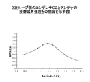
アンテナは1次ループ71と2次ループ72とからなり、1次ループ71は自己インダクタンスL1と抵抗R1を、また、2次ループ72は自己インダクタンスL2と抵抗R2を、それぞれ有する。Mは1次ループ71と2次ループ72の相互インダクタンスである。ここで、2次ループ72に直列に接続されているコンデンサC2とアンテナの放射磁界強度との関係を図18に示す。
【0007】
図18において、横軸のキャパシタンス比K2は、アンテナの共振周波数がキャリアの周波数と一致するときのコンデンサC2の値C0との比(K2=C2/C0)であり、縦軸の磁界強度比は、コンデンサC2=C0のときの磁界強度H0との比(=H/H0)である。
【0008】
図から明らかなように、比率K2が約1.2となるようにコンデンサC2を調整すると、アンテナの共振周波数をキャリアの周波数と一致させた場合(すなわち、K2=1の場合)に比べ、約1.4倍だけ磁界強度比を大きくすることができる。
【0009】
しかし、この方法では、無線信号を送受信することによって、被読取媒体上のデータを読み取るデータ読取装置において、回路係数などが必ずしも最適に調整されているとは限らないという問題がある。
【0010】
本発明の課題は、通信距離を延ばすことが可能なデータ読取装置、及びアンテナを提供することである。
【0011】
【特許文献1】
特開2001−185939「アンテナコイル及び電磁誘導型非接触データキャリアシステム」
【非特許文献1】
「回路の応答」コロナ社、電子通信学会編
【0012】
【課題を解決するための手段】
本発明は、上記課題を解決するため、下記のような構成を採用した。
すなわち、本発明の一態様によれば、本発明のアンテナは、無線信号を送受信することによって、被読取媒体上のデータを読み取るデータ読取装置に備えられたアンテナにおいて、信号処理回路から接続リードを介して電圧を供給されると共に、コンデンサ及びインダクタの少なくとも1つを含むリアクタンス回路が直列に接続された1次コイルと、該1次コイルと相互誘導により結合し、コンデンサが直列に接続された2次コイルとを備え、前記2次コイル側のコンデンサの両端に生じる電圧が最大となる、前記接続リードを含んだ前記信号処理回路のリアクタンスの値と、前記2次コイル側のコンデンサの値とを求め、前記2次コイル側のコンデンサを当該求めたコンデンサ値に設定し、当該求めた接続リードを含んだ前記信号処理回路のリアクタンスの値と、前記アンテナから見た接続リードを含んだ信号処理回路のリアクタンスの値との差のリアクタンスを、前記1次コイルに直列に接続することを特徴とするアンテナである。
【0013】
ここで、アンテナの2次コイル側のコンデンサの両端に生じる電圧が最大となるように、1次コイル側のリアクタンスと2次コイル側のコンデンサとを共に設定するので、従来例のように、前記2次コイル側のコンデンサの値に関係なく、1次コイル側に固定値として数千pF程度の値を有するコンデンサを直流カット用に設ける場合と比較して、通信距離を延ばすことが可能なアンテナを提供することができる。
【0014】
また、本発明の別態様によれば、本発明のデータ読取装置は、無線信号を送受信することによって、被読取媒体上のデータを読み取るデータ読取装置において、コンデンサ及びインダクタの少なくとも1つを含むリアクタンス回路が直列に接続された1次コイルと、該1次コイルと相互誘導により結合し、コンデンサが直列に接続された2次コイルとを有するアンテナと、前記1次コイルに接続リードを介して電圧を供給する信号処理回路とを備え、前記2次コイル側のコンデンサの両端に生じる電圧が最大となる、前記接続リードを含んだ前記信号処理回路のリアクタンスの値と、前記2次コイル側のコンデンサの値とを求め、前記2次コイル側のコンデンサを当該求めたコンデンサ値に設定し、当該求めた接続リードを含んだ前記信号処理回路のリアクタンスの値と、前記アンテナから見た接続リードを含んだ信号処理回路のリアクタンスの値との差のリアクタンスを、前記1次コイルに直列に接続することを特徴とするデータ読取装置である。
【0015】
ここで、アンテナの2次コイル側のコンデンサの両端に生じる電圧が最大となるように、1次コイル側のリアクタンスと2次コイル側のコンデンサとを共に設定するので、従来例のように、前記2次コイル側のコンデンサの値に関係なく、1次コイル側に固定値として数千pF程度の値を有するコンデンサを直流カット用に設ける場合と比較して、通信距離を延ばすことが可能なデータ読取装置を提供することができる。
【0016】
【発明の実施形態】
以下、本発明の実施の形態を図面を参照しながら説明する。
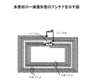
図1は、本発明の一実施形態のアンテナを示す図である。このアンテナは、無線信号を送受信することによって、被読取媒体上のデータを読み取るデータ読取装置に備えられたアンテナである。
【0017】
図1において、アンテナは、1次ループ(1次コイル)と2次ループ(2次コイル)とからなり、1次ループには、リアクタンス成分(図ではコンデンサCa)が直列に接続されている。また、2次ループには、共振コンデンサCbが直列に接続されている。なお、図1では、1次ループには、コンデンサCaを直列に接続しているが、コンデンサの替わりにインダクタを直列に接続したり、コンデンサとインダクタの組み合わせを接続したりしてもよい。
【0018】
以下では、1次ループに接続するリアクタンスの値(コンデンサ、またはインダクタ、あるいは、これらコンデンサとインダクタとの組み合わせ)をどのようにして求めるかにつき説明する。
【0019】
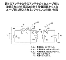
図2は、図1のアンテナとそのアンテナの1次ループ側に接続された送信回路(RF回路、または電源)とを示す等価回路である。なお、図2においては、1次ループ側に以下の手順により値を設定され挿入されることになる上記リアクタンス(例えば図1ではコンデンサCaに対応)は含まれていない。
【0020】
また、図2において、誘導性のリアクタンスを有するRF回路10は交流電圧V1が印加される電源11、電源抵抗12、電源インダクタンス13により構成される。Rgは電源抵抗12の抵抗値、Lgは電源インダクタンス13のインダクタンス値である。なお、RF回路10のリアクタンスが容量性の場合、電源インダクタンス13は(電源)キャパシタンスで置き換えられる。
【0021】
図2においてRF回路10は1次ループ(主要部)20に接続されている。1次ループ20は、図1の1次コイルに対応しており、抵抗21と自己インダクタンス22とを有する。R1は抵抗21の抵抗値、L1は自己インダクタンス22のインダクタンス値である。
【0022】
2次ループ(共振器)30は、図1の2次コイルに対応すると共に、1次ループ20と相互誘導により結合し、抵抗31と自己インダクタンス32と共振キャパシタンス(共振コンデンサ)33とを有する。R2は抵抗31の抵抗値、L2は自己インダクタンス32のインダクタンス値、Cは共振キャパシタンス33のキャパシタンス値である。また、V2は、共振コンデンサ33の両端に生じる電圧、Mは1次ループと2次ループとの相互インダクタンスである。
【0023】
カードの受信電圧はアンテナが作る磁束に比例し、その磁束はアンテナを流れる電流に比例する。アンテナを流れる電流には、1次ループを流れる電流I1と2次ループを流れる電流I2とがあり、それらの間には、I2>>I1の関係が成り立つので、与えられたアンテナ定数(R1,R2,L1,L2,M)の下で、通信距離をより長くするには、上記I2が最大となるように、等価回路における上記アンテナ定数以外の回路定数を調整することになる。なお、回路定数Rgをどこまでも小さく調整することはできない。その理由は、Rgを小さくすればI2の値を大きくすることができるが、回路が安定動作するためには、Rgは所定値以上でなければならず、この所定値がRgの下限値となるからである。一方、I2が最大のとき、V2も最大となるので、以下ではV2が最大となる場合について、2次ループ側のコンデンサの値に基づいて、1次ループ側のリアクタンスを設定する場合を考える。
【0024】
すなわち、まず、RF回路のリアクタンスが誘導性の場合には、V2を最大とするLgとCとの組を求め、そのようにして求めたLgとCとの組に対し、Lgとアンテナ側から見たRF回路のリアクタンスとの差をなくすように値を設定したリアクタンス(インダクタ、コンデンサ、またはそれらの組み合わせ)を1次ループに直列に接続する。
【0025】
次に、RF回路のリアクタンスが容量性の場合には、V2を最大とするCgとCとの組を求め、そのようにして求めたCgとCとの組に対し、Cgとアンテナ側から見たRF回路のリアクタンスとの差をなくすように値を設定したリアクタンス(インダクタ、コンデンサ、またはそれらの組み合わせ)を1次ループに直列に接続する。
【0026】
以下では、図2を参照しつつ、上記した1次ループ側のリアクタンスを設定するプロセスをより具体的に説明する。
図2の回路において、以下の式が成り立つ。
V1=(Rg+R1+jωLg+jωL1)×I1+jωMI2 ・・・(1)
V2=jωMI1+(jωL2+R2)×I2 ・・・(2)
=−I2/jωC ・・・(3)
ここで、(2)(3)式より、
I1=(C/M)(jωL2+(1/jωC)+R2)V2 ・・・(4)
(4)式を(1)式に代入すると、次式となる。
【0027】
V2/V1=1/α ・・・(5)
ただし、α=(C/M)(Rg+R1+jωLg+jωL1)(jωL2+
1/jωC+R2)+ω2CM ・・・(6)ここで、上記比V2/V1を最大、すなわち、αを最小とするCの値を下記(7)式より求める。
0=∂(|α|2)/∂C=2A・(dA/dC)+2B・(dB/dC)・・・(7)
ただし、Aはαの実数部、Bはαの虚数部で、|α|2=A2+B2
(6)式を(7)式に代入して計算することにより、下記(8)式が得られ、この式により与えられたLgに対し上記比V2/V1を最大とするCの値が求められる。
【0028】
【0029】
送信回路(RF回路)のリアクタンスが容量性の場合は、そのキャパシタンスをCgとすると、(1)式において、Lgを(−1/ω2Cg)で置き換えた次式により計算を行い、下記(9)式により与えられたCgに対し上記比V2/V1を最大とするCの値を求める。
【0030】
【0031】
ここで、例えばV2を最大にするLgとCの組を決めるには、(8)式を(5)(6)式に代入して比V2/V1をCを用いずにLgで表した式を求め、その式をLgで偏微分して、微係数=0となるLgの値を求める。そして、このようにして求めたLgに対応するCを(8)式により算出する。
【0032】
その後は、そのようにして求めたLgとCとの組に対し、Lgとアンテナ側から見たリアクタンスとの差をなくすように値を設定したリアクタンス(インダクタ、コンデンサ、またはそれらの組み合わせ)を1次ループに直列に接続する。
【0033】
なお、V2を最大にするCgとCの組についても同様の方法で決めることができるので、説明を省略する。
以下では、アンテナとそのアンテナの1次ループ側に接続されたRF回路とに具体的な数値を設定し、上記した1次ループに接続するリアクタンスの値を回路計算ツールにより求めた。
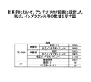
【0034】
図3は、この計算において使用したアンテナの形状を示す図であり、図4はアンテナやRF回路に設定した抵抗、インダクタンス等の値を示す図である。
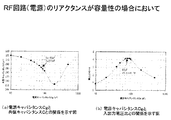
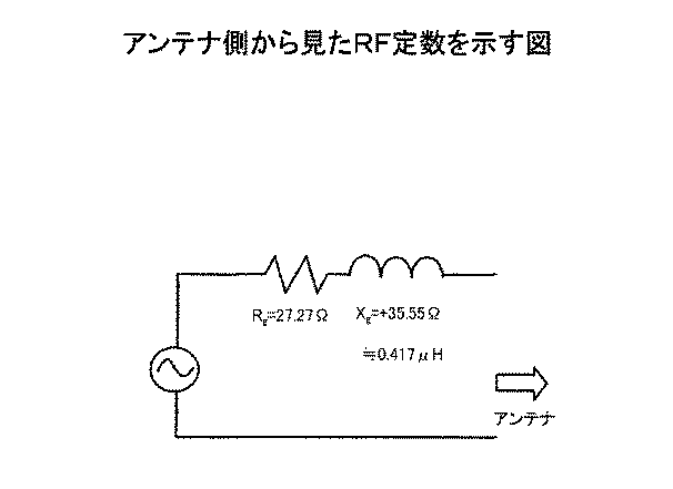
まず、アンテナからRF回路側を見たRFインピーダンス+アンテナの接続リードのインピーダンスとを求める。図5(a)は回路計算ツールによる計算回路である。RF回路の実測した抵抗及びリアクタンスの値は図4よりそれぞれ26Ω、0.282μH(j24Ωに相当)であり、アンテナ接続位置に電圧源を接続して、ノード▲7▼の電圧とノード▲1▼−▲4▼を流れる電流の比からインピーダンスの周波数特性を計算する。図5(b)はその周波数特性の計算結果を示す図である。図5(b)に示すグラフは、RF回路の交流電源の周波数を横軸にとり、インピーダンスの実数部(抵抗分)とインピーダンスの虚数部(リアクタンス分)とを縦軸にとっている。そして、その実数部と虚数部とに対応して2本の直線がグラフ上に描かれている。この計算例では、交流電源の周波数の値を13.56MHzに設定しているので、この13.56MHzのところでの抵抗分と、リアクタンス分とを読み取ることにより、図6に示すように、アンテナ側から見たRF側定数が求められる。
【0035】
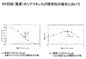
続いて、(8)式によりLgとCとの関係を求めて図示すると、図7(a)に示すグラフが得られる。また、このLgとCの組み合わせを(5)(6)式に代入してLgとV2/V1の関係を求めて図示すると、図7(b)に示すグラフが得られ、Lg=1.2μH(C=354pF)に対し電圧比V2/V1が最大となることがわかる。
【0036】
同様に、(9)式によりCgとCとの関係を求めて図示すると、図8(a)に示すグラフが得られる。また、このCgとCの組み合わせを(5)(6)式に代入してCgとV2/V1の関係を求めて図示すると、図8(b)に示すグラフが得られ、Cg=80pF(C=293pF)に対し電圧比V2/V1が最大となることがわかる。
【0037】
そして、図7(b)と図8(b)との電圧比V2/V1のピーク値を比較すればわかるように、この計算例では、RF回路のリアクタンスが容量性であった方が、RF回路のリアクタンスが誘導性である場合より、発生磁束を高くすることができる。
【0038】
この発生磁束がより高くなる場合、すなわち、RF回路のリアクタンスCg=80pF、共振器のキャパシタンスC=293pFの場合につき以下で、1次ループ側のリアクタンスの設定方法を説明する。
【0039】
図6に示すように、接続リードを含めたアンテナから見たRF回路のリアクタンスはXg=+35.55であるので、RF回路のリアクタンスCgとアンテナから見たRF回路のリアクタンスXgとの差により1次ループに直列に接続するキャパシタンスCcを次式により求めることができる。
【0040】
Xg−1/ωCc=1/ωCg
上式より、Cc=1/[(1/ωCg+Xg)ω]=1/[(1/2π×13.56×106×80×10−12)+35.55]×(2π×13.56×106)≒64pF
以上の計算から、磁束を最大とするには、図9に示すように、主要部のキャパシタンスの値として64pF,共振器のキャパシタンスの値として293pFを設定すればよい。
【0041】
図10は、1次コイル側のリアクタンスがコンデンサである場合に、その1次コイル側に直列に接続したコンデンサの容量Caと磁界強度比(上記電圧比V1/V2に比例)との関係を示す図である。
【0042】
図10において、各曲線は、所定のK2の値に対応している。ここで、K2=Cb/C0(Cbは2次コイルの共振コンデンサの容量、C0はアンテナの共振周波数がキャリア周波数と一致するときのCbの値)である。グラフの尺度が異なるので一概にはいえないが、各K2に対応する曲線のピークを結べば図7や図8に対応する図が得られる。
【0043】
図11は、1次ループと2次ループとのキャパシタンス比Ca/Cbと磁界強度との関係を示す図であり、特に、回路係数としてのコンデンサの容量が取る範囲が従来例と本実施形態とでは異なることを説明する図である。なお、グラフ上の点に対応するCaとCbの値は、図10の各K2において磁界が最大となるCaとCbである。従来の場合、1次ループ側に設けられるコンデンサの容量Caは、直流カット用のため、一般に数千pF以上である(ここでは1000pFとした)。これに対し、本実施形態では、上記計算例からも明らかなように、Caの代表的な値は数十pFである。これにより、本実施形態と従来例とでは、1次ループ側に設けられるコンデンサの容量Caに1桁以上の開きが生じることがわかる。
【0044】
図12は、本実施形態における回路係数としてのコンデンサの容量が取る範囲を示す図である。
図13は、磁界強度比と上記K2との関係を示す図であり、磁界強度比のピーク値を本実施形態と従来例とで比較している。本実施形態では、従来例と比較し、2次ループ側のキャパシタンスに応じて、1次ループ側のキャパシタンスを設定する構成としていることから、磁界強度比として従来の約1.4倍の値が得られる。
【0045】
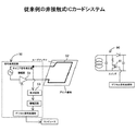
なお、図1では、Ca(もしくは対応するリアクタンス成分)、Cbをアンテナ面と同じ平面に接続しているが、図14に示すように、アンテナと、RF回路が含まれる信号処理回路基板をケーブル等で接続し、この基板上にCa、またはCbの少なくとも1つを設置するようにしてもよい(図では、CaとCbの双方を設置している)。アンテナを機器、例えば自動販売機等に取り付ける場合、アンテナ周囲には、金属や取り付けパネル等の構成品がある。そして、それら構成品によってコンデンサの調整スペースがなくなったり、それら構成品の影響でアンテナ特性が変化したりするという問題がある。そこで、上記したCa、Cbを信号処理回路基板上に設置することにより、コンデンサCa、Cbの回路係数に対する上記構成品による悪影響を防ぐことができる。
【0046】
【発明の効果】
以上、説明したように、本発明によれば、本発明のデータ読取装置に備えられたアンテナでは、2次コイル側のコンデンサの両端に生じる電圧が最大となるように、1次コイル側のリアクタンスと2次コイル側のコンデンサとを共に設定するので、通信距離を延ばすことが可能である。
【図面の簡単な説明】
【図1】本発明の一実施形態のアンテナを示す図である。
【図2】図1のアンテナとそのアンテナの1次ループ側に接続されたRF回路とを示す等価回路から1次ループ側に挿入されるリアクタンスを除いた図である。
【図3】計算例において使用したアンテナの形状を示す図である。
【図4】計算例において、アンテナやRF回路に設定した抵抗、インダクタンス等の数値を示す図である。
【図5】アンテナから見たRF回路側の定数の計算プロセスを説明する図であり、(a)は回路計算ツールによる計算回路を、(b)はその周波数特性の計算結果を、それぞれ示す図である。
【図6】アンテナ側から見たRF定数を示す図である。
【図7】RF回路(電源)のリアクタンスが誘導性の場合において、(a)は電源インダクタンスLgと共振キャパシタンスCとの関係を示す図であり、(b)は電源インダクタンスLgと入出力電圧比との関係を示す図である。
【図8】RF回路(電源)のリアクタンスが容量性の場合において、(a)は電源キャパシタンスCgと共振キャパシタンスCとの関係を示す図であり、(b)は電源キャパシタンスCgと入出力電圧比との関係を示す図である。
【図9】計算例の計算結果を示す図である。
【図10】1次コイル側のコンデンサの容量Caと磁界強度比との関係を示す図である。
【図11】1次ループと2次ループとのキャパシタンス比Ca/Cbと磁界強度との関係を示す図であり、特に、回路係数としてのコンデンサの容量が取る範囲が従来例と本実施形態とでは異なることを説明する図である。
【図12】本実施形態における回路係数としてのコンデンサの容量が取る範囲を示す図である。
【図13】磁界強度比と上記K2との関係を示す図であり、磁界強度比のピーク値を本実施形態と従来例とで比較している図である。
【図14】本実施形態のアンテナとそのアンテナの1次ループ側に接続されたRF回路とを含む情報読取装置の構成例である。
【図15】従来例の非接触式ICカードシステムである。
【図16】従来例のアンテナを示す図である。
【図17】従来例のアンテナとそのアンテナの1次ループ側に接続されたRF回路とを示す等価回路である。
【図18】2次ループ側のコンデンサC2とアンテナの放射磁界強度との関係を示す図である。
【符号の説明】
10 RF回路
11 電源
12 抵抗
13 インダクタンス
20 1次ループ
21 抵抗
22 インダクタンス
30 2次ループ
31 抵抗
32 インダクタンス
33 共振キャパシタンス
50 信号処理回路
51 増幅器
52 ループアンテナ
53 検波回路
60 カード
61 スイッチ
70 信号処理回路
71 1次ループ
72 2次ループ[0001]
BACKGROUND OF THE INVENTION
The present invention relates to a data reading device that reads data on a read medium such as a non-contact card by transmitting and receiving wireless signals.
[0002]
[Prior art]
Conventionally, there is a non-contact type IC card capable of non-contact communication using a radio signal. The operation when the information reading device reads information from the IC card will be described with reference to FIG. A predetermined carrier signal is generated by the carrier signal generator in the
[0003]
[Problems to be solved by the invention]
In the non-contact ID card system as shown in FIG. 15, it is desired to extend the communication distance between the information reading device and the card. One way to extend the communication distance is to increase the magnetic field intensity generated by the loop antenna. However, this method requires, for example, increasing the amplification factor of the amplifier, which increases the size and cost of the device. There is a problem of being connected.
[0004]
Therefore, as another method of extending the communication distance, a method as shown in
[0005]
As shown in FIG. 17, when the signal processing circuit (RF circuit) 70 is viewed from the antenna, the
[0006]
The antenna consists of the
[0007]
In FIG. 18, the capacitance ratio K 2 on the horizontal axis is the ratio (K 2 = C 2 / C 0 ) with the value C 0 of the capacitor C 2 when the resonant frequency of the antenna matches the carrier frequency. The magnetic field strength ratio of the shaft is a ratio (= H / H 0 ) with the magnetic field strength H 0 when the capacitor C 2 = C 0 .
[0008]
As is apparent from the figure, when the capacitor C 2 is adjusted so that the ratio K 2 is about 1.2, the antenna resonance frequency matches the carrier frequency (that is, when K 2 = 1). In comparison, the magnetic field strength ratio can be increased by about 1.4 times.
[0009]
However, this method has a problem that the circuit coefficient or the like is not always optimally adjusted in a data reader that reads data on a read medium by transmitting and receiving wireless signals.
[0010]
An object of the present invention is to provide a data reader and an antenna capable of extending a communication distance.
[0011]
[Patent Document 1]
Japanese Patent Laid-Open No. 2001-185939 “Antenna Coil and Electromagnetic Induction Type Non-Contact Data Carrier System”
[Non-Patent Document 1]
“Circuit Response” Corona, Electronic Communication Society [0012]
[Means for Solving the Problems]
The present invention employs the following configuration in order to solve the above problems.
That is, according to one aspect of the present invention, the antenna of the present invention includes a connection lead from a signal processing circuit in an antenna provided in a data reader that reads data on a read medium by transmitting and receiving a radio signal. It is supplied a voltage via reactance circuit including at least one of capacitors and inductors and the primary coil connected in series, and coupled by mutual induction with said primary coil, a capacitor connected in series 2 A reactance value of the signal processing circuit including the connection lead, and a value of the capacitor on the secondary coil side, in which a voltage generated at both ends of the capacitor on the secondary coil side is maximized. The signal processing circuit including the obtained connection lead, wherein the obtained capacitor value is set to the obtained capacitor value. The value of the reactance, the reactance of the difference between the value of the reactance of the signal processing circuit including a connection lead as seen from the antenna, an antenna, characterized in that connected in series with the primary coil.
[0013]
Here, both the reactance on the primary coil side and the capacitor on the secondary coil side are set so that the voltage generated at both ends of the capacitor on the secondary coil side of the antenna is maximized. An antenna that can extend the communication distance compared to the case where a capacitor having a fixed value of about several thousand pF is provided for the DC cut regardless of the value of the capacitor on the secondary coil side. Can be provided.
[0014]
According to another aspect of the present invention, the data reading device of the present invention is a data reading device that reads data on a read medium by transmitting and receiving a radio signal, and includes a reactance including at least one of a capacitor and an inductor. An antenna having a primary coil having a circuit connected in series, a secondary coil coupled to the primary coil by mutual induction, and a capacitor connected in series, and a voltage connected to the primary coil via a connection lead A signal processing circuit for supplying the signal, and a reactance value of the signal processing circuit including the connection lead that maximizes a voltage generated at both ends of the capacitor on the secondary coil side, and a capacitor on the secondary coil side And the capacitor on the secondary coil side is set to the obtained capacitor value, and the signal processing including the obtained connection lead is performed. Is data reading device, characterized in that connected to the value of the reactance circuit, the reactance of the difference between the value of the reactance of the signal processing circuit including a connection lead as seen from the antenna, in series with the primary coil .
[0015]
Here, both the reactance on the primary coil side and the capacitor on the secondary coil side are set so that the voltage generated at both ends of the capacitor on the secondary coil side of the antenna is maximized. Data that can extend the communication distance compared to the case where a capacitor having a fixed value of about several thousand pF is provided for the DC cut regardless of the value of the capacitor on the secondary coil side. A reader can be provided.
[0016]
DETAILED DESCRIPTION OF THE INVENTION
Embodiments of the present invention will be described below with reference to the drawings.
FIG. 1 is a diagram illustrating an antenna according to an embodiment of the present invention. This antenna is an antenna provided in a data reading device that reads data on a read medium by transmitting and receiving radio signals.
[0017]
In FIG. 1, the antenna includes a primary loop (primary coil) and a secondary loop (secondary coil), and a reactance component (capacitor C a in the figure) is connected in series to the primary loop. . Further, in the secondary loop, the resonance capacitor C b is connected in series. In FIG 1, the primary loop, but by connecting a capacitor C a in series, or to connect an inductor in series instead of the capacitor may or connect a combination of capacitors and inductors.
[0018]
In the following, how to find the value of reactance (capacitor or inductor, or a combination of these capacitors and inductor) connected to the primary loop will be described.
[0019]
FIG. 2 is an equivalent circuit showing the antenna of FIG. 1 and a transmission circuit (RF circuit or power supply) connected to the primary loop side of the antenna. In FIG. 2, the reactance (for example, corresponding to the capacitor C a in FIG. 1) whose value is set and inserted by the following procedure on the primary loop side is not included.
[0020]
In FIG. 2, the
[0021]
In FIG. 2, the
[0022]
The secondary loop (resonator) 30 corresponds to the secondary coil of FIG. 1, is coupled to the
[0023]
The received voltage of the card is proportional to the magnetic flux generated by the antenna, and the magnetic flux is proportional to the current flowing through the antenna. The current flowing through the antenna includes a current I 1 flowing through the primary loop and a current I 2 flowing through the secondary loop, and a relationship of I 2 >> I 1 is established between them. In order to increase the communication distance under the constants (R 1 , R 2 , L 1 , L 2 , M), circuit constants other than the antenna constants in the equivalent circuit are set so that the I 2 is maximized. Will be adjusted. The circuit constant Rg cannot be adjusted as small as possible. The reason is that if R g is reduced, the value of I 2 can be increased. However, in order for the circuit to operate stably, R g must be equal to or greater than a predetermined value, and this predetermined value is equal to R g . This is because the lower limit is reached. On the other hand, when I 2 is the maximum, V 2 is also the maximum, and in the following, when V 2 is the maximum, the reactance on the primary loop side is set based on the value of the capacitor on the secondary loop side think of.
[0024]
That is, first, when the reactance of the RF circuit is inductive, a set of L g and C that maximizes V 2 is obtained, and for the set of L g and C thus obtained, L g And a reactance (inductor, capacitor, or combination thereof) whose values are set so as to eliminate the difference between the RF circuit and the reactance of the RF circuit viewed from the antenna side are connected in series to the primary loop.
[0025]
Next, when the reactance of the RF circuit is capacitive, a pair of C g and C that maximizes V 2 is obtained, and for the pair of C g and C thus obtained, C g and A reactance (inductor, capacitor, or a combination thereof) whose value is set so as to eliminate the difference from the reactance of the RF circuit viewed from the antenna side is connected in series to the primary loop.
[0026]
Hereinafter, the process of setting the reactance on the primary loop side will be described more specifically with reference to FIG.
In the circuit of FIG.
V 1 = (R g + R 1 + jωL g + jωL 1 ) × I 1 + jωMI 2 (1)
V 2 = jωMI 1 + (jωL 2 + R 2 ) × I 2 (2)
= −I 2 / jωC (3)
Here, from the equations (2) and (3),
I 1 = (C / M) (jωL 2 + (1 / jωC) + R 2 ) V 2 (4)
Substituting equation (4) into equation (1) yields:
[0027]
V 2 / V 1 = 1 / α (5)
However, α = (C / M) (R g + R 1 + jωL g + jωL 1 ) (jωL 2 +
1 / jωC + R 2 ) + ω 2 CM (6) Here, the value of C that maximizes the ratio V 2 / V 1 , that is, minimizes α is obtained from the following equation (7).
0 = ∂ (| α | 2 ) / ∂C = 2A · (dA / dC) + 2B · (dB / dC) (7)
Where A is the real part of α, B is the imaginary part of α, and | α | 2 = A 2 + B 2
By substituting the equation (6) into the equation (7) and calculating, the following equation (8) is obtained, and for the L g given by this equation, the maximum ratio V 2 / V 1 is obtained. A value is determined.
[0028]
[0029]
When the reactance of the transmission circuit (RF circuit) is capacitive, and the capacitance is C g , the calculation is performed according to the following equation in which L g is replaced by (−1 / ω 2 C g ) in equation (1). Then, the value of C that maximizes the ratio V 2 / V 1 with respect to C g given by the following equation (9) is obtained.
[0030]
[0031]
Here, for example, in order to determine a pair of L g and C that maximizes V 2 , the ratio V 2 / V 1 is set to L without using C by substituting the expression (8) into the expressions (5) and (6). obtains a formula expressed in g, the expression and partial differentiation in L g, finding the value of L g which is a derivative = 0. Then, C corresponding to L g obtained in this way is calculated by equation (8).
[0032]
Then, with respect to the set of L g and C obtained in this way, L g and reactance setting a value to eliminate the difference between the reactance seen from the antenna side (inductor, capacitor or a combination thereof) Are connected in series to the primary loop.
[0033]
Since the V 2 can be determined in a similar manner for the set of C g and C to maximize omitted.
In the following, specific numerical values are set for the antenna and the RF circuit connected to the primary loop side of the antenna, and the reactance value connected to the primary loop is obtained by a circuit calculation tool.
[0034]
FIG. 3 is a diagram showing the shape of the antenna used in this calculation, and FIG. 4 is a diagram showing values such as resistance and inductance set in the antenna and the RF circuit.
First, the RF impedance when viewing the RF circuit side from the antenna + the impedance of the connection lead of the antenna is obtained. FIG. 5A shows a calculation circuit using a circuit calculation tool. The actually measured resistance and reactance values of the RF circuit are 26Ω and 0.282 μH (corresponding to j24Ω), respectively, as shown in FIG. 4. A voltage source is connected to the antenna connection position, and the voltage of node (7) and node (1) -Calculate the frequency characteristics of impedance from the ratio of the current flowing through (4). FIG. 5B shows the calculation result of the frequency characteristics. In the graph shown in FIG. 5B, the horizontal axis represents the frequency of the AC power supply of the RF circuit, and the vertical axis represents the real part (resistance) of the impedance and the imaginary part (reactance) of the impedance. Two straight lines are drawn on the graph corresponding to the real part and the imaginary part. In this calculation example, since the frequency value of the AC power supply is set to 13.56 MHz, by reading the resistance component and reactance component at 13.56 MHz, as shown in FIG. The RF side constant viewed from the above is obtained.
[0035]
Subsequently, when the relationship between Lg and C is obtained by the equation (8) and illustrated, the graph shown in FIG. 7A is obtained. Further, when the combination of L g and C is substituted into the equations (5) and (6) to obtain the relationship between L g and V 2 / V 1 , the graph shown in FIG. It can be seen that the voltage ratio V 2 / V 1 is maximized for g = 1.2 μH (C = 354 pF).
[0036]
Similarly, when the relationship between Cg and C is obtained by the equation (9) and illustrated, the graph shown in FIG. 8A is obtained. Further, when the combination of Cg and C is substituted into the equations (5) and (6) to obtain the relationship between Cg and V 2 / V 1 , the graph shown in FIG. It can be seen that the voltage ratio V 2 / V 1 is maximum for g = 80 pF (C = 293 pF).
[0037]
As can be seen by comparing the peak values of the voltage ratio V 2 / V 1 between FIG. 7B and FIG. 8B, in this calculation example, the reactance of the RF circuit should be capacitive. The generated magnetic flux can be made higher than when the reactance of the RF circuit is inductive.
[0038]
If the magnetic flux generated is higher, i.e., the reactance C g = 80 pF of RF circuits, the following per case capacitance C = 293pF resonator, illustrating a method of setting the primary loop side reactance.
[0039]
As shown in FIG. 6, the reactance of the RF circuit as viewed from including connection leads antenna is a X g = + 35.55, and the reactance X g for RF circuits as viewed from the reactance C g and the antenna of the RF circuit the capacitance C c connected in series to the primary loop by the difference can be obtained by the following equation.
[0040]
X g −1 / ωC c = 1 / ωC g
From the above equation, C c = 1 / [(1 / ωC g + X g ) ω] = 1 / [(1 / 2π × 13.56 × 10 6 × 80 × 10 −12 ) +35.55] × (2π × 13.56 × 10 6 ) ≈64 pF
From the above calculation, in order to maximize the magnetic flux, as shown in FIG. 9, 64 pF may be set as the capacitance value of the main part and 293 pF as the capacitance value of the resonator.
[0041]
FIG. 10 shows the relationship between the capacitance C a of the capacitor connected in series to the primary coil side and the magnetic field strength ratio (proportional to the voltage ratio V 1 / V 2 ) when the reactance on the primary coil side is a capacitor. It is a figure which shows a relationship.
[0042]
10, each curve corresponds to the value of the predetermined K 2. Here, K 2 = C b / C 0 (C b is the capacitance of the resonant capacitor of the secondary coil, and C 0 is the value of C b when the resonant frequency of the antenna matches the carrier frequency). Because scale of the graph is different it can not be said sweepingly, corresponding to FIG. 7 and 8 if Musube the peak of the curve corresponding to the K 2 is obtained.
[0043]
FIG. 11 is a diagram showing the relationship between the capacitance ratio C a / C b between the primary loop and the secondary loop and the magnetic field strength. In particular, the range that the capacitance of the capacitor as a circuit coefficient takes is the conventional example and the present embodiment. It is a figure explaining a difference with a form. The value of C a and C b corresponding to a point on the graph is the C a and C b the magnetic field is maximized at each K 2 in FIG. 10. In the conventional case, the capacitance C a of the capacitor provided on the primary loop side is generally several thousand pF or more (here, 1000 pF) for direct current cut. On the other hand, in this embodiment, as is clear from the above calculation example, a typical value of C a is several tens of pF. As a result, it can be seen that in this embodiment and the conventional example, the capacitance C a of the capacitor provided on the primary loop side is opened by one digit or more.
[0044]
FIG. 12 is a diagram illustrating a range taken by the capacitor as a circuit coefficient in the present embodiment.
13 is a diagram showing the relationship between the magnetic field intensity ratio and the K 2, it compares the peak value of the magnetic field intensity ratio in the present embodiment and the conventional example. In the present embodiment, the primary loop side capacitance is set according to the secondary loop side capacitance as compared with the conventional example, so that the magnetic field intensity ratio is about 1.4 times the conventional value. can get.
[0045]
In FIG. 1, C a (or the corresponding reactance component) and C b are connected to the same plane as the antenna surface. However, as shown in FIG. 14, the signal processing circuit board including the antenna and the RF circuit is provided. May be connected by a cable or the like, and at least one of C a or C b may be installed on this substrate (in the figure, both C a and C b are installed). When the antenna is attached to a device such as a vending machine, there are components such as metal and a mounting panel around the antenna. In addition, there is a problem in that the capacitor adjustment space is eliminated by these components, and the antenna characteristics change due to the influence of these components. Therefore, by installing the above-described C a and C b on the signal processing circuit board, it is possible to prevent an adverse effect caused by the above-described components on the circuit coefficients of the capacitors C a and C b .
[0046]
【The invention's effect】
As described above, according to the present invention, in the antenna provided in the data reading device of the present invention, the reactance on the primary coil side is maximized so that the voltage generated at both ends of the capacitor on the secondary coil side is maximized. And the capacitor on the secondary coil side are both set, so that the communication distance can be extended.
[Brief description of the drawings]
FIG. 1 is a diagram showing an antenna according to an embodiment of the present invention.
FIG. 2 is a diagram in which reactance inserted on the primary loop side is removed from an equivalent circuit showing the antenna of FIG. 1 and the RF circuit connected to the primary loop side of the antenna.
FIG. 3 is a diagram showing the shape of an antenna used in a calculation example.
FIG. 4 is a diagram illustrating numerical values such as resistance and inductance set in an antenna and an RF circuit in a calculation example.
5A and 5B are diagrams for explaining a calculation process of constants on the RF circuit side as viewed from the antenna, where FIG. 5A shows a calculation circuit by a circuit calculation tool, and FIG. 5B shows a calculation result of its frequency characteristics. It is.
FIG. 6 is a diagram illustrating an RF constant viewed from the antenna side.
7A is a diagram showing a relationship between a power supply inductance Lg and a resonance capacitance C when the reactance of the RF circuit (power supply) is inductive, and FIG. 7B is a diagram showing a relationship between the power supply inductance Lg and the input / output. It is a figure which shows the relationship with a voltage ratio.
8A is a diagram showing a relationship between a power source capacitance Cg and a resonance capacitance C when the reactance of the RF circuit (power source) is capacitive, and FIG. 8B is a diagram showing a relationship between the power source capacitance Cg and input / output. It is a figure which shows the relationship with a voltage ratio.
FIG. 9 is a diagram illustrating a calculation result of a calculation example.
FIG. 10 is a diagram showing the relationship between the capacitance C a of the capacitor on the primary coil side and the magnetic field strength ratio.
FIG. 11 is a diagram showing the relationship between the capacitance ratio C a / C b between the primary loop and the secondary loop and the magnetic field strength, and in particular, the range that the capacitance of the capacitor as a circuit coefficient takes is the conventional example and the present embodiment. It is a figure explaining a difference with a form.
FIG. 12 is a diagram showing a range taken by a capacitor as a circuit coefficient in the present embodiment.
FIG. 13 is a diagram showing the relationship between the magnetic field strength ratio and the K 2, and is a diagram comparing the peak value of the magnetic field strength ratio between the present embodiment and the conventional example.
FIG. 14 is a configuration example of an information reading apparatus including an antenna of the present embodiment and an RF circuit connected to the primary loop side of the antenna.
FIG. 15 shows a conventional non-contact IC card system.
FIG. 16 is a diagram showing a conventional antenna.
FIG. 17 is an equivalent circuit showing a conventional antenna and an RF circuit connected to the primary loop side of the antenna.
FIG. 18 is a diagram illustrating a relationship between a capacitor C 2 on the secondary loop side and a radiation magnetic field strength of the antenna.
[Explanation of symbols]
DESCRIPTION OF
Claims (3)
信号処理回路から接続リードを介して電圧を供給されると共に、コンデンサ及びインダクタの少なくとも1つを含むリアクタンス回路が直列に接続された1次コイルと、
該1次コイルと相互誘導により結合し、コンデンサが直列に接続された2次コイルとを備え、
前記2次コイル側のコンデンサの両端に生じる電圧が最大となる、前記接続リードを含んだ前記信号処理回路のリアクタンスの値と、前記2次コイル側のコンデンサの値とを求め、
前記2次コイル側のコンデンサを当該求めたコンデンサ値に設定し、
当該求めた接続リードを含んだ前記信号処理回路のリアクタンスの値と、前記アンテナから見た接続リードを含んだ信号処理回路のリアクタンスの値との差のリアクタンスを、前記1次コイルに直列に接続する
ことを特徴とするアンテナ。In an antenna provided in a data reader that reads data on a read medium by transmitting and receiving wireless signals,
A primary coil to which a voltage is supplied from a signal processing circuit via a connection lead and a reactance circuit including at least one of a capacitor and an inductor is connected in series ;
A secondary coil coupled to the primary coil by mutual induction and having a capacitor connected in series ;
Finding the value of reactance of the signal processing circuit including the connection lead and the value of the capacitor on the secondary coil side, in which the voltage generated across the capacitor on the secondary coil side is maximum,
Set the secondary coil side capacitor to the obtained capacitor value,
The reactance of the difference between the calculated reactance value of the signal processing circuit including the connection lead and the reactance value of the signal processing circuit including the connection lead viewed from the antenna is connected in series to the primary coil. An antenna characterized by.
コンデンサ及びインダクタの少なくとも1つを含むリアクタンス回路が直列に接続された1次コイルと、該1次コイルと相互誘導により結合し、コンデンサが直列に接続された2次コイルとを有するアンテナと、
前記1次コイルに接続リードを介して電圧を供給する信号処理回路とを備え、
前記2次コイル側のコンデンサの両端に生じる電圧が最大となる、前記接続リードを含んだ前記信号処理回路のリアクタンスの値と、前記2次コイル側のコンデンサの値とを求め、
前記2次コイル側のコンデンサを当該求めたコンデンサ値に設定し、
当該求めた接続リードを含んだ前記信号処理回路のリアクタンスの値と、前記アンテナから見た接続リードを含んだ信号処理回路のリアクタンスの値との差のリアクタンスを、前記1次コイルに直列に接続する
ことを特徴とするデータ読取装置。In a data reader that reads data on a read medium by transmitting and receiving wireless signals,
An antenna having a primary coil in which a reactance circuit including at least one of a capacitor and an inductor is connected in series , and a secondary coil coupled to the primary coil by mutual induction and having a capacitor connected in series ;
A signal processing circuit for supplying a voltage to the primary coil via a connection lead ;
Finding the value of reactance of the signal processing circuit including the connection lead and the value of the capacitor on the secondary coil side, in which the voltage generated across the capacitor on the secondary coil side is maximum,
Set the secondary coil side capacitor to the obtained capacitor value,
The reactance of the difference between the calculated reactance value of the signal processing circuit including the connection lead and the reactance value of the signal processing circuit including the connection lead viewed from the antenna is connected in series to the primary coil. A data reading device.
信号処理回路から接続リードを介して電圧を供給されると共に、コンデンサ及びインダクタの少なくとも1つを含むリアクタンス回路が直列に接続された1次コイルと、該1次コイルと相互誘導により結合し、コンデンサが直列に接続された2次コイルとを備える前記アンテナに対し、
前記2次コイル側のコンデンサの両端に生じる電圧が最大となる、前記接続リードを含んだ前記信号処理回路のリアクタンスの値と、前記2次コイル側のコンデンサの値とを求め、
前記2次コイル側のコンデンサを当該求めたコンデンサ値に設定し、
当該求めた接続リードを含んだ前記信号処理回路のリアクタンスの値と、前記アンテナから見た接続リードを含んだ信号処理回路のリアクタンスの値との差のリアクタンスを、前記1次コイルに直列に接続するリアクタンスとして設定する
ことを特徴とするアンテナの定数設定方法。In the antenna constant setting method provided in the data reader for reading data on the read medium by transmitting and receiving a radio signal,
A voltage is supplied from a signal processing circuit via a connection lead, and a reactance circuit including at least one of a capacitor and an inductor is connected in series , and the primary coil is coupled to the primary coil by mutual induction. For the antenna comprising a secondary coil connected in series ,
Finding the value of reactance of the signal processing circuit including the connection lead and the value of the capacitor on the secondary coil side, in which the voltage generated across the capacitor on the secondary coil side is maximum,
Set the secondary coil side capacitor to the obtained capacitor value,
The reactance of the difference between the calculated reactance value of the signal processing circuit including the connection lead and the reactance value of the signal processing circuit including the connection lead viewed from the antenna is connected in series to the primary coil. An antenna constant setting method, characterized in that the reactance is set as reactance .
Priority Applications (1)
| Application Number | Priority Date | Filing Date | Title |
|---|---|---|---|
| JP2003071020A JP4010263B2 (en) | 2003-03-14 | 2003-03-14 | Antenna and data reader |
Applications Claiming Priority (1)
| Application Number | Priority Date | Filing Date | Title |
|---|---|---|---|
| JP2003071020A JP4010263B2 (en) | 2003-03-14 | 2003-03-14 | Antenna and data reader |
Publications (2)
| Publication Number | Publication Date |
|---|---|
| JP2004282403A JP2004282403A (en) | 2004-10-07 |
| JP4010263B2 true JP4010263B2 (en) | 2007-11-21 |
Family
ID=33287559
Family Applications (1)
| Application Number | Title | Priority Date | Filing Date |
|---|---|---|---|
| JP2003071020A Expired - Fee Related JP4010263B2 (en) | 2003-03-14 | 2003-03-14 | Antenna and data reader |
Country Status (1)
| Country | Link |
|---|---|
| JP (1) | JP4010263B2 (en) |
Families Citing this family (73)
| Publication number | Priority date | Publication date | Assignee | Title |
|---|---|---|---|---|
| KR100693204B1 (en) * | 2005-09-22 | 2007-03-13 | 쓰리에이로직스(주) | Antenna for near field communication, near field communication terminal having the same, radio frequency antenna, and ic card having the same |
| US7519328B2 (en) | 2006-01-19 | 2009-04-14 | Murata Manufacturing Co., Ltd. | Wireless IC device and component for wireless IC device |
| WO2007119310A1 (en) * | 2006-04-14 | 2007-10-25 | Murata Manufacturing Co., Ltd. | Antenna |
| US9064198B2 (en) | 2006-04-26 | 2015-06-23 | Murata Manufacturing Co., Ltd. | Electromagnetic-coupling-module-attached article |
| CN101467209B (en) | 2006-06-30 | 2012-03-21 | 株式会社村田制作所 | Optical disc |
| WO2008050535A1 (en) | 2006-09-26 | 2008-05-02 | Murata Manufacturing Co., Ltd. | Electromagnetically coupled module and article with electromagnetically coupled module |
| US8235299B2 (en) | 2007-07-04 | 2012-08-07 | Murata Manufacturing Co., Ltd. | Wireless IC device and component for wireless IC device |
| JP4930586B2 (en) | 2007-04-26 | 2012-05-16 | 株式会社村田製作所 | Wireless IC device |
| EP2148449B1 (en) | 2007-05-11 | 2012-12-12 | Murata Manufacturing Co., Ltd. | Wireless ic device |
| JP4466795B2 (en) | 2007-07-09 | 2010-05-26 | 株式会社村田製作所 | Wireless IC device |
| EP2166490B1 (en) | 2007-07-17 | 2015-04-01 | Murata Manufacturing Co. Ltd. | Wireless ic device and electronic apparatus |
| CN102915462B (en) | 2007-07-18 | 2017-03-01 | 株式会社村田制作所 | Wireless IC device |
| JP4561931B2 (en) | 2007-12-26 | 2010-10-13 | 株式会社村田製作所 | Antenna device and wireless IC device |
| EP2251934B1 (en) | 2008-03-03 | 2018-05-02 | Murata Manufacturing Co. Ltd. | Wireless ic device and wireless communication system |
| EP2284949B1 (en) | 2008-05-21 | 2016-08-03 | Murata Manufacturing Co. Ltd. | Wireless ic device |
| CN102047271B (en) | 2008-05-26 | 2014-12-17 | 株式会社村田制作所 | Wireless IC device system and method for authenticating wireless IC device |
| JP5434920B2 (en) | 2008-08-19 | 2014-03-05 | 株式会社村田製作所 | Wireless IC device and manufacturing method thereof |
| DE112009002384B4 (en) | 2008-11-17 | 2021-05-06 | Murata Manufacturing Co., Ltd. | Antenna and wireless IC component |
| JP5041075B2 (en) | 2009-01-09 | 2012-10-03 | 株式会社村田製作所 | Wireless IC device and wireless IC module |
| EP2385580B1 (en) | 2009-01-30 | 2014-04-09 | Murata Manufacturing Co., Ltd. | Antenna and wireless ic device |
| JP5510450B2 (en) | 2009-04-14 | 2014-06-04 | 株式会社村田製作所 | Wireless IC device |
| EP2568534A3 (en) | 2009-04-21 | 2014-05-14 | Murata Manufacturing Co., Ltd. | Antenna devie and method of setting resonant frequency of antenna device |
| CN102449846B (en) | 2009-06-03 | 2015-02-04 | 株式会社村田制作所 | Wireless IC device and production method thereof |
| WO2010146944A1 (en) | 2009-06-19 | 2010-12-23 | 株式会社村田製作所 | Wireless ic device and method for coupling power supply circuit and radiating plates |
| CN102474009B (en) | 2009-07-03 | 2015-01-07 | 株式会社村田制作所 | Antenna and antenna module |
| JP5182431B2 (en) | 2009-09-28 | 2013-04-17 | 株式会社村田製作所 | Wireless IC device and environmental state detection method using the same |
| CN102577646B (en) | 2009-09-30 | 2015-03-04 | 株式会社村田制作所 | Circuit substrate and method of manufacture thereof |
| JP5304580B2 (en) | 2009-10-02 | 2013-10-02 | 株式会社村田製作所 | Wireless IC device |
| JP5522177B2 (en) | 2009-10-16 | 2014-06-18 | 株式会社村田製作所 | Antenna and wireless IC device |
| WO2011052310A1 (en) | 2009-10-27 | 2011-05-05 | 株式会社村田製作所 | Transmitting/receiving apparatus and wireless tag reader |
| EP2498207B1 (en) | 2009-11-04 | 2014-12-31 | Murata Manufacturing Co., Ltd. | Wireless ic tag, reader/writer, and information processing system |
| JP5327334B2 (en) | 2009-11-04 | 2013-10-30 | 株式会社村田製作所 | Communication terminal and information processing system |
| JP5333601B2 (en) | 2009-11-04 | 2013-11-06 | 株式会社村田製作所 | Communication terminal and information processing system |
| JP4645762B1 (en) * | 2009-11-19 | 2011-03-09 | パナソニック株式会社 | Transmission / reception antenna and transmission / reception apparatus using the same |
| JP4645763B1 (en) * | 2009-11-19 | 2011-03-09 | パナソニック株式会社 | Transmission / reception antenna and transmission / reception apparatus using the same |
| JP4674656B1 (en) * | 2010-06-04 | 2011-04-20 | パナソニック株式会社 | Transmission / reception antenna and transmission / reception apparatus using the same |
| CN104617374B (en) | 2009-11-20 | 2018-04-06 | 株式会社村田制作所 | Mobile communication terminal |
| WO2011077877A1 (en) | 2009-12-24 | 2011-06-30 | 株式会社村田製作所 | Antenna and handheld terminal |
| JP5403146B2 (en) | 2010-03-03 | 2014-01-29 | 株式会社村田製作所 | Wireless communication device and wireless communication terminal |
| CN102792520B (en) | 2010-03-03 | 2017-08-25 | 株式会社村田制作所 | Wireless communication module and Wireless Telecom Equipment |
| CN102576940B (en) | 2010-03-12 | 2016-05-04 | 株式会社村田制作所 | Wireless communication devices and metal article processed |
| WO2011118379A1 (en) | 2010-03-24 | 2011-09-29 | 株式会社村田製作所 | Rfid system |
| JP5630499B2 (en) | 2010-03-31 | 2014-11-26 | 株式会社村田製作所 | Antenna apparatus and wireless communication device |
| WO2012005278A1 (en) | 2010-07-08 | 2012-01-12 | 株式会社村田製作所 | Antenna and rfid device |
| WO2012014939A1 (en) | 2010-07-28 | 2012-02-02 | 株式会社村田製作所 | Antenna device and communications terminal device |
| WO2012020748A1 (en) | 2010-08-10 | 2012-02-16 | 株式会社村田製作所 | Printed wire board and wireless communication system |
| JP5234071B2 (en) | 2010-09-03 | 2013-07-10 | 株式会社村田製作所 | RFIC module |
| CN103038939B (en) | 2010-09-30 | 2015-11-25 | 株式会社村田制作所 | Wireless IC device |
| CN105206919B (en) | 2010-10-12 | 2018-11-02 | 株式会社村田制作所 | Antenna assembly and terminal installation |
| CN102971909B (en) | 2010-10-21 | 2014-10-15 | 株式会社村田制作所 | Communication terminal device |
| CN103119785B (en) | 2011-01-05 | 2016-08-03 | 株式会社村田制作所 | Wireless communication devices |
| CN103299325B (en) | 2011-01-14 | 2016-03-02 | 株式会社村田制作所 | RFID chip package and RFID label tag |
| JP4850975B1 (en) * | 2011-02-15 | 2012-01-11 | パナソニック株式会社 | Transceiver |
| CN104899639B (en) | 2011-02-28 | 2018-08-07 | 株式会社村田制作所 | Wireless communication devices |
| JP5273326B2 (en) | 2011-04-05 | 2013-08-28 | 株式会社村田製作所 | Wireless communication device |
| JP5482964B2 (en) | 2011-04-13 | 2014-05-07 | 株式会社村田製作所 | Wireless IC device and wireless communication terminal |
| WO2012157596A1 (en) | 2011-05-16 | 2012-11-22 | 株式会社村田製作所 | Wireless ic device |
| KR101338173B1 (en) | 2011-07-14 | 2013-12-06 | 가부시키가이샤 무라타 세이사쿠쇼 | Wireless communication device |
| JP5333707B2 (en) | 2011-07-15 | 2013-11-06 | 株式会社村田製作所 | Wireless communication device |
| JP5660217B2 (en) | 2011-07-19 | 2015-01-28 | 株式会社村田製作所 | Antenna device, RFID tag, and communication terminal device |
| CN203553354U (en) | 2011-09-09 | 2014-04-16 | 株式会社村田制作所 | Antenna device and wireless device |
| JP5344108B1 (en) | 2011-12-01 | 2013-11-20 | 株式会社村田製作所 | Wireless IC device and manufacturing method thereof |
| JP5354137B1 (en) | 2012-01-30 | 2013-11-27 | 株式会社村田製作所 | Wireless IC device |
| WO2013125610A1 (en) | 2012-02-24 | 2013-08-29 | 株式会社村田製作所 | Antenna device and wireless communication device |
| WO2013153697A1 (en) | 2012-04-13 | 2013-10-17 | 株式会社村田製作所 | Rfid tag inspection method, and inspection device |
| KR101765482B1 (en) | 2013-04-12 | 2017-08-08 | 주식회사 케이더파워 | Installation method for attenna apparatus with ntc attenna annd wireless charging coil |
| KR101765487B1 (en) | 2013-04-12 | 2017-08-08 | 주식회사 케이더파워 | Installation method for attenna apparatus with ntc attenna annd wireless charging coil |
| KR101279856B1 (en) | 2013-04-12 | 2013-06-28 | 주식회사 케이더파워 | Attenna apparatus with ntc attenna annd wireless charging coil |
| KR101335918B1 (en) * | 2013-08-13 | 2013-12-03 | 유원용 | Method for manufacturing wireless antenna for both radio frequency identification and wireless charging |
| KR101377714B1 (en) | 2013-08-14 | 2014-03-26 | 유원용 | Wireless antenna for both radio frequency identification and wireless charging |
| CN206163716U (en) | 2014-03-28 | 2017-05-10 | 株式会社村田制作所 | Antenna device and communication equipment |
| KR101782793B1 (en) | 2017-02-28 | 2017-09-28 | 주식회사 케이더파워 | Installation method for attenna apparatus with ntc attenna annd wireless charging coil |
| JP6243569B1 (en) * | 2017-06-20 | 2017-12-06 | 日本電信電話株式会社 | Loop antenna |
-
2003
- 2003-03-14 JP JP2003071020A patent/JP4010263B2/en not_active Expired - Fee Related
Also Published As
| Publication number | Publication date |
|---|---|
| JP2004282403A (en) | 2004-10-07 |
Similar Documents
| Publication | Publication Date | Title |
|---|---|---|
| JP4010263B2 (en) | Antenna and data reader | |
| US10404107B2 (en) | Non-contact charging device, and non-contact power supply system using same | |
| US20230094691A1 (en) | Foreign Object Detection Circuit | |
| US8130159B2 (en) | Electromagnetic field generation antenna for a transponder | |
| US6533178B1 (en) | Device for contactless transmission of data | |
| US8643473B2 (en) | Signal processing apparatus and signal processing method | |
| KR101956873B1 (en) | Antenna interface for radio frequency identification circuit | |
| JP5883890B2 (en) | Non-contact communication device and antenna resonance frequency control method thereof | |
| US6960984B1 (en) | Methods and systems for reactively compensating magnetic current loops | |
| JP2018512564A (en) | Apparatus and method for current sensor | |
| KR20040044116A (en) | Electromagnetic coupling characteristic adjustment method in non-contact power supply system, power supply device, and non-contact power supply system | |
| WO2017164228A1 (en) | Transmission device, antenna drive device, tuning method, and program for realizing tuning method | |
| JP3001915B2 (en) | Remote information exchange system between portable devices and stations | |
| Wegleiter et al. | Automatic antenna tuning unit to improve RFID system performance | |
| JP2015133602A5 (en) | ||
| JP2008535437A (en) | RFID reader with antenna and method of operating the same | |
| JP2005063123A (en) | Reader/writer device for non-contact card and method for automatically adjusting its antenna natural frequency, and program | |
| Maulana et al. | Wireless power transfer characterization based on inductive coupling method | |
| JP3579899B2 (en) | IC card reader / writer | |
| KR20020064451A (en) | An amplifying method for RF signals in a contactless IC card system by through a mutual induced amplifying junction antenna and an apparatus therefor | |
| Grosinger | Robustly operating: Passive near-field communication systems in metal environments | |
| CN108401472B (en) | Uniform wireless charging device | |
| JP4736306B2 (en) | An antenna that generates an electromagnetic field for the transponder | |
| JP3036224B2 (en) | Non-contact transmission device and its medium | |
| Khalifa et al. | The challenges of designing an inductively coupled power link for μm-sized on-chip coils |
Legal Events
| Date | Code | Title | Description |
|---|---|---|---|
| A621 | Written request for application examination |
Free format text: JAPANESE INTERMEDIATE CODE: A621 Effective date: 20050323 |
|
| A977 | Report on retrieval |
Free format text: JAPANESE INTERMEDIATE CODE: A971007 Effective date: 20070213 |
|
| A131 | Notification of reasons for refusal |
Free format text: JAPANESE INTERMEDIATE CODE: A131 Effective date: 20070220 |
|
| A521 | Request for written amendment filed |
Free format text: JAPANESE INTERMEDIATE CODE: A523 Effective date: 20070423 |
|
| TRDD | Decision of grant or rejection written | ||
| A01 | Written decision to grant a patent or to grant a registration (utility model) |
Free format text: JAPANESE INTERMEDIATE CODE: A01 Effective date: 20070814 |
|
| A61 | First payment of annual fees (during grant procedure) |
Free format text: JAPANESE INTERMEDIATE CODE: A61 Effective date: 20070827 |
|
| R150 | Certificate of patent or registration of utility model |
Ref document number: 4010263 Country of ref document: JP Free format text: JAPANESE INTERMEDIATE CODE: R150 Free format text: JAPANESE INTERMEDIATE CODE: R150 |
|
| FPAY | Renewal fee payment (event date is renewal date of database) |
Free format text: PAYMENT UNTIL: 20100914 Year of fee payment: 3 |
|
| FPAY | Renewal fee payment (event date is renewal date of database) |
Free format text: PAYMENT UNTIL: 20110914 Year of fee payment: 4 |
|
| R250 | Receipt of annual fees |
Free format text: JAPANESE INTERMEDIATE CODE: R250 |
|
| FPAY | Renewal fee payment (event date is renewal date of database) |
Free format text: PAYMENT UNTIL: 20110914 Year of fee payment: 4 |
|
| S533 | Written request for registration of change of name |
Free format text: JAPANESE INTERMEDIATE CODE: R313533 |
|
| FPAY | Renewal fee payment (event date is renewal date of database) |
Free format text: PAYMENT UNTIL: 20110914 Year of fee payment: 4 |
|
| R350 | Written notification of registration of transfer |
Free format text: JAPANESE INTERMEDIATE CODE: R350 |
|
| FPAY | Renewal fee payment (event date is renewal date of database) |
Free format text: PAYMENT UNTIL: 20110914 Year of fee payment: 4 |
|
| FPAY | Renewal fee payment (event date is renewal date of database) |
Free format text: PAYMENT UNTIL: 20120914 Year of fee payment: 5 |
|
| R250 | Receipt of annual fees |
Free format text: JAPANESE INTERMEDIATE CODE: R250 |
|
| FPAY | Renewal fee payment (event date is renewal date of database) |
Free format text: PAYMENT UNTIL: 20120914 Year of fee payment: 5 |
|
| FPAY | Renewal fee payment (event date is renewal date of database) |
Free format text: PAYMENT UNTIL: 20130914 Year of fee payment: 6 |
|
| R250 | Receipt of annual fees |
Free format text: JAPANESE INTERMEDIATE CODE: R250 |
|
| R250 | Receipt of annual fees |
Free format text: JAPANESE INTERMEDIATE CODE: R250 |
|
| R250 | Receipt of annual fees |
Free format text: JAPANESE INTERMEDIATE CODE: R250 |
|
| R250 | Receipt of annual fees |
Free format text: JAPANESE INTERMEDIATE CODE: R250 |
|
| R250 | Receipt of annual fees |
Free format text: JAPANESE INTERMEDIATE CODE: R250 |
|
| R250 | Receipt of annual fees |
Free format text: JAPANESE INTERMEDIATE CODE: R250 |
|
| R250 | Receipt of annual fees |
Free format text: JAPANESE INTERMEDIATE CODE: R250 |
|
| R250 | Receipt of annual fees |
Free format text: JAPANESE INTERMEDIATE CODE: R250 |
|
| LAPS | Cancellation because of no payment of annual fees |