JP2010051012A - Antenna, and radio ic memory - Google Patents
Antenna, and radio ic memory Download PDFInfo
- Publication number
- JP2010051012A JP2010051012A JP2009255118A JP2009255118A JP2010051012A JP 2010051012 A JP2010051012 A JP 2010051012A JP 2009255118 A JP2009255118 A JP 2009255118A JP 2009255118 A JP2009255118 A JP 2009255118A JP 2010051012 A JP2010051012 A JP 2010051012A
- Authority
- JP
- Japan
- Prior art keywords
- region
- antenna
- conductor
- along
- main surface
- Prior art date
- Legal status (The legal status is an assumption and is not a legal conclusion. Google has not performed a legal analysis and makes no representation as to the accuracy of the status listed.)
- Pending
Links
Images


Landscapes
- Details Of Aerials (AREA)
- Support Of Aerials (AREA)
Abstract
Description
本発明は、アンテナ、及び当該アンテナを備える無線ICメモリに関するものである。 The present invention relates to an antenna and a wireless IC memory including the antenna.
RFIDタグといった無線ICメモリ等においては、信号の無線による送受のためにアンテナが用いられる。このようなアンテナとしては、例えば、特開2001−313515号公報に記載されたアンテナが知られている。このアンテナは、ループ状に巻かれたループ部を含む導体配線を有しており、導体配線の一端及び他端は、当該ループ部の外側に設けられている。この導体配線は、その一端をループ部の内側から外側に引き出すための引出部を更に有している。かかる構造のアンテナは、導体配線のループ部と引出部とが接触しないように、多層構造をとっている。 In a wireless IC memory such as an RFID tag, an antenna is used for wireless transmission and reception of signals. As such an antenna, for example, an antenna described in Japanese Patent Laid-Open No. 2001-313515 is known. This antenna has a conductor wiring including a loop portion wound in a loop shape, and one end and the other end of the conductor wiring are provided outside the loop portion. This conductor wiring further has a lead-out portion for pulling out one end thereof from the inside to the outside of the loop portion. The antenna having such a structure has a multilayer structure so that the loop portion and the lead portion of the conductor wiring do not contact each other.
ところで、アンテナと、このアンテナに電気的に接続される回路との間に、部材を配置する場合がある。この場合に、アンテナの一端及び他端と上記回路との電気的な接続を確保するためには、上記部材に孔を設ける必要がある。しかしながら、この構造では、部材に孔を設けるための加工コストの増加が避けられない。 By the way, a member may be disposed between an antenna and a circuit electrically connected to the antenna. In this case, in order to ensure electrical connection between one end and the other end of the antenna and the circuit, it is necessary to provide a hole in the member. However, with this structure, an increase in processing cost for providing holes in the member is inevitable.
そこで、本発明は低コストに製造可能なアンテナ、及び当該アンテナを備える無線ICメモリを提供することを目的としている。 Therefore, an object of the present invention is to provide an antenna that can be manufactured at low cost and a wireless IC memory including the antenna.
本発明のアンテナは、部材と基体とを備えている。部材は、第1の主面、第2の主面、及び端面を有している。第1の主面と第2の主面とは対向しており、端面は第1の主面と第2の主面とに交差している。基体は、可撓性の基体である。基体は、順に連続する第1の領域、第2の領域、及び第3の領域を有している。第1の領域は、第1の主面に沿っており、第2の領域は、端面に沿っており、第3の領域は、第2の主面に沿っている。この基体には、一端及び他端を有する線状の導体が設けられている。導体の一端及び他端は、第2の主面に沿う面と反対側の第3の領域の面に設けられている。導体は、螺旋状部、第1の接続部、及び第2の接続部を有している。螺旋状部は、少なくとも第1の領域において螺旋状をなしている。第1の接続部は、螺旋状部の内側端と導体の一端とを接続している。第2の接続部は、螺旋状部の外側端と導体の他端とを接続している。螺旋状部を終端させる内側端は、第1の領域に存在しており、第1の接続部は、第1の領域、第2の領域、及び第3の領域を通って、螺旋状部の内側端と導体の一端とを接続している。 The antenna of the present invention includes a member and a base. The member has a first main surface, a second main surface, and an end surface. The first main surface and the second main surface are opposed to each other, and the end surface intersects the first main surface and the second main surface. The substrate is a flexible substrate. The base has a first region, a second region, and a third region that are successively arranged. The first region is along the first main surface, the second region is along the end surface, and the third region is along the second main surface. The base is provided with a linear conductor having one end and the other end. One end and the other end of the conductor are provided on the surface of the third region opposite to the surface along the second main surface. The conductor has a spiral portion, a first connection portion, and a second connection portion. The spiral portion has a spiral shape at least in the first region. The first connection portion connects the inner end of the spiral portion and one end of the conductor. The second connection portion connects the outer end of the spiral portion and the other end of the conductor. The inner end that terminates the spiral is in the first region, and the first connection passes through the first, second, and third regions of the spiral. The inner end and one end of the conductor are connected.
このアンテナによれば、可撓性の基体を折り曲げることができるので、部材の一方の主面(第1の主面)に沿っている第1の領域の導体をアンテナとして機能させ、部材の他方の主面(第2の主面)側に導体の一端及び他端を設けることができる。したがって、このアンテナによれば、部材に孔を設けなくとも、導体への電気的接続を確保することができる。 According to this antenna, since the flexible base can be bent, the conductor in the first region along one main surface (first main surface) of the member functions as the antenna, and the other of the members One end and the other end of the conductor can be provided on the main surface (second main surface) side. Therefore, according to this antenna, an electrical connection to the conductor can be ensured without providing a hole in the member.
本発明のアンテナにおいては、導体が、部材に沿う面と反対側の基体の面に設けられており、螺旋状部が、一端及び第1の接続部を内側にして、第1の領域、第2の領域、及び第3の領域に設けられており、第1の接続部に沿って第3の領域に突出された導体によるパターンの幅が第1の領域における螺旋状部の幅より小さくなっていてもよい。 In the antenna of the present invention, the conductor is provided on the surface of the base opposite to the surface along the member, and the spiral portion has the first region and the first connection portion with the one end and the first connection portion inside. 2 and the third region, and the width of the pattern formed by the conductor protruding to the third region along the first connection portion is smaller than the width of the spiral portion in the first region. It may be.
この構成によれば、第2及び第3の領域に突出した導体の線間の最大幅が第1の領域の導体の線間の最大幅より小さいので、第1の領域における導体のインダクタンス、即ち、アンテナとして機能すべき部分のインダクタンスに対する第2及び第3の領域の導体によるインダクタンスの影響を低減することができる。 According to this configuration, since the maximum width between the conductor lines protruding in the second and third regions is smaller than the maximum width between the conductor lines in the first region, the inductance of the conductor in the first region, that is, The influence of the inductance due to the conductors in the second and third regions on the inductance of the portion that should function as the antenna can be reduced.
本発明のアンテナにおいては、螺旋状部が、第1の領域の第1の主面に沿う面に設けられており、第1の接続部が、螺旋状部の内側端から基体のスルーホールを通り、部材の端面に沿う面と反対側の第2の領域の面及び第2の主面に沿う面と反対側の第3の領域の面を通って、一端に接続しており、第2の接続部が、外側端から基体のスルーホールを通り、部材の端面に沿う面と反対側の第2の領域の面及び第2の主面に沿う面と反対側の第3の領域の面を通って、他端に接続していてもよい。 In the antenna of the present invention, the spiral portion is provided on a surface along the first main surface of the first region, and the first connection portion extends from the inner end of the spiral portion to the through hole of the base body. And connected to one end through the surface of the second region opposite to the surface along the end surface of the member and the surface of the third region opposite to the surface along the second main surface, The connection portion of the second region passes through the through-hole of the base body from the outer end, and the surface of the second region opposite to the surface along the end surface of the member and the surface of the third region opposite to the surface along the second main surface. And may be connected to the other end.
本発明のアンテナにおいては、螺旋状部が、第1の主面に沿う面と反対側の第1の領域の面に設けられており、第1の接続部が、螺旋状部の内側端からスルーホールを介して基体の部材に沿う面を通り、更にスルーホールを介して第2の主面に沿う面と反対側の第3の領域の面を通って、一端に接続しており、第2の接続部が、部材の端面に沿う面と反対側の第2の領域の面及び第2の主面に沿う面と反対側の第3の領域の面を通って、他端に接続していてもよい。 In the antenna of the present invention, the spiral portion is provided on the surface of the first region opposite to the surface along the first main surface, and the first connection portion is from the inner end of the spiral portion. It passes through the surface along the base member through the through hole, and further connects to one end through the surface of the third region opposite to the surface along the second main surface through the through hole. 2 is connected to the other end through the surface of the second region opposite to the surface along the end surface of the member and the surface of the third region opposite to the surface along the second main surface. It may be.
本発明のアンテナにおいては、上記部材が軟磁性材料を含むことが好ましい。かかる部材を用いることによって、部材の裏側(第1の領域に対して反対側)に設けられる金属での渦電流による電磁波の影響を抑制することが可能である。 In the antenna of the present invention, the member preferably contains a soft magnetic material. By using such a member, it is possible to suppress the influence of electromagnetic waves due to eddy currents in the metal provided on the back side of the member (the side opposite to the first region).
本発明のアンテナでは、上記部材の端面が、凸状の曲面であることが好ましい。かかる部材によれば、基体の屈曲部分における応力を緩和することができるので、導体の断線が発生し難くなる。 In the antenna of the present invention, it is preferable that the end surface of the member is a convex curved surface. According to such a member, the stress at the bent portion of the base can be relieved, so that the conductor is hardly broken.
本発明の無線ICメモリは、上述の本発明のアンテナを備える。したがって、本発明の無線ICメモリは低コストに製造可能である。 The wireless IC memory of the present invention includes the above-described antenna of the present invention. Therefore, the wireless IC memory of the present invention can be manufactured at low cost.
本発明によれば、本発明は低コストに製造可能なアンテナ、及び当該アンテナを備える無線ICメモリが提供される。 According to the present invention, an antenna that can be manufactured at low cost and a wireless IC memory including the antenna are provided.
以下、図面を参照して本発明の好適な実施形態について詳細に説明する。なお、各図面において同一又は相当の部分に対しては同一の符号を附すこととする。 DESCRIPTION OF EMBODIMENTS Hereinafter, preferred embodiments of the present invention will be described in detail with reference to the drawings. In the drawings, the same or corresponding parts are denoted by the same reference numerals.
[第1の実施の形態] [First Embodiment]
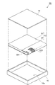
図1は、本発明の第1の実施の形態に係る無線ICメモリの分解斜視図である。図1に示す無線ICメモリ10は、非接触に情報を読み書き可能な情報記録媒体である。この無線ICメモリ10としては、所謂RFIDタグ等が例示される。無線ICメモリ10は、アンテナ12、回路基板14、及び筐体16を備えている。
FIG. 1 is an exploded perspective view of the wireless IC memory according to the first embodiment of the present invention. A
アンテナ12は、部材18と、基体20とを有している。図2は、本発明の第1の実施の形態に係るアンテナの分解斜視図である。部材18は、シート状をなしている。部材18は、本実施の形態では、軟磁性材料を含んでいる。
The
部材18は、第1の主面18a、第2の主面18b、及び端面18cを有している。第1の主面18a及び第2の主面18bは、矩形の平面であり、互いに対向している。端面18cは、第1の主面18a及び第2の主面18bに交差している。本実施の形態では、端面18cは、凸状の曲面になっている。かかる部材18には、基体20が取り付けられている。
The
図3は、図2に示すアンテナにおける基体の平面図である。基体20は、図3に示すように、順に並ぶ第1の領域20a、第2の領域20b、及び第3の領域20cを有している。図1及び図2に示すように、基体20は、可撓性を有している。基体20は、例えば、ポリイミド、或いは、PET(ポリエチレンテレフタレート)製である。
FIG. 3 is a plan view of a base in the antenna shown in FIG. As shown in FIG. 3, the
基体20の第1の領域20aは、第1の主面18aに沿って設けられており、第2の領域20bは端面18cに沿って設けられており、第3の領域20cは、第2の主面18bに沿って設けられている。
The
かかる基体20の部材18に沿う面と反対側の面には、線状の導体22が設けられている。この導体22は、例えば、Auといった材料から構成されており、印刷、或いはエッチングによって基体20上にパターニングされている。
A
導体22は、螺旋状部22a、第1の接続部22b、第2の接続部22c、一端22d、及び他端22eを有している。螺旋状部22aは、導体22の一端22d及び第1の接続部22bを内側にして螺旋状に設けられている。導体22の一端22dは、第3の領域20cに設けられており、直線に沿って延びる第1の接続部22bを介して螺旋状部22aの内側端22fに接続されている。また、導体22の他端22eも、第3の領域20cに設けられており、直線に沿って延びる第2の接続部22cを介して、螺旋状部22aの外側端22gに接続されている。
The
この導体22では、第1の領域20aにおける螺旋状部22aの幅W1より、第2の領域20b及び第3の領域20cにおける螺旋状部22aの幅W2、即ち第1の接続部22bに沿って第2の領域20b及び第3の領域20cに突出された導体22によるパターンの幅W2が小さくなっている。換言すると、幅W1は、第1の領域20a、第2の領域20b、及び第3の領域が並ぶ方向に交差する幅方向における距離であって、第1の領域20aの螺旋状部22aを構成する導体配線のうち当該幅方向における外側の線間の距離である。また、最大幅W2は、上記幅方向における距離であって、第2の領域20b及び第3の領域20cにおける螺旋状部22aを構成する導体配線のうち当該幅方向における外側の線間の距離である。このように距離W2が距離W1より小さいことから、螺旋状部22aは、第1の領域20aから第2の領域20b及び第3の領域20cに向けて突出するパターンとなっている。
In the
かかる導体22が設けられた基体20と部材18とによって構成されるアンテナ12は、図1に示すように、回路基板14に取り付けられている。
As shown in FIG. 1, the
回路基板14は、無線ICチップを搭載した回路基板である。回路基板14と、導体22の一端22d及び他端22eとは、バンプといった導電性材料によって電気的に接続されている。
The
回路基板14の無線ICチップには、駆動電圧生成回路、復調回路、変調回路、コントローラ、及びメモリが設けられている。駆動電圧生成回路は、アンテナ12に受信した電磁波から、無線ICチップを起動するための直流電圧を生成する。この駆動電圧生成回路としては、整流回路又は昇圧回路が例示される。
The wireless IC chip on the
無線ICチップでは、アンテナ12に受信した電磁波から復調回路が信号を復調し、この信号に基づいて、コントローラがメモリへの書き込み又はメモリからの読み出しを行う。読み出し時には、メモリから読み出された情報に基づいて変調した信号を変調回路が生成する。この変調回路からの出力に基づいてアンテナ12から電磁波が送信される。
In the wireless IC chip, the demodulation circuit demodulates the signal from the electromagnetic wave received by the
アンテナ12、及び回路基板14は、筐体16に取り付けられている。本実施の形態では、筐体16は、凹状の空間16aを画成する容器になっている。この空間16a内にアンテナ12、及び回路基板14が順に収容されている。
The
以下、無線ICメモリ10の作用について説明する。無線ICメモリ10のアンテナ12によれば、可撓性の基体20を部材18に沿って折り曲げることができるので、第1の主面18aに沿っている第1の領域20aの導体をアンテナとして機能させる一方、部材18の第2の主面18bの側に導体22の一端22d及び他端22eを設けることができる。したがって、このアンテナ12によれば、部材18にスルーホールを設けなくとも、導体22と回路基板14との電気的接続を確保することができる。
Hereinafter, the operation of the
また、幅W2が距離W1より小さいので、第1の領域20aにおける導体22のインダクタンス、即ち、アンテナとして機能すべき部分のインダクタンスに対する第2及び第3の領域20b,20cの導体22によるインダクタンスの影響を低減することができる。
In addition, since the width W2 is smaller than the distance W1, the influence of the inductance of the
また、部材18の端面18cが凸状の曲面になっているので、基体20の屈曲部分における応力が緩和される。その結果、屈曲部分における導体22の断線が発生し難くなっている。
Further, since the
また、部材18が、軟磁性材料を含んでいるので、回路基板14の金属での渦電流による電磁波の影響を抑制することが可能である。即ち、部材18の裏側には、金属材料を含む回路基板14等が設けられる。アンテナ12に到来する電磁波、或いはアンテナ12から発信する電磁波は、当該金属部材に渦電流を発生させる。この渦電流は、上記の電磁波を弱める反磁界を発生させる。したがって、アンテナ12の裏面に設けられた金属部材は、リーダ・ライタからアンテナ12に到来する電磁波、及びアンテナ12からリーダ・ライタに発信する電磁波の双方に影響を及ぼす。
In addition, since the
一方、本実施の形態の部材18は、軟磁性材料を含んでいるので、アンテナ12の裏側における磁束はその部分に集中する。その結果、金属表面を通過する磁束が減少し渦電流の発生が抑制される。
On the other hand, since the
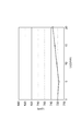
以下、本発明の第1の実施の形態のアンテナ12の特性について説明する。図4は、比較例に係わるアンテナの斜視図である。図4に示すアンテナ100Aは、線状の導体によって構成されている。アンテナ100Aでは、導体は、幅Wa1が20mmであり、且つ、長さがLa1+Lb1+Lc1の矩形の縁に沿う螺旋状のパターンを有している。また、アンテナ100Aでは、長さLa1は20mmであり、長さLc1の部分の導体が、長さLa1の部分の導体に対向するように屈曲されている。また、長さLb1は0.1mmである。なお、導体の巻き数は3である。
Hereinafter, the characteristics of the
図5は、図4に示すアンテナ100Aの特性を示す図である。図5には、長さLc1を変化させた場合のアンテナ100Aのインダクタンスが示されている。このインダクタンスは、モーメント法により算出されたものである。図5に示すように、その幅が長手方向に沿って均一な螺旋状の導体を屈曲させてアンテナ100Aを構成すると、アンテナ100Aのインダクタンスの大きさが、長さLc1に依存して大きく変化することがわかる。このことから、アンテナ100Aの構造では、螺旋状の導体を高精度に屈曲させる必要があることがわかる。
FIG. 5 is a diagram showing the characteristics of the
図6は、第1の実施の形態に係るアンテナの実施例の斜視図である。図6に示すアンテナ100Bも線状の導体によって構成されている。アンテナ100Bにおいても、導体は螺旋状のパターンを有しているが、この螺旋状のパターンでは、幅Wa2及び長さLa2が共に20mmの部分に対して、幅狭の部分が長さLc2で突出している。アンテナ100Bでは、この突出している部分が図6に示すように屈曲されている。なお、導体の巻き数は3である。
FIG. 6 is a perspective view of an example of the antenna according to the first embodiment. The
図7は、図6に示すアンテナ100Bの特性を示す図である。図7には、長さLc2を変化させた場合のアンテナ100Bのインダクタンスが示されている。このインダクタンスも、モーメント法により算出されたものである。図7に示すように、幅狭で突出する部分を屈曲させた形状のアンテナ100Bによれば、長さLc2の変化に対してアンテナ100Bのインダクタンスの変化が僅かである。このことから、アンテナ100Bによれば、螺旋状の導体を屈曲させる加工に精度を要しないことがわかる。したがって、第1の実施の形態のアンテナ12は、容易に製造可能であることが明らかである。
FIG. 7 is a diagram showing the characteristics of the
[第2の実施の形態] [Second Embodiment]
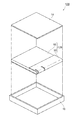
以下、本発明の第2の実施の形態にかかる無線ICメモリについて説明する。図8は、本発明の第2の実施の形態に係る無線ICメモリの分解斜視図である。図8に示す無線ICメモリ10Bは、アンテナ12に代わるアンテナ12Bを備えている。無線ICメモリ10Bのその他の構成については、第1の実施の形態の無線ICメモリ10の構成と同様である。
The wireless IC memory according to the second embodiment of the present invention will be described below. FIG. 8 is an exploded perspective view of the wireless IC memory according to the second embodiment of the present invention. A
図9は、本発明の第2の実施の形態に係るアンテナの分解斜視図である。図10は、図9に示すアンテナにおける基体の平面図である。図9及び図10に示すアンテナ12Bは、第1の実施の形態と同様の部材18と、基体30とを有している。
FIG. 9 is an exploded perspective view of an antenna according to the second embodiment of the present invention. FIG. 10 is a plan view of a base in the antenna shown in FIG. The
基体30は、基体20と同様に、可撓性を有している。基体30は、例えば、ポリイミド、或いは、PET製である。また、基体30は、基体20と同様に、順に並ぶ第1の領域30a、第2の領域30b、及び第3の領域30cを含んでいる。第1の領域30aは、第1の主面18aに沿っており、第2の領域30bは、端面18cに沿っており、第3の領域30cは、第2の主面18bに沿っている。
The
かかる基体30には、線状の導体32が設けられている。導体32は、例えば、Auといった材料から構成されており、印刷、或いはエッチングによって基体30上にパターニングされている。
The
導体32は、螺旋状部32a、第1の接続部32b、第2の接続部32c、一端32d、及び他端32eを有している。螺旋状部32aは、第1の領域30aにおける第1の主面18aに沿う面に、螺旋状に設けられている。
The
この螺旋状部32aの内側端は、第1の接続部32bを介して、一端32dに接続されている。この一端32dは、第2の主面18bに沿う面とは反対側の第3の領域30cの面に設けられている。第1の接続部32bは、上記の内側端との接続部位から基体30のスルーホールを通り、更に第2の領域30b及び第3の領域30cに延びて、一端32dに接続している。
The inner end of the
また、螺旋状部32aの外側端は、第2の接続部32cを介して、他端32eに接続されている。この他端32eは、第2の主面18bに沿う面とは反対側の第3の領域30cの面に設けられている。第2の接続部32cは、上記の外側端との接続部位から基体30のスルーホールを通り、更に第2の領域30b及び第3の領域30cに延びて、他端32eに接続している。
The outer end of the
かかるアンテナ12Bによれば、第1の実施の形態と同様の作用効果が奏される。したがって、アンテナ12Bは、低コストに製造可能なアンテナである。故に、このアンテナ12Bを備える無線ICメモリ10Bも低コストに製造可能である。
According to the
[第3の実施の形態] [Third Embodiment]
図11は、本発明の第3の実施の形態に係るアンテナの分解斜視図である。図12は、図11に示すアンテナにおける基体の平面図である。図11及び図12に示すアンテナ12Cは、第1の実施の形態と同様の部材18と、基体40とを有している。
FIG. 11 is an exploded perspective view of an antenna according to the third embodiment of the present invention. FIG. 12 is a plan view of a base in the antenna shown in FIG. The
基体40は、基体20と同様に、可撓性を有している。基体40は、例えば、ポリイミド、或いは、PET製である。また、基体40は、基体20と同様に、順に並ぶ第1の領域40a、第2の領域40b、及び第3の領域40cを含んでいる。第1の領域40aは、第1の主面18aに沿っており、第2の領域40bは、端面18cに沿っており、第3の領域40cは、第2の主面18bに沿っている。
The
かかる基体40には、線状の導体42が設けられている。導体42は、例えば、Auといった材料から構成されており、印刷、或いはエッチングによって基体40上にパターニングされている。
The
導体42は、螺旋状部42a、第1の接続部42b、第2の接続部42c、一端42d、及び他端42eを有している。螺旋状部42aは、第1の主面18aに沿う面と反対側の第1の領域40aの面に、螺旋状に設けられている。
The
この螺旋状部42aの内側端42fは、第1の接続部42bを介して、一端42dに接続されている。この一端42dは、第2の主面18bに沿う面とは反対側の第3の領域40cの面に設けられている。第1の接続部42bは、内側端42fとの接続部位から基体40のスルーホールを介して部材18に沿う基体40の面を通り、更にスルーホールを介して部材18に沿う面とは反対側の第3の領域40cの面を通り、一端42dに接続している。
The
また、第2の接続部32cは、部材18に沿う面とは反対側の基体18の面を通って、螺旋状部42aの外側端42gと他端32eとを接続している。
Further, the
かかるアンテナ12Cによれば、第1の実施の形態と同様の作用効果が奏される。したがって、アンテナ12Cは、低コストに製造可能なアンテナである。故に、このアンテナ12Cを備える無線ICメモリ10Cも低コストに製造可能である。
According to the
なお、本発明は上記した本実施形態に限定されることなく種々の変形が可能である。上述した実施の形態のアンテナは、スパイラルアンテナであるが、本発明の思想は、線状の導体を一巻き以上巻いてなるアンテナに適用可能である。かかるアンテナとしては、ループアンテナ、うずまきアンテナ、ヘリカルアンテナ、アンテナコイル、スパイラルインダクタ等が例示される。 The present invention is not limited to the above-described embodiment, and various modifications can be made. The antenna of the above-described embodiment is a spiral antenna, but the idea of the present invention can be applied to an antenna formed by winding a linear conductor one or more times. Examples of such an antenna include a loop antenna, a spiral antenna, a helical antenna, an antenna coil, and a spiral inductor.
なお、部材18は、基体に設けられた導体とは絶縁された金属であってもよい。この場合には、予め金属製の部材18を設けておくことによって、使用時における他の金属によるアンテナへの影響を低減することができる。また、部材18は、誘電体であってもよい。この場合には、部材18の裏側(第2の主面の側)に設けられた金属と第1の領域の導体との距離を大きくすることができる。
The
10,10B…無線ICメモリ、12,12B…アンテナ、14…回路基板、16…筐体、18…部材、18a…第1の主面、18b…第2の主面、18c…端面、20,30,40…基体、20a,30a,40a…第1の領域、20b,30b,40b…第2の領域、20c,30c,40c…第3の領域、22,32,42…導体、22a,32a,42a…螺旋状部、22b,32b,42b…第1の接続部、22c,32c,42c…第2の接続部、22d,32d,42d…一端、22e,32e,42e…他端、22f,42f…内側端、22g,42g…外側端。
DESCRIPTION OF
Claims (8)
一端及び他端を有する線状の導体が設けられた可撓性の基体と、
を備えており、
前記基体は、順に連続する第1の領域、第2の領域、及び第3の領域を有しており、
前記第1の領域は、前記第1の主面に沿っており、
前記第2の領域は、前記端面に沿っており、
前記第3の領域は、前記第2の主面に沿っており、
前記導体の一端及び他端は、前記第2の主面に沿う面と反対側の前記第3の領域の面に設けられており
前記導体は、少なくとも前記第1の領域において螺旋状をなす螺旋状部と、前記螺旋状部の内側端と該導体の前記一端とを接続する第1の接続部と、前記螺旋状部の外側端と該導体の前記他端とを接続する第2の接続部と、を有しており、
前記螺旋状部を終端させる前記内側端が、前記第1の領域に存在し、
前記第1の接続部は、前記第1の領域、前記第2の領域、及び前記第3の領域を通って、前記螺旋状部の前記内側端と前記導体の前記一端とを接続している、
アンテナ。 A member having a first main surface, a second main surface opposite to the first main surface, and an end surface intersecting the first main surface and the second main surface;
A flexible substrate provided with a linear conductor having one end and the other end;
With
The base has a first region, a second region, and a third region which are sequentially continuous,
The first region is along the first main surface;
The second region is along the end face;
The third region is along the second main surface,
One end and the other end of the conductor are provided on the surface of the third region opposite to the surface along the second main surface, and the conductor has a spiral shape at least in the first region. A first connection part that connects the inner part of the spiral part and the one end of the conductor, and a second connection that connects the outer end of the spiral part and the other end of the conductor. and parts, has a,
The inner end that terminates the spiral is in the first region;
The first connection portion connects the inner end of the spiral portion and the one end of the conductor through the first region, the second region, and the third region. ,
antenna.
前記螺旋状部は、前記一端及び前記第1の接続部を内側にして、前記第1の領域、前記第2の領域、及び前記第3の領域に設けられており、
前記第1の接続部に沿って前記第3の領域に突出された前記導体によるパターンの幅が前記第1の領域における前記螺旋状部の幅より小さい、
請求項1記載のアンテナ。 The conductor is provided on the surface of the base opposite to the surface along the member;
The spiral portion is provided in the first region, the second region, and the third region, with the one end and the first connection portion inside.
A width of a pattern by the conductor protruding into the third region along the first connection portion is smaller than a width of the spiral portion in the first region;
The antenna according to claim 1.
前記第1の接続部は、前記内側端から前記基体のスルーホールを通り、前記端面に沿う面と反対側の前記第2の領域の面及び前記第2の主面に沿う面と反対側の前記第3の領域の面を通って、前記一端に接続しており、
前記第2の接続部は、前記外側端から前記基体のスルーホールを通り、前記端面に沿う面と反対側の前記第2の領域の面及び前記第2の主面に沿う面と反対側の前記第3の領域の面を通って、前記他端に接続している、
請求項1記載のアンテナ。 The spiral portion is provided on a surface along the first main surface of the first region,
The first connecting portion passes through the through hole of the base body from the inner end, and is opposite to the surface of the second region opposite to the surface along the end surface and the surface along the second main surface. Connected to the one end through the surface of the third region,
The second connecting portion passes through the through hole of the base body from the outer end, and is opposite to the surface of the second region opposite to the surface along the end surface and the surface along the second main surface. Connected to the other end through the surface of the third region,
The antenna according to claim 1.
前記第1の接続部は、前記内側端からスルーホールを介して前記基体の前記部材に沿う面を通り、更にスルーホールを介して前記第2の主面に沿う面と反対側の前記第3の領域の面を通って、前記一端に接続しており、
前記第2の接続部は、前記端面に沿う面と反対側の前記第2の領域の面及び前記第2の主面に沿う面と反対側の前記第3の領域の面を通って、前記他端に接続している、
請求項1記載のアンテナ。 The spiral portion is provided on the surface of the first region opposite to the surface along the first main surface,
The first connecting portion passes through a surface along the member of the base body through a through hole from the inner end, and further passes through the third hole on the opposite side of the surface along the second main surface through the through hole. Connected to the one end through the surface of the area of
The second connecting portion passes through the surface of the second region opposite to the surface along the end surface and the surface of the third region opposite to the surface along the second main surface, Connected to the other end,
The antenna according to claim 1.
Priority Applications (1)
| Application Number | Priority Date | Filing Date | Title |
|---|---|---|---|
| JP2009255118A JP2010051012A (en) | 2009-11-06 | 2009-11-06 | Antenna, and radio ic memory |
Applications Claiming Priority (1)
| Application Number | Priority Date | Filing Date | Title |
|---|---|---|---|
| JP2009255118A JP2010051012A (en) | 2009-11-06 | 2009-11-06 | Antenna, and radio ic memory |
Related Parent Applications (1)
| Application Number | Title | Priority Date | Filing Date |
|---|---|---|---|
| JP2005221681A Division JP4513685B2 (en) | 2005-07-29 | 2005-07-29 | Antenna and wireless IC memory |
Publications (2)
| Publication Number | Publication Date |
|---|---|
| JP2010051012A true JP2010051012A (en) | 2010-03-04 |
| JP2010051012A5 JP2010051012A5 (en) | 2010-06-17 |
Family
ID=42067645
Family Applications (1)
| Application Number | Title | Priority Date | Filing Date |
|---|---|---|---|
| JP2009255118A Pending JP2010051012A (en) | 2009-11-06 | 2009-11-06 | Antenna, and radio ic memory |
Country Status (1)
| Country | Link |
|---|---|
| JP (1) | JP2010051012A (en) |
Cited By (25)
| Publication number | Priority date | Publication date | Assignee | Title |
|---|---|---|---|---|
| WO2012141070A1 (en) * | 2011-04-13 | 2012-10-18 | 株式会社村田製作所 | Wireless ic device and wireless communication terminal |
| WO2014076669A1 (en) | 2012-11-15 | 2014-05-22 | Logomotion, S.R.O. | Non-stationary magnetic field emitter, its connection in system and data modulation method |
| US8757502B2 (en) | 2011-02-28 | 2014-06-24 | Murata Manufacturing Co., Ltd. | Wireless communication device |
| US8770489B2 (en) | 2011-07-15 | 2014-07-08 | Murata Manufacturing Co., Ltd. | Radio communication device |
| US8797225B2 (en) | 2011-03-08 | 2014-08-05 | Murata Manufacturing Co., Ltd. | Antenna device and communication terminal apparatus |
| US8797148B2 (en) | 2008-03-03 | 2014-08-05 | Murata Manufacturing Co., Ltd. | Radio frequency IC device and radio communication system |
| US8814056B2 (en) | 2011-07-19 | 2014-08-26 | Murata Manufacturing Co., Ltd. | Antenna device, RFID tag, and communication terminal apparatus |
| US8853549B2 (en) | 2009-09-30 | 2014-10-07 | Murata Manufacturing Co., Ltd. | Circuit substrate and method of manufacturing same |
| US8876010B2 (en) | 2009-04-14 | 2014-11-04 | Murata Manufacturing Co., Ltd | Wireless IC device component and wireless IC device |
| US8905296B2 (en) | 2011-12-01 | 2014-12-09 | Murata Manufacturing Co., Ltd. | Wireless integrated circuit device and method of manufacturing the same |
| US8917211B2 (en) | 2008-11-17 | 2014-12-23 | Murata Manufacturing Co., Ltd. | Antenna and wireless IC device |
| US8976075B2 (en) | 2009-04-21 | 2015-03-10 | Murata Manufacturing Co., Ltd. | Antenna device and method of setting resonant frequency of antenna device |
| US8973841B2 (en) | 2008-05-21 | 2015-03-10 | Murata Manufacturing Co., Ltd. | Wireless IC device |
| US9024837B2 (en) | 2010-03-31 | 2015-05-05 | Murata Manufacturing Co., Ltd. | Antenna and wireless communication device |
| US9024725B2 (en) | 2009-11-04 | 2015-05-05 | Murata Manufacturing Co., Ltd. | Communication terminal and information processing system |
| US9117157B2 (en) | 2009-10-02 | 2015-08-25 | Murata Manufacturing Co., Ltd. | Wireless IC device and electromagnetic coupling module |
| US9281873B2 (en) | 2008-05-26 | 2016-03-08 | Murata Manufacturing Co., Ltd. | Wireless IC device system and method of determining authenticity of wireless IC device |
| WO2016071885A1 (en) | 2014-11-08 | 2016-05-12 | Logomotion, S.R.O. | Non-stationary magnetic field emitter |
| US9378452B2 (en) | 2011-05-16 | 2016-06-28 | Murata Manufacturing Co., Ltd. | Radio IC device |
| US9543642B2 (en) | 2011-09-09 | 2017-01-10 | Murata Manufacturing Co., Ltd. | Antenna device and wireless device |
| US9558384B2 (en) | 2010-07-28 | 2017-01-31 | Murata Manufacturing Co., Ltd. | Antenna apparatus and communication terminal instrument |
| US9692128B2 (en) | 2012-02-24 | 2017-06-27 | Murata Manufacturing Co., Ltd. | Antenna device and wireless communication device |
| US9727765B2 (en) | 2010-03-24 | 2017-08-08 | Murata Manufacturing Co., Ltd. | RFID system including a reader/writer and RFID tag |
| US10013650B2 (en) | 2010-03-03 | 2018-07-03 | Murata Manufacturing Co., Ltd. | Wireless communication module and wireless communication device |
| US10235544B2 (en) | 2012-04-13 | 2019-03-19 | Murata Manufacturing Co., Ltd. | Inspection method and inspection device for RFID tag |
Citations (4)
| Publication number | Priority date | Publication date | Assignee | Title |
|---|---|---|---|---|
| JP2004186827A (en) * | 2002-11-29 | 2004-07-02 | Nippon Plast Co Ltd | Manufacturing method of antenna system and antenna system |
| JP2004304370A (en) * | 2003-03-28 | 2004-10-28 | Sony Corp | Antenna coil and communication equipment |
| JP2004364199A (en) * | 2003-06-06 | 2004-12-24 | Sony Corp | Antenna module and portable communication terminal equipped therewith |
| JP4513685B2 (en) * | 2005-07-29 | 2010-07-28 | Tdk株式会社 | Antenna and wireless IC memory |
-
2009
- 2009-11-06 JP JP2009255118A patent/JP2010051012A/en active Pending
Patent Citations (4)
| Publication number | Priority date | Publication date | Assignee | Title |
|---|---|---|---|---|
| JP2004186827A (en) * | 2002-11-29 | 2004-07-02 | Nippon Plast Co Ltd | Manufacturing method of antenna system and antenna system |
| JP2004304370A (en) * | 2003-03-28 | 2004-10-28 | Sony Corp | Antenna coil and communication equipment |
| JP2004364199A (en) * | 2003-06-06 | 2004-12-24 | Sony Corp | Antenna module and portable communication terminal equipped therewith |
| JP4513685B2 (en) * | 2005-07-29 | 2010-07-28 | Tdk株式会社 | Antenna and wireless IC memory |
Cited By (30)
| Publication number | Priority date | Publication date | Assignee | Title |
|---|---|---|---|---|
| US8797148B2 (en) | 2008-03-03 | 2014-08-05 | Murata Manufacturing Co., Ltd. | Radio frequency IC device and radio communication system |
| US9022295B2 (en) | 2008-05-21 | 2015-05-05 | Murata Manufacturing Co., Ltd. | Wireless IC device |
| US8973841B2 (en) | 2008-05-21 | 2015-03-10 | Murata Manufacturing Co., Ltd. | Wireless IC device |
| US9281873B2 (en) | 2008-05-26 | 2016-03-08 | Murata Manufacturing Co., Ltd. | Wireless IC device system and method of determining authenticity of wireless IC device |
| US8917211B2 (en) | 2008-11-17 | 2014-12-23 | Murata Manufacturing Co., Ltd. | Antenna and wireless IC device |
| US8876010B2 (en) | 2009-04-14 | 2014-11-04 | Murata Manufacturing Co., Ltd | Wireless IC device component and wireless IC device |
| US8976075B2 (en) | 2009-04-21 | 2015-03-10 | Murata Manufacturing Co., Ltd. | Antenna device and method of setting resonant frequency of antenna device |
| US8853549B2 (en) | 2009-09-30 | 2014-10-07 | Murata Manufacturing Co., Ltd. | Circuit substrate and method of manufacturing same |
| US9117157B2 (en) | 2009-10-02 | 2015-08-25 | Murata Manufacturing Co., Ltd. | Wireless IC device and electromagnetic coupling module |
| US9024725B2 (en) | 2009-11-04 | 2015-05-05 | Murata Manufacturing Co., Ltd. | Communication terminal and information processing system |
| US10013650B2 (en) | 2010-03-03 | 2018-07-03 | Murata Manufacturing Co., Ltd. | Wireless communication module and wireless communication device |
| US9727765B2 (en) | 2010-03-24 | 2017-08-08 | Murata Manufacturing Co., Ltd. | RFID system including a reader/writer and RFID tag |
| US9024837B2 (en) | 2010-03-31 | 2015-05-05 | Murata Manufacturing Co., Ltd. | Antenna and wireless communication device |
| US9558384B2 (en) | 2010-07-28 | 2017-01-31 | Murata Manufacturing Co., Ltd. | Antenna apparatus and communication terminal instrument |
| US8960561B2 (en) | 2011-02-28 | 2015-02-24 | Murata Manufacturing Co., Ltd. | Wireless communication device |
| US8757502B2 (en) | 2011-02-28 | 2014-06-24 | Murata Manufacturing Co., Ltd. | Wireless communication device |
| US8797225B2 (en) | 2011-03-08 | 2014-08-05 | Murata Manufacturing Co., Ltd. | Antenna device and communication terminal apparatus |
| WO2012141070A1 (en) * | 2011-04-13 | 2012-10-18 | 株式会社村田製作所 | Wireless ic device and wireless communication terminal |
| US8740093B2 (en) | 2011-04-13 | 2014-06-03 | Murata Manufacturing Co., Ltd. | Radio IC device and radio communication terminal |
| JP5482964B2 (en) * | 2011-04-13 | 2014-05-07 | 株式会社村田製作所 | Wireless IC device and wireless communication terminal |
| US9378452B2 (en) | 2011-05-16 | 2016-06-28 | Murata Manufacturing Co., Ltd. | Radio IC device |
| US8770489B2 (en) | 2011-07-15 | 2014-07-08 | Murata Manufacturing Co., Ltd. | Radio communication device |
| US8814056B2 (en) | 2011-07-19 | 2014-08-26 | Murata Manufacturing Co., Ltd. | Antenna device, RFID tag, and communication terminal apparatus |
| US9543642B2 (en) | 2011-09-09 | 2017-01-10 | Murata Manufacturing Co., Ltd. | Antenna device and wireless device |
| US8905296B2 (en) | 2011-12-01 | 2014-12-09 | Murata Manufacturing Co., Ltd. | Wireless integrated circuit device and method of manufacturing the same |
| US9692128B2 (en) | 2012-02-24 | 2017-06-27 | Murata Manufacturing Co., Ltd. | Antenna device and wireless communication device |
| US10235544B2 (en) | 2012-04-13 | 2019-03-19 | Murata Manufacturing Co., Ltd. | Inspection method and inspection device for RFID tag |
| WO2014076669A1 (en) | 2012-11-15 | 2014-05-22 | Logomotion, S.R.O. | Non-stationary magnetic field emitter, its connection in system and data modulation method |
| US9590305B2 (en) | 2012-11-15 | 2017-03-07 | Smk Corporation | Non-stationary magnetic field emitter, its connection in system and data modulation method |
| WO2016071885A1 (en) | 2014-11-08 | 2016-05-12 | Logomotion, S.R.O. | Non-stationary magnetic field emitter |
Similar Documents
| Publication | Publication Date | Title |
|---|---|---|
| JP2010051012A (en) | Antenna, and radio ic memory | |
| JP5299518B2 (en) | Information processing system | |
| JP4034676B2 (en) | Non-contact communication type information carrier | |
| JP5454581B2 (en) | Antenna, manufacturing method thereof, and wireless IC device | |
| JP6485607B2 (en) | RFID tag | |
| JP2011004316A (en) | Antenna device | |
| JP2007053722A (en) | Antenna and wireless ic tag | |
| JP2012108843A (en) | Rfid tag | |
| JP4513685B2 (en) | Antenna and wireless IC memory | |
| JP2012059015A (en) | Radio ic tag and rfid system | |
| JP2006262054A (en) | Antenna module and portable information terminal provided with the same | |
| JP4771106B2 (en) | RFID antenna and manufacturing method thereof | |
| JP2011095844A (en) | Noncontact electronic device | |
| JP5489978B2 (en) | RFID reader / writer antenna | |
| JP4873158B2 (en) | RFID reader device | |
| JP4747715B2 (en) | Antenna and wireless IC memory | |
| JP2010028351A (en) | Booster antenna and contactless information medium | |
| JP2007311407A (en) | Ic chip, wafer finished with circuit formation, and noncontact communication member | |
| WO2017209195A1 (en) | Antenna device and ic tag employing same | |
| JP4550472B2 (en) | Information recording medium | |
| JP6187097B2 (en) | Antenna device | |
| JP6590119B1 (en) | RFID tag and article with RFID | |
| JP4238924B2 (en) | Non-contact IC card | |
| JP6555320B2 (en) | Wireless IC tag and RFID system | |
| JP2009253797A (en) | Wireless communication device |
Legal Events
| Date | Code | Title | Description |
|---|---|---|---|
| A621 | Written request for application examination |
Free format text: JAPANESE INTERMEDIATE CODE: A621 Effective date: 20091124 |
|
| A521 | Written amendment |
Free format text: JAPANESE INTERMEDIATE CODE: A523 Effective date: 20100426 |
|
| A977 | Report on retrieval |
Free format text: JAPANESE INTERMEDIATE CODE: A971007 Effective date: 20111104 |
|
| A131 | Notification of reasons for refusal |
Free format text: JAPANESE INTERMEDIATE CODE: A131 Effective date: 20111115 |
|
| A02 | Decision of refusal |
Free format text: JAPANESE INTERMEDIATE CODE: A02 Effective date: 20120529 |