EP2390915B1 - Lichtemittierende Vorrichtung und diese enthaltende Leuchteinheit - Google Patents
Lichtemittierende Vorrichtung und diese enthaltende Leuchteinheit Download PDFInfo
- Publication number
- EP2390915B1 EP2390915B1 EP11167007.1A EP11167007A EP2390915B1 EP 2390915 B1 EP2390915 B1 EP 2390915B1 EP 11167007 A EP11167007 A EP 11167007A EP 2390915 B1 EP2390915 B1 EP 2390915B1
- Authority
- EP
- European Patent Office
- Prior art keywords
- light emitting
- recess
- emitting device
- barrier section
- light
- Prior art date
- Legal status (The legal status is an assumption and is not a legal conclusion. Google has not performed a legal analysis and makes no representation as to the accuracy of the status listed.)
- Active
Links
Images


Classifications
-
- H—ELECTRICITY
- H01—ELECTRIC ELEMENTS
- H01L—SEMICONDUCTOR DEVICES NOT COVERED BY CLASS H10
- H01L33/00—Semiconductor devices with at least one potential-jump barrier or surface barrier specially adapted for light emission; Processes or apparatus specially adapted for the manufacture or treatment thereof or of parts thereof; Details thereof
- H01L33/02—Semiconductor devices with at least one potential-jump barrier or surface barrier specially adapted for light emission; Processes or apparatus specially adapted for the manufacture or treatment thereof or of parts thereof; Details thereof characterised by the semiconductor bodies
- H01L33/08—Semiconductor devices with at least one potential-jump barrier or surface barrier specially adapted for light emission; Processes or apparatus specially adapted for the manufacture or treatment thereof or of parts thereof; Details thereof characterised by the semiconductor bodies with a plurality of light emitting regions, e.g. laterally discontinuous light emitting layer or photoluminescent region integrated within the semiconductor body
-
- H—ELECTRICITY
- H01—ELECTRIC ELEMENTS
- H01L—SEMICONDUCTOR DEVICES NOT COVERED BY CLASS H10
- H01L33/00—Semiconductor devices with at least one potential-jump barrier or surface barrier specially adapted for light emission; Processes or apparatus specially adapted for the manufacture or treatment thereof or of parts thereof; Details thereof
- H01L33/48—Semiconductor devices with at least one potential-jump barrier or surface barrier specially adapted for light emission; Processes or apparatus specially adapted for the manufacture or treatment thereof or of parts thereof; Details thereof characterised by the semiconductor body packages
- H01L33/483—Containers
- H01L33/486—Containers adapted for surface mounting
-
- H—ELECTRICITY
- H01—ELECTRIC ELEMENTS
- H01L—SEMICONDUCTOR DEVICES NOT COVERED BY CLASS H10
- H01L33/00—Semiconductor devices with at least one potential-jump barrier or surface barrier specially adapted for light emission; Processes or apparatus specially adapted for the manufacture or treatment thereof or of parts thereof; Details thereof
- H01L33/44—Semiconductor devices with at least one potential-jump barrier or surface barrier specially adapted for light emission; Processes or apparatus specially adapted for the manufacture or treatment thereof or of parts thereof; Details thereof characterised by the coatings, e.g. passivation layer or anti-reflective coating
-
- F—MECHANICAL ENGINEERING; LIGHTING; HEATING; WEAPONS; BLASTING
- F21—LIGHTING
- F21K—NON-ELECTRIC LIGHT SOURCES USING LUMINESCENCE; LIGHT SOURCES USING ELECTROCHEMILUMINESCENCE; LIGHT SOURCES USING CHARGES OF COMBUSTIBLE MATERIAL; LIGHT SOURCES USING SEMICONDUCTOR DEVICES AS LIGHT-GENERATING ELEMENTS; LIGHT SOURCES NOT OTHERWISE PROVIDED FOR
- F21K9/00—Light sources using semiconductor devices as light-generating elements, e.g. using light-emitting diodes [LED] or lasers
- F21K9/20—Light sources comprising attachment means
- F21K9/23—Retrofit light sources for lighting devices with a single fitting for each light source, e.g. for substitution of incandescent lamps with bayonet or threaded fittings
-
- F—MECHANICAL ENGINEERING; LIGHTING; HEATING; WEAPONS; BLASTING
- F21—LIGHTING
- F21Y—INDEXING SCHEME ASSOCIATED WITH SUBCLASSES F21K, F21L, F21S and F21V, RELATING TO THE FORM OR THE KIND OF THE LIGHT SOURCES OR OF THE COLOUR OF THE LIGHT EMITTED
- F21Y2115/00—Light-generating elements of semiconductor light sources
- F21Y2115/10—Light-emitting diodes [LED]
-
- H—ELECTRICITY
- H01—ELECTRIC ELEMENTS
- H01L—SEMICONDUCTOR DEVICES NOT COVERED BY CLASS H10
- H01L2224/00—Indexing scheme for arrangements for connecting or disconnecting semiconductor or solid-state bodies and methods related thereto as covered by H01L24/00
- H01L2224/01—Means for bonding being attached to, or being formed on, the surface to be connected, e.g. chip-to-package, die-attach, "first-level" interconnects; Manufacturing methods related thereto
- H01L2224/42—Wire connectors; Manufacturing methods related thereto
- H01L2224/47—Structure, shape, material or disposition of the wire connectors after the connecting process
- H01L2224/48—Structure, shape, material or disposition of the wire connectors after the connecting process of an individual wire connector
- H01L2224/481—Disposition
- H01L2224/48135—Connecting between different semiconductor or solid-state bodies, i.e. chip-to-chip
- H01L2224/48137—Connecting between different semiconductor or solid-state bodies, i.e. chip-to-chip the bodies being arranged next to each other, e.g. on a common substrate
-
- H—ELECTRICITY
- H01—ELECTRIC ELEMENTS
- H01L—SEMICONDUCTOR DEVICES NOT COVERED BY CLASS H10
- H01L2224/00—Indexing scheme for arrangements for connecting or disconnecting semiconductor or solid-state bodies and methods related thereto as covered by H01L24/00
- H01L2224/01—Means for bonding being attached to, or being formed on, the surface to be connected, e.g. chip-to-package, die-attach, "first-level" interconnects; Manufacturing methods related thereto
- H01L2224/42—Wire connectors; Manufacturing methods related thereto
- H01L2224/47—Structure, shape, material or disposition of the wire connectors after the connecting process
- H01L2224/48—Structure, shape, material or disposition of the wire connectors after the connecting process of an individual wire connector
- H01L2224/481—Disposition
- H01L2224/48151—Connecting between a semiconductor or solid-state body and an item not being a semiconductor or solid-state body, e.g. chip-to-substrate, chip-to-passive
- H01L2224/48221—Connecting between a semiconductor or solid-state body and an item not being a semiconductor or solid-state body, e.g. chip-to-substrate, chip-to-passive the body and the item being stacked
- H01L2224/48245—Connecting between a semiconductor or solid-state body and an item not being a semiconductor or solid-state body, e.g. chip-to-substrate, chip-to-passive the body and the item being stacked the item being metallic
- H01L2224/48247—Connecting between a semiconductor or solid-state body and an item not being a semiconductor or solid-state body, e.g. chip-to-substrate, chip-to-passive the body and the item being stacked the item being metallic connecting the wire to a bond pad of the item
-
- H—ELECTRICITY
- H01—ELECTRIC ELEMENTS
- H01L—SEMICONDUCTOR DEVICES NOT COVERED BY CLASS H10
- H01L2224/00—Indexing scheme for arrangements for connecting or disconnecting semiconductor or solid-state bodies and methods related thereto as covered by H01L24/00
- H01L2224/01—Means for bonding being attached to, or being formed on, the surface to be connected, e.g. chip-to-package, die-attach, "first-level" interconnects; Manufacturing methods related thereto
- H01L2224/42—Wire connectors; Manufacturing methods related thereto
- H01L2224/47—Structure, shape, material or disposition of the wire connectors after the connecting process
- H01L2224/48—Structure, shape, material or disposition of the wire connectors after the connecting process of an individual wire connector
- H01L2224/481—Disposition
- H01L2224/48151—Connecting between a semiconductor or solid-state body and an item not being a semiconductor or solid-state body, e.g. chip-to-substrate, chip-to-passive
- H01L2224/48221—Connecting between a semiconductor or solid-state body and an item not being a semiconductor or solid-state body, e.g. chip-to-substrate, chip-to-passive the body and the item being stacked
- H01L2224/48245—Connecting between a semiconductor or solid-state body and an item not being a semiconductor or solid-state body, e.g. chip-to-substrate, chip-to-passive the body and the item being stacked the item being metallic
- H01L2224/48257—Connecting between a semiconductor or solid-state body and an item not being a semiconductor or solid-state body, e.g. chip-to-substrate, chip-to-passive the body and the item being stacked the item being metallic connecting the wire to a die pad of the item
-
- H—ELECTRICITY
- H01—ELECTRIC ELEMENTS
- H01L—SEMICONDUCTOR DEVICES NOT COVERED BY CLASS H10
- H01L2224/00—Indexing scheme for arrangements for connecting or disconnecting semiconductor or solid-state bodies and methods related thereto as covered by H01L24/00
- H01L2224/01—Means for bonding being attached to, or being formed on, the surface to be connected, e.g. chip-to-package, die-attach, "first-level" interconnects; Manufacturing methods related thereto
- H01L2224/42—Wire connectors; Manufacturing methods related thereto
- H01L2224/47—Structure, shape, material or disposition of the wire connectors after the connecting process
- H01L2224/49—Structure, shape, material or disposition of the wire connectors after the connecting process of a plurality of wire connectors
- H01L2224/491—Disposition
- H01L2224/4911—Disposition the connectors being bonded to at least one common bonding area, e.g. daisy chain
- H01L2224/49113—Disposition the connectors being bonded to at least one common bonding area, e.g. daisy chain the connectors connecting different bonding areas on the semiconductor or solid-state body to a common bonding area outside the body, e.g. converging wires
-
- H—ELECTRICITY
- H01—ELECTRIC ELEMENTS
- H01L—SEMICONDUCTOR DEVICES NOT COVERED BY CLASS H10
- H01L25/00—Assemblies consisting of a plurality of individual semiconductor or other solid state devices ; Multistep manufacturing processes thereof
- H01L25/03—Assemblies consisting of a plurality of individual semiconductor or other solid state devices ; Multistep manufacturing processes thereof all the devices being of a type provided for in the same subgroup of groups H01L27/00 - H01L33/00, or in a single subclass of H10K, H10N, e.g. assemblies of rectifier diodes
- H01L25/04—Assemblies consisting of a plurality of individual semiconductor or other solid state devices ; Multistep manufacturing processes thereof all the devices being of a type provided for in the same subgroup of groups H01L27/00 - H01L33/00, or in a single subclass of H10K, H10N, e.g. assemblies of rectifier diodes the devices not having separate containers
- H01L25/075—Assemblies consisting of a plurality of individual semiconductor or other solid state devices ; Multistep manufacturing processes thereof all the devices being of a type provided for in the same subgroup of groups H01L27/00 - H01L33/00, or in a single subclass of H10K, H10N, e.g. assemblies of rectifier diodes the devices not having separate containers the devices being of a type provided for in group H01L33/00
- H01L25/0753—Assemblies consisting of a plurality of individual semiconductor or other solid state devices ; Multistep manufacturing processes thereof all the devices being of a type provided for in the same subgroup of groups H01L27/00 - H01L33/00, or in a single subclass of H10K, H10N, e.g. assemblies of rectifier diodes the devices not having separate containers the devices being of a type provided for in group H01L33/00 the devices being arranged next to each other
-
- H—ELECTRICITY
- H01—ELECTRIC ELEMENTS
- H01L—SEMICONDUCTOR DEVICES NOT COVERED BY CLASS H10
- H01L2924/00—Indexing scheme for arrangements or methods for connecting or disconnecting semiconductor or solid-state bodies as covered by H01L24/00
- H01L2924/15—Details of package parts other than the semiconductor or other solid state devices to be connected
- H01L2924/181—Encapsulation
-
- H—ELECTRICITY
- H01—ELECTRIC ELEMENTS
- H01L—SEMICONDUCTOR DEVICES NOT COVERED BY CLASS H10
- H01L2924/00—Indexing scheme for arrangements or methods for connecting or disconnecting semiconductor or solid-state bodies as covered by H01L24/00
- H01L2924/19—Details of hybrid assemblies other than the semiconductor or other solid state devices to be connected
- H01L2924/191—Disposition
- H01L2924/19101—Disposition of discrete passive components
- H01L2924/19107—Disposition of discrete passive components off-chip wires
-
- H—ELECTRICITY
- H01—ELECTRIC ELEMENTS
- H01L—SEMICONDUCTOR DEVICES NOT COVERED BY CLASS H10
- H01L2933/00—Details relating to devices covered by the group H01L33/00 but not provided for in its subgroups
- H01L2933/0008—Processes
- H01L2933/0033—Processes relating to semiconductor body packages
-
- H—ELECTRICITY
- H01—ELECTRIC ELEMENTS
- H01L—SEMICONDUCTOR DEVICES NOT COVERED BY CLASS H10
- H01L33/00—Semiconductor devices with at least one potential-jump barrier or surface barrier specially adapted for light emission; Processes or apparatus specially adapted for the manufacture or treatment thereof or of parts thereof; Details thereof
- H01L33/48—Semiconductor devices with at least one potential-jump barrier or surface barrier specially adapted for light emission; Processes or apparatus specially adapted for the manufacture or treatment thereof or of parts thereof; Details thereof characterised by the semiconductor body packages
- H01L33/52—Encapsulations
- H01L33/54—Encapsulations having a particular shape
-
- H—ELECTRICITY
- H01—ELECTRIC ELEMENTS
- H01L—SEMICONDUCTOR DEVICES NOT COVERED BY CLASS H10
- H01L33/00—Semiconductor devices with at least one potential-jump barrier or surface barrier specially adapted for light emission; Processes or apparatus specially adapted for the manufacture or treatment thereof or of parts thereof; Details thereof
- H01L33/48—Semiconductor devices with at least one potential-jump barrier or surface barrier specially adapted for light emission; Processes or apparatus specially adapted for the manufacture or treatment thereof or of parts thereof; Details thereof characterised by the semiconductor body packages
- H01L33/62—Arrangements for conducting electric current to or from the semiconductor body, e.g. lead-frames, wire-bonds or solder balls
Definitions
- the embodiment relates to a light emitting device and a light unit having the same.
- LEDs Light emitting diodes
- the LED is advantageous as compared with conventional light sources, such as a fluorescent lamp or a glow lamp, in terms of power consumption, life span, response speed, safety and environmental-friendly requirement.
- conventional light sources such as a fluorescent lamp or a glow lamp
- various studies have been performed to replace the conventional light sources with the LEDs.
- the LEDs are increasingly used as light sources for lighting devices such as various lamps used in indoor/outdoor, liquid crystal displays, electric signboards, and street lamps.
- a light emitting device as defined in claim 1 is proposed.
- the embodiment provides a light emitting device, in which a barrier section is disposed in a recess to divide the recess into a plurality of regions.
- the embodiment provides a light emitting device comprising a plurality of light emitting diodes disposed in divisional regions of a recess to emit lights having different peak wavelengths.
- the embodiment provides a light emitting device comprising same phosphors or different phosphors disposed in divisional regions of a recess.
- the embodiment provides a light emitting device comprising a barrier section having a concave part formed with a stepped portion or an inclined portion in a recess.
- the embodiment provides a light unit comprising a plurality of light emitting devices.
- a light emitting device comprises a body having a recess; a barrier section protruding upward over a bottom surface of the recess and dividing the bottom surface of the recess into a plurality of regions; a plurality of light emitting diodes comprising a first diode disposed in a first region of the bottom surface of the recess and a second diode disposed in a second region of the bottom surface of the recess; a plurality of lead electrodes spaced apart from each other in the recess and selectively connected to the light emitting diodes; wires connecting the lead electrodes to the light emitting diodes; a resin layer in the recess; and at least one concave part in the barrier section, wherein the concave part has a height lower than a top surface of the barrier section and higher than the bottom surface of the recess and the wires are provided in the concave part to connect the lead electrodes to the light emitting diodes disposed in opposition to each other.
- a light unit comprises a light emitting module comprising a light emitting device and a board on which the light emitting device is arrayed; and a light guide plate disposed in a path of a light emitted from the light emitting module, wherein the light emitting device comprises a body having a recess; a barrier section protruding upward over a bottom surface of the recess and dividing the bottom surface of the recess into a plurality of regions; a plurality of light emitting diodes comprising a first diode disposed in a first region of the bottom surface of the recess and a second diode disposed in a second region of the bottom surface of the recess; a plurality of lead electrodes spaced apart from each other in the recess and selectively connected to the light emitting diodes; wires connecting the lead electrodes to the light emitting diodes; a resin layer in the recess; and at least one concave part in the barrier section, and wherein the con
- the embodiment can improve the excitation efficiency of a phosphor in a light emitting device.
- the embodiment can improve the light extraction efficiency in a light emitting device.
- the embodiment can provide a light emitting device capable of improving the color reproduction rate.
- the embodiment can provide the reliability of a light emitting device.
- each layer shown in the drawings may be exaggerated, omitted or schematically drawn for the purpose of convenience or clarity.
- the size of elements does not utterly reflect an actual size.
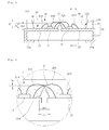
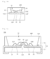
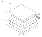
- FIG. 1 is a sectional view showing of a light emitting device according to the first example
- FIG. 2 is a partially enlarged view of FIG. 1
- FIG. 3 is a section view taken along A-A of FIG. 1
- FIG. 4 is a plan view of FIG. 1 .
- the light emitting device 100 may comprise a body 10, lead electrodes 21 and 22, light emitting diodes 32 and 32, resin layers 41, 42 and 43, and a barrier section 51.
- the body 10 may be formed by using an insulating material.
- the body 10 may comprise at least one of a resin material, such as PPA (polyphthalamide), LCP (liquid crystal polymer) or PA9T (polyamide9T), a metallic material, PSG (photo sensitive glass), sapphire (A1203), and a PCB (printed circuit board).
- a resin material such as PPA (polyphthalamide), LCP (liquid crystal polymer) or PA9T (polyamide9T)
- PSG photo sensitive glass
- sapphire A1203
- PCB printed circuit board
- the body 10 may have various shapes depending on the application and design of the light emitting device 100. When viewed from the top, the body 10 may have a rectangular shape, a polygonal shape or a circular shape.
- a cathode mark may be formed at an upper portion of the body 10.
- the cathode mark may sort the first and second lead electrodes 21 and 22 of the light emitting device 100, thereby preventing the confusion for the polarity direction of the first and second lead electrodes 21 and 22.
- the body 10 may comprise a base part 11 and a reflective part 12.
- the base part 11 supports the light emitting device 100 from the bottom of the reflective part 12.
- the reflective part 12 may comprise a recess 13, which is formed around a peripheral portion of a top surface of the base part 11 and has an open top surface, and reflects the light emitted from the light emitting diodes 31 and 32.
- the reflective part 12 may be formed by using a material same to the material for the base part 11 and may be integrally formed with the base part 11.
- the reflective part 12 may be formed by using a material different from the material for the base part 11. In this case, the reflective part 12 and the base part 11 may be formed by using the insulating material.
- the recess 13 is formed in the reflective part 12.
- the recess 13 has a concave shape having an open top shape.
- the lead electrodes 21 and 22 are provided on a bottom of the recess 13 while being electrically separated from each other.
- An inner wall of the reflective part 12 may be a circumference of the recess 13, which may be perpendicular or inclined at an angle of about 10° to about 80°, but the example is not limited thereto.
- An edge portion of the inner wall of the reflective part 12 provided between two adjacent planes may be curved or inclined at a predetermined angle.
- the recess 13 When viewed from the top, the recess 13 may have a circular shape, an oval shape or a polygonal shape, but the example is not limited thereto.
- the lead electrodes 21 and 22 are provided while being electrically separated from each other.
- the lead electrodes 21 and 22 may be metal plates having a predetermined thickness. A metal layer may be coated on the metal plates, but the example is not limited thereto.
- the lead electrodes 21 and 22 may comprise a metallic material.
- the lead electrodes 21 and 22 may comprise at least one of Ti, Cu, Ni, Au, Cr, Ta, Pt, Sn, Ag, and P.
- the lead electrodes 21 and 22 may comprise a single-layer structure or a multi-layer structure, but the example is not limited thereto.
- the lead electrodes 21 and 22 are provided on the bottom of the recess 13 and are exposed to the outside by passing through the body 10. In detail, the lead electrodes 21 and 22 are exposed to the outside by passing through between the base part 11 and the reflective part 12 of the body 10. In addition, other ends 21A and 22A of the lead electrodes 21 and 22 are disposed on a bottom surface or an outer side of the body 10 so as to be used as electrode terminals. In addition, the lead electrodes 21 and 22 can be provided in the base part 11 of the body 10 as a via structure, but the example is not limited thereto.
- the light emitting diodes 31 and 32 may be provided in the recess 13.
- the light emitting diodes 31 and 32 may emit lights having colors same to or different from each other.
- the light emitting diodes 31 and 32 may emit the light of a visible ray band, such as a red light, a green light, a blue light or a white light, or an ultraviolet band, but the example is not limited thereto.
- the light emitting diodes 31 and 32 may be prepared as a horizontal chip in which two electrodes are aligned in parallel to each other, and/or as a vertical chip in which two electrodes are aligned in opposition to each other.
- the horizontal chip may be connected to at least two wires and the vertical chip may be connected to at least one wire.
- the light emitting diodes 31 and 32 are electrically connected to the first and second lead electrode 22 through the wire bonding scheme, the flip chip scheme or the die bonding scheme.
- the first light emitting diode 31 is connected to the first and second lead electrodes 21 and 22 through a plurality of wires 31A and 31B
- the second light emitting diode 32 is connected to the first and second lead electrodes 21 and 22 through a plurality of wires 32A and 32B.
- the barrier section 51 is disposed between the first and second light emitting diodes 31 and 32.
- the barrier section 51 protrudes upward from the base part 11 of the body 10 and comprises a material same to the material for the body 10.
- the barrier section 51 may comprise an insulating material different from the material for the body 10, but the example is not limited thereto.
- the bottom surface of the recess 13 may be divided into at least two regions 13A and 13B by the barrier section 51.
- the divisional regions 13A and 13B may have the same size or different size, but the example is not limited thereto.
- the barrier section 51 has a sectional shape, in which a width W1 of a lower portion is larger than a width of an upper portion.
- the barrier section 51 may have a sectional shape comprising at least one of a triangle, a rectangle, a trapezoid, a hemisphere, and a combination thereof.
- the lower width W1 of the barrier section 51 may be larger than a gap G1 between the first and second lead electrodes 21 and 22. In this case, the amount of moisture penetrating into the body 10 through the gap G1 between the first and second lead electrodes 21 and 22 can be reduced.
- the height D2 of the barrier section 51 can be measured from the bottom surface of the recess 13 or the top surface of the first and second lead electrodes 21 and 22.
- the barrier section 51 may have the height of about 20! ⁇ m or above, preferably, about 100 ⁇ m to about 150Vm.
- the height D2 of the barrier section 51 is longer than a thickness of the light emitting diodes 31 and 32 and shorter than a depth D of the recess 13.
- the barrier section 51 is positioned lower than the wires 31B and 32A extending above the barrier section 51.
- the wires 31B and 32A are disposed such that a gap D4 having a size of abut 50 ⁇ m may be formed between the wires 31B and 32A and the top surface of the barrier section 51.
- a length L1 of the top surface of the barrier section 51 is longer than a width W2 of the bottom surface of the recess 13, but the example is not limited thereto.
- transmittive resin layers 41, 42 and 43 can be formed in the recess 13.
- the resin layers 41, 42 and 43 may comprise a resin material, such as transparent epoxy or silicone.
- a phosphor, an air gap or a diffusion agent may be selectively added to the resin layers 41, 42 and 43, but the example is not limited thereto.
- a lens may be formed on the resin layers 41, 42 and 43.
- the lens may comprise a concave lens, a convex lens or a concavo-convex lens.
- the first resin layer 41 may be formed in the first region 13A of the recess 13 and the second resin layer 42 may be formed on the second region 13B of the recess 13 about the barrier section 51.
- the first and second resin layers 41 and 42 may have the height lower than the top end of the barrier section 51. In this case, the first resin layer 41 is physically separated from the second resin layer 42 by the barrier section 51.
- the third resin layer 43 may be formed at the upper portion of the recess 13.
- the third resin layer 43 may be formed on the first and second resin layers 41 and 42.
- a phosphor having a predetermined color may be added to the third resin layer 43 or not, and the example is not limited thereto.
- the first and second resin layers 41 and 42 may have flat top surfaces.
- the first and second resin layers 41 and 42 may have the concave shapes or the convex shapes.
- the top surface of the third resin layer 43 may have a flat shape, a concave shape or a convex shape, but the example is not limited thereto.
- the first and second resin layers 41 and 42 may comprise a material (for instance, epoxy) softer than the material for the third resin layer 43, but the example is not limited thereto.
- the first light emitting diode 31 may be a blue LED chip and the second light emitting diode 32 may be a green LED chip.
- a red phosphor may be added to the first and second resin layers 41 and 42.
- the red phosphor of the first resin layer 41 absorbs the light having a blue wavelength to emit the light having a red wavelength
- the red phosphor of the second resin layer 42 absorbs the light having a green wavelength to emit the light having the red wavelength.
- the light having the blue wavelength and the light having the red wavelength are emitted through a region where the first light emitting diode 31 is disposed, and the light having the green wavelength and the light having the red wavelength are emitted through a region where the second light emitting diode 32 is disposed.
- the light having the red, green and blue wavelength can be effectively emitted, so that the color reproduction rate can be improved.
- a blue wavelength spectrum about 430nm to about 480nm
- a green wavelength spectrum about 500nm to about 550nm
- a red wavelength spectrum about 600nm to about 690nm
- the light intensity of the green wavelength and the red wavelength may be 120 or above.
- a package structure of the light emitting device may improve the efficiency of the white color as compared with the case in which the blue LED chip and the yellow phosphor are provided in one recess 13.
- the blue LED chip and the green LED chip may be driven under the same driving voltage, so the interconnection problem caused by potential difference can be simply solved.
- the light emitting diodes 31 and 32 are arrayed on the same axis Lx.
- the first and second light emitting diodes 31 and 32 may disposed within a predetermined distance (D/2) about the barrier section 51.
- the distance D between the light emitting diodes 31 and 32 in the recess 13 is same to the distance D between each light emitting diode 31 or 32 and the circumference of the recess 13.
- a plurality of first light emitting diodes 31 may be disposed in the first region 13A of the recess 13 and a plurality of second light emitting diodes 32 may be disposed in the second region 13B of the recess 13.
- the first and second light emitting diodes 31 and 32 may be connected with each other in series or parallel, but the example is not limited thereto.
- a plurality of barrier sections 51 C may be formed in the recess 13.
- Two adjacent barrier sections 51C may extend to the circumference of the recess 13 while forming a predetermined angle therebetween (for instance, 03: about 120°) about the center of the recess 13.
- the bottom surface of the recess 13 may be divided into at least three regions by the barrier sections 51C.
- the angle 03 may vary depending on the number of the regions divided by the barrier sections 51C, and the embodiment is not limited thereto.
- At least one light emitting diode 31, 32 or 33 may be disposed in each region 13A, 13B or 13C and the light emitting diode 31, 32 or 33 disposed in each region 13A, 13B or 13C may be covered with a resin layer.
- the light emitting diode 31, 32 or 33 may comprise a UV LED chip and a red phosphor, a green phosphor or a blue phosphor is added to the resin layer of each region 13A, 13B or 13C to provide the white light.
- the light emitting diode 31, 32 or 33 may comprise a red LED chip, a green LED chip or a blue LED chip.
- the light emitting diode 31, 32 or 33 may comprise the same LED chip, but the embodiment is not limited thereto.
- the resin layer and the barrier sections 51C have the height as shown in FIG. 1 .
- FIG. 7 is a sectional view showing a light emitting device according to the second example illustrating the invention.
- the light emitting device 101 may comprise a barrier section 52 disposed in the recess 13.
- a first resin layer 45 may be formed in the first region 13A divided by the barrier section 52 to cover the first light emitting diode 31 and a second resin layer 46 may be formed in the second region 13B to cover the second light emitting diode 32.
- the first light emitting diode 31 may be a blue LED chip
- the second light emitting diode 32 may be a UV LED chip
- a red phosphor may be added to the first resin layer 45
- a green phosphor may be added to the second resin layer 46.
- the light emitting device 101 may emit the lights having the color of blue, red and green.
- a parallel circuit pattern can be provided, but the example is not limited to such a circuit pattern.
- a red phosphor or a green phosphor may be added to the third resin layer 43, but the example is not limited thereto.
- FIG. 8 is a sectional view showing a light emitting device according to the third example illustrating the invention.
- the light emitting device may comprise a barrier section 51.
- the first light emitting diode 31 and the first resin layer 41 may be formed in the first region 13A of the recess 13 and the second light emitting diode 32 may be formed in the second region 13B of the recess 13 about the barrier section 51.
- a third resin layer 43A may be formed on the first resin layer 41 and in the second region 13B.
- the first light emitting diode 31 may be a blue LED chip
- the second light emitting diode 32 may be a green LED chip
- a red phosphor may be added to the first resin layer 41.
- This package structure absorbs a part of the light having the blue wavelength to convert the light into the red light, thereby reducing loss of the green light.
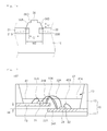
- FIG. 9 is a sectional view showing a light emitting device according to the fourth example illustrating the invention.
- the light emitting device 103 may comprise first and second light emitting diodes 31 and 32 opposite to each other about the barrier section 52, and a protective device 30 disposed below the barrier section 52 under the lead electrodes 21 and 22.
- the protective device 30 may be electrically connected to a bottom surface of the lead electrodes 21 and 22 and embedded in the base part 11.
- the protective device 30 may comprise a Zener diode or a TVS (Transient voltage suppression) diode.
- the barrier section 52 may have a trapezoidal sectional shape and both sides of the barrier section 52 correspond to both sides of the recess 13.
- a side inclination angle 02 of the barrier section 52 may be same to or different from a side inclination angle 81 of the reflective part 12. If the side inclination angle 02 of the barrier section 52 is different from the side inclination angle 81 of the reflective part 12, the following equation is satisfied: 81 > 02. Under the above angle condition, the light may be induced to be mixed at the upper portion of the recess 13 in the package.
- the first and second resin layers 47A and 47B formed in the recess may have the convex lens shape, and a convex lens 40 may be formed on the third resin layer 43.
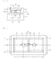
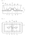
- FIG. 10 is a sectional view showing a light emitting device according to the fifth example illustrating the invention.
- the light emitting device 104 may comprise a plurality of barrier sections 52A, 52B and 52C in the recess 13.
- the barrier sections 52A, 52B and 52C may be aligned lengthwise along the body 10 at a predetermined interval.
- Lead electrodes 23, 24, 25 and 26 may be provided on regions 13D divided by the barrier sections 52A, 52B and 52C, respectively, and light emitting diodes 33 may be provided on the lead electrodes 23, 24, 25 and 26, respectively.
- the light emitting diodes 33 may comprise LED chips for emitting lights having the same color or at least two colors. For instance, the light emitting diodes 33 may be prepared as blue LED chips. In addition, the light emitting diodes 33 may comprise two blue LED chips and two green LED chips.
- the light emitting diodes 33 may be connected with each other in series or parallel, but the example is not limited thereto.
- Resin layers 48A, 48B, 48C and 48D are disposed on the regions 13D divided by the barrier sections 52A, 52B and 52C.
- a red phosphor or a phosphor having the other color may be added to the resin layers 48A, 48B, 48C and 48D, but the example is not limited thereto.
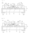
- FIG. 11 is a sectional view of a light emitting device according to the first embodiment of the invention
- FIG. 12 is a side sectional view taken along line B-B of FIG. 11 .
- the light emitting device 105 may comprise a barrier section 53 having a stepped concave part 53A. At least one concave part 53A may be formed in the barrier section 53.
- the concave part 53 has the height D5 lower than a top surface of the barrier section 53.
- the top surface of the barrier section 53 may be equal to or lower than a top surface of the reflective part 12, but the embodiment is not limited thereto.
- First and second regions 13A and 13B of the recess 13 may have a depth corresponding to a depth of the concave part 53A based on the barrier section 53.
- the depth of the concave part 53A of the barrier section 53 may be larger than the thickness of the first and second light emitting diodes 31 and 32 based on the bottom surface of the recess 13.
- the concave part 53A of the barrier section 53 may serve as a passage for a first wire 31B for connecting the first light emitting diode 31 to the second lead electrode 22 and a second wire 32A for connecting the second light emitting diode 32 to the first lead electrode 21. Since the concave part 53A serves as the passage for the first and second wires 31B and 31a, the height of the wires 31B and 31A may not be increased even if the height of the barrier section 53 is increased.
- the bottom surface of the concave part 53A may be flat or convex and both lateral sides of the concave part 53A may be inclined or perpendicular to the bottom surface of the recess 13 in correspondence with each other.
- first to third resin layers 41, 42 and 43B are formed in the recess 13.
- the first and second resin layers 41 and 42 may extend corresponding to the height D5 of the concave part 53A of the barrier section 53 from both sides of the bottom surface of the recess 13.
- the top surface of the first and second resin layers 41 and 42 may be lower than the highest point of the wires 31A, 31B, 32A and 32B.
- first and second resin layers 41 and 42 may have a thickness corresponding to the height of the top surface of the barrier section 53. In this case, the first and second resin layers 41 and 42 may be higher than the highest point of the wires 31A, 31B, 32A and 32B.
- the concave part 53A of the barrier section 53 may serve as the passage for the wires, so that the height of the barrier section may be increased as compared with that of other embodiments.
- the barrier section 53 may comprise a plurality of concave parts 53A and 53D.
- the concave parts 53A and 53D may be formed in the route of the wires 31B and 31A with a predetermined depth. Both side walls of the concave parts 53A and 53D may be inclined in the direction same to the extension direction of a virtual line drawn from one end to the other end of the wires.
- concave parts 53E and 53F are formed on the top surface of the barrier section 53.
- the concave parts 53E and 53F are stepped at least two times.
- the concave parts 53E and 53F have a two-stepped structure lower than the top surface of the barrier section 53. In this case, the center of the barrier section 53 is the lowest concave part 53F.
- FIG. 15 is a sectional view showing a light emitting device according to the sixth example illustrating the invention.
- the light emitting device 106 may comprise a barrier section 54 having a stepped sidewall in the recess 13.
- a stepped structure 54A of the barrier section 54 may be formed at the inclined sidewall of the barrier section 54 in the form of a one-stepped structure or a two-stepped structure.
- the stepped sidewall corresponds to both sidewalls 12A of the body 10.
- the stepped structure 54A of the barrier section 54 extends lengthwise along the barrier section 54.
- the stepped structure 54A of the barrier section 54 may reinforce adhesive strength of the resin layer 43B.
- the barrier section 54 may have a bar shape, a bending shape or a curved shape and may be formed along a straight line or an oblique line. A part of the barrier section 54 may be parallel to the lateral side of the recess 13, but the example is not limited thereto.
- the stepped structure of the barrier section 54 may be slantingly connected to the top surface of the barrier section 54 or perpendicularly connected to the top surface of the barrier section 54 as shown in FIG. 16 .
- the first lead electrode 21 is spaced apart from the second lead electrode 22 with a predetermined gap G1 and concavo-convex structures 21B and 22B may be formed on the top surface of the first and second lead electrodes 21 and 22.
- a lower width W2 of the barrier section 56 may be larger than the gap G1.
- a bottom surface of the barrier section 56 has a structure corresponding to the concavo-convex structures 21B and 22B of the first and second lead electrodes 21 and 22.
- the height of a stepped structure 56D at the both lateral sides 56B of the barrier section 56 may correspond to the thickness of the light emitting diode, but the example is not limited thereto.
- FIG. 17 is a sectional view showing a light emitting device according to the seventh example illustrating the invention.
- the light emitting device 107 may comprise first and second lead electrodes 23 and 23 aligned on different planes in the recess 13.
- the first lead electrode 23 may be aligned higher than the second electrode 24 in the recess 13 by a predetermined distance HI.
- a barrier section 55B may be disposed between the first and second lead electrodes 23 and 24 and the height of one lateral side of the barrier section 55B may be different from the height of the other lateral side of the barrier section 55B, so that the stepped structure of the lead electrodes 23 and 24 can be formed.
- one end of the second lead electrode 24 may overlap with the other end of the first lead electrode 23 in the vertical direction, but the example is not limited thereto.
- a second resin layer 42A may be formed on the second lead electrode 24 to cover the second light emitting diode 32.
- the thickness of the second resin layer 42A may be thicker than the thickness of the first resin layer 41. In this case, a greater amount of phosphors may be added to the second resin layer 42A as compared with the first resin layer 41. Since the thickness of the first resin layer 41 may be different from the thickness of the second resin layer 42A, quantity of light emitted from the first resin layer 41 may be different from quantity of light emitted from the second resin layer 42A. Thus, the color reproduction property may be improved based on the thickness difference between the first and second resin layers 41 and 42A.
- FIG. 18 is a sectional view showing a light emitting device according to the eighth example illustrating the invention
- FIG. 19 is a plane view of FIG. 18 .
- the light emitting device 108 may comprise a barrier section 115 on which an end portion of the first lead electrode 21 and/or the second lead electrode 22 is disposed.
- One end 121 of the first lead electrode 21 extends to one lateral side and one side of a top surface of the barrier section 115, and the other end 122 of the second lead electrode 22 extends to the other lateral side and/or the other side of the top surface of the barrier section 115.
- one end 121 of the first lead electrode 21 and the other end 122 of the second lead electrode 22 may extend to the top surface of the barrier section 115 while being physically separated from each other.
- the light reflection efficiency can be improved as compared with that of other examples and embodiments.
- the second wire 31B may be bonded to one end 121 of the first lead electrode 21 formed on one end of the barrier section 115 and the third wire 32A may be bonded to the other end 122 of the second lead electrode 22.
- the wire may not be disposed in other regions and the length of the wire can be reduced. Since the length of the wire can be reduced, the open of the wire can be prevented.
- the end portion of the first lead electrode 21 extends to the upper portion of the barrier section 155.
- the end portion of the first lead electrode 21 and/or the second lead electrode 22 may extend to the recess region. In this case, the wire bonding can be performed in each region of the recess 13.
- FIG. 20 is a sectional view showing a light emitting device according to the ninth example illustrating the invention.
- the light emitting device 109 may comprise a heat dissipation frame 116.
- the heat dissipation frame 116 may be interposed between the first and second lead electrode 21 and 22 and the first and second light emitting diodes 131 and 132 may be provided on the first and second lead electrode 21 and 22, respectively.
- the heat dissipation frame 116 may comprise bonding sections 116A and 116b disposed on the bottom surface of the recess 13, a barrier section 116D dividing the bottom surface of the recess 13, and a heat dissipation section 116C extending to the bottom surface of the body 10.
- the barrier section 116D may comprise a conductive material.
- the barrier section 116D serves as a barrier for the light emitting diodes 131 and 132 at the bottom surface of recess 13 and reflects the incident light.
- the heat dissipation section 116C transmitsthe heat generated from the light emitting diodes 131 and 132 to the downward direction, thereby improving the heat dissipation efficiency.
- the heat dissipation section 116C may have an electrode function.
- the heat dissipation section 116C may be designed to have only a heat dissipation function.
- the bonding sections 116A and 116B extend outward from both sides of the barrier section 116D.
- the light emitting diodes 131 and 132 are mounted on the bonding sections 116A and 116B, respectively.
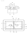
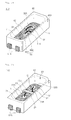
- FIG. 21 is a perspective view of a light emitting device according to the tenth example illustrating the invention
- FIG. 22 is a bottom view of FIG. 21
- FIG. 23 is a sectional view of FIG. 21 .
- the light emitting device 110 may comprise first and second lead electrodes 71 and 72 and the body 60.
- the bottom surfaces of the first and second lead electrodes 71 and 72 are aligned in line with the bottom surface of the body 60.
- a cathode mark 60A may be formed on a part of the body 60.
- the other end 71A of the first lead electrode 71 may protrude out of the body 60 and one side 72A of the second lead electrode 72 may protrude out of the body 60 in opposition to the other end 71A of the first lead electrode 71.
- the barrier section 65 protrudes between the first and second lead electrodes 71 and 72 and comprises a material same to the material for the body 60. At least the top surface of the barrier section 65 is disposed higher than the top surface of the light emitting diodes 31 and 32.
- the barrier section 65 mat have a bar shape.
- the barrier section 65 may have a constant width or the width of the barrier section 65 may vary depending on positions in the barrier section 65.
- the first and second lead electrodes 71 and 72 may be symmetrically disposed. Such a symmetrical structure can dissipate the heat generated from the light emitting diodes 31 and 32.
- the light emitting diodes 31 and 32 are connected to each other in series.
- the first light emitting diode 31 mounted on the first lead electrode 71 is directly connected to the second light emitting diode 32 mounted on the second lead electrode 72 through a wire 31C.
- an upper width W3 of the barrier section 65 may be larger than a gap G2 formed between the first lead electrode 71 and the second lead electrode 72 and a width W4 of a bottom surface 65A may be larger than the upper width W3.
- FIG. 24 is a sectional view of a light emitting device according to the eleventh example illustrating the invention.
- the light emitting device 112 may comprise a barrier section 66 having an oblique structure between the first and second lead electrodes 71 and 72.
- One side 66A of the barrier section 66 is directed to the second lead electrode 72 and the other side 66B of the barrier section 66 is directed to the first lead electrode 71 about the center of the barrier section 66 or the center of the recess 13.
- one side of the first lead electrode 71 may more extend toward the second lead electrode 72 and the other side of the second lead electrode 72 may move extend toward the first lead electrode 71.
- One side of the first lead electrode 71 is connected to the second light emitting diode 32 through a wire 32A, and the other side of the second lead electrode 72 is connected to the first light emitting diode 71 through a wire 31b.
- the wire 32A connected to the first lead electrode 71 is offset from the wire 32B connected to the second lead electrode 72.
- At least one concave part can be provided in the barrier section 66, but the example is not limited thereto.
- FIG. 25 is a sectional view of a light emitting device according to the twelfth example illustrating the invention.
- the light emitting device 113 may comprise a division section 62 formed between the first and second lead electrodes 71 and 72 and a barrier section 67 dividing the bottom surface of a recess 63 into at least two regions 63A and 63B.
- the division section 62 is aligned in the same line with the top surface of the first and second lead electrodes 71 and 72 and may comprise a material same to the material for the body 10.
- One side of the division section 62 is directed to the first lead electrode 71 and the other side of the division section 62 is directed to the second lead electrode 72 about the barrier section 67.
- one end of the second lead electrode 72 extends toward the first lead electrode 71 between the barrier section 67 and one side of the division section 62 and a part of the first lead electrode 71 extends toward the second lead electrode 72 between the barrier section 67 and the other side of the division section 62.
- the first lead electrode 71 and one end 72B of the second lead electrode 72 are disposed in a first region 63A of the recess 63 about the barrier section 67.
- the second lead electrode 72 and one end 71B of the first lead electrode 71 are disposed in a second region 63B of the recess 63 about the barrier section 67.
- the first light emitting diode 31 is mounted on the first lead electrode 71 disposed in the first region 63A of the recess 63 and electrically connected to one end 72B of the second lead electrode 72 through a wire 31B.
- the second light emitting diode 32 is mounted on the second lead electrode 72 disposed in the second region 63B of the recess 63 and electrically connected to one end 71B of the first lead electrode 71 through a wire 32A.
- the wire 31B connected to the first light emitting diode 31 may be connected to one end 72B of the second lead electrode 72 even if the wire 31B may not extend over the barrier section 67 so as to connected to the second lead electrode 72.
- the wire 32A connected to the second light emitting diode 32 may be connected to one end 71B of the first lead electrode 71 even if the wire 32A may not extend over the barrier section 67 so as to connected to the first lead electrode 71.
- a protective device 90 such as a Zener diode, may be embedded into a part of the barrier section 67. In this case, the light loss can be reduced due to the protective device 90.
- FIG. 26 is a sectional view of a light emitting device according to the thirteenth example illustrating the invention.
- the light emitting device 114 may be prepared in the form of a wafer level package.
- the light emitting device 114 may comprise the recess 13 having a predetermined depth.
- the recess 13 may be formed by etching a body 15.
- the body 15 may be prepared as a wafer level package (WLP) by using a silicon material.
- the body 15 may be formed by using Si, Al, AIN, AlOx, PSG (photo sensitive glass), A1203, or BeO.
- Silicon (Si) has advantages in terms of the fabricating efficiency of the package and the heat dissipation efficiency, so the silicon may be used for the body 15 in the example.
- the body 15 may be etched through a bulk etching process.
- the etching process may comprise at least one of a wet etching process, a dry etching process, and a laser drilling process. At least two of the above processes may be simultaneously used.
- a deep reactive ion etching process is a representative process of the dry etching process.
- the body 15 may be formed with the recess 13 having an open top surface. When viewed from the top, the body 15 may have a bath tub type concave shape, a polygonal concave shape or a circular concave shape, but the embodiment is not limited thereto.
- a patterning process is performed by using a mask and then the wet etching process is performed by using anisotropic wet etchant, such as KOH, TMAH or EDP.
- a sidewall 15A of the recess 13 of the body 15 may be inclined with respect to the bottom surface of the recess 13 at a predetermined angle or a predetermined curvature, or perpendicular to the bottom surface of the recess 13, but the embodiment is not limited thereto.
- An outer side of the body 15 may be bent at a predetermined angle.
- the outer side of the body 15 may be perpendicularly formed.
- An insulating layer 16 may be formed on the body 15.
- the insulating layer 16 may comprise at least one selected from the group consisting of a silicon thermal oxide layer (Si02 or SixOy), AlOx, a silicon nitride layer (Si3N4, SixNy, or SiOxNy), AIN and A1203, but the example is not limited thereto.
- a recess region of the body 15 may have a thickness thinner than a thickness of other regions of the body 15. Such a thickness difference may vary depending on the etching degree.
- At least one well may be formed in the body 15.
- the well may be formed by implanting or diffusing conductive impurities onto the top surface and/or the bottom surface of the body 15.
- the well is connected to at least one of the lead electrodes 121 and 122 to form a protective device, such as a Zener diode, or a constant current device.
- the lead electrodes 121 and 122 may be formed as a single layer or a multiple layer through the deposition process and/or the plating process.
- the lead electrodes 121 and 122 may have the stack structure, such as Cr/Au/Cu/Ni/Au, Cr/Cu/Cu/Ni/Au, Ti/Au/Cu/Ni/Au, Ta/Cu/Cu/ Ni/Au, or Ta/Ti/Cu/Cu/Ni/Au.
- a reflective metal and/or a bonding metal may be formed on the uppermost layer of the lead electrodes 121 and 122, but the example is not limited thereto.
- the first light emitting diode 31 may be mounted on the first lead electrode 121 and the second light emitting diode 32 may be mounted on the second lead electrode 122.
- a barrier section 117 protrudes in the recess 13.
- the barrier section 117 may be formed when the body is etched.
- the barrier section 117 may comprise a material same to the material for the insulating layer 16.
- the first lead electrode 121 extends to the bottom surface of the body 15 along one side of the body 15 in the recess 13 to form an electrode terminal 121B
- the second lead electrode 122 extends to the bottom surface of the body 15 along the other side of the body 15 in the recess 13 to form an electrode terminal 122B.
- the first and second lead electrodes 121 and 122 are spaced apart from each other in the recess 13 and separated from each other, electrically and physically.
- a part 121A of the first lead electrode 121 may extend to a lateral side and a top surface of the barrier section 117, and a part 122A of the second lead electrode 122 may extend to the lateral side and the top surface of the barrier section 117.
- end portions of the first and second lead electrodes 121 and 122 are disposed in different regions on the barrier section 117.
- end portions of the first and second lead electrodes 121 and 122 may extend to another region over the barrier section 117, but the embodiment is not limited thereto.
- the wire 31B connected to the first light emitting diode 31 may be bonded to the second lead electrode 122 disposed in the second region 13B, and the wire 32A connected to the second light emitting diode 32 may be bonded to the first lead electrode 121 disposed in the first region 13A.
- the first light emitting diode 31 may be disposed in the first region 13A, and the second light emitting diode 32 may be disposed in the second region 13B.
- a first resin layer 141 may be disposed in the first region 13A and a second resin layer 142 may be disposed in the second region 13B.
- Phosphors may be added to the first and second resin layers 141 and 142.
- red phosphors may be added to the first and second resin layers 141 and 142.
- the first light emitting diode 31 may comprise a blue light emitting diode
- the second light emitting diode 32 may comprise a green light emitting diode.
- the lights having colors of blue, green and red may be emitted, so that the white light can be provided.
- the red light may be emitted through the first and second regions 13A and 13B of the recess 13, most of the blue light may be emitted through the first region 13A of the recess 13, and most of the green light may be emitted through the second region 13B of the recess 13.
- the number of the second light emitting diodes 32 may be larger than the number of the first light emitting diodes 31, but the embodiment is not limited thereto.
- a single resin layer may be formed in the recess 13, but the example is not limited thereto.
- FIG. 27 is a sectional view of a light emitting device according to another example and FIG. 28 is a plan view of FIG. 27 .
- the description about the elements and structures described with reference to FIG. 26 may be omitted in order to avoid redundancy.
- wires 31B and 32A are bonded to one end 121C of the first lead electrode 121 and one end 122C of the second lead electrode 122 disposed on the barrier section 117 to reduce the length of the wire.
- a plurality of wires 31B and 32A having polarities different from each other may be bonded onto the barrier section 117, but the example is not limited thereto.
- the light emitting device package may have a side view type.
- a heat dissipation characteristic, conductivity, and a reflectance characteristic can be improved.
- a lens may be formed on the resin layer or the lens may be bonded with the resin, but the example is not limited thereto.
- the light emitting device according to the embodiment can be applied to the light unit.
- the light unit may comprise a plurality of light emitting devices.
- the light unit may comprise the display device as shown in FIGS. 29 and 30 and the lighting device as shown in FIG. 31 .
- the light unit having the light emitting device according to the embodiment may comprise a lighting lamp, a signal lamp, a headlight of a vehicle, and an electric signboard.
- FIG. 29 is an exploded perspective view showing the display device according to the embodiment.
- the display device 1000 may comprise a light guide plate 1041, a light emitting module 1031 for supplying the light to the light guide plate 1041, a reflective member 1022 provided below the light guide plate 1041, an optical sheet 1051 provided on the light guide plate 1041, a display panel 1061 provided on the optical sheet 1051, and a bottom cover 1011 for receiving the light guide plate 1041, the light emitting module 1031, and the reflective member 1022.
- the embodiment is not limited to the above structure.
- the bottom cover 1011, the reflective sheet 1022, the light guide plate 1041 and the optical sheet 1051 may constitute a light unit 1050.
- the light guide plate 1041 diffuses the light supplied from the light emitting module 1031 to provide surface light.
- the light guide plate 1041 may comprise transparent material.
- the light guide plate 1041 may comprise one of acryl- based resin such as PMMA (polymethyl methacrylate, PET (polyethylene terephthalate), PC (polycarbonate), COC (cyclic olefin copolymer) and PEN (polyethylene naphthalate) resin.
- PMMA polymethyl methacrylate
- PET polyethylene terephthalate
- PC polycarbonate
- COC cyclic olefin copolymer
- PEN polyethylene naphthalate
- the light emitting module 1031 supplies the light to at least one side of the light guide plate 1041.
- the light emitting module 1031 serves as the light source of the display device.
- At least one light emitting module 1031 may be provided to directly or indirectly supply the light from one side of the light guide plate 1041.
- the light emitting module 1031 may comprise a board 1033 and the light emitting devices 200 according to the embodiments.
- the light emitting devices 200 may be arrayed on the board 1033 while being spaced apart from each other at the predetermined interval.
- the board 1033 may comprise a printed circuit board (PCB) having a circuit pattern.
- the board 1033 may also comprise a metal core PCB (MCPCB) or a flexible PCB (FPCB), but the embodiment is not limited thereto. If the light emitting devices 200 may be provided on the side of the bottom cover 1011 or on a heat dissipation plate, the board 1033 may be omitted. The heat dissipation plate partially makes contact with the top surface of the bottom cover 1011.
- the light emitting devices 200 may be arranged such that light exit surfaces of the light emitting devices 200 are spaced apart from the light guide plate 1041 by a predetermined distance, but the embodiment is not limited thereto.
- the light emitting devices 200 may directly or indirectly supply the light to a light incident surface, which is one side of the light guide plate 1041, but the example is not limited thereto.
- the reflective member 1022 is disposed below the light guide plate 1041.
- the reflective member 1022 reflects the light, which is travelled downward through the bottom surface of the light guide plate 1041, in the upward direction, thereby improving the brightness of the light unit 1050.
- the reflective member 1022 may comprise PET, PC or PVC resin, but the embodiment is not limited thereto.
- the reflective member 1022 may serve as the top surface of the bottom cover 1011, but the example is not limited thereto.
- the bottom cover 1011 may receive the light guide plate 1041, the light emitting module 1031, and the reflective member 1022 therein. To this end, the bottom cover 1011 has a receiving section 1012 having a box shape with an open top surface, but the example is not limited thereto. The bottom cover 1011 may be coupled with a top cover, but the embodiment is not limited thereto.
- the bottom cover 1011 may be manufactured through a press process or an extrusion process by using a metallic material or a resin material.
- the bottom cover 1011 may comprise metal or non-metallic material having superior thermal conductivity, but the example is not limited thereto.
- the display panel 1061 may be an LCD panel comprising first and second transparent substrates, which are opposite to each other, and a liquid crystal layer interposed between the first and second substrates.
- a polarizing plate may be attached to at least one surface of the display panel 1061, but the embodiment is not limited thereto.
- the display panel 1061 displays information by using the light passing through the optical sheet 1051.
- the display device 1000 may be applied to various portable terminals, monitors of notebook computers, monitors or laptop computers, and televisions.
- the optical sheet 1051 may be disposed between the display panel 1061 and the light guide plate 1041 and comprise at least one transmittive sheet.
- the optical sheet 1051 may comprise at least one of a diffusion sheet, a horizontal and vertical prism sheet, and a brightness enhanced sheet.
- the diffusion sheet diffuses the incident light
- the horizontal and vertical prism sheet concentrates the incident light onto the display region
- the brightness enhanced sheet improves the brightness by reusing the lost light.
- a protective sheet may be provided on the display panel 1061, but the example is not limited thereto.
- the light guide plate 1041 and the optical sheet 1051 may be provided in the light path of the light emitting module 1031 as optical members, but the embodiment is not limited thereto.
- FIG. 30 is a sectional view showing the display device according to the example.
- the display device 1100 may comprise a bottom cover 1152, a board 1120 on which the light emitting devices 200 are arrayed, an optical member 1154, and a display panel 1155.
- the board 1120 and the light emitting devices 200 may constitute the light emitting module 1060.
- the bottom cover 1152, at least one light emitting module 1060, and the optical member 1154 may constitute the light unit.
- the bottom cover 1151 may be provided with a receiving section 1153, but the example is not limited thereto.
- the optical member 1154 may comprise at least one of a lens, a light guide plate, a diffusion sheet, a horizontal and vertical prism sheet, and a brightness enhanced sheet.
- the light guide plate may comprise PC or PMMA (Poly methyl methacrylate). The light guide plate can be omitted.
- the diffusion sheet diffuses the incident light
- the horizontal and vertical prism sheet concentrates the incident light onto the display region
- the brightness enhanced sheet improves the brightness by reusing the lost light.
- the optical member 1154 is disposed on the light emitting module 1060 in order to convert the light emitted from the light emitting module 1060 into the surface light. In addition, the optical member 1154 may diffuse or concentrate the light.
- FIG. 31 is a perspective view showing a lighting device according to the example.
- the lighting device 1500 may comprise a case 1510, a light emitting module 1530 provided in the case 1510, and a connection terminal 1520 provided in the case 1510 to receive power from an external power source.
- the case 1510 may comprise a material having superior heat dissipation property.
- the case 1510 may comprise a metallic material or a resin material.
- the light emitting module 1530 may comprise a board 1532 and light emitting devices 200 provided on the board 1532.
- the light emitting devices 200 may be spaced apart from each other or arrayed in the form of a matrix.
- the board 1532 may comprise an insulating member printed with a circuit pattern.
- the board 1532 may comprise at least one of a PCB, an MCPCB, an FPCB, a ceramic PCB, and an FR-4 substrate.
- the board 1532 may comprise a material that effectively reflects the light.
- a coating layer may be formed on the surface of the substrate 1532. At this time, the coating layer has a white color or a silver color to effectively reflect the light.
- At least one light emitting device 200 may be provided on the board 1532.
- Each light emitting device 200 may comprise at least one LED (light emitting diode) chip.
- the LED chip may comprise an LED that emits the light of visible ray band having red, green, blue or white color and a UV (ultraviolet) LED that emits UV light.
- the light emitting devices 200 of the light emitting module 1530 may be variously combined to provide various colors and brightness.
- the white LED, the red LED and the green LED may be combined to achieve the high color rendering index (CRI).
- connection terminal 1520 may be electrically connected to the light emitting module 1530 to supply power to the light emitting module 1530.
- the connection terminal 1520 may have a shape of a socket screw-coupled with the external power source, but the embodiment is not limited thereto.
- the connection terminal 1520 may be prepared in the form of a pin inserted into the external power source or connected to the external power source through a wire.
- the light emitting devices 200 may be packaged and then mounted on the board to provide the light emitting module, or the light emitting devices 200 may be mounted in the form of the LED chip and then packaged to provide the light emitting module.
- any reference in this specification to "one embodiment,” “an embodiment,” “example embodiment,” etc. means that a particular feature, structure, or characteristic described in connection with the embodiment is included in at least one embodiment of the invention.
- the appearances of such phrases in various places in the specification are not necessarily all referring to the same embodiment.
Landscapes
- Engineering & Computer Science (AREA)
- Microelectronics & Electronic Packaging (AREA)
- Manufacturing & Machinery (AREA)
- Computer Hardware Design (AREA)
- Power Engineering (AREA)
- Led Device Packages (AREA)
- Non-Portable Lighting Devices Or Systems Thereof (AREA)
Claims (15)
- Lichtemittierende Vorrichtung mit:einem Körper (10), der eine Vertiefung (13) aufweist;einem Trennsegment (53), das über eine Bodenfläche der Vertiefung nach oben hervorsteht und die Bodenfläche der Vertiefung in eine Vielzahl von Bereichen (13A; 13B) unterteilt;einer Vielzahl von lichtemittierenden Dioden (31; 32), die eine erste lichtemittierende Diode (31) in einem ersten Bereich (13A) der Bodenfläche der Vertiefung und eine zweite lichtemittierende Diode (32) in einem zweiten Bereich (13B) der Bodenfläche der Vertiefung umfasst;einer Vielzahl von Leitungselektroden (21; 22), die in der Vertiefung zueinander beabstandet und selektiv an die lichtemittierenden Dioden angeschlossen sind, wobei die Vielzahl der Leitungselektroden eine erste Leitungselektrode (21) und eine zweite Leitungselektrode (22) aufweist;Drähten (31A; 31B; 32; 32B), welche die Leitungselektroden mit den lichtemittierenden Dioden verbinden, wobei die Drähte einen ersten Draht (31B) und einen zweiten Draht (32A) aufweisen; undeiner Harzschicht (41; 42) in der Vertiefung,dadurch gekennzeichnet, dassdas Trennsegment (53) einen ersten Abschnitt (53B), einen zweiten Abschnitt (53A) und einen dritten Abschnitt (53B) umfasst,der zweite Abschnitt eine Höhe (D5) hat, die von der Bodenfläche der Vertiefung aus geringer ist als die Höhe (D6) des ersten Abschnitts und als die Höhe (D6) des dritten Abschnitts,die erste Leitungselektrode (21) im ersten Bereich (13A) vorgesehen ist,die zweite Leitungselektrode (22) im zweiten Bereich (13B) vorgesehen ist,der erste Draht (31B) die erste lichtemittierende Diode (31) durch den zweiten Abschnitt (53A) hindurch elektrisch an die zweite Leitungselektrode (22) anschließt, undder zweite Draht (32A) die zweite lichtemittierende Diode (32) durch den zweiten Abschnitt (53A) hindurch elektrisch an die erste Leitungselektrode (21) anschließt.
- Lichtemittierende Vorrichtung nach Anspruch 1, wobei der erste Abschnitt (53B) und der dritte Abschnitt (53B) zueinander beabstandet sind.
- Lichtemittierende Vorrichtung nach Anspruch 1, wobei eine Oberseite des ersten Abschnitts (53B) höher ist als der höchste Punkt der Drähte (31B; 32A).
- Lichtemittierende Vorrichtung nach Anspruch 1, wobei die Harzschicht Folgendes umfasst: eine erste Harzschicht (41) im ersten Bereich (13A) der Vertiefung (13) und eine zweite Harzschicht (42) im zweiten Bereich (13B) der Vertiefung.
- Lichtemittierende Vorrichtung nach Anspruch 4, die weiterhin wenigstens einen Typ Phosphor umfasst, der mindestens einer von der ersten und der zweiten Harzschicht (41; 42) beigemischt ist.
- Lichtemittierende Vorrichtung nach Anspruch 4, wobei die erste und die zweite Harzschicht (41; 42) eine Dicke aufweisen, die geringer ist als die Höhe (D6) des ersten Abschnitts (53B).
- Lichtemittierende Vorrichtung nach Anspruch 4, wobei die erste lichtemittierende Diode (31) eine blaue lichtemittierende Diode umfasst, die zweite lichtemittierende Diode (32) eine grüne lichtemittierende Diode umfasst und der ersten und zweiten Harzschicht (41; 42) roter Phosphor beigemischt ist.
- Lichtemittierende Vorrichtung nach Anspruch 4, wobei die erste lichtemittierende Diode (31) eine blaue lichtemittierende Diode umfasst, die zweite lichtemittierende Diode (32) eine UV-Licht emittierende Diode umfasst und der ersten Harzschicht (41) roter Phosphor beigemischt ist und der zweiten Harzschicht (42) grüner Phosphor beigemischt ist.
- Lichtemittierende Vorrichtung nach Anspruch 1, wobei das Trennsegment (53) einen Isolierwerkstoff oder ein leitfähiges Material umfasst.
- Lichtemittierende Vorrichtung nach Anspruch 1, wobei der zweite Abschnitt (53A) des Trennsegments (53), gemessen von der Bodenfläche der Vertiefung (13), eine Höhe (D5) hat, die größer ist als die Dicke der ersten und der zweiten lichtemittierenden Diode (31; 32).
- Lichtemittierende Vorrichtung nach Anspruch 1, wobei beide Seiten des Trennsegments (53) den unterteilten Bereichen der Vertiefung (13) entsprechen und eine Struktur umfassen, die zur Bodenfläche der Vertiefung geneigt ist oder senkrecht zu ihr verläuft.
- Lichtemittierende Vorrichtung nach Anspruch 1, wobei die erste Leitungselektrode (21) im ersten Bereich (13A) der Vertiefung (13) mit einer ersten Tiefe angeordnet ist und die zweite Leitungselektrode (22) im zweiten Bereich (13B) mit einer zweiten Tiefe angeordnet ist, die größer als die erste Tiefe ist.
- Lichtemittierende Vorrichtung nach Anspruch 4, welche auf der ersten Harzschicht (41) und der zweiten Harzschicht (42) weiterhin eine dritte Harzschicht (43) umfasst.
- Lichtemittierende Vorrichtung nach Anspruch 1, wobei sich wenigstens ein Endabschnitt (121) der Leitungselektroden (21; 22) bis zur Oberseite des Trennsegments (115) erstreckt.
- Leuchteinheit mit:einem lichtemittierenden Modul, welches eine lichtemittierende Vorrichtung nach einem der Ansprüche 1 bis 14 und eine Platine umfasst, auf der die lichtemittierende Vorrichtung angeordnet ist; undeine Lichtleitplatte, die auf dem Weg des Lichts angeordnet ist, das von dem lichtemittierenden Modul emittiert wird.
Applications Claiming Priority (1)
| Application Number | Priority Date | Filing Date | Title |
|---|---|---|---|
| KR1020100048291A KR101039994B1 (ko) | 2010-05-24 | 2010-05-24 | 발광소자 및 이를 구비한 라이트 유닛 |
Publications (2)
| Publication Number | Publication Date |
|---|---|
| EP2390915A1 EP2390915A1 (de) | 2011-11-30 |
| EP2390915B1 true EP2390915B1 (de) | 2014-10-08 |
Family
ID=44351639
Family Applications (1)
| Application Number | Title | Priority Date | Filing Date |
|---|---|---|---|
| EP11167007.1A Active EP2390915B1 (de) | 2010-05-24 | 2011-05-20 | Lichtemittierende Vorrichtung und diese enthaltende Leuchteinheit |
Country Status (6)
| Country | Link |
|---|---|
| US (2) | US8324654B2 (de) |
| EP (1) | EP2390915B1 (de) |
| JP (1) | JP2011249807A (de) |
| KR (1) | KR101039994B1 (de) |
| CN (1) | CN102263098B (de) |
| TW (1) | TWI521750B (de) |
Cited By (1)
| Publication number | Priority date | Publication date | Assignee | Title |
|---|---|---|---|---|
| CN116435201A (zh) * | 2023-06-12 | 2023-07-14 | 四川遂宁市利普芯微电子有限公司 | 一种塑封封装方法以及器件封装结构 |
Families Citing this family (134)
| Publication number | Priority date | Publication date | Assignee | Title |
|---|---|---|---|---|
| US7728345B2 (en) * | 2001-08-24 | 2010-06-01 | Cao Group, Inc. | Semiconductor light source for illuminating a physical space including a 3-dimensional lead frame |
| US8704265B2 (en) * | 2007-08-27 | 2014-04-22 | Lg Electronics Inc. | Light emitting device package and lighting apparatus using the same |
| US10256385B2 (en) | 2007-10-31 | 2019-04-09 | Cree, Inc. | Light emitting die (LED) packages and related methods |
| US8791471B2 (en) * | 2008-11-07 | 2014-07-29 | Cree Hong Kong Limited | Multi-chip light emitting diode modules |
| WO2011037185A1 (ja) * | 2009-09-24 | 2011-03-31 | 京セラ株式会社 | 実装用基板、発光体、および実装用基板の製造方法 |
| KR101039994B1 (ko) * | 2010-05-24 | 2011-06-09 | 엘지이노텍 주식회사 | 발광소자 및 이를 구비한 라이트 유닛 |
| KR101064036B1 (ko) * | 2010-06-01 | 2011-09-08 | 엘지이노텍 주식회사 | 발광 소자 패키지 및 조명 시스템 |
| JP2012104739A (ja) * | 2010-11-12 | 2012-05-31 | Toshiba Corp | 発光素子 |
| KR101411255B1 (ko) * | 2011-01-28 | 2014-06-23 | 삼성디스플레이 주식회사 | 광원 모듈 및 이의 제조 방법 |
| US20120314419A1 (en) * | 2011-06-08 | 2012-12-13 | Wen-Kung Sung | Heat dissipation structure of light-emitting diode |
| DE102011104302A1 (de) * | 2011-06-16 | 2012-12-20 | Osram Opto Semiconductors Gmbh | Optoelektronisches Halbleiterbauelement und Verwendung eines derartigen Halbleiterbauelements |
| JP5527286B2 (ja) * | 2011-06-29 | 2014-06-18 | 豊田合成株式会社 | 発光装置 |
| DE102011079403A1 (de) * | 2011-07-19 | 2013-01-24 | Osram Opto Semiconductors Gmbh | Optoelektronisches Bauelement und Verfahren zur Herstellung eines optoelektronischen Bauelements |
| KR101871501B1 (ko) | 2011-07-29 | 2018-06-27 | 엘지이노텍 주식회사 | 발광 소자 패키지 및 이를 구비한 조명 시스템 |
| CN102916108B (zh) * | 2011-08-05 | 2015-09-09 | 展晶科技(深圳)有限公司 | 发光二极管封装结构 |
| KR101237794B1 (ko) * | 2011-08-12 | 2013-02-28 | 주식회사 루멘스 | 발광소자 패키지 및 이를 구비하는 백라이트 유닛 |
| CN103000782B (zh) * | 2011-09-13 | 2016-09-07 | 展晶科技(深圳)有限公司 | 发光二极管封装结构 |
| CN107654912B (zh) * | 2011-11-01 | 2020-03-17 | 日亚化学工业株式会社 | 发光装置及照明器具 |
| TWI508332B (zh) * | 2011-11-09 | 2015-11-11 | Au Optronics Corp | 發光光源及其顯示面板 |
| US9223138B2 (en) | 2011-12-23 | 2015-12-29 | Microsoft Technology Licensing, Llc | Pixel opacity for augmented reality |
| CN103187485A (zh) * | 2011-12-27 | 2013-07-03 | 展晶科技(深圳)有限公司 | 发光二极管的制造方法 |
| CN103187487A (zh) * | 2011-12-28 | 2013-07-03 | 展晶科技(深圳)有限公司 | 半导体封装制程及其封装结构 |
| JP6196018B2 (ja) * | 2012-01-19 | 2017-09-13 | 株式会社小糸製作所 | 発光装置 |
| US9606586B2 (en) | 2012-01-23 | 2017-03-28 | Microsoft Technology Licensing, Llc | Heat transfer device |
| DE102013201363A1 (de) | 2012-01-31 | 2013-08-01 | Nichia Corp. | Lichtemittierendes Bauelement |
| JP6064606B2 (ja) * | 2012-01-31 | 2017-01-25 | 日亜化学工業株式会社 | 発光装置 |
| US9368546B2 (en) | 2012-02-15 | 2016-06-14 | Microsoft Technology Licensing, Llc | Imaging structure with embedded light sources |
| US9726887B2 (en) * | 2012-02-15 | 2017-08-08 | Microsoft Technology Licensing, Llc | Imaging structure color conversion |
| US9297996B2 (en) | 2012-02-15 | 2016-03-29 | Microsoft Technology Licensing, Llc | Laser illumination scanning |
| US9779643B2 (en) | 2012-02-15 | 2017-10-03 | Microsoft Technology Licensing, Llc | Imaging structure emitter configurations |
| JP2013182975A (ja) * | 2012-03-01 | 2013-09-12 | Sharp Corp | 発光装置及びこれを用いたバックライトシステム |
| US8858025B2 (en) * | 2012-03-07 | 2014-10-14 | Lg Innotek Co., Ltd. | Lighting device |
| US9578318B2 (en) | 2012-03-14 | 2017-02-21 | Microsoft Technology Licensing, Llc | Imaging structure emitter calibration |
| DE102012102301B4 (de) * | 2012-03-19 | 2021-06-17 | OSRAM Opto Semiconductors Gesellschaft mit beschränkter Haftung | Optoelektronischer Halbleiterchip und Scheinwerfer mit einem solchen Halbleiterchip |
| JP2013197369A (ja) * | 2012-03-21 | 2013-09-30 | Rohm Co Ltd | 光源装置およびledランプ |
| US11068049B2 (en) | 2012-03-23 | 2021-07-20 | Microsoft Technology Licensing, Llc | Light guide display and field of view |
| US9558590B2 (en) | 2012-03-28 | 2017-01-31 | Microsoft Technology Licensing, Llc | Augmented reality light guide display |
| US10191515B2 (en) | 2012-03-28 | 2019-01-29 | Microsoft Technology Licensing, Llc | Mobile device light guide display |
| US9717981B2 (en) | 2012-04-05 | 2017-08-01 | Microsoft Technology Licensing, Llc | Augmented reality and physical games |
| CN103378278B (zh) * | 2012-04-28 | 2016-01-06 | 展晶科技(深圳)有限公司 | 发光二极管封装结构 |
| KR101957884B1 (ko) * | 2012-05-14 | 2019-03-13 | 엘지이노텍 주식회사 | 발광 소자, 발광 소자 제조방법 및 조명 장치 |
| US10502876B2 (en) | 2012-05-22 | 2019-12-10 | Microsoft Technology Licensing, Llc | Waveguide optics focus elements |
| CN102709441A (zh) * | 2012-05-24 | 2012-10-03 | 重庆四联光电科技有限公司 | Led封装结构 |
| US8989535B2 (en) | 2012-06-04 | 2015-03-24 | Microsoft Technology Licensing, Llc | Multiple waveguide imaging structure |
| CN102800785A (zh) * | 2012-06-25 | 2012-11-28 | 浙江英特来光电科技有限公司 | 一种分离式可调光贴片smdled白灯 |
| CN103515367B (zh) * | 2012-06-25 | 2016-10-05 | 青岛玉兰祥商务服务有限公司 | 发光二极管封装结构 |
| DE102012105677B4 (de) | 2012-06-28 | 2016-06-09 | Osram Opto Semiconductors Gmbh | Leuchtdiodenmodul und Kfz-Scheinwerfer |
| KR20140004881A (ko) * | 2012-07-03 | 2014-01-14 | 삼성디스플레이 주식회사 | 백라이트 유닛 |
| TWM448801U (zh) * | 2012-07-04 | 2013-03-11 | Dow Corning Taiwan Inc | 發光二極體裝置及導線架料片 |
| TW201403789A (zh) * | 2012-07-06 | 2014-01-16 | Lextar Electronics Corp | 發光二極體陣列 |
| TWI473294B (zh) * | 2012-08-03 | 2015-02-11 | Genesis Photonics Inc | 發光裝置 |
| JP5686262B2 (ja) * | 2012-08-17 | 2015-03-18 | 復盛精密工業股▲ふん▼有限公司 | 発光ダイオードのリードフレームアセンブリーの製造方法 |
| US8960933B2 (en) * | 2012-08-24 | 2015-02-24 | Salvatore Guerrieri | LED housing |
| KR101998762B1 (ko) * | 2012-08-24 | 2019-07-10 | 엘지이노텍 주식회사 | 발광 소자 패키지 |
| DE102012107829B4 (de) * | 2012-08-24 | 2024-01-25 | OSRAM Opto Semiconductors Gesellschaft mit beschränkter Haftung | Optoelektronische Bauelemente und Verfahren zur Herstellung eines optoelektronischen Bauelements |
| WO2014030148A2 (en) * | 2012-08-24 | 2014-02-27 | Koninklijke Philips N.V. | A light emitting assembly, a lamp and a luminaire |
| CN103682028A (zh) * | 2012-08-30 | 2014-03-26 | 展晶科技(深圳)有限公司 | 发光二极管封装结构及其制造方法 |
| CN103682018B (zh) * | 2012-09-21 | 2017-04-26 | 展晶科技(深圳)有限公司 | 发光二极管及其制造方法 |
| CN104882439B (zh) * | 2012-09-29 | 2019-01-15 | 四川新力光源股份有限公司 | Led器件 |
| JP6102187B2 (ja) | 2012-10-31 | 2017-03-29 | 日亜化学工業株式会社 | 発光装置用パッケージ及びそれを用いた発光装置 |
| EP2915197B1 (de) * | 2012-11-01 | 2020-02-05 | Lumileds Holding B.V. | Led-basierte vorrichtung mit breiter farbskala |
| TW201418843A (zh) * | 2012-11-09 | 2014-05-16 | Innocom Tech Shenzhen Co Ltd | 液晶顯示器、背光模組及其發光二極體組件 |
| CN103807665A (zh) * | 2012-11-09 | 2014-05-21 | 群康科技(深圳)有限公司 | 液晶显示器、背光模块及其发光二极管组件 |
| CN102931179A (zh) * | 2012-11-14 | 2013-02-13 | 南京市江宁区丁卯电子科技中心 | 一种发光装置 |
| KR101997249B1 (ko) * | 2012-11-14 | 2019-07-08 | 엘지이노텍 주식회사 | 발광 소자 |
| CN103094452A (zh) * | 2012-11-14 | 2013-05-08 | 南京市江宁区丁卯电子科技中心 | 一种led的封装方法 |
| KR102019503B1 (ko) * | 2012-12-07 | 2019-09-06 | 엘지이노텍 주식회사 | 발광 소자 및 이를 구비한 조명 시스템 |
| JP6224320B2 (ja) * | 2012-12-19 | 2017-11-01 | ローム株式会社 | Ledモジュール |
| US10192358B2 (en) | 2012-12-20 | 2019-01-29 | Microsoft Technology Licensing, Llc | Auto-stereoscopic augmented reality display |
| JP6107136B2 (ja) | 2012-12-29 | 2017-04-05 | 日亜化学工業株式会社 | 発光装置用パッケージ及びそれを備える発光装置、並びにその発光装置を備える照明装置 |
| TWI660527B (zh) * | 2013-02-08 | 2019-05-21 | 晶元光電股份有限公司 | 發光二極體元件及其製造方法 |
| KR101605666B1 (ko) | 2013-02-20 | 2016-03-22 | 미쓰비시덴키 가부시키가이샤 | 냉각 장치 및 이것을 이용한 냉각 장치가 부착된 파워 모듈 |
| JP6476567B2 (ja) * | 2013-03-29 | 2019-03-06 | 日亜化学工業株式会社 | 発光装置 |
| CN103280511B (zh) * | 2013-05-27 | 2017-02-15 | 广东深莱特科技股份有限公司 | 用于防led引线断开的分压装置及其使用方法 |
| CN103346238A (zh) * | 2013-06-24 | 2013-10-09 | 深圳雷曼光电科技股份有限公司 | 一种表面贴装式led支架、led器件及led显示屏 |
| JP6484396B2 (ja) | 2013-06-28 | 2019-03-13 | 日亜化学工業株式会社 | 発光装置用パッケージ及びそれを用いた発光装置 |
| TWI523277B (zh) * | 2013-07-12 | 2016-02-21 | White light emitting diode module with ultraviolet light | |
| JP2015041685A (ja) * | 2013-08-21 | 2015-03-02 | 豊田合成株式会社 | 発光装置 |
| KR20150025231A (ko) * | 2013-08-28 | 2015-03-10 | 서울반도체 주식회사 | 광원 모듈 및 그 제조 방법, 및 백라이트 유닛 |
| JP6230392B2 (ja) * | 2013-11-29 | 2017-11-15 | シチズン電子株式会社 | 発光装置 |
| TWI559578B (zh) * | 2014-03-11 | 2016-11-21 | Bright Led Electronics Corp | A light-emitting diode module with mixed light |
| CN103872218B (zh) * | 2014-03-18 | 2016-09-28 | 深圳市瑞丰光电子股份有限公司 | Led支架及led发光体 |
| DE102014208960A1 (de) * | 2014-05-12 | 2015-11-12 | Osram Opto Semiconductors Gmbh | Oberflächenmontierbares optoelektronisches Bauelement und Verfahren zum Herstellen eines oberflächenmontierbaren optoelektronischen Bauelements |
| CN104037169B (zh) * | 2014-06-19 | 2017-02-22 | 深圳市华星光电技术有限公司 | 一种led封装结构及液晶显示装置 |
| WO2016006444A1 (ja) * | 2014-07-08 | 2016-01-14 | シャープ株式会社 | 発光装置 |
| US9304235B2 (en) | 2014-07-30 | 2016-04-05 | Microsoft Technology Licensing, Llc | Microfabrication |
| US10254942B2 (en) | 2014-07-31 | 2019-04-09 | Microsoft Technology Licensing, Llc | Adaptive sizing and positioning of application windows |
| US10592080B2 (en) | 2014-07-31 | 2020-03-17 | Microsoft Technology Licensing, Llc | Assisted presentation of application windows |
| US10678412B2 (en) | 2014-07-31 | 2020-06-09 | Microsoft Technology Licensing, Llc | Dynamic joint dividers for application windows |
| KR102170218B1 (ko) * | 2014-08-05 | 2020-10-26 | 엘지이노텍 주식회사 | 발광소자 패키지 |
| JP6524624B2 (ja) * | 2014-09-19 | 2019-06-05 | 日亜化学工業株式会社 | 発光装置 |
| US9853197B2 (en) * | 2014-09-29 | 2017-12-26 | Bridgelux, Inc. | Light emitting diode package having series connected LEDs |
| CN105591007B (zh) * | 2014-10-23 | 2018-04-03 | 展晶科技(深圳)有限公司 | 发光二极管封装结构 |
| JP6256699B2 (ja) * | 2014-11-11 | 2018-01-10 | 豊田合成株式会社 | 発光装置 |
| EP3232482A4 (de) * | 2014-12-11 | 2018-05-23 | Citizen Electronics Co., Ltd | Lichtemittierende vorrichtung |
| JP6827265B2 (ja) * | 2015-01-05 | 2021-02-10 | シチズン電子株式会社 | Led発光装置 |
| JP2016138901A (ja) * | 2015-01-26 | 2016-08-04 | 株式会社日立エルジーデータストレージ | 光モジュール、及び走査型画像表示装置 |
| US9535253B2 (en) | 2015-02-09 | 2017-01-03 | Microsoft Technology Licensing, Llc | Display system |
| US9513480B2 (en) | 2015-02-09 | 2016-12-06 | Microsoft Technology Licensing, Llc | Waveguide |
| US10018844B2 (en) | 2015-02-09 | 2018-07-10 | Microsoft Technology Licensing, Llc | Wearable image display system |
| US9827209B2 (en) | 2015-02-09 | 2017-11-28 | Microsoft Technology Licensing, Llc | Display system |
| US9429692B1 (en) | 2015-02-09 | 2016-08-30 | Microsoft Technology Licensing, Llc | Optical components |
| US11086216B2 (en) | 2015-02-09 | 2021-08-10 | Microsoft Technology Licensing, Llc | Generating electronic components |
| US10317677B2 (en) | 2015-02-09 | 2019-06-11 | Microsoft Technology Licensing, Llc | Display system |
| US9372347B1 (en) | 2015-02-09 | 2016-06-21 | Microsoft Technology Licensing, Llc | Display system |
| US9423360B1 (en) | 2015-02-09 | 2016-08-23 | Microsoft Technology Licensing, Llc | Optical components |
| US20180040780A1 (en) * | 2015-02-13 | 2018-02-08 | Citizen Electronics Co., Ltd. | Light-emitting device and method for producing the same |
| KR102408618B1 (ko) * | 2015-02-16 | 2022-06-14 | 쑤저우 레킨 세미컨덕터 컴퍼니 리미티드 | 발광 소자 패키지 및 이를 포함하는 조명 장치 |
| JP6811183B2 (ja) * | 2015-03-06 | 2021-01-13 | ルミレッズ ホールディング ベーフェー | 非対称分布されたledチップを有するledベースの照明装置 |
| JP6374339B2 (ja) | 2015-03-26 | 2018-08-15 | 日亜化学工業株式会社 | 発光装置 |
| US9853017B2 (en) * | 2015-06-05 | 2017-12-26 | Lumens Co., Ltd. | Light emitting device package and light emitting device package module |
| JP6472728B2 (ja) | 2015-08-04 | 2019-02-20 | 日亜化学工業株式会社 | 発光装置および発光装置を備えたバックライト |
| KR102522590B1 (ko) * | 2016-03-25 | 2023-04-17 | 쑤저우 레킨 세미컨덕터 컴퍼니 리미티드 | 발광소자 패키지 및 조명 장치 |
| JP6952945B2 (ja) * | 2016-03-25 | 2021-10-27 | スージョウ レキン セミコンダクター カンパニー リミテッド | 発光素子パッケージ及び照明装置 |
| JP6790416B2 (ja) * | 2016-03-31 | 2020-11-25 | 日亜化学工業株式会社 | 発光装置 |
| DE102016212138A1 (de) * | 2016-07-04 | 2018-01-04 | Osram Gmbh | Licht-emittierendes Modul, Licht-emittierende Vorrichtung und Verfahren zum Herstellen und zum Betreiben desselben |
| JP6885701B2 (ja) * | 2016-10-17 | 2021-06-16 | ローム株式会社 | 半導体装置 |
| JP6583247B2 (ja) * | 2016-12-21 | 2019-10-02 | 日亜化学工業株式会社 | 発光装置 |
| JP6414609B2 (ja) * | 2017-02-28 | 2018-10-31 | 日亜化学工業株式会社 | 発光装置用パッケージ及びそれを備える発光装置、並びにその発光装置を備える照明装置 |
| KR102369820B1 (ko) * | 2017-03-22 | 2022-03-03 | 쑤저우 레킨 세미컨덕터 컴퍼니 리미티드 | 반도체 소자 패키지 및 조명 시스템 |
| CN107479252B (zh) * | 2017-08-31 | 2020-11-13 | 深圳市华星光电技术有限公司 | Led灯珠及背光光源、背光模组 |
| KR102385940B1 (ko) * | 2017-09-01 | 2022-04-13 | 쑤저우 레킨 세미컨덕터 컴퍼니 리미티드 | 발광소자 패키지 및 광원 장치 |
| EP3460861B1 (de) * | 2017-09-21 | 2023-03-01 | InnoLux Corporation | Anzeigevorrichtung |
| US11257990B2 (en) * | 2017-09-29 | 2022-02-22 | Nichia Corporation | Light emitting device |
| JP6435031B2 (ja) * | 2017-10-05 | 2018-12-05 | ローム株式会社 | Ledモジュール |
| KR102487411B1 (ko) * | 2017-10-31 | 2023-01-12 | 엘지디스플레이 주식회사 | 발광소자 패키지 및 전자기기 |
| CN110047825A (zh) * | 2019-04-29 | 2019-07-23 | 广西师范大学 | 一种可蓝绿双波段激发红色荧光粉的白光led封装结构及发光方式 |
| JP7337590B2 (ja) * | 2019-08-05 | 2023-09-04 | ローム株式会社 | 半導体発光装置 |
| CN114335290A (zh) * | 2019-08-13 | 2022-04-12 | 光宝光电(常州)有限公司 | 封装结构 |
| CN112397630A (zh) * | 2019-08-13 | 2021-02-23 | 光宝光电(常州)有限公司 | 发光装置 |
| KR20210063518A (ko) * | 2019-11-22 | 2021-06-02 | 삼성전자주식회사 | 발광다이오드 패키지 |
| KR102338177B1 (ko) * | 2020-02-24 | 2021-12-10 | 주식회사 에스엘바이오닉스 | 반도체 발광소자 |
| KR20230067129A (ko) * | 2021-11-09 | 2023-05-16 | 삼성전기주식회사 | 인쇄회로기판 |
| KR20230096740A (ko) * | 2021-12-23 | 2023-06-30 | 엘지이노텍 주식회사 | 회로 기판 및 이를 포함하는 반도체 패키지 |
Citations (1)
| Publication number | Priority date | Publication date | Assignee | Title |
|---|---|---|---|---|
| DE102008003971A1 (de) * | 2008-01-11 | 2009-07-16 | Ledon Lighting Jennersdorf Gmbh | Leuchtdiodenanordnung mit Schutzrahmen |
Family Cites Families (59)
| Publication number | Priority date | Publication date | Assignee | Title |
|---|---|---|---|---|
| JP3351447B2 (ja) * | 1994-04-08 | 2002-11-25 | 日亜化学工業株式会社 | Ledディスプレイ |
| JP3572924B2 (ja) * | 1997-03-06 | 2004-10-06 | 松下電器産業株式会社 | 発光装置及びそれを用いた記録装置 |
| JP2000106458A (ja) * | 1998-09-29 | 2000-04-11 | Matsushita Electronics Industry Corp | 画像書込み用発光装置 |
| JP3829582B2 (ja) * | 2000-05-12 | 2006-10-04 | 豊田合成株式会社 | 発光装置 |
| DE10020465A1 (de) * | 2000-04-26 | 2001-11-08 | Osram Opto Semiconductors Gmbh | Strahlungsemittierendes Halbleiterbauelement mit Lumineszenzkonversionselement |
| DE10041686A1 (de) * | 2000-08-24 | 2002-03-14 | Osram Opto Semiconductors Gmbh | Bauelement mit einer Vielzahl von Lumineszenzdiodenchips |
| JP2002314143A (ja) * | 2001-04-09 | 2002-10-25 | Toshiba Corp | 発光装置 |
| US20030222268A1 (en) * | 2002-05-31 | 2003-12-04 | Yocom Perry Niel | Light sources having a continuous broad emission wavelength and phosphor compositions useful therefor |
| JP3912607B2 (ja) * | 2002-06-19 | 2007-05-09 | サンケン電気株式会社 | 半導体発光装置の製法 |
| JP4603368B2 (ja) | 2003-02-28 | 2010-12-22 | オスラム オプト セミコンダクターズ ゲゼルシャフト ミット ベシュレンクテル ハフツング | 構造化された金属被覆を施されたパッケージボディを有するオプトエレクトロニクス素子、この種の素子を製作する方法、およびプラスチックを含むボディに、構造化された金属被覆を施す方法 |
| JP2005079329A (ja) * | 2003-08-29 | 2005-03-24 | Stanley Electric Co Ltd | 表面実装型発光ダイオード |
| JP4654670B2 (ja) * | 2003-12-16 | 2011-03-23 | 日亜化学工業株式会社 | 発光装置及びその製造方法 |
| KR20050070349A (ko) * | 2003-12-30 | 2005-07-07 | 서울옵토디바이스주식회사 | 다색 발광 다이오드의 제조 방법 |
| JP4572312B2 (ja) * | 2004-02-23 | 2010-11-04 | スタンレー電気株式会社 | Led及びその製造方法 |
| US20050225222A1 (en) * | 2004-04-09 | 2005-10-13 | Joseph Mazzochette | Light emitting diode arrays with improved light extraction |
| JP4922555B2 (ja) * | 2004-09-24 | 2012-04-25 | スタンレー電気株式会社 | Led装置 |
| US20070257335A1 (en) * | 2004-10-29 | 2007-11-08 | O'brien Peter | Illuminator and Manufacturing Method |
| KR100663906B1 (ko) * | 2005-03-14 | 2007-01-02 | 서울반도체 주식회사 | 발광 장치 |
| JP2006309209A (ja) * | 2005-03-31 | 2006-11-09 | Mitsubishi Chemicals Corp | 画像表示装置 |
| JP4535928B2 (ja) * | 2005-04-28 | 2010-09-01 | シャープ株式会社 | 半導体発光装置 |
| US7329942B2 (en) | 2005-05-18 | 2008-02-12 | Ching-Fu Tsou | Array-type modularized light-emitting diode structure and a method for packaging the structure |
| KR101200400B1 (ko) * | 2005-12-01 | 2012-11-16 | 삼성전자주식회사 | 백색 발광 다이오드 |
| US7646450B2 (en) * | 2005-12-29 | 2010-01-12 | Lg Display Co., Ltd. | Light emitting diode array, method of manufacturing the same, backlight assembly having the same, and LCD having the same |
| JP2007231253A (ja) | 2006-01-31 | 2007-09-13 | Asahi Glass Co Ltd | 透光封止用硬化性樹脂組成物、樹脂封止発光素子及びその製造方法 |
| KR100875443B1 (ko) * | 2006-03-31 | 2008-12-23 | 서울반도체 주식회사 | 발광 장치 |
| KR100775574B1 (ko) * | 2006-04-20 | 2007-11-15 | 알티전자 주식회사 | 고효율 발광 다이오드 패키지 |
| JP4805026B2 (ja) * | 2006-05-29 | 2011-11-02 | シャープ株式会社 | 発光装置、表示装置及び発光装置の制御方法 |
| KR100809210B1 (ko) * | 2006-07-10 | 2008-02-29 | 삼성전기주식회사 | 고출력 led 패키지 및 그 제조방법 |
| JP2008041699A (ja) | 2006-08-01 | 2008-02-21 | Showa Denko Kk | Ledパッケージ |
| JP5205724B2 (ja) * | 2006-08-04 | 2013-06-05 | 日亜化学工業株式会社 | 発光装置 |
| JP2008108835A (ja) * | 2006-10-24 | 2008-05-08 | Harison Toshiba Lighting Corp | 半導体発光装置及びその製造方法 |
| ATE469530T1 (de) * | 2006-12-12 | 2010-06-15 | Inverto Nv | Led-beleuchtung mit kontinuierlicher und einstellbarer farbtemperatur (ct) unter aufrechterhaltung eines hohen cri |
| KR101396588B1 (ko) * | 2007-03-19 | 2014-05-20 | 서울반도체 주식회사 | 다양한 색온도를 갖는 발광 장치 |
| JP2008270144A (ja) | 2007-03-22 | 2008-11-06 | Furukawa Electric Co Ltd:The | ライトボックス |
| US7832886B2 (en) * | 2007-04-16 | 2010-11-16 | Gigno Technology Co., Ltd. | Light emitting module |
| JP2008270305A (ja) * | 2007-04-17 | 2008-11-06 | Nichia Corp | 発光装置 |
| JP2008294071A (ja) * | 2007-05-22 | 2008-12-04 | Toshiba Corp | 光半導体装置と、照明装置および表示装置 |
| JP2009021426A (ja) * | 2007-07-12 | 2009-01-29 | Sharp Corp | チップ部品型led及びその製造方法 |
| US7985980B2 (en) * | 2007-10-31 | 2011-07-26 | Sharp Kabushiki Kaisha | Chip-type LED and method for manufacturing the same |
| TWI378573B (en) * | 2007-10-31 | 2012-12-01 | Young Lighting Technology Corp | Light emitting diode package |
| KR100891810B1 (ko) * | 2007-11-06 | 2009-04-07 | 삼성전기주식회사 | 백색 발광 소자 |
| KR20090059622A (ko) | 2007-12-07 | 2009-06-11 | 엘지디스플레이 주식회사 | 백라이트 유닛과 그 구동방법 |
| JP5349811B2 (ja) * | 2008-02-06 | 2013-11-20 | シャープ株式会社 | 半導体発光装置 |
| KR100992778B1 (ko) * | 2008-05-23 | 2010-11-05 | 엘지이노텍 주식회사 | 발광소자 패키지 및 그 제조방법 |
| JP2010034183A (ja) * | 2008-07-28 | 2010-02-12 | Citizen Electronics Co Ltd | 発光装置 |
| KR100924912B1 (ko) * | 2008-07-29 | 2009-11-03 | 서울반도체 주식회사 | 웜화이트 발광장치 및 그것을 포함하는 백라이트 모듈 |
| US7919339B2 (en) * | 2008-09-08 | 2011-04-05 | Iledm Photoelectronics, Inc. | Packaging method for light emitting diode module that includes fabricating frame around substrate |
| KR101503499B1 (ko) | 2008-09-11 | 2015-03-18 | 서울반도체 주식회사 | 멀티칩 발광 다이오드 패키지 |
| US7871842B2 (en) * | 2008-10-03 | 2011-01-18 | E. I. Du Pont De Nemours And Company | Production process for surface-mounting ceramic LED package, surface-mounting ceramic LED package produced by said production process, and mold for producing said package |
| KR100982994B1 (ko) * | 2008-10-15 | 2010-09-17 | 삼성엘이디 주식회사 | Led 패키지 모듈 |
| KR101081246B1 (ko) * | 2008-11-21 | 2011-11-08 | 엘지이노텍 주식회사 | 발광 장치 및 그 제조방법 |
| JP5342867B2 (ja) * | 2008-12-19 | 2013-11-13 | スタンレー電気株式会社 | 半導体発光装置及び駆動方法 |
| JP5277085B2 (ja) * | 2009-06-18 | 2013-08-28 | スタンレー電気株式会社 | 発光装置及び発光装置の製造方法 |
| DE102009028322A1 (de) * | 2009-08-07 | 2011-02-10 | Robert Bosch Gmbh | Ladevorrichtung zum Aufladen eines Akkupacks |
| JP5330153B2 (ja) * | 2009-08-21 | 2013-10-30 | シャープ株式会社 | 半導体発光装置 |
| TW201128756A (en) * | 2010-02-02 | 2011-08-16 | Forward Electronics Co Ltd | Semiconductor package structure |
| JP2012004519A (ja) * | 2010-05-17 | 2012-01-05 | Sharp Corp | 発光装置および照明装置 |
| KR101039994B1 (ko) * | 2010-05-24 | 2011-06-09 | 엘지이노텍 주식회사 | 발광소자 및 이를 구비한 라이트 유닛 |
| TWI422073B (zh) * | 2010-05-26 | 2014-01-01 | Interlight Optotech Corp | 發光二極體封裝結構 |
-
2010
- 2010-05-24 KR KR1020100048291A patent/KR101039994B1/ko active IP Right Grant
-
2011
- 2011-05-18 US US13/110,106 patent/US8324654B2/en active Active
- 2011-05-20 EP EP11167007.1A patent/EP2390915B1/de active Active
- 2011-05-20 TW TW100117689A patent/TWI521750B/zh active
- 2011-05-24 JP JP2011115439A patent/JP2011249807A/ja active Pending
- 2011-05-24 CN CN201110139991.8A patent/CN102263098B/zh active Active
-
2012
- 2012-11-30 US US13/690,764 patent/US8860072B2/en active Active
Patent Citations (1)
| Publication number | Priority date | Publication date | Assignee | Title |
|---|---|---|---|---|
| DE102008003971A1 (de) * | 2008-01-11 | 2009-07-16 | Ledon Lighting Jennersdorf Gmbh | Leuchtdiodenanordnung mit Schutzrahmen |
Cited By (2)
| Publication number | Priority date | Publication date | Assignee | Title |
|---|---|---|---|---|
| CN116435201A (zh) * | 2023-06-12 | 2023-07-14 | 四川遂宁市利普芯微电子有限公司 | 一种塑封封装方法以及器件封装结构 |
| CN116435201B (zh) * | 2023-06-12 | 2023-09-12 | 四川遂宁市利普芯微电子有限公司 | 一种塑封封装方法以及器件封装结构 |
Also Published As
| Publication number | Publication date |
|---|---|
| US8860072B2 (en) | 2014-10-14 |
| EP2390915A1 (de) | 2011-11-30 |
| US8324654B2 (en) | 2012-12-04 |
| US20110215349A1 (en) | 2011-09-08 |
| TWI521750B (zh) | 2016-02-11 |
| KR101039994B1 (ko) | 2011-06-09 |
| JP2011249807A (ja) | 2011-12-08 |
| CN102263098A (zh) | 2011-11-30 |
| TW201203633A (en) | 2012-01-16 |
| US20130087817A1 (en) | 2013-04-11 |
| CN102263098B (zh) | 2015-09-16 |
Similar Documents
| Publication | Publication Date | Title |
|---|---|---|
| EP2390915B1 (de) | Lichtemittierende Vorrichtung und diese enthaltende Leuchteinheit | |
| TWI527988B (zh) | 發光裝置及應用其之照明單元 | |
| KR101028329B1 (ko) | 발광 소자 패키지 및 그 제조방법 | |
| EP2369652B1 (de) | Gehäuse für lichtemittierende Vorrichtung und Beleuchtungssystem damit | |
| EP2701193B1 (de) | Lichtemittierende Vorrichtung | |
| EP2538462B1 (de) | Lichtemittierendes Modul | |
| US8395170B2 (en) | Light emitting device package and light unit having the same | |
| EP2587561B1 (de) | Licht emittierendes bauelement | |
| EP2354819B1 (de) | Rückbeleuchtungseinheit und Anzeigevorrichtung damit | |
| EP2492983A2 (de) | Lichtemittierende vorrichtung und leuchteinheit damit | |
| KR101886127B1 (ko) | 발광 모듈 및 이를 구비한 백라이트 유닛 | |
| JP2011129916A (ja) | 発光素子及びそれを用いたライトユニット | |
| KR101047633B1 (ko) | 발광소자 및 이를 구비한 라이트 유닛 | |
| KR20140049274A (ko) | 광원 모듈 및 이를 구비한 조명시스템 | |
| KR20110128693A (ko) | 발광 소자 패키지 및 이를 구비한 라이트 유닛 | |
| KR20130022643A (ko) | 발광 소자 | |
| KR101936289B1 (ko) | 발광 소자 | |
| KR101924014B1 (ko) | 발광 소자 패키지 및 이를 구비한 조명 시스템 | |
| KR101946834B1 (ko) | 발광 소자 패키지 및 이를 구비한 라이트 유닛 | |
| KR20120000975A (ko) | 발광 소자 패키지, 발광 소자 패키지 제조방법, 및 조명 시스템 | |
| KR20150017596A (ko) | 발광 소자 및 조명 시스템 | |
| KR20130037042A (ko) | 발광 소자 패키지 | |
| KR20120020600A (ko) | 발광 소자 패키지 | |
| KR20120136043A (ko) | 발광소자 패키지 | |
| KR20130006064A (ko) | 발광소자 어레이 |
Legal Events
| Date | Code | Title | Description |
|---|---|---|---|
| 17P | Request for examination filed |
Effective date: 20110520 |
|
| AK | Designated contracting states |
Kind code of ref document: A1 Designated state(s): AL AT BE BG CH CY CZ DE DK EE ES FI FR GB GR HR HU IE IS IT LI LT LU LV MC MK MT NL NO PL PT RO RS SE SI SK SM TR |
|
| AX | Request for extension of the european patent |
Extension state: BA ME |
|
| PUAI | Public reference made under article 153(3) epc to a published international application that has entered the european phase |
Free format text: ORIGINAL CODE: 0009012 |
|
| 17Q | First examination report despatched |
Effective date: 20121011 |
|
| REG | Reference to a national code |
Ref country code: DE Ref legal event code: R079 Ref document number: 602011010376 Country of ref document: DE Free format text: PREVIOUS MAIN CLASS: H01L0025075000 Ipc: H01L0033480000 |
|
| GRAJ | Information related to disapproval of communication of intention to grant by the applicant or resumption of examination proceedings by the epo deleted |
Free format text: ORIGINAL CODE: EPIDOSDIGR1 |
|
| GRAP | Despatch of communication of intention to grant a patent |
Free format text: ORIGINAL CODE: EPIDOSNIGR1 |
|
| GRAP | Despatch of communication of intention to grant a patent |
Free format text: ORIGINAL CODE: EPIDOSNIGR1 |
|
| RIC1 | Information provided on ipc code assigned before grant |
Ipc: F21K 99/00 20100101ALN20140318BHEP Ipc: F21Y 101/02 20060101ALN20140318BHEP Ipc: H01L 33/48 20100101AFI20140318BHEP Ipc: H01L 25/075 20060101ALN20140318BHEP Ipc: H01L 33/54 20100101ALN20140318BHEP Ipc: H01L 33/62 20100101ALN20140318BHEP |
|
| INTG | Intention to grant announced |
Effective date: 20140404 |
|
| INTC | Intention to grant announced (deleted) | ||
| INTG | Intention to grant announced |
Effective date: 20140417 |
|
| RAP1 | Party data changed (applicant data changed or rights of an application transferred) |
Owner name: LG INNOTEK CO., LTD. |
|
| GRAS | Grant fee paid |
Free format text: ORIGINAL CODE: EPIDOSNIGR3 |
|
| GRAA | (expected) grant |
Free format text: ORIGINAL CODE: 0009210 |
|
| AK | Designated contracting states |
Kind code of ref document: B1 Designated state(s): AL AT BE BG CH CY CZ DE DK EE ES FI FR GB GR HR HU IE IS IT LI LT LU LV MC MK MT NL NO PL PT RO RS SE SI SK SM TR |
|
| REG | Reference to a national code |
Ref country code: GB Ref legal event code: FG4D |
|
| REG | Reference to a national code |
Ref country code: CH Ref legal event code: EP Ref country code: AT Ref legal event code: REF Ref document number: 691034 Country of ref document: AT Kind code of ref document: T Effective date: 20141015 |
|
| REG | Reference to a national code |
Ref country code: IE Ref legal event code: FG4D |
|
| REG | Reference to a national code |
Ref country code: DE Ref legal event code: R096 Ref document number: 602011010376 Country of ref document: DE Effective date: 20141120 |
|
| REG | Reference to a national code |
Ref country code: NL Ref legal event code: T3 |
|
| REG | Reference to a national code |
Ref country code: AT Ref legal event code: MK05 Ref document number: 691034 Country of ref document: AT Kind code of ref document: T Effective date: 20141008 |
|
| REG | Reference to a national code |
Ref country code: LT Ref legal event code: MG4D |
|
| REG | Reference to a national code |
Ref country code: FR Ref legal event code: PLFP Year of fee payment: 5 |
|
| PG25 | Lapsed in a contracting state [announced via postgrant information from national office to epo] |
Ref country code: ES Free format text: LAPSE BECAUSE OF FAILURE TO SUBMIT A TRANSLATION OF THE DESCRIPTION OR TO PAY THE FEE WITHIN THE PRESCRIBED TIME-LIMIT Effective date: 20141008 Ref country code: LT Free format text: LAPSE BECAUSE OF FAILURE TO SUBMIT A TRANSLATION OF THE DESCRIPTION OR TO PAY THE FEE WITHIN THE PRESCRIBED TIME-LIMIT Effective date: 20141008 Ref country code: FI Free format text: LAPSE BECAUSE OF FAILURE TO SUBMIT A TRANSLATION OF THE DESCRIPTION OR TO PAY THE FEE WITHIN THE PRESCRIBED TIME-LIMIT Effective date: 20141008 Ref country code: IS Free format text: LAPSE BECAUSE OF FAILURE TO SUBMIT A TRANSLATION OF THE DESCRIPTION OR TO PAY THE FEE WITHIN THE PRESCRIBED TIME-LIMIT Effective date: 20150208 Ref country code: PT Free format text: LAPSE BECAUSE OF FAILURE TO SUBMIT A TRANSLATION OF THE DESCRIPTION OR TO PAY THE FEE WITHIN THE PRESCRIBED TIME-LIMIT Effective date: 20150209 Ref country code: NO Free format text: LAPSE BECAUSE OF FAILURE TO SUBMIT A TRANSLATION OF THE DESCRIPTION OR TO PAY THE FEE WITHIN THE PRESCRIBED TIME-LIMIT Effective date: 20150108 |
|
| PG25 | Lapsed in a contracting state [announced via postgrant information from national office to epo] |
Ref country code: HR Free format text: LAPSE BECAUSE OF FAILURE TO SUBMIT A TRANSLATION OF THE DESCRIPTION OR TO PAY THE FEE WITHIN THE PRESCRIBED TIME-LIMIT Effective date: 20141008 Ref country code: PL Free format text: LAPSE BECAUSE OF FAILURE TO SUBMIT A TRANSLATION OF THE DESCRIPTION OR TO PAY THE FEE WITHIN THE PRESCRIBED TIME-LIMIT Effective date: 20141008 Ref country code: AT Free format text: LAPSE BECAUSE OF FAILURE TO SUBMIT A TRANSLATION OF THE DESCRIPTION OR TO PAY THE FEE WITHIN THE PRESCRIBED TIME-LIMIT Effective date: 20141008 Ref country code: RS Free format text: LAPSE BECAUSE OF FAILURE TO SUBMIT A TRANSLATION OF THE DESCRIPTION OR TO PAY THE FEE WITHIN THE PRESCRIBED TIME-LIMIT Effective date: 20141008 Ref country code: SE Free format text: LAPSE BECAUSE OF FAILURE TO SUBMIT A TRANSLATION OF THE DESCRIPTION OR TO PAY THE FEE WITHIN THE PRESCRIBED TIME-LIMIT Effective date: 20141008 Ref country code: CY Free format text: LAPSE BECAUSE OF FAILURE TO SUBMIT A TRANSLATION OF THE DESCRIPTION OR TO PAY THE FEE WITHIN THE PRESCRIBED TIME-LIMIT Effective date: 20141008 Ref country code: LV Free format text: LAPSE BECAUSE OF FAILURE TO SUBMIT A TRANSLATION OF THE DESCRIPTION OR TO PAY THE FEE WITHIN THE PRESCRIBED TIME-LIMIT Effective date: 20141008 Ref country code: GR Free format text: LAPSE BECAUSE OF FAILURE TO SUBMIT A TRANSLATION OF THE DESCRIPTION OR TO PAY THE FEE WITHIN THE PRESCRIBED TIME-LIMIT Effective date: 20150109 |
|
| REG | Reference to a national code |
Ref country code: DE Ref legal event code: R097 Ref document number: 602011010376 Country of ref document: DE |
|
| PG25 | Lapsed in a contracting state [announced via postgrant information from national office to epo] |
Ref country code: DK Free format text: LAPSE BECAUSE OF FAILURE TO SUBMIT A TRANSLATION OF THE DESCRIPTION OR TO PAY THE FEE WITHIN THE PRESCRIBED TIME-LIMIT Effective date: 20141008 Ref country code: SK Free format text: LAPSE BECAUSE OF FAILURE TO SUBMIT A TRANSLATION OF THE DESCRIPTION OR TO PAY THE FEE WITHIN THE PRESCRIBED TIME-LIMIT Effective date: 20141008 Ref country code: RO Free format text: LAPSE BECAUSE OF FAILURE TO SUBMIT A TRANSLATION OF THE DESCRIPTION OR TO PAY THE FEE WITHIN THE PRESCRIBED TIME-LIMIT Effective date: 20141008 Ref country code: EE Free format text: LAPSE BECAUSE OF FAILURE TO SUBMIT A TRANSLATION OF THE DESCRIPTION OR TO PAY THE FEE WITHIN THE PRESCRIBED TIME-LIMIT Effective date: 20141008 Ref country code: CZ Free format text: LAPSE BECAUSE OF FAILURE TO SUBMIT A TRANSLATION OF THE DESCRIPTION OR TO PAY THE FEE WITHIN THE PRESCRIBED TIME-LIMIT Effective date: 20141008 |
|
| PLBE | No opposition filed within time limit |
Free format text: ORIGINAL CODE: 0009261 |
|
| STAA | Information on the status of an ep patent application or granted ep patent |
Free format text: STATUS: NO OPPOSITION FILED WITHIN TIME LIMIT |
|
| PG25 | Lapsed in a contracting state [announced via postgrant information from national office to epo] |
Ref country code: IT Free format text: LAPSE BECAUSE OF FAILURE TO SUBMIT A TRANSLATION OF THE DESCRIPTION OR TO PAY THE FEE WITHIN THE PRESCRIBED TIME-LIMIT Effective date: 20141008 |
|
| 26N | No opposition filed |
Effective date: 20150709 |
|
| REG | Reference to a national code |
Ref country code: CH Ref legal event code: PL |
|
| PG25 | Lapsed in a contracting state [announced via postgrant information from national office to epo] |
Ref country code: MC Free format text: LAPSE BECAUSE OF FAILURE TO SUBMIT A TRANSLATION OF THE DESCRIPTION OR TO PAY THE FEE WITHIN THE PRESCRIBED TIME-LIMIT Effective date: 20141008 Ref country code: LU Free format text: LAPSE BECAUSE OF FAILURE TO SUBMIT A TRANSLATION OF THE DESCRIPTION OR TO PAY THE FEE WITHIN THE PRESCRIBED TIME-LIMIT Effective date: 20150520 Ref country code: CH Free format text: LAPSE BECAUSE OF NON-PAYMENT OF DUE FEES Effective date: 20150531 Ref country code: LI Free format text: LAPSE BECAUSE OF NON-PAYMENT OF DUE FEES Effective date: 20150531 |
|
| REG | Reference to a national code |
Ref country code: IE Ref legal event code: MM4A |
|
| PG25 | Lapsed in a contracting state [announced via postgrant information from national office to epo] |
Ref country code: SI Free format text: LAPSE BECAUSE OF FAILURE TO SUBMIT A TRANSLATION OF THE DESCRIPTION OR TO PAY THE FEE WITHIN THE PRESCRIBED TIME-LIMIT Effective date: 20141008 |
|
| REG | Reference to a national code |
Ref country code: FR Ref legal event code: PLFP Year of fee payment: 6 |
|
| PG25 | Lapsed in a contracting state [announced via postgrant information from national office to epo] |
Ref country code: IE Free format text: LAPSE BECAUSE OF NON-PAYMENT OF DUE FEES Effective date: 20150520 |
|
| PGFP | Annual fee paid to national office [announced via postgrant information from national office to epo] |
Ref country code: NL Payment date: 20160412 Year of fee payment: 6 |
|
| PGFP | Annual fee paid to national office [announced via postgrant information from national office to epo] |
Ref country code: GB Payment date: 20160412 Year of fee payment: 6 |
|
| PGFP | Annual fee paid to national office [announced via postgrant information from national office to epo] |
Ref country code: FR Payment date: 20160415 Year of fee payment: 6 |
|
| PG25 | Lapsed in a contracting state [announced via postgrant information from national office to epo] |
Ref country code: MT Free format text: LAPSE BECAUSE OF FAILURE TO SUBMIT A TRANSLATION OF THE DESCRIPTION OR TO PAY THE FEE WITHIN THE PRESCRIBED TIME-LIMIT Effective date: 20141008 |
|
| PG25 | Lapsed in a contracting state [announced via postgrant information from national office to epo] |
Ref country code: HU Free format text: LAPSE BECAUSE OF FAILURE TO SUBMIT A TRANSLATION OF THE DESCRIPTION OR TO PAY THE FEE WITHIN THE PRESCRIBED TIME-LIMIT; INVALID AB INITIO Effective date: 20110520 Ref country code: BG Free format text: LAPSE BECAUSE OF FAILURE TO SUBMIT A TRANSLATION OF THE DESCRIPTION OR TO PAY THE FEE WITHIN THE PRESCRIBED TIME-LIMIT Effective date: 20141008 Ref country code: SM Free format text: LAPSE BECAUSE OF FAILURE TO SUBMIT A TRANSLATION OF THE DESCRIPTION OR TO PAY THE FEE WITHIN THE PRESCRIBED TIME-LIMIT Effective date: 20141008 |
|
| PG25 | Lapsed in a contracting state [announced via postgrant information from national office to epo] |
Ref country code: TR Free format text: LAPSE BECAUSE OF FAILURE TO SUBMIT A TRANSLATION OF THE DESCRIPTION OR TO PAY THE FEE WITHIN THE PRESCRIBED TIME-LIMIT Effective date: 20141008 |
|
| PG25 | Lapsed in a contracting state [announced via postgrant information from national office to epo] |
Ref country code: BE Free format text: LAPSE BECAUSE OF FAILURE TO SUBMIT A TRANSLATION OF THE DESCRIPTION OR TO PAY THE FEE WITHIN THE PRESCRIBED TIME-LIMIT Effective date: 20141008 |
|
| REG | Reference to a national code |
Ref country code: NL Ref legal event code: MM Effective date: 20170601 |
|
| GBPC | Gb: european patent ceased through non-payment of renewal fee |
Effective date: 20170520 |
|
| REG | Reference to a national code |
Ref country code: FR Ref legal event code: ST Effective date: 20180131 |
|
| PG25 | Lapsed in a contracting state [announced via postgrant information from national office to epo] |
Ref country code: NL Free format text: LAPSE BECAUSE OF NON-PAYMENT OF DUE FEES Effective date: 20170601 |
|
| PG25 | Lapsed in a contracting state [announced via postgrant information from national office to epo] |
Ref country code: GB Free format text: LAPSE BECAUSE OF NON-PAYMENT OF DUE FEES Effective date: 20170520 |
|
| PG25 | Lapsed in a contracting state [announced via postgrant information from national office to epo] |
Ref country code: FR Free format text: LAPSE BECAUSE OF NON-PAYMENT OF DUE FEES Effective date: 20170531 |
|
| PG25 | Lapsed in a contracting state [announced via postgrant information from national office to epo] |
Ref country code: MK Free format text: LAPSE BECAUSE OF FAILURE TO SUBMIT A TRANSLATION OF THE DESCRIPTION OR TO PAY THE FEE WITHIN THE PRESCRIBED TIME-LIMIT Effective date: 20141008 |
|
| PG25 | Lapsed in a contracting state [announced via postgrant information from national office to epo] |
Ref country code: AL Free format text: LAPSE BECAUSE OF FAILURE TO SUBMIT A TRANSLATION OF THE DESCRIPTION OR TO PAY THE FEE WITHIN THE PRESCRIBED TIME-LIMIT Effective date: 20141008 |
|
| RIC2 | Information provided on ipc code assigned after grant |
Ipc: H01L 33/62 20100101ALN20140318BHEP Ipc: H01L 25/075 20060101ALN20140318BHEP Ipc: F21K 99/00 20160101ALN20140318BHEP Ipc: H01L 33/54 20100101ALN20140318BHEP Ipc: F21Y 101/02 20000101ALN20140318BHEP Ipc: H01L 33/48 20100101AFI20140318BHEP |
|
| REG | Reference to a national code |
Ref country code: DE Ref legal event code: R081 Ref document number: 602011010376 Country of ref document: DE Owner name: SUZHOU LEKIN SEMICONDUCTOR CO. LTD., TAICANG, CN Free format text: FORMER OWNER: LG INNOTEK CO., LTD., SEOUL, KR |
|
| PGFP | Annual fee paid to national office [announced via postgrant information from national office to epo] |
Ref country code: DE Payment date: 20230404 Year of fee payment: 13 |