JP6952945B2 - 発光素子パッケージ及び照明装置 - Google Patents
発光素子パッケージ及び照明装置 Download PDFInfo
- Publication number
- JP6952945B2 JP6952945B2 JP2017055275A JP2017055275A JP6952945B2 JP 6952945 B2 JP6952945 B2 JP 6952945B2 JP 2017055275 A JP2017055275 A JP 2017055275A JP 2017055275 A JP2017055275 A JP 2017055275A JP 6952945 B2 JP6952945 B2 JP 6952945B2
- Authority
- JP
- Japan
- Prior art keywords
- light emitting
- cavity
- frame
- contact portion
- emitting element
- Prior art date
- Legal status (The legal status is an assumption and is not a legal conclusion. Google has not performed a legal analysis and makes no representation as to the accuracy of the status listed.)
- Active
Links
- 238000005192 partition Methods 0.000 claims description 66
- 230000008878 coupling Effects 0.000 claims description 33
- 238000010168 coupling process Methods 0.000 claims description 33
- 238000005859 coupling reaction Methods 0.000 claims description 33
- 230000001681 protective effect Effects 0.000 claims description 24
- 125000006850 spacer group Chemical group 0.000 claims description 24
- 230000017525 heat dissipation Effects 0.000 claims description 8
- 239000011810 insulating material Substances 0.000 claims description 3
- 230000005855 radiation Effects 0.000 claims 3
- 239000004065 semiconductor Substances 0.000 description 14
- 238000002347 injection Methods 0.000 description 13
- 239000007924 injection Substances 0.000 description 13
- 238000000465 moulding Methods 0.000 description 12
- 238000000034 method Methods 0.000 description 7
- 230000008602 contraction Effects 0.000 description 6
- 238000000605 extraction Methods 0.000 description 6
- 239000000463 material Substances 0.000 description 6
- 230000007547 defect Effects 0.000 description 4
- 239000011159 matrix material Substances 0.000 description 4
- 238000010586 diagram Methods 0.000 description 3
- 230000002829 reductive effect Effects 0.000 description 3
- 239000000126 substance Substances 0.000 description 3
- 239000004954 Polyphthalamide Substances 0.000 description 2
- 150000001875 compounds Chemical class 0.000 description 2
- 238000005530 etching Methods 0.000 description 2
- 238000004519 manufacturing process Methods 0.000 description 2
- 239000007769 metal material Substances 0.000 description 2
- 239000000203 mixture Substances 0.000 description 2
- 238000012986 modification Methods 0.000 description 2
- 230000004048 modification Effects 0.000 description 2
- 150000004767 nitrides Chemical class 0.000 description 2
- 230000000149 penetrating effect Effects 0.000 description 2
- 239000006089 photosensitive glass Substances 0.000 description 2
- 229920006375 polyphtalamide Polymers 0.000 description 2
- 229920005989 resin Polymers 0.000 description 2
- 239000011347 resin Substances 0.000 description 2
- 239000000758 substrate Substances 0.000 description 2
- 239000004593 Epoxy Substances 0.000 description 1
- XUIMIQQOPSSXEZ-UHFFFAOYSA-N Silicon Chemical compound [Si] XUIMIQQOPSSXEZ-UHFFFAOYSA-N 0.000 description 1
- 229910052782 aluminium Inorganic materials 0.000 description 1
- 229910052785 arsenic Inorganic materials 0.000 description 1
- 238000005452 bending Methods 0.000 description 1
- 239000003086 colorant Substances 0.000 description 1
- 230000008094 contradictory effect Effects 0.000 description 1
- 230000003247 decreasing effect Effects 0.000 description 1
- 239000002019 doping agent Substances 0.000 description 1
- 229910052733 gallium Inorganic materials 0.000 description 1
- 229910052737 gold Inorganic materials 0.000 description 1
- 229910052738 indium Inorganic materials 0.000 description 1
- 239000004973 liquid crystal related substance Substances 0.000 description 1
- 229910052757 nitrogen Inorganic materials 0.000 description 1
- 230000003287 optical effect Effects 0.000 description 1
- TWNQGVIAIRXVLR-UHFFFAOYSA-N oxo(oxoalumanyloxy)alumane Chemical compound O=[Al]O[Al]=O TWNQGVIAIRXVLR-UHFFFAOYSA-N 0.000 description 1
- 230000000737 periodic effect Effects 0.000 description 1
- 229920001296 polysiloxane Polymers 0.000 description 1
- 238000007639 printing Methods 0.000 description 1
- 238000005215 recombination Methods 0.000 description 1
- 230000006798 recombination Effects 0.000 description 1
- 239000010703 silicon Substances 0.000 description 1
- 229910052710 silicon Inorganic materials 0.000 description 1
- 229910052709 silver Inorganic materials 0.000 description 1
- 230000003068 static effect Effects 0.000 description 1
- 230000001629 suppression Effects 0.000 description 1
- 230000001052 transient effect Effects 0.000 description 1
- 238000002834 transmittance Methods 0.000 description 1
- 229910052725 zinc Inorganic materials 0.000 description 1
Images


Classifications
-
- H—ELECTRICITY
- H01—ELECTRIC ELEMENTS
- H01L—SEMICONDUCTOR DEVICES NOT COVERED BY CLASS H10
- H01L25/00—Assemblies consisting of a plurality of individual semiconductor or other solid state devices ; Multistep manufacturing processes thereof
- H01L25/03—Assemblies consisting of a plurality of individual semiconductor or other solid state devices ; Multistep manufacturing processes thereof all the devices being of a type provided for in the same subgroup of groups H01L27/00 - H01L33/00, or in a single subclass of H10K, H10N, e.g. assemblies of rectifier diodes
- H01L25/04—Assemblies consisting of a plurality of individual semiconductor or other solid state devices ; Multistep manufacturing processes thereof all the devices being of a type provided for in the same subgroup of groups H01L27/00 - H01L33/00, or in a single subclass of H10K, H10N, e.g. assemblies of rectifier diodes the devices not having separate containers
- H01L25/075—Assemblies consisting of a plurality of individual semiconductor or other solid state devices ; Multistep manufacturing processes thereof all the devices being of a type provided for in the same subgroup of groups H01L27/00 - H01L33/00, or in a single subclass of H10K, H10N, e.g. assemblies of rectifier diodes the devices not having separate containers the devices being of a type provided for in group H01L33/00
- H01L25/0753—Assemblies consisting of a plurality of individual semiconductor or other solid state devices ; Multistep manufacturing processes thereof all the devices being of a type provided for in the same subgroup of groups H01L27/00 - H01L33/00, or in a single subclass of H10K, H10N, e.g. assemblies of rectifier diodes the devices not having separate containers the devices being of a type provided for in group H01L33/00 the devices being arranged next to each other
-
- H—ELECTRICITY
- H01—ELECTRIC ELEMENTS
- H01L—SEMICONDUCTOR DEVICES NOT COVERED BY CLASS H10
- H01L25/00—Assemblies consisting of a plurality of individual semiconductor or other solid state devices ; Multistep manufacturing processes thereof
- H01L25/16—Assemblies consisting of a plurality of individual semiconductor or other solid state devices ; Multistep manufacturing processes thereof the devices being of types provided for in two or more different main groups of groups H01L27/00 - H01L33/00, or in a single subclass of H10K, H10N, e.g. forming hybrid circuits
- H01L25/167—Assemblies consisting of a plurality of individual semiconductor or other solid state devices ; Multistep manufacturing processes thereof the devices being of types provided for in two or more different main groups of groups H01L27/00 - H01L33/00, or in a single subclass of H10K, H10N, e.g. forming hybrid circuits comprising optoelectronic devices, e.g. LED, photodiodes
-
- H—ELECTRICITY
- H01—ELECTRIC ELEMENTS
- H01L—SEMICONDUCTOR DEVICES NOT COVERED BY CLASS H10
- H01L27/00—Devices consisting of a plurality of semiconductor or other solid-state components formed in or on a common substrate
- H01L27/02—Devices consisting of a plurality of semiconductor or other solid-state components formed in or on a common substrate including semiconductor components specially adapted for rectifying, oscillating, amplifying or switching and having at least one potential-jump barrier or surface barrier; including integrated passive circuit elements with at least one potential-jump barrier or surface barrier
- H01L27/0203—Particular design considerations for integrated circuits
- H01L27/0248—Particular design considerations for integrated circuits for electrical or thermal protection, e.g. electrostatic discharge [ESD] protection
-
- H—ELECTRICITY
- H01—ELECTRIC ELEMENTS
- H01L—SEMICONDUCTOR DEVICES NOT COVERED BY CLASS H10
- H01L29/00—Semiconductor devices adapted for rectifying, amplifying, oscillating or switching, or capacitors or resistors with at least one potential-jump barrier or surface barrier, e.g. PN junction depletion layer or carrier concentration layer; Details of semiconductor bodies or of electrodes thereof ; Multistep manufacturing processes therefor
- H01L29/66—Types of semiconductor device ; Multistep manufacturing processes therefor
- H01L29/86—Types of semiconductor device ; Multistep manufacturing processes therefor controllable only by variation of the electric current supplied, or only the electric potential applied, to one or more of the electrodes carrying the current to be rectified, amplified, oscillated or switched
- H01L29/861—Diodes
- H01L29/866—Zener diodes
-
- H—ELECTRICITY
- H01—ELECTRIC ELEMENTS
- H01L—SEMICONDUCTOR DEVICES NOT COVERED BY CLASS H10
- H01L33/00—Semiconductor devices with at least one potential-jump barrier or surface barrier specially adapted for light emission; Processes or apparatus specially adapted for the manufacture or treatment thereof or of parts thereof; Details thereof
- H01L33/48—Semiconductor devices with at least one potential-jump barrier or surface barrier specially adapted for light emission; Processes or apparatus specially adapted for the manufacture or treatment thereof or of parts thereof; Details thereof characterised by the semiconductor body packages
- H01L33/483—Containers
- H01L33/486—Containers adapted for surface mounting
-
- H—ELECTRICITY
- H01—ELECTRIC ELEMENTS
- H01L—SEMICONDUCTOR DEVICES NOT COVERED BY CLASS H10
- H01L33/00—Semiconductor devices with at least one potential-jump barrier or surface barrier specially adapted for light emission; Processes or apparatus specially adapted for the manufacture or treatment thereof or of parts thereof; Details thereof
- H01L33/48—Semiconductor devices with at least one potential-jump barrier or surface barrier specially adapted for light emission; Processes or apparatus specially adapted for the manufacture or treatment thereof or of parts thereof; Details thereof characterised by the semiconductor body packages
- H01L33/52—Encapsulations
- H01L33/54—Encapsulations having a particular shape
-
- H—ELECTRICITY
- H01—ELECTRIC ELEMENTS
- H01L—SEMICONDUCTOR DEVICES NOT COVERED BY CLASS H10
- H01L33/00—Semiconductor devices with at least one potential-jump barrier or surface barrier specially adapted for light emission; Processes or apparatus specially adapted for the manufacture or treatment thereof or of parts thereof; Details thereof
- H01L33/48—Semiconductor devices with at least one potential-jump barrier or surface barrier specially adapted for light emission; Processes or apparatus specially adapted for the manufacture or treatment thereof or of parts thereof; Details thereof characterised by the semiconductor body packages
- H01L33/58—Optical field-shaping elements
- H01L33/60—Reflective elements
-
- H—ELECTRICITY
- H01—ELECTRIC ELEMENTS
- H01L—SEMICONDUCTOR DEVICES NOT COVERED BY CLASS H10
- H01L33/00—Semiconductor devices with at least one potential-jump barrier or surface barrier specially adapted for light emission; Processes or apparatus specially adapted for the manufacture or treatment thereof or of parts thereof; Details thereof
- H01L33/48—Semiconductor devices with at least one potential-jump barrier or surface barrier specially adapted for light emission; Processes or apparatus specially adapted for the manufacture or treatment thereof or of parts thereof; Details thereof characterised by the semiconductor body packages
- H01L33/62—Arrangements for conducting electric current to or from the semiconductor body, e.g. lead-frames, wire-bonds or solder balls
-
- H—ELECTRICITY
- H01—ELECTRIC ELEMENTS
- H01L—SEMICONDUCTOR DEVICES NOT COVERED BY CLASS H10
- H01L33/00—Semiconductor devices with at least one potential-jump barrier or surface barrier specially adapted for light emission; Processes or apparatus specially adapted for the manufacture or treatment thereof or of parts thereof; Details thereof
- H01L33/48—Semiconductor devices with at least one potential-jump barrier or surface barrier specially adapted for light emission; Processes or apparatus specially adapted for the manufacture or treatment thereof or of parts thereof; Details thereof characterised by the semiconductor body packages
- H01L33/64—Heat extraction or cooling elements
- H01L33/647—Heat extraction or cooling elements the elements conducting electric current to or from the semiconductor body
-
- H—ELECTRICITY
- H01—ELECTRIC ELEMENTS
- H01L—SEMICONDUCTOR DEVICES NOT COVERED BY CLASS H10
- H01L2224/00—Indexing scheme for arrangements for connecting or disconnecting semiconductor or solid-state bodies and methods related thereto as covered by H01L24/00
- H01L2224/01—Means for bonding being attached to, or being formed on, the surface to be connected, e.g. chip-to-package, die-attach, "first-level" interconnects; Manufacturing methods related thereto
- H01L2224/42—Wire connectors; Manufacturing methods related thereto
- H01L2224/47—Structure, shape, material or disposition of the wire connectors after the connecting process
- H01L2224/48—Structure, shape, material or disposition of the wire connectors after the connecting process of an individual wire connector
- H01L2224/4805—Shape
- H01L2224/4809—Loop shape
- H01L2224/48091—Arched
-
- H—ELECTRICITY
- H01—ELECTRIC ELEMENTS
- H01L—SEMICONDUCTOR DEVICES NOT COVERED BY CLASS H10
- H01L2224/00—Indexing scheme for arrangements for connecting or disconnecting semiconductor or solid-state bodies and methods related thereto as covered by H01L24/00
- H01L2224/01—Means for bonding being attached to, or being formed on, the surface to be connected, e.g. chip-to-package, die-attach, "first-level" interconnects; Manufacturing methods related thereto
- H01L2224/42—Wire connectors; Manufacturing methods related thereto
- H01L2224/47—Structure, shape, material or disposition of the wire connectors after the connecting process
- H01L2224/48—Structure, shape, material or disposition of the wire connectors after the connecting process of an individual wire connector
- H01L2224/481—Disposition
- H01L2224/48135—Connecting between different semiconductor or solid-state bodies, i.e. chip-to-chip
- H01L2224/48137—Connecting between different semiconductor or solid-state bodies, i.e. chip-to-chip the bodies being arranged next to each other, e.g. on a common substrate
-
- H—ELECTRICITY
- H01—ELECTRIC ELEMENTS
- H01L—SEMICONDUCTOR DEVICES NOT COVERED BY CLASS H10
- H01L2933/00—Details relating to devices covered by the group H01L33/00 but not provided for in its subgroups
- H01L2933/0008—Processes
- H01L2933/0033—Processes relating to semiconductor body packages
- H01L2933/0058—Processes relating to semiconductor body packages relating to optical field-shaping elements
-
- H—ELECTRICITY
- H01—ELECTRIC ELEMENTS
- H01L—SEMICONDUCTOR DEVICES NOT COVERED BY CLASS H10
- H01L33/00—Semiconductor devices with at least one potential-jump barrier or surface barrier specially adapted for light emission; Processes or apparatus specially adapted for the manufacture or treatment thereof or of parts thereof; Details thereof
- H01L33/48—Semiconductor devices with at least one potential-jump barrier or surface barrier specially adapted for light emission; Processes or apparatus specially adapted for the manufacture or treatment thereof or of parts thereof; Details thereof characterised by the semiconductor body packages
- H01L33/64—Heat extraction or cooling elements
- H01L33/642—Heat extraction or cooling elements characterized by the shape
Landscapes
- Engineering & Computer Science (AREA)
- Microelectronics & Electronic Packaging (AREA)
- Power Engineering (AREA)
- Computer Hardware Design (AREA)
- Manufacturing & Machinery (AREA)
- Physics & Mathematics (AREA)
- Condensed Matter Physics & Semiconductors (AREA)
- General Physics & Mathematics (AREA)
- Ceramic Engineering (AREA)
- Led Device Packages (AREA)
- Non-Portable Lighting Devices Or Systems Thereof (AREA)
Description
Claims (4)
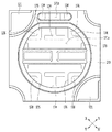
- 放熱フレームと、
第1及び第2接触部を有し、前記放熱フレームの一側に配置された第1リードフレームと、
第3及び第4接触部を有し、前記放熱フレームの他側に配置された第2リードフレームと、
前記放熱フレーム、前記第1及び第2リードフレームと結合され、第1キャビティ及び前記第1キャビティから離隔した第2キャビティを有する絶縁性材質の本体と、
前記第1キャビティの底に露出した前記放熱フレームの上に配置された複数の発光素子と、
を含み、
前記本体は、前記第1キャビティ内に配置され、前記複数の発光素子のうち少なくとも1つ以上を取り囲む反射部を含み、
前記反射部は、前記第1キャビティの下部に配置された第1〜第3反射隔壁を含み、
前記第1反射隔壁は、前記第1キャビティの内側面の一側から他側に延長され、
前記第2反射隔壁は、前記第1反射隔壁と対向し、前記第1キャビティの内側面の一側から他側に延長され、
前記第3反射隔壁は、前記第1反射隔壁の中心から前記第2反射隔壁の中心に延長され、
前記第1〜第3反射隔壁の各高さは、前記発光素子の高さ以上であり、前記第1キャビティの内側面の高さ以下であり、
前記第1リードフレームの第1接触部及び第2接触部は、前記第1キャビティの内側面の一側底に露出し、
前記第2リードフレームの第3接触部及び第4接触部は、前記第2キャビティの内側面の他側底に露出し、
前記第1接触部及び前記第3接触部は、前記第1反射隔壁の外側に配置され、
前記第2接触部及び前記第4接触部は、前記第2反射隔壁の外側に配置され、
前記発光素子は、前記第1キャビティ内で、前記第1接触部と前記第3接触部に電気的に連結された第1グループの発光素子と、前記第2接触部と前記第3接触部に電気的に連結された第2グループの発光素子とを含み、
前記本体は、前記第1キャビティの底で前記放熱フレームの上部に配置された第1結合部を含み、
前記第1〜第3反射隔壁は、前記第1結合部の上に配置され、
前記第1結合部は、第1及び第2延長部を含み、
前記第1延長部は、前記第1キャビティの内側面と直接接し、前記反射部の下部両側で相互対向するように配置され、
前記第2延長部は、前記第1延長部から前記第1〜第3反射隔壁の下部内側及び下部外側に延長され、
前記第1延長部は、前記第1及び第2反射隔壁のそれぞれの下部外側に延長され、
前記第1反射隔壁と前記第2反射隔壁は相互平行であり、
前記第1反射隔壁と前記第2反射隔壁との間の一側領域には、前記第1グループの発光素子が配置され、
前記第1反射隔壁と前記第2反射隔壁との間の他側領域には、前記第2グループの発光素子が配置される、発光素子パッケージ。 - 前記第2キャビティの内に配置された保護素子と、
前記第2キャビティの底に延長された前記放熱フレームの一部と、前記第1リードフレームの第5接触部と、前記第2リードフレームの第6接触部とを含み、
前記保護素子は、前記放熱フレームの一部上に配置され、前記第5接触部と前記第2接触部に電気的に連結され、
前記第5接触部は、前記第1リードフレームの第1接触部から延長され、
前記第6接触部は、前記第2リードフレームの第3接触部から延長される、請求項1に記載の発光素子パッケージ。 - 前記放熱フレーム、第1及び第2リードフレームの間には、第1及び第2スペーサーを含み、
前記放熱フレームは、前記本体の外側部に露出する第1突出部と、前記複数の発光素子が配置される実装部及び前記実装部から延長された第1屈曲部とを含み、
前記第1屈曲部は、前記第1突出部より大きい幅を有し、
前記第1リードフレームは、外側部に露出する第2突出部と、前記第1屈曲部方向に対向する第2屈曲部とを含み、
前記第2リードフレームは、外側部に露出する第3突出部と、前記第1屈曲部方向に対向する第3屈曲部とを含み、
前記第2及び第3屈曲部の第1方向に突出した幅は、前記第1及び第2スペーサーの幅より大きく、
前記第2及び第3屈曲部の前記第1方向と直交する第2方向の幅は、前記第1及び第2スペーサーの幅と同一または大きい、請求項1〜2のいずれか一項に記載の発光素子パッケージ。 - 前記第1及び第2リードフレームは前記第1キャビティを中心に相互対称する角に配置された第1及び第2パッドをさらに含み、
前記第1及び第2パッドは、上部が前記本体から露出し、
前記本体は、前記第1パッドの外側に配置された第1保護部及び前記第2パッドの外側に配置された第2保護部を含み、
前記第1保護部は、相互連結され、前記第1パッドの外側と直接接する第3及び第4直線部を含み、
前記第2保護部は、相互連結され、前記第2パッドの外側と直接接する第5及び第6直線部を含み、
前記第1及び第2パッドは、少なくとも1つ以上の貫通孔を含み、
前記第1パッドは、前記第1接触部の外側端部に配置され、
前記第2パッドは、前記第4接触部の外側端部に配置される、請求項1〜3のいずれか一項に記載の発光素子パッケージ。
Applications Claiming Priority (6)
| Application Number | Priority Date | Filing Date | Title |
|---|---|---|---|
| KR1020160036096A KR102509053B1 (ko) | 2016-03-25 | 2016-03-25 | 발광소자 패키지 및 조명 장치 |
| KR10-2016-0036100 | 2016-03-25 | ||
| KR10-2016-0036096 | 2016-03-25 | ||
| KR1020160036091A KR102522811B1 (ko) | 2016-03-25 | 2016-03-25 | 발광소자 패키지 및 조명 장치 |
| KR10-2016-0036091 | 2016-03-25 | ||
| KR1020160036100A KR102522590B1 (ko) | 2016-03-25 | 2016-03-25 | 발광소자 패키지 및 조명 장치 |
Publications (3)
| Publication Number | Publication Date |
|---|---|
| JP2017175132A JP2017175132A (ja) | 2017-09-28 |
| JP2017175132A5 JP2017175132A5 (ja) | 2020-04-16 |
| JP6952945B2 true JP6952945B2 (ja) | 2021-10-27 |
Family
ID=58401460
Family Applications (1)
| Application Number | Title | Priority Date | Filing Date |
|---|---|---|---|
| JP2017055275A Active JP6952945B2 (ja) | 2016-03-25 | 2017-03-22 | 発光素子パッケージ及び照明装置 |
Country Status (4)
| Country | Link |
|---|---|
| US (1) | US9997683B2 (ja) |
| EP (1) | EP3223322B1 (ja) |
| JP (1) | JP6952945B2 (ja) |
| CN (2) | CN107256859B (ja) |
Families Citing this family (7)
| Publication number | Priority date | Publication date | Assignee | Title |
|---|---|---|---|---|
| CN108027110B (zh) * | 2015-09-01 | 2020-07-10 | Lg 伊诺特有限公司 | 照明装置 |
| KR102432024B1 (ko) * | 2017-12-08 | 2022-08-12 | 쑤저우 레킨 세미컨덕터 컴퍼니 리미티드 | 발광소자 패키지 및 광원 장치 |
| JP1627942S (ja) * | 2018-09-27 | 2019-04-01 | ||
| USD895559S1 (en) * | 2019-01-15 | 2020-09-08 | Citizen Electronics Co., Ltd. | Light emitting diode |
| JP1640278S (ja) * | 2019-01-15 | 2019-09-02 | ||
| JP7210305B2 (ja) * | 2019-01-31 | 2023-01-23 | 日機装株式会社 | 流体殺菌装置 |
| CN211260395U (zh) * | 2019-09-29 | 2020-08-14 | 漳州立达信光电子科技有限公司 | 一种led灯以及控制电路 |
Family Cites Families (33)
| Publication number | Priority date | Publication date | Assignee | Title |
|---|---|---|---|---|
| JPH0550752U (ja) * | 1991-12-11 | 1993-07-02 | 株式会社精工舎 | 発光装置 |
| DE10041686A1 (de) * | 2000-08-24 | 2002-03-14 | Osram Opto Semiconductors Gmbh | Bauelement mit einer Vielzahl von Lumineszenzdiodenchips |
| EP1435118B1 (de) * | 2001-08-21 | 2011-11-02 | OSRAM Opto Semiconductors GmbH | Gehäuse für ein oberflächenmontierbares strahlungsemittierendes bauelement, oberflächenmontierbares strahlungsemittierendes bauelement und anordnung mit einer mehrzahl von oberflächenmontierbaren strahlungsemittierenden bauelementen |
| CN1489224A (zh) * | 2003-09-02 | 2004-04-14 | 陈洪花 | 高亮度超薄光半导体器件 |
| KR100591687B1 (ko) | 2005-05-06 | 2006-06-22 | 럭스피아 주식회사 | 칼라게멋을 향상한 멀티-칩 발광다이오드 패키지 및 이를채용한 백라이트 유닛 |
| KR100616695B1 (ko) * | 2005-10-04 | 2006-08-28 | 삼성전기주식회사 | 고출력 발광 다이오드 패키지 |
| DE102006015377B4 (de) * | 2006-04-03 | 2018-06-14 | Ivoclar Vivadent Ag | Halbleiter-Strahlungsquelle sowie Lichthärtgerät |
| KR100818162B1 (ko) * | 2007-05-14 | 2008-03-31 | 루미마이크로 주식회사 | 색온도 조절이 가능한 백색 led 장치 |
| KR200447448Y1 (ko) | 2007-11-29 | 2010-01-25 | (주)솔라루체 | Led 소자용 리드프레임 패키지 및 이를 이용한 led패키지 |
| KR100998233B1 (ko) * | 2007-12-03 | 2010-12-07 | 서울반도체 주식회사 | 슬림형 led 패키지 |
| JP2009224431A (ja) * | 2008-03-14 | 2009-10-01 | Nichia Corp | 半導体装置 |
| JP2010118560A (ja) * | 2008-11-13 | 2010-05-27 | Sumitomo Metal Electronics Devices Inc | 発光素子搭載用パッケージの製造方法 |
| US7923739B2 (en) * | 2009-06-05 | 2011-04-12 | Cree, Inc. | Solid state lighting device |
| KR101064072B1 (ko) * | 2009-02-24 | 2011-09-08 | 엘지이노텍 주식회사 | 발광 소자 패키지 |
| TWI389357B (zh) * | 2009-08-04 | 2013-03-11 | Advanced Optoelectronic Tech | 具有防水功能的表面黏著型發光二極體元件、具有防水功能的發光二極體模組以及其製作方法 |
| US20110062482A1 (en) * | 2010-01-20 | 2011-03-17 | Bridgelux, Inc. | Apparatus And Method For Enhancing Connectability In LED Array Using Metal Traces |
| JP5010716B2 (ja) * | 2010-01-29 | 2012-08-29 | 株式会社東芝 | Ledパッケージ |
| KR101282829B1 (ko) * | 2010-02-17 | 2013-07-26 | 일진엘이디(주) | 발광 다이오드 패키지 |
| JP2011204790A (ja) * | 2010-03-24 | 2011-10-13 | Toshiba Corp | 半導体発光装置 |
| KR101039994B1 (ko) * | 2010-05-24 | 2011-06-09 | 엘지이노텍 주식회사 | 발광소자 및 이를 구비한 라이트 유닛 |
| KR101103674B1 (ko) * | 2010-06-01 | 2012-01-11 | 엘지이노텍 주식회사 | 발광 소자 |
| CN102376855B (zh) * | 2010-08-09 | 2015-08-19 | Lg伊诺特有限公司 | 发光器件和具有发光器件的照明系统 |
| JP2012119376A (ja) * | 2010-11-29 | 2012-06-21 | Toshiba Corp | Ledパッケージ |
| KR101832306B1 (ko) * | 2011-05-30 | 2018-02-26 | 엘지이노텍 주식회사 | 발광소자 패키지 |
| KR101818466B1 (ko) * | 2011-08-18 | 2018-01-15 | 엘지디스플레이 주식회사 | 발광 다이오드 패키지 |
| US8895998B2 (en) * | 2012-03-30 | 2014-11-25 | Cree, Inc. | Ceramic-based light emitting diode (LED) devices, components and methods |
| TW201344971A (zh) * | 2012-04-18 | 2013-11-01 | Lextar Electronics Corp | 發光元件之封裝結構 |
| US10026676B2 (en) * | 2012-12-11 | 2018-07-17 | Advanced Semiconductor Engineering, Inc. | Semiconductor lead frame package and LED package |
| TWI518952B (zh) * | 2013-07-17 | 2016-01-21 | 隆達電子股份有限公司 | 發光二極體封裝結構及發光元件 |
| JP2015126137A (ja) * | 2013-12-26 | 2015-07-06 | アピックヤマダ株式会社 | リードフレーム、ledパッケージ用基板、リフレクタ部材、ledパッケージ、発光装置、発光システム、並びに、ledパッケージ用基板及びledパッケージの製造方法 |
| JP6671117B2 (ja) * | 2014-07-08 | 2020-03-25 | エルジー イノテック カンパニー リミテッド | 発光素子パッケージ |
| JP6413412B2 (ja) * | 2014-07-11 | 2018-10-31 | 日亜化学工業株式会社 | 半導体発光装置及びその製造方法 |
| EP2988341B1 (en) * | 2014-08-22 | 2017-04-05 | LG Innotek Co., Ltd. | Light emitting device package |
-
2017
- 2017-03-22 EP EP17162253.3A patent/EP3223322B1/en active Active
- 2017-03-22 JP JP2017055275A patent/JP6952945B2/ja active Active
- 2017-03-23 US US15/467,204 patent/US9997683B2/en active Active
- 2017-03-27 CN CN201710188302.XA patent/CN107256859B/zh active Active
- 2017-03-27 CN CN202210957506.6A patent/CN115274638A/zh active Pending
Also Published As
| Publication number | Publication date |
|---|---|
| US9997683B2 (en) | 2018-06-12 |
| CN115274638A (zh) | 2022-11-01 |
| CN107256859B (zh) | 2022-08-23 |
| JP2017175132A (ja) | 2017-09-28 |
| CN107256859A (zh) | 2017-10-17 |
| EP3223322B1 (en) | 2019-05-01 |
| US20170279015A1 (en) | 2017-09-28 |
| EP3223322A1 (en) | 2017-09-27 |
Similar Documents
| Publication | Publication Date | Title |
|---|---|---|
| JP6952945B2 (ja) | 発光素子パッケージ及び照明装置 | |
| KR101997243B1 (ko) | 발광 소자 및 조명 시스템 | |
| JP6796936B2 (ja) | 発光素子及びこれを備えたライトユニット | |
| JP6312999B2 (ja) | 発光素子及びこれを備えた照明システム | |
| CN107210352A (zh) | 发光元件 | |
| WO2016093325A1 (ja) | 発光装置 | |
| KR102279212B1 (ko) | 발광 소자 패키지 | |
| KR20140132517A (ko) | 발광 소자 | |
| US20200303596A1 (en) | Light-emitting device package and lighting module | |
| KR102153082B1 (ko) | 발광 장치 | |
| KR101916148B1 (ko) | 발광 소자, 발광 소자 제조방법 및 조명 시스템 | |
| KR101886073B1 (ko) | 발광 소자 패키지 및 이를 구비한 라이트 유닛 | |
| KR101970938B1 (ko) | 지향각이 조절된 발광소자 패키지 및 이를 이용한 발광장치 | |
| KR20150049669A (ko) | 발광 장치 | |
| US20100213497A1 (en) | Light emitting device package and lighting system including the same | |
| KR102509053B1 (ko) | 발광소자 패키지 및 조명 장치 | |
| KR101976547B1 (ko) | 발광 소자 및 이를 구비한 조명 시스템 | |
| KR102522811B1 (ko) | 발광소자 패키지 및 조명 장치 | |
| KR102181458B1 (ko) | 발광소자 | |
| KR102522590B1 (ko) | 발광소자 패키지 및 조명 장치 | |
| KR102209037B1 (ko) | 발광 소자 | |
| CN110249438B (zh) | 发光装置 | |
| KR102432215B1 (ko) | 라이트 유닛 및 이를 구비한 조명 장치 | |
| KR102042197B1 (ko) | 발광 소자 및 이를 구비한 조명 시스템 | |
| KR101896691B1 (ko) | 발광 소자 및 조명 시스템 |
Legal Events
| Date | Code | Title | Description |
|---|---|---|---|
| A521 | Request for written amendment filed |
Free format text: JAPANESE INTERMEDIATE CODE: A523 Effective date: 20200306 |
|
| A621 | Written request for application examination |
Free format text: JAPANESE INTERMEDIATE CODE: A621 Effective date: 20200306 |
|
| A977 | Report on retrieval |
Free format text: JAPANESE INTERMEDIATE CODE: A971007 Effective date: 20210219 |
|
| A131 | Notification of reasons for refusal |
Free format text: JAPANESE INTERMEDIATE CODE: A131 Effective date: 20210309 |
|
| A521 | Request for written amendment filed |
Free format text: JAPANESE INTERMEDIATE CODE: A523 Effective date: 20210607 |
|
| TRDD | Decision of grant or rejection written | ||
| A711 | Notification of change in applicant |
Free format text: JAPANESE INTERMEDIATE CODE: A711 Effective date: 20210618 |
|
| A01 | Written decision to grant a patent or to grant a registration (utility model) |
Free format text: JAPANESE INTERMEDIATE CODE: A01 Effective date: 20210622 |
|
| A61 | First payment of annual fees (during grant procedure) |
Free format text: JAPANESE INTERMEDIATE CODE: A61 Effective date: 20210721 |
|
| R150 | Certificate of patent or registration of utility model |
Ref document number: 6952945 Country of ref document: JP Free format text: JAPANESE INTERMEDIATE CODE: R150 |