JP6952945B2 - Light emitting element package and lighting device - Google Patents
Light emitting element package and lighting device Download PDFInfo
- Publication number
- JP6952945B2 JP6952945B2 JP2017055275A JP2017055275A JP6952945B2 JP 6952945 B2 JP6952945 B2 JP 6952945B2 JP 2017055275 A JP2017055275 A JP 2017055275A JP 2017055275 A JP2017055275 A JP 2017055275A JP 6952945 B2 JP6952945 B2 JP 6952945B2
- Authority
- JP
- Japan
- Prior art keywords
- light emitting
- cavity
- frame
- contact portion
- emitting element
- Prior art date
- Legal status (The legal status is an assumption and is not a legal conclusion. Google has not performed a legal analysis and makes no representation as to the accuracy of the status listed.)
- Active
Links
- 238000005192 partition Methods 0.000 claims description 66
- 230000008878 coupling Effects 0.000 claims description 33
- 238000010168 coupling process Methods 0.000 claims description 33
- 238000005859 coupling reaction Methods 0.000 claims description 33
- 230000001681 protective effect Effects 0.000 claims description 24
- 125000006850 spacer group Chemical group 0.000 claims description 24
- 230000017525 heat dissipation Effects 0.000 claims description 8
- 239000011810 insulating material Substances 0.000 claims description 3
- 230000005855 radiation Effects 0.000 claims 3
- 239000004065 semiconductor Substances 0.000 description 14
- 238000002347 injection Methods 0.000 description 13
- 239000007924 injection Substances 0.000 description 13
- 238000000465 moulding Methods 0.000 description 12
- 238000000034 method Methods 0.000 description 7
- 230000008602 contraction Effects 0.000 description 6
- 238000000605 extraction Methods 0.000 description 6
- 239000000463 material Substances 0.000 description 6
- 230000007547 defect Effects 0.000 description 4
- 239000011159 matrix material Substances 0.000 description 4
- 238000010586 diagram Methods 0.000 description 3
- 230000002829 reductive effect Effects 0.000 description 3
- 239000000126 substance Substances 0.000 description 3
- 239000004954 Polyphthalamide Substances 0.000 description 2
- 150000001875 compounds Chemical class 0.000 description 2
- 238000005530 etching Methods 0.000 description 2
- 238000004519 manufacturing process Methods 0.000 description 2
- 239000007769 metal material Substances 0.000 description 2
- 239000000203 mixture Substances 0.000 description 2
- 238000012986 modification Methods 0.000 description 2
- 230000004048 modification Effects 0.000 description 2
- 150000004767 nitrides Chemical class 0.000 description 2
- 230000000149 penetrating effect Effects 0.000 description 2
- 239000006089 photosensitive glass Substances 0.000 description 2
- 229920006375 polyphtalamide Polymers 0.000 description 2
- 229920005989 resin Polymers 0.000 description 2
- 239000011347 resin Substances 0.000 description 2
- 239000000758 substrate Substances 0.000 description 2
- 239000004593 Epoxy Substances 0.000 description 1
- XUIMIQQOPSSXEZ-UHFFFAOYSA-N Silicon Chemical compound [Si] XUIMIQQOPSSXEZ-UHFFFAOYSA-N 0.000 description 1
- 229910052782 aluminium Inorganic materials 0.000 description 1
- 229910052785 arsenic Inorganic materials 0.000 description 1
- 238000005452 bending Methods 0.000 description 1
- 239000003086 colorant Substances 0.000 description 1
- 230000008094 contradictory effect Effects 0.000 description 1
- 230000003247 decreasing effect Effects 0.000 description 1
- 239000002019 doping agent Substances 0.000 description 1
- 229910052733 gallium Inorganic materials 0.000 description 1
- 229910052737 gold Inorganic materials 0.000 description 1
- 229910052738 indium Inorganic materials 0.000 description 1
- 239000004973 liquid crystal related substance Substances 0.000 description 1
- 229910052757 nitrogen Inorganic materials 0.000 description 1
- 230000003287 optical effect Effects 0.000 description 1
- TWNQGVIAIRXVLR-UHFFFAOYSA-N oxo(oxoalumanyloxy)alumane Chemical compound O=[Al]O[Al]=O TWNQGVIAIRXVLR-UHFFFAOYSA-N 0.000 description 1
- 230000000737 periodic effect Effects 0.000 description 1
- 229920001296 polysiloxane Polymers 0.000 description 1
- 238000007639 printing Methods 0.000 description 1
- 238000005215 recombination Methods 0.000 description 1
- 230000006798 recombination Effects 0.000 description 1
- 239000010703 silicon Substances 0.000 description 1
- 229910052710 silicon Inorganic materials 0.000 description 1
- 229910052709 silver Inorganic materials 0.000 description 1
- 230000003068 static effect Effects 0.000 description 1
- 230000001629 suppression Effects 0.000 description 1
- 230000001052 transient effect Effects 0.000 description 1
- 238000002834 transmittance Methods 0.000 description 1
- 229910052725 zinc Inorganic materials 0.000 description 1
Images


Classifications
-
- H—ELECTRICITY
- H01—ELECTRIC ELEMENTS
- H01L—SEMICONDUCTOR DEVICES NOT COVERED BY CLASS H10
- H01L25/00—Assemblies consisting of a plurality of individual semiconductor or other solid state devices ; Multistep manufacturing processes thereof
- H01L25/03—Assemblies consisting of a plurality of individual semiconductor or other solid state devices ; Multistep manufacturing processes thereof all the devices being of a type provided for in the same subgroup of groups H01L27/00 - H01L33/00, or in a single subclass of H10K, H10N, e.g. assemblies of rectifier diodes
- H01L25/04—Assemblies consisting of a plurality of individual semiconductor or other solid state devices ; Multistep manufacturing processes thereof all the devices being of a type provided for in the same subgroup of groups H01L27/00 - H01L33/00, or in a single subclass of H10K, H10N, e.g. assemblies of rectifier diodes the devices not having separate containers
- H01L25/075—Assemblies consisting of a plurality of individual semiconductor or other solid state devices ; Multistep manufacturing processes thereof all the devices being of a type provided for in the same subgroup of groups H01L27/00 - H01L33/00, or in a single subclass of H10K, H10N, e.g. assemblies of rectifier diodes the devices not having separate containers the devices being of a type provided for in group H01L33/00
- H01L25/0753—Assemblies consisting of a plurality of individual semiconductor or other solid state devices ; Multistep manufacturing processes thereof all the devices being of a type provided for in the same subgroup of groups H01L27/00 - H01L33/00, or in a single subclass of H10K, H10N, e.g. assemblies of rectifier diodes the devices not having separate containers the devices being of a type provided for in group H01L33/00 the devices being arranged next to each other
-
- H—ELECTRICITY
- H01—ELECTRIC ELEMENTS
- H01L—SEMICONDUCTOR DEVICES NOT COVERED BY CLASS H10
- H01L25/00—Assemblies consisting of a plurality of individual semiconductor or other solid state devices ; Multistep manufacturing processes thereof
- H01L25/16—Assemblies consisting of a plurality of individual semiconductor or other solid state devices ; Multistep manufacturing processes thereof the devices being of types provided for in two or more different main groups of groups H01L27/00 - H01L33/00, or in a single subclass of H10K, H10N, e.g. forming hybrid circuits
- H01L25/167—Assemblies consisting of a plurality of individual semiconductor or other solid state devices ; Multistep manufacturing processes thereof the devices being of types provided for in two or more different main groups of groups H01L27/00 - H01L33/00, or in a single subclass of H10K, H10N, e.g. forming hybrid circuits comprising optoelectronic devices, e.g. LED, photodiodes
-
- H—ELECTRICITY
- H01—ELECTRIC ELEMENTS
- H01L—SEMICONDUCTOR DEVICES NOT COVERED BY CLASS H10
- H01L27/00—Devices consisting of a plurality of semiconductor or other solid-state components formed in or on a common substrate
- H01L27/02—Devices consisting of a plurality of semiconductor or other solid-state components formed in or on a common substrate including semiconductor components specially adapted for rectifying, oscillating, amplifying or switching and having potential barriers; including integrated passive circuit elements having potential barriers
- H01L27/0203—Particular design considerations for integrated circuits
- H01L27/0248—Particular design considerations for integrated circuits for electrical or thermal protection, e.g. electrostatic discharge [ESD] protection
-
- H—ELECTRICITY
- H01—ELECTRIC ELEMENTS
- H01L—SEMICONDUCTOR DEVICES NOT COVERED BY CLASS H10
- H01L29/00—Semiconductor devices specially adapted for rectifying, amplifying, oscillating or switching and having potential barriers; Capacitors or resistors having potential barriers, e.g. a PN-junction depletion layer or carrier concentration layer; Details of semiconductor bodies or of electrodes thereof ; Multistep manufacturing processes therefor
- H01L29/66—Types of semiconductor device ; Multistep manufacturing processes therefor
- H01L29/86—Types of semiconductor device ; Multistep manufacturing processes therefor controllable only by variation of the electric current supplied, or only the electric potential applied, to one or more of the electrodes carrying the current to be rectified, amplified, oscillated or switched
- H01L29/861—Diodes
- H01L29/866—Zener diodes
-
- H—ELECTRICITY
- H01—ELECTRIC ELEMENTS
- H01L—SEMICONDUCTOR DEVICES NOT COVERED BY CLASS H10
- H01L33/00—Semiconductor devices having potential barriers specially adapted for light emission; Processes or apparatus specially adapted for the manufacture or treatment thereof or of parts thereof; Details thereof
- H01L33/48—Semiconductor devices having potential barriers specially adapted for light emission; Processes or apparatus specially adapted for the manufacture or treatment thereof or of parts thereof; Details thereof characterised by the semiconductor body packages
- H01L33/483—Containers
- H01L33/486—Containers adapted for surface mounting
-
- H—ELECTRICITY
- H01—ELECTRIC ELEMENTS
- H01L—SEMICONDUCTOR DEVICES NOT COVERED BY CLASS H10
- H01L33/00—Semiconductor devices having potential barriers specially adapted for light emission; Processes or apparatus specially adapted for the manufacture or treatment thereof or of parts thereof; Details thereof
- H01L33/48—Semiconductor devices having potential barriers specially adapted for light emission; Processes or apparatus specially adapted for the manufacture or treatment thereof or of parts thereof; Details thereof characterised by the semiconductor body packages
- H01L33/52—Encapsulations
- H01L33/54—Encapsulations having a particular shape
-
- H—ELECTRICITY
- H01—ELECTRIC ELEMENTS
- H01L—SEMICONDUCTOR DEVICES NOT COVERED BY CLASS H10
- H01L33/00—Semiconductor devices having potential barriers specially adapted for light emission; Processes or apparatus specially adapted for the manufacture or treatment thereof or of parts thereof; Details thereof
- H01L33/48—Semiconductor devices having potential barriers specially adapted for light emission; Processes or apparatus specially adapted for the manufacture or treatment thereof or of parts thereof; Details thereof characterised by the semiconductor body packages
- H01L33/58—Optical field-shaping elements
- H01L33/60—Reflective elements
-
- H—ELECTRICITY
- H01—ELECTRIC ELEMENTS
- H01L—SEMICONDUCTOR DEVICES NOT COVERED BY CLASS H10
- H01L33/00—Semiconductor devices having potential barriers specially adapted for light emission; Processes or apparatus specially adapted for the manufacture or treatment thereof or of parts thereof; Details thereof
- H01L33/48—Semiconductor devices having potential barriers specially adapted for light emission; Processes or apparatus specially adapted for the manufacture or treatment thereof or of parts thereof; Details thereof characterised by the semiconductor body packages
- H01L33/62—Arrangements for conducting electric current to or from the semiconductor body, e.g. lead-frames, wire-bonds or solder balls
-
- H—ELECTRICITY
- H01—ELECTRIC ELEMENTS
- H01L—SEMICONDUCTOR DEVICES NOT COVERED BY CLASS H10
- H01L33/00—Semiconductor devices having potential barriers specially adapted for light emission; Processes or apparatus specially adapted for the manufacture or treatment thereof or of parts thereof; Details thereof
- H01L33/48—Semiconductor devices having potential barriers specially adapted for light emission; Processes or apparatus specially adapted for the manufacture or treatment thereof or of parts thereof; Details thereof characterised by the semiconductor body packages
- H01L33/64—Heat extraction or cooling elements
- H01L33/647—Heat extraction or cooling elements the elements conducting electric current to or from the semiconductor body
-
- H—ELECTRICITY
- H01—ELECTRIC ELEMENTS
- H01L—SEMICONDUCTOR DEVICES NOT COVERED BY CLASS H10
- H01L2224/00—Indexing scheme for arrangements for connecting or disconnecting semiconductor or solid-state bodies and methods related thereto as covered by H01L24/00
- H01L2224/01—Means for bonding being attached to, or being formed on, the surface to be connected, e.g. chip-to-package, die-attach, "first-level" interconnects; Manufacturing methods related thereto
- H01L2224/42—Wire connectors; Manufacturing methods related thereto
- H01L2224/47—Structure, shape, material or disposition of the wire connectors after the connecting process
- H01L2224/48—Structure, shape, material or disposition of the wire connectors after the connecting process of an individual wire connector
- H01L2224/4805—Shape
- H01L2224/4809—Loop shape
- H01L2224/48091—Arched
-
- H—ELECTRICITY
- H01—ELECTRIC ELEMENTS
- H01L—SEMICONDUCTOR DEVICES NOT COVERED BY CLASS H10
- H01L2224/00—Indexing scheme for arrangements for connecting or disconnecting semiconductor or solid-state bodies and methods related thereto as covered by H01L24/00
- H01L2224/01—Means for bonding being attached to, or being formed on, the surface to be connected, e.g. chip-to-package, die-attach, "first-level" interconnects; Manufacturing methods related thereto
- H01L2224/42—Wire connectors; Manufacturing methods related thereto
- H01L2224/47—Structure, shape, material or disposition of the wire connectors after the connecting process
- H01L2224/48—Structure, shape, material or disposition of the wire connectors after the connecting process of an individual wire connector
- H01L2224/481—Disposition
- H01L2224/48135—Connecting between different semiconductor or solid-state bodies, i.e. chip-to-chip
- H01L2224/48137—Connecting between different semiconductor or solid-state bodies, i.e. chip-to-chip the bodies being arranged next to each other, e.g. on a common substrate
-
- H—ELECTRICITY
- H01—ELECTRIC ELEMENTS
- H01L—SEMICONDUCTOR DEVICES NOT COVERED BY CLASS H10
- H01L2933/00—Details relating to devices covered by the group H01L33/00 but not provided for in its subgroups
- H01L2933/0008—Processes
- H01L2933/0033—Processes relating to semiconductor body packages
- H01L2933/0058—Processes relating to semiconductor body packages relating to optical field-shaping elements
-
- H—ELECTRICITY
- H01—ELECTRIC ELEMENTS
- H01L—SEMICONDUCTOR DEVICES NOT COVERED BY CLASS H10
- H01L33/00—Semiconductor devices having potential barriers specially adapted for light emission; Processes or apparatus specially adapted for the manufacture or treatment thereof or of parts thereof; Details thereof
- H01L33/48—Semiconductor devices having potential barriers specially adapted for light emission; Processes or apparatus specially adapted for the manufacture or treatment thereof or of parts thereof; Details thereof characterised by the semiconductor body packages
- H01L33/64—Heat extraction or cooling elements
- H01L33/642—Heat extraction or cooling elements characterized by the shape
Landscapes
- Engineering & Computer Science (AREA)
- Microelectronics & Electronic Packaging (AREA)
- Power Engineering (AREA)
- Computer Hardware Design (AREA)
- Manufacturing & Machinery (AREA)
- Physics & Mathematics (AREA)
- Condensed Matter Physics & Semiconductors (AREA)
- General Physics & Mathematics (AREA)
- Ceramic Engineering (AREA)
- Led Device Packages (AREA)
- Non-Portable Lighting Devices Or Systems Thereof (AREA)
Description
本発明は、発光素子パッケージ及び照明装置に関するものである。 The present invention relates to a light emitting element package and a lighting device.
発光素子(Light Emitting Device)は、電気エネルギーが光エネルギーに変換される特性のp-n接合ダイオードとして、周期律表上のIII族とV族等の化合物半導体から生成することができ、化合物半導体の組成比を調節することで、多様な色の具現が可能である。 A light emitting device (Light Emitting Device) can be generated from a compound semiconductor such as group III and group V on the periodic table as a pn junction diode having the characteristic that electric energy is converted into light energy, and the composition of the compound semiconductor. By adjusting the ratio, it is possible to realize various colors.
発光素子は、順方向電圧を印加した時、n層の電子とp層の正孔(hole)が結合して伝導帯(Conduction band)と価電子帯(Valance band)のバンドギャップエネルギーに該当するだけのエネルギーを発散するが、このエネルギーは主に熱や光の形態に放出され、光の形態に発散されると発光素子となる。 When a forward voltage is applied to the light emitting element, the electrons in the n-layer and the holes in the p-layer are combined to correspond to the band gap energy of the conduction band and the valence band. This energy is mainly emitted in the form of heat or light, and when it is emitted in the form of light, it becomes a light emitting element.
例えば、窒化物半導体は、高い熱的安定性と幅広いバンドギャップエネルギーによって、光素子及び高出力電子素子の開発分野で大きい関心を集めている。特に、窒化物半導体を利用した青色(Blue)発光素子、緑色(Green)発光素子、紫外線(UV)発光素子等は、商用化されて広く使われている。 For example, nitride semiconductors have received a great deal of attention in the field of developing optical devices and high-power electronic devices due to their high thermal stability and wide bandgap energy. In particular, blue (Blue) light emitting devices, green (Green) light emitting devices, ultraviolet (UV) light emitting devices and the like using nitride semiconductors have been commercialized and widely used.
最近、発光ダイオードの輝度問題が大きく改善され、液晶表示装置のバックライトユニット(Backlight Unit)、電光掲示板、表示器、家電製品等のような各種機器に適用されている。 Recently, the problem of brightness of light emitting diodes has been greatly improved, and it is applied to various devices such as a backlight unit of a liquid crystal display device, an electric bulletin board, a display, and a home appliance.
本発明は、光抽出効率を向上させることができる発光素子パッケージ及び照明装置を提供する。 The present invention provides a light emitting element package and a lighting device capable of improving light extraction efficiency.
本発明は、構成間の結合力を向上させることができる発光素子パッケージ及び照明装置を提供する。 The present invention provides a light emitting device package and a lighting device capable of improving the coupling force between configurations.
本発明は、安定した構造のCOB(Chip on Board)タイプの発光素子パッケージ及び照明装置を提供する。 The present invention provides a COB (Chip on Board) type light emitting element package and a lighting device having a stable structure.
本発明の発光素子パッケージは、フレームと、前記フレームから一定間隔離隔した第1リードフレームと、前記フレームから一定間隔離隔した第2リードフレームと、前記フレーム、第1及び第2リードフレームと結合され、第1キャビティを有する本体と、前記第1キャビティに露出した前記フレームの上に配置された複数の発光素子と、を含み、前記本体は、前記第1キャビティ内に配置され、前記複数の発光素子のうち少なくとも1つ以上を取り囲む反射部を含み、光抽出効率を向上させることができる。本発明は、反射部によって発光素子パッケージの収縮及び膨張による変形を改善することができる。本発明は、反射部によって前記第1キャビティ内に配置されたモールディング部の収縮及び膨張による変形を改善することができる。即ち、本発明は、前記モールディング部の変形を改善して、モールディング部の変形によるワイヤの損傷を改善することができる。 The light emitting device package of the present invention is coupled to a frame, a first lead frame isolated from the frame for a certain period of time, a second lead frame isolated from the frame for a certain period of time, and the frame, the first and second lead frames. The main body includes a main body having the first cavity and a plurality of light emitting elements arranged on the frame exposed in the first cavity, and the main body is arranged in the first cavity to emit light. A reflecting portion that surrounds at least one or more of the elements can be included to improve the light extraction efficiency. According to the present invention, the reflective portion can improve the deformation of the light emitting element package due to shrinkage and expansion. INDUSTRIAL APPLICABILITY According to the present invention, the deformation of the molding portion arranged in the first cavity by the reflecting portion due to contraction and expansion can be improved. That is, the present invention can improve the deformation of the molding portion and improve the damage of the wire due to the deformation of the molding portion.
本発明の照明装置は、前記発光素子パッケージを含むことができる。 The lighting device of the present invention can include the light emitting element package.
本発明の発光素子パッケージは、複数の発光素子が実装されるキャビティの中心領域を横断する反射部によって、発光素子パッケージの収縮及び膨張による変形を改善することができる。 In the light emitting element package of the present invention, the deformation due to the contraction and expansion of the light emitting element package can be improved by the reflecting portion that crosses the central region of the cavity in which the plurality of light emitting elements are mounted.
本発明は、複数の発光素子が実装されるキャビティの中心領域を横断する反射部によって、前記キャビティ内に配置されたモールディング部の収縮及び膨張による変形を改善することができる。即ち、本発明は、前記モールディング部の変形を改善して、モールディング部の変形によるワイヤの損傷を改善することができる。 INDUSTRIAL APPLICABILITY According to the present invention, it is possible to improve the deformation due to contraction and expansion of the molding portion arranged in the cavity by the reflecting portion that crosses the central region of the cavity in which the plurality of light emitting elements are mounted. That is, the present invention can improve the deformation of the molding portion and improve the damage of the wire due to the deformation of the molding portion.
本発明は、放熱プレートの上部面の上に段差部が配置されて本体との結合力を向上させることができ、段差構造によって外部の湿気浸透を改善することができる。 In the present invention, a stepped portion is arranged on the upper surface of the heat radiating plate to improve the bonding force with the main body, and the stepped structure can improve the permeation of moisture to the outside.
本発明は、第1及び第2リードフレームの下部に段差部が配置されて本体の射出工程時に金型フレームによって支持され、前記第1及び第2リードフレームの変形を改善でき、キャビティから露出する接続部とパッドを本体から露出させる本体の射出工程の信頼度を向上させることができる。また、第1及び第2リードフレームの下部段差構造によって、外部の湿気浸透を改善することができる。 In the present invention, a step portion is arranged at the lower part of the first and second lead frames and is supported by the mold frame during the injection process of the main body, the deformation of the first and second lead frames can be improved, and the first and second lead frames are exposed from the cavity. It is possible to improve the reliability of the injection process of the main body that exposes the connection portion and the pad from the main body. Further, the lower step structure of the first and second lead frames can improve the permeation of moisture to the outside.
本発明は、フレーム、第1及び第2リードフレームの縁端部に屈曲構造を含むことで、本体との結合力を向上させることができるだけでなく、これらの間に配置されるスペーサー周辺のクラックを改善することができる。 In the present invention, by including a bent structure at the edge of the frame, the first and second lead frames, not only the bonding force with the main body can be improved, but also cracks around the spacer arranged between them can be improved. Can be improved.
本発明は、パッドの外側を覆う保護部を含むことで、パッドを保護し、本体と第1及び第2リードフレームの間の結合力を向上させることができる。また、本発明は、前記パッドを貫通する少なくとも1つ以上の貫通孔を含むことで、本体と第1及び第2リードフレームの間の結合力を向上させることができる。 The present invention can protect the pad and improve the coupling force between the main body and the first and second lead frames by including a protective portion that covers the outside of the pad. Further, the present invention can improve the coupling force between the main body and the first and second lead frames by including at least one through hole penetrating the pad.
本実施例は、別の形態に変形または複数の実施例を組合わせることができ、本発明の範囲は、以下に説明するそれぞれの実施例に限定されるものではない。 The present embodiment can be modified into another embodiment or a plurality of examples can be combined, and the scope of the present invention is not limited to the respective examples described below.
特定実施例で説明された事項が、別の実施例で説明されなくても、別の実施例でその事項と反対または矛盾する説明がない限り、別の実施例に関連した説明と理解することができる。 Even if the matter described in a specific embodiment is not explained in another embodiment, it should be understood as an explanation related to another embodiment unless there is an explanation that contradicts or contradicts the matter in another embodiment. Can be done.
例えば、特定実施例で構成Aに対する特徴を説明し、別の実施例で構成Bに対する特徴を説明したとすれば、構成Aと構成Bが結合された実施例が明示されなくても、反対または矛盾する説明がない限り、本発明の技術的範囲に含まれると理解されるべきである。 For example, if a specific embodiment describes a feature for configuration A and another example describes a feature for configuration B, the opposite or opposite, even if the embodiment in which configuration A and configuration B are combined is not specified. Unless there is a contradictory explanation, it should be understood to be included in the technical scope of the present invention.
以下、上記した目的を具体的に実現できる本発明の実施例を、添付した図面を参照して説明する。 Hereinafter, examples of the present invention capable of specifically realizing the above-mentioned object will be described with reference to the attached drawings.
本発明の実施例の説明において、各elementの「上または下」に形成されると記載される場合、上または下は2つのelementが直接接触または1つ以上の別のelementが前記2つのelementとの間に配置されて形成されるものも含む。また、「上または下」と表現される場合、1つのelementを基準に上側方向だけでなく、下側方向の意味も含むことができる。 In the description of the embodiments of the present invention, when it is described that each element is formed "above or below", the upper or lower elements are in direct contact with each other or one or more other elements are said to be the two elements. Including those formed by being arranged between and. Further, when it is expressed as "up or down", it can include not only the meaning of the upper direction but also the meaning of the lower direction with respect to one element.
半導体素子は、発光素子、受光素子等各種電子素子を含むことができ、発光素子と受光素子は、いずれも第1導電型半導体層と活性層及び第2導電型半導体層を含むことができる。 The semiconductor element can include various electronic elements such as a light emitting element and a light receiving element, and the light emitting element and the light receiving element can both include a first conductive semiconductor layer, an active layer, and a second conductive semiconductor layer.
本実施例に係る半導体素子は、発光素子からなることができる。 The semiconductor element according to this embodiment can be composed of a light emitting element.
発光素子は、電子と正孔が再結合することで光を放出し、この光の波長は物質固有のエネルギーバンドギャップによって決定される。よって、放出される光は、前記物質の組成によって変わる。 The light emitting element emits light by recombination of electrons and holes, and the wavelength of this light is determined by the energy band gap peculiar to the substance. Therefore, the emitted light changes depending on the composition of the substance.
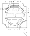
図1は実施例に係る発光素子パッケージを示した斜視図であり、図2は実施例に係る発光素子パッケージを示した断面図であり、図3は実施例に係る発光素子パッケージを示した平面図であり、図4は実施例に係る反射部を示した平面図であり、図5は実施例に係る反射部及び第1結合部を示した平面図である。 FIG. 1 is a perspective view showing the light emitting element package according to the embodiment, FIG. 2 is a cross-sectional view showing the light emitting element package according to the embodiment, and FIG. 3 is a plan view showing the light emitting element package according to the embodiment. FIG. 4 is a plan view showing a reflecting portion according to an embodiment, and FIG. 5 is a plan view showing a reflecting portion and a first coupling portion according to the embodiment.
図1〜図5に示されたように、実施例に係る発光素子パッケージ100は、フレーム110、第1リードフレーム120、第2リードフレーム130、本体170、保護素子160及び複数の発光素子150を含むことができる。実施例の発光素子パッケージ100は、前記フレーム110の上に前記保護素子160及び複数の発光素子150が実装される。前記第1及び第2リードフレーム120、130は、前記フレーム110から一定間隔離隔される。実施例の発光素子パッケージ100は、COB(Chip on Board)方式を採用することができる。例えば、実施例の発光素子パッケージ100は、基板の上に直接ダイボンディング(die bonding)し、ワイヤによって電気的に連結する方式を採用することができるが、これに限定されるものではない。
As shown in FIGS. 1 to 5, the light
前記本体170は、透光性材質、反射性材質、絶縁性材質のうち少なくとも1つを含むことができる。前記本体170は、前記複数の発光素子150から放出された光に対して、反射率が透過率より高い物質を含むことができる。前記本体170は、樹脂系列の絶縁物質からなることができる。例えば、前記本体170は、ポリフタルアミド(PPA:Polyphthalamide)、エポキシまたはシリコーン材質のような樹脂材質、シリコン(Si)、金属材質、PSG(photo sensitive glass)、サファイア(Al2O3)、印刷回路基板(PCB)のうち少なくとも1つからなることができる。前記本体170は、4つの角を含むことができる。
The
前記本体170は、第1方向X-X'に相互対称する第1及び第2角170a、170bと、前記第1方向X-X'と直交する第2方向Y-Y'に相互対称となる第3及び第4角170c、170dを含むことができる。前記第1角170aは、第1リードフレーム120の第1パッド121が露出される。前記第2角170bは、前記第2リードフレーム130の第2パッド131が露出される。前記第1及び第2角170a、170bは、前記第1及び第2パッド121、131の上部面を露出させることができる。前記第1及び第2角170a、170bの終端は、前記第1及び第2パッド121、131の縁端部を覆うことができる。例えば、前記第1及び第2角170a、170bの終端は、前記第1及び第2パッド121、131より外角に配置される。前記第3及び第4角170c、170dは、基板(図示しない)と前記発光素子パッケージ100の結合時にスクリュー(screw)が締結される。前記第3及び第4角170c、170dは、前記スクリューが締結されるように曲面構造を有することができるが、これに限定されるものではない。例えば、前記第3及び第4角170c、170dは、外側が凹状曲面構造を有することができる。
The
前記本体170は、フレーム110、第1及び第2リードフレーム120、130と結合される。前記本体120は、前記フレーム110、第1及び第2リードフレーム120、130の上部面一部を露出させる第1キャビティ171a及び第2キャビティ171bを含むことができる。前記第1キャビティ171aは、前記本体170の中心領域から延長される。前記第1キャビティ171aは、複数の発光素子150が実装される領域に配置される。前記第1キャビティ171aは、トップビュー形状が円形を有することができるが、これに限定されるものではない。例えば、前記第1キャビティ171aのトップビュー形状は、楕円形または少なくとも3以上の多角形形状を有することができる。前記第2キャビティ171bは、前記第1キャビティ171aから一定間隔離隔される。前記第2キャビティ171bは、前記本体170の一側面と隣接し、前記本体170の一側面と前記第1キャビティ171aの間に配置される。前記第2キャビティ171bは、前記本体170の一側面から一定間隔離隔される。前記第2キャビティ171bと前記第1キャビティ171aの間の間隔は0.1mm以上である。前記第2キャビティ171bと前記本体170の一側面の間の間隔は0.1mm以上である。実施例は、前記本体170の一側面、第1及び第2キャビティ171a、171bが0.1mm以上の間隔を有するようにすることで、第1及び第2キャビティ171a、171bの具現信頼度を向上させることができる。例えば、前記本体170の一側面、第1及び第2キャビティ171a、171bが0.1mm未満である場合、第1及び第2キャビティ171a、171bの射出不良を引き起こすことがある。前記第2キャビティ171bは、第1及び第3角170a、170cの間に配置されるが、これに限定されるものではない。前記第2キャビティ171bは、保護素子160が実装される領域に配置される。前記第2キャビティ171bは、前記第1キャビティ171aより小さい直径を有することができる。例えば、前記第2キャビティ171bは、前記第1キャビティ171aの底面面積より狭い底面面積を有することができる。前記第2キャビティ171bの面積は、前記第1キャビティの面積の10〜25%である。前記第2キャビティ171bの短軸幅171Wは、発光素子パッケージ100の全体幅の2%〜6%である。前記第2キャビティ171bの短軸幅171Wが発光素子パッケージ100の全体幅の2%未満である場合、前記保護素子160の大きさを制限して発光素子パッケージ100の安定性が低下することがある。前記第2キャビティ171bの短軸幅171Wが発光素子パッケージ100の全体幅の6%を超える場合、光が発光される発光領域を除いた発光素子パッケージ100のサイズ増加により、多様な分野への適用が制限されることがある。例えば、前記第2キャビティ171bの短軸幅171Wは0.150mm〜0.450mmである。
The
前記本体170は、前記第1角170a 〜第4角170dの間に配置される4つの外側部を含むことができる。前記4つの外側部は、フラットな面を有することができる。実施例は、前記外側部からフレーム110の一部、第1及び第2リードフレーム120、130の一部が露出される。例えば、前記本体170の外側部には、前記フレーム110から延長された第1突出部110pが配置される。ここで、前記第1突出部110pは、本体170の射出工程以後、単位パッケージ切断工程によって形成される。即ち、前記第1突出部110pは、単位パッケージ切断工程以前に、隣接したフレームを連結する連結部である。前記本体170の外側部には、前記第1リードフレーム120から延長された第2突出部120pが配置される。ここで、前記第2突出部120pは本体170の射出工程以後、単位パッケージ切断工程によって形成される。即ち、前記第2突出部120pは、単位パッケージ切断工程以前に、隣接した第1リードフレームを連結する連結部である。前記本体170の外側部には、前記第2リードフレーム130から延長された第3突出部130pが配置される。ここで、前記第3突出部130pは、本体170の射出工程以後、単位パッケージ切断工程によって形成される。即ち、前記第3突出部130pは、単位パッケージ切断工程以前に、隣接した第2リードフレームを連結する連結部である。
The
前記本体170は、第1及び第2スペーサー175、176を含むことができる。前記第1スペーサー175は、前記フレーム110と前記第1リードフレーム120の間に配置される。前記第2スペーサー176は、前記フレーム110と前記第2リードフレーム130の間に配置される。
The
前記本体170は、第1及び第2結合部173、174を含むことができる。前記第1及び第2結合部173、174は、前記フレーム110の上に配置される。前記第1及び第2結合部173、174は、前記本体170と前記放熱フレーム110の間の接触面積を増加させることができる。前記第1及び第2結合部173、174は、前記本体170及びフレーム110の間の結合力を向上させることができる。前記第1及び第2結合部173、174は、前記複数の発光素子150が実装される前記フレーム110の上部面の上に配置される。前記第1及び第2結合部173、174は、前記フレーム110の上部面の上に配置された段差部の上に配置される。前記段差部は、前記フレーム110の上部面の上で凹溝構造からなることができる。前記段差部は、図8及び図9を参照して詳しく説明するようにする。前記第1及び第2結合部173、174は、前記フレーム110の上部面と同一平面上に配置される。
The
前記本体170は、前記第1キャビティ171aの内部に反射部190を含むことができる。前記反射部190は、第1〜第3反射隔壁191、193、195を含むことができる。前記第1〜第3反射隔壁191、193、195は、前記フレーム110の上部面の上に配置された第1結合部173と連結される。例えば、前記第1〜第3反射隔壁191、193、195は、前記第1結合部173の上に配置される。前記第1〜第3反射隔壁191、193、195は、前記第1結合部173の上部面から突出した部分と定義することができる。前記第1〜第3反射隔壁191、193、195は、前記第1キャビティ171aの底から上部方向に突出することができる。前記第1及び第2反射隔壁191、193は、前記第1キャビティ171aの内壁面と連結される。前記第1及び第2反射隔壁191、193は、前記第1キャビティ171aの内壁面と直接接触することができる。前記第1及び第2反射隔壁191、193は相互一定間隔離隔される。前記第1及び第2反射隔壁191、193は平行するように配置される。前記第3反射隔壁195は、前記第1及び第2反射隔壁191、193の間に配置される。前記第3反射隔壁195は、前記第1及び第2反射隔壁191、193の中間地点に配置されるが、これに限定されるものではない。前記反射部190は、前記第1〜第3反射隔壁191、193、195によって2つの領域に分離される。前記2つの領域にはそれぞれ2つの発光素子が配置されるが、これに限定されるものではない。
The
前記第1〜第3反射隔壁191、193、195は、上部に行くほど小さくなる幅を有することができる。前記第1〜第3反射隔壁191、193、195は傾斜した側面を含むことができるが、これに限定されるものではない。例えば、前記第1〜第3反射隔壁191、193、195は、曲面構造の側面を含むことができる。ここで、前記第1及び第2反射隔壁191、193は、前記第1結合部173の上部面の上で上部方向に突出した部分と定義することができる。前記第1及び第2反射隔壁191、193は、上部及び前記第1結合部173と接する下部を含むことができる。前記第1及び第2反射隔壁191、193の上部は第1幅W1を含み、前記第1及び第2反射隔壁191、193の下部は第2幅W2を含むことができる。前記第1及び第2反射隔壁191、193の下部は、前記第1結合部173の上部面と同一平面上に配置される。前記第1及び第2反射隔壁191、193の第1幅W1は第2幅W2より小さい幅を有することができる。実施例の前記第1幅W1は0.1mm〜0.6mmであり、前記第2幅W2は0.2mm以上である。前記第2幅W2は0.2mm〜0.9mmである。ここで、前記第1及び第2反射隔壁191、193の下部は発光素子150の側面と垂直に接することもできる。
The first to third
前記第1及び第2反射隔壁191、193の下部は、前記第1結合部173と反射部190の境界領域となることができる。前記第1及び第2反射隔壁191、193の第2幅W2は、前記第3反射隔壁195の第3幅W3より小さい幅を有することができる。前記第3反射隔壁195の第3幅W3は、前記第1及び第2反射隔壁191、193の第2幅W2と同一または大きい。例えば、前記第3反射隔壁195の第3幅W3は、前記第1及び第2反射隔壁191、193の第2幅W2より2〜10倍大きい。前記第3反射隔壁195の第3幅W3は0.4mm〜2.0mmである。
The lower portions of the first and second
前記第3反射隔壁195の第3幅W3が0.4mm未満である場合、隣接した発光素子150との間隔が広くなるので、反射機能が低下することがある。前記第3反射隔壁195の第3幅W3が2.0mmを超える場合、第3反射隔壁195による暗部が発生することがあり、第1〜第3反射隔壁191、193、195の内側に配置される発光素子150の配置のための空間が制約される。
When the third width W3 of the third
前記第1〜第3反射隔壁191、193、195の下部幅は、前記第1結合部173の幅より小さい幅を有することができる。ここで、前記第1結合部173は、第1及び第2延長部173a、173bを含むことができる。前記第1延長部173aは、本体170の第1キャビティ171aの内側面と直接接することができる。前記第1延長部173aは、前記本体170の第1キャビティ171aの内側面から相互対向することができる。前記第2延長部173bは、前記第1延長部173aの間に配置される。前記第2延長部173bは相互一定間隔離隔される。前記第2延長部173bは、前記第1及び第2反射隔壁191、193の下に配置される。前記第2延長部173bは、前記第3反射隔壁195の下に配置され、前記第3反射隔壁195の幅より広い幅を有することができるが、これに限定されるものではない。前記第1及び第2延長部173a、173bは、前記反射部190と重なる。
The lower width of the first to third
前記第1延長部173aの間の間隔173W1は、前記第2幅W2の2倍〜12倍である。前記第2延長部173bのそれぞれの幅は、前記第2幅W2の1.0倍〜5倍である。前記第1延長部173aは1.5mm〜2.5mmであり、第2延長部173bのそれぞれの幅は0.2mm〜0.9mmである。前記第1延長部173aの間の間隔173W1は、前記第1及び第2反射隔壁191、193の間の間隔191Wより大きい。前記第2延長部173bの間の間隔173W2は、前記第1及び第2反射隔壁191、193の間の間隔191Wより小さい。実施例は、前記反射部190の面積より広い前記第1及び第2延長部173a、173bの面積によって、前記反射部190の製造時に射出信頼度を向上させることができる。
The distance 173W1 between the
前記第1〜第3反射隔壁191、193、195は、前記第1キャビティ171aの内側面より低い高さH1を有することができるが、これに限定されるものではない。例えば、前記第1〜第3反射隔壁191、193、195の高さH1は、発光素子150の高さと同一または大きい。前記第1〜第3反射隔壁191、193、195の高さH1は、第1キャビティ171aの内側面と同一または低い。
The first to third
前記反射部190は、前記第1〜第3反射隔壁191、193、195が出会う領域に第1及び第2曲面部197、199を含むことができる。前記第1及び第2曲面部197、199は、前記第1〜第3反射隔壁191、193、195が出会う領域に配置されて発光素子150からの光を多様な方向に屈折させ、発光素子パッケージ100の光抽出効率を向上させることができる。
The reflecting
前記複数の発光素子150は、前記フレーム110の上に配置される。前記複数の発光素子150は、前記本体170から露出した前記フレーム110の上に配置される。実施例の前記複数の発光素子150は、2つのグループで並列連結される。ここで、前記複数の発光素子150は、ワイヤ150wを介して電気的に連結される。実施例の前記複数の発光素子150は2つのグループで並列連結された構成に限定して説明しているが、これに限定されるものではない。例えば、前記発光素子150は多数のグループで並列連結されてもよい。前記複数の発光素子150は、前記第1及び第2リードフレーム120、130と電気的に連結される。前記複数の発光素子150は、ワイヤ150wを介して前記第1及び第2リードフレーム120、130と電気的に連結される。前記複数の発光素子150の第1グループは、ワイヤ150wを介して相互直列連結され、第1キャビティ171a内に露出した第1〜第4接続部126、128、136、138と接続される。ここで、前記第1及び第2接続部126、128は、前記第1リードフレーム120の一部である。前記第1及び第2接続部126、128の上部面は、前記第1キャビティ171a内で前記本体170から露出することができる。前記第3及び第4接続部136、138は、前記第2リードフレーム130の一部である。前記第3及び第4接続部136、138の上部面は、前記第1キャビティ171a内で前記本体170から露出することができる。
The plurality of
ここで、実施例は、第1及び第2リードフレーム120、130を含み、前記第1リードフレーム120は第3及び第4段差部125、127を含むことができ、前記第2リードフレーム130は第5及び第6段差部135、137を含むことができる。
Here, the embodiment includes the first and second lead frames 120 and 130, the
前記第1接続部126は、前記第3段差部125から延長される。前記第2接続部128は、前記第4段差部127から延長される。
The first connecting
前記第1接続部126の面積は、前記第3段差部125の面積の3%〜10%の面積を有することができる。前記第2接続部128の面積は、前記第4段差部127の面積の3%〜10%の面積を有することができる。前記第1接続部126の面積が前記第3段差部125の面積の3%未満である場合、ワイヤ150wをボンディングするための最小面積が確保されないので、ボンディング信頼性が低下することがある。前記第2接続部128の面積が前記第4段差部127の面積の3%未満である場合、ワイヤ150wをボンディングするための最小面積が確保されないので、ボンディング信頼性が低下することがある。前記第1接続部126の面積が前記第3段差部125の面積の10%を超える場合、発光素子150の配置面積が減少して、発光素子150の配列自由度が低下することがある。前記第2接続部128の面積が前記第4段差部127の面積の10%を超える場合、発光素子150の配置面積が減少して、発光素子150の配列自由度が低下することがある。
The area of the first connecting
前記第3接続部136は、前記第5段差部135から延長される。前記第4接続部138は、前記第6段差部137から延長される。
The
前記第3接続部136の面積は、前記第5段差部135の面積の3%〜10%の面積を有することができる。前記第4接続部138の面積は、前記第6段差部137の面積の3%〜10%の面積を有することができる。前記第3接続部136の面積が前記第5段差部135の面積の3%未満である場合、ワイヤ150wをボンディングするための最小面積が確保されないので、ボンディング信頼性が低下することがある。前記第4接続部138の面積が前記第6段差部137の面積の3%未満である場合、ワイヤ150wをボンディングするための最小面積が確保されないので、ボンディング信頼性が低下することがある。前記第3接続部136の面積が前記第5段差部135の面積の10%を超える場合、発光素子150の配置面積が減少して、発光素子150の配列自由度が低下することがある。前記第4接続部138の面積が前記第6段差部137の面積の10%を超える場合、発光素子150の配置面積が減少して、発光素子150の配列自由度が低下することがある。
The area of the third connecting
前記第1接続部126と前記第1キャビティ171aの内側面の間の幅は、30μm〜100μmである。前記第2接続部128と前記第1キャビティ171aの内側面の間の幅は30μm〜100μmである。前記第3接続部136と前記第1キャビティ171aの内側面の間の幅は30μm〜100μmである。前記第4接続部138と前記第1キャビティ171aの内側面の間の幅は30μm〜100μmである。前記第1〜第4接続部126、128、136、138のそれぞれと前記第1キャビティ171aの内側面の間の幅が30μm未満である場合、ワイヤ150wをボンディングするための最小面積が確保されないので、ボンディング信頼性が低下することがある。前記第1〜第4接続部126、128、136、138のそれぞれと前記第1キャビティ171aの内側面の間の幅が100μmを超える場合、発光素子150の配置面積が減少して、発光素子150の配列自由度が低下することがある。
The width between the first connecting
実施例で、前記第1〜第4接続部126、128、136、138の面積及び幅は、ワイヤ150wのボンディング信頼性を向上させ、発光素子150の配列自由度を向上させることができる。
In the embodiment, the areas and widths of the first to fourth connecting
前記保護素子160は、前記フレーム110の上に配置される。前記保護素子160は、前記第2キャビティ171bの底に露出した前記フレーム110の上部面の上に配置される。前記保護素子160は、ツェナーダイオード、サイリスタ(Thyristor)、TVS(Transient Voltage Suppression)等からなることができるが、これに限定されるものではない。実施例の保護素子160は、ESD(Electro Static Discharge)から前記発光素子150を保護するツェナーダイオードを一例として説明するようにする。前記保護素子160は、ワイヤを介して前記第1及び第2リードフレーム120、130と連結される。前記保護素子160は、第2キャビティ171b内に露出した第5及び第6接続部124、134と接続される。ここで、前記第5接続部124は、前記第1リードフレーム120の一部である。前記第5接続部124の上部面は、前記第2キャビティ171b内で前記本体170から露出することができる。前記第6接続部134は、前記第2リードフレーム130の一部である。前記第6接続部134の上部面は、前記第2キャビティ171b内で前記本体170から露出することができる。
The
図1〜図5の実施例は、COBタイプの発光素子パッケージ100の内部に、前記複数の発光素子150からの光を外部に反射させる反射部190を含むことで、光抽出効率を向上させることができる。
In the embodiment of FIGS. 1 to 5, the light extraction efficiency is improved by including the reflecting
実施例は、複数の発光素子150が実装される第1キャビティ171a内に配置された反射部190によって、発光素子パッケージ100の収縮及び膨張による変形を改善することができる。
In the embodiment, the deformation of the light emitting
実施例は、複数の発光素子150が実装される第1キャビティ171a内に配置された反射部190によって、前記第1キャビティ171a内に配置されたモールディング部(図示しない)の収縮及び膨張による変形を改善することができる。即ち、実施例は、前記モールディング部の変形を改善して、モールディング部の変形によるワイヤ150wの損傷を改善することができる。
In the embodiment, the reflecting
図6は実施例の本体と結合されたフレーム、第1及び第2リードフレームの上部を示した平面図であり、図7は実施例に係るフレーム、第1及び第2リードフレームの上部を平面図であり、図8は実施例の本体と結合されたフレーム、第1及び第2リードフレームの下部を示した平面図であり、図9は実施例に係るフレーム、第1及び第2リードフレームの下部を示した平面図である。 FIG. 6 is a plan view showing the upper portions of the frame and the first and second lead frames coupled to the main body of the embodiment, and FIG. 7 is a plan view of the upper portions of the frame and the first and second lead frames according to the embodiment. FIG. 8 is a plan view showing the lower part of the frame, the first and second lead frames connected to the main body of the embodiment, and FIG. 9 is the frame, the first and second lead frames according to the embodiment. It is a top view which showed the lower part of.
図6〜図9に示されたように、実施例の発光素子パッケージは、第1及び第2キャビティ171a、171bが配置された上部に露出したフレーム110を含むことができる。前記フレーム110は、第1及び第2段差部113、114を含むことができる。
As shown in FIGS. 6-9, the light emitting element package of the embodiment can include a
前記第1及び第2段差部113、114は、前記フレーム110の上部に配置される。前記第1及び第2段差部113、114は、リセス形状を有することができ、断面が階段構造を有することができるが、これに限定されるものではない。前記第1及び第2段差部113、114は、前記本体170との接触面積を広くすることで、前記本体170との結合力を向上させることができる。また、前記第1及び第2段差部113、114は、段差構造によって外部の湿気浸透を改善することができる。前記第1及び第2段差部113、114は、前記フレーム110の上部面一部がエッチングされて形成されるが、これに限定されるものではない。前記第1及び第2段差部113、114の厚さは、前記フレーム110の厚さの50%の厚さを有することができるが、これに限定されるものではない。例えば、前記第1及び第2段差部113、114の厚さは、前記フレーム110厚さの50%以上の厚さを有することができる。前記第1段差部113は、前記フレーム110の中心領域を横断するように配置される。前記第1段差部113は、前記本体170の第1結合部173と全体が重なり、前記第1結合部173と直接接することができる。前記第1段差部113は、第1及び第2溝部113a、113bを含むことができる。前記第1溝部113aは、前記第1段差部113の両終端に配置される。前記第1溝部113aは相互対称になる。前記第1溝部113aの一部は、前記第1キャビティ171aの内側に配置され、前記第1溝部113aの他の一部は、前記第1キャビティ171aの外側の本体170と接することができる。前記第2溝部113bは、前記第1溝部113aから延長される。前記第2溝部113bは相互一定間隔離隔される。前記第2溝部113bは、相互平行するように配置される。前記第2溝部113bは、相互連結させる連結構造を含むことができるが、これに限定されるものではない。前記放熱プレート110は、前記第1段差部113によって、前記第1段差部113の内側に2つの領域が設けられる。ここで、前記2つの領域には複数の発光素子が配置される。
The first and second stepped
前記第2段差部114は、前記第1段差部113から一定間隔離隔される。前記第2段差部114は、前記第1段差部113を基準に相互対称になる。前記第2段差部114は、第1及び第2直線部114a、114bを含むことができる。前記第1直線部114aは、前記第1段差部113の第2溝部113bと平行するように配置される。ここで、前記第1直線部114aと前記第1段差部113の間には、複数の発光素子が配置される。前記第2直線部114bは、前記第1直線部114aの中心領域から延長される。前記第2直線部114bは、前記第1直線部114aから前記フレーム110の外側方向に配置される。ここで、前記第2直線部114bの両側には発光素子が配置される。前記第2直線部114bは、第1キャビティ171aと接する終端114cを含むことができる。前記終端114cの一部は、前記第1キャビティ171aの内側に配置され、前記終端114cの他の一部は、前記第1キャビティ171aの外角の本体170と重なる。
The
前記終端114cは第4幅W4を有することができ、前記第2直線部114bは第5幅W5を有することができる。前記終端114cの第4幅Wは、前記第2直線部114bの第5幅W5と同一または広い幅を有することができる。実施例で、前記本体170から延長される前記終端114cの第4幅W4は、前記第2直線部114bの第5幅W5と同一または広く形成されて、前記第1直線部114aの縁端領域まで本体170の射出が形成される。即ち、実施例は、第5幅W5と同一または広い第4幅W4の前記終端114cによって、第1キャビティ171aから一番遠く配置された第1直線部114aの射出信頼性を向上させることができる。実施例の第5幅W5は、第4幅Wの50%〜100%の幅を有することができる。前記第5幅W5は0.2mm〜0.9mmである。前記第4幅Wは0.1mm〜0.9mmである。ここで、前記第1直線部114aは、前記第2直線部114bの第5幅W5より広い幅を有することができるが、これに限定されるものではない。例えば、前記第1直線部114aは第4幅Wの50%〜100%の幅を有することができ、0.2mm〜0.9mmである。
The
実施例は、放熱プレート110の上部面の上に第1及び第2段差部113、114が配置され、前記第1及び第2段差部113、114は、前記本体170の第1及び第2結合部173、174と結合されて本体170及び放熱プレート110の接触面積を増加させることで、結合力を向上させることができ、段差構造によって外部の湿気浸透を改善することができる。
In the embodiment, the first and second stepped
前記第3及び第4段差部125、127は、前記第1リードフレーム120の下部に配置される。前記第3及び第4段差部125、127はリセス形状を有することができ、断面が階段構造を有することができるが、これに限定されるものではない。前記第3及び第4段差部125、127は、前記本体170の射出工程で前記第1リードフレーム120の下部に配置される金型フレームによって支持され、前記第1リードフレーム120の変形を改善させることができる。また、前記第3及び第4段差部125、127は、第1リードフレーム120の変形を改善して、第1、第2及び第5接続部126、128、124を形成することができる。前記第3及び第4段差部125、127の一部は、前記第1、第2及び第5接続部126、128、124と重なる。前記第3及び第4段差部125、127は、前記第1、第2及び第5接続部126、128、124を、前記第1及び第2キャビティ171a、171b内で前記本体170から露出させることができる。前記第3段差部125は第1パッド121と重なる。前記第3段差部125は、第1パッド121を前記本体170から露出させることができる。前記第3及び第4段差部125、127は、段差構造によって外部の湿気浸透を改善することができる。前記第3及び第4段差部125、127の厚さは、前記第1リードフレーム120の厚さの50%の厚さを有することができるが、これに限定されるものではない。例えば、前記第3及び第4段差部125、127の厚さは、前記第1リードフレーム120厚さの50%以上の厚さを有することができる。
The third and fourth stepped
前記第5及び第6段差部135、137は、前記第2リードフレーム130の下部に配置される。前記第5及び第6段差部135、137はリセス形状を有することができ、断面が階段構造を有することができるが、これに限定されるものではない。前記第5及び第6段差部135、137は、前記本体170の射出工程で前記第2リードフレーム130の下部に配置される金型フレームによって支持され、前記第2リードフレーム130の変形を改善させることができる。また、前記第5及び第6段差部135、137は第2リードフレーム130の変形を改善して、第3、第4及び第6接続部136、138、134を形成することができる。前記第5及び第6段差部135、137の一部は、前記第3、第4及び第6接続部136、138、134と重なる。前記第5及び第6段差部135、137は、前記第3、第4及び第6接続部136、138、134を前記第1及び第2キャビティ171a、171b内で前記本体170から露出させることができる。前記第6段差部137は、第2パッド131と重なる。前記第6段差部137は、第2パッド131を前記本体170から露出させることができる。前記第5及び第6段差部135、137は、段差構造によって外部の湿気浸透を改善することができる。前記第5及び第6段差部135、137の厚さは、前記第2リードフレーム130の厚さの50%の厚さを有することができるが、これに限定されるものではない。例えば、前記第5及び第6段差部135、137の厚さは、前記第2リードフレーム130厚さの50%以上の厚さを有することができる。
The fifth and sixth stepped
実施例は、第1リードフレーム120の下部に第3及び第4段差部125、127が配置され、第2リードフレーム130の下部に第5及び第6段差部135、137が配置される。前記第3〜第6段差部125、127、135、137は、本体170の射出工程時に金型フレームによって支持され、前記第1及び第2リードフレーム120、130の変形を改善させることができる。実施例は、前記第3〜第6段差部125、127、135、137と重なった第1〜第6接続部126、128、136、138、124、134と、第1及び第2パッド121、131を本体170から露出させて、前記第1〜第6接続部126、128、136、138、124、134と、第1及び第2パッド121、131の製造不良を改善することができる。また、実施例は、第3〜第6段差部125、127、135、137の段差構造によって、外部の湿気浸透を改善することができる。
In the embodiment, the third and fourth stepped
図10は、実施例のフレーム、第1及び第2リードフレームの間の第1及び第2スペーサーを示した図である。 FIG. 10 is a diagram showing first and second spacers between the frame of the embodiment and the first and second lead frames.
図10に示されたように、実施例は、フレーム110、第1及び第2リードフレーム120、130を含み、前記フレーム110と前記第1リードフレーム120の間に第1スペーサー175が配置され、前記フレーム110と前記第2リードフレーム130の間に第2スペーサー176が配置される。
As shown in FIG. 10, the embodiment includes a
前記第1スペーサー175は、第6幅W6を有することができる。ここで、前記第1スペーサー175の第6幅W6は、前記フレーム110と前記第1リードフレーム120の離隔した間隔である。前記第1スペーサー175は、発光素子パッケージの外側部まで延長される。前記第2スペーサー176は、前記フレーム110と前記第2リードフレーム130の離隔した間隔である。前記第2スペーサー176と対称し、全体的に同じ幅を有することができるが、これに限定されるものではない。
The
前記フレーム110、第1及び第2リードフレーム120、130は、発光素子パッケージの縁端部に屈曲構造を含むことができる。前記屈曲構造は、前記第1及び第2スペーサー175、176の構造と対応することができる。実施例は、前記フレーム110、第1及び第2リードフレーム120、130の間の屈曲構造によって、本体と前記フレーム110、第1及び第2リードフレーム120、130の間の結合力を向上させることができ、外力による前記第1及び第2スペーサー175、176周辺のクラック(crack)を改善することができる。
The
前記フレーム110は、発光素子パッケージの外側部に露出する第1突出部110pを含むことができる。前記フレーム110は、発光素子が配置される実装部110bと、前記実装部110bから延長された第1屈曲部110aを含むことができる。前記第1屈曲部110aは、前記第1突出部110pと直接接することができる。前記第1屈曲部110aは、前記突出部110pより大きい幅を有することができる。
The
前記突出部110pの幅は、前記第1屈曲部110aの幅の20%〜50%の幅を有することができる。前記突出部110pの幅が前記第1屈曲部110aの幅の20%未満である場合、隣接したパッケージの間の強度が低下して切断工程や本体射出工程時に不良が発生する可能性がある。また、前記突出部110pの幅が前記第1屈曲部110aの幅の50%を超える場合、切断領域のフレーム110、第1及び第2リードフレーム120、130の強度が増減することで、切断領域の本体にクラックが発生する可能性がある。
The width of the protruding
実施例は、前記突出部110pより大きい幅を有する第1屈曲部110aの構造によって、本体と前記フレーム110、第1及び第2リードフレーム120、130の間の結合力を向上させることができる。また、実施例は、第1屈曲部110aより小さい幅を有する突出部110pの構造によって、パッケージの切断工程時に、強度が強いフレーム110、第1及び第2リードフレーム120、130を容易に切断できるようにして、切断領域周辺のクラック不良を改善することができる。
In the embodiment, the structure of the first
前記第1リードフレーム120は、外側部に露出する第2突出部120pを含むことができる。前記第1リードフレーム120は、前記第1屈曲部110aの方向に対向する第2屈曲部120aを含むことができる。前記第2屈曲部120aは、前記フレーム110の方向に突出することができる。前記第2屈曲部120aは、前記第1屈曲部110aの方向と対応する第1方向X-X'の第7幅W7と、前記第1方向X-X'と直交する第2方向Y-Y'の第8幅W8を含むことができる。前記第2屈曲部120aの第7幅W7は、前記第1スペーサー175の第6幅W6より大きい幅を有することができるが、これに限定されるものではない。例えば、前記第2屈曲部120aの第7幅W7は、前記第1スペーサー175の第6幅W6の1.2倍〜10倍である。前記第2屈曲部120aの第8幅W8は、前記第1スペーサー175の第6幅W6と同一または大きいことができるが、これに限定されるものではない。例えば、前記第2屈曲部120aの第8幅W8は、前記第1スペーサー175の第6幅W6の1倍〜10倍である。前記第7及び第8幅W7、W8が前記第6幅W6未満である場合、本体とフレーム110、第1及び第2リードフレーム120、130の間の結合力が低下することがあり、外力によって第1及び第2スペーサー175、176のクラックを改善できない。第7及び第8幅W7、W8が前記第6幅W6の10倍を超える場合、設計が難しい問題がある。
The
前記第6幅W6は0.2mm〜0.5mmであり、第7幅W7は0.24mm〜2mmであり、第8幅W8は0.2mm〜2mmである。例えば、実施例の前記第6幅W6は0.3mm、第7幅W7は0.5mm、第8幅W8は0.58mmである。 The sixth width W6 is 0.2 mm to 0.5 mm, the seventh width W7 is 0.24 mm to 2 mm, and the eighth width W8 is 0.2 mm to 2 mm. For example, the sixth width W6 of the embodiment is 0.3 mm, the seventh width W7 is 0.5 mm, and the eighth width W8 is 0.58 mm.
前記第2リードフレーム130は、外側部に露出する第3突出部130pを含むことができる。前記第2リードフレーム130は、前記第1屈曲部110aの方向に対向する第3屈曲部130aを含むことができる。前記第3屈曲部130aは、前記第2屈曲部120aを参照し、その詳細な説明は省略することにする。
The
実施例は、フレーム110、第1及び第2リードフレーム120、130の縁端部に屈曲構造を含むことで、本体との結合力を向上させることができるだけでなく、前記第1及び第2スペーサー175、176周辺のクラックを改善することができる。
In the embodiment, by including the bent structure at the edge portion of the
図11は実施例の第1パッド領域を示した図であり、図12は実施例の第2パッド領域を示した図である。 FIG. 11 is a diagram showing a first pad region of the embodiment, and FIG. 12 is a diagram showing a second pad region of the embodiment.
図1、図11及び図12に示されたように、実施例の発光素子パッケージ100は、相互対称になる第1及び第2角170a、170bに第1及び第2パッド121、131が配置される。
As shown in FIGS. 1, 11 and 12, in the light emitting
前記第1及び第2パッド121、131の上部面は、前記本体170から露出することができる。前記第1パッド121は、少なくとも1つ以上の貫通孔179を含むことができる。前記貫通孔179は、前記本体170の一部が満たされる。前記貫通孔179は、第1リードフレーム120と本体170との接触面積を広くして結合力を向上させることができる。実施例は、前記第1パッド121の外側を覆う第1保護部177と、前記第2パッド131の外側を覆う第2保護部178を含むことができる。前記第1及び第2保護部177、178は、前記本体170に含まれてもよい。前記第1保護部177は、前記第1パッド121の外側に配置されて直接接し、前記第2保護部178は、前記第2パッド131の外側に配置されて直接接する。前記第1及び第2保護部177、178は、前記第1及び第2角170a、170bの外側に配置され、前記第1及び第2パッド121、131を外部から保護することができる。
The upper surfaces of the first and
前記第1保護部177は、前記第1パッド121から延長された第2突出部120pの間に配置される。前記第1保護部177は、第3及び第4直線部177a、177bを含むことができる。前記第3及び第4直線部177a、177bは、前記第2突出部120pと直接接することができる。前記第3及び第4直線部177a、177bは相互連結される。前記第3及び第4直線部177a、177bは、前記第2突出部120pの間に露出する前記第1パッド121の外側面と直接接することができる。
The first
前記第2保護部178は、前記第2パッド131から延長された第3突出部130pの間に配置される。前記第2保護部178は、第5及び第6直線部178a、178bを含むことができる。前記第5及び第6直線部178a、178bは、前記第3突出部130pと直接接することができる。前記第5及び第6直線部178a、178bは相互連結される。前記第5及び第6直線部178a、178bは、前記第3突出部130pの間に露出する前記第2パッド131の外側面と直接接することができる。
The second
実施例は、第1及び第2パッド121、131の外側を覆う第1及び第2保護部177、178を含むことで、前記第1及び第2パッド121、131を保護し、本体170と第1及び第2リードフレーム120、130の間の結合力を向上させることができる。また、実施例は、前記第1及び第2パッド121、131を貫通する少なくとも1つ以上の貫通孔179を含むことで、本体170と第1及び第2リードフレーム120、130の間の結合力を向上させることができる。
An embodiment protects the first and
図13は、別の実施例の発光素子パッケージを示した斜視図である。 FIG. 13 is a perspective view showing a light emitting element package of another embodiment.
図13に示されたように、別の実施例の発光素子パッケージ200は、反射部290を含むことができる。別の実施例の発光素子パッケージ200は、反射部290を除いて、図1〜図12の実施例の発光素子パッケージ100の技術的特徴を採用することができる。
As shown in FIG. 13, the light emitting
前記本体170は、第1キャビティ171aの内部に反射部290を含むことができる。前記反射部290は、複数の発光素子150それぞれを取り囲むサブキャビティ290aを含むことができる。前記反射部290は、前記第1キャビティ171aの底から上部方向に突出した部分と定義することができる。前記反射部290は、複数の発光素子150の配置構造と対応することができる。例えば、前記反射部290は、マトリックスタイプを有することができるが、これに限定されるものではない。前記反射部290は、前記発光素子150の個数と対応するサブキャビティ290aを含むことができる。例えば、実施例は、16個の発光素子150と対応する16個のサブキャビティ290aを含むことができるが、これに限定されるものではない。
The
前記反射部290は、上部に行くほど小さくなる幅を有することができる。前記反射部290は、傾斜した側面を含むことができるが、これに限定されるものではない。例えば、前記反射部290は、曲面構造の側面を含むことができる。ここで、前記反射部290の上部及び下部幅は、実施例の第1及び第2反射隔壁191、193の技術的特徴を採用することができる。
The reflecting
前記反射部290は、前記第1キャビティ171aの内側面より低い高さを有することができるが、これに限定されるものではない。例えば、前記反射部290の高さは、発光素子150の高さと同一または大きい。前記反射部290の高さは、第1キャビティ171aの内側面と同一または低い。
The
別の実施例は、COBタイプの発光素子パッケージ200の内部に、前記複数の発光素子150からの光を外部に反射させるマトリックスタイプの反射部290を含むことで、光抽出効率を向上させることができる。
In another embodiment, the light extraction efficiency can be improved by including a matrix
別の実施例は、複数の発光素子150が実装される第1キャビティ171a内に配置されたマトリックスタイプの反射部290によって、発光素子パッケージ200の収縮及び膨張による変形を改善することができる。
In another embodiment, the deformation of the light emitting
別の実施例は、複数の発光素子150が実装される第1キャビティ171a内に配置されたマトリックスタイプの反射部290によって、前記第1キャビティ171a内に配置されたモールディング部(図示しない)の収縮及び膨張による変形を改善することができる。即ち、別の実施例は、前記モールディング部の変形を改善して、モールディング部の変形によるワイヤ150w損傷を改善することができる。
In another embodiment, the shrinkage of the molding portion (not shown) arranged in the
別の実施例は、発光素子150からの光を多様な方向に屈折させて、発光素子パッケージ100の光抽出効率を向上させることができる。
In another embodiment, the light from the
図14及び図15は、さらに別の実施例の発光素子パッケージを示した図である。 14 and 15 are views showing a light emitting device package of still another embodiment.
図14及び図15に示されたように、さらに別の実施例の発光素子パッケージ300は、段差部313及び結合部373を含むことができる。さらに別の実施例の発光素子パッケージ200は、段差部313及び結合部373を除いて、図1〜図12の実施例の発光素子パッケージ100の技術的特徴を採用することができる。
As shown in FIGS. 14 and 15, the light emitting
前記フレーム110は、段差部313を含むことができる。前記段差部313は、前記フレーム110の上部に配置される。前記段差部313は、リセス形状を有することができ、断面が階段構造を有することができるが、これに限定されるものではない。前記段差部313は、前記本体170との接触面積を広くして、前記本体170との結合力を向上させることができる。また、前記段差部313は、段差構造によって外部の湿気浸透を改善することができる。前記段差部313は、前記フレーム110の上部面一部がエッチングされて形成されるが、これに限定されるものではない。前記段差部313の厚さは、前記フレーム110の厚さの50%の厚さを有することができるが、これに限定されるものではない。例えば、前記段差部313の厚さは、前記フレーム110厚さの50%以上の厚さを有することができる。前記段差部313は、前記フレーム110の縁端部に沿って一定間隔離隔される。図示されないが、前記フレーム110の下部面には、前記フレーム110の縁端部に沿って下部段差構造(図示しない)を含むことができる。別の実施例の段差部313は、前記下部段差構造と重ならないように、前記フレーム110の縁端部に沿って一定間隔離隔されるが、これに限定されるものではない。例えば、前記フレーム110の下部面に段差構造が省略された場合、前記段差部313は、前記フレーム110の上部面端まで配置される。ここで、前記フレーム110は、上部面に複数の発光素子実装部350を含むことができる。前記複数の発光素子実装部350の厚さは、前記フレーム110の厚さと対応することができる。別の実施例のフレーム110は、前記フレーム110の縁端部及び前記複数の発光素子実装部350を除いた領域に段差部313が配置されて結合部373とフレーム110の接触面積を広くして、フレーム110と本体170の結合力を向上させることができる。
The
前記段差部313は、前記本体170の結合部373と全体が重なり、前記結合部373と直接接することができる。前記結合部373の上部面は、前記複数の発光素子実装部350の上部面と同一平面上に配置される。
The
さらに別の実施例は、前記複数の発光素子実装部350を除いた領域に段差部313が配置され、前記段差部313は、前記本体170の結合部373と結合されて本体170及び放熱プレート110の接触面積を増加させることで、結合力を向上させることができ、段差構造によって外部の湿気浸透を改善することができる。
In yet another embodiment, the
実施例に係る発光素子パッケージ110は、前記表示装置だけでなく、照明ユニット、指示装置、ランプ、街灯、車両用照明装置、車両用表示装置、スマート時計等に適用することができるが、これに限定されるものではない。
The light emitting
映像表示装置のバックライトユニットとして使用される場合、エッジタイプのバックライトユニットまたは直下タイプのバックライトユニットとして使用され、照明装置の光源として使用される場合、照明器具やバルブタイプとして使用され、また移動端末機の光源として使用されてもよい。 When used as a backlight unit for an image display device, it is used as an edge type backlight unit or a direct type backlight unit, and when used as a light source for a lighting device, it is used as a lighting fixture or bulb type. It may be used as a light source for a mobile terminal.
半導体素子は、上述した発光ダイオードの他にレーザーダイオードがある。 The semiconductor element includes a laser diode in addition to the light emitting diode described above.
また、上述した半導体素子は、必ずしも半導体のみにより具現されるものではなく、場合によって金属物質をさらに含むこともできる。例えば、受光素子のような半導体素子は、Ag、Al、Au、In、Ga、N、Zn、Se、PまたはAsのうち少なくとも1つを利用して具現することができ、p型やn型ドーパントによってドーピングされた半導体物質や真性半導体物質を利用して具現することもできる。 Further, the above-mentioned semiconductor element is not necessarily embodied only by a semiconductor, and may further contain a metallic substance in some cases. For example, a semiconductor element such as a light receiving element can be embodied by utilizing at least one of Ag, Al, Au, In, Ga, N, Zn, Se, P or As, and is p-type or n-type. It can also be embodied by utilizing a semiconductor material or an intrinsic semiconductor material doped with a dopant.
以上、実施例を中心に説明したが、これは単なる例示であり本発明を限定するのではなく、本発明が属する分野の通常の知識を有した者であれば、本実施例の本質的な特性を逸脱しない範囲内で、以上に例示されていない多様な変形と応用が可能であることが分かるだろう。例えば、実施例に具体的に示された各構成要素は、変形して実施することができ、そしてそのような変形と応用に係る差異点は、添付された請求の範囲で規定する本発明の範囲に含まれると解釈されるべきである。 Although the examples have been mainly described above, this is merely an example and does not limit the present invention, and any person who has ordinary knowledge in the field to which the present invention belongs is essential to the present embodiment. It will be found that various modifications and applications not illustrated above are possible within the range that does not deviate from the characteristics. For example, each component specifically shown in the examples can be modified and implemented, and the differences between such modifications and applications are defined in the appended claims. It should be interpreted as being included in the scope.
110 フレーム、120 第1リードフレーム、130 第2リードフレーム、170 本体、190、290 反射部。 110 frame, 120 first lead frame, 130 second lead frame, 170 main body, 190, 290 reflector.
Claims (4)
第1及び第2接触部を有し、前記放熱フレームの一側に配置された第1リードフレームと、
第3及び第4接触部を有し、前記放熱フレームの他側に配置された第2リードフレームと、
前記放熱フレーム、前記第1及び第2リードフレームと結合され、第1キャビティ及び前記第1キャビティから離隔した第2キャビティを有する絶縁性材質の本体と、
前記第1キャビティの底に露出した前記放熱フレームの上に配置された複数の発光素子と、
を含み、
前記本体は、前記第1キャビティ内に配置され、前記複数の発光素子のうち少なくとも1つ以上を取り囲む反射部を含み、
前記反射部は、前記第1キャビティの下部に配置された第1〜第3反射隔壁を含み、
前記第1反射隔壁は、前記第1キャビティの内側面の一側から他側に延長され、
前記第2反射隔壁は、前記第1反射隔壁と対向し、前記第1キャビティの内側面の一側から他側に延長され、
前記第3反射隔壁は、前記第1反射隔壁の中心から前記第2反射隔壁の中心に延長され、
前記第1〜第3反射隔壁の各高さは、前記発光素子の高さ以上であり、前記第1キャビティの内側面の高さ以下であり、
前記第1リードフレームの第1接触部及び第2接触部は、前記第1キャビティの内側面の一側底に露出し、
前記第2リードフレームの第3接触部及び第4接触部は、前記第2キャビティの内側面の他側底に露出し、
前記第1接触部及び前記第3接触部は、前記第1反射隔壁の外側に配置され、
前記第2接触部及び前記第4接触部は、前記第2反射隔壁の外側に配置され、
前記発光素子は、前記第1キャビティ内で、前記第1接触部と前記第3接触部に電気的に連結された第1グループの発光素子と、前記第2接触部と前記第3接触部に電気的に連結された第2グループの発光素子とを含み、
前記本体は、前記第1キャビティの底で前記放熱フレームの上部に配置された第1結合部を含み、
前記第1〜第3反射隔壁は、前記第1結合部の上に配置され、
前記第1結合部は、第1及び第2延長部を含み、
前記第1延長部は、前記第1キャビティの内側面と直接接し、前記反射部の下部両側で相互対向するように配置され、
前記第2延長部は、前記第1延長部から前記第1〜第3反射隔壁の下部内側及び下部外側に延長され、
前記第1延長部は、前記第1及び第2反射隔壁のそれぞれの下部外側に延長され、
前記第1反射隔壁と前記第2反射隔壁は相互平行であり、
前記第1反射隔壁と前記第2反射隔壁との間の一側領域には、前記第1グループの発光素子が配置され、
前記第1反射隔壁と前記第2反射隔壁との間の他側領域には、前記第2グループの発光素子が配置される、発光素子パッケージ。 With a heat dissipation frame
A first lead frame having first and second contact portions and arranged on one side of the heat dissipation frame,
A second lead frame having third and fourth contact portions and arranged on the other side of the heat dissipation frame,
An insulating material body that is coupled to the heat dissipation frame, the first and second lead frames, and has a first cavity and a second cavity separated from the first cavity.
A plurality of light emitting elements arranged on the heat radiation frame exposed at the bottom of the first cavity, and
Including
The main body is arranged in the first cavity and includes a reflecting portion that surrounds at least one or more of the plurality of light emitting elements.
The reflective portion includes first to third reflective partition walls arranged below the first cavity.
The first reflective partition wall extends from one side to the other side of the inner surface of the first cavity.
The second reflective partition wall faces the first reflective partition wall and extends from one side to the other side of the inner surface of the first cavity.
The third reflective partition wall extends from the center of the first reflective partition wall to the center of the second reflective partition wall.
The height of each of the first to third reflective partition walls is equal to or higher than the height of the light emitting element and equal to or lower than the height of the inner surface of the first cavity.
The first contact portion and the second contact portion of the first lead frame are exposed on one side bottom of the inner surface of the first cavity.
The third contact portion and the fourth contact portion of the second lead frame are exposed to the other side bottom of the inner surface of the second cavity.
The first contact portion and the third contact portion are arranged outside the first reflection partition wall.
The second contact portion and the fourth contact portion are arranged outside the second reflective partition wall.
In the first cavity, the light emitting element is formed on a first group of light emitting elements electrically connected to the first contact portion and the third contact portion, and the second contact portion and the third contact portion. look including a light emitting element electrically connected to the second group,
The body comprises a first coupling located at the bottom of the first cavity and above the heat dissipation frame.
The first to third reflective partition walls are arranged on the first joint portion, and the first to third reflective partition walls are arranged.
The first joint includes a first and a second extension.
The first extension portion is arranged so as to be in direct contact with the inner side surface of the first cavity and to face each other on both lower side surfaces of the reflection portion.
The second extension portion is extended from the first extension portion to the lower inner side and the lower outer side of the first to third reflective partition walls.
The first extension is extended to the lower outside of each of the first and second reflective bulkheads.
The first reflective partition wall and the second reflective partition wall are parallel to each other.
A light emitting element of the first group is arranged in a one-sided region between the first reflection partition wall and the second reflection partition wall.
A light emitting element package in which the light emitting elements of the second group are arranged in the other side region between the first reflecting partition wall and the second reflecting partition wall.
前記第2キャビティの底に延長された前記放熱フレームの一部と、前記第1リードフレームの第5接触部と、前記第2リードフレームの第6接触部とを含み、
前記保護素子は、前記放熱フレームの一部上に配置され、前記第5接触部と前記第2接触部に電気的に連結され、
前記第5接触部は、前記第1リードフレームの第1接触部から延長され、
前記第6接触部は、前記第2リードフレームの第3接触部から延長される、請求項1に記載の発光素子パッケージ。 A protective element arranged within the front Stories second cavity,
A part of the heat radiation frame extended to the bottom of the second cavity, a fifth contact portion of the first lead frame, and a sixth contact portion of the second lead frame are included.
The protective element is arranged on a part of the heat radiation frame, and is electrically connected to the fifth contact portion and the second contact portion.
The fifth contact portion is extended from the first contact portion of the first lead frame.
The light emitting element package according to claim 1, wherein the sixth contact portion is extended from the third contact portion of the second lead frame.
前記放熱フレームは、前記本体の外側部に露出する第1突出部と、前記複数の発光素子が配置される実装部及び前記実装部から延長された第1屈曲部とを含み、
前記第1屈曲部は、前記第1突出部より大きい幅を有し、
前記第1リードフレームは、外側部に露出する第2突出部と、前記第1屈曲部方向に対向する第2屈曲部とを含み、
前記第2リードフレームは、外側部に露出する第3突出部と、前記第1屈曲部方向に対向する第3屈曲部とを含み、
前記第2及び第3屈曲部の第1方向に突出した幅は、前記第1及び第2スペーサーの幅より大きく、
前記第2及び第3屈曲部の前記第1方向と直交する第2方向の幅は、前記第1及び第2スペーサーの幅と同一または大きい、請求項1〜2のいずれか一項に記載の発光素子パッケージ。 A first and second spacers are included between the heat dissipation frame and the first and second lead frames.
The heat radiating frame includes a first protruding portion exposed to an outer portion of the main body, a mounting portion on which the plurality of light emitting elements are arranged, and a first bent portion extended from the mounting portion.
The first bent portion has a width larger than that of the first protruding portion and has a width larger than that of the first protruding portion.
The first lead frame includes a second protruding portion exposed to the outer side and a second bent portion facing the first bent portion direction.
The second lead frame includes a third protruding portion exposed to the outer side and a third bent portion facing the first bent portion direction.
The width of the second and third bent portions protruding in the first direction is larger than the width of the first and second spacers.
The second and the second width that is perpendicular to the first direction of the third bend, the width and the same or greater of the first and second spacers, according to any one of claims 1 to 2 Light emitting element package.
前記第1及び第2パッドは、上部が前記本体から露出し、
前記本体は、前記第1パッドの外側に配置された第1保護部及び前記第2パッドの外側に配置された第2保護部を含み、
前記第1保護部は、相互連結され、前記第1パッドの外側と直接接する第3及び第4直線部を含み、
前記第2保護部は、相互連結され、前記第2パッドの外側と直接接する第5及び第6直線部を含み、
前記第1及び第2パッドは、少なくとも1つ以上の貫通孔を含み、
前記第1パッドは、前記第1接触部の外側端部に配置され、
前記第2パッドは、前記第4接触部の外側端部に配置される、請求項1〜3のいずれか一項に記載の発光素子パッケージ。 The first and second lead frames further include first and second pads arranged at angles symmetrical about the first cavity.
The upper part of the first and second pads is exposed from the main body.
The main body includes a first protective portion arranged outside the first pad and a second protective portion arranged outside the second pad.
The first protective section includes third and fourth straight sections that are interconnected and are in direct contact with the outside of the first pad.
The second protective section includes fifth and sixth straight sections that are interconnected and are in direct contact with the outside of the second pad.
The first and second pads include at least one through hole.
The first pad is arranged at the outer end of the first contact portion.
The light emitting element package according to any one of claims 1 to 3 , wherein the second pad is arranged at the outer end of the fourth contact portion.
Applications Claiming Priority (6)
| Application Number | Priority Date | Filing Date | Title |
|---|---|---|---|
| KR1020160036100A KR102522590B1 (en) | 2016-03-25 | 2016-03-25 | Light emitting package and lighting device having thereof |
| KR1020160036096A KR102509053B1 (en) | 2016-03-25 | 2016-03-25 | Light emitting package and lighting device having thereof |
| KR10-2016-0036096 | 2016-03-25 | ||
| KR1020160036091A KR102522811B1 (en) | 2016-03-25 | 2016-03-25 | Light emitting package and lighting device having thereof |
| KR10-2016-0036100 | 2016-03-25 | ||
| KR10-2016-0036091 | 2016-03-25 |
Publications (3)
| Publication Number | Publication Date |
|---|---|
| JP2017175132A JP2017175132A (en) | 2017-09-28 |
| JP2017175132A5 JP2017175132A5 (en) | 2020-04-16 |
| JP6952945B2 true JP6952945B2 (en) | 2021-10-27 |
Family
ID=58401460
Family Applications (1)
| Application Number | Title | Priority Date | Filing Date |
|---|---|---|---|
| JP2017055275A Active JP6952945B2 (en) | 2016-03-25 | 2017-03-22 | Light emitting element package and lighting device |
Country Status (4)
| Country | Link |
|---|---|
| US (1) | US9997683B2 (en) |
| EP (1) | EP3223322B1 (en) |
| JP (1) | JP6952945B2 (en) |
| CN (2) | CN115274638A (en) |
Families Citing this family (7)
| Publication number | Priority date | Publication date | Assignee | Title |
|---|---|---|---|---|
| US10317018B2 (en) * | 2015-09-01 | 2019-06-11 | Lg Innotek Co., Ltd. | Lighting device |
| KR102432024B1 (en) * | 2017-12-08 | 2022-08-12 | 쑤저우 레킨 세미컨덕터 컴퍼니 리미티드 | Light emitting device package and light unit |
| JP1627942S (en) * | 2018-09-27 | 2019-04-01 | ||
| JP1640278S (en) * | 2019-01-15 | 2019-09-02 | ||
| USD895559S1 (en) * | 2019-01-15 | 2020-09-08 | Citizen Electronics Co., Ltd. | Light emitting diode |
| JP7210305B2 (en) * | 2019-01-31 | 2023-01-23 | 日機装株式会社 | Fluid sterilizer |
| CN211260395U (en) * | 2019-09-29 | 2020-08-14 | 漳州立达信光电子科技有限公司 | LED lamp and control circuit |
Family Cites Families (33)
| Publication number | Priority date | Publication date | Assignee | Title |
|---|---|---|---|---|
| JPH0550752U (en) * | 1991-12-11 | 1993-07-02 | 株式会社精工舎 | Light emitting device |
| DE10041686A1 (en) * | 2000-08-24 | 2002-03-14 | Osram Opto Semiconductors Gmbh | Component with a large number of LED chips |
| EP1435118B1 (en) * | 2001-08-21 | 2011-11-02 | OSRAM Opto Semiconductors GmbH | Housing for a surface-mountable light-emitting component, surface-mountable light-emitting component and display or illumination system using a plurality of surface-mountable light-emitting components |
| CN1489224A (en) * | 2003-09-02 | 2004-04-14 | 陈洪花 | High-brightness ultrathin light semiconductor device |
| KR100591687B1 (en) | 2005-05-06 | 2006-06-22 | 럭스피아 주식회사 | Multi-chip light emitting diode package developing color gamut and back light unit employing the same |
| KR100616695B1 (en) * | 2005-10-04 | 2006-08-28 | 삼성전기주식회사 | High power light emitting diode package |
| DE102006015377B4 (en) * | 2006-04-03 | 2018-06-14 | Ivoclar Vivadent Ag | Semiconductor radiation source and light curing device |
| KR100818162B1 (en) * | 2007-05-14 | 2008-03-31 | 루미마이크로 주식회사 | White led device capable of adjusting correlated color temperature |
| KR200447448Y1 (en) | 2007-11-29 | 2010-01-25 | (주)솔라루체 | Lead Frame Package for LED Device and LED Package using the same |
| KR100998233B1 (en) * | 2007-12-03 | 2010-12-07 | 서울반도체 주식회사 | Slim led package |
| JP2009224431A (en) * | 2008-03-14 | 2009-10-01 | Nichia Corp | Semiconductor device |
| JP2010118560A (en) * | 2008-11-13 | 2010-05-27 | Sumitomo Metal Electronics Devices Inc | Method of manufacturing package for mounting light-emitting element |
| US7923739B2 (en) * | 2009-06-05 | 2011-04-12 | Cree, Inc. | Solid state lighting device |
| KR101064072B1 (en) * | 2009-02-24 | 2011-09-08 | 엘지이노텍 주식회사 | Light emitting device package |
| TWI389357B (en) * | 2009-08-04 | 2013-03-11 | Advanced Optoelectronic Tech | Smd-led component and led module with waterproof function, and manufacturing method thereof |
| US20110062482A1 (en) * | 2010-01-20 | 2011-03-17 | Bridgelux, Inc. | Apparatus And Method For Enhancing Connectability In LED Array Using Metal Traces |
| JP5010716B2 (en) * | 2010-01-29 | 2012-08-29 | 株式会社東芝 | LED package |
| KR101282829B1 (en) * | 2010-02-17 | 2013-07-26 | 일진엘이디(주) | LED package |
| JP2011204790A (en) * | 2010-03-24 | 2011-10-13 | Toshiba Corp | Semiconductor light emitting device |
| KR101039994B1 (en) * | 2010-05-24 | 2011-06-09 | 엘지이노텍 주식회사 | Light emitting device and light unit having thereof |
| KR101103674B1 (en) * | 2010-06-01 | 2012-01-11 | 엘지이노텍 주식회사 | Light emitting device |
| EP2418700B1 (en) * | 2010-08-09 | 2017-11-01 | LG Innotek Co., Ltd. | Light emitting device |
| JP2012119376A (en) * | 2010-11-29 | 2012-06-21 | Toshiba Corp | Led package |
| KR101832306B1 (en) * | 2011-05-30 | 2018-02-26 | 엘지이노텍 주식회사 | Light emitting device pakage |
| KR101818466B1 (en) * | 2011-08-18 | 2018-01-15 | 엘지디스플레이 주식회사 | Light emitting diode package |
| US8895998B2 (en) * | 2012-03-30 | 2014-11-25 | Cree, Inc. | Ceramic-based light emitting diode (LED) devices, components and methods |
| TW201344971A (en) * | 2012-04-18 | 2013-11-01 | Lextar Electronics Corp | Package structure of light emitting device |
| US10026676B2 (en) * | 2012-12-11 | 2018-07-17 | Advanced Semiconductor Engineering, Inc. | Semiconductor lead frame package and LED package |
| TWI518952B (en) * | 2013-07-17 | 2016-01-21 | 隆達電子股份有限公司 | Light-emitting diode package and light-emitting device |
| JP2015126137A (en) * | 2013-12-26 | 2015-07-06 | アピックヤマダ株式会社 | Lead frame, led package substrate, reflector component, led package, light emitting device, light emission system, and manufacturing methods of led package substrate and led package |
| JP6671117B2 (en) * | 2014-07-08 | 2020-03-25 | エルジー イノテック カンパニー リミテッド | Light emitting device package |
| JP6413412B2 (en) * | 2014-07-11 | 2018-10-31 | 日亜化学工業株式会社 | Semiconductor light emitting device and manufacturing method thereof |
| EP2988341B1 (en) * | 2014-08-22 | 2017-04-05 | LG Innotek Co., Ltd. | Light emitting device package |
-
2017
- 2017-03-22 EP EP17162253.3A patent/EP3223322B1/en active Active
- 2017-03-22 JP JP2017055275A patent/JP6952945B2/en active Active
- 2017-03-23 US US15/467,204 patent/US9997683B2/en active Active
- 2017-03-27 CN CN202210957506.6A patent/CN115274638A/en active Pending
- 2017-03-27 CN CN201710188302.XA patent/CN107256859B/en active Active
Also Published As
| Publication number | Publication date |
|---|---|
| JP2017175132A (en) | 2017-09-28 |
| CN115274638A (en) | 2022-11-01 |
| EP3223322A1 (en) | 2017-09-27 |
| US9997683B2 (en) | 2018-06-12 |
| CN107256859B (en) | 2022-08-23 |
| CN107256859A (en) | 2017-10-17 |
| US20170279015A1 (en) | 2017-09-28 |
| EP3223322B1 (en) | 2019-05-01 |
Similar Documents
| Publication | Publication Date | Title |
|---|---|---|
| JP6952945B2 (en) | Light emitting element package and lighting device | |
| KR101997243B1 (en) | Light emtting device and lighting system | |
| JP6796936B2 (en) | Light emitting element and light unit equipped with this | |
| JP6312999B2 (en) | LIGHT EMITTING ELEMENT AND LIGHTING SYSTEM HAVING THE SAME | |
| KR102085888B1 (en) | Light emitting device | |
| WO2016093325A1 (en) | Light emitting device | |
| CN107210352A (en) | Light-emitting component | |
| KR102279212B1 (en) | A light emitting device package | |
| US20200303596A1 (en) | Light-emitting device package and lighting module | |
| KR102153082B1 (en) | Light emitting apparatus | |
| KR101916148B1 (en) | Light emitting device, manufactured method of the light emitting device and lighting system | |
| KR101886073B1 (en) | Light emitting device and light unit having thereof | |
| KR101970938B1 (en) | Light emitting device package having a controlled beam angle and light emitting apparatus using the same | |
| KR20150049669A (en) | Light emitting apparatus | |
| US20100213497A1 (en) | Light emitting device package and lighting system including the same | |
| CN110249438B (en) | Light emitting device | |
| KR102509053B1 (en) | Light emitting package and lighting device having thereof | |
| KR101976547B1 (en) | Light emitting device and lighting system | |
| KR102522811B1 (en) | Light emitting package and lighting device having thereof | |
| KR102181458B1 (en) | Light emitting device | |
| KR102522590B1 (en) | Light emitting package and lighting device having thereof | |
| KR102432215B1 (en) | Light unit and lighting apparatus having the same | |
| KR102042197B1 (en) | Light emitting device and lighting system | |
| KR101896691B1 (en) | Light emitting device and lighting system | |
| KR20140046736A (en) | Light emitting device and lighting system |
Legal Events
| Date | Code | Title | Description |
|---|---|---|---|
| A521 | Request for written amendment filed |
Free format text: JAPANESE INTERMEDIATE CODE: A523 Effective date: 20200306 |
|
| A621 | Written request for application examination |
Free format text: JAPANESE INTERMEDIATE CODE: A621 Effective date: 20200306 |
|
| A977 | Report on retrieval |
Free format text: JAPANESE INTERMEDIATE CODE: A971007 Effective date: 20210219 |
|
| A131 | Notification of reasons for refusal |
Free format text: JAPANESE INTERMEDIATE CODE: A131 Effective date: 20210309 |
|
| A521 | Request for written amendment filed |
Free format text: JAPANESE INTERMEDIATE CODE: A523 Effective date: 20210607 |
|
| TRDD | Decision of grant or rejection written | ||
| A711 | Notification of change in applicant |
Free format text: JAPANESE INTERMEDIATE CODE: A711 Effective date: 20210618 |
|
| A01 | Written decision to grant a patent or to grant a registration (utility model) |
Free format text: JAPANESE INTERMEDIATE CODE: A01 Effective date: 20210622 |
|
| A61 | First payment of annual fees (during grant procedure) |
Free format text: JAPANESE INTERMEDIATE CODE: A61 Effective date: 20210721 |
|
| R150 | Certificate of patent or registration of utility model |
Ref document number: 6952945 Country of ref document: JP Free format text: JAPANESE INTERMEDIATE CODE: R150 |