JP6312999B2 - 発光素子及びこれを備えた照明システム - Google Patents
発光素子及びこれを備えた照明システム Download PDFInfo
- Publication number
- JP6312999B2 JP6312999B2 JP2013183676A JP2013183676A JP6312999B2 JP 6312999 B2 JP6312999 B2 JP 6312999B2 JP 2013183676 A JP2013183676 A JP 2013183676A JP 2013183676 A JP2013183676 A JP 2013183676A JP 6312999 B2 JP6312999 B2 JP 6312999B2
- Authority
- JP
- Japan
- Prior art keywords
- light emitting
- lead frame
- emitting device
- cavity
- width
- Prior art date
- Legal status (The legal status is an assumption and is not a legal conclusion. Google has not performed a legal analysis and makes no representation as to the accuracy of the status listed.)
- Active
Links
Images


Classifications
-
- H—ELECTRICITY
- H01—ELECTRIC ELEMENTS
- H01L—SEMICONDUCTOR DEVICES NOT COVERED BY CLASS H10
- H01L33/00—Semiconductor devices with at least one potential-jump barrier or surface barrier specially adapted for light emission; Processes or apparatus specially adapted for the manufacture or treatment thereof or of parts thereof; Details thereof
- H01L33/48—Semiconductor devices with at least one potential-jump barrier or surface barrier specially adapted for light emission; Processes or apparatus specially adapted for the manufacture or treatment thereof or of parts thereof; Details thereof characterised by the semiconductor body packages
- H01L33/483—Containers
- H01L33/486—Containers adapted for surface mounting
-
- H—ELECTRICITY
- H01—ELECTRIC ELEMENTS
- H01L—SEMICONDUCTOR DEVICES NOT COVERED BY CLASS H10
- H01L33/00—Semiconductor devices with at least one potential-jump barrier or surface barrier specially adapted for light emission; Processes or apparatus specially adapted for the manufacture or treatment thereof or of parts thereof; Details thereof
- H01L33/48—Semiconductor devices with at least one potential-jump barrier or surface barrier specially adapted for light emission; Processes or apparatus specially adapted for the manufacture or treatment thereof or of parts thereof; Details thereof characterised by the semiconductor body packages
- H01L33/52—Encapsulations
- H01L33/54—Encapsulations having a particular shape
-
- H—ELECTRICITY
- H01—ELECTRIC ELEMENTS
- H01L—SEMICONDUCTOR DEVICES NOT COVERED BY CLASS H10
- H01L33/00—Semiconductor devices with at least one potential-jump barrier or surface barrier specially adapted for light emission; Processes or apparatus specially adapted for the manufacture or treatment thereof or of parts thereof; Details thereof
- H01L33/48—Semiconductor devices with at least one potential-jump barrier or surface barrier specially adapted for light emission; Processes or apparatus specially adapted for the manufacture or treatment thereof or of parts thereof; Details thereof characterised by the semiconductor body packages
- H01L33/62—Arrangements for conducting electric current to or from the semiconductor body, e.g. lead-frames, wire-bonds or solder balls
-
- H—ELECTRICITY
- H01—ELECTRIC ELEMENTS
- H01L—SEMICONDUCTOR DEVICES NOT COVERED BY CLASS H10
- H01L2224/00—Indexing scheme for arrangements for connecting or disconnecting semiconductor or solid-state bodies and methods related thereto as covered by H01L24/00
- H01L2224/01—Means for bonding being attached to, or being formed on, the surface to be connected, e.g. chip-to-package, die-attach, "first-level" interconnects; Manufacturing methods related thereto
- H01L2224/42—Wire connectors; Manufacturing methods related thereto
- H01L2224/44—Structure, shape, material or disposition of the wire connectors prior to the connecting process
- H01L2224/45—Structure, shape, material or disposition of the wire connectors prior to the connecting process of an individual wire connector
- H01L2224/45001—Core members of the connector
- H01L2224/45099—Material
- H01L2224/451—Material with a principal constituent of the material being a metal or a metalloid, e.g. boron (B), silicon (Si), germanium (Ge), arsenic (As), antimony (Sb), tellurium (Te) and polonium (Po), and alloys thereof
- H01L2224/45138—Material with a principal constituent of the material being a metal or a metalloid, e.g. boron (B), silicon (Si), germanium (Ge), arsenic (As), antimony (Sb), tellurium (Te) and polonium (Po), and alloys thereof the principal constituent melting at a temperature of greater than or equal to 950°C and less than 1550°C
- H01L2224/45139—Silver (Ag) as principal constituent
-
- H—ELECTRICITY
- H01—ELECTRIC ELEMENTS
- H01L—SEMICONDUCTOR DEVICES NOT COVERED BY CLASS H10
- H01L2224/00—Indexing scheme for arrangements for connecting or disconnecting semiconductor or solid-state bodies and methods related thereto as covered by H01L24/00
- H01L2224/01—Means for bonding being attached to, or being formed on, the surface to be connected, e.g. chip-to-package, die-attach, "first-level" interconnects; Manufacturing methods related thereto
- H01L2224/42—Wire connectors; Manufacturing methods related thereto
- H01L2224/47—Structure, shape, material or disposition of the wire connectors after the connecting process
- H01L2224/48—Structure, shape, material or disposition of the wire connectors after the connecting process of an individual wire connector
- H01L2224/4805—Shape
- H01L2224/4809—Loop shape
- H01L2224/48091—Arched
-
- H—ELECTRICITY
- H01—ELECTRIC ELEMENTS
- H01L—SEMICONDUCTOR DEVICES NOT COVERED BY CLASS H10
- H01L2224/00—Indexing scheme for arrangements for connecting or disconnecting semiconductor or solid-state bodies and methods related thereto as covered by H01L24/00
- H01L2224/01—Means for bonding being attached to, or being formed on, the surface to be connected, e.g. chip-to-package, die-attach, "first-level" interconnects; Manufacturing methods related thereto
- H01L2224/42—Wire connectors; Manufacturing methods related thereto
- H01L2224/47—Structure, shape, material or disposition of the wire connectors after the connecting process
- H01L2224/48—Structure, shape, material or disposition of the wire connectors after the connecting process of an individual wire connector
- H01L2224/481—Disposition
- H01L2224/48151—Connecting between a semiconductor or solid-state body and an item not being a semiconductor or solid-state body, e.g. chip-to-substrate, chip-to-passive
- H01L2224/48221—Connecting between a semiconductor or solid-state body and an item not being a semiconductor or solid-state body, e.g. chip-to-substrate, chip-to-passive the body and the item being stacked
- H01L2224/48245—Connecting between a semiconductor or solid-state body and an item not being a semiconductor or solid-state body, e.g. chip-to-substrate, chip-to-passive the body and the item being stacked the item being metallic
- H01L2224/48247—Connecting between a semiconductor or solid-state body and an item not being a semiconductor or solid-state body, e.g. chip-to-substrate, chip-to-passive the body and the item being stacked the item being metallic connecting the wire to a bond pad of the item
-
- H—ELECTRICITY
- H01—ELECTRIC ELEMENTS
- H01L—SEMICONDUCTOR DEVICES NOT COVERED BY CLASS H10
- H01L2224/00—Indexing scheme for arrangements for connecting or disconnecting semiconductor or solid-state bodies and methods related thereto as covered by H01L24/00
- H01L2224/01—Means for bonding being attached to, or being formed on, the surface to be connected, e.g. chip-to-package, die-attach, "first-level" interconnects; Manufacturing methods related thereto
- H01L2224/42—Wire connectors; Manufacturing methods related thereto
- H01L2224/47—Structure, shape, material or disposition of the wire connectors after the connecting process
- H01L2224/48—Structure, shape, material or disposition of the wire connectors after the connecting process of an individual wire connector
- H01L2224/484—Connecting portions
- H01L2224/48463—Connecting portions the connecting portion on the bonding area of the semiconductor or solid-state body being a ball bond
- H01L2224/48465—Connecting portions the connecting portion on the bonding area of the semiconductor or solid-state body being a ball bond the other connecting portion not on the bonding area being a wedge bond, i.e. ball-to-wedge, regular stitch
-
- H—ELECTRICITY
- H01—ELECTRIC ELEMENTS
- H01L—SEMICONDUCTOR DEVICES NOT COVERED BY CLASS H10
- H01L2224/00—Indexing scheme for arrangements for connecting or disconnecting semiconductor or solid-state bodies and methods related thereto as covered by H01L24/00
- H01L2224/01—Means for bonding being attached to, or being formed on, the surface to be connected, e.g. chip-to-package, die-attach, "first-level" interconnects; Manufacturing methods related thereto
- H01L2224/42—Wire connectors; Manufacturing methods related thereto
- H01L2224/47—Structure, shape, material or disposition of the wire connectors after the connecting process
- H01L2224/49—Structure, shape, material or disposition of the wire connectors after the connecting process of a plurality of wire connectors
- H01L2224/491—Disposition
- H01L2224/4911—Disposition the connectors being bonded to at least one common bonding area, e.g. daisy chain
- H01L2224/49113—Disposition the connectors being bonded to at least one common bonding area, e.g. daisy chain the connectors connecting different bonding areas on the semiconductor or solid-state body to a common bonding area outside the body, e.g. converging wires
-
- H—ELECTRICITY
- H01—ELECTRIC ELEMENTS
- H01L—SEMICONDUCTOR DEVICES NOT COVERED BY CLASS H10
- H01L25/00—Assemblies consisting of a plurality of individual semiconductor or other solid state devices ; Multistep manufacturing processes thereof
- H01L25/16—Assemblies consisting of a plurality of individual semiconductor or other solid state devices ; Multistep manufacturing processes thereof the devices being of types provided for in two or more different main groups of groups H01L27/00 - H01L33/00, or in a single subclass of H10K, H10N, e.g. forming hybrid circuits
- H01L25/167—Assemblies consisting of a plurality of individual semiconductor or other solid state devices ; Multistep manufacturing processes thereof the devices being of types provided for in two or more different main groups of groups H01L27/00 - H01L33/00, or in a single subclass of H10K, H10N, e.g. forming hybrid circuits comprising optoelectronic devices, e.g. LED, photodiodes
-
- H—ELECTRICITY
- H01—ELECTRIC ELEMENTS
- H01L—SEMICONDUCTOR DEVICES NOT COVERED BY CLASS H10
- H01L2924/00—Indexing scheme for arrangements or methods for connecting or disconnecting semiconductor or solid-state bodies as covered by H01L24/00
- H01L2924/0001—Technical content checked by a classifier
- H01L2924/00011—Not relevant to the scope of the group, the symbol of which is combined with the symbol of this group
-
- H—ELECTRICITY
- H01—ELECTRIC ELEMENTS
- H01L—SEMICONDUCTOR DEVICES NOT COVERED BY CLASS H10
- H01L2924/00—Indexing scheme for arrangements or methods for connecting or disconnecting semiconductor or solid-state bodies as covered by H01L24/00
- H01L2924/0001—Technical content checked by a classifier
- H01L2924/00014—Technical content checked by a classifier the subject-matter covered by the group, the symbol of which is combined with the symbol of this group, being disclosed without further technical details
-
- H—ELECTRICITY
- H01—ELECTRIC ELEMENTS
- H01L—SEMICONDUCTOR DEVICES NOT COVERED BY CLASS H10
- H01L2924/00—Indexing scheme for arrangements or methods for connecting or disconnecting semiconductor or solid-state bodies as covered by H01L24/00
- H01L2924/10—Details of semiconductor or other solid state devices to be connected
- H01L2924/11—Device type
- H01L2924/13—Discrete devices, e.g. 3 terminal devices
- H01L2924/1301—Thyristor
Description
実施形態による発光素子又は発光素子は、照明システムに適用される。前記照明システムは、複数の発光素子がアレイされた構造を含み、図31及び図32に示されている表示装置、及び、図33に示されている照明装置を含み、照明灯、信号灯、車両前照灯、電光板などが含まれる。
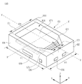
61-64: 外側面
101、201: キャビティー
111、211: 胴体
121、131、221、231: リードフレーム
122、123、133、222: 凹部
125、135、225: リード領域
161、161А、161B、261: モールド部材
171、271: 発光チップ
173、273: 保護チップ
181: 蛍光体層
Claims (22)
- 互いに対向する第1及び第2の外側面と、第3及び第4の外側面を有し、上部へ開放したキャビティーが設けられた胴体と、
前記キャビティーの底面から前記第1の外側面方向に延びた第1のリードフレームと、
前記キャビティーの底面から前記第2の外側面方向に延びた第2のリードフレームと、
前記第1のリードフレームの上に配置された発光チップと、
を含み、
前記キャビティーは、第1軸方向に前記第1及び第2の外側面にそれぞれ対応する第1及び第2の内側面を有し、前記第1の内側面と前記発光チップ間の間隔より、前記第2の内側面と前記発光チップ間の間隔が広く、
前記第1軸方向と直交する第2軸方向に、前記第2の内側面の幅は、前記第1の内側面の幅より狭く、
前記キャビティーの底に露出した前記第2のリードフレームの上面は、前記発光チップに隣接するほど広い幅を有し、
前記キャビティーは、前記第1の内側面に連結され、前記発光チップの両側において相互対応する第2軸方向の第3及び第4の内側面と、前記第2の内側面と前記第3の内側面の間に形成された第5の内側面と、前記第2の内側面と前記第4の内側面の間に形成された第6の内側面とを含み、
前記第5の内側面は、前記第3の内側面との内角が前記第2の内側面との内角より大きい角度で形成され、
前記第6の内側面は、前記第4の内側面との内角が前記第2の内側面との内角より大きい角度で形成されることを特徴とする発光素子。 - 前記第6の内側面と前記第4の内側面の間の内角は、前記第5の内側面と前記第3の内側面の間の角度と同一であることを特徴とする請求項1に記載の発光素子。
- 前記キャビティーの第2の内側面は、前記第1の内側面の幅よりも、2.5〜3.5倍狭い幅を有することを特徴とする請求項1又は請求項2に記載の発光素子。
- 前記第2のリードフレーム上に配置され、前記キャビティーと、前記胴体の第2及び第3の外側面の少なくとも一側面との間に配置された保護チップを含むことを特徴とする請求項1乃至3のいずれかに記載の発光素子。
- 前記保護チップは、前記キャビティーの第5及び第6の内側面の少なくとも1つと、前記胴体の第2の及び第3の外側面の少なくとも1つとの間に配置され、
前記第5の内側面と前記第2及び第3の外側面の間の前記胴体の角との間隔が5.82mm〜6.59mmの範囲であることを特徴とする請求項4に記載の発光素子。 - 前記第1のリードフレームには、前記第2のリードフレームに隣接した領域に第1の凹部が形成されることを特徴とする請求項1乃至5のいずれかに記載の発光素子。
- 前記第1のリードフレームには、前記胴体の第1外側面に対向する領域に第2の凹部が形成されることを特徴とする請求項6に記載の発光素子。
- 前記第1の凹部の第1の深さは、前記第2の凹部の第2の深さに比較して、2倍以上又は前記第1のリードフレームの長さの30〜60%の範囲の深さを有することを特徴とする請求項7に記載の発光素子。
- 前記第1のリードフレームと前記第2のリードフレームとの間の間隙の下面幅は、上面幅に比較して、2倍以上広いことを特徴とする請求項6乃至8のいずれかに記載の発光素子。
- 前記第1のリードフレームは、前記胴体の第1の外側面に隣接して、前記第3及び第4の外側面の下へ延び、
前記第1の凹部は、前記胴体の第3の外側面及び第4の外側面の間の間隔と等しい幅を有することを特徴とする請求項6乃至9のいずれかに記載の発光素子。 - 前記第1のリードフレームの下面面積は、前記第1のリードフレームの上面面積よりも30%以上狭く形成されることを特徴とする請求項6乃至10のいずれかに記載の発光素子。
- 前記第1のリードフレームは、前記第1の凹部と前記第2の凹部との間に配置された、前記胴体の下面に露出した第1のリード領域を有し、
前記第2のリードフレームは、前記第1及び第2のリードフレーム間の間隙に隣接し、前記胴体の下面に露出した第2のリード領域を有し、
前記発光チップは、前記第1のリードフレームと伝導性接着剤で接着されて電気的に連結され、
前記発光チップは、前記第2のリードフレームとワイヤで連結されることを特徴とする請求項7乃至11のいずれかに記載の発光素子。 - 前記第2のリードフレームは、前記胴体の第2の外側面に対向する領域に第3凹部を有し、
前記第2の凹部の第2の深さと前記第3凹部の第3深さとは、等しい深さを有することを特徴とする請求項7乃至12のいずれかに記載の発光素子。 - 前記第1のリードフレームは、前記胴体の第1の外側面、第3及び第4の外側面で露出した第1乃至第3の突起を有し、
前記第2のリードフレームは、前記胴体の第2、第3、及び第4の外側面で露出した第4乃至第6の突起を有し、
前記第1乃至第6の突起は、前記胴体の下面から離隔することを特徴とする請求項1乃至13のいずれかに記載の発光素子。 - 前記第5の内側面及び第6の内側面の少なくとも1つと、前記第2の内側面との間の内角は、鈍角で形成され、
前記第3の内側面と前記第4の内側面は、前記第1の内側面の両端部から直角方向に延長されることを特徴とする請求項2乃至14のいずれかに記載の発光素子。 - 前記第5の内側面と前記第3の内側面との間の内角は、鈍角で形成され、
前記第6の内側面と前記第4の内側面との間の内角は、鈍角で形成されることを特徴とする請求項2乃至15のいずれかに記載の発光素子。 - 前記第5の内側面及び第6の内側面の少なくとも1つは、曲面又は変曲点を有することを特徴とする請求項1乃至16のいずれかに記載の発光素子。
- 前記第5の内側面と前記第3の内側面の間の内角は、130度〜170度の範囲であり、
前記第5の内側面と前記第2の内側面の間の内角は、140度〜165度の範囲で形成され、前記第6の内側面と前記第2の内側面の間の内角と同一であることを特徴とする請求項1乃至17のいずれかに記載の発光素子。 - 前記第3の内側面と前記第5の内側面との間の変曲地点と、前記第4の内側面と前記第6の内側面との間の変曲地点とは、前記第1のリードフレーム及び前記第1及び第2のリードフレーム間の間隙の少なくとも1つに配置されることを特徴とする請求項1乃至17のいずれかに記載の発光素子。
- 前記第5の内側面または第6の内側面の幅は、前記第1の内側面の幅よりは小さく、前記第2の内側面の幅よりは広く形成されることを特徴とする請求項1乃至19のいずれかに記載の発光素子。
- 前記第2の外側面と、前記キャビティーの第2の内側面との間の上面幅は、前記第1の外側面と前記第1の内側面との間の上面幅よりも広いことを特徴とする請求項1乃至20のいずれかに記載の発光素子。
- 前記発光チップの周囲に第1のモールド部材と、前記第1のモールド部材上に第2のモールド部材と、前記発光チップと前記第2のモールド部材上に蛍光体層とを含むことを特徴とする請求項1乃至21のいずれかに記載の発光素子。
Applications Claiming Priority (2)
| Application Number | Priority Date | Filing Date | Title |
|---|---|---|---|
| KR1020120101821A KR102033928B1 (ko) | 2012-09-13 | 2012-09-13 | 발광 소자 및 조명 시스템 |
| KR10-2012-0101821 | 2012-09-13 |
Publications (3)
| Publication Number | Publication Date |
|---|---|
| JP2014057060A JP2014057060A (ja) | 2014-03-27 |
| JP2014057060A5 JP2014057060A5 (ja) | 2016-10-20 |
| JP6312999B2 true JP6312999B2 (ja) | 2018-04-18 |
Family
ID=48874933
Family Applications (1)
| Application Number | Title | Priority Date | Filing Date |
|---|---|---|---|
| JP2013183676A Active JP6312999B2 (ja) | 2012-09-13 | 2013-09-05 | 発光素子及びこれを備えた照明システム |
Country Status (5)
| Country | Link |
|---|---|
| US (2) | US9318675B2 (ja) |
| EP (1) | EP2709174B1 (ja) |
| JP (1) | JP6312999B2 (ja) |
| KR (1) | KR102033928B1 (ja) |
| CN (1) | CN103682068B (ja) |
Families Citing this family (18)
| Publication number | Priority date | Publication date | Assignee | Title |
|---|---|---|---|---|
| DE102013104840A1 (de) * | 2013-05-10 | 2014-11-13 | Osram Opto Semiconductors Gmbh | Strahlungsemittierendes Halbleiterbauelement und Verfahren zur Herstellung von strahlungsemittierenden Halbleiterbauelementen |
| DE102014101557A1 (de) * | 2014-02-07 | 2015-08-13 | Osram Opto Semiconductors Gmbh | Optoelektronisches Bauelement und Verfahren zu seiner Herstellung |
| WO2016035508A1 (ja) * | 2014-09-01 | 2016-03-10 | シャープ株式会社 | 発光装置 |
| JP6532200B2 (ja) | 2014-09-04 | 2019-06-19 | 日亜化学工業株式会社 | パッケージ及びそれを用いた発光装置 |
| JP6862141B2 (ja) | 2015-10-14 | 2021-04-21 | エルジー イノテック カンパニー リミテッド | 発光素子パッケージ及び照明装置 |
| KR20170064673A (ko) * | 2015-12-02 | 2017-06-12 | (주)포인트엔지니어링 | 칩기판 |
| JP2017135148A (ja) * | 2016-01-25 | 2017-08-03 | スタンレー電気株式会社 | 半導体装置 |
| JP6387973B2 (ja) | 2016-01-27 | 2018-09-12 | 日亜化学工業株式会社 | 発光装置 |
| USD831593S1 (en) * | 2016-03-24 | 2018-10-23 | Hamamatsu Photonics K.K | Optical semiconductor element |
| JP1563908S (ja) * | 2016-03-24 | 2016-11-21 | ||
| JP1563909S (ja) * | 2016-03-24 | 2016-11-21 | ||
| USD826184S1 (en) * | 2016-03-24 | 2018-08-21 | Hamamatsu Photonics K.K. | Optical semiconductor element |
| US10411169B2 (en) * | 2017-02-03 | 2019-09-10 | Nichia Corporation | Light emitting device having leads in resin package |
| US10374002B2 (en) * | 2017-02-13 | 2019-08-06 | Fuji Xerox Co., Ltd. | Layered structure including thyristor and light-emitting element, light-emitting component, light-emitting device, and image forming apparatus |
| JP6669208B2 (ja) * | 2018-08-02 | 2020-03-18 | 日亜化学工業株式会社 | 発光装置 |
| JP6669217B2 (ja) * | 2018-08-30 | 2020-03-18 | 日亜化学工業株式会社 | パッケージ及びそれを用いた発光装置 |
| KR101970938B1 (ko) * | 2019-02-11 | 2019-04-19 | 진재언 | 지향각이 조절된 발광소자 패키지 및 이를 이용한 발광장치 |
| US11417808B2 (en) | 2019-09-12 | 2022-08-16 | Nichia Corporation | Light emitting device |
Family Cites Families (19)
| Publication number | Priority date | Publication date | Assignee | Title |
|---|---|---|---|---|
| JPH0832118A (ja) * | 1994-07-19 | 1996-02-02 | Rohm Co Ltd | 発光ダイオード |
| CN100359703C (zh) | 2001-08-21 | 2008-01-02 | 奥斯兰姆奥普托半导体有限责任公司 | 辐射构件及其引线框和壳体及带辐射构件的显示装置和/或照明装置 |
| JP2005026401A (ja) * | 2003-07-01 | 2005-01-27 | Matsushita Electric Ind Co Ltd | 発光ダイオード |
| KR100587020B1 (ko) * | 2004-09-01 | 2006-06-08 | 삼성전기주식회사 | 고출력 발광 다이오드용 패키지 |
| JP2007142290A (ja) | 2005-11-21 | 2007-06-07 | Sharp Corp | 発光装置 |
| TWI284433B (en) * | 2006-02-23 | 2007-07-21 | Novalite Optronics Corp | Light emitting diode package and fabricating method thereof |
| US20100163920A1 (en) * | 2007-06-14 | 2010-07-01 | Rohm Co., Ltd. | Semiconductor light emitting device |
| KR20110018777A (ko) | 2009-08-18 | 2011-02-24 | 삼성엘이디 주식회사 | 발광 다이오드 패키지 |
| USD632659S1 (en) * | 2009-11-11 | 2011-02-15 | Everlight Electronics Co., Ltd. | Light emitting diode lamp |
| KR101028195B1 (ko) * | 2010-01-18 | 2011-04-11 | 엘지이노텍 주식회사 | 발광 소자 패키지 및 이를 구비한 라이트 유닛 |
| JP5922326B2 (ja) * | 2010-07-26 | 2016-05-24 | 大日本印刷株式会社 | Led用リードフレームまたは基板およびその製造方法、ならびに半導体装置およびその製造方法 |
| KR101186000B1 (ko) * | 2010-06-28 | 2012-09-25 | 엘지디스플레이 주식회사 | 발광 다이오드, 백라이트 유닛 및 이를 구비한 액정표시장치 |
| DE102010026343A1 (de) * | 2010-07-07 | 2012-03-29 | Osram Opto Semiconductors Gmbh | Bauelement und Verfahren zur Herstellung eines Bauelements |
| DE102010027253B4 (de) * | 2010-07-15 | 2022-05-12 | OSRAM Opto Semiconductors Gesellschaft mit beschränkter Haftung | Optoelektronisches Halbleiterbauteil |
| US20120098006A1 (en) * | 2010-10-22 | 2012-04-26 | Taiwan Semiconductor Manufacturing Company, Ltd. | Light emitting diode package with photoresist reflector and method of manufacturing |
| JP2012142426A (ja) * | 2010-12-28 | 2012-07-26 | Toshiba Corp | Ledパッケージ及びその製造方法 |
| KR20120118686A (ko) * | 2011-04-19 | 2012-10-29 | 엘지이노텍 주식회사 | 발광소자 모듈 |
| JP2012234955A (ja) * | 2011-04-28 | 2012-11-29 | Toshiba Corp | Ledパッケージ及びその製造方法 |
| US8692282B2 (en) * | 2011-10-27 | 2014-04-08 | Seoul Semiconductor Co., Ltd. | Light emitting diode package and light emitting module comprising the same |
-
2012
- 2012-09-13 KR KR1020120101821A patent/KR102033928B1/ko active IP Right Grant
-
2013
- 2013-03-15 US US13/836,574 patent/US9318675B2/en active Active
- 2013-07-29 EP EP13178406.8A patent/EP2709174B1/en active Active
- 2013-07-31 CN CN201310328799.2A patent/CN103682068B/zh active Active
- 2013-09-05 JP JP2013183676A patent/JP6312999B2/ja active Active
-
2016
- 2016-03-11 US US15/067,995 patent/US9620693B2/en active Active
Also Published As
| Publication number | Publication date |
|---|---|
| JP2014057060A (ja) | 2014-03-27 |
| CN103682068A (zh) | 2014-03-26 |
| US20160197254A1 (en) | 2016-07-07 |
| CN103682068B (zh) | 2018-01-30 |
| US9318675B2 (en) | 2016-04-19 |
| US20140070259A1 (en) | 2014-03-13 |
| EP2709174A3 (en) | 2014-10-29 |
| US9620693B2 (en) | 2017-04-11 |
| KR20140035213A (ko) | 2014-03-21 |
| KR102033928B1 (ko) | 2019-10-18 |
| EP2709174A2 (en) | 2014-03-19 |
| EP2709174B1 (en) | 2019-07-03 |
Similar Documents
| Publication | Publication Date | Title |
|---|---|---|
| JP6312999B2 (ja) | 発光素子及びこれを備えた照明システム | |
| JP6104570B2 (ja) | 発光素子及びこれを備えた照明装置 | |
| JP6283483B2 (ja) | 発光素子及びこれを備えた照明システム | |
| JP5745495B2 (ja) | 発光素子及びこれを備えた照明システム | |
| JP5788539B2 (ja) | 発光素子 | |
| JP6306842B2 (ja) | 発光素子及びこれを具備した照明システム | |
| KR102075561B1 (ko) | 발광 소자, 발광 모듈 및 조명 시스템 | |
| KR102153082B1 (ko) | 발광 장치 | |
| KR101926531B1 (ko) | 발광 소자, 발광 소자 제조방법 및 조명 시스템 | |
| KR102053287B1 (ko) | 발광 소자 및 이를 구비한 조명 시스템 | |
| KR101976547B1 (ko) | 발광 소자 및 이를 구비한 조명 시스템 | |
| KR101953280B1 (ko) | 발광소자 및 이를 구비한 조명 시스템 | |
| KR101977831B1 (ko) | 발광 소자 및 조명 시스템 | |
| KR102019498B1 (ko) | 발광 소자 및 조명 시스템 | |
| KR102042271B1 (ko) | 발광 소자 및 조명 시스템 | |
| KR101946831B1 (ko) | 발광 소자 패키지 | |
| KR102109139B1 (ko) | 발광 소자 및 이를 구비한 조명 시스템 | |
| KR101896691B1 (ko) | 발광 소자 및 조명 시스템 | |
| KR102042197B1 (ko) | 발광 소자 및 이를 구비한 조명 시스템 | |
| KR20130119132A (ko) | 발광 소자, 발광 모듈 및 조명 시스템 |
Legal Events
| Date | Code | Title | Description |
|---|---|---|---|
| A521 | Request for written amendment filed |
Free format text: JAPANESE INTERMEDIATE CODE: A523 Effective date: 20160902 |
|
| A621 | Written request for application examination |
Free format text: JAPANESE INTERMEDIATE CODE: A621 Effective date: 20160902 |
|
| A977 | Report on retrieval |
Free format text: JAPANESE INTERMEDIATE CODE: A971007 Effective date: 20170728 |
|
| A131 | Notification of reasons for refusal |
Free format text: JAPANESE INTERMEDIATE CODE: A131 Effective date: 20170808 |
|
| A521 | Request for written amendment filed |
Free format text: JAPANESE INTERMEDIATE CODE: A523 Effective date: 20171107 |
|
| TRDD | Decision of grant or rejection written | ||
| A01 | Written decision to grant a patent or to grant a registration (utility model) |
Free format text: JAPANESE INTERMEDIATE CODE: A01 Effective date: 20180227 |
|
| A61 | First payment of annual fees (during grant procedure) |
Free format text: JAPANESE INTERMEDIATE CODE: A61 Effective date: 20180322 |
|
| R150 | Certificate of patent or registration of utility model |
Ref document number: 6312999 Country of ref document: JP Free format text: JAPANESE INTERMEDIATE CODE: R150 |
|
| R250 | Receipt of annual fees |
Free format text: JAPANESE INTERMEDIATE CODE: R250 |
|
| S531 | Written request for registration of change of domicile |
Free format text: JAPANESE INTERMEDIATE CODE: R313531 |
|
| S111 | Request for change of ownership or part of ownership |
Free format text: JAPANESE INTERMEDIATE CODE: R313113 |
|
| R350 | Written notification of registration of transfer |
Free format text: JAPANESE INTERMEDIATE CODE: R350 |
|
| R350 | Written notification of registration of transfer |
Free format text: JAPANESE INTERMEDIATE CODE: R350 |
|
| R250 | Receipt of annual fees |
Free format text: JAPANESE INTERMEDIATE CODE: R250 |
|
| R250 | Receipt of annual fees |
Free format text: JAPANESE INTERMEDIATE CODE: R250 |