EP1592134B1 - Counter circuit, AD conversion method, AD converter, semiconductor device for detecting distribution of physical quantities, and electronic apparatus - Google Patents
Counter circuit, AD conversion method, AD converter, semiconductor device for detecting distribution of physical quantities, and electronic apparatus Download PDFInfo
- Publication number
- EP1592134B1 EP1592134B1 EP05009016A EP05009016A EP1592134B1 EP 1592134 B1 EP1592134 B1 EP 1592134B1 EP 05009016 A EP05009016 A EP 05009016A EP 05009016 A EP05009016 A EP 05009016A EP 1592134 B1 EP1592134 B1 EP 1592134B1
- Authority
- EP
- European Patent Office
- Prior art keywords
- signal
- counter
- counting
- count
- clock
- Prior art date
- Legal status (The legal status is an assumption and is not a legal conclusion. Google has not performed a legal analysis and makes no representation as to the accuracy of the status listed.)
- Active
Links
Images


Classifications
-
- H—ELECTRICITY
- H03—ELECTRONIC CIRCUITRY
- H03K—PULSE TECHNIQUE
- H03K23/00—Pulse counters comprising counting chains; Frequency dividers comprising counting chains
-
- H—ELECTRICITY
- H03—ELECTRONIC CIRCUITRY
- H03K—PULSE TECHNIQUE
- H03K23/00—Pulse counters comprising counting chains; Frequency dividers comprising counting chains
- H03K23/58—Gating or clocking signals not applied to all stages, i.e. asynchronous counters
- H03K23/62—Gating or clocking signals not applied to all stages, i.e. asynchronous counters reversible
-
- A—HUMAN NECESSITIES
- A61—MEDICAL OR VETERINARY SCIENCE; HYGIENE
- A61P—SPECIFIC THERAPEUTIC ACTIVITY OF CHEMICAL COMPOUNDS OR MEDICINAL PREPARATIONS
- A61P31/00—Antiinfectives, i.e. antibiotics, antiseptics, chemotherapeutics
- A61P31/04—Antibacterial agents
-
- H—ELECTRICITY
- H03—ELECTRONIC CIRCUITRY
- H03K—PULSE TECHNIQUE
- H03K23/00—Pulse counters comprising counting chains; Frequency dividers comprising counting chains
- H03K23/40—Gating or clocking signals applied to all stages, i.e. synchronous counters
- H03K23/50—Gating or clocking signals applied to all stages, i.e. synchronous counters using bi-stable regenerative trigger circuits
- H03K23/56—Reversible counters
-
- H—ELECTRICITY
- H03—ELECTRONIC CIRCUITRY
- H03M—CODING; DECODING; CODE CONVERSION IN GENERAL
- H03M1/00—Analogue/digital conversion; Digital/analogue conversion
- H03M1/10—Calibration or testing
- H03M1/1009—Calibration
- H03M1/1014—Calibration at one point of the transfer characteristic, i.e. by adjusting a single reference value, e.g. bias or gain error
- H03M1/1023—Offset correction
-
- H—ELECTRICITY
- H03—ELECTRONIC CIRCUITRY
- H03M—CODING; DECODING; CODE CONVERSION IN GENERAL
- H03M1/00—Analogue/digital conversion; Digital/analogue conversion
- H03M1/12—Analogue/digital converters
- H03M1/124—Sampling or signal conditioning arrangements specially adapted for A/D converters
- H03M1/129—Means for adapting the input signal to the range the converter can handle, e.g. limiting, pre-scaling ; Out-of-range indication
- H03M1/1295—Clamping, i.e. adjusting the DC level of the input signal to a predetermined value
-
- H—ELECTRICITY
- H03—ELECTRONIC CIRCUITRY
- H03M—CODING; DECODING; CODE CONVERSION IN GENERAL
- H03M1/00—Analogue/digital conversion; Digital/analogue conversion
- H03M1/12—Analogue/digital converters
- H03M1/48—Servo-type converters
-
- H—ELECTRICITY
- H04—ELECTRIC COMMUNICATION TECHNIQUE
- H04N—PICTORIAL COMMUNICATION, e.g. TELEVISION
- H04N25/00—Circuitry of solid-state image sensors [SSIS]; Control thereof
-
- H—ELECTRICITY
- H04—ELECTRIC COMMUNICATION TECHNIQUE
- H04N—PICTORIAL COMMUNICATION, e.g. TELEVISION
- H04N25/00—Circuitry of solid-state image sensors [SSIS]; Control thereof
- H04N25/70—SSIS architectures; Circuits associated therewith
- H04N25/71—Charge-coupled device [CCD] sensors; Charge-transfer registers specially adapted for CCD sensors
- H04N25/75—Circuitry for providing, modifying or processing image signals from the pixel array
-
- H—ELECTRICITY
- H03—ELECTRONIC CIRCUITRY
- H03M—CODING; DECODING; CODE CONVERSION IN GENERAL
- H03M1/00—Analogue/digital conversion; Digital/analogue conversion
- H03M1/12—Analogue/digital converters
- H03M1/1205—Multiplexed conversion systems
- H03M1/123—Simultaneous, i.e. using one converter per channel but with common control or reference circuits for multiple converters
-
- H—ELECTRICITY
- H03—ELECTRONIC CIRCUITRY
- H03M—CODING; DECODING; CODE CONVERSION IN GENERAL
- H03M1/00—Analogue/digital conversion; Digital/analogue conversion
- H03M1/12—Analogue/digital converters
- H03M1/50—Analogue/digital converters with intermediate conversion to time interval
- H03M1/56—Input signal compared with linear ramp
Definitions
- the present invention relates to asynchronous counter circuits, analog-to-digital (AD) conversion methods and AD converters for converting analog signals into digital data using the counter circuits, semiconductor devices for detecting distribution of physical quantities by an array of a plurality of unit elements, and electronic apparatuses.
- AD analog-to-digital
- the present invention relates to an asynchronous counter and techniques of AD conversion, suitably used in electronic apparatuses, for example, a semiconductor device for detecting distribution of physical quantities, such as a solid-state imaging device, that allows reading electric signals representing distribution of physical quantities obtained by an array of a plurality of unit elements that are sensitive to electromagnetic waves input from the outside, such as light or radiation.
- a semiconductor device for detecting distribution of physical quantities such as a solid-state imaging device, that allows reading electric signals representing distribution of physical quantities obtained by an array of a plurality of unit elements that are sensitive to electromagnetic waves input from the outside, such as light or radiation.
- Semiconductor devices for detecting physical quantities including a line or matrix of unit elements that are sensitive to electromagnetic waves input from the outside, such as light or radiation, are used in various fields.
- CCD charge coupled device
- MOS metal oxide semiconductor
- CMOS complementary metal oxide semiconductor
- CMOS solid-state imaging devices In a type of solid-state imaging device, referred to as an active pixel sensor (APS) or gain cell, a driving transistor for amplification is provided in a pixel signal generator that generates a pixel signal corresponding to signal charges generated by a charge generator.
- CMOS solid-state imaging devices are of the type described above.
- an active pixel sensor in order to read pixel signals to the outside, address control is exercised on a pixel unit including an array of unit pixels so that signals can be read from arbitrarily selected individual unit pixels. That is, an active pixel sensor is an example of address-controlled solid-state imaging device.
- each pixel is implemented using an active element of the MOS structure (MOS transistor) or the like so that the pixel itself is capable of amplification. That is, signal charges (photoelectrons) accumulated in a photodiode that functions as a photoelectric converter are amplified by the active element, and the amplified signals are read as image information.
- MOS transistor MOS transistor
- a pixel unit includes a two-dimensional array of a large number of pixel transistors. Accumulation of signal charges corresponding to incident line is started on a line-by-line basis or pixel-by-pixel basis. Current or voltage signals based on the accumulated signal charges are sequentially read from the respective pixels according to addressing.
- MOS including CMOS
- address control according to a method that is often used, pixels on one row are simultaneously accessed to read pixel signals from the pixel unit on a row-by-row basis.
- the analog pixel signals read from the pixel unit are converted into digital data by an analog-to-digital converter as needed. Since the pixel signals are output with signal components added to reset components, true effective signal components must be extracted by taking difference between signal voltage corresponding to reset component and signal voltage corresponding to signal component.
- AD conversion is performed using a counter circuit.
- the counter circuit used is usually a synchronous counter in which a flip-flop (basic element of the counter) outputs a count value in synchronization with a counter clock.
- an asynchronous counter is suitable for high-speed operation since the limiting operation frequency thereof is determined only by the limiting frequency of the first flip-flop.
- an asynchronous counter is preferably used as a counter circuit when an operation at a higher frequency is needed.
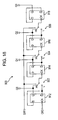
- Fig. 18 is a diagram showing an asynchronous counter according to the related art, which is capable of switching mode.
- a counter circuit 900 is capable of functioning as a 4-bit asynchronous counter.
- the counter circuit 900 is implemented by cascade connection of a plurality of negative-edge D flip-flops 912, 914, 916, and 918 (collectively 910).
- Each of the flip-flops 910 has an inverting output NQ (indicated with a horizontal bar over Q) connected to a D input terminal thereof.
- a clock terminal CK of the first flip-flop 910 receives input of a count clock CK0.
- the counter circuit 900 includes two-input single-output switches 922, 924, and 926 (collectively 920) for switching the values of the non-inverting outputs Q and the inverting outputs NQ of the flip-flops 910 respectively between the adjacent pairs of the flip-flops 910.
- Each of the switches 920 switches the two input signals according to a control signal SW from a controller (not shown) and inputs a selected signal to the clock terminal CK of the subsequent flip-flop 910.
- the control signal SW is used to switch counting operation of the counter circuit 900 between up-counting and down-counting.
- the control signal is at High (H) level
- the non-inverting output Q is selected so that the counter circuit 900 enters an up-count mode.
- the control signal SW is at Low (L) level
- the inverting output NO is selected so that the counter circuit 900 enters a down-count mode.
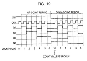
- Fig. 19 is a timing chart for explaining the operation of the counter circuit 900 shown in Fig. 18 .
- a 4-bit asynchronous counter switches between the non-inverting output Q and the inverting output NQ according to the control signal SW, so that up-counting is first performed and then down-counting is performed.
- the count value changes from 6 to 10.
- a scheme for overcoming this problem is proposed, for example, in Japanese Unexamined Patent Application Publication No. 6-216762 (hereinafter referred to as a second patent document).
- a device for inverting the status of each flip-flop and a device for initializing all the flip-flops on each even-numbered pulse train are provided.
- an asynchronous counter is capable of counting up to a maximum number n
- a first pulse train includes i pulses
- a second pulse train includes j pulses.
- the counter is reset in advance, and counts from 0 to i for the first pulse train. Then, when the status of the flip-flops of the counter is inverted, the n's complement of the value i is obtained, so that the value of the counter becomes n - i.
- the counter then counts from n - i to n - i + j.
- the difference of interest i - j is the n's complement of n - i + j, which is obtained by inverting the status of the flip-flops again.
- Fig. 21 is a schematic construction diagram of a CMOS solid-state imaging device (CMOS image sensor) according to the related art, in which an AD converter and a pixel unit are mounted on the same semiconductor substrate.
- a solid-state imaging device 1 includes a pixel unit (imaging unit) 10 in which a plurality of unit pixels 3 is arranged in rows and columns, a driving controller 7 provided externally to the pixel unit 10, a counter (CNT) 24, a column processor 26 including column AD circuits 25 provided for the respective columns, a reference-signal generator 27 including a digital-to-analog converter (DAC) for supplying a reference voltage for AD conversion to the column AD circuits 25 in the column processor 26, and an output circuit 28 including a subtractor circuit 29.
- a pixel unit imaging unit
- driving controller 7 provided externally to the pixel unit 10
- CNT counter
- a column processor 26 including column AD circuits 25 provided for the respective columns
- a reference-signal generator 27 including a digital-to-analog
- the driving controller 7 includes a horizontal scanning circuit (column scanning circuit) 12 that controls column address or column scanning, a vertical scanning circuit (row scanning circuit) 14 that controls row address or row scanning, and a timing controller 21 that receives a master clock CLK0 via a terminal 5a and that generates various internal clocks to control the horizontal scanning circuit 12, the vertical scanning circuit 14, and the like.
- a horizontal scanning circuit column scanning circuit
- a vertical scanning circuit row scanning circuit
- timing controller 21 that receives a master clock CLK0 via a terminal 5a and that generates various internal clocks to control the horizontal scanning circuit 12, the vertical scanning circuit 14, and the like.
- the unit pixels 3 are connected to row control lines 15 that are controlled by the vertical scanning circuit 14 and to vertical signal lines 19 that transfer pixel signals to the column processor 26.
- Each of the column AD circuits 25 includes a voltage comparator 252 and a data storage unit (latch) 255, and it has a function of an n-bit AD converter.
- the voltage comparator 252 compares a reference signal RAMP generated by the reference-signal generator 27 with an analog signal obtained for each row control line 15 (H0, H1, ...) from the unit pixels 3 via the vertical control lines 19 (V0, V1, ).
- the data storage unit 255 is a memory that holds a result of counting a time taken by the voltage comparator 252 to finish comparison by the counter 24.
- the data storage unit 255 includes n-bit latches 1 and 2 that are storage areas independent of each other.
- One input terminal RAMP of the voltage comparator 252 receives input of a stairs-like reference signal RAMP generated by the reference-signal generator 27 commonly with the input terminals RAMP of the other voltage comparators 252.
- the other input terminals of the voltage comparators 252 are connected to the vertical signal lines of the respectively associated columns so that pixel signals from the pixel unit 10 are individually input. Signals output from the voltage comparators 252 are supplied to the data storage units 255.
- the reference signal RAMP is digitally generated by performing counting based on a count clock CK0 corresponding to the master clock CLK0 (e.g., clock frequencies of these clocks are equal) supplied from the outside of the solid-state imaging device 1 and converting the count value into an analog signal.
- the counter 24 performs counting based on the count clock CK0 that is based on the master clock CLK0 (e.g., clock frequencies of these clocks are the same), and supplies count outputs CK1, CK2, ..., CKn, together with the count clock CK0, commonly to the column AD circuits 25 of the column processor 26.
- the column AD circuits 25 for the respective columns share the single counter 24.
- the outputs of the column AD circuits 25 are connected to horizontal signal lines 18.
- the horizontal signal lines 18 have signal lines for 2n bits, and are connected to the subtractor circuit 29 of the output circuit 28 via 2n sensing circuits (not shown) associated with the respective output lines.
- the timing controller 21 instructs, via a control line 12c, the horizontal scanning circuit 12 to read pixel data.
- the horizontal scanning circuit 12 sequentially transfers pixel data held in the latches 1 and 2 to the subtractor circuit 29 of the output circuit 28 by sequentially shifting a horizontal select signal CH(i). That is, the horizontal scanning circuit 12 performs read scanning in the horizontal (row) direction.
- the horizontal scanning circuit 12 generates a horizontal select signal CH(i) for performing read scanning in the horizontal (row) direction based on the master clock CLK0 supplied from the outside of the solid-state imaging device 1, similarly to the count clock CK0.
- Fig. 22 is a timing chart for explaining an operation of the solid-state imaging unit 1 according to the related art shown in Fig. 21 .
- the count value of the counter 254 is first reset to an initial value "0". Then, after the first reading operation of reading pixel signals from unit pixels 3 on an arbitrary row Hx to the vertical signal lines 19 (V0, V1, ...) becomes stable, a reference signal RAMP generated by the reference-signal generator 27, temporally changing so as to form substantially ramp waveform, is input, which is compared by the voltage comparator 252 with a pixel signal voltage on an arbitrary vertical signal line 19 (with a column number Vx).
- the counter 24 starts down-counting from the initial value "0" as the first counting operation.
- the voltage comparator 252 compares the ram reference signal RAMP from the reference-signal generator 27 with a pixel signal voltage Vx input via a vertical signal line 19. When these voltages become equal, the voltage comparator 252 inverts its output from H level to L level (t12).
- the data storage unit 255 latches the count outputs CK1, CK2, ... CKn from the counter 24 in accordance with a comparison period in the latch 1 of the data storage unit 255 in synchronization with the count clock CK0, whereby the first iteration of AD conversion is completed (t12).
- the timing controller 21 stops supply of control data to the voltage comparator 252 and supply of the count clock CK0 to the counter 254.
- the voltage comparator 252 stops generating the ramp reference signal RAMP.
- reset components ⁇ V of the unit pixels 3 are read, and the reset components ⁇ V includes offset noise that varies among the unit pixels 3. Generally, however, the variation in the reset components ⁇ V is small, and the reset levels are common among all the pixels, so that the output of an arbitrary vertical signal line 19 (Vx) is substantially known.
- the reset components ⁇ V are read in the first reading operation, it is possible to shorten the comparison period by adjusting the reference signal RAMP. According to this related art, the reset components ⁇ V are compared in a count period corresponding to 7 bits (128 clock cycles).
- the count value of the counter 254 is first reset to the initial value "0". Then, when the second reading operation of reading pixel signals from the unit pixels 3 on an arbitrary row Hx to the vertical signal lines 19 (V0, V1, ...) becomes stable, a reference signal RAMP generated by the reference-signal generator 27 so as to temporally change in a stairs-like manner and have substantially ramp waveform is input, and the voltage comparator 252 compares the reference signal RAMP with a pixel signal voltage on an arbitrary vertical signal line 19 (with a column number Vx).
- the counter 24 starts down-counting from the initial value "0" as the second counting operation.
- the voltage comparator 252 compares the ramp reference signal RAMP from the reference-signal generator 27 with a pixel signal voltage Vx input via a vertical signal line 19. When these voltages become equal, the voltage comparator 252 inverts its output from H level to L level (t22).
- the data storage unit 255 latches the count outputs CK1, CK2, ..., CKn from the counter 24 in accordance with the comparison period in synchronization with the count clock CK0, whereby the second iteration of AD conversion is completed (t22).
- the data storage unit 255 holds the count value in the first counting operation and the count value in the second counting operation in different places thereof, namely, in the latch 2.
- the second reading operation combinations of the reset components ⁇ V and the signal components Vsig of the unit pixels 3 are read.
- the timing controller 21 stops supply of control data to the voltage controller 252 and supply of the count clock CK0 to the counter 254.
- the voltage comparator 252 stops generating the ramp reference signal RAMP.
- the timing controller 21 instructs the horizontal scanning circuit 12 to read pixel data.
- the horizontal scanning circuit 12 sequentially shifts the horizontal select signal CH(i) supplied to the data storage unit 255 via the control line 12c.
- the count value latched in the data storage unit i.e., pixel data in the first iteration and the second iteration each represented by n-bit digital data is sequentially output to the outside of the column processor 26 via n (2n in total) horizontal signal lines 18 and is input to the subtractor circuit 29 of the output circuit 28.
- the n-bit subtractor circuit 29 for each pixel position, subtracts the pixel data of the first iteration, representing the reset component ⁇ V of a unit pixel 3, from the pixel data of the second iteration, representing the combination of the reset component ⁇ V and the signal component Vsig of the unit pixel 3, calculating the signal component Vsig of the unit pixel 3.
- the column AD circuits of the respective columns shares the single counter 24, and the results of the first and second counting operations must be held in the data storage unit 255 that functions as a memory.
- two n-bit latches are needed for an n-bit signal (2n latches are needed for each bit), causing an increase in circuit area (hereinafter referred to as a third problem).
- a memory for holding the result of the first reading operation and a memory for holding the result of the second reading operation must be individually provided (i.e., two memories are needed) separately from the counter. Furthermore, signal lines for transmitting n-bit count values from the memories to the counter are needed. Furthermore, in order to transfer the n-bit count values of the first and second counting operations to the subtractor, signal for 2n bits (double) are needed. This increases circuitry scale and circuit area, and also increases noise, consumption current, or power consumption.
- a memory for holding data obtained by AD conversion is needed separately from a memory for holding the result of counting.
- two memories are needed for this purpose, causing an increase in circuit area (hereinafter referred to as a seventh problem).
- a correlated double sampling (CDS) function and an AD conversion function are implemented by providing in series a counter that is commonly used among columns, and a CDS processing unit and a latch for holding the count value of the counter, provided for each column. This is described, for example, in the second non-patent document.
- an AD conversion function is implemented by providing a counter for each column in the column processor 26. This is described, for example, in the third and fourth non-patent documents.
- AD converters including counters and latches, which perform parallel processing for the vertical signal lines (columns), converts analog signals into digital signals by taking the difference between a reset component and a signal component while suppressing fixed pattern noise of pixels.
- memory for holding data obtained by AD conversion can be implemented by latches. This serves to avoid increase in circuit area. That is, the third, fifth, sixth, and seventh problems are overcome.
- the first patent document describes handling of a reset component and a signal component.
- digital data of the reset component is subtracted from digital data of the signal component for each column, so that the sixth problem is avoided.
- counting is performed in an external system interface to generate a count signal, and a count value at a time when a voltage of the reset component or the signal component matches a reference voltage for comparison is saved in a pair of buffers provided for each column.
- the scheme of AD conversion is the same as that in the first non-patent document in that a single counter is commonly used by the columns.
- JP 61-100025 an asynchronous up-down counter is disclosed.
- a signal processing circuit 5 inputs the up-down switching signal S 2 and generates a delayed up-down switching signal S 3 being a result of a prescribed time of delay to the signal S 2 and a stop signal S 4 having a time width corresponding to the period including the timing when the signal S 3 is switched.
- the signals S 3 , S 4 from the circuit 5 are inputted to the up-down counter 4 together with the clock signal S 1 .
- the counter 4 counts up or down the signal S 1 based on the signal S 3 and stops temporarily the counting by using the signal S 4 in the timing when the signal S 3 is switched from up to down or vice versa.
- the present invention has been made in view of the situation described above, and it is an object thereof to provide a scheme that overcomes the first and second problem. More preferably, it is an object of the present invention to provide a scheme that overcomes at least one of the third to seventh problems.
- an asynchronous counter circuit adapted to hold a count value and selectively perform counting in an up-count mode or a down-count mode
- the counter circuit comprising a switching processor connected between the flip-flops for selecting one of said up-count and down-count mode by selectively connecting a non-inverting output or an inverting output of a preceding flip-flop to a clock terminal of a succeeding flip-flop, wherein the switching processor being adapted for restoring, after switching of count mode from one of said up-count mode and down-count mode to the other one of said up-count mode and down-count mode, the counter value to the value that it had immediately before said switching of count mode by connecting said clock terminal of said succeeding flip-flop to a power supply level after said switching of count mode for a predetermined period of time.
- an analog-to-digital conversion method for converting a difference signal component into digital data, the difference signal component representing a difference between a reference component and a signal component included in an analog signal subject to processing, is provided.
- a signal corresponding to the reference component and a signal corresponding to the signal component are compared with a reference signal for conversion into digital data, and concurrently with the comparison, counting is performed in a down-count mode or an up-count mode, holding a count value at a time, when the result of the comparison changes. At this time, the counting mode is switched according to whether comparison is being performed for the reference component or the signal component.
- an analog-to-digital converter that is suitable for carrying out the AD conversion method described above.
- the AD converter includes a comparator that compares a signal corresponding to the reference component and a signal corresponding to the signal component with a reference signal for conversion into digital data; and an asynchronous counter that performs counting in a down-count mode or an up-count mode, concurrently with the comparison in the comparator, the counter holding a count value at a time when the result of the comparison changes in the comparator.
- a signal subject to processing including a reference component and a signal component
- counting is performed in a down-count mode or an up-count mode using an asynchronous counter, holding a count value at a time when the result of the comparison changes.
- the counting mode is switched according to whether comparison is being performed for the reference component or the signal component.
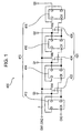
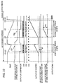
- Fig. 1 is a block circuit diagram showing the basic configuration of an asynchronous counter according to a first embodiment of the present invention.
- Fig. 2 is a block circuit diagram showing a specific implementation of the basic configuration according to the first embodiment.
- a counter circuit 400 is implemented by cascade connection of a plurality of negative-edge D flip-flops 412, 414, 416, and 418 (collectively 410).
- Each of the flip-flops 410 has an inverting output NQ (indicated in Fig. 1 by a horizontal bar over Q) connected to a D input terminal thereof.
- the counter circuit 400 is capable of functioning as a 4-bit asynchronous counter. Although four stages (corresponding to four bits) of flip-flops 412, 414, 416, and 418 are shown in Fig. 1 , actually, a number of flip-flops corresponding to the number of bits is provided.
- the counter circuit 400 includes three-input single-output tri-value switches 422, 424, and 426 (collectively 420) that switch among three values, namely, the non-inverting output Q, the inverting output NQ, and a power supply (Vdd) level.
- Each of the tri-value switches 420 switches among the three input signals according to 2-bit control signals SW1 and SW2 supplied from a controller (not shown), and inputs a selected signal to a clock terminal of the subsequent flip-flop 410.
- Each of the tri-value switches 420 functions as an initial-value setting processor that causes, at a time of switching of count mode, a count value immediately before mode switching to be set as a initial value so that counting is started from the value after the mode switching.
- the tri-value switches 420 are disposed between the respective adjacent pairs of the flip-flops 410.
- One of the non-inverting output NQ and the inverting output Q of a previous flip-flop 410 is selected as a counter clock and is supplied to the clock terminal CK of a subsequent flip flop 410 so that switching of count mode is allowed, and a count value of the previous flip-flop 410 immediately before mode switching is set to the subsequent flip-flop 410 as an initial value.
- the tri-value switches 420 can be respectively implemented by a pair of two-input single-output binary switches 432 and 433, a pair of two-input single-output binary switches 434 and 435, and a pair of two-input single-output binary switches 436 and 437, as shown in Fig. 2 .
- These binary switches will be collectively referred to as binary switches 430.
- each of the binary switches 430 is switched according to switching control signals SL and FL generated at different timings as the two-bit switching control signals SW1 and SW2 supplied from a controller (not shown).
- the binary switches 432, 434, and 436 at the previous stages switch the non-inverting outputs Q and the inverting outputs NQ of the respectively associated flip-flops 410 according to the switching control signal SL, and pass the results to one of the input terminals of the associated binary switches 433, 435, and 437 at the subsequent stages.
- the binary switches 433, 435, and 437 at the subsequent stages switches between the data passed from the binary switches 432, 434, and 436 at the previous stages and the power supply level input to the other input terminals thereof according to the switching control signal FL, and input the results to the clock terminals CK of the subsequent flip-flops 410.
- the previous binary switch 430 (432, 434, and 436) selects the non-inverting output NQ and the inverting output Q of the preceding flip-flop 430 according to the switching control signal SL, and supplies it to one input terminal of the subsequent binary switch 430 (433, 435, and 437).
- the switching control signal SL controls the previous binary switch 430 (432, 434, and 436), thereby switching the counting operation of the counter circuit 400 between up-counting and down-counting.
- the subsequent binary switch 430 (433, 435, and 437) adjusts the supply of the output (non-inverting output NQ or inverting output Q) of the preceding flip-flop 410, output from the previous binary switch 430 (432, 434, and 436) to the clock terminal of the succeeding flip-flop 410 according to the switching control signal FL.
- the switching control signal FL controls the subsequent binary switch 430 (433, 435, and 437) so that the supply of the output of the preceding flip-flop 410 (non-inverting output NQ or inverting output Q) to the clock terminal of the succeeding flip-flop 410 is stopped for a predetermined period after switching of count mode, and so that a signal corresponding to a clock is supplied to the clock terminal of the succeeding flip-flop 410 when the supply of non-inverting output NQ or inverting output Q is resumed.
- the continuity of count value is maintained when count mode is switched between the up-count mode and the down-count mode.
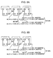
- Figs. 3A and 3B are diagrams showing example circuit configurations of the binary switches 430.
- Fig. 3A shows an example where each switch is implemented by a transfer gate. All the circuit elements are implemented using CMOS techniques.
- transfer gates 442 and 443 are provided in association with the previous binary switches 432, 434, and 436.
- transfer gates 446 and 447 are provided in association with the subsequent binary switches 433, 435, and 437. These transfer gates will be collectively referred to as transfer gates 440.
- the input of the transfer gate 442 receives the inverting output NQ of the preceding flip-flop 410.
- the input of the transfer gate 443 receives the non-inverting output Q of the preceding flip-flop 410.
- the outputs of the transfer gates 442 and 443 are commonly connected to the input of the transfer gate 446.
- the input of the transfer gate 447 is connected to a power supply level.
- the outputs of the transfer gates 446 and 447 are commonly connected to the clock terminal CK of the succeeding flip-flop 410.
- Each of the transfer gates 440 is implemented by a CMOS switch including an N-channel transistor n1 and a P-channel transistor p1.
- the gates (control input terminal) of the transistors n1 and p1 correspond to input terminals of the switching controls signals SL and FL or inverted switching control signals NSL and NFL.
- the inverted signal NSL is generated by an inverter 444 that inverts the switching control signal SL
- the inverted signal NFL is generated by an inverter 448 that inverts the switching control signal FL.
- the CMOS switch including the transistors n1 and p1 selectively outputs the non-inverting output Q or the inverting output NQ of the preceding flip-flop 410 by turning on when the gate of the transistor n1 is High and the gate of the transistor n1 is Low.
- the CMOS switch may be replaced by an N-channel MOS transistor switch or a P-channel MOS transistor switch including either the transistor n1 or the transistor p1. In that case, however, a problem relating to a threshold voltage Vth occurs.
- the CMOS switch formed by the transistor n1 and p1 is used.
- Fig. 3B shows an example where each switch is implemented by a logic gate.
- three two-input NAND gates 452, 453, and 454 are provided.
- an OD gate formed by a two-input NOR gate 456 and an inverter 457 is provided.
- One input of the NAND gate 452 receives the inverted signal NSL obtained by inverting the switching control signal SL by the inverter 455, and one input of the NAND gate 453 receives the switching control signal SL.
- the other input of the NAND gate 452 receives the inverting output NQ of the preceding flip-flop 410, and the other input of the NAND gate 453 receives the non-inverting output Q of the preceding flip-flop 410.
- the outputs of the NAND gates 452 and 453 are connected to the inputs of the NAND gate 454.
- One input terminal of the NOR gate 456 receives the output of the NAND gate 454, and the other input terminal thereof receives a switching control signal.
- the output of the NOR gate 456 is inverted by the inverter 457, and is then led to the clock terminal CK of the succeeding flip-flop 410.
- each of the previous binary switches 432, 434, and 436 selectively outputs the non-inverting output Q when the switching control signal SL is at High level, while selectively outputting the inverting output NQ when the switching control signal SL is at Low level.
- Each of the subsequent binary switches 433, 435, and 437 selectively outputs the output of the associated previous binary switch 432, 434, or 436 when the switching control signal FL is at Low level, while selectively outputting the power supply level (High level) when the switching control signal FL is at High level.
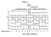
- Fig. 4 is a timing chart for explaining the operation of the counter circuit according to the first embodiment shown in Fig. 2 .
- Figs. 5A and 5B are diagrams for explaining change in the outputs of the flip-flops 410 in the first embodiment.
- each of the previous binary switches 432, 434, and 436 selectively outputs the non-inverting output Q
- each of the subsequent binary switch 433, 435, and 437 selectively outputs the output of the previous binary switch 432, 434, or 436.
- the counter circuit 400 switches from the up-count mode to the down-count mode, and starts down-counting when the clock CK0 is resumed.
- the switching control signal SL is switched from High level to Low level after up-counting is performed from a count value of 0 to a count value of 6.
- the pair of binary switches 430 selects the inverting output NQ of the preceding flip-flop 410 and inputs it to the clock terminal CK of the succeeding flip-flop 410.
- the output of the second flip-flop 410 is inverted from Low level to High level, and the output of the third flip-flop 410 is also inverted (t30+).
- the output of the second flip-flop 410 is inverted from High level to Low level (t30+).
- the count value starts to be broken only at the subsequent stage of a flip-flop 410 in which the non-inverting output Q is at High level, i.e., the inverting output NQ is at Low level, at the time of switching of count mode.
- the effect of inverting data (from H to L) of the inverting output NQ is propagated up to a flip-flop 410 in which the inverting output NQ is inverted from Low level to High level.
- the count value changes from "6" to "10" as shown in Fig. 4 .
- an active-H one-shot pulse is applied to the subsequent binary switches 433, 435, and 437 as the switching control signal FL (t32 to t34).
- the power supply level (High level) is input to the clock terminals CK of all the negative-edge flip-flops 410.
- the outputs of the negative edge flip-flops 410 do not change before and after the input of the one-shot pulse of the switching control signal FL.
- the output of the second flip-flop 410 is inverted from High level to Low level (t34+).
- the output of the second flip-flop 410 is inverted from Low level to High level, and the output of the third flip-flop 410 is also inverted (t34+).
- each flip-flop 410 in which the output is inverted in response to switching of count mode according to the switching control signal SL the output is inverted again, so that the count value is restored.
- the count value changed at the time of switching from up-counting to down-counting is restored to the state after the mode switching after once forcibly pulling the clock terminals of flip-flops 410 to High level by applying an active-H one-shot pulse as the switching control signal FL. If the inverting output NQ of the preceding flip-flop 410 is at Low level when the state after the mode switching is restored, the output of the succeeding flip-flop 410 is inverted, whereby the original count value is restored.
- Down-counting is performed in the negative direction as compared with up-counting.
- the result of subtraction i - j can be obtained as a result of counting by the counter circuit 400.
- the count value obtained by switching mode between up-counting and down-counting does not involve complement values, and the result of subtraction can be obtained directly.
- asynchronous counter circuit 400 With the asynchronous counter circuit 400, it is possible to continuously perform up-counting and down-counting directly by an asynchronous counter, which has hitherto been difficult, by adding simple switches. Since the value before switching is maintained at the time of switching between up-counting and down-counting, it is possible to continuously perform up-counting and down-counting or down-counting and up-counting and to obtain a result of subtraction between a count value of up-counting and a count value of down-counting.
- the first embodiment has been described in the context of an example where switching from up-counting to down-counting occurs.
- the continuity of count value cannot be maintained either when switching from down-counting to up-counting if the count mode is simply switched.
- a measure against overflow can be readily implemented using known techniques, for example, by adding an additional bit for overflow or by using a bit for carry or borrow.
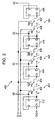
- Fig. 6 is a block circuit diagram showing the configuration of a second embodiment of an asynchronous counter according to the present invention, corresponding to the specific block circuit diagram of the first embodiment shown in Fig. 2 .
- three-input single-output tri-value switches 522, 524, and 526 that each switch among three input signals according to two-bit control signals SW1 and SW2 from a controller (not shown) and input a selected signal to the clock terminal CK of the succeeding flip-flop 510 are provided respectively between the adjacent pairs of flip-flops 510.
- Each of the three-input single-output tri-value switches 520 functions as an initial-value setting processor that sets a count value immediately before the mode switching as an initial value so that counting after the mode switching is started from the initial value.
- Each of the flip-flop 510 operates based on positive edges instead of negative edges, and in order to deal with the inversion of edge operations, each of the tri-value switches 520 provided between the flip-flops 510 switches among three values, namely, the non-inverting output Q and the inverting output NQ of the associated flip-flop 510 and a ground (GND) level.
- the three-input single-output tri-value switches 520 respectively include a pair of two-input single-output binary switches 532 and 533, a pair of two-input single-output binary switches 534 and 535, and a pair of two-input single-output binary switches 536 and 537. These binary switches will be collectively referred to as binary switches 530.
- Each of the previous binary switches 532, 534, and 536 similarly to the previous binary switches 432, 434, and 436 in the first embodiment, switches between the non-inverting output Q and the inverting output NQ of the associated flip-flop 510 according to the switching control signal SL, and passes the result to one input terminal of the associated subsequent binary switch 533, 535, or 537.
- Each of the subsequent binary switches 533, 535, and 537 switches between the data passed from the previous binary switch 532, 534, or 536 and the ground level input to the other input terminal according to the switching control signal FL, and inputs the result to the clock terminal CK of the succeeding flip-flop 510. That is, the second embodiment differs from the first embodiment in that one of the inputs of the subsequent binary switch in the tri-value switch 520 is changed from the power supply level to the ground level.
- Each of the previous binary switches 532, 534, and 536 selectively outputs the non-inverting output Q when the switching control signal SL is at High level, while selectively outputting the inverting output NQ when the switching control signal SL is at Low level.
- Each of the subsequent binary switches 533, 535, and 537 selectively outputs the output of the associated previous binary switch 532, 534, or 536 when the switching control signal FL is at Low level, while outputting the ground level (Low level) when the switching control signal FL is at High level.
- Fig. 7 is a timing chart for explaining the operation of the counter circuit 500 according to the second embodiment shown in Fig. 6 .
- Figs. 8A and 8B are diagrams for explaining change in the outputs of the flip-flops 510 in the second embodiment.
- the second embodiment is modified so that up-counting or down-counting is based on positive edges.
- the basic ideas are the same as in the first embodiment, and the advantages achieved are also the same.
- each of the previous binary switches 532, 534, and 536 selectively outputs the inverting output NQ
- each of the subsequent binary switches 533, 535, and 537 selectively outputs the output of the previous binary switch 532, 534, or 536.
- the counter circuit 500 switches from the up-count mode to the down-count mode, and starts down-counting when the clock CK0 is resumed.
- the switching control signal SL is switched from Low level to High level after up-counting is performed from a count value of 0 to a count value of 6.
- the pair of binary switches 530 selects the non-inverting output Q of the preceding flip-flop 510 and inputs it to the clock terminal CK of the succeeding flip-flop 510.
- Fig. 8A the output of the second flip-flop 510 is inverted from Low level to High level, and the output of the third flip-flop 510 is also inverted (t30+).
- Fig. 8B the output of the second flip-flop 510 is inverted from High level to Low level (t30+).
- the count value starts to be broken only at the subsequent stage of a flip-flop 510 in which the inverting output NQ is at Low level, i.e., the non-inverting output Q is at High level, at the time of the switching of count mode.
- the effect of inverting data (from L to H) of the non-inverting output Q is propagated to a flip-flop 510 in which the non-inverting output Q is inverted from High level to Low level.
- the count value changes from "6" to "10", as shown in Fig. 7 .
- an active-H one-shot pulse is applied to the subsequent binary switches 533, 535, and 537 as the switching control signal FL (t42 to t44).
- the ground level (Low level) is input to the clock terminals CK of all positive-edge flip-flops 510.
- the outputs of the positive-edge flip-flops 510 do not change before and after the one-shot pulse of the switching control signal FL is input.
- the non-inverting output Q of the preceding flip-flop 510 is again input to the clock terminal CK.
- the non-inverting output Q of the preceding flip-flop 510 is at High level, a positive edge is applied to the clock terminal CK of the succeeding flip-flop 510, so that the output of the succeeding flip-flop 510 is inverted.
- the output of the second flip-flop 510 is inverted from Low level to High level (t44+).
- the output of the second flip-flop 510 is inverted from High level to Low level, and the output of the third flip-flop 510 is also inverted (t44+).
- each flip-flop 510 in which the output is inverted in response to switching of count mode according to the switching control signal SL the output is inverted again, so that the original count value is restored.
- the count value changed at the time of switching from up-counting to down-counting is once pulling the clock terminals of flip-flops 510 forcibly to Low level before restoring the stage after the mode switching by applying an active-H one-shot pulse as the switching control signal FL. If the non-inverting output Q of the preceding flip-flop 510 is at High level when the state after the mode switching is restored, the output of the succeeding flip-flop 510 is inverted, whereby the original count value is restored.
- Down-counting is performed in the negative direction as compared with up-counting.
- the result of subtraction i - j can be obtained as a result of counting by the counter circuit 400.
- the second embodiment has been described in the context of an example where switching from up-counting to down-counting occurs.
- the continuity of count value cannot be maintained either when switching from down-counting to up-counting if the count mode is simply switched.
- a measure against overflow can be readily implemented using known techniques, for example, by adding an additional bit for overflow or by using a bit for carry or borrow.
- Fig. 9 is a block circuit diagram showing the configuration of a third embodiment of an asynchronous counter according to the present invention, corresponding to the specific circuit block diagram according to the first embodiment shown in Fig. 2 .
- a counter circuit 400 In a counter circuit 400 according to the third embodiment, an arrangement for switching the clock signal input to the clock terminal CK of the first flip-flop 412 in the counter circuit 400 according to the first embodiment shown in Fig. 2 is additionally provided. Furthermore, in the counter circuit 400 as a whole, the clock CK0 is used as the least significant bit Q0, and count outputs of the flip-flops 410 as the other bits Qx (Q1 to Q4 in this embodiment) are shifted higher by one bit compared with the first embodiment.
- the counter circuit 400 in the third embodiment includes an inverter 462 that inverts the clock CK0, and a two-input single output binary switch 464 that selects the clock CK0 or an inverted clock NCK0 inverted by the inverter 462 and inputs it to the clock terminal CK of the first flip-flop 412, i.e., switches whether to invert the clock CK0.
- the binary switch 464 selectively outputs the clock CK0 when the switching control signal SL is at High level, while selectively outputting the inverted clock NCKO when the switching control signal SL is at Low level.
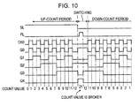
- Fig. 10 is a timing chart for explaining the operation of the counter circuit 400 according to the third embodiment shown in Fig. 9 .
- the clock CK0 is used as the least significant bit Q0.
- the number of count bits is increased by one, i.e., doubled, compared with the first embodiment. Furthermore, since High level and Low level of the clock CK0 contribute to count values, counting operations are performed based on both edges of the clock CK0, so that the speed of counting operations is doubled.
- the third embodiment can also be modified by replacing the negative-edge flip-flops 410 with the positive-edge flip-flops 510 so that up-counting or down-counting is performed based on positive edges.
- CMOS imaging device which is an example of X-Y-addressed solid-state imaging device
- NMOS transistors all the pixels of the CMOS imaging device are implemented by NMOS transistors.
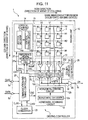
- Fig. 11 is a schematic diagram showing the construction of a CMOS solid-state imaging device (CMOS image sensor), which is a semiconductor device according to a first embodiment of the present invention.
- CMOS solid-state imaging device is also an electronic apparatus according to an embodiment of the present invention.
- a solid-state imaging device 1 includes a pixel unit in which a plurality of pixels each including a photoreceptor element (which is an example of charge generator) that outputs a voltage signal corresponding to the amount of incident light is arranged in rows and columns (i.e., in a two-dimensional matrix shape).
- a photoreceptor element which is an example of charge generator
- ADCs analog-to-digital converters
- CDS processing units and ADCs are provided in association with the respective columns", it is meant that a plurality of CDS processing units and ADCs are provided substantially in parallel to vertical signal lines 19 of the columns.
- the plurality of CDS processing units and ADCs when viewed in plan, may be both provided on one end of the pixel unit 10 with respect to the column direction (on the output side, i.e., on the lower side as viewed in Fig. 11 ), or separately provided on one end (on the output side, i.e., on the lower side as viewed in Fig. 11 ) and on the other end (on the upper side as viewed in Fig. 11 ) of the pixel unit 10 with respect to the column direction, respectively.
- horizontal scanning units that perform horizontal scanning with respect to the horizontal direction are provided separately on both ends so that the horizontal scanning units operate independently of each other.
- CDS processing units and ADCs are provided in association with the respective columns, in a region provided on the output side of an imaging unit, referred to as a column region, CDS processing units and ADCs are provided in association with the respective columns, and signals are sequentially read out to the output side. That is, the arrangement is a column-based arrangement.
- a CDS processing unit and an ADC may be provided in association with each set of (e.g., two) adjacent vertical signal lines 19 (columns), or a CDS processing unit and an ADC may be provided in association with each set of every N-th (N is a positive integer, with (N-1) intervening lines) vertical signal line 19 (column).
- a plurality of vertical signal lines 19 shares a CDS processing unit and an ADC, so that a switching circuit that supplies pixel signals for a plurality of columns, supplied from the pixel unit 10, to the CDS processing unit and the DAC is provided.
- a memory that holds output signals must be provided.
- each unit pixel is simplified. This allows an image sensor to have an increased number of pixels, to be implemented in a reduced size, and to be manufactured at a lower cost.
- the solid-state imaging device 1 includes the pixel unit (imaging unit) 10 in which a plurality of unit pixels 3 is arranged in rows and columns, a driving controller 7 provided externally to the pixel unit 10, a column processor 26, a reference-signal generator 27 for supplying a reference voltage for AD conversion to the column processor 26, and an output circuit 28.
- an automatic gain control (AGC) circuit for amplifying signals may be provided upstream or downstream of the column processor 26 in the same semiconductor region where the column processor 26 is provided.
- AGC automatic gain control
- AGC is exercised upstream of the column processor 26
- analog amplification is performed.
- AGC is exercised downstream of the column processor 26
- digital amplification is performed. Since signal levels could be deteriorated when n-bit digital data is simply amplified, preferably, analog amplification is performed before conversion into digital signals.
- the driving controller 7 exercises control for sequentially reading signals of the pixel unit 10.
- the driving controller 7 includes a horizontal scanning circuit (column scanning circuit) 12 that controls column addressing and column scanning, a vertical scanning circuit (row scanning circuit) 14 that controls row addressing and row scanning, and a communication and timing controller 20 that generates an internal clock.
- the solid-state imaging device 1 may include a clock converter 23, which is an example of a high-speed-clock generator that generates pulses of a clock having a higher frequency than an input clock, as indicated by a dotted line in the proximity of the communication and timing controller 20.
- a terminal 5a of the solid-state imaging device 1 receives input of a master clock CLK0.
- the master clock CLK0 has pulses that serve as a base for various driving pulses for capturing analog pixel signals to be processed from the pixel unit 10 to the column processor 26.
- the clock converter 23 includes a multiplier circuit 23a that generates pulses having a clock frequency that is faster than an input clock frequency.
- the clock converter 23 receives a low-speed clock CLK2 from the communication and timing controller 20, and generates therefrom a clock having a frequency that is twice as high or even higher.
- the multiplier circuit 23a of the clock converter is a k1 multiplier circuit, where k1 denotes a multiplier of the frequency of the low-speed clock CLK2, and can be implemented using various known circuits.
- Each of the unit pixels 3 typically includes a photodiode as a photoreceptor element (charge generator), and an intra-pixel amp having an amplifying semiconductor device (e.g., a transistor).
- a photoreceptor element charge generator
- an intra-pixel amp having an amplifying semiconductor device (e.g., a transistor).
- the intra-pixel amp is implemented, for example, by a floating-diffusion amp.
- a floating-diffusion amp for example, an amp including four transistors in relation to the charge generator, namely, a read-select transistor, which is an example of a charge reader (transferring gate/reading gate), a reset transistor, which is an example of a reset gate, a vertical-select transistor, and a source-follower amplifying transistor, which is an example of a detector that detects change in the potential of floating diffusion, may be used.
- a read-select transistor which is an example of a charge reader (transferring gate/reading gate)
- a reset transistor which is an example of a reset gate
- a vertical-select transistor for example, a vertical-select transistor, and a source-follower amplifying transistor, which is an example of a detector that detects change in the potential of floating diffusion.
- a source-follower amplifying transistor which is an example of a detector that detects change in the
- an arrangement including three transistors may be used, namely, an amplifying transistor for amplifying a signal voltage corresponding to signal charges generated by the charge generator, connected to a drain line (DRN), a reset transistor for resetting the charge generator, and a read-select transistor (transferring gate) that is scanned by a vertical shift register via a transferring line (TRF).
- an amplifying transistor for amplifying a signal voltage corresponding to signal charges generated by the charge generator, connected to a drain line (DRN), a reset transistor for resetting the charge generator, and a read-select transistor (transferring gate) that is scanned by a vertical shift register via a transferring line (TRF).
- the horizontal scanning circuit 12 functions as a reading scanner that reads a count value from the column processor 26.
- the components of the driving controller 7 are formed together with the pixel unit 10 in a semiconductor region of single-crystal silicon or the like using techniques used to manufacture semiconductor integrated circuits, forming a solid-state imaging device, which is an example of a semiconductor system.
- the unit pixels 3 are connected to the vertical scanning circuit 14 via row control lines 15 for row selection, and are connected via the vertical signal lines 19 to the column processor 26 in which the column AD circuits 25 are provided for the respective columns.
- the row control lines 15 generally refer to lines running from the vertical scanning circuit 14 into pixels.
- the horizontal scanning circuit 12 and the vertical scanning circuit 14 respectively include decoders, so that shift operations (scanning) are started in response to control signals CN1 and CN2 supplied from the communication and timing controller 20.
- the row control lines 15 include lines for transferring various pulse signals for driving the unit pixels 3 (e.g., a reset pulse RST, a transfer pulse TRF, and a DRN control pulse DRN).
- the communication and timing controller 20 includes a functional block corresponding to a timing generator (an example of read-address controller) that supplies clocks needed for the operation of the components and pulse signals at specific timings, and a functional block corresponding to a communication interface that receives a master clock CLK0 via a terminal 5a, that receives data DATA instructing an operation mode or the like via a terminal 5b, and that outputs data including information of the solid-state imaging device 1.
- a timing generator an example of read-address controller
- the communication and timing controller 20 outputs a horizontal address signal to a horizontal decoder 12a and a vertical address signal to a vertical decoder 14a so that the respective decoders 12a and 14a select corresponding row and column.
- the unit pixels 3 are arranged in a two-dimensional matrix shape, analog pixel signals that are generated by the pixel-signal generators 5 and output in the column direction via the vertical signal lines are accessed and captured on a row-by-row basis (in a column-parallel manner), i.e., vertical-scan reading is performed. Then, access in the row direction, i.e., the direction of array of the columns, is performed to read pixel signals (digitized pixel data in this embodiment) to the output side, i.e., horizontal-scan reading is performed. This serves to improve the speed of reading pixel signals or pixel data.
- scan reading only information of unit pixels 3 needed may be read by random access, i.e., by directly specifying addresses of unit pixels 3 to be read.
- the communication and timing controller 20 supplies a clock CLK1 having the same frequency as the master clock CLK0 input via the terminal 5a, a clock having a half frequency, or a low-speed clock having a further divided frequency to the components in the device, e.g., the horizontal scanning circuit 12, the vertical scanning circuit 14, or the column processor 26.
- the clock having the half frequency, and clocks having even lower frequencies in general will be referred to as low-speed clocks CLK2.
- the vertical scanning circuit 14 selects a row of the pixel unit 10 and supplies pulses needed for the row.
- the vertical scanning circuit 14 includes the vertical decoder 14a for defining a row to be read in the vertical direction (i.e., for selecting a row of the pixel unit 10), and a vertical driving circuit 14 for driving the row control lines 15 for the unit pixels 3 on a read row address defined by the vertical decoder 14a by supplying pulses thereto.
- the vertical decoder 14a also selects a row for electronic shutter or the like.
- the horizontal scanning circuit 12 in synchronization with the low-speed clocks CLK2, sequentially selects the column AD circuits 25 of the column processor 26, leading signals of the column AD circuits 25 to the horizontal signal lines (horizontal output lines) 18.
- the horizontal scanning circuit 12 includes the horizontal decoder 12a for defining a column to be read in the horizontal direction (for selecting the individual column AD circuits 25 in the column processor 26), and a horizontal driving circuit 12b for leading signals of the column processor 26 to the horizontal signal lines 18 according to a read address defined by the horizontal decoder 12a.
- the number of horizontal signal lines 18 corresponds to the number n (n is a positive integer) of bits of signals handled by the column AD circuits 25. For example, if n is ten, ten horizontal signal lines 18 are provided correspondingly to the number n of bits.
- pixel signals output from the unit pixels 3 are supplied to the column AD circuits 25 of the column processor 26 via the vertical signal lines 19 on a column-by-column basis.
- Each of the column AD circuits 25 of the column processor 26 receives signals of pixels of one line and processes the signals.
- each of the column AD circuits 25 includes an analog-to-digital converter (ADC) that converts analog signals into, for example, 10-bit digital data based on the low-speed clock CLK2.
- ADC analog-to-digital converter
- counting based on clock signals is started when a ramped reference signal (reference voltage) RAMP is supplied to a voltage comparator, and analog pixel signals: input via the vertical signal lines 19 are compared with the reference signal RAMP to carry out counting until pulse signals are obtained, whereby AD conversion is performed.
- reference signal reference voltage
- the circuit by suitably configuring the circuit, together with AD conversion, with regard to voltage-mode pixel signals input via the vertical signal lines 19, the difference between a signal level immediately before the pixel is reset (noise level) and a true signal level Vsig in accordance with the amount of light received can be calculated.
- a noise component called fixed pattern noise (FPN) or reset noise.
- Pixel data digitized by the column AD circuits 25 is transferred to the horizontal signal lines 18 via a horizontal selecting switch (not shown) that is driven according to horizontal select signals supplied from the horizontal scanning circuit 12, and is then input to the output circuit 28.
- the number of bits is not limited to 10, and may be less than 10 (e.g., 8) or greater than 10 (e.g., 14).
- the pixel unit 10 including a matrix of photoreceptor elements that act as charge generators sequentially outputs pixel signals for respective columns on a line-by-line basis. Then, a frame image, i.e., an image corresponding to the matrix of photoreceptors in the pixel unit 10, is presented as a set of pixel signals for the entire pixel unit 10.
- the reference-signal generator 27 includes a digital-to-analog converter (DAC) 27.
- the reference-signal generator 27 generates stairs-like ramp waveform based on control data CN4 from the communication and timing controller 20, in synchronization with a count clock CK0, and supplies the ramp waveform as a reference voltage for AD conversion (ADC reference signal) to the individual column AD circuits 25 of the column processor 26.
- ADC reference signal a reference voltage for AD conversion
- a filter for removing noise is provided.
- the control data CN4 supplied from the communication and timing controller 20 to the DAC 27a of the reference-signal generator 27 causes the ratio of change in digital data with respect to time to be constant so that the ramp voltage has the same gradient (ratio of change) on each comparing operation. For example, the count value is changed by 1 in each unit time.
- Each of the column AD circuits 25 includes a voltage comparator 252 that compares the reference signal RAMP generated by the DAC 27a of the reference-signal generator 27 with analog pixel signals obtained from the unit pixels 3 via the vertical signal lines 19 (V0, V1, ...) for each of the row control lines 15 (H0, H1, ...), and a counter 254 that counts time for completion of comparing operations of the voltage comparator 252 and holding the result.
- the column AD circuit 25 has a function of n-bit AD conversion.
- the communication and timing controller 20 functions as a controller that switches the mode of counting by the counter 254 according to whether a reset component ⁇ V or a signal component Vsig of a pixel signal the voltage comparator 252 is executing a comparing operation for.
- a control signal CN5 for instructing whether the counter 254 is to operate in down-count mode or up-count mode is input from the communication and timing controller 20 to the counter 254 of each of the column AD circuits 25.
- a switching control signal SL for instructing the counter 254 to operate in a down-count mode or an up-count mode and a switching control signal FL for maintaining the continuity of count value at the time of switching of count mode are input.
- One input terminal RAMP of the voltage comparator 252 receives input of the stairs-like reference signal RAMP generated by the reference-signal generator 27, commonly with the input terminals RAMP of the other voltage comparators 252.
- the other input terminals of the voltage comparators 252 are respectively connected to the vertical signal lines 19 of the associated columns so that pixel signals can be individually input from the pixel unit 10. Signals output from the voltage comparator 252 are supplied to the counters 254.
- a count clock CK0 is input from the communication and timing controller 20, commonly with the clock terminals CK of the other counters 254.
- the counter 254 can be implemented by changing the wiring of the data storage unit 255 formed by latches, shown in Fig. 21 , into wiring for synchronous counter, and the counter 254 internally performs counting based on input of a single count clock CK0.
- the count clock CK0 similarly to the stairs-like voltage waveform, is generated based on a high-speed clock (e.g., a multiplied clock) supplied from the clock converter 23, so that the count clock CK0 can be faster than the master clock CLK0 input via the terminal 5a.
- a high-speed clock e.g., a multiplied clock
- the n-bit counter 254 can be implemented by a combination of n latches, so that the circuitry scale is reduced to half compared with the data storage unit 255 formed by two lines of n latches shown in Fig. 21 . Furthermore, the counter 24 is not needed, so that the overall size becomes considerably compact compared with the arrangement shown in Fig. 21 .
- the counter 254 in the first embodiment uses a common up/down counter (U/D CNT) irrespective of counting mode, and is capable of switching between down-counting operation and up-counting operation (i.e., alternately).
- U/D CNT common up/down counter
- the counter 254 in the first embodiment uses an asynchronous counter that outputs a count value asynchronously with the count clock CK0. More specifically, the counter circuit 400 according to the first embodiment described with reference to Figs. 1 to 4 is used as a basic element.
- the counter 254 receives control pulses from the horizontal scanning circuit 12 via the control line 12c.
- the counter 254 has a latch function for holding the result of counting, and it holds a count output value until an instruction by control pulses is received via the control line 12c.
- the column AD circuits 25 constructed as described above are provided for the respective vertical signal lines 19 (V0, V1, ...), forming the column processor 26, which is a column-parallel ADC block.
- the outputs of the individual column AD circuits 25 are connected to the horizontal signal lines 18.
- the horizontal signal lines 18 includes n-bit signal lines corresponding to the bit width of the column AD circuits 25.
- the horizontal signal lines 18 are connected to the output circuit 28 via n sensing circuits (not shown) associated with the respective output lines.
- the column AD circuits 25 performs counting in a pixel-signal reading period, outputting the result of counting at specific timing. That is, first, the voltage comparator 252 compares the ramp waveform voltage supplied from the reference-signal generator 27 with the pixel-signal voltage input via the vertical signal line 19. When these voltages are equal, the output of the voltage comparator 252 is inverted (changes from H level to L level in this embodiment).
- the counter 254 starts counting in down-count mode or up-count mode in synchronization with the ram waveform voltage generated by the reference-signal generator 27.
- the counter 254 stops counting, and latches a current count value as pixel data, whereby AD conversion is completed.
- the counter 254 by shift operations according to horizontal select signals CH(i) input via the control line 12c from the horizontal scanning circuit 12 at specific timing, outputs pixel data stored sequentially to the outside of the column processor 26 or to the outside of the chip of the pixel unit 10 via the output terminal 5c.
- the solid-state imaging device 1 may include other various signal processing circuits, although such circuits are not shown since they are not directly relevant to the description of the embodiment.
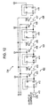
- Fig. 12 is a block circuit diagram showing a first example configuration of the counter 254.
- the basic configuration of asynchronous counter is the same as the counter circuit 400 according to the first embodiment described with reference to Figs. 1 to 4 .
- a gate circuit that controls input of a clock signal to the clock terminal CK of the first flip-flop 412 in the counter circuit 400 according to the first embodiment shown in Fig. 2 , based on a result of comparison by the voltage comparator 252, is additionally provided.
- the counter 254 in the first example includes a two-input AND gate 472 whose output is connected to the clock terminal of the first flip-flop 412.
- One input terminal of the AND gate 472 receives input of a result of comparison by the voltage comparator 252, and the other input terminal receives input of the counter clock CK0 from the communication and timing controller 20.
- the clock input to the clock terminal of the first flip-flop 412 is the logic product (AND) of the output of the voltage comparator 252 and the count clock CK0. Accordingly, it is possible to perform counting in accordance with a comparison period of the voltage comparator 252.
- the communication and timing controller 20 in order to activate generation of the reference signal RAMP by the reference-signal generator 27, supplies the control data CN4 and the count clock CK0 to the reference-signal generator 27.
- the reference-signal generator 27 starts counting in synchronization with the count clock CK0 from an initial value in accordance with the control data CN4, and generates a stairs-like ramp waveform by reducing voltage by a predetermined step size in each clock cycle, supplying the resulting reference signal RAMP to the voltage comparator 252.
- the voltage comparator 252 searches for a point where the ramp-waveform reference signal RAMP matches a voltage corresponding to a reference component or a signal component of a pixel signal from a unit pixel 3, and pulls its output to Low level when a match is found.
- the counter 254 commonly receives the counter clock CK0 supplied to the reference-signal generator 27.
- the AND gate 262 gates the counter clock CK0 by a comparison output supplied from the voltage comparator 252.
- a value that is finally written to each of the flip-flops 410 is a digital value representing the voltage corresponding to the reference component or the signal component of the pixel signal.
- the counter 254 performs counting based on the count clock CK0 from a time when the ramp-waveform reference signal RAMP used for comparison by the voltage comparator 252 is generated to a time when the reference signal RAMP matches a reference component or a signal component of a pixel signal, thereby obtaining digital data corresponding to the magnitude of the reference component or the signal component.
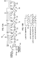
- Fig. 13A is a block circuit diagram showing a second example configuration of the counter 254, and Fig. 13B is a timing chart for explaining an operation thereof.
- the basic configuration of asynchronous counter is the same as the counter circuit 400 according to the first embodiment shown in Fig. 2 , similarly to the first example.
- a positive-edge D flip-flop 474 and a delaying circuit 476 are additionally provided.
- the delaying circuit 476 predetermine period (e.g., one clock cycle), as shown in Fig. 13B .
- the delaying circuit 476 can be implemented by various known circuit configurations, for example, by using gate delay.
- the D input terminal of the D flip-flop 474 receives a result of comparison by the voltage comparator 252.
- the clock terminal CK of the D flip-flop 474 receives the counter clock CK0 from the communication and timing controller 20.
- the non-inverting output Q of the D-flip-flop 474 is input to one input terminal of the AND gate 472.
- the D flip-flop 474 outputs the outputs of the voltage comparator 252 in synchronization with the rising edges of the counter clock CK0.
- the other input terminal of the AND gate 472 receives the counter clock CK0 from the communication and timing controller 20 via the delaying circuit 476.
- the output of the AND gate 472 is connected to the clock terminal of the first flip-flop 412.
- the AND gate 472 is used as a functional element that controls input of clock signal to the clock terminal CK of the first flip-flop 412.
- the AND gate 472 when such a simple AND gate is used, gridge or other noise due to timing deviation or the like could occur.
- the results of comparison by the voltage comparator 252 can be captured by the clock terminal of the first flip-flop 412 in synchronization with the counter clock CK0. This is preferably since the effect of gridge or the like is alleviated.
- the counter circuit 400 according to the first embodiment shown in Fig. 2 is used as the basic configuration of asynchronous counter in the counters 254 shown in Fig. 12 and Fig. 13A , similar up/down counters can be readily implemented using the counter circuits 400 and 500 according to the second and third embodiments.
- Fig. 14 is a diagram for explaining an operation of the column AD circuits 25 in the solid-state imaging device 1 according to the first embodiment shown in Fig. 11 .
- a mechanism for converting analog pixel signals sensed by the unit pixels 3 of the pixel unit 10 into digital signals for example, a point where the ramp-waveform reference signal RAMP that decreases at a specific gradient matches the voltage of a reference component or signal component in pixel signals from the unit pixels 3. Then, counting is performed based on a count clock between the time when the reference signal RAMP used for comparison is generated and the time when the signal corresponding to a reference component or signal component in pixel signals matches the reference signal, whereby a count value corresponding to the magnitude of the reference component or signal component is obtained.
- a signal component Vsig appears after a reset component ⁇ V that serves as a reference component, including noise of the pixel signal.
- the second iteration is performed for a signal including the signal component Vsig in addition to the reference component (reset component ⁇ V). Now, the operation will be described more specifically.
- the communication and timing controller 20 For the first iteration of reading, the communication and timing controller 20 resets the count value of the counter 254 to an initial value of "0", and causes the counter 254 to enter down-count mode by pulling the switching control signal SL to Low level.
- the communication and timing controller 20 supplies control data CN4 for generating the reference signal RAMP to the reference-signal generator 27.
- the reference-signal generator 27 In response to the control data CN4, the reference-signal generator 27 inputs ramp waveform that temporally changes in a ramp-like manner as a comparison voltage to one input terminal RAMP of the voltage comparator 252.
- the voltage comparator 252 compares the RAMP waveform comparison voltage with a pixel signal voltage of a vertical signal line 19 (Vx) supplied from the pixel unit 10.
- a count clock CK0 is input from the communication and timing controller 20 to the clock terminal of the counter 254, and down-counting is started from an initial value of "0" as the first counting operation. That is, counting is started toward the negative direction.
- the voltage comparator 252 compares the ramp reference signal RAMP supplied from the reference-signal generator 27 with the pixel signal voltage Vx input via the vertical signal line 19, and inverts its output from H level to L level when these voltages become equal (t12). That is, the voltage comparator 252 compares a voltage signal corresponding to a reset component Vrst with the reference signal RAMP, and generates an active-low (L) pulse signal after a time corresponding to the magnitude of the reset component Vrst elapses, outputting the pulse signal to the counter 254.
- the counter 254 stops counting substantially at the same time as the inversion of the output of the voltage comparator 252, and latches a current count value as pixel data, whereby AD conversion is completed (t12). That is, the counter 254 starts down-counting at the time of generation of the ramp reference signal RAMP supplied to the voltage comparator 252, and continues counting based on the clock CK0 until an active-low (L) pulse signal is obtained by comparison, thereby obtaining a count value corresponding to the magnitude of the reset component Vrst.
- the communication and timing controller 20 when a predetermined down-counting period elapses (t14), stops supply of control data to the voltage comparator 252 and supply of the count clock CK0 to the counter 254. Thus, the voltage comparator 252 stops generating the ramp reference signal RAMP.
- counting is performed by detecting the reset level Vrst in the pixel signal voltage Vx by the voltage comparator, i.e., the reset component ⁇ V of a unit pixel 3 is read.
- the reset component ⁇ V noise that varies among the unit pixels 3 is included as offset. Generally, however, variation of the reset component ⁇ V is small, and the reset level Vrst is substantially the same for all the pixels, so that the output value of the reset component ⁇ V on an arbitrary vertical signal line 19 is substantially known.
- the maximum period of comparison for the reset component ⁇ V is a count period corresponding to 7 bits (128 clock cycles).
- a signal component Vsig corresponding to the amount of incident light for each unit pixel 3 is read, and the same operation as the first reading operation is performed. More specifically, the communication and timing controller 20 first pulls the switching control signal SL to High level so that the counter 254 enters the up-count mode (t16).
- an active-H one-shot pulse is supplied to the counter 254 as the switching control signal FL (t17 to t18).
- the clock terminals of the flip-flops 410 constituting the asynchronous counter 254 are once forcibly pulsed to High level and are then returns to the status after the mode switching.
- the count value changed at the time of switching from down-counting to up-counting is restored to the original count value.
- the communication and timing controller 20 supplies control data CN4 for generating the reference-signal RAMP to the reference-signal generator 27 together with the clock CK0.
- the reference-signal generator 27 In response to the control data CN4, the reference-signal generator 27 inputs a ramp waveform that temporally changes in a ramp-like manner as a comparison voltage to the one input terminal RAMP of the voltage comparator 252.
- the voltage comparator 252 compares the ramp waveform comparison voltage (reference signal RAMP) with a pixel signal voltage of an arbitrary vertical signal line 19 (Vx) supplied from the pixel unit 10.
- the communication and timing controller 20 inputs a count clock CK0 to the clock terminal of the counter 254. Then, as the second counting operation, as opposed to the first counting operation, up-counting is started from a count value corresponding to the reset component ⁇ V of the unit pixel 3 obtained in the first reading operation. That is, counting is started in the positive direction.
- the voltage comparator 252 compares a pixel signal voltage Vx input via a vertical signal line 19 with the ramp reference signal RAMP supplied from the reference-signal generator 27. When these voltages become equal, the voltage comparator 252 inverts its output from H level to L level (t22). That is, the voltage comparator 252 compares a voltage signal corresponding to the signal component Vsig with the reference signal RAMP, generates an active-low (L) pulse signal after a time corresponding to the magnitude of the signal component Vsig elapses, and supplies the pulse signal to the counter 254.
- the counter 254 stops counting and latches a current count value as pixel data, whereby AD conversion is finished (t22). That is, the counter 254 starts down-counting when generation of the ramp reference signal RAMP supplied to the voltage comparator 252 is started, and continues counting based on the clock CK0 until an active-low (L) pulse signal is obtained by comparison, thereby obtaining a count value corresponding to the magnitude of the signal component Vsig.
- the communication and timing controller 20 when a predetermined down-counting period elapses (t24), stops supply of control data to the voltage comparator 252 and supply of the count clock CK0 to the counter 254. Thus, the voltage comparator 252 stops generating the ramp reference signal RAMP.
- counting is performed while detecting the signal component Vsig of the pixel signal voltage Vx by the voltage comparator 252, so that the signal component Vsig of the unit pixel 3 is read.
- the counter 254 performs down-counting in the first reading operation and up-counting in the second reading operation.
- the counter 254 automatically performs subtraction according to expression (1) below, holding a count value in accordance with the result of subtraction.
- Count value in the second comparison period - Count value in the first comparison period
- Expression (1) can be rearranged as expression (2), so that the count value held by the counter 254 corresponds to the signal component Vsig.
- the reset component ⁇ V including variation for each unit pixel 3 and the offset component for each column AD circuit 25 can be removed.
- the signal component Vsig corresponding to the amount of incident light for each unit pixel 3 can be extracted by a simple configuration. At this time, advantageously, reset noise can also be removed.
- the column AD circuit 25 in this embodiment operates as a correlated double sampling (CDS) processing unit as well as an AD converter that converts analog pixel signals into digital pixel data.
- CDS correlated double sampling
- the signal component Vsig corresponding to the amount of incident light is read.
- a long up-counting period (t20 to t24, comparison) period must be provided, considerably changing the ramp voltage supplied to the voltage comparator 252.
- the maximum period of comparison for the signal component Vsig is chosen to be a count period corresponding to 10 bits (1024 clock cycles). That is, the maximum period of comparison for the reset component ⁇ V (reference component) is chosen to be shorter than that for the signal component Vsig.
- the maximum period of comparison for the reset component ⁇ V (reference component) is chosen to be shorter than that for the signal component Vsig, so that the total AD conversion period over the two iterations becomes shorter.
- the number of bits of comparison differs between the first iteration and the second iteration.
- the gradient of the ramp voltage i.e., the rate of change in the reference signal RAMP
- the ramp voltage is generated by digital control, it is easy to maintain the same gradient of ramp voltage between the first iteration and the second iteration.
- the communication and timing controller 20 instructs the horizontal scanning circuit 12 to read pixel data.
- the horizontal scanning circuit 12 sequentially shifts the horizontal select signal CH(i) supplied to the counter 254 via the control line 12c.
- the count value according to expression (2) held by the counter 254, i.e., pixel data represented by n-bit digital data, is sequentially output from the output terminal 5c to the outside of the column processor 26 or to the outside of the chip including the pixel unit 10 via the n horizontal signal lines 18. Then, similar operation is repeated for each row, whereby video data D1 representing a two-dimensional image is obtained.
- the limiting operating frequency is determined only by the limiting frequency of the first flip-flop, so that high-speed operation is allowed. Even when a difference signal component between a reference component and a signal component is converted into digital data by performing AD conversion in two iterations, AD conversion as a whole can be executed quickly, and the AD conversion period can be shortened.
- the column AD circuit includes a comparator and a counter, irrespective of the number of bits, counting can be controlled by a single count clock for the operation of the counter and a control line for switching count mode.
- signal lines for leading count values of counters to memories, needed in the related art, are not needed. This serves to avoid increase in noise or increase in power consumption.
- a column AD circuit 25 that acts as an AD converter is implemented by a pair of the voltage comparator 252 and the counter 254, the counter 254 performs down-counting and up-counting in combination, and the difference between a basic component (reset component in this embodiment) and a signal component of a signal subject to processing is converted into digital data.
- This serves to avoid problems relating to circuitry scale, circuit area, power consumption, the number of wires for interfacing with other functional units, or noise or consumption current associated with the wires.
- Fig. 15 is a schematic diagram showing the construction of a CMOS solid-state imaging device (CMOS image sensor) according to a second embodiment of the present invention.
- CMOS image sensor CMOS image sensor
- the construction of column AD circuits 25 is modified.
- a data storage unit 256 that functions as an n-bit memory for holding the result of counting by the counter 254, and a switch 258 disposed between the counter 254 and the data storage unit 256 are provided.
- the switch 258 receives a memory transfer instruction pulse CN8 as a control pulse at a specific timing from the communication and timing controller 20, commonly with the switches 258 of the other columns. Upon receiving the memory transfer instruction pulse CN8, the switch 258 transfers a count value of the associated counter 254 to the data storage unit 256. The data storage unit 256 stores the count value transferred.
- the scheme for storing the count value of the counter 254 in the data storage unit 256 at a specific timing is not limited to providing the switch 258 therebetween.
- the counter 254 and the data storage unit 256 may be directly connected to each other while controlling an output enable terminal of the counter 254 by the memory transfer instruction pulse CN8.
- the memory transfer instruction pulse CN8 may be used as a latch clock that determines timing for the data storage unit 256 to capture data.
- the data storage unit 256 receives a control pulse from the horizontal scanning circuit 12 via a control line 12c.
- the data storage unit 256 holds the count value received from the counter 254 until an instruction by a control pulse is received via the control line 12c.
- the horizontal scanning circuit 12 has a function of a reading scanner that reads the count values held by the respective data storage units 256 concurrently with the respective voltage comparators 252 and counters 254 of the column processor 26 performing their respective operations.
- Fig. 16 is a timing chart for explaining the operation of the column AD circuits 25 in the solid-state imaging device 1 according to the second embodiment shown in Fig. 15 .
- AD conversion in the column AD circuits 25 is performed in the same manner as in the first embodiment, so that detailed description thereof will be omitted.
- the data storage units 256 are added to the construction of the first embodiment.
- the basic operations including AD conversion are the same as those in the first embodiment.
- the results of counting associated with a previous row Hx-1 is transferred to the data storage units 256.
- the first embodiment it is possible to output pixel data to the outside of the column processor 26 only after the second reading operation, i.e., AD conversion, is finished, so that the reading operation is restricted.
- the second reading operation i.e., AD conversion
- count values representing the previous results of subtraction are transferred to the data storage units 256 before the first reading operation (AD conversion), so that the reading operation is not restricted.
- the operation of outputting signals to the outside from the data storage units 256 via the horizontal signal line 18 and the output circuit 28 and the operation of reading signals from a current row Hx and counting by the counters 254 can be performed concurrently, allowing more efficient signal output.
- the clock terminals of flip-flops (latches) as basic elements of a counter are once forcibly pulled to High level (in the case of negative edges) or Low level (in the case of positive edges) and then returned to the status after the mode switching.
- the scheme for restoring a count value changed at a time of switching count mode to an original value is not limited to the scheme described above.
- Fig. 17 shows another example arrangement for restoring a count value broken at a time of switching count mode to an original count value.
- a counter circuit 600 is configured so that an arbitrary initial value can be loaded using known techniques.
- the counter circuit 600 includes flip flops 610 and latches 620.
- the example shown in Fig. 17 deals with 4-bit data.
- the inverting outputs NQn of the flip-clops 610 constituting the asynchronous counter circuit 600 are connected to the D terminals (D0 to D3) of the flip-flops 610. Furthermore, the non-inverting outputs Qn of the flip-flops 610 constituting the asynchronous counter circuit 600 are input to the D terminals (D0 to D3) of the latches 620 (four latches in Fig. 17 ). The non-inverting outputs of the latches 620 are input to data setting terminals Din0 to Din3 of the associated flip-flops 610.
- the non-inverting outputs Qn of the flip-flops 610 constituting the asynchronous counter are latched by the latches 620 (four latches in Fig. 17 ) based on associated clocks CKx so that states previous by one clock cycle are held.
- the associated clocks CKx refer to clocks input to the clock terminals of the individual flip-flops 610. Depending on count mode, the non-inverting output or the inverting output of the previous flip-flop is used.
- edge-triggered flip-flops are used in the embodiments described above, alternatively, level-triggered flip-flops may be used.
- the column AD circuit 25 including the voltage comparator 252 and the counter 254 is provided for each column and signals are converted into digital data on a column-by-column basis in the embodiments described above, without limitation to the arrangement described above, a single column AD circuit 25 may be provided for a plurality of columns with a switching circuit for switching among the columns.
- an AD conversion function is implemented in a column region provided on the reading side of the pixel unit 10
- an AD conversion function may be implemented in other regions. For example, pixel signals are output in analog up to the horizontal signal line 18, and the pixel signals are then AD-converted before being passed to the output circuit 28.
- memories for holding the results of counting associated with the reference component and the signal component can be implemented by a latch function of the counter, so that special memories for holding data obtained by AD conversion needed not be provided separately from the counter. It suffices to provide a single AD converter for all the columns. Although high-speed conversion is needed, circuitry scale is reduced compared with the embodiments described above.
- a signal component Vsig appears temporally after a reset component ⁇ V (reference component), and a processor at a subsequent stage processes a signal of positive polarity (the positive value becomes larger as the signal level becomes larger).
- comparison and down-counting are performed for the reset component ⁇ V (reference component)
- comparison and up-counting are performed for the signal component Vsig.
- combination and processing order of components and count modes are arbitrary.
- digital data obtained in the second iteration becomes a negative value, in which case correction is performed or other suitable measure is taken.
- the device architecture of the pixel unit 10 is such that the reset component ⁇ V (reference component) must be read after the signal component Vsig and a processor at a subsequent stage handles signals of positive polarity, it is efficient to perform comparison and down-counting for the signal component Vsig in the first processing iteration and to perform comparison and up-counting for the reset component ⁇ V (reference component) in the second processing iteration.
- signal charges may be generated in response to electromagnetic waves in general, such as infrared rays, ultraviolet rays, or X rays, without limitation to light.
- electromagnetic waves in general, such as infrared rays, ultraviolet rays, or X rays, without limitation to light.
- an AD converter column AD circuits in the example described above
- a comparator that compares a signal corresponding to a reference component and a signal corresponding to a signal component with a reference signal for AD conversion
- a counter that performs counting in a down-count mode or an up-count mode using an asynchronous counter and holds a count value at a time of completion of the comparison in the comparator.
- the scheme of AD conversion in the embodiments described above may be applied to any electronic apparatus employing AD conversion for converting a difference signal component between two signal components, without limitation to a solid-state imaging device.
- an electronic apparatus that obtains digital data (pixel data) of a true signal component and that performs desired digital signal processing based on the pixel data can be constructed.
- AD converter described in relation to the embodiments need not necessarily be provided as included in a solid-state imaging device or an electronic apparatus, and may be provided as an independent device in the form of an integrated circuit (IC) or an AD conversion module.
- IC integrated circuit
- the AD converter including the comparator and the asynchronous counter may be provided, an IC in which a reference-signal generator that generates the reference signal for AD conversion and supplies it to the comparator and a controller that switching counting mode in the counter according to whether the comparator is performing comparison for the reference component or the signal component is provided on the same semiconductor substrate, or a module including a combination of discrete chips, may be provided.
- Fig. 23 is a block diagram of an imaging device of module type of this invention, which includes a signal processing unit 71 processing output signals and optical system 72.
Priority Applications (2)
| Application Number | Priority Date | Filing Date | Title |
|---|---|---|---|
| EP10011235A EP2290822A1 (en) | 2004-04-26 | 2005-04-25 | Counter circuit, AD conversion method, AD converter, semiconductor device for detecting distributiuon of physical quantities, and electronics apparatus |
| EP09003836A EP2091154B1 (en) | 2004-04-26 | 2005-04-25 | AD conversion method, electronic apparatus and solid-state imaging device |
Applications Claiming Priority (2)
| Application Number | Priority Date | Filing Date | Title |
|---|---|---|---|
| JP2004129389 | 2004-04-26 | ||
| JP2004129389A JP4289206B2 (ja) | 2004-04-26 | 2004-04-26 | カウンタ回路 |
Related Child Applications (1)
| Application Number | Title | Priority Date | Filing Date |
|---|---|---|---|
| EP09003836A Division EP2091154B1 (en) | 2004-04-26 | 2005-04-25 | AD conversion method, electronic apparatus and solid-state imaging device |
Publications (3)
| Publication Number | Publication Date |
|---|---|
| EP1592134A2 EP1592134A2 (en) | 2005-11-02 |
| EP1592134A3 EP1592134A3 (en) | 2006-06-14 |
| EP1592134B1 true EP1592134B1 (en) | 2009-09-16 |
Family
ID=34935687
Family Applications (3)
| Application Number | Title | Priority Date | Filing Date |
|---|---|---|---|
| EP10011235A Ceased EP2290822A1 (en) | 2004-04-26 | 2005-04-25 | Counter circuit, AD conversion method, AD converter, semiconductor device for detecting distributiuon of physical quantities, and electronics apparatus |
| EP09003836A Active EP2091154B1 (en) | 2004-04-26 | 2005-04-25 | AD conversion method, electronic apparatus and solid-state imaging device |
| EP05009016A Active EP1592134B1 (en) | 2004-04-26 | 2005-04-25 | Counter circuit, AD conversion method, AD converter, semiconductor device for detecting distribution of physical quantities, and electronic apparatus |
Family Applications Before (2)
| Application Number | Title | Priority Date | Filing Date |
|---|---|---|---|
| EP10011235A Ceased EP2290822A1 (en) | 2004-04-26 | 2005-04-25 | Counter circuit, AD conversion method, AD converter, semiconductor device for detecting distributiuon of physical quantities, and electronics apparatus |
| EP09003836A Active EP2091154B1 (en) | 2004-04-26 | 2005-04-25 | AD conversion method, electronic apparatus and solid-state imaging device |
Country Status (7)
| Country | Link |
|---|---|
| US (3) | US7292177B2 (zh) |
| EP (3) | EP2290822A1 (zh) |
| JP (1) | JP4289206B2 (zh) |
| KR (2) | KR101155720B1 (zh) |
| CN (3) | CN101826867B (zh) |
| DE (1) | DE602005016628D1 (zh) |
| TW (2) | TWI398101B (zh) |
Families Citing this family (91)
| Publication number | Priority date | Publication date | Assignee | Title |
|---|---|---|---|---|
| JP4107269B2 (ja) * | 2004-02-23 | 2008-06-25 | ソニー株式会社 | 固体撮像装置 |
| EP1741188A1 (en) * | 2004-04-15 | 2007-01-10 | Koninklijke Philips Electronics N.V. | Phase locked loop circuit |
| JP4289206B2 (ja) | 2004-04-26 | 2009-07-01 | ソニー株式会社 | カウンタ回路 |
| DE602005013469D1 (de) * | 2004-11-08 | 2009-05-07 | Sony Corp | Verfahren zur Analog-Digital-Wandlung, Analog-Digital-Wandler, Halbleitervorrichtung zur Detektierung der Verteilung von physikalischen Grössen und elektronisches Gerät |
| KR100723517B1 (ko) * | 2005-12-14 | 2007-05-30 | 삼성전자주식회사 | 카운팅 값을 유지한 후 출력하는 카운터 및 상기 카운터를 구비하는 위상 고정 루프 |
| US7382008B2 (en) * | 2006-05-02 | 2008-06-03 | Eastman Kodak Company | Ultra-small CMOS image sensor pixel using a photodiode potential technique |
| JP4882652B2 (ja) | 2006-10-06 | 2012-02-22 | ソニー株式会社 | 固体撮像装置、固体撮像装置の駆動方法および撮像装置 |
| KR100830582B1 (ko) * | 2006-11-13 | 2008-05-22 | 삼성전자주식회사 | 디지털 더블 샘플링 방법 및 그것을 수행하는 씨모스이미지 센서 그리고 그것을 포함하는 디지털 카메라 |
| JP2008136043A (ja) * | 2006-11-29 | 2008-06-12 | Sony Corp | 固体撮像装置、撮像装置 |
| JP5076568B2 (ja) | 2007-03-12 | 2012-11-21 | ソニー株式会社 | データ処理方法、データ処理装置、固体撮像装置、撮像装置、電子機器 |
| JP2008310425A (ja) * | 2007-06-12 | 2008-12-25 | Seiko Epson Corp | 集積回路装置、電子機器 |
| JP4929090B2 (ja) * | 2007-07-26 | 2012-05-09 | パナソニック株式会社 | 固体撮像装置およびその駆動方法 |
| KR101377270B1 (ko) * | 2007-08-29 | 2014-03-21 | 삼성전자주식회사 | 리플 카운터를 포함하는 이미지 센서와 상기 이미지 센서의 동작 방법 |
| JP4946761B2 (ja) * | 2007-09-28 | 2012-06-06 | ソニー株式会社 | 固体撮像素子およびカメラシステム |
| JP4853445B2 (ja) * | 2007-09-28 | 2012-01-11 | ソニー株式会社 | A/d変換回路、固体撮像素子、およびカメラシステム |
| TWI399088B (zh) | 2007-10-12 | 2013-06-11 | Sony Corp | 資料處理器,固態成像裝置,成像裝置,及電子設備 |
| JP2009130582A (ja) * | 2007-11-22 | 2009-06-11 | Nikon Corp | 固体撮像装置、電子カメラ |
| JP5245370B2 (ja) * | 2007-11-22 | 2013-07-24 | 株式会社ニコン | 固体撮像装置、電子カメラ |
| JP2009159331A (ja) * | 2007-12-26 | 2009-07-16 | Panasonic Corp | 固体撮像装置、その駆動方法およびカメラ |
| KR101504515B1 (ko) * | 2008-02-01 | 2015-03-20 | 삼성전자주식회사 | 카운터 어레이 및 이를 포함하는 이미지 센서 |
| JP4661891B2 (ja) | 2008-03-18 | 2011-03-30 | ソニー株式会社 | Ad変換装置、固体撮像素子、およびカメラシステム |
| JP5279352B2 (ja) * | 2008-06-06 | 2013-09-04 | キヤノン株式会社 | 固体撮像装置 |
| JP5198156B2 (ja) * | 2008-06-09 | 2013-05-15 | オリンパス株式会社 | 撮像装置 |
| US8253809B2 (en) * | 2008-08-27 | 2012-08-28 | Sony Corporation | Analog-digital converter, analog-digital conversion method, image pickup device, method of driving the same, and camera |
| JP5293052B2 (ja) * | 2008-09-29 | 2013-09-18 | 富士通セミコンダクター株式会社 | 固体撮像素子 |
| US7864915B2 (en) * | 2008-10-08 | 2011-01-04 | Qualcomm Incorporated | Low-power asynchronous counter and method |
| JP4640507B2 (ja) * | 2009-01-06 | 2011-03-02 | ソニー株式会社 | 固体撮像装置、固体撮像装置の信号処理方法、および撮像装置 |
| KR101621244B1 (ko) | 2009-02-13 | 2016-05-16 | 삼성전자주식회사 | 카운터 회로, 이를 포함하는 장치 및 카운팅 방법 |
| KR101365408B1 (ko) | 2009-03-03 | 2014-02-19 | 삼성전자주식회사 | 카운터 회로, 이를 포함하는 물리량 측정 장치 및 카운팅 방법 |
| JP5407523B2 (ja) * | 2009-04-24 | 2014-02-05 | ソニー株式会社 | 積分型ad変換装置、固体撮像素子、およびカメラシステム |
| JP5372667B2 (ja) * | 2009-09-01 | 2013-12-18 | オリンパス株式会社 | Ad変換器および固体撮像装置 |
| JP2011066618A (ja) * | 2009-09-16 | 2011-03-31 | Honda Motor Co Ltd | カウンタ回路、及びその方法 |
| KR101647366B1 (ko) * | 2009-09-25 | 2016-08-11 | 삼성전자주식회사 | 카운터 회로, 이를 포함하는 장치 및 카운팅 방법 |
| US8259198B2 (en) * | 2009-10-20 | 2012-09-04 | Apple Inc. | System and method for detecting and correcting defective pixels in an image sensor |
| JP5481221B2 (ja) * | 2010-02-08 | 2014-04-23 | パナソニック株式会社 | 固体撮像装置及びad変換方法 |
| JP5619434B2 (ja) * | 2010-02-26 | 2014-11-05 | パナソニック株式会社 | 固体撮像装置および撮像装置 |
| JP5507309B2 (ja) | 2010-03-30 | 2014-05-28 | 本田技研工業株式会社 | 信号処理方法及び固体撮像装置 |
| JP5476190B2 (ja) | 2010-03-31 | 2014-04-23 | 本田技研工業株式会社 | 固体撮像装置 |
| JP5528204B2 (ja) | 2010-05-14 | 2014-06-25 | パナソニック株式会社 | 固体撮像装置、撮像システム、及び固体撮像装置の駆動方法 |
| JP5531797B2 (ja) * | 2010-06-15 | 2014-06-25 | ソニー株式会社 | 固体撮像素子およびカメラシステム |
| JP5777942B2 (ja) * | 2010-07-02 | 2015-09-09 | オリンパス株式会社 | 撮像装置 |
| KR20120013782A (ko) * | 2010-08-06 | 2012-02-15 | 삼성전자주식회사 | 데이터 처리 방법 및 그 장치, 및 기록매체 |
| JP5536584B2 (ja) * | 2010-08-06 | 2014-07-02 | オリンパス株式会社 | 時間検出回路、ad変換器、および固体撮像装置 |
| TWI394665B (zh) * | 2010-09-30 | 2013-05-01 | Microjet Technology Co Ltd | 噴墨晶片 |
| JP5455860B2 (ja) * | 2010-10-15 | 2014-03-26 | 株式会社東芝 | カウンタ回路および固体撮像装置 |
| CN102468842A (zh) * | 2010-11-16 | 2012-05-23 | 北京中电华大电子设计有限责任公司 | 一种同步计数器电路及其实现方法 |
| US9269416B2 (en) * | 2010-11-30 | 2016-02-23 | Radiant Technologies, Inc. | Non-volatile counter utilizing a ferroelectric capacitor |
| US8368570B2 (en) | 2011-01-31 | 2013-02-05 | SK Hynix Inc. | Method and system for calibrating column parallel ADCs |
| JP5631781B2 (ja) * | 2011-03-08 | 2014-11-26 | オリンパス株式会社 | Ad変換回路および撮像装置 |
| JP5818485B2 (ja) * | 2011-04-05 | 2015-11-18 | アズビル株式会社 | 計数装置および計数方法 |
| KR101850086B1 (ko) * | 2011-07-08 | 2018-04-19 | 삼성전자주식회사 | 듀얼 모드 비교기 및 이를 포함하는 아날로그 투 디지털 컨버터 |
| US8686338B2 (en) * | 2011-08-03 | 2014-04-01 | Symbol Technologies, Inc. | Method and apparatus for controlling output of the solid-state imager in a barcode reader |
| JP5858695B2 (ja) | 2011-09-08 | 2016-02-10 | キヤノン株式会社 | 固体撮像装置及び固体撮像装置の駆動方法 |
| JP5659112B2 (ja) * | 2011-09-12 | 2015-01-28 | オリンパス株式会社 | Ad変換回路および撮像装置 |
| JP5425156B2 (ja) * | 2011-10-07 | 2014-02-26 | キヤノン株式会社 | Ad変換器、光電変換装置、および撮像システム |
| US8809759B2 (en) * | 2011-10-11 | 2014-08-19 | Omnivision Technologies, Inc. | Multiple-row concurrent readout scheme for high-speed CMOS image sensor with backside illumination |
| JP5234157B2 (ja) * | 2011-10-21 | 2013-07-10 | ソニー株式会社 | A/d変換方法およびカメラシステム |
| TWI533699B (zh) * | 2012-01-27 | 2016-05-11 | Sony Corp | A solid-state imaging element and a driving method, and an electronic device |
| JP6044632B2 (ja) * | 2012-02-29 | 2016-12-14 | ソニー株式会社 | カラムa/d変換器、カラムa/d変換方法、固体撮像装置およびカメラシステム |
| JP2013255101A (ja) * | 2012-06-07 | 2013-12-19 | Olympus Corp | 撮像装置 |
| JP6019793B2 (ja) * | 2012-06-20 | 2016-11-02 | ソニー株式会社 | カウンタ、カウント方法、ad変換装置、固体撮像素子、および電子装置 |
| JP6132506B2 (ja) * | 2012-10-05 | 2017-05-24 | キヤノン株式会社 | 光電変換装置および撮像システム |
| KR101996491B1 (ko) * | 2013-06-14 | 2019-07-05 | 에스케이하이닉스 주식회사 | 이중 데이터 레이트 카운터 및 그를 이용한 아날로그-디지털 변환 장치와 씨모스 이미지 센서 |
| JP6192391B2 (ja) * | 2013-07-05 | 2017-09-06 | キヤノン株式会社 | 光電変換システム |
| KR101485535B1 (ko) * | 2013-07-19 | 2015-01-29 | 한국표준과학연구원 | 신호 처리 장치 및 그것의 초기화 방법 |
| KR20150041393A (ko) * | 2013-10-08 | 2015-04-16 | 에스케이하이닉스 주식회사 | 카운터 회로 및 그를 포함하는 반도체 장치 |
| CN104079831B (zh) * | 2014-06-30 | 2017-09-12 | 苏州吉视电子科技有限公司 | 一种具有多路闪光同步信号的相机 |
| KR102170619B1 (ko) | 2014-07-03 | 2020-10-28 | 삼성전자주식회사 | 이미지 센서와 이를 포함하는 장치 |
| CN104079845A (zh) * | 2014-07-14 | 2014-10-01 | 昆山锐芯微电子有限公司 | 触发电路、计数器、cmos图像传感器及其读取电路 |
| KR102230446B1 (ko) * | 2014-07-31 | 2021-03-23 | 에스케이하이닉스 주식회사 | 전자 장치 및 그를 포함하는 전자 시스템 |
| KR101571133B1 (ko) | 2014-08-11 | 2015-11-23 | 한국과학기술연구원 | 동시계수기 및 동시발생 계수 방법 |
| JP6371407B2 (ja) * | 2014-11-12 | 2018-08-08 | オリンパス株式会社 | 時間検出回路、ad変換回路、および固体撮像装置 |
| CN104507218B (zh) * | 2014-12-15 | 2017-03-15 | 罗小华 | 基于电源线边沿信号控制的彩灯装置 |
| KR102321519B1 (ko) | 2015-06-17 | 2021-11-04 | 에스케이하이닉스 주식회사 | 반도체장치 및 반도체시스템 |
| CN106331537B (zh) * | 2015-10-27 | 2019-04-26 | 北京智谷睿拓技术服务有限公司 | 数字图像传感器及其控制方法、图像采集设备 |
| TWI645719B (zh) * | 2017-01-17 | 2018-12-21 | 瑞昱半導體股份有限公司 | 取樣時脈測試電路與取樣時脈測試方法 |
| JP6871815B2 (ja) * | 2017-06-30 | 2021-05-12 | キヤノン株式会社 | 撮像装置及びその駆動方法 |
| CN107294523B (zh) * | 2017-07-11 | 2024-02-23 | 宗仁科技(平潭)股份有限公司 | 一种24进制减法计数电路及芯片 |
| EP3606043B1 (en) * | 2018-03-30 | 2023-08-16 | Shenzhen Goodix Technology Co., Ltd. | Analog-to-digital converter circuit, image sensor, and analog-to-digital conversion method |
| WO2019219842A1 (en) * | 2018-05-17 | 2019-11-21 | Ams International Ag | Sensor arrangement and method for sensor measurement |
| CN110441043B (zh) * | 2019-08-15 | 2020-12-15 | 西京学院 | 一种基于电机特性的电动锁螺丝工具滑丝检测系统和方法 |
| KR102259845B1 (ko) * | 2019-12-17 | 2021-06-03 | 한국원자력연구원 | 이미지 보상 장치 및 방법 |
| TWI776488B (zh) * | 2021-04-29 | 2022-09-01 | 華邦電子股份有限公司 | 計數裝置 |
| CN113346904B (zh) * | 2021-05-21 | 2024-01-12 | 西安理工大学 | 用于提升单斜式模数转换电路精度的高速转换电路及方法 |
| CN113162609A (zh) * | 2021-05-26 | 2021-07-23 | 中国科学院微电子研究所 | 一种异步计数器 |
| CN113671466A (zh) * | 2021-08-10 | 2021-11-19 | 南京大学 | 一种适用于压缩感知的spad阵列 |
| WO2023062935A1 (ja) * | 2021-10-15 | 2023-04-20 | ソニーセミコンダクタソリューションズ株式会社 | 固体撮像素子、撮像装置、および、固体撮像素子の制御方法 |
| TWI823224B (zh) * | 2021-12-30 | 2023-11-21 | 新唐科技股份有限公司 | 控制電路及控制方法 |
| CN114337652B (zh) * | 2022-02-15 | 2022-06-17 | 山东兆通微电子有限公司 | 一种分频器电路及频率合成器 |
| CN114578743B (zh) * | 2022-05-06 | 2022-07-08 | 四川赛狄信息技术股份公司 | 基于fpga的舰载多路信号采集同步控制系统 |
| CN116886092B (zh) * | 2023-09-07 | 2023-12-01 | 思特威(上海)电子科技股份有限公司 | 可配置计数器、斜坡发生器、模数转换器及图像传感器 |
Family Cites Families (30)
| Publication number | Priority date | Publication date | Assignee | Title |
|---|---|---|---|---|
| US4023160A (en) * | 1975-10-16 | 1977-05-10 | Rca Corporation | Analog to digital converter |
| US4509183A (en) * | 1982-09-16 | 1985-04-02 | Helene R. Wright | Bidirectional transition counter with threshold output |
| JPS61100025A (ja) | 1984-10-22 | 1986-05-19 | Matsushita Electric Ind Co Ltd | 非同期式アツプダウンカウンタ |
| JPS62195924A (ja) | 1986-02-24 | 1987-08-29 | Hitachi Ltd | カウンタ回路 |
| JP2577896B2 (ja) * | 1986-10-24 | 1997-02-05 | クラリオン株式会社 | m系列符号発生器 |
| JP2708455B2 (ja) | 1988-03-25 | 1998-02-04 | 株式会社日立製作所 | 固体撮像装置 |
| US4891827A (en) * | 1988-03-07 | 1990-01-02 | Digital Equipment Corporation | Loadable ripple counter |
| US5020082A (en) * | 1988-06-15 | 1991-05-28 | Seiko Epson Corporation | Asynchronous counter |
| US5060243A (en) * | 1990-05-29 | 1991-10-22 | Motorola, Inc. | Ripple counter with reverse-propagated zero detection |
| SU1750056A1 (ru) | 1990-10-01 | 1992-07-23 | Винницкий политехнический институт | Асинхронный реверсивный двоичный счетчик |
| JPH04192624A (ja) * | 1990-11-22 | 1992-07-10 | Matsushita Electric Ind Co Ltd | アナログ信号処理装置を駆動する駆動回路に用いる計数回路 |
| JPH06164372A (ja) * | 1992-11-19 | 1994-06-10 | Mitsubishi Electric Corp | 非同期式アップ/ダウンカウンタ |
| FR2698501B1 (fr) * | 1992-11-24 | 1995-02-17 | Sgs Thomson Microelectronics | Compteur rapide permettant alternativement de compter et de décompter des trains d'impulsions. |
| JPH06311025A (ja) | 1993-04-27 | 1994-11-04 | Oki Micro Design Miyazaki:Kk | アップダウンカウンタ回路 |
| TW242718B (en) * | 1993-12-24 | 1995-03-11 | Myson Technology Inc Taiwan | Asynchronous monostable multivibrator |
| KR100232017B1 (ko) | 1997-06-03 | 1999-12-01 | 김영환 | 업/다운 전환 카운터 |
| US5877715A (en) * | 1997-06-12 | 1999-03-02 | International Business Machines Corporation | Correlated double sampling with up/down counter |
| KR19990005891A (ko) * | 1997-06-30 | 1999-01-25 | 김영환 | 업-다운 카운터 회로 |
| US5920274A (en) * | 1997-08-05 | 1999-07-06 | International Business Machines Corporation | Image sensor employing non-uniform A/D conversion |
| GB2334848B (en) | 1998-02-28 | 2000-04-19 | Hyundai Electronics Ind | CMOS image sensor with testing circuit for verifying operation thereof |
| US6583817B1 (en) * | 1998-06-24 | 2003-06-24 | Taiwan Advanced Sensors Corp. | Autocalibration of the A/D converter within the CMOS type image sensor |
| KR100284309B1 (ko) * | 1998-12-30 | 2001-03-02 | 김영환 | 이미지 센서에서의 리셋 전압을 자동으로 조절하기 위한 리셋전압 조절 장치 |
| US6567340B1 (en) * | 1999-09-23 | 2003-05-20 | Netlogic Microsystems, Inc. | Memory storage cell based array of counters |
| US6965407B2 (en) * | 2001-03-26 | 2005-11-15 | Silicon Video, Inc. | Image sensor ADC and CDS per column |
| KR20030032180A (ko) * | 2001-10-16 | 2003-04-26 | 삼성전자주식회사 | 카운팅 스피드를 개선시킨 카운터 |
| US6735270B1 (en) * | 2002-11-14 | 2004-05-11 | Lsi Logic Corporation | Asynchronous up-down counter and method for operating the same |
| US7129883B2 (en) * | 2004-02-23 | 2006-10-31 | Sony Corporation | Method and apparatus for AD conversion, semiconductor device for detecting distribution of physical quantity, and electronic apparatus |
| JP4655500B2 (ja) * | 2004-04-12 | 2011-03-23 | ソニー株式会社 | Ad変換装置並びに物理量分布検知の半導体装置および電子機器 |
| US6853698B1 (en) * | 2004-04-20 | 2005-02-08 | Xilinx, Inc. | Ripple counter circuits and methods providing improved self-testing functionality |
| JP4289206B2 (ja) * | 2004-04-26 | 2009-07-01 | ソニー株式会社 | カウンタ回路 |
-
2004
- 2004-04-26 JP JP2004129389A patent/JP4289206B2/ja not_active Expired - Lifetime
-
2005
- 2005-04-21 TW TW098119990A patent/TWI398101B/zh not_active IP Right Cessation
- 2005-04-21 TW TW094112727A patent/TWI319662B/zh active
- 2005-04-25 EP EP10011235A patent/EP2290822A1/en not_active Ceased
- 2005-04-25 EP EP09003836A patent/EP2091154B1/en active Active
- 2005-04-25 US US11/113,949 patent/US7292177B2/en active Active
- 2005-04-25 EP EP05009016A patent/EP1592134B1/en active Active
- 2005-04-25 DE DE602005016628T patent/DE602005016628D1/de active Active
- 2005-04-25 KR KR1020050033991A patent/KR101155720B1/ko active IP Right Grant
- 2005-04-26 CN CN2010101706644A patent/CN101826867B/zh active Active
- 2005-04-26 CN CN2005100792162A patent/CN1697323B/zh active Active
- 2005-04-26 CN CN201210039781.6A patent/CN102594335B/zh active Active
-
2007
- 2007-09-27 US US11/862,364 patent/US7495597B2/en active Active
-
2008
- 2008-12-08 US US12/329,682 patent/US7629914B2/en active Active
-
2011
- 2011-11-09 KR KR1020110116354A patent/KR101202140B1/ko active IP Right Grant
Also Published As
| Publication number | Publication date |
|---|---|
| EP2091154B1 (en) | 2011-12-07 |
| CN102594335B (zh) | 2015-10-28 |
| US7292177B2 (en) | 2007-11-06 |
| EP2290822A1 (en) | 2011-03-02 |
| EP2290822A8 (en) | 2011-04-06 |
| US7629914B2 (en) | 2009-12-08 |
| CN101826867B (zh) | 2012-06-13 |
| EP1592134A2 (en) | 2005-11-02 |
| KR20110135903A (ko) | 2011-12-20 |
| CN102594335A (zh) | 2012-07-18 |
| TWI319662B (en) | 2010-01-11 |
| TWI398101B (zh) | 2013-06-01 |
| US7495597B2 (en) | 2009-02-24 |
| TW200614671A (en) | 2006-05-01 |
| CN1697323B (zh) | 2012-05-02 |
| TW200943716A (en) | 2009-10-16 |
| DE602005016628D1 (de) | 2009-10-29 |
| CN101826867A (zh) | 2010-09-08 |
| US20080019472A1 (en) | 2008-01-24 |
| JP4289206B2 (ja) | 2009-07-01 |
| JP2005311933A (ja) | 2005-11-04 |
| CN1697323A (zh) | 2005-11-16 |
| KR101155720B1 (ko) | 2012-06-12 |
| US20090084941A1 (en) | 2009-04-02 |
| KR101202140B1 (ko) | 2012-11-15 |
| EP2091154A1 (en) | 2009-08-19 |
| US20050242849A1 (en) | 2005-11-03 |
| EP1592134A3 (en) | 2006-06-14 |
| KR20060045836A (ko) | 2006-05-17 |
Similar Documents
| Publication | Publication Date | Title |
|---|---|---|
| EP1592134B1 (en) | Counter circuit, AD conversion method, AD converter, semiconductor device for detecting distribution of physical quantities, and electronic apparatus | |
| US7088279B2 (en) | AD conversion method, AD converter, semiconductor device for detecting distribution of physical quantities, and electronic apparatus | |
| EP1655840B1 (en) | Analog-to-digital conversion method, analog-to-digital converter, semiconductor device for detecting distribution of physical quantity, and electronic apparatus | |
| EP2093883B1 (en) | Method and apparatus for AD conversion, semiconductor device for detecting distribution of physical quantity, and electronic apparatus | |
| JP4470700B2 (ja) | Ad変換方法およびad変換装置並びに物理量分布検知の半導体装置および電子機器 | |
| JP4743227B2 (ja) | Ad変換方法およびad変換装置、並びに物理量分布検知の半導体装置および電子機器 |
Legal Events
| Date | Code | Title | Description |
|---|---|---|---|
| PUAI | Public reference made under article 153(3) epc to a published international application that has entered the european phase |
Free format text: ORIGINAL CODE: 0009012 |
|
| AK | Designated contracting states |
Kind code of ref document: A2 Designated state(s): AT BE BG CH CY CZ DE DK EE ES FI FR GB GR HU IE IS IT LI LT LU MC NL PL PT RO SE SI SK TR |
|
| AX | Request for extension of the european patent |
Extension state: AL BA HR LV MK YU |
|
| PUAL | Search report despatched |
Free format text: ORIGINAL CODE: 0009013 |
|
| AK | Designated contracting states |
Kind code of ref document: A3 Designated state(s): AT BE BG CH CY CZ DE DK EE ES FI FR GB GR HU IE IS IT LI LT LU MC NL PL PT RO SE SI SK TR |
|
| AX | Request for extension of the european patent |
Extension state: AL BA HR LV MK YU |
|
| 17P | Request for examination filed |
Effective date: 20061027 |
|
| AKX | Designation fees paid |
Designated state(s): DE FR GB |
|
| 17Q | First examination report despatched |
Effective date: 20070315 |
|
| GRAP | Despatch of communication of intention to grant a patent |
Free format text: ORIGINAL CODE: EPIDOSNIGR1 |
|
| GRAS | Grant fee paid |
Free format text: ORIGINAL CODE: EPIDOSNIGR3 |
|
| GRAA | (expected) grant |
Free format text: ORIGINAL CODE: 0009210 |
|
| AK | Designated contracting states |
Kind code of ref document: B1 Designated state(s): DE FR GB |
|
| REG | Reference to a national code |
Ref country code: GB Ref legal event code: FG4D |
|
| REF | Corresponds to: |
Ref document number: 602005016628 Country of ref document: DE Date of ref document: 20091029 Kind code of ref document: P |
|
| PLBE | No opposition filed within time limit |
Free format text: ORIGINAL CODE: 0009261 |
|
| STAA | Information on the status of an ep patent application or granted ep patent |
Free format text: STATUS: NO OPPOSITION FILED WITHIN TIME LIMIT |
|
| 26N | No opposition filed |
Effective date: 20100617 |
|
| REG | Reference to a national code |
Ref country code: FR Ref legal event code: PLFP Year of fee payment: 12 |
|
| REG | Reference to a national code |
Ref country code: FR Ref legal event code: PLFP Year of fee payment: 13 |
|
| REG | Reference to a national code |
Ref country code: FR Ref legal event code: PLFP Year of fee payment: 14 |
|
| REG | Reference to a national code |
Ref country code: GB Ref legal event code: 746 Effective date: 20211108 |
|
| PGFP | Annual fee paid to national office [announced via postgrant information from national office to epo] |
Ref country code: FR Payment date: 20230321 Year of fee payment: 19 |
|
| PGFP | Annual fee paid to national office [announced via postgrant information from national office to epo] |
Ref country code: GB Payment date: 20230322 Year of fee payment: 19 |
|
| P01 | Opt-out of the competence of the unified patent court (upc) registered |
Effective date: 20230527 |
|
| PGFP | Annual fee paid to national office [announced via postgrant information from national office to epo] |
Ref country code: DE Payment date: 20230321 Year of fee payment: 19 |