EP1186019B1 - Trench semiconductor device having gate oxide layer with multiple thicknesses and processes of fabricating the same - Google Patents
Trench semiconductor device having gate oxide layer with multiple thicknesses and processes of fabricating the same Download PDFInfo
- Publication number
- EP1186019B1 EP1186019B1 EP00932771A EP00932771A EP1186019B1 EP 1186019 B1 EP1186019 B1 EP 1186019B1 EP 00932771 A EP00932771 A EP 00932771A EP 00932771 A EP00932771 A EP 00932771A EP 1186019 B1 EP1186019 B1 EP 1186019B1
- Authority
- EP
- European Patent Office
- Prior art keywords
- layer
- trench
- hard mask
- polysilicon
- polysilicon layer
- Prior art date
- Legal status (The legal status is an assumption and is not a legal conclusion. Google has not performed a legal analysis and makes no representation as to the accuracy of the status listed.)
- Expired - Lifetime
Links
Images


Classifications
-
- H—ELECTRICITY
- H10—SEMICONDUCTOR DEVICES; ELECTRIC SOLID-STATE DEVICES NOT OTHERWISE PROVIDED FOR
- H10D—INORGANIC ELECTRIC SEMICONDUCTOR DEVICES
- H10D30/00—Field-effect transistors [FET]
- H10D30/01—Manufacture or treatment
- H10D30/021—Manufacture or treatment of FETs having insulated gates [IGFET]
- H10D30/028—Manufacture or treatment of FETs having insulated gates [IGFET] of double-diffused metal oxide semiconductor [DMOS] FETs
- H10D30/0291—Manufacture or treatment of FETs having insulated gates [IGFET] of double-diffused metal oxide semiconductor [DMOS] FETs of vertical DMOS [VDMOS] FETs
- H10D30/0297—Manufacture or treatment of FETs having insulated gates [IGFET] of double-diffused metal oxide semiconductor [DMOS] FETs of vertical DMOS [VDMOS] FETs using recessing of the gate electrodes, e.g. to form trench gate electrodes
-
- H—ELECTRICITY
- H10—SEMICONDUCTOR DEVICES; ELECTRIC SOLID-STATE DEVICES NOT OTHERWISE PROVIDED FOR
- H10D—INORGANIC ELECTRIC SEMICONDUCTOR DEVICES
- H10D30/00—Field-effect transistors [FET]
- H10D30/60—Insulated-gate field-effect transistors [IGFET]
- H10D30/63—Vertical IGFETs
- H10D30/635—Vertical IGFETs having no inversion channels, e.g. vertical accumulation channel FETs [ACCUFET] or normally-on vertical IGFETs
-
- H—ELECTRICITY
- H10—SEMICONDUCTOR DEVICES; ELECTRIC SOLID-STATE DEVICES NOT OTHERWISE PROVIDED FOR
- H10D—INORGANIC ELECTRIC SEMICONDUCTOR DEVICES
- H10D30/00—Field-effect transistors [FET]
- H10D30/60—Insulated-gate field-effect transistors [IGFET]
- H10D30/64—Double-diffused metal-oxide semiconductor [DMOS] FETs
- H10D30/66—Vertical DMOS [VDMOS] FETs
- H10D30/665—Vertical DMOS [VDMOS] FETs having edge termination structures
-
- H—ELECTRICITY
- H10—SEMICONDUCTOR DEVICES; ELECTRIC SOLID-STATE DEVICES NOT OTHERWISE PROVIDED FOR
- H10D—INORGANIC ELECTRIC SEMICONDUCTOR DEVICES
- H10D30/00—Field-effect transistors [FET]
- H10D30/60—Insulated-gate field-effect transistors [IGFET]
- H10D30/64—Double-diffused metal-oxide semiconductor [DMOS] FETs
- H10D30/66—Vertical DMOS [VDMOS] FETs
- H10D30/668—Vertical DMOS [VDMOS] FETs having trench gate electrodes, e.g. UMOS transistors
-
- H—ELECTRICITY
- H10—SEMICONDUCTOR DEVICES; ELECTRIC SOLID-STATE DEVICES NOT OTHERWISE PROVIDED FOR
- H10D—INORGANIC ELECTRIC SEMICONDUCTOR DEVICES
- H10D62/00—Semiconductor bodies, or regions thereof, of devices having potential barriers
- H10D62/10—Shapes, relative sizes or dispositions of the regions of the semiconductor bodies; Shapes of the semiconductor bodies
- H10D62/13—Semiconductor regions connected to electrodes carrying current to be rectified, amplified or switched, e.g. source or drain regions
- H10D62/149—Source or drain regions of field-effect devices
- H10D62/151—Source or drain regions of field-effect devices of IGFETs
- H10D62/156—Drain regions of DMOS transistors
- H10D62/157—Impurity concentrations or distributions
-
- H—ELECTRICITY
- H10—SEMICONDUCTOR DEVICES; ELECTRIC SOLID-STATE DEVICES NOT OTHERWISE PROVIDED FOR
- H10D—INORGANIC ELECTRIC SEMICONDUCTOR DEVICES
- H10D64/00—Electrodes of devices having potential barriers
- H10D64/20—Electrodes characterised by their shapes, relative sizes or dispositions
- H10D64/27—Electrodes not carrying the current to be rectified, amplified, oscillated or switched, e.g. gates
- H10D64/311—Gate electrodes for field-effect devices
- H10D64/411—Gate electrodes for field-effect devices for FETs
- H10D64/511—Gate electrodes for field-effect devices for FETs for IGFETs
- H10D64/514—Gate electrodes for field-effect devices for FETs for IGFETs characterised by the insulating layers
- H10D64/516—Gate electrodes for field-effect devices for FETs for IGFETs characterised by the insulating layers the thicknesses being non-uniform
-
- H—ELECTRICITY
- H10—SEMICONDUCTOR DEVICES; ELECTRIC SOLID-STATE DEVICES NOT OTHERWISE PROVIDED FOR
- H10D—INORGANIC ELECTRIC SEMICONDUCTOR DEVICES
- H10D84/00—Integrated devices formed in or on semiconductor substrates that comprise only semiconducting layers, e.g. on Si wafers or on GaAs-on-Si wafers
- H10D84/101—Integrated devices comprising main components and built-in components, e.g. IGBT having built-in freewheel diode
- H10D84/141—VDMOS having built-in components
- H10D84/148—VDMOS having built-in components the built-in components being breakdown diodes, e.g. Zener diodes
-
- H—ELECTRICITY
- H10—SEMICONDUCTOR DEVICES; ELECTRIC SOLID-STATE DEVICES NOT OTHERWISE PROVIDED FOR
- H10D—INORGANIC ELECTRIC SEMICONDUCTOR DEVICES
- H10D12/00—Bipolar devices controlled by the field effect, e.g. insulated-gate bipolar transistors [IGBT]
- H10D12/411—Insulated-gate bipolar transistors [IGBT]
- H10D12/441—Vertical IGBTs
- H10D12/461—Vertical IGBTs having non-planar surfaces, e.g. having trenches, recesses or pillars in the surfaces of the emitter, base or collector regions
- H10D12/481—Vertical IGBTs having non-planar surfaces, e.g. having trenches, recesses or pillars in the surfaces of the emitter, base or collector regions having gate structures on slanted surfaces, on vertical surfaces, or in grooves, e.g. trench gate IGBTs
-
- H—ELECTRICITY
- H10—SEMICONDUCTOR DEVICES; ELECTRIC SOLID-STATE DEVICES NOT OTHERWISE PROVIDED FOR
- H10D—INORGANIC ELECTRIC SEMICONDUCTOR DEVICES
- H10D30/00—Field-effect transistors [FET]
- H10D30/80—FETs having rectifying junction gate electrodes
- H10D30/83—FETs having PN junction gate electrodes
- H10D30/831—Vertical FETs having PN junction gate electrodes
-
- H—ELECTRICITY
- H10—SEMICONDUCTOR DEVICES; ELECTRIC SOLID-STATE DEVICES NOT OTHERWISE PROVIDED FOR
- H10D—INORGANIC ELECTRIC SEMICONDUCTOR DEVICES
- H10D62/00—Semiconductor bodies, or regions thereof, of devices having potential barriers
- H10D62/10—Shapes, relative sizes or dispositions of the regions of the semiconductor bodies; Shapes of the semiconductor bodies
- H10D62/13—Semiconductor regions connected to electrodes carrying current to be rectified, amplified or switched, e.g. source or drain regions
- H10D62/149—Source or drain regions of field-effect devices
- H10D62/151—Source or drain regions of field-effect devices of IGFETs
-
- H—ELECTRICITY
- H10—SEMICONDUCTOR DEVICES; ELECTRIC SOLID-STATE DEVICES NOT OTHERWISE PROVIDED FOR
- H10D—INORGANIC ELECTRIC SEMICONDUCTOR DEVICES
- H10D62/00—Semiconductor bodies, or regions thereof, of devices having potential barriers
- H10D62/10—Shapes, relative sizes or dispositions of the regions of the semiconductor bodies; Shapes of the semiconductor bodies
- H10D62/17—Semiconductor regions connected to electrodes not carrying current to be rectified, amplified or switched, e.g. channel regions
- H10D62/393—Body regions of DMOS transistors or IGBTs
-
- H—ELECTRICITY
- H10—SEMICONDUCTOR DEVICES; ELECTRIC SOLID-STATE DEVICES NOT OTHERWISE PROVIDED FOR
- H10D—INORGANIC ELECTRIC SEMICONDUCTOR DEVICES
- H10D64/00—Electrodes of devices having potential barriers
- H10D64/20—Electrodes characterised by their shapes, relative sizes or dispositions
- H10D64/27—Electrodes not carrying the current to be rectified, amplified, oscillated or switched, e.g. gates
- H10D64/311—Gate electrodes for field-effect devices
- H10D64/411—Gate electrodes for field-effect devices for FETs
- H10D64/511—Gate electrodes for field-effect devices for FETs for IGFETs
- H10D64/517—Gate electrodes for field-effect devices for FETs for IGFETs characterised by the conducting layers
- H10D64/519—Gate electrodes for field-effect devices for FETs for IGFETs characterised by the conducting layers characterised by their top-view geometrical layouts
Definitions
- This invention relates to semiconductor devices having a gate electrode that is embedded in a trench and in particular to structures and methods of protecting such devices against damage to the gate oxide layer when the devices are subjected to high voltage differences while in an off condition.
- the invention particularly relates to trench MOSFETs.
- a gate electrode is formed in a trench that extends from the surface of a semiconductor chip.
- a trench-gated MOSFET includes insulated gate bipolar transistors (IGBTs), junction field-effect transistors (JFETs) and accumulation-mode field-effect transistors (ACCUFETs). All of these devices share the common characteristic of a trench structure where the bottom of the trench for some reason can be exposed to high electric fields or where the bottom of the trench might form a parasitic capacitor including the gate electrode and the semiconductor material surrounding the trench.
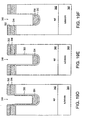
- Figs. 1 through 10 show cross-sectional views and characteristics of known trench-gated devices.
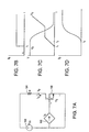
- Fig. 1 shows a trench-gated MOSFET 100 having a top metal layer 102, a gate 104 formed in a trench 106 and separated from an epitaxial silicon layer 108 by a gate oxide layer 110.
- MOSFET 100 also includes an N+ source region 112 and a P-body 114.
- the drain of MOSFET 100 includes the N-epi layer 108 and an N+ substrate 116.
- a deep P+ region 118 is created under P-body 114, as suggested in U.S. Patent No. 5,072,266 to Bulucea et al .
- the PN junction between deep P+ region 118 and N-epi layer 108 forms a voltage-clamping diode 117 where avalanche breakdown normally occurs.
- a P+ body contact region 119 forms a contact between metal layer 102 and P-body 114.
- the gate which is typically formed of polysilicon, is protected from the metal layer 102 by an oxide layer 120 that is above the gate 104 and that is patterned with a feature that does not correspond to the trench itself, typically a contact mask.
- gate oxide layer 110 consists of a uniform thin layer of oxide along the three sides of the polysilicon gate 104. That is, the portions of gate oxide layer 110 on the sidewalls of the trench and also the curved and linear portions of the gate oxide layer 110 at the bottom of the trench (except for some stress-related and etch-related changes in the oxide thickness that occur at the trench bottom) are generally of a uniform thickness in the range of, for example, 15nm to 120nm (150 ⁇ to 1,200 ⁇ ).
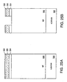
- Fig. 2 shows a MOSFET 130 which is generally similar to MOSFET 100 but does not include a deep P+ region 118.
- the gate of MOSFET 130 protrudes slightly through P-body 132 because the depth of P-body 132 and the depth of the trench 134 are determined in two unrelated processes.
- this variation affects the operation of the device and may affect its reliability as well.
- Fig. 2 there is no additional diode formed by the deep P+ region 118 to clamp the voltage, so breakdown can occur wherever the voltage is raised to the point that the device goes into avalanche.
- MOSFET 140 shown in Fig. 3 , is variation of MOSFETs 100 and 130, where the MOSFET cells 142 contain no deep P+ region, and a diode cell 144 containing a deep P+ region is distributed at predetermined intervals throughout the array to act as a voltage clamp and limit the strength of the electric fields in the MOSFET cells.
- the gate oxide layer is of uniform thickness.
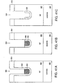
- Figs. 4A-4G illustrate various aspects of the breakdown phenomenon.
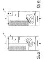
- Fig. 4A shows the electric field strength contours at breakdown in a trench-gated device 150 having a relatively thick gate oxide layer.
- Device 150 is in effect a gated diode, a structural element of most trench-gated vertical power MOSFETs.
- the strongest electric field where impact ionization would occur during avalanche breakdown, is located at the junction directly beneath the P+ body region.
- device 160 shown in Fig. 4B , has a relatively thin gate oxide layer. While some ionization still occurs underneath the P+ region, the highest electric field levels are now located near the corner of the trench.
- a field plate induced breakdown mechanism causes the strength of the electric field to increase.
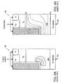
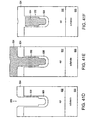
- Figs. 4C and 4D show the ionization contours of devices 150 and 160, respectively, when they go into avalanche breakdown. Whether there is a thick gate oxide layer, as in Fig. 4C , or thin gate oxide layer, as in Fig. 4D , eventually in "deep" avalanche, i.e., when the device is forced to conduct large currents in avalanche, breakdown starts to occur at the corner of the trench. Even in the thick oxide case ( Fig. 4C ), where the peak electric field is not at the corner of the trench ( Fig. 4A ), as the drain voltage increases eventually ionization occurs at the corner of the trench. However, there are more contours in Fig. 4D , indicating a higher ionization rate where the gate oxide layer is thin.
- Fig. 4E shows that if one introduces a diode clamp including a deep P+ region, as shown on the right-hand side, the diode will break down at a lower voltage, and avalanche breakdown should not occur at the corner of the trench. If the resistance of the current path through the diode is low enough, then the diode will clamp the maximum voltage of the device. As a result, the voltage will never rise to the point that avalanche breakdown occurs near the corners of the trenches.
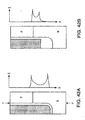
- Fig. 4F is a graph showing the breakdown voltage (BV) as a function of gate oxide thickness (X OX ) for 20 V and 30 V devices.
- the doping concentration of the epitaxial (epi) layer in the 30 volt device is more lightly doped.
- the 30 V device would ideally have an avalanche breakdown of around 38 volts.
- the epi would be more heavily doped and the device would ideally have an avalanche breakdown of around 26 or 27 V.
- the gate oxide is thinned from 100nm (1,000 ⁇ ) to a few tenths of nm (few hundred ⁇ )
- the breakdown voltages are relatively constant or may actually even increase somewhat as the shape of the field plate of the gate is actually beginning to help relax the electric field. At thicknesses of less a few tenth of nm (few hundred ⁇ ), however, breakdown degradation begins to occur.
- the area labeled field plate induced (fpi) breakdown is the area labeled field plate induced (fpi) breakdown. In this area, breakdown occurs near the trench.
- fpi field plate induced
- Fig. 4G is a schematic diagram of the devices shown in Figs. 4A-4D showing a gated diode in parallel with a MOSFET and a diode voltage clamp in parallel with both the MOSFET and gated diode.
- the arrangement is designed such that the diode clamp breaks down first.
- the gated diode never "avalanches" before the diode clamp. This becomes more and more difficult to do as the gate oxide layer becomes thinner.
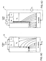
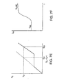
- Figs. 5A and 5B show the ionization contours in a device 170 having a sharp trench corner and a device 172 having a rounded trench corner.
- Fig. 5B indicates that rounding the trench corners does reduce the magnitude of the ionization, but ultimately if one drives the device deeply enough into breakdown, the breakdown still occurs at the trench corner, and the device is at risk.
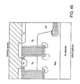
- Figs. 6A-6C show the electric field strength contours, the equipotential lines and the electric field lines, respectively, in a MOSFET 180.
- the gate of MOSFET 180 is tied to the source and body and is grounded, and the drain is biased at V D . From Fig. 6B it is evident that the drain voltage V D is divided and spaced out across the region. On the left hand side of Fig. 6B , the equipotential lines are squeezed closer together, and particularly around the trench corner they are squeezed even tighter. This produces electric field lines that are at right angles to the equipotential lines, as shown in Fig. 6C .
- a high electric field occurs at the trench corner and why rounding the corner does not solve this problem. It is basically a volumetric problem in that there is an electric field that terminates on an electrode having a lower surface area, namely the gate, and so the electric field lines are crowded at the corner.
- Fig. 6D shows MOSFET 180 when it is turned on by putting a positive voltage V G on the gate.
- a current flows down the side wall of the trench and then it also spreads out along the bottom of the trench and into the region below the mesa at an angle from the side of the trench.
- the current flows through areas that have high electric fields, as shown by the electric field contours of Fig. 6A .
- the current carriers collide with the atoms of the epi layer and knock off, by momentum transfer, additional carriers. This forms new electron-hole pairs that in turn are accelerated and create additional collisions, ionizing additional atoms.
- Fig. 6E shows the ionization contours in MOSFET 180 when it is in the on state.
- the ionization contours shown in Fig. 6E are different from those shown in Fig. 4C , for example, when device 150 is in the off state.
- the difference is that the ionization contours pull upwards all the way around the side of the trench, even up near the P-body. This has a number of damaging effects on the device.
- One effect is that it creates electron-hole pairs in the vicinity of the gate oxide that can be accelerated quite easily by the high electric field in that area. The electron-hole pairs can actually be trapped in the gate oxide, and they can damage the gate oxide.
- this phenomenon produces an upper limit in the amount of voltage that one can put on the device, because so many electron-hole pairs may be produced that they begin to modulate the effective doping concentration of the epitaxial layer, by making the region around the side of the trench seem more heavily doped than it actually is. That occurs because electrons from the newly generated electron-hole pairs are swept into the substrate by the positive drain voltage V D , and the holes are swept into the P-body.
- the net effect is that, since the electrons and holes can only travel at a certain velocity, the local charge distribution adjusts itself to maintain charge neutrality.
- surrounding the reverse-biased junction is a region known as a depletion region or space charge region, where (in the absence of impact ionization) no free charge carriers are present.
- the immobile charge residing within the depletion region namely positive ions on the N-type side of the junction and negative ions on the P-type side of the junction, produces a "built-in" electric field across the junction.
- the holes drifting across the N-type region add to the positive fixed charge and thereby increase the electric field, further enhancing the impact ionization process.
- These excess holes make the epitaxial region, which in this example is N-type material, appear more heavily doped because of the increase in the "built-in” field.
- the net effect is an increase in the electric field, which degrades the breakdown.
- This effect is shown in the current-voltage characteristics of Fig. 6F where the drain current I D increases dramatically at a certain drain voltage. The drain voltage at which this happens is the same for each of the gate voltages shown. This problem becomes worse as the gate oxide is thinned.
- FIG. 7A is a schematic diagram of a MOSFET 190 having a gate driven by a current source 192 and having resistive load 194.
- a voltage source 196 connected to the source and drain supplies a voltage V DD resulting in a drain voltage V D at the drain.
- current source 192 begins to supply a constant current to the gate and the voltage on the gate relative to the source, labeled V G in Fig. 7C , starts to rise. But because it does not immediately hit threshold, the drain voltage V D does not start to fall because MOSFET 190 is not yet turned on.
- MOSFET 190 As soon as the V G hits threshold, at time t 2 , MOSFET 190 saturates and turns on and carries current. V D starts to drop, but as it starts to drop it causes a capacitive coupling between the drain and the gate of MOSFET 190 and halts the upwards progression of the gate voltage V G . V G remains flat until MOSFET 190 gets into its linear region. Then, MOSFET 190 begins to look like an on-resistance in a voltage divider, with a small voltage across MOSFET 190 and most of the voltage V DD across resistor 194.
- Fig. 7E shows a plot of V G as function of the charge on the gate Q G , where Q G is equal to I G times the time t, I G being a constant.
- the gate voltage V G rises to a certain level, then it remains constant, and then it rises again. If there were no feedback capacitance between the drain and gate, the voltage would rise linearly, but instead the straight line is interrupted by the plateau.
- the point V G1 , Q G1 corresponds to a certain capacitance because C is equal to ⁇ Q over ⁇ V. Since it takes more charge to get to the point, Q G2 and V G1 , then that point reflects more capacitance. So the capacitance in the device, as shown in Fig. 7F , starts at a low value C ISS , which is relatively constant, and then it jumps to a higher effective value C G (eff), and then it is relatively constant. Because of this effect the device has a higher effective capacitance than is desirable during the switching transition. As a result, there is an undue amount of energy lost in turning the device on.
- the input capacitance actually has a number of components, including the gate-to-source capacitance C GS and the gate-to-body capacitance C GB , neither of which exhibits the amplification effect of the gate-to-drain capacitance C GD .
- the gate-to-drain capacitance C GD is shown in Fig. 7G , around the bottom and side wall of the trench.
- the equivalent schematic is shown in Fig. 7H . Even if C GD is the same order of magnitude as C GS and C GB , electrically it will look much larger (e.g., 5 to 10 times larger) because it is amplified during the switching process.
- Figs. 8A-8C illustrate a process for forming a trench with rounded corners.
- small reaction ions 202 etch the silicon through an opening in a mask 200 at the surface. Ions 202 are accelerated by an electric field in a downward direction such that they etch a trench having essentially a straight side wall. When the trench reaches a certain depth the electric field is relaxed, as shown in Fig. 8B . Alternatively, one could possibly change the chemistry.
- the electric field is modified so that the etching ions are traveling in all different directions.
- the process includes an anisotropic etch that is converted to an isotropic etch.
- the anisotropy is also influenced by the formation of a polymer as a by-product of the etching operation on the sidewall of the trench. If the chemistry removes the polymer as soon as it forms, the etch will behave in a more isotropic way. If the polymer remains on the sidewall, only the bottom of the trench will continue to etch.
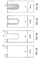
- Figs. 9A-9D show a method that includes creating a mask 210 ( Fig. 9A ), etching the trench 212 ( Fig. 9B ), forming an oxide layer 214 on the walls of the trench ( Fig. 9C ), which may be removed and then re-grown to remove defects (this is called sacrificial oxidation), and then filling the trench with a polysilicon layer 216 ( Fig. 9D ).
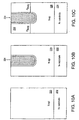
- Figs. 10A-10F illustrate a typical process of forming a trench MOSFET.
- the process starts with an N-epitaxial layer 220 grown on an N+ substrate 222 ( Fig. 10A ).
- a polysilicon-filled trench 224 is formed in N-epi layer 220 ( Fig. 10B ).
- the surface may or may not be planar depending on how the surface oxides are made in the process.
- a P-body 226 is introduced, although the P-body 226 could be introduced prior to the formation of the trench 224 ( Fig. 10C ).
- Both process flows are manufacturable, but forming the trench first is preferable because the etching process can influence the doping concentrations in the P-body.
- the surface is masked and an N+ source region 228 is implanted ( Fig. 10D ).
- An optional shallow P+ region 230 is implanted to ohmic contact between the P-body and a metal layer to be deposited later.
- P+ region 230 can be implanted through an opening in an oxide layer 232 that is deposited across the region and then etched to form a contact mask ( Fig. 10E ).
- the contact mask may or may not be used to define the P+ region 232.
- a metal layer 234 is deposited on the surface to contact the N+ source region 228 and P+ region 230 ( Fig. 10F ).
- EP 0 801 426 A2 shows a process for forming a trench MOS gate device comprising etching a trench in a silicon device wafer and forming layers of dielectric material on the trench floor and on the sidewalls, each layer having a controlled thickness dimension, related by a controlled floor to sidewall layer thickness ratio that is preferably at least 1 to 1.
- a first portion of the gate oxide is formed by thermal oxidation, the rest of the gate oxide is formed by chemical vapor deposition.
- the ratio of floor to sidewall oxide layer thickness can be adjusted over a wide range by adjusting the ratio of the thickness of the thermal to the deposited oxide.
- a manufacturing process for forming a trench gate semiconductor device with a thicker dielectric layer at the bottom of the trench is performed by either using a polyplug or a resist plug.
- the disclosed processes comprise the removal of a portion of the dielectric layer from the sidewalls of the trench.
- a trench-gated semiconductor device having a dielectric layer separating the gate electrode from the semiconductor material surrounding the trench wherein the thickness of the dielectric layer is greater in a region at the bottom of the trench.
- the conductive material is etched back to a level roughly coplanar with the surface of the semiconductor material, and a dielectric layer is deposited over the top surface of the dielectric material.
- the conductive material e.g., polysilicon
- the conductive material is oxidized to form on oxide layer, preferably after the conductive material has been etched back into the trench.
- the conductive material can be oxidized to a thickness such that the oxide itself is adequate to insulate the gate electrode, or another conductive material, such as glass, can be deposited over the oxidized conductive material.
- the conductive material that forms the gate electrode is deposited in two stages.
- a masking material such as photoresist is applied after the preferential deposition of the dielectric material.
- the masking material is removed from all locations except the bottom of the trench, and the trench is subjected to an etch or dip to remove dielectric material from the sidewalls of the trench.
- a dielectric layer is then formed on the sidewalls of the trench.
- a material such as polysilicon that can be oxidized to form a dielectric is deposited and etched back until only a portion of the material remains on top of the dielectric at the bottom of the trench. The material is then oxidized to form a thicker dielectric layer at the bottom of the trench.
- Processes in accordance with this invention may include a process for self aligning the trench with a contact to the top surface of the "mesa" between the trenches.
- a "hard” layer of a material such as silicon nitride is used as a trench mask.
- the hard mask remains in place until a dielectric layer has been formed over the gate electrode, preferably by oxidizing polysilicon gate.
- the hard mask is then removed, exposing the entire top surface of the mesa and allowing a contact to be made thereto with a metal layer.
- a process of this invention may include the use of a sidewall spacer near the top corners of the trench to prevent a short between the gate electrode and the semiconductor mesa.
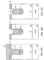
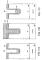
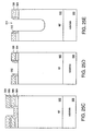
- Figs. 11-27 show various structures and sequences for forming a thick gate oxide on the bottom of the trench.
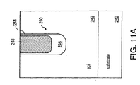
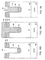
- Fig. 11A shows an epitaxial (“epi") layer 242 grown on a substrate 240.
- a trench 250 is formed in epi layer 242.
- a gate oxide layer 244 lines the walls of trench 250, and a thick portion 246 of gate oxide layer 244 is located at the bottom of trench 250.
- Trench 250 is filled with polysilicon 248. Note that there is no oxide layer on top of polysilicon 248.
- the arrangement of Fig. 11A could be an intermediate structure; an oxide layer could be formed on top of polysilicon 248 at a later stage of the process.
- Polysilicon 248 is typically doped to a heavy doping concentration. It may be formed with a top surface substantially planar, i.e., flat, with the silicon epi surface by a number of means.
- One method to make the surface flat is to deposit the polysilicon layer to a greater thickness and then etch it back.
- Another means to produce a flat surface is to deposit the polysilicon to a thickness greater than the amount needed to fill the trench and then chemical mechanically polish the surface flat.
- a flat surface is desirable to reduce the height of steps which may form later in the fabrication process.
- Fig. 11B shows a structure with an oxide layer 252 on top of polysilicon layer 248. Since the lateral edges of oxide layer 252 do not correspond to the walls of trench 250, oxide layer 252 is most likely formed with a mask and etching step. Oxide layer 252 could be either deposited (e.g., by chemical vapor deposition) or it could be thermally grown or some combination of these steps.
- Fig. 11C shows a top oxide layer 254 that is grown in accordance with the teachings of US. Application No. 09/296,959 and International Publication Number WO-A-80/65646 . The sides of oxide layer 254 are generally aligned with the walls of trench 250 and oxide layer 254 extends down into trench 250. Polysilicon layer 248 is thus embedded in trench 250.
- the embodiments of Figs. 11B and 11C both have a thick gate oxide region 246 at the bottom of the trench.
- Fig. 12 is a schematic diagram of several process flows that can be used to fabricate gate trenches in accordance with this invention. The details of these process flows are shown in Figs. 13-20 .
- Fig. 12 illustrates in block diagram form that the trench may be formed using a photoresist mask or a hard mask sequence, followed by a directed oxide deposition planarized by either a selective etch, a dipback, or a selective oxidization. Finally, the trench is filled with polysilicon using a one-step or two-step process.
- the trench is formed using a mask that is later removed, so that the mask is not available as a reference for other processing steps.
- the other option is to use a "hard" mask to form the trench, as described in the above-referenced Application No. 09/296,959, which is then employed as a reference later in the process.
- This option is generally described in Figs. 19 and 20 .
- a sacrificial oxide layer is grown on the walls of the trench and then removed.
- An oxide lining may then be formed on the walls of the trench. This stage yields a trench having a uniform oxide layer on its walls, with or without a hard mask on the top surface of the silicon.
- the directed dielectric deposition which involves depositing more oxide on the bottom of the trench than on the sidewalls of the trench.
- a selective etchback can be performed, allowing thick oxide to remain at the bottom of the trench and removing the oxide from the sidewalls of the trench.
- a "dipback" to remove the oxide layer from the sidewalls of the trench.
- a selective oxidation as shown in Figs. 17A and 18 , wherein a polysilicon layer is formed at the bottom of the trench and then oxidized to form additional oxide at the bottom of the trench.
- the selective oxidation of a polysilicon layer can be performed in addition to the directed dielectric deposition.
- a trench has been fabricated with a thick oxide layer on the bottom. There may or may not be a "hard” mask on the top surface of the semiconductor.
- a thin oxide layer is grown on the walls of the trench and the trench is filled with polysilicon.
- the polysilicon may be deposited as a single layer or it can be deposited as two layers with an etchback between the depositions. Depositing the polysilicon in a two-stage process may be beneficial to the introduction of dopants into the "mesa" between the trenches, and to make a more lightly doped polysilicon layer available on the surface of the wafer to produce diodes, resistors, and other polysilicon devices.
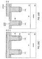
- Figs. 13A-13N illustrate a process using the oxide "dipback" method.
- the process starts with an epi layer 262 formed on a substrate 260.
- a mask layer 264 is formed on the top surface of epi layer 262, with an opening where the trench is to be formed.
- Mask layer 264 may be photoresist or some other material and may be formed on top of an oxide layer 266.
- a trench 268 is then formed using conventional processes, as shown in Fig. 13A .
- a sacrificial oxide layer 270 has been formed on the surface of the trench. Sacrificial oxide layer 270 is then removed, as shown in Fig. 13C .
- Sacrificial oxide layer 270 could be from 10nm (100 ⁇ ) to 100nm (1000 ⁇ ) thick; typically, it would be in the range of 30nm (300 ⁇ ) thick. It can be formed by heating the structure at 800° C to 1100° C for 10 minutes to five hours in an oxidizing ambient.
- the ambient could be either oxygen or it could be oxygen and hydrogen. If the ambient is a combination of oxygen and hydrogen, it is considered a "wet" oxidation because the reaction would produce water vapor and this would affect the consistency and growth rate of the oxide.
- an oxide lining 272 is then formed on the walls of trench 268.
- Lining 272 could have a thickness in the range of 10nm to 60nm (100 ⁇ TO 600 ⁇ ). Lining 272 prevents the deposited oxides from contacting the silicon directly, which would have the potential for charged states, especially at the interface between the silicon and the deposited oxide.. Adding a clean oxide layer on the walls of the trench provides a reduced charge state.
- an electric field is applied above the surface of epi layer 262, and dielectric ions are formed and directed downward into trench 268 by means of the electric field.
- a plasma-enhanced chemical vapor deposition chamber is used for this process.
- the electric field accelerates the dielectric ions downward so that they preferentially deposit on horizontal surfaces, including the bottom of trench 268.
- the chemical vapor deposition of oxide involves a gaseous chemical reaction of oxygen and silane, dichlorosilane, or silicon tetrachloride.
- the source of oxygen is typically nitreous oxide, and silane is typically the silicon source.
- Plasma-enhanced chemical vapor deposition machines are available from such companies as Novellus Systems and Applied Materials.
- Another method to achieve a directional deposition is to sputter a oxide film from an oxide-coated target onto the wafer. Since sputtering is a momentum transfer process, the deposition occurs in a straight line.
- oxide layer 270 has been formed inside and outside the trench 268. Note that oxide layer 270 is thicker at the bottom of trench 268 than on the sidewalls of trench 268. It is also thicker on the flat surfaces of epi layer 262. Processes other than chemical vapor deposition, such as sputtering, could also be used to produce oxide layer 270.
- Layer 270 could be formed of materials other than oxide, such as phosphorus-doped glass or boron phosphorus silicon glass. It could also consist of other materials having a low dielectric constant K, such as polymers or polyimide . Air bubbles could be incorporated in layer 270 to reduce its dielectric constant.
- oxide layer 270 has been etched back or dipped back to remove the portions on the sidewalls of trench 268. A bottom portion 274 of oxide layer 270 remains at the bottom of trench 268. As shown in Fig. 13H , the structure is then heated to form a thin oxide layer 276 on the sidewalls of trench 268. A polysilicon layer 278 is then deposited to fill trench 268 and overflow the top surface of the structure. This is shown in Fig. 13I .
- polysilicon layer 278 is then etched back until it is roughly coplanar with the top surface of epi layer 262.
- the portions of oxide layer 270 on the surface of epi layer 262 are removed, taking care not to etch too much of the oxide layer 276 on the sidewalls of the trench.
- the result of this step is shown in Fig. 13K . Avoiding the removal of oxide layer 276 is best performed by having polysilicon layer 278 protrude slightly above the oxide layer 276.
- the entire top surface of the structure, including the top surface of polysilicon layer 278, has been oxidized to form an oxide layer 280.
- a glass layer 282 is laid down over the surface of oxide layer 280, and glass layer 282 and oxide layer 280 are then patterned and etched to form contact openings to the epi layer 262, yielding the structure shown in Fig. 13N .
- Figs. 14A-14F show an alternate process flow beginning with the structure shown in Fig. 13I .
- Fig. 14A corresponds to Fig. 13I .
- Polysilicon layer 278 is etched back, as shown in Fig. 14B , and then the top surface of the remaining portion of polysilicon layer 278 is oxidized to form an oxide layer 290, as shown in Fig. 14C .
- a glass layer 292 is then deposited over the entire surface of the structure, as shown in Fig. 14D .
- a mask layer 294 is formed on the top surface of glass layer 292, and layers 270 and 292 are etched to form contact openings, as shown in Fig. 14F .
- Mask layer 294 is then removed.
- Figs. 15A-15F illustrate yet another alternative process, beginning again with the structure shown in Fig. 13I .
- Fig. 15A corresponds to Fig. 13I .
- Polysilicon layer 278 is etched back to a level inside the trench, as shown in Fig. 15B .
- a second polysilicon layer 300 is deposited over the entire structure, as shown in Fig. 15C .
- Polysilicon layer 300 is then etched back, but care is exercised to ensure that the portion of oxide layer 276 at the upper corner of the trench is not exposed.
- the resulting structure is shown in Fig. 15D .
- oxide layer 270 is removed, as shown in Fig. 15E , and an oxide layer 302 is formed over the entire surface of the structure.
- a glass layer 304 is then deposited over oxide layer 302, yielding the structure illustrated in Fig. 15F .
- Figs. 16A-16E illustrate an alternative process, beginning with the structure in Fig. 13F .
- Fig. 16A corresponds to Fig. 13F .
- a photoresist layer is then formed over the structure and is developed and rinsed in a way that is sufficient to clean the photoresist layer off the top of the structure but leave it at the bottom of trench 268. This takes advantage of the fact that it is difficult to get the photoresist out of the bottom of the trench 268.
- the resulting structure with a remaining portion of photoresist layer 310 in the bottom of trench 268 is shown in Fig. 16B .
- An oxide etch is then performed removing the portion of oxide layer 270 from the sidewalls of trench 268.
- a thorough rinse is then performed to remove photoresist 310, producing the structure illustrated in Fig. 16C .
- the structure is then oxidized to form a thin oxide layer 312 on the sidewalls of the trench and the trench is filled with a polysilicon layer 314, as shown in Figs. 16D and 16E .
- a two-step polysilicon deposition could be performed as shown in Figs. 15A-15C .
- Figs. 17A-17F show yet another alternative process sequence, beginning with the structure shown in Fig. 13F .
- Fig. 17A corresponds to Fig. 13F .
- a sacrificial polysilicon layer 320 is deposited. Polysilicon layer 320 is etched back until only a small portion 322 remains at the bottom of trench 268. The portion 322 of polysilicon layer 320 is then oxidized.
- a low temperature oxidation process is used (e.g., 700 to 950 °C), since at a low temperature polysilicon oxidizes more rapidly than single crystal silicon. Thus oxide forms in portion 322 at a faster rate than on the sidewalls of trench 268.
- the resulting structure is shown in Fig.
- oxide layer 270 is removed from the sidewalls of trench 268, as shown in Fig. 17E , and a thin gate oxide layer 326 is formed on the sidewalls of trench 268, as shown in Fig. 17F .
- Figs. 18A-18F show process sequence as an example, beginning with the structure shown in Fig. 13B .
- Fig. 18A corresponds to Fig. 13D , where oxide lining 272 has just been formed.
- a sacrificial polysilicon layer 330 is deposited, as shown in Fig. 18B .
- Polysilicon layer 330 is etched back until only a small portion 332 remains at the bottom of trench 268, as shown in Fig. 18C .
- the structure is then subjected to a low-temperature oxidation, as described above, converting polysilicon portion 332 into an oxide layer 334, as shown in Fig. 18D .
- Oxide lining 272 is then stripped from the sidewalls and top surfaces of the structure, as shown in Fig. 18E , and a gate oxide layer 336 is grown on the sidewalls of trench 268. The resulting structure is then shown in Fig. 18F .
- Figs. 19A-19I illustrate a process which contains elements of the super self-aligned process described in the above-referenced Application No. 09/296,959.
- the structure is formed in an epi layer 342 which is grown on a substrate 340.
- a thin oxide layer 346 is formed on the surface of epi layer 342, and this is covered by a layer 344 of a hard masking material such as silicon nitride.
- An opening is etched in nitride layer 344 and oxide layer 346, as shown in Fig. 19A .
- a trench 348 is etched in epi layer 342 using a conventional process.
- a sacrificial oxide layer (not shown) is formed on the walls of trench 348 and then removed.
- an oxide lining 350 is then formed on the walls of trench 348.
- a directional deposition of the kind described above in connection with Fig. 13E is performed, forming an oxide layer 352.
- Oxide layer 352 includes a thick portion 354 at the bottom of trench 348.
- the portions of oxide layer 352 and oxide lining 350 are removed from the sidewalls of trench 348. This is done by dipping the structure in, for example, 170 HF acid.
- a gate oxide layer 356 is then formed and the trench is filled with a polysilicon layer 358.
- polysilicon layer 358 is then etched back to a level above the surface of the thin oxide layer 346.
- the thick oxide layer 352 has been removed from above the nitride layer 344, with the polysilicon layer 358 protecting the thin oxide layer 356 at the edges of trench 348.
- the structure is then annealed such that a portion of polysilicon layer 358 is oxidized to form a thick oxide layer 360 in the upper region of the trench, as shown in Fig. 19K .
- nitride layer 344 is removed.
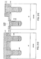
- Figs. 20A-20F show a two-stage polysilicon process with two trenches, one of which is in the active array and the other of which is part of a gate bus. The process starts at the point illustrated in Fig. 19H , with a polysilicon layer 388 filling trenches 374A and 374B. A thick oxide layer 384 has been formed at the bottom of trenches 374A and 374B. A silicon nitride layer 374 overlies the surface of epi layer 372. Nitride layer 374 is covered by an oxide layer 382.
- Polysilicon layer 388 is etched back as shown in Fig. 20B , and oxide layer 382 is removed.
- a second polysilicon layer 390 is deposited over polysilicon layer 388, and a "hard" layer 392, formed of nitride or polyimide, for example, is deposited on top of the second polysilicon layer 390.
- the resulting structure is illustrated in Fig. 20C .
- polysilicon layer 390 and the hard layer 392 are etched from the region of the active array (trench 374A), leaving these layers in the region of the gate bus (trench 374B).
- the structure is then heated to oxidize polysilicon layer 388 in trench 374A producing a thick oxide layer 394 in the upper region of that trench.
- an oxide layer 396 forms on the exposed edge of second polysilicon layer 390. This structure is shown in Fig. 20E .
- Figs. 21A-21E and 22A-22C illustrate two problems that need to be avoided.
- Fig. 21A shows a sacrificial oxide layer 400 along the walls of the trench and a thin oxide layer 404 and a nitride layer 402 on the top surface of the epi layer.
- Fig. 21B in the process of removing the sacrificial oxide layer 400, a portion of the thin oxide layer 404 has been removed underneath nitride layer 402.
- the solution to this problem is to minimize the oxide overetch time or to use an oxide layer 404 that is as thin as possible, even as thin as 1,5 to 9 nm (15 to 90 ⁇ ).
- Figs.21D and 21E show the arrangement after a polysilicon layer 412 has been deposited and etched back from an active array area of the device, showing the thin oxide layer that separates polysilicon layer 412 from the epi layer at the upper corner of the trenches.
- Figs. 22A-22C illustrate another potential problem area.
- Fig. 22A shows a device at the same stage that is illustrated in Fig. 19D , with thick oxide layer 352 having been directionally deposited, forming a thick portion 354 at the bottom of the trench.
- a portion of the thin oxide layer 346 is removed from underneath nitride layer 344.
- the gate oxide layer 356 is grown, the portion of the oxide layer at the upper corner of the trench is unduly thin, and this can lead to defects in the oxide and shorting between the gate and the epi layer.
- This problem is illustrated in Fig. 22C .
- the solution is to minimize any oxide overetch or alternatively to use a plasma etch whose chemistry etches isotropically.
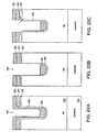
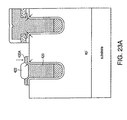
- Fig. 23A shows a problem that can result when the polysilicon fills a cavity that is formed under the nitride layer, as shown in Fig. 21E .
- a portion 420A of polysilicon layer 420 extends outside the trench and will form a short to a metal layer deposited later to contact the epi layer. During oxidation, the oxide 422 does not consume the silicon filling under the nitride overhang. Removal of the nitride exposes the gate to a source metal short.
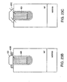
- Fig. 23B shows a variation in which the portion 420B is separated by oxide from the main polysilicon layer 420.
- 23C illustrates a case in which polysilicon layer 420 has formed upward projecting spikes 420C, creating the likelihood of a short between the gate polysilicon layer 420 and a later deposited metal layer. Again, the polysilicon filling under the nitride remains after oxidation leaving a possible gate-to-source short.
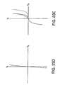
- Fig. 23D shows the gate I-V characteristic of a shorted device.
- the low resistance is referred to as a "hard” short.
- Fig. 23E shows the characteristics of a "soft" or diode-like short.
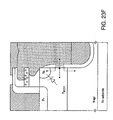
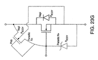
- the diode-like short can occur within a gate bus region as shown in Fig. 23F .
- an N+ region or plume is doped into the P body wherever the polysilicon touches the silicon mesa, producing a parasitic diode and MOSFET shown schematically in Fig. 23G .
- Figs. 24A-24F illustrate the processing mechanism that causes the diode short as an overetch first polysilicon layer or a misshapen, distorted trench.
- the active cell and gate bus region are filled with a first layer of N+ doped polysilicon and are then etched back to produce the structure shown in Fig. 24B . If the etchback of the polysilicon is nonuniform, one side of the trench oxide may be exposed, as shown in fig. 24C , which then is attacked and etched during dip which removes the top oxide.
- the second polysilicon layer is deposited and patterned by a mask, leaving the active cell on the left and the gate bus on the right. After top oxidization, shown in Fig.
- the active cell on the left oxidizes and heals itself, but in the gate bus region the polysilicon touching the silicon dopes an N+ plume leading to the diode-like gate short of Fig. 24F .
- Uniform etchback of the polysilicon and uniformly shaped trenches avoid this problem.
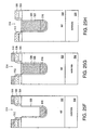
- Figs. 25A-25H describe a process for avoiding these problems by the use of a nitride sidewall spacer.
- the process starts with an epi layer 502 that is grown on a substrate 500.
- a thin oxide layer 504 is grown on the top surface of epi layer 502 and a nitride layer 506 (or some other "hard” layer) and a second oxide layer 508 are formed in succession over oxide layer 504.
- layers 504, 506 and 508 form an oxide-nitride-oxide (ONO) sandwich, well known in the field.
- ONO oxide-nitride-oxide
- nitride layer 510 is then deposited over the top of the structure, yielding the arrangement shown in Fig. 25C .
- Nitride layer 510 is etched anisotropically. Since the vertical thickness of nitride layer 510 is much greater near the edges of the ONO sandwich, the anisotropic etch leaves sidewall spacers 512 at the exposed edge of oxide layer 504 and nitride layer 506. This structure, following the removal of oxide layer 508 is shown in Fig. 25D .
- a trench 514 is then etched, and the typical sacrificial gate oxide layer (not shown) is formed and removed.
- Fig. 25F shows the structure after the directional deposition of an oxide layer 516, which leaves a thick oxide portion 518 at the bottom of the trench 514. This is done after the formation of a gate oxide layer 520.
- the trench is then filled with a polysilicon layer 522, which is etched back, taking care not to attack the underlying oxide layer 520.
- the top region where the polysilicon and silicon nearly touch will be oxidized further later in the process. Also, some oxide will grow under the nitride sidewall cap, like a "bird's beak".
- Oxide layer 516 is then removed, producing the embodiment shown in Fig. 25H .
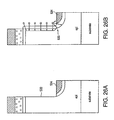
- Figs. 26A and 26B growing the gate oxide on the sidewalls of the trench can lead to a "kink" in the sidewall of the trench, shown as kink 530 in Fig. 26B .
- the problem is that, as shown in Fig. 26A , the oxide grows uniformly on the exposed sidewall 532 of the trench. However, where the thick oxide 534 begins at the bottom of the trench, owing to the geometry of the structure, the oxidation does not proceed in a linear fashion. This creates a reduced thickness of the oxide layer at kink 530.
- FIG. 27A shows the structure after the thermal growth of an oxide lining 540 and the directional deposition of an oxide layer 542, as described above. Lining 540 and layer 542 are removed from the sidewall of the trench as shown in Fig. 27B . The structure is then dipped in 170 HF acid. Since oxide deposited by deposition etches faster than thermally grown oxide, the structure appears as in Fig. 27C following the dip, with the top surface of lining 540 being slightly above the top surface of the oxide layer 542. When the gate oxide layer is thermally grown on the sidewalls of the trench, the resulting oxide is of a relatively uniform thickness. There is no "kink" in the wall of the trench.
- Fig. 27D shows the arrangement after a gate oxide layer 544 has been grown on the sidewall of the trench. The dotted line indicates the original position of the silicon prior to oxidation.
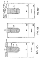
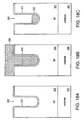
- Figs. 28-33 illustrate various devices that can be fabricated using the principles of this invention.
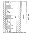
- Fig. 28 shows a power MOSFET having a flat-bottomed P-body region and an N buried layer at the interface between the epi layer and substrate.
- Fig. 28 illustrates a device combining the thick trench bottom oxide with a contact that extends entirely across the mesa between trenches although a contact mask and nonplanar top oxide layer could be utilized.
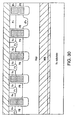
- Fig. 29 shows a MOSFET that is similar to the one shown in Fig. 28 except that each MOSFET cell contains a deep P+ region, in accordance with the teachings of U.S. Patent No. 5,072,266 to Bulucea et al .
- the trenches extend into the N-buried layer so that only the thick oxide region overlaps the heavily doped buried layer.
- Fig. 33 is an accumulation mode MOSFET (ACCUFET), such as the one taught in U.S. Patent No. 5,856,692 to Williams et al ..
- ACCUFET accumulation mode MOSFET
- Fig. 34 is a conceptual drawing showing a process flow for a trench MOSFET using a conventional contact mask and incorporating a thick trench bottom oxide.
- the steps of the process generally include the formation of the drain and deep body regions, the etching of the trench and formation of the gate, the implantation of the body and source regions, and the opening of contacts and deposition of a metal layer.
- the boxes with the corners clipped represent optional steps.
- the introduction of a deeper body region by implant or by implant and diffusion is consistent with this process.
- a trench 552 is formed in an N epi layer 550, using an oxide layer 554 as a mask.
- An oxide lining 556 is formed on the walls of the trench 552 ( Fig. 35B ), and a directional oxide deposition is carried out as described above, forming an oxide layer 558 having a thick portion 560 at the bottom of the trench ( Fig. 35C ).
- the sidewalls of trench 552 are then etched ( Fig. 35D ), and a gate oxide layer is thermally grown on the walls of trench 552 ( Fig. 35E ).
- a polysilicon layer 564 is then deposited to fill the trench 552 ( Fig. 35F ).
- Polysilicon layer 564 is etched back into the trench ( Fig. 35G ).
- An oxide layer 566 is deposited over the top surface of the structure and extends down into the trench to the top surface of polysilicon layer 564 ( Fig. 35H ).
- Oxide layer 566 is then etched back ( Fig. 35I ), and a P-type dopant such as boron is implanted to form P body region 568.
- the top surface is then masked (not shown), and an N-type dopant such as arsenic or phosphorus is implanted to form N+ source regions 570.
- Another oxide layer 572 is deposited on the top surface and patterned, yielding the structure shown in Fig. 35L .
- the contact can then be filled by the top metal or alternatively filled with a planarizing metal such as tungsten first, or with a barrier metal such as Ti/TiN.
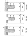
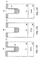
- Figs. 36-39 illustrate several examples in which the polysilicon gate is "keyhole" shaped in cross-section.
- the thicker gate oxide extends not only along the bottom of the trench but also along the sidewalls of the trench towards the junction between the P body region and the N epi layer.
- the thickened gate oxide along the sidewalls of the trench helps to soften the electric field at that junction.
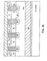
- Fig. 36 shows a MOSFET having flat-bottomed P body regions and a diode cell incorporated at periodic intervals among the MOSFET cells.
- a keyhole-shaped gate is employed.
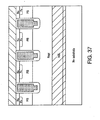
- Fig. 37 shows an embodiment where the P body does not extend to the surface but instead is contacted in the third dimension.
- a shallow P+ region is shown within the mesa at a depth greater than the N+ source regions.
- Fig. 38 shows an embodiment wherein the trenches extend into an N buried layer formed at the interface between the epi layer and the substrate.
- Fig. 39 shows an embodiment where the P body is contacted in the third dimension, and the trenches extend into an N buried layer.
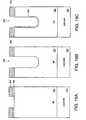
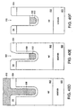
- FIGs. 40A-40L A process sequence for forming a device having a keyhole shaped trench is illustrated in Figs. 40A-40L as an example.
- the process starts with an epi layer 602 grown on a substrate 600.
- An oxide layer 604 is formed at the top surface of epi layer 602, as shown in Fig. 40A .
- Oxide layer 604 is patterned and a trench 606 is etched, as shown in Fig. 40B .
- a sacrificial oxide layer (not shown) is formed on the walls of the trench and removed.
- An oxide lining 608 is then grown on the walls of trench 606 (as shown in Fig. 40C ).
- a polysilicon layer 610 is deposited to fill the trench 606 and then etched back such that a portion 612 remains at the bottom of the trench.
- the oxide lining 608 is then etched from the walls of the trench 606, as shown in Fig. 40F .
- An anisotropic silicon etch is then performed to depress the top surface of polysilicon portion 612 below the top surface of oxide lining 608, as shown in Fig. 40G .
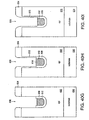
- a thermal oxidation process is then applied, forming an oxide layer 616 on the walls of the trench 606 and an oxide layer 618 at the top surface of polysilicon portion 612. The result is shown in Fig. 40H .
- Oxide layer 618 is then etched, a portion of oxide layer 616 being removed in the process, producing the structure shown in Fig. 40I .
- a second polysilicon layer 619 is then deposited over the entire structure, as shown in Fig. 40J .
- Polysilicon layer 619 is etched back, as shown in Fig. 40K .
- the top surface of polysilicon layer 619 is then oxidized, as shown in Fig. 40L .
- FIGs. 41A-41F A variation of this process is illustrated in Figs. 41A-41F .
- a photoresist layer is applied, developed, and washed away, leaving only a portion 630 at the bottom of the trench 606. This is shown in Fig. 41A .
- Oxide lining 608 is then etched from the walls of the trench 606, as shown in Fig. 41B and the portion 630 of the photoresist layer is removed from the bottom of the trench. This yields the structure shown in Fig. 41C .
- a gate oxide layer 632 is thermally grown on the walls of trench 606, and trench 606 is filled with a polysilicon layer 634, as shown in Figs. 41D and 41E .
- Polysilicon layer 634 is etched back to the level of the top surface of the epi layer 602. Polysilicon layer 634 is then oxidized thermally to produce the device shown in Fig. 41F .
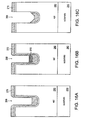
- Figs. 42A-42C show a comparison of the strength of the electric field along the sidewall of the trench in a prior art trench device with the strength of the electric field in the embodiment of this invention.
- Fig. 42A shows that in the prior art device the electric field has two sharp peaks which occur, respectively, at the body-drain junction and the bottom of the gate electrode.
- Fig. 42B shows a device having a thick oxide layer on the bottom of the trench. As indicated, the electric field still has a sharp peak at the body-drain junction but the peak at the bottom of the gate electrode is somewhat lower than in the prior art device.
- Fig. 42C shows a device having a keyhole shaped gate electrode. In this case, the electric field still reaches a peak at the body-drain junction, but the sharp peak at the bottom of the gate electrode is eliminated.
Landscapes
- Electrodes Of Semiconductors (AREA)
- Element Separation (AREA)
- Insulated Gate Type Field-Effect Transistor (AREA)
- Formation Of Insulating Films (AREA)
- Drying Of Semiconductors (AREA)
Priority Applications (1)
| Application Number | Priority Date | Filing Date | Title |
|---|---|---|---|
| EP08016928A EP2020681B1 (en) | 1999-05-25 | 2000-05-24 | Process of manufacturing a trench gate semiconductor device |
Applications Claiming Priority (3)
| Application Number | Priority Date | Filing Date | Title |
|---|---|---|---|
| US318403 | 1999-05-25 | ||
| US09/318,403 US6291298B1 (en) | 1999-05-25 | 1999-05-25 | Process of manufacturing Trench gate semiconductor device having gate oxide layer with multiple thicknesses |
| PCT/US2000/014363 WO2000072372A1 (en) | 1999-05-25 | 2000-05-24 | Trench semiconductor device having gate oxide layer with multiple thicknesses and processes of fabricating the same |
Related Child Applications (2)
| Application Number | Title | Priority Date | Filing Date |
|---|---|---|---|
| EP08016928A Division EP2020681B1 (en) | 1999-05-25 | 2000-05-24 | Process of manufacturing a trench gate semiconductor device |
| EP08016928.7 Division-Into | 2008-09-25 |
Publications (3)
| Publication Number | Publication Date |
|---|---|
| EP1186019A1 EP1186019A1 (en) | 2002-03-13 |
| EP1186019A4 EP1186019A4 (en) | 2004-05-26 |
| EP1186019B1 true EP1186019B1 (en) | 2010-05-12 |
Family
ID=23238055
Family Applications (2)
| Application Number | Title | Priority Date | Filing Date |
|---|---|---|---|
| EP08016928A Expired - Lifetime EP2020681B1 (en) | 1999-05-25 | 2000-05-24 | Process of manufacturing a trench gate semiconductor device |
| EP00932771A Expired - Lifetime EP1186019B1 (en) | 1999-05-25 | 2000-05-24 | Trench semiconductor device having gate oxide layer with multiple thicknesses and processes of fabricating the same |
Family Applications Before (1)
| Application Number | Title | Priority Date | Filing Date |
|---|---|---|---|
| EP08016928A Expired - Lifetime EP2020681B1 (en) | 1999-05-25 | 2000-05-24 | Process of manufacturing a trench gate semiconductor device |
Country Status (9)
| Country | Link |
|---|---|
| US (6) | US6291298B1 (enExample) |
| EP (2) | EP2020681B1 (enExample) |
| JP (1) | JP4834228B2 (enExample) |
| KR (1) | KR100700322B1 (enExample) |
| CN (1) | CN1205658C (enExample) |
| AU (1) | AU5044600A (enExample) |
| DE (1) | DE60044396D1 (enExample) |
| TW (1) | TW457629B (enExample) |
| WO (1) | WO2000072372A1 (enExample) |
Families Citing this family (185)
| Publication number | Priority date | Publication date | Assignee | Title |
|---|---|---|---|---|
| US7084456B2 (en) * | 1999-05-25 | 2006-08-01 | Advanced Analogic Technologies, Inc. | Trench MOSFET with recessed clamping diode using graded doping |
| US6291298B1 (en) * | 1999-05-25 | 2001-09-18 | Advanced Analogic Technologies, Inc. | Process of manufacturing Trench gate semiconductor device having gate oxide layer with multiple thicknesses |
| TW442972B (en) * | 1999-10-01 | 2001-06-23 | Anpec Electronics Corp | Fabricating method of trench-type gate power metal oxide semiconductor field effect transistor |
| US6825087B1 (en) | 1999-11-24 | 2004-11-30 | Fairchild Semiconductor Corporation | Hydrogen anneal for creating an enhanced trench for trench MOSFETS |
| US6461918B1 (en) | 1999-12-20 | 2002-10-08 | Fairchild Semiconductor Corporation | Power MOS device with improved gate charge performance |
| US20030017164A1 (en) | 2001-07-03 | 2003-01-23 | Mallinckrodt Inc. | Dye-azide compounds for dual phototherapy |
| WO2001071817A2 (en) * | 2000-03-17 | 2001-09-27 | General Semiconductor, Inc. | Dmos transistor having a trench gate electrode and method of making the same |
| US6391699B1 (en) * | 2000-06-05 | 2002-05-21 | Fairchild Semiconductor Corporation | Method of manufacturing a trench MOSFET using selective growth epitaxy |
| JP2002043573A (ja) * | 2000-07-28 | 2002-02-08 | Toyota Motor Corp | 半導体装置および半導体装置の製造方法 |
| US7745289B2 (en) | 2000-08-16 | 2010-06-29 | Fairchild Semiconductor Corporation | Method of forming a FET having ultra-low on-resistance and low gate charge |
| US6509233B2 (en) | 2000-10-13 | 2003-01-21 | Siliconix Incorporated | Method of making trench-gated MOSFET having cesium gate oxide layer |
| KR100338783B1 (en) * | 2000-10-28 | 2002-06-01 | Samsung Electronics Co Ltd | Semiconductor device having expanded effective width of active region and fabricating method thereof |
| US6730606B1 (en) * | 2000-11-03 | 2004-05-04 | Semiconductor Components Industries, L.L.C. | Trench growth techniques using selective epitaxy |
| US6368912B1 (en) * | 2000-12-08 | 2002-04-09 | Nanya Technology Corporation | Method of fabricating an isolation structure between a vertical transistor and a deep trench capacitor |
| US6677641B2 (en) | 2001-10-17 | 2004-01-13 | Fairchild Semiconductor Corporation | Semiconductor structure with improved smaller forward voltage loss and higher blocking capability |
| US7132712B2 (en) | 2002-11-05 | 2006-11-07 | Fairchild Semiconductor Corporation | Trench structure having one or more diodes embedded therein adjacent a PN junction |
| US6803626B2 (en) | 2002-07-18 | 2004-10-12 | Fairchild Semiconductor Corporation | Vertical charge control semiconductor device |
| US6818513B2 (en) | 2001-01-30 | 2004-11-16 | Fairchild Semiconductor Corporation | Method of forming a field effect transistor having a lateral depletion structure |
| US6916745B2 (en) | 2003-05-20 | 2005-07-12 | Fairchild Semiconductor Corporation | Structure and method for forming a trench MOSFET having self-aligned features |
| US7345342B2 (en) | 2001-01-30 | 2008-03-18 | Fairchild Semiconductor Corporation | Power semiconductor devices and methods of manufacture |
| JP4073176B2 (ja) | 2001-04-02 | 2008-04-09 | 新電元工業株式会社 | 半導体装置およびその製造方法 |
| US6764906B2 (en) | 2001-07-03 | 2004-07-20 | Siliconix Incorporated | Method for making trench mosfet having implanted drain-drift region |
| US7009247B2 (en) * | 2001-07-03 | 2006-03-07 | Siliconix Incorporated | Trench MIS device with thick oxide layer in bottom of gate contact trench |
| US6849898B2 (en) * | 2001-08-10 | 2005-02-01 | Siliconix Incorporated | Trench MIS device with active trench corners and thick bottom oxide |
| US20060038223A1 (en) * | 2001-07-03 | 2006-02-23 | Siliconix Incorporated | Trench MOSFET having drain-drift region comprising stack of implanted regions |
| US7033876B2 (en) | 2001-07-03 | 2006-04-25 | Siliconix Incorporated | Trench MIS device having implanted drain-drift region and thick bottom oxide and process for manufacturing the same |
| US7291884B2 (en) * | 2001-07-03 | 2007-11-06 | Siliconix Incorporated | Trench MIS device having implanted drain-drift region and thick bottom oxide |
| US6882000B2 (en) | 2001-08-10 | 2005-04-19 | Siliconix Incorporated | Trench MIS device with reduced gate-to-drain capacitance |
| EP1302987A1 (en) * | 2001-10-16 | 2003-04-16 | Siliconix, Inc. | Trench-gated vertical MOSFET having gate oxide layer containing cesium and process of forming the same |
| US7061066B2 (en) | 2001-10-17 | 2006-06-13 | Fairchild Semiconductor Corporation | Schottky diode using charge balance structure |
| US6674124B2 (en) * | 2001-11-15 | 2004-01-06 | General Semiconductor, Inc. | Trench MOSFET having low gate charge |
| JP3891090B2 (ja) * | 2001-12-06 | 2007-03-07 | 株式会社デンソー | 還流ダイオードおよび負荷駆動回路 |
| GB0129450D0 (en) * | 2001-12-08 | 2002-01-30 | Koninkl Philips Electronics Nv | Trenched semiconductor devices and their manufacture |
| US7078296B2 (en) | 2002-01-16 | 2006-07-18 | Fairchild Semiconductor Corporation | Self-aligned trench MOSFETs and methods for making the same |
| DE10262418B3 (de) * | 2002-02-21 | 2015-10-08 | Infineon Technologies Ag | MOS-Transistoreinrichtung |
| KR100859701B1 (ko) | 2002-02-23 | 2008-09-23 | 페어차일드코리아반도체 주식회사 | 고전압 수평형 디모스 트랜지스터 및 그 제조 방법 |
| TWI248136B (en) * | 2002-03-19 | 2006-01-21 | Infineon Technologies Ag | Method for fabricating a transistor arrangement having trench transistor cells having a field electrode |
| KR100878220B1 (ko) * | 2002-05-24 | 2009-01-13 | 삼성전자주식회사 | 액정표시장치 |
| RU2209490C1 (ru) * | 2002-05-30 | 2003-07-27 | Красников Геннадий Яковлевич | Способ изготовления мощного сильноточного моп транзистора |
| KR100845227B1 (ko) * | 2002-06-27 | 2008-07-09 | 매그나칩 반도체 유한회사 | 소자 분리막 형성 방법 |
| US6855985B2 (en) * | 2002-09-29 | 2005-02-15 | Advanced Analogic Technologies, Inc. | Modular bipolar-CMOS-DMOS analog integrated circuit & power transistor technology |
| US7576388B1 (en) | 2002-10-03 | 2009-08-18 | Fairchild Semiconductor Corporation | Trench-gate LDMOS structures |
| US7033891B2 (en) | 2002-10-03 | 2006-04-25 | Fairchild Semiconductor Corporation | Trench gate laterally diffused MOSFET devices and methods for making such devices |
| US6710418B1 (en) | 2002-10-11 | 2004-03-23 | Fairchild Semiconductor Corporation | Schottky rectifier with insulation-filled trenches and method of forming the same |
| GB0229212D0 (en) * | 2002-12-14 | 2003-01-22 | Koninkl Philips Electronics Nv | Method of manufacture of a trench semiconductor device |
| US7332398B2 (en) | 2002-12-14 | 2008-02-19 | Nxp B.V. | Manufacture of trench-gate semiconductor devices |
| GB0229210D0 (en) | 2002-12-14 | 2003-01-22 | Koninkl Philips Electronics Nv | Method of manufacture of a trench semiconductor device |
| JP5362955B2 (ja) * | 2003-01-21 | 2013-12-11 | ノース−ウエスト ユニヴァーシティ | 高速スイッチング絶縁ゲート型パワー半導体デバイス |
| US6861701B2 (en) * | 2003-03-05 | 2005-03-01 | Advanced Analogic Technologies, Inc. | Trench power MOSFET with planarized gate bus |
| US6939817B2 (en) * | 2003-05-08 | 2005-09-06 | Micron Technology, Inc. | Removal of carbon from an insulative layer using ozone |
| US7638841B2 (en) | 2003-05-20 | 2009-12-29 | Fairchild Semiconductor Corporation | Power semiconductor devices and methods of manufacture |
| US7754550B2 (en) * | 2003-07-10 | 2010-07-13 | International Rectifier Corporation | Process for forming thick oxides on Si or SiC for semiconductor devices |
| JP3954541B2 (ja) * | 2003-08-05 | 2007-08-08 | 株式会社東芝 | 半導体装置及びその製造方法 |
| KR100994719B1 (ko) | 2003-11-28 | 2010-11-16 | 페어차일드코리아반도체 주식회사 | 슈퍼정션 반도체장치 |
| US7368777B2 (en) | 2003-12-30 | 2008-05-06 | Fairchild Semiconductor Corporation | Accumulation device with charge balance structure and method of forming the same |
| DE10361697B4 (de) * | 2003-12-30 | 2011-08-11 | Infineon Technologies AG, 81669 | Verfahren zum Herstellen einer Grabenstruktur mit Oxidationsauskleidung, zum Herstellen einer integrierten Halbleiterschaltungsanordnung oder eines Chips, zum Herstellen eines Halbleiterbauelements sowie mit diesem Verfahren hergestellte integrierte Halbleiterschaltungsanordnung, hergestellter Chip, hergestelltes Halbleiterbauelement |
| KR100545177B1 (ko) * | 2003-12-31 | 2006-01-24 | 동부아남반도체 주식회사 | 반도체 소자의 소자 분리막 및 그의 제조 방법 |
| JP2005340626A (ja) * | 2004-05-28 | 2005-12-08 | Toshiba Corp | 半導体装置 |
| US7268395B2 (en) | 2004-06-04 | 2007-09-11 | International Rectifier Corporation | Deep trench super switch device |
| US7417266B1 (en) * | 2004-06-10 | 2008-08-26 | Qspeed Semiconductor Inc. | MOSFET having a JFET embedded as a body diode |
| JP2008505480A (ja) * | 2004-06-30 | 2008-02-21 | アドバンスト・アナロジック・テクノロジーズ・インコーポレイテッド | 深い位置にクランプダイオードを備えたトレンチ型mosfet |
| US7352036B2 (en) | 2004-08-03 | 2008-04-01 | Fairchild Semiconductor Corporation | Semiconductor power device having a top-side drain using a sinker trench |
| US7265415B2 (en) | 2004-10-08 | 2007-09-04 | Fairchild Semiconductor Corporation | MOS-gated transistor with reduced miller capacitance |
| JP4791723B2 (ja) * | 2004-10-18 | 2011-10-12 | 株式会社東芝 | 半導体装置及びその製造方法 |
| US7371641B2 (en) * | 2004-10-29 | 2008-05-13 | International Rectifier Corporation | Method of making a trench MOSFET with deposited oxide |
| US20060163650A1 (en) * | 2005-01-27 | 2006-07-27 | Ling Ma | Power semiconductor device with endless gate trenches |
| KR100729923B1 (ko) * | 2005-03-31 | 2007-06-18 | 주식회사 하이닉스반도체 | 스텝 sti 프로파일을 이용한 낸드 플래쉬 메모리 소자의트랜지스터 형성방법 |
| CN101185169B (zh) | 2005-04-06 | 2010-08-18 | 飞兆半导体公司 | 沟栅场效应晶体管及其形成方法 |
| US8115252B2 (en) * | 2005-05-12 | 2012-02-14 | M-Mos Sdn.Bhd | Elimination of gate oxide weak spot in deep trench |
| JP4955222B2 (ja) | 2005-05-20 | 2012-06-20 | ルネサスエレクトロニクス株式会社 | 半導体装置の製造方法 |
| US7393749B2 (en) | 2005-06-10 | 2008-07-01 | Fairchild Semiconductor Corporation | Charge balance field effect transistor |
| EP1742257B1 (en) * | 2005-07-08 | 2012-09-05 | STMicroelectronics Srl | Method of manufacturing a semiconductor power device |
| US7385248B2 (en) | 2005-08-09 | 2008-06-10 | Fairchild Semiconductor Corporation | Shielded gate field effect transistor with improved inter-poly dielectric |
| CN101288175B (zh) * | 2005-08-17 | 2010-10-06 | 国际整流器公司 | 具有相互连接的栅极沟槽的功率半导体设备 |
| US7943990B2 (en) * | 2005-08-17 | 2011-05-17 | International Rectifier Corporation | Power semiconductor device with interconnected gate trenches |
| US7446374B2 (en) | 2006-03-24 | 2008-11-04 | Fairchild Semiconductor Corporation | High density trench FET with integrated Schottky diode and method of manufacture |
| JP4622905B2 (ja) * | 2006-03-24 | 2011-02-02 | トヨタ自動車株式会社 | 絶縁ゲート型半導体装置の製造方法 |
| US7319256B1 (en) | 2006-06-19 | 2008-01-15 | Fairchild Semiconductor Corporation | Shielded gate trench FET with the shield and gate electrodes being connected together |
| US8642441B1 (en) | 2006-12-15 | 2014-02-04 | Spansion Llc | Self-aligned STI with single poly for manufacturing a flash memory device |
| KR100824205B1 (ko) * | 2006-12-26 | 2008-04-21 | 매그나칩 반도체 유한회사 | Dmos 트랜지스터 및 그 제조방법 |
| US7723172B2 (en) * | 2007-04-23 | 2010-05-25 | Icemos Technology Ltd. | Methods for manufacturing a trench type semiconductor device having a thermally sensitive refill material |
| JP5183959B2 (ja) * | 2007-04-23 | 2013-04-17 | 新日本無線株式会社 | Mosfet型半導体装置の製造方法 |
| US8222874B2 (en) | 2007-06-26 | 2012-07-17 | Vishay-Siliconix | Current mode boost converter using slope compensation |
| US8129779B2 (en) | 2007-09-03 | 2012-03-06 | Rohm Co., Ltd. | Trench gate type VDMOSFET device with thicker gate insulation layer portion for reducing gate to source capacitance |
| EP2208229A4 (en) | 2007-09-21 | 2011-03-16 | Fairchild Semiconductor | SUPER TRANSITION STRUCTURES FOR PERFORMANCE ARRANGEMENTS AND MANUFACTURING PROCESSES |
| JP2009088188A (ja) * | 2007-09-28 | 2009-04-23 | Sanyo Electric Co Ltd | トレンチゲート型トランジスタ及びその製造方法 |
| WO2009041742A1 (ja) | 2007-09-28 | 2009-04-02 | Sanyo Electric Co., Ltd. | トレンチゲート型トランジスタ及びその製造方法 |
| TWI383500B (zh) * | 2007-10-12 | 2013-01-21 | Promos Technologies Inc | 功率金氧半導體陣列 |
| TW200921912A (en) * | 2007-11-05 | 2009-05-16 | Anpec Electronics Corp | Power transistor capable of decreasing capacitance between gate and drain |
| KR100970282B1 (ko) * | 2007-11-19 | 2010-07-15 | 매그나칩 반도체 유한회사 | 트렌치 mosfet 및 그 제조방법 |
| JP5266738B2 (ja) * | 2007-12-05 | 2013-08-21 | トヨタ自動車株式会社 | トレンチゲート型半導体装置の製造方法 |
| US20100013009A1 (en) * | 2007-12-14 | 2010-01-21 | James Pan | Structure and Method for Forming Trench Gate Transistors with Low Gate Resistance |
| US7772668B2 (en) | 2007-12-26 | 2010-08-10 | Fairchild Semiconductor Corporation | Shielded gate trench FET with multiple channels |
| JP2009182114A (ja) * | 2008-01-30 | 2009-08-13 | Elpida Memory Inc | 半導体装置およびその製造方法 |
| JP5452876B2 (ja) * | 2008-03-13 | 2014-03-26 | ローム株式会社 | 半導体装置およびその製造方法 |
| KR101535222B1 (ko) * | 2008-04-17 | 2015-07-08 | 삼성전자주식회사 | 반도체 소자 및 그의 제조 방법 |
| US7919388B2 (en) * | 2008-05-30 | 2011-04-05 | Freescale Semiconductor, Inc. | Methods for fabricating semiconductor devices having reduced gate-drain capacitance |
| US7838389B2 (en) * | 2008-05-30 | 2010-11-23 | Freescale Semiconductor, Inc. | Enclosed void cavity for low dielectric constant insulator |
| US7807576B2 (en) * | 2008-06-20 | 2010-10-05 | Fairchild Semiconductor Corporation | Structure and method for forming a thick bottom dielectric (TBD) for trench-gate devices |
| US8642459B2 (en) | 2008-08-28 | 2014-02-04 | Infineon Technologies Ag | Method for forming a semiconductor device with an isolation region on a gate electrode |
| TWI414019B (zh) * | 2008-09-11 | 2013-11-01 | He Jian Technology Suzhou Co Ltd | 一種閘氧化層的製造方法 |
| US20120273916A1 (en) | 2011-04-27 | 2012-11-01 | Yedinak Joseph A | Superjunction Structures for Power Devices and Methods of Manufacture |
| US7910983B2 (en) * | 2008-09-30 | 2011-03-22 | Infineon Technologies Austria Ag | MOS transistor having an increased gate-drain capacitance |
| US8426275B2 (en) * | 2009-01-09 | 2013-04-23 | Niko Semiconductor Co., Ltd. | Fabrication method of trenched power MOSFET |
| TWI435447B (zh) * | 2009-01-09 | 2014-04-21 | Niko Semiconductor Co Ltd | 功率金氧半導體場效電晶體及其製造方法 |
| CN101859700B (zh) * | 2009-04-09 | 2012-05-30 | 上海先进半导体制造股份有限公司 | 多晶硅淀积工艺 |
| CN101866849B (zh) * | 2009-04-16 | 2012-06-27 | 上海华虹Nec电子有限公司 | 在沟槽底部制备氧化膜的方法 |
| JP5613995B2 (ja) * | 2009-04-28 | 2014-10-29 | 富士電機株式会社 | 炭化珪素半導体装置およびその製造方法 |
| CN101887852B (zh) * | 2009-05-13 | 2012-08-01 | 上海华虹Nec电子有限公司 | 深沟槽填充方法 |
| US8058670B2 (en) * | 2009-06-04 | 2011-11-15 | Force—MOS Technology Corporation | Insulated gate bipolar transistor (IGBT) with monolithic deep body clamp diode to prevent latch-up |
| US8264066B2 (en) * | 2009-07-08 | 2012-09-11 | Taiwan Semiconductor Manufacturing Company, Ltd. | Liner formation in 3DIC structures |
| US9425305B2 (en) | 2009-10-20 | 2016-08-23 | Vishay-Siliconix | Structures of and methods of fabricating split gate MIS devices |
| US9419129B2 (en) | 2009-10-21 | 2016-08-16 | Vishay-Siliconix | Split gate semiconductor device with curved gate oxide profile |
| US8129778B2 (en) * | 2009-12-02 | 2012-03-06 | Fairchild Semiconductor Corporation | Semiconductor devices and methods for making the same |
| CN102097378B (zh) * | 2009-12-10 | 2013-12-04 | 力士科技股份有限公司 | 一种沟槽金属氧化物半导体场效应管的制造方法 |
| US20110198689A1 (en) * | 2010-02-17 | 2011-08-18 | Suku Kim | Semiconductor devices containing trench mosfets with superjunctions |
| WO2011109559A2 (en) | 2010-03-02 | 2011-09-09 | Kyle Terrill | Structures and methods of fabricating dual gate devices |
| US8378392B2 (en) * | 2010-04-07 | 2013-02-19 | Force Mos Technology Co., Ltd. | Trench MOSFET with body region having concave-arc shape |
| US8432000B2 (en) | 2010-06-18 | 2013-04-30 | Fairchild Semiconductor Corporation | Trench MOS barrier schottky rectifier with a planar surface using CMP techniques |
| CN102024848A (zh) * | 2010-11-04 | 2011-04-20 | 天津环鑫科技发展有限公司 | 用于功率器件的沟槽结构及其制造方法 |
| US8415747B2 (en) * | 2010-12-28 | 2013-04-09 | Infineon Technologies Austria Ag | Semiconductor device including diode |
| US8598654B2 (en) | 2011-03-16 | 2013-12-03 | Fairchild Semiconductor Corporation | MOSFET device with thick trench bottom oxide |
| US8836028B2 (en) | 2011-04-27 | 2014-09-16 | Fairchild Semiconductor Corporation | Superjunction structures for power devices and methods of manufacture |
| US8673700B2 (en) | 2011-04-27 | 2014-03-18 | Fairchild Semiconductor Corporation | Superjunction structures for power devices and methods of manufacture |
| US8772868B2 (en) | 2011-04-27 | 2014-07-08 | Fairchild Semiconductor Corporation | Superjunction structures for power devices and methods of manufacture |
| US8786010B2 (en) | 2011-04-27 | 2014-07-22 | Fairchild Semiconductor Corporation | Superjunction structures for power devices and methods of manufacture |
| WO2012158977A2 (en) | 2011-05-18 | 2012-11-22 | Vishay-Siliconix | Semiconductor device |
| US20130023097A1 (en) * | 2011-07-14 | 2013-01-24 | Purtell Robert J | U-mos trench profile optimization and etch damage removal using microwaves |
| TWI413193B (zh) * | 2011-08-11 | 2013-10-21 | Super Group Semiconductor Co Ltd | 溝槽式功率金氧半場效電晶體之製作方法 |
| KR101776319B1 (ko) | 2011-08-23 | 2017-09-08 | 현대자동차주식회사 | 반도체 소자 |
| CN103000521B (zh) * | 2011-09-13 | 2015-05-27 | 帅群微电子股份有限公司 | 沟槽式功率金氧半场效晶体管的制作方法 |
| JP5704039B2 (ja) * | 2011-10-06 | 2015-04-22 | 信越半導体株式会社 | 貼り合わせsoiウェーハの製造方法 |
| US8633094B2 (en) | 2011-12-01 | 2014-01-21 | Power Integrations, Inc. | GaN high voltage HFET with passivation plus gate dielectric multilayer structure |
| US8940620B2 (en) | 2011-12-15 | 2015-01-27 | Power Integrations, Inc. | Composite wafer for fabrication of semiconductor devices |
| CN103247529B (zh) * | 2012-02-10 | 2016-08-03 | 无锡华润上华半导体有限公司 | 一种沟槽场效应器件及其制作方法 |
| US8946814B2 (en) | 2012-04-05 | 2015-02-03 | Icemos Technology Ltd. | Superjunction devices having narrow surface layout of terminal structures, buried contact regions and trench gates |
| US8642425B2 (en) * | 2012-05-29 | 2014-02-04 | Semiconductor Components Industries, Llc | Method of making an insulated gate semiconductor device and structure |
| JP2013258333A (ja) * | 2012-06-13 | 2013-12-26 | Toshiba Corp | 電力用半導体装置 |
| CN103578952B (zh) * | 2012-08-09 | 2016-12-28 | 中国科学院微电子研究所 | 半导体器件制造方法 |
| JP2014056913A (ja) | 2012-09-12 | 2014-03-27 | Sumitomo Electric Ind Ltd | 炭化珪素半導体装置 |
| JP5811973B2 (ja) * | 2012-09-12 | 2015-11-11 | 住友電気工業株式会社 | 炭化珪素半導体装置の製造方法 |
| JP6056292B2 (ja) * | 2012-09-12 | 2017-01-11 | 住友電気工業株式会社 | 炭化珪素半導体装置の製造方法 |
| CN103824764A (zh) * | 2012-11-19 | 2014-05-28 | 上海华虹宏力半导体制造有限公司 | 一种沟槽型mos器件中沟槽栅的制备方法 |
| TWI521693B (zh) | 2012-11-27 | 2016-02-11 | 財團法人工業技術研究院 | 蕭基能障二極體及其製造方法 |
| CN103943503A (zh) * | 2013-01-23 | 2014-07-23 | 上海华虹宏力半导体制造有限公司 | Mosfet的bto结构制造工艺方法 |
| US8928037B2 (en) | 2013-02-28 | 2015-01-06 | Power Integrations, Inc. | Heterostructure power transistor with AlSiN passivation layer |
| US9349856B2 (en) * | 2013-03-26 | 2016-05-24 | Toyoda Gosei Co., Ltd. | Semiconductor device including first interface and second interface as an upper surface of a convex protruded from first interface and manufacturing device thereof |
| US10249721B2 (en) | 2013-04-04 | 2019-04-02 | Infineon Technologies Austria Ag | Semiconductor device including a gate trench and a source trench |
| JP6131689B2 (ja) * | 2013-04-16 | 2017-05-24 | 住友電気工業株式会社 | 炭化珪素半導体装置の製造方法 |
| JP2014207403A (ja) * | 2013-04-16 | 2014-10-30 | 住友電気工業株式会社 | 炭化珪素半導体装置の製造方法 |
| CN103311112B (zh) * | 2013-06-14 | 2016-01-27 | 矽力杰半导体技术(杭州)有限公司 | 在沟槽内形成多晶硅的方法 |
| US9570570B2 (en) * | 2013-07-17 | 2017-02-14 | Cree, Inc. | Enhanced gate dielectric for a field effect device with a trenched gate |
| US9666663B2 (en) | 2013-08-09 | 2017-05-30 | Infineon Technologies Ag | Semiconductor device with cell trench structures and contacts and method of manufacturing a semiconductor device |
| CN104022041A (zh) * | 2014-06-09 | 2014-09-03 | 苏州东微半导体有限公司 | 一种沟槽型mos晶体管的制造方法 |
| CN104008976A (zh) * | 2014-06-09 | 2014-08-27 | 苏州东微半导体有限公司 | 一种沟槽功率器件的制造方法 |
| CN104008975A (zh) * | 2014-06-09 | 2014-08-27 | 苏州东微半导体有限公司 | 一种沟槽型功率mos晶体管的制造方法 |
| CN107078161A (zh) | 2014-08-19 | 2017-08-18 | 维西埃-硅化物公司 | 电子电路 |
| CN105632931B (zh) | 2014-11-04 | 2020-04-28 | 台湾积体电路制造股份有限公司 | 半导体器件的制造方法及半导体器件 |
| JP6514035B2 (ja) * | 2015-05-27 | 2019-05-15 | 株式会社豊田中央研究所 | 半導体装置 |
| CN106910767A (zh) * | 2015-12-23 | 2017-06-30 | 株洲南车时代电气股份有限公司 | 沟槽栅igbt制作方法及沟槽栅igbt |
| CN105514022B (zh) * | 2015-12-31 | 2018-04-17 | 上海华虹宏力半导体制造有限公司 | 在沟槽内部表面形成场氧化硅的方法 |
| CN105702570A (zh) * | 2016-01-29 | 2016-06-22 | 上海华虹宏力半导体制造有限公司 | 沟槽型mos器件中沟槽底部形成屏蔽膜层的方法 |
| TWI715711B (zh) * | 2017-01-25 | 2021-01-11 | 聯華電子股份有限公司 | 半導體元件及其製造方法 |
| JP6724844B2 (ja) * | 2017-03-30 | 2020-07-15 | 豊田合成株式会社 | 半導体装置 |
| DE102017108738B4 (de) * | 2017-04-24 | 2022-01-27 | Infineon Technologies Ag | SiC-HALBLEITERVORRICHTUNG MIT EINEM VERSATZ IN EINEM GRABENBODEN UND HERSTELLUNGSVERFAHREN HIERFÜR |
| JP7179276B2 (ja) * | 2017-09-29 | 2022-11-29 | 株式会社タムラ製作所 | 電界効果トランジスタ |
| KR102471277B1 (ko) | 2018-09-19 | 2022-11-28 | 삼성전자주식회사 | 게이트 절연층을 갖는 반도체 소자 |
| US11217541B2 (en) | 2019-05-08 | 2022-01-04 | Vishay-Siliconix, LLC | Transistors with electrically active chip seal ring and methods of manufacture |
| CN112447507B (zh) * | 2019-08-30 | 2024-06-18 | 株洲中车时代半导体有限公司 | 一种提高沟槽栅击穿特性的goi测试样片制造方法 |
| US11218144B2 (en) | 2019-09-12 | 2022-01-04 | Vishay-Siliconix, LLC | Semiconductor device with multiple independent gates |
| CN113130652B (zh) * | 2020-01-16 | 2025-05-16 | 全宇昕科技股份有限公司 | 金属氧化物半导体场效晶体管及其制造方法 |
| CN111180316A (zh) * | 2020-02-22 | 2020-05-19 | 重庆伟特森电子科技有限公司 | 一种碳化硅厚底氧化层沟槽mos制备方法 |
| CN111477679B (zh) * | 2020-04-17 | 2023-06-13 | 重庆伟特森电子科技有限公司 | 不对称沟槽型SiC-MOSFET栅的制备方法 |
| CN111489961A (zh) * | 2020-04-17 | 2020-08-04 | 重庆伟特森电子科技有限公司 | 沟槽转角处栅氧具有高场强承受力的SiC-MOSFET栅的制备方法 |
| CN111489963B (zh) * | 2020-04-17 | 2023-04-18 | 重庆伟特森电子科技有限公司 | 一种沟槽转角处具有厚栅氧化层的SiC-MOSFET栅的制备方法 |
| CN111403487B (zh) * | 2020-05-07 | 2024-02-06 | 创能动力科技有限公司 | 一种集成mosfet及二极管的半导体装置及其制造方法 |
| US11527618B2 (en) | 2020-07-18 | 2022-12-13 | Semiconductor Components Industries, Llc | Up-diffusion suppression in a power MOSFET |
| US11855140B2 (en) | 2020-09-29 | 2023-12-26 | Taiwan Semiconductor Manufacturing Co., Ltd. | Gate oxide of nanostructure transistor with increased corner thickness |
| CN112309975B (zh) * | 2020-10-27 | 2024-02-02 | 杭州士兰微电子股份有限公司 | 双向功率器件的制造方法 |
| CN113066867B (zh) * | 2021-03-15 | 2022-09-09 | 无锡新洁能股份有限公司 | 高可靠的碳化硅mosfet器件及其工艺方法 |
| US11302776B1 (en) | 2021-05-31 | 2022-04-12 | Genesic Semiconductor Inc. | Method and manufacture of robust, high-performance devices |
| US11830943B2 (en) * | 2021-07-26 | 2023-11-28 | Analog Power Conversion LLC | RF SiC MOSFET with recessed gate dielectric |
| CN115513061A (zh) * | 2022-11-22 | 2022-12-23 | 广东芯粤能半导体有限公司 | 半导体结构的制备方法及半导体结构 |
| CN115939192B (zh) * | 2022-11-30 | 2025-07-18 | 联合微电子中心有限责任公司 | 一种具有高k金属栅结构的半导体器件及其制作方法 |
| US20250254909A1 (en) * | 2024-02-01 | 2025-08-07 | Wolfspeed, Inc. | Power semiconductor devices including integrated polysilicon devices |
Family Cites Families (53)
| Publication number | Priority date | Publication date | Assignee | Title |
|---|---|---|---|---|
| US78814A (en) * | 1868-06-09 | John p | ||
| JP2647884B2 (ja) * | 1988-01-27 | 1997-08-27 | 株式会社日立製作所 | 半導体装置の製造方法 |
| US4967245A (en) * | 1988-03-14 | 1990-10-30 | Siliconix Incorporated | Trench power MOSFET device |
| US5283201A (en) * | 1988-05-17 | 1994-02-01 | Advanced Power Technology, Inc. | High density power device fabrication process |
| JPH06232163A (ja) * | 1993-02-05 | 1994-08-19 | Omron Corp | 縦型mosfet装置及びその製造方法 |
| US5357397A (en) * | 1993-03-15 | 1994-10-18 | Hewlett-Packard Company | Electric field emitter device for electrostatic discharge protection of integrated circuits |
| US5843581A (en) * | 1993-06-03 | 1998-12-01 | Cryovac, Inc. | Barrier blend and food packaging film containing the blend |
| US5773871A (en) * | 1993-06-24 | 1998-06-30 | Northern Telecom Limited | Integrated circuit structure and method of fabrication thereof |
| JPH07122749A (ja) * | 1993-09-01 | 1995-05-12 | Toshiba Corp | 半導体装置及びその製造方法 |
| US5529943A (en) * | 1994-09-30 | 1996-06-25 | United Microelectronics Corporation | Method of making buried bit line ROM with low bit line resistance |
| DE19636302C2 (de) * | 1995-09-06 | 1998-08-20 | Denso Corp | Siliziumkarbidhalbleitervorrichtung und Verfahren zur Herstellung |
| KR0159075B1 (ko) * | 1995-11-11 | 1998-12-01 | 김광호 | 트렌치 dmos장치 및 그의 제조방법 |
| JPH09181304A (ja) * | 1995-12-21 | 1997-07-11 | Toyota Motor Corp | 半導体装置及びその製造方法 |
| US5637898A (en) * | 1995-12-22 | 1997-06-10 | North Carolina State University | Vertical field effect transistors having improved breakdown voltage capability and low on-state resistance |
| JPH09246550A (ja) * | 1996-03-05 | 1997-09-19 | Toyota Central Res & Dev Lab Inc | 半導体装置,半導体装置の製造方法,絶縁ゲート型半導体装置および絶縁ゲート型半導体装置の製造方法 |
| JPH09266309A (ja) * | 1996-03-27 | 1997-10-07 | Toyota Central Res & Dev Lab Inc | 半導体装置およびその製造方法 |
| US5770878A (en) * | 1996-04-10 | 1998-06-23 | Harris Corporation | Trench MOS gate device |
| JPH09283535A (ja) * | 1996-04-18 | 1997-10-31 | Toyota Motor Corp | 半導体装置の製造方法 |
| US6236099B1 (en) * | 1996-04-22 | 2001-05-22 | International Rectifier Corp. | Trench MOS device and process for radhard device |
| US5872392A (en) * | 1996-04-30 | 1999-02-16 | Nippon Steel Corporation | Semiconductor device and a method of fabricating the same |
| US5824580A (en) | 1996-07-30 | 1998-10-20 | International Business Machines Corporation | Method of manufacturing an insulated gate field effect transistor |
| US5937296A (en) * | 1996-12-20 | 1999-08-10 | Siemens Aktiengesellschaft | Memory cell that includes a vertical transistor and a trench capacitor |
| JP3904648B2 (ja) * | 1997-01-31 | 2007-04-11 | 株式会社ルネサステクノロジ | 半導体装置 |
| JPH10294456A (ja) * | 1997-04-17 | 1998-11-04 | Toshiba Corp | 半導体装置 |
| US5851900A (en) * | 1997-04-28 | 1998-12-22 | Mosel Vitelic Inc. | Method of manufacturing a shallow trench isolation for a semiconductor device |
| US5872058A (en) * | 1997-06-17 | 1999-02-16 | Novellus Systems, Inc. | High aspect ratio gapfill process by using HDP |
| JP3976374B2 (ja) * | 1997-07-11 | 2007-09-19 | 三菱電機株式会社 | トレンチmosゲート構造を有する半導体装置及びその製造方法 |
| US5981356A (en) * | 1997-07-28 | 1999-11-09 | Integrated Device Technology, Inc. | Isolation trenches with protected corners |
| US6206970B1 (en) * | 1997-09-03 | 2001-03-27 | Micron Technology, Inc. | Semiconductor wafer processor, semiconductor processor gas filtering system and semiconductor processing methods |
| US5843820A (en) * | 1997-09-29 | 1998-12-01 | Vanguard International Semiconductor Corporation | Method of fabricating a new dynamic random access memory (DRAM) cell having a buried horizontal trench capacitor |
| US6383864B2 (en) * | 1997-09-30 | 2002-05-07 | Siemens Aktiengesellschaft | Memory cell for dynamic random access memory (DRAM) |
| US5943581A (en) | 1997-11-05 | 1999-08-24 | Vanguard International Semiconductor Corporation | Method of fabricating a buried reservoir capacitor structure for high-density dynamic random access memory (DRAM) circuits |
| US6960818B1 (en) * | 1997-12-30 | 2005-11-01 | Siemens Aktiengesellschaft | Recessed shallow trench isolation structure nitride liner and method for making same |
| US6091105A (en) * | 1998-03-30 | 2000-07-18 | Advanced Micro Devices, Inc. | Method of making a self-aligned dopant enhanced RTA MOSFET |
| US5989978A (en) * | 1998-07-16 | 1999-11-23 | Chartered Semiconductor Manufacturing, Ltd. | Shallow trench isolation of MOSFETS with reduced corner parasitic currents |
| US6074909A (en) * | 1998-07-31 | 2000-06-13 | Siemens Aktiengesellschaft | Apparatus and method for forming controlled deep trench top isolation layers |
| US6143624A (en) * | 1998-10-14 | 2000-11-07 | Advanced Micro Devices, Inc. | Shallow trench isolation formation with spacer-assisted ion implantation |
| US6150219A (en) * | 1998-11-19 | 2000-11-21 | United Microelectronics Corp. | Method for fabricating a high bias device |
| US6144054A (en) * | 1998-12-04 | 2000-11-07 | International Business Machines Corporation | DRAM cell having an annular signal transfer region |
| US6235606B1 (en) | 1999-01-04 | 2001-05-22 | United Microelectronics Corp. | Method of fabricating shallow trench isolation |
| US6165882A (en) * | 1999-04-02 | 2000-12-26 | Advanced Micro Devices, Inc. | Polysilicon gate having a metal plug, for reduced gate resistance, within a trench extending into the polysilicon layer of the gate |
| US6413822B2 (en) * | 1999-04-22 | 2002-07-02 | Advanced Analogic Technologies, Inc. | Super-self-aligned fabrication process of trench-gate DMOS with overlying device layer |
| US6291298B1 (en) * | 1999-05-25 | 2001-09-18 | Advanced Analogic Technologies, Inc. | Process of manufacturing Trench gate semiconductor device having gate oxide layer with multiple thicknesses |
| US6200881B1 (en) * | 1999-07-23 | 2001-03-13 | Worldwide Semiconductor Manufacturing Corp. | Method of forming a shallow trench isolation |
| US6265295B1 (en) * | 1999-09-03 | 2001-07-24 | Taiwan Semiconductor Manufacturing Company | Method of preventing tilting over |
| US6344415B1 (en) * | 1999-09-15 | 2002-02-05 | United Microelectronics Corp. | Method for forming a shallow trench isolation structure |
| US6882000B2 (en) * | 2001-08-10 | 2005-04-19 | Siliconix Incorporated | Trench MIS device with reduced gate-to-drain capacitance |
| US6784505B2 (en) | 2002-05-03 | 2004-08-31 | Fairchild Semiconductor Corporation | Low voltage high density trench-gated power device with uniformly doped channel and its edge termination technique |
| US6919259B2 (en) * | 2002-10-21 | 2005-07-19 | Taiwan Semiconductor Manufacturing Co., Ltd | Method for STI etching using endpoint detection |
| US6903013B2 (en) * | 2003-05-16 | 2005-06-07 | Chartered Semiconductor Manufacturing Ltd. | Method to fill a trench and tunnel by using ALD seed layer and electroless plating |
| US6800509B1 (en) * | 2003-06-24 | 2004-10-05 | Anpec Electronics Corporation | Process for enhancement of voltage endurance and reduction of parasitic capacitance for a trench power MOSFET |
| JP2005026380A (ja) * | 2003-06-30 | 2005-01-27 | Toshiba Corp | 不揮発性メモリを含む半導体装置及びその製造方法 |
| US7078814B2 (en) * | 2004-05-25 | 2006-07-18 | International Business Machines Corporation | Method of forming a semiconductor device having air gaps and the structure so formed |
-
1999
- 1999-05-25 US US09/318,403 patent/US6291298B1/en not_active Expired - Lifetime
-
2000
- 2000-05-24 KR KR1020017015071A patent/KR100700322B1/ko not_active Expired - Fee Related
- 2000-05-24 CN CNB008101647A patent/CN1205658C/zh not_active Expired - Fee Related
- 2000-05-24 DE DE60044396T patent/DE60044396D1/de not_active Expired - Lifetime
- 2000-05-24 JP JP2000620671A patent/JP4834228B2/ja not_active Expired - Fee Related
- 2000-05-24 EP EP08016928A patent/EP2020681B1/en not_active Expired - Lifetime
- 2000-05-24 AU AU50446/00A patent/AU5044600A/en not_active Abandoned
- 2000-05-24 EP EP00932771A patent/EP1186019B1/en not_active Expired - Lifetime
- 2000-05-24 WO PCT/US2000/014363 patent/WO2000072372A1/en not_active Ceased
- 2000-08-15 TW TW089110160A patent/TW457629B/zh not_active IP Right Cessation
-
2001
- 2001-02-21 US US09/792,667 patent/US20010026961A1/en not_active Abandoned
-
2004
- 2004-03-04 US US10/793,089 patent/US6900100B2/en not_active Expired - Lifetime
-
2005
- 2005-05-25 US US11/137,056 patent/US7282412B2/en not_active Expired - Fee Related
- 2005-05-25 US US11/137,001 patent/US7276411B2/en not_active Expired - Fee Related
- 2005-05-25 US US11/137,151 patent/US7238568B2/en not_active Expired - Fee Related
Also Published As
| Publication number | Publication date |
|---|---|
| TW457629B (en) | 2001-10-01 |
| US20050215012A1 (en) | 2005-09-29 |
| EP2020681B1 (en) | 2011-09-14 |
| WO2000072372A8 (en) | 2002-09-26 |
| JP2003509836A (ja) | 2003-03-11 |
| AU5044600A (en) | 2000-12-12 |
| WO2000072372A1 (en) | 2000-11-30 |
| CN1205658C (zh) | 2005-06-08 |
| US20050215027A1 (en) | 2005-09-29 |
| US7238568B2 (en) | 2007-07-03 |
| DE60044396D1 (de) | 2010-06-24 |
| US6291298B1 (en) | 2001-09-18 |
| US20010026961A1 (en) | 2001-10-04 |
| EP2020681A3 (en) | 2009-06-10 |
| US7276411B2 (en) | 2007-10-02 |
| KR100700322B1 (ko) | 2007-03-29 |
| JP4834228B2 (ja) | 2011-12-14 |
| EP1186019A4 (en) | 2004-05-26 |
| EP2020681A2 (en) | 2009-02-04 |
| EP1186019A1 (en) | 2002-03-13 |
| US20040203200A1 (en) | 2004-10-14 |
| US6900100B2 (en) | 2005-05-31 |
| CN1360735A (zh) | 2002-07-24 |
| US20050215013A1 (en) | 2005-09-29 |
| US7282412B2 (en) | 2007-10-16 |
| KR20020037726A (ko) | 2002-05-22 |
Similar Documents
| Publication | Publication Date | Title |
|---|---|---|
| EP1186019B1 (en) | Trench semiconductor device having gate oxide layer with multiple thicknesses and processes of fabricating the same | |
| TWI509809B (zh) | 帶有自對準有源接觸的基於高密度溝槽的功率mosfet及其制備方法 | |
| US9484453B2 (en) | Device structure and methods of making high density MOSFETs for load switch and DC-DC applications | |
| US9502554B2 (en) | High frequency switching MOSFETs with low output capacitance using a depletable P-shield | |
| EP1340263B1 (en) | Trench-gate field-effect transistors and their manufacture | |
| US7009247B2 (en) | Trench MIS device with thick oxide layer in bottom of gate contact trench | |
| US20120292693A1 (en) | Fabrication of trench dmos device having thick bottom shielding oxide | |
| WO2001082359A2 (en) | Method of making a semiconductor device having a recessed insulating layer of varying thickness | |
| EP1162665A2 (en) | Trench gate MIS device and method of fabricating the same |
Legal Events
| Date | Code | Title | Description |
|---|---|---|---|
| PUAI | Public reference made under article 153(3) epc to a published international application that has entered the european phase |
Free format text: ORIGINAL CODE: 0009012 |
|
| 17P | Request for examination filed |
Effective date: 20011220 |
|
| AK | Designated contracting states |
Kind code of ref document: A1 Designated state(s): AT BE CH CY DE DK ES FI FR GB GR IE IT LI LU MC NL PT SE Kind code of ref document: A1 Designated state(s): DE FR GB NL |
|
| AX | Request for extension of the european patent |
Free format text: AL;LT;LV;MK;RO;SI |
|
| RIN1 | Information on inventor provided before grant (corrected) |
Inventor name: GRABOWSKI, WAYNE, B. Inventor name: WILLIAMS, RICHARD, K. |
|
| RBV | Designated contracting states (corrected) |
Designated state(s): DE FR GB NL |
|
| RIC1 | Information provided on ipc code assigned before grant |
Ipc: 7H 01L 21/336 A Ipc: 7H 01L 29/78 B |
|
| A4 | Supplementary search report drawn up and despatched |
Effective date: 20040416 |
|
| RAP1 | Party data changed (applicant data changed or rights of an application transferred) |
Owner name: ADVANCED ANALOGIC TECHNOLOGIES, INC. |
|
| RIN1 | Information on inventor provided before grant (corrected) |
Inventor name: GRABOWSKI, WAYNE, B. Inventor name: WILLIAMS, RICHARD, K. |
|
| GRAP | Despatch of communication of intention to grant a patent |
Free format text: ORIGINAL CODE: EPIDOSNIGR1 |
|
| GRAS | Grant fee paid |
Free format text: ORIGINAL CODE: EPIDOSNIGR3 |
|
| GRAA | (expected) grant |
Free format text: ORIGINAL CODE: 0009210 |
|
| AK | Designated contracting states |
Kind code of ref document: B1 Designated state(s): DE FR GB NL |
|
| REG | Reference to a national code |
Ref country code: GB Ref legal event code: FG4D |
|
| REF | Corresponds to: |
Ref document number: 60044396 Country of ref document: DE Date of ref document: 20100624 Kind code of ref document: P |
|
| RAP2 | Party data changed (patent owner data changed or rights of a patent transferred) |
Owner name: ADVANCED ANALOGIC TECHNOLOGIES, INC. |
|
| REG | Reference to a national code |
Ref country code: NL Ref legal event code: T3 |
|
| REG | Reference to a national code |
Ref country code: FR Ref legal event code: CA |
|
| PLBE | No opposition filed within time limit |
Free format text: ORIGINAL CODE: 0009261 |
|
| STAA | Information on the status of an ep patent application or granted ep patent |
Free format text: STATUS: NO OPPOSITION FILED WITHIN TIME LIMIT |
|
| 26N | No opposition filed |
Effective date: 20110215 |
|
| REG | Reference to a national code |
Ref country code: DE Ref legal event code: R097 Ref document number: 60044396 Country of ref document: DE Effective date: 20110214 |
|
| REG | Reference to a national code |
Ref country code: FR Ref legal event code: PLFP Year of fee payment: 17 |
|
| REG | Reference to a national code |
Ref country code: DE Ref legal event code: R082 Ref document number: 60044396 Country of ref document: DE Representative=s name: ISARPATENT - PATENT- UND RECHTSANWAELTE BEHNIS, DE Ref country code: DE Ref legal event code: R082 Ref document number: 60044396 Country of ref document: DE Representative=s name: ISARPATENT - PATENTANWAELTE- UND RECHTSANWAELT, DE |
|
| REG | Reference to a national code |
Ref country code: NL Ref legal event code: HC Owner name: ADVANCED ANALOGIC TECHNOLOGIES INCORPORATED; US Free format text: DETAILS ASSIGNMENT: CHANGE OF OWNER(S), CHANGE OF OWNER(S) NAME; FORMER OWNER NAME: ADVANCED ANALOGIC TECHNOLOGIES, INC. Effective date: 20170321 |
|
| REG | Reference to a national code |
Ref country code: GB Ref legal event code: S117 Free format text: REQUEST FILED; REQUEST FOR CORRECTION UNDER SECTION 117 FILED ON 20 MARCH 2017 |
|
| REG | Reference to a national code |
Ref country code: FR Ref legal event code: PLFP Year of fee payment: 18 |
|
| REG | Reference to a national code |
Ref country code: GB Ref legal event code: S117 Free format text: REQUEST NOT PROCEEDED WITH; REQUEST FOR CORRECTION UNDER SECTION 117 FILED ON 20 MARCH 2017 NOT PROCEEDED WITH ON 30 JUNE 2017 |
|
| REG | Reference to a national code |
Ref country code: FR Ref legal event code: CA Effective date: 20170920 Ref country code: FR Ref legal event code: CD Owner name: ADVANCED ANALOGIC TECHNOLOGIES INCORPORATED, US Effective date: 20170920 |
|
| REG | Reference to a national code |
Ref country code: FR Ref legal event code: PLFP Year of fee payment: 19 |
|
| PGFP | Annual fee paid to national office [announced via postgrant information from national office to epo] |
Ref country code: DE Payment date: 20180529 Year of fee payment: 19 |
|
| PGFP | Annual fee paid to national office [announced via postgrant information from national office to epo] |
Ref country code: FR Payment date: 20180525 Year of fee payment: 19 Ref country code: NL Payment date: 20180526 Year of fee payment: 19 |
|
| PGFP | Annual fee paid to national office [announced via postgrant information from national office to epo] |
Ref country code: GB Payment date: 20180529 Year of fee payment: 19 |
|
| REG | Reference to a national code |
Ref country code: DE Ref legal event code: R119 Ref document number: 60044396 Country of ref document: DE |
|
| REG | Reference to a national code |
Ref country code: NL Ref legal event code: MM Effective date: 20190601 |
|
| GBPC | Gb: european patent ceased through non-payment of renewal fee |
Effective date: 20190524 |
|
| PG25 | Lapsed in a contracting state [announced via postgrant information from national office to epo] |
Ref country code: NL Free format text: LAPSE BECAUSE OF NON-PAYMENT OF DUE FEES Effective date: 20190601 Ref country code: GB Free format text: LAPSE BECAUSE OF NON-PAYMENT OF DUE FEES Effective date: 20190524 Ref country code: DE Free format text: LAPSE BECAUSE OF NON-PAYMENT OF DUE FEES Effective date: 20191203 |
|
| PG25 | Lapsed in a contracting state [announced via postgrant information from national office to epo] |
Ref country code: FR Free format text: LAPSE BECAUSE OF NON-PAYMENT OF DUE FEES Effective date: 20190531 |
|
| REG | Reference to a national code |
Ref country code: DE Ref legal event code: R081 Ref document number: 60044396 Country of ref document: DE Owner name: ADVANCED ANALOGIC TECHNOLOGIES INCORPORATED, S, US Free format text: FORMER OWNER: ADVANCED ANALOGIC TECHNOLOGIES, INC., SANTA CLARA, CALIF., US Ref country code: DE Ref legal event code: R082 Ref document number: 60044396 Country of ref document: DE Representative=s name: ISARPATENT - PATENT- UND RECHTSANWAELTE BEHNIS, DE |