EP0622708A2 - Photoelektrische Sensor, Aufzeichnungssystem, und Verfahren für Datenaufzeichnung und Reprographie - Google Patents
Photoelektrische Sensor, Aufzeichnungssystem, und Verfahren für Datenaufzeichnung und Reprographie Download PDFInfo
- Publication number
- EP0622708A2 EP0622708A2 EP94106484A EP94106484A EP0622708A2 EP 0622708 A2 EP0622708 A2 EP 0622708A2 EP 94106484 A EP94106484 A EP 94106484A EP 94106484 A EP94106484 A EP 94106484A EP 0622708 A2 EP0622708 A2 EP 0622708A2
- Authority
- EP
- European Patent Office
- Prior art keywords
- information recording
- information
- photoelectric sensor
- layer
- recording medium
- Prior art date
- Legal status (The legal status is an assumption and is not a legal conclusion. Google has not performed a legal analysis and makes no representation as to the accuracy of the status listed.)
- Granted
Links
Images


Classifications
-
- G—PHYSICS
- G03—PHOTOGRAPHY; CINEMATOGRAPHY; ANALOGOUS TECHNIQUES USING WAVES OTHER THAN OPTICAL WAVES; ELECTROGRAPHY; HOLOGRAPHY
- G03G—ELECTROGRAPHY; ELECTROPHOTOGRAPHY; MAGNETOGRAPHY
- G03G5/00—Recording members for original recording by exposure, e.g. to light, to heat, to electrons; Manufacture thereof; Selection of materials therefor
- G03G5/02—Charge-receiving layers
-
- G—PHYSICS
- G11—INFORMATION STORAGE
- G11B—INFORMATION STORAGE BASED ON RELATIVE MOVEMENT BETWEEN RECORD CARRIER AND TRANSDUCER
- G11B11/00—Recording on or reproducing from the same record carrier wherein for these two operations the methods are covered by different main groups of groups G11B3/00 - G11B7/00 or by different subgroups of group G11B9/00; Record carriers therefor
- G11B11/08—Recording on or reproducing from the same record carrier wherein for these two operations the methods are covered by different main groups of groups G11B3/00 - G11B7/00 or by different subgroups of group G11B9/00; Record carriers therefor using recording by electric charge or by variation of electric resistance or capacitance
Definitions
- the present invention relates to a photoelectric sensor capable of recording light information on an information recording medium in the form of visible information or electrostatic information. More specifically, the present invention relates to a photoelectric sensor having on an electrode a photo-induced current amplifying layer which has photo-induced current amplifying action and/or injection current stabilizing action. The present invention also relates to an information recording system including the photoelectric sensor and an information recording medium, and to an information recording and reproducing method which employs the information recording system.
- the present invention relates to an information recording system including a photoelectric sensor having a photo-induced current amplifying layer that markedly amplifies the information recording performance with respect to an information recording medium, thereby making it possible to obtain a predetermined image density and eliminate unevenness of the recorded image and generation of image noise, and also relates to an information recording and reproducing method which employs the information recording system.
- thermoplastic resin layer There is another conventional information recording and reproducing method in which the electric charge retaining layer in the above-described method is replaced by a thermoplastic resin layer, and after electrostatic charge has been recorded on the surface of the thermoplastic resin layer, heating is carried out to form a frost image on the surface of the thermoplastic resin layer, thereby making the recorded electrostatic charge visible, as described, for example, in Japanese Patent Application Laid-Open (KOKAI) No. 03-192288.
- the present applicants have developed an information recording and reproducing method in which the information recording layer of the above-described information recording medium is a polymer dispersed liquid crystal layer, and in which exposure is carried out under voltage application in the same way as the above, and the molecules in the liquid crystal layer are aligned by an electric field formed by a photoelectric sensor, thereby effecting information recording, and the recorded information is reproduced as visible information by transmitted or reflected light.
- the information recording and reproducing method we have filed applications as Japanese Patent Application Nos. 04-3394, 04-24722 and 05-266646. This method enables the recorded information to be made visible without using a polarized light plate.
- the present invention provides a photoelectric sensor having a photoconductive layer on an electrode and used to form information on an information recording medium.
- the photoelectric sensor is semiconductive and has such a function that when a voltage is applied between the electrode of the photoelectric sensor and an electrode of the information recording medium while information exposure is being carried out, or when information exposure is carried out with a voltage being applied between the two electrodes, information can be recorded on the information recording medium with an electric current amplified to a level higher than the intensity of a photoelectric current induced by the information exposure, and that even after termination of the information exposure, when the voltage is continuously applied, the photoelectric sensor shows moderately decaying electrical conductivity and continuously effects information recording to the information recording medium.
- the photoelectric sensor has a photo-induced current amplifying layer provided between the electrode and the photoconductive layer.
- the present invention provides a photoelectric sensor having a photoconductive layer on an electrode and used to form information on an information recording medium having an information recording layer stacked on an electrode so that information can be formed on the information recording layer by an electric field or electric charge given thereto from the photoelectric sensor disposed to face the information recording medium.
- the photoelectric sensor is semiconductive and has such a function that when a voltage is applied between the electrode of the photoelectric sensor and the electrode of the information recording medium while information exposure is being carried out, or when information exposure is carried out with a voltage being applied between the two electrodes, the electric field or electric charge given to the information recording medium is amplified, and that even after termination of the information exposure, when the voltage is continuously applied, the photoelectric sensor sustains electrical conductivity and continuously gives the electric field or electric charge to the information recording medium.
- the photoelectric sensor has a photo-induced current amplifying layer provided between the electrode and the photoconductive layer.
- the photoconductive layer may have a single-layer structure containing a photoconductive substance and a charge transport substance.
- the photoconductive layer may have a double-layered structure including a charge generation layer and a charge transport layer.
- the photo-induced current amplifying layer contains at least one substance selected from an electron accepting substance, an organic pigment and a synthetic resin material.
- the photo-induced current amplifying layer has photo-induced current amplifying action and/or injection current stabilizing action.
- the passing current density at the unexposed portion is 10 ⁇ 4 A/cm2 to 10 ⁇ 7 A/cm2.
- a thermally stimulated current is measured at a bias voltage of 1.5 V/um
- clear peak is observed in the range of 50 o C to 110 o C, and the current density at the peak is not lower than 5 x 10 ⁇ 8 A/cm2.
- the present invention provides an information recording system for recording light information on an information recording medium by information exposure.
- the system comprises the above-described photoelectric sensor and the information recording medium having an information recording layer formed on an electrode.
- the photoelectric sensor and the information recording medium are disposed on an optical axis to face each other across a gap and connected to each other so that a voltage can be applied between the electrode of the photoelectric sensor and the electrode of the information recording medium.
- the information recording layer may comprise a liquid crystal phase and a resin phase.
- the information recording layer may be made of a thermoplastic resin and heated after electric charge corresponding to information exposure has been given to a surface thereof, thereby forming a frost image corresponding to the information exposure on the surface of the information recording layer.
- the information recording layer may be an electric charge retaining layer, so that electric charge corresponding to information exposure is given to and formed on a surface of the information recording layer, or the electric charge formed on the surface of the information recording layer is developed with a toner.
- the information recording layer may have memory properties.
- the passing current density at the unexposed portion is 10 ⁇ 4 A/cm2 to 10 ⁇ 7 A/cm2, and the resistivity of the information recording medium is 1010 ohm-cm to 1013 ohm-cm.
- the present invention provides an information recording system having a photo-induced current amplifying layer, a photoconductive layer, a dielectric layer, an information recording layer, and an upper electrode, which are successively stacked on a lower electrode in the mentioned order, wherein a photoelectric sensor part including the lower electrode, the photo-induced current amplifying layer and the photoconductive layer comprises the above-described photoelectric sensor, and the lower and upper electrodes are connected together so that a voltage can be applied therebetween.
- the information recording layer of the information recording medium may comprise a liquid crystal phase and a resin phase.
- the present invention provides an information recording and reproducing method wherein light information is recorded on an information recording medium by information exposure.
- the method comprises: using the above-described photoelectric sensor and the information recording medium having an information recording layer formed on an electrode, at least one of the electrodes of the photoelectric sensor and the information recording medium being transparent; disposing the photoelectric sensor and the information recording medium on an optical axis to face each other across a gap; applying a voltage between the two electrodes while carrying out light information exposure, or carrying out light information exposure while applying a voltage between the two electrodes, thereby recording light information on the information recording medium; and reproducing the light information recorded on the information recording medium as visible information by transmitted or reflected light.
- the present invention provides an information recording and reproducing method wherein light information is recorded on an information recording medium by information exposure.
- the method comprises: using the above-described photoelectric sensor and the information recording medium having an information recording layer of a thermoplastic resin formed on an electrode; carrying out light information exposure; heating the information recording layer after electric charge has been given to a surface thereof by the light information exposure, thereby forming a frost image corresponding to the information exposure on the surface of the information recording layer; and reproducing the light information recorded on the information recording medium as visible information by transmitted or reflected light.
- the present invention provides an information recording and reproducing method wherein light information is recorded on an information recording medium by information exposure.
- the method comprises: using the above-described photoelectric sensor and the information recording medium having as an information recording layer an electric charge retaining layer formed on an electrode; carrying out light information exposure to give electric charge to the information recording layer, thereby recording light information on the information recording medium; and reading and reproducing the recorded light information with an electric potential sensor.
- the present invention provides an information recording and reproducing method wherein light information is recorded on an information recording medium by information exposure.
- the method comprises: using the above-described photoelectric sensor and the information recording medium having as an information recording layer an electric charge retaining layer formed on an electrode; carrying out light information exposure to give electric charge to the information recording layer, thereby recording light information on the information recording medium; developing the recorded light information with a toner; and reproducing the recorded light information as visible information by transmitted or reflected light.
- the present invention provides an information recording and reproducing method wherein light information is recorded on an information recording medium by information exposure.
- the method comprises: using the information recording medium having a photo-induced current amplifying layer, a photoconductive layer, a dielectric layer, an information recording layer, and an upper electrode, which are successively stacked on a lower electrode in the mentioned order, in which a photoelectric sensor part including the lower electrode, the photo-induced current amplifying layer and the photoconductive layer comprises the above-described photoelectric sensor, at least one of the upper and lower electrodes being transparent; applying a voltage between the upper and lower electrodes while carrying out light information exposure, or carrying out light information exposure while applying a voltage between the upper and lower electrodes, thereby recording light information on the information recording medium; and reproducing the light information recorded on the information recording medium as visible information by transmitted or reflected light.
- the photoelectric sensor of the present invention which is used to record light information on an information recording medium, has a photo-induced current amplifying layer and a photoconductive layer which are stacked on an electrode.
- the photoelectric sensor is semiconductive and has such a function that when a voltage is applied between the electrode of the photoelectric sensor and an electrode of the information recording medium while information exposure is being carried out, or when information exposure is carried out with a voltage being applied between the two electrodes, the electric field or electric charge given to the information recording medium is amplified, and that even after termination of the information exposure, when the voltage is continuously applied, the photoelectric sensor sustains electrical conductivity and continuously gives the electric field or electric charge to the information recording medium.
- the photoelectric sensor has a photo-induced current amplifying layer provided between the electrode and the photoconductive layer, the injection of charge carriers from the electrode into the photoconductive layer can be stably controlled, and when no light is applied to the photoelectric sensor, the overall electrical conductivity of the photoelectric sensor is kept semiconductive. In addition, it is possible to eliminate partial or local unevenness of sensitivity of the photoelectric sensor, which would otherwise be likely to occur when light is applied to the photoelectric sensor.
- the trap sites present in the photo-induced current amplifying layer have been partly filled in advance of irradiation with light, and therefore the injection of charge carriers from the electrode into the photoconductive layer can be stably controlled by providing between the electrode and the photoconductive layer a photo-induced current amplifying layer having a trap site filling rate set at a predetermined value. Consequently, when no light is applied to the photoelectric sensor, the overall electrical conductivity of the photoelectric sensor can be maintained at a semiconductive level within the electrical conductivity range according to the present invention.
- the photoelectric sensor is free from partial unevenness of the recorded information occurring over a relatively wide area and observed as unevenness of sensitivity and local unevenness of the recorded information occurring locally and observed as noise, which sensitivity unevenness and noise are supposed to be caused by nonuniform injection of charge carriers from the electrode into the photoconductive layer, which is likely to occur because of nonuniform contact at the interface between the electrode and the photoconductive layer.
- the photoelectric sensor of the present invention enables high-sensitivity and high-quality information recording on an information recording medium without unevenness of sensitivity and noise.
- Fig. 1 is a sectional view for explanation of a single-layer photoelectric sensor of the present invention.
- Fig. 2 is a sectional view for explanation of a double-layered photoelectric sensor of the present invention.
- Fig. 3 is a sectional view for explanation of a first information recording system of the present invention.
- Fig. 4 is a sectional view for explanation of a second information recording system of the present invention.
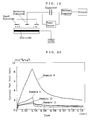
- Fig. 5 is a graph showing spectral characteristics of a green filter in a measuring system used to explain the photocurrent amplifying action of the photoelectric sensor according to the present invention.
- Fig. 6 is a graph showing the results of measurement of photocurrent amplifying action of a comparative photoelectric sensor.
- Fig. 7 is a graph showing the change of quantum efficiency of the comparative photoelectric sensor during light irradiation.
- Fig. 8 is a graph showing the results of measurement of photocurrent amplifying action of the photoelectric sensor of the present invention.
- Fig. 9 is a graph showing the change of quantum efficiency of the photoelectric sensor according to the present invention during light irradiation.
- Fig. 10 illustrates an information recording method for the first information recording system of the present invention.
- Fig. 11 illustrates an information reproducing method for the first information recording system of the present invention.
- Fig. 12 illustrates one example of an information output system.
- Fig. 13 illustrates a current measuring device used for the photoelectric sensor according to the present invention.
- Fig. 14 illustrates a current measuring device used to measure thermally stimulated current.
- Fig. 15 is a graph showing the results of measurement of thermally stimulated current.
- Fig. 16 is a graph showing electrical characteristics of one example of the photoelectric sensor according to the present invention.
- Fig. 17 is a graph showing electrical characteristics of other examples of the photoelectric sensor according to the present invention and a comparative photoelectric sensor.
- Fig. 18 is a graph showing the quantum efficiency of the photoelectric sensors of the present invention and the comparative photoelectric sensor.
- Fig. 19 illustrates an information output system.
- Fig. 20 is a graph showing electrical characteristics of further examples of the photoelectric sensor according to the present invention.
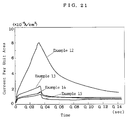
- Fig. 21 is a graph showing electrical characteristics of further examples of the photoelectric sensor according to the present invention.
- the photoelectric sensor of the present invention which is used in an information recording system, has a photo-induced current amplifying layer and a photoconductive layer stacked on an electrode.
- the photoconductive layer may have a single-layer structure or a double-layered structure including a charge generation layer and a charge transport layer, which are stacked one on top of another.
- the photoconductive layer generally functions such that when it is irradiated with light, photo-induced charge carriers (electrons or holes) are generated in the irradiated portion and these carriers are movable across the width of the layer.
- the photoelectric sensor of the present invention has a photo-induced current amplifying layer (described later) provided between the electrode and the photoconductive layer, thereby enabling an electric field or electric charge, which is given to an information recording medium when the photoelectric sensor is irradiated with light, to be amplified with time during the light irradiation.
- the photoelectric sensor sustains the increased conductivity in the form of moderately decaying electrical conductivity and continuously gives the electric field or the electric charge to the information recording medium.
- the photoelectric sensor has a photo-induced current amplifying layer provided between the photoconductive layer and the electrode, the injection of charge carriers from the electrode into the photoconductive layer can be stably controlled, and when no light is applied to the photoelectric sensor, the overall electrical conductivity of the photoelectric sensor is kept semiconductive.
- green light was selected from light emitted from a xenon lamp (L2274, manufactured by Hamamatsu Photonics K.K.) as a light source by using a green filter (manufactured by Vacuum Optics Co., of Japan) and applied at a luminous intensity of 20 lux. The intensity of light was measured with an illuminometer (manufactured by Minolta Camera Co., Ltd.).
- Fig. 5 shows the characteristics of the filter used.
- the ratio of the photo-induced current actually generated in the photosensitive sensor to the theoretical photocurrent is defined as the quantum efficiency of the photoelectric sensor:
- Quantum efficiency photo-induced current actually generated in the photoelectric sensor / theoretical photocurrent
- photo-induced current is employed herein to mean what is obtained by subtracting the value of base current, which is a current flowing through a portion irradiated with no light, from the value of current flowing through a portion irradiated with light. Therefore, the photo-induced current is not so-called photocurrent but a current which flows due to light irradiation in excess of the base current during the light irradiation or even after the light irradiation.
- the photo-induced current amplifying action in the photoelectric sensor of the present invention is defined as the behavior of such photo-induced current.
- the photoelectric sensor including a photo-induced current amplifying layer having photo-induced current amplifying action according to the present invention and a photoelectric sensor (hereinafter referred to as "comparative sensor") having no photo-induced current amplifying layer will be explained below by using the results of measurement carried out with the above-described measuring system.
- the results of measurement with regard to the comparative sensor are shown in Fig. 6.
- the line m is a reference line indicating the above-described theoretical value (1.35 x 10 ⁇ 6 A/cm2).
- the line m shows a state wherein light irradiation is effected for 0.033 sec. and the voltage application is continued even after the termination of the light irradiation.
- the line n shows the current measured in the photoelectric sensor having no photo-induced current amplifying layer. It will be understood from the line n that the increase of the photocurrent is small during the light irradiation, and the value does not exceed the theoretical value (1.35 x 10 ⁇ 6 A/cm2).
- the quantum efficiency of the comparative sensor is only about 0.5 at the highest.
- Fig. 7 shows the change of the quantum efficiency during the light irradiation.
- the photo-induced current increases during the light irradiation, as shown, for example, in Fig. 8, and as will be clear from Fig. 9, which shows the relationship between the quantum efficiency and time, the quantum efficiency exceeds 1 about 0.003 sec. after the initiation of the light irradiation, and it still continues increasing thereafter. That is, the provision of the photo-induced current amplifying layer makes it possible to obtain a much higher amplification factor than in the case of a photo-induced current condition which is usually attainable with a photoelectric sensor having no photo-induced current amplifying layer.
- the photocurrent decays rapidly at the same time as the light irradiation terminates. Therefore, no current effective as light information can be obtained even when the voltage application is continued after the termination of the light irradiation.
- the photoelectric sensor of the present invention the photo-induced current continuously flows when the voltage application is continued even after the termination of the light irradiation. Thus, the photo-induced current can be continuously taken out, and light information can be continuously obtained.
- photo-induced current amplifying action can be effectively produced. It is further surmised that when exposure is terminated with the voltage application condition maintained, photocarriers generated by the exposure immediately decay and disappear, but the decay of the trapped carriers is moderate, and hence the current of charge carriers injected from the electrode, which is induced by the trapped carriers, flows in a sufficient amount although it decays.
- the phenomenon that the electrical conductivity gradually decays is referred to as "moderately decaying electrical conductivity".
- the photo-induced current is the advantageous result obtained by the current amplification, which is triggered by light, in the photoelectric sensor of the present invention. Since a photocurrent larger than the photocurrent generated by incident light, which is expected from an ordinary photosensitive member, flows by virtue of the amplifying action, light information can be effectively supplied to an information recording medium.
- the injection current stabilizing action includes two actions, that is, the action of controlling the amount of charge carrier injected, and the action of uniforming the injection of carriers. First, the injection control action will be explained.
- the photoelectric sensor of the present invention is a semiconductive device whose resistivity in dark is preferably in the range of 109 ohm-cm to 1013 ohm-cm from the viewpoint of the density of current flowing.
- the resistivity is in the range of 1010 ohm-cm to 1011 ohm-cm, a particularly remarkable amplifying action is obtained.
- a photoelectric sensor having a resistivity more than 1013 ohm-cm shows no amplifying action as occurs in the photoelectric sensor of the present invention in the field intensity range of 105 V/cm to 106 V/cm.
- a photoelectric sensor having a resistivity less than 109 ohm-cm an exceedingly large current flows, so that noise is likely to occur due to the current. Therefore, such a photoelectric sensor is unfavorable.
- the amount of charge carrier injected from the electrode can be controlled so that the overall electrical conductivity of the photoelectric sensor is set at a favorable level.
- the photoelectric sensor having considerably excellent amplifying characteristics.
- photosensitive devices employed for general electrophotography have a dark resistivity in the range of 1014 ohm-cm to 1016 ohm-cm. Therefore, the photoelectric sensor of the present invention cannot attain the object of the present invention in electrophotography, whereas photoelectric sensors having a photoconductive layer with a relatively high dark resistivity for use in general electrophotography cannot be used for the purpose of the present invention.
- the sensitivity of the photoelectric sensor must be set in the operating voltage region of the liquid crystal. That is, the contrast voltage, which is a difference between the potential (light potential) applied to the information recording medium at the exposed region and the potential (dark potential) applied to the information recording medium at the unexposed region, must be set at a predetermined level in the operating voltage region of the liquid crystal in the information recording medium.
- the dark potential that is applied to the liquid crystal layer at the unexposed region of the photoelectric sensor must be set at a level approximately equal to the operation initiating potential of the liquid crystal.
- the photoelectric sensor is required to have a conductivity at which a base current in the range of 10 ⁇ 4 A/cm2 to 10 ⁇ 7 A/cm2, preferably in the range of 10 ⁇ 5 A/cm2 to 10 ⁇ 6 A/cm2, is generated under the condition where the resistivity of the information recording medium is in the range of 1010 ohm-cm to 1013 ohm-cm and an electric field of 105 V/cm to 106 V/cm is given to the photoelectric sensor.
- the molecules in the liquid crystal phase are not aligned even if exposure light is applied.
- the base current exceeds 10 ⁇ 4 A/cm2
- a large current flows at the same time as the voltage application is initiated even if no exposure light is applied, causing the molecules of the liquid crystal to be aligned. Therefore, even if exposure is carried out, no transmittance difference can be obtained between the exposed and unexposed regions.
- the operating voltage and its range differ among liquid crystals, when the level of applied voltage and voltage application time are to be set, it is preferable to properly set the voltage distribution in the information recording medium.
- the overall electrical conductivity of the photoelectric sensor can be controlled by providing the photo-induced current amplifying layer, it is possible to obtain a photoelectric sensor conformable to the operating voltage and range of a liquid crystal medium used. Accordingly, the recording image density can be set within a predetermined range, and stable light information recording can be effected.
- the photoelectric sensor of the present invention a relatively large amount of injection current flows, and the amount of charge carrier injected is largely limited by the injection from the electrode into the photoconductive layer.
- the condition of the interface between the electrode and the photoconductive layer is important.
- an extremely thin photo-induced current amplifying layer is provided between the electrode and the photoconductive layer so that the injection of charge carriers is effected through the photo-induced current amplifying layer. Accordingly, by properly providing the photo-induced current amplifying layer, it is possible to control the amount of charge carrier injected from the electrode into the photoconductive layer through the photo-induced current amplifying layer.
- the overall electrical conductivity of the photoelectric sensor can be set at a predetermined level.
- the photoelectric sensor of the present invention has high resolution and high sensitivity, unevenness of sensitivity or noise which gives rise to no problem in an ordinary photosensitive member may be undesirably recorded on an information recording medium as a noticeable defect, causing a serious problem in terms of the image quality. It is possible in the present invention to minimize the sensitivity unevenness and the image noise by providing a photo-induced current amplifying layer between the electrode and photoconductive layer of the photoelectric sensor.
- charge trap sites are present in the photoelectric sensor of the present invention, which trap and accumulate part of photo-induced charge carriers with time, as has been described above, and that since a certain amount of charge has already been trapped in the charge trap sites for some reason before photo-induced current amplification is performed, it is possible to measure a thermally stimulated current.
- the thermally stimulated current in the photoelectric sensor of the present invention is measured as follows: A sample for measurement is prepared by depositing a gold electrode having a film thickness of 30 nm, a sheet resistivity of 1,000 ohm/sq., and a size of 0.16 cm2 on the photoconductive layer, and the thermally stimulated current is measured with a short-circuit thermally stimulated current measuring device (manufactured by Toyo Seiki K.K.), as shown in Fig. 14. A DC voltage of 1.5 V/ ⁇ m is applied between the photoelectric sensor electrode as a positive electrode and the gold electrode as a negative electrode, and at the same time, the photoelectric sensor for measurement is heated at a heating rate of 10 o C/min. Under these conditions, the current flowing during the heating process is measured with a micro-ammeter.
- a photoelectric sensor including a photo-induced current amplifying layer having photo-induced current amplifying action according to the present invention and a photoelectric sensor (comparative sensor) having no photo-induced current amplifying layer will be explained below by use of the results of measurement carried out using the above-described measuring device.
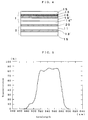
- Fig. 15 The results of the measurement are shown in Fig. 15.
- the axis of abscissas represents the heating temperature ( o C), and the axis of ordinates represents the current density value (10 ⁇ 6 A/cm2).
- the line A in the photoelectric sensor having the photo-induced current amplifying layer according to the present invention, a clear peaked waveform is observed besides the base current in the temperature range of 50 o C to 110 o C, and a peak appears in the vicinity of 88 o C. At the peak, a current value of 4.4x10 ⁇ 7 A/cm2 was obtained.
- the very small current that is observed in the measurement of the thermally stimulated current is considered to be attributable to the charge trapped in the charge trap sites present in the photoelectric sensor. That is, the trapped charge itself or charge that is induced by the trapped charge is stimulated by heating to move inside or outside the photoelectric sensor. Thus, a very small current is induced to flow through the external circuit by the movement of the charge.
- the photoelectric sensor having photo-induced current amplifying action according to the present invention has many charge trap sites that trap and accumulate part of photo-induced charge carriers with time, as described above, and that a certain amount of charge produced for some reason has already been trapped in the trap sites before photo-induced current amplification is performed, and the trapped charge itself or charge that is induced by the trapped charge is stimulated by heating to move inside or outside the photoelectric sensor.
- a very small current is induced to flow through the external circuit by the movement of the charge, and it is therefore possible to measure the thermally stimulated current.
- the photoelectric sensor of the present invention when measurement of the thermally stimulated current is carried out at a bias voltage of 1.5 V/ ⁇ m, clear peak should be observed in the temperature range of 50 o C to 110 o C, and the current density at the peak should be not lower than 5 x 10 ⁇ 8 A/cm2.
- Fig. 1 is a sectional view for explanation of the single-layer photoelectric sensor, in which reference numeral 13 denotes an electrode, 16 a photo-induced current amplifying layer, 14 a photoconductive layer, and 15 a substrate.
- the photoconductive layer 14 is formed of an inorganic or organic photoconductive substance.
- inorganic photoconductive substances include Se, Se-Te, ZnO, TiO2, Si, CdS, etc. These substances may be used alone or in the form of a combination of two or more of them.
- Such an inorganic photoconductive material is stacked on the electrode to a layer thickness of 1 ⁇ m to 30 ⁇ m, preferably 3 ⁇ m to 20 ⁇ m, by vapor deposition, sputtering, CVD, etc. It is also possible to use an inorganic photoconductive substance in the form of finely divided particles dispersed in a binder.
- binders usable in the present invention include a silicone resin, a polycarbonate resin, a polyvinyl formal resin, a polyvinyl acetal resin, a polyvinyl butyral resin, a styrene resin, a styrene-butadiene copolymer resin, an epoxy resin, an acrylic resin, a saturated or unsaturated polyester resin, a methacrylic resin, a vinyl chloride resin, a vinyl acetate resin, a vinyl chloride-vinyl acetate copolymer resin, etc.
- These binder resins may be used alone or in the form of a combination of two or more of them. It is preferable to disperse 0.1 to 10 parts by weight, preferably 1 to 5 parts by weight, of finely divided photoconductive particles in 1 part by weight of a binder resin material.
- Organic photoconductive substances include dispersions of high- and low-molecular photoconductive substances in an insulating binder.
- high-molecular photoconductive substances are polyvinyl carbazole (PVK), and poly-N-ethylenic unsaturated group-substituted carbazoles in which an ethylenic unsaturated group, e.g., allyl group or acryloxyalkyl group, is contained in place of the vinyl group in PVK.
- high-molecular photoconductive substances further include poly-N-ethylenic unsaturated group-substituted phenothiazines, e.g., poly-N-acrylphenothiazine, poly-N-( ⁇ -acryloxy)phenothiazine, etc., and polyvinyl pyrene.
- poly-N-ethylenic unsaturated group-substituted carbazoles particularly polyvinyl carbazole may preferably be employed.
- low-molecular photoconductive substances are oxadiazoles substituted by alkylaminophenyl group or the like, a triphenylmethane derivative, a hydrazone derivative, a butadiene derivative, a stilbene derivative, etc. It is also possible to form the photoconductive layer by using a charge generating substance and a charge transport substance, which are employed in a double-layered photoelectric sensor. In such a case, the charge generating and transport substances may be mixed in the ratio of from 1:1 to 1:10, preferably from 1:2 to 1:5.
- An organic photoconductive layer having film-forming properties may be formed by dispersing 0.1 to 10 parts by weight, preferably 0.1 to 1 part by weight, of an electrically insulating resin material in 1 part by weight of one selected from among the above organic photoconductive substances.
- An organic photoconductive layer produced by any of the above-described methods is formed on the electrode so that the dry film thickness is in the range of 1 ⁇ m to 50 ⁇ m, preferably in the range of 3 ⁇ m to 20 ⁇ m. Within the film thickness range, the photoelectric sensor exhibits excellent sensitivity and image quality.
- FIG. 2 is a sectional view for explanation of the double-layered photoelectric sensor, in which reference numeral 13 denotes an electrode, 16 a photo-induced current amplifying layer, 14' a charge generation layer, 14'' a charge transport layer, and 15 a substrate.
- the double-layered photoelectric sensor has a photo-induced current amplifying layer, a charge generation layer and a charge transport layer, which are successively formed on the electrode.
- This type of photoelectric sensor includes an inorganic material photoelectric sensor and an organic material photoelectric sensor.
- the charge generation layer 14' in the inorganic material photoelectric sensor is formed on the electrode to a thickness of 0.05 ⁇ m to 1 ⁇ m by vapor deposition, sputtering, CVD, etc. using a material such as Se-Te or Si doped with sulfur or oxygen, for example.
- a charge transport layer is formed on the charge generation layer to a thickness of 1 ⁇ m to 50 ⁇ m, preferably 3 ⁇ m to 20 ⁇ m, in the same way as the above using a material such as Se, As2Se3, Si, or Si doped with methane, for example.
- the charge generation layer 14' in the organic material photoelectric sensor is composed of a charge generating substance and a binder.
- charge generating substances usable in the present invention are cationic dyes, e.g., pyrylium dyes, thiapyrylium dyes, azulenium dyes, cyanine dyes, azulenium salt dye, etc., squalium salt dyes, phthalocyanine pigments, perylene pigments, polycyclic quinone pigments, e.g., pyranthrone pigments, etc., indigo pigments, quinacridone pigments, pyrrole pigments, and azo pigments, which are shown below.
- the dyes and pigments may be used alone or in the form of a combination of two or more of them.
- binders usable in the present invention are a silicone resin, a polycarbonate resin, a polyvinyl formal resin, a polyvinyl acetal resin, a polyvinyl butyral resin, a styrene resin, a styrene-butadiene copolymer resin, an epoxy resin, an acrylic resin, a saturated or unsaturated polyester resin, a methacrylic resin, a vinyl chloride resin, a vinyl acetate resin, a vinyl chloride-vinyl acetate copolymer resin, etc.
- These binder resins may be used alone or in the form of a combination of two or more of them.
- the dry film thickness of the charge generation layer is in the range of 0.01 ⁇ m to 2 ⁇ m, preferably in the range of 0.1 ⁇ m to 0.5 ⁇ m. Within this thickness range, the photoelectric sensor exhibits excellent sensitivity and image quality.
- the charge transport layer 14'' is composed of a charge transport substance and a binder.
- the charge transport substance is a substance having excellent properties to transport electric charge generated in the charge generation layer.
- Examples of charge transport substances usable in the present invention are oxadiazole, oxazole, triazole, thiazole, triphenylmethane, styryl, pyrazoline, hydrazone, aromatic amine, carbazole, polyvinyl carbazole, stilbene, enamine, azine, triphenylamine and butadiene compounds, polycyclic aromatic compounds, and stilbene dimers.
- the charge transport substance must have excellent hole transport properties.
- the binder it is possible to use the same binders as those mentioned for the charge generation layer, and in addition, a polyarylate resin and a phenoxy resin can be used for the binder.
- binders are a styrene resin, a styrene-butadiene copolymer resin, and a polycarbonate resin. It is preferable to use 0.1 to 10 parts by weight, preferably 0.1 to 1 part by weight, of a binder per part by weight of a charge transport substance.
- the dry film thickness of the charge transport layer is in the range of 1 ⁇ m to 50 ⁇ m, preferably in the range of 3 ⁇ m to 20 ⁇ m. With such a film thickness, excellent sensitivity and image quality can be obtained.
- the electrode 13 needs to be transparent if the information recording medium (described later) is opaque. However, if the information recording medium is transparent, the electrode 13 may be either transparent or opaque. Any material which stably gives a resistivity of not higher than 106 ohm-cm can be used for the electrode 13. Examples of such material are a thin metallic conductive film, e.g., gold, platinum, zinc, titanium, copper, iron, tin, etc., a metallic oxide conductive film, e.g., tin oxide, indium oxide, zinc oxide, titanium oxide, tungsten oxide, vanadium oxide, etc., and an organic conductive film, e.g., quaternary ammonium salt, and so forth. These materials may be used alone or in the form of a composite material comprising two or more of them. Among these materials, oxide conductors are preferable; indium-tin oxide compound (ITO) is particularly preferable.
- ITO indium-tin oxide compound
- the electrode 13 is formed by vapor deposition, sputtering, CVD, coating, plating, dipping, electrolytic polymerization, etc.
- the film thickness of the electrode needs to be changed depending upon the electrical characteristics of the material thereof and the level of voltage applied during information recording. For example, the thickness is about from 10 nm to 300 nm in the case of an ITO film.
- the electrode 13 may be formed either on the whole area between the substrate and the information recording layer or in conformity with a desired pattern.
- the electrode 13 may also be formed by stacking two or more different kinds of material.
- the substrate 15 needs to be transparent if the information recording medium (described later) is opaque. However, if the information recording medium is transparent, the substrate 15 may be either transparent or opaque.
- the substrate 15 has the shape of card, film, tape, disk or the like and supports the photoelectric sensor so as to provide the required strength. Accordingly, the substrate 15 need not be provided if the photoelectric sensor itself has supporting properties, and various materials are usable, provided that they are sufficiently strong to support the photoelectric sensor. Examples of usable materials are a flexible plastic film, or a rigid material such as glass, plastic sheet, card, etc. made of polyethylene, polypropylene, polyethylene terephthalate, polymethyl methacrylate, polymethyl acrylate, polyester, polycarbonate, etc.
- anti-reflection properties are preferably imparted to the substrate by stacking a layer having anti-reflection effect on the surface of the substrate 15 which is remote from the electrode 13, or by adjusting the film thickness of the transparent substrate to a level at which anti-reflection effect is obtainable, or by combining together these two measures, according to need.
- the photoconductive layer may contain additives such as an electron accepting substance, an electron donating substance, a sensitizing dye, an antioxidizing agent, an ultra-violet absorbing agent, a light stabilizer, etc. Electron accepting substances and sensitizing dyes have functions to adjust and stabilize the base current and to attain sensitization.
- Examples of electron accepting substances include nitro-substituted benzenes, amino-substituted benzenes, halogen-substituted benzenes, substituted naphthalenes, benzoquinones, nitro-substituted fluorenones, chloranils, and the compounds enumerated above as examples of charge transport substances.
- Examples of sensitizing dyes are a triphenylmethane dye, a pyrylium salt dye, a xanthene dye, and a leuco dye.
- antioxidizing agents are phenol-, sulfur-and phosphorus-containing antioxidizing agents.
- ultraviolet absorbing agents are salicyclic acid-, benzophenone-, benzotriazole- and cyanoacrylate-containing ultraviolet absorbing agents.
- light stabilizers are ultraviolet light stabilizers, hindered amine light stabilizers, etc.
- An electron accepting substance and a sensitizing dye are each added in the ratio of 0.001 to 10 parts by weight, preferably 0.01 to 1 part by weight, to 1 part by weight of a photoconductive substance. If the lower limit of the above range, i.e., 0.001 part by weight, is not reached, the desired action cannot be obtained. If the upper limit of the above range, i.e., 10 parts by weight, is exceeded, an adverse effect is made on the image quality.
- An antioxidizing agent, an ultraviolet absorbing agent, and a light stabilizer are each added in the ratio of 0.001 to 10 parts by weight, preferably 0.01 to 1 part by weight, to 1 part by weight of a photoconductive substance, alone or in the form of a combination of a plurality of agents. If the lower limit of the above range, i.e., 0.001 part by weight, is not reached, no advantageous effect is obtained from the addition of these substances. If the upper limit of the above range, i.e., 10 parts by weight, is exceeded, an adverse effect is made on the image quality.
- the above-described substances may be added to each of the charge generation and transport layers in the same ratio. Preferably, these substances are added to the charge generation layer.
- the photo-induced current amplifying layer that is used to constitute the photoelectric sensor of the present invention will be explained.
- the photo-induced current amplifying layer 16 is provided between the electrode 13 and the photoconductive layer 14 or the charge generation layer 14'. Although the reason is not clear, the photo-induced current amplifying layer 16 has the action of amplifying the photo-induced current in the photoelectric sensor, the action of controlling the injection of charge carriers from the electrode 13 into the photoconductive layer 14 or the charge generation layer 14' to thereby control the voltage actually applied to the information recording medium, and the action of uniforming the injection of charge carriers from the electrode 13 into the photoconductive layer 14 or the charge generation layer 14' to thereby reduce the noise, unevenness and so forth of information recorded on the information recording medium.
- the first action is effective in improving the recording sensitivity of the photoelectric sensor.
- the second action is effective in controlling the image density of the recorded image.
- the third action is effective in improving the image quality of the recorded image.
- binders usable in the present invention include a silicone resin, a polycarbonate resin, a polyvinyl formal resin, a polyvinyl acetal resin, a polyvinyl butyral resin, a styrene resin, a styrene-butadiene copolymer resin, an epoxy resin, an acrylic resin, a saturated or unsaturated polyester resin, a methacrylic resin, a vinyl chloride resin, a vinyl acetate resin, a vinyl chloride-vinyl acetate copolymer resin, etc.
- binder resins may be used alone or in the form of a combination of two or more of them. It is also possible to use a soluble polyamide, a phenolic resin, a polyurethane, a polyurea, a casein, a polypeptide, a polyvinyl alcohol, a polyvinyl pyrrolidone, a maleic anhydride ester polymer, a quaternary ammonium salt-containing polymer, a cellulose compound, etc. These binder resins may be used alone or in the form of a combination of two or more of them. Particularly preferable examples are a polyvinyl formal resin, a polyvinyl acetal resin, and a polyvinyl butyral resin.
- the thickness of the photo-induced current amplifying layer is set in the range of 0.005 ⁇ m to 5 ⁇ m, preferably in the range of 0.05 ⁇ m to 0.5 ⁇ m.
- the photo-induced current amplifying layer may be provided by a coating method, e.g., dip coating, roll coating, spin coating, etc. If the thickness is less than 0.005 ⁇ m, no image noise reducing action is available. If the thickness is greater than 5 ⁇ m, the resulting layer will hinder the injection of charge carriers from the electrode into the charge generation layer.
- various kinds of electron accepting substance, electron donating substance, photoconductive substance, inorganic salt and organic salt may be added to the photo-induced current amplifying layer according to need. These additives may be used alone or in the form of a combination of two or more of them.
- electron accepting substances include substituted benzenes represented by 1,3-dinitrobenzene, substituted naphthalenes, substituted or non-substituted benzoquinones represented by p-benzoquinone, 2,5-dichloro-p-benzoquinone, and 2,3-dichloro-5,6-dicyano-p-benzoquinone, substituted and non-substituted naphthoquinones, substituted and non-substituted anthraquinones, substituted fluorenones represented by 2,4,7-trinitrofluorenone and 2,4,5,7-tetranitrofluorenone, chloranils represented by p-chloranil and o-chloranil, and substituted quinodimethans represented by 7,7,8,8-tetracyanoquinodimethan.
- substituted benzenes represented by 1,3-dinitrobenzene
- substituted naphthalenes substituted or non-substit
- Examples of usable photoconductive substances include inorganic and organic photoconductive substances mentioned above for the single-layer photoelectric sensor and charge generating substances mentioned above for the double-layered photoelectric sensor.
- Examples of inorganic photoconductive substances are Se, Se-Te, ZnO, TiO2, Si, Si doped with sulfur, oxygen or the like, CdS, etc. These inorganic photoconductive substances may be used in the form of finely divided particles alone or in a combination of two or more of them.
- Organic photoconductive substances include high-and low-molecular photoconductive substances.
- high-molecular photoconductive substances are polyvinyl carbazole (PVK), and poly-N-ethylenic unsaturated group-substituted carbazoles in which an ethylenic unsaturated group, e.g., allyl group or acryloxyalkyl group, is contained in place of the vinyl group in PVK.
- high-molecular photoconductive substances further include poly-N-ethylenic unsaturated group-substituted phenothiazines, e.g., poly-N-acrylphenothiazine, poly-N-( ⁇ -acryloxy)phenothiazine, etc., and polyvinyl pyrene.
- low-molecular photoconductive substances examples include oxadiazoles substituted by alkylaminophenyl group or the like, a triphenylmethane derivative, a hydrazone derivative, a butadiene derivative, a stilbene derivative, etc.
- Examples of charge generating substances usable in the present invention are cationic dyes, e.g., pyrylium dyes, thiapyrylium dyes, azulenium dyes, cyanine dyes, azulenium salt dye, etc., squalium salt dyes, phthalocyanine pigments, perylene pigments, polycyclic quinone pigments, e.g., pyranthrone pigments, etc., indigo pigments, quinacridone pigments, pyrrole pigments, and azo pigments.
- the dyes and pigments may be used alone or in the form of a combination of two or more of them.
- inorganic and organic salts usable in the present invention are perchlorates, borofluorates, thiocyanates, nitrates, carboxylates, sulfonates, and halides, which have as cationic species metallic ions such as lithium, sodium, potassium, magnesium, calcium, or aluminum, quaternary ammonium ions, organic ions, etc.
- additives are added in the ratio of 0.001 to 10 parts by weight, preferably 0.05 to 5 parts by weight, to 1 part by weight of a binder resin.
- the additives may be used alone or in the form of a combination of two or more of them. It is particularly preferable to use a combination of an electron accepting compound and an organic photoconductive pigment, e.g., a substituted benzoquinone and an azo pigment. With such a combination, particularly great amplifying action is obtained.
- the information recording medium 2 will be explained.
- the information recording medium used in the present invention has an information recording layer formed of a polymer dispersed liquid crystal.
- the polymer dispersed liquid crystal has a structure in which resin particles are dispersed in a liquid crystal phase.
- examples of usable liquid crystal materials are a smectic liquid crystal, nematic liquid crystal, cholesteric liquid crystal and a mixture of these liquid crystals.
- a smectic liquid crystal from the point of view of retaining the liquid crystal alignment and holding the recorded information permanently, that is, from the viewpoint of memory effect.
- smectic liquid crystals usable in the present invention are as follows: cyanobiphenyl, cyanoterphenyl and phenylester liquid crystals, in which the end group of a liquid crystalline substance has a long carbon chain; liquid crystal substances that present smectic A phase, e.g., fluorine liquid crystal; liquid crystal substances presenting smectic C phase, which are used as ferroelectric liquid crystals; and liquid crystal substances that present smectic H, G, E or F phase.
- Examples of materials which are preferable to use for forming the resin phase are ultraviolet curing resin materials which are compatible with a liquid crystal material or a common solvent therewith in the form of a monomer or an oligomer.
- Examples of such ultraviolet curing resin materials are acrylic and methacrylic esters.
- thermosetting resin materials which are compatible with a solvent common to the liquid crystal material, for example, an acrylic resin, methacrylic resin, polyester resin, polystyrene resin, copolymers composed mainly of these resin materials, epoxy resin, silicone resin, etc.
- the liquid crystal content in the information recording layer is 10% to 90% by weight, more preferably 40% to 80% by weight. If the liquid crystal content is less than 10% by weight, light transmittance is low even when the molecules in the liquid crystal phase are aligned by recording of information, whereas, if the liquid crystal content exceeds 90% by weight, the liquid crystal oozes out, causing unevenness of the recorded information.
- the thickness of the information recording layer influences the definition of recorded information
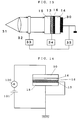
- the information recording medium is disposed to face the photoelectric sensor across a spacer 19 made of an insulating resin film such as polyimide, as shown in Fig. 3, and the electrodes 13 and 13' are connected to each other through a voltage source V, thereby forming a first information recording system of the present invention. At least one of the electrodes 13 and 13' in this system must be transparent.
- Fig. 4 is a sectional view of the second information recording system according to the present invention, in which reference numeral 20 denotes a dielectric layer, and the same reference numerals as those in Fig. 3 denote the same contents.
- the second information recording system is arranged such that the photoelectric sensor and the information recording medium in the first information recording system are disposed to face each other across a dielectric layer 20 without an air gap.
- the second information recording system is particularly suitable for an arrangement in which the photoconductive layer of the photoelectric sensor is formed by coating using a solvent.
- the arrangement of the second information recording system makes it possible to prevent unevenness of the recorded image which might otherwise be caused by elution of the liquid crystal from the information recording layer by the interaction between the photoconductive layer and the information recording layer if the latter is coated directly on the former, or elution of the photoconductive material by a solvent used for forming the information recording layer. It is also possible to integrate the photoelectric sensor and the information recording medium into one unit.
- the material for forming the dielectric layer 20 needs to be incompatible with either of the materials for forming the photoconductive layer and the information recording layer and must not have electrical conductivity. If the material is electrically conductive, the space charge is diffused, causing deterioration of the resolution. Therefore, insulating properties are required. However, since the dielectric layer lowers the distributed voltage that is applied to the liquid crystal layer or degrades the definition, it is preferable for the layer thickness to be as small as possible, preferably 2 ⁇ m or less. On the other hand, reduction in the layer thickness gives rise to not only generation of image noise due to the interaction that progresses with the passage of time but also the problem of permeation due to defects such as pinholes at the time of coating the material for stacking the layer.
- the layer thickness is properly set in accordance with the material which is to be coated.
- the layer thickness is preferably 10 ⁇ m or less, more preferably in the range of 0.1 ⁇ m to 3 ⁇ m.
- the dielectric layer is preferably formed by depositing an inorganic material, e.g., SiO2, TiO2, CeO2, Al2O3, GeO2, Si3N4, AlN, TiN, MgF2, ZnS, a mixture of silicon dioxide and titanium dioxide, a mixture of zinc sulfide and magnesium fluoride, a mixture of aluminum oxide and germanium, etc., by vapor deposition, sputtering, chemical vapor deposition (CVD), etc. It is also possible to use an aqueous solution of polyvinyl alcohol, water-system polyurethane, water glass, etc.
- an inorganic material e.g., SiO2, TiO2, CeO2, Al2O3, GeO2, Si3N4, AlN, TiN, MgF2, ZnS, a mixture of silicon dioxide and titanium dioxide, a mixture of zinc sulfide and magnesium fluoride, a mixture of aluminum oxide and germanium, etc.
- CVD chemical vapor deposition
- a water-soluble resin material which is less compatible with an organic solvent and to coat such an aqueous solution by spin coating, blade coating, roll coating and so forth.
- a coatable fluorocarbon resin may also be used. In such a case, it may be dissolved in a fluorine-containing solvent and coated by spin coating or stacked by blade coating, roll coating, etc.
- Coatable fluorocarbon resins which are preferable to use include fluorocarbon resins disclosed, for example, in Japanese Patent Application Laid-Open (KOKAI) No. 04-24722, and organic materials, e.g., poly-para-xylylene, etc., which are subjected to film formation in a vacuum system.
- fluorocarbon resins disclosed, for example, in Japanese Patent Application Laid-Open (KOKAI) No. 04-24722
- organic materials e.g., poly-para-xylylene, etc.
- FIG. 10 is a sectional view for explanation of the information recording method for the first information recording system of the present invention.
- the information recording method is carried out in the same way.
- reference numeral 11 denotes an information recording layer, 13 an electrode of a photoelectric sensor, 13' an electrode of an information recording medium, 16 a photo-induced current amplifying layer, 14 a photoconductive layer, 21 a light source, 22 a shutter having a driving mechanism, 23 a pulse generator serving as a power source, and 24 a camera obscura.
- the information recording method of the present invention enables planar analog recording and makes it possible to obtain recording at the liquid crystal particle level and hence high resolution, and it also permits the exposure light pattern to be retained in the form of a visible image by the molecular alignment in the liquid crystal phase.
- a method that uses a camera or a recording method that uses laser may be employed.
- the recording method by a camera uses an information recording medium in place of a photographic film used in an ordinary camera. Either an optical or electrical shutter can be used for this camera. It is also possible to conduct color photography by using a prism and a color filter by which light information is separated into R, G and B light components and taken out in the form of parallel rays, and forming one frame from three information recording mediums for R, G and B light components or from one set of R, G and B images recorded on different portions of one information recording medium.
- argon laser (514 nm, 488 nm), helium-neon laser (633 nm) or semiconductor laser (780 nm, 810 nm, etc.) may be used as a light source.
- Laser exposure corresponding to an image signal, character signal, code signal or line drawing signal is performed by scanning.
- Analog recording such as recording of an image is effected by modulating the intensity of laser light
- digital recording such as recording of characters, code or line drawing is effected by on/off control of laser light.
- An image that consists of halftone dots is formed by on/off controlling laser light through a dot generator.
- the photoconductive layer in the photoelectric sensor need not have panchromatic spectral characteristics, but it is only required to have sensitivity to the wavelength of the laser light source employed.
- the exposure light information recorded on the information recording medium is reproduced by transmitted light, as shown in Fig. 11.
- the first information recording system light is applied to the information recording medium separated from the system, whereas, in the case of the second information recording system, light is applied thereto in this state, without separating the information recording medium. Consequently, in the information recording region, light A is transmitted because the liquid crystal molecules are aligned in the direction of the electric field, whereas, in the region where no information has been recorded, light B is scattered, thus presenting a contrast with the information recording region.
- the recorded information may be read by reflected light by use of a light-reflecting layer.
- the photoelectric sensor of the present invention and an information recording medium are loaded into an imaging camera (e.g., RB67, manufactured by Mamiya Camera Co., Ltd.) in place of an ordinary photographic film. Then, a DC voltage of 700 V is applied between the respective electrodes of the photoelectric sensor and the information recording medium for 0.04 sec., and at the same time, exposure is carried out by projecting a gray scale from the photoelectric sensor side for 1/30 sec. By doing so, record regions comprising light-transmitting portions corresponding to the gray scale are formed on the information recording layer. Thus, information recording can be effected.
- an imaging camera e.g., RB67, manufactured by Mamiya Camera Co., Ltd.
- the information recorded on the information recording medium is read with an image scanner having a CCD line sensor in an information output system as shown in Fig. 12, and the read information is output by using a sublimation transfer printer (e.g., SP-5500, manufactured by Victor Company of Japan, Limited).
- a sublimation transfer printer e.g., SP-5500, manufactured by Victor Company of Japan, Limited.
- Information that is recorded by the molecular alignment in the liquid crystal is visible information which can be read by visual observation, and it can also be read in the form of an enlarged image by using a projector.
- the information can be read with high accuracy. It should be noted that occurrence of scattered light can be prevented by using a Schlieren optical system, if necessary.
- information recorded by exposure light is made visible by the molecular alignment in the liquid crystal, and the information once made visible can be kept from disappearing by properly selecting a combination of a liquid crystal and a resin material.
- memory properties can be imparted to the information recording medium. Since the recorded visible information can be erased by heating the information recording medium to a high temperature near the isotropic phase transition temperature, the information recording medium can be reused.
- an electrostatic information recording medium having an electric charge retaining layer as an information recording layer, as described, for example, in Japanese Patent Application Laid-Open (KOKAI) Nos. 03-7942, 05-107775, 05-107776, 05-107777, and 04-70842.
- KKAI Japanese Patent Application Laid-Open
- information is stored in the form of electrostatic charge in the information recording medium. Therefore, the electrostatic charge can be reproduced by toner development, or by an electric potential reading method as described, for example, in Japanese Patent Application Laid-open (KOKAI) No. 01-290366.
- thermoplastic resin layer As an information recording layer, as described, for example, in Japanese Patent Application Laid-Open (KOKAI) No. 04-46347.
- the thermoplastic resin layer is heated to thereby store the information as a frost image, which can be reproduced as visible information.
- a bis-azo pigment having the following structure as a photoconductive substance and 1 part by weight of a polyvinyl formal resin were mixed with 98 parts by weight of 1,4-dioxane and 98 parts by weight of cyclohexanone, and the mixture was thoroughly kneaded by using a mixing machine to obtain a pigment dispersion.
- 2,3-dichloro-5,6-dicyano-p-benzoquinone having the following structure as an electron accepting substance was added to the pigment dispersion in the ratio of 0.1 mol to 1 mol of the pigment in the dispersion and completely dissolved in the pigment dispersion, thereby obtaining a coating solution for forming a photo-induced current amplifying layer.
- an ITO film having a sheet resistivity of 80 ohm/sq. and a thickness of 100 nm was grown by sputtering to obtain an electrode.
- the electrode was subjected to a cleaning treatment twice by using a scrubber cleaning machine (Plate Cleaner, Model 602, trade name, manufactured by Ultratech Co., Ltd.).
- the cleaning treatment was comprised of spraying of pure water for 2 sec., scrubber cleaning for 20 sec., rinsing with pure water for 15 sec., removal of water by high-speed rotation for 25 sec., and infrared drying for 55 sec.
- the surface of the electrode thus treated was coated with the prepared coating solution for forming a photo-induced current amplifying layer in 0.4 sec. by a spinner at 4,000 rpm, and the coated electrode was allowed to stand under a dust-free condition, thereby effecting leveling drying. Thereafter, drying was carried out for 0.5 hour at 100 o C.
- a photo-induced current amplifying layer having a thickness of 100 nm was stacked on the electrode.
- a pyrrolopyrrole pigment manufactured by Ciba-Geigy Ltd. having the following structure as a charge generating substance was deposited on the photo-induced current amplifying layer at a rate of 3 nm/sec. under a vacuum of 10 ⁇ 6 Torr and then allowed to stand for 1 hour in acetone vapor, thereby stacking a charge generation layer of 200 nm in thickness on the photo-induced current amplifying layer.
- the surface of the charge generation layer was coated with a coating solution in 0.4 sec. by a spinner at 400 rpm.
- the coating solution was prepared by uniformly dissolving 3 parts by weight of a biphenylamine derivative having the following structure as a charge transport substance, and 2 parts by weight of a polystyrene resin material (HRM-3, manufactured by Denki Kagaku Kogyo K.K.) in 14 parts by weight of dichloromethane and 22 parts by weight of 1,1,2-trichloroethane.
- HRM-3 polystyrene resin material manufactured by Denki Kagaku Kogyo K.K.
- the coating was dried for 2 hours at 80 o C, thereby stacking a charge transport layer on the charge generation layer, and thus obtaining a photoelectric sensor having a photoconductive layer of 10 ⁇ m in thickness that comprised the charge generation and transport layers according to the present invention.
- a sample for measurement was prepared by depositing a gold electrode having a size of 0.16 cm2, a thickness of 10 nm and a sheet resistivity of 1,000 ohm/sq. on the charge transport layer of the photoelectric sensor, and a current measuring system as shown in Fig. 13 was constructed.
- reference numeral 15 denotes a photoelectric sensor substrate, 13 a photoelectric sensor electrode, 16 a photo-induced current amplifying layer, 14 a photoconductive layer including a charge generation layer and a charge transport layer, 30 a gold electrode, 31 a light source, 32 a shutter (No. O electromagnetic shutter, manufactured by Copal Co., Ltd.), 33 a shutter driving mechanism, 34 a pulse generator (manufactured by Yokogawa Hewlett-Packard Co.), and 35 an oscilloscope.
- green light was selected from light emitted from a xenon lamp (L2274, manufactured by Hamamatsu Photonics K.K.) as a light source by using a green filter (manufactured by Vacuum Optics Co., of Japan), and applied to the photoelectric sensor at a luminous intensity of 20 lux.
- the intensity of irradiation light was measured with an illuminometer (manufactured by Minolta Camera Co., Ltd.).
- Fig. 5 shows the characteristics of the filter used.
- the voltage application was continued for 0.15 sec. from the light irradiation initiation time even after the termination of the light irradiation, and the change of current with time during the voltage application was measured with the oscilloscope 35.
- no exposure was carried out, but the voltage application alone was performed, and the change of current with time was measured in the same way as the above. The measurement was carried out at room temperature.
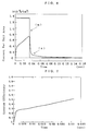
- Fig. 16 The results of the measurement are shown in Fig. 16.
- the axis of abscissas represents the voltage application time (second), and the axis of ordinates represents the current density (10 ⁇ 6 A/cm2).
- the line A shows the measured current value in the case where exposure was carried out
- the line B shows the measured current value in the case where no exposure was carried out, but the voltage application alone was performed.
- the line A two points (a) and (b) of inflections are observed on the curve representing the amount of current flowing in the photoelectric sensor of the present invention. It is considered from the comparison with a comparative sensor (described later) that the amount of current below the inflection point (a) is the amount of current flowing in proportion to the quantity of exposure energy (the current will be hereinafter referred to as "photo-induced current").
- the inflection point (b) is a point of change in the amount of current due to the termination of the exposure.
- the photo-induced current continues to increase during the exposure, and it continuously flows even after the termination of the exposure and gradually decays after a predetermined time.
- the resistivity was determined to be 4 x 10¹¹ ohm-cm from the value of current flowing in the photoelectric sensor.
- an ITO film having a thickness of 100 nm was grown by sputtering, thereby obtaining an electrode. Thereafter, the surface of the electrode was cleaned.
- the surface of the electrode was coated with a coating solution by using a blade coater provided with a gap of 50 ⁇ m.
- the coating solution was obtained by uniformly dissolving 40 parts by weight of a multifunctional monomer (dipentaerythritol hexaacrylate, M-400, manufactured by Toa Gosei Chemical Industry Co., Ltd.), 2 parts by weight of a photo-curing initiator (2-hydroxy-2-methyl-1-phenylpropane-1-one, Darocure 1173, manufactured by Ciba-Geigy Ltd.), 50 parts by weight of a liquid crystal [90% of which was a smectic liquid crystal (S-6, manufactured by Merck & Co., Ltd.) and 10% of which was a nematic liquid crystal (E31LV, manufactured by Merck & Co., Ltd.)], and 3 parts by weight of a surface-active agent (Fluorad FC-430, manufactured by Sumitomo 3M) in 96 parts by weight of x
- the coating was dried for 3 minutes at 47 o C and then vacuum-dried for 2 minutes at 47 o C. Immediately thereafter, the dry coating film was cured by irradiation with ultraviolet rays at 0.3 J/cm2, thereby obtaining an information recording medium having an information recording layer of 6 ⁇ m in thickness.
- a cross-section of the information recording layer was dried after the liquid crystal had been extracted with hot methanol, and then the internal structure of the information recording layer was observed with a scanning electron microscope having a magnifying power of 1,000 (S-800, manufactured by Hitachi, Ltd.). As a result, it was revealed that the surface of the information recording layer was covered with the ultraviolet curing resin material having a thickness of 0.6 ⁇ m and the inside of the layer had a structure in which the liquid crystal phase that formed a continuous layer was filled with the resin particle phase having a particle diameter of 0.1 ⁇ m.
- the stack structure thus obtained was loaded into an imaging camera (RB67, manufactured by Mamiya Camera Co., Ltd.) in place of a photographic film, as shown in Fig. 10.
- a DC voltage of 700 V was applied between the respective electrodes of the photoelectric sensor and the information recording medium for 0.04 sec., and at the same time, exposure was carried out by projecting a gray scale from the photoelectric sensor side for 1/30 sec. at an exposure of 0.2 to 200 lux. After the exposure, the information recording medium was taken out.
- record regions comprising light-transmitting portions corresponding to the gray scale were observed on the information recording layer.
- the sensitivity was improved to a considerable extent.
- the recorded image had no image unevenness or image noise attributable to partial or local unevenness of sensitivity of the photoelectric sensor. Thus, a favorable recorded image was obtained.
- reference numeral 41 denotes an information recording medium scanner, 42 a personal computer, and 43 a printer.
- the information recorded on the information recording medium was read with an image scanner employing a CCD line sensor, and the read information was output by using a sublimation transfer printer (SP-5500, manufactured by Victor Company of Japan, Limited). As a result, a favorable print, which had gradation corresponding to the gray scale and was free from image unevenness and image noise, was obtained.
- SP-5500 manufactured by Victor Company of Japan, Limited
- a color image was similarly recorded by separating the applied light into three colors, i.e., R, G and B, using prisms and a color filter.
- the recorded image was free from image unevenness and image noise attributable to partial or local unevenness of sensitivity of the photoelectric sensor.
- information on the color image thus recorded was read and output in the same way as the above, a favorable print, which was free from image unevenness and image noise, was obtained.
- the photoelectric sensor of the present invention a certain amount of charge has already been trapped in the charge trap sites before light amplification is performed. Therefore, it is possible to measure a thermally stimulated current.
- the thermally stimulated current in the photoelectric sensor of the present invention was measured as follows.
- a sample for measurement was prepared by depositing a gold electrode having a film thickness of 30 nm, a sheet resistivity of 1,000 ohm/sq., and a size of 0.16 cm2 on the photoconductive layer, and 3 days after the preparation of the photoelectric sensor, the thermally stimulated current was measured with a short-circuit thermally stimulated current measuring device (manufactured by Toyo Seiki K.K.), as shown in Fig. 14.
- a DC voltage of 1.5 V/ ⁇ m was applied between the photoelectric sensor electrode as a positive electrode and the gold electrode as a negative electrode, and at the same time, the photoelectric sensor for measurement was heated at a heating rate of 10 o C/min. Under these conditions, the current flowing during the heating process was measured with a micro-ammeter.
- reference numeral 15 denotes a photoelectric sensor substrate, 13 a photoelectric sensor electrode, 16 a photo-induced current amplifying layer, 14 a photoconductive layer including a charge generation layer and a charge transport layer, 30 a gold electrode, 100 a micro-ammeter, and 101 a DC power source.
- a DC power source with a micro-ammeter HP4140B, manufactured by Hewlett-Packard Co.
- the temperature of the sample was measured near the sample, that is, at a sample mount part covered with a heat insulation cover, by using an alumel-chromel thermocouple.
- Fig. 15 The results of the measurement are shown in Fig. 15.
- the axis of abscissas represents the heating temperature ( o C)
- the axis of ordinates represents the current value (A).
- the line A in the photoelectric sensor having the photo-induced current amplifying layer according to the present invention, a clear peaked waveform was observed besides the base current in the temperature range of 50 o C to 110 o C. A peak appeared in the vicinity of 88 o C, and the current density at the peak was 4.4 x 10 ⁇ 7 A/cm2.
- a comparative photoelectric sensor was prepared in the same way as in Example 1 except that no photo-induced current amplifying layer was provided in the comparative photoelectric sensor.
- Fig. 17 shows the results of calculation of quantum efficiency in the same way as in Example 1.
- An information recording system similar to the above was prepared by using the comparative photoelectric sensor and the above-described information recording medium.
- a DC voltage of 700 V was applied between the two electrodes for 0.04 sec., and at the same time, exposure was carried out by projecting a gray scale from the photoelectric sensor side.
- the information recording medium was taken out, and the recorded information was read and output by an information output system similar to the above. It was revealed that information only in an extremely narrow exposure range of the gray scale was recorded on the information recording medium.
- image unevenness and noise in the form of undesired blank spot which were attributable to partial or local unevenness of sensitivity of the photoelectric sensor, were observed on the medium having the light information recorded thereon.
- Example 2 Further, measurement of a thermally stimulated current was carried out in the same way as in Example 1. The results of the measurement are shown by the line B in Fig. 15. As shown by the line B, in the photoelectric sensor having no photo-induced current amplifying layer, a peaked waveform was observed besides the base current in the temperature range of 50 o to 110 o C, but the peak was very small, and the current density at the peak in the vicinity of 88 o C was extremely low, i.e., 4.5 x 10 ⁇ 8 A/cm2.
- a photo-induced current amplifying layer having a thickness of 100 nm was stacked on the electrode.
- a charge generation layer and a charge transport layer were formed in the same way as in Example 1, thereby preparing a double-layered photoelectric sensor.
- Fig. 17 shows the results of calculation of quantum efficiency made in the same way as in Example 1.
- Image recording was carried out in the same way as in Example 1 by using the photoelectric sensor of the present invention prepared as described above and an information recording medium prepared in the same way as in Example 1.
- the recorded image was free from image unevenness and image noise attributable to partial or local unevenness of sensitivity of the photoelectric sensor. Thus, a favorable recorded image was obtained.
- the information recorded on the information recording medium was read and output in the same way as in Example 1. As a result, it was revealed that the gray scale was reproduced to a considerable extent, and that the sensitivity was considerably improved in comparison to the comparative photoelectric sensor. In addition, a favorable print, which was free from image unevenness and image noise, was obtained. Thus, the image quality was improved.
- a color image was recorded by separating the applied light into three colors, i.e., R, G and B, using prisms and a color filter in the same way as in Example 1.
- the recorded image was free from image unevenness and image noise attributable to partial or local unevenness of sensitivity of the photoelectric sensor.
- a favorable print which was free from image unevenness and image noise, was obtained.
- a bis-azo pigment having the following structure as a photoconductive substance and 1 part by weight of a polyvinyl formal resin were mixed with 98 parts by weight of 1,4-dioxane and 98 parts by weight of cyclohexanone, and the mixture was thoroughly kneaded by using a mixing machine to prepare a dispersion, thereby obtaining a coating solution for forming a photo-induced current amplifying layer.
- the surface of a cleaned electrode was coated with the prepared coating solution in 0.4 sec. by a spinner at 4,000 rpm, and the coated electrode was allowed to stand under a dust-free condition, thereby effecting leveling drying.
- a photo-induced current amplifying layer having a thickness of 100 nm was stacked on the electrode.
- a charge generation layer and a charge transport layer were formed under the same conditions as in Example 1, thereby preparing a double-layered photoelectric sensor.
- Fig. 17 shows the results of calculation of quantum efficiency made in the same way as in Example 1.
- Image recording was carried out in the same way as in Example 1 by using the photoelectric sensor obtained as described above and an information recording medium prepared in the same way as in Example 1.
- the recorded image was free from image unevenness and image noise attributable to partial or local unevenness of sensitivity of the photoelectric sensor. Thus, a favorable recorded image was obtained.
- the information recorded on the information recording medium was read and output in the same way as in Example 1. As a result, it was revealed that the gray scale was reproduced to a certain extent, and that the sensitivity was somewhat improved in comparison to the comparative photoelectric sensor. In addition, a favorable print, which was free from image unevenness and image noise, was obtained. Thus, the image quality was improved.
- a color image was recorded by separating the applied light into three colors, i.e., R, G and B, using prisms and a color filter in the same way as in Example 1.
- the recorded image was free from image unevenness and image noise attributable to partial or local unevenness of sensitivity of the photoelectric sensor.
- a favorable print which was free from image unevenness and image noise, was obtained.
- Example 1 part by weight of a polyvinyl formal resin was mixed with 98 parts by weight of 1,4-dioxane and 98 parts by weight of cyclohexanone, and the mixture was thoroughly kneaded by using a mixing machine, thereby obtaining a coating solution for forming a photo-induced current amplifying layer.
- the surface of a cleaned electrode was coated with the prepared coating solution in 0.4 sec. by a spinner at 4,000 rpm, and the coated electrode was allowed to stand under a dust-free condition, thereby effecting leveling drying. Thereafter, drying was carried out for 0.5 hour at 100 o C.
- a photo-induced current amplifying layer having a thickness of 100 nm was stacked on the electrode.
- a charge generation layer and a charge transport layer were formed under the same conditions as in Example 1, thereby preparing a double-layered photoelectric sensor.
- Fig. 17 shows the results of calculation of quantum efficiency made in the same way as in Example 1.
- Image recording was carried out in the same way as in Example 1 by using the photoelectric sensor of the present invention prepared as described above and an information recording medium prepared in the same way as in Example 1.
- the recorded image was free from image unevenness and image noise attributable to partial or local unevenness of sensitivity of the photoelectric sensor. Thus, a favorable recorded image was obtained.
- the information recorded on the information recording medium was read and output in the same way as in Example 1. As a result, it was revealed that the reproduction of the gray scale was slightly better than in the case of the comparative photoelectric sensor, and the improvement in the sensitivity was very little. However, a favorable print, which was free from image unevenness and image noise, was obtained. Thus, the image quality was improved.
- a color image was recorded by separating the applied light into three colors, i.e., R, G and B, using prisms and a color filter in the same way as in Example 1.
- the recorded image was free from image unevenness and image noise attributable to partial or local unevenness of sensitivity of the photoelectric sensor.
- a favorable print which was free from image unevenness and image noise, was obtained.
- a polyvinyl alcohol manufactured by Nippon Synthetic Chemical Industry Co., Ltd.; the degree of saponification: 97% to 99%
- the coating solution was coated on the photoconductive layer of a photoelectric sensor prepared in the same way as in Example 1 by using a spinner, thereby stacking a dielectric layer of 1 ⁇ m in thickness on the photoconductive layer.
- an information recording layer was formed on the dielectric layer by the same method as that used to form the information recording layer in Example 1. Further, an ITO film was grown on the information recording layer to a thickness of 20 nm by sputtering, thereby stacking an electrically conductive layer on the information recording layer. In this way, an information recording medium was prepared.
- a DC voltage of 680 V was applied between the two electrodes of the information recording system, and at the same time, exposure was carried out by projecting a gray scale from the photoelectric sensor side for 1/30 sec at an exposure of 0.2 to 200 lux in the same way as in Example 1.
- the voltage application time was 0.02 sec.
- the information recording medium was taken out, and the recorded information was read and output by an information output system similar to that used in Example 1. As a result, a favorable print was obtained.
- tin oxide was deposited to a thickness of 100 nm to prepare an electrode. Thereafter, the electrode was subjected to a cleaning treatment similar to that in Example 1.
- the surface of the cleaned electrode was coated with a coating solution in 5 sec. by a spinner at 2,000 rpm.
- the coating solution was obtained by uniformly mixing 16 parts by weight of a ⁇ -pinene polymer (Kristalex 3100, manufactured by Rika Hercules Co.), and 80 parts by weight of xylene. Thereafter, it was allowed to stand for 30 minutes at room temperature, thereby obtaining an information recording medium having an information recording layer of 0.7 ⁇ m in thickness.
- Example 2 An information recording system similar to that in Example 1 was prepared by using the information recording medium prepared as described above and a photoelectric sensor prepared in the same way as in Example 1. A DC voltage of 800 V was applied between the two electrodes, and at the same time, exposure was carried out by projecting a gray scale from the photoelectric sensor side for 0.1 sec. at an exposure of 0.2 to 200 lux. The voltage application time was 0.5 sec. After the exposure, the information recording medium was taken out and heated for 30 sec. at 80 o C to effect development. As a result, a frost image corresponding to the gray scale was formed.
- a DC voltage of 800 V was applied between the two electrodes, and at the same time, exposure was carried out by projecting a gray scale from the photoelectric sensor side for 0.1 sec. at an exposure of 0.2 to 200 lux. The voltage application time was 0.5 sec. After the exposure, the information recording medium was taken out and heated for 30 sec. at 80 o C to effect development. As a result, a frost image corresponding to the gray scale was formed
- Example 1 On a glass substrate having a thickness of 1.1 mm and thoroughly cleaned, an ITO film having a thickness of 100 nm was grown by sputtering to obtain an electrode. Thereafter, the electrode was subjected to a cleaning treatment in the same way as in Example 1.
- the surface of the electrode was coated by spinner coating method (1,500 rpm; 20sec) with a solution of 7% fluorocarbon resin (Cytop, manufactured by Asahi Glass Company, Ltd., having a glass transition temperature of 100 o C, a water absorption of 0.01% and a resistivity of 1 x 10¹⁸ ohm-cm) in a fluorine-containing solvent, and it was dried for 3 hours at room temperature, thereby obtaining an information recording medium having an information recording layer of 3 ⁇ m in thickness.
- a solution of 7% fluorocarbon resin (Cytop, manufactured by Asahi Glass Company, Ltd., having a glass transition temperature of 100 o C, a water absorption of 0.01% and a resistivity of 1 x 10¹⁸ ohm-cm) in a fluorine-containing solvent
- Example 2 An information recording system similar to that used in Example 1 was constructed by using the information recording medium prepared as described above and a photoelectric sensor prepared in the same way as in Example 1. A DC voltage of 900 V was applied between the two electrodes, and at the same time, exposure was carried out by projecting a gray scale from the photoelectric sensor side for 1/30 sec. at an exposure of 0.2 to 200 lux. The voltage application time was 0.1 sec.
- a bis-azo pigment having the following structure as a photoconductive substance and 1 part by weight of a polyvinyl formal resin were mixed with 98 parts by weight of 1,4-dioxane and 98 parts by weight of cyclohexanone, and the mixture was thoroughly kneaded by using a mixing machine to obtain a pigment dispersion.
- 2,3-dichloro-5,6-dicyano-p-benzoquinone having the following structure as an electron accepting substance was added to the pigment dispersion in the ratio of 0.1 mol to 1 mol of the pigment in the dispersion and completely dissolved in the pigment dispersion, thereby obtaining a coating solution for forming a photo-induced current amplifying layer.
- an ITO film having a sheet resistivity of 80 ohm/sq. and a thickness of 100 nm was grown by sputtering to obtain an electrode.
- the electrode was subjected to a cleaning treatment twice by using a scrubber cleaning machine (Plate Cleaner, Model 602, trade name, manufactured by Ultratech Co., Ltd.).
- the cleaning treatment was comprised of spraying of pure water for 2 sec., scrubber cleaning for 20 sec., rinsing with pure water for 15 sec., removal of water by high-speed rotation for 25 sec., and infrared drying for 55 sec.
- the surface of the electrode thus treated was coated with the prepared coating solution for forming a photo-induced current amplifying layer in 0.4 sec. by a spinner at 4,000 rpm, and the coated electrode was allowed to stand under a dust-free condition, thereby effecting leveling drying. Thereafter, drying was carried out for 0.5 hour at 100 o C. Thus, a photo-induced current amplifying layer having a thickness of 100 nm was formed.
- a pyrrolopyrrole pigment manufactured by Ciba-Geigy Ltd. having the following structure as a charge generating substance was deposited on the photo-induced current amplifying layer at a rate of 3 nm/sec. under a vacuum of 10 ⁇ 6 Torr and then allowed to stand for 1 hour in acetone vapor, thereby stacking a charge generation layer of 200 nm in thickness on the photo-induced current amplifying layer.
- the surface of the charge generation layer was coated with a coating solution in 0.4 sec. by a spinner at 400 rpm.
- the coating solution was prepared by uniformly dissolving 25 parts by weight of a compound having the following structure as a charge transport substance, and 5 parts by weight of a polystyrene resin material (HPM-3, manufactured by Denki Kagaku Kogyo K.K.) in 68 parts by weight of dichloromethane and 102 parts by weight of 1,1,2-trichloroethane.
- HPM-3 polystyrene resin material
- dichloromethane 68 parts by weight of dichloromethane
- 1,1,2-trichloroethane 1,1,2-trichloroethane
- the coating was dried for 2 hours at 80 o C, thereby stacking a charge transport layer on the charge generation layer, and thus obtaining a photoelectric sensor having a photoconductive layer of 20 ⁇ m in thickness that comprised the charge generation and transport layers according to the present invention.
- the electrical characteristics of the photoelectric sensor thus obtained were measured by a current measuring device similar to that used in Example 1. The results of the measurement are shown in Fig. 20. As will be understood from the graph, an increase in the photocurrent according to the light irradiation was observed, and the amplifying effect was greater than in the comparative photoelectric sensor.
- Image recording was carried out in the same way as in Example 1 by using the photoelectric sensor prepared as described above and an information recording medium prepared in the same way as in Example 1.
- the recorded image was free from image unevenness and image noise attributable to partial or local unevenness of sensitivity of the photoelectric sensor. Thus, a favorable recorded image was obtained.
- the information recorded on the information recording medium was read and output in the same way as in Example 1. As a result, a favorable print, which had gradation corresponding to the gray scale and was free from image unevenness and image noise, was obtained. Thus, the image quality was improved.
- a color image was recorded by separating the applied light into three colors, i.e., R, G and B, using prisms and a color filter in the same way as in Example 1.
- the recorded image was free from image unevenness and image noise attributable to partial or local unevenness of sensitivity of the photoelectric sensor.
- a favorable print which was free from image unevenness and image noise, was obtained.
- a photo-induced current amplifying layer having a thickness of 100 nm was stacked on the electrode.
- a charge generation layer and a charge transport layer were formed in the same way as in Example 8, thereby preparing a double-layered photoelectric sensor.
- the electrical characteristics of the photoelectric sensor thus obtained were measured by a current measuring device similar to that used in Example 1. The results of the measurement are shown in Fig. 20. As will be understood from the graph, an increase in the photocurrent according to the light irradiation was observed, and the amplifying effect was greater than in the comparative photoelectric sensor.
- Image recording was carried out in the same way as in Example 1 by using the photoelectric sensor of the present invention prepared as described above and an information recording medium prepared in the same way as in Example 1.
- the recorded image was free from image unevenness and image noise attributable to partial or local unevenness of sensitivity of the photoelectric sensor. Thus, a favorable recorded image was obtained.
- the information recorded on the information recording medium was read and output in the same way as in Example 1. As a result, it was revealed that the gray scale was reproduced to a considerable extent, and that the sensitivity was considerably improved in comparison to the comparative photoelectric sensor. In addition, a favorable print, which was free from image unevenness and image noise, was obtained. Thus, the image quality was improved.
- a color image was recorded by separating the applied light into three colors, i.e., R, G and B, using prisms and a color filter in the same way as in Example 1.
- the recorded image was free from image unevenness and image noise attributable to partial or local unevenness of sensitivity of the photoelectric sensor.
- a favorable print which was free from image unevenness and image noise, was obtained.
- a photo-induced current amplifying layer having a thickness of 100 nm was stacked on the electrode.
- a charge generation layer and a charge transport layer were formed in the same way as in Example 8, thereby preparing a double-layered photoelectric sensor.
- the electrical characteristics of the photoelectric sensor thus obtained were measured by a current measuring device similar to that used in Example 1. The results of the measurement are shown in Fig. 20. As will be understood from the graph, an increase in the photocurrent according to the light irradiation was observed, and the amplifying effect was greater than in the comparative photoelectric sensor.
- Image recording was carried out in the same way as in Example 1 by using the photoelectric sensor of the present invention prepared as described above and an information recording medium prepared in the same way as in Example 1.
- the recorded image was free from image unevenness and image noise attributable to partial or local unevenness of sensitivity of the photoelectric sensor. Thus, a favorable recorded image was obtained.
- the information recorded on the information recording medium was read and output in the same way as in Example 1. As a result, it was revealed that the gray scale was reproduced to a certain extent, and that the sensitivity was somewhat improved in comparison to the comparative photoelectric sensor. In addition, a favorable print, which was free from image unevenness and image noise, was obtained. Thus, the image quality was improved.
- a color image was recorded by separating the applied light into three colors, i.e., R, G and B, using prisms and a color filter in the same way as in Example 1.
- the recorded image was free from image unevenness and image noise attributable to partial or local unevenness of sensitivity of the photoelectric sensor.
- a favorable print which was free from image unevenness and image noise, was obtained.
- a photo-induced current amplifying layer 1 part by weight of a polyvinyl formal resin was dissolved in 98 parts by weight of 1,4-dioxane and 98 parts by weight of cyclohexanone, thereby obtaining a coating solution for forming a photo-induced current amplifying layer.
- the surface of a cleaned electrode was coated with the prepared coating solution in 0.4 sec. by a spinner at 4,000 rpm, and the coated electrode was allowed to stand under a dust-free condition, thereby effecting leveling drying. Thereafter, drying was carried out for 0.5 hour at 100 o C.
- a photo-induced current amplifying layer having a thickness of 100 nm was stacked on the electrode.
- a charge generation layer and a charge transport layer were formed in the same way as in Example 8, thereby preparing a double-layered photoelectric sensor.
- the electrical characteristics of the photoelectric sensor thus obtained were measured by a current measuring device similar to that used in Example 1. The results of the measurement are shown in Fig. 20. As will be understood from the graph, an increase in the photocurrent according to the light irradiation was observed, and the amplifying effect was greater than in the comparative photoelectric sensor.
- Image recording was carried out in the same way as in Example 1 by using the photoelectric sensor of the present invention prepared as described above and an information recording medium prepared in the same way as in Example 1.
- the recorded image was free from image unevenness and image noise attributable to partial or local unevenness of sensitivity of the photoelectric sensor. Thus, a favorable recorded image was obtained.
- the information recorded on the information recording medium was read and output in the same way as in Example 1. As a result, it was revealed that the reproduction of the gray scale was slightly better than in the case of the comparative photoelectric sensor, and the improvement in the sensitivity was very little. However, a favorable print, which was free from image unevenness and image noise, was obtained. Thus, the image quality was improved.
- a color image was recorded by separating the applied light into three colors, i.e., R, G and B, using prisms and a color filter in the same way as in Example 1.
- the recorded image was free from image unevenness and image noise attributable to partial or local unevenness of sensitivity of the photoelectric sensor.
- a favorable print which was free from image unevenness and image noise, was obtained.
- a bis-azo pigment having the following structure as a photoconductive substance and 1 part by weight of a polyvinyl formal resin were mixed with 98 parts by weight of 1,4-dioxane and 98 parts by weight of cyclohexanone, and the mixture was thoroughly kneaded by using a mixing machine to obtain a pigment dispersion.
- 2,3-dichloro-5,6-dicyano-p-benzoquinone having the following structure as an electron accepting substance was added to the pigment dispersion in the ratio of 0.1 mol to 1 mol of the pigment in the dispersion and completely dissolved in the pigment dispersion, thereby obtaining a coating solution for forming a photo-induced current amplifying layer.
- Example 2 the surface of a cleaned electrode was coated with the prepared coating solution for forming a photo-induced current amplifying layer in 0.4 sec. by a spinner at 4,000 rpm, and the coated electrode was allowed to stand under a dust-free condition, thereby effecting leveling drying. Thereafter, drying was carried out for 0.5 hour at 100 o C. Thus, a photo-induced current amplifying layer having a thickness of 100 nm was stacked on the electrode.
- a pyrrolopyrrole pigment manufactured by Ciba-Geigy Ltd. having the following structure as a charge generating substance was deposited on the photo-induced current amplifying layer at a rate of 3 nm/sec. under a vacuum of 10 ⁇ 6 Torr and then allowed to stand for 1 hour in acetone vapor, thereby stacking a charge generation layer of 200 nm in thickness on the photo-induced current amplifying layer.
- the surface of the charge generation layer was coated with a coating solution in 0.4 sec. by a spinner at 400 rpm.
- the coating solution was prepared by uniformly dissolving 25 parts by weight of a compound having the following structure as a charge transport substance, and 5 parts by weight of a polystyrene resin material (HRM-3, manufactured by Denki Kagaku Kogyo K.K.) in 68 parts by weight of dichloromethane and 102 parts by weight of 1,1,2-trichloroethane.
- HRM-3 polystyrene resin material
- dichloromethane 68 parts by weight of dichloromethane
- 1,1,2-trichloroethane 1,1,2-trichloroethane
- the coating was dried for 2 hours at 80 o C, thereby stacking a charge transport layer on the charge generation layer, and thus obtaining a photoelectric sensor having a photoconductive layer of 20 ⁇ m in thickness that comprised the charge generation and transport layers according to the present invention.
- the electrical characteristics of the photoelectric sensor thus obtained were measured by a current measuring device similar to that used in Example 1. The results of the measurement are shown in Fig. 21. As will be understood from the graph, an increase in the photocurrent according to the light irradiation was observed.
- Image recording was carried out in the same way as in Example 1 by using the photoelectric sensor of the present invention prepared as described above and an information recording medium prepared in the same way as in Example 1.
- the recorded image was free from image unevenness and image noise attributable to partial or local unevenness of sensitivity of the photoelectric sensor. Thus, a favorable recorded image was obtained.
- the information recorded on the information recording medium was read and output in the same way as in Example 1. As a result, a favorable print, which had gradation corresponding to the gray scale and was free from image unevenness and image noise, was obtained. Thus, the image quality was improved.
- a color image was recorded by separating the applied light into three colors, i.e., R, G and B, using prisms and a color filter in the same way as in Example 1.
- the recorded image was free from image unevenness and image noise attributable to partial or local unevenness of sensitivity of the photoelectric sensor.
- a favorable print which was free from image unevenness and image noise, was obtained.
- a photo-induced current amplifying layer having a thickness of 100 nm was stacked on the electrode.
- a charge generation layer and a charge transport layer were formed under the same conditions as in Example 12, thereby preparing a double-layered photoelectric sensor.
- the electrical characteristics of the photoelectric sensor thus obtained were measured by a current measuring device similar to that used in Example 1. The results of the measurement are shown in Fig. 21. As will be understood from the graph, an increase in the photocurrent according to the light irradiation was observed.
- Image recording was carried out in the same way as in Example 1 by using the photoelectric sensor of the present invention prepared as described above and an information recording medium prepared in the same way as in Example 1.
- the recorded image was free from image unevenness and image noise attributable to partial or local unevenness of sensitivity of the photoelectric sensor. Thus, a favorable recorded image was obtained.
- the information recorded on the information recording medium was read and output in the same way as in Example 1. As a result, it was revealed that the gray scale was reproduced to a considerable extent, and that the sensitivity was considerably improved in comparison to the comparative photoelectric sensor. In addition, a favorable print, which was free from image unevenness and image noise, was obtained. Thus, the image quality was improved.
- a color image was recorded by separating the applied light into three colors, i.e., R, G and B, using prisms and a color filter in the same way as in Example 1.
- the recorded image was free from image unevenness and image noise attributable to partial or local unevenness of sensitivity of the photoelectric sensor.
- a favorable print which was free from image unevenness and image noise, was obtained.
- a bis-azo pigment having the following structure as a photoconductive substance and 1 part by weight of a polyvinyl formal resin were mixed with 98 parts by weight of 1,4-dioxane and 98 parts by weight of cyclohexanone, and the mixture was thoroughly kneaded by using a mixing machine to prepare a pigment dispersion, thereby obtaining a coating solution for forming a photo-induced current amplifying layer.
- the surface of a cleaned electrode was coated with the prepared coating solution in 0.4 sec. by a spinner at 4,000 rpm, and the coated electrode was allowed to stand under a dust-free condition, thereby effecting leveling drying.
- a photo-induced current amplifying layer having a thickness of 100 nm was stacked on the electrode.
- a charge generation layer and a charge transport layer were formed in the same way as in Example 12, thereby preparing a double-layered photoelectric sensor.
- the electrical characteristics of the photoelectric sensor thus obtained were measured by a current measuring device similar to that used in Example 1. The results of the measurement are shown in Fig. 21. As will be understood from the graph, an increase in the photocurrent according to the light irradiation was observed.
- Image recording was carried out in the same way as in Example 1 by using the photoelectric sensor of the present invention prepared as described above and an information recording medium prepared in the same way as in Example 1.
- the recorded image was free from image unevenness and image noise attributable to partial or local unevenness of sensitivity of the photoelectric sensor. Thus, a favorable recorded image was obtained.
- the information recorded on the information recording medium was read and output in the same way as in Example 1. As a result, it was revealed that the gray scale was reproduced to a certain extent, and that the sensitivity was somewhat improved in comparison to the comparative photoelectric sensor. In addition, a favorable print, which was free from image unevenness and image noise, was obtained. Thus, the image quality was improved.
- a color image was recorded by separating the applied light into three colors, i.e., R, G and B, using prisms and a color filter in the same way as in Example 1.
- the recorded image was free from image unevenness and image noise attributable to partial or local unevenness of sensitivity of the photoelectric sensor.
- a favorable print which was free from image unevenness and image noise, was obtained.
- Example 2 1 part by weight of a polyvinyl formal resin was dissolved in 98 parts by weight of 1,4-dioxane and 98 parts by weight of cyclohexanone, thereby obtaining a coating solution for forming a photo-induced current amplifying layer.
- the surface of a cleaned electrode was coated with the prepared coating solution in 0.4 sec. by a spinner at 4,000 rpm, and the coated electrode was allowed to stand under a dust-free condition, thereby effecting leveling drying. Thereafter, drying was carried out for 0.5 hour at 100 o C.
- a photo-induced current amplifying layer having a thickness of 100 nm was stacked on the electrode.
- a charge generation layer and a charge transport layer were formed in the same way as in Example 12, thereby preparing a double-layered photoelectric sensor.
- the electrical characteristics of the photoelectric sensor thus obtained were measured by a current measuring device similar to that used in Example 1. The results of the measurement are shown in Fig. 21. As will be understood from the graph, an increase in the photocurrent according to the light irradiation was observed.
- Image recording was carried out in the same way as in Example 1 by using the photoelectric sensor prepared as described above and an information recording medium prepared in the same way as in Example 1.
- the recorded image was free from image unevenness and image noise attributable to partial or local unevenness of sensitivity of the photoelectric sensor. Thus, a favorable recorded image was obtained.
- the information recorded on the information recording medium was read and output in the same way as in Example 1. As a result, it was revealed that the reproduction of the gray scale was slightly better than in the case of the comparative photoelectric sensor, and the improvement in the sensitivity was very little. However, a favorable print, which was free from image unevenness and image noise, was obtained. Thus, the image quality was improved.
- a color image was recorded by separating the applied light into three colors, i.e., R, G and B, using prisms and a color filter in the same way as in Example 1.
- the recorded image was free from image unevenness and image noise attributable to partial or local unevenness of sensitivity of the photoelectric sensor.
- a favorable print which was free from image unevenness and image noise, was obtained.
- Example 2 the surface of a cleaned electrode was coated with the prepared coating solution for forming a photo-induced current amplifying layer in 0.4 sec. by a spinner at 4,000 rpm, and the coated electrode was allowed to stand under a dust-free condition, thereby effecting leveling drying. Thereafter, drying was carried out for 0.5 hour at 100 o C. Thus, a photo-induced current amplifying layer having a thickness of 100 nm was stacked on the electrode.
- the surface of the photo-induced current amplifying layer was coated with a pigment dispersion in 0.4 sec. by a spinner at 2,000 rpm.
- the pigment dispersion was prepared by mixing 3 parts by weight of a bis-azo pigment having the following structure as a charge generating substance and 1 part by weight of a polyvinyl formal resin with 98 parts by weight of 1,4-dioxane and 98 parts by weight of cyclohexanone, and thoroughly kneading the mixture by using a mixing machine. After the coating process, drying was carried out for 1 hour at 100 o C. Thus, a charge generation layer having a thickness of 200 nm was stacked on the photo-induced current amplifying layer.
- the surface of the charge generation layer was coated with a coating solution in 0.4 sec. by a spinner at 400 rpm.
- the coating solution was prepared by uniformly dissolving 25 parts by weight of a compound having the following structure as a charge transport substance, and 5 parts by weight of a polystyrene resin material (HRM-3, manufactured by Denki Kagaku Kogyo K.K.) in 68 parts by weight of dichloromethane and 102 parts by weight of 1,1,2-trichloroethane.
- HRM-3 polystyrene resin material
- the coating was dried for 2 hours at 80 o C, thereby stacking a charge transport layer on the charge generation layer, and thus obtaining a photoelectric sensor having a photoconductive layer of 20 ⁇ m in thickness that comprised the charge generation and transport layers according to the present invention.
- Image recording was carried out in the same way as in Example 1 by using the photoelectric sensor of the present invention prepared as described above and an information recording medium prepared in the same way as in Example 1.
- the recorded image was free from image unevenness and image noise attributable to partial or local unevenness of sensitivity of the photoelectric sensor. Thus, a favorable recorded image was obtained.
- the information recorded on the information recording medium was read and output in the same way as in Example 1. As a result, a favorable print, which had gradation corresponding to the gray scale and was free from image unevenness and image noise, was obtained. Thus, the image quality was improved.
- a color image was recorded by separating the applied light into three colors, i.e., R, G and B, using prisms and a color filter in the same way as in Example 1.
- the recorded image was free from image unevenness and image noise attributable to partial or local unevenness of sensitivity of the photoelectric sensor.
- a favorable print which was free from image unevenness and image noise, was obtained.
- Example 2 1 part by weight of a polyvinyl formal resin was dissolved in 98 parts by weight of 1,4-dioxane and 98 parts by weight of cyclohexanone, thereby obtaining a coating solution for forming a photo-induced current amplifying layer.
- the surface of a cleaned electrode was coated with the prepared coating solution in 0.4 sec. by a spinner at 4,000 rpm, and the coated electrode was allowed to stand under a dust-free condition, thereby effecting leveling drying. Thereafter, drying was carried out for 0.5 hour at 100 o C.
- a photo-induced current amplifying layer having a thickness of 100 nm was stacked on the electrode.
- a charge generation layer and a charge transport layer were formed under the same conditions as in Example 16, thereby preparing a double-layered photoelectric sensor.
- Image recording was carried out in the same way as in Example 1 by using the photoelectric sensor obtained as described above and an information recording medium prepared in the same way as in Example 1.
- the recorded image was free from image unevenness and image noise attributable to partial or local unevenness of sensitivity of the photoelectric sensor. Thus, a favorable recorded image was obtained.
- the information recorded on the information recording medium was read and output in the same way as in Example 1. As a result, a favorable print, which had gradation corresponding to the gray scale and was free from image unevenness and image noise, was obtained. Thus, the image quality was improved.
- a color image was recorded by separating the applied light into three colors, i.e., R, G and B, using prisms and a color filter in the same way as in Example 1.
- the recorded image was free from image unevenness and image noise attributable to partial or local unevenness of sensitivity of the photoelectric sensor.
- a favorable print which was free from image unevenness and image noise, was obtained.
- Example 2 the surface of a cleaned electrode was coated with the prepared coating solution for forming a photo-induced current amplifying layer in 0.4 sec. by a spinner at 4,000 rpm, and the coated electrode was allowed to stand under a dust-free condition, thereby effecting leveling drying. Thereafter, drying was carried out for 0.5 hour at 100 o C. Thus, a photo-induced current amplifying layer having a thickness of 100 nm was stacked on the electrode.
- the surface of the photo-induced current amplifying layer was coated with a pigment dispersion in 0.4 sec. by a spinner at 2,000 rpm.
- the pigment dispersion was prepared by mixing 3 parts by weight of a bis-azo pigment having the following structure as a charge generating substance and 1 part by weight of a polyvinyl formal resin with 98 parts by weight of 1,4-dioxane and 98 parts by weight of cyclohexanone, and thoroughly kneading the mixture by using a mixing machine. After the coating process, drying was carried out for 1 hour at 100 o C. Thus, a charge generation layer having a thickness of 200 nm was stacked on the photo-induced current amplifying layer.
- the surface of the charge generation layer was coated with a coating solution in 0.4 sec. by a spinner at 400 rpm.
- the coating solution was prepared by uniformly dissolving 3 parts by weight of a compound having the following structure as a charge transport substance, and 2 parts by weight of a polycarbonate resin material in 22 parts by weight of dichloromethane. After the coating process, the coated electrode was allowed to stand under a calm condition until a dry film was formed on the surface of the coating so that the surface of the coating film was unadherable, thereby effecting leveling drying.
- the coating was dried for 2 hours at 80 o C, thereby stacking a charge transport layer on the charge generation layer, and thus obtaining a photoelectric sensor having a photoconductive layer of 10 ⁇ m in thickness that comprised the charge generation and transport layers according to the present invention.
- Image recording was carried out in the same way as in Example 1 by using the photoelectric sensor of the present invention prepared as described above and an information recording medium prepared in the same way as in Example 1.
- the recorded image was free from image unevenness and image noise attributable to partial or local unevenness of sensitivity of the photoelectric sensor. Thus, a favorable recorded image was obtained.
- the information recorded on the information recording medium was read and output in the same way as in Example 1. As a result, a favorable print, which had gradation corresponding to the gray scale and was free from image unevenness and image noise, was obtained. Thus, the image quality was improved.
- a color image was recorded by separating the applied light into three colors, i.e., R, G and B, using prisms and a color filter in the same way as in Example 1.
- the recorded image was free from image unevenness and image noise attributable to partial or local unevenness of sensitivity of the photoelectric sensor.
- a favorable print which was free from image unevenness and image noise, was obtained.
- a photo-induced current amplifying layer 1 part by weight of a polyvinyl formal resin was dissolved in 98 parts by weight of 1,4-dioxane and 98 parts by weight of cyclohexanone, thereby obtaining a coating solution for forming a photo-induced current amplifying layer.
- the surface of a cleaned electrode was coated with the prepared coating solution in 0.4 sec. by a spinner at 4,000 rpm, and the coated electrode was allowed to stand under a dust-free condition, thereby effecting leveling drying. Thereafter, drying was carried out for 0.5 hour at 100 o C.
- a photo-induced current amplifying layer having a thickness of 100 nm was stacked on the electrode.
- a charge generation layer and a charge transport layer were formed in the same way as in Example 18, thereby preparing a double-layered photoelectric sensor.
- Image recording was carried out in the same way as in Example 1 by using the photoelectric sensor obtained as described above and an information recording medium prepared in the same way as in Example 1.
- the recorded image was free from image unevenness and image noise attributable to partial or local unevenness of sensitivity of the photoelectric sensor. Thus, a favorable recorded image was obtained.
- the information recorded on the information recording medium was read and output in the same way as in Example 1. As a result, a favorable print, which had gradation corresponding to the gray scale and was free from image unevenness and image noise, was obtained. Thus, the image quality was improved.
- a color image was recorded by separating the applied light into three colors, i.e., R, G and B, using prisms and a color filter in the same way as in Example 1.
- the recorded image was free from image unevenness and image noise attributable to partial or local unevenness of sensitivity of the photoelectric sensor.
- a favorable print which was free from image unevenness and image noise, was obtained.
- Example 2 the surface of a cleaned electrode was coated with the prepared coating solution for forming a photo-induced current amplifying layer in 0.4 sec. by a spinner at 4,000 rpm, and the coated electrode was allowed to stand under a dust-free condition, thereby effecting leveling drying. Thereafter, drying was carried out for 0.5 hour at 100 o C. Thus, a photo-induced current amplifying layer having a thickness of 100 nm was stacked on the electrode.
- the surface of the photo-induced current amplifying layer was coated with a pigment dispersion in 0.4 sec. by a spinner at 2,000 rpm.
- the pigment dispersion was prepared by mixing 3 parts by weight of a bis-azo pigment having the following structure as a charge generating substance and 1 part by weight of a polyvinyl formal resin with 98 parts by weight of 1,4-dioxane and 98 parts by weight of cyclohexanone, and thoroughly kneading the mixture by using a mixing machine. After the coating process, drying was carried out for 1 hour at 100 o C. Thus, a charge generation layer having a thickness of 200 nm was stacked on the photo-induced current amplifying layer.
- the surface of the charge generation layer was coated with a coating solution in 0.4 sec. by a spinner at 400 rpm.
- the coating solution was prepared by uniformly dissolving 25 parts by weight of a compound (T-405, manufactured by Anan Co., Ltd.) having the following structure as a charge transport substance, and 5 parts by weight of a polystyrene resin material (HRM-3, manufactured by Denki Kagaku Kogyo K.K.) in 68 parts by weight of dichloromethane and 102 parts by weight of 1,1,2-trichloroethane.
- the coated electrode was allowed to stand under a calm condition until a dry film was formed on the surface of the coating so that the surface of the coating film was unadherable, thereby effecting leveling drying.
- the coating was dried for 2 hours at 80 o C, thereby stacking a charge transport layer on the charge generation layer, and thus obtaining a photoelectric sensor having a photoconductive layer of 20 ⁇ m in thickness that comprised the charge generation and transport layers according to the present invention.
- Image recording was carried out in the same way as in Example 1 by using the photoelectric sensor of the present invention prepared as described above and an information recording medium prepared in the same way as in Example 1.
- the recorded image was free from image unevenness and image noise attributable to partial or local unevenness of sensitivity of the photoelectric sensor. Thus, a favorable recorded image was obtained.
- the information recorded on the information recording medium was read and output in the same way as in Example 1. As a result, a favorable print, which had gradation corresponding to the gray scale and was free from image unevenness and image noise, was obtained. Thus, the image quality was improved.
- a color image was recorded by separating the applied light into three colors, i.e., R, G and B, using prisms and a color filter in the same way as in Example 1.
- the recorded image was free from image unevenness and image noise attributable to partial or local unevenness of sensitivity of the photoelectric sensor.
- a favorable print which was free from image unevenness and image noise, was obtained.
- a photo-induced current amplifying layer 1 part by weight of a polyvinyl formal resin was dissolved in 98 parts by weight of 1,4-dioxane and 98 parts by weight of cyclohexanone, thereby obtaining a coating solution for forming a photo-induced current amplifying layer.
- the surface of a cleaned electrode was coated with the prepared coating solution in 0.4 sec. by a spinner at 4,000 rpm, and the coated electrode was allowed to stand under a dust-free condition, thereby effecting leveling drying. Thereafter, drying was carried out for 0.5 hour at 100 o C.
- a photo-induced current amplifying layer having a thickness of 100 nm was stacked on the electrode.
- a charge generation layer and a charge transport layer were formed in the same way as in Example 18, thereby preparing a double-layered photoelectric sensor.
- Image recording was carried out in the same way as in Example 1 by using the photoelectric sensor of the present invention prepared as described above and an information recording medium prepared in the same way as in Example 1.
- the recorded image was free from image unevenness and image noise attributable to partial or local unevenness of sensitivity of the photoelectric sensor. Thus, a favorable recorded image was obtained.
- the information recorded on the information recording medium was read and output in the same way as in Example 1. As a result, a favorable print, which had gradation corresponding to the gray scale and was free from image unevenness and image noise, was obtained. Thus, the image quality was improved.
- a color image was recorded by separating the applied light into three colors, i.e., R, G and B, using prisms and a color filter in the same way as in Example 1.
- the recorded image was free from image unevenness and image noise attributable to partial or local unevenness of sensitivity of the photoelectric sensor.
- a favorable print which was free from image unevenness and image noise, was obtained.
- the photoelectric sensor of the present invention has a photo-induced current amplifying layer provided between the electrode and the photoconductive layer, thereby making it possible to stably control the injection of charge carriers from the electrode into the photoconductive layer and to allow the overall electrical conductivity of the photoelectric sensor to be semiconductive when no light is applied thereto.
- the photoelectric sensor is free from partial unevenness of the recorded information occurring over a relatively wide area and observed as unevenness of sensitivity and local unevenness of the recorded information occurring locally and observed as noise.
- the photoelectric sensor of the present invention enables high-sensitivity and high-quality information recording on an information recording medium without unevenness of sensitivity and noise.
Landscapes
- Physics & Mathematics (AREA)
- General Physics & Mathematics (AREA)
- Light Receiving Elements (AREA)
Applications Claiming Priority (3)
| Application Number | Priority Date | Filing Date | Title |
|---|---|---|---|
| JP99594/93 | 1993-04-26 | ||
| JP9959493 | 1993-04-26 | ||
| JP9959493 | 1993-04-26 |
Publications (3)
| Publication Number | Publication Date |
|---|---|
| EP0622708A2 true EP0622708A2 (de) | 1994-11-02 |
| EP0622708A3 EP0622708A3 (de) | 1995-03-08 |
| EP0622708B1 EP0622708B1 (de) | 2000-07-12 |
Family
ID=14251429
Family Applications (1)
| Application Number | Title | Priority Date | Filing Date |
|---|---|---|---|
| EP94106484A Expired - Lifetime EP0622708B1 (de) | 1993-04-26 | 1994-04-26 | Photoelektrische Sensor, Aufzeichnungssystem, und Verfahren für Datenaufzeichnung und Reprographie |
Country Status (3)
| Country | Link |
|---|---|
| US (1) | US5903296A (de) |
| EP (1) | EP0622708B1 (de) |
| DE (1) | DE69425184T2 (de) |
Cited By (2)
| Publication number | Priority date | Publication date | Assignee | Title |
|---|---|---|---|---|
| EP0732629A1 (de) * | 1995-03-17 | 1996-09-18 | Dai Nippon Printing Co., Ltd. | Photoelektrischer Sensor, Informationsaufzeichnungssystem und Verfahren zur Informationsaufzeichnung und -wiedergabe |
| EP1367448A2 (de) * | 2002-05-30 | 2003-12-03 | Fuji Photo Film Co., Ltd. | Bildaufzeichnungsmedium |
Families Citing this family (8)
| Publication number | Priority date | Publication date | Assignee | Title |
|---|---|---|---|---|
| EP0972817B1 (de) * | 1998-07-13 | 2004-10-13 | Dai Nippon Printing Co., Ltd. | Ferroelektrisches flüssigkristallines Ladungstransportmaterial |
| JP4074719B2 (ja) * | 1999-01-08 | 2008-04-09 | 大日本印刷株式会社 | 情報記録媒体 |
| JP3325881B2 (ja) * | 2000-09-25 | 2002-09-17 | 科学技術振興事業団 | 有機光電流増倍デバイス |
| JP4120268B2 (ja) * | 2002-05-27 | 2008-07-16 | 株式会社日立製作所 | 情報記録媒体および情報記録方法 |
| US6718152B2 (en) | 2002-07-18 | 2004-04-06 | Xerox Corporation | Fully fluorinated polymer coated development electrodes |
| US20070095667A1 (en) * | 2005-10-27 | 2007-05-03 | Applera Corporation | Optoelectronic Separation of Biomolecules |
| KR101224768B1 (ko) * | 2006-02-02 | 2013-01-21 | 삼성전자주식회사 | 유기 메모리 소자 및 그의 제조방법 |
| JP4853540B2 (ja) * | 2009-03-26 | 2012-01-11 | 富士ゼロックス株式会社 | 書込装置 |
Citations (5)
| Publication number | Priority date | Publication date | Assignee | Title |
|---|---|---|---|---|
| EP0342967A2 (de) * | 1988-05-17 | 1989-11-23 | Dai Nippon Printing Co., Ltd. | Elektrostatisches Informationsaufzeichnungsmedium und elektrostatische Informationsaufzeichnungs- und -wiedergabemethode |
| EP0404575A2 (de) * | 1989-06-22 | 1990-12-27 | Victor Company Of Japan, Ltd. | Aufzeichnungsmedium |
| EP0422238A1 (de) * | 1989-03-17 | 1991-04-17 | Dai Nippon Printing Co., Ltd. | Fotoempfindliches glied und elektrostatisches datenspeicherverfahren |
| EP0454869A1 (de) * | 1989-11-17 | 1991-11-06 | Dai Nippon Printing Co., Ltd. | Elektrostatischer informationsaufzeichnungsträger und verfahren zur elektrostatischen informationsaufzeichnung und -wiedergabe |
| EP0455824A1 (de) * | 1989-11-29 | 1991-11-13 | Dai Nippon Printing Co., Ltd. | Träger für frostbild sowie methode und gerät zum herstellen und lesen eines frostbildes |
Family Cites Families (91)
| Publication number | Priority date | Publication date | Assignee | Title |
|---|---|---|---|---|
| US3958207A (en) * | 1974-07-17 | 1976-05-18 | Xerox Corporation | Injection current device and method |
| JP2770910B2 (ja) * | 1989-03-03 | 1998-07-02 | 大日本印刷株式会社 | カラースキャナー |
| JP2891461B2 (ja) * | 1988-05-17 | 1999-05-17 | 大日本印刷株式会社 | トナー画像形成方法 |
| JPH02289865A (ja) * | 1989-03-17 | 1990-11-29 | Dainippon Printing Co Ltd | 光電子増倍管を用いた静電カメラ |
| JP2862261B2 (ja) * | 1989-03-18 | 1999-03-03 | 大日本印刷株式会社 | 静電記録用カセット及びカセット式静電カメラ |
| JPH01293359A (ja) * | 1988-05-20 | 1989-11-27 | Dainippon Printing Co Ltd | 静電複写装置 |
| JP2891462B2 (ja) * | 1988-05-20 | 1999-05-17 | 大日本印刷株式会社 | 電荷保持媒体露光記録方法 |
| JPH01290368A (ja) * | 1988-05-17 | 1989-11-22 | Dainippon Printing Co Ltd | 静電潜像画像化システム |
| JP2716042B2 (ja) * | 1988-05-17 | 1998-02-18 | 大日本印刷株式会社 | 高解像度静電カメラ |
| JPH01298860A (ja) * | 1988-05-26 | 1989-12-01 | Dainippon Printing Co Ltd | 静電潜像読み取り入力スキャナー |
| JPH01298865A (ja) * | 1988-05-26 | 1989-12-01 | Dainippon Printing Co Ltd | 電荷保持媒体を用いた画像処理システム |
| JPH02230244A (ja) * | 1989-03-03 | 1990-09-12 | Dainippon Printing Co Ltd | 印刷原稿保護システム |
| JP2692892B2 (ja) * | 1988-09-13 | 1997-12-17 | 大日本印刷株式会社 | 電圧印加露光方法 |
| JP3034256B2 (ja) * | 1988-09-13 | 2000-04-17 | 大日本印刷株式会社 | 高解像度静電カメラ |
| JP2732855B2 (ja) * | 1988-05-20 | 1998-03-30 | 大日本印刷株式会社 | 音声情報入力機能を備えた静電カメラ |
| JP2696803B2 (ja) * | 1989-03-17 | 1998-01-14 | 大日本印刷株式会社 | カラーフィルタを用いた画像記録装置 |
| JPH02153365A (ja) * | 1988-12-06 | 1990-06-13 | Dainippon Printing Co Ltd | 原版複製方法 |
| JP2835368B2 (ja) * | 1988-09-29 | 1998-12-14 | 大日本印刷株式会社 | 画像形成方法及び画像形成装置 |
| JPH02275980A (ja) * | 1989-03-18 | 1990-11-09 | Dainippon Printing Co Ltd | 微粒子パターンの光学的読取り方法 |
| JPH01295897A (ja) * | 1988-05-24 | 1989-11-29 | Dainippon Printing Co Ltd | 静電荷記録カード |
| JP2716975B2 (ja) * | 1988-05-20 | 1998-02-18 | 大日本印刷株式会社 | 音声、画像情報を記録した電荷保持媒体及びその記録、再生方法 |
| JP2832023B2 (ja) * | 1988-05-24 | 1998-12-02 | 大日本印刷株式会社 | 保護膜を有する電荷保持媒体 |
| JPH02275960A (ja) * | 1989-03-15 | 1990-11-09 | Dainippon Printing Co Ltd | 電荷保持媒体及び電荷保持方法 |
| JP2842870B2 (ja) * | 1988-05-17 | 1999-01-06 | 大日本印刷株式会社 | 静電画像記録再生方法 |
| JPH02173756A (ja) * | 1988-12-27 | 1990-07-05 | Dainippon Printing Co Ltd | 静電画像記録方法、及び静電画像記録装置 |
| JP2795851B2 (ja) * | 1988-05-24 | 1998-09-10 | 大日本印刷株式会社 | 静電画像記録媒体、および電荷保持媒体 |
| JPH01296256A (ja) * | 1988-05-24 | 1989-11-29 | Dainippon Printing Co Ltd | 電荷保持媒体 |
| JPH01296255A (ja) * | 1988-05-24 | 1989-11-29 | Dainippon Printing Co Ltd | 電荷保持媒体 |
| JPH02176765A (ja) * | 1988-12-28 | 1990-07-09 | Dainippon Printing Co Ltd | 静電画像記録再生方法 |
| JPH02262664A (ja) * | 1988-12-08 | 1990-10-25 | Dainippon Printing Co Ltd | 内部蓄積型静電画像記録媒体、及び静電画像記録方法 |
| JP2667198B2 (ja) * | 1988-05-24 | 1997-10-27 | 大日本印刷株式会社 | 電荷保持媒体 |
| JP2667222B2 (ja) * | 1988-09-24 | 1997-10-27 | 大日本印刷株式会社 | 静電画像記録媒体 |
| JPH0289081A (ja) * | 1988-09-26 | 1990-03-29 | Dainippon Printing Co Ltd | ホログラフィックカラーフィルタ |
| JP2902036B2 (ja) * | 1989-03-16 | 1999-06-07 | 大日本印刷株式会社 | 静電情報記録再生方法 |
| JPH02242260A (ja) * | 1989-03-15 | 1990-09-26 | Dainippon Printing Co Ltd | 光導電性微粒子分散型感光体 |
| JP2807254B2 (ja) * | 1989-03-16 | 1998-10-08 | 大日本印刷株式会社 | カラーフィルタの作製方法 |
| JPH02244064A (ja) * | 1989-03-16 | 1990-09-28 | Dainippon Printing Co Ltd | 画像記録方法 |
| JP2597705B2 (ja) * | 1989-03-18 | 1997-04-09 | 大日本印刷株式会社 | 電気光学材料層を有する電荷保持媒体 |
| JPH0734043B2 (ja) * | 1989-03-16 | 1995-04-12 | 大日本印刷株式会社 | カラーフィルタの作製方法 |
| JPH02244062A (ja) * | 1989-03-16 | 1990-09-28 | Dainippon Printing Co Ltd | 画像記録増感方法 |
| JPH02244166A (ja) * | 1989-03-17 | 1990-09-28 | Dainippon Printing Co Ltd | 画像記録方法 |
| JPH02245763A (ja) * | 1989-03-18 | 1990-10-01 | Dainippon Printing Co Ltd | フィルタ付感光体の製造方法 |
| JPH02244053A (ja) * | 1989-03-16 | 1990-09-28 | Dainippon Printing Co Ltd | 電荷保持媒体の製造方法 |
| JP2681384B2 (ja) * | 1989-03-18 | 1997-11-26 | 大日本印刷株式会社 | 静電パターン情報の電気光学的読み取り方法及び装置 |
| JPH02245758A (ja) * | 1989-03-18 | 1990-10-01 | Dainippon Printing Co Ltd | 内部蓄積型静電画像記録媒体 |
| JPH02244167A (ja) * | 1989-03-17 | 1990-09-28 | Dainippon Printing Co Ltd | 画像記録方法 |
| JPH02244157A (ja) * | 1989-03-17 | 1990-09-28 | Dainippon Printing Co Ltd | バリヤ制御型感光体及びその露光方法 |
| JPH02244160A (ja) * | 1989-03-17 | 1990-09-28 | Dainippon Printing Co Ltd | セレン感光体及び静電画像記録方法 |
| JPH02245761A (ja) * | 1989-03-18 | 1990-10-01 | Dainippon Printing Co Ltd | 超格子アバランシェホトダイオードを使用した感光体及び静電画像記録方法 |
| JP2820225B2 (ja) * | 1989-03-17 | 1998-11-05 | 大日本印刷株式会社 | 静電潜像のトナー現像方法 |
| JP2907438B2 (ja) * | 1989-03-17 | 1999-06-21 | 大日本印刷株式会社 | 静電印刷方法 |
| JP2744631B2 (ja) * | 1989-03-17 | 1998-04-28 | 大日本印刷株式会社 | 熱刺激電流測定方法および装置 |
| JPH02245766A (ja) * | 1989-03-18 | 1990-10-01 | Dainippon Printing Co Ltd | アモルファスシリコン感光体及び静電画像記録方法 |
| JP2826119B2 (ja) * | 1989-03-17 | 1998-11-18 | 大日本印刷株式会社 | 光電子倍増効果を有する感光体、及び静電画像記録方法 |
| JP2619948B2 (ja) * | 1989-03-18 | 1997-06-11 | 大日本印刷株式会社 | 注入電荷制御型感光体 |
| JPH02244155A (ja) * | 1989-03-17 | 1990-09-28 | Dainippon Printing Co Ltd | 電荷保持媒体 |
| JPH02244156A (ja) * | 1989-03-17 | 1990-09-28 | Dainippon Printing Co Ltd | 内部電荷保持媒体 |
| JPH02245182A (ja) * | 1989-03-18 | 1990-09-28 | Dainippon Printing Co Ltd | 静電荷パターンによる血液、体液等の成分分離方法 |
| JP2854875B2 (ja) * | 1989-03-18 | 1999-02-10 | 大日本印刷株式会社 | 情報記録再生方法 |
| JPH02245764A (ja) * | 1989-03-18 | 1990-10-01 | Dainippon Printing Co Ltd | 画像形成媒体及び画像形成方法 |
| JPH02245765A (ja) * | 1989-03-18 | 1990-10-01 | Dainippon Printing Co Ltd | 情報記録媒体及び情報記録再生方法 |
| JPH02245760A (ja) * | 1989-03-18 | 1990-10-01 | Dainippon Printing Co Ltd | 表面注入型感光体 |
| JPH037943A (ja) * | 1989-03-18 | 1991-01-16 | Dainippon Printing Co Ltd | 静電情報記録媒体及び静電情報記録方法 |
| JPH02245759A (ja) * | 1989-03-18 | 1990-10-01 | Dainippon Printing Co Ltd | 内部蓄積型静電画像記録媒体 |
| JPH02245181A (ja) * | 1989-03-18 | 1990-09-28 | Dainippon Printing Co Ltd | 静電荷パターンによる細胞培養方法 |
| JP2959636B2 (ja) * | 1989-05-16 | 1999-10-06 | 大日本印刷株式会社 | 静電画像記録カード |
| JPH03158867A (ja) * | 1989-11-17 | 1991-07-08 | Dainippon Printing Co Ltd | 電荷保持媒体を用いた集版システム |
| JPH03174166A (ja) * | 1989-09-21 | 1991-07-29 | Dainippon Printing Co Ltd | 電荷保持媒体を用いた印刷版及びその製造方法 |
| JPH03154875A (ja) * | 1989-11-13 | 1991-07-02 | Dainippon Printing Co Ltd | 電気光学結晶を用いた電位センサ及び電位測定方法 |
| JP2862299B2 (ja) * | 1989-12-22 | 1999-03-03 | 大日本印刷株式会社 | 画像記録方法 |
| JP3031694B2 (ja) * | 1989-11-16 | 2000-04-10 | 大日本印刷株式会社 | 電圧印加露光方法 |
| JP2862608B2 (ja) * | 1989-12-28 | 1999-03-03 | 大日本印刷株式会社 | 画像形成方法および装置 |
| JPH03158857A (ja) * | 1989-11-17 | 1991-07-08 | Dainippon Printing Co Ltd | 電荷保持媒体 |
| JP2892059B2 (ja) * | 1989-11-17 | 1999-05-17 | 大日本印刷株式会社 | 積層型情報記録媒体及び情報記録方法 |
| JPH03158859A (ja) * | 1989-11-17 | 1991-07-08 | Dainippon Printing Co Ltd | 電荷注入型情報記録媒体及び情報記録方法 |
| JP2815202B2 (ja) * | 1989-11-29 | 1998-10-27 | 大日本印刷株式会社 | オーバーヘッドプロジェクタ原稿作成方法および作成装置 |
| JPH06105378B2 (ja) * | 1989-12-28 | 1994-12-21 | 大日本印刷株式会社 | オーバーヘッドプロジェクタ原稿作成装置 |
| JP2665263B2 (ja) * | 1989-11-30 | 1997-10-22 | 大日本印刷株式会社 | 高精細フロスト像を用いた入力スキャナー |
| JP2820226B2 (ja) * | 1989-11-29 | 1998-11-05 | 大日本印刷株式会社 | 静電荷情報の複写方法 |
| JPH03192288A (ja) * | 1989-11-29 | 1991-08-22 | Dainippon Printing Co Ltd | 静電荷像転写現像方法 |
| JP2598827B2 (ja) * | 1989-11-29 | 1997-04-09 | 大日本印刷株式会社 | フロスト像作成方法 |
| JPH077236B2 (ja) * | 1989-12-05 | 1995-01-30 | 大日本印刷株式会社 | フロスト像作成方法 |
| JPH0446347A (ja) * | 1990-06-14 | 1992-02-17 | Dainippon Printing Co Ltd | 情報記録媒体 |
| JPH03231754A (ja) * | 1990-02-07 | 1991-10-15 | Dainippon Printing Co Ltd | a―セレン―テルル感光体及び静電情報記録方法 |
| JPH03246560A (ja) * | 1990-02-23 | 1991-11-01 | Victor Co Of Japan Ltd | 記録方法 |
| JPH0440475A (ja) * | 1990-06-06 | 1992-02-10 | Dainippon Printing Co Ltd | 動画撮影装置 |
| JPH0470870A (ja) * | 1990-07-12 | 1992-03-05 | Dainippon Printing Co Ltd | 静電画像連写方法 |
| JPH0470759A (ja) * | 1990-07-11 | 1992-03-05 | Dainippon Printing Co Ltd | 感光体及び静電情報記録方法 |
| JP2980349B2 (ja) * | 1990-07-11 | 1999-11-22 | 大日本印刷株式会社 | 静電情報記録方法 |
| JPH0470871A (ja) * | 1990-07-12 | 1992-03-05 | Dainippon Printing Co Ltd | 画像露光方法 |
| JPH0470808A (ja) * | 1990-07-12 | 1992-03-05 | Dainippon Printing Co Ltd | 静電画像再生方式 |
-
1994
- 1994-04-26 DE DE69425184T patent/DE69425184T2/de not_active Expired - Fee Related
- 1994-04-26 EP EP94106484A patent/EP0622708B1/de not_active Expired - Lifetime
-
1997
- 1997-06-05 US US08/869,512 patent/US5903296A/en not_active Expired - Fee Related
Patent Citations (5)
| Publication number | Priority date | Publication date | Assignee | Title |
|---|---|---|---|---|
| EP0342967A2 (de) * | 1988-05-17 | 1989-11-23 | Dai Nippon Printing Co., Ltd. | Elektrostatisches Informationsaufzeichnungsmedium und elektrostatische Informationsaufzeichnungs- und -wiedergabemethode |
| EP0422238A1 (de) * | 1989-03-17 | 1991-04-17 | Dai Nippon Printing Co., Ltd. | Fotoempfindliches glied und elektrostatisches datenspeicherverfahren |
| EP0404575A2 (de) * | 1989-06-22 | 1990-12-27 | Victor Company Of Japan, Ltd. | Aufzeichnungsmedium |
| EP0454869A1 (de) * | 1989-11-17 | 1991-11-06 | Dai Nippon Printing Co., Ltd. | Elektrostatischer informationsaufzeichnungsträger und verfahren zur elektrostatischen informationsaufzeichnung und -wiedergabe |
| EP0455824A1 (de) * | 1989-11-29 | 1991-11-13 | Dai Nippon Printing Co., Ltd. | Träger für frostbild sowie methode und gerät zum herstellen und lesen eines frostbildes |
Cited By (6)
| Publication number | Priority date | Publication date | Assignee | Title |
|---|---|---|---|---|
| EP0732629A1 (de) * | 1995-03-17 | 1996-09-18 | Dai Nippon Printing Co., Ltd. | Photoelektrischer Sensor, Informationsaufzeichnungssystem und Verfahren zur Informationsaufzeichnung und -wiedergabe |
| US5717626A (en) * | 1995-03-17 | 1998-02-10 | Dai Nippon Printing Co., Ltd. | Photoelectric sensor, information recording system, and information recording and reproducing method |
| EP1367448A2 (de) * | 2002-05-30 | 2003-12-03 | Fuji Photo Film Co., Ltd. | Bildaufzeichnungsmedium |
| EP1367448A3 (de) * | 2002-05-30 | 2004-11-17 | Fuji Photo Film Co., Ltd. | Bildaufzeichnungsmedium |
| US7214956B2 (en) | 2002-05-30 | 2007-05-08 | Fujifilm Corporation | Image recording medium |
| US7361923B2 (en) | 2002-05-30 | 2008-04-22 | Fujifilm Corporation | Image recording medium |
Also Published As
| Publication number | Publication date |
|---|---|
| EP0622708B1 (de) | 2000-07-12 |
| EP0622708A3 (de) | 1995-03-08 |
| DE69425184D1 (de) | 2000-08-17 |
| US5903296A (en) | 1999-05-11 |
| DE69425184T2 (de) | 2001-03-22 |
Similar Documents
| Publication | Publication Date | Title |
|---|---|---|
| EP0595255B1 (de) | Photoelektrischer Sensor, Informationsaufzeichnungssystem und Methode zur Informationsaufzeichnung | |
| EP0622708A2 (de) | Photoelektrische Sensor, Aufzeichnungssystem, und Verfahren für Datenaufzeichnung und Reprographie | |
| US5717626A (en) | Photoelectric sensor, information recording system, and information recording and reproducing method | |
| JP4117806B2 (ja) | 光センサー | |
| JP3623026B2 (ja) | 光センサー、情報記録装置及び情報記録再生方法 | |
| JP3623027B2 (ja) | 光センサー、情報記録装置及び情報記録再生方法 | |
| JP2866801B2 (ja) | 光センサー、情報記録装置および情報記録方法 | |
| JPH07333641A (ja) | 情報記録媒体、情報記録装置及び情報記録再生方法 | |
| JPH06265931A (ja) | 情報記録システムおよび情報記録方法 | |
| JPH1065136A (ja) | 光センサー、情報記録装置及び情報記録再生方法 | |
| JP3969675B2 (ja) | 光センサー、情報記録装置および情報記録再生方法 | |
| JP3351629B2 (ja) | 光センサー、情報記録装置及び情報記録再生方法 | |
| JP3352531B2 (ja) | 光センサー、情報記録装置および情報記録再生方法 | |
| JP2866798B2 (ja) | 光センサー、情報記録装置および情報記録方法 | |
| JPH0854643A (ja) | 光センサー、情報記録装置および情報記録再生方法 | |
| JP3153344B2 (ja) | 情報記録媒体及び静電情報記録再生方法 | |
| JP3372288B2 (ja) | 光センサーおよび情報記録システム | |
| JP3138251B2 (ja) | 情報記録方法及び装置 | |
| JPH07333914A (ja) | 色分解フィルタ一体型光センサー、カラー情報記録装置およびカラー情報記録再生方法 | |
| JPH08220555A (ja) | 光センサー、情報記録装置および情報記録方法 | |
| JPH08220556A (ja) | 光センサー、情報記録装置および情報記録方法 | |
| JPH09203661A (ja) | 光センサー、情報記録装置及び情報記録再生方法 | |
| JPH0728257A (ja) | 光センサー、情報記録装置および情報記録再生方法 | |
| JPH11160896A (ja) | 光センサーおよび情報記録装置 | |
| JPH08285683A (ja) | 光センサー、情報記録装置および情報記録方法 |
Legal Events
| Date | Code | Title | Description |
|---|---|---|---|
| PUAI | Public reference made under article 153(3) epc to a published international application that has entered the european phase |
Free format text: ORIGINAL CODE: 0009012 |
|
| AK | Designated contracting states |
Kind code of ref document: A2 Designated state(s): DE FR GB |
|
| PUAL | Search report despatched |
Free format text: ORIGINAL CODE: 0009013 |
|
| AK | Designated contracting states |
Kind code of ref document: A3 Designated state(s): DE FR GB |
|
| 17P | Request for examination filed |
Effective date: 19950823 |
|
| 17Q | First examination report despatched |
Effective date: 19970116 |
|
| GRAG | Despatch of communication of intention to grant |
Free format text: ORIGINAL CODE: EPIDOS AGRA |
|
| GRAG | Despatch of communication of intention to grant |
Free format text: ORIGINAL CODE: EPIDOS AGRA |
|
| GRAG | Despatch of communication of intention to grant |
Free format text: ORIGINAL CODE: EPIDOS AGRA |
|
| GRAH | Despatch of communication of intention to grant a patent |
Free format text: ORIGINAL CODE: EPIDOS IGRA |
|
| GRAH | Despatch of communication of intention to grant a patent |
Free format text: ORIGINAL CODE: EPIDOS IGRA |
|
| GRAH | Despatch of communication of intention to grant a patent |
Free format text: ORIGINAL CODE: EPIDOS IGRA |
|
| GRAA | (expected) grant |
Free format text: ORIGINAL CODE: 0009210 |
|
| AK | Designated contracting states |
Kind code of ref document: B1 Designated state(s): DE FR GB |
|
| REF | Corresponds to: |
Ref document number: 69425184 Country of ref document: DE Date of ref document: 20000817 |
|
| ET | Fr: translation filed | ||
| PLBE | No opposition filed within time limit |
Free format text: ORIGINAL CODE: 0009261 |
|
| STAA | Information on the status of an ep patent application or granted ep patent |
Free format text: STATUS: NO OPPOSITION FILED WITHIN TIME LIMIT |
|
| 26N | No opposition filed | ||
| REG | Reference to a national code |
Ref country code: GB Ref legal event code: IF02 |
|
| PGFP | Annual fee paid to national office [announced via postgrant information from national office to epo] |
Ref country code: GB Payment date: 20050324 Year of fee payment: 12 |
|
| PGFP | Annual fee paid to national office [announced via postgrant information from national office to epo] |
Ref country code: DE Payment date: 20050609 Year of fee payment: 12 |
|
| PG25 | Lapsed in a contracting state [announced via postgrant information from national office to epo] |
Ref country code: GB Free format text: LAPSE BECAUSE OF NON-PAYMENT OF DUE FEES Effective date: 20060426 |
|
| PG25 | Lapsed in a contracting state [announced via postgrant information from national office to epo] |
Ref country code: DE Free format text: LAPSE BECAUSE OF NON-PAYMENT OF DUE FEES Effective date: 20061101 |
|
| GBPC | Gb: european patent ceased through non-payment of renewal fee |
Effective date: 20060426 |
|
| PGFP | Annual fee paid to national office [announced via postgrant information from national office to epo] |
Ref country code: FR Payment date: 20080319 Year of fee payment: 15 |
|
| REG | Reference to a national code |
Ref country code: FR Ref legal event code: ST Effective date: 20091231 |
|
| PG25 | Lapsed in a contracting state [announced via postgrant information from national office to epo] |
Ref country code: FR Free format text: LAPSE BECAUSE OF NON-PAYMENT OF DUE FEES Effective date: 20091222 |