WO2021187585A1 - 透明導電性フィルム - Google Patents
透明導電性フィルム Download PDFInfo
- Publication number
- WO2021187585A1 WO2021187585A1 PCT/JP2021/011162 JP2021011162W WO2021187585A1 WO 2021187585 A1 WO2021187585 A1 WO 2021187585A1 JP 2021011162 W JP2021011162 W JP 2021011162W WO 2021187585 A1 WO2021187585 A1 WO 2021187585A1
- Authority
- WO
- WIPO (PCT)
- Prior art keywords
- transparent conductive
- conductive layer
- film
- transparent
- layer
- Prior art date
- Legal status (The legal status is an assumption and is not a legal conclusion. Google has not performed a legal analysis and makes no representation as to the accuracy of the status listed.)
- Ceased
Links
Images



Classifications
-
- C—CHEMISTRY; METALLURGY
- C08—ORGANIC MACROMOLECULAR COMPOUNDS; THEIR PREPARATION OR CHEMICAL WORKING-UP; COMPOSITIONS BASED THEREON
- C08J—WORKING-UP; GENERAL PROCESSES OF COMPOUNDING; AFTER-TREATMENT NOT COVERED BY SUBCLASSES C08B, C08C, C08F, C08G or C08H
- C08J7/00—Chemical treatment or coating of shaped articles made of macromolecular substances
- C08J7/04—Coating
- C08J7/044—Forming conductive coatings; Forming coatings having anti-static properties
-
- H—ELECTRICITY
- H01—ELECTRIC ELEMENTS
- H01B—CABLES; CONDUCTORS; INSULATORS; SELECTION OF MATERIALS FOR THEIR CONDUCTIVE, INSULATING OR DIELECTRIC PROPERTIES
- H01B1/00—Conductors or conductive bodies characterised by the conductive materials; Selection of materials as conductors
- H01B1/06—Conductors or conductive bodies characterised by the conductive materials; Selection of materials as conductors mainly consisting of other non-metallic substances
- H01B1/08—Conductors or conductive bodies characterised by the conductive materials; Selection of materials as conductors mainly consisting of other non-metallic substances oxides
-
- B—PERFORMING OPERATIONS; TRANSPORTING
- B32—LAYERED PRODUCTS
- B32B—LAYERED PRODUCTS, i.e. PRODUCTS BUILT-UP OF STRATA OF FLAT OR NON-FLAT, e.g. CELLULAR OR HONEYCOMB, FORM
- B32B7/00—Layered products characterised by the relation between layers; Layered products characterised by the relative orientation of features between layers, or by the relative values of a measurable parameter between layers, i.e. products comprising layers having different physical, chemical or physicochemical properties; Layered products characterised by the interconnection of layers
-
- B—PERFORMING OPERATIONS; TRANSPORTING
- B32—LAYERED PRODUCTS
- B32B—LAYERED PRODUCTS, i.e. PRODUCTS BUILT-UP OF STRATA OF FLAT OR NON-FLAT, e.g. CELLULAR OR HONEYCOMB, FORM
- B32B7/00—Layered products characterised by the relation between layers; Layered products characterised by the relative orientation of features between layers, or by the relative values of a measurable parameter between layers, i.e. products comprising layers having different physical, chemical or physicochemical properties; Layered products characterised by the interconnection of layers
- B32B7/02—Physical, chemical or physicochemical properties
- B32B7/022—Mechanical properties
-
- B—PERFORMING OPERATIONS; TRANSPORTING
- B32—LAYERED PRODUCTS
- B32B—LAYERED PRODUCTS, i.e. PRODUCTS BUILT-UP OF STRATA OF FLAT OR NON-FLAT, e.g. CELLULAR OR HONEYCOMB, FORM
- B32B7/00—Layered products characterised by the relation between layers; Layered products characterised by the relative orientation of features between layers, or by the relative values of a measurable parameter between layers, i.e. products comprising layers having different physical, chemical or physicochemical properties; Layered products characterised by the interconnection of layers
- B32B7/02—Physical, chemical or physicochemical properties
- B32B7/023—Optical properties
-
- B—PERFORMING OPERATIONS; TRANSPORTING
- B32—LAYERED PRODUCTS
- B32B—LAYERED PRODUCTS, i.e. PRODUCTS BUILT-UP OF STRATA OF FLAT OR NON-FLAT, e.g. CELLULAR OR HONEYCOMB, FORM
- B32B7/00—Layered products characterised by the relation between layers; Layered products characterised by the relative orientation of features between layers, or by the relative values of a measurable parameter between layers, i.e. products comprising layers having different physical, chemical or physicochemical properties; Layered products characterised by the interconnection of layers
- B32B7/02—Physical, chemical or physicochemical properties
- B32B7/025—Electric or magnetic properties
-
- B—PERFORMING OPERATIONS; TRANSPORTING
- B32—LAYERED PRODUCTS
- B32B—LAYERED PRODUCTS, i.e. PRODUCTS BUILT-UP OF STRATA OF FLAT OR NON-FLAT, e.g. CELLULAR OR HONEYCOMB, FORM
- B32B7/00—Layered products characterised by the relation between layers; Layered products characterised by the relative orientation of features between layers, or by the relative values of a measurable parameter between layers, i.e. products comprising layers having different physical, chemical or physicochemical properties; Layered products characterised by the interconnection of layers
- B32B7/02—Physical, chemical or physicochemical properties
- B32B7/027—Thermal properties
- B32B7/028—Heat-shrinkability
-
- B—PERFORMING OPERATIONS; TRANSPORTING
- B32—LAYERED PRODUCTS
- B32B—LAYERED PRODUCTS, i.e. PRODUCTS BUILT-UP OF STRATA OF FLAT OR NON-FLAT, e.g. CELLULAR OR HONEYCOMB, FORM
- B32B9/00—Layered products comprising a layer of a particular substance not covered by groups B32B11/00 - B32B29/00
-
- B—PERFORMING OPERATIONS; TRANSPORTING
- B32—LAYERED PRODUCTS
- B32B—LAYERED PRODUCTS, i.e. PRODUCTS BUILT-UP OF STRATA OF FLAT OR NON-FLAT, e.g. CELLULAR OR HONEYCOMB, FORM
- B32B9/00—Layered products comprising a layer of a particular substance not covered by groups B32B11/00 - B32B29/00
- B32B9/04—Layered products comprising a layer of a particular substance not covered by groups B32B11/00 - B32B29/00 comprising such particular substance as the main or only constituent of a layer, which is next to another layer of the same or of a different material
-
- C—CHEMISTRY; METALLURGY
- C08—ORGANIC MACROMOLECULAR COMPOUNDS; THEIR PREPARATION OR CHEMICAL WORKING-UP; COMPOSITIONS BASED THEREON
- C08J—WORKING-UP; GENERAL PROCESSES OF COMPOUNDING; AFTER-TREATMENT NOT COVERED BY SUBCLASSES C08B, C08C, C08F, C08G or C08H
- C08J5/00—Manufacture of articles or shaped materials containing macromolecular substances
- C08J5/18—Manufacture of films or sheets
-
- C—CHEMISTRY; METALLURGY
- C08—ORGANIC MACROMOLECULAR COMPOUNDS; THEIR PREPARATION OR CHEMICAL WORKING-UP; COMPOSITIONS BASED THEREON
- C08J—WORKING-UP; GENERAL PROCESSES OF COMPOUNDING; AFTER-TREATMENT NOT COVERED BY SUBCLASSES C08B, C08C, C08F, C08G or C08H
- C08J7/00—Chemical treatment or coating of shaped articles made of macromolecular substances
- C08J7/04—Coating
- C08J7/042—Coating with two or more layers, where at least one layer of a composition contains a polymer binder
-
- C—CHEMISTRY; METALLURGY
- C08—ORGANIC MACROMOLECULAR COMPOUNDS; THEIR PREPARATION OR CHEMICAL WORKING-UP; COMPOSITIONS BASED THEREON
- C08J—WORKING-UP; GENERAL PROCESSES OF COMPOUNDING; AFTER-TREATMENT NOT COVERED BY SUBCLASSES C08B, C08C, C08F, C08G or C08H
- C08J7/00—Chemical treatment or coating of shaped articles made of macromolecular substances
- C08J7/04—Coating
- C08J7/046—Forming abrasion-resistant coatings; Forming surface-hardening coatings
-
- C—CHEMISTRY; METALLURGY
- C23—COATING METALLIC MATERIAL; COATING MATERIAL WITH METALLIC MATERIAL; CHEMICAL SURFACE TREATMENT; DIFFUSION TREATMENT OF METALLIC MATERIAL; COATING BY VACUUM EVAPORATION, BY SPUTTERING, BY ION IMPLANTATION OR BY CHEMICAL VAPOUR DEPOSITION, IN GENERAL; INHIBITING CORROSION OF METALLIC MATERIAL OR INCRUSTATION IN GENERAL
- C23C—COATING METALLIC MATERIAL; COATING MATERIAL WITH METALLIC MATERIAL; SURFACE TREATMENT OF METALLIC MATERIAL BY DIFFUSION INTO THE SURFACE, BY CHEMICAL CONVERSION OR SUBSTITUTION; COATING BY VACUUM EVAPORATION, BY SPUTTERING, BY ION IMPLANTATION OR BY CHEMICAL VAPOUR DEPOSITION, IN GENERAL
- C23C14/00—Coating by vacuum evaporation, by sputtering or by ion implantation of the coating forming material
- C23C14/0021—Reactive sputtering or evaporation
- C23C14/0036—Reactive sputtering
- C23C14/0057—Reactive sputtering using reactive gases other than O2, H2O, N2, NH3 or CH4
-
- C—CHEMISTRY; METALLURGY
- C23—COATING METALLIC MATERIAL; COATING MATERIAL WITH METALLIC MATERIAL; CHEMICAL SURFACE TREATMENT; DIFFUSION TREATMENT OF METALLIC MATERIAL; COATING BY VACUUM EVAPORATION, BY SPUTTERING, BY ION IMPLANTATION OR BY CHEMICAL VAPOUR DEPOSITION, IN GENERAL; INHIBITING CORROSION OF METALLIC MATERIAL OR INCRUSTATION IN GENERAL
- C23C—COATING METALLIC MATERIAL; COATING MATERIAL WITH METALLIC MATERIAL; SURFACE TREATMENT OF METALLIC MATERIAL BY DIFFUSION INTO THE SURFACE, BY CHEMICAL CONVERSION OR SUBSTITUTION; COATING BY VACUUM EVAPORATION, BY SPUTTERING, BY ION IMPLANTATION OR BY CHEMICAL VAPOUR DEPOSITION, IN GENERAL
- C23C14/00—Coating by vacuum evaporation, by sputtering or by ion implantation of the coating forming material
- C23C14/02—Pretreatment of the material to be coated
- C23C14/024—Deposition of sublayers, e.g. to promote adhesion of the coating
-
- C—CHEMISTRY; METALLURGY
- C23—COATING METALLIC MATERIAL; COATING MATERIAL WITH METALLIC MATERIAL; CHEMICAL SURFACE TREATMENT; DIFFUSION TREATMENT OF METALLIC MATERIAL; COATING BY VACUUM EVAPORATION, BY SPUTTERING, BY ION IMPLANTATION OR BY CHEMICAL VAPOUR DEPOSITION, IN GENERAL; INHIBITING CORROSION OF METALLIC MATERIAL OR INCRUSTATION IN GENERAL
- C23C—COATING METALLIC MATERIAL; COATING MATERIAL WITH METALLIC MATERIAL; SURFACE TREATMENT OF METALLIC MATERIAL BY DIFFUSION INTO THE SURFACE, BY CHEMICAL CONVERSION OR SUBSTITUTION; COATING BY VACUUM EVAPORATION, BY SPUTTERING, BY ION IMPLANTATION OR BY CHEMICAL VAPOUR DEPOSITION, IN GENERAL
- C23C14/00—Coating by vacuum evaporation, by sputtering or by ion implantation of the coating forming material
- C23C14/06—Coating by vacuum evaporation, by sputtering or by ion implantation of the coating forming material characterised by the coating material
- C23C14/08—Oxides
- C23C14/086—Oxides of zinc, germanium, cadmium, indium, tin, thallium or bismuth
-
- C—CHEMISTRY; METALLURGY
- C23—COATING METALLIC MATERIAL; COATING MATERIAL WITH METALLIC MATERIAL; CHEMICAL SURFACE TREATMENT; DIFFUSION TREATMENT OF METALLIC MATERIAL; COATING BY VACUUM EVAPORATION, BY SPUTTERING, BY ION IMPLANTATION OR BY CHEMICAL VAPOUR DEPOSITION, IN GENERAL; INHIBITING CORROSION OF METALLIC MATERIAL OR INCRUSTATION IN GENERAL
- C23C—COATING METALLIC MATERIAL; COATING MATERIAL WITH METALLIC MATERIAL; SURFACE TREATMENT OF METALLIC MATERIAL BY DIFFUSION INTO THE SURFACE, BY CHEMICAL CONVERSION OR SUBSTITUTION; COATING BY VACUUM EVAPORATION, BY SPUTTERING, BY ION IMPLANTATION OR BY CHEMICAL VAPOUR DEPOSITION, IN GENERAL
- C23C14/00—Coating by vacuum evaporation, by sputtering or by ion implantation of the coating forming material
- C23C14/22—Coating by vacuum evaporation, by sputtering or by ion implantation of the coating forming material characterised by the process of coating
- C23C14/34—Sputtering
-
- C—CHEMISTRY; METALLURGY
- C23—COATING METALLIC MATERIAL; COATING MATERIAL WITH METALLIC MATERIAL; CHEMICAL SURFACE TREATMENT; DIFFUSION TREATMENT OF METALLIC MATERIAL; COATING BY VACUUM EVAPORATION, BY SPUTTERING, BY ION IMPLANTATION OR BY CHEMICAL VAPOUR DEPOSITION, IN GENERAL; INHIBITING CORROSION OF METALLIC MATERIAL OR INCRUSTATION IN GENERAL
- C23C—COATING METALLIC MATERIAL; COATING MATERIAL WITH METALLIC MATERIAL; SURFACE TREATMENT OF METALLIC MATERIAL BY DIFFUSION INTO THE SURFACE, BY CHEMICAL CONVERSION OR SUBSTITUTION; COATING BY VACUUM EVAPORATION, BY SPUTTERING, BY ION IMPLANTATION OR BY CHEMICAL VAPOUR DEPOSITION, IN GENERAL
- C23C14/00—Coating by vacuum evaporation, by sputtering or by ion implantation of the coating forming material
- C23C14/22—Coating by vacuum evaporation, by sputtering or by ion implantation of the coating forming material characterised by the process of coating
- C23C14/34—Sputtering
- C23C14/35—Sputtering by application of a magnetic field, e.g. magnetron sputtering
-
- C—CHEMISTRY; METALLURGY
- C23—COATING METALLIC MATERIAL; COATING MATERIAL WITH METALLIC MATERIAL; CHEMICAL SURFACE TREATMENT; DIFFUSION TREATMENT OF METALLIC MATERIAL; COATING BY VACUUM EVAPORATION, BY SPUTTERING, BY ION IMPLANTATION OR BY CHEMICAL VAPOUR DEPOSITION, IN GENERAL; INHIBITING CORROSION OF METALLIC MATERIAL OR INCRUSTATION IN GENERAL
- C23C—COATING METALLIC MATERIAL; COATING MATERIAL WITH METALLIC MATERIAL; SURFACE TREATMENT OF METALLIC MATERIAL BY DIFFUSION INTO THE SURFACE, BY CHEMICAL CONVERSION OR SUBSTITUTION; COATING BY VACUUM EVAPORATION, BY SPUTTERING, BY ION IMPLANTATION OR BY CHEMICAL VAPOUR DEPOSITION, IN GENERAL
- C23C14/00—Coating by vacuum evaporation, by sputtering or by ion implantation of the coating forming material
- C23C14/22—Coating by vacuum evaporation, by sputtering or by ion implantation of the coating forming material characterised by the process of coating
- C23C14/56—Apparatus specially adapted for continuous coating; Arrangements for maintaining the vacuum, e.g. vacuum locks
- C23C14/562—Apparatus specially adapted for continuous coating; Arrangements for maintaining the vacuum, e.g. vacuum locks for coating elongated substrates
-
- C—CHEMISTRY; METALLURGY
- C23—COATING METALLIC MATERIAL; COATING MATERIAL WITH METALLIC MATERIAL; CHEMICAL SURFACE TREATMENT; DIFFUSION TREATMENT OF METALLIC MATERIAL; COATING BY VACUUM EVAPORATION, BY SPUTTERING, BY ION IMPLANTATION OR BY CHEMICAL VAPOUR DEPOSITION, IN GENERAL; INHIBITING CORROSION OF METALLIC MATERIAL OR INCRUSTATION IN GENERAL
- C23C—COATING METALLIC MATERIAL; COATING MATERIAL WITH METALLIC MATERIAL; SURFACE TREATMENT OF METALLIC MATERIAL BY DIFFUSION INTO THE SURFACE, BY CHEMICAL CONVERSION OR SUBSTITUTION; COATING BY VACUUM EVAPORATION, BY SPUTTERING, BY ION IMPLANTATION OR BY CHEMICAL VAPOUR DEPOSITION, IN GENERAL
- C23C14/00—Coating by vacuum evaporation, by sputtering or by ion implantation of the coating forming material
- C23C14/58—After-treatment
- C23C14/5806—Thermal treatment
-
- G—PHYSICS
- G02—OPTICS
- G02F—OPTICAL DEVICES OR ARRANGEMENTS FOR THE CONTROL OF LIGHT BY MODIFICATION OF THE OPTICAL PROPERTIES OF THE MEDIA OF THE ELEMENTS INVOLVED THEREIN; NON-LINEAR OPTICS; FREQUENCY-CHANGING OF LIGHT; OPTICAL LOGIC ELEMENTS; OPTICAL ANALOGUE/DIGITAL CONVERTERS
- G02F1/00—Devices or arrangements for the control of the intensity, colour, phase, polarisation or direction of light arriving from an independent light source, e.g. switching, gating or modulating; Non-linear optics
- G02F1/01—Devices or arrangements for the control of the intensity, colour, phase, polarisation or direction of light arriving from an independent light source, e.g. switching, gating or modulating; Non-linear optics for the control of the intensity, phase, polarisation or colour
- G02F1/13—Devices or arrangements for the control of the intensity, colour, phase, polarisation or direction of light arriving from an independent light source, e.g. switching, gating or modulating; Non-linear optics for the control of the intensity, phase, polarisation or colour based on liquid crystals, e.g. single liquid crystal display cells
- G02F1/133—Constructional arrangements; Operation of liquid crystal cells; Circuit arrangements
- G02F1/1333—Constructional arrangements; Manufacturing methods
-
- G—PHYSICS
- G02—OPTICS
- G02F—OPTICAL DEVICES OR ARRANGEMENTS FOR THE CONTROL OF LIGHT BY MODIFICATION OF THE OPTICAL PROPERTIES OF THE MEDIA OF THE ELEMENTS INVOLVED THEREIN; NON-LINEAR OPTICS; FREQUENCY-CHANGING OF LIGHT; OPTICAL LOGIC ELEMENTS; OPTICAL ANALOGUE/DIGITAL CONVERTERS
- G02F1/00—Devices or arrangements for the control of the intensity, colour, phase, polarisation or direction of light arriving from an independent light source, e.g. switching, gating or modulating; Non-linear optics
- G02F1/01—Devices or arrangements for the control of the intensity, colour, phase, polarisation or direction of light arriving from an independent light source, e.g. switching, gating or modulating; Non-linear optics for the control of the intensity, phase, polarisation or colour
- G02F1/13—Devices or arrangements for the control of the intensity, colour, phase, polarisation or direction of light arriving from an independent light source, e.g. switching, gating or modulating; Non-linear optics for the control of the intensity, phase, polarisation or colour based on liquid crystals, e.g. single liquid crystal display cells
- G02F1/133—Constructional arrangements; Operation of liquid crystal cells; Circuit arrangements
- G02F1/1333—Constructional arrangements; Manufacturing methods
- G02F1/1343—Electrodes
-
- G—PHYSICS
- G06—COMPUTING OR CALCULATING; COUNTING
- G06F—ELECTRIC DIGITAL DATA PROCESSING
- G06F3/00—Input arrangements for transferring data to be processed into a form capable of being handled by the computer; Output arrangements for transferring data from processing unit to output unit, e.g. interface arrangements
- G06F3/01—Input arrangements or combined input and output arrangements for interaction between user and computer
- G06F3/03—Arrangements for converting the position or the displacement of a member into a coded form
- G06F3/041—Digitisers, e.g. for touch screens or touch pads, characterised by the transducing means
-
- H—ELECTRICITY
- H01—ELECTRIC ELEMENTS
- H01B—CABLES; CONDUCTORS; INSULATORS; SELECTION OF MATERIALS FOR THEIR CONDUCTIVE, INSULATING OR DIELECTRIC PROPERTIES
- H01B1/00—Conductors or conductive bodies characterised by the conductive materials; Selection of materials as conductors
- H01B1/20—Conductive material dispersed in non-conductive organic material
-
- H—ELECTRICITY
- H01—ELECTRIC ELEMENTS
- H01B—CABLES; CONDUCTORS; INSULATORS; SELECTION OF MATERIALS FOR THEIR CONDUCTIVE, INSULATING OR DIELECTRIC PROPERTIES
- H01B5/00—Non-insulated conductors or conductive bodies characterised by their form
- H01B5/14—Non-insulated conductors or conductive bodies characterised by their form comprising conductive layers or films on insulating-supports
-
- H—ELECTRICITY
- H01—ELECTRIC ELEMENTS
- H01Q—ANTENNAS, i.e. RADIO AERIALS
- H01Q1/00—Details of, or arrangements associated with, antennas
- H01Q1/36—Structural form of radiating elements, e.g. cone, spiral, umbrella; Particular materials used therewith
- H01Q1/38—Structural form of radiating elements, e.g. cone, spiral, umbrella; Particular materials used therewith formed by a conductive layer on an insulating support
-
- H—ELECTRICITY
- H01—ELECTRIC ELEMENTS
- H01Q—ANTENNAS, i.e. RADIO AERIALS
- H01Q1/00—Details of, or arrangements associated with, antennas
- H01Q1/52—Means for reducing coupling between antennas; Means for reducing coupling between an antenna and another structure
-
- H—ELECTRICITY
- H05—ELECTRIC TECHNIQUES NOT OTHERWISE PROVIDED FOR
- H05K—PRINTED CIRCUITS; CASINGS OR CONSTRUCTIONAL DETAILS OF ELECTRIC APPARATUS; MANUFACTURE OF ASSEMBLAGES OF ELECTRICAL COMPONENTS
- H05K9/00—Screening of apparatus or components against electric or magnetic fields
-
- H—ELECTRICITY
- H10—SEMICONDUCTOR DEVICES; ELECTRIC SOLID-STATE DEVICES NOT OTHERWISE PROVIDED FOR
- H10F—INORGANIC SEMICONDUCTOR DEVICES SENSITIVE TO INFRARED RADIATION, LIGHT, ELECTROMAGNETIC RADIATION OF SHORTER WAVELENGTH OR CORPUSCULAR RADIATION
- H10F77/00—Constructional details of devices covered by this subclass
- H10F77/20—Electrodes
Definitions
- the present invention relates to a transparent conductive film.
- a transparent conductive film having a transparent base film and a transparent conductive layer (transparent conductive layer) in order in the thickness direction is known.
- the transparent conductive layer is used as a conductor film for forming a pattern of transparent electrodes in various devices such as liquid crystal displays, touch panels, and optical sensors.
- an amorphous film of the transparent conductive material is formed on the base film by a sputtering method (film formation step).
- the amorphous transparent conductive layer on the base film is crystallized by heating (crystallization step).
- an inert gas such as argon is conventionally used as the sputtering gas for colliding with the target (film-forming material supply material) and ejecting atoms on the target surface.
- argon is conventionally used as the sputtering gas for colliding with the target (film-forming material supply material) and ejecting atoms on the target surface.
- a technique relating to such a transparent conductive film is described in, for example, Patent Document 1 below.
- the rate of crystallization of the transparent conductive layer by heating in the crystallization step is high. Further, the transparent conductive layer is required to have low resistance. In particular, there is a strong demand for transparent conductive layers for transparent electrodes.
- the present invention provides a transparent conductive film suitable for realizing a high crystallization rate by heating and a low resistance after crystallization in a transparent conductive layer.
- a transparent base material and an amorphous transparent conductive layer are provided in this order in the thickness direction, and the transparent conductive layer contains krypton and is 5.5 ⁇ 10 -4 ⁇ ⁇ cm.
- the transparent conductive layer contains krypton and is 5.5 ⁇ 10 -4 ⁇ ⁇ cm.
- the present invention [2] includes the transparent conductive film according to the above [1], wherein the transparent conductive layer contains an indium-containing conductive oxide.
- the present invention [3] includes the transparent conductive film according to the above [1] or [2], wherein the specific resistance is 10 ⁇ 10 -4 ⁇ ⁇ cm or less.
- the present invention [4] includes the transparent conductive film according to any one of the above [1] to [3], wherein the transparent conductive layer has a thickness of 20 nm or more.
- the transparent conductive film described in one is included.
- the transparent conductive film of the present invention realizes a high crystallization rate in the transparent conductive layer because the transparent conductive layer contains krypton and has a specific resistance of 5.5 ⁇ 10 -4 ⁇ ⁇ cm or more. , Suitable for achieving low resistivity after crystallization.
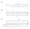
- FIG. 3A shows a step of preparing a resin film
- FIG. 3B shows a step of forming a functional layer on the resin film
- FIG. 3C shows a step of forming a transparent conductive layer on the functional layer.
- the transparent conductive film shown in FIG. 1 the case where the transparent conductive layer is patterned is shown.
- the transparent conductive film shown in FIG. 1 the case where the transparent conductive layer is patterned is shown.
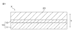
- FIG. 1 is a schematic cross-sectional view of the transparent conductive film X, which is an embodiment of the transparent conductive film of the present invention.
- the transparent conductive film X includes a transparent base material 10 and a transparent conductive layer 20 in this order toward one side in the thickness direction T.
- the transparent conductive film X, the transparent base material 10, and the transparent conductive layer 20 each have a shape that spreads in a direction (plane direction) orthogonal to the thickness direction T.
- the transmissive conductive film X is an element provided in a touch sensor, a light control element, a photoelectric conversion element, a heat ray control member, an antenna member, an electromagnetic wave shield member, a heater member, a lighting device, an image display device, and the like.
- the transparent base material 10 includes a resin film 11 and a functional layer 12 in this order toward one side in the thickness direction T.
- the resin film 11 is a transparent resin film having flexibility.
- the material of the resin film 11 include polyester resin, polyolefin resin, acrylic resin, polycarbonate resin, polyether sulfone resin, polyarylate resin, melamine resin, polyamide resin, polyimide resin, cellulose resin, and polystyrene resin.
- the polyester resin include polyethylene terephthalate (PET), polybutylene terephthalate, and polyethylene naphthalate.
- PET polyethylene terephthalate
- Polyolefin resins include, for example, polyethylene, polypropylene, and cycloolefin polymers (COPs).
- the acrylic resin include polymethacrylate.
- As the material of the resin film 11 at least one selected from the group consisting of polyester resin and polyolefin resin is preferably used from the viewpoint of transparency and strength, and more preferably selected from the group consisting of COP and PET. At least one is used.
- the surface of the resin film 11 on the functional layer 12 side may be surface-modified.
- Examples of the surface modification treatment include corona treatment, plasma treatment, ozone treatment, primer treatment, glow treatment, and coupling agent treatment.
- the thickness of the resin film 11 is preferably 5 ⁇ m or more, more preferably 10 ⁇ m or more, and further preferably 15 ⁇ m or more. Such a configuration is suitable for ensuring the strength of the transparent conductive film X.
- the thickness of the resin film 11 is preferably 100 ⁇ m or less, more preferably 80 ⁇ m or less, and further preferably 60 ⁇ m or less. Such a configuration is suitable for ensuring the flexibility of the transparent conductive film X and realizing good handleability.
- the total light transmittance (JIS K 7375-2008) of the resin film 11 is preferably 60% or more, more preferably 80% or more, still more preferably 85% or more. Such a configuration is obtained when the transparent conductive film X is provided in a touch sensor, a dimming element, a photoelectric conversion element, a heat ray control member, an antenna member, an electromagnetic wave shield member, a heater member, a lighting device, an image display device, or the like. It is suitable for ensuring the transparency required for the transparent conductive film X.
- the total light transmittance of the resin film 11 is, for example, 100% or less.
- the functional layer 12 is located on one surface of the resin film 11 in the thickness direction T. Further, in the present embodiment, the functional layer 12 is a hard coat layer for preventing scratches from being formed on the exposed surface (upper surface in FIG. 1) of the transparent conductive layer 20.
- the hard coat layer is a cured product of a curable resin composition.
- the resin contained in the curable resin composition include polyester resin, acrylic resin, urethane resin, amide resin, silicone resin, epoxy resin, and melamine resin.
- the curable resin composition include an ultraviolet curable resin composition and a thermosetting resin composition.
- an ultraviolet curable resin composition is preferably used from the viewpoint of helping to improve the production efficiency of the transparent conductive film X because it can be cured without heating at a high temperature.
- Specific examples of the ultraviolet curable resin composition include the composition for forming a hard coat layer described in JP-A-2016-179686.
- the curable resin composition may contain fine particles.
- the thickness of the functional layer 12 as the hard coat layer is preferably 0.1 ⁇ m or more, more preferably 0.3 ⁇ m or more, and further preferably 0.5 ⁇ m or more. Such a configuration is suitable for exhibiting sufficient scratch resistance in the transparent conductive layer 20.
- the thickness of the functional layer 12 as the hard coat layer is preferably 10 ⁇ m or less, more preferably 5 ⁇ m or less, and further preferably 3 ⁇ m or less from the viewpoint of ensuring the transparency of the functional layer 12.
- the surface of the functional layer 12 on the transparent conductive layer 20 side may be surface-modified.
- Examples of the surface modification treatment include corona treatment, plasma treatment, ozone treatment, primer treatment, glow treatment, and coupling agent treatment.
- the thickness of the transparent base material 10 is preferably 5 ⁇ m or more, more preferably 10 ⁇ m or more, and further preferably 15 ⁇ m or more. Such a configuration is suitable for ensuring the strength of the transparent conductive film X.
- the thickness of the transparent base material 10 is preferably 100 ⁇ m or less, more preferably 80 ⁇ m or less, and further preferably 60 ⁇ m or less. Such a configuration is suitable for ensuring the flexibility of the transparent conductive film X and realizing good handleability.
- the total light transmittance (JIS K 7375-2008) of the transparent base material 10 is preferably 60% or more, more preferably 80% or more, still more preferably 85% or more. Such a configuration is obtained when the transparent conductive film X is provided in a touch sensor, a dimming element, a photoelectric conversion element, a heat ray control member, an antenna member, an electromagnetic wave shield member, a heater member, a lighting device, an image display device, or the like. It is suitable for ensuring the transparency required for the transparent conductive film X.
- the total light transmittance of the transparent base material 10 is, for example, 100% or less.
- An anti-blocking layer may be provided on the surface of the transparent base material 10 opposite to the transparent conductive layer 20. Such a configuration is preferable from the viewpoint of preventing the transparent base materials 10 from sticking to each other (blocking) when the transparent base material 10 takes the form of a roll.
- the anti-blocking layer can be formed from, for example, a curable resin composition containing fine particles.
- the transparent conductive layer 20 is located on one surface of the transparent base material 10 in the thickness direction T.
- the transparent conductive layer 20 is an amorphous film having both light transmittance and conductivity.
- the amorphous transparent conductive layer 20 is converted into a crystalline transparent conductive layer (transparent conductive layer 20'described later) by heating, and the resistance is lowered.
- the transparent conductive layer 20 is a layer formed of a transparent conductive material.
- the transparent conductive material contains, for example, a conductive oxide as a main component.
- the conductive oxide for example, at least one kind of metal selected from the group consisting of In, Sn, Zn, Ga, Sb, Ti, Si, Zr, Mg, Al, Au, Ag, Cu, Pd and W.
- a metal oxide containing a semi-metal can be mentioned.
- the conductive oxide include an indium-containing conductive oxide and an antimony-containing conductive oxide.
- the indium-containing conductive oxide include indium tin oxide composite oxide (ITO), indium zinc composite oxide (IZO), indium gallium composite oxide (IGO), and indium gallium zinc composite oxide (IGZO). Be done.
- the antimony-containing conductive oxide include antimony tin composite oxide (ATO).
- an indium-containing conductive oxide is preferably used as the conductive oxide, and ITO is more preferably used.
- the ITO may contain a metal or a semimetal other than In and Sn in an amount less than the respective contents of In and Sn.
- the ratio of the tin oxide content to the total content of indium (In 2 O 3 ) and tin oxide (SnO 2) in the ITO is preferably 1% by mass or more. It is more preferably 3% by mass or more, further preferably 5% by mass or more, and particularly preferably 7% by mass or more.
- the ratio of the number of tin atoms to the number of indium atoms in ITO is preferably 0.01 or more, more preferably 0.03 or more, still more preferably 0.05 or more, and particularly preferably 0.05 or more. It is 07 or more.
- the ratio of the tin oxide content to the total content of indium oxide (In 2 O 3 ) and tin oxide (SnO 2 ) in ITO is preferably 15% by mass or less, more preferably 13% by mass or less, still more preferably. Is 12% by mass or less.
- the ratio of the number of tin atoms to the number of indium atoms in ITO is preferably 0.16 or less, more preferably 0.14 or less, and further preferably 0.13 or less.
- the ratio of the number of tin atoms to the number of indium atoms in ITO can be obtained, for example, by specifying the abundance ratio of indium atoms and tin atoms in the object to be measured by X-ray Photoelectron Spectroscopy.
- the above-mentioned content ratio of tin oxide in ITO is obtained from, for example, the abundance ratio of the indium atom and the tin atom thus specified.
- the above-mentioned content ratio of tin oxide in ITO may be judged from the tin oxide (SnO 2) content ratio of the ITO target used at the time of sputtering film formation.
- the tin oxide content ratio in the transparent conductive layer 20 may be non-uniform in the thickness direction T.
- the transparent base material 10 comprises a first region 21 having a relatively high tin oxide content and a second region 22 having a relatively low tin oxide content. It may be included in this order from the side.
- the boundary between the first region 21 and the second region 22 is drawn by a virtual line. When the composition of the first region 21 and the composition of the second region 22 are not significantly different, the boundary between the first region 21 and the second region 22 may not be clearly discriminated.
- the tin oxide content in the first region 21 is preferably 5% by mass or more, more preferably 7% by mass or more, and further preferably 9% by mass or more.
- the tin oxide content in the first region 21 is preferably 15% by mass or less, more preferably 13% by mass or less, still more preferably 11% by mass or less.
- the tin oxide content in the second region 22 is preferably 0.5% by mass or more, more preferably 1% by mass or more, and further preferably 2% by mass or more.
- the tin oxide content in the second region 22 is preferably 8% by mass or less, more preferably 6% by mass or less, and further preferably 4% by mass or less.
- the ratio of the thickness of the first region 21 to the thickness of the transparent conductive layer 20 is preferably 50% or more, more preferably 60% or more, still more preferably 70% or more.
- the ratio of the thickness of the second region 22 to the thickness of the transparent conductive layer 20 is preferably 50% or less, more preferably 40% or less, still more preferably 30% or less.
- the transparent conductive layer 20 contains krypton (Kr) as a rare gas atom.
- the noble gas atom in the transparent conductive layer 20 is derived from the noble gas atom used as the sputtering gas in the sputtering method described later.
- the transparent conductive layer 20 is a film (sputtered film) formed by a sputtering method.
- the transparent conductive layer 20 which is a Kr-containing sputtering film is more suitable for realizing a higher crystallization rate by heating than the amorphous transparent conductive layer which is an Ar-containing sputtering film. That is, the configuration in which the transparent conductive layer 20 contains Kr is suitable for achieving a high crystallization rate in the transparent conductive layer 20. Further, the transparent conductive layer 20 which is a Kr-containing sputter film is more suitable than the amorphous transparent conductive layer which is an Ar-containing sputter film because it realizes better crystal growth by heating and forms large crystal grains.
- Suitable for obtaining a transparent conductive layer 20'with low resistance (the larger the crystal grains in the transparent conductive layer 20', the lower the resistance of the transparent conductive layer 20').
- the presence or absence of Kr in the transparent conductive layer 20 and the transparent conductive layer 20' is identified, for example, by fluorescent X-ray analysis described later with respect to Examples.
- the Kr content ratio in the transparent conductive layer 20 is preferably 0.0001 atomic% or more in the entire area in the thickness direction T.
- the transparent conductive layer 20 may include a region in which the noble gas atom content ratio is less than 0.0001 atomic% in at least a part of the thickness direction T (that is, in a part of the thickness direction T, the thickness direction).
- the abundance ratio of noble gas atoms in the cross section in the plane direction orthogonal to T may be less than 0.0001 atomic%).
- the content ratio of Kr in the transparent conductive layer 20 is preferably 1 atomic% or less, more preferably 0.5 atomic% or less, still more preferably 0.3 atomic% or less, particularly preferably 0.3 atomic% or less in the entire area in the thickness direction T.
- the content ratio of Kr in the transparent conductive layer 20 may be non-uniform in the thickness direction T.
- the Kr content may gradually increase or decrease as the distance from the transparent base material 10 increases.
- a partial region in which the Kr content gradually increases as the distance from the transparent base material 10 increases is located on the transparent base material 10
- a partial region in which the Kr content gradually decreases as the distance from the transparent base material 10 increases is located on the transparent base material 10
- the thickness of the transparent conductive layer 20 is, for example, 10 nm or more, preferably 20 nm or more, and more preferably 25 nm or more. Such a configuration is preferable from the viewpoint of reducing the resistance of the transparent conductive layer 20'obtained by crystallizing the transparent conductive layer 20.
- the thickness of the transparent conductive layer 20 is, for example, 1000 nm or less, preferably less than 300 nm, more preferably 250 nm or less, further preferably 200 nm or less, still more preferably 160 nm or less, particularly preferably less than 150 nm, and most preferably. It is 148 nm or less. Such a configuration is suitable for suppressing warpage in the transparent conductive film X provided with the transparent conductive layer 20'obtained by crystallizing the transparent conductive layer 20.
- the specific resistance of the transparent conductive layer 20 is 5.5 ⁇ 10 -4 ⁇ ⁇ cm or more, preferably 5.8 ⁇ 10 -4 ⁇ ⁇ cm or more, and more preferably 6.0 ⁇ 10 -4 ⁇ ⁇ cm.
- the above is more preferably 6.2 ⁇ 10 -4 ⁇ ⁇ cm or more, and particularly preferably 6.4 ⁇ 10 -4 ⁇ ⁇ cm or more.
- the specific resistance of the transparent conductive layer 20 is preferably 10 ⁇ 10 -4 ⁇ ⁇ cm or less, more preferably 8 ⁇ 10 -4 ⁇ ⁇ cm or less, still more preferably 7.5 ⁇ 10 -4 ⁇ ⁇ cm or less, particularly. It is preferably 7.3 ⁇ 10 -4 ⁇ ⁇ cm or less.
- Amorphous transparent conductive films having a specific resistance of less than 5.5 ⁇ 10 -4 ⁇ ⁇ cm, which is too low, include a significant number of locally crystallized portions, and such transparent conductive films. In the process of crystallization by heating, the portion prevents the formation of large crystal grains (the larger the crystal grains in the transparent conductive film, the lower the resistivity of the film). On the other hand, with an amorphous transparent conductive film having a specific resistance exceeding 10 ⁇ 10 -4 ⁇ ⁇ cm and being too high, a sufficiently low resistance cannot be realized even if the resistance is reduced by crystallization.
- the specific resistance is calculated by multiplying the surface resistance by the thickness.
- the resistivity can be controlled by, for example, adjusting various conditions when the transparent conductive layer 20 is sputter-deposited.
- the conditions include, for example, the temperature of the base (transparent base material 10 in this embodiment) on which the transparent conductive layer 20 is formed, the amount of oxygen introduced into the film forming chamber, the air pressure in the film forming chamber, and on the target. Horizontal magnetic field strength can be mentioned.
- the specific resistance of the transparent conductive layer 20 after heat treatment at 130 ° C. for 60 minutes is, for example, 2.5 ⁇ 10 -4 ⁇ ⁇ cm or less, preferably 2.2 ⁇ 10 -4 ⁇ ⁇ cm or less. It is preferably 2 ⁇ 10 -4 ⁇ ⁇ cm or less, more preferably 1.9 ⁇ 10 -4 ⁇ ⁇ cm or less, and particularly preferably 1.8 ⁇ 10 -4 ⁇ ⁇ cm or less.
- the specific resistance of the transparent conductive layer 20 after heat treatment at 130 ° C. for 60 minutes is preferably 0.1 ⁇ 10 -4 ⁇ ⁇ cm or more, more preferably 0.5 ⁇ 10 -4 ⁇ ⁇ cm or more. More preferably, it is 1.0 ⁇ 10 -4 ⁇ ⁇ cm or more.
- the total light transmittance (JIS K 7375-2008) of the transparent conductive layer 20 is preferably 60% or more, more preferably 80% or more, still more preferably 85% or more. Such a configuration is obtained when the transparent conductive film X is provided in a touch sensor, a dimming element, a photoelectric conversion element, a heat ray control member, an antenna member, an electromagnetic wave shield member, a heater member, a lighting device, an image display device, or the like. It is suitable for ensuring the transparency required for the transparent conductive film X. Further, the total light transmittance of the transparent conductive layer 20 is, for example, 100% or less.
- the transparent conductive layer is amorphous, for example, as follows. First, the transparent conductive layer (in the case of the transparent conductive film X, the transparent conductive layer 20 on the transparent base material 10) is immersed in hydrochloric acid having a concentration of 5% by mass at 20 ° C. for 15 minutes. Next, the transparent conductive layer is washed with water and then dried. Next, on the exposed plane of the transparent conductive layer (in the transparent conductive film X, the surface of the transparent conductive layer 20 opposite to the transparent base material 10), the resistance between the pair of terminals having a separation distance of 15 mm (resistance between terminals). ) Is measured. In this measurement, when the resistance between terminals exceeds 10 k ⁇ , the transparent conductive layer is amorphous.
- the transparent conductive film X is manufactured as follows, for example.
- the resin film 11 is prepared.
- the functional layer 12 is formed on one surface of the resin film 11 in the thickness direction T.
- the transparent base material 10 is produced by forming the functional layer 12 on the resin film 11.
- the above-mentioned functional layer 12 as a hard coat layer can be formed by applying a curable resin composition on a resin film 11 to form a coating film, and then curing the coating film.
- the curable resin composition contains an ultraviolet-forming resin
- the coating film is cured by ultraviolet irradiation.
- the curable resin composition contains a thermosetting resin
- the coating film is cured by heating.
- the exposed surface of the functional layer 12 formed on the resin film 11 is surface-modified, if necessary.
- plasma treatment for example, argon gas is used as the inert gas.
- the discharge power in the plasma processing is, for example, 10 W or more, and for example, 5000 W or less.
- the transparent conductive layer 20 is formed on the transparent base material 10. Specifically, a material is formed on the functional layer 12 of the transparent base material 10 by a sputtering method to form the transparent conductive layer 20.
- the transparent base film 10 is run from the feeding roll to the winding roll provided in the apparatus while running the transparent base film 10. A material is formed on the material 10 to form a transparent conductive layer 20.
- a sputtering film forming apparatus provided with one film forming chamber may be used, or a sputtering film forming apparatus including a plurality of film forming chambers sequentially arranged along a traveling path of the transparent base material 10 may be used.
- An apparatus may be used (when forming the transparent conductive layer 20 including the first region 21 and the second region 22 described above, a sputtering film forming apparatus provided with a plurality of film forming chambers is used).
- a sputtering gas in the sputtering method, specifically, while introducing a sputtering gas (inert gas) into the film forming chamber provided in the sputtering film forming apparatus under vacuum conditions, a negative voltage is applied to the target arranged on the cathode in the film forming chamber. Is applied. As a result, a glow discharge is generated to ionize gas atoms, the gas ions collide with the target surface at high speed, the target material is ejected from the target surface, and the ejected target material is placed on the functional layer 12 of the transparent base material 10. To deposit in.
- a sputtering gas in the film forming chamber provided in the sputtering film forming apparatus under vacuum conditions
- the above-mentioned conductive oxide for forming the transparent conductive layer 20 is used, preferably an indium-containing conductive oxide is used, and more preferably. ITO is used.
- the sputtering gas may contain an inert gas other than Kr.
- the inert gas other than Kr include rare gas atoms other than Kr.
- rare gas atoms other than Kr include Ar and Xe.
- the content ratio is preferably 50% by volume or less, more preferably 40% by volume or less, still more preferably 30 deposition% or less.
- the sputtering method is preferably a reactive sputtering method.
- a reactive gas is introduced into the film forming chamber in addition to the sputtering gas.
- the ratio of the amount of oxygen introduced to the total amount of sputtering gas and oxygen introduced into the film forming chamber in the reactive sputtering method is, for example, 0.01 flow rate% or more, and for example, 15 flow rate% or less.
- the air pressure in the film formation chamber during film formation (sputter film formation) by the sputtering method is, for example, 0.02 Pa or more, and for example, 1 Pa or less.
- the temperature of the transparent substrate 10 during the sputtering film formation is, for example, 100 ° C. or lower. In order to suppress outgas from the transparent base material 10 during sputter film formation, it is preferable to cool the transparent base material 10. Suppression of outgas from the transparent substrate 10 during the sputter film formation helps to obtain the transparent conductive layer 20 having a high crystallization rate. From this point of view, the temperature of the transparent substrate 10 during the sputtering film formation is preferably 20 ° C. or lower, more preferably 10 ° C. or lower, still more preferably 5 ° C. or lower, particularly preferably 0 ° C. or lower, and also. For example, it is ⁇ 50 ° C. or higher, preferably ⁇ 20 ° C. or higher, more preferably ⁇ 10 ° C. or higher, and even more preferably ⁇ 7 ° C. or higher.
- Examples of the power supply for applying a voltage to the target include a DC power supply, an AC power supply, an MF power supply, and an RF power supply.
- a DC power source and an RF power source may be used in combination.
- the absolute value of the discharge voltage during the sputtering film formation is, for example, 50 V or more, and is, for example, 500 V or less, preferably 400 V or less.
- the transparent conductive film X can be manufactured as described above.
- the transparent conductive layer 20 in the transparent conductive film X may be patterned as schematically shown in FIG.
- the transparent conductive layer 20 can be patterned by etching the transparent conductive layer 20 through a predetermined etching mask.
- the patterned transparent conductive layer 20 functions as, for example, a wiring pattern.
- the transparent conductive layer 20 in the transparent conductive film X is converted into a crystalline transparent conductive layer 20'(shown in FIG. 5) by heating.
- the heating means include an infrared heater and an oven (heat medium heating type oven, hot air heating type oven).
- the heating environment may be either a vacuum environment or an atmospheric environment.
- heating is carried out in the presence of oxygen.
- the heating temperature is, for example, 100 ° C. or higher, preferably 120 ° C. or higher, from the viewpoint of ensuring a high crystallization rate.
- the heating temperature is, for example, 200 ° C. or lower, preferably 180 ° C. or lower, more preferably 170 ° C. or lower, still more preferably 165 ° C.
- the heating time is, for example, 1 minute or more, preferably 5 minutes or more.
- the heating time is, for example, 300 minutes or less, preferably 120 minutes or less, and more preferably 90 minutes or less.
- the above-mentioned patterning of the transparent conductive layer 20 may be performed before heating for crystallization, or may be performed after heating for crystallization.
- the specific resistance of the transparent conductive layer 20' is , for example, 2.5 ⁇ 10 -4 ⁇ ⁇ cm or less, preferably 2.2 ⁇ 10 -4 ⁇ ⁇ cm or less, and more preferably 2 ⁇ 10 -4 ⁇ ⁇ cm. Hereinafter, it is more preferably 1.9 ⁇ 10 -4 ⁇ ⁇ cm or less, and particularly preferably 1.8 ⁇ 10 -4 ⁇ ⁇ cm or less.
- the specific resistance of the transparent conductive layer 20' is preferably 0.1 ⁇ 10 -4 ⁇ ⁇ cm or more, more preferably 0.5 ⁇ 10 -4 ⁇ ⁇ cm or more, and further preferably 1.0 ⁇ 10 ⁇ . It is 4 ⁇ ⁇ cm or more.
- the transparent conductive layer 20 contains krypton and has a specific resistance of 5.5 ⁇ 10 -4 ⁇ ⁇ cm or more. Therefore, the transparent conductive film X is suitable for realizing a high crystallization rate and a low resistance after crystallization in the transparent conductive layer 20.
- the functional layer 12 adheres to the transparent base material 10 in order to realize high adhesion of the transparent conductive layer 20 (the transparent conductive layer 20'after the crystallization of the transparent conductive layer 20; the same applies hereinafter). It may be a sex-improving layer.
- the configuration in which the functional layer 12 is an adhesion improving layer is suitable for ensuring the adhesion between the transparent base material 10 and the transparent conductive layer 20.
- the functional layer 12 may be an index-matching layer for adjusting the reflectance of the surface of the transparent base material 10 (one surface in the thickness direction T).
- the configuration in which the functional layer 12 is the refractive index adjusting layer is suitable for making it difficult to visually recognize the pattern shape of the transparent conductive layer 20 when the transparent conductive layer 20 on the transparent base material 10 is patterned.
- the functional layer 12 may be a peeling functional layer for practically peeling the transparent conductive layer 20 from the transparent base material 10.
- the structure in which the functional layer 12 is a peeling functional layer is suitable for peeling the transparent conductive layer 20 from the transparent base material 10 and transferring the transparent conductive layer 20 to another member.
- the functional layer 12 may be a composite layer in which a plurality of layers are connected in the thickness direction T.
- the composite layer preferably includes two or more layers selected from the group consisting of a hard coat layer, an adhesion improving layer, a refractive index adjusting layer, and a peeling functional layer.
- Such a configuration is suitable for complex expression of the above-mentioned functions of each selected layer in the functional layer 12.
- the functional layer 12 includes an adhesion improving layer, a hard coat layer, and a refractive index adjusting layer on the resin film 11 in this order toward one side in the thickness direction T.
- the functional layer 12 includes a peeling functional layer, a hard coat layer, and a refractive index adjusting layer on the resin film 11 in this order toward one side in the thickness direction T.
- the transparent conductive film X is used in a state where it is attached to an article and the transparent conductive layer 20'is patterned as needed.
- the transparent conductive film X is attached to the article, for example, via a fixing functional layer.
- Examples of articles include elements, members, and devices. That is, examples of the article with a transparent conductive film include an element with a transparent conductive film, a member with a transparent conductive film, and a device with a transparent conductive film.
- Examples of the element include a dimming element and a photoelectric conversion element.
- Examples of the dimming element include a current-driven dimming element and an electric field-driven dimming element.
- Examples of the current-driven dimming element include an electrochromic (EC) dimming element.
- Examples of the electric field drive type dimming element include a PDLC (polymer dispersed liquid crystal) dimming element, a PNLC (polymer network liquid crystal) dimming element, and an SPD (suspended particle device) dimming element.
- Examples of the photoelectric conversion element include a solar cell and the like.
- Examples of the solar cell include an organic thin-film solar cell and a dye-sensitized solar cell.
- Examples of the member include an electromagnetic wave shield member, a heat ray control member, a heater member, and an antenna member.
- Examples of the device include a touch sensor device, a lighting device, and an image display device.
- the fixing functional layer examples include an adhesive layer and an adhesive layer.
- the material of the fixing function layer any material having transparency and exhibiting the fixing function can be used without particular limitation.
- the fixing functional layer is preferably formed of a resin.
- the resin include acrylic resin, silicone resin, polyester resin, polyurethane resin, polyamide resin, polyvinyl ether resin, vinyl acetate / vinyl chloride copolymer, modified polyolefin resin, epoxy resin, fluororesin, natural rubber, and synthetic rubber. Be done.
- Acrylic resin is preferable as the resin because it exhibits adhesive properties such as cohesiveness, adhesiveness, and appropriate wettability, is excellent in transparency, and is excellent in weather resistance and heat resistance.
- a corrosion inhibitor may be added to the fixing functional layer (resin forming the fixing functional layer) in order to suppress corrosion of the transparent conductive layer 20'.
- a migration inhibitor (for example, a material disclosed in Japanese Patent Application Laid-Open No. 2015-0222397) may be added to the fixing functional layer (resin forming the fixing functional layer) in order to suppress migration of the transparent conductive layer 20'. ..
- the fixing functional layer (resin forming the fixing functional layer) may be blended with an ultraviolet absorber in order to suppress deterioration of the article when it is used outdoors.
- the ultraviolet absorber include benzophenone compounds, benzotriazole compounds, salicylic acid compounds, oxalic acid anilides compounds, cyanoacrylate compounds, and triazine compounds.
- the transparent conductive film X when the transparent base material 10 of the transparent conductive film X is fixed to the article via the fixing functional layer, the transparent conductive film X includes the transparent conductive layer 20'(the transparent conductive layer 20' after patterning). ) Is exposed.
- the cover layer may be arranged on the exposed surface of the transparent conductive layer 20'.
- the cover layer is a layer that covers the transparent conductive layer 20', and can improve the reliability of the transparent conductive layer 20'and suppress functional deterioration due to damage to the transparent conductive layer 20'.
- Such a cover layer is preferably formed of a dielectric material, more preferably of a composite material of a resin and an inorganic material. Examples of the resin include the above-mentioned resins for the fixing functional layer.
- the inorganic material examples include inorganic oxides and fluorides.
- the inorganic oxide examples include silicon oxide, titanium oxide, niobium oxide, aluminum oxide, zirconium dioxide, and calcium oxide.
- the fluoride examples include magnesium fluoride.
- the cover layer may contain the above-mentioned corrosion inhibitor, migration inhibitor, and ultraviolet absorber.
- the present invention will be specifically described below with reference to examples.
- the present invention is not limited to the examples.
- the specific numerical values such as the compounding amount (content), the physical property value, the parameter, etc. described below are the compounding amounts corresponding to them described in the above-mentioned "mode for carrying out the invention”. It can be replaced with an upper limit (numerical value defined as “less than or equal to” or “less than”) or a lower limit (numerical value defined as "greater than or equal to” or “greater than or equal to”) such as content), physical property value, and parameter.
- the first curable composition is applied to one surface of a long cycloolefin polymer (COP) film (trade name "Zeonoa ZF16", thickness 40 ⁇ m, manufactured by Zeon Corporation) as a transparent substrate.
- COP cycloolefin polymer
- a coating film was formed.
- the first curable composition contains 100 parts by mass of a coating liquid containing polyfunctional urethane acrylate (trade name "UNIDIC RS29-120", manufactured by DIC) and crosslinked acrylic / styrene resin particles (trade name "SSX105”, particle diameter 3 ⁇ m). , Sekisui Jushi Co., Ltd.) Contains 0.07 parts by mass.
- the first coating film was dried, the first coating film was cured by irradiation with ultraviolet rays to form an anti-blocking (AB) layer (thickness 1 ⁇ m).
- the second curable composition was applied to the other surface of the COP film to form a second coating film.
- the second curable composition is a composition prepared in the same manner as the first curable composition except that it does not contain crosslinked acrylic / styrene resin particles (trade name “SSX105”).
- SSX105 crosslinked acrylic / styrene resin particles
- an amorphous transparent conductive layer having a thickness of 40 nm was formed on the HC layer of the transparent substrate by the reactive sputtering method (transparent conductive layer forming step).
- a sputter film forming apparatus (winding type DC magnetron sputtering apparatus) capable of carrying out a film forming process by a roll-to-roll method was used.
- the traveling speed of the transparent substrate in the apparatus was 4.0 m / min.
- the conditions for sputter film formation are as follows.
- a first sintered body of indium oxide and tin oxide (tin oxide concentration was 10% by mass) was used.
- a DC power supply was used as the power supply for applying the voltage to the target, and the output of the DC power supply was 19.1 kW.
- the horizontal magnetic field strength on the target was 90 mT.
- the film formation temperature (the temperature of the transparent base material on which the transparent conductive layer is laminated) was set to ⁇ 5 ° C. Further, after the film forming chamber is evacuated until the ultimate vacuum degree in the film forming chamber of the apparatus reaches 0.9 ⁇ 10 -4 Pa, Kr as a sputtering gas and Kr as a reactive gas are used in the film forming chamber.
- Oxygen was introduced, and the air pressure in the film forming chamber was set to 0.2 Pa.
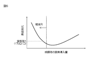
- the ratio of the oxygen introduction amount to the total introduction amount of Kr and oxygen introduced into the film forming chamber is about 2 flow rate%, and the oxygen introduction amount is in the region of the surface resistance-oxygen introduction amount curve as shown in FIG. It was adjusted so that the value of the surface resistance of the formed ITO film in R was 170 ⁇ / ⁇ .
- the surface resistance-oxygen introduction amount curve shown in FIG. 6 depends on the oxygen introduction amount of the surface resistance of the transparent conductive layer when the transparent conductive layer is formed by the reactive sputtering method under the same conditions as above except for the oxygen introduction amount. Gender can be investigated and created in advance.
- the transparent conductive layer (thickness 40 nm) of the transparent conductive film of Example 1 is made of an amorphous ITO containing Kr.
- Example 2 A transparent conductive film of Example 2 was produced in the same manner as the transparent conductive film of Example 1 except for the following in the process of forming the transparent conductive layer.
- the DC power output for sputter film formation was set to 25.1 kW.
- An amorphous transparent conductive layer having a thickness of 50 nm was formed while adjusting the amount of oxygen introduced so that the value of the surface resistance of the formed ITO film was 130 ⁇ / ⁇ .
- the transparent conductive layer (thickness 50 nm) of the transparent conductive film of Example 2 is made of an amorphous ITO containing Kr.
- Example 3 A transparent conductive film of Example 3 was produced in the same manner as the transparent conductive film of Example 1 except for the following in the process of forming the transparent conductive layer.
- the DC power output for sputter film formation was set to 15.8 kW.
- An amorphous transparent conductive layer having a thickness of 32 nm was formed while adjusting the amount of oxygen introduced so that the value of the surface resistance of the formed ITO film was 220 ⁇ / ⁇ .
- the transparent conductive layer (thickness 32 nm) of the transparent conductive film of Example 3 is made of an amorphous ITO containing Kr.
- Example 4 The transparent conductive film of Example 4 was produced in the same manner as the transparent conductive film of Example 1 except for the following in the process of forming the transparent conductive layer. While running the transparent substrate at a traveling speed of 5.4 m / min, the first sputtering film formation in the first deposition film forming chamber of the sputtering film forming apparatus and the second sputtering in the second forming film forming chamber of the same apparatus are provided. The film formation was carried out in sequence. In the first sputtering film formation, a first region (thickness 22.5 nm) of the transparent conductive layer was formed on the transparent substrate. In the second sputter film formation, a second region (thickness 2.5 nm) of the transparent conductive layer was formed on the first region.
- the conditions for the first sputter film formation are as follows.
- a first sintered body of indium oxide and tin oxide (tin oxide concentration was 10% by mass) was used.
- a DC power supply was used as the power supply for applying the voltage to the target, and the output of the DC power supply was 14.9 kW.
- the horizontal magnetic field strength on the target was 90 mT.
- the film formation temperature was ⁇ 5 ° C.
- the first film forming chamber is reactive with Kr as a sputtering gas. Oxygen as a gas was introduced, and the air pressure in the first film forming chamber was set to 0.2 Pa.
- the ratio of the amount of oxygen introduced to the total amount of Kr and oxygen introduced into the first film forming chamber is about 2 flow rate%, and the value of the surface resistance of the formed ITO film is 280 ⁇ / ⁇ . Adjusted to be.
- the conditions for the second sputter film formation are as follows. As a target, a second sintered body of indium oxide and tin oxide (tin oxide concentration was 3% by mass) was used. The output of the DC power supply was set to 2.0 kW. Further, after setting the ultimate vacuum degree in the second film forming chamber to 0.9 ⁇ 10 -4 Pa, Kr as a sputtering gas and oxygen as a reactive gas were introduced into the second film forming chamber, and the second film forming chamber was introduced. 2 The air pressure in the film forming chamber was set to 0.2 Pa. Other conditions in the second sputter film formation are the same as those in the first sputter film formation.
- the transparent conductive layer (thickness 25 nm) of the transparent conductive film of Example 4 has a first region (thickness 22 nm) composed of a Kr-containing amorphous ITO (tin oxide concentration 10% by mass) and a Kr-containing non-transparent layer. It has a second region (thickness 2.5 nm) composed of crystalline ITO (indium tin oxide concentration 3% by mass) in order from the transparent substrate side.
- the ratio of the thickness of the first region to the thickness of the transparent conductive layer is 90%, and the ratio of the thickness of the second region is 10%.
- Comparative Example 1 A transparent conductive film of Comparative Example 1 was produced in the same manner as the transparent conductive film of Example 1 except for the following in the process of forming the transparent conductive layer.
- the traveling speed of the transparent substrate was set to 5.4 m / min.
- the DC power output at the time of sputter film formation was set to 20.8 kW.
- Ar was used as the sputtering gas.
- An amorphous transparent conductive layer having a thickness of 32 nm was formed while adjusting the amount of oxygen introduced so that the value of the surface resistance of the formed ITO film was 220 ⁇ / ⁇ .
- the transparent conductive layer (thickness 32 nm) of the transparent conductive film of Comparative Example 1 is made of Ar-containing amorphous ITO.
- Comparative Example 2 A transparent conductive film of Comparative Example 2 was produced in the same manner as the transparent conductive film of Example 4 except for the following in the process of forming the transparent conductive layer.
- the DC power output is 18.5 kW
- Ar is used as the sputtering gas
- the thickness is adjusted while adjusting the oxygen introduction amount so that the surface resistance value of the formed ITO film is 220 ⁇ / ⁇ .
- a first region of 28.8 nm was formed.
- the DC power supply output is 2.3 kW
- Ar is used as the sputtering gas
- the thickness is adjusted while adjusting the oxygen introduction amount so that the surface resistance value of the formed ITO film is 220 ⁇ / ⁇ .
- a second region of 3.2 nm was formed.
- the transparent conductive layer (thickness 32 nm) of the transparent conductive film of Comparative Example 2 contains a first region (thickness 28.8 nm) composed of an Ar-containing amorphous ITO (tin oxide concentration 10% by mass) and Ar.
- a second region (thickness 3.2 nm) composed of amorphous ITO (indium tin oxide concentration 3% by mass) is provided in this order from the transparent substrate side.
- the ratio of the thickness of the first region to the thickness of the transparent conductive layer is 90%, and the ratio of the thickness of the second region is 10%.
- each transparent conductive layer in Examples 1 to 4 and Comparative Examples 1 to 3 was measured by FE-TEM observation. Specifically, first, a cross-section observation sample of each transparent conductive layer in Examples 1 to 4 and Comparative Examples 1 to 3 was prepared by the FIB microsampling method. In the FIB microsampling method, an FIB device (trade name "FB2200", manufactured by Hitachi) was used, and the acceleration voltage was set to 10 kV. Next, the thickness of the transparent conductive layer in the cross-section observation sample was measured by FE-TEM observation. In the FE-TEM observation, an FE-TEM device (trade name "JEM-2800", manufactured by JEOL) was used, and the acceleration voltage was set to 200 kV.
- FE-TEM observation an FE-TEM device (trade name "JEM-2800", manufactured by JEOL) was used, and the acceleration voltage was set to 200 kV.
- Example 4 and Comparative Example 2 For the thickness of the first region of each transparent conductive layer in Example 4 and Comparative Example 2, a cross-section observation sample was prepared from the intermediate product before forming the second region on the first region, and the sample was prepared. It was measured by FE-TEM observation of. The thickness of the second region of each transparent conductive layer in Example 4 and Comparative Example 2 was obtained by subtracting the thickness of the first region from the total thickness of the transparent conductive layer.
- ⁇ Crystallization rate> The crystallization rate of the transparent conductive layer was examined for each of the transparent conductive films of Examples 1 to 5 and Comparative Examples 1 to 3. Specifically, first, a measurement sample (5 cm ⁇ 5 cm) was cut out from the transparent conductive film. Next, the sample was set on the stage of the measuring device. The measuring device was prepared by replacing the stage of the Hall effect measuring device "HL5500PC” manufactured by Accent Optical Technologies with a stage equipped with a heater (trade name "JHTM-300HC-001A", manufactured by Nippon Thermal Engineering Co., Ltd.). In addition, in this apparatus, after the stage was heated to 130 ° C.
- the surface resistance of the sample was measured from the time when the temperature reached 130 ° C. to 20 minutes every 1 minute (measurement was performed by JIS). (By the four-terminal method based on K 7194 (1994)) Next, for each measured resistance value, the rate of change in resistance value based on the resistance value obtained in the previous measurement (1 minute ago). Then, the measurement time of the reference resistance value for the resistance value at which the resistance value change rate was first 1% or less was defined as the crystallization time (for example, in the sample of the transparent conductive film of Example 3). Since the rate of change in the resistance value after 5 minutes based on the resistance value 4 minutes after reaching 130 ° C.
- the transparent conductive film of the present invention can be used as a feed material for a conductor film for forming a pattern of transparent electrodes in various devices such as liquid crystal displays, touch panels, and optical sensors.
Landscapes
- Chemical & Material Sciences (AREA)
- Engineering & Computer Science (AREA)
- Organic Chemistry (AREA)
- Chemical Kinetics & Catalysis (AREA)
- Materials Engineering (AREA)
- Mechanical Engineering (AREA)
- Metallurgy (AREA)
- Physics & Mathematics (AREA)
- Thermal Sciences (AREA)
- Polymers & Plastics (AREA)
- Medicinal Chemistry (AREA)
- Health & Medical Sciences (AREA)
- Nonlinear Science (AREA)
- General Physics & Mathematics (AREA)
- Manufacturing & Machinery (AREA)
- Mathematical Physics (AREA)
- Crystallography & Structural Chemistry (AREA)
- Optics & Photonics (AREA)
- General Engineering & Computer Science (AREA)
- Theoretical Computer Science (AREA)
- Ceramic Engineering (AREA)
- Human Computer Interaction (AREA)
- Microelectronics & Electronic Packaging (AREA)
- Spectroscopy & Molecular Physics (AREA)
- Dispersion Chemistry (AREA)
- Laminated Bodies (AREA)
- Non-Insulated Conductors (AREA)
- Physical Vapour Deposition (AREA)
- Manufacturing Of Electric Cables (AREA)
- Shielding Devices Or Components To Electric Or Magnetic Fields (AREA)
- Photovoltaic Devices (AREA)
- Liquid Crystal (AREA)
Abstract
本発明の透明導電性フィルム(X)は、透明基材(10)と、非晶質の透明導電層(20)とを、厚さ方向(T)にこの順で備える。透明導電層(20)は、クリプトンを含有し、5.5×10⁻⁴Ω・cm以上の比抵抗を有する。
Description
本発明は、透明導電性フィルムに関する。
従来、透明な基材フィルムと透明な導電層(透明導電層)とを厚さ方向に順に備える透明導電性フィルムが知られている。透明導電層は、例えば、液晶ディスプレイ、タッチパネル、および光センサなどの各種デバイスにおける透明電極をパターン形成するための導体膜として用いられる。透明導電層の形成過程では、例えば、まず、スパッタリング法によって基材フィルム上に透明導電材料の非晶質膜が形成される(成膜工程)。次に、基材フィルム上の非晶質の透明導電層が加熱によって結晶化される(結晶化工程)。成膜工程におけるスパッタリング法では、従来、ターゲット(成膜材料供給材)に衝突してターゲット表面の原子を弾き出すためのスパッタリングガスとして、アルゴンなどの不活性ガスが用いられる。このような透明導電性フィルムに関する技術については、例えば下記の特許文献1に記載されている。
透明導電性フィルムの製造効率の観点からは、結晶化工程での加熱による透明導電層の結晶化の速度は、高い方が好ましい。また、透明導電層には、低抵抗であることが要求される。特に透明電極用途の透明導電層には、その要求が強い。
本発明は、透明導電層において、加熱による高い結晶化速度を実現するとともに、結晶化後の低抵抗を実現するのに適した、透明導電性フィルムを提供する。
本発明[1]は、透明基材と非晶質の透明導電層とを厚さ方向にこの順で備え、前記透明導電層が、クリプトンを含有し、5.5×10⁻⁴Ω・cm以上の比抵抗を有する、透明導電性フィルムを含む。
本発明[2]は、前記透明導電層がインジウム含有導電性酸化物を含む、上記[1]に記載の透明導電性フィルムを含む。
本発明[3]は、前記比抵抗が10×10-4Ω・cm以下である、上記[1]または[2]に記載の透明導電性フィルムを含む。
本発明[4]は、前記透明導電層が20nm以上の厚さを有する、上記[1]から[3]のいずれか一つに記載の透明導電性フィルムを含む。
本発明[5]は、前記透明導電層が、130℃で60分間の加熱処理後に2.2×10⁻⁴Ω・cm未満の比抵抗を有する、上記[1]から[4]のいずれか一つに記載の透明導電性フィルムを含む。
本発明の透明導電性フィルムは、透明導電層が、クリプトンを含有し且つ5.5×10⁻⁴Ω・cm以上の比抵抗を有することから、透明導電層において高い結晶化速度を実現するとともに、結晶化後の低抵抗を実現するのに適する。
図1は、本発明の透明導電性フィルムの一実施形態である透明導電性フィルムXの断面模式図である。透明導電性フィルムXは、透明基材10と、透明導電層20とを、厚さ方向Tの一方側に向かってこの順で備える。透明導電性フィルムX、透明基材10、および透明導電層20は、それぞれ、厚さ方向Tに直交する方向(面方向)に広がる形状を有する。透過性導電フィルムXは、タッチセンサ、調光素子、光電変換素子、熱線制御部材、アンテナ部材、電磁波シールド部材、ヒーター部材、照明装置、および画像表示装置などに備えられる一要素である。
透明基材10は、樹脂フィルム11と、機能層12とを、厚さ方向Tの一方側に向かってこの順で備える。
樹脂フィルム11は、可撓性を有する透明な樹脂フィルムである。樹脂フィルム11の材料としては、例えば、ポリエステル樹脂、ポリオレフィン樹脂、アクリル樹脂、ポリカーボネート樹脂、ポリエーテルスルフォン樹脂、ポリアリレート樹脂、メラミン樹脂、ポリアミド樹脂、ポリイミド樹脂、セルロース樹脂、およびポリスチレン樹脂が挙げられる。ポリエステル樹脂としては、例えば、ポリエチレンテレフタレート(PET)、ポリブチレンテレフタレート、およびポリエチレンナフタレートが挙げられる。ポリオレフィン樹脂としては、例えば、ポリエチレン、ポリプロピレン、およびシクロオレフィンポリマー(COP)が挙げられる。アクリル樹脂としては、例えばポリメタクリレートが挙げられる。樹脂フィルム11の材料としては、透明性および強度の観点から、好ましくは、ポリエステル樹脂およびポリオレフィン樹脂からなる群より選択される少なくとも一つが用いられ、より好ましくは、COPおよびPETからなる群より選択される少なくとも一つが用いられる。
樹脂フィルム11における機能層12側表面は、表面改質処理されていてもよい。表面改質処理としては、例えば、コロナ処理、プラズマ処理、オゾン処理、プライマー処理、グロー処理、およびカップリング剤処理が挙げられる。
樹脂フィルム11の厚さは、好ましくは5μm以上、より好ましくは10μm以上、更に好ましくは15μm以上である。このような構成は、透明導電性フィルムXの強度を確保するのに適する。樹脂フィルム11の厚さは、好ましくは100μm以下、より好ましくは80μm以下、更に好ましくは60μm以下である。このような構成は、透明導電性フィルムXの柔軟性を確保して良好な取扱い性を実現するのに適する。
樹脂フィルム11の全光線透過率(JIS K 7375-2008)は、好ましくは60%以上、より好ましくは80%以上、更に好ましくは85%以上である。このような構成は、タッチセンサ、調光素子、光電変換素子、熱線制御部材、アンテナ部材、電磁波シールド部材、ヒーター部材、照明装置、および画像表示装置などに透明導電性フィルムXが備えられる場合に当該透明導電性フィルムXに求められる透明性を確保するのに適する。樹脂フィルム11の全光線透過率は、例えば100%以下である。
機能層12は、本実施形態では、樹脂フィルム11における厚さ方向Tの一方面上に位置する。また、本実施形態では、機能層12は、透明導電層20の露出表面(図1では上面)に擦り傷が形成されにくくするためのハードコート層である。
ハードコート層は、硬化性樹脂組成物の硬化物である。硬化性樹脂組成物が含有する樹脂としては、例えば、ポリエステル樹脂、アクリル樹脂、ウレタン樹脂、アミド樹脂、シリコーン樹脂、エポキシ樹脂、およびメラミン樹脂が挙げられる。また、硬化性樹脂組成物としては、例えば、紫外線硬化型の樹脂組成物、および、熱硬化型の樹脂組成物が挙げられる。高温加熱せずに硬化可能であるために透明導電性フィルムXの製造効率向上に役立つ観点から、硬化性樹脂組成物としては、好ましくは、紫外線硬化型の樹脂組成物が用いられる。紫外線硬化型の樹脂組成物の具体例としては、特開2016-179686号公報に記載のハードコート層形成用組成物が挙げられる。また、硬化性樹脂組成物は微粒子を含有してもよい。
ハードコート層としての機能層12の厚さは、好ましくは0.1μm以上、より好ましくは0.3μm以上、更に好ましくは0.5μm以上である。このような構成は、透明導電層20において充分な耐擦過性を発現させるのに適する。ハードコート層としての機能層12の厚さは、機能層12の透明性を確保する観点からは、好ましくは10μm以下、より好ましくは5μm以下、更に好ましくは3μm以下である。
機能層12における透明導電層20側表面は、表面改質処理されていてもよい。表面改質処理としては、例えば、コロナ処理、プラズマ処理、オゾン処理、プライマー処理、グロー処理、およびカップリング剤処理が挙げられる。
透明基材10の厚さは、好ましくは5μm以上、より好ましくは10μm以上、更に好ましくは15μm以上である。このような構成は、透明導電性フィルムXの強度を確保するのに適する。透明基材10の厚さは、好ましくは100μm以下、より好ましくは80μm以下、更に好ましくは60μm以下である。このような構成は、透明導電性フィルムXの柔軟性を確保して良好な取扱い性を実現するのに適する。
透明基材10の全光線透過率(JIS K 7375-2008)は、好ましくは60%以上、より好ましくは80%以上、更に好ましくは85%以上である。このような構成は、タッチセンサ、調光素子、光電変換素子、熱線制御部材、アンテナ部材、電磁波シールド部材、ヒーター部材、照明装置、および画像表示装置などに透明導電性フィルムXが備えられる場合に当該透明導電性フィルムXに求められる透明性を確保するのに適する。透明基材10の全光線透過率は、例えば100%以下である。
透明基材10における、透明導電層20とは反対側の表面には、アンチブロッキング層が設けられてもよい。このような構成は、透明基材10がロールの形態をとる場合に透明基材10どうしが貼り付いてしまうこと(ブロッキング)を防止する観点から好ましい。アンチブロッキング層は、例えば、微粒子含有の硬化性樹脂組成物から形成できる。
透明導電層20は、本実施形態では、透明基材10における厚さ方向Tの一方面上に位置する。透明導電層20は、光透過性と導電性とを兼ね備えた非晶質膜である。非晶質の透明導電層20は、加熱によって結晶質の透明導電層(後記の透明導電層20')に転化されて、抵抗が下がる。
透明導電層20は、透明導電材料から形成された層である。透明導電材料は、主成分として、例えば導電性酸化物を含有する。
導電性酸化物としては、例えば、In、Sn、Zn、Ga、Sb、Ti、Si、Zr、Mg、Al、Au、Ag、Cu、Pd、Wからなる群より選択される少なくとも一種類の金属または半金属を含有する金属酸化物が挙げられる。具体的には、導電性酸化物としては、インジウム含有導電性酸化物およびアンチモン含有導電性酸化物が挙げられる。インジウム含有導電性酸化物としては、例えば、インジウムスズ複合酸化物(ITO)、インジウム亜鉛複合酸化物(IZO)、インジウムガリウム複合酸化物(IGO)、およびインジウムガリウム亜鉛複合酸化物(IGZO)が挙げられる。アンチモン含有導電性酸化物としては、例えばアンチモンスズ複合酸化物(ATO)が挙げられる。高い透明性と良好な導電性とを実現する観点からは、導電性酸化物としては、好ましくはインジウム含有導電性酸化物が用いられ、より好ましくはITOが用いられる。このITOは、InおよびSn以外の金属または半金属を、InおよびSnのそれぞれの含有量より少ない量で含有してもよい。
導電性酸化物としてITOが用いられる場合、当該ITOにおける酸化インジウム(In2O3)および酸化スズ(SnO2)の合計含有量に対する酸化スズの含有量の割合は、好ましくは1質量%以上、より好ましくは3質量%以上、更に好ましくは5質量%以上、特に好ましくは7質量%以上である。ITOにおけるインジウム原子数に対するスズ原子数の比率(スズ原子数/インジウム原子数)は、好ましくは0.01以上、より好ましくは0.03以上、更に好ましくは0.05以上、特に好ましくは0.07以上である。これら構成は、透明導電層20の耐久性を確保するのに適する。また、ITOにおける酸化インジウム(In2O3)および酸化スズ(SnO2)の合計含有量に対する酸化スズの含有量の割合は、好ましくは15質量%以下、より好ましくは13質量%以下、更に好ましくは12質量%以下である。ITOにおけるインジウム原子数に対するスズ原子数の比率(スズ原子数/インジウム原子数)は、好ましくは0.16以下、より好ましくは0.14以下、更に好ましくは0.13以下である。これら構成は、加熱により結晶化しやすい透明導電層20を得るのに適する。ITOにおけるインジウム原子数に対するスズ原子数の比率は、例えば、測定対象物について、X線光電子分光法(X-ray Photoelectron Spectroscopy)によってインジウム原子とスズ原子の存在比率を特定することにより、求められる。ITOにおける酸化スズの上記含有割合は、例えば、そのようにして特定されたインジウム原子とスズ原子の存在比率から、求められる。ITOにおける酸化スズの上記含有割合は、スパッタ成膜時に用いるITOターゲットの酸化スズ(SnO2)含有割合から判断してもよい。
透明導電層20における酸化スズ含有割合は、厚さ方向Tにおいて非一様であってもよい。例えば、透明導電層20は、図2に示すように、酸化スズ含有割合が相対的に高い第1領域21と、酸化スズ含有割合が相対的に低い第2領域22とを、透明基材10側からこの順で含んでもよい。図2では、第1領域21と第2領域22との境界が仮想線によって描出されている。第1領域21の組成と第2領域22の組成とが有意には異ならない場合、第1領域21と第2領域22との境界は、明確には判別できない場合もある。
第1領域21における酸化スズ含有割合は、好ましくは5質量%以上、より好ましくは7質量%以上、更に好ましくは9質量%以上である。第1領域21における酸化スズ含有割合は、好ましくは15質量%以下、より好ましくは13質量%以下、更に好ましくは11質量%以下である。第2領域22における酸化スズ含有割合は、好ましくは0.5質量%以上、より好ましくは1質量%以上、更に好ましくは2質量%以上である。第2領域22における酸化スズ含有割合は、好ましくは8質量%以下、より好ましくは6質量%以下、更に好ましくは4質量%以下である。透明導電層20の厚さにおける第1領域21の厚さの割合は、好ましくは50%以上、より好ましくは60%以上、更に好ましくは70%以上である。また、透明導電層20の厚さにおける第2領域22の厚さの割合は、好ましくは50%以下、より好ましくは40%以下、更に好ましくは30%以下である。これら構成は、透明導電層20を結晶化させて得られる透明導電層20'の低抵抗化の観点から好ましい。
透明導電層20は、希ガス原子としてクリプトン(Kr)を含有する。透明導電層20における希ガス原子は、本実施形態では、後述のスパッタリング法においてスパッタリングガスとして用いられる希ガス原子に由来する。本実施形態において、透明導電層20は、スパッタリング法で形成された膜(スパッタ膜)である。
Kr含有スパッタ膜である透明導電層20は、Ar含有スパッタ膜である非晶質透明導電層よりも、加熱による高い結晶化速度を実現するのに適する。すなわち、透明導電層20がKrを含有する構成は、透明導電層20において高い結晶化速度を実現するのに適する。また、Kr含有スパッタ膜である透明導電層20は、Ar含有スパッタ膜である非晶質透明導電層よりも、加熱によって良好な結晶成長を実現して大きな結晶粒を形成するのに適し、従って、低抵抗の透明導電層20'を得るのに適する(透明導電層20'内の結晶粒が大きいほど、透明導電層20'の抵抗は低い)。透明導電層20および透明導電層20'におけるKrの存否は、例えば、実施例に関して後述する蛍光X線分析によって同定される。
透明導電層20におけるKr含有割合は、好ましくは、厚さ方向Tの全域において0.0001原子%以上である。透明導電層20は、希ガス原子含有割合が0.0001原子%未満である領域を、厚さ方向Tの少なくとも一部に含んでもよい(即ち、厚さ方向Tの一部では、厚さ方向Tと直交する面方向の断面における希ガス原子の存在割合が0.0001原子%未満であってもよい)。また、透明導電層20におけるKrの含有割合は、厚さ方向Tの全域において、好ましくは1原子%以下、より好ましくは0.5原子%以下、更に好ましくは0.3原子%以下、特に好ましくは0.2原子%以下である。このような構成は、非晶質の透明導電層20を加熱により結晶化させて結晶質の透明導電層20'を形成する時に、良好な結晶成長を実現して大きな結晶粒を形成するのに適し、従って、低抵抗の透明導電層20'を得るのに適する。
透明導電層20におけるKrの含有割合は、厚さ方向Tにおいて非一様であってもよい。例えば、厚さ方向Tにおいて、透明基材10から遠ざかるほどKr含有割合が漸増または漸減してもよい。或いは、厚さ方向Tにおいて、透明基材10から遠ざかるほどKr含有割合が漸増する部分領域が透明基材10側に位置し、且つ、透明基材10から遠ざかるほどKr含有割合が漸減する部分領域が透明基材10とは反対側に位置してもよい。或いは、厚さ方向Tにおいて、透明基材10から遠ざかるほどKr含有割合が漸減する部分領域が透明基材10側に位置し、且つ、透明基材10から遠ざかるほどKr含有割合が漸増する部分領域が透明基材10とは反対側に位置してもよい。
透明導電層20の厚さは、例えば10nm以上であり、好ましくは20nm以上、より好ましくは25nm以上である。このような構成は、透明導電層20を結晶化させて得られる透明導電層20'の低抵抗化の観点から好ましい。また、透明導電層20の厚さは、例えば1000nm以下であり、好ましくは300nm未満、より好ましくは250nm以下、さらに好ましくは200nm以下、ことさらに好ましくは160nm以下、特に好ましくは150nm未満、最も好ましくは148nm以下である。このような構成は、透明導電層20を結晶化させて得られる透明導電層20'を備える透明導電性フィルムXにおいて、反りを抑制するのに適する。
透明導電層20の比抵抗は、5.5×10⁻⁴Ω・cm以上であり、好ましくは5.8×10⁻⁴Ω・cm以上、より好ましくは6.0×10⁻⁴Ω・cm以上、更に好ましくは6.2×10⁻⁴Ω・cm以上、特に好ましくは6.4×10⁻⁴Ω・cm以上である。透明導電層20の比抵抗は、好ましくは10×10-4Ω・cm以下、より好ましくは8×10⁻⁴Ω・cm以下、更に好ましくは7.5×10⁻⁴Ω・cm以下、特に好ましくは7.3×10⁻⁴Ω・cm以下である。比抵抗に関するこれら構成は、透明導電層20を結晶化させて得られる透明導電層20'の低抵抗化の観点から好ましい。具体的には、次のとおりである。
比抵抗が5.5×10⁻⁴Ω・cmを下回って低すぎる非晶質透明導電膜には、局所的に結晶化が進行している部分が有意数含まれ、そのような透明導電膜の加熱による結晶化の過程では、前記部分が、大きな結晶粒の形成を阻む(透明導電膜内の結晶粒が大きいほど同膜の抵抗は低い)。一方、比抵抗が10×10-4Ω・cmを上回って高すぎる非晶質透明導電膜では、結晶化により抵抗が低下しても、充分な低抵抗を実現できない。
比抵抗は、表面抵抗に厚さを乗じて求められる。また、比抵抗は、例えば、透明導電層20をスパッタ成膜する時の各種条件の調整により、制御できる。当該条件としては、例えば、透明導電層20が成膜される下地(本実施形態では透明基材10)の温度、成膜室内への酸素導入量、成膜室内の気圧、および、ターゲット上の水平磁場強度が挙げられる。
透明導電層20の、130℃で60分間の加熱処理後の比抵抗は、例えば2.5×10⁻⁴Ω・cm以下であり、好ましくは2.2×10⁻⁴Ω・cm以下、より好ましくは2×10⁻⁴Ω・cm以下、更に好ましくは1.9×10⁻⁴Ω・cm以下、特に好ましくは1.8×10⁻⁴Ω・cm以下である。また、透明導電層20の、130℃で60分間の加熱処理後の比抵抗は、好ましくは0.1×10⁻⁴Ω・cm以上、より好ましくは0.5×10⁻⁴Ω・cm以上、更に好ましくは1.0×10⁻⁴Ω・cm以上である。これら構成は、タッチセンサ、調光素子、光電変換素子、熱線制御部材、アンテナ部材、電磁波シールド部材、ヒーター部材、照明装置、および画像表示装置などにおいて透明導電層に求められる低抵抗性を確保するのに適する。
透明導電層20の全光線透過率(JIS K 7375-2008)は、好ましくは60%以上、より好ましくは80%以上、更に好ましくは85%以上である。このような構成は、タッチセンサ、調光素子、光電変換素子、熱線制御部材、アンテナ部材、電磁波シールド部材、ヒーター部材、照明装置、および画像表示装置などに透明導電性フィルムXが備えられる場合に当該透明導電性フィルムXに求められる透明性を確保するのに適する。また、透明導電層20の全光線透過率は、例えば100%以下である。
透明導電層が非晶質であることは、例えば、次のようにして判断できる。まず、透明導電層(透明導電性フィルムXでは、透明基材10上の透明導電層20)を、濃度5質量%の塩酸に、20℃で15分間、浸漬する。次に、透明導電層を、水洗した後、乾燥する。次に、透明導電層の露出平面(透明導電性フィルムXでは、透明導電層20における透明基材10とは反対側の表面)において、離隔距離15mmの一対の端子の間の抵抗(端子間抵抗)を測定する。この測定において、端子間抵抗が10kΩを超える場合、透明導電層は非晶質である。
透明導電性フィルムXは、例えば以下のように製造される。
まず、図3Aに示すように、樹脂フィルム11を用意する。
次に、図3Bに示すように、樹脂フィルム11の厚さ方向Tの一方面上に機能層12を形成する。樹脂フィルム11上への機能層12の形成により、透明基材10が作製される。
ハードコート層としての上述の機能層12は、樹脂フィルム11上に、硬化性樹脂組成物を塗布して塗膜を形成した後、この塗膜を硬化させることによって形成できる。硬化性樹脂組成物が紫外線化型樹脂を含有する場合には、紫外線照射によって前記塗膜を硬化させる。硬化性樹脂組成物が熱硬化型樹脂を含有する場合には、加熱によって前記塗膜を硬化させる。
樹脂フィルム11上に形成された機能層12の露出表面は、必要に応じて、表面改質処理される。表面改質処理としてプラズマ処理する場合、不活性ガスとして例えばアルゴンガスを用いる。また、プラズマ処理における放電電力は、例えば10W以上であり、また、例えば5000W以下である。
次に、図3Cに示すように、透明基材10上に透明導電層20を形成する。具体的には、スパッタリング法により、透明基材10における機能層12上に材料を成膜して透明導電層20を形成する。
スパッタリング法では、ロールトゥロール方式で成膜プロセスを実施できるスパッタ成膜装置を使用するのが好ましい。透明導電性フィルムXの製造において、ロールトゥロール方式のスパッタ成膜装置を使用する場合、長尺状の透明基材10を、装置が備える繰出しロールから巻取りロールまで走行させつつ、当該透明基材10上に材料を成膜して透明導電層20を形成する。また、当該スパッタリング法では、一つの成膜室を備えるスパッタ成膜装置を使用してもよいし、透明基材10の走行経路に沿って順に配置された複数の成膜室を備えるスパッタ成膜装置を使用してもよい(上述の第1領域21と第2領域22とを含む透明導電層20を形成する場合には、複数の成膜室を備えるスパッタ成膜装置を使用する)。
スパッタリング法では、具体的には、スパッタ成膜装置が備える成膜室内に真空条件下でスパッタリングガス(不活性ガス)を導入しつつ、成膜室内のカソード上に配置されたターゲットにマイナスの電圧を印加する。これにより、グロー放電を発生させてガス原子をイオン化し、当該ガスイオンを高速でターゲット表面に衝突させ、ターゲット表面からターゲット材料を弾き出し、弾き出たターゲット材料を透明基材10における機能層12上に堆積させる。
成膜室内のカソード上に配置されるターゲットの材料としては、透明導電層20を形成するための上述の導電性酸化物が用いられ、好ましくはインジウム含有導電性酸化物が用いられ、より好ましくはITOが用いられる。
スパッタリングガスとしては、Krが用いられる。スパッタリングガスは、Kr以外の不活性ガスを含んでもよい。Kr以外の不活性ガスとしては、例えば、Kr以外の希ガス原子が挙げられる。Kr以外の希ガス原子としては、例えば、ArおよびXeが挙げられる。スパッタリングガスがKr以外の不活性ガスを含有する場合、その含有割合は、好ましくは50体積%以下、より好ましくは40体積%以下、更に好ましくは30堆積%以下である。
スパッタリング法は、好ましくは、反応性スパッタリング法である。反応性スパッタリング法では、スパッタリングガスに加えて反応性ガスが、成膜室内に導入される。
反応性スパッタリング法において成膜室に導入されるスパッタリングガスおよび酸素の合計導入量に対する、酸素の導入量の割合は、例えば0.01流量%以上であり、また、例えば15流量%以下である。
スパッタリング法による成膜(スパッタ成膜)中の成膜室内の気圧は、例えば0.02Pa以上であり、また、例えば1Pa以下である。
スパッタ成膜中の透明基材10の温度は、例えば100℃以下である。スパッタ成膜中の透明基材10からのアウトガスを抑制するには、当該透明基材10を冷却するのが好ましい。スパッタ成膜中の透明基材10からのアウトガスの抑制は、高い結晶化速度を有する透明導電層20を得るのに役立つ。このような観点から、スパッタ成膜中の透明基材10の温度は、好ましくは20℃以下、より好ましくは10℃以下、さらに好ましくは5℃以下、特に好ましくは0℃以下であり、また、例えば-50℃以上、好ましくは-20℃以上、より好ましくは-10℃以上、さらに好ましくは-7℃以上である。
ターゲットに対する電圧印加のための電源としては、例えば、DC電源、AC電源、MF電源およびRF電源が挙げられる。電源としては、DC電源とRF電源とを併用してもよい。スパッタ成膜中の放電電圧の絶対値は、例えば50V以上であり、また、例えば500V以下、好ましくは400V以下である。
例えば以上のようにして、透明導電性フィルムXを製造できる。
透明導電性フィルムXにおける透明導電層20は、図4に模式的に示すように、パターニングされてもよい。所定のエッチングマスクを介して透明導電層20をエッチング処理することにより、透明導電層20をパターニングできる。パターニングされた透明導電層20は、例えば、配線パターンとして機能する。
また、透明導電性フィルムXにおける透明導電層20は、加熱により、結晶質の透明導電層20'(図5に示す)に転化される。加熱の手段としては、例えば、赤外線ヒーターおよびオーブン(熱媒加熱式オーブン,熱風加熱式オーブン)が挙げられる。加熱時の環境は、真空環境および大気環境のいずれでもよい。好ましくは、酸素存在下での加熱が実施される。加熱温度は、高い結晶化速度を確保する観点からは、例えば100℃以上であり、好ましくは120℃以上である。加熱温度は、透明基材10への加熱の影響を抑制する観点から、例えば200℃以下であり、好ましくは180℃以下、より好ましくは170℃以下、更に好ましくは165℃以下である。加熱時間は、例えば1分以上であり、好ましくは5分以上である。加熱時間は、例えば300分以下であり、好ましくは120分以下、より好ましくは90分以下である。透明導電層20の上述のパターニングは、結晶化のための加熱より前に実施されてもよいし、結晶化のための加熱より後に実施されてもよい。
透明導電層20'の比抵抗は、例えば2.5×10⁻⁴Ω・cm以下であり、好ましくは2.2×10⁻⁴Ω・cm以下、より好ましくは2×10⁻⁴Ω・cm以下、更に好ましくは1.9×10⁻⁴Ω・cm以下、特に好ましくは1.8×10⁻⁴Ω・cm以下である。また、透明導電層20'の比抵抗は、好ましくは0.1×10⁻⁴Ω・cm以上、より好ましくは0.5×10⁻⁴Ω・cm以上、更に好ましくは1.0×10⁻⁴Ω・cm以上である。これら構成は、タッチセンサ、調光素子、光電変換素子、熱線制御部材、アンテナ部材、電磁波シールド部材、ヒーター部材、照明装置、および画像表示装置などにおいて透明導電層に求められる低抵抗性を確保するのに適する。
透明導電性フィルムXにおいては、上述のように、透明導電層20が、クリプトンを含有し、且つ5.5×10⁻⁴Ω・cm以上の比抵抗を有する。そのため、透明導電性フィルムXは、透明導電層20において、高い結晶化速度を実現するとともに、結晶化後の低抵抗を実現するのに適する。
透明導電性フィルムXにおいて、機能層12は、透明基材10に対する透明導電層20(透明導電層20の結晶化後では透明導電層20'。以下同じ)の高い密着性を実現するための密着性向上層であってもよい。機能層12が密着性向上層である構成は、透明基材10と透明導電層20との間の密着力を確保するのに適する。
機能層12は、透明基材10の表面(厚さ方向Tの一方面)の反射率を調整するための屈折率調整層(index-matching layer)であってもよい。機能層12が屈折率調整層である構成は、透明基材10上の透明導電層20がパターニングされている場合に、当該透明導電層20のパターン形状を視認されにくくするのに適する。
機能層12は、透明基材10から透明導電層20を実用的に剥離可能にするための剥離機能層であってもよい。機能層12が剥離機能層である構成は、透明基材10から透明導電層20を剥離して、当該透明導電層20を他の部材に転写するのに適する。
機能層12は、複数の層が厚さ方向Tに連なる複合層であってもよい。複合層は、好ましくは、ハードコート層、密着性向上層、屈折率調整層、および剥離機能層からなる群より選択される2以上の層を含む。このような構成は、選択される各層の上述の機能を、機能層12において複合的に発現するのに適する。好ましい一形態では、機能層12は、樹脂フィルム11上において、密着性向上層と、ハードコート層と、屈折率調整層とを、厚さ方向Tの一方側に向かってこの順で備える。好ましい他の形態では、機能層12は、樹脂フィルム11上において、剥離機能層と、ハードコート層と、屈折率調整層とを、厚さ方向Tの一方側に向かってこの順で備える。
透明導電性フィルムXは、物品に対して貼り合わされ、且つ必要に応じて透明導電層20'がパターニングされた状態で、利用される。透明導電性フィルムXは、例えば固着機能層を介して、物品に対して貼り合わされる。
物品としては、例えば、素子、部材、および装置が挙げられる。すなわち、透明導電性フィルム付き物品としては、例えば、透明導電性フィルム付き素子、透明導電性フィルム付き部材、および透明導電性フィルム付き装置が挙げられる。
素子としては、例えば、調光素子および光電変換素子が挙げられる。調光素子としては、例えば、電流駆動型調光素子および電界駆動型調光素子が挙げられる。電流駆動型調光素子としては、例えば、エレクトロクロミック(EC)調光素子が挙げられる。電界駆動型調光素子としては、例えば、PDLC(polymer dispersed liquid crystal)調光素子、PNLC(polymer network liquid crystal)調光素子、および、SPD(suspended particle device)調光素子が挙げられる。光電変換素子としては、例えば太陽電池などが挙げられる。太陽電池としては、例えば、有機薄膜太陽電池および色素増感太陽電池が挙げられる。部材としては、例えば、電磁波シールド部材、熱線制御部材、ヒーター部材、およびアンテナ部材が挙げられる。装置としては、例えば、タッチセンサ装置、照明装置、および画像表示装置が挙げられる。
上述の固着機能層としては、例えば、粘着層および接着層が挙げられる。固着機能層の材料としては、透明性を有し且つ固着機能を発揮する材料であれば、特に制限なく用いられる。固着機能層は、好ましくは、樹脂から形成されている。樹脂としては、例えば、アクリル樹脂、シリコーン樹脂、ポリエステル樹脂、ポリウレタン樹脂、ポリアミド樹脂、ポリビニルエーテル樹脂、酢酸ビニル/塩化ビニルコポリマー、変性ポリオレフィン樹脂、エポキシ樹脂、フッ素樹脂、天然ゴム、および合成ゴムが挙げられる。凝集性、接着性、適度な濡れ性などの粘着特性を示すこと、透明性に優れること、並びに、耐候性および耐熱性に優れることから、前記樹脂としては、アクリル樹脂が好ましい。
固着機能層(固着機能層を形成する樹脂)には、透明導電層20'の腐食抑制のために、腐食防止剤を配合してもよい。固着機能層(固着機能層を形成する樹脂)には、透明導電層20'のマイグレーション抑制のために、マイグレーション防止剤(例えば、特開2015-022397号に開示の材料)を配合してもよい。また、固着機能層(固着機能層を形成する樹脂)には、物品の屋外使用時の劣化を抑制するために、紫外線吸収剤を配合してもよい。紫外線吸収剤としては、例えば、ベンゾフェノン化合物、ベンゾトリアゾール化合物、サリチル酸化合物、シュウ酸アニリド化合物、シアノアクリレート化合物、および、トリアジン化合物が挙げられる。
また、透明導電性フィルムXの透明基材10を、物品に対して固着機能層を介して固定した場合、透明導電性フィルムXにおいて透明導電層20'(パターニング後の透明導電層20'を含む)は露出する。このような場合、透明導電層20'の当該露出面にカバー層を配置してもよい。カバー層は、透明導電層20'を被覆する層であり、透明導電層20'の信頼性を向上させ、また、透明導電層20'の受傷による機能劣化を抑制できる。そのようなカバー層は、好ましくは、誘電体材料から形成されており、より好ましくは、樹脂と無機材料との複合材料から形成されている。樹脂としては、例えば、固着機能層に関して上記した樹脂が挙げられる。無機材料としては、例えば、無機酸化物およびフッ化物が挙げられる。無機酸化物としては、例えば、酸化ケイ素、酸化チタン、酸化ニオブ、酸化アルミニウム、二酸化ジルコニウム、および酸化カルシウムが挙げられる。フッ化物としては、例えばフッ化マグネシウムが挙げられる。また、カバー層(樹脂および無機材料の混合物)には、上記の腐食防止剤、マイグレーション防止剤、および紫外線吸収剤を配合してもよい。
本発明について、以下に実施例を示して具体的に説明する。本発明は実施例に限定されない。また、以下に記載されている配合量(含有量)、物性値、パラメータなどの具体的数値は、上述の「発明を実施するための形態」において記載されている、それらに対応する配合量(含有量)、物性値、パラメータなどの上限(「以下」または「未満」として定義されている数値)または下限(「以上」または「超える」として定義されている数値)に代替することができる。
〔実施例1〕
透明基材としての長尺のシクロオレフィンポリマー(COP)フィルム(商品名「ゼオノア ZF16」,厚さ40μm,日本ゼオン社製)の一方の面に、第1硬化性組成物を塗布して第1塗膜を形成した。第1硬化性組成物は、多官能ウレタンアクリレート含有コーティング液(商品名「UNIDIC RS29-120」,DIC社製)100質量部と、架橋アクリル・スチレン樹脂粒子(商品名「SSX105」,粒子径3μm,積水樹脂社製)0.07質量部とを含有する。次に、第1塗膜を乾燥させた後、紫外線照射により、第1塗膜を硬化させてアンチブロッキング(AB)層(厚さ1μm)を形成した。次に、COPフィルムの他方の面に、第2硬化性組成物を塗布して第2塗膜を形成した。第2硬化性組成物は、架橋アクリル・スチレン樹脂粒子(商品名「SSX105」)を含有させなかったこと以外は第1硬化性組成物と同様に調整した組成物である。次に、第2塗膜を乾燥させた後、紫外線照射により、第2塗膜を硬化させてハードコート(HC)層(厚さ1μm)を形成した。以上のようにして、透明基材を作製した。
透明基材としての長尺のシクロオレフィンポリマー(COP)フィルム(商品名「ゼオノア ZF16」,厚さ40μm,日本ゼオン社製)の一方の面に、第1硬化性組成物を塗布して第1塗膜を形成した。第1硬化性組成物は、多官能ウレタンアクリレート含有コーティング液(商品名「UNIDIC RS29-120」,DIC社製)100質量部と、架橋アクリル・スチレン樹脂粒子(商品名「SSX105」,粒子径3μm,積水樹脂社製)0.07質量部とを含有する。次に、第1塗膜を乾燥させた後、紫外線照射により、第1塗膜を硬化させてアンチブロッキング(AB)層(厚さ1μm)を形成した。次に、COPフィルムの他方の面に、第2硬化性組成物を塗布して第2塗膜を形成した。第2硬化性組成物は、架橋アクリル・スチレン樹脂粒子(商品名「SSX105」)を含有させなかったこと以外は第1硬化性組成物と同様に調整した組成物である。次に、第2塗膜を乾燥させた後、紫外線照射により、第2塗膜を硬化させてハードコート(HC)層(厚さ1μm)を形成した。以上のようにして、透明基材を作製した。
次に、反応性スパッタリング法により、透明基材におけるHC層上に、厚さ40nmの非晶質の透明導電層を形成した(透明導電層形成工程)。反応性スパッタリング法では、ロールトゥロール方式で成膜プロセスを実施できるスパッタ成膜装置(巻取式のDCマグネトロンスパッタリング装置)を使用した。装置内での透明基材の走行速度は4.0m/分とした。スパッタ成膜の条件は、次のとおりである。
ターゲットとしては、酸化インジウムと酸化スズとの第1焼結体(酸化スズ濃度は10質量%)を用いた。ターゲットに対する電圧印加のための電源としては、DC電源を用い、DC電源の出力は19.1kWとした。ターゲット上の水平磁場強度は90mTとした。成膜温度(透明導電層が積層される透明基材の温度)は-5℃とした。また、装置が備える成膜室内の到達真空度が0.9×10⁻⁴Paに至るまで成膜室内を真空排気した後、成膜室内に、スパッタリングガスとしてのKrと、反応性ガスとしての酸素とを導入し、成膜室内の気圧を0.2Paとした。成膜室に導入されるKrおよび酸素の合計導入量に対する酸素導入量の割合は約2流量%であり、その酸素導入量は、図6に示すように、表面抵抗-酸素導入量曲線の領域R内であって、形成されるITO膜の表面抵抗の値が170Ω/□になるように調整した。図6に示す表面抵抗-酸素導入量曲線は、酸素導入量以外の条件は上記と同じ条件で透明導電層を反応性スパッタリング法で形成した場合の、透明導電層の表面抵抗の酸素導入量依存性を、予め調べて作成できる。
以上のようにして、実施例1の透明導電性フィルムを作製した。実施例1の透明導電性フィルムの透明導電層(厚さ40nm)は、Kr含有の非晶質ITOからなる。
〔実施例2〕
透明導電層形成工程における次のこと以外は、実施例1の透明導電性フィルムと同様にして、実施例2の透明導電性フィルムを作製した。スパッタ成膜のDC電源出力を25.1kWとした。形成されるITO膜の表面抵抗の値が130Ω/□になるように酸素導入量を調整しつつ、厚さ50nmの非晶質の透明導電層を形成した。
透明導電層形成工程における次のこと以外は、実施例1の透明導電性フィルムと同様にして、実施例2の透明導電性フィルムを作製した。スパッタ成膜のDC電源出力を25.1kWとした。形成されるITO膜の表面抵抗の値が130Ω/□になるように酸素導入量を調整しつつ、厚さ50nmの非晶質の透明導電層を形成した。
実施例2の透明導電性フィルムの透明導電層(厚さ50nm)は、Kr含有の非晶質ITOからなる。
〔実施例3〕
透明導電層形成工程における次のこと以外は、実施例1の透明導電性フィルムと同様にして、実施例3の透明導電性フィルムを作製した。スパッタ成膜のDC電源出力を15.8kWとした。形成されるITO膜の表面抵抗の値が220Ω/□になるように酸素導入量を調整しつつ、厚さ32nmの非晶質の透明導電層を形成した。
透明導電層形成工程における次のこと以外は、実施例1の透明導電性フィルムと同様にして、実施例3の透明導電性フィルムを作製した。スパッタ成膜のDC電源出力を15.8kWとした。形成されるITO膜の表面抵抗の値が220Ω/□になるように酸素導入量を調整しつつ、厚さ32nmの非晶質の透明導電層を形成した。
実施例3の透明導電性フィルムの透明導電層(厚さ32nm)は、Kr含有の非晶質ITOからなる。
〔実施例4〕
透明導電層形成工程における次のこと以外は、実施例1の透明導電性フィルムと同様にして、実施例4の透明導電性フィルムを作製した。透明基材を走行速度5.4m/分で走行させつつ、スパッタ成膜装置が備える第1成膜室での第1スパッタ成膜と、同装置が備える第2成膜室での第2スパッタ成膜とを、順次に実施した。第1スパッタ成膜では、透明基材上に透明導電層の第1領域(厚さ22.5nm)を形成した。第2スパッタ成膜では、第1領域上に透明導電層の第2領域(厚さ2.5nm)を形成した。
透明導電層形成工程における次のこと以外は、実施例1の透明導電性フィルムと同様にして、実施例4の透明導電性フィルムを作製した。透明基材を走行速度5.4m/分で走行させつつ、スパッタ成膜装置が備える第1成膜室での第1スパッタ成膜と、同装置が備える第2成膜室での第2スパッタ成膜とを、順次に実施した。第1スパッタ成膜では、透明基材上に透明導電層の第1領域(厚さ22.5nm)を形成した。第2スパッタ成膜では、第1領域上に透明導電層の第2領域(厚さ2.5nm)を形成した。
第1スパッタ成膜の条件は、次のとおりである。ターゲットとしては、酸化インジウムと酸化スズとの第1焼結体(酸化スズ濃度は10質量%)を用いた。ターゲットに対する電圧印加のための電源としては、DC電源を用い、DC電源の出力は14.9kWとした。ターゲット上の水平磁場強度は90mTとした。成膜温度は-5℃とした。また、第1成膜室内の到達真空度が0.9×10⁻⁴Paに至るまで第1成膜室内を真空排気した後、第1成膜室内に、スパッタリングガスとしてのKrと、反応性ガスとしての酸素とを導入し、第1成膜室内の気圧を0.2Paとした。第1成膜室に導入されるKrおよび酸素の合計導入量に対する酸素導入量の割合は約2流量%であり、その酸素導入量は、形成されるITO膜の表面抵抗の値が280Ω/□になるように調整した。
第2スパッタ成膜の条件は、次のとおりである。ターゲットとしては、酸化インジウムと酸化スズとの第2焼結体(酸化スズ濃度は3質量%)を用いた。DC電源の出力は2.0kWとした。また、第2成膜室内の到達真空度を0.9×10⁻⁴Paにした後、第2成膜室内に、スパッタリングガスとしてのKrと、反応性ガスとしての酸素とを導入し、第2成膜室内の気圧を0.2Paとした。第2スパッタ成膜における他の条件は、第1スパッタ成膜と同じである。
以上のようにして、実施例4の透明導電性フィルムを作製した。実施例4の透明導電性フィルムの透明導電層(厚さ25nm)は、Kr含有の非晶質ITO(酸化スズ濃度10質量%)からなる第1領域(厚さ22nm)と、Kr含有の非晶質ITO(酸化スズ濃度3質量%)からなる第2領域(厚さ2.5nm)とを、透明基材側から順に有する。透明導電層の厚さに対し、第1領域の厚さの割合は90%であり、第2領域の厚さの割合は10%である。
〔比較例1〕
透明導電層形成工程における次のこと以外は、実施例1の透明導電性フィルムと同様にして、比較例1の透明導電性フィルムを作製した。透明基材の走行速度を5.4m/分とした。スパッタ成膜時のDC電源出力を20.8kWとした。スパッタリングガスとしてArを用いた。形成されるITO膜の表面抵抗の値が220Ω/□になるように酸素導入量を調整しつつ、厚さ32nmの非晶質の透明導電層を形成した。
透明導電層形成工程における次のこと以外は、実施例1の透明導電性フィルムと同様にして、比較例1の透明導電性フィルムを作製した。透明基材の走行速度を5.4m/分とした。スパッタ成膜時のDC電源出力を20.8kWとした。スパッタリングガスとしてArを用いた。形成されるITO膜の表面抵抗の値が220Ω/□になるように酸素導入量を調整しつつ、厚さ32nmの非晶質の透明導電層を形成した。
比較例1の透明導電性フィルムの透明導電層(厚さ32nm)は、Ar含有の非晶質ITOからなる。
〔比較例2〕
透明導電層形成工程における次のこと以外は、実施例4の透明導電性フィルムと同様にして、比較例2の透明導電性フィルムを作製した。第1スパッタ成膜において、DC電源出力を18.5kWとし、スパッタリングガスとしてArを用い、形成されるITO膜の表面抵抗の値が220Ω/□になるように酸素導入量を調整しつつ厚さ28.8nmの第1領域を形成した。第2スパッタ成膜において、DC電源出力を2.3kWとし、スパッタリングガスとしてArを用い、形成されるITO膜の表面抵抗の値が220Ω/□になるように酸素導入量を調整しつつ厚さ3.2nmの第2領域を形成した。
透明導電層形成工程における次のこと以外は、実施例4の透明導電性フィルムと同様にして、比較例2の透明導電性フィルムを作製した。第1スパッタ成膜において、DC電源出力を18.5kWとし、スパッタリングガスとしてArを用い、形成されるITO膜の表面抵抗の値が220Ω/□になるように酸素導入量を調整しつつ厚さ28.8nmの第1領域を形成した。第2スパッタ成膜において、DC電源出力を2.3kWとし、スパッタリングガスとしてArを用い、形成されるITO膜の表面抵抗の値が220Ω/□になるように酸素導入量を調整しつつ厚さ3.2nmの第2領域を形成した。
比較例2の透明導電性フィルムの透明導電層(厚さ32nm)は、Ar含有の非晶質ITO(酸化スズ濃度10質量%)からなる第1領域(厚さ28.8nm)と、Ar含有の非晶質ITO(酸化スズ濃度3質量%)からなる第2領域(厚さ3.2nm)とを、透明基材側から順に有する。透明導電層の厚さに対し、第1領域の厚さの割合は90%であり、第2領域の厚さの割合は10%である。
〔比較例3〕
透明導電層形成工程において、形成されるITO膜の表面抵抗の値が140Ω/□になるように酸素導入量を調整しつつ厚さ32nmの非晶質の透明導電層を形成したこと以外は、実施例1の透明導電性フィルムと同様にして、比較例3の透明導電性フィルムを作製した。比較例3の透明導電性フィルムの透明導電層(厚さ32nm)は、Kr含有の非晶質ITOからなる。
透明導電層形成工程において、形成されるITO膜の表面抵抗の値が140Ω/□になるように酸素導入量を調整しつつ厚さ32nmの非晶質の透明導電層を形成したこと以外は、実施例1の透明導電性フィルムと同様にして、比較例3の透明導電性フィルムを作製した。比較例3の透明導電性フィルムの透明導電層(厚さ32nm)は、Kr含有の非晶質ITOからなる。
〈透明導電層の厚さ〉
実施例1~4および比較例1~3における各透明導電層の厚さを、FE-TEM観察により測定した。具体的には、まず、FIBマイクロサンプリング法により、実施例1~4および比較例1~3における各透明導電層の断面観察用サンプルを作製した。FIBマイクロサンプリング法では、FIB装置(商品名「FB2200」,Hitachi製)を使用し、加速電圧を10kVとした。次に、断面観察用サンプルにおける透明導電層の厚さを、FE-TEM観察によって測定した。FE-TEM観察では、FE-TEM装置(商品名「JEM-2800」,JEOL製)を使用し、加速電圧を200kVとした。
実施例1~4および比較例1~3における各透明導電層の厚さを、FE-TEM観察により測定した。具体的には、まず、FIBマイクロサンプリング法により、実施例1~4および比較例1~3における各透明導電層の断面観察用サンプルを作製した。FIBマイクロサンプリング法では、FIB装置(商品名「FB2200」,Hitachi製)を使用し、加速電圧を10kVとした。次に、断面観察用サンプルにおける透明導電層の厚さを、FE-TEM観察によって測定した。FE-TEM観察では、FE-TEM装置(商品名「JEM-2800」,JEOL製)を使用し、加速電圧を200kVとした。
実施例4および比較例2における各透明導電層の第1領域の厚さは、当該第1領域の上に第2領域を形成する前の中間作製物から断面観察用サンプルを作製し、当該サンプルのFE-TEM観察により測定した。実施例4および比較例2における各透明導電層の第2領域の厚さは、透明導電層の総厚から第1領域の厚さを差し引いて求めた。
〈比抵抗〉
実施例1~4および比較例1~3における各透明導電層について、加熱処理後の比抵抗を調べた。加熱処理では、加熱手段として熱風オーブンを使用し、加熱温度を130℃とし、加熱時間を60分間とした。JIS K 7194(1994年)に準拠した四端子法により、透明導電層の表面抵抗を測定した後、表面抵抗値と透明導電層の厚さとを乗じることにより、比抵抗(Ω・cm)を求めた。加熱処理後の比抵抗の値を表1に示す。表1には、加熱処理前の比抵抗の値も示す。
実施例1~4および比較例1~3における各透明導電層について、加熱処理後の比抵抗を調べた。加熱処理では、加熱手段として熱風オーブンを使用し、加熱温度を130℃とし、加熱時間を60分間とした。JIS K 7194(1994年)に準拠した四端子法により、透明導電層の表面抵抗を測定した後、表面抵抗値と透明導電層の厚さとを乗じることにより、比抵抗(Ω・cm)を求めた。加熱処理後の比抵抗の値を表1に示す。表1には、加熱処理前の比抵抗の値も示す。
〈透明導電層内のKr原子の確認〉
実施例1~4および比較例3における各透明導電層がKr原子を含有することは、次のようにして確認した。まず、走査型蛍光X線分析装置(商品名「ZSX PrimusIV」,リガク社製)を使用して、下記の測定条件にて蛍光X線分析測定を5回繰り返し、各走査角度の平均値を算出し、X線スペクトルを作成した。そして、作成されたX線スペクトルにおいて、走査角度28.2°近傍にピークが出ていることを確認することにより、透明導電層にKr原子が含有されることを確認した。
実施例1~4および比較例3における各透明導電層がKr原子を含有することは、次のようにして確認した。まず、走査型蛍光X線分析装置(商品名「ZSX PrimusIV」,リガク社製)を使用して、下記の測定条件にて蛍光X線分析測定を5回繰り返し、各走査角度の平均値を算出し、X線スペクトルを作成した。そして、作成されたX線スペクトルにおいて、走査角度28.2°近傍にピークが出ていることを確認することにより、透明導電層にKr原子が含有されることを確認した。
<測定条件>
スペクトル;Kr-KA
測定径:30mm
雰囲気:真空
ターゲット:Rh
管電圧:50kV
管電流:60mA
1次フィルタ:Ni40
走査角度(deg):27.0~29.5
ステップ(deg):0.020
速度(deg/分):0.75
アッテネータ:1/1
スリット:S2
分光結晶:LiF(200)
検出器:SC
PHA:100~300
スペクトル;Kr-KA
測定径:30mm
雰囲気:真空
ターゲット:Rh
管電圧:50kV
管電流:60mA
1次フィルタ:Ni40
走査角度(deg):27.0~29.5
ステップ(deg):0.020
速度(deg/分):0.75
アッテネータ:1/1
スリット:S2
分光結晶:LiF(200)
検出器:SC
PHA:100~300
〈結晶化速度〉
実施例1~5および比較例1~3の各透明導電性フィルムについて、透明導電層の結晶化速度を調べた。具体的には、まず、透明導電性フィルムから測定用のサンプル(5cm×5cm)を切り出した。次に、測定装置のステージ上にサンプルをセットした。測定装置は、Accent Optical Technologies社製のホール効果測定器「HL5500PC」のステージを、ヒーター付きのステージ(商品名「JHTM-300HC-001A」,日本サーマルエンジニアリング社製」に取り換えることによって用意した。次に、この装置において、ステージを昇温速度36℃/分で130℃に昇温させた後、130℃到達時点から1分おきに20分まで、サンプルの表面抵抗を測定した(測定は、JIS K 7194(1994年)に準拠した四端子法による)。次に、測定された各抵抗値について、一つ前(1分前)の測定で得られた抵抗値を基準とする抵抗値変化率を求めた。そして、抵抗値変化率が最初に1%以下となった抵抗値にとっての基準抵抗値の測定時間を、結晶化時間とした(例えば、実施例3の透明導電性フィルムのサンプルでは、130℃到達時点から4分後の抵抗値を基準とする5分後の抵抗値の変化率が、1%以下となった最初の抵抗値変化率であったので、結晶化時間は4分である)。その結果を表1に示す。比較例3の測定用サンプルでは、130℃到達時点から20分までの間に抵抗値変化率が1%以下とはならなかった。すなわち、比較例3の透明導電性フィルムにおける透明導電層の結晶化速度は、20分超(>20分)であった。
実施例1~5および比較例1~3の各透明導電性フィルムについて、透明導電層の結晶化速度を調べた。具体的には、まず、透明導電性フィルムから測定用のサンプル(5cm×5cm)を切り出した。次に、測定装置のステージ上にサンプルをセットした。測定装置は、Accent Optical Technologies社製のホール効果測定器「HL5500PC」のステージを、ヒーター付きのステージ(商品名「JHTM-300HC-001A」,日本サーマルエンジニアリング社製」に取り換えることによって用意した。次に、この装置において、ステージを昇温速度36℃/分で130℃に昇温させた後、130℃到達時点から1分おきに20分まで、サンプルの表面抵抗を測定した(測定は、JIS K 7194(1994年)に準拠した四端子法による)。次に、測定された各抵抗値について、一つ前(1分前)の測定で得られた抵抗値を基準とする抵抗値変化率を求めた。そして、抵抗値変化率が最初に1%以下となった抵抗値にとっての基準抵抗値の測定時間を、結晶化時間とした(例えば、実施例3の透明導電性フィルムのサンプルでは、130℃到達時点から4分後の抵抗値を基準とする5分後の抵抗値の変化率が、1%以下となった最初の抵抗値変化率であったので、結晶化時間は4分である)。その結果を表1に示す。比較例3の測定用サンプルでは、130℃到達時点から20分までの間に抵抗値変化率が1%以下とはならなかった。すなわち、比較例3の透明導電性フィルムにおける透明導電層の結晶化速度は、20分超(>20分)であった。
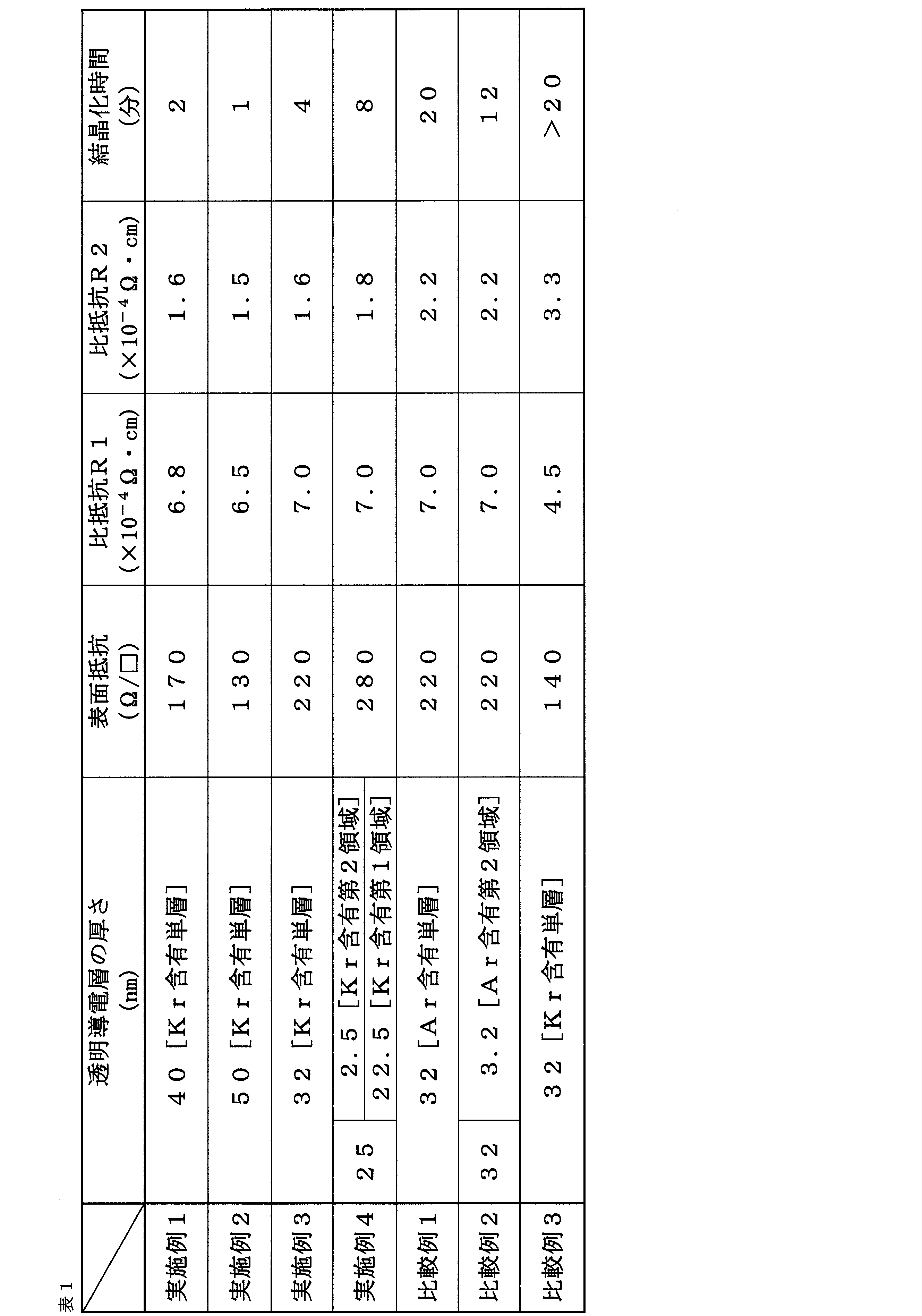
本発明の透明導電性フィルムは、例えば、液晶ディスプレイ、タッチパネル、および光センサなどの各種デバイスにおける透明電極をパターン形成するための導体膜の供給材として用いることができる。
X 透明導電性フィルム
T 厚さ方向
10 透明基材
11 樹脂フィルム
12 機能層
20,20’ 透明導電層
T 厚さ方向
10 透明基材
11 樹脂フィルム
12 機能層
20,20’ 透明導電層
Claims (5)
- 透明基材と非晶質の透明導電層とを厚さ方向にこの順で備え、
前記透明導電層が、クリプトンを含有し、5.5×10⁻⁴Ω・cm以上の比抵抗を有する、透明導電性フィルム。 - 前記透明導電層がインジウム含有導電性酸化物を含む、請求項1に記載の透明導電性フィルム。
- 前記比抵抗が10×10-4Ω・cm以下である、請求項1または2に記載の透明導電性フィルム。
- 前記透明導電層が20nm以上の厚さを有する、請求項1から3のいずれか一つに記載の透明導電性フィルム。
- 前記透明導電層が、130℃で60分間の加熱処理後に2.2×10⁻⁴Ω・cm未満の比抵抗を有する、請求項1から4のいずれか一つに記載の透明導電性フィルム。
Priority Applications (4)
| Application Number | Priority Date | Filing Date | Title |
|---|---|---|---|
| JP2021517066A JP7237150B2 (ja) | 2020-03-19 | 2021-03-18 | 透明導電性フィルム |
| KR1020227030805A KR20220155282A (ko) | 2020-03-19 | 2021-03-18 | 투명 도전성 필름 |
| CN202180022256.0A CN115298762A (zh) | 2020-03-19 | 2021-03-18 | 透明导电性薄膜 |
| JP2022078435A JP2022105579A (ja) | 2020-03-19 | 2022-05-11 | 透明導電性フィルム |
Applications Claiming Priority (26)
| Application Number | Priority Date | Filing Date | Title |
|---|---|---|---|
| JP2020049864 | 2020-03-19 | ||
| JP2020-049864 | 2020-03-19 | ||
| JP2020074853 | 2020-04-20 | ||
| JP2020-074854 | 2020-04-20 | ||
| JP2020-074853 | 2020-04-20 | ||
| JP2020074854 | 2020-04-20 | ||
| JP2020-134833 | 2020-08-07 | ||
| JP2020134832 | 2020-08-07 | ||
| JP2020134833 | 2020-08-07 | ||
| JP2020-134832 | 2020-08-07 | ||
| JP2020140240 | 2020-08-21 | ||
| JP2020140239 | 2020-08-21 | ||
| JP2020-140241 | 2020-08-21 | ||
| JP2020-140239 | 2020-08-21 | ||
| JP2020140241 | 2020-08-21 | ||
| JP2020-140240 | 2020-08-21 | ||
| JP2020-140238 | 2020-08-21 | ||
| JP2020140238 | 2020-08-21 | ||
| JP2020149474 | 2020-09-04 | ||
| JP2020-149474 | 2020-09-04 | ||
| JP2020181349 | 2020-10-29 | ||
| JP2020-181349 | 2020-10-29 | ||
| JP2020200422 | 2020-12-02 | ||
| JP2020200421 | 2020-12-02 | ||
| JP2020-200422 | 2020-12-02 | ||
| JP2020-200421 | 2020-12-02 |
Publications (1)
| Publication Number | Publication Date |
|---|---|
| WO2021187585A1 true WO2021187585A1 (ja) | 2021-09-23 |
Family
ID=77770986
Family Applications (10)
| Application Number | Title | Priority Date | Filing Date |
|---|---|---|---|
| PCT/JP2021/011148 Ceased WO2021187573A1 (ja) | 2020-03-19 | 2021-03-18 | 透明導電性フィルム、および透明導電性フィルムの製造方法 |
| PCT/JP2021/011160 Ceased WO2021187583A1 (ja) | 2020-03-19 | 2021-03-18 | 透明導電層および透明導電性フィルム |
| PCT/JP2021/011162 Ceased WO2021187585A1 (ja) | 2020-03-19 | 2021-03-18 | 透明導電性フィルム |
| PCT/JP2021/011163 Ceased WO2021187586A1 (ja) | 2020-03-19 | 2021-03-18 | 透明導電性フィルム |
| PCT/JP2021/011164 Ceased WO2021187587A1 (ja) | 2020-03-19 | 2021-03-18 | 透明導電性フィルム |
| PCT/JP2021/011161 Ceased WO2021187584A1 (ja) | 2020-03-19 | 2021-03-18 | 透明導電層および透明導電性フィルム |
| PCT/JP2021/011166 Ceased WO2021187589A1 (ja) | 2020-03-19 | 2021-03-18 | 透明導電層および透明導電性シート |
| PCT/JP2021/011159 Ceased WO2021187582A1 (ja) | 2020-03-19 | 2021-03-18 | 透明導電層および透明導電性フィルム |
| PCT/JP2021/011156 Ceased WO2021187581A1 (ja) | 2020-03-19 | 2021-03-18 | 透明導電性フィルム、および透明導電性フィルムの製造方法 |
| PCT/JP2021/011165 Ceased WO2021187588A1 (ja) | 2020-03-19 | 2021-03-18 | 透明導電層および透明導電性シート |
Family Applications Before (2)
| Application Number | Title | Priority Date | Filing Date |
|---|---|---|---|
| PCT/JP2021/011148 Ceased WO2021187573A1 (ja) | 2020-03-19 | 2021-03-18 | 透明導電性フィルム、および透明導電性フィルムの製造方法 |
| PCT/JP2021/011160 Ceased WO2021187583A1 (ja) | 2020-03-19 | 2021-03-18 | 透明導電層および透明導電性フィルム |
Family Applications After (7)
| Application Number | Title | Priority Date | Filing Date |
|---|---|---|---|
| PCT/JP2021/011163 Ceased WO2021187586A1 (ja) | 2020-03-19 | 2021-03-18 | 透明導電性フィルム |
| PCT/JP2021/011164 Ceased WO2021187587A1 (ja) | 2020-03-19 | 2021-03-18 | 透明導電性フィルム |
| PCT/JP2021/011161 Ceased WO2021187584A1 (ja) | 2020-03-19 | 2021-03-18 | 透明導電層および透明導電性フィルム |
| PCT/JP2021/011166 Ceased WO2021187589A1 (ja) | 2020-03-19 | 2021-03-18 | 透明導電層および透明導電性シート |
| PCT/JP2021/011159 Ceased WO2021187582A1 (ja) | 2020-03-19 | 2021-03-18 | 透明導電層および透明導電性フィルム |
| PCT/JP2021/011156 Ceased WO2021187581A1 (ja) | 2020-03-19 | 2021-03-18 | 透明導電性フィルム、および透明導電性フィルムの製造方法 |
| PCT/JP2021/011165 Ceased WO2021187588A1 (ja) | 2020-03-19 | 2021-03-18 | 透明導電層および透明導電性シート |
Country Status (6)
| Country | Link |
|---|---|
| US (2) | US20230127104A1 (ja) |
| JP (15) | JP7237150B2 (ja) |
| KR (11) | KR20220156819A (ja) |
| CN (10) | CN115298763A (ja) |
| TW (10) | TW202145262A (ja) |
| WO (10) | WO2021187573A1 (ja) |
Families Citing this family (10)
| Publication number | Priority date | Publication date | Assignee | Title |
|---|---|---|---|---|
| WO2022092190A2 (ja) * | 2020-10-29 | 2022-05-05 | 日東電工株式会社 | 透明導電性フィルム、および透明導電性フィルムの製造方法 |
| WO2022202715A1 (ja) * | 2021-03-23 | 2022-09-29 | 日東電工株式会社 | 電極 |
| US20230391969A1 (en) * | 2021-08-06 | 2023-12-07 | Nitto Denko Corporation | Laminate |
| CN116348293B (zh) * | 2021-08-06 | 2024-04-02 | 日东电工株式会社 | 层叠体 |
| JP7509852B2 (ja) * | 2022-11-10 | 2024-07-02 | 日東電工株式会社 | 透明導電性フィルム |
| WO2024166683A1 (ja) * | 2023-02-08 | 2024-08-15 | 日東電工株式会社 | 調光フィルム |
| JP7549117B1 (ja) | 2023-12-21 | 2024-09-10 | 日東電工株式会社 | 調光フィルム |
| JP2024131595A (ja) | 2023-03-16 | 2024-09-30 | 日東電工株式会社 | 透明導電性フィルム |
| JP2024131594A (ja) | 2023-03-16 | 2024-09-30 | 日東電工株式会社 | 透明導電性フィルム |
| JP7768443B1 (ja) * | 2025-03-21 | 2025-11-12 | 住友ベークライト株式会社 | 積層体、及び積層体の製造方法 |
Citations (1)
| Publication number | Priority date | Publication date | Assignee | Title |
|---|---|---|---|---|
| JPH05334924A (ja) * | 1992-05-29 | 1993-12-17 | Tonen Corp | 透明導電薄膜の製造法 |
Family Cites Families (52)
| Publication number | Priority date | Publication date | Assignee | Title |
|---|---|---|---|---|
| JPS61279003A (ja) * | 1985-06-05 | 1986-12-09 | コニカ株式会社 | 透明導電性フイルム |
| JPH0658476B2 (ja) * | 1985-06-19 | 1994-08-03 | 株式会社日立製作所 | 液晶表示素子用基板の製造方法 |
| JPH07258827A (ja) * | 1994-03-25 | 1995-10-09 | Mitsubishi Electric Corp | 金属薄膜,その形成方法,半導体装置およびその製造方法 |
| JPH07262829A (ja) * | 1994-03-25 | 1995-10-13 | Hitachi Ltd | 透明導電膜及びその形成方法 |
| JP4010587B2 (ja) * | 1995-12-20 | 2007-11-21 | 三井化学株式会社 | 透明導電性積層体及びそれを用いたエレクトロルミネッセンス発光素子 |
| JP2000038654A (ja) * | 1998-07-21 | 2000-02-08 | Nippon Sheet Glass Co Ltd | 透明導電膜付き基板の製造方法、透明導電膜付き基板およびそれを用いた液晶表示素子 |
| JP3549089B2 (ja) | 1998-07-28 | 2004-08-04 | セントラル硝子株式会社 | 透明導電膜付きガラス基板とその製法 |
| JP2000238178A (ja) * | 1999-02-24 | 2000-09-05 | Teijin Ltd | 透明導電積層体 |
| JP2000282225A (ja) * | 1999-04-01 | 2000-10-10 | Nippon Sheet Glass Co Ltd | 透明導電膜形成方法及び該方法より形成された透明導電膜 |
| JP4132458B2 (ja) * | 1999-08-23 | 2008-08-13 | Tdk株式会社 | 有機el素子 |
| JP2002371355A (ja) * | 2001-06-14 | 2002-12-26 | Nitto Denko Corp | 透明薄膜の製造方法 |
| JP2002371350A (ja) * | 2001-06-14 | 2002-12-26 | Nitto Denko Corp | 透明積層体の製造方法 |
| JP4177709B2 (ja) | 2002-05-20 | 2008-11-05 | 株式会社日本触媒 | 繊維状の金属酸化物微粒子 |
| WO2004105055A1 (ja) * | 2003-05-26 | 2004-12-02 | Nippon Soda Co., Ltd. | 透明導電膜付透光性基板 |
| WO2006033166A1 (ja) * | 2004-09-24 | 2006-03-30 | Tadahiro Ohmi | 有機el発光素子、その製造方法および表示装置 |
| JP4618707B2 (ja) * | 2004-03-19 | 2011-01-26 | 日東電工株式会社 | 電解質膜および固体高分子型燃料電池 |
| JP4882262B2 (ja) * | 2005-03-31 | 2012-02-22 | 凸版印刷株式会社 | 透明導電膜積層体の製造方法 |
| JP4899443B2 (ja) * | 2005-11-22 | 2012-03-21 | 大日本印刷株式会社 | 導電性基板 |
| US7867636B2 (en) * | 2006-01-11 | 2011-01-11 | Murata Manufacturing Co., Ltd. | Transparent conductive film and method for manufacturing the same |
| JP2010080358A (ja) * | 2008-09-29 | 2010-04-08 | Hitachi Ltd | 透明導電膜付基板、及びそれを用いた表示素子及び太陽電池 |
| JP2010162746A (ja) * | 2009-01-14 | 2010-07-29 | Jsr Corp | 透明導電性積層フィルム及びそれを用いたタッチパネル |
| JP2010177161A (ja) * | 2009-02-02 | 2010-08-12 | Toyobo Co Ltd | 透明導電性フィルム |
| KR101656118B1 (ko) * | 2009-09-18 | 2016-09-08 | 파나소닉 아이피 매니지먼트 가부시키가이샤 | 태양 전지, 태양 전지 모듈 및 태양 전지 시스템 |
| JP6023402B2 (ja) * | 2010-12-27 | 2016-11-09 | 日東電工株式会社 | 透明導電性フィルムおよびその製造方法 |
| JP4960511B1 (ja) * | 2011-01-26 | 2012-06-27 | 株式会社東芝 | 半導体発光素子及びその製造方法 |
| JP5729595B2 (ja) | 2011-03-11 | 2015-06-03 | 三菱マテリアル株式会社 | 太陽電池用透明導電膜およびその製造方法 |
| JP5244950B2 (ja) * | 2011-10-06 | 2013-07-24 | 日東電工株式会社 | 透明導電性フィルム |
| JP2013193440A (ja) * | 2012-03-22 | 2013-09-30 | Sekisui Nano Coat Technology Co Ltd | 光透過性導電性フィルム、その製造方法及びその用途 |
| CN103999166B (zh) * | 2012-06-07 | 2018-01-09 | 日东电工株式会社 | 透明导电性膜 |
| JP5620967B2 (ja) | 2012-11-22 | 2014-11-05 | 日東電工株式会社 | 透明導電性フィルム |
| JP6261987B2 (ja) * | 2013-01-16 | 2018-01-17 | 日東電工株式会社 | 透明導電フィルムおよびその製造方法 |
| JP6227321B2 (ja) * | 2013-08-05 | 2017-11-08 | リンテック株式会社 | プロテクトフィルム付き透明導電性フィルム |
| JP2015146244A (ja) * | 2014-02-03 | 2015-08-13 | 凸版印刷株式会社 | 透明導電性フィルムおよびこの製造方法 |
| WO2015178298A1 (ja) * | 2014-05-20 | 2015-11-26 | 日東電工株式会社 | 透明導電性フィルムおよびその製造方法 |
| KR20170008195A (ko) * | 2014-05-20 | 2017-01-23 | 닛토덴코 가부시키가이샤 | 투명 도전성 필름 |
| CN106460161B (zh) * | 2014-11-07 | 2018-12-04 | 捷客斯金属株式会社 | Ito溅射靶及其制造方法和ito透明导电膜及ito透明导电膜的制造方法 |
| US20170271613A1 (en) * | 2014-12-03 | 2017-09-21 | Joled Inc. | Organic light-emitting device |
| WO2016158606A1 (ja) * | 2015-03-31 | 2016-10-06 | 東洋紡株式会社 | 透明導電性フィルム |
| JP6553451B2 (ja) * | 2015-08-25 | 2019-07-31 | 日東電工株式会社 | 透明樹脂フィルム、透明導電性フィルムおよびそれを用いたタッチパネル |
| JP6159490B1 (ja) * | 2015-09-30 | 2017-07-05 | 積水化学工業株式会社 | 光透過性導電フィルム、及び、アニール処理された光透過性導電フィルムの製造方法 |
| JP6412539B2 (ja) * | 2015-11-09 | 2018-10-24 | 日東電工株式会社 | 光透過性導電フィルムおよび調光フィルム |
| JP6654865B2 (ja) * | 2015-11-12 | 2020-02-26 | 日東電工株式会社 | 非晶質透明導電性フィルム、ならびに、結晶質透明導電性フィルムおよびその製造方法 |
| JP7046497B2 (ja) | 2016-09-02 | 2022-04-04 | 日東電工株式会社 | 液晶調光部材、光透過性導電フィルム、および液晶調光素子 |
| CN109073940B (zh) * | 2016-04-01 | 2022-03-08 | 日东电工株式会社 | 液晶调光构件、透光性导电薄膜、及液晶调光元件 |
| WO2017170760A1 (ja) * | 2016-04-01 | 2017-10-05 | 日東電工株式会社 | 光透過性フィルム |
| CN109313962A (zh) * | 2016-06-10 | 2019-02-05 | 日东电工株式会社 | 透明导电性薄膜及触摸面板 |
| JP6803191B2 (ja) * | 2016-10-14 | 2020-12-23 | 株式会社カネカ | 透明導電性フィルムの製造方法 |
| JP6490262B2 (ja) * | 2017-05-09 | 2019-03-27 | 日東電工株式会社 | 光透過性導電層付きフィルム、調光フィルムおよび調光装置 |
| JP2018192634A (ja) * | 2017-05-12 | 2018-12-06 | 株式会社ダイセル | カールが抑制されたハードコートフィルム及びその製造方法 |
| JP7264807B2 (ja) * | 2017-12-28 | 2023-04-25 | 日東電工株式会社 | 光透過性導電フィルム、その製造方法、調光フィルム、および、調光部材 |
| CN108486550B (zh) * | 2018-04-27 | 2020-06-16 | 华南理工大学 | 一种金属氧化物透明导电薄膜的制备方法及其产品和用途 |
| JP7054651B2 (ja) * | 2018-06-19 | 2022-04-14 | 日東電工株式会社 | 下地層付きフィルム、透明導電性フィルム、透明導電性フィルム積層体および画像表示装置 |
-
2021
- 2021-03-18 KR KR1020227030813A patent/KR20220156819A/ko active Pending
- 2021-03-18 US US17/912,182 patent/US20230127104A1/en not_active Abandoned
- 2021-03-18 JP JP2021517066A patent/JP7237150B2/ja active Active
- 2021-03-18 JP JP2021545488A patent/JP7073589B2/ja active Active
- 2021-03-18 KR KR1020227030805A patent/KR20220155282A/ko active Pending
- 2021-03-18 KR KR1020227030815A patent/KR20220155287A/ko active Pending
- 2021-03-18 KR KR1020227030814A patent/KR20220156820A/ko not_active Ceased
- 2021-03-18 KR KR1020227030816A patent/KR20220155288A/ko active Pending
- 2021-03-18 WO PCT/JP2021/011148 patent/WO2021187573A1/ja not_active Ceased
- 2021-03-18 KR KR1020227030826A patent/KR20220156825A/ko active Pending
- 2021-03-18 WO PCT/JP2021/011160 patent/WO2021187583A1/ja not_active Ceased
- 2021-03-18 KR KR1020247001254A patent/KR20240011876A/ko active Pending
- 2021-03-18 US US17/912,196 patent/US20230131985A1/en not_active Abandoned
- 2021-03-18 WO PCT/JP2021/011162 patent/WO2021187585A1/ja not_active Ceased
- 2021-03-18 CN CN202180022368.6A patent/CN115298763A/zh active Pending
- 2021-03-18 CN CN202180022376.0A patent/CN115315759A/zh active Pending
- 2021-03-18 KR KR1020227030803A patent/KR20220155281A/ko not_active Ceased
- 2021-03-18 KR KR1020227030806A patent/KR20220155283A/ko not_active Ceased
- 2021-03-18 WO PCT/JP2021/011163 patent/WO2021187586A1/ja not_active Ceased
- 2021-03-18 CN CN202180022926.9A patent/CN115315760A/zh active Pending
- 2021-03-18 JP JP2021545487A patent/JP7073588B2/ja active Active
- 2021-03-18 JP JP2021517065A patent/JP6970861B1/ja active Active
- 2021-03-18 CN CN202180021961.9A patent/CN115298759A/zh active Pending
- 2021-03-18 KR KR1020227030820A patent/KR20220156824A/ko active Pending
- 2021-03-18 JP JP2021545862A patent/JP6974656B1/ja active Active
- 2021-03-18 JP JP2021545721A patent/JP7308960B2/ja active Active
- 2021-03-18 JP JP2021517067A patent/JP7278372B2/ja active Active
- 2021-03-18 JP JP2021545483A patent/JP6971433B1/ja active Active
- 2021-03-18 WO PCT/JP2021/011164 patent/WO2021187587A1/ja not_active Ceased
- 2021-03-18 JP JP2021545486A patent/JP7240514B2/ja active Active
- 2021-03-18 WO PCT/JP2021/011161 patent/WO2021187584A1/ja not_active Ceased
- 2021-03-18 KR KR1020227030827A patent/KR20220156826A/ko active Pending
- 2021-03-18 CN CN202180022256.0A patent/CN115298762A/zh active Pending
- 2021-03-18 WO PCT/JP2021/011166 patent/WO2021187589A1/ja not_active Ceased
- 2021-03-18 CN CN202180022337.0A patent/CN115335924B/zh active Active
- 2021-03-18 WO PCT/JP2021/011159 patent/WO2021187582A1/ja not_active Ceased
- 2021-03-18 CN CN202180021972.7A patent/CN115280429A/zh active Pending
- 2021-03-18 JP JP2021545482A patent/JP6987321B1/ja active Active
- 2021-03-18 CN CN202180022424.6A patent/CN115298764A/zh active Pending
- 2021-03-18 CN CN202180022001.4A patent/CN115280430B/zh active Active
- 2021-03-18 WO PCT/JP2021/011156 patent/WO2021187581A1/ja not_active Ceased
- 2021-03-18 WO PCT/JP2021/011165 patent/WO2021187588A1/ja not_active Ceased
- 2021-03-18 CN CN202180021850.8A patent/CN115280428A/zh active Pending
- 2021-03-19 TW TW110110105A patent/TW202145262A/zh unknown
- 2021-03-19 TW TW110110107A patent/TW202145263A/zh unknown
- 2021-03-19 TW TW110110042A patent/TW202141535A/zh unknown
- 2021-03-19 TW TW110110096A patent/TWI885098B/zh active
- 2021-03-19 TW TW110110106A patent/TW202143252A/zh unknown
- 2021-03-19 TW TW110110098A patent/TW202141536A/zh unknown
- 2021-03-19 TW TW110109978A patent/TW202145258A/zh unknown
- 2021-03-19 TW TW110110099A patent/TWI819287B/zh active
- 2021-03-19 TW TW110110097A patent/TW202147345A/zh unknown
- 2021-03-19 TW TW110110100A patent/TW202139214A/zh unknown
- 2021-11-04 JP JP2021180164A patent/JP7273930B2/ja active Active
- 2021-11-30 JP JP2021193794A patent/JP7213941B2/ja active Active
-
2022
- 2022-05-11 JP JP2022078435A patent/JP2022105579A/ja active Pending
- 2022-05-25 JP JP2022084908A patent/JP2022118005A/ja active Pending
- 2022-06-09 JP JP2022093446A patent/JP2022133292A/ja active Pending
Patent Citations (1)
| Publication number | Priority date | Publication date | Assignee | Title |
|---|---|---|---|---|
| JPH05334924A (ja) * | 1992-05-29 | 1993-12-17 | Tonen Corp | 透明導電薄膜の製造法 |
Also Published As
Similar Documents
| Publication | Publication Date | Title |
|---|---|---|
| JP7237150B2 (ja) | 透明導電性フィルム | |
| WO2022091606A1 (ja) | 透明導電性フィルム | |
| JP7451505B2 (ja) | 透明導電性フィルムの製造方法 | |
| JP7556912B2 (ja) | 透明導電性フィルムの製造方法 | |
| JP7565936B2 (ja) | 光透過性導電膜および透明導電性フィルム | |
| JP7654592B2 (ja) | 透明導電性フィルム | |
| JP7240513B2 (ja) | 透明導電性フィルム | |
| JP7425266B2 (ja) | 透明導電性フィルム | |
| JP7535528B2 (ja) | 光透過性導電膜および透明導電性フィルム | |
| WO2022092190A2 (ja) | 透明導電性フィルム、および透明導電性フィルムの製造方法 | |
| WO2023042848A1 (ja) | 透明導電性フィルム | |
| WO2021187576A1 (ja) | 透明導電性フィルム |
Legal Events
| Date | Code | Title | Description |
|---|---|---|---|
| ENP | Entry into the national phase |
Ref document number: 2021517066 Country of ref document: JP Kind code of ref document: A |
|
| 121 | Ep: the epo has been informed by wipo that ep was designated in this application |
Ref document number: 21772469 Country of ref document: EP Kind code of ref document: A1 |
|
| NENP | Non-entry into the national phase |
Ref country code: DE |
|
| 122 | Ep: pct application non-entry in european phase |
Ref document number: 21772469 Country of ref document: EP Kind code of ref document: A1 |