JP2010107976A - 表示装置 - Google Patents
表示装置 Download PDFInfo
- Publication number
- JP2010107976A JP2010107976A JP2009229378A JP2009229378A JP2010107976A JP 2010107976 A JP2010107976 A JP 2010107976A JP 2009229378 A JP2009229378 A JP 2009229378A JP 2009229378 A JP2009229378 A JP 2009229378A JP 2010107976 A JP2010107976 A JP 2010107976A
- Authority
- JP
- Japan
- Prior art keywords
- thin film
- wiring
- layer
- gate electrode
- film transistor
- Prior art date
- Legal status (The legal status is an assumption and is not a legal conclusion. Google has not performed a legal analysis and makes no representation as to the accuracy of the status listed.)
- Withdrawn
Links
- 239000004065 semiconductor Substances 0.000 claims abstract description 112
- 239000010409 thin film Substances 0.000 claims description 199
- 239000010408 film Substances 0.000 claims description 198
- 239000000758 substrate Substances 0.000 claims description 89
- 230000015572 biosynthetic process Effects 0.000 claims description 19
- 239000011159 matrix material Substances 0.000 claims description 15
- 239000011701 zinc Substances 0.000 claims description 14
- 229910052733 gallium Inorganic materials 0.000 claims description 12
- 229910052725 zinc Inorganic materials 0.000 claims description 9
- 229910052738 indium Inorganic materials 0.000 claims description 8
- GYHNNYVSQQEPJS-UHFFFAOYSA-N Gallium Chemical compound [Ga] GYHNNYVSQQEPJS-UHFFFAOYSA-N 0.000 claims description 2
- HCHKCACWOHOZIP-UHFFFAOYSA-N Zinc Chemical compound [Zn] HCHKCACWOHOZIP-UHFFFAOYSA-N 0.000 claims description 2
- APFVFJFRJDLVQX-UHFFFAOYSA-N indium atom Chemical compound [In] APFVFJFRJDLVQX-UHFFFAOYSA-N 0.000 claims description 2
- 230000002093 peripheral effect Effects 0.000 claims description 2
- 230000001681 protective effect Effects 0.000 abstract description 23
- 239000010410 layer Substances 0.000 description 214
- 238000000034 method Methods 0.000 description 42
- 239000004973 liquid crystal related substance Substances 0.000 description 38
- 239000000463 material Substances 0.000 description 28
- 239000000123 paper Substances 0.000 description 21
- 230000006870 function Effects 0.000 description 19
- 239000003990 capacitor Substances 0.000 description 17
- 238000005401 electroluminescence Methods 0.000 description 16
- 239000001301 oxygen Substances 0.000 description 15
- 229910052760 oxygen Inorganic materials 0.000 description 15
- 238000004544 sputter deposition Methods 0.000 description 15
- QVGXLLKOCUKJST-UHFFFAOYSA-N atomic oxygen Chemical compound [O] QVGXLLKOCUKJST-UHFFFAOYSA-N 0.000 description 14
- 238000005530 etching Methods 0.000 description 14
- 239000002245 particle Substances 0.000 description 14
- 229910052581 Si3N4 Inorganic materials 0.000 description 13
- 239000011521 glass Substances 0.000 description 13
- HQVNEWCFYHHQES-UHFFFAOYSA-N silicon nitride Chemical compound N12[Si]34N5[Si]62N3[Si]51N64 HQVNEWCFYHHQES-UHFFFAOYSA-N 0.000 description 13
- 239000010936 titanium Substances 0.000 description 13
- 229910052782 aluminium Inorganic materials 0.000 description 12
- 239000004020 conductor Substances 0.000 description 11
- 229920005989 resin Polymers 0.000 description 11
- 239000011347 resin Substances 0.000 description 11
- XKRFYHLGVUSROY-UHFFFAOYSA-N Argon Chemical compound [Ar] XKRFYHLGVUSROY-UHFFFAOYSA-N 0.000 description 10
- IJGRMHOSHXDMSA-UHFFFAOYSA-N Atomic nitrogen Chemical compound N#N IJGRMHOSHXDMSA-UHFFFAOYSA-N 0.000 description 10
- VYPSYNLAJGMNEJ-UHFFFAOYSA-N Silicium dioxide Chemical compound O=[Si]=O VYPSYNLAJGMNEJ-UHFFFAOYSA-N 0.000 description 10
- XAGFODPZIPBFFR-UHFFFAOYSA-N aluminium Chemical compound [Al] XAGFODPZIPBFFR-UHFFFAOYSA-N 0.000 description 10
- 239000013078 crystal Substances 0.000 description 10
- 239000000565 sealant Substances 0.000 description 10
- 229910052814 silicon oxide Inorganic materials 0.000 description 10
- XLOMVQKBTHCTTD-UHFFFAOYSA-N Zinc monoxide Chemical compound [Zn]=O XLOMVQKBTHCTTD-UHFFFAOYSA-N 0.000 description 9
- 238000010438 heat treatment Methods 0.000 description 9
- 239000003094 microcapsule Substances 0.000 description 9
- 239000000203 mixture Substances 0.000 description 9
- 229910045601 alloy Inorganic materials 0.000 description 8
- 239000000956 alloy Substances 0.000 description 8
- 238000010586 diagram Methods 0.000 description 8
- 239000011229 interlayer Substances 0.000 description 8
- 229910052751 metal Inorganic materials 0.000 description 8
- 239000012298 atmosphere Substances 0.000 description 7
- AMGQUBHHOARCQH-UHFFFAOYSA-N indium;oxotin Chemical compound [In].[Sn]=O AMGQUBHHOARCQH-UHFFFAOYSA-N 0.000 description 7
- 238000004519 manufacturing process Methods 0.000 description 7
- 238000009832 plasma treatment Methods 0.000 description 7
- 230000008569 process Effects 0.000 description 7
- 229910052710 silicon Inorganic materials 0.000 description 7
- 239000002356 single layer Substances 0.000 description 7
- XUIMIQQOPSSXEZ-UHFFFAOYSA-N Silicon Chemical compound [Si] XUIMIQQOPSSXEZ-UHFFFAOYSA-N 0.000 description 6
- 229910052786 argon Inorganic materials 0.000 description 6
- 230000005684 electric field Effects 0.000 description 6
- 239000000945 filler Substances 0.000 description 6
- 239000001257 hydrogen Substances 0.000 description 6
- 229910052739 hydrogen Inorganic materials 0.000 description 6
- 229910003437 indium oxide Inorganic materials 0.000 description 6
- PJXISJQVUVHSOJ-UHFFFAOYSA-N indium(iii) oxide Chemical compound [O-2].[O-2].[O-2].[In+3].[In+3] PJXISJQVUVHSOJ-UHFFFAOYSA-N 0.000 description 6
- 238000003780 insertion Methods 0.000 description 6
- 230000037431 insertion Effects 0.000 description 6
- 239000002184 metal Substances 0.000 description 6
- 239000010703 silicon Substances 0.000 description 6
- 229910052719 titanium Inorganic materials 0.000 description 6
- UFHFLCQGNIYNRP-UHFFFAOYSA-N Hydrogen Chemical compound [H][H] UFHFLCQGNIYNRP-UHFFFAOYSA-N 0.000 description 5
- 229910007541 Zn O Inorganic materials 0.000 description 5
- 239000011651 chromium Substances 0.000 description 5
- KPUWHANPEXNPJT-UHFFFAOYSA-N disiloxane Chemical class [SiH3]O[SiH3] KPUWHANPEXNPJT-UHFFFAOYSA-N 0.000 description 5
- 239000007789 gas Substances 0.000 description 5
- 229910052757 nitrogen Inorganic materials 0.000 description 5
- TWNQGVIAIRXVLR-UHFFFAOYSA-N oxo(oxoalumanyloxy)alumane Chemical compound O=[Al]O[Al]=O TWNQGVIAIRXVLR-UHFFFAOYSA-N 0.000 description 5
- 239000012798 spherical particle Substances 0.000 description 5
- 240000002329 Inga feuillei Species 0.000 description 4
- GWEVSGVZZGPLCZ-UHFFFAOYSA-N Titan oxide Chemical compound O=[Ti]=O GWEVSGVZZGPLCZ-UHFFFAOYSA-N 0.000 description 4
- RTAQQCXQSZGOHL-UHFFFAOYSA-N Titanium Chemical compound [Ti] RTAQQCXQSZGOHL-UHFFFAOYSA-N 0.000 description 4
- 229920001940 conductive polymer Polymers 0.000 description 4
- PMHQVHHXPFUNSP-UHFFFAOYSA-M copper(1+);methylsulfanylmethane;bromide Chemical compound Br[Cu].CSC PMHQVHHXPFUNSP-UHFFFAOYSA-M 0.000 description 4
- 239000007788 liquid Substances 0.000 description 4
- 150000004767 nitrides Chemical class 0.000 description 4
- QGLKJKCYBOYXKC-UHFFFAOYSA-N nonaoxidotritungsten Chemical compound O=[W]1(=O)O[W](=O)(=O)O[W](=O)(=O)O1 QGLKJKCYBOYXKC-UHFFFAOYSA-N 0.000 description 4
- 230000003287 optical effect Effects 0.000 description 4
- 229920003023 plastic Polymers 0.000 description 4
- 239000004033 plastic Substances 0.000 description 4
- 229920006267 polyester film Polymers 0.000 description 4
- 239000000126 substance Substances 0.000 description 4
- OGIDPMRJRNCKJF-UHFFFAOYSA-N titanium oxide Inorganic materials [Ti]=O OGIDPMRJRNCKJF-UHFFFAOYSA-N 0.000 description 4
- 229910001930 tungsten oxide Inorganic materials 0.000 description 4
- YVTHLONGBIQYBO-UHFFFAOYSA-N zinc indium(3+) oxygen(2-) Chemical compound [O--].[Zn++].[In+3] YVTHLONGBIQYBO-UHFFFAOYSA-N 0.000 description 4
- 239000011787 zinc oxide Substances 0.000 description 4
- NIXOWILDQLNWCW-UHFFFAOYSA-N acrylic acid group Chemical group C(C=C)(=O)O NIXOWILDQLNWCW-UHFFFAOYSA-N 0.000 description 3
- 229910021417 amorphous silicon Inorganic materials 0.000 description 3
- 238000004458 analytical method Methods 0.000 description 3
- 238000000137 annealing Methods 0.000 description 3
- 229910052804 chromium Inorganic materials 0.000 description 3
- 238000004891 communication Methods 0.000 description 3
- 238000001312 dry etching Methods 0.000 description 3
- 239000000428 dust Substances 0.000 description 3
- 230000000694 effects Effects 0.000 description 3
- 230000005611 electricity Effects 0.000 description 3
- 230000005669 field effect Effects 0.000 description 3
- 239000012535 impurity Substances 0.000 description 3
- 229910052742 iron Inorganic materials 0.000 description 3
- 230000007246 mechanism Effects 0.000 description 3
- 229910052750 molybdenum Inorganic materials 0.000 description 3
- 229910052759 nickel Inorganic materials 0.000 description 3
- 150000002894 organic compounds Chemical class 0.000 description 3
- 238000005192 partition Methods 0.000 description 3
- 229920002620 polyvinyl fluoride Polymers 0.000 description 3
- 239000000243 solution Substances 0.000 description 3
- 230000003068 static effect Effects 0.000 description 3
- 238000003860 storage Methods 0.000 description 3
- 229910052715 tantalum Inorganic materials 0.000 description 3
- 229910052721 tungsten Inorganic materials 0.000 description 3
- 238000001039 wet etching Methods 0.000 description 3
- UWCWUCKPEYNDNV-LBPRGKRZSA-N 2,6-dimethyl-n-[[(2s)-pyrrolidin-2-yl]methyl]aniline Chemical compound CC1=CC=CC(C)=C1NC[C@H]1NCCC1 UWCWUCKPEYNDNV-LBPRGKRZSA-N 0.000 description 2
- CURLTUGMZLYLDI-UHFFFAOYSA-N Carbon dioxide Chemical compound O=C=O CURLTUGMZLYLDI-UHFFFAOYSA-N 0.000 description 2
- VYZAMTAEIAYCRO-UHFFFAOYSA-N Chromium Chemical compound [Cr] VYZAMTAEIAYCRO-UHFFFAOYSA-N 0.000 description 2
- MYMOFIZGZYHOMD-UHFFFAOYSA-N Dioxygen Chemical compound O=O MYMOFIZGZYHOMD-UHFFFAOYSA-N 0.000 description 2
- PXGOKWXKJXAPGV-UHFFFAOYSA-N Fluorine Chemical compound FF PXGOKWXKJXAPGV-UHFFFAOYSA-N 0.000 description 2
- 229910005191 Ga 2 O 3 Inorganic materials 0.000 description 2
- VEXZGXHMUGYJMC-UHFFFAOYSA-N Hydrochloric acid Chemical compound Cl VEXZGXHMUGYJMC-UHFFFAOYSA-N 0.000 description 2
- ZOKXTWBITQBERF-UHFFFAOYSA-N Molybdenum Chemical compound [Mo] ZOKXTWBITQBERF-UHFFFAOYSA-N 0.000 description 2
- 229910052779 Neodymium Inorganic materials 0.000 description 2
- 239000004642 Polyimide Substances 0.000 description 2
- 230000001133 acceleration Effects 0.000 description 2
- 125000000217 alkyl group Chemical group 0.000 description 2
- DQXBYHZEEUGOBF-UHFFFAOYSA-N but-3-enoic acid;ethene Chemical compound C=C.OC(=O)CC=C DQXBYHZEEUGOBF-UHFFFAOYSA-N 0.000 description 2
- 230000015556 catabolic process Effects 0.000 description 2
- 230000001413 cellular effect Effects 0.000 description 2
- 239000010949 copper Substances 0.000 description 2
- 238000005520 cutting process Methods 0.000 description 2
- 238000009792 diffusion process Methods 0.000 description 2
- 229910001882 dioxygen Inorganic materials 0.000 description 2
- 239000005038 ethylene vinyl acetate Substances 0.000 description 2
- 230000005281 excited state Effects 0.000 description 2
- 230000001747 exhibiting effect Effects 0.000 description 2
- 239000000284 extract Substances 0.000 description 2
- 239000005262 ferroelectric liquid crystals (FLCs) Substances 0.000 description 2
- 239000011152 fibreglass Substances 0.000 description 2
- 239000011737 fluorine Substances 0.000 description 2
- 229910052731 fluorine Inorganic materials 0.000 description 2
- 238000001095 inductively coupled plasma mass spectrometry Methods 0.000 description 2
- 238000002347 injection Methods 0.000 description 2
- 239000007924 injection Substances 0.000 description 2
- 238000005259 measurement Methods 0.000 description 2
- 239000011859 microparticle Substances 0.000 description 2
- 239000011733 molybdenum Substances 0.000 description 2
- QEFYFXOXNSNQGX-UHFFFAOYSA-N neodymium atom Chemical compound [Nd] QEFYFXOXNSNQGX-UHFFFAOYSA-N 0.000 description 2
- 239000011368 organic material Substances 0.000 description 2
- BPUBBGLMJRNUCC-UHFFFAOYSA-N oxygen(2-);tantalum(5+) Chemical compound [O-2].[O-2].[O-2].[O-2].[O-2].[Ta+5].[Ta+5] BPUBBGLMJRNUCC-UHFFFAOYSA-N 0.000 description 2
- 238000000206 photolithography Methods 0.000 description 2
- 239000000049 pigment Substances 0.000 description 2
- 229920001200 poly(ethylene-vinyl acetate) Polymers 0.000 description 2
- 229920002037 poly(vinyl butyral) polymer Polymers 0.000 description 2
- 229910021420 polycrystalline silicon Inorganic materials 0.000 description 2
- 229920001721 polyimide Polymers 0.000 description 2
- -1 polysiloxane Polymers 0.000 description 2
- 229920000915 polyvinyl chloride Polymers 0.000 description 2
- 239000004800 polyvinyl chloride Substances 0.000 description 2
- 230000004044 response Effects 0.000 description 2
- 238000005001 rutherford backscattering spectroscopy Methods 0.000 description 2
- 229910052706 scandium Inorganic materials 0.000 description 2
- SIXSYDAISGFNSX-UHFFFAOYSA-N scandium atom Chemical compound [Sc] SIXSYDAISGFNSX-UHFFFAOYSA-N 0.000 description 2
- 239000002904 solvent Substances 0.000 description 2
- 125000006850 spacer group Chemical group 0.000 description 2
- 125000001424 substituent group Chemical group 0.000 description 2
- GUVRBAGPIYLISA-UHFFFAOYSA-N tantalum atom Chemical compound [Ta] GUVRBAGPIYLISA-UHFFFAOYSA-N 0.000 description 2
- 229910001936 tantalum oxide Inorganic materials 0.000 description 2
- 230000007704 transition Effects 0.000 description 2
- 229910052723 transition metal Inorganic materials 0.000 description 2
- WFKWXMTUELFFGS-UHFFFAOYSA-N tungsten Chemical compound [W] WFKWXMTUELFFGS-UHFFFAOYSA-N 0.000 description 2
- 239000010937 tungsten Substances 0.000 description 2
- 238000001771 vacuum deposition Methods 0.000 description 2
- 210000003462 vein Anatomy 0.000 description 2
- 239000004925 Acrylic resin Substances 0.000 description 1
- 229920000178 Acrylic resin Polymers 0.000 description 1
- 229910017073 AlLi Inorganic materials 0.000 description 1
- 239000004986 Cholesteric liquid crystals (ChLC) Substances 0.000 description 1
- RYGMFSIKBFXOCR-UHFFFAOYSA-N Copper Chemical compound [Cu] RYGMFSIKBFXOCR-UHFFFAOYSA-N 0.000 description 1
- 239000004593 Epoxy Substances 0.000 description 1
- 206010052128 Glare Diseases 0.000 description 1
- DGAQECJNVWCQMB-PUAWFVPOSA-M Ilexoside XXIX Chemical compound C[C@@H]1CC[C@@]2(CC[C@@]3(C(=CC[C@H]4[C@]3(CC[C@@H]5[C@@]4(CC[C@@H](C5(C)C)OS(=O)(=O)[O-])C)C)[C@@H]2[C@]1(C)O)C)C(=O)O[C@H]6[C@@H]([C@H]([C@@H]([C@H](O6)CO)O)O)O.[Na+] DGAQECJNVWCQMB-PUAWFVPOSA-M 0.000 description 1
- OAICVXFJPJFONN-UHFFFAOYSA-N Phosphorus Chemical compound [P] OAICVXFJPJFONN-UHFFFAOYSA-N 0.000 description 1
- 239000004952 Polyamide Substances 0.000 description 1
- 229910003902 SiCl 4 Inorganic materials 0.000 description 1
- 229910002808 Si–O–Si Inorganic materials 0.000 description 1
- 229910006404 SnO 2 Inorganic materials 0.000 description 1
- 238000002441 X-ray diffraction Methods 0.000 description 1
- GDFCWFBWQUEQIJ-UHFFFAOYSA-N [B].[P] Chemical compound [B].[P] GDFCWFBWQUEQIJ-UHFFFAOYSA-N 0.000 description 1
- 239000005407 aluminoborosilicate glass Substances 0.000 description 1
- 239000005354 aluminosilicate glass Substances 0.000 description 1
- 150000004945 aromatic hydrocarbons Chemical class 0.000 description 1
- 125000003118 aryl group Chemical group 0.000 description 1
- 229910052788 barium Inorganic materials 0.000 description 1
- DSAJWYNOEDNPEQ-UHFFFAOYSA-N barium atom Chemical compound [Ba] DSAJWYNOEDNPEQ-UHFFFAOYSA-N 0.000 description 1
- QVQLCTNNEUAWMS-UHFFFAOYSA-N barium oxide Chemical compound [Ba]=O QVQLCTNNEUAWMS-UHFFFAOYSA-N 0.000 description 1
- 230000008901 benefit Effects 0.000 description 1
- UMIVXZPTRXBADB-UHFFFAOYSA-N benzocyclobutene Chemical compound C1=CC=C2CCC2=C1 UMIVXZPTRXBADB-UHFFFAOYSA-N 0.000 description 1
- 230000002457 bidirectional effect Effects 0.000 description 1
- 239000011230 binding agent Substances 0.000 description 1
- KGBXLFKZBHKPEV-UHFFFAOYSA-N boric acid Chemical compound OB(O)O KGBXLFKZBHKPEV-UHFFFAOYSA-N 0.000 description 1
- 239000004327 boric acid Substances 0.000 description 1
- 239000005380 borophosphosilicate glass Substances 0.000 description 1
- 239000005388 borosilicate glass Substances 0.000 description 1
- 239000001569 carbon dioxide Substances 0.000 description 1
- 229910002092 carbon dioxide Inorganic materials 0.000 description 1
- 239000000969 carrier Substances 0.000 description 1
- 239000000919 ceramic Substances 0.000 description 1
- 230000003098 cholesteric effect Effects 0.000 description 1
- 238000004040 coloring Methods 0.000 description 1
- 239000002131 composite material Substances 0.000 description 1
- 239000000356 contaminant Substances 0.000 description 1
- 239000002872 contrast media Substances 0.000 description 1
- 229920001577 copolymer Polymers 0.000 description 1
- 229910052802 copper Inorganic materials 0.000 description 1
- 230000007797 corrosion Effects 0.000 description 1
- 238000005260 corrosion Methods 0.000 description 1
- 229910021419 crystalline silicon Inorganic materials 0.000 description 1
- 230000007547 defect Effects 0.000 description 1
- 230000002950 deficient Effects 0.000 description 1
- 238000007872 degassing Methods 0.000 description 1
- 238000000151 deposition Methods 0.000 description 1
- 230000008021 deposition Effects 0.000 description 1
- 238000013461 design Methods 0.000 description 1
- 238000001514 detection method Methods 0.000 description 1
- 239000003989 dielectric material Substances 0.000 description 1
- AJNVQOSZGJRYEI-UHFFFAOYSA-N digallium;oxygen(2-) Chemical compound [O-2].[O-2].[O-2].[Ga+3].[Ga+3] AJNVQOSZGJRYEI-UHFFFAOYSA-N 0.000 description 1
- 238000006073 displacement reaction Methods 0.000 description 1
- 230000009977 dual effect Effects 0.000 description 1
- 239000003822 epoxy resin Substances 0.000 description 1
- 239000004744 fabric Substances 0.000 description 1
- 238000007667 floating Methods 0.000 description 1
- 239000011888 foil Substances 0.000 description 1
- 230000005283 ground state Effects 0.000 description 1
- 229910000449 hafnium oxide Inorganic materials 0.000 description 1
- WIHZLLGSGQNAGK-UHFFFAOYSA-N hafnium(4+);oxygen(2-) Chemical compound [O-2].[O-2].[Hf+4] WIHZLLGSGQNAGK-UHFFFAOYSA-N 0.000 description 1
- 230000005525 hole transport Effects 0.000 description 1
- 150000002431 hydrogen Chemical class 0.000 description 1
- 125000002887 hydroxy group Chemical group [H]O* 0.000 description 1
- 239000011261 inert gas Substances 0.000 description 1
- 150000002484 inorganic compounds Chemical class 0.000 description 1
- 229910010272 inorganic material Inorganic materials 0.000 description 1
- 239000012212 insulator Substances 0.000 description 1
- 150000002500 ions Chemical class 0.000 description 1
- 238000003475 lamination Methods 0.000 description 1
- 238000005224 laser annealing Methods 0.000 description 1
- 239000000395 magnesium oxide Substances 0.000 description 1
- CPLXHLVBOLITMK-UHFFFAOYSA-N magnesium oxide Inorganic materials [Mg]=O CPLXHLVBOLITMK-UHFFFAOYSA-N 0.000 description 1
- AXZKOIWUVFPNLO-UHFFFAOYSA-N magnesium;oxygen(2-) Chemical compound [O-2].[Mg+2] AXZKOIWUVFPNLO-UHFFFAOYSA-N 0.000 description 1
- 239000000696 magnetic material Substances 0.000 description 1
- 230000005389 magnetism Effects 0.000 description 1
- 238000000838 magnetophoresis Methods 0.000 description 1
- 229910052748 manganese Inorganic materials 0.000 description 1
- 238000000691 measurement method Methods 0.000 description 1
- 229910021645 metal ion Inorganic materials 0.000 description 1
- 238000012986 modification Methods 0.000 description 1
- 230000004048 modification Effects 0.000 description 1
- 239000012299 nitrogen atmosphere Substances 0.000 description 1
- 238000007645 offset printing Methods 0.000 description 1
- 239000012788 optical film Substances 0.000 description 1
- AHLBNYSZXLDEJQ-FWEHEUNISA-N orlistat Chemical compound CCCCCCCCCCC[C@H](OC(=O)[C@H](CC(C)C)NC=O)C[C@@H]1OC(=O)[C@H]1CCCCCC AHLBNYSZXLDEJQ-FWEHEUNISA-N 0.000 description 1
- 230000003647 oxidation Effects 0.000 description 1
- 238000007254 oxidation reaction Methods 0.000 description 1
- SIWVEOZUMHYXCS-UHFFFAOYSA-N oxo(oxoyttriooxy)yttrium Chemical compound O=[Y]O[Y]=O SIWVEOZUMHYXCS-UHFFFAOYSA-N 0.000 description 1
- 229910052698 phosphorus Inorganic materials 0.000 description 1
- 239000011574 phosphorus Substances 0.000 description 1
- 238000005268 plasma chemical vapour deposition Methods 0.000 description 1
- 229920002647 polyamide Polymers 0.000 description 1
- 229920000767 polyaniline Polymers 0.000 description 1
- 229920000647 polyepoxide Polymers 0.000 description 1
- 229920000128 polypyrrole Polymers 0.000 description 1
- 229920001296 polysiloxane Polymers 0.000 description 1
- 229920000123 polythiophene Polymers 0.000 description 1
- 238000011002 quantification Methods 0.000 description 1
- 230000005855 radiation Effects 0.000 description 1
- 239000012495 reaction gas Substances 0.000 description 1
- 230000008707 rearrangement Effects 0.000 description 1
- 230000006798 recombination Effects 0.000 description 1
- 238000005215 recombination Methods 0.000 description 1
- 238000007650 screen-printing Methods 0.000 description 1
- 239000003566 sealing material Substances 0.000 description 1
- 229920002050 silicone resin Polymers 0.000 description 1
- 239000011734 sodium Substances 0.000 description 1
- 229910052708 sodium Inorganic materials 0.000 description 1
- 238000004528 spin coating Methods 0.000 description 1
- 238000005507 spraying Methods 0.000 description 1
- 239000010935 stainless steel Substances 0.000 description 1
- 229910001220 stainless steel Inorganic materials 0.000 description 1
- 239000007858 starting material Substances 0.000 description 1
- 229920001187 thermosetting polymer Polymers 0.000 description 1
- 150000003608 titanium Chemical class 0.000 description 1
- 229910000314 transition metal oxide Inorganic materials 0.000 description 1
- 150000003624 transition metals Chemical class 0.000 description 1
- 238000002834 transmittance Methods 0.000 description 1
- XLYOFNOQVPJJNP-UHFFFAOYSA-N water Chemical compound O XLYOFNOQVPJJNP-UHFFFAOYSA-N 0.000 description 1
- OYQCBJZGELKKPM-UHFFFAOYSA-N zinc indium(3+) oxygen(2-) Chemical compound [O-2].[Zn+2].[O-2].[In+3] OYQCBJZGELKKPM-UHFFFAOYSA-N 0.000 description 1
Images


Classifications
-
- G—PHYSICS
- G02—OPTICS
- G02F—OPTICAL DEVICES OR ARRANGEMENTS FOR THE CONTROL OF LIGHT BY MODIFICATION OF THE OPTICAL PROPERTIES OF THE MEDIA OF THE ELEMENTS INVOLVED THEREIN; NON-LINEAR OPTICS; FREQUENCY-CHANGING OF LIGHT; OPTICAL LOGIC ELEMENTS; OPTICAL ANALOGUE/DIGITAL CONVERTERS
- G02F1/00—Devices or arrangements for the control of the intensity, colour, phase, polarisation or direction of light arriving from an independent light source, e.g. switching, gating or modulating; Non-linear optics
- G02F1/01—Devices or arrangements for the control of the intensity, colour, phase, polarisation or direction of light arriving from an independent light source, e.g. switching, gating or modulating; Non-linear optics for the control of the intensity, phase, polarisation or colour
- G02F1/13—Devices or arrangements for the control of the intensity, colour, phase, polarisation or direction of light arriving from an independent light source, e.g. switching, gating or modulating; Non-linear optics for the control of the intensity, phase, polarisation or colour based on liquid crystals, e.g. single liquid crystal display cells
- G02F1/133—Constructional arrangements; Operation of liquid crystal cells; Circuit arrangements
- G02F1/136—Liquid crystal cells structurally associated with a semi-conducting layer or substrate, e.g. cells forming part of an integrated circuit
-
- H—ELECTRICITY
- H01—ELECTRIC ELEMENTS
- H01L—SEMICONDUCTOR DEVICES NOT COVERED BY CLASS H10
- H01L29/00—Semiconductor devices adapted for rectifying, amplifying, oscillating or switching, or capacitors or resistors with at least one potential-jump barrier or surface barrier, e.g. PN junction depletion layer or carrier concentration layer; Details of semiconductor bodies or of electrodes thereof ; Multistep manufacturing processes therefor
- H01L29/66—Types of semiconductor device ; Multistep manufacturing processes therefor
- H01L29/68—Types of semiconductor device ; Multistep manufacturing processes therefor controllable by only the electric current supplied, or only the electric potential applied, to an electrode which does not carry the current to be rectified, amplified or switched
- H01L29/76—Unipolar devices, e.g. field effect transistors
- H01L29/772—Field effect transistors
- H01L29/78—Field effect transistors with field effect produced by an insulated gate
- H01L29/786—Thin film transistors, i.e. transistors with a channel being at least partly a thin film
- H01L29/7869—Thin film transistors, i.e. transistors with a channel being at least partly a thin film having a semiconductor body comprising an oxide semiconductor material, e.g. zinc oxide, copper aluminium oxide, cadmium stannate
-
- H—ELECTRICITY
- H01—ELECTRIC ELEMENTS
- H01L—SEMICONDUCTOR DEVICES NOT COVERED BY CLASS H10
- H01L27/00—Devices consisting of a plurality of semiconductor or other solid-state components formed in or on a common substrate
- H01L27/02—Devices consisting of a plurality of semiconductor or other solid-state components formed in or on a common substrate including semiconductor components specially adapted for rectifying, oscillating, amplifying or switching and having at least one potential-jump barrier or surface barrier; including integrated passive circuit elements with at least one potential-jump barrier or surface barrier
- H01L27/0203—Particular design considerations for integrated circuits
- H01L27/0248—Particular design considerations for integrated circuits for electrical or thermal protection, e.g. electrostatic discharge [ESD] protection
- H01L27/0251—Particular design considerations for integrated circuits for electrical or thermal protection, e.g. electrostatic discharge [ESD] protection for MOS devices
- H01L27/0266—Particular design considerations for integrated circuits for electrical or thermal protection, e.g. electrostatic discharge [ESD] protection for MOS devices using field effect transistors as protective elements
-
- H—ELECTRICITY
- H01—ELECTRIC ELEMENTS
- H01L—SEMICONDUCTOR DEVICES NOT COVERED BY CLASS H10
- H01L27/00—Devices consisting of a plurality of semiconductor or other solid-state components formed in or on a common substrate
- H01L27/02—Devices consisting of a plurality of semiconductor or other solid-state components formed in or on a common substrate including semiconductor components specially adapted for rectifying, oscillating, amplifying or switching and having at least one potential-jump barrier or surface barrier; including integrated passive circuit elements with at least one potential-jump barrier or surface barrier
- H01L27/12—Devices consisting of a plurality of semiconductor or other solid-state components formed in or on a common substrate including semiconductor components specially adapted for rectifying, oscillating, amplifying or switching and having at least one potential-jump barrier or surface barrier; including integrated passive circuit elements with at least one potential-jump barrier or surface barrier the substrate being other than a semiconductor body, e.g. an insulating body
- H01L27/1214—Devices consisting of a plurality of semiconductor or other solid-state components formed in or on a common substrate including semiconductor components specially adapted for rectifying, oscillating, amplifying or switching and having at least one potential-jump barrier or surface barrier; including integrated passive circuit elements with at least one potential-jump barrier or surface barrier the substrate being other than a semiconductor body, e.g. an insulating body comprising a plurality of TFTs formed on a non-semiconducting substrate, e.g. driving circuits for AMLCDs
- H01L27/1222—Devices consisting of a plurality of semiconductor or other solid-state components formed in or on a common substrate including semiconductor components specially adapted for rectifying, oscillating, amplifying or switching and having at least one potential-jump barrier or surface barrier; including integrated passive circuit elements with at least one potential-jump barrier or surface barrier the substrate being other than a semiconductor body, e.g. an insulating body comprising a plurality of TFTs formed on a non-semiconducting substrate, e.g. driving circuits for AMLCDs with a particular composition, shape or crystalline structure of the active layer
- H01L27/1225—Devices consisting of a plurality of semiconductor or other solid-state components formed in or on a common substrate including semiconductor components specially adapted for rectifying, oscillating, amplifying or switching and having at least one potential-jump barrier or surface barrier; including integrated passive circuit elements with at least one potential-jump barrier or surface barrier the substrate being other than a semiconductor body, e.g. an insulating body comprising a plurality of TFTs formed on a non-semiconducting substrate, e.g. driving circuits for AMLCDs with a particular composition, shape or crystalline structure of the active layer with semiconductor materials not belonging to the group IV of the periodic table, e.g. InGaZnO
-
- H—ELECTRICITY
- H01—ELECTRIC ELEMENTS
- H01L—SEMICONDUCTOR DEVICES NOT COVERED BY CLASS H10
- H01L27/00—Devices consisting of a plurality of semiconductor or other solid-state components formed in or on a common substrate
- H01L27/02—Devices consisting of a plurality of semiconductor or other solid-state components formed in or on a common substrate including semiconductor components specially adapted for rectifying, oscillating, amplifying or switching and having at least one potential-jump barrier or surface barrier; including integrated passive circuit elements with at least one potential-jump barrier or surface barrier
- H01L27/12—Devices consisting of a plurality of semiconductor or other solid-state components formed in or on a common substrate including semiconductor components specially adapted for rectifying, oscillating, amplifying or switching and having at least one potential-jump barrier or surface barrier; including integrated passive circuit elements with at least one potential-jump barrier or surface barrier the substrate being other than a semiconductor body, e.g. an insulating body
- H01L27/1214—Devices consisting of a plurality of semiconductor or other solid-state components formed in or on a common substrate including semiconductor components specially adapted for rectifying, oscillating, amplifying or switching and having at least one potential-jump barrier or surface barrier; including integrated passive circuit elements with at least one potential-jump barrier or surface barrier the substrate being other than a semiconductor body, e.g. an insulating body comprising a plurality of TFTs formed on a non-semiconducting substrate, e.g. driving circuits for AMLCDs
- H01L27/124—Devices consisting of a plurality of semiconductor or other solid-state components formed in or on a common substrate including semiconductor components specially adapted for rectifying, oscillating, amplifying or switching and having at least one potential-jump barrier or surface barrier; including integrated passive circuit elements with at least one potential-jump barrier or surface barrier the substrate being other than a semiconductor body, e.g. an insulating body comprising a plurality of TFTs formed on a non-semiconducting substrate, e.g. driving circuits for AMLCDs with a particular composition, shape or layout of the wiring layers specially adapted to the circuit arrangement, e.g. scanning lines in LCD pixel circuits
Abstract
【解決手段】ゲート電極を被覆するゲート絶縁膜と、ゲート絶縁膜上においてゲート電極と端部が重畳する第1配線層及び第2配線層と、少なくともゲート電極と重畳しゲート絶縁膜及び該第1配線層及び該第2配線層における導電層の側面部及び上面部と接する酸化物半導体層とを有する非線形素子を用いて保護回路を構成する。非線形素子のゲート電極は走査線又は信号線と接続され、非線形素子の第1配線層又は第2配線層がゲート電極の電位が印加されるようにゲート電極層と直接接続されていることで、接続抵抗の低減による安定動作と接続部分の占有面積を縮小する。
【選択図】図5
Description
本実施の形態では、画素部とその周辺に非線形素子を含む保護回路が形成された表示装置の一態様を図面を参照して説明する。
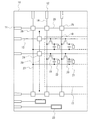
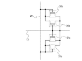
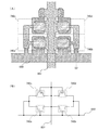
この保護回路は、共通配線29に第1端子(ゲート)及び第3端子(ドレイン)を接続し、走査線13に第2端子(ソース)を接続した二つの非線形素子(30b、31b)と、走査線13に第1端子(ゲート)及び第3端子(ドレイン)を接続し、走査線13に第2端子(ソース)を接続した二つの非線形素子(30a、31a)の計四つの非線形素子を用いている。すなわち、整流方向が互いに逆向きになるよう2つの非線形素子を接続した一組を、共通配線29と走査線13の間に二組接続している。言い換えると、走査線13と共通配線29の間に、整流方向が走査線13から共通配線29に向かう2つのトランジスタと、整流方向が共通配線29から走査線13に向かう2つのトランジスタを接続する構成である。このように、共通配線29と走査線13を四つの非線形素子で接続することで、走査線13にサージ電圧が印加された場合のみならず、共通配線29静電気等により帯電した場合であっても、その電荷がそのまま走査線13に流れ込んでしまうのを防止することができる。なお、図9に、4つの非線形素子を基板上に配置する場合の一態様を等価回路図と共に示す。図9(B)に例示する等価回路図は図3と等価であり、図9(B)に記載されたそれぞれの非線形素子は図3に記載された非線形素子に対応する。具体的には、非線形素子740aは非線形素子30bに対応し、非線形素子740bは非線形素子31bに対応し、非線形素子740cは非線形素子30aに対応し、740dは31aに対応する。また、図9の走査線651は走査線13に対応し、共通配線650は共通配線29に対応する。従って、図9(A)に例示する4つの非線形素子を基板上に配置して形成した保護回路の一態様は、図3に例示する保護回路の一態様でもある。

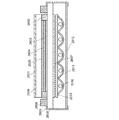
本実施の形態では、実施の形態1において図4(A)に示した保護回路の作製工程の一様態を図6及び図7を参照して説明する。図6及び図7は図4(A)中のQ1−Q2切断線に対応した断面図を表している。
本実施の形態では、本発明の一態様を適用した表示装置として同一基板上に保護回路と、画素部に配置する薄膜トランジスタを有する電子ペーパーの例を示す。
本実施の形態では、本発明の一態様の半導体装置の一例である表示装置において、同一基板上に少なくとも保護回路と、駆動回路の一部と、画素部に配置する薄膜トランジスタを作製する例について図11乃至図16を用いて以下に説明する。
本発明の一態様においては非線形素子と共に薄膜トランジスタを作製し、該薄膜トランジスタを画素部、さらには駆動回路に用いて表示機能を有する半導体装置(表示装置ともいう)を作製することができる。また、本発明の一態様においては非線形素子と薄膜トランジスタを駆動回路の一部または全体に用い、画素部と同じ基板上に一体形成し、システムオンパネルを形成することができる。
シロキサン系樹脂は、置換基に水素の他、フッ素、アルキル基、またはアリール基のうち少なくとも1種を有していてもよい。なお、これらの材料で形成される絶縁膜を複数積層させることで、絶縁層4021を形成してもよい。
本発明の一態様においては非線形素子と共に薄膜トランジスタを作製し、該薄膜トランジスタを画素部、さらには駆動回路に用いて表示機能を有する半導体装置(表示装置ともいう)を作製することができる。
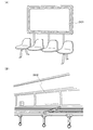
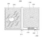
本発明の一態様の表示装置は、電子ペーパーとして適用することができる。電子ペーパーは、情報を表示するものであればあらゆる分野の電子機器に用いることが可能である。例えば、電子ペーパーを用いて、電子書籍(電子ブック)、ポスター、電車などの乗り物の車内広告、クレジットカード等の各種カードにおける表示等に適用することができる。電子機器の一例を図22、図23に示す。
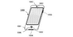
本発明の一態様に係る半導体装置は、さまざまな電子機器(遊技機も含む)に適用することができる。電子機器としては、例えば、テレビジョン装置(テレビ、またはテレビジョン受信機ともいう)、コンピュータ用などのモニタ、デジタルカメラ、デジタルビデオカメラ、デジタルフォトフレーム、携帯電話機(携帯電話、携帯電話装置ともいう)、携帯型ゲーム機、携帯情報端末、音響再生装置、パチンコ機などの大型ゲーム機などが挙げられる。
11 走査線入力端子
12 信号線入力端子
13 走査線
14 信号線
16 ゲート電極
17 画素部
18 画素
19 画素トランジスタ
20 保持容量部
21 画素電極
22 容量線
23 共通端子
24 保護回路
25 保護回路
26 保護回路
27 容量バス線
28 共通配線
29 共通配線
30 非線形素子
30a 非線形素子
30b 非線形素子
31 非線形素子
31a 非線形素子
31b 非線形素子
100 基板
102 ゲート絶縁膜
107 層間絶縁膜
111 ゲート電極
113 酸化物半導体層
117a 配線層
117b 配線層
128 コンタクトホール
131 レジストマスク
170a 非線形素子
170b 非線形素子
581 薄膜トランジスタ
585 絶縁層
587 電極層
588 電極層
589 球形粒子
590a 黒色領域
590b 白色領域
594 キャビティ
595 充填材
650 共通配線
651 走査線
730a 非線形素子
730b 非線形素子
730c 非線形素子
740a 非線形素子
740b 非線形素子
740c 非線形素子
740d 非線形素子
1000 携帯電話機
1001 筐体
1002 表示部
1003 操作ボタン
1004 外部接続ポート
1005 スピーカ
1006 マイク
2600 TFT基板
2601 対向基板
2602 シール材
2603 画素部
2604 表示素子
2605 着色層
2606 偏光板
2607 偏光板
2608 配線回路部
2609 フレキシブル配線基板
2610 冷陰極管
2611 反射板
2612 回路基板
2613 拡散板
2631 ポスター
2632 車内広告
2700 電子書籍
2701 筐体
2703 筐体
2705 表示部
2707 表示部
2711 軸部
2721 電源
2723 操作キー
2725 スピーカ
4001 基板
4002 画素部
4003 信号線駆動回路
4004 走査線駆動回路
4005 シール材
4006 基板
4008 液晶層
4010 薄膜トランジスタ
4011 薄膜トランジスタ
4013 液晶素子
4015 接続端子電極
4016 端子電極
4018 FPC
4019 異方性導電膜
4020 絶縁層
4021 絶縁層
4030 画素電極層
4031 対向電極層
4032 絶縁層
4501 基板
4502 画素部
4503a 信号線駆動回路
4504a 走査線駆動回路
4505 シール材
4506 基板
4507 充填材
4509 薄膜トランジスタ
4510 薄膜トランジスタ
4511 発光素子
4512 電界発光層
4513 電極層
4515 接続端子電極
4516 端子電極
4517 電極層
4518a FPC
4519 異方性導電膜
4520 隔壁
5300 基板
5301 画素部
5302 走査線駆動回路
5303 信号線駆動回路
5400 基板
5401 画素部
5402 走査線駆動回路
5403 信号線駆動回路
5404 走査線駆動回路
5501 配線
5502 配線
5503 配線
5504 配線
5505 配線
5506 配線
5543 ノード
5544 ノード
5571 薄膜トランジスタ
5572 薄膜トランジスタ
5573 薄膜トランジスタ
5574 薄膜トランジスタ
5575 薄膜トランジスタ
5576 薄膜トランジスタ
5577 薄膜トランジスタ
5578 薄膜トランジスタ
5601 ドライバIC
5602 スイッチ群
5603a 薄膜トランジスタ
5603b 薄膜トランジスタ
5603c 薄膜トランジスタ
5611 配線
5612 配線
5613 配線
5621 配線
5701 フリップフロップ
5703a タイミング
5703b タイミング
5703c タイミング
5711 配線
5712 配線
5713 配線
5714 配線
5715 配線
5716 配線
5717 配線
5721 信号
5803a タイミング
5803b タイミング
5803c タイミング
5821 信号
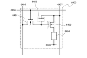
6400 画素
6401 スイッチング用トランジスタ
6402 駆動用トランジスタ
6403 容量素子
6404 発光素子
6405 信号線
6406 走査線
6407 電源線
6408 共通電極
7001 TFT
7002 発光素子
7003 陰極
7004 発光層
7005 陽極
7011 駆動用TFT
7012 発光素子
7013 陰極
7014 発光層
7015 陽極
7016 遮蔽膜
7017 導電膜
7021 駆動用TFT
7022 発光素子
7023 陰極
7024 発光層
7025 陽極
7027 導電膜
9600 テレビジョン装置
9601 筐体
9603 表示部
9605 スタンド
9607 表示部
9609 操作キー
9610 リモコン操作機
9700 デジタルフォトフレーム
9701 筐体
9703 表示部
9881 筐体
9882 表示部
9883 表示部
9884 スピーカ部
9885 入力手段(操作キー)
9886 記録媒体挿入部
9887 接続端子
9888 センサ
9889 マイクロフォン
9890 LEDランプ
9891 筐体
9893 連結部
9900 スロットマシン
9901 筐体
9903 表示部
Claims (3)
- 絶縁表面を有する基板上に走査線と信号線が交差して設けられ、
画素電極がマトリクス状に配列する画素部を有する表示装置であり、
前記画素部は、酸化物半導体層にチャネル形成領域が形成される薄膜トランジスタを有し、
前記薄膜トランジスタは、前記走査線と接続するゲート電極と、
前記信号線と接続し前記酸化物半導体層に接する第1配線層を有し、
前記基板の周辺部に配設される信号入力端子と前記画素部の間には、非線形素子が設けられ、
前記非線形素子は、ゲート電極及び該ゲート電極を被覆するゲート絶縁膜と、
前記ゲート絶縁膜上において前記ゲート電極と端部が重畳する第1配線層及び第2配線層と、
少なくとも前記ゲート電極と重畳し前記ゲート絶縁膜及び前記第1配線層及び前記第2配線層の側面部及び上面部と接する酸化物半導体層とを有し、
前記非線形素子のゲート電極は走査線又は信号線と接続され、前記非線形素子の第1配線層又は第2配線層が、前記ゲート電極の電位が印加されるようにゲート電極層と直接接続されていることを特徴とする表示装置。 - 絶縁表面を有する基板上に走査線と信号線が交差して設けられ、
画素電極がマトリクス状に配列する画素部を有する表示装置であり、
前記画素部は、酸化物半導体層にチャネル形成領域が形成される薄膜トランジスタを有し、
前記薄膜トランジスタは、前記走査線と接続するゲート電極と、
前記信号線と接続し前記酸化物半導体層に接する第1配線層と、
前記画素電極と接続し前記酸化物半導体層に接する第2配線層とを有し、
前記基板上であり前記画素部の外側領域に、前記走査線と共通配線を接続する保護回路と、
前記信号線と共通配線を接続する保護回路とが設けられ、
前記保護回路は、ゲート電極及び該ゲート電極を被覆するゲート絶縁膜と、
前記ゲート絶縁膜上において前記ゲート電極と端部が重畳する第1配線層及び第2配線層と、
少なくとも前記ゲート電極と重畳し前記ゲート絶縁膜及び前記第1配線層及び前記第2配線層の側面部及び上面部と接する酸化物半導体層とを有する非線形素子を有し、
前記非線形素子のゲート電極と、第1配線層又は第2配線層が直接接続されていることを特徴とする表示装置。 - 請求項1又は2において、
前記酸化物半導体層は、インジウム、ガリウム、及び亜鉛を含むことを特徴とする表示装置。
Priority Applications (1)
| Application Number | Priority Date | Filing Date | Title |
|---|---|---|---|
| JP2009229378A JP2010107976A (ja) | 2008-10-03 | 2009-10-01 | 表示装置 |
Applications Claiming Priority (2)
| Application Number | Priority Date | Filing Date | Title |
|---|---|---|---|
| JP2008259063 | 2008-10-03 | ||
| JP2009229378A JP2010107976A (ja) | 2008-10-03 | 2009-10-01 | 表示装置 |
Related Child Applications (1)
| Application Number | Title | Priority Date | Filing Date |
|---|---|---|---|
| JP2013192573A Division JP5766246B2 (ja) | 2008-10-03 | 2013-09-18 | 半導体装置 |
Publications (2)
| Publication Number | Publication Date |
|---|---|
| JP2010107976A true JP2010107976A (ja) | 2010-05-13 |
| JP2010107976A5 JP2010107976A5 (ja) | 2012-02-02 |
Family
ID=42073577
Family Applications (4)
| Application Number | Title | Priority Date | Filing Date |
|---|---|---|---|
| JP2009229378A Withdrawn JP2010107976A (ja) | 2008-10-03 | 2009-10-01 | 表示装置 |
| JP2013192573A Active JP5766246B2 (ja) | 2008-10-03 | 2013-09-18 | 半導体装置 |
| JP2015120826A Active JP6010188B2 (ja) | 2008-10-03 | 2015-06-16 | 表示装置及び表示モジュール |
| JP2016180092A Active JP6317406B2 (ja) | 2008-10-03 | 2016-09-15 | 半導体装置及び表示装置 |
Family Applications After (3)
| Application Number | Title | Priority Date | Filing Date |
|---|---|---|---|
| JP2013192573A Active JP5766246B2 (ja) | 2008-10-03 | 2013-09-18 | 半導体装置 |
| JP2015120826A Active JP6010188B2 (ja) | 2008-10-03 | 2015-06-16 | 表示装置及び表示モジュール |
| JP2016180092A Active JP6317406B2 (ja) | 2008-10-03 | 2016-09-15 | 半導体装置及び表示装置 |
Country Status (5)
| Country | Link |
|---|---|
| US (3) | US7989815B2 (ja) |
| JP (4) | JP2010107976A (ja) |
| KR (4) | KR101803720B1 (ja) |
| TW (2) | TWI469302B (ja) |
| WO (1) | WO2010038819A1 (ja) |
Cited By (9)
| Publication number | Priority date | Publication date | Assignee | Title |
|---|---|---|---|---|
| KR20140068765A (ko) | 2012-11-28 | 2014-06-09 | 가부시키가이샤 한도오따이 에네루기 켄큐쇼 | 표시 장치 및 전자 기기 |
| KR20140068762A (ko) | 2012-11-28 | 2014-06-09 | 가부시키가이샤 한도오따이 에네루기 켄큐쇼 | 표시 장치 |
| KR20140082934A (ko) | 2012-12-25 | 2014-07-03 | 가부시키가이샤 한도오따이 에네루기 켄큐쇼 | 저항 소자, 표시 장치, 및 전자기기 |
| JP2015115428A (ja) * | 2013-12-11 | 2015-06-22 | 凸版印刷株式会社 | 静電気保護素子及びそれを用いた静電気保護回路 |
| KR20150122166A (ko) | 2013-02-25 | 2015-10-30 | 가부시키가이샤 한도오따이 에네루기 켄큐쇼 | 표시 장치 및 전자 기기 |
| TWI607210B (zh) * | 2012-02-10 | 2017-12-01 | 美商克萊譚克公司 | 於半導體裝置檢查系統中用於切趾的檢查系統 |
| JP2019204960A (ja) * | 2013-04-04 | 2019-11-28 | 株式会社半導体エネルギー研究所 | 半導体装置 |
| JP2021040140A (ja) * | 2010-09-10 | 2021-03-11 | 株式会社半導体エネルギー研究所 | 半導体装置 |
| KR20220110719A (ko) * | 2010-09-13 | 2022-08-09 | 가부시키가이샤 한도오따이 에네루기 켄큐쇼 | 반도체 장치, 파워 다이오드 및 정류기 |
Families Citing this family (33)
| Publication number | Priority date | Publication date | Assignee | Title |
|---|---|---|---|---|
| CN102881696A (zh) | 2008-09-19 | 2013-01-16 | 株式会社半导体能源研究所 | 显示装置 |
| KR101722409B1 (ko) * | 2008-09-19 | 2017-04-03 | 가부시키가이샤 한도오따이 에네루기 켄큐쇼 | 반도체 장치 |
| KR101803720B1 (ko) | 2008-10-03 | 2017-12-01 | 가부시키가이샤 한도오따이 에네루기 켄큐쇼 | 표시 장치 |
| EP2172804B1 (en) | 2008-10-03 | 2016-05-11 | Semiconductor Energy Laboratory Co, Ltd. | Display device |
| CN101719493B (zh) | 2008-10-08 | 2014-05-14 | 株式会社半导体能源研究所 | 显示装置 |
| KR101460868B1 (ko) | 2009-07-10 | 2014-11-11 | 가부시키가이샤 한도오따이 에네루기 켄큐쇼 | 반도체 장치 |
| WO2011048925A1 (en) | 2009-10-21 | 2011-04-28 | Semiconductor Energy Laboratory Co., Ltd. | Method for manufacturing semiconductor device |
| WO2011052258A1 (ja) * | 2009-10-27 | 2011-05-05 | シャープ株式会社 | 表示パネル及び表示装置 |
| WO2011052437A1 (en) | 2009-10-30 | 2011-05-05 | Semiconductor Energy Laboratory Co., Ltd. | Non-linear element, display device including non-linear element, and electronic device including display device |
| WO2011065209A1 (en) * | 2009-11-27 | 2011-06-03 | Semiconductor Energy Laboratory Co., Ltd. | Non-linear element, display device including non-linear element, and electronic device including display device |
| WO2011086905A1 (ja) * | 2010-01-13 | 2011-07-21 | シャープ株式会社 | アクティブマトリクス基板及びその製造方法 |
| JP5494115B2 (ja) * | 2010-03-29 | 2014-05-14 | ソニー株式会社 | 表示装置及び電子機器 |
| TWI410722B (zh) * | 2010-09-02 | 2013-10-01 | Au Optronics Corp | 液晶顯示單元 |
| WO2012043971A2 (ko) * | 2010-09-29 | 2012-04-05 | 포항공과대학교 산학협력단 | 롤 형상의 모기판을 이용한 플렉서블 전자소자의 제조방법, 플렉서블 전자소자 및 플렉서블 기판 |
| TWI624878B (zh) | 2011-03-11 | 2018-05-21 | 半導體能源研究所股份有限公司 | 半導體裝置的製造方法 |
| KR102378948B1 (ko) | 2011-07-22 | 2022-03-24 | 가부시키가이샤 한도오따이 에네루기 켄큐쇼 | 발광 장치 |
| TWI470808B (zh) | 2011-12-28 | 2015-01-21 | Au Optronics Corp | 半導體元件及其製作方法 |
| DE102012205415A1 (de) * | 2012-04-03 | 2013-10-10 | Bayerische Motoren Werke Aktiengesellschaft | Fahrzeug |
| KR20140059576A (ko) * | 2012-11-08 | 2014-05-16 | 삼성디스플레이 주식회사 | 박막 트랜지스터 및 이를 포함하는 유기 발광 디스플레이 장치 |
| KR102105485B1 (ko) * | 2012-11-23 | 2020-04-29 | 삼성디스플레이 주식회사 | 박막 트랜지스터 기판 및 그 제조 방법 |
| KR102209871B1 (ko) | 2012-12-25 | 2021-02-01 | 가부시키가이샤 한도오따이 에네루기 켄큐쇼 | 반도체 장치 |
| JP6083089B2 (ja) * | 2013-03-27 | 2017-02-22 | 株式会社Joled | 半導体装置、表示装置および電子機器 |
| US9915848B2 (en) | 2013-04-19 | 2018-03-13 | Semiconductor Energy Laboratory Co., Ltd. | Display device and electronic device |
| KR102053410B1 (ko) * | 2013-04-24 | 2019-12-09 | 삼성디스플레이 주식회사 | 박막 트랜지스터 및 유기 발광 표시 장치 |
| US9704894B2 (en) | 2013-05-10 | 2017-07-11 | Semiconductor Energy Laboratory Co., Ltd. | Display device including pixel electrode including oxide |
| TWI687748B (zh) | 2013-06-05 | 2020-03-11 | 日商半導體能源研究所股份有限公司 | 顯示裝置及電子裝置 |
| CN103995407B (zh) | 2014-05-08 | 2016-08-24 | 京东方科技集团股份有限公司 | 阵列基板和显示面板 |
| WO2016063169A1 (en) | 2014-10-23 | 2016-04-28 | Semiconductor Energy Laboratory Co., Ltd. | Light-emitting element |
| US10680017B2 (en) | 2014-11-07 | 2020-06-09 | Semiconductor Energy Laboratory Co., Ltd. | Light-emitting element including EL layer, electrode which has high reflectance and a high work function, display device, electronic device, and lighting device |
| CN105470388B (zh) * | 2015-11-18 | 2018-09-28 | 深圳市华星光电技术有限公司 | 有机半导体薄膜晶体管及其制作方法 |
| KR102517092B1 (ko) * | 2017-08-02 | 2023-04-04 | 삼성전자주식회사 | 가요성 디스플레이 패널을 포함하는 전자 장치 |
| CN107274851A (zh) * | 2017-08-14 | 2017-10-20 | 京东方科技集团股份有限公司 | 显示面板及其驱动方法和显示装置 |
| US11287707B2 (en) * | 2018-11-15 | 2022-03-29 | Sharp Kabushiki Kaisha | Array substrate, array substrate body component, and display device |
Citations (12)
| Publication number | Priority date | Publication date | Assignee | Title |
|---|---|---|---|---|
| JPS63220289A (ja) * | 1987-03-10 | 1988-09-13 | 日本電気株式会社 | 薄膜トランジスタアレイ |
| JPH0588198A (ja) * | 1991-09-27 | 1993-04-09 | Nec Corp | 液晶表示装置 |
| JPH08179360A (ja) * | 1994-12-20 | 1996-07-12 | Casio Comput Co Ltd | アクティブマトリックスパネル |
| JPH09504120A (ja) * | 1993-10-22 | 1997-04-22 | コピン・コーポレーシヨン | 頭部装着形表示システム |
| JPH11183876A (ja) * | 1997-12-24 | 1999-07-09 | Casio Comput Co Ltd | 液晶表示装置及びその駆動方法 |
| JP2003086808A (ja) * | 2001-09-10 | 2003-03-20 | Masashi Kawasaki | 薄膜トランジスタおよびマトリクス表示装置 |
| JP2007096055A (ja) * | 2005-09-29 | 2007-04-12 | Semiconductor Energy Lab Co Ltd | 半導体装置、及び半導体装置の作製方法 |
| JP2007220818A (ja) * | 2006-02-15 | 2007-08-30 | Kochi Prefecture Sangyo Shinko Center | 薄膜トランジスタ及びその製法 |
| JP2007250982A (ja) * | 2006-03-17 | 2007-09-27 | Canon Inc | 酸化物半導体を用いた薄膜トランジスタ及び表示装置 |
| JP2008053356A (ja) * | 2006-08-23 | 2008-03-06 | Canon Inc | アモルファス酸化物半導体膜を用いた薄膜トランジスタの製造方法 |
| JP2008107807A (ja) * | 2006-09-29 | 2008-05-08 | Semiconductor Energy Lab Co Ltd | 液晶表示装置および電子機器 |
| JP2008182219A (ja) * | 2006-12-28 | 2008-08-07 | Semiconductor Energy Lab Co Ltd | 半導体装置 |
Family Cites Families (184)
| Publication number | Priority date | Publication date | Assignee | Title |
|---|---|---|---|---|
| US3819952A (en) | 1973-01-29 | 1974-06-25 | Mitsubishi Electric Corp | Semiconductor device |
| EP0445535B1 (en) | 1990-02-06 | 1995-02-01 | Sel Semiconductor Energy Laboratory Co., Ltd. | Method of forming an oxide film |
| JP3071851B2 (ja) | 1991-03-25 | 2000-07-31 | 株式会社半導体エネルギー研究所 | 電気光学装置 |
| JP3375659B2 (ja) * | 1991-03-28 | 2003-02-10 | テキサス インスツルメンツ インコーポレイテツド | 静電放電保護回路の形成方法 |
| US5233448A (en) * | 1992-05-04 | 1993-08-03 | Industrial Technology Research Institute | Method of manufacturing a liquid crystal display panel including photoconductive electrostatic protection |
| US5464990A (en) * | 1992-09-25 | 1995-11-07 | Fuji Xerox Co., Ltd. | Voltage non-linear device and liquid crystal display device incorporating same |
| US6424321B1 (en) | 1993-10-22 | 2002-07-23 | Kopin Corporation | Head-mounted matrix display |
| US7310072B2 (en) | 1993-10-22 | 2007-12-18 | Kopin Corporation | Portable communication display device |
| US5815126A (en) | 1993-10-22 | 1998-09-29 | Kopin Corporation | Monocular portable communication and display system |
| JP2701738B2 (ja) | 1994-05-17 | 1998-01-21 | 日本電気株式会社 | 有機薄膜el素子 |
| JPH08179359A (ja) * | 1994-12-20 | 1996-07-12 | Casio Comput Co Ltd | アクティブマトリックスパネル |
| JPH08254693A (ja) * | 1995-03-16 | 1996-10-01 | Hitachi Ltd | 液晶表示基板およびその製造方法 |
| EP0820644B1 (en) * | 1995-08-03 | 2005-08-24 | Koninklijke Philips Electronics N.V. | Semiconductor device provided with transparent switching element |
| JP3007025B2 (ja) * | 1995-08-25 | 2000-02-07 | シャープ株式会社 | アクティブマトリクス型液晶表示装置及びその製造方法 |
| JP3183390B2 (ja) * | 1995-09-05 | 2001-07-09 | キヤノン株式会社 | 光電変換装置及びそれを用いた撮像装置 |
| CN1145839C (zh) * | 1995-10-03 | 2004-04-14 | 精工爱普生株式会社 | 薄膜元件的制造方法 |
| US5847410A (en) | 1995-11-24 | 1998-12-08 | Semiconductor Energy Laboratory Co. | Semiconductor electro-optical device |
| JP3625598B2 (ja) * | 1995-12-30 | 2005-03-02 | 三星電子株式会社 | 液晶表示装置の製造方法 |
| JP3629798B2 (ja) * | 1996-02-20 | 2005-03-16 | カシオ計算機株式会社 | 配線パターン |
| JPH1020336A (ja) * | 1996-07-02 | 1998-01-23 | Sharp Corp | アクティブマトリクス基板およびその製造方法 |
| JPH10123574A (ja) * | 1996-10-17 | 1998-05-15 | Hitachi Ltd | アクティブマトリクス基板 |
| KR100252308B1 (ko) | 1997-01-10 | 2000-04-15 | 구본준, 론 위라하디락사 | 박막트랜지스터 어레이 |
| JPH11174970A (ja) * | 1997-12-16 | 1999-07-02 | Hitachi Ltd | 薄膜デバイス |
| JP4170454B2 (ja) | 1998-07-24 | 2008-10-22 | Hoya株式会社 | 透明導電性酸化物薄膜を有する物品及びその製造方法 |
| JP4264675B2 (ja) | 1998-08-17 | 2009-05-20 | 栄 田中 | 液晶表示装置とその製造方法 |
| US6043971A (en) * | 1998-11-04 | 2000-03-28 | L.G. Philips Lcd Co., Ltd. | Electrostatic discharge protection device for liquid crystal display using a COG package |
| JP2000150861A (ja) * | 1998-11-16 | 2000-05-30 | Tdk Corp | 酸化物薄膜 |
| JP3276930B2 (ja) * | 1998-11-17 | 2002-04-22 | 科学技術振興事業団 | トランジスタ及び半導体装置 |
| TW444257B (en) * | 1999-04-12 | 2001-07-01 | Semiconductor Energy Lab | Semiconductor device and method for fabricating the same |
| US7379039B2 (en) * | 1999-07-14 | 2008-05-27 | Sony Corporation | Current drive circuit and display device using same pixel circuit, and drive method |
| TW526455B (en) * | 1999-07-14 | 2003-04-01 | Sony Corp | Current drive circuit and display comprising the same, pixel circuit, and drive method |
| JP2001053283A (ja) * | 1999-08-12 | 2001-02-23 | Semiconductor Energy Lab Co Ltd | 半導体装置及びその作製方法 |
| TW457690B (en) * | 1999-08-31 | 2001-10-01 | Fujitsu Ltd | Liquid crystal display |
| JP4390991B2 (ja) * | 1999-08-31 | 2009-12-24 | シャープ株式会社 | 液晶表示装置 |
| TW460731B (en) | 1999-09-03 | 2001-10-21 | Ind Tech Res Inst | Electrode structure and production method of wide viewing angle LCD |
| US7098084B2 (en) | 2000-03-08 | 2006-08-29 | Semiconductor Energy Laboratory Co., Ltd. | Semiconductor device and manufacturing method thereof |
| JP2001324725A (ja) * | 2000-05-12 | 2001-11-22 | Hitachi Ltd | 液晶表示装置およびその製造方法 |
| JP2002026333A (ja) | 2000-07-11 | 2002-01-25 | Nec Corp | アクティブマトリクス基板の製造方法 |
| JP4089858B2 (ja) | 2000-09-01 | 2008-05-28 | 国立大学法人東北大学 | 半導体デバイス |
| KR20020038482A (ko) * | 2000-11-15 | 2002-05-23 | 모리시타 요이찌 | 박막 트랜지스터 어레이, 그 제조방법 및 그것을 이용한표시패널 |
| JP3997731B2 (ja) * | 2001-03-19 | 2007-10-24 | 富士ゼロックス株式会社 | 基材上に結晶性半導体薄膜を形成する方法 |
| JP2002289859A (ja) | 2001-03-23 | 2002-10-04 | Minolta Co Ltd | 薄膜トランジスタ |
| KR100386849B1 (ko) * | 2001-07-10 | 2003-06-09 | 엘지.필립스 엘시디 주식회사 | 박막 트랜지스터 표시장치의 정전방전 방지회로 |
| GB0119299D0 (en) | 2001-08-08 | 2001-10-03 | Koninkl Philips Electronics Nv | Electrostatic discharge protection for pixellated electronic device |
| JP2003069028A (ja) | 2001-08-27 | 2003-03-07 | Casio Comput Co Ltd | 薄膜トランジスタパネル |
| JP3925839B2 (ja) | 2001-09-10 | 2007-06-06 | シャープ株式会社 | 半導体記憶装置およびその試験方法 |
| JP3810725B2 (ja) * | 2001-09-21 | 2006-08-16 | 株式会社半導体エネルギー研究所 | 発光装置及び電子機器 |
| WO2003040441A1 (en) * | 2001-11-05 | 2003-05-15 | Japan Science And Technology Agency | Natural superlattice homologous single crystal thin film, method for preparation thereof, and device using said single crystal thin film |
| JP4164562B2 (ja) | 2002-09-11 | 2008-10-15 | 独立行政法人科学技術振興機構 | ホモロガス薄膜を活性層として用いる透明薄膜電界効果型トランジスタ |
| JP3810681B2 (ja) | 2001-12-20 | 2006-08-16 | シャープ株式会社 | 薄膜トランジスタ基板および液晶表示装置 |
| JP4083486B2 (ja) * | 2002-02-21 | 2008-04-30 | 独立行政法人科学技術振興機構 | LnCuO(S,Se,Te)単結晶薄膜の製造方法 |
| US7049190B2 (en) * | 2002-03-15 | 2006-05-23 | Sanyo Electric Co., Ltd. | Method for forming ZnO film, method for forming ZnO semiconductor layer, method for fabricating semiconductor device, and semiconductor device |
| JP3933591B2 (ja) * | 2002-03-26 | 2007-06-20 | 淳二 城戸 | 有機エレクトロルミネッセント素子 |
| US6933528B2 (en) * | 2002-04-04 | 2005-08-23 | Nec Lcd Technologies, Ltd. | In-plane switching mode active matrix type liquid crystal display device and method of fabricating the same |
| US7339187B2 (en) | 2002-05-21 | 2008-03-04 | State Of Oregon Acting By And Through The Oregon State Board Of Higher Education On Behalf Of Oregon State University | Transistor structures |
| US7002176B2 (en) | 2002-05-31 | 2006-02-21 | Ricoh Company, Ltd. | Vertical organic transistor |
| JP2004022625A (ja) * | 2002-06-13 | 2004-01-22 | Murata Mfg Co Ltd | 半導体デバイス及び該半導体デバイスの製造方法 |
| US7105868B2 (en) * | 2002-06-24 | 2006-09-12 | Cermet, Inc. | High-electron mobility transistor with zinc oxide |
| JP4565799B2 (ja) * | 2002-07-01 | 2010-10-20 | 大林精工株式会社 | 横電界方式液晶表示装置、その製造方法、走査露光装置およびミックス走査露光装置 |
| TWI357616B (en) * | 2002-09-20 | 2012-02-01 | Semiconductor Energy Lab | Display device and manufacturing method thereof |
| US7067843B2 (en) * | 2002-10-11 | 2006-06-27 | E. I. Du Pont De Nemours And Company | Transparent oxide semiconductor thin film transistors |
| TW200415393A (en) * | 2003-01-15 | 2004-08-16 | Toshiba Matsushita Display Tec | LCD device |
| JP2004246202A (ja) | 2003-02-14 | 2004-09-02 | Koninkl Philips Electronics Nv | 静電放電保護回路を有する電子装置 |
| JP4166105B2 (ja) | 2003-03-06 | 2008-10-15 | シャープ株式会社 | 半導体装置およびその製造方法 |
| JP2004273732A (ja) | 2003-03-07 | 2004-09-30 | Sharp Corp | アクティブマトリクス基板およびその製造方法 |
| KR100528697B1 (ko) * | 2003-05-06 | 2005-11-16 | 엘지.필립스 엘시디 주식회사 | 액정표시장치의 검사방법 및 장치 |
| JP4108633B2 (ja) | 2003-06-20 | 2008-06-25 | シャープ株式会社 | 薄膜トランジスタおよびその製造方法ならびに電子デバイス |
| US7262463B2 (en) * | 2003-07-25 | 2007-08-28 | Hewlett-Packard Development Company, L.P. | Transistor including a deposited channel region having a doped portion |
| JP2005108912A (ja) * | 2003-09-29 | 2005-04-21 | Quanta Display Japan Inc | 液晶表示装置とその製造方法 |
| JP4574158B2 (ja) | 2003-10-28 | 2010-11-04 | 株式会社半導体エネルギー研究所 | 半導体表示装置及びその作製方法 |
| US7282782B2 (en) * | 2004-03-12 | 2007-10-16 | Hewlett-Packard Development Company, L.P. | Combined binary oxide semiconductor device |
| KR20070116888A (ko) | 2004-03-12 | 2007-12-11 | 도꾸리쯔교세이호징 가가꾸 기쥬쯔 신꼬 기꼬 | 아몰퍼스 산화물 및 박막 트랜지스터 |
| US7145174B2 (en) * | 2004-03-12 | 2006-12-05 | Hewlett-Packard Development Company, Lp. | Semiconductor device |
| US7297977B2 (en) | 2004-03-12 | 2007-11-20 | Hewlett-Packard Development Company, L.P. | Semiconductor device |
| KR101116816B1 (ko) | 2004-06-05 | 2012-02-28 | 엘지디스플레이 주식회사 | 반투과형 박막 트랜지스터 기판 및 그 제조 방법 |
| US7211825B2 (en) * | 2004-06-14 | 2007-05-01 | Yi-Chi Shih | Indium oxide-based thin film transistors and circuits |
| TWI229933B (en) | 2004-06-25 | 2005-03-21 | Novatek Microelectronics Corp | High voltage device for electrostatic discharge protective circuit and high voltage device |
| JP2006030627A (ja) | 2004-07-16 | 2006-02-02 | Sharp Corp | 表示装置用基板及びそれを用いた液晶表示装置 |
| JP4193805B2 (ja) * | 2004-07-27 | 2008-12-10 | セイコーエプソン株式会社 | 発光装置および画像形成装置 |
| JP2006100760A (ja) * | 2004-09-02 | 2006-04-13 | Casio Comput Co Ltd | 薄膜トランジスタおよびその製造方法 |
| US7285501B2 (en) * | 2004-09-17 | 2007-10-23 | Hewlett-Packard Development Company, L.P. | Method of forming a solution processed device |
| US7298084B2 (en) * | 2004-11-02 | 2007-11-20 | 3M Innovative Properties Company | Methods and displays utilizing integrated zinc oxide row and column drivers in conjunction with organic light emitting diodes |
| EP1815530B1 (en) * | 2004-11-10 | 2021-02-17 | Canon Kabushiki Kaisha | Field effect transistor employing an amorphous oxide |
| BRPI0517568B8 (pt) * | 2004-11-10 | 2022-03-03 | Canon Kk | Transistor de efeito de campo |
| US7791072B2 (en) * | 2004-11-10 | 2010-09-07 | Canon Kabushiki Kaisha | Display |
| US7453065B2 (en) * | 2004-11-10 | 2008-11-18 | Canon Kabushiki Kaisha | Sensor and image pickup device |
| US7829444B2 (en) * | 2004-11-10 | 2010-11-09 | Canon Kabushiki Kaisha | Field effect transistor manufacturing method |
| US7863611B2 (en) * | 2004-11-10 | 2011-01-04 | Canon Kabushiki Kaisha | Integrated circuits utilizing amorphous oxides |
| JP5118811B2 (ja) * | 2004-11-10 | 2013-01-16 | キヤノン株式会社 | 発光装置及び表示装置 |
| US7579224B2 (en) * | 2005-01-21 | 2009-08-25 | Semiconductor Energy Laboratory Co., Ltd. | Method for manufacturing a thin film semiconductor device |
| TWI412138B (zh) * | 2005-01-28 | 2013-10-11 | Semiconductor Energy Lab | 半導體裝置,電子裝置,和半導體裝置的製造方法 |
| US7608531B2 (en) * | 2005-01-28 | 2009-10-27 | Semiconductor Energy Laboratory Co., Ltd. | Semiconductor device, electronic device, and method of manufacturing semiconductor device |
| US7858451B2 (en) * | 2005-02-03 | 2010-12-28 | Semiconductor Energy Laboratory Co., Ltd. | Electronic device, semiconductor device and manufacturing method thereof |
| US7948171B2 (en) * | 2005-02-18 | 2011-05-24 | Semiconductor Energy Laboratory Co., Ltd. | Light emitting device |
| JP2006245093A (ja) | 2005-03-01 | 2006-09-14 | Renei Kagi Kofun Yugenkoshi | 高電圧デバイス並びに静電気保護回路用高電圧デバイス |
| US20060197092A1 (en) * | 2005-03-03 | 2006-09-07 | Randy Hoffman | System and method for forming conductive material on a substrate |
| US8681077B2 (en) * | 2005-03-18 | 2014-03-25 | Semiconductor Energy Laboratory Co., Ltd. | Semiconductor device, and display device, driving method and electronic apparatus thereof |
| WO2006105077A2 (en) * | 2005-03-28 | 2006-10-05 | Massachusetts Institute Of Technology | Low voltage thin film transistor with high-k dielectric material |
| US7645478B2 (en) * | 2005-03-31 | 2010-01-12 | 3M Innovative Properties Company | Methods of making displays |
| US8300031B2 (en) * | 2005-04-20 | 2012-10-30 | Semiconductor Energy Laboratory Co., Ltd. | Semiconductor device comprising transistor having gate and drain connected through a current-voltage conversion element |
| CN100538794C (zh) | 2005-05-02 | 2009-09-09 | 株式会社半导体能源研究所 | 发光器件及其驱动方法、显示模块以及电子器具 |
| JP2006344849A (ja) | 2005-06-10 | 2006-12-21 | Casio Comput Co Ltd | 薄膜トランジスタ |
| TWI260094B (en) | 2005-06-13 | 2006-08-11 | Au Optronics Corp | Active device matrix substrate |
| US7402506B2 (en) * | 2005-06-16 | 2008-07-22 | Eastman Kodak Company | Methods of making thin film transistors comprising zinc-oxide-based semiconductor materials and transistors made thereby |
| US7691666B2 (en) | 2005-06-16 | 2010-04-06 | Eastman Kodak Company | Methods of making thin film transistors comprising zinc-oxide-based semiconductor materials and transistors made thereby |
| US7507618B2 (en) | 2005-06-27 | 2009-03-24 | 3M Innovative Properties Company | Method for making electronic devices using metal oxide nanoparticles |
| US7732330B2 (en) | 2005-06-30 | 2010-06-08 | Semiconductor Energy Laboratory Co., Ltd. | Semiconductor device and manufacturing method using an ink-jet method of the same |
| US7655566B2 (en) | 2005-07-27 | 2010-02-02 | Semiconductor Energy Laboratory Co., Ltd. | Method for manufacturing semiconductor device |
| KR100711890B1 (ko) * | 2005-07-28 | 2007-04-25 | 삼성에스디아이 주식회사 | 유기 발광표시장치 및 그의 제조방법 |
| JP4039446B2 (ja) * | 2005-08-02 | 2008-01-30 | エプソンイメージングデバイス株式会社 | 電気光学装置及び電子機器 |
| JP2007059128A (ja) * | 2005-08-23 | 2007-03-08 | Canon Inc | 有機el表示装置およびその製造方法 |
| JP2007073705A (ja) * | 2005-09-06 | 2007-03-22 | Canon Inc | 酸化物半導体チャネル薄膜トランジスタおよびその製造方法 |
| JP4280736B2 (ja) * | 2005-09-06 | 2009-06-17 | キヤノン株式会社 | 半導体素子 |
| JP4850457B2 (ja) | 2005-09-06 | 2012-01-11 | キヤノン株式会社 | 薄膜トランジスタ及び薄膜ダイオード |
| JP5116225B2 (ja) * | 2005-09-06 | 2013-01-09 | キヤノン株式会社 | 酸化物半導体デバイスの製造方法 |
| JP5064747B2 (ja) | 2005-09-29 | 2012-10-31 | 株式会社半導体エネルギー研究所 | 半導体装置、電気泳動表示装置、表示モジュール、電子機器、及び半導体装置の作製方法 |
| EP1998375A3 (en) * | 2005-09-29 | 2012-01-18 | Semiconductor Energy Laboratory Co, Ltd. | Semiconductor device having oxide semiconductor layer and manufacturing method |
| US7982215B2 (en) | 2005-10-05 | 2011-07-19 | Idemitsu Kosan Co., Ltd. | TFT substrate and method for manufacturing TFT substrate |
| JP5037808B2 (ja) * | 2005-10-20 | 2012-10-03 | キヤノン株式会社 | アモルファス酸化物を用いた電界効果型トランジスタ、及び該トランジスタを用いた表示装置 |
| JP5089139B2 (ja) | 2005-11-15 | 2012-12-05 | 株式会社半導体エネルギー研究所 | 半導体装置の作製方法 |
| KR101358954B1 (ko) | 2005-11-15 | 2014-02-06 | 가부시키가이샤 한도오따이 에네루기 켄큐쇼 | 다이오드 및 액티브 매트릭스 표시장치 |
| JP4846348B2 (ja) * | 2005-11-18 | 2011-12-28 | 株式会社 日立ディスプレイズ | 表示装置 |
| KR100754126B1 (ko) * | 2005-11-23 | 2007-08-30 | 삼성에스디아이 주식회사 | 액정표시장치 어레이 기판 및 그 제조방법 |
| JP5250929B2 (ja) | 2005-11-30 | 2013-07-31 | 凸版印刷株式会社 | トランジスタおよびその製造方法 |
| US20070146564A1 (en) * | 2005-12-23 | 2007-06-28 | Innolux Display Corp. | ESD protection circuit and driving circuit for LCD |
| TWI292281B (en) * | 2005-12-29 | 2008-01-01 | Ind Tech Res Inst | Pixel structure of active organic light emitting diode and method of fabricating the same |
| US7867636B2 (en) * | 2006-01-11 | 2011-01-11 | Murata Manufacturing Co., Ltd. | Transparent conductive film and method for manufacturing the same |
| JP4977478B2 (ja) * | 2006-01-21 | 2012-07-18 | 三星電子株式会社 | ZnOフィルム及びこれを用いたTFTの製造方法 |
| US7576394B2 (en) * | 2006-02-02 | 2009-08-18 | Kochi Industrial Promotion Center | Thin film transistor including low resistance conductive thin films and manufacturing method thereof |
| JP2007212699A (ja) * | 2006-02-09 | 2007-08-23 | Idemitsu Kosan Co Ltd | 反射型tft基板及び反射型tft基板の製造方法 |
| US7977169B2 (en) * | 2006-02-15 | 2011-07-12 | Kochi Industrial Promotion Center | Semiconductor device including active layer made of zinc oxide with controlled orientations and manufacturing method thereof |
| US8222116B2 (en) * | 2006-03-03 | 2012-07-17 | Semiconductor Energy Laboratory Co., Ltd. | Method for manufacturing semiconductor device |
| JP2007272203A (ja) | 2006-03-06 | 2007-10-18 | Nec Corp | 表示装置 |
| JP5110803B2 (ja) | 2006-03-17 | 2012-12-26 | キヤノン株式会社 | 酸化物膜をチャネルに用いた電界効果型トランジスタ及びその製造方法 |
| KR20070101595A (ko) | 2006-04-11 | 2007-10-17 | 삼성전자주식회사 | ZnO TFT |
| US20070246778A1 (en) | 2006-04-21 | 2007-10-25 | Meng-Chi Liou | Electrostatic discharge panel protection structure |
| US20070252928A1 (en) | 2006-04-28 | 2007-11-01 | Toppan Printing Co., Ltd. | Structure, transmission type liquid crystal display, reflection type display and manufacturing method thereof |
| KR100847640B1 (ko) * | 2006-05-23 | 2008-07-21 | 가시오게산키 가부시키가이샤 | 표시장치 |
| JP2007316105A (ja) * | 2006-05-23 | 2007-12-06 | Casio Comput Co Ltd | 表示装置 |
| JP5028033B2 (ja) | 2006-06-13 | 2012-09-19 | キヤノン株式会社 | 酸化物半導体膜のドライエッチング方法 |
| KR101478810B1 (ko) | 2006-07-28 | 2015-01-02 | 가부시키가이샤 한도오따이 에네루기 켄큐쇼 | 축전 장치 |
| JP4609797B2 (ja) * | 2006-08-09 | 2011-01-12 | Nec液晶テクノロジー株式会社 | 薄膜デバイス及びその製造方法 |
| JP4999400B2 (ja) * | 2006-08-09 | 2012-08-15 | キヤノン株式会社 | 酸化物半導体膜のドライエッチング方法 |
| JP4404881B2 (ja) * | 2006-08-09 | 2010-01-27 | 日本電気株式会社 | 薄膜トランジスタアレイ、その製造方法及び液晶表示装置 |
| JP4332545B2 (ja) * | 2006-09-15 | 2009-09-16 | キヤノン株式会社 | 電界効果型トランジスタ及びその製造方法 |
| JP5164357B2 (ja) * | 2006-09-27 | 2013-03-21 | キヤノン株式会社 | 半導体装置及び半導体装置の製造方法 |
| JP4274219B2 (ja) * | 2006-09-27 | 2009-06-03 | セイコーエプソン株式会社 | 電子デバイス、有機エレクトロルミネッセンス装置、有機薄膜半導体装置 |
| JP5116277B2 (ja) * | 2006-09-29 | 2013-01-09 | 株式会社半導体エネルギー研究所 | 半導体装置、表示装置、液晶表示装置、表示モジュール及び電子機器 |
| TWI585730B (zh) | 2006-09-29 | 2017-06-01 | 半導體能源研究所股份有限公司 | 顯示裝置和電子裝置 |
| JP4932415B2 (ja) * | 2006-09-29 | 2012-05-16 | 株式会社半導体エネルギー研究所 | 半導体装置 |
| US7622371B2 (en) * | 2006-10-10 | 2009-11-24 | Hewlett-Packard Development Company, L.P. | Fused nanocrystal thin film semiconductor and method |
| KR20080034704A (ko) * | 2006-10-17 | 2008-04-22 | 삼성에스디아이 주식회사 | 유기 박막 트랜지스터 표시 기판 및 그 제조 방법 |
| US7772021B2 (en) * | 2006-11-29 | 2010-08-10 | Samsung Electronics Co., Ltd. | Flat panel displays comprising a thin-film transistor having a semiconductive oxide in its channel and methods of fabricating the same for use in flat panel displays |
| JP2008140684A (ja) * | 2006-12-04 | 2008-06-19 | Toppan Printing Co Ltd | カラーelディスプレイおよびその製造方法 |
| JP5305630B2 (ja) | 2006-12-05 | 2013-10-02 | キヤノン株式会社 | ボトムゲート型薄膜トランジスタの製造方法及び表示装置の製造方法 |
| KR101146574B1 (ko) | 2006-12-05 | 2012-05-16 | 캐논 가부시끼가이샤 | 산화물 반도체를 이용한 박막 트랜지스터의 제조방법 및 표시장치 |
| KR101363714B1 (ko) | 2006-12-11 | 2014-02-14 | 엘지디스플레이 주식회사 | 유기 박막트랜지스터, 그 제조 방법, 이를 이용한 정전기방지 소자, 액정표시장치 및 그 제조 방법 |
| JP5325415B2 (ja) * | 2006-12-18 | 2013-10-23 | 株式会社半導体エネルギー研究所 | 半導体装置 |
| KR100993420B1 (ko) | 2006-12-29 | 2010-11-09 | 엘지디스플레이 주식회사 | 액정표시장치 |
| KR101303578B1 (ko) * | 2007-01-05 | 2013-09-09 | 삼성전자주식회사 | 박막 식각 방법 |
| US8207063B2 (en) * | 2007-01-26 | 2012-06-26 | Eastman Kodak Company | Process for atomic layer deposition |
| KR100858088B1 (ko) * | 2007-02-28 | 2008-09-10 | 삼성전자주식회사 | 박막 트랜지스터 및 그 제조 방법 |
| KR100851215B1 (ko) * | 2007-03-14 | 2008-08-07 | 삼성에스디아이 주식회사 | 박막 트랜지스터 및 이를 이용한 유기 전계 발광표시장치 |
| JP4727684B2 (ja) * | 2007-03-27 | 2011-07-20 | 富士フイルム株式会社 | 薄膜電界効果型トランジスタおよびそれを用いた表示装置 |
| US7795613B2 (en) | 2007-04-17 | 2010-09-14 | Toppan Printing Co., Ltd. | Structure with transistor |
| KR101325053B1 (ko) * | 2007-04-18 | 2013-11-05 | 삼성디스플레이 주식회사 | 박막 트랜지스터 기판 및 이의 제조 방법 |
| KR20080094300A (ko) | 2007-04-19 | 2008-10-23 | 삼성전자주식회사 | 박막 트랜지스터 및 그 제조 방법과 박막 트랜지스터를포함하는 평판 디스플레이 |
| KR101334181B1 (ko) | 2007-04-20 | 2013-11-28 | 삼성전자주식회사 | 선택적으로 결정화된 채널층을 갖는 박막 트랜지스터 및 그제조 방법 |
| WO2008133345A1 (en) * | 2007-04-25 | 2008-11-06 | Canon Kabushiki Kaisha | Oxynitride semiconductor |
| JP5261979B2 (ja) | 2007-05-16 | 2013-08-14 | 凸版印刷株式会社 | 画像表示装置 |
| KR101345376B1 (ko) | 2007-05-29 | 2013-12-24 | 삼성전자주식회사 | ZnO 계 박막 트랜지스터 및 그 제조방법 |
| WO2009069674A1 (en) * | 2007-11-29 | 2009-06-04 | Semiconductor Energy Laboratory Co., Ltd. | Liquid crystal display device and electronic device |
| JP5215158B2 (ja) * | 2007-12-17 | 2013-06-19 | 富士フイルム株式会社 | 無機結晶性配向膜及びその製造方法、半導体デバイス |
| KR101555496B1 (ko) * | 2008-01-15 | 2015-09-24 | 가부시키가이샤 한도오따이 에네루기 켄큐쇼 | 발광 장치 |
| TWI711182B (zh) * | 2008-07-31 | 2020-11-21 | 日商半導體能源研究所股份有限公司 | 半導體裝置及半導體裝置的製造方法 |
| WO2010029866A1 (en) | 2008-09-12 | 2010-03-18 | Semiconductor Energy Laboratory Co., Ltd. | Display device |
| WO2010029865A1 (en) | 2008-09-12 | 2010-03-18 | Semiconductor Energy Laboratory Co., Ltd. | Display device |
| JP4623179B2 (ja) * | 2008-09-18 | 2011-02-02 | ソニー株式会社 | 薄膜トランジスタおよびその製造方法 |
| CN102881696A (zh) | 2008-09-19 | 2013-01-16 | 株式会社半导体能源研究所 | 显示装置 |
| KR101722409B1 (ko) | 2008-09-19 | 2017-04-03 | 가부시키가이샤 한도오따이 에네루기 켄큐쇼 | 반도체 장치 |
| EP2172804B1 (en) | 2008-10-03 | 2016-05-11 | Semiconductor Energy Laboratory Co, Ltd. | Display device |
| KR101803720B1 (ko) | 2008-10-03 | 2017-12-01 | 가부시키가이샤 한도오따이 에네루기 켄큐쇼 | 표시 장치 |
| CN101719493B (zh) | 2008-10-08 | 2014-05-14 | 株式会社半导体能源研究所 | 显示装置 |
| JP5451280B2 (ja) * | 2008-10-09 | 2014-03-26 | キヤノン株式会社 | ウルツ鉱型結晶成長用基板およびその製造方法ならびに半導体装置 |
-
2009
- 2009-09-24 KR KR1020177019951A patent/KR101803720B1/ko active IP Right Grant
- 2009-09-24 KR KR1020117010133A patent/KR101652693B1/ko active IP Right Grant
- 2009-09-24 KR KR1020117015512A patent/KR101273972B1/ko active IP Right Grant
- 2009-09-24 KR KR1020167022259A patent/KR101761108B1/ko active IP Right Grant
- 2009-09-24 WO PCT/JP2009/067118 patent/WO2010038819A1/en active Application Filing
- 2009-09-29 TW TW100123837A patent/TWI469302B/zh not_active IP Right Cessation
- 2009-09-29 TW TW98132970A patent/TWI469298B/zh not_active IP Right Cessation
- 2009-10-01 US US12/571,552 patent/US7989815B2/en active Active
- 2009-10-01 JP JP2009229378A patent/JP2010107976A/ja not_active Withdrawn
-
2011
- 2011-06-30 US US13/173,559 patent/US8334540B2/en active Active
-
2012
- 2012-12-06 US US13/706,589 patent/US8674371B2/en active Active
-
2013
- 2013-09-18 JP JP2013192573A patent/JP5766246B2/ja active Active
-
2015
- 2015-06-16 JP JP2015120826A patent/JP6010188B2/ja active Active
-
2016
- 2016-09-15 JP JP2016180092A patent/JP6317406B2/ja active Active
Patent Citations (12)
| Publication number | Priority date | Publication date | Assignee | Title |
|---|---|---|---|---|
| JPS63220289A (ja) * | 1987-03-10 | 1988-09-13 | 日本電気株式会社 | 薄膜トランジスタアレイ |
| JPH0588198A (ja) * | 1991-09-27 | 1993-04-09 | Nec Corp | 液晶表示装置 |
| JPH09504120A (ja) * | 1993-10-22 | 1997-04-22 | コピン・コーポレーシヨン | 頭部装着形表示システム |
| JPH08179360A (ja) * | 1994-12-20 | 1996-07-12 | Casio Comput Co Ltd | アクティブマトリックスパネル |
| JPH11183876A (ja) * | 1997-12-24 | 1999-07-09 | Casio Comput Co Ltd | 液晶表示装置及びその駆動方法 |
| JP2003086808A (ja) * | 2001-09-10 | 2003-03-20 | Masashi Kawasaki | 薄膜トランジスタおよびマトリクス表示装置 |
| JP2007096055A (ja) * | 2005-09-29 | 2007-04-12 | Semiconductor Energy Lab Co Ltd | 半導体装置、及び半導体装置の作製方法 |
| JP2007220818A (ja) * | 2006-02-15 | 2007-08-30 | Kochi Prefecture Sangyo Shinko Center | 薄膜トランジスタ及びその製法 |
| JP2007250982A (ja) * | 2006-03-17 | 2007-09-27 | Canon Inc | 酸化物半導体を用いた薄膜トランジスタ及び表示装置 |
| JP2008053356A (ja) * | 2006-08-23 | 2008-03-06 | Canon Inc | アモルファス酸化物半導体膜を用いた薄膜トランジスタの製造方法 |
| JP2008107807A (ja) * | 2006-09-29 | 2008-05-08 | Semiconductor Energy Lab Co Ltd | 液晶表示装置および電子機器 |
| JP2008182219A (ja) * | 2006-12-28 | 2008-08-07 | Semiconductor Energy Lab Co Ltd | 半導体装置 |
Cited By (28)
| Publication number | Priority date | Publication date | Assignee | Title |
|---|---|---|---|---|
| JP2021040140A (ja) * | 2010-09-10 | 2021-03-11 | 株式会社半導体エネルギー研究所 | 半導体装置 |
| KR20220110719A (ko) * | 2010-09-13 | 2022-08-09 | 가부시키가이샤 한도오따이 에네루기 켄큐쇼 | 반도체 장치, 파워 다이오드 및 정류기 |
| KR102653084B1 (ko) | 2010-09-13 | 2024-04-01 | 가부시키가이샤 한도오따이 에네루기 켄큐쇼 | 반도체 장치, 파워 다이오드 및 정류기 |
| TWI607210B (zh) * | 2012-02-10 | 2017-12-01 | 美商克萊譚克公司 | 於半導體裝置檢查系統中用於切趾的檢查系統 |
| US9130367B2 (en) | 2012-11-28 | 2015-09-08 | Semiconductor Energy Laboratory Co., Ltd. | Display device |
| KR20220088664A (ko) | 2012-11-28 | 2022-06-28 | 가부시키가이샤 한도오따이 에네루기 켄큐쇼 | 표시 장치 및 전자 기기 |
| US9324737B2 (en) | 2012-11-28 | 2016-04-26 | Semiconductor Energy Laboratory Co., Ltd. | Display device and electronic device |
| KR20140068765A (ko) | 2012-11-28 | 2014-06-09 | 가부시키가이샤 한도오따이 에네루기 켄큐쇼 | 표시 장치 및 전자 기기 |
| KR20210094506A (ko) | 2012-11-28 | 2021-07-29 | 가부시키가이샤 한도오따이 에네루기 켄큐쇼 | 표시 장치 |
| US9842863B2 (en) | 2012-11-28 | 2017-12-12 | Semiconductor Energy Laboratory Co., Ltd. | Display device and electronic device |
| KR20140068762A (ko) | 2012-11-28 | 2014-06-09 | 가부시키가이샤 한도오따이 에네루기 켄큐쇼 | 표시 장치 |
| KR20230012092A (ko) | 2012-11-28 | 2023-01-25 | 가부시키가이샤 한도오따이 에네루기 켄큐쇼 | 표시 장치 |
| US10229934B2 (en) | 2012-12-25 | 2019-03-12 | Semiconductor Energy Laboratory Co., Ltd. | Resistor, display device, and electronic device |
| US10629625B2 (en) | 2012-12-25 | 2020-04-21 | Semiconductor Energy Laboratory Co., Ltd. | Resistor, display device, and electronic device |
| KR20220050120A (ko) | 2012-12-25 | 2022-04-22 | 가부시키가이샤 한도오따이 에네루기 켄큐쇼 | 저항 소자, 표시 장치, 및 전자기기 |
| KR20210132630A (ko) | 2012-12-25 | 2021-11-04 | 가부시키가이샤 한도오따이 에네루기 켄큐쇼 | 저항 소자, 표시 장치, 및 전자기기 |
| KR20140082934A (ko) | 2012-12-25 | 2014-07-03 | 가부시키가이샤 한도오따이 에네루기 켄큐쇼 | 저항 소자, 표시 장치, 및 전자기기 |
| US10978492B2 (en) | 2012-12-25 | 2021-04-13 | Semiconductor Energy Laboratory Co., Ltd. | Resistor, display device, and electronic device |
| KR20210042299A (ko) | 2012-12-25 | 2021-04-19 | 가부시키가이샤 한도오따이 에네루기 켄큐쇼 | 저항 소자, 표시 장치, 및 전자기기 |
| US9482919B2 (en) | 2013-02-25 | 2016-11-01 | Semiconductor Energy Laboratory Co., Ltd. | Display device and electronic device with improved driver circuit |
| KR20210011074A (ko) | 2013-02-25 | 2021-01-29 | 가부시키가이샤 한도오따이 에네루기 켄큐쇼 | 반도체 장치 |
| KR20200080335A (ko) | 2013-02-25 | 2020-07-06 | 가부시키가이샤 한도오따이 에네루기 켄큐쇼 | 표시 장치 및 전자 기기 |
| JP2018151649A (ja) * | 2013-02-25 | 2018-09-27 | 株式会社半導体エネルギー研究所 | 表示装置 |
| KR20150122166A (ko) | 2013-02-25 | 2015-10-30 | 가부시키가이샤 한도오따이 에네루기 켄큐쇼 | 표시 장치 및 전자 기기 |
| US10991731B2 (en) | 2013-04-04 | 2021-04-27 | Semiconductor Energy Laboratory Co., Ltd. | Method for manufacturing semiconductor device |
| JP2019204960A (ja) * | 2013-04-04 | 2019-11-28 | 株式会社半導体エネルギー研究所 | 半導体装置 |
| US11495626B2 (en) | 2013-04-04 | 2022-11-08 | Semiconductor Energy Laboratory Co., Ltd. | Method for manufacturing semiconductor device |
| JP2015115428A (ja) * | 2013-12-11 | 2015-06-22 | 凸版印刷株式会社 | 静電気保護素子及びそれを用いた静電気保護回路 |
Also Published As
| Publication number | Publication date |
|---|---|
| KR101803720B1 (ko) | 2017-12-01 |
| JP6010188B2 (ja) | 2016-10-19 |
| JP2017041639A (ja) | 2017-02-23 |
| KR20110086017A (ko) | 2011-07-27 |
| KR101273972B1 (ko) | 2013-06-12 |
| KR101761108B1 (ko) | 2017-07-25 |
| US20100084653A1 (en) | 2010-04-08 |
| US20110260159A1 (en) | 2011-10-27 |
| US8674371B2 (en) | 2014-03-18 |
| JP2015213179A (ja) | 2015-11-26 |
| JP5766246B2 (ja) | 2015-08-19 |
| KR20110083760A (ko) | 2011-07-20 |
| US8334540B2 (en) | 2012-12-18 |
| US20130092934A1 (en) | 2013-04-18 |
| US7989815B2 (en) | 2011-08-02 |
| TW201143010A (en) | 2011-12-01 |
| JP6317406B2 (ja) | 2018-04-25 |
| TW201030923A (en) | 2010-08-16 |
| TWI469302B (zh) | 2015-01-11 |
| WO2010038819A1 (en) | 2010-04-08 |
| KR20170086144A (ko) | 2017-07-25 |
| TWI469298B (zh) | 2015-01-11 |
| KR101652693B1 (ko) | 2016-09-01 |
| JP2014042036A (ja) | 2014-03-06 |
| KR20160101725A (ko) | 2016-08-25 |
Similar Documents
| Publication | Publication Date | Title |
|---|---|---|
| JP6600761B1 (ja) | 表示装置 | |
| JP6317406B2 (ja) | 半導体装置及び表示装置 | |
| JP6408529B2 (ja) | 表示装置 | |
| JP5534769B2 (ja) | 表示装置 | |
| JP5436129B2 (ja) | 表示装置 | |
| JP5091209B2 (ja) | 表示装置 | |
| JP5436108B2 (ja) | 表示装置 |
Legal Events
| Date | Code | Title | Description |
|---|---|---|---|
| A521 | Request for written amendment filed |
Free format text: JAPANESE INTERMEDIATE CODE: A523 Effective date: 20111209 |
|
| A621 | Written request for application examination |
Free format text: JAPANESE INTERMEDIATE CODE: A621 Effective date: 20111209 |
|
| A977 | Report on retrieval |
Free format text: JAPANESE INTERMEDIATE CODE: A971007 Effective date: 20130124 |
|
| A131 | Notification of reasons for refusal |
Free format text: JAPANESE INTERMEDIATE CODE: A131 Effective date: 20130205 |
|
| A521 | Request for written amendment filed |
Free format text: JAPANESE INTERMEDIATE CODE: A523 Effective date: 20130220 |
|
| A02 | Decision of refusal |
Free format text: JAPANESE INTERMEDIATE CODE: A02 Effective date: 20130806 |
|
| A761 | Written withdrawal of application |
Free format text: JAPANESE INTERMEDIATE CODE: A761 Effective date: 20130918 |