EP3562020B1 - Power semiconductor device and power conversion device - Google Patents
Power semiconductor device and power conversion device Download PDFInfo
- Publication number
- EP3562020B1 EP3562020B1 EP19175045.4A EP19175045A EP3562020B1 EP 3562020 B1 EP3562020 B1 EP 3562020B1 EP 19175045 A EP19175045 A EP 19175045A EP 3562020 B1 EP3562020 B1 EP 3562020B1
- Authority
- EP
- European Patent Office
- Prior art keywords
- power
- terminal
- module
- conductor plate
- power semiconductor
- Prior art date
- Legal status (The legal status is an assumption and is not a legal conclusion. Google has not performed a legal analysis and makes no representation as to the accuracy of the status listed.)
- Active
Links
- 239000004065 semiconductor Substances 0.000 title claims description 114
- 238000006243 chemical reaction Methods 0.000 title description 55
- 238000007789 sealing Methods 0.000 claims description 100
- 239000004020 conductor Substances 0.000 claims description 74
- 229920005989 resin Polymers 0.000 claims description 64
- 239000011347 resin Substances 0.000 claims description 64
- 229910052751 metal Inorganic materials 0.000 claims description 17
- 239000002184 metal Substances 0.000 claims description 17
- 238000000034 method Methods 0.000 claims description 17
- 239000000463 material Substances 0.000 claims description 11
- 238000004519 manufacturing process Methods 0.000 claims description 8
- 239000003566 sealing material Substances 0.000 claims description 2
- 238000005520 cutting process Methods 0.000 claims 2
- 238000005304 joining Methods 0.000 claims 1
- 239000003990 capacitor Substances 0.000 description 76
- 230000017525 heat dissipation Effects 0.000 description 38
- 239000000498 cooling water Substances 0.000 description 22
- 238000009413 insulation Methods 0.000 description 20
- 230000000694 effects Effects 0.000 description 15
- 230000035882 stress Effects 0.000 description 15
- 230000009467 reduction Effects 0.000 description 14
- 230000008569 process Effects 0.000 description 12
- 238000010586 diagram Methods 0.000 description 9
- 230000005540 biological transmission Effects 0.000 description 8
- 238000004891 communication Methods 0.000 description 8
- 239000002826 coolant Substances 0.000 description 8
- 238000001816 cooling Methods 0.000 description 8
- 238000009499 grossing Methods 0.000 description 8
- 238000011084 recovery Methods 0.000 description 8
- 238000001514 detection method Methods 0.000 description 7
- 238000003825 pressing Methods 0.000 description 6
- 238000003780 insertion Methods 0.000 description 5
- 230000037431 insertion Effects 0.000 description 5
- 238000003466 welding Methods 0.000 description 5
- 230000004907 flux Effects 0.000 description 4
- 230000002401 inhibitory effect Effects 0.000 description 4
- XLYOFNOQVPJJNP-UHFFFAOYSA-N water Substances O XLYOFNOQVPJJNP-UHFFFAOYSA-N 0.000 description 4
- 238000007906 compression Methods 0.000 description 3
- 230000007246 mechanism Effects 0.000 description 3
- 230000001360 synchronised effect Effects 0.000 description 3
- 238000001721 transfer moulding Methods 0.000 description 3
- 239000004411 aluminium Substances 0.000 description 2
- 229910052782 aluminium Inorganic materials 0.000 description 2
- XAGFODPZIPBFFR-UHFFFAOYSA-N aluminium Chemical compound [Al] XAGFODPZIPBFFR-UHFFFAOYSA-N 0.000 description 2
- 238000007599 discharging Methods 0.000 description 2
- 238000009826 distribution Methods 0.000 description 2
- 230000006698 induction Effects 0.000 description 2
- 230000035515 penetration Effects 0.000 description 2
- 230000002093 peripheral effect Effects 0.000 description 2
- 238000005476 soldering Methods 0.000 description 2
- 238000004804 winding Methods 0.000 description 2
- 229910000838 Al alloy Inorganic materials 0.000 description 1
- 229910000962 AlSiC Inorganic materials 0.000 description 1
- 229910052779 Neodymium Inorganic materials 0.000 description 1
- BQCADISMDOOEFD-UHFFFAOYSA-N Silver Chemical compound [Ag] BQCADISMDOOEFD-UHFFFAOYSA-N 0.000 description 1
- 230000005856 abnormality Effects 0.000 description 1
- 239000000956 alloy Substances 0.000 description 1
- 238000005452 bending Methods 0.000 description 1
- 230000000903 blocking effect Effects 0.000 description 1
- 238000005266 casting Methods 0.000 description 1
- 239000012141 concentrate Substances 0.000 description 1
- 238000011109 contamination Methods 0.000 description 1
- 230000001419 dependent effect Effects 0.000 description 1
- 230000005669 field effect Effects 0.000 description 1
- 230000005484 gravity Effects 0.000 description 1
- 238000009434 installation Methods 0.000 description 1
- 239000012774 insulation material Substances 0.000 description 1
- 238000009766 low-temperature sintering Methods 0.000 description 1
- 239000007769 metal material Substances 0.000 description 1
- 229910044991 metal oxide Inorganic materials 0.000 description 1
- 150000004706 metal oxides Chemical class 0.000 description 1
- 239000013528 metallic particle Substances 0.000 description 1
- QEFYFXOXNSNQGX-UHFFFAOYSA-N neodymium atom Chemical compound [Nd] QEFYFXOXNSNQGX-UHFFFAOYSA-N 0.000 description 1
- 238000010248 power generation Methods 0.000 description 1
- 238000012545 processing Methods 0.000 description 1
- 230000001172 regenerating effect Effects 0.000 description 1
- 229910052709 silver Inorganic materials 0.000 description 1
- 239000004332 silver Substances 0.000 description 1
- 239000007787 solid Substances 0.000 description 1
- 230000008646 thermal stress Effects 0.000 description 1
- 229920005992 thermoplastic resin Polymers 0.000 description 1
- 229920001187 thermosetting polymer Polymers 0.000 description 1
- 238000012546 transfer Methods 0.000 description 1
Images


Classifications
-
- H—ELECTRICITY
- H05—ELECTRIC TECHNIQUES NOT OTHERWISE PROVIDED FOR
- H05K—PRINTED CIRCUITS; CASINGS OR CONSTRUCTIONAL DETAILS OF ELECTRIC APPARATUS; MANUFACTURE OF ASSEMBLAGES OF ELECTRICAL COMPONENTS
- H05K5/00—Casings, cabinets or drawers for electric apparatus
- H05K5/02—Details
- H05K5/0247—Electrical details of casings, e.g. terminals, passages for cables or wiring
-
- H—ELECTRICITY
- H05—ELECTRIC TECHNIQUES NOT OTHERWISE PROVIDED FOR
- H05K—PRINTED CIRCUITS; CASINGS OR CONSTRUCTIONAL DETAILS OF ELECTRIC APPARATUS; MANUFACTURE OF ASSEMBLAGES OF ELECTRICAL COMPONENTS
- H05K7/00—Constructional details common to different types of electric apparatus
- H05K7/20—Modifications to facilitate cooling, ventilating, or heating
- H05K7/2089—Modifications to facilitate cooling, ventilating, or heating for power electronics, e.g. for inverters for controlling motor
- H05K7/20927—Liquid coolant without phase change
-
- H—ELECTRICITY
- H01—ELECTRIC ELEMENTS
- H01L—SEMICONDUCTOR DEVICES NOT COVERED BY CLASS H10
- H01L23/00—Details of semiconductor or other solid state devices
- H01L23/34—Arrangements for cooling, heating, ventilating or temperature compensation ; Temperature sensing arrangements
- H01L23/46—Arrangements for cooling, heating, ventilating or temperature compensation ; Temperature sensing arrangements involving the transfer of heat by flowing fluids
- H01L23/473—Arrangements for cooling, heating, ventilating or temperature compensation ; Temperature sensing arrangements involving the transfer of heat by flowing fluids by flowing liquids
-
- H—ELECTRICITY
- H01—ELECTRIC ELEMENTS
- H01L—SEMICONDUCTOR DEVICES NOT COVERED BY CLASS H10
- H01L23/00—Details of semiconductor or other solid state devices
- H01L23/48—Arrangements for conducting electric current to or from the solid state body in operation, e.g. leads, terminal arrangements ; Selection of materials therefor
- H01L23/488—Arrangements for conducting electric current to or from the solid state body in operation, e.g. leads, terminal arrangements ; Selection of materials therefor consisting of soldered or bonded constructions
- H01L23/495—Lead-frames or other flat leads
- H01L23/49541—Geometry of the lead-frame
- H01L23/49562—Geometry of the lead-frame for devices being provided for in H01L29/00
-
- H—ELECTRICITY
- H01—ELECTRIC ELEMENTS
- H01L—SEMICONDUCTOR DEVICES NOT COVERED BY CLASS H10
- H01L23/00—Details of semiconductor or other solid state devices
- H01L23/48—Arrangements for conducting electric current to or from the solid state body in operation, e.g. leads, terminal arrangements ; Selection of materials therefor
- H01L23/488—Arrangements for conducting electric current to or from the solid state body in operation, e.g. leads, terminal arrangements ; Selection of materials therefor consisting of soldered or bonded constructions
- H01L23/495—Lead-frames or other flat leads
- H01L23/49575—Assemblies of semiconductor devices on lead frames
-
- H—ELECTRICITY
- H01—ELECTRIC ELEMENTS
- H01L—SEMICONDUCTOR DEVICES NOT COVERED BY CLASS H10
- H01L24/00—Arrangements for connecting or disconnecting semiconductor or solid-state bodies; Methods or apparatus related thereto
- H01L24/01—Means for bonding being attached to, or being formed on, the surface to be connected, e.g. chip-to-package, die-attach, "first-level" interconnects; Manufacturing methods related thereto
- H01L24/34—Strap connectors, e.g. copper straps for grounding power devices; Manufacturing methods related thereto
- H01L24/36—Structure, shape, material or disposition of the strap connectors prior to the connecting process
-
- H—ELECTRICITY
- H01—ELECTRIC ELEMENTS
- H01L—SEMICONDUCTOR DEVICES NOT COVERED BY CLASS H10
- H01L24/00—Arrangements for connecting or disconnecting semiconductor or solid-state bodies; Methods or apparatus related thereto
- H01L24/01—Means for bonding being attached to, or being formed on, the surface to be connected, e.g. chip-to-package, die-attach, "first-level" interconnects; Manufacturing methods related thereto
- H01L24/34—Strap connectors, e.g. copper straps for grounding power devices; Manufacturing methods related thereto
- H01L24/39—Structure, shape, material or disposition of the strap connectors after the connecting process
- H01L24/40—Structure, shape, material or disposition of the strap connectors after the connecting process of an individual strap connector
-
- H—ELECTRICITY
- H01—ELECTRIC ELEMENTS
- H01L—SEMICONDUCTOR DEVICES NOT COVERED BY CLASS H10
- H01L24/00—Arrangements for connecting or disconnecting semiconductor or solid-state bodies; Methods or apparatus related thereto
- H01L24/73—Means for bonding being of different types provided for in two or more of groups H01L24/10, H01L24/18, H01L24/26, H01L24/34, H01L24/42, H01L24/50, H01L24/63, H01L24/71
-
- H—ELECTRICITY
- H02—GENERATION; CONVERSION OR DISTRIBUTION OF ELECTRIC POWER
- H02M—APPARATUS FOR CONVERSION BETWEEN AC AND AC, BETWEEN AC AND DC, OR BETWEEN DC AND DC, AND FOR USE WITH MAINS OR SIMILAR POWER SUPPLY SYSTEMS; CONVERSION OF DC OR AC INPUT POWER INTO SURGE OUTPUT POWER; CONTROL OR REGULATION THEREOF
- H02M7/00—Conversion of ac power input into dc power output; Conversion of dc power input into ac power output
- H02M7/42—Conversion of dc power input into ac power output without possibility of reversal
- H02M7/44—Conversion of dc power input into ac power output without possibility of reversal by static converters
- H02M7/48—Conversion of dc power input into ac power output without possibility of reversal by static converters using discharge tubes with control electrode or semiconductor devices with control electrode
- H02M7/53—Conversion of dc power input into ac power output without possibility of reversal by static converters using discharge tubes with control electrode or semiconductor devices with control electrode using devices of a triode or transistor type requiring continuous application of a control signal
- H02M7/537—Conversion of dc power input into ac power output without possibility of reversal by static converters using discharge tubes with control electrode or semiconductor devices with control electrode using devices of a triode or transistor type requiring continuous application of a control signal using semiconductor devices only, e.g. single switched pulse inverters
-
- H—ELECTRICITY
- H05—ELECTRIC TECHNIQUES NOT OTHERWISE PROVIDED FOR
- H05K—PRINTED CIRCUITS; CASINGS OR CONSTRUCTIONAL DETAILS OF ELECTRIC APPARATUS; MANUFACTURE OF ASSEMBLAGES OF ELECTRICAL COMPONENTS
- H05K7/00—Constructional details common to different types of electric apparatus
- H05K7/14—Mounting supporting structure in casing or on frame or rack
- H05K7/1422—Printed circuit boards receptacles, e.g. stacked structures, electronic circuit modules or box like frames
- H05K7/1427—Housings
- H05K7/1432—Housings specially adapted for power drive units or power converters
- H05K7/14322—Housings specially adapted for power drive units or power converters wherein the control and power circuits of a power converter are arranged within the same casing
-
- H—ELECTRICITY
- H05—ELECTRIC TECHNIQUES NOT OTHERWISE PROVIDED FOR
- H05K—PRINTED CIRCUITS; CASINGS OR CONSTRUCTIONAL DETAILS OF ELECTRIC APPARATUS; MANUFACTURE OF ASSEMBLAGES OF ELECTRICAL COMPONENTS
- H05K7/00—Constructional details common to different types of electric apparatus
- H05K7/20—Modifications to facilitate cooling, ventilating, or heating
- H05K7/20845—Modifications to facilitate cooling, ventilating, or heating for automotive electronic casings
-
- H—ELECTRICITY
- H05—ELECTRIC TECHNIQUES NOT OTHERWISE PROVIDED FOR
- H05K—PRINTED CIRCUITS; CASINGS OR CONSTRUCTIONAL DETAILS OF ELECTRIC APPARATUS; MANUFACTURE OF ASSEMBLAGES OF ELECTRICAL COMPONENTS
- H05K7/00—Constructional details common to different types of electric apparatus
- H05K7/20—Modifications to facilitate cooling, ventilating, or heating
- H05K7/2089—Modifications to facilitate cooling, ventilating, or heating for power electronics, e.g. for inverters for controlling motor
-
- H—ELECTRICITY
- H01—ELECTRIC ELEMENTS
- H01L—SEMICONDUCTOR DEVICES NOT COVERED BY CLASS H10
- H01L21/00—Processes or apparatus adapted for the manufacture or treatment of semiconductor or solid state devices or of parts thereof
- H01L21/02—Manufacture or treatment of semiconductor devices or of parts thereof
- H01L21/04—Manufacture or treatment of semiconductor devices or of parts thereof the devices having potential barriers, e.g. a PN junction, depletion layer or carrier concentration layer
- H01L21/50—Assembly of semiconductor devices using processes or apparatus not provided for in a single one of the subgroups H01L21/06 - H01L21/326, e.g. sealing of a cap to a base of a container
- H01L21/56—Encapsulations, e.g. encapsulation layers, coatings
- H01L21/565—Moulds
-
- H—ELECTRICITY
- H01—ELECTRIC ELEMENTS
- H01L—SEMICONDUCTOR DEVICES NOT COVERED BY CLASS H10
- H01L2224/00—Indexing scheme for arrangements for connecting or disconnecting semiconductor or solid-state bodies and methods related thereto as covered by H01L24/00
- H01L2224/01—Means for bonding being attached to, or being formed on, the surface to be connected, e.g. chip-to-package, die-attach, "first-level" interconnects; Manufacturing methods related thereto
- H01L2224/02—Bonding areas; Manufacturing methods related thereto
- H01L2224/04—Structure, shape, material or disposition of the bonding areas prior to the connecting process
- H01L2224/06—Structure, shape, material or disposition of the bonding areas prior to the connecting process of a plurality of bonding areas
- H01L2224/0601—Structure
- H01L2224/0603—Bonding areas having different sizes, e.g. different heights or widths
-
- H—ELECTRICITY
- H01—ELECTRIC ELEMENTS
- H01L—SEMICONDUCTOR DEVICES NOT COVERED BY CLASS H10
- H01L2224/00—Indexing scheme for arrangements for connecting or disconnecting semiconductor or solid-state bodies and methods related thereto as covered by H01L24/00
- H01L2224/01—Means for bonding being attached to, or being formed on, the surface to be connected, e.g. chip-to-package, die-attach, "first-level" interconnects; Manufacturing methods related thereto
- H01L2224/02—Bonding areas; Manufacturing methods related thereto
- H01L2224/04—Structure, shape, material or disposition of the bonding areas prior to the connecting process
- H01L2224/06—Structure, shape, material or disposition of the bonding areas prior to the connecting process of a plurality of bonding areas
- H01L2224/061—Disposition
- H01L2224/0618—Disposition being disposed on at least two different sides of the body, e.g. dual array
- H01L2224/06181—On opposite sides of the body
-
- H—ELECTRICITY
- H01—ELECTRIC ELEMENTS
- H01L—SEMICONDUCTOR DEVICES NOT COVERED BY CLASS H10
- H01L2224/00—Indexing scheme for arrangements for connecting or disconnecting semiconductor or solid-state bodies and methods related thereto as covered by H01L24/00
- H01L2224/01—Means for bonding being attached to, or being formed on, the surface to be connected, e.g. chip-to-package, die-attach, "first-level" interconnects; Manufacturing methods related thereto
- H01L2224/26—Layer connectors, e.g. plate connectors, solder or adhesive layers; Manufacturing methods related thereto
- H01L2224/28—Structure, shape, material or disposition of the layer connectors prior to the connecting process
- H01L2224/29—Structure, shape, material or disposition of the layer connectors prior to the connecting process of an individual layer connector
- H01L2224/29001—Core members of the layer connector
- H01L2224/29099—Material
- H01L2224/291—Material with a principal constituent of the material being a metal or a metalloid, e.g. boron [B], silicon [Si], germanium [Ge], arsenic [As], antimony [Sb], tellurium [Te] and polonium [Po], and alloys thereof
- H01L2224/29138—Material with a principal constituent of the material being a metal or a metalloid, e.g. boron [B], silicon [Si], germanium [Ge], arsenic [As], antimony [Sb], tellurium [Te] and polonium [Po], and alloys thereof the principal constituent melting at a temperature of greater than or equal to 950°C and less than 1550°C
- H01L2224/29139—Silver [Ag] as principal constituent
-
- H—ELECTRICITY
- H01—ELECTRIC ELEMENTS
- H01L—SEMICONDUCTOR DEVICES NOT COVERED BY CLASS H10
- H01L2224/00—Indexing scheme for arrangements for connecting or disconnecting semiconductor or solid-state bodies and methods related thereto as covered by H01L24/00
- H01L2224/01—Means for bonding being attached to, or being formed on, the surface to be connected, e.g. chip-to-package, die-attach, "first-level" interconnects; Manufacturing methods related thereto
- H01L2224/26—Layer connectors, e.g. plate connectors, solder or adhesive layers; Manufacturing methods related thereto
- H01L2224/31—Structure, shape, material or disposition of the layer connectors after the connecting process
- H01L2224/32—Structure, shape, material or disposition of the layer connectors after the connecting process of an individual layer connector
- H01L2224/321—Disposition
- H01L2224/32151—Disposition the layer connector connecting between a semiconductor or solid-state body and an item not being a semiconductor or solid-state body, e.g. chip-to-substrate, chip-to-passive
- H01L2224/32221—Disposition the layer connector connecting between a semiconductor or solid-state body and an item not being a semiconductor or solid-state body, e.g. chip-to-substrate, chip-to-passive the body and the item being stacked
- H01L2224/32225—Disposition the layer connector connecting between a semiconductor or solid-state body and an item not being a semiconductor or solid-state body, e.g. chip-to-substrate, chip-to-passive the body and the item being stacked the item being non-metallic, e.g. insulating substrate with or without metallisation
-
- H—ELECTRICITY
- H01—ELECTRIC ELEMENTS
- H01L—SEMICONDUCTOR DEVICES NOT COVERED BY CLASS H10
- H01L2224/00—Indexing scheme for arrangements for connecting or disconnecting semiconductor or solid-state bodies and methods related thereto as covered by H01L24/00
- H01L2224/01—Means for bonding being attached to, or being formed on, the surface to be connected, e.g. chip-to-package, die-attach, "first-level" interconnects; Manufacturing methods related thereto
- H01L2224/26—Layer connectors, e.g. plate connectors, solder or adhesive layers; Manufacturing methods related thereto
- H01L2224/31—Structure, shape, material or disposition of the layer connectors after the connecting process
- H01L2224/32—Structure, shape, material or disposition of the layer connectors after the connecting process of an individual layer connector
- H01L2224/321—Disposition
- H01L2224/32151—Disposition the layer connector connecting between a semiconductor or solid-state body and an item not being a semiconductor or solid-state body, e.g. chip-to-substrate, chip-to-passive
- H01L2224/32221—Disposition the layer connector connecting between a semiconductor or solid-state body and an item not being a semiconductor or solid-state body, e.g. chip-to-substrate, chip-to-passive the body and the item being stacked
- H01L2224/32245—Disposition the layer connector connecting between a semiconductor or solid-state body and an item not being a semiconductor or solid-state body, e.g. chip-to-substrate, chip-to-passive the body and the item being stacked the item being metallic
-
- H—ELECTRICITY
- H01—ELECTRIC ELEMENTS
- H01L—SEMICONDUCTOR DEVICES NOT COVERED BY CLASS H10
- H01L2224/00—Indexing scheme for arrangements for connecting or disconnecting semiconductor or solid-state bodies and methods related thereto as covered by H01L24/00
- H01L2224/01—Means for bonding being attached to, or being formed on, the surface to be connected, e.g. chip-to-package, die-attach, "first-level" interconnects; Manufacturing methods related thereto
- H01L2224/26—Layer connectors, e.g. plate connectors, solder or adhesive layers; Manufacturing methods related thereto
- H01L2224/31—Structure, shape, material or disposition of the layer connectors after the connecting process
- H01L2224/33—Structure, shape, material or disposition of the layer connectors after the connecting process of a plurality of layer connectors
- H01L2224/331—Disposition
- H01L2224/3318—Disposition being disposed on at least two different sides of the body, e.g. dual array
- H01L2224/33181—On opposite sides of the body
-
- H—ELECTRICITY
- H01—ELECTRIC ELEMENTS
- H01L—SEMICONDUCTOR DEVICES NOT COVERED BY CLASS H10
- H01L2224/00—Indexing scheme for arrangements for connecting or disconnecting semiconductor or solid-state bodies and methods related thereto as covered by H01L24/00
- H01L2224/01—Means for bonding being attached to, or being formed on, the surface to be connected, e.g. chip-to-package, die-attach, "first-level" interconnects; Manufacturing methods related thereto
- H01L2224/34—Strap connectors, e.g. copper straps for grounding power devices; Manufacturing methods related thereto
- H01L2224/39—Structure, shape, material or disposition of the strap connectors after the connecting process
- H01L2224/40—Structure, shape, material or disposition of the strap connectors after the connecting process of an individual strap connector
- H01L2224/401—Disposition
- H01L2224/40135—Connecting between different semiconductor or solid-state bodies, i.e. chip-to-chip
- H01L2224/40137—Connecting between different semiconductor or solid-state bodies, i.e. chip-to-chip the bodies being arranged next to each other, e.g. on a common substrate
-
- H—ELECTRICITY
- H01—ELECTRIC ELEMENTS
- H01L—SEMICONDUCTOR DEVICES NOT COVERED BY CLASS H10
- H01L2224/00—Indexing scheme for arrangements for connecting or disconnecting semiconductor or solid-state bodies and methods related thereto as covered by H01L24/00
- H01L2224/01—Means for bonding being attached to, or being formed on, the surface to be connected, e.g. chip-to-package, die-attach, "first-level" interconnects; Manufacturing methods related thereto
- H01L2224/42—Wire connectors; Manufacturing methods related thereto
- H01L2224/44—Structure, shape, material or disposition of the wire connectors prior to the connecting process
- H01L2224/45—Structure, shape, material or disposition of the wire connectors prior to the connecting process of an individual wire connector
- H01L2224/45001—Core members of the connector
- H01L2224/4501—Shape
- H01L2224/45012—Cross-sectional shape
- H01L2224/45015—Cross-sectional shape being circular
-
- H—ELECTRICITY
- H01—ELECTRIC ELEMENTS
- H01L—SEMICONDUCTOR DEVICES NOT COVERED BY CLASS H10
- H01L2224/00—Indexing scheme for arrangements for connecting or disconnecting semiconductor or solid-state bodies and methods related thereto as covered by H01L24/00
- H01L2224/01—Means for bonding being attached to, or being formed on, the surface to be connected, e.g. chip-to-package, die-attach, "first-level" interconnects; Manufacturing methods related thereto
- H01L2224/42—Wire connectors; Manufacturing methods related thereto
- H01L2224/47—Structure, shape, material or disposition of the wire connectors after the connecting process
- H01L2224/48—Structure, shape, material or disposition of the wire connectors after the connecting process of an individual wire connector
- H01L2224/481—Disposition
- H01L2224/48151—Connecting between a semiconductor or solid-state body and an item not being a semiconductor or solid-state body, e.g. chip-to-substrate, chip-to-passive
- H01L2224/48221—Connecting between a semiconductor or solid-state body and an item not being a semiconductor or solid-state body, e.g. chip-to-substrate, chip-to-passive the body and the item being stacked
- H01L2224/48245—Connecting between a semiconductor or solid-state body and an item not being a semiconductor or solid-state body, e.g. chip-to-substrate, chip-to-passive the body and the item being stacked the item being metallic
- H01L2224/48247—Connecting between a semiconductor or solid-state body and an item not being a semiconductor or solid-state body, e.g. chip-to-substrate, chip-to-passive the body and the item being stacked the item being metallic connecting the wire to a bond pad of the item
-
- H—ELECTRICITY
- H01—ELECTRIC ELEMENTS
- H01L—SEMICONDUCTOR DEVICES NOT COVERED BY CLASS H10
- H01L2224/00—Indexing scheme for arrangements for connecting or disconnecting semiconductor or solid-state bodies and methods related thereto as covered by H01L24/00
- H01L2224/73—Means for bonding being of different types provided for in two or more of groups H01L2224/10, H01L2224/18, H01L2224/26, H01L2224/34, H01L2224/42, H01L2224/50, H01L2224/63, H01L2224/71
- H01L2224/732—Location after the connecting process
- H01L2224/73201—Location after the connecting process on the same surface
- H01L2224/73215—Layer and wire connectors
-
- H—ELECTRICITY
- H01—ELECTRIC ELEMENTS
- H01L—SEMICONDUCTOR DEVICES NOT COVERED BY CLASS H10
- H01L2224/00—Indexing scheme for arrangements for connecting or disconnecting semiconductor or solid-state bodies and methods related thereto as covered by H01L24/00
- H01L2224/73—Means for bonding being of different types provided for in two or more of groups H01L2224/10, H01L2224/18, H01L2224/26, H01L2224/34, H01L2224/42, H01L2224/50, H01L2224/63, H01L2224/71
- H01L2224/732—Location after the connecting process
- H01L2224/73201—Location after the connecting process on the same surface
- H01L2224/73221—Strap and wire connectors
-
- H—ELECTRICITY
- H01—ELECTRIC ELEMENTS
- H01L—SEMICONDUCTOR DEVICES NOT COVERED BY CLASS H10
- H01L2224/00—Indexing scheme for arrangements for connecting or disconnecting semiconductor or solid-state bodies and methods related thereto as covered by H01L24/00
- H01L2224/73—Means for bonding being of different types provided for in two or more of groups H01L2224/10, H01L2224/18, H01L2224/26, H01L2224/34, H01L2224/42, H01L2224/50, H01L2224/63, H01L2224/71
- H01L2224/732—Location after the connecting process
- H01L2224/73251—Location after the connecting process on different surfaces
- H01L2224/73265—Layer and wire connectors
-
- H—ELECTRICITY
- H01—ELECTRIC ELEMENTS
- H01L—SEMICONDUCTOR DEVICES NOT COVERED BY CLASS H10
- H01L2224/00—Indexing scheme for arrangements for connecting or disconnecting semiconductor or solid-state bodies and methods related thereto as covered by H01L24/00
- H01L2224/80—Methods for connecting semiconductor or other solid state bodies using means for bonding being attached to, or being formed on, the surface to be connected
- H01L2224/83—Methods for connecting semiconductor or other solid state bodies using means for bonding being attached to, or being formed on, the surface to be connected using a layer connector
- H01L2224/838—Bonding techniques
- H01L2224/83801—Soldering or alloying
-
- H—ELECTRICITY
- H01—ELECTRIC ELEMENTS
- H01L—SEMICONDUCTOR DEVICES NOT COVERED BY CLASS H10
- H01L2224/00—Indexing scheme for arrangements for connecting or disconnecting semiconductor or solid-state bodies and methods related thereto as covered by H01L24/00
- H01L2224/80—Methods for connecting semiconductor or other solid state bodies using means for bonding being attached to, or being formed on, the surface to be connected
- H01L2224/83—Methods for connecting semiconductor or other solid state bodies using means for bonding being attached to, or being formed on, the surface to be connected using a layer connector
- H01L2224/838—Bonding techniques
- H01L2224/8384—Sintering
-
- H—ELECTRICITY
- H01—ELECTRIC ELEMENTS
- H01L—SEMICONDUCTOR DEVICES NOT COVERED BY CLASS H10
- H01L2224/00—Indexing scheme for arrangements for connecting or disconnecting semiconductor or solid-state bodies and methods related thereto as covered by H01L24/00
- H01L2224/80—Methods for connecting semiconductor or other solid state bodies using means for bonding being attached to, or being formed on, the surface to be connected
- H01L2224/84—Methods for connecting semiconductor or other solid state bodies using means for bonding being attached to, or being formed on, the surface to be connected using a strap connector
-
- H—ELECTRICITY
- H01—ELECTRIC ELEMENTS
- H01L—SEMICONDUCTOR DEVICES NOT COVERED BY CLASS H10
- H01L23/00—Details of semiconductor or other solid state devices
- H01L23/28—Encapsulations, e.g. encapsulating layers, coatings, e.g. for protection
- H01L23/31—Encapsulations, e.g. encapsulating layers, coatings, e.g. for protection characterised by the arrangement or shape
- H01L23/3107—Encapsulations, e.g. encapsulating layers, coatings, e.g. for protection characterised by the arrangement or shape the device being completely enclosed
-
- H—ELECTRICITY
- H01—ELECTRIC ELEMENTS
- H01L—SEMICONDUCTOR DEVICES NOT COVERED BY CLASS H10
- H01L24/00—Arrangements for connecting or disconnecting semiconductor or solid-state bodies; Methods or apparatus related thereto
- H01L24/01—Means for bonding being attached to, or being formed on, the surface to be connected, e.g. chip-to-package, die-attach, "first-level" interconnects; Manufacturing methods related thereto
- H01L24/26—Layer connectors, e.g. plate connectors, solder or adhesive layers; Manufacturing methods related thereto
- H01L24/28—Structure, shape, material or disposition of the layer connectors prior to the connecting process
- H01L24/29—Structure, shape, material or disposition of the layer connectors prior to the connecting process of an individual layer connector
-
- H—ELECTRICITY
- H01—ELECTRIC ELEMENTS
- H01L—SEMICONDUCTOR DEVICES NOT COVERED BY CLASS H10
- H01L24/00—Arrangements for connecting or disconnecting semiconductor or solid-state bodies; Methods or apparatus related thereto
- H01L24/01—Means for bonding being attached to, or being formed on, the surface to be connected, e.g. chip-to-package, die-attach, "first-level" interconnects; Manufacturing methods related thereto
- H01L24/26—Layer connectors, e.g. plate connectors, solder or adhesive layers; Manufacturing methods related thereto
- H01L24/31—Structure, shape, material or disposition of the layer connectors after the connecting process
- H01L24/32—Structure, shape, material or disposition of the layer connectors after the connecting process of an individual layer connector
-
- H—ELECTRICITY
- H01—ELECTRIC ELEMENTS
- H01L—SEMICONDUCTOR DEVICES NOT COVERED BY CLASS H10
- H01L24/00—Arrangements for connecting or disconnecting semiconductor or solid-state bodies; Methods or apparatus related thereto
- H01L24/01—Means for bonding being attached to, or being formed on, the surface to be connected, e.g. chip-to-package, die-attach, "first-level" interconnects; Manufacturing methods related thereto
- H01L24/26—Layer connectors, e.g. plate connectors, solder or adhesive layers; Manufacturing methods related thereto
- H01L24/31—Structure, shape, material or disposition of the layer connectors after the connecting process
- H01L24/33—Structure, shape, material or disposition of the layer connectors after the connecting process of a plurality of layer connectors
-
- H—ELECTRICITY
- H01—ELECTRIC ELEMENTS
- H01L—SEMICONDUCTOR DEVICES NOT COVERED BY CLASS H10
- H01L24/00—Arrangements for connecting or disconnecting semiconductor or solid-state bodies; Methods or apparatus related thereto
- H01L24/01—Means for bonding being attached to, or being formed on, the surface to be connected, e.g. chip-to-package, die-attach, "first-level" interconnects; Manufacturing methods related thereto
- H01L24/42—Wire connectors; Manufacturing methods related thereto
- H01L24/47—Structure, shape, material or disposition of the wire connectors after the connecting process
- H01L24/48—Structure, shape, material or disposition of the wire connectors after the connecting process of an individual wire connector
-
- H—ELECTRICITY
- H01—ELECTRIC ELEMENTS
- H01L—SEMICONDUCTOR DEVICES NOT COVERED BY CLASS H10
- H01L25/00—Assemblies consisting of a plurality of individual semiconductor or other solid state devices ; Multistep manufacturing processes thereof
- H01L25/03—Assemblies consisting of a plurality of individual semiconductor or other solid state devices ; Multistep manufacturing processes thereof all the devices being of a type provided for in the same subgroup of groups H01L27/00 - H01L33/00, or in a single subclass of H10K, H10N, e.g. assemblies of rectifier diodes
- H01L25/10—Assemblies consisting of a plurality of individual semiconductor or other solid state devices ; Multistep manufacturing processes thereof all the devices being of a type provided for in the same subgroup of groups H01L27/00 - H01L33/00, or in a single subclass of H10K, H10N, e.g. assemblies of rectifier diodes the devices having separate containers
- H01L25/11—Assemblies consisting of a plurality of individual semiconductor or other solid state devices ; Multistep manufacturing processes thereof all the devices being of a type provided for in the same subgroup of groups H01L27/00 - H01L33/00, or in a single subclass of H10K, H10N, e.g. assemblies of rectifier diodes the devices having separate containers the devices being of a type provided for in group H01L29/00
- H01L25/112—Mixed assemblies
-
- H—ELECTRICITY
- H01—ELECTRIC ELEMENTS
- H01L—SEMICONDUCTOR DEVICES NOT COVERED BY CLASS H10
- H01L2924/00—Indexing scheme for arrangements or methods for connecting or disconnecting semiconductor or solid-state bodies as covered by H01L24/00
- H01L2924/0001—Technical content checked by a classifier
- H01L2924/00014—Technical content checked by a classifier the subject-matter covered by the group, the symbol of which is combined with the symbol of this group, being disclosed without further technical details
-
- H—ELECTRICITY
- H01—ELECTRIC ELEMENTS
- H01L—SEMICONDUCTOR DEVICES NOT COVERED BY CLASS H10
- H01L2924/00—Indexing scheme for arrangements or methods for connecting or disconnecting semiconductor or solid-state bodies as covered by H01L24/00
- H01L2924/10—Details of semiconductor or other solid state devices to be connected
- H01L2924/11—Device type
- H01L2924/12—Passive devices, e.g. 2 terminal devices
- H01L2924/1203—Rectifying Diode
-
- H—ELECTRICITY
- H01—ELECTRIC ELEMENTS
- H01L—SEMICONDUCTOR DEVICES NOT COVERED BY CLASS H10
- H01L2924/00—Indexing scheme for arrangements or methods for connecting or disconnecting semiconductor or solid-state bodies as covered by H01L24/00
- H01L2924/10—Details of semiconductor or other solid state devices to be connected
- H01L2924/11—Device type
- H01L2924/13—Discrete devices, e.g. 3 terminal devices
- H01L2924/1304—Transistor
- H01L2924/1305—Bipolar Junction Transistor [BJT]
- H01L2924/13055—Insulated gate bipolar transistor [IGBT]
-
- H—ELECTRICITY
- H01—ELECTRIC ELEMENTS
- H01L—SEMICONDUCTOR DEVICES NOT COVERED BY CLASS H10
- H01L2924/00—Indexing scheme for arrangements or methods for connecting or disconnecting semiconductor or solid-state bodies as covered by H01L24/00
- H01L2924/10—Details of semiconductor or other solid state devices to be connected
- H01L2924/11—Device type
- H01L2924/13—Discrete devices, e.g. 3 terminal devices
- H01L2924/1304—Transistor
- H01L2924/1306—Field-effect transistor [FET]
- H01L2924/13091—Metal-Oxide-Semiconductor Field-Effect Transistor [MOSFET]
-
- H—ELECTRICITY
- H01—ELECTRIC ELEMENTS
- H01L—SEMICONDUCTOR DEVICES NOT COVERED BY CLASS H10
- H01L2924/00—Indexing scheme for arrangements or methods for connecting or disconnecting semiconductor or solid-state bodies as covered by H01L24/00
- H01L2924/15—Details of package parts other than the semiconductor or other solid state devices to be connected
- H01L2924/181—Encapsulation
-
- H—ELECTRICITY
- H01—ELECTRIC ELEMENTS
- H01L—SEMICONDUCTOR DEVICES NOT COVERED BY CLASS H10
- H01L2924/00—Indexing scheme for arrangements or methods for connecting or disconnecting semiconductor or solid-state bodies as covered by H01L24/00
- H01L2924/20—Parameters
- H01L2924/207—Diameter ranges
-
- H—ELECTRICITY
- H01—ELECTRIC ELEMENTS
- H01L—SEMICONDUCTOR DEVICES NOT COVERED BY CLASS H10
- H01L2924/00—Indexing scheme for arrangements or methods for connecting or disconnecting semiconductor or solid-state bodies as covered by H01L24/00
- H01L2924/30—Technical effects
- H01L2924/301—Electrical effects
- H01L2924/30107—Inductance
-
- H—ELECTRICITY
- H01—ELECTRIC ELEMENTS
- H01L—SEMICONDUCTOR DEVICES NOT COVERED BY CLASS H10
- H01L2924/00—Indexing scheme for arrangements or methods for connecting or disconnecting semiconductor or solid-state bodies as covered by H01L24/00
- H01L2924/30—Technical effects
- H01L2924/301—Electrical effects
- H01L2924/3025—Electromagnetic shielding
-
- H—ELECTRICITY
- H01—ELECTRIC ELEMENTS
- H01L—SEMICONDUCTOR DEVICES NOT COVERED BY CLASS H10
- H01L2924/00—Indexing scheme for arrangements or methods for connecting or disconnecting semiconductor or solid-state bodies as covered by H01L24/00
- H01L2924/30—Technical effects
- H01L2924/35—Mechanical effects
- H01L2924/351—Thermal stress
Definitions
- the present invention relates to a power semiconductor device including power semiconductor elements which perform switching operations to convert direct-current (DC) power to alternating-current (AC) power or AC power to DC power, and relates to a power conversion device using the power semiconductor device.
- a power conversion unit includes a function to convert DC power supplied from a DC power supply into AC power to be supplied to AC electrical load such as a rotating electrical machine or a function to convert AC power generated by a rotating electrical machine into DC power to be supplied to a DC power supply.
- the power conversion unit includes a power semiconductor device including power semiconductor elements which perform switching operations. The power semiconductor elements repeat conduction operations and interruption operations so that power is converted from DC power to AC power or from AC power to DC power.
- Patent Literature 1 Japanese Laid Open Patent Publication No. 2010-110143 ) states a power semiconductor device in which power semiconductor elements are sealed with resin material in a state where the positive electrode-side terminal and the negative electrode-side terminal are laminated and which is housed in a can-type case.
- JP 2006 120970 A relates to a semiconductor module in which a semiconductor element is molded with a resin and the semiconductor module protects from overcurrent and is assembled with high accuracy.
- US 2010/148298 A1 relates to a power semiconductor device that includes an IGBT module used in a drive circuit for driving a driving motor of an electric vehicle.
- EP 2 101 402 A2 relates to an electric power conversion apparatus that includes an inverter circuit.
- JP 2010 110143 A relates to a power module for mutually converting DC power and AC current, a power converter including the power module, and an electric vehicle including the power converter wherein the power module and the power conversion device using the power module are provided with two base plates each having a main surface facing each other, and a base plate between the two base plates.
- the present invention intends to reduce damage on power semiconductor elements in the manufacturing process.
- a power semiconductor device according to the present invention is intended to solve the above issue according to the features of claim 1.
- Dependent claims relate to preferred embodiments of the present invention.
- a power semiconductor device includes: a plurality of power semiconductor elements constituting upper and lower arms of an inverter circuit; a first sealing member having a polyhedron shape and sealing the plurality of power semiconductor elements; a positive electrode-side terminal connected with any of the plurality of power semiconductor elements and protruding from the first sealing member; a negative electrode-side terminal connected with any of the plurality of power semiconductor elements and protruding from first sealing member; a second sealing member sealing at least a part of the positive electrode-side terminal and at least a part of the negative electrode-side terminal; and a case in which the power semiconductor elements sealed with the first sealing member are housed, wherein: the positive electrode-side terminal and the negative electrode-side terminal are aligned along one surface of the first sealing member at their portions protruding from the first sealing member; and the positive electrode-side terminal and the negative electrode-side terminal protrude in a layered state from the second sealing member and extend out of the case.
- a power semiconductor device includes: a series circuit of a first power semiconductor element for upper arm of an inverter and a second power semiconductor element for lower arm of the inverter; a first sealing member sealing the series circuit; an internal terminal protruding from the first sealing member, for supplying DC power to the series circuit; an external terminal with a layer structure connected to the internal terminal; a second sealing member sealing a connection section between the internal terminal and the external terminal; and a case in which the series circuit sealed with the first sealing member and the internal terminal are housed, wherein: the external terminal is configured to extend out of the case; and magnetic fluxes are generated in directions canceling each other out by current flowing through each layer of the external terminal.
- the case is formed of an electrically conductive member; and an eddy current is induced in the case by current flowing through the series circuit connected to the internal terminal.
- the case is provided with a heat dissipation surface including fins for heat dissipation outside thereof; and the power semiconductor elements, constituting the series circuit sealed with the first sealing member, are arranged opposite to the heat dissipation surface inside the case.
- the power semiconductor device of any one of the 2nd through 4th aspects may further include: a control terminal that transmits a drive signal of the first and second power semiconductor elements; and a bus bar for control terminal connected by metallic bonding to the control terminal.
- the second sealing member further seals a connection section between the control terminal and the bus bar for control terminal.
- the control terminal and the internal terminal each protrude in a same direction from the first sealing member; the control terminal and the internal terminal are each bent in a same direction at each of their ends; and a bent end of the control terminal and that of the internal terminal are metallically bonded with the bus bar for control terminal and the external terminal, respectively.
- control terminal and the internal terminal are aligned at their portions protruding from the first sealing member.
- the power semiconductor device of any one of the 2nd through 7th aspects may further include: an output terminal protruding from the first sealing member, for outputting AC power having been converted from the DC power by the series circuit; and an output bus bar connected by metallic bonding to the output terminal.
- the second sealing member further seals a connection section between the output terminal and the output bus bar.
- the case has one opening face; the connection section between the internal terminal and the external terminal is arranged inward of the case from the opening face; and the external terminal extends out of the case from the opening face.
- the power semiconductor device of any one of the 2nd through 9th aspects may further include a supporting member supporting the external terminal.
- the supporting member is fixed to the case.
- the second sealing member is filled in a space between inside of the case and the first sealing member.
- a power semiconductor device includes: a first and second power semiconductor elements constituting an upper and lower arms, respectively, of an inverter circuit and each including a control electrode; a first and second control terminals each connected with the control electrodes included in the first and second power semiconductor elements, respectively; a positive terminal and a negative terminal which are connected with a positive electrode side and a negative electrode side, respectively, of a series circuit constituted with the first and second power semiconductor elements and which supply DC power to the series circuit; and an output terminal for outputting AC power having been converted from the DC power by the series circuit, wherein: the first control terminal, the second control terminal, the positive terminal, the negative terminal and the output terminal are each aligned; the control electrodes included in the first and second power semiconductor elements are each arranged in a position shifted to either one side relative to a central line which is perpendicular to an alignment direction of each of the terminals; the first and second control terminals are each arranged on one side where the control electrodes are arranged in the
- a power conversion device includes: a smoothing capacitor; a bridge circuit connected to the smoothing capacitor and constituted with a plurality of power semiconductor devices for converting from DC power to AC power or from AC power to DC power; and a cooling flow path former through which a cooling medium to cool the power semiconductor devices flows, wherein: the power semiconductor device includes: a power semiconductor element; a first sealing member sealing the power semiconductor element; an internal terminal protruding from the first sealing member; am external terminal connected to the internal terminal; a second sealing member sealing a connection section between the internal terminal and the external terminal; and a case in which the power semiconductor element sealed with the first sealing member and the internal terminal are housed, and the external terminal extends out.
- the case is provided with a heat dissipation surface including fins for heat dissipation outside thereof; the power semiconductor element sealed with the first sealing member is arranged opposite to the heat dissipation surface inside the case; and the external terminal extends out.
- a power conversion device includes: a smoothing capacitor; a bridge circuit connected to the smoothing capacitor and constituted with a plurality of power semiconductor devices for converting from DC power to AC power or from AC power to DC power; and a cooling flow path former through which a cooling medium to cool the power semiconductor devices flows, wherein: the power semiconductor device includes: a series circuit of a first and second power semiconductor elements for upper arm and lower arm of an inverter; a first sealing member sealing the series circuit of the first and second power semiconductor elements; an internal terminal for supplying DC power to the series circuit protruding from the first sealing member; an external terminal with a layer structure connected to the internal terminal; a second sealing member sealing a connection section between the internal terminal and the external terminal; and a metal case in which the power semiconductor elements sealed with the first sealing member and the internal terminal are housed, the external terminal is configured to extend out; an eddy current is induced in the metal case by current flowing through the series circuit connected to the internal terminal; and magnetic fluxe
- the smoothing capacitor includes: a plurality of capacitor cells arranged in the smoothing capacitor and connected in parallel; a power supply terminal for connection to a DC power supply; and a plurality of terminals with a layer structure connected with the external terminal of the power semiconductor device; and the terminals with the layer structure of the smoothing capacitor are each connected to the external terminal of the power semiconductor device.
- the power semiconductor elements will be prevented from being damaged in the manufacturing process of power modules.
- FIG. 1 is a diagram showing control blocks of a hybrid electric vehicle (hereinafter referred to as "HEV").
- An engine EGN and a motor generator MG1 generate torque for driving a vehicle.
- the motor generator MG1 has a function not only to generate rotational torque but also to convert mechanical energy applied from outside to the motor generator MG1 into electric power.
- the motor generator MG1 is, for example, a synchronous machine or an induction machine, and, as described above, works as a motor or an electric generator depending upon the operational method.
- the motor generator MG1 When mounted on a vehicle, the motor generator MG1 is preferred to be small in size and high in power, and thus a permanent magnet type synchronous electric machine which uses a magnet such as neodymium is appropriate.
- a permanent magnet type synchronous electric machine is excellent for a vehicle also because its rotor generates less heat than that of an induction electric machine.
- Output torque on the output side of the engine EGN is transmitted to the motor generator MG1 through a power distribution mechanism TSM.
- Rotational torque from the power distribution mechanism TSM or rotational torque generated by the motor generator MG1 is transmitted to wheels through a transmission TM and a differential gear DEF.
- rotational torque is transmitted from the wheels to the motor generator MG1.
- the motor generator MG1 generates AC power based upon the rotational torque supplied from the wheels.
- the generated AC power is, as described later, converted into DC power by the power conversion device 200 and charges a high-voltage battery 136.
- the electric power charged at the battery 136 is used again as travel energy.
- the inverter circuit 140 is electrically connected with the battery 136 through a DC connector 138. Electric power is transferred between the battery 136 and the inverter circuit 140.
- the motor generator MG1 operates as a motor
- the inverter circuit 140 generates AC power based upon DC power supplied from the battery 136 through the DC connector 138 and supplies it to the motor generator MG1 through an AC terminal 188.
- the structure constituted with the motor generator MG1 and the inverter circuit 140 operates as a first electric motor generator unit.
- the first electric motor generator unit operates on electric power of the battery 136 as an electric motor unit so as to drive the vehicle only on power of the motor generator MG1.
- the first electric motor generator unit operates as a power generation unit on power of an engine 120 or power from the wheels so as to generate electric power, thereby charging the battery 136.
- the battery 136 is also used as a power source for driving a motor for auxiliaries.
- the motor for auxiliaries is, for example, a motor to drive the compressor of the air conditioner or a motor to drive a hydraulic pump for control.
- DC power is supplied from the battery 136 to a power module for auxiliaries and the power module for auxiliaries generates AC power and supplies it to the motor for auxiliaries.
- the power module for auxiliaries having basically the same circuit configuration and functions as those the inverter circuit 140 has, controls the phase, frequency, and electric power of AC to be supplies to the motor for auxiliaries.
- the power conversion device 200 includes the capacitor module 500 for smoothing DC power to be supplied to the inverter circuit 140.
- the power conversion device 200 includes a communication connector 21 for receiving an instruction from a higher-order control device or transmitting data indicating a status to the higher-order control device.
- a control circuit 172 calculates a control amount of the motor generator MG1 based upon an instruction to be input from the connector 21 and in addition calculates whether to operate as a motor or to operate as an electric generator. Based upon those calculation results, the control circuit 172 generates control pulses and supplies the control pulses to a driver circuit 174. Based upon the supplied control pulses, the driver circuit 174 generates drive pulses for controlling the inverter circuit 140.
- a series circuit 150 of upper and lower arms is constituted with an IGBT 328 and a diode 156, which operate as the upper arm, and an IGBT 330 and a diode 166, which operate as the lower arm.
- the inverter circuit 140 includes this series circuit 150 corresponding to each of three phases, i.e., a U phase, a V phase, and a W phase, of the AC power to be output.
- these three phases correspond to each phase winding of the three phases of an armature winding of the motor generator MG1.
- the series circuit 150 of upper and lower arms of each of the three phases outputs AC current from an intermediate electrode 169, which is the midpoint of the series circuit.
- This intermediate electrode 169 is connected through an AC terminal 159 and an AC terminal 188 with AC bus bars 802 and 804 to be described below, which are AC power lines to the motor generator MG1.
- a collector electrode 153 of the IGBT 328 of the upper arm is electrically connected through a positive terminal 157 to a capacitor terminal 506 on the positive electrode side of the capacitor module 500.
- an emitter electrode of the IGBT 330 of the lower arm is electrically connected through a negative terminal 158 to a capacitor terminal 504 on the negative electrode side of the capacitor module 500.
- control circuit 172 receives a control instruction from the higher-order control device through the connector 21. Then, based upon this, the control circuit 172 generates the control pulses, which are control signals for controlling the IGBT 328 and the IGBT 330 constituting the upper arm or the lower arm of the series circuit 150 of each of the phases constituting the inverter circuit 140, and supplies the control pulses to the driver circuit 174.
- the driver circuit 174 based upon the above control pulses, supplies the drive pulses for controlling the IGBT 328 and the IGBT 330 constituting the upper arm or the lower arm of the series circuit 150 of each of the phases to the IGBT 328 and the IGBT 330 of each of the phases.
- the IGBT 328 and the IGBT 330 based upon the drive pulses from the driver circuit 174, carry out a conduction or interruption operation to convert the DC power supplied from the battery 136 into three-phase AC power. This converted electric power is supplied to the motor generator MG1.
- the IGBT 328 includes the collector electrode 153, an emitter electrode 155 for signals, and a gate electrode 154.
- the IGBT 330 includes the collector electrode 163, an emitter electrode 165 for signals, and a gate electrode 164.
- the diode 156 is electrically connected between the collector electrode 153 and the emitter electrode 155.
- the diode 166 is electrically connected between the collector electrode 163 and the emitter electrode 165.
- MOSFET metal-oxide semiconductor field-effect transistor
- the capacitor module 500 includes the positive electrode-side capacitor terminal 506, the negative electrode-side capacitor terminal 504, a positive electrode-side power supply terminal 509, and a negative electrode-side power supply terminal 508.
- High-voltage DC power is supplied from the battery 136 through the DC connector 138 to the positive electrode-side power supply terminal 509 and the negative electrode-side power supply terminal 508, and then supplied from the positive electrode-side capacitor terminal 506 and the negative electrode-side capacitor terminal 504 of the capacitor module 500 to the inverter circuit 140.
- the DC power having been converted from AC power by the inverter circuit 140 is supplied from the positive electrode-side capacitor terminal 506 and the negative electrode-side capacitor terminal 504 to the capacitor module 500, supplied from the positive electrode-side power supply terminal 509 and the negative electrode-side power supply terminal 508 through the DC connector 138 to the battery 136, and then stored in the battery 136.
- the control circuit 172 includes a microcomputer for performing calculation processing of switching timing of the IGBT 328 and the IGBT 330.
- Input information to the microcomputer includes a target torque value required to the motor generator MG1, a current value supplied from the series circuit 150 to the motor generator MG1, and a magnetic pole position of the rotor of the motor generator MG1.
- the target torque value is based upon an instruction signal having been output from a higher-order control device not shown in the figures.
- the current value is detected based upon a detection signal by a current sensor 180.
- the magnetic pole position is detected based upon a detection signal having been output from a rotating magnetic pole sensor (not shown in the figures) such as a resolver provided to the motor generator MG1. While in the present embodiment, the explanation is made on an example in which the current sensor 180 detects current values for three phases, the current sensor 180 may be arranged to detect current values for two phases and obtains currents for three phases on calculation.
- the microcomputer in the control circuit 172 calculates current instruction values of a d axis and a q axis of the motor generator MG1 based upon the target torque value, calculates voltage instruction values of the d axis and the q axis based upon differences between the calculated current instruction values of the d axis and the q axis and the detected current values of the d axis and the q axis, and then converts the calculated voltage instruction values of the d axis and the q axis into voltage instruction values of the U phase, the V phase, and the W phase based upon the detected magnetic pole position.
- the microcomputer generates a pulse-like modulated wave based upon comparison between a fundamental wave (sine wave), which is based upon the voltage instruction values of the U phase, the V phase, and the W phase, and a carrier wave (triangle wave), and then outputs this generated modulated wave to the driver circuit 174 as a PWM (pulse-width modulation) signal.
- a fundamental wave sine wave
- a carrier wave triangle wave
- the driver circuit 174 When driving the lower arm, the driver circuit 174 outputs a drive signal, which is an amplified PWM signal, to the gate electrode of the IGBT 330 of the corresponding lower arm.
- the driver circuit 174 shifts the reference potential level of the PWM signal to the reference potential level of the upper arm, amplifies the PWM signal, and then outputs it as a drive signal to the gate electrode of the IGBT 328 of the corresponding upper arm.
- the microcomputer in the control circuit 172 performs abnormality detection (over current, over voltage, over temperature, and the like) so as to protect the series circuit 150.
- sensing information has been input to the control circuit 172.
- information of current flowing through the emitter electrode of each of the IGBT 328 and the IGBT 330 is input from the emitter electrode 155 for signals and the emitter electrode 165 for signals of each of the arms to a corresponding drive unit (IC).
- This causes each of the drive units (IC) to perform over current detection and, if over current is detected, to stop switching operations of the corresponding IGBT 328 and IGBT 330 and protect the corresponding IGBT 328 and IGBT 330 from the over current.
- Information of temperature of the series circuit 150 is input from a temperature sensor (not shown in the figures) provided to the series circuit 150 to the microcomputer.
- information of DC positive electrode-side voltage at the series circuit 150 is input to the microcomputer. Based upon those pieces of information, the microcomputer performs over temperature detection and over voltage detection and, if over temperature or over voltage is detected, stops all the switching operations of the IGBT 328 and the IGBT 330.
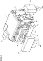
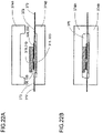
- FIGS. 3 and 4 are external perspective views of the power conversion device 200 as an embodiment according to the present invention.
- FIG. 4 shows a state in which an AC connector 187 and the DC connector 138 are removed.
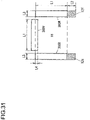
- the power conversion device 200 of the present embodiment is provided in a rectangular planar shape which is substantially square so as to be small in size and has an effect of facilitating mounting to the vehicle.
- a reference numeral 8 denotes a lid, 10 a housing, 12 a flow path former, 13 a cooling medium inlet pipe, 14 an outlet pipe, and 420 a lower cover.
- the connector 21 is a connector for signals provided for external connection.
- the lid 8 is fixed to an upper opening of the housing 10 in which circuit components constituting the power conversion device 200 are housed.
- the flow path former 12 which is fixed to a lower part of the housing 10, holds the power modules 300 and the capacitor module 500, which are described later, and cools them by a cooling medium. Since water, for instance, is most commonly used as a cooling medium, the explanation will hereinafter be made with cooling water as an example.
- An inlet pipe 13 and an outlet pipe 14 are provided on one lateral surface of the flow path former 12, and cooling water supplied from the inlet pipe 13 flows into a flow path 19, described later, in the flow path former 12 and is released from the outlet pipe 14.
- An AC interface 185 on which the AC connector 187 is mounted and a DC interface 137 on which the DC connector 138 is mounted are provided on a lateral surface of the housing 10.
- the AC interface 185 is provided on the lateral surface on which the pipes 13 and 14 are provided, and an AC wiring 187a of the AC connector 187 mounted on the AC interface 185 extends downward through between the pipes 13 and 14.
- the DC interface 137 is provided on the lateral surface adjacent to the lateral surface on which the AC interface 185 is provided, and a DC wiring 138a of the DC connector 138 mounted on the DC interface 137 also extends downward the power conversion device 200.
- the AC interface 185 and the pipes 13 and 14 are thus arranged on the side of a same lateral surface 12d and the AC wiring 187a is drawn downward as it passes through between the pipes 13 and 14, the space occupied by the pipes 13 and 14, the AC connector 187, and the AC wiring 187a is reduced in size, thereby preventing the whole device from becoming large in size.
- the AC wiring 187a is drawn downward with respect to the pipes 13 and 14, the AC wiring 187a is easily wired, thereby improving productivity.
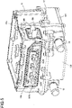
- FIG. 5 is a view showing a state in which the lid 8, the DC interface 137, and the AC interface 185 are removed from the power conversion device 200 shown in FIG. 4 .
- One lateral surface of the housing 10 is provided with an opening 10a through which the AC interface 185 is fixed and another lateral surface adjacent thereto is provided with an opening 10b through which the DC interface 137 is fixed.
- FIG. 6 is a view showing a state in which the housing 10 is removed from the flow path former 12 in FIG. 5 .
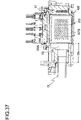
- the housing 10 is sectioned by a dividing wall 10c into two housing spaces, i.e., an upper housing space and a lower housing space.
- a control circuit board 20, to which the connector 21 is fixed, is housed in the upper housing space and a driver circuit board 22 and the bus bar assembly 800, which will be described later, are housed in the lower housing space (refer to FIG. 7 ).
- the control circuit board 20 is mounted with the control circuit 172 shown in FIG. 2
- the driver circuit board 22 is mounted with the driver circuit board 174.
- the control circuit board 20 and the driver circuit board 22 are connected through a flat cable not shown in the figure (refer to FIG. 7 described later), and the flat cable is drawn from the lower housing space to the upper housing space via a slit-like opening 10d formed on the dividing wall 10c.
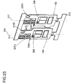
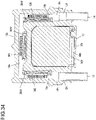
- FIG. 7 is an exploded perspective view of the power conversion device 200.
- the control circuit board 20 on which the control circuit 172 is mounted as described above is arranged inside the lid 8, i.e., in the upper housing space of the housing 10, the control circuit board 20 on which the control circuit 172 is mounted as described above is arranged.
- the lid 8 is provided with an opening (not shown in the figure) for the connector 21. Low-voltage DC power to operate the control circuit in the power conversion device 200 is supplied from the connector 21.
- the flow path former 12 is provided with a flow path through which cooling water having flowed in from the inlet pipe 13 flows, which will be described in detail later.
- the flow path is formed in a U shape so that the cooling water flows along three lateral surfaces of the flow path former 12.
- the cooling water, having flowed in from the inlet pipe 13, flows into the flow path from an end of the U shaped flow path, flows through the flow path, and then flows out from the outlet pipe 14, which is connected to the other end of the flow path.
- three openings 402a to 402c are formed, from which the power modules 300U, 300V, and 300W, which are provided with the built-in series circuits 150 (refer to FIG. 1 ), are inserted into the flow path.
- the power module 300U is provided with the built-in U phase series circuit 150
- the power module 300V is provided with the built-in V phase series circuit 150
- the power module 300W is provided with the built-in W phase series circuit 150.
- the power modules 300U to 300W have the same structure and the same external shape.
- the openings 402a to 402c are covered with flange sections of the inserted power modules 300U to 300W.
- the flow path former 12 is provided with a housing space 405 for housing electric components as surrounded by the U shaped flow path.
- the capacitor module 500 is housed in the housing space 405.
- the capacitor module 500 housed in the housing space 405, is cooled by the cooling water flowing through the flow path.
- the bus bar assembly 800 on which the AC bus bars 802U to 802W are mounted, is arranged.
- the bus bar assembly 800 is fixed on the upper surface of the flow path former 12.
- a current sensor module 180 is fixed on the bus bar assembly 800.
- the driver circuit board 22 is fixed to supporting members 807a, provided on the bus bar assembly 800, so as to be arranged above the bus bar assembly 800. As described above, the control circuit board 20 and the driver circuit board 22 are connected through a flat cable. The flat cable is drawn from the lower housing space to the upper housing space through the slit-like opening 10d, formed on the dividing wall 10c.
- the power modules 300U to 300W, the driver circuit board 22, and the control circuit board 20 are hierarchically arranged in the height direction and the control circuit board 20 is arranged at a farthest place from the high-rate power modules 300U to 300W, thereby reducing contamination of switching noise and the like to the control circuit board 20.
- the driver circuit board 22 and the control circuit board 20 are arranged in different housing spaces sectioned by the dividing wall 10c, the dividing wall 10c functions as an electromagnetic shield, thereby reducing noise contaminated from the driver circuit board 22 to the control circuit board 20.
- the housing 10 is formed of metal material such as aluminium.
- control circuit board 20 is fixed on the dividing wall 10c, which is integrally provided with the housing 10, the mechanical resonance frequency of the control circuit board 20 becomes higher against external vibration. For this reason, the power conversion device 200 is less susceptible to vibration from the vehicle side, thereby improving reliability.
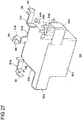
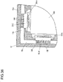
- FIG. 8 is an external perspective view of the flow path former 12, to which the power modules 300U to 300W, the capacitor module 500, and the bus bar assembly 800 are assembled.
- FIG. 9 shows a state in which the bus bar assembly 800 is removed from the flow path former 12. The bus bar assembly 800 is bolted to the flow path former 12.
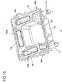
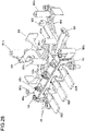
- FIG. 10 is a perspective view of the flow path former 12 and FIG. 11 is an exploded perspective view of the flow path former 12 seen from behind.
- the flow path former 12 is provided in a rectangular planar shape which is substantially square and the lateral surface 12d thereof is provided with the inlet pipe 13 and the outlet pipe 14. It is to be noted that the lateral surface 12d is formed in a stepped manner at the portion on which the pipes 13 and 14 are provided.
- the flow path 19 is formed into a U shape along the other three lateral surfaces 12a to 12c.
- the back side of the flow path former 12 is provided with an unsectioned U shaped opening 404 having substantially the same shape as a cross-sectional shape of the flow path 19.
- the opening 404 is covered with the U shaped lower cover 420.
- a sealing member 409a is provided between the lower cover 420 and the flow path former 12, thereby providing an airtight seal.
- the flow path 19, provided in a U shape, is divided into three flow path sections 19a, 19b, and 19c depending upon the direction of the flow of cooling water.
- the first flow path section 19a is provided along the lateral surface 12a in a position opposite to the lateral surface 12d on which the pipes 13 and 14 are provided
- the second flow path section 19b is provided along the lateral surface 12b adjacent to one side of the lateral surface 12a
- the third flow path section 19c is provided along the lateral surface 12c adjacent to the other side of the lateral surface 12a, as described later in detail.
- Cooling water flows in from the inlet pipe 13 to the flow path section 19b, flows through in order of the flow path section 19b, the flow path section 19a, and the flow path section 19c as indicated by the dashed arrow, and then flows out from the outlet pipe 14.
- a rectangular opening 402a, parallel to the lateral surface 12a, is formed in a position opposite to the flow path section 19a
- a rectangular opening 402b, parallel to the lateral surface 12b, is formed in a position opposite to the flow path section 19b
- a rectangular opening 402c, parallel to the lateral surface 12c is formed in a position opposite to the flow path section 19c.
- raised portions 406 protruding downward the flow path 19 are formed on the lower cover 420 in a position opposite to each of the openings 402a to 402c described above. These raised portions 406 are recesses if seen from the flow path 19 side, and lower end portions of the power modules 300U to 300W inserted through the openings 402a to 402c fit into these recesses. Since the flow path former 12 is formed so that the opening 404 is opposite to the openings 402a to 402c, it is easily manufactured by aluminium casting.
- the flow path former 12 is provided with the rectangular housing space 405 formed so that its three sides are surrounded by the flow path 19.
- the capacitor module 500 is housed in the housing space 405. Since the housing space 405 surrounded by the flow path 19 is provided in a rectangular shape, the capacitor module 500 is provided in a rectangular shape, thereby improving the productivity of the capacitor module 500.
- the structure of the power modules 300U to 300W and power modules 301U to 301W, which are used in the inverter circuit 140, will be explained in detail with reference to FIG. 12A to FIG. 26B .
- the power modules 300U to 300W and the power modules 301U to 301W each have the same structure and hence the structure of the power module 300U will be explained as a representative thereof.
- a signal terminal 325U corresponds to the gate electrode 154 and the emitter electrode 155 for signals, disclosed in FIG. 2
- a signal terminal 325L corresponds to the gate electrode 164 and the emitter electrode 165, disclosed in FIG. 2 .
- a DC positive terminal 315B is identical to the positive terminal 157, disclosed in FIG. 2
- a DC negative terminal 319B is identical to the negative terminal 158, disclosed in FIG. 2
- an AC terminal 320B is the same as the AC terminal 159, disclosed in FIG. 2 .
- FIG. 12A is a perspective view of the power module 300U of the present embodiment.
- FIG. 12B is a sectional view of the power module 300U of the present embodiment being cut on a cross section D and seen from a direction E.
- FIGS. 13A , B, and C are views showing the power module 300U with a screw 309 and a second sealing resin 351 removed from the configuration in the state shown in FIGS. 12A and 12B for better understanding.
- FIG. 13A is a perspective view
- FIG. 13B is a sectional view of the power module 300U of the present embodiment being cut on the cross section D and seen from the direction E as in FIG. 12B .
- FIG. 13C shows a sectional view before pressure is applied to fins 305 so that curved portions 304A are deformed.
- FIGS. 14A and 14B are views showing the power module 300U with a module case 304 further removed from the configuration in the state shown in FIGS. 13A and 13B .
- FIG. 14A is a perspective view and
- FIG. 14B is a sectional view of the power module 300U of the present embodiment being cut on the cross section D and seen from the direction E as in FIG. 12B and FIG. 13B .
- FIG. 15 is a perspective view of the power module 300U with a first sealing resin 348 and a wiring insulation section 608 further removed from the configuration in the state shown in FIGS. 14A and 14B .
- FIGS. 16A and 16B are views showing an ancillary molded body 600 of the power module 300U.
- FIG. 16A is a perspective view and
- FIG. 16B is a sectional view of the ancillary molded body 600 being cut on the cross section D and seen from the direction E as in FIG. 12B , FIG. 13B , and FIG. 14B .
- the power semiconductor elements (the IGBT 328, the IGBT 330, the diode 156, and the diode 166) constituting the series circuit 150 of the upper and lower arms are, as shown in FIGS. 14A, 14B , and 15 , sandwiched from the both sides and fixed by a conductor plate 315 and a conductor plate 318 or a conductor plate 320 and a conductor plate 319.
- the conductor plate 315 and the like are sealed by the first sealing resin 348 in a state where their heat dissipation surfaces are exposed, and an insulation sheet 333 is thermo-compression bonded to the heat dissipation surfaces.
- the first sealing resin 348 is provided in a polyhedron shape (here, substantially rectangular solid shape) as shown in FIGS. 14A and 14B .
- a module primary seal body 302 sealed by the first sealing resin 348 is inserted into the module case 304 and thermo-compression bonded onto the inner surface of the module case 304, which is a can-type cooler, across the insulation sheet 333.
- the can-type cooler is a cylinder shaped cooler having an insertion slot 306 on one side and a bottom on the other side.
- An air gap remaining inside the module case 304 is filled with the second sealing resin 351.
- the module case 304 is formed of an electrically conductive member such as aluminium alloy material (Al, AISi, AlSiC, Al-C, and the like) and integrally formed seamlessly.
- the module case 304 is configured not to include an opening other than the insertion slot 306, and the insertion slot 306 is surrounded by a flange 304B around the outer circumference thereof.
- Al aluminium alloy material
- a first heat dissipation surface 307A and a second heat dissipation surface 307B which have a larger surface than another surface, are arranged in a state where they are opposite to each other, and each of the power semiconductor elements (the IGBT 328, the IGBT 330, the diode 156, and the diode 166) is arranged opposite to these heat dissipation surfaces.
- the module case 304 may not be provided in an accurately rectangular shape but may be round in corners as shown in FIG. 12A .
- the cooling medium is prevented by a simple structure from entering inside the module case 304.
- the fins 305 are formed uniformly on each of the first heat dissipation surface 307A and the second heat dissipation surface 307B, opposite to each other.
- the extremely thin curved portions 304A are formed on the outer circumference of the first heat dissipation surface 307A and the second heat dissipation surface 307B. The curved portions 304A are made extremely thin to an extent where they are easily deformed by applying pressure to the fins 305, thereby improving the productivity after the module primary seal body 302 is inserted.
- the conductor plate 315 and the like are thermo-compression bonded onto the inner wall of the module case 304 through the insulation sheet 333 as described above so as to allow the air gap between the conductor plate 315 and the like and the inner wall of the module case 304 to be reduced, thereby transmitting generated heat at the power semiconductor elements to the fins 305 efficiently.
- the insulation sheet 333 is made thick and flexible to some extent so that the generated thermal stress is absorbed in the insulation sheet 333, and thus the power semiconductor device is excellent for use in a power conversion device for a vehicle with severe temperature changes.
- a metal DC positive wiring 315A and a metal DC negative wiring 319A, which are to be electrically connected with the capacitor module 500, are provided outside the module case 304 and end sections thereof are provided with the DC positive terminal 315B (157) and the DC negative terminal 319B (158), respectively.
- a metal AC wiring 320A for supplying AC power to the motor generator MG1 is provided and its end is provided with the AC terminal 320B (159).
- the DC positive wiring 315A is connected with the conductor plate 315
- the DC negative wiring 319A is connected with the conductor plate 319
- the AC wiring 320A is connected with the conductor plate 320.
- metal signal wirings 324U and 324L which are to be electrically connected with the driver circuit 174, are provided outside the module case 304, their end sections are provided with the signal terminal 325U (154, 155) and the signal terminal 325L (164, 165), respectively.
- the signal wiring 324U is connected with the IGBT 328 and the signal wiring 324L is connected with the IGBT 328.
- the DC positive wiring 315A, the DC negative wiring 319A, the AC wiring 320A, the signal wiring 324U, and the signal wiring 324L are integrally formed as the ancillary molded body 600 in a state where they are insulated from one another by the wiring insulation section 608 formed of resin material.
- the wiring insulation section 608 also acts as a supporting member for supporting each wiring, and thus thermosetting resin or thermoplastic resin, having insulation properties, is appropriate for the resin material used for the wiring insulation section 608. This ensures insulation among the DC positive wiring 315A, the DC negative wiring 319A, the AC wiring 320A, the signal wiring 324U and the signal wiring 324L, thereby enabling high density wiring.
- the ancillary molded body 600 is metallically bonded with the module primary seal body 302 at a connection section 370 before fixed to the module case 304 with the screw 309 passing through a screw hole provided on the wiring insulation section 608.
- the metal bonding of the module primary seal body 302 with the ancillary molded body 600 at the connection section 370 may be TIG-welded, for instance.
- the DC positive wiring 315A and the DC negative wiring 319A are layered in a state where they are opposite to each other across the wiring insulation section 608, thereby constituting a shape extending substantially in parallel. Such arrangement and shape causes the instantaneous currents to flow against and in the opposite direction to each other during switching operations of the power semiconductor elements. This has an effect to cause the magnetic fields generated by the current to cancel each other out, thereby allowing reduction of inductance. It is to be noted that the AC wiring 320A and the signal terminals 325U and 325L also extend in the same direction as the DC positive wiring 315A and the DC negative wiring 319A.
- connection section 370 at which the module primary seal body 302 and the ancillary molded body 600 are metallically bonded, is sealed in the module case 304 with the second sealing resin 351. This stably ensures a necessary insulation distance between the connection section 370 and the module case 304, thereby achieving reduction in size of the power module 300U compared to one that is not sealed.
- an ancillary module-side DC positive connection terminal 315C As shown in FIG. 15 and FIGS. 16A and 16B , on the ancillary module 600 side of the connection section 370, an ancillary module-side DC positive connection terminal 315C, an ancillary module-side DC negative connection terminal 319C, an ancillary module-side AC connection terminal 320C, an ancillary module-side signal connection terminal 326U, and an ancillary module-side signal connection terminal 326L are aligned.
- an element-side DC positive connection terminal 315D, an element-side DC negative connection terminal 319D, an element-side AC connection terminal 320D, an element-side signal connection terminal 327U, and an element-side signal connection terminal 327L are aligned along one surface of the first sealing resin 348 provided in a polyhedron shape.
- each of the terminals is configured to be aligned at the connection section 370, thereby facilitating manufacturing of the module primary seal body 302 by transfer molding.
- a terminal constituted with the DC positive wiring 315A (inclusive of the DC positive terminal 315B and the ancillary module-side DC positive connection terminal 315C) and the element-side DC positive connection terminal 315D will be referred to as a positive electrode-side terminal
- a terminal constituted with the DC negative wiring 319A (inclusive of the DC negative terminal 319B and the ancillary module-side DC negative connection terminal 319C) and the element-side DC negative connection terminal 315D will be referred to as a negative electrode-side terminal
- a terminal constituted with the AC wiring 320A (inclusive of the AC terminal 320B and the ancillary module-side AC connection terminal 320C) and the element-side AC connection terminal 320D will be referred to as an output terminal
- each of the above terminals protrudes from the first sealing resin 348 and the second sealing resin 351 through the connection section 370, and each of the protruding portions from the first sealing resin 348 (the element-side DC positive connection terminal 315D, the element-side DC negative connection terminal 319D, the element-side AC connection terminal 320D, the element-side signal connection terminal 327U, and the element-side signal connection terminal 327L) is aligned along one surface of the first sealing resin 348 provided in the polyhedron shape described above.
- the positive electrode-side terminal and the negative electrode-side terminal protrude from the second sealing resin 351 in a layered state and extend out of the module case 304.
- Such configuration will prevent over stress on the connection section of the power semiconductor elements with the terminal and a gap in mold from occurring at the time of clamping when the power semiconductor elements are sealed with the first sealing resin 348 so as to manufacture the module primary seal body 302.
- magnetic fluxes in directions canceling each other out are generated by the currents of opposite directions flowing through the layered positive electrode-side terminal and negative electrode-side terminal, thereby achieving reduction of inductance.
- the ancillary module-side DC positive connection terminal 315C and the ancillary module-side DC negative connection terminal 319C are formed at the end sections of the DC positive wiring 315A and the DC negative wiring 319A on the opposite side of the DC positive terminal 315B and the DC negative terminal 319B, respectively.
- the ancillary module-side AC connection terminal 320C is formed at the end section of the AC wiring 320A on the opposite side of the AC terminal 320B.
- the ancillary module-side signal connection terminals 326U and 326L are formed at the end sections of the signal wirings 324U and 324L on the opposite side of the signal terminals 325U and 325L, respectively.
- the element-side DC positive connection terminal 315D, the element-side DC negative connection terminal 319D, and the element-side AC connection terminal 320D are formed on the conductor plates 315, 319, and 320, respectively.
- the element-side signal connection terminals 327U and 327L are connected through a bonding wire 371 with the IGBTs 328 and 330, respectively.
- the conductor plate 315 on the DC positive electrode side, the conductor plate 320 on the AC output side, and the element-side signal connection terminals 327U and 327L are integrally processed so that they are arranged on substantially the same plane in a state where they are tied to a common tie bar 372.
- the collector electrode of the IGBT 328 of the upper arm side and the cathode electrode of the diode 156 of the upper arm side are fixed to the conductor plate 315.
- the collector electrode of the IGBT 330 of the lower arm side and the cathode electrode of the diode 166 of the lower arm side are fixed to the conductor plate 320.
- the conductor plate 318 and the conductor plate 319 are arranged on substantially the same plane over the IGBTs 328 and 330 and the diodes 155 and 166.
- the emitter electrode of the IGBT 328 of the upper arm side and the anode electrode of the diode 156 of the upper arm side are fixed to the conductor plate 318.
- the emitter electrode of the IGBT 330 of the lower arm side and the anode electrode of the diode 166 of the lower arm side are fixed to the conductor plate 319.
- Each of the power semiconductor elements is fixed through a metal bonding material 160 to an element fixing portion 322 provided on each of the conductor plates.
- the metal bonding material 160 is, for example, a soldering material, a silver sheet, a low-temperature sintering jointing material including fine metallic particles, or the like.
- Each of the power semiconductor elements has a plate-like flat configuration, each of the electrodes of which is formed on the front and back surfaces. As shown in FIG. 17 , each of the electrodes of the power semiconductor elements is sandwiched by the conductor plate 315 and the conductor plate 318 or by the conductor plate 320 and the conductor plate 319. In other words, the conductor plate 315 and the conductor plate 318 are arranged in a layered manner opposite to each other in substantially parallel through the IGBT 328 and the diode 156. Similarly, the conductor plate 320 and the conductor plate 319 are arranged in a layered manner opposite to each other in substantially parallel through the IGBT 330 and the diode 166. In addition, the conductor plate 320 and the conductor plate 318 are connected through an intermediate electrode 329. This connection causes the upper arm circuit and the lower arm circuit to be electrically connected, thereby forming an upper and lower arm series circuit.
- the IGBT 328 and the diode 156 are sandwiched between the conductor plate 315 and the conductor plate 318, the IGBT 330 and the diode 166 are sandwiched between the conductor plate 320 and the conductor plate 319, and the conductor plate 320 and the conductor plate 318 are connected through the intermediate electrode 329 as illustrated in FIG. 18 .
- a control electrode 328A of the IGBT 328 and the element-side signal connection terminal 327U are connected through the bonding wire 371 and a control electrode 330A of the IGBT 330 and the element-side signal connection terminal 327L are connected through the bonding wire 371 as illustrated in FIG. 19 .
- the portion including the power semiconductor elements and the bonding wire 371 is sealed with the first sealing resin 348 as illustrated in FIG. 20 .
- the portion including the power semiconductor elements and the bonding wire 371 is formed by mold-pressing from above and below on the mold pressing surface 373 and filling the first sealing resin 348 in the mold by transfer mold.
- the tie bar 372 is removed so as to separate the element-side DC positive connection terminal 315D, the element-side AC connection terminal 320D, and the element-side signal connection terminals 327U and 327L individually. Then, each end of the element-side DC positive connection terminal 315D, the element-side DC negative connection terminal 319D, the element-side AC connection terminal 320D, and the element-side signal connection terminals 327U and 327L, which are aligned on one side of the module primary seal body 302, is bent in the same direction as illustrated in FIG. 21 . This will facilitate the work of metallically bonding the module primary seal body 302 with the ancillary molded body 600 at the connection section 370 and improve the productivity, thereby improving the reliability of the metal bond.
- FIGS. 22A and 22B are views for explaining the transfer molding process of the first sealing resin 348.
- FIG. 22A shows a vertical sectional view before clamping and
- FIG. 22B shows a vertical sectional view after clamping.
- the module primary seal body 302 before sealed shown in FIG. 19 is placed between an upper mold 374A and a lower mold 374B.
- the upper mold 374A and the lower mold 374B sandwich and clamp the module primary seal body 302 from above and below on the mold pressing surface 373 so as to form a mold cavity 375 in the mold as shown in FIG. 22B .
- the mold cavity 375 is filled with the first sealing resin 348 and formed so that the power semiconductor elements (the IGBTs 328 and 330 and the diodes 155 and 166) are sealed with the first sealing resin 348 in the module primary seal body 302.
- the element-side DC positive connection terminal 315D, the element-side DC negative connection terminal 319D, the element-side AC connection terminal 320D, the element-side signal connection terminal 327U, and the element-side signal connection terminal 327L are aligned.
- Such terminal arrangement enables clamping using the upper mold 374A and the lower mold 374B without generating unnecessary stress at the connection section of each of the terminals with the power semiconductor elements and without a gap. Accordingly, the power semiconductor elements will be sealed without damaging the power semiconductor elements or leaking the first sealing resin 348 from the gap.
- FIG. 23 shows a state where the conductor plates 318 and 319 and the intermediate electrode 329 are removed from the configuration in FIG. 18 for better understanding.
- the control electrodes 328A and 330A are each arranged in a position shifted to the left in the figure with respect to central lines 376 and 377, respectively.
- the central lines 376 and 377 are perpendicular to the arrangement direction of the element-side DC positive connection terminal 315D, the element-side DC negative connection terminal 319D, the element-side AC connection terminal 320D, the element-side signal connection terminal 327U, and the element-side signal connection terminal 327L.
- the element-side signal connection terminal 327U is arranged on the half side in which the control electrode 328A is arranged and the element-side DC positive connection terminal 315D is arranged on the other half side.
- the element-side signal connection terminal 327L is arranged on the half side in which the control electrode 330A is arranged and the element-side AC connection terminal 320D is arranged on the other half side.
- the element-side DC negative connection terminal 319D is arranged between the element-side DC positive connection terminal 315D and the element-side signal connection terminal 327L.
- Such arrangement minimizes the length of the bonding wire 371, which connects the control electrodes 328A and 330A with the element-side signal connection terminals 327U and 327L, respectively, thereby improving the reliability in connection.
- collective arrangement of each of the terminals will achieve reduction in size of the module primary seal body 302 and thus the power module 300U.
- the element-side DC positive connection terminal 315D, the element-side AC connection terminal 320D, the element-side signal connection terminal 327U, and the element-side signal connection terminal 327L are integrally processed in a state where they are tied to the common tie bar 372. This will significantly reduce variations in flatness and thickness among these terminals.
- the element-side DC negative connection terminal 319D is combined with that having been processed separately from each of the above terminals, variations in flatness and thickness become greater than each of the other terminals, and thus unnecessary stress may occur at the connection section of the terminal and the power semiconductor elements when clamping.
- FIG. 24 is a view showing a variation for avoiding the disadvantage described above.
- a stress relief section 319E for absorbing and relieving the stress when clamping is provided on the conductor plate 319 on which the element-side DC negative connection terminal 319D is provided.
- the stress relief section 319E is preferred to be positioned between the area on which the power semiconductor elements are mounted (soldered area) and the mold pressing surface 373. It is to be noted that it may be conceived that the stress relief section 319E is prepared by simply making the conductor plate 319 partly thinner than other portions. In that case, however, the current density increases at the thin portion, which may reduce electrical performance. Hence, as shown in FIG.
- a part of the conductor plate 319 is bent to provide the stress relief section 319E. This prevents the current density from increasing at the stress relief section 319E and the current flows in opposite directions at the turning portion, provided by bending, thereby also contributing to reduction of inductance.
- FIG. 25 is a circuit diagram showing the circuit configuration of the power module 300U.
- the collector electrode of the IGBT 328 of the upper arm side and the cathode electrode of the diode 156 of the upper arm side are connected through the conductor plate 315.
- the collector electrode of the IGBT 330 of the lower arm side and the cathode electrode of the diode 166 of the lower arm side are connected through the conductor plate 320.
- the emitter electrode of the IGBT 328 of the upper arm side and the anode electrode of the diode 156 of the upper arm side are connected through the conductor plate 318.
- the emitter electrode of the IGBT 330 of the lower arm side and the anode electrode of the diode 166 of the lower arm side are connected through the conductor plate 319.
- the conductor plates 318 and 320 are connected through the intermediate electrode 329.
- Such circuit configuration forms the upper and lower arm series circuit.
- FIG. 26A is a diagram showing an equivalent circuit when a recovery current flows through and FIG. 26B is a view showing the recovery current path.
- the diode 166 of the lower arm side is assumed to be made conductive in a forward bias state.
- the IGBT 328 of the upper arm side enters an ON state
- the diode 166 of the lower arm side is reverse-biased and recovery current due to carrier mobility passes through the upper and lower arms.
- a recovery current 360 flows through each of the conductor plates 315, 318, 319, and 320 as shown in FIG. 26B .
- the recovery current 360 passes through the DC positive terminal 315B (157), which is arranged opposite to the DC negative terminal 319B (158), as indicated by the dotted line, then flows through a loop-shaped path formed by each of the conductor plates 315, 318, 319, and 320, and flows through the DC negative terminal 319B (158), which is arranged opposite to the DC positive terminal 315B (157), again as indicated by the solid line.
- the flow of current through the loop-shaped path causes an eddy current 361 to flow through the first heat dissipation surface 307A and the second heat dissipation surface 307B of the module case 304.
- the magnetic field canceling effect produced by an equivalent circuit 362 in the current path of the eddy current 361 reduces a wiring inductance 363 in the loop-shaped path.
- the inductance reduction effect increases as the current path of the recovery current 360 is closer to a loop shape.
- the loop-shaped current path goes through a path close to the DC positive terminal 315B (157) side of the conductor plate 315 and passes through the IGBT 328 and the diode 156.
- the loop-shaped current path goes through a path farther than the DC positive terminal 315B (157) side of the conductor plate 318, and then, as indicated by the dotted line, goes through a path farther than the DC positive terminal 315B (157) side of the conductor plate 320 and passes through the IGBT 330 and the diode 166.
- the loop-shaped current path goes through a path close to the DC negative wiring 319A side of the conductor plate 319.
- the loop-shaped current path thus goes through paths of a closer side or a farther side with respect to the DC positive terminal 315B (157) and the DC negative terminal 319B (158) so as to form a current path closer to a loop shape.
- FIG. 38 is a view showing a variation with a divided DC negative wiring. It is to be noted that structures denoted by the same reference numeral as that described earlier have the same function. Since the element-side DC negative connection terminal 319D shown in FIG. 18 is combined with that having been processed separately from each of the above terminals, variations in flatness and thickness become greater than each of the other terminals, and thus unnecessary stress may occur at the connection section of the terminal and the power semiconductor elements when clamping.
- the element-side DC negative connection terminal 319D shown in FIG. 18 is divided so that a negative electrode-side connection terminal 319F is arranged on substantially the same plane as the element-side AC connection terminal 320D and the element-side DC positive connection terminal 315D.
- an element-side DC negative connection terminal 319G extends from an edge of the conductor 319 to a position opposite to a part of the negative electrode-side connection terminal 319F. Then, the end of the element-side DC negative connection terminal 319G is bent towards the negative electrode-side connection terminal 319F side.
- the end of the element-side DC negative connection terminal 319G is connected with the negative electrode-side connection terminal 319F through a metal bonding material 161.
- the module body shown in FIG. 40 is sealed with the first sealing resin 348 according to the production method shown in FIGS. 22A and 22B , and thus a module primary seal body is completed as shown in FIG. 41 .
- the negative electrode-side connection terminal 319F is formed integrally with the tie bar 372 together with the element-side DC positive connection terminal 315D, the element-side AC connection terminal 320D, and the element-side signal connection terminal 327U. It is then possible to cut the tie bar 372 collectively with the connection section with the negative electrode-side connection terminal 319F.
- FIG. 27 is an external perspective view of the capacitor module 500.
- a plurality of capacitor cells are provided in the capacitor module 500.
- capacitor terminals 503a to 503c are provided in a protruding manner adjacent to the opposite surface to the flow path 19 of the capacitor module 500.
- the capacitor terminals 503a to 503c are formed corresponding to the positive terminal 157 and the negative terminal 158 of each of the power modules 300.
- the capacitor terminals 503a to 503c are provided in the same shape and an insulation sheet is provided between the negative electrode-side capacitor terminal 504 and the positive electrode-side capacitor terminal 506, which constitute the capacitor terminals 503a to 503c, thereby ensuring insulation between the terminals.
- Protruding portions 500e and 500f are formed above a lateral surface 500d side of the capacitor module 500.
- a discharge resistor is mounted in the protruding portion 500e and a Y capacitor for protecting against common-mode noise is mounted in the protruding portion 500f.
- the power supply terminal 508 and 509 shown in FIG. 5 are mounted to terminals 500g and 500h protruding from the upper surface of the protruding portion 500f. As shown in FIG.
- recesses 405a and 405b are formed between the openings 402b and 402c and the lateral surface 12d, so that, when the capacitor module 500 is housed in the housing space 405 of the flow path former 12, the protruding portion 500e is housed in the recess 405a and the protruding portion 500f is housed in the recess 405b.
- the discharge resistor mounted in the protruding portion 500e is a resistor for discharging electric charge accumulated at the capacitor cells in the capacitor module 500 when the inverter is stopped.
- the recess 405a in which the protruding portion 500e is housed is provided directly above the flow path of cooling water flowing in from the inlet pipe 13, thereby inhibiting rise in temperature at the discharge resistor when discharging.
- FIG. 28 is a perspective view of the bus bar assembly 800.
- the bus bar assembly 800 includes the AC bus bars 802U, 802V, and 802W of the U, V, and W phases, a holding member 803 for holding and fixing the AC bus bars 802U to 802W, and the current sensor module 180 for detecting AC current flowing through the AC bus bars 802U to 802W.
- the AC bus bars 802U to 802W are each formed of a wide conductor.
- the holding member 803 formed of insulation material such as resin, the plurality of supporting members 807a for holding the driver circuit board 22 are formed in a protruding manner upward from the holding member 803.
- the current sensor module 180 is arranged on the bus bar assembly 800 so that the current sensor module 180 is in parallel to the lateral surface 12d at a position adjacent to the lateral surface 12d of the flow path former 12 when the bus bar assembly 800 is fixed on the flow path former 12 as shown in FIG. 8 described earlier.
- through holes 181 through which the AC bus bars 802U to 802W pass are formed on a lateral surface of the current sensor module 180.
- Sensor elements are provided in portions where the through holes 181 of the current sensor module 180 are formed, and signal lines 182a of each of the sensor elements protrude from the upper surface of the current sensor module 180.
- Each of the sensor elements are aligned in the extending direction of the current sensor module 180, i.e., the extending direction of the lateral surface 12d of the flow path former 12.
- the AC bus bars 802U to 802W passes through the corresponding through hole 181 and their end portion protrude in parallel.
- Protrusions 806a and 806b for positioning are formed on the holding member 803 in an upward protruding manner.
- the current sensor module 180 is screwed to the holding member 803, where the current sensor module 180 is positioned by engaging the protrusions 806a and 806b with positioning holes formed in the frame body of the current sensor module 180.
- the protrusions 806a and 806b for positioning are engaged into the positioning holes formed on the driver circuit board 22 side, so that the signal line 182a of the current sensor module 180 is positioned into the through hole of the driver circuit board 22.
- the signal line 182a is soldered to the wiring pattern of the driver circuit board 22.
- the holding member 803, the supporting members 807a and the protrusions 806a and 806b are integrally provided with resin. Since the holding member 803 thus has a positioning function of the current sensor module 180 and the driver circuit board 22, assembling and soldering works between the signal line 182a and the driver circuit board 22 are made easy. In addition, a mechanism to hold the current sensor module 180 and the driver circuit board 22 is provided on the holding member 803, thereby reducing the number of components in the power conversion device as a whole.
- connection sections 805 are fixed to the holding member 803 so that their wide surfaces are leveled out and connection sections 805 to be connected to the AC terminals 159 of the power modules 300U to 300W are erected vertically.
- the connection sections 805 each have a protruding and recessed end, on which heat concentrates upon welding.
- each of the AC bus bars 802U to 802W protruding from the through hole 181 of the current sensor module 180 is to be arranged on the lateral surface 12d of the flow path former 12. Since each of the power modules 300U to 300W is arranged on the flow path section 19a, 19b, and 19c formed along the lateral surfaces 12a, 12b, and 12c of the flow path former 12, the connection sections 805 of the AC bus bars 802U to 802W are arranged at positions corresponding to the lateral surface 12a to 12c of the bus bar assembly 800. As a result, as shown in FIG.
- the U phase AC bus bar 802U extends from the power module 300U arranged in the vicinity of the lateral surface 12b to the lateral surface 12d
- the V phase AC bus bar 802V extends from the power module 300V arranged in the vicinity of the lateral surface 12a to the lateral surface 12d
- the W phase AC bus bar 802W extends from the power module 300W arranged in the vicinity of the lateral surface 12c to the lateral surface 12d.
- FIG. 29 is a view showing the flow path former 12 in which the power modules 300U to 300W are fixed in the openings 402a to 402c and the capacitor module 500 is housed the housing space 405.
- the power module 300U of the U phase is fixed in the opening 402b
- the power module 300V of the V phase is fixed in the opening 402a
- the power module 300W of the W phase is fixed in the opening 402c.
- the capacitor module 500 is housed in the housing space 405 and the terminal on the capacitor side and the terminal of each of the power modules are connected by welding or the like.
- Each of the terminals protrudes from the upper end surface of the flow path former 12, and welding work is carried out by bringing the welding machine from above.
- each of the power modules 300U to 300W provided in a U shape are connected with the capacitor terminals 503a to 503c provided in a protruding manner on the upper surface of the capacitor module 500. Since the three power modules 300U to 300W are provided to surround the capacitor module 500, the positional relationship of each of the power modules 300U to 300W with respect to the capacitor module 500 becomes equivalent, each of the power modules 300U to 300W will thus be connected to the capacitor module 500 in a well-balanced manner using the capacitor terminals 503a to 503c having the same shape. Due to this, the circuit constant of the capacitor module 500 and the power modules 300U to 300W becomes easily balanced in each of the three phases, thereby achieving a configuration in which current is easily input and output.
- FIG. 30 is a horizontal sectional view of the flow path former 12 in which the power modules 300U to 300W and the capacitor module 500 are arranged as shown in FIG. 29 .
- the U shaped flow path 19 is formed in the flow path former 12, and the U phase power module 300U is arranged at the flow path section 19b formed along the lateral surface 12b on the left side of the figure.
- the V phase power module 300V is arranged at the flow path section 19a formed along the lateral surface 12a on the opposite side of the lateral surface 12d on which the pipes 13 and 14 are provided
- the W phase power module 300W is arranged at the flow path section 19c formed along the lateral surface 12 on the right side.
- Openings 12g and 12h are formed on the lateral surface 12d of the flow path former 12.
- the opening 12g communicates with the flow path section 19b through a communication path 12e.
- the opening 12h communicates with the flow path section 19c through a communication path 12f.
- the pipes 13 and 14 arranged in the openings 12g and 12h are mounted to the communication paths 12e and 12f in a press fitting manner.
- FIG. 37 shows a sectional view of the flow path former 12 seen from the arrow direction of the A-A cross section of FIG. 30 . It is to be noted that FIG. 37 shows a state in which the A-A cross section is horizontally inverted.
- the communication path 12e significantly changes in the shape of the flow path cross section along the flow direction of cooling water.
- the flow of cooling water of the present embodiment is bifurcated by the lateral surface of the power module 300U, so that one of the bifurcated flows heads for the first heat dissipation surface 307A side of the module case 304 and the other heads for the second heat dissipation surface 307B side of the module case 304.
- the first heat dissipation surface 307A is a heat dissipation surface on the other side of the second heat dissipation surface 307B shown in FIG. 37 . Therefore, hit of the flow of cooling water of the present embodiment against the lateral surface of the power module 300U tends to increase pressure loss for causing the cooling water to flow. In order to inhibit such increase in the pressure loss, it is necessary to regulate the flow of cooling water in the vicinity of the lateral surface portion of the power module 300U.
- an entrance section 12j is formed in the direction from the inlet pipe 13 side towards the power module 300U with its width in the height direction increasing in a stepwise manner. It is to be noted that the entrance section 12j may not be provided in the stepwise manner as in FIG. 37 but may be provided in a smooth slope-like shape.
- the U shaped flow path 19 is formed along the three lateral surfaces 12a to 12c of the flow path former 12 having a substantially square planar shape and the power modules 300U to 300W are arranged at the flow path sections 19a to 19c so that the power modules 300U to 300W, each of which has a flat shape, are in parallel with the lateral surfaces 12a to 12c.
- the capacitor module 500 which is an electric component, is housed in the center space (the housing space 405) surrounded by the flow path 19.
- Such module arrangement allows the flow path former 12, in which the power modules 300U to 300W and the capacitor module 500 are housed, to be reduced in size.
- FIG. 31 is a schematic view for explaining the arrangement of the three power modules 300U to 300W.
- the power modules 300U to 300W have the same configuration and the same shape.
- the width of the lateral surfaces 12b and 12c of the flow path former needs to be at least around the sum of a length L1 along the flow path of the power modules 300U to 300W and a length L2 of the communication path.
- the lateral surface 12a requires at least around the length L1. It is naturally conceivable that in practice, as shown in FIG. 30 , the dimension needs to be slightly adjusted in view of the flow of cooling water e.g., the connection section of the flow path section.
- the shape seen with a planar view (planar shape) is provided in a substantially square so as to reduce the power conversion device 200 in size. Since the communication path is necessary with respect to the direction along the lateral surfaces 12b and 12c as described above, from a point of view of reduction in size it is preferred to arrange the power module 300V so that a part of the power module 300V is included in a space S1 between the pair of the power modules 300U and 300W as shown in FIG. 31 .
- the lateral dimension (the width dimension of the lateral surface 12a) of the arrangement space in FIG. 31 is at least around L1 + 2 ⁇ L3 where the thickness of the power module is denoted by L3.
- L3 and L4 are set so that the longitudinal dimension L1 + L2 + (L3 - L4) is comparable to L1 + 2 ⁇ L3, thereby reducing the area in the planar view and making it substantially square.
- the flow path section 19a is formed so as to pass through the space between the power modules 300U and 300W as shown in FIG. 30 .
- the interval between the power modules 300U and 300W is slightly larger than the length L1 of the power module 300V.
- the space above the pipes 13 and 14 and the hole 12e and the hole 12f through which the pipes 13 and 14 are to be press-fitted will be an empty space. Then, the recesses 405a and 405b are formed in this space as shown in FIG. 10 and the protruding portion 500e, which is a discharge resistor mounting portion of the capacitor module 500, and the protruding portion 500f, which is a Y capacitor mounting portion, are arranged as shown in FIG. 29 so that the empty space is effectively utilized, thereby contributing to reduction in size of the power conversion device 200.
- the pipes 13 and 14 are collectively positioned on the single lateral surface 12d so that the flow of cooling water is straighten from the inlet pipe 13 to the flow path section 19b and from the flow path section 19c to the outlet pipe 14, thereby reducing pressure loss significantly.
- an increase in installation space of the device due to the protrusion of the pipes will be prevented, thereby improving the in-vehicle mountability.
- the pipes 13 and 14 are press-fitted to the holes 12e and 12f only on one surface of the housing, thereby improving the workability and productivity.
- the flow path 19 is provided to surround the three sides of the capacitor module 500, thereby cooling the capacitor module 500 effectively.
- the power conversion device 200 of the present embodiment since the power conversion device 200 of the present embodiment is to be mounted on a vehicle, it is often arranged in an engine bay in general. Since inside the engine bay becomes relatively high in temperature due to heat from the engine, the travel motor, and the like, heat penetration from the surrounding to the power conversion device 200 becomes an issue. However, as shown in FIG. 30 , the capacitor module 500 is surrounded on its three sides by the flow path 19 through which the cooling water flows, thereby effectively blocking the heat penetration from the surrounding of the device.
- the bus bar assembly 800 is fixed above the capacitor module 500 as shown in FIG. 8 and welding work of the terminals is carried out.
- the bus bars 802U to 802W connected to the terminals of the power modules 300U to 300W arranged in a U shape are wired above the capacitor module 500 away from each of the connection sections and drawn from the lateral surface 12d side of the flow path former 12.
- bus bars 802U to 802W will be collectively arranged in one position, i.e., the space of the opening 10a of the housing 10 to which the AC interface 185 is mounted (refer to FIG. 5 ).
- bus bar configuration will keep the power modules 300U to 300W away from the AC connector section where heat is generated and temperature is likely to rise, thereby inhibiting the heat from being transmitted to the power modules 300U to 300W through the bus bars 802U to 802W.
- the bus bars 802U to 802W are arranged other than above the flow path 19, thereby reducing the possibility of electrical leakage caused by water leak even if the water leaks from the flow path 19.
- the bus bar assembly 800 is configured to be fixed to the flow path former 12 through which cooling water flows, thereby not only inhibiting the rise in temperature of the bus bar assembly 800 but also inhibiting the rise in temperature of the current sensor 180 held in the bus bar assembly 800.
- the sensor element provided in the current sensor 180 has a heat-sensitive feature and thus the above configuration will improve the reliability of the current sensor 180.
- the driver circuit board 22 is fixed to the supporting members 807a, formed on the holding member 803 of the bus bar assembly 800, as shown in FIG. 6 .
- the vehicle-mounted power conversion device 200 is susceptible to an effect of vibrations from the vehicle.
- the plurality of supporting members 807a formed in the holding member 803 are configured to support the driver circuit board 22 not only in the periphery thereof but also in the vicinity of the center, thereby reducing the effect of vibrations applied to the driver circuit board 22.
- the supporting members 807a supports the driver circuit board 22 in the center so that the resonance frequency of the driver circuit board 22 will be made higher than the frequency of vibrations transmitted from the vehicle side, thereby reducing the effect of vibrations to the driver circuit board 22. It is to be noted that the driver circuit board 22 is screwed to the supporting members 807a.
- the housing 10 is bolted to the flow path former 12 as shown in FIG. 6 and the control circuit board 20 is fixed on the dividing wall 10c which sections between the upper housing space and the lower housing space of the housing 10.
- the driver circuit board 22 in the lower housing space and the control circuit board 20 in the upper housing space are connected through the flat cable as shown in FIG. 7 .
- the dividing wall 10c is provided with the slit-like opening 10d for drawing the flat cable from the lower housing space to the upper housing space.
- control terminals from each of the power modules 300U to 300W to be connected to the driver circuit board 22 are also aligned in a U shape along the sides of the driver circuit board 22 corresponding to the lateral surfaces 12b, 12a, and 12c as shown in FIG. 6 .
- a control signal for driving and controlling the power modules 300U to 300W is of high voltage.
- a sensor signal of the current sensor 180 and a signal by the flat cable are of low voltage. It is thus preferred that the wiring of the high-voltage system and the wiring of the low-voltage system are arranged away from each other in order to reduce the effect of noise of the high-voltage system against the low-voltage system.
- the power modules 300U to 300W are arranged in a U shape along the lateral surfaces 12b, 12a, and 12c, the space in the vicinity of the side corresponding to the lateral surface 12d on the driver circuit board 22 will be utilized as a space away from the control terminal.
- the bus bars 802U to 802W which are the targets of detection by the current sensor 180, are collectively arranged on the lateral surface 12d side, the current sensor 180 is arranged in parallel in the vicinity of the lateral surface 12d.
- the signal terminal 182a is arranged in a space in the vicinity of the side corresponding to the lateral surface 12d on the driver circuit board 22 described above, and will be sufficiently kept away from the control terminal of the high-voltage system.
- the flat cable is arranged on the side of the driver circuit board 22 corresponding to the lateral surface 12c and connected on the board in the vicinity of the lateral surface 12d away from the control terminal so as to reduce the effect from the control terminal. This allows the pattern for low-voltage signals and the pattern for high-voltage signals to be separated easily on the driver circuit board 22.
- control circuit board 20 of the low-voltage system is arranged in the upper housing space separated by the dividing wall 10c and the flat cable is drawn from the lower housing space through the slit-like opening 10d, thereby reducing the effect of noise on the control circuit board 20.
- noise is sufficiently protected in the power conversion device 200 of the present embodiment.
- the power conversion device 200 of the present embodiment has a configuration in which the capacitor module 500 and the power modules 300U to 300W are arranged on the flow path former 12 so that the work of fixing the necessary components such as the bus bar assembly 800 and the board can be carried out in order from the bottom, thereby improving the productivity and reliability.
- FIG. 32 is a view showing a cross section of the power conversion device 200, the sectional view in which the power conversion device 200 is seen from the direction of the pipes 13 and 14.
- the openings 402a to 402c, formed on the flow path former 12, are covered with the flange 304b, provided in the module case 304 of the power modules 300U to 300W. It is to be noted that although not shown in the figure, a sealing material is provided between the flange 304b and the flow path former 12 so as to ensure air tightness.
- a heat dissipation surface space in which the fins 305 for heat dissipation are provided is arranged in the flow path 19 and the lower end portion in which the fins 305 are not provided is housed inside an inner recess of the raised portion 406 formed on the lower cover 420. This will prevent cooling water from flowing into a space in which the fins 305 are not formed.
- the capacitor module 500 which is relatively heavy in weight is arranged in the lower center of the power conversion device 200 as shown in FIG. 32 , the power conversion device 200 has a good balance of the center of gravity, thereby keeping the power conversion device 200 from moving even if vibrations are applied.
- FIG. 33 is a view explaining an arrangement of the power conversion device 200 of the present embodiment when mounted to a vehicle.
- FIG. 33 shows the arrangement in an engine bay 1000 in terms of three layout patterns A to C in the same figure.
- the lower side of the figure corresponds to the vehicle front, and a radiator 1001 is arranged on the front side of the engine bay 1000.
- the transmission TM with the built-in motor generator MG1 is arranged on the rear side of the radiator 1001.
- the connector 21 for signals is connected to a vehicle signal harness provided in the engine bay 1000.
- the battery 136 is not illustrated in FIG. 33 , the battery 136 is heavy in weight and therefore it is arranged in the vicinity of the center of the vehicle, i.e., rearward of the vehicle from the engine bay 1000 in general.
- Connection between the power conversion device 200 and the vehicle side is related to the arrangement of the pipes 13 and 14 relating to the cooling water, the AC connector 187 for supplying AC power to the motor generator MG1, and the connector 21 for communication to be connected to the higher-order control circuit provided on the vehicle side.
- the AC connector 187 and the pipes 13 and 14 are arranged on the lateral surface 12d side of the flow path former 12, the connector 21 for signals is arranged on the lateral surface 12b, and the DC connector 138 is arranged on the lateral surface 12c.
- the AC wiring 187a drawn from the AC connector 187 is drawn to the lower side of the power conversion device 200 through between the pipes 13 and 14.
- the DC wiring 138a of the DC connector 138 is also drawn to the lower side of the power conversion device 200.
- the power conversion device 200 is arranged above the transmission TM.
- the cooling water of the radiator 1001 is supplied to the flow path 19 of the flow path former 12.
- the power conversion device 200 it is preferred to arrange the power conversion device 200 so that the lateral surface 12d on which the pipes 13 and 14 and the AC connector 187 are provided is arranged towards the direction of the radiator 1001 or the transmission TM.
- the battery 136 which is a DC power supply, is provided rearward from the engine bay 1000, it is preferred that the lateral surface 12c, on which the DC connector 138 is mounted, is arranged towards the rear in view of wiring of the DC wiring 138a.
- the DC connector 138, the AC connector 187, and the connector 21 for signals face in a preferred direction in terms of the wiring layout.
- the pipes 13 and 14 face in the direction of the transmission TM, the cooling pipes are required to be bent in the direction of the radiator 1001.
- the AC wiring 187a is drawn downward from the AC connector 187, interference between the cooling pipes and the AC wiring 187a will be avoided and reduction in workability will be prevented.
- the pipes 13 and 14, the AC connector 187, and the connector 21 for signals face in a preferred direction.
- the DC connector 138 faces towards the side of the vehicle, reduction in workability is avoided because the DC wiring 138a drawn downward from the DC connector 138 may simply be wired rearwards.
- the lateral surface 12d is arranged towards the direction of the radiator 1001.
- the AC wiring 187a and cooling pipe will not interfere because the AC wiring 187a is drawn downward through between the pipes 13 and 14. Therefore, no trouble will occur in the piping work and the wiring work.
- the pipes 13 and 14, the DC connector 138, the AC connector 187, and the connector 21 for signals are arranged in the engine bay 1000 in a preferred manner.
- a variety of situations as in the layout patterns A to C are managed, thereby providing the power conversion device 200 with excellent in-vehicle mountability.
- the power modules 300U to 300W have a structure in which the unit in which the power semiconductor elements are sandwiched by the conductor plates is housed in the module case 304, on both the front and back surfaces of which the heat dissipation surfaces on which the fins 305 are formed are provided.
- the power modules 300U to 300W are provided in the flow path 19 in the center of the flow path.
- the arrangement method of the power module is not limited to that described above and a variety of arrangements are possible.
- FIG. 34 and FIG. 35 show an arrangement method of the power module in which only one surface of the module case constitutes a heat dissipation surface.
- the power modules 301U to 301W which correspond to the power modules 300U to 300W described above, are provided with the fins 305 for heat dissipation only on one surface of the flat power module.
- the power modules 301U to 301W are arranged to be closely attached to the inner peripheral surfaces of the flow path sections 19a to 19c, i.e., the wall surfaces surrounding the capacitor module 500. Cooling water flows along the heat dissipation surfaces on which the fins 305 are formed.
- the power modules 301U to 301W are arranged to be closely attached to the outer peripheral surfaces of the flow path sections 19a to 19c.
- the whole power modules 301U to 301W are arranged in the flow path 19, they may be arranged so that only the heat dissipation surfaces are exposed in the flow path 19 as in FIG. 36 .
- the power semiconductor elements are provided on a heat sink 3010, on the back side of which the fins 305 are formed, they will be arranged in the same manner in a configuration covered with the casing as shown in FIGS. 34 and 35 .
Landscapes
- Engineering & Computer Science (AREA)
- Microelectronics & Electronic Packaging (AREA)
- Power Engineering (AREA)
- Computer Hardware Design (AREA)
- Physics & Mathematics (AREA)
- Condensed Matter Physics & Semiconductors (AREA)
- General Physics & Mathematics (AREA)
- Thermal Sciences (AREA)
- Inverter Devices (AREA)
Applications Claiming Priority (2)
| Application Number | Priority Date | Filing Date | Title |
|---|---|---|---|
| JP2010140723A JP5380376B2 (ja) | 2010-06-21 | 2010-06-21 | パワー半導体装置 |
| EP11169980.7A EP2416483B1 (en) | 2010-06-21 | 2011-06-15 | Power semiconductor device and power conversion device |
Related Parent Applications (2)
| Application Number | Title | Priority Date | Filing Date |
|---|---|---|---|
| EP11169980.7A Division EP2416483B1 (en) | 2010-06-21 | 2011-06-15 | Power semiconductor device and power conversion device |
| EP11169980.7A Division-Into EP2416483B1 (en) | 2010-06-21 | 2011-06-15 | Power semiconductor device and power conversion device |
Publications (2)
| Publication Number | Publication Date |
|---|---|
| EP3562020A1 EP3562020A1 (en) | 2019-10-30 |
| EP3562020B1 true EP3562020B1 (en) | 2022-04-20 |
Family
ID=44720535
Family Applications (2)
| Application Number | Title | Priority Date | Filing Date |
|---|---|---|---|
| EP11169980.7A Active EP2416483B1 (en) | 2010-06-21 | 2011-06-15 | Power semiconductor device and power conversion device |
| EP19175045.4A Active EP3562020B1 (en) | 2010-06-21 | 2011-06-15 | Power semiconductor device and power conversion device |
Family Applications Before (1)
| Application Number | Title | Priority Date | Filing Date |
|---|---|---|---|
| EP11169980.7A Active EP2416483B1 (en) | 2010-06-21 | 2011-06-15 | Power semiconductor device and power conversion device |
Country Status (4)
| Country | Link |
|---|---|
| US (4) | US9179581B2 (ja) |
| EP (2) | EP2416483B1 (ja) |
| JP (6) | JP5380376B2 (ja) |
| CN (1) | CN102332831B (ja) |
Families Citing this family (95)
| Publication number | Priority date | Publication date | Assignee | Title |
|---|---|---|---|---|
| JP4848187B2 (ja) * | 2006-01-17 | 2011-12-28 | 日立オートモティブシステムズ株式会社 | 電力変換装置 |
| US10321585B2 (en) | 2008-07-29 | 2019-06-11 | Hitachi, Ltd. | Power conversion apparatus and electric vehicle |
| JP4657329B2 (ja) * | 2008-07-29 | 2011-03-23 | 日立オートモティブシステムズ株式会社 | 電力変換装置および電動車両 |
| JP5557585B2 (ja) * | 2010-04-26 | 2014-07-23 | 日立オートモティブシステムズ株式会社 | パワーモジュール |
| JP5380376B2 (ja) * | 2010-06-21 | 2014-01-08 | 日立オートモティブシステムズ株式会社 | パワー半導体装置 |
| JP5581131B2 (ja) * | 2010-06-30 | 2014-08-27 | 日立オートモティブシステムズ株式会社 | パワーモジュール及びそれを用いた電力変換装置 |
| WO2012105611A1 (ja) | 2011-02-02 | 2012-08-09 | ローム株式会社 | 半導体パワーデバイスおよびその製造方法 |
| JP5506740B2 (ja) | 2011-05-31 | 2014-05-28 | 日立オートモティブシステムズ株式会社 | 電力変換装置 |
| JP5502805B2 (ja) | 2011-06-08 | 2014-05-28 | 日立オートモティブシステムズ株式会社 | パワーモジュールおよびそれを用いた電力変換装置 |
| JP5520889B2 (ja) | 2011-06-24 | 2014-06-11 | 日立オートモティブシステムズ株式会社 | パワー半導体モジュール及びそれを用いた電力変換装置 |
| JP5651552B2 (ja) * | 2011-07-22 | 2015-01-14 | 日立オートモティブシステムズ株式会社 | 電力変換装置 |
| JP5338932B2 (ja) * | 2011-07-26 | 2013-11-13 | 株式会社デンソー | 電力変換装置 |
| JP5508357B2 (ja) | 2011-07-29 | 2014-05-28 | 日立オートモティブシステムズ株式会社 | 電力変換装置 |
| JP5567530B2 (ja) | 2011-08-19 | 2014-08-06 | 日立オートモティブシステムズ株式会社 | 摩擦攪拌接合構造およびパワー半導体装置 |
| US9048721B2 (en) * | 2011-09-27 | 2015-06-02 | Keihin Corporation | Semiconductor device |
| CN103023279B (zh) * | 2011-09-27 | 2015-05-13 | 株式会社京浜 | 半导体控制装置 |
| CN104011853B (zh) * | 2011-12-26 | 2016-11-09 | 三菱电机株式会社 | 电力用半导体装置及其制造方法 |
| JP5823020B2 (ja) * | 2012-03-19 | 2015-11-25 | 三菱電機株式会社 | 電力変換装置 |
| JP5835466B2 (ja) * | 2012-03-28 | 2015-12-24 | 富士電機株式会社 | 半導体装置 |
| JP5838918B2 (ja) * | 2012-06-13 | 2016-01-06 | 株式会社デンソー | 電力変換装置 |
| JP5747869B2 (ja) * | 2012-06-18 | 2015-07-15 | 株式会社デンソー | 電力変換装置 |
| JP5699995B2 (ja) * | 2012-07-02 | 2015-04-15 | 株式会社デンソー | 電力変換装置 |
| JP2014027797A (ja) | 2012-07-27 | 2014-02-06 | Yazaki Corp | 電気接続箱 |
| JP5941787B2 (ja) * | 2012-08-09 | 2016-06-29 | 日立オートモティブシステムズ株式会社 | パワーモジュールおよびパワーモジュールの製造方法 |
| JP5879233B2 (ja) * | 2012-08-31 | 2016-03-08 | 日立オートモティブシステムズ株式会社 | パワー半導体モジュール |
| WO2014046072A1 (ja) * | 2012-09-19 | 2014-03-27 | 日産自動車株式会社 | 電動車両用強電ユニットの搭載構造 |
| JP5851372B2 (ja) * | 2012-09-28 | 2016-02-03 | 日立オートモティブシステムズ株式会社 | 電力変換装置 |
| JP2014074678A (ja) * | 2012-10-05 | 2014-04-24 | Tokai Rika Co Ltd | 電流検出装置 |
| KR101890752B1 (ko) | 2012-11-01 | 2018-08-22 | 삼성전자 주식회사 | 균일한 병렬 스위치 특성을 갖는 파워모듈용 기판 및 이를 포함하는 파워모듈 |
| ITMO20120321A1 (it) * | 2012-12-21 | 2014-06-22 | Meta System Spa | Procedimento per la realizzazione e l'assemblaggio di schede elettroniche e dispositivo elettronico cosi' ottenibile |
| US9730365B2 (en) * | 2012-12-30 | 2017-08-08 | General Electric Company | Heat sink apparatus and method for power semiconductor device module |
| JP5701412B2 (ja) * | 2013-02-21 | 2015-04-15 | 株式会社デンソー | 電力変換装置 |
| JP5932704B2 (ja) * | 2013-04-04 | 2016-06-08 | 株式会社日本自動車部品総合研究所 | 電力変換装置 |
| JP6364704B2 (ja) * | 2013-04-30 | 2018-08-01 | 株式会社明電舎 | 車載用電力変換装置 |
| JP6161713B2 (ja) * | 2013-10-07 | 2017-07-12 | 日立オートモティブシステムズ株式会社 | 電力変換装置 |
| JP5505915B1 (ja) * | 2013-10-30 | 2014-05-28 | 太陽誘電株式会社 | 通信モジュール |
| US9160825B2 (en) * | 2013-10-30 | 2015-10-13 | Taiyo Yuden Co., Ltd. | Communication module |
| JP6102691B2 (ja) * | 2013-11-15 | 2017-03-29 | 株式会社デンソー | 電力変換装置 |
| US20150138734A1 (en) * | 2013-11-18 | 2015-05-21 | Magna Electronics Inc. | 360 degree direct cooled power module |
| JP6112003B2 (ja) * | 2013-12-18 | 2017-04-12 | トヨタ自動車株式会社 | 冷却機能付き電子装置 |
| JP5991345B2 (ja) * | 2013-12-26 | 2016-09-14 | 株式会社デンソー | 電力変換装置 |
| EP3101688B1 (en) * | 2014-01-27 | 2019-10-02 | Hitachi, Ltd. | Power module and manufacturing method therefor |
| KR20150111422A (ko) * | 2014-03-21 | 2015-10-06 | 엘에스산전 주식회사 | 자동차용 전장 부품 케이스 |
| JP6256145B2 (ja) * | 2014-03-26 | 2018-01-10 | 株式会社デンソー | 半導体装置及びその製造方法 |
| US10564193B2 (en) * | 2014-04-30 | 2020-02-18 | Onbalance Technologies Inc. | Energy monitoring and analysis system |
| JP6245075B2 (ja) * | 2014-05-28 | 2017-12-13 | アイシン・エィ・ダブリュ株式会社 | 車両用駆動装置 |
| JP6354392B2 (ja) * | 2014-07-03 | 2018-07-11 | 株式会社デンソー | 半導体装置 |
| US9829516B1 (en) * | 2014-09-23 | 2017-11-28 | Amazon Technologies, Inc. | Non-intrusive transient power detection system |
| WO2016071964A1 (ja) * | 2014-11-04 | 2016-05-12 | 三菱電機株式会社 | 電動機駆動装置および空気調和機 |
| KR101961575B1 (ko) * | 2014-11-04 | 2019-03-25 | 미쓰비시덴키 가부시키가이샤 | 전동기 구동 장치 및 공기 조화기 |
| US10128625B2 (en) | 2014-11-18 | 2018-11-13 | General Electric Company | Bus bar and power electronic device with current shaping terminal connector and method of making a terminal connector |
| JP6382097B2 (ja) | 2014-12-24 | 2018-08-29 | 株式会社 日立パワーデバイス | 半導体パワーモジュールおよびそれを用いた電力変換装置 |
| US10582620B2 (en) * | 2015-01-19 | 2020-03-03 | Mitsubishi Electric Corporation | Controller |
| WO2016181516A1 (ja) * | 2015-05-13 | 2016-11-17 | 三菱電機株式会社 | 半導体モジュール |
| DE102015209279A1 (de) * | 2015-05-21 | 2016-11-24 | Robert Bosch Gmbh | Elektrische Kontaktanordnung |
| RU2702103C2 (ru) * | 2015-07-09 | 2019-10-04 | СиИ+Ти ПАУЭР ЛЮКСЕМБУРГ | Инвертор с высокой удельной мощностью |
| US9584061B1 (en) * | 2015-09-17 | 2017-02-28 | Toyota Motor Engineering & Manufacturing North America, Inc. | Electric drive systems including smoothing capacitor cooling devices and systems |
| FR3043880B1 (fr) * | 2015-11-13 | 2017-12-29 | Valeo Systemes De Controle Moteur | Boitier pour un equipement electrique |
| KR101629397B1 (ko) * | 2015-12-03 | 2016-06-13 | 연세대학교 산학협력단 | 비대칭 모듈러 멀티레벨 컨버터 제어 장치 및 방법 |
| CN108701688B (zh) * | 2015-12-04 | 2021-11-09 | 罗姆股份有限公司 | 功率模块装置、冷却构造体、以及电动汽车或混合动力汽车 |
| JP6544222B2 (ja) * | 2015-12-11 | 2019-07-17 | 住友電気工業株式会社 | 半導体モジュール及び半導体モジュールユニット |
| USD811437S1 (en) * | 2016-03-30 | 2018-02-27 | Siemens Aktiengesellschaft | Motor controller |
| JP6209644B1 (ja) * | 2016-04-27 | 2017-10-04 | カルソニックカンセイ株式会社 | 半導体装置の冷却装置 |
| JP6575930B2 (ja) * | 2016-06-02 | 2019-09-18 | 株式会社オートネットワーク技術研究所 | 基板ユニット |
| DE112017003073T5 (de) * | 2016-06-21 | 2019-03-07 | Mitsubishi Electric Corporation | Stromwandlungsvorrichtung |
| CN107851636B (zh) * | 2016-07-15 | 2020-08-14 | 新电元工业株式会社 | 半导体模块 |
| DE102016120778B4 (de) | 2016-10-31 | 2024-01-25 | Infineon Technologies Ag | Baugruppe mit vertikal beabstandeten, teilweise verkapselten Kontaktstrukturen |
| JP6702155B2 (ja) * | 2016-11-22 | 2020-05-27 | トヨタ自動車株式会社 | インバータの車載構造 |
| JP6594916B2 (ja) * | 2017-01-12 | 2019-10-23 | 日立オートモティブシステムズ株式会社 | 電流検出装置 |
| DE112017006041T5 (de) * | 2017-01-13 | 2019-09-05 | Hitachi Automotive Systems, Ltd. | Leistungsumsetzer |
| JP6750514B2 (ja) | 2017-01-18 | 2020-09-02 | 株式会社デンソー | 半導体装置 |
| JP2019033628A (ja) * | 2017-08-09 | 2019-02-28 | 株式会社デンソー | 電力変換装置 |
| JP6640165B2 (ja) * | 2017-09-29 | 2020-02-05 | 三菱電機株式会社 | 電力変換装置 |
| CN110164858B (zh) * | 2018-02-16 | 2023-05-05 | 株式会社电装 | 半导体器件 |
| KR102532313B1 (ko) * | 2018-03-07 | 2023-05-15 | 현대자동차주식회사 | 차량용 하이브리드 전력제어장치 |
| WO2020049891A1 (ja) * | 2018-09-05 | 2020-03-12 | 日立オートモティブシステムズ株式会社 | パワー半導体装置 |
| KR102554431B1 (ko) | 2018-09-05 | 2023-07-13 | 삼성전자주식회사 | 반도체 장치 및 반도체 장치 제조 방법 |
| FR3091137B1 (fr) * | 2018-12-21 | 2021-01-15 | Valeo Siemens Eautomotive France Sas | Procédé d’assemblage d’un équipement électrique, notamment d’un onduleur |
| FR3091138B1 (fr) * | 2018-12-21 | 2022-07-22 | Valeo Siemens Eautomotive France Sas | Ensemble électrique comprenant des moyens de blindage électromagnétique intégrés |
| JP7233014B2 (ja) * | 2018-12-26 | 2023-03-06 | パナソニックIpマネジメント株式会社 | 電力変換装置 |
| EP3687059A1 (de) * | 2019-01-22 | 2020-07-29 | Siemens Aktiengesellschaft | Betreiben von schaltelementen eines mehrpegelenergiewandlers |
| JP7120083B2 (ja) * | 2019-03-06 | 2022-08-17 | 株式会社デンソー | 半導体装置 |
| JP7003964B2 (ja) * | 2019-04-05 | 2022-01-21 | 株式会社デンソー | 電力変換装置 |
| JP7180540B2 (ja) * | 2019-05-28 | 2022-11-30 | 株式会社デンソー | 電力変換ユニット |
| US10667413B1 (en) * | 2019-07-01 | 2020-05-26 | Sumitomo Wiring Systems, Ltd. | Power distribution box assembly with terminal tower |
| DE102019214789A1 (de) | 2019-09-26 | 2021-04-01 | Zf Friedrichshafen Ag | Steuergerät zum Betreiben eines Elektroantriebs für ein Fahrzeug und Verfahren zum Herstellen eines deratigen Steuergeräts |
| DE102019216679A1 (de) * | 2019-10-29 | 2021-04-29 | Zf Friedrichshafen Ag | Elektronikmodul für einen Elektroantrieb eines Fahrzeugs mit gleichlangen Strompfaden für einen Highside-Schalter und einen Lowside-Schalter |
| WO2021176934A1 (ja) * | 2020-03-05 | 2021-09-10 | 富士電機株式会社 | 電力変換装置 |
| US11967899B2 (en) | 2020-05-22 | 2024-04-23 | Marel Power Solutions | Fluid cooled inverter |
| EP3951851A1 (de) * | 2020-08-05 | 2022-02-09 | Siemens Aktiengesellschaft | Leistungshalbleitermodulsystem und herstellungsverfahren für ein leistungshalbleitermodulsystem |
| CN112706631B (zh) * | 2020-12-21 | 2022-04-26 | 中车永济电机有限公司 | 一种高功率密度水冷双向充电机装置 |
| GB2602338B (en) * | 2020-12-23 | 2023-03-15 | Yasa Ltd | A Method and Apparatus for Cooling One or More Power Devices |
| EP4349143A1 (en) | 2021-05-27 | 2024-04-10 | Valeo eAutomotive Germany GmbH | Cooling structure, power module comprising such a cooling structure, electrical power converter, such as an inverter, comprising such a power module |
| WO2023113824A1 (en) * | 2021-12-17 | 2023-06-22 | Vishay SIliconix, LLC | Semiconductor device and method of forming components for semiconductor device |
| CN115038312A (zh) * | 2022-06-24 | 2022-09-09 | 中国第一汽车股份有限公司 | 电机控制器的功率封装模块 |
Family Cites Families (40)
| Publication number | Priority date | Publication date | Assignee | Title |
|---|---|---|---|---|
| US5202578A (en) * | 1989-09-11 | 1993-04-13 | Kabushiki Kaisha Toshiba | Module-type semiconductor device of high power capacity |
| JP3129020B2 (ja) | 1992-04-09 | 2001-01-29 | 富士電機株式会社 | 半導体装置 |
| JP2912526B2 (ja) * | 1993-07-05 | 1999-06-28 | 三菱電機株式会社 | 半導体パワーモジュールおよび複合基板 |
| US5956231A (en) * | 1994-10-07 | 1999-09-21 | Hitachi, Ltd. | Semiconductor device having power semiconductor elements |
| JPH1010508A (ja) * | 1996-06-25 | 1998-01-16 | Toshiba Corp | 液晶セルの組立装置 |
| JP3674333B2 (ja) * | 1998-09-11 | 2005-07-20 | 株式会社日立製作所 | パワー半導体モジュール並びにそれを用いた電動機駆動システム |
| JP3642012B2 (ja) * | 2000-07-21 | 2005-04-27 | 株式会社日立製作所 | 半導体装置,電力変換装置及び自動車 |
| JP2002315357A (ja) * | 2001-04-16 | 2002-10-25 | Hitachi Ltd | インバータ装置 |
| JP3910383B2 (ja) | 2001-07-17 | 2007-04-25 | 株式会社日立製作所 | パワーモジュールおよびインバータ |
| JP3740117B2 (ja) * | 2002-11-13 | 2006-02-01 | 三菱電機株式会社 | 電力用半導体装置 |
| JP2004208411A (ja) | 2002-12-25 | 2004-07-22 | Denso Corp | ハーフブリッジ回路用半導体モジュール |
| JP2004265931A (ja) * | 2003-02-14 | 2004-09-24 | Hitachi Ltd | 半導体素子駆動用集積回路及び電力変換装置 |
| US6933593B2 (en) * | 2003-08-14 | 2005-08-23 | International Rectifier Corporation | Power module having a heat sink |
| EP2216891B1 (en) * | 2003-08-21 | 2012-01-04 | Denso Corporation | Mounting structure ofa semiconductor device |
| US7358442B2 (en) * | 2003-09-30 | 2008-04-15 | Rockwell Automation Technologies, Inc. | Bus structure for power switching circuits |
| US7301755B2 (en) * | 2003-12-17 | 2007-11-27 | Siemens Vdo Automotive Corporation | Architecture for power modules such as power inverters |
| JP4566678B2 (ja) * | 2004-10-04 | 2010-10-20 | 日立オートモティブシステムズ株式会社 | パワーモジュール |
| JP4547231B2 (ja) * | 2004-10-22 | 2010-09-22 | 日立オートモティブシステムズ株式会社 | 電力変換装置 |
| JP2006120970A (ja) * | 2004-10-25 | 2006-05-11 | Toyota Motor Corp | 半導体モジュールとその製造方法 |
| JP4569766B2 (ja) * | 2005-05-31 | 2010-10-27 | トヨタ自動車株式会社 | 半導体装置 |
| JP4581885B2 (ja) | 2005-07-22 | 2010-11-17 | 株式会社デンソー | 半導体装置 |
| JP4979909B2 (ja) | 2005-08-19 | 2012-07-18 | 株式会社日立製作所 | 電力変換装置 |
| JP4603956B2 (ja) | 2005-08-26 | 2010-12-22 | 日立オートモティブシステムズ株式会社 | 電力変換装置 |
| US8129836B2 (en) * | 2006-06-09 | 2012-03-06 | Honda Motor Co., Ltd. | Semiconductor device |
| JP2008118067A (ja) * | 2006-11-08 | 2008-05-22 | Hitachi Ltd | パワーモジュール及びモータ一体型コントロール装置 |
| JP4909712B2 (ja) * | 2006-11-13 | 2012-04-04 | 日立オートモティブシステムズ株式会社 | 電力変換装置 |
| JP2008227131A (ja) | 2007-03-13 | 2008-09-25 | Renesas Technology Corp | 半導体装置及びその製造方法 |
| JP5227532B2 (ja) * | 2007-04-02 | 2013-07-03 | 日立オートモティブシステムズ株式会社 | インバータ回路用の半導体モジュール |
| JP4452952B2 (ja) * | 2007-06-20 | 2010-04-21 | 日立オートモティブシステムズ株式会社 | 電力変換装置 |
| JP4567029B2 (ja) * | 2007-06-22 | 2010-10-20 | 日立オートモティブシステムズ株式会社 | 電力変換装置 |
| JP4452953B2 (ja) * | 2007-08-09 | 2010-04-21 | 日立オートモティブシステムズ株式会社 | 電力変換装置 |
| JP4580997B2 (ja) | 2008-03-11 | 2010-11-17 | 日立オートモティブシステムズ株式会社 | 電力変換装置 |
| JP5067267B2 (ja) * | 2008-06-05 | 2012-11-07 | 三菱電機株式会社 | 樹脂封止型半導体装置とその製造方法 |
| JP4666185B2 (ja) * | 2008-06-26 | 2011-04-06 | 三菱電機株式会社 | 半導体装置 |
| JP4988665B2 (ja) | 2008-08-06 | 2012-08-01 | 日立オートモティブシステムズ株式会社 | 半導体装置および半導体装置を用いた電力変換装置 |
| JP5098951B2 (ja) * | 2008-10-22 | 2012-12-12 | 富士電機株式会社 | 半導体装置 |
| JP5002568B2 (ja) * | 2008-10-29 | 2012-08-15 | 日立オートモティブシステムズ株式会社 | 電力変換装置 |
| JP5557441B2 (ja) * | 2008-10-31 | 2014-07-23 | 日立オートモティブシステムズ株式会社 | 電力変換装置および電動車両 |
| JP2010140723A (ja) | 2008-12-10 | 2010-06-24 | Autonetworks Technologies Ltd | 車輌用スイッチシステム |
| JP5380376B2 (ja) * | 2010-06-21 | 2014-01-08 | 日立オートモティブシステムズ株式会社 | パワー半導体装置 |
-
2010
- 2010-06-21 JP JP2010140723A patent/JP5380376B2/ja active Active
-
2011
- 2011-06-15 EP EP11169980.7A patent/EP2416483B1/en active Active
- 2011-06-15 EP EP19175045.4A patent/EP3562020B1/en active Active
- 2011-06-20 US US13/163,950 patent/US9179581B2/en active Active
- 2011-06-21 CN CN201110176325.1A patent/CN102332831B/zh active Active
-
2013
- 2013-09-30 JP JP2013205250A patent/JP5744999B2/ja active Active
-
2015
- 2015-04-27 JP JP2015089935A patent/JP5973026B2/ja active Active
- 2015-09-17 US US14/856,819 patent/US10034401B2/en active Active
-
2016
- 2016-07-13 JP JP2016138115A patent/JP6663810B2/ja active Active
-
2018
- 2018-06-25 US US16/017,827 patent/US10512181B2/en active Active
-
2019
- 2019-01-28 JP JP2019011798A patent/JP6818785B6/ja active Active
- 2019-11-01 US US16/671,872 patent/US11432419B2/en active Active
-
2020
- 2020-12-22 JP JP2020211955A patent/JP7012813B2/ja active Active
Also Published As
| Publication number | Publication date |
|---|---|
| JP2012005322A (ja) | 2012-01-05 |
| EP3562020A1 (en) | 2019-10-30 |
| US20110310585A1 (en) | 2011-12-22 |
| EP2416483A3 (en) | 2017-06-28 |
| JP7012813B2 (ja) | 2022-01-28 |
| JP2016182037A (ja) | 2016-10-13 |
| US20160007492A1 (en) | 2016-01-07 |
| CN102332831B (zh) | 2014-08-20 |
| JP5380376B2 (ja) | 2014-01-08 |
| US20200068735A1 (en) | 2020-02-27 |
| JP2021052587A (ja) | 2021-04-01 |
| JP6663810B2 (ja) | 2020-03-13 |
| JP6818785B6 (ja) | 2021-03-17 |
| JP2019071784A (ja) | 2019-05-09 |
| US9179581B2 (en) | 2015-11-03 |
| JP6818785B2 (ja) | 2021-01-20 |
| JP2014027877A (ja) | 2014-02-06 |
| US10034401B2 (en) | 2018-07-24 |
| CN102332831A (zh) | 2012-01-25 |
| JP5744999B2 (ja) | 2015-07-08 |
| US10512181B2 (en) | 2019-12-17 |
| EP2416483A2 (en) | 2012-02-08 |
| EP2416483B1 (en) | 2019-08-07 |
| JP2015156800A (ja) | 2015-08-27 |
| US11432419B2 (en) | 2022-08-30 |
| US20180303001A1 (en) | 2018-10-18 |
| JP5973026B2 (ja) | 2016-08-17 |
Similar Documents
| Publication | Publication Date | Title |
|---|---|---|
| US11432419B2 (en) | Power semiconductor device and power conversion device | |
| EP2584690B1 (en) | Power conversion device | |
| EP2682986B1 (en) | Power semiconductor module, power semiconductor module manufacturing method, and power conversion apparatus | |
| US9419535B2 (en) | Electric power converter | |
| JP5422466B2 (ja) | 電力変換装置 | |
| EP2555408A1 (en) | Power conversion device | |
| WO2012090667A1 (ja) | 車両用電力変換装置 | |
| WO2012043088A1 (ja) | 電力変換装置 | |
| JP2012253954A (ja) | 電力用変換装置 | |
| JP5857092B2 (ja) | 電力変換装置 |
Legal Events
| Date | Code | Title | Description |
|---|---|---|---|
| PUAI | Public reference made under article 153(3) epc to a published international application that has entered the european phase |
Free format text: ORIGINAL CODE: 0009012 |
|
| STAA | Information on the status of an ep patent application or granted ep patent |
Free format text: STATUS: REQUEST FOR EXAMINATION WAS MADE |
|
| 17P | Request for examination filed |
Effective date: 20190909 |
|
| AC | Divisional application: reference to earlier application |
Ref document number: 2416483 Country of ref document: EP Kind code of ref document: P |
|
| AK | Designated contracting states |
Kind code of ref document: A1 Designated state(s): AL AT BE BG CH CY CZ DE DK EE ES FI FR GB GR HR HU IE IS IT LI LT LU LV MC MK MT NL NO PL PT RO RS SE SI SK SM TR |
|
| RAP3 | Party data changed (applicant data changed or rights of an application transferred) |
Owner name: HITACHI ASTEMO, LTD. |
|
| GRAP | Despatch of communication of intention to grant a patent |
Free format text: ORIGINAL CODE: EPIDOSNIGR1 |
|
| STAA | Information on the status of an ep patent application or granted ep patent |
Free format text: STATUS: GRANT OF PATENT IS INTENDED |
|
| INTG | Intention to grant announced |
Effective date: 20211112 |
|
| GRAS | Grant fee paid |
Free format text: ORIGINAL CODE: EPIDOSNIGR3 |
|
| GRAA | (expected) grant |
Free format text: ORIGINAL CODE: 0009210 |
|
| STAA | Information on the status of an ep patent application or granted ep patent |
Free format text: STATUS: THE PATENT HAS BEEN GRANTED |
|
| AC | Divisional application: reference to earlier application |
Ref document number: 2416483 Country of ref document: EP Kind code of ref document: P |
|
| AK | Designated contracting states |
Kind code of ref document: B1 Designated state(s): AL AT BE BG CH CY CZ DE DK EE ES FI FR GB GR HR HU IE IS IT LI LT LU LV MC MK MT NL NO PL PT RO RS SE SI SK SM TR |
|
| REG | Reference to a national code |
Ref country code: GB Ref legal event code: FG4D |
|
| REG | Reference to a national code |
Ref country code: CH Ref legal event code: EP |
|
| REG | Reference to a national code |
Ref country code: IE Ref legal event code: FG4D |
|
| REG | Reference to a national code |
Ref country code: DE Ref legal event code: R096 Ref document number: 602011072800 Country of ref document: DE |
|
| REG | Reference to a national code |
Ref country code: AT Ref legal event code: REF Ref document number: 1485984 Country of ref document: AT Kind code of ref document: T Effective date: 20220515 |
|
| REG | Reference to a national code |
Ref country code: NO Ref legal event code: T2 Effective date: 20220420 |
|
| REG | Reference to a national code |
Ref country code: LT Ref legal event code: MG9D |
|
| REG | Reference to a national code |
Ref country code: NL Ref legal event code: MP Effective date: 20220420 |
|
| REG | Reference to a national code |
Ref country code: AT Ref legal event code: MK05 Ref document number: 1485984 Country of ref document: AT Kind code of ref document: T Effective date: 20220420 |
|
| PG25 | Lapsed in a contracting state [announced via postgrant information from national office to epo] |
Ref country code: NL Free format text: LAPSE BECAUSE OF FAILURE TO SUBMIT A TRANSLATION OF THE DESCRIPTION OR TO PAY THE FEE WITHIN THE PRESCRIBED TIME-LIMIT Effective date: 20220420 |
|
| PG25 | Lapsed in a contracting state [announced via postgrant information from national office to epo] |
Ref country code: SE Free format text: LAPSE BECAUSE OF FAILURE TO SUBMIT A TRANSLATION OF THE DESCRIPTION OR TO PAY THE FEE WITHIN THE PRESCRIBED TIME-LIMIT Effective date: 20220420 Ref country code: PT Free format text: LAPSE BECAUSE OF FAILURE TO SUBMIT A TRANSLATION OF THE DESCRIPTION OR TO PAY THE FEE WITHIN THE PRESCRIBED TIME-LIMIT Effective date: 20220822 Ref country code: LT Free format text: LAPSE BECAUSE OF FAILURE TO SUBMIT A TRANSLATION OF THE DESCRIPTION OR TO PAY THE FEE WITHIN THE PRESCRIBED TIME-LIMIT Effective date: 20220420 Ref country code: HR Free format text: LAPSE BECAUSE OF FAILURE TO SUBMIT A TRANSLATION OF THE DESCRIPTION OR TO PAY THE FEE WITHIN THE PRESCRIBED TIME-LIMIT Effective date: 20220420 Ref country code: GR Free format text: LAPSE BECAUSE OF FAILURE TO SUBMIT A TRANSLATION OF THE DESCRIPTION OR TO PAY THE FEE WITHIN THE PRESCRIBED TIME-LIMIT Effective date: 20220721 Ref country code: FI Free format text: LAPSE BECAUSE OF FAILURE TO SUBMIT A TRANSLATION OF THE DESCRIPTION OR TO PAY THE FEE WITHIN THE PRESCRIBED TIME-LIMIT Effective date: 20220420 Ref country code: ES Free format text: LAPSE BECAUSE OF FAILURE TO SUBMIT A TRANSLATION OF THE DESCRIPTION OR TO PAY THE FEE WITHIN THE PRESCRIBED TIME-LIMIT Effective date: 20220420 Ref country code: BG Free format text: LAPSE BECAUSE OF FAILURE TO SUBMIT A TRANSLATION OF THE DESCRIPTION OR TO PAY THE FEE WITHIN THE PRESCRIBED TIME-LIMIT Effective date: 20220720 Ref country code: AT Free format text: LAPSE BECAUSE OF FAILURE TO SUBMIT A TRANSLATION OF THE DESCRIPTION OR TO PAY THE FEE WITHIN THE PRESCRIBED TIME-LIMIT Effective date: 20220420 |
|
| PG25 | Lapsed in a contracting state [announced via postgrant information from national office to epo] |
Ref country code: RS Free format text: LAPSE BECAUSE OF FAILURE TO SUBMIT A TRANSLATION OF THE DESCRIPTION OR TO PAY THE FEE WITHIN THE PRESCRIBED TIME-LIMIT Effective date: 20220420 Ref country code: PL Free format text: LAPSE BECAUSE OF FAILURE TO SUBMIT A TRANSLATION OF THE DESCRIPTION OR TO PAY THE FEE WITHIN THE PRESCRIBED TIME-LIMIT Effective date: 20220420 Ref country code: LV Free format text: LAPSE BECAUSE OF FAILURE TO SUBMIT A TRANSLATION OF THE DESCRIPTION OR TO PAY THE FEE WITHIN THE PRESCRIBED TIME-LIMIT Effective date: 20220420 Ref country code: IS Free format text: LAPSE BECAUSE OF FAILURE TO SUBMIT A TRANSLATION OF THE DESCRIPTION OR TO PAY THE FEE WITHIN THE PRESCRIBED TIME-LIMIT Effective date: 20220820 |
|
| REG | Reference to a national code |
Ref country code: DE Ref legal event code: R097 Ref document number: 602011072800 Country of ref document: DE |
|
| PG25 | Lapsed in a contracting state [announced via postgrant information from national office to epo] |
Ref country code: SM Free format text: LAPSE BECAUSE OF FAILURE TO SUBMIT A TRANSLATION OF THE DESCRIPTION OR TO PAY THE FEE WITHIN THE PRESCRIBED TIME-LIMIT Effective date: 20220420 Ref country code: SK Free format text: LAPSE BECAUSE OF FAILURE TO SUBMIT A TRANSLATION OF THE DESCRIPTION OR TO PAY THE FEE WITHIN THE PRESCRIBED TIME-LIMIT Effective date: 20220420 Ref country code: RO Free format text: LAPSE BECAUSE OF FAILURE TO SUBMIT A TRANSLATION OF THE DESCRIPTION OR TO PAY THE FEE WITHIN THE PRESCRIBED TIME-LIMIT Effective date: 20220420 Ref country code: MC Free format text: LAPSE BECAUSE OF FAILURE TO SUBMIT A TRANSLATION OF THE DESCRIPTION OR TO PAY THE FEE WITHIN THE PRESCRIBED TIME-LIMIT Effective date: 20220420 Ref country code: EE Free format text: LAPSE BECAUSE OF FAILURE TO SUBMIT A TRANSLATION OF THE DESCRIPTION OR TO PAY THE FEE WITHIN THE PRESCRIBED TIME-LIMIT Effective date: 20220420 Ref country code: DK Free format text: LAPSE BECAUSE OF FAILURE TO SUBMIT A TRANSLATION OF THE DESCRIPTION OR TO PAY THE FEE WITHIN THE PRESCRIBED TIME-LIMIT Effective date: 20220420 Ref country code: CZ Free format text: LAPSE BECAUSE OF FAILURE TO SUBMIT A TRANSLATION OF THE DESCRIPTION OR TO PAY THE FEE WITHIN THE PRESCRIBED TIME-LIMIT Effective date: 20220420 |
|
| REG | Reference to a national code |
Ref country code: CH Ref legal event code: PL |
|
| REG | Reference to a national code |
Ref country code: BE Ref legal event code: MM Effective date: 20220630 |
|
| PLBE | No opposition filed within time limit |
Free format text: ORIGINAL CODE: 0009261 |
|
| STAA | Information on the status of an ep patent application or granted ep patent |
Free format text: STATUS: NO OPPOSITION FILED WITHIN TIME LIMIT |
|
| 26N | No opposition filed |
Effective date: 20230123 |
|
| PG25 | Lapsed in a contracting state [announced via postgrant information from national office to epo] |
Ref country code: AL Free format text: LAPSE BECAUSE OF FAILURE TO SUBMIT A TRANSLATION OF THE DESCRIPTION OR TO PAY THE FEE WITHIN THE PRESCRIBED TIME-LIMIT Effective date: 20220420 |
|
| PG25 | Lapsed in a contracting state [announced via postgrant information from national office to epo] |
Ref country code: LU Free format text: LAPSE BECAUSE OF NON-PAYMENT OF DUE FEES Effective date: 20220615 Ref country code: LI Free format text: LAPSE BECAUSE OF NON-PAYMENT OF DUE FEES Effective date: 20220630 Ref country code: IE Free format text: LAPSE BECAUSE OF NON-PAYMENT OF DUE FEES Effective date: 20220615 Ref country code: CH Free format text: LAPSE BECAUSE OF NON-PAYMENT OF DUE FEES Effective date: 20220630 |
|
| PG25 | Lapsed in a contracting state [announced via postgrant information from national office to epo] |
Ref country code: SI Free format text: LAPSE BECAUSE OF FAILURE TO SUBMIT A TRANSLATION OF THE DESCRIPTION OR TO PAY THE FEE WITHIN THE PRESCRIBED TIME-LIMIT Effective date: 20220420 Ref country code: BE Free format text: LAPSE BECAUSE OF NON-PAYMENT OF DUE FEES Effective date: 20220630 |
|
| PGFP | Annual fee paid to national office [announced via postgrant information from national office to epo] |
Ref country code: NO Payment date: 20230608 Year of fee payment: 13 Ref country code: FR Payment date: 20230510 Year of fee payment: 13 Ref country code: DE Payment date: 20230502 Year of fee payment: 13 |
|
| PGFP | Annual fee paid to national office [announced via postgrant information from national office to epo] |
Ref country code: GB Payment date: 20230427 Year of fee payment: 13 |
|
| PG25 | Lapsed in a contracting state [announced via postgrant information from national office to epo] |
Ref country code: IT Free format text: LAPSE BECAUSE OF FAILURE TO SUBMIT A TRANSLATION OF THE DESCRIPTION OR TO PAY THE FEE WITHIN THE PRESCRIBED TIME-LIMIT Effective date: 20220420 |
|
| PG25 | Lapsed in a contracting state [announced via postgrant information from national office to epo] |
Ref country code: HU Free format text: LAPSE BECAUSE OF FAILURE TO SUBMIT A TRANSLATION OF THE DESCRIPTION OR TO PAY THE FEE WITHIN THE PRESCRIBED TIME-LIMIT; INVALID AB INITIO Effective date: 20110615 |
|
| PG25 | Lapsed in a contracting state [announced via postgrant information from national office to epo] |
Ref country code: MK Free format text: LAPSE BECAUSE OF FAILURE TO SUBMIT A TRANSLATION OF THE DESCRIPTION OR TO PAY THE FEE WITHIN THE PRESCRIBED TIME-LIMIT Effective date: 20220420 Ref country code: CY Free format text: LAPSE BECAUSE OF FAILURE TO SUBMIT A TRANSLATION OF THE DESCRIPTION OR TO PAY THE FEE WITHIN THE PRESCRIBED TIME-LIMIT Effective date: 20220420 |